US9835856B2 - Adaptive optic having meander resistors - Google Patents
Adaptive optic having meander resistorsDownload PDFInfo
- Publication number
- US9835856B2 US9835856B2US14/780,580US201314780580AUS9835856B2US 9835856 B2US9835856 B2US 9835856B2US 201314780580 AUS201314780580 AUS 201314780580AUS 9835856 B2US9835856 B2US 9835856B2
- Authority
- US
- United States
- Prior art keywords
- pixels
- resistor
- signal path
- adaptive optic
- meander
- Prior art date
- Legal status (The legal status is an assumption and is not a legal conclusion. Google has not performed a legal analysis and makes no representation as to the accuracy of the status listed.)
- Active, expires
Links
Images


Classifications
- G—PHYSICS
- G02—OPTICS
- G02B—OPTICAL ELEMENTS, SYSTEMS OR APPARATUS
- G02B27/00—Optical systems or apparatus not provided for by any of the groups G02B1/00 - G02B26/00, G02B30/00
- G02B27/0025—Optical systems or apparatus not provided for by any of the groups G02B1/00 - G02B26/00, G02B30/00 for optical correction, e.g. distorsion, aberration
- G02B27/0068—Optical systems or apparatus not provided for by any of the groups G02B1/00 - G02B26/00, G02B30/00 for optical correction, e.g. distorsion, aberration having means for controlling the degree of correction, e.g. using phase modulators, movable elements
- G—PHYSICS
- G02—OPTICS
- G02B—OPTICAL ELEMENTS, SYSTEMS OR APPARATUS
- G02B26/00—Optical devices or arrangements for the control of light using movable or deformable optical elements
- G02B26/06—Optical devices or arrangements for the control of light using movable or deformable optical elements for controlling the phase of light
- G—PHYSICS
- G02—OPTICS
- G02B—OPTICAL ELEMENTS, SYSTEMS OR APPARATUS
- G02B27/00—Optical systems or apparatus not provided for by any of the groups G02B1/00 - G02B26/00, G02B30/00
- G02B27/0025—Optical systems or apparatus not provided for by any of the groups G02B1/00 - G02B26/00, G02B30/00 for optical correction, e.g. distorsion, aberration
- G—PHYSICS
- G02—OPTICS
- G02F—OPTICAL DEVICES OR ARRANGEMENTS FOR THE CONTROL OF LIGHT BY MODIFICATION OF THE OPTICAL PROPERTIES OF THE MEDIA OF THE ELEMENTS INVOLVED THEREIN; NON-LINEAR OPTICS; FREQUENCY-CHANGING OF LIGHT; OPTICAL LOGIC ELEMENTS; OPTICAL ANALOGUE/DIGITAL CONVERTERS
- G02F1/00—Devices or arrangements for the control of the intensity, colour, phase, polarisation or direction of light arriving from an independent light source, e.g. switching, gating or modulating; Non-linear optics
- G02F1/01—Devices or arrangements for the control of the intensity, colour, phase, polarisation or direction of light arriving from an independent light source, e.g. switching, gating or modulating; Non-linear optics for the control of the intensity, phase, polarisation or colour
- G02F1/13—Devices or arrangements for the control of the intensity, colour, phase, polarisation or direction of light arriving from an independent light source, e.g. switching, gating or modulating; Non-linear optics for the control of the intensity, phase, polarisation or colour based on liquid crystals, e.g. single liquid crystal display cells
- G02F1/133—Constructional arrangements; Operation of liquid crystal cells; Circuit arrangements
- G02F1/1333—Constructional arrangements; Manufacturing methods
- G02F1/1343—Electrodes
- G02F1/134309—Electrodes characterised by their geometrical arrangement
- G—PHYSICS
- G02—OPTICS
- G02F—OPTICAL DEVICES OR ARRANGEMENTS FOR THE CONTROL OF LIGHT BY MODIFICATION OF THE OPTICAL PROPERTIES OF THE MEDIA OF THE ELEMENTS INVOLVED THEREIN; NON-LINEAR OPTICS; FREQUENCY-CHANGING OF LIGHT; OPTICAL LOGIC ELEMENTS; OPTICAL ANALOGUE/DIGITAL CONVERTERS
- G02F1/00—Devices or arrangements for the control of the intensity, colour, phase, polarisation or direction of light arriving from an independent light source, e.g. switching, gating or modulating; Non-linear optics
- G02F1/01—Devices or arrangements for the control of the intensity, colour, phase, polarisation or direction of light arriving from an independent light source, e.g. switching, gating or modulating; Non-linear optics for the control of the intensity, phase, polarisation or colour
- G02F1/13—Devices or arrangements for the control of the intensity, colour, phase, polarisation or direction of light arriving from an independent light source, e.g. switching, gating or modulating; Non-linear optics for the control of the intensity, phase, polarisation or colour based on liquid crystals, e.g. single liquid crystal display cells
- G02F1/133—Constructional arrangements; Operation of liquid crystal cells; Circuit arrangements
- G02F1/1333—Constructional arrangements; Manufacturing methods
- G02F1/1345—Conductors connecting electrodes to cell terminals
- G—PHYSICS
- G02—OPTICS
- G02F—OPTICAL DEVICES OR ARRANGEMENTS FOR THE CONTROL OF LIGHT BY MODIFICATION OF THE OPTICAL PROPERTIES OF THE MEDIA OF THE ELEMENTS INVOLVED THEREIN; NON-LINEAR OPTICS; FREQUENCY-CHANGING OF LIGHT; OPTICAL LOGIC ELEMENTS; OPTICAL ANALOGUE/DIGITAL CONVERTERS
- G02F1/00—Devices or arrangements for the control of the intensity, colour, phase, polarisation or direction of light arriving from an independent light source, e.g. switching, gating or modulating; Non-linear optics
- G02F1/29—Devices or arrangements for the control of the intensity, colour, phase, polarisation or direction of light arriving from an independent light source, e.g. switching, gating or modulating; Non-linear optics for the control of the position or the direction of light beams, i.e. deflection
- G02F1/292—Devices or arrangements for the control of the intensity, colour, phase, polarisation or direction of light arriving from an independent light source, e.g. switching, gating or modulating; Non-linear optics for the control of the position or the direction of light beams, i.e. deflection by controlled diffraction or phased-array beam steering
- G—PHYSICS
- G02—OPTICS
- G02F—OPTICAL DEVICES OR ARRANGEMENTS FOR THE CONTROL OF LIGHT BY MODIFICATION OF THE OPTICAL PROPERTIES OF THE MEDIA OF THE ELEMENTS INVOLVED THEREIN; NON-LINEAR OPTICS; FREQUENCY-CHANGING OF LIGHT; OPTICAL LOGIC ELEMENTS; OPTICAL ANALOGUE/DIGITAL CONVERTERS
- G02F2203/00—Function characteristic
- G02F2203/18—Function characteristic adaptive optics, e.g. wavefront correction
- G—PHYSICS
- G02—OPTICS
- G02F—OPTICAL DEVICES OR ARRANGEMENTS FOR THE CONTROL OF LIGHT BY MODIFICATION OF THE OPTICAL PROPERTIES OF THE MEDIA OF THE ELEMENTS INVOLVED THEREIN; NON-LINEAR OPTICS; FREQUENCY-CHANGING OF LIGHT; OPTICAL LOGIC ELEMENTS; OPTICAL ANALOGUE/DIGITAL CONVERTERS
- G02F2203/00—Function characteristic
- G02F2203/50—Phase-only modulation
- G—PHYSICS
- G09—EDUCATION; CRYPTOGRAPHY; DISPLAY; ADVERTISING; SEALS
- G09G—ARRANGEMENTS OR CIRCUITS FOR CONTROL OF INDICATING DEVICES USING STATIC MEANS TO PRESENT VARIABLE INFORMATION
- G09G2300/00—Aspects of the constitution of display devices
- G09G2300/04—Structural and physical details of display devices
- G09G2300/0421—Structural details of the set of electrodes
- G09G2300/0426—Layout of electrodes and connections
- G—PHYSICS
- G09—EDUCATION; CRYPTOGRAPHY; DISPLAY; ADVERTISING; SEALS
- G09G—ARRANGEMENTS OR CIRCUITS FOR CONTROL OF INDICATING DEVICES USING STATIC MEANS TO PRESENT VARIABLE INFORMATION
- G09G2320/00—Control of display operating conditions
- G09G2320/02—Improving the quality of display appearance
- G09G2320/0223—Compensation for problems related to R-C delay and attenuation in electrodes of matrix panels, e.g. in gate electrodes or on-substrate video signal electrodes
Definitions
- the structures and techniques described hereinrelate to optical transmit-receive systems and more particularly to free-space laser/optical transmit-receive systems.
- an adaptive optic (AO) actuatorprovides means to correct a phase front on a pixel by pixel level.
- AO actuatorsoperate as so-called “reflective-mode” devices and are typically implemented via deformable mirrors or MEMS mirrors. With exception of liquid crystal cells, all known technologies for realizing an AO are inherently limited to reflective-mode operation.
- reflective-mode AO devicesUse of reflective-mode AO devices often results in unnecessarily complicated optical layouts. Furthermore, reflective-mode AO actuators are generally larger and heavier than desired for many applications. Additionally, such reflective-mode AO actuators are not as fast as desired, do not handle phase fonts with phase discontinuities do not have sufficient spatial resolution, and do not handle high levels of optical power.
- Prior-art transmissive AOs based on liquid crystal technologieswhich alleviate a number of the difficulties with mechanical AOs, are known but suffer from low bandwidth and also variable response time from pixel to pixel.
- an adaptive optic actuatorincludes a two-dimensional array of pixels with each of the pixels comprising a meander-resistor with the layout of each meander-resistor selected to provide a uniform time constants to all pixels across the aperture.
- an adaptive optichaving a specially designed electrode layout resulting in uniform time constants to all pixels across the aperture is provided.
- an adaptive optic actuatorincludes a two-dimensional array of pixels with each of the pixels being furnished with a resistor having a resistance value selected to equalize an RC rise time to that pixel.
- an adaptive optic actuatorincludes an array of pixels each of which is provided from a liquid crystal cell comprising: a superstrate having an inner surface; a substrate having an inner surface opposed to the surface of the superstrate; said substrate and superstrate having electrically conductive structures formed thereon and disposed as electrodes which permit different voltages to he applied to each pixel; an electrical signal path, capable of carrying one or more control signals, coupled to each pixel in said array of pixels, wherein each electrode signal path is provided having a path length and resistance such that a substantially uniform time constant is provided to all pixels across said array of pixels.
- An adaptive optic actuatorcomprising a two-dimensional array of pixels each of the pixels having an associated control line signal path electrically coupled thereto with each control line signal path being furnished with a resistor having a resistance value selected to equalize an RC rise time to the associated pixel.
- each control lineis capable of carrying one or more control signals, and the control line signal path is configured such that a uniform time constant is provided to all pixels across the array of pixels.
- the pixelsare provided having a square cross-sectional shape to better support the intended use of an AO with square beams.
- an electrode layout which results in uniform time constants to all pixels across the apertureis used.
- the pixelsare square to better support the intended. use of the AO with square beams. It should, of course, be appreciated that the concepts, systems and techniques described herein are not limited to square beams and that any beam shape may be used.
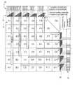
- FIGS. 1 and 2are a series of plan views of the electrically active substrate of an adaptive optic (AO) actuator
- FIGS. 3 and 4are a series of plan views of a portion of the AO actuator shown in FIGS. 1 and 2 ;
- FIG. 4Ais an expanded view of a portion of FIG. 4 ;
- FIG. 4Bis an expanded view of as portion of FIG. 4A .
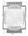
- an adaptive opticcomprises a voltage-addressable, transmission-mode, liquid-crystal (LC) cell, as is generally known in the art, having substrates 10 patterned into an array of independent pixels generally denoted 14 to support two-dimensional (2-D) addressing for use as an AO actuator.
- LCliquid-crystal
- each individual pixel in FIGS. 1-4Bis also provided having a unique alpha-numeric designation (e.g. A 1 -A 4 ; B 1 -B 12 ; C 1 -C 20 , D 1 -D 28 ; E 1 -E 36 , F 1 -F 44 , G 1 -G 40 ).
- the adaptive opticis provided having a plurality of pixels having various shapes (squares and triangles) and arranged in columns and rows. Each of the pixels is coupled to a corresponding one of an output of a control circuit (not shown in FIGS. 1-4B ).
- control circuitsmay be disposed on a substrate of the LC, via “flip-chip” or other chip-on-glass assembly technique, or else the control circuits may he “off-glass”.
- the control circuitsare coupled to pixels 14 via electrical signal paths which coupled control signals to conductors disposed on the substrate.
- each pixel 14is individually addressable via the leads which are very narrow and are not clearly shown on the figures, but which run from each compensating resistor to its corresponding pixel being routed in the narrow gaps between pixels.
- the control circuit(s)are capable of providing one or more control signals to each of the pixels of the AO.
- Each signal path coupled between the flex circuit and pixelsincludes an RC balancing resistor, generally denoted 20 .
- the resistorsare provided having a meander-resistor layout ( FIG. 4B ).
- the path lengths in the meander-resistor layoutare selected so as to result in a substantially uniform speed in controlling pixels across the array. That is, the time it takes for any pixel in the AO pixel array to respond to a control signal is substantially the same regardless of pixel location within the AO.
- any effects(such as decrease of RMS voltage arising from delay and attenuation between the voltage source and the pixel) will be equalized across all pixels, enabling compensation for such voltage decrease in the calibration tables already needed for any liquid-crystal device.
- the AOincludes a specially designed electrode layout which results in uniform time constants to all pixels across the aperture.
- a meander-resistor layoutis used to achieve the desired uniform time constants.
- Each pixelhas a capacitance which is known in advance, given its area and the device thickness as well as the properties of the liquid crystal, and thus resistors may be designed which make the product of R i C i the same, where i runs over for all pixels.
- the meander resistor chosen for this pixelwould be of minimal resistance, preferably zero resistance, i.e., would be absent from the substrate layout.
- Compensating resistors 20may be disposed in the superstrate glue line (i.e. a space into which sealant or “glue” is disposed to form sidewalls and couple a superstrate a substrate) and resistors 20 are coupled via connecting elements 16 which provide a transition to leadouts (and eventually to flex circuits 18 a , 18 b and controllers) outside of the superstate.
- a total of eight meander-resistor layout cell typesare needed for pixels in one quadrant of the AO
- an electrode layout which results in uniform time constants to all pixels across the apertureis used.
- the pixelsare square to better support the intended use of the AO with square beams.
- the concepts, systems and techniques described hereinare not limited to square beams and that any beam shape may be used.
- an AO with a different pixel geometry than squaremay employ compensation resistors designed according to this teaching. For example, a hexagonal close-packed array, as is known in the art, a useful geometry for an AO.
- the feed lines for the pixelsare of variable length, with longer ones for the central pixels, so the compensation resistor technique here taught is applicable for equalizing the response time and hence enabling more convenient drive voltage circuitry having the same calibration table for all pixels.
Landscapes
- Physics & Mathematics (AREA)
- Nonlinear Science (AREA)
- General Physics & Mathematics (AREA)
- Optics & Photonics (AREA)
- Mathematical Physics (AREA)
- Chemical & Material Sciences (AREA)
- Crystallography & Structural Chemistry (AREA)
- Geometry (AREA)
- Liquid Crystal (AREA)
- Semiconductor Integrated Circuits (AREA)
- Liquid Crystal Display Device Control (AREA)
- Optical Modulation, Optical Deflection, Nonlinear Optics, Optical Demodulation, Optical Logic Elements (AREA)
Abstract
Description
This work was supported by the Department of Defense under Contract No. FA8650-05-C-7211. The Government has certain rights in this invention.
This application is a U.S. National Stage of PCT application PCT/US2013/042638 filed in the English language on May 24, 2013, and entitled “ADAPTIVE OPTIC HAVING MEANDER RESISTORS ,” which application is hereby incorporated herein by reference.
The structures and techniques described herein relate to optical transmit-receive systems and more particularly to free-space laser/optical transmit-receive systems.
As is also known in the art, an adaptive optic (AO) actuator provides means to correct a phase front on a pixel by pixel level.
As is also known, conventional AO actuators operate as so-called “reflective-mode” devices and are typically implemented via deformable mirrors or MEMS mirrors. With exception of liquid crystal cells, all known technologies for realizing an AO are inherently limited to reflective-mode operation.
Use of reflective-mode AO devices often results in unnecessarily complicated optical layouts. Furthermore, reflective-mode AO actuators are generally larger and heavier than desired for many applications. Additionally, such reflective-mode AO actuators are not as fast as desired, do not handle phase fonts with phase discontinuities do not have sufficient spatial resolution, and do not handle high levels of optical power.
Also, all mechanically based AOs suffer interactuator modulation, whereby the setting of one pixel affects the setting of adjacent pixels. This prevents such AOs from correcting wavefronts with discontinuous phase, as is common in atmospheres with high levels of turbulence. MEMS-based devices (e.g. such a those manufactured by Boston MicroMachines) offer the smallest known interactuator coupling of about 13%.
Prior-art transmissive AOs based on liquid crystal technologies, which alleviate a number of the difficulties with mechanical AOs, are known but suffer from low bandwidth and also variable response time from pixel to pixel.
It would, therefore, be desirable to provide an AO actuator that is compact, lightweight, high speed or at least having pixel speeds constant across the aperture, and high power in the preferred transmission-mode embodiment, and which works well with discontinuous phase fronts.
In accordance with the concepts, systems, components and techniques described herein, an adaptive optic actuator includes a two-dimensional array of pixels with each of the pixels comprising a meander-resistor with the layout of each meander-resistor selected to provide a uniform time constants to all pixels across the aperture.
With this particular arrangement, an adaptive optic having a specially designed electrode layout resulting in uniform time constants to all pixels across the aperture is provided.
In accordance with the concepts, systems, components and techniques described herein, an adaptive optic actuator includes a two-dimensional array of pixels with each of the pixels being furnished with a resistor having a resistance value selected to equalize an RC rise time to that pixel.
In accordance with the concepts, systems, components and techniques described herein, an adaptive optic actuator includes an array of pixels each of which is provided from a liquid crystal cell comprising: a superstrate having an inner surface; a substrate having an inner surface opposed to the surface of the superstrate; said substrate and superstrate having electrically conductive structures formed thereon and disposed as electrodes which permit different voltages to he applied to each pixel; an electrical signal path, capable of carrying one or more control signals, coupled to each pixel in said array of pixels, wherein each electrode signal path is provided having a path length and resistance such that a substantially uniform time constant is provided to all pixels across said array of pixels.
An adaptive optic actuator comprising a two-dimensional array of pixels each of the pixels having an associated control line signal path electrically coupled thereto with each control line signal path being furnished with a resistor having a resistance value selected to equalize an RC rise time to the associated pixel. With this arrangement, each control line is capable of carrying one or more control signals, and the control line signal path is configured such that a uniform time constant is provided to all pixels across the array of pixels.
In one embodiment, the pixels are provided having a square cross-sectional shape to better support the intended use of an AO with square beams.
As noted above in some embodiments, an electrode layout which results in uniform time constants to all pixels across the aperture is used. In an optical application in which square beams are used, the pixels are square to better support the intended. use of the AO with square beams. It should, of course, be appreciated that the concepts, systems and techniques described herein are not limited to square beams and that any beam shape may be used.
The foregoing features of the circuits and techniques described herein, may be more fully understood from the following description of the drawings in which:
Referring now toFIG. 1-4B in which like elements are provided, having like reference designations throughout the several views, an adaptive optic (AO) comprises a voltage-addressable, transmission-mode, liquid-crystal (LC) cell, as is generally known in the art, havingsubstrates 10 patterned into an array of independent pixels generally denoted14 to support two-dimensional (2-D) addressing for use as an AO actuator. In addition to each pixel being denoted withreference numeral 14, it should be noted that each individual pixel inFIGS. 1-4B is also provided having a unique alpha-numeric designation (e.g. A1-A4; B1 -B12; C1 -C20, D1 -D28; E1 -E36, F1 -F44, G1 -G40).
In the exemplary embodiment ofFIGS. 1-4B , the adaptive optic is provided having a plurality of pixels having various shapes (squares and triangles) and arranged in columns and rows. Each of the pixels is coupled to a corresponding one of an output of a control circuit (not shown inFIGS. 1-4B ). It should be noted that control circuits may be disposed on a substrate of the LC, via “flip-chip” or other chip-on-glass assembly technique, or else the control circuits may he “off-glass”. The control circuits are coupled topixels 14 via electrical signal paths which coupled control signals to conductors disposed on the substrate.Electrical transitions 16 and compensating resistors20 (also referred to as an RC balancing resistors) form a portion of such signal paths to thepixels 14. Such signal paths may also include, for example, a flex cable coupled to a controller or other signal source (not visible inFIG. 1 ). It should be noted that eachpixel 14 is individually addressable via the leads which are very narrow and are not clearly shown on the figures, but which run from each compensating resistor to its corresponding pixel being routed in the narrow gaps between pixels. Thus the control circuit(s) are capable of providing one or more control signals to each of the pixels of the AO.
Each signal path coupled between the flex circuit and pixels includes an RC balancing resistor, generally denoted20. In preferred embodiments the resistors are provided having a meander-resistor layout (FIG. 4B ). The path lengths in the meander-resistor layout are selected so as to result in a substantially uniform speed in controlling pixels across the array. That is, the time it takes for any pixel in the AO pixel array to respond to a control signal is substantially the same regardless of pixel location within the AO. Since these response times are equal, any effects (such as decrease of RMS voltage arising from delay and attenuation between the voltage source and the pixel) will be equalized across all pixels, enabling compensation for such voltage decrease in the calibration tables already needed for any liquid-crystal device.
Referring now toFIGS. 3-4B , as noted above, the AO includes a specially designed electrode layout which results in uniform time constants to all pixels across the aperture. As most clearly visible inFIG. 4B , a meander-resistor layout is used to achieve the desired uniform time constants. Each pixel has a capacitance which is known in advance, given its area and the device thickness as well as the properties of the liquid crystal, and thus resistors may be designed which make the product of RiCithe same, where i runs over for all pixels. Normally one would determine the resistance and capacitance of the pixel with the largest product (the “slowest” pixel), e.g., one of the pixels in the center of the aperture, whose connection to the edge of the aperture is longest and hence most resistive. For this pixel, here denumerated pixel no.1, we have some value of R1C1. The meander resistor chosen for this pixel would be of minimal resistance, preferably zero resistance, i.e., would be absent from the substrate layout. For each of the other pixels, Whose intrinsic Ri0Ci(comprising the pixel capacitance Ciand the resistance Ri0of the connection from the edge of the aperture to the pixel without adding a compensating resistor) is therefore smaller than R1C1, a compensating resistor is included in series with the connection. Thus, all pixels are “slowed down” such that they all have substantially the same RC response time.
The above approach enables one to compensate for the effect of voltage attenuation in the RC networks in a uniform manner for all pixels, enabling use of a single calibration table for all pixels, which is a highly desirable feature for obtaining accurate phase control. Compensatingresistors 20 may be disposed in the superstrate glue line (i.e. a space into which sealant or “glue” is disposed to form sidewalls and couple a superstrate a substrate) andresistors 20 are coupled via connectingelements 16 which provide a transition to leadouts (and eventually to flexcircuits 18a,18band controllers) outside of the superstate. As clearly visible inFIGS. 3 and 4 , a total of eight meander-resistor layout cell types are needed for pixels in one quadrant of the AO
As noted above, an electrode layout which results in uniform time constants to all pixels across the aperture is used. In an optical application in which square beams are used, the pixels are square to better support the intended use of the AO with square beams. It should, of course, be appreciated that the concepts, systems and techniques described herein are not limited to square beams and that any beam shape may be used. Likewise, an AO with a different pixel geometry than square may employ compensation resistors designed according to this teaching. For example, a hexagonal close-packed array, as is known in the art, a useful geometry for an AO. The feed lines for the pixels are of variable length, with longer ones for the central pixels, so the compensation resistor technique here taught is applicable for equalizing the response time and hence enabling more convenient drive voltage circuitry having the same calibration table for all pixels.
Having described one or more preferred embodiments of the circuits, techniques and concepts described herein, it will now become apparent to those of ordinary skill in the art that other embodiments incorporating these circuits, techniques and concepts may be used. Accordingly, it is submitted that that the scope of the patent should not be limited to the described embodiments, but rather, should be limited only by the spirit and scope of the appended claims.
Claims (13)
1. An adaptive optic actuator comprising:
a two-dimensional array of pixels; and
a plurality of electrical signal paths, each of said electrical signal paths coupled to one of the pixels in said two-dimensional array of pixels, wherein each electrical signal path is capable of carrying one or more control signals and is configured such that a substantially uniform time constant is provided to all pixels across said array of pixels wherein at least some of said plurality of electrical sign al paths comprise a compensating resistor to provide the substantially uniform time constant to all pixels across said two-dimensional array of pixels and wherein said compensating resistor is provided as a meander-resistor signal path.
2. The adaptive optic actuator ofclaim 1 wherein at least some of said electrical signal paths corresponds to a meander-resistor signal path with the layout of each meander-resistor signal path selected to provide a uniform time constant to all pixels across the array of pixels.
3. The adaptive optic actuator ofclaim 1 wherein each of said pixels in said a two-dimensional array of pixels is provided from a liquid crystal cell comprising:
a superstrate having an inner surface;
a substrate having an inner surface opposed to the surface of the superstrate, wherein said plurality of electrical signal paths are disposed on one of said substrate and said superstrate.
4. The adaptive optic actuator ofclaim 1 wherein said liquid crystal cell is provided as a voltage-addressable, transmission-mode, liquid-crystal cell.
5. The adaptive optic actuator ofclaim 1 wherein at least some of said pixels are provided having a shape corresponding to at least one of: a square cross-sectional shape; and/or a triangular cross-sectional shape.
6. An adaptive optic actuator comprising:
a two-dimensional array of pixels; and
a plurality of electrical signal paths, each of said electrical signal paths coupled to one of the pixels in said two-dimensional array of pixels, wherein each electrical signal path is capable of carrying one or more control signals and is configured such that a substantially uniform time constant is provided to all pixels across said array of pixels wherein at least some of said plurality of electrical sign al paths comprise a compensating resistor to provide the substantially uniform time constant to all pixels across said two-dimensional array of pixels and wherein said compensating resistor is provided as a meander-resistor signal path and wherein each meander-resistor signal path is provided having a resistance value selected to equalize an RC rise time to the associated pixel.
7. The adaptive optic actuator ofclaim 6 wherein at least some of said electrical signal paths corresponds to a meander-resistor signal path with the layout of each meander-resistor signal path selected to provide a uniform time constant to all pixels across the aperture.
8. The adaptive optic actuator ofclaim 6 wherein each of said pixels in said a two-dimensional array of pixels is provided from a liquid crystal cell comprising:
a superstrate having an inner surface;
a substrate having an inner surface opposed to the surface of the superstrate, wherein said plurality of electrical signal paths are disposed on one of said substrate and said superstrate.
9. The adaptive optic actuator ofclaim 6 wherein said liquid crystal cell is provided as a voltage-addressable, transmission-mode, liquid-crystal cell.
10. The adaptive optic actuator ofclaim 6 wherein at least some of said pixels are provided having a shape corresponding to at least one of: a square cross-sectional shape; and/or a triangular cross-sectional shape.
11. An adaptive optic actuator having a two-dimensional array of pixels each of said pixels each of said pixels having an associated control line electrically coupled thereto with each control line comprising a meander-resistor signal path with the layout of each meander-resistor signal path selected to provide a uniform time constant to all pixels in the two-dimensional array of pixels.
12. The adaptive optic actuator ofclaim 11 wherein:
each of said pixels in said a two-dimensional array of pixels is provided from a liquid crystal cell comprises: a superstrate having an inner surface; a substrate having an inner surface opposed to the surface of the superstrate and wherein said plurality of electrical signal paths are disposed on one of said substrate and said superstrate; and
said liquid crystal cell is provided as a voltage-addressable, transmission-mode, liquid-crystal cell; and
at least some of said pixels are provided having a shape corresponding to at least one of: a square cross-sectional shape; and/or a triangular cross-sectional shape.
13. The adaptive optic actuator ofclaim 11 wherein each meander-resistor signal path comprises a resistor having a resistance value selected to equalize an RC rise time to the associated pixel.
Applications Claiming Priority (1)
| Application Number | Priority Date | Filing Date | Title |
|---|---|---|---|
| PCT/US2013/042638WO2014189522A1 (en) | 2013-05-24 | 2013-05-24 | Adaptive - optics liquid - crystal array device having meander resistors |
Publications (2)
| Publication Number | Publication Date |
|---|---|
| US20160077333A1 US20160077333A1 (en) | 2016-03-17 |
| US9835856B2true US9835856B2 (en) | 2017-12-05 |
Family
ID=48576602
Family Applications (1)
| Application Number | Title | Priority Date | Filing Date |
|---|---|---|---|
| US14/780,580Active2033-10-04US9835856B2 (en) | 2013-05-24 | 2013-05-24 | Adaptive optic having meander resistors |
Country Status (8)
| Country | Link |
|---|---|
| US (1) | US9835856B2 (en) |
| EP (1) | EP3004979B1 (en) |
| JP (1) | JP6359088B2 (en) |
| AU (1) | AU2013389971B2 (en) |
| CA (1) | CA2910592C (en) |
| IL (1) | IL242306B (en) |
| NZ (1) | NZ713761A (en) |
| WO (1) | WO2014189522A1 (en) |
Families Citing this family (1)
| Publication number | Priority date | Publication date | Assignee | Title |
|---|---|---|---|---|
| US9971183B1 (en) | 2017-06-02 | 2018-05-15 | Raytheon Company | High power adaptive optic system and components therein |
Citations (95)
| Publication number | Priority date | Publication date | Assignee | Title |
|---|---|---|---|---|
| US4135789A (en) | 1977-07-01 | 1979-01-23 | Beckman Instruments, Inc. | Seal for liquid crystal display |
| US4141651A (en) | 1977-01-10 | 1979-02-27 | Raytheon Company | Laser gyroscope output optics structure |
| US4229106A (en) | 1978-05-18 | 1980-10-21 | Raytheon Company | Electromagnetic wave ring resonator |
| US4284329A (en) | 1978-01-03 | 1981-08-18 | Raytheon Company | Laser gyroscope system |
| US4418102A (en) | 1981-05-14 | 1983-11-29 | Eaton Corporation | Liquid crystal displays having improved hermetic seal |
| US4482249A (en) | 1976-01-02 | 1984-11-13 | Raytheon Company | Electromagnetic wave ring resonator |
| US4525028A (en) | 1981-04-23 | 1985-06-25 | Raytheon Company | Enhanced magnetic mirror |
| US4545650A (en) | 1982-12-30 | 1985-10-08 | International Business Machines Corporation | Liquid filled electro-optic display cell with diaphragm seal |
| US4548501A (en) | 1978-01-03 | 1985-10-22 | Raytheon Company | Laser gyroscope system |
| US4684219A (en) | 1985-01-02 | 1987-08-04 | International Business Machines Corporation | Display cell with self-sealing, collapsing plug |
| US4687331A (en) | 1982-05-19 | 1987-08-18 | Raytheon Company | Ring laser gyroscope |
| US4695490A (en) | 1985-10-15 | 1987-09-22 | Rca Corporation | Seal for liquid crystal display |
| US4813774A (en) | 1982-08-27 | 1989-03-21 | Raytheon Company | Skewed rhombus ring laser gyro |
| US4813766A (en) | 1988-03-02 | 1989-03-21 | Raytheon Company | Optical time delay apparatus |
| US4818087A (en) | 1982-08-27 | 1989-04-04 | Raytheon Company | Orthohedral ring laser gyro |
| US4882235A (en) | 1988-03-02 | 1989-11-21 | Raytheon Company | Liquid crystal cell window |
| US4943709A (en) | 1989-05-11 | 1990-07-24 | Hughes Aircraft Company | Liquid crystal adaptive optics system |
| US4964251A (en) | 1987-06-25 | 1990-10-23 | Allied-Signal Inc. | Dual-pane thermal window with liquid crystal shade |
| US4964701A (en) | 1988-10-04 | 1990-10-23 | Raytheon Company | Deflector for an optical beam |
| US5004343A (en) | 1986-03-14 | 1991-04-02 | Raytheon Company | Multiple ring paths in one block |
| US5018835A (en) | 1989-01-03 | 1991-05-28 | Raytheon Company | Deflector for an optical beam including refractive means |
| US5084898A (en) | 1990-12-18 | 1992-01-28 | Raytheon Company | Passive pathlength control mirror for laser |
| US5093740A (en) | 1991-02-28 | 1992-03-03 | Raytheon Company | Optical beam steerer having subaperture addressing |
| US5093747A (en) | 1991-02-28 | 1992-03-03 | Raytheon Company | Method for providing beam steering in a subaperture-addressed optical beam steerer |
| US5126869A (en) | 1990-12-03 | 1992-06-30 | Raytheon Company | Two-dimensional, phased-array optical beam steerer |
| US5151814A (en) | 1987-08-19 | 1992-09-29 | Hughes Aircraft Company | Phased array for optical beam control |
| US5216729A (en) | 1991-11-18 | 1993-06-01 | Harmonic Lightwaves, Inc. | Active alignment system for laser to fiber coupling |
| US5233673A (en) | 1991-10-09 | 1993-08-03 | Hughes Aircraft Company | Output steerable optical phased array |
| US5241995A (en) | 1991-09-24 | 1993-09-07 | Litton Systems Canada Limited | Method of filling a suspended particle display |
| US5246042A (en) | 1991-09-24 | 1993-09-21 | Litton Systems Canada Limited | Method of filling a suspended particle display |
| US5253033A (en) | 1990-12-03 | 1993-10-12 | Raytheon Company | Laser radar system with phased-array beam steerer |
| US5276747A (en) | 1993-01-21 | 1994-01-04 | E-Tek Dynamics, Inc. | Polarization-independent optical switch/attenuator |
| US5309263A (en) | 1989-11-24 | 1994-05-03 | Semiconductor Energy Laboratory Co., Ltd. | Liquid crystal electro-optical device and manufacturing method for the same |
| US5333046A (en) | 1982-08-27 | 1994-07-26 | Raytheon Company | Diagonal pathlength control |
| US5363228A (en) | 1993-03-05 | 1994-11-08 | General Electric Company | Optical device with spatial light modulators for switching arbitrarily polarized light |
| US5404365A (en) | 1993-07-30 | 1995-04-04 | Fuji Photo Film Co., Ltd. | Polarized light coherent combining laser apparatus |
| US5412475A (en) | 1982-08-27 | 1995-05-02 | Raytheon Company | Diagonal pathlength control |
| JPH1048660A (en) | 1996-08-06 | 1998-02-20 | Toshiba Corp | Liquid crystal display |
| US5740288A (en) | 1995-02-22 | 1998-04-14 | E-Tek Dynamics, Inc. | Variable polarization beam splitter, combiner and mixer |
| US5963682A (en) | 1994-05-24 | 1999-10-05 | Raytheon Company | Optical beam steering system |
| US6013339A (en) | 1995-03-01 | 2000-01-11 | Matsushita Electric Industrial Co., Ltd. | Liquid crystal display panel, seal material for liquid crystal cell and liquid crystal display |
| US6099970A (en) | 1997-02-10 | 2000-08-08 | Trw Inc. | High electron mobility transparent conductor |
| US6246369B1 (en) | 1999-09-14 | 2001-06-12 | Navsys Corporation | Miniature phased array antenna system |
| US6282224B1 (en) | 1999-01-13 | 2001-08-28 | Raytheon Company | Non-planar Q-switched ring laser system |
| US20010033400A1 (en) | 1996-07-12 | 2001-10-25 | Sutherland Richard L. | Switchable polymer-dispersed liquid crystal optical elements |
| JP2002227130A (en) | 2001-02-05 | 2002-08-14 | Dps Bridge Works Co Ltd | Connecting structure for concrete member |
| US6473148B1 (en) | 2000-11-28 | 2002-10-29 | Yafo Networks, Inc. | Seal pattern for liquid crystal device |
| US6490076B2 (en) | 2001-01-11 | 2002-12-03 | Hrl Laboratories, Llc | Optical phased array for depolarized optical beam control |
| US20020186919A1 (en) | 2001-06-08 | 2002-12-12 | Hrl Laboratories, Llc | Electro-optical programmable true-time delay generator |
| US6545563B1 (en) | 1990-07-16 | 2003-04-08 | Raytheon Company | Digitally controlled monolithic microwave integrated circuits |
| US6597836B2 (en) | 2001-06-20 | 2003-07-22 | The Boeing Company | Optical phased array control system |
| JP2003322864A (en) | 2002-04-30 | 2003-11-14 | Toshiba Corp | Liquid crystal display |
| US6673497B2 (en) | 2000-01-04 | 2004-01-06 | University Of Central Florida | High efficiency volume diffractive elements in photo-thermo-refractive glass |
| US6704474B1 (en) | 1994-05-24 | 2004-03-09 | Raytheon Company | Optical beam steering system |
| US6710736B2 (en) | 1999-06-14 | 2004-03-23 | Time Domain Corporation | System and method for intrusion detection using a time domain radar array |
| US20040135956A1 (en) | 2002-08-07 | 2004-07-15 | Samsung Electronics Co., Ltd. | Integrated circuit and display device including integrated circuit |
| JP2005010737A (en) | 2003-06-18 | 2005-01-13 | Hannstar Display Corp | Liquid crystal panel having compensation capacitor which suppresses variation of rc delay |
| US20050018954A1 (en) | 2000-06-16 | 2005-01-27 | Bruno Vinouze | Liquid crystal optical switch with bumt-in control |
| US20050031264A1 (en) | 2002-03-15 | 2005-02-10 | Pd-Ld, Inc. | Fiber optic devices having volume Bragg grating elements |
| US6861270B2 (en) | 2000-06-01 | 2005-03-01 | Shiro Sakai | Method for manufacturing gallium nitride compound semiconductor and light emitting element |
| US20050069245A1 (en) | 2003-09-30 | 2005-03-31 | Mitchell Thomas A. | Compact optical switches |
| US6884647B2 (en) | 2000-09-22 | 2005-04-26 | Shiro Sakai | Method for roughening semiconductor surface |
| US6908026B2 (en) | 2001-11-06 | 2005-06-21 | Raytheon Company | Method and apparatus for making a lid with an optically transmissive window |
| US6974517B2 (en) | 2001-06-13 | 2005-12-13 | Raytheon Company | Lid with window hermetically sealed to frame, and a method of making it |
| US6988338B1 (en) | 2002-10-10 | 2006-01-24 | Raytheon Company | Lid with a thermally protected window |
| US20060033995A1 (en) | 2004-08-12 | 2006-02-16 | Smith Irl W | Wide-angle beam steering system |
| US7006747B2 (en) | 2003-01-17 | 2006-02-28 | 3M Innovative Properties Company | Optical devices incorporating photo reactive polymers |
| US7005685B2 (en) | 2002-02-28 | 2006-02-28 | Shiro Sakai | Gallium-nitride-based compound semiconductor device |
| US7015511B2 (en) | 2001-06-29 | 2006-03-21 | Nitride Semiconductors Co., Ltd. | Gallium nitride-based light emitting device and method for manufacturing the same |
| US7046326B2 (en) | 2003-02-21 | 2006-05-16 | Xtellus, Inc. | Multi-pixel liquid crystal cell array |
| US7095925B2 (en) | 2004-11-03 | 2006-08-22 | Intel Corporation | Optical phased array transmitter/receiver |
| US20060210219A1 (en) | 2005-03-16 | 2006-09-21 | Hitachi Cable, Ltd. | Optical transmitter |
| US20070014517A1 (en) | 2005-05-25 | 2007-01-18 | Biolase Technology, Inc. | Electromagnetic energy emitting device with increased spot size |
| US7166182B2 (en) | 2002-09-04 | 2007-01-23 | Sipix Imaging, Inc. | Adhesive and sealing layers for electrophoretic displays |
| US20070030294A1 (en) | 2005-08-05 | 2007-02-08 | Texas Instruments Incorporated | System and method for implementation of transition zone associated with an actuator for an optical device in a display system |
| US7196758B2 (en) | 2003-12-30 | 2007-03-27 | 3M Innovative Properties Company | Method of alignment of liquid crystals comprising exposing an alignment material to an interference pattern |
| US7226850B2 (en) | 2005-05-19 | 2007-06-05 | Raytheon Company | Gallium nitride high electron mobility transistor structure |
| US20070285370A1 (en) | 2006-06-08 | 2007-12-13 | Dong-Gyu Kim | Thin film transistor substrate and liquid crystal display panel having the same |
| US7355671B2 (en) | 2003-02-21 | 2008-04-08 | Xtellus Inc. | Fabrication method for liquid crystal cell |
| US7365369B2 (en) | 1997-06-11 | 2008-04-29 | Nichia Corporation | Nitride semiconductor device |
| US20080129945A1 (en) | 2006-12-04 | 2008-06-05 | Lg Philips Lcd Co., Ltd. | Liquid crystal display device |
| US20090029071A1 (en) | 2005-12-15 | 2009-01-29 | Sei Hybrid Products, Inc | Transparent Spinel Substrate, Transparent Substrate for Optical Engine, Rear Projection Television Receiver Using Them and Image Projector Using Liquid Crystal |
| US20090044496A1 (en) | 2007-08-16 | 2009-02-19 | Botelho John W | Method and apparatus for sealing a glass package |
| US20090058788A1 (en)* | 2007-08-29 | 2009-03-05 | Sung Chul Ha | Apparatus and method of driving data of liquid crystal display device |
| US20090142073A1 (en) | 2007-11-30 | 2009-06-04 | Smith Irl W | Method and apparatus for maintaining a coherent combined beam during arbitrary steering |
| US7557378B2 (en) | 2006-11-08 | 2009-07-07 | Raytheon Company | Boron aluminum nitride diamond heterostructure |
| US7570310B2 (en) | 2005-10-18 | 2009-08-04 | Fuji Xerox Co., Ltd. | Method for driving optical address type spatial light modulation device and apparatus for driving optical address type spatial light modulation device |
| US7692759B2 (en) | 2005-03-01 | 2010-04-06 | Stichting Dutch Polymer Institute | Polarization gratings in mesogenic films |
| US7848370B2 (en) | 2007-01-26 | 2010-12-07 | Telaris Inc. | Electronically phase-locked laser systems |
| US20100320474A1 (en) | 2009-06-22 | 2010-12-23 | Raytheon Company | Gallium nitride for liquid crystal electrodes |
| US7889767B2 (en) | 2004-10-13 | 2011-02-15 | Raytheon Company | Self-coherent combining technique for high power laser implementation and method |
| US7990660B2 (en) | 2007-02-09 | 2011-08-02 | Headway Technologies, Inc. | Multiple CCP layers in magnetic read head devices |
| US20120081621A1 (en) | 2010-10-01 | 2012-04-05 | Raytheon Company | High Fill-Factor Electronic Beam Steerer |
| US20140268328A1 (en) | 2013-03-13 | 2014-09-18 | Raytheon Company | Polarization Grating Stack |
| US20150146139A1 (en) | 2012-05-24 | 2015-05-28 | Raytheon Company | Liquid Crystal Control Structure, Tip-Tilt-Focus Optical Phased Array And High Power Adaptive Optic |
Family Cites Families (6)
| Publication number | Priority date | Publication date | Assignee | Title |
|---|---|---|---|---|
| US7088323B2 (en)* | 2000-12-21 | 2006-08-08 | Lg.Philips Lcd Co., Ltd. | Liquid crystal display device and method for fabricating the same |
| JP2002221730A (en)* | 2001-01-24 | 2002-08-09 | Sony Corp | Liquid crystal display device |
| KR20060058987A (en)* | 2004-11-26 | 2006-06-01 | 삼성전자주식회사 | Gate line driving circuit, display device having same, driving device and method thereof |
| JP5727120B2 (en)* | 2006-08-25 | 2015-06-03 | 三星ディスプレイ株式會社Samsung Display Co.,Ltd. | Liquid crystal display |
| KR101917753B1 (en)* | 2011-06-24 | 2018-11-13 | 가부시키가이샤 한도오따이 에네루기 켄큐쇼 | Display device |
| US20140267965A1 (en)* | 2011-11-18 | 2014-09-18 | Sharp Kabushiki Kaisha | Optical deflector |
- 2013
- 2013-05-24CACA2910592Apatent/CA2910592C/enactiveActive
- 2013-05-24WOPCT/US2013/042638patent/WO2014189522A1/enactiveApplication Filing
- 2013-05-24NZNZ713761Apatent/NZ713761A/enunknown
- 2013-05-24EPEP13727011.2Apatent/EP3004979B1/enactiveActive
- 2013-05-24USUS14/780,580patent/US9835856B2/enactiveActive
- 2013-05-24JPJP2016513914Apatent/JP6359088B2/enactiveActive
- 2013-05-24AUAU2013389971Apatent/AU2013389971B2/enactiveActive
- 2015
- 2015-10-27ILIL242306Apatent/IL242306B/enactiveIP Right Grant
Patent Citations (104)
| Publication number | Priority date | Publication date | Assignee | Title |
|---|---|---|---|---|
| US4482249A (en) | 1976-01-02 | 1984-11-13 | Raytheon Company | Electromagnetic wave ring resonator |
| US4141651A (en) | 1977-01-10 | 1979-02-27 | Raytheon Company | Laser gyroscope output optics structure |
| US4135789A (en) | 1977-07-01 | 1979-01-23 | Beckman Instruments, Inc. | Seal for liquid crystal display |
| US4548501A (en) | 1978-01-03 | 1985-10-22 | Raytheon Company | Laser gyroscope system |
| US4284329A (en) | 1978-01-03 | 1981-08-18 | Raytheon Company | Laser gyroscope system |
| US4229106A (en) | 1978-05-18 | 1980-10-21 | Raytheon Company | Electromagnetic wave ring resonator |
| US4525028A (en) | 1981-04-23 | 1985-06-25 | Raytheon Company | Enhanced magnetic mirror |
| US4418102A (en) | 1981-05-14 | 1983-11-29 | Eaton Corporation | Liquid crystal displays having improved hermetic seal |
| US4687331A (en) | 1982-05-19 | 1987-08-18 | Raytheon Company | Ring laser gyroscope |
| US4813774A (en) | 1982-08-27 | 1989-03-21 | Raytheon Company | Skewed rhombus ring laser gyro |
| US4818087A (en) | 1982-08-27 | 1989-04-04 | Raytheon Company | Orthohedral ring laser gyro |
| US5333046A (en) | 1982-08-27 | 1994-07-26 | Raytheon Company | Diagonal pathlength control |
| US5412475A (en) | 1982-08-27 | 1995-05-02 | Raytheon Company | Diagonal pathlength control |
| US4545650A (en) | 1982-12-30 | 1985-10-08 | International Business Machines Corporation | Liquid filled electro-optic display cell with diaphragm seal |
| US4684219A (en) | 1985-01-02 | 1987-08-04 | International Business Machines Corporation | Display cell with self-sealing, collapsing plug |
| US4695490A (en) | 1985-10-15 | 1987-09-22 | Rca Corporation | Seal for liquid crystal display |
| US5004343A (en) | 1986-03-14 | 1991-04-02 | Raytheon Company | Multiple ring paths in one block |
| US4964251A (en) | 1987-06-25 | 1990-10-23 | Allied-Signal Inc. | Dual-pane thermal window with liquid crystal shade |
| US5151814A (en) | 1987-08-19 | 1992-09-29 | Hughes Aircraft Company | Phased array for optical beam control |
| US4882235A (en) | 1988-03-02 | 1989-11-21 | Raytheon Company | Liquid crystal cell window |
| US4813766A (en) | 1988-03-02 | 1989-03-21 | Raytheon Company | Optical time delay apparatus |
| US4964701A (en) | 1988-10-04 | 1990-10-23 | Raytheon Company | Deflector for an optical beam |
| US5018835A (en) | 1989-01-03 | 1991-05-28 | Raytheon Company | Deflector for an optical beam including refractive means |
| US4943709A (en) | 1989-05-11 | 1990-07-24 | Hughes Aircraft Company | Liquid crystal adaptive optics system |
| US5559619A (en) | 1989-11-24 | 1996-09-24 | Semiconductor Energy Laboratory Co., Ltd. | Liquid crystal electro-optical device and manufacturing method for the same |
| US5309263A (en) | 1989-11-24 | 1994-05-03 | Semiconductor Energy Laboratory Co., Ltd. | Liquid crystal electro-optical device and manufacturing method for the same |
| US6545563B1 (en) | 1990-07-16 | 2003-04-08 | Raytheon Company | Digitally controlled monolithic microwave integrated circuits |
| US5126869A (en) | 1990-12-03 | 1992-06-30 | Raytheon Company | Two-dimensional, phased-array optical beam steerer |
| US5253033A (en) | 1990-12-03 | 1993-10-12 | Raytheon Company | Laser radar system with phased-array beam steerer |
| US5084898A (en) | 1990-12-18 | 1992-01-28 | Raytheon Company | Passive pathlength control mirror for laser |
| US5093747A (en) | 1991-02-28 | 1992-03-03 | Raytheon Company | Method for providing beam steering in a subaperture-addressed optical beam steerer |
| US5093740A (en) | 1991-02-28 | 1992-03-03 | Raytheon Company | Optical beam steerer having subaperture addressing |
| US5246042A (en) | 1991-09-24 | 1993-09-21 | Litton Systems Canada Limited | Method of filling a suspended particle display |
| US5241995A (en) | 1991-09-24 | 1993-09-07 | Litton Systems Canada Limited | Method of filling a suspended particle display |
| US5233673A (en) | 1991-10-09 | 1993-08-03 | Hughes Aircraft Company | Output steerable optical phased array |
| US5216729A (en) | 1991-11-18 | 1993-06-01 | Harmonic Lightwaves, Inc. | Active alignment system for laser to fiber coupling |
| US5276747A (en) | 1993-01-21 | 1994-01-04 | E-Tek Dynamics, Inc. | Polarization-independent optical switch/attenuator |
| US5363228A (en) | 1993-03-05 | 1994-11-08 | General Electric Company | Optical device with spatial light modulators for switching arbitrarily polarized light |
| US5404365A (en) | 1993-07-30 | 1995-04-04 | Fuji Photo Film Co., Ltd. | Polarized light coherent combining laser apparatus |
| US6704474B1 (en) | 1994-05-24 | 2004-03-09 | Raytheon Company | Optical beam steering system |
| US6810164B2 (en) | 1994-05-24 | 2004-10-26 | Raytheon Company | Optical beam steering system |
| US5963682A (en) | 1994-05-24 | 1999-10-05 | Raytheon Company | Optical beam steering system |
| US5740288A (en) | 1995-02-22 | 1998-04-14 | E-Tek Dynamics, Inc. | Variable polarization beam splitter, combiner and mixer |
| US6013339A (en) | 1995-03-01 | 2000-01-11 | Matsushita Electric Industrial Co., Ltd. | Liquid crystal display panel, seal material for liquid crystal cell and liquid crystal display |
| US20010033400A1 (en) | 1996-07-12 | 2001-10-25 | Sutherland Richard L. | Switchable polymer-dispersed liquid crystal optical elements |
| JPH1048660A (en) | 1996-08-06 | 1998-02-20 | Toshiba Corp | Liquid crystal display |
| US6103604A (en) | 1997-02-10 | 2000-08-15 | Trw Inc. | High electron mobility transparent conductor |
| US6099970A (en) | 1997-02-10 | 2000-08-08 | Trw Inc. | High electron mobility transparent conductor |
| US7365369B2 (en) | 1997-06-11 | 2008-04-29 | Nichia Corporation | Nitride semiconductor device |
| US6282224B1 (en) | 1999-01-13 | 2001-08-28 | Raytheon Company | Non-planar Q-switched ring laser system |
| US6710736B2 (en) | 1999-06-14 | 2004-03-23 | Time Domain Corporation | System and method for intrusion detection using a time domain radar array |
| US6246369B1 (en) | 1999-09-14 | 2001-06-12 | Navsys Corporation | Miniature phased array antenna system |
| US6673497B2 (en) | 2000-01-04 | 2004-01-06 | University Of Central Florida | High efficiency volume diffractive elements in photo-thermo-refractive glass |
| US6861270B2 (en) | 2000-06-01 | 2005-03-01 | Shiro Sakai | Method for manufacturing gallium nitride compound semiconductor and light emitting element |
| US20050018954A1 (en) | 2000-06-16 | 2005-01-27 | Bruno Vinouze | Liquid crystal optical switch with bumt-in control |
| US6884647B2 (en) | 2000-09-22 | 2005-04-26 | Shiro Sakai | Method for roughening semiconductor surface |
| US6473148B1 (en) | 2000-11-28 | 2002-10-29 | Yafo Networks, Inc. | Seal pattern for liquid crystal device |
| US6490076B2 (en) | 2001-01-11 | 2002-12-03 | Hrl Laboratories, Llc | Optical phased array for depolarized optical beam control |
| JP2002227130A (en) | 2001-02-05 | 2002-08-14 | Dps Bridge Works Co Ltd | Connecting structure for concrete member |
| US20020186919A1 (en) | 2001-06-08 | 2002-12-12 | Hrl Laboratories, Llc | Electro-optical programmable true-time delay generator |
| US6974517B2 (en) | 2001-06-13 | 2005-12-13 | Raytheon Company | Lid with window hermetically sealed to frame, and a method of making it |
| US6597836B2 (en) | 2001-06-20 | 2003-07-22 | The Boeing Company | Optical phased array control system |
| US7015511B2 (en) | 2001-06-29 | 2006-03-21 | Nitride Semiconductors Co., Ltd. | Gallium nitride-based light emitting device and method for manufacturing the same |
| US6908026B2 (en) | 2001-11-06 | 2005-06-21 | Raytheon Company | Method and apparatus for making a lid with an optically transmissive window |
| US7005685B2 (en) | 2002-02-28 | 2006-02-28 | Shiro Sakai | Gallium-nitride-based compound semiconductor device |
| US20050031264A1 (en) | 2002-03-15 | 2005-02-10 | Pd-Ld, Inc. | Fiber optic devices having volume Bragg grating elements |
| JP2003322864A (en) | 2002-04-30 | 2003-11-14 | Toshiba Corp | Liquid crystal display |
| US20040135956A1 (en) | 2002-08-07 | 2004-07-15 | Samsung Electronics Co., Ltd. | Integrated circuit and display device including integrated circuit |
| US7166182B2 (en) | 2002-09-04 | 2007-01-23 | Sipix Imaging, Inc. | Adhesive and sealing layers for electrophoretic displays |
| US6988338B1 (en) | 2002-10-10 | 2006-01-24 | Raytheon Company | Lid with a thermally protected window |
| US7006747B2 (en) | 2003-01-17 | 2006-02-28 | 3M Innovative Properties Company | Optical devices incorporating photo reactive polymers |
| US7046326B2 (en) | 2003-02-21 | 2006-05-16 | Xtellus, Inc. | Multi-pixel liquid crystal cell array |
| US7355671B2 (en) | 2003-02-21 | 2008-04-08 | Xtellus Inc. | Fabrication method for liquid crystal cell |
| US7352428B2 (en) | 2003-02-21 | 2008-04-01 | Xtellus Inc. | Liquid crystal cell platform |
| JP2005010737A (en) | 2003-06-18 | 2005-01-13 | Hannstar Display Corp | Liquid crystal panel having compensation capacitor which suppresses variation of rc delay |
| US20050069245A1 (en) | 2003-09-30 | 2005-03-31 | Mitchell Thomas A. | Compact optical switches |
| US7196758B2 (en) | 2003-12-30 | 2007-03-27 | 3M Innovative Properties Company | Method of alignment of liquid crystals comprising exposing an alignment material to an interference pattern |
| US7215472B2 (en) | 2004-08-12 | 2007-05-08 | Raytheon Company | Wide-angle beam steering system |
| US20060033995A1 (en) | 2004-08-12 | 2006-02-16 | Smith Irl W | Wide-angle beam steering system |
| US7428100B2 (en) | 2004-08-12 | 2008-09-23 | Raytheon Company | Wide-angle beam steering system |
| US7889767B2 (en) | 2004-10-13 | 2011-02-15 | Raytheon Company | Self-coherent combining technique for high power laser implementation and method |
| US7095925B2 (en) | 2004-11-03 | 2006-08-22 | Intel Corporation | Optical phased array transmitter/receiver |
| US7692759B2 (en) | 2005-03-01 | 2010-04-06 | Stichting Dutch Polymer Institute | Polarization gratings in mesogenic films |
| US20060210219A1 (en) | 2005-03-16 | 2006-09-21 | Hitachi Cable, Ltd. | Optical transmitter |
| US7226850B2 (en) | 2005-05-19 | 2007-06-05 | Raytheon Company | Gallium nitride high electron mobility transistor structure |
| US20070014517A1 (en) | 2005-05-25 | 2007-01-18 | Biolase Technology, Inc. | Electromagnetic energy emitting device with increased spot size |
| US20070030294A1 (en) | 2005-08-05 | 2007-02-08 | Texas Instruments Incorporated | System and method for implementation of transition zone associated with an actuator for an optical device in a display system |
| JP2009503621A (en) | 2005-08-05 | 2009-01-29 | テキサス インスツルメンツ インコーポレイテッド | Transition band implementation method in optical device of display system |
| US7570310B2 (en) | 2005-10-18 | 2009-08-04 | Fuji Xerox Co., Ltd. | Method for driving optical address type spatial light modulation device and apparatus for driving optical address type spatial light modulation device |
| US20090029071A1 (en) | 2005-12-15 | 2009-01-29 | Sei Hybrid Products, Inc | Transparent Spinel Substrate, Transparent Substrate for Optical Engine, Rear Projection Television Receiver Using Them and Image Projector Using Liquid Crystal |
| JP2007328346A (en) | 2006-06-08 | 2007-12-20 | Samsung Electronics Co Ltd | Thin film transistor substrate and liquid crystal display panel including the same |
| US20070285370A1 (en) | 2006-06-08 | 2007-12-13 | Dong-Gyu Kim | Thin film transistor substrate and liquid crystal display panel having the same |
| US7557378B2 (en) | 2006-11-08 | 2009-07-07 | Raytheon Company | Boron aluminum nitride diamond heterostructure |
| US20080129945A1 (en) | 2006-12-04 | 2008-06-05 | Lg Philips Lcd Co., Ltd. | Liquid crystal display device |
| US7848370B2 (en) | 2007-01-26 | 2010-12-07 | Telaris Inc. | Electronically phase-locked laser systems |
| US7990660B2 (en) | 2007-02-09 | 2011-08-02 | Headway Technologies, Inc. | Multiple CCP layers in magnetic read head devices |
| US20090044496A1 (en) | 2007-08-16 | 2009-02-19 | Botelho John W | Method and apparatus for sealing a glass package |
| US20090058788A1 (en)* | 2007-08-29 | 2009-03-05 | Sung Chul Ha | Apparatus and method of driving data of liquid crystal display device |
| US20090142073A1 (en) | 2007-11-30 | 2009-06-04 | Smith Irl W | Method and apparatus for maintaining a coherent combined beam during arbitrary steering |
| US20100320474A1 (en) | 2009-06-22 | 2010-12-23 | Raytheon Company | Gallium nitride for liquid crystal electrodes |
| US8268707B2 (en) | 2009-06-22 | 2012-09-18 | Raytheon Company | Gallium nitride for liquid crystal electrodes |
| US20120081621A1 (en) | 2010-10-01 | 2012-04-05 | Raytheon Company | High Fill-Factor Electronic Beam Steerer |
| US20150146139A1 (en) | 2012-05-24 | 2015-05-28 | Raytheon Company | Liquid Crystal Control Structure, Tip-Tilt-Focus Optical Phased Array And High Power Adaptive Optic |
| US20140268328A1 (en) | 2013-03-13 | 2014-09-18 | Raytheon Company | Polarization Grating Stack |
Non-Patent Citations (74)
| Title |
|---|
| "Liquid crystal blazed-grating beam deflector," by Wang et al. Applied Optics, vol. 39, No. 35, pp. 6545-6555, 2000. |
| Australian Second Patent Examination Report dated Nov. 10, 2016 for Australian Appl. No. 2013389971, 3 pages. |
| Canadan Office Action dated Oct. 26, 2016 for Canadian Application No. 2,910,592; 4 pages. |
| Dorschner; "Adaptive Photonic Phase Locked Elements;" An Overview; DARPA/MTO Symposium; Mar. 2007; pp. 1-15. |
| English Translation of Japanese Office Action for Japanese Appl. No. 2016-513914 dated Nov. 29, 2016; 2 pages. |
| Examiner Report dated Aug. 12, 2016 for Canadian Application No. 2,874,616; 3 pages. |
| Examiner's Report dated Nov. 27, 2015 for Appl. No. 2,874,616; 4 pages. |
| Fan et al.; "Fast-Response and scattering-free polymer network liquid crystals for infrared light modulators;" Applied Physics Letters; American Institute of Physics; vol. 84; No. 8; Feb. 23, 2004; pp. 1233-1235. |
| First Examination Report dated Jun. 3, 2016 for New Zealand Application No. 713761; 5 pages. |
| First Examination Report dated Jun. 8, 2016 for Australian Application No. 2013389971; 3 pages. |
| Further Examination Report dated Feb. 28, 2017 for New Zealand Appl. No. 713761; 1 page. |
| Further Examination Report dated Oct. 20, 2015 for New Zealand Appl. No. 702327; 2 pages. |
| Further Examination Report Postponed Acceptance dated Feb. 5, 2016 for New Zealand Appl. No. 702327; 1 page. |
| Gelissen et al.; "Polarization Control Using Nematic Liquid Crystals;" Advances in Optical Information Processing; Proceedings of SPIE vol. 4046; Apr. 25, 2000; pp. 118-129. |
| International Preliminary Report on Patentability of the ISA for PCT/US2011/054245 dated Apr. 11, 2013. |
| Japanese Office Action (with English translation) dated Jun. 27, 2017 for JP Appl. No. 2016-513914; 8 pages. |
| Kanghua Lu, et al.; "Theory and design of the liquid crystal TV as an optical spatial phase modulator;" 2417 Optical Engineering; vol. 29; No. 3; Mar. 1, 1990; pp. 240-246. |
| Karim, et al.; "Electrooptic Displays for Optical Information Processing;" Proceedings of the IEEE; vol. 84; No. 6; Jun. 1, 1996; pp. 814-827. |
| Kim, et al.; "Wide-angle, nonmechanical beam steering using thin liquid crystal polarization gratings;" Proc. of SPIE, vol. 7093; Jan. 2008, pp. 1-12. |
| McManamon, et al., "Optical Phased Array Technology;" Proceedings of the IEEE; vol. 84; No. 2; Feb. 1996; pp. 268-298. |
| McManamon, et al.; "A Review of Phased Array Steering for Narrow-Band Electrooptical System;" Proceeding of the IEEE; vol. 97; No. 6; Jun. 2009; pp. 1078-1096. |
| Miller; Self-aligning univeral beam coupler; Optics Express; vol. 21; No. 5; Mar. 11, 2013; pp. 6360-6370. |
| New Zealand Further Examination Report dated Nov. 29, 2016 for New Zealand Appl. No. 713761; 4 pages. |
| Nicolescu, et al.; "Polarization-independent tunable optical filters based on liquid crystal polarization gratings;" Proceedings of SPIE; vol. 6654; No. 665405; Aug. 2007; 12 pages. |
| NonFinal Office Action dated Jun. 8, 2016 for U.S. Appl. No. 14/404,787; 32 pages. |
| Notice of Allowance dated Feb. 8, 2017 for Canadian Appl. No. 2,874,616; 1 page. |
| Notice of Allowance dated Jan. 3, 2017 for U.S. Appl. No. 14/404,787; 11 pages. |
| Notice of Allowance dated Jul. 10, 2017 for Canadian Application No. 2,910,592; 1 page. |
| Office Action dated Feb. 21, 2013 from U.S. Appl. No. 13/250,111. |
| Office Action dated Oct. 13, 2016 from U.S. Appl. No. 14/404,787; 20 pages. |
| Office Action dated Sep. 6, 2013 from U.S. Appl. No. 13/250,111. |
| Office Action for Application No. 2013266159 dated May 26, 2015; 3 pages. |
| Office Action for Application No. 702327 dated Mar. 24, 2015. |
| Partial PCT Search Report received with Invitation to Pay Additional Fees in PCT/US2011/054245 dated Jan. 18, 2012. |
| PCT International Preliminary Report of Patentability of PCT/US2013/042641 dated Dec. 4, 2014 11 pages. |
| PCT International Preliminary Report on Patentability for PCT/US2013/042646 dated May 24, 2013 6 pages. |
| PCT International Preliminary Report on Patentability for PCT/US2013/042653 dated May 24, 2013 10 pages. |
| PCT International Preliminary Report on Patentability of the ISA dated Dec. 3, 2015 for Appl. No. PCT/US2013/042638; 8 pages. |
| PCT Invitation to Pay Additional Fees for PCT/US2013/042641 dated Sep. 20, 2013 10 pages. |
| PCT Search Report of the ISA for PCT/US2011/054245 dated Mar. 26, 2012. |
| PCT Search Report of the ISA for PCT/US2013/042641 dated Jan. 30, 2014 9 pages. |
| PCT Search Report of the ISA for PCT/US2013/042646 dated Sep. 3, 2013 5 pages. |
| PCT Search Report of the ISA for PCT/US2013/042653 dated Nov. 7, 2013 6 pages. |
| Ren et al.; "Tunable Microlens arrays using polymers network liquid crystal;" Optics Communications; Science Direct; Sep. 22, 2003; pp. 267-271. |
| Response to Aug. 12, 2016 Examiner's Report for Canadian Application No. 2,874,616 as filed on Sep. 28, 2016; 8 pages. |
| Response to Australian Office Action dated Nov. 2, 2015 for Appl. No. 2013266159; 45 pages. |
| Response to Canadian Office Action dated Oct. 26, 2016 for Canadian Application No. 2,910,592;as filed on Jan. 24. 2017; 7 pages. |
| Response to Examiner's Report dated Nov. 27, 2015 for Canadian Application No. 2,874,616 as filed on Jan. 28, 2016; 13 pages. |
| Response to First Examination Report dated Jun. 3, 2016 for New Zealand Application No. 713761; as filed on Oct. 27, 2016; 2 pages. |
| Response to First Examination Report dated Jun. 8, 2016 for Australian Application No. 2013389971 as filed on Oct. 27, 2016; 21 pages. |
| Response to Japanese Office Action with English Translation dated Nov. 29, 2016 for Japanese Appl. No. 2016-513914 as filed on Feb. 22, 2017; 7 pages. |
| Response to Jun. 8, 2016 Office Action for U.S. Appl. No. 14/404,787, filed Sep. 8, 2016. |
| Response to New Zealand Office Action dated Sep. 22, 2015 for Appl. No. 702327; 64 pages. |
| Response to Oct. 20, 2015 Further Examination Report as filed on Jan. 19, 2016 for New Zealand Appl. No. 702327; 61 pages. |
| Response to Office Action dated Feb. 21, 2013 as filed on May 16, 2013 from U.S. Appl. No. 13/250,111. |
| Response to Office Action dated Oct. 13, 2016 for U.S. Appl. No. 14/404,787, filed Dec. 13, 2016; 13 pages. |
| Response to Rule 161 Communication for Application No. 11770009.6 as filed on Dec. 23, 2013. |
| Response to Rule 161 EPC Communication filed on Jul. 13, 2016 for EP Application No. EP13727011.2. |
| Response to Rules 161(1) and 162 EPC Communication dated Jan. 12, 2015 for EP Appl. No. 13732664.1. |
| Response to Second Examination Report dated Nov. 10, 2016 for Australian Appl. No. 2013389971 as filed on Jan. 30, 2017; 2 pages. |
| Response to Second Examination Report dated Nov. 29, 2016 for New Zealand Appl. No. 7137961 as filed on Jan. 30, 2017, 25 pages. |
| Rockwell, et al.; "Semi-guiding high-aspect-ratio-core (SHARC) fiber providing single-mode operation and an ultra-large core area in a compact coliable package;" Optics Express; vol. 19; No. 15; Jul. 18, 2011; pp. 14746-14762. |
| Rule 161 Communication for Application No. 11770009.6 dated Jun. 12, 2013. |
| Search Report of the ISA for PCT/US2013/042638 dated Sep. 17, 2013. |
| U.S. Appl. No. 13/250,111, filed Sep. 30, 2011. |
| U.S. Appl. No. 13/801,411, filed Mar. 13, 2013. |
| U.S. Appl. No. 14/404,787, filed Dec. 1, 2014; 225 pages. |
| Voluntary Amendment as filed Feb. 15, 2016 for New Zealand Appl. No. 713761; 19 pages. |
| Voluntary Amendment for Australian Patent Application No. 2013389971 dated Dec. 24, 2015; 8 pages. |
| Written Opinion of the ISA for PCT/US2011/054245 dated Mar. 26, 2012. |
| Written Opinion of the ISA for PCT/US2013/042638 dated Sep. 17, 2013. |
| Written Opinion of the ISA for PCT/US2013/042641 dated Jan. 30, 2014 9 pages. |
| Written Opinion of the ISA for PCT/US2013/042646 dated Sep. 3, 2013 4 pages. |
| Written Opinion of the ISA for PCT/US2013/042653 dated Nov. 7, 2013 9 pages. |
Also Published As
| Publication number | Publication date |
|---|---|
| EP3004979B1 (en) | 2019-01-16 |
| AU2013389971B2 (en) | 2017-03-09 |
| US20160077333A1 (en) | 2016-03-17 |
| CA2910592A1 (en) | 2014-11-27 |
| IL242306B (en) | 2020-11-30 |
| JP6359088B2 (en) | 2018-07-18 |
| WO2014189522A1 (en) | 2014-11-27 |
| JP2016521010A (en) | 2016-07-14 |
| AU2013389971A1 (en) | 2015-11-12 |
| CA2910592C (en) | 2017-11-21 |
| EP3004979A1 (en) | 2016-04-13 |
| NZ713761A (en) | 2017-05-26 |
Similar Documents
| Publication | Publication Date | Title |
|---|---|---|
| US4982184A (en) | Electrocrystallochromic display and element | |
| US10243276B2 (en) | Phased array antenna system including a modular control and monitoring architecture | |
| CN110398850B (en) | Multi-channel liquid crystal programmable phase modulation system based on MCU | |
| US10895670B2 (en) | Camera module including liquid lens and optical device comprising same | |
| US20180188615A1 (en) | Display device | |
| EP2856250B1 (en) | Liquid crystal control structure, tip-tilt-focus optical phased array and high power adaptive optic | |
| US20180268772A1 (en) | Pixel cell, display substrate, display device, and method of driving pixel electrode | |
| US10663282B1 (en) | Fiber-coupled phased array of photonic integrated circuit imagers | |
| KR102656851B1 (en) | Display device and driving method thereof | |
| US9835856B2 (en) | Adaptive optic having meander resistors | |
| EP3690522A1 (en) | Liquid crystal grating and driving method thereof, and display device | |
| EP3699684B1 (en) | Light deflector and light output device including the same | |
| US11506824B2 (en) | Circuit for controlling liquid lens | |
| US20130088682A1 (en) | Controllable optical device and the forming method thereof | |
| JP2018136567A (en) | Adaptive optical liquid crystal array device with serpentine resistors | |
| US20070069999A1 (en) | Spatial light modulator employing voltage gradient pixels, and associated methods | |
| KR102516688B1 (en) | Display device | |
| US11580928B2 (en) | Circuit of controlling common voltage of liquid crystal panel | |
| SE520359C2 (en) | Electrical circuit to compensate for unwanted voltage drop in a conductor | |
| KR101882734B1 (en) | Electrophoretic display device | |
| CN111146588B (en) | Phased Array Antenna | |
| US10573221B2 (en) | Display apparatus | |
| EP3340228B1 (en) | Display device | |
| JP2016521010A5 (en) | ||
| US7656573B2 (en) | Method and apparatus for controlling a gap between conductors in an electro-mechanical device |
Legal Events
| Date | Code | Title | Description |
|---|---|---|---|
| AS | Assignment | Owner name:RAYTHEON COMPANY, MASSACHUSETTS Free format text:ASSIGNMENT OF ASSIGNORS INTEREST;ASSIGNORS:DORSCHNER, TERRY A.;SMITH, IRL W.;PALMACCIO, LINDA A.;AND OTHERS;SIGNING DATES FROM 20150909 TO 20150923;REEL/FRAME:036711/0369 | |
| AS | Assignment | Owner name:RAYTHEON COMPANY, MASSACHUSETTS Free format text:ASSIGNMENT OF ASSIGNORS INTEREST;ASSIGNOR:COLLINS, STEVEN R.;REEL/FRAME:037129/0823 Effective date:20151123 | |
| STCF | Information on status: patent grant | Free format text:PATENTED CASE | |
| MAFP | Maintenance fee payment | Free format text:PAYMENT OF MAINTENANCE FEE, 4TH YEAR, LARGE ENTITY (ORIGINAL EVENT CODE: M1551); ENTITY STATUS OF PATENT OWNER: LARGE ENTITY Year of fee payment:4 | |
| MAFP | Maintenance fee payment | Free format text:PAYMENT OF MAINTENANCE FEE, 8TH YEAR, LARGE ENTITY (ORIGINAL EVENT CODE: M1552); ENTITY STATUS OF PATENT OWNER: LARGE ENTITY Year of fee payment:8 |