US9831690B2 - Method and device for balancing electrical voltages in electrical accumulator units - Google Patents
Method and device for balancing electrical voltages in electrical accumulator unitsDownload PDFInfo
- Publication number
- US9831690B2 US9831690B2US13/261,285US200913261285AUS9831690B2US 9831690 B2US9831690 B2US 9831690B2US 200913261285 AUS200913261285 AUS 200913261285AUS 9831690 B2US9831690 B2US 9831690B2
- Authority
- US
- United States
- Prior art keywords
- accumulator
- terminal
- pole
- switch
- charging coil
- Prior art date
- Legal status (The legal status is an assumption and is not a legal conclusion. Google has not performed a legal analysis and makes no representation as to the accuracy of the status listed.)
- Active, expires
Links
Images


Classifications
- H—ELECTRICITY
- H02—GENERATION; CONVERSION OR DISTRIBUTION OF ELECTRIC POWER
- H02J—CIRCUIT ARRANGEMENTS OR SYSTEMS FOR SUPPLYING OR DISTRIBUTING ELECTRIC POWER; SYSTEMS FOR STORING ELECTRIC ENERGY
- H02J7/00—Circuit arrangements for charging or depolarising batteries or for supplying loads from batteries
- H02J7/0013—Circuit arrangements for charging or depolarising batteries or for supplying loads from batteries acting upon several batteries simultaneously or sequentially
- H02J7/0014—Circuits for equalisation of charge between batteries
- H02J7/0016—Circuits for equalisation of charge between batteries using shunting, discharge or bypass circuits
- H—ELECTRICITY
- H02—GENERATION; CONVERSION OR DISTRIBUTION OF ELECTRIC POWER
- H02J—CIRCUIT ARRANGEMENTS OR SYSTEMS FOR SUPPLYING OR DISTRIBUTING ELECTRIC POWER; SYSTEMS FOR STORING ELECTRIC ENERGY
- H02J7/00—Circuit arrangements for charging or depolarising batteries or for supplying loads from batteries
- H02J7/0013—Circuit arrangements for charging or depolarising batteries or for supplying loads from batteries acting upon several batteries simultaneously or sequentially
- H02J7/0014—Circuits for equalisation of charge between batteries
- B60L11/1866—
- B—PERFORMING OPERATIONS; TRANSPORTING
- B60—VEHICLES IN GENERAL
- B60L—PROPULSION OF ELECTRICALLY-PROPELLED VEHICLES; SUPPLYING ELECTRIC POWER FOR AUXILIARY EQUIPMENT OF ELECTRICALLY-PROPELLED VEHICLES; ELECTRODYNAMIC BRAKE SYSTEMS FOR VEHICLES IN GENERAL; MAGNETIC SUSPENSION OR LEVITATION FOR VEHICLES; MONITORING OPERATING VARIABLES OF ELECTRICALLY-PROPELLED VEHICLES; ELECTRIC SAFETY DEVICES FOR ELECTRICALLY-PROPELLED VEHICLES
- B60L58/00—Methods or circuit arrangements for monitoring or controlling batteries or fuel cells, specially adapted for electric vehicles
- B60L58/10—Methods or circuit arrangements for monitoring or controlling batteries or fuel cells, specially adapted for electric vehicles for monitoring or controlling batteries
- B60L58/18—Methods or circuit arrangements for monitoring or controlling batteries or fuel cells, specially adapted for electric vehicles for monitoring or controlling batteries of two or more battery modules
- B60L58/22—Balancing the charge of battery modules
- G01R31/3658—
- G—PHYSICS
- G01—MEASURING; TESTING
- G01R—MEASURING ELECTRIC VARIABLES; MEASURING MAGNETIC VARIABLES
- G01R31/00—Arrangements for testing electric properties; Arrangements for locating electric faults; Arrangements for electrical testing characterised by what is being tested not provided for elsewhere
- G01R31/36—Arrangements for testing, measuring or monitoring the electrical condition of accumulators or electric batteries, e.g. capacity or state of charge [SoC]
- G01R31/396—Acquisition or processing of data for testing or for monitoring individual cells or groups of cells within a battery
- H—ELECTRICITY
- H02—GENERATION; CONVERSION OR DISTRIBUTION OF ELECTRIC POWER
- H02J—CIRCUIT ARRANGEMENTS OR SYSTEMS FOR SUPPLYING OR DISTRIBUTING ELECTRIC POWER; SYSTEMS FOR STORING ELECTRIC ENERGY
- H02J7/00—Circuit arrangements for charging or depolarising batteries or for supplying loads from batteries
- H02J7/0013—Circuit arrangements for charging or depolarising batteries or for supplying loads from batteries acting upon several batteries simultaneously or sequentially
- H02J7/0014—Circuits for equalisation of charge between batteries
- H02J7/0018—Circuits for equalisation of charge between batteries using separate charge circuits
- Y—GENERAL TAGGING OF NEW TECHNOLOGICAL DEVELOPMENTS; GENERAL TAGGING OF CROSS-SECTIONAL TECHNOLOGIES SPANNING OVER SEVERAL SECTIONS OF THE IPC; TECHNICAL SUBJECTS COVERED BY FORMER USPC CROSS-REFERENCE ART COLLECTIONS [XRACs] AND DIGESTS
- Y02—TECHNOLOGIES OR APPLICATIONS FOR MITIGATION OR ADAPTATION AGAINST CLIMATE CHANGE
- Y02T—CLIMATE CHANGE MITIGATION TECHNOLOGIES RELATED TO TRANSPORTATION
- Y02T10/00—Road transport of goods or passengers
- Y02T10/60—Other road transportation technologies with climate change mitigation effect
- Y02T10/70—Energy storage systems for electromobility, e.g. batteries
- Y02T10/7055—
Definitions
- the inventionrelates to a method for balancing the electrical voltages of at least two serially connected electrical accumulator units.
- the inventionalso relates to a corresponding electrical accumulator.
- the one accumulator unitis connected to the winding of a coil for the excitation of that coil, and that next, by means of the excited coil, the other accumulator unit is charged by the connection of the winding to that other accumulator unit. It is provided that the same winding that is used for exciting the coil is also used for charging the other accumulator unit. In this way, it becomes possible for the energy stored in the accumulator units not to be merely converted into heat, but to be transferred from the one accumulator unit to the other, so that the electrical voltages of the various accumulator units are balanced with each other.
- Charging the other accumulator unitshould be understood to mean that the coil is excited, and by means of the electrical energy that is thus available, the other accumulator unit is further charged. Charging should accordingly be understood to mean not full charging of the entire electrical accumulator, but rather transporting an electrical charge between the accumulator units and the coil for the sake of balancing the electrical voltages.
- the one accumulator unitwhich is connected to the winding of the coil for its excitation, has a higher electrical voltage than the accumulator unit that is charged next, by the connection of the winding.
- accumulator unitsone accumulator cell each, in particular a battery cell, is used.
- the coilis charged by closure of a switch.
- Using the switchmakes it possible to charge at least one coil in a targeted manner. In this way, the method can be employed in targeted manner to individual accumulator units, without always having to include all the accumulator units in the method.
- the two accumulator unitsare located adjacent one another. Being located adjacent one another should be understood to mean that the accumulator units are connected directly in series with one another, and a positive pole of one of the accumulator units is connected directly to a negative pole of the other accumulator unit via a line.
- each adjacent accumulator unitis assigned a coil.
- each adjacent accumulator unitis assigned its own coil, with a winding.
- the coilcharges the other accumulator unit by opening the switch.
- the switchBy appropriate interconnection, it becomes possible to end the charging of the coil by opening the switch, and by reinduction, or in other words de-excitation, the coil makes the energy stored in it available. In that case, the coil outputs the stored electrical energy, and that energy is taken up by the other accumulator unit, which is being charged.
- the combination here of closing the switch to charge the coil and opening the switch to charge the accumulator unitis advantageous, since by means of only two positions of the switch, both the charging of the coil and the charging of the accumulator unit can be brought about in succession in a simple way.
- the other accumulator unitis charged by the coil via at least one diode. This is especially advantageous whenever a flow of current, which flows into the coil upon charging, is reversed and flows out of the coil again, for charging the accumulator unit in the reverse manner.
- the coilcan be connected to two accumulator units simultaneously, and the charging of the other accumulator unit depends on whether the coil is being charged or discharged.
- the inventionrelates further to an electrical accumulator having at least two serially connected electrical accumulator units and one electrical balancing circuit, in particular for performing the method described above, in which the balancing circuit has at least one coil having a winding and its winding is connectable to one of the accumulator units for exciting the coil, and in which, for charging the other accumulator unit, the winding can be connected to that accumulator unit.
- the balancing circuithas at least one diode and/or at least one switch.
- the switchis embodied as a semiconductor switch, in particular a transistor, thyristor, or the like.
- semiconductor elementsBy the use of semiconductor elements, very easy automation is made possible, by means of electrical components, such as circuits.
- the device of the inventioncan be embodied in a space-saving way and can be produced economically.
- each of the accumulator unitshas an accumulator cell, in particular a battery cell.
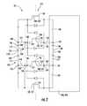
- FIG. 1shows an electric switch with a balancing circuit
- FIG. 2shows the accumulator with the balancing circuit of FIG. 1 in a first method step
- FIG. 3shows the accumulator with the balancing circuit of FIG. 1 in a second method step.
- FIG. 1shows a detail of an electrical accumulator 101 , comprising three accumulator units 102 in the form of accumulator cells 103 that are connected in series adjacent to one another.
- the electrical accumulator 101is embodied as a battery 104
- the accumulator cells 103are embodied as battery cells 105 .
- the accumulator units 102form the electrical accumulator 101 by means of the fact that a first accumulator unit 106 is connected via its negative pole 106 ′′ and a line 107 to a node point 108 , which leads via a line 109 to a positive pole 110 ′ of a second accumulator unit 110 .
- the second accumulator unit 110is connected in turn via its negative pole 110 ′′ and a line 111 to a node point 112 , which leads via a line 113 to a positive pole 114 ′ of a third accumulator unit 114 .
- a balancing circuit 115is assigned to the accumulator 101 .
- the balancing circuit 115is connected via a line 116 to a positive pole 106 ′ of the first accumulator unit 105 . It is also connected to the node point 108 via a line 117 , to the node point 112 via a line 118 , and to a negative pole 114 ′′ of the third accumulator unit 114 via a line 119 .
- the balancing circuit 115has a plurality of electric coils 121 , each with a winding 120 .
- the balancing circuit 115furthermore has diodes 122 and switches 123 .
- the line 116is connected via a node point 124 to a further line 125 , which leads to a first winding 126 .
- the first winding 126is connected via a line 127 to a node point 128 , which has a further line 129 which leads to a first switch 130 . Beginning at the first switch 130 , a line 131 leads to a node point 132 .
- a line 133leads to a further node point 134 , which in turn is connected via a line 135 to a second winding 136 .
- the second winding 136is connected via a line 137 to a node point 138 , which is connected via a line 139 to a further node point 140 .
- the node point 140is also connected to the line 117 .
- a first diode 142is connected to the node point 140 .
- the diode 142is also connected to the node point 128 via a line 143 .
- the diode 142is disposed between the lines 141 and 143 in such a way that it has a conducting direction from the line 141 to the line 143 .
- the node point 134is connected via a line 144 to a second diode 145 , which in turn is connected via a line 146 to the node point 124 .
- the second diode 145has a conducting direction from the line 144 to the line 146 .
- a further line 149leads to a second switch 150 .
- a line 151leads to a node point 152 .
- a line 153leads to a further node point 154 , which in turn is connected via a line 155 to a third winding 156 .
- the winding 156is connected via a line 157 to a node point 158 , which is connected via a line 159 to a further node point 160 .
- the node point 160is also connected to the line 118 .
- a third diode 162is connected to the node point 160 .
- the diode 162is also connected to the node point 134 via a line 163 .
- the diode 162is disposed between the lines 161 and 163 in such a way that it has a conducting direction from the line 161 to the line 163 .
- the node point 154is connected via a line 164 to a fourth diode 165 , which in turn is connected via a line 166 to the node point 138 .
- the fourth diode 165has a conducting direction from the line 164 to the line 166 .
- a further line 169leads to a third switch 170 .
- a line 171leads to a node point 174 .
- the node point 174is in turn connected via a line 175 to a fourth winding 176 .
- the winding 176is connected via a line 177 to a node point 180 .
- the node point 180is also connected to the line 119 .
- a fifth diode 182is connected to the node point 180 .
- the diode 182is also connected to the node point 154 via a line 183 .
- the diode 182is disposed between the lines 181 and 183 in such a way that it has a conducting direction from the line 181 to the line 183 .
- the node point 174is connected via a line 184 to a sixth diode 185 , which in turn is connected to the node point 158 via a line 186 .
- the sixth diode 185has a conducting direction from the line 184 to the line 186 .
- the switches 123are assigned to an electronic control unit 190 .
- theyare embodied as semiconductor switches 191 in the form of transistors 192 , so that the control unit 190 forms an integrated circuit 193 .
- Dashed lines 179indicate that both the electrical accumulator 101 and the balancing circuit 115 are continued logically onward in the direction of the lines 179 .
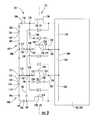
- FIG. 2shows the electrical accumulator 101 and the balancing circuit 115 of FIG. 1 with all their features. Unlike in FIG. 1 , in FIG. 2 the second switch 150 is closed, for performing a first method step.
- the accumulator unit 110furthermore has a higher voltage than the other accumulator units 106 and 114 .
- the electric circuit 195 in FIG. 2is shown in heavy lines and is provided with current direction arrows 196 .
- the electric circuit 195extends from the positive pole 110 ′ of the second accumulator unit 110 via the line 109 and onward via the line 117 to the node point 140 , so that by means of the lines 137 and 139 , the coil 121 of the second winding 136 is charged.
- the electric circuit 195also extends via the lines 135 , 133 and 149 to the closed second switch 150 . It continues via the lines 151 , 153 and 154 to the third winding 156 . Beginning at the third winding 156 , the electric circuit 195 is closed via the lines 157 , 159 , 118 and 111 to the negative pole 110 ′′ of the second accumulator unit 110 .
- this closed electric circuit 195By means of this closed electric circuit 195 , a charge is transferred into the second and third windings 136 and 156 and stored there.
- the closure of the second switch 150is effected by the control unit 190 . It is provided that each accumulator unit 102 charges two windings 120 .
- the electric circuit 195is closed, and it is opened again either after a certain period of time or after a certain level of the current that flows through the switch is reached.
- FIG. 3shows the accumulator 101 and the balancing circuit 115 of FIG. 1 with all their features.
- the switches 123are all opened for a second method step, and the coils assigned to the second winding 136 and the third winding 156 are excited.
- the resultis two electric circuits 197 and 198 ; the electric circuit 197 is assigned to the first accumulator unit 106 , and the second electric circuit 198 is assigned to the third accumulator unit 114 .
- the electric circuit 197extends from the second winding 136 to the second diode 145 , via the lines 135 and 144 .
- the electric circuit 197extends onward via the lines 146 and 116 into the positive pole 106 ′ of the first accumulator unit 106 . From the negative pole 106 ′′ of the accumulator unit 106 , the electric circuit 197 extends via the lines 107 , 117 , 139 and 138 back to the second winding 136 .
- the electric circuit 198begins at the third winding 156 , which is connected via the lines 157 , 159 , 118 and 113 to the positive pole 114 ′ of the third accumulator unit 114 .
- the fifth diode 182is connected via the lines 119 and 181 , so that beginning at the diode 182 , the electric circuit 198 is closed via the lines 183 and 155 .
- the various current directionsare represented by current direction arrows 196 . The current directions run in the directions that correspond to the conducting directions of the second diode 145 and the fifth diode 182 .
- the coils of the windings 136 and 156can be de-excited; that is, they give up their charges, which flow into the corresponding accumulator units 106 and 114 and as a result further charge those accumulator units. For that purpose it is unnecessary to employ further control means for the second method step, since this process ensues automatically because of the balancing circuit shown.
- the method steps shown in FIGS. 2 and 3describe the possibility of charging the first accumulator unit 106 and the second accumulator unit 114 with an electrical charge from the second accumulator unit 110 .
- This processis highly energy-efficient, since electrical charges are transferred among the accumulator units.
Landscapes
- Engineering & Computer Science (AREA)
- Power Engineering (AREA)
- Charge And Discharge Circuits For Batteries Or The Like (AREA)
- Secondary Cells (AREA)
- Battery Mounting, Suspending (AREA)
Abstract
Description
Claims (4)
Applications Claiming Priority (1)
| Application Number | Priority Date | Filing Date | Title |
|---|---|---|---|
| PCT/EP2009/065469WO2011060818A1 (en) | 2009-11-19 | 2009-11-19 | Method and device for balancing electrical voltages in electrical accumulator units |
Publications (2)
| Publication Number | Publication Date |
|---|---|
| US20120223669A1 US20120223669A1 (en) | 2012-09-06 |
| US9831690B2true US9831690B2 (en) | 2017-11-28 |
Family
ID=42537767
Family Applications (1)
| Application Number | Title | Priority Date | Filing Date |
|---|---|---|---|
| US13/261,285Active2031-02-26US9831690B2 (en) | 2009-11-19 | 2009-11-19 | Method and device for balancing electrical voltages in electrical accumulator units |
Country Status (4)
| Country | Link |
|---|---|
| US (1) | US9831690B2 (en) |
| EP (1) | EP2502323A1 (en) |
| JP (1) | JP5650235B2 (en) |
| WO (1) | WO2011060818A1 (en) |
Cited By (1)
| Publication number | Priority date | Publication date | Assignee | Title |
|---|---|---|---|---|
| US11342776B2 (en)* | 2020-06-15 | 2022-05-24 | Magnetic Energy Charging, Inc. | Battery charger and method for charging a battery |
Families Citing this family (2)
| Publication number | Priority date | Publication date | Assignee | Title |
|---|---|---|---|---|
| CN108995549B (en)* | 2018-07-03 | 2020-06-16 | 上海电机学院 | Electric quantity balancing circuit, device and method for single batteries of electric vehicle |
| KR102821612B1 (en)* | 2019-11-18 | 2025-06-16 | 주식회사 엘지에너지솔루션 | Cell balancing apparatus, battery apparatus including the same, and cell balancing method |
Citations (17)
| Publication number | Priority date | Publication date | Assignee | Title |
|---|---|---|---|---|
| JPH07322516A (en)* | 1994-05-25 | 1995-12-08 | Okamura Kenkyusho:Kk | Battery charge control device and method |
| US5631534A (en)* | 1995-08-21 | 1997-05-20 | Delco Electronics Corp. | Bidirectional current pump for battery charge balancing |
| JPH10257683A (en) | 1997-03-07 | 1998-09-25 | Japan Storage Battery Co Ltd | Charging-discharging circuit for combined batteries |
| US5821729A (en)* | 1994-06-29 | 1998-10-13 | Fraunhofer-Gesellschaft Zur Forderung Der Angewandten Forschung E.V. | Method and device for charge exchange between a plurality of energy stores or converters connected in series |
| CA2231260A1 (en) | 1998-03-06 | 1999-09-06 | William G. Dunford | Battery equalizer |
| US6150795A (en)* | 1999-11-05 | 2000-11-21 | Power Designers, Llc | Modular battery charge equalizers and method of control |
| US6222344B1 (en)* | 1999-12-06 | 2001-04-24 | Bae Systems Controls, Inc. | Magnetically coupled autonomous battery equalization circuit |
| US20040135544A1 (en)* | 2002-11-25 | 2004-07-15 | Tiax, Llc | System and method for determining and balancing state of charge among series connected electrical energy storage units |
| US20040222771A1 (en) | 2003-05-09 | 2004-11-11 | Mitsubishi Denki Kabushiki Kaisha | Battery power circuit and automobile battery power circuit |
| US20050029987A1 (en) | 2003-08-08 | 2005-02-10 | Pao-Chuan Lin | Battery energy balance circuit and battery charging bypass circuit |
| FR2860353A1 (en) | 2003-09-29 | 2005-04-01 | Thales Sa | MODULE FOR TRANSFERRING LOADS BETWEEN TWO DIPOLES |
| US20050077879A1 (en)* | 2003-10-14 | 2005-04-14 | Near Timothy Paul | Energy transfer device for series connected energy source and storage devices |
| US20050140335A1 (en)* | 2003-12-31 | 2005-06-30 | Chun-Hsien Lee | Equalizer for series of connected battery strings |
| US20060119319A1 (en)* | 2004-12-08 | 2006-06-08 | Fuji Jukogyo Kabushiki Kaisha | Voltage equalization control system of accumulator |
| JP2006296179A (en) | 2005-03-16 | 2006-10-26 | Macnica Inc | Electricity accumulating device of capacitor and its charging and discharging method |
| WO2007148745A1 (en)* | 2006-06-22 | 2007-12-27 | Fdk Corporation | Multi-series accumulation cell, series accumulation cell device, and series cell voltage balance correction circuit |
| US8008890B2 (en)* | 2007-02-09 | 2011-08-30 | Sk Energy Co., Ltd. | Charge equalization apparatus |
- 2009
- 2009-11-19EPEP09799048Apatent/EP2502323A1/ennot_activeCeased
- 2009-11-19JPJP2012539190Apatent/JP5650235B2/ennot_activeExpired - Fee Related
- 2009-11-19USUS13/261,285patent/US9831690B2/enactiveActive
- 2009-11-19WOPCT/EP2009/065469patent/WO2011060818A1/enactiveApplication Filing
Patent Citations (20)
| Publication number | Priority date | Publication date | Assignee | Title |
|---|---|---|---|---|
| JPH07322516A (en)* | 1994-05-25 | 1995-12-08 | Okamura Kenkyusho:Kk | Battery charge control device and method |
| US5821729A (en)* | 1994-06-29 | 1998-10-13 | Fraunhofer-Gesellschaft Zur Forderung Der Angewandten Forschung E.V. | Method and device for charge exchange between a plurality of energy stores or converters connected in series |
| US5631534A (en)* | 1995-08-21 | 1997-05-20 | Delco Electronics Corp. | Bidirectional current pump for battery charge balancing |
| JPH10257683A (en) | 1997-03-07 | 1998-09-25 | Japan Storage Battery Co Ltd | Charging-discharging circuit for combined batteries |
| CA2231260A1 (en) | 1998-03-06 | 1999-09-06 | William G. Dunford | Battery equalizer |
| US6150795A (en)* | 1999-11-05 | 2000-11-21 | Power Designers, Llc | Modular battery charge equalizers and method of control |
| JP2003513605A (en) | 1999-11-05 | 2003-04-08 | パワー デザイナーズ リミテッド ライアビリティ カンパニー | Modular battery charge equalizer and control method |
| US6222344B1 (en)* | 1999-12-06 | 2001-04-24 | Bae Systems Controls, Inc. | Magnetically coupled autonomous battery equalization circuit |
| US20040135544A1 (en)* | 2002-11-25 | 2004-07-15 | Tiax, Llc | System and method for determining and balancing state of charge among series connected electrical energy storage units |
| US20060055367A1 (en) | 2003-05-09 | 2006-03-16 | Mitsubishi Denki Kabushiki Kaisha | Battery power circuit and automobile battery power circuit |
| US20040222771A1 (en) | 2003-05-09 | 2004-11-11 | Mitsubishi Denki Kabushiki Kaisha | Battery power circuit and automobile battery power circuit |
| US20050029987A1 (en) | 2003-08-08 | 2005-02-10 | Pao-Chuan Lin | Battery energy balance circuit and battery charging bypass circuit |
| FR2860353A1 (en) | 2003-09-29 | 2005-04-01 | Thales Sa | MODULE FOR TRANSFERRING LOADS BETWEEN TWO DIPOLES |
| US20050077879A1 (en)* | 2003-10-14 | 2005-04-14 | Near Timothy Paul | Energy transfer device for series connected energy source and storage devices |
| US20050140335A1 (en)* | 2003-12-31 | 2005-06-30 | Chun-Hsien Lee | Equalizer for series of connected battery strings |
| US20060119319A1 (en)* | 2004-12-08 | 2006-06-08 | Fuji Jukogyo Kabushiki Kaisha | Voltage equalization control system of accumulator |
| JP2006296179A (en) | 2005-03-16 | 2006-10-26 | Macnica Inc | Electricity accumulating device of capacitor and its charging and discharging method |
| WO2007148745A1 (en)* | 2006-06-22 | 2007-12-27 | Fdk Corporation | Multi-series accumulation cell, series accumulation cell device, and series cell voltage balance correction circuit |
| US8692515B2 (en)* | 2006-06-22 | 2014-04-08 | Fdk Corporation | Series-connected rechargeable cells, series-connected rechargeable cell device, voltage-balance correcting circuit for series-connected cells |
| US8008890B2 (en)* | 2007-02-09 | 2011-08-30 | Sk Energy Co., Ltd. | Charge equalization apparatus |
Cited By (2)
| Publication number | Priority date | Publication date | Assignee | Title |
|---|---|---|---|---|
| US11342776B2 (en)* | 2020-06-15 | 2022-05-24 | Magnetic Energy Charging, Inc. | Battery charger and method for charging a battery |
| US11710978B2 (en) | 2020-06-15 | 2023-07-25 | Magnetic Energy Charging, Inc. | Battery charger and method for charging a battery |
Also Published As
| Publication number | Publication date |
|---|---|
| US20120223669A1 (en) | 2012-09-06 |
| EP2502323A1 (en) | 2012-09-26 |
| JP5650235B2 (en) | 2015-01-07 |
| JP2013511943A (en) | 2013-04-04 |
| WO2011060818A1 (en) | 2011-05-26 |
Similar Documents
| Publication | Publication Date | Title |
|---|---|---|
| US9478995B2 (en) | Battery system | |
| US8471529B2 (en) | Battery fault tolerant architecture for cell failure modes parallel bypass circuit | |
| CN101944756B (en) | Power source apparatus for vehicle | |
| US8710801B2 (en) | Battery comprising circuitry for charge and discharge control, and method of operating a battery | |
| US9024586B2 (en) | Battery fault tolerant architecture for cell failure modes series bypass circuit | |
| CN106165240B (en) | Topology for mixing storage system and control strategy | |
| KR101863717B1 (en) | Charge equalization system for batteries | |
| US9331515B2 (en) | System for charging an energy store, and method for operating the charging system | |
| US20130314045A1 (en) | Charging an energy store | |
| US9083188B2 (en) | Balance correcting apparatus and electricity storage system | |
| HK1252922A1 (en) | Hybrid power pack | |
| KR20130073915A (en) | Balancing system for power battery and corresponding load balancing method | |
| EP2830189A1 (en) | Balance correction device and power storage system | |
| US20220077790A1 (en) | Multi-output power supply device | |
| CN103250321B (en) | Method for being charged for battery | |
| CN101888102B (en) | Vehicle power system | |
| US9831690B2 (en) | Method and device for balancing electrical voltages in electrical accumulator units | |
| US20130009601A1 (en) | Balancing electrical voltages of electrical accumulator units | |
| CN110316007A (en) | Vehicle power source device | |
| US9143004B2 (en) | Method and circuit arrangement for charging an intermediate circuit capacitor | |
| CN119856361A (en) | Power conversion device and program | |
| JP2008253083A (en) | Power supply device for mobile vehicle | |
| US20120235627A1 (en) | Balancing electrical voltages of groups of electrical accumulator units | |
| JP2019022334A (en) | Abnormality determination device of rotary electric machine | |
| JP2016034220A (en) | Cell voltage correction circuit |
Legal Events
| Date | Code | Title | Description |
|---|---|---|---|
| AS | Assignment | Owner name:ROBERT BOSCH GMBH, GERMANY Free format text:ASSIGNMENT OF ASSIGNORS INTEREST;ASSIGNOR:BUTZMANN, STEFAN;REEL/FRAME:028351/0768 Effective date:20120503 | |
| STCF | Information on status: patent grant | Free format text:PATENTED CASE | |
| FEPP | Fee payment procedure | Free format text:MAINTENANCE FEE REMINDER MAILED (ORIGINAL EVENT CODE: REM.); ENTITY STATUS OF PATENT OWNER: LARGE ENTITY | |
| FEPP | Fee payment procedure | Free format text:SURCHARGE FOR LATE PAYMENT, LARGE ENTITY (ORIGINAL EVENT CODE: M1554); ENTITY STATUS OF PATENT OWNER: LARGE ENTITY | |
| MAFP | Maintenance fee payment | Free format text:PAYMENT OF MAINTENANCE FEE, 4TH YEAR, LARGE ENTITY (ORIGINAL EVENT CODE: M1551); ENTITY STATUS OF PATENT OWNER: LARGE ENTITY Year of fee payment:4 | |
| AS | Assignment | Owner name:INNOVATION ASSET COLLECTIVE, CANADA Free format text:ASSIGNMENT OF ASSIGNORS INTEREST;ASSIGNOR:ROBERT BOSCH GMBH;REEL/FRAME:062496/0861 Effective date:20221117 | |
| MAFP | Maintenance fee payment | Free format text:PAYMENT OF MAINTENANCE FEE, 8TH YEAR, LARGE ENTITY (ORIGINAL EVENT CODE: M1552); ENTITY STATUS OF PATENT OWNER: LARGE ENTITY Year of fee payment:8 |