US9831612B1 - High speed electrical connector with improved EMI suppression and mechanical retention shield - Google Patents
High speed electrical connector with improved EMI suppression and mechanical retention shieldDownload PDFInfo
- Publication number
- US9831612B1 US9831612B1US12/852,417US85241710AUS9831612B1US 9831612 B1US9831612 B1US 9831612B1US 85241710 AUS85241710 AUS 85241710AUS 9831612 B1US9831612 B1US 9831612B1
- Authority
- US
- United States
- Prior art keywords
- connector
- usb
- usb connector
- shielding
- apertures
- Prior art date
- Legal status (The legal status is an assumption and is not a legal conclusion. Google has not performed a legal analysis and makes no representation as to the accuracy of the status listed.)
- Active, expires
Links
Images


Classifications
- H—ELECTRICITY
- H01—ELECTRIC ELEMENTS
- H01R—ELECTRICALLY-CONDUCTIVE CONNECTIONS; STRUCTURAL ASSOCIATIONS OF A PLURALITY OF MUTUALLY-INSULATED ELECTRICAL CONNECTING ELEMENTS; COUPLING DEVICES; CURRENT COLLECTORS
- H01R13/00—Details of coupling devices of the kinds covered by groups H01R12/70 or H01R24/00 - H01R33/00
- H01R13/648—Protective earth or shield arrangements on coupling devices, e.g. anti-static shielding
- H01R13/658—High frequency shielding arrangements, e.g. against EMI [Electro-Magnetic Interference] or EMP [Electro-Magnetic Pulse]
- H—ELECTRICITY
- H01—ELECTRIC ELEMENTS
- H01R—ELECTRICALLY-CONDUCTIVE CONNECTIONS; STRUCTURAL ASSOCIATIONS OF A PLURALITY OF MUTUALLY-INSULATED ELECTRICAL CONNECTING ELEMENTS; COUPLING DEVICES; CURRENT COLLECTORS
- H01R12/00—Structural associations of a plurality of mutually-insulated electrical connecting elements, specially adapted for printed circuits, e.g. printed circuit boards [PCB], flat or ribbon cables, or like generally planar structures, e.g. terminal strips, terminal blocks; Coupling devices specially adapted for printed circuits, flat or ribbon cables, or like generally planar structures; Terminals specially adapted for contact with, or insertion into, printed circuits, flat or ribbon cables, or like generally planar structures
- H01R12/70—Coupling devices
- H01R12/71—Coupling devices for rigid printing circuits or like structures
- H01R12/72—Coupling devices for rigid printing circuits or like structures coupling with the edge of the rigid printed circuits or like structures
- H01R12/722—Coupling devices for rigid printing circuits or like structures coupling with the edge of the rigid printed circuits or like structures coupling devices mounted on the edge of the printed circuits
- H01R12/724—Coupling devices for rigid printing circuits or like structures coupling with the edge of the rigid printed circuits or like structures coupling devices mounted on the edge of the printed circuits containing contact members forming a right angle
- H01R13/65802—
- H—ELECTRICITY
- H01—ELECTRIC ELEMENTS
- H01R—ELECTRICALLY-CONDUCTIVE CONNECTIONS; STRUCTURAL ASSOCIATIONS OF A PLURALITY OF MUTUALLY-INSULATED ELECTRICAL CONNECTING ELEMENTS; COUPLING DEVICES; CURRENT COLLECTORS
- H01R12/00—Structural associations of a plurality of mutually-insulated electrical connecting elements, specially adapted for printed circuits, e.g. printed circuit boards [PCB], flat or ribbon cables, or like generally planar structures, e.g. terminal strips, terminal blocks; Coupling devices specially adapted for printed circuits, flat or ribbon cables, or like generally planar structures; Terminals specially adapted for contact with, or insertion into, printed circuits, flat or ribbon cables, or like generally planar structures
- H—ELECTRICITY
- H01—ELECTRIC ELEMENTS
- H01R—ELECTRICALLY-CONDUCTIVE CONNECTIONS; STRUCTURAL ASSOCIATIONS OF A PLURALITY OF MUTUALLY-INSULATED ELECTRICAL CONNECTING ELEMENTS; COUPLING DEVICES; CURRENT COLLECTORS
- H01R13/00—Details of coupling devices of the kinds covered by groups H01R12/70 or H01R24/00 - H01R33/00
- H01R13/648—Protective earth or shield arrangements on coupling devices, e.g. anti-static shielding
- H01R13/658—High frequency shielding arrangements, e.g. against EMI [Electro-Magnetic Interference] or EMP [Electro-Magnetic Pulse]
- H01R13/6591—Specific features or arrangements of connection of shield to conductive members
- H01R13/6594—Specific features or arrangements of connection of shield to conductive members the shield being mounted on a PCB and connected to conductive members
- H01R23/6873—
- H—ELECTRICITY
- H01—ELECTRIC ELEMENTS
- H01R—ELECTRICALLY-CONDUCTIVE CONNECTIONS; STRUCTURAL ASSOCIATIONS OF A PLURALITY OF MUTUALLY-INSULATED ELECTRICAL CONNECTING ELEMENTS; COUPLING DEVICES; CURRENT COLLECTORS
- H01R2107/00—Four or more poles
- H—ELECTRICITY
- H01—ELECTRIC ELEMENTS
- H01R—ELECTRICALLY-CONDUCTIVE CONNECTIONS; STRUCTURAL ASSOCIATIONS OF A PLURALITY OF MUTUALLY-INSULATED ELECTRICAL CONNECTING ELEMENTS; COUPLING DEVICES; CURRENT COLLECTORS
- H01R24/00—Two-part coupling devices, or either of their cooperating parts, characterised by their overall structure
- H01R24/60—Contacts spaced along planar side wall transverse to longitudinal axis of engagement
Definitions
- Embodiments of the present disclosurerelate to shielding, and more particularly, the embodiments relate to shielding for a connector that prevents electromagnetic interference.
- Electromagnetic interferencecan adversely affect the performance of these devices especially devices that handle high frequency data signals. Accordingly, most such devices typically comprise at least one shielding enclosure.
- electronic devicesmust typically include features such as apertures, slots, cabling, connector ports, and the like in order to connect to other devices.
- openings or breaks in the shielding enclosuremay be needed for cooling or ventilation of the electronic components. These features cause openings or breaks in the shielding enclosure through which electromagnetic interference can penetrate.
- the design of such featurescan be important to the performance of the device.
- a universal serial bus (USB) connectorcomprises a housing configured to accept at least one male USB connector and connect the USB connector to a set of electrical connections.
- the connectoralso comprises a shielding shell, coupled to the housing, comprising a set of structures for mounting the connector and defining a plurality of apertures through which the set of electrical connections may pass.
- the shielding shellincludes at least one grounding structure configured to reduce electromagnetic interference (EMI) generated from signals over the set of electrical connections.
- EMIelectromagnetic interference
- a female USB connectorcomprises an insulative housing having a front side and a rear side, an electrically conductive shell, a first set of contacts, and a second set of contacts.
- the electrically conductive shellencloses the insulative housing and cooperates with the insulative housing to define a front receiving cavity adapted for receiving a complementary male USB connector and a set of apertures on the rear side.
- the first set of contactsare held in the insulative housing and are provided for transmitting a first set of signals carrying data at a first data rate, wherein the first set of contacts have respective portions exposed in the receiving cavity and extending rearward through a first aperture on the rear side.
- the second set of contactsare held in the insulative housing and are provided for transmitting a second set of signals carrying data at a second rate that is higher than the first data rate, wherein the second set of contacts have respective portions exposed in the receiving cavity and extending rearward through a second aperture on the rear side.
- the first and second aperturesare separated by a grounding structure that extends from the electrically conductive shell.
- FIG. 1is a front perspective view of a connector according to an embodiment of the present invention.
- FIG. 2Ais a rear perspective view of the connector of FIG. 1 according to an embodiment of the present invention.
- FIG. 2Bshows a rear planar view of the connector of FIG. 1 according to an embodiment of the present invention.
- FIG. 2Cshows another rear perspective view of the connector according to an embodiment of the present invention.
- FIG. 3shows a bottom perspective view of the connector according to an embodiment of the present invention.
- FIG. 4shows an exemplary external shield for an embodiment of the present invention.
- FIG. 5shows an exemplary internal shield for an embodiment of the present invention.
- FIG. 6shows an exemplary housing for an embodiment of the present invention.
- FIG. 7shows an exemplary contact pin for an embodiment of the present invention.
- FIG. 8shows an exemplary housing with contact pins installed for an embodiment of the present invention.
- FIG. 9shows a cutaway side view of a connector according to an embodiment of the present invention.
- the embodiments of the present inventionprovide a shielded connector having improved shielding effectiveness to reduce electromagnetic interference (EMI).
- EMIelectromagnetic interference
- Some of the various embodimentsprovide high-speed electrical connectors capable of carrying very large (e.g., gigabyte and higher) data rate signals.
- the shieldingmay employ, among other things, one or more shielding structures to reduce the EMI associated with these and other signals.
- the shielding structuresmay be configured, or oriented, to reduce or limit the exposure to apertures within the connector through which EMI can penetrate.
- a universal serial bus (USB) connectormay support a USB 3.0 connector, USB 2.0 connector, or both.
- a grounding tab or pegmay be placed in the rear of the connector between the USB 3.0 and the USB 2.0 connections to divide the aperture for the port into a plurality of sections.
- the grounding tab or pegmay also serve as a structural support for the connector.
- USB connectorsuch as a connector supporting USB 3.0
- a USB connectorsuch as a connector supporting USB 3.0
- One skilled in the artwill recognize that the various embodiments can be applied to other types of connectors.
- FIG. 1provides a front perspective view of an exemplary connector of the present invention.
- FIGS. 2A-2Cshow rear views of the connector and illustrate the shielding/grounding structure of the present embodiment.
- FIG. 3shows a bottom perspective view of the connector.
- FIGS. 4-7show examples of the major components of the connector.
- FIG. 8shows the connector without its shielding enclosure.
- FIG. 9shows a cutaway side view to illustrate the matched impedance geometry of the connector pins employed in the connector.
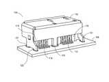
- FIG. 1is a front perspective view of a connector 100 according to an embodiment of the present invention.
- connector 100is a female USB connector that can accommodate both USB 3.0 and USB 2.0 connections.
- connector 100may comprise an upper, external shield 102 , a lower, internal shield 104 , and a housing structure 106 .
- the upper and lower shields 102 , 104 and the housing structure 106are components that may collectively be constructed together to form the connector 100 proper.
- the upper shield 102 and lower shield 104may be welded, such as laser welded, together to form a shielding shell around the housing structure 106 .
- the connector 100in assembled form as a female USB, provides a receiving cavity (or opening) 110 to accept complimentary male USB connectors.
- connector 100is shown mounted on to a printed circuit board 108 to show how connector 100 may be implemented within an electronic device (not shown).
- the components of connector 100will now be further described.
- External shield 102serves as part of the shielding shell and provides shielding for the connector 100 .
- External shielding 102may be constructed from a low impedance material, such as a metal.
- external shield 102is produced from a sheet metal material to facilitate production.
- the dimensions of external shield 102may be based on a variety of factors, such as, dimensions needed for the connector engagement, allowance for re-work during manufacturing, and the like.
- Internal shield 104 of the shielding shellserves as a complimentary part to external shield 102 and also may provide shielding for the connector 100 .
- Internal shield 104may be constructed from a low impedance material, such as a metal.
- internal shield 104may be produced from a sheet metal material.
- Housing 106provides the structural foundation for connector 100 .
- the housing 106is constructed from an insulative material, such as plastic.
- housing 106may be configured and shaped for a female USB connector.
- the housing 106is configured to accept a USB 3.0 and USB 2.0 connector in a side-by-side configuration.
- connector 100 and housing 106may be configured to accommodate other types of connectors and other types of arrangements within the principles of the present invention.
- FIG. 2Ais a rear perspective view of the connector 100 according to an embodiment of the present invention.
- the connector 100may comprise a first set of contacts 112 and a second set of contacts 114 .
- the first set of contacts 112carry USB 2.0 data signals while the second set of contacts 114 may carry USB 3.0 data signals.
- connector 100may provide apertures 116 and 118 through which contacts 112 and 114 may be exposed for electrical contact, e.g., in order to connect to other components of an electronic device.
- connector 100may comprise a shielding grounding structure 120 and mounting structures 122 .
- shielding grounding structure 120may be a peg-like structure that extends from external shield 102 for attachment to a through-hole provided in board 108 .
- shielding grounding structure 120is shown as a single, solid structure.
- shielding grounding structure 120may comprise multiple structures and features.
- shielding grounding structure 120may comprise two or more peg-like structures, or a single peg-like structure with a slit cut in it.
- the shielding grounding structure 120may be positioned in proximity to the second set of contacts 114 to assist in reducing EMI generated by the USB 3.0 signals.
- Mounting structures 122may be structures that extend from external shield 102 and provide a retention and grounding feature for connector 100 .
- mounting structures 122may be provided at the corners of external shield 102 and configured as peg-like structures that extend from the external shield 102 and configured for attachment to respective through-holes provided in the printed circuit board 108 .
- shielding grounding structure 120can provide additional retention strength and grounding paths that compliment mounting structures 122 .
- FIG. 2Bshows a rear view of the connector 100 according to an embodiment of the present invention.
- the rear of connector 100provides an overall opening having a length L 1 and height H.
- shielding grounding structure 120essentially divides this overall opening into a first aperture 116 and a second aperture 118 .
- Second aperture 118may thus have a length of L 2 .
- SEshielding effectiveness
- the shielding shell formed from upper shield 102 and lower shield 104may be configured to achieve a desired SE.
- SEcan be defined as the ratio of the strength of an EMI field within two different enclosures.
- SEcan be expressed in units of decibels according to the formula:
- SE20 log( ⁇ /2 L), where ⁇ is the wavelength of the signal and L is the length of the aperture being studied.
- ⁇is the wavelength of the signal
- Lis the length of the aperture being studied.
- a frequency of about 3-5 GHzis relevant, which results in a ⁇ range that is approximately 60-100 mm.
- connector 100provides an overall opening having a length L 1 and a height H. In the absence of shielding grounding structure 120 , connector 100 thus provides an aperture of L 1 by H through which EMI generated by the USB 2.0 and USB 3.0 signals may emanate. In some embodiments, connector 100 may provide a total aperture length L 1 of about 13 mm. As to the height H, it may be configured based on providing an opening of about 1/20 th of the relevant wavelength ⁇ , while also allowing sufficient clearance for re-work (if needed). In the present disclosure, it was discovered that the USB 3.0 signals, due to their higher frequency, were generating EMI that would affect the performance of an electronic device. As noted above, conventional solutions, such as grounding tape, and the like, were either cost prohibitive or ineffective in reducing the EMI to sufficient levels.
- aperture 116may have a length L 2 and also a height H.
- shielding grounding structure 120was placed to provide a length L 2 of about 4-5 mm to place the structure in proximity to the USB 3.0 signals, while also providing sufficient clearance for re-work (if needed). For example, in one embodiment, shielding grounding structure 120 was placed to provide a length L 2 of 4.8 mm for aperture 118 .
- the shielding effectiveness (SE) of connector 100 as it relates especially to EMI for USB 3.0 signalsmay now be studied.
- L 113 mm, thus . . . .
- the embodiments of the present inventionwere found to dramatically improve EMI suppression, e.g., by over 8 dB, of the connector 100 .
- FIG. 2Cshows another rear perspective view of the connector 100 according to an embodiment of the present invention.
- the connector 100is shown un-mounted.
- the shielding grounding structure 120 and mounting structures 122may extend from external shield 102 and may be shaped as peg-like structures for attachment to respective through-holes in a printed circuit board 108 (not shown in FIG. 2C ).
- other types of retention featuressuch as one or more tabs, fingers, knobs, protrusions, or other shaped members may be used in conjunction with corresponding mating receiving holes on the printed circuit board, and may be employed by the embodiments of the present invention.
- Shielding grounding structure 120may be configured with different shapes.
- shielding grounding structure 120may have various depths, widths, and lengths depending on the EMI characteristics or manufacturing characteristics desired.
- shielding grounding structure 120may have various features, such as curves, surface treatments, and other shapes, depending on the desired features.
- FIG. 3shows a bottom perspective view of the connector 100 according to an embodiment of the present invention.
- the housing 106may comprise registration features 124 .
- Registration features 124may be provided to assist in mounting of connector 100 to printed circuit board 108 .
- FIG. 4shows an exemplary external shield 102 for an embodiment of the present invention.
- FIG. 5shows an exemplary internal shield 104 for an embodiment of the present invention.
- FIG. 6shows an exemplary housing 106 for an embodiment of the present invention.
- FIG. 7shows an exemplary contact pin 700 for an embodiment of the present invention.
- connector 100may comprise sets of contacts 112 and 114 to carry data signals, such as USB 2.0 and USB 3.0 signals.
- contact pin 700may have a geometry to provide for a matched impedance for carrying signals through the connector 100 .
- FIG. 8shows an exemplary housing 106 with contact pins 700 installed for an embodiment of the present invention.
- housing 106may separate or compartmentalize contact pins 700 into sets 114 and 116 to carry USB 2.0 and USB 3.0 signals, respectively.
- FIG. 9shows a cutaway side view of the connector 100 according to an embodiment of the present invention and to illustrate the matched impedance geometry of contact pin 700 .
- contact pin 700is predominantly spaced the same distance L 3 from external shield 102 .
- This spacing geometryprovides for a matched capacitance impedance shield, and thus, also improves the shielding of the connector 100 .
- grounding structures and mounting structuresmay be provided with the shielding shell of the present invention.
- a single grounding structure 120is shown in the embodiment described herein, it is understood that two or more grounding structures may also be provided, in order to provide additional physical barriers and further compartmentalize or separate the set of contacts 112 , 114 from one another.
- the number of grounding structures 120 that can be employedis limited by the physical exposure required of each aperture to allow the set of contacts 112 , 114 sufficient room to attach to other electrical devices.
- the grounding structures 120may be formed of any shape or size, so long as the structures 120 are capable of providing sufficient physical barriers to EMI for the apertures. As shown and described above, the grounding structure 120 extends from the external shield 102 . However, the grounding structure 120 may also be formed as a separate component and attached to the shielding.
Landscapes
- Details Of Connecting Devices For Male And Female Coupling (AREA)
Abstract
Description
Claims (19)
Priority Applications (1)
| Application Number | Priority Date | Filing Date | Title |
|---|---|---|---|
| US12/852,417US9831612B1 (en) | 2010-08-06 | 2010-08-06 | High speed electrical connector with improved EMI suppression and mechanical retention shield |
Applications Claiming Priority (1)
| Application Number | Priority Date | Filing Date | Title |
|---|---|---|---|
| US12/852,417US9831612B1 (en) | 2010-08-06 | 2010-08-06 | High speed electrical connector with improved EMI suppression and mechanical retention shield |
Publications (1)
| Publication Number | Publication Date |
|---|---|
| US9831612B1true US9831612B1 (en) | 2017-11-28 |
Family
ID=60407671
Family Applications (1)
| Application Number | Title | Priority Date | Filing Date |
|---|---|---|---|
| US12/852,417Active2032-02-18US9831612B1 (en) | 2010-08-06 | 2010-08-06 | High speed electrical connector with improved EMI suppression and mechanical retention shield |
Country Status (1)
| Country | Link |
|---|---|
| US (1) | US9831612B1 (en) |
Cited By (9)
| Publication number | Priority date | Publication date | Assignee | Title |
|---|---|---|---|---|
| CN109510032A (en)* | 2019-01-09 | 2019-03-22 | 四川华丰企业集团有限公司 | Terminative connector for high-speed differential signal connector |
| CN109510033A (en)* | 2019-01-09 | 2019-03-22 | 四川华丰企业集团有限公司 | Terminative connector for high-speed differential signal connector |
| CN109524851A (en)* | 2019-01-09 | 2019-03-26 | 四川华丰企业集团有限公司 | Terminative connector for high-speed differential signal connector |
| CN109546463A (en)* | 2019-01-09 | 2019-03-29 | 四川华丰企业集团有限公司 | Female end signal transmission module with metal shielding board |
| CN109546469A (en)* | 2019-01-09 | 2019-03-29 | 四川华丰企业集团有限公司 | Female end signal transmission module with metal shielding board |
| CN109546470A (en)* | 2019-01-09 | 2019-03-29 | 四川华丰企业集团有限公司 | Female end signal transmission module with metal shielding board |
| CN109546461A (en)* | 2019-01-09 | 2019-03-29 | 四川华丰企业集团有限公司 | Female end signal transmission module with metal shielding board |
| CN109546472A (en)* | 2019-01-09 | 2019-03-29 | 四川华丰企业集团有限公司 | Female end signal transmission module with metal shielding board |
| CN111641095A (en)* | 2019-03-01 | 2020-09-08 | 西部数据技术公司 | Vertical surface mount C-type USB connector |
Citations (19)
| Publication number | Priority date | Publication date | Assignee | Title |
|---|---|---|---|---|
| US5637015A (en)* | 1995-08-31 | 1997-06-10 | Hon Hai Precision Ind. Co., Ltd. | Shielded electrical connector |
| US6238241B1 (en)* | 1999-12-27 | 2001-05-29 | Hon Hai Precision Ind. Co., Ltd. | Stacked electrical connector assembly |
| US6346009B1 (en)* | 1998-11-11 | 2002-02-12 | Molex Incorporated | Shielded multiple electrical connector assembly |
| US6394841B1 (en)* | 1998-02-16 | 2002-05-28 | Hirose Electric Co., Ltd. | Electric connector having shield plates |
| US6688915B2 (en)* | 2001-10-29 | 2004-02-10 | J.S.T. Mfg. Co., Ltd. | Electric connector having conductive inner and outer shells securely fastened to each other |
| US6835092B2 (en)* | 2003-05-09 | 2004-12-28 | Hon Hai Precision Ind. Co., Ltd. | Stacked electrical connector assembly with enhanced grounding arrangement |
| US20050181671A1 (en)* | 2004-02-17 | 2005-08-18 | Jinkui Hu | Stacked electrical connector |
| US20060014431A1 (en)* | 2004-07-19 | 2006-01-19 | Fci Americas Technology, Inc. | USB electrical connector |
| US20060084301A1 (en)* | 2002-06-21 | 2006-04-20 | Fromm Galen F | High-density, impedance-tuned connector having modular construction |
| US20090042451A1 (en)* | 2007-08-10 | 2009-02-12 | Hon Hai Precision Ind. Co., Ltd. | Electrical connector with improved contacts arrangement |
| US7517253B1 (en) | 2008-02-01 | 2009-04-14 | Taiwin Electronics Co., Ltd. | Connector socket for eSATA and USB plugs |
| US20090111330A1 (en) | 2007-10-29 | 2009-04-30 | Hon Hai Precision Ind. Co., Ltd. | Triple mating configurations of connector |
| US7534143B1 (en) | 2007-11-16 | 2009-05-19 | Hon Hai Precision Ind. Co., Ltd. | Electrical connector with improved wire termination arrangement |
| US7604512B1 (en) | 2009-03-31 | 2009-10-20 | U.D. Electronic Corp. | Female USB connector |
| US20090305532A1 (en) | 2008-06-06 | 2009-12-10 | Pin-Yuan Hou | Connector |
| US20100015855A1 (en) | 2008-07-17 | 2010-01-21 | Taiwin Electronics Co., Ltd. | Receptacle connector |
| US20100022138A1 (en) | 2008-07-22 | 2010-01-28 | Hosiden Corporation | Connector |
| US20100068939A1 (en) | 2008-09-16 | 2010-03-18 | Hon Hai Pricision Ind.Co., Ltd. | Electrical connector assembly with improved contact arrangement |
| US8172585B2 (en)* | 2008-12-19 | 2012-05-08 | Chant Sincere Co., Ltd. | USB connector and contact array thereof |
- 2010
- 2010-08-06USUS12/852,417patent/US9831612B1/enactiveActive
Patent Citations (20)
| Publication number | Priority date | Publication date | Assignee | Title |
|---|---|---|---|---|
| US5637015A (en)* | 1995-08-31 | 1997-06-10 | Hon Hai Precision Ind. Co., Ltd. | Shielded electrical connector |
| US6394841B1 (en)* | 1998-02-16 | 2002-05-28 | Hirose Electric Co., Ltd. | Electric connector having shield plates |
| US6346009B1 (en)* | 1998-11-11 | 2002-02-12 | Molex Incorporated | Shielded multiple electrical connector assembly |
| US6238241B1 (en)* | 1999-12-27 | 2001-05-29 | Hon Hai Precision Ind. Co., Ltd. | Stacked electrical connector assembly |
| US6688915B2 (en)* | 2001-10-29 | 2004-02-10 | J.S.T. Mfg. Co., Ltd. | Electric connector having conductive inner and outer shells securely fastened to each other |
| US20060084301A1 (en)* | 2002-06-21 | 2006-04-20 | Fromm Galen F | High-density, impedance-tuned connector having modular construction |
| US7156672B2 (en)* | 2002-06-21 | 2007-01-02 | Molex Incororporated | High-density, impedance-tuned connector having modular construction |
| US6835092B2 (en)* | 2003-05-09 | 2004-12-28 | Hon Hai Precision Ind. Co., Ltd. | Stacked electrical connector assembly with enhanced grounding arrangement |
| US20050181671A1 (en)* | 2004-02-17 | 2005-08-18 | Jinkui Hu | Stacked electrical connector |
| US20060014431A1 (en)* | 2004-07-19 | 2006-01-19 | Fci Americas Technology, Inc. | USB electrical connector |
| US20090042451A1 (en)* | 2007-08-10 | 2009-02-12 | Hon Hai Precision Ind. Co., Ltd. | Electrical connector with improved contacts arrangement |
| US20090111330A1 (en) | 2007-10-29 | 2009-04-30 | Hon Hai Precision Ind. Co., Ltd. | Triple mating configurations of connector |
| US7534143B1 (en) | 2007-11-16 | 2009-05-19 | Hon Hai Precision Ind. Co., Ltd. | Electrical connector with improved wire termination arrangement |
| US7517253B1 (en) | 2008-02-01 | 2009-04-14 | Taiwin Electronics Co., Ltd. | Connector socket for eSATA and USB plugs |
| US20090305532A1 (en) | 2008-06-06 | 2009-12-10 | Pin-Yuan Hou | Connector |
| US20100015855A1 (en) | 2008-07-17 | 2010-01-21 | Taiwin Electronics Co., Ltd. | Receptacle connector |
| US20100022138A1 (en) | 2008-07-22 | 2010-01-28 | Hosiden Corporation | Connector |
| US20100068939A1 (en) | 2008-09-16 | 2010-03-18 | Hon Hai Pricision Ind.Co., Ltd. | Electrical connector assembly with improved contact arrangement |
| US8172585B2 (en)* | 2008-12-19 | 2012-05-08 | Chant Sincere Co., Ltd. | USB connector and contact array thereof |
| US7604512B1 (en) | 2009-03-31 | 2009-10-20 | U.D. Electronic Corp. | Female USB connector |
Cited By (17)
| Publication number | Priority date | Publication date | Assignee | Title |
|---|---|---|---|---|
| CN109546469B (en)* | 2019-01-09 | 2023-11-03 | 四川华丰科技股份有限公司 | Female end signal transmission module with metal shielding plate |
| CN109546470B (en)* | 2019-01-09 | 2023-10-10 | 四川华丰科技股份有限公司 | Female end signal transmission module with metal shielding plate |
| CN109524851A (en)* | 2019-01-09 | 2019-03-26 | 四川华丰企业集团有限公司 | Terminative connector for high-speed differential signal connector |
| CN109546463A (en)* | 2019-01-09 | 2019-03-29 | 四川华丰企业集团有限公司 | Female end signal transmission module with metal shielding board |
| CN109546469A (en)* | 2019-01-09 | 2019-03-29 | 四川华丰企业集团有限公司 | Female end signal transmission module with metal shielding board |
| CN109546470A (en)* | 2019-01-09 | 2019-03-29 | 四川华丰企业集团有限公司 | Female end signal transmission module with metal shielding board |
| CN109546461A (en)* | 2019-01-09 | 2019-03-29 | 四川华丰企业集团有限公司 | Female end signal transmission module with metal shielding board |
| CN109546472A (en)* | 2019-01-09 | 2019-03-29 | 四川华丰企业集团有限公司 | Female end signal transmission module with metal shielding board |
| CN109510033A (en)* | 2019-01-09 | 2019-03-22 | 四川华丰企业集团有限公司 | Terminative connector for high-speed differential signal connector |
| CN109546461B (en)* | 2019-01-09 | 2023-11-03 | 四川华丰科技股份有限公司 | Female end signal transmission module with metal shielding plate |
| CN109546463B (en)* | 2019-01-09 | 2023-11-03 | 四川华丰科技股份有限公司 | Female end signal transmission module with metal shielding plate |
| CN109524851B (en)* | 2019-01-09 | 2023-11-03 | 四川华丰科技股份有限公司 | Female connector for high-speed differential signal connector |
| CN109510032A (en)* | 2019-01-09 | 2019-03-22 | 四川华丰企业集团有限公司 | Terminative connector for high-speed differential signal connector |
| CN109546472B (en)* | 2019-01-09 | 2023-11-03 | 四川华丰科技股份有限公司 | Female end signal transmission module with metal shielding plate |
| CN109510033B (en)* | 2019-01-09 | 2023-11-03 | 四川华丰科技股份有限公司 | Female connector for high-speed differential signal connector |
| CN109510032B (en)* | 2019-01-09 | 2023-11-03 | 四川华丰科技股份有限公司 | Female connector for high-speed differential signal connector |
| CN111641095A (en)* | 2019-03-01 | 2020-09-08 | 西部数据技术公司 | Vertical surface mount C-type USB connector |
Similar Documents
| Publication | Publication Date | Title |
|---|---|---|
| US9831612B1 (en) | High speed electrical connector with improved EMI suppression and mechanical retention shield | |
| CA2307921C (en) | Shielded header | |
| US8888529B2 (en) | Electrical connector having common ground shield | |
| EP0732776B1 (en) | High performance shielded connector | |
| US5083945A (en) | Shielded electrical connector assembly | |
| US9472887B1 (en) | Electrical connector having a ground bracket | |
| US9490586B1 (en) | Electrical connector having a ground shield | |
| US8834205B2 (en) | Pluggable module system | |
| TWI568102B (en) | Communication connector of high frequency signal with improved crosstalk performance | |
| CN111628357A (en) | Electrical connector for mitigating electrical resonance | |
| US11005218B2 (en) | Shielding structure for an electrical connector | |
| US6203373B1 (en) | Shielded electrical connector | |
| US7704098B2 (en) | Registered jack with enhanced EMI protection | |
| EP3673541B1 (en) | Transceiver receptacle with emi cage and bezel clips that provide high shielding effectiveness | |
| US6739915B1 (en) | Electrical connector with rear retention mechanism of outer shell | |
| US11870184B2 (en) | Multipolar connector set | |
| US6957982B1 (en) | Stacked modular jack | |
| US4381129A (en) | Grounded, multi-pin connector for shielded flat cable | |
| JP2007519211A (en) | Improved electrical signal transmission system | |
| US6184460B1 (en) | Modular box shield for forming a coaxial header | |
| TW201524039A (en) | Receptacle assembly having a plurality of termination points | |
| WO2021154415A1 (en) | Transceiver receptacle with emi cage and bezel clips that provide high shielding effectiveness | |
| US6210228B1 (en) | Shielded electrical connector | |
| US20050070161A1 (en) | Modular jack with external electromagnetic shielding | |
| KR101843724B1 (en) | Receptacle Connector |
Legal Events
| Date | Code | Title | Description |
|---|---|---|---|
| AS | Assignment | Owner name:WESTERN DIGITAL TECHNOLOGIES, INC., CALIFORNIA Free format text:ASSIGNMENT OF ASSIGNORS INTEREST;ASSIGNOR:SZEREMETA, WALLY;REEL/FRAME:024805/0122 Effective date:20100806 | |
| AS | Assignment | Owner name:U.S. BANK NATIONAL ASSOCIATION, AS COLLATERAL AGENT, CALIFORNIA Free format text:SECURITY AGREEMENT;ASSIGNOR:WESTERN DIGITAL TECHNOLOGIES, INC.;REEL/FRAME:038744/0281 Effective date:20160512 Owner name:JPMORGAN CHASE BANK, N.A., AS COLLATERAL AGENT, ILLINOIS Free format text:SECURITY AGREEMENT;ASSIGNOR:WESTERN DIGITAL TECHNOLOGIES, INC.;REEL/FRAME:038744/0481 Effective date:20160512 Owner name:JPMORGAN CHASE BANK, N.A., AS COLLATERAL AGENT, ILLINOIS Free format text:SECURITY AGREEMENT;ASSIGNOR:WESTERN DIGITAL TECHNOLOGIES, INC.;REEL/FRAME:038722/0229 Effective date:20160512 Owner name:JPMORGAN CHASE BANK, N.A., AS COLLATERAL AGENT, IL Free format text:SECURITY AGREEMENT;ASSIGNOR:WESTERN DIGITAL TECHNOLOGIES, INC.;REEL/FRAME:038722/0229 Effective date:20160512 Owner name:U.S. BANK NATIONAL ASSOCIATION, AS COLLATERAL AGEN Free format text:SECURITY AGREEMENT;ASSIGNOR:WESTERN DIGITAL TECHNOLOGIES, INC.;REEL/FRAME:038744/0281 Effective date:20160512 Owner name:JPMORGAN CHASE BANK, N.A., AS COLLATERAL AGENT, IL Free format text:SECURITY AGREEMENT;ASSIGNOR:WESTERN DIGITAL TECHNOLOGIES, INC.;REEL/FRAME:038744/0481 Effective date:20160512 | |
| STCF | Information on status: patent grant | Free format text:PATENTED CASE | |
| AS | Assignment | Owner name:WESTERN DIGITAL TECHNOLOGIES, INC., CALIFORNIA Free format text:RELEASE BY SECURED PARTY;ASSIGNOR:U.S. BANK NATIONAL ASSOCIATION, AS COLLATERAL AGENT;REEL/FRAME:045501/0714 Effective date:20180227 | |
| MAFP | Maintenance fee payment | Free format text:PAYMENT OF MAINTENANCE FEE, 4TH YEAR, LARGE ENTITY (ORIGINAL EVENT CODE: M1551); ENTITY STATUS OF PATENT OWNER: LARGE ENTITY Year of fee payment:4 | |
| AS | Assignment | Owner name:WESTERN DIGITAL TECHNOLOGIES, INC., CALIFORNIA Free format text:RELEASE OF SECURITY INTEREST AT REEL 038744 FRAME 0481;ASSIGNOR:JPMORGAN CHASE BANK, N.A.;REEL/FRAME:058982/0556 Effective date:20220203 | |
| AS | Assignment | Owner name:JPMORGAN CHASE BANK, N.A., ILLINOIS Free format text:PATENT COLLATERAL AGREEMENT - A&R LOAN AGREEMENT;ASSIGNOR:WESTERN DIGITAL TECHNOLOGIES, INC.;REEL/FRAME:064715/0001 Effective date:20230818 Owner name:JPMORGAN CHASE BANK, N.A., ILLINOIS Free format text:PATENT COLLATERAL AGREEMENT - DDTL LOAN AGREEMENT;ASSIGNOR:WESTERN DIGITAL TECHNOLOGIES, INC.;REEL/FRAME:067045/0156 Effective date:20230818 | |
| MAFP | Maintenance fee payment | Free format text:PAYMENT OF MAINTENANCE FEE, 8TH YEAR, LARGE ENTITY (ORIGINAL EVENT CODE: M1552); ENTITY STATUS OF PATENT OWNER: LARGE ENTITY Year of fee payment:8 |