US9830087B2 - Memory wear leveling - Google Patents
Memory wear levelingDownload PDFInfo
- Publication number
- US9830087B2 US9830087B2US14/540,968US201414540968AUS9830087B2US 9830087 B2US9830087 B2US 9830087B2US 201414540968 AUS201414540968 AUS 201414540968AUS 9830087 B2US9830087 B2US 9830087B2
- Authority
- US
- United States
- Prior art keywords
- sector
- sub
- wear
- sectors
- memory
- Prior art date
- Legal status (The legal status is an assumption and is not a legal conclusion. Google has not performed a legal analysis and makes no representation as to the accuracy of the status listed.)
- Active, expires
Links
Images


Classifications
- G—PHYSICS
- G06—COMPUTING OR CALCULATING; COUNTING
- G06F—ELECTRIC DIGITAL DATA PROCESSING
- G06F3/00—Input arrangements for transferring data to be processed into a form capable of being handled by the computer; Output arrangements for transferring data from processing unit to output unit, e.g. interface arrangements
- G06F3/06—Digital input from, or digital output to, record carriers, e.g. RAID, emulated record carriers or networked record carriers
- G06F3/0601—Interfaces specially adapted for storage systems
- G06F3/0602—Interfaces specially adapted for storage systems specifically adapted to achieve a particular effect
- G06F3/0614—Improving the reliability of storage systems
- G06F3/0616—Improving the reliability of storage systems in relation to life time, e.g. increasing Mean Time Between Failures [MTBF]
- G—PHYSICS
- G06—COMPUTING OR CALCULATING; COUNTING
- G06F—ELECTRIC DIGITAL DATA PROCESSING
- G06F3/00—Input arrangements for transferring data to be processed into a form capable of being handled by the computer; Output arrangements for transferring data from processing unit to output unit, e.g. interface arrangements
- G06F3/06—Digital input from, or digital output to, record carriers, e.g. RAID, emulated record carriers or networked record carriers
- G06F3/0601—Interfaces specially adapted for storage systems
- G06F3/0628—Interfaces specially adapted for storage systems making use of a particular technique
- G06F3/0638—Organizing or formatting or addressing of data
- G06F3/0644—Management of space entities, e.g. partitions, extents, pools
- G—PHYSICS
- G06—COMPUTING OR CALCULATING; COUNTING
- G06F—ELECTRIC DIGITAL DATA PROCESSING
- G06F3/00—Input arrangements for transferring data to be processed into a form capable of being handled by the computer; Output arrangements for transferring data from processing unit to output unit, e.g. interface arrangements
- G06F3/06—Digital input from, or digital output to, record carriers, e.g. RAID, emulated record carriers or networked record carriers
- G06F3/0601—Interfaces specially adapted for storage systems
- G06F3/0628—Interfaces specially adapted for storage systems making use of a particular technique
- G06F3/0646—Horizontal data movement in storage systems, i.e. moving data in between storage devices or systems
- G06F3/0647—Migration mechanisms
- G06F3/0649—Lifecycle management
- G—PHYSICS
- G06—COMPUTING OR CALCULATING; COUNTING
- G06F—ELECTRIC DIGITAL DATA PROCESSING
- G06F3/00—Input arrangements for transferring data to be processed into a form capable of being handled by the computer; Output arrangements for transferring data from processing unit to output unit, e.g. interface arrangements
- G06F3/06—Digital input from, or digital output to, record carriers, e.g. RAID, emulated record carriers or networked record carriers
- G06F3/0601—Interfaces specially adapted for storage systems
- G06F3/0668—Interfaces specially adapted for storage systems adopting a particular infrastructure
- G06F3/0671—In-line storage system
- G06F3/0673—Single storage device
- G06F3/0679—Non-volatile semiconductor memory device, e.g. flash memory, one time programmable memory [OTP]
- G—PHYSICS
- G06—COMPUTING OR CALCULATING; COUNTING
- G06F—ELECTRIC DIGITAL DATA PROCESSING
- G06F3/00—Input arrangements for transferring data to be processed into a form capable of being handled by the computer; Output arrangements for transferring data from processing unit to output unit, e.g. interface arrangements
- G06F3/06—Digital input from, or digital output to, record carriers, e.g. RAID, emulated record carriers or networked record carriers
- G06F3/0601—Interfaces specially adapted for storage systems
- G06F3/0668—Interfaces specially adapted for storage systems adopting a particular infrastructure
- G06F3/0671—In-line storage system
- G06F3/0683—Plurality of storage devices
- G06F3/0688—Non-volatile semiconductor memory arrays
Definitions
- Embodiment of the present inventionrelate generally to the field of memory devices and more particularly, to systems and methods of wear leveling for memory devices.
- Computer systems and other electrical systemsgenerally include one or more memory devices.
- computersoften employ NOR flash memory and NAND flash memory.
- NOR and NAND flasheach have certain advantages over the other.
- NOR flash memorytypically has slower write and erase speeds than NAND flash.
- NAND flash memorytypically has more endurance than NOR flash memory.
- NOR flash memorytypically enables random access to data stored within the memory devices, whereas, NAND flash memory generally requires accessing and writing data in larger groups.
- NAND flash memorytypically includes a plurality of blocks that each includes a plurality of pages, wherein each page includes a large number of bytes of data. In operation, data is erased one block at a time, and written one page at a time.
- NAND memory cellshave a limited number of write/erase cycles (e.g. 100,000 program/erase cycles).
- Wear levelingcan be applied to spread data across various physical sectors of the memory.
- Wear levelinggenerally includes writing data to the various sectors to ensure an even use of the cells to prevent certain portions of the memory array from prematurely failing.
- Wear levelingmay include initially writing the data to one of the various sectors in the memory array, or may include moving the data from one physical sector within the memory array and writing that same data to another physical sectors in the memory array.
- Some memory technologiesfeature an additional level of granularity inside each sector called sub-sectors.
- Sub-sectorsare segments of memory inside the sector of a memory.
- the sub-sectorsmay be individually accessed (e.g., programmed and/or erased). Accordingly, the sub-sectors have separate cycling, and thus, different wear-out from other sub-sectors within the memory.
- traditional wear leveling techniqueshave not effectively accounted for sub-sector wear, especially in high data cycling application (e.g., page-flash implementations), where the number of cycles may reach into the hundreds of thousands.
- FIG. 1is a block diagram depicting a memory system having sub-sector wear circuitry that performs an intra-sector swap, in accordance with an embodiment
- FIG. 2is a flow diagram illustrating the sector for sub-sector swap process, in accordance with an embodiment
- FIG. 3is a schematic diagram illustrating a sector for sub-sector swap where over-cycling may occur; in accordance with an embodiment
- FIG. 4is a flow-chart illustrating such an intra-sector swap process, in accordance with an embodiment
- FIG. 5is a schematic diagram illustrating intra-sector swap using the process of FIG. 4 , in accordance with an embodiment
- FIG. 6is a flow diagram illustrating an intermediate intra-sector bundle swap process, in accordance with an embodiment
- FIG. 7is a schematic diagram illustrating intra-sector swap, using the process of FIG. 6 , in accordance with an embodiment
- FIG. 8is a schematic drawing illustrating a system with rescrambling circuitry, in accordance with an embodiment
- FIG. 9is a schematic drawing illustrating a system having rescrambling circuitry that uses a multiplexer (MUX), in accordance with an embodiment.
- MUXmultiplexer
- FIG. 10is a schematic drawing illustrating a system having rescrambling circuitry that uses a combinational logic, in accordance with an embodiment.
- FIG. 1is a block diagram that depicts a memory system, as generally designated by reference numeral 10 .
- the memory system 10may be any of a variety of types, such as those used in a computer, pager, cellular phone, personal organizer, control circuit, etc.
- the memory devicemay be NAND or NOR type flash memory.
- the system 10includes a master device 12 and a slave device 14 .
- the master device 12may include a microcontroller and the slave device 14 may include a memory device.
- the master device 12communicates with the slave device 14 via various transmission lines.
- the master device 12 and the slave device 14send and receive signals via a peripheral interface (PI).
- the PIincludes a PI bus 16 .
- the PI bus 16is a synchronous serial data link standard that operates in full duplex mode. Devices on the PI bus 16 may operate in a master/slave mode that enables the master device 12 to initiate data frames to one or more slave devices 14 .
- the master device 12 and the slave device 14generally include shift registers that enable them to exchange and store data values. In operation, the master device 12 and the slave device 14 can do various things with the data stored in the registers, such as save the data to memory
- the slave device 14(e.g., the memory device) includes a controller 18 , a cache 20 , a memory array 22 , and an ECC 24 status register.
- the controller 18receives and transmits data via the PI bus 16 . Data that is transmitted across the PI bus 16 is received by inputs of the controller 18 .
- the controller 18also transmits and receives signals via data transfer input/output lines (DT I/O) and control lines 26 , 28 and 29 that are internal to the memory device 14 .
- the DT I/O linesenable communication with the cache 20 .
- the control line 26enables the controller 18 to transmit and receive control signals to and from the cache 20 .
- the control line 28enables the PI controller to transmit and receive control signals to and from the memory array 22 .
- the control line 29enables the PI controller to transmit and receive control signals to and from the error-correcting code (ECC) status register 24 .
- ECCerror-correcting code
- the controller 18receives the data transmitted via the PI bus 16 , and synchronizes the flow of data (DT I/O) and control signals between other components of the memory 14 .
- the PI controller 18may receive data and commands in a serialized format via the bus 16 , and parse the incoming serialized signal for the data and the commands.
- the controller 18may include shift registers that provide appropriate timing of the signals transmitted and received by the controller 18 .
- the controller 18may include algorithms that are run onboard to interpret incoming signals that include commands, addresses, data, and the like. The algorithms may also include routines to determine the appropriate outputs of the controller 18 , including address schemes, error corrections, movements of data within the memory array 22 , and the like. As will be discussed in more detail below, in some embodiments, the controller 18 may move stored data to prevent excessive wear caused by data cycling. Similarly, the controller 18 may include circuitry to synchronize the transmission of data from the controller 18 to the master device 12 via the bus 16 .
- datais transferred to or from the memory array 22 byte-by-byte through the cache 20 .
- the cache 20acts as a data buffer for the data being transferred from the controller 18 to the memory array 22 .
- Datamay be written into the cache 20 and subsequently written into the memory array 22 .
- datamay be read from the memory array 22 into the cache 20 , and subsequently transmitted from the cache 20 to the master device 12 via the controller 18 and the bus 16 .
- the cache 20may be various sizes.
- the cache 20may include 2048 bytes, 4096 bytes, 8192 bytes or a multiple thereof.
- the cache 20may also be smaller sizes such, as 256 bytes or 512 bytes.
- a data registermay reside in the cache 20 or the memory array 22 to provide a path for the transfer of data between the cache 20 , and the memory array 22 .
- a plurality of data bitsmay be shifted into the data register before being written to an address of the memory array 22 .
- the ECC status register 24is used to detect and/or correct bit errors that can occur during normal operation, as well as bit errors that occur due to charge loss/gain that develop over time.
- the ECC status register 24may include circuitry used to detect and correct errors when reading data back from the memory array 22 .
- the ECC status register 24may supplement algorithms employed on the controller 18 .
- the ECC status register 24may also include a group of sub-registers.
- These sub-registersmay include an ECC enable/disable register that enables optional ECC for the memory device data, an ECC type register that stores the total number of errors discovered, an ECC location register that stores the location of any uncorrectable errors, an ECC NAND memory result register that stores information regarding the result of any error correction process on the memory array 22 , or an ECC cache memory result register that stores information regarding the result of any error correction process on the cache 20 .
- the ECC status register 24may include all of the previous ECC sub-registers or any combination of the preceding sub-registers. Although the ECC status register 24 is shown to be external to the controller 18 , the ECC status register 24 may be integral to the controller 18 .
- the memory array 22includes a memory cell array that is divided into sectors 30 . Each sector includes a fixed number of sub-sectors 32 .
- the memory array 22may include any number and size of sectors 30 and sub-sectors 32 .
- the memory array 22may be programmed and/or erased at the sector 30 and/or the sub-sector 32 level.
- Wear levelingcan be applied to spread data across various physical locations of the memory. Wear leveling generally includes writing data to the various locations to ensure an even use of the cells to prevent certain portions of the memory array 22 from prematurely failing. Wear leveling may include initially writing the data to one of the various locations in the memory array 22 , or may include moving the data from one physical location (e.g., an address) within the memory array 22 and writing that same data to another physical location in the NAND memory array 22 . The controller 18 may manage the wear leveling routines used to determine where the data is written to.
- controller 18may monitor the memory usage and determine an appropriate address to write data within the memory array 22 .
- the controller 18(or other component of the memory system 10 ) may include sub-sector wear circuitry 34 that, as will be discussed in more detail below, provides wear leveling based upon the amount of wear of individual sub-sectors 32 within the memory array 22 .
- a block mapping unit(BMU) may be responsible for tracking swap histories as well as re-mapping sectors and/or sub-sectors (e.g., updating addresses of sectors and/or sub-sectors to be re-mapped).
- sub-sector wear circuitry 34is illustrated as a part of the controller 18 in embodiment of FIG. 1 , the sub-sector wear circuitry 34 may be implemented, in part or in whole, at other components of the memory system 10 .
- the master device 12may include a portion of the wear level routines making up the circuitry 34 .
- the slave device 14may include another portion of the wear level routines making up the circuitry 34 .
- the sub-sector wear circuitry 34may be implemented using a number of different approaches.
- a hierarchical wear level approachmay be implemented.
- the hierarchical wear level approachmay implement sub-sector 32 wear leveling inside each sector 30 .
- sub-sectors 32may be swapped inside a sector 30 based upon the relative wear levels of the sub-sectors 32 within the sector 30 .
- a trade-off for a hierarchical wear level approachis that there is increased hardware overhead for such an approach. For example, assignment of individual address remapping hardware may be needed within each sector to achieve this approach.
- sub-sectorsmay be individually swapped as if they were individual sectors. In essence, this acts to flatten the sub-sector hierarchy, causing an increase in the number of swaps and the swapping pool.
- a trade-off for this approachis that the increased swapping pool may lead to very complex management of swapping, especially at the sector level.
- FIG. 2is a flow diagram illustrating the sector for sub-sector swap process 50 , in accordance with an embodiment.
- the system 10may detect whether any of the sectors 30 have a high wear level (decision block 52 ).
- the sector wear levelmay be based upon information about one or more of the sub-sectors 32 within the sector 30 .
- wearmay be determined based upon highest cycle count of a sub-sector 32 within the sector 30 , a sum of the sub-sector 32 cycle counts for all sub-sectors 32 within a given sector 30 , an average of the sub-sector 32 cycle counts for all sub-sectors 32 within a given sector 30 , etc.
- a high wear levelmay be found when a pre-determined threshold cycle count is breached (e.g., when a cycle count exceeds 100,000 cycles).
- the system 10continues to monitor for sectors 30 having a high wear level. Once a sector 30 is found to have a high wear level, a swap may be triggered, where the sector 30 having the high wear level is the target sector for swapping to a destination sector 30 . Accordingly, this high wear level sector 30 may be referred to as the “Target sector.”
- the best destination sector 30may be the sector 30 having the least wear. This sector may be referred to as the “Min Sector.”
- the Min Sectoris determined (block 54 ).
- the wear levelmay be based upon highest cycle count of a sub-sector 32 within the sector 30 , a sum of the sub-sector 32 cycle counts for all sub-sectors 32 within a given sector 30 , an average of the sub-sector 32 cycle counts for all sub-sectors 32 within a given sector 30 , etc.
- the Min Sectormay be determined by pinpointing the sector having the lowest wear level based upon the cycle counts. Once the Target Sector and the Min Sector are determined, a swap occurs from the Target Sector to the Min Sector (block 56 ).
- the swapmay include moving data within the memory array 22 to alternative locations in the memory array 22 .
- This processmay generally include loading data from a first address in the memory array 22 into a cache. The cached data may then be written to a new destination location within the array 22 .
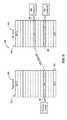
- FIG. 3is a schematic diagram illustrating a sector for sub-sector swap 60 where over-cycling may occur.
- sub-sectors 32 for transfer from the target sector 62 to the Min Sector 64retain their relative positions at the Min Sector 64 . Accordingly, sub-sector SS 4 of the Target Sector 62 remains SS 4 in the Min Sector 64 after transfer. As illustrated, SS 4 in the Min Sector 64 may be the relatively-highest wear level sub-sector in the Min Sector 64 . Accordingly, this swap may lead to an accumulation of cycles and an over-cycling of the Min Sector 64 .
- additional logic/circuitrymay be implemented to extend the sector for sub-sector swap to reduce sub-sector 32 wear.
- the additional logic/circuitrymay embed an intra-sector swap of a sub-sector 32 whenever a sector 30 swap is triggered in the sector for sub-sector swap process 50 of FIG. 2 .
- FIG. 4is a flow-chart illustrating such an intra-sector swap process 70 .
- the system 10may detect whether any of the sectors 30 have a high wear level (decision block 52 ). Further, the sector wear level may be based upon information about one or more of the sub-sectors 32 within the sector 30 , such as the highest cycle count of a sub-sector 32 within the sector 30 , a sum of the sub-sector 32 cycle counts for all sub-sectors 32 within a given sector 30 , an average of the sub-sector 32 cycle counts for all sub-sectors 32 within a given sector 30 , etc. As mentioned above, a high wear level may be found when a pre-determined threshold cycle count is breached (e.g., when a cycle count exceeds 100,000 cycles).
- the system 10continues to monitor for sectors 30 having a high wear level. Once a sector 30 is found to have a high wear level, a swap may be triggered from the Target Sector 62 to the Min Sector 64 . Once a swap is triggered, the Min Sector 64 is determined (block 54 ). As mentioned above, the Min Sector 64 may be determined by pinpointing the sector having the lowest wear level based upon sub-sector cycle counts.
- the embedded sub-sector swap process 72includes determining the Min Sub-Sector (the sub-sector having the lowest wear level) of the Min Sector 64 (block 76 ).
- the Target sub-sectore.g., the sub-sector having the high wear in the target sector 62
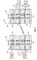
- FIG. 5is a schematic diagram illustrating intra-sector swap 90 , in accordance with the process 70 of FIG. 4 .
- sub-sector SS 4is the Max Sub-Sector 92 of the target sector 62 .
- SS 4is the sub-sector to be erased.
- the Max Sub-Sector 92is swapped with the Min Sub-Sector 94 . Accordingly, over-cycling may be reduced, by ensuring that the Max Sub-Sector 92 is not placed in the sub-sector 96 having the relatively highest wear in the Min Sector 64 .
- the intra-sector swap of Max Sub-Sector 92 and the Min Sub-Sector 94may result in the reduction of cycle accumulation.
- each sector 30includes 16 sub-sectors 32 .
- the cycle numbermay be 16 times less than the a process that does not utilize this swap.
- any processing time increasemay be negligible.
- the process 70may utilize an increased silicon area.
- the block mapping unit(BMU) may need to track each sub-sector's address instead of merely tracking sector addresses.
- FIG. 6is a flow diagram illustrating an intermediate intra-sector bundle swap process 110 , in accordance with an embodiment.
- the sub-sectorsmay be bundled (block 112 ), such that a less granular address for a plurality of the sub-sectors may be alternatively used.
- the addressesmay be less granular, fewer bits of data may be used to define an address of the bundled sub-sectors. Thus, less silicon area may be utilized.
- the system 10may detect whether any of the sectors 30 have a high wear level (decision block 52 ).
- the sector wear levelmay be based upon information about one or more of the sub-sectors 32 within the sector 30 , such as the highest cycle count of a sub-sector 32 within the sector 30 , a sum of the sub-sector 32 cycle counts for all sub-sectors 32 within a given sector 30 , an average of the sub-sector 32 cycle counts for all sub-sectors 32 within a given sector 30 , etc.
- a high wear levelmay be found when a pre-determined threshold cycle count is breached (e.g., when a cycle count exceeds 100,000 cycles).
- the system 10continues to monitor for sectors 30 having a high wear level. Once a sector 30 is found to have a high wear level, a swap may be triggered from the Target Sector 62 to the Min Sector 64 . Once a swap is triggered, the Min Sector is determined (block 54 ). As mentioned above, the Min Sector 64 may be determined by pinpointing the sector having the lowest wear level based upon sub-sector cycle counts.
- the embedded bundled sub-sector swap process 114includes determining the Min Bundle (the bundle containing the sub-sector having the lowest wear level and/or the bundle having the lowest wear level) of the Min Sector 64 (block 118 ).
- the Target Bundlee.g., the bundle containing the sub-sector having the high wear in the target sector 62
- the process 110may provide less mitigation of cycle counts than the process 70 , it reduces the number of cycles over a standard sector for sub-sector swap approach. Further, because the swaps involve bundles of sub-sectors rather than individual sub-sectors, the management complexity and silicon area usage may be reduced. For example, the block mapping units may retain and manage swaps on a less-granular level than process 70 . Thus, the processing complexity and the silicon area may be reduced, while still mitigating some of the un-necessary cycling that occurs in the sector to sub-sector swap approach that does not include an intra-sector swap.
- FIG. 7is a schematic diagram illustrating intra-sector swap 140 , in accordance with the process 110 of FIG. 6 .
- the sub-sectors 32are bundled into addressable bundles 142 .
- the sub-sectorsare bundled into quartets of four subsectors 32 .
- each of the bundlesis addressable in a less-granular manner than would be possible when addressing each sub-sector 32 individually.
- the bundlesmay be address using two-bits 144 .
- individually addressing each sub-sector 32may utilize increased silicon area.
- at least 4 bits of datawould be used to uniquely identify the sub-sector 32 address.
- the sub-sector SS 4is the Max sub-sector 92 of the target sector 62 .
- SS 4is the sub-sector to be erased.
- the bundle 146 with the address “10”is the Max bundle 146 , because it contains the Max sub-sector 92 .
- the Max Bundle 146is swapped with the Min Bundle 148 (the bundle 142 that contains the Min Sub-Sector 94 ).
- over-cyclingmay be reduced, by ensuring that the Max Bundle 146 is not placed in the bundle containing the sub-sector 96 having the relatively highest wear in the Min Sector 64 .
- the intra-sector bundled sub-sector swap of Max Bundle 146 and the Min Bundle 148may result in the reduction of cycle accumulation.
- each sector 30includes 4 bundles 142 .
- the cycle numbermay be 4 times less than the a process that does not utilize this swap.
- the processing and silicon area utilizationmay be less than the process 70 .
- the processing time increasemay be negligible.
- FIG. 8is a schematic drawing illustrating a system 160 with rescrambling circuitry 162 that can globally re-map addresses of the sub-sectors, bundles of sub-sectors, etc. to dilute the Max Sub-Sector 92 and/or the Max Bundle 146 from being placed at a sub-sector 32 location in the Min Sector 64 having the highest wear of the Min Sector 64 .
- the block mapping unit (BMU) 164receives the logical sector address 166 of a sector 30 where rescrambling is to occur.
- the BMU 164may then cause a global address re-mapping by outputting a physical sector address 168 of the sector 30 and one or more configuration bits 170 that cause a particular remapping of a logical intra-sector address 172 to occur.
- the configuration bitsare received at the rescrambling circuitry 162 , where a remapped physical intra-sector address 174 is outputted based upon the configuration bits 170 and the logical intra-sector address 172 .
- the rescrambling circuitry 162may include a multiplexer (MUX) solution, as illustrated in FIG. 9 .
- the configuration bits 170may include multiple sets of bits 190 , where the sets of bits 190 represent addresses to swap to.
- the sets of bits 190each represent one of the four quartet bundles.
- 4 (the number of items that can be swapped to) ⁇ 2 (the number of bits needed to represent the address of the swapped to items)are passed to the rescrambling circuitry 162 .
- the multiplexer(e.g., the rescrambling circuitry 162 ) selects one of the sets of bits 190 for remapping, as indicated by the dashed lines 192 .
- the multiplexer selectionis controlled by the logical intra-sector address 172 received as input to the rescrambling circuitry 162 .
- a remapped physical intra-sector address 174is outputted.
- this rescrambling solutionmay require less silicon area than circuitry that performs an intra-sector swap (e.g., in accordance with the process 70 and/or 110 ).
- this processmay include some additional overhead, because the number of sets of bits 190 may be numerous. Accordingly, in some embodiments, it may be beneficial to use an alternative solution that uses fewer configuration bits 170 .
- FIG. 10illustrates an embodiment of a system 160 where combinational logic 200 (e.g., Summation logic 202 and/or Exclusive Or (XOR) logic 204 ) is used in conjunction with a single set 210 of configuration bits 170 and the logical intra-sector address 172 to output a remapped physical intra-sector address 174 .
- combinational logic 200e.g., Summation logic 202 and/or Exclusive Or (XOR) logic 204
- the block mapping unit (BMU) 164receives the logical sector address 166 as input.
- the BMU 164provides, as output, the physical sector address 168 and a set 210 of configuration bits 170 that may be used in conjunction with the combination logic 200 to remap the logical intra-sector address 172 .
- the remapping provided by the rescrambling logicmay dilute intra-sector cycling by avoiding a high-wear to high-wear placement of sub-sectors.
- this solutiondoes not necessarily provide a highest-wear to lowest-wear solution.
- the rescrambling circuitryuses the combination logic 200 between the logical intra-sector address 172 and the set 210 to output the remapped physical intra-sector address. For example, to remap a bundle quartet having the address “01” to a bundle quartet having the address “10” using the summation logic 202 , the set 210 of configuration bits 170 provided from the BMU 164 are “01.” Alternatively, to achieve the same remap using the XOR logic 204 , the set 210 of configuration bits 170 are “11.”
- the time performance of sub-sector wear levelingmay be vastly improved. Further, hardware and software logic overhead may be reduced by substituting re-scrambling logic for an intra-sector swap.
Landscapes
- Engineering & Computer Science (AREA)
- Theoretical Computer Science (AREA)
- Human Computer Interaction (AREA)
- Physics & Mathematics (AREA)
- General Engineering & Computer Science (AREA)
- General Physics & Mathematics (AREA)
- Techniques For Improving Reliability Of Storages (AREA)
- Memory System (AREA)
- Read Only Memory (AREA)
- Memory System Of A Hierarchy Structure (AREA)
Abstract
Description
Claims (30)
Priority Applications (7)
| Application Number | Priority Date | Filing Date | Title |
|---|---|---|---|
| US14/540,968US9830087B2 (en) | 2014-11-13 | 2014-11-13 | Memory wear leveling |
| KR1020177015711AKR102245652B1 (en) | 2014-11-13 | 2015-11-02 | Memory wear leveling |
| CN201580062243.0ACN107003810B (en) | 2014-11-13 | 2015-11-02 | Memory wear is average |
| PCT/US2015/058634WO2016077091A1 (en) | 2014-11-13 | 2015-11-02 | Memory wear leveling |
| JP2017525331AJP6317039B2 (en) | 2014-11-13 | 2015-11-02 | Memory wear leveling |
| TW104137602ATWI576758B (en) | 2014-11-13 | 2015-11-13 | Memory wear leveling |
| US15/812,932US20180067661A1 (en) | 2014-11-13 | 2017-11-14 | Memory wear leveling |
Applications Claiming Priority (1)
| Application Number | Priority Date | Filing Date | Title |
|---|---|---|---|
| US14/540,968US9830087B2 (en) | 2014-11-13 | 2014-11-13 | Memory wear leveling |
Related Child Applications (1)
| Application Number | Title | Priority Date | Filing Date |
|---|---|---|---|
| US15/812,932ContinuationUS20180067661A1 (en) | 2014-11-13 | 2017-11-14 | Memory wear leveling |
Publications (2)
| Publication Number | Publication Date |
|---|---|
| US20160139826A1 US20160139826A1 (en) | 2016-05-19 |
| US9830087B2true US9830087B2 (en) | 2017-11-28 |
Family
ID=55954861
Family Applications (2)
| Application Number | Title | Priority Date | Filing Date |
|---|---|---|---|
| US14/540,968Active2035-03-11US9830087B2 (en) | 2014-11-13 | 2014-11-13 | Memory wear leveling |
| US15/812,932AbandonedUS20180067661A1 (en) | 2014-11-13 | 2017-11-14 | Memory wear leveling |
Family Applications After (1)
| Application Number | Title | Priority Date | Filing Date |
|---|---|---|---|
| US15/812,932AbandonedUS20180067661A1 (en) | 2014-11-13 | 2017-11-14 | Memory wear leveling |
Country Status (6)
| Country | Link |
|---|---|
| US (2) | US9830087B2 (en) |
| JP (1) | JP6317039B2 (en) |
| KR (1) | KR102245652B1 (en) |
| CN (1) | CN107003810B (en) |
| TW (1) | TWI576758B (en) |
| WO (1) | WO2016077091A1 (en) |
Cited By (2)
| Publication number | Priority date | Publication date | Assignee | Title |
|---|---|---|---|---|
| US20180067661A1 (en)* | 2014-11-13 | 2018-03-08 | Micron Technology, Inc. | Memory wear leveling |
| US10817430B2 (en) | 2018-10-02 | 2020-10-27 | Micron Technology, Inc. | Access unit and management segment memory operations |
Families Citing this family (6)
| Publication number | Priority date | Publication date | Assignee | Title |
|---|---|---|---|---|
| WO2019017017A1 (en)* | 2017-07-18 | 2019-01-24 | ソニーセミコンダクタソリューションズ株式会社 | Memory controller for wear-leveling processing |
| US20190129627A1 (en)* | 2017-10-31 | 2019-05-02 | EMC IP Holding Company LLC | Method and system for wear-leveling using a multi-gap progress field |
| US10606743B2 (en)* | 2017-12-05 | 2020-03-31 | Micron Technology, Inc. | Data movement operations in non-volatile memory |
| CN108920386B (en)* | 2018-07-20 | 2020-06-26 | 中兴通讯股份有限公司 | Wear leveling and access method, equipment and storage medium for nonvolatile memory |
| EP4042283A4 (en)* | 2019-10-09 | 2023-07-12 | Micron Technology, Inc. | Self-adaptive wear leveling method and algorithm |
| KR102860142B1 (en) | 2023-03-03 | 2025-09-16 | 윈본드 일렉트로닉스 코포레이션 | Semiconductor device and wear leveling method |
Citations (40)
| Publication number | Priority date | Publication date | Assignee | Title |
|---|---|---|---|---|
| US5430859A (en)* | 1991-07-26 | 1995-07-04 | Sundisk Corporation | Solid state memory system including plural memory chips and a serialized bus |
| US5956743A (en)* | 1997-08-25 | 1999-09-21 | Bit Microsystems, Inc. | Transparent management at host interface of flash-memory overhead-bytes using flash-specific DMA having programmable processor-interrupt of high-level operations |
| US6000006A (en)* | 1997-08-25 | 1999-12-07 | Bit Microsystems, Inc. | Unified re-map and cache-index table with dual write-counters for wear-leveling of non-volatile flash RAM mass storage |
| US20040080985A1 (en)* | 2002-10-28 | 2004-04-29 | Sandisk Corporation, A Delaware Corporation | Maintaining erase counts in non-volatile storage systems |
| US20040083335A1 (en)* | 2002-10-28 | 2004-04-29 | Gonzalez Carlos J. | Automated wear leveling in non-volatile storage systems |
| US20040177212A1 (en)* | 2002-10-28 | 2004-09-09 | Sandisk Corporation | Maintaining an average erase count in a non-volatile storage system |
| US20050091445A1 (en)* | 2003-10-28 | 2005-04-28 | Sandisk Corporation | Internal maintenance schedule request for non-volatile memory system |
| US6973531B1 (en)* | 2002-10-28 | 2005-12-06 | Sandisk Corporation | Tracking the most frequently erased blocks in non-volatile memory systems |
| US6985992B1 (en)* | 2002-10-28 | 2006-01-10 | Sandisk Corporation | Wear-leveling in non-volatile storage systems |
| US7096313B1 (en)* | 2002-10-28 | 2006-08-22 | Sandisk Corporation | Tracking the least frequently erased blocks in non-volatile memory systems |
| US7103732B1 (en)* | 2002-10-28 | 2006-09-05 | Sandisk Corporation | Method and apparatus for managing an erase count block |
| US20080162798A1 (en) | 1991-09-13 | 2008-07-03 | Lofgren Karl M J | Wear leveling techniques for flash eeprom systems |
| US7441067B2 (en) | 2004-11-15 | 2008-10-21 | Sandisk Corporation | Cyclic flash memory wear leveling |
| US20080313505A1 (en) | 2007-06-14 | 2008-12-18 | Samsung Electronics Co., Ltd. | Flash memory wear-leveling |
| US20090198873A1 (en)* | 2008-02-05 | 2009-08-06 | Spansion Llc | Partial allocate paging mechanism |
| US20090254689A1 (en)* | 2008-02-12 | 2009-10-08 | Vijay Karamcheti | Methods and apparatus for two-dimensional main memory |
| US20100229005A1 (en)* | 2009-03-04 | 2010-09-09 | Apple Inc. | Data whitening for writing and reading data to and from a non-volatile memory |
| US20110302358A1 (en)* | 2007-02-22 | 2011-12-08 | Super Talent Technology Corp. | Flash-Memory Device with RAID-type Controller |
| US20110307758A1 (en)* | 2010-06-15 | 2011-12-15 | Fusion-Io, Inc. | Apparatus, system, and method for providing error correction |
| US20120129301A1 (en)* | 2010-11-18 | 2012-05-24 | Monolithic 3D Inc. | System comprising a semiconductor device and structure |
| US20120278543A1 (en)* | 2007-02-22 | 2012-11-01 | Super Talent Electronics, Inc. | Flash-Memory Device with RAID-type Controller |
| US20120284587A1 (en) | 2008-06-18 | 2012-11-08 | Super Talent Electronics, Inc. | Super-Endurance Solid-State Drive with Endurance Translation Layer (ETL) and Diversion of Temp Files for Reduced Flash Wear |
| US20120311237A1 (en)* | 2011-05-30 | 2012-12-06 | Young-Jin Park | Storage device, storage system and method of virtualizing a storage device |
| US20120331208A1 (en)* | 2003-10-28 | 2012-12-27 | Sandisk Technologies Inc. | Adaptive internal table backup for non-volatile memory system |
| US20130166827A1 (en)* | 2010-06-28 | 2013-06-27 | International Business Machines Corporation | Wear-level of cells/pages/sub-pages/blocks of a memory |
| US20130238846A1 (en) | 2007-10-17 | 2013-09-12 | Micron Technology, Inc. | Serial interface nand |
| US8583987B2 (en)* | 2010-11-16 | 2013-11-12 | Micron Technology, Inc. | Method and apparatus to perform concurrent read and write memory operations |
| US20140040681A1 (en) | 2012-08-02 | 2014-02-06 | Sandisk Technologies Inc. | Device based wear leveling |
| US8711625B2 (en)* | 2009-07-06 | 2014-04-29 | Sandisk Technologies Inc. | Bad column management with bit information in non-volatile memory systems |
| US20140129758A1 (en)* | 2012-11-06 | 2014-05-08 | Spansion Llc | Wear leveling in flash memory devices with trim commands |
| US20140189284A1 (en)* | 2011-12-23 | 2014-07-03 | Nevin Hyuseinova | Sub-block based wear leveling |
| US20140192583A1 (en)* | 2005-06-24 | 2014-07-10 | Suresh Natarajan Rajan | Configurable memory circuit system and method |
| US8842473B2 (en)* | 2012-03-15 | 2014-09-23 | Sandisk Technologies Inc. | Techniques for accessing column selecting shift register with skipped entries in non-volatile memories |
| US20140310574A1 (en)* | 2012-12-28 | 2014-10-16 | Super Talent Technology, Corp. | Green eMMC Device (GeD) Controller with DRAM Data Persistence, Data-Type Splitting, Meta-Page Grouping, and Diversion of Temp Files for Enhanced Flash Endurance |
| US20140310569A1 (en)* | 2013-04-11 | 2014-10-16 | Spansion Llc | Restoring ECC syndrome in non-volatile memory devices |
| US20150058436A1 (en)* | 2013-08-22 | 2015-02-26 | Kabushiki Kaisha Toshiba | Storage device and data processing method |
| US20150067232A1 (en)* | 2013-08-29 | 2015-03-05 | Micron Technology, Inc. | Sub-sector wear leveling in memories |
| US20150067248A1 (en)* | 2013-08-30 | 2015-03-05 | Jun Hee Yoo | Dram controller having dram bad page management function and bad page management method thereof |
| US9213594B2 (en)* | 2011-01-19 | 2015-12-15 | Intelligent Intellectual Property Holdings 2 Llc | Apparatus, system, and method for managing out-of-service conditions |
| US20160313929A1 (en)* | 2013-12-12 | 2016-10-27 | Commissariat à l'énergie atomique et aux énergies alternatives | System and method for managing wear of an electronic memory |
Family Cites Families (25)
| Publication number | Priority date | Publication date | Assignee | Title |
|---|---|---|---|---|
| US7610438B2 (en)* | 2000-01-06 | 2009-10-27 | Super Talent Electronics, Inc. | Flash-memory card for caching a hard disk drive with data-area toggling of pointers stored in a RAM lookup table |
| US8266367B2 (en)* | 2003-12-02 | 2012-09-11 | Super Talent Electronics, Inc. | Multi-level striping and truncation channel-equalization for flash-memory system |
| EP1265252A1 (en)* | 2001-06-05 | 2002-12-11 | STMicroelectronics S.r.l. | A method for sector erasure and sector erase verification in a non-voltaile FLASH EEPROM |
| US7415646B1 (en)* | 2004-09-22 | 2008-08-19 | Spansion Llc | Page—EXE erase algorithm for flash memory |
| WO2007039859A2 (en)* | 2005-10-05 | 2007-04-12 | Nxp B.V. | Teletext processing circuit |
| US7778088B2 (en)* | 2006-12-19 | 2010-08-17 | Spansion Llc | Erasing flash memory using adaptive drain and/or gate bias |
| DE602008002277D1 (en)* | 2007-05-02 | 2010-10-07 | St Microelectronics Sa | Non-volatile memory with fast-writing |
| US8694715B2 (en)* | 2007-10-22 | 2014-04-08 | Densbits Technologies Ltd. | Methods for adaptively programming flash memory devices and flash memory systems incorporating same |
| US8335977B2 (en)* | 2007-12-05 | 2012-12-18 | Densbits Technologies Ltd. | Flash memory apparatus and methods using a plurality of decoding stages including optional use of concatenated BCH codes and/or designation of “first below” cells |
| KR101454817B1 (en)* | 2008-01-11 | 2014-10-30 | 삼성전자주식회사 | Semiconductor memory devices and wear leveling methods thereof |
| EP2592553B1 (en)* | 2008-03-11 | 2015-11-18 | Agere Systems, Inc. | Methods and apparatus for storing data in a multi-level cell flash memory device with cross-page sectors, multi-page coding and per-page coding |
| US8738840B2 (en)* | 2008-03-31 | 2014-05-27 | Spansion Llc | Operating system based DRAM/FLASH management scheme |
| KR101437123B1 (en)* | 2008-04-01 | 2014-09-02 | 삼성전자 주식회사 | Memory system and its wear management method |
| US9547589B2 (en)* | 2008-06-18 | 2017-01-17 | Super Talent Technology, Corp. | Endurance translation layer (ETL) and diversion of temp files for reduced flash wear of a super-endurance solid-state drive |
| US8843691B2 (en)* | 2008-06-25 | 2014-09-23 | Stec, Inc. | Prioritized erasure of data blocks in a flash storage device |
| US8140739B2 (en)* | 2008-08-08 | 2012-03-20 | Imation Corp. | Flash memory based storage devices utilizing magnetoresistive random access memory (MRAM) to store files having logical block addresses stored in a write frequency file buffer table |
| JP5272013B2 (en)* | 2008-10-01 | 2013-08-28 | 株式会社日立製作所 | Semiconductor device |
| US8566510B2 (en)* | 2009-05-12 | 2013-10-22 | Densbits Technologies Ltd. | Systems and method for flash memory management |
| US8688894B2 (en)* | 2009-09-03 | 2014-04-01 | Pioneer Chip Technology Ltd. | Page based management of flash storage |
| EP2299363B1 (en)* | 2009-09-21 | 2013-01-09 | STMicroelectronics (Rousset) SAS | Method for levelling the wear in a non-volatile memory |
| US20110320910A1 (en)* | 2010-06-29 | 2011-12-29 | Yi-Chun Liu | Storage management method and storage system |
| WO2012050935A2 (en)* | 2010-09-28 | 2012-04-19 | Fusion-Io, Inc. | Apparatus, system, and method for data transformations within a data storage device |
| US9547586B2 (en)* | 2013-01-03 | 2017-01-17 | Macronix International Co., Ltd. | Metadata containers with indirect pointers |
| US9336129B2 (en)* | 2013-10-02 | 2016-05-10 | Sandisk Technologies Inc. | System and method for bank logical data remapping |
| US9830087B2 (en)* | 2014-11-13 | 2017-11-28 | Micron Technology, Inc. | Memory wear leveling |
- 2014
- 2014-11-13USUS14/540,968patent/US9830087B2/enactiveActive
- 2015
- 2015-11-02JPJP2017525331Apatent/JP6317039B2/enactiveActive
- 2015-11-02CNCN201580062243.0Apatent/CN107003810B/enactiveActive
- 2015-11-02KRKR1020177015711Apatent/KR102245652B1/enactiveActive
- 2015-11-02WOPCT/US2015/058634patent/WO2016077091A1/enactiveApplication Filing
- 2015-11-13TWTW104137602Apatent/TWI576758B/enactive
- 2017
- 2017-11-14USUS15/812,932patent/US20180067661A1/ennot_activeAbandoned
Patent Citations (42)
| Publication number | Priority date | Publication date | Assignee | Title |
|---|---|---|---|---|
| US5430859A (en)* | 1991-07-26 | 1995-07-04 | Sundisk Corporation | Solid state memory system including plural memory chips and a serialized bus |
| US20080162798A1 (en) | 1991-09-13 | 2008-07-03 | Lofgren Karl M J | Wear leveling techniques for flash eeprom systems |
| US5956743A (en)* | 1997-08-25 | 1999-09-21 | Bit Microsystems, Inc. | Transparent management at host interface of flash-memory overhead-bytes using flash-specific DMA having programmable processor-interrupt of high-level operations |
| US6000006A (en)* | 1997-08-25 | 1999-12-07 | Bit Microsystems, Inc. | Unified re-map and cache-index table with dual write-counters for wear-leveling of non-volatile flash RAM mass storage |
| US20040083335A1 (en)* | 2002-10-28 | 2004-04-29 | Gonzalez Carlos J. | Automated wear leveling in non-volatile storage systems |
| US20040177212A1 (en)* | 2002-10-28 | 2004-09-09 | Sandisk Corporation | Maintaining an average erase count in a non-volatile storage system |
| US6973531B1 (en)* | 2002-10-28 | 2005-12-06 | Sandisk Corporation | Tracking the most frequently erased blocks in non-volatile memory systems |
| US6985992B1 (en)* | 2002-10-28 | 2006-01-10 | Sandisk Corporation | Wear-leveling in non-volatile storage systems |
| US7096313B1 (en)* | 2002-10-28 | 2006-08-22 | Sandisk Corporation | Tracking the least frequently erased blocks in non-volatile memory systems |
| US7103732B1 (en)* | 2002-10-28 | 2006-09-05 | Sandisk Corporation | Method and apparatus for managing an erase count block |
| US7120729B2 (en) | 2002-10-28 | 2006-10-10 | Sandisk Corporation | Automated wear leveling in non-volatile storage systems |
| US20040080985A1 (en)* | 2002-10-28 | 2004-04-29 | Sandisk Corporation, A Delaware Corporation | Maintaining erase counts in non-volatile storage systems |
| US20050091445A1 (en)* | 2003-10-28 | 2005-04-28 | Sandisk Corporation | Internal maintenance schedule request for non-volatile memory system |
| US20120331208A1 (en)* | 2003-10-28 | 2012-12-27 | Sandisk Technologies Inc. | Adaptive internal table backup for non-volatile memory system |
| US7441067B2 (en) | 2004-11-15 | 2008-10-21 | Sandisk Corporation | Cyclic flash memory wear leveling |
| US20140192583A1 (en)* | 2005-06-24 | 2014-07-10 | Suresh Natarajan Rajan | Configurable memory circuit system and method |
| US20120278543A1 (en)* | 2007-02-22 | 2012-11-01 | Super Talent Electronics, Inc. | Flash-Memory Device with RAID-type Controller |
| US20110302358A1 (en)* | 2007-02-22 | 2011-12-08 | Super Talent Technology Corp. | Flash-Memory Device with RAID-type Controller |
| US20080313505A1 (en) | 2007-06-14 | 2008-12-18 | Samsung Electronics Co., Ltd. | Flash memory wear-leveling |
| US20130238846A1 (en) | 2007-10-17 | 2013-09-12 | Micron Technology, Inc. | Serial interface nand |
| US20090198873A1 (en)* | 2008-02-05 | 2009-08-06 | Spansion Llc | Partial allocate paging mechanism |
| US20090254689A1 (en)* | 2008-02-12 | 2009-10-08 | Vijay Karamcheti | Methods and apparatus for two-dimensional main memory |
| US20120284587A1 (en) | 2008-06-18 | 2012-11-08 | Super Talent Electronics, Inc. | Super-Endurance Solid-State Drive with Endurance Translation Layer (ETL) and Diversion of Temp Files for Reduced Flash Wear |
| US20100229005A1 (en)* | 2009-03-04 | 2010-09-09 | Apple Inc. | Data whitening for writing and reading data to and from a non-volatile memory |
| US8711625B2 (en)* | 2009-07-06 | 2014-04-29 | Sandisk Technologies Inc. | Bad column management with bit information in non-volatile memory systems |
| US20110307758A1 (en)* | 2010-06-15 | 2011-12-15 | Fusion-Io, Inc. | Apparatus, system, and method for providing error correction |
| US20130166827A1 (en)* | 2010-06-28 | 2013-06-27 | International Business Machines Corporation | Wear-level of cells/pages/sub-pages/blocks of a memory |
| US8583987B2 (en)* | 2010-11-16 | 2013-11-12 | Micron Technology, Inc. | Method and apparatus to perform concurrent read and write memory operations |
| US20120129301A1 (en)* | 2010-11-18 | 2012-05-24 | Monolithic 3D Inc. | System comprising a semiconductor device and structure |
| US9213594B2 (en)* | 2011-01-19 | 2015-12-15 | Intelligent Intellectual Property Holdings 2 Llc | Apparatus, system, and method for managing out-of-service conditions |
| US20120311237A1 (en)* | 2011-05-30 | 2012-12-06 | Young-Jin Park | Storage device, storage system and method of virtualizing a storage device |
| US20140189284A1 (en)* | 2011-12-23 | 2014-07-03 | Nevin Hyuseinova | Sub-block based wear leveling |
| US8842473B2 (en)* | 2012-03-15 | 2014-09-23 | Sandisk Technologies Inc. | Techniques for accessing column selecting shift register with skipped entries in non-volatile memories |
| US20140040681A1 (en) | 2012-08-02 | 2014-02-06 | Sandisk Technologies Inc. | Device based wear leveling |
| US20140129758A1 (en)* | 2012-11-06 | 2014-05-08 | Spansion Llc | Wear leveling in flash memory devices with trim commands |
| WO2014074449A2 (en) | 2012-11-06 | 2014-05-15 | Spansion Llc | Wear leveling in flash memory devices with trim commands |
| US20140310574A1 (en)* | 2012-12-28 | 2014-10-16 | Super Talent Technology, Corp. | Green eMMC Device (GeD) Controller with DRAM Data Persistence, Data-Type Splitting, Meta-Page Grouping, and Diversion of Temp Files for Enhanced Flash Endurance |
| US20140310569A1 (en)* | 2013-04-11 | 2014-10-16 | Spansion Llc | Restoring ECC syndrome in non-volatile memory devices |
| US20150058436A1 (en)* | 2013-08-22 | 2015-02-26 | Kabushiki Kaisha Toshiba | Storage device and data processing method |
| US20150067232A1 (en)* | 2013-08-29 | 2015-03-05 | Micron Technology, Inc. | Sub-sector wear leveling in memories |
| US20150067248A1 (en)* | 2013-08-30 | 2015-03-05 | Jun Hee Yoo | Dram controller having dram bad page management function and bad page management method thereof |
| US20160313929A1 (en)* | 2013-12-12 | 2016-10-27 | Commissariat à l'énergie atomique et aux énergies alternatives | System and method for managing wear of an electronic memory |
Non-Patent Citations (1)
| Title |
|---|
| Taiwan Office Action & Search Report; TW Application No. 104137602; dated Sep. 29, 2016. |
Cited By (4)
| Publication number | Priority date | Publication date | Assignee | Title |
|---|---|---|---|---|
| US20180067661A1 (en)* | 2014-11-13 | 2018-03-08 | Micron Technology, Inc. | Memory wear leveling |
| US10817430B2 (en) | 2018-10-02 | 2020-10-27 | Micron Technology, Inc. | Access unit and management segment memory operations |
| US11301391B2 (en) | 2018-10-02 | 2022-04-12 | Micron Technology, Inc. | Access unit and management segment memory operations |
| US11868267B2 (en) | 2018-10-02 | 2024-01-09 | Micron Technology, Inc. | Access unit and management segment memory operations |
Also Published As
| Publication number | Publication date |
|---|---|
| JP2017538206A (en) | 2017-12-21 |
| JP6317039B2 (en) | 2018-04-25 |
| TWI576758B (en) | 2017-04-01 |
| US20180067661A1 (en) | 2018-03-08 |
| TW201633110A (en) | 2016-09-16 |
| CN107003810A (en) | 2017-08-01 |
| US20160139826A1 (en) | 2016-05-19 |
| KR102245652B1 (en) | 2021-04-29 |
| KR20170084194A (en) | 2017-07-19 |
| CN107003810B (en) | 2019-01-29 |
| WO2016077091A1 (en) | 2016-05-19 |
Similar Documents
| Publication | Publication Date | Title |
|---|---|---|
| US9830087B2 (en) | Memory wear leveling | |
| US9448868B2 (en) | Data storing method, memory control circuit unit and memory storage apparatus | |
| US9268687B2 (en) | Data writing method, memory control circuit unit and memory storage apparatus | |
| US9053808B2 (en) | Flash memory with targeted read scrub algorithm | |
| US9946478B2 (en) | Memory managing method, memory control circuit unit and memory storage apparatus | |
| CN112992206A (en) | Techniques to prevent read disturb in NAND memories | |
| US10437520B2 (en) | Method for performing writing management in a memory device, and associated memory device and controller thereof | |
| US20170315925A1 (en) | Mapping table loading method, memory control circuit unit and memory storage apparatus | |
| US9280460B2 (en) | Data writing method, memory control circuit unit and memory storage apparatus | |
| US9639475B2 (en) | Buffer memory management method, memory control circuit unit and memory storage device | |
| US9880742B2 (en) | Valid data merging method, memory controller and memory storage apparatus | |
| US10579518B2 (en) | Memory management method and storage controller | |
| US8417879B2 (en) | Method for suppressing errors, and associated memory device and controller thereof | |
| US9582224B2 (en) | Memory control circuit unit, memory storage apparatus and data accessing method | |
| US10283196B2 (en) | Data writing method, memory control circuit unit and memory storage apparatus | |
| US20150363120A1 (en) | On demand block management | |
| US9619380B2 (en) | Data writing method, memory control circuit unit and memory storage apparatus | |
| KR20090006920A (en) | Cache memory device and data processing method of cache memory device | |
| US11782788B2 (en) | Error-correction-detection coding for hybrid memory module | |
| US20210255950A1 (en) | Data arrangement method, memory storage device and memory control circuit unit | |
| CN114968074B (en) | Data storage device and non-volatile memory control method | |
| US9830077B2 (en) | Data writing method, memory control circuit unit and memory storage apparatus |
Legal Events
| Date | Code | Title | Description |
|---|---|---|---|
| AS | Assignment | Owner name:MICRON TECHNOLOGY, INC., IDAHO Free format text:ASSIGNMENT OF ASSIGNORS INTEREST;ASSIGNORS:FONTANA, MARCO GIOVANNI;MONTANARO, MASSIMO;REEL/FRAME:034202/0374 Effective date:20141112 | |
| AS | Assignment | Owner name:U.S. BANK NATIONAL ASSOCIATION, AS COLLATERAL AGENT, CALIFORNIA Free format text:SECURITY INTEREST;ASSIGNOR:MICRON TECHNOLOGY, INC.;REEL/FRAME:038669/0001 Effective date:20160426 Owner name:U.S. BANK NATIONAL ASSOCIATION, AS COLLATERAL AGEN Free format text:SECURITY INTEREST;ASSIGNOR:MICRON TECHNOLOGY, INC.;REEL/FRAME:038669/0001 Effective date:20160426 | |
| AS | Assignment | Owner name:MORGAN STANLEY SENIOR FUNDING, INC., AS COLLATERAL AGENT, MARYLAND Free format text:PATENT SECURITY AGREEMENT;ASSIGNOR:MICRON TECHNOLOGY, INC.;REEL/FRAME:038954/0001 Effective date:20160426 Owner name:MORGAN STANLEY SENIOR FUNDING, INC., AS COLLATERAL Free format text:PATENT SECURITY AGREEMENT;ASSIGNOR:MICRON TECHNOLOGY, INC.;REEL/FRAME:038954/0001 Effective date:20160426 | |
| AS | Assignment | Owner name:U.S. BANK NATIONAL ASSOCIATION, AS COLLATERAL AGENT, CALIFORNIA Free format text:CORRECTIVE ASSIGNMENT TO CORRECT THE REPLACE ERRONEOUSLY FILED PATENT #7358718 WITH THE CORRECT PATENT #7358178 PREVIOUSLY RECORDED ON REEL 038669 FRAME 0001. ASSIGNOR(S) HEREBY CONFIRMS THE SECURITY INTEREST;ASSIGNOR:MICRON TECHNOLOGY, INC.;REEL/FRAME:043079/0001 Effective date:20160426 Owner name:U.S. BANK NATIONAL ASSOCIATION, AS COLLATERAL AGEN Free format text:CORRECTIVE ASSIGNMENT TO CORRECT THE REPLACE ERRONEOUSLY FILED PATENT #7358718 WITH THE CORRECT PATENT #7358178 PREVIOUSLY RECORDED ON REEL 038669 FRAME 0001. ASSIGNOR(S) HEREBY CONFIRMS THE SECURITY INTEREST;ASSIGNOR:MICRON TECHNOLOGY, INC.;REEL/FRAME:043079/0001 Effective date:20160426 | |
| STCF | Information on status: patent grant | Free format text:PATENTED CASE | |
| AS | Assignment | Owner name:JPMORGAN CHASE BANK, N.A., AS COLLATERAL AGENT, ILLINOIS Free format text:SECURITY INTEREST;ASSIGNORS:MICRON TECHNOLOGY, INC.;MICRON SEMICONDUCTOR PRODUCTS, INC.;REEL/FRAME:047540/0001 Effective date:20180703 Owner name:JPMORGAN CHASE BANK, N.A., AS COLLATERAL AGENT, IL Free format text:SECURITY INTEREST;ASSIGNORS:MICRON TECHNOLOGY, INC.;MICRON SEMICONDUCTOR PRODUCTS, INC.;REEL/FRAME:047540/0001 Effective date:20180703 | |
| AS | Assignment | Owner name:MICRON TECHNOLOGY, INC., IDAHO Free format text:RELEASE BY SECURED PARTY;ASSIGNOR:U.S. BANK NATIONAL ASSOCIATION, AS COLLATERAL AGENT;REEL/FRAME:047243/0001 Effective date:20180629 | |
| AS | Assignment | Owner name:MICRON TECHNOLOGY, INC., IDAHO Free format text:RELEASE BY SECURED PARTY;ASSIGNOR:MORGAN STANLEY SENIOR FUNDING, INC., AS COLLATERAL AGENT;REEL/FRAME:050937/0001 Effective date:20190731 | |
| AS | Assignment | Owner name:MICRON SEMICONDUCTOR PRODUCTS, INC., IDAHO Free format text:RELEASE BY SECURED PARTY;ASSIGNOR:JPMORGAN CHASE BANK, N.A., AS COLLATERAL AGENT;REEL/FRAME:051028/0001 Effective date:20190731 Owner name:MICRON TECHNOLOGY, INC., IDAHO Free format text:RELEASE BY SECURED PARTY;ASSIGNOR:JPMORGAN CHASE BANK, N.A., AS COLLATERAL AGENT;REEL/FRAME:051028/0001 Effective date:20190731 | |
| MAFP | Maintenance fee payment | Free format text:PAYMENT OF MAINTENANCE FEE, 4TH YEAR, LARGE ENTITY (ORIGINAL EVENT CODE: M1551); ENTITY STATUS OF PATENT OWNER: LARGE ENTITY Year of fee payment:4 | |
| MAFP | Maintenance fee payment | Free format text:PAYMENT OF MAINTENANCE FEE, 8TH YEAR, LARGE ENTITY (ORIGINAL EVENT CODE: M1552); ENTITY STATUS OF PATENT OWNER: LARGE ENTITY Year of fee payment:8 |