US9828278B2 - Method and apparatus for separation of strengthened glass and articles produced thereby - Google Patents
Method and apparatus for separation of strengthened glass and articles produced therebyDownload PDFInfo
- Publication number
- US9828278B2 US9828278B2US14/094,656US201314094656AUS9828278B2US 9828278 B2US9828278 B2US 9828278B2US 201314094656 AUS201314094656 AUS 201314094656AUS 9828278 B2US9828278 B2US 9828278B2
- Authority
- US
- United States
- Prior art keywords
- substrate
- region
- laser light
- strengthened glass
- guide
- Prior art date
- Legal status (The legal status is an assumption and is not a legal conclusion. Google has not performed a legal analysis and makes no representation as to the accuracy of the status listed.)
- Expired - Fee Related, expires
Links
- 238000000034methodMethods0.000titleclaimsabstractdescription113
- 239000006058strengthened glassSubstances0.000titleclaimsdescription43
- 238000000926separation methodMethods0.000titledescription4
- 239000000758substrateSubstances0.000claimsabstractdescription188
- 230000008569processEffects0.000claimsdescription64
- 238000003754machiningMethods0.000claimsdescription43
- 230000006835compressionEffects0.000claimsdescription39
- 238000007906compressionMethods0.000claimsdescription39
- 239000000463materialSubstances0.000claimsdescription30
- 230000000977initiatory effectEffects0.000claimsdescription29
- 230000003287optical effectEffects0.000claimsdescription15
- 230000005855radiationEffects0.000claimsdescription13
- 230000003746surface roughnessEffects0.000claimsdescription11
- 239000003574free electronSubstances0.000claimsdescription10
- 238000005520cutting processMethods0.000claimsdescription7
- 238000010521absorption reactionMethods0.000claimsdescription6
- 238000005530etchingMethods0.000claimsdescription6
- 230000003116impacting effectEffects0.000claimsdescription6
- 239000005345chemically strengthened glassSubstances0.000claimsdescription4
- 150000002500ionsChemical class0.000claimsdescription4
- 238000012545processingMethods0.000claimsdescription4
- 239000005361soda-lime glassSubstances0.000claimsdescription4
- 238000000992sputter etchingMethods0.000claimsdescription3
- 239000005407aluminoborosilicate glassSubstances0.000claimsdescription2
- 239000005354aluminosilicate glassSubstances0.000claimsdescription2
- 239000005388borosilicate glassSubstances0.000claimsdescription2
- 238000003426chemical strengthening reactionMethods0.000claimsdescription2
- 238000009792diffusion processMethods0.000claimsdescription2
- 238000010894electron beam technologyMethods0.000claimsdescription2
- 238000005342ion exchangeMethods0.000claimsdescription2
- 238000005468ion implantationMethods0.000claimsdescription2
- 238000005496temperingMethods0.000claimsdescription2
- 230000031700light absorptionEffects0.000claims1
- 239000011521glassSubstances0.000description14
- 239000003999initiatorSubstances0.000description10
- 239000000203mixtureSubstances0.000description6
- QTBSBXVTEAMEQO-UHFFFAOYSA-NAcetic acidChemical compoundCC(O)=OQTBSBXVTEAMEQO-UHFFFAOYSA-N0.000description3
- 238000005422blastingMethods0.000description3
- 238000012986modificationMethods0.000description3
- 230000004048modificationEffects0.000description3
- KRHYYFGTRYWZRS-UHFFFAOYSA-NFluoraneChemical compoundFKRHYYFGTRYWZRS-UHFFFAOYSA-N0.000description2
- 238000005270abrasive blastingMethods0.000description2
- 230000015572biosynthetic processEffects0.000description2
- 230000008859changeEffects0.000description2
- 230000007547defectEffects0.000description2
- 230000000153supplemental effectEffects0.000description2
- 229910000838Al alloyInorganic materials0.000description1
- CURLTUGMZLYLDI-UHFFFAOYSA-NCarbon dioxideChemical compoundO=C=OCURLTUGMZLYLDI-UHFFFAOYSA-N0.000description1
- GRYLNZFGIOXLOG-UHFFFAOYSA-NNitric acidChemical compoundO[N+]([O-])=OGRYLNZFGIOXLOG-UHFFFAOYSA-N0.000description1
- 238000002679ablationMethods0.000description1
- 230000002378acidificating effectEffects0.000description1
- 229910052782aluminiumInorganic materials0.000description1
- XAGFODPZIPBFFR-UHFFFAOYSA-NaluminiumChemical compound[Al]XAGFODPZIPBFFR-UHFFFAOYSA-N0.000description1
- 239000011324beadSubstances0.000description1
- 238000005452bendingMethods0.000description1
- 235000011089carbon dioxideNutrition0.000description1
- 230000015556catabolic processEffects0.000description1
- 238000003486chemical etchingMethods0.000description1
- 238000004891communicationMethods0.000description1
- 238000001312dry etchingMethods0.000description1
- 230000002708enhancing effectEffects0.000description1
- 238000001704evaporationMethods0.000description1
- 230000008020evaporationEffects0.000description1
- 238000002474experimental methodMethods0.000description1
- 239000002360explosiveSubstances0.000description1
- 230000006870functionEffects0.000description1
- 238000010884ion-beam techniqueMethods0.000description1
- 239000007788liquidSubstances0.000description1
- 238000004519manufacturing processMethods0.000description1
- 229910052751metalInorganic materials0.000description1
- 239000002184metalSubstances0.000description1
- 229910001092metal group alloyInorganic materials0.000description1
- 229910017604nitric acidInorganic materials0.000description1
- 239000002245particleSubstances0.000description1
- 238000000059patterningMethods0.000description1
- 230000001681protective effectEffects0.000description1
- 238000007788rougheningMethods0.000description1
- 238000006748scratchingMethods0.000description1
- 230000002393scratching effectEffects0.000description1
- 239000004065semiconductorSubstances0.000description1
- 239000010935stainless steelSubstances0.000description1
- 229910001220stainless steelInorganic materials0.000description1
- 238000005728strengtheningMethods0.000description1
- 239000000126substanceSubstances0.000description1
- 239000010409thin filmSubstances0.000description1
- 238000012546transferMethods0.000description1
- 238000001039wet etchingMethods0.000description1
- -1without limitationSubstances0.000description1
Images


Classifications
- C—CHEMISTRY; METALLURGY
- C03—GLASS; MINERAL OR SLAG WOOL
- C03B—MANUFACTURE, SHAPING, OR SUPPLEMENTARY PROCESSES
- C03B33/00—Severing cooled glass
- C03B33/02—Cutting or splitting sheet glass or ribbons; Apparatus or machines therefor
- C03B33/0222—Scoring using a focussed radiation beam, e.g. laser
- B—PERFORMING OPERATIONS; TRANSPORTING
- B23—MACHINE TOOLS; METAL-WORKING NOT OTHERWISE PROVIDED FOR
- B23K—SOLDERING OR UNSOLDERING; WELDING; CLADDING OR PLATING BY SOLDERING OR WELDING; CUTTING BY APPLYING HEAT LOCALLY, e.g. FLAME CUTTING; WORKING BY LASER BEAM
- B23K26/00—Working by laser beam, e.g. welding, cutting or boring
- B23K26/0006—Working by laser beam, e.g. welding, cutting or boring taking account of the properties of the material involved
- B23K26/0087—
- B—PERFORMING OPERATIONS; TRANSPORTING
- B23—MACHINE TOOLS; METAL-WORKING NOT OTHERWISE PROVIDED FOR
- B23K—SOLDERING OR UNSOLDERING; WELDING; CLADDING OR PLATING BY SOLDERING OR WELDING; CUTTING BY APPLYING HEAT LOCALLY, e.g. FLAME CUTTING; WORKING BY LASER BEAM
- B23K26/00—Working by laser beam, e.g. welding, cutting or boring
- B23K26/02—Positioning or observing the workpiece, e.g. with respect to the point of impact; Aligning, aiming or focusing the laser beam
- B23K26/06—Shaping the laser beam, e.g. by masks or multi-focusing
- B23K26/0604—Shaping the laser beam, e.g. by masks or multi-focusing by a combination of beams
- B—PERFORMING OPERATIONS; TRANSPORTING
- B23—MACHINE TOOLS; METAL-WORKING NOT OTHERWISE PROVIDED FOR
- B23K—SOLDERING OR UNSOLDERING; WELDING; CLADDING OR PLATING BY SOLDERING OR WELDING; CUTTING BY APPLYING HEAT LOCALLY, e.g. FLAME CUTTING; WORKING BY LASER BEAM
- B23K26/00—Working by laser beam, e.g. welding, cutting or boring
- B23K26/02—Positioning or observing the workpiece, e.g. with respect to the point of impact; Aligning, aiming or focusing the laser beam
- B23K26/06—Shaping the laser beam, e.g. by masks or multi-focusing
- B23K26/062—Shaping the laser beam, e.g. by masks or multi-focusing by direct control of the laser beam
- B23K26/0622—Shaping the laser beam, e.g. by masks or multi-focusing by direct control of the laser beam by shaping pulses
- B23K26/0624—Shaping the laser beam, e.g. by masks or multi-focusing by direct control of the laser beam by shaping pulses using ultrashort pulses, i.e. pulses of 1ns or less
- B—PERFORMING OPERATIONS; TRANSPORTING
- B23—MACHINE TOOLS; METAL-WORKING NOT OTHERWISE PROVIDED FOR
- B23K—SOLDERING OR UNSOLDERING; WELDING; CLADDING OR PLATING BY SOLDERING OR WELDING; CUTTING BY APPLYING HEAT LOCALLY, e.g. FLAME CUTTING; WORKING BY LASER BEAM
- B23K26/00—Working by laser beam, e.g. welding, cutting or boring
- B23K26/08—Devices involving relative movement between laser beam and workpiece
- B23K26/082—Scanning systems, i.e. devices involving movement of the laser beam relative to the laser head
- B—PERFORMING OPERATIONS; TRANSPORTING
- B23—MACHINE TOOLS; METAL-WORKING NOT OTHERWISE PROVIDED FOR
- B23K—SOLDERING OR UNSOLDERING; WELDING; CLADDING OR PLATING BY SOLDERING OR WELDING; CUTTING BY APPLYING HEAT LOCALLY, e.g. FLAME CUTTING; WORKING BY LASER BEAM
- B23K26/00—Working by laser beam, e.g. welding, cutting or boring
- B23K26/352—Working by laser beam, e.g. welding, cutting or boring for surface treatment
- B23K26/359—Working by laser beam, e.g. welding, cutting or boring for surface treatment by providing a line or line pattern, e.g. a dotted break initiation line
- B—PERFORMING OPERATIONS; TRANSPORTING
- B23—MACHINE TOOLS; METAL-WORKING NOT OTHERWISE PROVIDED FOR
- B23K—SOLDERING OR UNSOLDERING; WELDING; CLADDING OR PLATING BY SOLDERING OR WELDING; CUTTING BY APPLYING HEAT LOCALLY, e.g. FLAME CUTTING; WORKING BY LASER BEAM
- B23K26/00—Working by laser beam, e.g. welding, cutting or boring
- B23K26/36—Removing material
- B23K26/362—Laser etching
- B23K26/364—Laser etching for making a groove or trench, e.g. for scribing a break initiation groove
- B—PERFORMING OPERATIONS; TRANSPORTING
- B23—MACHINE TOOLS; METAL-WORKING NOT OTHERWISE PROVIDED FOR
- B23K—SOLDERING OR UNSOLDERING; WELDING; CLADDING OR PLATING BY SOLDERING OR WELDING; CUTTING BY APPLYING HEAT LOCALLY, e.g. FLAME CUTTING; WORKING BY LASER BEAM
- B23K26/00—Working by laser beam, e.g. welding, cutting or boring
- B23K26/36—Removing material
- B23K26/40—Removing material taking account of the properties of the material involved
- C—CHEMISTRY; METALLURGY
- C03—GLASS; MINERAL OR SLAG WOOL
- C03C—CHEMICAL COMPOSITION OF GLASSES, GLAZES OR VITREOUS ENAMELS; SURFACE TREATMENT OF GLASS; SURFACE TREATMENT OF FIBRES OR FILAMENTS MADE FROM GLASS, MINERALS OR SLAGS; JOINING GLASS TO GLASS OR OTHER MATERIALS
- C03C23/00—Other surface treatment of glass not in the form of fibres or filaments
- C03C23/0005—Other surface treatment of glass not in the form of fibres or filaments by irradiation
- C03C23/0025—Other surface treatment of glass not in the form of fibres or filaments by irradiation by a laser beam
- B—PERFORMING OPERATIONS; TRANSPORTING
- B23—MACHINE TOOLS; METAL-WORKING NOT OTHERWISE PROVIDED FOR
- B23K—SOLDERING OR UNSOLDERING; WELDING; CLADDING OR PLATING BY SOLDERING OR WELDING; CUTTING BY APPLYING HEAT LOCALLY, e.g. FLAME CUTTING; WORKING BY LASER BEAM
- B23K2103/00—Materials to be soldered, welded or cut
- B23K2103/50—Inorganic material, e.g. metals, not provided for in B23K2103/02 – B23K2103/26
- B23K2203/50—
- Y—GENERAL TAGGING OF NEW TECHNOLOGICAL DEVELOPMENTS; GENERAL TAGGING OF CROSS-SECTIONAL TECHNOLOGIES SPANNING OVER SEVERAL SECTIONS OF THE IPC; TECHNICAL SUBJECTS COVERED BY FORMER USPC CROSS-REFERENCE ART COLLECTIONS [XRACs] AND DIGESTS
- Y10—TECHNICAL SUBJECTS COVERED BY FORMER USPC
- Y10T—TECHNICAL SUBJECTS COVERED BY FORMER US CLASSIFICATION
- Y10T428/00—Stock material or miscellaneous articles
- Y10T428/24—Structurally defined web or sheet [e.g., overall dimension, etc.]
- Y10T428/24479—Structurally defined web or sheet [e.g., overall dimension, etc.] including variation in thickness
- Y10T428/24488—Differential nonuniformity at margin
Definitions
- Embodiments of the present inventionrelate generally to methods for separating substrates of glass and, more specifically, to methods for separating strengthened glass substrates. Embodiments of the present invention also relate to apparatuses for separating substrates of glass, and to pieces of glass that have been separated from substrates of glass.
- Thin strengthened glass substratessuch as chemically- or thermally-strengthened substrates have found wide-spread application in consumer electronics because of their excellent strength and damage resistance.
- such glass substratesmay be used as cover substrates for LCD and LED displays and touch applications incorporated in mobile telephones, display devices such as televisions and computer monitors, and various other electronic devices.
- the magnitude of compressive stress and the elastic energy stored within a central tension regionmay make cutting and finishing of chemically- or thermally-strengthened glass substrates difficult.
- the high surface compression and deep compression layersmake it difficult to mechanically scribe the glass substrate as in traditional scribe-and-bend processes.
- the stored elastic energy in the central tension regionis sufficiently high, the glass may break in an explosive manner when the surface compression layer is penetrated. In other instances, the release of the elastic energy may cause the break to deviate from a desired separation path. Accordingly, a need exists for alternative methods for separating strengthened glass substrates.
- FIGS. 1A and 1Bare top plan and cross-section views, respectively, illustrating a strengthened glass substrate capable of being separated according to exemplary embodiments.
- FIG. 2Ais a plan view illustrating one embodiment of a process of forming a guide trench in the substrate exemplarily described with respect to FIGS. 1A and 1B .
- FIG. 2Bis a cross-section view taken along line IIB-IIB of FIG. 2A .
- FIG. 3Ais a cross-section view illustrating one embodiment of a guide trench formed according to the process exemplarily described with respect to FIGS. 2A and 2B .
- FIG. 3Bis a cross-section view taken along line IIIB-IIIB of FIG. 3A .
- FIGS. 4 and 5are cross-section views illustrating one embodiment of a process of separating a substrate along the guide trench exemplarily described with respect to FIGS. 2A-3B .
- FIG. 6Ais a top plan view illustrating pieces of strengthened glass that have been separated from the substrate shown in FIG. 1 according to the processes exemplarily described with respect to FIGS. 2A-5 .
- FIG. 6Bis a side plan view illustrating a piece of strengthened glass shown in FIG. 6A .
- FIG. 7schematically illustrates one embodiment of an apparatus configured to perform the processes exemplarily described with respect to FIGS. 2A-6B .
- a groupis described as “consisting” of at least one of a group of elements or combinations thereof, it is understood that the group may consist of any number of those elements recited, either individually or in combination with each other. Unless otherwise specified, a range of values, when recited, includes both the upper and lower limits of the range, as well as any sub-ranges therebetween.
- FIGS. 1A and 1Bare top plan and cross-section views, respectively, illustrating a strengthened glass substrate capable of being separated according to embodiments of the present invention.
- a strengthened glass substrate 100(also referred to herein simply as a “substrate”) includes a first surface 102 , a second surface 104 opposite the first surface, and edges 106 a , 106 b , 108 a and 108 b . Generally, the edges 106 a , 106 b , 108 a and 108 b extend from the first surface 102 to the second surface 104 .
- the substrate 100is illustrated as essentially square when viewed from a top plan view, it will be appreciated that the substrate 100 can be any shape when viewed from a top plan view.
- the substrate 100can be formed from any glass composition including, without limitation, borosilicate glasses, soda-lime glass, aluminosilicate glass, aluminoborosilicate glass, or the like, or a combination thereof.
- the substrate 100 separated according to the embodiments described hereinmay be strengthened by a strengthening process such as an ion exchange chemical strengthening process, thermal tempering, or the like or a combination thereof. It should be understood that although embodiments herein are described in the context of chemically strengthened glass substrates, other types of strengthened glass substrates may be separated according the embodiments exemplarily described herein.
- the substrate 100may have a thickness, t, greater than 200 ⁇ m and less than 10 mm.
- the thickness, tmay be in a range from 500 ⁇ m to 2 mm. In another embodiment, the thickness, t, may be in a range from 600 ⁇ m to 1 mm. It will be appreciated, however, that the thickness, t, may be greater than 10 mm or less than 200 ⁇ m.
- an interior 110 of the substrate 100includes compression regions (e.g., first compression region 110 a and second compression region 110 b ) and a tension region 110 c .
- compression regionse.g., first compression region 110 a and second compression region 110 b
- tension region 110 ce.g., a tension region 110 c .
- Portions of the substrate 100 within the compression regions 110 a and 110 bare kept in a compressive stress state that provides the glass substrate 100 its strength.
- the portion of the substrate 100 in the tension region 110 cis under tensile stress to compensate for the compressive stresses in the compression regions 110 a and 110 b .
- the compressive and tensile forces within the interior 110balance each other out so the net stress of the substrate 100 is zero.
- the first compression region 110 aextends from the first main surface 102 toward the second main surface 104 by a distance (or depth) d 1 , and thus has a thickness (or “depth of layer”, DOL) of d 1 .
- d 1can be defined as the distance from the physical surface of the substrate 100 to a point within the interior 110 where the stress is zero.
- the DOL of the second compression region 110 bcan also be d 1 .
- d 1can be generally greater than 10 ⁇ m. In one embodiment, d 1 is greater than 20 ⁇ m. In one embodiment, d 1 is greater than 40 ⁇ m. In another embodiment, d 1 is greater than 50 ⁇ m. In yet another embodiment, d 1 can even be greater than 100 ⁇ m. Moreover, d 1 may be between any of the lesser of these values to any of the greater of these values. It will be appreciated that the substrate 100 can be prepared in any manner to produce a compression region with d 1 less than 10 ⁇ m.
- the tension region 110 cextends to the edge surfaces 106 a and 106 b (as well as edge surfaces 108 a and 108 b ). In another embodiment, however, additional compression regions can extend along edge surfaces 106 a , 106 b , 108 a and 108 b . These edge compression regions may exemplarily extend greater than 10 ⁇ m to greater than 100 ⁇ m from the edge surfaces 106 a , 106 b , 108 a and 108 b or greater than the intermediate distances between as discussed with respect to the compression region d 1 .
- the compression regionsmay form a compressively-stressed outer region extending from the surfaces of the substrate 100 into an interior of the substrate 100 and the tension region 110 c , which is under a state of tension, is surrounded by compressively-stressed outer region.
- the magnitude of compressive stress in the compression regions 110 a and 110 bare measured at or near (i.e., within 100 ⁇ m) the first surface 102 and second surface 104 , respectively, and can be greater than 69 MPa.
- the magnitude of compressive stresses in the compression regions 110 a and 110 bcan be greater than 100 MPa, greater than 200 MPa, greater than 300 MPa, greater than 400 MPa, greater than 500 MPa, greater than 600 MPa, greater than 700 MPa, greater than 800 MPa, greater than 900 MPa, or even greater than 1 GPa.
- the magnitude of compressive stressesmay be between any of the lesser of these values to any of the greater of these values.
- the magnitude of tensile stress in the tension region 110 ccan be obtained by the following:
- CTCS ⁇ DOL t - 2 ⁇ DOL
- CTis the central tension within the substrate 100
- CSis the maximum compressive stress in a compression region(s) expressed in MPa
- tis the thickness of the substrate 100 expressed in mm
- DOLis the depth of layer of the compression region(s) expressed in mm.
- the substrate 100can be separated along a guide path such as guide path 112 .
- guide path 112is illustrated as extending in a straight line, it will be appreciated that all or part of the guide path 112 may extend along a curved line.
- FIGS. 2A to 5illustrate one embodiment of a process of separating a strengthened glass substrate such as substrate 100 , which includes forming a guide structure (e.g., a guide trench) in the substrate 100 and then separating the substrate 100 along the guide trench.
- a guide structuree.g., a guide trench
- FIGS. 2A and 2Bare top plan and cross-section views, respectively, illustrating one embodiment of a process of forming the guide trench
- FIGS. 3A and 3Bare cross-section and side plan views, respectively, illustrating one embodiment of a guide trench formed according to the process exemplarily described with respect to FIGS. 2A and 2B
- FIGS. 4 and 5are cross-section views illustrating one embodiment of a process of separating a substrate along the guide trench exemplarily described with respect to FIGS. 2A-3B .
- a guide trench(e.g., the guide trench 200 shown in FIGS. 3A and 3B ) can be formed by directing a beam 202 of laser light onto the substrate 100 and then causing the beam 202 to be scanned relative to the substrate 100 between two points (e.g., points A and B, illustrated in FIG. 1A ) along the guide path 112 at least once.
- point Ais located at edge 106 b and point B is spaced apart from the edge 106 a .
- point Bcan be located at the edge 106 a .
- FIGS. 2A and 2Billustrate the guide trench-forming process at a state in which the beam 202 has partially completed a first scan where the beam 202 is being scanned from point A to point B.
- the beam 202 of laser lightis directed onto the substrate along an optical path such that the beam 202 passes through the first surface 102 and, thereafter, through the second surface 104 .
- the light within the beam 202is provided as a series of pulses of laser light and the beam 202 can be directed along the optical path by first producing a beam of laser light and then subsequently focusing the beam of laser light to produce the beam waist 204 .
- the beam waist 204is located outside the substrate 100 such that beam waist 204 is closer to the second surface 104 than the first surface 102 .
- the beam waist 204can be provided closer to the second surface 104 than the first surface 102 .
- the beam waist 204can intersect the first surface 102 (so as to be at the first surface 102 ) or the second surface 104 (so as to be at the second surface 104 ).
- the beam waist 204can be spaced apart from the substrate (e.g., when measured along the optical path) by a distance greater than 0.5 mm. In one embodiment, the beam waist 204 can be spaced apart from the substrate 100 by a distance less than 3 mm. In one embodiment, the beam waist 204 can be spaced apart from the substrate 100 by a distance of 1.5 mm within a range of plus or minus 0.5 mm or within a range of plus or minus 0.25 mm. It will be appreciated, however, that the beam waist 204 can be spaced apart from the substrate 100 by a distance greater than 3 mm or less than 0.5 mm.
- the distance by which the beam waist 204 is spaced apart from the substrate 100can be selected based on whether the beam waist 204 is closer to the first surface 102 or the second surface 104 . As will be discussed in greater detail below, the distance by which the beam waist 204 is spaced apart from the substrate 100 can be selected based on the desired configuration of a guide trench used to aid in separation of the substrate 100 .
- light within the beam 202 of laser lighthas at least one wavelength greater than 100 nm.
- light within the beam 202 of laser lightcan have at least one wavelength less than 3000 nm.
- light within the beam 202 of laser lightcan have a wavelength of about 523 nm, 532 nm, 543 nm, or the like or a combination thereof.
- light within the beam 202is provided as a series of pulses of laser light.
- at least one of the pulsescan have a pulse duration greater than 10 femtoseconds (fs).
- at least one of the pulsescan have a pulse duration less than 500 nanoseconds (fs).
- At least one pulsescan have a pulse duration of about 10 picoseconds (ps) or a pulse duration of 10 ps within a range of plus or minus 250 fs or within a range of plus or minus 50 fs.
- the beam 202may be directed along the optical path at a repetition rate greater than 10 Hz. In one embodiment, the beam 202 may be directed along the optical path at a repetition rate less than 100 MHz. In another embodiment, the beam 202 may be directed along the optical path at a repetition rate of about 400 kHz, at a repetition rate between 1 kHz and 1 MHz, or at repetition rate between 1 MHz and 50 MHz.
- the power of the beam 202may be selected based on, among other parameters, the wavelength of light within the beam 202 and the pulse duration. For example, when the beam 202 has a green wavelength (e.g., 523 nm, 532 nm, 543 nm, or the like) and a pulse duration of about 10 ps, the power of the beam 202 may have a power of 20 W (or about 20 W).
- the beam 202has a green wavelength (e.g., 523 nm, 532 nm, 543 nm, or the like) and a pulse duration of about 10 ps
- the power of the beam 202may have a power of 20 W (or about 20 W).
- the power of the beam 202may have a power in a range from 10 W-20 W (or from about 10 W to about 20 W). It will be appreciated, however, that the power of the beam 202 may be selected as desired. Moreover, regardless of wavelength and pulse duration, the beam 202 may have a power in a range from 1 W to 40 W, a range of 5 W to 30 W, or a range of 5 W to 15 W.
- parameters of the beam 202can be selected such that the beam 202 has an intensity and fluence in a spot 206 at the first surface 102 sufficient to ablate a portion of the substrate 100 illuminated by the spot 206 or to induce non-linear absorption (e.g., multiphoton absorption, avalanche absorption, or the like or a combination thereof) of light within the beam 202 by the portion of the first surface 102 illuminated by the spot 206 .
- the spot 206can be moved to the second surface 104 . Accordingly, a portion of the substrate 100 at the first surface 102 or the second surface 104 can be removed (e.g., by ablation, evaporation, etc.) or otherwise cracked when the portion is illuminated by the spot 206 .
- a region of the surface to be processedcan optionally be subjected to a pre-machining enhancement process as exemplarily described in U.S. Provisional Application No. 61/705,559, which is incorporated herein by reference in its entirety.
- the workpiece 100is first subjected to a pre-machining enhancement process configured to facilitate subsequent laser-machining of the workpiece 100 .
- the pre-machining enhancement processfacilitates subsequent laser-machining of the workpiece 100 by enhancing the uniformity of non-linear absorption of laser energy that is directed onto the workpiece 100 upon initiating the laser-machining process.
- an enhancement regionis formed at a portion of the exterior surface of the workpiece 100 .
- the enhancement regionmay occupy only a portion of the first major surface region 102 , it will be appreciated that the enhancement region may occupy all of the first major surface region 102 , and may further occupy all or part of any the second major surface region 104 as well as any of the side surface regions. It will be appreciated, however, that any number of discrete enhancement regions may be provided.
- the pre-machining enhancement processcan include generating free electrons at a region of the exterior surface of the workpiece 100 (e.g., at an enhancement region of the exterior surface), creating defects within the enhancement region of the exterior surface, modifying a composition of at least a portion of exterior surface within the enhancement region, modifying the surface morphology of at least a portion of exterior surface within the enhancement region, or the like or a combination thereof. It will be appreciated that selection of the particular pre-machining enhancement process to be performed and the characteristics of the selected pre-machining enhancement process will depend on the material within the enhancement region and the characteristics of the subsequent laser-machining process used to form a desired feature.
- one or more of any of the aforementioned pre-machining enhancement processesmay be performed by introducing negatively charged ions (atomic or molecular) into the exterior surface, or into the interior 110 of the workpiece 100 .
- the ionsmay be introduced by any suitable method including, for example, ion implantation, diffusion (e.g., from a liquid or a gas), or the like or a combination thereof.
- the surface morphology of the workpiece 100may be modified by forming one or more cracks within the exterior surface of the workpiece 100 , by chemically etching at least a portion of the exterior surface of the workpiece 100 , by sputter etching at least a portion of the exterior surface of the workpiece 100 , by mechanically abrading at least a portion of the exterior surface of the workpiece 100 , or the like or a combination thereof.
- one or more cracksmay be formed by mechanically impacting the exterior surface of the workpiece 100 at a location within or near the enhancement region (e.
- the chemical etchingmay involve a wet etching process, a dry etching process, or the like or a combination thereof, where the particular etchant used may depend on the material forming the enhancement region and the desired change in surface morphology.
- the etchantmay include hydrofluoric acidic, HNA (hydrofluoric acid/nitric acid/ acetic acid), or the like or a combination thereof.
- the sputter etchingmay involve any etching process involving momentum transfer between accelerated ions (either inert or reactive) and the workpiece 100 .
- the mechanical abradingmay involve any scuffing, scratching, wearing down, marring, rubbing away, or abrasive blasting (e.g., wet abrasive blasting, bead blasting, dry ice blasting, bristle blasting, or the like or a combination thereof), or the like or a combination thereof.
- abrasive blastinge.g., wet abrasive blasting, bead blasting, dry ice blasting, bristle blasting, or the like or a combination thereof
- the surface morphology of at least a portion of the exterior surface of the workpiece 100may be modified by directing an energy beam onto at least a portion of the exterior surface.
- energy beamsthat may be directed in accordance with this embodiment include electron beams, ion beams, laser beams, or the like or a combination thereof.
- the surface roughness of at least a portion of the exterior surface of the workpiece 100may be desirably increased upon modifying the surface morphology of at least the portion of the exterior surface of the workpiece 100 . It will be appreciated that the desired roughness to facilitate subsequent laser-machining can also depend upon the material from which the workpiece 100 is formed, the particular feature to be machined, the characteristics of the laser-based machining process, or the like or a combination thereof.
- the enhancement regionin embodiments in which the workpiece is formed of unstrengthened soda-lime glass, it is desirable for the enhancement region to have an Ra (avg) surface roughness value in a range between 2.0 ⁇ m and 9.0 ⁇ m, or an Rq (rms) surface roughness value in a range between 4.0 ⁇ m and 11.0 ⁇ m.
- the Ra and Rq values for the enhancement regionmay be higher than 9.0 ⁇ m and 11.0 ⁇ m, respectively, if desired. Results of experiments tend to indicate that the quality of laser-machined features increases as the surface roughness at the enhancement region increases.
- a relatively high-quality laser-machined featurewill be associated will have relatively fewer and/or smaller surface chips (e.g., having, on average, a size of less than 40 ⁇ m, less than 30 ⁇ m, or less than 20 ⁇ m) in the exterior surface of the workpiece 100 surrounding the laser machined feature than a relatively low-quality laser-machined feature.
- surface chipse.g., having, on average, a size of less than 40 ⁇ m, less than 30 ⁇ m, or less than 20 ⁇ m
- the enhancement regioncan be formed to have a desirable, consistent surface roughness when a laser beam is used to form the enhancement region during the pre-machining enhancement process.
- Parameters of the laser beamcan be selected and controlled so that the laser beam irradiates a spot on the exterior surface of the workpiece 100 with laser energy having an intensity of over 10 12 W/cm 2 .
- parameters of the laser beamsuch as wavelength, pulse duration, pulse repetition rate, power, spot size, scan rate, can be selected and controlled as desired to achieve uniform surface roughening within the enhancement region.
- the wavelength of the laser beamcan be in a range from 100 nm to 3000 nm (e.g., 355 nm, 532 nm, 1064 nm, or the like or a combination thereof).
- the pulse duration of the laser beamcan be less than 1 ns (or less than about 1 ns). In one embodiment, the pulse duration of the laser beam can be less than 100 ps. In another embodiment, the pulse duration of the laser beam can be in a range from 10 ps to 15 ps.
- the pulse repetition rate of the laser beamcan be in a range from 30 kHz to 1 MHz. In one embodiment, the pulse repetition rate of the laser beam can be in a range from 30 kHz to 500 kHz.
- the pulse repetition rate of the laser beamcan be 200 kHz.
- the spot size of the laser beamcan be in a range from 3 pm to 50 pm. In one embodiment, the spot size of the laser beam can be 7 ⁇ m.
- the average power of the laser beamcan be in a range from 0.5 W to 75 W. In one embodiment, the average power of the laser beam can be 2 W.
- the scan speed of the laser beamcan be in a range from 100 mm/ s to 5000 mm/ s. In one embodiment, the scan speed of the laser beam can be 140 mm/s.
- One or more of the aforementioned laser beam parameterscan be selected and controlled so that the laser beam irradiates the exterior surface of the workpiece at a pitch in a range from about 50% to about 70% of the spot size.
- a pre-machining enhancement processcan be performed, according to one embodiment, by directing a laser beam 202 from a laser system onto the exterior surface of the workpiece 100 .
- the workpiece 100can be oriented relative to the laser system such that the laser beam 202 impinges the first major surface region 102 at the enhancement region.
- the laser beam 202may be focused at a beam waist 204 located either at or above the first major surface region 102 (e.g., so as to be located outside the workpiece 100 ) so that the laser beam 202 irradiates a spot at a portion of the first major surface region 102 with laser energy having a peak intensity sufficient to modify (e.g., increase) the surface roughness of the workpiece surface irradiated by the laser beam 202 , thereby creating a roughened surface within the enhancement region. Parameters of this pre-machining enhancement process can be controlled to ensure that the roughened surface has a desired surface roughness.
- the laser beam 202may be scanned and/or the workpiece 100 may be translated to cause the spot to be moved along the exterior surface of the workpiece 100 within the enhancement region.
- the aforementioned pre-machining enhancement processwas performed by providing the workpiece as a piece of unstrengthened soda-lime glass and the laser 202 directed 10 ns pulses of green light onto the first major surface 102 .
- the resultant roughened surfacehad surface roughness values of 8.5 ⁇ m (Ra) and 10.6 ⁇ m (Rq).
- a pre-machining enhancement process according to another embodiment wherein the laser beam 202may be directed onto the workpiece 100 such that the laser beam 202 first impinges the first major surface region 102 and is then transmitted through the workpiece 100 .
- the laser beam 202is focused at a beam waist 204 located either at or below the second major surface region 104 (e.g., so as to be located outside the workpiece 100 ) so that the laser beam 202 irradiates a spot at a portion of the second major surface region 104 with laser energy having a peak intensity sufficient to modify (e. g., increase) the surface roughness of the workpiece surface irradiated by the laser beam 202 , thereby creating the roughened surface at an enhancement region located at the second major surface region 104 .
- a pre-machining enhancement processcan be performed wherein a donor object may be disposed adjacent to the second major surface region 104 (e.g., such that a donor surface of the donor object abuts the second major surface region 104 ).
- the donor objectcan be disposed adjacent to the second major surface region 104 so the donor surface is spaced apart from the second major surface region 104 (e.g., by a distance of 1 mm).
- the donor objectis a metallic object, and may include a metal such as aluminum or the like, a metal alloy such as an aluminum alloy, stainless steel, or the like or a combination thereof.
- the laser beam 202may be directed onto the workpiece 100 such that the laser beam 200 first impinges the first major surface region 102 and this then transmitted through the workpiece 100 and through the second major surface region 104 to impinge upon the donor object.
- the laser beam 202may be focused at a beam waist 204 located either at or below the second major surface region 104 (e.g., so as to be located outside the workpiece 100 ) or so that the laser beam 202 irradiates a spot at a portion of the donor object with laser energy having a laser fluence and/or peak intensity sufficient to ablate, vaporize, ionize, boil, eject, free, or otherwise remove donor material (e.g., electrons, atoms, molecules, particles, etc.) the from the donor object.
- donor materiale.g., electrons, atoms, molecules, particles, etc.
- the removal of donor materialis effected such that the removed donor material impacts against, is implanted into, is diffused through, or is otherwise introduced to an enhancement region at the second major surface region 104 of the exterior surface of the workpiece 100 .
- one or more or all of the aforementioned pre-machining enhancement processese.g., generating free electrons at the enhancement region, creating defects within the enhancement region, modifying a composition of at least a portion of exterior surface within the enhancement region, modifying the surface morphology of at least a portion of exterior surface within the enhancement region, etc. may be performed.
- the spot 206can have a circular shape with a diameter greater than 1 ⁇ m. In another embodiment, the diameter of the spot 206 can be less than 100 ⁇ m. In yet another embodiment, the diameter of the spot 206 can be about 30 ⁇ m. In some embodiments, the diameter of the spot 206 can be between 10 ⁇ m and 50 ⁇ m, or between 20 ⁇ m and 40 ⁇ m. It will be appreciated, however, that the diameter can be greater than 100 ⁇ m or less than 1 ⁇ m. It will also be appreciated that the spot 206 can have any shape (e.g., ellipse, line, square, trapezoid, or the like or a combination thereof), and such shape may have major spatial axis. For convenience, the terms diameter and major spatial axis are used interchangeably.
- the beam 202can be scanned between the two points A and B along a guide path 112 at least once. In one embodiment, the beam 202 is scanned between the two points along the guide path at least 5 times. In another embodiment, the beam 202 is scanned between the two points along the guide path at least 10 times. In yet another embodiment, the beam 202 is scanned between the two points along the guide path for from 5 to 10 passes. Generally, the beam 202 can be scanned between the two points along a guide path 112 at a scan rate greater than or equal to 1 m/s. In another embodiment, the beam 202 is scanned between the two points along a guide path 112 at a scan rate greater than 2 m/s.
- the beam 202may also be scanned between the two points along the guide path 112 at a scan rate less than 1 m/s.
- the beam 202can be scanned at a scan rate at or within 2.5 mm/s of 80 mm/s, 75 mm/s, 50 mm/s, 30 mm/s, or the like.
- the scan rate and the number of times the beam 202 is scanned between the two points A and Bcan be selected based on the aforementioned beam parameters, as well as desired depth of the guide trench 200 composition of the substrate, edge quality desired of pieces separated from the substrate 100 .
- Guide trench parameterssuch as the width (e.g., denoted at “w 1 ”, see FIG. 2A ), depth (e.g., denoted at “d 2 ”, see FIG. 3A ), location of an end of the guide trench 200 , cross-sectional profile, and the like, can be selected by adjusting one or more scanning parameters, beam waist placement parameters and/or the aforementioned beam parameters.
- Exemplary scanning parametersinclude the aforementioned scan rate, number of times to scan between points A and B, or the like or a combination thereof.
- Exemplary beam waist placement parametersinclude whether or not the beam waist 204 is located outside the substrate 100 and how far the beam waist 204 is spaced apart from the substrate 100 , whether or not the beam waist 204 is closer to the first surface 102 or the second surface 104 , whether or not the beam waist 204 is at the first surface 102 or the second surface 104 , or the like or a combination thereof.
- a guide trench 200is formed as shown in FIGS. 3A and 3B .
- the depth d 2 of the guide trench 200can be defined as the distance from the physical surface of the substrate 100 in which it is formed (e.g., the first surface 102 , as exemplarily illustrated) to the lower surface 300 of the guide trench 200 .
- d 2can be greater than d 1 , equal to d 1 or less than d 1 .
- d 2can be in a range of 5% (or less than 5%) to 100% (or more than 100%) greater than d 1 .
- d 2can be in a range of 25% to 75% greater than d 1 or in a range of 40% to 60% greater than d 1 .
- d 2can be in a range of 1% (or less than 1%) to 90% (or more than 90%) less than d 1 .
- d 2can be in a range of 25% to 75% less than d 1 or in a range of 40% to 60% less than d 1 .
- the aforementioned beam parameters, scanning parameters, beam waist placement parameters, and the likecan be selected such that d 2 can be greater than 30 ⁇ m.
- d 2can be less than 50 ⁇ m.
- d 2can be about 40 ⁇ m, or 40 ⁇ m plus or minus 2.5 ⁇ m.
- an end 302 of the guide trench 200is spaced apart from the edge 106 a of the substrate 100 .
- the location of the end 302 within the substrate 100corresponds to the location of point B shown in FIG. 1A .
- point Bwere relocated to the edge 106 a
- the end 302 of the guide trench 200would coincide with the edge 106 a (so as to be at the edge 106 a ).
- the aforementioned beam parameters, scanning parameters, beam waist placement parameters, and the likecan be selected to adjust the radius of curvature of the lower surface 300 of the guide trench 200 .
- scanning parameters, beam waist placement parameters, substrate parameterse.g., substrate composition, compression region depth, magnitude of compressive stresses within a compression region, magnitude of tensile stresses within a tension region, or the like or a combination thereof
- guide trench parameterse.g., the depth d 2 of the guide trench 200 , the radius of curvature of the guide trench 200 , location of the end 302 of the guide trench 200 relative to the edge of the substrate 100 , or the like
- guide trench parameterse.g., the depth d 2 of the guide trench 200 , the radius of curvature of the guide trench 200 , location of the end 302 of the guide trench 200 relative to the edge of the substrate 100 , or the like
- guide trench parameterse.g., the depth d 2 of the guide trench 200 , the radius of curvature of the guide trench 200 ,
- the substrate 100may separate along a path that undesirably deviates away from the guide path 112 , or may undesirably produce small cracks in the substrate 100 that can reduce the strength of pieces of strengthened glass that are separated from the substrate 100 .
- FIGS. 4 and 5are cross-section views illustrating one embodiment of a process of separating a substrate along a guide trench as shown in FIGS. 2A-3B .
- the aforementioned guide trench parameterscan be selected to ensure that the substrate 100 separates (e.g., along the guide trench 200 ) spontaneously upon formation of the guide trench 200 .
- the aforementioned guide trench parametersare selected such that the substrate 100 is prevented from spontaneously separating along the guide trench 200 .
- one or more additional processescan be performed to form a vent crack within the substrate 100 after the guide trench 200 is formed. The width, depth, size, etc., of such a vent crack can be selected and/or adjusted (e.g., based on the parameters of the one or more additional processes) to ensure that the substrate 100 can be separated along the guide path 112 upon forming the vent crack.
- vent crack and the guide trench 200can be configured such that the substrate 100 is separable along the guide path 112 upon forming the vent crack.
- the vent crackcan be formed in any manner.
- the vent crackcan be formed by laser radiation onto the substrate 100 , by mechanically impacting the substrate 100 , by chemically etching the substrate 100 , or the like or a combination thereof.
- the laser radiationcan have at least one wavelength that is greater than 100 nm. In one embodiment, the laser radiation can have at least one wavelength that is less than 11 ⁇ m. For example, the laser radiation can have at least one wavelength that is less than 3000 nm. In another embodiment, the laser radiation has at least one wavelength selected from the group consisting of 266 nm, 523 nm, 532 nm, 543 nm, 780 nm, 800 nm, 1064 nm, 1550 nm, 10.6 ⁇ m, or the like. In one embodiment, the laser radiation can be directed into the guide trench 200 , outside the guide trench 200 , or a combination thereof.
- the laser radiationcan be directed at an edge of a surface of the substrate 100 or away from the edge.
- the laser radiationcan have a beam waist similar to the beam waist 200 .
- Such a beam waistmay be located outside the substrate 100 or be at least partially coincident with any portion of the substrate 100 .
- a portion of the substrate 100can be mechanically impacted any suitable method (e.g., by hitting, grinding, cutting, or the like or a combination thereof).
- a portion of the substrate 100can be removed upon being contacted with an etchant (e.g., a dry etchant, a wet etchant, or the like or a combination thereof).
- an etchante.g., a dry etchant, a wet etchant, or the like or a combination thereof.
- the vent crackcan be characterized as being formed by removing a portion of the substrate 100 .
- the vent crackaccording to one embodiment can be formed by removing a portion of the substrate 100 to form an initiation trench, such as initiation trench 400 , along the guide path 112 .
- the initiation trench 400can be aligned with the guide trench 200 .
- the initiation trench 400can be spaced apart from the guide path 112 so as not to be aligned with the guide trench 200 .
- the initiation trench 400is still sufficiently close to the guide path 112 to initiate a crack that can propagate to the guide trench 200 .
- the initiation trench 400 and the guide trench 200extend into the substrate 100 from the same surface (e.g., the first surface 102 , as exemplarily illustrated). In the illustrated embodiment, the initiation trench 400 extends into the substrate 100 from the surface 102 . In another embodiment however, the initiation trench 400 can extend into the substrate 100 from the guide trench 200 (e.g., from the lower surface 300 of guide trench 200 ). In the illustrated embodiment, the initiation trench 400 extends from the end 302 of the guide trench 200 along the guide path 112 (e.g., toward the edge 106 b ).
- the initiation trench 400can extend along the guide path 112 from the edge 106 a of the substrate 100 , or can extend along the guide path 112 from any location of the guide path 200 .
- a width of the initiation trench 400can be greater than, less than or equal to the width, w1, of the of the guide trench 200 .
- the length of the initiation trench 400e.g., as measured along the guide path 112 shown in FIG. 1A
- the length of the initiation trench 400is less than the length of the guide trench 200 (e.g., as also measured along the guide path 112 ).
- the length of the initiation trench 400can be equal to or greater than the length of the guide trench 200 .
- the initiation trench 400extends to a depth d 3 such that a lower surface 402 extends into the tension region 110 c .
- the initiation trench 400can extend almost to tension region 110 c or extend to a boundary between compression region 110 a and tension region 110 c .
- the depth d 3 of the initiation trench 400can be defined as the distance from the physical surface of the substrate 100 in which it is formed (e.g., the first surface 102 , as exemplarily illustrated) to the lower surface 402 of the initiation trench 400 .
- d 3can be in a range of 5% (or less than 5%) to 100% (or more than 100%) greater than d 1 .
- d 3can be in a range of 1% (or less than 1%) to 90% (or more than 90%) less than d 1 .
- the aforementioned beam parameters, scanning parameters, beam waist placement parameters, or the like, or a combination thereofcan be selected such that d 3 can be at least 20 ⁇ m, at least 30 ⁇ m, at least 40 ⁇ m, at least 50 ⁇ m, greater than 50 ⁇ m, less than 20 ⁇ m, or the like.
- d 3can be about 40 ⁇ m or about 50 ⁇ m.
- the initiation trench 400can be formed by any desired method.
- the initiation trench 400can be formed by directing laser radiation onto the substrate 100 , by mechanically impacting the substrate 100 (e.g., by cutting, grinding, etc.), by chemically etching the substrate 100 , or the like or a combination thereof.
- the vent crackUpon forming the vent crack, the vent crack spontaneously propagates along the guide trench 200 to separate the substrate 100 along the guide path 112 .
- a leading edge 500 of the vent crackcan propagate in the direction indicated by arrow 502 , along the guide trench 200 .
- Reference numeral 504identifies a new edge surface of a portion of the substrate 100 that has been separated along the guide path 112 .
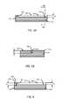
- FIG. 6Ais a top plan view illustrating pieces of strengthened glass that have been separated from the substrate shown in FIG. 1 according to the processes exemplarily described with respect to FIGS. 2A-5 .
- FIG. 6Bis a side plan view illustrating a piece of strengthened glass shown in FIG. 6A .
- each article 600 or 602can include a first surface 102 ′ and a second surface 104 ′ corresponding to the first surface 102 and second surface 104 , respectively, of the substrate 100 .
- Each articlecan further include an edge 604 obtained upon separating the substrate 100 .
- the edge 604can include the edge surface 504 and a notch region 606 .
- the notch region 606corresponds to the portions of the substrate 100 that were exposed to guide trench 200 , the initiation trench 400 or a combination thereof.
- the notch region 606extends from an edge 608 of the edge surface 504 and an edge 610 of the first surface 102 ′.
- the notch region 606may have a depth d 4 that is greater than, less than, or equal to any of depths d 2 or d 3 .
- d 4may be substantially equal to d 2 or d 3 .
- d 4can be measured as the distance between edges 608 and 610 along a direction that is at least substantially perpendicular to the first surface 102 ′ (or second surface 104 ′) or along a direction that is at least substantially parallel to the edge surface 504 .
- the notch region 606may have a width w 2 that is greater than, less than, or equal to width w 1 .
- w 2may be substantially 50% of w 1 .
- w 2can be measured as the distance between edges 608 and 610 along a direction that is at least substantially perpendicular to the edge surface 504 or along a direction that is at least substantially parallel to the first surface 102 ′ (or second surface 104 ′).
- Strengthened glass articlessuch as article 600 or 602
- ITinformation-related terminals
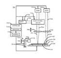
- FIG. 7schematically illustrates one embodiment of an apparatus configured to perform the processes exemplarily described with respect to FIGS. 2A-6B .
- an apparatussuch as apparatus 700 can separate a strengthened glass substrate such as substrate 100 .
- the apparatus 700may include a workpiece positioning system and a laser system.
- the workpiece support systemis configured to support the substrate 100 such that the first surface 102 faces toward the laser system and such that the beam waist is locatable relative to the substrate 100 as exemplarily described above with respect to FIG. 2B .
- the workpiece support systemcan include a chuck such as chuck 702 configured to support the substrate 100 and a movable stage 704 configured to move the chuck 702 .
- the chuck 702can be configured to contact only a portion of the second surface 104 of substrate 100 (as illustrated) or may contact all of the second surface 104 .
- the moveable stage 704is configured to move the chuck 702 laterally relative to the laser system. Thus the moveable stage 704 can be operated to cause the beam waist to be scanned relative to the substrate 100 .
- the laser systemis configured to direct a beam such as the aforementioned beam 202 along an optical path (wherein the beam 202 has a beam waist as exemplarily described above with respect to beam waist 204 ).
- the laser systemmay include a laser 706 configured to produce a beam 702 a of laser light and an optical assembly 708 configured to focus the beam 702 a to produce the beam waist 204 .
- the optical assembly 708may include a lens and may be moveable along a direction indicated by arrow 708 a to change the location (e.g., along a z-axis) of the beam waist of the beam 202 relative to the substrate 100 .
- the laser systemmay further include a beam steering system 710 configured to move the beam waist of the beam 202 laterally relative to the substrate 100 and the workpiece support system.
- the beam steering system 710can include a galvanometer, a fast steering mirror, an acousto-optic deflector, an electro-optic deflector or the like or a combination thereof.
- the beam steering system 710can be operated to cause the beam waist to be scanned relative to the substrate 100 .
- the apparatus 700may further include a controller 712 communicatively coupled to one or more of the components of the laser system, to one or more of the components of the workpiece support system, or a combination thereof.
- the controllermay include a processor 714 and a memory 716 .
- the processor 714may be configured to execute instructions stored by the memory 716 to control an operation of at least one component of the laser system, the workpiece support system, or a combination thereof so that the embodiments exemplarily described above with respect to FIGS. 1 to 5 can be performed.
- the processor 714can include operating logic (not shown) that defines various control functions, and may be in the form of dedicated hardware, such as a hardwired state machine, a processor executing programming instructions, and/or a different form as would occur to those skilled in the art. Operating logic may include digital circuitry, analog circuitry, software, or a hybrid combination of any of these types.
- processor 714includes a programmable microcontroller microprocessor, or other processor that can include one or more processing units arranged to execute instructions stored in memory 716 in accordance with the operating logic.
- Memory 716can include one or more types including semiconductor, magnetic, and/or optical varieties, and/or may be of a volatile and/or nonvolatile variety.
- memory 716stores instructions that can be executed by the operating logic. Alternatively or additionally, memory 716 may store data that is manipulated by the operating logic. In one arrangement, operating logic and memory are included in a controller/processor form of operating logic that manages and controls operational aspects of any component of the apparatus 700 , although in other arrangements they may be separate.
- the controller 712may control an operation of one or both the laser system and the workpiece positioning system to form the initiation trench 400 using the laser 706 . In another embodiment, the controller 712 may control an operation of at least one of the laser system, the workpiece positioning system and a vent crack initiator system to form the initiation trench 400 .
- a vent crack initiator systemsuch as vent crack initiator system 718 may be included within the apparatus 700 .
- the vent crack initiator system 718can include a vent crack initiator device 720 operative to form the aforementioned initiation trench 400 .
- the vent crack initiator device 720may be coupled to a positioning assembly 722 (e.g., a dual-axis robot) configured to move the vent crack initiator device 720 (e.g., along a direction indicated by one or both of arrows 718 a and 718 b ).
- the vent crack initiator device 720may include a grinding wheel, a cutting blade, a laser source, an etchant nozzle or the like or a combination thereof.
- another vent crack initiator systemmay include a laser, such as laser 724 , operative to generate a beam of light and direct the beam of light into the aforementioned laser system facilitate formation of the initiation trench 400 .
- another vent crack initiator systemmay include a supplemental laser system configured to generate a beam 726 of laser light sufficient to form the initiation trench 400 as exemplarily described above.
- the supplemental laser systemcan include a laser 728 operative to generate a beam 728 a of light an optical assembly 730 configured to focus the beam 728 a direct the beam 726 to the substrate 100 .
Landscapes
- Physics & Mathematics (AREA)
- Optics & Photonics (AREA)
- Engineering & Computer Science (AREA)
- Plasma & Fusion (AREA)
- Mechanical Engineering (AREA)
- Chemical & Material Sciences (AREA)
- Materials Engineering (AREA)
- Organic Chemistry (AREA)
- Health & Medical Sciences (AREA)
- Toxicology (AREA)
- Life Sciences & Earth Sciences (AREA)
- Chemical Kinetics & Catalysis (AREA)
- General Chemical & Material Sciences (AREA)
- Geochemistry & Mineralogy (AREA)
- Re-Forming, After-Treatment, Cutting And Transporting Of Glass Products (AREA)
- Laser Beam Processing (AREA)
Abstract
Description
where CT is the central tension within the
Claims (38)
Priority Applications (1)
| Application Number | Priority Date | Filing Date | Title |
|---|---|---|---|
| US14/094,656US9828278B2 (en) | 2012-02-28 | 2013-12-02 | Method and apparatus for separation of strengthened glass and articles produced thereby |
Applications Claiming Priority (7)
| Application Number | Priority Date | Filing Date | Title |
|---|---|---|---|
| US201261604380P | 2012-02-28 | 2012-02-28 | |
| US201261705038P | 2012-09-24 | 2012-09-24 | |
| US201261705559P | 2012-09-25 | 2012-09-25 | |
| US201261732856P | 2012-12-03 | 2012-12-03 | |
| US13/778,950US9828277B2 (en) | 2012-02-28 | 2013-02-27 | Methods for separation of strengthened glass |
| US14/033,368US10357850B2 (en) | 2012-09-24 | 2013-09-20 | Method and apparatus for machining a workpiece |
| US14/094,656US9828278B2 (en) | 2012-02-28 | 2013-12-02 | Method and apparatus for separation of strengthened glass and articles produced thereby |
Related Parent Applications (2)
| Application Number | Title | Priority Date | Filing Date |
|---|---|---|---|
| US13/778,950Continuation-In-PartUS9828277B2 (en) | 2012-02-28 | 2013-02-27 | Methods for separation of strengthened glass |
| US14/033,368Continuation-In-PartUS10357850B2 (en) | 2012-02-28 | 2013-09-20 | Method and apparatus for machining a workpiece |
Publications (3)
| Publication Number | Publication Date |
|---|---|
| US20140093693A1 US20140093693A1 (en) | 2014-04-03 |
| US20170305780A9 US20170305780A9 (en) | 2017-10-26 |
| US9828278B2true US9828278B2 (en) | 2017-11-28 |
Family
ID=50385498
Family Applications (1)
| Application Number | Title | Priority Date | Filing Date |
|---|---|---|---|
| US14/094,656Expired - Fee RelatedUS9828278B2 (en) | 2012-02-28 | 2013-12-02 | Method and apparatus for separation of strengthened glass and articles produced thereby |
Country Status (1)
| Country | Link |
|---|---|
| US (1) | US9828278B2 (en) |
Cited By (3)
| Publication number | Priority date | Publication date | Assignee | Title |
|---|---|---|---|---|
| US20160004033A1 (en)* | 2013-02-28 | 2016-01-07 | Corning Incorporated | Glass mirror apparatus and methods of manufacturing a glass mirror apparatus |
| US20190135678A1 (en)* | 2014-11-10 | 2019-05-09 | Corning Incorporated | Laser processing of transparent article using multiple foci |
| US20190248702A1 (en)* | 2018-02-12 | 2019-08-15 | Samsung Display Co., Ltd. | Glass article and method for producing the same |
Families Citing this family (15)
| Publication number | Priority date | Publication date | Assignee | Title |
|---|---|---|---|---|
| KR20120073249A (en)* | 2009-08-28 | 2012-07-04 | 코닝 인코포레이티드 | Methods for laser cutting articles from chemically strengthened glass substrates |
| US10357850B2 (en) | 2012-09-24 | 2019-07-23 | Electro Scientific Industries, Inc. | Method and apparatus for machining a workpiece |
| KR20140138134A (en) | 2012-02-28 | 2014-12-03 | 일렉트로 싸이언티픽 인더스트리이즈 인코포레이티드 | Method and apparatus for separation of strengthened glass and articles produced thereby |
| WO2013130608A1 (en) | 2012-02-29 | 2013-09-06 | Electro Scientific Industries, Inc. | Methods and apparatus for machining strengthened glass and articles produced thereby |
| US9610653B2 (en) | 2012-09-21 | 2017-04-04 | Electro Scientific Industries, Inc. | Method and apparatus for separation of workpieces and articles produced thereby |
| US9328011B2 (en)* | 2013-06-04 | 2016-05-03 | Coherent, Inc. | Laser-scribing of chemically strengthened glass |
| US9776906B2 (en) | 2014-03-28 | 2017-10-03 | Electro Scientific Industries, Inc. | Laser machining strengthened glass |
| DE102014119064A1 (en)* | 2014-12-18 | 2016-06-23 | Schott Ag | Glass film with specially formed edge, process for its production and its use |
| HUE057430T2 (en)* | 2015-08-10 | 2022-05-28 | Saint Gobain | Method for cutting a thin glass layer |
| EP3359324B1 (en)* | 2015-10-07 | 2021-11-17 | Corning Incorporated | Method of laser cutting a coated substrate |
| US10919794B2 (en) | 2017-12-04 | 2021-02-16 | General Atomics | Method of cutting glass using a laser |
| JP7108517B2 (en)* | 2018-10-30 | 2022-07-28 | 浜松ホトニクス株式会社 | Laser processing equipment |
| EA202191999A1 (en)* | 2019-02-20 | 2021-11-09 | Агк Гласс Юроп | METHOD FOR MANUFACTURING PARTIALLY TEXTURED GLASS PRODUCT |
| CN114390964A (en)* | 2019-07-17 | 2022-04-22 | 安科制造集团有限公司 | Non-metallic razor blade and razor assembly |
| CN111103684B (en)* | 2020-01-06 | 2020-11-06 | 深圳市大德激光技术有限公司 | Multi-head cooperative control method and system for beam energy of laser light splitting |
Citations (159)
| Publication number | Priority date | Publication date | Assignee | Title |
|---|---|---|---|---|
| US3287200A (en)* | 1962-10-04 | 1966-11-22 | Pittsburgh Plate Glass Co | Method of strengthening glass by ion exchange and articles therefrom |
| US4702042A (en) | 1984-09-27 | 1987-10-27 | Libbey-Owens-Ford Co. | Cutting strengthened glass |
| US4828900A (en) | 1987-12-23 | 1989-05-09 | Ppg Industries, Inc. | Discrete glass cutting and edge shaping |
| US5043553A (en) | 1988-10-12 | 1991-08-27 | Rolls-Royce Plc | Method and apparatus for drilling a shaped hole in a workpiece |
| US5413664A (en) | 1990-05-09 | 1995-05-09 | Canon Kabushiki Kaisha | Apparatus for preparing a semiconductor device, photo treatment apparatus, pattern forming apparatus and fabrication apparatus |
| US5543365A (en) | 1994-12-02 | 1996-08-06 | Texas Instruments Incorporated | Wafer scribe technique using laser by forming polysilicon |
| US5609284A (en) | 1992-04-02 | 1997-03-11 | Fonon Technology Limited | Method of splitting non-metallic materials |
| US5637244A (en) | 1993-05-13 | 1997-06-10 | Podarok International, Inc. | Method and apparatus for creating an image by a pulsed laser beam inside a transparent material |
| US5656186A (en) | 1994-04-08 | 1997-08-12 | The Regents Of The University Of Michigan | Method for controlling configuration of laser induced breakdown and ablation |
| US5665134A (en) | 1995-06-07 | 1997-09-09 | Hughes Missile Systems Company | Laser machining of glass-ceramic materials |
| JPH10128563A (en)* | 1996-10-24 | 1998-05-19 | Nippon Sheet Glass Co Ltd | Laser beam machining method for micro lens |
| US5826772A (en) | 1995-08-31 | 1998-10-27 | Corning Incorporated | Method and apparatus for breaking brittle materials |
| JPH11163403A (en) | 1997-11-28 | 1999-06-18 | Nichia Chem Ind Ltd | Method for manufacturing nitride semiconductor device |
| US5973290A (en) | 1997-02-26 | 1999-10-26 | W. L. Gore & Associates, Inc. | Laser apparatus having improved via processing rate |
| US6143382A (en) | 1997-06-04 | 2000-11-07 | Nippon Sheet Glass Co., Ltd. | Glass substrate having fine holes |
| US6211488B1 (en) | 1998-12-01 | 2001-04-03 | Accudyne Display And Semiconductor Systems, Inc. | Method and apparatus for separating non-metallic substrates utilizing a laser initiated scribe |
| US20010035447A1 (en) | 2000-05-05 | 2001-11-01 | Andreas Gartner | Methods for laser cut initiation |
| US6313435B1 (en) | 1998-11-20 | 2001-11-06 | 3M Innovative Properties Company | Mask orbiting for laser ablated feature formation |
| US20010038930A1 (en) | 1997-07-24 | 2001-11-08 | Hiroki Yamamoto | Glass substrate for a magnetic disk, a magnetic disk which can be formed with a stable texture |
| US20010040150A1 (en) | 1997-10-30 | 2001-11-15 | Hoya Corporation | Glass substrate for information-recording medium and manufacturing method of the glass substrate |
| US6326589B1 (en) | 1997-09-19 | 2001-12-04 | Fraunhofer-Gesellschaft Zur Forderung Der Angewandten Forschung E.V. | Method and device for treating materials with plasma-inducing high energy radiation |
| US6333485B1 (en) | 1998-12-11 | 2001-12-25 | International Business Machines Corporation | Method for minimizing sample damage during the ablation of material using a focused ultrashort pulsed beam |
| US20020005805A1 (en) | 2000-06-12 | 2002-01-17 | Hiroshi Ogura | Method of machining glass substrate and method of fabricating high-frequency circuit |
| US20020033558A1 (en) | 2000-09-20 | 2002-03-21 | Fahey Kevin P. | UV laser cutting or shape modification of brittle, high melting temperature target materials such as ceramics or glasses |
| WO2002022301A1 (en) | 2000-09-13 | 2002-03-21 | Hamamatsu Photonics K.K. | Laser beam machining method and laser beam machining device |
| US20020037132A1 (en) | 2000-02-17 | 2002-03-28 | Sercel Peter C. | Resonant optical power control device assemblies |
| US20020041946A1 (en) | 2000-08-18 | 2002-04-11 | Nippon Sheet Glass Co., Ltd. | Process for cutting a glass sheet and a glass disk for a recording medium |
| US20020060978A1 (en) | 2000-10-10 | 2002-05-23 | Akemi Hirotsune | Information recording media, a method for recording/reproducing information, an apparatus for recording/reproducing information |
| JP2002192369A (en) | 2000-09-13 | 2002-07-10 | Hamamatsu Photonics Kk | Laser beam machining method and laser beam machining device |
| JP2002241141A (en) | 2001-02-08 | 2002-08-28 | Nippon Steel Techno Research Corp | Working method for glass by means of laser and device therefor |
| JP2002308637A (en) | 2001-04-04 | 2002-10-23 | Sony Corp | Method and apparatus for manufacturing glass substrate |
| WO2003002289A1 (en) | 2001-06-28 | 2003-01-09 | Electro Scientific Industries, Inc. | Multistep laser processing of wafers supporting surface device layers |
| US6521862B1 (en) | 2001-10-09 | 2003-02-18 | International Business Machines Corporation | Apparatus and method for improving chamfer quality of disk edge surfaces with laser treatment |
| US20030044539A1 (en) | 2001-02-06 | 2003-03-06 | Oswald Robert S. | Process for producing photovoltaic devices |
| JP2003088976A (en) | 2001-09-12 | 2003-03-25 | Hamamatsu Photonics Kk | Laser beam machining method |
| US20030096078A1 (en) | 2001-11-21 | 2003-05-22 | Nippon Sheet Glass Co., Ltd. | Glass substrate for data recording medium and manufacturing method thereof |
| US20030102291A1 (en) | 2001-11-30 | 2003-06-05 | Xinbing Liu | System and method of laser drilling |
| US20030111447A1 (en) | 2000-01-27 | 2003-06-19 | Corkum Paul B. | Method and apparatus for repair of defects in materials with short laser pulses |
| US20030150839A1 (en) | 2002-02-05 | 2003-08-14 | Fumitoshi Kobayashi | Glass substrate with fine hole and method for producing the same |
| US20030201261A1 (en) | 2000-12-01 | 2003-10-30 | Lg Electronics Inc. | Glass cutting method and apparatus |
| US6642476B2 (en) | 2001-07-23 | 2003-11-04 | Siemens Automative Corporation | Apparatus and method of forming orifices and chamfers for uniform orifice coefficient and surface properties by laser |
| US6642477B1 (en) | 2001-10-23 | 2003-11-04 | Imra America, Inc. | Method for laser drilling a counter-tapered through-hole in a material |
| US20030217568A1 (en) | 2002-02-22 | 2003-11-27 | Hirotaka Koyo | Glass structure and method for producing the same |
| US20040089644A1 (en) | 2002-11-12 | 2004-05-13 | Kazuma Sekiya | Laser machining method and laser machining apparatus |
| US6756563B2 (en) | 2002-03-07 | 2004-06-29 | Orbotech Ltd. | System and method for forming holes in substrates containing glass |
| US6795274B1 (en) | 1999-09-07 | 2004-09-21 | Asahi Glass Company, Ltd. | Method for manufacturing a substantially circular substrate by utilizing scribing |
| US6809291B1 (en) | 2002-08-30 | 2004-10-26 | Southeastern Universities Research Assn., Inc. | Process for laser machining and surface treatment |
| JP2004299969A (en) | 2003-03-31 | 2004-10-28 | Toshiba Ceramics Co Ltd | How to slice silica glass |
| US6820330B1 (en) | 1996-12-13 | 2004-11-23 | Tessera, Inc. | Method for forming a multi-layer circuit assembly |
| US20050042805A1 (en) | 2003-07-11 | 2005-02-24 | Swenson Edward J. | Method of forming a scribe line on a passive electronic component substrate |
| JP2005081715A (en) | 2003-09-09 | 2005-03-31 | Sony Corp | Laser beam machining apparatus and laser beam machining method |
| JP2005088023A (en) | 2003-09-12 | 2005-04-07 | Seiko Epson Corp | Transparency processing method |
| US20050087522A1 (en) | 2003-10-24 | 2005-04-28 | Yunlong Sun | Laser processing of a locally heated target material |
| JP2005144530A (en) | 2003-11-19 | 2005-06-09 | National Institute Of Advanced Industrial & Technology | Laser precision processing of transparent media |
| CN1657220A (en) | 2004-02-19 | 2005-08-24 | 佳能株式会社 | Laser based splitting method, object to be split, and semiconductor element chip |
| US20050184035A1 (en) | 1995-08-07 | 2005-08-25 | Mitsubishi Denki Kabushiki Kaisha | Pulsed laser beam machining method and apparatus for machining a wiring board at multiple locations |
| US20050221044A1 (en) | 2002-05-07 | 2005-10-06 | Saint-Gobain Glass France | Glass cutting method which does not involve breaking |
| US20050230365A1 (en) | 2004-04-14 | 2005-10-20 | Weisheng Lei | Methods of drilling through-holes in homogenous and non-homogeneous substrates |
| US6962279B1 (en) | 2000-10-18 | 2005-11-08 | Ge Medical Systems Global Technology Company, Llc | Apparatus and method for glass separation for flat panel displays |
| US20060021978A1 (en) | 2002-02-21 | 2006-02-02 | Alexeev Andrey M | Method for cutting non-metallic materials and device for carring out said method |
| US7007512B2 (en) | 2000-11-17 | 2006-03-07 | National Institute Of Advanced Industrial Science And Technology | Method for machining glass substrate |
| US20060049156A1 (en) | 2002-02-15 | 2006-03-09 | Michael Mulloy | Method of forming substrate for fluid ejection device |
| US7023001B2 (en) | 2003-03-31 | 2006-04-04 | Institut National D'optique | Method for engraving materials using laser etched V-grooves |
| US20060091125A1 (en)* | 2004-11-03 | 2006-05-04 | Intel Corporation | Laser micromachining method |
| DE10029110B4 (en) | 1999-06-15 | 2006-05-18 | Fraunhofer-Gesellschaft zur Förderung der angewandten Forschung e.V. | Method for material processing and use thereof |
| US7060933B2 (en) | 2004-06-08 | 2006-06-13 | Igor Troitski | Method and laser system for production of laser-induced images inside and on the surface of transparent material |
| US20060151450A1 (en) | 2003-01-06 | 2006-07-13 | Ki-Yong You | Glass-plate cutting machine |
| US20060169677A1 (en) | 2005-02-03 | 2006-08-03 | Laserfacturing Inc. | Method and apparatus for via drilling and selective material removal using an ultrafast pulse laser |
| US20070012665A1 (en) | 2005-07-12 | 2007-01-18 | Hewlett-Packard Development Company Lp | Laser ablation |
| US20070039932A1 (en) | 2004-04-27 | 2007-02-22 | Michael Haase | Device for separative machining of components made from brittle material with stress-free component mounting |
| US20070170162A1 (en) | 2004-05-14 | 2007-07-26 | Oliver Haupt | Method and device for cutting through semiconductor materials |
| JP2007283318A (en) | 2006-04-13 | 2007-11-01 | Seiko Epson Corp | Substrate manufacturing method, laser processing device, display device, electro-optical device, electronic device |
| JP2007290011A (en) | 2006-04-26 | 2007-11-08 | Seiko Epson Corp | Substrate and substrate cutting method, electro-optical device, electronic apparatus |
| CN101073145A (en) | 2004-12-08 | 2007-11-14 | 雷射先进科技株式会社 | Division starting poin forming method in body to be divided, dividing method for body to be divided, and method of processing work by pulse laser beam |
| US20070262464A1 (en) | 2004-08-24 | 2007-11-15 | Micron Technology, Inc. | Method of forming vias in semiconductor substrates and resulting structures |
| US20070272668A1 (en) | 2006-05-25 | 2007-11-29 | Albelo Jeffrey A | Ultrashort laser pulse wafer scribing |
| US20070272666A1 (en) | 2006-05-25 | 2007-11-29 | O'brien James N | Infrared laser wafer scribing using short pulses |
| JP2007319881A (en) | 2006-05-31 | 2007-12-13 | Seiko Epson Corp | Substrate manufacturing method, laser processing device, display device, electro-optical device, electronic device |
| US20070291496A1 (en) | 2006-06-02 | 2007-12-20 | Electro Scientific Industries, Inc. | Process for optically transparent via filling |
| DE102006046313B3 (en) | 2006-09-29 | 2008-01-24 | Fraunhofer-Gesellschaft zur Förderung der angewandten Forschung e.V. | Method for structuring fiber optic line along longitudinal axis e.g., for telecommunications, involves passing laser beam through focusing optics onto surface of fiber |
| US20080050888A1 (en) | 2006-08-24 | 2008-02-28 | Sean Matthew Garner | Laser separation of thin laminated glass substrates for flexible display applications |
| US20080047933A1 (en) | 2004-03-18 | 2008-02-28 | Antti Salminen | Method For Machining A Material With High-Power Density Electromagnetic Radiation |
| US20080093775A1 (en) | 2006-08-19 | 2008-04-24 | Colorado State University Research Foundation | Nanometer-scale ablation using focused, coherent extreme ultraviolet/soft x-ray light |
| US7378342B2 (en) | 2004-08-27 | 2008-05-27 | Micron Technology, Inc. | Methods for forming vias varying lateral dimensions |
| US20080128953A1 (en) | 2003-05-19 | 2008-06-05 | Yusuke Nagai | Workpiece dividing method utilizing laser beam |
| US20080185367A1 (en) | 2007-02-01 | 2008-08-07 | Uri El-Hanany | Method and system of machining using a beam of photons |
| DE102007009786A1 (en) | 2007-02-27 | 2008-08-28 | Schott Ag | Process to surface harden a glass panel whose material contains sodium by treatment with potassium nitrate |
| WO2008108332A1 (en) | 2007-03-02 | 2008-09-12 | Nippon Electric Glass Co., Ltd. | Reinforced plate glass and method for manufacturing the same |
| US20080283509A1 (en) | 2007-05-15 | 2008-11-20 | Anatoli Anatolyevich Abramov | Method and apparatus for scoring and separating a brittle material with a single beam of radiation |
| US20080290077A1 (en) | 2007-05-22 | 2008-11-27 | Demeritt Jeffery Alan | Separation of transparent glasses and systems and methods therefor |
| US20080296273A1 (en) | 2007-06-01 | 2008-12-04 | Electro Scientific Industries, Inc. | Method of and apparatus for laser drilling holes with improved taper |
| US20090020511A1 (en) | 2007-07-17 | 2009-01-22 | Kommera Swaroop K | Ablation |
| US20090045179A1 (en) | 2007-08-15 | 2009-02-19 | Ellen Marie Kosik Williams | Method and system for cutting solid materials using short pulsed laser |
| JP2009061462A (en) | 2007-09-05 | 2009-03-26 | Sumitomo Electric Ind Ltd | Substrate manufacturing method and substrate |
| JP2009072829A (en) | 2007-09-21 | 2009-04-09 | Icu Research & Industrial Cooperation Group | Substrate cutting apparatus using ultra-short pulse laser beam and cutting method therefor |
| US20090201444A1 (en) | 2001-11-08 | 2009-08-13 | Koji Yamabuchi | Method and apparatus for cutting apart a glass substrate, liquid crystal panel, and apparatus for fabricating a liquid crystal panel |
| US20090212030A1 (en) | 2008-02-25 | 2009-08-27 | Optisolar, Inc., A Delaware Corporation | Autofocus for Ablation Laser |
| EP2096375A1 (en) | 2008-02-26 | 2009-09-02 | Rioglass Solar, S.A. | A reflector element for a solar heat reflector and the method for producing the same |
| US20090224432A1 (en) | 2004-12-08 | 2009-09-10 | Syohei Nagatomo | Method of forming split originating point on object to be split, method of splitting object to be split, and method of processing object to be processed by pulse laser beam |
| US20090242525A1 (en) | 2008-03-31 | 2009-10-01 | Electro Scientific Industries, Inc. | Laser machining of fired ceramic and other hard and/or thick materials |
| US7605344B2 (en) | 2003-07-18 | 2009-10-20 | Hamamatsu Photonics K.K. | Laser beam machining method, laser beam machining apparatus, and laser beam machining product |
| JP2009280452A (en) | 2008-05-23 | 2009-12-03 | Central Glass Co Ltd | Glass substrate and method for producing the same |
| US20100025387A1 (en)* | 2005-09-08 | 2010-02-04 | Imra America, Inc. | Transparent material processing with an ultrashort pulse laser |
| KR20100031462A (en) | 2008-09-12 | 2010-03-22 | 오므론 가부시키가이샤 | Forming method and device of scribing-line for cutting |
| US7723212B2 (en) | 2004-07-30 | 2010-05-25 | Mitsuboshi Diamond Industrial Co., Ltd | Method for forming median crack in substrate and apparatus for forming median crack in substrate |
| US20100147813A1 (en) | 2008-12-17 | 2010-06-17 | Electro Scientific Industries, Inc. | Method for laser processing glass with a chamfered edge |
| JP2010142862A (en) | 2008-12-22 | 2010-07-01 | Cyber Laser Kk | Method for producing nano-periodic structure on surface of dielectric material |
| US20100197116A1 (en) | 2008-03-21 | 2010-08-05 | Imra America, Inc. | Laser-based material processing methods and systems |
| US20100206008A1 (en) | 2009-02-19 | 2010-08-19 | Harvey Daniel R | Method of separating strengthened glass |
| US20100221583A1 (en) | 2009-02-27 | 2010-09-02 | Applied Materials, Inc. | Hdd pattern implant system |
| US20100243626A1 (en) | 2009-03-28 | 2010-09-30 | Electro Scientific Industries, Inc. | Method and Apparatus for Laser Machining |
| US20100291353A1 (en) | 2009-02-19 | 2010-11-18 | Matthew John Dejneka | Method of separating strengthened glass |
| CN101903301A (en) | 2007-12-18 | 2010-12-01 | Hoya株式会社 | Cover glass for mobile terminal, method for manufacturing same, and mobile terminal device |
| US20100301024A1 (en) | 2009-05-28 | 2010-12-02 | Electro Scientific Industries, Inc. | Laser processing systems using through-the-lens alignment of a laser beam with a target feature |
| US20100320179A1 (en) | 2007-10-16 | 2010-12-23 | Hideki Morita | Method for Creating Trench in U Shape in Brittle Material Substrate, Method for Removing Process, Method for Hollowing Process and Chamfering Method Using Same |
| WO2011025903A1 (en) | 2009-08-28 | 2011-03-03 | Corning Incorporated | Methods for laser cutting glass substrates |
| WO2011025908A1 (en) | 2009-08-28 | 2011-03-03 | Corning Incorporated | Methods for laser cutting articles from chemically strengthened glass substrates |
| JP2011088179A (en) | 2009-10-22 | 2011-05-06 | V Technology Co Ltd | Laser beam machining apparatus |
| US20110127242A1 (en) | 2009-11-30 | 2011-06-02 | Xinghua Li | Methods for laser scribing and separating glass substrates |
| US20110127244A1 (en) | 2009-11-30 | 2011-06-02 | Xinghua Li | Methods for laser scribing and separating glass substrates |
| US20110183116A1 (en)* | 2010-01-27 | 2011-07-28 | Jeng-Jye Hung | Method for cutting tempered glass and preparatory tempered glass structure |
| JP2011164508A (en) | 2010-02-15 | 2011-08-25 | Sony Corp | Method for manufacturing electric solid-state device, and electric solid-state device |
| US20110226832A1 (en) | 2010-03-19 | 2011-09-22 | John Frederick Bayne | Mechanical scoring and separation of strengthened glass |
| WO2011117006A1 (en) | 2010-03-22 | 2011-09-29 | Fraunhofer-Gesellschaft zur Förderung der angewandten Forschung e.V. | Process and apparatus for separating individual panes from a laminated glass sheet |
| EP2371778A1 (en) | 2010-03-30 | 2011-10-05 | Linde Aktiengesellschaft | Method for producing toughened flat glass with anti-reflective properties |
| US20110240617A1 (en) | 2004-03-31 | 2011-10-06 | Imra America, Inc. | Laser-based material processing apparatus and methods |
| US20110240611A1 (en) | 2010-03-05 | 2011-10-06 | Micronic MyData Systems AB | Methods and Device for Laser Processing |
| US20110240616A1 (en) | 2010-04-02 | 2011-10-06 | Electro Scientific Industries, Inc. | method and apparatus for laser singulation of brittle materials |
| US20110250423A1 (en) | 2008-12-25 | 2011-10-13 | Asahi Glass Company, Limited | Process and system for cutting a brittle-material plate, and window glass for a vehicle |
| US20110259631A1 (en) | 2008-12-13 | 2011-10-27 | M-Solv Ltd. | Method and apparatus for laser machining relatively narrow and relatively wide structures |
| US20110266264A1 (en) | 2009-01-03 | 2011-11-03 | Philip Thomas Rumsby | Method and apparatus for forming grooves in the surface of a polymer layer |
| JP2011230940A (en) | 2010-04-26 | 2011-11-17 | Mitsuboshi Diamond Industrial Co Ltd | Cutting method for brittle material substrate |
| US8075999B2 (en) | 2008-08-08 | 2011-12-13 | Corning Incorporated | Strengthened glass articles and methods of making |
| JP2011251879A (en) | 2010-06-02 | 2011-12-15 | Asahi Glass Co Ltd | Method and device for cutting chemically strengthened glass |
| US20110318996A1 (en) | 2010-06-28 | 2011-12-29 | Shin-Etsu Chemical Co., Ltd. | Method for manufacturing electronic grade synthetic quartz glass substrate |
| US8110419B2 (en) | 2009-08-20 | 2012-02-07 | Integrated Photovoltaic, Inc. | Process of manufacturing photovoltaic device |
| CN102356050A (en) | 2009-02-19 | 2012-02-15 | 康宁股份有限公司 | Method of separating strengthened glass |
| KR20120015366A (en) | 2010-07-19 | 2012-02-21 | 엘지디스플레이 주식회사 | Tempered glass cutting method and cutting device |
| US20120052252A1 (en) | 2010-08-26 | 2012-03-01 | Jeffrey Todd Kohli | Methods for extracting strengthened glass substrates from glass sheets |
| US20120061361A1 (en) | 2010-09-10 | 2012-03-15 | Disco Corporation | Method of dividing workpiece |
| CN102405520A (en) | 2009-03-27 | 2012-04-04 | 伊雷克托科学工业股份有限公司 | Method for laser singulation of chip scale packages on glass substrates |
| JP2012096257A (en) | 2010-11-01 | 2012-05-24 | Disco Corp | Machining method and machining device |
| US20120135195A1 (en)* | 2010-11-30 | 2012-05-31 | Gregory Scott Glaesemann | Methods for separating glass articles from strengthened glass substrate sheets |
| US20120135177A1 (en) | 2010-11-30 | 2012-05-31 | Cornejo Ivan A | Methods for forming grooves and separating strengthened glass substrate sheets |
| US20120168412A1 (en) | 2011-01-05 | 2012-07-05 | Electro Scientific Industries, Inc | Apparatus and method for forming an aperture in a substrate |
| US20120196071A1 (en) | 2011-02-01 | 2012-08-02 | Cornejo Ivan A | Strengthened glass substrate sheets and methods for fabricating glass panels from glass substrate sheets |
| US20120211923A1 (en) | 2011-02-18 | 2012-08-23 | Sean Matthew Garner | Laser cutting method |
| US20120328905A1 (en)* | 2006-09-29 | 2012-12-27 | University Of Rochester | Nanostructured materials, methods, and applications |
| US20130037992A1 (en) | 2006-08-04 | 2013-02-14 | Erel Milshtein | Laser scribing apparatus, systems, and methods |
| US8383983B2 (en) | 2009-03-25 | 2013-02-26 | Samsung Display Co., Ltd. | Substrate cutting apparatus and method of cutting substrate using the same |
| US20130129947A1 (en) | 2011-11-18 | 2013-05-23 | Daniel Ralph Harvey | Glass article having high damage resistance |
| US20130155004A1 (en) | 2011-12-16 | 2013-06-20 | Micro Technology Co., Ltd. | Strengthened glass, touch panel and method of manufacturing strengthened glass |
| US20130192305A1 (en) | 2011-08-10 | 2013-08-01 | Matthew L. Black | Methods for separating glass substrate sheets by laser-formed grooves |
| US20130224439A1 (en) | 2012-02-28 | 2013-08-29 | Electro Scientific Industries, Inc. | Method and apparatus for separation of strengthened glass and articles produced thereby |
| US20130221053A1 (en) | 2012-02-28 | 2013-08-29 | Electro Scientific Industries, Inc. | Method and apparatus for separation of strengthened glass and articles produced thereby |
| US8584354B2 (en) | 2010-08-26 | 2013-11-19 | Corning Incorporated | Method for making glass interposer panels |
| US20130323469A1 (en)* | 2012-06-05 | 2013-12-05 | Corning Incorporated | Methods of cutting glass using a laser |
| US20130328905A1 (en)* | 2010-01-06 | 2013-12-12 | Canon Kabushiki Kaisha | Image processing apparatus and image processing method |
| US8720228B2 (en) | 2010-08-31 | 2014-05-13 | Corning Incorporated | Methods of separating strengthened glass substrates |
- 2013
- 2013-12-02USUS14/094,656patent/US9828278B2/ennot_activeExpired - Fee Related
Patent Citations (180)
| Publication number | Priority date | Publication date | Assignee | Title |
|---|---|---|---|---|
| US3287200A (en)* | 1962-10-04 | 1966-11-22 | Pittsburgh Plate Glass Co | Method of strengthening glass by ion exchange and articles therefrom |
| US4702042A (en) | 1984-09-27 | 1987-10-27 | Libbey-Owens-Ford Co. | Cutting strengthened glass |
| US4828900A (en) | 1987-12-23 | 1989-05-09 | Ppg Industries, Inc. | Discrete glass cutting and edge shaping |
| EP0321838B1 (en) | 1987-12-23 | 1993-02-24 | Ppg Industries, Inc. | Discrete glass cutting and edge shaping |
| US5043553A (en) | 1988-10-12 | 1991-08-27 | Rolls-Royce Plc | Method and apparatus for drilling a shaped hole in a workpiece |
| US5413664A (en) | 1990-05-09 | 1995-05-09 | Canon Kabushiki Kaisha | Apparatus for preparing a semiconductor device, photo treatment apparatus, pattern forming apparatus and fabrication apparatus |
| US5609284A (en) | 1992-04-02 | 1997-03-11 | Fonon Technology Limited | Method of splitting non-metallic materials |
| US5637244A (en) | 1993-05-13 | 1997-06-10 | Podarok International, Inc. | Method and apparatus for creating an image by a pulsed laser beam inside a transparent material |
| US5656186A (en) | 1994-04-08 | 1997-08-12 | The Regents Of The University Of Michigan | Method for controlling configuration of laser induced breakdown and ablation |
| US5543365A (en) | 1994-12-02 | 1996-08-06 | Texas Instruments Incorporated | Wafer scribe technique using laser by forming polysilicon |
| US5665134A (en) | 1995-06-07 | 1997-09-09 | Hughes Missile Systems Company | Laser machining of glass-ceramic materials |
| US20050184035A1 (en) | 1995-08-07 | 2005-08-25 | Mitsubishi Denki Kabushiki Kaisha | Pulsed laser beam machining method and apparatus for machining a wiring board at multiple locations |
| US5826772A (en) | 1995-08-31 | 1998-10-27 | Corning Incorporated | Method and apparatus for breaking brittle materials |
| JPH10128563A (en)* | 1996-10-24 | 1998-05-19 | Nippon Sheet Glass Co Ltd | Laser beam machining method for micro lens |
| US6820330B1 (en) | 1996-12-13 | 2004-11-23 | Tessera, Inc. | Method for forming a multi-layer circuit assembly |
| US5973290A (en) | 1997-02-26 | 1999-10-26 | W. L. Gore & Associates, Inc. | Laser apparatus having improved via processing rate |
| US6143382A (en) | 1997-06-04 | 2000-11-07 | Nippon Sheet Glass Co., Ltd. | Glass substrate having fine holes |
| US20010038930A1 (en) | 1997-07-24 | 2001-11-08 | Hiroki Yamamoto | Glass substrate for a magnetic disk, a magnetic disk which can be formed with a stable texture |
| US6326589B1 (en) | 1997-09-19 | 2001-12-04 | Fraunhofer-Gesellschaft Zur Forderung Der Angewandten Forschung E.V. | Method and device for treating materials with plasma-inducing high energy radiation |
| US20010040150A1 (en) | 1997-10-30 | 2001-11-15 | Hoya Corporation | Glass substrate for information-recording medium and manufacturing method of the glass substrate |
| JPH11163403A (en) | 1997-11-28 | 1999-06-18 | Nichia Chem Ind Ltd | Method for manufacturing nitride semiconductor device |
| US6313435B1 (en) | 1998-11-20 | 2001-11-06 | 3M Innovative Properties Company | Mask orbiting for laser ablated feature formation |
| US6211488B1 (en) | 1998-12-01 | 2001-04-03 | Accudyne Display And Semiconductor Systems, Inc. | Method and apparatus for separating non-metallic substrates utilizing a laser initiated scribe |
| US6333485B1 (en) | 1998-12-11 | 2001-12-25 | International Business Machines Corporation | Method for minimizing sample damage during the ablation of material using a focused ultrashort pulsed beam |
| DE10029110B4 (en) | 1999-06-15 | 2006-05-18 | Fraunhofer-Gesellschaft zur Förderung der angewandten Forschung e.V. | Method for material processing and use thereof |
| US6795274B1 (en) | 1999-09-07 | 2004-09-21 | Asahi Glass Company, Ltd. | Method for manufacturing a substantially circular substrate by utilizing scribing |
| US20030111447A1 (en) | 2000-01-27 | 2003-06-19 | Corkum Paul B. | Method and apparatus for repair of defects in materials with short laser pulses |
| US20020037132A1 (en) | 2000-02-17 | 2002-03-28 | Sercel Peter C. | Resonant optical power control device assemblies |
| US20010035447A1 (en) | 2000-05-05 | 2001-11-01 | Andreas Gartner | Methods for laser cut initiation |
| US20040200067A1 (en) | 2000-06-12 | 2004-10-14 | Masushita Electric Industrial Co., Ltd. | Method of machining glass substrate and method of fabricating high-frequency circuit |
| US20020005805A1 (en) | 2000-06-12 | 2002-01-17 | Hiroshi Ogura | Method of machining glass substrate and method of fabricating high-frequency circuit |
| US20040104846A1 (en) | 2000-06-12 | 2004-06-03 | Matsushita Electrical Industrial Co., Ltd. | Method of machining glass substrate and method of fabricating high-frequency circuit |
| US20020041946A1 (en) | 2000-08-18 | 2002-04-11 | Nippon Sheet Glass Co., Ltd. | Process for cutting a glass sheet and a glass disk for a recording medium |
| US6634186B2 (en) | 2000-08-18 | 2003-10-21 | Nippon Sheet Glass Co., Ltd. | Process for cutting a glass sheet and a glass disk for a recording medium |
| WO2002022301A1 (en) | 2000-09-13 | 2002-03-21 | Hamamatsu Photonics K.K. | Laser beam machining method and laser beam machining device |
| US6992026B2 (en) | 2000-09-13 | 2006-01-31 | Hamamatsu Photonics K.K. | Laser processing method and laser processing apparatus |
| CN100471609C (en) | 2000-09-13 | 2009-03-25 | 浜松光子学株式会社 | Object cutting method |
| JP2002192369A (en) | 2000-09-13 | 2002-07-10 | Hamamatsu Photonics Kk | Laser beam machining method and laser beam machining device |
| US20040002199A1 (en) | 2000-09-13 | 2004-01-01 | Hamamatsu Photonics K.K. | Laser processing method and laser processing apparatus |
| US20020033558A1 (en) | 2000-09-20 | 2002-03-21 | Fahey Kevin P. | UV laser cutting or shape modification of brittle, high melting temperature target materials such as ceramics or glasses |
| US20020060978A1 (en) | 2000-10-10 | 2002-05-23 | Akemi Hirotsune | Information recording media, a method for recording/reproducing information, an apparatus for recording/reproducing information |
| US6962279B1 (en) | 2000-10-18 | 2005-11-08 | Ge Medical Systems Global Technology Company, Llc | Apparatus and method for glass separation for flat panel displays |
| US7007512B2 (en) | 2000-11-17 | 2006-03-07 | National Institute Of Advanced Industrial Science And Technology | Method for machining glass substrate |
| US20030201261A1 (en) | 2000-12-01 | 2003-10-30 | Lg Electronics Inc. | Glass cutting method and apparatus |
| US20030044539A1 (en) | 2001-02-06 | 2003-03-06 | Oswald Robert S. | Process for producing photovoltaic devices |
| JP2002241141A (en) | 2001-02-08 | 2002-08-28 | Nippon Steel Techno Research Corp | Working method for glass by means of laser and device therefor |
| JP2002308637A (en) | 2001-04-04 | 2002-10-23 | Sony Corp | Method and apparatus for manufacturing glass substrate |
| WO2003002289A1 (en) | 2001-06-28 | 2003-01-09 | Electro Scientific Industries, Inc. | Multistep laser processing of wafers supporting surface device layers |
| US6642476B2 (en) | 2001-07-23 | 2003-11-04 | Siemens Automative Corporation | Apparatus and method of forming orifices and chamfers for uniform orifice coefficient and surface properties by laser |
| JP2003088976A (en) | 2001-09-12 | 2003-03-25 | Hamamatsu Photonics Kk | Laser beam machining method |
| US6521862B1 (en) | 2001-10-09 | 2003-02-18 | International Business Machines Corporation | Apparatus and method for improving chamfer quality of disk edge surfaces with laser treatment |
| US6642477B1 (en) | 2001-10-23 | 2003-11-04 | Imra America, Inc. | Method for laser drilling a counter-tapered through-hole in a material |
| US20090201444A1 (en) | 2001-11-08 | 2009-08-13 | Koji Yamabuchi | Method and apparatus for cutting apart a glass substrate, liquid crystal panel, and apparatus for fabricating a liquid crystal panel |
| US20030096078A1 (en) | 2001-11-21 | 2003-05-22 | Nippon Sheet Glass Co., Ltd. | Glass substrate for data recording medium and manufacturing method thereof |
| US20050223744A1 (en) | 2001-11-21 | 2005-10-13 | Tamaki Horisaka | Glass substrate for data recording medium and manufacturing method thereof |
| US20030102291A1 (en) | 2001-11-30 | 2003-06-05 | Xinbing Liu | System and method of laser drilling |
| US20060127640A1 (en) | 2002-02-05 | 2006-06-15 | Fumitoshi Kobayashi | Glass substrate with fine hole and method for producing the same |
| US20030150839A1 (en) | 2002-02-05 | 2003-08-14 | Fumitoshi Kobayashi | Glass substrate with fine hole and method for producing the same |
| US20060049156A1 (en) | 2002-02-15 | 2006-03-09 | Michael Mulloy | Method of forming substrate for fluid ejection device |
| US20060021978A1 (en) | 2002-02-21 | 2006-02-02 | Alexeev Andrey M | Method for cutting non-metallic materials and device for carring out said method |
| US7217448B2 (en) | 2002-02-22 | 2007-05-15 | Nippon Sheet Glass Co., Ltd. | Glass structure and method for producing the same |
| US20030217568A1 (en) | 2002-02-22 | 2003-11-27 | Hirotaka Koyo | Glass structure and method for producing the same |
| US6756563B2 (en) | 2002-03-07 | 2004-06-29 | Orbotech Ltd. | System and method for forming holes in substrates containing glass |
| US20050221044A1 (en) | 2002-05-07 | 2005-10-06 | Saint-Gobain Glass France | Glass cutting method which does not involve breaking |
| US6809291B1 (en) | 2002-08-30 | 2004-10-26 | Southeastern Universities Research Assn., Inc. | Process for laser machining and surface treatment |
| US20040089644A1 (en) | 2002-11-12 | 2004-05-13 | Kazuma Sekiya | Laser machining method and laser machining apparatus |
| US20060151450A1 (en) | 2003-01-06 | 2006-07-13 | Ki-Yong You | Glass-plate cutting machine |
| JP2004299969A (en) | 2003-03-31 | 2004-10-28 | Toshiba Ceramics Co Ltd | How to slice silica glass |
| US7023001B2 (en) | 2003-03-31 | 2006-04-04 | Institut National D'optique | Method for engraving materials using laser etched V-grooves |
| US20080128953A1 (en) | 2003-05-19 | 2008-06-05 | Yusuke Nagai | Workpiece dividing method utilizing laser beam |
| US20050042805A1 (en) | 2003-07-11 | 2005-02-24 | Swenson Edward J. | Method of forming a scribe line on a passive electronic component substrate |
| US7605344B2 (en) | 2003-07-18 | 2009-10-20 | Hamamatsu Photonics K.K. | Laser beam machining method, laser beam machining apparatus, and laser beam machining product |
| JP2005081715A (en) | 2003-09-09 | 2005-03-31 | Sony Corp | Laser beam machining apparatus and laser beam machining method |
| JP2005088023A (en) | 2003-09-12 | 2005-04-07 | Seiko Epson Corp | Transparency processing method |
| US20050087522A1 (en) | 2003-10-24 | 2005-04-28 | Yunlong Sun | Laser processing of a locally heated target material |
| JP2005144530A (en) | 2003-11-19 | 2005-06-09 | National Institute Of Advanced Industrial & Technology | Laser precision processing of transparent media |
| CN1657220A (en) | 2004-02-19 | 2005-08-24 | 佳能株式会社 | Laser based splitting method, object to be split, and semiconductor element chip |
| US20080047933A1 (en) | 2004-03-18 | 2008-02-28 | Antti Salminen | Method For Machining A Material With High-Power Density Electromagnetic Radiation |
| US20110240617A1 (en) | 2004-03-31 | 2011-10-06 | Imra America, Inc. | Laser-based material processing apparatus and methods |
| US20050230365A1 (en) | 2004-04-14 | 2005-10-20 | Weisheng Lei | Methods of drilling through-holes in homogenous and non-homogeneous substrates |
| US20070039932A1 (en) | 2004-04-27 | 2007-02-22 | Michael Haase | Device for separative machining of components made from brittle material with stress-free component mounting |
| US20070170162A1 (en) | 2004-05-14 | 2007-07-26 | Oliver Haupt | Method and device for cutting through semiconductor materials |
| US7060933B2 (en) | 2004-06-08 | 2006-06-13 | Igor Troitski | Method and laser system for production of laser-induced images inside and on the surface of transparent material |
| US7723212B2 (en) | 2004-07-30 | 2010-05-25 | Mitsuboshi Diamond Industrial Co., Ltd | Method for forming median crack in substrate and apparatus for forming median crack in substrate |
| US20070262464A1 (en) | 2004-08-24 | 2007-11-15 | Micron Technology, Inc. | Method of forming vias in semiconductor substrates and resulting structures |
| US7378342B2 (en) | 2004-08-27 | 2008-05-27 | Micron Technology, Inc. | Methods for forming vias varying lateral dimensions |
| US7169687B2 (en) | 2004-11-03 | 2007-01-30 | Intel Corporation | Laser micromachining method |
| US20060091125A1 (en)* | 2004-11-03 | 2006-05-04 | Intel Corporation | Laser micromachining method |
| CN101073145A (en) | 2004-12-08 | 2007-11-14 | 雷射先进科技株式会社 | Division starting poin forming method in body to be divided, dividing method for body to be divided, and method of processing work by pulse laser beam |
| US20090224432A1 (en) | 2004-12-08 | 2009-09-10 | Syohei Nagatomo | Method of forming split originating point on object to be split, method of splitting object to be split, and method of processing object to be processed by pulse laser beam |
| US20060169677A1 (en) | 2005-02-03 | 2006-08-03 | Laserfacturing Inc. | Method and apparatus for via drilling and selective material removal using an ultrafast pulse laser |
| US20070012665A1 (en) | 2005-07-12 | 2007-01-18 | Hewlett-Packard Development Company Lp | Laser ablation |
| US20100025387A1 (en)* | 2005-09-08 | 2010-02-04 | Imra America, Inc. | Transparent material processing with an ultrashort pulse laser |
| JP2007283318A (en) | 2006-04-13 | 2007-11-01 | Seiko Epson Corp | Substrate manufacturing method, laser processing device, display device, electro-optical device, electronic device |
| JP2007290011A (en) | 2006-04-26 | 2007-11-08 | Seiko Epson Corp | Substrate and substrate cutting method, electro-optical device, electronic apparatus |
| US20070272666A1 (en) | 2006-05-25 | 2007-11-29 | O'brien James N | Infrared laser wafer scribing using short pulses |
| US20070272668A1 (en) | 2006-05-25 | 2007-11-29 | Albelo Jeffrey A | Ultrashort laser pulse wafer scribing |
| JP2007319881A (en) | 2006-05-31 | 2007-12-13 | Seiko Epson Corp | Substrate manufacturing method, laser processing device, display device, electro-optical device, electronic device |
| US20070291496A1 (en) | 2006-06-02 | 2007-12-20 | Electro Scientific Industries, Inc. | Process for optically transparent via filling |
| US20130037992A1 (en) | 2006-08-04 | 2013-02-14 | Erel Milshtein | Laser scribing apparatus, systems, and methods |
| US20080093775A1 (en) | 2006-08-19 | 2008-04-24 | Colorado State University Research Foundation | Nanometer-scale ablation using focused, coherent extreme ultraviolet/soft x-ray light |
| US20080050888A1 (en) | 2006-08-24 | 2008-02-28 | Sean Matthew Garner | Laser separation of thin laminated glass substrates for flexible display applications |
| US20120328905A1 (en)* | 2006-09-29 | 2012-12-27 | University Of Rochester | Nanostructured materials, methods, and applications |
| DE102006046313B3 (en) | 2006-09-29 | 2008-01-24 | Fraunhofer-Gesellschaft zur Förderung der angewandten Forschung e.V. | Method for structuring fiber optic line along longitudinal axis e.g., for telecommunications, involves passing laser beam through focusing optics onto surface of fiber |
| US20080185367A1 (en) | 2007-02-01 | 2008-08-07 | Uri El-Hanany | Method and system of machining using a beam of photons |
| DE102007009786A1 (en) | 2007-02-27 | 2008-08-28 | Schott Ag | Process to surface harden a glass panel whose material contains sodium by treatment with potassium nitrate |
| WO2008108332A1 (en) | 2007-03-02 | 2008-09-12 | Nippon Electric Glass Co., Ltd. | Reinforced plate glass and method for manufacturing the same |
| US20080283509A1 (en) | 2007-05-15 | 2008-11-20 | Anatoli Anatolyevich Abramov | Method and apparatus for scoring and separating a brittle material with a single beam of radiation |
| US20080290077A1 (en) | 2007-05-22 | 2008-11-27 | Demeritt Jeffery Alan | Separation of transparent glasses and systems and methods therefor |
| US20080296273A1 (en) | 2007-06-01 | 2008-12-04 | Electro Scientific Industries, Inc. | Method of and apparatus for laser drilling holes with improved taper |
| US20090020511A1 (en) | 2007-07-17 | 2009-01-22 | Kommera Swaroop K | Ablation |
| US20090045179A1 (en) | 2007-08-15 | 2009-02-19 | Ellen Marie Kosik Williams | Method and system for cutting solid materials using short pulsed laser |
| JP2009061462A (en) | 2007-09-05 | 2009-03-26 | Sumitomo Electric Ind Ltd | Substrate manufacturing method and substrate |
| JP2009072829A (en) | 2007-09-21 | 2009-04-09 | Icu Research & Industrial Cooperation Group | Substrate cutting apparatus using ultra-short pulse laser beam and cutting method therefor |
| US20100320179A1 (en) | 2007-10-16 | 2010-12-23 | Hideki Morita | Method for Creating Trench in U Shape in Brittle Material Substrate, Method for Removing Process, Method for Hollowing Process and Chamfering Method Using Same |
| US20110003619A1 (en) | 2007-12-18 | 2011-01-06 | Hoya Corporation | Cover glass for mobile terminals, manufacturing method of the same and mobile terminal device |
| CN101903301A (en) | 2007-12-18 | 2010-12-01 | Hoya株式会社 | Cover glass for mobile terminal, method for manufacturing same, and mobile terminal device |
| US20090212030A1 (en) | 2008-02-25 | 2009-08-27 | Optisolar, Inc., A Delaware Corporation | Autofocus for Ablation Laser |
| EP2096375A1 (en) | 2008-02-26 | 2009-09-02 | Rioglass Solar, S.A. | A reflector element for a solar heat reflector and the method for producing the same |
| WO2009106582A2 (en) | 2008-02-26 | 2009-09-03 | Rioglass Solar, S.A. | A reflector element for a solar heat reflector and the method for producing the same |
| JP2011517299A (en) | 2008-03-07 | 2011-06-02 | イムラ アメリカ インコーポレイテッド | Transparent material processing with ultrashort pulse laser |
| US20100197116A1 (en) | 2008-03-21 | 2010-08-05 | Imra America, Inc. | Laser-based material processing methods and systems |
| US20090242525A1 (en) | 2008-03-31 | 2009-10-01 | Electro Scientific Industries, Inc. | Laser machining of fired ceramic and other hard and/or thick materials |
| JP2009280452A (en) | 2008-05-23 | 2009-12-03 | Central Glass Co Ltd | Glass substrate and method for producing the same |
| US8075999B2 (en) | 2008-08-08 | 2011-12-13 | Corning Incorporated | Strengthened glass articles and methods of making |
| KR20100031462A (en) | 2008-09-12 | 2010-03-22 | 오므론 가부시키가이샤 | Forming method and device of scribing-line for cutting |
| CN101670487B (en) | 2008-09-12 | 2013-01-09 | 欧姆龙株式会社 | Method and device for forming line used for cutting |
| US20110259631A1 (en) | 2008-12-13 | 2011-10-27 | M-Solv Ltd. | Method and apparatus for laser machining relatively narrow and relatively wide structures |
| US20100147813A1 (en) | 2008-12-17 | 2010-06-17 | Electro Scientific Industries, Inc. | Method for laser processing glass with a chamfered edge |
| JP2010142862A (en) | 2008-12-22 | 2010-07-01 | Cyber Laser Kk | Method for producing nano-periodic structure on surface of dielectric material |
| US20110250423A1 (en) | 2008-12-25 | 2011-10-13 | Asahi Glass Company, Limited | Process and system for cutting a brittle-material plate, and window glass for a vehicle |
| US20110266264A1 (en) | 2009-01-03 | 2011-11-03 | Philip Thomas Rumsby | Method and apparatus for forming grooves in the surface of a polymer layer |
| WO2010096359A1 (en) | 2009-02-19 | 2010-08-26 | Corning Incorporated | Method of separating strengthened glass |
| CN102356050A (en) | 2009-02-19 | 2012-02-15 | 康宁股份有限公司 | Method of separating strengthened glass |
| US20100291353A1 (en) | 2009-02-19 | 2010-11-18 | Matthew John Dejneka | Method of separating strengthened glass |
| US20100206008A1 (en) | 2009-02-19 | 2010-08-19 | Harvey Daniel R | Method of separating strengthened glass |
| US20100221583A1 (en) | 2009-02-27 | 2010-09-02 | Applied Materials, Inc. | Hdd pattern implant system |
| US8383983B2 (en) | 2009-03-25 | 2013-02-26 | Samsung Display Co., Ltd. | Substrate cutting apparatus and method of cutting substrate using the same |
| CN102405520A (en) | 2009-03-27 | 2012-04-04 | 伊雷克托科学工业股份有限公司 | Method for laser singulation of chip scale packages on glass substrates |
| US8609512B2 (en) | 2009-03-27 | 2013-12-17 | Electro Scientific Industries, Inc. | Method for laser singulation of chip scale packages on glass substrates |
| US20100243626A1 (en) | 2009-03-28 | 2010-09-30 | Electro Scientific Industries, Inc. | Method and Apparatus for Laser Machining |
| US20100301024A1 (en) | 2009-05-28 | 2010-12-02 | Electro Scientific Industries, Inc. | Laser processing systems using through-the-lens alignment of a laser beam with a target feature |
| US8110419B2 (en) | 2009-08-20 | 2012-02-07 | Integrated Photovoltaic, Inc. | Process of manufacturing photovoltaic device |
| US8932510B2 (en) | 2009-08-28 | 2015-01-13 | Corning Incorporated | Methods for laser cutting glass substrates |
| US20120145331A1 (en)* | 2009-08-28 | 2012-06-14 | Kior, Inc, | Methods for laser cutting articles from ion exchanged glass substrates |
| WO2011025903A1 (en) | 2009-08-28 | 2011-03-03 | Corning Incorporated | Methods for laser cutting glass substrates |
| US20110049765A1 (en) | 2009-08-28 | 2011-03-03 | Xinghua Li | Methods for Laser Cutting Glass Substrates |
| WO2011025908A1 (en) | 2009-08-28 | 2011-03-03 | Corning Incorporated | Methods for laser cutting articles from chemically strengthened glass substrates |
| JP2011088179A (en) | 2009-10-22 | 2011-05-06 | V Technology Co Ltd | Laser beam machining apparatus |
| US20110127244A1 (en) | 2009-11-30 | 2011-06-02 | Xinghua Li | Methods for laser scribing and separating glass substrates |
| US20110127242A1 (en) | 2009-11-30 | 2011-06-02 | Xinghua Li | Methods for laser scribing and separating glass substrates |
| US20130328905A1 (en)* | 2010-01-06 | 2013-12-12 | Canon Kabushiki Kaisha | Image processing apparatus and image processing method |
| US20110183116A1 (en)* | 2010-01-27 | 2011-07-28 | Jeng-Jye Hung | Method for cutting tempered glass and preparatory tempered glass structure |
| JP2011164508A (en) | 2010-02-15 | 2011-08-25 | Sony Corp | Method for manufacturing electric solid-state device, and electric solid-state device |
| US20110240611A1 (en) | 2010-03-05 | 2011-10-06 | Micronic MyData Systems AB | Methods and Device for Laser Processing |
| US20110226832A1 (en) | 2010-03-19 | 2011-09-22 | John Frederick Bayne | Mechanical scoring and separation of strengthened glass |
| WO2011117006A1 (en) | 2010-03-22 | 2011-09-29 | Fraunhofer-Gesellschaft zur Förderung der angewandten Forschung e.V. | Process and apparatus for separating individual panes from a laminated glass sheet |
| EP2371778A1 (en) | 2010-03-30 | 2011-10-05 | Linde Aktiengesellschaft | Method for producing toughened flat glass with anti-reflective properties |
| US20110240616A1 (en) | 2010-04-02 | 2011-10-06 | Electro Scientific Industries, Inc. | method and apparatus for laser singulation of brittle materials |
| JP2011230940A (en) | 2010-04-26 | 2011-11-17 | Mitsuboshi Diamond Industrial Co Ltd | Cutting method for brittle material substrate |
| JP2011251879A (en) | 2010-06-02 | 2011-12-15 | Asahi Glass Co Ltd | Method and device for cutting chemically strengthened glass |
| US20110318996A1 (en) | 2010-06-28 | 2011-12-29 | Shin-Etsu Chemical Co., Ltd. | Method for manufacturing electronic grade synthetic quartz glass substrate |
| KR20120015366A (en) | 2010-07-19 | 2012-02-21 | 엘지디스플레이 주식회사 | Tempered glass cutting method and cutting device |
| US20120052252A1 (en) | 2010-08-26 | 2012-03-01 | Jeffrey Todd Kohli | Methods for extracting strengthened glass substrates from glass sheets |
| US8584354B2 (en) | 2010-08-26 | 2013-11-19 | Corning Incorporated | Method for making glass interposer panels |
| US8720228B2 (en) | 2010-08-31 | 2014-05-13 | Corning Incorporated | Methods of separating strengthened glass substrates |
| US20120061361A1 (en) | 2010-09-10 | 2012-03-15 | Disco Corporation | Method of dividing workpiece |
| JP2012096257A (en) | 2010-11-01 | 2012-05-24 | Disco Corp | Machining method and machining device |
| US20120135177A1 (en) | 2010-11-30 | 2012-05-31 | Cornejo Ivan A | Methods for forming grooves and separating strengthened glass substrate sheets |
| US20120135195A1 (en)* | 2010-11-30 | 2012-05-31 | Gregory Scott Glaesemann | Methods for separating glass articles from strengthened glass substrate sheets |
| US20120168412A1 (en) | 2011-01-05 | 2012-07-05 | Electro Scientific Industries, Inc | Apparatus and method for forming an aperture in a substrate |
| US20120196071A1 (en) | 2011-02-01 | 2012-08-02 | Cornejo Ivan A | Strengthened glass substrate sheets and methods for fabricating glass panels from glass substrate sheets |
| US20120211923A1 (en) | 2011-02-18 | 2012-08-23 | Sean Matthew Garner | Laser cutting method |
| US20130192305A1 (en) | 2011-08-10 | 2013-08-01 | Matthew L. Black | Methods for separating glass substrate sheets by laser-formed grooves |
| US8635887B2 (en) | 2011-08-10 | 2014-01-28 | Corning Incorporated | Methods for separating glass substrate sheets by laser-formed grooves |
| US20130129947A1 (en) | 2011-11-18 | 2013-05-23 | Daniel Ralph Harvey | Glass article having high damage resistance |
| US20130155004A1 (en) | 2011-12-16 | 2013-06-20 | Micro Technology Co., Ltd. | Strengthened glass, touch panel and method of manufacturing strengthened glass |
| US20130221053A1 (en) | 2012-02-28 | 2013-08-29 | Electro Scientific Industries, Inc. | Method and apparatus for separation of strengthened glass and articles produced thereby |
| US20130224439A1 (en) | 2012-02-28 | 2013-08-29 | Electro Scientific Industries, Inc. | Method and apparatus for separation of strengthened glass and articles produced thereby |
| US20130323469A1 (en)* | 2012-06-05 | 2013-12-05 | Corning Incorporated | Methods of cutting glass using a laser |
Non-Patent Citations (28)
| Title |
|---|
| Anatoli A. Abramov et al., "Laser Separation of Chemically Strengthened Glass" Physics Procedia 5 (2010), 285-290. (6 pages). |
| Beat Neuenschwander et al., "Processing of Metals and Dielectric Materials with PS-Laserpulses: Results, Strategies, Limitations and Needs" Proc. SPIE 7584, Laser Applications in Microelectronic and Optoelectronic Manufacturing XV, 75840R (Feb. 17, 2010); 14 pages. |
| Bradley Elkins Riley, "Evporative Etching for Non-Contact Glass Scribing Using a Single-Mode Ytterbium Fiber North Laser", North Carolina State University, 2007, 96 pages. |
| English translation of the Aug. 1, 2016 Office action concerning Chinese Patent Application No. 201380009749.6, which corresponds with the U.S. Appl. No. 13/779,183. |
| English translation of the Aug. 17, 2015 Office action concerning Chinese Patent Application No. 2009801535237,which corresponds with the subject U.S. Appl. No. 12/336,609. |
| English translation of the Aug. 30, 2016 Office action concerning Taiwan Patent Application No. 102107470, which corresponds with the U.S. Appl. No. 13/779,183. |
| English translation of the Feb. 22, 2016 Office action concerning Chinese Patent Application No. 200980153523.7, which corresponds with the subject U.S. Appl. No. 12/336,609. |
| English translation of the Feb. 7, 2017 Office action concerning Japanese Patent Application No. 2014-559964, which corresponds with the subject U.S. Appl. No. 13/778,950, 4pages. |
| English translation of the Jul. 20, 2016 Office action concerning Chinese Patent Application No. 201380009726.5 which corresponds with the U.S. Appl. No. 13/779,050. |
| English translation of the Jun. 17, 2016 Office action concerning Chinese Patent Application No. 201380009631.3 which corresponds with the related U.S. Appl. No. 13/778,950. |
| English translation of the Jun. 27, 2017 Office action concerning Japanese Patent Application No. 2015-533250. 10 pages. |
| English translation of the Mar. 17, 2016 Office action concerning Chinese Patent Application No. 201380049563.3, which corresponds with the subject U.S. Appl. No. 14/033,368. |
| English translation of the Mar. 3, 2016 Office action concerning Chinese Patent Application No. 201380009726.5, which corresponds with U.S. Appl. No. 138779,050. |
| International search report of PCT/US2013/027947, 2 pages, dated May 31, 2013. |
| J. Zhang et al., "High-Speed Machining of Glass Materials by Laser-Induced Plasma-Assisted Ablation Using a 532-nm Laser", Appl. Phys. A 67, 499-501, 1998. |
| Kunihito Nagayama et al. (2011), Pulse Laser Ablation by Reflection of Laser Pulse at Interface of Transparent Materials, Lasers-Applications in Science and Industry, Dr Krzysztof Jakubczak (Ed.), ISBN: 978-953-307-755-0, InTech, Available from: http://www.intechopen.com/books/lasers-applications-in-science-and-industry/pulse-laser-ablation-bvreflectionof-laser-pulse-at-interface-of-transparent-materials (21 pages). |
| Kunihito Nagayama et al. (2011), Pulse Laser Ablation by Reflection of Laser Pulse at Interface of Transparent Materials, Lasers—Applications in Science and Industry, Dr Krzysztof Jakubczak (Ed.), ISBN: 978-953-307-755-0, InTech, Available from: http://www.intechopen.com/books/lasers-applications-in-science-and-industry/pulse-laser-ablation-bvreflectionof-laser-pulse-at-interface-of-transparent-materials (21 pages). |
| Lawrence Shah et al., "Femtosecond Laser Deep Hole Drilling of Silicate Glasses in Air", applied Surface Science, 2001, p. 151-164. |
| Loeschner, U., et al. "Micromachining of glass with short ns-pulses and highly repetitive fs-laser pulses." Proceedings of the ICALEO. 2008. 9 pages. |
| M B Strigin, A N Chudinov, "Laser Processing of Glass by Picosecond Pulses", Quantum Electronics 24 (8) 732-735 (1994). |
| Machine translation of Japanese Pat. Appl. Pub. No. 2001-274441, published Oct. 5, 2001. |
| Rabia Qindeel et al., "IR Laser Plasma Interaction With Glass", American Journal of Applied Science 4 (12), 2007, pp. 1009-1015. |
| Rico Bohme, "Laser-Induced Backside Wet Etching of Glasses and Crystals", Nov. 6, 2007. (130 pages). |
| The Chinese office action for Chinese Patent Application No. 200980153523.7 dated Jan. 8, 2014, 7 pages. |
| The Chinese office action for Chinese Patent Application No. 200980153523.7 dated Jun. 5, 2013, 8 pages. |
| Thomas Paul Dumont, et al., "Laser Interaction With Materials: From Transparent Materials to Thin Films", Swiss Federal Institute of Technology Zurich for the degree of Doctor of Natural Sciences, Diss. ETH No. 16620, year of 2006. (162 Pages). |
| Written Opinion of PCT/US2013/027947, May 31, 2013 (7 pages). |
| Y. Hanada et al., "Laser-Induced Plasma-assisted Ablation (LIPAA): Fundamental and Industrial Applications", High- Power Laser Ablation VI, Proc. of SPIE vol. 6261, 626111-1 to-15 (2006). (15 pages). |
Cited By (7)
| Publication number | Priority date | Publication date | Assignee | Title |
|---|---|---|---|---|
| US20160004033A1 (en)* | 2013-02-28 | 2016-01-07 | Corning Incorporated | Glass mirror apparatus and methods of manufacturing a glass mirror apparatus |
| US10551590B2 (en)* | 2013-02-28 | 2020-02-04 | Corning Incorporated | Glass mirror apparatus and methods of manufacturing a glass mirror apparatus |
| US20190135678A1 (en)* | 2014-11-10 | 2019-05-09 | Corning Incorporated | Laser processing of transparent article using multiple foci |
| US10843956B2 (en)* | 2014-11-10 | 2020-11-24 | Corning Incorporated | Laser processing of transparent article using multiple foci |
| US20190248702A1 (en)* | 2018-02-12 | 2019-08-15 | Samsung Display Co., Ltd. | Glass article and method for producing the same |
| US11708301B2 (en)* | 2018-02-12 | 2023-07-25 | Samsung Display Co., Ltd. | Glass article and method for producing the same |
| US12351508B2 (en) | 2018-02-12 | 2025-07-08 | Samsung Display Co., Ltd. | Glass article and method for producing the same |
Also Published As
| Publication number | Publication date |
|---|---|
| US20170305780A9 (en) | 2017-10-26 |
| US20140093693A1 (en) | 2014-04-03 |
Similar Documents
| Publication | Publication Date | Title |
|---|---|---|
| US9828278B2 (en) | Method and apparatus for separation of strengthened glass and articles produced thereby | |
| US10357850B2 (en) | Method and apparatus for machining a workpiece | |
| US9828277B2 (en) | Methods for separation of strengthened glass | |
| JP7313390B2 (en) | Laser cutting and processing of display glass compositions | |
| US9227868B2 (en) | Method and apparatus for machining strengthened glass and articles produced thereby | |
| US20130221053A1 (en) | Method and apparatus for separation of strengthened glass and articles produced thereby | |
| TWI649148B (en) | Method for laser cutting a display glass component and glass article prepared by the method | |
| US10597321B2 (en) | Edge chamfering methods | |
| TWI679077B (en) | Methods for laser drilling materials and glass articles | |
| TWI672187B (en) | Device and method for cutting out contours from planar substrates by means of laser | |
| US9610653B2 (en) | Method and apparatus for separation of workpieces and articles produced thereby | |
| TW201601900A (en) | Laser cutting composite glass product and cutting method | |
| WO2015113024A1 (en) | Edge chamfering methods | |
| US20150059411A1 (en) | Method of separating a glass sheet from a carrier |
Legal Events
| Date | Code | Title | Description |
|---|---|---|---|
| AS | Assignment | Owner name:ELECTRO SCIENTIFIC INDUSTRIES, INC., OREGON Free format text:ASSIGNMENT OF ASSIGNORS INTEREST;ASSIGNORS:ZHANG, HAIBIN;XU, QIAN;REEL/FRAME:031967/0558 Effective date:20131202 | |
| STCF | Information on status: patent grant | Free format text:PATENTED CASE | |
| AS | Assignment | Owner name:BARCLAYS BANK PLC, AS COLLATERAL AGENT, NEW YORK Free format text:PATENT SECURITY AGREEMENT (ABL);ASSIGNORS:ELECTRO SCIENTIFIC INDUSTRIES, INC.;MKS INSTRUMENTS, INC.;NEWPORT CORPORATION;REEL/FRAME:048211/0312 Effective date:20190201 Owner name:BARCLAYS BANK PLC, AS COLLATERAL AGENT, NEW YORK Free format text:PATENT SECURITY AGREEMENT (TERM LOAN);ASSIGNORS:ELECTRO SCIENTIFIC INDUSTRIES, INC.;MKS INSTRUMENTS, INC.;NEWPORT CORPORATION;REEL/FRAME:048211/0227 Effective date:20190201 | |
| AS | Assignment | Owner name:BARCLAYS BANK PLC, AS COLLATERAL AGENT, NEW YORK Free format text:CORRECTIVE ASSIGNMENT TO CORRECT THE REMOVE U.S. PATENT NO. 7,919,646 PREVIOUSLY RECORDED ON REEL 048211 FRAME 0227. ASSIGNOR(S) HEREBY CONFIRMS THE PATENT SECURITY AGREEMENT (TERM LOAN);ASSIGNORS:ELECTRO SCIENTIFIC INDUSTRIES, INC.;MKS INSTRUMENTS, INC.;NEWPORT CORPORATION;REEL/FRAME:055006/0492 Effective date:20190201 Owner name:BARCLAYS BANK PLC, AS COLLATERAL AGENT, NEW YORK Free format text:CORRECTIVE ASSIGNMENT TO CORRECT THE REMOVE U.S. PATENT NO.7,919,646 PREVIOUSLY RECORDED ON REEL 048211 FRAME 0312. ASSIGNOR(S) HEREBY CONFIRMS THE PATENT SECURITY AGREEMENT (ABL);ASSIGNORS:ELECTRO SCIENTIFIC INDUSTRIES, INC.;MKS INSTRUMENTS, INC.;NEWPORT CORPORATION;REEL/FRAME:055668/0687 Effective date:20190201 | |
| FEPP | Fee payment procedure | Free format text:MAINTENANCE FEE REMINDER MAILED (ORIGINAL EVENT CODE: REM.); ENTITY STATUS OF PATENT OWNER: LARGE ENTITY | |
| LAPS | Lapse for failure to pay maintenance fees | Free format text:PATENT EXPIRED FOR FAILURE TO PAY MAINTENANCE FEES (ORIGINAL EVENT CODE: EXP.); ENTITY STATUS OF PATENT OWNER: LARGE ENTITY | |
| STCH | Information on status: patent discontinuation | Free format text:PATENT EXPIRED DUE TO NONPAYMENT OF MAINTENANCE FEES UNDER 37 CFR 1.362 | |
| FP | Lapsed due to failure to pay maintenance fee | Effective date:20211128 | |
| AS | Assignment | Owner name:ELECTRO SCIENTIFIC INDUSTRIES, INC., OREGON Free format text:RELEASE BY SECURED PARTY;ASSIGNOR:BARCLAYS BANK PLC;REEL/FRAME:063009/0001 Effective date:20220817 Owner name:NEWPORT CORPORATION, MASSACHUSETTS Free format text:RELEASE BY SECURED PARTY;ASSIGNOR:BARCLAYS BANK PLC;REEL/FRAME:063009/0001 Effective date:20220817 Owner name:MKS INSTRUMENTS, INC., MASSACHUSETTS Free format text:RELEASE BY SECURED PARTY;ASSIGNOR:BARCLAYS BANK PLC;REEL/FRAME:063009/0001 Effective date:20220817 Owner name:ELECTRO SCIENTIFIC INDUSTRIES, INC., OREGON Free format text:RELEASE BY SECURED PARTY;ASSIGNOR:BARCLAYS BANK PLC;REEL/FRAME:062739/0001 Effective date:20220817 Owner name:NEWPORT CORPORATION, MASSACHUSETTS Free format text:RELEASE BY SECURED PARTY;ASSIGNOR:BARCLAYS BANK PLC;REEL/FRAME:062739/0001 Effective date:20220817 Owner name:MKS INSTRUMENTS, INC., MASSACHUSETTS Free format text:RELEASE BY SECURED PARTY;ASSIGNOR:BARCLAYS BANK PLC;REEL/FRAME:062739/0001 Effective date:20220817 |