US9823090B2 - Magnetic field sensor for sensing a movement of a target object - Google Patents
Magnetic field sensor for sensing a movement of a target objectDownload PDFInfo
- Publication number
- US9823090B2 US9823090B2US14/529,606US201414529606AUS9823090B2US 9823090 B2US9823090 B2US 9823090B2US 201414529606 AUS201414529606 AUS 201414529606AUS 9823090 B2US9823090 B2US 9823090B2
- Authority
- US
- United States
- Prior art keywords
- magnetic field
- signal
- target object
- field sensor
- magnetoresistance elements
- Prior art date
- Legal status (The legal status is an assumption and is not a legal conclusion. Google has not performed a legal analysis and makes no representation as to the accuracy of the status listed.)
- Active, expires
Links
Images


Classifications
- G—PHYSICS
- G01—MEASURING; TESTING
- G01D—MEASURING NOT SPECIALLY ADAPTED FOR A SPECIFIC VARIABLE; ARRANGEMENTS FOR MEASURING TWO OR MORE VARIABLES NOT COVERED IN A SINGLE OTHER SUBCLASS; TARIFF METERING APPARATUS; MEASURING OR TESTING NOT OTHERWISE PROVIDED FOR
- G01D5/00—Mechanical means for transferring the output of a sensing member; Means for converting the output of a sensing member to another variable where the form or nature of the sensing member does not constrain the means for converting; Transducers not specially adapted for a specific variable
- G01D5/12—Mechanical means for transferring the output of a sensing member; Means for converting the output of a sensing member to another variable where the form or nature of the sensing member does not constrain the means for converting; Transducers not specially adapted for a specific variable using electric or magnetic means
- G01D5/14—Mechanical means for transferring the output of a sensing member; Means for converting the output of a sensing member to another variable where the form or nature of the sensing member does not constrain the means for converting; Transducers not specially adapted for a specific variable using electric or magnetic means influencing the magnitude of a current or voltage
- G01D5/142—Mechanical means for transferring the output of a sensing member; Means for converting the output of a sensing member to another variable where the form or nature of the sensing member does not constrain the means for converting; Transducers not specially adapted for a specific variable using electric or magnetic means influencing the magnitude of a current or voltage using Hall-effect devices
- G01D5/147—Mechanical means for transferring the output of a sensing member; Means for converting the output of a sensing member to another variable where the form or nature of the sensing member does not constrain the means for converting; Transducers not specially adapted for a specific variable using electric or magnetic means influencing the magnitude of a current or voltage using Hall-effect devices influenced by the movement of a third element, the position of Hall device and the source of magnetic field being fixed in respect to each other
- G—PHYSICS
- G01—MEASURING; TESTING
- G01D—MEASURING NOT SPECIALLY ADAPTED FOR A SPECIFIC VARIABLE; ARRANGEMENTS FOR MEASURING TWO OR MORE VARIABLES NOT COVERED IN A SINGLE OTHER SUBCLASS; TARIFF METERING APPARATUS; MEASURING OR TESTING NOT OTHERWISE PROVIDED FOR
- G01D5/00—Mechanical means for transferring the output of a sensing member; Means for converting the output of a sensing member to another variable where the form or nature of the sensing member does not constrain the means for converting; Transducers not specially adapted for a specific variable
- G01D5/12—Mechanical means for transferring the output of a sensing member; Means for converting the output of a sensing member to another variable where the form or nature of the sensing member does not constrain the means for converting; Transducers not specially adapted for a specific variable using electric or magnetic means
- G01D5/14—Mechanical means for transferring the output of a sensing member; Means for converting the output of a sensing member to another variable where the form or nature of the sensing member does not constrain the means for converting; Transducers not specially adapted for a specific variable using electric or magnetic means influencing the magnitude of a current or voltage
- G01D5/16—Mechanical means for transferring the output of a sensing member; Means for converting the output of a sensing member to another variable where the form or nature of the sensing member does not constrain the means for converting; Transducers not specially adapted for a specific variable using electric or magnetic means influencing the magnitude of a current or voltage by varying resistance
Definitions
- This inventionrelates generally to magnetic field sensors, and, more particularly, to magnetic field sensors having a substrate with magnetic field sensing elements thereupon to sense a motion of a ferromagnetic object, all arranged in a variety of relative positions.
- Magnetic field sensorsgenerally include a magnetic field sensing element and other electronic components. Some magnetic field sensors also include a permanent magnet (a hard ferromagnetic object) in a so-called “back biased” arrangement described more fully below. Other magnetic field sensors sense motion of a magnet.
- Magnetic field sensorsprovide an electrical signal representative of a sensed magnetic field.
- the sensed magnetic fieldis a magnetic field generated by the magnet, in which case, in the presence of a moving ferromagnetic object, the magnetic field generated by the magnet and sensed by the magnetic field sensor varies in accordance with a shape or profile of the moving ferromagnetic object.
- magnetic field sensors that sense a moving magnetdirectly sense variations of magnetic field magnitude and direction that result from movement of the magnet.
- Magnetic field sensorsare often used to detect movement of features of a ferromagnetic gear, such as gear teeth and/or gear slots or valleys.
- a magnetic field sensor in this applicationis commonly referred to as a “gear tooth” sensor.
- the gearis placed upon a ferromagnetic target object, for example, a camshaft in an engine.
- a ferromagnetic target objecte.g., camshaft
- Gear tooth sensorsare used, for example, in automotive applications to provide information to an engine control processor for ignition timing control, fuel management, anti-lock braking systems, wheel speed sensors, and other operations.
- Information provided by the gear tooth sensor to the engine control processorcan include, but is not limited to, an absolute angle of rotation of a ferromagnetic target object (e.g., a camshaft) as it rotates, a speed of the rotation, and a direction of the rotation.
- a ferromagnetic target objecte.g., a camshaft
- the engine control processorcan adjust the timing of firing of the ignition system and the timing of fuel injection by the fuel injection system.
- a positive digital-to-analog converter (PDAC) and a negative digital-to-analog converter (NDAC)track positive and negative peaks of a magnetic field signal, respectively, for use in generating a threshold signal.
- a varying magnetic field signalis compared to the threshold signal.
- the outputs of the PDAC and the NDACmay not be accurate indications of the positive and negative peaks of the magnetic field signal until several cycles of the signal (i.e., signal peaks) occur (i.e., until several gear teeth have passed).
- This type of magnetic field sensorwhich generally requires time to become fully accurate, is referred to herein as a so-called “precision rotation detector.”
- a “true power on state” (TPOS) detectorcan provide an accurate output signal shortly after movement of a ferromagnetic target object (e.g., camshaft) from zero rotating speed, or a low rotation speed in some applications of, for example, less than 100 rpm, or also shortly before movement slowing to zero rotating speed. Furthermore, even when the ferromagnetic target object is not moving, the TPOS detector can provide an indication of whether the TPOS detector is in front of a tooth or a valley of a gear. However, when the ferromagnetic target object is stationary, the conventional TPOS detector is not able to identify an absolute or relative angle of rotation of the ferromagnetic target object.
- the TPOS detectorcan be used in conjunction with a precision rotation detector within a common integrated circuit, each providing information to the engine control processor at different times.
- TPOS detectors and precision rotation detectorsare shown herein within a common integrated circuit. However, the TPOS detector or the precision rotation detector can also be used alone in separate circuits.
- the conventional TPOS detectorprovides an accurate output signal with only a small initial rotation of the ferromagnetic target object, and before the precision rotation detector can provide an accurate output signal.
- the TPOS detectorcan provide information to the engine control processor that can be more accurate than information provided by the precision rotation detector for time periods at the beginning and at the end of rotation of the ferromagnetic target object (e.g., start and stop of the engine and camshaft), but which may be less accurate when the object is rotating at speed.
- the engine control processorcan use the TPOS detector.
- the engine control processorcan primarily use rotation information provided by the precision rotation detector. In most conventional applications, once the magnetic field sensor switches to use the precision rotation detector, it does not return to use the TPOS detector until the ferromagnetic target object stops rotating or nearly stops rotating.
- a conventional TPOS detectoris described in U.S. Pat. No. 7,362,094, entitled “Method and Apparatus for Magnetic Article Detection,” issued Apr. 22, 2008.
- the conventional TPOS detectorincludes a comparator for comparing the magnetic field signal to a fixed, often trimmed, threshold signal.
- the conventional TPOS detectorcan be used in conjunction with and can detect rotational information about a TPOS cam (like a gear), which is disposed upon a ferromagnetic target object, e.g., an engine camshaft, configured to rotate.
- An example of an output signal from a conventional TPOS detectorhas at least two states, and typically a high and a low state.
- the state of the conventional TPOS output signalis high at some times and low at other times as the ferromagnetic target object rotates, in accordance with features on the TPOS cam (or gear) attached to the ferromagnetic target object.
- an output signal from a conventional precision rotation detectoralso has at least two states, and typically a high and a low state.
- the state of the conventional precision rotation detector output signalis high at some times and low at other times as the ferromagnetic target object rotates, also in accordance with features on the TPOS cam (or gear) attached to the ferromagnetic target object
- TPOS detectorshave the ability to differentiate a gear tooth from a gear valley, and to make such detection when the gear is rotating and when the gear is not rotating.
- some conventional precision rotation detectorshave the ability to differentiate a gear tooth from a gear valley when the gear is rotating, but not when the gear is stationary. Detectors that can identify a gear tooth from a valley are sometimes referred to as “tooth detectors.” Thus, TPOS detectors are usually tooth detectors. Some precision rotation detectors can also be tooth detectors.
- Some other conventional precision rotation detectorsare unable to differentiate a gear tooth from a valley, but instead, can differentiate an edge of a tooth of the gear from the tooth or the valley. Such detectors are sometimes referred to as “edge detectors.” Usually, TPOS detectors are not edge detectors. However, some precision rotation detectors can be edge detectors.
- the conventional magnetic field sensormust achieve an accurate output signal that accurately differentiates between gear teeth and gear valleys even in the presence of an air gap between the magnetic field sensor and the gear that may change from installation to installation or from time to time. Still further, the conventional magnetic field sensor must achieve these differentiations even in the presence of unit-to-unit variations in relative positions of the magnet and the magnetic field sensing element within the magnetic field sensor. Still further, the conventional magnetic field sensor must achieve these differentiations even in the presence of unit-to-unit variations in the magnetic field generated by the magnet. Still further, the conventional magnetic field sensor must achieve these differentiations even in the presence of variations of an axial rotation of the magnetic field sensor relative to the gear. Still further, the conventional magnetic field sensor must achieve these differentiations even in the presence of variations of temperature around the magnetic field sensor.
- a magnetic field sensorachieves an accurate output signal that accurately differentiates between gear teeth and gear valleys while using a simpler and less expensive magnet. The differentiation is achieved even in the presence of variations of mechanical and thermal parameters associated with the magnetic field sensor.
- a magnetic field sensorfor sensing a movement of a ferromagnetic target object having ferromagnetic target object features with a target feature width, includes a substrate, a first magnetoresistance element disposed upon the substrate for generating a first signal responsive to movement of the ferromagnetic target object features, and a second magnetoresistance element disposed upon the substrate for generating a second signal responsive to movement of the ferromagnetic target object features.
- the magnetic field sensorfurther includes a first combining circuit disposed upon the substrate and configured to combine the first signal and the second signal to generate a feature signal having a largest value when a ferromagnetic target object feature is centered with the first and second magnetoresistance elements.
- the magnetic field sensorfurther includes a second combining circuit disposed upon the substrate and configured to combine the first signal and the second signal to generate an edge signal having a largest value when the first magnetoresistance elements is on one side of an edge of a target feature and the second magnetoresistance element is on the other side of the same edge.
- FIG. 1is a block diagram of a prior art magnetic field sensor having a magnetic field sensing element, an electronic circuit, and a magnet;
- FIG. 1Ais a block diagram of an example of an electronic circuit that can be used as the electronic circuit of FIG. 1 ;
- FIG. 2is a block diagram of another prior art magnetic field sensor having three magnetic field sensing elements, an electronic circuit, and a magnet;
- FIG. 2Ais a block diagram of an example of an electronic circuit that can be used as the electronic circuit of FIG. 2 ;
- FIG. 3is a block diagram showing an example of a magnetic field sensor having magnetic field sensing elements and an electronic circuit both disposed on a substrate, and also having a magnet, the magnetic field sensor dispose proximate to a ferromagnetic object in the form of a ferromagnetic gear;
- FIG. 4is a block diagram showing an example of the magnetic field sensor of FIG. 3 disposed to overlap the ferromagnetic object;
- FIG. 5is a block diagram showing an example of the magnetic field sensor of FIG. 3 disposed proximate to the ferromagnetic object but with a different orientation;
- FIG. 6is a block diagram showing another example of a magnetic field sensor having magnetic field sensing elements and an electronic circuit both disposed on a substrate, and also having a different magnet, the magnetic field sensor dispose proximate to the ferromagnetic object;
- FIG. 7is a block diagram showing another example of a magnetic field sensor having magnetic field sensing elements and an electronic circuit both disposed on a substrate, having no magnet, the magnetic field sensor dispose proximate to a different ferromagnetic object in the form of a ring magnet;
- FIG. 8is a block diagram showing an example of the magnetic field sensor of FIG. 7 disposed to overlap the ferromagnetic object
- FIG. 9is a block diagram showing an example of the magnetic field sensor of FIG. 7 disposed proximate to the ferromagnetic object but with a different orientation;
- FIG. 10is a block diagram showing two magnetoresistance elements and an electronic circuit disposed upon a substrate, which can be representative of any of the above magnetic field sensing elements of FIGS. 3-9 , all disposed proximate to a ferromagnetic object;
- FIG. 11is a block diagram of two magnetoresistance elements, which can be used as the magnetic field sensing elements of any of the above magnetic field sensing elements of FIGS. 3-9 and which can be used as the two magnetoresistance elements of FIG. 10 ;
- FIG. 12is a schematic diagram showing an example of two magnetoresistance elements arranged in a bridge, where the two magnetoresistance elements can be used as any of the magnetic field sensing elements of FIGS. 3-9 and as the two magnetoresistance elements of FIGS. 10-11 ;
- FIG. 13is a schematic diagram showing another example of two magnetoresistance elements arranged in a bridge, where the two magnetoresistance elements can be used as any of the magnetic field sensing elements of FIGS. 3-9 and as the two magnetoresistance elements of FIGS. 10-11 ;
- FIG. 14is a block diagram showing an example of four magnetoresistance elements and an electronic circuit disposed upon a substrate, which can be representative of any of the above magnetic field sensing elements of FIGS. 3-9 , all disposed proximate to a ferromagnetic object;
- FIG. 15is a block diagram showing another example of four magnetoresistance elements and an electronic circuit disposed upon a substrate, which can be representative of any of the above magnetic field sensing elements of FIGS. 3-9 , all disposed proximate to a ferromagnetic object;
- FIG. 16is a schematic diagram showing an example of four magnetoresistance elements arranged separately, where the four magnetoresistance elements can be used as any of the magnetic field sensing elements of FIGS. 3-9 and as the four magnetoresistance elements of FIGS. 14-15 ;
- FIG. 17is a schematic diagram showing an example of four magnetoresistance elements arranged in a bridge, where the four magnetoresistance elements can be used as any of the magnetic field sensing elements of FIGS. 3-9 and as the four magnetoresistance elements of FIGS. 14-15 ;
- FIG. 18is a schematic diagram showing another example of four magnetoresistance elements arranged in a bridge, where the four magnetoresistance elements can be used as any of the magnetic field sensing elements of FIGS. 3-9 and as the four magnetoresistance elements of FIGS. 14-15 ;
- FIG. 19is a schematic diagram Showing an example of four magnetoresistance elements arranged in a bridge, where the four magnetoresistance elements can be used as any of the magnetic field sensing elements of FIGS. 3-9 and as the four magnetoresistance elements of FIGS. 14-15 ;
- FIG. 20is a schematic diagram showing an example of four magnetoresistance elements arranged in a bridge, where the four magnetoresistance elements can be used as any of the magnetic field sensing elements of FIGS. 3-9 and as the four magnetoresistance elements of FIGS. 14-15 ;
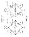
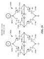
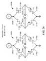
- FIG. 21is a block diagram showing an example of eight magnetoresistance elements and an electronic, circuit disposed upon a substrate, which can be representative of any of the above magnetic field sensing elements of FIGS. 3-9 , all disposed proximate to a ferromagnetic object;
- FIG. 22is a block diagram showing another example of eight magnetoresistance elements and an electronic circuit disposed upon a substrate, which can be representative of any of the above magnetic field sensing elements of FIGS. 3-9 , all disposed proximate to a ferromagnetic object;
- FIG. 23is a schematic diagram showing an example of eight magnetoresistance elements arranged in two bridges, where the eight magnetoresistance elements can be used as any of the magnetic field sensing elements of FIGS. 3-9 and as the eight magnetoresistance elements of FIGS. 21 and 22 ;
- FIG. 24is a schematic diagram showing another example of eight magnetoresistance elements arranged in two bridges, where the eight magnetoresistance elements can be used as any of the magnetic field sensing elements of FIGS. 3-9 and as the eight magnetoresistance elements of FIGS. 21 and 22 ;
- FIG. 25is a schematic diagram showing an example of eight magnetoresistance elements arranged in two bridges, where the eight magnetoresistance elements can be used as any of the magnetic field sensing elements of FIGS. 3-9 and as the eight magnetoresistance elements of FIGS. 21 and 22 ;
- FIG. 26is a schematic diagram showing an example of eight magnetoresistance elements arranged in two bridges, where the eight magnetoresistance elements can be used as any of the magnetic field sensing elements of FIGS. 3-9 and as the eight magnetoresistance elements of FIGS. 21 and 22 ;
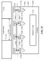
- FIG. 27is a schematic diagram showing an electronic circuit that can be used to process two signals generated by any of the above magnetic field sensors.
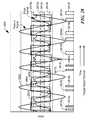
- FIG. 28is a graph showing an example of the two signals generated by any of the above magnetic field sensors.
- magnetic field sensing elementis used to describe a variety of electronic elements that can sense a magnetic field.
- the magnetic field sensing elementcan be, but is not limited to, a Hall effect element, a magnetoresistance element, or a magnetotransistor.
- Hall effect elementsfor example, a planar Hall element, a vertical Hall element, and a Circular Vertical Hall (CVH) element.
- magnetoresistance elementsfor example, a semiconductor magnetoresistance element such as Indium Antimonide (InSb), a giant magnetoresistance (GMR) element, for example, a spin valve, an anisotropic magnetoresistance element (AMR), a tunneling magnetoresistance (TMR) element, and a magnetic tunnel junction (MTJ).
- the magnetic field sensing elementmay be a single element or, alternatively, may include two or more magnetic field sensing elements arranged in various configurations, e.g., a half bridge or full (Wheatstone) bridge.
- the magnetic field sensing elementmay be a device made of a type IV semiconductor material such as Silicon (Si) or Germanium (Ge), or a type III-V semiconductor material like Gallium-Arsenide (GaAs) or an Indium compound, e.g., Indium-Antimonide (InSb).
- a type IV semiconductor materialsuch as Silicon (Si) or Germanium (Ge)
- a type III-V semiconductor materiallike Gallium-Arsenide (GaAs) or an Indium compound, e.g., Indium-Antimonide (InSb).
- some of the above-described magnetic field sensing elementstend to have an axis of maximum sensitivity parallel to a substrate that supports the magnetic field sensing element, and others of the above-described magnetic field sensing elements tend to have an axis of maximum sensitivity perpendicular to a substrate that supports the magnetic field sensing element.
- planar Hall elementstend to have axes of sensitivity perpendicular to a substrate
- metal based or metallic magnetoresistance elementse.g., GMR, TMR, AMR
- vertical Hall elementstend to have axes of sensitivity parallel to a substrate.
- magnetic field sensoris used to describe a circuit that uses a magnetic field sensing element, generally in combination with other circuits.
- Magnetic field sensorsare used in a variety of applications, including, but not limited to, an angle sensor that senses an angle of a direction of a magnetic field, a current sensor that senses a magnetic field generated by a current carried by a current-carrying conductor, a magnetic switch that senses the proximity of a ferromagnetic object, a rotation detector that senses passing ferromagnetic articles, for example, magnetic domains of a ring magnet or a ferromagnetic target (e.g., gear teeth) where the magnetic field sensor is used in combination with a back-biased or other magnet, and a magnetic field sensor that senses a magnetic field density of a magnetic field.
- an angle sensorthat senses an angle of a direction of a magnetic field
- a current sensorthat senses a magnetic field generated by a current carried by a current-carrying conductor
- a magnetic switchthat
- the term “accuracy,” when referring to a magnetic field sensor,is used to refer to a variety of aspects of the magnetic field sensor. These aspects include, but are not limited to, an ability of the magnetic field sensor to differentiate: a gear tooth from a gear valley (or, more generally, the presence of a ferromagnetic object from the absence of a ferromagnetic object) when the gear is not rotating and/or when the gear is rotating (or, more generally, when a ferromagnetic object is moving or not moving), an ability to differentiate an edge of a tooth of the gear from the tooth or the valley of the gear (or, more generally, the edge of a ferromagnetic object or a change in magnetization direction of a hard ferromagnetic object), and a rotational accuracy with which the edge of the gear tooth is identified (or, more generally, the positional accuracy with which an edge of a ferromagnetic object or hard ferromagnetic object can be identified).
- accuracyrefers to output signal edge placement accuracy and consistency
- parallel and perpendicularare used in various contexts herein. It should be understood that the terms parallel and perpendicular do not require exact perpendicularity or exact parallelism, but instead it is intended that normal manufacturing tolerances apply, which tolerances depend upon the context in which the terms are used. In some instances, the term “substantially” is used to modify the terms “parallel” or “perpendicular.” In general, use of the term “substantially” reflects angles that are beyond manufacturing tolerances, for example, within +/ ⁇ ten degrees.
- magnetic field sensorsit is desirable for magnetic field sensors to achieve a certain level or amount of accuracy even in the presence of variations in an air gap between the magnetic field sensor and the gear that may change from installation to installation or from time to time. It is also desirable for magnetic field sensors to achieve accuracy even in the presence of variations in relative positions of the magnet and the magnetic field sensing element within the magnetic field sensor. It is also desirable for magnetic field sensors to achieve accuracy even in the presence of unit-to-unit variations in the magnetic field generated by a magnet within the magnetic field sensors. It is also desirable for magnetic field sensors to achieve accuracy even in the presence of variations of an axial rotation of the magnetic field sensors relative to the gear. It is also desirable for magnetic field sensors to achieve accuracy even in the presence of temperature variations of the magnetic field sensors.
- similar circuits and techniquescan be used with other cams or gears or ring magnet disposed upon the engine camshaft, or upon other rotating parts of an engine (e.g., crank shaft, transmission gear, anti-lock braking system (ABS), or upon rotating parts of a device that is not an engine.
- Other applicationsmay include linear translation sensors or other sensors where the target is not a rotating gear.
- the gear (or target) or the ring magnetis not a part of the magnetic field sensors described below.
- the gearcan have ferromagnetic gear teeth, which are generally soft ferromagnetic objects, but which can also be hard ferromagnetic objects, patterns, or domains which may or may not have actual physical changes in their shape.
- magnetic field sensorsthat can sense ferromagnetic gear teeth or gear teeth edges upon a gear configured to rotate
- the magnetic field sensorscan be used in other applications.
- the other applicationsinclude, but are not limited to, sensing ferromagnetic objects upon a structure configured to move linearly.
- baselineand the phrase “baseline level” are used to describe a lowest magnitude (which may be near zero or may be some other magnetic field) of a magnetic field experienced by a magnetic field sensing element within a magnetic field sensor when the magnetic field sensor is operating in a system. In some systems, this lowest magnetic field occurs when a magnetic field sensor is proximate to a gear valley as opposed to a gear tooth.
- a difference between the baseline level and a higher level achieved, for example, when a gear tooth is proximate to a magnetic field sensoris related to an ability of the magnetic field sensor to differentiate between a gear tooth and a valley, and thus, related to accuracy of the magnetic field sensor.
- a baseline levelis generated when a magnetic field sensor is proximate to a gear valley and a higher level is achieved when the magnetic field sensor is proximate to a gear tooth
- other physical arrangementsare also possible, for example, a reverse arrangement for which a baseline level is generated when a magnetic field sensor is proximate to a gear tooth and a higher level is achieved when the magnetic field sensor is proximate to a gear valley.
- processoris used to describe an electronic circuit that performs a function, an operation, or a sequence of operations.
- the function, operation, or sequence of operationscan be hard coded into the electronic circuit or soft coded by way of instructions held in a memory device.
- a “processor”can perform the function, operation, or sequence of operations using digital values or using analog signals.
- the “processor”can be embodied in an application specific integrated circuit (ASIC), which can be an analog ASIC or a digital ASIC. In some embodiments, the “processor” can be embodied in a microprocessor with associated program memory. In some embodiments, the “processor” can be embodied in a discrete electronic circuit, which can be an analog or digital.
- ASICapplication specific integrated circuit
- the “processor”can be embodied in a microprocessor with associated program memory.
- the “processor”can be embodied in a discrete electronic circuit, which can be an analog or digital.
- moduleis used to describe a “processor.”
- a processorcan contain internal processors or internal modules that perform portions of the function, operation, or sequence of operations of the processor.
- a modulecan contain internal processors or internal modules that perform portions of the function, operation, or sequence of operations of the module.
- a comparatorcan be implemented as an analog comparator that compares analog voltages, as a digital comparator that compares digital values, or as a processor or module that compares digital values. Examples shown herein to be analog examples do not limit the scope of described embodiments to be analog embodiments only.
- the term “predetermined,” when referring to a value or signal,is used to refer to a value or signal that is set, or fixed, in the factory at the time of manufacture, or by external means, e.g., programming, thereafter.
- the term “determined,” when referring to a value or signal,is used to refer to a value or signal that is identified by a circuit during operation, after manufacture.
- active electronic componentis used to describe and electronic component that has at least one p-n junction.
- a transistor, a diode, and a logic gateare examples of active electronic components.
- a capacitor and a resistorare examples of passive electronic components.
- the term “magnetic field sensing element’ and the term “magnetoresistance element”are used to describe one magnetic field sensing element and one magnetoresistance element, respectively.
- the term “magnetic field sensing element’ and the term “magnetoresistance element”can be used to describe more than one physical semiconductor structure (for example, more than one magnetoresistance element yoke) coupled together in such a way as to generate one signal responsive to a magnetic field.
- individual magnetoresistance elements shown in figures belowcan instead each be comprised of more than one magnetoresistance element.
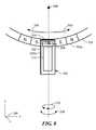
- an example of a magnetic field sensor 10is responsive to a gear 22 having ferromagnetic gear teeth, e.g., gear teeth 22 a , 22 b , 22 c .
- gear 22is but one type of “ferromagnetic target object” or simply “target” which the magnetic field sensor 10 can be responsive.
- the magnetic field sensor 10includes a magnetic field sensing element 12 coupled to an electronic circuit 16 .
- the magnetic field sensing element 12 and the electronic circuit 16can be disposed upon (i.e., integrated within or upon) a substrate 14 .
- the magnetic field sensing element 12is shown to be a Hall element with an exaggerated size, and rotated out of the plane of the substrate 14 .
- the Hall element 12is shown to be on top of the substrate 14 , but it will be appreciated that Hall elements are usually disposed upon or within a surface of a substrate of an integrated circuit.
- the magnetic field sensor 10can also include a magnet 18 (e.g. a permanent magnet or hard ferromagnetic material).
- the magnet 18is configured to generate a magnetic field, which is generally directed along an axis 24 at the position of the magnetic field sensing element 12 , and which is subject to direction and amplitude changes depending upon positions of the gear teeth 22 a , 22 b , 22 c relative to the magnetic field sensor 10 .
- the structure of the magnetic field at faces of the magnet 18can be more complex due to a core 20 .
- the electronic circuit 16is configured to generate an output signal (not shown).
- the output signalwhen the gear is not moving, is indicative of whether the magnetic field sensor 10 is over a gear tooth or a gear valley.
- the magnetic field sensor 10is sometimes referred to as a “tooth detector” as opposed to an “edge detector.”
- the output signalwhen the gear is rotating, has an edge rate or a frequency indicative of a speed of rotation of the gear. Edges or transitions of states of the output signal can be used to identify positions of edges of the gear teeth as they pass by the magnetic field sensor.
- the magnet 18can include the central core 20 comprised of a soft ferromagnetic material disposed within the magnet 18 .
- a magnet with a coreis described in U.S. Pat. No. 6,278,269, entitled “Magnet Structure,” issued Aug. 21, 2001, which patent is assigned to the assignee of the present invention and incorporated herein by reference in its entirety.
- the pole configuration provided by the magnet 18 with the core 20lowers the base field (or baseline) of a flux density of the magnetic field at some points above the surface of the core 20 (e.g., to the left of the core as shown) when a valley of the gear 22 is proximate to the magnetic field sensor 10 .
- a predetermined baselinee.g., within a range of about +/six hundred Gauss
- a resulting differential magnetic field signal 12 a , 12 bi.e., an analog differential proximity signal
- the magnetic field sensing element 12experiences a higher magnetic field and generates the differential magnetic field signal 12 a , 12 b with a higher value.
- a difference between the baseline magnetic field and the higher magnetic fieldis related to ultimate accuracy of the magnetic field sensor 10 .
- the baseline magnetic fieldwhich can occur when the magnetic field sensor 10 is proximate to a valley in the gear 22 , remains relatively low, with little change, even as the air gap between the gear 22 and the magnetic field sensor 10 varies.
- This advantageous result of low baseline substantially independent of air gapis achieved by operation of the core 20 , which results in opposite magnetic poles being presented at the face of the core 20 (i.e., left side as shown) proximate to the magnetic field sensing element 12 , particularly when the magnetic field sensing element 12 is proximate to a valley in the gear 22 .
- This effectis also described in U.S. Pat. No. 5,781,005, issued Jul. 14, 1998, entitled “Hall-Effect Ferromagnetic-Article-Proximity Sensor,” which patent is assigned to the assignee of the present invention and incorporated herein by reference in its entirety.
- the above-described low baselinealso provides an ability to more easily compensate for temperature effects, since the baseline magnetic field is relatively small, and therefore, circuit variations that occur due to temperature can have less influence when the magnetic field sensor 10 is proximate to a valley in the gear 22 .
- any error in the circuitryis able to be well corrected near the baseline magnetic field level or range, since any multiplication of the error (near zero) is smaller. Therefore, a magnetic field threshold used to distinguish a tooth from a valley can be made smaller while maintaining precision because there is less noise or error in the system over its operating conditions such as temperature, or humidity.
- the magnetic field described above and provided by the magnet 18 with the core 20results in an improved accuracy of the magnetic field sensor 10 .
- the low baselineallows the magnetic field sensing element 12 to be somewhat statically misaligned from a center of the magnet 18 , as will occur due to unit-to-unit variations of mechanical alignments, without sacrificing accuracy of the magnetic field sensor 10 . Accuracy is discussed above.
- an example of a prior art electronic circuit 50can be the same as or similar to electronic circuit 16 of FIG. 1 .
- the electronic circuit 50can include in amplifier 54 coupled to receive a differential signal 52 a , 52 b , which can be the same as or similar to the differential signal 12 a , 12 b generated by the magnetic field sensing element 12 of FIG. 1 .
- the amplifier 54is configured to generate an amplified signal 54 a , which, in some embodiments, can split into two channels, a TPOS detector channel and a precision rotation detector channel.
- a TPOS detector 56can be coupled to receive the amplified signal 54 a and configured to generate a TPOS output signal 56 a .
- the TPOS detector 56can include a comparator (not shown) configured to compare the amplified signal 54 a with a fixed (and trimmed) threshold.
- the TPOS output signal 56 acan be a two-state binary signal for which a high state is indicative of a gear tooth being proximate to the magnetic field sensor 10 of FIG. 1 and a low state is indicative of a gear valley being proximate to the magnetic field sensor 10 , or vice versa.
- an automatic gain control (AGC) 58can be coupled to receive the amplified signal 54 a and configured to generate a gain controlled signal 58 a .
- a precision rotation detector 60can be coupled to receive the gain controlled signal 58 a and configured to generate a precision rotation detector output signal 60 a .
- the precision rotation detector output signal 60 acan be a two-state binary signal for which a high state is indicative of a gear tooth being proximate to the magnetic field sensor 10 of FIG. 1 and a low state is indicative of a gear valley being proximate to the magnetic field sensor 10 , or vice versa.
- both the TPOS detector 56 and the precision rotation detector 60can be “tooth detectors.”
- the precision rotation detector channeluses the AGC 58 , which, when the gear 22 is not rotating, will settle to an undesirable gain, resulting, once the gear 22 starts to rotate, in a period of time during which the gain is incorrect and the precision rotation detector is not fully accurate. Even if the AGC 58 were not used, still the precision rotation detector 60 uses internal thresholds that are properly updated only when the gear 22 is rotating. However, in other embodiments, the threshold can be supplied from outside of the electronic circuit 50 .
- the precision rotation detector 60can be an “edge detector,” which is unable to identify whether the magnetic field sensor 12 is proximate to a gear tooth or a gear valley, particularly when the gear is not moving, but which is able to sense edges of gear teeth as they move past the magnetic field sensor 10 .
- Precision rotation detectorse.g., the precision rotation detector 60
- the TPOS output signal 56 ais indicative of whether the magnetic field sensing element 12 is proximate to a gear tooth or a gear valley, even when the gear, e.g., the gear 22 of FIG. 1 , is stationary.
- the TPOS detector 56uses a fixed threshold, in some embodiments, having limited adjustment at power up, variations in the edge placement in the TPOS output signal 56 a will occur due to a variety of factors, including, but not limited to, temperature variations, and variations in the air gap between the magnetic field sensing element 12 and the gear 22 .
- the precision rotation detector 60continually makes adjustments of thresholds to provide the precision rotation detector output signal 60 a with better accuracy of edge placements of the precision rotation detector output signal 60 a relative to physical positions of gear teeth. As described above, in part, it is these adjustments that make the precision rotation detector less accurate when it is first powered up or when the gear 22 first starts to rotate.
- a multiplexer/output module 62can be coupled to receive the TPOS output signal 56 a and coupled to receive the precision rotation detector output signal 60 a .
- Select logic 64can provide a selection signal 64 a , received by the multiplexer/output module 62 .
- the multiplexer/output module 62is configured to generate an output signal 62 a representative of a selected one of the TPOS output signal 56 a or the precision rotation detector output signal 60 a .
- the output signal 62 acan be provided in a variety of signal formats, including, but not limited to, a SENT format, an I 2 C format, a PWM format, or a two-state format native to the TPOS output signal 56 a and to the precision rotation detector output signal 60 a.
- the select logic 64selects the output signal 62 a to be representative of the TPOS output signal 56 a for a predetermined amount of time after the gear 22 starts rotating as indicated by the TPOS output signal 56 a . Thereafter, the select logic 64 selects the output signal 62 a to be representative of the precision rotation detector output signal 60 a.
- FIG. 2another example of a prior art magnetic field sensor 200 is responsive to a gear 214 having gear teeth, e.g., gear teeth 214 a , 214 b , 214 c .
- the magnetic field sensor 200includes three magnetic field sensing elements 202 , 204 , 206 coupled to an electronic circuit 210 .
- the magnetic field sensing elements 202 , 204are separated in a direction perpendicular to an axis 216 by a distance between about 1.5 millimeters and about 3.0 millimeters, and the magnetic field sensing element 206 is located midway between the magnetic field sensing elements 202 , 204 .
- the three magnetic field sensing elements 202 , 204 , 206 and an electronic circuit 210can be disposed upon (i.e., integrated within or upon) a substrate 208 .
- the magnetic field sensing elements 202 , 204 , 206are shown to be Hall elements with an exaggerated size, and rotated out of the plane of the substrate 208 .
- the Hall elements 202 , 204 , 206are shown to be on top of the substrate 208 , but it will be appreciated that Hall elements are usually disposed upon or within a surface of a substrate of an integrated circuit.
- the magnetic field sensor 200can also include a magnet 212 .
- the magnet 212is configured to generate a magnetic field, which is generally directed along an axis 216 at the position of the magnetic field sensing elements 202 , 204 , 206 .
- the electronic circuit 210is configured to generate an output signal (not shown).
- An exemplary electronic circuit 210is described below in conjunction with FIG. 2A . Let it suffice here to say that the electronic circuit generates differences of signals. Thus, it will be apparent that the magnetic field sensor 200 is an edge detector and not a tooth detector.
- the output signalwhen the gear 214 is rotating, is indicative speed of rotation of the gear 214 and also indicative of positions of edges of the gear teeth.
- the magnetic field sensor 200is unable to provide a TPOS function, and, when the gear 214 is stationary, is unable to identify whether the magnetic field sensing elements 202 , 204 , 206 are proximate to a gear tooth or a valley in the gear 214 .
- the magnet 212can be comprised of one uniform material, and can have no central core, which is shown and described in conjunction with FIG. 1 . However, in other embodiments, the magnet 212 can have a central core the same as or similar to that shown and described in conjunction with FIG. 1 .
- the magnetic field sensor 200uses the three magnetic field sensing elements 202 , 204 , 206 to generate a respective three differential signals 202 a , 202 b , and 204 a , 204 b , and 206 a , 206 b .
- the simple magnet 212does not provide the low baseline of a magnet with a core, differences of the above differential signals result in the effect of a low baseline.
- a differencing of the above differential signalsresults in a zero electronic signal.
- an example of a prior art electronic circuit 250can be the same as or similar to electronic circuit 210 of FIG. 2 .
- the electronic circuit 250can include amplifiers 258 , 260 , 262 coupled to receive differential signals 252 a , 252 b , and 254 a , 254 b , and 256 a , 256 b , respectively.
- the differential signal 252 a , 252 bcan be the same as or similar to the differential signal 202 a , 202 b
- the differential signal 254 a , 254 bcan be the same as or similar to the differential signals 204 a , 204 b
- the differential signal 256 a , 256 bcan be the same as or similar to the differential signal 206 a , 206 b generated, respectively, by the magnetic field sensing elements 202 , 204 , 206 of FIG. 2
- the amplifiers 258 , 260 , 262are configured to generate amplified signals 258 a , 260 a , 262 a , respectively.
- the amplified signals 258 a , 260 aare received by a first differencing module 264 , which is configured to generate a first difference signal 264 a .
- the amplified signals 260 a , 262 aare received by a second differencing module 266 , which is configured to generate a second difference signal 266 a.
- the electronic circuit 250includes two precision rotation detector channels, described above in conjunction with FIG. 1A .
- a AGCs 270 , 276can be the same as or similar to the AGC 56 of FIG. 1A .
- Precisions rotation detectors 272 , 278can be the same as or similar to the precision rotation detector 60 of FIG. 1A .
- the precision rotation detector 272can generate a precision rotation detector output signal 272 a and the precision rotation detector 278 can generate a precision rotation detector output signal 278 a .
- the precision rotation detector output signals 272 a , 278 acan be the same as or similar to the precision rotation detector output signal 60 a of FIG. 1A .
- a speed and direction module 274can be coupled to receive the precision rotation detector output signals 272 a , 278 a.
- the precision rotation detector output signals 272 a , 278 aare at relative phases that are determined by a direction of rotation of the gear 214 . It should also be apparent that the state transition rates of the precision rotation detector output signals 272 a , 278 a are representative of a speed of rotation of the gear 214 .
- the speed and direction moduleis configured to generate an output signal that can be representative of at least one of the speed of rotation or a direction of rotation of the gear 214 .
- the output signal 62 ais representative of both the speed of rotation and the direction of rotation.
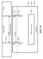
- a magnetic field sensor 300is responsive to a gear 322 having gear teeth, e.g., gear teeth 322 a , 322 b , 322 c .
- the gear 322can be a ferromagnetic gear, i.e., a ferromagnetic target object having ferromagnetic teeth, also ferromagnetic objects, and referred to herein as target features.
- the magnetic field sensor 300can include a substrate 302 with a major surface 302 a.
- the magnetic field sensor 300can include magnetic field sensing elements 304 disposed on the major surface 302 a of the substrate 302 . Further details of the magnetic field sensing elements 304 are described below. However, let is suffice here to say that the magnetic field sensing elements 304 can include at least two magnetoresistance elements.
- the magnetic field sensing elements 304can be coupled to or within an electronic circuit 314 also disposed on the major surface 302 a of the substrate 302 .
- the magnetic field sensor 300can also include a magnet 332 .
- the magnet 332is configured to generate a magnetic field, which is generally directed along an axis 308 at the position of the magnetic field sensing elements 304 , and is generally parallel to the major surface 302 a of the substrate 302 .
- the magnetic field sensing elements 304have respective maximum response axes parallel to the major surface 302 a of the substrate 302 .
- the maximum response axesare parallel to each other.
- the maximum response axesare substantially parallel to the axis 308 .
- the maximum response axesare substantially perpendicular to the axis 308 .
- the magnetic field sensing elements 304are disposed at positions such that an axis (e.g., 308 ) between (i.e., passing through) the magnetic field sensing elements 304 does not intersect the gear 322 .
- the axis (e.g., 308 ) between (i.e., passing through) the magnetic field sensing elements 304is substantially parallel to a tangent 330 to a direction of movement, e.g., 326 , of the gear 322 .
- a line between north (N) and south (S) poles of the magnet 332is substantially parallel to the major surface 302 a of the substrate 302 , and is substantially parallel to the axis (e.g., 308 ) between (i.e., passing through) the two magnetic field sensing elements 304 , 306 .
- the line between the north and south poles of the magnet 332does not intersect the gear 322 and is not in a direction toward the gear 322 .
- the electronic circuit 314is configured to generate an output signal (not shown).
- An exemplary electronic circuit 314is described below in conjunction with FIG. 26 . Let it suffice here to say that the electronic circuit 314 generates a difference of signals and a sum of signals. Thus, it will become apparent that the magnetic field sensor 300 is both an edge detector and a tooth detector.
- the output signalwhen the gear 322 is rotating, is indicative of a speed of rotation of the gear 322 and also indicative of positions of edges of the gear teeth.
- the magnetic field sensor 300is able to provide a tooth detecting (e.g., TPOS) function, and, when the gear 322 is stationary, is able to identify whether the magnetic field sensing elements 304 are proximate to a gear tooth or a valley in the gear 322 .
- TPOStooth detecting
- the magnet 332can be comprised of one uniform material, and can have no central core, which is shown and described in conjunction with FIG. 1 . However, in other embodiments, the magnet 332 can have a central core the same as or similar to that shown and described in conjunction with FIG. 1 . Such core can have an axis aligned with an axis 324 .
- the magnetic field sensor 300can be rotated in a direction 316 to a next position three hundred and sixty degrees apart from the position shown, with no degradation of performance. However, intermediate rotations may result in a degradation of performance.
- the magnetic field sensor 300can be rotated in a direction of and arrow 318 with a center of rotation anywhere along a line 324 , through approximately +/ ⁇ twenty degrees, without substantial degradation of performance.
- the magnetic field sensing elements 304are magnetoresistance elements.
- the magnetic field sensor 300is shown in an arrangement wherein the substrate 302 , and the magnetic field sensing elements 304 thereon, overlap the gear 322 .
- the magnetic field sensor 300is shown in an arrangement rotated about the x-axis ninety degrees outward from the page or ninety degrees into the page as compared to the arrangement shown in FIG. 3 .
- the magnetic field sensing elements 304remain disposed proximate to the gear 322 .
- a magnetic field sensor 600is like the magnetic field sensor 300 of FIG. 3 , but the magnetic field sensor 600 has a different magnet 602 .
- the magnetic field sensor 600has the different magnet 602 for which a line between north (N) and south (S) poles of the magnet 602 is substantially parallel to the major surface 302 a of the substrate 302 , but substantially perpendicular to the axis (e.g., 308 ) between (i.e., passing through) the magnetic field sensing elements.
- the line between the north and south poles of the magnet 602is in a direction toward the gear 322 .
- the magnet 602is a simple magnet without a core, such core described above in conjunction with FIG. 1 . In other embodiments, the magnet 602 has a core with an axis along the line 324 .
- FIGS. 7-9 described belowshow the same or similar magnetic field sensors for sensing movement of a ring magnet. Comments made above about edge detectors, tooth detectors, and TPOS functions apply in a similar way when sensing a ring magnet.
- a magnetic field sensor 700is like the magnetic field sensor 300 of FIG. 3 .
- the magnetic field sensor 700has no internal magnet. Instead, the magnetic field sensor 700 is responsive to passing magnetic domains, e.g., 702 a , of a ring magnet 702 .
- the magnetic domains of the ring magnet 702are polarized parallel to the page. In some other embodiments, the magnetic domains of the ring magnet 702 are polarized perpendicular to the page.
- the magnetic field sensor 700is shown in an arrangement wherein the substrate 302 , and the magnetic field sensing elements 304 thereon, overlap the ring magnet 702 . It should be apparent that the magnetic fields sensor 700 could be rotated one hundred eighty degrees about the y-axis such that the magnetic field sensing elements 304 still overlap the magnetic domains, e.g., 702 a , of the ring magnet 702 . A line perpendicular to the surface 302 a of the substrate 302 and passing through the magnetic field sensing elements 304 intersects the ring magnet 702 .
- the magnetic field sensor 700is shown in an arrangement rotated about the x-axis ninety degrees outward from the page or ninety degrees into the page as compared to the arrangement shown in FIG. 5 .
- the magnetic field sensing elements 304remained disposed proximate to the ring magnet 702 .
- V 1 , V 2are shown to designate two signals. It should be understood that these designations indicate a logical relationship between similar designations in similar figures. However, these designations do not indicate that a signal so designated in one figure is the same signal as one with the same designation in other figures.
- R 1 , R 2are shown to designate two fixed resistors. It should be understood that these designations indicate a logical relationship between similar designations in similar figures. However, these designations do not indicate that a resistor so designated in one figure is the same resistor as one with the same designation in other figures.
- a magnetic field sensor 1000can include a substrate 1002 having a surface 1002 a , which is one of two parallel major surfaces of the substrate 1002 .
- Two magnetoresistance elements 1004 , 1006can be disposed upon the surface 1002 a along an axis 1010 .
- the two magnetoresistance elements 1004 , 1006 (A, B)can be part of or coupled to an electronic circuit 1008 , which is also disposed upon or within the surface 1002 a of the substrate 1002 .
- the two magnetoresistance elements 1004 , 1006 (A, B)can be the same as or similar to the magnetic field sensing elements 304 of FIGS. 3-9 .
- the axis 1010can be parallel to the axis 308 of FIGS. 3-9 .
- Magnetoresistance elementse.g., 1004 , 1006 (A, B), are shown in all embodiments herein to be in the form of so-called “yokes,” which have a C-shape (or a reverse C-shape).
- the yokescan have longest yoke axes substantially perpendicular to the axis 1010 .
- Advantages of yoke shapesare known. It will be understood that other magnetoresistance elements used in embodiments herein can have other shapes, for example, lines, polylines, or rectangles.
- Maximum response axes of the magnetoresistance elements 1004 , 1006 (A, B)can be parallel to and along the axis 1010 and in the same direction. It should be understood that the magnetoresistance elements 1004 , 1006 (A, B) having maximum response axes parallel to the axis 1010 are also responsive to magnetic fields at other angles in the plane of the substrate 1002 (and also out of the plane of the substrate 1002 ). The degree to which the magnetoresistance elements 1004 , 1006 (A, B) are responsive to magnetic fields at other angles not parallel to the axis 1010 (and not perpendicular to the longest yoke axes) is determined by a magnitude of a geometric projection of the magnetic field at the other angle onto the axis 1010 . Thus, the term “projected magnetic field” is used below to describe this projection.
- the degree to which the magnetoresistance elements 1004 , 1006 (A, B) are responsive to magnetic fields at other angles not parallel to the axis 1010is determined by a magnitude of a geometric projection of the magnetic field at the other angle onto an axis that is perpendicular to the longest axes of the yoke shapes. This is also referred to herein as a projected magnetic field.
- the magnetic field sensor 1000is responsive to movement of a ferromagnetic target object 1012 having features, e.g., 1012 a , with width 1014 .
- the ferromagnetic target object 1012can be the same as or similar to the gear 322 of FIGS. 3-6 or the ring magnet 702 of FIGS. 7-9 .
- the features, e.g., 1012 acan be the same as or similar to the gear teeth, e.g., 322 a , of FIGS. 3-6 or the magnetic regions, e.g., 702 a , of the ring magnet 702 of FIGS. 7-9 .
- the magnetic field sensor 1000can be the same as or similar to the magnetic field sensor 300 of FIGS. 3-5 , the magnetic field sensor 600 of FIG. 6 , and the magnetic field sensor 700 of FIGS. 7-9 . However, the magnetic field sensor 1000 is not shown in the rotated position described above in conjunction with FIGS. 5 and 9 . Nevertheless the magnetic field sensor 1000 can be rotated into or out of the page in the same way.
- the two magnetoresistance elements 1004 , 1006 (A, B)have a separation 1016 between about one half and about one and one half of the width 1014 of the target feature 1012 a , for example, a gear tooth of a ferromagnetic gear or a magnetic domain of a ferromagnetic ring magnet.
- the two magnetoresistance elements 1004 , 1006 (A, B)have a separation 1016 between about one half and about twice the width 1014 of the target feature 1012 a .
- the separation 1016is much smaller than half of the width 1014 , for example, one one hundredth of the width 1014 , or larger than twice the width 1014 .
- the separation 1016is about equal to the width 1014 of the target feature 1012 a , for example, a gear tooth of a ferromagnetic gear or a magnetic domain of a ferromagnetic ring magnet.
- the two magnetoresistance elements 1004 , 1006(A, B) can generate two output signals.
- Figures shown and described beloware representative of a variety of ways in which the two magnetic field sensing elements 1004 , 1006 can generate two output signals.
- the target feature 1012 awith a width 1014 equal to the spacing 1016 between the two magnetoresistance elements 1004 , 1006 , when the target feature 1012 a is centered about (i.e., between) the two magnetoresistance elements 1004 , 1006 (A, B), it can be shown that any magnetoresistance element(s) (e.g., 1004 (A)) on one side of a center of the target feature 1012 a experience a projected magnetic field pointed in one direction along the axis 1010 , and any magnetoresistance element(s) (e.g., 1006 (B)) on the other side of the center of the target feature 1012 a experience a projected magnetic field pointed in the other direction.
- any magnetoresistance element(s)e.g., 1004 (A)
- any magnetoresistance element(s)e.g., 1006 (B)
- any magnetoresistance element(s)e.g., 1004 (A)
- any magnetoresistance element(s)e.g., 1006 (B)
- any magnetoresistance element(s)e.g., 1006 (B)
- the magnetic field sensor 1000can include a magnet.
- the two magnetoresistance elements 1004 , 1006(A, B), are coupled between a respective current sources 1102 , 1104 and ground.
- Designations V 1 and V 2are used below for clarity as described above.
- the target feature 1012 a of FIG. 10is centered with the two magnetoresistance elements 1004 , 1006 (A, B), a difference V 1 ⁇ V 2 of the two output signals V 1 , V 2 has a maximum (positive or negative) instantaneous value.
- the target feature 1012 acan be a tooth, e.g., 322 a , (or alternatively, a valley) of the gear 322 of FIG. 3 , or a magnetic domain, e.g.
- V 1 ⁇ V 2is representative of a proximity of a tooth or proximity of a magnetic domain, and is, therefore, representative of a “feature” of the ferromagnetic target object.
- a sum V 1 +V 2 of the two output signals V 1 , V 2has a maximum (positive or negative) instantaneous value.
- the sum V 1 +V 2is representative of a proximity of an edge, and is, therefore, representative of an “edge” of the ferromagnetic target object.
- a magnetic field sensor using both the difference V 1 ⁇ V 2 of the two signals V 1 , V 2 and also the sum V 1 +V 2 of the two signals V 1 , V 2can operate both as a tooth detector and a an edge detector, respectively.
- the tooth detector capabilityallows a magnetic field sensor using the two magnetoresistance elements 1004 , 1006 , coupled as shown, to operate with a true-power-on-state (TPOS) function.
- the two signals V 1 , V 2 here and in figures belowcan be used to determine both speed and direction of a moving ferromagnetic object. It will also become apparent from discussion below that the sum V 1 +V 2 of the two signals is ninety degrees apart from the difference V 1 ⁇ V 2 of the two signals.
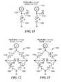
- the two magnetoresistance elements 1004 , 1006are coupled in a bridge arrangement 1200 with fixed resistors 1202 , 1204 , also referred to herein as resistors R 1 , R 2 .
- the fixed resistors 1202 , 1204can be magnetically insensitive elements (or less sensitive elements) having some layers like a magnetoresistance element, as described, for example, in U.S. Pat. No. 7,777,607, issued Aug. 17, 2010, assigned to the assignee of the present application, and incorporated by reference herein in its entirety.
- Such magnetically insensitive elementstend to have a temperature coefficient the same as that of the two magnetoresistance elements 1104 , 1106 (A, B), and thus, the bridge 1200 can be substantially insensitive to temperature variations.
- the bridge 1200can be powered by a voltage source 1206 .
- the two output signals V 1 , V 2are treated as one differential signal V 1 , V 2 .
- the two output signals V 1 , V 2are treated separately.
- the target feature 1012 a of FIG. 10is centered with the two magnetoresistance elements 1004 , 1006 (A, B), a difference V 1 ⁇ V 2 of the two output signals V 1 , V 2 has a maximum (positive or negative) instantaneous value.
- the target feature 1012 acan be a tooth, e.g., 322 a , (or alternatively, a valley) of the gear 322 of FIG. 3 , or a magnetic domain, e.g.
- V 1 ⁇ V 2is representative of a proximity of a tooth or proximity of a magnetic domain, and is, therefore, representative of a “feature” of the ferromagnetic target object.
- a sum V 1 +V 2 of the two output signals V 1 , V 2has a maximum (positive or negative) instantaneous value.
- the sum V 1 +V 2is representative of a proximity of an edge, and is, therefore, representative of an “edge” of the ferromagnetic target object.
- a magnetic field sensor using both the difference V 1 ⁇ V 2 of the two signals V 1 , V 2 and also the sum V 1 +V 2 of the two signals V 1 , V 2can operate both as a tooth detector and a an edge detector, respectively.
- the tooth detector capabilityallows a magnetic field sensor using the two magnetoresistance elements 1004 , 1006 (A, B), coupled as shown, to operate with a true-power-on-state (TPOS) function.
- TPOStrue-power-on-state
- the two magnetoresistance elements 1004 , 1006are coupled in a bridge arrangement 1300 with fixed resistors 1302 , 1304 (also referred to herein as R 1 , R 2 ).
- the fixed resistors 1302 , 1304can be magnetically insensitive elements having some layers like a magnetoresistance element, as described, for example, in U.S. Pat. No. 7,777,607, issued Aug. 17, 2010.
- the bridge 1300can be powered by a voltage source 1306 .
- the two output signals V 1 , V 2are treated as one differential signal V 1 , V 2 .
- the two output signals V 1 , V 2are treated separately.
- the target feature 1012 a of FIG. 10is centered with the two magnetoresistance elements 1004 , 1006 (A, B), a sum V 1 +V 2 of the two output signals V 1 , V 2 has a maximum (positive or negative) instantaneous value.
- the target feature 1012 acan be a tooth, e.g., 322 a , (or alternatively, a valley) of the gear 322 of FIG. 3 , or a magnetic domain, e.g.
- V 1 +V 2is representative of a proximity of a tooth or proximity of a magnetic domain, and is, therefore, representative of a “feature” of the ferromagnetic target object.
- a difference V 1 ⁇ V 2 of the two output signals V 1 , V 2has a maximum (positive or negative) instantaneous value.
- the difference V 1 ⁇ V 2is representative of a proximity of an edge, and is, therefore, representative of an “edge” of the ferromagnetic target object.
- a magnetic field sensor using both the sum V 1 +V 2 of the two signals V 1 , V 2 and also the difference V 1 ⁇ V 2 of the two signals V 1 , V 2can operate both as a tooth detector and a an edge detector, respectively.
- the tooth detector capabilityallows a magnetic field sensor using the two magnetoresistance elements 1004 , 1006 (A, B), coupled as shown, to operate with a true-power-on-state (TPOS) function.
- TPOStrue-power-on-state
- FIGS. 12 and 13 aboveshow particular bridge arrangements, there are other possible bridge arrangements that should be apparent.
- the magnetic field sensing elements 1004 , 1006can be interchanged in position.
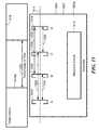
- a magnetic field sensor 1400can include a substrate 1402 having a surface 1402 a , which is one of two parallel major surfaces of the substrate 1402 .
- magnetoresistance elements 1404 , 1406 , 1408 , 1410can be disposed upon the surface 1402 a .
- the four magnetoresistance elements 1404 , 1406 , 1408 , 1410can be part of or coupled to an electronic circuit 1412 , which is also disposed upon or within the surface 1402 a of the substrate 1412 .
- the four magnetoresistance elements 1404 , 1406 , 1408 , 1410(A, B, C, D) can be the same as or similar to the magnetic field sensing elements 304 of FIGS. 3-9 .
- Maximum response axes of the magnetoresistance elements 1404 , 1410can be parallel to and along an axis 1414 .
- Maximum response axes of the magnetoresistance elements 1406 , 1408can be parallel to and along an axis 1416 .
- the axes 1414 , 1416can be parallel to the axis 308 of FIGS. 3-9 .
- Angles of magnetic fieldsare discussed above in conjunction with FIG. 10 .
- the term “projected magnetic field”is used to describe geometric projections of magnetic fields upon the axes 1414 , 1416 .
- the magnetic field sensor 1400is responsive to movement of a ferromagnetic target object 1418 having features, e.g., 1418 a , with width 1424 .
- the ferromagnetic target object 1418can be the same as or similar to the gear 322 of FIGS. 3-6 or the ring magnet 702 of FIGS. 7-9 .
- the features, e.g., 1418 acan be the same as or similar to the gear teeth, e.g., 322 a , of FIGS. 3-6 or the magnetic regions, e.g., 502 a , of the ring magnet 702 of FIGS. 7-9 .
- the magnetic field sensor 1400can be the same as or similar to the magnetic field sensor 300 of FIGS. 3-5 , the magnetic field sensor 600 of FIG. 6 , and the magnetic field sensor 700 of FIGS. 7-9 . However, the magnetic field sensor 1400 is not shown in the rotated position described above in conjunction with FIGS. 5 and 9 . Nevertheless the magnetic field sensor 1400 can be rotated into or out of the page in the same way.
- the magnetoresistance elements 1404 , 1410are disposed along the axis 1414 proximate to the ferromagnetic target object 1418 and the magnetoresistance elements 1406 , 1408 are disposed along the axis 1416 more distant from the ferromagnetic target object 1418 .
- the axes 1414 , 1416can be parallel to the axis 308 of FIGS. 3-9 .
- the two magnetoresistance elements 1404 , 1408 (A, C)have a separation 1420 between about one half and about one and one half of the width 1424 of the target feature 1418 a , for example, a gear tooth of a ferromagnetic gear or a magnetic domain of a ferromagnetic ring magnet.
- the two magnetoresistance elements 1404 , 1408 (A, C)have a separation 1420 between about between about one half and about twice the width 1424 of the target feature 1418 a .
- the separation 1420is much smaller than half of the width 1424 , for example, one one hundredth of the width 1424 , or larger than twice the width 1424 .
- the separation 1420is about equal to the width 1424 of the target feature 1418 a.
- the two magnetoresistance elements 1406 , 1410 (B, D)have a separation 1422 between about one half and about one and one half of the width 1424 of the target feature 1418 a , for example, a gear tooth of a ferromagnetic gear or a magnetic domain of a ferromagnetic ring magnet.
- the two magnetoresistance elements 1406 , 1410 (B, D)have a separation 1422 between about one half and about twice the width 1424 of the target feature 1418 a .
- the separation 1422is much smaller than half of the width 1424 , for example, one one hundredth of the width 1424 , or larger than twice the width 1424 .
- the separation 1422is about equal to the width 1424 of the target feature 1418 a.
- the two magnetoresistance elements 1404 , 1406 (A, B)have a separation 1428 between about one half and about one and one half of the width 1424 of the target feature 1418 a . In some other embodiments, the two magnetoresistance elements 1404 , 1406 (A, B) have a separation 1428 between about one half and about twice the width 1424 of the target feature 1418 a . In some embodiments used in examples below, the separation 1428 is about equal to the width 1424 of the target feature 1418 a . However, in other embodiments, the separation 1428 is much smaller than half of the width 1424 , for example, one one hundredth of the width 1424 , or larger than twice the width 1424 .
- the separation 1428is about equal to the width 1424 of the target feature 1418 a.
- the two magnetoresistance elements 1408 , 1410have a separation 1430 between about one half and about one and one half of the width 1424 of the target feature 1418 a .
- the two magnetoresistance elements 1408 , 1410 (C, D)have a separation 1430 between about one half and about twice the width 1424 of the target feature 1418 a .
- the separation 1430is about equal to the width 1424 of the target feature 1418 a .
- the separation 1430is much smaller than half of the width 1424 , for example, one one hundredth of the width 1424 or larger than twice the width 1424 .
- the separation 1430is about equal to the width 1424 of the target feature 1418 a.
- the four magnetoresistance elements 1404 , 1406 , 1408 , 1410can generate at least two output signals.
- Figures shown and described beloware representative of a variety of ways in which the four magnetoresistance elements 1404 , 1406 , 1408 , 1410 (A, B, C, D) can generate at least two output signals.
- the target feature 1418 awith a width 1424 equal to the spacings 1420 , 1422 , when the target feature 1418 a is centered about (i.e., between) the four magnetoresistance elements 1404 , 1406 , 1408 , 1410 (A, B, C, D), it can be shown that any magnetoresistance element(s) (e.g., 1404 , 1406 (A, B)) on one side of a center of the target feature 1418 a experiences a projected magnetic field pointed in one direction along the axes 1414 , 1416 , and any magnetoresistance element(s) (e.g., 1408 , 1410 (C, D)) on the other side of the center of the target feature 1418 a experiences a projected magnetic field pointed in the other direction.
- any magnetoresistance element(s)e.g., 1404 , 1406 (A, B)
- any magnetoresistance element(s)e.g., 1408 , 1410 (C
- any magnetoresistance element(s)e.g., 1404 , 1406 (A, B)
- any magnetoresistance element(s)e.g., 1404 , 1406 (A, B)
- any magnetoresistance element(s)e.g., 1408 , 1410 (C, D)
- any magnetoresistance element(s)e.g., 1408 , 1410 (C, D)
- the two magnetoresistance elements 1406 , 1408 (B, C)experience projected magnetic fields pointed in the same direction along the axis 1416 , but opposite in direction to the projected magnetic fields experienced by the two magnetoresistance elements 1404 , 1410 (A, D).
- resistance of both of the two magnetoresistance elements 1406 , 1408 (B, C)change in the same direction but opposite to the resistance change of the two magnetoresistance elements 1404 , 1410 (A, D).
- the resistance change of the two magnetoresistance elements 1406 , 1408 (B, C)is small, if any.
- the magnetic field sensor 1400can include a magnet.
- a magnetic field sensor 1500can include a substrate 1502 having a surface 1502 a , which is one of two parallel major surfaces of the substrate 1502 .
- the four magnetoresistance elements 1404 , 1406 , 1408 , 1410can be disposed upon the surface 1502 a along an axis 1514 .
- the four magnetoresistance elements 1404 , 1406 , 1408 , 1410can be part of or coupled to the electronic circuit 1412 , which is also disposed upon or within the surface 1502 a of the substrate 1502 .
- the four magnetoresistance elements 1404 , 1406 , 1408 , 1410can be the same as or similar to the magnetic field sensing elements 304 of FIGS. 3-9 .
- the axis 1514can be parallel to the axis 308 of FIGS. 3-9 .
- Maximum response axes of the four magnetoresistance elements 1404 , 1406 , 1408 , 1410can be parallel to and along an axis 1514 , and in the same direction. Angles of magnetic fields are discussed above in conjunction with FIG. 10 . As described above, the term “projected magnetic field” is used to describe geometric projections of magnetic fields upon the axis 1514 .
- the magnetic field sensor 1500is responsive to movement of the ferromagnetic target object 1418 .
- the four magnetoresistance elements 1404 , 1406 , 1408 , 1410are disposed along the axis 1514 proximate to the ferromagnetic target object 1418 .
- the magnetic field sensor 1500can be the same as or similar to the magnetic field sensor 300 of FIGS. 3-5 , the magnetic field sensor 600 of FIG. 6 , of the magnetic field sensor 700 of FIGS. 7-9 . However, the magnetic field sensor 1500 is not shown in the rotated position described above in conjunction with FIGS. 5 and 9 . Nevertheless the magnetic field sensor 1500 can be rotated into or out of the page in the same way.
- the four magnetoresistance elements 1404 , 1406 , 1408 , 1410can be the same as or similar to the magnetic field sensing elements 304 of FIGS. 3-9 .
- the ferromagnetic target object 1418can be the same as or similar to the gear 322 of FIGS. 3-6 or the ring magnet 702 of FIGS. 7-9 .
- the axis 1514can be parallel to the axis 308 of FIGS. 3-9 .
- the two magnetoresistance elements 1404 , 1408 (A, C)have a separation 1520 between about one half and about one and one half of the width 1424 of the target feature 1418 a , for example, a gear tooth of a ferromagnetic gear or a magnetic domain of a ferromagnetic ring magnet.
- the two magnetoresistance elements 1404 , 1408 (A, C)have a separation 1520 between about one half and about twice the width 1424 of the target feature 1418 a .
- the separation 1520is much smaller than half of the width 1424 , for example, one one hundredth of the width 1424 or larger than twice the width 1424 .
- the separation 1520is about equal to the width 1424 of the target feature 1418 a.
- the two magnetoresistance elements 1406 , 1410 (B, D)have a separation 1522 between about one half and about one and one half of the width 1424 of the target feature 1418 a , for example, a gear tooth of a ferromagnetic gear or a magnetic domain of a ferromagnetic ring magnet.
- the two magnetoresistance elements 1406 , 1410 (B, D)have a separation 1522 between about one half and about twice the width 1424 of the target feature 1418 a .
- the separation 1522is much smaller than half of the width 1424 , for example, one one hundredth of the width 1424 or larger than twice the width 1424 .
- the separation 1522is about equal to the width 1424 of the target feature 1418 a.
- the two magnetoresistance elements 1404 , 1406 (A, B)have a separation 1524 between about one half and about one and one half of the width 1424 of the target feature 1418 a . In some other embodiments, the two magnetoresistance elements 1404 , 1406 (A, B) have a separation 1524 between about one half and about twice the width 1424 of the target feature 1418 a . However, in other embodiments, the separation 1424 is much smaller than half of the width 1424 , for example, one one hundredth of the width 1424 or larger than twice the width 1424 .
- the separation 1524is about equal to the width 1424 of the target feature 1418 a.
- the two magnetoresistance elements 1408 , 1410have a separation 1526 between about one half and about one and one half of the width 1424 of the target feature 1418 a .
- the two magnetoresistance elements 1408 , 1410 (C, D)have a separation 1526 between about one half and twice the width 1424 of the target feature 1418 a .
- the separation 1526is much smaller than half of the width 1424 , for example, one one hundredth of the width 1424 or larger than twice the width 1424 .
- the separation 1526is about equal to the width 1424 of the target feature 1418 a.
- the four magnetoresistance elements 1404 , 1406 , 1408 , 1410can generate at least two output signals.
- Figures shown and described beloware representative of a variety of ways in which the four magnetoresistance elements 1404 , 1406 , 1408 , 1410 (A, B, C, D) can generate at least two output signals.
- the target feature 1012 awith a width 1014 equal to the spacings 1520 , 1522 , when the target feature 1418 a is centered about (i.e., between) the four magnetoresistance elements 1404 , 1406 , 1408 , 1410 (A, B, C, D), it can be shown that any magnetoresistance element(s) (e.g., 1404 , 1406 (A, B)) on one side of a center of the target feature 1418 a experiences a projected magnetic field pointed in one direction along the axis 1514 , and any magnetoresistance element(s) (e.g., 1408 , 1410 (C, D)) on the other side of the center of the target feature 1418 a experiences a projected magnetic field pointed in the other direction.
- any magnetoresistance element(s)e.g., 1404 , 1406 (A, B)
- any magnetoresistance element(s)e.g., 1408 , 1410 (C, D)
- any magnetoresistance element(s)e.g., 1404 , 1406 (A, B)
- any magnetoresistance element(s)e.g., 1404 , 1406 (A, B)
- any magnetoresistance element(s)e.g., 1408 , 1410 (C, D)
- any magnetoresistance element(s)e.g., 1408 , 1410 (C, D)
- the two magnetoresistance elements 1406 , 1408 (B, C)experience projected magnetic fields pointed in the same direction along the axis 1514 , but opposite in direction from the projected magnetic fields experienced by the two magnetoresistance elements 1404 , 1410 (A, D).
- resistance of both of the two magnetoresistance elements 1406 , 1408 (B, C)change in the same direction but opposite to the resistance change of the two magnetoresistance elements 1404 , 1410 (A, D).
- the magnetic field sensor 1400can include a magnet.
- the four magnetoresistance elements 1404 , 1406 , 1408 , 1410are coupled to respective current sources 1602 , 1604 , 1606 , 1608 resulting in respective signals 1610 , 1612 , 1614 , 1616 , also referred to generically herein as signals VA, VB, VC, VD, respectively.
- a difference V 1 ⁇ V 2 of the two output signals V 1 , V 2has a maximum (positive or negative) instantaneous value when an edge of the target feature 1418 a is centered about (i.e., between) the four magnetoresistance elements 1404 , 1406 , 1408 , 1410 (A, B, C, D). Largest signals can be achieved when the distances 1520 , 1522 are equal to the distance 1424 .
- a magnetic field sensor using the four magnetoresistance elements 1404 , 1406 , 1408 , 1410(A, B, C, D) and using both the sum V 1 +V 2 of the two signals V 1 , V 2 and also the difference V 1 ⁇ V 2 of the two signals V 1 , V 2 can operate both as a tooth detector and a an edge detector, respectively.
- the tooth detector capabilityallows a magnetic field sensor using the four magnetoresistance elements 1404 , 1406 , 1408 , 1410 (A, B, C, D) to operate with a true-power-on-state (TPOS) function.
- TPOStrue-power-on-state
- FIG. 17in which like elements of FIGS. 14 and 15 are shown having like reference designations, the four magnetoresistance elements 1404 , 1406 , 1408 , 1410 (A, B, C, D) are coupled in a bridge arrangement 1700 .
- the bridge 1700can be powered by a voltage source 1702 .
- the two output signals V 1 , V 2are treated as one differential signal V 1 , V 2 .
- the two output signals V 1 , V 2are treated separately.
- a difference V 1 ⁇ V 2 of the two signals V 1 , V 2has a maximum (positive or negative) instantaneous value when the object feature 1418 a of FIGS. 14 and 15 , but particularly FIG. 14 , is centered about the four magnetoresistance elements 1404 , 1406 , 1408 , 1410 (A, B, C, D).
- the difference V 1 ⁇ V 2therefore, provides a feature signal.
- a sum V 1 +V 2 of the two output signals V 1 , V 2has a maximum (positive or negative) instantaneous value when an edge of the target feature 1418 a is centered about (i.e., between) the four magnetoresistance elements 1404 , 1406 , 1408 , 1410 (A, B, C, D).
- a magnetic field sensor using the bridge 1700 and using both the difference V 1 ⁇ V 2 of the two signals V 1 , V 2 and also the sum V 1 +V 2 of the two signals V 1 , V 2can operate both as a tooth detector and a an edge detector, respectively.
- the tooth detector capabilityallows a magnetic field sensor using the four magnetoresistance elements 1404 , 1406 , 1408 , 1410 (A, B, C, D) to operate with a true-power-on-state (TPOS) function.
- the bridge 1700is best suited for the arrangement of FIG. 14 , but can also function with the arrangement of FIG. 15 .
- FIG. 18in which like elements of FIGS. 14 and 15 are shown having like reference designations, the four magnetoresistance elements 1404 , 1406 , 1408 , 1410 (A, B, C, D) are coupled in a bridge arrangement 1800 .
- the bridge 1800can be powered by a voltage source 1802 .
- the two output signals V 1 , V 2are treated as one differential signal V 1 , V 2 .
- the two output signals V 1 , V 2are treated separately.
- a difference V 1 ⁇ V 2 of the two signals V 1 , V 2has a maximum (positive or negative) instantaneous value when the object feature 1418 a of FIGS. 14 and 15 is centered about the four magnetoresistance elements 1404 , 1406 , 1408 , 1410 (A, B, C, D).
- the difference V 1 ⁇ V 2therefore, provides a feature signal.
- a sum V 1 +V 2 of the two output signals V 1 , V 2has a maximum (positive or negative) instantaneous value when an edge of the target feature 1418 a is centered about (i.e., between) the four magnetoresistance elements 1404 , 1406 , 1408 , 1410 (A, B, C, D).
- a magnetic field sensor using the bridge 1700 and using both the difference V 1 ⁇ V 2 of the two signals V 1 , V 2 and also the sum V 1 +V 2 of the two signals V 1 , V 2can operate both as a tooth detector and a an edge detector, respectively.
- the tooth detector capabilityallows a magnetic field sensor using the four magnetoresistance elements 1404 , 1406 , 1408 , 1410 (A, B, C, D) to operate with a true-power-on-state (TPOS) function.
- the bridge 1800is well suited for the arrangements of FIGS. 14 and 15 .
- FIG. 19in which like elements of FIGS. 14 and 15 are shown having like reference designations, the four magnetoresistance elements 1404 , 1406 , 1408 , 1410 (A, B, C, D) are coupled in a bridge arrangement 1900 .
- the bridge 1900can be powered by a voltage source 1902 .
- the two output signals V 1 , V 2are treated as one differential signal V 1 , V 2 .
- the two output signals V 1 , V 2are treated separately.
- a sum V 1 +V 2 of the two signals V 1 , V 2has a maximum (positive or negative) instantaneous value when the object feature 1418 a of FIGS. 14 and 15 , but particularly FIG. 14 , is centered about the four magnetoresistance elements 1404 , 1406 , 1408 , 1410 (A, B, C, D).
- the sum V 1 +V 2therefore, provides a feature signal.
- a difference V 1 ⁇ V 2 of the two output signals V 1 , V 2has a maximum (positive or negative) instantaneous value when an edge of the target feature 1418 a is centered about (i.e., between) the four magnetoresistance elements 1404 , 1406 , 1408 , 1410 (A, B, C, D).
- a magnetic field sensor using the bridge 1900 and using both the sum V 1 +V 2 of the two signals V 1 , V 2 and also the difference V 1 ⁇ V 2 of the two signals V 1 , V 2can operate both as a tooth detector and a an edge detector, respectively.
- the tooth detector capabilityallows a magnetic field sensor using bridge 1900 to operate with a true-power-on-state (TPOS) function.
- the bridge 1900is best suited for the arrangement of FIG. 14 , but can also function with the arrangement of FIG. 15 .
- FIG. 20in which like elements of FIGS. 14 and 15 are shown having like reference designations, the four magnetoresistance elements 1404 , 1406 , 1408 , 1410 (A, B, C, D) are coupled in a bridge arrangement 2000 .
- the bridge 2000can be powered by a voltage source 2002 .
- the two output signals V 1 , V 2are treated as one differential signal V 1 , V 2 .
- the two output signals V 1 , V 2are treated separately.
- a difference V 1 ⁇ V 2 of the two output signals V 1 , V 2has a maximum (positive or negative) instantaneous value when an edge of the target feature 1418 a is centered about (i.e., between) the four magnetoresistance elements 1404 , 1406 , 1408 , 1410 (A, B, C, D).
- a magnetic field sensor using the bridge 2000 and using both the sum V 1 +V 2 of the two signals V 1 , V 2 and also the difference V 1 ⁇ V 2 of the two signals V 1 , V 2can operate both as a tooth detector and a an edge detector, respectively.
- the tooth detector capabilityallows a magnetic field sensor using bridge 2000 to operate with a true-power-on-state (TPOS) function.
- the bridge 2000is well suited for the arrangements of FIGS. 14 and 15 .
- FIGS. 17-20While various bridge arrangements are shown in FIGS. 17-20 , there are other similar bridge arrangements that can be used to generate a feature signal and an edge signal.
- a magnetic field sensor 2100can include a substrate 2102 having a surface 2102 a , which is one of two parallel major surfaces of the substrate 2102 .
- Eight magnetoresistance elements 2104 a , 2104 b , 2106 a , 2106 b , 2108 a , 2108 b , 2110 a , 2110 b(also referred to herein as A 1 , A 2 , B 1 , B 2 , C 1 , C 2 , D 1 , D 2 ) can be disposed upon the surface 2102 a .
- the eight magnetoresistance elements 2104 a , 2104 b , 2106 a , 2106 b , 2108 a , 2108 b , 2110 a , 2110 b(A 1 , A 2 , B 1 , B 2 , C 1 , C 2 , D 1 , D 2 ) can be arranged in proximate pairs P 1 , P 2 , P 3 , P 4 .
- the eight magnetoresistance elements 2104 a , 2104 b , 2106 a , 2106 b , 2108 a , 2108 b , 2110 a , 2110 b(A 1 , A 2 , B 1 , B 2 , C 1 , C 2 , D 1 , D 2 ) can be part of or coupled to an electronic circuit 2112 , which is also disposed upon or within the surface 2102 a of the substrate 2102 .
- the eight magnetoresistance elements 2104 a , 2104 b , 2106 a , 2106 b , 2108 a , 2108 b , 2110 a , 2110 b(A 1 , A 2 , B, B 2 , C 1 , C 2 , D 1 , D 2 ) can be the same as or similar to the magnetic field sensing elements 304 of FIGS. 3-9 .
- Maximum response axes of the magnetoresistance elements 2104 a , 2104 b , 2110 a , 2110 b(A 1 , A 2 , D 1 , D 2 ) can be parallel to and along an axis 2114 .
- Maximum response axes of the magnetoresistance elements 2106 a , 2106 b , 2108 a , 2108 b(B 1 , B 2 , C 1 , C 2 ) can be parallel to and along an axis 2116 .
- the axes 2114 , 2116can be parallel to the axis 308 of FIGS. 3-9 .
- Angles of magnetic fieldsare discussed above in conjunction with FIG. 10 .
- the term “projected magnetic field”is used to describe geometric projections of magnetic fields upon the axes 2114 , 2116 .
- the magnetic field sensor 2100is responsive to movement of a ferromagnetic target object 2118 having features, e.g., 2118 a , with width 2124 .
- the ferromagnetic target object 2118can be the same as or similar to the gear 322 of FIGS. 3-6 or the ring magnet 702 of FIGS. 7-9 .
- the features, e.g., 2118 acan be the same as or similar to the gear teeth, e.g., 322 a , of FIGS. 3-6 or the magnetic regions, e.g., 502 a , of the ring magnet 702 of FIGS. 7-9 .
- the magnetic field sensor 2100can be the same as or similar to the magnetic field sensor 300 of FIGS. 3-5 , the magnetic field sensor 600 of FIG. 6 , and the magnetic field sensor 700 of FIGS. 7-9 . However, the magnetic field sensor 2100 is not shown in the rotated position described above in conjunction with FIGS. 5 and 9 . Nevertheless the magnetic field sensor 2100 can be rotated into or out of the page in the same way.
- the magnetoresistance elements 2104 a , 2104 b , 2110 a , 2110 bare disposed along the axis 2114 proximate to the ferromagnetic target object 2118 and the magnetoresistance elements 2106 a , 2106 b , 2108 a , 2108 b (B 1 , B 2 , C 1 , C 2 ) are disposed along the axis 2116 more distant from the ferromagnetic target object 2118 .
- the axes 2114 , 2116can be parallel to the axis 308 of FIGS. 3-9 .
- the two magnetoresistance elements 2104 a , 2104 b(A 1 , A 2 ) have a separation 2120 to the two magnetoresistance elements 2108 a , 2108 b (C 1 , C 2 ) between about one half and about one and one half of the width 2124 of the target feature 2118 a , for example, a gear tooth of a ferromagnetic gear or a magnetic domain of a ferromagnetic ring magnet.
- the two magnetoresistance elements 2104 a , 2104 b(A 1 , A 2 ) have a separation 2120 to the two magnetoresistance elements 2108 a , 2108 b (C 1 , C 2 ) between about one half and about twice the width 2124 of the target feature 2118 a .
- the separation 2120is much smaller than half of the width 2124 , for example, one one hundredth of the width 2124 , or larger than twice the width 2124 .
- the separation 2120is about equal to the width 2124 of the target feature 2118 a.
- the two magnetoresistance elements 2106 a , 2106 b(B 1 , B 2 ) have a separation 2122 to the two magnetoresistance elements 2110 a , 2110 b (D 1 , D 2 ) between about one half and about one and one half of the width 2124 of the target feature 2118 a , for example, a gear tooth of a ferromagnetic gear or a magnetic domain of a ferromagnetic ring magnet.
- the two magnetoresistance elements 2106 a , 2106 b(B 1 , B 2 ) have a separation 2122 to the two magnetoresistance elements 2110 a , 2110 b (D 1 , D 2 ) between about one half and about twice the width 2124 of the target feature 2118 a .
- the separation 2122is much smaller than half of the width 2124 , for example, one one hundredth of the width 2124 , or larger than twice the width 2124 .
- the separation 2122is about equal to the width 2124 of the target feature 2118 a.
- the two magnetoresistance elements 2104 a , 2104 b(A 1 , A 2 ) have a separation 2124 to the two magnetoresistance elements 2106 a , 2106 b (B 1 , B 2 ) between about one half and about one and one half of the width 2124 of the target feature 2118 a .
- the two magnetoresistance elements 2104 a , 2104 b(A 1 , A 2 ) have a separation 2124 to the two magnetoresistance elements 2106 a , 2106 b (B 1 , B 2 ) between about one half and about twice the width 2124 of the target feature 2118 a .
- the separation 2124is much smaller than half of the width 2124 , for example, one one hundredth of the width 2124 , or larger than twice the width 2124 .
- the separation 2124is about equal to the width 2124 of the target feature 2118 a.
- the two magnetoresistance elements 2108 a , 2108 bhave a separation 2126 to the two magnetoresistance elements 2110 a , 2110 b (D 1 , D 2 ) between about one half and about one and one half of the width 2124 of the target feature 2118 a .
- the two magnetoresistance elements 2108 a , 2108 bhave a separation 2126 to the two magnetoresistance elements 2110 a , 2110 b (D 1 , D 2 ) between about one half and about twice the width 2124 of the target feature 2118 a .
- the separation 2126is much smaller than half of the width 2124 , for example, one one hundredth of the width 2124 , or larger than twice the width 2124 .
- the separation 2126is about equal to the width 2124 of the target feature 2118 a.
- the eight magnetoresistance elements 2104 a , 2104 b , 2106 a , 2106 b , 2108 a , 2108 b , 2110 a , 2110 b(A 1 , A 2 , B 1 , B 2 , C 1 , C 2 , D 1 , D 2 ) can generate at least two output signals.
- Figures shown and described beloware representative of a variety of ways in which the eight magnetoresistance elements 2104 a , 2104 b , 2106 a , 2106 b , 2108 a , 2108 b , 2110 a , 2110 b (A 1 , A 2 , B 1 , B 2 , C 1 , C 2 , D 1 , D 2 ) can generate at least two output signals.
- the target feature 2118 aawith a width 2124 equal to the spacings 2120 , 2122
- the target feature 2118 ais centered about (i.e., between) the eight magnetoresistance elements 2104 a , 2104 b , 2106 a , 2106 b , 2108 a , 2108 b , 2110 a , 2110 b (A 1 , A 2 , B 1 , B 2 , C 1 , C 2 , D 1 , D 2 )
- any magnetoresistance element(s)e.g., 2104 a , 4104 b , 2106 a , 2106 b (A 1 , A 2 , B 1 , B 2 ) on one side of a center of the target feature 2118 a experiences a projected magnetic field pointed in one direction along the axes 2114 , 2116 , and any magnetoresistance element(s) (e.g., 2108 a)
- any magnetoresistance element(s)e.g., 2104 a , 2104 b , 2106 a , 2106 b (A 1 , A 2 , B 1 , B 2 , C 1 , C 2 , D 1 , D 2
- any magnetoresistance element(s)e.g., 2104 a , 2104 b , 2106 a , 2106 b (A 1 , A 2 , B 1 , B 2 )
- any magnetoresistance element(s)e.g., 2108 a , 2108 b , 2110 a , 2110 b (C 1 , C 2 , D 1 , D 2 )
- the eight magnetoresistance elements 2104 a , 2104 b , 2106 a , 2106 b , 2108 a , 2108 b , 2110 a , 2110 b(A 1 , A 2 , B 1 , B 2 , C 1 , C 2 , D 1 , D 2 )
- the four magnetoresistance elements 2106 a , 2106 b , 2108 a , 2108 b(B 1 , B 2 , C 1 , C 2 ), being distal from the target feature 2118 a , experience relatively little magnetic field variation and relatively little resistance change as the ferromagnetic target object 2118 moves.
- the four magnetoresistance elements 2106 a , 2106 b , 2108 a , 2108 bexperience projected magnetic fields pointed in the same direction along the axis 2116 , but opposite in direction from the projected magnetic fields experienced by the four magnetoresistance elements 2104 a , 2104 b , 2110 a , 2110 b (A 1 , A 2 , D 1 , D 2 ).
- resistance of four magnetoresistance elements 2106 a , 2106 b , 2108 a , 2108 b(B 1 , B 2 , C 1 , C 2 ) change in the same direction but opposite to the resistance change of the four magnetoresistance elements 2104 a , 2104 b , 2110 a , 2110 b (A 1 , A 2 , D 1 , D 2 ).
- the resistance change of the two magnetoresistance elements 1406 , 1408 (B, C)is small, if any.
- the magnetic field sensor 2100can include a magnet.
- a magnetic field sensor 2200can include a substrate 2202 having a surface 2202 a , which is one of two parallel major surfaces of the substrate 2202 .
- the eight magnetoresistance elements 2104 a , 2104 b , 2106 a , 2106 b , 2108 a , 2108 b , 2110 a , 2110 b(A 1 , A 2 , B 1 , B 2 , C 1 , C 2 , D 1 , D 2 ) can be disposed upon the surface 2202 a along an axis 2214 .
- the eight magnetoresistance elements 2104 a , 2104 b , 2106 a , 2106 b , 2108 a , 2108 b , 2110 a , 2110 b(A 1 , A 2 , B 1 , B 2 , C 1 , C 2 , D 1 , D 2 ) can be part of or coupled to the electronic circuit 2112 , which is also disposed upon or within the surface 2202 a of the substrate 2202 .
- the eight magnetoresistance elements 2104 a , 2104 b , 2106 a , 2106 b , 2108 a , 2108 b , 2110 a , 2110 b(A 1 , A 2 , B 1 , B 2 , C 1 , C 2 , D 1 , D 2 ) can be the same as or similar to the magnetic field sensing elements 304 of FIGS. 3-9 .
- the axis 2214can be parallel to the axis 308 of FIGS. 3-9 .
- Maximum response axes of the eight magnetoresistance elements 2104 a , 2104 b , 2106 a , 2106 b , 2108 a , 2108 b , 2110 a , 2110 b(A 1 , A 2 , B 1 , B 2 , C 1 , C 2 , D 1 , D 2 ) can be parallel to and along an axis 2214 , and in the same direction. Angles of magnetic fields are discussed above in conjunction with FIG. 10 . As described above, the term “projected magnetic field” is used to describe geometric projections of magnetic fields upon the axis 2214 .
- the magnetic field sensor 2200is responsive to movement of the ferromagnetic target object 2118 .
- the eight magnetoresistance elements 2104 a , 2104 b , 2106 a , 2106 b , 2108 a , 2108 b , 2110 a , 2110 b(A 1 , A 2 , B 1 , B 2 , C 1 , C 2 , D 1 , D 2 ) are disposed along the axis 2214 proximate to the ferromagnetic target object 2118 .
- the magnetic field sensor 2200can be the same as or similar to the magnetic field sensor 300 of FIGS. 3-5 , the magnetic field sensor 600 of FIG. 6 , of the magnetic field sensor 700 of FIGS. 7-9 .
- the magnetic field sensor 1500is not shown in the rotated position described above in conjunction with FIGS. 5 and 9 . Nevertheless the magnetic field sensor 2200 can be rotated into or out of the page in the same way.
- the eight magnetoresistance elements 2104 a , 2104 b , 2106 a , 2106 b , 2108 a , 2108 b , 2110 a , 2110 b(A 1 , A 2 , B 1 , B 2 , C 1 , C 2 , D 1 , D 2 ) can be the same as or similar to the magnetic field sensing elements 304 of FIGS. 3-9 .
- the ferromagnetic target object 2118can be the same as or similar to the gear 322 of FIGS. 3-6 or the ring magnet 702 of FIGS. 7-9 .
- the axis 2214can be parallel to the axis 308 of FIGS. 3-9 .
- the two magnetoresistance elements 2104 a , 2104 b(A 1 , A 2 ) have a separation 2220 to the two magnetoresistance elements 2108 a , 2108 b (C 1 , C 2 ) between about one half and about one and one half of the width 2124 of the target feature 2118 a , for example, a gear tooth of a ferromagnetic gear or a magnetic domain of a ferromagnetic ring magnet.
- the two magnetoresistance elements 2104 a , 2104 b(A 1 , A 2 ) have a separation 2220 to the two magnetoresistance elements 2108 a , 2108 b (C 1 , C 2 ) between about one half and about twice the width 2124 of the target feature 2118 a .
- the separation 2220is much smaller than half of the width 2124 , for example, one one hundredth of the width 2124 , or larger than twice the width 2124 .
- the separation 2220is about equal to the width 2124 of the target feature 2118 a.
- the two magnetoresistance elements 2106 a , 2106 b(B 1 , B 2 ) have a separation 2222 to the two magnetoresistance elements 2110 a , 2110 b (D 1 , D 2 ) between about one half and about one and one half of the width 2124 of the target feature 2118 a , for example, a gear tooth of a ferromagnetic gear or a magnetic domain of a ferromagnetic ring magnet.
- the two magnetoresistance elements 2106 a , 2106 b(B 1 , B 2 ) have a separation 2222 to the two magnetoresistance elements 2110 a , 2110 b (D 1 , D 2 ) between about one half and about twice the width 2124 of the target feature 2118 a .
- the separation 2221is much smaller than half of the width 2124 , for example, one one hundredth of the width 2124 , or larger than twice the width 2124 .
- the separation 2222is about equal to the width 2124 of the target feature 2118 a.
- the two magnetoresistance elements 2104 a , 2104 b(A 1 , A 2 ) have a separation 2224 to the two magnetoresistance elements 2106 a , 2106 b (B 1 , B 2 ) between about one half and about one and one half of the width 2124 of the target feature 2118 a .
- the two magnetoresistance elements 2104 a , 2104 b(A 1 , A 2 ) have a separation 2224 to the two magnetoresistance elements 2106 a , 2106 b (B 1 , B 2 ) between about one half and twice the width 2124 of the target feature 2118 a .
- the separation 2224is much smaller than half of the width 2124 , for example, one one hundredth of the width 2124 , or larger than twice the width 2124 .
- the separation 2224is about equal to the width 2124 of the target feature 2118 a.
- the two magnetoresistance elements 2108 a , 2108 bhave a separation 2226 to the two magnetoresistance elements 2110 a , 2110 b (D 1 , D 2 ) between about one half and about one and one half of the width 2124 of the target feature 2118 a .
- the two magnetoresistance elements 2108 a , 2108 bhave a separation 2226 to the two magnetoresistance elements 2110 a , 2110 b (D 1 , D 2 ) between about twice the width 2124 of the target feature 2118 a .
- the separation 2226is much smaller than half of the width 2124 , for example, one one hundredth of the width 2124 , or larger than twice the width 2124 .
- the separation 2226is about equal to the width 2124 of the target feature 2118 a.
- the eight magnetoresistance elements 2104 a , 2104 b , 2106 a , 2106 b , 2108 a , 2108 b , 2110 a , 2110 b(A 1 , A 2 , B 1 , B 2 , C 1 , C 2 , D 1 , D 2 ) can generate at least two output signals.
- Figures shown and described beloware representative of a variety of ways in which the eight magnetoresistance elements 2104 a , 2104 b , 2106 a , 2106 b , 2108 a , 2108 b , 2110 a , 2110 b (A 1 , A 2 , B 1 , B 2 , C 1 , C 2 , D 1 , D 2 ) can generate at least two output signals.
- the target feature 2118 aawith a width 2124 equal to the spacings 2220 , 2222
- the target feature 2118 ais centered about (i.e., between) the eight magnetoresistance elements 2104 a , 2104 b , 2106 a , 2106 b , 2108 a , 2108 b , 2110 a , 2110 b (A 1 , A 2 , B 1 , B 2 , C 1 , C 2 , D 1 , D 2 )
- any magnetoresistance element(s)e.g., 2104 a , 4104 b , 2106 a , 2106 b (A 1 , A 2 , B 1 , B 2 ) on one side of a center of the target feature 2118 a experiences a projected magnetic field pointed in one direction along the axis 2114
- any magnetoresistance element(s)e.g., 2108 a , 2108
- any magnetoresistance element(s)e.g., 2104 a , 2104 b , 2106 a , 2106 b (A 1 , A 2 , B 1 , B 2 , C 1 , C 2 , D 1 , D 2
- any magnetoresistance element(s)e.g., 2104 a , 2104 b , 2106 a , 2106 b (A 1 , A 2 , B 1 , B 2 )
- any magnetoresistance element(s)e.g., 2108 a , 2108 b , 2110 a , 2110 b (C 1 , C 2 , D 1 , D 2 )
- any magnetoresistance element(s)e.g., 2108 a , 2108 b , 2110 a , 2110 b (C 1 , C 2 , D 1 , D 2 )
- the four magnetoresistance elements 2106 a , 2106 b , 2108 a , 2108 bexperience projected magnetic fields pointed in the same direction along the axis 2116 , but opposite in direction from the projected magnetic fields experienced by the four magnetoresistance elements 2104 a , 2104 b , 2110 a , 2110 b (A 1 , A 2 , D 1 , D 2 ).
- resistance of four magnetoresistance elements 2106 a , 2106 b , 2108 a , 2108 b(B 1 , B 2 , C 1 , C 2 ) change in the same direction but opposite to the resistance change of the four magnetoresistance elements 2104 a , 2104 b , 2110 a , 2110 b (A 1 , A 2 , D 1 , D 2 ).
- the magnetic field sensor 2200can include a magnet.
- FIGS. 23-26four different arrangements of the eight magnetoresistance elements 2104 a , 2104 b , 2106 a , 2106 b , 2108 a , 2108 b , 2110 a , 2110 b (A 1 , A 2 , B 1 , B 2 , C 1 , C 2 , D 1 , D 2 ) of FIGS. 21 and 22 are shown.
- the eight magnetoresistance elements 2104 a , 2104 b , 2106 a , 2106 b , 2108 a , 2108 b , 2110 a , 2110 b(A 1 , A 2 , B 1 , B 2 , C 1 , C 2 , D 1 , D 2 ) are coupled into two different bridge circuits.
- signals V 1 , V 2are treated as differential signal and any sums or differences of the signals V 1 , V 2 are taken with the differential signals.
- Polarities of the differential signals V 1 , V 2are indicated with plus and minus symbols. Reversal of the plus and minus symbols results in changes to equations shown in the figures.
- the eight magnetoresistance elements 2104 a , 2104 b , 2106 a , 2106 b , 2108 a , 2108 b , 2110 a , 2110 b(A 1 , A 2 , B 1 , B 2 , C 1 , C 2 , D 1 , D 2 ) are coupled in two bridge arrangements 2300 a , 2300 b
- the bridge 2300 acan be powered by a voltage source 2302 a and the bridge 2300 b can be powered by a voltage source 2302 b .
- the two output signals V 1 , V 2are treated as two differential signals V 1 , V 2 .
- a sum V 1 +V 2 of the two signals V 1 , V 2has a maximum (positive or negative) instantaneous value when the object feature 2118 a of FIGS. 21 and 22 is centered about the eight magnetoresistance elements 2104 a , 2104 b , 2106 a , 2106 b , 2108 a , 2108 b , 2110 a , 2110 b (A 1 , A 2 , B 1 , B 2 , C 1 , C 2 , D 1 , D 2 ).
- the sum V 1 +V 2therefore, provides a feature signal.
- a difference V 1 ⁇ V 2 of the two output signals V 1 , V 2has a maximum (positive or negative) instantaneous value when an edge of the target feature 2118 a is centered about (i.e., between) the eight magnetoresistance elements 2104 a , 2104 b , 2106 a , 2106 b , 2108 a , 2108 b , 2110 a , 2110 b (A 1 , A 2 , B 1 , B 2 , C 1 , C 2 , D 1 , D 2 ).
- a magnetic field sensor using the two bridges 2300 a , 2300 b and using both the sum V 1 +V 2 of the two signals V 1 , V 2 and also the difference V 1 ⁇ V 2 of the two signals V 1 , V 2can operate both as a tooth detector and a an edge detector, respectively.
- the tooth detector capabilityallows a magnetic field sensor using the two bridges 2300 a , 2300 b to operate with a true-power-on-state (TPOS) function.
- TPOStrue-power-on-state
- a magnetic field sensor using the two bridges 2300 a , 2300 bis well suited for the arrangements of FIGS. 21 and 22 .
- the eight magnetoresistance elements 2104 a , 2104 b , 2106 a , 2106 b , 2108 a , 2108 b , 2110 a , 2110 b(A 1 , A 2 , B 1 , B 2 , C 1 , C 2 , D 1 , D 2 ) are coupled in two bridge arrangements 2400 a , 2400 b
- the bridge 2400 acan be powered by a voltage source 2402 a and the bridge 2400 b can be powered by a voltage source 2402 b .
- the two output signals V 1 , V 2are treated as two differential signals V 1 , V 2 .
- a sum V 1 +V 2 of the two signals V 1 , V 2has a maximum (positive or negative) instantaneous value when the object feature 2118 a of FIGS. 21 and 22 is centered about the eight magnetoresistance elements 2104 a , 2104 b , 2106 a , 2106 b , 2108 a , 2108 b , 2110 a , 2110 b (A 1 , A 2 , B 1 , B 2 , C 1 , C 2 , D 1 , D 2 ).
- the sum V 1 +V 2therefore, provides a feature signal.
- a difference V 1 ⁇ V 2 of the two output signals V 1 , V 2has a maximum (positive or negative) instantaneous value when an edge of the target feature 2118 a is centered about (i.e., between) the eight magnetoresistance elements 2104 a , 2104 b , 2106 a , 2106 b , 2108 a , 2108 b , 2110 a , 2110 b (A 1 , A 2 , B 1 , B 2 , C 1 , C 2 , D 1 , D 2 ). Largest signals can be achieved when the distances 2120 , 2122 are equal to the distance 2124 .
- a magnetic field sensor using the two bridges 2400 a , 2400 b and using both the sum V 1 +V 2 of the two signals V 1 , V 2 and also the difference V 1 ⁇ V 2 of the two signals V 1 , V 2can operate both as a tooth detector and a an edge detector, respectively.
- the tooth detector capabilityallows a magnetic field sensor using the two bridges 2400 a , 2400 b to operate with a true-power-on-state (TPOS) function.
- TPOStrue-power-on-state
- a magnetic field sensor using the two bridges 2400 a , 2400 bis well suited for the arrangements of FIGS. 21 and 22 .
- the eight magnetoresistance elements 2104 a , 2104 b , 2106 a , 2106 b , 2108 a , 2108 b , 2110 a , 2110 b(A 1 , A 2 , B 1 , B 2 , C 1 , C 2 , D 1 , D 2 ) are coupled in two bridge arrangements 2500 a , 2500 b
- the bridge 2500 acan be powered by a voltage source 2502 a and the bridge 2500 b can be powered by a voltage source 2502 b .
- the two output signals V 1 , V 2are treated as two differential signals V 1 , V 2 .
- a sum V 1 +V 2 of the two signals V 1 , V 2has a maximum (positive or negative) instantaneous value when the object feature 2118 a of FIGS. 21 and 22 is centered about the eight magnetoresistance elements 2104 a , 2104 b , 2106 a , 2106 b , 2108 a , 2108 b , 2110 a , 2110 b (A 1 , A 2 , B 1 , B 2 , C 1 , C 2 , D 1 , D 2 ).
- the sum V 1 +V 2therefore, provides a feature signal.
- a difference V 1 ⁇ V 2 of the two output signals V 1 , V 2has a maximum (positive or negative) instantaneous value when an edge of the target feature 2118 a is centered about (i.e., between) the eight magnetoresistance elements 2104 a , 2104 b , 2106 a , 2106 b , 2108 a , 2108 b , 2110 a , 2110 b (A 1 , A 2 , B 1 , B 2 , C 1 , C 2 , D 1 , D 2 ).
- a magnetic field sensor using the two bridges 2500 a , 2500 b and using both the sum V 1 +V 2 of the two signals V 1 , V 2 and also the difference V 1 ⁇ V 2 of the two signals V 1 , V 2can operate both as a tooth detector and a an edge detector, respectively.
- the tooth detector capabilityallows a magnetic field sensor using the two bridges 2500 a , 2500 b to operate with a true-power-on-state (TPOS) function.
- TPOStrue-power-on-state
- a magnetic field sensor using the two bridges 2600 a , 2600 bis best suited for the arrangement of FIG. 21 , but can also function with the arrangement of FIG. 22 .
- the eight magnetoresistance elements 2104 a , 2104 b , 2106 a , 2106 b , 2108 a , 2108 b , 2110 a , 2110 b(A 1 , A 2 , B 1 , B 2 , C 1 , C 2 , D 1 , D 2 ) are coupled in two bridge arrangements 2600 a , 2600 b
- the bridge 2600 acan be powered by a voltage source 2602 a and the bridge 2600 b can be powered by a voltage source 2602 b .
- the two output signals V 1 , V 2are treated as two differential signals V 1 , V 2 .
- a sum V 1 +V 2 of the two signals V 1 , V 2has a maximum (positive or negative) instantaneous value when the object feature 2118 a of FIGS. 21 and 22 is centered about the eight magnetoresistance elements 2104 a , 2104 b , 2106 a , 2106 b , 2108 a , 2108 b , 2110 a , 2110 b (A 1 , A 2 , B 1 , B 2 , C 1 , C 2 , D 1 , D 2 ).
- the sum V 1 +V 2therefore, provides a feature signal.
- a difference V 1 ⁇ V 2 of the two output signals V 1 , V 2has a maximum (positive or negative) instantaneous value when an edge of the target feature 2118 a is centered about (i.e., between) the eight magnetoresistance elements 2104 a , 2104 b , 2106 a , 2106 b , 2108 a , 2108 b , 2110 a , 2110 b (A 1 , A 2 , B 1 , B 2 , C 1 , C 2 , D 1 , D 2 ).
- a magnetic field sensor using the two bridges 2600 a , 2600 b and using both the sum V 1 +V 2 of the two signals V 1 , V 2 and also the difference V 1 ⁇ V 2 of the two signals V 1 , V 2can operate both as a tooth detector and a an edge detector, respectively.
- the tooth detector capabilityallows a magnetic field sensor using the two bridges 2600 a , 2600 b to operate with a true-power-on-state (TPOS) function.
- TPOStrue-power-on-state
- a magnetic field sensor using the two bridges 2600 a , 2600 bis best suited for the arrangement of FIG. 21 , but can also function with the arrangement of FIG. 22 .
- FIGS. 23-26While various two bridge arrangements are shown in FIGS. 23-26 , there are other similar bridge arrangements that can be used to generate a feature signal and an edge signal.
- an example of a magnetic field sensor 2700can include an electronic circuit 2701 that can be the same as or similar to the electronic circuit 314 of FIGS. 3-9 , the same as or similar to the electronic circuit 1006 of FIG. 10 , the same as or similar to the electronic circuit 1412 of FIGS. 14 and 15 , and the same as or similar to the electronic circuit 2122 of FIGS. 21 and 22 .
- a first combining circuit 2708is coupled to receive the two signals 2704 , 2706 (V 1 , V 2 ), and configured to generate a differential feature signal 2708 a , 2708 b .
- the differential feature signal 2708 , 2708is a feature signal indicative of the proximity of a feature of a ferromagnetic target object. Feature signals are described above in conjunction with FIGS. 10-26 . While a differential feature signal 2708 a , 2708 b is shown, a feature signal can also be single ended.
- the first combining circuit 2708can be a summing circuit or a differencing circuit.
- the type of the first combining circuit 2708will be apparent from nomenclature used on FIGS. 10-26 .
- An analog-to-digital converter (ADC) 2710is coupled to receive the differential combined signal 2708 a , 2708 b and configured to generate a converted signal.
- a digital low pass filter 2712is coupled to receive the converted signal and configured to generate a low pass filtered signal
- Another digital filter 2714for example, a digital notch filter, can be coupled to receive the low pass filtered signal and configured to generate a notch filtered signal 2714 a .
- the digital filter 2714can be a digital low pass filter.
- a second combining circuit 2718is coupled to receive the two signals 2704 , 2706 (V 1 , V 2 ), and configured to generate a differential edge signal 2718 a , 2718 b .
- the differential edge signal 2718 a , 2718 bis an edge signal indicative of the proximity of and edge of a feature of a ferromagnetic target object. Feature signals are described above in conjunction with FIGS. 10-26 . While a differential edge signal 2718 a , 2718 b is shown, an edge signal can also be single ended.
- the second combining circuit 2718can be a summing circuit or a differencing circuit.
- the type of the second combining circuit 2718will be apparent from nomenclature used on FIGS. 10-26 .
- An analog-to-digital converter (ADC) 2720is coupled to receive the differential combined signal 2718 a , 2718 b and configured to generate a converted signal.
- a digital low pass filter 2722is coupled to receive the converted signal and configured to generate a low pass filtered signal.
- Another digital filter 2724for example, a digital notch filter, can be coupled to receive the low pass filtered signal and configured to generate a notch filtered signal 2724 a.
- a speed, direction, vibration processor 2716is coupled to receive the notch filtered signal 2714 a and the notch filtered signal 2724 a .
- the speed, direction, vibration processoris configured to generate a signal 2716 a indicative of a speed of movement of a ferromagnetic target object to which the magnetoresistance elements 2702 are proximate, a direction of movement of the ferromagnetic target object, and, in some embodiments, a vibration of the ferromagnetic target object.
- Speed and direction detectionare described below in conjunction with FIG. 28 .
- Vibration processingcan be of a type, for example, described in U.S. Pat. No. 7,772,838, issued Aug. 10, 2010 or in U.S. Pat. No. 8,450,996, issued May 28, 2013, or in U.S. Pat. No. 7,253,614, issued Aug. 7, 2007, all of which are assigned to the assignee of the present application, and all of which are incorporated by reference herein in their entirety.
- the electronic circuitcan also include a built-in-self-test (BIST) module 2179 configured to perform one or more self-tests of the magnetic field sensor 2700 and configured to generate a self-test signal 2719 a representative of self-test results.
- BISTbuilt-in-self-test
- the self-test resultscan be merged into the signal 2716 a so that the signal 2716 a is indicative of at least one of a speed of movement of a ferromagnetic target object, a direction of movement of the ferromagnetic target object, or the self-test results.
- the speed, direction, vibration processor 2716can include or otherwise be coupled to an output format module 2717 configured to provide the signal 2716 a as a formatted signal.
- the formatted signalcan be of a type described in U.S. Pat. No. 7,026,808, issued Apr. 11, 2006, or in any of the above-described patents and patent applications, all of which are assigned to the assignee of the present application, and all of which are incorporated by reference
- the signal 2716 ais provided as an output signal from the electronic circuit 2701 .
- the electronic circuit 2701has only two coupling nodes for a so-called “two wire arrangement,” a signal/power node 2701 a and a ground node 2701 b.
- an output current generator 2728is coupled to receive the signal 2716 a and configured to generate a current signal flowing between terminals 2728 a and 2728 b .
- the output current generator 2728is coupled to receive a voltage signal from a power supply (Vcc) 2738 disposed outside of the electronic circuit 2701 .
- a resulting signal 2738 ais both a voltage supply signal and a current signal, and is referred to herein as voltage/current signal 2738 a . It will be apparent how to extract the current signal from the voltage/current signal 2738 a.
- a voltage regulator 2740can be coupled to receive the voltage/current signal 2738 a and configured to generate a regulated voltage 2740 a distributed throughout the electronic circuit 2701 .
- the electronic circuit 2701can include an electrically erasable programmable read-only memory (EEPROM) 2726 configured to hold configuration values provided to the speed, direction, vibration processor 2716 as a signal 2726 a .
- the values stored in the EEPROM 2726can include, but are not limited to, static or computed threshold values (see, e.g., 2810 a , 2810 b , 2812 a , 2812 b of FIG. 28 ), a number of peaks and valley value that can determine when an action is taken, and edge count value associate with transitions of POSCOMP signals (see, e.g., 2806 , 2808 of FIG.
- the EEPROM 2726can also store a value indicative of whether the above-described edge signals or the above-described feature signals are used to provide timing markers for output pulses in the signal 2716 a . Output pulses are described more fully below in conjunction with FIG. 28 .
- the output current generator 2728can include a field effect transistor (FET) 2730 .
- FETfield effect transistor
- Two zener diodes 2734 , 2736can be coupled in series across the output current generator 2728 and 10 provide electrostatic discharge (ESD) protection.
- the electronic circuitcan include temperature compensation modules 2721 , 2723 configures to provide temperature compensation control signals 2721 am 2723 a to control characteristics of the electronic circuit, for example, a gain of the combining circuits 2798 , 2718
- a graph 2800has a horizontal axis with a scale in units of time in arbitrary units or in units of position of a moving ferromagnetic target object in arbitrary units.
- the graph 2800has a vertical axis with a scale in units of volts in arbitrary units.
- a signal 2802is representative of a feature signal as may be generated by any of the magnetic field sensors, bridges, or combinations of individual magnetoresistance elements described above in conjunction with FIGS. 3-26 , when proximate to a rotating ferromagnetic target object.
- the signal 2802is representative of the differential feature signal 2708 a , 2708 b of FIG. 27 .
- a feature signalhas a maximum (positive or negative) value when a feature of a ferromagnetic target object is proximate to (i.e., centered about) magnetoresistance elements shown and described above.
- a signal 2804is representative of an edge signal as may be generated by any of the magnetic field sensors, bridges, or combinations of individual magnetoresistance elements described above in conjunction with FIGS. 3-26 , when proximate to a rotating ferromagnetic target object.
- the signal 2802is representative of the differential edge signal 2718 a , 2718 b of FIG. 27 .
- an edge signalhas a maximum (positive or negative) value when an edge of a feature of a ferromagnetic target object is proximate to (i.e., centered about) magnetoresistance elements shown and described above.
- the feature signal 2802 and the edge signal 2804have a known phase difference, a sign of which is determined by the direction of rotation of the ferromagnetic target object.
- a known phase relationshipis ninety degrees.
- a rotation direction changeis shown to occur at a line 2814 , at which time, the phase difference between the feature signal 2802 and the edge signal 2804 (also 2806 , 2808 ) reverses.
- the speed, direction, vibration processor 2716 of FIG. 27can calculate a frequency or rate of either one of the feature signal 2802 or the edge signal 2804 to determine the speed of rotation of the ferromagnetic target object. It should also be apparent that the speed, direction, vibration processor 2716 of FIG. 27 can calculate a sign of the phase difference between the feature signal 2802 and the edge signal 2804 to determine the direction of rotation of the ferromagnetic target object.
- the speed, direction, vibration processor 2716 of FIG. 27can internally generate so-called POSCOMP signals 2806 , 2808 , which can be digital signals. While represented here as signals, the magnetic field sensor 2700 of FIG. 27 can instead merely generate binary state transitions at each of edge of what are shown to be the POSCOMP signals 2806 , 2808 .
- the signal 2806can be generated by comparing the signals 2802 against upper and lower threshold values 2810 a , 2810 b .
- the signal 2808can be generated by comparing the signal 2804 against upper and lower threshold values 2812 a , 2812 b.
- the threshold values 2810 a , 2810 b , 2812 a , 2812 bcan be computed by the speed, direction, vibration processor 2716 of FIG. 27 in a variety of ways.
- the threshold values 2810 a , 2810 bcan be computed according to detected peak-to-peak values of the signal 2802 .
- the threshold values 2812 a , 2812 bcan be computed according to detected peak-to-peak values of the signal 2804 .
- an upper threshold valuecan be about sixty percent of a peak-to-peak value of a corresponding signal 2802 or 2804 and a lower threshold value can be about forty percent of a peak-to-peak value of a corresponding signal 2802 or 2804 .
- Other ways in which threshold values can be generatedare described below.
- the signals 2806 , 2808maintain a phase difference close to ninety degree for each of the rotation directions of the ferromagnetic target object, which changes direction at the time 2814 .
- the signal 2716 a generated by the speed, direction, vibration processor 2716 of FIG. 27can encode speed, direction, and optionally, vibration and/or self-test results in a variety of different ways into one signal. Some ways are described, for example in U.S. Pat. No. 7,026,808, issued Apr. 11, 2006, in U.S. Pat. No. 7,772,838, issued Aug. 10, 2014, and in U.S. Pat. No. 8,624,588, issued Jan. 7, 2014, all of which are assigned to the assignee of the present application, and all of which are incorporated by reference in their entirety. Other formats are also possible.
- One encodingis represented by pulses 2816 a - 2816 e , wherein rising edges of the signal 2806 result in pulses 2816 a - 2816 c having a first pulse width, for example forty-five microseconds, when the ferromagnetic target object rotates or moves in a first direction before the time 2814 .
- rising edges of the signal 2806result in pulses 2816 d , 2816 e having a second different pulse width, for example, ninety or one hundred eighty microseconds.
- pulses 2818 a - 2818 tAnother different timing of the same type of encoding (see, e.g., U.S. Pat. No. 7,026,808) is represented by pulses 2818 a - 2818 t wherein rising edges of the signal 2808 result in pulses 2818 a - 2818 c having a first pulse width, for example forty-five microseconds, when the ferromagnetic target object rotates or moves in a first direction before the time 2814 .
- rising edges of the signal 2808result in pulses 2818 d - 2818 f having a second different pulse width, for example, ninety or one hundred eighty microseconds.
- a value representative of which one of the signals 2806 , 2808 to use to align pulsescan be stored in the EEPROM 2726 of FIG. 27 .
- a usercan select the value.
- the magnetic field sensor 2700 of FIG. 27can be fabricated to use one or the other signal.
- the magnetic field sensor 2700 of FIG. 27it may be desirable to generate the signal 2716 a with pulses, e.g., 2816 a - 2816 e , 2818 a - 2818 f , (or other encoding) aligned with peaks of the feature signal 2802 , peaks of the edge signal 2804 , zero crossings of the feature signal 2802 , or zero crossings of the edge signal 2804 .
- the above-described selection or option of whether to use transitions of the signal 2806 or transitions of the signal 2808 with which to align the pulsesis one way to provide the selected alignment.
- selection of the threshold values 2810 a , 2810 b , 2812 a , 2812 bcan affect the alignment.
- threshold values 2810 a , 2810 b , 2812 a , 2812 b described abovecorrespond to thresholds determined by threshold (peak-to-peak percentage) detectors
- other embodimentscan use peak (peak referenced) detectors, for which thresholds tend to be much closer to peak values of the signals 2802 , 2804 .
- manipulation of the threshold valuescan also result it manipulation of alignment of the pulses (or other encoding) in the signal 2716 a.
- threshold detectorsare described, for example in U.S. Pat. No. 6,525,531, issued Feb. 25, 2003 and some types of peak detectors are described, for example, in U.S. Pat. No. 7,368,904, issued May 6, 2008 and in U.S. Pat. No. 6,693,419, issued Feb. 17, 2004, all of which are assigned to the assignee of the present application, and all of which are incorporated by reference herein.
Landscapes
- Physics & Mathematics (AREA)
- General Physics & Mathematics (AREA)
- Transmission And Conversion Of Sensor Element Output (AREA)
- Measuring Magnetic Variables (AREA)
- Compositions Of Macromolecular Compounds (AREA)
Abstract
Description
Claims (33)
Priority Applications (6)
| Application Number | Priority Date | Filing Date | Title |
|---|---|---|---|
| US14/529,606US9823090B2 (en) | 2014-10-31 | 2014-10-31 | Magnetic field sensor for sensing a movement of a target object |
| PCT/US2015/055230WO2016108992A2 (en) | 2014-10-31 | 2015-10-13 | Magnetic field sensor for sensing a movement of a target object |
| KR1020177014358AKR102469714B1 (en) | 2014-10-31 | 2015-10-13 | Magnetic field sensor for sensing a movement of a target object |
| EP15853626.8AEP3209974B1 (en) | 2014-10-31 | 2015-10-13 | Magnetic field sensor for sensing a movement of a target object |
| JP2017522906AJP6689839B2 (en) | 2014-10-31 | 2015-10-13 | Magnetic field sensor for detecting movement of target object |
| US15/603,712US9939291B2 (en) | 2008-01-10 | 2017-05-24 | Multi-layer core golf ball |
Applications Claiming Priority (1)
| Application Number | Priority Date | Filing Date | Title |
|---|---|---|---|
| US14/529,606US9823090B2 (en) | 2014-10-31 | 2014-10-31 | Magnetic field sensor for sensing a movement of a target object |
Related Parent Applications (1)
| Application Number | Title | Priority Date | Filing Date |
|---|---|---|---|
| US13/433,321Continuation-In-PartUS10449420B2 (en) | 2008-01-10 | 2012-03-29 | Multi-layer core golf ball |
Related Child Applications (1)
| Application Number | Title | Priority Date | Filing Date |
|---|---|---|---|
| US15/603,712ContinuationUS9939291B2 (en) | 2008-01-10 | 2017-05-24 | Multi-layer core golf ball |
Publications (2)
| Publication Number | Publication Date |
|---|---|
| US20160123768A1 US20160123768A1 (en) | 2016-05-05 |
| US9823090B2true US9823090B2 (en) | 2017-11-21 |
Family
ID=55802448
Family Applications (2)
| Application Number | Title | Priority Date | Filing Date |
|---|---|---|---|
| US14/529,606Active2035-04-25US9823090B2 (en) | 2008-01-10 | 2014-10-31 | Magnetic field sensor for sensing a movement of a target object |
| US15/603,712ActiveUS9939291B2 (en) | 2008-01-10 | 2017-05-24 | Multi-layer core golf ball |
Family Applications After (1)
| Application Number | Title | Priority Date | Filing Date |
|---|---|---|---|
| US15/603,712ActiveUS9939291B2 (en) | 2008-01-10 | 2017-05-24 | Multi-layer core golf ball |
Country Status (5)
| Country | Link |
|---|---|
| US (2) | US9823090B2 (en) |
| EP (1) | EP3209974B1 (en) |
| JP (1) | JP6689839B2 (en) |
| KR (1) | KR102469714B1 (en) |
| WO (1) | WO2016108992A2 (en) |
Cited By (12)
| Publication number | Priority date | Publication date | Assignee | Title |
|---|---|---|---|---|
| US10753769B2 (en) | 2014-10-31 | 2020-08-25 | Allegro Microsystems, Llc | Magnetic field sensor providing a movement detector |
| US10823586B2 (en) | 2018-12-26 | 2020-11-03 | Allegro Microsystems, Llc | Magnetic field sensor having unequally spaced magnetic field sensing elements |
| US10866117B2 (en) | 2018-03-01 | 2020-12-15 | Allegro Microsystems, Llc | Magnetic field influence during rotation movement of magnetic target |
| US11067642B2 (en) | 2019-03-22 | 2021-07-20 | Voltafield Technology Corporation | Device for generating a magnetic field of calibration and built-in self-calibration magnetic sensor and calibration method using the same |
| US11175359B2 (en) | 2019-08-28 | 2021-11-16 | Allegro Microsystems, Llc | Reducing voltage non-linearity in a bridge having tunneling magnetoresistance (TMR) elements |
| US11199424B2 (en) | 2018-01-31 | 2021-12-14 | Allegro Microsystems, Llc | Reducing angle error in a magnetic field angle sensor |
| US11237020B2 (en) | 2019-11-14 | 2022-02-01 | Allegro Microsystems, Llc | Magnetic field sensor having two rows of magnetic field sensing elements for measuring an angle of rotation of a magnet |
| US11255700B2 (en) | 2018-08-06 | 2022-02-22 | Allegro Microsystems, Llc | Magnetic field sensor |
| US11280637B2 (en) | 2019-11-14 | 2022-03-22 | Allegro Microsystems, Llc | High performance magnetic angle sensor |
| US11408948B2 (en) | 2020-03-18 | 2022-08-09 | Allegro Microsystems, Llc | Linear bridge having nonlinear elements for operation in high magnetic field intensities |
| US11467233B2 (en) | 2020-03-18 | 2022-10-11 | Allegro Microsystems, Llc | Linear bridges having nonlinear elements |
| US11636889B2 (en)* | 2015-02-04 | 2023-04-25 | MultiDimension Technology Co., Ltd. | Automatic magnetic flow recording device |
Families Citing this family (5)
| Publication number | Priority date | Publication date | Assignee | Title |
|---|---|---|---|---|
| US10449420B2 (en)* | 2008-01-10 | 2019-10-22 | Acushnet Company | Multi-layer core golf ball |
| US20200309983A1 (en)* | 2019-03-29 | 2020-10-01 | Ablic Inc. | Magnetic substance detection sensor |
| US11327127B2 (en)* | 2019-07-10 | 2022-05-10 | Allegro Microsystems, Llc | Magnetic field sensor with reduced influence of external stray magnetic fields |
| US11598655B2 (en) | 2021-07-13 | 2023-03-07 | Allegro Microsystems, Llc | Magnetic-field sensor with test pin for control of signal range and/or offset |
| US11525705B1 (en)* | 2021-07-13 | 2022-12-13 | Allegro Microsystems, Llc | Magnetic-field sensor with test pin for diagnostic assessment of target validity, target placement and/or control of signal range and/or offset |
Citations (371)
| Publication number | Priority date | Publication date | Assignee | Title |
|---|---|---|---|---|
| US3132337A (en) | 1960-09-12 | 1964-05-05 | Ibm | Variable reluctance slotted drum position indicating device |
| US3195043A (en) | 1961-05-19 | 1965-07-13 | Westinghouse Electric Corp | Hall effect proximity transducer |
| US3281628A (en) | 1964-08-14 | 1966-10-25 | Telefunken Patent | Automated semiconductor device method and structure |
| US3607528A (en) | 1968-02-08 | 1971-09-21 | James S Gassaway | Magnetic memory members and methods of making the same |
| US3611138A (en) | 1970-03-05 | 1971-10-05 | Gen Motors Corp | Tachometer system including an rf signal modulator and detector |
| US3661061A (en) | 1969-05-05 | 1972-05-09 | Atomic Energy Commission | Picture position finder |
| US3728786A (en) | 1970-11-16 | 1973-04-24 | Crouzet Sa | Method of manufacture of a permanent-magnetized rotor for a synchronous motor |
| DE2518054A1 (en) | 1975-04-23 | 1976-11-04 | Siemens Ag | Detector for linear motion or direction of rotation - with hysteresis switching stage to detect direction of motion has differential stage output in series with hysteresis stage |
| US4048670A (en) | 1975-06-30 | 1977-09-13 | Sprague Electric Company | Stress-free hall-cell package |
| US4188605A (en) | 1978-07-21 | 1980-02-12 | Stout Glenn M | Encapsulated Hall effect device |
| US4204317A (en) | 1977-11-18 | 1980-05-27 | The Arnold Engineering Company | Method of making a lead frame |
| US4236832A (en) | 1977-06-29 | 1980-12-02 | Tokyo Shibaura Denki Kabushiki Kaisha | Strain insensitive integrated circuit resistor pair |
| US4283643A (en) | 1979-05-25 | 1981-08-11 | Electric Power Research Institute, Inc. | Hall sensing apparatus |
| US4315523A (en) | 1980-03-06 | 1982-02-16 | American Flow Systems, Inc. | Electronically controlled flow meter and flow control system |
| US4438347A (en) | 1980-08-13 | 1984-03-20 | Siemens Aktiengesellschaft | Device for changing the electrical circuit configuration of integrated semiconductor circuits |
| GB2135060A (en) | 1983-02-07 | 1984-08-22 | Nl Industries Inc | Sensing rotation of a shaft electromagnetically |
| US4490674A (en)* | 1981-11-18 | 1984-12-25 | Nippon Electric Co., Ltd. | Rotational angle detection device having two magnetoresistive sensing elements |
| US4573258A (en) | 1984-01-18 | 1986-03-04 | Atsugi Motor Parts Co., Ltd. | Method of manufacturing motor |
| JPS6148777A (en) | 1984-08-16 | 1986-03-10 | エルゲーツエツト・ランデイス・ウント・ギール・ツーク・アクチエンゲゼルシヤフト | Compensator for variation of conversion coefficient of magnetic field sensor |
| US4614111A (en) | 1985-02-15 | 1986-09-30 | Wolff George D | Position sensor for fuel injection apparatus |
| US4649796A (en) | 1986-06-18 | 1987-03-17 | The United States Of America As Represented By The Secretary Of The Army | Method and apparatus for setting a projectile fuze during muzzle exit |
| US4670715A (en) | 1983-01-28 | 1987-06-02 | Caterpillar Inc. | Frictionally supported gear tooth sensor with self-adjusting air gap |
| US4719419A (en) | 1985-07-15 | 1988-01-12 | Harris Graphics Corporation | Apparatus for detecting a rotary position of a shaft |
| US4733455A (en) | 1985-08-07 | 1988-03-29 | Victor Company Of Japan, Limited | Method of manufacturing a magnetic head with an MR element |
| JPS6384176A (en) | 1986-09-29 | 1988-04-14 | Toshiba Corp | Magnetic field convergence type Hall element and its manufacturing method |
| US4745363A (en) | 1986-07-16 | 1988-05-17 | North American Philips Corporation | Non-oriented direct coupled gear tooth sensor using a Hall cell |
| US4746859A (en) | 1986-12-22 | 1988-05-24 | Sundstrand Corporation | Power and temperature independent magnetic position sensor for a rotor |
| US4758943A (en) | 1985-04-03 | 1988-07-19 | Hightech Network Ab | Method and an apparatus for automatically tuning a process regulator |
| US4760285A (en) | 1987-03-30 | 1988-07-26 | Honeywell Inc. | Hall effect device with epitaxal layer resistive means for providing temperature independent sensitivity |
| US4764767A (en) | 1985-08-27 | 1988-08-16 | Kabushiki Kaisha Sg | Absolute rotational position detection device |
| US4769344A (en) | 1984-06-04 | 1988-09-06 | Mitsubishi Denki Kabushiki Kaisha | Method of resin encapsulating a semiconductor device |
| US4772929A (en) | 1987-01-09 | 1988-09-20 | Sprague Electric Company | Hall sensor with integrated pole pieces |
| JPS63263782A (en) | 1987-04-22 | 1988-10-31 | Hitachi Ltd | magnetoelectric conversion element |
| EP0289414A2 (en) | 1987-04-28 | 1988-11-02 | Commissariat A L'energie Atomique | Method and device for the digitization and linearization of a quasi-sinusoidal sensor |
| WO1988009026A1 (en) | 1987-05-15 | 1988-11-17 | SSD Limited | Improvements relating to rotary encoders |
| US4789826A (en) | 1987-03-19 | 1988-12-06 | Ampex Corporation | System for sensing the angular position of a rotatable member using a hall effect transducer |
| JPS63300911A (en) | 1987-05-30 | 1988-12-08 | Yaskawa Electric Mfg Co Ltd | Multi-rotation absolute value encoder |
| US4796354A (en) | 1986-03-19 | 1989-01-10 | Honda Giken Kogyo Kabushiki Kaisha | Method of manufacturing a position sensor for detecting angular position |
| US4823075A (en) | 1987-10-13 | 1989-04-18 | General Electric Company | Current sensor using hall-effect device with feedback |
| US4833406A (en) | 1986-04-17 | 1989-05-23 | Household Commercial Financial Services Inc. | Temperature compensated Hall-effect sensor apparatus |
| US4893027A (en) | 1986-09-25 | 1990-01-09 | Gebhard Balluff Fabrik Feinmechanischer Erzeugnisse Gmbh & Co. | Proximity switch insensitive to interference fields |
| EP0357013A2 (en) | 1988-09-02 | 1990-03-07 | Honeywell Inc. | Magnetic field measuring circuit |
| US4908685A (en) | 1985-05-10 | 1990-03-13 | Asahi Kasei Kogyo Kabushiki Kaisha | Magnetoelectric transducer |
| US4910861A (en) | 1988-10-07 | 1990-03-27 | Emerson Electric Co. | Method of manufacturing retention structure for electric motor rotor magnets |
| EP0361456A2 (en) | 1988-09-30 | 1990-04-04 | Murata Manufacturing Co., Ltd. | Magnetic sensor |
| JPH02116753A (en) | 1988-10-26 | 1990-05-01 | Mitsubishi Electric Corp | Rotation direction detection device |
| JPH02149013A (en) | 1988-11-30 | 1990-06-07 | Toshiba Corp | oscillation circuit |
| US4935698A (en) | 1989-03-03 | 1990-06-19 | Sprague Electric Company | Sensor having dual Hall IC, pole piece and magnet |
| US4954777A (en) | 1987-12-22 | 1990-09-04 | Institut Dr. Friedrich Forster Prufgeratebau Gmbh & Co. Kg | Device for defect testing of non-ferromagnetic test samples and for ferromagnetic inclusions |
| US4970411A (en) | 1988-04-21 | 1990-11-13 | Lgz Landis & Gyr Zug Ag | Arrangement for improving the longterm stability of a Hall element |
| US4983916A (en) | 1988-01-26 | 1991-01-08 | Yamaha Corporation | Compact magnetic encoder |
| JPH0329817A (en) | 1989-06-28 | 1991-02-07 | Fanuc Ltd | Wireless manual encoder |
| US5012322A (en) | 1987-05-18 | 1991-04-30 | Allegro Microsystems, Inc. | Semiconductor die and mounting assembly |
| US5021493A (en) | 1990-03-21 | 1991-06-04 | The Goodyear Tire & Rubber Company | Rubber composition and tire with component(s) thereof |
| US5028868A (en) | 1988-10-11 | 1991-07-02 | Mitsubishi Denki K.K. | Hall effect type sensing device and magnetic circuit device for a hall effect type sensor |
| US5038130A (en) | 1990-11-06 | 1991-08-06 | Santa Barbara Research Center | System for sensing changes in a magnetic field |
| US5045920A (en) | 1990-06-28 | 1991-09-03 | Allegro Microsystems, Inc. | Dual-Hall ferrous-article-proximity sensor |
| US5078944A (en) | 1987-11-02 | 1992-01-07 | Matsushita Electric Industrial Co., Ltd. | Method for making permanent magnet type demagnetizing head |
| US5084289A (en) | 1989-02-01 | 1992-01-28 | Korea Food Research Institute | Method for the inhibition of oxidation of edible oils utilizing a fat soluble anti-oxidant and a water soluble anti-oxdant in a reverse micelle system |
| DE4031560A1 (en) | 1990-10-05 | 1992-04-09 | Dieter Prof Dr Ing Seitzer | Integrated current sensor for current limiting and measuring - has components sensitive to magnetic field and excitation paths formed by film technique on substrate |
| JPH04152688A (en) | 1990-10-17 | 1992-05-26 | Fujitsu Ltd | Magnetoresistance element |
| US5121289A (en) | 1990-01-31 | 1992-06-09 | Honeywell Inc. | Encapsulatable sensor assembly |
| US5137677A (en) | 1989-03-09 | 1992-08-11 | Mitsubishi Denki K.K. | Hall sensor device and method of producing the same |
| US5139973A (en) | 1990-12-17 | 1992-08-18 | Allegro Microsystems, Inc. | Method for making a semiconductor package with the distance between a lead frame die pad and heat spreader determined by the thickness of an intermediary insulating sheet |
| EP0504583A1 (en) | 1991-02-18 | 1992-09-23 | ITT Automotive Europe GmbH | Method of and arrangement for detecting a direction of movement, especially a direction of rotation |
| US5168244A (en) | 1991-06-19 | 1992-12-01 | Nec Corporation | Electric circuit fabricated from magneto-resistive elements and active circuit elements |
| US5167896A (en) | 1991-01-16 | 1992-12-01 | Kyowa Electric & Chemical Co., Ltd. | Method of manufacturing a front cabinet for use with a display |
| US5185919A (en) | 1990-11-19 | 1993-02-16 | Ford Motor Company | Method of manufacturing a molded fuel injector |
| US5196794A (en) | 1989-03-14 | 1993-03-23 | Mitsubishi Denki K.K. | Hall-effect sensor with integrally molded frame, magnet, flux guide and insulative film |
| US5200698A (en) | 1989-01-17 | 1993-04-06 | Gec Alsthom Sa | System for sensing the position of a rotating steel shaft including a track formed by a strip having discontinuous electrical properties, and a method of manufacturing such a track |
| US5210493A (en) | 1992-02-27 | 1993-05-11 | General Motors Corporation | Method for embedding wires within a powder metal core and sensor assembly produced by such a method |
| US5216405A (en) | 1991-01-14 | 1993-06-01 | General Motors Corporation | Package for the magnetic field sensitive device |
| WO1993012403A1 (en) | 1991-12-19 | 1993-06-24 | Swf Auto-Electric Gmbh | Sensor of the speed of rotation, in particular of toothed wheels |
| US5244834A (en) | 1989-05-10 | 1993-09-14 | Nippondenso Co., Ltd. | Semiconductor device |
| US5247278A (en) | 1991-11-26 | 1993-09-21 | Honeywell Inc. | Magnetic field sensing device |
| US5247202A (en) | 1991-10-09 | 1993-09-21 | Landis & Gyr Betriebs Ag | Plurality of arrangements each including an ic magnetic field sensor and two ferromagnetic field concentrators, and a procedure for incorporating each arrangement into a package |
| US5250925A (en) | 1992-05-11 | 1993-10-05 | General Motors Corporation | Package for speed sensing device having minimum air gap |
| US5286426A (en) | 1992-04-01 | 1994-02-15 | Allegro Microsystems, Inc. | Assembling a lead frame between a pair of molding cavity plates |
| US5289344A (en) | 1992-10-08 | 1994-02-22 | Allegro Microsystems Inc. | Integrated-circuit lead-frame package with failure-resistant ground-lead and heat-sink means |
| CH683469A5 (en) | 1992-07-03 | 1994-03-15 | Landis & Gyr Business Support | Semiconductor wafer contg. magnetic field sensor - is installed between pole shoes of laminated ferromagnetic magnetic flux concentrator to measure magnetic field in proximity |
| WO1994008203A1 (en) | 1992-09-29 | 1994-04-14 | Honeywell Inc. | Asymmetrical magnetic position detector |
| US5304926A (en) | 1992-04-08 | 1994-04-19 | Honeywell Inc. | Geartooth position sensor with two hall effect elements |
| US5329416A (en) | 1993-07-06 | 1994-07-12 | Alliedsignal Inc. | Active broadband magnetic flux rate feedback sensing arrangement |
| US5331478A (en) | 1992-10-07 | 1994-07-19 | Silicon Systems, Inc. | Magnetoresistive head amplifier |
| US5332965A (en) | 1992-06-22 | 1994-07-26 | Durakool Incorporated | Contactless linear angular position sensor having an adjustable flux concentrator for sensitivity adjustment and temperature compensation |
| US5332956A (en) | 1991-11-08 | 1994-07-26 | Gold Star Co., Ltd. | Motor rotation controlling device |
| JPH06273437A (en) | 1993-03-22 | 1994-09-30 | Yazaki Corp | Rotation detection apparatus |
| GB2276727A (en) | 1993-04-01 | 1994-10-05 | Rolls Royce & Ass | Magnetoresistive magnetometer |
| EP0629834A1 (en) | 1992-03-02 | 1994-12-21 | Seiko Epson Corporation | Displacement sensor |
| US5399968A (en) | 1992-01-31 | 1995-03-21 | Northrop Grumman Corporation | Eddy current probe having body of high permeability supporting drive coil and plural sensors |
| US5412255A (en) | 1991-05-07 | 1995-05-02 | Vdo Adolf Schindling Ag | Switch device suitable for use in automotive vehicles |
| US5414355A (en) | 1994-03-03 | 1995-05-09 | Honeywell Inc. | Magnet carrier disposed within an outer housing |
| US5424558A (en) | 1993-05-17 | 1995-06-13 | High Yield Technology, Inc. | Apparatus and a method for dynamically tuning a particle sensor in response to varying process conditions |
| WO1995018982A1 (en) | 1994-01-11 | 1995-07-13 | Honeywell Inc. | Sensor with magnetoresistive elements |
| US5434105A (en) | 1994-03-04 | 1995-07-18 | National Semiconductor Corporation | Process for attaching a lead frame to a heat sink using a glob-top encapsulation |
| US5453727A (en) | 1991-07-16 | 1995-09-26 | Asahi Kasai Kogyo Kabushiki Kaisha | Semiconductor sensors and method for fabricating the same |
| EP0680103A1 (en) | 1994-04-25 | 1995-11-02 | General Motors Corporation | Magnetic field sensor |
| US5469058A (en) | 1992-12-30 | 1995-11-21 | Dunnam; Curt | Feedback enhanced sensor, alternating magnetic field detector |
| US5479695A (en) | 1991-05-02 | 1996-01-02 | At&T Corp. | Method of making a multilayer monolithic magnetic component |
| US5486759A (en) | 1992-10-21 | 1996-01-23 | Robert Bosch Gmbh | Device for detecting the movement of a movable component and signalling the detected movement over a single line |
| US5488294A (en) | 1995-01-18 | 1996-01-30 | Honeywell Inc. | Magnetic sensor with means for retaining a magnet at a precise calibrated position |
| WO1996002849A1 (en) | 1994-07-19 | 1996-02-01 | Honeywell Inc. | Temperature compensation circuit for a hall effect element |
| US5491633A (en) | 1991-05-20 | 1996-02-13 | General Motors Corporation | Position sensor for electromechanical suspension |
| US5497081A (en) | 1992-06-22 | 1996-03-05 | Durakool Incorporated | Mechanically adjustable linear-output angular position sensor |
| US5500589A (en) | 1995-01-18 | 1996-03-19 | Honeywell Inc. | Method for calibrating a sensor by moving a magnet while monitoring an output signal from a magnetically sensitive component |
| US5500994A (en) | 1993-12-30 | 1996-03-26 | Mabuchi Motor Co., Ltd. | Method of manufacturing a rotor |
| JPH0897486A (en) | 1994-09-22 | 1996-04-12 | Hitachi Cable Ltd | Hall sensor |
| US5521501A (en) | 1993-06-09 | 1996-05-28 | Institut Fuer Mikrostrukturtechnologie Und Optoelektronik E.V. | Magnetic field sensor constructed from a remagnetization line and one magnetoresistive resistor or a plurality of magnetoresistive resistors |
| US5551146A (en) | 1991-07-08 | 1996-09-03 | Murata Manufacturing Co., Ltd. | Method of manufacturing a solid inductor |
| US5552706A (en) | 1992-12-29 | 1996-09-03 | Eastman Kodak Company | Magnetoresistive magnetic field sensor divided into a plurality of subelements which are arrayed spatially in series but are connected electrically in parallel |
| US5581170A (en) | 1994-12-12 | 1996-12-03 | Unitrode Corporation | Battery protector |
| US5581179A (en) | 1995-05-31 | 1996-12-03 | Allegro Microsystems, Inc. | Hall-effect ferrous-article-proximity sensor assembly |
| US5596272A (en) | 1995-09-21 | 1997-01-21 | Honeywell Inc. | Magnetic sensor with a beveled permanent magnet |
| US5621319A (en) | 1995-12-08 | 1997-04-15 | Allegro Microsystems, Inc. | Chopped hall sensor with synchronously chopped sample-and-hold circuit |
| DE19539458A1 (en) | 1995-10-24 | 1997-04-30 | Bosch Gmbh Robert | Self-testing Hall sensor, e.g for vehicle steering angle monitor |
| US5627315A (en) | 1995-04-18 | 1997-05-06 | Honeywell Inc. | Accelerometer with a cantilever beam formed as part of the housing structure |
| US5631557A (en) | 1996-02-16 | 1997-05-20 | Honeywell Inc. | Magnetic sensor with encapsulated magnetically sensitive component and magnet |
| US5640090A (en) | 1995-01-31 | 1997-06-17 | Mitsumi Electric Company, Ltd. | Sensor IC |
| JPH09166612A (en) | 1995-12-18 | 1997-06-24 | Nissan Motor Co Ltd | Magnetic sensor |
| FR2748105A1 (en) | 1996-04-25 | 1997-10-31 | Siemens Automotive Sa | Magnetic sensor for use in automobile shaft, wheel rotational measurements. |
| US5691637A (en) | 1992-08-28 | 1997-11-25 | True Position Magnetics, Inc. | Magnetic field position transducer for two or more dimensions |
| US5696790A (en) | 1995-10-04 | 1997-12-09 | Tut Systems, Inc. | Method and apparatus for time dependent data transmission |
| US5712562A (en) | 1995-10-13 | 1998-01-27 | Bently Nevada Corporation | Encapsulated transducer with an alignment plug and method of manufacture |
| US5714102A (en) | 1992-01-02 | 1998-02-03 | International Business Machines Corporation | Method for manufacturing electro-magnetic shield having multiple polymeric layers of differing fill compositions |
| JPH1038988A (en) | 1996-07-30 | 1998-02-13 | Yazaki Corp | Integrated magnetoresistive element circuit |
| US5719496A (en) | 1995-06-07 | 1998-02-17 | Durakool Incorporated | Dual-element proximity sensor for sensing the direction of rotation of a ferrous target wheel |
| DE19634715A1 (en) | 1996-08-28 | 1998-03-05 | Teves Gmbh Alfred | Arrangement for detecting the turning behavior of a wheel |
| US5729128A (en) | 1996-11-22 | 1998-03-17 | Honeywell Inc. | Magnetic sensor with a magnetically sensitive component that is movable during calibration and rigidly attachable to a formed magnet |
| US5757181A (en) | 1992-06-22 | 1998-05-26 | Durakool Incorporated | Electronic circuit for automatically compensating for errors in a sensor with an analog output signal |
| DE19650935A1 (en) | 1996-12-07 | 1998-06-10 | Teves Gmbh Alfred | Method and circuit arrangement for the transmission of speed information and additional data |
| US5781005A (en) | 1995-06-07 | 1998-07-14 | Allegro Microsystems, Inc. | Hall-effect ferromagnetic-article-proximity sensor |
| US5789658A (en) | 1995-10-31 | 1998-08-04 | Siemens Aktiengesellschaft | Adaptation method for correcting tolerances of a transducer wheel |
| US5789915A (en) | 1989-02-17 | 1998-08-04 | Nartron Corporation | Magnetic field energy responsive position sensing apparatus and method |
| US5796249A (en) | 1995-03-23 | 1998-08-18 | Institut Fuer Physikalische Hochtechnologle E.V. | Magnetoresistive angular position sensor and rotation speed sensor |
| US5818222A (en) | 1995-06-07 | 1998-10-06 | The Cherry Corporation | Method for adjusting ferrous article proximity detector |
| US5839185A (en) | 1997-02-26 | 1998-11-24 | Sundstrand Corporation | Method of fabricating a magnetic flux concentrating core |
| US5841276A (en) | 1995-05-12 | 1998-11-24 | Nippondenso Co., Ltd | Magnetic gear rotation sensor |
| JPH10318784A (en) | 1997-05-20 | 1998-12-04 | Matsushita Electric Ind Co Ltd | Rotation detection device |
| JPH10332725A (en) | 1997-04-01 | 1998-12-18 | Denso Corp | Detection signal processing device for rotation sensor |
| US5859387A (en) | 1996-11-29 | 1999-01-12 | Allegro Microsystems, Inc. | Semiconductor device leadframe die attach pad having a raised bond pad |
| EP0898180A2 (en) | 1997-08-19 | 1999-02-24 | Allegro Microsystems Inc. | Package for a magnetic field sensing device |
| US5883567A (en) | 1997-10-10 | 1999-03-16 | Analog Devices, Inc. | Packaged integrated circuit with magnetic flux concentrator |
| JPH1174142A (en) | 1997-08-27 | 1999-03-16 | Hitachi Metals Ltd | Device for molding cylindrical resin magnet |
| US5886070A (en) | 1996-07-04 | 1999-03-23 | Aichi Steel Works, Ltd. | Production method for anisotropic resin-bonded magnets |
| DE19838433A1 (en) | 1997-08-25 | 1999-03-25 | Aisin Seiki | Rotation detection device, for use in aircraft or machine tool |
| JPH1184363A (en) | 1997-09-11 | 1999-03-26 | Seiko Epson Corp | Liquid crystal display panel and method of manufacturing the same |
| US5912556A (en) | 1996-11-06 | 1999-06-15 | Honeywell Inc. | Magnetic sensor with a chip attached to a lead assembly within a cavity at the sensor's sensing face |
| WO1999049322A1 (en) | 1998-03-20 | 1999-09-30 | Continental Teves Ag & Co. Ohg | Sensor system for detecting movements |
| DE19851839A1 (en) | 1998-04-23 | 1999-11-11 | Mitsubishi Electric Corp | Magnetic detector for use with a toothed magnetic material rotating device to determine the angle of rotation |
| US6011770A (en) | 1997-12-10 | 2000-01-04 | Texas Instrumental Incorporated | Method and apparatus for high-order bandpass filter with linearly adjustable bandwidth |
| US6016055A (en) | 1995-02-02 | 2000-01-18 | Siemens Aktiengesellschaft | Device for increasing the magnetic flux density in the vicinity of a hall sensor cooperating with a magnet wheel |
| US6043644A (en) | 1996-04-29 | 2000-03-28 | Cesm Centre Suisse D'electronique Et De Microtechnique Sa - Recherche Et Developpement | Device for detecting position and movement by using magnetic field variation |
| US6043646A (en) | 1994-08-31 | 2000-03-28 | Siemens Aktiengesellschaft | Proximity switch with magnetic field-sensitive sensor |
| JP2000183241A (en) | 1998-12-21 | 2000-06-30 | Sanyo Electric Co Ltd | Semiconductor device and manufacture thereof |
| US6100754A (en) | 1998-08-03 | 2000-08-08 | Advanced Micro Devices, Inc. | VT reference voltage for extremely low power supply |
| US6136250A (en) | 1998-01-30 | 2000-10-24 | Comair Rotron, Inc. | Apparatus and method of encapsulating motors |
| US6169396B1 (en) | 1997-02-19 | 2001-01-02 | Mitsubishi Denki Kabushiki Kaisha | Sensing device for detecting change in an applied magnetic field achieving high accuracy by improved configuration |
| US6175233B1 (en) | 1996-10-18 | 2001-01-16 | Cts Corporation | Two axis position sensor using sloped magnets to generate a variable magnetic field and hall effect sensors to detect the variable magnetic field |
| US6181036B1 (en) | 1998-06-30 | 2001-01-30 | Ykk Corporation | Rotational angle detector for brushless motor and brushless motor using the detector |
| US6180041B1 (en) | 1992-07-07 | 2001-01-30 | Nippon Seiki K.K. | Process for manufacturing a pointer |
| US6184679B1 (en) | 1995-10-30 | 2001-02-06 | Sentron Ag | Magnetic field sensor comprising two hall elements |
| JP2001043475A (en) | 1999-07-27 | 2001-02-16 | Nsk Ltd | Transmission method of sensor detection signal |
| US6194893B1 (en) | 1998-04-21 | 2001-02-27 | Mitsubishi Denki Kabushiki Kaisha | Magnetic detector for detecting movement of a magnetic member |
| US6198373B1 (en) | 1997-08-19 | 2001-03-06 | Taiyo Yuden Co., Ltd. | Wire wound electronic component |
| JP2001141738A (en) | 1999-11-18 | 2001-05-25 | Sumitomo Electric Ind Ltd | Rotation sensor and method of manufacturing the same |
| US6242905B1 (en) | 1998-04-23 | 2001-06-05 | Siemens Aktiengesellschaft | Method for identifying the direction of rotation of a wheel using hall probes |
| US6242604B1 (en) | 1996-09-30 | 2001-06-05 | Mallinckrodt Inc. | Process for preparing a morphinan derivative |
| US20010002791A1 (en) | 1999-12-07 | 2001-06-07 | Hiroyuki Tsuge | Detected signal processing device for rotating sensor and detected signal outputting method therefor |
| JP2001165702A (en) | 1999-12-10 | 2001-06-22 | Sumitomo Electric Ind Ltd | Magnetic variable detection sensor |
| DE19961504A1 (en) | 1999-12-20 | 2001-06-28 | Bosch Gmbh Robert | Rotational speed signal error detection method for anti-slip or anti-lock regulation system of vehicle, involves detecting speed change based on specific condition involving pulse width of falling pulses of measurement signal |
| US20010009367A1 (en) | 1999-02-26 | 2001-07-26 | Dieter Seitzer | Sensor device to record speed and motion direction of an object, especially rotational speed and direction of a rotating object |
| US6278269B1 (en) | 1999-03-08 | 2001-08-21 | Allegro Microsystems, Inc. | Magnet structure |
| US6291989B1 (en)* | 1999-08-12 | 2001-09-18 | Delphi Technologies, Inc. | Differential magnetic position sensor with adaptive matching for detecting angular position of a toothed target wheel |
| US6297627B1 (en) | 1996-01-17 | 2001-10-02 | Allegro Microsystems, Inc. | Detection of passing magnetic articles with a peak-to-peak percentage threshold detector having a forcing circuit and automatic gain control |
| US6297628B1 (en) | 1998-11-17 | 2001-10-02 | Honeywell Inc | Magnetoresistive bridge array |
| WO2001074139A2 (en) | 2000-04-04 | 2001-10-11 | Honeywell International Inc. | Hall-effect element with integrated offset control and method for operating hall-effect element to reduce null offset |
| US6351506B1 (en) | 1999-04-19 | 2002-02-26 | National Semiconductor Corporation | Switched capacitor filter circuit having reduced offsets and providing offset compensation when used in a closed feedback loop |
| US20020027488A1 (en) | 2000-08-31 | 2002-03-07 | Kambiz Hayat-Dawoodi | Method and system for isolated coupling |
| US6356068B1 (en) | 1997-09-15 | 2002-03-12 | Ams International Ag | Current monitor system and a method for manufacturing it |
| JP2002117500A (en) | 2000-10-05 | 2002-04-19 | Ntt Data Corp | Flight path setting device and recording medium |
| US6392478B1 (en) | 1999-11-23 | 2002-05-21 | U.S. Philips Corporation | Amplification device having an adjustable bandwidth |
| JP2002149013A (en) | 2000-11-06 | 2002-05-22 | Minolta Co Ltd | Image forming apparatus |
| US20020084923A1 (en) | 2000-12-29 | 2002-07-04 | Jin Li | Method and apparatus for adaptive DC level control |
| US6436748B1 (en) | 1999-08-31 | 2002-08-20 | Micron Technology, Inc. | Method for fabricating CMOS transistors having matching characteristics and apparatus formed thereby |
| US6437558B2 (en) | 1998-07-31 | 2002-08-20 | Spinix Corporation | Passive solid-state magnetic field sensors and applications therefor |
| US6452381B1 (en) | 1997-11-28 | 2002-09-17 | Denso Corporation | Magnetoresistive type position detecting device |
| US6462536B1 (en) | 1997-06-21 | 2002-10-08 | Micro-Epsilon Messtechnik Gmbh & Co. Kg | Eddy current sensor |
| JP2002357920A (en) | 2001-05-31 | 2002-12-13 | Nippon Zeon Co Ltd | Developing method and image forming method |
| US6501270B1 (en) | 2000-05-15 | 2002-12-31 | Siemens Vdo Automotive Corporation | Hall effect sensor assembly with cavities for integrated capacitors |
| US20030001563A1 (en) | 2001-06-27 | 2003-01-02 | Turner Jason D. | Rotational velocity and direction sensing system |
| US6525531B2 (en) | 1996-01-17 | 2003-02-25 | Allegro, Microsystems, Inc. | Detection of passing magnetic articles while adapting the detection threshold |
| US20030038675A1 (en) | 2001-08-20 | 2003-02-27 | Gailus Paul H. | Feedback loop with adjustable bandwidth |
| US20030062891A1 (en) | 2001-10-02 | 2003-04-03 | Slates Richard Dale | Multi-coil proximity probe system: apparatus and method |
| US6545457B2 (en) | 2000-07-07 | 2003-04-08 | Sanken Electric Co., Ltd. | Current detector utilizing hall effect |
| US6545332B2 (en) | 2001-01-17 | 2003-04-08 | Siliconware Precision Industries Co., Ltd. | Image sensor of a quad flat package |
| US6545462B2 (en) | 2000-08-21 | 2003-04-08 | Sentron Ag | Sensor for the detection of the direction of a magnetic field having magnetic flux concentrators and hall elements |
| US6566862B1 (en) | 1999-03-15 | 2003-05-20 | Atsutoshi Goto | Self-induction-type position detector device for detecting object position |
| US20030102909A1 (en) | 2000-07-05 | 2003-06-05 | Mario Motz | Amplifier circuit with offset compensation |
| US20030107366A1 (en) | 2001-12-06 | 2003-06-12 | Busch Nicholas F. | Sensor with off-axis magnet calibration |
| JP2003177171A (en) | 2001-12-11 | 2003-06-27 | Sumitomo Electric Ind Ltd | Magnetic variable sensor and manufacturing method thereof |
| US6590804B1 (en) | 2002-07-16 | 2003-07-08 | Hewlett-Packard Development Company, L.P. | Adjustable current mode differential amplifier |
| WO2003069358A2 (en) | 2002-01-31 | 2003-08-21 | Allegro Microsystems, Inc. | Method and apparatus for providing information from a speed and direction sensor |
| DE10210184A1 (en) | 2002-03-07 | 2003-09-18 | Philips Intellectual Property | Magnetic field arrangement for detection of the position and rotational velocity of a rotating element has a coil arrangement for generation of an additional time varying magnetic field to reduce finishing tolerance effects |
| US20030173955A1 (en) | 2002-03-18 | 2003-09-18 | Hirofumi Uenoyama | Position determination device using magnetoresistive element |
| US6640451B1 (en) | 2000-01-28 | 2003-11-04 | Visteon Global Technologies, Inc. | System and method for sensing the angular position of a rotatable member |
| US6653968B1 (en) | 1999-08-06 | 2003-11-25 | Robert Bosch Gmbh | System for generating a signal to superimpose information |
| US20030227286A1 (en) | 2002-04-29 | 2003-12-11 | Siemens Aktiengesellschaft | Rotary motion detector |
| WO2003107018A1 (en) | 2002-06-18 | 2003-12-24 | 旭化成株式会社 | Current measuring method and current measuring device |
| US6674679B1 (en) | 2002-10-01 | 2004-01-06 | Hewlett-Packard Development Company, L.P. | Adjustable current mode differential amplifier for multiple bias point sensing of MRAM having equi-potential isolation |
| US20040032251A1 (en) | 2002-08-14 | 2004-02-19 | Zimmerman Mike W. | Calibrated, low-profile magnetic sensor |
| JP2004055932A (en) | 2002-07-22 | 2004-02-19 | Asahi Kasei Corp | Magnetoelectric conversion element and method of manufacturing the same |
| US20040046248A1 (en) | 2002-09-05 | 2004-03-11 | Corning Intellisense Corporation | Microsystem packaging and associated methods |
| JP2004093381A (en) | 2002-08-30 | 2004-03-25 | Toshiba Corp | Radiation detector and radiation detection method |
| US20040062362A1 (en) | 2002-09-18 | 2004-04-01 | Yasuyuki Matsuya | Data communication method, data transmitting apparatus, data receiving apparatus, and data transmission program |
| WO2004027436A1 (en) | 2002-09-20 | 2004-04-01 | Allegro Microsystems, Inc. | Integrated current sensor |
| US20040080314A1 (en) | 2002-10-24 | 2004-04-29 | Mitsubishi Denki Kabushiki Kaisha | Magnetic detection apparatus |
| JP2004152688A (en) | 2002-10-31 | 2004-05-27 | Toshiba Plant Systems & Services Corp | Cable connection part and its insulation method |
| US20040135220A1 (en) | 2002-12-25 | 2004-07-15 | Sanken Electric Co., Ltd. | Noise-proof semiconductor device having a Hall effect element |
| US6770163B1 (en) | 2000-09-08 | 2004-08-03 | Asm Technology Singapore Pte Ltd | Mold and method for encapsulation of electronic device |
| EP1443332A1 (en) | 2001-11-01 | 2004-08-04 | Asahi Kasei EMD Corporation | Current sensor and current sensor manufacturing method |
| US20040155644A1 (en) | 2003-02-11 | 2004-08-12 | Jason Stauth | Integrated sensor |
| US6781233B2 (en) | 2001-08-28 | 2004-08-24 | Infineon Technologies Ag | Semiconductor device and converter device with an integrated capacitor |
| US20040174164A1 (en) | 2003-03-03 | 2004-09-09 | Denso Corporation | Magnetic sensor and method for fabricating the same |
| US20040184196A1 (en) | 2003-03-18 | 2004-09-23 | Jayasekara Wipul P. | Magnetoresistive sensor having a high resistance soft magnetic layer between sensor stack and shield |
| US20040189285A1 (en) | 2003-03-31 | 2004-09-30 | Denso Corporation | Magnetic sensor adjusting method, magnetic sensor adjusting device and magnetic sensor |
| US20040196045A1 (en) | 2000-05-09 | 2004-10-07 | Larsen James Wagner | Systems and methods useful for detecting presence and / or location of various materials |
| DE10314602A1 (en) | 2003-03-31 | 2004-10-21 | Infineon Technologies Ag | Monolithically integrated differential magnetic field sensor device, has layer of permeable material covering two magnetic field sensor elements, parallel to substrate |
| US6822443B1 (en) | 2000-09-11 | 2004-11-23 | Albany Instruments, Inc. | Sensors and probes for mapping electromagnetic fields |
| US20040252563A1 (en) | 2003-06-12 | 2004-12-16 | Rohm Co., Ltd. | Magnetic record reproducing device |
| JP2004356338A (en) | 2003-05-28 | 2004-12-16 | Res Inst Electric Magnetic Alloys | Thin film magnetic sensor and method of manufacturing the same |
| JP2004357858A (en) | 2003-06-03 | 2004-12-24 | Samii Kk | Attachment/detachment facilitating mechanism for game board |
| US20050017709A1 (en) | 2003-07-25 | 2005-01-27 | Honeywell International Inc. | Magnetoresistive turbocharger compressor wheel speed sensor |
| US6853178B2 (en) | 2000-06-19 | 2005-02-08 | Texas Instruments Incorporated | Integrated circuit leadframes patterned for measuring the accurate amplitude of changing currents |
| WO2005013363A2 (en) | 2003-07-31 | 2005-02-10 | Siemens Aktiengesellschaft | Circuit arrangement placed on a substrate and method for producing the same |
| US6896407B2 (en) | 2001-11-05 | 2005-05-24 | Yamatake Corporation | Temperature information detecting device for angle sensor and position detecting device |
| US6902951B2 (en) | 2002-10-29 | 2005-06-07 | Infineon Technologies Ag | Electronic device configured as a multichip module, leadframe, panel with leadframe positions, and method for producing the electronic device |
| US20050120782A1 (en) | 2003-12-08 | 2005-06-09 | Kokusan Denki Co., Ltd. | Engine rotation information detection device |
| US20050122099A1 (en) | 2001-09-25 | 2005-06-09 | Kazunobu Imamoto | Non-destructive inspection method |
| US20050122095A1 (en) | 2003-12-05 | 2005-06-09 | Dooley Kevin A. | Rotation sensor and method |
| US6917321B1 (en) | 2000-05-21 | 2005-07-12 | Analog Devices, Inc. | Method and apparatus for use in switched capacitor systems |
| US20050167790A1 (en) | 2003-12-31 | 2005-08-04 | Carsem (M) Sdn.Bhd. | Integrated circuit package with transparent encapsulant and method for making thereof |
| US20050179429A1 (en) | 2002-04-18 | 2005-08-18 | Continental Teves, Ag & Co Ohg | Method and device for the detection of local displacements and rotations |
| EP1580560A1 (en) | 2004-03-24 | 2005-09-28 | Aisin Seiki Kabushiki Kaisha | Rotation-detecting-apparatus |
| US20050225318A1 (en) | 2004-04-08 | 2005-10-13 | Bailey James M | Methods and apparatus for vibration detection |
| JP2005337866A (en) | 2004-05-26 | 2005-12-08 | Asahi Kasei Corp | Magnetic detector and semiconductor package |
| JP2005345302A (en) | 2004-06-03 | 2005-12-15 | Denso Corp | Rotation detection apparatus and method for manufacturing rotation detection apparatus |
| US20050280411A1 (en) | 2004-06-16 | 2005-12-22 | Bicking Robert E | GMR sensor with flux concentrators |
| JP2006003096A (en) | 2004-06-15 | 2006-01-05 | Mitsubishi Electric Corp | Magnetic detector |
| US20060038559A1 (en) | 2004-08-20 | 2006-02-23 | Honeywell International, Inc. | Magnetically biased eddy current sensor |
| EP1637898A1 (en) | 2004-09-16 | 2006-03-22 | Liaisons Electroniques-Mecaniques Lem S.A. | Continuously calibrated magnetic field sensor |
| US20060068237A1 (en) | 2004-09-29 | 2006-03-30 | Murphy Michael W | Integrated current sensors for a fuel cell stack |
| US7023205B1 (en) | 2000-08-01 | 2006-04-04 | General Dynamics Advanced Information Systems, Inc. | Eddy current sensor capable of sensing through a conductive barrier |
| US7031170B2 (en) | 2001-09-28 | 2006-04-18 | Infineon Technologies Ag | Electronic device having a plastic housing and components of a height-structured metallic leadframe and methods for the production of the electronic device |
| US7038448B2 (en) | 2001-05-25 | 2006-05-02 | Sentron Ag | Magnetic field sensor |
| US20060097717A1 (en) | 2004-11-02 | 2006-05-11 | Denso Corporation | Rotation detecting device |
| US7049924B2 (en) | 2004-06-30 | 2006-05-23 | Okuma Corporation | Electromagnetic induction type position sensor |
| EP1662353A1 (en) | 2004-11-25 | 2006-05-31 | Alcatel | Method and device for recognition of the direction of travel |
| US20060125473A1 (en) | 2002-10-07 | 2006-06-15 | Didier Frachon | Variable reluctance position sensor |
| EP1679524A1 (en) | 2005-01-11 | 2006-07-12 | Ecole Polytechnique Federale De Lausanne Epfl - Sti - Imm - Lmis3 | Hall sensor and method of operating a Hall sensor |
| WO2006083479A1 (en) | 2005-02-04 | 2006-08-10 | Allegro Microsystems, Inc. | Integrated sensor having a magnetic flux concentrator |
| US20060181263A1 (en) | 2003-08-26 | 2006-08-17 | Allegro Microsystems, Inc. | Current sensor |
| US20060202692A1 (en) | 2005-02-23 | 2006-09-14 | Infineon Technologies Ag. | Magnetoresistive sensor element and concept for manufacturing and testing the same |
| US7112955B2 (en) | 2001-08-23 | 2006-09-26 | Koninklijke Philips Electronics N.V. | Magnetic sensing device including a magnetoresistive sensor and a supporting magnet |
| US7126327B1 (en) | 2005-07-22 | 2006-10-24 | Honeywell International Inc. | Asymmetrical AMR wheatstone bridge layout for position sensor |
| US20060238190A1 (en) | 2005-04-21 | 2006-10-26 | Denso Corporation | Rotation detecting device |
| US20060261801A1 (en)* | 2005-05-20 | 2006-11-23 | Honeywell International Inc. | Magnetoresistive sensor |
| JP2007012582A (en) | 2005-05-30 | 2007-01-18 | Internatl Superconductivity Technology Center | RE oxide superconducting wire joining method |
| US7184876B2 (en) | 2004-06-18 | 2007-02-27 | Siemens Vdo Automotive | Device and process for determining the position of an engine |
| US7193412B2 (en) | 2004-03-24 | 2007-03-20 | Stoneridge Control Devices, Inc. | Target activated sensor |
| US7199579B2 (en) | 2004-03-08 | 2007-04-03 | Allegro Microsystems, Inc. | Proximity detector |
| US20070110199A1 (en) | 2005-11-15 | 2007-05-17 | Afshin Momtaz | Receive equalizer with adaptive loops |
| JP2007218799A (en) | 2006-02-17 | 2007-08-30 | Asahi Kasei Electronics Co Ltd | Semiconductor magnetoresistive element and magnetic sensor module using the same |
| US7269992B2 (en) | 2005-06-15 | 2007-09-18 | Honeywell International Inc. | Magnet orientation and calibration for small package turbocharger speed sensor |
| US7285952B1 (en) | 2006-02-23 | 2007-10-23 | Denso Corporation | Rotation angle detecting device |
| EP1850143A1 (en) | 2005-02-08 | 2007-10-31 | Rohm Co., Ltd. | Magnetic sensor circuit and portable terminal provided with such magnetic sensor circuit |
| US7292095B2 (en) | 2006-01-26 | 2007-11-06 | Texas Instruments Incorporated | Notch filter for ripple reduction in chopper stabilized amplifiers |
| US7295000B2 (en) | 2004-05-26 | 2007-11-13 | Infineon Technologies Ag | Method for detecting disturbances when determining the rotational speed of a rotor and evaluation circuit |
| WO2007138508A1 (en) | 2006-05-30 | 2007-12-06 | Koninklijke Philips Electronics N. V. | Sensor device with adaptive field compensation |
| US20070285089A1 (en) | 2006-03-31 | 2007-12-13 | Daihen Corporation | Current detection printed board, voltage detection printed board, current/voltage detection printed board, current/voltage detector, current detector and voltage detector |
| US7319319B2 (en) | 2001-10-30 | 2008-01-15 | Tt Electronics Technology Limited | Sensing apparatus and method |
| US20080013298A1 (en) | 2006-07-14 | 2008-01-17 | Nirmal Sharma | Methods and apparatus for passive attachment of components for integrated circuits |
| US7325175B2 (en) | 2005-05-04 | 2008-01-29 | Broadcom Corporation | Phase adjust using relative error |
| US7323780B2 (en) | 2005-11-10 | 2008-01-29 | International Business Machines Corporation | Electrical interconnection structure formation |
| DE102006037226A1 (en) | 2006-08-09 | 2008-02-14 | Fraunhofer-Gesellschaft zur Förderung der angewandten Forschung e.V. | Calibratable magnetic 3D-point sensor during measuring operation |
| US7345468B2 (en) | 2004-03-02 | 2008-03-18 | Denso Corporation | Detection signal processing circuit and detection signal processing apparatus for a rotation sensor |
| US7362094B2 (en) | 2006-01-17 | 2008-04-22 | Allegro Microsystems, Inc. | Methods and apparatus for magnetic article detection |
| US7361531B2 (en) | 2005-11-01 | 2008-04-22 | Allegro Microsystems, Inc. | Methods and apparatus for Flip-Chip-On-Lead semiconductor package |
| US20080094055A1 (en) | 2006-10-19 | 2008-04-24 | Gerardo Monreal | Chopped hall effect sensor |
| US7365530B2 (en) | 2004-04-08 | 2008-04-29 | Allegro Microsystems, Inc. | Method and apparatus for vibration detection |
| US7385394B2 (en) | 2005-06-15 | 2008-06-10 | Infineon Technologies Ag | Integrated magnetic sensor component |
| US20080137784A1 (en) | 2006-12-08 | 2008-06-12 | Krone Andrew W | Reducing noise during a gain change |
| FR2909756A1 (en) | 2006-12-06 | 2008-06-13 | Bosch Gmbh Robert | Movement detecting system i.e. movement sensor, for wheel of motor vehicle, has high frequency transmission circuit linked to electronic reading circuit for receiving reading signal and sending high frequency signal to transmitting antenna |
| US20080237818A1 (en) | 2007-03-29 | 2008-10-02 | Engel Raymond W | Methods and apparatus for multi-stage molding of integrated circuit package |
| US20080238410A1 (en) | 2006-10-16 | 2008-10-02 | Ami Semiconductor Belgium Bvba | Auto-calibration of magnetic sensor |
| DE102007018238A1 (en) | 2007-04-18 | 2008-10-23 | Robert Bosch Gmbh | Device for detecting the rotational speed of a rotatable part |
| JP2008264569A (en) | 1997-10-08 | 2008-11-06 | Kaneka Corp | Balloon catheter and manufacturing method for it |
| WO2008145662A1 (en) | 2007-05-29 | 2008-12-04 | Ecole Polytechnique Federale De Lausanne | Magnetic field sensor for measuring direction of a magnetic field in a plane |
| US20090001964A1 (en) | 2007-06-29 | 2009-01-01 | Bernhard Strzalkowski | Integrated Hybrid Current Sensor |
| US20090001965A1 (en) | 2007-06-28 | 2009-01-01 | Udo Ausserlechner | Magnetic-Field Sensor and Method of Calibrating a Magnetic-Field Sensor |
| US20090001972A1 (en) | 2007-06-26 | 2009-01-01 | Devon Fernandez | Calibration circuits and methods for proximity detector |
| US7474093B2 (en) | 2006-09-25 | 2009-01-06 | Infineon Technologies Ag | Magnetic field sensor apparatus |
| US20090058404A1 (en) | 2007-08-30 | 2009-03-05 | Denso Corporation | Rotation detection sensor |
| US20090085706A1 (en) | 2007-09-28 | 2009-04-02 | Access Business Group International Llc | Printed circuit board coil |
| DE102007041230B3 (en) | 2007-08-31 | 2009-04-09 | Fraunhofer-Gesellschaft zur Förderung der angewandten Forschung e.V. | Calibratable multi-dimensional magnetic point sensor and corresponding method and computer program therefor |
| US20090102467A1 (en) | 2007-10-22 | 2009-04-23 | Johnson Controls Inc. | Method and apparatus for sensing shaft rotation |
| EP2063229A1 (en) | 2007-11-21 | 2009-05-27 | Micronas GmbH | Magnetic field sensor system |
| US20090140725A1 (en) | 2007-12-04 | 2009-06-04 | Infineon Technologies Ag | Integrated circuit including sensor having injection molded magnetic material |
| US20090146647A1 (en) | 2007-12-05 | 2009-06-11 | Infineon Technologies Ag | System including sensing elements at different distances from vertical magnetic field lines |
| US20090152696A1 (en) | 2005-07-08 | 2009-06-18 | Nxp B.V. | Semiconductor device |
| US20090167298A1 (en) | 2006-03-10 | 2009-07-02 | European Advanced Superconductors Gmbh & Co., Kg | System and method for the nondestructive testing of elongate bodies and their weldbond joints |
| US20090206827A1 (en) | 2006-11-21 | 2009-08-20 | Hitachi Metals, Ltd. | Rotation-angle-detecting apparatus, rotating machine, and rotation-angle-detecting method |
| US20090206831A1 (en) | 2006-02-24 | 2009-08-20 | Commissariat A L'energie Atomique | Method and device for non destructive evaluation of defects in a metallic object |
| US20090212765A1 (en) | 2008-02-26 | 2009-08-27 | Doogue Michael C | Magnetic field sensor with automatic sensitivity adjustment |
| US20090243601A1 (en) | 2008-03-28 | 2009-10-01 | Martin Feldtkeller | Inductive Proximity Switch |
| US7598601B2 (en) | 2003-08-26 | 2009-10-06 | Allegro Microsystems, Inc. | Current sensor |
| US7605647B1 (en) | 2008-04-29 | 2009-10-20 | Allegro Microsystems, Inc. | Chopper-stabilized amplifier and magnetic field sensor |
| US7635993B2 (en) | 2004-05-18 | 2009-12-22 | Nxp B.V. | Digital magnetic current sensor and logic |
| US20090315543A1 (en) | 2008-06-24 | 2009-12-24 | Magic Technologies, Inc. | Gear tooth sensor (GTS) with magnetoresistive bridge |
| WO2010014309A1 (en) | 2008-07-31 | 2010-02-04 | Allegro Microsystems, Inc. | Apparatus and method for providing an output signal indicative of a speed of rotation and a direction of rotation of a ferromagnetic object |
| US20100045268A1 (en) | 2008-08-22 | 2010-02-25 | Honeywell International Inc. | Comparator circuit having latching behavior and digital output sensors therefrom |
| US20100072988A1 (en) | 2008-09-22 | 2010-03-25 | Infineon Technologies Ag | System that obtains a switching point with the encoder in a static position |
| US7694200B2 (en) | 2007-07-18 | 2010-04-06 | Allegro Microsystems, Inc. | Integrated circuit having built-in self-test features |
| WO2010065315A1 (en) | 2008-12-05 | 2010-06-10 | Allegro Microsystems, Inc. | Magnetic field sensors and methods for fabricating the magnetic field sensors |
| US7764118B2 (en) | 2008-09-11 | 2010-07-27 | Analog Devices, Inc. | Auto-correction feedback loop for offset and ripple suppression in a chopper-stabilized amplifier |
| US20100188078A1 (en) | 2009-01-28 | 2010-07-29 | Andrea Foletto | Magnetic sensor with concentrator for increased sensing range |
| US7768083B2 (en) | 2006-01-20 | 2010-08-03 | Allegro Microsystems, Inc. | Arrangements for an integrated sensor |
| US7769110B2 (en) | 2005-05-13 | 2010-08-03 | Broadcom Corporation | Threshold adjust system and method |
| US20100201356A1 (en) | 2009-02-11 | 2010-08-12 | Infineon Technologies Ag | Sensor |
| US20100211347A1 (en) | 2009-02-17 | 2010-08-19 | Allegro Microsystems, Inc. | Circuits and Methods for Generating a Self-Test of a Magnetic Field Sensor |
| US7800389B2 (en) | 2007-07-13 | 2010-09-21 | Allegro Microsystems, Inc. | Integrated circuit having built-in self-test features |
| US7808074B2 (en) | 2005-07-08 | 2010-10-05 | Infineon Technologies Ag | Advanced leadframe having predefined bases for attaching passive components |
| US7816905B2 (en) | 2008-06-02 | 2010-10-19 | Allegro Microsystems, Inc. | Arrangements for a current sensing circuit and integrated current sensor |
| US20100276769A1 (en) | 2009-04-30 | 2010-11-04 | Infineon Technologies Ag | Semiconductor device |
| US7839141B2 (en) | 2007-08-14 | 2010-11-23 | Infineon Technologies Ag | Method of biasing a magneto resistive sensor element |
| US20100295140A1 (en) | 2009-05-20 | 2010-11-25 | Infineon Technologies Ag | Semiconductor device |
| US20110018533A1 (en) | 2009-07-22 | 2011-01-27 | Allegro Microsystems, Inc. | Circuits and Methods for Generating a Diagnostic Mode of Operation in a Magnetic Field Sensor |
| US20110048102A1 (en) | 2009-08-27 | 2011-03-03 | Devon Fernandez | Circuits and Methods for Calibration of a Motion Detector |
| US7936144B2 (en) | 2008-03-06 | 2011-05-03 | Allegro Microsystems, Inc. | Self-calibration algorithms in a small motor driver IC with an integrated position sensor |
| US20110127998A1 (en) | 2009-11-30 | 2011-06-02 | Infineon Technologies Ag | Gmr sensor within molded magnetic material employing non-magnetic spacer |
| US7956604B2 (en) | 2008-07-09 | 2011-06-07 | Infineon Technologies, Ag | Integrated sensor and magnetic field concentrator devices |
| US7961823B2 (en) | 2004-06-02 | 2011-06-14 | Broadcom Corporation | System and method for adjusting multiple control loops using common criteria |
| US7990209B2 (en) | 2009-06-19 | 2011-08-02 | Allegro Microsystems, Inc. | Switched capacitor notch filter |
| US20110267040A1 (en) | 2008-09-24 | 2011-11-03 | Moving Magnet Technologies (Mmt) | Linear or rotary position sensor with a permanent magnet for detecting a ferromagnetic target |
| US8058870B2 (en) | 2008-05-30 | 2011-11-15 | Infineon Technologies Ag | Methods and systems for magnetic sensing |
| US8063634B2 (en) | 2008-07-31 | 2011-11-22 | Allegro Microsystems, Inc. | Electronic circuit and method for resetting a magnetoresistance element |
| US20110298448A1 (en) | 2010-06-03 | 2011-12-08 | Allegro Microsystems, Inc. | Motion Sensor, Method, and Computer-Readable Storage Medium Providing a Motion Sensor That Can Rapidly Calibrate Gains |
| US8080993B2 (en) | 2008-03-27 | 2011-12-20 | Infineon Technologies Ag | Sensor module with mold encapsulation for applying a bias magnetic field |
| GB2481482A (en) | 2011-04-27 | 2011-12-28 | Univ Manchester | Electromagnetic sensor for detecting microstructure of metal target |
| EP2402719A1 (en) | 2009-02-26 | 2012-01-04 | Alps Electric Co., Ltd. | Rotation detection device |
| US20120007589A1 (en) | 2010-07-07 | 2012-01-12 | Asahi Kasei Microdevices Corporation | Position detecting apparatus |
| US20120019236A1 (en) | 2010-07-26 | 2012-01-26 | Radiation Monitoring Devices, Inc. | Eddy current detection |
| US8106654B2 (en) | 2008-05-27 | 2012-01-31 | Infineon Technologies Ag | Magnetic sensor integrated circuit device and method |
| US8128549B2 (en) | 2007-02-20 | 2012-03-06 | Neuronetics, Inc. | Capacitor failure detection |
| US8274279B2 (en) | 2006-10-17 | 2012-09-25 | Athena Industrial Technologies, Inc. | Inspection apparatus and method |
| US20120249133A1 (en) | 2011-04-01 | 2012-10-04 | Allegro Microsystems, Inc. | Differential magnetic field sensor structure for orientation independent measurement |
| WO2012148646A1 (en) | 2011-04-27 | 2012-11-01 | Allegro Microsystems, Inc. | Circuits and methods for self-calibrating or self-testing a magnetic field sensor |
| DE102011102483A1 (en) | 2011-05-24 | 2012-11-29 | Austriamicrosystems Ag | Method for operating a Hall sensor arrangement and Hall sensor arrangement |
| US20130015845A1 (en) | 2011-07-11 | 2013-01-17 | Honeywell International Inc. | Absolute angular position sensor using two magnetoresistive sensors |
| US20130113474A1 (en) | 2011-11-04 | 2013-05-09 | Infineon Technologies Ag | Magnetic Sensor Device |
| US20130214774A1 (en) | 2012-02-16 | 2013-08-22 | Allegro Microsystems, Inc. | Circuits And Methods Using Adjustable Feedback For Self-Calibrating Or Self-Testing A Magnetic Field Sensor With An Adjustable Time Constant |
| US20130278246A1 (en) | 2012-04-23 | 2013-10-24 | Infineon Technologies Ag | Bias Field Generator and Method |
| WO2013169455A1 (en) | 2012-05-10 | 2013-11-14 | Allegro Microsystems, Llc | Methods and apparatus for magnetic sensor having integrated coil |
| US8610430B2 (en) | 2008-05-30 | 2013-12-17 | Infineon Technologies Ag | Bias field generation for a magneto sensor |
| EP2730893A1 (en) | 2011-07-05 | 2014-05-14 | Denso Corporation | Mobile object detecting apparatus |
| US20140175584A1 (en) | 2012-12-21 | 2014-06-26 | Andrea Foletto | Magnetic field sensor and method of fabricating a magnetic field sensor having a plurality of vertical hall elements arranged in at least a portion of a polygonal shape |
| US20140176126A1 (en) | 2012-12-21 | 2014-06-26 | Allegro Microsystems, Inc. | Magnetic Field Sensor Arrangements and Associated Methods |
| US8773124B2 (en) | 2007-05-30 | 2014-07-08 | Infineon Technologies Ag | Magnetic-field sensor |
| US20140266176A1 (en) | 2013-03-15 | 2014-09-18 | Allegro Microsystems, Llc | Magnetic Field Sensor and Associated Method That Can Store a Measured Threshold Value in a Memory Device During a Time When The Magnetic Field Sensor is Powered Off |
| US9164156B2 (en) | 2011-09-30 | 2015-10-20 | Infineon Technologies Ag | Apparatus having a back-bias magnet and a semiconductor chip element |
| US9201123B2 (en) | 2011-11-04 | 2015-12-01 | Infineon Technologies Ag | Magnetic sensor device and a method for fabricating the same |
| US9347799B2 (en) | 2013-02-20 | 2016-05-24 | Nxp B.V. | Magnetic field sensor system with a magnetic wheel rotatable around a wheel axis and with magnetic sensor elements being arranged within a plane perpendicular to the wheel axis |
Family Cites Families (78)
| Publication number | Priority date | Publication date | Assignee | Title |
|---|---|---|---|---|
| US4650193A (en) | 1984-12-10 | 1987-03-17 | Spalding & Evenflo Companies, Inc. | Golf ball |
| US6299550B1 (en) | 1989-03-10 | 2001-10-09 | Spalding Sports Worldwide, Inc. | Golf ball with multiple shell layers |
| US5306760A (en) | 1992-01-09 | 1994-04-26 | Lisco, Inc. | Improved golf ball cover compositions containing high levels of fatty acid salts |
| US5312857A (en) | 1992-01-09 | 1994-05-17 | Lisco, Inc. | Golf ball cover compositions containing high levels of metal stearates |
| US5273286A (en) | 1992-11-06 | 1993-12-28 | Sun Donald J C | Multiple concentric section golf ball |
| JPH06218077A (en) | 1993-01-26 | 1994-08-09 | Sumitomo Rubber Ind Ltd | Three-piece solid golf ball |
| US5803831A (en) | 1993-06-01 | 1998-09-08 | Lisco Inc. | Golf ball and method of making same |
| US5833553A (en) | 1993-04-28 | 1998-11-10 | Lisco, Inc. | Golf ball |
| US6837805B2 (en) | 1993-04-28 | 2005-01-04 | Callaway Golf Company | Golf ball with multi-layer cover |
| US6213895B1 (en) | 1997-03-28 | 2001-04-10 | Spalding Sports Worldwide, Inc. | Dual cores for golf balls |
| US6210293B1 (en) | 1993-06-01 | 2001-04-03 | Spalding Sports Worldwide, Inc. | Multi-layer golf ball |
| US6083119A (en) | 1993-06-01 | 2000-07-04 | Spalding Sports Worldwide, Inc. | Multi-layer golf ball |
| JPH085399A (en)* | 1994-06-20 | 1996-01-12 | Sony Magnescale Inc | Magnetic sensor |
| US7090798B2 (en) | 1997-05-27 | 2006-08-15 | Acushnet Company | Multilayer golf ball with a thin thermoset outer layer |
| US5885172A (en) | 1997-05-27 | 1999-03-23 | Acushnet Company | Multilayer golf ball with a thin thermoset outer layer |
| US6616549B2 (en) | 1995-06-07 | 2003-09-09 | Acushnet Company | Multi-layer high spin golf ball |
| US5688191A (en) | 1995-06-07 | 1997-11-18 | Acushnet Company | Multilayer golf ball |
| US6355715B1 (en) | 1995-06-07 | 2002-03-12 | Acushnet Company | Multi-layered golf ball and composition |
| US5947842A (en) | 1995-06-07 | 1999-09-07 | Acushnet Company | Multi-layer low-spin golf ball |
| US6315680B1 (en) | 1995-06-07 | 2001-11-13 | Acushnet Company | Multilayer golf ball |
| US5810678A (en) | 1995-06-07 | 1998-09-22 | Acushnet Company | Multilayer golf ball |
| US6793593B2 (en) | 1995-06-15 | 2004-09-21 | Callaway Golf Company | Golf ball with dual cover |
| US6117025A (en) | 1995-06-15 | 2000-09-12 | Spalding Sports Worldwide, Inc. | Golf ball with cover having at least three layers |
| JPH0928830A (en) | 1995-07-13 | 1997-02-04 | Sumitomo Rubber Ind Ltd | Solid golf ball |
| US5733206A (en) | 1995-10-31 | 1998-03-31 | Lisco, Inc. | Golf Ball |
| US6468168B1 (en) | 1995-10-31 | 2002-10-22 | Spalding Sports Worldwide, Inc. | Golf ball |
| US5816937A (en) | 1996-01-12 | 1998-10-06 | Bridgestone Sports Co., Ltd. | Golf ball having a multilayer cover |
| CA2194934C (en) | 1996-01-25 | 2006-01-10 | Michael J. Sullivan | Golf ball with ionomeric cover and method of making same |
| US6350793B1 (en) | 1996-02-06 | 2002-02-26 | Spalding Sports Worldwide, Inc. | Method of improving scuff and cut resistance of ionomer covered golf ball |
| JP3393004B2 (en) | 1996-04-01 | 2003-04-07 | キャスコ株式会社 | Solid golf ball |
| GB2318740B (en) | 1996-11-01 | 1998-10-14 | Kasco Corp | Solid golf ball |
| US5783293A (en) | 1996-11-07 | 1998-07-21 | Acushnet Company | Golf ball with a multi-layered cover |
| KR0179448B1 (en) | 1996-12-26 | 1999-02-01 | 황춘근 | Golf ball |
| US5789475A (en) | 1997-02-18 | 1998-08-04 | E. I. Du Pont De Nemours And Company | Adipic acid modified-ionomers having improved properties and processability |
| US5973046A (en) | 1997-02-18 | 1999-10-26 | E. I. Du Pont De Nemours And Company | Modified-ionomers having improved properties and processability |
| US6100321A (en) | 1997-04-15 | 2000-08-08 | E. I. Du Pont De Nemours And Company | Stearic-modified ionomers for golf balls |
| US6635716B2 (en) | 2001-09-13 | 2003-10-21 | Acushnet Company | Golf ball cores comprising a halogenated organosulfur compound |
| US6068561A (en) | 1997-07-21 | 2000-05-30 | Taylor Made Golf Company, Inc. | Multi-layer golf ball and method of manufacturing |
| JP4006550B2 (en) | 1997-08-14 | 2007-11-14 | ブリヂストンスポーツ株式会社 | Solid golf balls |
| US6291592B1 (en) | 1998-12-24 | 2001-09-18 | Acushnet Company | Low compression, resilient golf balls including aromatic catalyst and method for making same |
| US6162135A (en) | 1998-12-24 | 2000-12-19 | Acushnet Company | Low compression, resilient golf balls including an inorganic sulfide catalyst and methods for making the same |
| US6180040B1 (en) | 1998-09-02 | 2001-01-30 | Acushnet Company | Method of forming a golf ball core |
| US6815480B2 (en) | 1998-10-21 | 2004-11-09 | E. I. Du Pont De Nemours And Company | Highly-resilient thermoplastic elastomer compositions |
| US6653382B1 (en) | 1999-10-21 | 2003-11-25 | E. I. Du Pont De Nemours And Company | Highly-neutralized ethylene copolymers and their use in golf balls |
| DE69922686D1 (en) | 1998-10-21 | 2005-01-20 | Du Pont | HIGH-ELASTIC THERMOPLASTIC ELASTOMER MIXTURES |
| JP3402227B2 (en) | 1998-11-26 | 2003-05-06 | ブリヂストンスポーツ株式会社 | Golf ball cover material and golf ball |
| JP3656806B2 (en) | 1999-02-10 | 2005-06-08 | ブリヂストンスポーツ株式会社 | Solid golf balls |
| JP3656807B2 (en) | 1999-02-10 | 2005-06-08 | ブリヂストンスポーツ株式会社 | Solid golf balls |
| US6565454B2 (en) | 1999-03-12 | 2003-05-20 | Acushnet Company | Variable stress wound golf balls and a method for forming such golf balls |
| US6284840B1 (en) | 1999-04-02 | 2001-09-04 | Acushnet Company | Golf ball core compositions containing high Vicat softening temperature, resilient thermoplastic materials |
| FR2792403B1 (en)* | 1999-04-14 | 2001-05-25 | Roulements Soc Nouvelle | POSITION AND / OR DISPLACEMENT SENSOR COMPRISING A PLURALITY OF ALIGNED SENSITIVE ELEMENTS |
| JP2001017572A (en) | 1999-07-09 | 2001-01-23 | Bridgestone Sports Co Ltd | Solid golf ball |
| US6339119B1 (en) | 1999-10-22 | 2002-01-15 | Acushnet Company | Scorch retarding golf ball composition |
| JP3772252B2 (en) | 2000-02-10 | 2006-05-10 | ブリヂストンスポーツ株式会社 | Multi-piece golf ball manufacturing method |
| JP3772251B2 (en) | 2000-02-10 | 2006-05-10 | ブリヂストンスポーツ株式会社 | Multi-piece golf ball manufacturing method |
| JP3672016B2 (en) | 2000-04-24 | 2005-07-13 | ブリヂストンスポーツ株式会社 | Multi-piece solid golf ball |
| JP3554526B2 (en) | 2000-05-24 | 2004-08-18 | 住友ゴム工業株式会社 | Solid golf ball |
| JP4793516B2 (en) | 2000-06-09 | 2011-10-12 | ブリヂストンスポーツ株式会社 | Golf ball resin composition and golf ball |
| US6562906B2 (en) | 2000-08-11 | 2003-05-13 | E. I. Du Pont De Nemours And Company | Bi-modal ionomers |
| US6723008B2 (en) | 2000-09-11 | 2004-04-20 | Bridgestone Sports Co., Ltd. | Multi-piece solid golf ball |
| US6746345B2 (en) | 2000-09-11 | 2004-06-08 | Bridgestone Sports Co., Ltd. | Multi-piece solid golf ball |
| JP3767683B2 (en) | 2000-11-22 | 2006-04-19 | ブリヂストンスポーツ株式会社 | Method for manufacturing golf ball material |
| JP3767678B2 (en) | 2000-12-13 | 2006-04-19 | ブリヂストンスポーツ株式会社 | Method for manufacturing golf ball material |
| DE10113871A1 (en)* | 2001-03-21 | 2002-09-26 | Philips Corp Intellectual Pty | Arrangement for position, angle or speed determination |
| US7125345B2 (en) | 2002-10-24 | 2006-10-24 | Acushnet Company | Low deformation golf ball |
| JP3861983B2 (en) | 2001-04-24 | 2006-12-27 | ブリヂストンスポーツ株式会社 | Multi-piece solid golf ball manufacturing method |
| JP4816847B2 (en) | 2001-05-23 | 2011-11-16 | ブリヂストンスポーツ株式会社 | Multi-piece solid golf ball |
| US6756436B2 (en) | 2001-06-26 | 2004-06-29 | Acushnet Company | Golf balls comprising highly-neutralized acid polymers |
| US6693419B2 (en) | 2002-05-28 | 2004-02-17 | Allegro Microsystems, Inc. | Proximity detector |
| US6702694B1 (en) | 2002-09-05 | 2004-03-09 | Bridgestone Sports Co., Ltd. | Multi-piece solid golf ball |
| US6783468B2 (en) | 2002-10-24 | 2004-08-31 | Acushnet Company | Low deformation golf ball |
| US7777607B2 (en) | 2004-10-12 | 2010-08-17 | Allegro Microsystems, Inc. | Resistor having a predetermined temperature coefficient |
| US7253614B2 (en) | 2005-03-21 | 2007-08-07 | Allegro Microsystems, Inc. | Proximity detector having a sequential flow state machine |
| JP5245114B2 (en)* | 2007-12-19 | 2013-07-24 | 旭化成エレクトロニクス株式会社 | Position detection device |
| US9662542B2 (en)* | 2008-01-10 | 2017-05-30 | Acushnet Company | Multi-layer core golf ball |
| US8886471B2 (en)* | 2008-06-26 | 2014-11-11 | Infineon Technologies Ag | Rotation sensing method and system |
| US8450996B2 (en) | 2010-06-03 | 2013-05-28 | Allegro Microsystems, Llc | Motion sensor, method, and computer-readable storage medium providing a motion sensor with a magnetic field sensing element for generating a magnetic field signal and a state processor to identify a plurality of states corresponding to ranges of values of the magnetic field signal having a reduced amount of state chatter |
| JP2015045572A (en)* | 2013-08-28 | 2015-03-12 | ファナック株式会社 | Magnetic detector for detecting position by using magnetism |
- 2014
- 2014-10-31USUS14/529,606patent/US9823090B2/enactiveActive
- 2015
- 2015-10-13JPJP2017522906Apatent/JP6689839B2/enactiveActive
- 2015-10-13WOPCT/US2015/055230patent/WO2016108992A2/enactiveApplication Filing
- 2015-10-13EPEP15853626.8Apatent/EP3209974B1/enactiveActive
- 2015-10-13KRKR1020177014358Apatent/KR102469714B1/enactiveActive
- 2017
- 2017-05-24USUS15/603,712patent/US9939291B2/enactiveActive
Patent Citations (447)
| Publication number | Priority date | Publication date | Assignee | Title |
|---|---|---|---|---|
| US3132337A (en) | 1960-09-12 | 1964-05-05 | Ibm | Variable reluctance slotted drum position indicating device |
| US3195043A (en) | 1961-05-19 | 1965-07-13 | Westinghouse Electric Corp | Hall effect proximity transducer |
| US3281628A (en) | 1964-08-14 | 1966-10-25 | Telefunken Patent | Automated semiconductor device method and structure |
| US3607528A (en) | 1968-02-08 | 1971-09-21 | James S Gassaway | Magnetic memory members and methods of making the same |
| US3661061A (en) | 1969-05-05 | 1972-05-09 | Atomic Energy Commission | Picture position finder |
| US3611138A (en) | 1970-03-05 | 1971-10-05 | Gen Motors Corp | Tachometer system including an rf signal modulator and detector |
| US3728786A (en) | 1970-11-16 | 1973-04-24 | Crouzet Sa | Method of manufacture of a permanent-magnetized rotor for a synchronous motor |
| DE2518054A1 (en) | 1975-04-23 | 1976-11-04 | Siemens Ag | Detector for linear motion or direction of rotation - with hysteresis switching stage to detect direction of motion has differential stage output in series with hysteresis stage |
| US4048670A (en) | 1975-06-30 | 1977-09-13 | Sprague Electric Company | Stress-free hall-cell package |
| US4236832A (en) | 1977-06-29 | 1980-12-02 | Tokyo Shibaura Denki Kabushiki Kaisha | Strain insensitive integrated circuit resistor pair |
| US4204317A (en) | 1977-11-18 | 1980-05-27 | The Arnold Engineering Company | Method of making a lead frame |
| US4188605A (en) | 1978-07-21 | 1980-02-12 | Stout Glenn M | Encapsulated Hall effect device |
| US4283643A (en) | 1979-05-25 | 1981-08-11 | Electric Power Research Institute, Inc. | Hall sensing apparatus |
| US4315523A (en) | 1980-03-06 | 1982-02-16 | American Flow Systems, Inc. | Electronically controlled flow meter and flow control system |
| US4438347A (en) | 1980-08-13 | 1984-03-20 | Siemens Aktiengesellschaft | Device for changing the electrical circuit configuration of integrated semiconductor circuits |
| US4490674A (en)* | 1981-11-18 | 1984-12-25 | Nippon Electric Co., Ltd. | Rotational angle detection device having two magnetoresistive sensing elements |
| US4670715A (en) | 1983-01-28 | 1987-06-02 | Caterpillar Inc. | Frictionally supported gear tooth sensor with self-adjusting air gap |
| GB2135060A (en) | 1983-02-07 | 1984-08-22 | Nl Industries Inc | Sensing rotation of a shaft electromagnetically |
| US4573258A (en) | 1984-01-18 | 1986-03-04 | Atsugi Motor Parts Co., Ltd. | Method of manufacturing motor |
| US4769344A (en) | 1984-06-04 | 1988-09-06 | Mitsubishi Denki Kabushiki Kaisha | Method of resin encapsulating a semiconductor device |
| JPS6148777A (en) | 1984-08-16 | 1986-03-10 | エルゲーツエツト・ランデイス・ウント・ギール・ツーク・アクチエンゲゼルシヤフト | Compensator for variation of conversion coefficient of magnetic field sensor |
| US4752733A (en) | 1984-08-16 | 1988-06-21 | Jan Petr | Compensating circuit for a magnetic field sensor |
| US4614111A (en) | 1985-02-15 | 1986-09-30 | Wolff George D | Position sensor for fuel injection apparatus |
| US4758943A (en) | 1985-04-03 | 1988-07-19 | Hightech Network Ab | Method and an apparatus for automatically tuning a process regulator |
| US4908685A (en) | 1985-05-10 | 1990-03-13 | Asahi Kasei Kogyo Kabushiki Kaisha | Magnetoelectric transducer |
| US4719419A (en) | 1985-07-15 | 1988-01-12 | Harris Graphics Corporation | Apparatus for detecting a rotary position of a shaft |
| US4733455A (en) | 1985-08-07 | 1988-03-29 | Victor Company Of Japan, Limited | Method of manufacturing a magnetic head with an MR element |
| US4764767A (en) | 1985-08-27 | 1988-08-16 | Kabushiki Kaisha Sg | Absolute rotational position detection device |
| US4796354A (en) | 1986-03-19 | 1989-01-10 | Honda Giken Kogyo Kabushiki Kaisha | Method of manufacturing a position sensor for detecting angular position |
| US4833406A (en) | 1986-04-17 | 1989-05-23 | Household Commercial Financial Services Inc. | Temperature compensated Hall-effect sensor apparatus |
| US4649796A (en) | 1986-06-18 | 1987-03-17 | The United States Of America As Represented By The Secretary Of The Army | Method and apparatus for setting a projectile fuze during muzzle exit |
| US4745363A (en) | 1986-07-16 | 1988-05-17 | North American Philips Corporation | Non-oriented direct coupled gear tooth sensor using a Hall cell |
| US4893027A (en) | 1986-09-25 | 1990-01-09 | Gebhard Balluff Fabrik Feinmechanischer Erzeugnisse Gmbh & Co. | Proximity switch insensitive to interference fields |
| JPS6384176A (en) | 1986-09-29 | 1988-04-14 | Toshiba Corp | Magnetic field convergence type Hall element and its manufacturing method |
| US4746859A (en) | 1986-12-22 | 1988-05-24 | Sundstrand Corporation | Power and temperature independent magnetic position sensor for a rotor |
| US4772929A (en) | 1987-01-09 | 1988-09-20 | Sprague Electric Company | Hall sensor with integrated pole pieces |
| US4789826A (en) | 1987-03-19 | 1988-12-06 | Ampex Corporation | System for sensing the angular position of a rotatable member using a hall effect transducer |
| US4760285A (en) | 1987-03-30 | 1988-07-26 | Honeywell Inc. | Hall effect device with epitaxal layer resistive means for providing temperature independent sensitivity |
| JPS63263782A (en) | 1987-04-22 | 1988-10-31 | Hitachi Ltd | magnetoelectric conversion element |
| EP0289414A3 (en) | 1987-04-28 | 1988-11-09 | Commissariat A L'energie Atomique | Method and device for the digitization and linearization of a quasi-sinusoidal sensor |
| EP0289414A2 (en) | 1987-04-28 | 1988-11-02 | Commissariat A L'energie Atomique | Method and device for the digitization and linearization of a quasi-sinusoidal sensor |
| WO1988009026A1 (en) | 1987-05-15 | 1988-11-17 | SSD Limited | Improvements relating to rotary encoders |
| US5012322A (en) | 1987-05-18 | 1991-04-30 | Allegro Microsystems, Inc. | Semiconductor die and mounting assembly |
| JPS63300911A (en) | 1987-05-30 | 1988-12-08 | Yaskawa Electric Mfg Co Ltd | Multi-rotation absolute value encoder |
| US4823075A (en) | 1987-10-13 | 1989-04-18 | General Electric Company | Current sensor using hall-effect device with feedback |
| US5078944A (en) | 1987-11-02 | 1992-01-07 | Matsushita Electric Industrial Co., Ltd. | Method for making permanent magnet type demagnetizing head |
| US4954777A (en) | 1987-12-22 | 1990-09-04 | Institut Dr. Friedrich Forster Prufgeratebau Gmbh & Co. Kg | Device for defect testing of non-ferromagnetic test samples and for ferromagnetic inclusions |
| US4983916A (en) | 1988-01-26 | 1991-01-08 | Yamaha Corporation | Compact magnetic encoder |
| US4970411A (en) | 1988-04-21 | 1990-11-13 | Lgz Landis & Gyr Zug Ag | Arrangement for improving the longterm stability of a Hall element |
| EP0357013A2 (en) | 1988-09-02 | 1990-03-07 | Honeywell Inc. | Magnetic field measuring circuit |
| EP0357013A3 (en) | 1988-09-02 | 1991-05-15 | Honeywell Inc. | Magnetic field measuring circuit |
| EP0361456A2 (en) | 1988-09-30 | 1990-04-04 | Murata Manufacturing Co., Ltd. | Magnetic sensor |
| EP0361456A3 (en) | 1988-09-30 | 1992-03-04 | Murata Manufacturing Co., Ltd. | Magnetic sensor |
| US4910861A (en) | 1988-10-07 | 1990-03-27 | Emerson Electric Co. | Method of manufacturing retention structure for electric motor rotor magnets |
| US5028868A (en) | 1988-10-11 | 1991-07-02 | Mitsubishi Denki K.K. | Hall effect type sensing device and magnetic circuit device for a hall effect type sensor |
| JPH02116753A (en) | 1988-10-26 | 1990-05-01 | Mitsubishi Electric Corp | Rotation direction detection device |
| JPH02149013A (en) | 1988-11-30 | 1990-06-07 | Toshiba Corp | oscillation circuit |
| US5200698A (en) | 1989-01-17 | 1993-04-06 | Gec Alsthom Sa | System for sensing the position of a rotating steel shaft including a track formed by a strip having discontinuous electrical properties, and a method of manufacturing such a track |
| US5084289A (en) | 1989-02-01 | 1992-01-28 | Korea Food Research Institute | Method for the inhibition of oxidation of edible oils utilizing a fat soluble anti-oxidant and a water soluble anti-oxdant in a reverse micelle system |
| US5789915A (en) | 1989-02-17 | 1998-08-04 | Nartron Corporation | Magnetic field energy responsive position sensing apparatus and method |
| US4935698A (en) | 1989-03-03 | 1990-06-19 | Sprague Electric Company | Sensor having dual Hall IC, pole piece and magnet |
| US5137677A (en) | 1989-03-09 | 1992-08-11 | Mitsubishi Denki K.K. | Hall sensor device and method of producing the same |
| US5196794A (en) | 1989-03-14 | 1993-03-23 | Mitsubishi Denki K.K. | Hall-effect sensor with integrally molded frame, magnet, flux guide and insulative film |
| US5244834A (en) | 1989-05-10 | 1993-09-14 | Nippondenso Co., Ltd. | Semiconductor device |
| JPH0329817A (en) | 1989-06-28 | 1991-02-07 | Fanuc Ltd | Wireless manual encoder |
| US5121289A (en) | 1990-01-31 | 1992-06-09 | Honeywell Inc. | Encapsulatable sensor assembly |
| US5021493A (en) | 1990-03-21 | 1991-06-04 | The Goodyear Tire & Rubber Company | Rubber composition and tire with component(s) thereof |
| US5045920A (en) | 1990-06-28 | 1991-09-03 | Allegro Microsystems, Inc. | Dual-Hall ferrous-article-proximity sensor |
| DE4031560A1 (en) | 1990-10-05 | 1992-04-09 | Dieter Prof Dr Ing Seitzer | Integrated current sensor for current limiting and measuring - has components sensitive to magnetic field and excitation paths formed by film technique on substrate |
| JPH04152688A (en) | 1990-10-17 | 1992-05-26 | Fujitsu Ltd | Magnetoresistance element |
| US5038130A (en) | 1990-11-06 | 1991-08-06 | Santa Barbara Research Center | System for sensing changes in a magnetic field |
| US5185919A (en) | 1990-11-19 | 1993-02-16 | Ford Motor Company | Method of manufacturing a molded fuel injector |
| US5139973A (en) | 1990-12-17 | 1992-08-18 | Allegro Microsystems, Inc. | Method for making a semiconductor package with the distance between a lead frame die pad and heat spreader determined by the thickness of an intermediary insulating sheet |
| US5216405A (en) | 1991-01-14 | 1993-06-01 | General Motors Corporation | Package for the magnetic field sensitive device |
| US5167896A (en) | 1991-01-16 | 1992-12-01 | Kyowa Electric & Chemical Co., Ltd. | Method of manufacturing a front cabinet for use with a display |
| EP0504583A1 (en) | 1991-02-18 | 1992-09-23 | ITT Automotive Europe GmbH | Method of and arrangement for detecting a direction of movement, especially a direction of rotation |
| US5479695A (en) | 1991-05-02 | 1996-01-02 | At&T Corp. | Method of making a multilayer monolithic magnetic component |
| US5412255A (en) | 1991-05-07 | 1995-05-02 | Vdo Adolf Schindling Ag | Switch device suitable for use in automotive vehicles |
| US5491633A (en) | 1991-05-20 | 1996-02-13 | General Motors Corporation | Position sensor for electromechanical suspension |
| US5168244A (en) | 1991-06-19 | 1992-12-01 | Nec Corporation | Electric circuit fabricated from magneto-resistive elements and active circuit elements |
| US5551146A (en) | 1991-07-08 | 1996-09-03 | Murata Manufacturing Co., Ltd. | Method of manufacturing a solid inductor |
| US5453727A (en) | 1991-07-16 | 1995-09-26 | Asahi Kasai Kogyo Kabushiki Kaisha | Semiconductor sensors and method for fabricating the same |
| US5247202A (en) | 1991-10-09 | 1993-09-21 | Landis & Gyr Betriebs Ag | Plurality of arrangements each including an ic magnetic field sensor and two ferromagnetic field concentrators, and a procedure for incorporating each arrangement into a package |
| US5332956A (en) | 1991-11-08 | 1994-07-26 | Gold Star Co., Ltd. | Motor rotation controlling device |
| US5247278A (en) | 1991-11-26 | 1993-09-21 | Honeywell Inc. | Magnetic field sensing device |
| WO1993012403A1 (en) | 1991-12-19 | 1993-06-24 | Swf Auto-Electric Gmbh | Sensor of the speed of rotation, in particular of toothed wheels |
| US5714102A (en) | 1992-01-02 | 1998-02-03 | International Business Machines Corporation | Method for manufacturing electro-magnetic shield having multiple polymeric layers of differing fill compositions |
| US5399968A (en) | 1992-01-31 | 1995-03-21 | Northrop Grumman Corporation | Eddy current probe having body of high permeability supporting drive coil and plural sensors |
| US5210493A (en) | 1992-02-27 | 1993-05-11 | General Motors Corporation | Method for embedding wires within a powder metal core and sensor assembly produced by such a method |
| US5315245A (en) | 1992-02-27 | 1994-05-24 | General Motors Corporation | Sensor assembly having embedded wires within a powder metal core and a method therefor |
| US5545983A (en) | 1992-03-02 | 1996-08-13 | Seiko Epson Corporation | Displacement sensor with temperature compensation by combining outputs in a predetermined ratio |
| EP0629834A1 (en) | 1992-03-02 | 1994-12-21 | Seiko Epson Corporation | Displacement sensor |
| US5286426A (en) | 1992-04-01 | 1994-02-15 | Allegro Microsystems, Inc. | Assembling a lead frame between a pair of molding cavity plates |
| US5304926A (en) | 1992-04-08 | 1994-04-19 | Honeywell Inc. | Geartooth position sensor with two hall effect elements |
| US5250925A (en) | 1992-05-11 | 1993-10-05 | General Motors Corporation | Package for speed sensing device having minimum air gap |
| US5332965A (en) | 1992-06-22 | 1994-07-26 | Durakool Incorporated | Contactless linear angular position sensor having an adjustable flux concentrator for sensitivity adjustment and temperature compensation |
| US5818223A (en) | 1992-06-22 | 1998-10-06 | Durakool, Inc. | Rotary position sensor with circular magnet |
| US5497081A (en) | 1992-06-22 | 1996-03-05 | Durakool Incorporated | Mechanically adjustable linear-output angular position sensor |
| US5757181A (en) | 1992-06-22 | 1998-05-26 | Durakool Incorporated | Electronic circuit for automatically compensating for errors in a sensor with an analog output signal |
| CH683469A5 (en) | 1992-07-03 | 1994-03-15 | Landis & Gyr Business Support | Semiconductor wafer contg. magnetic field sensor - is installed between pole shoes of laminated ferromagnetic magnetic flux concentrator to measure magnetic field in proximity |
| US6180041B1 (en) | 1992-07-07 | 2001-01-30 | Nippon Seiki K.K. | Process for manufacturing a pointer |
| US5691637A (en) | 1992-08-28 | 1997-11-25 | True Position Magnetics, Inc. | Magnetic field position transducer for two or more dimensions |
| US5341097A (en) | 1992-09-29 | 1994-08-23 | Honeywell Inc. | Asymmetrical magnetic position detector |
| WO1994008203A1 (en) | 1992-09-29 | 1994-04-14 | Honeywell Inc. | Asymmetrical magnetic position detector |
| US5331478A (en) | 1992-10-07 | 1994-07-19 | Silicon Systems, Inc. | Magnetoresistive head amplifier |
| US5289344A (en) | 1992-10-08 | 1994-02-22 | Allegro Microsystems Inc. | Integrated-circuit lead-frame package with failure-resistant ground-lead and heat-sink means |
| US5486759A (en) | 1992-10-21 | 1996-01-23 | Robert Bosch Gmbh | Device for detecting the movement of a movable component and signalling the detected movement over a single line |
| US5552706A (en) | 1992-12-29 | 1996-09-03 | Eastman Kodak Company | Magnetoresistive magnetic field sensor divided into a plurality of subelements which are arrayed spatially in series but are connected electrically in parallel |
| US5469058A (en) | 1992-12-30 | 1995-11-21 | Dunnam; Curt | Feedback enhanced sensor, alternating magnetic field detector |
| JPH06273437A (en) | 1993-03-22 | 1994-09-30 | Yazaki Corp | Rotation detection apparatus |
| GB2276727A (en) | 1993-04-01 | 1994-10-05 | Rolls Royce & Ass | Magnetoresistive magnetometer |
| US5424558A (en) | 1993-05-17 | 1995-06-13 | High Yield Technology, Inc. | Apparatus and a method for dynamically tuning a particle sensor in response to varying process conditions |
| US5521501A (en) | 1993-06-09 | 1996-05-28 | Institut Fuer Mikrostrukturtechnologie Und Optoelektronik E.V. | Magnetic field sensor constructed from a remagnetization line and one magnetoresistive resistor or a plurality of magnetoresistive resistors |
| US5329416A (en) | 1993-07-06 | 1994-07-12 | Alliedsignal Inc. | Active broadband magnetic flux rate feedback sensing arrangement |
| US5500994A (en) | 1993-12-30 | 1996-03-26 | Mabuchi Motor Co., Ltd. | Method of manufacturing a rotor |
| US5477143A (en) | 1994-01-11 | 1995-12-19 | Honeywell Inc. | Sensor with magnetoresistors disposed on a plane which is parallel to and displaced from the magnetic axis of a permanent magnet |
| WO1995018982A1 (en) | 1994-01-11 | 1995-07-13 | Honeywell Inc. | Sensor with magnetoresistive elements |
| US5414355A (en) | 1994-03-03 | 1995-05-09 | Honeywell Inc. | Magnet carrier disposed within an outer housing |
| US5434105A (en) | 1994-03-04 | 1995-07-18 | National Semiconductor Corporation | Process for attaching a lead frame to a heat sink using a glob-top encapsulation |
| US5508611A (en) | 1994-04-25 | 1996-04-16 | General Motors Corporation | Ultrathin magnetoresistive sensor package |
| EP0680103A1 (en) | 1994-04-25 | 1995-11-02 | General Motors Corporation | Magnetic field sensor |
| WO1996002849A1 (en) | 1994-07-19 | 1996-02-01 | Honeywell Inc. | Temperature compensation circuit for a hall effect element |
| US6043646A (en) | 1994-08-31 | 2000-03-28 | Siemens Aktiengesellschaft | Proximity switch with magnetic field-sensitive sensor |
| JPH0897486A (en) | 1994-09-22 | 1996-04-12 | Hitachi Cable Ltd | Hall sensor |
| US5581170A (en) | 1994-12-12 | 1996-12-03 | Unitrode Corporation | Battery protector |
| US5500589A (en) | 1995-01-18 | 1996-03-19 | Honeywell Inc. | Method for calibrating a sensor by moving a magnet while monitoring an output signal from a magnetically sensitive component |
| US5488294A (en) | 1995-01-18 | 1996-01-30 | Honeywell Inc. | Magnetic sensor with means for retaining a magnet at a precise calibrated position |
| US5640090A (en) | 1995-01-31 | 1997-06-17 | Mitsumi Electric Company, Ltd. | Sensor IC |
| US6016055A (en) | 1995-02-02 | 2000-01-18 | Siemens Aktiengesellschaft | Device for increasing the magnetic flux density in the vicinity of a hall sensor cooperating with a magnet wheel |
| US5796249A (en) | 1995-03-23 | 1998-08-18 | Institut Fuer Physikalische Hochtechnologle E.V. | Magnetoresistive angular position sensor and rotation speed sensor |
| US5627315A (en) | 1995-04-18 | 1997-05-06 | Honeywell Inc. | Accelerometer with a cantilever beam formed as part of the housing structure |
| US5841276A (en) | 1995-05-12 | 1998-11-24 | Nippondenso Co., Ltd | Magnetic gear rotation sensor |
| US5581179A (en) | 1995-05-31 | 1996-12-03 | Allegro Microsystems, Inc. | Hall-effect ferrous-article-proximity sensor assembly |
| US5719496A (en) | 1995-06-07 | 1998-02-17 | Durakool Incorporated | Dual-element proximity sensor for sensing the direction of rotation of a ferrous target wheel |
| US5818222A (en) | 1995-06-07 | 1998-10-06 | The Cherry Corporation | Method for adjusting ferrous article proximity detector |
| US5781005A (en) | 1995-06-07 | 1998-07-14 | Allegro Microsystems, Inc. | Hall-effect ferromagnetic-article-proximity sensor |
| US5596272A (en) | 1995-09-21 | 1997-01-21 | Honeywell Inc. | Magnetic sensor with a beveled permanent magnet |
| US5696790A (en) | 1995-10-04 | 1997-12-09 | Tut Systems, Inc. | Method and apparatus for time dependent data transmission |
| US5712562A (en) | 1995-10-13 | 1998-01-27 | Bently Nevada Corporation | Encapsulated transducer with an alignment plug and method of manufacture |
| DE19539458A1 (en) | 1995-10-24 | 1997-04-30 | Bosch Gmbh Robert | Self-testing Hall sensor, e.g for vehicle steering angle monitor |
| US6184679B1 (en) | 1995-10-30 | 2001-02-06 | Sentron Ag | Magnetic field sensor comprising two hall elements |
| US5789658A (en) | 1995-10-31 | 1998-08-04 | Siemens Aktiengesellschaft | Adaptation method for correcting tolerances of a transducer wheel |
| US5621319A (en) | 1995-12-08 | 1997-04-15 | Allegro Microsystems, Inc. | Chopped hall sensor with synchronously chopped sample-and-hold circuit |
| JPH09166612A (en) | 1995-12-18 | 1997-06-24 | Nissan Motor Co Ltd | Magnetic sensor |
| US6525531B2 (en) | 1996-01-17 | 2003-02-25 | Allegro, Microsystems, Inc. | Detection of passing magnetic articles while adapting the detection threshold |
| US6297627B1 (en) | 1996-01-17 | 2001-10-02 | Allegro Microsystems, Inc. | Detection of passing magnetic articles with a peak-to-peak percentage threshold detector having a forcing circuit and automatic gain control |
| US5631557A (en) | 1996-02-16 | 1997-05-20 | Honeywell Inc. | Magnetic sensor with encapsulated magnetically sensitive component and magnet |
| FR2748105A1 (en) | 1996-04-25 | 1997-10-31 | Siemens Automotive Sa | Magnetic sensor for use in automobile shaft, wheel rotational measurements. |
| US6043644A (en) | 1996-04-29 | 2000-03-28 | Cesm Centre Suisse D'electronique Et De Microtechnique Sa - Recherche Et Developpement | Device for detecting position and movement by using magnetic field variation |
| US5886070A (en) | 1996-07-04 | 1999-03-23 | Aichi Steel Works, Ltd. | Production method for anisotropic resin-bonded magnets |
| JPH1038988A (en) | 1996-07-30 | 1998-02-13 | Yazaki Corp | Integrated magnetoresistive element circuit |
| DE19634715A1 (en) | 1996-08-28 | 1998-03-05 | Teves Gmbh Alfred | Arrangement for detecting the turning behavior of a wheel |
| US6339322B1 (en) | 1996-08-28 | 2002-01-15 | Continental Teves Ag & Co., Ohg | System for a detecting wheel rotation |
| US6242604B1 (en) | 1996-09-30 | 2001-06-05 | Mallinckrodt Inc. | Process for preparing a morphinan derivative |
| US6175233B1 (en) | 1996-10-18 | 2001-01-16 | Cts Corporation | Two axis position sensor using sloped magnets to generate a variable magnetic field and hall effect sensors to detect the variable magnetic field |
| US5912556A (en) | 1996-11-06 | 1999-06-15 | Honeywell Inc. | Magnetic sensor with a chip attached to a lead assembly within a cavity at the sensor's sensing face |
| US5729128A (en) | 1996-11-22 | 1998-03-17 | Honeywell Inc. | Magnetic sensor with a magnetically sensitive component that is movable during calibration and rigidly attachable to a formed magnet |
| US5859387A (en) | 1996-11-29 | 1999-01-12 | Allegro Microsystems, Inc. | Semiconductor device leadframe die attach pad having a raised bond pad |
| EP0944888B1 (en) | 1996-12-07 | 2001-10-10 | Continental Teves AG & Co. oHG | Method and circuit for transmitting information on rotational speed and additional data |
| DE19650935A1 (en) | 1996-12-07 | 1998-06-10 | Teves Gmbh Alfred | Method and circuit arrangement for the transmission of speed information and additional data |
| US6687644B1 (en) | 1996-12-07 | 2004-02-03 | Continental Teves Ag & Co., Ohg | Method and circuit for transmitting information on rotational speed and additional data |
| US6169396B1 (en) | 1997-02-19 | 2001-01-02 | Mitsubishi Denki Kabushiki Kaisha | Sensing device for detecting change in an applied magnetic field achieving high accuracy by improved configuration |
| US5839185A (en) | 1997-02-26 | 1998-11-24 | Sundstrand Corporation | Method of fabricating a magnetic flux concentrating core |
| JPH10332725A (en) | 1997-04-01 | 1998-12-18 | Denso Corp | Detection signal processing device for rotation sensor |
| JPH10318784A (en) | 1997-05-20 | 1998-12-04 | Matsushita Electric Ind Co Ltd | Rotation detection device |
| US6462536B1 (en) | 1997-06-21 | 2002-10-08 | Micro-Epsilon Messtechnik Gmbh & Co. Kg | Eddy current sensor |
| EP0898180A2 (en) | 1997-08-19 | 1999-02-24 | Allegro Microsystems Inc. | Package for a magnetic field sensing device |
| US6265865B1 (en) | 1997-08-19 | 2001-07-24 | Allegro Microsystems, Inc. | Single unitary plastic package for a magnetic field sensing device |
| US5963028A (en) | 1997-08-19 | 1999-10-05 | Allegro Microsystems, Inc. | Package for a magnetic field sensing device |
| US6198373B1 (en) | 1997-08-19 | 2001-03-06 | Taiyo Yuden Co., Ltd. | Wire wound electronic component |
| DE19838433A1 (en) | 1997-08-25 | 1999-03-25 | Aisin Seiki | Rotation detection device, for use in aircraft or machine tool |
| US6242904B1 (en) | 1997-08-25 | 2001-06-05 | Aisin Seiki Kabushiki Kaisha | Rotation detecting device for detecting direction of rotation |
| JPH1174142A (en) | 1997-08-27 | 1999-03-16 | Hitachi Metals Ltd | Device for molding cylindrical resin magnet |
| JPH1184363A (en) | 1997-09-11 | 1999-03-26 | Seiko Epson Corp | Liquid crystal display panel and method of manufacturing the same |
| US6356068B1 (en) | 1997-09-15 | 2002-03-12 | Ams International Ag | Current monitor system and a method for manufacturing it |
| JP2008264569A (en) | 1997-10-08 | 2008-11-06 | Kaneka Corp | Balloon catheter and manufacturing method for it |
| US5883567A (en) | 1997-10-10 | 1999-03-16 | Analog Devices, Inc. | Packaged integrated circuit with magnetic flux concentrator |
| US6452381B1 (en) | 1997-11-28 | 2002-09-17 | Denso Corporation | Magnetoresistive type position detecting device |
| US6011770A (en) | 1997-12-10 | 2000-01-04 | Texas Instrumental Incorporated | Method and apparatus for high-order bandpass filter with linearly adjustable bandwidth |
| US6136250A (en) | 1998-01-30 | 2000-10-24 | Comair Rotron, Inc. | Apparatus and method of encapsulating motors |
| WO1999049322A1 (en) | 1998-03-20 | 1999-09-30 | Continental Teves Ag & Co. Ohg | Sensor system for detecting movements |
| US6542847B1 (en) | 1998-03-20 | 2003-04-01 | Continental Teves Ag & Co., Ohg | Sensor system for detecting movements |
| US6194893B1 (en) | 1998-04-21 | 2001-02-27 | Mitsubishi Denki Kabushiki Kaisha | Magnetic detector for detecting movement of a magnetic member |
| US6528992B2 (en) | 1998-04-23 | 2003-03-04 | Mitsubishi Denki Kabushiki Kaisha | Magnetic detector having magnetic field sensing device centrally aligned with magnetic field generator |
| US6242905B1 (en) | 1998-04-23 | 2001-06-05 | Siemens Aktiengesellschaft | Method for identifying the direction of rotation of a wheel using hall probes |
| DE19851839A1 (en) | 1998-04-23 | 1999-11-11 | Mitsubishi Electric Corp | Magnetic detector for use with a toothed magnetic material rotating device to determine the angle of rotation |
| US6181036B1 (en) | 1998-06-30 | 2001-01-30 | Ykk Corporation | Rotational angle detector for brushless motor and brushless motor using the detector |
| US6437558B2 (en) | 1998-07-31 | 2002-08-20 | Spinix Corporation | Passive solid-state magnetic field sensors and applications therefor |
| US6100754A (en) | 1998-08-03 | 2000-08-08 | Advanced Micro Devices, Inc. | VT reference voltage for extremely low power supply |
| US6297628B1 (en) | 1998-11-17 | 2001-10-02 | Honeywell Inc | Magnetoresistive bridge array |
| JP2000183241A (en) | 1998-12-21 | 2000-06-30 | Sanyo Electric Co Ltd | Semiconductor device and manufacture thereof |
| US20010009367A1 (en) | 1999-02-26 | 2001-07-26 | Dieter Seitzer | Sensor device to record speed and motion direction of an object, especially rotational speed and direction of a rotating object |
| US6278269B1 (en) | 1999-03-08 | 2001-08-21 | Allegro Microsystems, Inc. | Magnet structure |
| US6692676B1 (en) | 1999-03-08 | 2004-02-17 | Allegro Microsystems, Inc. | Method for fabricating a magnet structure |
| US6566862B1 (en) | 1999-03-15 | 2003-05-20 | Atsutoshi Goto | Self-induction-type position detector device for detecting object position |
| US6351506B1 (en) | 1999-04-19 | 2002-02-26 | National Semiconductor Corporation | Switched capacitor filter circuit having reduced offsets and providing offset compensation when used in a closed feedback loop |
| JP2001043475A (en) | 1999-07-27 | 2001-02-16 | Nsk Ltd | Transmission method of sensor detection signal |
| US6653968B1 (en) | 1999-08-06 | 2003-11-25 | Robert Bosch Gmbh | System for generating a signal to superimpose information |
| US6291989B1 (en)* | 1999-08-12 | 2001-09-18 | Delphi Technologies, Inc. | Differential magnetic position sensor with adaptive matching for detecting angular position of a toothed target wheel |
| US6436748B1 (en) | 1999-08-31 | 2002-08-20 | Micron Technology, Inc. | Method for fabricating CMOS transistors having matching characteristics and apparatus formed thereby |
| JP2001141738A (en) | 1999-11-18 | 2001-05-25 | Sumitomo Electric Ind Ltd | Rotation sensor and method of manufacturing the same |
| US6392478B1 (en) | 1999-11-23 | 2002-05-21 | U.S. Philips Corporation | Amplification device having an adjustable bandwidth |
| US20010002791A1 (en) | 1999-12-07 | 2001-06-07 | Hiroyuki Tsuge | Detected signal processing device for rotating sensor and detected signal outputting method therefor |
| US6492804B2 (en) | 1999-12-07 | 2002-12-10 | Denso Corporation | Detected signal processing device for rotating sensor and detected signal outputting method therefor |
| JP2001165951A (en) | 1999-12-07 | 2001-06-22 | Denso Corp | Rotation sensor detection signal processing device and rotation sensor detection signal output method |
| JP2001165702A (en) | 1999-12-10 | 2001-06-22 | Sumitomo Electric Ind Ltd | Magnetic variable detection sensor |
| DE19961504A1 (en) | 1999-12-20 | 2001-06-28 | Bosch Gmbh Robert | Rotational speed signal error detection method for anti-slip or anti-lock regulation system of vehicle, involves detecting speed change based on specific condition involving pulse width of falling pulses of measurement signal |
| US6640451B1 (en) | 2000-01-28 | 2003-11-04 | Visteon Global Technologies, Inc. | System and method for sensing the angular position of a rotatable member |
| WO2001074139A2 (en) | 2000-04-04 | 2001-10-11 | Honeywell International Inc. | Hall-effect element with integrated offset control and method for operating hall-effect element to reduce null offset |
| WO2001074139A3 (en) | 2000-04-04 | 2002-09-26 | Honeywell Int Inc | Hall-effect element with integrated offset control and method for operating hall-effect element to reduce null offset |
| US20040196045A1 (en) | 2000-05-09 | 2004-10-07 | Larsen James Wagner | Systems and methods useful for detecting presence and / or location of various materials |
| US6501270B1 (en) | 2000-05-15 | 2002-12-31 | Siemens Vdo Automotive Corporation | Hall effect sensor assembly with cavities for integrated capacitors |
| US6917321B1 (en) | 2000-05-21 | 2005-07-12 | Analog Devices, Inc. | Method and apparatus for use in switched capacitor systems |
| US6853178B2 (en) | 2000-06-19 | 2005-02-08 | Texas Instruments Incorporated | Integrated circuit leadframes patterned for measuring the accurate amplitude of changing currents |
| US20030102909A1 (en) | 2000-07-05 | 2003-06-05 | Mario Motz | Amplifier circuit with offset compensation |
| US6545457B2 (en) | 2000-07-07 | 2003-04-08 | Sanken Electric Co., Ltd. | Current detector utilizing hall effect |
| US7023205B1 (en) | 2000-08-01 | 2006-04-04 | General Dynamics Advanced Information Systems, Inc. | Eddy current sensor capable of sensing through a conductive barrier |
| US6545462B2 (en) | 2000-08-21 | 2003-04-08 | Sentron Ag | Sensor for the detection of the direction of a magnetic field having magnetic flux concentrators and hall elements |
| US20020027488A1 (en) | 2000-08-31 | 2002-03-07 | Kambiz Hayat-Dawoodi | Method and system for isolated coupling |
| US6770163B1 (en) | 2000-09-08 | 2004-08-03 | Asm Technology Singapore Pte Ltd | Mold and method for encapsulation of electronic device |
| US6822443B1 (en) | 2000-09-11 | 2004-11-23 | Albany Instruments, Inc. | Sensors and probes for mapping electromagnetic fields |
| JP2002117500A (en) | 2000-10-05 | 2002-04-19 | Ntt Data Corp | Flight path setting device and recording medium |
| JP2002149013A (en) | 2000-11-06 | 2002-05-22 | Minolta Co Ltd | Image forming apparatus |
| US7190784B2 (en) | 2000-12-29 | 2007-03-13 | Legerity, Inc. | Method and apparatus for adaptive DC level control |
| US20020084923A1 (en) | 2000-12-29 | 2002-07-04 | Jin Li | Method and apparatus for adaptive DC level control |
| US6545332B2 (en) | 2001-01-17 | 2003-04-08 | Siliconware Precision Industries Co., Ltd. | Image sensor of a quad flat package |
| US7038448B2 (en) | 2001-05-25 | 2006-05-02 | Sentron Ag | Magnetic field sensor |
| JP2002357920A (en) | 2001-05-31 | 2002-12-13 | Nippon Zeon Co Ltd | Developing method and image forming method |
| US20030001563A1 (en) | 2001-06-27 | 2003-01-02 | Turner Jason D. | Rotational velocity and direction sensing system |
| US20030038675A1 (en) | 2001-08-20 | 2003-02-27 | Gailus Paul H. | Feedback loop with adjustable bandwidth |
| US7112955B2 (en) | 2001-08-23 | 2006-09-26 | Koninklijke Philips Electronics N.V. | Magnetic sensing device including a magnetoresistive sensor and a supporting magnet |
| US6781233B2 (en) | 2001-08-28 | 2004-08-24 | Infineon Technologies Ag | Semiconductor device and converter device with an integrated capacitor |
| US20050122099A1 (en) | 2001-09-25 | 2005-06-09 | Kazunobu Imamoto | Non-destructive inspection method |
| US7031170B2 (en) | 2001-09-28 | 2006-04-18 | Infineon Technologies Ag | Electronic device having a plastic housing and components of a height-structured metallic leadframe and methods for the production of the electronic device |
| US20030062891A1 (en) | 2001-10-02 | 2003-04-03 | Slates Richard Dale | Multi-coil proximity probe system: apparatus and method |
| US7319319B2 (en) | 2001-10-30 | 2008-01-15 | Tt Electronics Technology Limited | Sensing apparatus and method |
| EP1443332A1 (en) | 2001-11-01 | 2004-08-04 | Asahi Kasei EMD Corporation | Current sensor and current sensor manufacturing method |
| US6896407B2 (en) | 2001-11-05 | 2005-05-24 | Yamatake Corporation | Temperature information detecting device for angle sensor and position detecting device |
| US20030107366A1 (en) | 2001-12-06 | 2003-06-12 | Busch Nicholas F. | Sensor with off-axis magnet calibration |
| JP2003177171A (en) | 2001-12-11 | 2003-06-27 | Sumitomo Electric Ind Ltd | Magnetic variable sensor and manufacturing method thereof |
| JP2005517928A (en) | 2002-01-31 | 2005-06-16 | アレグロ・マイクロシステムズ・インコーポレーテッド | Method and apparatus for supplying information from speed and direction sensors |
| WO2003069358A3 (en) | 2002-01-31 | 2004-02-26 | Allegro Microsystems Inc | Method and apparatus for providing information from a speed and direction sensor |
| US7026808B2 (en) | 2002-01-31 | 2006-04-11 | Allegro Microsystems, Inc. | Method and apparatus for providing information from a speed and direction sensor |
| WO2003069358A2 (en) | 2002-01-31 | 2003-08-21 | Allegro Microsystems, Inc. | Method and apparatus for providing information from a speed and direction sensor |
| US6815944B2 (en) | 2002-01-31 | 2004-11-09 | Allegro Microsystems, Inc. | Method and apparatus for providing information from a speed and direction sensor |
| DE10210184A1 (en) | 2002-03-07 | 2003-09-18 | Philips Intellectual Property | Magnetic field arrangement for detection of the position and rotational velocity of a rotating element has a coil arrangement for generation of an additional time varying magnetic field to reduce finishing tolerance effects |
| US20030173955A1 (en) | 2002-03-18 | 2003-09-18 | Hirofumi Uenoyama | Position determination device using magnetoresistive element |
| US20050179429A1 (en) | 2002-04-18 | 2005-08-18 | Continental Teves, Ag & Co Ohg | Method and device for the detection of local displacements and rotations |
| US20030227286A1 (en) | 2002-04-29 | 2003-12-11 | Siemens Aktiengesellschaft | Rotary motion detector |
| US20060033487A1 (en) | 2002-06-18 | 2006-02-16 | Shuichi Nagano | Current measuring method and current measuring device |
| WO2003107018A1 (en) | 2002-06-18 | 2003-12-24 | 旭化成株式会社 | Current measuring method and current measuring device |
| US6590804B1 (en) | 2002-07-16 | 2003-07-08 | Hewlett-Packard Development Company, L.P. | Adjustable current mode differential amplifier |
| JP2004055932A (en) | 2002-07-22 | 2004-02-19 | Asahi Kasei Corp | Magnetoelectric conversion element and method of manufacturing the same |
| US20040032251A1 (en) | 2002-08-14 | 2004-02-19 | Zimmerman Mike W. | Calibrated, low-profile magnetic sensor |
| US6798193B2 (en) | 2002-08-14 | 2004-09-28 | Honeywell International Inc. | Calibrated, low-profile magnetic sensor |
| JP2004093381A (en) | 2002-08-30 | 2004-03-25 | Toshiba Corp | Radiation detector and radiation detection method |
| US20040046248A1 (en) | 2002-09-05 | 2004-03-11 | Corning Intellisense Corporation | Microsystem packaging and associated methods |
| US20040062362A1 (en) | 2002-09-18 | 2004-04-01 | Yasuyuki Matsuya | Data communication method, data transmitting apparatus, data receiving apparatus, and data transmission program |
| US6781359B2 (en) | 2002-09-20 | 2004-08-24 | Allegro Microsystems, Inc. | Integrated current sensor |
| US7265531B2 (en) | 2002-09-20 | 2007-09-04 | Allegro Microsystems, Inc. | Integrated current sensor |
| WO2004027436A1 (en) | 2002-09-20 | 2004-04-01 | Allegro Microsystems, Inc. | Integrated current sensor |
| US6674679B1 (en) | 2002-10-01 | 2004-01-06 | Hewlett-Packard Development Company, L.P. | Adjustable current mode differential amplifier for multiple bias point sensing of MRAM having equi-potential isolation |
| US20060125473A1 (en) | 2002-10-07 | 2006-06-15 | Didier Frachon | Variable reluctance position sensor |
| US20040080314A1 (en) | 2002-10-24 | 2004-04-29 | Mitsubishi Denki Kabushiki Kaisha | Magnetic detection apparatus |
| US6902951B2 (en) | 2002-10-29 | 2005-06-07 | Infineon Technologies Ag | Electronic device configured as a multichip module, leadframe, panel with leadframe positions, and method for producing the electronic device |
| JP2004152688A (en) | 2002-10-31 | 2004-05-27 | Toshiba Plant Systems & Services Corp | Cable connection part and its insulation method |
| US20040135220A1 (en) | 2002-12-25 | 2004-07-15 | Sanken Electric Co., Ltd. | Noise-proof semiconductor device having a Hall effect element |
| US7518354B2 (en) | 2003-02-11 | 2009-04-14 | Allegro Microsystems, Inc. | Multi-substrate integrated sensor |
| US7259545B2 (en) | 2003-02-11 | 2007-08-21 | Allegro Microsystems, Inc. | Integrated sensor |
| WO2004072672A1 (en) | 2003-02-11 | 2004-08-26 | Allegro Microsystems, Inc. | Integrated sensor |
| US7746056B2 (en) | 2003-02-11 | 2010-06-29 | Allegro Microsystems, Inc. | Integrated sensor |
| US20040155644A1 (en) | 2003-02-11 | 2004-08-12 | Jason Stauth | Integrated sensor |
| US20040174164A1 (en) | 2003-03-03 | 2004-09-09 | Denso Corporation | Magnetic sensor and method for fabricating the same |
| US20040184196A1 (en) | 2003-03-18 | 2004-09-23 | Jayasekara Wipul P. | Magnetoresistive sensor having a high resistance soft magnetic layer between sensor stack and shield |
| DE10314602A1 (en) | 2003-03-31 | 2004-10-21 | Infineon Technologies Ag | Monolithically integrated differential magnetic field sensor device, has layer of permeable material covering two magnetic field sensor elements, parallel to substrate |
| US20040189285A1 (en) | 2003-03-31 | 2004-09-30 | Denso Corporation | Magnetic sensor adjusting method, magnetic sensor adjusting device and magnetic sensor |
| JP2004356338A (en) | 2003-05-28 | 2004-12-16 | Res Inst Electric Magnetic Alloys | Thin film magnetic sensor and method of manufacturing the same |
| JP2004357858A (en) | 2003-06-03 | 2004-12-24 | Samii Kk | Attachment/detachment facilitating mechanism for game board |
| US20040252563A1 (en) | 2003-06-12 | 2004-12-16 | Rohm Co., Ltd. | Magnetic record reproducing device |
| US20050017709A1 (en) | 2003-07-25 | 2005-01-27 | Honeywell International Inc. | Magnetoresistive turbocharger compressor wheel speed sensor |
| WO2005013363A3 (en) | 2003-07-31 | 2005-09-15 | Siemens Ag | Circuit arrangement placed on a substrate and method for producing the same |
| WO2005013363A2 (en) | 2003-07-31 | 2005-02-10 | Siemens Aktiengesellschaft | Circuit arrangement placed on a substrate and method for producing the same |
| US7598601B2 (en) | 2003-08-26 | 2009-10-06 | Allegro Microsystems, Inc. | Current sensor |
| US20060181263A1 (en) | 2003-08-26 | 2006-08-17 | Allegro Microsystems, Inc. | Current sensor |
| US20050122095A1 (en) | 2003-12-05 | 2005-06-09 | Dooley Kevin A. | Rotation sensor and method |
| US20050120782A1 (en) | 2003-12-08 | 2005-06-09 | Kokusan Denki Co., Ltd. | Engine rotation information detection device |
| US20050167790A1 (en) | 2003-12-31 | 2005-08-04 | Carsem (M) Sdn.Bhd. | Integrated circuit package with transparent encapsulant and method for making thereof |
| US7345468B2 (en) | 2004-03-02 | 2008-03-18 | Denso Corporation | Detection signal processing circuit and detection signal processing apparatus for a rotation sensor |
| US7199579B2 (en) | 2004-03-08 | 2007-04-03 | Allegro Microsystems, Inc. | Proximity detector |
| EP1580560A1 (en) | 2004-03-24 | 2005-09-28 | Aisin Seiki Kabushiki Kaisha | Rotation-detecting-apparatus |
| US7193412B2 (en) | 2004-03-24 | 2007-03-20 | Stoneridge Control Devices, Inc. | Target activated sensor |
| US7365530B2 (en) | 2004-04-08 | 2008-04-29 | Allegro Microsystems, Inc. | Method and apparatus for vibration detection |
| US20050225318A1 (en) | 2004-04-08 | 2005-10-13 | Bailey James M | Methods and apparatus for vibration detection |
| US7592801B2 (en) | 2004-04-08 | 2009-09-22 | Allegro Microsystems, Inc. | Methods and apparatus for vibration detection |
| US7635993B2 (en) | 2004-05-18 | 2009-12-22 | Nxp B.V. | Digital magnetic current sensor and logic |
| US7295000B2 (en) | 2004-05-26 | 2007-11-13 | Infineon Technologies Ag | Method for detecting disturbances when determining the rotational speed of a rotor and evaluation circuit |
| JP2005337866A (en) | 2004-05-26 | 2005-12-08 | Asahi Kasei Corp | Magnetic detector and semiconductor package |
| US7961823B2 (en) | 2004-06-02 | 2011-06-14 | Broadcom Corporation | System and method for adjusting multiple control loops using common criteria |
| JP2005345302A (en) | 2004-06-03 | 2005-12-15 | Denso Corp | Rotation detection apparatus and method for manufacturing rotation detection apparatus |
| JP2006003096A (en) | 2004-06-15 | 2006-01-05 | Mitsubishi Electric Corp | Magnetic detector |
| US7112957B2 (en) | 2004-06-16 | 2006-09-26 | Honeywell International Inc. | GMR sensor with flux concentrators |
| US20050280411A1 (en) | 2004-06-16 | 2005-12-22 | Bicking Robert E | GMR sensor with flux concentrators |
| US7184876B2 (en) | 2004-06-18 | 2007-02-27 | Siemens Vdo Automotive | Device and process for determining the position of an engine |
| US7049924B2 (en) | 2004-06-30 | 2006-05-23 | Okuma Corporation | Electromagnetic induction type position sensor |
| US20060038559A1 (en) | 2004-08-20 | 2006-02-23 | Honeywell International, Inc. | Magnetically biased eddy current sensor |
| US7746065B2 (en) | 2004-09-16 | 2010-06-29 | Liaisons Electroniques-Mecaniques Lem S.A. | Continuously calibrated magnetic field sensor |
| WO2006056829A1 (en) | 2004-09-16 | 2006-06-01 | Liaisons Electroniques-Mécaniques LEM S.A. | Continuously calibrated magnetic field sensor |
| EP1637898A1 (en) | 2004-09-16 | 2006-03-22 | Liaisons Electroniques-Mecaniques Lem S.A. | Continuously calibrated magnetic field sensor |
| US20070247141A1 (en) | 2004-09-16 | 2007-10-25 | Liaisons Electroniques-Mecaniques Lem S.A. | Continuosly Calibrated Magnetic Field Sensor |
| US20060068237A1 (en) | 2004-09-29 | 2006-03-30 | Murphy Michael W | Integrated current sensors for a fuel cell stack |
| US20060097717A1 (en) | 2004-11-02 | 2006-05-11 | Denso Corporation | Rotation detecting device |
| EP1662353A1 (en) | 2004-11-25 | 2006-05-31 | Alcatel | Method and device for recognition of the direction of travel |
| EP1679524A1 (en) | 2005-01-11 | 2006-07-12 | Ecole Polytechnique Federale De Lausanne Epfl - Sti - Imm - Lmis3 | Hall sensor and method of operating a Hall sensor |
| US7476953B2 (en) | 2005-02-04 | 2009-01-13 | Allegro Microsystems, Inc. | Integrated sensor having a magnetic flux concentrator |
| WO2006083479A1 (en) | 2005-02-04 | 2006-08-10 | Allegro Microsystems, Inc. | Integrated sensor having a magnetic flux concentrator |
| US20060175674A1 (en) | 2005-02-04 | 2006-08-10 | Allegro Microsystems, Inc. | Integrated sensor having a magnetic flux concentrator |
| US7701208B2 (en) | 2005-02-08 | 2010-04-20 | Rohm Co., Ltd. | Magnetic sensor circuit and portable terminal provided with such magnetic sensor circuit |
| EP1850143A1 (en) | 2005-02-08 | 2007-10-31 | Rohm Co., Ltd. | Magnetic sensor circuit and portable terminal provided with such magnetic sensor circuit |
| US7323870B2 (en) | 2005-02-23 | 2008-01-29 | Infineon Technologies Ag | Magnetoresistive sensor element and method of assembling magnetic field sensor elements with on-wafer functional test |
| US20060202692A1 (en) | 2005-02-23 | 2006-09-14 | Infineon Technologies Ag. | Magnetoresistive sensor element and concept for manufacturing and testing the same |
| US7355388B2 (en) | 2005-04-21 | 2008-04-08 | Denso Corporation | Rotation detecting device using magnetic sensor |
| US20060238190A1 (en) | 2005-04-21 | 2006-10-26 | Denso Corporation | Rotation detecting device |
| US7325175B2 (en) | 2005-05-04 | 2008-01-29 | Broadcom Corporation | Phase adjust using relative error |
| US7769110B2 (en) | 2005-05-13 | 2010-08-03 | Broadcom Corporation | Threshold adjust system and method |
| US20060261801A1 (en)* | 2005-05-20 | 2006-11-23 | Honeywell International Inc. | Magnetoresistive sensor |
| JP2007012582A (en) | 2005-05-30 | 2007-01-18 | Internatl Superconductivity Technology Center | RE oxide superconducting wire joining method |
| US7269992B2 (en) | 2005-06-15 | 2007-09-18 | Honeywell International Inc. | Magnet orientation and calibration for small package turbocharger speed sensor |
| US7385394B2 (en) | 2005-06-15 | 2008-06-10 | Infineon Technologies Ag | Integrated magnetic sensor component |
| US7808074B2 (en) | 2005-07-08 | 2010-10-05 | Infineon Technologies Ag | Advanced leadframe having predefined bases for attaching passive components |
| US20090152696A1 (en) | 2005-07-08 | 2009-06-18 | Nxp B.V. | Semiconductor device |
| US7126327B1 (en) | 2005-07-22 | 2006-10-24 | Honeywell International Inc. | Asymmetrical AMR wheatstone bridge layout for position sensor |
| US7361531B2 (en) | 2005-11-01 | 2008-04-22 | Allegro Microsystems, Inc. | Methods and apparatus for Flip-Chip-On-Lead semiconductor package |
| US7323780B2 (en) | 2005-11-10 | 2008-01-29 | International Business Machines Corporation | Electrical interconnection structure formation |
| US20070110199A1 (en) | 2005-11-15 | 2007-05-17 | Afshin Momtaz | Receive equalizer with adaptive loops |
| US7362094B2 (en) | 2006-01-17 | 2008-04-22 | Allegro Microsystems, Inc. | Methods and apparatus for magnetic article detection |
| US20100237450A1 (en) | 2006-01-20 | 2010-09-23 | Allegro Microsystems, Inc. | Arrangements For An Integrated Sensor |
| US7768083B2 (en) | 2006-01-20 | 2010-08-03 | Allegro Microsystems, Inc. | Arrangements for an integrated sensor |
| US7292095B2 (en) | 2006-01-26 | 2007-11-06 | Texas Instruments Incorporated | Notch filter for ripple reduction in chopper stabilized amplifiers |
| JP2007218799A (en) | 2006-02-17 | 2007-08-30 | Asahi Kasei Electronics Co Ltd | Semiconductor magnetoresistive element and magnetic sensor module using the same |
| US7285952B1 (en) | 2006-02-23 | 2007-10-23 | Denso Corporation | Rotation angle detecting device |
| US20090206831A1 (en) | 2006-02-24 | 2009-08-20 | Commissariat A L'energie Atomique | Method and device for non destructive evaluation of defects in a metallic object |
| US20090167298A1 (en) | 2006-03-10 | 2009-07-02 | European Advanced Superconductors Gmbh & Co., Kg | System and method for the nondestructive testing of elongate bodies and their weldbond joints |
| US20070285089A1 (en) | 2006-03-31 | 2007-12-13 | Daihen Corporation | Current detection printed board, voltage detection printed board, current/voltage detection printed board, current/voltage detector, current detector and voltage detector |
| WO2007138508A1 (en) | 2006-05-30 | 2007-12-06 | Koninklijke Philips Electronics N. V. | Sensor device with adaptive field compensation |
| US20120086090A1 (en) | 2006-07-14 | 2012-04-12 | Allegro Microsystems, Inc. | Methods and apparatus for passive attachment of components for integrated circuits |
| WO2008008140A3 (en) | 2006-07-14 | 2008-05-08 | Allegro Microsystems Inc | Methods and apparatus for passive attachment of components for integrated circuits |
| US20080013298A1 (en) | 2006-07-14 | 2008-01-17 | Nirmal Sharma | Methods and apparatus for passive attachment of components for integrated circuits |
| WO2008008140A2 (en) | 2006-07-14 | 2008-01-17 | Allegro Microsystems, Inc. | Methods and apparatus for passive attachment of components for integrated circuits |
| DE102006037226A1 (en) | 2006-08-09 | 2008-02-14 | Fraunhofer-Gesellschaft zur Förderung der angewandten Forschung e.V. | Calibratable magnetic 3D-point sensor during measuring operation |
| US7474093B2 (en) | 2006-09-25 | 2009-01-06 | Infineon Technologies Ag | Magnetic field sensor apparatus |
| US8134358B2 (en) | 2006-10-16 | 2012-03-13 | Semiconductor Components Industries, Llc | Method of auto calibrating a magnetic field sensor for drift and structure therefor |
| US20080238410A1 (en) | 2006-10-16 | 2008-10-02 | Ami Semiconductor Belgium Bvba | Auto-calibration of magnetic sensor |
| US8274279B2 (en) | 2006-10-17 | 2012-09-25 | Athena Industrial Technologies, Inc. | Inspection apparatus and method |
| US7425821B2 (en) | 2006-10-19 | 2008-09-16 | Allegro Microsystems, Inc. | Chopped Hall effect sensor |
| WO2008048379A1 (en) | 2006-10-19 | 2008-04-24 | Allegro Microsystems, Inc. | Chopped hall effect sensor |
| US20080094055A1 (en) | 2006-10-19 | 2008-04-24 | Gerardo Monreal | Chopped hall effect sensor |
| US20090206827A1 (en) | 2006-11-21 | 2009-08-20 | Hitachi Metals, Ltd. | Rotation-angle-detecting apparatus, rotating machine, and rotation-angle-detecting method |
| FR2909756A1 (en) | 2006-12-06 | 2008-06-13 | Bosch Gmbh Robert | Movement detecting system i.e. movement sensor, for wheel of motor vehicle, has high frequency transmission circuit linked to electronic reading circuit for receiving reading signal and sending high frequency signal to transmitting antenna |
| US20080137784A1 (en) | 2006-12-08 | 2008-06-12 | Krone Andrew W | Reducing noise during a gain change |
| US7729675B2 (en) | 2006-12-08 | 2010-06-01 | Silicon Laboratories Inc. | Reducing noise during a gain change |
| US8128549B2 (en) | 2007-02-20 | 2012-03-06 | Neuronetics, Inc. | Capacitor failure detection |
| US8143169B2 (en) | 2007-03-29 | 2012-03-27 | Allegro Microsystems, Inc. | Methods for multi-stage molding of integrated circuit package |
| US20100330708A1 (en) | 2007-03-29 | 2010-12-30 | Allegro Microsystems, Inc. | Methods for multi-stage molding of integrated circuit package |
| US7816772B2 (en) | 2007-03-29 | 2010-10-19 | Allegro Microsystems, Inc. | Methods and apparatus for multi-stage molding of integrated circuit package |
| US20080237818A1 (en) | 2007-03-29 | 2008-10-02 | Engel Raymond W | Methods and apparatus for multi-stage molding of integrated circuit package |
| WO2008121443A1 (en) | 2007-03-29 | 2008-10-09 | Allegro Microsystems, Inc. | Methods and apparatus for multi-stage molding of integrated circuit package |
| DE102007018238A1 (en) | 2007-04-18 | 2008-10-23 | Robert Bosch Gmbh | Device for detecting the rotational speed of a rotatable part |
| WO2008145662A1 (en) | 2007-05-29 | 2008-12-04 | Ecole Polytechnique Federale De Lausanne | Magnetic field sensor for measuring direction of a magnetic field in a plane |
| US8773124B2 (en) | 2007-05-30 | 2014-07-08 | Infineon Technologies Ag | Magnetic-field sensor |
| US20090001972A1 (en) | 2007-06-26 | 2009-01-01 | Devon Fernandez | Calibration circuits and methods for proximity detector |
| US20090001965A1 (en) | 2007-06-28 | 2009-01-01 | Udo Ausserlechner | Magnetic-Field Sensor and Method of Calibrating a Magnetic-Field Sensor |
| US20090001964A1 (en) | 2007-06-29 | 2009-01-01 | Bernhard Strzalkowski | Integrated Hybrid Current Sensor |
| US7800389B2 (en) | 2007-07-13 | 2010-09-21 | Allegro Microsystems, Inc. | Integrated circuit having built-in self-test features |
| US7694200B2 (en) | 2007-07-18 | 2010-04-06 | Allegro Microsystems, Inc. | Integrated circuit having built-in self-test features |
| US7839141B2 (en) | 2007-08-14 | 2010-11-23 | Infineon Technologies Ag | Method of biasing a magneto resistive sensor element |
| US20090058404A1 (en) | 2007-08-30 | 2009-03-05 | Denso Corporation | Rotation detection sensor |
| DE102007041230B3 (en) | 2007-08-31 | 2009-04-09 | Fraunhofer-Gesellschaft zur Förderung der angewandten Forschung e.V. | Calibratable multi-dimensional magnetic point sensor and corresponding method and computer program therefor |
| US20110031960A1 (en) | 2007-08-31 | 2011-02-10 | Hans-Peter Hohe | Calibratable Multidimensional Magnetic Point Sensor |
| US20090085706A1 (en) | 2007-09-28 | 2009-04-02 | Access Business Group International Llc | Printed circuit board coil |
| US20090102467A1 (en) | 2007-10-22 | 2009-04-23 | Johnson Controls Inc. | Method and apparatus for sensing shaft rotation |
| US8089276B2 (en) | 2007-11-21 | 2012-01-03 | Micronas Gmbh | Magnetic field sensor assembly |
| EP2063229A1 (en) | 2007-11-21 | 2009-05-27 | Micronas GmbH | Magnetic field sensor system |
| US20090140725A1 (en) | 2007-12-04 | 2009-06-04 | Infineon Technologies Ag | Integrated circuit including sensor having injection molded magnetic material |
| US20090146647A1 (en) | 2007-12-05 | 2009-06-11 | Infineon Technologies Ag | System including sensing elements at different distances from vertical magnetic field lines |
| WO2009108422A3 (en) | 2008-02-26 | 2009-12-10 | Allegro Microsystems, Inc. | Magnetic field sensor with automatic sensitivity adjustment |
| US20110074405A1 (en) | 2008-02-26 | 2011-03-31 | Allegro Microsystems, Inc. | Magnetic Field Sensor with Automatic Sensitivity Adjustment |
| US7923996B2 (en) | 2008-02-26 | 2011-04-12 | Allegro Microsystems, Inc. | Magnetic field sensor with automatic sensitivity adjustment |
| US8030918B2 (en) | 2008-02-26 | 2011-10-04 | Allegro Microsystems, Inc. | Magnetic field sensor with automatic sensitivity adjustment |
| WO2009108422A2 (en) | 2008-02-26 | 2009-09-03 | Allegro Microsystems, Inc. | Magnetic field sensor with automatic sensitivity adjustment |
| US20090212765A1 (en) | 2008-02-26 | 2009-08-27 | Doogue Michael C | Magnetic field sensor with automatic sensitivity adjustment |
| US7936144B2 (en) | 2008-03-06 | 2011-05-03 | Allegro Microsystems, Inc. | Self-calibration algorithms in a small motor driver IC with an integrated position sensor |
| US8080993B2 (en) | 2008-03-27 | 2011-12-20 | Infineon Technologies Ag | Sensor module with mold encapsulation for applying a bias magnetic field |
| US20090243601A1 (en) | 2008-03-28 | 2009-10-01 | Martin Feldtkeller | Inductive Proximity Switch |
| US7605647B1 (en) | 2008-04-29 | 2009-10-20 | Allegro Microsystems, Inc. | Chopper-stabilized amplifier and magnetic field sensor |
| US8106654B2 (en) | 2008-05-27 | 2012-01-31 | Infineon Technologies Ag | Magnetic sensor integrated circuit device and method |
| US8610430B2 (en) | 2008-05-30 | 2013-12-17 | Infineon Technologies Ag | Bias field generation for a magneto sensor |
| US8058870B2 (en) | 2008-05-30 | 2011-11-15 | Infineon Technologies Ag | Methods and systems for magnetic sensing |
| US7816905B2 (en) | 2008-06-02 | 2010-10-19 | Allegro Microsystems, Inc. | Arrangements for a current sensing circuit and integrated current sensor |
| US20090315543A1 (en) | 2008-06-24 | 2009-12-24 | Magic Technologies, Inc. | Gear tooth sensor (GTS) with magnetoresistive bridge |
| US7956604B2 (en) | 2008-07-09 | 2011-06-07 | Infineon Technologies, Ag | Integrated sensor and magnetic field concentrator devices |
| US20100026279A1 (en) | 2008-07-31 | 2010-02-04 | Ravi Vig | Apparatus and Method for Providing an Output Signal Indicative of a Speed of Rotation and a Direction of Rotation as a Ferromagnetic Object |
| US8063634B2 (en) | 2008-07-31 | 2011-11-22 | Allegro Microsystems, Inc. | Electronic circuit and method for resetting a magnetoresistance element |
| US8624588B2 (en) | 2008-07-31 | 2014-01-07 | Allegro Microsystems, Llc | Apparatus and method for providing an output signal indicative of a speed of rotation and a direction of rotation as a ferromagnetic object |
| WO2010014309A1 (en) | 2008-07-31 | 2010-02-04 | Allegro Microsystems, Inc. | Apparatus and method for providing an output signal indicative of a speed of rotation and a direction of rotation of a ferromagnetic object |
| US20100045268A1 (en) | 2008-08-22 | 2010-02-25 | Honeywell International Inc. | Comparator circuit having latching behavior and digital output sensors therefrom |
| US7764118B2 (en) | 2008-09-11 | 2010-07-27 | Analog Devices, Inc. | Auto-correction feedback loop for offset and ripple suppression in a chopper-stabilized amplifier |
| US20100072988A1 (en) | 2008-09-22 | 2010-03-25 | Infineon Technologies Ag | System that obtains a switching point with the encoder in a static position |
| US20110267040A1 (en) | 2008-09-24 | 2011-11-03 | Moving Magnet Technologies (Mmt) | Linear or rotary position sensor with a permanent magnet for detecting a ferromagnetic target |
| US9116018B2 (en) | 2008-09-24 | 2015-08-25 | Moving Magnet Technologies (Mmt) | Linear or rotary position sensor with a permanent magnet for detecting a ferromagnetic target |
| US20120013333A1 (en) | 2008-12-05 | 2012-01-19 | Allegro Microsystems, Inc. | Magnetic Field Sensors and Methods for Fabricating the Magnetic Field Sensors |
| US20100141249A1 (en) | 2008-12-05 | 2010-06-10 | Virgil Ararao | Magnetic Field Sensors and Methods for Fabricating the Magnetic Field Sensors |
| WO2010065315A1 (en) | 2008-12-05 | 2010-06-10 | Allegro Microsystems, Inc. | Magnetic field sensors and methods for fabricating the magnetic field sensors |
| US20100188078A1 (en) | 2009-01-28 | 2010-07-29 | Andrea Foletto | Magnetic sensor with concentrator for increased sensing range |
| US20100201356A1 (en) | 2009-02-11 | 2010-08-12 | Infineon Technologies Ag | Sensor |
| US20100211347A1 (en) | 2009-02-17 | 2010-08-19 | Allegro Microsystems, Inc. | Circuits and Methods for Generating a Self-Test of a Magnetic Field Sensor |
| WO2010096367A1 (en) | 2009-02-17 | 2010-08-26 | Allegro Microsystems, Inc. | Circuits and methods for generating a self-test of a magnetic field sensor |
| EP2402719A1 (en) | 2009-02-26 | 2012-01-04 | Alps Electric Co., Ltd. | Rotation detection device |
| US8253210B2 (en) | 2009-04-30 | 2012-08-28 | Infineon Technologies Ag | Semiconductor device including a magnetic sensor chip |
| US20100276769A1 (en) | 2009-04-30 | 2010-11-04 | Infineon Technologies Ag | Semiconductor device |
| DE102010016584A1 (en) | 2009-05-20 | 2010-11-25 | Infineon Technologies Ag | Semiconductor device |
| US20100295140A1 (en) | 2009-05-20 | 2010-11-25 | Infineon Technologies Ag | Semiconductor device |
| US8362579B2 (en) | 2009-05-20 | 2013-01-29 | Infineon Technologies Ag | Semiconductor device including a magnetic sensor chip |
| US7990209B2 (en) | 2009-06-19 | 2011-08-02 | Allegro Microsystems, Inc. | Switched capacitor notch filter |
| US20110018533A1 (en) | 2009-07-22 | 2011-01-27 | Allegro Microsystems, Inc. | Circuits and Methods for Generating a Diagnostic Mode of Operation in a Magnetic Field Sensor |
| WO2011011479A1 (en) | 2009-07-22 | 2011-01-27 | Allegro Microsystems, Inc. | Circuits and methods for generating a diagnostic mode of operation in a magnetic field sensor |
| US20110048102A1 (en) | 2009-08-27 | 2011-03-03 | Devon Fernandez | Circuits and Methods for Calibration of a Motion Detector |
| US20110127998A1 (en) | 2009-11-30 | 2011-06-02 | Infineon Technologies Ag | Gmr sensor within molded magnetic material employing non-magnetic spacer |
| US20110298448A1 (en) | 2010-06-03 | 2011-12-08 | Allegro Microsystems, Inc. | Motion Sensor, Method, and Computer-Readable Storage Medium Providing a Motion Sensor That Can Rapidly Calibrate Gains |
| US20120007589A1 (en) | 2010-07-07 | 2012-01-12 | Asahi Kasei Microdevices Corporation | Position detecting apparatus |
| US20120019236A1 (en) | 2010-07-26 | 2012-01-26 | Radiation Monitoring Devices, Inc. | Eddy current detection |
| US20120249133A1 (en) | 2011-04-01 | 2012-10-04 | Allegro Microsystems, Inc. | Differential magnetic field sensor structure for orientation independent measurement |
| GB2481482A (en) | 2011-04-27 | 2011-12-28 | Univ Manchester | Electromagnetic sensor for detecting microstructure of metal target |
| US20120274314A1 (en) | 2011-04-27 | 2012-11-01 | Allegro Microsystems, Inc. | Circuits and Methods for Self-Calibrating or Self-Testing a Magnetic Field Sensor |
| WO2012148646A1 (en) | 2011-04-27 | 2012-11-01 | Allegro Microsystems, Inc. | Circuits and methods for self-calibrating or self-testing a magnetic field sensor |
| DE102011102483A1 (en) | 2011-05-24 | 2012-11-29 | Austriamicrosystems Ag | Method for operating a Hall sensor arrangement and Hall sensor arrangement |
| EP2730893A1 (en) | 2011-07-05 | 2014-05-14 | Denso Corporation | Mobile object detecting apparatus |
| US20130015845A1 (en) | 2011-07-11 | 2013-01-17 | Honeywell International Inc. | Absolute angular position sensor using two magnetoresistive sensors |
| US9164156B2 (en) | 2011-09-30 | 2015-10-20 | Infineon Technologies Ag | Apparatus having a back-bias magnet and a semiconductor chip element |
| US20130113474A1 (en) | 2011-11-04 | 2013-05-09 | Infineon Technologies Ag | Magnetic Sensor Device |
| US9201123B2 (en) | 2011-11-04 | 2015-12-01 | Infineon Technologies Ag | Magnetic sensor device and a method for fabricating the same |
| US20130214774A1 (en) | 2012-02-16 | 2013-08-22 | Allegro Microsystems, Inc. | Circuits And Methods Using Adjustable Feedback For Self-Calibrating Or Self-Testing A Magnetic Field Sensor With An Adjustable Time Constant |
| US20130278246A1 (en) | 2012-04-23 | 2013-10-24 | Infineon Technologies Ag | Bias Field Generator and Method |
| WO2013169455A1 (en) | 2012-05-10 | 2013-11-14 | Allegro Microsystems, Llc | Methods and apparatus for magnetic sensor having integrated coil |
| US20140176126A1 (en) | 2012-12-21 | 2014-06-26 | Allegro Microsystems, Inc. | Magnetic Field Sensor Arrangements and Associated Methods |
| US20140175584A1 (en) | 2012-12-21 | 2014-06-26 | Andrea Foletto | Magnetic field sensor and method of fabricating a magnetic field sensor having a plurality of vertical hall elements arranged in at least a portion of a polygonal shape |
| US9347799B2 (en) | 2013-02-20 | 2016-05-24 | Nxp B.V. | Magnetic field sensor system with a magnetic wheel rotatable around a wheel axis and with magnetic sensor elements being arranged within a plane perpendicular to the wheel axis |
| US20140266176A1 (en) | 2013-03-15 | 2014-09-18 | Allegro Microsystems, Llc | Magnetic Field Sensor and Associated Method That Can Store a Measured Threshold Value in a Memory Device During a Time When The Magnetic Field Sensor is Powered Off |
Non-Patent Citations (273)
| Title |
|---|
| Ahn et al., "A New Toroidal-Meander Type Integrated Inductor With a Multilevel Meander Magnetic Core", IEEE Transcactions on Magnetics, vol. 30, No. 1, Jan. 1994, pp. 73-79. |
| Allegro "True Zero-Speed Low-Jitter High Accuracy Gear Tooth Sensor;" ATS625LSG; 2005; Allegro MicroSystems, Inc. Worcester, MA 01615; pp 1-21. |
| Allegro "Two-Wire True Zero Speed Miniature Differential Peak-Detecting Gear Tooth Sensor;" ATS645LSH; 2004; Allegro MicroSystems, Inc., Worcester, MA 01615; pp. 1-14. |
| Allegro Microsystems, Inc. Data Sheet ATS601LSG; "Non-TPOS, Tooth Detecting Speed Sensor;" Nov. 1, 2011, 9 pages. |
| Allegro Microsystems, Inc. Date Sheet A1341; "High Precision, Highly Programmable Linear Hall Effect Sensor IC with EEPROM, Output Protocols SENT and PWM, and Advanced Output Linearization Capabilities;" May 17, 2010; 46 pages. |
| Allegro Microsystems, Inc., "Gear-Tooth Sensor for Automotive Applications," Aug. 3, 2001. |
| Allegro Microsystems, Inc., Hall-Effect IC Applications Guide, http://www.allegromicro.com/en/Products/Design/an/an27701.pdf, Copyright 1987, 1997, pp. 1-36. |
| Amendment filed Mar. 30, 2017 for U.S. Appl. No, 14/529,669; 12 pages. |
| Amendment filed on Apr. 11, 2017 for U.S. Appl. No. 13/946,380; 18 pages. |
| Amendment under PCT Article 19 filed on Oct. 5, 2010 in PCT/US2010/024256, 18 pages, 18 pages. |
| Ausserlechner et al.; "Compensation of the Piezo-Hall Effect in Intergrated Hall Sensors on (100)-Si;" IEEE Sensors Journal, vol. 7, No. 11; Nov. 2007; ISBN: 1530-437X; pp. 1475-1482. |
| Ausserlechner et al.; "Drift of Magnetic Sensitivity of Small Hall Sensors Due to Moisture Absorbed by the IC-Package;" Proceedings of IEEE Sensors, 2004; vol. 1; Oct. 24, 2004; ISBN:0-7803-8692-2; pp. 455-458. |
| Ausserlechner; "Limits of Offset Cancellation by the Principle of Spinning Current Hall Probe;" Proceedings of IEEE Sensors; Oct. 2004; pp. 1117-1120. |
| Ausserlechner; "The piezo-Hall effect in n-silicon for arbitrary crystal orientation;" Proceedings of IEEE Sensors; vol. 3; Oct. 24, 2004; ISBN: 0-7803-8692-2; pp. 1149-1152. |
| Bahreyni, et al.; "A Resonant Micromachined Magnetic Field Sensor;" IEEE Sensors Journal; vol. 7, No. 9, Sep. 2007; pp. 1326-1334. |
| Barrettino, et al.; "CMOS-Based Monolithic Controllers for Smart Sensors Comprising Micromembranes and Microcantilevers;" IEEE Transactions on Circuits and Systems—I Regular Papers vol. 54, No. 1; Jan. 2007; pp. 141-152. |
| Baschirotto et al.; "Development and Analysis of PCB Vector 2-D Magnetic Field Sensor System for Electronic Compass;" IEEE Sensors Journal vol. 6, No. 2; Apr. 2006; pp. 365-371. |
| Bilotti et al.; "Monolithic Magnetic Hail Sensor Using Dynamic Quadrature Offset Cancellation;" IEEE Journal of Solid-State Circuits; vol. 32, Issue 6; Jun. 1997; pp. 829-836. |
| Bowers et al., "Microfabrication and Process Integration of Powder-Based Permanent Magnets", Interdisciplinary Microsystems Group, Dept. Electrical and Computer Engineering, University of Florida, USA; Technologies for Future Micro-Nano Manufacturing Workshop, Napa, California, Aug. 8-10, 2011, pp. 162-165. |
| Chinese First Office Action (with English translation) dated Aug. 29, 2012; for Chinese Pat. App. No. 200980106535.4; 8 pages. |
| Chinese Notice of Allowance (with English translation) dated Jul. 4, 2011; for Chinese Pat. App. No. 200880008895.3; 4 pages. |
| Chinese Notice of Completing Formalities for Patent Registration (with English translation); dated Mar. 6, 2013; for Chinese Pat. App. No. 200920783766.7; 4 pages. |
| Chinese Office Action (with English translation) dated Sep. 9, 2010; for Chinese Pat. App. No. 200880008895.3; 12 pages. |
| Chinese Response to Office Action received Mar. 28, 2011; for Chinese Pat. App. No. 200880008895.3; 7 pages. |
| Chinese Second Office Action (with English translation) dated Apr. 15, 2013; for Chinese Pat App. No. 200980106536,4; 9 pages. |
| Corrected Notice of Allowability dated Aug. 9, 2013; for U.S. Appl. No. 12/840,324; 6 pages. |
| Corrected Notice of Allowability dated Jul. 17, 2013; for U.S. Appl. No. 12/840,324; 7 pages. |
| Demierre, et al.; "Reference Magnetic Actuator for Self-Calibration of a Very Small Hall Sensor Array;" Sensors and Actuators A97-98; Apr. 2002; pp. 39-46. |
| Dwyer, "Back-Biased Packaging Advances (SE, SG & SH versus SA & SB)," http://www.allegromicro.com/en/Products/Design/packaging—advances/index.asp; Copyright 2008, pp. 1-5. |
| Email from NTD Patent and Trademark Office dated Jun. 11, 2012; for Chinese Pat. App. No. 200920783766.7; 2 pages. |
| EP Official Communication, dated Feb. 23, 2012; for EP. Pat. App. No. 10739429.8; 2 pages. |
| EP Response filed on Dec. 9, 2016 to Official Communcation dated Oct. 14, 2016 regarding European Pat. Appl. No. 14742067.3; 23 pages. |
| European Board of Appeals Datasheet for the Decision dated Nov. 22, 2007; for European Pat. App. No. 03 710 766.1; 22 pages. |
| European Board of Appeals Decision dated Feb. 28, 2005; for European Pat. App. No. 03 710 766.1; 14 pages. |
| European Communication for the Board of Appeals dated Apr. 30, 2009; for European Pat. App. No. 03 710 766.1; 2 pages. |
| European Decision to Grant Patent dated Sep. 5, 2013; for European Pat. App. No. 10739429.8; 2 pages. |
| European Preliminary Amendment from the Board of Appeal dated May 26, 2009; for European Pat. App. No. 03 710 766.1; pages. |
| European Response to Written Opinion dated Apr. 18, 2011; for European Pat. App. No. 09789890.2; 11 pages. |
| European Search Report dated Apr. 5, 2017 for EP Pat. Appl, No. 16192498.0; 10 pages. |
| European Search Report dated Jul. 4, 2011; for European Pat. App. No. 13169661.9; 11 pages. |
| Final Office Action dated Aug. 28, 2015; for U.S. Appl. No. 13/946,417; 34 pages. |
| Final Office Action dated Dec. 15, 2015; for U.S. Appl. No. 13/946,380; 36 pages. |
| Final Office Action dated Feb. 12, 2013; for U.S. Appl. No. 12/840,324; 19 pages. |
| Final Office Action dated Jan. 12, 2017 for U.S. Appl. No. 13/946,380; 32 pages. |
| Final Office Action dated Jan. 4, 2017 for U.S. Appl. No. 14/529,594; 38 pages. |
| Final Office Action dated Jan. 9, 2017 for U.S. Appl. No. 14/529,669; 11 pages. |
| Final Office Action dated Jul. 1, 2013; for U.S. Appl. No. 12/183,367; 6 pages. |
| Final Office Action dated Jul. 23, 2013; for U.S. Appl. No. 12/183,367; 8 pages. |
| Final Office Action dated May 10, 2012; for U.S. Appl. No. 12/328,798; 17 pages. |
| Final Office Action dated May 2, 2013; for U.S. Appl. No. 12/183,367; 15 pages. |
| Final Office Action dated Oct. 6, 2016; for U.S. Appl. No. 13/946,417; 45 pages. |
| Frick, et al.; "CMOS Microsystem for AC Current Measurement with Galvanic Isolation;" IEEE Sensors Journal; vol. 3, No. 6; Dec. 2003; pp. 752-760. |
| Halg; "Piezo-Hall Coefficients of n-Type Silicon;" Journal of Applied Physics; vol. 64, pp. 276-282. |
| Honeywell International, Inc., "Hall Effect Sensing and Application," Micro Switch Sensing and Control, Chapter 3, http://content.honeywell.com/sensing/prodinfo/solidstate/technical/hallbook.pdf, date unavailable but believed to be before Jan. 2008, pp. 9-18. |
| Hosticka; "CMOS Sensor Systems;" Sensors and Actuators A66; Apr. 1998; pp. 335-341. |
| Infineon Product Brief, TLE 4941plusC, Differential Hall IC for Wheel Speed Sensing, Oct. 2010, www.infineon.com/sensors, 2 pages. |
| Infineon Technologies; "Differential Two-Wire Hall Effect Sensor IC;" TLE4942 Prelimary Data Sheet; Jun. 2000; pp. 1-13. |
| International Search Report and Written Opinion dated Nov. 4, 2014 for Int'l PCT Application PCT/US2014/044993; 13 pages. |
| International Search Report and Written Opinion dated Oct. 28, 2014 for Int'l PCT Application PCT/US2014/044991; 12 pages. |
| International Search Report and Written Opinion of the ISA dated Aug. 3, 2016; for PCT Application No. PCT/US2015/055230; 12 pages. |
| Japanese First Office Action (English translation) received Jul. 26, 2012; for Japanese Pat. App. No. 2010-201028; 5 pages. |
| Japanese First Office Action (with English translation) dated May 3, 2012; for Chinese Pat. App. No. 200920783766.7; 13 pages. |
| Japanese Notice of Allowance dated Nov. 8, 2011; for Japanese Pat. App. No. 2009-568426; 3 pages. |
| Japanese Notice of Reasons for Rejection; dated Jul. 16, 2013; for Japanese Pat. App. No. 2011-539582; 3 pages. |
| Japanese Response to First Office Action (with English translation) received Oct. 16, 2012; for Japanese Pat. App. No. 2010-201028; 10 pages. |
| Japanese Second Office Action (English translation) received Aug. 7, 2013; for Japanese Pat. App. No. 2010-201028; 3 pages. |
| Japanese Second Office Action dated Jan. 18, 2013; for Chinese Pat. App. No. 200920783766.7; 8 pages. |
| Johnson et al., "Hybrid Hall Effect Device," Appl. Phys. Lett., vol. 71, No. 7, Aug. 1997, pp. 974-976. |
| Kanda et al.; "The Piezo-Hall Effect in n-Silicon;" 22nd International Conference on the Physics of Semiconductors; vol. 1, Jan. 1995; pp. 89-92. |
| Kapser et al.; "Integrated GMR Based Wheel Speed Sensor for Automotive Applications;" IEEE 2007 Conference on Sensors; Oct. 2007; pp. 848-851. |
| Krammerer et al.: "A Hall effect sensors network insensitive to mechanical stress;" Proceedings of IEEE Sensors; vol. 3, Oct. 2004; pp. 1071-1074. |
| Lagorce et al.; "Magnetic and Mechanical Properties of Micromachined Strontium Ferrite/Polyimide Composites;" Journal of Microelectromechanical Systems; vol. 6, No. 4, Dec. 1997; pp. 307-312. |
| Lequense et al.; "High-Accuracy Magnetic Position Encoder Concept;" IEEE Transactions on Industry Applications; vol. 35, No. 3; May/Jun. 1999; pp. 568-576. |
| Letter from NTD Patent & Trademark Agency Limited dated Mar. 28, 2011; for Chinese Pat. App. No. 200880008895.3; 1 page. |
| Letter from NTD Patent & Trademark Agency Limited dated Oct. 13, 2010; for Chinese Pat. App. No. 200880008895.3; 2 pages. |
| Letter from NTD Patent and Trademark Agency dated Feb. 6, 2013; for Chinese Pat. App. No. 200920783766.7; 2 pages. |
| Letter from NTD Patent and Trademark Agency dated Jul. 11, 2013; for Chinese Pat. App. No. 200980106535,4; 1 pages. |
| Letter from NTD Patent and Trademark Agency dated Mar. 21, 2013; for Chinese Pat. App. No. 200920783766.7; 1 page. |
| Letter from NTD Patent and Trademark Office dated Jan. 19, 2013; for Chinese Pat. App. No. 200980106535,4; 1 page. |
| Letter from NTD Patent and Trademark Office dated May 21, 2013; for Chinese Pat. App. No. 200980106535.4; 2 pages. |
| Letter from NTD Patent and Trademark Office dated Oct. 10, 2012; for Chinese Pat. App. No. 200980106535.4; 2 pages. |
| Letter from NTD Patent and Trademark Office dated Oct. 18, 2012; for Chinese Pat. App. No. 200920783766.7; 1 pages. |
| Letter from Yuasa and Hara dated Apr. 23, 2009; Japanese Response to Second Office Action filed Mar. 25, 2009; for JP Pat. App. No. 2009-568426; 8 pages. |
| Letter from Yuasa and Hara dated Aug. 16, 2013; for Japanese Pat. App. No. 2011-539582; 3 pages. |
| Letter from Yuasa and Hara dated Aug. 7, 2013; for Japanese Pat. App. No. 2010-201028; 4 pages. |
| Letter from Yuasa and Hara dated Dec. 12, 2008; Japanese Second Office Action; for JP Pat. App. No. 2009-568426; 4 pages. |
| Letter from Yuasa and Hara dated Jan. 17, 2011; Japanese Third Office Action dated Feb. 16, 2011; for JP Pat. App. No. 2009-568426; 5 pages. |
| Letter from Yuasa and Hara dated Jul. 26, 2012; for Japanese Pat. App. No. 2010-201028; 5 pages. |
| Letter from Yuasa and Hara dated Jun. 4, 2008; Japanese First Office Action issued Apr. 7, 2008; for JP Pat. App. No. 2009-568426; 5 pages. |
| Letter from Yuasa and Hara dated Jun. 9, 2011; Japanese Response to Third Office Action filed May 13, 2011; for JP Pat. App. No. 2009-568428; 27 pages. |
| Letter from Yuasa and Hara dated May 27, 2013; for Japanese Pat. App. No. 2010-547666; 2 pages. |
| Letter from Yuasa and Hara dated Oct. 16, 2012; for Japanese Pat. App. No. 2010-201028; 2 pages. |
| Letter from Yuasa and Hara dated Oct. 21, 2008; Japanese Response to First Office Action filed Sep. 22, 2008; for JP Pat. App. No. 2009-568426; 14 pages. |
| Letter to NTD Patent and Trademark Agency dated Feb. 6, 2013; for Chinese Pat. App. No. 200920783766.7; 2 pages. |
| Letter to NTD Patent and Trademark Agency dated Jun. 19, 2013; for Chinese Pat. App. No. 200980106535,4; 11 pages. |
| Letter to NTD Patent and Trademark Office dated Aug. 29, 2012; for Chinese Pat. App. No. 200920783766.7; 20 pages. |
| Letter to NTD Patent and Trademark Office dated Dec. 11, 2012; for Chinese Pat. App. No. 200980106535.4; 8 pages. |
| Magnani et al.; "Mechanical Stress Measurement Electronics Based on Piezo-Resistive and Piezo-Hall Effects;" 9th International Conference on Electronics, Circuits and Systems 2002; vol. 1; SBN: 0-7803-7596-3; Dec. 2002; pp. 363-366. |
| Manic et al.; "Short and Long-Term Stability Problems of Hall Plates in Plastic Packages;" IEEE 38th Annual International Reliability Physics Symposium; Apr. 2000; pp. 225-230. |
| Manic; "Drift in Silicon Integrated Sensors and Circuits Due to the Thermo-Mechanical Stresses;" Lausanne, École Polytechnique Fédérale De Lausanne 2000; Part 1 of 2; 74 pages. |
| Manic; "Drift in Silicon Integrated Sensors and Circuits Due to the Thermo-Mechanical Stresses;" Lausanne, École Polytechnique Fédérale De Lausanne 2000; Part 2 of 2; 102 pages. |
| Melexis Microelectronic Systems, Hall Applications Guide, Section 3—Applications, 1997 (48 pages). |
| Motz et al.; "An Integrate Magnetic Sensor with Two Continuous-Time ΔΣ-Converters and Stress Compensation Capability;" IEEE International Solid-State Circuits Conference; Digest of Technical Papers; Feb. 6, 2006; ISBN: 1-4244-0079-1; pp. 1151-1160. |
| Motz et al.; "An Integrated Hall Sensor Platform Design for Position, Angle and Current Sensing;" IEEE Sensors 2006; Exco, Daegu, Korea / Oct. 22-25, 2006; pp. 1008-1011. |
| Motz, et al.; "A Chopped Hall Sensor with Small Jitter and Programmable "True Power-On" Function;" IEEE Journal of Solid-State Circuits; vol. 40, No. 7; Jul. 2005; pp. 1533-1540. |
| Munter; "A Low-offset Spinning-current Hall Plate;" Sensors and Actuators A21-A23; 1990; pp. 742-746. |
| Munter; "Electronic Circuitry for a Smart Spinning-current Hall Plate with Low Offset:" Sensors and Actuators A; Jun. 1991;.pp. 747-751. |
| Non-Final Office Action dated Dec. 3, 2015; for U.S. Appl. No. 13/946,417; 29 pages. |
| Notice of Aliowance dated Mar. 1, 2013; for U.S. Appl. No. 12/328,798; 10 pages. |
| Notice of Allowance dated Dec. 10, 2012; for U.S. Appl. No. 12/706,318; 9 pages. |
| Notice of Allowance dated Feb. 11, 2011; for U.S. Appl. No. 12/307,393; 8 pages. |
| Notice of Allowance dated Feb. 21, 2013; for U.S. Appl. No. 13/241,380; 9 pages. |
| Notice of Allowance dated Jul. 13, 2017 for U.S. Appl. No. 13/946,380; 11 pages. |
| Notice of Allowance dated Jul. 19, 2011; for U.S. Appl. No. 12/959,672; 8 pages. |
| Notice of Allowance dated Jun. 27, 2011; for U.S. Appl. No. 12/959,672; 8 pages. |
| Notice of Allowance dated Mar. 10, 2017 for U.S. Appl. No. 14/529,577; 8 pages. |
| Notice of Allowance dated May 10, 2017 for U.S. Appl. No. 14/529,594; 8 pages. |
| Notice of Allowance dated May 24, 2013; for U.S. Appl. No. 12/840,324; 12 pages. |
| Notice of Allowance dated Nov. 3, 2010; for U.S. Appl. No. 12/037,393; 7 pages. |
| Notice of Allowance dated Oct. 26, 2012; for U.S. Appl. No. 12/328,798; 13 pages. |
| Notice of Allowance dated Oct. 28, 2013; for U.S. Appl. No. 13/095,371; 19 pages. |
| Notice of Allowance dated Oct. 29, 2012; for U.S. Appl. No. 13/241,380; 23 pages. |
| Notice of Allowance dated Sep. 6, 2013; for U.S. Appl. No. 12/183,367; 7 pages. |
| Office Action date Jul. 14, 2016 for U.S. Appl. No. 14/529,594; 94 pages. |
| Office Action dated Aug. 26, 2016 for U.S. Appl. No. 13/946,380; 40 pages. |
| Office Action dated Dec. 14, 2009; for U.S. Appl. No. 12/328,798; 20 pages. |
| Office Action dated Feb. 2, 2011; for U.S. Appl. No. 12/959,672; 13 pages. |
| Office Action dated Feb. 22, 2012; for U.S. Appl. No. 13/241,380; 23 pages. |
| Office Action dated Jan. 18, 2013; for U.S. Appl. No. 12/360,889; 7 pages. |
| Office Action dated Jul. 19, 2012; for U.S. Appl. No. 13/241,380; 18 pages. |
| Office Action dated Jul. 28, 2016 for U.S. Appl. No. 14/529,669; 78 pages. |
| Office Action dated Jul. 6, 2012; for U.S. Appl. No. 12/706,318; 29 pages. |
| Office Action dated Jul. 9, 2015; for U.S. Appl. No. 13/946,380; 63 pages. |
| Office Action dated Jun. 11, 2013; for U.S. Appl. No. 13/095,371; 31 pages. |
| Office Action dated Jun. 28, 2013; for U.S. Appl. No. 12/360,889; 7 pages. |
| Office Action dated Jun. 30, 2010; for U.S. Appl. No. 12/037,393; 21 pages. |
| Office Action dated Jun. 7, 2012; for U.S. Appl. No. 12/360,889; 9 pages. |
| Office Action dated Mar. 15, 2017 from U.S. Appl. No. 13/946,417; 43 Pages. |
| Office Action dated Mar. 20, 2015; for U.S. Appl. No. 13/946,417; 54 pages. |
| Office Action dated May 12, 2011; for U.S. Appl. No. 12/183,367; 17 pages. |
| Office Action dated May 19, 2017 for U.S. Appl. No. 13/946,380; 20 pages. |
| Office Action dated May 24, 2010; for U.S. Appl. No. 12/328,798; 22 pages. |
| Office Action dated Nov. 9, 2016 regarding U.S. Appl. No. 14/529,577; 14 pages. |
| Office Action dated Oct. 20, 2011; for U.S. Appl. No. 12/183,367; 11 pages. |
| Office Action dated Oct. 31, 2011; for U.S. Appl. No. 12/328,798; 23 pages. |
| Office Action dated Sep. 11, 2012; for U.S. Appl. No. 12/840,324; 30 pages. |
| Office Action in U.S. Appl. No. 13/468,478 dated Jan. 15, 2014, 36 pages. |
| Office Action/Restriction Requirement dated Apr. 12; 2012;; for U.S. Appl. No. 12/183,367; 6 pages. |
| Office Action/Restriction Requirement dated May 14, 2010; for U.S. Appl. No. 12/037,393; 6 pages. |
| Office Action/Restriction Requirement dated Oct. 23, 2009; for U.S. Appl. No. 12/328,798; 7 pages. |
| Oniku et al., "High-Energy-Density Permanent Micromagnets Formed From Heterogeneous Magnetic Powder Mixtures", Interdisciplinary Microsystems Group, Dept. of Electrical and Computer Engineering, University of Florida, Gainesviile, FL 32611, USA; Preprint of MEMS 2012 Conf. Paper, 4 pages. |
| Oniku et al.; "High-Energy-Density Permanent Micromagnets Formed From Heterogeneous Magnetic, Powder Mixtures;" IEEE 25th International Conference on Micro Electro Mechanical Systems, Jan. 2012; 4 pages. |
| Park et al.: "Batch-Fabricated Microinductors with Electroplated Magnetically Anisotropic and Laminated Alloy Cores", IEEE Transactions on Magnetics, vol. 35, No. 5, Sep. 1999; 10 pages. |
| Park et al.; "Ferrite-Based Integrated Planar Inductors and Transformers Fabricated at Low Temperature;" IEEE Transactions on Magnetics; vol. 33, No. 5; Sep. 1997; pp. 3322-3324. |
| Partin et al.; "Temperature Stable Hall Effect Sensors;" IEEE Sensors Journal, vol. 6, No. 1; Feb. 2006; pp. 106-110. |
| Pastre, et al.: "A Hall Sensor-Based Current Measurement Microsystem With Continuous Gain Calibration;" Research in Microelectronics and Electronics, IEEE vol. 2; Jul. 25, 2005; ISBN: 0-7803-9345-7; pp. 95-98. |
| Pastre, et al.; "A Hall Sensor Analog Front End for Current Measurement with Continuous Gain Calibration;" IEEE Sensors Journal; vol. 7, No. 5; May 2007; pp. 860-867. |
| PCT Internationai Preliminary Report on Patentability and Written Opinion of the ISA dated Sep. 1, 2011; for PCT Pat. App. No. PCT/US2010/024256; 9 pages. |
| PCT International Preliminary Report and Written Opinion on Patentability of the ISA dated Aug. 7, 2007; for PCT/US2006/000363; 9 pages. |
| PCT International Preliminary Report on Patentability and Written Opinion for PCT/US2009/048237 dated Feb. 10, 2011, 8 pages. |
| PCT International Preliminary Report on Patentability and Written Opinion mailed Sep. 10, 2010 for PCT/US2009/031776. |
| PCT International Preliminary Report on Patentability and Written Opinion of the ISA date Jan. 28, 2016; For PCT Pat. App. No. PCT/US2014/044236; 17 pages. |
| PCT International Preliminary Report on Patentability and Written Opinion of the ISA; dated Feb. 2, 2012; for PCT Pat. App. No. PCT/US2010/042694; 11 pages. |
| PCT International Preliminary Report on Patentability and Written Opinion of the ISA; dated Jun. 7, 2011; for PCT Pat. App. No. PCT/us2009/065044; 7 pages. |
| PCT International Preliminary Report on Patentability for PCT/US2008/053551; dated Oct. 8, 2009; 7 pages. |
| PCT International Search Report and Written Opinion of the ISA date Dec. 23, 2015; For PCT App. No. PCT/US2015/055233; 12 pages. |
| PCT International Search Report and Written Opinion of the ISA date Jan. 15, 2016; For PCT Pat. App. No. PCT/US2015/055236; 12 pages. |
| PCT International Search Report and Written Opinion of the ISA dated Feb. 4, 2016; For PCT Pat. App. No. PCT/US2015/055474; 15 pages. |
| PCT Invitation to Pay Additional Fees and Partial Search Report dated Nov. 4, 2014; for PCT Pat. App. No. PCT/US2014/044236; 7 pages. |
| PCT Search Report and the Written Opinion of the ISA dated Jul. 17, 2013; for PCT/US2013/037065; 13 pages. |
| PCT Search Report and Written Opinion for PCT/US2009/065044 dated Jan. 7, 2010; 11 pages. |
| PCT Search Report and Written Opinion of the ISA dated Dec. 19, 2014; for PCT Pat. App. No. PCT/US2014/044236; 23 pages. |
| PCT Search Report and Written Opinion of the ISA for PCT Pat. App. No. PCT/US2012/032315; dated Jun. 22, 2012; 16 pages. |
| PCT Search Report and Written Opinion of the ISA for PCT/US2008/053551; dated Jul. 15, 2008; 11 pages. |
| PCT Search Report and Written Opinion of the ISA for PCT/US2010/024256 dated Aug. 11, 2010; 11 pages. |
| PCT Search Report and Written Opinion of the ISA for PCT/US2010/042694 dated Sep. 27, 2010; 13 pages. |
| PCT Search Report dated Nov. 19, 2003 for PCT Pat. App. No. PCT/US03/02489; 5 pages. |
| PCT Search Report for PCT/US2006/000363 dated May 11, 2006. |
| PCT Search Report of the ISA for PCT/US2009/031776 dated Oct. 23, 2009. |
| PCT Search Report of the ISA for PCT/US2009/048237 dated Aug. 25, 2009; 2 pages. |
| Popovic; "Sensor Microsystems;" Proc. 20th International Conference on Microelectronics (MWIL 95); vol. 2; NIS, Serbia, Sep. 12-14, 1995; pp. 531-537. |
| Preliminary Amendment filed on Jun. 16, 2017 for U.S. Appl. No. 15/624,898; 15 pages. |
| Randhawa; "Monolithic Integrated Hall Devices in Silicon Circuits;" Microelectronics Journal; vol. 12, No. 6; Sep. 14-17, 1981; pp. 24-29. |
| Request for Continued Examination dated Aug. 9, 2012; for U.S. Appl. No. 12/328,798; 1 page. |
| Request for Continued Examination dated Jan. 24, 2013; for U.S. Appl. No. 12/328,798; 3 pages. |
| Request for Continued Examination dated Jan. 24, 2013; for U.S. Appl. No. 13/241,380; 3 pages. |
| Request for Continued Examination dated Jan. 25, 2011; for U.S. Appl. No. 12/037,393; 1 page. |
| Request for Continued Examination dated Jul. 12, 2001; for U.S. Appl. No. 12/959,672; 2 pages. |
| Request for Continued Examination dated Nov. 9, 2015; For U.S. Appl. No. 13/946,417; 3 pages. |
| Request for Continued Examination filed Apr. 24, 2017 for U.S. Appl. No. 14/529,669; 3 pages. |
| Request for Continued Examination filed on Apr. 11, 2017 for U.S. Appl. No. 13/946,380; 3 pages. |
| Response dated Mar. 3, 2016 to Office Action dated Dec. 3, 2015; For U.S. Appl. No. 13/946,417; 17 pages. |
| Response dated Nov. 9, 2015 to Final Office Action dated Aug. 28, 2015; For U.S. Appl. No. 13/946,417; 14 pages. |
| Response dated Nov. 9, 2015 to Office Action dated Jul. 9, 2015; For U.S. Appl. No. 13/946,380; 26 pages. |
| Response filed on Jun. 19, 2015 to Office Action dated Mar. 20, 2015; for U.S. Appl. No. 13/946,417; 15 pages. |
| Response filed on Nov. 9, 2016 to the Non-Final Office Action dated Aug. 26, 2016; for U.S. Appl. No. 13/946,380; 19 pages. |
| Response to Chinese First Office Action dated Aug. 29, 2012; for Chinese Pat. App. No. 200980106535.4; 12 pages. |
| Response to Chinese Second Office Action dated Aug. 29, 2012; for Chinese Pat. App. No. 200980106535.4; 12 pages. |
| Response to EP Official Communication dated Feb. 23, 2012 for EP. Pat. App. No. 10739429.8; filed on Sep. 4, 2012, 21 pages. |
| Response to Final Office Action dated Feb. 12, 2013; for U.S. Appl. No. 12/840,324; 12 pages. |
| Response to Final Office Action dated May 10, 2012; for U.S. Appl. No. 12/328,798; 6 pages. |
| Response to Final Office Action dated May 2, 2013; for U.S. Appl. No. 12/183,367; 8 pages. |
| Response to Final Office Action filed on Mar. 31, 2017 for U.S. Appl. No. 14/529,594, 16 pages. |
| Response to Japanese First Office Action dated May 3, 2013; for Chinese. Pat. App. No. 200920783766.7; 9 pages. |
| Response to Japanese Second Office Action (with English translation) dated Jan. 18, 2013; for Chinese Pat. App. No. 200920783766.7; 7 pages. |
| Response to Notice to File Corrected Application Papers dated Aug. 28, 2017 and filed on Aug. 29, 2017 for U.S. Appl. No. 13/946,380; 3 pages. |
| Response to Oct. 6, 2016 Final Office Action from U.S. Appl. No. 13/946,417 as filed on Jan. 24, 2017; 14 Pages. |
| Response to Office Action dated Dec. 14, 2009; for U.S. Appl. No. 12/328,798; 22 pages. |
| Response to Office Action dated Feb. 2, 2011; for U.S. Appl. No. 12/959,672; 8 pages. |
| Response to Office Action dated Feb. 22, 2012; for U.S. Appl. No. 13/241,380; 16 pages. |
| Response to Office Action dated Jan. 18, 2013; for U.S. Appl. No. 12/360,889; 6 pages. |
| Response to Office Action dated Jul. 19, 2012; for U.S. Appl. No. 13/241,380; 6 pages. |
| Response to Office Action dated Jul. 23, 2013; for U.S. Appl. No. 12/183,367; 13 pages. |
| Response to Office Action dated Jul. 28, 2016 for U.S. Appl. No. 14/529,669; Response filed on Oct. 28, 2016; 18 Pages. |
| Response to Office Action dated Jul. 6, 2012; for U.S. Appl. No. 12/706,318; 12 pages. |
| Response to Office Action dated Jun. 11, 2013; for U.S. Appl. No. 13/095,371; 25 pages. |
| Response to Office Action dated Jun. 22, 2017 for U.S. Appl. No. 13/946,380; 8 pages. |
| Response to Office Action dated Jun. 28, 2013; for U.S. Appl. No. 12/360,889; 15 pages. |
| Response to Office Action dated Jun. 30, 2010; for U.S. Appl. No. 12/037,393; 34 pages. |
| Response to Office Action dated Jun. 7, 2012; for U.S. Appl. No. 12/360,889; 11 pages. |
| Response to Office Action dated May 12, 2011; for U.S. Appl. No. 12/183,367; 13 pages. |
| Response to Office Action dated May 24, 2010; for U.S. Appl. No. 12/328,798; 23 pages. |
| Response to Office Action dated Oct. 20, 2011; for U.S. Appl. No. 12/183,367; 15 pages. |
| Response to Office Action dated Oct. 31, 2011; for U.S. Appl. No. 12/328,798; 14 pages. |
| Response to Office Action dated Sep. 11, 2012; for U.S. Appl. No. 12/840,324; 15 pages. |
| Response to Office Action filed Jan. 27, 2017 for U.S. Appl. No. 14/529,577; 18 pages. |
| Response to Office Action filed Oct. 14, 2016 for U.S. Appl. No. 14/529,594; 29 pages. |
| Response to Office Action filed on Jun. 29, 2017 for U.S. Appl. No. 14/529,669; 11 pages. |
| Response to Office Action filed on Nov. 9, 2016 for U.S. Appl. No. 13/946,380; 19 pages. |
| Response to Office Action/Restriction Requirement dated Apr. 12, 2013; for U.S. Appl. No. 12/183,367;2 pages. |
| Response to Office Action/Restriction Requirement dated May 14, 2010; for U.S. Appl. No. 12/037,393; 6 pages. |
| Response to Office Action/Restriction Requirement dated Oct. 23, 2009; for U.S. Appl. No. 12/328,798; 1 page. |
| Response with RCE filed on Apr. 12, 2016 to the Final Office Action dated Dec. 15, 25; for U.S. Appl. No. 13/946,380; 20 pages. |
| Robert Bosch GmbH Stuttgart; "Active Sensor for ABS/ASR/VDC-Systems with 2-Wire-Current Interface;" Specification TLE4941/TLE4942; Version 5; Jun. 25, 2000; 44 pages. |
| Ruther et al.; "Integrated CMOS-Based Sensor Array for Mechanical Stress Mapping;" 5th IEEE Conference on Sensors, Oct. 2007; pp. 1131-1134. |
| Ruther et al.; "Thermomagnetic Residual Offset in Integrated Hall Plates;" IEEE Sensors Journal; vol. 3,No. 6; Dec. 2003; pp. 693-699. |
| Sargent; "Switched-capacitor IC controls feedback loop;" EDN; Design Ideas; Feb. 17, 2000; pp. 154 and 156. |
| Schneider; "Temperature Calibration of CMOS Magnetic Vector Probe for Contactless Angle Measurement System," IEDM 1996 pp. 533-536. |
| Schott et al.; "Linearizing Integrated Hall Devices;" 1997 International Conference on Solid-State Sensors and Actuators, Jun. 16-19, 1997; pp. 393-396. |
| Schott, et al.; "CMOS Single-Chip Electronic Compass with Microcontroller;" IEEE Journal of Solid-State Circuits; vol. 42, No. 12; Dec. 2007; pp. 2923-2933. |
| Simon et al.; "Autocalibration of Silicon Hall Devices;" 8th International Conference on Solid-State Sensors and Actuators; vol. 2; Jun. 25, 1995; pp. 237-240. |
| Smith et al.; "Low Magnetic Field Sensing with GMR Sensors;" Sensor Magazine; Part 1; Sep. 1999; http://archives.sensormag.com/articles/0999/76mail.shtml; pp. 1-8. |
| Smith et al.; "Low Magnetic Field Sensing with GMR Sensors;" Sensor Magazine; Part 2; Oct. 1999; http://archives.sensormag.com/articles/1099/84/mail.shtml; pp. 1-11. |
| Steiner et al.; "Double-Hall Sensor with Self-Compensated Offset;" International Electron Devices Meeting; Dec. 7, 1997; ISBN: 0-7803-4100-7; pp. 911-914. |
| Steiner et al; Offset Reduction in Hall Devices by Continuous Spinning Current Method; Sensors and Actuators A66; 1998; pp. 167-172. |
| Stellrecht et al.; Characterization of Hygroscopic Swelling Behavior of Mold Compounds and Plastic Packages; IEEE Transactions on Components and Packaging Technologies; vol. 27, No. 3; Sep. 2004; pp. 499-506. |
| Supplemental Response to Office Action dated Jul. 6, 2012; for U.S. Appl. No. 12/706,318; 12 pages. |
| Supplemental Response to Restriction Requirement date Feb. 6, 2013; for U.S. Appl. No. 12/183,367; 2 pages. |
| Tian et al.; "Multiple Sensors on Pulsed Eddy-Current Detection for 3-D Subsurface Crack Assessment;" IEEE Sensors Journal, vol. 5, No. 1; Feb. 2005; pp. 90-96. |
| Trontelj et al; "CMOS Integrated Magnetic Field Source Used as a Reference in Magnetic Field Sensors on Common Substrate;" WEP 1-6; IMTC; May 1994; pp. 461-463. |
| U.S. Appl. No. 12/840,324, filed Jul. 21, 2010, Cesaretti et al. |
| U.S. Appl. No. 12/959,672, filed Dec. 3, 2010, Doogue et al. |
| U.S. Appl. No. 12/968,353, filed Dec. 15, 2010, Donovan et al. |
| U.S. Appl. No. 13/095,371, filed Apr. 27, 2011, Cesaretti et al. |
| U.S. Appl. No. 13/350,970, filed Jan. 16, 2012, Milano et al. |
| U.S. Appl. No. 13/398,127, filed Feb. 16, 2012, Cesaeretti et al. |
| U.S. Appl. No. 13/424,618, filed Mar. 20, 2012, Doogue et al. |
| U.S. Appl. No. 13/439,094, filed Apr. 4, 2012, Friedrich et al. |
| U.S. Appl. No. 13/526,106, filed Jun. 18, 2012, Vig et al. |
| U.S. Appl. No. 13/748,999, filed Jan. 24, 2013, Vig et al. |
| U.S. Appl. No. 13/871,131, filed Apr. 26, 2013, David et al. |
| U.S. Appl. No. 13/946,010, filed Jul. 19, 2013, David et al. |
| U.S. Appl. No. 13/946,380, filed Jul. 19, 2013, Taylor et al. |
| U.S. Appl. No. 13/946,400, filed Jul. 19, 2013, David et al. |
| U.S. Appl. No. 13/946,417, filed Jul. 19, 2013, Burdette et al. |
| U.S. Appl. No. 13/946,830, filed Jul. 19, 2013, Taylor et al. |
| U.S. Appl. No. 14/529,577, filed Oct. 31, 2014, Foletto et al. |
| U.S. Appl. No. 14/529,594, filed Oct. 31, 2014, Drouin et al. |
| U.S. Appl. No. 14/529,669, filed Oct. 31, 2014, David et al. |
| U.S. Appl. No. 15/624,898, dated Jun. 16, 2017, Drouin et al. |
| U.S. Final Office Action dated Sep. 8, 2017 for U.S. Appl. No. 13/946,417; 56 pages. |
| Wu, et al.; "A Chopper Current-Feedback Instrumentation Amplifier with a 1mHz 1/f Noise Corner and an AC-Coupled Ripple-Reduction Loop;" IEEE International Solid-State Circuits Conference; Feb. 10, 2009; pp. 322-324. |
| Zou et al.; "Three-Dimensional Die Surface Stress Measurements in Delaminated and Non-Delaminated Plastic Packages;" 48th Electronic Components and Technology Conference; May 25, 1998; pp. 1223-1234. |
Cited By (16)
| Publication number | Priority date | Publication date | Assignee | Title |
|---|---|---|---|---|
| US10753769B2 (en) | 2014-10-31 | 2020-08-25 | Allegro Microsystems, Llc | Magnetic field sensor providing a movement detector |
| US11307054B2 (en) | 2014-10-31 | 2022-04-19 | Allegro Microsystems, Llc | Magnetic field sensor providing a movement detector |
| US11636889B2 (en)* | 2015-02-04 | 2023-04-25 | MultiDimension Technology Co., Ltd. | Automatic magnetic flow recording device |
| US11199424B2 (en) | 2018-01-31 | 2021-12-14 | Allegro Microsystems, Llc | Reducing angle error in a magnetic field angle sensor |
| US10866117B2 (en) | 2018-03-01 | 2020-12-15 | Allegro Microsystems, Llc | Magnetic field influence during rotation movement of magnetic target |
| US11313700B2 (en) | 2018-03-01 | 2022-04-26 | Allegro Microsystems, Llc | Magnetic field influence during rotation movement of magnetic target |
| US11686599B2 (en) | 2018-08-06 | 2023-06-27 | Allegro Microsystems, Llc | Magnetic field sensor |
| US11255700B2 (en) | 2018-08-06 | 2022-02-22 | Allegro Microsystems, Llc | Magnetic field sensor |
| US10823586B2 (en) | 2018-12-26 | 2020-11-03 | Allegro Microsystems, Llc | Magnetic field sensor having unequally spaced magnetic field sensing elements |
| US11067642B2 (en) | 2019-03-22 | 2021-07-20 | Voltafield Technology Corporation | Device for generating a magnetic field of calibration and built-in self-calibration magnetic sensor and calibration method using the same |
| US11525875B2 (en) | 2019-08-28 | 2022-12-13 | Allegro Microsystems, Llc | Reducing voltage non-linearity in a bridge having tunneling magnetoresistance (TMR) elements |
| US11175359B2 (en) | 2019-08-28 | 2021-11-16 | Allegro Microsystems, Llc | Reducing voltage non-linearity in a bridge having tunneling magnetoresistance (TMR) elements |
| US11280637B2 (en) | 2019-11-14 | 2022-03-22 | Allegro Microsystems, Llc | High performance magnetic angle sensor |
| US11237020B2 (en) | 2019-11-14 | 2022-02-01 | Allegro Microsystems, Llc | Magnetic field sensor having two rows of magnetic field sensing elements for measuring an angle of rotation of a magnet |
| US11467233B2 (en) | 2020-03-18 | 2022-10-11 | Allegro Microsystems, Llc | Linear bridges having nonlinear elements |
| US11408948B2 (en) | 2020-03-18 | 2022-08-09 | Allegro Microsystems, Llc | Linear bridge having nonlinear elements for operation in high magnetic field intensities |
Also Published As
| Publication number | Publication date |
|---|---|
| US9939291B2 (en) | 2018-04-10 |
| JP6689839B2 (en) | 2020-04-28 |
| JP2017533435A (en) | 2017-11-09 |
| WO2016108992A3 (en) | 2016-09-01 |
| KR102469714B1 (en) | 2022-11-22 |
| KR20170074992A (en) | 2017-06-30 |
| EP3209974A2 (en) | 2017-08-30 |
| WO2016108992A2 (en) | 2016-07-07 |
| EP3209974B1 (en) | 2019-11-27 |
| US20160123768A1 (en) | 2016-05-05 |
| US20170254667A1 (en) | 2017-09-07 |
Similar Documents
| Publication | Publication Date | Title |
|---|---|---|
| US9719806B2 (en) | Magnetic field sensor for sensing a movement of a ferromagnetic target object | |
| US9823090B2 (en) | Magnetic field sensor for sensing a movement of a target object | |
| US11307054B2 (en) | Magnetic field sensor providing a movement detector | |
| US10837800B2 (en) | Arrangements for magnetic field sensors that act as movement detectors | |
| US10260905B2 (en) | Arrangements for magnetic field sensors to cancel offset variations | |
| EP3674669B1 (en) | Magnetic field sensor having unequally spaced magnetic field sensing elements | |
| US11022464B2 (en) | Back-biased magnetic field sensor having one or more magnetoresistance elements |
Legal Events
| Date | Code | Title | Description |
|---|---|---|---|
| AS | Assignment | Owner name:ALLEGRO MICROSYSTEMS, LLC, MASSACHUSETTS Free format text:ASSIGNMENT OF ASSIGNORS INTEREST;ASSIGNORS:FOLETTO, ANDREA;VUILLERMET, YANNICK;FRIEDRICH, ANDREAS P.;AND OTHERS;SIGNING DATES FROM 20141027 TO 20141028;REEL/FRAME:034124/0195 | |
| STCF | Information on status: patent grant | Free format text:PATENTED CASE | |
| CC | Certificate of correction | ||
| AS | Assignment | Owner name:MIZUHO BANK LTD., AS COLLATERAL AGENT, NEW YORK Free format text:PATENT SECURITY AGREEMENT;ASSIGNOR:ALLEGRO MICROSYSTEMS, LLC;REEL/FRAME:053957/0620 Effective date:20200930 Owner name:CREDIT SUISSE AG, CAYMAN ISLANDS BRANCH, AS COLLATERAL AGENT, NEW YORK Free format text:PATENT SECURITY AGREEMENT;ASSIGNOR:ALLEGRO MICROSYSTEMS, LLC;REEL/FRAME:053957/0874 Effective date:20200930 | |
| MAFP | Maintenance fee payment | Free format text:PAYMENT OF MAINTENANCE FEE, 4TH YEAR, LARGE ENTITY (ORIGINAL EVENT CODE: M1551); ENTITY STATUS OF PATENT OWNER: LARGE ENTITY Year of fee payment:4 | |
| AS | Assignment | Owner name:ALLEGRO MICROSYSTEMS, LLC, NEW HAMPSHIRE Free format text:RELEASE OF SECURITY INTEREST IN PATENTS (R/F 053957/0620);ASSIGNOR:MIZUHO BANK, LTD., AS COLLATERAL AGENT;REEL/FRAME:064068/0360 Effective date:20230621 Owner name:MORGAN STANLEY SENIOR FUNDING, INC., AS THE COLLATERAL AGENT, MARYLAND Free format text:PATENT SECURITY AGREEMENT;ASSIGNOR:ALLEGRO MICROSYSTEMS, LLC;REEL/FRAME:064068/0459 Effective date:20230621 | |
| AS | Assignment | Owner name:ALLEGRO MICROSYSTEMS, LLC, NEW HAMPSHIRE Free format text:RELEASE OF SECURITY INTEREST IN PATENTS AT REEL 053957/FRAME 0874;ASSIGNOR:CREDIT SUISSE AG, CAYMAN ISLANDS BRANCH, AS COLLATERAL AGENT;REEL/FRAME:065420/0572 Effective date:20231031 | |
| MAFP | Maintenance fee payment | Free format text:PAYMENT OF MAINTENANCE FEE, 8TH YEAR, LARGE ENTITY (ORIGINAL EVENT CODE: M1552); ENTITY STATUS OF PATENT OWNER: LARGE ENTITY Year of fee payment:8 |