US9813067B2 - Clock signal and supply voltage variation tracking - Google Patents
Clock signal and supply voltage variation trackingDownload PDFInfo
- Publication number
- US9813067B2 US9813067B2US14/736,005US201514736005AUS9813067B2US 9813067 B2US9813067 B2US 9813067B2US 201514736005 AUS201514736005 AUS 201514736005AUS 9813067 B2US9813067 B2US 9813067B2
- Authority
- US
- United States
- Prior art keywords
- voltage
- signal
- circuit
- threshold value
- clock
- Prior art date
- Legal status (The legal status is an assumption and is not a legal conclusion. Google has not performed a legal analysis and makes no representation as to the accuracy of the status listed.)
- Active
Links
- 230000004044responseEffects0.000claimsabstractdescription6
- 239000003990capacitorSubstances0.000claimsdescription36
- 230000003044adaptive effectEffects0.000claimsdescription8
- 238000012937correctionMethods0.000claimsdescription8
- 238000000034methodMethods0.000claimsdescription7
- 230000003068static effectEffects0.000claimsdescription7
- 230000000737periodic effectEffects0.000claimsdescription6
- 230000015654memoryEffects0.000description39
- LGVJIYCMHMKTPB-DMTCNVIQSA-N(2s,3r)-2-azaniumyl-3-hydroxypentanoateChemical compoundCC[C@@H](O)[C@H](N)C(O)=OLGVJIYCMHMKTPB-DMTCNVIQSA-N0.000description24
- YSBWPORVNMMWTB-UHFFFAOYSA-NN-(2,2-diphenylethyl)-1,5-dimethyl-N-[2-(methylamino)-2-oxoethyl]-6-oxopyridine-3-carboxamideChemical compoundC1(=CC=CC=C1)C(CN(C(=O)C1=CN(C(C(=C1)C)=O)C)CC(=O)NC)C1=CC=CC=C1YSBWPORVNMMWTB-UHFFFAOYSA-N0.000description24
- 238000010586diagramMethods0.000description17
- 230000008859changeEffects0.000description4
- 238000012544monitoring processMethods0.000description3
- 230000003111delayed effectEffects0.000description2
- 230000004913activationEffects0.000description1
- 238000013459approachMethods0.000description1
- 239000002131composite materialSubstances0.000description1
- 230000009849deactivationEffects0.000description1
- 230000003247decreasing effectEffects0.000description1
- 230000000694effectsEffects0.000description1
- 238000012986modificationMethods0.000description1
- 230000004048modificationEffects0.000description1
- 230000008569processEffects0.000description1
- 239000004065semiconductorSubstances0.000description1
- 230000001360synchronised effectEffects0.000description1
Images


Classifications
- H—ELECTRICITY
- H03—ELECTRONIC CIRCUITRY
- H03L—AUTOMATIC CONTROL, STARTING, SYNCHRONISATION OR STABILISATION OF GENERATORS OF ELECTRONIC OSCILLATIONS OR PULSES
- H03L7/00—Automatic control of frequency or phase; Synchronisation
- H03L7/06—Automatic control of frequency or phase; Synchronisation using a reference signal applied to a frequency- or phase-locked loop
- H03L7/08—Details of the phase-locked loop
- H03L7/0802—Details of the phase-locked loop the loop being adapted for reducing power consumption
- H—ELECTRICITY
- H03—ELECTRONIC CIRCUITRY
- H03K—PULSE TECHNIQUE
- H03K5/00—Manipulating of pulses not covered by one of the other main groups of this subclass
- H03K5/156—Arrangements in which a continuous pulse train is transformed into a train having a desired pattern
- H03K5/1565—Arrangements in which a continuous pulse train is transformed into a train having a desired pattern the output pulses having a constant duty cycle
- H—ELECTRICITY
- H03—ELECTRONIC CIRCUITRY
- H03L—AUTOMATIC CONTROL, STARTING, SYNCHRONISATION OR STABILISATION OF GENERATORS OF ELECTRONIC OSCILLATIONS OR PULSES
- H03L1/00—Stabilisation of generator output against variations of physical values, e.g. power supply
- H—ELECTRICITY
- H03—ELECTRONIC CIRCUITRY
- H03L—AUTOMATIC CONTROL, STARTING, SYNCHRONISATION OR STABILISATION OF GENERATORS OF ELECTRONIC OSCILLATIONS OR PULSES
- H03L7/00—Automatic control of frequency or phase; Synchronisation
- H03L7/06—Automatic control of frequency or phase; Synchronisation using a reference signal applied to a frequency- or phase-locked loop
- H03L7/08—Details of the phase-locked loop
- H03L7/081—Details of the phase-locked loop provided with an additional controlled phase shifter
- H03L7/0812—Details of the phase-locked loop provided with an additional controlled phase shifter and where no voltage or current controlled oscillator is used
- H—ELECTRICITY
- H03—ELECTRONIC CIRCUITRY
- H03L—AUTOMATIC CONTROL, STARTING, SYNCHRONISATION OR STABILISATION OF GENERATORS OF ELECTRONIC OSCILLATIONS OR PULSES
- H03L7/00—Automatic control of frequency or phase; Synchronisation
- H03L7/06—Automatic control of frequency or phase; Synchronisation using a reference signal applied to a frequency- or phase-locked loop
- H03L7/08—Details of the phase-locked loop
- H03L7/085—Details of the phase-locked loop concerning mainly the frequency- or phase-detection arrangement including the filtering or amplification of its output signal
- H03L7/089—Details of the phase-locked loop concerning mainly the frequency- or phase-detection arrangement including the filtering or amplification of its output signal the phase or frequency detector generating up-down pulses
- H03L7/0891—Details of the phase-locked loop concerning mainly the frequency- or phase-detection arrangement including the filtering or amplification of its output signal the phase or frequency detector generating up-down pulses the up-down pulses controlling source and sink current generators, e.g. a charge pump
Definitions
- DRAMdynamic random access memory
- DRAMdynamic random access memory
- DRAMdynamic random access memory
- the clock signalis typically delayed by the internal components of the memory.
- PLLphase locked loop
- the clock circuitadjusts the timing of internal clock relative to the external clock to account for the internal delay of the memory and ensures that the internal clock of the memory has a timing relative to the external clock so that memory operations, such providing data, receiving data, and receiving commands and address information, is in phase with the external clock of the system.
- DCCduty cycle correction circuit
- a phase detector in the DLLcompares the internal clock phase with the external clock phase in order to determine the proper phase delay to apply in providing the internal clock.
- the DLLcould discontinue comparing the internal and external clock cycles once a lock is achieved and continue to apply the determined delay in order to lock the internal and external clocks.
- the process of comparison and determining the necessary delayis typically known as “tracking.”
- external clocksare not ideal clocks because the frequency and duty cycle of the external clock are subject to change over time.
- the magnitude of the supply voltagemay also vary over time, causing circuit performance of circuits in the memory to vary as well. The result of these variations is that a determined delay which achieved a lock at one point in time may be insufficient or excessive to achieve a lock at a later point in time.
- DLL trackingOne way to compensate for the variations in the external clock is to leave DLL tracking on at all times. This method ensures that the internal and external clocks are always locked but is costly in terms of power consumption. Another approach would be to periodically enable DLL tracking based on the activity of the device. For example, DLL tracking may be enabled only when a read event occurs in the device. Periodic DLL tracking represents a lower power alternative to tracking all of the time, but this type of tracking is largely speculative and may enable DLL tracking when no tracking is needed or may fail to enable tracking even when the external clock or system power supply is particularly volatile.
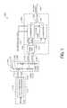
- FIG. 1is a functional block diagram of a DLL tracking enablement circuit based on voltage variations, according to an embodiment of the invention.
- FIG. 2is a functional block diagram of a DLL tracking enablement circuit based on clock frequency variations, according to an embodiment of the invention.
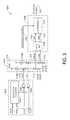
- FIG. 3is a functional block diagram of a DCC tracking enablement circuit based on duty cycle variations, according to an embodiment of the invention.
- FIG. 4is a functional block diagram of a combination DLL and DCC tracking enablement circuit according to an embodiment of the invention.
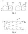
- FIG. 5is a schematic diagram of a frequency divider according to an embodiment of the invention for use in a DLL and/or DCC tracking enablement circuit.
- FIG. 6is a schematic diagram of a non-overlapping clock generation circuit according to an embodiment of the invention for use in a DLL and/or DCC tracking enablement circuit.
- FIG. 7is a schematic diagram of a sense amplifier according to an embodiment of the invention for use in a DLL and/or DCC tracking enablement circuit.
- FIG. 8is a schematic diagram of a comparator circuit according to an embodiment of the invention for use in a DLL and/or DCC tracking enablement circuit.
- FIG. 9is a block diagram of a memory, according to an embodiment of the invention.
- Embodiments of the disclosed circuitsdisclose low power DLL and/or DCC tracking circuits that monitor the signal clock and supply voltage for variations, for example, clock frequency, duty cycle, and/or supply voltage variations, and enable DLL and DCC tracking based on the variations. Enabling DLL and/or DCC tracking means that a DLL circuit and/or a DCC circuit is actively monitoring and modifying the clock signal in order to correct for phase and/or duty cycle distortion.
- FIG. 1illustrates an apparatus 100 (e.g., an integrated circuit, a memory device, a memory system, an electronic device or system, a smart phone, a tablet, a computer, a server, etc.) according to an embodiment of the disclosure.
- Apparatus 100includes a DLL tracking enablement circuit, generally designated 100 , in accordance with an embodiment of the present invention.
- the DLL tracking enablement circuit 100generally includes a clock generation circuit 102 , a charge pump 104 , and a comparison circuit 106 .
- the clock generation circuit 102includes a non-overlapping clock generator 110 .
- the non-overlapping clock generator 110is an electronic circuit that receives a single clock signal as an input and outputs two discrete clock signals that are non-overlapping. That is, the output signals of the non-overlapping clock generator 110 do not have the same clock level (i.e., a high clock level, or a low clock level) at the same time.
- the non-overlapping clock generator 110receives the system clock, XCLK 108 , as an input clock signal.
- the non-overlapping clock generator 110outputs two non-overlapping clock signals, CLKA 112 and CLKB 114 .
- An example non-overlapping clock generatoris discussed in further detail below with respect to FIG. 6 .
- the charge pump 104is an electronic circuit that outputs two signals, SensA 124 and SensB 126 , which depend on the input clock signals, CLKA 112 and CLKB 114 , and variations in a supply voltage 116 .
- the charge pump 104includes two parallel charging circuits, one for each of the non-overlapping clock signals CLKA 112 and CLKB 114 .
- Each charging circuitincludes a pass gate (e.g., pass gate 118 A or 118 B), a first capacitor (e.g., capacitor 120 A or 120 B), and a second capacitor (e.g., capacitor 122 A or 122 B).
- the first capacitor 120 and the second capacitor 122 of a charging circuitmay be coupled as capacitor divider circuit.
- a supply voltage 116is provided to each charging circuit.
- the supply voltage 116may be the supply voltage for a memory, such as a DRAM.
- the pass gates 118 A and 118 Bmay be, for example, transistors that act as switches with CLKA 112 and CLKB 114 providing the control signals, respectively.
- the charging circuitsare active when the respective non-overlapping clock signal CLKA 112 and CLKB 114 is at a high clock level.
- the capacitors 120 A and 120 Bhave the same capacitance.
- the capacitors 122 A and 122 Bmay have the same capacitance.
- Various embodimentsmay include greater or fewer capacitors.
- the supply voltage 116is provided to a pass gate (i.e., pass gate 118 A or pass gate 118 B), which is coupled to a first capacitor (i.e., capacitor 120 A or capacitor 120 B).
- a pass gatei.e., pass gate 118 A or pass gate 118 B
- Capacitors 120 A and 120 Bmay each be coupled to a second capacitor (i.e., capacitors 122 A and 122 B, respectively), which may then be fed to ground.
- the charging circuit including capacitors 120 A and 122 AWhen CLKA 112 is at a high clock level, the charging circuit including capacitors 120 A and 122 A is active, and the pass gate 118 A forms a closed switch which allows current to flow from the supply voltage 116 and charge the capacitors 120 A and 122 A. As the capacitors charge, an output voltage signal SensA 124 is generated by the charging circuit. The output voltage signal SensA 124 is proportional to the supply voltage 116 during the time that the charging circuit is active. Similarly, when CLKB 114 is at a high clock level, the charging circuit including capacitors 120 B and 122 B is active, and the pass gate 118 B forms a closed switch which allows current to flow from the supply voltage 116 , charging the capacitors 120 B and 122 B.
- an output voltage signal SensB 126is generated by the charging circuit.
- the output voltage signal SensB 126is proportional to the supply voltage 116 during the time that the charging circuit is active.
- CLKA 112 and CLKB 114are non-overlapping clock signals.
- SensA 124 and SensB 126represent signals that are proportional to the supply voltage 116 taken over non-overlapping time periods. Accordingly, if the supply voltage 116 varies between the time period during which SensA 124 is generated and the time period during which SensB 126 is generated, that variation will be manifested as a voltage differential between SensA 124 and SensB 126 .
- the comparison circuit 106receives as inputs SensA 124 and SensB 126 .
- the comparison circuit 106is configured to determine a voltage difference between the input signals, and compare the voltage difference to a threshold value in order to determine whether DLL tracking should be enabled.
- the comparison circuit 106includes a sense amplifier 128 , comparators 134 A and 134 B, a NOR gate 138 and an inverter 140 .
- the sense amplifier 128may be any type of sense amplifier capable of proportionally amplifying the voltages of SensA 124 and SensB 126 relative to one another.
- the sense amplifier 128may output two amplified voltage signals VAH 130 and VBH 132 , which are proportional to SensA 124 and SensB 126 , respectively.
- the comparators 134 A and 134 Bmay be any comparison circuits capable of determining a difference between two voltages (e.g., VAH 130 and VBH 132 ) and determining whether the difference between the two voltages exceeds a predetermined threshold value.
- the comparators 134 A and 134 Bmay include static or adaptive hysteresis which may encourage or discourage the enablement or disablement of DLL tracking depending on past states of the comparator.
- a hysteresis control signal 136may be used to control the hysteresis.
- hysteresis control signal 136may provide an analog or digital weighting factor which can favor or disfavor the activation or deactivation of tracking enablement 142 by altering the threshold value.
- the comparison circuit 106includes two comparators 134 A and 134 B.
- the comparators 134 A and 134 Bmay each receive as inputs VAH 130 and VBH 132 .
- One of the comparatorse.g., comparator 134 A
- the comparator 134 Amay compare the voltage difference of VAH 130 subtracted from VBH 132 with the threshold value. If the comparator 134 A determines that the difference between VBH 132 and VAH 130 is greater than the threshold value, then the comparator 134 A may output a signal indicating that DLL tracking should be enabled.
- the second comparatormay compare the voltage difference of VBH 132 subtracted from VAH 130 with the threshold value. If comparator 134 B determines that the difference between VAH 130 and VBH 132 is greater than the threshold value, then the comparator 134 B outputs a signal indicating that DLL tracking should be enabled.
- the comparison circuit 106can ensure that DLL tracking is enabled in the event of a positive or negative voltage variation exceeding the threshold value.
- An example comparator circuitis discussed in more detail below with respect to FIG. 8 .
- the NOR gate 138 and the inverter 140are used to provide a tracking enable signal 142 that may be used to enable tracking in response to receiving a signal indicating that the one of the differences between the signals VAH 130 and VBH 132 exceeds the threshold value. Accordingly, DLL tracking is enabled when the comparison circuit 106 determines that the supply voltage 116 has drifted a sufficient (greater than the threshold value) amount over a certain time period determined by CLKA 112 and CLKB 114 . When tracking enable signal 142 is active, DLL tracking is enabled and actively monitors and modifies the clock signal in order to account for phase variations in the input clock signal. Tracking enable signal 142 may be provided to, for example, a DLL control circuit which may provide control information to the DLL and manage the delay applied to an input clock signal.
- FIG. 2is a functional block diagram of a DLL tracking enablement circuit according to an embodiment of the invention, generally designated 200 , based on clock frequency variations.
- the DLL tracking enablement circuit 200may generally include a clock generation circuit 202 , a charge pump 204 , and a comparison circuit 206 .
- the clock generation circuit 202may include a frequency divider 244 and a non-overlapping clock generator 210 .
- the clock generation circuit 202receives a clock signal XCLK 208 , which may be, for example, the external system clock of a DRAM device.
- XCLK 208may be implemented in similar ways as XCLK 108 as described above with respect to FIG. 1 .
- the frequency divider 244is an electronic circuit that receives XCLK 208 as an input and outputs a periodic clock signal to the non-overlapping clock generator 210 .
- the clock signal output by the frequency divider 244has a frequency that is less than the frequency of XCLK 208 .
- the frequency divider 244may be, for example, a configurable 2 N divider.
- the frequency divider 244may be any integer divider, and may include a duty cycle correction circuit if the frequency divider 244 divides XCLK 208 by an odd integer.
- the non-overlapping clock generator 210may be implemented in the same manner as the non-overlapping clock generator 110 as described above with respect to FIG. 1 .
- the non-overlapping clock generator 210receives the frequency divided clock signal from the frequency divider 244 and generates non-overlapping clock signals CLKA 212 and CLKB 214 .
- a sample non-overlapping clock generation circuitis discussed in further detail below with respect to FIG. 6 .
- the frequency divider 244reduces the frequency of XCLK 208 . Accordingly, a single clock cycle output by the frequency divider 244 corresponds to an integer multiple of XCLK 208 clock cycles. As noted above, the exact frequency of clock cycles of XCLK 208 may vary with time. Such variations are included in the clock cycle output by the frequency divider 244 . Therefore, CLKA 212 and CLKB 214 generated by the non-overlapping clock generator 210 represent the time for multiple cycles of XCLK 208 taken at different points in time. For example, one cycle of CLKA 212 may represent the time that passed during 2 N cycles of XCLK 208 beginning at a time t 1 .
- one cycle of CLKB 214may represent the time that passed during 2 N cycles of XCLK 208 beginning at time t 2 .
- CLKA 212 and CLKB 214represent the same number of cycles of XCLK 208 and the frequency of XCLK 208 is variable with time, the periods of CLKA 212 and CLKB 214 may be different. That is, CLKA 212 and CLKB 214 have different periods because the frequency of XCLK 208 may have changed between and/or during the times that divider 244 generated the divided clock signal.
- the charge pump 204is an electronic circuit for providing two comparable signals whose voltages depend on CLKA 212 and CLKB 214 .
- the charge pump 204receives CLKA 212 and CLKB 214 as input signals and outputs two signals SensA 224 and SensB 226 with voltages proportional to the periods of CLKA 212 and CLKB 214 , respectively.
- charge pump 204includes two charging circuits.
- Each charging circuitincludes a constant current source 216 coupled to a pass gate (i.e., pass gate 218 A or 218 B).
- the pass gates 218 A and 218 Bmay be coupled to capacitors 220 A and 220 B, respectively.
- Capacitors 220 A and 220 Bmay be coupled to capacitors 222 A and 222 B, respectively, which are coupled to ground.
- Output signals SensA 224 and SensB 226may be generated between capacitors 220 A and 222 A and between capacitors 220 B and 222 B, respectively.
- Each charging circuitgenerates an output signal (e.g., SensA 224 or SensB 226 ) during the time period that the respective input signal (e.g., CLKA 212 or CLKB 214 ) has a high clock level.
- the pass gate 218 Aallows current to flow from the constant current source 216 through the charging circuit.
- the capacitor 220 Awill accumulate charge and develop a voltage differential according to the relationship
- Vl ⁇ t C , where l is the constant current provided by the constant current source 216 , t is the time period during which CLKA 212 has a high clock level, and C is the capacitance of the capacitor 220 A.
- the output signal SensA 224will have a voltage proportional to the voltage across the capacitor 220 A, which is proportional to the time period, t, during which CLKA 212 has a high clock level. Accordingly, the voltage of the output signal SensA 224 is also proportional to the time period during which CLKA 212 has a high clock level.
- the second charging circuitwhich includes the constant current source 216 , the pass gate 218 B, and the capacitors 220 B and 222 B, operates in an analogous manner to the first charging circuit. Accordingly, the output signal SensB 226 is proportional to the time period during which the input clock signal CLKB 214 has a high clock level.
- CLKA 212 and CLKB 214may be active for different lengths of time if the frequency of XCLK 208 changes between or during the sample times over which CLKA 212 and CLKB 214 were generated by the frequency divider 244 . Therefore, a change in the clock frequency of XCLK 208 between or during the sample times of CLKA 212 and CLKB 214 is proportionally reflected as a voltage difference between SensA 224 and SensB 226 .
- the comparison circuit 206is an electronic circuit that amplifies and compares the differences between SensA 224 and SensB 226 with a threshold value.
- the comparison circuit 206generally includes a sense amplifier 228 , comparators 234 A and 234 B, NOR gate 238 and inverter 240 .
- comparison circuit 206may be substantially the same as comparison circuit 106 , as described above with respect to FIG. 1 .
- the sense amplifier 228receives SensA 224 and SensB 226 as input signals, proportionally amplifies the voltages of the received signals, and outputs signals VAH 230 and VBH 232 .
- An example sense amplifier circuitis discussed below with respect to FIG. 7 .
- the comparators 234 A and 234 Bmay compare the differences between VAH 230 and VBH 232 with a threshold value and outputs a respective signal indicative of whether the difference exceeds the threshold value. For example, one of the comparators (e.g., comparator 234 A) compares the voltage difference of VAH 230 subtracted from VBH 232 with a threshold value. If the comparator 234 A determines that the difference between VBH 232 and VAH 230 is greater than the threshold value, then comparator 234 A may output a signal indicating that DLL tracking should be enabled. The second comparator (e.g., comparator 234 B) compares the voltage difference of VBH 232 subtracted from VAH 230 with the threshold value.
- comparator 234 Acompares the voltage difference of VBH 232 subtracted from VAH 230 with the threshold value.
- the comparator 234 Bdetermines that the difference between VAH 230 and VBH 232 is greater than the threshold value, then the comparator 234 B outputs a signal indicating that DLL tracking should be enabled.
- the comparison circuit 206ensures that DLL tracking is enabled in the event of an increased or decreased clock frequency variation exceeding the threshold value.
- the comparators 234 A and 234 Bmay include static or adaptive hysteresis which may encourage or discourage the enablement of DLL tracking depending on past states of the comparator.
- a hysteresis control signal 236may be used to control the hysteresis, as will be appreciated by one skilled in the art.
- An example comparator circuit implementing static hysteresisis discussed in more detail below with respect to FIG. 8 .
- the NOR gate 238 and the inverter 240are used to provide tracking enable signal 242 that may be used to enable tracking in response to receiving a signal from one of the comparators ( 234 A or 234 B) indicating that the one of the differences between signals VAH 230 or VBH 232 exceeds the threshold value. Accordingly, DLL tracking is enabled when the comparison circuit 106 determines that the clock frequency of XCLK 208 has drifted a sufficient (greater than the threshold value) amount over a certain time period, as determined by CLKA 212 and CLKB 214 , and the tracking enable signal 242 is active.
- the embodiment of FIG. 2may be modified in order to monitor both voltage variations (as described with respect to the embodiment of FIG. 1 ) and clock frequency variations.
- the constant current source 216may be replaced with the supply voltage of the memory, such as supply voltage 116 in FIG. 1 .
- the current of the supply voltagedepends upon the variable voltage of the supply.
- FIG. 3is a functional block diagram of a DCC tracking enablement circuit according to an embodiment of the invention, generally designated 300 .
- the DCC tracking enablement circuit 300generally includes a clock generation circuit 302 , a charge pump 304 , and a comparison circuit 306 .
- the clock generation circuit 302includes a frequency divider 344 , an AND gate 338 , and an AND gate 340 .
- the clock generation circuit 302receives a clock signal XCLK 308 and a clock signal XCLKF 310 .
- XCLK 308may be the system clock and XCLKF 310 may be the same as XCLK 308 , but with a phase delay relative to XCLK 308 .
- XCLK 308 and XCLKF 310may be complimentary signals. However, as will be appreciated by one skilled in the art, overlap may exist as a result of duty cycle variation in the input clock signals XCLK 308 and XCLKF 310 .
- the frequency divider 344may be any frequency divider or counter circuit capable of receiving a periodic signal as an input and outputting a periodic signal having a reduced frequency. In various embodiments, the frequency divider 344 may be implemented in a similar manner to frequency divider 244 as discussed above with respect to FIG. 2 .
- the output of the frequency divider 344defines the time period over which duty cycle variation is being sampled.
- the AND gate 338receives as inputs XCLK 308 and the output of the frequency divider 344 .
- the AND gate 338generates an output signal CLKH 314 which has a high clock level when, during the sample period defined by the output of the frequency divider 344 , XCLK 308 has a high clock level. Accordingly, the time during which CLKH has a high clock level is proportional to the duty cycle of XCLK 308 during the sample period.
- the AND gate 340receives as inputs XCLKF 310 and the output of the frequency divider 344 .
- the AND gate 340outputs a signal CLKL 316 that has a high clock level when, during the sample period defined by the output of the frequency divider 344 , CLKF has a high clock level.
- CLKL 316is proportional to the time during the sample period that XCLK 308 has a low clock level (i.e. the compliment of the duty cycle of XCLK 308 ). In other words, either CLKH or CLKL will be active during the sample period, but CLKH and CLKL are not active at the same time.
- the charge pump 304includes a current source 316 , pass gates 318 A and 318 B, and capacitors 320 A, 320 B, 322 A and 322 B.
- the charge pump 304may be implemented in a similar manner as charge pumps 104 and 204 as described above with respect to FIGS. 1 and 2 .
- CLKH and CLKLare proportional to the duty cycle of XCLK 308
- the time during which the two charging circuits of the charge pump 304 are activeis also proportional to the duty cycle of XCLK 308 .
- the charge pump 304outputs two signals, SensH 324 and SensL 326 , which have voltages that are proportional to the high clock level portion and the low clock level portion of XCLK 308 during the sample time, respectively.
- the comparison circuit 306receives as inputs SensH 324 and SensL 326 and generally includes a sense amplifier 328 and a comparator 334 .
- the comparison circuit 306may be implemented in a similar manner as comparison circuits 106 and 206 as described above with respect to FIGS. 1 and 2 .
- Sense amplifier 328may proportionally amplify SensH 324 and SensL 326 to generate VAH 330 and VBH 332 .
- Comparator 334may compare a difference between VAH 330 and VBH 332 with a threshold value and output an active or inactive tracking enable signal 342 having a logic level indicative of whether the difference between VAH 330 and VBH 332 exceeds a threshold value.
- the comparator 334may include static or adaptive hysteresis, which may be controlled by hysteresis control signal 336 .
- hysteresis control signal 336a determination by the comparator 334 that the difference between VAH 330 and VBH 332 exceeds a threshold value indicates that the duty cycle of XCLK 308 has departed from the ideal 50% by more than a threshold value, and therefore a DCC correction circuit should be enabled to correct for the duty cycle variation.
- the tracking enable signal 342may be provided, for example, to a DCC control circuit capable of managing a duty cycle correction applied to an input clock signal.
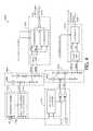
- FIG. 4is a functional block diagram of a combination DLL and DCC tracking enablement circuit according to an embodiment of the invention, generally designated 400 .
- the DLL and DCC tracking enablement circuit 400includes clock generation circuits 402 and 414 , charge pumps 404 and 416 , and comparison circuits 406 and 418 .
- the DLL and DCC tracking enablement circuit 400receives a clock signal, XCLK 408 , and a clock signal, XCLKF 412 as inputs.
- the DLL and DCC tracking enablement circuit 400outputs a DLL tracking enable signal 410 and a DCC tracking enable signal 420 .
- the clock generation circuit 402may be implemented in the same manner as clock generation circuit 102 or 202 as described above with respect to FIGS.
- Clock generation circuit 414may be implemented in the same manner as clock generation circuit 302 as described above with respect to FIG. 3 .
- Charge pumps 404 and 416may be implemented in the same manner as charge pumps 104 , 204 , and 304 as described above with respect to FIGS. 1-3 .
- Comparison circuits 406 and 418may be implemented in the same manner as comparison circuits 106 , 206 , and 306 as described above with respect to FIGS. 1-3 .
- the DLL and DCC tracking enablement circuit 400provides a customizable composite circuit for determining whether to enable DLL and/or DCC tracking. The embodiment of FIG.
- FIG. 4recognizes that it may be desirable to have different voltage comparison threshold values or different frequency dividers between the DLL tracking enablement circuit and the DCC tracking enablement circuit. Accordingly, the embodiment of FIG. 4 provides a parallel configuration which allows for customized circuit components between the DLL tracking enablement circuit and the DCC tracking enablement circuit.
- FIG. 5is a schematic diagram of an example 2 N frequency divider circuit according to an embodiment of the invention, generally designated 500 .
- the frequency divider circuit 500may be used in a DLL and/or DCC tracking enablement circuit.
- Frequency divider circuit 500generally includes a number, N, of D flip-flops 504 which are linked together in serial such that the inverted output of one D flip-flop 504 provides the clock signal of the following D flip-flop 504 .
- the output of each D flip-flop 504has a frequency equal to the frequency of the input clock divided by a power of two.
- the frequency divider 500has a division period of less than 256 cycles (i.e., a 2 8 division).
- frequency divider 500may be implemented as frequency divider 244 or 344 as described above with respect to FIGS. 2 and 3 . Other frequency divider circuits are possible without departing from the scope of the present disclosure.
- FIG. 6is a schematic diagram of a non-overlapping clock generation circuit according to an embodiment of the invention, generally designated 600 .
- the non-overlapping clock generation circuitmay be used in a DLL and/or DCC tracking enablement circuit.
- the clock generation circuit 600generally receives a periodic clock signal XCLK 602 and generates two non-overlapping clock signals CLKA 604 and CLKB 606 using NAND gates and inverters with feedback.
- clock generator 600may be implemented as non-overlapping clock generators 110 and 210 as discussed above.
- Clock generator 600represents an example clock generator. Those skilled in the art will recognize that other possible non-overlapping clock generation circuits may be used without departing from the scope of this disclosure.
- FIG. 7is a schematic diagram of a sense amplifier according to an embodiment of the invention, generally designated 700 .
- the sense amplifier 700may be used in a DLL and/or DCC tracking enablement circuit.
- sense amplifier 700may be implemented as sense amplifier 128 , 228 , and/or 328 , as described above with respect to FIGS. 1-3 .
- sense amplifier 700receives two input signals SensA 702 and SensB 704 , proportionally amplifies each input signal through two identical amplifier circuits, and outputs two output signals VAH 706 and VBH 708 .
- SensA 702may be implemented as SensA 124 , 224 , and/or SensH 324 , as discussed above with respect to FIGS. 1-3 .
- SensB 704may be implemented as SensB 126 , 226 , and/or SensL 326 , as discussed above with respect to FIGS. 1-3 .
- VAH 706may be implemented as VAH 130 , 230 , and/or 330 , as discussed above with respect to FIGS. 1-3 .
- VBH 708may be implemented as VAH 132 , 232 , and/or 332 , as discussed above with respect to FIGS. 1-3 .
- the sense amplifier 700represents an example sense amplifier. Those skilled in the art will recognize that other possible sense amplifiers may be used without departing from the scope of this disclosure.
- FIG. 8is a schematic diagram of a comparator circuit according to an embodiment of the invention, generally designated 800 .
- the comparator circuit 800may be used in a DLL and/or DCC tracking enablement circuit.
- comparator 800may be implemented as one or more of comparators 134 A, 134 B, 234 A, 234 B, or 334 .
- comparator 800may be a differential comparator having two pairs of transistors 808 and 810 .
- a static hysteresismay be applied to the comparator 800 .
- the comparatorcompares the difference between the input signals VAH 802 and VBH 804 to a predetermined threshold value and outputs a tracking enable signal 806 if the comparator 800 determines that the difference between VAH 802 and VBH 804 exceeds the threshold value.
- the comparator 800may include a feedback loop and/or a hysteresis control signal which allow for adaptive hysteresis capabilities. By using adaptive hysteresis, the comparator 800 may reduce the frequency with which tracking is enabled and therefore reduce the power consumed by a DLL, a DCC correction circuit, or both.
- the comparator 800represents an example comparator. Those skilled in the art will recognize that other possible comparators may be used without departing from the scope of this disclosure.
- FIG. 9is a block diagram of a memory, according to an embodiment of the invention.
- the memory 900may include an array 902 of memory cells, which may be, for example, volatile memory cells (e.g., dynamic random-access memory (DRAM) memory cells, static random-access memory (SRAM) memory cells), non-volatile memory cells (e.g., flash memory cells), or some other types of memory cells.
- the memory 900includes a command decoder 906 that may receive memory commands through a command bus 908 and provide (e.g., generate) corresponding control signals within the memory 900 to carry out various memory operations.
- the command decoder 906may respond to memory commands provided to the command bus 908 to perform various operations on the memory array 902 .
- command decoder 906may be used to provide internal control signals to read data from and write data to the memory array 902 .
- Row and column address signalsmay be provided (e.g., applied) to an address latch 910 in the memory 900 through an address bus 920 .
- the address latch 910may then provide (e.g., output) a separate column address and a separate row address.
- the address latch 910may provide row and column addresses to a row address decoder 922 and a column address decoder 928 , respectively.
- the column address decoder 928may select bit lines extending through the array 902 corresponding to respective column addresses.
- the row address decoder 922may be connected to a word line driver 924 that activates respective rows of memory cells in the array 902 corresponding to received row addresses.
- the selected data linee.g., a bit line or bit lines
- corresponding to a received column addressmay be coupled to a read/write circuitry 930 to provide read data to an output data buffer 934 via an input-output data path 940 .
- Write datamay be provided to the memory array 902 through an input data buffer 944 and the memory array read/write circuitry 930 .
- the memory 900may include a clock generator 916 that includes a delay circuit 914 .
- the delay circuit 914provides an output clock signal OUT 912 signal that may be used for clocking circuitry of the memory 900 .
- the delay circuit 914may include one or more tracking enablement circuits 917 , which can be activated by a tracking enable signal 918 , according to embodiments of the invention.
- the delay circuit 914may include a tracking enablement circuit 917 in accordance with any of the previously described embodiments with reference to FIGS. 1-4 .
- the variation of frequency and/or the duty cycle of the input clock signal 108 , 208 , 308 , 310 , 408 or 412are translated into the variation of signal voltage level of the output signals SENSA, SENSB, SENSH or SENSL.
- the signal voltage levelis stored in the capacitors 122 A, 122 B, 222 A, 222 B, 322 A, 322 B as signal information based on a corresponding time period of the input clock signal 108 , 208 , 308 , 310 , 408 or 412 .
- the signal information stored in the capacitorsmay also include the variation of supply voltage level of the power supply voltage source VPERI 116 , 216 or 316 .
- the comparison circuit 106 , 206 , 306 , 406 , 418 in FIGS. 1-4is coupled to the capacitors as storage elements and configured to provide a control signal.
- the control signalmay include a tracking enable signal 142 , 242 , 342 , 410 , and/or 420 .
- the comparison circuit 106 , 206 , 306 , 406 , 418may be constructed of a logic circuit though the comparison circuit in FIG. 7 or FIG. 8 is constructed by an analogue circuit.
- the embodimentmay include steps of monitoring a signal information, such as a variation of supply voltage of the power source, a variation of a frequency and/or a duty cycle of input clock signal, detecting whether the signal information exceeds a predetermined value, and providing a tracking enable signal enabling a tracking enablement circuit, such as a DLL tracking circuit and a duty cycle tracking circuit, if the signal information exceeds the predetermined value.
- a signal informationsuch as a variation of supply voltage of the power source, a variation of a frequency and/or a duty cycle of input clock signal
- detecting whether the signal information exceeds a predetermined valuedetecting whether the signal information exceeds a predetermined value
- a tracking enable signalenabling a tracking enablement circuit, such as a DLL tracking circuit and a duty cycle tracking circuit
- the comparison circuitmay be called a control circuit which can provide a control signal based on two signal information.
- the control signalcan include an active tracking enablement signal enabling an active tracking circuit such as a DLL tracking circuit and a duty cycle tracking circuit.
- One of the two signal informationmay be information obtained by monitoring a status such as the voltage source, the frequency or the duty cycle of the input clock signal.
- the other of the two signal informationmay be reference information such as a predetermined value or an average value obtained during a predetermined period.
- the comparison circuit 106 , 206includes the two comparators 134 A and 134 B, 234 A and 234 B, respectively, however, those skilled in the art will appreciate that the comparison circuit 106 , 206 may be constructed of single comparator with hysteresis control, respectively, like the comparison circuit 306 in FIG. 3 .
Landscapes
- Physics & Mathematics (AREA)
- Nonlinear Science (AREA)
- Stabilization Of Oscillater, Synchronisation, Frequency Synthesizers (AREA)
- Amplifiers (AREA)
Abstract
Description
where l is the constant current provided by the constant current source216, t is the time period during which
Claims (22)
Priority Applications (2)
| Application Number | Priority Date | Filing Date | Title |
|---|---|---|---|
| US14/736,005US9813067B2 (en) | 2015-06-10 | 2015-06-10 | Clock signal and supply voltage variation tracking |
| US15/628,260US10193558B2 (en) | 2015-06-10 | 2017-06-20 | Clock signal and supply voltage variation tracking |
Applications Claiming Priority (1)
| Application Number | Priority Date | Filing Date | Title |
|---|---|---|---|
| US14/736,005US9813067B2 (en) | 2015-06-10 | 2015-06-10 | Clock signal and supply voltage variation tracking |
Related Child Applications (1)
| Application Number | Title | Priority Date | Filing Date |
|---|---|---|---|
| US15/628,260DivisionUS10193558B2 (en) | 2015-06-10 | 2017-06-20 | Clock signal and supply voltage variation tracking |
Publications (2)
| Publication Number | Publication Date |
|---|---|
| US20160365860A1 US20160365860A1 (en) | 2016-12-15 |
| US9813067B2true US9813067B2 (en) | 2017-11-07 |
Family
ID=57517513
Family Applications (2)
| Application Number | Title | Priority Date | Filing Date |
|---|---|---|---|
| US14/736,005ActiveUS9813067B2 (en) | 2015-06-10 | 2015-06-10 | Clock signal and supply voltage variation tracking |
| US15/628,260ActiveUS10193558B2 (en) | 2015-06-10 | 2017-06-20 | Clock signal and supply voltage variation tracking |
Family Applications After (1)
| Application Number | Title | Priority Date | Filing Date |
|---|---|---|---|
| US15/628,260ActiveUS10193558B2 (en) | 2015-06-10 | 2017-06-20 | Clock signal and supply voltage variation tracking |
Country Status (1)
| Country | Link |
|---|---|
| US (2) | US9813067B2 (en) |
Cited By (5)
| Publication number | Priority date | Publication date | Assignee | Title |
|---|---|---|---|---|
| US9997220B2 (en) | 2016-08-22 | 2018-06-12 | Micron Technology, Inc. | Apparatuses and methods for adjusting delay of command signal path |
| US10193558B2 (en) | 2015-06-10 | 2019-01-29 | Micron Technology, Inc. | Clock signal and supply voltage variation tracking |
| US10224938B2 (en) | 2017-07-26 | 2019-03-05 | Micron Technology, Inc. | Apparatuses and methods for indirectly detecting phase variations |
| US10658019B2 (en) | 2007-03-15 | 2020-05-19 | Micron Technology, Inc. | Circuit, system and method for controlling read latency |
| US10755758B2 (en) | 2016-04-26 | 2020-08-25 | Micron Technology, Inc. | Methods and apparatuses including command delay adjustment circuit |
Families Citing this family (1)
| Publication number | Priority date | Publication date | Assignee | Title |
|---|---|---|---|---|
| KR20240143518A (en)* | 2023-03-24 | 2024-10-02 | 삼성전자주식회사 | Semiconductor device perfoming clock gating and operating method of the semiconductor device |
Citations (167)
| Publication number | Priority date | Publication date | Assignee | Title |
|---|---|---|---|---|
| US5004933A (en) | 1986-06-02 | 1991-04-02 | Tektronix, Inc. | Phase-selectable flip-flop |
| US6111810A (en) | 1998-09-30 | 2000-08-29 | Nec Corporation | Synchronous semiconductor memory device having burst access mode and multi-bit pre-fetch operation |
| US6219384B1 (en) | 1995-06-26 | 2001-04-17 | Phillip S. Kliza | Circuit for determining clock propagation delay in a transmission line |
| US6260128B1 (en) | 1997-08-13 | 2001-07-10 | Kabushiki Kaisha Toshiba | Semiconductor memory device which operates in synchronism with a clock signal |
| US6275077B1 (en) | 1999-08-31 | 2001-08-14 | Sun Microsystems, Inc. | Method and apparatus for programmable adjustment of bus driver propagation times |
| US20010015924A1 (en) | 1999-12-24 | 2001-08-23 | Kazutami Arimoto | Test interface circuit and semiconductor integrated circuit device including the same |
| US6327318B1 (en) | 1998-06-30 | 2001-12-04 | Mosaid Technologies Incorporated | Process, voltage, temperature independent switched delay compensation scheme |
| US20020057624A1 (en) | 1997-03-05 | 2002-05-16 | Manning Troy A. | Delay-locked loop with binary-coupled capacitor |
| US6424592B1 (en) | 2000-11-30 | 2002-07-23 | Mitsubishi Denki Kabushiki Kaisha | Semiconductor integrated circuit having circuit for correcting data output timing |
| US20020110035A1 (en) | 2001-02-12 | 2002-08-15 | Wen Li | Method of reducing standby current during power down mode |
| US6438055B1 (en) | 1999-10-20 | 2002-08-20 | Fujitsu Limited | Dynamic memory circuit with automatic refresh function |
| US6459313B1 (en) | 1998-09-18 | 2002-10-01 | Lsi Logic Corporation | IO power management: synchronously regulated output skew |
| US20020149506A1 (en)* | 2001-04-06 | 2002-10-17 | Hans Altrichter | Circuit configuration and sensor device |
| US6489823B2 (en) | 2000-10-18 | 2002-12-03 | Mitsubishi Denki Kabushiki Kaisha | Semiconductor device capable of generating highly precise internal clock |
| US6510095B1 (en) | 2001-09-28 | 2003-01-21 | Fujitsu Limited | Semiconductor memory device for operating in synchronization with edge of clock signal |
| US20030117864A1 (en) | 2001-10-22 | 2003-06-26 | Hampel Craig E. | Phase adjustment apparatus and method for a memory device signaling system |
| US20030147299A1 (en) | 2002-02-05 | 2003-08-07 | Mitsubishi Denki Kabushiki Kaisha | Semiconductor memory device capable of making switch between synchronizing signals for operation on data generated by different circuit configurations |
| US20030161210A1 (en) | 2002-02-28 | 2003-08-28 | Pramod Acharya | Control circuit for an S-DRAM |
| US6636110B1 (en) | 1998-05-01 | 2003-10-21 | Mitsubishi Denki Kabushiki Kaisha | Internal clock generating circuit for clock synchronous semiconductor memory device |
| US6687185B1 (en) | 2002-08-29 | 2004-02-03 | Micron Technology, Inc. | Method and apparatus for setting and compensating read latency in a high speed DRAM |
| US6710726B2 (en) | 2002-04-03 | 2004-03-23 | Samsung Electronics Co., Ltd. | Serializer-deserializer circuit having increased margins for setup and hold time |
| US6744285B2 (en) | 2002-08-08 | 2004-06-01 | Agilent Technologies, Inc. | Method and apparatus for synchronously transferring data across multiple clock domains |
| US6781861B2 (en) | 2001-08-06 | 2004-08-24 | Micron Technology, Inc. | Method and apparatus for determining digital delay line entry point |
| US6839288B1 (en) | 2003-11-12 | 2005-01-04 | Infineon Technologies Ag | Latch scheme with invalid command detector |
| US20050024107A1 (en) | 2003-07-31 | 2005-02-03 | Elpida Memory, Inc | Delay circuit and delay sysnchronization loop device |
| US6861901B2 (en) | 2002-07-01 | 2005-03-01 | Texas Instruments Deutschland, Gmbh | Voltage follower circuit |
| US20050047222A1 (en) | 2003-08-27 | 2005-03-03 | Rentschler Eric Mccutcheon | Data signal reception latch control using clock aligned relative to strobe signal |
| US20050052309A1 (en)* | 2003-09-09 | 2005-03-10 | Yao-Chi Wang | [automatic threshold voltage control circuit and signal converting circuit and method thereof] |
| US6868504B1 (en) | 2000-08-31 | 2005-03-15 | Micron Technology, Inc. | Interleaved delay line for phase locked and delay locked loops |
| US20050132043A1 (en) | 2003-12-12 | 2005-06-16 | Hon Hai Precision Industry Co., Ltd. | System and method for command line interface command processing |
| US6914798B2 (en) | 2001-06-30 | 2005-07-05 | Hynix Semiconductor Inc. | Register controlled DLL for reducing current consumption |
| US6930955B2 (en) | 2003-03-18 | 2005-08-16 | Micron Technology, Inc. | Method and apparatus for establishing and maintaining desired read latency in high-speed DRAM |
| US20050184780A1 (en)* | 2004-02-23 | 2005-08-25 | Hynix Semiconductor Inc. | Clock duty ratio correction circuit |
| US6973008B2 (en) | 2003-04-29 | 2005-12-06 | Infineon Technologies Ag | Apparatus for flexible deactivation of word lines of dynamic memory modules and method therefor |
| US20050270852A1 (en) | 2004-05-27 | 2005-12-08 | Infineon Technologies Ag | Read latency control circuit |
| US6980479B2 (en) | 2003-04-29 | 2005-12-27 | Hynix Semiconductor Inc. | Semiconductor device for domain crossing |
| US6988218B2 (en) | 2002-02-11 | 2006-01-17 | Micron Technology, Inc. | System and method for power saving delay locked loop control by selectively locking delay interval |
| US20060062341A1 (en) | 2004-09-20 | 2006-03-23 | Edmondson John H | Fast-lock clock-data recovery system |
| US20060064620A1 (en) | 2004-09-15 | 2006-03-23 | Justus Kuhn | Self test for the phase angle of the data read clock signal DQS |
| US7042799B2 (en) | 2003-12-30 | 2006-05-09 | Hynix Semiconductor Inc. | Write circuit of double data rate synchronous DRAM |
| US7046060B1 (en) | 2004-10-27 | 2006-05-16 | Infineon Technologies, Ag | Method and apparatus compensating for frequency drift in a delay locked loop |
| US7058799B2 (en) | 2001-06-19 | 2006-06-06 | Micron Technology, Inc. | Apparatus and method for clock domain crossing with integrated decode |
| US7061941B1 (en) | 2000-11-28 | 2006-06-13 | Winbond Electronics Corporation America | Data input and output circuits for multi-data rate operation |
| US7065001B2 (en) | 2004-08-04 | 2006-06-20 | Micron Technology, Inc. | Method and apparatus for initialization of read latency tracking circuit in high-speed DRAM |
| US20060155948A1 (en) | 2004-10-27 | 2006-07-13 | Hermann Ruckerbauer | Semiconductor memory system and method for data transmission |
| US20060182212A1 (en) | 2005-02-11 | 2006-08-17 | International Business Machines Corporation | Method and apparatus for generating synchronization signals for synchronizing multiple chips in a system |
| US20060193194A1 (en) | 2005-02-28 | 2006-08-31 | Josef Schnell | Data strobe synchronization for DRAM devices |
| US7111185B2 (en) | 2003-12-23 | 2006-09-19 | Micron Technology, Inc. | Synchronization device with delay line control circuit to control amount of delay added to input signal and tuning elements to receive signal form delay circuit |
| US7119591B1 (en) | 2004-01-05 | 2006-10-10 | Integrated Device Technology, Inc. | Delay-locked loop (DLL) integrated circuits having binary-weighted delay chain units with built-in phase comparators that support efficient phase locking |
| US20060250861A1 (en) | 2005-05-03 | 2006-11-09 | Samsung Electronics Co., Ltd. | Semiconductor memory device and latency signal generating method thereof |
| US20060250883A1 (en) | 2005-05-04 | 2006-11-09 | Kazimierz Szczypinski | Integrated semiconductor memory device for synchronizing a signal with a clock signal |
| US7158443B2 (en) | 2005-06-01 | 2007-01-02 | Micron Technology, Inc. | Delay-lock loop and method adapting itself to operate over a wide frequency range |
| US20070033427A1 (en) | 2005-07-19 | 2007-02-08 | International Business Machines Corporation | Power efficient cycle stealing |
| US20070046346A1 (en) | 2005-08-30 | 2007-03-01 | Alessandro Minzoni | Clock controller with integrated DLL and DCC |
| US7187599B2 (en) | 2005-05-25 | 2007-03-06 | Infineon Technologies North America Corp. | Integrated circuit chip having a first delay circuit trimmed via a second delay circuit |
| US20070088903A1 (en) | 2005-10-17 | 2007-04-19 | Samsung Electronics Co., Ltd. | Memory module, memory system and method for controlling the memory system |
| US7248512B2 (en) | 2004-11-08 | 2007-07-24 | Hynix Semiconductor Inc. | Semiconductor memory device having controller with improved current consumption |
| US20070192651A1 (en) | 2002-08-12 | 2007-08-16 | Broadcom Corporation | Low-Speed DLL Employing a Digital Phase Interpolator based upon a High-Speed Clock |
| US7269754B2 (en) | 2002-12-30 | 2007-09-11 | Intel Corporation | Method and apparatus for flexible and programmable clock crossing control with dynamic compensation |
| US7268605B2 (en) | 2004-06-14 | 2007-09-11 | Rambus, Inc. | Technique for operating a delay circuit |
| US7280430B2 (en) | 2005-04-30 | 2007-10-09 | Hynix Semiconductor Inc. | Semiconductor memory device |
| US20070291558A1 (en) | 2006-06-15 | 2007-12-20 | Hynix Semiconductor Inc. | Data strobe signal generator for generating data strobe signal based on adjustable preamble value and semiconductor memory device with the same |
| US7319728B2 (en) | 2002-05-16 | 2008-01-15 | Micron Technology, Inc. | Delay locked loop with frequency control |
| US7336752B2 (en) | 2002-12-31 | 2008-02-26 | Mosaid Technologies Inc. | Wide frequency range delay locked loop |
| US7340632B2 (en) | 2004-01-10 | 2008-03-04 | Hynix Semiconductor Inc. | Domain crossing device |
| US20080080271A1 (en) | 2006-09-29 | 2008-04-03 | Hynix Semiconductor Inc. | Delay selecting circuit for semiconductor memory device |
| US20080080267A1 (en) | 2006-09-29 | 2008-04-03 | Lee Hyeng Ouk | Data output control circuit and data output control method |
| US7355464B2 (en) | 2005-05-09 | 2008-04-08 | Micron Technology, Inc. | Apparatus and method for controlling a delay- or phase-locked loop as a function of loop frequency |
| US7375560B2 (en) | 2004-08-31 | 2008-05-20 | Micron Technology, Inc. | Method and apparatus for timing domain crossing |
| US20080126822A1 (en) | 2006-11-28 | 2008-05-29 | Kyoung-Ho Kim | Apparatus for aligning input data in semiconductor memory device |
| US20080137471A1 (en) | 2006-12-07 | 2008-06-12 | Josef Schnell | Memory with clock distribution options |
| US20080144423A1 (en) | 2006-12-19 | 2008-06-19 | Jongtae Kwak | Timing synchronization circuit with loop counter |
| US20080180144A1 (en) | 2007-01-30 | 2008-07-31 | Mosaid Technologies Incorporated | Phase detector circuit and method therefor |
| US7411852B2 (en) | 2005-10-27 | 2008-08-12 | Elpida Memory, Inc. | Semiconductor memory device and method of adjusting same |
| US20080204071A1 (en) | 2007-02-27 | 2008-08-28 | Samsung Electronics Co., Ltd. | On-die termination circuit, method of controlling the same, and ODT synchronous buffer |
| US7428284B2 (en) | 2005-03-14 | 2008-09-23 | Micron Technology, Inc. | Phase detector and method providing rapid locking of delay-lock loops |
| US20080232180A1 (en) | 2006-10-31 | 2008-09-25 | Hynix Semiconductor Inc. | Semiconductor memory device and method for driving the same |
| US20080232179A1 (en) | 2007-03-15 | 2008-09-25 | Micron Technology, Inc. | Circuit, system and method for controlling read latency |
| US20080253205A1 (en) | 2007-04-11 | 2008-10-16 | Hynix Semiconductor Inc. | Write control signal generation circuit, semiconductor ic having the same and method of driving semicounductor ic |
| US7443216B2 (en) | 2007-02-20 | 2008-10-28 | Micron Technology, Inc. | Trimmable delay locked loop circuitry with improved initialization characteristics |
| US7451338B2 (en) | 2005-09-30 | 2008-11-11 | Intel Corporation | Clock domain crossing |
| US7463534B2 (en) | 2006-04-18 | 2008-12-09 | Hynix Semiconductor Inc. | Write apparatus for DDR SDRAM semiconductor memory device |
| US7489172B2 (en) | 2005-09-29 | 2009-02-10 | Hynix Semiconductor Inc. | DLL driver control circuit |
| US20090041104A1 (en) | 2006-06-27 | 2009-02-12 | Bogdan John W | Phase and Frequency Recovery Techniques |
| US7509517B2 (en) | 2003-07-31 | 2009-03-24 | Advantest Corporation | Clock transferring apparatus for synchronizing input data with internal clock and test apparatus having the same |
| US7541851B2 (en) | 2006-12-11 | 2009-06-02 | Micron Technology, Inc. | Control of a variable delay line using line entry point to modify line power supply voltage |
| US7580321B2 (en) | 2005-10-20 | 2009-08-25 | Elpida Memory, Inc. | Synchronous semiconductor memory device |
| US20090219068A1 (en) | 2008-02-28 | 2009-09-03 | Sony Corporation | Phase detector, phase comparator, and clock synchronizing device |
| US20090232250A1 (en) | 2008-03-12 | 2009-09-17 | Takaaki Yamada | Communication system, receiver and reception method |
| US7593273B2 (en) | 2006-11-06 | 2009-09-22 | Altera Corporation | Read-leveling implementations for DDR3 applications on an FPGA |
| US7609584B2 (en) | 2005-11-19 | 2009-10-27 | Samsung Electronics Co., Ltd. | Latency control circuit and method thereof and an auto-precharge control circuit and method thereof |
| US7616040B2 (en) | 2006-12-08 | 2009-11-10 | Sony Corporation | Flip-flop and semiconductor integrated circuit |
| US7631248B2 (en) | 2004-09-29 | 2009-12-08 | Intel Corporation | Cycle-stealing decoding apparatus, systems, and methods |
| US20090315600A1 (en) | 2008-06-18 | 2009-12-24 | Micron Technologies, Inc. | Locked-loop quiescence apparatus, systems, and methods |
| US20100001762A1 (en) | 2008-07-03 | 2010-01-07 | Hynix Semiconductor, Inc. | Domain crossing circuit and method |
| US7660187B2 (en) | 2004-08-04 | 2010-02-09 | Micron Technology, Inc. | Method and apparatus for initialization of read latency tracking circuit in high-speed DRAM |
| US7663946B2 (en) | 2007-07-12 | 2010-02-16 | Hynix Semiconductor Inc. | Semiconductor memory device having on-die-termination device and operation method thereof |
| US7671648B2 (en) | 2006-10-27 | 2010-03-02 | Micron Technology, Inc. | System and method for an accuracy-enhanced DLL during a measure initialization mode |
| US20100054060A1 (en) | 2007-03-29 | 2010-03-04 | Young-Jun Ku | Delay locked loop and semiconductor memory device with the same |
| US20100052739A1 (en) | 2008-08-28 | 2010-03-04 | Elpida Memory, Inc | Device and control method of device |
| US7675439B2 (en) | 2007-12-26 | 2010-03-09 | Altek Corporation | Serial/parallel data conversion apparatus and method thereof |
| US7675791B2 (en) | 2005-08-29 | 2010-03-09 | Samsung Electronics Co., Ltd. | Synchronous memory device |
| US20100066422A1 (en) | 2008-09-16 | 2010-03-18 | Jen-Che Tsai | Clock timing calibration circuit and clock timing calibration method for calibrating phase difference between different clock signals and related analog-to-digital conversion system using the same |
| US7698589B2 (en) | 2006-03-21 | 2010-04-13 | Mediatek Inc. | Memory controller and device with data strobe calibration |
| US7715260B1 (en) | 2008-12-01 | 2010-05-11 | United Microelectronics Corp. | Operating voltage tuning method for static random access memory |
| CN101752009A (en) | 2008-12-16 | 2010-06-23 | 联华电子股份有限公司 | Method for adjusting operation voltage of static random access memory |
| US20100165769A1 (en) | 2008-12-25 | 2010-07-01 | Elpida Memory. Inc. | Semiconductor memory device having auto-precharge function |
| US20100165780A1 (en) | 2008-12-27 | 2010-07-01 | Bains Kuljit S | Dynamic random access memory with shadow writes |
| US7751261B2 (en) | 2007-02-08 | 2010-07-06 | Samsung Electronics Co., Ltd. | Method and apparatus for controlling read latency of high-speed DRAM |
| US20100177589A1 (en) | 2008-05-22 | 2010-07-15 | Elpida Memory Inc. | Semiconductor device having latency counter |
| US20100195429A1 (en) | 2009-02-03 | 2010-08-05 | Nec Electronics Corporation | Semiconductor memory device |
| US7773435B2 (en) | 2008-01-03 | 2010-08-10 | Samsung Electronics Co., Ltd. | Semiconductor memory devices for controlling latency |
| US20100208535A1 (en) | 2009-02-17 | 2010-08-19 | Elpida Memory, Inc. | Semiconductor memory device, memory module including the same, and data processing system |
| US20100208534A1 (en) | 2009-02-17 | 2010-08-19 | Elpida Memory, Inc. | Semiconductor memory device, memory module including the same, and data processing system |
| US20100232213A1 (en) | 2009-03-12 | 2010-09-16 | Hyong-Ryol Hwang | Control signal transmitting system of a semiconductor device |
| US20100254198A1 (en) | 2009-04-01 | 2010-10-07 | Venkatraghavan Bringivijayaraghavan | Write command and write data timing circuit and methods for timing the same |
| US7822904B2 (en) | 1999-07-29 | 2010-10-26 | Micron Technology, Inc. | Capturing read data |
| US7826305B2 (en) | 2007-07-10 | 2010-11-02 | Elpida Memory, Inc. | Latency counter, semiconductor memory device including the same, and data processing system |
| US7826583B2 (en) | 2006-10-31 | 2010-11-02 | Hynix Semiconductor Inc. | Clock data recovery apparatus |
| US20100327926A1 (en) | 2009-06-24 | 2010-12-30 | Elpida Memory, Inc. | DLL circuit and semiconductor device having the DLL circuit |
| US7872924B2 (en) | 2008-10-28 | 2011-01-18 | Micron Technology, Inc. | Multi-phase duty-cycle corrected clock signal generator and memory having same |
| US7876640B2 (en) | 2008-09-23 | 2011-01-25 | Micron Technology, Inc. | Control voltage tracking circuits, methods for recording a control voltage for a clock synchronization circuit and methods for setting a voltage controlled delay |
| US7885365B2 (en) | 2007-08-31 | 2011-02-08 | International Business Machines Corporation | Low-power, low-area high-speed receiver architecture |
| US20110047319A1 (en) | 2009-08-18 | 2011-02-24 | Samsung Electronics Co., Ltd. | Memory devices and systems including write leveling operations and methods of performing write leveling operations in memory devices and systems |
| US20110055671A1 (en) | 2009-09-03 | 2011-03-03 | International Business Machines Corporation | Advanced memory device having improved performance, reduced power and increased reliability |
| US20110057697A1 (en) | 2009-09-08 | 2011-03-10 | Elpida Memory, Inc. | Clock generating circuit, semiconductor device including the same, and data processing system |
| US7913103B2 (en) | 2007-08-31 | 2011-03-22 | Globalfoundries Inc. | Method and apparatus for clock cycle stealing |
| US7928782B2 (en) | 2009-01-28 | 2011-04-19 | Micron Technology, Inc. | Digital locked loops and methods with configurable operating parameters |
| US20110102039A1 (en) | 2009-10-30 | 2011-05-05 | Seok-Bo Shin | Apparatus and method for correcting duty cycle of clock signal |
| US7948817B2 (en) | 2009-02-27 | 2011-05-24 | International Business Machines Corporation | Advanced memory device having reduced power and improved performance |
| US7983094B1 (en) | 2006-11-06 | 2011-07-19 | Altera Corporation | PVT compensated auto-calibration scheme for DDR3 |
| US20110238941A1 (en) | 2010-03-29 | 2011-09-29 | Freescale Semiconductor, Inc. | Scheduling memory access requests using predicted memory timing and state information |
| US8116415B2 (en) | 2007-10-02 | 2012-02-14 | Panasonic Corporation | Semiconductor integrated circuit, communication apparatus, information playback apparatus, image display apparatus, electronic apparatus, electronic control apparatus and mobile apparatus |
| US8144529B2 (en) | 2009-03-31 | 2012-03-27 | Intel Corporation | System and method for delay locked loop relock mode |
| US20120084575A1 (en) | 2010-09-30 | 2012-04-05 | Jose Luis Flores | Synchronized Voltage Scaling and Device Calibration |
| US20120147692A1 (en) | 2010-12-13 | 2012-06-14 | Elpida Memory, Inc. | Semiconductor device outputting read data in synchronization with clock signal |
| US20120212268A1 (en) | 2011-02-22 | 2012-08-23 | Hynix Semiconductor Inc. | Phase control circuit |
| US20120254873A1 (en) | 2011-03-29 | 2012-10-04 | Micron Technology, Inc. | Command paths, apparatuses and methods for providing a command to a data block |
| US20120269015A1 (en) | 2011-04-25 | 2012-10-25 | Micron Technology, Inc. | Command paths, apparatuses, memories, and methods for providing internal commands to a data path |
| US20120274376A1 (en) | 2005-05-19 | 2012-11-01 | Micron Technology, Inc. | Duty cycle corrector circuits |
| US8321714B2 (en) | 2010-07-16 | 2012-11-27 | Macroblock, Inc. | Serial controller and bi-directional serial controller |
| US20130002320A1 (en) | 2011-07-01 | 2013-01-03 | Faraday Technology Corp. | Delay-locked loop |
| US8358546B2 (en) | 2009-11-13 | 2013-01-22 | Samsung Electronics Co., Ltd. | Semiconductor device having additive latency |
| US8392741B2 (en) | 2010-02-04 | 2013-03-05 | Hynix Semiconductor Inc. | Latency control circuit and semiconductor memory device including the same |
| US20130141994A1 (en) | 2011-12-05 | 2013-06-06 | Elpida Memory, Inc. | Semiconductor device having skew detection circuit measuring skew between clock signal and data strobe signal |
| US20130194013A1 (en) | 2012-02-01 | 2013-08-01 | Micron Technology, Inc. | Apparatuses and methods for altering a forward path delay of a signal path |
| JP2013222997A (en) | 2012-04-13 | 2013-10-28 | Ps4 Luxco S A R L | Semiconductor device |
| US20130321052A1 (en) | 2012-06-01 | 2013-12-05 | Micron Technology, Inc. | Methods and apparatuses for shifting data signals to match command signal delay |
| US20130342254A1 (en) | 2012-06-22 | 2013-12-26 | Micron Technology, Inc. | Apparatuses and methods for adjusting a minimum forward path delay of a signal path |
| US20140010025A1 (en) | 2012-07-06 | 2014-01-09 | Micron Technology, Inc. | Apparatuses and methods for adjusting a path delay of a command path |
| US20140055184A1 (en) | 2012-08-22 | 2014-02-27 | Micron Technology, Inc | Apparatuses, integrated circuits, and methods for synchronizing data signals with a command signal |
| US20140119141A1 (en) | 2012-10-25 | 2014-05-01 | Micron Technology, Inc. | Apparatuses and methods for capturing data in a memory |
| US8717078B2 (en) | 2012-06-13 | 2014-05-06 | Arm Limited | Sequential latching device with elements to increase hold times on the diagnostic data path |
| US20140176213A1 (en) | 2011-06-10 | 2014-06-26 | International Business Machines Corporation | Programmable delay generator and cascaded interpolator |
| US20140177359A1 (en) | 2012-12-24 | 2014-06-26 | Arm Limited | Method and apparatus for aligning a clock signal and a data strobe signal in a memory system |
| US8788896B2 (en) | 2012-01-11 | 2014-07-22 | Lsi Corporation | Scan chain lockup latch with data input control responsive to scan enable signal |
| US20140293719A1 (en) | 2013-03-29 | 2014-10-02 | Hangi Jung | Semiconductor memory device with a delay locked loop circuit and a method for controlling an operation thereof |
| US20140340158A1 (en)* | 2013-05-17 | 2014-11-20 | Cirrus Logic, Inc. | Reducing kickback current to power supply during charge pump mode transitions |
| US9001955B2 (en) | 2008-03-31 | 2015-04-07 | Cambridge Silicon Radio Limited | Phase-locked loop modulation |
| US20150156009A1 (en) | 2005-06-27 | 2015-06-04 | John W. Bogdan | Direct Synchronization of Synthesized Clock |
| US9053815B2 (en) | 2013-05-28 | 2015-06-09 | Nanya Technology Corporation | Circuit in dynamic random access memory devices |
| US20150235691A1 (en) | 2014-02-20 | 2015-08-20 | Micron Technology, Inc. | Methods and apparatuses for controlling timing paths and latency based on a loop delay |
| US20150340072A1 (en) | 2014-05-22 | 2015-11-26 | Micron Technology, Inc. | Apparatuses and methods for timing provision of a command to input circuitry |
| US20160056807A1 (en) | 2011-12-15 | 2016-02-25 | Intel Corporation | Apparatus, system, and method for re-synthesizing a clock signal |
| US20160322964A1 (en) | 2015-04-28 | 2016-11-03 | Micron Technology, Inc. | Methods and apparatuses including command latency control circuit |
| US9508409B2 (en) | 2014-04-16 | 2016-11-29 | Micron Technology, Inc. | Apparatuses and methods for implementing masked write commands |
| US9601170B1 (en) | 2016-04-26 | 2017-03-21 | Micron Technology, Inc. | Apparatuses and methods for adjusting a delay of a command signal path |
Family Cites Families (43)
| Publication number | Priority date | Publication date | Assignee | Title |
|---|---|---|---|---|
| US4644248A (en) | 1985-10-23 | 1987-02-17 | Westinghouse Electric Corp. | Line fault tolerant synchronous timing reference generator for static VAR generators |
| US5935253A (en) | 1991-10-17 | 1999-08-10 | Intel Corporation | Method and apparatus for powering down an integrated circuit having a core that operates at a speed greater than the bus frequency |
| US5610558A (en) | 1995-11-03 | 1997-03-11 | Motorola, Inc. | Controlled tracking of oscillators in a circuit with multiple frequency sensitive elements |
| JPH11110065A (en) | 1997-10-03 | 1999-04-23 | Mitsubishi Electric Corp | Internal clock signal generation circuit |
| US20020184577A1 (en) | 2001-05-29 | 2002-12-05 | James Chow | Precision closed loop delay line for wide frequency data recovery |
| US7135903B2 (en) | 2002-09-03 | 2006-11-14 | Rambus Inc. | Phase jumping locked loop circuit |
| US6759881B2 (en) | 2002-03-22 | 2004-07-06 | Rambus Inc. | System with phase jumping locked loop circuit |
| KR100507875B1 (en) | 2002-06-28 | 2005-08-18 | 주식회사 하이닉스반도체 | Clock Divider in Delay Locked Loop and its method |
| US6885252B2 (en) | 2002-07-09 | 2005-04-26 | Mediatex Inc. | Clock recovery circuit capable of automatically adjusting frequency range of a VCO |
| JP2004046686A (en) | 2002-07-15 | 2004-02-12 | Renesas Technology Corp | Circuit for generating clock |
| US7221201B2 (en) | 2004-08-11 | 2007-05-22 | Micron Technology, Inc. | Fast-locking digital phase locked loop |
| US7157948B2 (en) | 2004-09-10 | 2007-01-02 | Lsi Logic Corporation | Method and apparatus for calibrating a delay line |
| US7227809B2 (en)* | 2005-10-14 | 2007-06-05 | Micron Technology, Inc. | Clock generator having a delay locked loop and duty cycle correction circuit in a parallel configuration |
| US7970090B1 (en) | 2006-04-18 | 2011-06-28 | Xilinx, Inc. | Method and apparatus for a self-synchronizing system |
| KR100811263B1 (en)* | 2006-06-29 | 2008-03-07 | 주식회사 하이닉스반도체 | Duty cycle correction circuit and delay locked loop circuit |
| KR100746229B1 (en) | 2006-07-07 | 2007-08-03 | 삼성전자주식회사 | Semiconductor memory device |
| US20080082707A1 (en) | 2006-09-29 | 2008-04-03 | Synfora, Inc. | Non-blocking bus controller for a pipelined, variable latency, hierarchical bus with point-to-point first-in first-out ordering |
| US8045406B2 (en) | 2006-10-31 | 2011-10-25 | Samsung Electronics Co., Ltd. | Latency circuit using division method related to CAS latency and semiconductor memory device |
| US7643334B1 (en) | 2007-04-26 | 2010-01-05 | Super Talent Electronics, Inc. | High-speed controller for phase-change memory peripheral device |
| US7715272B2 (en) | 2008-05-22 | 2010-05-11 | Elpida Memory, Inc. | Semiconductor device having latency counter |
| US8141024B2 (en) | 2008-09-04 | 2012-03-20 | Synopsys, Inc. | Temporally-assisted resource sharing in electronic systems |
| KR20100055105A (en) | 2008-11-17 | 2010-05-26 | 삼성전자주식회사 | Phase-change random access memory device |
| JP2010123164A (en) | 2008-11-18 | 2010-06-03 | Elpida Memory Inc | Semiconductor storage device and control method thereof |
| KR101050404B1 (en) | 2008-12-04 | 2011-07-19 | 주식회사 하이닉스반도체 | Pipe latch circuit and its driving method |
| US8013654B1 (en) | 2008-12-17 | 2011-09-06 | Mediatek Inc. | Clock generator, pulse generator utilizing the clock generator, and methods thereof |
| KR100985410B1 (en) | 2008-12-30 | 2010-10-06 | 주식회사 하이닉스반도체 | Semiconductor devices |
| JP2010219751A (en) | 2009-03-16 | 2010-09-30 | Elpida Memory Inc | Semiconductor device |
| JP5197485B2 (en) | 2009-05-22 | 2013-05-15 | ルネサスエレクトロニクス株式会社 | PLL circuit |
| US8004884B2 (en) | 2009-07-31 | 2011-08-23 | International Business Machines Corporation | Iterative write pausing techniques to improve read latency of memory systems |
| JP2011061457A (en) | 2009-09-09 | 2011-03-24 | Elpida Memory Inc | Clock generating circuit, semiconductor device including the same, and data processing system |
| US8291126B2 (en) | 2010-03-23 | 2012-10-16 | Spansion Llc | Variable read latency on a serial memory bus |
| US8433028B2 (en) | 2010-06-07 | 2013-04-30 | Silicon Laboratories Inc. | Latency locked loop circuit for driving a buffer circuit |
| US8179174B2 (en) | 2010-06-15 | 2012-05-15 | Mstar Semiconductor, Inc. | Fast phase locking system for automatically calibrated fractional-N PLL |
| US8645637B2 (en) | 2010-11-16 | 2014-02-04 | Micron Technology, Inc. | Interruption of write memory operations to provide faster read access in a serial interface memory |
| US8643409B2 (en) | 2011-07-01 | 2014-02-04 | Rambus Inc. | Wide-range clock multiplier |
| US8536915B1 (en) | 2012-07-02 | 2013-09-17 | Qualcomm Incorporated | Low-noise and low-reference spur frequency multiplying delay lock-loop |
| JP2015076711A (en) | 2013-10-08 | 2015-04-20 | マイクロン テクノロジー, インク. | Semiconductor device |
| KR20150106092A (en) | 2014-03-11 | 2015-09-21 | 에스케이하이닉스 주식회사 | Latency control circuit and semiconductor apparatus using the same |
| KR102001691B1 (en) | 2014-03-13 | 2019-07-18 | 에스케이하이닉스 주식회사 | Delay Locked Loop |
| US9413364B2 (en) | 2014-07-09 | 2016-08-09 | Intel Corporation | Apparatus and method for clock synchronization for inter-die synchronized data transfer |
| US9813067B2 (en) | 2015-06-10 | 2017-11-07 | Micron Technology, Inc. | Clock signal and supply voltage variation tracking |
| US9865317B2 (en) | 2016-04-26 | 2018-01-09 | Micron Technology, Inc. | Methods and apparatuses including command delay adjustment circuit |
| US9997220B2 (en) | 2016-08-22 | 2018-06-12 | Micron Technology, Inc. | Apparatuses and methods for adjusting delay of command signal path |
- 2015
- 2015-06-10USUS14/736,005patent/US9813067B2/enactiveActive
- 2017
- 2017-06-20USUS15/628,260patent/US10193558B2/enactiveActive
Patent Citations (194)
| Publication number | Priority date | Publication date | Assignee | Title |
|---|---|---|---|---|
| US5004933A (en) | 1986-06-02 | 1991-04-02 | Tektronix, Inc. | Phase-selectable flip-flop |
| US6219384B1 (en) | 1995-06-26 | 2001-04-17 | Phillip S. Kliza | Circuit for determining clock propagation delay in a transmission line |
| US20020057624A1 (en) | 1997-03-05 | 2002-05-16 | Manning Troy A. | Delay-locked loop with binary-coupled capacitor |
| US6260128B1 (en) | 1997-08-13 | 2001-07-10 | Kabushiki Kaisha Toshiba | Semiconductor memory device which operates in synchronism with a clock signal |
| US6636110B1 (en) | 1998-05-01 | 2003-10-21 | Mitsubishi Denki Kabushiki Kaisha | Internal clock generating circuit for clock synchronous semiconductor memory device |
| US6327318B1 (en) | 1998-06-30 | 2001-12-04 | Mosaid Technologies Incorporated | Process, voltage, temperature independent switched delay compensation scheme |
| US6459313B1 (en) | 1998-09-18 | 2002-10-01 | Lsi Logic Corporation | IO power management: synchronously regulated output skew |
| US6111810A (en) | 1998-09-30 | 2000-08-29 | Nec Corporation | Synchronous semiconductor memory device having burst access mode and multi-bit pre-fetch operation |
| US7822904B2 (en) | 1999-07-29 | 2010-10-26 | Micron Technology, Inc. | Capturing read data |
| US6275077B1 (en) | 1999-08-31 | 2001-08-14 | Sun Microsystems, Inc. | Method and apparatus for programmable adjustment of bus driver propagation times |
| US6438055B1 (en) | 1999-10-20 | 2002-08-20 | Fujitsu Limited | Dynamic memory circuit with automatic refresh function |
| US20010015924A1 (en) | 1999-12-24 | 2001-08-23 | Kazutami Arimoto | Test interface circuit and semiconductor integrated circuit device including the same |
| US6868504B1 (en) | 2000-08-31 | 2005-03-15 | Micron Technology, Inc. | Interleaved delay line for phase locked and delay locked loops |
| US6489823B2 (en) | 2000-10-18 | 2002-12-03 | Mitsubishi Denki Kabushiki Kaisha | Semiconductor device capable of generating highly precise internal clock |
| US7061941B1 (en) | 2000-11-28 | 2006-06-13 | Winbond Electronics Corporation America | Data input and output circuits for multi-data rate operation |
| US6424592B1 (en) | 2000-11-30 | 2002-07-23 | Mitsubishi Denki Kabushiki Kaisha | Semiconductor integrated circuit having circuit for correcting data output timing |
| US20020110035A1 (en) | 2001-02-12 | 2002-08-15 | Wen Li | Method of reducing standby current during power down mode |
| US20020149506A1 (en)* | 2001-04-06 | 2002-10-17 | Hans Altrichter | Circuit configuration and sensor device |
| US7058799B2 (en) | 2001-06-19 | 2006-06-06 | Micron Technology, Inc. | Apparatus and method for clock domain crossing with integrated decode |
| US6914798B2 (en) | 2001-06-30 | 2005-07-05 | Hynix Semiconductor Inc. | Register controlled DLL for reducing current consumption |
| US6781861B2 (en) | 2001-08-06 | 2004-08-24 | Micron Technology, Inc. | Method and apparatus for determining digital delay line entry point |
| US6510095B1 (en) | 2001-09-28 | 2003-01-21 | Fujitsu Limited | Semiconductor memory device for operating in synchronization with edge of clock signal |
| US20030117864A1 (en) | 2001-10-22 | 2003-06-26 | Hampel Craig E. | Phase adjustment apparatus and method for a memory device signaling system |
| US20030147299A1 (en) | 2002-02-05 | 2003-08-07 | Mitsubishi Denki Kabushiki Kaisha | Semiconductor memory device capable of making switch between synchronizing signals for operation on data generated by different circuit configurations |
| US6988218B2 (en) | 2002-02-11 | 2006-01-17 | Micron Technology, Inc. | System and method for power saving delay locked loop control by selectively locking delay interval |
| US20030161210A1 (en) | 2002-02-28 | 2003-08-28 | Pramod Acharya | Control circuit for an S-DRAM |
| US6710726B2 (en) | 2002-04-03 | 2004-03-23 | Samsung Electronics Co., Ltd. | Serializer-deserializer circuit having increased margins for setup and hold time |
| US7319728B2 (en) | 2002-05-16 | 2008-01-15 | Micron Technology, Inc. | Delay locked loop with frequency control |
| US6861901B2 (en) | 2002-07-01 | 2005-03-01 | Texas Instruments Deutschland, Gmbh | Voltage follower circuit |
| US6744285B2 (en) | 2002-08-08 | 2004-06-01 | Agilent Technologies, Inc. | Method and apparatus for synchronously transferring data across multiple clock domains |
| US20070192651A1 (en) | 2002-08-12 | 2007-08-16 | Broadcom Corporation | Low-Speed DLL Employing a Digital Phase Interpolator based upon a High-Speed Clock |
| US6687185B1 (en) | 2002-08-29 | 2004-02-03 | Micron Technology, Inc. | Method and apparatus for setting and compensating read latency in a high speed DRAM |
| US7269754B2 (en) | 2002-12-30 | 2007-09-11 | Intel Corporation | Method and apparatus for flexible and programmable clock crossing control with dynamic compensation |
| US7336752B2 (en) | 2002-12-31 | 2008-02-26 | Mosaid Technologies Inc. | Wide frequency range delay locked loop |
| US6930955B2 (en) | 2003-03-18 | 2005-08-16 | Micron Technology, Inc. | Method and apparatus for establishing and maintaining desired read latency in high-speed DRAM |
| US6973008B2 (en) | 2003-04-29 | 2005-12-06 | Infineon Technologies Ag | Apparatus for flexible deactivation of word lines of dynamic memory modules and method therefor |
| US6980479B2 (en) | 2003-04-29 | 2005-12-27 | Hynix Semiconductor Inc. | Semiconductor device for domain crossing |
| US7509517B2 (en) | 2003-07-31 | 2009-03-24 | Advantest Corporation | Clock transferring apparatus for synchronizing input data with internal clock and test apparatus having the same |
| US20050024107A1 (en) | 2003-07-31 | 2005-02-03 | Elpida Memory, Inc | Delay circuit and delay sysnchronization loop device |
| US20050047222A1 (en) | 2003-08-27 | 2005-03-03 | Rentschler Eric Mccutcheon | Data signal reception latch control using clock aligned relative to strobe signal |
| US20050052309A1 (en)* | 2003-09-09 | 2005-03-10 | Yao-Chi Wang | [automatic threshold voltage control circuit and signal converting circuit and method thereof] |
| US6839288B1 (en) | 2003-11-12 | 2005-01-04 | Infineon Technologies Ag | Latch scheme with invalid command detector |
| US20050132043A1 (en) | 2003-12-12 | 2005-06-16 | Hon Hai Precision Industry Co., Ltd. | System and method for command line interface command processing |
| US7945800B2 (en) | 2003-12-23 | 2011-05-17 | Round Rock Research, Llc | Synchronization devices having input/output delay model tuning elements in signal paths to provide tuning capabilities to offset signal mismatch |
| US7111185B2 (en) | 2003-12-23 | 2006-09-19 | Micron Technology, Inc. | Synchronization device with delay line control circuit to control amount of delay added to input signal and tuning elements to receive signal form delay circuit |
| US7042799B2 (en) | 2003-12-30 | 2006-05-09 | Hynix Semiconductor Inc. | Write circuit of double data rate synchronous DRAM |
| US7119591B1 (en) | 2004-01-05 | 2006-10-10 | Integrated Device Technology, Inc. | Delay-locked loop (DLL) integrated circuits having binary-weighted delay chain units with built-in phase comparators that support efficient phase locking |
| US7340632B2 (en) | 2004-01-10 | 2008-03-04 | Hynix Semiconductor Inc. | Domain crossing device |
| US20050184780A1 (en)* | 2004-02-23 | 2005-08-25 | Hynix Semiconductor Inc. | Clock duty ratio correction circuit |
| US20050270852A1 (en) | 2004-05-27 | 2005-12-08 | Infineon Technologies Ag | Read latency control circuit |
| US7268605B2 (en) | 2004-06-14 | 2007-09-11 | Rambus, Inc. | Technique for operating a delay circuit |
| US7065001B2 (en) | 2004-08-04 | 2006-06-20 | Micron Technology, Inc. | Method and apparatus for initialization of read latency tracking circuit in high-speed DRAM |
| US7660187B2 (en) | 2004-08-04 | 2010-02-09 | Micron Technology, Inc. | Method and apparatus for initialization of read latency tracking circuit in high-speed DRAM |
| US7375560B2 (en) | 2004-08-31 | 2008-05-20 | Micron Technology, Inc. | Method and apparatus for timing domain crossing |
| US20060064620A1 (en) | 2004-09-15 | 2006-03-23 | Justus Kuhn | Self test for the phase angle of the data read clock signal DQS |
| US20060062341A1 (en) | 2004-09-20 | 2006-03-23 | Edmondson John H | Fast-lock clock-data recovery system |
| US7631248B2 (en) | 2004-09-29 | 2009-12-08 | Intel Corporation | Cycle-stealing decoding apparatus, systems, and methods |
| US20060155948A1 (en) | 2004-10-27 | 2006-07-13 | Hermann Ruckerbauer | Semiconductor memory system and method for data transmission |
| US7046060B1 (en) | 2004-10-27 | 2006-05-16 | Infineon Technologies, Ag | Method and apparatus compensating for frequency drift in a delay locked loop |
| US7248512B2 (en) | 2004-11-08 | 2007-07-24 | Hynix Semiconductor Inc. | Semiconductor memory device having controller with improved current consumption |
| US20060182212A1 (en) | 2005-02-11 | 2006-08-17 | International Business Machines Corporation | Method and apparatus for generating synchronization signals for synchronizing multiple chips in a system |
| US20060193194A1 (en) | 2005-02-28 | 2006-08-31 | Josef Schnell | Data strobe synchronization for DRAM devices |
| US7209396B2 (en) | 2005-02-28 | 2007-04-24 | Infineon Technologies Ag | Data strobe synchronization for DRAM devices |
| US7428284B2 (en) | 2005-03-14 | 2008-09-23 | Micron Technology, Inc. | Phase detector and method providing rapid locking of delay-lock loops |
| US7280430B2 (en) | 2005-04-30 | 2007-10-09 | Hynix Semiconductor Inc. | Semiconductor memory device |
| US20060250861A1 (en) | 2005-05-03 | 2006-11-09 | Samsung Electronics Co., Ltd. | Semiconductor memory device and latency signal generating method thereof |
| US7170819B2 (en) | 2005-05-04 | 2007-01-30 | Infineon Technologies Ag | Integrated semiconductor memory device for synchronizing a signal with a clock signal |
| US20060250883A1 (en) | 2005-05-04 | 2006-11-09 | Kazimierz Szczypinski | Integrated semiconductor memory device for synchronizing a signal with a clock signal |
| US7355464B2 (en) | 2005-05-09 | 2008-04-08 | Micron Technology, Inc. | Apparatus and method for controlling a delay- or phase-locked loop as a function of loop frequency |
| US20120274376A1 (en) | 2005-05-19 | 2012-11-01 | Micron Technology, Inc. | Duty cycle corrector circuits |
| US7187599B2 (en) | 2005-05-25 | 2007-03-06 | Infineon Technologies North America Corp. | Integrated circuit chip having a first delay circuit trimmed via a second delay circuit |
| US7158443B2 (en) | 2005-06-01 | 2007-01-02 | Micron Technology, Inc. | Delay-lock loop and method adapting itself to operate over a wide frequency range |
| US20150156009A1 (en) | 2005-06-27 | 2015-06-04 | John W. Bogdan | Direct Synchronization of Synthesized Clock |
| US20070033427A1 (en) | 2005-07-19 | 2007-02-08 | International Business Machines Corporation | Power efficient cycle stealing |
| US7675791B2 (en) | 2005-08-29 | 2010-03-09 | Samsung Electronics Co., Ltd. | Synchronous memory device |
| US20070046346A1 (en) | 2005-08-30 | 2007-03-01 | Alessandro Minzoni | Clock controller with integrated DLL and DCC |
| US7489172B2 (en) | 2005-09-29 | 2009-02-10 | Hynix Semiconductor Inc. | DLL driver control circuit |
| US7451338B2 (en) | 2005-09-30 | 2008-11-11 | Intel Corporation | Clock domain crossing |
| US20070088903A1 (en) | 2005-10-17 | 2007-04-19 | Samsung Electronics Co., Ltd. | Memory module, memory system and method for controlling the memory system |
| US7580321B2 (en) | 2005-10-20 | 2009-08-25 | Elpida Memory, Inc. | Synchronous semiconductor memory device |
| US7411852B2 (en) | 2005-10-27 | 2008-08-12 | Elpida Memory, Inc. | Semiconductor memory device and method of adjusting same |
| US7609584B2 (en) | 2005-11-19 | 2009-10-27 | Samsung Electronics Co., Ltd. | Latency control circuit and method thereof and an auto-precharge control circuit and method thereof |
| US7698589B2 (en) | 2006-03-21 | 2010-04-13 | Mediatek Inc. | Memory controller and device with data strobe calibration |
| US7463534B2 (en) | 2006-04-18 | 2008-12-09 | Hynix Semiconductor Inc. | Write apparatus for DDR SDRAM semiconductor memory device |
| US20070291558A1 (en) | 2006-06-15 | 2007-12-20 | Hynix Semiconductor Inc. | Data strobe signal generator for generating data strobe signal based on adjustable preamble value and semiconductor memory device with the same |
| US20090041104A1 (en) | 2006-06-27 | 2009-02-12 | Bogdan John W | Phase and Frequency Recovery Techniques |
| US20080080267A1 (en) | 2006-09-29 | 2008-04-03 | Lee Hyeng Ouk | Data output control circuit and data output control method |
| US20080080271A1 (en) | 2006-09-29 | 2008-04-03 | Hynix Semiconductor Inc. | Delay selecting circuit for semiconductor memory device |
| US7671648B2 (en) | 2006-10-27 | 2010-03-02 | Micron Technology, Inc. | System and method for an accuracy-enhanced DLL during a measure initialization mode |
| US20080232180A1 (en) | 2006-10-31 | 2008-09-25 | Hynix Semiconductor Inc. | Semiconductor memory device and method for driving the same |
| US7826583B2 (en) | 2006-10-31 | 2010-11-02 | Hynix Semiconductor Inc. | Clock data recovery apparatus |
| US7593273B2 (en) | 2006-11-06 | 2009-09-22 | Altera Corporation | Read-leveling implementations for DDR3 applications on an FPGA |
| US7983094B1 (en) | 2006-11-06 | 2011-07-19 | Altera Corporation | PVT compensated auto-calibration scheme for DDR3 |
| US20080126822A1 (en) | 2006-11-28 | 2008-05-29 | Kyoung-Ho Kim | Apparatus for aligning input data in semiconductor memory device |
| US20080137471A1 (en) | 2006-12-07 | 2008-06-12 | Josef Schnell | Memory with clock distribution options |
| US7616040B2 (en) | 2006-12-08 | 2009-11-10 | Sony Corporation | Flip-flop and semiconductor integrated circuit |
| US7541851B2 (en) | 2006-12-11 | 2009-06-02 | Micron Technology, Inc. | Control of a variable delay line using line entry point to modify line power supply voltage |
| US20140258764A1 (en) | 2006-12-19 | 2014-09-11 | Micron Technology, Inc. | Timing synchronization circuit with loop counter |
| US20080144423A1 (en) | 2006-12-19 | 2008-06-19 | Jongtae Kwak | Timing synchronization circuit with loop counter |
| US20100199117A1 (en) | 2006-12-19 | 2010-08-05 | Micron Technology, Inc. | Timing synchronization circuit with loop counter |
| US9529379B2 (en) | 2006-12-19 | 2016-12-27 | Micron Technology, Inc. | Timing synchronization circuit with loop counter |
| US8732509B2 (en) | 2006-12-19 | 2014-05-20 | Micron Technology, Inc. | Timing synchronization circuit with loop counter |
| US7716510B2 (en) | 2006-12-19 | 2010-05-11 | Micron Technology, Inc. | Timing synchronization circuit with loop counter |
| US20080180144A1 (en) | 2007-01-30 | 2008-07-31 | Mosaid Technologies Incorporated | Phase detector circuit and method therefor |
| US7751261B2 (en) | 2007-02-08 | 2010-07-06 | Samsung Electronics Co., Ltd. | Method and apparatus for controlling read latency of high-speed DRAM |
| US7443216B2 (en) | 2007-02-20 | 2008-10-28 | Micron Technology, Inc. | Trimmable delay locked loop circuitry with improved initialization characteristics |
| US20080204071A1 (en) | 2007-02-27 | 2008-08-28 | Samsung Electronics Co., Ltd. | On-die termination circuit, method of controlling the same, and ODT synchronous buffer |
| US7656745B2 (en) | 2007-03-15 | 2010-02-02 | Micron Technology, Inc. | Circuit, system and method for controlling read latency |
| US8018791B2 (en) | 2007-03-15 | 2011-09-13 | Micron Technology, Inc. | Circuit, system and method for controlling read latency |
| US20110298512A1 (en) | 2007-03-15 | 2011-12-08 | Micron Technology, Inc. | Circuit, system and method for controlling read latency |
| US20150170725A1 (en) | 2007-03-15 | 2015-06-18 | Micron Technology, Inc. | Circuit, system and method for controlling read latency |
| US20080232179A1 (en) | 2007-03-15 | 2008-09-25 | Micron Technology, Inc. | Circuit, system and method for controlling read latency |
| US20100054060A1 (en) | 2007-03-29 | 2010-03-04 | Young-Jun Ku | Delay locked loop and semiconductor memory device with the same |
| US20080253205A1 (en) | 2007-04-11 | 2008-10-16 | Hynix Semiconductor Inc. | Write control signal generation circuit, semiconductor ic having the same and method of driving semicounductor ic |
| US7826305B2 (en) | 2007-07-10 | 2010-11-02 | Elpida Memory, Inc. | Latency counter, semiconductor memory device including the same, and data processing system |
| US7663946B2 (en) | 2007-07-12 | 2010-02-16 | Hynix Semiconductor Inc. | Semiconductor memory device having on-die-termination device and operation method thereof |
| US7885365B2 (en) | 2007-08-31 | 2011-02-08 | International Business Machines Corporation | Low-power, low-area high-speed receiver architecture |
| US7913103B2 (en) | 2007-08-31 | 2011-03-22 | Globalfoundries Inc. | Method and apparatus for clock cycle stealing |
| US8116415B2 (en) | 2007-10-02 | 2012-02-14 | Panasonic Corporation | Semiconductor integrated circuit, communication apparatus, information playback apparatus, image display apparatus, electronic apparatus, electronic control apparatus and mobile apparatus |
| US7675439B2 (en) | 2007-12-26 | 2010-03-09 | Altek Corporation | Serial/parallel data conversion apparatus and method thereof |
| US7773435B2 (en) | 2008-01-03 | 2010-08-10 | Samsung Electronics Co., Ltd. | Semiconductor memory devices for controlling latency |
| US20090219068A1 (en) | 2008-02-28 | 2009-09-03 | Sony Corporation | Phase detector, phase comparator, and clock synchronizing device |
| US20090232250A1 (en) | 2008-03-12 | 2009-09-17 | Takaaki Yamada | Communication system, receiver and reception method |
| US9001955B2 (en) | 2008-03-31 | 2015-04-07 | Cambridge Silicon Radio Limited | Phase-locked loop modulation |
| US20100177589A1 (en) | 2008-05-22 | 2010-07-15 | Elpida Memory Inc. | Semiconductor device having latency counter |
| US20090315600A1 (en) | 2008-06-18 | 2009-12-24 | Micron Technologies, Inc. | Locked-loop quiescence apparatus, systems, and methods |
| US20100001762A1 (en) | 2008-07-03 | 2010-01-07 | Hynix Semiconductor, Inc. | Domain crossing circuit and method |
| US8115529B2 (en) | 2008-08-28 | 2012-02-14 | Elpida Memory, Inc. | Device and control method of device |
| US20100052739A1 (en) | 2008-08-28 | 2010-03-04 | Elpida Memory, Inc | Device and control method of device |
| US20100066422A1 (en) | 2008-09-16 | 2010-03-18 | Jen-Che Tsai | Clock timing calibration circuit and clock timing calibration method for calibrating phase difference between different clock signals and related analog-to-digital conversion system using the same |
| US7876640B2 (en) | 2008-09-23 | 2011-01-25 | Micron Technology, Inc. | Control voltage tracking circuits, methods for recording a control voltage for a clock synchronization circuit and methods for setting a voltage controlled delay |
| US7872924B2 (en) | 2008-10-28 | 2011-01-18 | Micron Technology, Inc. | Multi-phase duty-cycle corrected clock signal generator and memory having same |
| US7715260B1 (en) | 2008-12-01 | 2010-05-11 | United Microelectronics Corp. | Operating voltage tuning method for static random access memory |
| CN101752009A (en) | 2008-12-16 | 2010-06-23 | 联华电子股份有限公司 | Method for adjusting operation voltage of static random access memory |
| US20100165769A1 (en) | 2008-12-25 | 2010-07-01 | Elpida Memory. Inc. | Semiconductor memory device having auto-precharge function |
| US20100165780A1 (en) | 2008-12-27 | 2010-07-01 | Bains Kuljit S | Dynamic random access memory with shadow writes |
| US7928782B2 (en) | 2009-01-28 | 2011-04-19 | Micron Technology, Inc. | Digital locked loops and methods with configurable operating parameters |
| US20100195429A1 (en) | 2009-02-03 | 2010-08-05 | Nec Electronics Corporation | Semiconductor memory device |
| US20100208534A1 (en) | 2009-02-17 | 2010-08-19 | Elpida Memory, Inc. | Semiconductor memory device, memory module including the same, and data processing system |
| US20100208535A1 (en) | 2009-02-17 | 2010-08-19 | Elpida Memory, Inc. | Semiconductor memory device, memory module including the same, and data processing system |
| US7948817B2 (en) | 2009-02-27 | 2011-05-24 | International Business Machines Corporation | Advanced memory device having reduced power and improved performance |
| US20100232213A1 (en) | 2009-03-12 | 2010-09-16 | Hyong-Ryol Hwang | Control signal transmitting system of a semiconductor device |
| US8144529B2 (en) | 2009-03-31 | 2012-03-27 | Intel Corporation | System and method for delay locked loop relock mode |
| US7969813B2 (en) | 2009-04-01 | 2011-06-28 | Micron Technology, Inc. | Write command and write data timing circuit and methods for timing the same |
| US20110228625A1 (en) | 2009-04-01 | 2011-09-22 | Venkatraghavan Bringivijayaraghavan | Write command and write data timing circuit and methods for timing the same |
| US20130250701A1 (en) | 2009-04-01 | 2013-09-26 | Micron Technology, Inc. | Write command and write data timing circuit and methods for timing the same |
| US8441888B2 (en) | 2009-04-01 | 2013-05-14 | Micron Technology, Inc. | Write command and write data timing circuit and methods for timing the same |
| US20100254198A1 (en) | 2009-04-01 | 2010-10-07 | Venkatraghavan Bringivijayaraghavan | Write command and write data timing circuit and methods for timing the same |
| US20100327926A1 (en) | 2009-06-24 | 2010-12-30 | Elpida Memory, Inc. | DLL circuit and semiconductor device having the DLL circuit |
| US20110047319A1 (en) | 2009-08-18 | 2011-02-24 | Samsung Electronics Co., Ltd. | Memory devices and systems including write leveling operations and methods of performing write leveling operations in memory devices and systems |
| US20110055671A1 (en) | 2009-09-03 | 2011-03-03 | International Business Machines Corporation | Advanced memory device having improved performance, reduced power and increased reliability |
| US20110057697A1 (en) | 2009-09-08 | 2011-03-10 | Elpida Memory, Inc. | Clock generating circuit, semiconductor device including the same, and data processing system |
| US20110102039A1 (en) | 2009-10-30 | 2011-05-05 | Seok-Bo Shin | Apparatus and method for correcting duty cycle of clock signal |
| US8358546B2 (en) | 2009-11-13 | 2013-01-22 | Samsung Electronics Co., Ltd. | Semiconductor device having additive latency |
| US8392741B2 (en) | 2010-02-04 | 2013-03-05 | Hynix Semiconductor Inc. | Latency control circuit and semiconductor memory device including the same |
| US20110238941A1 (en) | 2010-03-29 | 2011-09-29 | Freescale Semiconductor, Inc. | Scheduling memory access requests using predicted memory timing and state information |
| US8321714B2 (en) | 2010-07-16 | 2012-11-27 | Macroblock, Inc. | Serial controller and bi-directional serial controller |
| US20120084575A1 (en) | 2010-09-30 | 2012-04-05 | Jose Luis Flores | Synchronized Voltage Scaling and Device Calibration |
| US20120147692A1 (en) | 2010-12-13 | 2012-06-14 | Elpida Memory, Inc. | Semiconductor device outputting read data in synchronization with clock signal |
| US20120212268A1 (en) | 2011-02-22 | 2012-08-23 | Hynix Semiconductor Inc. | Phase control circuit |
| TW201303735A (en) | 2011-03-29 | 2013-01-16 | Micron Technology Inc | Command paths, apparatuses and methods for providing a command to a data block |
| US20120254873A1 (en) | 2011-03-29 | 2012-10-04 | Micron Technology, Inc. | Command paths, apparatuses and methods for providing a command to a data block |
| US8509011B2 (en) | 2011-04-25 | 2013-08-13 | Micron Technology, Inc. | Command paths, apparatuses, memories, and methods for providing internal commands to a data path |
| US8644096B2 (en) | 2011-04-25 | 2014-02-04 | Micron Technology, Inc. | Command paths, apparatuses, memories, and methods for providing internal commands to a data path |
| US20120269015A1 (en) | 2011-04-25 | 2012-10-25 | Micron Technology, Inc. | Command paths, apparatuses, memories, and methods for providing internal commands to a data path |
| US20130329503A1 (en) | 2011-04-25 | 2013-12-12 | Micron Technology, Inc. | Command paths, apparatuses, memories, and methods for providing internal commands to a data path |
| US20140176213A1 (en) | 2011-06-10 | 2014-06-26 | International Business Machines Corporation | Programmable delay generator and cascaded interpolator |
| US20130002320A1 (en) | 2011-07-01 | 2013-01-03 | Faraday Technology Corp. | Delay-locked loop |
| US20130141994A1 (en) | 2011-12-05 | 2013-06-06 | Elpida Memory, Inc. | Semiconductor device having skew detection circuit measuring skew between clock signal and data strobe signal |
| US20160056807A1 (en) | 2011-12-15 | 2016-02-25 | Intel Corporation | Apparatus, system, and method for re-synthesizing a clock signal |
| US8788896B2 (en) | 2012-01-11 | 2014-07-22 | Lsi Corporation | Scan chain lockup latch with data input control responsive to scan enable signal |
| US20140035640A1 (en) | 2012-02-01 | 2014-02-06 | Micron Technology, Inc. | Apparatuses and methods for altering a forward path delay of a signal path |
| US20130194013A1 (en) | 2012-02-01 | 2013-08-01 | Micron Technology, Inc. | Apparatuses and methods for altering a forward path delay of a signal path |
| JP2013222997A (en) | 2012-04-13 | 2013-10-28 | Ps4 Luxco S A R L | Semiconductor device |
| US9166579B2 (en) | 2012-06-01 | 2015-10-20 | Micron Technology, Inc. | Methods and apparatuses for shifting data signals to match command signal delay |
| US20130321052A1 (en) | 2012-06-01 | 2013-12-05 | Micron Technology, Inc. | Methods and apparatuses for shifting data signals to match command signal delay |
| US8717078B2 (en) | 2012-06-13 | 2014-05-06 | Arm Limited | Sequential latching device with elements to increase hold times on the diagnostic data path |
| US9054675B2 (en) | 2012-06-22 | 2015-06-09 | Micron Technology, Inc. | Apparatuses and methods for adjusting a minimum forward path delay of a signal path |
| US20130342254A1 (en) | 2012-06-22 | 2013-12-26 | Micron Technology, Inc. | Apparatuses and methods for adjusting a minimum forward path delay of a signal path |
| US20140010025A1 (en) | 2012-07-06 | 2014-01-09 | Micron Technology, Inc. | Apparatuses and methods for adjusting a path delay of a command path |
| US20140055184A1 (en) | 2012-08-22 | 2014-02-27 | Micron Technology, Inc | Apparatuses, integrated circuits, and methods for synchronizing data signals with a command signal |
| US9329623B2 (en) | 2012-08-22 | 2016-05-03 | Micron Technology, Inc. | Apparatuses, integrated circuits, and methods for synchronizing data signals with a command signal |
| US20140119141A1 (en) | 2012-10-25 | 2014-05-01 | Micron Technology, Inc. | Apparatuses and methods for capturing data in a memory |
| US20140177359A1 (en) | 2012-12-24 | 2014-06-26 | Arm Limited | Method and apparatus for aligning a clock signal and a data strobe signal in a memory system |
| US20140293719A1 (en) | 2013-03-29 | 2014-10-02 | Hangi Jung | Semiconductor memory device with a delay locked loop circuit and a method for controlling an operation thereof |
| US20140340158A1 (en)* | 2013-05-17 | 2014-11-20 | Cirrus Logic, Inc. | Reducing kickback current to power supply during charge pump mode transitions |
| US9053815B2 (en) | 2013-05-28 | 2015-06-09 | Nanya Technology Corporation | Circuit in dynamic random access memory devices |
| US20150235691A1 (en) | 2014-02-20 | 2015-08-20 | Micron Technology, Inc. | Methods and apparatuses for controlling timing paths and latency based on a loop delay |
| US9508409B2 (en) | 2014-04-16 | 2016-11-29 | Micron Technology, Inc. | Apparatuses and methods for implementing masked write commands |
| US20150340072A1 (en) | 2014-05-22 | 2015-11-26 | Micron Technology, Inc. | Apparatuses and methods for timing provision of a command to input circuitry |
| US9530473B2 (en) | 2014-05-22 | 2016-12-27 | Micron Technology, Inc. | Apparatuses and methods for timing provision of a command to input circuitry |
| US20160322964A1 (en) | 2015-04-28 | 2016-11-03 | Micron Technology, Inc. | Methods and apparatuses including command latency control circuit |
| US9531363B2 (en) | 2015-04-28 | 2016-12-27 | Micron Technology, Inc. | Methods and apparatuses including command latency control circuit |
| US9601170B1 (en) | 2016-04-26 | 2017-03-21 | Micron Technology, Inc. | Apparatuses and methods for adjusting a delay of a command signal path |
Non-Patent Citations (5)
| Title |
|---|
| "Interfacing DDR SDRAM with Stratix II Devices", Version 3.2, Altera Corp, Sep. 2008. |
| Lee, "How to Implement DDR SGRAM in Graphic System", Samsung Electric, 4Q1998 (Oct.-Dec. 1998). |
| U.S. Appl. No. 15/139,102, entitled "Methods and Apparatuses Including Command Delay Adjustment Circuit", filed Apr. 26, 2016. |
| U.S. Appl. No. 15/243,651, entitled "Apparatuses and Methods for Adjusting Delay of Command Signal Path", filed Aug. 22, 2016. |
| U.S. Appl. No. 15/660,405, entitled "Apparatuses and Methods for Indirectly Detecting Phase Variations", filed Jul. 26, 2017. |
Cited By (7)
| Publication number | Priority date | Publication date | Assignee | Title |
|---|---|---|---|---|
| US10658019B2 (en) | 2007-03-15 | 2020-05-19 | Micron Technology, Inc. | Circuit, system and method for controlling read latency |
| US10193558B2 (en) | 2015-06-10 | 2019-01-29 | Micron Technology, Inc. | Clock signal and supply voltage variation tracking |
| US10755758B2 (en) | 2016-04-26 | 2020-08-25 | Micron Technology, Inc. | Methods and apparatuses including command delay adjustment circuit |
| US9997220B2 (en) | 2016-08-22 | 2018-06-12 | Micron Technology, Inc. | Apparatuses and methods for adjusting delay of command signal path |
| US11087806B2 (en) | 2016-08-22 | 2021-08-10 | Micron Technology, Inc. | Apparatuses and methods for adjusting delay of command signal path |
| US10224938B2 (en) | 2017-07-26 | 2019-03-05 | Micron Technology, Inc. | Apparatuses and methods for indirectly detecting phase variations |
| US10797708B2 (en) | 2017-07-26 | 2020-10-06 | Micron Technology, Inc. | Apparatuses and methods for indirectly detecting phase variations |
Also Published As
| Publication number | Publication date |
|---|---|
| US20170288682A1 (en) | 2017-10-05 |
| US20160365860A1 (en) | 2016-12-15 |
| US10193558B2 (en) | 2019-01-29 |
Similar Documents
| Publication | Publication Date | Title |
|---|---|---|
| US10193558B2 (en) | Clock signal and supply voltage variation tracking | |
| US8598930B2 (en) | Digital delay-locked loop with drift sensor | |
| US8730751B2 (en) | Semiconductor memory device for controlling operation of delay-locked loop circuit | |
| KR102194768B1 (en) | Semiconductor memory device and semiconductor memory system | |
| US6812760B1 (en) | System and method for comparison and compensation of delay variations between fine delay and coarse delay circuits | |
| US6628555B2 (en) | Semiconductor circuit having a detection circuit for controlling a power boosting circuit | |
| US8710886B2 (en) | Semiconductor memory device and method for driving the same | |
| US7602223B2 (en) | Delay-locked loop circuit and method of generating multiplied clock therefrom | |
| US9104223B2 (en) | Output voltage variation reduction | |
| US8610473B2 (en) | Phase lock loop with adaptive loop bandwidth | |
| US20050275470A1 (en) | Low power and low timing jitter phase-lock loop and method | |
| US8143940B2 (en) | Internal supply voltage generating circuit and method for generating internal supply voltage | |
| US20060023562A1 (en) | Delay stage-interweaved analog DLL/PLL | |
| US7463081B2 (en) | Internal voltage generator and internal clock generator including the same, and internal voltage generating method thereof | |
| KR20150115382A (en) | Memory device of adaptively calibrating timing margin and integrated circuit including the same | |
| US8509024B2 (en) | Semiconductor device having plural internal voltage generating circuits and method of controlling the same | |
| US20110001525A1 (en) | Delay locked loop circuit | |
| US9742386B2 (en) | Efficient duty-cycle balanced clock generation circuit for single and multiple-phase clock signals | |
| US20080252340A1 (en) | Delay locked loop (dll) circuits having an expanded operation range and methods of operating the same | |
| US10483985B2 (en) | Oscillator using supply regulation loop and operating method thereof | |
| US20090002051A1 (en) | Input circuit of semiconductor integrated circuit | |
| US8804456B1 (en) | Delay locked loop (DLL) system for a memory device with wide operating frequency via a variable supply applied to a delay line | |
| US8331190B2 (en) | Semiconductor memory device and operation method thereof | |
| KR20110043988A (en) | Semiconductor memory devices with delayed synchronous loops that operate over a wide frequency range and reduce current consumption | |
| US8963598B2 (en) | Duty rate detecter and semiconductor device using the same |
Legal Events
| Date | Code | Title | Description |
|---|---|---|---|
| AS | Assignment | Owner name:MICRON TECHNOLOGY, INC., IDAHO Free format text:ASSIGNMENT OF ASSIGNORS INTEREST;ASSIGNORS:MA, YANTAO;GOMM, TYLER;REEL/FRAME:035818/0858 Effective date:20150608 | |
| AS | Assignment | Owner name:U.S. BANK NATIONAL ASSOCIATION, AS COLLATERAL AGENT, CALIFORNIA Free format text:SECURITY INTEREST;ASSIGNOR:MICRON TECHNOLOGY, INC.;REEL/FRAME:038669/0001 Effective date:20160426 Owner name:U.S. BANK NATIONAL ASSOCIATION, AS COLLATERAL AGEN Free format text:SECURITY INTEREST;ASSIGNOR:MICRON TECHNOLOGY, INC.;REEL/FRAME:038669/0001 Effective date:20160426 | |
| AS | Assignment | Owner name:MORGAN STANLEY SENIOR FUNDING, INC., AS COLLATERAL AGENT, MARYLAND Free format text:PATENT SECURITY AGREEMENT;ASSIGNOR:MICRON TECHNOLOGY, INC.;REEL/FRAME:038954/0001 Effective date:20160426 Owner name:MORGAN STANLEY SENIOR FUNDING, INC., AS COLLATERAL Free format text:PATENT SECURITY AGREEMENT;ASSIGNOR:MICRON TECHNOLOGY, INC.;REEL/FRAME:038954/0001 Effective date:20160426 | |
| AS | Assignment | Owner name:U.S. BANK NATIONAL ASSOCIATION, AS COLLATERAL AGENT, CALIFORNIA Free format text:CORRECTIVE ASSIGNMENT TO CORRECT THE REPLACE ERRONEOUSLY FILED PATENT #7358718 WITH THE CORRECT PATENT #7358178 PREVIOUSLY RECORDED ON REEL 038669 FRAME 0001. ASSIGNOR(S) HEREBY CONFIRMS THE SECURITY INTEREST;ASSIGNOR:MICRON TECHNOLOGY, INC.;REEL/FRAME:043079/0001 Effective date:20160426 Owner name:U.S. BANK NATIONAL ASSOCIATION, AS COLLATERAL AGEN Free format text:CORRECTIVE ASSIGNMENT TO CORRECT THE REPLACE ERRONEOUSLY FILED PATENT #7358718 WITH THE CORRECT PATENT #7358178 PREVIOUSLY RECORDED ON REEL 038669 FRAME 0001. ASSIGNOR(S) HEREBY CONFIRMS THE SECURITY INTEREST;ASSIGNOR:MICRON TECHNOLOGY, INC.;REEL/FRAME:043079/0001 Effective date:20160426 | |
| FEPP | Fee payment procedure | Free format text:PAYOR NUMBER ASSIGNED (ORIGINAL EVENT CODE: ASPN) | |
| STCF | Information on status: patent grant | Free format text:PATENTED CASE | |
| AS | Assignment | Owner name:JPMORGAN CHASE BANK, N.A., AS COLLATERAL AGENT, ILLINOIS Free format text:SECURITY INTEREST;ASSIGNORS:MICRON TECHNOLOGY, INC.;MICRON SEMICONDUCTOR PRODUCTS, INC.;REEL/FRAME:047540/0001 Effective date:20180703 Owner name:JPMORGAN CHASE BANK, N.A., AS COLLATERAL AGENT, IL Free format text:SECURITY INTEREST;ASSIGNORS:MICRON TECHNOLOGY, INC.;MICRON SEMICONDUCTOR PRODUCTS, INC.;REEL/FRAME:047540/0001 Effective date:20180703 | |
| AS | Assignment | Owner name:MICRON TECHNOLOGY, INC., IDAHO Free format text:RELEASE BY SECURED PARTY;ASSIGNOR:U.S. BANK NATIONAL ASSOCIATION, AS COLLATERAL AGENT;REEL/FRAME:047243/0001 Effective date:20180629 | |
| AS | Assignment | Owner name:MICRON TECHNOLOGY, INC., IDAHO Free format text:RELEASE BY SECURED PARTY;ASSIGNOR:MORGAN STANLEY SENIOR FUNDING, INC., AS COLLATERAL AGENT;REEL/FRAME:050937/0001 Effective date:20190731 | |
| AS | Assignment | Owner name:MICRON TECHNOLOGY, INC., IDAHO Free format text:RELEASE BY SECURED PARTY;ASSIGNOR:JPMORGAN CHASE BANK, N.A., AS COLLATERAL AGENT;REEL/FRAME:051028/0001 Effective date:20190731 Owner name:MICRON SEMICONDUCTOR PRODUCTS, INC., IDAHO Free format text:RELEASE BY SECURED PARTY;ASSIGNOR:JPMORGAN CHASE BANK, N.A., AS COLLATERAL AGENT;REEL/FRAME:051028/0001 Effective date:20190731 | |
| MAFP | Maintenance fee payment | Free format text:PAYMENT OF MAINTENANCE FEE, 4TH YEAR, LARGE ENTITY (ORIGINAL EVENT CODE: M1551); ENTITY STATUS OF PATENT OWNER: LARGE ENTITY Year of fee payment:4 | |
| MAFP | Maintenance fee payment | Free format text:PAYMENT OF MAINTENANCE FEE, 8TH YEAR, LARGE ENTITY (ORIGINAL EVENT CODE: M1552); ENTITY STATUS OF PATENT OWNER: LARGE ENTITY Year of fee payment:8 |