US9806273B2 - Field effect transistor array using single wall carbon nano-tubes - Google Patents
Field effect transistor array using single wall carbon nano-tubesDownload PDFInfo
- Publication number
- US9806273B2 US9806273B2US11/790,052US79005207AUS9806273B2US 9806273 B2US9806273 B2US 9806273B2US 79005207 AUS79005207 AUS 79005207AUS 9806273 B2US9806273 B2US 9806273B2
- Authority
- US
- United States
- Prior art keywords
- tubes
- carbon nano
- substrate
- electrodes
- insulating layer
- Prior art date
- Legal status (The legal status is an assumption and is not a legal conclusion. Google has not performed a legal analysis and makes no representation as to the accuracy of the status listed.)
- Active, expires
Links
Images

Classifications
- H—ELECTRICITY
- H10—SEMICONDUCTOR DEVICES; ELECTRIC SOLID-STATE DEVICES NOT OTHERWISE PROVIDED FOR
- H10K—ORGANIC ELECTRIC SOLID-STATE DEVICES
- H10K10/00—Organic devices specially adapted for rectifying, amplifying, oscillating or switching; Organic capacitors or resistors having potential barriers
- H10K10/40—Organic transistors
- H10K10/46—Field-effect transistors, e.g. organic thin-film transistors [OTFT]
- H10K10/462—Insulated gate field-effect transistors [IGFETs]
- H10K10/466—Lateral bottom-gate IGFETs comprising only a single gate
- H01L51/0545—
- B—PERFORMING OPERATIONS; TRANSPORTING
- B82—NANOTECHNOLOGY
- B82Y—SPECIFIC USES OR APPLICATIONS OF NANOSTRUCTURES; MEASUREMENT OR ANALYSIS OF NANOSTRUCTURES; MANUFACTURE OR TREATMENT OF NANOSTRUCTURES
- B82Y10/00—Nanotechnology for information processing, storage or transmission, e.g. quantum computing or single electron logic
- H01L51/0048—
- H—ELECTRICITY
- H10—SEMICONDUCTOR DEVICES; ELECTRIC SOLID-STATE DEVICES NOT OTHERWISE PROVIDED FOR
- H10K—ORGANIC ELECTRIC SOLID-STATE DEVICES
- H10K85/00—Organic materials used in the body or electrodes of devices covered by this subclass
- H10K85/20—Carbon compounds, e.g. carbon nanotubes or fullerenes
- H10K85/221—Carbon nanotubes
Definitions
- the present inventionrelates generally to field effect transistors and, more particularly, to a field effect transistor array which utilizes single wall carbon nano-tubes as the channel for the field effect transistors.
- Carbon nano-tubesare perhaps the best available material for realizing nano and molecular scale electronics and sensor devices. Indeed, experiments demonstrating the use of single wall nano-tubes as the active channel in a MOS field effect transistor (FET) have opened the possibility for a wide range of integrated carbon nano-tube nano electronics.
- FETMOS field effect transistor
- the present inventionprovides a field effect transistor (FET) array utilizing single wall carbon nano-tubes as the channel for the transistor, as well as a method for fabricating the FET which overcomes all the above-mentioned disadvantages of the previously known devices and methods.
- FETfield effect transistor
- a metal oxide layeris formed on a highly N-doped silicon substrate using conventional semiconductor fabrication techniques. Thereafter, an iron-containing catalyst precursor polymer film is spinned on the substrate, thus forming a thin layer of the iron-containing polymer on the substrate.
- single wall carbon nano-tubesare grown in the polymer film by chemical vapor deposition such that, following the chemical vapor deposition, relatively long strands of single wall carbon nano-tubes are formed on the metal oxide layer on the substrate.
- the single wall nano-tubesmay be either single tubes or thin, uniform bundles of tubes.
- a plurality of electrodesare deposited over the nano-tubes so that the electrodes are spaced apart and parallel to each other.
- the electrodescomprise a titanium and gold alloy.
- the titanium layerimproves the adhesion of the gold electrodes to the substrate.
- the carbon nano-tubes formed on the substrateinclude both metallic carbon nano-tubes, as well as semiconductor carbon nano-tubes.
- the metallic carbon nano-tubeswhich do not exhibit the semiconductor characteristics desired for a field effect transistor, are then destroyed by applying a relatively high voltage, e.g. 1-2 volts, between each successive pair of electrodes, thus leaving only the desired semiconductor carbon nano-tubes between adjacent electrodes.
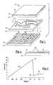
- FIG. 1is a diagrammatic view illustrating a preferred embodiment of the present invention
- FIG. 2is a fragmentary sectional view of the preferred embodiment of the invention.
- FIG. 3is a graph illustrating the destruction of metal carbon nano-tubes.
- a process for forming a field effect transistor array 10 utilizing single wall carbon nano-tubes as a channelis illustrated.
- a thermal oxide layer 12is formed on a semiconductor substrate 14 .
- the semiconductor substrate 14is preferably silicon and is heavily N-doped.
- conventional semiconductor processing methodsare utilized to form the thermal oxide layer 12 on the substrate 14 so that the thermal oxide layer 12 is approximately 1,000 angstroms in thickness, although the thickness of the oxide layer 12 may vary without deviation from the spirit or scope of the invention.
- an iron-containing catalytic polymer 16( FIG. 1 ) is spun on top of the oxide layer 12 such that the thickness of the polymer coating 16 is relatively thin, for example, in the range of about 10 microns in thickness.
- a plurality of nano-tubes 20are then grown or formed on the polymer containing substrate by subjecting it to chemical vapor deposition.
- a reactive gassuch as carbon dioxide
- the substrate 14heated to approximately 400° C.
- a reactive gassuch as carbon dioxide
- the polymer filmbreaks into hydrocarbon gases leaving behind iron atoms Fe which form nano-size particles that serve as catalysts for the growth of the nano-tubes.
- the carbon atoms in the gasstart forming cage-type structures or tubules on nano-size Fe particles and grow from there into single wall carbon nano-tubes.
- the carbon nano-tubes 20grow in random directions on the wafer/substrate 14 .
- a plurality of electrodes 24are then deposited on top of the nano-tubes 20 of the substrate 14 such that the electrodes 24 are elongated and spaced-apart and parallel to each other.
- the electrodes 24may be approximately 100 micrometers in width and spaced-apart from each other by about 7.5 microns.
- electrodes 24are preferably formed of a titanium and gold alloy in which the titanium increases the adhesion of the electrodes 24 to the upper surface of the wafer while the gold exhibits maximum conductivity.
- the entire structureis then preferably annealed at about 200° C. for about 30 minutes in a nitrogen atmosphere to improve the electrodes and nano-tube interface.
- adjacent electrical electrodesform the source and drain of a field effect transistor with the substrate 14 forming the gate.
- One or more nano-tubes extending between adjacent pairs of electrodes 24form the channel for the field effect transistor.
- the single wall carbon nano-tubes 20 formed on the wafer surfacetypically contain both metallic carbon nano-tubes, and semiconductor nano-tubes.
- the metallic carbon nano-tubesfurthermore, do not exhibit the desired semiconductor properties for the field effect transistor.
- a relatively high voltagee.g. 1-2 volts
- the currentincreases steadily, and generally linearly, as shown at 30 , as the volts between the source and drain increases until approximately 1.4 volts.
- the metal tubesare destroyed by the high voltage without damaging the semiconductor carbon nano-tubes. This, in turn, results in a dramatic decrease of the current, as shown at point 34 .
- the semiconductor carbon nano-tubesform the channel and exhibit semiconductor properties, as shown at 36 .
- each pair of electrodes 24form an individually addressable field effect transistor assuming, of course, that a sufficient number of semiconductor carbon nano-tubes extend between and connect two adjacent electrodes. Individual testing and mapping of each of the field effect transistors on the array may then be performed to determine which field effect transistors exhibit satisfactory performance and which do not.
- the present inventionprovides a field effect array utilizing single wall carbon nano-tubes as the channel which enjoys a simple way for processing.
Landscapes
- Engineering & Computer Science (AREA)
- Chemical & Material Sciences (AREA)
- Nanotechnology (AREA)
- Physics & Mathematics (AREA)
- Mathematical Physics (AREA)
- Theoretical Computer Science (AREA)
- Crystallography & Structural Chemistry (AREA)
- Thin Film Transistor (AREA)
- Carbon And Carbon Compounds (AREA)
Abstract
Description
This patent application claims the benefit of U.S. Provisional Patent Application Ser. No. 60/878,064, filed 3 Jan. 2007, the contents of which are incorporated herein by reference.
The invention described herein may be manufactured, used, and licensed by or for the United States Government.
1. Field of the Invention
The present invention relates generally to field effect transistors and, more particularly, to a field effect transistor array which utilizes single wall carbon nano-tubes as the channel for the field effect transistors.
2. Description of the Related Art
Carbon nano-tubes are perhaps the best available material for realizing nano and molecular scale electronics and sensor devices. Indeed, experiments demonstrating the use of single wall nano-tubes as the active channel in a MOS field effect transistor (FET) have opened the possibility for a wide range of integrated carbon nano-tube nano electronics.
The assembly and fabrication of carbon nano-tube electronic devices, however, disadvantageously requires several tedious steps to realize a single or a few functional devices. Furthermore, these previously known assembly and fabrication methods do not lend themselves to high-yield microcircuit production.
The present invention provides a field effect transistor (FET) array utilizing single wall carbon nano-tubes as the channel for the transistor, as well as a method for fabricating the FET which overcomes all the above-mentioned disadvantages of the previously known devices and methods.
In brief, in the present invention, a metal oxide layer is formed on a highly N-doped silicon substrate using conventional semiconductor fabrication techniques. Thereafter, an iron-containing catalyst precursor polymer film is spinned on the substrate, thus forming a thin layer of the iron-containing polymer on the substrate.
Thereafter, single wall carbon nano-tubes are grown in the polymer film by chemical vapor deposition such that, following the chemical vapor deposition, relatively long strands of single wall carbon nano-tubes are formed on the metal oxide layer on the substrate. The single wall nano-tubes may be either single tubes or thin, uniform bundles of tubes.
After formation of the carbon nano-tubes on the oxide layer of the metal substrate, a plurality of electrodes are deposited over the nano-tubes so that the electrodes are spaced apart and parallel to each other. Preferably, the electrodes comprise a titanium and gold alloy. The titanium layer improves the adhesion of the gold electrodes to the substrate.
The carbon nano-tubes formed on the substrate include both metallic carbon nano-tubes, as well as semiconductor carbon nano-tubes. The metallic carbon nano-tubes, which do not exhibit the semiconductor characteristics desired for a field effect transistor, are then destroyed by applying a relatively high voltage, e.g. 1-2 volts, between each successive pair of electrodes, thus leaving only the desired semiconductor carbon nano-tubes between adjacent electrodes.
Following destruction of the metallic carbon nano-tubes, a plurality of individually addressable field effect transistors remain with adjacent electrodes forming the source and drain for each field effect transistor.
A better understanding of the present can be had upon reference to the following detailed description when read in conjunction with the accompanying drawing, wherein like reference characters refer to like parts throughout the several views, and in which:
With reference first toFIGS. 1 and 2 , a process for forming a fieldeffect transistor array 10 utilizing single wall carbon nano-tubes as a channel is illustrated. As shown at10 inFIG. 1 , athermal oxide layer 12 is formed on asemiconductor substrate 14. Thesemiconductor substrate 14 is preferably silicon and is heavily N-doped. Furthermore, conventional semiconductor processing methods are utilized to form thethermal oxide layer 12 on thesubstrate 14 so that thethermal oxide layer 12 is approximately 1,000 angstroms in thickness, although the thickness of theoxide layer 12 may vary without deviation from the spirit or scope of the invention.
Following the formation of thethermal oxide layer 12 on thesubstrate 14, an iron-containing catalytic polymer16 (FIG. 1 ) is spun on top of theoxide layer 12 such that the thickness of thepolymer coating 16 is relatively thin, for example, in the range of about 10 microns in thickness.
A plurality of nano-tubes 20 are then grown or formed on the polymer containing substrate by subjecting it to chemical vapor deposition. For example, with thesubstrate 14 heated to approximately 400° C., a reactive gas, such as carbon dioxide, is blown over the wafer for 20-30 minutes. At this temperature the polymer film breaks into hydrocarbon gases leaving behind iron atoms Fe which form nano-size particles that serve as catalysts for the growth of the nano-tubes. The carbon atoms in the gas start forming cage-type structures or tubules on nano-size Fe particles and grow from there into single wall carbon nano-tubes. During the carbon nano-tube formation, the carbon nano-tubes 20 grow in random directions on the wafer/substrate 14.
A plurality ofelectrodes 24 are then deposited on top of the nano-tubes 20 of thesubstrate 14 such that theelectrodes 24 are elongated and spaced-apart and parallel to each other. For example, theelectrodes 24 may be approximately 100 micrometers in width and spaced-apart from each other by about 7.5 microns.
Lithographic metal electrode deposition techniques are used to form theelectrodes 24. For example,electrodes 24 are preferably formed of a titanium and gold alloy in which the titanium increases the adhesion of theelectrodes 24 to the upper surface of the wafer while the gold exhibits maximum conductivity.
The entire structure is then preferably annealed at about 200° C. for about 30 minutes in a nitrogen atmosphere to improve the electrodes and nano-tube interface.
After theelectrodes 24 have been deposited on the wafer, adjacent electrical electrodes form the source and drain of a field effect transistor with thesubstrate 14 forming the gate. One or more nano-tubes extending between adjacent pairs ofelectrodes 24 form the channel for the field effect transistor.
The single wall carbon nano-tubes 20 formed on the wafer surface typically contain both metallic carbon nano-tubes, and semiconductor nano-tubes. The metallic carbon nano-tubes, furthermore, do not exhibit the desired semiconductor properties for the field effect transistor.
Consequently, in order to destroy the metallic single wall carbon nano-tubes, a relatively high voltage, e.g. 1-2 volts, is applied between each successive pair ofelectrodes 24, while maintaining the gate in a state of saturation. As shown inFIG. 3 , the current increases steadily, and generally linearly, as shown at30, as the volts between the source and drain increases until approximately 1.4 volts. At thispoint 32, the metal tubes are destroyed by the high voltage without damaging the semiconductor carbon nano-tubes. This, in turn, results in a dramatic decrease of the current, as shown atpoint 34. Thereafter, the semiconductor carbon nano-tubes form the channel and exhibit semiconductor properties, as shown at36.
Following the destruction of the metallic carbon nano-tubes, a field effect transistor array results in which each pair ofelectrodes 24 form an individually addressable field effect transistor assuming, of course, that a sufficient number of semiconductor carbon nano-tubes extend between and connect two adjacent electrodes. Individual testing and mapping of each of the field effect transistors on the array may then be performed to determine which field effect transistors exhibit satisfactory performance and which do not.
From the foregoing, it can be seen that the present invention provides a field effect array utilizing single wall carbon nano-tubes as the channel which enjoys a simple way for processing. Having described our invention, however, many modifications thereto will become apparent to those of skill in the art to which pertains without deviation from the spirit of the invention as defined by the scope of the appended claims.
Claims (18)
1. A field effect transistor comprising
a substrate,
a semiconducting channel for transistor action comprising substantially only a plurality of semiconducting carbon nano-tubes disposed on a surface of said substrate wherein said plurality of carbon nano-tubes are disposed in random directions parallel to said surface of said substrate, and
a plurality of electrodes disposed over said plurality of semiconducting carbon nano-tubes such that said electrodes are spaced apart from each other,
wherein said electrodes are linear, elongated and parallel to each other so that at least one of said nano-tube extends below and connects at least two of the plurality of electrodes.
2. The transistor as defined inclaim 1 wherein said substrate comprises a doped silicon layer covered at least in part by an electrical insulating layer.
3. The transistor as defined inclaim 2 wherein said insulating layer comprises an oxide layer.
4. The transistor as defined inclaim 1 wherein each said electrode comprises gold.
5. The transistor as defined inclaim 1 wherein the electrodes comprise a titanium and gold alloy.
6. The transistor as defined inclaim 1 wherein the carbon nano-tubes comprise single wall carbon nano-tubes.
7. The transistor as defined inclaim 6 wherein the single wall carbon nano-tubes are randomly disposed on the surface of said substrate in bundles that comprise single wall carbon nano-tubes wherein the bundles are disposed on the surface of said substrate at a density of from 3 to 6 bundles per 100 μm2.
8. The transistor as defined inclaim 1 wherein the carbon nano-tubes are randomly disposed on the surface of said substrate in bundles and further wherein between 375 and 500 bundles extend below and connect one of said plurality of electrodes to an adjacent electrode.
9. A metal-oxide semiconductor field effect transistor comprising:
a substrate,
an electrical insulating layer disposed on said substrate,
a semiconducting channel for transistor action comprising substantially only a plurality of semiconducting single wall carbon nano-tubes disposed in random horizontal directions on a said electrical insulating layer,
a plurality of electrodes disposed over said plurality of semiconducting single wall carbon nano-tubes such that said electrodes are spaced apart from each other,
wherein said plurality of single wall carbon nano-tubes randomly disposed on the surface of said substrate contain a density of from 3 to 6 bundles of disentangled, nearly-defect-free single-walled carbon nano-tubes per 100 μm2.
10. A method of fabricating a field effect transistor having a semiconducting channel for transistor action, the method comprising the steps of:
forming an electrical insulating layer on a doped silicon substrate,
growing carbon nano-tubes on said insulating layer in random directions that are parallel to a surface of said insulating layer,
removing metallic nano-tubes while leaving substantially only semiconducting nano-tubes which had been grown on said insulating layer to form the semiconducting channel, and
depositing a plurality of spaced apart electrodes on said semiconducting carbon nano-tubes and said insulating layer,
wherein said electrodes are linear, elongated and parallel to each other so that at least one of said semiconducting carbon nano-tube extends below and connects at least two of the plurality of electrodes.
11. The method as defined inclaim 10 wherein said growing step further comprises the step of applying a layer of iron containing polymer on said substrate and thereafter subjecting said polymer layer to a reactive gas.
12. The method as defined inclaim 10 and further comprising the step of applying a voltage across said nano-tubes in a magnitude sufficient to destroy metallic nano-tubes but insufficient to harm semiconductor nano-tubes.
13. The method as defined inclaim 10 wherein said electrodes comprise a gold and titanium alloy.
14. The method as defined inclaim 10 wherein said forming step further comprises the step of forming an oxide layer on said doped silicon substrate.
15. The method as defined inclaim 10 wherein said growing step further comprises the steps of applying an iron containing polymer layer to said insulating layer and thereafter subjecting said polymer layer to a reactive gas.
16. The method as defined inclaim 10 wherein the carbon nano-tubes comprise single wall carbon nano-tubes.
17. The method as defined inclaim 16 wherein the single wall carbon nano-tubes are randomly grown on the surface of said substrate in bundles that comprise single wall carbon nano-tubes and at a density of from 3 to 6 bundles per 100 μm2.
18. A method of fabricating a metal-oxide semiconductor field effect transistor having a semiconducting channel for transistor action, the method comprising the steps of:
forming an electrical insulating layer on a heavily doped conducting silicon substrate,
depositing a catalyst precursor polymer over the electrical insulating layer,
growing a plurality of single-walled carbon nano-tubes on said insulating layer in random directions that are parallel to said insulating layer,
removing metallic nano-tubes while leaving substantially only semiconducting single-walled carbon nano-tubes which had been grown on said insulating layer to form the semiconducting channel for transistor action,
depositing a plurality of spaced apart metal electrodes on said semiconducting carbon nano-tubes and said insulating layer, said metal electrodes forming contacts for a drain and a source of said transistor,
wherein said plurality of single wall carbon nano-tubes are randomly grown on the surface of said substrate containing a density of from 3 to 6 bundles of disentangled, nearly-defect-free single-walled carbon nano-tubes per 100 μm2.
Priority Applications (1)
| Application Number | Priority Date | Filing Date | Title |
|---|---|---|---|
| US11/790,052US9806273B2 (en) | 2007-01-03 | 2007-04-23 | Field effect transistor array using single wall carbon nano-tubes |
Applications Claiming Priority (2)
| Application Number | Priority Date | Filing Date | Title |
|---|---|---|---|
| US87806407P | 2007-01-03 | 2007-01-03 | |
| US11/790,052US9806273B2 (en) | 2007-01-03 | 2007-04-23 | Field effect transistor array using single wall carbon nano-tubes |
Publications (2)
| Publication Number | Publication Date |
|---|---|
| US20080157061A1 US20080157061A1 (en) | 2008-07-03 |
| US9806273B2true US9806273B2 (en) | 2017-10-31 |
Family
ID=39582530
Family Applications (1)
| Application Number | Title | Priority Date | Filing Date |
|---|---|---|---|
| US11/790,052Active2029-09-14US9806273B2 (en) | 2007-01-03 | 2007-04-23 | Field effect transistor array using single wall carbon nano-tubes |
Country Status (1)
| Country | Link |
|---|---|
| US (1) | US9806273B2 (en) |
Families Citing this family (1)
| Publication number | Priority date | Publication date | Assignee | Title |
|---|---|---|---|---|
| CN105655406A (en)* | 2016-03-01 | 2016-06-08 | 京东方科技集团股份有限公司 | Carbon nano tube thin film transistor and manufacturing method thereof |
Citations (36)
| Publication number | Priority date | Publication date | Assignee | Title |
|---|---|---|---|---|
| US6423583B1 (en)* | 2001-01-03 | 2002-07-23 | International Business Machines Corporation | Methodology for electrically induced selective breakdown of nanotubes |
| US20020130353A1 (en)* | 1999-07-02 | 2002-09-19 | Lieber Charles M. | Nanoscopic wire-based devices, arrays, and methods of their manufacture |
| US6515339B2 (en)* | 2000-07-18 | 2003-02-04 | Lg Electronics Inc. | Method of horizontally growing carbon nanotubes and field effect transistor using the carbon nanotubes grown by the method |
| US20030068432A1 (en)* | 1998-08-14 | 2003-04-10 | The Board Of Trustees Of The Leland Stanford Junior University | Carbon nanotube devices |
| US20030227015A1 (en) | 2000-06-27 | 2003-12-11 | Samsung Electronics Co., Ltd | Vertical nano-size transistor using carbon nanotubes and manufacturing method thereof |
| US20030228467A1 (en)* | 2002-04-18 | 2003-12-11 | Maik Liebau | Targeted deposition of nanotubes |
| US6750471B2 (en) | 1998-11-18 | 2004-06-15 | International Business Machines Corporation | Molecular memory & logic |
| US6798000B2 (en) | 2000-07-04 | 2004-09-28 | Infineon Technologies Ag | Field effect transistor |
| US20040201064A1 (en) | 2001-09-05 | 2004-10-14 | Konica Corporation | Organic thin-film semiconductor element and manufacturing method for the same |
| US6870124B2 (en)* | 2002-05-08 | 2005-03-22 | Dana Corporation | Plasma-assisted joining |
| US6891227B2 (en) | 2002-03-20 | 2005-05-10 | International Business Machines Corporation | Self-aligned nanotube field effect transistor and method of fabricating same |
| US6900479B2 (en) | 2002-07-25 | 2005-05-31 | California Institute Of Technology | Stochastic assembly of sublithographic nanoscale interfaces |
| US20050129573A1 (en)* | 2003-09-12 | 2005-06-16 | Nanomix, Inc. | Carbon dioxide nanoelectronic sensor |
| US20050157445A1 (en)* | 2003-09-18 | 2005-07-21 | Keith Bradley | Nanostructures with electrodeposited nanoparticles |
| US20050167655A1 (en)* | 2004-01-29 | 2005-08-04 | International Business Machines Corporation | Vertical nanotube semiconductor device structures and methods of forming the same |
| US6930343B2 (en)* | 2002-11-15 | 2005-08-16 | Samsung Electronics Co., Ltd. | Nonvolatile memory device utilizing a vertical nanotube |
| US20050242344A1 (en)* | 2004-04-29 | 2005-11-03 | Hyun-Jee Lee | Method of forming electron emission source, the electron emission source, and electron emission device including the electron emission source |
| US20050244326A1 (en)* | 1996-08-08 | 2005-11-03 | William Marsh Rice University | Method for fractionating single-wall carbon nanotubes |
| US6972467B2 (en)* | 2002-08-23 | 2005-12-06 | Intel Corporation | Multi-gate carbon nano-tube transistors |
| US20050279988A1 (en) | 2004-06-18 | 2005-12-22 | Nantero, Inc. | Nanotube-based transfer devices and related circuits |
| US7014743B2 (en)* | 2002-12-09 | 2006-03-21 | The University Of North Carolina At Chapel Hill | Methods for assembly and sorting of nanostructure-containing materials and related articles |
| US7015500B2 (en) | 2002-02-09 | 2006-03-21 | Samsung Electronics Co., Ltd. | Memory device utilizing carbon nanotubes |
| US7030408B1 (en) | 1999-03-29 | 2006-04-18 | Hewlett-Packard Development Company, L.P. | Molecular wire transistor (MWT) |
| US20060169585A1 (en) | 2005-01-31 | 2006-08-03 | Nagahara Larry A | Carbon nanotube sensor |
| US20060175601A1 (en) | 2000-08-22 | 2006-08-10 | President And Fellows Of Harvard College | Nanoscale wires and related devices |
| US7115901B2 (en) | 2003-06-09 | 2006-10-03 | Nantero, Inc. | Non-volatile electromechanical field effect devices and circuits using same and methods of forming same |
| US20060237708A1 (en) | 2002-05-03 | 2006-10-26 | Samsung Electronics Co., Ltd. | Semiconductor carbon nanotubes fabricated by hydrogen functionalization and method for fabricating the same |
| US7129554B2 (en) | 2000-12-11 | 2006-10-31 | President & Fellows Of Harvard College | Nanosensors |
| US7135728B2 (en) | 2002-09-30 | 2006-11-14 | Nanosys, Inc. | Large-area nanoenabled macroelectronic substrates and uses therefor |
| US20070110741A1 (en)* | 2005-11-16 | 2007-05-17 | Gwangju Institute Of Science And Technology | Single-wall carbon nanotube-egg white protein composite and preparation thereof |
| US20070132043A1 (en)* | 2002-01-16 | 2007-06-14 | Keith Bradley | Nano-electronic sensors for chemical and biological analytes, including capacitance and bio-membrane devices |
| US20080149970A1 (en)* | 2006-12-21 | 2008-06-26 | Thomas Shawn G | Multi-gated carbon nanotube field effect transistor |
| US7522040B2 (en)* | 2004-04-20 | 2009-04-21 | Nanomix, Inc. | Remotely communicating, battery-powered nanostructure sensor devices |
| US20090232724A1 (en)* | 2008-03-11 | 2009-09-17 | Ali Afzali-Ardakani | Method of separating metallic and semiconducting carbon nanotubes from a mixture of same |
| US7687841B2 (en)* | 2005-08-02 | 2010-03-30 | Micron Technology, Inc. | Scalable high performance carbon nanotube field effect transistor |
| US7956525B2 (en)* | 2003-05-16 | 2011-06-07 | Nanomix, Inc. | Flexible nanostructure electronic devices |
Family Cites Families (6)
| Publication number | Priority date | Publication date | Assignee | Title |
|---|---|---|---|---|
| US279988A (en)* | 1883-06-26 | Richard smith | ||
| US169585A (en)* | 1875-11-02 | Improvement in fire-blowers | ||
| US201064A (en)* | 1878-03-05 | Improvement in hollow augers | ||
| US175601A (en)* | 1876-04-04 | Improvement in traction-engines | ||
| US237708A (en)* | 1881-02-15 | Combined steam and air engine | ||
| US227015A (en)* | 1880-04-27 | Flier for speeders |
- 2007
- 2007-04-23USUS11/790,052patent/US9806273B2/enactiveActive
Patent Citations (36)
| Publication number | Priority date | Publication date | Assignee | Title |
|---|---|---|---|---|
| US20050244326A1 (en)* | 1996-08-08 | 2005-11-03 | William Marsh Rice University | Method for fractionating single-wall carbon nanotubes |
| US20030068432A1 (en)* | 1998-08-14 | 2003-04-10 | The Board Of Trustees Of The Leland Stanford Junior University | Carbon nanotube devices |
| US6750471B2 (en) | 1998-11-18 | 2004-06-15 | International Business Machines Corporation | Molecular memory & logic |
| US7030408B1 (en) | 1999-03-29 | 2006-04-18 | Hewlett-Packard Development Company, L.P. | Molecular wire transistor (MWT) |
| US20020130353A1 (en)* | 1999-07-02 | 2002-09-19 | Lieber Charles M. | Nanoscopic wire-based devices, arrays, and methods of their manufacture |
| US20030227015A1 (en) | 2000-06-27 | 2003-12-11 | Samsung Electronics Co., Ltd | Vertical nano-size transistor using carbon nanotubes and manufacturing method thereof |
| US6798000B2 (en) | 2000-07-04 | 2004-09-28 | Infineon Technologies Ag | Field effect transistor |
| US6515339B2 (en)* | 2000-07-18 | 2003-02-04 | Lg Electronics Inc. | Method of horizontally growing carbon nanotubes and field effect transistor using the carbon nanotubes grown by the method |
| US20060175601A1 (en) | 2000-08-22 | 2006-08-10 | President And Fellows Of Harvard College | Nanoscale wires and related devices |
| US7129554B2 (en) | 2000-12-11 | 2006-10-31 | President & Fellows Of Harvard College | Nanosensors |
| US6423583B1 (en)* | 2001-01-03 | 2002-07-23 | International Business Machines Corporation | Methodology for electrically induced selective breakdown of nanotubes |
| US20040201064A1 (en) | 2001-09-05 | 2004-10-14 | Konica Corporation | Organic thin-film semiconductor element and manufacturing method for the same |
| US20070132043A1 (en)* | 2002-01-16 | 2007-06-14 | Keith Bradley | Nano-electronic sensors for chemical and biological analytes, including capacitance and bio-membrane devices |
| US7015500B2 (en) | 2002-02-09 | 2006-03-21 | Samsung Electronics Co., Ltd. | Memory device utilizing carbon nanotubes |
| US6891227B2 (en) | 2002-03-20 | 2005-05-10 | International Business Machines Corporation | Self-aligned nanotube field effect transistor and method of fabricating same |
| US20030228467A1 (en)* | 2002-04-18 | 2003-12-11 | Maik Liebau | Targeted deposition of nanotubes |
| US20060237708A1 (en) | 2002-05-03 | 2006-10-26 | Samsung Electronics Co., Ltd. | Semiconductor carbon nanotubes fabricated by hydrogen functionalization and method for fabricating the same |
| US6870124B2 (en)* | 2002-05-08 | 2005-03-22 | Dana Corporation | Plasma-assisted joining |
| US6900479B2 (en) | 2002-07-25 | 2005-05-31 | California Institute Of Technology | Stochastic assembly of sublithographic nanoscale interfaces |
| US6972467B2 (en)* | 2002-08-23 | 2005-12-06 | Intel Corporation | Multi-gate carbon nano-tube transistors |
| US7135728B2 (en) | 2002-09-30 | 2006-11-14 | Nanosys, Inc. | Large-area nanoenabled macroelectronic substrates and uses therefor |
| US6930343B2 (en)* | 2002-11-15 | 2005-08-16 | Samsung Electronics Co., Ltd. | Nonvolatile memory device utilizing a vertical nanotube |
| US7014743B2 (en)* | 2002-12-09 | 2006-03-21 | The University Of North Carolina At Chapel Hill | Methods for assembly and sorting of nanostructure-containing materials and related articles |
| US7956525B2 (en)* | 2003-05-16 | 2011-06-07 | Nanomix, Inc. | Flexible nanostructure electronic devices |
| US7115901B2 (en) | 2003-06-09 | 2006-10-03 | Nantero, Inc. | Non-volatile electromechanical field effect devices and circuits using same and methods of forming same |
| US20050129573A1 (en)* | 2003-09-12 | 2005-06-16 | Nanomix, Inc. | Carbon dioxide nanoelectronic sensor |
| US20050157445A1 (en)* | 2003-09-18 | 2005-07-21 | Keith Bradley | Nanostructures with electrodeposited nanoparticles |
| US20050167655A1 (en)* | 2004-01-29 | 2005-08-04 | International Business Machines Corporation | Vertical nanotube semiconductor device structures and methods of forming the same |
| US7522040B2 (en)* | 2004-04-20 | 2009-04-21 | Nanomix, Inc. | Remotely communicating, battery-powered nanostructure sensor devices |
| US20050242344A1 (en)* | 2004-04-29 | 2005-11-03 | Hyun-Jee Lee | Method of forming electron emission source, the electron emission source, and electron emission device including the electron emission source |
| US20050279988A1 (en) | 2004-06-18 | 2005-12-22 | Nantero, Inc. | Nanotube-based transfer devices and related circuits |
| US20060169585A1 (en) | 2005-01-31 | 2006-08-03 | Nagahara Larry A | Carbon nanotube sensor |
| US7687841B2 (en)* | 2005-08-02 | 2010-03-30 | Micron Technology, Inc. | Scalable high performance carbon nanotube field effect transistor |
| US20070110741A1 (en)* | 2005-11-16 | 2007-05-17 | Gwangju Institute Of Science And Technology | Single-wall carbon nanotube-egg white protein composite and preparation thereof |
| US20080149970A1 (en)* | 2006-12-21 | 2008-06-26 | Thomas Shawn G | Multi-gated carbon nanotube field effect transistor |
| US20090232724A1 (en)* | 2008-03-11 | 2009-09-17 | Ali Afzali-Ardakani | Method of separating metallic and semiconducting carbon nanotubes from a mixture of same |
Non-Patent Citations (38)
| Title |
|---|
| Abstract titled "Simple, High Yield Nano-device Fabrication via SWNT Controlled Growth from a Catalytic Block Copolymer" corresponding to presentation of the same title given at the 2005 American Physical Society (APS) March Meeting held Mar. 21-25, 2005 in Los Angeles, CA. This abstract was distributed to meeting attendees prior to the meeting (as part of the meeting agenda). |
| An, A Simple Chemical Route to Selectively Eliminate Metallic Carbon Nanotubes in Nanotube Network Devices, J. Am. Chem. Soc. 126, 10520 (2004). |
| Bachtold et al. Logic Circuits with Carbon Nanotube Transistors. Science 294, 1317-1320 (Nov. 9, 2001). |
| Balasubramanian, A Selective Electrochemical Approach to Carbon Nanotube Field-Effect TransistorsNano Lett. 4, 827 (2004). |
| Collins, Engineering Carbon Nanotubes and Nanotube Circuits Using Electrical Breakdown, Science 292, 706 (2001). |
| Ebbesen et al. Electrical conductivity of individual carbon nanotubes. Nature 382, 54-56 (Jul. 4, 1996). |
| El Khakani, M. A.; Yi, J. H. "The nanostructure and electrical properties of SWT bundle networks grown by an 'all-laser' growth process for annoelectronic device applications." Nanotechnology (2004), 15(10) S534-S539 Coden; NNOTER; ISSN: 0957-4484.* |
| El Khakani, M. A.; Yi, J. H. "The nanostructure and electrical properties of SWT bundle networks grown by an ‘all-laser’ growth process for annoelectronic device applications." Nanotechnology (2004), 15(10) S534-S539 Coden; NNOTER; ISSN: 0957-4484.* |
| Franklin, Integration of suspended carbon nanotube arrays into electronic devices and electromechanical systems, Appl. Phys. Lett. 81, 913 (2002). |
| Fuhrer et al. Crossed Nanotube Junctions. Science 288, 494-497 (Apr. 21, 2000). |
| Hamada et al. New One-Dimensional Conductors: Graphitic Microtubules. Physical Review Letters 68(10), 1579-1581 (Mar. 9, 1992). |
| Iijima. Helical microtubules of graphitic carbon. Nature 354, 56-58 (Nov. 7, 1991). |
| Javey, Electrical properties and devices of large-diameter single-walled carbon nanotubes, Appl. Phys. Lett. 80, 1064 (2002). |
| Kong, Synthesis of individual singlewalled carbon nanotubes on patterned siliconwafers, Nature London 395, 878 (1998). |
| Krupke, Separation of Metallic from Semiconducting Single-Walled Carbon Nanotubes, Science 301, 344 (2003). |
| Lastella et al. Parallel arrays of individually addressable single-walled carbon nanotube field-effect transistors. Journal of Applied Physics 99, 024302 (2006). |
| Lastella, Density control of single-walled carbon nanotubes using patterned iron nanoparticle catalysts derived from phaseseparated thin films, J. Mater. Chem. 14, 1791 (2004). |
| Lastella, Parallel arrays of inidividually adressable singl-walled carbon nanotube filed-effec transistors, J. of Appl. Phys., 99, 0234302-1-4 (2006). |
| Li, Carbon Nanotube Sensors for Gas and Organic Vapor Detection, Nano Lett. 3, 929 (2003). |
| Martel et al. Single- and multi-wall carbon nanotube field-effect transistors. Applied Physics Letters 73(17), 2447-2449 (Oct. 26, 1998). |
| Mintmire et al. Are Fullerene Tubules Metallic? Physical Review Letters 68(5), 631-634 (Feb. 3, 1992). |
| Odom et al. Atomic structure and electronic properties of single-walled carbon nanotubes. Nature 391, 62-64 (Jan. 1, 1998). |
| Papadopoulos et al. Electronic Transport in Y-Junction Carbon Nanotubes. Physical Review Letters 85(16), 3476-3479 (Oct. 16, 2000). |
| Qi et al. Miniature Organic Transistors with Carbon Nanotubes as Quasi-One-Dimensional Electrodes. J. Am. Chem. Soc. 126, 11774-11775 (2004). |
| Qi, Toward Large Arrays of Multiplex Functionalized Carbon Nanotube Sensors for Highly Sensitive and Selective Molecular Detection, Nano Lett. 3, 347 (2003). |
| Saito et al. Electronic structure of chiral graphene tubules. Applied Physics Letters 60(18), 2204-2206 (May 4, 1992). |
| Sarah Lastella, et al., "Chemical Vapor Deposition Grown Single-Walled Carbon Nanotube Junctions for Nano-Electronics and Sensors," presented at the Army Science Conference (24th) held on Nov. 29-Dec. 2, 2005 in Orlando, Florida. |
| Satishkumar et al. Y-junction carbon nanotubes. Applied Physics Letters 77(16), 2530-2532 (Oct. 16, 2000). |
| Seidel, Bias dependence and electrical breakdown of small diameter single-walled carbon nanotubes, J. Appl. Phys. 96, 6694 (2004). |
| Seidel, High-Current Nanotube Transistors, Nano Lett. 4, 831 (2004). |
| Slides which were contemporaneously displayed during the presentation titled "Simple, High Yield Nano-device Fabrication via SWNT Controlled Growth from a Catalytic Block Copolymer," at the 2005 American Physical Society (APS) March Meeting held Mar. 21-25, 2005 in Los Angeles, CA. This presentation was given at the A14 focus session on Mar. 21, 2005 from 9:24AM-9:36AM. |
| Snow, High-mobility carbon-nanotube thin-film transistors on a polymeric substrate, Appl. Phys. Lett. 86, 33105 (2005). |
| Someya, Alcohol Vapor Sensors Based on Single-Walled Carbon Nanotube Field Effect Transistors, Nano Lett. 3, 877 (2003). |
| Tans et al. Room-temperature transistor based on a single carbon nanotube. Nature 393, 49-52 (May 7, 1998). |
| Tseng, Monolithic Integration of Carbon Nanotube Devices with Silicon MOS Technology, Nano Lett. 4, 123 (2004). |
| Wildoer et al. Electronic structure of atomically resolved carbon nanotubes. Nature 391, 59-62 (Jan. 1, 1998). |
| Wind et al. Vertical scaling of carbon nanotube field-effect transistors using top gate electronics. Applied Physics Letters 80(20), 3817-3819 (May 20, 2002). |
| Zhou, Electrical measurements of individual semiconducting single-walled carbon nanotubes of various diameters, Appl. Phys. Lett. 76, 1597 2000. |
Also Published As
| Publication number | Publication date |
|---|---|
| US20080157061A1 (en) | 2008-07-03 |
Similar Documents
| Publication | Publication Date | Title |
|---|---|---|
| Thelander et al. | Electron transport in InAs nanowires and heterostructure nanowire devices | |
| Weber et al. | Silicon-nanowire transistors with intruded nickel-silicide contacts | |
| US8415787B2 (en) | Integrated circuits having interconnects and heat dissipators based on nanostructures | |
| US6894359B2 (en) | Sensitivity control for nanotube sensors | |
| US20110089404A1 (en) | Microfabrication of Carbon-based Devices Such as Gate-Controlled Graphene Devices | |
| US20060186451A1 (en) | Memory device for storing electric charge, and method for fabricating it | |
| CN101313092B (en) | Nanostructure-based interconnects and heat sinks | |
| US20100301336A1 (en) | Method to Improve Nucleation of Materials on Graphene and Carbon Nanotubes | |
| US6441392B1 (en) | Device based on quantic islands and method for making same | |
| KR20020015795A (en) | Parallel and selective growth method of carbon nanotubes on the substrates for electronic-spintronic device applications | |
| US9331151B2 (en) | Method for coupling a graphene layer and a substrate and device comprising the graphene/substrate structure obtained | |
| Jung et al. | Understanding and improving carbon nanotube-electrode contact in bottom-contacted nanotube gas sensors | |
| Wang et al. | High‐Performance partially aligned semiconductive single‐walled carbon nanotube transistors achieved with a parallel technique | |
| US6808605B2 (en) | Fabrication method of metallic nanowires | |
| US20080023839A9 (en) | Molybdenum-based electrode with carbon nanotube growth | |
| JP4320316B2 (en) | Sensor for detecting chemical substances | |
| US9806273B2 (en) | Field effect transistor array using single wall carbon nano-tubes | |
| US10141261B2 (en) | Device comprising nanostructures and method of manufacturing thereof | |
| US20090188695A1 (en) | Nanostructures and method for making such nanostructures | |
| JP6675945B2 (en) | Graphene transistor and method for manufacturing the same | |
| US6218175B1 (en) | Nano-devices using block-copolymers | |
| JPWO2006104150A1 (en) | Semiconductor device manufacturing method and semiconductor device | |
| Lin et al. | A Triode Device with a Gate Controllable Schottky Barrier: Germanium Nanowire Transistors and Their Applications | |
| KR101976919B1 (en) | Complex structures including lowdimensional nanomaterial layer of suspending structure and method of manufacturing the same | |
| Norhakim et al. | Effect of Thickness of the Poly (vinyl alcohol) Passivation Layer on Ambipolar Characteristics of Graphene Field-effect Transistor |
Legal Events
| Date | Code | Title | Description |
|---|---|---|---|
| AS | Assignment | Owner name:ARMY, UNITED STATES OF AMERICA AS REPRESENTED BY T Free format text:ASSIGNMENT OF ASSIGNORS INTEREST;ASSIGNORS:KARNA, SHASHI P.;MALLICK, GOVIND;REEL/FRAME:019272/0044 Effective date:20070412 | |
| STCF | Information on status: patent grant | Free format text:PATENTED CASE | |
| MAFP | Maintenance fee payment | Free format text:PAYMENT OF MAINTENANCE FEE, 4TH YEAR, LARGE ENTITY (ORIGINAL EVENT CODE: M1551); ENTITY STATUS OF PATENT OWNER: LARGE ENTITY Year of fee payment:4 | |
| FEPP | Fee payment procedure | Free format text:MAINTENANCE FEE REMINDER MAILED (ORIGINAL EVENT CODE: REM.); ENTITY STATUS OF PATENT OWNER: LARGE ENTITY |