US9799669B2 - Single-semiconductor-layer channel in a memory opening for a three-dimensional non-volatile memory device - Google Patents
Single-semiconductor-layer channel in a memory opening for a three-dimensional non-volatile memory deviceDownload PDFInfo
- Publication number
- US9799669B2 US9799669B2US14/972,618US201514972618AUS9799669B2US 9799669 B2US9799669 B2US 9799669B2US 201514972618 AUS201514972618 AUS 201514972618AUS 9799669 B2US9799669 B2US 9799669B2
- Authority
- US
- United States
- Prior art keywords
- layer
- semiconductor material
- semiconductor
- single crystalline
- memory
- Prior art date
- Legal status (The legal status is an assumption and is not a legal conclusion. Google has not performed a legal analysis and makes no representation as to the accuracy of the status listed.)
- Active
Links
Images


Classifications
- H—ELECTRICITY
- H10—SEMICONDUCTOR DEVICES; ELECTRIC SOLID-STATE DEVICES NOT OTHERWISE PROVIDED FOR
- H10B—ELECTRONIC MEMORY DEVICES
- H10B41/00—Electrically erasable-and-programmable ROM [EEPROM] devices comprising floating gates
- H10B41/30—Electrically erasable-and-programmable ROM [EEPROM] devices comprising floating gates characterised by the memory core region
- H10B41/35—Electrically erasable-and-programmable ROM [EEPROM] devices comprising floating gates characterised by the memory core region with a cell select transistor, e.g. NAND
- H01L27/1157—
- G—PHYSICS
- G11—INFORMATION STORAGE
- G11C—STATIC STORES
- G11C16/00—Erasable programmable read-only memories
- G11C16/02—Erasable programmable read-only memories electrically programmable
- G11C16/04—Erasable programmable read-only memories electrically programmable using variable threshold transistors, e.g. FAMOS
- G11C16/0483—Erasable programmable read-only memories electrically programmable using variable threshold transistors, e.g. FAMOS comprising cells having several storage transistors connected in series
- H01L27/11524—
- H01L27/11556—
- H01L27/11578—
- H01L27/11582—
- H—ELECTRICITY
- H10—SEMICONDUCTOR DEVICES; ELECTRIC SOLID-STATE DEVICES NOT OTHERWISE PROVIDED FOR
- H10B—ELECTRONIC MEMORY DEVICES
- H10B41/00—Electrically erasable-and-programmable ROM [EEPROM] devices comprising floating gates
- H10B41/20—Electrically erasable-and-programmable ROM [EEPROM] devices comprising floating gates characterised by three-dimensional arrangements, e.g. with cells on different height levels
- H10B41/23—Electrically erasable-and-programmable ROM [EEPROM] devices comprising floating gates characterised by three-dimensional arrangements, e.g. with cells on different height levels with source and drain on different levels, e.g. with sloping channels
- H10B41/27—Electrically erasable-and-programmable ROM [EEPROM] devices comprising floating gates characterised by three-dimensional arrangements, e.g. with cells on different height levels with source and drain on different levels, e.g. with sloping channels the channels comprising vertical portions, e.g. U-shaped channels
- H—ELECTRICITY
- H10—SEMICONDUCTOR DEVICES; ELECTRIC SOLID-STATE DEVICES NOT OTHERWISE PROVIDED FOR
- H10B—ELECTRONIC MEMORY DEVICES
- H10B43/00—EEPROM devices comprising charge-trapping gate insulators
- H10B43/20—EEPROM devices comprising charge-trapping gate insulators characterised by three-dimensional arrangements, e.g. with cells on different height levels
- H10B43/23—EEPROM devices comprising charge-trapping gate insulators characterised by three-dimensional arrangements, e.g. with cells on different height levels with source and drain on different levels, e.g. with sloping channels
- H10B43/27—EEPROM devices comprising charge-trapping gate insulators characterised by three-dimensional arrangements, e.g. with cells on different height levels with source and drain on different levels, e.g. with sloping channels the channels comprising vertical portions, e.g. U-shaped channels
- H—ELECTRICITY
- H10—SEMICONDUCTOR DEVICES; ELECTRIC SOLID-STATE DEVICES NOT OTHERWISE PROVIDED FOR
- H10B—ELECTRONIC MEMORY DEVICES
- H10B43/00—EEPROM devices comprising charge-trapping gate insulators
- H10B43/30—EEPROM devices comprising charge-trapping gate insulators characterised by the memory core region
- H10B43/35—EEPROM devices comprising charge-trapping gate insulators characterised by the memory core region with cell select transistors, e.g. NAND
Definitions
- the present disclosurerelates generally to the field of semiconductor devices and specifically to three-dimensional non-volatile memory devices, such as vertical NAND strings and other three-dimensional devices, and methods of making the same.
- a 3D NAND stacked memory devicecan be formed from an array of alternating conductive and dielectric layers. A memory opening is formed through the layers to define many memory layers simultaneously. A NAND string is then formed by filling the memory opening with appropriate materials. A straight NAND string extends in one memory opening, while a pipe- or U-shaped NAND string (p-BiCS) includes a pair of vertical columns of memory cells. Control gates of the memory cells may be provided by the conductive layers.
- a memory film layeris deposited in each memory opening through an alternating stack of first material layers and second material layers.
- a first semiconductor material layermay be conformally deposited on the contiguous memory film layer.
- the horizontal bottom portion of the memory film layercan be removed from each memory opening by an anisotropic etch to physically expose a first electrode or the substrate underlying the memory opening.
- a second semiconductor material layeris subsequently deposited directly on the first electrode or the substrate exposed in the memory opening and on the first semiconductor material layer.
- the first and second semiconductor material layerscollectively function as a semiconductor channel of each memory cell in the NAND string.
- a method of fabricating a memory deviceis provided.
- a stack of alternating layers of a first material and a second material different from the first materialis formed over a substrate including a semiconductor material.
- a portion of the stackis etched to form a memory opening extending from a top surface of the stack to a top surface of the substrate.
- a memory film layeris formed within the memory opening, and a sacrificial material layer is formed on the memory film layer. Horizontal portions of the sacrificial material layer and the memory film layer are etched to physically expose a portion of the top surface of the substrate underneath the memory opening, while leaving a vertical portion of the sacrificial material layer remaining on a vertical portion of the memory film layer.
- the sacrificial material layeris removed selective to a remaining portion of the memory film layer.
- a three-dimensional memory devicewhich includes a substrate having a major surface, and an alternating stack of insulating material layers and control gate electrodes located over the substrate.
- the alternating stackhas a memory opening extending through the alternating stack in a direction substantially perpendicular to the major surface.
- the three-dimensional memory devicefurther includes a memory film located at a peripheral region of the memory opening, a semiconductor channel including a vertical portion extending substantially perpendicular to the major surface and contacting an inner sidewall of the memory film, and a single crystalline doped semiconductor material portion located within, or on, the substrate.
- a sidewall of the upper portion of the semiconductor channel in contact with the memory filmis laterally offset with respect to a sidewall of the lower portion of the semiconductor channel in contact with the memory film.
- the semiconductor channeldoes not include a substantially contiguous interface composed of grain boundaries, not contacting the memory film, and vertically extending through the semiconductor channel between a plurality of the control gate electrodes.
- FIGS. 1A-1Kare sequential vertical cross-sectional views of steps in a method of making a first exemplary device structure containing a NAND string according to a first embodiment of the present disclosure.
- FIG. 1Lis a vertical cross-sectional view of a first variation of the first exemplary device structure according to the first embodiment of the present disclosure.
- FIGS. 1M and 1Nare sequential vertical cross-sectional views of a second variation of the first exemplary device structure according to the first embodiment of the present disclosure.
- FIGS. 2A and 2Bare sequential vertical cross-sectional views of a method of making a second exemplary device structure according to a second embodiment of the present disclosure.
- FIG. 2Cis a vertical cross-sectional view of a first variation of the second exemplary device structure according to the second embodiment of the present disclosure.
- FIG. 2Dis a vertical cross-sectional view of a second variation of the second exemplary device structure according to the second embodiment of the present disclosure.
- FIG. 3Ais a vertical cross-sectional views of a third exemplary device structure according to a third embodiment of the present disclosure.
- FIG. 3Bis a vertical cross-sectional view of a first variation of the third exemplary device structure according to the third embodiment of the present disclosure.
- FIG. 3Cis a vertical cross-sectional view of a second variation of the third exemplary device structure according to the third embodiment of the present disclosure.
- FIG. 3Dis a vertical cross-sectional view of a third variation of the third exemplary device structure according to the third embodiment of the present disclosure.
- FIGS. 4 to 11are side cross-sectional views of steps in a method of forming metal replacement gates in the NAND strings in any of exemplary device structures of the previous embodiments.
- the present disclosureis directed to three-dimensional non-volatile memory devices, such as vertical NAND strings and other three-dimensional devices, and methods of making the same, the various aspects of which are described below.
- the embodiments of the disclosurecan be employed to form various semiconductor devices such as three-dimensional monolithic memory array devices comprising a plurality of NAND memory strings.
- the drawingsare not drawn to scale. Multiple instances of an element may be duplicated where a single instance of the element is illustrated, unless absence of duplication of elements is expressly described or clearly indicated otherwise. Ordinals such as “first,” “second,” and “third” are employed merely to identify similar elements, and different ordinals may be employed across the specification and the claims of the instant disclosure.
- the two step semiconductor material deposition process in the prior artcreates a substantially contiguous interface between the semiconductor layers.
- the substantially contiguous interfaceextends substantially throughout the entire extent of the first and second semiconductor material layers.
- a substantially contiguous set of grain boundariestypically run along the interface.
- the present inventorsrealized that the presence of the substantially contiguous set of grain boundaries between the first and second semiconductor material layers in prior art semiconductor channels is a significant source of defects in the semiconductor channel, increases the overall grain boundary area (i.e., the grain interface area), and often has the effect of reducing the average grain size in the semiconductor channel. Electrical characteristics of the memory cells can deteriorate due the large number of lattice defects that are concentrated at the grain boundary interfaces.
- each of the first and second semiconductor material layersneeds to have a thickness greater than a minimum thickness required for uniform thickness. Due to such constraints, the two step doped semiconductor material deposition process as known in the art may lead to deterioration of boosting potential and program disturb, deterioration of the cell current, an increase in the variability of the memory cells, and/or an increase in the program noise.
- a memory film layeris formed in a memory opening through an alternating stack of first material layers and second material layers for a three dimensional, vertical NAND string.
- a sacrificial material layeris deposited on the memory film layer. Horizontal portions of the sacrificial material layer and the memory film layer at the bottom of the memory opening are removed by an anisotropic etch to expose a first electrode or the substrate underlying the memory opening, while vertical portions of the sacrificial material layer protect vertical portions of the memory film layer.
- a single semiconductor material layercan be formed on the first electrode or the substrate, and directly on the memory film as a single “uninterrupted” material layer, i.e., a material layer that does not include any interfacial layer therein as a consequence of being deposited in a single deposition step.
- the single semiconductor material layercan be a doped semiconductor material layer.
- the single semiconductor material layermay not be an intentionally doped semiconductor material. If not intentionally doped, the single semiconductor material layer still may have a certain level of doping by p-type dopants or n-type dopants.
- the type of dopingmay be p-type in one example, and the atomic concentration of the p-type dopants may be in a range from 5.0 ⁇ 10 16 /cm 3 to 5.0 ⁇ 10 17 cm/ 3 , although higher or lower atomic concentrations can also occur depending on the process employed.
- the semiconductor material layerdoes not include any contiguous set of grain boundaries that runs parallel to the interface between the semiconductor material layer and the memory film.
- Dopant implantation and/or surface treatment of the first electrode or the substrate; vertical recessing of first electrode or the substrate; lateral recessing of the memory film selective to the sacrificial material layer; and/or formation of an epitaxial semiconductor material portion of the channelmay be optionally performed prior to formation of the semiconductor material layer. Surface treatment of the semiconductor material layer may also be performed.
- a monolithic three dimensional memory arrayis one in which multiple memory levels are formed above a single substrate, such as a semiconductor wafer, with no intervening substrates.
- the term “monolithic”means that layers of each level of the array are directly deposited on the layers of each underlying level of the array.
- two dimensional arraysmay be formed separately and then packaged together to form a non-monolithic memory device.
- non-monolithic stacked memorieshave been constructed by forming memory levels on separate substrates and vertically stacking the memory levels, as described in U.S. Pat. No.
- the substratesmay be thinned or removed from the memory levels before bonding, but as the memory levels are initially formed over separate substrates, such memories are not true monolithic three dimensional memory arrays.
- the substratemay include integrated circuits fabricated thereon, such as driver circuits for a memory device
- the various three dimensional memory devices of the present disclosureinclude a monolithic three-dimensional NAND string memory device, and can be fabricated employing the various embodiments described herein.
- the monolithic three dimensional NAND stringis located in a monolithic, three dimensional array of NAND strings located over the substrate. At least one memory cell in the first device level of the three dimensional array of NAND strings is located over another memory cell in the second device level of the three dimensional array of NAND strings.
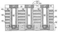
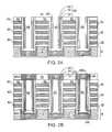
- a first exemplary device structureincludes a substrate 8 , which can be a semiconductor substrate.
- the substrate 8can include a substrate semiconductor layer 10 and optional first electrodes 12 (which can alternatively function as source or drain regions) embedded within the substrate semiconductor layer 10 .
- the first electrodesmay be omitted.
- the substrate 8can be a bulk semiconductor substrate, in which case the entirety of the substrate 8 is a semiconductor substrate.
- the substrate 8can be a top semiconductor layer of a semiconductor-on-insulator (SOI) substrate or a top semiconductor material portion a hybrid substrate including at least one bulk semiconductor region and at least one SOI region.
- the substrate semiconductor layer 10can be the top semiconductor layer of an SOI substrate, a semiconductor material layer in a bulk portion, or a top semiconductor portion of in an SOI region of a hybrid substrate.
- the substrate semiconductor layer 10is a semiconductor material layer, and can include at least one elemental semiconductor material, at least one III-V compound semiconductor material, at least one II-VI compound semiconductor material, at least one organic semiconductor material, or other semiconductor materials known in the art.
- the substrate 8has a major surface 9 , which can be, for example, a topmost surface of the substrate semiconductor layer 10 .
- the major surface 9can be a semiconductor surface. In one embodiment, the major surface 9 can be a single crystalline semiconductor surface.
- a “semiconductor material”refers to a material having a resistivity in the range from 1.0 ⁇ 10 ⁇ 5 Ohm-cm to 1.0 ⁇ 10 5 Ohm-cm, and is capable of producing a doped material having a resistivity in a range from 1.0 ⁇ 10 ⁇ 5 Ohm-cm to 1.0 Ohm-cm upon suitable doping with an electrical dopant.
- an “electrical dopant”refers to a p-type dopant that adds a hole to a balance band within a band structure, or an n-type dopant that adds an electron to a conduction band within a band structure.
- a “major surface”refers to a planar surface having a greater area than at least another surface that may be another planar surface or a curved surface.
- a planar surfaceis a surface that is contained within a Euclidean two-dimensional plane or deviating from a Euclidean two-dimensional plane only by variations caused by surface bowing and/or surface roughness of a magnitude inherently present in commercially available semiconductor substrates.
- the substrate semiconductor layer 10can include a single crystalline semiconductor material, a polycrystalline semiconductor material, and/or an amorphous semiconductor material.
- the substrate semiconductor layer 10can be a single crystalline semiconductor material layer.
- the substrate semiconductor layer 10can include a single crystalline silicon layer, a single crystalline silicon-germanium alloy layer, or a single crystalline silicon-carbon alloy layer.
- the substrate semiconductor layer 10can include a polycrystalline silicon layer, a polycrystalline silicon-germanium alloy layer, or a polycrystalline silicon-carbon alloy layer.
- Portions of the substrate semiconductor layer 10can be suitably doped with p-type dopants (e.g., the semiconductor layer 10 may be a p-well region in the substrate 8 ) or n-type dopants.
- the optional first electrodes 12include a doped semiconductor material.
- the first electrodes 12can be formed as doped portions of the substrate semiconductor layer 10 , i.e., by doping portions of the substrate semiconductor layer 10 with p-type dopants or n-type dopants.
- the first electrodes 12can be formed as source regions or drain regions for monolithic three-dimensional NAND string memory devices to be subsequently formed.
- the first electrodes 12may be suitably patterned to be electrically shorted to neighboring first electrodes 12 along one direction and/or electrically isolated from neighboring first electrodes 12 along another direction in an array configuration for the monolithic three-dimensional NAND string memory devices.
- the source or drain regions in the substratemay be formed at a later step in the process by ion implantation through a back side opening, as will be described in more detail below. While embodiments employing a semiconductor substrate for the substrate 8 are illustrated herein, embodiments employing non-semiconductor substrates are also contemplated herein, provided that the first electrodes 12 including a conductive material (which may be doped semiconductor material) can be formed in, or on, a non-semiconductor substrate.
- a conductive materialwhich may be doped semiconductor material
- select gate electrodescan be formed within, or on top of, the substrate semiconductor layer 10 employing previously known methods, or methods yet to be invented, for implementing the array of vertical NAND strings.
- a lower select gate device levelmay be fabricated as described in U.S. patent application Ser. No. 14/133,979, filed on Dec. 19, 2013, U.S. patent application Ser. No. 14/225,116, filed on Mar. 25, 2014, and/or U.S. patent application Ser. No. 14/225,176, filed on Mar. 25, 2014, all of which are incorporated herein by reference.
- a top surface of each first electrode 12can be physically exposed at the front side (upper side) of the substrate 8 .
- a protective film(not shown), such as a silicon dioxide layer, may be provided on the top surface of the substrate 8 in order to provide temporary protection for the substrate semiconductor layer 10 and/or the first electrodes 12 .
- a stack of alternating layers of a first material and a second material different from the first materialis formed over the substrate 8 .
- the stack of the alternating layersis herein referred to as an alternating stack ( 32 , 34 ).
- the alternating stack ( 32 , 42 )can include first material layers 32 composed of the first material, and second material layers 42 composed of a second material different from that of first material layers 32 .
- the second material layersmay comprise electrically conductive material which forms the control gate electrodes of the NAND string.
- the second material layers 42may comprise electrically insulating or conductive sacrificial layers which are removed through the back side openings and replaced with metal control gate electrodes.
- the first materialcan be at least one electrically insulating material.
- each first material layer 32can be an insulating material layer.
- Electrically insulating materials that can be employed for the first material layers 32include, but are not limited to silicon oxide (including doped or undoped silicate glass), silicon nitride, silicon oxynitride, organosilicate glass (OSG), spin-on dielectric materials, dielectric metal oxides that are commonly known as high dielectric constant (high-k) dielectric oxides (e.g., aluminum oxide, hafnium oxide, etc.) and silicates thereof, dielectric metal oxynitrides and silicates thereof, and organic insulating materials.
- high-khigh dielectric constant
- the second material layers 42can function as control gate electrodes made of at least one conductive material.
- each second material layer 42can be a conductive material layer.
- Conductive materials that can be employed for the second material layers 42 that constitute the control gate electrodesinclude, but are not limited to, a doped semiconductor material, elemental metals, intermetallic alloys, conductive nitrides of at least one elemental metal, a silicate of at least one metal, conductive carbon allotropes, organic conductive materials, and combinations thereof.
- the second materialcan be doped polysilicon, tungsten, tungsten nitride, tantalum, tantalum nitride, titanium, titanium nitride, cobalt, copper, aluminum, an alloy thereof, or a combination thereof.
- the second material layers 42may comprise sacrificial layers, such as silicon nitride or polysilicon sacrificial layers. In this case, at least one, and/or each, of the second material layers 42 can be a sacrificial material layer.
- the second material layers 42can be silicon nitride layers that can be subsequently removed, for example, by a wet etch employing phosphoric acid.
- the first material layers 32can include silicon oxide, and second material layers can include silicon nitride sacrificial layers or doped polysilicon or doped amorphous silicon layers that can be subsequently converted into doped polysilicon through a thermal anneal at an elevated temperature.
- the first material of the first material layers 32can be deposited, for example, by chemical vapor deposition (CVD).
- CVDchemical vapor deposition
- TEOStetraethyl orthosilicate
- the second material of the second material layers 42can be formed, for example, by physical vapor deposition (PVD; sputtering), chemical vapor deposition, electroplating, electroless plating, or combinations thereof.
- the second material layers 42can be suitably patterned to function as the control gate electrodes of the monolithic three-dimensional NAND string memory devices to be subsequently formed.
- Each second material layer 42may comprise a portion having a strip shape extending substantially parallel to the major surface 9 of the substrate 8 .
- the thicknesses of the first material layers 32 and the second material layers 42can be in a range from 8 nm to 128 nm, although lesser and greater thicknesses can be employed for each first material layer 32 and for each control gate electrode 42 . In one embodiment, the thicknesses of the first material layers 32 and the second material layers 42 can be in a range from 20 nm to 50 nm.
- the number of repetitions of the pairs of a first material layer 32 and a second material layer (e.g., control gate electrode or sacrificial material) 42can be in a range from 2 to 1,024, and typically from 8 to 256, although a greater number of repetitions can also be employed.
- the top and bottom gate electrodes in the stackmay function as the select gate electrodes.
- a lithographic material stack 48can be formed over the top surface of the alternating stack ( 32 , 42 ).
- the lithographic material stack 48can include, for example, an organic planarization layer (OPL) 45 , such as amorphous carbon, an antireflective coating (ARC) layer 46 , and a photoresist layer 47 .
- OPLorganic planarization layer
- ARCantireflective coating
- the photoresist layer 47can be lithographically patterned, for example, by lithographic exposure and development, to form openings therein. The pattern of the openings corresponds to the areas of memory openings to be subsequently formed through the alternating stack ( 32 , 42 ).
- the pattern of the openings in the patterned photoresist layer 47can be circular, elliptical, polygonal, or of a closed curvilinear shape.
- a “closed” shaperefers to a two-dimensional shape that is defined by a contiguous periphery that begins and ends at a same point without crossing itself, i.e., a shape defined by a periphery that can be traced throughout the entirety of the periphery to come back to the starting point without crossing any portion of the periphery during the tracing.
- each shape for an opening in the photoresist layer 47(and the corresponding shape for a memory opening to be subsequently formed) can be identical, or can be related to a neighboring shape through symmetry.
- the pattern of the opening in the photoresist layer 47can be a periodic pattern.
- the shapes of the openings in the patterned photoresist layer 47can be substantially circular or substantially elliptical.
- the sizes (e.g., a diameter or a major axis) of the openings in the patterned photoresist layer 47can be in a range from 30 nm to 300 nm, although lesser and greater dimensions can also be employed.
- a hard mask layermay be optionally employed, for example, between the lithographic material stack 48 and the top surface of the alternating stack ( 32 , 42 ). While an embodiment in which the lithographic material stack 48 includes an organic planarization layer (OPL) 45 , an ARC layer 46 , and a photoresist layer 47 is illustrated herein, any alternative lithographic material layer (e.g., photoresist) or any alternative lithographic material stack can be employed in lieu of the lithographic material stack 48 illustrated herein.
- OPLorganic planarization layer
- the pattern in the patterned photoresist layer 47can be transferred through the ARC layer 46 and the OPL 45 , and subsequently through the entirety of the alternating stack ( 32 , 42 ) by at least one anisotropic etch that employs the patterned photoresist layer 47 , and/or any patterned portion of the ARC layer 46 and the OPL 45 , and/or any patterned portion of a hard mask layer, if present, as an etch mask.
- a plurality of etch chemistriesmay be employed to etch through the various materials of the ARC layer 46 , the OPL 45 , the optional hard mask layer, and the alternating stack ( 32 , 42 ).
- Portions of the alternating stack ( 32 , 42 ) underlying the openings in the photoresist layer 45are etched to form memory openings 49 .
- the transfer of the pattern in the photoresist layer 47 through the alternating stack ( 32 , 42 )forms the memory opening 49 through the alternating stack ( 32 , 42 ).
- the chemistry of the anisotropic etch process employed to etch through the materials of the alternating stack ( 32 , 42 )can alternate to optimize etching of the first and second materials in the alternating stack ( 32 , 42 ).
- the anisotropic etchcan be, for example, a series of reactive ion etches.
- a sacrificial etch stop layermay be employed between the alternating stack ( 32 , 42 ) and the substrate 8 .
- the sidewalls of the memory openings 49can be substantially vertical, or can be tapered.
- a surface dielectric portion 82can be formed by converting a surface portion of each second material layer 42 that is physically exposed to a memory opening 49 into a dielectric material portion. For example, after etching through a bottommost layer 42 within the alternating stack ( 32 , 42 ), an oxidation process, a nitridation process, or an oxynitridation process can be performed to convert the surface portions of the second material layers 42 that are physically exposed to the memory opening 49 into dielectric oxide portions, dielectric nitride portions, or dielectric oxynitrides portions.
- the conversion of the surface portions of the second material layers 42 into the surface dielectric portions 82can be performed by a thermal oxidation process, a thermal nitridation process, a thermal oxynitridation process, a plasma oxidation process, a plasma nitridation process, a plasma oxynitridation process, or a combination thereof.
- the conversion of the surface portions of the second material layers 42 into the surface dielectric portions 82can be performed by in-situ steam generation oxidation process.
- the surface portions 82 of silicon nitride sacrificial layers 42may be converted to silicon oxide or silicon oxynitride.
- the thickness of the surface dielectric portions 82can be in a range from 0.5 nm to 10 nm, although lesser and greater thicknesses can also be employed. Any remaining portion of the bottommost first material layer 32 underneath each memory opening 49 is subsequently etched so that the memory openings 49 extend from the top surface of the alternating stack ( 32 , 42 ) to the top surface of the first electrodes 12 or the substrate semiconductor layer 10 . Remaining portions of the lithographic material stack 48 (and optionally remaining portions of a hard mask layer, if present) can be subsequently removed selective to the materials of the alternating stack ( 32 , 42 ).
- a removal of a first materialis “selective to” a second material if the removal process removes the first material at a rate that is at least twice the rate of removal of the second material.
- the ratio of the rate of removal of the first material to the rate of removal of the second materialis herein referred to as a “selectivity” of the removal process for the first material with respect to the second material.
- the openings in the photoresist layer 45 and the memory openings 49can overlie the first electrodes 12 or the major surface 9 of the substrate 8 .
- a first element“overlies” a second element if a first horizontal plane including the bottommost point of the first element is within, or above, a second horizontal plane including a topmost point of the second element and if there exits an areal overlap between the area of the first element and the area of the second element in a see-through view along a direction perpendicular to the first and second horizontal planes. If a first element overlies a second element, the second element “underlies” the first element. In one embodiment, the entire area of a memory opening 49 can be within the area of an underlying first electrode 12 or the substrate semiconductor layer 10 .
- an overetch into the first electrodes 12 or the substrate semiconductor layer 10can be optionally performed after the top surfaces of the first electrodes 12 or the substrate semiconductor layer 10 are physically exposed.
- the overetchmay be performed prior to, or after, removal of the lithographic material stack 48 .
- the overetchcan be an anisotropic etch, and recesses the physically exposed portions of the top surfaces of the first electrodes 12 or the substrate semiconductor layer 10 underlying the memory openings by a recess depth.
- the recessed surfaces of the first electrodes 12 or the substrate semiconductor layer 10can be vertically offset from the undressed top surfaces of the first electrodes 12 or the substrate semiconductor layer 10 by the recess depth.
- the recess depthcan be, for example, in a range from 1 nm to 50 nm, although lesser and greater recess depths can also be employed.
- the overetchis optional, and may be omitted.
- the bottom surface of each memory opening 49can be coplanar with the topmost surface of the first electrodes 12 , and/or the topmost surface of the substrate 8 .
- Each of the memory openings 49can include a sidewall (or a plurality of sidewalls) that extends substantially perpendicular to the major surface of the substrate 8 and is defined by the physically exposed sidewall surfaces of the alternating stack ( 32 , 42 , 82 ).
- Each of the memory openings 49can further include a bottom surface that is a top surface of a first electrode 12 or the substrate semiconductor layer 10 .
- the sidewalls of the first electrodes 12which are present around the recesses within the first electrodes 12 , can be vertically coincident with the sidewalls of the memory openings 49 .
- a first surfaceis “vertically coincident” with a second surface if there exists a vertical plane including both the first surface and the second surface. Such a vertical plane may, or may not, have a horizontal curvature, but does not include any curvature along the vertical direction, i.e., extends straight up and down.
- a memory film layer 50 Cis formed in the memory openings and over the alternating stack ( 32 , 42 ).
- the memory film layer 50 Ccan be a stack of contiguous material layers that overlie the entirety of the alternating stack ( 31 , 42 , 82 ).
- the memory film layer 50 Ccontacts all sidewall surface(s) and all bottom surface(s) of the memory openings 49 .
- the memory film layer 50 Cis a contiguous film stack that provides the functionality of charge storage in the absence of an external electrical bias voltage, while enabling charge transfer in the presence of a suitable external electrical bias voltage.
- the memory film layer 50 Ccan be a stack, in the order of formation, of a blocking dielectric layer 52 L, a charge storage layer 54 L, and a tunnel dielectric layer 56 L.
- the blocking dielectric layer 52 Lcontacts the sidewalls of the memory openings 49 .
- the blocking dielectric layer 52 Lcan contact the sidewalls of the surface dielectric portions 82 , or in the absence of the surface dielectric portions 82 , can contact the sidewalls of the second material layers 42 .
- the blocking dielectric layer 52 Lmay include one or more dielectric material layers that can function as the dielectric material(s) of a control gate dielectric between the second material layers 42 and charge storage regions to be subsequently formed out of the charge storage layer 54 L.
- the blocking dielectric layer 52 Lcan include silicon oxide, a dielectric metal oxide, a dielectric metal oxynitride, or a combination thereof. In one embodiment, the blocking dielectric layer 52 L can include a stack of at least one silicon oxide layer and at least one dielectric metal oxide layer.
- the blocking dielectric layer 52 Lcan be formed by a conformal deposition process such as chemical vapor deposition (CVD) and/or atomic layer deposition (ALD), and/or by deposition of a conformal material layer (such as an amorphous silicon layer) and subsequent conversion of the conformal material layer into a dielectric material layer (such as a silicon oxide layer).
- CVDchemical vapor deposition
- ALDatomic layer deposition
- the thickness of the blocking dielectric layer 52 Lcan be in a range from 6 nm to 24 nm, although lesser and greater thicknesses can also be employed.
- the blocking dielectric layer 52 Lmay be omitted from the memory opening 49 , and instead be formed through the back side opening in back side recesses left by the removal of the sacrificial layers 42 prior to forming the metal control gate electrodes through the back side opening.
- the charge storage layer 54 Lincludes a dielectric charge trapping material, which can be, for example, silicon nitride, or a conductive material such as doped polysilicon or a metallic material. In one embodiment, the charge storage layer 54 L includes silicon nitride.
- the charge storage layer 54 Lcan be formed as a single charge storage layer of homogeneous composition, or can include a stack of multiple charge storage material layers.
- the multiple charge storage material layerscan comprise a plurality of spaced-apart floating gate material layers that contain conductive materials (e.g., metal such as tungsten, molybdenum, tantalum, titanium, platinum, ruthenium, and alloys thereof, or a metal silicide such as tungsten silicide, molybdenum silicide, tantalum silicide, titanium silicide, nickel silicide, cobalt silicide, or a combination thereof) and/or semiconductor materials (e.g., polycrystalline or amorphous semiconductor material including at least one elemental semiconductor element or at least one compound semiconductor material).
- conductive materialse.g., metal such as tungsten, molybdenum, tantalum, titanium, platinum, ruthenium, and alloys thereof, or a metal silicide such as tungsten silicide, molybdenum silicide, tantalum silicide, titanium silicide, nickel silicide, cobalt silicide, or a combination thereof
- the charge storage layer 54 Lmay comprise an insulating charge trapping material, such as one or more silicon nitride segments.
- the charge storage layer 54 Lmay comprise conductive nanoparticles such as metal nanoparticles, which can be, for example, ruthenium nanoparticles.
- the charge storage layer 54 Lcan be formed, for example, by chemical vapor deposition (CVD), atomic layer deposition (ALD), physical vapor deposition (PVD), or any suitable deposition technique for the selected material(s) for the charge storage layer 54 L.
- the thickness of the charge storage layercan be in a range from 2 nm to 20 nm, although lesser and greater thicknesses can also be employed.
- the tunnel dielectric layer 56 Lincludes a dielectric material through which charge tunneling can be performed under suitable electrical bias conditions.
- the charge tunnelingmay be performed through hot-carrier injection or by Fowler-Nordheim tunneling induced charge transfer depending on the mode of operation of the monolithic three-dimensional NAND string memory device to be formed.
- the tunneling dielectric layer 56 Lcan include silicon oxide, silicon nitride, silicon oxynitride, dielectric metal oxides (such as aluminum oxide and hafnium oxide), dielectric metal oxynitride, dielectric metal silicates, alloys thereof, and/or combinations thereof.
- the tunneling dielectric layer 56 Lcan include a stack of a first silicon oxide layer, a silicon oxynitride layer, and a second silicon oxide layer, which is commonly known as an ONO stack.
- the tunneling dielectric layer 56 Lcan include a silicon oxide layer that is substantially free of carbon or a silicon oxynitride layer that is substantially free of carbon.
- the thickness of the tunnel dielectric layer 56 Lcan be in a range from 2 nm to 20 nm, although lesser and greater thicknesses can also be employed.
- a sacrificial material layer 57 Lcan be formed on the memory film layer 50 C.
- the sacrificial material layer 57 Lincludes a material that is different from the material of the innermost layer of the tunnel dielectric layer 56 L within the memory openings 49 (which is the same as the topmost layer of the tunnel dielectric layer 56 L over the alternating stack ( 32 , 42 , 82 )) so that the sacrificial material layer 57 L can be subsequently removed selective to the tunnel dielectric layer 56 L.
- the materials that can be employed for the sacrificial material layer 57 Linclude, but are not limited to, a chemical vapor deposition (CVD) silicon oxide, silicon nitride, a semiconductor material, organosilicate glass, an organic polymer, an inorganic polymer, amorphous carbon, and a diamond-like carbon.
- a CVD silicon oxiderefers to a silicon oxide material formed by chemical vapor deposition employing a carbon-including precursor (such as tetraethyl orthosilicate) and inherently includes carbon as impurity at an atomic concentration of at least 0.1%, and typically in a range from 0.2% to 1.0%.
- the sacrificial material layer 57 Lincludes a dielectric material.
- the sacrificial material layer 57 Lincludes a material other than a semiconductor material.
- the sacrificial material layer 57 Lincludes a material other than a silicon-containing semiconductor material.
- the innermost layer of the tunnel dielectric layer 56 L within the memory openings 49can be silicon oxynitride obtained by oxidation of silicon nitride (for example, by thermal conversion of silicon nitride by in-situ steam generation oxidation process), and the sacrificial material layer 57 L can include a low temperature oxide (LTO), which is a CVD silicon oxide obtained by a plasma enhanced chemical vapor deposition (PECVD) employing tetraethyl orthosilicate (TEOS) as a precursor.
- PECVDplasma enhanced chemical vapor deposition
- TEOStetraethyl orthosilicate
- Typical deposition temperatures of the LTOcan be in a range from 25° C. to 200° C.
- the CVD silicon oxide of the sacrificial material layer 57 Lcan be removed selective to the material of the tunnel dielectric layer 56 L in a subsequent processing step with a high selectivity, which can be significantly greater than 2.
- the innermost layer of the tunnel dielectric layer 56 L within the memory openings 49can be silicon oxide or silicon oxynitride obtained by oxidation of silicon nitride (for example, by thermal conversion of silicon nitride by in-situ steam generation oxidation process), and the sacrificial material layer 57 L can include silicon nitride deposited by low pressure chemical vapor deposition (LPCVD), plasma enhanced chemical vapor deposition (PECVD), or atomic layer deposition (ALD).
- LPCVDlow pressure chemical vapor deposition
- PECVDplasma enhanced chemical vapor deposition
- ALDatomic layer deposition
- silicon nitride deposited by a chemical vapor deposition process employing hexachlorodisilane as a silicon precursorcan be employed as the material of the sacrificial material layer 57 L.
- the sacrificial material layer 57 Lcan be conformally, or non-conformally, deposited.
- the thickness of the sacrificial material layer 57 L, as measured near a bottom end of a vertical portion of the sacrificial material layer 57 L within a memory opening 49can be in a range from 2 nm to 30 nm, although lesser and greater thicknesses can also be employed.
- the sacrificial material layer 57 Lcan be conformally deposited.
- horizontal portions of the sacrificial material layer 57 L and the memory film layer 50 Care etched to physically expose portions of the top surface of the substrate 8 underneath each memory opening 49 , while a vertical portion of the sacrificial material layer 57 is present on each vertical portion of the memory film layer 50 C.
- an anisotropic etchcan be employed to etch the horizontal portions of the sacrificial material layer 57 L and the memory film layer 50 C from above the alternating stack ( 32 , 42 , 82 ), and to etch each horizontal portion of the sacrificial material layer 57 L and the memory film layer 50 C at the bottom of each memory opening 49 .
- the vertical portions of the sacrificial material layer 57 Lcovers and protects the vertical portions of the memory film layer 57 during the anisotropic etch from the reactive ions that are present within the plasma of etchant gases.
- each disjoined material portion ( 50 , 57 )is located within a memory opening 49 (See FIG. 1D ), and includes a memory film 50 and a sacrificial material layer 57 .
- Each memory film 50can include an optional blocking dielectric 52 which is a remaining portion of the blocking dielectric layer 52 L, a charge storage region 54 which is a remaining portion of the charge storage layer 54 L, and a tunnel dielectric 56 which is a remaining portion of the tunnel dielectric layer 56 L.
- Each memory film 50includes a remaining contiguous vertical portion of the memory film layer 50 C (See FIG. 1F ) that is located within a memory opening 49 , and each sacrificial material layer 57 can be a remaining contiguous vertical portion of the sacrificial material layer 57 L (See FIG. 1F ).
- Each memory film 50can be homeomorphic to a torus, and each sacrificial material layer 57 can be homeomorphic to a torus.
- an elementis homeomorphic to a geometrical shape if the shape of the element can be mapped to the geometrical shape by continuous deformation without creation or destruction of any hole.
- each sacrificial material layer 57can have a cylindrical shape
- each memory film 50can have a shape that is modified from a cylindrical shape by the addition of an annulus that underlies an overlying sacrificial material layer 57 and replicates the horizontal cross-sectional shape of the overlying sacrificial material layer 57 .
- a top surface of a first electrode 12can be physically exposed within the cavity defined by the inner sidewalls of an overlying sacrificial material layer 57 .
- a sacrificial material layer 57can have an inner sidewall that is vertically coincident with a sidewall a horizontal portion of a memory film 50 .
- Each sacrificial material layer 57covers, and protects, the memory film 50 that contacts the sacrificial material layer 57 during the anisotropic etch that physically exposes the surfaces of the first electrodes 12 .
- each tunnel dielectric 56is protected by a sacrificial material layer 57 during the anisotropic etch that physically exposed the surfaces of the first electrodes 12 so that the quality of the tunnel dielectric 56 is not degraded during the anisotropic etch.
- the sacrificial material layers 57are removed selective to the memory films 50 and the first electrodes 12 or the substrate semiconductor layer 10 by an etch.
- the etchcan be an isotropic etch such as a wet etch or an isotropic dry etch.
- the chemistry of the etchcan be selected to obtain a high selectivity with respect to the outermost material of the memory films 50 .
- the innermost layer of the tunnel dielectrics 56can be silicon oxynitride obtained by oxidation of silicon nitride (for example, by thermal conversion of silicon nitride by in-situ steam generation oxidation process), the sacrificial material layers 57 can include low temperature oxide, and the removal of the sacrificial material layers 57 can be performed by a wet etch employing a dilute hydrofluoric (HF) acid and/or by a dry etch employing hydrofluoric acid vapor to provide high selectivity to the memory films 50 .
- dilute hydrofluoric acid and hydrofluoric acid vaporprovide high selectivity for the etching of low temperature oxide with respect to silicon oxynitride due to the presence of nitrogen atoms within the silicon oxynitride.
- the innermost layer of the tunnel dielectric layers 56can be silicon oxide or silicon oxynitride obtained by oxidation of silicon nitride (for example, by thermal conversion of silicon nitride by in-situ steam generation oxidation process), and the sacrificial material layers 57 can include silicon nitride, and the removal of the sacrificial material layers 57 can be performed by a wet etch employing phosphoric acid.
- phosphoric acidprovides high selectivity during the etch of silicon nitride with respect to silicon oxynitride or silicon oxides.
- a substantially isotropic dry etchemploying at least one hydrofluorocarbon gas or at least one hydrochlorocarbon gas may be employed to remove silicon nitride selective to silicon oxynitride or silicon oxide.
- the etch chemistry for removal of the sacrificial material layers 57can be selected such that collateral removal of the tunneling dielectrics 56 can be minimized, i.e., to maximize the selectivity of the etch process with respect to the innermost material of the tunneling dielectrics 56 . Due to the presence of the sacrificial material layers 57 during removal of physically exposed horizontal portions of the memory film layer 50 C, the inner sidewalls of the upper portion 50 U of each memory film 50 that extend vertically throughout the alternating stack ( 32 , 42 , 82 ) are laterally offset outward from the inner sidewalls of the lower portion 50 L of the memory film 50 by a uniform distance.
- the uniform distanceis invariant along the inner sidewalls of the lower portion 50 L of the memory film 50 .
- the uniform distanceis the thickness of the bottom portion of the sacrificial material layer 57 (See FIG. 1G ) that is removed from within the memory film 50 .
- a semiconductor material layer 60 Ccan be deposited directly on a top surface of the each first electrode 12 or the substrate semiconductor layer 10 , directly on inner sidewalls of the memory films 50 , and over the alternating stack ( 32 , 42 ).
- the semiconductor material layer 60 Cis deposited directly on the first electrodes 12 or on the semiconductor substrate 8 .
- the semiconductor material layer 60 Cmay, or may not, be deposited conformally. In one embodiment, the semiconductor material layer 60 C can be deposited conformally, i.e., with substantially the same thickness throughout.
- the semiconductor material layer 60 Cincludes a polycrystalline semiconductor material or an amorphous semiconductor material that can be subsequently annealed at an elevated temperature to form a polycrystalline semiconductor material.
- Semiconductor materials that can be employed for the semiconductor material layer 60 Cinclude, but are not limited to, silicon, germanium, a silicon-germanium alloy, a silicon-carbon alloy, a silicon-germanium-carbon alloy, a III-V compound semiconductor material, a II-VI compound semiconductor material, an organic semiconductor material, or a combination thereof.
- the semiconductor material layer 60 Ccan be formed by a conformal deposition process such as chemical vapor deposition (CVD) or atomic layer deposition (ALD).
- the thickness of the semiconductor material layer 60 Ccan be in a range from 3 nm to 30 nm, although lesser and greater thicknesses can also be employed. In one embodiment, thickness of the semiconductor material layer 60 C can be in a range from 6 nm to 15 nm.
- the semiconductor material layer 60 Ccan include a semiconductor material. As discussed above, the semiconductor material layer 60 C may be intentionally doped, or unintentionally doped. Unintentional doping of the semiconductor material layer 60 C may occur, for example, by residual electrical dopants that are present in a process chamber or diffuse out of the substrate 8 during formation of the semiconductor material layer 60 C.
- the doped semiconductor materialcan be p-doped or n-doped, i.e., doped with p-type electrical dopants or n-type electrical dopants.
- the doping of the semiconductor material layer 60 Ccan be performed in-situ, for example, by flowing at least one dopant gas concurrently or alternately with at least one precursor gas for the semiconductor material.
- the doping of the semiconductor material layer 60 Ccan be performed ex-situ, for example, by introducing p-type dopants or n-type dopants into the semiconductor material layer 60 C by ion implantation, plasma doping, and/or outdiffusion of electrical dopants from a disposable dopant source material that is subsequently removed.
- Various processing stepsmay be optionally performed to increase the average grain size within the polycrystalline material of the semiconductor material layer 60 C, either as deposited or to be subsequently formed upon annealing of a deposited amorphous material.
- the physically exposed surfaces of the semiconductor material layer 60 Ccan be treated with a plasma of a non-electrical dopant.
- a non-electrical dopantrefers to a dopant that does not add a charge carrier to the band structure of a semiconductor material, i.e., does not add a hole within a balance band of the semiconductor material and does not add an electron within a conduction band of the semiconductor material.
- the semiconductor material layer 60 Ccan be treated with nitrogen plasma to passivate dangling bonds or other mobility traps for charge carriers, and to reduce the density of grain boundaries.
- the semiconductor material layer 60 Ccan be doped with carbon to reduce the density of grain boundaries.
- Carboncan be introduced into the semiconductor material layer 60 C by in-situ doping at an atomic concentration in a range from 0.01% to 1.00%, although lesser and greater atomic concentrations can also be employed.
- an optional core dielectric material layer 62can be deposited within remaining cavities of the memory openings 49 and over the semiconductor material layer 60 C.
- the core dielectric material layerincludes a dielectric material such as silicon oxide, organosilicate glass (OSG), a spin-on dielectric material, or a combination thereof.
- the core dielectric material layerincludes undoped silicon oxide.
- the core dielectric material layercan be deposited, for example, by chemical vapor deposition and/or by spin coating. The amount of the deposited dielectric material for the core dielectric material layer is selected such that the entire cavity of each memory opening is filled with the deposited dielectric material.
- the portions of the core dielectric material layer and the semiconductor material layer 60 C above the top surface of the alternating stack ( 32 , 42 )can be removed, for example, by a planarization process and/or a recess etch.
- CMPchemical mechanical polishing
- CMPcan be employed to remove the portions of the core dielectric material layer 62 and the semiconductor material layer 60 C from above the top surface of the alternating stack ( 32 , 42 ).
- Each remaining portion of the semiconductor material layer 60 C within a memory opening 49constitutes a through-stack channel 60 , which can be a semiconductor channel between the source and the drain of the monolithic three-dimensional NAND string memory device of the present disclosure.
- Each remaining portion of the core dielectric material layerconstitutes a dielectric core 62 , which contacts inner sidewalls of the through-stack channel 60 that laterally surrounds the dielectric core 62 .
- the through-stack channel 60includes an electrically doped (i.e., p-doped or n-doped) polycrystalline material, which is polycrystalline from the time of deposition of the semiconductor material layer 60 C or becomes polycrystalline after a subsequent anneal process.
- a predominant fraction of the grains of the polycrystalline material of each through-stack channel 60can extend from the outer surface of the through-stack channel 60 to the inner surface of the through-stack channel 60 .
- more than 50% of the grains of the polycrystalline material of each through-stack channel 60can include a first surface that contacts the memory film 50 and a second surface that contacts the dielectric core 60 within each grain.
- each through-stack channel 60does not include a substantially contiguous interface containing grain boundaries located between the outer surface of the through-stack channel 60 and the inner surface of the through-stack channel 60 and extending over an entire interface between the through-stack channel 60 and the memory film 50 .
- an interfaceis “substantially contiguous” if the interface vertically extends in the channel through a substantial vertical distance, e.g., through more than two, such as more than five, such as all, of the control gate electrodes 42 within the alternating stack ( 32 , 42 ).
- the total area of a discontinuity (e.g., lack of grain boundary) within the interfaceis sufficiently high that the number of additional defects is high enough to degrade characteristics of the cell channel, leading to degradation of mobility, cell current, sub-threshold slope, variability, boosting potential, etc.
- the total area of a discontinuity (e.g., lack of grain boundary) within the interfaceis 20% or less, such as zero to 10%, for example 1 to 5% of the entire area of the interface and the discontinuity.
- the number total area of the discontinuitymay be higher.
- the discontinuitymay occur due to grain growth during an annealing step which may eliminate a small portion of the grain boundaries at the interface.
- the semiconductor material layer 60 Cis formed during a single deposition process, a stack of multiple semiconductor materials does not exist in any of the through-stack channels 60 .
- the through-stack channel 60 of the present disclosuredoes not include any contiguous interface of a large number of grain boundaries and/or defects that runs parallel to the interface between the through-stack channel 60 and the memory film 50 .
- the through-stack channel 60 of the present disclosurecan provide lesser grain boundaries and higher conductivity than prior art semiconductor material layers having similar overall dimensions and similar material compositions.
- a top dielectric layer 70can be formed over the alternating stack ( 32 , 42 , 82 ), the memory films 50 , the through-stack channels 60 , and the dielectric cores 62 .
- the top dielectric layer 70includes a dielectric material such as silicon oxide, silicon nitride, organosilicate glass, or a combination thereof.
- the top dielectric layer 70can be deposited, for example, by chemical vapor deposition.
- the thickness of the top dielectric layer 70can be in a range from 30 nm to 1,000 nm, although lesser and greater thicknesses can also be employed.
- Openingscan be made through the top dielectric layer 70 in regions that overlies the through-stack channels 60 .
- the openingscan be made to encompass each contiguous area including an adjoining pair of a through-stack channel 60 and a dielectric core 62 .
- the openings through the top dielectric layer 70can be made by applying a photoresist layer (not shown) over the top dielectric layer 70 , lithographically patterning the photoresist layer 70 , an etching portions of the top semiconductor layer 70 that are not covered by the remaining portions of the photoresist layer. Top surfaces of the through-stack channels 60 are physically exposed at the bottom of the openings through the top dielectric layer 70 .
- the photoresist layercan be removed, for example, by ashing.
- a conductive or semiconductor materialis deposited into the openings in the top dielectric layer 70 , for example, by physical vapor deposition, chemical vapor deposition, electroplating, electroless plating, or a combination thereof.
- the conductive materialis planarized so that the portion of the conductive material above the top surface of the top dielectric layer 70 is removed.
- the planarization of the conductive materialcan be performed, for example, by chemical mechanical polishing (CMP).
- CMPchemical mechanical polishing
- Each remaining portion of the conductive materialconstitutes a second electrode 72 .
- Each pair of a first electrode 12 and a second electrode 72 electrically shorted to the same through-stack channel 60can function as a pair of a source region and a drain region for a monolithic three-dimensional NAND string memory device.
- a first electrode 12(which can be a doped semiconductor portion) can function as a source region
- a second electrode 72(which can be another doped semiconductor portion) can function as a drain region within a monolithic three-dimensional NAND string memory device, or vice versa.
- the top portion of the channel 60is doped by ion implantation to form a drain or source region therein. Electrical contacts and interconnects are then formed to the electrodes/source/drain regions 12 , 72 .
- the first exemplary device structure illustrated in FIG. 1Kis a three-dimensional memory device that includes a substrate 8 having a major surface 9 , and an alternating stack ( 32 , 42 , 82 ) of insulating material layers composed of the first material layers 32 and control gate electrodes composed of the second material layers 42 located over the substrate 8 .
- the alternating stackhas a memory opening 49 (See FIG. 1D ) extending through the alternating stack ( 32 , 42 , 83 ) in a direction substantially perpendicular to the major surface 9 .
- the first exemplary device structurefurther includes a memory film 50 located at a peripheral region of the memory opening 49 , and a semiconductor channel embodied as the through-stack channel 60 .
- the through-stack channel 60includes an upper portion 60 U extending substantially perpendicular to the major surface 9 and contacting an inner sidewall of the memory film 50 and a lower portion 60 L contacting a single crystalline semiconductor material portion located within, or on, the substrate 8 .
- a sidewall of the upper portion 60 U of the semiconductor channelcan be laterally offset with respect to a sidewall of the lower portion 60 L of the semiconductor channel.
- an outer sidewall of the upper portion 60 U of the semiconductor channel (i.e., the through-stack channel 60 ) in contact with a first portion of the memory film 50is laterally offset with respect to an outer sidewall of the lower portion 60 L of the semiconductor channel in contact with a second portion of the memory film 50 .
- An inner sidewall of the upper portion 60 U of the semiconductor channel (i.e., the through-stack channel 60 ) in contact with a first portion of a dielectric core 62is laterally offset with respect to an inner sidewall of the lower portion 60 L of the through-stack channel in contact with a second portion of the dielectric core 62 .
- a first sidewallis laterally offset from a second sidewall if there is no vertical plane that can include the first sidewall and the second sidewall.
- the through-stack channel 60does not include a contiguous interface extending along the vertical direction, i.e., along a direction parallel to an outer surface of the through-stack channel 60 .
- a substantially contiguous surface composed of grain boundaries, and different from the outer surface of the through-substrate channel 60does not exist within the semiconductor channel.
- the semiconductor channel made of the through-stack channel 60does not include a substantially contiguous interface vertically extending through any substantial vertical distance, e.g., through more than two, such as more than five, such as all, of the control gate electrodes 42 within the alternating stack ( 32 , 42 ).
- the semiconductor channeldoes not include a substantially contiguous interface composed of grain boundaries, not contacting the memory film 50 , and vertically extending through the control gate electrodes 42 .
- the memory film 50can include a stack containing, from one side to another, a blocking dielectric 52 , a charge storage region 54 , and a tunneling dielectric 56 .
- a blocking dielectric 52 and/or tunneling dielectric 56can be comprised of one or more dielectric films made of different materials.
- the single crystalline semiconductor material portioncan be a doped semiconductor material portion of substrate 8 .
- the single crystalline semiconductor material portioncan be, for example, a first electrode 12 .
- an outer sidewall of the upper portion 60 U of the semiconductor channel(i.e., the through-stack channel 60 ) can extends farther outward from a geometrical center of the memory opening 49 (e.g., the vertical axis in the center of opening 49 ) than an outer sidewall of the lower portion 60 L of the semiconductor channel.
- a dielectric core 62can be embedded within the memory film 50 .
- a first interface between the dielectric core 62 and the upper portion 60 U of the semiconductor channeli.e., the through-stack channel 60
- FIG. 1La first alternative structure for the first exemplary device structure is illustrated.
- the dielectric core 62is omitted and the thickness of the semiconductor channel layer 60 C is such that the entirety of each cavity within the memory openings 49 is filled with the semiconductor material layer 60 C as deposited.
- Through-stack channels 60can be formed by subsequent removal of the portion of the semiconductor material layer 60 C from above the horizontal plane including top surface of the alternating stack ( 32 , 42 , 82 ). Each of through-stack channels 60 can be topologically homeomorphic to a sphere. Subsequently, the processing steps of FIG. 1K can be performed to provide the first variation of the first exemplary device structure illustrated in FIG. 1L .
- FIGS. 1M and 1Nillustrate a second alternative structure for the first exemplary device in which physically exposed portions of the semiconductor substrate 8 are vertically recessed while the sacrificial material layers 57 are present on the memory films 50 .
- the memory opening 49is extended further into the substrate 8 after the sacrificial material layers 57 are formed.
- the memory films 50include remaining vertical portions of the memory film layer 50 C (See FIG. 1F ).
- the vertical recessing of the physically exposed portions of the semiconductor substrate 8can be performed, for example, by an anisotropic etch process.
- the anisotropic etch processcan be a continuation of the anisotropic etch process employed to remove horizontal portions of the memory film layer 50 C, or can be an anisotropic etch process employing another etch chemistry that is different from the etch chemistry for removing the horizontal portions of the memory film layer 50 C and is selected to remove the semiconductor material of the first electrodes 12 or the substrate semiconductor layer 10 .
- each memory opening 49can be expanded by the volume of the removed material from an underlying first electrode 12 or the substrate semiconductor layer 10 .
- the sidewalls of the recessed portion of each first electrode 12 or the substrate semiconductor layer 10can be vertically coincident with the inner sidewalls of an annular portion of the overlying memory film 50 and with the inner sidewalls of the overlying sacrificial material layer 57 .
- the recess depth of the recessed surface of a first electrode from the horizontal plane including the bottommost surface of an overlying memory film 50can be in a range from 1 nm to 30 nm, although lesser and greater recess depths can also be employed.
- a first horizontal surface of the single crystalline semiconductor material portion(such as a top surface of a first electrode 12 or the substrate semiconductor layer 10 that is located below the horizontal plane including the major surface 9 and above the recessed surface of the first electrode 12 obtained by the processing step of FIG. 1M ) is in contact with a horizontal surface of an overlying memory film 50 .
- a second horizontal surface of the single crystalline semiconductor material portion(such as the recessed surface of the first electrode 12 obtained by the processing step of FIG. 1M ) that is vertically offset with respect to the first horizontal surface is in contact with an overlying semiconductor channel (i.e., the through-stack channel 60 ).
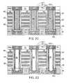
- a second exemplary device structure according to a second embodiment of the present disclosurecan be derived from the first exemplary device structure of FIG. 1G by etching a horizontal portion of each memory film 50 from underneath the sacrificial material layers 57 .
- physically exposed portions of the memory films 50(which include the horizontal portions of the memory films 40 ) can be isotropically etched employing the sacrificial material layers 57 as an etch mask.
- the material of the sacrificial material layers 57 and the etch chemistry of the isotropic etchcan be selected such that the chemistry of the isotropic etch is selective to the material of the sacrificial material layers 57 .
- a hydrofluoric acid (HF) based wet etch chemistrycan be employed to remove the physically exposed portions of the memory films 50 .
- the entirety of the annular portion (i.e., the horizontal portion) of each memory film 50can be removed by the isotropic etch. Further, the topmost portions of the memory film 50 near the top surface of the alternating stack ( 32 , 42 , 82 ) can be collaterally recessed (not illustrated).
- the area of a lower portion of the cavity underlying the horizontal plane including the bottom surfaces of the sacrificial material layers 57becomes greater than the area of an upper portion of the cavity that overlies the horizontal plane including the bottom surfaces of the sacrificial material layers 57 .
- the outer extent of the lower portion of the cavitymay extend to the vertical planes including the vertical boundaries of an overlying memory opening 49 (See FIG. 1D ), or may extend to a lesser extent than the vertical planes including the vertical boundaries of an overlying memory opening 49 .
- an outer sidewall of the lower portion 60 L of the semiconductor channel(i.e., the through-stack channel 60 ) extends farther outward from a geometrical center of the memory opening 49 (See FIG. 1D ) than an outer sidewall of the upper portion 60 U of the semiconductor channel.
- a lower portion 50 L of the memory film 50has a lesser thickness than an upper portion 50 U of the memory film 50 that contacts the upper portion 60 U of the through-stack channel 60 .
- the blocking dielectric 52 portion of the memory film 50remains while the charge storage region 54 and tunnel dielectric portions 56 are removed. Because of the presence of an undercut region in the cavity formed after the processing steps of FIG. 2A , the through-stack channel 60 contacts a bottom surface of the memory film 50 .
- FIG. 2CA first alternative structure for the second exemplary device structure is illustrated in FIG. 2C .
- This embodimentis similar to that of FIG. 1L in that the dielectric core 62 is omitted and the channel 60 fills the entire middle memory opening 49 .
- the device of FIG. 2Cis different from that of FIG. 1L is that the device of FIG. 2C also includes the lateral recess described above with respect to FIGS. 2A and 2B .
- FIG. 2DA second alternative structure for the second exemplary device structure is illustrated in FIG. 2D .
- This embodimentis similar to that of FIGS. 1M and 1N in that it includes the vertical recess of the substrate that is described above.
- the device of FIG. 2Dis different from that of FIG. 1N is that the device of FIG. 2D also includes the lateral recess described above with respect to FIGS. 2A and 2B .
- the omission of the dielectric core 62 and the vertical recessmay be used in combination in the same device if desired.
- the device of FIG. 2Dmay be formed by performing the vertical recess of the substrate shown in FIG. 1M followed by subsequently performing the processing steps of FIG. 2A (i.e., the lateral etching of horizontal portions of the memory films 50 employing the sacrificial material layers 57 as an etch mask), followed by the processing steps of FIGS. 1H, 1I, 1J, and 1K .
- a first horizontal surface(such as the horizontal surface of a first electrode 12 in physical contact with the bottommost surface of an overlying memory film 50 ) can be in contact with a horizontal surface of a memory film 50 .
- a second horizontal surface(such as the most recessed top surface of the first electrode 12 ) that is vertically offset with respect to the first horizontal surface can be in contact with the semiconductor channel (i.e., the though-stack channel 60 ).
- a lower portion 50 L of the memory film 50can have a lesser thickness than an upper portion 50 L of the memory film 50 that contacts the upper portion of the silicon channel 60 . Because of the presence of an undercut region in the cavity formed after the processing steps of FIG. 2A , the semiconductor channel (i.e., the through-stack channel 60 ) contacts a bottom surface of the memory film 50 .
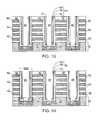
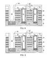
- FIG. 3Aillustrates a third exemplary device structure according to a third embodiment of the present disclosure.
- This embodimentdiffers from the embodiments of FIGS. 1A-1N and 2A-2D in that a semiconductor channel ( 60 , 64 ) includes a lower portion and an upper portion.
- the lower portion of the semiconductor channel ( 60 , 64 )is an epitaxial channel 64 , which is an epitaxial semiconductor (e.g., single crystal epitaxial silicon) pillar that is epitaxially grown from a surface of a single crystal semiconductor material in the substrate 8 .
- the upper portion of the semiconductor channel ( 60 , 64 )is a through-stack channel 60 as described above, and comprises a polycrystalline or amorphous semiconductor material (e.g., polysilicon).
- the through-stack channel 60 and the epitaxial channel 64can have a doping of the same conductivity type, i.e., either p-type, n-type, or intrinsic.
- Each epitaxial channel 64is formed directly on each physically exposed surface of single crystalline semiconductor material portions located within or on the semiconductor substrate 8 .
- Each single crystalline semiconductor material portionscan be a first electrode 12 or the substrate semiconductor layer 10 underlying a memory film 60 .
- the epitaxial channel 64 overlying the first electrode 12can be another single crystalline semiconductor material portion having a single crystalline structure that is in epitaxial alignment with the underlying single crystalline semiconductor material portion of the first electrode 12 .
- each first electrode 12is herein referred to as a first single crystalline semiconductor material portion
- each epitaxial channel 64is herein referred to as a second single crystalline semiconductor material portion.
- the first electrodes 12 and the epitaxial channel 64can have a doping of a same conductivity type, which can be p-type or n-type.
- the epitaxial channel 64can be formed, for example, by selective epitaxy.
- at least one semiconductor precursor gassuch as SiH 4 , Si 2 Cl 2 , SiCl 3 , SiCl 4 , Si 2 Cl 6 , or combinations thereof
- At least one etchant gassuch as HCl is flowed simultaneously or alternately into the process chamber.
- the ratio between the flow rate of the at least one semiconductor precursor gas and the flow rate of the at least one etchant gasis selected such that deposition of a semiconductor material occurs on crystalline surfaces such as the semiconductor surfaces of the first electrodes 12 or the substrate semiconductor layer 10 , while deposition of the semiconductor material on amorphous surfaces such as the surfaces of the various dielectric materials of the memory films 50 and the top surface of the alternating stack ( 32 , 42 , 82 ) is suppressed.
- the deposition of the semiconductor materialproceeds only from the top surface of the substrate exposed in the memory openings 49 .
- the process parameterscan be selected such that the epitaxial channels 64 can be single crystalline and in epitaxial alignment with the single crystalline structures of the substrate.
- Each of the epitaxial channels 64can be formed as a single crystalline semiconductor material portion directly on a single crystalline surface of the substrate 8 , and specifically on a single crystalline surface of a first electrode 12 or the substrate semiconductor layer 10 , by selective epitaxy.
- FIGS. 1I, 1J, and 1Kcan be performed to provide the third exemplary device structure illustrated in FIG. 3A .
- the semiconductor material layer 60 Cis formed directly on the epitaxial channels 64 .
- the thickness of the semiconductor material layer 60 Ccan be increased at the processing step of FIG. 1I to fill the entire volume of each cavity, and the processing step for formation of a core dielectric material layer can be eliminated to omit the dielectric cores 62 as in the first variation of the first exemplary device structure of FIG. 1L .
- the third exemplary device structure of FIG. 3Ais a three-dimensional memory device that includes a substrate 8 having a major surface 9 , and an alternating stack ( 32 , 42 , 82 ) of insulating material layers composed of the first material layers 32 and control gate electrodes composed of the second material layers 42 located over the substrate 8 .
- the alternating stackhas a memory opening 49 (See FIG. 1D ) extending through the alternating stack ( 32 , 42 , 83 ) in a direction substantially perpendicular to the major surface 9 .
- the third exemplary device structurefurther includes a memory film 50 located at a peripheral region of the memory opening 49 , and a semiconductor channel ( 60 , 64 ) including an upper portion extending substantially perpendicular to the major surface 9 and contacting an inner sidewall of the memory film 50 , and a lower portion (i.e., the epitaxial channel 64 ) contacting a single crystalline semiconductor material portion (such as a first electrode 12 or the substrate semiconductor layer 10 ) located on the substrate 8 .
- a sidewall of the upper portion (i.e., an upper portion of the through-stack channel 60 ) of the semiconductor channel ( 60 , 64 )can be laterally offset with respect to a sidewall of the lower portion (i.e., the epitaxial channel 64 ) of the semiconductor channel ( 60 , 64 ).
- An outer sidewall of the upper portion of the semiconductor channel ( 60 , 64 ) (i.e., the outer sidewall of the through-stack channel 60 ) in contact with a first portion of the memory film 50is laterally offset with respect to an outer sidewall of the lower portion of the semiconductor channel (i.e., the epitaxial channel 64 ) in contact with a second portion of the memory film 50 .
- the through-stack channel 69does not include a substantially contiguous interface extending along the vertical direction, i.e., along a direction parallel to an outer surface of the through-stack channel 60 .
- a contiguous surface composed of grain boundaries, and different from the outer surface of the through-substrate channel 60does not exist within the semiconductor channel ( 60 , 64 ).
- the semiconductor channel ( 60 , 64 ) including the through-stack channel 60does not include a substantially contiguous interface vertically extending through a plurality (e.g., at least 2, such as at least 5, such as all) of the control gate electrodes 42 within the alternating stack ( 32 , 42 ).
- the semiconductor channel ( 60 , 64 )does not include a substantially contiguous interface composed of grain boundaries, not contacting the memory film 50 , and vertically extending through the control gate electrodes 42 .
- a contiguous interface having a closed periphery and not having any hole thereinis present between a single crystalline doped semiconductor material portion (such as the epitaxial channels 64 ) and the through-stack channel 60 .
- the entirety of the closed peripheryis contained within surfaces of the memory film 50 and above a horizontal plane including a bottommost surface of the memory film 50 .
- a “closed periphery”is a periphery of a closed shape.
- the single crystalline doped semiconductor material portion located in the substrate 8can be a first electrode 12 or the substrate semiconductor layer 10 .
- the single crystalline doped semiconductor material portion of the epitaxial channels 64can be in epitaxial alignment with the single crystalline doped semiconductor material portion of the first electrode 12 or the substrate semiconductor layer.
- the amount of the deposited semiconductor materialcan be selected such that the topmost surface of an epitaxial channel 64 is formed above the horizontal plane including a top surface of a horizontal portion (the annular portion) of a memory film 50 .
- the epitaxial channels 64as a single crystalline doped semiconductor portion, includes a region that overlies a horizontal portion of the memory film 50 .
- the epitaxial channel 64can contact an inner sidewall of the memory film 50 , and the first electrode 12 can contact a bottommost surface of the memory film 50
- FIG. 3Billustrates a first alternative structure for the third exemplary device structure which contains shorter portions 64 than those in FIG. 3A .
- This devicecan be formed employing the methods for forming the third exemplary device structure illustrated in FIG. 3A with a reduction for the amount of the deposited semiconductor material for the epitaxial channels 64 .
- the topmost surface of an epitaxial channel 64can be formed below the horizontal plane including a top surface of a horizontal portion (the annular portion) of a memory film 50 .
- FIG. 3Cillustrates a second alternative structure for the third exemplary device structure.
- This embodimentincludes both the lateral recess of FIG. 2A and the portion 64 of FIG. 3A .
- This devicecan be formed forming the lateral recess shown in FIG. 2A , then removing the sacrificial material layers 57 , and then performing the selective epitaxy process employed to form the epitaxial channels 64 . Subsequently, the processing steps of FIGS. 1I, 1J, and 1K can be performed to provide the device structure illustrated in FIG. 3C .
- the second alternative structure for the third exemplary device structureis a three-dimensional memory device that includes a substrate 8 having a major surface 9 , and an alternating stack ( 32 , 42 , 82 ) of insulating material layers composed of the first material layers 32 and control gate electrodes composed of the second material layers 42 located over the substrate 8 .
- the alternating stackhas a memory opening 49 (See FIG. 1D ) extending through the alternating stack ( 32 , 42 , 83 ) in a direction substantially perpendicular to the major surface 9 .
- the second variation of the third exemplary device structurefurther includes a memory film 50 located at a peripheral region of the memory opening 49 , and a semiconductor channel ( 60 , 64 ) including an upper portion (i.e., an upper portion of the through-stack channel 60 ) extending substantially perpendicular to the major surface 9 and contacting an inner sidewall of the memory film 50 ; and a lower portion (i.e., the epitaxial channel 64 ) contacting a single crystalline doped semiconductor material portion (such as a first electrode 10 or the substrate semiconductor layer 10 ) located within the substrate 8 .
- a semiconductor channel60 , 64
- a sidewall of the upper portion (i.e., an upper portion of the through-stack channel 60 ) of the semiconductor channel ( 60 , 64 )can be laterally offset with respect to a sidewall of the lower portion (i.e., the epitaxial channel 64 ) of the semiconductor channel ( 60 , 64 ).
- an outer sidewall of the upper portion of the semiconductor channel ( 60 , 64 ) (i.e., the outer sidewall of the through-stack channel 60 ) in contact with a first portion of the memory film 50is laterally offset with respect to an outer sidewall of the lower portion of the semiconductor channel (i.e., the epitaxial channel 64 ) in contact with a second portion of the memory film 50 .
- the epitaxial channel 64can be in contact with a bottom portion of the through-stack channel 60 .
- the through-stack channel 69does not include a substantially contiguous interface extending along the vertical direction, i.e., along a direction parallel to an outer surface of the through-stack channel 60 .
- a contiguous surface composed of grain boundaries and different from the outer surface of the through-substrate channel 60does not exist within the semiconductor channel ( 60 , 64 ).
- the semiconductor channel ( 60 , 64 ) including the through-stack channel 60does not include a substantially contiguous interface vertically extending through a plurality (such as at least 2, such as at least 5, such as all) of the control gate electrodes 42 within the alternating stack ( 32 , 42 ).
- the semiconductor channel ( 60 , 64 )does not include a substantially contiguous interface composed of grain boundaries, not contacting the memory film 50 , and vertically extending through the semiconductor channel between a plurality of the control gate electrodes 42 .
- a bottom portion of the memory film 50includes the second inner sidewall 51 on an inner side and an outer sidewall 53 on an outer side.
- a sidewall of the single crystalline doped semiconductor material portioncontacts the second inner sidewall 51 of the memory film 50 .
- the single crystalline doped semiconductor material portion of the epitaxial channels 64contacts a top surface of another single crystalline doped semiconductor material portion of a first electrode 12 within the substrate 8 .
- FIG. 3Dillustrates a third alternative structure for the third exemplary device structure.
- This embodimentincludes both vertical substrate recess of FIGS. 1M and 1N and the portion 64 of FIG. 3A , optionally the lateral recess of FIG. 2A .
- a this devicemay be formed by performing the lateral recess of FIG. 2A , followed by performing the vertical recess of FIG. 1M and then performing the selective epitaxy process employed to form the epitaxial channels 64 of FIG. 3A .
- the vertical recess of FIG. 1Mmay be performed firm followed by subsequently performing the processing steps of FIG. 2A (i.e., the lateral etching of horizontal portions of the memory films 50 employing the sacrificial material layers 57 as an etch mask), followed by the selective epitaxy process employed to form the epitaxial channels 64 .
- each single crystalline doped semiconductor material portion of the epitaxial channels 64contacts two top surfaces of another single crystalline doped semiconductor material portion of the substrate 8 .
- the two top surfaces of the first substrate 8are vertically offset from each other.
- dielectric core 62may be omitted in the devices of FIGS. 3A-3D as described above with respect to FIG. 1L .
- the various embodiments of the present disclosureis compatible with embodiments in which an alternating stack is initially formed as a stack including insulating material layers as the first material layers 32 and sacrificial material layers as the second material layers 42 .
- the sacrificial material layersoccupy the volumes of the control gate electrodes to be subsequently formed.
- the sacrificial material layerscan be replaced with control gate electrodes including a conductive material at a subsequent processing step, which can be, for example, after formation of the semiconductor channels and prior to, or after, formation of the second electrodes 72 . All such variations are expressly contemplated herein.
- control gate electrodes, and optionally the blocking dielectric and/or the charge storage region(s)may be formed by a replacement process through a back side opening 84 , as shown in FIGS. 4-11 . While the present disclosure is described employing an embodiment in which the first electrodes 12 are formed directly underneath the memory openings, embodiments are expressly contemplated herein in which the first electrodes (e.g., source or drain regions) are laterally offset from the memory openings, as described below.
- FIG. 4illustrates an exemplary device structure following the filling of the memory openings and formation of the second electrodes and the top dielectric layer 70 according to any of the embodiments above.
- the second electrodes 72can be recessed relative to the top surface of the alternating stack ( 32 , 42 ), or can be formed on the top surface of the alternating stack ( 32 , 42 ).
- the top surfaces of the second electrodes 72may be physically exposed, or may be covered by the top dielectric layer 72 , which can function as a hard mask layer.
- the second electrodes 72may function as a source region or as a drain region of a vertical memory device. As shown in FIG.
- a back side opening 84(e.g., a slit trench) is then formed through the alternating stack ( 32 , 42 ) by any suitable lithography and etching steps.
- a surface of the substrate 8can be physically exposed at the bottom of the back side opening 84 .
- the physically exposed surfacecan be a surface of a doped well, which can be, for example, a p-type doped well (p-well) located in the substrate 8 .
- a source/drain region 14may be formed in the substrate semiconductor layer 10 in the substrate 8 by ion implantation through the back side opening 84 .
- the source/drain region 14may be a source region, and can have an opposite conductivity type (e.g., n-type) to that of the substrate semiconductor layer 10 (e.g., a p-type well) and the semiconductor channel ( 60 and optionally 64 ).
- the channel of the memory devicecan have a vertical portion including the through-stack channel 60 (and optionally an epitaxial channel 64 ) and a horizontal portion in the substrate semiconductor layer 10 and extending between the source/drain region 14 and the bottommost portion of the semiconductor channel ( 60 and optionally 64 ).
- the sacrificial material layers(embodied as the second material layers 42 ) can be removed through the back side openings 84 to form back side recesses 86 between vertically adjacent pairs of the first material layers 32 , as shown in FIG. 5 .
- the filled-in memory holes(each of which contains a memory film, a through-stack channel 60 , and optionally a dielectric core 62 ) function as supporting structural elements ensuring mechanical stability of the remainder of the alternating material stack.
- the second material layers 42may be removed by selective etching, such as a silicon nitride selective etching which removes silicon nitride but does not remove the silicon oxide.
- the selective etchmay stop on oxide-based dielectric materials such as the surface dielectric portions 82 , if present, or the blocking dielectrics 52 (See FIG. 1K ), which form the outer parts of the memory films 50 .
- an additional blocking dielectricmay be formed from the back side in the back side recesses 86 in addition to, or in lieu of, the surface dielectric portions 82 and/or in addition to, or in lieu of, any remaining portion of the blocking dielectrics 52 prior to forming the control gate electrodes 3 by deposition of a conductive material in the back side recesses 86 .
- forming the blocking dielectric layercomprises forming the blocking dielectric layer in the back side opening 84 and in the back side recesses 86 .
- the at least one charge storage region 54may be formed through either the front side memory opening 49 or the back side opening 84 .
- the step of forming the at least one charge storage regioncan comprise at least one of forming the at least one charge storage region prior to forming the blocking dielectric layer in the back side opening, and/or forming the at least one charge storage region 54 over the pre-existing blocking dielectric 56 in the front side memory opening 49 , or over the sidewall in the front side memory opening 49 (if the blocking dielectric is formed through the back side opening 84 ).
- a conductive material comprising at least one metal and/or at least one metal alloycan be deposited to form a contiguous conductive material portion 88 , which includes control gate electrodes 3 .
- the control gate electrodes 3are formed in the back side recesses 86 through the back side openings 84 , as shown in FIG. 6 .
- the control gate electrodes 3 of the contiguous conductive material portion 88can fully fill the back side recesses 86 (See FIG. 5 ), and portions of the contiguous conductive material portion 88 other than the control gate electrodes 3 can partially or fully fill the back side openings 84 (e.g., trenches) and overlie the top dielectric layer 70 .
- the conductive material of the control gate electrodes 3may comprise any suitable materials for the second material layers 42 in embodiments in which the second material layers 42 includes a conductive material as described above.
- the conductive materialmay comprise a TiN liner or another barrier martial, and additionally tungsten. If a blocking dielectric layer is formed the back side recesses 86 through the back side opening 84 , then the control gate electrodes 3 are formed over the blocking dielectric layer in the back side recesses 86 .
- sub-portions of the contiguous conductive material portion 88 other than the control gate electrodes 3are removed from the back side openings 84 (e.g., trenches) and from over the top dielectric layer 70 by at least one etch, which can be an isotropic etch or a combination of an isotropic etch and an anisotropic etch.
- the deposited conductive material of the contiguous conductive material portion 88is removed without removing the control gate electrodes 3 to complete the formation of the control gate electrodes 3 .
- select gate electrodesmay be formed above and below the control gate electrodes 3 at the same time or during a different step.
- An insulating layer 90 Lsuch as a silicon oxide layer, is formed on sidewalls and bottom of the back side trenches 84 and over the top dielectric layer 70 , as shown in FIG. 8 .
- Each horizontal portion of the insulating layer 90 Lis then removed from the bottom 84 a of the back side trench 84 and from above the top dielectric layer 70 by anisotropic etching (e.g., by RIE spacer etch).
- the remaining portion of the insulating layer 90 L on the sidewalls of the trench 84constitutes an insulator spacer 90 .
- This etching stepexposes p-well 10 through the bottom 84 a of the trench 84 .
- a substrate electrode contact layer 94 Lcan then be formed in the back side trench 84 directly on the source/drain region 14 in the substrate semiconductor layer 10 (which can be, for example, a p-well) in the substrate 8 , as shown in FIG. 10 .
- the substrate electrode contact 94 Lmay be formed by depositing any suitable metal or metal alloy layers, such as TiN, ruthenium, and/or tungsten over layer 90 in the back side trench 84 .
- the portion of the substrate electrode contact layer 94 L located over the top dielectric layer 70can be removed by CMP or etching to leave a substrate electrode contact 94 in the dielectrically insulated trench 84 , as shown in FIG. 11 . If the source/drain region 14 is a source region, the substrate electrode contact 94 can be a source contact.
Landscapes
- Engineering & Computer Science (AREA)
- Microelectronics & Electronic Packaging (AREA)
- Semiconductor Memories (AREA)
- Non-Volatile Memory (AREA)
Abstract
Description
Claims (16)
Priority Applications (1)
| Application Number | Priority Date | Filing Date | Title |
|---|---|---|---|
| US14/972,618US9799669B2 (en) | 2013-09-15 | 2015-12-17 | Single-semiconductor-layer channel in a memory opening for a three-dimensional non-volatile memory device |
Applications Claiming Priority (5)
| Application Number | Priority Date | Filing Date | Title |
|---|---|---|---|
| US201361878023P | 2013-09-15 | 2013-09-15 | |
| US201361879071P | 2013-09-17 | 2013-09-17 | |
| US201461977193P | 2014-04-09 | 2014-04-09 | |
| US14/462,156US9230980B2 (en) | 2013-09-15 | 2014-08-18 | Single-semiconductor-layer channel in a memory opening for a three-dimensional non-volatile memory device |
| US14/972,618US9799669B2 (en) | 2013-09-15 | 2015-12-17 | Single-semiconductor-layer channel in a memory opening for a three-dimensional non-volatile memory device |
Related Parent Applications (1)
| Application Number | Title | Priority Date | Filing Date |
|---|---|---|---|
| US14/462,156DivisionUS9230980B2 (en) | 2013-09-15 | 2014-08-18 | Single-semiconductor-layer channel in a memory opening for a three-dimensional non-volatile memory device |
Publications (2)
| Publication Number | Publication Date |
|---|---|
| US20160111432A1 US20160111432A1 (en) | 2016-04-21 |
| US9799669B2true US9799669B2 (en) | 2017-10-24 |
Family
ID=51663438
Family Applications (2)
| Application Number | Title | Priority Date | Filing Date |
|---|---|---|---|
| US14/462,156ActiveUS9230980B2 (en) | 2013-09-15 | 2014-08-18 | Single-semiconductor-layer channel in a memory opening for a three-dimensional non-volatile memory device |
| US14/972,618ActiveUS9799669B2 (en) | 2013-09-15 | 2015-12-17 | Single-semiconductor-layer channel in a memory opening for a three-dimensional non-volatile memory device |
Family Applications Before (1)
| Application Number | Title | Priority Date | Filing Date |
|---|---|---|---|
| US14/462,156ActiveUS9230980B2 (en) | 2013-09-15 | 2014-08-18 | Single-semiconductor-layer channel in a memory opening for a three-dimensional non-volatile memory device |
Country Status (2)
| Country | Link |
|---|---|
| US (2) | US9230980B2 (en) |
| WO (1) | WO2015038427A1 (en) |
Cited By (8)
| Publication number | Priority date | Publication date | Assignee | Title |
|---|---|---|---|---|
| CN110534519A (en)* | 2018-05-27 | 2019-12-03 | 杭州海存信息技术有限公司 | Improved three-dimensional longitudinal memory |
| US10784281B2 (en) | 2018-10-26 | 2020-09-22 | Samsung Electronics Co., Ltd. | Three-dimensional semiconductor memory devices |
| US10991705B2 (en) | 2019-07-30 | 2021-04-27 | Sandisk Technologies Llc | Three-dimensional memory device having enhanced contact between polycrystalline channel and epitaxial pedestal structure and method of making the same |
| US10991706B2 (en) | 2019-07-30 | 2021-04-27 | Sandisk Technologies Llc | Three-dimensional memory device having enhanced contact between polycrystalline channel and epitaxial pedestal structure and method of making the same |
| US10991718B2 (en) | 2019-07-30 | 2021-04-27 | Sandisk Technologies Llc | Three-dimensional memory device containing a vertical semiconductor channel containing a connection strap and method of making the same |
| US11024645B2 (en) | 2019-07-30 | 2021-06-01 | Sandisk Technologies Llc | Three-dimensional memory device containing a silicon nitride ring in an opening in a memory film and method of making the same |
| US11171150B2 (en) | 2019-03-07 | 2021-11-09 | Sandisk Technologies Llc | Three-dimensional memory device containing a channel connection strap and method for making the same |
| US20230171962A1 (en)* | 2016-04-15 | 2023-06-01 | Micron Technology, Inc. | Integrated Structures Comprising Vertical Channel Material and Having Conductively-Doped Semiconductor Material Directly Against Lower Sidewalls of the Channel Material |
Families Citing this family (214)
| Publication number | Priority date | Publication date | Assignee | Title |
|---|---|---|---|---|
| US9324576B2 (en) | 2010-05-27 | 2016-04-26 | Applied Materials, Inc. | Selective etch for silicon films |
| US10283321B2 (en) | 2011-01-18 | 2019-05-07 | Applied Materials, Inc. | Semiconductor processing system and methods using capacitively coupled plasma |
| US8999856B2 (en) | 2011-03-14 | 2015-04-07 | Applied Materials, Inc. | Methods for etch of sin films |
| US9064815B2 (en) | 2011-03-14 | 2015-06-23 | Applied Materials, Inc. | Methods for etch of metal and metal-oxide films |
| US9267739B2 (en) | 2012-07-18 | 2016-02-23 | Applied Materials, Inc. | Pedestal with multi-zone temperature control and multiple purge capabilities |
| US9373517B2 (en) | 2012-08-02 | 2016-06-21 | Applied Materials, Inc. | Semiconductor processing with DC assisted RF power for improved control |
| US9132436B2 (en) | 2012-09-21 | 2015-09-15 | Applied Materials, Inc. | Chemical control features in wafer process equipment |
| US10256079B2 (en) | 2013-02-08 | 2019-04-09 | Applied Materials, Inc. | Semiconductor processing systems having multiple plasma configurations |
| US9362130B2 (en) | 2013-03-01 | 2016-06-07 | Applied Materials, Inc. | Enhanced etching processes using remote plasma sources |
| US20140271097A1 (en) | 2013-03-15 | 2014-09-18 | Applied Materials, Inc. | Processing systems and methods for halide scavenging |
| US9773648B2 (en) | 2013-08-30 | 2017-09-26 | Applied Materials, Inc. | Dual discharge modes operation for remote plasma |
| US9576809B2 (en) | 2013-11-04 | 2017-02-21 | Applied Materials, Inc. | Etch suppression with germanium |
| US9520303B2 (en) | 2013-11-12 | 2016-12-13 | Applied Materials, Inc. | Aluminum selective etch |
| US9093387B1 (en)* | 2014-01-08 | 2015-07-28 | International Business Machines Corporation | Metallic mask patterning process for minimizing collateral etch of an underlayer |
| KR20150096582A (en)* | 2014-02-14 | 2015-08-25 | 에스케이하이닉스 주식회사 | Transistor, semiconductor device and method of manufacturing the same |
| US9299537B2 (en) | 2014-03-20 | 2016-03-29 | Applied Materials, Inc. | Radial waveguide systems and methods for post-match control of microwaves |
| US9903020B2 (en) | 2014-03-31 | 2018-02-27 | Applied Materials, Inc. | Generation of compact alumina passivation layers on aluminum plasma equipment components |
| US9309598B2 (en) | 2014-05-28 | 2016-04-12 | Applied Materials, Inc. | Oxide and metal removal |
| US9379124B2 (en)* | 2014-06-25 | 2016-06-28 | Sandisk Technologies Inc. | Vertical floating gate NAND with selectively deposited ALD metal films |
| US9496167B2 (en) | 2014-07-31 | 2016-11-15 | Applied Materials, Inc. | Integrated bit-line airgap formation and gate stack post clean |
| US20160042968A1 (en)* | 2014-08-05 | 2016-02-11 | Applied Materials, Inc. | Integrated oxide and si etch for 3d cell channel mobility improvements |
| US9659753B2 (en) | 2014-08-07 | 2017-05-23 | Applied Materials, Inc. | Grooved insulator to reduce leakage current |
| US9553102B2 (en)* | 2014-08-19 | 2017-01-24 | Applied Materials, Inc. | Tungsten separation |
| US9412749B1 (en) | 2014-09-19 | 2016-08-09 | Sandisk Technologies Llc | Three dimensional memory device having well contact pillar and method of making thereof |
| US9613822B2 (en) | 2014-09-25 | 2017-04-04 | Applied Materials, Inc. | Oxide etch selectivity enhancement |
| US9711522B2 (en)* | 2014-10-03 | 2017-07-18 | Sandisk Technologies Llc | Memory hole structure in three dimensional memory |
| US9966240B2 (en) | 2014-10-14 | 2018-05-08 | Applied Materials, Inc. | Systems and methods for internal surface conditioning assessment in plasma processing equipment |
| US9355922B2 (en) | 2014-10-14 | 2016-05-31 | Applied Materials, Inc. | Systems and methods for internal surface conditioning in plasma processing equipment |
| US9305937B1 (en)* | 2014-10-21 | 2016-04-05 | Sandisk Technologies Inc. | Bottom recess process for an outer blocking dielectric layer inside a memory opening |
| US9780102B2 (en)* | 2014-11-07 | 2017-10-03 | Micron Technology, Inc. | Memory cell pillar including source junction plug |
| EP3221884B1 (en)* | 2014-11-18 | 2022-06-01 | GlobalWafers Co., Ltd. | High resistivity semiconductor-on-insulator wafers with charge trapping layers and method of manufacturing thereof |
| US11637002B2 (en) | 2014-11-26 | 2023-04-25 | Applied Materials, Inc. | Methods and systems to enhance process uniformity |
| US10224210B2 (en) | 2014-12-09 | 2019-03-05 | Applied Materials, Inc. | Plasma processing system with direct outlet toroidal plasma source |
| US10573496B2 (en) | 2014-12-09 | 2020-02-25 | Applied Materials, Inc. | Direct outlet toroidal plasma source |
| US9484357B2 (en)* | 2014-12-16 | 2016-11-01 | Sandisk Technologies Llc | Selective blocking dielectric formation in a three-dimensional memory structure |
| US11257693B2 (en) | 2015-01-09 | 2022-02-22 | Applied Materials, Inc. | Methods and systems to improve pedestal temperature control |
| US20160225652A1 (en) | 2015-02-03 | 2016-08-04 | Applied Materials, Inc. | Low temperature chuck for plasma processing systems |
| US9728437B2 (en) | 2015-02-03 | 2017-08-08 | Applied Materials, Inc. | High temperature chuck for plasma processing systems |
| US9881805B2 (en) | 2015-03-02 | 2018-01-30 | Applied Materials, Inc. | Silicon selective removal |
| US10068914B2 (en)* | 2015-04-17 | 2018-09-04 | Macronix International Co., Ltd. | Semiconductor structure and manufacturing method of the same |
| CN106158777B (en)* | 2015-04-23 | 2019-09-03 | 旺宏电子股份有限公司 | Semiconductor structure and manufacturing method thereof |
| CN106298787B (en)* | 2015-06-11 | 2020-01-14 | 旺宏电子股份有限公司 | Memory element and method for manufacturing the same |
| US9589981B2 (en)* | 2015-06-15 | 2017-03-07 | Sandisk Technologies Llc | Passive devices for integration with three-dimensional memory devices |
| US9530784B1 (en)* | 2015-06-18 | 2016-12-27 | Macronix International Co., Ltd. | Memory device and method for fabricating the same |
| US9741593B2 (en) | 2015-08-06 | 2017-08-22 | Applied Materials, Inc. | Thermal management systems and methods for wafer processing systems |
| US9691645B2 (en) | 2015-08-06 | 2017-06-27 | Applied Materials, Inc. | Bolted wafer chuck thermal management systems and methods for wafer processing systems |
| US9349605B1 (en) | 2015-08-07 | 2016-05-24 | Applied Materials, Inc. | Oxide etch selectivity systems and methods |
| US9741732B2 (en) | 2015-08-19 | 2017-08-22 | Micron Technology, Inc. | Integrated structures |
| US10504700B2 (en) | 2015-08-27 | 2019-12-10 | Applied Materials, Inc. | Plasma etching systems and methods with secondary plasma injection |
| US20170062456A1 (en)* | 2015-08-31 | 2017-03-02 | Cypress Semiconductor Corporation | Vertical division of three-dimensional memory device |
| KR102424370B1 (en)* | 2015-10-08 | 2022-07-22 | 삼성전자주식회사 | Vertical type semiconductor devices and methods of manufacturing the same |
| CN105374826B (en)* | 2015-10-20 | 2019-01-15 | 中国科学院微电子研究所 | Three-dimensional semiconductor device and method for manufacturing the same |
| US9620512B1 (en) | 2015-10-28 | 2017-04-11 | Sandisk Technologies Llc | Field effect transistor with a multilevel gate electrode for integration with a multilevel memory device |
| US9842851B2 (en)* | 2015-10-30 | 2017-12-12 | Sandisk Technologies Llc | Three-dimensional memory devices having a shaped epitaxial channel portion |
| US9754958B2 (en) | 2015-10-30 | 2017-09-05 | Sandisk Technologies Llc | Three-dimensional memory devices having a shaped epitaxial channel portion and method of making thereof |
| CN108140643B (en)* | 2015-11-20 | 2022-03-15 | 桑迪士克科技有限责任公司 | Three-dimensional NAND device including support pedestal structure for buried source line and method of fabricating the same |
| US9705071B2 (en)* | 2015-11-24 | 2017-07-11 | International Business Machines Corporation | Structure and method to reduce shorting and process degradation in STT-MRAM devices |
| JP2017107938A (en)* | 2015-12-08 | 2017-06-15 | 株式会社東芝 | Semiconductor device and method of manufacturing the same |
| JP6514138B2 (en)* | 2016-03-10 | 2019-05-15 | 東芝メモリ株式会社 | Semiconductor device manufacturing method |
| US9748262B1 (en) | 2016-04-13 | 2017-08-29 | Macronix International Co., Ltd. | Memory structure and manufacturing method of the same |
| CN107302006B (en)* | 2016-04-13 | 2020-01-07 | 旺宏电子股份有限公司 | Memory structure and method of making the same |
| TWI605548B (en)* | 2016-05-04 | 2017-11-11 | 旺宏電子股份有限公司 | Memory structure and manufacturing method thereof |
| US10522371B2 (en) | 2016-05-19 | 2019-12-31 | Applied Materials, Inc. | Systems and methods for improved semiconductor etching and component protection |
| US10504754B2 (en) | 2016-05-19 | 2019-12-10 | Applied Materials, Inc. | Systems and methods for improved semiconductor etching and component protection |
| US10121794B2 (en)* | 2016-06-20 | 2018-11-06 | Sandisk Technologies Llc | Three-dimensional memory device having epitaxial germanium-containing vertical channel and method of making thereof |
| US9978768B2 (en)* | 2016-06-29 | 2018-05-22 | Sandisk Technologies Llc | Method of making three-dimensional semiconductor memory device having laterally undulating memory films |
| US9865484B1 (en) | 2016-06-29 | 2018-01-09 | Applied Materials, Inc. | Selective etch using material modification and RF pulsing |
| US9576967B1 (en)* | 2016-06-30 | 2017-02-21 | Sandisk Technologies Llc | Method of suppressing epitaxial growth in support openings and three-dimensional memory device containing non-epitaxial support pillars in the support openings |
| US9991328B2 (en) | 2016-08-25 | 2018-06-05 | International Business Machines Corporation | Tunable on-chip nanosheet resistor |
| US10629473B2 (en) | 2016-09-09 | 2020-04-21 | Applied Materials, Inc. | Footing removal for nitride spacer |
| US10062575B2 (en) | 2016-09-09 | 2018-08-28 | Applied Materials, Inc. | Poly directional etch by oxidation |
| US9934942B1 (en) | 2016-10-04 | 2018-04-03 | Applied Materials, Inc. | Chamber with flow-through source |
| US9721789B1 (en) | 2016-10-04 | 2017-08-01 | Applied Materials, Inc. | Saving ion-damaged spacers |
| US10546729B2 (en) | 2016-10-04 | 2020-01-28 | Applied Materials, Inc. | Dual-channel showerhead with improved profile |
| US10062585B2 (en) | 2016-10-04 | 2018-08-28 | Applied Materials, Inc. | Oxygen compatible plasma source |
| KR102636463B1 (en) | 2016-10-05 | 2024-02-14 | 삼성전자주식회사 | Semiconductor memory device |
| US10062579B2 (en) | 2016-10-07 | 2018-08-28 | Applied Materials, Inc. | Selective SiN lateral recess |
| US9911754B1 (en)* | 2016-10-07 | 2018-03-06 | Macronix International Co., Ltd. | 3D memory structure |
| US9947549B1 (en) | 2016-10-10 | 2018-04-17 | Applied Materials, Inc. | Cobalt-containing material removal |
| US9941293B1 (en) | 2016-10-12 | 2018-04-10 | Sandisk Technologies Llc | Select transistors with tight threshold voltage in 3D memory |
| US9768034B1 (en) | 2016-11-11 | 2017-09-19 | Applied Materials, Inc. | Removal methods for high aspect ratio structures |
| US10163696B2 (en) | 2016-11-11 | 2018-12-25 | Applied Materials, Inc. | Selective cobalt removal for bottom up gapfill |
| US10026621B2 (en) | 2016-11-14 | 2018-07-17 | Applied Materials, Inc. | SiN spacer profile patterning |
| US10242908B2 (en) | 2016-11-14 | 2019-03-26 | Applied Materials, Inc. | Airgap formation with damage-free copper |
| US9972641B1 (en)* | 2016-11-17 | 2018-05-15 | Sandisk Technologies Llc | Three-dimensional memory device having a multilevel drain select gate electrode and method of making thereof |
| US10083982B2 (en)* | 2016-11-17 | 2018-09-25 | Sandisk Technologies Llc | Three-dimensional memory device having select gate electrode that is thicker than word lines and method of making thereof |
| KR102686930B1 (en) | 2016-12-19 | 2024-07-19 | 삼성전자주식회사 | Vertical structure non-volatile memory device and method for manufacturing the same |
| US10566206B2 (en) | 2016-12-27 | 2020-02-18 | Applied Materials, Inc. | Systems and methods for anisotropic material breakthrough |
| US10074666B2 (en)* | 2017-01-09 | 2018-09-11 | Sandisk Technologies Llc | Three-dimensional memory device with enhanced mechanical stability semiconductor pedestal and method of making thereof |
| US9853038B1 (en) | 2017-01-20 | 2017-12-26 | Sandisk Technologies Llc | Three-dimensional memory device having integrated support and contact structures and method of making thereof |
| US10084081B2 (en) | 2017-01-23 | 2018-09-25 | International Business Machines Corporation | Vertical transistor with enhanced drive current |
| US10431429B2 (en) | 2017-02-03 | 2019-10-01 | Applied Materials, Inc. | Systems and methods for radial and azimuthal control of plasma uniformity |
| US10403507B2 (en) | 2017-02-03 | 2019-09-03 | Applied Materials, Inc. | Shaped etch profile with oxidation |
| US10043684B1 (en) | 2017-02-06 | 2018-08-07 | Applied Materials, Inc. | Self-limiting atomic thermal etching systems and methods |
| US10319739B2 (en) | 2017-02-08 | 2019-06-11 | Applied Materials, Inc. | Accommodating imperfectly aligned memory holes |
| US10020314B1 (en)* | 2017-03-02 | 2018-07-10 | Sandisk Technologies Llc | Forming memory cell film in stack opening |
| CN106847821B (en)* | 2017-03-07 | 2018-09-14 | 长江存储科技有限责任公司 | Semiconductor structure and forming method thereof |
| US10943834B2 (en) | 2017-03-13 | 2021-03-09 | Applied Materials, Inc. | Replacement contact process |
| US10319649B2 (en) | 2017-04-11 | 2019-06-11 | Applied Materials, Inc. | Optical emission spectroscopy (OES) for remote plasma monitoring |
| CN108807408B (en)* | 2017-05-02 | 2020-12-11 | 旺宏电子股份有限公司 | Manufacturing method of semiconductor structure |
| US11276590B2 (en) | 2017-05-17 | 2022-03-15 | Applied Materials, Inc. | Multi-zone semiconductor substrate supports |
| US11276559B2 (en) | 2017-05-17 | 2022-03-15 | Applied Materials, Inc. | Semiconductor processing chamber for multiple precursor flow |
| JP7176860B6 (en) | 2017-05-17 | 2022-12-16 | アプライド マテリアルズ インコーポレイテッド | Semiconductor processing chamber to improve precursor flow |
| US10497579B2 (en) | 2017-05-31 | 2019-12-03 | Applied Materials, Inc. | Water-free etching methods |
| US10049891B1 (en) | 2017-05-31 | 2018-08-14 | Applied Materials, Inc. | Selective in situ cobalt residue removal |
| US10920320B2 (en) | 2017-06-16 | 2021-02-16 | Applied Materials, Inc. | Plasma health determination in semiconductor substrate processing reactors |
| US10224340B2 (en)* | 2017-06-19 | 2019-03-05 | Sandisk Technologies Llc | Three-dimensional memory device having discrete direct source strap contacts and method of making thereof |
| US10115730B1 (en) | 2017-06-19 | 2018-10-30 | Sandisk Technologies Llc | Three-dimensional memory device containing structurally reinforced pedestal channel portions and method of making thereof |
| US10541246B2 (en) | 2017-06-26 | 2020-01-21 | Applied Materials, Inc. | 3D flash memory cells which discourage cross-cell electrical tunneling |
| US10727080B2 (en) | 2017-07-07 | 2020-07-28 | Applied Materials, Inc. | Tantalum-containing material removal |
| US10541184B2 (en) | 2017-07-11 | 2020-01-21 | Applied Materials, Inc. | Optical emission spectroscopic techniques for monitoring etching |
| US10354889B2 (en) | 2017-07-17 | 2019-07-16 | Applied Materials, Inc. | Non-halogen etching of silicon-containing materials |
| US10043674B1 (en) | 2017-08-04 | 2018-08-07 | Applied Materials, Inc. | Germanium etching systems and methods |
| US10170336B1 (en) | 2017-08-04 | 2019-01-01 | Applied Materials, Inc. | Methods for anisotropic control of selective silicon removal |
| US10297458B2 (en) | 2017-08-07 | 2019-05-21 | Applied Materials, Inc. | Process window widening using coated parts in plasma etch processes |
| US10522561B2 (en) | 2017-08-23 | 2019-12-31 | Yangtze Memory Technologies Co., Ltd. | Method for forming a three-dimensional memory device |
| CN107464817B (en)* | 2017-08-23 | 2018-09-18 | 长江存储科技有限责任公司 | A kind of production method of 3D nand flash memories |
| CN107591405B (en)* | 2017-08-31 | 2018-12-25 | 长江存储科技有限责任公司 | A kind of preparation method and three-dimensional storage of three-dimensional storage channel |
| CN107507772B (en)* | 2017-08-31 | 2021-03-19 | 长江存储科技有限责任公司 | A kind of channel hole bottom etching method |
| KR102452612B1 (en)* | 2017-09-11 | 2022-10-11 | 삼성전자주식회사 | Semiconductor memory devices and methods of fabricating the same |
| US10290647B2 (en) | 2017-09-26 | 2019-05-14 | Sandisk Technologies Llc | Three-dimensional memory device containing structurally reinforced pedestal channel portions and method of making the same |
| US10551166B2 (en)* | 2017-10-11 | 2020-02-04 | Kla-Tencor Corporation | Optical measurement of a highly absorbing film layer over highly reflective film stacks |
| US10128086B1 (en) | 2017-10-24 | 2018-11-13 | Applied Materials, Inc. | Silicon pretreatment for nitride removal |
| US10283324B1 (en) | 2017-10-24 | 2019-05-07 | Applied Materials, Inc. | Oxygen treatment for nitride etching |
| KR102344895B1 (en)* | 2017-11-13 | 2021-12-29 | 삼성전자주식회사 | Vertical semiconductor devices and methods of manufacturing the same |
| KR102524808B1 (en) | 2017-11-21 | 2023-04-24 | 삼성전자주식회사 | Semiconductor device |
| CN107946313A (en)* | 2017-11-21 | 2018-04-20 | 长江存储科技有限责任公司 | The preparation method and 3D nand flash memories of a kind of 3D nand flash memories stacked structure |
| US10256112B1 (en) | 2017-12-08 | 2019-04-09 | Applied Materials, Inc. | Selective tungsten removal |
| KR102533146B1 (en) | 2017-12-08 | 2023-05-18 | 삼성전자주식회사 | Three-dimensional semiconductor devices and method for fabricating the same |
| US10256252B1 (en) | 2017-12-13 | 2019-04-09 | Sandisk Technologies Llc | Three-dimensional memory device containing structurally reinforced pedestal channel portions and methods of making the same |
| US10903054B2 (en) | 2017-12-19 | 2021-01-26 | Applied Materials, Inc. | Multi-zone gas distribution systems and methods |
| US11328909B2 (en) | 2017-12-22 | 2022-05-10 | Applied Materials, Inc. | Chamber conditioning and removal processes |
| US10854426B2 (en) | 2018-01-08 | 2020-12-01 | Applied Materials, Inc. | Metal recess for semiconductor structures |
| US10373969B2 (en)* | 2018-01-09 | 2019-08-06 | Sandisk Technologies Llc | Three-dimensional memory device including partially surrounding select gates and fringe field assisted programming thereof |
| US10892267B2 (en) | 2018-02-15 | 2021-01-12 | Sandisk Technologies Llc | Three-dimensional memory device containing through-memory-level contact via structures and method of making the same |
| US10679870B2 (en) | 2018-02-15 | 2020-06-09 | Applied Materials, Inc. | Semiconductor processing chamber multistage mixing apparatus |
| US10971507B2 (en) | 2018-02-15 | 2021-04-06 | Sandisk Technologies Llc | Three-dimensional memory device containing through-memory-level contact via structures |
| US10964512B2 (en) | 2018-02-15 | 2021-03-30 | Applied Materials, Inc. | Semiconductor processing chamber multistage mixing apparatus and methods |
| US10727248B2 (en) | 2018-02-15 | 2020-07-28 | Sandisk Technologies Llc | Three-dimensional memory device containing through-memory-level contact via structures |
| US10903230B2 (en) | 2018-02-15 | 2021-01-26 | Sandisk Technologies Llc | Three-dimensional memory device containing through-memory-level contact via structures and method of making the same |
| TWI766433B (en) | 2018-02-28 | 2022-06-01 | 美商應用材料股份有限公司 | Systems and methods to form airgaps |
| US10593560B2 (en) | 2018-03-01 | 2020-03-17 | Applied Materials, Inc. | Magnetic induction plasma source for semiconductor processes and equipment |
| US10319600B1 (en) | 2018-03-12 | 2019-06-11 | Applied Materials, Inc. | Thermal silicon etch |
| US10497573B2 (en) | 2018-03-13 | 2019-12-03 | Applied Materials, Inc. | Selective atomic layer etching of semiconductor materials |
| US10269820B1 (en) | 2018-04-03 | 2019-04-23 | Sandisk Technologies Llc | Three-dimensional memory device containing different pedestal width support pillar structures and method of making the same |
| US10573527B2 (en) | 2018-04-06 | 2020-02-25 | Applied Materials, Inc. | Gas-phase selective etching systems and methods |
| US10490406B2 (en) | 2018-04-10 | 2019-11-26 | Appled Materials, Inc. | Systems and methods for material breakthrough |
| US10756186B2 (en) | 2018-04-12 | 2020-08-25 | Sandisk Technologies Llc | Three-dimensional memory device including germanium-containing vertical channels and method of making the same |
| US10699879B2 (en) | 2018-04-17 | 2020-06-30 | Applied Materials, Inc. | Two piece electrode assembly with gap for plasma control |
| WO2019200561A1 (en) | 2018-04-18 | 2019-10-24 | Yangtze Memory Technologies Co., Ltd. | Method for forming channel hole plug of three-dimensional memory device |
| US10886137B2 (en) | 2018-04-30 | 2021-01-05 | Applied Materials, Inc. | Selective nitride removal |
| US10755941B2 (en) | 2018-07-06 | 2020-08-25 | Applied Materials, Inc. | Self-limiting selective etching systems and methods |
| US10872778B2 (en) | 2018-07-06 | 2020-12-22 | Applied Materials, Inc. | Systems and methods utilizing solid-phase etchants |
| US10672642B2 (en) | 2018-07-24 | 2020-06-02 | Applied Materials, Inc. | Systems and methods for pedestal configuration |
| WO2020034084A1 (en) | 2018-08-14 | 2020-02-20 | Yangtze Memory Technologies Co., Ltd. | Stacked connections in 3d memory and methods of making the same |
| US10777567B2 (en)* | 2018-08-22 | 2020-09-15 | International Business Machines Corporation | Epitaxy lateral overgrowth for 3D NAND |
| CN108847413B (en)* | 2018-08-31 | 2024-07-19 | 长江存储科技有限责任公司 | 3D memory device |
| US11049755B2 (en) | 2018-09-14 | 2021-06-29 | Applied Materials, Inc. | Semiconductor substrate supports with embedded RF shield |
| US10892198B2 (en) | 2018-09-14 | 2021-01-12 | Applied Materials, Inc. | Systems and methods for improved performance in semiconductor processing |
| US11062887B2 (en) | 2018-09-17 | 2021-07-13 | Applied Materials, Inc. | High temperature RF heater pedestals |
| US11417534B2 (en) | 2018-09-21 | 2022-08-16 | Applied Materials, Inc. | Selective material removal |
| US11682560B2 (en) | 2018-10-11 | 2023-06-20 | Applied Materials, Inc. | Systems and methods for hafnium-containing film removal |
| US10685971B2 (en)* | 2018-10-15 | 2020-06-16 | Macronix International Co., Ltd. | Three dimensional memory device and method for fabricating the same |
| CN109496355B (en)* | 2018-10-23 | 2020-03-27 | 长江存储科技有限责任公司 | Three-dimensional memory device with semiconductor plug formed using backside substrate thinning |
| US11121002B2 (en) | 2018-10-24 | 2021-09-14 | Applied Materials, Inc. | Systems and methods for etching metals and metal derivatives |
| CN109326600B (en)* | 2018-10-26 | 2021-04-27 | 长江存储科技有限责任公司 | Three-dimensional memory device and preparation method thereof |
| KR102142591B1 (en)* | 2018-11-13 | 2020-08-07 | 삼성전자 주식회사 | Three dimensional flash memory for supporting field erase technic and manufacturing method thereof |
| US10868025B2 (en) | 2018-11-26 | 2020-12-15 | Sandisk Technologies Llc | Three-dimensional memory device including replacement crystalline channels and methods of making the same |
| US11437242B2 (en) | 2018-11-27 | 2022-09-06 | Applied Materials, Inc. | Selective removal of silicon-containing materials |
| US11721727B2 (en) | 2018-12-17 | 2023-08-08 | Sandisk Technologies Llc | Three-dimensional memory device including a silicon-germanium source contact layer and method of making the same |
| WO2020131170A1 (en) | 2018-12-17 | 2020-06-25 | Sandisk Technologies Llc | Three-dimensional memory device having stressed vertical semiconductor channels and method of making the same |
| US10797061B2 (en) | 2018-12-17 | 2020-10-06 | Sandisk Technologies Llc | Three-dimensional memory device having stressed vertical semiconductor channels and method of making the same |
| US10797060B2 (en) | 2018-12-17 | 2020-10-06 | Sandisk Technologies Llc | Three-dimensional memory device having stressed vertical semiconductor channels and method of making the same |
| US11721527B2 (en) | 2019-01-07 | 2023-08-08 | Applied Materials, Inc. | Processing chamber mixing systems |
| US10920319B2 (en) | 2019-01-11 | 2021-02-16 | Applied Materials, Inc. | Ceramic showerheads with conductive electrodes |
| US10985172B2 (en) | 2019-01-18 | 2021-04-20 | Sandisk Technologies Llc | Three-dimensional memory device with mobility-enhanced vertical channels and methods of forming the same |
| US10790300B2 (en) | 2019-03-01 | 2020-09-29 | Sandisk Technologies Llc | Three-dimensional memory device having an epitaxial vertical semiconductor channel and method for making the same |
| US11398451B2 (en) | 2019-03-01 | 2022-07-26 | Sandisk Technologies Llc | Methods for reusing substrates during manufacture of a bonded assembly including a logic die and a memory die |
| US11424231B2 (en) | 2019-03-01 | 2022-08-23 | Sandisk Technologies Llc | Three-dimensional memory device having an epitaxial vertical semiconductor channel and method for making the same |
| US11239253B2 (en) | 2019-03-01 | 2022-02-01 | Sandisk Technologies Llc | Three-dimensional memory device having an epitaxial vertical semiconductor channel and method for making the same |
| WO2020198943A1 (en) | 2019-03-29 | 2020-10-08 | Yangtze Memory Technologies Co., Ltd. | Memory stacks having silicon oxynitride gate-to-gate dielectric layers and methods for forming the same |
| CN110085596B (en)* | 2019-03-29 | 2022-03-25 | 长江存储科技有限责任公司 | Three-dimensional memory, preparation method thereof, and electronic device |
| WO2020198944A1 (en) | 2019-03-29 | 2020-10-08 | Yangtze Memory Technologies Co., Ltd. | Memory stacks having silicon nitride gate-to-gate dielectric layers and methods for forming the same |
| WO2020206681A1 (en) | 2019-04-12 | 2020-10-15 | Yangtze Memory Technologies Co., Ltd. | Three-dimensional memory device with deposited semiconductor plugs and methods for forming the same |
| US10923498B2 (en) | 2019-04-25 | 2021-02-16 | Sandisk Technologies Llc | Three-dimensional memory device containing direct source contact structure and methods for making the same |
| US10804291B1 (en) | 2019-05-09 | 2020-10-13 | Sandisk Technologies Llc | Three-dimensional memory device using epitaxial semiconductor channels and a buried source line and method of making the same |
| US11469251B2 (en)* | 2019-05-15 | 2022-10-11 | Sandisk Technologies Llc | Memory device using a multilayer ferroelectric stack and method of forming the same |
| CN110112136B (en)* | 2019-05-20 | 2021-12-17 | 长江存储科技有限责任公司 | Semiconductor structure and forming method thereof |
| US11538822B2 (en)* | 2019-06-18 | 2022-12-27 | Micron Technology, Inc. | Integrated assemblies having metal-containing liners along bottoms of trenches, and methods of forming integrated assemblies |
| US11049880B2 (en) | 2019-08-02 | 2021-06-29 | Sandisk Technologies Llc | Three-dimensional memory device containing epitaxial ferroelectric memory elements and methods for forming the same |
| US11239254B2 (en) | 2019-08-02 | 2022-02-01 | Sandisk Technologies Llc | Three-dimensional memory device containing epitaxial ferroelectric memory elements and methods for forming the same |
| JP7412453B2 (en) | 2019-08-29 | 2024-01-12 | 長江存儲科技有限責任公司 | Novel 3D NAND memory device and method of forming the same |
| US11004863B2 (en)* | 2019-08-30 | 2021-05-11 | Macronix International Co., Ltd. | Non-volatile memory with gate all around thin film transistor and method of manufacturing the same |
| KR20210027986A (en)* | 2019-09-03 | 2021-03-11 | 에스케이하이닉스 주식회사 | Semiconductor memory device and manufacturing method thereof |
| WO2021097796A1 (en)* | 2019-11-22 | 2021-05-27 | Yangtze Memory Technologies Co., Ltd. | Contact structures having conductive portions in substrate in three-dimensional memory devices and methods for forming the same |
| JP2021150463A (en)* | 2020-03-18 | 2021-09-27 | キオクシア株式会社 | Semiconductor device |
| CN111492481B (en)* | 2020-03-20 | 2021-06-22 | 长江存储科技有限责任公司 | Three-dimensional memory device and fabrication method |
| CN111403408B (en)* | 2020-03-23 | 2023-06-30 | 长江存储科技有限责任公司 | Semiconductor device manufacturing method and semiconductor device manufactured by same |
| EP3942612B1 (en) | 2020-05-27 | 2024-01-03 | Yangtze Memory Technologies Co., Ltd. | Methods for forming three-dimensional memory devices |
| CN111801800B (en) | 2020-05-27 | 2022-06-07 | 长江存储科技有限责任公司 | three-dimensional memory device |
| CN111801799B (en) | 2020-05-27 | 2021-03-23 | 长江存储科技有限责任公司 | Method for forming a three-dimensional memory device |
| CN111801798B (en) | 2020-05-27 | 2021-04-16 | 长江存储科技有限责任公司 | three-dimensional memory device |
| US11521984B2 (en) | 2020-06-24 | 2022-12-06 | Sandisk Technologies Llc | Three-dimensional memory device containing low resistance source-level contact and method of making thereof |
| US11444099B2 (en) | 2020-07-07 | 2022-09-13 | Micron Technology, Inc. | Microelectronic devices with lower recessed conductive structures and related systems |
| US11482539B2 (en) | 2020-10-28 | 2022-10-25 | Sandisk Technologies Llc | Three-dimensional memory device including metal silicide source regions and methods for forming the same |
| US11785779B2 (en)* | 2021-03-30 | 2023-10-10 | Taiwan Semiconductor Manufacturing Company, Ltd. | Method for forming a semiconductor memory structure using a liner layer as an etch stop |
| CN115224038B (en)* | 2021-04-21 | 2025-03-04 | 华邦电子股份有限公司 | Memory device and method of manufacturing the same |
| CN113555504B (en)* | 2021-07-22 | 2023-10-03 | 长鑫存储技术有限公司 | Semiconductor structures and methods of manufacturing semiconductor structures |
| US12058861B2 (en)* | 2021-08-23 | 2024-08-06 | Micron Technology, Inc. | Memory arrays comprising strings of memory cells and methods used in forming a memory array comprising strings of memory cells |
| US20230066753A1 (en)* | 2021-09-01 | 2023-03-02 | Micron Technology, Inc. | Electronic devices including vertical strings of memory cells, and related memory devices, systems and methods |
| US12342537B2 (en) | 2022-03-17 | 2025-06-24 | SanDisk Technologies, Inc. | Three-dimensional memory device containing epitaxial pedestals and top source contact |
| CN119278670A (en)* | 2022-05-18 | 2025-01-07 | 应用材料公司 | Epitaxial silicon channel growth |
| WO2023225199A1 (en)* | 2022-05-18 | 2023-11-23 | Applied Materials, Inc. | Epitaxial silicon channel growth |
| US20230395528A1 (en)* | 2022-06-01 | 2023-12-07 | Micron Technology, Inc. | Patterning of 3d nand pillars and flying buttress supports with two stripe technique |
Citations (56)
| Publication number | Priority date | Publication date | Assignee | Title |
|---|---|---|---|---|
| US5915167A (en) | 1997-04-04 | 1999-06-22 | Elm Technology Corporation | Three dimensional structure memory |
| WO2002015277A2 (en) | 2000-08-14 | 2002-02-21 | Matrix Semiconductor, Inc. | Dense arrays and charge storage devices, and methods for making same |
| US6998305B2 (en) | 2003-01-24 | 2006-02-14 | Asm America, Inc. | Enhanced selectivity for epitaxial deposition |
| US7005350B2 (en) | 2002-12-31 | 2006-02-28 | Matrix Semiconductor, Inc. | Method for fabricating programmable memory array structures incorporating series-connected transistor strings |
| US7023739B2 (en) | 2003-12-05 | 2006-04-04 | Matrix Semiconductor, Inc. | NAND memory array incorporating multiple write pulse programming of individual memory cells and method for operation of same |
| US7177191B2 (en) | 2004-12-30 | 2007-02-13 | Sandisk 3D Llc | Integrated circuit including memory array incorporating multiple types of NAND string structures |
| US7221588B2 (en) | 2003-12-05 | 2007-05-22 | Sandisk 3D Llc | Memory array incorporating memory cells arranged in NAND strings |
| US7233522B2 (en) | 2002-12-31 | 2007-06-19 | Sandisk 3D Llc | NAND memory array incorporating capacitance boosting of channel regions in unselected memory cells and method for operation of same |
| US20070210338A1 (en) | 2006-03-08 | 2007-09-13 | Orlowski Marius K | Charge storage structure formation in transistor with vertical channel region |
| US20070252201A1 (en) | 2006-03-27 | 2007-11-01 | Masaru Kito | Nonvolatile semiconductor memory device and manufacturing method thereof |
| US7514321B2 (en) | 2007-03-27 | 2009-04-07 | Sandisk 3D Llc | Method of making three dimensional NAND memory |
| US20090101969A1 (en) | 2007-10-10 | 2009-04-23 | Kabushiki Kaisha Toshiba | Semiconductor device and method of manufacturing the same |
| US7575973B2 (en) | 2007-03-27 | 2009-08-18 | Sandisk 3D Llc | Method of making three dimensional NAND memory |
| US20090230449A1 (en) | 2008-03-17 | 2009-09-17 | Kabushiki Kaisha Toshiba | Semiconductor storage device |
| US20090242967A1 (en) | 2008-03-14 | 2009-10-01 | Kabushiki Kaisha Toshiba | Non-volatile semiconductor storage device and method of manufacturing the same |
| US20100044778A1 (en) | 2008-08-21 | 2010-02-25 | Kwang-Soo Seol | Non-volatile memory device and method of manufacturing same |
| US7696559B2 (en) | 2005-12-28 | 2010-04-13 | Kabushiki Kaisha Toshiba | Semiconductor memory device including pillar-shaped semiconductor layers and a method of fabricating the same |
| US20100112769A1 (en) | 2007-11-08 | 2010-05-06 | Samsung Electronics Co., Ltd. | Vertical-type non-volatile memory devices and methods of manufacturing the same |
| US20100120214A1 (en) | 2008-11-12 | 2010-05-13 | Samsung Electronics Co., Ltd. | Method of manufacturing nonvolatile memory device and nonvolatile memory device manufactured by the method |
| US20100155810A1 (en) | 2008-12-24 | 2010-06-24 | Samsung Electronics Co., Ltd. | Multi-layer nonvolatile memory devices having vertical charge storage regions |
| US20100155818A1 (en) | 2008-12-24 | 2010-06-24 | Heung-Jae Cho | Vertical channel type nonvolatile memory device and method for fabricating the same |
| US7745265B2 (en) | 2007-03-27 | 2010-06-29 | Sandisk 3D, Llc | Method of making three dimensional NAND memory |
| US20100163968A1 (en)* | 2008-12-31 | 2010-07-01 | Samsung Electronics Co., Ltd. | Semiconductor memory device having insulation patterns and cell gate patterns |
| US20100181610A1 (en) | 2009-01-19 | 2010-07-22 | Samsung Electronics Co., Ltd. | Non-volatile memory device and method for fabricating non-volatile memory device |
| US20100207195A1 (en) | 2007-12-11 | 2010-08-19 | Kabushiki Kaisha Toshiba | Non-volatile semiconductor storage device and method of manufacturing the same |
| US7808038B2 (en) | 2007-03-27 | 2010-10-05 | Sandisk 3D Llc | Method of making three dimensional NAND memory |
| US20100258852A1 (en) | 2009-04-13 | 2010-10-14 | Se-Yun Lim | Non-volatile memory device and method for fabricating the same |
| US7848145B2 (en) | 2007-03-27 | 2010-12-07 | Sandisk 3D Llc | Three dimensional NAND memory |
| US7851851B2 (en) | 2007-03-27 | 2010-12-14 | Sandisk 3D Llc | Three dimensional NAND memory |
| US20100320528A1 (en) | 2009-06-22 | 2010-12-23 | Samsung Electronics Co., Ltd. | Three-dimensional semiconductor memory device |
| US20110076819A1 (en) | 2009-09-29 | 2011-03-31 | Jinho Kim | Three-dimensional semiconductor memory device and method of fabricating the same |
| US20110133606A1 (en) | 2008-08-01 | 2011-06-09 | Nikko Company | Apparatus for holding piezoelectric vibrator |
| US8008710B2 (en) | 2008-08-12 | 2011-08-30 | Kabushiki Kaisha Toshiba | Non-volatile semiconductor storage device |
| US8053829B2 (en) | 2008-12-10 | 2011-11-08 | Samsung Electronics Co., Ltd. | Methods of fabricating nonvolatile memory devices |
| US20110294290A1 (en)* | 2010-05-28 | 2011-12-01 | Toshiro Nakanishi | Three-dimensional semiconductor memory device and method for manufacturing the same |
| US20120001249A1 (en) | 2010-06-30 | 2012-01-05 | Sandisk Corporation | Ultrahigh density vertical nand memory device & method of making thereof |
| US20120001247A1 (en) | 2010-06-30 | 2012-01-05 | Sandisk Corporation | Ultrahigh density vertical nand memory device and method of making thereof |
| US20120001250A1 (en) | 2010-06-30 | 2012-01-05 | Sandisk Corporation | Ultrahigh density vertical nand memory device and method of making thereof |
| US20120012920A1 (en) | 2010-07-15 | 2012-01-19 | Seung-Mok Shin | Vertical non-volatile memory device |
| US20120068255A1 (en)* | 2010-09-16 | 2012-03-22 | Samsung Electronics Co., Ltd. | Three-dimensional semiconductor memory devices |
| US8187936B2 (en) | 2010-06-30 | 2012-05-29 | SanDisk Technologies, Inc. | Ultrahigh density vertical NAND memory device and method of making thereof |
| US20120256247A1 (en) | 2011-04-11 | 2012-10-11 | Sandisk Corporation | 3D Vertical NAND and Method of Making Thereof by Front and Back Side Processing |
| US8394716B2 (en) | 2009-12-18 | 2013-03-12 | Samsung Electronics Co., Ltd. | Methods of manufacturing three-dimensional semiconductor devices and related devices |
| US20130153983A1 (en)* | 2011-12-19 | 2013-06-20 | Yoo Nam Jeon | 3-d nonvolatile memory device, memory system including the 3-d nonvolatile memory device, and method of manufacturing the 3-d nonvolatile memory device |
| US20130248974A1 (en) | 2012-03-21 | 2013-09-26 | SanDisk Technologies, Inc. | Compact three dimensional vertical nand and method of making thereof |
| US20130264631A1 (en) | 2012-04-10 | 2013-10-10 | SanDisk Technologies, Inc. | Vertical nand device with low capacitance and silicided word lines |
| US20130313627A1 (en) | 2012-05-23 | 2013-11-28 | SanDisk Technologies, Inc. | Multi-Level Contact to a 3D Memory Array and Method of Making |
| US8614126B1 (en) | 2012-08-15 | 2013-12-24 | Sandisk Technologies Inc. | Method of making a three-dimensional memory array with etch stop |
| US20140035026A1 (en)* | 2012-07-31 | 2014-02-06 | Byong-hyun JANG | Semiconductor memory devices and methods of fabricating the same |
| US8658499B2 (en) | 2012-07-09 | 2014-02-25 | Sandisk Technologies Inc. | Three dimensional NAND device and method of charge trap layer separation and floating gate formation in the NAND device |
| US20140225181A1 (en) | 2013-02-08 | 2014-08-14 | SanDisk Technologies, Inc. | Three dimensional nand device with semiconductor, metal or silicide floating gates and method of making thereof |
| US8946023B2 (en) | 2013-03-12 | 2015-02-03 | Sandisk Technologies Inc. | Method of making a vertical NAND device using sequential etching of multilayer stacks |
| US20150076584A1 (en) | 2013-09-17 | 2015-03-19 | Jayavel Pachamuthu | High aspect ratio memory hole channel contact formation |
| US20150076580A1 (en) | 2013-09-15 | 2015-03-19 | SanDisk Technologies, Inc. | Method of integrating select gate source and memory hole for three-dimensional non-volatile memory device |
| US8987089B1 (en) | 2013-09-17 | 2015-03-24 | Sandisk Technologies Inc. | Methods of fabricating a three-dimensional non-volatile memory device |
| US20150179660A1 (en) | 2013-12-19 | 2015-06-25 | SanDisk Technologies, Inc. | Three Dimensional NAND Device with Channel Located on Three Sides of Lower Select Gate and Method of Making Thereof |
- 2014
- 2014-08-18USUS14/462,156patent/US9230980B2/enactiveActive
- 2014-09-05WOPCT/US2014/054246patent/WO2015038427A1/enactiveApplication Filing
- 2015
- 2015-12-17USUS14/972,618patent/US9799669B2/enactiveActive
Patent Citations (60)
| Publication number | Priority date | Publication date | Assignee | Title |
|---|---|---|---|---|
| US5915167A (en) | 1997-04-04 | 1999-06-22 | Elm Technology Corporation | Three dimensional structure memory |
| WO2002015277A2 (en) | 2000-08-14 | 2002-02-21 | Matrix Semiconductor, Inc. | Dense arrays and charge storage devices, and methods for making same |
| US7005350B2 (en) | 2002-12-31 | 2006-02-28 | Matrix Semiconductor, Inc. | Method for fabricating programmable memory array structures incorporating series-connected transistor strings |
| US7233522B2 (en) | 2002-12-31 | 2007-06-19 | Sandisk 3D Llc | NAND memory array incorporating capacitance boosting of channel regions in unselected memory cells and method for operation of same |
| US6998305B2 (en) | 2003-01-24 | 2006-02-14 | Asm America, Inc. | Enhanced selectivity for epitaxial deposition |
| US7023739B2 (en) | 2003-12-05 | 2006-04-04 | Matrix Semiconductor, Inc. | NAND memory array incorporating multiple write pulse programming of individual memory cells and method for operation of same |
| US7221588B2 (en) | 2003-12-05 | 2007-05-22 | Sandisk 3D Llc | Memory array incorporating memory cells arranged in NAND strings |
| US7177191B2 (en) | 2004-12-30 | 2007-02-13 | Sandisk 3D Llc | Integrated circuit including memory array incorporating multiple types of NAND string structures |
| US7696559B2 (en) | 2005-12-28 | 2010-04-13 | Kabushiki Kaisha Toshiba | Semiconductor memory device including pillar-shaped semiconductor layers and a method of fabricating the same |
| US20070210338A1 (en) | 2006-03-08 | 2007-09-13 | Orlowski Marius K | Charge storage structure formation in transistor with vertical channel region |
| US20070252201A1 (en) | 2006-03-27 | 2007-11-01 | Masaru Kito | Nonvolatile semiconductor memory device and manufacturing method thereof |
| US7745265B2 (en) | 2007-03-27 | 2010-06-29 | Sandisk 3D, Llc | Method of making three dimensional NAND memory |
| US7575973B2 (en) | 2007-03-27 | 2009-08-18 | Sandisk 3D Llc | Method of making three dimensional NAND memory |
| US7514321B2 (en) | 2007-03-27 | 2009-04-07 | Sandisk 3D Llc | Method of making three dimensional NAND memory |
| US7808038B2 (en) | 2007-03-27 | 2010-10-05 | Sandisk 3D Llc | Method of making three dimensional NAND memory |
| US7848145B2 (en) | 2007-03-27 | 2010-12-07 | Sandisk 3D Llc | Three dimensional NAND memory |
| US7851851B2 (en) | 2007-03-27 | 2010-12-14 | Sandisk 3D Llc | Three dimensional NAND memory |
| US20090101969A1 (en) | 2007-10-10 | 2009-04-23 | Kabushiki Kaisha Toshiba | Semiconductor device and method of manufacturing the same |
| US20100112769A1 (en) | 2007-11-08 | 2010-05-06 | Samsung Electronics Co., Ltd. | Vertical-type non-volatile memory devices and methods of manufacturing the same |
| US20100207195A1 (en) | 2007-12-11 | 2010-08-19 | Kabushiki Kaisha Toshiba | Non-volatile semiconductor storage device and method of manufacturing the same |
| US20090242967A1 (en) | 2008-03-14 | 2009-10-01 | Kabushiki Kaisha Toshiba | Non-volatile semiconductor storage device and method of manufacturing the same |
| US20090230449A1 (en) | 2008-03-17 | 2009-09-17 | Kabushiki Kaisha Toshiba | Semiconductor storage device |
| US20110133606A1 (en) | 2008-08-01 | 2011-06-09 | Nikko Company | Apparatus for holding piezoelectric vibrator |
| US8008710B2 (en) | 2008-08-12 | 2011-08-30 | Kabushiki Kaisha Toshiba | Non-volatile semiconductor storage device |
| US20100044778A1 (en) | 2008-08-21 | 2010-02-25 | Kwang-Soo Seol | Non-volatile memory device and method of manufacturing same |
| US20110266606A1 (en) | 2008-11-12 | 2011-11-03 | Samsung Electronics Co., Ltd. | Method of manufacturing nonvolatile memory device and nonvolatile memory device manufactured by the method |
| US20100120214A1 (en) | 2008-11-12 | 2010-05-13 | Samsung Electronics Co., Ltd. | Method of manufacturing nonvolatile memory device and nonvolatile memory device manufactured by the method |
| US8053829B2 (en) | 2008-12-10 | 2011-11-08 | Samsung Electronics Co., Ltd. | Methods of fabricating nonvolatile memory devices |
| US20100155818A1 (en) | 2008-12-24 | 2010-06-24 | Heung-Jae Cho | Vertical channel type nonvolatile memory device and method for fabricating the same |
| US20100155810A1 (en) | 2008-12-24 | 2010-06-24 | Samsung Electronics Co., Ltd. | Multi-layer nonvolatile memory devices having vertical charge storage regions |
| US20100163968A1 (en)* | 2008-12-31 | 2010-07-01 | Samsung Electronics Co., Ltd. | Semiconductor memory device having insulation patterns and cell gate patterns |
| US20100181610A1 (en) | 2009-01-19 | 2010-07-22 | Samsung Electronics Co., Ltd. | Non-volatile memory device and method for fabricating non-volatile memory device |
| US20100258852A1 (en) | 2009-04-13 | 2010-10-14 | Se-Yun Lim | Non-volatile memory device and method for fabricating the same |
| US20100320528A1 (en) | 2009-06-22 | 2010-12-23 | Samsung Electronics Co., Ltd. | Three-dimensional semiconductor memory device |
| US20110076819A1 (en) | 2009-09-29 | 2011-03-31 | Jinho Kim | Three-dimensional semiconductor memory device and method of fabricating the same |
| US8394716B2 (en) | 2009-12-18 | 2013-03-12 | Samsung Electronics Co., Ltd. | Methods of manufacturing three-dimensional semiconductor devices and related devices |
| US20110294290A1 (en)* | 2010-05-28 | 2011-12-01 | Toshiro Nakanishi | Three-dimensional semiconductor memory device and method for manufacturing the same |
| US8349681B2 (en) | 2010-06-30 | 2013-01-08 | Sandisk Technologies Inc. | Ultrahigh density monolithic, three dimensional vertical NAND memory device |
| US20120001249A1 (en) | 2010-06-30 | 2012-01-05 | Sandisk Corporation | Ultrahigh density vertical nand memory device & method of making thereof |
| US20120001247A1 (en) | 2010-06-30 | 2012-01-05 | Sandisk Corporation | Ultrahigh density vertical nand memory device and method of making thereof |
| US20120001250A1 (en) | 2010-06-30 | 2012-01-05 | Sandisk Corporation | Ultrahigh density vertical nand memory device and method of making thereof |
| US8187936B2 (en) | 2010-06-30 | 2012-05-29 | SanDisk Technologies, Inc. | Ultrahigh density vertical NAND memory device and method of making thereof |
| US8193054B2 (en) | 2010-06-30 | 2012-06-05 | SanDisk Technologies, Inc. | Ultrahigh density vertical NAND memory device and method of making thereof |
| US8198672B2 (en) | 2010-06-30 | 2012-06-12 | SanDisk Technologies, Inc. | Ultrahigh density vertical NAND memory device |
| US20120012920A1 (en) | 2010-07-15 | 2012-01-19 | Seung-Mok Shin | Vertical non-volatile memory device |
| US20120068255A1 (en)* | 2010-09-16 | 2012-03-22 | Samsung Electronics Co., Ltd. | Three-dimensional semiconductor memory devices |
| US20120256247A1 (en) | 2011-04-11 | 2012-10-11 | Sandisk Corporation | 3D Vertical NAND and Method of Making Thereof by Front and Back Side Processing |
| US20130153983A1 (en)* | 2011-12-19 | 2013-06-20 | Yoo Nam Jeon | 3-d nonvolatile memory device, memory system including the 3-d nonvolatile memory device, and method of manufacturing the 3-d nonvolatile memory device |
| US20130248974A1 (en) | 2012-03-21 | 2013-09-26 | SanDisk Technologies, Inc. | Compact three dimensional vertical nand and method of making thereof |
| US20130264631A1 (en) | 2012-04-10 | 2013-10-10 | SanDisk Technologies, Inc. | Vertical nand device with low capacitance and silicided word lines |
| US20130313627A1 (en) | 2012-05-23 | 2013-11-28 | SanDisk Technologies, Inc. | Multi-Level Contact to a 3D Memory Array and Method of Making |
| US8658499B2 (en) | 2012-07-09 | 2014-02-25 | Sandisk Technologies Inc. | Three dimensional NAND device and method of charge trap layer separation and floating gate formation in the NAND device |
| US20140035026A1 (en)* | 2012-07-31 | 2014-02-06 | Byong-hyun JANG | Semiconductor memory devices and methods of fabricating the same |
| US8614126B1 (en) | 2012-08-15 | 2013-12-24 | Sandisk Technologies Inc. | Method of making a three-dimensional memory array with etch stop |
| US20140225181A1 (en) | 2013-02-08 | 2014-08-14 | SanDisk Technologies, Inc. | Three dimensional nand device with semiconductor, metal or silicide floating gates and method of making thereof |
| US8946023B2 (en) | 2013-03-12 | 2015-02-03 | Sandisk Technologies Inc. | Method of making a vertical NAND device using sequential etching of multilayer stacks |
| US20150076580A1 (en) | 2013-09-15 | 2015-03-19 | SanDisk Technologies, Inc. | Method of integrating select gate source and memory hole for three-dimensional non-volatile memory device |
| US20150076584A1 (en) | 2013-09-17 | 2015-03-19 | Jayavel Pachamuthu | High aspect ratio memory hole channel contact formation |
| US8987089B1 (en) | 2013-09-17 | 2015-03-24 | Sandisk Technologies Inc. | Methods of fabricating a three-dimensional non-volatile memory device |
| US20150179660A1 (en) | 2013-12-19 | 2015-06-25 | SanDisk Technologies, Inc. | Three Dimensional NAND Device with Channel Located on Three Sides of Lower Select Gate and Method of Making Thereof |
Non-Patent Citations (13)
| Title |
|---|
| Chen et al., "Reliability Characteristics of NiSi Nanocrystals Embedded in Oxide and Nitride Layers for Nonvolatile Memory Application," Applied Physics Letters 92, 152114 (2008). |
| Endoh et al., "Novel Ultra High Density Memory with a Stacked-Surrounding Gate Transistor (S-SGT) Structured Cell," IEDM Proc. (2001) 33-36. |
| International Application No. PCT/US2014/054246, Invitation to Pay Additional Fees and Partial International Search Report, issued Dec. 3, 2014. |
| J. Ooshita, Toshiba Announces 32Gb 3D-Stacked Multi-Level NAND Flash, 3 pages, http://techon.nikkeibp.co.jp/english/NEWS-EN/20090619/171977/ Nikkei Microdevices, Tech-On, Jun. 19, 2009. |
| J. Ooshita, Toshiba Announces 32Gb 3D-Stacked Multi-Level NAND Flash, 3 pages, http://techon.nikkeibp.co.jp/english/NEWS—EN/20090619/171977/ Nikkei Microdevices, Tech-On, Jun. 19, 2009. |
| Jang et al., "Memory Properties of Nickel Silicide Nanocrystal Layer for Possible Application to Nonvolatile Memory Devices," IEEE Transactions on Electron Devices, vol. 56, No. 12, Dec. 2009. |
| Jang et al., "Vertical Cell Array Using TCAT (Terabit Cell Array Transistor) Technology for Ultra High Density NAND Flash Memory," 2009 Symposium on VLSI Technology Digest of Technical Papers, pp. 192-193. |
| Katsumata et al., "Pipe-Shaped BiCS Flash Memory with 16 Stacked Layers and Multi-Level-Cell Operation for Ultra High Density Storage Devices," 2009 Symposium on VLSI Technology Digest of Technical Papers, pp. 136-137. |
| Li et al., "Sacrificial Polymers for Nanofluidic Channels in Biological Applications", Nanotechnology 14 (2003) 578-583. |
| Maeda et al., "Multi-Stacked 1G Cell/Layer Pipe-Shaped BiCS Flash Memory," 2009 Symposium on VLSI Technology Digest of Technical Papers, pp. 22-23. |
| Masahide Kimura, "3D Cells Make Terabit NAND Flash Possible," Nikkei Electronics Asia, Sep. 17, 2009, 6pgs. |
| Notification Concerning Transmittal of International Preliminary Report on Patentability from the International Bureau for International Patent Application No. PCT/US2014/054246, mailed Mar. 24, 2016, 12 pages. |
| Tanaka et al., "Bit-Cost Scalable Technology for Low-Cost and Ultrahigh-Density Flash Memory," Toshiba Review, vol. 63, No. 2, 2008, pp. 28-31. |
Cited By (10)
| Publication number | Priority date | Publication date | Assignee | Title |
|---|---|---|---|---|
| US20230171962A1 (en)* | 2016-04-15 | 2023-06-01 | Micron Technology, Inc. | Integrated Structures Comprising Vertical Channel Material and Having Conductively-Doped Semiconductor Material Directly Against Lower Sidewalls of the Channel Material |
| US12029039B2 (en)* | 2016-04-15 | 2024-07-02 | Lodestar Licensing Group Llc | Integrated structures comprising vertical channel material and having conductively-doped semiconductor material directly against lower sidewalls of the channel material |
| CN110534519A (en)* | 2018-05-27 | 2019-12-03 | 杭州海存信息技术有限公司 | Improved three-dimensional longitudinal memory |
| CN110534519B (en)* | 2018-05-27 | 2022-04-22 | 杭州海存信息技术有限公司 | Improved three-dimensional vertical memory |
| US10784281B2 (en) | 2018-10-26 | 2020-09-22 | Samsung Electronics Co., Ltd. | Three-dimensional semiconductor memory devices |
| US11171150B2 (en) | 2019-03-07 | 2021-11-09 | Sandisk Technologies Llc | Three-dimensional memory device containing a channel connection strap and method for making the same |
| US10991705B2 (en) | 2019-07-30 | 2021-04-27 | Sandisk Technologies Llc | Three-dimensional memory device having enhanced contact between polycrystalline channel and epitaxial pedestal structure and method of making the same |
| US10991706B2 (en) | 2019-07-30 | 2021-04-27 | Sandisk Technologies Llc | Three-dimensional memory device having enhanced contact between polycrystalline channel and epitaxial pedestal structure and method of making the same |
| US10991718B2 (en) | 2019-07-30 | 2021-04-27 | Sandisk Technologies Llc | Three-dimensional memory device containing a vertical semiconductor channel containing a connection strap and method of making the same |
| US11024645B2 (en) | 2019-07-30 | 2021-06-01 | Sandisk Technologies Llc | Three-dimensional memory device containing a silicon nitride ring in an opening in a memory film and method of making the same |
Also Published As
| Publication number | Publication date |
|---|---|
| US20150076586A1 (en) | 2015-03-19 |
| US9230980B2 (en) | 2016-01-05 |
| WO2015038427A1 (en) | 2015-03-19 |
| US20160111432A1 (en) | 2016-04-21 |
Similar Documents
| Publication | Publication Date | Title |
|---|---|---|
| US9799669B2 (en) | Single-semiconductor-layer channel in a memory opening for a three-dimensional non-volatile memory device | |
| US10319680B1 (en) | Metal contact via structure surrounded by an air gap and method of making thereof | |
| US9711524B2 (en) | Three-dimensional memory device containing plural select gate transistors having different characteristics and method of making thereof | |
| US9870945B2 (en) | Crystalline layer stack for forming conductive layers in a three-dimensional memory structure | |
| US9780034B1 (en) | Three-dimensional memory device containing annular etch-stop spacer and method of making thereof | |
| US9875929B1 (en) | Three-dimensional memory device with annular blocking dielectrics and discrete charge storage elements and method of making thereof | |
| US9991277B1 (en) | Three-dimensional memory device with discrete self-aligned charge storage elements and method of making thereof | |
| US9768192B1 (en) | Three-dimensional memory device containing annular etch-stop spacer and method of making thereof | |
| US9449987B1 (en) | Three dimensional memory device with epitaxial semiconductor pedestal for peripheral transistors | |
| US9570463B1 (en) | Multilevel memory stack structure with joint electrode having a collar portion and methods for manufacturing the same | |
| US9576967B1 (en) | Method of suppressing epitaxial growth in support openings and three-dimensional memory device containing non-epitaxial support pillars in the support openings | |
| US9876025B2 (en) | Methods for manufacturing ultrathin semiconductor channel three-dimensional memory devices | |
| US9543320B2 (en) | Three-dimensional memory structure having self-aligned drain regions and methods of making thereof | |
| US9853043B2 (en) | Method of making a multilevel memory stack structure using a cavity containing a sacrificial fill material | |
| US9780108B2 (en) | Ultrathin semiconductor channel three-dimensional memory devices | |
| US9786681B1 (en) | Multilevel memory stack structure employing stacks of a support pedestal structure and a support pillar structure | |
| US9524981B2 (en) | Three dimensional memory device with hybrid source electrode for wafer warpage reduction | |
| US9627403B2 (en) | Multilevel memory stack structure employing support pillar structures | |
| US10128261B2 (en) | Cobalt-containing conductive layers for control gate electrodes in a memory structure | |
| US9449981B2 (en) | Three dimensional NAND string memory devices and methods of fabrication thereof | |
| US9530785B1 (en) | Three-dimensional memory devices having a single layer channel and methods of making thereof | |
| US20170229472A1 (en) | Multi-tier replacement memory stack structure integration scheme |
Legal Events
| Date | Code | Title | Description |
|---|---|---|---|
| AS | Assignment | Owner name:SANDISK TECHNOLOGIES LLC, TEXAS Free format text:CHANGE OF NAME;ASSIGNOR:SANDISK TECHNOLOGIES INC;REEL/FRAME:038812/0954 Effective date:20160516 | |
| STCF | Information on status: patent grant | Free format text:PATENTED CASE | |
| MAFP | Maintenance fee payment | Free format text:PAYMENT OF MAINTENANCE FEE, 4TH YEAR, LARGE ENTITY (ORIGINAL EVENT CODE: M1551); ENTITY STATUS OF PATENT OWNER: LARGE ENTITY Year of fee payment:4 | |
| AS | Assignment | Owner name:SANDISK TECHNOLOGIES, INC., CALIFORNIA Free format text:ASSIGNMENT OF ASSIGNORS INTEREST;ASSIGNOR:SANDISK TECHNOLOGIES LLC;REEL/FRAME:069796/0423 Effective date:20241227 | |
| MAFP | Maintenance fee payment | Free format text:PAYMENT OF MAINTENANCE FEE, 8TH YEAR, LARGE ENTITY (ORIGINAL EVENT CODE: M1552); ENTITY STATUS OF PATENT OWNER: LARGE ENTITY Year of fee payment:8 | |
| AS | Assignment | Owner name:SANDISK TECHNOLOGIES, INC., CALIFORNIA Free format text:PARTIAL RELEASE OF SECURITY INTERESTS;ASSIGNOR:JPMORGAN CHASE BANK, N.A., AS AGENT;REEL/FRAME:071382/0001 Effective date:20250424 Owner name:JPMORGAN CHASE BANK, N.A., AS COLLATERAL AGENT, ILLINOIS Free format text:SECURITY AGREEMENT;ASSIGNOR:SANDISK TECHNOLOGIES, INC.;REEL/FRAME:071050/0001 Effective date:20250424 |