US9798308B2 - Temperature controller for semiconductor wafer and temperature control method for semiconductor wafer - Google Patents
Temperature controller for semiconductor wafer and temperature control method for semiconductor waferDownload PDFInfo
- Publication number
- US9798308B2 US9798308B2US14/593,081US201514593081AUS9798308B2US 9798308 B2US9798308 B2US 9798308B2US 201514593081 AUS201514593081 AUS 201514593081AUS 9798308 B2US9798308 B2US 9798308B2
- Authority
- US
- United States
- Prior art keywords
- temperature
- control
- setpoint
- master
- manipulated variable
- Prior art date
- Legal status (The legal status is an assumption and is not a legal conclusion. Google has not performed a legal analysis and makes no representation as to the accuracy of the status listed.)
- Active, expires
Links
- 239000004065semiconductorSubstances0.000titleclaimsabstractdescription34
- 238000000034methodMethods0.000titleclaimsdescription46
- 238000001514detection methodMethods0.000claimsdescription17
- 239000011159matrix materialSubstances0.000description24
- 238000004088simulationMethods0.000description24
- 230000009466transformationEffects0.000description13
- XUIMIQQOPSSXEZ-UHFFFAOYSA-NSiliconChemical compound[Si]XUIMIQQOPSSXEZ-UHFFFAOYSA-N0.000description11
- 229910052710siliconInorganic materials0.000description11
- 239000010703siliconSubstances0.000description11
- 230000000694effectsEffects0.000description9
- 230000004044responseEffects0.000description8
- 238000010438heat treatmentMethods0.000description5
- 238000012546transferMethods0.000description5
- 238000004364calculation methodMethods0.000description4
- 230000002452interceptive effectEffects0.000description4
- 238000010586diagramMethods0.000description3
- 238000002474experimental methodMethods0.000description3
- 230000008569processEffects0.000description3
- NAWXUBYGYWOOIX-SFHVURJKSA-N(2s)-2-[[4-[2-(2,4-diaminoquinazolin-6-yl)ethyl]benzoyl]amino]-4-methylidenepentanedioic acidChemical compoundC1=CC2=NC(N)=NC(N)=C2C=C1CCC1=CC=C(C(=O)N[C@@H](CC(=C)C(O)=O)C(O)=O)C=C1NAWXUBYGYWOOIX-SFHVURJKSA-N0.000description2
- 238000013459approachMethods0.000description2
- 230000008859changeEffects0.000description2
- 238000001816coolingMethods0.000description2
- 238000001035dryingMethods0.000description2
- 230000005611electricityEffects0.000description2
- 238000002360preparation methodMethods0.000description2
- 230000002123temporal effectEffects0.000description2
- 230000004913activationEffects0.000description1
- XAGFODPZIPBFFR-UHFFFAOYSA-NaluminiumChemical compound[Al]XAGFODPZIPBFFR-UHFFFAOYSA-N0.000description1
- 229910052782aluminiumInorganic materials0.000description1
- 238000012937correctionMethods0.000description1
- 239000007789gasSubstances0.000description1
- 239000001307heliumSubstances0.000description1
- 229910052734heliumInorganic materials0.000description1
- SWQJXJOGLNCZEY-UHFFFAOYSA-Nhelium atomChemical compound[He]SWQJXJOGLNCZEY-UHFFFAOYSA-N0.000description1
- 238000012544monitoring processMethods0.000description1
- 239000013643reference controlSubstances0.000description1
- 229920006395saturated elastomerPolymers0.000description1
- 238000009738saturatingMethods0.000description1
Images


Classifications
- G—PHYSICS
- G05—CONTROLLING; REGULATING
- G05B—CONTROL OR REGULATING SYSTEMS IN GENERAL; FUNCTIONAL ELEMENTS OF SUCH SYSTEMS; MONITORING OR TESTING ARRANGEMENTS FOR SUCH SYSTEMS OR ELEMENTS
- G05B15/00—Systems controlled by a computer
- G05B15/02—Systems controlled by a computer electric
- H—ELECTRICITY
- H01—ELECTRIC ELEMENTS
- H01L—SEMICONDUCTOR DEVICES NOT COVERED BY CLASS H10
- H01L21/00—Processes or apparatus adapted for the manufacture or treatment of semiconductor or solid state devices or of parts thereof
- H01L21/67—Apparatus specially adapted for handling semiconductor or electric solid state devices during manufacture or treatment thereof; Apparatus specially adapted for handling wafers during manufacture or treatment of semiconductor or electric solid state devices or components ; Apparatus not specifically provided for elsewhere
- H01L21/67005—Apparatus not specifically provided for elsewhere
- H01L21/67242—Apparatus for monitoring, sorting or marking
- H01L21/67248—Temperature monitoring
- G—PHYSICS
- G05—CONTROLLING; REGULATING
- G05D—SYSTEMS FOR CONTROLLING OR REGULATING NON-ELECTRIC VARIABLES
- G05D23/00—Control of temperature
- G05D23/19—Control of temperature characterised by the use of electric means
- G05D23/1927—Control of temperature characterised by the use of electric means using a plurality of sensors
- G05D23/193—Control of temperature characterised by the use of electric means using a plurality of sensors sensing the temperaure in different places in thermal relationship with one or more spaces
- G05D23/1932—Control of temperature characterised by the use of electric means using a plurality of sensors sensing the temperaure in different places in thermal relationship with one or more spaces to control the temperature of a plurality of spaces
- G05D23/1934—Control of temperature characterised by the use of electric means using a plurality of sensors sensing the temperaure in different places in thermal relationship with one or more spaces to control the temperature of a plurality of spaces each space being provided with one sensor acting on one or more control means
Definitions
- the present inventionrelates to a temperature controller for a semiconductor wafer and a temperature control method for a semiconductor wafer that are configured to perform a temperature control on a plurality of temperature adjusters to adjust the temperature of the semiconductor wafer.
- a process for treating a semiconductor wafer such as a silicon waferincludes controlling the in-plane temperature distribution of the silicon wafer as desired while controlling the temperature of the silicon wafer to a temperature setpoint.
- heatersare each incorporated in an independent control loop so that the semiconductor wafer is simultaneously heated using a plurality of temperature adjusters.
- one of a plurality of control loopsis controlled as a master, and a deviation between a control variable (a setpoint) of the master loop and a control variable of a slave loop(s) is calculated and controlled so that the slave loop(s) follows the behavior of the master loop.
- an average of control variables for loopsis defined as a representative variable, and a difference between the control variables for the loops is defined as a gradient variable (another control variable), the representative variable following a setpoint with the gradient variable being kept constant.
- the control variablesare transformed using a transformation matrix. Further, a non-interfering matrix is used to reduce interference among the loops, and a manipulated variable transformation matrix is used to return the control variables to the original dimension.
- Patent Literatures 1 and 2have a problem of lowering a control performance because when the temperature adjusters (an actuator) undergo saturation in the process of responding to the setpoint, further compensation is unavailable.
- An object of the inventionis to provide a temperature control system for a semiconductor wafer and a temperature control method for a semiconductor wafer that ensure the following ability and uniformity of control variables among loops and allow temperature adjusters to respond to a setpoint almost at the fastest possible speed.
- a temperature controller for a semiconductor waferthe temperature controller being configured to perform a temperature control on a plurality of temperature adjusters including a reference temperature adjuster to adjust a temperature of the semiconductor wafer, includes:
- a master loopconfigured to control a temperature of the reference temperature adjuster
- At least one slave loopconfigured to follow the master loop to control a temperature of rest of the temperature adjusters
- a master temperature detectorconfigured to detect the temperature of the semiconductor wafer having been adjusted by the reference temperature adjuster
- a slave temperature detectorconfigured to detect the temperature of the semiconductor wafer having been adjusted by the rest of the temperature adjusters
- a manipulated variable calculatorconfigured to calculate, from the temperature detected by the master temperature detector and the temperature detected by the slave temperature detector, a manipulated variable for the reference temperature adjuster and a manipulated variable for the rest of the temperature adjusters, the manipulated variable calculator including:
- the setpoint setting sectionsets the temperature detected by the master temperature detector as the control setpoint for the reference temperature adjuster, until a temporary setpoint below the actual control setpoint is reached; and sets the actual control setpoint as the control setpoint for the reference temperature adjuster after the temporary setpoint is reached.
- the temporary setpointincludes a plurality of temporary setpoints.
- a third aspect of the inventionit is determined whether or not the temporary setpoint is reached on a basis of at least one of temperature and time.
- a temperature control method for a semiconductor waferbeing configured to perform a temperature control on a plurality of temperature adjusters including a reference temperature adjuster to adjust a temperature of the semiconductor wafer, the plurality of temperature adjusters being controlled by a temperature control system, the temperature control system including:
- a master loopconfigured to control a temperature of the reference temperature adjuster
- At least one slave loopconfigured to control a temperature of rest of the temperature adjusters
- a manipulated variable calculatorconfigured to apply a manipulated variable to each of the reference temperature adjuster and the rest of the temperature adjusters
- the temperature control methodbeing configured to be performed by the manipulated variable calculator, the temperature control method includes:
- the setpoint setting sectionsets a temperature detected by the master temperature detector as a control setpoint for the reference temperature adjuster of the master loop, until a temporary setpoint below an actual control setpoint, which is preset as a desired temperature of the semiconductor wafer, is reached; and sets the actual control setpoint as the control setpoint for the reference temperature adjuster after the temporary setpoint is reached.
- the temperature detection valueis set as the control setpoint to be achieved until the temporary setpoint is reached, a feedback control of the temperature detection value is cancelled and thus is not performed.
- the temperature adjustmentcan be performed based on the feedforward variable almost at the fastest possible speed of the temperature adjuster of the master loop.
- a typical feedback controlis performed in combination with the feedforward control so that the control setpoint is promptly reached.
- a plurality of temporary setpointsare preset, thereby further minutely determining feedforward variables to achieve a highly accurate temperature control.
- the temporary setpointis reached on a basis of at least one of temperature and time, thereby achieving a highly accurate temperature adjustment control.
- the fourth aspect of the inventioncan provide effects similar to those of the first aspect.
- FIG. 1is a block diagram showing a temperature adjustment apparatus according to a first exemplary embodiment of the invention.
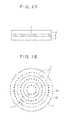
- FIG. 2Ais a sectional view showing an arrangement of a heater and a temperature sensor according to the first exemplary embodiment.
- FIG. 2Bis a plan view showing an arrangement of the heater and the temperature sensor according to the first exemplary embodiment.
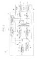
- FIG. 3is a block diagram showing a structure of a controller that controls the temperature adjustment apparatus according to the first exemplary embodiment.
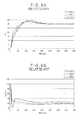
- FIG. 4is graphs for explaining the effects of the first exemplary embodiment, showing a relationship between a control variable PV and a manipulated variable MV.
- FIG. 5is graphs for explaining the effects of the first exemplary embodiment, showing a relationship between the control variable PV and the manipulated variable MV.
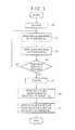
- FIG. 6is a flow chart for explaining the effects of the first exemplary embodiment.
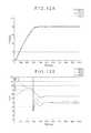
- FIG. 7is graphs for explaining the effects of a second exemplary embodiment of the invention, showing a relationship between the control variable PV and the manipulated variable MV.
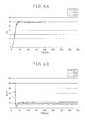
- FIG. 8Ais a graph for explaining the result of a simulation according to the first exemplary embodiment, showing a variation of the control variable PV (in the case that a target without interference is controlled).
- FIG. 8Bis a graph for explaining the result of the simulation according to the first exemplary embodiment, showing a variation of the manipulated variable MV (in the case that the target without interference is controlled).
- FIG. 9Ais a graph for explaining the result of a simulation by a typical method, showing a variation of the control variable PV (in the case that the target without interference is controlled).
- FIG. 9Bis a graph for explaining the result of the simulation by the typical method, showing a variation of the manipulated variable MV (in the case that the target without interference is controlled).
- FIG. 10Ais a graph for explaining the result of a simulation by a typical gradient temperature control method, showing a variation of the control variable PV (in the case that the target without interference is controlled).
- FIG. 10Bis a graph for explaining the result of the simulation by the typical gradient temperature control method, showing a variation of the manipulated variable MV (in the case that the target without interference is controlled).
- FIG. 11schematically illustrates a model designed to have interference among temperature adjusters.
- FIG. 12Ais a graph for explaining the result of the simulation according to the first exemplary embodiment, showing a variation of the control variable PV (in the case that the target with interference is controlled).
- FIG. 12Bis a graph for explaining the result of the simulation according to the first exemplary embodiment, showing a variation of the manipulated variable MV (in the case that the target with interference is controlled).
- FIG. 13Ais a graph for explaining the result of the simulation by the typical method, showing a variation of the control variable PV (in the case that the target with interference is controlled).
- FIG. 13Bis a graph for explaining the result of the simulation by the typical method, showing a variation of the manipulated variable MV (in the case that the target with interference is controlled).
- FIG. 14Ais a graph for explaining the result of the simulation by the typical gradient temperature control method, showing a variation of the control variable PV (in the case that the target with interference is controlled).
- FIG. 14Bis a graph for explaining the result of the simulation by the typical gradient temperature control method, showing a variation of the manipulated variable MV (in the case that the target with interference is controlled).
- FIG. 1shows a temperature adjustment apparatus 1 according to a first exemplary embodiment of the invention.
- the temperature adjustment apparatus 1controls the temperature of a silicon wafer W set on a stage 2 to a temperature setpoint and controls the in-plane temperature distribution of the silicon wafer W.
- the temperature adjustment apparatus 1is used, for instance, in a dry process.
- the temperature adjustment apparatus 1includes the stage 2 and a heater 3 . It should be noted that the stage 2 , which is heated by the heater 3 in the first exemplary embodiment, may alternatively be heated by a chiller or a thermoelectric element, and a cooling control may be performed in the case of using the chiller or the thermoelectric element.
- the stage 2is disposed in a vacuum chamber 4 and the silicon wafer W is set on the stage 2 .
- the silicon wafer Wis electrostatically held on the stage 2 .
- helium gasmay be delivered between the stage 2 and the silicon wafer W to enhance efficiency in heat transfer between the stage 2 and the silicon wafer W.
- the vacuum chamber 4is vacuumized and maintained in a predetermined low-pressure state.
- the heater 3includes a plurality of heaters 3 disposed in the stage 2 to adjust the in-plane temperature distribution of the silicon wafer W on the stage 2 .
- FIG. 2Ais a sectional view of the stage 2 , showing that a plate 5 is disposed on the heaters 3 on the stage 2 .
- a temperature sensor 6(a temperature detector) is disposed in the plate 5 .
- FIG. 2Bis a plan view of the stage 2 , showing that the stage 2 is divided into three concentric zones 2 A, 2 B, 2 C, in each of which the heaters 3 are disposed.
- the temperature sensor 6 in the plate 5includes temperature sensors 6 disposed at positions corresponding to the heaters 3 .
- the zones 2 A, 2 B and 2 C of the stage 2can be independently heated by supplying electricity to the heaters 3 . Accordingly, the heaters 3 are controlled by adjusting the supply of electricity thereto to adjust the in-plane temperature distribution of the silicon wafer W on the stage 2 .
- the heaters 3 disposed in each of the zones 2 A, 2 B and 2 Care controlled by a controller 24 .
- the controller 24controls the heaters 3 , which include master heaters 3 M and slave heaters 3 S, based on temperatures detected by the temperature sensor 6 as described above, and has a functional structure as shown in a block diagram of FIG. 3 .
- the controller 24includes: a master loop MR for controlling the heaters 3 M for heating the zone 2 A shown in FIGS. 2A and 2B ; a slave loop SR for controlling the heaters 3 S for heating the zone 2 B and the zone 2 C; a master temperature sensor 6 M that detects the temperatures of the heaters 3 M; a slave temperature sensor 6 S that detects the temperatures of the heaters 3 S; and a manipulated variable calculator 30 that calculates a manipulated variable for each of the master loop MR and the slave loop SR.
- the slave loop SRincludes two loops for the zones 2 B, 2 C that similarly follow the master loop MR, and thus only one of the loops is shown in FIG. 3 .
- a control variable for a slave sidefollows a control variable for a master side to control the temperature distribution. Accordingly, the maximum response speed of the control system is usually limited by a loop with the slowest response speed, so that the loop with the slowest response speed should be defined as the master loop MR.
- the manipulated variable calculator 30applies manipulated variables MVm, MVs based on a master control setpoint SVm and a slave control setpoint SVs to the heaters 3 M, 3 S, respectively.
- the manipulated variable calculator 30includes: a setpoint setting section 31 , a switch 32 , a master deviation calculator 33 M, a slave deviation calculator 33 S, a master control calculator 34 M, a manipulated variable converter 35 , a master feedforward variable adding section 36 M, a slave feedforward variable adding section 36 S, a master manipulated variable regulator 37 M, a slave manipulated variable regulator 37 S, an offset setting section 38 and a setpoint filter 39 .
- the setpoint setting section 31monitors a temperature detection value PVm from the temperature sensor 6 M of the master loop MR, and switches the switch 32 when the temperature detection value reaches a preset temporary setpoint X (described later).
- the switch 32is initially set in a first position for setting the temperature detection value PVm from the temperature sensor 6 M as the master control setpoint SVm.
- the setpoint setting section 31switches the switch 32 to a second position for setting an actually preset control setpoint as the master control setpoint SVm.
- the control setpoint SVmay be SVf inputted through the setpoint filter 39 .
- the setpoint setting section 31varies a feedforward variable FFm to be added to the master feedforward variable adding section 36 M and a feedforward variable FFs to be added to the slave feedforward variable adding section 36 S, while monitoring the temperature detection value PVm.
- the master deviation calculator 33 Mcalculates a deviation em between the control setpoint SVm inputted through the switch 32 and the temperature detection value PVm from the temperature sensor 6 M, and outputs it to the master control calculator 34 M.
- the slave deviation calculator 33 Scalculates a deviation es between the slave control setpoint SVs, which is the temperature detection value PVm from the master temperature sensor 6 M, and the detection value PVs from the slave temperature sensor 6 S, and outputs it to the slave control calculator 34 S.
- a temperature difference ⁇is set in the offset setting section 38 .
- the master control calculator 34 Moutputs a calculation result Um to the manipulated variable converter 35 .
- the slave control calculator 34 Ssimilarly outputs a calculation result Us to the manipulated variable converter 35 .
- the manipulated variable converter 35is configured to convert the inputted calculation result Um from the master control calculator 34 M and calculation result Us from the slave control calculator 34 S into manipulated variables so that mutual interference between the master loop MR and the slave loop SR is reduced.
- the two inputs Um, Usare converted into the two outputs Vm, Vs using a transformation matrix H and the thus-obtained master manipulated variables Vm and slave manipulated variable Vs are outputted.
- the transformation matrix H for obtaining the manipulated variablesis represented by the following formula (1), given that the transfer function matrix P(s) has two rows and two columns.
- the master feedforward variable adding section 36 Madds the feedforward variable FFm to the master output Vm from the manipulated variable converter 35 , whereas the slave feedforward variable adding section 36 S adds the feedforward variable FFs to the slave output Vs.
- the master manipulated variable regulator 37 Mregulates the manipulated variable so that the output of the heaters 3 M falls within a range from the minimum output to the maximum output thereof.
- the master manipulated variable regulator 37 Moutputs a corresponding determination signal awm to the master control calculator 34 M.
- the output of the master manipulated variable regulator 37 Mis outputted as the manipulated variable MVm to the heaters 3 M.
- the slave manipulated variable regulator 37 Sregulates the manipulated variable so that the output of the heaters 3 S falls within a range from the minimum output to the maximum output thereof.
- the slave manipulated variable regulator 37 Soutputs a corresponding determination signal aws to the slave control calculator 34 S.
- the output of the slave manipulated variable regulator 37 Sis outputted as the manipulated variable MVs to the heaters 3 S.
- the determination signals awm, awsfunction as anti-windup activation signals in the master control calculator 34 M and the slave control calculator 34 S, respectively.
- FIG. 4shows setpoint responses through a single-input single-output system.
- FIG. 4(A)shows a temporal variation of the control variable PV and
- FIG. 4(B)shows a temporal variation of the manipulated variable MV.
- the control setpoint SVcan be reached in the shortest time by: saturating the heaters 3 M with a manipulated variable ff 1 , which enables the maximum output of the heaters 3 M, so that the temperature is increased at the maximum speed; switching the manipulated variable to zero before the control setpoint SV is reached (the manipulated variable may be set at a minus in the case of using a thermoelectric element capable of heating and cooling); letting the control setpoint SV be automatically reached (the control setpoint SV may be reached with a braking force in the case of a minus manipulated variable); and finally immediately switching the manipulated variable to ff 2 enabling the temperature to be settled at the control setpoint SV.
- the above operation methodis considerably difficult to perform under a feedback control such as a PID control in which a variable is calculated based on a deviation, and thus a feedforward control is suitably employed.
- the setpoint setting section 31performs a control using the switch 32 to: set the temperature detection value PVm from the temperature sensor 6 M as the control setpoint, when the manipulated variable PV is in a range A defined below the temporary setpoint X below the control setpoint SV; and set the actually preset control setpoint or Svf, which is inputted through the setpoint filter 39 , as the control setpoint, when the manipulated in a range B over the temporary setpoint X.
- the temperature detection value PVmis set as the control setpoint SVm
- the deviation between the control setpoint SVm and the temperature detection value PVm calculated by the master deviation calculator 33 Mis zero, so that the sum of the feedforward variable ff 1 in the range A and a correction signal (e.g., h12 ⁇ Us, in the formula (1)) outputted from the slave side through the transformation matrix H is set as the manipulated variable for driving the heaters 3 M.
- a correction signale.g., h12 ⁇ Us, in the formula (1)
- a feedforward variable ff 1s for the heaters 3 S of the slave loop SRcan be calculated using a steady-state gain matrix Gp in the above formula (1).
- a gain ratio g of an output in response to the input of the manipulated variable MV with the same magnitudecan be obtained by the following formula (2).
- a master feedforward variable ff 2m and a slave feedforward variable ff 2s in the range Bare calculated as follows.
- the master feedforward variable ff 2m and the slave feedforward variable ff 2sare equal to the manipulated variable in the steady state and thus can be calculated by the following formula (4).
- a trial-and-error approachsuch as simulation or experiment with actual equipment is required to determine the temporary setpoint X.
- the setpointIn switching the setpoint from X to SV in the range B, it is preferable that the setpoint should be gradually changed through the setpoint filter 39 to the setpoint to be finally achieved because a drastic change of the setpoint is accompanied by a drastic change of the manipulated variable, which may result in an unfavorable influence on the control.
- a first order lag filteris used as the setpoint filter 39 , but it is not requisite.
- a trial-and-error approachis also required to determine a filter time constant. In the case of using a first order lag filter with a time constant of Tf seconds, SV f is represented by the following formula (5).
- rangesare defined on a basis of temperature in the first exemplary embodiment, but may be defined on a basis of a combination of temperature and time.
- the setpoint setting section 31sets the temperature detection value PVm detected by the temperature sensor 6 as the setpoint SVm (step S 1 ), and starts driving of the heaters 3 M of the master loop MR under a feedforward control mainly based on the feedforward variable ff 1m (step S 2 ). Simultaneously, the setpoint setting section 31 starts driving of the slave loop SR under a feedforward control based on the feedforward variable ff 1s and a feedback control based on a slave deviation es (step S 3 ).
- the setpoint setting section 31monitors the temperature detection value PVm detected by the temperature sensor 6 and determines whether or not the temporary setpoint X is reached (step S 4 ).
- the setpoint setting section 31sets the actually preset control setpoint SV or SVf, which is inputted through the setpoint filter 39 , as the master control setpoint SVm using the switch 32 (step S 5 ), and starts the feedback control of the master heaters 3 M based on the feedforward control based on the feedforward variable ff 2m and the feedback control based on the master deviation em (step S 6 ).
- the setpoint setting section 31starts driving of the slave heaters 3 S based on the feedforward variable ff 2s and the slave deviation es (step S 7 ).
- the manipulated variableis immediately switched from the feedforward variable ff 1 to the feedforward variable ff 2 as shown in FIG. 5 .
- the second exemplary embodimentis different from the first exemplary embodiment in that the manipulated variable is switched as shown in FIG. 7 .
- the range Ais further divided into a plurality of ranges and feedforward variables are switched in accordance with these ranges to achieve a further minute control as shown in FIG. 7(B) .
- the second exemplary embodimentis different from the first exemplary embodiment in that the range A is divided into a range A 0 and a range A 1 with reference to the temporary setpoint Y, and the feedforward variables ff m10 , ff s10 are added in the range A 0 whereas the feedforward variables ff m11 , ff s11 are added in the range A 1 .
- the second exemplary embodimentcan provide effects similar to those of the first exemplary embodiment.
- a transfer function of the heaters 3(a target to be controlled) was represented by the following formula (6).
- [ y 1 y 2 y 3 ][ 1.2 ⁇ ⁇ exp ⁇ ( - 2 ⁇ s ) ( 70 ⁇ s + 1 ) ⁇ ( 10 ⁇ s + 1 ) 0 0 0 1.6 ⁇ ⁇ exp ⁇ ( - 2 ⁇ s ) ( 60 ⁇ s + 1 ) ⁇ ( 10 ⁇ s + 1 ) 0 0 0 2.0 ⁇ ⁇ exp ⁇ ( - 2 ⁇ s ) ( 50 ⁇ s + 1 ) ⁇ ( 10 ⁇ s + 1 ) ] ⁇ [ u 1 u 2 u 3 ] ( 6 )
- the steady-state gain matrix Gp of this targetwas represented by the following formula (7).
- the gain ratio gwas calculated by the above formula.
- the gain ratio gwas represented by the following formula (8).
- the feedforward variable ff 2 in the range Bwas represented by the following formula (9) when the setpoint was, for instance, 30.
- a PID controllerwas used as the controller and the manipulated variable (%) was set at a value calculated by the following formula (10). It should be noted that Pb represents a proportional range, Ti represents an integral time, and Td represents a derivative time.
- the method according to the first exemplary embodimentachieves early rise time and excellent uniformity.
- [ y 1 y 2 y 3 ][ 42.7 ⁇ ⁇ exp ⁇ ( - 2 ⁇ s ) ( 297 ⁇ s + 1 ) 22.2 ⁇ ⁇ exp ⁇ ( - 2 ⁇ s ) ( 432 ⁇ s + 1 ) 19.6 ⁇ ⁇ exp ⁇ ( - 2 ⁇ s ) ( 484 ⁇ s + 1 ) 22.8 ⁇ ⁇ exp ⁇ ( - 2 ⁇ s ) ( 434 ⁇ s + 1 ) 36.9 ⁇ ⁇ exp ⁇ ( - 2 ⁇ s ) ( 305 ⁇ s + 1 ) 32.5 ⁇ ⁇ exp ⁇ ( - 2 ⁇ s ) ( 383 ⁇ s + 1 ) 16.0 ⁇ ⁇ exp ⁇ ( - 2 ⁇ s ) ( 476 ⁇ s + 1 ) 31.7 ⁇ ⁇ exp ⁇ ( - 2 ⁇ s ) ( 352 ⁇ s + 1 )
- the steady-state gain matrix Gp of the heating elements (the target)was represented by the following formula (12).
- the gain ratio gwas calculated by the above formula.
- the gain ratio gwas represented by the following formula (13).
- the feedforward variable ff 2 (%) in the range Bwas represented by the following formula (14) when the setpoint was, for instance, 40.
- the temperature setpointwas changed from 37 degrees C. to 40 degrees C. through a first order lag filter with a time constant of 20 seconds.
- a PID controllerwas used as the controller and the manipulated variable (%) was set at a value calculated by the following formula (10).
- a non-interfering matrix as represented by the following formula (15)was obtained by a commonly known method.
- a manipulated variable transformation matrix for master-slavewas represented by the following formula (16).
- a manipulated variable transformation matrix for the gradient temperature control methodis represented by the following formula (17).
- a transformation matrix H 1 obtained by combining the non-interfering matrix represented by the formula (15) and the manipulated variable transformation matrixwas represented by the following formula (18) in the case of master-slave.
- a transformation matrix H 2 obtained by combining the non-interfering matrix and the manipulated variable transformation matrix for the gradient temperature control methodwas represented by the following formula (19).
- the method according to the first exemplary embodimentachieves early rise time and excellent uniformity irrespective of whether or not the target to be controlled suffers interference.
Landscapes
- Engineering & Computer Science (AREA)
- Physics & Mathematics (AREA)
- General Physics & Mathematics (AREA)
- Automation & Control Theory (AREA)
- Condensed Matter Physics & Semiconductors (AREA)
- Manufacturing & Machinery (AREA)
- Computer Hardware Design (AREA)
- Microelectronics & Electronic Packaging (AREA)
- Power Engineering (AREA)
- Remote Sensing (AREA)
- General Engineering & Computer Science (AREA)
- Control Of Temperature (AREA)
- Feedback Control In General (AREA)
Abstract
Description
The entire disclosure of Japanese Patent Application No. 2014-012293 filed Jan. 27, 2014 is expressly incorporated herein by reference herein.
The present invention relates to a temperature controller for a semiconductor wafer and a temperature control method for a semiconductor wafer that are configured to perform a temperature control on a plurality of temperature adjusters to adjust the temperature of the semiconductor wafer.
A process for treating a semiconductor wafer such as a silicon wafer includes controlling the in-plane temperature distribution of the silicon wafer as desired while controlling the temperature of the silicon wafer to a temperature setpoint.
For instance, according to a known method, heaters are each incorporated in an independent control loop so that the semiconductor wafer is simultaneously heated using a plurality of temperature adjusters.
Regarding the above temperature control for a semiconductor wafer, it is necessary that control variables should have a constant deviation from a reference control variable until the temperature reaches a setpoint and that the temperature should be maintained at the setpoint irrespective of any disturbance. In connection with the above, a master-slave control method and a gradient temperature control method are typically known (see, for instance, Patent Literature 1: JP-A-7-200076 and Patent Literature 2: JP-A-2000-187514).
In the master-slave control method, one of a plurality of control loops is controlled as a master, and a deviation between a control variable (a setpoint) of the master loop and a control variable of a slave loop(s) is calculated and controlled so that the slave loop(s) follows the behavior of the master loop.
In the gradient temperature control method, an average of control variables for loops is defined as a representative variable, and a difference between the control variables for the loops is defined as a gradient variable (another control variable), the representative variable following a setpoint with the gradient variable being kept constant. The control variables are transformed using a transformation matrix. Further, a non-interfering matrix is used to reduce interference among the loops, and a manipulated variable transformation matrix is used to return the control variables to the original dimension.
However, the techniques disclosed inPatent Literatures
An object of the invention is to provide a temperature control system for a semiconductor wafer and a temperature control method for a semiconductor wafer that ensure the following ability and uniformity of control variables among loops and allow temperature adjusters to respond to a setpoint almost at the fastest possible speed.
In a first aspect of the invention,
a temperature controller for a semiconductor wafer, the temperature controller being configured to perform a temperature control on a plurality of temperature adjusters including a reference temperature adjuster to adjust a temperature of the semiconductor wafer, includes:
a master loop configured to control a temperature of the reference temperature adjuster;
at least one slave loop configured to follow the master loop to control a temperature of rest of the temperature adjusters;
a master temperature detector configured to detect the temperature of the semiconductor wafer having been adjusted by the reference temperature adjuster;
a slave temperature detector configured to detect the temperature of the semiconductor wafer having been adjusted by the rest of the temperature adjusters; and
a manipulated variable calculator configured to calculate, from the temperature detected by the master temperature detector and the temperature detected by the slave temperature detector, a manipulated variable for the reference temperature adjuster and a manipulated variable for the rest of the temperature adjusters, the manipulated variable calculator including:
- a setpoint setting section configured to set, as a control setpoint for the reference temperature adjuster, an actual control setpoint preset as a desired temperature of the semiconductor wafer or a value equal to the temperature detected by the master temperature detector;
- a master deviation calculator configured to calculate a deviation between the control setpoint set by the setpoint setting section and the temperature detected by the master temperature detector;
- a slave deviation calculator configured to calculate a deviation between the temperature detected by the master temperature detector and the temperature detected by the slave temperature detector;
- a master control calculator configured to receive the deviation calculated by the master deviation calculator to calculate the manipulated variable for the reference temperature adjuster;
- a slave control calculator configured to receive the deviation calculated by the slave deviation calculator to calculate the manipulated variable for the rest of the temperature adjusters;
- a manipulated variable converter configured to output the manipulated variable calculated by the master control calculator and the manipulated variable calculated by the slave control calculator respectively to the reference temperature adjuster and the rest of the temperature adjusters after converting the manipulated variable calculated by the master control calculator and the manipulated variable calculated by the slave control calculator so that interference between the master loop and the slave loop is reduced; and
- a feedforward variable adding section configured to add a predetermined feedforward variable corresponding to an output from the manipulated variable converter, in which
the setpoint setting section: sets the temperature detected by the master temperature detector as the control setpoint for the reference temperature adjuster, until a temporary setpoint below the actual control setpoint is reached; and sets the actual control setpoint as the control setpoint for the reference temperature adjuster after the temporary setpoint is reached.
In a second aspect of the invention, the temporary setpoint includes a plurality of temporary setpoints.
In a third aspect of the invention, it is determined whether or not the temporary setpoint is reached on a basis of at least one of temperature and time.
In a fourth aspect of the invention,
a temperature control method for a semiconductor wafer, the temperature control method being configured to perform a temperature control on a plurality of temperature adjusters including a reference temperature adjuster to adjust a temperature of the semiconductor wafer, the plurality of temperature adjusters being controlled by a temperature control system, the temperature control system including:
a master loop configured to control a temperature of the reference temperature adjuster;
at least one slave loop configured to control a temperature of rest of the temperature adjusters; and
a manipulated variable calculator configured to apply a manipulated variable to each of the reference temperature adjuster and the rest of the temperature adjusters,
the temperature control method being configured to be performed by the manipulated variable calculator, the temperature control method includes:
setting, as a control setpoint for the master loop, a temperature detection value of the semiconductor wafer having been subjected to a temperature adjustment by the temperature adjusters;
performing the temperature control of the temperature adjusters based on a preset feedforward variable;
determining whether or not a temporary setpoint below an actually preset control setpoint to be finally achieved is reached;
switching the control setpoint for the master loop to the control setpoint to be finally achieved, when the temporary setpoint is determined to be reached; and
performing a feedback control in combination with a feedforward control based on a preset feedforward variable.
In the first aspect of the invention, the setpoint setting section: sets a temperature detected by the master temperature detector as a control setpoint for the reference temperature adjuster of the master loop, until a temporary setpoint below an actual control setpoint, which is preset as a desired temperature of the semiconductor wafer, is reached; and sets the actual control setpoint as the control setpoint for the reference temperature adjuster after the temporary setpoint is reached.
Therefore, since the temperature detection value is set as the control setpoint to be achieved until the temporary setpoint is reached, a feedback control of the temperature detection value is cancelled and thus is not performed.
As a result, at the start of the temperature adjustment control, the temperature adjustment can be performed based on the feedforward variable almost at the fastest possible speed of the temperature adjuster of the master loop.
After the temporary setpoint is reached, a typical feedback control is performed in combination with the feedforward control so that the control setpoint is promptly reached.
In the second aspect of the invention, a plurality of temporary setpoints are preset, thereby further minutely determining feedforward variables to achieve a highly accurate temperature control.
In the third aspect of the invention, it is determined whether or not the temporary setpoint is reached on a basis of at least one of temperature and time, thereby achieving a highly accurate temperature adjustment control.
The fourth aspect of the invention can provide effects similar to those of the first aspect.
Exemplary embodiment(s) of the invention will be described below with reference to the attached drawings.
Thetemperature adjustment apparatus 1 includes thestage 2 and aheater 3. It should be noted that thestage 2, which is heated by theheater 3 in the first exemplary embodiment, may alternatively be heated by a chiller or a thermoelectric element, and a cooling control may be performed in the case of using the chiller or the thermoelectric element.
Thestage 2 is disposed in avacuum chamber 4 and the silicon wafer W is set on thestage 2. The silicon wafer W is electrostatically held on thestage 2. It should be noted that helium gas may be delivered between thestage 2 and the silicon wafer W to enhance efficiency in heat transfer between thestage 2 and the silicon wafer W.
In the dry process, thevacuum chamber 4 is vacuumized and maintained in a predetermined low-pressure state.
As shown inFIGS. 2A and 2B , theheater 3 includes a plurality ofheaters 3 disposed in thestage 2 to adjust the in-plane temperature distribution of the silicon wafer W on thestage 2.
Thezones stage 2 can be independently heated by supplying electricity to theheaters 3. Accordingly, theheaters 3 are controlled by adjusting the supply of electricity thereto to adjust the in-plane temperature distribution of the silicon wafer W on thestage 2. Theheaters 3 disposed in each of thezones controller 24.
Thecontroller 24 controls theheaters 3, which includemaster heaters 3M andslave heaters 3S, based on temperatures detected by thetemperature sensor 6 as described above, and has a functional structure as shown in a block diagram ofFIG. 3 .
Thecontroller 24 includes: a master loop MR for controlling theheaters 3M for heating thezone 2A shown inFIGS. 2A and 2B ; a slave loop SR for controlling theheaters 3S for heating thezone 2B and the zone2C; amaster temperature sensor 6M that detects the temperatures of theheaters 3M; aslave temperature sensor 6S that detects the temperatures of theheaters 3S; and a manipulatedvariable calculator 30 that calculates a manipulated variable for each of the master loop MR and the slave loop SR. It should be noted that the slave loop SR includes two loops for thezones 2B,2C that similarly follow the master loop MR, and thus only one of the loops is shown inFIG. 3 .
In a master-slave control system, a control variable for a slave side follows a control variable for a master side to control the temperature distribution. Accordingly, the maximum response speed of the control system is usually limited by a loop with the slowest response speed, so that the loop with the slowest response speed should be defined as the master loop MR.
The manipulatedvariable calculator 30 applies manipulated variables MVm, MVs based on a master control setpoint SVm and a slave control setpoint SVs to theheaters
The manipulatedvariable calculator 30 includes: asetpoint setting section 31, aswitch 32, amaster deviation calculator 33M, aslave deviation calculator 33S, amaster control calculator 34M, a manipulatedvariable converter 35, a master feedforwardvariable adding section 36M, a slave feedforwardvariable adding section 36S, a master manipulatedvariable regulator 37M, a slave manipulated variable regulator37S, an offset settingsection 38 and asetpoint filter 39.
Thesetpoint setting section 31 monitors a temperature detection value PVm from thetemperature sensor 6M of the master loop MR, and switches theswitch 32 when the temperature detection value reaches a preset temporary setpoint X (described later). At the start of an operation, theswitch 32 is initially set in a first position for setting the temperature detection value PVm from thetemperature sensor 6M as the master control setpoint SVm. When determining that the temperature detection value PVm from thetemperature sensor 6M reaches the temporary setpoint X, thesetpoint setting section 31 switches theswitch 32 to a second position for setting an actually preset control setpoint as the master control setpoint SVm. It should be noted that the control setpoint SV may be SVf inputted through thesetpoint filter 39.
Thesetpoint setting section 31 varies a feedforward variable FFm to be added to the master feedforwardvariable adding section 36M and a feedforward variable FFs to be added to the slave feedforwardvariable adding section 36S, while monitoring the temperature detection value PVm.
Themaster deviation calculator 33M calculates a deviation em between the control setpoint SVm inputted through theswitch 32 and the temperature detection value PVm from thetemperature sensor 6M, and outputs it to themaster control calculator 34M.
Theslave deviation calculator 33S calculates a deviation es between the slave control setpoint SVs, which is the temperature detection value PVm from themaster temperature sensor 6M, and the detection value PVs from theslave temperature sensor 6S, and outputs it to theslave control calculator 34S. When a constant temperature difference is to be provided between the master and the slave, a temperature difference δ is set in the offset settingsection 38.
Themaster control calculator 34M, an example of which is a PID controller, outputs a calculation result Um to the manipulatedvariable converter 35.
Theslave control calculator 34S similarly outputs a calculation result Us to the manipulatedvariable converter 35.
The manipulatedvariable converter 35 is configured to convert the inputted calculation result Um from themaster control calculator 34M and calculation result Us from theslave control calculator 34S into manipulated variables so that mutual interference between the master loop MR and the slave loop SR is reduced. The two inputs Um, Us are converted into the two outputs Vm, Vs using a transformation matrix H and the thus-obtained master manipulated variables Vm and slave manipulated variable Vs are outputted. The transformation matrix H is obtained from, for instance, a steady-state gain matrix Gp=P(0) and a master-slave manipulated variable transformation matrix Gm, given that a target to be controlled is represented by a transfer function matrix P(s). The transformation matrix H for obtaining the manipulated variables is represented by the following formula (1), given that the transfer function matrix P(s) has two rows and two columns.
The master feedforwardvariable adding section 36M adds the feedforward variable FFm to the master output Vm from the manipulatedvariable converter 35, whereas the slave feedforwardvariable adding section 36S adds the feedforward variable FFs to the slave output Vs.
The master manipulatedvariable regulator 37M regulates the manipulated variable so that the output of theheaters 3M falls within a range from the minimum output to the maximum output thereof. When determining that the manipulated variable reaches a saturation level, the master manipulatedvariable regulator 37M outputs a corresponding determination signal awm to themaster control calculator 34M. The output of the master manipulatedvariable regulator 37M is outputted as the manipulated variable MVm to theheaters 3M.
Similarly, the slave manipulated variable regulator37S regulates the manipulated variable so that the output of theheaters 3S falls within a range from the minimum output to the maximum output thereof. When determining that the manipulated variable reaches a saturation level, the slave manipulated variable regulator37S outputs a corresponding determination signal aws to theslave control calculator 34S. The output of the slave manipulated variable regulator37S is outputted as the manipulated variable MVs to theheaters 3S. The determination signals awm, aws function as anti-windup activation signals in themaster control calculator 34M and theslave control calculator 34S, respectively.
In setpoint response through a control system in which theheaters 3M could be saturated, the control setpoint SV can be reached in the shortest time by: saturating theheaters 3M with a manipulated variable ff1, which enables the maximum output of theheaters 3M, so that the temperature is increased at the maximum speed; switching the manipulated variable to zero before the control setpoint SV is reached (the manipulated variable may be set at a minus in the case of using a thermoelectric element capable of heating and cooling); letting the control setpoint SV be automatically reached (the control setpoint SV may be reached with a braking force in the case of a minus manipulated variable); and finally immediately switching the manipulated variable to ff2enabling the temperature to be settled at the control setpoint SV.
The above operation method is considerably difficult to perform under a feedback control such as a PID control in which a variable is calculated based on a deviation, and thus a feedforward control is suitably employed.
The first exemplary embodiment is based on the above idea. Specifically, as shown inFIG. 5 , thesetpoint setting section 31 performs a control using theswitch 32 to: set the temperature detection value PVm from thetemperature sensor 6M as the control setpoint, when the manipulated variable PV is in a range A defined below the temporary setpoint X below the control setpoint SV; and set the actually preset control setpoint or Svf, which is inputted through thesetpoint filter 39, as the control setpoint, when the manipulated in a range B over the temporary setpoint X.
As a result, when the temperature detection value PVm is set as the control setpoint SVm, the deviation between the control setpoint SVm and the temperature detection value PVm calculated by themaster deviation calculator 33M is zero, so that the sum of the feedforward variable ff1in the range A and a correction signal (e.g., h12×Us, in the formula (1)) outputted from the slave side through the transformation matrix H is set as the manipulated variable for driving theheaters 3M.
In driving theheaters 3M of the master loop MR with the maximum output, a feedforward variable ff1sfor theheaters 3S of the slave loop SR can be calculated using a steady-state gain matrix Gp in the above formula (1).
Specifically, a gain ratio g of an output in response to the input of the manipulated variable MV with the same magnitude can be obtained by the following formula (2).
Therefore, when g2>g1,
ff1m=100% (master side)
ff1s=100×(k11+k12)/(k21+k22)% (slave side)
ff1m=100% (master side)
ff1s=100×(k11+k12)/(k21+k22)% (slave side)
On the other hand, when g2<g1,
ff1m=100×(k21+k22)/(k11+k12)% (master side)
ff1s=100% (slave side)
The above values are set as initial values and adjusted by simulation, experiment with actual equipment, or the like.
ff1m=100×(k21+k22)/(k11+k12)% (master side)
ff1s=100% (slave side)
The above values are set as initial values and adjusted by simulation, experiment with actual equipment, or the like.
A master feedforward variable ff2mand a slave feedforward variable ff2sin the range B are calculated as follows.
When outputs in response to the input of the manipulated variable MV are equally the setpoint SV to be finally achieved, an input-output relationship in a steady state is represented by the following formula (3) using the steady-state gain matrix Gp.
Therefore, the master feedforward variable ff2mand the slave feedforward variable ff2sare equal to the manipulated variable in the steady state and thus can be calculated by the following formula (4).
A trial-and-error approach such as simulation or experiment with actual equipment is required to determine the temporary setpoint X. In switching the setpoint from X to SV in the range B, it is preferable that the setpoint should be gradually changed through thesetpoint filter 39 to the setpoint to be finally achieved because a drastic change of the setpoint is accompanied by a drastic change of the manipulated variable, which may result in an unfavorable influence on the control. For instance, a first order lag filter is used as thesetpoint filter 39, but it is not requisite. A trial-and-error approach is also required to determine a filter time constant. In the case of using a first order lag filter with a time constant of Tf seconds, SVfis represented by the following formula (5).
It should be noted that the ranges are defined on a basis of temperature in the first exemplary embodiment, but may be defined on a basis of a combination of temperature and time.
Next, a specific process of the first exemplary embodiment will be described with reference to a flow chart shown inFIG. 6 .
First, thesetpoint setting section 31 sets the temperature detection value PVm detected by thetemperature sensor 6 as the setpoint SVm (step S1), and starts driving of theheaters 3M of the master loop MR under a feedforward control mainly based on the feedforward variable ff1m(step S2). Simultaneously, thesetpoint setting section 31 starts driving of the slave loop SR under a feedforward control based on the feedforward variable ff1sand a feedback control based on a slave deviation es (step S3).
Thesetpoint setting section 31 monitors the temperature detection value PVm detected by thetemperature sensor 6 and determines whether or not the temporary setpoint X is reached (step S4).
When the temporary setpoint X is determined to be reached, thesetpoint setting section 31 sets the actually preset control setpoint SV or SVf, which is inputted through thesetpoint filter 39, as the master control setpoint SVm using the switch32 (step S5), and starts the feedback control of themaster heaters 3M based on the feedforward control based on the feedforward variable ff2mand the feedback control based on the master deviation em (step S6). Thesetpoint setting section 31 starts driving of theslave heaters 3S based on the feedforward variable ff2sand the slave deviation es (step S7).
Next, a second exemplary embodiment of the invention will be described. It should be noted that, in the following description, parts and the like identical to those described above are attached with the same reference signs and the explanation thereof is omitted.
In the first exemplary embodiment, when the temporary setpoint X is reached, the manipulated variable is immediately switched from the feedforward variable ff1to the feedforward variable ff2as shown inFIG. 5 .
In contrast, the second exemplary embodiment is different from the first exemplary embodiment in that the manipulated variable is switched as shown inFIG. 7 .
Specifically, in the second exemplary embodiment, the range A is further divided into a plurality of ranges and feedforward variables are switched in accordance with these ranges to achieve a further minute control as shown inFIG. 7(B) . The second exemplary embodiment is different from the first exemplary embodiment in that the range A is divided into a range A0 and a range A1 with reference to the temporary setpoint Y, and the feedforward variables ffm10, ffs10are added in the range A0 whereas the feedforward variables ffm11, ffs11are added in the range A1.
The second exemplary embodiment can provide effects similar to those of the first exemplary embodiment.
In order to demonstrate the effects of the invention, the method according to the first exemplary embodiment, a typical master-slave control method and the gradient temperature control method disclosed in the publication of Japanese Patent No. 3278807 were each applied to theheaters
[5-1] Target without Interference to be Controlled
A transfer function of the heaters3 (a target to be controlled) was represented by the following formula (6).
The steady-state gain matrix Gp of this target was represented by the following formula (7).
The gain ratio g was calculated by the above formula. When an arbitrary value such as 1 was assigned, the gain ratio g was represented by the following formula (8).
Based on the above ratio, the feedforward variable in the range A was determined as ff1=[100 75 60](%) based on ff1m, ff1scalculated by the formula (2).
The feedforward variable ff2in the range B was represented by the following formula (9) when the setpoint was, for instance, 30.
A PID controller was used as the controller and the manipulated variable (%) was set at a value calculated by the following formula (10). It should be noted that Pb represents a proportional range, Ti represents an integral time, and Td represents a derivative time.
After the above preparation was done, a simulation by the method according to the first exemplary embodiment, a simulation by the typical master-slave method and a simulation by the gradient temperature control method disclosed in Japanese Patent No. 3278807 were performed. The results of the above simulations are respectively shown inFIGS. 8A and 8B ,FIGS. 9A and 9B , andFIGS. 10A and 10B .
It should be noted that PID constants used in any of the above simulations were as follows.
MV1, PV1: Pb=100, Ti=35, Td=20
MV2, PV2: Pb=40, Ti=35, Td=20
MV3, PV3: Pb=40, Ti=35, Td=20
As a result of the above comparison, it is proved that the method according to the first exemplary embodiment achieves early rise time and excellent uniformity.
[5-2] Target with Interference to be Controlled
Next, regarding a target with interference to be controlled, the method according toclaim 1, the typical master-slave method and the gradient temperature control method disclosed in Japanese Patent No. 3278807 were compared.
Specifically, it was assumed that an aluminum plate as shown inFIG. 11 was heated using heating elements (resistance) at three spots (Z1 to Z3). From the result of an experiment on dynamic characteristics, the transfer function of the target to be controlled was represented by the following formula (11).
The steady-state gain matrix Gp of the heating elements (the target) was represented by the following formula (12).
The gain ratio g was calculated by the above formula. When an arbitrary value such as 1 was assigned, the gain ratio g was represented by the following formula (13).
Based on the above ratio, the feedforward variable in the range A was determined as ff1=[100 92 90](%).
The feedforward variable ff2(%) in the range B was represented by the following formula (14) when the setpoint was, for instance, 40.
The feedforward variable ff1was switched to the feedforward variable ff2at y1=37 degrees C. The temperature setpoint was changed from 37 degrees C. to 40 degrees C. through a first order lag filter with a time constant of 20 seconds.
A PID controller was used as the controller and the manipulated variable (%) was set at a value calculated by the following formula (10).
PID constants used in any of the above simulations were as follows.
MV1, PV1: Pb=3.3, Ti=100, Td=0
MV2, PV2: Pb=3.3, Ti=100, Td=0
MV3, PV3: Pb=3.3, Ti=100, Td=0
A non-interfering matrix as represented by the following formula (15) was obtained by a commonly known method.
A manipulated variable transformation matrix for master-slave was represented by the following formula (16).
A manipulated variable transformation matrix for the gradient temperature control method is represented by the following formula (17).
A transformation matrix H1 obtained by combining the non-interfering matrix represented by the formula (15) and the manipulated variable transformation matrix was represented by the following formula (18) in the case of master-slave.
A transformation matrix H2 obtained by combining the non-interfering matrix and the manipulated variable transformation matrix for the gradient temperature control method was represented by the following formula (19).
After the above preparation was done, a simulation by the method according to the first exemplary embodiment, a simulation by the typical master-slave method and a simulation by the gradient temperature control method disclosed in Japanese Patent No. 3278807 were performed. The results of the above simulations are respectively shown inFIGS. 12A and 12B ,FIGS. 13A and 13B , andFIGS. 14A and 14B .
As a result, it is proved that the method according to the first exemplary embodiment achieves early rise time and excellent uniformity irrespective of whether or not the target to be controlled suffers interference.
Claims (4)
1. A temperature controller for a semiconductor wafer, the temperature controller performing a temperature control on a plurality of temperature adjusters including a reference temperature adjuster to adjust a temperature of the semiconductor wafer, the temperature controller comprising:
a master loop, controlling a temperature of the reference temperature adjuster;
at least one slave loop, following the master loop to control a temperature of rest of the temperature adjusters;
a master temperature detector, detecting the temperature of the semiconductor wafer having been adjusted by the reference temperature adjuster;
a slave temperature detector, detecting the temperature of the semiconductor wafer having been adjusted by the rest of the temperature adjusters; and
a manipulated variable calculator, calculating, from the temperature detected by the master temperature detector and the temperature detected by the slave temperature detector, a manipulated variable for the reference temperature adjuster and a manipulated variable for the rest of the temperature adjusters, the manipulated variable calculator comprising:
a setpoint setting section, setting as a control setpoint for the reference temperature adjuster an actual control setpoint preset as a desired temperature of the semiconductor wafer or a value equal to the temperature detected by the master temperature detector;
a master deviation calculator, calculating a deviation between the control setpoint set by the setpoint setting section and the temperature detected by the master temperature detector;
a slave deviation calculator, calculating a deviation between the temperature detected by the master temperature detector and the temperature detected by the slave temperature detector;
a master control calculator, receiving the deviation calculated by the master deviation calculator to calculate the manipulated variable for the reference temperature adjuster;
a slave control calculator, receiving the deviation calculated by the slave deviation calculator to calculate the manipulated variable for the rest of the temperature adjusters;
a manipulated variable converter, outputting the manipulated variable calculated by the master control calculator and the manipulated variable calculated by the slave control calculator respectively to the reference temperature adjuster and the rest of the temperature adjusters after converting the manipulated variable calculated by the master control calculator and the manipulated variable calculated by the slave control calculator so that interference between the master loop and the slave loop is reduced; and
a feedforward variable adding section, adding a predetermined feedforward variable corresponding to an output from the manipulated variable converter, wherein
the setpoint setting section: sets the temperature detected by the master temperature detector as the control setpoint for the reference temperature adjuster, until a temporary setpoint below the actual control setpoint is reached; and sets the actual control setpoint as the control setpoint for the reference temperature adjuster after the temporary setpoint is reached.
2. The temperature controller for the semiconductor wafer according toclaim 1 , wherein the temporary setpoint comprises a plurality of temporary setpoints.
3. The temperature controller for the semiconductor wafer according toclaim 1 , wherein it is determined whether or not the temporary setpoint is reached on a basis of at least one of temperature and time.
4. A temperature control method for a semiconductor wafer, the temperature control method performing a temperature control on a plurality of temperature adjusters including a reference temperature adjuster to adjust a temperature of the semiconductor wafer, the plurality of temperature adjusters being controlled by a temperature control system, the temperature control system comprising:
a master loop, controlling a temperature of the reference temperature adjuster;
at least one slave loop, controlling a temperature of rest of the temperature adjusters; and
a manipulated variable calculator, applying a manipulated variable to each of the reference temperature adjuster and the rest of the temperature adjusters, the manipulated variable calculator comprising:
a setpoint setting section, setting as a control setpoint for the reference temperature adjuster an actual control setpoint preset as a desired temperature of the semiconductor wafer or a value equal to the temperature detected by a master temperature detector that detects the temperature of the semiconductor wafer having been adjusted by the reference temperature adjuster;
a master deviation calculator, calculating a deviation between the control setpoint set by the setpoint setting section and the temperature detected by the master temperature detector,
a slave deviation calculator, calculating a deviation between the temperature detected by the master temperature detector and the temperature detected by a slave temperature detector that detects the temperature of the semiconductor wafer having been adjusted by the rest the of temperature adjusters,
a master control calculator, receiving the deviation calculated by the master deviation calculator to calculate the manipulated variable for the reference temperature adjuster,
a slave control calculator, receiving the deviation calculated by the slave deviation calculator to calculate the manipulated variable for the rest of the temperature adjusters, and
a manipulated variable converter, outputting the manipulated variable calculated by the master control calculator and the manipulated variable calculated by the slave control calculator respectively to the reference temperature adjuster and the rest of the temperature adjusters after converting the manipulated variable calculated by the master control calculator and the manipulated variable calculated by the slave control calculator so that interference between the master loop and the slave loop is reduced;
the temperature control method being performed by the manipulated variable calculator, the temperature control method comprising:
setting, as a control setpoint for the master loop, a temperature detection value of the semiconductor wafer having been subjected to a temperature adjustment by the temperature adjusters;
performing the temperature control of the temperature adjusters based on a preset feedforward variable;
determining whether or not a temporary setpoint below an actually preset control setpoint to be finally achieved is reached;
switching the control setpoint for the master loop to the control setpoint to be finally achieved, when the temporary setpoint is determined to be reached; and
performing a feedback control in combination with a feedforward control based on a preset feedforward variable.
Applications Claiming Priority (2)
| Application Number | Priority Date | Filing Date | Title |
|---|---|---|---|
| JP2014-012293 | 2014-01-27 | ||
| JP2014012293AJP6324739B2 (en) | 2014-01-27 | 2014-01-27 | Semiconductor wafer temperature control device and semiconductor wafer temperature control method |
Publications (2)
| Publication Number | Publication Date |
|---|---|
| US20150212528A1 US20150212528A1 (en) | 2015-07-30 |
| US9798308B2true US9798308B2 (en) | 2017-10-24 |
Family
ID=53678966
Family Applications (1)
| Application Number | Title | Priority Date | Filing Date |
|---|---|---|---|
| US14/593,081Active2036-04-09US9798308B2 (en) | 2014-01-27 | 2015-01-09 | Temperature controller for semiconductor wafer and temperature control method for semiconductor wafer |
Country Status (2)
| Country | Link |
|---|---|
| US (1) | US9798308B2 (en) |
| JP (1) | JP6324739B2 (en) |
Cited By (316)
| Publication number | Priority date | Publication date | Assignee | Title |
|---|---|---|---|---|
| US10409303B2 (en)* | 2016-03-16 | 2019-09-10 | Kelk Ltd. | Temperature controller of semiconductor wafer and temperature control method of semiconductor wafer |
| US10590535B2 (en) | 2017-07-26 | 2020-03-17 | Asm Ip Holdings B.V. | Chemical treatment, deposition and/or infiltration apparatus and method for using the same |
| US10600673B2 (en) | 2015-07-07 | 2020-03-24 | Asm Ip Holding B.V. | Magnetic susceptor to baseplate seal |
| US10604847B2 (en) | 2014-03-18 | 2020-03-31 | Asm Ip Holding B.V. | Gas distribution system, reactor including the system, and methods of using the same |
| US10612136B2 (en) | 2018-06-29 | 2020-04-07 | ASM IP Holding, B.V. | Temperature-controlled flange and reactor system including same |
| US10643904B2 (en) | 2016-11-01 | 2020-05-05 | Asm Ip Holdings B.V. | Methods for forming a semiconductor device and related semiconductor device structures |
| US10643826B2 (en) | 2016-10-26 | 2020-05-05 | Asm Ip Holdings B.V. | Methods for thermally calibrating reaction chambers |
| US10658181B2 (en) | 2018-02-20 | 2020-05-19 | Asm Ip Holding B.V. | Method of spacer-defined direct patterning in semiconductor fabrication |
| US10655221B2 (en) | 2017-02-09 | 2020-05-19 | Asm Ip Holding B.V. | Method for depositing oxide film by thermal ALD and PEALD |
| US10658205B2 (en) | 2017-09-28 | 2020-05-19 | Asm Ip Holdings B.V. | Chemical dispensing apparatus and methods for dispensing a chemical to a reaction chamber |
| US10665452B2 (en) | 2016-05-02 | 2020-05-26 | Asm Ip Holdings B.V. | Source/drain performance through conformal solid state doping |
| US10672636B2 (en) | 2017-08-09 | 2020-06-02 | Asm Ip Holding B.V. | Cassette holder assembly for a substrate cassette and holding member for use in such assembly |
| US10683571B2 (en) | 2014-02-25 | 2020-06-16 | Asm Ip Holding B.V. | Gas supply manifold and method of supplying gases to chamber using same |
| US10685834B2 (en) | 2017-07-05 | 2020-06-16 | Asm Ip Holdings B.V. | Methods for forming a silicon germanium tin layer and related semiconductor device structures |
| US10692741B2 (en) | 2017-08-08 | 2020-06-23 | Asm Ip Holdings B.V. | Radiation shield |
| US10707106B2 (en) | 2011-06-06 | 2020-07-07 | Asm Ip Holding B.V. | High-throughput semiconductor-processing apparatus equipped with multiple dual-chamber modules |
| US10714335B2 (en) | 2017-04-25 | 2020-07-14 | Asm Ip Holding B.V. | Method of depositing thin film and method of manufacturing semiconductor device |
| US10714315B2 (en) | 2012-10-12 | 2020-07-14 | Asm Ip Holdings B.V. | Semiconductor reaction chamber showerhead |
| US10714350B2 (en) | 2016-11-01 | 2020-07-14 | ASM IP Holdings, B.V. | Methods for forming a transition metal niobium nitride film on a substrate by atomic layer deposition and related semiconductor device structures |
| US10714385B2 (en) | 2016-07-19 | 2020-07-14 | Asm Ip Holding B.V. | Selective deposition of tungsten |
| US10720322B2 (en) | 2016-02-19 | 2020-07-21 | Asm Ip Holding B.V. | Method for forming silicon nitride film selectively on top surface |
| US10720331B2 (en) | 2016-11-01 | 2020-07-21 | ASM IP Holdings, B.V. | Methods for forming a transition metal nitride film on a substrate by atomic layer deposition and related semiconductor device structures |
| US10734223B2 (en) | 2017-10-10 | 2020-08-04 | Asm Ip Holding B.V. | Method for depositing a metal chalcogenide on a substrate by cyclical deposition |
| US10734244B2 (en) | 2017-11-16 | 2020-08-04 | Asm Ip Holding B.V. | Method of processing a substrate and a device manufactured by the same |
| US10731249B2 (en) | 2018-02-15 | 2020-08-04 | Asm Ip Holding B.V. | Method of forming a transition metal containing film on a substrate by a cyclical deposition process, a method for supplying a transition metal halide compound to a reaction chamber, and related vapor deposition apparatus |
| US10734497B2 (en) | 2017-07-18 | 2020-08-04 | Asm Ip Holding B.V. | Methods for forming a semiconductor device structure and related semiconductor device structures |
| US10741385B2 (en) | 2016-07-28 | 2020-08-11 | Asm Ip Holding B.V. | Method and apparatus for filling a gap |
| US10755922B2 (en) | 2018-07-03 | 2020-08-25 | Asm Ip Holding B.V. | Method for depositing silicon-free carbon-containing film as gap-fill layer by pulse plasma-assisted deposition |
| US10755923B2 (en) | 2018-07-03 | 2020-08-25 | Asm Ip Holding B.V. | Method for depositing silicon-free carbon-containing film as gap-fill layer by pulse plasma-assisted deposition |
| US10770336B2 (en) | 2017-08-08 | 2020-09-08 | Asm Ip Holding B.V. | Substrate lift mechanism and reactor including same |
| US10767789B2 (en) | 2018-07-16 | 2020-09-08 | Asm Ip Holding B.V. | Diaphragm valves, valve components, and methods for forming valve components |
| US10770286B2 (en) | 2017-05-08 | 2020-09-08 | Asm Ip Holdings B.V. | Methods for selectively forming a silicon nitride film on a substrate and related semiconductor device structures |
| US10784102B2 (en) | 2016-12-22 | 2020-09-22 | Asm Ip Holding B.V. | Method of forming a structure on a substrate |
| US10787741B2 (en) | 2014-08-21 | 2020-09-29 | Asm Ip Holding B.V. | Method and system for in situ formation of gas-phase compounds |
| US10797133B2 (en) | 2018-06-21 | 2020-10-06 | Asm Ip Holding B.V. | Method for depositing a phosphorus doped silicon arsenide film and related semiconductor device structures |
| US10804098B2 (en) | 2009-08-14 | 2020-10-13 | Asm Ip Holding B.V. | Systems and methods for thin-film deposition of metal oxides using excited nitrogen-oxygen species |
| US10811256B2 (en) | 2018-10-16 | 2020-10-20 | Asm Ip Holding B.V. | Method for etching a carbon-containing feature |
| USD900036S1 (en) | 2017-08-24 | 2020-10-27 | Asm Ip Holding B.V. | Heater electrical connector and adapter |
| US10818758B2 (en) | 2018-11-16 | 2020-10-27 | Asm Ip Holding B.V. | Methods for forming a metal silicate film on a substrate in a reaction chamber and related semiconductor device structures |
| US10829852B2 (en) | 2018-08-16 | 2020-11-10 | Asm Ip Holding B.V. | Gas distribution device for a wafer processing apparatus |
| US10832903B2 (en) | 2011-10-28 | 2020-11-10 | Asm Ip Holding B.V. | Process feed management for semiconductor substrate processing |
| US10847371B2 (en) | 2018-03-27 | 2020-11-24 | Asm Ip Holding B.V. | Method of forming an electrode on a substrate and a semiconductor device structure including an electrode |
| US10844486B2 (en) | 2009-04-06 | 2020-11-24 | Asm Ip Holding B.V. | Semiconductor processing reactor and components thereof |
| US10847366B2 (en) | 2018-11-16 | 2020-11-24 | Asm Ip Holding B.V. | Methods for depositing a transition metal chalcogenide film on a substrate by a cyclical deposition process |
| US10844484B2 (en) | 2017-09-22 | 2020-11-24 | Asm Ip Holding B.V. | Apparatus for dispensing a vapor phase reactant to a reaction chamber and related methods |
| US10847365B2 (en) | 2018-10-11 | 2020-11-24 | Asm Ip Holding B.V. | Method of forming conformal silicon carbide film by cyclic CVD |
| US10854498B2 (en) | 2011-07-15 | 2020-12-01 | Asm Ip Holding B.V. | Wafer-supporting device and method for producing same |
| USD903477S1 (en) | 2018-01-24 | 2020-12-01 | Asm Ip Holdings B.V. | Metal clamp |
| US10851456B2 (en) | 2016-04-21 | 2020-12-01 | Asm Ip Holding B.V. | Deposition of metal borides |
| US10858737B2 (en) | 2014-07-28 | 2020-12-08 | Asm Ip Holding B.V. | Showerhead assembly and components thereof |
| US10867788B2 (en) | 2016-12-28 | 2020-12-15 | Asm Ip Holding B.V. | Method of forming a structure on a substrate |
| US10867786B2 (en) | 2018-03-30 | 2020-12-15 | Asm Ip Holding B.V. | Substrate processing method |
| US10865475B2 (en) | 2016-04-21 | 2020-12-15 | Asm Ip Holding B.V. | Deposition of metal borides and silicides |
| US10872771B2 (en) | 2018-01-16 | 2020-12-22 | Asm Ip Holding B. V. | Method for depositing a material film on a substrate within a reaction chamber by a cyclical deposition process and related device structures |
| US10883175B2 (en) | 2018-08-09 | 2021-01-05 | Asm Ip Holding B.V. | Vertical furnace for processing substrates and a liner for use therein |
| US10892156B2 (en) | 2017-05-08 | 2021-01-12 | Asm Ip Holding B.V. | Methods for forming a silicon nitride film on a substrate and related semiconductor device structures |
| US10896820B2 (en) | 2018-02-14 | 2021-01-19 | Asm Ip Holding B.V. | Method for depositing a ruthenium-containing film on a substrate by a cyclical deposition process |
| US10910262B2 (en) | 2017-11-16 | 2021-02-02 | Asm Ip Holding B.V. | Method of selectively depositing a capping layer structure on a semiconductor device structure |
| US10914004B2 (en) | 2018-06-29 | 2021-02-09 | Asm Ip Holding B.V. | Thin-film deposition method and manufacturing method of semiconductor device |
| US10923344B2 (en) | 2017-10-30 | 2021-02-16 | Asm Ip Holding B.V. | Methods for forming a semiconductor structure and related semiconductor structures |
| US10928731B2 (en) | 2017-09-21 | 2021-02-23 | Asm Ip Holding B.V. | Method of sequential infiltration synthesis treatment of infiltrateable material and structures and devices formed using same |
| US10934619B2 (en) | 2016-11-15 | 2021-03-02 | Asm Ip Holding B.V. | Gas supply unit and substrate processing apparatus including the gas supply unit |
| US10941490B2 (en) | 2014-10-07 | 2021-03-09 | Asm Ip Holding B.V. | Multiple temperature range susceptor, assembly, reactor and system including the susceptor, and methods of using the same |
| USD913980S1 (en) | 2018-02-01 | 2021-03-23 | Asm Ip Holding B.V. | Gas supply plate for semiconductor manufacturing apparatus |
| US10975470B2 (en) | 2018-02-23 | 2021-04-13 | Asm Ip Holding B.V. | Apparatus for detecting or monitoring for a chemical precursor in a high temperature environment |
| US11004977B2 (en) | 2017-07-19 | 2021-05-11 | Asm Ip Holding B.V. | Method for depositing a group IV semiconductor and related semiconductor device structures |
| US11001925B2 (en) | 2016-12-19 | 2021-05-11 | Asm Ip Holding B.V. | Substrate processing apparatus |
| US11015245B2 (en) | 2014-03-19 | 2021-05-25 | Asm Ip Holding B.V. | Gas-phase reactor and system having exhaust plenum and components thereof |
| US11018002B2 (en) | 2017-07-19 | 2021-05-25 | Asm Ip Holding B.V. | Method for selectively depositing a Group IV semiconductor and related semiconductor device structures |
| US11018047B2 (en) | 2018-01-25 | 2021-05-25 | Asm Ip Holding B.V. | Hybrid lift pin |
| US11022879B2 (en) | 2017-11-24 | 2021-06-01 | Asm Ip Holding B.V. | Method of forming an enhanced unexposed photoresist layer |
| US11024523B2 (en) | 2018-09-11 | 2021-06-01 | Asm Ip Holding B.V. | Substrate processing apparatus and method |
| US11031242B2 (en) | 2018-11-07 | 2021-06-08 | Asm Ip Holding B.V. | Methods for depositing a boron doped silicon germanium film |
| USD922229S1 (en) | 2019-06-05 | 2021-06-15 | Asm Ip Holding B.V. | Device for controlling a temperature of a gas supply unit |
| US11049751B2 (en) | 2018-09-14 | 2021-06-29 | Asm Ip Holding B.V. | Cassette supply system to store and handle cassettes and processing apparatus equipped therewith |
| US11056344B2 (en) | 2017-08-30 | 2021-07-06 | Asm Ip Holding B.V. | Layer forming method |
| US11056567B2 (en) | 2018-05-11 | 2021-07-06 | Asm Ip Holding B.V. | Method of forming a doped metal carbide film on a substrate and related semiconductor device structures |
| US11053591B2 (en) | 2018-08-06 | 2021-07-06 | Asm Ip Holding B.V. | Multi-port gas injection system and reactor system including same |
| US11069510B2 (en) | 2017-08-30 | 2021-07-20 | Asm Ip Holding B.V. | Substrate processing apparatus |
| US11081345B2 (en) | 2018-02-06 | 2021-08-03 | Asm Ip Holding B.V. | Method of post-deposition treatment for silicon oxide film |
| US11088002B2 (en) | 2018-03-29 | 2021-08-10 | Asm Ip Holding B.V. | Substrate rack and a substrate processing system and method |
| US11087997B2 (en) | 2018-10-31 | 2021-08-10 | Asm Ip Holding B.V. | Substrate processing apparatus for processing substrates |
| US11094546B2 (en) | 2017-10-05 | 2021-08-17 | Asm Ip Holding B.V. | Method for selectively depositing a metallic film on a substrate |
| US11094582B2 (en) | 2016-07-08 | 2021-08-17 | Asm Ip Holding B.V. | Selective deposition method to form air gaps |
| US11101370B2 (en) | 2016-05-02 | 2021-08-24 | Asm Ip Holding B.V. | Method of forming a germanium oxynitride film |
| US11114294B2 (en) | 2019-03-08 | 2021-09-07 | Asm Ip Holding B.V. | Structure including SiOC layer and method of forming same |
| US11114283B2 (en) | 2018-03-16 | 2021-09-07 | Asm Ip Holding B.V. | Reactor, system including the reactor, and methods of manufacturing and using same |
| USD930782S1 (en) | 2019-08-22 | 2021-09-14 | Asm Ip Holding B.V. | Gas distributor |
| US11127589B2 (en) | 2019-02-01 | 2021-09-21 | Asm Ip Holding B.V. | Method of topology-selective film formation of silicon oxide |
| US11127617B2 (en) | 2017-11-27 | 2021-09-21 | Asm Ip Holding B.V. | Storage device for storing wafer cassettes for use with a batch furnace |
| USD931978S1 (en) | 2019-06-27 | 2021-09-28 | Asm Ip Holding B.V. | Showerhead vacuum transport |
| US11139191B2 (en) | 2017-08-09 | 2021-10-05 | Asm Ip Holding B.V. | Storage apparatus for storing cassettes for substrates and processing apparatus equipped therewith |
| US11139308B2 (en) | 2015-12-29 | 2021-10-05 | Asm Ip Holding B.V. | Atomic layer deposition of III-V compounds to form V-NAND devices |
| US11158513B2 (en) | 2018-12-13 | 2021-10-26 | Asm Ip Holding B.V. | Methods for forming a rhenium-containing film on a substrate by a cyclical deposition process and related semiconductor device structures |
| USD935572S1 (en) | 2019-05-24 | 2021-11-09 | Asm Ip Holding B.V. | Gas channel plate |
| US11171025B2 (en) | 2019-01-22 | 2021-11-09 | Asm Ip Holding B.V. | Substrate processing device |
| US11205585B2 (en) | 2016-07-28 | 2021-12-21 | Asm Ip Holding B.V. | Substrate processing apparatus and method of operating the same |
| US11217444B2 (en) | 2018-11-30 | 2022-01-04 | Asm Ip Holding B.V. | Method for forming an ultraviolet radiation responsive metal oxide-containing film |
| USD940837S1 (en) | 2019-08-22 | 2022-01-11 | Asm Ip Holding B.V. | Electrode |
| US11222772B2 (en) | 2016-12-14 | 2022-01-11 | Asm Ip Holding B.V. | Substrate processing apparatus |
| US11227789B2 (en) | 2019-02-20 | 2022-01-18 | Asm Ip Holding B.V. | Method and apparatus for filling a recess formed within a substrate surface |
| US11227782B2 (en) | 2019-07-31 | 2022-01-18 | Asm Ip Holding B.V. | Vertical batch furnace assembly |
| US11232963B2 (en) | 2018-10-03 | 2022-01-25 | Asm Ip Holding B.V. | Substrate processing apparatus and method |
| US11233133B2 (en) | 2015-10-21 | 2022-01-25 | Asm Ip Holding B.V. | NbMC layers |
| US11230766B2 (en) | 2018-03-29 | 2022-01-25 | Asm Ip Holding B.V. | Substrate processing apparatus and method |
| US11242598B2 (en) | 2015-06-26 | 2022-02-08 | Asm Ip Holding B.V. | Structures including metal carbide material, devices including the structures, and methods of forming same |
| US11251068B2 (en) | 2018-10-19 | 2022-02-15 | Asm Ip Holding B.V. | Substrate processing apparatus and substrate processing method |
| US11251040B2 (en) | 2019-02-20 | 2022-02-15 | Asm Ip Holding B.V. | Cyclical deposition method including treatment step and apparatus for same |
| USD944946S1 (en) | 2019-06-14 | 2022-03-01 | Asm Ip Holding B.V. | Shower plate |
| US11270899B2 (en) | 2018-06-04 | 2022-03-08 | Asm Ip Holding B.V. | Wafer handling chamber with moisture reduction |
| US11274369B2 (en) | 2018-09-11 | 2022-03-15 | Asm Ip Holding B.V. | Thin film deposition method |
| US11282698B2 (en) | 2019-07-19 | 2022-03-22 | Asm Ip Holding B.V. | Method of forming topology-controlled amorphous carbon polymer film |
| US11286558B2 (en) | 2019-08-23 | 2022-03-29 | Asm Ip Holding B.V. | Methods for depositing a molybdenum nitride film on a surface of a substrate by a cyclical deposition process and related semiconductor device structures including a molybdenum nitride film |
| US11286562B2 (en) | 2018-06-08 | 2022-03-29 | Asm Ip Holding B.V. | Gas-phase chemical reactor and method of using same |
| US11289326B2 (en) | 2019-05-07 | 2022-03-29 | Asm Ip Holding B.V. | Method for reforming amorphous carbon polymer film |
| US11295980B2 (en) | 2017-08-30 | 2022-04-05 | Asm Ip Holding B.V. | Methods for depositing a molybdenum metal film over a dielectric surface of a substrate by a cyclical deposition process and related semiconductor device structures |
| USD947913S1 (en) | 2019-05-17 | 2022-04-05 | Asm Ip Holding B.V. | Susceptor shaft |
| USD948463S1 (en) | 2018-10-24 | 2022-04-12 | Asm Ip Holding B.V. | Susceptor for semiconductor substrate supporting apparatus |
| US11306395B2 (en) | 2017-06-28 | 2022-04-19 | Asm Ip Holding B.V. | Methods for depositing a transition metal nitride film on a substrate by atomic layer deposition and related deposition apparatus |
| USD949319S1 (en) | 2019-08-22 | 2022-04-19 | Asm Ip Holding B.V. | Exhaust duct |
| US11315794B2 (en) | 2019-10-21 | 2022-04-26 | Asm Ip Holding B.V. | Apparatus and methods for selectively etching films |
| US11339476B2 (en) | 2019-10-08 | 2022-05-24 | Asm Ip Holding B.V. | Substrate processing device having connection plates, substrate processing method |
| US11342216B2 (en) | 2019-02-20 | 2022-05-24 | Asm Ip Holding B.V. | Cyclical deposition method and apparatus for filling a recess formed within a substrate surface |
| US11345999B2 (en) | 2019-06-06 | 2022-05-31 | Asm Ip Holding B.V. | Method of using a gas-phase reactor system including analyzing exhausted gas |
| US11355338B2 (en) | 2019-05-10 | 2022-06-07 | Asm Ip Holding B.V. | Method of depositing material onto a surface and structure formed according to the method |
| US11361990B2 (en) | 2018-05-28 | 2022-06-14 | Asm Ip Holding B.V. | Substrate processing method and device manufactured by using the same |
| US11374112B2 (en) | 2017-07-19 | 2022-06-28 | Asm Ip Holding B.V. | Method for depositing a group IV semiconductor and related semiconductor device structures |
| US11378337B2 (en) | 2019-03-28 | 2022-07-05 | Asm Ip Holding B.V. | Door opener and substrate processing apparatus provided therewith |
| US11390950B2 (en) | 2017-01-10 | 2022-07-19 | Asm Ip Holding B.V. | Reactor system and method to reduce residue buildup during a film deposition process |
| US11393690B2 (en) | 2018-01-19 | 2022-07-19 | Asm Ip Holding B.V. | Deposition method |
| US11390945B2 (en) | 2019-07-03 | 2022-07-19 | Asm Ip Holding B.V. | Temperature control assembly for substrate processing apparatus and method of using same |
| US11390946B2 (en) | 2019-01-17 | 2022-07-19 | Asm Ip Holding B.V. | Methods of forming a transition metal containing film on a substrate by a cyclical deposition process |
| US11401605B2 (en) | 2019-11-26 | 2022-08-02 | Asm Ip Holding B.V. | Substrate processing apparatus |
| US11410851B2 (en) | 2017-02-15 | 2022-08-09 | Asm Ip Holding B.V. | Methods for forming a metallic film on a substrate by cyclical deposition and related semiconductor device structures |
| US11414760B2 (en) | 2018-10-08 | 2022-08-16 | Asm Ip Holding B.V. | Substrate support unit, thin film deposition apparatus including the same, and substrate processing apparatus including the same |
| US11424119B2 (en) | 2019-03-08 | 2022-08-23 | Asm Ip Holding B.V. | Method for selective deposition of silicon nitride layer and structure including selectively-deposited silicon nitride layer |
| US11430640B2 (en) | 2019-07-30 | 2022-08-30 | Asm Ip Holding B.V. | Substrate processing apparatus |
| US11430674B2 (en) | 2018-08-22 | 2022-08-30 | Asm Ip Holding B.V. | Sensor array, apparatus for dispensing a vapor phase reactant to a reaction chamber and related methods |
| US11437241B2 (en) | 2020-04-08 | 2022-09-06 | Asm Ip Holding B.V. | Apparatus and methods for selectively etching silicon oxide films |
| US11443926B2 (en) | 2019-07-30 | 2022-09-13 | Asm Ip Holding B.V. | Substrate processing apparatus |
| US11447861B2 (en) | 2016-12-15 | 2022-09-20 | Asm Ip Holding B.V. | Sequential infiltration synthesis apparatus and a method of forming a patterned structure |
| US11447864B2 (en) | 2019-04-19 | 2022-09-20 | Asm Ip Holding B.V. | Layer forming method and apparatus |
| USD965044S1 (en) | 2019-08-19 | 2022-09-27 | Asm Ip Holding B.V. | Susceptor shaft |
| US11453943B2 (en) | 2016-05-25 | 2022-09-27 | Asm Ip Holding B.V. | Method for forming carbon-containing silicon/metal oxide or nitride film by ALD using silicon precursor and hydrocarbon precursor |
| USD965524S1 (en) | 2019-08-19 | 2022-10-04 | Asm Ip Holding B.V. | Susceptor support |
| US11469098B2 (en) | 2018-05-08 | 2022-10-11 | Asm Ip Holding B.V. | Methods for depositing an oxide film on a substrate by a cyclical deposition process and related device structures |
| US11476109B2 (en) | 2019-06-11 | 2022-10-18 | Asm Ip Holding B.V. | Method of forming an electronic structure using reforming gas, system for performing the method, and structure formed using the method |
| US11473195B2 (en) | 2018-03-01 | 2022-10-18 | Asm Ip Holding B.V. | Semiconductor processing apparatus and a method for processing a substrate |
| US11482418B2 (en) | 2018-02-20 | 2022-10-25 | Asm Ip Holding B.V. | Substrate processing method and apparatus |
| US11482412B2 (en) | 2018-01-19 | 2022-10-25 | Asm Ip Holding B.V. | Method for depositing a gap-fill layer by plasma-assisted deposition |
| US11482533B2 (en) | 2019-02-20 | 2022-10-25 | Asm Ip Holding B.V. | Apparatus and methods for plug fill deposition in 3-D NAND applications |
| US11488854B2 (en) | 2020-03-11 | 2022-11-01 | Asm Ip Holding B.V. | Substrate handling device with adjustable joints |
| US11488819B2 (en) | 2018-12-04 | 2022-11-01 | Asm Ip Holding B.V. | Method of cleaning substrate processing apparatus |
| US11492703B2 (en) | 2018-06-27 | 2022-11-08 | Asm Ip Holding B.V. | Cyclic deposition methods for forming metal-containing material and films and structures including the metal-containing material |
| US11495459B2 (en) | 2019-09-04 | 2022-11-08 | Asm Ip Holding B.V. | Methods for selective deposition using a sacrificial capping layer |
| US11499222B2 (en) | 2018-06-27 | 2022-11-15 | Asm Ip Holding B.V. | Cyclic deposition methods for forming metal-containing material and films and structures including the metal-containing material |
| US11501968B2 (en) | 2019-11-15 | 2022-11-15 | Asm Ip Holding B.V. | Method for providing a semiconductor device with silicon filled gaps |
| US11499226B2 (en) | 2018-11-02 | 2022-11-15 | Asm Ip Holding B.V. | Substrate supporting unit and a substrate processing device including the same |
| US11515187B2 (en) | 2020-05-01 | 2022-11-29 | Asm Ip Holding B.V. | Fast FOUP swapping with a FOUP handler |
| US11515188B2 (en) | 2019-05-16 | 2022-11-29 | Asm Ip Holding B.V. | Wafer boat handling device, vertical batch furnace and method |
| US11521851B2 (en) | 2020-02-03 | 2022-12-06 | Asm Ip Holding B.V. | Method of forming structures including a vanadium or indium layer |
| US11527403B2 (en) | 2019-12-19 | 2022-12-13 | Asm Ip Holding B.V. | Methods for filling a gap feature on a substrate surface and related semiconductor structures |
| US11527400B2 (en) | 2019-08-23 | 2022-12-13 | Asm Ip Holding B.V. | Method for depositing silicon oxide film having improved quality by peald using bis(diethylamino)silane |
| US11530876B2 (en) | 2020-04-24 | 2022-12-20 | Asm Ip Holding B.V. | Vertical batch furnace assembly comprising a cooling gas supply |
| US11532757B2 (en) | 2016-10-27 | 2022-12-20 | Asm Ip Holding B.V. | Deposition of charge trapping layers |
| US11530483B2 (en) | 2018-06-21 | 2022-12-20 | Asm Ip Holding B.V. | Substrate processing system |
| US11551925B2 (en) | 2019-04-01 | 2023-01-10 | Asm Ip Holding B.V. | Method for manufacturing a semiconductor device |
| US11551912B2 (en) | 2020-01-20 | 2023-01-10 | Asm Ip Holding B.V. | Method of forming thin film and method of modifying surface of thin film |
| US11557474B2 (en) | 2019-07-29 | 2023-01-17 | Asm Ip Holding B.V. | Methods for selective deposition utilizing n-type dopants and/or alternative dopants to achieve high dopant incorporation |
| USD975665S1 (en) | 2019-05-17 | 2023-01-17 | Asm Ip Holding B.V. | Susceptor shaft |
| US11562901B2 (en) | 2019-09-25 | 2023-01-24 | Asm Ip Holding B.V. | Substrate processing method |
| US11572620B2 (en) | 2018-11-06 | 2023-02-07 | Asm Ip Holding B.V. | Methods for selectively depositing an amorphous silicon film on a substrate |
| US11581186B2 (en) | 2016-12-15 | 2023-02-14 | Asm Ip Holding B.V. | Sequential infiltration synthesis apparatus |
| US11587815B2 (en) | 2019-07-31 | 2023-02-21 | Asm Ip Holding B.V. | Vertical batch furnace assembly |
| US11587814B2 (en) | 2019-07-31 | 2023-02-21 | Asm Ip Holding B.V. | Vertical batch furnace assembly |
| USD979506S1 (en) | 2019-08-22 | 2023-02-28 | Asm Ip Holding B.V. | Insulator |
| US11594600B2 (en) | 2019-11-05 | 2023-02-28 | Asm Ip Holding B.V. | Structures with doped semiconductor layers and methods and systems for forming same |
| US11594450B2 (en) | 2019-08-22 | 2023-02-28 | Asm Ip Holding B.V. | Method for forming a structure with a hole |
| US11605528B2 (en) | 2019-07-09 | 2023-03-14 | Asm Ip Holding B.V. | Plasma device using coaxial waveguide, and substrate treatment method |
| USD980813S1 (en) | 2021-05-11 | 2023-03-14 | Asm Ip Holding B.V. | Gas flow control plate for substrate processing apparatus |
| USD980814S1 (en) | 2021-05-11 | 2023-03-14 | Asm Ip Holding B.V. | Gas distributor for substrate processing apparatus |
| US11610775B2 (en) | 2016-07-28 | 2023-03-21 | Asm Ip Holding B.V. | Method and apparatus for filling a gap |
| US11610774B2 (en) | 2019-10-02 | 2023-03-21 | Asm Ip Holding B.V. | Methods for forming a topographically selective silicon oxide film by a cyclical plasma-enhanced deposition process |
| US11615970B2 (en) | 2019-07-17 | 2023-03-28 | Asm Ip Holding B.V. | Radical assist ignition plasma system and method |
| USD981973S1 (en) | 2021-05-11 | 2023-03-28 | Asm Ip Holding B.V. | Reactor wall for substrate processing apparatus |
| US11626308B2 (en) | 2020-05-13 | 2023-04-11 | Asm Ip Holding B.V. | Laser alignment fixture for a reactor system |
| US11626316B2 (en) | 2019-11-20 | 2023-04-11 | Asm Ip Holding B.V. | Method of depositing carbon-containing material on a surface of a substrate, structure formed using the method, and system for forming the structure |
| US11629406B2 (en)* | 2018-03-09 | 2023-04-18 | Asm Ip Holding B.V. | Semiconductor processing apparatus comprising one or more pyrometers for measuring a temperature of a substrate during transfer of the substrate |
| US11629407B2 (en) | 2019-02-22 | 2023-04-18 | Asm Ip Holding B.V. | Substrate processing apparatus and method for processing substrates |
| US11637011B2 (en) | 2019-10-16 | 2023-04-25 | Asm Ip Holding B.V. | Method of topology-selective film formation of silicon oxide |
| US11637014B2 (en) | 2019-10-17 | 2023-04-25 | Asm Ip Holding B.V. | Methods for selective deposition of doped semiconductor material |
| US11639548B2 (en) | 2019-08-21 | 2023-05-02 | Asm Ip Holding B.V. | Film-forming material mixed-gas forming device and film forming device |
| US11639811B2 (en) | 2017-11-27 | 2023-05-02 | Asm Ip Holding B.V. | Apparatus including a clean mini environment |
| US11643724B2 (en) | 2019-07-18 | 2023-05-09 | Asm Ip Holding B.V. | Method of forming structures using a neutral beam |
| US11646205B2 (en) | 2019-10-29 | 2023-05-09 | Asm Ip Holding B.V. | Methods of selectively forming n-type doped material on a surface, systems for selectively forming n-type doped material, and structures formed using same |
| US11644758B2 (en) | 2020-07-17 | 2023-05-09 | Asm Ip Holding B.V. | Structures and methods for use in photolithography |
| US11646184B2 (en) | 2019-11-29 | 2023-05-09 | Asm Ip Holding B.V. | Substrate processing apparatus |
| US11646204B2 (en) | 2020-06-24 | 2023-05-09 | Asm Ip Holding B.V. | Method for forming a layer provided with silicon |
| US11649546B2 (en) | 2016-07-08 | 2023-05-16 | Asm Ip Holding B.V. | Organic reactants for atomic layer deposition |
| US11658035B2 (en) | 2020-06-30 | 2023-05-23 | Asm Ip Holding B.V. | Substrate processing method |
| US11658029B2 (en) | 2018-12-14 | 2023-05-23 | Asm Ip Holding B.V. | Method of forming a device structure using selective deposition of gallium nitride and system for same |
| US11658030B2 (en) | 2017-03-29 | 2023-05-23 | Asm Ip Holding B.V. | Method for forming doped metal oxide films on a substrate by cyclical deposition and related semiconductor device structures |
| US11664267B2 (en) | 2019-07-10 | 2023-05-30 | Asm Ip Holding B.V. | Substrate support assembly and substrate processing device including the same |
| US11664199B2 (en) | 2018-10-19 | 2023-05-30 | Asm Ip Holding B.V. | Substrate processing apparatus and substrate processing method |
| US11664245B2 (en) | 2019-07-16 | 2023-05-30 | Asm Ip Holding B.V. | Substrate processing device |
| US11674220B2 (en) | 2020-07-20 | 2023-06-13 | Asm Ip Holding B.V. | Method for depositing molybdenum layers using an underlayer |
| US11680839B2 (en) | 2019-08-05 | 2023-06-20 | Asm Ip Holding B.V. | Liquid level sensor for a chemical source vessel |
| US11688603B2 (en) | 2019-07-17 | 2023-06-27 | Asm Ip Holding B.V. | Methods of forming silicon germanium structures |
| USD990534S1 (en) | 2020-09-11 | 2023-06-27 | Asm Ip Holding B.V. | Weighted lift pin |
| US11685991B2 (en) | 2018-02-14 | 2023-06-27 | Asm Ip Holding B.V. | Method for depositing a ruthenium-containing film on a substrate by a cyclical deposition process |
| USD990441S1 (en) | 2021-09-07 | 2023-06-27 | Asm Ip Holding B.V. | Gas flow control plate |
| US11705333B2 (en) | 2020-05-21 | 2023-07-18 | Asm Ip Holding B.V. | Structures including multiple carbon layers and methods of forming and using same |
| US11718913B2 (en) | 2018-06-04 | 2023-08-08 | Asm Ip Holding B.V. | Gas distribution system and reactor system including same |
| US11725280B2 (en) | 2020-08-26 | 2023-08-15 | Asm Ip Holding B.V. | Method for forming metal silicon oxide and metal silicon oxynitride layers |
| US11725277B2 (en) | 2011-07-20 | 2023-08-15 | Asm Ip Holding B.V. | Pressure transmitter for a semiconductor processing environment |
| US11735422B2 (en) | 2019-10-10 | 2023-08-22 | Asm Ip Holding B.V. | Method of forming a photoresist underlayer and structure including same |
| US11742198B2 (en) | 2019-03-08 | 2023-08-29 | Asm Ip Holding B.V. | Structure including SiOCN layer and method of forming same |
| US11742189B2 (en) | 2015-03-12 | 2023-08-29 | Asm Ip Holding B.V. | Multi-zone reactor, system including the reactor, and method of using the same |
| US11769682B2 (en) | 2017-08-09 | 2023-09-26 | Asm Ip Holding B.V. | Storage apparatus for storing cassettes for substrates and processing apparatus equipped therewith |
| US11767589B2 (en) | 2020-05-29 | 2023-09-26 | Asm Ip Holding B.V. | Substrate processing device |
| US11776846B2 (en) | 2020-02-07 | 2023-10-03 | Asm Ip Holding B.V. | Methods for depositing gap filling fluids and related systems and devices |
| US11781243B2 (en) | 2020-02-17 | 2023-10-10 | Asm Ip Holding B.V. | Method for depositing low temperature phosphorous-doped silicon |
| US11781221B2 (en) | 2019-05-07 | 2023-10-10 | Asm Ip Holding B.V. | Chemical source vessel with dip tube |
| US11804364B2 (en) | 2020-05-19 | 2023-10-31 | Asm Ip Holding B.V. | Substrate processing apparatus |
| US11814747B2 (en) | 2019-04-24 | 2023-11-14 | Asm Ip Holding B.V. | Gas-phase reactor system-with a reaction chamber, a solid precursor source vessel, a gas distribution system, and a flange assembly |
| US11821078B2 (en) | 2020-04-15 | 2023-11-21 | Asm Ip Holding B.V. | Method for forming precoat film and method for forming silicon-containing film |
| US11823876B2 (en) | 2019-09-05 | 2023-11-21 | Asm Ip Holding B.V. | Substrate processing apparatus |
| US11823866B2 (en) | 2020-04-02 | 2023-11-21 | Asm Ip Holding B.V. | Thin film forming method |
| US11827981B2 (en) | 2020-10-14 | 2023-11-28 | Asm Ip Holding B.V. | Method of depositing material on stepped structure |
| US11830738B2 (en) | 2020-04-03 | 2023-11-28 | Asm Ip Holding B.V. | Method for forming barrier layer and method for manufacturing semiconductor device |
| US11828707B2 (en) | 2020-02-04 | 2023-11-28 | Asm Ip Holding B.V. | Method and apparatus for transmittance measurements of large articles |
| US11830730B2 (en) | 2017-08-29 | 2023-11-28 | Asm Ip Holding B.V. | Layer forming method and apparatus |
| US11840761B2 (en) | 2019-12-04 | 2023-12-12 | Asm Ip Holding B.V. | Substrate processing apparatus |
| US11876356B2 (en) | 2020-03-11 | 2024-01-16 | Asm Ip Holding B.V. | Lockout tagout assembly and system and method of using same |
| US11873557B2 (en) | 2020-10-22 | 2024-01-16 | Asm Ip Holding B.V. | Method of depositing vanadium metal |
| US11887857B2 (en) | 2020-04-24 | 2024-01-30 | Asm Ip Holding B.V. | Methods and systems for depositing a layer comprising vanadium, nitrogen, and a further element |
| US11885023B2 (en) | 2018-10-01 | 2024-01-30 | Asm Ip Holding B.V. | Substrate retaining apparatus, system including the apparatus, and method of using same |
| USD1012873S1 (en) | 2020-09-24 | 2024-01-30 | Asm Ip Holding B.V. | Electrode for semiconductor processing apparatus |
| US11885013B2 (en) | 2019-12-17 | 2024-01-30 | Asm Ip Holding B.V. | Method of forming vanadium nitride layer and structure including the vanadium nitride layer |
| US11885020B2 (en) | 2020-12-22 | 2024-01-30 | Asm Ip Holding B.V. | Transition metal deposition method |
| US11891696B2 (en) | 2020-11-30 | 2024-02-06 | Asm Ip Holding B.V. | Injector configured for arrangement within a reaction chamber of a substrate processing apparatus |
| US11898243B2 (en) | 2020-04-24 | 2024-02-13 | Asm Ip Holding B.V. | Method of forming vanadium nitride-containing layer |
| US11901179B2 (en) | 2020-10-28 | 2024-02-13 | Asm Ip Holding B.V. | Method and device for depositing silicon onto substrates |
| US11915929B2 (en) | 2019-11-26 | 2024-02-27 | Asm Ip Holding B.V. | Methods for selectively forming a target film on a substrate comprising a first dielectric surface and a second metallic surface |
| US11923181B2 (en) | 2019-11-29 | 2024-03-05 | Asm Ip Holding B.V. | Substrate processing apparatus for minimizing the effect of a filling gas during substrate processing |
| US11929251B2 (en) | 2019-12-02 | 2024-03-12 | Asm Ip Holding B.V. | Substrate processing apparatus having electrostatic chuck and substrate processing method |
| US11946137B2 (en) | 2020-12-16 | 2024-04-02 | Asm Ip Holding B.V. | Runout and wobble measurement fixtures |
| US11961741B2 (en) | 2020-03-12 | 2024-04-16 | Asm Ip Holding B.V. | Method for fabricating layer structure having target topological profile |
| US11959168B2 (en) | 2020-04-29 | 2024-04-16 | Asm Ip Holding B.V. | Solid source precursor vessel |
| US11967488B2 (en) | 2013-02-01 | 2024-04-23 | Asm Ip Holding B.V. | Method for treatment of deposition reactor |
| USD1023959S1 (en) | 2021-05-11 | 2024-04-23 | Asm Ip Holding B.V. | Electrode for substrate processing apparatus |
| US11976359B2 (en) | 2020-01-06 | 2024-05-07 | Asm Ip Holding B.V. | Gas supply assembly, components thereof, and reactor system including same |
| US11987881B2 (en) | 2020-05-22 | 2024-05-21 | Asm Ip Holding B.V. | Apparatus for depositing thin films using hydrogen peroxide |
| US11986868B2 (en) | 2020-02-28 | 2024-05-21 | Asm Ip Holding B.V. | System dedicated for parts cleaning |
| US11993843B2 (en) | 2017-08-31 | 2024-05-28 | Asm Ip Holding B.V. | Substrate processing apparatus |
| US11993847B2 (en) | 2020-01-08 | 2024-05-28 | Asm Ip Holding B.V. | Injector |
| US11996309B2 (en) | 2019-05-16 | 2024-05-28 | Asm Ip Holding B.V. | Wafer boat handling device, vertical batch furnace and method |
| US11996289B2 (en) | 2020-04-16 | 2024-05-28 | Asm Ip Holding B.V. | Methods of forming structures including silicon germanium and silicon layers, devices formed using the methods, and systems for performing the methods |
| US11996292B2 (en) | 2019-10-25 | 2024-05-28 | Asm Ip Holding B.V. | Methods for filling a gap feature on a substrate surface and related semiconductor structures |
| US12009224B2 (en) | 2020-09-29 | 2024-06-11 | Asm Ip Holding B.V. | Apparatus and method for etching metal nitrides |
| US12009241B2 (en) | 2019-10-14 | 2024-06-11 | Asm Ip Holding B.V. | Vertical batch furnace assembly with detector to detect cassette |
| US12006572B2 (en) | 2019-10-08 | 2024-06-11 | Asm Ip Holding B.V. | Reactor system including a gas distribution assembly for use with activated species and method of using same |
| US12020934B2 (en) | 2020-07-08 | 2024-06-25 | Asm Ip Holding B.V. | Substrate processing method |
| US12027365B2 (en) | 2020-11-24 | 2024-07-02 | Asm Ip Holding B.V. | Methods for filling a gap and related systems and devices |
| US12025484B2 (en) | 2018-05-08 | 2024-07-02 | Asm Ip Holding B.V. | Thin film forming method |
| US12033885B2 (en) | 2020-01-06 | 2024-07-09 | Asm Ip Holding B.V. | Channeled lift pin |
| US12040177B2 (en) | 2020-08-18 | 2024-07-16 | Asm Ip Holding B.V. | Methods for forming a laminate film by cyclical plasma-enhanced deposition processes |
| US12040200B2 (en) | 2017-06-20 | 2024-07-16 | Asm Ip Holding B.V. | Semiconductor processing apparatus and methods for calibrating a semiconductor processing apparatus |
| US12040199B2 (en) | 2018-11-28 | 2024-07-16 | Asm Ip Holding B.V. | Substrate processing apparatus for processing substrates |
| US12051602B2 (en) | 2020-05-04 | 2024-07-30 | Asm Ip Holding B.V. | Substrate processing system for processing substrates with an electronics module located behind a door in a front wall of the substrate processing system |
| US12051567B2 (en) | 2020-10-07 | 2024-07-30 | Asm Ip Holding B.V. | Gas supply unit and substrate processing apparatus including gas supply unit |
| US12057314B2 (en) | 2020-05-15 | 2024-08-06 | Asm Ip Holding B.V. | Methods for silicon germanium uniformity control using multiple precursors |
| US12074022B2 (en) | 2020-08-27 | 2024-08-27 | Asm Ip Holding B.V. | Method and system for forming patterned structures using multiple patterning process |
| US12087586B2 (en) | 2020-04-15 | 2024-09-10 | Asm Ip Holding B.V. | Method of forming chromium nitride layer and structure including the chromium nitride layer |
| US12106944B2 (en) | 2020-06-02 | 2024-10-01 | Asm Ip Holding B.V. | Rotating substrate support |
| US12107005B2 (en) | 2020-10-06 | 2024-10-01 | Asm Ip Holding B.V. | Deposition method and an apparatus for depositing a silicon-containing material |
| US12112940B2 (en) | 2019-07-19 | 2024-10-08 | Asm Ip Holding B.V. | Method of forming topology-controlled amorphous carbon polymer film |
| US12125700B2 (en) | 2020-01-16 | 2024-10-22 | Asm Ip Holding B.V. | Method of forming high aspect ratio features |
| US12129545B2 (en) | 2020-12-22 | 2024-10-29 | Asm Ip Holding B.V. | Precursor capsule, a vessel and a method |
| US12131885B2 (en) | 2020-12-22 | 2024-10-29 | Asm Ip Holding B.V. | Plasma treatment device having matching box |
| US12148609B2 (en) | 2020-09-16 | 2024-11-19 | Asm Ip Holding B.V. | Silicon oxide deposition method |
| US12154824B2 (en) | 2020-08-14 | 2024-11-26 | Asm Ip Holding B.V. | Substrate processing method |
| US12159788B2 (en) | 2020-12-14 | 2024-12-03 | Asm Ip Holding B.V. | Method of forming structures for threshold voltage control |
| US12169361B2 (en) | 2019-07-30 | 2024-12-17 | Asm Ip Holding B.V. | Substrate processing apparatus and method |
| US12173404B2 (en) | 2020-03-17 | 2024-12-24 | Asm Ip Holding B.V. | Method of depositing epitaxial material, structure formed using the method, and system for performing the method |
| US12195852B2 (en) | 2020-11-23 | 2025-01-14 | Asm Ip Holding B.V. | Substrate processing apparatus with an injector |
| US12209308B2 (en) | 2020-11-12 | 2025-01-28 | Asm Ip Holding B.V. | Reactor and related methods |
| US12211742B2 (en) | 2020-09-10 | 2025-01-28 | Asm Ip Holding B.V. | Methods for depositing gap filling fluid |
| US12218000B2 (en) | 2020-09-25 | 2025-02-04 | Asm Ip Holding B.V. | Semiconductor processing method |
| US12218269B2 (en) | 2020-02-13 | 2025-02-04 | Asm Ip Holding B.V. | Substrate processing apparatus including light receiving device and calibration method of light receiving device |
| USD1060598S1 (en) | 2021-12-03 | 2025-02-04 | Asm Ip Holding B.V. | Split showerhead cover |
| US12217954B2 (en) | 2020-08-25 | 2025-02-04 | Asm Ip Holding B.V. | Method of cleaning a surface |
| US12217946B2 (en) | 2020-10-15 | 2025-02-04 | Asm Ip Holding B.V. | Method of manufacturing semiconductor device, and substrate treatment apparatus using ether-CAT |
| US12221357B2 (en) | 2020-04-24 | 2025-02-11 | Asm Ip Holding B.V. | Methods and apparatus for stabilizing vanadium compounds |
| US12230531B2 (en) | 2018-04-09 | 2025-02-18 | Asm Ip Holding B.V. | Substrate supporting apparatus, substrate processing apparatus including the same, and substrate processing method |
| US12243757B2 (en) | 2020-05-21 | 2025-03-04 | Asm Ip Holding B.V. | Flange and apparatus for processing substrates |
| US12241158B2 (en) | 2020-07-20 | 2025-03-04 | Asm Ip Holding B.V. | Method for forming structures including transition metal layers |
| US12243747B2 (en) | 2020-04-24 | 2025-03-04 | Asm Ip Holding B.V. | Methods of forming structures including vanadium boride and vanadium phosphide layers |
| US12243742B2 (en) | 2020-04-21 | 2025-03-04 | Asm Ip Holding B.V. | Method for processing a substrate |
| US12240760B2 (en) | 2016-03-18 | 2025-03-04 | Asm Ip Holding B.V. | Aligned carbon nanotubes |
| US12247286B2 (en) | 2019-08-09 | 2025-03-11 | Asm Ip Holding B.V. | Heater assembly including cooling apparatus and method of using same |
| US12255053B2 (en) | 2020-12-10 | 2025-03-18 | Asm Ip Holding B.V. | Methods and systems for depositing a layer |
| US12252785B2 (en) | 2019-06-10 | 2025-03-18 | Asm Ip Holding B.V. | Method for cleaning quartz epitaxial chambers |
| US12266524B2 (en) | 2020-06-16 | 2025-04-01 | Asm Ip Holding B.V. | Method for depositing boron containing silicon germanium layers |
| US12272527B2 (en) | 2018-05-09 | 2025-04-08 | Asm Ip Holding B.V. | Apparatus for use with hydrogen radicals and method of using same |
| US12276023B2 (en) | 2017-08-04 | 2025-04-15 | Asm Ip Holding B.V. | Showerhead assembly for distributing a gas within a reaction chamber |
| US12278129B2 (en) | 2020-03-04 | 2025-04-15 | Asm Ip Holding B.V. | Alignment fixture for a reactor system |
| US12288710B2 (en) | 2020-12-18 | 2025-04-29 | Asm Ip Holding B.V. | Wafer processing apparatus with a rotatable table |
| US12322591B2 (en) | 2020-07-27 | 2025-06-03 | Asm Ip Holding B.V. | Thin film deposition process |
| US12378665B2 (en) | 2018-10-26 | 2025-08-05 | Asm Ip Holding B.V. | High temperature coatings for a preclean and etch apparatus and related methods |
| US12406846B2 (en) | 2020-05-26 | 2025-09-02 | Asm Ip Holding B.V. | Method for depositing boron and gallium containing silicon germanium layers |
| US12410515B2 (en) | 2020-01-29 | 2025-09-09 | Asm Ip Holding B.V. | Contaminant trap system for a reactor system |
| US12431354B2 (en) | 2020-07-01 | 2025-09-30 | Asm Ip Holding B.V. | Silicon nitride and silicon oxide deposition methods using fluorine inhibitor |
| US12428726B2 (en) | 2019-10-08 | 2025-09-30 | Asm Ip Holding B.V. | Gas injection system and reactor system including same |
| US12431334B2 (en) | 2020-02-13 | 2025-09-30 | Asm Ip Holding B.V. | Gas distribution assembly |
| US12444599B2 (en) | 2021-12-08 | 2025-10-14 | Asm Ip Holding B.V. | Method for forming an ultraviolet radiation responsive metal oxide-containing film |
Families Citing this family (5)
| Publication number | Priority date | Publication date | Assignee | Title |
|---|---|---|---|---|
| JP6307347B2 (en)* | 2014-05-19 | 2018-04-04 | 株式会社Kelk | Semiconductor wafer temperature controller |
| CN104238592B (en)* | 2014-09-15 | 2016-08-24 | 北京东方计量测试研究所 | A kind of fast constant temperature case self-adaptation control method and control system |
| US10157761B2 (en) | 2016-08-17 | 2018-12-18 | Kelk Ltd. | Temperature controller of semiconductor wafer |
| US10332764B2 (en)* | 2016-08-17 | 2019-06-25 | Kelk Ltd. | Temperature controller of semiconductor wafer and temperature control method of semiconductor wafer |
| US20230350438A1 (en)* | 2022-04-29 | 2023-11-02 | Semes Co., Ltd. | Process measurement apparatus and method |
Citations (14)
| Publication number | Priority date | Publication date | Assignee | Title |
|---|---|---|---|---|
| JPS62129602A (en) | 1985-12-02 | 1987-06-11 | 株式会社東芝 | Main steam pressure control device |
| JPS63245501A (en) | 1987-03-31 | 1988-10-12 | Toshiba Corp | Control device |
| JPH01191901A (en) | 1988-01-27 | 1989-08-02 | Toshiba Corp | process control equipment |
| JPH07200076A (en) | 1993-12-28 | 1995-08-04 | Komatsu Electron Metals Co Ltd | Heat treatment device |
| US5715361A (en)* | 1995-04-13 | 1998-02-03 | Cvc Products, Inc. | Rapid thermal processing high-performance multizone illuminator for wafer backside heating |
| JP2000187514A (en) | 1998-10-14 | 2000-07-04 | Omron Corp | Controller, temperature controller and thermal treatment equipment |
| US6114670A (en)* | 1999-07-01 | 2000-09-05 | Voyan Technology | Nonlinear feedforward control for ramp following and overshoot minimization |
| JP2001265447A (en) | 2000-03-15 | 2001-09-28 | Omron Corp | Controller, temperature controller and heat treating device |
| JP2002023805A (en) | 2000-07-12 | 2002-01-25 | Yamatake Corp | Control system |
| US20020143426A1 (en)* | 2001-02-06 | 2002-10-03 | Asml Us, Inc. | Inertial temperature control system and method |
| US20050115945A1 (en)* | 2003-11-14 | 2005-06-02 | Kesteren Tom A.V. | Heat treatment apparatus with temperature control system |
| JP2009015545A (en) | 2007-07-04 | 2009-01-22 | Espec Corp | Temperature control device |
| JP2014013607A (en) | 2013-09-18 | 2014-01-23 | Omron Corp | Feedforward amount adjustment support device and feedforward amount adjustment support program |
| US20160196960A1 (en)* | 2012-12-25 | 2016-07-07 | Kelk Ltd. | Temperature Control Device |
Family Cites Families (2)
| Publication number | Priority date | Publication date | Assignee | Title |
|---|---|---|---|---|
| JPS62129602U (en)* | 1986-02-03 | 1987-08-17 | ||
| JP3744355B2 (en)* | 2001-01-11 | 2006-02-08 | 株式会社デンソー | Water heater |
- 2014
- 2014-01-27JPJP2014012293Apatent/JP6324739B2/enactiveActive
- 2015
- 2015-01-09USUS14/593,081patent/US9798308B2/enactiveActive
Patent Citations (15)
| Publication number | Priority date | Publication date | Assignee | Title |
|---|---|---|---|---|
| JPS62129602A (en) | 1985-12-02 | 1987-06-11 | 株式会社東芝 | Main steam pressure control device |
| JPS63245501A (en) | 1987-03-31 | 1988-10-12 | Toshiba Corp | Control device |
| JPH01191901A (en) | 1988-01-27 | 1989-08-02 | Toshiba Corp | process control equipment |
| JPH07200076A (en) | 1993-12-28 | 1995-08-04 | Komatsu Electron Metals Co Ltd | Heat treatment device |
| US5715361A (en)* | 1995-04-13 | 1998-02-03 | Cvc Products, Inc. | Rapid thermal processing high-performance multizone illuminator for wafer backside heating |
| JP3278807B2 (en) | 1998-10-14 | 2002-04-30 | オムロン株式会社 | Control device, temperature controller and heat treatment device |
| JP2000187514A (en) | 1998-10-14 | 2000-07-04 | Omron Corp | Controller, temperature controller and thermal treatment equipment |
| US6114670A (en)* | 1999-07-01 | 2000-09-05 | Voyan Technology | Nonlinear feedforward control for ramp following and overshoot minimization |
| JP2001265447A (en) | 2000-03-15 | 2001-09-28 | Omron Corp | Controller, temperature controller and heat treating device |
| JP2002023805A (en) | 2000-07-12 | 2002-01-25 | Yamatake Corp | Control system |
| US20020143426A1 (en)* | 2001-02-06 | 2002-10-03 | Asml Us, Inc. | Inertial temperature control system and method |
| US20050115945A1 (en)* | 2003-11-14 | 2005-06-02 | Kesteren Tom A.V. | Heat treatment apparatus with temperature control system |
| JP2009015545A (en) | 2007-07-04 | 2009-01-22 | Espec Corp | Temperature control device |
| US20160196960A1 (en)* | 2012-12-25 | 2016-07-07 | Kelk Ltd. | Temperature Control Device |
| JP2014013607A (en) | 2013-09-18 | 2014-01-23 | Omron Corp | Feedforward amount adjustment support device and feedforward amount adjustment support program |
Non-Patent Citations (4)
| Title |
|---|
| Choi, Jin Young, and Hyun Min Do. "A learning approach of wafer temperature control in a rapid thermal processing system." IEEE transactions on Semiconductor Manufacturing 14.1 (2001): pp. 1-10.* |
| Greene, Lori E., et al. "Low-temperature wafer-scale production of ZnO nanowire arrays." Angewandte Chemie International Edition 42.26 (2003): pp. 3031-3034.* |
| Office Action for corresponding Japanese Application No. 2014-012293, dated Aug. 22, 2017, 9 pages, with English translation. |
| Schmidt, Martin A. "Wafer-to-wafer bonding for microstructure formation." Proceedings of the IEEE 86.8 (1998): pp. 1575-1585.* |
Cited By (396)
| Publication number | Priority date | Publication date | Assignee | Title |
|---|---|---|---|---|
| US10844486B2 (en) | 2009-04-06 | 2020-11-24 | Asm Ip Holding B.V. | Semiconductor processing reactor and components thereof |
| US10804098B2 (en) | 2009-08-14 | 2020-10-13 | Asm Ip Holding B.V. | Systems and methods for thin-film deposition of metal oxides using excited nitrogen-oxygen species |
| US10707106B2 (en) | 2011-06-06 | 2020-07-07 | Asm Ip Holding B.V. | High-throughput semiconductor-processing apparatus equipped with multiple dual-chamber modules |
| US10854498B2 (en) | 2011-07-15 | 2020-12-01 | Asm Ip Holding B.V. | Wafer-supporting device and method for producing same |
| US11725277B2 (en) | 2011-07-20 | 2023-08-15 | Asm Ip Holding B.V. | Pressure transmitter for a semiconductor processing environment |
| US10832903B2 (en) | 2011-10-28 | 2020-11-10 | Asm Ip Holding B.V. | Process feed management for semiconductor substrate processing |
| US10714315B2 (en) | 2012-10-12 | 2020-07-14 | Asm Ip Holdings B.V. | Semiconductor reaction chamber showerhead |
| US11501956B2 (en) | 2012-10-12 | 2022-11-15 | Asm Ip Holding B.V. | Semiconductor reaction chamber showerhead |
| US11967488B2 (en) | 2013-02-01 | 2024-04-23 | Asm Ip Holding B.V. | Method for treatment of deposition reactor |
| US10683571B2 (en) | 2014-02-25 | 2020-06-16 | Asm Ip Holding B.V. | Gas supply manifold and method of supplying gases to chamber using same |
| US10604847B2 (en) | 2014-03-18 | 2020-03-31 | Asm Ip Holding B.V. | Gas distribution system, reactor including the system, and methods of using the same |
| US11015245B2 (en) | 2014-03-19 | 2021-05-25 | Asm Ip Holding B.V. | Gas-phase reactor and system having exhaust plenum and components thereof |
| US10858737B2 (en) | 2014-07-28 | 2020-12-08 | Asm Ip Holding B.V. | Showerhead assembly and components thereof |
| US10787741B2 (en) | 2014-08-21 | 2020-09-29 | Asm Ip Holding B.V. | Method and system for in situ formation of gas-phase compounds |
| US11795545B2 (en) | 2014-10-07 | 2023-10-24 | Asm Ip Holding B.V. | Multiple temperature range susceptor, assembly, reactor and system including the susceptor, and methods of using the same |
| US10941490B2 (en) | 2014-10-07 | 2021-03-09 | Asm Ip Holding B.V. | Multiple temperature range susceptor, assembly, reactor and system including the susceptor, and methods of using the same |
| US11742189B2 (en) | 2015-03-12 | 2023-08-29 | Asm Ip Holding B.V. | Multi-zone reactor, system including the reactor, and method of using the same |
| US11242598B2 (en) | 2015-06-26 | 2022-02-08 | Asm Ip Holding B.V. | Structures including metal carbide material, devices including the structures, and methods of forming same |
| US10600673B2 (en) | 2015-07-07 | 2020-03-24 | Asm Ip Holding B.V. | Magnetic susceptor to baseplate seal |
| US11233133B2 (en) | 2015-10-21 | 2022-01-25 | Asm Ip Holding B.V. | NbMC layers |
| US11139308B2 (en) | 2015-12-29 | 2021-10-05 | Asm Ip Holding B.V. | Atomic layer deposition of III-V compounds to form V-NAND devices |
| US11956977B2 (en) | 2015-12-29 | 2024-04-09 | Asm Ip Holding B.V. | Atomic layer deposition of III-V compounds to form V-NAND devices |
| US10720322B2 (en) | 2016-02-19 | 2020-07-21 | Asm Ip Holding B.V. | Method for forming silicon nitride film selectively on top surface |
| US11676812B2 (en) | 2016-02-19 | 2023-06-13 | Asm Ip Holding B.V. | Method for forming silicon nitride film selectively on top/bottom portions |
| US10409303B2 (en)* | 2016-03-16 | 2019-09-10 | Kelk Ltd. | Temperature controller of semiconductor wafer and temperature control method of semiconductor wafer |
| US12240760B2 (en) | 2016-03-18 | 2025-03-04 | Asm Ip Holding B.V. | Aligned carbon nanotubes |
| US10865475B2 (en) | 2016-04-21 | 2020-12-15 | Asm Ip Holding B.V. | Deposition of metal borides and silicides |
| US10851456B2 (en) | 2016-04-21 | 2020-12-01 | Asm Ip Holding B.V. | Deposition of metal borides |
| US10665452B2 (en) | 2016-05-02 | 2020-05-26 | Asm Ip Holdings B.V. | Source/drain performance through conformal solid state doping |
| US11101370B2 (en) | 2016-05-02 | 2021-08-24 | Asm Ip Holding B.V. | Method of forming a germanium oxynitride film |
| US11453943B2 (en) | 2016-05-25 | 2022-09-27 | Asm Ip Holding B.V. | Method for forming carbon-containing silicon/metal oxide or nitride film by ALD using silicon precursor and hydrocarbon precursor |
| US11094582B2 (en) | 2016-07-08 | 2021-08-17 | Asm Ip Holding B.V. | Selective deposition method to form air gaps |
| US11749562B2 (en) | 2016-07-08 | 2023-09-05 | Asm Ip Holding B.V. | Selective deposition method to form air gaps |
| US11649546B2 (en) | 2016-07-08 | 2023-05-16 | Asm Ip Holding B.V. | Organic reactants for atomic layer deposition |
| US10714385B2 (en) | 2016-07-19 | 2020-07-14 | Asm Ip Holding B.V. | Selective deposition of tungsten |
| US10741385B2 (en) | 2016-07-28 | 2020-08-11 | Asm Ip Holding B.V. | Method and apparatus for filling a gap |
| US11205585B2 (en) | 2016-07-28 | 2021-12-21 | Asm Ip Holding B.V. | Substrate processing apparatus and method of operating the same |
| US11610775B2 (en) | 2016-07-28 | 2023-03-21 | Asm Ip Holding B.V. | Method and apparatus for filling a gap |
| US11107676B2 (en) | 2016-07-28 | 2021-08-31 | Asm Ip Holding B.V. | Method and apparatus for filling a gap |
| US11694892B2 (en) | 2016-07-28 | 2023-07-04 | Asm Ip Holding B.V. | Method and apparatus for filling a gap |
| US10943771B2 (en) | 2016-10-26 | 2021-03-09 | Asm Ip Holding B.V. | Methods for thermally calibrating reaction chambers |
| US10643826B2 (en) | 2016-10-26 | 2020-05-05 | Asm Ip Holdings B.V. | Methods for thermally calibrating reaction chambers |
| US11532757B2 (en) | 2016-10-27 | 2022-12-20 | Asm Ip Holding B.V. | Deposition of charge trapping layers |
| US10643904B2 (en) | 2016-11-01 | 2020-05-05 | Asm Ip Holdings B.V. | Methods for forming a semiconductor device and related semiconductor device structures |
| US10714350B2 (en) | 2016-11-01 | 2020-07-14 | ASM IP Holdings, B.V. | Methods for forming a transition metal niobium nitride film on a substrate by atomic layer deposition and related semiconductor device structures |
| US11810788B2 (en) | 2016-11-01 | 2023-11-07 | Asm Ip Holding B.V. | Methods for forming a transition metal niobium nitride film on a substrate by atomic layer deposition and related semiconductor device structures |
| US10720331B2 (en) | 2016-11-01 | 2020-07-21 | ASM IP Holdings, B.V. | Methods for forming a transition metal nitride film on a substrate by atomic layer deposition and related semiconductor device structures |
| US10934619B2 (en) | 2016-11-15 | 2021-03-02 | Asm Ip Holding B.V. | Gas supply unit and substrate processing apparatus including the gas supply unit |
| US11396702B2 (en) | 2016-11-15 | 2022-07-26 | Asm Ip Holding B.V. | Gas supply unit and substrate processing apparatus including the gas supply unit |
| US11222772B2 (en) | 2016-12-14 | 2022-01-11 | Asm Ip Holding B.V. | Substrate processing apparatus |
| US11581186B2 (en) | 2016-12-15 | 2023-02-14 | Asm Ip Holding B.V. | Sequential infiltration synthesis apparatus |
| US11447861B2 (en) | 2016-12-15 | 2022-09-20 | Asm Ip Holding B.V. | Sequential infiltration synthesis apparatus and a method of forming a patterned structure |
| US11970766B2 (en) | 2016-12-15 | 2024-04-30 | Asm Ip Holding B.V. | Sequential infiltration synthesis apparatus |
| US12000042B2 (en) | 2016-12-15 | 2024-06-04 | Asm Ip Holding B.V. | Sequential infiltration synthesis apparatus and a method of forming a patterned structure |
| US11851755B2 (en) | 2016-12-15 | 2023-12-26 | Asm Ip Holding B.V. | Sequential infiltration synthesis apparatus and a method of forming a patterned structure |
| US11001925B2 (en) | 2016-12-19 | 2021-05-11 | Asm Ip Holding B.V. | Substrate processing apparatus |
| US10784102B2 (en) | 2016-12-22 | 2020-09-22 | Asm Ip Holding B.V. | Method of forming a structure on a substrate |
| US11251035B2 (en) | 2016-12-22 | 2022-02-15 | Asm Ip Holding B.V. | Method of forming a structure on a substrate |
| US10867788B2 (en) | 2016-12-28 | 2020-12-15 | Asm Ip Holding B.V. | Method of forming a structure on a substrate |
| US12043899B2 (en) | 2017-01-10 | 2024-07-23 | Asm Ip Holding B.V. | Reactor system and method to reduce residue buildup during a film deposition process |
| US11390950B2 (en) | 2017-01-10 | 2022-07-19 | Asm Ip Holding B.V. | Reactor system and method to reduce residue buildup during a film deposition process |
| US10655221B2 (en) | 2017-02-09 | 2020-05-19 | Asm Ip Holding B.V. | Method for depositing oxide film by thermal ALD and PEALD |
| US11410851B2 (en) | 2017-02-15 | 2022-08-09 | Asm Ip Holding B.V. | Methods for forming a metallic film on a substrate by cyclical deposition and related semiconductor device structures |
| US12106965B2 (en) | 2017-02-15 | 2024-10-01 | Asm Ip Holding B.V. | Methods for forming a metallic film on a substrate by cyclical deposition and related semiconductor device structures |
| US11658030B2 (en) | 2017-03-29 | 2023-05-23 | Asm Ip Holding B.V. | Method for forming doped metal oxide films on a substrate by cyclical deposition and related semiconductor device structures |
| US10714335B2 (en) | 2017-04-25 | 2020-07-14 | Asm Ip Holding B.V. | Method of depositing thin film and method of manufacturing semiconductor device |
| US10950432B2 (en) | 2017-04-25 | 2021-03-16 | Asm Ip Holding B.V. | Method of depositing thin film and method of manufacturing semiconductor device |
| US10770286B2 (en) | 2017-05-08 | 2020-09-08 | Asm Ip Holdings B.V. | Methods for selectively forming a silicon nitride film on a substrate and related semiconductor device structures |
| US10892156B2 (en) | 2017-05-08 | 2021-01-12 | Asm Ip Holding B.V. | Methods for forming a silicon nitride film on a substrate and related semiconductor device structures |
| US11848200B2 (en) | 2017-05-08 | 2023-12-19 | Asm Ip Holding B.V. | Methods for selectively forming a silicon nitride film on a substrate and related semiconductor device structures |
| US12040200B2 (en) | 2017-06-20 | 2024-07-16 | Asm Ip Holding B.V. | Semiconductor processing apparatus and methods for calibrating a semiconductor processing apparatus |
| US11976361B2 (en) | 2017-06-28 | 2024-05-07 | Asm Ip Holding B.V. | Methods for depositing a transition metal nitride film on a substrate by atomic layer deposition and related deposition apparatus |
| US11306395B2 (en) | 2017-06-28 | 2022-04-19 | Asm Ip Holding B.V. | Methods for depositing a transition metal nitride film on a substrate by atomic layer deposition and related deposition apparatus |
| US10685834B2 (en) | 2017-07-05 | 2020-06-16 | Asm Ip Holdings B.V. | Methods for forming a silicon germanium tin layer and related semiconductor device structures |
| US11164955B2 (en) | 2017-07-18 | 2021-11-02 | Asm Ip Holding B.V. | Methods for forming a semiconductor device structure and related semiconductor device structures |
| US11695054B2 (en) | 2017-07-18 | 2023-07-04 | Asm Ip Holding B.V. | Methods for forming a semiconductor device structure and related semiconductor device structures |
| US10734497B2 (en) | 2017-07-18 | 2020-08-04 | Asm Ip Holding B.V. | Methods for forming a semiconductor device structure and related semiconductor device structures |
| US11374112B2 (en) | 2017-07-19 | 2022-06-28 | Asm Ip Holding B.V. | Method for depositing a group IV semiconductor and related semiconductor device structures |
| US11018002B2 (en) | 2017-07-19 | 2021-05-25 | Asm Ip Holding B.V. | Method for selectively depositing a Group IV semiconductor and related semiconductor device structures |
| US11004977B2 (en) | 2017-07-19 | 2021-05-11 | Asm Ip Holding B.V. | Method for depositing a group IV semiconductor and related semiconductor device structures |
| US12363960B2 (en) | 2017-07-19 | 2025-07-15 | Asm Ip Holding B.V. | Method for depositing a Group IV semiconductor and related semiconductor device structures |
| US10590535B2 (en) | 2017-07-26 | 2020-03-17 | Asm Ip Holdings B.V. | Chemical treatment, deposition and/or infiltration apparatus and method for using the same |
| US11802338B2 (en) | 2017-07-26 | 2023-10-31 | Asm Ip Holding B.V. | Chemical treatment, deposition and/or infiltration apparatus and method for using the same |
| US12276023B2 (en) | 2017-08-04 | 2025-04-15 | Asm Ip Holding B.V. | Showerhead assembly for distributing a gas within a reaction chamber |
| US11417545B2 (en) | 2017-08-08 | 2022-08-16 | Asm Ip Holding B.V. | Radiation shield |
| US10770336B2 (en) | 2017-08-08 | 2020-09-08 | Asm Ip Holding B.V. | Substrate lift mechanism and reactor including same |
| US11587821B2 (en) | 2017-08-08 | 2023-02-21 | Asm Ip Holding B.V. | Substrate lift mechanism and reactor including same |
| US10692741B2 (en) | 2017-08-08 | 2020-06-23 | Asm Ip Holdings B.V. | Radiation shield |
| US11139191B2 (en) | 2017-08-09 | 2021-10-05 | Asm Ip Holding B.V. | Storage apparatus for storing cassettes for substrates and processing apparatus equipped therewith |
| US11769682B2 (en) | 2017-08-09 | 2023-09-26 | Asm Ip Holding B.V. | Storage apparatus for storing cassettes for substrates and processing apparatus equipped therewith |
| US10672636B2 (en) | 2017-08-09 | 2020-06-02 | Asm Ip Holding B.V. | Cassette holder assembly for a substrate cassette and holding member for use in such assembly |
| USD900036S1 (en) | 2017-08-24 | 2020-10-27 | Asm Ip Holding B.V. | Heater electrical connector and adapter |
| US11830730B2 (en) | 2017-08-29 | 2023-11-28 | Asm Ip Holding B.V. | Layer forming method and apparatus |
| US11581220B2 (en) | 2017-08-30 | 2023-02-14 | Asm Ip Holding B.V. | Methods for depositing a molybdenum metal film over a dielectric surface of a substrate by a cyclical deposition process and related semiconductor device structures |
| US11295980B2 (en) | 2017-08-30 | 2022-04-05 | Asm Ip Holding B.V. | Methods for depositing a molybdenum metal film over a dielectric surface of a substrate by a cyclical deposition process and related semiconductor device structures |
| US11069510B2 (en) | 2017-08-30 | 2021-07-20 | Asm Ip Holding B.V. | Substrate processing apparatus |
| US11056344B2 (en) | 2017-08-30 | 2021-07-06 | Asm Ip Holding B.V. | Layer forming method |
| US11993843B2 (en) | 2017-08-31 | 2024-05-28 | Asm Ip Holding B.V. | Substrate processing apparatus |
| US10928731B2 (en) | 2017-09-21 | 2021-02-23 | Asm Ip Holding B.V. | Method of sequential infiltration synthesis treatment of infiltrateable material and structures and devices formed using same |
| US10844484B2 (en) | 2017-09-22 | 2020-11-24 | Asm Ip Holding B.V. | Apparatus for dispensing a vapor phase reactant to a reaction chamber and related methods |
| US10658205B2 (en) | 2017-09-28 | 2020-05-19 | Asm Ip Holdings B.V. | Chemical dispensing apparatus and methods for dispensing a chemical to a reaction chamber |
| US11387120B2 (en) | 2017-09-28 | 2022-07-12 | Asm Ip Holding B.V. | Chemical dispensing apparatus and methods for dispensing a chemical to a reaction chamber |
| US11094546B2 (en) | 2017-10-05 | 2021-08-17 | Asm Ip Holding B.V. | Method for selectively depositing a metallic film on a substrate |
| US12033861B2 (en) | 2017-10-05 | 2024-07-09 | Asm Ip Holding B.V. | Method for selectively depositing a metallic film on a substrate |
| US10734223B2 (en) | 2017-10-10 | 2020-08-04 | Asm Ip Holding B.V. | Method for depositing a metal chalcogenide on a substrate by cyclical deposition |
| US10923344B2 (en) | 2017-10-30 | 2021-02-16 | Asm Ip Holding B.V. | Methods for forming a semiconductor structure and related semiconductor structures |
| US12040184B2 (en) | 2017-10-30 | 2024-07-16 | Asm Ip Holding B.V. | Methods for forming a semiconductor structure and related semiconductor structures |
| US10910262B2 (en) | 2017-11-16 | 2021-02-02 | Asm Ip Holding B.V. | Method of selectively depositing a capping layer structure on a semiconductor device structure |
| US10734244B2 (en) | 2017-11-16 | 2020-08-04 | Asm Ip Holding B.V. | Method of processing a substrate and a device manufactured by the same |
| US11022879B2 (en) | 2017-11-24 | 2021-06-01 | Asm Ip Holding B.V. | Method of forming an enhanced unexposed photoresist layer |
| US11639811B2 (en) | 2017-11-27 | 2023-05-02 | Asm Ip Holding B.V. | Apparatus including a clean mini environment |
| US11127617B2 (en) | 2017-11-27 | 2021-09-21 | Asm Ip Holding B.V. | Storage device for storing wafer cassettes for use with a batch furnace |
| US11682572B2 (en) | 2017-11-27 | 2023-06-20 | Asm Ip Holdings B.V. | Storage device for storing wafer cassettes for use with a batch furnace |
| US11501973B2 (en) | 2018-01-16 | 2022-11-15 | Asm Ip Holding B.V. | Method for depositing a material film on a substrate within a reaction chamber by a cyclical deposition process and related device structures |
| US10872771B2 (en) | 2018-01-16 | 2020-12-22 | Asm Ip Holding B. V. | Method for depositing a material film on a substrate within a reaction chamber by a cyclical deposition process and related device structures |
| US11393690B2 (en) | 2018-01-19 | 2022-07-19 | Asm Ip Holding B.V. | Deposition method |
| US11482412B2 (en) | 2018-01-19 | 2022-10-25 | Asm Ip Holding B.V. | Method for depositing a gap-fill layer by plasma-assisted deposition |
| US12119228B2 (en) | 2018-01-19 | 2024-10-15 | Asm Ip Holding B.V. | Deposition method |
| US11972944B2 (en) | 2018-01-19 | 2024-04-30 | Asm Ip Holding B.V. | Method for depositing a gap-fill layer by plasma-assisted deposition |
| USD903477S1 (en) | 2018-01-24 | 2020-12-01 | Asm Ip Holdings B.V. | Metal clamp |
| US11018047B2 (en) | 2018-01-25 | 2021-05-25 | Asm Ip Holding B.V. | Hybrid lift pin |
| USD913980S1 (en) | 2018-02-01 | 2021-03-23 | Asm Ip Holding B.V. | Gas supply plate for semiconductor manufacturing apparatus |
| US11081345B2 (en) | 2018-02-06 | 2021-08-03 | Asm Ip Holding B.V. | Method of post-deposition treatment for silicon oxide film |
| US11735414B2 (en) | 2018-02-06 | 2023-08-22 | Asm Ip Holding B.V. | Method of post-deposition treatment for silicon oxide film |
| US11387106B2 (en) | 2018-02-14 | 2022-07-12 | Asm Ip Holding B.V. | Method for depositing a ruthenium-containing film on a substrate by a cyclical deposition process |
| US10896820B2 (en) | 2018-02-14 | 2021-01-19 | Asm Ip Holding B.V. | Method for depositing a ruthenium-containing film on a substrate by a cyclical deposition process |
| US11685991B2 (en) | 2018-02-14 | 2023-06-27 | Asm Ip Holding B.V. | Method for depositing a ruthenium-containing film on a substrate by a cyclical deposition process |
| US12173402B2 (en) | 2018-02-15 | 2024-12-24 | Asm Ip Holding B.V. | Method of forming a transition metal containing film on a substrate by a cyclical deposition process, a method for supplying a transition metal halide compound to a reaction chamber, and related vapor deposition apparatus |
| US10731249B2 (en) | 2018-02-15 | 2020-08-04 | Asm Ip Holding B.V. | Method of forming a transition metal containing film on a substrate by a cyclical deposition process, a method for supplying a transition metal halide compound to a reaction chamber, and related vapor deposition apparatus |
| US11482418B2 (en) | 2018-02-20 | 2022-10-25 | Asm Ip Holding B.V. | Substrate processing method and apparatus |
| US10658181B2 (en) | 2018-02-20 | 2020-05-19 | Asm Ip Holding B.V. | Method of spacer-defined direct patterning in semiconductor fabrication |
| US10975470B2 (en) | 2018-02-23 | 2021-04-13 | Asm Ip Holding B.V. | Apparatus for detecting or monitoring for a chemical precursor in a high temperature environment |
| US11939673B2 (en) | 2018-02-23 | 2024-03-26 | Asm Ip Holding B.V. | Apparatus for detecting or monitoring for a chemical precursor in a high temperature environment |
| US11473195B2 (en) | 2018-03-01 | 2022-10-18 | Asm Ip Holding B.V. | Semiconductor processing apparatus and a method for processing a substrate |
| US11629406B2 (en)* | 2018-03-09 | 2023-04-18 | Asm Ip Holding B.V. | Semiconductor processing apparatus comprising one or more pyrometers for measuring a temperature of a substrate during transfer of the substrate |
| US11114283B2 (en) | 2018-03-16 | 2021-09-07 | Asm Ip Holding B.V. | Reactor, system including the reactor, and methods of manufacturing and using same |
| US11398382B2 (en) | 2018-03-27 | 2022-07-26 | Asm Ip Holding B.V. | Method of forming an electrode on a substrate and a semiconductor device structure including an electrode |
| US10847371B2 (en) | 2018-03-27 | 2020-11-24 | Asm Ip Holding B.V. | Method of forming an electrode on a substrate and a semiconductor device structure including an electrode |
| US12020938B2 (en) | 2018-03-27 | 2024-06-25 | Asm Ip Holding B.V. | Method of forming an electrode on a substrate and a semiconductor device structure including an electrode |
| US11088002B2 (en) | 2018-03-29 | 2021-08-10 | Asm Ip Holding B.V. | Substrate rack and a substrate processing system and method |
| US11230766B2 (en) | 2018-03-29 | 2022-01-25 | Asm Ip Holding B.V. | Substrate processing apparatus and method |
| US10867786B2 (en) | 2018-03-30 | 2020-12-15 | Asm Ip Holding B.V. | Substrate processing method |
| US12230531B2 (en) | 2018-04-09 | 2025-02-18 | Asm Ip Holding B.V. | Substrate supporting apparatus, substrate processing apparatus including the same, and substrate processing method |
| US11469098B2 (en) | 2018-05-08 | 2022-10-11 | Asm Ip Holding B.V. | Methods for depositing an oxide film on a substrate by a cyclical deposition process and related device structures |
| US12025484B2 (en) | 2018-05-08 | 2024-07-02 | Asm Ip Holding B.V. | Thin film forming method |
| US12272527B2 (en) | 2018-05-09 | 2025-04-08 | Asm Ip Holding B.V. | Apparatus for use with hydrogen radicals and method of using same |
| US11056567B2 (en) | 2018-05-11 | 2021-07-06 | Asm Ip Holding B.V. | Method of forming a doped metal carbide film on a substrate and related semiconductor device structures |
| US11361990B2 (en) | 2018-05-28 | 2022-06-14 | Asm Ip Holding B.V. | Substrate processing method and device manufactured by using the same |
| US11908733B2 (en) | 2018-05-28 | 2024-02-20 | Asm Ip Holding B.V. | Substrate processing method and device manufactured by using the same |
| US11718913B2 (en) | 2018-06-04 | 2023-08-08 | Asm Ip Holding B.V. | Gas distribution system and reactor system including same |
| US11837483B2 (en) | 2018-06-04 | 2023-12-05 | Asm Ip Holding B.V. | Wafer handling chamber with moisture reduction |
| US11270899B2 (en) | 2018-06-04 | 2022-03-08 | Asm Ip Holding B.V. | Wafer handling chamber with moisture reduction |
| US11286562B2 (en) | 2018-06-08 | 2022-03-29 | Asm Ip Holding B.V. | Gas-phase chemical reactor and method of using same |
| US10797133B2 (en) | 2018-06-21 | 2020-10-06 | Asm Ip Holding B.V. | Method for depositing a phosphorus doped silicon arsenide film and related semiconductor device structures |
| US11530483B2 (en) | 2018-06-21 | 2022-12-20 | Asm Ip Holding B.V. | Substrate processing system |
| US11296189B2 (en) | 2018-06-21 | 2022-04-05 | Asm Ip Holding B.V. | Method for depositing a phosphorus doped silicon arsenide film and related semiconductor device structures |
| US11814715B2 (en) | 2018-06-27 | 2023-11-14 | Asm Ip Holding B.V. | Cyclic deposition methods for forming metal-containing material and films and structures including the metal-containing material |
| US11952658B2 (en) | 2018-06-27 | 2024-04-09 | Asm Ip Holding B.V. | Cyclic deposition methods for forming metal-containing material and films and structures including the metal-containing material |
| US11492703B2 (en) | 2018-06-27 | 2022-11-08 | Asm Ip Holding B.V. | Cyclic deposition methods for forming metal-containing material and films and structures including the metal-containing material |
| US11499222B2 (en) | 2018-06-27 | 2022-11-15 | Asm Ip Holding B.V. | Cyclic deposition methods for forming metal-containing material and films and structures including the metal-containing material |
| US11168395B2 (en) | 2018-06-29 | 2021-11-09 | Asm Ip Holding B.V. | Temperature-controlled flange and reactor system including same |
| US10914004B2 (en) | 2018-06-29 | 2021-02-09 | Asm Ip Holding B.V. | Thin-film deposition method and manufacturing method of semiconductor device |
| US10612136B2 (en) | 2018-06-29 | 2020-04-07 | ASM IP Holding, B.V. | Temperature-controlled flange and reactor system including same |
| US10755922B2 (en) | 2018-07-03 | 2020-08-25 | Asm Ip Holding B.V. | Method for depositing silicon-free carbon-containing film as gap-fill layer by pulse plasma-assisted deposition |
| US11646197B2 (en) | 2018-07-03 | 2023-05-09 | Asm Ip Holding B.V. | Method for depositing silicon-free carbon-containing film as gap-fill layer by pulse plasma-assisted deposition |
| US11923190B2 (en) | 2018-07-03 | 2024-03-05 | Asm Ip Holding B.V. | Method for depositing silicon-free carbon-containing film as gap-fill layer by pulse plasma-assisted deposition |
| US10755923B2 (en) | 2018-07-03 | 2020-08-25 | Asm Ip Holding B.V. | Method for depositing silicon-free carbon-containing film as gap-fill layer by pulse plasma-assisted deposition |
| US10767789B2 (en) | 2018-07-16 | 2020-09-08 | Asm Ip Holding B.V. | Diaphragm valves, valve components, and methods for forming valve components |
| US11053591B2 (en) | 2018-08-06 | 2021-07-06 | Asm Ip Holding B.V. | Multi-port gas injection system and reactor system including same |
| US10883175B2 (en) | 2018-08-09 | 2021-01-05 | Asm Ip Holding B.V. | Vertical furnace for processing substrates and a liner for use therein |
| US10829852B2 (en) | 2018-08-16 | 2020-11-10 | Asm Ip Holding B.V. | Gas distribution device for a wafer processing apparatus |
| US11430674B2 (en) | 2018-08-22 | 2022-08-30 | Asm Ip Holding B.V. | Sensor array, apparatus for dispensing a vapor phase reactant to a reaction chamber and related methods |
| US11804388B2 (en) | 2018-09-11 | 2023-10-31 | Asm Ip Holding B.V. | Substrate processing apparatus and method |
| US11024523B2 (en) | 2018-09-11 | 2021-06-01 | Asm Ip Holding B.V. | Substrate processing apparatus and method |
| US11274369B2 (en) | 2018-09-11 | 2022-03-15 | Asm Ip Holding B.V. | Thin film deposition method |
| US11049751B2 (en) | 2018-09-14 | 2021-06-29 | Asm Ip Holding B.V. | Cassette supply system to store and handle cassettes and processing apparatus equipped therewith |
| US11885023B2 (en) | 2018-10-01 | 2024-01-30 | Asm Ip Holding B.V. | Substrate retaining apparatus, system including the apparatus, and method of using same |
| US11232963B2 (en) | 2018-10-03 | 2022-01-25 | Asm Ip Holding B.V. | Substrate processing apparatus and method |
| US11414760B2 (en) | 2018-10-08 | 2022-08-16 | Asm Ip Holding B.V. | Substrate support unit, thin film deposition apparatus including the same, and substrate processing apparatus including the same |
| US10847365B2 (en) | 2018-10-11 | 2020-11-24 | Asm Ip Holding B.V. | Method of forming conformal silicon carbide film by cyclic CVD |
| US10811256B2 (en) | 2018-10-16 | 2020-10-20 | Asm Ip Holding B.V. | Method for etching a carbon-containing feature |
| US11251068B2 (en) | 2018-10-19 | 2022-02-15 | Asm Ip Holding B.V. | Substrate processing apparatus and substrate processing method |
| US11664199B2 (en) | 2018-10-19 | 2023-05-30 | Asm Ip Holding B.V. | Substrate processing apparatus and substrate processing method |
| USD948463S1 (en) | 2018-10-24 | 2022-04-12 | Asm Ip Holding B.V. | Susceptor for semiconductor substrate supporting apparatus |
| US12378665B2 (en) | 2018-10-26 | 2025-08-05 | Asm Ip Holding B.V. | High temperature coatings for a preclean and etch apparatus and related methods |
| US11087997B2 (en) | 2018-10-31 | 2021-08-10 | Asm Ip Holding B.V. | Substrate processing apparatus for processing substrates |
| US11735445B2 (en) | 2018-10-31 | 2023-08-22 | Asm Ip Holding B.V. | Substrate processing apparatus for processing substrates |
| US11866823B2 (en) | 2018-11-02 | 2024-01-09 | Asm Ip Holding B.V. | Substrate supporting unit and a substrate processing device including the same |
| US11499226B2 (en) | 2018-11-02 | 2022-11-15 | Asm Ip Holding B.V. | Substrate supporting unit and a substrate processing device including the same |
| US11572620B2 (en) | 2018-11-06 | 2023-02-07 | Asm Ip Holding B.V. | Methods for selectively depositing an amorphous silicon film on a substrate |
| US11031242B2 (en) | 2018-11-07 | 2021-06-08 | Asm Ip Holding B.V. | Methods for depositing a boron doped silicon germanium film |
| US11244825B2 (en) | 2018-11-16 | 2022-02-08 | Asm Ip Holding B.V. | Methods for depositing a transition metal chalcogenide film on a substrate by a cyclical deposition process |
| US10818758B2 (en) | 2018-11-16 | 2020-10-27 | Asm Ip Holding B.V. | Methods for forming a metal silicate film on a substrate in a reaction chamber and related semiconductor device structures |
| US11411088B2 (en) | 2018-11-16 | 2022-08-09 | Asm Ip Holding B.V. | Methods for forming a metal silicate film on a substrate in a reaction chamber and related semiconductor device structures |
| US10847366B2 (en) | 2018-11-16 | 2020-11-24 | Asm Ip Holding B.V. | Methods for depositing a transition metal chalcogenide film on a substrate by a cyclical deposition process |
| US11798999B2 (en) | 2018-11-16 | 2023-10-24 | Asm Ip Holding B.V. | Methods for forming a metal silicate film on a substrate in a reaction chamber and related semiconductor device structures |
| US12040199B2 (en) | 2018-11-28 | 2024-07-16 | Asm Ip Holding B.V. | Substrate processing apparatus for processing substrates |
| US11217444B2 (en) | 2018-11-30 | 2022-01-04 | Asm Ip Holding B.V. | Method for forming an ultraviolet radiation responsive metal oxide-containing film |
| US11488819B2 (en) | 2018-12-04 | 2022-11-01 | Asm Ip Holding B.V. | Method of cleaning substrate processing apparatus |
| US11769670B2 (en) | 2018-12-13 | 2023-09-26 | Asm Ip Holding B.V. | Methods for forming a rhenium-containing film on a substrate by a cyclical deposition process and related semiconductor device structures |
| US11158513B2 (en) | 2018-12-13 | 2021-10-26 | Asm Ip Holding B.V. | Methods for forming a rhenium-containing film on a substrate by a cyclical deposition process and related semiconductor device structures |
| US11658029B2 (en) | 2018-12-14 | 2023-05-23 | Asm Ip Holding B.V. | Method of forming a device structure using selective deposition of gallium nitride and system for same |
| US11390946B2 (en) | 2019-01-17 | 2022-07-19 | Asm Ip Holding B.V. | Methods of forming a transition metal containing film on a substrate by a cyclical deposition process |
| US11959171B2 (en) | 2019-01-17 | 2024-04-16 | Asm Ip Holding B.V. | Methods of forming a transition metal containing film on a substrate by a cyclical deposition process |
| US11171025B2 (en) | 2019-01-22 | 2021-11-09 | Asm Ip Holding B.V. | Substrate processing device |
| US11127589B2 (en) | 2019-02-01 | 2021-09-21 | Asm Ip Holding B.V. | Method of topology-selective film formation of silicon oxide |
| US11251040B2 (en) | 2019-02-20 | 2022-02-15 | Asm Ip Holding B.V. | Cyclical deposition method including treatment step and apparatus for same |
| US11798834B2 (en) | 2019-02-20 | 2023-10-24 | Asm Ip Holding B.V. | Cyclical deposition method and apparatus for filling a recess formed within a substrate surface |
| US11482533B2 (en) | 2019-02-20 | 2022-10-25 | Asm Ip Holding B.V. | Apparatus and methods for plug fill deposition in 3-D NAND applications |
| US11342216B2 (en) | 2019-02-20 | 2022-05-24 | Asm Ip Holding B.V. | Cyclical deposition method and apparatus for filling a recess formed within a substrate surface |
| US11615980B2 (en) | 2019-02-20 | 2023-03-28 | Asm Ip Holding B.V. | Method and apparatus for filling a recess formed within a substrate surface |
| US11227789B2 (en) | 2019-02-20 | 2022-01-18 | Asm Ip Holding B.V. | Method and apparatus for filling a recess formed within a substrate surface |
| US12176243B2 (en) | 2019-02-20 | 2024-12-24 | Asm Ip Holding B.V. | Method and apparatus for filling a recess formed within a substrate surface |
| US12410522B2 (en) | 2019-02-22 | 2025-09-09 | Asm Ip Holding B.V. | Substrate processing apparatus and method for processing substrates |
| US11629407B2 (en) | 2019-02-22 | 2023-04-18 | Asm Ip Holding B.V. | Substrate processing apparatus and method for processing substrates |
| US11742198B2 (en) | 2019-03-08 | 2023-08-29 | Asm Ip Holding B.V. | Structure including SiOCN layer and method of forming same |
| US11901175B2 (en) | 2019-03-08 | 2024-02-13 | Asm Ip Holding B.V. | Method for selective deposition of silicon nitride layer and structure including selectively-deposited silicon nitride layer |
| US11114294B2 (en) | 2019-03-08 | 2021-09-07 | Asm Ip Holding B.V. | Structure including SiOC layer and method of forming same |
| US11424119B2 (en) | 2019-03-08 | 2022-08-23 | Asm Ip Holding B.V. | Method for selective deposition of silicon nitride layer and structure including selectively-deposited silicon nitride layer |
| US11378337B2 (en) | 2019-03-28 | 2022-07-05 | Asm Ip Holding B.V. | Door opener and substrate processing apparatus provided therewith |
| US11551925B2 (en) | 2019-04-01 | 2023-01-10 | Asm Ip Holding B.V. | Method for manufacturing a semiconductor device |
| US11447864B2 (en) | 2019-04-19 | 2022-09-20 | Asm Ip Holding B.V. | Layer forming method and apparatus |
| US11814747B2 (en) | 2019-04-24 | 2023-11-14 | Asm Ip Holding B.V. | Gas-phase reactor system-with a reaction chamber, a solid precursor source vessel, a gas distribution system, and a flange assembly |
| US11781221B2 (en) | 2019-05-07 | 2023-10-10 | Asm Ip Holding B.V. | Chemical source vessel with dip tube |
| US11289326B2 (en) | 2019-05-07 | 2022-03-29 | Asm Ip Holding B.V. | Method for reforming amorphous carbon polymer film |
| US11355338B2 (en) | 2019-05-10 | 2022-06-07 | Asm Ip Holding B.V. | Method of depositing material onto a surface and structure formed according to the method |
| US11515188B2 (en) | 2019-05-16 | 2022-11-29 | Asm Ip Holding B.V. | Wafer boat handling device, vertical batch furnace and method |
| US11996309B2 (en) | 2019-05-16 | 2024-05-28 | Asm Ip Holding B.V. | Wafer boat handling device, vertical batch furnace and method |
| USD947913S1 (en) | 2019-05-17 | 2022-04-05 | Asm Ip Holding B.V. | Susceptor shaft |
| USD975665S1 (en) | 2019-05-17 | 2023-01-17 | Asm Ip Holding B.V. | Susceptor shaft |
| USD935572S1 (en) | 2019-05-24 | 2021-11-09 | Asm Ip Holding B.V. | Gas channel plate |
| USD922229S1 (en) | 2019-06-05 | 2021-06-15 | Asm Ip Holding B.V. | Device for controlling a temperature of a gas supply unit |
| US11453946B2 (en) | 2019-06-06 | 2022-09-27 | Asm Ip Holding B.V. | Gas-phase reactor system including a gas detector |
| US12195855B2 (en) | 2019-06-06 | 2025-01-14 | Asm Ip Holding B.V. | Gas-phase reactor system including a gas detector |
| US11345999B2 (en) | 2019-06-06 | 2022-05-31 | Asm Ip Holding B.V. | Method of using a gas-phase reactor system including analyzing exhausted gas |
| US12252785B2 (en) | 2019-06-10 | 2025-03-18 | Asm Ip Holding B.V. | Method for cleaning quartz epitaxial chambers |
| US11476109B2 (en) | 2019-06-11 | 2022-10-18 | Asm Ip Holding B.V. | Method of forming an electronic structure using reforming gas, system for performing the method, and structure formed using the method |
| US11908684B2 (en) | 2019-06-11 | 2024-02-20 | Asm Ip Holding B.V. | Method of forming an electronic structure using reforming gas, system for performing the method, and structure formed using the method |
| USD944946S1 (en) | 2019-06-14 | 2022-03-01 | Asm Ip Holding B.V. | Shower plate |
| USD931978S1 (en) | 2019-06-27 | 2021-09-28 | Asm Ip Holding B.V. | Showerhead vacuum transport |
| US11390945B2 (en) | 2019-07-03 | 2022-07-19 | Asm Ip Holding B.V. | Temperature control assembly for substrate processing apparatus and method of using same |
| US11746414B2 (en) | 2019-07-03 | 2023-09-05 | Asm Ip Holding B.V. | Temperature control assembly for substrate processing apparatus and method of using same |
| US11605528B2 (en) | 2019-07-09 | 2023-03-14 | Asm Ip Holding B.V. | Plasma device using coaxial waveguide, and substrate treatment method |
| US11664267B2 (en) | 2019-07-10 | 2023-05-30 | Asm Ip Holding B.V. | Substrate support assembly and substrate processing device including the same |
| US12107000B2 (en) | 2019-07-10 | 2024-10-01 | Asm Ip Holding B.V. | Substrate support assembly and substrate processing device including the same |
| US11996304B2 (en) | 2019-07-16 | 2024-05-28 | Asm Ip Holding B.V. | Substrate processing device |
| US11664245B2 (en) | 2019-07-16 | 2023-05-30 | Asm Ip Holding B.V. | Substrate processing device |
| US11615970B2 (en) | 2019-07-17 | 2023-03-28 | Asm Ip Holding B.V. | Radical assist ignition plasma system and method |
| US11688603B2 (en) | 2019-07-17 | 2023-06-27 | Asm Ip Holding B.V. | Methods of forming silicon germanium structures |
| US12129548B2 (en) | 2019-07-18 | 2024-10-29 | Asm Ip Holding B.V. | Method of forming structures using a neutral beam |
| US11643724B2 (en) | 2019-07-18 | 2023-05-09 | Asm Ip Holding B.V. | Method of forming structures using a neutral beam |
| US11282698B2 (en) | 2019-07-19 | 2022-03-22 | Asm Ip Holding B.V. | Method of forming topology-controlled amorphous carbon polymer film |
| US12112940B2 (en) | 2019-07-19 | 2024-10-08 | Asm Ip Holding B.V. | Method of forming topology-controlled amorphous carbon polymer film |
| US11557474B2 (en) | 2019-07-29 | 2023-01-17 | Asm Ip Holding B.V. | Methods for selective deposition utilizing n-type dopants and/or alternative dopants to achieve high dopant incorporation |
| US12169361B2 (en) | 2019-07-30 | 2024-12-17 | Asm Ip Holding B.V. | Substrate processing apparatus and method |
| US11443926B2 (en) | 2019-07-30 | 2022-09-13 | Asm Ip Holding B.V. | Substrate processing apparatus |
| US11430640B2 (en) | 2019-07-30 | 2022-08-30 | Asm Ip Holding B.V. | Substrate processing apparatus |
| US11587815B2 (en) | 2019-07-31 | 2023-02-21 | Asm Ip Holding B.V. | Vertical batch furnace assembly |
| US11876008B2 (en) | 2019-07-31 | 2024-01-16 | Asm Ip Holding B.V. | Vertical batch furnace assembly |
| US11227782B2 (en) | 2019-07-31 | 2022-01-18 | Asm Ip Holding B.V. | Vertical batch furnace assembly |
| US11587814B2 (en) | 2019-07-31 | 2023-02-21 | Asm Ip Holding B.V. | Vertical batch furnace assembly |
| US11680839B2 (en) | 2019-08-05 | 2023-06-20 | Asm Ip Holding B.V. | Liquid level sensor for a chemical source vessel |
| US12247286B2 (en) | 2019-08-09 | 2025-03-11 | Asm Ip Holding B.V. | Heater assembly including cooling apparatus and method of using same |
| USD965044S1 (en) | 2019-08-19 | 2022-09-27 | Asm Ip Holding B.V. | Susceptor shaft |
| USD965524S1 (en) | 2019-08-19 | 2022-10-04 | Asm Ip Holding B.V. | Susceptor support |
| US11639548B2 (en) | 2019-08-21 | 2023-05-02 | Asm Ip Holding B.V. | Film-forming material mixed-gas forming device and film forming device |
| USD949319S1 (en) | 2019-08-22 | 2022-04-19 | Asm Ip Holding B.V. | Exhaust duct |
| USD979506S1 (en) | 2019-08-22 | 2023-02-28 | Asm Ip Holding B.V. | Insulator |
| US11594450B2 (en) | 2019-08-22 | 2023-02-28 | Asm Ip Holding B.V. | Method for forming a structure with a hole |
| US12040229B2 (en) | 2019-08-22 | 2024-07-16 | Asm Ip Holding B.V. | Method for forming a structure with a hole |
| USD930782S1 (en) | 2019-08-22 | 2021-09-14 | Asm Ip Holding B.V. | Gas distributor |
| USD940837S1 (en) | 2019-08-22 | 2022-01-11 | Asm Ip Holding B.V. | Electrode |
| US11286558B2 (en) | 2019-08-23 | 2022-03-29 | Asm Ip Holding B.V. | Methods for depositing a molybdenum nitride film on a surface of a substrate by a cyclical deposition process and related semiconductor device structures including a molybdenum nitride film |
| US11827978B2 (en) | 2019-08-23 | 2023-11-28 | Asm Ip Holding B.V. | Methods for depositing a molybdenum nitride film on a surface of a substrate by a cyclical deposition process and related semiconductor device structures including a molybdenum nitride film |
| US12033849B2 (en) | 2019-08-23 | 2024-07-09 | Asm Ip Holding B.V. | Method for depositing silicon oxide film having improved quality by PEALD using bis(diethylamino)silane |
| US11898242B2 (en) | 2019-08-23 | 2024-02-13 | Asm Ip Holding B.V. | Methods for forming a polycrystalline molybdenum film over a surface of a substrate and related structures including a polycrystalline molybdenum film |
| US11527400B2 (en) | 2019-08-23 | 2022-12-13 | Asm Ip Holding B.V. | Method for depositing silicon oxide film having improved quality by peald using bis(diethylamino)silane |
| US11495459B2 (en) | 2019-09-04 | 2022-11-08 | Asm Ip Holding B.V. | Methods for selective deposition using a sacrificial capping layer |
| US11823876B2 (en) | 2019-09-05 | 2023-11-21 | Asm Ip Holding B.V. | Substrate processing apparatus |
| US11562901B2 (en) | 2019-09-25 | 2023-01-24 | Asm Ip Holding B.V. | Substrate processing method |
| US11610774B2 (en) | 2019-10-02 | 2023-03-21 | Asm Ip Holding B.V. | Methods for forming a topographically selective silicon oxide film by a cyclical plasma-enhanced deposition process |
| US12230497B2 (en) | 2019-10-02 | 2025-02-18 | Asm Ip Holding B.V. | Methods for forming a topographically selective silicon oxide film by a cyclical plasma-enhanced deposition process |
| US12428726B2 (en) | 2019-10-08 | 2025-09-30 | Asm Ip Holding B.V. | Gas injection system and reactor system including same |
| US11339476B2 (en) | 2019-10-08 | 2022-05-24 | Asm Ip Holding B.V. | Substrate processing device having connection plates, substrate processing method |
| US12006572B2 (en) | 2019-10-08 | 2024-06-11 | Asm Ip Holding B.V. | Reactor system including a gas distribution assembly for use with activated species and method of using same |
| US11735422B2 (en) | 2019-10-10 | 2023-08-22 | Asm Ip Holding B.V. | Method of forming a photoresist underlayer and structure including same |
| US12009241B2 (en) | 2019-10-14 | 2024-06-11 | Asm Ip Holding B.V. | Vertical batch furnace assembly with detector to detect cassette |
| US11637011B2 (en) | 2019-10-16 | 2023-04-25 | Asm Ip Holding B.V. | Method of topology-selective film formation of silicon oxide |
| US11637014B2 (en) | 2019-10-17 | 2023-04-25 | Asm Ip Holding B.V. | Methods for selective deposition of doped semiconductor material |
| US11315794B2 (en) | 2019-10-21 | 2022-04-26 | Asm Ip Holding B.V. | Apparatus and methods for selectively etching films |
| US11996292B2 (en) | 2019-10-25 | 2024-05-28 | Asm Ip Holding B.V. | Methods for filling a gap feature on a substrate surface and related semiconductor structures |
| US11646205B2 (en) | 2019-10-29 | 2023-05-09 | Asm Ip Holding B.V. | Methods of selectively forming n-type doped material on a surface, systems for selectively forming n-type doped material, and structures formed using same |
| US12266695B2 (en) | 2019-11-05 | 2025-04-01 | Asm Ip Holding B.V. | Structures with doped semiconductor layers and methods and systems for forming same |
| US11594600B2 (en) | 2019-11-05 | 2023-02-28 | Asm Ip Holding B.V. | Structures with doped semiconductor layers and methods and systems for forming same |
| US11501968B2 (en) | 2019-11-15 | 2022-11-15 | Asm Ip Holding B.V. | Method for providing a semiconductor device with silicon filled gaps |
| US11626316B2 (en) | 2019-11-20 | 2023-04-11 | Asm Ip Holding B.V. | Method of depositing carbon-containing material on a surface of a substrate, structure formed using the method, and system for forming the structure |
| US11401605B2 (en) | 2019-11-26 | 2022-08-02 | Asm Ip Holding B.V. | Substrate processing apparatus |
| US11915929B2 (en) | 2019-11-26 | 2024-02-27 | Asm Ip Holding B.V. | Methods for selectively forming a target film on a substrate comprising a first dielectric surface and a second metallic surface |
| US11646184B2 (en) | 2019-11-29 | 2023-05-09 | Asm Ip Holding B.V. | Substrate processing apparatus |
| US11923181B2 (en) | 2019-11-29 | 2024-03-05 | Asm Ip Holding B.V. | Substrate processing apparatus for minimizing the effect of a filling gas during substrate processing |
| US11929251B2 (en) | 2019-12-02 | 2024-03-12 | Asm Ip Holding B.V. | Substrate processing apparatus having electrostatic chuck and substrate processing method |
| US11840761B2 (en) | 2019-12-04 | 2023-12-12 | Asm Ip Holding B.V. | Substrate processing apparatus |
| US11885013B2 (en) | 2019-12-17 | 2024-01-30 | Asm Ip Holding B.V. | Method of forming vanadium nitride layer and structure including the vanadium nitride layer |
| US11527403B2 (en) | 2019-12-19 | 2022-12-13 | Asm Ip Holding B.V. | Methods for filling a gap feature on a substrate surface and related semiconductor structures |
| US12119220B2 (en) | 2019-12-19 | 2024-10-15 | Asm Ip Holding B.V. | Methods for filling a gap feature on a substrate surface and related semiconductor structures |
| US11976359B2 (en) | 2020-01-06 | 2024-05-07 | Asm Ip Holding B.V. | Gas supply assembly, components thereof, and reactor system including same |
| US12033885B2 (en) | 2020-01-06 | 2024-07-09 | Asm Ip Holding B.V. | Channeled lift pin |
| US11993847B2 (en) | 2020-01-08 | 2024-05-28 | Asm Ip Holding B.V. | Injector |
| US12125700B2 (en) | 2020-01-16 | 2024-10-22 | Asm Ip Holding B.V. | Method of forming high aspect ratio features |
| US11551912B2 (en) | 2020-01-20 | 2023-01-10 | Asm Ip Holding B.V. | Method of forming thin film and method of modifying surface of thin film |
| US12410515B2 (en) | 2020-01-29 | 2025-09-09 | Asm Ip Holding B.V. | Contaminant trap system for a reactor system |
| US11521851B2 (en) | 2020-02-03 | 2022-12-06 | Asm Ip Holding B.V. | Method of forming structures including a vanadium or indium layer |
| US11828707B2 (en) | 2020-02-04 | 2023-11-28 | Asm Ip Holding B.V. | Method and apparatus for transmittance measurements of large articles |
| US11776846B2 (en) | 2020-02-07 | 2023-10-03 | Asm Ip Holding B.V. | Methods for depositing gap filling fluids and related systems and devices |
| US12218269B2 (en) | 2020-02-13 | 2025-02-04 | Asm Ip Holding B.V. | Substrate processing apparatus including light receiving device and calibration method of light receiving device |
| US12431334B2 (en) | 2020-02-13 | 2025-09-30 | Asm Ip Holding B.V. | Gas distribution assembly |
| US11781243B2 (en) | 2020-02-17 | 2023-10-10 | Asm Ip Holding B.V. | Method for depositing low temperature phosphorous-doped silicon |
| US11986868B2 (en) | 2020-02-28 | 2024-05-21 | Asm Ip Holding B.V. | System dedicated for parts cleaning |
| US12278129B2 (en) | 2020-03-04 | 2025-04-15 | Asm Ip Holding B.V. | Alignment fixture for a reactor system |
| US11876356B2 (en) | 2020-03-11 | 2024-01-16 | Asm Ip Holding B.V. | Lockout tagout assembly and system and method of using same |
| US11488854B2 (en) | 2020-03-11 | 2022-11-01 | Asm Ip Holding B.V. | Substrate handling device with adjustable joints |
| US11837494B2 (en) | 2020-03-11 | 2023-12-05 | Asm Ip Holding B.V. | Substrate handling device with adjustable joints |
| US11961741B2 (en) | 2020-03-12 | 2024-04-16 | Asm Ip Holding B.V. | Method for fabricating layer structure having target topological profile |
| US12173404B2 (en) | 2020-03-17 | 2024-12-24 | Asm Ip Holding B.V. | Method of depositing epitaxial material, structure formed using the method, and system for performing the method |
| US11823866B2 (en) | 2020-04-02 | 2023-11-21 | Asm Ip Holding B.V. | Thin film forming method |
| US11830738B2 (en) | 2020-04-03 | 2023-11-28 | Asm Ip Holding B.V. | Method for forming barrier layer and method for manufacturing semiconductor device |
| US11437241B2 (en) | 2020-04-08 | 2022-09-06 | Asm Ip Holding B.V. | Apparatus and methods for selectively etching silicon oxide films |
| US11821078B2 (en) | 2020-04-15 | 2023-11-21 | Asm Ip Holding B.V. | Method for forming precoat film and method for forming silicon-containing film |
| US12087586B2 (en) | 2020-04-15 | 2024-09-10 | Asm Ip Holding B.V. | Method of forming chromium nitride layer and structure including the chromium nitride layer |
| US11996289B2 (en) | 2020-04-16 | 2024-05-28 | Asm Ip Holding B.V. | Methods of forming structures including silicon germanium and silicon layers, devices formed using the methods, and systems for performing the methods |
| US12243742B2 (en) | 2020-04-21 | 2025-03-04 | Asm Ip Holding B.V. | Method for processing a substrate |
| US11887857B2 (en) | 2020-04-24 | 2024-01-30 | Asm Ip Holding B.V. | Methods and systems for depositing a layer comprising vanadium, nitrogen, and a further element |
| US12221357B2 (en) | 2020-04-24 | 2025-02-11 | Asm Ip Holding B.V. | Methods and apparatus for stabilizing vanadium compounds |
| US12243747B2 (en) | 2020-04-24 | 2025-03-04 | Asm Ip Holding B.V. | Methods of forming structures including vanadium boride and vanadium phosphide layers |
| US11530876B2 (en) | 2020-04-24 | 2022-12-20 | Asm Ip Holding B.V. | Vertical batch furnace assembly comprising a cooling gas supply |
| US11898243B2 (en) | 2020-04-24 | 2024-02-13 | Asm Ip Holding B.V. | Method of forming vanadium nitride-containing layer |
| US12130084B2 (en) | 2020-04-24 | 2024-10-29 | Asm Ip Holding B.V. | Vertical batch furnace assembly comprising a cooling gas supply |
| US11959168B2 (en) | 2020-04-29 | 2024-04-16 | Asm Ip Holding B.V. | Solid source precursor vessel |
| US11515187B2 (en) | 2020-05-01 | 2022-11-29 | Asm Ip Holding B.V. | Fast FOUP swapping with a FOUP handler |
| US11798830B2 (en) | 2020-05-01 | 2023-10-24 | Asm Ip Holding B.V. | Fast FOUP swapping with a FOUP handler |
| US12051602B2 (en) | 2020-05-04 | 2024-07-30 | Asm Ip Holding B.V. | Substrate processing system for processing substrates with an electronics module located behind a door in a front wall of the substrate processing system |
| US11626308B2 (en) | 2020-05-13 | 2023-04-11 | Asm Ip Holding B.V. | Laser alignment fixture for a reactor system |
| US12057314B2 (en) | 2020-05-15 | 2024-08-06 | Asm Ip Holding B.V. | Methods for silicon germanium uniformity control using multiple precursors |
| US11804364B2 (en) | 2020-05-19 | 2023-10-31 | Asm Ip Holding B.V. | Substrate processing apparatus |
| US11705333B2 (en) | 2020-05-21 | 2023-07-18 | Asm Ip Holding B.V. | Structures including multiple carbon layers and methods of forming and using same |
| US12243757B2 (en) | 2020-05-21 | 2025-03-04 | Asm Ip Holding B.V. | Flange and apparatus for processing substrates |
| US11987881B2 (en) | 2020-05-22 | 2024-05-21 | Asm Ip Holding B.V. | Apparatus for depositing thin films using hydrogen peroxide |
| US12406846B2 (en) | 2020-05-26 | 2025-09-02 | Asm Ip Holding B.V. | Method for depositing boron and gallium containing silicon germanium layers |
| US11767589B2 (en) | 2020-05-29 | 2023-09-26 | Asm Ip Holding B.V. | Substrate processing device |
| US12106944B2 (en) | 2020-06-02 | 2024-10-01 | Asm Ip Holding B.V. | Rotating substrate support |
| US12266524B2 (en) | 2020-06-16 | 2025-04-01 | Asm Ip Holding B.V. | Method for depositing boron containing silicon germanium layers |
| US11646204B2 (en) | 2020-06-24 | 2023-05-09 | Asm Ip Holding B.V. | Method for forming a layer provided with silicon |
| US11658035B2 (en) | 2020-06-30 | 2023-05-23 | Asm Ip Holding B.V. | Substrate processing method |
| US12431354B2 (en) | 2020-07-01 | 2025-09-30 | Asm Ip Holding B.V. | Silicon nitride and silicon oxide deposition methods using fluorine inhibitor |
| US12020934B2 (en) | 2020-07-08 | 2024-06-25 | Asm Ip Holding B.V. | Substrate processing method |
| US12055863B2 (en) | 2020-07-17 | 2024-08-06 | Asm Ip Holding B.V. | Structures and methods for use in photolithography |
| US11644758B2 (en) | 2020-07-17 | 2023-05-09 | Asm Ip Holding B.V. | Structures and methods for use in photolithography |
| US12241158B2 (en) | 2020-07-20 | 2025-03-04 | Asm Ip Holding B.V. | Method for forming structures including transition metal layers |
| US11674220B2 (en) | 2020-07-20 | 2023-06-13 | Asm Ip Holding B.V. | Method for depositing molybdenum layers using an underlayer |
| US12322591B2 (en) | 2020-07-27 | 2025-06-03 | Asm Ip Holding B.V. | Thin film deposition process |
| US12154824B2 (en) | 2020-08-14 | 2024-11-26 | Asm Ip Holding B.V. | Substrate processing method |
| US12040177B2 (en) | 2020-08-18 | 2024-07-16 | Asm Ip Holding B.V. | Methods for forming a laminate film by cyclical plasma-enhanced deposition processes |
| US12217954B2 (en) | 2020-08-25 | 2025-02-04 | Asm Ip Holding B.V. | Method of cleaning a surface |
| US11725280B2 (en) | 2020-08-26 | 2023-08-15 | Asm Ip Holding B.V. | Method for forming metal silicon oxide and metal silicon oxynitride layers |
| US12074022B2 (en) | 2020-08-27 | 2024-08-27 | Asm Ip Holding B.V. | Method and system for forming patterned structures using multiple patterning process |
| US12211742B2 (en) | 2020-09-10 | 2025-01-28 | Asm Ip Holding B.V. | Methods for depositing gap filling fluid |
| USD990534S1 (en) | 2020-09-11 | 2023-06-27 | Asm Ip Holding B.V. | Weighted lift pin |
| US12148609B2 (en) | 2020-09-16 | 2024-11-19 | Asm Ip Holding B.V. | Silicon oxide deposition method |
| USD1012873S1 (en) | 2020-09-24 | 2024-01-30 | Asm Ip Holding B.V. | Electrode for semiconductor processing apparatus |
| US12218000B2 (en) | 2020-09-25 | 2025-02-04 | Asm Ip Holding B.V. | Semiconductor processing method |
| US12009224B2 (en) | 2020-09-29 | 2024-06-11 | Asm Ip Holding B.V. | Apparatus and method for etching metal nitrides |
| US12107005B2 (en) | 2020-10-06 | 2024-10-01 | Asm Ip Holding B.V. | Deposition method and an apparatus for depositing a silicon-containing material |
| US12051567B2 (en) | 2020-10-07 | 2024-07-30 | Asm Ip Holding B.V. | Gas supply unit and substrate processing apparatus including gas supply unit |
| US11827981B2 (en) | 2020-10-14 | 2023-11-28 | Asm Ip Holding B.V. | Method of depositing material on stepped structure |
| US12217946B2 (en) | 2020-10-15 | 2025-02-04 | Asm Ip Holding B.V. | Method of manufacturing semiconductor device, and substrate treatment apparatus using ether-CAT |
| US11873557B2 (en) | 2020-10-22 | 2024-01-16 | Asm Ip Holding B.V. | Method of depositing vanadium metal |
| US11901179B2 (en) | 2020-10-28 | 2024-02-13 | Asm Ip Holding B.V. | Method and device for depositing silicon onto substrates |
| US12209308B2 (en) | 2020-11-12 | 2025-01-28 | Asm Ip Holding B.V. | Reactor and related methods |
| US12195852B2 (en) | 2020-11-23 | 2025-01-14 | Asm Ip Holding B.V. | Substrate processing apparatus with an injector |
| US12027365B2 (en) | 2020-11-24 | 2024-07-02 | Asm Ip Holding B.V. | Methods for filling a gap and related systems and devices |
| US11891696B2 (en) | 2020-11-30 | 2024-02-06 | Asm Ip Holding B.V. | Injector configured for arrangement within a reaction chamber of a substrate processing apparatus |
| US12255053B2 (en) | 2020-12-10 | 2025-03-18 | Asm Ip Holding B.V. | Methods and systems for depositing a layer |
| US12159788B2 (en) | 2020-12-14 | 2024-12-03 | Asm Ip Holding B.V. | Method of forming structures for threshold voltage control |
| US11946137B2 (en) | 2020-12-16 | 2024-04-02 | Asm Ip Holding B.V. | Runout and wobble measurement fixtures |
| US12288710B2 (en) | 2020-12-18 | 2025-04-29 | Asm Ip Holding B.V. | Wafer processing apparatus with a rotatable table |
| US12131885B2 (en) | 2020-12-22 | 2024-10-29 | Asm Ip Holding B.V. | Plasma treatment device having matching box |
| US12129545B2 (en) | 2020-12-22 | 2024-10-29 | Asm Ip Holding B.V. | Precursor capsule, a vessel and a method |
| US11885020B2 (en) | 2020-12-22 | 2024-01-30 | Asm Ip Holding B.V. | Transition metal deposition method |
| US12442082B2 (en) | 2021-05-04 | 2025-10-14 | Asm Ip Holding B.V. | Reactor system comprising a tuning circuit |
| USD981973S1 (en) | 2021-05-11 | 2023-03-28 | Asm Ip Holding B.V. | Reactor wall for substrate processing apparatus |
| USD1023959S1 (en) | 2021-05-11 | 2024-04-23 | Asm Ip Holding B.V. | Electrode for substrate processing apparatus |
| USD980814S1 (en) | 2021-05-11 | 2023-03-14 | Asm Ip Holding B.V. | Gas distributor for substrate processing apparatus |
| USD980813S1 (en) | 2021-05-11 | 2023-03-14 | Asm Ip Holding B.V. | Gas flow control plate for substrate processing apparatus |
| USD990441S1 (en) | 2021-09-07 | 2023-06-27 | Asm Ip Holding B.V. | Gas flow control plate |
| USD1060598S1 (en) | 2021-12-03 | 2025-02-04 | Asm Ip Holding B.V. | Split showerhead cover |
| US12444599B2 (en) | 2021-12-08 | 2025-10-14 | Asm Ip Holding B.V. | Method for forming an ultraviolet radiation responsive metal oxide-containing film |
Also Published As
| Publication number | Publication date |
|---|---|
| JP6324739B2 (en) | 2018-05-16 |
| US20150212528A1 (en) | 2015-07-30 |
| JP2015141443A (en) | 2015-08-03 |
Similar Documents
| Publication | Publication Date | Title |
|---|---|---|
| US9798308B2 (en) | Temperature controller for semiconductor wafer and temperature control method for semiconductor wafer | |
| US10157761B2 (en) | Temperature controller of semiconductor wafer | |
| EP1291741B1 (en) | Controller, temperature regulator, and heat treatment apparatus | |
| KR102159781B1 (en) | Advanced temperature control for wafer carriers in plasma processing chambers | |
| US10332764B2 (en) | Temperature controller of semiconductor wafer and temperature control method of semiconductor wafer | |
| US10908195B2 (en) | System and method for controlling power to a heater | |
| US6496749B1 (en) | Semiconductor producing apparatus and temperature control method therefor | |
| KR100441046B1 (en) | Inertial temperature control system and method | |
| US20170269616A1 (en) | Temperature controller of semiconductor wafer and temperature control method of semiconductor wafer | |
| WO2016042589A1 (en) | Control apparatus | |
| US10629463B2 (en) | Thermal processing apparatus and thermal processing method | |
| JP6405133B2 (en) | Semiconductor wafer temperature control device and semiconductor wafer temperature control method | |
| US6895287B2 (en) | Control method and control apparatus | |
| US10325788B2 (en) | Temperature controller of semiconductor wafer and temperature control method of semiconductor wafer | |
| JPH11345030A (en) | Temperature control device for zoned heater | |
| JP3911953B2 (en) | Control device and temperature controller | |
| KR20240056414A (en) | Wafer temperature control device, wafer temperature control method, and wafer temperature control program | |
| JP3664125B2 (en) | Control device, temperature controller and heat treatment device | |
| KR20110115797A (en) | Proportional Integral Controller and its Control Method | |
| JP4192393B2 (en) | air conditioner | |
| WO1999040497A1 (en) | Temperature controller for zone division heater | |
| JP4634197B2 (en) | Substrate processing apparatus and semiconductor device manufacturing method | |
| JPH11162822A (en) | Method for controlling temperature of hot plate | |
| JP2015220359A (en) | Semiconductor wafer temperature controller |
Legal Events
| Date | Code | Title | Description |
|---|---|---|---|
| AS | Assignment | Owner name:KELK LTD., JAPAN Free format text:ASSIGNMENT OF ASSIGNORS INTEREST;ASSIGNOR:MIMURA, KAZUHIRO;REEL/FRAME:034705/0479 Effective date:20141204 | |
| STCF | Information on status: patent grant | Free format text:PATENTED CASE | |
| MAFP | Maintenance fee payment | Free format text:PAYMENT OF MAINTENANCE FEE, 4TH YEAR, LARGE ENTITY (ORIGINAL EVENT CODE: M1551); ENTITY STATUS OF PATENT OWNER: LARGE ENTITY Year of fee payment:4 | |
| MAFP | Maintenance fee payment | Free format text:PAYMENT OF MAINTENANCE FEE, 8TH YEAR, LARGE ENTITY (ORIGINAL EVENT CODE: M1552); ENTITY STATUS OF PATENT OWNER: LARGE ENTITY Year of fee payment:8 |