US9793319B2 - Multilayered seed structure for perpendicular MTJ memory element - Google Patents
Multilayered seed structure for perpendicular MTJ memory elementDownload PDFInfo
- Publication number
- US9793319B2 US9793319B2US15/295,002US201615295002AUS9793319B2US 9793319 B2US9793319 B2US 9793319B2US 201615295002 AUS201615295002 AUS 201615295002AUS 9793319 B2US9793319 B2US 9793319B2
- Authority
- US
- United States
- Prior art keywords
- magnetic
- memory element
- layer
- random access
- access memory
- Prior art date
- Legal status (The legal status is an assumption and is not a legal conclusion. Google has not performed a legal analysis and makes no representation as to the accuracy of the status listed.)
- Active
Links
Images


Classifications
- H—ELECTRICITY
- H10—SEMICONDUCTOR DEVICES; ELECTRIC SOLID-STATE DEVICES NOT OTHERWISE PROVIDED FOR
- H10B—ELECTRONIC MEMORY DEVICES
- H10B61/00—Magnetic memory devices, e.g. magnetoresistive RAM [MRAM] devices
- H10B61/20—Magnetic memory devices, e.g. magnetoresistive RAM [MRAM] devices comprising components having three or more electrodes, e.g. transistors
- H01L27/226—
- G—PHYSICS
- G11—INFORMATION STORAGE
- G11C—STATIC STORES
- G11C11/00—Digital stores characterised by the use of particular electric or magnetic storage elements; Storage elements therefor
- G11C11/02—Digital stores characterised by the use of particular electric or magnetic storage elements; Storage elements therefor using magnetic elements
- G11C11/16—Digital stores characterised by the use of particular electric or magnetic storage elements; Storage elements therefor using magnetic elements using elements in which the storage effect is based on magnetic spin effect
- G11C11/161—Digital stores characterised by the use of particular electric or magnetic storage elements; Storage elements therefor using magnetic elements using elements in which the storage effect is based on magnetic spin effect details concerning the memory cell structure, e.g. the layers of the ferromagnetic memory cell
- H01L43/02—
- H01L43/08—
- H01L43/10—
- H—ELECTRICITY
- H10—SEMICONDUCTOR DEVICES; ELECTRIC SOLID-STATE DEVICES NOT OTHERWISE PROVIDED FOR
- H10N—ELECTRIC SOLID-STATE DEVICES NOT OTHERWISE PROVIDED FOR
- H10N50/00—Galvanomagnetic devices
- H10N50/10—Magnetoresistive devices
- H—ELECTRICITY
- H10—SEMICONDUCTOR DEVICES; ELECTRIC SOLID-STATE DEVICES NOT OTHERWISE PROVIDED FOR
- H10N—ELECTRIC SOLID-STATE DEVICES NOT OTHERWISE PROVIDED FOR
- H10N50/00—Galvanomagnetic devices
- H10N50/80—Constructional details
- H—ELECTRICITY
- H10—SEMICONDUCTOR DEVICES; ELECTRIC SOLID-STATE DEVICES NOT OTHERWISE PROVIDED FOR
- H10N—ELECTRIC SOLID-STATE DEVICES NOT OTHERWISE PROVIDED FOR
- H10N50/00—Galvanomagnetic devices
- H10N50/80—Constructional details
- H10N50/85—Materials of the active region
- H—ELECTRICITY
- H10—SEMICONDUCTOR DEVICES; ELECTRIC SOLID-STATE DEVICES NOT OTHERWISE PROVIDED FOR
- H10B—ELECTRONIC MEMORY DEVICES
- H10B61/00—Magnetic memory devices, e.g. magnetoresistive RAM [MRAM] devices
- H10B61/20—Magnetic memory devices, e.g. magnetoresistive RAM [MRAM] devices comprising components having three or more electrodes, e.g. transistors
- H10B61/22—Magnetic memory devices, e.g. magnetoresistive RAM [MRAM] devices comprising components having three or more electrodes, e.g. transistors of the field-effect transistor [FET] type
Definitions
- the present inventionrelates to a magnetic random access memory (MRAM) device, and more particularly, to a spin transfer torque MRAM device including a multilayered seed structure.
- MRAMmagnetic random access memory
- STT-MRAMSpin transfer torque magnetic random access memory
- An STT-MRAM devicenormally comprises an array of memory cells, each of which includes at least a magnetic memory element and a selection element coupled in series between appropriate electrodes. Upon application of a switching current to the magnetic memory element, the electrical resistance of the magnetic memory element would change accordingly, thereby switching the stored logic in the respective memory cell.
- FIG. 1shows a conventional memory element for an STT-MRAM device comprising a magnetic reference layer 50 and a magnetic free layer 52 with an insulating tunnel junction layer 54 interposed therebetween, thereby collectively forming a magnetic tunnel junction (MTJ) 56 .
- the magnetic reference layer 50 and free layer 52have magnetization directions 58 and 60 , respectively, which are substantially perpendicular to the respective layer planes. Therefore, the MTJ 56 is a perpendicular type comprising the magnetic layers 50 and 52 with perpendicular anisotropy.
- the magnetization direction 60 of the magnetic free layer 52can be switched between two directions: parallel and anti-parallel with respect to the magnetization direction 58 of the magnetic reference layer 50 .
- the insulating tunnel junction layer 54is normally made of a dielectric material with a thickness ranging from a few to a few tens of angstroms.
- the electrical resistance of the perpendicular MTJ 56is high when the magnetization directions 58 and 60 of the magnetic reference layer 50 and free layer 52 are substantially anti-parallel. Accordingly, the stored logic in the magnetic memory element can be switched by changing the magnetization direction 60 of the magnetic free layer 52 .
- An STT-MRAM element having features of the present inventioncomprises a multilayered seed structure formed by interleaving a first type sublayer and a second type sublayer to form one or more repeats of a unit bilayer structure and a first magnetic layer formed on top of the multilayered seed structure.
- the unit bilayer structureis made of the first and second type sublayers with at least one of the first and second type sublayers including therein one or more ferromagnetic elements.
- the multilayered seed structuremay be amorphous or non-magnetic or both.
- the unit bilayer structuremay be made of CoFeB and Ta sublayers.
- FIG. 1is a cross sectional view of a conventional perpendicular magnetic tunnel junction
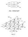
- FIG. 2is a schematic circuit diagram of an STT-MRAM device according to an embodiment of the present invention.
- FIG. 3is a cross sectional view of an embodiment of the present invention as applied to a perpendicular MTJ memory element having a multilayered seed structure;
- FIG. 4is a cross sectional view of another embodiment of the present invention as applied to a perpendicular MTJ memory element having a multilayered seed structure;
- FIG. 5is a cross sectional view of still another embodiment of the present invention as applied to a perpendicular MTJ memory element having a multilayered seed structure;
- FIG. 6is a cross sectional view of yet another embodiment of the present invention as applied to a perpendicular MTJ memory element having a multilayered seed structure.
- the material ABcan be an alloy, a compound, or a combination thereof, except where the context excludes that possibility.
- noncrystallinemeans an amorphous state or a state in which fine crystals are dispersed in an amorphous matrix, not a single crystal or polycrystalline state. In case of state in which fine crystals are dispersed in an amorphous matrix, those in which a crystalline peak is substantially not observed by, for example, X-ray diffraction can be designated as “noncrystalline.”
- superlatticemeans a synthetic periodic structure of layers of at least two constituent materials.
- a superlatticehas at least two repeated unit stacks with each unit stack formed by laminating the constituent materials. Because of the periodic nature of its structure, a superlattice may exhibit characteristic satellite peaks when analyzed by diffraction methods, such as X-ray diffraction and neutron diffraction.
- a [Co/Pt] n superlatticewould denote a structure formed by n stacks of bilayer structure of cobalt (Co) and platinum (Pt).
- magnetic dead layermeans a layer of supposedly ferromagnetic material that does not exhibit a net magnetic moment in the absence of an external magnetic field.
- a magnetic dead layer of several atomic layersmay form in a magnetic film in contact with another layer material owing to intermixing of atoms at the interface.
- a magnetic dead layermay form as thickness of a magnetic film decreases to a point that the magnetic film becomes superparamagnetic.
- the term “at least” followed by a numberis used herein to denote the start of a range beginning with that number, which may be a range having an upper limit or no upper limit, depending on the variable being defined. For example, “at least 1” means 1 or more than 1.
- the term “at most” followed by a numberis used herein to denote the end of a range ending with that number, which may be a range having 1 or 0 as its lower limit, or a range having no lower limit, depending upon the variable being defined. For example, “at most 4” means 4 or less than 4, and “at most 40%” means 40% or less than 40%.
- a rangeis given as “(a first number) to (a second number)” or “(a first number)-(a second number),” this means a range whose lower limit is the first number and whose upper limit is the second number.
- “25 to 100 nm”means a range whose lower limit is 25 nm and whose upper limit is 100 nm.
- FIG. 2is a schematic circuit diagram of an STT-MRAM device 100 according to an embodiment of the present invention.
- the STT-MRAM device 100comprises a plurality of memory cells 102 with each of the memory cells 102 including a selection transistor 104 coupled to a MTJ memory element 106 ; a plurality of parallel word lines 108 with each being coupled to gates of a respective row of the selection transistors 104 in a first direction; and a plurality of parallel bit lines 110 with each being coupled to a respective row of the memory elements 106 in a second direction substantially perpendicular to the first direction.
- the STT-MRAM device 100may optionally include a plurality of parallel source lines 112 with each being coupled to a respective row of the selection transistors 104 in the first or second direction.
- the MTJ memory element 106has a perpendicular MTJ structure that includes a multilayered seed structure.
- An embodiment of the present invention as applied to a perpendicular MTJ memory elementwill now be described with reference to FIG. 3 .
- the illustrated perpendicular MTJ memory element 120comprises a multilayered seed structure 122 formed on top of an optional bottom electrode 124 , a magnetic free layer 126 formed on top of the multilayered seed structure 122 , an insulating tunnel junction layer 128 formed on top of the magnetic free layer 126 , and a magnetic reference layer 130 formed on top of the insulating tunnel junction layer 128 .
- the memory element 120may optionally include an underlayer (not shown) interposed between the multilayered seed structure 122 and the magnetic free layer 126 .
- FIG. 4illustrates another embodiment of the present invention that comprises a multilayered seed structure 122 formed on top of an optional bottom electrode 124 , a magnetic reference layer 130 formed on top of the multilayered seed structure 122 , an insulating tunnel junction layer 128 formed on top of the magnetic reference layer 130 , and a magnetic free layer 126 formed on top of the insulating tunnel junction layer 128 .
- the memory element 131may optionally include an underlayer (not shown) interposed between the multilayered seed structure 122 and the magnetic reference layer 130 .
- the memory element 131 of FIG. 4differs from the memory element 120 of FIG. 3 in that the stacking order of the magnetic free layer 126 and the magnetic reference layer 130 is reversed. Therefore, the memory elements 120 and 131 have “top-pinned” and “bottom-pinned” structures, respectively.
- the multilayered seed structure 122 of FIGS. 3 and 4is to provide a smooth surface for the magnetic free layer 126 or the magnetic reference layer 130 to form upon.
- the multilayered seed structure 122is formed by interleaving a first type sublayer 132 and a second type sublayer 134 to form n number of stacks or repeats of a unit bilayer structure 136 made of the first and second type sublayers 132 and 134 , where n is an integer greater or equal to 1. At least one of the first and second type sublayers 132 and 134 includes therein one or more ferromagnetic elements.
- the multilayered seed structure 122has a structure denoted by [first type sublayer/second type sublayer] n with the first and second type sublayers 132 and 134 on bottom and top, respectively.
- the first type sublayer 132is preferred to be smooth and may be amorphous.
- the first type sublayer 132may be made of a material comprising at least one non-magnetic element selected from the group consisting of titanium (Ti), zirconium (Zr), hafnium (Hf), vanadium (V), niobium (Nb), tantalum (Ta), chromium (Cr), molybdenum (Mo), tungsten (W), platinum (Pt), palladium (Pd), and ruthenium (Ru).
- the first type sublayer 132may comprise one or more ferromagnetic elements, such as but not limited to cobalt (Co), nickel (Ni), and iron (Fe), to form a material, such as but not limited to Co, Ni, Fe, CoNi, CoFe, NiFe, CoNiFe.
- ferromagnetic elementssuch as but not limited to cobalt (Co), nickel (Ni), and iron (Fe)
- Cocobalt
- Ninickel
- Feiron
- the first type sublayer 132may further include at least one non-magnetic element, such as but not limited to boron (B), titanium (Ti), zirconium (Zr), hafnium (Hf), vanadium (V), niobium (Nb), tantalum (Ta), chromium (Cr), molybdenum (Mo), tungsten (W), aluminum (Al), silicon (Si), germanium (Ge), gallium (Ga), oxygen (O), nitrogen (N), carbon (C), platinum (Pt), palladium (Pd), ruthenium (Ru), and phosphorus (P), to form an alloy or compound, such as but not limited to cobalt-iron-boron (CoFeB), cobalt-iron-boron-titanium (CoFeBTi), cobalt-iron-boron-zirconium, (CoFeBZr), cobalt-iron-boron-hafnium (CoFeBHf), cobalt-iron-boro
- the first type sublayer 132may have a thickness of at least about 0.2 nm, preferably about 0.4 to 3.0 nm, more preferably about 0.4 nm to 2.5 nm. Accordingly, in embodiments where the first type sublayer 132 includes therein magnetic elements, the first type sublayer 132 may become non-magnetic or behave like a magnetic dead layer when the thickness decreases to a point that the supposedly ferromagnetic material becomes superparamagnetic.
- the second type sublayer 134is preferred to be smooth and may be amorphous.
- the second type sublayer 134may be made of any suitable material for the first type sublayer 132 as described above and may have the same thickness ranges as the first type sublayer 132 as described above.
- the first type sublayer 132is made of Ta and has a thickness of about 2.0 nm
- the second type sublayer 134is made of CoFeB and has a thickness of about 0.6 nm.
- Both the 2.0 nm thick Ta and the 0.6 nm thick CoFeBmay be amorphous.
- the 0.6 nm thick CoFeBmay be non-magnetic or superparamagnetic, thereby rendering the multilayered seed structure 122 to be non-magnetic.
- the multilayered seed structure 122may be made of [CoFeB/Ta] n , [CoFeB/Ru] n , [Ru/CoFeB] n , [CoFeB/FeZrB] n , [FeZrB/CoFeB] n , [FeZrB/Ta] n , or [Ta/FeZrB] n .
- the second type sublayer 134which is on top of the multilayered seed structure 122 , is not made of Ta
- an optional underlayer made of Tamay be inserted between the multilayered seed structure 122 and the magnetic free layer 126 of FIG. 3 to prevent direct contact therebetween.
- an optional underlayer made of Tamay be inserted between the multilayered seed structure 122 and the magnetic reference layer 130 of FIG. 4 .
- the optional bottom electrode 124 made of Tamay be added to isolate the multilayered seed structure 122 of FIGS. 3 and 4 from structures therebeneath.
- the multilayered seed structure 122may not exhibit the characteristic satellite peaks associated with superlattice when analyzed by X-ray or neutron diffraction, especially when one or both of the first and second type layers 132 and 134 are amorphous.
- the magnetic free layer 126 of FIGS. 3 and 4has a variable magnetization direction 138 substantially perpendicular to the layer plane thereof.
- the magnetic free layer 126may comprise one or more ferromagnetic elements, such as but not limited to Co, Ni, and Fe, to form a magnetic material, such as but not limited to Co, Ni, Fe, CoNi, CoFe, NiFe, or CoNiFe.
- the magnetic material of the magnetic free layer 126may further include at least one non-magnetic element, such as but not limited to B, Ti, Zr, Hf, V, Nb, Ta, Cr, Mo, W, Al, Si, Ge, Ga, O, N, C, Pt, Pd, Ru, or P, to form a magnetic alloy or compound, such as but not limited to FePt, CoPt, CoFeB, CoFeBTi, CoFeBZr, CoFeBHf, CoFeBV, CoFeBTa, CoFeBCr, CoFeTi, CoFeZr, CoFeHf, CoFeV, CoFeNb, CoFeTa, CoFeCr, CoFeMo, CoFeW, CoFeAl, CoFeSi, CoFeGe, CoFeP, CoCr, CoCrB, CoCrPt, CoCrPtB, CoCrPd, CoCrTi, CoCrZ
- the magnetic free layer 126may comprise at least two magnetic sublayers with each of the magnetic sublayers made of a suitable magnetic material for the magnetic free layer 126 as described above.
- the magnetic free layer 126may further comprise at least one insertion or perpendicular enhancement layer (PEL) made of a suitable non-magnetic material, such as but not limited to Ta, W, Hf, or Ru, between the magnetic sublayers.
- PELperpendicular enhancement layer
- the magnetic free layer 126comprises two magnetic sublayers with a Ta perpendicular enhancement layer (PEL) interposed therebetween.
- the insulating tunnel junction layer 128which has an energy barrier through which electrons can pass by tunnel effect, may be made of any suitable insulating material, such as but not limited to magnesium oxide (MgO) and aluminum oxide (AlO x ).
- the magnetic reference layer 130 of FIGS. 3 and 4has a first fixed magnetization direction 140 substantially perpendicular to the layer plane thereof.
- the magnetic reference layer 130may comprise one or more ferromagnetic elements, such as but not limited to Co, Ni, and Fe, to form a magnetic material, such as but not limited to Co, Ni, Fe, CoNi, CoFe, NiFe, or CoNiFe.
- the magnetic material of the magnetic reference layer 130may further include at least one non-magnetic element, such as but not limited to samarium (Sm), neodymium (Nd), B, Ti, Zr, Hf, V, Nb, Ta, Cr, Mo, W, Al, Si, Ge, Ga, O, N, C, Pt, Pd, Ru, or P, to form a magnetic alloy or compound, such as but not limited to SmCo, NdFeB, FePt, CoPt, CoFeB, CoFeBTi, CoFeBZr, CoFeBHf, CoFeBV, CoFeBTa, CoFeBCr, CoFeTi, CoFeZr, CoFeHf, CoFeV, CoFeNb, CoFeTa, CoFeCr, CoFeMo, CoFeW, CoFeAl, CoFeSi, CoFeGe, CoFeP, CoCr, CoCrB, Co
- the magnetic reference layer 130may comprise at least two magnetic sublayers with each of the magnetic sublayers made of a suitable magnetic material for the magnetic reference layer 130 as described above.
- the magnetic reference layer 130may further comprise at least one insertion or perpendicular enhancement layer (PEL) made of a suitable non-magnetic material, such as but not limited to Ta, W, Hf, or Ru, between the magnetic sublayers.
- PELperpendicular enhancement layer
- the magnetic reference layer 130comprises two magnetic sublayers with a Ta perpendicular enhancement layer (PEL) interposed therebetween.
- the magnetic reference layer 130comprises two magnetic sublayers with each sublayer comprising cobalt and iron.
- the magnetic reference layer 130may have a multilayer structure formed by interleaving at least two different types of materials with at least one of the at least two different types of materials being magnetic, such as but not limited to [Co/Pt] n , [Pt/Co] n , [Co/Pd] n , [Pd/Co] n , [Co/Ni] n , [Ni/Co] n , [CoFe/Pt] n , [Pt/CoFe] n , [Pt(Pd)/Co] n , or [Co/Pt(Pd)] n .
- the multilayer structure of the magnetic reference layer 130may or may not exhibit the characteristic satellite peaks associated with superlattice when analyzed by X-ray or neutron diffraction.
- the optional bottom electrode 124 of FIGS. 3 and 4may be made of any suitable conductor, such as but not limited to Ta, tantalum nitride (TaN), Ti, titanium nitride (TiN), W, Ru, copper (Cu), or CuN.
- Tatantalum nitride
- TiNtitanium nitride
- TiNtitanium nitride
- WRu
- Cucopper
- the optional bottom electrode 124 made of Tamay be added to isolate the multilayered seed structure 122 from structures therebeneath.
- the positions of the magnetic free layer 126 and the magnetic reference layer 130 shown in FIG. 3can be swapped without affecting the performance of the memory element 120 .
- the magnetic reference layer 130may alternatively form on the multilayered seed structure 122 with the insulating tunnel junction layer 128 formed on the magnetic reference layer 130 and the magnetic free layer 126 formed on the insulating tunnel junction layer 128 , as illustrated in FIG. 4 .
- the illustrated MTJ memory element 142 of FIG. 5further includes a substrate 144 upon which the optional bottom electrode 124 forms, an optional underlayer 146 formed between the multilayered seed structure 122 and the magnetic free layer 126 , an anti-ferromagnetic coupling layer 148 formed on top of the magnetic reference layer 130 , a magnetic fixed layer 150 formed on top of the anti-ferromagnetic coupling layer 148 , and an optional cap layer 152 formed on top of the magnetic fixed layer 150 .
- the substratemay include therein a contact 154 coupled to the optional bottom electrode 124 .
- the multilayered seed structure 122forms directly on the substrate 144 or the contact 154 .
- the magnetic free layer 126forms directly on the multilayered seed structure 122 .
- the substrate 144is made of an insulating material and may include therein the optional contact 154 coupled to a selection transistor (not shown) therebeneath.
- the contact 154may be made of any suitable conductor, such as but not limited to Ta, Cu, W, Ti, Ru, TaN, CuN, TiN, or any combination thereof.
- One of the functions of the optional underlayer 146is to separate the magnetic free layer 126 from the multilayered seed structure 122 when the second type sublayer 134 , which is on top of the multilayered seed structure 122 , is not made of Ta.
- the underlayer 146may be made of any suitable material, such as but not limited to Ti, Zr, Hf, V, Nb, Ta, Cr, Mo, W, Rh, Pd, Pt, Cu, Ag, Ru, or any combination thereof.
- the magnetic fixed layer 150has a second fixed magnetization direction 156 that is substantially perpendicular to the layer plane thereof and is substantially opposite to the first fixed magnetization direction 140 of the magnetic reference layer 130 .
- the magnetic fixed layer 150provides anti-ferromagnetic coupling to the magnetic reference layer 130 by pinning the magnetization direction 140 thereof in opposite orientation relative to that of the magnetic fixed layer 150 through the anti-ferromagnetic coupling layer 148 , which may be made of a material comprising at least one element selected from the group consisting of ruthenium (Ru), rhodium (Rh), iridium (Ir), tantalum (Ta), manganese (Mn), oxygen (O), and nitrogen (N).
- Ruruthenium
- Rhrhodium
- Iriridium
- Tatantalum
- Mnmanganese
- Nnitrogen
- the anti-ferromagnetic coupling layer 148is made of Ru or Ta. Another function of the magnetic fixed layer 150 , which has an opposite magnetization direction 156 compared with the magnetic reference layer 130 , is to cancel, as much as possible, the stray magnetic field exerted by the magnetic reference layer 130 on the magnetic free layer 126 , thereby minimizing the offset field or net external field at the magnetic free layer 126 .
- the magnetic fixed layer 150may have any suitable structure as describe above for the magnetic reference layer 130 , such as single layer or multilayer structure.
- the magnetic fixed layer 150may be made of any suitable magnetic material for the magnetic reference layer 130 as described above.
- the magnetic fixed layer 150is made of [Co/Pt] n , [Pt/Co] n , [Co/Ni] n , [Ni/Co] n , or any combination thereof.
- the magnetic fixed layer 150is made of an alloy comprising Co, Fe, and B.
- the optional cap layer 152may be made of any suitable material, such as but not limited to Ti, Zr, Hf, V, Nb, Ta, Cr, Mo, W, Rh, Pd, Pt, Cu, Ag, Ru, or any combination thereof.
- the optional cap layer 152may alternatively be formed of any suitable structure for the multilayered seed structure 122 as described above.
- the stacking order of the magnetic layers 126 , 130 , and 150 of the memory element 142may be inverted without affecting the performance thereof.
- the resulting structureas illustrated in FIG. 6 , comprises the multilayered seed structure 122 forms on the substrate 144 or the contact 154 , the magnetic fixed layer 150 formed on the multilayered seed structure 122 , the anti-ferromagnetic coupling layer 148 formed on the magnetic fixed layer 150 , the magnetic reference layer 130 formed on the anti-ferromagnetic coupling layer 148 , the insulating tunnel junction layer 128 formed on the magnetic reference layer 130 , the magnetic free layer 126 formed on the insulating tunnel junction layer 128 , and the optional cap layer formed on the magnetic free layer 126 .
- the memory element 160 of FIG. 6may include the optional bottom electrode 124 formed between the multilayered seed structure 122 and the substrate 144 or the contact 154 , or the optional underlayer 146 formed between the multilayered seed structure 122 and the magnetic fixed layer 150 , or both.
- the magnetic fixed layeris made of [Co/Pt] n , [Pt/Co] n , [Co/Ni] n , [Ni/Co] n , or any combination thereof.
- the magnetic reference layer 130includes two magnetic sublayers in contact with each sublayer comprising cobalt and iron.
- one magnetic sublayer formed adjacent to the anti-ferromagnetic layer 148may comprise cobalt and iron, while the other magnetic sublayer formed adjacent to the insulating tunnel junction layer 128 may comprise cobalt, iron, and boron, or comprise cobalt, iron, and tantalum.
Landscapes
- Engineering & Computer Science (AREA)
- Computer Hardware Design (AREA)
- Mram Or Spin Memory Techniques (AREA)
- Hall/Mr Elements (AREA)
Abstract
Description
Claims (20)
Priority Applications (9)
| Application Number | Priority Date | Filing Date | Title |
|---|---|---|---|
| US15/295,002US9793319B2 (en) | 2014-05-21 | 2016-10-17 | Multilayered seed structure for perpendicular MTJ memory element |
| US15/687,258US10050083B2 (en) | 2014-05-21 | 2017-08-25 | Magnetic structure with multilayered seed |
| US16/101,325US10347691B2 (en) | 2014-05-21 | 2018-08-10 | Magnetic memory element with multilayered seed structure |
| US16/287,987US10438997B2 (en) | 2014-05-21 | 2019-02-27 | Multilayered seed structure for magnetic memory element including a CoFeB seed layer |
| US16/595,120US10720469B2 (en) | 2014-05-21 | 2019-10-07 | Multilayered seed structure for magnetic memory element including a CoFeB seed layer |
| US16/903,172US10950659B2 (en) | 2014-05-21 | 2020-06-16 | Multilayered seed for perpendicular magnetic structure |
| US17/175,663US11348971B2 (en) | 2014-05-21 | 2021-02-13 | Multilayered seed for perpendicular magnetic structure |
| US17/752,154US11785784B2 (en) | 2014-05-21 | 2022-05-24 | Multilayered seed for perpendicular magnetic structure including an oxide layer |
| US18/241,856US12133395B2 (en) | 2014-05-21 | 2023-09-02 | Multilayered seed for perpendicular magnetic structure including an oxide layer |
Applications Claiming Priority (3)
| Application Number | Priority Date | Filing Date | Title |
|---|---|---|---|
| US201462001554P | 2014-05-21 | 2014-05-21 | |
| US14/687,161US9496489B2 (en) | 2014-05-21 | 2015-04-15 | Magnetic random access memory with multilayered seed structure |
| US15/295,002US9793319B2 (en) | 2014-05-21 | 2016-10-17 | Multilayered seed structure for perpendicular MTJ memory element |
Related Parent Applications (1)
| Application Number | Title | Priority Date | Filing Date |
|---|---|---|---|
| US14/687,161ContinuationUS9496489B2 (en) | 2014-05-21 | 2015-04-15 | Magnetic random access memory with multilayered seed structure |
Related Child Applications (2)
| Application Number | Title | Priority Date | Filing Date |
|---|---|---|---|
| US15/491,220Continuation-In-PartUS10008663B1 (en) | 2014-05-21 | 2017-04-19 | Perpendicular magnetic fixed layer with high anisotropy |
| US15/687,258Continuation-In-PartUS10050083B2 (en) | 2014-05-21 | 2017-08-25 | Magnetic structure with multilayered seed |
Publications (2)
| Publication Number | Publication Date |
|---|---|
| US20170033156A1 US20170033156A1 (en) | 2017-02-02 |
| US9793319B2true US9793319B2 (en) | 2017-10-17 |
Family
ID=54556691
Family Applications (4)
| Application Number | Title | Priority Date | Filing Date |
|---|---|---|---|
| US14/687,161Active2035-05-18US9496489B2 (en) | 2014-05-21 | 2015-04-15 | Magnetic random access memory with multilayered seed structure |
| US14/701,955ActiveUS9419207B2 (en) | 2014-05-21 | 2015-05-01 | Magnetic random access memory with multilayered seed structure |
| US14/727,642ActiveUS9444038B2 (en) | 2014-05-21 | 2015-06-01 | Magnetic random access memory with nickel/transition metal multilayered seed structure |
| US15/295,002ActiveUS9793319B2 (en) | 2014-05-21 | 2016-10-17 | Multilayered seed structure for perpendicular MTJ memory element |
Family Applications Before (3)
| Application Number | Title | Priority Date | Filing Date |
|---|---|---|---|
| US14/687,161Active2035-05-18US9496489B2 (en) | 2014-05-21 | 2015-04-15 | Magnetic random access memory with multilayered seed structure |
| US14/701,955ActiveUS9419207B2 (en) | 2014-05-21 | 2015-05-01 | Magnetic random access memory with multilayered seed structure |
| US14/727,642ActiveUS9444038B2 (en) | 2014-05-21 | 2015-06-01 | Magnetic random access memory with nickel/transition metal multilayered seed structure |
Country Status (1)
| Country | Link |
|---|---|
| US (4) | US9496489B2 (en) |
Cited By (36)
| Publication number | Priority date | Publication date | Assignee | Title |
|---|---|---|---|---|
| US10141498B2 (en) | 2015-12-10 | 2018-11-27 | Everspin Technologies, Inc. | Magnetoresistive stack, seed region thereof and method of manufacturing same |
| US10360964B2 (en) | 2016-09-27 | 2019-07-23 | Spin Memory, Inc. | Method of writing contents in memory during a power up sequence using a dynamic redundancy register in a memory device |
| US10360962B1 (en) | 2017-12-28 | 2019-07-23 | Spin Memory, Inc. | Memory array with individually trimmable sense amplifiers |
| US10366775B2 (en) | 2016-09-27 | 2019-07-30 | Spin Memory, Inc. | Memory device using levels of dynamic redundancy registers for writing a data word that failed a write operation |
| US10395711B2 (en) | 2017-12-28 | 2019-08-27 | Spin Memory, Inc. | Perpendicular source and bit lines for an MRAM array |
| US10395712B2 (en) | 2017-12-28 | 2019-08-27 | Spin Memory, Inc. | Memory array with horizontal source line and sacrificial bitline per virtual source |
| US10411185B1 (en) | 2018-05-30 | 2019-09-10 | Spin Memory, Inc. | Process for creating a high density magnetic tunnel junction array test platform |
| US10437723B2 (en) | 2016-09-27 | 2019-10-08 | Spin Memory, Inc. | Method of flushing the contents of a dynamic redundancy register to a secure storage area during a power down in a memory device |
| US10437491B2 (en) | 2016-09-27 | 2019-10-08 | Spin Memory, Inc. | Method of processing incomplete memory operations in a memory device during a power up sequence and a power down sequence using a dynamic redundancy register |
| US10446744B2 (en) | 2018-03-08 | 2019-10-15 | Spin Memory, Inc. | Magnetic tunnel junction wafer adaptor used in magnetic annealing furnace and method of using the same |
| US10481976B2 (en) | 2017-10-24 | 2019-11-19 | Spin Memory, Inc. | Forcing bits as bad to widen the window between the distributions of acceptable high and low resistive bits thereby lowering the margin and increasing the speed of the sense amplifiers |
| US10483320B2 (en) | 2015-12-10 | 2019-11-19 | Everspin Technologies, Inc. | Magnetoresistive stack with seed region and method of manufacturing the same |
| US10489245B2 (en) | 2017-10-24 | 2019-11-26 | Spin Memory, Inc. | Forcing stuck bits, waterfall bits, shunt bits and low TMR bits to short during testing and using on-the-fly bit failure detection and bit redundancy remapping techniques to correct them |
| US10529439B2 (en) | 2017-10-24 | 2020-01-07 | Spin Memory, Inc. | On-the-fly bit failure detection and bit redundancy remapping techniques to correct for fixed bit defects |
| US10529915B2 (en) | 2018-03-23 | 2020-01-07 | Spin Memory, Inc. | Bit line structures for three-dimensional arrays with magnetic tunnel junction devices including an annular free magnetic layer and a planar reference magnetic layer |
| US10546624B2 (en) | 2017-12-29 | 2020-01-28 | Spin Memory, Inc. | Multi-port random access memory |
| US10546625B2 (en) | 2016-09-27 | 2020-01-28 | Spin Memory, Inc. | Method of optimizing write voltage based on error buffer occupancy |
| US10593396B2 (en) | 2018-07-06 | 2020-03-17 | Spin Memory, Inc. | Multi-bit cell read-out techniques for MRAM cells with mixed pinned magnetization orientations |
| US10600478B2 (en) | 2018-07-06 | 2020-03-24 | Spin Memory, Inc. | Multi-bit cell read-out techniques for MRAM cells with mixed pinned magnetization orientations |
| US10650875B2 (en) | 2018-08-21 | 2020-05-12 | Spin Memory, Inc. | System for a wide temperature range nonvolatile memory |
| US10656994B2 (en) | 2017-10-24 | 2020-05-19 | Spin Memory, Inc. | Over-voltage write operation of tunnel magnet-resistance (“TMR”) memory device and correcting failure bits therefrom by using on-the-fly bit failure detection and bit redundancy remapping techniques |
| US10784437B2 (en) | 2018-03-23 | 2020-09-22 | Spin Memory, Inc. | Three-dimensional arrays with MTJ devices including a free magnetic trench layer and a planar reference magnetic layer |
| US10811594B2 (en) | 2017-12-28 | 2020-10-20 | Spin Memory, Inc. | Process for hard mask development for MRAM pillar formation using photolithography |
| US10818331B2 (en) | 2016-09-27 | 2020-10-27 | Spin Memory, Inc. | Multi-chip module for MRAM devices with levels of dynamic redundancy registers |
| US10840259B2 (en) | 2018-08-13 | 2020-11-17 | Sandisk Technologies Llc | Three-dimensional memory device including liner free molybdenum word lines and methods of making the same |
| US10840439B2 (en) | 2017-12-29 | 2020-11-17 | Spin Memory, Inc. | Magnetic tunnel junction (MTJ) fabrication methods and systems |
| US10886330B2 (en) | 2017-12-29 | 2021-01-05 | Spin Memory, Inc. | Memory device having overlapping magnetic tunnel junctions in compliance with a reference pitch |
| US10891997B2 (en) | 2017-12-28 | 2021-01-12 | Spin Memory, Inc. | Memory array with horizontal source line and a virtual source line |
| US10971680B2 (en) | 2018-10-01 | 2021-04-06 | Spin Memory, Inc. | Multi terminal device stack formation methods |
| TWI727351B (en)* | 2018-06-29 | 2021-05-11 | 台灣積體電路製造股份有限公司 | Semiconductor device, magneto-resistive random-access memory device and method for manufacturing the same |
| US11107974B2 (en) | 2018-03-23 | 2021-08-31 | Spin Memory, Inc. | Magnetic tunnel junction devices including a free magnetic trench layer and a planar reference magnetic layer |
| US11107979B2 (en) | 2018-12-28 | 2021-08-31 | Spin Memory, Inc. | Patterned silicide structures and methods of manufacture |
| US11107978B2 (en) | 2018-03-23 | 2021-08-31 | Spin Memory, Inc. | Methods of manufacturing three-dimensional arrays with MTJ devices including a free magnetic trench layer and a planar reference magnetic layer |
| US11223010B2 (en)* | 2016-04-08 | 2022-01-11 | International Business Machines Corporation | Thin reference layer for STT MRAM |
| US11621293B2 (en) | 2018-10-01 | 2023-04-04 | Integrated Silicon Solution, (Cayman) Inc. | Multi terminal device stack systems and methods |
| US11935677B2 (en) | 2020-10-22 | 2024-03-19 | Samsung Electronics Co., Ltd. | Magnetic device |
Families Citing this family (64)
| Publication number | Priority date | Publication date | Assignee | Title |
|---|---|---|---|---|
| US9461242B2 (en) | 2013-09-13 | 2016-10-04 | Micron Technology, Inc. | Magnetic memory cells, methods of fabrication, semiconductor devices, memory systems, and electronic systems |
| US9608197B2 (en) | 2013-09-18 | 2017-03-28 | Micron Technology, Inc. | Memory cells, methods of fabrication, and semiconductor devices |
| US9529060B2 (en)* | 2014-01-09 | 2016-12-27 | Allegro Microsystems, Llc | Magnetoresistance element with improved response to magnetic fields |
| US10454024B2 (en) | 2014-02-28 | 2019-10-22 | Micron Technology, Inc. | Memory cells, methods of fabrication, and memory devices |
| US9281466B2 (en) | 2014-04-09 | 2016-03-08 | Micron Technology, Inc. | Memory cells, semiconductor structures, semiconductor devices, and methods of fabrication |
| US9269888B2 (en)* | 2014-04-18 | 2016-02-23 | Micron Technology, Inc. | Memory cells, methods of fabrication, and semiconductor devices |
| US10438997B2 (en)* | 2014-05-21 | 2019-10-08 | Avalanche Technology, Inc. | Multilayered seed structure for magnetic memory element including a CoFeB seed layer |
| US10395707B2 (en)* | 2014-09-26 | 2019-08-27 | Intel Corporation | Amorphous seed layer for improved stability in perpendicular STTM stack |
| US9349945B2 (en) | 2014-10-16 | 2016-05-24 | Micron Technology, Inc. | Memory cells, semiconductor devices, and methods of fabrication |
| US9768377B2 (en) | 2014-12-02 | 2017-09-19 | Micron Technology, Inc. | Magnetic cell structures, and methods of fabrication |
| US10439131B2 (en) | 2015-01-15 | 2019-10-08 | Micron Technology, Inc. | Methods of forming semiconductor devices including tunnel barrier materials |
| KR101705962B1 (en)* | 2015-01-19 | 2017-02-14 | 한양대학교 산학협력단 | Magnetic tunnel junction structure with perpendicular magnetic anisotropy and Magnetic element including the same |
| US10468590B2 (en) | 2015-04-21 | 2019-11-05 | Spin Memory, Inc. | High annealing temperature perpendicular magnetic anisotropy structure for magnetic random access memory |
| US9728712B2 (en) | 2015-04-21 | 2017-08-08 | Spin Transfer Technologies, Inc. | Spin transfer torque structure for MRAM devices having a spin current injection capping layer |
| US9853206B2 (en) | 2015-06-16 | 2017-12-26 | Spin Transfer Technologies, Inc. | Precessional spin current structure for MRAM |
| US9773974B2 (en) | 2015-07-30 | 2017-09-26 | Spin Transfer Technologies, Inc. | Polishing stop layer(s) for processing arrays of semiconductor elements |
| US10163479B2 (en) | 2015-08-14 | 2018-12-25 | Spin Transfer Technologies, Inc. | Method and apparatus for bipolar memory write-verify |
| JP5985728B1 (en)* | 2015-09-15 | 2016-09-06 | 株式会社東芝 | Magnetic memory |
| US10115892B2 (en)* | 2015-11-23 | 2018-10-30 | Headway Technologies, Inc. | Multilayer structure for reducing film roughness in magnetic devices |
| US9780299B2 (en) | 2015-11-23 | 2017-10-03 | Headway Technologies, Inc. | Multilayer structure for reducing film roughness in magnetic devices |
| US9741926B1 (en) | 2016-01-28 | 2017-08-22 | Spin Transfer Technologies, Inc. | Memory cell having magnetic tunnel junction and thermal stability enhancement layer |
| US9673385B1 (en)* | 2016-03-24 | 2017-06-06 | Headway Technologies, Inc. | Seed layer for growth of <111> magnetic materials |
| US9680089B1 (en)* | 2016-05-13 | 2017-06-13 | Micron Technology, Inc. | Magnetic tunnel junctions |
| US10460781B2 (en) | 2016-09-27 | 2019-10-29 | Spin Memory, Inc. | Memory device with a dual Y-multiplexer structure for performing two simultaneous operations on the same row of a memory bank |
| US10446210B2 (en) | 2016-09-27 | 2019-10-15 | Spin Memory, Inc. | Memory instruction pipeline with a pre-read stage for a write operation for reducing power consumption in a memory device that uses dynamic redundancy registers |
| US10991410B2 (en) | 2016-09-27 | 2021-04-27 | Spin Memory, Inc. | Bi-polar write scheme |
| WO2018061710A1 (en)* | 2016-09-28 | 2018-04-05 | Tdk株式会社 | Magnetoresistive effect element |
| US10665777B2 (en) | 2017-02-28 | 2020-05-26 | Spin Memory, Inc. | Precessional spin current structure with non-magnetic insertion layer for MRAM |
| US10672976B2 (en) | 2017-02-28 | 2020-06-02 | Spin Memory, Inc. | Precessional spin current structure with high in-plane magnetization for MRAM |
| US10032978B1 (en) | 2017-06-27 | 2018-07-24 | Spin Transfer Technologies, Inc. | MRAM with reduced stray magnetic fields |
| US10255935B2 (en)* | 2017-07-21 | 2019-04-09 | Applied Materials, Inc. | Magnetic tunnel junctions suitable for high temperature thermal processing |
| US10734013B2 (en) | 2017-10-03 | 2020-08-04 | Western Digital Technologies, Inc. | Spin transfer torque (STT) device with multilayer seed layers for magnetic recording and memory |
| US10424726B2 (en) | 2017-12-28 | 2019-09-24 | Spin Memory, Inc. | Process for improving photoresist pillar adhesion during MRAM fabrication |
| US10367139B2 (en) | 2017-12-29 | 2019-07-30 | Spin Memory, Inc. | Methods of manufacturing magnetic tunnel junction devices |
| US10199083B1 (en) | 2017-12-29 | 2019-02-05 | Spin Transfer Technologies, Inc. | Three-terminal MRAM with ac write-assist for low read disturb |
| US10840436B2 (en) | 2017-12-29 | 2020-11-17 | Spin Memory, Inc. | Perpendicular magnetic anisotropy interface tunnel junction devices and methods of manufacture |
| US10424723B2 (en) | 2017-12-29 | 2019-09-24 | Spin Memory, Inc. | Magnetic tunnel junction devices including an optimization layer |
| US10651370B2 (en)* | 2017-12-29 | 2020-05-12 | Spin Memory, Inc. | Perpendicular magnetic tunnel junction retention and endurance improvement |
| US10784439B2 (en) | 2017-12-29 | 2020-09-22 | Spin Memory, Inc. | Precessional spin current magnetic tunnel junction devices and methods of manufacture |
| US10270027B1 (en) | 2017-12-29 | 2019-04-23 | Spin Memory, Inc. | Self-generating AC current assist in orthogonal STT-MRAM |
| US10360961B1 (en) | 2017-12-29 | 2019-07-23 | Spin Memory, Inc. | AC current pre-charge write-assist in orthogonal STT-MRAM |
| US10236048B1 (en) | 2017-12-29 | 2019-03-19 | Spin Memory, Inc. | AC current write-assist in orthogonal STT-MRAM |
| US10236047B1 (en) | 2017-12-29 | 2019-03-19 | Spin Memory, Inc. | Shared oscillator (STNO) for MRAM array write-assist in orthogonal STT-MRAM |
| US10319900B1 (en) | 2017-12-30 | 2019-06-11 | Spin Memory, Inc. | Perpendicular magnetic tunnel junction device with precessional spin current layer having a modulated moment density |
| US10339993B1 (en) | 2017-12-30 | 2019-07-02 | Spin Memory, Inc. | Perpendicular magnetic tunnel junction device with skyrmionic assist layers for free layer switching |
| US10141499B1 (en) | 2017-12-30 | 2018-11-27 | Spin Transfer Technologies, Inc. | Perpendicular magnetic tunnel junction device with offset precessional spin current layer |
| US10255962B1 (en) | 2017-12-30 | 2019-04-09 | Spin Memory, Inc. | Microwave write-assist in orthogonal STT-MRAM |
| US10229724B1 (en) | 2017-12-30 | 2019-03-12 | Spin Memory, Inc. | Microwave write-assist in series-interconnected orthogonal STT-MRAM devices |
| US10236439B1 (en) | 2017-12-30 | 2019-03-19 | Spin Memory, Inc. | Switching and stability control for perpendicular magnetic tunnel junction device |
| US10468588B2 (en) | 2018-01-05 | 2019-11-05 | Spin Memory, Inc. | Perpendicular magnetic tunnel junction device with skyrmionic enhancement layers for the precessional spin current magnetic layer |
| US10438995B2 (en) | 2018-01-08 | 2019-10-08 | Spin Memory, Inc. | Devices including magnetic tunnel junctions integrated with selectors |
| US10438996B2 (en) | 2018-01-08 | 2019-10-08 | Spin Memory, Inc. | Methods of fabricating magnetic tunnel junctions integrated with selectors |
| US10943951B2 (en)* | 2018-04-03 | 2021-03-09 | National University Of Singapore | Spin orbit torque magnetic random access memory structures and methods for fabrication |
| US10468171B1 (en) | 2018-06-27 | 2019-11-05 | Globalfoundries Singapore Pte. Ltd. | Integrated circuits with magnetic tunnel junctions and methods of producing the same |
| US11770979B2 (en)* | 2018-06-29 | 2023-09-26 | Intel Corporation | Conductive alloy layer in magnetic memory devices and methods of fabrication |
| US10559338B2 (en) | 2018-07-06 | 2020-02-11 | Spin Memory, Inc. | Multi-bit cell read-out techniques |
| US10692569B2 (en) | 2018-07-06 | 2020-06-23 | Spin Memory, Inc. | Read-out techniques for multi-bit cells |
| US10699761B2 (en) | 2018-09-18 | 2020-06-30 | Spin Memory, Inc. | Word line decoder memory architecture |
| US10580827B1 (en) | 2018-11-16 | 2020-03-03 | Spin Memory, Inc. | Adjustable stabilizer/polarizer method for MRAM with enhanced stability and efficient switching |
| JP7160945B2 (en)* | 2018-12-27 | 2022-10-25 | アルプスアルパイン株式会社 | EXCHANGE COUPLING FILM AND MAGNETORESISTIC EFFECT ELEMENT AND MAGNETIC DETECTION DEVICE USING THE SAME |
| US12052928B2 (en)* | 2021-08-09 | 2024-07-30 | Everspin Technologies, Inc. | Magnetoresistive devices and methods therefor |
| US11719771B1 (en) | 2022-06-02 | 2023-08-08 | Allegro Microsystems, Llc | Magnetoresistive sensor having seed layer hysteresis suppression |
| US12320870B2 (en) | 2022-07-19 | 2025-06-03 | Allegro Microsystems, Llc | Controlling out-of-plane anisotropy in an MR sensor with free layer dusting |
| US20240081155A1 (en)* | 2022-09-07 | 2024-03-07 | HeFeChip Corporation Limited | Magnetic tunnel junction structure with non-magnetic amorphous insertion layer |
Citations (21)
| Publication number | Priority date | Publication date | Assignee | Title |
|---|---|---|---|---|
| US5701223A (en) | 1995-06-30 | 1997-12-23 | International Business Machines Corporation | Spin valve magnetoresistive sensor with antiparallel pinned layer and improved exchange bias layer, and magnetic recording system using the sensor |
| US6473337B1 (en) | 2001-10-24 | 2002-10-29 | Hewlett-Packard Company | Memory device having memory cells with magnetic tunnel junction and tunnel junction in series |
| US20050041463A1 (en) | 2003-08-22 | 2005-02-24 | Drewes Joel A. | Mram layer having domain wall traps |
| US20050079638A1 (en) | 2003-10-14 | 2005-04-14 | Drewes Joel A. | System and method for reducing shorting in memory cells |
| US20050185455A1 (en) | 2004-02-25 | 2005-08-25 | Yiming Huai | Perpendicular magnetization magnetic element utilizing spin transfer |
| US20060061915A1 (en) | 2004-09-23 | 2006-03-23 | Headway Technologies, Inc. | CoFe insertion for exchange bias and sensor improvement |
| US20070264728A1 (en) | 2006-05-11 | 2007-11-15 | Tdk Corporation | Manufacturing method of tunnel magnetoresistive effect element, manufacturing method of thin-film magnetic head, and manufacturing method of magnetic memory |
| US20070297220A1 (en) | 2006-06-22 | 2007-12-27 | Masatoshi Yoshikawa | Magnetoresistive element and magnetic memory |
| US20080246104A1 (en) | 2007-02-12 | 2008-10-09 | Yadav Technology | High Capacity Low Cost Multi-State Magnetic Memory |
| US20080261082A1 (en) | 2006-12-28 | 2008-10-23 | Kazumasa Nishimura | Tunneling magnetoresistive element including multilayer free magnetic layer having inserted nonmagnetic metal sublayer |
| US20090213642A1 (en) | 2008-02-25 | 2009-08-27 | Wolfgang Raberg | Integrated Circuit, Memory Cell Arrangement, Memory Cell, Memory Module, Method of Operating an Integrated Circuit, and Method of Manufacturing a Memory Cell |
| US7696551B2 (en) | 2007-09-20 | 2010-04-13 | Magic Technologies, Inc. | Composite hard mask for the etching of nanometer size magnetic multilayer based device |
| US20100315863A1 (en) | 2009-06-11 | 2010-12-16 | Qualcomm Incorporated | Magnetic Tunnel Junction Device and Fabrication |
| US20110064969A1 (en) | 2009-09-15 | 2011-03-17 | Grandis Inc. | Magnetic Element Having Perpendicular Anisotropy With Enhanced Efficiency |
| US8184411B2 (en) | 2009-10-26 | 2012-05-22 | Headway Technologies, Inc. | MTJ incorporating CoFe/Ni multilayer film with perpendicular magnetic anisotropy for MRAM application |
| US20120126905A1 (en) | 2010-11-22 | 2012-05-24 | Headway Technologies, Inc. | Assisting FGL oscillations with perpendicular anisotropy for MAMR |
| US20130009260A1 (en) | 2011-07-07 | 2013-01-10 | Dmytro Apalkov | Method And System For Providing A Magnetic Junction Using Half Metallic Ferromagnets |
| US8541855B2 (en) | 2011-05-10 | 2013-09-24 | Magic Technologies, Inc. | Co/Ni multilayers with improved out-of-plane anisotropy for magnetic device applications |
| US20140103469A1 (en) | 2012-10-11 | 2014-04-17 | Headway Technologies, Inc. | Seed Layer for Multilayer Magnetic Materials |
| US20140153324A1 (en) | 2012-12-03 | 2014-06-05 | Taiwan Semiconductor Manufacturing Company, Ltd | Magnetic Tunnel Junction Memory Device |
| US20150008550A1 (en) | 2013-06-17 | 2015-01-08 | Imec | Magnetic memory element |
Family Cites Families (2)
| Publication number | Priority date | Publication date | Assignee | Title |
|---|---|---|---|---|
| JP5232206B2 (en)* | 2010-09-21 | 2013-07-10 | 株式会社東芝 | Magnetoresistive element and magnetic random access memory |
| US20130108889A1 (en)* | 2011-10-27 | 2013-05-02 | Agency For Science, Technology And Research | Magnetoresistance Device and Memory Device Including the Magnetoresistance Device |
- 2015
- 2015-04-15USUS14/687,161patent/US9496489B2/enactiveActive
- 2015-05-01USUS14/701,955patent/US9419207B2/enactiveActive
- 2015-06-01USUS14/727,642patent/US9444038B2/enactiveActive
- 2016
- 2016-10-17USUS15/295,002patent/US9793319B2/enactiveActive
Patent Citations (22)
| Publication number | Priority date | Publication date | Assignee | Title |
|---|---|---|---|---|
| US5701223A (en) | 1995-06-30 | 1997-12-23 | International Business Machines Corporation | Spin valve magnetoresistive sensor with antiparallel pinned layer and improved exchange bias layer, and magnetic recording system using the sensor |
| US6473337B1 (en) | 2001-10-24 | 2002-10-29 | Hewlett-Packard Company | Memory device having memory cells with magnetic tunnel junction and tunnel junction in series |
| US20050041463A1 (en) | 2003-08-22 | 2005-02-24 | Drewes Joel A. | Mram layer having domain wall traps |
| US20050079638A1 (en) | 2003-10-14 | 2005-04-14 | Drewes Joel A. | System and method for reducing shorting in memory cells |
| US20050185455A1 (en) | 2004-02-25 | 2005-08-25 | Yiming Huai | Perpendicular magnetization magnetic element utilizing spin transfer |
| US20060061915A1 (en) | 2004-09-23 | 2006-03-23 | Headway Technologies, Inc. | CoFe insertion for exchange bias and sensor improvement |
| US20070264728A1 (en) | 2006-05-11 | 2007-11-15 | Tdk Corporation | Manufacturing method of tunnel magnetoresistive effect element, manufacturing method of thin-film magnetic head, and manufacturing method of magnetic memory |
| US20070297220A1 (en) | 2006-06-22 | 2007-12-27 | Masatoshi Yoshikawa | Magnetoresistive element and magnetic memory |
| US20080261082A1 (en) | 2006-12-28 | 2008-10-23 | Kazumasa Nishimura | Tunneling magnetoresistive element including multilayer free magnetic layer having inserted nonmagnetic metal sublayer |
| US20080246104A1 (en) | 2007-02-12 | 2008-10-09 | Yadav Technology | High Capacity Low Cost Multi-State Magnetic Memory |
| US7696551B2 (en) | 2007-09-20 | 2010-04-13 | Magic Technologies, Inc. | Composite hard mask for the etching of nanometer size magnetic multilayer based device |
| US20090213642A1 (en) | 2008-02-25 | 2009-08-27 | Wolfgang Raberg | Integrated Circuit, Memory Cell Arrangement, Memory Cell, Memory Module, Method of Operating an Integrated Circuit, and Method of Manufacturing a Memory Cell |
| US20100315863A1 (en) | 2009-06-11 | 2010-12-16 | Qualcomm Incorporated | Magnetic Tunnel Junction Device and Fabrication |
| US20110064969A1 (en) | 2009-09-15 | 2011-03-17 | Grandis Inc. | Magnetic Element Having Perpendicular Anisotropy With Enhanced Efficiency |
| US8184411B2 (en) | 2009-10-26 | 2012-05-22 | Headway Technologies, Inc. | MTJ incorporating CoFe/Ni multilayer film with perpendicular magnetic anisotropy for MRAM application |
| US20120126905A1 (en) | 2010-11-22 | 2012-05-24 | Headway Technologies, Inc. | Assisting FGL oscillations with perpendicular anisotropy for MAMR |
| US8541855B2 (en) | 2011-05-10 | 2013-09-24 | Magic Technologies, Inc. | Co/Ni multilayers with improved out-of-plane anisotropy for magnetic device applications |
| US20130009260A1 (en) | 2011-07-07 | 2013-01-10 | Dmytro Apalkov | Method And System For Providing A Magnetic Junction Using Half Metallic Ferromagnets |
| US20140103469A1 (en) | 2012-10-11 | 2014-04-17 | Headway Technologies, Inc. | Seed Layer for Multilayer Magnetic Materials |
| US9490054B2 (en)* | 2012-10-11 | 2016-11-08 | Headway Technologies, Inc. | Seed layer for multilayer magnetic materials |
| US20140153324A1 (en) | 2012-12-03 | 2014-06-05 | Taiwan Semiconductor Manufacturing Company, Ltd | Magnetic Tunnel Junction Memory Device |
| US20150008550A1 (en) | 2013-06-17 | 2015-01-08 | Imec | Magnetic memory element |
Cited By (46)
| Publication number | Priority date | Publication date | Assignee | Title |
|---|---|---|---|---|
| US10141498B2 (en) | 2015-12-10 | 2018-11-27 | Everspin Technologies, Inc. | Magnetoresistive stack, seed region thereof and method of manufacturing same |
| US20200043979A1 (en)* | 2015-12-10 | 2020-02-06 | Everspin Technologies, Inc. | Magnetoresistive stack with seed region and method of manufacturing the same |
| US10483320B2 (en) | 2015-12-10 | 2019-11-19 | Everspin Technologies, Inc. | Magnetoresistive stack with seed region and method of manufacturing the same |
| US11690229B2 (en) | 2015-12-10 | 2023-06-27 | Everspin Technologies, Inc. | Magnetoresistive stack with seed region and method of manufacturing the same |
| US10692926B2 (en)* | 2015-12-10 | 2020-06-23 | Everspin Technologies, Inc. | Magnetoresistive stack with seed region and method of manufacturing the same |
| US10910434B2 (en)* | 2015-12-10 | 2021-02-02 | Everspin Technologies, Inc. | Magnetoresistive stack with seed region and method of manufacturing the same |
| US12089418B2 (en) | 2015-12-10 | 2024-09-10 | Everspin Technologies, Inc. | Magnetoresistive stack with seed region and method of manufacturing the same |
| US11223010B2 (en)* | 2016-04-08 | 2022-01-11 | International Business Machines Corporation | Thin reference layer for STT MRAM |
| US10366774B2 (en) | 2016-09-27 | 2019-07-30 | Spin Memory, Inc. | Device with dynamic redundancy registers |
| US10437723B2 (en) | 2016-09-27 | 2019-10-08 | Spin Memory, Inc. | Method of flushing the contents of a dynamic redundancy register to a secure storage area during a power down in a memory device |
| US10437491B2 (en) | 2016-09-27 | 2019-10-08 | Spin Memory, Inc. | Method of processing incomplete memory operations in a memory device during a power up sequence and a power down sequence using a dynamic redundancy register |
| US10424393B2 (en) | 2016-09-27 | 2019-09-24 | Spin Memory, Inc. | Method of reading data from a memory device using multiple levels of dynamic redundancy registers |
| US10366775B2 (en) | 2016-09-27 | 2019-07-30 | Spin Memory, Inc. | Memory device using levels of dynamic redundancy registers for writing a data word that failed a write operation |
| US10818331B2 (en) | 2016-09-27 | 2020-10-27 | Spin Memory, Inc. | Multi-chip module for MRAM devices with levels of dynamic redundancy registers |
| US10360964B2 (en) | 2016-09-27 | 2019-07-23 | Spin Memory, Inc. | Method of writing contents in memory during a power up sequence using a dynamic redundancy register in a memory device |
| US10546625B2 (en) | 2016-09-27 | 2020-01-28 | Spin Memory, Inc. | Method of optimizing write voltage based on error buffer occupancy |
| US10489245B2 (en) | 2017-10-24 | 2019-11-26 | Spin Memory, Inc. | Forcing stuck bits, waterfall bits, shunt bits and low TMR bits to short during testing and using on-the-fly bit failure detection and bit redundancy remapping techniques to correct them |
| US10529439B2 (en) | 2017-10-24 | 2020-01-07 | Spin Memory, Inc. | On-the-fly bit failure detection and bit redundancy remapping techniques to correct for fixed bit defects |
| US10481976B2 (en) | 2017-10-24 | 2019-11-19 | Spin Memory, Inc. | Forcing bits as bad to widen the window between the distributions of acceptable high and low resistive bits thereby lowering the margin and increasing the speed of the sense amplifiers |
| US10656994B2 (en) | 2017-10-24 | 2020-05-19 | Spin Memory, Inc. | Over-voltage write operation of tunnel magnet-resistance (“TMR”) memory device and correcting failure bits therefrom by using on-the-fly bit failure detection and bit redundancy remapping techniques |
| US10930332B2 (en) | 2017-12-28 | 2021-02-23 | Spin Memory, Inc. | Memory array with individually trimmable sense amplifiers |
| US10395712B2 (en) | 2017-12-28 | 2019-08-27 | Spin Memory, Inc. | Memory array with horizontal source line and sacrificial bitline per virtual source |
| US10891997B2 (en) | 2017-12-28 | 2021-01-12 | Spin Memory, Inc. | Memory array with horizontal source line and a virtual source line |
| US10395711B2 (en) | 2017-12-28 | 2019-08-27 | Spin Memory, Inc. | Perpendicular source and bit lines for an MRAM array |
| US10811594B2 (en) | 2017-12-28 | 2020-10-20 | Spin Memory, Inc. | Process for hard mask development for MRAM pillar formation using photolithography |
| US10360962B1 (en) | 2017-12-28 | 2019-07-23 | Spin Memory, Inc. | Memory array with individually trimmable sense amplifiers |
| US10546624B2 (en) | 2017-12-29 | 2020-01-28 | Spin Memory, Inc. | Multi-port random access memory |
| US10840439B2 (en) | 2017-12-29 | 2020-11-17 | Spin Memory, Inc. | Magnetic tunnel junction (MTJ) fabrication methods and systems |
| US10886330B2 (en) | 2017-12-29 | 2021-01-05 | Spin Memory, Inc. | Memory device having overlapping magnetic tunnel junctions in compliance with a reference pitch |
| US10446744B2 (en) | 2018-03-08 | 2019-10-15 | Spin Memory, Inc. | Magnetic tunnel junction wafer adaptor used in magnetic annealing furnace and method of using the same |
| US10784437B2 (en) | 2018-03-23 | 2020-09-22 | Spin Memory, Inc. | Three-dimensional arrays with MTJ devices including a free magnetic trench layer and a planar reference magnetic layer |
| US10529915B2 (en) | 2018-03-23 | 2020-01-07 | Spin Memory, Inc. | Bit line structures for three-dimensional arrays with magnetic tunnel junction devices including an annular free magnetic layer and a planar reference magnetic layer |
| US11107978B2 (en) | 2018-03-23 | 2021-08-31 | Spin Memory, Inc. | Methods of manufacturing three-dimensional arrays with MTJ devices including a free magnetic trench layer and a planar reference magnetic layer |
| US11107974B2 (en) | 2018-03-23 | 2021-08-31 | Spin Memory, Inc. | Magnetic tunnel junction devices including a free magnetic trench layer and a planar reference magnetic layer |
| US10411185B1 (en) | 2018-05-30 | 2019-09-10 | Spin Memory, Inc. | Process for creating a high density magnetic tunnel junction array test platform |
| US10615337B2 (en) | 2018-05-30 | 2020-04-07 | Spin Memory, Inc. | Process for creating a high density magnetic tunnel junction array test platform |
| TWI727351B (en)* | 2018-06-29 | 2021-05-11 | 台灣積體電路製造股份有限公司 | Semiconductor device, magneto-resistive random-access memory device and method for manufacturing the same |
| US10600478B2 (en) | 2018-07-06 | 2020-03-24 | Spin Memory, Inc. | Multi-bit cell read-out techniques for MRAM cells with mixed pinned magnetization orientations |
| US10593396B2 (en) | 2018-07-06 | 2020-03-17 | Spin Memory, Inc. | Multi-bit cell read-out techniques for MRAM cells with mixed pinned magnetization orientations |
| US10991721B2 (en) | 2018-08-13 | 2021-04-27 | Sandisk Technologies Llc | Three-dimensional memory device including liner free molybdenum word lines and methods of making the same |
| US10840259B2 (en) | 2018-08-13 | 2020-11-17 | Sandisk Technologies Llc | Three-dimensional memory device including liner free molybdenum word lines and methods of making the same |
| US10650875B2 (en) | 2018-08-21 | 2020-05-12 | Spin Memory, Inc. | System for a wide temperature range nonvolatile memory |
| US10971680B2 (en) | 2018-10-01 | 2021-04-06 | Spin Memory, Inc. | Multi terminal device stack formation methods |
| US11621293B2 (en) | 2018-10-01 | 2023-04-04 | Integrated Silicon Solution, (Cayman) Inc. | Multi terminal device stack systems and methods |
| US11107979B2 (en) | 2018-12-28 | 2021-08-31 | Spin Memory, Inc. | Patterned silicide structures and methods of manufacture |
| US11935677B2 (en) | 2020-10-22 | 2024-03-19 | Samsung Electronics Co., Ltd. | Magnetic device |
Also Published As
| Publication number | Publication date |
|---|---|
| US20150340601A1 (en) | 2015-11-26 |
| US9419207B2 (en) | 2016-08-16 |
| US9444038B2 (en) | 2016-09-13 |
| US20150340599A1 (en) | 2015-11-26 |
| US20150340598A1 (en) | 2015-11-26 |
| US20170033156A1 (en) | 2017-02-02 |
| US9496489B2 (en) | 2016-11-15 |
Similar Documents
| Publication | Publication Date | Title |
|---|---|---|
| US9793319B2 (en) | Multilayered seed structure for perpendicular MTJ memory element | |
| US11785784B2 (en) | Multilayered seed for perpendicular magnetic structure including an oxide layer | |
| US9166143B1 (en) | Magnetic random access memory with multiple free layers | |
| US10361362B2 (en) | Magnetic random access memory with ultrathin reference layer | |
| US9780300B2 (en) | Magnetic memory element with composite perpendicular enhancement layer | |
| US10050083B2 (en) | Magnetic structure with multilayered seed | |
| US20170288137A9 (en) | Magnetic random access memory with perpendicular enhancement layer | |
| US10347691B2 (en) | Magnetic memory element with multilayered seed structure | |
| US10008663B1 (en) | Perpendicular magnetic fixed layer with high anisotropy | |
| US20250063952A1 (en) | Magnetic Memory Element Including Perpendicular Enhancement Layer and Oxide Cap Layer | |
| US11417836B2 (en) | Magnetic memory element incorporating dual perpendicular enhancement layers | |
| US10910555B2 (en) | Magnetic memory element incorporating perpendicular enhancement layer |
Legal Events
| Date | Code | Title | Description |
|---|---|---|---|
| AS | Assignment | Owner name:AVALANCHE TECHNOLOGY, INC., CALIFORNIA Free format text:ASSIGNMENT OF ASSIGNORS INTEREST;ASSIGNORS:GAN, HUADONG;HUAI, YIMING;YEN, BING K;AND OTHERS;REEL/FRAME:040380/0964 Effective date:20161017 | |
| AS | Assignment | Owner name:STRUCTURED ALPHA LP, CANADA Free format text:SECURITY INTEREST;ASSIGNOR:AVALANCHE TECHNOLOGY, INC.;REEL/FRAME:042273/0813 Effective date:20170413 | |
| STCF | Information on status: patent grant | Free format text:PATENTED CASE | |
| AS | Assignment | Owner name:STRUCTURED ALPHA LP, CANADA Free format text:SECURITY INTEREST;ASSIGNOR:AVALANCHE TECHNOLOGY, INC.;REEL/FRAME:051930/0396 Effective date:20200212 | |
| AS | Assignment | Owner name:SILICON VALLEY BANK, CALIFORNIA Free format text:SECURITY INTEREST;ASSIGNOR:AVALANCHE TECHNOLOGY, INC.;REEL/FRAME:053156/0223 Effective date:20200212 | |
| MAFP | Maintenance fee payment | Free format text:PAYMENT OF MAINTENANCE FEE, 4TH YR, SMALL ENTITY (ORIGINAL EVENT CODE: M2551); ENTITY STATUS OF PATENT OWNER: SMALL ENTITY Year of fee payment:4 | |
| AS | Assignment | Owner name:STRUCTURED ALPHA LP, CANADA Free format text:SECURITY INTEREST;ASSIGNOR:AVALANCHE TECHNOLOGY, INC.;REEL/FRAME:057213/0050 Effective date:20210408 Owner name:STRUCTURED ALPHA LP, CANADA Free format text:SECURITY INTEREST;ASSIGNOR:AVALANCHE TECHNOLOGY, INC.;REEL/FRAME:057217/0674 Effective date:20210408 | |
| AS | Assignment | Owner name:STRUCTURED ALPHA LP, CANADA Free format text:SECURITY INTEREST;ASSIGNOR:AVALANCHE TECHNOLOGY, INC.;REEL/FRAME:059436/0203 Effective date:20220228 | |
| FEPP | Fee payment procedure | Free format text:7.5 YR SURCHARGE - LATE PMT W/IN 6 MO, SMALL ENTITY (ORIGINAL EVENT CODE: M2555); ENTITY STATUS OF PATENT OWNER: SMALL ENTITY | |
| MAFP | Maintenance fee payment | Free format text:PAYMENT OF MAINTENANCE FEE, 8TH YR, SMALL ENTITY (ORIGINAL EVENT CODE: M2552); ENTITY STATUS OF PATENT OWNER: SMALL ENTITY Year of fee payment:8 |