US9785588B2 - Methods and systems for devices with self-selecting bus decoder - Google Patents
Methods and systems for devices with self-selecting bus decoderDownload PDFInfo
- Publication number
- US9785588B2 US9785588B2US13/801,447US201313801447AUS9785588B2US 9785588 B2US9785588 B2US 9785588B2US 201313801447 AUS201313801447 AUS 201313801447AUS 9785588 B2US9785588 B2US 9785588B2
- Authority
- US
- United States
- Prior art keywords
- memory
- bus
- request
- search
- microcontroller
- Prior art date
- Legal status (The legal status is an assumption and is not a legal conclusion. Google has not performed a legal analysis and makes no representation as to the accuracy of the status listed.)
- Active, expires
Links
Images


Classifications
- G—PHYSICS
- G06—COMPUTING OR CALCULATING; COUNTING
- G06F—ELECTRIC DIGITAL DATA PROCESSING
- G06F13/00—Interconnection of, or transfer of information or other signals between, memories, input/output devices or central processing units
- G06F13/14—Handling requests for interconnection or transfer
- G06F13/20—Handling requests for interconnection or transfer for access to input/output bus
- G06F13/28—Handling requests for interconnection or transfer for access to input/output bus using burst mode transfer, e.g. direct memory access DMA, cycle steal
- G—PHYSICS
- G06—COMPUTING OR CALCULATING; COUNTING
- G06F—ELECTRIC DIGITAL DATA PROCESSING
- G06F13/00—Interconnection of, or transfer of information or other signals between, memories, input/output devices or central processing units
- G06F13/38—Information transfer, e.g. on bus
- G—PHYSICS
- G06—COMPUTING OR CALCULATING; COUNTING
- G06F—ELECTRIC DIGITAL DATA PROCESSING
- G06F13/00—Interconnection of, or transfer of information or other signals between, memories, input/output devices or central processing units
- G06F13/38—Information transfer, e.g. on bus
- G06F13/382—Information transfer, e.g. on bus using universal interface adapter
- G06F13/385—Information transfer, e.g. on bus using universal interface adapter for adaptation of a particular data processing system to different peripheral devices
- G—PHYSICS
- G06—COMPUTING OR CALCULATING; COUNTING
- G06F—ELECTRIC DIGITAL DATA PROCESSING
- G06F13/00—Interconnection of, or transfer of information or other signals between, memories, input/output devices or central processing units
- G06F13/38—Information transfer, e.g. on bus
- G06F13/40—Bus structure
- G06F13/4004—Coupling between buses
- G06F13/4027—Coupling between buses using bus bridges
Definitions
- Embodiments of the inventionrelate generally to electronic devices and, more specifically, in certain embodiments, to electronic devices having a bus translator.
- pattern recognition tasksare increasingly challenging. Ever larger volumes of data are transmitted between computers, and the number of patterns that users wish to identify is increasing. For example, spam or malware are often detected by searching for patterns in a data stream, e.g., particular phrases or pieces of code. The number of patterns increases with the variety of spam and malware, as new patterns may be implemented to search for new variants. Searching a data stream for each of these patterns can form a computing bottleneck. Often, as the data stream is received, it is searched for each pattern, one at a time. The delay before the system is ready to search the next portion of the data stream increases with the number of patterns. Thus, pattern recognition may slow the receipt of data.
- Pattern-recognition devices, and associated peripheral devicesmay be coupled to a variety of different types of devices, e.g., microcontrollers.
- microcontrollersSingle-chip microcontrollers are microprocessors that typically have integrated functions such as program storage, data storage, interfaces etc. Such microcontrollers are often designed for a dedicated and specific functionality and/or device.
- microcontrollersoften provide these integrated functions at a lower cost
- adding additional program storage, data storage, or other functionsmay increase the cost of the microcontroller, reducing the feasibility of use of the microcontroller in a system or device.
- the addition of memorysuch as RAM, ROM, etc
- such microcontrollersoften have multiplexed buses to reduce die size, package size, etc.
- an added functionwill also include a gate-array device to perform bus translation.
- the microcontrollermay not have the power and/or the space to implement these additional components, and such external functions may not be cost-feasible.
- microcontrollersmay employ more program or data storage in the form or RAM, ROM, or other memory. Because of the challenges described above, system developers often must wait for newer microcontroller having the desired features, or more expensive microcontrollers with the features added externally. Further, as described above, adding additional or enhanced functions often creates die size, power, and cost challenges.
- FIG. 1depicts an example of system that searches a data stream
- FIG. 2depicts an example of a pattern-recognition processor in the system of FIG. 1 ;
- FIG. 3depicts an example of a search-term cell in the pattern-recognition processor of FIG. 2 ;
- FIGS. 4 and 5depict the search-term cell of FIG. 3 searching the data stream for a single character
- FIGS. 6-8depict a recognition module including several search-term cells searching the data stream for a word
- FIG. 9depicts the recognition module configured to search the data stream for two words in parallel
- FIGS. 10-12depict the recognition module searching according to a search criterion that specifies multiple words with the same prefix
- FIG. 13depicts an embodiment of a peripheral device having a self-selecting bus decoder coupled to a microcontroller
- FIG. 14depicts further details the embodiment the peripheral device and bus decoder depicted in FIG. 13 ;
- FIG. 15depicts another embodiment of a peripheral device having a self-selecting bus decoder and a bus translator
- FIG. 16depicts an embodiment of a process of operation of the peripheral device having a self-selecting bus decoder.
- FIG. 1depicts an example of a system 10 that searches a data stream 12 .
- the system 10may include a pattern-recognition processor 14 that searches the data stream 12 according to search criteria 16 .
- Each search criterionmay specify one or more target expressions, i.e., patterns.
- target expressionrefers to a sequence of data for which the pattern-recognition processor 14 is searching. Examples of target expressions include a sequence of characters that spell a certain word, a sequence of genetic base pairs that specify a gene, a sequence of bits in a picture or video file that form a portion of an image, a sequence of bits in an executable file that form a part of a program, or a sequence of bits in an audio file that form a part of a song or a spoken phrase.
- a search criterionmay specify more than one target expression.
- a search criterionmay specify all five-letter words beginning with the sequence of letters “cl”, any word beginning with the sequence of letters “cl”, a paragraph that includes the word “cloud” more than three times, etc.
- the number of possible sets of target expressionsis arbitrarily large, e.g., there may be as many target expressions as there are permutations of data that the data stream could present.
- the search criteriamay be expressed in a variety of formats, including as regular expressions, a programming language that concisely specifies sets of target expressions without necessarily listing each target expression.
- Each search criterionmay be constructed from one or more search terms.
- each target expression of a search criterionmay include one or more search terms and some target expressions may use common search terms.
- search termrefers to a sequence of data that is searched for, during a single search cycle.
- the sequence of datamay include multiple bits of data in a binary format or other formats, e.g., base ten, ASCII, etc.
- the sequencemay encode the data with a single digit or multiple digits, e.g., several binary digits.
- the pattern-recognition processor 14may search a text data stream 12 one character at a time, and the search terms may specify a set of single characters, e.g., the letter “a”, either the letters “a” or “e”, or a wildcard search term that specifies a set of all single characters.
- Search termsmay be smaller or larger than the number of bits that specify a character (or other grapheme—i.e., fundamental unit—of the information expressed by the data stream, e.g., a musical note, a genetic base pair, a base-10 digit, or a sub-pixel).
- a search termmay be 8 bits and a single character may be 16 bits, in which case two consecutive search terms may specify a single character.
- the search criteria 16may be formatted for the pattern-recognition processor 14 by a compiler 18 . Formatting may include deconstructing search terms from the search criteria. For example, if the graphemes expressed by the data stream 12 are larger than the search terms, the compiler may deconstruct the search criterion into multiple search terms to search for a single grapheme. Similarly, if the graphemes expressed by the data stream 12 are smaller than the search terms, the compiler 18 may provide a single search term, with unused bits, for each separate grapheme. The compiler 18 may also format the search criteria 16 to support various regular expressions operators that are not natively supported by the pattern-recognition processor 14 .
- the pattern-recognition processor 14may search the data stream 12 by evaluating each new term from the data stream 12 .
- the word “term” hererefers to the amount of data that could match a search term.
- the pattern-recognition processor 14may determine whether the currently presented term matches the current search term in the search criterion. If the term matches the search term, the evaluation is “advanced”, i.e., the next term is compared to the next search term in the search criterion. If the term does not match, the next term is compared to the first term in the search criterion, thereby resetting the search.
- Each search criterionmay be compiled into a different finite state machine in the pattern-recognition processor 14 .
- the finite state machinesmay run in parallel, searching the data stream 12 according to the search criteria 16 .
- the finite state machinesmay step through each successive search term in a search criterion as the preceding search term is matched by the data stream 12 , or if the search term is unmatched, the finite state machines may begin searching for the first search term of the search criterion.
- the pattern-recognition processor 14may evaluate each new term according to several search criteria, and their respective search terms, at about the same time, e.g., during a single device cycle.
- the parallel finite state machinesmay each receive the term from the data stream 12 at about the same time, and each of the parallel finite state machines may determine whether the term advances the parallel finite state machine to the next search term in its search criterion.
- the parallel finite state machinesmay evaluate terms according to a relatively large number of search criteria, e.g., more than 100, more than 1000, or more than 10,000.
- search-cycle durationdoes not scale with the number of search criteria, so the number of search criteria may have little to no effect on the performance of the pattern-recognition processor 14 .
- the pattern-recognition processor 14may report the satisfaction of the criterion to a processing unit, such as a central processing unit (CPU) 20 .
- the central processing unit 20may control the pattern-recognition processor 14 and other portions of the system 10 .
- the system 10may be any of a variety of systems or devices that search a stream of data.
- the system 10may be a desktop, laptop, handheld or other type of computer that monitors the data stream 12 .
- the system 10may also be a network node, such as a router, a server, or a client (e.g., one of the previously-described types of computers).
- the system 10may be some other sort of electronic device, such as a copier, a scanner, a printer, a game console, a television, a set-top video distribution or recording system, a cable box, a personal digital media player, a factory automation system, an automotive computer system, or a medical device. (The terms used to describe these various examples of systems, like many of the other terms used herein, may share some referents and, as such, should not be construed narrowly in virtue of the other items listed.)
- the data stream 12may be one or more of a variety of types of data streams that a user or other entity might wish to search.
- the data stream 12may be a stream of data received over a network, such as packets received over the Internet or voice or data received over a cellular network.
- the data stream 12may be data received from a sensor in communication with the system 10 , such as an imaging sensor, a temperature sensor, an accelerometer, or the like, or combinations thereof.
- the data stream 12may be received by the system 10 as a serial data stream, in which the data is received in an order that has meaning, such as in a temporally, lexically, or semantically significant order.
- the data stream 12may be received in parallel or out of order and, then, converted into a serial data stream, e.g., by reordering packets received over the Internet.
- the data stream 12may present terms serially, but the bits expressing each of the terms may be received in parallel.
- the data stream 12may be received from a source external to the system 10 , or may be formed by interrogating a memory device and forming the data stream 12 from stored data.
- search criteria 16may be a virus definition file. Viruses or other malware may be characterized, and aspects of the malware may be used to form search criteria that indicate whether the data stream 12 is likely delivering malware.
- the resulting search criteriamay be stored on a server, and an operator of a client system may subscribe to a service that downloads the search criteria to the system 10 .
- the search criteria 16may be periodically updated from the server as different types of malware emerge.
- the search criteriamay also be used to specify undesirable content that might be received over a network, for instance unwanted emails (commonly known as spam) or other content that a user finds objectionable.
- the data stream 12may be searched by a third party with an interest in the data being received by the system 10 .
- the data stream 12may be monitored for text, a sequence of audio, or a sequence of video that occurs in a copyrighted work.
- the data stream 12may be monitored for utterances that are relevant to a criminal investigation or civil proceeding or are of interest to an employer.
- the search criteria 16may also include patterns in the data stream 12 for which a translation is available, e.g., in memory addressable by the CPU 20 or the pattern-recognition processor 14 .
- the search criteria 16may each specify an English word for which a corresponding Spanish word is stored in memory.
- the search criteria 16may specify encoded versions of the data stream 12 , e.g., MP3, MPEG 4, FLAC, Ogg Vorbis, etc., for which a decoded version of the data stream 12 is available, or vice versa.
- the pattern recognition processor 14may be a hardware device that is integrated with the CPU 20 into a single component (such as a single device) or may be formed as a separate component.
- the pattern-recognition processor 14may be a separate integrated circuit.
- the pattern-recognition processor 14may be referred to as a “co-processor” or a “pattern-recognition co-processor”.
- FIG. 2depicts an example of the pattern-recognition processor 14 .
- the pattern-recognition processor 14may include a recognition module 22 and an aggregation module 24 .
- the recognition module 22may be configured to compare received terms to search terms, and both the recognition module 22 and the aggregation module 24 may cooperate to determine whether matching a term with a search term satisfies a search criterion.
- the recognition module 22may include a row decoder 28 and a plurality of feature cells 30 .
- Each feature cell 30may specify a search term, and groups of feature cells 30 may form a parallel finite state machine that forms a search criterion.
- Components of the feature cells 30may form a search-term array 32 , a detection array 34 , and an activation-routing matrix 36 .
- the search-term array 32may include a plurality of input conductors 37 , each of which may place each of the feature cells 30 in communication with the row decoder 28 .
- the row decoder 28may select particular conductors among the plurality of input conductors 37 based on the content of the data stream 12 .
- the row decoder 28may be a one byte to 256 row decoder that activates one of 256 rows based on the value of a received byte, which may represent one term.
- a one-byte term of 0000 0000may correspond to the top row among the plurality of input conductors 37
- a one-byte term of 1111 1111may correspond to the bottom row among the plurality of input conductors 37 .
- different input conductors 37may be selected, depending on which terms are received from the data stream 12 .
- the row decoder 28may deactivate the row corresponding to the previous term and activate the row corresponding to the new term.
- the detection array 34may couple to a detection bus 38 that outputs signals indicative of complete or partial satisfaction of search criteria to the aggregation module 24 .
- the activation-routing matrix 36may selectively activate and deactivate feature cells 30 based on the number of search terms in a search criterion that have been matched.
- the aggregation module 24may include a latch matrix 40 , an aggregation-routing matrix 42 , a threshold-logic matrix 44 , a logical-product matrix 46 , a logical-sum matrix 48 , and an initialization-routing matrix 50 .
- the latch matrix 40may implement portions of certain search criteria. Some search criteria, e.g., some regular expressions, count only the first occurrence of a match or group of matches.
- the latch matrix 40may include latches that record whether a match has occurred. The latches may be cleared during initialization, and periodically re-initialized during operation, as search criteria are determined to be satisfied or not further satisfiable—i.e., an earlier search term may need to be matched again before the search criterion could be satisfied.
- the aggregation-routing matrix 42may function similar to the activation-routing matrix 36 .
- the aggregation-routing matrix 42may receive signals indicative of matches on the detection bus 38 and may route the signals to different group-logic lines 53 connecting to the threshold-logic matrix 44 .
- the aggregation-routing matrix 42may also route outputs of the initialization-routing matrix 50 to the detection array 34 to reset portions of the detection array 34 when a search criterion is determined to be satisfied or not further satisfiable.
- the threshold-logic matrix 44may include a plurality of counters, e.g., 32-bit counters configured to count up or down.
- the threshold-logic matrix 44may be loaded with an initial count, and it may count up or down from the count based on matches signaled by the recognition module. For instance, the threshold-logic matrix 44 may count the number of occurrences of a word in some length of text.
- the outputs of the threshold-logic matrix 44may be inputs to the logical-product matrix 46 .
- the logical-product matrix 46may selectively generate “product” results (e.g., “AND” function in Boolean logic).
- the logical-product matrix 46may be implemented as a square matrix, in which the number of output products is equal the number of input lines from the threshold-logic matrix 44 , or the logical-product matrix 46 may have a different number of inputs than outputs.
- the resulting product valuesmay be output to the logical-sum matrix 48 .
- the logical-sum matrix 48may selectively generate sums (e.g., “OR” functions in Boolean logic.)
- the logical-sum matrix 48may also be a square matrix, or the logical-sum matrix 48 may have a different number of inputs than outputs. Since the inputs are logical products, the outputs of the logical-sum matrix 48 may be logical-Sums-of-Products (e.g., Boolean logic Sum-of-Product (SOP) form).
- SOPBoolean logic Sum-of-Product
- the initialization-routing matrix 50may reset portions of the detection array 34 and the aggregation module 24 via the aggregation-routing matrix 42 .
- the initialization-routing matrix 50may also be implemented as a square matrix, or the initialization-routing matrix 50 may have a different number of inputs than outputs.
- the initialization-routing matrix 50may respond to signals from the logical-sum matrix 48 and re-initialize other portions of the pattern-recognition processor 14 , such as when a search criterion is satisfied or determined to be not further satisfiable.
- the aggregation module 24may include an output buffer 51 that receives the outputs of the threshold-logic matrix 44 , the aggregation-routing matrix 42 , and the logical-sum matrix 48 .
- the output of the aggregation module 24may be transmitted from the output buffer 51 may be transmitted to the CPU 20 ( FIG. 1 ) on the output bus 26 .
- an output multiplexermay multiplex signals from these components 42 , 44 , and 48 and output signals indicative of satisfaction of criteria or matches of search terms to the CPU 20 ( FIG. 1 ).
- results from the pattern-recognition processor 14may be reported without transmitting the signals through the output multiplexer, which is not to suggest that any other feature described herein could not also be omitted.
- signals from the threshold-logic matrix 44 , the logical-product matrix 46 , the logical-sum matrix 48 , or the initialization routing matrix 50may be transmitted to the CPU in parallel on the output bus 26 .
- FIG. 3illustrates a portion of a single feature cell 30 in the search-term array 32 ( FIG. 2 ), a component referred to herein as a search-term cell 54 .
- the search-term cells 54may include an output conductor 56 and a plurality of memory cells 58 .
- Each of the memory cells 58may be coupled to both the output conductor 56 and one of the conductors among the plurality of input conductors 37 .
- each of the memory cells 58may output a value indicative of its stored value, outputting the data through the output conductor 56 .
- the plurality of input conductors 37may be referred to as “word lines”, and the output conductor 56 may be referred to as a “data line”.
- the memory cells 58may include any of a variety of types of memory cells.
- the memory cells 58may be volatile memory, such as dynamic random access memory (DRAM) cells having a transistor and a capacitor. The source and the drain of the transistor may be connected to a plate of the capacitor and the output conductor 56 , respectively, and the gate of the transistor may be connected to one of the input conductors 37 .
- each of the memory cells 58may include a static random access memory (SRAM) cell.
- the SRAM cellmay have an output that is selectively coupled to the output conductor 56 by an access transistor controlled by one of the input conductors 37 .
- the memory cells 58may also include nonvolatile memory, such as phase-change memory (e.g., an ovonic device), flash memory, silicon-oxide-nitride-oxide-silicon (SONOS) memory, magneto-resistive memory, or other types of nonvolatile memory.
- nonvolatile memorysuch as phase-change memory (e.g., an ovonic device), flash memory, silicon-oxide-nitride-oxide-silicon (SONOS) memory, magneto-resistive memory, or other types of nonvolatile memory.
- phase-change memorye.g., an ovonic device
- flash memorye.g., an ovonic device
- SONOSsilicon-oxide-nitride-oxide-silicon
- magneto-resistive memorye.g., magneto-resistive memory
- FIGS. 4 and 5depict an example of the search-term cell 54 in operation.
- FIG. 4illustrates the search-term cell 54 receiving a term that does not match the cell's search term
- FIG. 5illustrates a match.
- the search-term cell 54may be configured to search for one or more terms by storing data in the memory cells 58 .
- the memory cells 58may each represent a term that the data stream 12 might present, e.g., in FIG. 3 , each memory cell 58 represents a single letter or number, starting with the letter “a” and ending with the number “9”.
- Memory cells 58 representing terms that satisfy the search termmay be programmed to store a first value, and memory cells 58 that do not represent terms that satisfy the search term may be programmed to store a different value.
- the search-term cell 54is configured to search for the letter “b”.
- the memory cells 58 that represent “b”may store a 1, or logic high, and the memory cells 58 that do not represent “b” may be programmed to store a 0, or logic low.
- the row decoder 28may select the input conductor 37 coupled to memory cells 58 representing the received term.
- the data stream 12presents a lowercase “e”. This term may be presented by the data stream 12 in the form of an eight-bit ASCII code, and the row decoder 28 may interpret this byte as a row address, outputting a signal on the conductor 60 by energizing it.
- the memory cell 58 controlled by the conductor 60may output a signal indicative of the data that the memory cell 58 stores, and the signal may be conveyed by the output conductor 56 .
- the search-term cell 54because the letter “e” is not one of the terms specified by the search-term cell 54 , it does not match the search term, and the search-term cell 54 outputs a 0 value, indicating no match was found.
- the data stream 12presents a character “b”.
- the row decoder 28may interpret this term as an address, and the row decoder 28 may select the conductor 62 .
- the memory cell 58 representing the letter “b”outputs its stored value, which in this case is a 1, indicating a match.
- the search-term cells 54may be configured to search for more than one term at a time.
- Multiple memory cells 58may be programmed to store a 1, specifying a search term that matches with more than one term. For instance, the memory cells 58 representing the letters lowercase “a” and uppercase “A” may be programmed to store a 1, and the search-term cell 54 may search for either term. In another example, the search-term cell 54 may be configured to output a match if any character is received. All of the memory cells 58 may be programmed to store a 1, such that the search-term cell 54 may function as a wildcard term in a search criterion.
- FIGS. 6-8depict the recognition module 22 searching according to a multi-term search criterion, e.g., for a word. Specifically, FIG. 6 illustrates the recognition module 22 detecting the first letter of a word, FIG. 7 illustrates detection of the second letter, and FIG. 8 illustrates detection of the last letter.
- the recognition module 22may be configured to search for the word “big”.
- Three adjacent feature cells 63 , 64 , and 66are illustrated.
- the feature cell 63is configured to detect the letter “b”.
- the feature cell 64is configured to detect the letter “i”.
- the feature cell 66is configured to both detect the letter “g” and indicate that the search criterion is satisfied.
- FIG. 6also depicts additional details of the detection array 34 .
- the detection array 34may include a detection cell 68 in each of the feature cells 63 , 64 , and 66 .
- Each of the detection cells 68may include a memory cell 70 , such as one of the types of memory cells described above (e.g., a flip-flop), that indicates whether the feature cell 63 , 64 , or 66 is active or inactive.
- the detection cells 68may be configured to output a signal to the activation-routing matrix 36 indicating whether the detection cell both is active and has received a signal from its associated search-term cell 54 indicating a match. Inactive features cells 63 , 64 , and 66 may disregard matches.
- Each of the detection cells 68may include an AND gate with inputs from the memory cell 70 and the output conductor 56 . The output of the AND gate may be routed to both the detection bus 38 and the activation-routing matrix 36 , or one or the other.
- the activation-routing matrix 36may selectively activate the feature cells 63 , 64 , and 66 by writing to the memory cells 70 in the detection array 34 .
- the activation-routing matrix 36may activate feature cells 63 , 64 , or 66 according to the search criterion and which search term is being searched for next in the data stream 12 .
- each of the feature cells 63 , 64 , and 66may output a signal on their output conductor 56 , indicating the value stored in the memory cell 58 connected to the conductor 62 , which represents the letter “b”.
- the detection cells 56may then each determine whether they have received a signal indicating a match and whether they are active. Because the feature cell 63 is configured to detect the letter “b” and is active, as indicated by its memory cell 70 , the detection cell 68 in the feature cell 63 may output a signal to the activation-routing matrix 36 indicating that the first search term of the search criterion has been matched.
- the activation-routing matrix 36may activate the next feature cell 64 by writing a 1 to its memory cell 70 in its detection cell 68 .
- the activation-routing matrix 36may also maintain the active state of the feature cell 63 , in case the next term satisfies the first search term, e.g., if the sequence of terms “bbig” is received.
- the first search term of search criteriamay be maintained in an active state during a portion or substantially all of the time during which the data stream 12 is searched.
- the data stream 12presents the letter “i” to the recognition module 22 .
- each of the feature cells 63 , 64 , and 66may output a signal on their output conductor 56 , indicating the value stored in the memory cell 58 connected to the conductor 72 , which represents the letter “i”.
- the detection cells 56may then each determine whether they have received a signal indicating a match and whether they are active. Because the feature cell 64 is configured to detect the letter “i” and is active, as indicated by its memory cell 70 , the detection cell 68 in the feature cell 64 may output a signal to the activation-routing matrix 36 indicating that the next search term of its search criterion has been matched.
- the activation-routing matrix 36may activate the feature cell 66 , as illustrated by FIG. 8 .
- the feature cell 64may be deactivated.
- the feature cell 64may be deactivated by its detection cell 68 resetting its memory cell 70 between detection cycles or the activation-routing matrix 36 may deactivate the feature cell 64 , for example.
- the data stream 12presents the term “g” to the row decoder 28 , which selects the conductor 74 representing the term “g”.
- each of the feature cells 63 , 64 , and 66may output a signal on their output conductor 56 , indicating the value stored in the memory cell 58 connected to the conductor 74 , which represents the letter “g”.
- the detection cells 56may then each determine whether they have received a signal indicating a match and whether they are active.
- the detection cell 68 in the feature cell 66may output a signal to the activation routing matrix 36 indicating that the last search term of its search criterion has been matched.
- the end of a search criterion or a portion of a search criterionmay be identified by the activation-routing matrix 36 or the detection cell 68 .
- These components 36 or 68may include memory indicating whether their feature cell 63 , 64 , or 66 specifies the last search term of a search criterion or a component of a search criterion.
- a search criterionmay specify all sentences in which the word “cattle” occurs twice, and the recognition module may output a signal indicating each occurrence of “cattle” within a sentence to the aggregation module, which may count the occurrences to determine whether the search criterion is satisfied.
- Feature cells 63 , 64 , or 66may be activated under several conditions.
- a feature cell 63 , 64 , or 66may be “always active”, meaning that it remains active during all or substantially all of a search.
- An example of an always active feature cell 63 , 64 , or 66is the first feature cell of the search criterion, e.g., feature cell 63 .
- a feature cell 63 , 64 , or 66may be “active when requested”, meaning that the feature cell 63 , 64 , or 66 is active when some condition precedent is matched, e.g., when the preceding search terms in a search criterion are matched.
- An exampleis the feature cell 64 , which is active when requested by the feature cell 63 in FIGS. 6-8 , and the feature cell 66 , which active when requested by the feature cell 64 .
- a feature cell 63 , 64 , or 66may be “self activated”, meaning that once it is activated, it activates itself as long as its search term is matched. For example, a self activated feature cell having a search term that is matched by any numerical digit may remain active through the sequence “123456xy” until the letter “x” is reached. Each time the search term of the self activated feature cell is matched, it may activate the next feature cell in the search criterion.
- an always active feature cellmay be formed from a self activating feature cell and an active when requested feature cell: the self activating feature cell may be programmed with all of its memory cells 58 storing a 1, and it may repeatedly activate the active when requested feature cell after each term.
- each feature cell 63 , 64 , and 66may include a memory cell in its detection cell 68 or in the activation-routing matrix 36 that specifies whether the feature cell is always active, thereby forming an always active feature cell from a single feature cell.
- FIG. 9depicts an example of a recognition module 22 configured to search according to a first search criterion 75 and a second search criterion 76 in parallel.
- the first search criterion 75specifies the word “big”
- the second search criterion 76specifies the word “cab”.
- a signal indicative of the current term from the data stream 12may be communicated to feature cells in each search criterion 75 and 76 at generally the same time.
- Each of the input conductors 37spans both of the search criteria 75 and 76 .
- both of the search criteria 75 and 76may evaluate the current term generally simultaneously. This is believed to speed the evaluation of search criteria.
- Other embodimentsmay include more feature cells configured to evaluate more search criteria in parallel. For example, some embodiments may include more than 100, 500, 1000, 5000, or 10,000 feature cells operating in parallel. These feature cells may evaluate hundreds or thousands of search criteria generally simultaneously.
- Search criteria with different numbers of search termsmay be formed by allocating more or fewer feature cells to the search criteria.
- Simple search criteriamay consume fewer resources in the form of feature cells than complex search criteria. This is believed to reduce the cost of the pattern-recognition processor 14 ( FIG. 2 ) relative to processors with a large number of generally identical cores, all configured to evaluate complex search criteria.
- FIGS. 10-12depict both an example of a more complex search criterion and features of the activation-routing matrix 36 .
- the activation-routing matrix 36may include a plurality of activation-routing cells 78 , groups of which may be associated with each of the feature cells 63 , 64 , 66 , 80 , 82 , 84 , and 86 .
- each of the feature cellsmay include 5, 10, 20, 50, or more activation-routing cells 78 .
- the activation-routing cells 78may be configured to transmit activation signals to the next search term in a search criterion when a preceding search term is matched.
- the activation-routing cells 78may be configured to route activation signals to adjacent feature cells or other activation-routing cells 78 within the same feature cell.
- the activation-routing cells 78may include memory that indicates which feature cells correspond to the next search term in a search criterion.
- the recognition module 22may be configured to search according to complex search criteria than criteria that specify single words. For instance, the recognition module 22 may be configured to search for words beginning with a prefix 88 and ending with one of two suffixes 90 or 92 .
- the illustrated search criterionspecifies words beginning with the letters “c” and “l” in sequence and ending with either the sequence of letters “ap” or the sequence of letters “oud”. This is an example of a search criterion specifying multiple target expressions, e.g., the word “clap” or the word “cloud”.
- the data stream 12presents the letter “c” to the recognition module 22 , and feature cell 63 is both active and detects a match.
- the activation-routing matrix 36may activate the next feature cell 64 .
- the activation-routing matrix 36may also maintain the active state of the feature cell 63 , as the feature cell 63 is the first search term in the search criterion.
- the data stream 12presents a letter “l”, and the feature cell 64 recognizes a match and is active.
- the activation-routing matrix 36may transmit an activation signal both to the first feature cell 66 of the first suffix 90 and to the first feature cell 82 of the second suffix 92 .
- more suffixesmay be activated, or multiple prefixes may active one or more suffixes.
- the data stream 12presents the letter “o” to the recognition module 22 , and the feature cell 82 of the second suffix 92 detects a match and is active.
- the activation-routing matrix 36may activate the next feature cell 84 of the second suffix 92 .
- the search for the first suffix 90may die out, as the feature cell 66 is allowed to go inactive.
- the steps illustrated by FIGS. 10-12may continue through the letters “u” and “d”, or the search may die out until the next time the prefix 88 is matched.
- the pattern recognition functionality provided by the pattern-recognition processor 14may be added to an existing system or device having a microcontroller.
- the pattern-recognition processor 14may be connected to the microcontroller as a peripheral device (e.g., a device external to the microcontroller), or some or all of the pattern-recognition functionality may be added to the microcontroller via additional software, firmware, and/or hardware.
- the microcontrollermay use additional memory for providing, storing, and processing the data stream 12 .
- a microcontrollermay provide search terms to an external device or receive search results from the external device.
- the external devicemay include volatile or non-volatile memory, e.g., DRAM, SRAM, Flash, ROM, PROM, EEPROM, etc.
- the peripheral devicemay also include functionality such as pattern recognition, data acquisition, or any other suitable functionality.
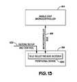
- FIG. 13illustrates an embodiment of a single-chip microcontroller 94 and a peripheral device 96 accessible by the microcontroller 94 over a microcontroller bus 98 .
- the microcontroller 94may include any functionality, such as data processing, data storage, interfaces, etc. Because of the integrated functionalities provided in the microcontroller 94 , in a typical embodiment, the microcontroller 94 does not provide any memory management, bus translation, or other externally accessible functions or components to enable the addition of the peripheral device 96 .
- the peripheral devicemay include some type of memory, such as DRAM.
- the peripheral device 96may include a self-selecting bus decoder 100 .
- the self-selecting bus decoder 100receives a memory mapping configuration and self-selects memory access, as requested by a signal from the microcontroller 94 on each bus-cycle.
- the bus decoder 100may receive signals from the microcontroller 94 over the microcontroller bus 98 and may also receive decode set-up and control signal 102 .
- the self-selecting bus decoder 100enables the addition of the peripheral device 96 to the microcontroller 94 without adding any components to the microcontroller 94 or between the peripheral device 96 and the microcontroller 94 .
- the peripheral device 96may be added to a printed circuit assembly (PCA) containing the microcontroller 94 and connected via printed circuit traces to the microcontroller 94 .
- PCAprinted circuit assembly
- FIG. 14illustrates the self-selecting bus decoder 100 , and included logic, in further detail.
- the self-selecting bus decoder 100may include address-matching and mapping logic 104 and bus-cycle validation logic 106 .
- the function provided by the peripheral device 96such as data storage and/or data processing via included memory, is illustrated by the peripheral function block 108 .
- the peripheral device 96 and the microcontroller 94may communicate over a microcontroller bus 98 . Any signals provided from the microcontroller 94 pass over the microcontroller bus 98 to the self-selecting decoder 100 .
- the self-selecting decoder 100processes any signals received from the microcontroller 94 and, as described further below, determines if the peripheral device should provide a response to the signal.
- the output from the peripheral device 96may be provided to the microcontroller 94 over the microcontroller bus 98 .
- the address-matching and mapping logic 104 of the decoder 100receives the decode set-up and control signal 102 .
- the decode set-up and control signal 102provides a memory mapping configuration to the address-matching and mapping logic 104 .
- the decode set-up and control signal 102may convey any other signals that configure the decoder 100 .
- the decode set-up and control signal 102may be configured by electrically connecting pins or other electrical connections on the PCA, e.g., after connection of the peripheral device 96 to the PCA.
- the memory mapping configuration provided by the decode set-up and control signal 102may specify a range of memory addresses provided by memory of the peripheral device 96 , and/or a range of memory addresses provided by the microcontroller 94 .
- the address-matching and mapping logic 104may determine if the peripheral device 96 should respond to this address range, i.e., if the memory address range is “mapped” to the peripheral device 96 .
- the address-matching and mapping logic 104may receive a signal from the microcontroller 94 that includes a memory address. Based on the memory mapping configuration provided by the decode set-up and control signal 102 and the memory address, the address-matching and mapping logic 104 may determine if the peripheral device 96 should be selected. If the memory address is in the range of memory addresses provided by the peripheral device 96 , then the peripheral device 96 may be selected to fulfill any memory operation requested in the signal provided by the microcontroller 94 .
- the bus-cycle-validation logic 106identifies the memory operation provided to the peripheral device 96 from the microcontroller 94 .
- a request for a memory operationmay be provided in the signal sent to the peripheral device 94 over the microcontroller bus 98 .
- this signalmay also include a memory address, in addition to a request for a memory operation.
- the bus-cycle validation logic 106may determine if the requested operation is a direct memory access (DMA) operation, write, read, refresh, and/or any other operation.
- DMAdirect memory access
- the bus-cycle validation logic 106determines if a response may be provided by the peripheral device 96 and what type of response to provide.
- the bus-cycle validation logic 106may provide a cycle-enable signal 112 to initiate the peripheral function 108 .
- the cycle-enable signalselects the peripheral function 108 of the peripheral device 96 to respond to the memory request.
- the peripheral function 108provides the appropriate response to the memory request received from the microcontroller 94 , such as write, read, refresh, etc.
- the peripheral function 108may provide data to the microcontroller 94 over the microcontroller bus 98 , such as the contents of the data at the specified memory address.
- the response provided by the peripheral function block 108may also provide status information to the microcontroller 94 , such as an indication of the completion of the current operation, errors, etc.
- the address-matching and mapping logic 104 and the bus-cycle validation logic 106operate in parallel in each bus-cycle. That is, for each bus-cycle, the operations performed by each logic block of the self-select bus decoder 100 are executed in a single bus-cycle. For each memory operation requested by the microcontroller 94 , the self-selecting bus decoder 100 determines if the request may be responded to by the peripheral device 96 , determines if the request requires a response from the peripheral device 96 , and selects the peripheral device 96 to provide the appropriate response.
- a peripheral device with a self-selecting bus decoder 100may include a bus translator, as further described in U.S. patent application Ser. No. 12/265,436 filed on Nov. 5, 2008, titled “Bus Translator,” by Harold B Noyes et al.
- FIG. 15depicts an embodiment illustrating the microcontroller 94 coupled to a peripheral device 116 having a self-selecting bus decoder 118 and a bus translator 120 .
- the bus translator 120 and the self-selecting bus decoder 118may communicate over an internal bus 122 .
- the internal bus 122provides any translated signals from the bus translator 120 to the self-selecting bus decoder 118 .
- the self-selecting bus decoder 118includes address-matching and mapping logic 124 and bus-cycle validation logic 126 , and may provide a cycle-enable signal 128 to enable a peripheral function 130 .
- the address-matching and mapping logic 124may receive a memory mapping configuration via a decode set-up and control signal 132 .
- the bus translator 120may be configured to translate signals on each of the plurality of different types of buses 134 into signals that are appropriate for the self-selecting bus decoder 118 of the peripheral device 116 to receive through the internal bus 122 and vice-versa.
- the bus translatormay include a plurality of bus drivers 136 (e.g., drivers A-E), and a plurality of bus physical interfaces 138 (e.g., bus A-E I/O pins)
- the bus translator 120may include a multiplexer or a demultiplexer to increase or decrease the number of signals that convey data between the internal bus 122 and a selected one of the plurality of different buses 134 .
- the bus translator 120may also be configured to adjust the timing of signals that convey data between the internal bus 122 and the selected one of the plurality of different buses 134 to be appropriate for each of the buses 134 and 122 .
- the bus translator 120may also be configured to adjust the voltage of signals conveying data between the internal bus 122 and the selected one of the plurality of different buses 134 .
- a control signal 140may convey signals that configure the bus translator 120 .
- the control signal 140may convey a signal that configures the bus translator 120 to select one of the different types of buses 134 .
- the control signal 140may convey data that is stored in registers in the bus translator 120 .
- the control signal 140may be omitted (which is not to suggest that any other feature described herein may not also be omitted), and the bus translator 120 may be configured by blowing fuses within the bus translator 120 during manufacturing or by electrically connecting pins or other electrical connections on the peripheral device 116 , e.g., with a jumper, after the peripheral device 116 is manufactured.
- the peripheral device 116may be configured to automatically detect which of the different types of buses 134 is being used, e.g., by selecting a bus based on which of the physical bus interfaces 138 is connected to an external bus.
- the plurality of different buses 134may include several different types of buses.
- the plurality of different buses 134may include an asynchronous bus with non-multiplexed address and data, an asynchronous bus with multiplexed address and data, a synchronous bus with non-multiplexed address and data, a synchronous bus with multiplexed address and data, a synchronous dynamic random access memory (SDRAM) bus, a double data rate (DDR) bus, a DDR2 bus, a DDR3 bus, a DDR4 bus, a PCI bus, a PCI express bus, a PCIx bus, a security gateway management interface (SGMI) bus, or other types of buses.
- SDRAMsynchronous dynamic random access memory
- DDRdouble data rate
- PCIPCI express bus
- PCIx busPCIx bus
- SGMIsecurity gateway management interface
- the peripheral device 116may communicate with the microcontroller 94 through a microcontroller bus 144 .
- the microcontroller bus 144may be one of the types of buses that are compliant with the plurality of different buses 134 coupled to the bus translator 120 within the peripheral device 116 .
- the microcontroller bus 144may couple to the physical bus interface 138 that is appropriate for the microcontroller bus 144 . For example, if the microcontroller bus 144 is a DDR2 bus, it may couple to a physical bus interface 138 that is compliant with the DDR2 bus specification. The other physical bus interfaces may remain unused.
- the bus translator 120may translate the signals. Translating the signals may include multiplexing or demultiplexing the signals, increasing or decreasing the timing of the signals, or changing the voltage of the signals. Regardless of which of the plurality of different buses 134 is selected, the translated signals on the internal bus 122 may be similar or the same, and the bus translator 120 may be configured to receive the signals and transmit the signals through the internal bus 122 .
- the microcontroller 94may request one or more memory operations in a signal sent to the peripheral device 116 .
- the signalis first received by the bus translator 120 through the physical bus interface 138 and one of the plurality of different buses 134 .
- the self-selecting bus decoder 118may process the signal as described above. For example, the address-matching and mapping logic 124 may determine if a memory address of the signal is provided by the memory of the peripheral device 116 , and the bus-cycle validation logic 126 may determine the type of memory operation and the appropriate response.
- the self-selecting bus decoder 118may output the cycle enable signal 128 to select the peripheral function 130 of the peripheral device 116 . Any response provided by the peripheral function 130 may be sent as an output signal to bus translator 120 via the internal bus 122 .
- the bus translator 120can translate the output signal of the peripheral function 130 to the selected one of the plurality of different buses 134 .
- the responsee.g., the output signal from the peripheral function 130 , is then sent over the microcontroller bus 144 to the microcontroller 94 .
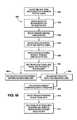
- FIG. 16illustrates an example of a process 150 for operating a peripheral device with a self-selecting bus decoder.
- the process 150may begin with selecting a bus from among a plurality of different buses available to peripheral device (block 152 ). Selecting one bus among the plurality of different buses may be performed after or during the manufacture of the device.
- the plurality of different types of busesmay include any of those described above.
- the devicemay be configured to communicate through two or more buses, three or more buses, four or more buses, five or more buses, or six or more buses. Alternatively, as discussed above, certain embodiments may omit a bus translator and configuration of bus type, e.g., if the microcontroller and peripheral device communicate over the same or a similar bus.
- the peripheral devicemay be coupled to a microcontroller through the selected bus (block 154 ). Coupling the peripheral device to the microcontroller through the selected bus may include installing the device on a PCA, e.g. a system board, motherboard, etc.
- a PCAe.g. a system board, motherboard, etc.
- a memory mapping configurationmay be specified (block 156 ), such as through pins or other electrical connections on the PCA, that maps a range of address to the peripheral device and/or a range of addresses to the microcontroller.
- the self-selecting bus decoder of the peripheral devicemay receive a decode set-up and control signal that provides the memory mapping configuration (block 158 ).
- the microcontroller coupled to the peripheral devicemay make a request for a memory operation at a certain memory address or addresses, such as by sending a signal over the selected bus, i.e., one of the buses selected from one of the plurality of different buses coupled to the bus translator, to the peripheral device (block 160 ).
- the bus translatormay translate the request from the microcontroller and provide the translated request to the self-selecting bus decoder over an internal bus of the device (block 162 ).
- the self-selecting bus decodermay execute the address-matching and mapping logic (block 164 ) and the bus-cycle validation logic (block 166 ) in parallel.
- the address-matching and mapping logicdetermines that the memory address or addresses of the request are in the range of memory addresses provided by the peripheral device (block 164 ).
- the bus-cycle validation logicdetermines the type of memory operation of the request and determines the appropriate response (block 166 ).
- the self-selecting bus decodermay enable the peripheral device to respond to the request (block 168 ), e.g., through a cycle-enable signal provided to a function of the peripheral device.
- the response to the requestis provided to the bus translator (block 170 ).
- the bus translatortranslates the response and sends the response to the microcontroller (block 172 ), such as by sending a signal over the selected one of the plurality of different buses coupled to the bus translator.
- the process 150is believed to reduce the cost and difficulty of adding functionality to microcontrollers via addition of a peripheral device. Because the peripheral device may self-select based on a requested memory operation from the microcontroller and may communicate through a variety of different types of buses, the peripheral device may be used and coupled to a microcontroller without the addition of other components to the microcontroller or between the peripheral device and the microcontroller.
Landscapes
- Engineering & Computer Science (AREA)
- Theoretical Computer Science (AREA)
- General Engineering & Computer Science (AREA)
- Physics & Mathematics (AREA)
- General Physics & Mathematics (AREA)
- Computer Hardware Design (AREA)
- Information Retrieval, Db Structures And Fs Structures Therefor (AREA)
Abstract
Description
Claims (21)
Priority Applications (7)
| Application Number | Priority Date | Filing Date | Title |
|---|---|---|---|
| US13/801,447US9785588B2 (en) | 2008-11-10 | 2013-03-13 | Methods and systems for devices with self-selecting bus decoder |
| US15/728,151US10180922B2 (en) | 2008-11-10 | 2017-10-09 | Methods and systems for devices with self-selecting bus decoder |
| US16/247,244US10572414B2 (en) | 2008-11-10 | 2019-01-14 | Methods and systems for devices with self-selecting bus decoder |
| US16/799,444US10942877B2 (en) | 2008-11-10 | 2020-02-24 | Methods and systems for devices with self-selecting bus decoder |
| US17/184,372US11782859B2 (en) | 2008-11-10 | 2021-02-24 | Methods and systems for devices with self-selecting bus decoder |
| US18/300,112US12197363B2 (en) | 2008-11-10 | 2023-04-13 | Methods and systems for pattern recognition processing |
| US18/986,137US20250238383A1 (en) | 2008-11-10 | 2024-12-18 | Methods and systems for devices with self-selecting bus decoder |
Applications Claiming Priority (2)
| Application Number | Priority Date | Filing Date | Title |
|---|---|---|---|
| US12/268,270US8402188B2 (en) | 2008-11-10 | 2008-11-10 | Methods and systems for devices with a self-selecting bus decoder |
| US13/801,447US9785588B2 (en) | 2008-11-10 | 2013-03-13 | Methods and systems for devices with self-selecting bus decoder |
Related Parent Applications (1)
| Application Number | Title | Priority Date | Filing Date |
|---|---|---|---|
| US12/268,270ContinuationUS8402188B2 (en) | 2008-11-10 | 2008-11-10 | Methods and systems for devices with a self-selecting bus decoder |
Related Child Applications (2)
| Application Number | Title | Priority Date | Filing Date |
|---|---|---|---|
| US15/278,151ContinuationUS10198501B2 (en) | 2016-09-28 | 2016-09-28 | Optimizing retrieval of data related to temporal based queries |
| US15/728,151ContinuationUS10180922B2 (en) | 2008-11-10 | 2017-10-09 | Methods and systems for devices with self-selecting bus decoder |
Publications (2)
| Publication Number | Publication Date |
|---|---|
| US20130198433A1 US20130198433A1 (en) | 2013-08-01 |
| US9785588B2true US9785588B2 (en) | 2017-10-10 |
Family
ID=41528546
Family Applications (8)
| Application Number | Title | Priority Date | Filing Date |
|---|---|---|---|
| US12/268,270Active2032-01-18US8402188B2 (en) | 2008-11-10 | 2008-11-10 | Methods and systems for devices with a self-selecting bus decoder |
| US13/801,447Active2030-06-15US9785588B2 (en) | 2008-11-10 | 2013-03-13 | Methods and systems for devices with self-selecting bus decoder |
| US15/728,151ActiveUS10180922B2 (en) | 2008-11-10 | 2017-10-09 | Methods and systems for devices with self-selecting bus decoder |
| US16/247,244ActiveUS10572414B2 (en) | 2008-11-10 | 2019-01-14 | Methods and systems for devices with self-selecting bus decoder |
| US16/799,444ActiveUS10942877B2 (en) | 2008-11-10 | 2020-02-24 | Methods and systems for devices with self-selecting bus decoder |
| US17/184,372ActiveUS11782859B2 (en) | 2008-11-10 | 2021-02-24 | Methods and systems for devices with self-selecting bus decoder |
| US18/300,112ActiveUS12197363B2 (en) | 2008-11-10 | 2023-04-13 | Methods and systems for pattern recognition processing |
| US18/986,137PendingUS20250238383A1 (en) | 2008-11-10 | 2024-12-18 | Methods and systems for devices with self-selecting bus decoder |
Family Applications Before (1)
| Application Number | Title | Priority Date | Filing Date |
|---|---|---|---|
| US12/268,270Active2032-01-18US8402188B2 (en) | 2008-11-10 | 2008-11-10 | Methods and systems for devices with a self-selecting bus decoder |
Family Applications After (6)
| Application Number | Title | Priority Date | Filing Date |
|---|---|---|---|
| US15/728,151ActiveUS10180922B2 (en) | 2008-11-10 | 2017-10-09 | Methods and systems for devices with self-selecting bus decoder |
| US16/247,244ActiveUS10572414B2 (en) | 2008-11-10 | 2019-01-14 | Methods and systems for devices with self-selecting bus decoder |
| US16/799,444ActiveUS10942877B2 (en) | 2008-11-10 | 2020-02-24 | Methods and systems for devices with self-selecting bus decoder |
| US17/184,372ActiveUS11782859B2 (en) | 2008-11-10 | 2021-02-24 | Methods and systems for devices with self-selecting bus decoder |
| US18/300,112ActiveUS12197363B2 (en) | 2008-11-10 | 2023-04-13 | Methods and systems for pattern recognition processing |
| US18/986,137PendingUS20250238383A1 (en) | 2008-11-10 | 2024-12-18 | Methods and systems for devices with self-selecting bus decoder |
Country Status (3)
| Country | Link |
|---|---|
| US (8) | US8402188B2 (en) |
| TW (1) | TWI426390B (en) |
| WO (1) | WO2010053714A1 (en) |
Cited By (2)
| Publication number | Priority date | Publication date | Assignee | Title |
|---|---|---|---|---|
| US20180032456A1 (en)* | 2008-11-10 | 2018-02-01 | Micron Technology, Inc. | Methods and systems for devices with self-selecting bus decoder |
| US10235627B2 (en)* | 2009-12-15 | 2019-03-19 | Micron Technology, Inc. | Adaptive content inspection |
Families Citing this family (30)
| Publication number | Priority date | Publication date | Assignee | Title |
|---|---|---|---|---|
| US8938590B2 (en) | 2008-10-18 | 2015-01-20 | Micron Technology, Inc. | Indirect register access method and system |
| US8209521B2 (en) | 2008-10-18 | 2012-06-26 | Micron Technology, Inc. | Methods of indirect register access including automatic modification of a directly accessible address register |
| US7917684B2 (en) | 2008-11-05 | 2011-03-29 | Micron Technology, Inc. | Bus translator |
| US7970964B2 (en) | 2008-11-05 | 2011-06-28 | Micron Technology, Inc. | Methods and systems to accomplish variable width data input |
| US10007486B2 (en) | 2008-12-01 | 2018-06-26 | Micron Technology, Inc. | Systems and methods to enable identification of different data sets |
| US20100138575A1 (en) | 2008-12-01 | 2010-06-03 | Micron Technology, Inc. | Devices, systems, and methods to synchronize simultaneous dma parallel processing of a single data stream by multiple devices |
| US8214672B2 (en) | 2009-01-07 | 2012-07-03 | Micron Technology, Inc. | Method and systems for power consumption management of a pattern-recognition processor |
| US8281395B2 (en) | 2009-01-07 | 2012-10-02 | Micron Technology, Inc. | Pattern-recognition processor with matching-data reporting module |
| US20100174887A1 (en) | 2009-01-07 | 2010-07-08 | Micron Technology Inc. | Buses for Pattern-Recognition Processors |
| US9501705B2 (en) | 2009-12-15 | 2016-11-22 | Micron Technology, Inc. | Methods and apparatuses for reducing power consumption in a pattern recognition processor |
| US9323994B2 (en) | 2009-12-15 | 2016-04-26 | Micron Technology, Inc. | Multi-level hierarchical routing matrices for pattern-recognition processors |
| JP5471631B2 (en)* | 2010-03-10 | 2014-04-16 | セイコーエプソン株式会社 | Electronics |
| JP5790532B2 (en)* | 2012-02-13 | 2015-10-07 | セイコーエプソン株式会社 | Electronic device and memory control method |
| US20130275709A1 (en) | 2012-04-12 | 2013-10-17 | Micron Technology, Inc. | Methods for reading data from a storage buffer including delaying activation of a column select |
| US9524248B2 (en) | 2012-07-18 | 2016-12-20 | Micron Technology, Inc. | Memory management for a hierarchical memory system |
| US9703574B2 (en) | 2013-03-15 | 2017-07-11 | Micron Technology, Inc. | Overflow detection and correction in state machine engines |
| US9448965B2 (en) | 2013-03-15 | 2016-09-20 | Micron Technology, Inc. | Receiving data streams in parallel and providing a first portion of data to a first state machine engine and a second portion to a second state machine |
| WO2016109571A1 (en) | 2014-12-30 | 2016-07-07 | Micron Technology, Inc | Devices for time division multiplexing of state machine engine signals |
| US10430210B2 (en) | 2014-12-30 | 2019-10-01 | Micron Technology, Inc. | Systems and devices for accessing a state machine |
| US11366675B2 (en) | 2014-12-30 | 2022-06-21 | Micron Technology, Inc. | Systems and devices for accessing a state machine |
| US10977309B2 (en) | 2015-10-06 | 2021-04-13 | Micron Technology, Inc. | Methods and systems for creating networks |
| US10846103B2 (en) | 2015-10-06 | 2020-11-24 | Micron Technology, Inc. | Methods and systems for representing processing resources |
| US10691964B2 (en) | 2015-10-06 | 2020-06-23 | Micron Technology, Inc. | Methods and systems for event reporting |
| US10146555B2 (en) | 2016-07-21 | 2018-12-04 | Micron Technology, Inc. | Adaptive routing to avoid non-repairable memory and logic defects on automata processor |
| US10268602B2 (en) | 2016-09-29 | 2019-04-23 | Micron Technology, Inc. | System and method for individual addressing |
| US10019311B2 (en) | 2016-09-29 | 2018-07-10 | Micron Technology, Inc. | Validation of a symbol response memory |
| US10592450B2 (en) | 2016-10-20 | 2020-03-17 | Micron Technology, Inc. | Custom compute cores in integrated circuit devices |
| US12197510B2 (en) | 2016-10-20 | 2025-01-14 | Micron Technology, Inc. | Traversal of S portion of a graph problem to be solved using automata processor |
| US10929764B2 (en) | 2016-10-20 | 2021-02-23 | Micron Technology, Inc. | Boolean satisfiability |
| CN107885678B (en)* | 2017-11-24 | 2020-12-22 | 英业达科技有限公司 | Hard disk control interface device |
Citations (56)
| Publication number | Priority date | Publication date | Assignee | Title |
|---|---|---|---|---|
| US5300830A (en) | 1992-05-15 | 1994-04-05 | Micron Semiconductor, Inc. | Programmable logic device macrocell with an exclusive feedback and exclusive external input lines for registered and combinatorial modes using a dedicated product term for control |
| US5331227A (en) | 1992-05-15 | 1994-07-19 | Micron Semiconductor, Inc. | Programmable logic device macrocell with an exclusive feedback line and an exclusive external input line |
| US5754878A (en) | 1996-03-18 | 1998-05-19 | Advanced Micro Devices, Inc. | CPU with DSP function preprocessor having pattern recognition detector that uses table for translating instruction sequences intended to perform DSP function into DSP macros |
| US5860028A (en)* | 1996-02-01 | 1999-01-12 | Paragon Electric Company, Inc. | I/O bus expansion system wherein processor checks plurality of possible address until a response from the peripheral selected by address decoder using user input |
| US5881312A (en) | 1993-03-19 | 1999-03-09 | Intel Corporation | Memory transfer apparatus and method useful within a pattern recognition system |
| US5974519A (en)* | 1996-07-15 | 1999-10-26 | Lg Semicon Co., Ltd. | Address re-designate circuit for microcontroller |
| US6240003B1 (en) | 2000-05-01 | 2001-05-29 | Micron Technology, Inc. | DRAM content addressable memory using part of the content as an address |
| US6260132B1 (en)* | 1999-02-01 | 2001-07-10 | Vlsi Technology, Inc. | Method and apparatus for secure address re-mapping |
| US6279128B1 (en) | 1994-12-29 | 2001-08-21 | International Business Machines Corporation | Autonomous system for recognition of patterns formed by stored data during computer memory scrubbing |
| US6421757B1 (en)* | 1998-09-30 | 2002-07-16 | Conexant Systems, Inc | Method and apparatus for controlling the programming and erasing of flash memory |
| US6499074B1 (en)* | 1999-08-23 | 2002-12-24 | Advanced Micro Devices, Inc. | Redirecting I/O address holes |
| US20030149826A1 (en)* | 2002-02-05 | 2003-08-07 | Daisuke Kadota | Access control device for bus bridge circuit and method for controlling the same |
| US6754749B1 (en)* | 2001-01-22 | 2004-06-22 | Sharewave, Inc. | Multiple use integrated circuit for embedded systems |
| US6880087B1 (en) | 1999-10-08 | 2005-04-12 | Cisco Technology, Inc. | Binary state machine system and method for REGEX processing of a data stream in an intrusion detection system |
| US6906938B2 (en) | 2003-08-15 | 2005-06-14 | Micron Technology, Inc. | CAM memory architecture and a method of forming and operating a device according to a CAM memory architecture |
| US6925510B2 (en) | 2002-02-22 | 2005-08-02 | Winbond Electronics, Corp. | Peripheral or memory device having a combined ISA bus and LPC bus |
| US6944710B2 (en) | 2002-12-30 | 2005-09-13 | Micron Technology, Inc. | Multiple category CAM |
| US7089352B2 (en) | 2002-12-23 | 2006-08-08 | Micron Technology, Inc. | CAM modified to be used for statistic calculation in network switches and routers |
| US7130231B2 (en) | 2004-11-19 | 2006-10-31 | International Business Machines Corporation | Method, apparatus, and computer program product for implementing enhanced DRAM interface checking |
| US7146643B2 (en) | 2002-10-29 | 2006-12-05 | Lockheed Martin Corporation | Intrusion detection accelerator |
| US20070028226A1 (en) | 2000-11-17 | 2007-02-01 | Shao-Chun Chen | Pattern detection preprocessor in an electronic device update generation system |
| US20070075878A1 (en) | 2005-09-21 | 2007-04-05 | Stmicroelectronics Sa | Memory circuit for aho-corasick type character recognition automaton and method of storing data in such a circuit |
| US7269704B2 (en)* | 2005-03-30 | 2007-09-11 | Atmel Corporation | Method and apparatus for reducing system inactivity during time data float delay and external memory write |
| US7392229B2 (en)* | 2005-02-12 | 2008-06-24 | Curtis L. Harris | General purpose set theoretic processor |
| US20080250191A1 (en)* | 2007-04-04 | 2008-10-09 | Atmel Corporation | Flexible, low cost apparatus and method to introduce and check algorithm modifications in a non-volatile memory |
| US7478184B2 (en)* | 2003-12-25 | 2009-01-13 | Fujitsu Limited | Integrated circuit device including processor selection in a multiprocessor system |
| US7487542B2 (en) | 2004-01-14 | 2009-02-03 | International Business Machines Corporation | Intrusion detection using a network processor and a parallel pattern detection engine |
| US7512634B2 (en) | 2006-06-05 | 2009-03-31 | Tarari, Inc. | Systems and methods for processing regular expressions |
| US20090125657A1 (en)* | 2007-11-12 | 2009-05-14 | Hon Hai Precision Industry Co., Ltd. | Serial peripheral interface circuit |
| US7627793B2 (en) | 2004-08-23 | 2009-12-01 | Micron Technology, Inc. | Method and apparatus for generating and detecting initialization patterns for high speed DRAM systems |
| US20100100691A1 (en) | 2008-10-18 | 2010-04-22 | Micron Technology, Inc. | Indirect Register Access Method and System |
| US20100115347A1 (en) | 2008-11-05 | 2010-05-06 | Micron Technology, Inc. | Pattern-Recognition Processor with Results Buffer |
| US20100122001A1 (en)* | 2008-11-10 | 2010-05-13 | Miller Gary L | Technique for interconnecting integrated circuits |
| US20100138634A1 (en) | 2008-12-01 | 2010-06-03 | Micron Technology, Inc. | Devices, systems, and methods to synchronize parallel processing of a single data stream |
| US20100138575A1 (en) | 2008-12-01 | 2010-06-03 | Micron Technology, Inc. | Devices, systems, and methods to synchronize simultaneous dma parallel processing of a single data stream by multiple devices |
| US20100138432A1 (en) | 2008-12-01 | 2010-06-03 | Micron Technology, Inc. | Systems and Methods to Enable Identification of Different Data Sets |
| US20100138635A1 (en) | 2008-12-01 | 2010-06-03 | Micron Technology, Inc. | Systems and Methods for Managing Endian Mode of a Device |
| US20100174887A1 (en) | 2009-01-07 | 2010-07-08 | Micron Technology Inc. | Buses for Pattern-Recognition Processors |
| US20100185647A1 (en) | 2009-01-12 | 2010-07-22 | Micron Technology, Inc. | Devices, systems, and methods for communicating pattern matching results of a parallel pattern search engine |
| US7774286B1 (en) | 2006-10-24 | 2010-08-10 | Harris Curtis L | GPSTP with multiple thread functionality |
| US7917684B2 (en) | 2008-11-05 | 2011-03-29 | Micron Technology, Inc. | Bus translator |
| US7970964B2 (en) | 2008-11-05 | 2011-06-28 | Micron Technology, Inc. | Methods and systems to accomplish variable width data input |
| US8065249B1 (en) | 2006-10-13 | 2011-11-22 | Harris Curtis L | GPSTP with enhanced aggregation functionality |
| US20110307503A1 (en) | 2010-06-10 | 2011-12-15 | Paul Dlugosch | Analyzing data using a hierarchical structure |
| US20110307433A1 (en) | 2010-06-10 | 2011-12-15 | Paul Dlugosch | Programmable device, heirarchical parallel machines, methods for providing state information |
| US8140780B2 (en) | 2008-12-31 | 2012-03-20 | Micron Technology, Inc. | Systems, methods, and devices for configuring a device |
| US8195946B2 (en)* | 2005-04-11 | 2012-06-05 | Stmicroelectronics S.A. | Protection of data of a memory associated with a microprocessor |
| US8209521B2 (en) | 2008-10-18 | 2012-06-26 | Micron Technology, Inc. | Methods of indirect register access including automatic modification of a directly accessible address register |
| US8214672B2 (en) | 2009-01-07 | 2012-07-03 | Micron Technology, Inc. | Method and systems for power consumption management of a pattern-recognition processor |
| US20120192166A1 (en) | 2011-01-25 | 2012-07-26 | Junjuan Xu | State grouping for element utilization |
| US20120192163A1 (en) | 2011-01-25 | 2012-07-26 | Paul Glendenning | Method and apparatus for compiling regular expressions |
| US20120192165A1 (en) | 2011-01-25 | 2012-07-26 | Junjuan Xu | Unrolling quantifications to control in-degree and/or out-degree of automaton |
| US20120192164A1 (en) | 2011-01-25 | 2012-07-26 | Junjuan Xu | Utilizing special purpose elements to implement a fsm |
| US8281395B2 (en) | 2009-01-07 | 2012-10-02 | Micron Technology, Inc. | Pattern-recognition processor with matching-data reporting module |
| US8402188B2 (en)* | 2008-11-10 | 2013-03-19 | Micron Technology, Inc. | Methods and systems for devices with a self-selecting bus decoder |
| US8516167B2 (en)* | 2011-08-03 | 2013-08-20 | Atmel Corporation | Microcontroller system bus scheduling for multiport slave modules |
Family Cites Families (22)
| Publication number | Priority date | Publication date | Assignee | Title |
|---|---|---|---|---|
| US5537664A (en)* | 1993-06-30 | 1996-07-16 | Intel Corporation | Methods and apparatus for generating I/O recovery delays in a computer system |
| JPH08147161A (en)* | 1994-11-21 | 1996-06-07 | Nec Corp | Data processor |
| US6178469B1 (en)* | 1998-06-30 | 2001-01-23 | Compaq Computer Corporation | Enabling access to a selected one of two detected same type peripheral devices connected to separate peripheral slots in a computer |
| US7058750B1 (en)* | 2000-05-10 | 2006-06-06 | Intel Corporation | Scalable distributed memory and I/O multiprocessor system |
| US6785758B1 (en)* | 2001-06-01 | 2004-08-31 | Advanced Micro Devices, Inc. | System and method for machine specific register addressing in a split transactional unidirectional bus architecture |
| US20030014579A1 (en)* | 2001-07-11 | 2003-01-16 | Motorola, Inc | Communication controller and method of transforming information |
| US20030126346A1 (en)* | 2001-12-31 | 2003-07-03 | Kuo Sung H. | Dynamic load balancing in a multi-bus computer system |
| US7711931B2 (en) | 2003-08-28 | 2010-05-04 | Mips Technologies, Inc. | Synchronized storage providing multiple synchronization semantics |
| KR100633742B1 (en)* | 2003-12-23 | 2006-10-13 | 한국전자통신연구원 | Direct memory access control device and method for automatically updating data transfer size from peripheral device |
| JP2005327062A (en)* | 2004-05-14 | 2005-11-24 | Oki Electric Ind Co Ltd | Control method for input/output terminal module and input/output terminal module |
| JP2006246356A (en)* | 2005-03-07 | 2006-09-14 | Canon Inc | Data receiving system, data output method thereof, receiving device, and control program |
| KR20070080307A (en)* | 2006-02-07 | 2007-08-10 | 삼성전자주식회사 | System with bus structure to improve CPU performance and performance improvement method |
| US7613847B2 (en)* | 2006-05-16 | 2009-11-03 | Hewlett-Packard Development Company, L.P. | Partially virtualizing an I/O device for use by virtual machines |
| TW200813724A (en)* | 2006-07-28 | 2008-03-16 | Samsung Electronics Co Ltd | Multipath accessible semiconductor memory device with host interface between processors |
| TWI332623B (en)* | 2007-02-15 | 2010-11-01 | Via Tech Inc | Data processing systems and methods |
| CN101499048A (en)* | 2008-01-29 | 2009-08-05 | 国际商业机器公司 | Bus encoding/decoding method and bus encoder/decoder |
| US8112552B2 (en)* | 2008-02-25 | 2012-02-07 | Microsoft Corporation | Default peripheral device selection based on location |
| US8250250B2 (en)* | 2009-10-28 | 2012-08-21 | Apple Inc. | Using central direct memory access (CDMA) controller to test integrated circuit |
| US8281188B2 (en)* | 2010-08-05 | 2012-10-02 | Miller Gary L | Data processing system with peripheral configuration information error detection |
| KR102012699B1 (en)* | 2013-01-25 | 2019-08-21 | 삼성전자 주식회사 | Multi bus system and semiconductor system comprising thereof |
| WO2014120113A1 (en)* | 2013-01-29 | 2014-08-07 | Hewlett-Packard Development Company | Assigning processors to memory mapped configuration |
| JP7122969B2 (en)* | 2016-02-29 | 2022-08-22 | ルネサス エレクトロニクス アメリカ インコーポレイテッド | Systems and methods for programming microcontroller data transfers |
- 2008
- 2008-11-10USUS12/268,270patent/US8402188B2/enactiveActive
- 2009
- 2009-10-22WOPCT/US2009/061649patent/WO2010053714A1/enactiveApplication Filing
- 2009-11-04TWTW098137442Apatent/TWI426390B/enactive
- 2013
- 2013-03-13USUS13/801,447patent/US9785588B2/enactiveActive
- 2017
- 2017-10-09USUS15/728,151patent/US10180922B2/enactiveActive
- 2019
- 2019-01-14USUS16/247,244patent/US10572414B2/enactiveActive
- 2020
- 2020-02-24USUS16/799,444patent/US10942877B2/enactiveActive
- 2021
- 2021-02-24USUS17/184,372patent/US11782859B2/enactiveActive
- 2023
- 2023-04-13USUS18/300,112patent/US12197363B2/enactiveActive
- 2024
- 2024-12-18USUS18/986,137patent/US20250238383A1/enactivePending
Patent Citations (57)
| Publication number | Priority date | Publication date | Assignee | Title |
|---|---|---|---|---|
| US5331227A (en) | 1992-05-15 | 1994-07-19 | Micron Semiconductor, Inc. | Programmable logic device macrocell with an exclusive feedback line and an exclusive external input line |
| US5300830A (en) | 1992-05-15 | 1994-04-05 | Micron Semiconductor, Inc. | Programmable logic device macrocell with an exclusive feedback and exclusive external input lines for registered and combinatorial modes using a dedicated product term for control |
| US5881312A (en) | 1993-03-19 | 1999-03-09 | Intel Corporation | Memory transfer apparatus and method useful within a pattern recognition system |
| US6279128B1 (en) | 1994-12-29 | 2001-08-21 | International Business Machines Corporation | Autonomous system for recognition of patterns formed by stored data during computer memory scrubbing |
| US5860028A (en)* | 1996-02-01 | 1999-01-12 | Paragon Electric Company, Inc. | I/O bus expansion system wherein processor checks plurality of possible address until a response from the peripheral selected by address decoder using user input |
| US5754878A (en) | 1996-03-18 | 1998-05-19 | Advanced Micro Devices, Inc. | CPU with DSP function preprocessor having pattern recognition detector that uses table for translating instruction sequences intended to perform DSP function into DSP macros |
| US5974519A (en)* | 1996-07-15 | 1999-10-26 | Lg Semicon Co., Ltd. | Address re-designate circuit for microcontroller |
| US6421757B1 (en)* | 1998-09-30 | 2002-07-16 | Conexant Systems, Inc | Method and apparatus for controlling the programming and erasing of flash memory |
| US6260132B1 (en)* | 1999-02-01 | 2001-07-10 | Vlsi Technology, Inc. | Method and apparatus for secure address re-mapping |
| US6499074B1 (en)* | 1999-08-23 | 2002-12-24 | Advanced Micro Devices, Inc. | Redirecting I/O address holes |
| US6880087B1 (en) | 1999-10-08 | 2005-04-12 | Cisco Technology, Inc. | Binary state machine system and method for REGEX processing of a data stream in an intrusion detection system |
| US6240003B1 (en) | 2000-05-01 | 2001-05-29 | Micron Technology, Inc. | DRAM content addressable memory using part of the content as an address |
| US20070028226A1 (en) | 2000-11-17 | 2007-02-01 | Shao-Chun Chen | Pattern detection preprocessor in an electronic device update generation system |
| US6754749B1 (en)* | 2001-01-22 | 2004-06-22 | Sharewave, Inc. | Multiple use integrated circuit for embedded systems |
| US20030149826A1 (en)* | 2002-02-05 | 2003-08-07 | Daisuke Kadota | Access control device for bus bridge circuit and method for controlling the same |
| US6925510B2 (en) | 2002-02-22 | 2005-08-02 | Winbond Electronics, Corp. | Peripheral or memory device having a combined ISA bus and LPC bus |
| US7146643B2 (en) | 2002-10-29 | 2006-12-05 | Lockheed Martin Corporation | Intrusion detection accelerator |
| US7089352B2 (en) | 2002-12-23 | 2006-08-08 | Micron Technology, Inc. | CAM modified to be used for statistic calculation in network switches and routers |
| US6944710B2 (en) | 2002-12-30 | 2005-09-13 | Micron Technology, Inc. | Multiple category CAM |
| US6906938B2 (en) | 2003-08-15 | 2005-06-14 | Micron Technology, Inc. | CAM memory architecture and a method of forming and operating a device according to a CAM memory architecture |
| US7478184B2 (en)* | 2003-12-25 | 2009-01-13 | Fujitsu Limited | Integrated circuit device including processor selection in a multiprocessor system |
| US7487542B2 (en) | 2004-01-14 | 2009-02-03 | International Business Machines Corporation | Intrusion detection using a network processor and a parallel pattern detection engine |
| US7627793B2 (en) | 2004-08-23 | 2009-12-01 | Micron Technology, Inc. | Method and apparatus for generating and detecting initialization patterns for high speed DRAM systems |
| US7130231B2 (en) | 2004-11-19 | 2006-10-31 | International Business Machines Corporation | Method, apparatus, and computer program product for implementing enhanced DRAM interface checking |
| US7392229B2 (en)* | 2005-02-12 | 2008-06-24 | Curtis L. Harris | General purpose set theoretic processor |
| US7487131B2 (en) | 2005-02-12 | 2009-02-03 | Curtis L. Harris | General Purpose set theoretic processor |
| US7269704B2 (en)* | 2005-03-30 | 2007-09-11 | Atmel Corporation | Method and apparatus for reducing system inactivity during time data float delay and external memory write |
| US8195946B2 (en)* | 2005-04-11 | 2012-06-05 | Stmicroelectronics S.A. | Protection of data of a memory associated with a microprocessor |
| US20070075878A1 (en) | 2005-09-21 | 2007-04-05 | Stmicroelectronics Sa | Memory circuit for aho-corasick type character recognition automaton and method of storing data in such a circuit |
| US7512634B2 (en) | 2006-06-05 | 2009-03-31 | Tarari, Inc. | Systems and methods for processing regular expressions |
| US8065249B1 (en) | 2006-10-13 | 2011-11-22 | Harris Curtis L | GPSTP with enhanced aggregation functionality |
| US7774286B1 (en) | 2006-10-24 | 2010-08-10 | Harris Curtis L | GPSTP with multiple thread functionality |
| US20080250191A1 (en)* | 2007-04-04 | 2008-10-09 | Atmel Corporation | Flexible, low cost apparatus and method to introduce and check algorithm modifications in a non-volatile memory |
| US20090125657A1 (en)* | 2007-11-12 | 2009-05-14 | Hon Hai Precision Industry Co., Ltd. | Serial peripheral interface circuit |
| US20100100691A1 (en) | 2008-10-18 | 2010-04-22 | Micron Technology, Inc. | Indirect Register Access Method and System |
| US8209521B2 (en) | 2008-10-18 | 2012-06-26 | Micron Technology, Inc. | Methods of indirect register access including automatic modification of a directly accessible address register |
| US7970964B2 (en) | 2008-11-05 | 2011-06-28 | Micron Technology, Inc. | Methods and systems to accomplish variable width data input |
| US7917684B2 (en) | 2008-11-05 | 2011-03-29 | Micron Technology, Inc. | Bus translator |
| US20100115347A1 (en) | 2008-11-05 | 2010-05-06 | Micron Technology, Inc. | Pattern-Recognition Processor with Results Buffer |
| US8402188B2 (en)* | 2008-11-10 | 2013-03-19 | Micron Technology, Inc. | Methods and systems for devices with a self-selecting bus decoder |
| US20100122001A1 (en)* | 2008-11-10 | 2010-05-13 | Miller Gary L | Technique for interconnecting integrated circuits |
| US20100138575A1 (en) | 2008-12-01 | 2010-06-03 | Micron Technology, Inc. | Devices, systems, and methods to synchronize simultaneous dma parallel processing of a single data stream by multiple devices |
| US20100138634A1 (en) | 2008-12-01 | 2010-06-03 | Micron Technology, Inc. | Devices, systems, and methods to synchronize parallel processing of a single data stream |
| US20100138635A1 (en) | 2008-12-01 | 2010-06-03 | Micron Technology, Inc. | Systems and Methods for Managing Endian Mode of a Device |
| US20100138432A1 (en) | 2008-12-01 | 2010-06-03 | Micron Technology, Inc. | Systems and Methods to Enable Identification of Different Data Sets |
| US8140780B2 (en) | 2008-12-31 | 2012-03-20 | Micron Technology, Inc. | Systems, methods, and devices for configuring a device |
| US8281395B2 (en) | 2009-01-07 | 2012-10-02 | Micron Technology, Inc. | Pattern-recognition processor with matching-data reporting module |
| US20100174887A1 (en) | 2009-01-07 | 2010-07-08 | Micron Technology Inc. | Buses for Pattern-Recognition Processors |
| US8214672B2 (en) | 2009-01-07 | 2012-07-03 | Micron Technology, Inc. | Method and systems for power consumption management of a pattern-recognition processor |
| US20100185647A1 (en) | 2009-01-12 | 2010-07-22 | Micron Technology, Inc. | Devices, systems, and methods for communicating pattern matching results of a parallel pattern search engine |
| US20110307433A1 (en) | 2010-06-10 | 2011-12-15 | Paul Dlugosch | Programmable device, heirarchical parallel machines, methods for providing state information |
| US20110307503A1 (en) | 2010-06-10 | 2011-12-15 | Paul Dlugosch | Analyzing data using a hierarchical structure |
| US20120192163A1 (en) | 2011-01-25 | 2012-07-26 | Paul Glendenning | Method and apparatus for compiling regular expressions |
| US20120192165A1 (en) | 2011-01-25 | 2012-07-26 | Junjuan Xu | Unrolling quantifications to control in-degree and/or out-degree of automaton |
| US20120192164A1 (en) | 2011-01-25 | 2012-07-26 | Junjuan Xu | Utilizing special purpose elements to implement a fsm |
| US20120192166A1 (en) | 2011-01-25 | 2012-07-26 | Junjuan Xu | State grouping for element utilization |
| US8516167B2 (en)* | 2011-08-03 | 2013-08-20 | Atmel Corporation | Microcontroller system bus scheduling for multiport slave modules |
Non-Patent Citations (24)
| Title |
|---|
| Beesley, K. R.; Arabic Morphology Using Only Finite-State Operations; Xerox Research Centre Europe; pp. 50-57 (1998). |
| Bird. S. et al.; One-Level Phonology: Autosegmental Representations and Rules as Finite Automata; Association for Computational Linguistics; University of Edinburgh; vol. 20; No. 1; pp. 55-90 (1994). |
| Bispo, J. et al.; Regular Expression Matching for Reconfigurable Packet Inspection; IEEE (2006). |
| Bispo, J. et al.; Synthesis of Regular Expressions Targeting FPGAs: Current Status and Open Issues; IST/INESC-ID, Libson, Portugal; pp. 1-12 (2007). |
| Brodie, B. et al.; A scalable Architecture for High-Throughput Regular-Expression Pattern Matching; Exegy Inc.; pp. 1-12 (2006). |
| Clark, C. et al., A Unified Model of Pattern-Matching Circuit Architectures; Tech Report GIT-CERCS-05-20;Georgia Institute of Technology; pp. 1-17 (2005). |
| Clark, C. et al.; Scalable Pattern Matching for High Speed Networks; Proceedings of the 12th Annual IEEE symposium on Field-Programmable Custom Computing Machines (FCCM'04);Georgia Institute of Technology; pp. 1-9 (2004). |
| Clark, C.; A Unified Model of Pattern-Matching Circuits for Field-Programmable Gate Arrays [Doctoral Dissertation]; Georgia Institute of Technology; pp. 1-177 (2006). |
| Clark, C.; Design of Efficient FPGA Circuits for Matching Complex Patterns in Network Intrusion Detection Systems (Master of Science Thesis); Georgia Institute of Technology; pp. 1-56 (Dec. 2003). |
| Fide, S.; String Processing in Hardware; Scalable Parallel and Distributed Systems Lab; Proceedings of the 12th Annual IEEE symposium on Field-Programmable Custom Computing Machines (FCCM'04);School of Electrical and Computer Engineering; Georgia Institute of Technology; pp. 1-9 (2004). |
| Fisk, M. et al.; Applying Fast String Matching to Intrusion Detection; Los Alamos National Laboratory; University of California San Diego; pp. 1-21 (Sep. 2001). |
| Freescale and Kaspersky® Accelerated Antivirus Solution Platform for OEM Vendors; Freescale Semiconductors Document; pp. 1-16 (2007). |
| Hurson A. R.; A VLSI Design for the Parallel Finite State Automaton and Its Performance Evaluation as a Hardware Scanner; International Journal of Computer and Information Sciences, vol. 13, No. 6. (1984). |
| Korenek, J.; Traffic Scanner-Hardware Accelerated Intrusion Detection System; http://www.liberouter.org/; (2006). |
| Kumar, S. et al.; Curing Regular Expressions matching Algorithms from Insomnia, Amnesia, and Acaluia; Department of Computer Science and Engineering; Washington University in St. Louis; pp. 1-17 (Apr. 27, 2007). |
| Lin, C. et al.; Optimization of Pattern Matching Circuits for Regular Expression on FPGA; IEEE Transactions on Very Large Scale Integrations Systems; vol. 15, No. 12, pp. 1-6 (Dec. 2007). |
| Lipovski, G.; Dynamic Systolic Associative Memory Chip; IEEE; Department of Electrical and Computer Engineering; University of Texas at Austin; pp. 481-492 (1990). |
| Prais et al., Method for Address Decode for Memory Card, IP.Com Journal, IP.Com Inc., vol. 33. No. 2 (1990). |
| Schultz, K. et al.; Fully Parallel Integrated CAM/RAM Using Preclassification to Enable Large Capacities; IEEE Journal on Solid-State Circuits; vol. 31; No. 5; pp. 689-699 (May 1996). |
| Shafai, F. et al.; Fully Parallel 30-MHz, 2.5-Mb CAM; IEEE Journal of Solid-State Circuits, vol. 33; No. 11; pp. 1690-1696 (Nov. 1998). |
| Sidhu, R. et al.; Fast Regular Expression Pattern Matching using FPGAs; Department of EE-Systems; University of Southern California; pp. 1-12 (2001). |
| U.S. Appl. No. 60/652,738, filed Feb. 12, 2005, Harris. |
| Wada T.; Multiobject Behavior Recognition Event Driven Selective Attention Method; IEEE; pp. 1-16 (2000). |
| Yu, F.; High Speed Deep Packet Inspection with Hardwares Support; Electrical Engineering and Computer Sciences; University of California at Berkeley; pp. 1-217 (Nov. 22, 2006). |
Cited By (7)
| Publication number | Priority date | Publication date | Assignee | Title |
|---|---|---|---|---|
| US20180032456A1 (en)* | 2008-11-10 | 2018-02-01 | Micron Technology, Inc. | Methods and systems for devices with self-selecting bus decoder |
| US10180922B2 (en)* | 2008-11-10 | 2019-01-15 | Micron Technology, Inc. | Methods and systems for devices with self-selecting bus decoder |
| US10572414B2 (en) | 2008-11-10 | 2020-02-25 | Micron Technology, Inc. | Methods and systems for devices with self-selecting bus decoder |
| US10942877B2 (en) | 2008-11-10 | 2021-03-09 | Micron Technology, Inc. | Methods and systems for devices with self-selecting bus decoder |
| US11782859B2 (en) | 2008-11-10 | 2023-10-10 | Micron Technology, Inc. | Methods and systems for devices with self-selecting bus decoder |
| US12197363B2 (en) | 2008-11-10 | 2025-01-14 | Micron Technology, Inc. | Methods and systems for pattern recognition processing |
| US10235627B2 (en)* | 2009-12-15 | 2019-03-19 | Micron Technology, Inc. | Adaptive content inspection |
Also Published As
| Publication number | Publication date |
|---|---|
| US10572414B2 (en) | 2020-02-25 |
| US20250238383A1 (en) | 2025-07-24 |
| TWI426390B (en) | 2014-02-11 |
| US12197363B2 (en) | 2025-01-14 |
| US20190146937A1 (en) | 2019-05-16 |
| US20200192839A1 (en) | 2020-06-18 |
| US8402188B2 (en) | 2013-03-19 |
| US20100122024A1 (en) | 2010-05-13 |
| WO2010053714A1 (en) | 2010-05-14 |
| US20230297529A1 (en) | 2023-09-21 |
| TW201022951A (en) | 2010-06-16 |
| US10180922B2 (en) | 2019-01-15 |
| US20180032456A1 (en) | 2018-02-01 |
| US20130198433A1 (en) | 2013-08-01 |
| US20210182224A1 (en) | 2021-06-17 |
| US10942877B2 (en) | 2021-03-09 |
| US20230342315A9 (en) | 2023-10-26 |
| US11782859B2 (en) | 2023-10-10 |
Similar Documents
| Publication | Publication Date | Title |
|---|---|---|
| US12197363B2 (en) | Methods and systems for pattern recognition processing | |
| US11830243B2 (en) | Bus translator | |
| US12067767B2 (en) | Buses for pattern-recognition processors | |
| US10838966B2 (en) | Devices, systems, and methods to synchronize simultaneous DMA parallel processing of a single data stream by multiple devices | |
| EP2386080B1 (en) | Method and device for power consumption management of a pattern-recognition processor | |
| US9164945B2 (en) | Devices, systems, and methods to synchronize parallel processing of a single data stream | |
| WO2010065331A1 (en) | Systems and methods for managing endian mode of a device |
Legal Events
| Date | Code | Title | Description |
|---|---|---|---|
| AS | Assignment | Owner name:U.S. BANK NATIONAL ASSOCIATION, AS COLLATERAL AGENT, CALIFORNIA Free format text:SECURITY INTEREST;ASSIGNOR:MICRON TECHNOLOGY, INC.;REEL/FRAME:038669/0001 Effective date:20160426 Owner name:U.S. BANK NATIONAL ASSOCIATION, AS COLLATERAL AGEN Free format text:SECURITY INTEREST;ASSIGNOR:MICRON TECHNOLOGY, INC.;REEL/FRAME:038669/0001 Effective date:20160426 | |
| AS | Assignment | Owner name:MORGAN STANLEY SENIOR FUNDING, INC., AS COLLATERAL AGENT, MARYLAND Free format text:PATENT SECURITY AGREEMENT;ASSIGNOR:MICRON TECHNOLOGY, INC.;REEL/FRAME:038954/0001 Effective date:20160426 Owner name:MORGAN STANLEY SENIOR FUNDING, INC., AS COLLATERAL Free format text:PATENT SECURITY AGREEMENT;ASSIGNOR:MICRON TECHNOLOGY, INC.;REEL/FRAME:038954/0001 Effective date:20160426 | |
| AS | Assignment | Owner name:U.S. BANK NATIONAL ASSOCIATION, AS COLLATERAL AGENT, CALIFORNIA Free format text:CORRECTIVE ASSIGNMENT TO CORRECT THE REPLACE ERRONEOUSLY FILED PATENT #7358718 WITH THE CORRECT PATENT #7358178 PREVIOUSLY RECORDED ON REEL 038669 FRAME 0001. ASSIGNOR(S) HEREBY CONFIRMS THE SECURITY INTEREST;ASSIGNOR:MICRON TECHNOLOGY, INC.;REEL/FRAME:043079/0001 Effective date:20160426 Owner name:U.S. BANK NATIONAL ASSOCIATION, AS COLLATERAL AGEN Free format text:CORRECTIVE ASSIGNMENT TO CORRECT THE REPLACE ERRONEOUSLY FILED PATENT #7358718 WITH THE CORRECT PATENT #7358178 PREVIOUSLY RECORDED ON REEL 038669 FRAME 0001. ASSIGNOR(S) HEREBY CONFIRMS THE SECURITY INTEREST;ASSIGNOR:MICRON TECHNOLOGY, INC.;REEL/FRAME:043079/0001 Effective date:20160426 | |
| STCF | Information on status: patent grant | Free format text:PATENTED CASE | |
| CC | Certificate of correction | ||
| AS | Assignment | Owner name:JPMORGAN CHASE BANK, N.A., AS COLLATERAL AGENT, ILLINOIS Free format text:SECURITY INTEREST;ASSIGNORS:MICRON TECHNOLOGY, INC.;MICRON SEMICONDUCTOR PRODUCTS, INC.;REEL/FRAME:047540/0001 Effective date:20180703 Owner name:JPMORGAN CHASE BANK, N.A., AS COLLATERAL AGENT, IL Free format text:SECURITY INTEREST;ASSIGNORS:MICRON TECHNOLOGY, INC.;MICRON SEMICONDUCTOR PRODUCTS, INC.;REEL/FRAME:047540/0001 Effective date:20180703 | |
| AS | Assignment | Owner name:MICRON TECHNOLOGY, INC., IDAHO Free format text:RELEASE BY SECURED PARTY;ASSIGNOR:U.S. BANK NATIONAL ASSOCIATION, AS COLLATERAL AGENT;REEL/FRAME:047243/0001 Effective date:20180629 | |
| AS | Assignment | Owner name:MICRON TECHNOLOGY, INC., IDAHO Free format text:RELEASE BY SECURED PARTY;ASSIGNOR:MORGAN STANLEY SENIOR FUNDING, INC., AS COLLATERAL AGENT;REEL/FRAME:050937/0001 Effective date:20190731 | |
| AS | Assignment | Owner name:MICRON SEMICONDUCTOR PRODUCTS, INC., IDAHO Free format text:RELEASE BY SECURED PARTY;ASSIGNOR:JPMORGAN CHASE BANK, N.A., AS COLLATERAL AGENT;REEL/FRAME:051028/0001 Effective date:20190731 Owner name:MICRON TECHNOLOGY, INC., IDAHO Free format text:RELEASE BY SECURED PARTY;ASSIGNOR:JPMORGAN CHASE BANK, N.A., AS COLLATERAL AGENT;REEL/FRAME:051028/0001 Effective date:20190731 | |
| MAFP | Maintenance fee payment | Free format text:PAYMENT OF MAINTENANCE FEE, 4TH YEAR, LARGE ENTITY (ORIGINAL EVENT CODE: M1551); ENTITY STATUS OF PATENT OWNER: LARGE ENTITY Year of fee payment:4 | |
| MAFP | Maintenance fee payment | Free format text:PAYMENT OF MAINTENANCE FEE, 8TH YEAR, LARGE ENTITY (ORIGINAL EVENT CODE: M1552); ENTITY STATUS OF PATENT OWNER: LARGE ENTITY Year of fee payment:8 |