US9782091B2 - Opto-electrical device for artifact reduction - Google Patents
Opto-electrical device for artifact reductionDownload PDFInfo
- Publication number
- US9782091B2 US9782091B2US13/557,516US201213557516AUS9782091B2US 9782091 B2US9782091 B2US 9782091B2US 201213557516 AUS201213557516 AUS 201213557516AUS 9782091 B2US9782091 B2US 9782091B2
- Authority
- US
- United States
- Prior art keywords
- electrode
- external surface
- recording electrode
- roughened
- roughened external
- Prior art date
- Legal status (The legal status is an assumption and is not a legal conclusion. Google has not performed a legal analysis and makes no representation as to the accuracy of the status listed.)
- Active, expires
Links
Images


Classifications
- A—HUMAN NECESSITIES
- A61—MEDICAL OR VETERINARY SCIENCE; HYGIENE
- A61B—DIAGNOSIS; SURGERY; IDENTIFICATION
- A61B5/00—Measuring for diagnostic purposes; Identification of persons
- A61B5/24—Detecting, measuring or recording bioelectric or biomagnetic signals of the body or parts thereof
- A61B5/04001—
- A—HUMAN NECESSITIES
- A61—MEDICAL OR VETERINARY SCIENCE; HYGIENE
- A61B—DIAGNOSIS; SURGERY; IDENTIFICATION
- A61B5/00—Measuring for diagnostic purposes; Identification of persons
- A61B5/68—Arrangements of detecting, measuring or recording means, e.g. sensors, in relation to patient
- A61B5/6846—Arrangements of detecting, measuring or recording means, e.g. sensors, in relation to patient specially adapted to be brought in contact with an internal body part, i.e. invasive
- A61B5/6847—Arrangements of detecting, measuring or recording means, e.g. sensors, in relation to patient specially adapted to be brought in contact with an internal body part, i.e. invasive mounted on an invasive device
- A—HUMAN NECESSITIES
- A61—MEDICAL OR VETERINARY SCIENCE; HYGIENE
- A61N—ELECTROTHERAPY; MAGNETOTHERAPY; RADIATION THERAPY; ULTRASOUND THERAPY
- A61N5/00—Radiation therapy
- A61N5/06—Radiation therapy using light
- A61N5/0613—Apparatus adapted for a specific treatment
- A61N5/0622—Optical stimulation for exciting neural tissue
- A—HUMAN NECESSITIES
- A61—MEDICAL OR VETERINARY SCIENCE; HYGIENE
- A61B—DIAGNOSIS; SURGERY; IDENTIFICATION
- A61B5/00—Measuring for diagnostic purposes; Identification of persons
- A61B5/68—Arrangements of detecting, measuring or recording means, e.g. sensors, in relation to patient
- A61B5/6846—Arrangements of detecting, measuring or recording means, e.g. sensors, in relation to patient specially adapted to be brought in contact with an internal body part, i.e. invasive
- A61B5/6867—Arrangements of detecting, measuring or recording means, e.g. sensors, in relation to patient specially adapted to be brought in contact with an internal body part, i.e. invasive specially adapted to be attached or implanted in a specific body part
- A61B5/6868—Brain
- A—HUMAN NECESSITIES
- A61—MEDICAL OR VETERINARY SCIENCE; HYGIENE
- A61N—ELECTROTHERAPY; MAGNETOTHERAPY; RADIATION THERAPY; ULTRASOUND THERAPY
- A61N1/00—Electrotherapy; Circuits therefor
- A61N1/02—Details
- A61N1/04—Electrodes
- A61N1/05—Electrodes for implantation or insertion into the body, e.g. heart electrode
- A61N1/0526—Head electrodes
- A61N1/0529—Electrodes for brain stimulation
- A61N1/0534—Electrodes for deep brain stimulation
- A—HUMAN NECESSITIES
- A61—MEDICAL OR VETERINARY SCIENCE; HYGIENE
- A61N—ELECTROTHERAPY; MAGNETOTHERAPY; RADIATION THERAPY; ULTRASOUND THERAPY
- A61N5/00—Radiation therapy
- A61N5/06—Radiation therapy using light
- A61N5/0601—Apparatus for use inside the body
- A61N2005/0612—Apparatus for use inside the body using probes penetrating tissue; interstitial probes
- Y—GENERAL TAGGING OF NEW TECHNOLOGICAL DEVELOPMENTS; GENERAL TAGGING OF CROSS-SECTIONAL TECHNOLOGIES SPANNING OVER SEVERAL SECTIONS OF THE IPC; TECHNICAL SUBJECTS COVERED BY FORMER USPC CROSS-REFERENCE ART COLLECTIONS [XRACs] AND DIGESTS
- Y10—TECHNICAL SUBJECTS COVERED BY FORMER USPC
- Y10T—TECHNICAL SUBJECTS COVERED BY FORMER US CLASSIFICATION
- Y10T29/00—Metal working
- Y10T29/49—Method of mechanical manufacture
- Y10T29/49826—Assembling or joining
- Y10T29/49885—Assembling or joining with coating before or during assembling
- Y10T29/49886—Assembling or joining with coating before or during assembling to roughen surface
Definitions
- This inventionrelates generally to the neural device field, and more specifically to an improved opto-electrical device with artifact reduction in the neural device field.
- optogenetic toolsto perturb neural circuits, particularly neural circuits with cell-type specificity.
- These optogenetic toolsenable optical stimulation of neurons using light-sensitive ion channels (such as transfection occurring from viral vectors carrying opsins such as ChR2 or Halorhodopsin) for optical stimulation and neuromodulation applications.
- a transfected neuronmay be selectively activated or silenced as a result of exposure to a certain wavelength of light.
- Optogeneticsallows experimenters or medical practitioners to use light stimulation to selectively excite neural channels and/or inhibit other neural channels with high precision.
- the neural sensing elementsexperience increased noise and artifact from the photoelectrochemical (PEC) effect, also known as the Becquerel effect.
- PECphotoelectrochemical
- Becquerel effectresults in artifacts of electrical signals that interfere with or obscure the recording of desired neural electrical signals, thereby interfering with the function and operation of neural optogenetic devices.
- This inventionprovides such an improved opto-electrical device.
- the inventionprovides an optical electrode having a plurality of electrodes, including a recording electrode having a roughened surface and an optical light source configured to emit light, wherein at least a portion of the light impinges on the recording electrode.
- the inventionprovides a method of producing an optical electrode with a reduced photoelectrochemical artifact.
- the methodincludes steps of coupling a plurality of electrodes to a carrier, the plurality of electrodes having at least one recording electrode; providing a roughened surface on the at least one recording electrode; and coupling an optical light source to the carrier, the optical light source being configured to emit light and wherein at least a portion of the light impinges on the at least one recording electrode.
- the inventionprovides an opto-electronic neural interface system.
- the systemincludes an optical electrode having a plurality of electrodes, including a recording electrode having a roughened surface, and an optical light source configured to emit light, wherein at least a portion of the light impinges on the recording electrode; an electrical subsystem in communication with the plurality of electrodes; and an optical subsystem in communication with the optical light source.
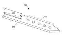
- FIG. 1is a side-view schematic of one embodiment of an optical electrode.
- FIG. 2is a perspective view schematic of another embodiment of an optical electrode.
- FIG. 3is a sectional view of an embodiment of an electrode with roughening material applied to the electrode surface.
- FIG. 4is a sectional view of another embodiment of a roughened electrode.
- FIGS. 5A and 5Bshow electrical recordings from electrodes depicting the artifact stabilization time for electrodes that are smooth (uncoated; FIG. 5A ) or roughened (treated with PEDOT at 3 nC/ ⁇ m 2 ; FIG. 5B ).
- FIGS. 6A and 6Bshow electrical recordings from electrodes depicting the artifact dissipation time for electrodes that are smooth (uncoated; FIG. 6A ) or roughened (treated with PEDOT at 1 nC/ ⁇ m 2 ; FIG. 6B ).
- FIG. 7shows the level of photoelectrochemical artifact on a series of recording electrodes in which only the even-numbered electrodes are roughened, using 473 nm light applied parallel to the probe shank.
- FIG. 8shows the level of photoelectrochemical artifact on a series of recording electrodes in which only the even-numbered electrodes are roughened, using 635 nm light applied parallel to the probe shank.
- FIG. 9shows the level of photoelectrochemical artifact on a series of recording electrodes in which only the even-numbered electrodes are roughened, using 473 nm light applied perpendicular to the probe shank.
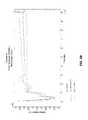
- FIG. 10shows the level of photoelectrochemical artifact on a series of recording electrodes in which only the even-numbered electrodes are roughened, using 473 nm light applied parallel to the probe shank and at a distance of 200 ⁇ m from the leftmost electrode.
- FIG. 11shows a bar graph depicting the average photoelectrochemical artifact amplitude from FIG. 10 of the roughened and unroughened electrodes.
- FIG. 12shows an embodiment of a system for use with embodiments of the disclosed optical electrode.
- an opto-electrical device 100includes: a carrier 110 insertable in tissue; an electrode array 112 disposed on the carrier 110 and having a plurality of electrodes including at least one recording electrode site having a roughened surface 112 a , the recording electrode configured to ‘record’ or sense electrical signals from its surroundings; and an optical light source 120 configured to illuminate selectively-targeted regions of the tissue.
- the opto-electrical device 100may be used in applications with optogenetic techniques involving optical stimulation patterns of tissue and neural recording capabilities.
- the opto-electrical device 100is insertable or implantable in neural tissue (e.g. the brain), but may additionally and/or alternatively be used with other suitable tissues.
- the carrier 110functions to provide structural support for the electrode array 112 and, in some cases, for insertion and/or implantation of the opto-electrical device 100 into tissue.
- the carrier 110may be planar, cylindrical, or other suitable shapes.
- the carrier 110may be similar to that in the neural device described in U.S. Patent Application number 2011/0112591 (hereinafter referred to as the '591 publication) entitled “Waveguide neural interface device,” which is incorporated in its entirety by this reference.
- other suitable carriers 110may be used.
- the carrier 110may be made of other suitable materials or combination of materials, including those listed in the '591 publication or in US 2011/0093052 (hereinafter referred to as the '052 publication) entitled “Neural Interface System,” which is incorporated in its entirety by this reference.
- the waveguide 120may serve as a carrier with an electrode array 112 being associated with the waveguide 120 .
- optrodessuch as those disclosed herein may be used with a neural interface system, such as disclosed in the '052 publication.
- the opto-electrical device 100is part of a neural interface system 1000 , which may include an electrical subsystem 1100 , an optical subsystem 1200 , and a controller 2000 .
- the electrical subsystem 1100functions to operate with the electrode array 112 , for example when the electrode array 112 is implanted into a subject 1500 ( FIG. 13 ).
- the subject 1500may include any number of animals into which the opto-electrical device 100 may be implanted and with which the neural interface system 1000 may be employed, including without limitation rodents (e.g. rats, mice, rabbits, etc.) and primates (e.g. humans, monkeys, etc.).
- the controller 2000may control one or both of the electrical subsystem 1100 and the optical subsystem 1200 to carry out the functions of the neural interface system 1000 such as those disclosed herein.
- the electrical subsystem 1100 , optical subsystem 1200 , and controller 2000may be integrated into a single unit or may be separate units, and each may be external to the subject 1500 or may be part of an implanted device.
- Each of the electrical subsystem 1100 , optical subsystem 1200 , and controller 2000may include a processor, memory, storage, amplifiers, A/D convertors, input/output mechanisms, and communication mechanisms, including capabilities for wired and/or wireless communications within the components of the system 1000 and between the system 1000 and external computers and networks.
- the electrical subsystem 1100includes at least one of several variations of suitable electronic subsystems to operate with (e.g. sense electrical signals at) the electrode array 112 or combinations thereof.
- the electrical subsystem 1100may be a printed circuit board with or without onboard amplifier or integrated circuits and/or on-chip circuitry for signal sensing and/or conditioning and/or stimulus generation, an Application Specific Integrated Circuit (ASIC), a multiplexer chip, a buffer amplifier, an electronics interface, a pulse generator (which produces signals such as a high-frequency, pulsed electric current, and which in certain embodiments may be implantable), a power supply (which in various embodiments can include an implantable rechargeable battery), integrated electronics for signal processing of the input (recorded) or output (stimulation) signals (either of which may be processed in real time), other suitable electrical subsystem, or combinations thereof, as disclosed in the '052 publication.
- ASICApplication Specific Integrated Circuit
- ASICApplication Specific Integrated Circuit
- multiplexer chipwhich produces signals such as a high-frequency,
- the optical subsystem 1200which is in communication with the optical light source 120 , includes power and control units to control the light source 120 in order to generate light pulses of suitable wavelength, duration, intensity, and pulse shape.
- the optical light source 120functions to illuminate surrounding tissue and stimulating targeted tissue.
- the optical light source 120is coupled to the carrier such that the light from the optical light source 120 has an angle of incidence that is minimal relative to the surface of the recording electrode sites (e.g. less than normal incidence).
- the optical light source 120provides illumination approximately parallel to the surface of the recording electrode site.
- the optical light source 120may be positioned in other suitable locations relative to the electrode site surface.
- the optical light source 120may include one or more LEDs or a waveguide, where the LEDs may be included on the carrier 110 (e.g. in the vicinity of the electrode array 112 ).
- the waveguidemay be coupled to a light source that is nearby (e.g. part of the implantable device) or remote (e.g. part of an external component associated with the implantable device).
- the light source to which the waveguide is coupledmay be one or more LEDs, a laser, or other suitable light source (e.g. as disclosed in the '591 publication), and in various embodiments is controlled by the optical subsystem 1200 .
- the optical light source 120can have a number of configurations relative to the electrode array 112 , e.g.
- light emitted from the optical light source 120may impinge on one or more electrodes in the electrode array 112 in a direction that is parallel, perpendicular, or at other angles relative to the surface on which the plurality of electrodes is disposed.
- the electrode array 112functions to electrically communicate with its surroundings.
- the electrode array 112can include one or more recording electrode sites that sense and record neural signals in surrounding tissue, and in some embodiments the electrode array 112 may additionally and/or alternatively include stimulation electrode sites.
- the electrode array 112may be arranged longitudinally along (e.g. as shown in FIGS. 1 and 2 ) and/or circumferentially around a cylindrical carrier 110 , along a face or edge of a planar carrier 110 , or in other suitable arrangements on the carrier 110 .
- the opto-electrical device 100may further include an optical light source 120 such as a waveguide arranged proximate to the electrode array 112 , as shown in FIGS. 1 and 2 or as shown and described in the '591 publication.
- the electrode sitesmay include conductive metal (e.g. gold, platinum, iridium, platinum-iridium, titanium nitride, iridium oxide, etc.) and may be formed by microfabrication techniques, such as thin-film or other microelectromechanical systems (MEMS) manufacturing processes.
- conductive metale.g. gold, platinum, iridium, platinum-iridium, titanium nitride, iridium oxide, etc.
- MEMSmicroelectromechanical systems
- a metal electrode that is “smooth” (not roughened) in generalhas an average roughness (R a ) of less than 10 nm (average of series of maximum and minimum height measurements). It is demonstrated herein that treatments that increase the average roughness of a recording electrode (or a material applied thereto, FIG. 3 ) to greater than about 10 nm have the effect of reducing the photoelectrochemical artifact.
- a roughened electrode 112 ahas an average roughness of greater than 10 nm, greater than 20 nm, greater than 30 nm, greater than 50 nm, or greater than 100 nm.
- Average roughness (R a )is an arithmetic average of absolute values of vertical deviations of height on a surface, expressed in units of height (e.g. nanometers).
- one or more recording electrodes 112 a in the electrode array 112may have a roughened surface ( FIGS. 1, 3, and 4 ).
- the rougheningcan take a number of forms and may produce a tortuous surface such as with recesses, pores, and/or other surface modifications that reduce the smoothness and increase the effective surface area of the electrode surface.
- the roughened surfacemay have a pattern (e.g. grooves, cross-hatching, regularly-spaced protrusions or depressions, etc.) or may be essentially random.
- the roughened surface 112 amay be produced by applying a material ( FIG. 3 ) to the electrode, by producing an electrode having a roughened surface as part of the electrode itself ( FIG. 4 ), or a combination of methods.
- the material applied to the surfacecan include PEDOT/PSS (poly(3,4-ethylenedioxythiophene)/poly(styrene sulfonate), iridium oxide, or nanostructures (e.g. nanotubes, nanoparticles, nanospheres) made from a variety of materials.
- PEDOT/PSSpoly(3,4-ethylenedioxythiophene)/poly(styrene sulfonate), iridium oxide, or nanostructures (e.g. nanotubes, nanoparticles, nanospheres) made from a variety of materials.
- glass or polystyrene nanospheres or microspheresmay be applied to one or more electrodes on the electrode array 112 during microfabrication to form a highly dense pattern on the modified electrode array.
- platinummay be applied to a surface using electrodeposition of Pt nanoparticles.
- the recording electrode and the roughened surface 112 amay be substantially free of transparent and semi-transparent conductors such
- polystyrene nanosphereswere applied to an electrode surface producing feature sizes of at least 200 nm in height and an average roughness R a of 300 nm.
- R awas found to be 365 ⁇ 37 nm (average ⁇ standard error) and the RMS (root mean square) surface roughness was 368 nm.
- a roughened electrode 112has an RMS surface roughness of greater than 50 nm, greater than 100 nm, or greater than 200 nm.
- PEDOT/PSSwas applied to a micromachined electrode (e.g. using techniques such as those in U.S. Pat. No. 8,005,526, which incorporated herein by reference) and the size of features was found to range from 50 nm-1000 nm and the R a was 700 ⁇ 243 nm for particular surfaces that were measured.
- iridium oxidecan be applied to the recording electrode to roughen the surface, as shown in Dias et al. (2010, “New dry electrodes based on iridium oxide (IrO) for non-invasive biopotential recordings and stimulation,” Sensors and Actuators A: Physical, 164:28-34; incorporated by reference herein).
- Iridium oxidecan produce filamentous, globular, or other surface features with feature sizes of 10 nm or greater and average roughness R a values ranging from 27 nm to 183 nm.
- the electrode surfacemay be roughened in one or more variations of surface modification steps.
- the electrode modificationmay include direct metal deposition (e.g., physical vapor deposition or PVD, sputtering, evaporation), electrochemical deposition from a solution, electrochemical activation (e.g. oxide growth), a sol-gel process, and/or micromachining and microfabrication techniques including the use of plasma etching (in which the exact chemistry depends on the type of metal in the electrode surface).
- Various parameters, such as duration, pressure, and temperature of deposition and other toolsmay also be adjusted to selectively modify the electrode site surfaces. However, other suitable methods of selectively depositing, forming, or machining a rough, tortuously textured conductive medium may be used.
- the electrode surfacemay be modified by micromachining or other suitable techniques to create a porous, discontinuous surface with a similarly tortuous electrical double layer.
- the electrode site surfacesmay include materials that are naturally recessed and/or porous.
- Each of the one or more roughened electrodes 112 awhich are generally planar, has a geometric surface area based on its physical dimensions such as length, width, and/or diameter.
- each of the one or more roughened electrodes 112 ahas an effective surface area that is at least two to ten times greater than the geometric surface area of the same electrode, and in various embodiments is at least twenty, fifty, one hundred, or one thousand times greater than the geometric surface area of the same electrode.
- the rougheningWhen a roughened electrode surface is immersed in brain tissue or other electrolyte environments and subsequently exposed to light, the roughening reduces the electrical artifacts that occur due to the photoelectrochemical effect (also known as the Becquerel effect). As mentioned above, these electrical artifacts, which occur with use of conventional optrodes, may interfere with or obscure the recording of the desired neural signals. In one hypothesis, the photoelectrochemical effect is thought to begin with a photoelectric event in which photons cause emission of electrons upon striking a non-transparent metal surface.
- the rougheningmay reduce the artifact due to the photoelectrochemical effect by increasing an effective surface area of the electrode and producing a lower surface charge density.
- the lower surface charge densitymay reduce the probability that an emitted electron will interact with a charge in the electrical double layer.
- two groups of electrode siteswere placed in an ionic solution of PBS 1 ⁇ and electrical signals were recorded after being impinged with a laser diode: a first group in which the electrode sites were coated with PEDOT at 3 nC/ ⁇ m 2 ( FIG. 5B ) or at 1 nC/ ⁇ m 2 (FIG. 6 B), and a second group in which the electrode sites were not substantially coated with PEDOT, such that the first group of electrode sites ( FIGS. 5B, 6B ) had surfaces substantially roughened compared to that of the second group of electrode sites ( FIGS. 5A, 6A ). As shown in FIGS.
- the signal from the roughened electrode sitesrecorded significantly shorter artifact stabilization time than the unroughened electrode sites.
- the signal from the roughened electrode sitesrecorded an artifact significantly smaller in amplitude than that from the unroughened electrode sites.
- the artifactdissipated as an inverted waveform, more quickly than in the signal from the unroughened electrode sites.
- Electrophysiologistsmay also easily filter out short-duration artifacts more readily than artifacts having a pulse-width similar to the physiological signal, e.g. the pulse-width of a single-cell action potentials.
- a smaller electrode having a smaller recessed surface area ( ⁇ 177 ⁇ m 2 ) and a larger electrode having a larger recessed surface area ( ⁇ 703 ⁇ m 2 )were placed in an ionic solution and illuminated with light incident approximately parallel to the electrode surface.
- Comparison of the signal recorded by the smaller electrode and the signal recorded by the larger electrodesuggested that when light is incident on an electrode approximately parallel to the surface, then the surface area of the electrode is inversely proportional to the amplitude of the artifact.
- the even-numbered electrodes in a linear arrayconsisting of platinum, were patterned with nanoscale platinum structures to roughen the surface of even-numbered sites ( FIG. 7 ).
- Light(473 nm, 50 Hz, 5 ms, 1 mW) was applied parallel to the probe shank containing the linear array, closest to electrode number 1 .
- the level of artifact on the even-numbered electrodes(only values for electrodes 2 , 6 , and 12 are shown) is greatly reduced compared to the uncoated electrodes.
- the artifactis reduced by 90% compared to the predicted level of artifact for that electrode after accounting for spreading and scattering ( FIG. 7 , inset).
- an optical electrode in which the even-numbered electrodes were roughenedwas illuminated with light (473 nm, 50 Hz, 5 ms, 2 mW) perpendicular to the shank of the electrode with the light source being essentially adjacent to the electrodes (d ⁇ 0; FIG. 9 ).
- the roughened even-numbered electrodesshowed a 29% decrease in artifact on average compared to the uncoated (smooth) odd-numbered electrodes.
- FIG. 10shows the artifact amplitude for an optical electrode with a linear array of recording electrodes in which the even-numbered recording electrodes are roughened.
- Light(473 nm, 50 Hz, 5 ms, 2 mW) is applied parallel to the shank of the optical electrode using an optical fiber placed at approximately 200 ⁇ m from the proximal recording electrode (i.e. 200 ⁇ m to the left of electrode 12 in the diagram of FIG. 10 ).
- the inventionprovides, among other things, an optical electrode and a method of producing an optical electrode.
- an optical electrodeand a method of producing an optical electrode.
Landscapes
- Health & Medical Sciences (AREA)
- Life Sciences & Earth Sciences (AREA)
- Engineering & Computer Science (AREA)
- Biomedical Technology (AREA)
- General Health & Medical Sciences (AREA)
- Biophysics (AREA)
- Pathology (AREA)
- Veterinary Medicine (AREA)
- Public Health (AREA)
- Animal Behavior & Ethology (AREA)
- Medical Informatics (AREA)
- Physics & Mathematics (AREA)
- Heart & Thoracic Surgery (AREA)
- Molecular Biology (AREA)
- Surgery (AREA)
- Radiology & Medical Imaging (AREA)
- Nuclear Medicine, Radiotherapy & Molecular Imaging (AREA)
- Neurosurgery (AREA)
- Optical Head (AREA)
- Neurology (AREA)
Abstract
Description
Claims (17)
Priority Applications (3)
| Application Number | Priority Date | Filing Date | Title |
|---|---|---|---|
| US13/557,516US9782091B2 (en) | 2011-07-25 | 2012-07-25 | Opto-electrical device for artifact reduction |
| US15/728,251US10231636B2 (en) | 2011-07-25 | 2017-10-09 | Opto-electrical device and method for artifact reduction |
| US16/277,334US11234627B2 (en) | 2011-07-25 | 2019-02-15 | Opto-electrical device and method for artifact reduction |
Applications Claiming Priority (2)
| Application Number | Priority Date | Filing Date | Title |
|---|---|---|---|
| US201161511358P | 2011-07-25 | 2011-07-25 | |
| US13/557,516US9782091B2 (en) | 2011-07-25 | 2012-07-25 | Opto-electrical device for artifact reduction |
Related Child Applications (1)
| Application Number | Title | Priority Date | Filing Date |
|---|---|---|---|
| US15/728,251ContinuationUS10231636B2 (en) | 2011-07-25 | 2017-10-09 | Opto-electrical device and method for artifact reduction |
Publications (2)
| Publication Number | Publication Date |
|---|---|
| US20130030275A1 US20130030275A1 (en) | 2013-01-31 |
| US9782091B2true US9782091B2 (en) | 2017-10-10 |
Family
ID=46755082
Family Applications (3)
| Application Number | Title | Priority Date | Filing Date |
|---|---|---|---|
| US13/557,516Active2033-09-15US9782091B2 (en) | 2011-07-25 | 2012-07-25 | Opto-electrical device for artifact reduction |
| US15/728,251ActiveUS10231636B2 (en) | 2011-07-25 | 2017-10-09 | Opto-electrical device and method for artifact reduction |
| US16/277,334Active2033-02-13US11234627B2 (en) | 2011-07-25 | 2019-02-15 | Opto-electrical device and method for artifact reduction |
Family Applications After (2)
| Application Number | Title | Priority Date | Filing Date |
|---|---|---|---|
| US15/728,251ActiveUS10231636B2 (en) | 2011-07-25 | 2017-10-09 | Opto-electrical device and method for artifact reduction |
| US16/277,334Active2033-02-13US11234627B2 (en) | 2011-07-25 | 2019-02-15 | Opto-electrical device and method for artifact reduction |
Country Status (3)
| Country | Link |
|---|---|
| US (3) | US9782091B2 (en) |
| EP (1) | EP2736402B1 (en) |
| WO (1) | WO2013016389A1 (en) |
Cited By (1)
| Publication number | Priority date | Publication date | Assignee | Title |
|---|---|---|---|---|
| US20170106204A1 (en)* | 2015-10-16 | 2017-04-20 | California Institute Of Technology | Implantable, highly collimated light-emitters for biological applications |
Families Citing this family (41)
| Publication number | Priority date | Publication date | Assignee | Title |
|---|---|---|---|---|
| EP2465925A1 (en) | 2005-07-22 | 2012-06-20 | The Board Of Trustees Of The Leland | Light-activated cation channel and uses thereof |
| US10052497B2 (en) | 2005-07-22 | 2018-08-21 | The Board Of Trustees Of The Leland Stanford Junior University | System for optical stimulation of target cells |
| US8926959B2 (en) | 2005-07-22 | 2015-01-06 | The Board Of Trustees Of The Leland Stanford Junior University | System for optical stimulation of target cells |
| US9238150B2 (en) | 2005-07-22 | 2016-01-19 | The Board Of Trustees Of The Leland Stanford Junior University | Optical tissue interface method and apparatus for stimulating cells |
| US9274099B2 (en) | 2005-07-22 | 2016-03-01 | The Board Of Trustees Of The Leland Stanford Junior University | Screening test drugs to identify their effects on cell membrane voltage-gated ion channel |
| US20090093403A1 (en) | 2007-03-01 | 2009-04-09 | Feng Zhang | Systems, methods and compositions for optical stimulation of target cells |
| US8398692B2 (en) | 2007-01-10 | 2013-03-19 | The Board Of Trustees Of The Leland Stanford Junior University | System for optical stimulation of target cells |
| US8401609B2 (en) | 2007-02-14 | 2013-03-19 | The Board Of Trustees Of The Leland Stanford Junior University | System, method and applications involving identification of biological circuits such as neurological characteristics |
| US10434327B2 (en) | 2007-10-31 | 2019-10-08 | The Board Of Trustees Of The Leland Stanford Junior University | Implantable optical stimulators |
| US10035027B2 (en) | 2007-10-31 | 2018-07-31 | The Board Of Trustees Of The Leland Stanford Junior University | Device and method for ultrasonic neuromodulation via stereotactic frame based technique |
| EP3165534B1 (en) | 2008-04-23 | 2018-09-26 | The Board of Trustees of The Leland Stanford Junior University | Systems, methods and compositions for optical stimulation of target cells |
| CN102076866A (en) | 2008-05-29 | 2011-05-25 | 利兰·斯坦福青年大学托管委员会 | Cell lines, systems and methods for optically controlling second messengers |
| WO2009155371A1 (en) | 2008-06-17 | 2009-12-23 | The Board Of Trustees Of The Leland Stanford Junior University | Methods, systems and devices for optical stimulation of target cells using an optical transmission element |
| SG191604A1 (en) | 2008-06-17 | 2013-07-31 | Univ Leland Stanford Junior | Apparatus and methods for controlling cellular development |
| US9101759B2 (en) | 2008-07-08 | 2015-08-11 | The Board Of Trustees Of The Leland Stanford Junior University | Materials and approaches for optical stimulation of the peripheral nervous system |
| NZ602416A (en) | 2008-11-14 | 2014-08-29 | Univ Leland Stanford Junior | Optically-based stimulation of target cells and modifications thereto |
| ES2676274T3 (en) | 2010-03-17 | 2018-07-18 | The Board Of Trustees Of The Leland Stanford Junior University | Light sensitive molecules that allow the passage of ions |
| EP2635341B1 (en) | 2010-11-05 | 2018-08-08 | The Board of Trustees of the Leland Stanford Junior University | Upconversion of light for use in optogenetic methods |
| JP6276591B2 (en) | 2010-11-05 | 2018-02-07 | ザ ボード オブ トラスティーズ オブ ザ レランド スタンフォード ジュニア ユニバーシティー | Photo-activated chimeric opsin and method of use thereof |
| EP2635295B1 (en) | 2010-11-05 | 2017-12-20 | The Board of Trustees of the Leland Stanford Junior University | Control and characterization of memory function |
| EP2635346B1 (en) | 2010-11-05 | 2017-03-29 | The Board of Trustees of the Leland Stanford Junior University | Optogenetic control of reward-related behaviors |
| WO2012061744A2 (en) | 2010-11-05 | 2012-05-10 | The Board Of Trustees Of The Leland Stanford Junior University | Stabilized step function opsin proteins and methods of using the same |
| EP2635109A4 (en) | 2010-11-05 | 2014-03-19 | Univ Leland Stanford Junior | OPTICALLY CONTROLLED CNS DYSFUNCTION |
| US8696722B2 (en) | 2010-11-22 | 2014-04-15 | The Board Of Trustees Of The Leland Stanford Junior University | Optogenetic magnetic resonance imaging |
| US10493297B2 (en) | 2011-07-25 | 2019-12-03 | Neuronexus Technologies, Inc. | Neuromodulation transfection system with passive fluid delivery |
| US9700736B2 (en) | 2011-07-25 | 2017-07-11 | Neuronexus Technologies, Inc. | Neuromodulation transfection system with active fluid delivery |
| EP2570153B1 (en)* | 2011-09-14 | 2017-09-13 | NeuroNexus Technologies, Inc. | Methods for forming an electrode device with reduced impedance |
| JP6406581B2 (en) | 2011-12-16 | 2018-10-17 | ザ ボード オブ トラスティーズ オブ ザ レランド スタンフォード ジュニア ユニバーシティー | Opsin polypeptides and uses thereof |
| US20140024701A1 (en) | 2012-02-21 | 2014-01-23 | Circuit Therapeutics, Inc. | Compositions and Methods for Treating Neurogenic Disorders of the Pelvic Floor |
| US9636380B2 (en) | 2013-03-15 | 2017-05-02 | The Board Of Trustees Of The Leland Stanford Junior University | Optogenetic control of inputs to the ventral tegmental area |
| EP2968997B1 (en) | 2013-03-15 | 2019-06-26 | The Board of Trustees of the Leland Stanford Junior University | Optogenetic control of behavioral state |
| CN105431046B (en) | 2013-04-29 | 2020-04-17 | 小利兰·斯坦福大学托管委员会 | Devices, systems, and methods for optogenetic modulation of action potentials in target cells |
| EP3033427A4 (en) | 2013-08-14 | 2017-05-31 | The Board Of Trustees Of The University Of the Leland Stanford Junior University | Compositions and methods for controlling pain |
| CN103462600B (en)* | 2013-09-04 | 2015-04-15 | 中国科学院深圳先进技术研究院 | Photoelectrode component and in-vivo photoelectrode imaging system |
| US10387962B1 (en) | 2014-07-21 | 2019-08-20 | State Farm Mutual Automobile Insurance Company | Methods of reconstructing an accident scene using telematics data |
| KR102344486B1 (en)* | 2015-03-19 | 2021-12-29 | 한국전자통신연구원 | Neural electrode for measuring neural signal and method for manufacturing thereof |
| US10568516B2 (en) | 2015-06-22 | 2020-02-25 | The Board Of Trustees Of The Leland Stanford Junior University | Methods and devices for imaging and/or optogenetic control of light-responsive neurons |
| CA3027560A1 (en)* | 2016-06-17 | 2017-12-21 | Gensight Biologics | Device for illuminating an object with a controlled light intensity and associated method |
| US11294165B2 (en) | 2017-03-30 | 2022-04-05 | The Board Of Trustees Of The Leland Stanford Junior University | Modular, electro-optical device for increasing the imaging field of view using time-sequential capture |
| US20210045690A1 (en)* | 2018-03-01 | 2021-02-18 | Universitat Basel Vizerektorat Forschung | Neural probe for electrostimulation or recording and fabrication process for such a probe |
| CN113245650B (en)* | 2021-06-03 | 2022-06-24 | 烟台大学 | A kind of deep brain stimulation cannula electrode and its surface textured random bionic microtexture preparation method |
Citations (62)
| Publication number | Priority date | Publication date | Assignee | Title |
|---|---|---|---|---|
| US3628017A (en) | 1970-06-18 | 1971-12-14 | Itek Corp | Ultraviolet light-sensitive cell using a substantially chemically unchanged semiconductor electrode in an electrolyte |
| US4717581A (en)* | 1986-02-06 | 1988-01-05 | Eic Laboratories, Inc. | Iridium oxide coated electrodes for neural stimulation |
| US5629009A (en) | 1989-02-22 | 1997-05-13 | Massachusetts Institute Of Technology | Delivery system for controlled release of bioactive factors |
| US5683443A (en)* | 1995-02-07 | 1997-11-04 | Intermedics, Inc. | Implantable stimulation electrodes with non-native metal oxide coating mixtures |
| US6238994B1 (en) | 1997-07-02 | 2001-05-29 | Micron Technology, Inc. | Method of creating a rough electrode (high surface area) from Ti and TiN and resulting article |
| US6294074B1 (en) | 2000-05-18 | 2001-09-25 | The University Of Chicago | Electrode design for corrosion monitoring using electrochemical noise measurements |
| US20020183682A1 (en) | 1999-06-04 | 2002-12-05 | Nissim Darvish | Drug delivery device |
| US20030147958A1 (en) | 2002-01-29 | 2003-08-07 | Cheol-Hee Ahn | Biodegradable multi-block copolymers of poly(amino acid)s and poly(ethylene glycol) for the delivery of bioactive agents |
| US20040111139A1 (en) | 2002-12-10 | 2004-06-10 | Mccreery Douglas B. | Apparatus and methods for differential stimulation of nerve fibers |
| US20060024359A1 (en) | 1995-06-07 | 2006-02-02 | Walker Jeffrey P | Drug delivery system and method |
| US7310546B2 (en) | 2001-11-06 | 2007-12-18 | Prass Richard L | Artifact detection electrode |
| US7375870B2 (en) | 2002-06-13 | 2008-05-20 | Nokia Corporation | Enhancement electrode configuration for electrically controlled light modulators |
| WO2008089003A2 (en) | 2007-01-09 | 2008-07-24 | The Board Of Trustees Of The Leland Stanford Junior University | System for optical stimulation of target cells |
| US20080208283A1 (en)* | 2007-02-26 | 2008-08-28 | Rio Vetter | Neural Interface System |
| US20080249391A1 (en)* | 2006-07-18 | 2008-10-09 | Drexel University | Chronic in-vivo neurotransmitter sensor |
| US20090054954A1 (en) | 2007-08-22 | 2009-02-26 | Cardiac Pacemakers, Inc. | Optical depolarization of cardiac tissue |
| US20090099038A1 (en) | 2005-07-22 | 2009-04-16 | Karl Deisseroth | Cell line, system and method for optical-based screening of ion-channel modulators |
| US20090118800A1 (en) | 2007-10-31 | 2009-05-07 | Karl Deisseroth | Implantable optical stimulators |
| WO2009072123A2 (en) | 2007-12-06 | 2009-06-11 | Technion Research & Development Foundation Ltd. | Method and system for optical stimulation of neurons |
| WO2009124220A2 (en) | 2008-04-02 | 2009-10-08 | St. Jude Medical, Atrial Fibrillation Division, Inc. | Photodynamic-based myocardial mapping device and method |
| WO2009131837A2 (en) | 2008-04-23 | 2009-10-29 | The Board Of Trustees Of The Leland Stanford Junior University. | Systems, methods and compositions for optical stimulation of target cells |
| US20090292325A1 (en) | 2008-05-02 | 2009-11-26 | Cederna Paul S | Hybrid bioelectrical interface device |
| US20100015095A1 (en) | 2006-05-04 | 2010-01-21 | Wayne State University | Restoration of visual responses by in vivo delivery of rhodopsin nucleic acids |
| US20100049263A1 (en) | 2006-01-24 | 2010-02-25 | Reeve Helen L | Method and device for detecting and treating depression |
| WO2010029297A1 (en) | 2008-09-10 | 2010-03-18 | Imperial Innovations Limited | Photo-ionic pacemakers |
| WO2010056970A2 (en) | 2008-11-14 | 2010-05-20 | The Board Of Trustees Of The Leland Stanford Junior University | Optically-based stimulation of target cells and modifications thereto |
| US20100137960A1 (en)* | 2008-12-03 | 2010-06-03 | Boston Scientific Neuromodulation Corporation | Implantable neurostimulators having reduced pocket stimulation |
| US20100161017A1 (en) | 2008-12-23 | 2010-06-24 | Korea Institute Of Science And Technology | Apparatus for stimulating the brain and measuring the light induced neuronal activity and method for manufacturing the same |
| US20100190229A1 (en) | 2005-07-22 | 2010-07-29 | Feng Zhang | System for optical stimulation of target cells |
| US20100191308A1 (en) | 2009-01-23 | 2010-07-29 | Med-El Elektromedizinische Geraete Gmbh | Stimulation Channel Conditioning |
| US20100211172A1 (en) | 2007-04-02 | 2010-08-19 | Georgia Tech Research Corporation | Implantable Device For Communicating With Biological Tissue |
| US7781195B1 (en) | 1997-12-17 | 2010-08-24 | University Of South Florida | Electroporation device |
| WO2010105728A2 (en) | 2009-03-20 | 2010-09-23 | Retina Implant Ag | Active retinal implant |
| US20100268150A1 (en) | 2009-04-17 | 2010-10-21 | The Regents Of The University Of California | Method and apparatus for optogenetic treatment of blindness including retinitis pigmentosa |
| US20110021970A1 (en) | 2007-11-06 | 2011-01-27 | Duke University | Non-invasive energy upconversion methods and systems for in-situ photobiomodulation |
| US7887681B2 (en)* | 2002-04-11 | 2011-02-15 | Second Sight Medical Products, Inc. | Platinum electrode surface coating and method for manufacturing the same |
| US20110087126A1 (en) | 2009-10-08 | 2011-04-14 | Massachusetts Institute Of Technology | Light-Proof Electrodes |
| US20110093052A1 (en) | 2009-10-16 | 2011-04-21 | Anderson David J | Neural interface system |
| WO2011057137A1 (en) | 2009-11-05 | 2011-05-12 | Neuronexus Technologies | Waveguide neural interface device |
| WO2011057276A2 (en) | 2009-11-09 | 2011-05-12 | University Of Utah Research Foundation | Three-dimensional penetrating optical-electrical neural interface for selective stimulation and recording |
| US7955889B1 (en) | 2006-07-11 | 2011-06-07 | The Trustees Of Princeton University | Organic photosensitive cells grown on rough electrode with nano-scale morphology control |
| US20110144566A1 (en) | 2007-08-17 | 2011-06-16 | Searete Llc, A Limited Liability Corporation Of The State Of Delaware | Systems, devices, and methods including catheters having an actively controllable therapeutic agent delivery component |
| US20110172736A1 (en) | 2010-01-14 | 2011-07-14 | Nano-Retina, Inc. | Penetrating electrodes for retinal stimulation |
| US8005526B2 (en) | 2005-08-31 | 2011-08-23 | The Regents Of The University Of Michigan | Biologically integrated electrode devices |
| US20110318775A1 (en) | 2009-12-04 | 2011-12-29 | Sanford-Burnham Medical Research Institute | Method, system and composition for optically inducing cardiomyocyte contraction |
| US20120035725A1 (en) | 2010-08-06 | 2012-02-09 | Nano-Retina, Inc. | Retinal prosthesis techniques |
| US20120035726A1 (en) | 2010-08-06 | 2012-02-09 | Nano-Retina, Inc. | Retinal prosthesis techniques |
| WO2012052727A2 (en) | 2010-10-21 | 2012-04-26 | King's College London | Cells and devices |
| US20120101356A1 (en)* | 2010-10-26 | 2012-04-26 | Korea Institute Of Science And Technology | Optical Stimulus Probe with Reflecting Surface |
| WO2012061744A2 (en) | 2010-11-05 | 2012-05-10 | The Board Of Trustees Of The Leland Stanford Junior University | Stabilized step function opsin proteins and methods of using the same |
| WO2012061676A1 (en) | 2010-11-05 | 2012-05-10 | The Board Of Trustees Of The Leland Stanford Junior University | Light-activated chimeric opsins and methods of using the same |
| WO2012061688A1 (en) | 2010-11-05 | 2012-05-10 | The Board Of Trustees Of The Leland Stanford Junior University | Optogenetic control of reward-related behaviors |
| US20120130302A1 (en) | 2009-03-20 | 2012-05-24 | Retina Implant Ag | Active retinal implant |
| WO2012075337A2 (en) | 2010-12-01 | 2012-06-07 | Spinal Modulation, Inc. | Directed delivery of agents to neural anatomy |
| US20120149052A1 (en) | 2009-07-20 | 2012-06-14 | Fondazione Centro San Raffaele Del Monte Tabor | Method for optical measuring variations of cell membrane conductance |
| US8355793B2 (en)* | 2009-01-02 | 2013-01-15 | Cochlear Limited | Optical neural stimulating device having a short stimulating assembly |
| US20130030352A1 (en) | 2011-07-25 | 2013-01-31 | Seymour John P | Neuromodulation transfection system with active fluid delivery |
| WO2013016392A1 (en) | 2011-07-25 | 2013-01-31 | Neuronexus Technologies, Inc. | Neuromodulation transfection system with passive fluid delivery |
| US20130079615A1 (en)* | 2009-11-19 | 2013-03-28 | The Regents Of The University Of Michigan | Neural probe with optical stimulation capability |
| US20130090542A1 (en)* | 2010-06-18 | 2013-04-11 | The Regents Of The University Of Michigan | Implantable micro-component electrodes |
| US20130131485A1 (en)* | 2011-11-23 | 2013-05-23 | Korea Institute Of Science And Technology | Tetrode for measuring bio-signals and method of manufacturing the same |
| US20140350375A1 (en)* | 2013-05-24 | 2014-11-27 | University Of Houston | Integrated thin-film optrode |
Family Cites Families (2)
| Publication number | Priority date | Publication date | Assignee | Title |
|---|---|---|---|---|
| USPP13394P2 (en) | 2001-07-16 | 2002-12-24 | Klemm & Sohn Gmbh & Co. Kg | Calibrachoa plant named ‘KLEC00070’ |
| KR100924696B1 (en) | 2007-07-05 | 2009-11-03 | 삼성전자주식회사 | Method for improving recording density of hard disk drive and its control device |
- 2012
- 2012-07-25USUS13/557,516patent/US9782091B2/enactiveActive
- 2012-07-25EPEP12751638.3Apatent/EP2736402B1/ennot_activeNot-in-force
- 2012-07-25WOPCT/US2012/048073patent/WO2013016389A1/enactiveApplication Filing
- 2017
- 2017-10-09USUS15/728,251patent/US10231636B2/enactiveActive
- 2019
- 2019-02-15USUS16/277,334patent/US11234627B2/enactiveActive
Patent Citations (67)
| Publication number | Priority date | Publication date | Assignee | Title |
|---|---|---|---|---|
| US3628017A (en) | 1970-06-18 | 1971-12-14 | Itek Corp | Ultraviolet light-sensitive cell using a substantially chemically unchanged semiconductor electrode in an electrolyte |
| US4717581A (en)* | 1986-02-06 | 1988-01-05 | Eic Laboratories, Inc. | Iridium oxide coated electrodes for neural stimulation |
| US5629009A (en) | 1989-02-22 | 1997-05-13 | Massachusetts Institute Of Technology | Delivery system for controlled release of bioactive factors |
| US5683443A (en)* | 1995-02-07 | 1997-11-04 | Intermedics, Inc. | Implantable stimulation electrodes with non-native metal oxide coating mixtures |
| US20060024359A1 (en) | 1995-06-07 | 2006-02-02 | Walker Jeffrey P | Drug delivery system and method |
| US6238994B1 (en) | 1997-07-02 | 2001-05-29 | Micron Technology, Inc. | Method of creating a rough electrode (high surface area) from Ti and TiN and resulting article |
| US7781195B1 (en) | 1997-12-17 | 2010-08-24 | University Of South Florida | Electroporation device |
| US20020183682A1 (en) | 1999-06-04 | 2002-12-05 | Nissim Darvish | Drug delivery device |
| US6294074B1 (en) | 2000-05-18 | 2001-09-25 | The University Of Chicago | Electrode design for corrosion monitoring using electrochemical noise measurements |
| US7310546B2 (en) | 2001-11-06 | 2007-12-18 | Prass Richard L | Artifact detection electrode |
| US20030147958A1 (en) | 2002-01-29 | 2003-08-07 | Cheol-Hee Ahn | Biodegradable multi-block copolymers of poly(amino acid)s and poly(ethylene glycol) for the delivery of bioactive agents |
| US7887681B2 (en)* | 2002-04-11 | 2011-02-15 | Second Sight Medical Products, Inc. | Platinum electrode surface coating and method for manufacturing the same |
| US7375870B2 (en) | 2002-06-13 | 2008-05-20 | Nokia Corporation | Enhancement electrode configuration for electrically controlled light modulators |
| US20040111139A1 (en) | 2002-12-10 | 2004-06-10 | Mccreery Douglas B. | Apparatus and methods for differential stimulation of nerve fibers |
| US20090099038A1 (en) | 2005-07-22 | 2009-04-16 | Karl Deisseroth | Cell line, system and method for optical-based screening of ion-channel modulators |
| US20100190229A1 (en) | 2005-07-22 | 2010-07-29 | Feng Zhang | System for optical stimulation of target cells |
| US8005526B2 (en) | 2005-08-31 | 2011-08-23 | The Regents Of The University Of Michigan | Biologically integrated electrode devices |
| US20100049263A1 (en) | 2006-01-24 | 2010-02-25 | Reeve Helen L | Method and device for detecting and treating depression |
| US20100015095A1 (en) | 2006-05-04 | 2010-01-21 | Wayne State University | Restoration of visual responses by in vivo delivery of rhodopsin nucleic acids |
| US7955889B1 (en) | 2006-07-11 | 2011-06-07 | The Trustees Of Princeton University | Organic photosensitive cells grown on rough electrode with nano-scale morphology control |
| US20080249391A1 (en)* | 2006-07-18 | 2008-10-09 | Drexel University | Chronic in-vivo neurotransmitter sensor |
| WO2008089003A2 (en) | 2007-01-09 | 2008-07-24 | The Board Of Trustees Of The Leland Stanford Junior University | System for optical stimulation of target cells |
| US20080208283A1 (en)* | 2007-02-26 | 2008-08-28 | Rio Vetter | Neural Interface System |
| US20100211172A1 (en) | 2007-04-02 | 2010-08-19 | Georgia Tech Research Corporation | Implantable Device For Communicating With Biological Tissue |
| US20110144566A1 (en) | 2007-08-17 | 2011-06-16 | Searete Llc, A Limited Liability Corporation Of The State Of Delaware | Systems, devices, and methods including catheters having an actively controllable therapeutic agent delivery component |
| US20090054954A1 (en) | 2007-08-22 | 2009-02-26 | Cardiac Pacemakers, Inc. | Optical depolarization of cardiac tissue |
| US20090118800A1 (en) | 2007-10-31 | 2009-05-07 | Karl Deisseroth | Implantable optical stimulators |
| US20110021970A1 (en) | 2007-11-06 | 2011-01-27 | Duke University | Non-invasive energy upconversion methods and systems for in-situ photobiomodulation |
| WO2009072123A2 (en) | 2007-12-06 | 2009-06-11 | Technion Research & Development Foundation Ltd. | Method and system for optical stimulation of neurons |
| WO2009124220A2 (en) | 2008-04-02 | 2009-10-08 | St. Jude Medical, Atrial Fibrillation Division, Inc. | Photodynamic-based myocardial mapping device and method |
| US20110105998A1 (en) | 2008-04-23 | 2011-05-05 | The Board Of Trustees Of The Leland Stanford Junio | Systems, methods and compositions for optical stimulation of target cells |
| WO2009131837A2 (en) | 2008-04-23 | 2009-10-29 | The Board Of Trustees Of The Leland Stanford Junior University. | Systems, methods and compositions for optical stimulation of target cells |
| US20090292325A1 (en) | 2008-05-02 | 2009-11-26 | Cederna Paul S | Hybrid bioelectrical interface device |
| WO2010029297A1 (en) | 2008-09-10 | 2010-03-18 | Imperial Innovations Limited | Photo-ionic pacemakers |
| US20110311489A1 (en) | 2008-11-14 | 2011-12-22 | Karl Deisseroth | Optically-based stimulation of target cells and modifications thereto |
| WO2010056970A2 (en) | 2008-11-14 | 2010-05-20 | The Board Of Trustees Of The Leland Stanford Junior University | Optically-based stimulation of target cells and modifications thereto |
| US20100137960A1 (en)* | 2008-12-03 | 2010-06-03 | Boston Scientific Neuromodulation Corporation | Implantable neurostimulators having reduced pocket stimulation |
| US20100161017A1 (en) | 2008-12-23 | 2010-06-24 | Korea Institute Of Science And Technology | Apparatus for stimulating the brain and measuring the light induced neuronal activity and method for manufacturing the same |
| US8355793B2 (en)* | 2009-01-02 | 2013-01-15 | Cochlear Limited | Optical neural stimulating device having a short stimulating assembly |
| US20100191308A1 (en) | 2009-01-23 | 2010-07-29 | Med-El Elektromedizinische Geraete Gmbh | Stimulation Channel Conditioning |
| WO2010105728A2 (en) | 2009-03-20 | 2010-09-23 | Retina Implant Ag | Active retinal implant |
| US20120130302A1 (en) | 2009-03-20 | 2012-05-24 | Retina Implant Ag | Active retinal implant |
| US20100268150A1 (en) | 2009-04-17 | 2010-10-21 | The Regents Of The University Of California | Method and apparatus for optogenetic treatment of blindness including retinitis pigmentosa |
| US20120149052A1 (en) | 2009-07-20 | 2012-06-14 | Fondazione Centro San Raffaele Del Monte Tabor | Method for optical measuring variations of cell membrane conductance |
| US20110087126A1 (en) | 2009-10-08 | 2011-04-14 | Massachusetts Institute Of Technology | Light-Proof Electrodes |
| US20110093052A1 (en) | 2009-10-16 | 2011-04-21 | Anderson David J | Neural interface system |
| US20110112591A1 (en) | 2009-11-05 | 2011-05-12 | Seymour John P | Waveguide neural interface device |
| WO2011057137A1 (en) | 2009-11-05 | 2011-05-12 | Neuronexus Technologies | Waveguide neural interface device |
| WO2011057276A2 (en) | 2009-11-09 | 2011-05-12 | University Of Utah Research Foundation | Three-dimensional penetrating optical-electrical neural interface for selective stimulation and recording |
| US20130079615A1 (en)* | 2009-11-19 | 2013-03-28 | The Regents Of The University Of Michigan | Neural probe with optical stimulation capability |
| US20110318775A1 (en) | 2009-12-04 | 2011-12-29 | Sanford-Burnham Medical Research Institute | Method, system and composition for optically inducing cardiomyocyte contraction |
| US20110172736A1 (en) | 2010-01-14 | 2011-07-14 | Nano-Retina, Inc. | Penetrating electrodes for retinal stimulation |
| US20130090542A1 (en)* | 2010-06-18 | 2013-04-11 | The Regents Of The University Of Michigan | Implantable micro-component electrodes |
| US20120035725A1 (en) | 2010-08-06 | 2012-02-09 | Nano-Retina, Inc. | Retinal prosthesis techniques |
| US20120035726A1 (en) | 2010-08-06 | 2012-02-09 | Nano-Retina, Inc. | Retinal prosthesis techniques |
| WO2012052727A2 (en) | 2010-10-21 | 2012-04-26 | King's College London | Cells and devices |
| US20120101356A1 (en)* | 2010-10-26 | 2012-04-26 | Korea Institute Of Science And Technology | Optical Stimulus Probe with Reflecting Surface |
| WO2012061676A1 (en) | 2010-11-05 | 2012-05-10 | The Board Of Trustees Of The Leland Stanford Junior University | Light-activated chimeric opsins and methods of using the same |
| WO2012061679A2 (en) | 2010-11-05 | 2012-05-10 | The Board Of Trustees Of The Leland Stanford Junior University | Light-activated chimeric opsins and methods of using the same |
| WO2012061688A1 (en) | 2010-11-05 | 2012-05-10 | The Board Of Trustees Of The Leland Stanford Junior University | Optogenetic control of reward-related behaviors |
| WO2012061744A2 (en) | 2010-11-05 | 2012-05-10 | The Board Of Trustees Of The Leland Stanford Junior University | Stabilized step function opsin proteins and methods of using the same |
| WO2012075337A2 (en) | 2010-12-01 | 2012-06-07 | Spinal Modulation, Inc. | Directed delivery of agents to neural anatomy |
| WO2013016391A1 (en) | 2011-07-25 | 2013-01-31 | Neuronexus Technologies, Inc. | Neuromodulation transfection system with means for active fluid delivery and a method for its use |
| WO2013016392A1 (en) | 2011-07-25 | 2013-01-31 | Neuronexus Technologies, Inc. | Neuromodulation transfection system with passive fluid delivery |
| US20130030352A1 (en) | 2011-07-25 | 2013-01-31 | Seymour John P | Neuromodulation transfection system with active fluid delivery |
| US20130131485A1 (en)* | 2011-11-23 | 2013-05-23 | Korea Institute Of Science And Technology | Tetrode for measuring bio-signals and method of manufacturing the same |
| US20140350375A1 (en)* | 2013-05-24 | 2014-11-27 | University Of Houston | Integrated thin-film optrode |
Non-Patent Citations (25)
| Title |
|---|
| Adamantidis et al., "Neural substrates of awakening probed with optogenetic control of hypocretin neurons," Nature, Nov. 2007, vol. 450, pp. 420-425. |
| Aravanis et al., "An optical neural interface: in vivo control of rodent motor cortex with integrated fiberoptic and optogenetic technology," Journal of Neural Engineering, 2007, vol. 4, pp. S143-S156. |
| Arenkiel et al., "In Vivo Light-Induced Activation of Neural Circuitry in Transgenic Mice Expressing Channelrhodopsin-2," Neuron, Apr. 2007, vol. 54, pp. 205-218. |
| Bernstein et al., "Prosthetic systems for therapeutic optical activation and silencing of genetically-targeted neurons," Proc Soc Photo Opt Instrum Eng, 2008, 6854, 68540H. |
| Dias et al., "New dry electrodes based on iridium oxide (IrO) for non-invasive biopotential recordings and stimulation," Sensors and Actuators A: Physical, 2010, vol. 164, pp. 28-34. |
| Farah et al., "Patterned Optical Activation of Retinal Ganglion Cells," Proceedings of the 29th Annual International Conference of the IEEE EMBS, Cité Internationale, Lyon, France, Aug. 23-26, 2007, pp. 6368-6370. |
| Froehlich et al., "Messung Und Analyse Monophasischer Aktionspotentiale Mit Hilfe Fraktal Beschichteter Elektroden-Teil I," Biomedizinsche Technik, Fachverlad Schiele Und Schoen GmbH, Berlin, DE, vol. 40, No. 6, Jun. 1, 1995, pp. 154-159. |
| Froehlich et al., "Messung Und Analyse Monophasischer Aktionspotentiale Mit Hilfe Fraktal Beschichteter Elektroden—Teil I," Biomedizinsche Technik, Fachverlad Schiele Und Schoen GmbH, Berlin, DE, vol. 40, No. 6, Jun. 1, 1995, pp. 154-159. |
| Gradinaru et al., "Targeting and Readout Strategies for Fast Optical Neural Control In Vitro and In Vivo," The Journal of Neuroscience, Dec. 2007, vol. 27(52), pp. 14231-14238. |
| Light-Induced Artifact, Retrieved from the Internet on Jun. 21, 2012 <URL: http://www.openoptogenetics.org/index.php?title=Light-Induced-Artifact>. |
| Light-Induced Artifact, Retrieved from the Internet on Jun. 21, 2012 <URL: http://www.openoptogenetics.org/index.php?title=Light-Induced—Artifact>. |
| Lu Y et al: "Electrodeposited polypyrrolejcarbon nanotubes composite films electrodes for neural interfaces", Biomaterials, Elsevier Science Publishers BV., Barking, GB, vol. 31, No. 19, Jul. 1, 2010, pp. 5169-5181. |
| Pachnis, Neutralisation of myoelectric interference from recorded nerve signals using models of the electrode impedance, University College London Department of Electronic and Electrical Engineering, Sep. 2010. |
| Paik et al. "Roughened polysilicon for low impedance microelectrodes in neural probes" Journal of Micromechanics and Microengineering Issue 13 (2003) pp. 373-379.* |
| PCT/US2012/048073 International Search Report and Written Opinion dated Oct. 17, 2012 (11 pages). |
| PCT/US2012/048075 International Search Report and Written Opinion dated Nov. 21, 2012 (17 pages). |
| PCT/US2012/048076 International Search Report and Written Opinion dated Oct. 17, 2012 (8 pages). |
| Royer et al., "Light activation and detection of hippocampal neurons in the behaving rat," Presentation Abstract, Neuroscience, Nov. 17, 2008. |
| Shimada, "Neural Function Observation with Microelectrode Array," NIT Technical Review, Aug. 2009, vol. 7, No. 8, pp. 1-5. |
| Villalobos et al., "All-optical control of neuronal function via optical delivery of light-sensitive proteins and optogenetic stimulation," 2012 BiOs, SPRI Photonics West, 8207G-178, Session 7, p. 65. |
| Zhang et al., "A Microelectrode Array Incorporating an Optical Waveguide Device for Stimulation and Spatiotemporal Electrical Recording of Neural Activity," 31st Annual International Conference of the IEEE EMBS, Minneapolis, Minnesota, USA, Sep. 2-6, 2009, pp. 2046-2049. |
| Zhang et al., "Channelrhodopsin-2 and optical control of excitable cells," Nature Methods, Oct. 2006, vol. 3, No. 10, pp. 785-792. |
| Zhang et al., "Circuit-breakers: optical technologies for probing neural signals and systems," Neuroscience, Aug. 20007, vol. 8, pp. 577-581. |
| Zhang et al., "Integrated device for optical stimulation and spatiotemporal electrical recording of neural activity in light-sensitized brain tissue," J Neural Eng, Oct. 2009, vol. 6(5), pp. 1-24. |
| Zhang et al., "Multimodal fast optical interrogation of neural circuitry," Nature, Apr. 2007, vol. 446, pp. 633-641. |
Cited By (2)
| Publication number | Priority date | Publication date | Assignee | Title |
|---|---|---|---|---|
| US20170106204A1 (en)* | 2015-10-16 | 2017-04-20 | California Institute Of Technology | Implantable, highly collimated light-emitters for biological applications |
| US10471273B2 (en)* | 2015-10-16 | 2019-11-12 | California Institute Of Technology | Implantable, highly collimated light-emitters for biological applications |
Also Published As
| Publication number | Publication date |
|---|---|
| EP2736402B1 (en) | 2018-01-10 |
| US11234627B2 (en) | 2022-02-01 |
| US20130030275A1 (en) | 2013-01-31 |
| WO2013016389A1 (en) | 2013-01-31 |
| US10231636B2 (en) | 2019-03-19 |
| EP2736402A1 (en) | 2014-06-04 |
| US20180110431A1 (en) | 2018-04-26 |
| US20200046239A1 (en) | 2020-02-13 |
Similar Documents
| Publication | Publication Date | Title |
|---|---|---|
| US11234627B2 (en) | Opto-electrical device and method for artifact reduction | |
| Zeng et al. | Challenges and opportunities of implantable neural interfaces: From material, electrochemical and biological perspectives | |
| Cogan et al. | Over-pulsing degrades activated iridium oxide films used for intracortical neural stimulation | |
| Weremfo et al. | Investigating the interfacial properties of electrochemically roughened platinum electrodes for neural stimulation | |
| Abu Shihada et al. | Highly customizable 3D microelectrode arrays for in vitro and in vivo neuronal tissue recordings | |
| JP2010505563A (en) | Device having a substrate | |
| US20080214920A1 (en) | Apparatus and Method For Coupling Implanted Electrodes to Nervous Tissue | |
| US9117680B2 (en) | Biomedical electrode | |
| US20240215885A1 (en) | Biocompatible implantable electrode | |
| Ghane-Motlagh et al. | A review of microelectrode array technologies: design and implementation challenges | |
| Stocking et al. | Intracortical neural stimulation with untethered, ultrasmall carbon fiber electrodes mediated by the photoelectric effect | |
| Xu et al. | Design, fabrication, and evaluation of a parylene thin-film electrode array for cochlear implants | |
| Amini et al. | Femtosecond laser hierarchical surface restructuring for next generation neural interfacing electrodes and microelectrode arrays | |
| Borda et al. | Three-dimensional multilayer concentric bipolar electrodes restrict spatial activation in optic nerve stimulation | |
| JP6046280B2 (en) | Implantable medical device and method for forming an implantable medical device | |
| Sun et al. | Close-packed PEDOT: PSS-coated graphene microelectrodes for high-resolution interrogation of neural activity | |
| US12245369B2 (en) | Methods and systems for fabricating 3D multielectrode arrays with 3D printed electrodes | |
| US12420110B2 (en) | Methods and systems for modulating cellular activation | |
| Blagojevic et al. | Hierarchical Surface Restructuring of Ultra‐Thin Electrodes and Microelectrode Arrays for Neural Interfacing with Peripheral and Central Nervous Systems | |
| Terasawa et al. | Mechanical machining-based three-dimensional electrode array for chronic neural stimulation | |
| Choi et al. | Fabrication and evaluation of nanostructured microelectrodes for high-spatial resolution in retinal prostheses | |
| Gleick | Metallized printed microstructures for precision biomedical recording and stimulation | |
| Baek et al. | Fabrication of Donut-Type Neural Electrode for Visual Information as Well as Surface Electrical Stimulation | |
| Borda et al. | Three-dimensional multilayer concentric bipolar electrodes enhance the selectivity of optic nerve stimulation | |
| Gheewala | Development of Flexible Neural Probes for Stimulation and Recording in the Central Nervous System |
Legal Events
| Date | Code | Title | Description |
|---|---|---|---|
| AS | Assignment | Owner name:NEURONEXUS TECHNOLOGIES, INC., MICHIGAN Free format text:ASSIGNMENT OF ASSIGNORS INTEREST;ASSIGNORS:SEYMOUR, JOHN P.;JEON, JONGEUN;HEWITT, NICHOLAS;AND OTHERS;REEL/FRAME:029077/0127 Effective date:20121003 | |
| AS | Assignment | Owner name:GREATBATCH LTD., NEW YORK Free format text:ASSIGNMENT OF ASSIGNORS INTEREST;ASSIGNOR:NEURONEXUS TECHNOLOGIES, INC.;REEL/FRAME:036701/0156 Effective date:20151001 | |
| AS | Assignment | Owner name:MANUFACTURERS AND TRADERS TRUST COMPANY, NEW YORK Free format text:SECURITY INTEREST;ASSIGNORS:GREATBATCH, INC.;GREATBATCH LTD.;ELECTROCHEM SOLUTIONS, INC.;AND OTHERS;REEL/FRAME:036980/0482 Effective date:20151027 | |
| AS | Assignment | Owner name:NEURONEXUS TECHNOLOGIES, INC., MICHIGAN Free format text:ASSIGNMENT OF ASSIGNORS INTEREST;ASSIGNOR:GREATBATCH, LTD.;REEL/FRAME:037435/0512 Effective date:20160108 | |
| AS | Assignment | Owner name:NEURONEXUS TECHNOLOGIES, INC., MICHIGAN Free format text:CORRECTIVE ASSIGNMENT TO CORRECT THE ASSIGNORS NAME PREVIOUSLY RECORDED ON REEL 037435 FRAME 0512. ASSIGNOR(S) HEREBY CONFIRMS THE ASSIGNMENT;ASSIGNOR:GREATBATCH LTD.;REEL/FRAME:037579/0177 Effective date:20160108 | |
| AS | Assignment | Owner name:NEURONEXUS TECHNOLOGIES, INC., MICHIGAN Free format text:RELEASE BY SECURED PARTY;ASSIGNOR:MANUFACTURERS AND TRADERS TRUST COMPANY;REEL/FRAME:039132/0773 Effective date:20160418 Owner name:ELECTROCHEM SOLUTIONS, INC., NEW YORK Free format text:RELEASE BY SECURED PARTY;ASSIGNOR:MANUFACTURERS AND TRADERS TRUST COMPANY;REEL/FRAME:039132/0773 Effective date:20160418 Owner name:GREATBATCH INC., NEW YORK Free format text:RELEASE BY SECURED PARTY;ASSIGNOR:MANUFACTURERS AND TRADERS TRUST COMPANY;REEL/FRAME:039132/0773 Effective date:20160418 Owner name:QIG GROUP LLC, TEXAS Free format text:RELEASE BY SECURED PARTY;ASSIGNOR:MANUFACTURERS AND TRADERS TRUST COMPANY;REEL/FRAME:039132/0773 Effective date:20160418 Owner name:GREATBATCH LTD., NEW YORK Free format text:RELEASE BY SECURED PARTY;ASSIGNOR:MANUFACTURERS AND TRADERS TRUST COMPANY;REEL/FRAME:039132/0773 Effective date:20160418 Owner name:MICRO POWER ELECTRONICS, INC., OREGON Free format text:RELEASE BY SECURED PARTY;ASSIGNOR:MANUFACTURERS AND TRADERS TRUST COMPANY;REEL/FRAME:039132/0773 Effective date:20160418 | |
| STCF | Information on status: patent grant | Free format text:PATENTED CASE | |
| CC | Certificate of correction | ||
| MAFP | Maintenance fee payment | Free format text:PAYMENT OF MAINTENANCE FEE, 4TH YEAR, LARGE ENTITY (ORIGINAL EVENT CODE: M1551); ENTITY STATUS OF PATENT OWNER: LARGE ENTITY Year of fee payment:4 | |
| AS | Assignment | Owner name:MICRO POWER ELECTRONICS, INC., NEW YORK Free format text:RELEASE BY SECURED PARTY;ASSIGNOR:MANUFACTURERS AND TRADERS TRUST COMPANY (AS ADMINISTRATIVE AGENT);REEL/FRAME:060938/0069 Effective date:20210903 Owner name:PRECIMED INC., NEW YORK Free format text:RELEASE BY SECURED PARTY;ASSIGNOR:MANUFACTURERS AND TRADERS TRUST COMPANY (AS ADMINISTRATIVE AGENT);REEL/FRAME:060938/0069 Effective date:20210903 Owner name:GREATBATCH-GLOBE TOOL, INC., NEW YORK Free format text:RELEASE BY SECURED PARTY;ASSIGNOR:MANUFACTURERS AND TRADERS TRUST COMPANY (AS ADMINISTRATIVE AGENT);REEL/FRAME:060938/0069 Effective date:20210903 Owner name:NEURONEXUS TECHNOLOGIES, INC., NEW YORK Free format text:RELEASE BY SECURED PARTY;ASSIGNOR:MANUFACTURERS AND TRADERS TRUST COMPANY (AS ADMINISTRATIVE AGENT);REEL/FRAME:060938/0069 Effective date:20210903 Owner name:ELECTROCHEM SOLUTIONS, INC., NEW YORK Free format text:RELEASE BY SECURED PARTY;ASSIGNOR:MANUFACTURERS AND TRADERS TRUST COMPANY (AS ADMINISTRATIVE AGENT);REEL/FRAME:060938/0069 Effective date:20210903 Owner name:GREATBATCH LTD., NEW YORK Free format text:RELEASE BY SECURED PARTY;ASSIGNOR:MANUFACTURERS AND TRADERS TRUST COMPANY (AS ADMINISTRATIVE AGENT);REEL/FRAME:060938/0069 Effective date:20210903 Owner name:GREATBATCH, INC., NEW YORK Free format text:RELEASE BY SECURED PARTY;ASSIGNOR:MANUFACTURERS AND TRADERS TRUST COMPANY (AS ADMINISTRATIVE AGENT);REEL/FRAME:060938/0069 Effective date:20210903 | |
| AS | Assignment | Owner name:MICRO POWER ELECTRONICS, INC., NEW YORK Free format text:RELEASE BY SECURED PARTY;ASSIGNOR:MANUFACTURERS AND TRADERS TRUST COMPANY (AS ADMINISTRATIVE AGENT);REEL/FRAME:061659/0858 Effective date:20210903 Owner name:PRECIMED INC., NEW YORK Free format text:RELEASE BY SECURED PARTY;ASSIGNOR:MANUFACTURERS AND TRADERS TRUST COMPANY (AS ADMINISTRATIVE AGENT);REEL/FRAME:061659/0858 Effective date:20210903 Owner name:GREATBATCH-GLOBE TOOL, INC., NEW YORK Free format text:RELEASE BY SECURED PARTY;ASSIGNOR:MANUFACTURERS AND TRADERS TRUST COMPANY (AS ADMINISTRATIVE AGENT);REEL/FRAME:061659/0858 Effective date:20210903 Owner name:NEURONEXUS TECHNOLOGIES, INC., NEW YORK Free format text:RELEASE BY SECURED PARTY;ASSIGNOR:MANUFACTURERS AND TRADERS TRUST COMPANY (AS ADMINISTRATIVE AGENT);REEL/FRAME:061659/0858 Effective date:20210903 Owner name:ELECTROCHEM SOLUTIONS, INC., NEW YORK Free format text:RELEASE BY SECURED PARTY;ASSIGNOR:MANUFACTURERS AND TRADERS TRUST COMPANY (AS ADMINISTRATIVE AGENT);REEL/FRAME:061659/0858 Effective date:20210903 Owner name:GREATBATCH LTD., NEW YORK Free format text:RELEASE BY SECURED PARTY;ASSIGNOR:MANUFACTURERS AND TRADERS TRUST COMPANY (AS ADMINISTRATIVE AGENT);REEL/FRAME:061659/0858 Effective date:20210903 Owner name:GREATBATCH, INC., NEW YORK Free format text:RELEASE BY SECURED PARTY;ASSIGNOR:MANUFACTURERS AND TRADERS TRUST COMPANY (AS ADMINISTRATIVE AGENT);REEL/FRAME:061659/0858 Effective date:20210903 | |
| FEPP | Fee payment procedure | Free format text:MAINTENANCE FEE REMINDER MAILED (ORIGINAL EVENT CODE: REM.); ENTITY STATUS OF PATENT OWNER: LARGE ENTITY |