US9780190B2 - InP-based transistor fabrication - Google Patents
InP-based transistor fabricationDownload PDFInfo
- Publication number
- US9780190B2 US9780190B2US13/654,531US201213654531AUS9780190B2US 9780190 B2US9780190 B2US 9780190B2US 201213654531 AUS201213654531 AUS 201213654531AUS 9780190 B2US9780190 B2US 9780190B2
- Authority
- US
- United States
- Prior art keywords
- layer
- inp
- gate
- region
- channel
- Prior art date
- Legal status (The legal status is an assumption and is not a legal conclusion. Google has not performed a legal analysis and makes no representation as to the accuracy of the status listed.)
- Active, expires
Links
Images


Classifications
- H01L29/66522—
- H—ELECTRICITY
- H10—SEMICONDUCTOR DEVICES; ELECTRIC SOLID-STATE DEVICES NOT OTHERWISE PROVIDED FOR
- H10D—INORGANIC ELECTRIC SEMICONDUCTOR DEVICES
- H10D30/00—Field-effect transistors [FET]
- H10D30/01—Manufacture or treatment
- H10D30/021—Manufacture or treatment of FETs having insulated gates [IGFET]
- H—ELECTRICITY
- H01—ELECTRIC ELEMENTS
- H01L—SEMICONDUCTOR DEVICES NOT COVERED BY CLASS H10
- H01L21/00—Processes or apparatus adapted for the manufacture or treatment of semiconductor or solid state devices or of parts thereof
- H01L21/02—Manufacture or treatment of semiconductor devices or of parts thereof
- H01L21/02104—Forming layers
- H01L21/02107—Forming insulating materials on a substrate
- H01L21/02296—Forming insulating materials on a substrate characterised by the treatment performed before or after the formation of the layer
- H01L21/02299—Forming insulating materials on a substrate characterised by the treatment performed before or after the formation of the layer pre-treatment
- H01L21/02301—Forming insulating materials on a substrate characterised by the treatment performed before or after the formation of the layer pre-treatment in-situ cleaning
- H—ELECTRICITY
- H01—ELECTRIC ELEMENTS
- H01L—SEMICONDUCTOR DEVICES NOT COVERED BY CLASS H10
- H01L21/00—Processes or apparatus adapted for the manufacture or treatment of semiconductor or solid state devices or of parts thereof
- H01L21/02—Manufacture or treatment of semiconductor devices or of parts thereof
- H01L21/02104—Forming layers
- H01L21/02365—Forming inorganic semiconducting materials on a substrate
- H01L21/02367—Substrates
- H01L21/0237—Materials
- H01L21/02373—Group 14 semiconducting materials
- H01L21/02381—Silicon, silicon germanium, germanium
- H—ELECTRICITY
- H01—ELECTRIC ELEMENTS
- H01L—SEMICONDUCTOR DEVICES NOT COVERED BY CLASS H10
- H01L21/00—Processes or apparatus adapted for the manufacture or treatment of semiconductor or solid state devices or of parts thereof
- H01L21/02—Manufacture or treatment of semiconductor devices or of parts thereof
- H01L21/02104—Forming layers
- H01L21/02365—Forming inorganic semiconducting materials on a substrate
- H01L21/02367—Substrates
- H01L21/0237—Materials
- H01L21/02387—Group 13/15 materials
- H01L21/02392—Phosphides
- H—ELECTRICITY
- H01—ELECTRIC ELEMENTS
- H01L—SEMICONDUCTOR DEVICES NOT COVERED BY CLASS H10
- H01L21/00—Processes or apparatus adapted for the manufacture or treatment of semiconductor or solid state devices or of parts thereof
- H01L21/02—Manufacture or treatment of semiconductor devices or of parts thereof
- H01L21/02104—Forming layers
- H01L21/02365—Forming inorganic semiconducting materials on a substrate
- H01L21/02436—Intermediate layers between substrates and deposited layers
- H01L21/02439—Materials
- H01L21/02455—Group 13/15 materials
- H01L21/02461—Phosphides
- H—ELECTRICITY
- H01—ELECTRIC ELEMENTS
- H01L—SEMICONDUCTOR DEVICES NOT COVERED BY CLASS H10
- H01L21/00—Processes or apparatus adapted for the manufacture or treatment of semiconductor or solid state devices or of parts thereof
- H01L21/02—Manufacture or treatment of semiconductor devices or of parts thereof
- H01L21/02104—Forming layers
- H01L21/02365—Forming inorganic semiconducting materials on a substrate
- H01L21/02518—Deposited layers
- H01L21/02521—Materials
- H01L21/02538—Group 13/15 materials
- H01L21/02543—Phosphides
- H—ELECTRICITY
- H01—ELECTRIC ELEMENTS
- H01L—SEMICONDUCTOR DEVICES NOT COVERED BY CLASS H10
- H01L21/00—Processes or apparatus adapted for the manufacture or treatment of semiconductor or solid state devices or of parts thereof
- H01L21/02—Manufacture or treatment of semiconductor devices or of parts thereof
- H01L21/04—Manufacture or treatment of semiconductor devices or of parts thereof the devices having potential barriers, e.g. a PN junction, depletion layer or carrier concentration layer
- H01L21/18—Manufacture or treatment of semiconductor devices or of parts thereof the devices having potential barriers, e.g. a PN junction, depletion layer or carrier concentration layer the devices having semiconductor bodies comprising elements of Group IV of the Periodic Table or AIIIBV compounds with or without impurities, e.g. doping materials
- H01L21/28—Manufacture of electrodes on semiconductor bodies using processes or apparatus not provided for in groups H01L21/20 - H01L21/268
- H01L21/28008—Making conductor-insulator-semiconductor electrodes
- H01L21/28264—Making conductor-insulator-semiconductor electrodes the insulator being formed after the semiconductor body, the semiconductor being a III-V compound
- H01L29/517—
- H01L29/66446—
- H01L29/66462—
- H01L29/778—
- H—ELECTRICITY
- H10—SEMICONDUCTOR DEVICES; ELECTRIC SOLID-STATE DEVICES NOT OTHERWISE PROVIDED FOR
- H10D—INORGANIC ELECTRIC SEMICONDUCTOR DEVICES
- H10D30/00—Field-effect transistors [FET]
- H10D30/01—Manufacture or treatment
- H—ELECTRICITY
- H10—SEMICONDUCTOR DEVICES; ELECTRIC SOLID-STATE DEVICES NOT OTHERWISE PROVIDED FOR
- H10D—INORGANIC ELECTRIC SEMICONDUCTOR DEVICES
- H10D30/00—Field-effect transistors [FET]
- H10D30/01—Manufacture or treatment
- H10D30/015—Manufacture or treatment of FETs having heterojunction interface channels or heterojunction gate electrodes, e.g. HEMT
- H—ELECTRICITY
- H10—SEMICONDUCTOR DEVICES; ELECTRIC SOLID-STATE DEVICES NOT OTHERWISE PROVIDED FOR
- H10D—INORGANIC ELECTRIC SEMICONDUCTOR DEVICES
- H10D30/00—Field-effect transistors [FET]
- H10D30/40—FETs having zero-dimensional [0D], one-dimensional [1D] or two-dimensional [2D] charge carrier gas channels
- H10D30/47—FETs having zero-dimensional [0D], one-dimensional [1D] or two-dimensional [2D] charge carrier gas channels having 2D charge carrier gas channels, e.g. nanoribbon FETs or high electron mobility transistors [HEMT]
- H—ELECTRICITY
- H10—SEMICONDUCTOR DEVICES; ELECTRIC SOLID-STATE DEVICES NOT OTHERWISE PROVIDED FOR
- H10D—INORGANIC ELECTRIC SEMICONDUCTOR DEVICES
- H10D64/00—Electrodes of devices having potential barriers
- H10D64/60—Electrodes characterised by their materials
- H10D64/66—Electrodes having a conductor capacitively coupled to a semiconductor by an insulator, e.g. MIS electrodes
- H10D64/68—Electrodes having a conductor capacitively coupled to a semiconductor by an insulator, e.g. MIS electrodes characterised by the insulator, e.g. by the gate insulator
- H10D64/691—Electrodes having a conductor capacitively coupled to a semiconductor by an insulator, e.g. MIS electrodes characterised by the insulator, e.g. by the gate insulator comprising metallic compounds, e.g. metal oxides or metal silicates
Definitions
- the technology disclosed hereinrelates generally to semiconductor structures and methods of making semiconductor structures and more specifically to use of alternatives to Si for constructing transistors using InP-based materials.
- atomic layer deposition (ALD) techniques with high-k gate dielectricsare used to provide inversion-type enhancement-mode InP-based MOSFETs that demonstrate substantial technological improvements.
- drain currents for InP devices described belowmay have drain currents more than 1,000 times greater than drain currents for existing enhancement-mode GaAs MOSFETs.
- Other aspectsinclude improved performance with respect to Fermi level pinning and higher electron saturation velocity (2 ⁇ 10 7 cm/s).
- aspects of the embodiments described belowcan provide high-field transconductance greatly improved (>50% higher) in comparison to devices having equivalent channel lengths and fabricated with more conventional semiconductors such as Si, Ge, or GaAs.
- the ALD high-k/InP-based material systemmitigates problems associated with Fermi-level pinning reported in the literature.
- Provision of high-performance InP-based MOSFETsmay enable a new generation of high-frequency transistors because of the intrinsically higher and robust charge-transport properties of InP-based materials relative to other semiconducting materials.
- the presence of a gate dielectric in MOSFET structuresreduces overall device leakage and enhances both control and responsivity of channel regions.
- the need for gate dielectric materials suitable for use with InP, and methods for formation thereof,has hitherto limited the commercialization of InP-based MOSFETS.
- Previous efforts focused on the deposition of dielectric materials on InPhave resulted in various difficulties including interfacial chemical instabilities, electronic instabilities such as Fermi-energy pinning, and device fabrication difficulties involving high series-resistance source and drain terminals.
- Embodiments of the present inventionprovide techniques enable the fabrication of commercially viable InP-based MOSFETs, a long-sought but yet-to-be-achieved goal.
- an embodiment of the inventionincludes a method of fabricating a transistor.
- An InP-based material layer structure including a channel layeris provided.
- a source region and a drain regionare defined in the InP-based material layer structure.
- a channel regionis provided between the source and drain regions, the channel region including at least a portion of the channel layer.
- a gate dielectricis deposited over the channel region by atomic layer deposition (ALD).
- a gateis provided above the channel region. At least a portion of the gate dielectric may be disposed between the gate and the channel region, and the transistor may operate as an inversion-type, enhancement-mode device.
- the source and drain regionsare at least partially disposed in the channel layer.
- the source and drain regionsare disposed above the channel layer.
- the gate dielectriccomprises at least one of a group II material and/or a transition metal, e.g., includes at least one of aluminum, Al 2 O 3 , hafnium, and/or HfO.
- the channel layermay include a strained region.
- the channel layermay include at least one of InSb, InGaAs, InAs, and/or InP.
- the channel layermay include a plurality of substantially lattice-matched layers.
- the transistormay be, e.g., a MOSFET or a HEMT.
- the InP-based material layermay be provided over a silicon substrate.
- an embodiment of the inventionincludes a method of fabricating a transistor.
- An InP-based material layer including a channel layeris provided.
- a source region and a drain regionare defined in the InP-based material layer.
- a channel regionis provided between the source and drain regions, the channel region including at least a portion of the channel layer.
- a gate dielectricis formed over the channel region, the gate dielectric including at least one of a group II material or a transition metal.
- a gateis provided above the channel region. At least a portion of the gate dielectric may be disposed between the gate and the channel region, and the transistor may operate as an inversion-type, enhancement-mode device.
- the gate dielectricmay include aluminum and/or hafnium.
- the gate dielectricis formed by ALD.
- an embodiment of the inventionincludes a method of fabricating a semiconductor structure.
- a semiconductor layer comprising indium and phosphorousis provided.
- a dielectric layer comprising hafniumis deposited by ALD above at least a portion of the semiconductor layer.
- a conductive layeris provided over at least a portion of the dielectric layer. The dielectric layer is disposed between the semiconductor layer and the conductive layer.
- the semiconductor layerincludes a transistor channel region and the conductive layer including a transistor gate region.
- the dielectric layermay include at least one of oxygen, silicon, and/or nitrogen.
- the semiconductor layeris provided over a substrate that includes silicon.
- an embodiment of the inventionincludes a semiconductor structure.
- the structureincludes a silicon substrate.
- An InP-based material layer structure including a channel layeris disposed above the substrate.
- a transistor including a source region, a drain region, and an inversion-type channel regionmay be disposed at least partially within the channel layer, and a gate region is disposed above the channel region.
- a mask layeris disposed above the substrate and includes a plurality of openings; a second layer of material having a lattice-mismatch with silicon is disposed within the openings.
- the second layermay include indium and phosphorous.
- a dielectric layeris disposed between the channel region and the gate region, the dielectric layer including at least one of aluminum and/or hafnium.
- the channel layerincludes a strained region.
- the channel layerincludes at least one of InSb, InGaAs, InAs, and/or InP.
- the channel layerincludes a plurality of substantially lattice-matched layers.
- an embodiment of the inventionincludes a method of making a semiconductor structure.
- a substrate including a top layer having a compound comprising indium and a second elementis provided.
- a dielectric layeris provided over the top layer, a region of the dielectric layer adjacent the top layer being substantially non-reactive with indium and the second element and configured to suppress out-diffusion of dopants from the top layer during a thermal anneal step.
- a dopant speciesis implanted into the top layer.
- the top layeris thermally annealed to activate the dopant at a relatively high temperature.
- the second elementis phosphorous, antimony, aluminum, gallium, and/or arsenic.
- Implanting a dopant species into the top layerincludes implanting the dopant species through the dielectric layer.
- the dielectric layerincludes first and second layers, the first layer being adjacent the top layer and substantially non-reactive with indium and the second element, the first layer having a first composition and the second layer having a second composition different from the first composition.
- the second layerincludes oxygen, aluminum, and/or hafnium.
- the substrateincludes a bottom portion including silicon.
- an embodiment of the inventionincludes a method of forming a transistor.
- the methodincludes providing a substrate including a top layer disposed thereover, the top layer including a compound comprising indium and a second element.
- a dielectric layeris deposited above the top substrate layer by atomic layer deposition.
- a mask layermay be disposed above the dielectric layer to define a gate region, a source region, and a drain region of a transistor.
- a dopantis implanted through the dielectric layer into the source region and the drain region proximate the gate region, the mask layer blocking implantation of the dopant into the gate region.
- a high temperature annealis performed to activate the dopant in the source and drain regions.
- the substrateincludes a bottom portion including silicon.
- Implanting a dopant through the dielectric layer to define the source and drain regionssubstantially amorphizes the source and drain regions.
- the high temperature annealrecrystallizes the source and drain regions.
- a portion of the mask layeris replaced with a gate structure without lithography so that the gate structure is aligned to the source and drain regions.
- a substantially lattice-matched layeris provided atop the substrate in which the source and drain regions are formed.
- the layermay include at least one of InSb, InGaAs, InAs, and/or InP; the layer may include a plurality of substantially lattice-matched layers.
- an embodiment of the inventionincludes a method of forming a transistor.
- a substrate including indium and phosphorousis provided.
- a mask layeris disposed above the substrate to define a gate region of a transistor.
- a dopantis implanted to create source and drain regions, with the mask layer blocking implantation of the dopant into the gate region.
- a portion of the mask layeris replaced with a gate structure without lithography so that the gate structure is aligned to the source and drain regions.
- the substrateincludes a bottom portion including silicon.
- Implanting a dopantsubstantially amorphizes the source and drain regions.
- a high temperature annealis performed to activate the dopant and to recrystallize the source and drain regions.
- a high temperature annealis performed to activate the dopant in the source and drain regions.
- the gate structureincludes a dielectric layer created after performing a high temperature anneal to activate the dopant.
- an embodiment of the inventionincludes a method of forming a transistor.
- a substratecomprising indium and phosphorous is provided.
- a maskis provided above the substrate to define source, drain, and gate regions of a transistor.
- a dopantis implanted into the source and drain regions. At least a portion of the source and drain regions is amorphized.
- An annealis performed to recrystallize the amorphized portions of the source and drain regions.
- the substrateincludes a bottom portion comprising silicon.
- the substrateincludes a top layer comprising indium and phosphorous, InP, InSb, InGaAs and/or InAs.
- a barrier layer in contact with a top portion of the substrateis provided.
- a region of the barrier layer in contact with the top portion of the substrateis substantially free of oxygen and/or includes nitrogen.
- the barrier layerincludes at least one of AlN, TaN, and/or TiN.
- the barrier layerincludes a dielectric layer relatively inert to the top portion and the dielectric layer is formed by atomic layer deposition.
- a second dielectric layeris provided above the dielectric layer, with the second dielectric layer being not inert to the top portion of the substrate.
- the barrier layeris oxidized to improve a dielectric property of the barrier layer.
- the steps of implanting and amorphizinginclude a single step of implanting a dopant that amorphizes at least a portion of the source and drain regions.
- the dopantincludes SiX, with X including a group VIIA element. Ohmic contacts adjacent the source and drain regions are defined.
- an embodiment of the inventionincludes forming a transistor.
- a substrate including indium and phosphorousis provided.
- a mask layermay be formed above the substrate to define a source region, a drain region, and a gate region of a transistor.
- a dopantis implanted into the source and drain regions, the mask layer blocking implantation of the dopant into the gate region.
- the mask layeris removed to expose the gate region. At least a portion of a channel layer is epitaxially grown.
- the portion of the channel layeris epitaxially grown by ALD, MBE, or CVD.
- Epitaxially growing at least a portion of the channel layerincludes growing one or more of InSb, InGaAs, InAs, and/or InP.
- the gate channelincludes indium and phosphorous; indium and antimony; indium and arsenic; and/or gallium and arsenic.
- the substrateincludes a top surface prior to the step of forming the mask layer, the gate channel layer includes a top surface, and the top surface of the gate channel layer is disposed above the top surface of the substrate.
- the substrateincludes a top surface prior to the step of forming the mask layer, the gate channel layer includes a bottom surface, and the bottom surface of the gate channel layer is disposed below the top surface of the substrate.
- an embodiment of the inventionincludes a method of forming a transistor.
- the methodincludes providing a substrate including indium and phosphorous.
- a mask layermay be disposed above the substrate to define source, drain, gate, and gate channel regions of a transistor.
- a first dopant typeis provided in the gate channel region.
- a portion of the substrate in the source and drain regionsmay be removed to form source and drain recesses.
- the source and drain recessesare filled with a semiconductor material having a second dopant type different from the first dopant type.
- the second dopant typeis opposite from the first dopant type.
- Filling the source and drain recessesincludes an epitaxial growth technique, e.g., at least one of MBE, ALD, and CVD.
- Filling the source and drain recessesincludes filling the source and drain recesses with a material having a lattice constant different from a lattice constant of the substrate and the material induces stress in the channel region.
- the semiconductor materialincludes at least one of GaAs, InGaAs, In-rich InGaAs, or InP.
- an embodiment of the inventionincludes a method of fabricating a transistor.
- a crystalline substrate having a first lattice constant substantially different from a lattice constant of InPis provided.
- a non-crystalline maskis provided above the substrate, the mask including an opening having sidewalls that extend above the substrate by a height.
- a crystalline buffer layer having a second lattice constant substantially similar to the lattice constant of InPmay be provided within the opening.
- the buffer layermay have a height less than the mask opening sidewall height, the buffer layer height being sufficient to permit defects arising from the lattice mismatch to exit the buffer layer at the mask opening sidewalls.
- a channel layeris provided above the buffer layer, the channel layer being substantially lattice-matched with the buffer layer.
- a source region, a drain region, and a channel region of a transistorare defined in the channel layer.
- a gateis provided above the channel layer.
- the substrateis a silicon substrate.
- the maskincludes SiO 2 .
- the buffer layerincludes a III-V material, e.g., InP.
- the channel layerincludes at least one of InP, InSb, InGaAs, InAs, and/or InP.
- the channel layeris disposed within the mask opening.
- the channel layeris disposed substantially completely above the mask.
- the transistoris an inversion-type, enhancement-mode transistor.
- an embodiment of the inventionincludes a method of processing a semiconductor structure.
- a substratecomprising indium and phosphorous is provided.
- Oxide from a top surface of the substrateis removed using at least one of HF, HCl, and NH 4 OH.
- the top surfaceis passivated using at least one of an (NH 4 ) 2 S or an OH-group compound.
- the removing and passivating stepsmay be performed in situ or performed ex situ.
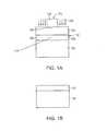
- FIGS. 1( a )-( b )are schematic cross-sectional views illustrating an embodiment of the invention including the implantation and anneal of source and drain regions through a layer that is subsequently removed;
- FIGS. 2( a )-( j )are schematic cross-sectional views of enhancement-mode InP MOSFETs fabricate in accordance with embodiments of the invention, and charts describing experimental procedures and data obtained for enhancement-mode InP MOSFETs;
- FIGS. 3( a )-( d )are schematic cross-sectional views illustrating the fabrication of InP-based devices on lattice-mismatched substrates such as silicon, in accordance with an embodiment of the invention
- FIGS. 4( a )-( c )are schematic cross sectional views illustrating fabrication of an enhancement-type InP MOSFET, in accordance with an embodiment of the invention.
- FIGS. 5( a )-( g )are schematic cross-sectional views illustrating a method of making a self-aligned gate structure for an InP-based MOSFET, according to an embodiment of the invention
- FIGS. 6( a )-( b )are schematic cross-sectional views illustrating dielectric layers deposited on an InP substrate.
- FIGS. 7( a )-( d )are schematic cross sectional views illustrating a method of implantation and amorphization of source and drain regions through a diffusion/barrier layer and subsequent recrystallization of the source and drain regions and oxidation to improve the layer's dielectric properties.
- aspects of this inventionaddress, among other things, the challenges of forming a high-quality interface between a gate dielectric and InP and other InP-based materials through the use of ALD. See also Y. Q. Wu, et al., “Inversion-type enhancement-mode InP MOSFETs with ALD Al 2 O 3 , HfO 2 and HfAlO nanolaminates as high-k gate dielectrics,” Proceedings of 65 th Device Research Conference , Notre Dame, USA (2007) and Y. Q.
- a semiconductor substrate 100has an InP-based top layer 110 disposed thereover.
- the substrate 100may include a semiconductor material and may be, for example, a bulk silicon wafer, a bulk germanium wafer, a semiconductor-on-insulator (SOI) substrate, or a strained semiconductor-on-insulator (SSOI) substrate.
- the substrate 100may include or consist essentially of a first semiconductor material, such as a group IV element, e.g., germanium or silicon.
- the substrate 100includes or consists essentially of ( 100 ) silicon.
- the substrate 100is an InP substrate, with a top region of the InP substrate defining the InP-based top layer 110 .
- the InP-based top layer 110may be formed by molecular beam epitaxy (MBE), a chemical vapor deposition (CVD) process, e.g., metalorganic CVD (MOCVD), or other deposition techniques on the substrate 100 .
- MBEmolecular beam epitaxy
- CVDchemical vapor deposition
- MOCVDmetalorganic CVD
- the top layermay have a thickness ranging from, e.g., 1 nm to 100 ⁇ m.
- the composition and lattice constant of the InP-based top layer 110is different from the composition and lattice constant of the substrate 100 .
- the thickness of the InP-based top layer 110is below its critical thickness and the InP-based top layer 110 , i.e., the channel layer, may include a strained region.
- the critical thicknessis about 15 nm
- the InP-based top layer 110preferably has a thickness less than 15 nm.
- the thickness of the InP-based top layer 110is greater than the critical thickness and the layer is at least partially relaxed. In an embodiment, the InP-based top layer 110 is relaxed.
- one or more layers of materials that are substantially lattice-matched to InPsuch as InAlAs or InGaAs, or thin layers of non-lattice-matched III-V compounds, such as GaAs, InSb or InAs, are provided above the InP-based top layer 110 for use in forming transistor source, drain, and/or channel regions.
- Such thin layers of non-lattice-matched III-V compoundsmay be strained, which may result in enhanced performance characteristics such as improved electron and/or hole mobility.
- substantially lattice-matched to InPmeans having a lattice constant difference with a lattice constant of InP of no greater than about 10%, preferably no greater than about 5% .
- the thickness of such layersis preferably less than about 10 nm.
- InP-based materialsis used to refer to compositions that include or consist essentially of InP and may include additional elements.
- InP-based material layer structureis used to refer to an InP layer or InP-based layer alone or in combination with one or more layers that are substantially lattice matched to InP or in combination with thin, strained, non-lattice-matched III-V layers.
- an encapsulation protection layer 120i.e., a dielectric layer, is disposed on the top surface of the InP-based top layer 110 .
- This protection layerallows implantation therethrough while preventing damage of the InP-based top layer.
- a suitable protection layerinclude a SiO 2 or SiN layer deposited by a CVD process, e.g., MOCVD, or an Al 2 O 3 layer or a nanolaminate layer, including a material such as HfO 2 and/or HfAlO, deposited by ALD.
- a mask 130is formed above the protection layer, and used to define a gate region 140 , a source region 150 and a drain region 160 for a transistor.
- the maskforms a dummy gate structure 170 , which serves as a hard mask for a subsequent ion implantation step.
- the maskmay be formed from a suitable masking material, such as a dielectric material, e.g., Si 3 N 4 , in accordance with methods known to one of skill in the art.
- the source and drain regions 150 , 160are defined in the InP-based top layer by performing an appropriate source/drain dopant ion implantation 180 , using conventional techniques known to those of skill in the art, taking into account the composition of the protection layer.
- a channel region 190is provided between the source and drain regions and includes at least a portion of the InP-based top layer 110 , i.e., the channel layer.
- An annealis then performed at a suitably high temperature to activate the implanted dopant, for example between about 600 and 900° C. with rapid thermal processing (“RTP”).
- RTPrapid thermal processing
- the encapsulation protection layerprotects the InP-based material surface during the implantation and anneal processes.
- the encapsulation protection layer and the dummy gate structuremay be removed after the implantation and anneal steps to create a device-ready InP-based top layer 110 as shown in FIG. 1( b ) .
- a portion of its top surfacemay be removed to ensure the elimination of any portion that is or may be damaged.
- Another optional method to improve the quality of the InP-based top layer 110is to provide an additional protective/sacrificial cap layer (not shown) on the top surface InP-based top layer 110 before forming the protection layer 120 , for example, a passivation layer including one or more materials such as S, NH 4 OH, amorphous Si, and/or amorphous Ge.
- a high-quality gate dielectric layer(not shown) is deposited by, e.g., an ALD process in, for example, an ASC F-120 ALD reactor.
- the gate dielectric layermay be a high-k dielectric.
- Exemplary gate dielectric structuresinclude, for example, a layer of Al 2 O 3 , a layer of HfO 2 layer, a nanolaminate layer of HfO 2 and Al 2 O 3 , or HfAlO, or any other suitable gate dielectric material.
- a post-deposition anneal (PDA)may be performed using O 2 , N 2 or any other suitable ambient at an appropriate temperature, for example between about 400 and 700° C.
- FIGS. 2( a )-( b )illustrate examples of InP MOSFETs.
- An InP MOSFET 200may be formed as follows. First, an appropriately doped or semi-insulating semiconductor substrate with an InP-based channel layer is provided, i.e., an InP-based layer 110 , over a substrate 100 . Optionally, an additional epitaxial layer 200 may be deposited above the InP channel layer as described above for FIG. 1 ., e.g., by CVD, MOCVD or MBE.
- This additional epitaxial layer 200may be InP and may include multiple layers of a material other than InP, such as InSb, InAs, GaAs, InAlAs, and/or InGaAs that may be substantially lattice-mismatched to InP. In order to maintain strain in the epitaxial layer 200 , its thickness may be below the critical thickness.
- Source and drain regions 150 , 160that have a conduction type opposite to that of the channel region, i.e., with n-type source and drain for a p-type channel (for an n-type inversion-type MOSFET), or with p-type source and drain for an n-type channel (for a p-type inversion-type MOSFET).
- an appropriate p-type source and drain implantationmay be a Group II element such as Mg, Be, etc., with a dosage ranging from, e.g., 4 ⁇ 10 17 /cm 3 to 1 ⁇ 10 19 /cm 3 , with an implantation depth of, e.g., 1 nm to 1 ⁇ m.
- An appropriate n-type source and drain implantationmay be a Group IV element, e.g., Si, Ge, etc. with a dosage ranging from, e.g., 4 ⁇ 10 17 /cm 3 to 1 ⁇ 10 19 /cm 3 with an implantation depth of, e.g., 1 nm to 1 ⁇ m.
- a target for both n-type and p-type source and drain implantationsis to achieve dosage levels as high as are typically attained in Si devices. This may be a challenge in InP-based materials because n-type dopants in a III-V material may exhibit p-type behavior above a certain concentration.
- n-type dopant Siwhen present in a concentration greater than about 1 ⁇ 10 19 /cm 3 in InP, exhibits p-type behavior.
- a high-quality gate dielectric 210is formed, typically by first performing a surface-preparation step including a liquid-phase pretreatment or a gas-phase pretreatment employing, e.g., (NH 4 ) 2 S or (NH 4 )OH, followed by surface treatment with hydrogen or nitrogen plasma, either in-situ in the same chamber, if feasible, or ex-situ.
- a surface-preparation stepincluding a liquid-phase pretreatment or a gas-phase pretreatment employing, e.g., (NH 4 ) 2 S or (NH 4 )OH, followed by surface treatment with hydrogen or nitrogen plasma, either in-situ in the same chamber, if feasible, or ex-situ.
- an ALD processis used to deposit a high-k dielectric layer.
- the gate dielectric layermay be an Al 2 O 3 layer, an HfO 2 layer, a nanolaminate layer of HfO 2 and HfAlO, a group-II oxide, or any other dielectric material such
- the gate dielectric layermay have a thickness selected from a range of 1 nm to 1000 nm, preferably 1 nm-10 nm.
- the gate 220is defined by conventional gate electrode deposition and lithographic patterning. Subsequently, source and drain ohmic contacts are formed.
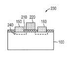
- FIG. 2( b )illustrates the structure of a prototype inversion-type InP MOSFET 230 , integrated with a high-k dielectric deposited by ALD.
- the substrate 100may be an InP semi-insulating substrate.
- the source and drain regions 150 , 160are defined over an Si implanted n+ region 240 .
- the gate dielectric 210may be formed from a high-k dielectric, such as Al 2 O 3 , HfO 2 , or HfAlO, and/or combinations thereof.
- the gate 220is formed from a suitable conducting material, such as nickel/gold.
- FIG. 2( c )summarizes the key steps for the fabrication of Al 2 O 3 /InP MOSFETs by use of ALD on an InP semi-insulating substrate, as illustrated in FIG. 2( b ) .
- surface cleaning and preparation of the substrate 100includes HF- or HCl-based native oxide removal, NH 4 OH-based native oxide cleaning and OH-group passivation, and (NH 4 ) 2 S based sulfur passivation.
- ex-situ wet-cleaning process stepsmay be extended to an in-situ gap-phase dry-cleaning process that comprises HF or HCl gas-phase cleaning, NH 4 OH gas-phase cleaning, and (NH 4 ) 2 S gas-phase passivation. Additionally, acetone, methanol, and iso-proponal cleaning may be performed.
- the substrateis transferred in a room ambient to an ALD reactor, such as an ASM F-120 ALD reactor, for gate dielectric 210 formation.
- the gate dielectric 210may be, for example, an Al 2 O 3 layer having a thickness of, e.g., 30 nm, deposited at a substrate temperature of 300° C., using alternately pulsed chemical precursors of Al(CH 3 ) 3 (the Al precursor) and H 2 O (the oxygen precursor) in a carrier N 2 gas flow.
- Source and drain regions 150 , 160are selectively implanted through the 30 nm thick Al 2 O 3 layer, e.g., with a Si dose of 1 ⁇ 10 14 cm ⁇ 2 at 140 keV.
- Implantation activationmay be achieved by rapid thermal anneal (RTA), e.g., at 720° C. for 10 seconds.
- RTArapid thermal anneal
- Regrown oxidemay be etched away using BHF.
- a thin layer of Al 2 O 3 or HfO 2 or HfAlO (e.g., 8 nm)is deposited, and a post deposition anneal is performed.
- Those of skill in the artare familiar with suitable alternative materials and process parameters for surface preparation and implantation and activation of source and drain regions.
- the source and drain ohmic contactsmay be defined by an electron beam evaporation of a combination of AuGe/Pt/Au and a lift-off process, followed by a RTA process at 500° C. for 30 seconds, also in an N 2 ambient.
- the gate electrodemay be defined by electron beam evaporation of conductive materials, such as Ni/Au, Ti/Au, AuGe/Ni/Au, and/or AuGe/Pt/Au and a lift-off process.
- conductive materialssuch as Ni/Au, Ti/Au, AuGe/Ni/Au, and/or AuGe/Pt/Au and a lift-off process.
- FIGS. 2( d )-( j )data for an enhancement-mode n-channel InP MOSFET fabricated on a semi-insulating substrate with (ALD) Al 2 O 3 as the gate dielectric are shown.
- the results illustrated in FIGS. 2( d )-( j )are for MOSFETs with nominal gate lengths varying from 0.75 ⁇ m to 40 ⁇ m and a gate width of 100 ⁇ m.
- Transfer-length-method (TLM) structuresare used to determine contact resistance of 2.5 ohm-mllimeter ( ⁇ mm) and sheet resistance of 230 ⁇ /sq. at the implanted area. Measurements are made with standard equipment such as an HP4284 LCR meter for the capacitance measurement and a Keithley 4200 for measurement of the MOSFET output characteristics.
- FIG. 2( d )illustrates the drain current vs. drain bias as a function of gate bias for a 1 ⁇ m InP MOSFET with 8 nm regrown Al 2 O 3 as gate dielectric.
- the figureillustrates the dc I ds ⁇ V ds characteristic with a gate bias from 0 to 8 V.
- the measured MOSFEThas a designed gate length at mask level (LMask) of 0.75 ⁇ m and a gate width (L w ) of 100 ⁇ m.
- a maximum drain current of 70 mA/mmis obtained at a gate bias of 8 V and a drain bias of 3 V.
- the gate leakage currentis below 10 ⁇ A/mm under the same bias condition, more than 4 orders of magnitude smaller than the drain on-current.
- the relatively low g mmay be improved by reducing the thickness of the dielectric, increasing the dielectric constant, and improving the quality of the interface.
- FIG. 2( e )illustrates measured channel resistance vs. mask gate length for different gate biases with Al 2 O 3 thickness of 30 nm. Specifically, FIG. 2( e ) shows the effective gate length (L eff ) and series resistance (R SD ) extracted by plotting channel resistance R Ch vs. L Mask . R SD and ⁇ L, which is the difference between L Mask and L eff , are determined to be 38.6 ⁇ mm and 0.5 ⁇ m, respectively, by the equation below:
- the effective electron mobility ⁇ effis weakly dependent on gate bias from 2-4 V and is taken as a constant in this calculation.
- R SD and L effis determined as the intercept of the linear fitting of R Ch at different gate biases and L mask as shown in FIG. 2( e ) .
- the R SD value of 386 ⁇ and the ⁇ L value of 0.5 ⁇ mwere determined using line fitting.
- the obtained R SDis consistent with the results from measurement by a TLM technique since R SD includes contact resistance, sheet resistance, accumulation resistance and spread resistance.
- ⁇ Lis caused by the inter-diffusion of source and drain implant activation and the proximity effect of the photolithography process.
- FIG. 2( f )illustrates extrinsic and intrinsic drain current and trans-conductance vs. gate bias.
- the intrinsic transfer characteristicsis calculated by subtracting the series resistance R SD and using effective gate length L eff instead of mask gate length L Mask and compared with the extrinsic one, as shown in FIG. 2( f ) .
- the intrinsic drain current and transconductanceare only about 10% larger than the extrinsic ones due to the large gate length of 20 ⁇ m.
- FIG. 2( f )also shows that the subthreshold characteristic is scarcely changed.
- the threshold voltage determined by conventional method of linear region extrapolationdoes show some difference as highlighted as extrinsic threshold voltage V T and intrinsic threshold voltage V T * in FIG. 2( b ) .
- FIG. 2( g )illustrates threshold voltage vs. the gate length using the intrinsic I-V characteristics of the device using five different methods—the ratio method (RM), the extrapolation in the linear region method (ELR), the second derivative method (SD), the second derivative logarithmic method (SDL), and the match-point method (MP).
- RMratio method
- ELRextrapolation in the linear region method
- SDsecond derivative method
- SDLsecond derivative logarithmic method
- MPmatch-point method
- the second derivative method and ratio methodgive mostly the same value at the long gate length device and both show V T * roll-off behavior for the submicron gate length device. These two methods may be more reliable ways to determine threshold voltage since the conducting mechanism changes during the transition near threshold, when drain current increases from exponentially to linear or quadratic dependence on the effective gate voltage (V g -V T ).
- FIG. 2( h )illustrates drain current vs. drain bias as a function of gate bias for a 2 ⁇ m InP MOSFET with 8 nm Al 2 O 3 gate oxide.
- the sub-threshold slope (S.S>) and DIBL characteristics of 280 mV/dec and 50 mV for the MOSFETare illustrated.
- FIG. 2( i )illustrates effective mobility vs. normal electric field for the InP MOSFET with 30 nm Al 2 O 3 gate oxide and a 100 kHz split-CV measurement.
- Effective mobilityis another important parameter for evaluating MOSFET performance.
- the “Split-CV” methodis used to measure the channel capacitance, which may be used to calculate the total inversion charge in the channel by integrating the C-V curve.
- the inset of FIG. 2( i )is a 100 kHz C-V curve between gate and channel measured on a 40 ⁇ m gate length device from which inversion capacitance is seen clearly.
- the extracted mobilityhas a peak value of 650 cm 2 /Vs around a normal electric field of 0.22 MV/cm as shown in FIG. 2( i ) .
- Better mobility performancemay be achievable by using an epitaxial InP layer to improve host material quality and optimize the device fabrication process.
- FIG. 2( j )illustrates C-V measurements of an 8 nm Al 2 O 3 /n-InP MOSCAP from quasi-static up to 1 MHz.
- the samplesinclude 8 nm thick Al 2 O 3 deposited on an n-type InP substrate at 300° C. by ALD.
- a 500° C. post deposition annealingimproves C-V characteristics only moderately for InP as shown in FIG. 2( j ) , in contrast to the GaAs case.
- the frequency dispersion at accumulation capacitancemay be attributed to the relative high interface trap density (D it ) at the conduction band edge, though the extrinsic parasitic effects could also contribute to the frequency dispersion partly.
- the mid-gap Dit is estimated to be approximately 2-3 ⁇ 10 12 /cm 2 ⁇ eV determined by the high-frequency (HF)-low-frequency (LF) method.
- This valueis consistent with the value determined from the m-factor, a parameter related to sub-threshold characteristics. More specifically, the subthreshold slope is relatively large due to the large gate oxide thickness or the small oxide capacitance C ox and the existing interface trap capacitance C it . M-factor is defined as 60 mV/dec. ⁇ (1+C it /C ox ). From the measured sub-threshold slope, an interface trap density D it of ⁇ 2-3 ⁇ 10 12 /cm 2 ⁇ eV is determined.
- Moderate hysteresis of 100-300 mVexhibits in the C-V loops (not shown).
- the C-V characteristics in FIG. 2( j )show a clear transition from accumulation to depletion for HF C-V and the inversion features for LF C-V and quasi-static C-V indicating that the conventional Fermi-level pinning phenomenon reported in the literature is overcome in this ALD Al 2 O 3 /InP sample.
- the unpinning of the Fermi levelmay be attributed to the self-cleaning ALD Al 2 O 3 process that removes the native oxide on the InP surface, similarly to the situation in ALD Al 2 O 3 formed on GaAs.
- the unpinning of the Fermi level by the ALD Al 2 O 3 process described aboveis significant, as it contributes to the realization of enhancement-mode MOSFETs on InP, as demonstrated in FIG. 2( d ) .
- a 0.75- ⁇ m gate-length E-mode n-channel MOSFET with an Al 2 O 3 gate oxide thickness of 30 nmmay have a gate leakage current less than 10 ⁇ A/mm at a gate bias of 8 V, a maximum drain current of 70 mA/mm, and a transconductance of 10 mS/mm.
- the peak effective mobilityis ⁇ 650 cm 2 /Vs and the interface trap density of Al 2 O 3 /InP is estimated to be ⁇ 2-3 ⁇ 10 12 /cm 2 eV.
- the prototype measurements reflected in FIGS. 2( d )-( j )reflect the use of Al 2 O 3 as the gate dielectric.
- other materialssuch as Hf-based high-k materials, can be used for the gate dielectric.
- An exemplary process for formation of HfO 2 as a dielectric by using ALDis to use ALD precursors such as HfCl 4 , TEMAHf or TDMAHf and oxygen precursors such as H 2 O or O 3 .
- a typical HfO 2 ALD processis performed between 200-350° C. Surface cleaning and preparation is similar with use of materials such as HF, HCl, NH 4 OH and (NH 4 ) 2 S.
- the substratemay be a semi-insulating InP substrate or alternatively may be another material that supports an InP channel device.
- a Si or SOI substratecan provide cost and manufacturing advantages because of the possibility of using large-scale wafers and the well-developed Si-based processing facilities.
- InP-based devicesmay be integrated on Si substrates by the use of aspect ratio trapping (ART) techniques.
- ARTaspect ratio trapping
- FIGS. 3( a )-( d )Two exemplary approaches for such integration using ART techniques are illustrated in FIGS. 3( a )-( d ) .
- a detailed description of ART techniquesmay be found in U.S. patent application Ser. No. 11/728,032, incorporated herein in its entirety.
- FIGS. 3( a )-3( b )show how ART techniques may be used to grow a high-quality InP layer above a buffer layer on a lattice-mismatched underlying material, such as a Si wafer.
- the crystalline substratemay have a lattice constant substantially different from a lattice consant of InP.
- a non-crystalline materiale.g., a dielectric layer 300
- the dielectric layer 300may include a dielectric material, such as silicon nitride or silicon dioxide.
- the dielectric layer 300may be formed by a method known to one of skill in the art, e.g., thermal oxidation or plasma-enhanced chemical vapor deposition. As illustrated, the dielectric layer 300 has a thickness t 1 corresponding to a desired height of crystalline material to be deposited in a window 310 formed through the dielectric layer 300 . In some embodiments, the thickness t 1 of the dielectric layer 300 is selected from a range of, e.g., 20-50000 nm.
- a mask(not shown), such as a photoresist mask, is formed over the substrate 100 and the dielectric layer 300 .
- the maskis patterned to expose at least a portion of the dielectric layer 300 .
- the exposed portion of the dielectric layer 300is removed by, e.g., reactive ion etching (RIE) to define the window 310 in the non-crystalline mask, i.e., in the dielectric layer 300 .
- RIEreactive ion etching
- the window 310extends to a surface of the substrate 100 and may be defined by at least one sidewall 320 .
- the sidewall 320is formed from the dielectric layer 300 and is, therefore, non-crystalline.
- the sidewall 320may have a height h at least equal to a predetermined distance H from the surface of the substrate 100 , i.e., the sidewall extends above the substrate by the height h. It has been observed experimentally that dislocations in a mismatched cubic semiconductor grown on a Si (100) surface in the near-vicinity (e.g., within approximately 500 nm or less) of a vertical dielectric sidewall 420 surface bend toward that surface at approximately 30 degrees through 60 degrees. For example, the dislocations may bend toward that surface at approximately a 45 degree angle to that surface. Based on this relationship, one may typically expect the predetermined distance H necessary to trap defects to be approximately equal to a width between 1 ⁇ 2w and 2w, where w is the width of the window.
- the window 310may be substantially rectangular in terms of cross-sectional profile, a top view, or both, and have a width w that is smaller than a length l (not shown) of the window.
- the width w of the windowmay be less than about 5000 nm, e.g., about 20-1000 nm. In some embodiments, the width of the window is about 150 nm.
- a length l of the windowmay exceed each of w and H.
- the ratio of the height h of the window to the width w of the windowmay be ⁇ 1, and preferably is between about 1 and about 50.
- the substrate 100 materiale.g., Si
- the aspect ratio of the height of the mask relative to the width of the openingdefects arising from deposition of the buffer layer may exit at the sidewalls below the top surface of the mask layer. This provides a high-quality top surface of the buffer layer 330 upon which the InP-based top layer 110 may be grown epitaxially.
- the buffer layer 330may include a second crystalline semiconductor material that may include or consist essentially of a group IV element or compound, a III-V compound, and/or a II-VI compound.
- suitable group IV elements or compoundsinclude germanium, silicon germanium, and silicon carbide.
- suitable III-V compoundsinclude gallium arsenide, gallium nitride, indium arsenide, indium antimonide, indium aluminum antimonide, indium aluminum arsenide, indium phosphide, and indium gallium arsenide.
- suitable II-VI compoundsinclude zinc selenide and zinc oxide.
- the buffer layer 330is lattice-matched to the InP-based top layer 110 formed thereover, i.e., the buffer layer 330 may have a second lattice constant substantially similar to the lattice constant of InP.
- the second crystalline semiconductor materialmay be formed by selective epitaxial growth in any suitable epitaxial deposition system, including, but not limited to, MOCVD, atmospheric-pressure CVD (APCVD), low- (or reduced-) pressure CVD (LPCVD), ultra-high-vacuum CVD (UHCVD), MBE, or ALD.
- selective epitaxial growthtypically includes introducing a source gas into the chamber.
- the source gasmay include at least one precursor gas and a carrier gas, such as, for example, hydrogen.
- the reactor chambermay be heated by, for example, RF-heating.
- the growth temperature in the chambermay range from about 300° C. to about 900° C., depending on the composition of the epitaxial region.
- the growth systemmay also utilize low-energy plasma to enhance the layer growth kinetics.
- CVDhas a number of advantages, including the capability for depositing films with low defect densities and rapidly varying alloy compositions, as well as high quality regrowth capability. CVD may also provide improved manufacturability due to relatively higher throughput, relatively short downtimes, and scalability to very large reactors.
- the epitaxial growth systemmay be a single-wafer reactor or a multiple-wafer batch reactor.
- Suitable CVD systems commonly used for volume epitaxy in manufacturing applicationsinclude, for example, an Aixtron 2600 multi-wafer system available from Aixtron, based in Aachen, Germany; an EPI CENTURA single-wafer multi-chamber systems available from Applied Materials of Santa Clara, Calif.; or EPSILON single-wafer epitaxial reactors available from ASM International based in Bilthoven, The Netherlands.
- Dislocation defects in the second crystalline semiconductor materialreach and terminate at the sidewalls 320 of the window in the dielectric material 300 at or below a vertical predetermined distance H from the surface of the substrate, such that dislocations in the second crystalline semiconductor material decrease in density with increasing distance from the bottom portion of the window. Accordingly, the upper portion of the buffer layer 330 is substantially exhausted of dislocation defects.
- Various dislocation defectssuch as threading dislocations, stacking faults, twin boundaries, or anti-phase boundaries may thus be substantially eliminated from the upper portion of the epitaxial region.
- a density of such dislocation defectsmay be less than, for example, 10 6 /cm 2 , preferably less than 10 3 /cm 2 .
- the second crystalline semiconductor materialmay be either substantially relaxed or strained.
- the InP-based top layer 110i.e., the channel layer, is formed over the buffer layer 330 , the channel layer being substantially lattice-matched with the buffer layer.
- the techniques as described above in connection with FIGS. 1 and 2may be used to create a device 340 , such as a transistor, which incorporates the InP-based top layer, preferably as a channel.
- the source and drain regions of the transistormay also be formed in the channel layer, and a gate formed above the channel layer.
- the openingmay be configured in a variety of ways based on materials and applications, such as in a trench configuration.
- the mask 300defines a plurality of openings 310 above substrate 100 .
- An InP-based materialsuch as InP
- the InP-based materialis epitaxially grown to extend above the mask 300 to define a high quality coalesced InP-based top layer 110 , upon which InP-based devices 340 , such as the MOSFETs described above with reference to FIGS. 1 and 2 , may be fabricated.
- a semiconductor substrate 100 with an InP-based top channel layer 110is provided, with predefined channel doping type and doping level.
- the channelmay be, for example, p-type doped with a doping level of 1 ⁇ 10 18 /cm 3 to 1 ⁇ 10 19 /cm 3 .
- a suitable n-type dopantis a Group IV element, such as Si.
- a suitable p-typeis a Group II element, such as Mg.
- a relatively high doping levelis preferred for enabling the low contact resistances. It is a challenge, however, to dope InP and other III-V materials to a level greater than 1 ⁇ 10 20 /cm 3 .
- a gate dielectric 210is deposited on the InP channel material according to the methods described above, for example using ALD to deposit a dielectric material such as Al 2 O 3 .
- the dielectric materialmay include hafnium, e.g, HfO 2 .
- a conductive layere.g., a gate electrode layer is formed over the gate dielectric, such that the dielectric layer is disposed between a semiconductor layer, i.e., the InP-based top channel layer 110 , and the conductive layer.
- a gate 220is defined in the conductive layer by patterning methods known to one of skill in the art.
- a source region and a drain regionare patterned in a lithographic mask next to the gate structure, and the portions of the InP-based top layer 110 in the source and drain regions are removed by, e.g., dry etching, to form source and drain recesses 400 , 400 ′, as shown in FIG. 4( b ) .
- the source and drain recesses 400 , 400 ′are filled with an appropriate source/drain material 410 that has a doping type opposite to that of the channel region, as shown in FIG. 4( c ) .
- InPmay be grown epitaxially within the source and drain recesses 400 , 400 ′ by CVD with doping performed in situ.
- an n-type dopantmay be used for the source and drain to create an n-MOSFET.
- the doping typesare reversed for a p-MOSFET. Those of skill in the art understand how to use appropriate dopants and materials to achieve the desired device characteristics.
- FIGS. 5( a )-( g )illustrate a method of creating a MOSFET with source and drain regions that are self-aligned to the gate, i.e., the edges of the source and drain regions next to the gate are defined by the same mask that defines the edges of the gate next to the source and drain regions.
- a mask 500defines the locations of the gate and channel locations over a substrate 100 .
- the mask 500functions as a dummy gate and also as a barrier to ion implantation in the channel region during creation of the source and drain regions 510 , 520 by ion implantation, as shown in FIG. 5( b ) .
- the maskmay be made from an appropriate material, such as photoresist.
- an insulator 530such as SiN is deposited over the mask 500 and source and drain regions 510 , 520 , and is then etched back to expose a top surface of the mask 500 (i.e., of the dummy gate) as shown in FIGS. 5( c )-5( d ) .
- the dummy gateis then removed by a selective etch, e.g., by a wet etch such as KOH or TMAH, or a dry etch in a reactive ion etching system, to define an opening 540 .
- a gate dielectric 550 and gate material layers 560are deposited into the opening created by the removal of the dummy gate, and etched back as shown in FIGS. 5( f )-( g ) .
- this self-aligned gate procedureenables the use of InP as a channel material and ALD for depositing a high-k gate dielectric while maintaining small (sub-micron) feature sizes and spacing.
- Forming a dummy gateenables the formation of a self-aligned gate, without exposure of the device gate dielectric and gate electrode to a high temperature dopant activation process that may damage a high-k dielectric.
- the dummy gate approachincludes forming a gate dielectric after a source/drain implantation and activation, rather than before these steps, as in a conventional process flow.
- InPis a binary compound semiconductor resulting from a relatively weak covalent bond between indium and phosphorous. While InP MOSFETs feature characteristics such as enhanced drain currents and improved performance with respect to Fermi-level pinning and higher electron saturation velocity, the relatively strong electropositivity of indium can be a disadvantage, resulting, for example, in the relatively high reactivity of InP with oxygen. Thus, for example, as shown in FIGS.
- a diffusion/barrier layer 600 including a relatively inert materialssuch as transition metal nitrides or group III-nitrides (e.g., BN, AlN, MoN, TaN, TiN, or AlN, etc., which are much less reactive with InP than oxygen, especially at higher temperatures) adjacent the top surface of the InP-based top layer 110 of substrate 100 .
- a relatively inert materialssuch as transition metal nitrides or group III-nitrides (e.g., BN, AlN, MoN, TaN, TiN, or AlN, etc., which are much less reactive with InP than oxygen, especially at higher temperatures) adjacent the top surface of the InP-based top layer 110 of substrate 100 .
- the use of a relatively inert diffusion/barrier layer 600permits the sequential deposition of a relatively non-inert dielectric 610 such as SiO 2 or Al 2 O 3 above the relatively inert layer.
- a relatively non-inert dielectric 610such as SiO 2 or Al 2 O 3 above the relatively inert layer.
- the inert barrier layer 600may be kept relatively thin, e.g., as thin as one monolayer (which typically will be about 15 angstroms ( ⁇ )), or preferably about 5 to 10 nanometers (nm), although the barrier layer can be substantially thicker, e.g., as thick as 1 ⁇ m or more.
- the barrier layermay be AlN or AlON or a nanolaminate—e.g., alternating layers of AlN and Al 2 O 3 , deposited as monolayers or in layers of about 5 nm—which can enhance the ability of the barrier layer to trap materials such as In or P before they can diffuse through the barrier layer.
- FIGS. 7( a )-( d )illustrate a method of forming source and drain regions that also provides for an improved dielectric layer, e.g., an improved gate dielectric layer.
- a dielectric 700 inert to InPsuch as a transition metal-nitride
- FIG. 7( b )the gate 710 is defined and the source and drain regions 720 , 730 of a transistor are implanted using techniques similar to those discussed above for FIGS. 1 and 2 , and the source and drain regions are amorphized.
- amorphizationis accomplished by using a heavy dopant species such as SiF x , with sufficient dopant dosage and energy to concomitantly accomplish both amorphization and high dopant concentration of the source/drain regions.
- amorphizationis accomplished by implanting an inert element such as argon or another suitable noble gas prior to the implantation of the dopant species.
- amorphizationis accomplished by using a heavy dopant species such as SiF x , with sufficient dopant dosage and energy to concomitantly accomplish amorphization of and high dopant concentration in the source/drain regions.
- complete amorphization of the InP latticemay be accomplished through the use of high dosage implants using compounds such as SiF x between 10 14 cm ⁇ 2 and 10 16 cm ⁇ 2 through dielectric layer(s).
- Easy displacement of the In sublattice along ⁇ 0001> directionscan enable amorphization through heavy dosage implantation.
- the source/drain regions 720 , 730are annealed at a temperature sufficiently high to ensure recrystallization, such as by RTA between 400° C. and 1000° C.
- recrystallizationsuch as by RTA between 400° C. and 1000° C.
- an oxidizing speciese.g., PECVD SiO 2
- PECVD SiO 2is introduced at a temperature of, e.g., 300° C., to enable formation of an oxynitride from the dielectric 700 , e.g., from a dielectric transition metal nitride.
- Converting the dielectric transition metal nitride into an oxynitrideprovides an improved dielectric from the same layer that provided an effective diffusion barrier, eliminating the need to deposit new dielectric material. Effective performance of the transistor embodiment of FIG. 7 is enhanced by the use of ohmic contacts.
- HEMThigh electron mobility transistor
- InP-based materialmay be incorporated in a HEMT as a portion of the channel layer.
Landscapes
- Engineering & Computer Science (AREA)
- Physics & Mathematics (AREA)
- Condensed Matter Physics & Semiconductors (AREA)
- General Physics & Mathematics (AREA)
- Manufacturing & Machinery (AREA)
- Computer Hardware Design (AREA)
- Microelectronics & Electronic Packaging (AREA)
- Power Engineering (AREA)
- Chemical & Material Sciences (AREA)
- Materials Engineering (AREA)
- Insulated Gate Type Field-Effect Transistor (AREA)
Abstract
Description
This application is a divisional of U.S. Patent Application Ser. No. 12/139,010, filed Jun. 13, 2008, entitled “InP-BASED TRANSISTOR FABRICATION,” which claims the benefit of and priority to U.S. Provisional Application Ser. No. 60/934,716, filed Jun. 15, 2007, the entire disclosures of these applications are incorporated by reference herein in their entireties.
Subject matter disclosed herein was made pursuant to a joint research agreement between AmberWave Systems Corporation and Purdue University.
The technology disclosed herein relates generally to semiconductor structures and methods of making semiconductor structures and more specifically to use of alternatives to Si for constructing transistors using InP-based materials.
The increasing operating speeds and miniaturization of semiconductor devices have given rise to a need to find alternatives to silicon for the source, drain, and channel regions of transistors and to SiO2for the gate dielectric of FET transistors. Research has been performed on compound semiconductors such as GaAs and other III-V materials for high-performance transistor applications. Although there have been successful demonstrations of depletion-mode GaAs metal-oxide-semiconductor field-effect transistors (MOSFETs), inversion-type enhancement-mode GaAs MOSFETs have suffered from problems such as relatively low drain currents. Notwithstanding research and development efforts by many institutions into aspects of III-V materials, there remains a need for commercially viable techniques for providing improved performance using materials such as InP.
According to aspects of embodiments of the invention described below, atomic layer deposition (ALD) techniques with high-k gate dielectrics are used to provide inversion-type enhancement-mode InP-based MOSFETs that demonstrate substantial technological improvements. For example, drain currents for InP devices described below may have drain currents more than 1,000 times greater than drain currents for existing enhancement-mode GaAs MOSFETs. Other aspects include improved performance with respect to Fermi level pinning and higher electron saturation velocity (2×107cm/s). At equivalent gate lengths, aspects of the embodiments described below can provide high-field transconductance greatly improved (>50% higher) in comparison to devices having equivalent channel lengths and fabricated with more conventional semiconductors such as Si, Ge, or GaAs. The ALD high-k/InP-based material system mitigates problems associated with Fermi-level pinning reported in the literature.
Provision of high-performance InP-based MOSFETs may enable a new generation of high-frequency transistors because of the intrinsically higher and robust charge-transport properties of InP-based materials relative to other semiconducting materials. The presence of a gate dielectric in MOSFET structures reduces overall device leakage and enhances both control and responsivity of channel regions. The need for gate dielectric materials suitable for use with InP, and methods for formation thereof, has hitherto limited the commercialization of InP-based MOSFETS. Previous efforts focused on the deposition of dielectric materials on InP have resulted in various difficulties including interfacial chemical instabilities, electronic instabilities such as Fermi-energy pinning, and device fabrication difficulties involving high series-resistance source and drain terminals. Embodiments of the present invention provide techniques enable the fabrication of commercially viable InP-based MOSFETs, a long-sought but yet-to-be-achieved goal.
In an aspect, an embodiment of the invention includes a method of fabricating a transistor. An InP-based material layer structure including a channel layer is provided. A source region and a drain region are defined in the InP-based material layer structure. A channel region is provided between the source and drain regions, the channel region including at least a portion of the channel layer. A gate dielectric is deposited over the channel region by atomic layer deposition (ALD). A gate is provided above the channel region. At least a portion of the gate dielectric may be disposed between the gate and the channel region, and the transistor may operate as an inversion-type, enhancement-mode device.
One or more of the following features may be included. The source and drain regions are at least partially disposed in the channel layer. The source and drain regions are disposed above the channel layer. The gate dielectric comprises at least one of a group II material and/or a transition metal, e.g., includes at least one of aluminum, Al2O3, hafnium, and/or HfO. The channel layer may include a strained region. The channel layer may include at least one of InSb, InGaAs, InAs, and/or InP. The channel layer may include a plurality of substantially lattice-matched layers.
The transistor may be, e.g., a MOSFET or a HEMT. The InP-based material layer may be provided over a silicon substrate.
In another aspect, an embodiment of the invention includes a method of fabricating a transistor. An InP-based material layer including a channel layer is provided. A source region and a drain region are defined in the InP-based material layer. A channel region is provided between the source and drain regions, the channel region including at least a portion of the channel layer. A gate dielectric is formed over the channel region, the gate dielectric including at least one of a group II material or a transition metal. A gate is provided above the channel region. At least a portion of the gate dielectric may be disposed between the gate and the channel region, and the transistor may operate as an inversion-type, enhancement-mode device.
One or more of the following features may be included. The gate dielectric may include aluminum and/or hafnium. The gate dielectric is formed by ALD.
In still another aspect, an embodiment of the invention includes a method of fabricating a semiconductor structure. A semiconductor layer comprising indium and phosphorous is provided. A dielectric layer comprising hafnium is deposited by ALD above at least a portion of the semiconductor layer. A conductive layer is provided over at least a portion of the dielectric layer. The dielectric layer is disposed between the semiconductor layer and the conductive layer.
One or more of the following features may be included. The semiconductor layer includes a transistor channel region and the conductive layer including a transistor gate region. The dielectric layer may include at least one of oxygen, silicon, and/or nitrogen. The semiconductor layer is provided over a substrate that includes silicon.
In another aspect, an embodiment of the invention includes a semiconductor structure. The structure includes a silicon substrate. An InP-based material layer structure including a channel layer is disposed above the substrate. A transistor including a source region, a drain region, and an inversion-type channel region may be disposed at least partially within the channel layer, and a gate region is disposed above the channel region.
One or more of the following features may be included. A mask layer is disposed above the substrate and includes a plurality of openings; a second layer of material having a lattice-mismatch with silicon is disposed within the openings. The second layer may include indium and phosphorous.
A dielectric layer is disposed between the channel region and the gate region, the dielectric layer including at least one of aluminum and/or hafnium. The channel layer includes a strained region. The channel layer includes at least one of InSb, InGaAs, InAs, and/or InP. The channel layer includes a plurality of substantially lattice-matched layers.
In still another aspect, an embodiment of the invention includes a method of making a semiconductor structure. A substrate including a top layer having a compound comprising indium and a second element is provided. A dielectric layer is provided over the top layer, a region of the dielectric layer adjacent the top layer being substantially non-reactive with indium and the second element and configured to suppress out-diffusion of dopants from the top layer during a thermal anneal step. A dopant species is implanted into the top layer. The top layer is thermally annealed to activate the dopant at a relatively high temperature.
One or more of the following features may be included. The second element is phosphorous, antimony, aluminum, gallium, and/or arsenic. Implanting a dopant species into the top layer includes implanting the dopant species through the dielectric layer. The dielectric layer includes first and second layers, the first layer being adjacent the top layer and substantially non-reactive with indium and the second element, the first layer having a first composition and the second layer having a second composition different from the first composition. The second layer includes oxygen, aluminum, and/or hafnium. The substrate includes a bottom portion including silicon.
In another aspect, an embodiment of the invention includes a method of forming a transistor. The method includes providing a substrate including a top layer disposed thereover, the top layer including a compound comprising indium and a second element. A dielectric layer is deposited above the top substrate layer by atomic layer deposition. A mask layer may be disposed above the dielectric layer to define a gate region, a source region, and a drain region of a transistor. A dopant is implanted through the dielectric layer into the source region and the drain region proximate the gate region, the mask layer blocking implantation of the dopant into the gate region. A high temperature anneal is performed to activate the dopant in the source and drain regions.
One or more of the following features may be included. The substrate includes a bottom portion including silicon. Implanting a dopant through the dielectric layer to define the source and drain regions substantially amorphizes the source and drain regions. The high temperature anneal recrystallizes the source and drain regions. A portion of the mask layer is replaced with a gate structure without lithography so that the gate structure is aligned to the source and drain regions. A substantially lattice-matched layer is provided atop the substrate in which the source and drain regions are formed. The layer may include at least one of InSb, InGaAs, InAs, and/or InP; the layer may include a plurality of substantially lattice-matched layers.
In another aspect, an embodiment of the invention includes a method of forming a transistor. A substrate including indium and phosphorous is provided. A mask layer is disposed above the substrate to define a gate region of a transistor. A dopant is implanted to create source and drain regions, with the mask layer blocking implantation of the dopant into the gate region. A portion of the mask layer is replaced with a gate structure without lithography so that the gate structure is aligned to the source and drain regions.
One or more of the following features may be included. The substrate includes a bottom portion including silicon. Implanting a dopant substantially amorphizes the source and drain regions. A high temperature anneal is performed to activate the dopant and to recrystallize the source and drain regions.
A high temperature anneal is performed to activate the dopant in the source and drain regions. The gate structure includes a dielectric layer created after performing a high temperature anneal to activate the dopant.
In yet another aspect, an embodiment of the invention includes a method of forming a transistor. A substrate comprising indium and phosphorous is provided. A mask is provided above the substrate to define source, drain, and gate regions of a transistor. A dopant is implanted into the source and drain regions. At least a portion of the source and drain regions is amorphized. An anneal is performed to recrystallize the amorphized portions of the source and drain regions.
One or more of the following features may be included. The substrate includes a bottom portion comprising silicon. The substrate includes a top layer comprising indium and phosphorous, InP, InSb, InGaAs and/or InAs. A barrier layer in contact with a top portion of the substrate is provided. A region of the barrier layer in contact with the top portion of the substrate is substantially free of oxygen and/or includes nitrogen. The barrier layer includes at least one of AlN, TaN, and/or TiN.
The barrier layer includes a dielectric layer relatively inert to the top portion and the dielectric layer is formed by atomic layer deposition. A second dielectric layer is provided above the dielectric layer, with the second dielectric layer being not inert to the top portion of the substrate.
The barrier layer is oxidized to improve a dielectric property of the barrier layer. The steps of implanting and amorphizing include a single step of implanting a dopant that amorphizes at least a portion of the source and drain regions. The dopant includes SiX, with X including a group VIIA element. Ohmic contacts adjacent the source and drain regions are defined.
In still another aspect, an embodiment of the invention includes forming a transistor. A substrate including indium and phosphorous is provided. A mask layer may be formed above the substrate to define a source region, a drain region, and a gate region of a transistor. A dopant is implanted into the source and drain regions, the mask layer blocking implantation of the dopant into the gate region. The mask layer is removed to expose the gate region. At least a portion of a channel layer is epitaxially grown.
One or more of the following features may be included. The portion of the channel layer is epitaxially grown by ALD, MBE, or CVD. Epitaxially growing at least a portion of the channel layer includes growing one or more of InSb, InGaAs, InAs, and/or InP. The gate channel includes indium and phosphorous; indium and antimony; indium and arsenic; and/or gallium and arsenic.
The substrate includes a top surface prior to the step of forming the mask layer, the gate channel layer includes a top surface, and the top surface of the gate channel layer is disposed above the top surface of the substrate. The substrate includes a top surface prior to the step of forming the mask layer, the gate channel layer includes a bottom surface, and the bottom surface of the gate channel layer is disposed below the top surface of the substrate.
In yet another aspect, an embodiment of the invention includes a method of forming a transistor. The method includes providing a substrate including indium and phosphorous. A mask layer may be disposed above the substrate to define source, drain, gate, and gate channel regions of a transistor. A first dopant type is provided in the gate channel region. A portion of the substrate in the source and drain regions may be removed to form source and drain recesses. The source and drain recesses are filled with a semiconductor material having a second dopant type different from the first dopant type.
One or more of the following features may be included. The second dopant type is opposite from the first dopant type. Filling the source and drain recesses includes an epitaxial growth technique, e.g., at least one of MBE, ALD, and CVD. Filling the source and drain recesses includes filling the source and drain recesses with a material having a lattice constant different from a lattice constant of the substrate and the material induces stress in the channel region. The semiconductor material includes at least one of GaAs, InGaAs, In-rich InGaAs, or InP.
In another aspect, an embodiment of the invention includes a method of fabricating a transistor. A crystalline substrate having a first lattice constant substantially different from a lattice constant of InP is provided. A non-crystalline mask is provided above the substrate, the mask including an opening having sidewalls that extend above the substrate by a height. A crystalline buffer layer having a second lattice constant substantially similar to the lattice constant of InP may be provided within the opening. The buffer layer may have a height less than the mask opening sidewall height, the buffer layer height being sufficient to permit defects arising from the lattice mismatch to exit the buffer layer at the mask opening sidewalls. A channel layer is provided above the buffer layer, the channel layer being substantially lattice-matched with the buffer layer. A source region, a drain region, and a channel region of a transistor are defined in the channel layer. A gate is provided above the channel layer.
One or more of the following features may be included. The substrate is a silicon substrate. The mask includes SiO2. The buffer layer includes a III-V material, e.g., InP. The channel layer includes at least one of InP, InSb, InGaAs, InAs, and/or InP. The channel layer is disposed within the mask opening. The channel layer is disposed substantially completely above the mask. The transistor is an inversion-type, enhancement-mode transistor.
In another aspect, an embodiment of the invention includes a method of processing a semiconductor structure. A substrate comprising indium and phosphorous is provided. Oxide from a top surface of the substrate is removed using at least one of HF, HCl, and NH4OH. The top surface is passivated using at least one of an (NH4)2S or an OH-group compound.
The removing and passivating steps may be performed in situ or performed ex situ.
Aspects of this invention address, among other things, the challenges of forming a high-quality interface between a gate dielectric and InP and other InP-based materials through the use of ALD. See also Y. Q. Wu, et al., “Inversion-type enhancement-mode InP MOSFETs with ALD Al2O3, HfO2and HfAlO nanolaminates as high-k gate dielectrics,”Proceedings of65thDevice Research Conference, Notre Dame, USA (2007) and Y. Q. Wu, et al., “Enhancement-mode InP n-channel metal-oxide-semiconductor field-effect-transistors with atomic-layer-deposited Al2O3dielectrics,”Applied Physics Letters91, 022108-022110 (2007), incorporated by reference herein in their entireties.
Referring toFIG. 1(a) , asemiconductor substrate 100 has an InP-basedtop layer 110 disposed thereover. In various embodiments, a portion of this InP layer may be used to form a channel for a transistor. Thesubstrate 100 may include a semiconductor material and may be, for example, a bulk silicon wafer, a bulk germanium wafer, a semiconductor-on-insulator (SOI) substrate, or a strained semiconductor-on-insulator (SSOI) substrate. Thesubstrate 100 may include or consist essentially of a first semiconductor material, such as a group IV element, e.g., germanium or silicon. In an embodiment, thesubstrate 100 includes or consists essentially of (100) silicon. In some embodiments, thesubstrate 100 is an InP substrate, with a top region of the InP substrate defining the InP-basedtop layer 110.
The InP-basedtop layer 110 may be formed by molecular beam epitaxy (MBE), a chemical vapor deposition (CVD) process, e.g., metalorganic CVD (MOCVD), or other deposition techniques on thesubstrate 100. In an embodiment in which the InP-basedtop layer 110 is InP disposed over an InP substrate, the top layer may have a thickness ranging from, e.g., 1 nm to 100 μm. In an embodiment, the composition and lattice constant of the InP-basedtop layer 110 is different from the composition and lattice constant of thesubstrate 100. In a preferred embodiment, the thickness of the InP-basedtop layer 110 is below its critical thickness and the InP-basedtop layer 110, i.e., the channel layer, may include a strained region. For example, with a lattice-mismatch of 5%, the critical thickness is about 15 nm, and the InP-basedtop layer 110 preferably has a thickness less than 15 nm. In other embodiments, the thickness of the InP-basedtop layer 110 is greater than the critical thickness and the layer is at least partially relaxed. In an embodiment, the InP-basedtop layer 110 is relaxed.
In alternative embodiments, one or more layers of materials that are substantially lattice-matched to InP, such as InAlAs or InGaAs, or thin layers of non-lattice-matched III-V compounds, such as GaAs, InSb or InAs, are provided above the InP-basedtop layer 110 for use in forming transistor source, drain, and/or channel regions. Such thin layers of non-lattice-matched III-V compounds may be strained, which may result in enhanced performance characteristics such as improved electron and/or hole mobility. As used herein, “substantially lattice-matched to InP” means having a lattice constant difference with a lattice constant of InP of no greater than about 10%, preferably no greater than about 5% . To maintain strain in non-lattice-matched III-V compounds, such as GaAs, InSb, and InAs, the thickness of such layers is preferably less than about 10 nm.
As used herein, the term “InP-based materials” is used to refer to compositions that include or consist essentially of InP and may include additional elements. As used herein, “InP-based material layer structure” is used to refer to an InP layer or InP-based layer alone or in combination with one or more layers that are substantially lattice matched to InP or in combination with thin, strained, non-lattice-matched III-V layers.
To prevent damage to the top layer during ion implantation, such as when creating transistor source and drain regions, anencapsulation protection layer 120, i.e., a dielectric layer, is disposed on the top surface of the InP-basedtop layer 110. This protection layer allows implantation therethrough while preventing damage of the InP-based top layer. Examples of a suitable protection layer include a SiO2or SiN layer deposited by a CVD process, e.g., MOCVD, or an Al2O3layer or a nanolaminate layer, including a material such as HfO2and/or HfAlO, deposited by ALD. Amask 130 is formed above the protection layer, and used to define agate region 140, asource region 150 and adrain region 160 for a transistor. The mask forms adummy gate structure 170, which serves as a hard mask for a subsequent ion implantation step. The mask may be formed from a suitable masking material, such as a dielectric material, e.g., Si3N4, in accordance with methods known to one of skill in the art.
The source and drainregions dopant ion implantation 180, using conventional techniques known to those of skill in the art, taking into account the composition of the protection layer. Achannel region 190 is provided between the source and drain regions and includes at least a portion of the InP-basedtop layer 110, i.e., the channel layer. An anneal is then performed at a suitably high temperature to activate the implanted dopant, for example between about 600 and 900° C. with rapid thermal processing (“RTP”). The encapsulation protection layer protects the InP-based material surface during the implantation and anneal processes.
The encapsulation protection layer and the dummy gate structure may be removed after the implantation and anneal steps to create a device-ready InP-basedtop layer 110 as shown inFIG. 1(b) . Optionally, to improve the surface quality of the InP-based top layer prior to device fabrication, a portion of its top surface may be removed to ensure the elimination of any portion that is or may be damaged. Another optional method to improve the quality of the InP-basedtop layer 110 is to provide an additional protective/sacrificial cap layer (not shown) on the top surface InP-basedtop layer 110 before forming theprotection layer 120, for example, a passivation layer including one or more materials such as S, NH4OH, amorphous Si, and/or amorphous Ge.
Subsequently, the surface of the InP-basedtop layer 110 is cleaned, and a high-quality gate dielectric layer (not shown) is deposited by, e.g., an ALD process in, for example, an ASC F-120 ALD reactor. The gate dielectric layer may be a high-k dielectric. Exemplary gate dielectric structures include, for example, a layer of Al2O3, a layer of HfO2layer, a nanolaminate layer of HfO2and Al2O3, or HfAlO, or any other suitable gate dielectric material. A post-deposition anneal (PDA) may be performed using O2, N2or any other suitable ambient at an appropriate temperature, for example between about 400 and 700° C.
A gate (not shown) is formed above the channel region. At least a portion of the gate dielectric is disposed between the gate and the channel region, and the transistor operates as an inversion-type enhancement-mode device, i.e., a device that is off at a gate voltage Vg=0, and is on at Vg>0.
As is known to those skilled in the art, there has been a long-time standing Fermi-level pinning issue in fabricating III-V compound semiconductor MOSFET devices. As discussed in the context ofFIG. 2 , this issue is addressed in embodiments of the instant invention.
An appropriate source and drain ion implantation is performed to create source and drainregions quality gate dielectric 210 is formed, typically by first performing a surface-preparation step including a liquid-phase pretreatment or a gas-phase pretreatment employing, e.g., (NH4)2S or (NH4)OH, followed by surface treatment with hydrogen or nitrogen plasma, either in-situ in the same chamber, if feasible, or ex-situ. Preferably an ALD process is used to deposit a high-k dielectric layer. The gate dielectric layer may be an Al2O3layer, an HfO2layer, a nanolaminate layer of HfO2and HfAlO, a group-II oxide, or any other dielectric material such as a rare-earth oxide or metallic oxide. The gate dielectric layer may have a thickness selected from a range of 1 nm to 1000 nm, preferably 1 nm-10 nm. Thegate 220 is defined by conventional gate electrode deposition and lithographic patterning. Subsequently, source and drain ohmic contacts are formed.
TheInP MOSFET 230 operates as an inversion-type, enhancement mode device. Because the source and drain regions are of a doping type opposite to that of the channel, e.g., n-type source and drain regions and a p-type channel, at a gate voltage Vg=0, the device is off, such that no current flows between the source and drain.
After surface degreasing and (NH4)2S-based pretreatment, the substrate is transferred in a room ambient to an ALD reactor, such as an ASM F-120 ALD reactor, for gate dielectric210 formation. Thegate dielectric 210 may be, for example, an Al2O3layer having a thickness of, e.g., 30 nm, deposited at a substrate temperature of 300° C., using alternately pulsed chemical precursors of Al(CH3)3(the Al precursor) and H2O (the oxygen precursor) in a carrier N2gas flow.
Source anddrain regions
The source and drain ohmic contacts may be defined by an electron beam evaporation of a combination of AuGe/Pt/Au and a lift-off process, followed by a RTA process at 500° C. for 30 seconds, also in an N2ambient.
The gate electrode may be defined by electron beam evaporation of conductive materials, such as Ni/Au, Ti/Au, AuGe/Ni/Au, and/or AuGe/Pt/Au and a lift-off process.
Referring now toFIGS. 2(d)-(j) , data for an enhancement-mode n-channel InP MOSFET fabricated on a semi-insulating substrate with (ALD) Al2O3as the gate dielectric are shown. The results illustrated inFIGS. 2(d)-(j) are for MOSFETs with nominal gate lengths varying from 0.75 μm to 40 μm and a gate width of 100 μm. Transfer-length-method (TLM) structures are used to determine contact resistance of 2.5 ohm-mllimeter (Ω·mm) and sheet resistance of 230 Ω/sq. at the implanted area. Measurements are made with standard equipment such as an HP4284 LCR meter for the capacitance measurement and a Keithley 4200 for measurement of the MOSFET output characteristics.
Since the fabrication process used in some embodiments is not self-aligned, accurate determination of the effective gate length and series resistance is especially important for evaluating the intrinsic device performance and the potential for further optimization.FIG. 2(e) illustrates measured channel resistance vs. mask gate length for different gate biases with Al2O3thickness of 30 nm. Specifically,FIG. 2(e) shows the effective gate length (Leff) and series resistance (RSD) extracted by plotting channel resistance RChvs. LMask. RSDand ΔL, which is the difference between LMaskand Leff, are determined to be 38.6 Ω·mm and 0.5 μm, respectively, by the equation below:
The effective electron mobility μeffis weakly dependent on gate bias from 2-4 V and is taken as a constant in this calculation. RSDand Leffis determined as the intercept of the linear fitting of RChat different gate biases and Lmaskas shown in
To better extract the threshold voltage, which is an important parameter in E-mode device characterization, several different methods are used to determine VT* on various gate lengths as presented inFIG. 2(g) .FIG. 2(g) illustrates threshold voltage vs. the gate length using the intrinsic I-V characteristics of the device using five different methods—the ratio method (RM), the extrapolation in the linear region method (ELR), the second derivative method (SD), the second derivative logarithmic method (SDL), and the match-point method (MP). The figure shows that the linear method may not be appropriate for determine threshold voltage for a non-self-aligned process. The second derivative method and ratio method give mostly the same value at the long gate length device and both show VT* roll-off behavior for the submicron gate length device. These two methods may be more reliable ways to determine threshold voltage since the conducting mechanism changes during the transition near threshold, when drain current increases from exponentially to linear or quadratic dependence on the effective gate voltage (Vg-VT).
Detailed C-V measurements of MOS capacitors were carried out to evaluate the interface quality of Al2O3formed by ALD on InP.FIG. 2(j) illustrates C-V measurements of an 8 nm Al2O3/n-InP MOSCAP from quasi-static up to 1 MHz.
Specifically, the samples include 8 nm thick Al2O3deposited on an n-type InP substrate at 300° C. by ALD. A 500° C. post deposition annealing improves C-V characteristics only moderately for InP as shown inFIG. 2(j) , in contrast to the GaAs case. The frequency dispersion at accumulation capacitance may be attributed to the relative high interface trap density (Dit) at the conduction band edge, though the extrinsic parasitic effects could also contribute to the frequency dispersion partly. The mid-gap Ditis estimated to be approximately 2-3×10¹²/cm2−eV determined by the high-frequency (HF)-low-frequency (LF) method. This value is consistent with the value determined from the m-factor, a parameter related to sub-threshold characteristics. More specifically, the subthreshold slope is relatively large due to the large gate oxide thickness or the small oxide capacitance Coxand the existing interface trap capacitance Cit. M-factor is defined as 60 mV/dec.×(1+Cit/Cox). From the measured sub-threshold slope, an interface trap density Ditof ˜2-3×10¹²/cm2−eV is determined.
Moderate hysteresis of 100-300 mV exhibits in the C-V loops (not shown). The C-V characteristics inFIG. 2(j) show a clear transition from accumulation to depletion for HF C-V and the inversion features for LF C-V and quasi-static C-V indicating that the conventional Fermi-level pinning phenomenon reported in the literature is overcome in this ALD Al2O3/InP sample. The unpinning of the Fermi level may be attributed to the self-cleaning ALD Al2O3process that removes the native oxide on the InP surface, similarly to the situation in ALD Al2O3formed on GaAs. The unpinning of the Fermi level by the ALD Al2O3process described above is significant, as it contributes to the realization of enhancement-mode MOSFETs on InP, as demonstrated inFIG. 2(d) .
The ALD process on III-V compound semiconductors enables the formation of high-quality gate dielectrics and unpinning of the Fermi level on compound semiconductors. A 0.75-μm gate-length E-mode n-channel MOSFET with an Al2O3gate oxide thickness of 30 nm may have a gate leakage current less than 10 μA/mm at a gate bias of 8 V, a maximum drain current of 70 mA/mm, and a transconductance of 10 mS/mm. The peak effective mobility is ˜650 cm2/Vs and the interface trap density of Al2O3/InP is estimated to be ˜2-3×10¹²/cm2eV.
The prototype measurements reflected inFIGS. 2(d)-(j) reflect the use of Al2O3as the gate dielectric. Alternatively other materials, such as Hf-based high-k materials, can be used for the gate dielectric. An exemplary process for formation of HfO2as a dielectric by using ALD is to use ALD precursors such as HfCl4, TEMAHf or TDMAHf and oxygen precursors such as H2O or O3. A typical HfO2ALD process is performed between 200-350° C. Surface cleaning and preparation is similar with use of materials such as HF, HCl, NH4OH and (NH4)2S.
For InP devices, such as the examples ofFIGS. 2(a)-(j) , the substrate may be a semi-insulating InP substrate or alternatively may be another material that supports an InP channel device. For example, a Si or SOI substrate, can provide cost and manufacturing advantages because of the possibility of using large-scale wafers and the well-developed Si-based processing facilities.
InP-based devices may be integrated on Si substrates by the use of aspect ratio trapping (ART) techniques. Two exemplary approaches for such integration using ART techniques are illustrated inFIGS. 3(a)-(d) . A detailed description of ART techniques may be found in U.S. patent application Ser. No. 11/728,032, incorporated herein in its entirety.
A mask (not shown), such as a photoresist mask, is formed over thesubstrate 100 and thedielectric layer 300. The mask is patterned to expose at least a portion of thedielectric layer 300. The exposed portion of thedielectric layer 300 is removed by, e.g., reactive ion etching (RIE) to define thewindow 310 in the non-crystalline mask, i.e., in thedielectric layer 300. Thewindow 310 extends to a surface of thesubstrate 100 and may be defined by at least onesidewall 320. Thesidewall 320 is formed from thedielectric layer 300 and is, therefore, non-crystalline. Thesidewall 320 may have a height h at least equal to a predetermined distance H from the surface of thesubstrate 100, i.e., the sidewall extends above the substrate by the height h. It has been observed experimentally that dislocations in a mismatched cubic semiconductor grown on a Si (100) surface in the near-vicinity (e.g., within approximately 500 nm or less) of a vertical dielectric sidewall420 surface bend toward that surface at approximately 30 degrees through 60 degrees. For example, the dislocations may bend toward that surface at approximately a 45 degree angle to that surface. Based on this relationship, one may typically expect the predetermined distance H necessary to trap defects to be approximately equal to a width between ½w and 2w, where w is the width of the window.
Thewindow 310 may be substantially rectangular in terms of cross-sectional profile, a top view, or both, and have a width w that is smaller than a length l (not shown) of the window. For example, the width w of the window may be less than about 5000 nm, e.g., about 20-1000 nm. In some embodiments, the width of the window is about 150 nm. A length l of the window may exceed each of w and H. The ratio of the height h of the window to the width w of the window may be ≧1, and preferably is between about 1 and about 50.
Acrystalline buffer layer 330 including a material, such as Ge or InP, that has a lattice mismatch with thesubstrate 100 material, e.g., Si, is epitaxially grown within theopening 310. By configuring the aspect ratio of the height of the mask relative to the width of the opening, defects arising from deposition of the buffer layer may exit at the sidewalls below the top surface of the mask layer. This provides a high-quality top surface of thebuffer layer 330 upon which the InP-basedtop layer 110 may be grown epitaxially.
In particular, thebuffer layer 330 may include a second crystalline semiconductor material that may include or consist essentially of a group IV element or compound, a III-V compound, and/or a II-VI compound. Examples of suitable group IV elements or compounds include germanium, silicon germanium, and silicon carbide. Examples of suitable III-V compounds include gallium arsenide, gallium nitride, indium arsenide, indium antimonide, indium aluminum antimonide, indium aluminum arsenide, indium phosphide, and indium gallium arsenide. Examples of suitable II-VI compounds include zinc selenide and zinc oxide. Thebuffer layer 330 is lattice-matched to the InP-basedtop layer 110 formed thereover, i.e., thebuffer layer 330 may have a second lattice constant substantially similar to the lattice constant of InP.
The second crystalline semiconductor material may be formed by selective epitaxial growth in any suitable epitaxial deposition system, including, but not limited to, MOCVD, atmospheric-pressure CVD (APCVD), low- (or reduced-) pressure CVD (LPCVD), ultra-high-vacuum CVD (UHCVD), MBE, or ALD. In the CVD process, selective epitaxial growth typically includes introducing a source gas into the chamber. The source gas may include at least one precursor gas and a carrier gas, such as, for example, hydrogen. The reactor chamber may be heated by, for example, RF-heating. The growth temperature in the chamber may range from about 300° C. to about 900° C., depending on the composition of the epitaxial region. The growth system may also utilize low-energy plasma to enhance the layer growth kinetics. CVD has a number of advantages, including the capability for depositing films with low defect densities and rapidly varying alloy compositions, as well as high quality regrowth capability. CVD may also provide improved manufacturability due to relatively higher throughput, relatively short downtimes, and scalability to very large reactors.
The epitaxial growth system may be a single-wafer reactor or a multiple-wafer batch reactor. Suitable CVD systems commonly used for volume epitaxy in manufacturing applications include, for example, an Aixtron 2600 multi-wafer system available from Aixtron, based in Aachen, Germany; an EPI CENTURA single-wafer multi-chamber systems available from Applied Materials of Santa Clara, Calif.; or EPSILON single-wafer epitaxial reactors available from ASM International based in Bilthoven, The Netherlands.
Dislocation defects in the second crystalline semiconductor material reach and terminate at thesidewalls 320 of the window in thedielectric material 300 at or below a vertical predetermined distance H from the surface of the substrate, such that dislocations in the second crystalline semiconductor material decrease in density with increasing distance from the bottom portion of the window. Accordingly, the upper portion of thebuffer layer 330 is substantially exhausted of dislocation defects. Various dislocation defects such as threading dislocations, stacking faults, twin boundaries, or anti-phase boundaries may thus be substantially eliminated from the upper portion of the epitaxial region. A density of such dislocation defects may be less than, for example, 106/cm2, preferably less than 103/cm2. The second crystalline semiconductor material may be either substantially relaxed or strained.
The InP-basedtop layer 110, i.e., the channel layer, is formed over thebuffer layer 330, the channel layer being substantially lattice-matched with the buffer layer. After using ART techniques to provide a high-quality InP-basedtop layer 110, the techniques as described above in connection withFIGS. 1 and 2 may be used to create adevice 340, such as a transistor, which incorporates the InP-based top layer, preferably as a channel. The source and drain regions of the transistor may also be formed in the channel layer, and a gate formed above the channel layer.
Although using a Si substrate provides cost and manufacturability advantages, ART techniques may be used with a variety of substrate and mask materials. As discussed in U.S. Ser. No. 11/728,032, the opening may be configured in a variety of ways based on materials and applications, such as in a trench configuration.
Referring now toFIGS. 3(c)-(d) , an alternative ART approach for providing an InP-based channel layer is described. Themask 300 defines a plurality ofopenings 310 abovesubstrate 100. An InP-based material, such as InP, is epitaxially grown within the openings, which are configured with an aspect ratio so that the majority of defects arising from the lattice mismatch between the underlying substrate, e.g., Si and InP, exit the InP-based layer at the mask sidewalls within the openings. The InP-based material is epitaxially grown to extend above themask 300 to define a high quality coalesced InP-basedtop layer 110, upon which InP-baseddevices 340, such as the MOSFETs described above with reference toFIGS. 1 and 2 , may be fabricated.
Creation and activation of the source and drain may be a challenging step in forming transistors such as an inversion-type InP MOSFET. An alternative to the implanted source/drain formation approach discussed above uses a replacement source/drain structure. Referring toFIG. 4(a) , asemiconductor substrate 100 with an InP-basedtop channel layer 110 is provided, with predefined channel doping type and doping level. The channel may be, for example, p-type doped with a doping level of 1×10¹⁸/cm3to 1×10¹⁹/cm3. For a III-V material such as InP, a suitable n-type dopant is a Group IV element, such as Si. A suitable p-type is a Group II element, such as Mg. A relatively high doping level is preferred for enabling the low contact resistances. It is a challenge, however, to dope InP and other III-V materials to a level greater than 1×10²⁰/cm3.
Agate dielectric 210 is deposited on the InP channel material according to the methods described above, for example using ALD to deposit a dielectric material such as Al2O3. The dielectric material may include hafnium, e.g, HfO2. Thereafter, a conductive layer, e.g., a gate electrode layer is formed over the gate dielectric, such that the dielectric layer is disposed between a semiconductor layer, i.e., the InP-basedtop channel layer 110, and the conductive layer. Agate 220 is defined in the conductive layer by patterning methods known to one of skill in the art.
Using techniques known to those familiar with the art, a source region and a drain region are patterned in a lithographic mask next to the gate structure, and the portions of the InP-basedtop layer 110 in the source and drain regions are removed by, e.g., dry etching, to form source and drainrecesses FIG. 4(b) . The source and drainrecesses drain material 410 that has a doping type opposite to that of the channel region, as shown inFIG. 4(c) . In an embodiment, InP may be grown epitaxially within the source and drainrecesses
This approach, including the regrowth of the source and drain in the recesses, may allow the achievement of higher doping concentrations in the source and drain regions, and may enable lower contact resistances. The MOSFET structure illustrated inFIG. 4c may be an inversion-type, enhancement-mode device. As discussed previously, at Vg=0, a pn-junction blockades the drain current in the channel so that the device is off. At Vg>0, the InP-based channel under the gate is inverted to become n-type, so the device is on with a large drain current.
InP is a binary compound semiconductor resulting from a relatively weak covalent bond between indium and phosphorous. While InP MOSFETs feature characteristics such as enhanced drain currents and improved performance with respect to Fermi-level pinning and higher electron saturation velocity, the relatively strong electropositivity of indium can be a disadvantage, resulting, for example, in the relatively high reactivity of InP with oxygen. Thus, for example, as shown inFIGS. 6(a)-6(b) , to mitigate interfacial instability difficulties between InP and dielectric materials as well as to prevent incongruent sublimation of the III-V material InP, it is possible to use a diffusion/barrier layer 600 including a relatively inert materials such as transition metal nitrides or group III-nitrides (e.g., BN, AlN, MoN, TaN, TiN, or AlN, etc., which are much less reactive with InP than oxygen, especially at higher temperatures) adjacent the top surface of the InP-basedtop layer 110 ofsubstrate 100. As shown inFIG. 6(b) , the use of a relatively inert diffusion/barrier layer 600 permits the sequential deposition of a relatively non-inert dielectric610 such as SiO2or Al2O3above the relatively inert layer. By use of ALD, theinert barrier layer 600 may be kept relatively thin, e.g., as thin as one monolayer (which typically will be about 15 angstroms (Å)), or preferably about 5 to 10 nanometers (nm), although the barrier layer can be substantially thicker, e.g., as thick as 1 μm or more. In alternative embodiments, the barrier layer may be AlN or AlON or a nanolaminate—e.g., alternating layers of AlN and Al2O3, deposited as monolayers or in layers of about 5 nm—which can enhance the ability of the barrier layer to trap materials such as In or P before they can diffuse through the barrier layer.
InFIG. 7(c) the source/drain regions FIG. 7(d) an oxidizing species, e.g., PECVD SiO2, is introduced at a temperature of, e.g., 300° C., to enable formation of an oxynitride from the dielectric700, e.g., from a dielectric transition metal nitride. Converting the dielectric transition metal nitride into an oxynitride provides an improved dielectric from the same layer that provided an effective diffusion barrier, eliminating the need to deposit new dielectric material. Effective performance of the transistor embodiment ofFIG. 7 is enhanced by the use of ohmic contacts.
In some embodiments, processes and materials analogous to the methods described above may be used to form a high electron mobility transistor (HEMT) including an InP-based material. A HEMT is a field effect transistor incorporating a junction between two materials with different band gaps (i.e., a heterojunction) as the channel instead of a doped region. An InP-based material may be incorporated in a HEMT as a portion of the channel layer.
The embodiments disclosed above and their variations address a variety of challenges in providing enhanced MOSFET performance in a commercially viable way through various combinations of materials and techniques such as InP-based, ALD, and Al2O3or Hf-based dielectrics in conjunction with various other features and steps. Those skilled in the art will understand how to substitute other materials and process steps to apply these inventive combinations to a variety of applications.
Claims (20)
1. A method of fabricating a transistor, the method comprising:
providing an InP-based material layer structure including a channel layer;
passivating the InP-based material layer structure with sulfur;
forming a protection dielectric layer over the passivated InP-based material layer structure;
forming a source region and a drain region in the passivated InP-based material layer structure using implantation of dopants through the protection dielectric layer;
providing a channel region between the source and drain regions, the channel region including at least a portion of the channel layer;
after forming the source region and the drain region, completely removing the protection dielectric layer;
after completely removing the protection dielectric layer, removing a native oxide from the passivated InP-based material layer structure using an in situ gas-phase cleaning process;
after removing the native oxide from the passivated InP-based material layer structure, depositing a gate dielectric over the passivated InP-based material layer structure including the channel region by atomic layer deposition (ALD); and
providing a gate above the channel region, wherein at least a portion of the gate dielectric is disposed between the gate and the channel region.
2. The method ofclaim 1 wherein the source and drain regions are at least partially disposed in the channel layer.
3. The method ofclaim 1 wherein the source and drain regions are disposed above the channel layer.
4. The method ofclaim 1 wherein the gate dielectric comprises at least one of a group II material or a transition metal.
5. The method ofclaim 4 wherein the gate dielectric comprises aluminum.
6. The method ofclaim 4 wherein the gate dielectric comprises hafnium.
7. The method ofclaim 1 wherein the channel layer comprises a strained region.
8. The method ofclaim 1 wherein the channel layer comprises at least one of InSb, InGaAs, InAs, or InP.
9. The method ofclaim 1 wherein the channel layer comprises a plurality of substantially lattice-matched layers.
10. The method ofclaim 1 wherein the transistor is a MOSFET.
11. The method ofclaim 1 further comprising:
providing a silicon substrate, wherein the InP-based material layer structure is provided over the silicon substrate.
12. The method ofclaim 1 , wherein the in situ gas-phase cleaning process is performed using a HF-based gas, a HCl-based gas, or a combination thereof.
13. A method of fabricating a semiconductor structure, the method comprising:
providing a semiconductor layer comprising indium and phosphorous;
cleaning and passivating the semiconductor layer;
after cleaning and passivating the semiconductor layer, depositing by ALD, above at least a portion of the semiconductor layer, a dielectric layer comprising hafnium;
providing a conductive layer over at least a portion of the dielectric layer, wherein the dielectric layer is disposed between the semiconductor layer and the conductive layer;
defining a gate region from the conductive layer, a channel region being in the semiconductor layer and defined by the gate region; and
before depositing the dielectric layer, defining a source region and a drain region in the semiconductor layer, the channel region being disposed between the source region and the drain region.
14. The method ofclaim 13 wherein the dielectric layer further comprises at least one of oxygen, silicon, or nitrogen.
15. The method ofclaim 13 wherein the semiconductor layer is provided over a substrate, and the substrate comprises silicon.
16. The method ofclaim 13 , wherein the cleaning and passivating comprises using (NH4)2S for sulfur passivation.
17. The method ofclaim 13 , wherein the cleaning and passivation comprises:
removing a native oxide;
performing a native oxide cleaning; and
passivating the semiconductor layer using at least one of (NH4)2S or NH4OH.
18. The method ofclaim 13 , wherein the cleaning and passivation consists essentially of gas-phase processing.
19. The method ofclaim 13 , wherein the cleaning and passivation consists essentially of liquid-phase processing.
20. A method comprising:
providing an InP layer on a substrate;
forming a source region and a drain region in the InP layer, a channel region being disposed in the InP layer and between the source region and the drain region;
after forming the source region and the drain region, removing a native oxide on the InP layer using a HF-based gas, a HCl-based gas, or a combination thereof in a chamber;
performing a cleaning process and OH-passivating the InP layer after removing the native oxide, the cleaning process and the OH-passivating using a NH4OH gas in situ in the chamber;
S-passivating the InP layer after performing the cleaning process and OH-passivating, the S-passivating the InP layer using a (NH4)2S gas in situ in the chamber;
after the S-passivating the InP layer, depositing by ALD a high-k dielectric layer on the InP layer; and
forming a gate electrode on the high-k dielectric layer, wherein the high-k dielectric layer is disposed between the InP layer and the gate electrode, the channel region being defined by the gate electrode.
Priority Applications (2)
| Application Number | Priority Date | Filing Date | Title |
|---|---|---|---|
| US13/654,531US9780190B2 (en) | 2007-06-15 | 2012-10-18 | InP-based transistor fabrication |
| US15/694,375US10541315B2 (en) | 2007-06-15 | 2017-09-01 | INP-based transistor fabrication |
Applications Claiming Priority (3)
| Application Number | Priority Date | Filing Date | Title |
|---|---|---|---|
| US93471607P | 2007-06-15 | 2007-06-15 | |
| US12/139,010US8329541B2 (en) | 2007-06-15 | 2008-06-13 | InP-based transistor fabrication |
| US13/654,531US9780190B2 (en) | 2007-06-15 | 2012-10-18 | InP-based transistor fabrication |
Related Parent Applications (1)
| Application Number | Title | Priority Date | Filing Date |
|---|---|---|---|
| US12/139,010DivisionUS8329541B2 (en) | 2007-06-15 | 2008-06-13 | InP-based transistor fabrication |
Related Child Applications (1)
| Application Number | Title | Priority Date | Filing Date |
|---|---|---|---|
| US15/694,375ContinuationUS10541315B2 (en) | 2007-06-15 | 2017-09-01 | INP-based transistor fabrication |
Publications (2)
| Publication Number | Publication Date |
|---|---|
| US20130040431A1 US20130040431A1 (en) | 2013-02-14 |
| US9780190B2true US9780190B2 (en) | 2017-10-03 |
Family
ID=40346924
Family Applications (3)
| Application Number | Title | Priority Date | Filing Date |
|---|---|---|---|
| US12/139,010Active2030-11-16US8329541B2 (en) | 2007-06-15 | 2008-06-13 | InP-based transistor fabrication |
| US13/654,531Active2028-11-07US9780190B2 (en) | 2007-06-15 | 2012-10-18 | InP-based transistor fabrication |
| US15/694,375Active2028-07-24US10541315B2 (en) | 2007-06-15 | 2017-09-01 | INP-based transistor fabrication |
Family Applications Before (1)
| Application Number | Title | Priority Date | Filing Date |
|---|---|---|---|
| US12/139,010Active2030-11-16US8329541B2 (en) | 2007-06-15 | 2008-06-13 | InP-based transistor fabrication |
Family Applications After (1)
| Application Number | Title | Priority Date | Filing Date |
|---|---|---|---|
| US15/694,375Active2028-07-24US10541315B2 (en) | 2007-06-15 | 2017-09-01 | INP-based transistor fabrication |
Country Status (1)
| Country | Link |
|---|---|
| US (3) | US8329541B2 (en) |
Cited By (2)
| Publication number | Priority date | Publication date | Assignee | Title |
|---|---|---|---|---|
| US20220376104A1 (en)* | 2021-05-20 | 2022-11-24 | Cree, Inc. | Transistors including semiconductor surface modification and related fabrication methods |
| US12446252B2 (en)* | 2021-05-20 | 2025-10-14 | Macom Technology Solutions Holdings, Inc. | Transistors including semiconductor surface modification and related fabrication methods |
Families Citing this family (434)
| Publication number | Priority date | Publication date | Assignee | Title |
|---|---|---|---|---|
| US8324660B2 (en) | 2005-05-17 | 2012-12-04 | Taiwan Semiconductor Manufacturing Company, Ltd. | Lattice-mismatched semiconductor structures with reduced dislocation defect densities and related methods for device fabrication |
| US9153645B2 (en) | 2005-05-17 | 2015-10-06 | Taiwan Semiconductor Manufacturing Company, Ltd. | Lattice-mismatched semiconductor structures with reduced dislocation defect densities and related methods for device fabrication |
| WO2007112066A2 (en) | 2006-03-24 | 2007-10-04 | Amberwave Systems Corporation | Lattice-mismatched semiconductor structures and related methods for device fabrication |
| US8173551B2 (en) | 2006-09-07 | 2012-05-08 | Taiwan Semiconductor Manufacturing Co., Ltd. | Defect reduction using aspect ratio trapping |
| WO2008039534A2 (en) | 2006-09-27 | 2008-04-03 | Amberwave Systems Corporation | Quantum tunneling devices and circuits with lattice- mismatched semiconductor structures |
| US8502263B2 (en)* | 2006-10-19 | 2013-08-06 | Taiwan Semiconductor Manufacturing Company, Ltd. | Light-emitter-based devices with lattice-mismatched semiconductor structures |
| US7825328B2 (en) | 2007-04-09 | 2010-11-02 | Taiwan Semiconductor Manufacturing Company, Ltd. | Nitride-based multi-junction solar cell modules and methods for making the same |
| US8304805B2 (en)* | 2009-01-09 | 2012-11-06 | Taiwan Semiconductor Manufacturing Company, Ltd. | Semiconductor diodes fabricated by aspect ratio trapping with coalesced films |
| WO2008124154A2 (en) | 2007-04-09 | 2008-10-16 | Amberwave Systems Corporation | Photovoltaics on silicon |
| US8237151B2 (en) | 2009-01-09 | 2012-08-07 | Taiwan Semiconductor Manufacturing Company, Ltd. | Diode-based devices and methods for making the same |
| US8329541B2 (en) | 2007-06-15 | 2012-12-11 | Taiwan Semiconductor Manufacturing Company, Ltd. | InP-based transistor fabrication |
| JP2010538495A (en) | 2007-09-07 | 2010-12-09 | アンバーウェーブ・システムズ・コーポレーション | Multi-junction solar cell |
| JP5498662B2 (en)* | 2008-03-26 | 2014-05-21 | 国立大学法人 東京大学 | Semiconductor device and manufacturing method of semiconductor device |
| US8183667B2 (en) | 2008-06-03 | 2012-05-22 | Taiwan Semiconductor Manufacturing Co., Ltd. | Epitaxial growth of crystalline material |
| US8274097B2 (en) | 2008-07-01 | 2012-09-25 | Taiwan Semiconductor Manufacturing Company, Ltd. | Reduction of edge effects from aspect ratio trapping |
| US8981427B2 (en) | 2008-07-15 | 2015-03-17 | Taiwan Semiconductor Manufacturing Company, Ltd. | Polishing of small composite semiconductor materials |
| EP2335273A4 (en) | 2008-09-19 | 2012-01-25 | Taiwan Semiconductor Mfg | FORMATION OF DEVICES BY GROWTH OF EPITAXIAL LAYERS |
| US20100072515A1 (en)* | 2008-09-19 | 2010-03-25 | Amberwave Systems Corporation | Fabrication and structures of crystalline material |
| US9711373B2 (en)* | 2008-09-22 | 2017-07-18 | Taiwan Semiconductor Manufacturing Company, Ltd. | Method of fabricating a gate dielectric for high-k metal gate devices |
| US8253211B2 (en)* | 2008-09-24 | 2012-08-28 | Taiwan Semiconductor Manufacturing Company, Ltd. | Semiconductor sensor structures with reduced dislocation defect densities |
| US10378106B2 (en) | 2008-11-14 | 2019-08-13 | Asm Ip Holding B.V. | Method of forming insulation film by modified PEALD |
| JP5496635B2 (en)* | 2008-12-19 | 2014-05-21 | 住友電工デバイス・イノベーション株式会社 | Manufacturing method of semiconductor device |
| US8629446B2 (en) | 2009-04-02 | 2014-01-14 | Taiwan Semiconductor Manufacturing Company, Ltd. | Devices formed from a non-polar plane of a crystalline material and method of making the same |
| US9394608B2 (en) | 2009-04-06 | 2016-07-19 | Asm America, Inc. | Semiconductor processing reactor and components thereof |
| US8878363B2 (en) | 2009-06-26 | 2014-11-04 | Intel Corporation | Fermi-level unpinning structures for semiconductive devices, processes of forming same, and systems containing same |
| US8802201B2 (en) | 2009-08-14 | 2014-08-12 | Asm America, Inc. | Systems and methods for thin-film deposition of metal oxides using excited nitrogen-oxygen species |
| US8961687B2 (en)* | 2009-08-31 | 2015-02-24 | Alliance For Sustainable Energy, Llc | Lattice matched crystalline substrates for cubic nitride semiconductor growth |
| US8575471B2 (en)* | 2009-08-31 | 2013-11-05 | Alliance For Sustainable Energy, Llc | Lattice matched semiconductor growth on crystalline metallic substrates |
| US20110062492A1 (en)* | 2009-09-15 | 2011-03-17 | Taiwan Semiconductor Manufacturing Company, Ltd. | High-Quality Hetero-Epitaxy by Using Nano-Scale Epitaxy Technology |
| US8507365B2 (en)* | 2009-12-21 | 2013-08-13 | Alliance For Sustainable Energy, Llc | Growth of coincident site lattice matched semiconductor layers and devices on crystalline substrates |
| US8698306B2 (en) | 2010-05-20 | 2014-04-15 | Taiwan Semiconductor Manufacturing Company, Ltd. | Substrate contact opening |
| WO2012074523A1 (en) | 2010-12-01 | 2012-06-07 | Alliance For Sustainable Energy, Llc | Methods of producing free-standing semiconductors using sacrificial buffer layers and recyclable substrates |
| US9425249B2 (en) | 2010-12-01 | 2016-08-23 | Alliance For Sustainable Energy, Llc | Coincident site lattice-matched growth of semiconductors on substrates using compliant buffer layers |
| US9312155B2 (en) | 2011-06-06 | 2016-04-12 | Asm Japan K.K. | High-throughput semiconductor-processing apparatus equipped with multiple dual-chamber modules |
| US10364496B2 (en) | 2011-06-27 | 2019-07-30 | Asm Ip Holding B.V. | Dual section module having shared and unshared mass flow controllers |
| US10854498B2 (en) | 2011-07-15 | 2020-12-01 | Asm Ip Holding B.V. | Wafer-supporting device and method for producing same |
| US20130023129A1 (en) | 2011-07-20 | 2013-01-24 | Asm America, Inc. | Pressure transmitter for a semiconductor processing environment |
| EP2745326A1 (en) | 2011-08-17 | 2014-06-25 | Ramgoss Inc. | Vertical field effect transistor on oxide semiconductor substrate and method of manufacturing the same |
| US9017481B1 (en) | 2011-10-28 | 2015-04-28 | Asm America, Inc. | Process feed management for semiconductor substrate processing |
| KR101805634B1 (en)* | 2011-11-15 | 2017-12-08 | 삼성전자 주식회사 | Semiconductor device comprising III-V group barrier and method of manufacturing the same |
| US9653559B2 (en)* | 2011-12-27 | 2017-05-16 | Intel Corporation | Methods to enhance doping concentration in near-surface layers of semiconductors and methods of making same |
| US8927984B2 (en) | 2012-01-17 | 2015-01-06 | Ramgoss, Inc. | Rotated channel semiconductor field effect transistor |
| WO2013121926A1 (en)* | 2012-02-13 | 2013-08-22 | 東京エレクトロン株式会社 | Semiconductor device and method for manufacturing same |
| US8946830B2 (en) | 2012-04-04 | 2015-02-03 | Asm Ip Holdings B.V. | Metal oxide protective layer for a semiconductor device |
| US9558931B2 (en)* | 2012-07-27 | 2017-01-31 | Asm Ip Holding B.V. | System and method for gas-phase sulfur passivation of a semiconductor surface |
| US9911676B2 (en)* | 2012-07-27 | 2018-03-06 | Asm Ip Holding B.V. | System and method for gas-phase passivation of a semiconductor surface |
| US9659799B2 (en) | 2012-08-28 | 2017-05-23 | Asm Ip Holding B.V. | Systems and methods for dynamic semiconductor process scheduling |
| US9021985B2 (en) | 2012-09-12 | 2015-05-05 | Asm Ip Holdings B.V. | Process gas management for an inductively-coupled plasma deposition reactor |
| US8716751B2 (en)* | 2012-09-28 | 2014-05-06 | Intel Corporation | Methods of containing defects for non-silicon device engineering |
| US10714315B2 (en) | 2012-10-12 | 2020-07-14 | Asm Ip Holdings B.V. | Semiconductor reaction chamber showerhead |
| US9391181B2 (en) | 2012-12-21 | 2016-07-12 | Intel Corporation | Lattice mismatched hetero-epitaxial film |
| US20160376700A1 (en) | 2013-02-01 | 2016-12-29 | Asm Ip Holding B.V. | System for treatment of deposition reactor |
| US8878188B2 (en)* | 2013-02-22 | 2014-11-04 | Translucent, Inc. | REO gate dielectric for III-N device on Si substrate |
| US9484191B2 (en) | 2013-03-08 | 2016-11-01 | Asm Ip Holding B.V. | Pulsed remote plasma method and system |
| US9589770B2 (en) | 2013-03-08 | 2017-03-07 | Asm Ip Holding B.V. | Method and systems for in-situ formation of intermediate reactive species |
| US9552979B2 (en)* | 2013-05-31 | 2017-01-24 | Asm Ip Holding B.V. | Cyclic aluminum nitride deposition in a batch reactor |
| US9093532B2 (en) | 2013-06-21 | 2015-07-28 | International Business Machines Corporation | Overlapped III-V finFET with doped semiconductor extensions |
| US8993054B2 (en) | 2013-07-12 | 2015-03-31 | Asm Ip Holding B.V. | Method and system to reduce outgassing in a reaction chamber |
| EP2827395A1 (en)* | 2013-07-16 | 2015-01-21 | Imec | Method for patterning a magnetic tunnel junction stack |
| US9018111B2 (en) | 2013-07-22 | 2015-04-28 | Asm Ip Holding B.V. | Semiconductor reaction chamber with plasma capabilities |
| US9793115B2 (en) | 2013-08-14 | 2017-10-17 | Asm Ip Holding B.V. | Structures and devices including germanium-tin films and methods of forming same |
| US8916445B1 (en) | 2013-08-16 | 2014-12-23 | International Business Machines Corporation | Semiconductor devices and methods of manufacture |
| US9240412B2 (en) | 2013-09-27 | 2016-01-19 | Asm Ip Holding B.V. | Semiconductor structure and device and methods of forming same using selective epitaxial process |
| US9484423B2 (en) | 2013-11-01 | 2016-11-01 | Samsung Electronics Co., Ltd. | Crystalline multiple-nanosheet III-V channel FETs |
| US9570609B2 (en) | 2013-11-01 | 2017-02-14 | Samsung Electronics Co., Ltd. | Crystalline multiple-nanosheet strained channel FETs and methods of fabricating the same |
| US9605343B2 (en) | 2013-11-13 | 2017-03-28 | Asm Ip Holding B.V. | Method for forming conformal carbon films, structures conformal carbon film, and system of forming same |
| US10683571B2 (en) | 2014-02-25 | 2020-06-16 | Asm Ip Holding B.V. | Gas supply manifold and method of supplying gases to chamber using same |
| US9355920B2 (en)* | 2014-03-10 | 2016-05-31 | Taiwan Semiconductor Manufacturing Company, Ltd. | Methods of forming semiconductor devices and FinFET devices, and FinFET devices |
| US10167557B2 (en) | 2014-03-18 | 2019-01-01 | Asm Ip Holding B.V. | Gas distribution system, reactor including the system, and methods of using the same |
| US11015245B2 (en) | 2014-03-19 | 2021-05-25 | Asm Ip Holding B.V. | Gas-phase reactor and system having exhaust plenum and components thereof |
| US9496184B2 (en)* | 2014-04-04 | 2016-11-15 | International Business Machines Corporation | III-V, SiGe, or Ge base lateral bipolar transistor and CMOS hybrid technology |
| TWI570911B (en)* | 2014-05-19 | 2017-02-11 | 新世紀光電股份有限公司 | Semiconductor structure |
| US9647098B2 (en) | 2014-07-21 | 2017-05-09 | Samsung Electronics Co., Ltd. | Thermionically-overdriven tunnel FETs and methods of fabricating the same |
| US10858737B2 (en) | 2014-07-28 | 2020-12-08 | Asm Ip Holding B.V. | Showerhead assembly and components thereof |
| US9890456B2 (en) | 2014-08-21 | 2018-02-13 | Asm Ip Holding B.V. | Method and system for in situ formation of gas-phase compounds |
| US9657845B2 (en) | 2014-10-07 | 2017-05-23 | Asm Ip Holding B.V. | Variable conductance gas distribution apparatus and method |
| US10941490B2 (en) | 2014-10-07 | 2021-03-09 | Asm Ip Holding B.V. | Multiple temperature range susceptor, assembly, reactor and system including the susceptor, and methods of using the same |
| KR102300403B1 (en) | 2014-11-19 | 2021-09-09 | 에이에스엠 아이피 홀딩 비.브이. | Method of depositing thin film |
| KR102263121B1 (en) | 2014-12-22 | 2021-06-09 | 에이에스엠 아이피 홀딩 비.브이. | Semiconductor device and manufacuring method thereof |
| US10529542B2 (en) | 2015-03-11 | 2020-01-07 | Asm Ip Holdings B.V. | Cross-flow reactor and method |
| US10276355B2 (en) | 2015-03-12 | 2019-04-30 | Asm Ip Holding B.V. | Multi-zone reactor, system including the reactor, and method of using the same |
| US9761440B2 (en)* | 2015-03-13 | 2017-09-12 | Taiwan Semiconductor Manufacturing Company, Ltd. | Surface passivation on indium-based materials |
| US9972711B2 (en) | 2015-06-03 | 2018-05-15 | International Business Machines Corporation | Reduced resistance short-channel InGaAs planar MOSFET |
| US10458018B2 (en) | 2015-06-26 | 2019-10-29 | Asm Ip Holding B.V. | Structures including metal carbide material, devices including the structures, and methods of forming same |
| US10600673B2 (en) | 2015-07-07 | 2020-03-24 | Asm Ip Holding B.V. | Magnetic susceptor to baseplate seal |
| US10043661B2 (en) | 2015-07-13 | 2018-08-07 | Asm Ip Holding B.V. | Method for protecting layer by forming hydrocarbon-based extremely thin film |
| US10083836B2 (en) | 2015-07-24 | 2018-09-25 | Asm Ip Holding B.V. | Formation of boron-doped titanium metal films with high work function |
| US10087525B2 (en) | 2015-08-04 | 2018-10-02 | Asm Ip Holding B.V. | Variable gap hard stop design |
| US9752224B2 (en)* | 2015-08-05 | 2017-09-05 | Applied Materials, Inc. | Structure for relaxed SiGe buffers including method and apparatus for forming |
| US9647114B2 (en) | 2015-08-14 | 2017-05-09 | Asm Ip Holding B.V. | Methods of forming highly p-type doped germanium tin films and structures and devices including the films |
| US9960072B2 (en) | 2015-09-29 | 2018-05-01 | Asm Ip Holding B.V. | Variable adjustment for precise matching of multiple chamber cavity housings |
| US10211308B2 (en) | 2015-10-21 | 2019-02-19 | Asm Ip Holding B.V. | NbMC layers |
| US10322384B2 (en) | 2015-11-09 | 2019-06-18 | Asm Ip Holding B.V. | Counter flow mixer for process chamber |
| US9905420B2 (en) | 2015-12-01 | 2018-02-27 | Asm Ip Holding B.V. | Methods of forming silicon germanium tin films and structures and devices including the films |
| US11139308B2 (en) | 2015-12-29 | 2021-10-05 | Asm Ip Holding B.V. | Atomic layer deposition of III-V compounds to form V-NAND devices |
| US10615161B2 (en) | 2016-02-08 | 2020-04-07 | International Business Machines Corporation | III-V fins by aspect ratio trapping and self-aligned etch to remove rough epitaxy surface |
| US10468251B2 (en) | 2016-02-19 | 2019-11-05 | Asm Ip Holding B.V. | Method for forming spacers using silicon nitride film for spacer-defined multiple patterning |
| US10529554B2 (en) | 2016-02-19 | 2020-01-07 | Asm Ip Holding B.V. | Method for forming silicon nitride film selectively on sidewalls or flat surfaces of trenches |
| US10593600B2 (en) | 2016-02-24 | 2020-03-17 | International Business Machines Corporation | Distinct gate stacks for III-V-based CMOS circuits comprising a channel cap |
| US10062693B2 (en) | 2016-02-24 | 2018-08-28 | International Business Machines Corporation | Patterned gate dielectrics for III-V-based CMOS circuits |
| US10501866B2 (en) | 2016-03-09 | 2019-12-10 | Asm Ip Holding B.V. | Gas distribution apparatus for improved film uniformity in an epitaxial system |
| US10343920B2 (en) | 2016-03-18 | 2019-07-09 | Asm Ip Holding B.V. | Aligned carbon nanotubes |
| US9892913B2 (en) | 2016-03-24 | 2018-02-13 | Asm Ip Holding B.V. | Radial and thickness control via biased multi-port injection settings |
| US10087522B2 (en) | 2016-04-21 | 2018-10-02 | Asm Ip Holding B.V. | Deposition of metal borides |
| US10865475B2 (en) | 2016-04-21 | 2020-12-15 | Asm Ip Holding B.V. | Deposition of metal borides and silicides |
| US10190213B2 (en) | 2016-04-21 | 2019-01-29 | Asm Ip Holding B.V. | Deposition of metal borides |
| US10032628B2 (en) | 2016-05-02 | 2018-07-24 | Asm Ip Holding B.V. | Source/drain performance through conformal solid state doping |
| US10367080B2 (en) | 2016-05-02 | 2019-07-30 | Asm Ip Holding B.V. | Method of forming a germanium oxynitride film |
| KR102592471B1 (en) | 2016-05-17 | 2023-10-20 | 에이에스엠 아이피 홀딩 비.브이. | Method of forming metal interconnection and method of fabricating semiconductor device using the same |
| US11453943B2 (en) | 2016-05-25 | 2022-09-27 | Asm Ip Holding B.V. | Method for forming carbon-containing silicon/metal oxide or nitride film by ALD using silicon precursor and hydrocarbon precursor |
| US10249736B2 (en) | 2016-06-15 | 2019-04-02 | International Business Machines Corporation | Aspect ratio trapping in channel last process |
| US10388509B2 (en) | 2016-06-28 | 2019-08-20 | Asm Ip Holding B.V. | Formation of epitaxial layers via dislocation filtering |
| US10612137B2 (en) | 2016-07-08 | 2020-04-07 | Asm Ip Holdings B.V. | Organic reactants for atomic layer deposition |
| US9859151B1 (en) | 2016-07-08 | 2018-01-02 | Asm Ip Holding B.V. | Selective film deposition method to form air gaps |
| US9793135B1 (en) | 2016-07-14 | 2017-10-17 | ASM IP Holding B.V | Method of cyclic dry etching using etchant film |
| US10714385B2 (en) | 2016-07-19 | 2020-07-14 | Asm Ip Holding B.V. | Selective deposition of tungsten |
| KR102354490B1 (en) | 2016-07-27 | 2022-01-21 | 에이에스엠 아이피 홀딩 비.브이. | Method of processing a substrate |
| US10177025B2 (en) | 2016-07-28 | 2019-01-08 | Asm Ip Holding B.V. | Method and apparatus for filling a gap |
| KR102532607B1 (en) | 2016-07-28 | 2023-05-15 | 에이에스엠 아이피 홀딩 비.브이. | Substrate processing apparatus and method of operating the same |
| US9887082B1 (en) | 2016-07-28 | 2018-02-06 | Asm Ip Holding B.V. | Method and apparatus for filling a gap |
| US9812320B1 (en) | 2016-07-28 | 2017-11-07 | Asm Ip Holding B.V. | Method and apparatus for filling a gap |
| US10395919B2 (en) | 2016-07-28 | 2019-08-27 | Asm Ip Holding B.V. | Method and apparatus for filling a gap |
| US10090316B2 (en) | 2016-09-01 | 2018-10-02 | Asm Ip Holding B.V. | 3D stacked multilayer semiconductor memory using doped select transistor channel |
| WO2018063280A1 (en)* | 2016-09-30 | 2018-04-05 | Intel Corporation | Epitaxial buffer to reduce sub-channel leakage in mos transistors |
| US10410943B2 (en) | 2016-10-13 | 2019-09-10 | Asm Ip Holding B.V. | Method for passivating a surface of a semiconductor and related systems |
| US10643826B2 (en) | 2016-10-26 | 2020-05-05 | Asm Ip Holdings B.V. | Methods for thermally calibrating reaction chambers |
| US11532757B2 (en) | 2016-10-27 | 2022-12-20 | Asm Ip Holding B.V. | Deposition of charge trapping layers |
| US10435790B2 (en) | 2016-11-01 | 2019-10-08 | Asm Ip Holding B.V. | Method of subatmospheric plasma-enhanced ALD using capacitively coupled electrodes with narrow gap |
| US10643904B2 (en) | 2016-11-01 | 2020-05-05 | Asm Ip Holdings B.V. | Methods for forming a semiconductor device and related semiconductor device structures |
| US10229833B2 (en) | 2016-11-01 | 2019-03-12 | Asm Ip Holding B.V. | Methods for forming a transition metal nitride film on a substrate by atomic layer deposition and related semiconductor device structures |
| US10714350B2 (en) | 2016-11-01 | 2020-07-14 | ASM IP Holdings, B.V. | Methods for forming a transition metal niobium nitride film on a substrate by atomic layer deposition and related semiconductor device structures |
| US10134757B2 (en) | 2016-11-07 | 2018-11-20 | Asm Ip Holding B.V. | Method of processing a substrate and a device manufactured by using the method |
| KR102546317B1 (en) | 2016-11-15 | 2023-06-21 | 에이에스엠 아이피 홀딩 비.브이. | Gas supply unit and substrate processing apparatus including the same |
| US10340135B2 (en) | 2016-11-28 | 2019-07-02 | Asm Ip Holding B.V. | Method of topologically restricted plasma-enhanced cyclic deposition of silicon or metal nitride |
| KR102762543B1 (en) | 2016-12-14 | 2025-02-05 | 에이에스엠 아이피 홀딩 비.브이. | Substrate processing apparatus |
| US11581186B2 (en) | 2016-12-15 | 2023-02-14 | Asm Ip Holding B.V. | Sequential infiltration synthesis apparatus |
| US11447861B2 (en) | 2016-12-15 | 2022-09-20 | Asm Ip Holding B.V. | Sequential infiltration synthesis apparatus and a method of forming a patterned structure |
| US9916980B1 (en) | 2016-12-15 | 2018-03-13 | Asm Ip Holding B.V. | Method of forming a structure on a substrate |
| KR102700194B1 (en) | 2016-12-19 | 2024-08-28 | 에이에스엠 아이피 홀딩 비.브이. | Substrate processing apparatus |
| CN106486355B (en)* | 2016-12-20 | 2019-03-01 | 成都海威华芯科技有限公司 | A kind of wet etching method of InGaP |
| US10269558B2 (en) | 2016-12-22 | 2019-04-23 | Asm Ip Holding B.V. | Method of forming a structure on a substrate |
| WO2018125081A1 (en)* | 2016-12-28 | 2018-07-05 | Intel Corporation | Transistors employing blanket-grown metamorphic buffer layer |
| US10867788B2 (en) | 2016-12-28 | 2020-12-15 | Asm Ip Holding B.V. | Method of forming a structure on a substrate |
| TWI754684B (en)* | 2017-01-03 | 2022-02-11 | 荷蘭商Asm智慧財產控股公司 | System and method for gas-phase passivation of a semiconductor surface |
| US11390950B2 (en) | 2017-01-10 | 2022-07-19 | Asm Ip Holding B.V. | Reactor system and method to reduce residue buildup during a film deposition process |
| US9984949B1 (en) | 2017-01-12 | 2018-05-29 | International Business Machines Corporation | Surface passivation having reduced interface defect density |
| US10655221B2 (en) | 2017-02-09 | 2020-05-19 | Asm Ip Holding B.V. | Method for depositing oxide film by thermal ALD and PEALD |
| US10468261B2 (en) | 2017-02-15 | 2019-11-05 | Asm Ip Holding B.V. | Methods for forming a metallic film on a substrate by cyclical deposition and related semiconductor device structures |
| US10283353B2 (en) | 2017-03-29 | 2019-05-07 | Asm Ip Holding B.V. | Method of reforming insulating film deposited on substrate with recess pattern |
| US10529563B2 (en) | 2017-03-29 | 2020-01-07 | Asm Ip Holdings B.V. | Method for forming doped metal oxide films on a substrate by cyclical deposition and related semiconductor device structures |
| US10103040B1 (en) | 2017-03-31 | 2018-10-16 | Asm Ip Holding B.V. | Apparatus and method for manufacturing a semiconductor device |
| USD830981S1 (en) | 2017-04-07 | 2018-10-16 | Asm Ip Holding B.V. | Susceptor for semiconductor substrate processing apparatus |
| KR102457289B1 (en) | 2017-04-25 | 2022-10-21 | 에이에스엠 아이피 홀딩 비.브이. | Method for depositing a thin film and manufacturing a semiconductor device |
| US10892156B2 (en) | 2017-05-08 | 2021-01-12 | Asm Ip Holding B.V. | Methods for forming a silicon nitride film on a substrate and related semiconductor device structures |
| US10770286B2 (en) | 2017-05-08 | 2020-09-08 | Asm Ip Holdings B.V. | Methods for selectively forming a silicon nitride film on a substrate and related semiconductor device structures |
| US10446393B2 (en) | 2017-05-08 | 2019-10-15 | Asm Ip Holding B.V. | Methods for forming silicon-containing epitaxial layers and related semiconductor device structures |
| US10504742B2 (en) | 2017-05-31 | 2019-12-10 | Asm Ip Holding B.V. | Method of atomic layer etching using hydrogen plasma |
| US10886123B2 (en) | 2017-06-02 | 2021-01-05 | Asm Ip Holding B.V. | Methods for forming low temperature semiconductor layers and related semiconductor device structures |
| US12040200B2 (en) | 2017-06-20 | 2024-07-16 | Asm Ip Holding B.V. | Semiconductor processing apparatus and methods for calibrating a semiconductor processing apparatus |
| US11306395B2 (en) | 2017-06-28 | 2022-04-19 | Asm Ip Holding B.V. | Methods for depositing a transition metal nitride film on a substrate by atomic layer deposition and related deposition apparatus |
| US10685834B2 (en) | 2017-07-05 | 2020-06-16 | Asm Ip Holdings B.V. | Methods for forming a silicon germanium tin layer and related semiconductor device structures |
| KR20190009245A (en) | 2017-07-18 | 2019-01-28 | 에이에스엠 아이피 홀딩 비.브이. | Methods for forming a semiconductor device structure and related semiconductor device structures |
| US10541333B2 (en) | 2017-07-19 | 2020-01-21 | Asm Ip Holding B.V. | Method for depositing a group IV semiconductor and related semiconductor device structures |
| US11018002B2 (en) | 2017-07-19 | 2021-05-25 | Asm Ip Holding B.V. | Method for selectively depositing a Group IV semiconductor and related semiconductor device structures |
| US11374112B2 (en) | 2017-07-19 | 2022-06-28 | Asm Ip Holding B.V. | Method for depositing a group IV semiconductor and related semiconductor device structures |
| US10312055B2 (en) | 2017-07-26 | 2019-06-04 | Asm Ip Holding B.V. | Method of depositing film by PEALD using negative bias |
| US10590535B2 (en) | 2017-07-26 | 2020-03-17 | Asm Ip Holdings B.V. | Chemical treatment, deposition and/or infiltration apparatus and method for using the same |
| US10605530B2 (en) | 2017-07-26 | 2020-03-31 | Asm Ip Holding B.V. | Assembly of a liner and a flange for a vertical furnace as well as the liner and the vertical furnace |
| TWI815813B (en) | 2017-08-04 | 2023-09-21 | 荷蘭商Asm智慧財產控股公司 | Showerhead assembly for distributing a gas within a reaction chamber |
| US10692741B2 (en) | 2017-08-08 | 2020-06-23 | Asm Ip Holdings B.V. | Radiation shield |
| US10770336B2 (en) | 2017-08-08 | 2020-09-08 | Asm Ip Holding B.V. | Substrate lift mechanism and reactor including same |
| US11769682B2 (en) | 2017-08-09 | 2023-09-26 | Asm Ip Holding B.V. | Storage apparatus for storing cassettes for substrates and processing apparatus equipped therewith |
| US10249524B2 (en) | 2017-08-09 | 2019-04-02 | Asm Ip Holding B.V. | Cassette holder assembly for a substrate cassette and holding member for use in such assembly |
| US11139191B2 (en) | 2017-08-09 | 2021-10-05 | Asm Ip Holding B.V. | Storage apparatus for storing cassettes for substrates and processing apparatus equipped therewith |
| US10236177B1 (en) | 2017-08-22 | 2019-03-19 | ASM IP Holding B.V.. | Methods for depositing a doped germanium tin semiconductor and related semiconductor device structures |
| USD900036S1 (en) | 2017-08-24 | 2020-10-27 | Asm Ip Holding B.V. | Heater electrical connector and adapter |
| US11830730B2 (en) | 2017-08-29 | 2023-11-28 | Asm Ip Holding B.V. | Layer forming method and apparatus |
| US11056344B2 (en) | 2017-08-30 | 2021-07-06 | Asm Ip Holding B.V. | Layer forming method |
| US11295980B2 (en) | 2017-08-30 | 2022-04-05 | Asm Ip Holding B.V. | Methods for depositing a molybdenum metal film over a dielectric surface of a substrate by a cyclical deposition process and related semiconductor device structures |
| KR102491945B1 (en) | 2017-08-30 | 2023-01-26 | 에이에스엠 아이피 홀딩 비.브이. | Substrate processing apparatus |
| KR102401446B1 (en) | 2017-08-31 | 2022-05-24 | 에이에스엠 아이피 홀딩 비.브이. | Substrate processing apparatus |
| US10607895B2 (en) | 2017-09-18 | 2020-03-31 | Asm Ip Holdings B.V. | Method for forming a semiconductor device structure comprising a gate fill metal |
| KR102630301B1 (en) | 2017-09-21 | 2024-01-29 | 에이에스엠 아이피 홀딩 비.브이. | Method of sequential infiltration synthesis treatment of infiltrateable material and structures and devices formed using same |
| US10844484B2 (en) | 2017-09-22 | 2020-11-24 | Asm Ip Holding B.V. | Apparatus for dispensing a vapor phase reactant to a reaction chamber and related methods |
| US10658205B2 (en) | 2017-09-28 | 2020-05-19 | Asm Ip Holdings B.V. | Chemical dispensing apparatus and methods for dispensing a chemical to a reaction chamber |
| US10403504B2 (en) | 2017-10-05 | 2019-09-03 | Asm Ip Holding B.V. | Method for selectively depositing a metallic film on a substrate |
| US10319588B2 (en) | 2017-10-10 | 2019-06-11 | Asm Ip Holding B.V. | Method for depositing a metal chalcogenide on a substrate by cyclical deposition |
| US10923344B2 (en) | 2017-10-30 | 2021-02-16 | Asm Ip Holding B.V. | Methods for forming a semiconductor structure and related semiconductor structures |
| KR102443047B1 (en) | 2017-11-16 | 2022-09-14 | 에이에스엠 아이피 홀딩 비.브이. | Method of processing a substrate and a device manufactured by the same |
| US10910262B2 (en) | 2017-11-16 | 2021-02-02 | Asm Ip Holding B.V. | Method of selectively depositing a capping layer structure on a semiconductor device structure |
| US11022879B2 (en) | 2017-11-24 | 2021-06-01 | Asm Ip Holding B.V. | Method of forming an enhanced unexposed photoresist layer |
| WO2019103613A1 (en) | 2017-11-27 | 2019-05-31 | Asm Ip Holding B.V. | A storage device for storing wafer cassettes for use with a batch furnace |
| CN111344522B (en) | 2017-11-27 | 2022-04-12 | 阿斯莫Ip控股公司 | Including clean mini-environment device |
| US10290508B1 (en) | 2017-12-05 | 2019-05-14 | Asm Ip Holding B.V. | Method for forming vertical spacers for spacer-defined patterning |
| US10872771B2 (en) | 2018-01-16 | 2020-12-22 | Asm Ip Holding B. V. | Method for depositing a material film on a substrate within a reaction chamber by a cyclical deposition process and related device structures |
| KR102695659B1 (en) | 2018-01-19 | 2024-08-14 | 에이에스엠 아이피 홀딩 비.브이. | Method for depositing a gap filling layer by plasma assisted deposition |
| TWI799494B (en) | 2018-01-19 | 2023-04-21 | 荷蘭商Asm 智慧財產控股公司 | Deposition method |
| USD903477S1 (en) | 2018-01-24 | 2020-12-01 | Asm Ip Holdings B.V. | Metal clamp |
| US11018047B2 (en) | 2018-01-25 | 2021-05-25 | Asm Ip Holding B.V. | Hybrid lift pin |
| US10535516B2 (en) | 2018-02-01 | 2020-01-14 | Asm Ip Holdings B.V. | Method for depositing a semiconductor structure on a surface of a substrate and related semiconductor structures |
| USD880437S1 (en) | 2018-02-01 | 2020-04-07 | Asm Ip Holding B.V. | Gas supply plate for semiconductor manufacturing apparatus |
| US11081345B2 (en) | 2018-02-06 | 2021-08-03 | Asm Ip Holding B.V. | Method of post-deposition treatment for silicon oxide film |
| WO2019158960A1 (en) | 2018-02-14 | 2019-08-22 | Asm Ip Holding B.V. | A method for depositing a ruthenium-containing film on a substrate by a cyclical deposition process |
| US10896820B2 (en) | 2018-02-14 | 2021-01-19 | Asm Ip Holding B.V. | Method for depositing a ruthenium-containing film on a substrate by a cyclical deposition process |
| US10731249B2 (en) | 2018-02-15 | 2020-08-04 | Asm Ip Holding B.V. | Method of forming a transition metal containing film on a substrate by a cyclical deposition process, a method for supplying a transition metal halide compound to a reaction chamber, and related vapor deposition apparatus |
| KR102636427B1 (en) | 2018-02-20 | 2024-02-13 | 에이에스엠 아이피 홀딩 비.브이. | Substrate processing method and apparatus |
| US10658181B2 (en) | 2018-02-20 | 2020-05-19 | Asm Ip Holding B.V. | Method of spacer-defined direct patterning in semiconductor fabrication |
| US10975470B2 (en) | 2018-02-23 | 2021-04-13 | Asm Ip Holding B.V. | Apparatus for detecting or monitoring for a chemical precursor in a high temperature environment |
| US11473195B2 (en) | 2018-03-01 | 2022-10-18 | Asm Ip Holding B.V. | Semiconductor processing apparatus and a method for processing a substrate |
| US11629406B2 (en) | 2018-03-09 | 2023-04-18 | Asm Ip Holding B.V. | Semiconductor processing apparatus comprising one or more pyrometers for measuring a temperature of a substrate during transfer of the substrate |
| US11114283B2 (en) | 2018-03-16 | 2021-09-07 | Asm Ip Holding B.V. | Reactor, system including the reactor, and methods of manufacturing and using same |
| KR102646467B1 (en) | 2018-03-27 | 2024-03-11 | 에이에스엠 아이피 홀딩 비.브이. | Method of forming an electrode on a substrate and a semiconductor device structure including an electrode |
| US10510536B2 (en) | 2018-03-29 | 2019-12-17 | Asm Ip Holding B.V. | Method of depositing a co-doped polysilicon film on a surface of a substrate within a reaction chamber |
| US11230766B2 (en) | 2018-03-29 | 2022-01-25 | Asm Ip Holding B.V. | Substrate processing apparatus and method |
| US11088002B2 (en) | 2018-03-29 | 2021-08-10 | Asm Ip Holding B.V. | Substrate rack and a substrate processing system and method |
| KR102501472B1 (en) | 2018-03-30 | 2023-02-20 | 에이에스엠 아이피 홀딩 비.브이. | Substrate processing method |
| KR102600229B1 (en) | 2018-04-09 | 2023-11-10 | 에이에스엠 아이피 홀딩 비.브이. | Substrate supporting device, substrate processing apparatus including the same and substrate processing method |
| US12025484B2 (en) | 2018-05-08 | 2024-07-02 | Asm Ip Holding B.V. | Thin film forming method |
| TWI811348B (en) | 2018-05-08 | 2023-08-11 | 荷蘭商Asm 智慧財產控股公司 | Methods for depositing an oxide film on a substrate by a cyclical deposition process and related device structures |
| US12272527B2 (en) | 2018-05-09 | 2025-04-08 | Asm Ip Holding B.V. | Apparatus for use with hydrogen radicals and method of using same |
| KR20190129718A (en) | 2018-05-11 | 2019-11-20 | 에이에스엠 아이피 홀딩 비.브이. | Methods for forming a doped metal carbide film on a substrate and related semiconductor device structures |
| KR102596988B1 (en) | 2018-05-28 | 2023-10-31 | 에이에스엠 아이피 홀딩 비.브이. | Method of processing a substrate and a device manufactured by the same |
| TWI840362B (en) | 2018-06-04 | 2024-05-01 | 荷蘭商Asm Ip私人控股有限公司 | Wafer handling chamber with moisture reduction |
| US11718913B2 (en) | 2018-06-04 | 2023-08-08 | Asm Ip Holding B.V. | Gas distribution system and reactor system including same |
| US11286562B2 (en) | 2018-06-08 | 2022-03-29 | Asm Ip Holding B.V. | Gas-phase chemical reactor and method of using same |
| US10797133B2 (en) | 2018-06-21 | 2020-10-06 | Asm Ip Holding B.V. | Method for depositing a phosphorus doped silicon arsenide film and related semiconductor device structures |
| KR102568797B1 (en) | 2018-06-21 | 2023-08-21 | 에이에스엠 아이피 홀딩 비.브이. | Substrate processing system |
| KR102854019B1 (en) | 2018-06-27 | 2025-09-02 | 에이에스엠 아이피 홀딩 비.브이. | Periodic deposition method for forming a metal-containing material and films and structures comprising the metal-containing material |
| TWI873894B (en) | 2018-06-27 | 2025-02-21 | 荷蘭商Asm Ip私人控股有限公司 | Cyclic deposition methods for forming metal-containing material and films and structures including the metal-containing material |
| US10612136B2 (en) | 2018-06-29 | 2020-04-07 | ASM IP Holding, B.V. | Temperature-controlled flange and reactor system including same |
| KR102686758B1 (en) | 2018-06-29 | 2024-07-18 | 에이에스엠 아이피 홀딩 비.브이. | Method for depositing a thin film and manufacturing a semiconductor device |
| US10755922B2 (en) | 2018-07-03 | 2020-08-25 | Asm Ip Holding B.V. | Method for depositing silicon-free carbon-containing film as gap-fill layer by pulse plasma-assisted deposition |
| US10388513B1 (en) | 2018-07-03 | 2019-08-20 | Asm Ip Holding B.V. | Method for depositing silicon-free carbon-containing film as gap-fill layer by pulse plasma-assisted deposition |
| US10767789B2 (en) | 2018-07-16 | 2020-09-08 | Asm Ip Holding B.V. | Diaphragm valves, valve components, and methods for forming valve components |
| US10483099B1 (en) | 2018-07-26 | 2019-11-19 | Asm Ip Holding B.V. | Method for forming thermally stable organosilicon polymer film |
| US11053591B2 (en) | 2018-08-06 | 2021-07-06 | Asm Ip Holding B.V. | Multi-port gas injection system and reactor system including same |
| US10883175B2 (en) | 2018-08-09 | 2021-01-05 | Asm Ip Holding B.V. | Vertical furnace for processing substrates and a liner for use therein |
| US10829852B2 (en) | 2018-08-16 | 2020-11-10 | Asm Ip Holding B.V. | Gas distribution device for a wafer processing apparatus |
| US11430674B2 (en) | 2018-08-22 | 2022-08-30 | Asm Ip Holding B.V. | Sensor array, apparatus for dispensing a vapor phase reactant to a reaction chamber and related methods |
| US11024523B2 (en) | 2018-09-11 | 2021-06-01 | Asm Ip Holding B.V. | Substrate processing apparatus and method |
| KR102707956B1 (en) | 2018-09-11 | 2024-09-19 | 에이에스엠 아이피 홀딩 비.브이. | Method for deposition of a thin film |
| US11049751B2 (en) | 2018-09-14 | 2021-06-29 | Asm Ip Holding B.V. | Cassette supply system to store and handle cassettes and processing apparatus equipped therewith |
| US11522060B2 (en)* | 2018-09-26 | 2022-12-06 | Intel Corporation | Epitaxial layers on contact electrodes for thin- film transistors |
| CN110970344B (en) | 2018-10-01 | 2024-10-25 | Asmip控股有限公司 | Substrate holding apparatus, system comprising the same and method of using the same |
| US11232963B2 (en) | 2018-10-03 | 2022-01-25 | Asm Ip Holding B.V. | Substrate processing apparatus and method |
| KR102592699B1 (en) | 2018-10-08 | 2023-10-23 | 에이에스엠 아이피 홀딩 비.브이. | Substrate support unit and apparatuses for depositing thin film and processing the substrate including the same |
| US10847365B2 (en) | 2018-10-11 | 2020-11-24 | Asm Ip Holding B.V. | Method of forming conformal silicon carbide film by cyclic CVD |
| US10811256B2 (en) | 2018-10-16 | 2020-10-20 | Asm Ip Holding B.V. | Method for etching a carbon-containing feature |
| KR102546322B1 (en) | 2018-10-19 | 2023-06-21 | 에이에스엠 아이피 홀딩 비.브이. | Substrate processing apparatus and substrate processing method |
| KR102605121B1 (en) | 2018-10-19 | 2023-11-23 | 에이에스엠 아이피 홀딩 비.브이. | Substrate processing apparatus and substrate processing method |
| USD948463S1 (en) | 2018-10-24 | 2022-04-12 | Asm Ip Holding B.V. | Susceptor for semiconductor substrate supporting apparatus |
| US10381219B1 (en) | 2018-10-25 | 2019-08-13 | Asm Ip Holding B.V. | Methods for forming a silicon nitride film |
| US12378665B2 (en) | 2018-10-26 | 2025-08-05 | Asm Ip Holding B.V. | High temperature coatings for a preclean and etch apparatus and related methods |
| US11087997B2 (en) | 2018-10-31 | 2021-08-10 | Asm Ip Holding B.V. | Substrate processing apparatus for processing substrates |
| KR102748291B1 (en) | 2018-11-02 | 2024-12-31 | 에이에스엠 아이피 홀딩 비.브이. | Substrate support unit and substrate processing apparatus including the same |
| US11572620B2 (en) | 2018-11-06 | 2023-02-07 | Asm Ip Holding B.V. | Methods for selectively depositing an amorphous silicon film on a substrate |
| US11031242B2 (en) | 2018-11-07 | 2021-06-08 | Asm Ip Holding B.V. | Methods for depositing a boron doped silicon germanium film |
| US10818758B2 (en) | 2018-11-16 | 2020-10-27 | Asm Ip Holding B.V. | Methods for forming a metal silicate film on a substrate in a reaction chamber and related semiconductor device structures |
| US10847366B2 (en) | 2018-11-16 | 2020-11-24 | Asm Ip Holding B.V. | Methods for depositing a transition metal chalcogenide film on a substrate by a cyclical deposition process |
| US10559458B1 (en) | 2018-11-26 | 2020-02-11 | Asm Ip Holding B.V. | Method of forming oxynitride film |
| US12040199B2 (en) | 2018-11-28 | 2024-07-16 | Asm Ip Holding B.V. | Substrate processing apparatus for processing substrates |
| US11217444B2 (en) | 2018-11-30 | 2022-01-04 | Asm Ip Holding B.V. | Method for forming an ultraviolet radiation responsive metal oxide-containing film |
| KR102636428B1 (en) | 2018-12-04 | 2024-02-13 | 에이에스엠 아이피 홀딩 비.브이. | A method for cleaning a substrate processing apparatus |
| US11158513B2 (en) | 2018-12-13 | 2021-10-26 | Asm Ip Holding B.V. | Methods for forming a rhenium-containing film on a substrate by a cyclical deposition process and related semiconductor device structures |
| TWI874340B (en) | 2018-12-14 | 2025-03-01 | 荷蘭商Asm Ip私人控股有限公司 | Method of forming device structure, structure formed by the method and system for performing the method |
| TWI866480B (en) | 2019-01-17 | 2024-12-11 | 荷蘭商Asm Ip 私人控股有限公司 | Methods of forming a transition metal containing film on a substrate by a cyclical deposition process |
| KR102727227B1 (en) | 2019-01-22 | 2024-11-07 | 에이에스엠 아이피 홀딩 비.브이. | Semiconductor processing device |
| CN111524788B (en) | 2019-02-01 | 2023-11-24 | Asm Ip私人控股有限公司 | Method for forming topologically selective films of silicon oxide |
| TWI873122B (en) | 2019-02-20 | 2025-02-21 | 荷蘭商Asm Ip私人控股有限公司 | Method of filling a recess formed within a surface of a substrate, semiconductor structure formed according to the method, and semiconductor processing apparatus |
| TWI845607B (en) | 2019-02-20 | 2024-06-21 | 荷蘭商Asm Ip私人控股有限公司 | Cyclical deposition method and apparatus for filling a recess formed within a substrate surface |
| TWI838458B (en) | 2019-02-20 | 2024-04-11 | 荷蘭商Asm Ip私人控股有限公司 | Apparatus and methods for plug fill deposition in 3-d nand applications |
| KR102626263B1 (en) | 2019-02-20 | 2024-01-16 | 에이에스엠 아이피 홀딩 비.브이. | Cyclical deposition method including treatment step and apparatus for same |
| TWI842826B (en) | 2019-02-22 | 2024-05-21 | 荷蘭商Asm Ip私人控股有限公司 | Substrate processing apparatus and method for processing substrate |
| KR102782593B1 (en) | 2019-03-08 | 2025-03-14 | 에이에스엠 아이피 홀딩 비.브이. | Structure Including SiOC Layer and Method of Forming Same |
| KR102858005B1 (en) | 2019-03-08 | 2025-09-09 | 에이에스엠 아이피 홀딩 비.브이. | Method for Selective Deposition of Silicon Nitride Layer and Structure Including Selectively-Deposited Silicon Nitride Layer |
| US11742198B2 (en) | 2019-03-08 | 2023-08-29 | Asm Ip Holding B.V. | Structure including SiOCN layer and method of forming same |
| JP2020167398A (en) | 2019-03-28 | 2020-10-08 | エーエスエム・アイピー・ホールディング・ベー・フェー | Door openers and substrate processing equipment provided with door openers |
| KR102809999B1 (en) | 2019-04-01 | 2025-05-19 | 에이에스엠 아이피 홀딩 비.브이. | Method of manufacturing semiconductor device |
| KR20200123380A (en) | 2019-04-19 | 2020-10-29 | 에이에스엠 아이피 홀딩 비.브이. | Layer forming method and apparatus |
| KR20200125453A (en) | 2019-04-24 | 2020-11-04 | 에이에스엠 아이피 홀딩 비.브이. | Gas-phase reactor system and method of using same |
| KR20200130121A (en) | 2019-05-07 | 2020-11-18 | 에이에스엠 아이피 홀딩 비.브이. | Chemical source vessel with dip tube |
| US11289326B2 (en) | 2019-05-07 | 2022-03-29 | Asm Ip Holding B.V. | Method for reforming amorphous carbon polymer film |
| KR20200130652A (en) | 2019-05-10 | 2020-11-19 | 에이에스엠 아이피 홀딩 비.브이. | Method of depositing material onto a surface and structure formed according to the method |
| JP7612342B2 (en) | 2019-05-16 | 2025-01-14 | エーエスエム・アイピー・ホールディング・ベー・フェー | Wafer boat handling apparatus, vertical batch furnace and method |
| JP7598201B2 (en) | 2019-05-16 | 2024-12-11 | エーエスエム・アイピー・ホールディング・ベー・フェー | Wafer boat handling apparatus, vertical batch furnace and method |
| USD975665S1 (en) | 2019-05-17 | 2023-01-17 | Asm Ip Holding B.V. | Susceptor shaft |
| USD947913S1 (en) | 2019-05-17 | 2022-04-05 | Asm Ip Holding B.V. | Susceptor shaft |
| USD935572S1 (en) | 2019-05-24 | 2021-11-09 | Asm Ip Holding B.V. | Gas channel plate |
| USD922229S1 (en) | 2019-06-05 | 2021-06-15 | Asm Ip Holding B.V. | Device for controlling a temperature of a gas supply unit |
| KR20200141002A (en) | 2019-06-06 | 2020-12-17 | 에이에스엠 아이피 홀딩 비.브이. | Method of using a gas-phase reactor system including analyzing exhausted gas |
| KR20200141931A (en) | 2019-06-10 | 2020-12-21 | 에이에스엠 아이피 홀딩 비.브이. | Method for cleaning quartz epitaxial chambers |
| KR20200143254A (en) | 2019-06-11 | 2020-12-23 | 에이에스엠 아이피 홀딩 비.브이. | Method of forming an electronic structure using an reforming gas, system for performing the method, and structure formed using the method |
| USD944946S1 (en) | 2019-06-14 | 2022-03-01 | Asm Ip Holding B.V. | Shower plate |
| USD931978S1 (en) | 2019-06-27 | 2021-09-28 | Asm Ip Holding B.V. | Showerhead vacuum transport |
| KR20210005515A (en) | 2019-07-03 | 2021-01-14 | 에이에스엠 아이피 홀딩 비.브이. | Temperature control assembly for substrate processing apparatus and method of using same |
| JP7499079B2 (en) | 2019-07-09 | 2024-06-13 | エーエスエム・アイピー・ホールディング・ベー・フェー | Plasma device using coaxial waveguide and substrate processing method |
| CN112216646A (en) | 2019-07-10 | 2021-01-12 | Asm Ip私人控股有限公司 | Substrate supporting assembly and substrate processing device comprising same |
| KR20210010307A (en) | 2019-07-16 | 2021-01-27 | 에이에스엠 아이피 홀딩 비.브이. | Substrate processing apparatus |
| KR102860110B1 (en) | 2019-07-17 | 2025-09-16 | 에이에스엠 아이피 홀딩 비.브이. | Methods of forming silicon germanium structures |
| KR20210010816A (en) | 2019-07-17 | 2021-01-28 | 에이에스엠 아이피 홀딩 비.브이. | Radical assist ignition plasma system and method |
| US11643724B2 (en) | 2019-07-18 | 2023-05-09 | Asm Ip Holding B.V. | Method of forming structures using a neutral beam |
| KR20210010817A (en) | 2019-07-19 | 2021-01-28 | 에이에스엠 아이피 홀딩 비.브이. | Method of Forming Topology-Controlled Amorphous Carbon Polymer Film |
| TWI839544B (en) | 2019-07-19 | 2024-04-21 | 荷蘭商Asm Ip私人控股有限公司 | Method of forming topology-controlled amorphous carbon polymer film |
| TWI851767B (en) | 2019-07-29 | 2024-08-11 | 荷蘭商Asm Ip私人控股有限公司 | Methods for selective deposition utilizing n-type dopants and/or alternative dopants to achieve high dopant incorporation |
| CN112309899A (en) | 2019-07-30 | 2021-02-02 | Asm Ip私人控股有限公司 | Substrate processing apparatus |
| US12169361B2 (en) | 2019-07-30 | 2024-12-17 | Asm Ip Holding B.V. | Substrate processing apparatus and method |
| CN112309900A (en) | 2019-07-30 | 2021-02-02 | Asm Ip私人控股有限公司 | Substrate processing apparatus |
| US11227782B2 (en) | 2019-07-31 | 2022-01-18 | Asm Ip Holding B.V. | Vertical batch furnace assembly |
| US11587815B2 (en) | 2019-07-31 | 2023-02-21 | Asm Ip Holding B.V. | Vertical batch furnace assembly |
| US11587814B2 (en) | 2019-07-31 | 2023-02-21 | Asm Ip Holding B.V. | Vertical batch furnace assembly |
| CN112323048B (en) | 2019-08-05 | 2024-02-09 | Asm Ip私人控股有限公司 | Liquid level sensor for chemical source container |
| CN112342526A (en) | 2019-08-09 | 2021-02-09 | Asm Ip私人控股有限公司 | Heater assembly including cooling device and method of using same |
| USD965524S1 (en) | 2019-08-19 | 2022-10-04 | Asm Ip Holding B.V. | Susceptor support |
| USD965044S1 (en) | 2019-08-19 | 2022-09-27 | Asm Ip Holding B.V. | Susceptor shaft |
| JP2021031769A (en) | 2019-08-21 | 2021-03-01 | エーエスエム アイピー ホールディング ビー.ブイ. | Production apparatus of mixed gas of film deposition raw material and film deposition apparatus |
| USD930782S1 (en) | 2019-08-22 | 2021-09-14 | Asm Ip Holding B.V. | Gas distributor |
| USD979506S1 (en) | 2019-08-22 | 2023-02-28 | Asm Ip Holding B.V. | Insulator |
| USD949319S1 (en) | 2019-08-22 | 2022-04-19 | Asm Ip Holding B.V. | Exhaust duct |
| USD940837S1 (en) | 2019-08-22 | 2022-01-11 | Asm Ip Holding B.V. | Electrode |
| KR20210024423A (en) | 2019-08-22 | 2021-03-05 | 에이에스엠 아이피 홀딩 비.브이. | Method for forming a structure with a hole |
| KR20210024420A (en) | 2019-08-23 | 2021-03-05 | 에이에스엠 아이피 홀딩 비.브이. | Method for depositing silicon oxide film having improved quality by peald using bis(diethylamino)silane |
| US11286558B2 (en) | 2019-08-23 | 2022-03-29 | Asm Ip Holding B.V. | Methods for depositing a molybdenum nitride film on a surface of a substrate by a cyclical deposition process and related semiconductor device structures including a molybdenum nitride film |
| KR102806450B1 (en) | 2019-09-04 | 2025-05-12 | 에이에스엠 아이피 홀딩 비.브이. | Methods for selective deposition using a sacrificial capping layer |
| KR102733104B1 (en) | 2019-09-05 | 2024-11-22 | 에이에스엠 아이피 홀딩 비.브이. | Substrate processing apparatus |
| US11562901B2 (en) | 2019-09-25 | 2023-01-24 | Asm Ip Holding B.V. | Substrate processing method |
| CN112593212B (en) | 2019-10-02 | 2023-12-22 | Asm Ip私人控股有限公司 | Method for forming topologically selective silicon oxide film by cyclic plasma enhanced deposition process |
| KR20210042810A (en) | 2019-10-08 | 2021-04-20 | 에이에스엠 아이피 홀딩 비.브이. | Reactor system including a gas distribution assembly for use with activated species and method of using same |
| TW202128273A (en) | 2019-10-08 | 2021-08-01 | 荷蘭商Asm Ip私人控股有限公司 | Gas injection system, reactor system, and method of depositing material on surface of substratewithin reaction chamber |
| TWI846953B (en) | 2019-10-08 | 2024-07-01 | 荷蘭商Asm Ip私人控股有限公司 | Substrate processing device |
| TWI846966B (en) | 2019-10-10 | 2024-07-01 | 荷蘭商Asm Ip私人控股有限公司 | Method of forming a photoresist underlayer and structure including same |
| US12009241B2 (en) | 2019-10-14 | 2024-06-11 | Asm Ip Holding B.V. | Vertical batch furnace assembly with detector to detect cassette |
| TWI834919B (en) | 2019-10-16 | 2024-03-11 | 荷蘭商Asm Ip私人控股有限公司 | Method of topology-selective film formation of silicon oxide |
| US11637014B2 (en) | 2019-10-17 | 2023-04-25 | Asm Ip Holding B.V. | Methods for selective deposition of doped semiconductor material |
| KR102845724B1 (en) | 2019-10-21 | 2025-08-13 | 에이에스엠 아이피 홀딩 비.브이. | Apparatus and methods for selectively etching films |
| KR20210050453A (en) | 2019-10-25 | 2021-05-07 | 에이에스엠 아이피 홀딩 비.브이. | Methods for filling a gap feature on a substrate surface and related semiconductor structures |
| US11646205B2 (en) | 2019-10-29 | 2023-05-09 | Asm Ip Holding B.V. | Methods of selectively forming n-type doped material on a surface, systems for selectively forming n-type doped material, and structures formed using same |
| KR20210054983A (en) | 2019-11-05 | 2021-05-14 | 에이에스엠 아이피 홀딩 비.브이. | Structures with doped semiconductor layers and methods and systems for forming same |
| US11501968B2 (en) | 2019-11-15 | 2022-11-15 | Asm Ip Holding B.V. | Method for providing a semiconductor device with silicon filled gaps |
| KR102861314B1 (en) | 2019-11-20 | 2025-09-17 | 에이에스엠 아이피 홀딩 비.브이. | Method of depositing carbon-containing material on a surface of a substrate, structure formed using the method, and system for forming the structure |
| US11450529B2 (en) | 2019-11-26 | 2022-09-20 | Asm Ip Holding B.V. | Methods for selectively forming a target film on a substrate comprising a first dielectric surface and a second metallic surface |
| CN112951697B (en) | 2019-11-26 | 2025-07-29 | Asmip私人控股有限公司 | Substrate processing apparatus |
| CN120432376A (en) | 2019-11-29 | 2025-08-05 | Asm Ip私人控股有限公司 | Substrate processing apparatus |
| CN112885692B (en) | 2019-11-29 | 2025-08-15 | Asmip私人控股有限公司 | Substrate processing apparatus |
| JP7527928B2 (en) | 2019-12-02 | 2024-08-05 | エーエスエム・アイピー・ホールディング・ベー・フェー | Substrate processing apparatus and substrate processing method |
| KR20210070898A (en) | 2019-12-04 | 2021-06-15 | 에이에스엠 아이피 홀딩 비.브이. | Substrate processing apparatus |
| KR20210078405A (en) | 2019-12-17 | 2021-06-28 | 에이에스엠 아이피 홀딩 비.브이. | Method of forming vanadium nitride layer and structure including the vanadium nitride layer |
| KR20210080214A (en) | 2019-12-19 | 2021-06-30 | 에이에스엠 아이피 홀딩 비.브이. | Methods for filling a gap feature on a substrate and related semiconductor structures |
| JP7636892B2 (en) | 2020-01-06 | 2025-02-27 | エーエスエム・アイピー・ホールディング・ベー・フェー | Channeled Lift Pins |
| JP7730637B2 (en) | 2020-01-06 | 2025-08-28 | エーエスエム・アイピー・ホールディング・ベー・フェー | Gas delivery assembly, components thereof, and reactor system including same |
| US11993847B2 (en) | 2020-01-08 | 2024-05-28 | Asm Ip Holding B.V. | Injector |
| KR20210093163A (en) | 2020-01-16 | 2021-07-27 | 에이에스엠 아이피 홀딩 비.브이. | Method of forming high aspect ratio features |
| KR102675856B1 (en) | 2020-01-20 | 2024-06-17 | 에이에스엠 아이피 홀딩 비.브이. | Method of forming thin film and method of modifying surface of thin film |
| TWI889744B (en) | 2020-01-29 | 2025-07-11 | 荷蘭商Asm Ip私人控股有限公司 | Contaminant trap system, and baffle plate stack |
| TW202513845A (en) | 2020-02-03 | 2025-04-01 | 荷蘭商Asm Ip私人控股有限公司 | Semiconductor structures and methods for forming the same |
| KR20210100010A (en) | 2020-02-04 | 2021-08-13 | 에이에스엠 아이피 홀딩 비.브이. | Method and apparatus for transmittance measurements of large articles |
| US11776846B2 (en) | 2020-02-07 | 2023-10-03 | Asm Ip Holding B.V. | Methods for depositing gap filling fluids and related systems and devices |
| TW202146691A (en) | 2020-02-13 | 2021-12-16 | 荷蘭商Asm Ip私人控股有限公司 | Gas distribution assembly, shower plate assembly, and method of adjusting conductance of gas to reaction chamber |
| KR20210103956A (en) | 2020-02-13 | 2021-08-24 | 에이에스엠 아이피 홀딩 비.브이. | Substrate processing apparatus including light receiving device and calibration method of light receiving device |
| TWI855223B (en) | 2020-02-17 | 2024-09-11 | 荷蘭商Asm Ip私人控股有限公司 | Method for growing phosphorous-doped silicon layer |
| CN113410160A (en) | 2020-02-28 | 2021-09-17 | Asm Ip私人控股有限公司 | System specially used for cleaning parts |
| KR20210113043A (en) | 2020-03-04 | 2021-09-15 | 에이에스엠 아이피 홀딩 비.브이. | Alignment fixture for a reactor system |
| KR20210116240A (en) | 2020-03-11 | 2021-09-27 | 에이에스엠 아이피 홀딩 비.브이. | Substrate handling device with adjustable joints |
| US11876356B2 (en) | 2020-03-11 | 2024-01-16 | Asm Ip Holding B.V. | Lockout tagout assembly and system and method of using same |
| KR102775390B1 (en) | 2020-03-12 | 2025-02-28 | 에이에스엠 아이피 홀딩 비.브이. | Method for Fabricating Layer Structure Having Target Topological Profile |
| US12173404B2 (en) | 2020-03-17 | 2024-12-24 | Asm Ip Holding B.V. | Method of depositing epitaxial material, structure formed using the method, and system for performing the method |
| KR102755229B1 (en) | 2020-04-02 | 2025-01-14 | 에이에스엠 아이피 홀딩 비.브이. | Thin film forming method |
| TWI887376B (en) | 2020-04-03 | 2025-06-21 | 荷蘭商Asm Ip私人控股有限公司 | Method for manufacturing semiconductor device |
| TWI888525B (en) | 2020-04-08 | 2025-07-01 | 荷蘭商Asm Ip私人控股有限公司 | Apparatus and methods for selectively etching silcon oxide films |
| KR20210128343A (en) | 2020-04-15 | 2021-10-26 | 에이에스엠 아이피 홀딩 비.브이. | Method of forming chromium nitride layer and structure including the chromium nitride layer |
| US11821078B2 (en) | 2020-04-15 | 2023-11-21 | Asm Ip Holding B.V. | Method for forming precoat film and method for forming silicon-containing film |
| US11996289B2 (en) | 2020-04-16 | 2024-05-28 | Asm Ip Holding B.V. | Methods of forming structures including silicon germanium and silicon layers, devices formed using the methods, and systems for performing the methods |
| KR20210130646A (en) | 2020-04-21 | 2021-11-01 | 에이에스엠 아이피 홀딩 비.브이. | Method for processing a substrate |
| KR20210132612A (en) | 2020-04-24 | 2021-11-04 | 에이에스엠 아이피 홀딩 비.브이. | Methods and apparatus for stabilizing vanadium compounds |
| KR20210132600A (en) | 2020-04-24 | 2021-11-04 | 에이에스엠 아이피 홀딩 비.브이. | Methods and systems for depositing a layer comprising vanadium, nitrogen, and a further element |
| TW202208671A (en) | 2020-04-24 | 2022-03-01 | 荷蘭商Asm Ip私人控股有限公司 | Methods of forming structures including vanadium boride and vanadium phosphide layers |
| KR102866804B1 (en) | 2020-04-24 | 2025-09-30 | 에이에스엠 아이피 홀딩 비.브이. | Vertical batch furnace assembly comprising a cooling gas supply |
| CN113555279A (en) | 2020-04-24 | 2021-10-26 | Asm Ip私人控股有限公司 | Methods of forming vanadium nitride-containing layers and structures comprising the same |
| KR102783898B1 (en) | 2020-04-29 | 2025-03-18 | 에이에스엠 아이피 홀딩 비.브이. | Solid source precursor vessel |
| KR20210134869A (en) | 2020-05-01 | 2021-11-11 | 에이에스엠 아이피 홀딩 비.브이. | Fast FOUP swapping with a FOUP handler |
| JP7726664B2 (en) | 2020-05-04 | 2025-08-20 | エーエスエム・アイピー・ホールディング・ベー・フェー | Substrate processing system for processing a substrate |
| KR102788543B1 (en) | 2020-05-13 | 2025-03-27 | 에이에스엠 아이피 홀딩 비.브이. | Laser alignment fixture for a reactor system |
| TW202146699A (en) | 2020-05-15 | 2021-12-16 | 荷蘭商Asm Ip私人控股有限公司 | Method of forming a silicon germanium layer, semiconductor structure, semiconductor device, method of forming a deposition layer, and deposition system |
| KR20210143653A (en) | 2020-05-19 | 2021-11-29 | 에이에스엠 아이피 홀딩 비.브이. | Substrate processing apparatus |
| KR20210145079A (en) | 2020-05-21 | 2021-12-01 | 에이에스엠 아이피 홀딩 비.브이. | Flange and apparatus for processing substrates |
| KR102795476B1 (en) | 2020-05-21 | 2025-04-11 | 에이에스엠 아이피 홀딩 비.브이. | Structures including multiple carbon layers and methods of forming and using same |
| TWI873343B (en) | 2020-05-22 | 2025-02-21 | 荷蘭商Asm Ip私人控股有限公司 | Reaction system for forming thin film on substrate |
| KR20210146802A (en) | 2020-05-26 | 2021-12-06 | 에이에스엠 아이피 홀딩 비.브이. | Method for depositing boron and gallium containing silicon germanium layers |
| TWI876048B (en) | 2020-05-29 | 2025-03-11 | 荷蘭商Asm Ip私人控股有限公司 | Substrate processing device |
| TW202212620A (en) | 2020-06-02 | 2022-04-01 | 荷蘭商Asm Ip私人控股有限公司 | Apparatus for processing substrate, method of forming film, and method of controlling apparatus for processing substrate |
| TW202208659A (en) | 2020-06-16 | 2022-03-01 | 荷蘭商Asm Ip私人控股有限公司 | Method for depositing boron containing silicon germanium layers |
| TW202218133A (en) | 2020-06-24 | 2022-05-01 | 荷蘭商Asm Ip私人控股有限公司 | Method for forming a layer provided with silicon |
| TWI873359B (en) | 2020-06-30 | 2025-02-21 | 荷蘭商Asm Ip私人控股有限公司 | Substrate processing method |
| US12431354B2 (en) | 2020-07-01 | 2025-09-30 | Asm Ip Holding B.V. | Silicon nitride and silicon oxide deposition methods using fluorine inhibitor |
| TW202202649A (en) | 2020-07-08 | 2022-01-16 | 荷蘭商Asm Ip私人控股有限公司 | Substrate processing method |
| KR20220010438A (en) | 2020-07-17 | 2022-01-25 | 에이에스엠 아이피 홀딩 비.브이. | Structures and methods for use in photolithography |
| KR20220011092A (en) | 2020-07-20 | 2022-01-27 | 에이에스엠 아이피 홀딩 비.브이. | Method and system for forming structures including transition metal layers |
| TWI878570B (en) | 2020-07-20 | 2025-04-01 | 荷蘭商Asm Ip私人控股有限公司 | Method and system for depositing molybdenum layers |
| US12322591B2 (en) | 2020-07-27 | 2025-06-03 | Asm Ip Holding B.V. | Thin film deposition process |
| CN111668090B (en)* | 2020-07-31 | 2023-03-14 | 广东省大湾区集成电路与系统应用研究院 | Semiconductor structure and manufacturing method thereof |
| KR20220021863A (en) | 2020-08-14 | 2022-02-22 | 에이에스엠 아이피 홀딩 비.브이. | Method for processing a substrate |
| US12040177B2 (en) | 2020-08-18 | 2024-07-16 | Asm Ip Holding B.V. | Methods for forming a laminate film by cyclical plasma-enhanced deposition processes |
| TW202228863A (en) | 2020-08-25 | 2022-08-01 | 荷蘭商Asm Ip私人控股有限公司 | Method for cleaning a substrate, method for selectively depositing, and reaction system |
| US11725280B2 (en) | 2020-08-26 | 2023-08-15 | Asm Ip Holding B.V. | Method for forming metal silicon oxide and metal silicon oxynitride layers |
| TW202229601A (en) | 2020-08-27 | 2022-08-01 | 荷蘭商Asm Ip私人控股有限公司 | Method of forming patterned structures, method of manipulating mechanical property, device structure, and substrate processing system |
| TW202217045A (en) | 2020-09-10 | 2022-05-01 | 荷蘭商Asm Ip私人控股有限公司 | Methods for depositing gap filing fluids and related systems and devices |
| USD990534S1 (en) | 2020-09-11 | 2023-06-27 | Asm Ip Holding B.V. | Weighted lift pin |
| KR20220036866A (en) | 2020-09-16 | 2022-03-23 | 에이에스엠 아이피 홀딩 비.브이. | Silicon oxide deposition method |
| USD1012873S1 (en) | 2020-09-24 | 2024-01-30 | Asm Ip Holding B.V. | Electrode for semiconductor processing apparatus |
| TWI889903B (en) | 2020-09-25 | 2025-07-11 | 荷蘭商Asm Ip私人控股有限公司 | Semiconductor processing method |
| US12009224B2 (en) | 2020-09-29 | 2024-06-11 | Asm Ip Holding B.V. | Apparatus and method for etching metal nitrides |
| KR20220045900A (en) | 2020-10-06 | 2022-04-13 | 에이에스엠 아이피 홀딩 비.브이. | Deposition method and an apparatus for depositing a silicon-containing material |
| CN114293174A (en) | 2020-10-07 | 2022-04-08 | Asm Ip私人控股有限公司 | Gas supply unit and substrate processing apparatus including the same |
| TW202229613A (en) | 2020-10-14 | 2022-08-01 | 荷蘭商Asm Ip私人控股有限公司 | Method of depositing material on stepped structure |
| TW202232565A (en) | 2020-10-15 | 2022-08-16 | 荷蘭商Asm Ip私人控股有限公司 | Method of manufacturing semiconductor device, and substrate treatment apparatus using ether-cat |
| TW202217037A (en) | 2020-10-22 | 2022-05-01 | 荷蘭商Asm Ip私人控股有限公司 | Method of depositing vanadium metal, structure, device and a deposition assembly |
| TW202223136A (en) | 2020-10-28 | 2022-06-16 | 荷蘭商Asm Ip私人控股有限公司 | Method for forming layer on substrate, and semiconductor processing system |
| TW202229620A (en) | 2020-11-12 | 2022-08-01 | 特文特大學 | Deposition system, method for controlling reaction condition, method for depositing |
| TW202229795A (en) | 2020-11-23 | 2022-08-01 | 荷蘭商Asm Ip私人控股有限公司 | A substrate processing apparatus with an injector |
| TW202235649A (en) | 2020-11-24 | 2022-09-16 | 荷蘭商Asm Ip私人控股有限公司 | Methods for filling a gap and related systems and devices |
| TW202235675A (en) | 2020-11-30 | 2022-09-16 | 荷蘭商Asm Ip私人控股有限公司 | Injector, and substrate processing apparatus |
| US12255053B2 (en) | 2020-12-10 | 2025-03-18 | Asm Ip Holding B.V. | Methods and systems for depositing a layer |
| TW202233884A (en) | 2020-12-14 | 2022-09-01 | 荷蘭商Asm Ip私人控股有限公司 | Method of forming structures for threshold voltage control |
| US11946137B2 (en) | 2020-12-16 | 2024-04-02 | Asm Ip Holding B.V. | Runout and wobble measurement fixtures |
| TW202232639A (en) | 2020-12-18 | 2022-08-16 | 荷蘭商Asm Ip私人控股有限公司 | Wafer processing apparatus with a rotatable table |
| TW202231903A (en) | 2020-12-22 | 2022-08-16 | 荷蘭商Asm Ip私人控股有限公司 | Transition metal deposition method, transition metal layer, and deposition assembly for depositing transition metal on substrate |
| US11721743B2 (en)* | 2020-12-22 | 2023-08-08 | Applied Materials, Inc. | Implantation enabled precisely controlled source and drain etch depth |
| TW202226899A (en) | 2020-12-22 | 2022-07-01 | 荷蘭商Asm Ip私人控股有限公司 | Plasma treatment device having matching box |
| TW202242184A (en) | 2020-12-22 | 2022-11-01 | 荷蘭商Asm Ip私人控股有限公司 | Precursor capsule, precursor vessel, vapor deposition assembly, and method of loading solid precursor into precursor vessel |
| USD980813S1 (en) | 2021-05-11 | 2023-03-14 | Asm Ip Holding B.V. | Gas flow control plate for substrate processing apparatus |
| USD1023959S1 (en) | 2021-05-11 | 2024-04-23 | Asm Ip Holding B.V. | Electrode for substrate processing apparatus |
| USD980814S1 (en) | 2021-05-11 | 2023-03-14 | Asm Ip Holding B.V. | Gas distributor for substrate processing apparatus |
| USD981973S1 (en) | 2021-05-11 | 2023-03-28 | Asm Ip Holding B.V. | Reactor wall for substrate processing apparatus |
| USD990441S1 (en) | 2021-09-07 | 2023-06-27 | Asm Ip Holding B.V. | Gas flow control plate |
| USD1060598S1 (en) | 2021-12-03 | 2025-02-04 | Asm Ip Holding B.V. | Split showerhead cover |
Citations (416)
| Publication number | Priority date | Publication date | Assignee | Title |
|---|---|---|---|---|
| US4307510A (en) | 1980-03-12 | 1981-12-29 | The United States Of America As Represented By The Administrator Of The National Aeronautics & Space Administration | Computer circuit card puller |
| US4322253A (en) | 1980-04-30 | 1982-03-30 | Rca Corporation | Method of making selective crystalline silicon regions containing entrapped hydrogen by laser treatment |
| US4370510A (en) | 1980-09-26 | 1983-01-25 | California Institute Of Technology | Gallium arsenide single crystal solar cell structure and method of making |
| US4545109A (en) | 1983-01-21 | 1985-10-08 | Rca Corporation | Method of making a gallium arsenide field effect transistor |
| US4551394A (en) | 1984-11-26 | 1985-11-05 | Honeywell Inc. | Integrated three-dimensional localized epitaxial growth of Si with localized overgrowth of GaAs |
| US4651179A (en) | 1983-01-21 | 1987-03-17 | Rca Corporation | Low resistance gallium arsenide field effect transistor |
| US4727047A (en) | 1980-04-10 | 1988-02-23 | Massachusetts Institute Of Technology | Method of producing sheets of crystalline material |
| US4774205A (en) | 1986-06-13 | 1988-09-27 | Massachusetts Institute Of Technology | Monolithic integration of silicon and gallium arsenide devices |
| US4789643A (en) | 1986-09-25 | 1988-12-06 | Mitsubishi Denki Kabushiki Kaisha | Method of manufacturing a heterojunction bipolar transistor involving etch and refill |
| US4826784A (en) | 1987-11-13 | 1989-05-02 | Kopin Corporation | Selective OMCVD growth of compound semiconductor materials on silicon substrates |
| US4860081A (en) | 1984-06-28 | 1989-08-22 | Gte Laboratories Incorporated | Semiconductor integrated circuit structure with insulative partitions |
| GB2215514A (en) | 1988-03-04 | 1989-09-20 | Plessey Co Plc | Terminating dislocations in semiconductor epitaxial layers |
| US4876210A (en) | 1987-04-30 | 1989-10-24 | The University Of Delaware | Solution growth of lattice mismatched and solubility mismatched heterostructures |
| EP0352472A2 (en) | 1988-07-25 | 1990-01-31 | Texas Instruments Incorporated | Heteroepitaxy of lattice-mismatched semiconductor materials |
| JPH0262090A (en) | 1988-08-29 | 1990-03-01 | Matsushita Electric Ind Co Ltd | Method for manufacturing optical semiconductor devices |
| US4948456A (en) | 1989-06-09 | 1990-08-14 | Delco Electronics Corporation | Confined lateral selective epitaxial growth |
| US4963508A (en) | 1985-09-03 | 1990-10-16 | Daido Tokushuko Kabushiki Kaisha | Method of making an epitaxial gallium arsenide semiconductor wafer using a strained layer superlattice |
| JPH033330A (en)* | 1989-05-31 | 1991-01-09 | Toshiba Corp | Formation of insulating film onto semiconductor crystal substrate |
| US5032893A (en) | 1988-04-01 | 1991-07-16 | Cornell Research Foundation, Inc. | Method for reducing or eliminating interface defects in mismatched semiconductor eiplayers |
| US5034337A (en) | 1989-02-10 | 1991-07-23 | Texas Instruments Incorporated | Method of making an integrated circuit that combines multi-epitaxial power transistors with logic/analog devices |
| US5036374A (en)* | 1987-04-09 | 1991-07-30 | Seiko Instruments Inc. | Insulated gate semiconductor device using compound semiconductor at the channel |
| US5061644A (en) | 1988-12-22 | 1991-10-29 | Honeywell Inc. | Method for fabricating self-aligned semiconductor devices |
| US5079616A (en) | 1988-02-11 | 1992-01-07 | Gte Laboratories Incorporated | Semiconductor structure |
| US5091333A (en) | 1983-09-12 | 1992-02-25 | Massachusetts Institute Of Technology | Reducing dislocations in semiconductors utilizing repeated thermal cycling during multistage epitaxial growth |
| US5091767A (en) | 1991-03-18 | 1992-02-25 | At&T Bell Laboratories | Article comprising a lattice-mismatched semiconductor heterostructure |
| US5093699A (en) | 1990-03-12 | 1992-03-03 | Texas A & M University System | Gate adjusted resonant tunnel diode device and method of manufacture |
| US5098850A (en) | 1989-06-16 | 1992-03-24 | Canon Kabushiki Kaisha | Process for producing substrate for selective crystal growth, selective crystal growth process and process for producing solar battery by use of them |
| US5105247A (en) | 1990-08-03 | 1992-04-14 | Cavanaugh Marion E | Quantum field effect device with source extension region formed under a gate and between the source and drain regions |
| US5108947A (en) | 1989-01-31 | 1992-04-28 | Agfa-Gevaert N.V. | Integration of gaas on si substrates |
| US5156995A (en) | 1988-04-01 | 1992-10-20 | Cornell Research Foundation, Inc. | Method for reducing or eliminating interface defects in mismatched semiconductor epilayers |
| US5159413A (en) | 1990-04-20 | 1992-10-27 | Eaton Corporation | Monolithic integrated circuit having compound semiconductor layer epitaxially grown on ceramic substrate |
| US5166767A (en) | 1987-04-14 | 1992-11-24 | National Semiconductor Corporation | Sidewall contact bipolar transistor with controlled lateral spread of selectively grown epitaxial layer |
| US5223043A (en) | 1991-02-11 | 1993-06-29 | The United States Of America As Represented By The United States Department Of Energy | Current-matched high-efficiency, multijunction monolithic solar cells |
| US5236546A (en) | 1987-01-26 | 1993-08-17 | Canon Kabushiki Kaisha | Process for producing crystal article |
| US5238869A (en) | 1988-07-25 | 1993-08-24 | Texas Instruments Incorporated | Method of forming an epitaxial layer on a heterointerface |
| US5256594A (en) | 1989-06-16 | 1993-10-26 | Intel Corporation | Masking technique for depositing gallium arsenide on silicon |
| US5269852A (en) | 1991-05-27 | 1993-12-14 | Canon Kabushiki Kaisha | Crystalline solar cell and method for producing the same |
| US5269876A (en) | 1987-01-26 | 1993-12-14 | Canon Kabushiki Kaisha | Process for producing crystal article |
| US5272105A (en) | 1988-02-11 | 1993-12-21 | Gte Laboratories Incorporated | Method of manufacturing an heteroepitaxial semiconductor structure |
| US5281283A (en) | 1987-03-26 | 1994-01-25 | Canon Kabushiki Kaisha | Group III-V compound crystal article using selective epitaxial growth |
| US5285086A (en) | 1990-08-02 | 1994-02-08 | At&T Bell Laboratories | Semiconductor devices with low dislocation defects |
| US5295150A (en) | 1992-12-11 | 1994-03-15 | Eastman Kodak Company | Distributed feedback-channeled substrate planar semiconductor laser |
| EP0600276A2 (en) | 1992-12-04 | 1994-06-08 | Siemens Aktiengesellschaft | Process for production of a laterally limited monocrystal area by selective epitaxy and its application for production of a bipolar transistor as well as well as a MOS-transistor |
| US5403751A (en) | 1990-11-29 | 1995-04-04 | Canon Kabushiki Kaisha | Process for producing a thin silicon solar cell |
| US5405453A (en) | 1993-11-08 | 1995-04-11 | Applied Solar Energy Corporation | High efficiency multi-junction solar cell |
| US5407869A (en)* | 1991-11-06 | 1995-04-18 | University Of Florida | Method of passivating group III-V surfaces |
| US5407491A (en) | 1993-04-08 | 1995-04-18 | University Of Houston | Tandem solar cell with improved tunnel junction |
| US5410167A (en) | 1992-07-10 | 1995-04-25 | Fujitsu Limited | Semiconductor device with reduced side gate effect |
| US5417180A (en) | 1991-10-24 | 1995-05-23 | Rohm Co., Ltd. | Method for forming SOI structure |
| US5427976A (en) | 1991-03-27 | 1995-06-27 | Nec Corporation | Method of producing a semiconductor on insulating substrate, and a method of forming a transistor thereon |
| US5438018A (en) | 1992-12-07 | 1995-08-01 | Fujitsu Limited | Method of making semiconductor device by selective epitaxial growth |
| JPH07230952A (en) | 1994-02-16 | 1995-08-29 | Ricoh Co Ltd | Recrystallization method |
| US5461243A (en) | 1993-10-29 | 1995-10-24 | International Business Machines Corporation | Substrate for tensilely strained semiconductor |
| US5518953A (en) | 1991-09-24 | 1996-05-21 | Rohm Co., Ltd. | Method for manufacturing semiconductor device having grown layer on insulating layer |
| US5528209A (en) | 1995-04-27 | 1996-06-18 | Hughes Aircraft Company | Monolithic microwave integrated circuit and method |
| US5545586A (en) | 1990-11-27 | 1996-08-13 | Nec Corporation | Method of making a transistor having easily controllable impurity profile |
| US5548129A (en) | 1994-01-10 | 1996-08-20 | Hughes Aircraft Company | Quantum well structure with self-aligned gate and method of making the same |
| US5589696A (en) | 1991-10-15 | 1996-12-31 | Nec Corporation | Tunnel transistor comprising a semiconductor film between gate and source/drain |
| US5616947A (en)* | 1994-02-01 | 1997-04-01 | Matsushita Electric Industrial Co., Ltd. | Semiconductor device having an MIS structure |
| US5621227A (en) | 1995-07-18 | 1997-04-15 | Discovery Semiconductors, Inc. | Method and apparatus for monolithic optoelectronic integrated circuit using selective epitaxy |
| US5640022A (en) | 1993-08-27 | 1997-06-17 | Sanyo Electric Co., Inc. | Quantum effect device |
| US5689125A (en)* | 1995-06-12 | 1997-11-18 | The United States Of America As Represented By The Secretary Of The Air Force | Cadmium sulfide interface layers for improving III-V semiconductor device performance and characteristics |
| EP0817096A2 (en) | 1996-04-02 | 1998-01-07 | Texas Instruments Incorporated | Integrated circuit |
| US5710436A (en) | 1994-09-27 | 1998-01-20 | Kabushiki Kaisha Toshiba | Quantum effect device |
| US5717709A (en) | 1993-06-04 | 1998-02-10 | Sharp Kabushiki Kaisha | Semiconductor light-emitting device capable of having good stability in fundamental mode of oscillation, decreasing current leakage, and lowering oscillation threshold limit, and method of making the same |
| JPH10126010A (en) | 1996-10-23 | 1998-05-15 | Ricoh Co Ltd | Method of manufacturing semiconductor laser device |
| US5779028A (en)* | 1994-03-07 | 1998-07-14 | Dunlop-Enerka B.V. | Belt having transverse rigidity |
| US5792679A (en) | 1993-08-30 | 1998-08-11 | Sharp Microelectronics Technology, Inc. | Method for forming silicon-germanium/Si/silicon dioxide heterostructure using germanium implant |
| US5825049A (en) | 1996-10-09 | 1998-10-20 | Sandia Corporation | Resonant tunneling device with two-dimensional quantum well emitter and base layers |
| US5825240A (en) | 1994-11-30 | 1998-10-20 | Massachusetts Institute Of Technology | Resonant-tunneling transmission line technology |
| JPH10284436A (en) | 1997-04-11 | 1998-10-23 | Matsushita Electric Ind Co Ltd | Ohmic electrode formation method |
| JPH10284507A (en) | 1997-04-04 | 1998-10-23 | Matsushita Electric Ind Co Ltd | Semiconductor device |
| US5849077A (en) | 1994-04-11 | 1998-12-15 | Texas Instruments Incorporated | Process for growing epitaxial silicon in the windows of an oxide-patterned wafer |
| US5853497A (en) | 1996-12-12 | 1998-12-29 | Hughes Electronics Corporation | High efficiency multi-junction solar cells |
| US5869845A (en) | 1997-06-26 | 1999-02-09 | Texas Instruments Incorporated | Resonant tunneling memory |
| US5883549A (en) | 1997-06-20 | 1999-03-16 | Hughes Electronics Corporation | Bipolar junction transistor (BJT)--resonant tunneling diode (RTD) oscillator circuit and method |
| US5886385A (en) | 1996-08-22 | 1999-03-23 | Kabushiki Kaisha Toshiba | Semiconductor device and manufacturing method thereof |
| US5903170A (en) | 1997-06-03 | 1999-05-11 | The Regents Of The University Of Michigan | Digital logic design using negative differential resistance diodes and field-effect transistors |
| US5953361A (en) | 1995-05-31 | 1999-09-14 | Siemens Aktiengesellschaft | DFB laser diode structure having complex optical grating coupling |
| JPH11251684A (en) | 1998-02-26 | 1999-09-17 | Nichia Chem Ind Ltd | Nitride semiconductor device |
| US5966620A (en) | 1996-11-15 | 1999-10-12 | Canon Kabshiki Kaisha | Process for producing semiconductor article |
| JPH11307866A (en) | 1998-04-24 | 1999-11-05 | Nec Corp | Nitride compound semiconductor laser element |
| US5986291A (en)* | 1993-10-12 | 1999-11-16 | La Corporation De L'ecole Polytechnique | Field effect devices |
| US5998781A (en) | 1997-04-30 | 1999-12-07 | Sandia Corporation | Apparatus for millimeter-wave signal generation |
| US6011271A (en) | 1994-04-28 | 2000-01-04 | Fujitsu Limited | Semiconductor device and method of fabricating the same |
| US6015979A (en) | 1997-08-29 | 2000-01-18 | Kabushiki Kaisha Toshiba | Nitride-based semiconductor element and method for manufacturing the same |
| JP2000021789A (en) | 1997-08-29 | 2000-01-21 | Toshiba Corp | Nitride-based semiconductor device, light-emitting device and method of manufacturing the same |
| US6049098A (en) | 1995-04-27 | 2000-04-11 | Nec Corporation | Bipolar transistor having an emitter region formed of silicon carbide |
| US6049099A (en)* | 1998-05-11 | 2000-04-11 | The United States Of America As Represented By The Secretary Of The Air Force | Cadmium sulfide layers for indium phosphide-based heterojunction bipolar transistors |
| US6083598A (en) | 1995-12-20 | 2000-07-04 | Kabushiki Kaisha Toshiba | Information recording medium, method for manufacturing the medium, and apparatus for manufacturing the medium |
| JP2000216432A (en) | 1999-01-20 | 2000-08-04 | Nichia Chem Ind Ltd | Gallium nitride based compound semiconductor device |
| US6100106A (en) | 1997-11-17 | 2000-08-08 | Nec Corporation | Fabrication of nitride semiconductor light-emitting device |
| US6111288A (en) | 1997-03-18 | 2000-08-29 | Kabushiki Kaisha Toshiba | Quantum tunneling effect device and semiconductor composite substrate |
| US6110813A (en) | 1997-04-04 | 2000-08-29 | Matsushita Electric Industrial Co., Ltd. | Method for forming an ohmic electrode |
| US6121542A (en) | 1996-05-17 | 2000-09-19 | Canon Kabushiki Kaisha | Photovoltaic device |
| JP2000286449A (en) | 1999-03-31 | 2000-10-13 | Toyoda Gosei Co Ltd | Iii nitride compound semiconductor device and its manufacture |
| JP2000299532A (en) | 1999-02-10 | 2000-10-24 | Nichia Chem Ind Ltd | Nitride semiconductor laser element |
| DE10017137A1 (en) | 1999-04-14 | 2000-10-26 | Siemens Ag | Novel silicon structure, used for solar cells or LCD TFTs, comprises a crystalline textured silicon thin film over a biaxially textured lattice-matched diffusion barrier buffer layer on a thermal expansion-matched inert substrate |
| US6150242A (en) | 1998-03-25 | 2000-11-21 | Texas Instruments Incorporated | Method of growing crystalline silicon overlayers on thin amorphous silicon oxide layers and forming by method a resonant tunneling diode |
| US6153010A (en) | 1997-04-11 | 2000-11-28 | Nichia Chemical Industries Ltd. | Method of growing nitride semiconductors, nitride semiconductor substrate and nitride semiconductor device |
| WO2000072383A1 (en) | 1999-05-25 | 2000-11-30 | The University Court Of The University Of Glasgow | Improved optoelectronic device |
| WO2001001465A1 (en) | 1999-06-25 | 2001-01-04 | Massachusetts Institute Of Technology | Cyclic thermal anneal for dislocation reduction |
| JP2001007447A (en) | 1999-06-18 | 2001-01-12 | Nichia Chem Ind Ltd | Nitride semiconductor laser element |
| US6191432B1 (en) | 1996-09-02 | 2001-02-20 | Kabushiki Kaisha Toshiba | Semiconductor device and memory device |
| JP2001102678A (en) | 1999-09-29 | 2001-04-13 | Toshiba Corp | Gallium nitride based compound semiconductor device |
| US6225650B1 (en) | 1997-03-25 | 2001-05-01 | Mitsubishi Cable Industries, Ltd. | GAN group crystal base member having low dislocation density, use thereof and manufacturing methods thereof |
| US6228691B1 (en) | 1999-06-30 | 2001-05-08 | Intel Corp. | Silicon-on-insulator devices and method for producing the same |
| US6229153B1 (en) | 1996-06-21 | 2001-05-08 | Wisconsin Alumni Research Corporation | High peak current density resonant tunneling diode |
| US6252261B1 (en) | 1998-09-30 | 2001-06-26 | Nec Corporation | GaN crystal film, a group III element nitride semiconductor wafer and a manufacturing process therefor |
| US6252287B1 (en) | 1999-05-19 | 2001-06-26 | Sandia Corporation | InGaAsN/GaAs heterojunction for multi-junction solar cells |
| US20010006249A1 (en) | 1997-09-16 | 2001-07-05 | Eugene A Fitzgerald | Co-planar si and ge composite substrate and method of producing same |
| US6271551B1 (en) | 1995-12-15 | 2001-08-07 | U.S. Philips Corporation | Si-Ge CMOS semiconductor device |
| US20010021539A1 (en)* | 2000-01-27 | 2001-09-13 | Toshimitsu Akane | Process for formation of cap layer for semiconductor |
| JP2001257351A (en) | 2000-03-10 | 2001-09-21 | Toshiba Corp | Semiconductor device and manufacturing method thereof |
| US6300650B1 (en) | 1996-08-30 | 2001-10-09 | Ricoh Company, Ltd. | Optical semiconductor device having a multilayer reflection structure |
| US20010045604A1 (en) | 2000-05-25 | 2001-11-29 | Hitachi, Ltd. | Semiconductor device and manufacturing method |
| US6325850B1 (en) | 1997-10-20 | 2001-12-04 | CENTRE NATIONAL DE LA RECHERCHé SCIENTIFIQUE (CNRS) | Method for producing a gallium nitride epitaxial layer |
| US6339232B1 (en) | 1999-09-20 | 2002-01-15 | Kabushika Kaisha Toshiba | Semiconductor device |
| US6342404B1 (en) | 1999-03-31 | 2002-01-29 | Toyoda Gosei Co., Ltd. | Group III nitride compound semiconductor device and method for producing |
| WO2002009187A2 (en) | 2000-07-24 | 2002-01-31 | Motorola, Inc. | Heterojunction tunneling diodes and process for fabricating same |
| US20020011612A1 (en) | 2000-07-31 | 2002-01-31 | Kabushiki Kaisha Toshiba | Semiconductor device and method for manufacturing the same |
| US20020017642A1 (en) | 2000-08-01 | 2002-02-14 | Mitsubishi Materials Corporation | Semiconductor substrate, field effect transistor, method of forming SiGe layer and method of forming strained Si layer using same, and method of manufacturing field effect transistor |
| US6348096B1 (en) | 1997-03-13 | 2002-02-19 | Nec Corporation | Method for manufacturing group III-V compound semiconductors |
| US20020022290A1 (en) | 1999-10-14 | 2002-02-21 | Hua-Shuang Kong | Single step pendeo-and lateral epitaxial overgrowth of group III-nitride epitaxial layers with group III-nitride buffer layer and resulting structures |
| US20020030246A1 (en) | 2000-06-28 | 2002-03-14 | Motorola, Inc. | Structure and method for fabricating semiconductor structures and devices not lattice matched to the substrate |
| US6362071B1 (en) | 2000-04-05 | 2002-03-26 | Motorola, Inc. | Method for forming a semiconductor device with an opening in a dielectric layer |
| US20020036290A1 (en) | 2000-09-28 | 2002-03-28 | Kabushiki Kaisha Toshiba | Semiconductor device having MIS field effect transistors or three-dimensional structure |
| JP2002118255A (en) | 2000-07-31 | 2002-04-19 | Toshiba Corp | Semiconductor device and manufacturing method thereof |
| US20020047155A1 (en) | 2000-09-21 | 2002-04-25 | Babcock Jeffrey A. | Programmable neuron MOSFET on SOI |
| US6380590B1 (en) | 2001-02-22 | 2002-04-30 | Advanced Micro Devices, Inc. | SOI chip having multiple threshold voltage MOSFETs by using multiple channel materials and method of fabricating same |
| US6380051B1 (en) | 1998-06-24 | 2002-04-30 | Sharp Kabushiki Kaisha | Layered structure including a nitride compound semiconductor film and method for making the same |
| US6380097B1 (en)* | 1998-05-11 | 2002-04-30 | The United States Of America As Represented By The Secretary Of The Air Force | Method for obtaining a sulfur-passivated semiconductor surface |
| JP2002141553A (en) | 1995-02-23 | 2002-05-17 | Nichia Chem Ind Ltd | Nitride semiconductor light emitting device |
| US20020068458A1 (en)* | 2000-12-06 | 2002-06-06 | Chiang Tony P. | Method for integrated in-situ cleaning and susequent atomic layer deposition within a single processing chamber |
| US6403451B1 (en) | 2000-02-09 | 2002-06-11 | Noerh Carolina State University | Methods of fabricating gallium nitride semiconductor layers on substrates including non-gallium nitride posts |
| US20020084000A1 (en) | 1997-06-24 | 2002-07-04 | Eugene A. Fitzgerald | Controlling threading dislocation densities in Ge on Si using graded GeSi layers and planarization |
| JP2002241192A (en) | 2001-02-14 | 2002-08-28 | Toyoda Gosei Co Ltd | Semiconductor crystal manufacturing method and semiconductor light emitting device |
| US20020127427A1 (en) | 2001-01-02 | 2002-09-12 | Eastman Kodak Company | Organic light emitting diode devices with improved luminance efficiency |
| US6456214B1 (en) | 2000-09-27 | 2002-09-24 | Raytheon Company | High-speed comparator utilizing resonant tunneling diodes and associated method |
| US6458614B1 (en) | 1998-03-26 | 2002-10-01 | Murata Manufacturing Co., | Opto-electronic integrated circuit |
| JP2002293698A (en) | 2001-03-30 | 2002-10-09 | Toyoda Gosei Co Ltd | Semiconductor substrate manufacturing method and semiconductor element |
| WO2002086952A1 (en) | 2001-04-23 | 2002-10-31 | Motorola Inc. | Mixed-signal semiconductor structure |
| US6475869B1 (en) | 2001-02-26 | 2002-11-05 | Advanced Micro Devices, Inc. | Method of forming a double gate transistor having an epitaxial silicon/germanium channel region |
| WO2002088834A2 (en) | 2001-04-25 | 2002-11-07 | The University Court Of The University Of Glasgow | Optoelectronic device |
| US20020168802A1 (en) | 2001-05-14 | 2002-11-14 | Hsu Sheng Teng | SiGe/SOI CMOS and method of making the same |
| US20020168844A1 (en) | 2001-03-07 | 2002-11-14 | Nec Corporation | Group III-V compound semiconductor crystal structure and method of epitaxial growth of the same as well as semiconductor device including the same |
| US20020179005A1 (en) | 1999-05-10 | 2002-12-05 | Masayoshi Koike | Method for manufacturing group III nitride compound semiconductor and a light-emitting device using group III nitride compound semiconductor |
| US6492216B1 (en) | 2002-02-07 | 2002-12-10 | Taiwan Semiconductor Manufacturing Company | Method of forming a transistor with a strained channel |
| US6500257B1 (en) | 1998-04-17 | 2002-12-31 | Agilent Technologies, Inc. | Epitaxial material grown laterally within a trench and method for producing same |
| US6503610B2 (en) | 2000-03-24 | 2003-01-07 | Sumitomo Chemical Company, Limited | Group III-V compound semiconductor and method of producing the same |
| US6512252B1 (en) | 1999-11-15 | 2003-01-28 | Matsushita Electric Industrial Co., Ltd. | Semiconductor device |
| US20030030117A1 (en) | 2001-05-22 | 2003-02-13 | Hitachi, Ltd. | Semiconductor device |
| US6521514B1 (en) | 1999-11-17 | 2003-02-18 | North Carolina State University | Pendeoepitaxial methods of fabricating gallium nitride semiconductor layers on sapphire substrates |
| US20030045017A1 (en) | 2001-09-06 | 2003-03-06 | Kazumasa Hiramatsu | Method for fabricating III-V Group compound semiconductor |
| US20030057486A1 (en) | 2001-09-27 | 2003-03-27 | International Business Machines Corporation | Fin field effect transistor with self-aligned gate |
| US20030064535A1 (en) | 2001-09-28 | 2003-04-03 | Kub Francis J. | Method of manufacturing a semiconductor device having a thin GaN material directly bonded to an optimized substrate |
| US20030070707A1 (en) | 2001-10-12 | 2003-04-17 | King Richard Roland | Wide-bandgap, lattice-mismatched window layer for a solar energy conversion device |
| US6552259B1 (en) | 1999-10-18 | 2003-04-22 | Sharp Kabushiki Kaisha | Solar cell with bypass function and multi-junction stacked type solar cell with bypass function, and method for manufacturing these devices |
| US20030087462A1 (en) | 2001-11-02 | 2003-05-08 | Norikatsu Koide | Semiconductor light emitting device and method for producing the same |
| CN2550906Y (en) | 2002-05-27 | 2003-05-14 | 李映华 | Stereo light double side junction light battery |
| US20030089899A1 (en) | 2000-08-22 | 2003-05-15 | Lieber Charles M. | Nanoscale wires and related devices |
| US6566284B2 (en) | 2001-08-07 | 2003-05-20 | Hrl Laboratories, Llc | Method of manufacture for 80 nanometer diameter resonant tunneling diode with improved peak-to-valley ratio and resonant tunneling diode therefrom |
| JP2003163370A (en) | 2001-09-11 | 2003-06-06 | Toyoda Gosei Co Ltd | Manufacturing method of semiconductor crystal |
| US6576532B1 (en) | 2001-11-30 | 2003-06-10 | Motorola Inc. | Semiconductor device and method therefor |
| US6579463B1 (en) | 2000-08-18 | 2003-06-17 | The Regents Of The University Of Colorado | Tunable nanomasks for pattern transfer and nanocluster array formation |
| TW544930B (en) | 2001-09-11 | 2003-08-01 | Toyoda Gosei Kk | Method for producing semiconductor crystal |
| US6603172B1 (en) | 1996-06-17 | 2003-08-05 | Matsushita Electric Industrial Co., Ltd. | Semiconductor device and method of manufacturing the same |
| KR20030065631A (en) | 2002-01-30 | 2003-08-09 | 한국과학기술원 | Double-Gate FinFET |
| US6606335B1 (en) | 1998-07-14 | 2003-08-12 | Fujitsu Limited | Semiconductor laser, semiconductor device, and their manufacture methods |
| US20030155586A1 (en) | 1999-05-21 | 2003-08-21 | Toyoda Gosei Co., Ltd. | Methods and devices using group III nitride compound semiconductor |
| WO2003073517A1 (en) | 2002-02-27 | 2003-09-04 | Midwest Research Institute | Monolithic photovoltaic energy conversion device |
| US6617643B1 (en) | 2002-06-28 | 2003-09-09 | Mcnc | Low power tunneling metal-oxide-semiconductor (MOS) device |
| US20030168002A1 (en) | 2001-11-16 | 2003-09-11 | Zaidi Saleem H. | Nanostructures for hetero-expitaxial growth on silicon substrates |
| US20030178677A1 (en) | 2002-03-19 | 2003-09-25 | International Business Machines Corporation | Strained fin fets structure and method |
| US20030183827A1 (en) | 2001-06-13 | 2003-10-02 | Matsushita Electric Industrial Co., Ltd. | Nitride semiconductor, method for manufacturing the same and nitride semiconductor device |
| US20030203531A1 (en) | 2001-05-09 | 2003-10-30 | Vitaly Shchukin | Defect-free semiconductor templates for epitaxial growth and method of making same |
| US6645797B1 (en) | 2002-12-06 | 2003-11-11 | Advanced Micro Devices, Inc. | Method for forming fins in a FinFET device using sacrificial carbon layer |
| US20030227036A1 (en) | 2002-02-22 | 2003-12-11 | Naoharu Sugiyama | Semiconductor device |
| US20040005740A1 (en) | 2002-06-07 | 2004-01-08 | Amberwave Systems Corporation | Strained-semiconductor-on-insulator device structures |
| WO2004004927A2 (en) | 2002-07-08 | 2004-01-15 | Btg International Limited | Nanostructures and methods for manufacturing the same |
| US20040012037A1 (en) | 2002-07-18 | 2004-01-22 | Motorola, Inc. | Hetero-integration of semiconductor materials on silicon |
| US6686245B1 (en) | 2002-12-20 | 2004-02-03 | Motorola, Inc. | Vertical MOSFET with asymmetric gate structure |
| US20040031979A1 (en) | 2002-06-07 | 2004-02-19 | Amberwave Systems Corporation | Strained-semiconductor-on-insulator device structures |
| US20040041932A1 (en) | 2002-08-27 | 2004-03-04 | Calvin Chao | Photoconductor-on-active-pixel (POAP) sensor utilizing a multi-layered radiation absorbing structure |
| US20040043584A1 (en) | 2002-08-27 | 2004-03-04 | Thomas Shawn G. | Semiconductor device and method of making same |
| US6703253B2 (en) | 2001-11-15 | 2004-03-09 | Sharp Kabushiki Kaisha | Method for producing semiconductor light emitting device and semiconductor light emitting device produced by such method |
| WO2004023536A1 (en) | 2002-09-03 | 2004-03-18 | University Of Warwick | Formation of lattice-tuning semiconductor substrates |
| US6710368B2 (en) | 2001-10-01 | 2004-03-23 | Ken Scott Fisher | Quantum tunneling transistor |
| US6709982B1 (en) | 2002-11-26 | 2004-03-23 | Advanced Micro Devices, Inc. | Double spacer FinFET formation |
| JP3515974B2 (en) | 2001-06-13 | 2004-04-05 | 松下電器産業株式会社 | Nitride semiconductor, manufacturing method thereof and nitride semiconductor device |
| US20040067660A1 (en)* | 2002-10-03 | 2004-04-08 | Agere Systems, Inc. | Process for semiconductor device fabrication in which a insulating layer is formed on a semiconductor substrate |
| US6720196B2 (en) | 2001-05-11 | 2004-04-13 | Sanyo Electric Co., Ltd. | Nitride-based semiconductor element and method of forming nitride-based semiconductor |
| US20040072410A1 (en) | 1997-10-30 | 2004-04-15 | Kensaku Motoki | GaN single crystal substrate and method of making the same |
| US20040075105A1 (en) | 2002-08-23 | 2004-04-22 | Amberwave Systems Corporation | Semiconductor heterostructures having reduced dislocation pile-ups and related methods |
| US6727523B2 (en) | 1999-12-16 | 2004-04-27 | Sony Corporation | Method of manufacturing crystal of iii-v compounds of the nitride system, crystal substrate of iii-v compounds of the nitride system, crystal film of iii-v compounds of the nitride system, and method of manufacturing device |
| US20040087051A1 (en) | 2001-12-20 | 2004-05-06 | Matsushita Electric Industrial Co., Ltd. | Method of fabricating nitride based semiconductor substrate and method of fabricating nitride based semiconductor device |
| US20040121507A1 (en) | 2002-12-18 | 2004-06-24 | Bude Jeffrey Devin | Semiconductor devices with reduced active region deffects and unique contacting schemes |
| US20040118451A1 (en) | 2002-05-24 | 2004-06-24 | Wladyslaw Walukiewicz | Broad spectrum solar cell |
| US20040123796A1 (en) | 2001-02-14 | 2004-07-01 | Seiji Nagai | Production method for semiconductor crystal and semiconductor luminous element |
| US6762483B1 (en) | 2003-01-23 | 2004-07-13 | Advanced Micro Devices, Inc. | Narrow fin FinFET |
| JP2004200375A (en) | 2002-12-18 | 2004-07-15 | Matsushita Electric Ind Co Ltd | Semiconductor laser device and method of manufacturing the same |
| US20040142503A1 (en) | 2003-01-21 | 2004-07-22 | Samsung Electronics Co., Ltd. | Method of manufacturing highly efficient semiconductor device |
| US20040155249A1 (en) | 2003-01-28 | 2004-08-12 | Sony Corporation | Optical semiconductor apparatus |
| DE10320160A1 (en) | 2003-02-14 | 2004-08-26 | Osram Opto Semiconductors Gmbh | Production of semiconductor bodies for e.g. optoelectronic components comprises forming a mask layer on the substrate or on an initial layer having windows to the substrate, back-etching, and further processing |
| US6787864B2 (en) | 2002-09-30 | 2004-09-07 | Advanced Micro Devices, Inc. | Mosfets incorporating nickel germanosilicided gate and methods for their formation |
| US20040173812A1 (en) | 2003-03-07 | 2004-09-09 | Amberwave Systems Corporation | Shallow trench isolation process |
| US6794718B2 (en) | 2002-12-19 | 2004-09-21 | International Business Machines Corporation | High mobility crystalline planes in double-gate CMOS technology |
| US20040185665A1 (en) | 2003-03-07 | 2004-09-23 | Fuji Electric Holdings Co., Ltd. | Fabrication method of semiconductor wafer |
| US20040183078A1 (en) | 2003-03-21 | 2004-09-23 | Wang Tien Yang | Semiconductor light-emitting device and method for manufacturing the same |
| US20040188791A1 (en) | 2003-03-31 | 2004-09-30 | Ray-Hua Horng | Light emitting diode and method for producing the same |
| US6800910B2 (en) | 2002-09-30 | 2004-10-05 | Advanced Micro Devices, Inc. | FinFET device incorporating strained silicon in the channel region |
| US20040195624A1 (en) | 2003-04-04 | 2004-10-07 | National Taiwan University | Strained silicon fin field effect transistor |
| US6803598B1 (en) | 1999-05-07 | 2004-10-12 | University Of Delaware | Si-based resonant interband tunneling diodes and method of making interband tunneling diodes |
| US6812495B2 (en) | 2002-06-19 | 2004-11-02 | Massachusetts Institute Of Technology | Ge photodetectors |
| US6815241B2 (en) | 2002-09-25 | 2004-11-09 | Cao Group, Inc. | GaN structures having low dislocation density and methods of manufacture |
| US6815738B2 (en) | 2003-02-28 | 2004-11-09 | International Business Machines Corporation | Multiple gate MOSFET structure with strained Si Fin body |
| US20040227187A1 (en) | 2003-02-13 | 2004-11-18 | Zhiyuan Cheng | Integrated semiconductor device and method to make same |
| US6825534B2 (en) | 1999-06-04 | 2004-11-30 | International Business Machines Corporation | Semiconductor device on a combination bulk silicon and silicon-on-insulator (SOI) substrate |
| US6831350B1 (en) | 2003-10-02 | 2004-12-14 | Freescale Semiconductor, Inc. | Semiconductor structure with different lattice constant materials and method for forming the same |
| US20040256613A1 (en) | 2003-06-18 | 2004-12-23 | Katsuya Oda | Semiconductor device, semiconductor circuit module and manufacturing method of the same |
| US20040256647A1 (en) | 2003-06-23 | 2004-12-23 | Sharp Laboratories Of America Inc. | Strained silicon finFET device |
| US6835618B1 (en) | 2003-08-05 | 2004-12-28 | Advanced Micro Devices, Inc. | Epitaxially grown fin for FinFET |
| US20040262617A1 (en) | 2003-06-24 | 2004-12-30 | Hahm Hun Joo | White light emitting diode and method for manufacturing the same |
| US6838322B2 (en) | 2003-05-01 | 2005-01-04 | Freescale Semiconductor, Inc. | Method for forming a double-gated semiconductor device |
| US20050003572A1 (en) | 2003-04-30 | 2005-01-06 | Osram Opto Semiconductors Gmbh | Method for fabricating a plurality of semiconductor chips |
| US20050001216A1 (en) | 2000-10-18 | 2005-01-06 | Adkisson James W. | Method of fabricating semiconductor side wall fin |
| US6841410B2 (en) | 2001-09-03 | 2005-01-11 | Nec Corporation | Method for forming group-III nitride semiconductor layer and group-III nitride semiconductor device |
| US6841808B2 (en) | 2000-06-23 | 2005-01-11 | Toyoda Gosei Co., Ltd. | Group III nitride compound semiconductor device and method for producing the same |
| US20050009304A1 (en) | 1998-06-10 | 2005-01-13 | Tsvetanka Zheleva | Methods of fabricating gallium nitride semiconductor layers by lateral growth into trenches |
| US20050017351A1 (en) | 2003-06-30 | 2005-01-27 | Ravi Kramadhati V. | Silicon on diamond wafers and devices |
| US6849077B2 (en) | 2000-02-11 | 2005-02-01 | Evysio Medical Devices Ulc | Stent delivery system and method of use |
| US6849487B2 (en) | 2003-05-27 | 2005-02-01 | Motorola, Inc. | Method for forming an electronic structure using etch |
| WO2005013375A1 (en) | 2003-08-05 | 2005-02-10 | Fujitsu Limited | Semiconductor device and its manufacturing method |
| US6855990B2 (en) | 2002-11-26 | 2005-02-15 | Taiwan Semiconductor Manufacturing Co., Ltd | Strained-channel multiple-gate transistor |
| US6855583B1 (en) | 2003-08-05 | 2005-02-15 | Advanced Micro Devices, Inc. | Method for forming tri-gate FinFET with mesa isolation |
| US6855982B1 (en) | 2004-02-02 | 2005-02-15 | Advanced Micro Devices, Inc. | Self aligned double gate transistor having a strained channel region and process therefor |
| US20050035410A1 (en) | 2003-08-15 | 2005-02-17 | Yee-Chia Yeo | Semiconductor diode with reduced leakage |
| US20050040444A1 (en) | 2003-08-22 | 2005-02-24 | International Business Machines Corporation | Strained-channel fin field effect transistor (FET) with a uniform channel thickness and separate gates |
| US20050040473A1 (en)* | 2003-06-12 | 2005-02-24 | Tomohiro Saito | Semiconductor device and method of manufacturing the same |
| US20050045983A1 (en) | 2003-07-28 | 2005-03-03 | Takafumi Noda | Semiconductor device and method for manufacturing the same |
| US20050054164A1 (en) | 2003-09-09 | 2005-03-10 | Advanced Micro Devices, Inc. | Strained silicon MOSFETs having reduced diffusion of n-type dopants |
| US20050054180A1 (en) | 2003-09-09 | 2005-03-10 | Sang Han | Threading-dislocation-free nanoheteroepitaxy of Ge on Si using self-directed touch-down of Ge through a thin SiO2 layer |
| US6867433B2 (en) | 2003-04-30 | 2005-03-15 | Taiwan Semiconductor Manufacturing Company, Ltd. | Semiconductor-on-insulator chip incorporating strained-channel partially-depleted, fully-depleted, and multiple-gate transistors |
| US20050056827A1 (en) | 2003-09-15 | 2005-03-17 | Agency For Science, Technology And Research | CMOS compatible low band offset double barrier resonant tunneling diode |
| US20050056892A1 (en) | 2003-09-15 | 2005-03-17 | Seliskar John J. | Fully-depleted castellated gate MOSFET device and method of manufacture thereof |
| US6873009B2 (en) | 1999-05-13 | 2005-03-29 | Hitachi, Ltd. | Vertical semiconductor device with tunnel insulator in current path controlled by gate electrode |
| US20050073028A1 (en) | 2003-10-02 | 2005-04-07 | Grant John M. | Semiconductor device incorporating a defect controlled strained channel structure and method of making the same |
| US20050072995A1 (en) | 2003-10-06 | 2005-04-07 | Anthony Thomas C. | Magnetic memory |
| US6882051B2 (en) | 2001-03-30 | 2005-04-19 | The Regents Of The University Of California | Nanowires, nanostructures and devices fabricated therefrom |
| US6888181B1 (en) | 2004-03-18 | 2005-05-03 | United Microelectronics Corp. | Triple gate device having strained-silicon channel |
| US6887773B2 (en) | 2002-06-19 | 2005-05-03 | Luxtera, Inc. | Methods of incorporating germanium within CMOS process |
| US20050093021A1 (en) | 2003-10-31 | 2005-05-05 | Ouyang Qiqing C. | High mobility heterojunction complementary field effect transistors and methods thereof |
| US20050093154A1 (en) | 2003-07-25 | 2005-05-05 | Interuniversitair Microelektronica Centrum (Imec Vzw) | Multiple gate semiconductor device and method for forming same |
| US20050104156A1 (en) | 2003-11-13 | 2005-05-19 | Texas Instruments Incorporated | Forming a semiconductor structure in manufacturing a semiconductor device using one or more epitaxial growth processes |
| US20050104152A1 (en) | 2003-09-19 | 2005-05-19 | Snyder John P. | Schottky barrier integrated circuit |
| US20050110082A1 (en)* | 2003-11-25 | 2005-05-26 | Taiwan Semiconductor Manufacturing Co., Ltd. | Semiconductor device having high drive current and method of manufacture therefor |
| WO2005048330A1 (en) | 2003-11-12 | 2005-05-26 | Advancesis Limited | Formation of lattice-tuning semiconductor substrates |
| US6900070B2 (en) | 2002-04-15 | 2005-05-31 | The Regents Of The University Of California | Dislocation reduction in non-polar gallium nitride thin films |
| US6900502B2 (en) | 2003-04-03 | 2005-05-31 | Taiwan Semiconductor Manufacturing Company, Ltd. | Strained channel on insulator device |
| US20050118825A1 (en) | 2002-02-28 | 2005-06-02 | Kazuki Nishijima | Process for producing group III nitride compound semiconductor |
| US20050118793A1 (en) | 2003-10-03 | 2005-06-02 | Snyder John P. | Schottky-barrier MOSFET manufacturing method using isotropic etch process |
| US6902965B2 (en) | 2003-10-31 | 2005-06-07 | Taiwan Semiconductor Manufacturing Company, Ltd. | Strained silicon structure |
| US6902991B2 (en) | 2002-10-24 | 2005-06-07 | Advanced Micro Devices, Inc. | Semiconductor device having a thick strained silicon layer and method of its formation |
| US20050121688A1 (en) | 2003-12-03 | 2005-06-09 | Sumitomo Electric Industries, Ltd. | Light emitting device |
| US20050127451A1 (en) | 2003-12-05 | 2005-06-16 | Yoshinori Tsuchiya | Semiconductor device |
| US6909186B2 (en) | 2003-05-01 | 2005-06-21 | International Business Machines Corporation | High performance FET devices and methods therefor |
| US20050136626A1 (en) | 2003-06-30 | 2005-06-23 | Mike Morse | Methods of forming a high germanium concentration silicon germanium alloy by epitaxial lateral overgrowth and structures formed thereby |
| US20050136677A1 (en)* | 2003-12-18 | 2005-06-23 | Brask Justin K. | Method for making a semiconductor device that includes a metal gate electrode |
| US20050139860A1 (en) | 2003-10-22 | 2005-06-30 | Snyder John P. | Dynamic schottky barrier MOSFET device and method of manufacture |
| EP1551063A1 (en) | 2002-06-04 | 2005-07-06 | Nitride Semiconductors Co., Ltd. | Gallium nitride compound semiconductor device and manufacturing method |
| US20050145941A1 (en) | 2004-01-07 | 2005-07-07 | International Business Machines Corporation | High performance strained silicon FinFETs device and method for forming same |
| US20050148161A1 (en) | 2004-01-02 | 2005-07-07 | Huajie Chen | Method of preventing surface roughening during hydrogen prebake of SiGe substrates |
| US20050145954A1 (en) | 2004-01-05 | 2005-07-07 | International Business Machines Corporation | Structures and methods for making strained mosfets |
| US6917068B1 (en) | 2002-06-21 | 2005-07-12 | Advanced Micro Devices, Inc. | Semiconductor device having conductive structures formed near a gate electrode |
| US6920159B2 (en) | 2002-11-29 | 2005-07-19 | Optitune Plc | Tunable optical source |
| US20050156202A1 (en) | 2004-01-17 | 2005-07-21 | Hwa-Sung Rhee | At least penta-sided-channel type of FinFET transistor |
| US6921982B2 (en) | 2003-07-21 | 2005-07-26 | International Business Machines Corporation | FET channel having a strained lattice structure along multiple surfaces |
| US6921673B2 (en) | 2001-03-27 | 2005-07-26 | Sony Corporation | Nitride semiconductor device and method of manufacturing the same |
| US20050164475A1 (en) | 2004-01-23 | 2005-07-28 | Martin Peckerar | Technique for perfecting the active regions of wide bandgap semiconductor nitride devices |
| US20050181549A1 (en) | 2004-02-17 | 2005-08-18 | Barr Alexander L. | Semiconductor structure having strained semiconductor and method therefor |
| US20050184302A1 (en) | 2000-04-04 | 2005-08-25 | Toshimasa Kobayashi | Nitride semiconductor device and method of manufacturing the same |
| US6936875B2 (en) | 2002-10-02 | 2005-08-30 | Renesas Technology Corp. | Insulated-gate field-effect transistor, method of fabricating same, and semiconductor device employing same |
| US6943407B2 (en) | 2003-06-17 | 2005-09-13 | International Business Machines Corporation | Low leakage heterojunction vertical transistors and high performance devices thereof |
| US6946683B2 (en) | 2002-01-28 | 2005-09-20 | Nichia Corporation | Opposed terminal structure having a nitride semiconductor element |
| US6949769B2 (en) | 2002-09-17 | 2005-09-27 | Taiwan Semiconductor Manufacturing Company, Ltd. | Suppression of MOSFET gate leakage current |
| US20050212051A1 (en) | 2003-04-16 | 2005-09-29 | Sarnoff Corporation | Low voltage silicon controlled rectifier (SCR) for electrostatic discharge (ESD) protection of silicon-on-insulator technologies |
| US20050211291A1 (en) | 2004-03-23 | 2005-09-29 | The Boeing Company | Solar cell assembly |
| US6951819B2 (en) | 2002-12-05 | 2005-10-04 | Blue Photonics, Inc. | High efficiency, monolithic multijunction solar cells containing lattice-mismatched materials and methods of forming same |
| US20050217565A1 (en) | 2002-05-28 | 2005-10-06 | Hacene Lahreche | Method for epitaxial growth of a gallium nitride film separated from its substrate |
| US6955969B2 (en) | 2003-09-03 | 2005-10-18 | Advanced Micro Devices, Inc. | Method of growing as a channel region to reduce source/drain junction capacitance |
| WO2005098963A1 (en) | 2004-03-31 | 2005-10-20 | Intel Corporation | A bulk non-planar transistor having a strained channel with enhanced mobility and methods of fabrication |
| US6958254B2 (en) | 2001-05-08 | 2005-10-25 | Btg International Limited | Method to produce germanium layers |
| US20050245095A1 (en) | 2002-04-15 | 2005-11-03 | The Regents Of The University Of California | Growth of planar reduced dislocation density m-plane gallium nitride by hydride vapor phase epitaxy |
| US20050263751A1 (en) | 2004-02-27 | 2005-12-01 | Hall Kimberley C | Non-magnetic semiconductor spin transistor |
| US6974733B2 (en) | 2003-06-16 | 2005-12-13 | Intel Corporation | Double-gate transistor with enhanced carrier mobility |
| US20050274409A1 (en) | 2004-06-15 | 2005-12-15 | The Boeing Company | Multijunction solar cell having a lattice mismatched GrIII-GrV-X layer and a composition-graded buffer layer |
| US6977194B2 (en) | 2003-10-30 | 2005-12-20 | International Business Machines Corporation | Structure and method to improve channel mobility by gate electrode stress modification |
| WO2005122267A2 (en) | 2004-06-03 | 2005-12-22 | The Regents Of The University Of California | Growth of planar reduced dislocation density m-plane gallium nitride by hydride vapor phase epitaxy |
| US6982204B2 (en) | 2002-07-16 | 2006-01-03 | Cree, Inc. | Nitride-based transistors and methods of fabrication thereof using non-etched contact recesses |
| US6984571B1 (en) | 1999-10-01 | 2006-01-10 | Ziptronix, Inc. | Three dimensional device integration method and integrated device |
| US20060019462A1 (en) | 2004-07-23 | 2006-01-26 | International Business Machines Corporation | Patterned strained semiconductor substrate and device |
| US6991998B2 (en) | 2004-07-02 | 2006-01-31 | International Business Machines Corporation | Ultra-thin, high quality strained silicon-on-insulator formed by elastic strain transfer |
| US6994751B2 (en) | 2001-02-27 | 2006-02-07 | Sanyo Electric Co., Ltd. | Nitride-based semiconductor element and method of forming nitride-based semiconductor |
| US6995456B2 (en) | 2004-03-12 | 2006-02-07 | International Business Machines Corporation | High-performance CMOS SOI devices on hybrid crystal-oriented substrates |
| US6998684B2 (en) | 2004-03-31 | 2006-02-14 | International Business Machines Corporation | High mobility plane CMOS SOI |
| US7002175B1 (en) | 2004-10-08 | 2006-02-21 | Agency For Science, Technology And Research | Method of making resonant tunneling diodes and CMOS backend-process-compatible three dimensional (3-D) integration |
| US7001804B2 (en) | 2004-01-30 | 2006-02-21 | Atmel Germany Gmbh | Method of producing active semiconductor layers of different thicknesses in an SOI wafer |
| US20060049409A1 (en) | 2002-12-18 | 2006-03-09 | Rafferty Conor S | Method for forming integrated circuit utilizing dual semiconductors |
| WO2006025407A1 (en) | 2004-08-31 | 2006-03-09 | Akihiko Kikuchi | Light emitting element and its manufacturing method |
| US20060057800A1 (en)* | 2002-03-13 | 2006-03-16 | Micron Technology, Inc. | Methods for treating pluralities of discrete semiconductor substrates |
| US7015497B1 (en) | 2002-08-27 | 2006-03-21 | The Ohio State University | Self-aligned and self-limited quantum dot nanoswitches and methods for making same |
| US20060073681A1 (en) | 2004-09-08 | 2006-04-06 | Han Sang M | Nanoheteroepitaxy of Ge on Si as a foundation for group III-V and II-VI integration |
| US7033436B2 (en) | 2001-04-12 | 2006-04-25 | Sony Corporation | Crystal growth method for nitride semiconductor and formation method for semiconductor device |
| US7033936B1 (en) | 1999-08-17 | 2006-04-25 | Imperial Innovations Limited | Process for making island arrays |
| US7041178B2 (en) | 2000-02-16 | 2006-05-09 | Ziptronix, Inc. | Method for low temperature bonding and bonded structure |
| US20060102931A1 (en)* | 2004-11-17 | 2006-05-18 | Thomas Edward Kopley | Field effect transistor having a carrier exclusion layer |
| US20060105533A1 (en) | 2004-11-16 | 2006-05-18 | Chong Yung F | Method for engineering hybrid orientation/material semiconductor substrate |
| US20060113605A1 (en)* | 2004-12-01 | 2006-06-01 | Amberwave Systems Corporation | Hybrid fin field-effect transistor structures and related methods |
| US20060113603A1 (en) | 2004-12-01 | 2006-06-01 | Amberwave Systems Corporation | Hybrid semiconductor-on-insulator structures and related methods |
| US20060112986A1 (en) | 2004-10-21 | 2006-06-01 | Aonex Technologies, Inc. | Multi-junction solar cells and methods of making same using layer transfer and bonding techniques |
| US20060128124A1 (en) | 2002-12-16 | 2006-06-15 | Haskell Benjamin A | Growth of reduced dislocation density non-polar gallium nitride by hydride vapor phase epitaxy |
| US20060131606A1 (en) | 2004-12-18 | 2006-06-22 | Amberwave Systems Corporation | Lattice-mismatched semiconductor structures employing seed layers and related fabrication methods |
| US20060144435A1 (en) | 2002-05-21 | 2006-07-06 | Wanlass Mark W | High-efficiency, monolithic, multi-bandgap, tandem photovoltaic energy converters |
| US20060145264A1 (en) | 2005-01-05 | 2006-07-06 | Internaional Business Machines Corporation | Stressed field effect transistors on hybrid orientation substrate |
| US7078299B2 (en) | 2003-09-03 | 2006-07-18 | Advanced Micro Devices, Inc. | Formation of finFET using a sidewall epitaxial layer |
| US7078731B2 (en) | 2002-12-27 | 2006-07-18 | General Electric Company | Gallium nitride crystals and wafers and method of making |
| US20060160291A1 (en) | 2005-01-19 | 2006-07-20 | Sharp Laboratories Of America, Inc. | Integration of biaxial tensile strained NMOS and uniaxial compressive strained PMOS on the same wafer |
| US20060166437A1 (en) | 2005-01-26 | 2006-07-27 | Micron Technology, Inc. | Isolation regions for semiconductor devices and their formation |
| US20060162768A1 (en) | 2002-05-21 | 2006-07-27 | Wanlass Mark W | Low bandgap, monolithic, multi-bandgap, optoelectronic devices |
| US7084441B2 (en) | 2004-05-20 | 2006-08-01 | Cree, Inc. | Semiconductor devices having a hybrid channel layer, current aperture transistors and methods of fabricating same |
| US7084051B2 (en) | 2002-06-07 | 2006-08-01 | Sharp Kabushiki Kaisha | Manufacturing method for semiconductor substrate and manufacturing method for semiconductor device |
| US20060169987A1 (en) | 2005-01-13 | 2006-08-03 | Makoto Miura | Semiconductor device and manufacturing method thereof |
| US7088143B2 (en) | 2003-05-22 | 2006-08-08 | The Regents Of The University Of Michigan | Dynamic circuits having improved noise tolerance and method for designing same |
| US7087965B2 (en) | 2004-04-22 | 2006-08-08 | International Business Machines Corporation | Strained silicon CMOS on hybrid crystal orientations |
| US20060175601A1 (en) | 2000-08-22 | 2006-08-10 | President And Fellows Of Harvard College | Nanoscale wires and related devices |
| US7091561B2 (en) | 2003-06-13 | 2006-08-15 | Kabushiki Kaisha Toshiba | Field effect transistor and method of manufacturing the same |
| US20060189056A1 (en) | 2003-08-12 | 2006-08-24 | Chih-Hsin Ko | Strained channel complementary field-effect transistors and methods of manufacture |
| US7098508B2 (en) | 2003-08-25 | 2006-08-29 | International Business Machines Corporation | Ultra-thin silicon-on-insulator and strained-silicon-direct-on-insulator with hybrid crystal orientations |
| US20060202276A1 (en) | 2005-03-08 | 2006-09-14 | Seiko Epson Corporation | Semiconductor device and method of making semiconductor devices |
| US20060205197A1 (en) | 2005-03-09 | 2006-09-14 | Siltron Inc. | Compound semiconductor devices and methods of manufacturing the same |
| US20060211210A1 (en) | 2004-08-27 | 2006-09-21 | Rensselaer Polytechnic Institute | Material for selective deposition and etching |
| US7119402B2 (en) | 2003-09-05 | 2006-10-10 | Kabushiki Kaisha Toshiba | Field effect transistor and manufacturing method thereof |
| US7118987B2 (en) | 2004-01-29 | 2006-10-10 | Taiwan Semiconductor Manufacturing Co., Ltd. | Method of achieving improved STI gap fill with reduced stress |
| US7122733B2 (en) | 2002-09-06 | 2006-10-17 | The Boeing Company | Multi-junction photovoltaic cell having buffer layers for the growth of single crystal boron compounds |
| US7125785B2 (en) | 2004-06-14 | 2006-10-24 | International Business Machines Corporation | Mixed orientation and mixed material semiconductor-on-insulator wafer |
| US7132691B1 (en) | 1998-09-10 | 2006-11-07 | Rohm Co., Ltd. | Semiconductor light-emitting device and method for manufacturing the same |
| US7138292B2 (en) | 2003-09-10 | 2006-11-21 | Lsi Logic Corporation | Apparatus and method of manufacture for integrated circuit and CMOS device including epitaxially grown dielectric on silicon carbide |
| US7138302B2 (en) | 2004-01-12 | 2006-11-21 | Advanced Micro Devices, Inc. | Method of fabricating an integrated circuit channel region |
| WO2006125040A2 (en) | 2005-05-17 | 2006-11-23 | Amberwave Systems Corporation | Lattice-mismatched semiconductor structures with reduced dislocation defect densities related methods for device fabrication |
| US20060267047A1 (en) | 2005-05-26 | 2006-11-30 | Matsushita Electric Industrial Co., Ltd. | Hetero-junction bipolar transistor and manufacturing method of the same |
| US20060266281A1 (en) | 2004-05-18 | 2006-11-30 | Bernard Beaumont | Manufacturing gallium nitride substrates by lateral overgrowth through masks and devices fabricated thereof |
| US7145167B1 (en) | 2000-03-11 | 2006-12-05 | International Business Machines Corporation | High speed Ge channel heterostructures for field effect devices |
| US7160753B2 (en) | 2004-03-16 | 2007-01-09 | Voxtel, Inc. | Silicon-on-insulator active pixel sensors |
| US7164183B2 (en) | 2003-06-09 | 2007-01-16 | Canon Kabushiki Kaisha | Semiconductor substrate, semiconductor device, and method of manufacturing the same |
| WO2007014294A2 (en) | 2005-07-26 | 2007-02-01 | Amberwave Systems Corporation | Solutions integrated circuit integration of alternative active area materials |
| US20070025670A1 (en) | 2005-08-01 | 2007-02-01 | Dong Pan | Method of fabricating Ge or SiGe/Si waveguide or photonic crystal structures by selective growth |
| US20070029643A1 (en) | 2003-03-21 | 2007-02-08 | Johnson Mark A L | Methods for nanoscale structures from optical lithography and subsequent lateral growth |
| US7176522B2 (en) | 2003-11-25 | 2007-02-13 | Taiwan Semiconductor Manufacturing Company, Ltd. | Semiconductor device having high drive current and method of manufacturing thereof |
| US7180134B2 (en) | 2004-01-30 | 2007-02-20 | Taiwan Semiconductor Manufacturing Company, Ltd. | Methods and structures for planar and multiple-gate transistors formed on SOI |
| US20070054467A1 (en) | 2005-09-07 | 2007-03-08 | Amberwave Systems Corporation | Methods for integrating lattice-mismatched semiconductor structure on insulators |
| US20070054465A1 (en) | 2005-09-07 | 2007-03-08 | Amberwave Systems Corporation | Lattice-mismatched semiconductor structures on insulators |
| US7198995B2 (en) | 2003-12-12 | 2007-04-03 | International Business Machines Corporation | Strained finFETs and method of manufacture |
| US7205604B2 (en) | 2001-03-13 | 2007-04-17 | International Business Machines Corporation | Ultra scalable high speed heterojunction vertical n-channel MISFETs and methods thereof |
| US20070099329A1 (en) | 2005-10-27 | 2007-05-03 | Sharp Laboratories Of America, Inc. | Method of fabricating a germanium photo detector on a high quality germanium epitaxial overgrowth layer |
| US20070102721A1 (en) | 2005-11-04 | 2007-05-10 | Denbaars Steven P | High light extraction efficiency light emitting diode (LED) |
| US20070105335A1 (en) | 2005-11-01 | 2007-05-10 | Massachusetts Institute Of Technology | Monolithically integrated silicon and III-V electronics |
| US20070102732A1 (en)* | 2005-11-10 | 2007-05-10 | Ming-Kwei Lee | Metal oxide semiconductor device |
| US7224033B2 (en) | 2005-02-15 | 2007-05-29 | International Business Machines Corporation | Structure and method for manufacturing strained FINFET |
| US20070132034A1 (en)* | 2005-12-14 | 2007-06-14 | Giuseppe Curello | Isolation body for semiconductor devices and method to form the same |
| US20070138565A1 (en)* | 2005-12-15 | 2007-06-21 | Intel Corporation | Extreme high mobility CMOS logic |
| US7244958B2 (en) | 2004-06-24 | 2007-07-17 | International Business Machines Corporation | Integration of strained Ge into advanced CMOS technology |
| US7247534B2 (en) | 2003-11-19 | 2007-07-24 | International Business Machines Corporation | Silicon device on Si:C-OI and SGOI and method of manufacture |
| US20070187796A1 (en) | 2006-02-10 | 2007-08-16 | Noble Device Technologies Corp. | Semiconductor photonic devices with enhanced responsivity and reduced stray light |
| US20070187668A1 (en) | 2006-02-16 | 2007-08-16 | Takashi Noguchi | Crystal substrates and methods of fabricating the same |
| US20070196987A1 (en) | 2006-02-21 | 2007-08-23 | Dureseti Chidambarrao | Pseudomorphic Si/SiGe/Si body device with embedded SiGe source/drain |
| US7262117B1 (en) | 2003-06-10 | 2007-08-28 | Luxtera, Inc. | Germanium integrated CMOS wafer and method for manufacturing the same |
| US7268058B2 (en) | 2004-01-16 | 2007-09-11 | Intel Corporation | Tri-gate transistors and methods to fabricate same |
| US20070262363A1 (en)* | 2003-02-28 | 2007-11-15 | Board Of Regents, University Of Texas System | Low temperature fabrication of discrete silicon-containing substrates and devices |
| US20070267722A1 (en) | 2006-05-17 | 2007-11-22 | Amberwave Systems Corporation | Lattice-mismatched semiconductor structures with reduced dislocation defect densities and related methods for device fabrication |
| US20070284613A1 (en)* | 2006-06-09 | 2007-12-13 | Chi On Chui | Strain-inducing semiconductor regions |
| US20070284629A1 (en)* | 2006-03-17 | 2007-12-13 | Marks Tobin J | High-performance field effect transistors with self-assembled nanodielectrics |
| US20080001169A1 (en) | 2006-03-24 | 2008-01-03 | Amberwave Systems Corporation | Lattice-mismatched semiconductor structures and related methods for device fabrication |
| US20080048216A1 (en)* | 2006-05-30 | 2008-02-28 | Ye Peide D | Apparatus and method of forming metal oxide semiconductor field-effect transistor with atomic layer deposited gate dielectric |
| US20080070355A1 (en) | 2006-09-18 | 2008-03-20 | Amberwave Systems Corporation | Aspect ratio trapping for mixed signal applications |
| US20080073641A1 (en) | 2006-09-27 | 2008-03-27 | Amberwave Systems Corporation | Quantum tunneling devices and circuits with lattice-mismatched semiconductor structures |
| US20080073667A1 (en) | 2006-09-27 | 2008-03-27 | Amberwave Systems Corporation | Tri-gate field-effect transistors formed by aspect ratio trapping |
| US7361576B2 (en) | 2005-05-31 | 2008-04-22 | The Regents Of The University Of California | Defect reduction of non-polar and semi-polar III-Nitrides with sidewall lateral epitaxial overgrowth (SLEO) |
| US20080093622A1 (en) | 2006-10-19 | 2008-04-24 | Amberwave Systems Corporation | Light-Emitter-Based Devices with Lattice-Mismatched Semiconductor Structures |
| US20080099785A1 (en) | 2006-09-07 | 2008-05-01 | Amberwave Systems Coporation | Defect Reduction Using Aspect Ratio Trapping |
| US20080154197A1 (en) | 2006-12-20 | 2008-06-26 | Joel Brian Derrico | System and method for regulating the temperature of a fluid injected into a patient |
| US20080194078A1 (en) | 2007-02-08 | 2008-08-14 | Shin-Etsu Chemical Co., Ltd. | Method for manufacturing semiconductor substrate |
| US20080245400A1 (en) | 2007-04-09 | 2008-10-09 | Amberwave Systems Corporation | Nitride-based multi-junction solar cell modules and methods for making the same |
| WO2008124154A2 (en) | 2007-04-09 | 2008-10-16 | Amberwave Systems Corporation | Photovoltaics on silicon |
| US20080286957A1 (en) | 2007-05-18 | 2008-11-20 | Samsung Electronics Co., Ltd. | Method forming epitaxial silicon structure |
| KR20090010284A (en) | 2007-07-23 | 2009-01-30 | 엘지이노텍 주식회사 | Semiconductor light emitting device and manufacturing method thereof |
| US20090042344A1 (en) | 2007-06-15 | 2009-02-12 | Amberwave Systems Corporation | InP-Based Transistor Fabrication |
| US20090039361A1 (en) | 2005-05-17 | 2009-02-12 | Amberwave Systems Corporation | Lattice-mismatched semiconductor structures with reduced dislocation defect densities and related methods for device fabrication |
| US20090065047A1 (en) | 2007-09-07 | 2009-03-12 | Amberwave Systems Corporation | Multi-Junction Solar Cells |
| US20090072284A1 (en) | 2002-12-18 | 2009-03-19 | Noble Peak Vision Corp. | Image sensor comprising isolated germanium photodetectors integrated with a silicon substrate and silicon circuitry |
| US20090110898A1 (en) | 2007-10-31 | 2009-04-30 | International Business Machines Corporation | High resistivity soi base wafer using thermally annealed substrate |
| JP2009177167A (en) | 2007-12-28 | 2009-08-06 | Sumitomo Chemical Co Ltd | Semiconductor substrate, semiconductor substrate manufacturing method, and electronic device |
| US7582498B2 (en) | 2003-10-24 | 2009-09-01 | Momentive Performance Materials Inc. | Resonant cavity light emitting devices and associated method |
| US20090289280A1 (en)* | 2008-05-22 | 2009-11-26 | Da Zhang | Method for Making Transistors and the Device Thereof |
| US20090321882A1 (en) | 2008-06-03 | 2009-12-31 | Amberwave Systems Corporation | Epitazial growth of crystalline material |
| US20100012976A1 (en) | 2008-07-15 | 2010-01-21 | Amberwave Systems Corporation | Polishing of small composite semiconductor materials |
| US7655960B2 (en) | 2001-09-19 | 2010-02-02 | Sumito Electric Industries, Ltd. | A1xInyGa1-x-yN mixture crystal substrate, method of growing same and method of producing same |
| US20100025683A1 (en) | 2008-07-01 | 2010-02-04 | Amberwave Systems Corporation | Reduction of edge effects from aspect ration trapping |
| US20100065824A1 (en)* | 2008-09-16 | 2010-03-18 | Imec | Method for reducing fermi-level-pinning in a non-silicon channel mos device |
| US20100072515A1 (en) | 2008-09-19 | 2010-03-25 | Amberwave Systems Corporation | Fabrication and structures of crystalline material |
| US20100176371A1 (en) | 2009-01-09 | 2010-07-15 | Taiwan Semiconductor Manufacturing Company, Ltd. | Semiconductor Diodes Fabricated by Aspect Ratio Trapping with Coalesced Films |
| US20100176375A1 (en) | 2009-01-09 | 2010-07-15 | Taiwan Semiconductor Manufacturing Company, Ltd. | Diode-Based Devices and Methods for Making the Same |
| US20100216277A1 (en) | 2008-09-19 | 2010-08-26 | Taiwan Semiconductor Manufacturing Company, Ltd. | Formation of Devices by Epitaxial Layer Overgrowth |
| US20100252861A1 (en) | 2009-04-02 | 2010-10-07 | Taiwan Semiconductor Manufacturing Company, Ltd. | Devices Formed from a Non-Polar Plane of a Crystalline Material and Method of Making the Same |
| US20100283083A1 (en)* | 2006-06-15 | 2010-11-11 | Yuki Niiyama | Normally-off field effect transistor using III-nitride semiconductor and method for manufacturing such transistor |
| US20110049568A1 (en) | 2005-05-17 | 2011-03-03 | Taiwan Semiconductor Manufacturing Company, Ltd. | Lattice-Mismatched Semiconductor Structures with Reduced Dislocation Defect Densities and Related Methods for Device Fabrication |
| CN104143760A (en)* | 2013-05-10 | 2014-11-12 | 长春理工大学 | Surface passivation method in the preparation of InP-based semiconductor lasers by ALD |
Family Cites Families (25)
| Publication number | Priority date | Publication date | Assignee | Title |
|---|---|---|---|---|
| US187018A (en)* | 1877-02-06 | Improvement in harrows | ||
| US73667A (en)* | 1868-01-21 | Benjamin f | ||
| US73028A (en)* | 1868-01-07 | Impeoyed vise-clamp | ||
| US75105A (en)* | 1868-03-03 | Seaman allaire | ||
| US202276A (en)* | 1878-04-09 | Improvement in psychrometers | ||
| US113603A (en)* | 1871-04-11 | Improvement in bottle-fastenings | ||
| US3572A (en)* | 1844-05-06 | House-power for dkiviltgr machiueky | ||
| US99785A (en)* | 1870-02-15 | Improvement in fastening handles to cutlery | ||
| US160291A (en)* | 1875-03-02 | Improvement in beer-coolers | ||
| US175601A (en)* | 1876-04-04 | Improvement in traction-engines | ||
| US54180A (en)* | 1866-04-24 | Improvement in machines for cutting laths | ||
| US292719A (en)* | 1884-01-29 | Edward weston | ||
| US73641A (en)* | 1868-01-21 | Improvement in eaeyestebs | ||
| US19462A (en)* | 1858-02-23 | Stbaw-ctjtter | ||
| US187668A (en)* | 1877-02-20 | Improvement in tobacco-safes | ||
| US186510A (en)* | 1877-01-23 | Improvement in pocket-book locks | ||
| US211210A (en)* | 1879-01-07 | Improvement in curing leaf-tobacco | ||
| US87462A (en)* | 1869-03-02 | Improved locomotive alarm-bell | ||
| US212051A (en)* | 1879-02-04 | Improvement in ore-separators | ||
| US189056A (en)* | 1877-04-03 | Improvement in paper-bag machines | ||
| US45983A (en)* | 1865-01-24 | Improvement in revolving fire-arms | ||
| US6249A (en)* | 1849-04-03 | Planiu g | ||
| US2229643A (en)* | 1937-01-02 | 1941-01-28 | Superheater Co Ltd | Method and apparatus for controlling temperature of superheated steam |
| HU170923B (en)* | 1975-05-21 | 1977-10-28 | Ajkai Timfoeldgyar Aluminium | Method for making mercury cathode of solid-supporting electrode |
| US8253211B2 (en) | 2008-09-24 | 2012-08-28 | Taiwan Semiconductor Manufacturing Company, Ltd. | Semiconductor sensor structures with reduced dislocation defect densities |
- 2008
- 2008-06-13USUS12/139,010patent/US8329541B2/enactiveActive
- 2012
- 2012-10-18USUS13/654,531patent/US9780190B2/enactiveActive
- 2017
- 2017-09-01USUS15/694,375patent/US10541315B2/enactiveActive
Patent Citations (515)
| Publication number | Priority date | Publication date | Assignee | Title |
|---|---|---|---|---|
| US4307510A (en) | 1980-03-12 | 1981-12-29 | The United States Of America As Represented By The Administrator Of The National Aeronautics & Space Administration | Computer circuit card puller |
| US4727047A (en) | 1980-04-10 | 1988-02-23 | Massachusetts Institute Of Technology | Method of producing sheets of crystalline material |
| US4322253A (en) | 1980-04-30 | 1982-03-30 | Rca Corporation | Method of making selective crystalline silicon regions containing entrapped hydrogen by laser treatment |
| US4370510A (en) | 1980-09-26 | 1983-01-25 | California Institute Of Technology | Gallium arsenide single crystal solar cell structure and method of making |
| US4545109A (en) | 1983-01-21 | 1985-10-08 | Rca Corporation | Method of making a gallium arsenide field effect transistor |
| US4651179A (en) | 1983-01-21 | 1987-03-17 | Rca Corporation | Low resistance gallium arsenide field effect transistor |
| US5091333A (en) | 1983-09-12 | 1992-02-25 | Massachusetts Institute Of Technology | Reducing dislocations in semiconductors utilizing repeated thermal cycling during multistage epitaxial growth |
| US4860081A (en) | 1984-06-28 | 1989-08-22 | Gte Laboratories Incorporated | Semiconductor integrated circuit structure with insulative partitions |
| US4551394A (en) | 1984-11-26 | 1985-11-05 | Honeywell Inc. | Integrated three-dimensional localized epitaxial growth of Si with localized overgrowth of GaAs |
| US4963508A (en) | 1985-09-03 | 1990-10-16 | Daido Tokushuko Kabushiki Kaisha | Method of making an epitaxial gallium arsenide semiconductor wafer using a strained layer superlattice |
| US4774205A (en) | 1986-06-13 | 1988-09-27 | Massachusetts Institute Of Technology | Monolithic integration of silicon and gallium arsenide devices |
| US4789643A (en) | 1986-09-25 | 1988-12-06 | Mitsubishi Denki Kabushiki Kaisha | Method of manufacturing a heterojunction bipolar transistor involving etch and refill |
| US5269876A (en) | 1987-01-26 | 1993-12-14 | Canon Kabushiki Kaisha | Process for producing crystal article |
| US5236546A (en) | 1987-01-26 | 1993-08-17 | Canon Kabushiki Kaisha | Process for producing crystal article |
| US5281283A (en) | 1987-03-26 | 1994-01-25 | Canon Kabushiki Kaisha | Group III-V compound crystal article using selective epitaxial growth |
| US5036374A (en)* | 1987-04-09 | 1991-07-30 | Seiko Instruments Inc. | Insulated gate semiconductor device using compound semiconductor at the channel |
| US5166767A (en) | 1987-04-14 | 1992-11-24 | National Semiconductor Corporation | Sidewall contact bipolar transistor with controlled lateral spread of selectively grown epitaxial layer |
| US4876210A (en) | 1987-04-30 | 1989-10-24 | The University Of Delaware | Solution growth of lattice mismatched and solubility mismatched heterostructures |
| US4826784A (en) | 1987-11-13 | 1989-05-02 | Kopin Corporation | Selective OMCVD growth of compound semiconductor materials on silicon substrates |
| US5272105A (en) | 1988-02-11 | 1993-12-21 | Gte Laboratories Incorporated | Method of manufacturing an heteroepitaxial semiconductor structure |
| US5079616A (en) | 1988-02-11 | 1992-01-07 | Gte Laboratories Incorporated | Semiconductor structure |
| GB2215514A (en) | 1988-03-04 | 1989-09-20 | Plessey Co Plc | Terminating dislocations in semiconductor epitaxial layers |
| US5156995A (en) | 1988-04-01 | 1992-10-20 | Cornell Research Foundation, Inc. | Method for reducing or eliminating interface defects in mismatched semiconductor epilayers |
| US5032893A (en) | 1988-04-01 | 1991-07-16 | Cornell Research Foundation, Inc. | Method for reducing or eliminating interface defects in mismatched semiconductor eiplayers |
| US5959308A (en) | 1988-07-25 | 1999-09-28 | Texas Instruments Incorporated | Epitaxial layer on a heterointerface |
| US5238869A (en) | 1988-07-25 | 1993-08-24 | Texas Instruments Incorporated | Method of forming an epitaxial layer on a heterointerface |
| EP0352472A2 (en) | 1988-07-25 | 1990-01-31 | Texas Instruments Incorporated | Heteroepitaxy of lattice-mismatched semiconductor materials |
| JPH0262090A (en) | 1988-08-29 | 1990-03-01 | Matsushita Electric Ind Co Ltd | Method for manufacturing optical semiconductor devices |
| US5061644A (en) | 1988-12-22 | 1991-10-29 | Honeywell Inc. | Method for fabricating self-aligned semiconductor devices |
| US5108947A (en) | 1989-01-31 | 1992-04-28 | Agfa-Gevaert N.V. | Integration of gaas on si substrates |
| US5034337A (en) | 1989-02-10 | 1991-07-23 | Texas Instruments Incorporated | Method of making an integrated circuit that combines multi-epitaxial power transistors with logic/analog devices |
| JPH033330A (en)* | 1989-05-31 | 1991-01-09 | Toshiba Corp | Formation of insulating film onto semiconductor crystal substrate |
| US4948456A (en) | 1989-06-09 | 1990-08-14 | Delco Electronics Corporation | Confined lateral selective epitaxial growth |
| US5256594A (en) | 1989-06-16 | 1993-10-26 | Intel Corporation | Masking technique for depositing gallium arsenide on silicon |
| US5098850A (en) | 1989-06-16 | 1992-03-24 | Canon Kabushiki Kaisha | Process for producing substrate for selective crystal growth, selective crystal growth process and process for producing solar battery by use of them |
| US5093699A (en) | 1990-03-12 | 1992-03-03 | Texas A & M University System | Gate adjusted resonant tunnel diode device and method of manufacture |
| US5159413A (en) | 1990-04-20 | 1992-10-27 | Eaton Corporation | Monolithic integrated circuit having compound semiconductor layer epitaxially grown on ceramic substrate |
| US5164359A (en) | 1990-04-20 | 1992-11-17 | Eaton Corporation | Monolithic integrated circuit having compound semiconductor layer epitaxially grown on ceramic substrate |
| US5356831A (en) | 1990-04-20 | 1994-10-18 | Eaton Corporation | Method of making a monolithic integrated circuit having compound semiconductor layer epitaxially grown on ceramic substrate |
| US5285086A (en) | 1990-08-02 | 1994-02-08 | At&T Bell Laboratories | Semiconductor devices with low dislocation defects |
| US5105247A (en) | 1990-08-03 | 1992-04-14 | Cavanaugh Marion E | Quantum field effect device with source extension region formed under a gate and between the source and drain regions |
| US5545586A (en) | 1990-11-27 | 1996-08-13 | Nec Corporation | Method of making a transistor having easily controllable impurity profile |
| JP3202223B2 (en) | 1990-11-27 | 2001-08-27 | 日本電気株式会社 | Method for manufacturing transistor |
| US5403751A (en) | 1990-11-29 | 1995-04-04 | Canon Kabushiki Kaisha | Process for producing a thin silicon solar cell |
| US5223043A (en) | 1991-02-11 | 1993-06-29 | The United States Of America As Represented By The United States Department Of Energy | Current-matched high-efficiency, multijunction monolithic solar cells |
| US5091767A (en) | 1991-03-18 | 1992-02-25 | At&T Bell Laboratories | Article comprising a lattice-mismatched semiconductor heterostructure |
| US5427976A (en) | 1991-03-27 | 1995-06-27 | Nec Corporation | Method of producing a semiconductor on insulating substrate, and a method of forming a transistor thereon |
| US5269852A (en) | 1991-05-27 | 1993-12-14 | Canon Kabushiki Kaisha | Crystalline solar cell and method for producing the same |
| US5518953A (en) | 1991-09-24 | 1996-05-21 | Rohm Co., Ltd. | Method for manufacturing semiconductor device having grown layer on insulating layer |
| US5589696A (en) | 1991-10-15 | 1996-12-31 | Nec Corporation | Tunnel transistor comprising a semiconductor film between gate and source/drain |
| US5417180A (en) | 1991-10-24 | 1995-05-23 | Rohm Co., Ltd. | Method for forming SOI structure |
| US5407869A (en)* | 1991-11-06 | 1995-04-18 | University Of Florida | Method of passivating group III-V surfaces |
| US5410167A (en) | 1992-07-10 | 1995-04-25 | Fujitsu Limited | Semiconductor device with reduced side gate effect |
| US5622891A (en) | 1992-07-10 | 1997-04-22 | Fujitsu Limited | Method of manufacturing semiconductor device with reduced side gate effect |
| US5432120A (en) | 1992-12-04 | 1995-07-11 | Siemens Aktiengesellschaft | Method for producing a laterally limited single-crystal region with selective epitaxy and the employment thereof for manufacturing a bipolar transistor as well as a MOS transistor |
| EP0600276A2 (en) | 1992-12-04 | 1994-06-08 | Siemens Aktiengesellschaft | Process for production of a laterally limited monocrystal area by selective epitaxy and its application for production of a bipolar transistor as well as well as a MOS-transistor |
| US5438018A (en) | 1992-12-07 | 1995-08-01 | Fujitsu Limited | Method of making semiconductor device by selective epitaxial growth |
| US5295150A (en) | 1992-12-11 | 1994-03-15 | Eastman Kodak Company | Distributed feedback-channeled substrate planar semiconductor laser |
| US5407491A (en) | 1993-04-08 | 1995-04-18 | University Of Houston | Tandem solar cell with improved tunnel junction |
| US5717709A (en) | 1993-06-04 | 1998-02-10 | Sharp Kabushiki Kaisha | Semiconductor light-emitting device capable of having good stability in fundamental mode of oscillation, decreasing current leakage, and lowering oscillation threshold limit, and method of making the same |
| US5640022A (en) | 1993-08-27 | 1997-06-17 | Sanyo Electric Co., Inc. | Quantum effect device |
| US5792679A (en) | 1993-08-30 | 1998-08-11 | Sharp Microelectronics Technology, Inc. | Method for forming silicon-germanium/Si/silicon dioxide heterostructure using germanium implant |
| US5986291A (en)* | 1993-10-12 | 1999-11-16 | La Corporation De L'ecole Polytechnique | Field effect devices |
| US5461243A (en) | 1993-10-29 | 1995-10-24 | International Business Machines Corporation | Substrate for tensilely strained semiconductor |
| US5405453A (en) | 1993-11-08 | 1995-04-11 | Applied Solar Energy Corporation | High efficiency multi-junction solar cell |
| US5548129A (en) | 1994-01-10 | 1996-08-20 | Hughes Aircraft Company | Quantum well structure with self-aligned gate and method of making the same |
| US5616947A (en)* | 1994-02-01 | 1997-04-01 | Matsushita Electric Industrial Co., Ltd. | Semiconductor device having an MIS structure |
| JPH07230952A (en) | 1994-02-16 | 1995-08-29 | Ricoh Co Ltd | Recrystallization method |
| US5779028A (en)* | 1994-03-07 | 1998-07-14 | Dunlop-Enerka B.V. | Belt having transverse rigidity |
| US5849077A (en) | 1994-04-11 | 1998-12-15 | Texas Instruments Incorporated | Process for growing epitaxial silicon in the windows of an oxide-patterned wafer |
| US6235547B1 (en) | 1994-04-28 | 2001-05-22 | Fujitsu Limited | Semiconductor device and method of fabricating the same |
| US6011271A (en) | 1994-04-28 | 2000-01-04 | Fujitsu Limited | Semiconductor device and method of fabricating the same |
| US5710436A (en) | 1994-09-27 | 1998-01-20 | Kabushiki Kaisha Toshiba | Quantum effect device |
| US5825240A (en) | 1994-11-30 | 1998-10-20 | Massachusetts Institute Of Technology | Resonant-tunneling transmission line technology |
| JP2002141553A (en) | 1995-02-23 | 2002-05-17 | Nichia Chem Ind Ltd | Nitride semiconductor light emitting device |
| US5528209A (en) | 1995-04-27 | 1996-06-18 | Hughes Aircraft Company | Monolithic microwave integrated circuit and method |
| US6049098A (en) | 1995-04-27 | 2000-04-11 | Nec Corporation | Bipolar transistor having an emitter region formed of silicon carbide |
| US5953361A (en) | 1995-05-31 | 1999-09-14 | Siemens Aktiengesellschaft | DFB laser diode structure having complex optical grating coupling |
| US5689125A (en)* | 1995-06-12 | 1997-11-18 | The United States Of America As Represented By The Secretary Of The Air Force | Cadmium sulfide interface layers for improving III-V semiconductor device performance and characteristics |
| US5621227A (en) | 1995-07-18 | 1997-04-15 | Discovery Semiconductors, Inc. | Method and apparatus for monolithic optoelectronic integrated circuit using selective epitaxy |
| US6271551B1 (en) | 1995-12-15 | 2001-08-07 | U.S. Philips Corporation | Si-Ge CMOS semiconductor device |
| US6083598A (en) | 1995-12-20 | 2000-07-04 | Kabushiki Kaisha Toshiba | Information recording medium, method for manufacturing the medium, and apparatus for manufacturing the medium |
| EP0817096A2 (en) | 1996-04-02 | 1998-01-07 | Texas Instruments Incorporated | Integrated circuit |
| US6121542A (en) | 1996-05-17 | 2000-09-19 | Canon Kabushiki Kaisha | Photovoltaic device |
| US6603172B1 (en) | 1996-06-17 | 2003-08-05 | Matsushita Electric Industrial Co., Ltd. | Semiconductor device and method of manufacturing the same |
| US20040016921A1 (en) | 1996-06-21 | 2004-01-29 | Wisconsin Alumni Research Foundation | High peak current density resonant tunneling diode |
| US6229153B1 (en) | 1996-06-21 | 2001-05-08 | Wisconsin Alumni Research Corporation | High peak current density resonant tunneling diode |
| US5886385A (en) | 1996-08-22 | 1999-03-23 | Kabushiki Kaisha Toshiba | Semiconductor device and manufacturing method thereof |
| US6300650B1 (en) | 1996-08-30 | 2001-10-09 | Ricoh Company, Ltd. | Optical semiconductor device having a multilayer reflection structure |
| US6191432B1 (en) | 1996-09-02 | 2001-02-20 | Kabushiki Kaisha Toshiba | Semiconductor device and memory device |
| US5825049A (en) | 1996-10-09 | 1998-10-20 | Sandia Corporation | Resonant tunneling device with two-dimensional quantum well emitter and base layers |
| JPH10126010A (en) | 1996-10-23 | 1998-05-15 | Ricoh Co Ltd | Method of manufacturing semiconductor laser device |
| US5966620A (en) | 1996-11-15 | 1999-10-12 | Canon Kabshiki Kaisha | Process for producing semiconductor article |
| US5853497A (en) | 1996-12-12 | 1998-12-29 | Hughes Electronics Corporation | High efficiency multi-junction solar cells |
| US6348096B1 (en) | 1997-03-13 | 2002-02-19 | Nec Corporation | Method for manufacturing group III-V compound semiconductors |
| US20020066403A1 (en) | 1997-03-13 | 2002-06-06 | Nec Corporation | Method for manufacturing group III-V compound semiconductors |
| US6111288A (en) | 1997-03-18 | 2000-08-29 | Kabushiki Kaisha Toshiba | Quantum tunneling effect device and semiconductor composite substrate |
| US6320220B1 (en) | 1997-03-18 | 2001-11-20 | Kabushiki Kaisha Toshiba | Quantum tunneling effect device and semiconductor composite substrate |
| US6225650B1 (en) | 1997-03-25 | 2001-05-01 | Mitsubishi Cable Industries, Ltd. | GAN group crystal base member having low dislocation density, use thereof and manufacturing methods thereof |
| US6110813A (en) | 1997-04-04 | 2000-08-29 | Matsushita Electric Industrial Co., Ltd. | Method for forming an ohmic electrode |
| US6274889B1 (en) | 1997-04-04 | 2001-08-14 | Matsushita Electric Industrial Co., Ltd. | Method for forming ohmic electrode, and semiconductor device |
| JPH10284507A (en) | 1997-04-04 | 1998-10-23 | Matsushita Electric Ind Co Ltd | Semiconductor device |
| JPH10284436A (en) | 1997-04-11 | 1998-10-23 | Matsushita Electric Ind Co Ltd | Ohmic electrode formation method |
| US6153010A (en) | 1997-04-11 | 2000-11-28 | Nichia Chemical Industries Ltd. | Method of growing nitride semiconductors, nitride semiconductor substrate and nitride semiconductor device |
| US20020046693A1 (en) | 1997-04-11 | 2002-04-25 | Nichia Chemical Industries, Ltd. | Nitride semiconductor growth method, nitride semiconductor substrate, and nitride semiconductor device |
| US6756611B2 (en) | 1997-04-11 | 2004-06-29 | Nichia Chemical Industries, Ltd. | Nitride semiconductor growth method, nitride semiconductor substrate, and nitride semiconductor device |
| US5998781A (en) | 1997-04-30 | 1999-12-07 | Sandia Corporation | Apparatus for millimeter-wave signal generation |
| US5903170A (en) | 1997-06-03 | 1999-05-11 | The Regents Of The University Of Michigan | Digital logic design using negative differential resistance diodes and field-effect transistors |
| US5883549A (en) | 1997-06-20 | 1999-03-16 | Hughes Electronics Corporation | Bipolar junction transistor (BJT)--resonant tunneling diode (RTD) oscillator circuit and method |
| US20020084000A1 (en) | 1997-06-24 | 2002-07-04 | Eugene A. Fitzgerald | Controlling threading dislocation densities in Ge on Si using graded GeSi layers and planarization |
| US7250359B2 (en) | 1997-06-24 | 2007-07-31 | Massachusetts Institute Of Technology | Controlling threading dislocation densities in Ge on Si using graded GeSi layers and planarization |
| US5869845A (en) | 1997-06-26 | 1999-02-09 | Texas Instruments Incorporated | Resonant tunneling memory |
| US6015979A (en) | 1997-08-29 | 2000-01-18 | Kabushiki Kaisha Toshiba | Nitride-based semiconductor element and method for manufacturing the same |
| JP2000021789A (en) | 1997-08-29 | 2000-01-21 | Toshiba Corp | Nitride-based semiconductor device, light-emitting device and method of manufacturing the same |
| US20010006249A1 (en) | 1997-09-16 | 2001-07-05 | Eugene A Fitzgerald | Co-planar si and ge composite substrate and method of producing same |
| US6325850B1 (en) | 1997-10-20 | 2001-12-04 | CENTRE NATIONAL DE LA RECHERCHé SCIENTIFIQUE (CNRS) | Method for producing a gallium nitride epitaxial layer |
| US20040072410A1 (en) | 1997-10-30 | 2004-04-15 | Kensaku Motoki | GaN single crystal substrate and method of making the same |
| US6100106A (en) | 1997-11-17 | 2000-08-08 | Nec Corporation | Fabrication of nitride semiconductor light-emitting device |
| JPH11251684A (en) | 1998-02-26 | 1999-09-17 | Nichia Chem Ind Ltd | Nitride semiconductor device |
| US6150242A (en) | 1998-03-25 | 2000-11-21 | Texas Instruments Incorporated | Method of growing crystalline silicon overlayers on thin amorphous silicon oxide layers and forming by method a resonant tunneling diode |
| US6458614B1 (en) | 1998-03-26 | 2002-10-01 | Murata Manufacturing Co., | Opto-electronic integrated circuit |
| US6500257B1 (en) | 1998-04-17 | 2002-12-31 | Agilent Technologies, Inc. | Epitaxial material grown laterally within a trench and method for producing same |
| JPH11307866A (en) | 1998-04-24 | 1999-11-05 | Nec Corp | Nitride compound semiconductor laser element |
| US6380097B1 (en)* | 1998-05-11 | 2002-04-30 | The United States Of America As Represented By The Secretary Of The Air Force | Method for obtaining a sulfur-passivated semiconductor surface |
| US6049099A (en)* | 1998-05-11 | 2000-04-11 | The United States Of America As Represented By The Secretary Of The Air Force | Cadmium sulfide layers for indium phosphide-based heterojunction bipolar transistors |
| US20050009304A1 (en) | 1998-06-10 | 2005-01-13 | Tsvetanka Zheleva | Methods of fabricating gallium nitride semiconductor layers by lateral growth into trenches |
| US7195993B2 (en) | 1998-06-10 | 2007-03-27 | North Carolina State University | Methods of fabricating gallium nitride semiconductor layers by lateral growth into trenches |
| US6380051B1 (en) | 1998-06-24 | 2002-04-30 | Sharp Kabushiki Kaisha | Layered structure including a nitride compound semiconductor film and method for making the same |
| US6606335B1 (en) | 1998-07-14 | 2003-08-12 | Fujitsu Limited | Semiconductor laser, semiconductor device, and their manufacture methods |
| US7132691B1 (en) | 1998-09-10 | 2006-11-07 | Rohm Co., Ltd. | Semiconductor light-emitting device and method for manufacturing the same |
| US6252261B1 (en) | 1998-09-30 | 2001-06-26 | Nec Corporation | GaN crystal film, a group III element nitride semiconductor wafer and a manufacturing process therefor |
| JP2000216432A (en) | 1999-01-20 | 2000-08-04 | Nichia Chem Ind Ltd | Gallium nitride based compound semiconductor device |
| JP2000299532A (en) | 1999-02-10 | 2000-10-24 | Nichia Chem Ind Ltd | Nitride semiconductor laser element |
| US20020070383A1 (en) | 1999-03-31 | 2002-06-13 | Naoki Shibata | Group III nitride compound semiconductor device and method for producing the same |
| JP2000286449A (en) | 1999-03-31 | 2000-10-13 | Toyoda Gosei Co Ltd | Iii nitride compound semiconductor device and its manufacture |
| US6982435B2 (en) | 1999-03-31 | 2006-01-03 | Toyoda Gosei Co., Ltd. | Group III nitride compound semiconductor device and method for producing the same |
| US6342404B1 (en) | 1999-03-31 | 2002-01-29 | Toyoda Gosei Co., Ltd. | Group III nitride compound semiconductor device and method for producing |
| DE10017137A1 (en) | 1999-04-14 | 2000-10-26 | Siemens Ag | Novel silicon structure, used for solar cells or LCD TFTs, comprises a crystalline textured silicon thin film over a biaxially textured lattice-matched diffusion barrier buffer layer on a thermal expansion-matched inert substrate |
| US6803598B1 (en) | 1999-05-07 | 2004-10-12 | University Of Delaware | Si-based resonant interband tunneling diodes and method of making interband tunneling diodes |
| US20020179005A1 (en) | 1999-05-10 | 2002-12-05 | Masayoshi Koike | Method for manufacturing group III nitride compound semiconductor and a light-emitting device using group III nitride compound semiconductor |
| US6645295B1 (en) | 1999-05-10 | 2003-11-11 | Toyoda Gosei Co., Ltd. | Method for manufacturing group III nitride compound semiconductor and a light-emitting device using group III nitride compound semiconductor |
| US6873009B2 (en) | 1999-05-13 | 2005-03-29 | Hitachi, Ltd. | Vertical semiconductor device with tunnel insulator in current path controlled by gate electrode |
| US6252287B1 (en) | 1999-05-19 | 2001-06-26 | Sandia Corporation | InGaAsN/GaAs heterojunction for multi-junction solar cells |
| US20030155586A1 (en) | 1999-05-21 | 2003-08-21 | Toyoda Gosei Co., Ltd. | Methods and devices using group III nitride compound semiconductor |
| WO2000072383A1 (en) | 1999-05-25 | 2000-11-30 | The University Court Of The University Of Glasgow | Improved optoelectronic device |
| US6825534B2 (en) | 1999-06-04 | 2004-11-30 | International Business Machines Corporation | Semiconductor device on a combination bulk silicon and silicon-on-insulator (SOI) substrate |
| JP2001007447A (en) | 1999-06-18 | 2001-01-12 | Nichia Chem Ind Ltd | Nitride semiconductor laser element |
| US6635110B1 (en) | 1999-06-25 | 2003-10-21 | Massachusetts Institute Of Technology | Cyclic thermal anneal for dislocation reduction |
| US6352942B1 (en) | 1999-06-25 | 2002-03-05 | Massachusetts Institute Of Technology | Oxidation of silicon on germanium |
| WO2001001465A1 (en) | 1999-06-25 | 2001-01-04 | Massachusetts Institute Of Technology | Cyclic thermal anneal for dislocation reduction |
| US6228691B1 (en) | 1999-06-30 | 2001-05-08 | Intel Corp. | Silicon-on-insulator devices and method for producing the same |
| US7033936B1 (en) | 1999-08-17 | 2006-04-25 | Imperial Innovations Limited | Process for making island arrays |
| US6339232B1 (en) | 1999-09-20 | 2002-01-15 | Kabushika Kaisha Toshiba | Semiconductor device |
| JP2001102678A (en) | 1999-09-29 | 2001-04-13 | Toshiba Corp | Gallium nitride based compound semiconductor device |
| US6984571B1 (en) | 1999-10-01 | 2006-01-10 | Ziptronix, Inc. | Three dimensional device integration method and integrated device |
| US20020022290A1 (en) | 1999-10-14 | 2002-02-21 | Hua-Shuang Kong | Single step pendeo-and lateral epitaxial overgrowth of group III-nitride epitaxial layers with group III-nitride buffer layer and resulting structures |
| US20040082150A1 (en) | 1999-10-14 | 2004-04-29 | Hua-Shuang Kong | Single step pendeo-and lateral epitaxial overgrowth of group III-nitride epitaxial layers with group III-nitride buffer layer and resulting structures |
| US6955977B2 (en) | 1999-10-14 | 2005-10-18 | Cree, Inc. | Single step pendeo-and lateral epitaxial overgrowth of group III-nitride epitaxial layers with group III-nitride buffer layer and resulting structures |
| US6812053B1 (en) | 1999-10-14 | 2004-11-02 | Cree, Inc. | Single step pendeo- and lateral epitaxial overgrowth of Group III-nitride epitaxial layers with Group III-nitride buffer layer and resulting structures |
| US20030207518A1 (en) | 1999-10-14 | 2003-11-06 | Hua-Shuang Kong | Single step pendeo- and lateral epitaxial overgrowth of Group III-nitride epitaxial layers with Group III-nitride buffer layer and resulting structures |
| US6552259B1 (en) | 1999-10-18 | 2003-04-22 | Sharp Kabushiki Kaisha | Solar cell with bypass function and multi-junction stacked type solar cell with bypass function, and method for manufacturing these devices |
| US6753555B2 (en) | 1999-11-15 | 2004-06-22 | Matsushita Electric Industrial Co., Ltd. | DTMOS device having low threshold voltage |
| US7205586B2 (en) | 1999-11-15 | 2007-04-17 | Matsushita Electric Industrial Co., Ltd. | Semiconductor device having SiGe channel region |
| US6512252B1 (en) | 1999-11-15 | 2003-01-28 | Matsushita Electric Industrial Co., Ltd. | Semiconductor device |
| US6521514B1 (en) | 1999-11-17 | 2003-02-18 | North Carolina State University | Pendeoepitaxial methods of fabricating gallium nitride semiconductor layers on sapphire substrates |
| US6727523B2 (en) | 1999-12-16 | 2004-04-27 | Sony Corporation | Method of manufacturing crystal of iii-v compounds of the nitride system, crystal substrate of iii-v compounds of the nitride system, crystal film of iii-v compounds of the nitride system, and method of manufacturing device |
| US20010021539A1 (en)* | 2000-01-27 | 2001-09-13 | Toshimitsu Akane | Process for formation of cap layer for semiconductor |
| US6403451B1 (en) | 2000-02-09 | 2002-06-11 | Noerh Carolina State University | Methods of fabricating gallium nitride semiconductor layers on substrates including non-gallium nitride posts |
| US6849077B2 (en) | 2000-02-11 | 2005-02-01 | Evysio Medical Devices Ulc | Stent delivery system and method of use |
| US7041178B2 (en) | 2000-02-16 | 2006-05-09 | Ziptronix, Inc. | Method for low temperature bonding and bonded structure |
| JP2001257351A (en) | 2000-03-10 | 2001-09-21 | Toshiba Corp | Semiconductor device and manufacturing method thereof |
| US7145167B1 (en) | 2000-03-11 | 2006-12-05 | International Business Machines Corporation | High speed Ge channel heterostructures for field effect devices |
| US6503610B2 (en) | 2000-03-24 | 2003-01-07 | Sumitomo Chemical Company, Limited | Group III-V compound semiconductor and method of producing the same |
| US20050184302A1 (en) | 2000-04-04 | 2005-08-25 | Toshimasa Kobayashi | Nitride semiconductor device and method of manufacturing the same |
| US6362071B1 (en) | 2000-04-05 | 2002-03-26 | Motorola, Inc. | Method for forming a semiconductor device with an opening in a dielectric layer |
| US20010045604A1 (en) | 2000-05-25 | 2001-11-29 | Hitachi, Ltd. | Semiconductor device and manufacturing method |
| US6841808B2 (en) | 2000-06-23 | 2005-01-11 | Toyoda Gosei Co., Ltd. | Group III nitride compound semiconductor device and method for producing the same |
| US20020030246A1 (en) | 2000-06-28 | 2002-03-14 | Motorola, Inc. | Structure and method for fabricating semiconductor structures and devices not lattice matched to the substrate |
| WO2002009187A2 (en) | 2000-07-24 | 2002-01-31 | Motorola, Inc. | Heterojunction tunneling diodes and process for fabricating same |
| JP2002118255A (en) | 2000-07-31 | 2002-04-19 | Toshiba Corp | Semiconductor device and manufacturing method thereof |
| US20020011612A1 (en) | 2000-07-31 | 2002-01-31 | Kabushiki Kaisha Toshiba | Semiconductor device and method for manufacturing the same |
| US20020017642A1 (en) | 2000-08-01 | 2002-02-14 | Mitsubishi Materials Corporation | Semiconductor substrate, field effect transistor, method of forming SiGe layer and method of forming strained Si layer using same, and method of manufacturing field effect transistor |
| US6579463B1 (en) | 2000-08-18 | 2003-06-17 | The Regents Of The University Of Colorado | Tunable nanomasks for pattern transfer and nanocluster array formation |
| US20060175601A1 (en) | 2000-08-22 | 2006-08-10 | President And Fellows Of Harvard College | Nanoscale wires and related devices |
| US20030089899A1 (en) | 2000-08-22 | 2003-05-15 | Lieber Charles M. | Nanoscale wires and related devices |
| US6407425B1 (en) | 2000-09-21 | 2002-06-18 | Texas Instruments Incorporated | Programmable neuron MOSFET on SOI |
| US20020047155A1 (en) | 2000-09-21 | 2002-04-25 | Babcock Jeffrey A. | Programmable neuron MOSFET on SOI |
| US6456214B1 (en) | 2000-09-27 | 2002-09-24 | Raytheon Company | High-speed comparator utilizing resonant tunneling diodes and associated method |
| US20020036290A1 (en) | 2000-09-28 | 2002-03-28 | Kabushiki Kaisha Toshiba | Semiconductor device having MIS field effect transistors or three-dimensional structure |
| US20050001216A1 (en) | 2000-10-18 | 2005-01-06 | Adkisson James W. | Method of fabricating semiconductor side wall fin |
| US20020068458A1 (en)* | 2000-12-06 | 2002-06-06 | Chiang Tony P. | Method for integrated in-situ cleaning and susequent atomic layer deposition within a single processing chamber |
| US20020127427A1 (en) | 2001-01-02 | 2002-09-12 | Eastman Kodak Company | Organic light emitting diode devices with improved luminance efficiency |
| JP2002241192A (en) | 2001-02-14 | 2002-08-28 | Toyoda Gosei Co Ltd | Semiconductor crystal manufacturing method and semiconductor light emitting device |
| US20040123796A1 (en) | 2001-02-14 | 2004-07-01 | Seiji Nagai | Production method for semiconductor crystal and semiconductor luminous element |
| US6380590B1 (en) | 2001-02-22 | 2002-04-30 | Advanced Micro Devices, Inc. | SOI chip having multiple threshold voltage MOSFETs by using multiple channel materials and method of fabricating same |
| US6475869B1 (en) | 2001-02-26 | 2002-11-05 | Advanced Micro Devices, Inc. | Method of forming a double gate transistor having an epitaxial silicon/germanium channel region |
| US6994751B2 (en) | 2001-02-27 | 2006-02-07 | Sanyo Electric Co., Ltd. | Nitride-based semiconductor element and method of forming nitride-based semiconductor |
| US6809351B2 (en) | 2001-03-07 | 2004-10-26 | Nec Corporation | Group III-V compound semiconductor crystal structure and method of epitaxial growth of the same as well as semiconductor device including the same |
| US20020168844A1 (en) | 2001-03-07 | 2002-11-14 | Nec Corporation | Group III-V compound semiconductor crystal structure and method of epitaxial growth of the same as well as semiconductor device including the same |
| US7205604B2 (en) | 2001-03-13 | 2007-04-17 | International Business Machines Corporation | Ultra scalable high speed heterojunction vertical n-channel MISFETs and methods thereof |
| US6921673B2 (en) | 2001-03-27 | 2005-07-26 | Sony Corporation | Nitride semiconductor device and method of manufacturing the same |
| US6882051B2 (en) | 2001-03-30 | 2005-04-19 | The Regents Of The University Of California | Nanowires, nanostructures and devices fabricated therefrom |
| JP2002293698A (en) | 2001-03-30 | 2002-10-09 | Toyoda Gosei Co Ltd | Semiconductor substrate manufacturing method and semiconductor element |
| US6996147B2 (en) | 2001-03-30 | 2006-02-07 | The Regents Of The University Of California | Methods of fabricating nanostructures and nanowires and devices fabricated therefrom |
| US7033436B2 (en) | 2001-04-12 | 2006-04-25 | Sony Corporation | Crystal growth method for nitride semiconductor and formation method for semiconductor device |
| WO2002086952A1 (en) | 2001-04-23 | 2002-10-31 | Motorola Inc. | Mixed-signal semiconductor structure |
| WO2002088834A2 (en) | 2001-04-25 | 2002-11-07 | The University Court Of The University Of Glasgow | Optoelectronic device |
| US20040247218A1 (en) | 2001-04-25 | 2004-12-09 | Ironside Charles Norman | Optoelectronic device |
| US6958254B2 (en) | 2001-05-08 | 2005-10-25 | Btg International Limited | Method to produce germanium layers |
| US7101444B2 (en) | 2001-05-09 | 2006-09-05 | Nl Nanosemiconductor Gmbh | Defect-free semiconductor templates for epitaxial growth |
| US20040150001A1 (en) | 2001-05-09 | 2004-08-05 | Vitaly Shchukin | Defect-free semiconductor templates for epitaxial growth |
| US6784074B2 (en) | 2001-05-09 | 2004-08-31 | Nsc-Nanosemiconductor Gmbh | Defect-free semiconductor templates for epitaxial growth and method of making same |
| US20030203531A1 (en) | 2001-05-09 | 2003-10-30 | Vitaly Shchukin | Defect-free semiconductor templates for epitaxial growth and method of making same |
| US6720196B2 (en) | 2001-05-11 | 2004-04-13 | Sanyo Electric Co., Ltd. | Nitride-based semiconductor element and method of forming nitride-based semiconductor |
| US20020168802A1 (en) | 2001-05-14 | 2002-11-14 | Hsu Sheng Teng | SiGe/SOI CMOS and method of making the same |
| US20030030117A1 (en) | 2001-05-22 | 2003-02-13 | Hitachi, Ltd. | Semiconductor device |
| JP3515974B2 (en) | 2001-06-13 | 2004-04-05 | 松下電器産業株式会社 | Nitride semiconductor, manufacturing method thereof and nitride semiconductor device |
| US20030183827A1 (en) | 2001-06-13 | 2003-10-02 | Matsushita Electric Industrial Co., Ltd. | Nitride semiconductor, method for manufacturing the same and nitride semiconductor device |
| US20030230759A1 (en) | 2001-08-07 | 2003-12-18 | Stephen Thomas | 80 nanometer diameter resonant tunneling diode with improved peak-to-valley ratio |
| US6566284B2 (en) | 2001-08-07 | 2003-05-20 | Hrl Laboratories, Llc | Method of manufacture for 80 nanometer diameter resonant tunneling diode with improved peak-to-valley ratio and resonant tunneling diode therefrom |
| US6841410B2 (en) | 2001-09-03 | 2005-01-11 | Nec Corporation | Method for forming group-III nitride semiconductor layer and group-III nitride semiconductor device |
| US20030045017A1 (en) | 2001-09-06 | 2003-03-06 | Kazumasa Hiramatsu | Method for fabricating III-V Group compound semiconductor |
| TW544930B (en) | 2001-09-11 | 2003-08-01 | Toyoda Gosei Kk | Method for producing semiconductor crystal |
| JP2003163370A (en) | 2001-09-11 | 2003-06-06 | Toyoda Gosei Co Ltd | Manufacturing method of semiconductor crystal |
| US7655960B2 (en) | 2001-09-19 | 2010-02-02 | Sumito Electric Industries, Ltd. | A1xInyGa1-x-yN mixture crystal substrate, method of growing same and method of producing same |
| US20040092060A1 (en) | 2001-09-27 | 2004-05-13 | Gambino Jeffrey P. | FIN field effect transistor with self-aligned gate |
| US20030057486A1 (en) | 2001-09-27 | 2003-03-27 | International Business Machines Corporation | Fin field effect transistor with self-aligned gate |
| US20030064535A1 (en) | 2001-09-28 | 2003-04-03 | Kub Francis J. | Method of manufacturing a semiconductor device having a thin GaN material directly bonded to an optimized substrate |
| US6710368B2 (en) | 2001-10-01 | 2004-03-23 | Ken Scott Fisher | Quantum tunneling transistor |
| US20030070707A1 (en) | 2001-10-12 | 2003-04-17 | King Richard Roland | Wide-bandgap, lattice-mismatched window layer for a solar energy conversion device |
| US20030087462A1 (en) | 2001-11-02 | 2003-05-08 | Norikatsu Koide | Semiconductor light emitting device and method for producing the same |
| US6703253B2 (en) | 2001-11-15 | 2004-03-09 | Sharp Kabushiki Kaisha | Method for producing semiconductor light emitting device and semiconductor light emitting device produced by such method |
| US6835246B2 (en) | 2001-11-16 | 2004-12-28 | Saleem H. Zaidi | Nanostructures for hetero-expitaxial growth on silicon substrates |
| US20030168002A1 (en) | 2001-11-16 | 2003-09-11 | Zaidi Saleem H. | Nanostructures for hetero-expitaxial growth on silicon substrates |
| US6576532B1 (en) | 2001-11-30 | 2003-06-10 | Motorola Inc. | Semiconductor device and method therefor |
| US20040087051A1 (en) | 2001-12-20 | 2004-05-06 | Matsushita Electric Industrial Co., Ltd. | Method of fabricating nitride based semiconductor substrate and method of fabricating nitride based semiconductor device |
| US6946683B2 (en) | 2002-01-28 | 2005-09-20 | Nichia Corporation | Opposed terminal structure having a nitride semiconductor element |
| KR20030065631A (en) | 2002-01-30 | 2003-08-09 | 한국과학기술원 | Double-Gate FinFET |
| US6492216B1 (en) | 2002-02-07 | 2002-12-10 | Taiwan Semiconductor Manufacturing Company | Method of forming a transistor with a strained channel |
| US20030227036A1 (en) | 2002-02-22 | 2003-12-11 | Naoharu Sugiyama | Semiconductor device |
| WO2003073517A1 (en) | 2002-02-27 | 2003-09-04 | Midwest Research Institute | Monolithic photovoltaic energy conversion device |
| US7128846B2 (en) | 2002-02-28 | 2006-10-31 | Toyoda Gosei Co., Ltd. | Process for producing group III nitride compound semiconductor |
| US20050118825A1 (en) | 2002-02-28 | 2005-06-02 | Kazuki Nishijima | Process for producing group III nitride compound semiconductor |
| US20060057800A1 (en)* | 2002-03-13 | 2006-03-16 | Micron Technology, Inc. | Methods for treating pluralities of discrete semiconductor substrates |
| US20030178681A1 (en) | 2002-03-19 | 2003-09-25 | Clark William F. | Strained fin FETs structure and method |
| US6849884B2 (en) | 2002-03-19 | 2005-02-01 | International Business Machines Corporation | Strained Fin FETs structure and method |
| US20030178677A1 (en) | 2002-03-19 | 2003-09-25 | International Business Machines Corporation | Strained fin fets structure and method |
| US6767793B2 (en) | 2002-03-19 | 2004-07-27 | International Business Machines Corporation | Strained fin FETs structure and method |
| US6900070B2 (en) | 2002-04-15 | 2005-05-31 | The Regents Of The University Of California | Dislocation reduction in non-polar gallium nitride thin films |
| US20050245095A1 (en) | 2002-04-15 | 2005-11-03 | The Regents Of The University Of California | Growth of planar reduced dislocation density m-plane gallium nitride by hydride vapor phase epitaxy |
| US20060144435A1 (en) | 2002-05-21 | 2006-07-06 | Wanlass Mark W | High-efficiency, monolithic, multi-bandgap, tandem photovoltaic energy converters |
| US20060162768A1 (en) | 2002-05-21 | 2006-07-27 | Wanlass Mark W | Low bandgap, monolithic, multi-bandgap, optoelectronic devices |
| US7217882B2 (en) | 2002-05-24 | 2007-05-15 | Cornell Research Foundation, Inc. | Broad spectrum solar cell |
| US20040118451A1 (en) | 2002-05-24 | 2004-06-24 | Wladyslaw Walukiewicz | Broad spectrum solar cell |
| CN2550906Y (en) | 2002-05-27 | 2003-05-14 | 李映华 | Stereo light double side junction light battery |
| US20050217565A1 (en) | 2002-05-28 | 2005-10-06 | Hacene Lahreche | Method for epitaxial growth of a gallium nitride film separated from its substrate |
| US7372066B2 (en) | 2002-06-04 | 2008-05-13 | Nitride Semiconductors Co., Ltd. | Gallium nitride compound semiconductor device and manufacturing method |
| EP1551063A1 (en) | 2002-06-04 | 2005-07-06 | Nitride Semiconductors Co., Ltd. | Gallium nitride compound semiconductor device and manufacturing method |
| US7109516B2 (en) | 2002-06-07 | 2006-09-19 | Amberwave Systems Corporation | Strained-semiconductor-on-insulator finFET device structures |
| US7420201B2 (en) | 2002-06-07 | 2008-09-02 | Amberwave Systems Corporation | Strained-semiconductor-on-insulator device structures with elevated source/drain regions |
| US20060186510A1 (en) | 2002-06-07 | 2006-08-24 | Amberwave Systems Corporation | Strained-semiconductor-on-insulator bipolar device structures |
| US20060197124A1 (en) | 2002-06-07 | 2006-09-07 | Amberwave Systems Corporation | Double gate strained-semiconductor-on-insulator device structures |
| US20050280103A1 (en) | 2002-06-07 | 2005-12-22 | Amberwave Systems Corporation | Strained-semiconductor-on-insulator finFET device structures |
| US20060197126A1 (en) | 2002-06-07 | 2006-09-07 | Amberwave Systems Corporation | Methods for forming structures including strained-semiconductor-on-insulator devices |
| US7074623B2 (en) | 2002-06-07 | 2006-07-11 | Amberwave Systems Corporation | Methods of forming strained-semiconductor-on-insulator finFET device structures |
| US20040031979A1 (en) | 2002-06-07 | 2004-02-19 | Amberwave Systems Corporation | Strained-semiconductor-on-insulator device structures |
| US20060197123A1 (en) | 2002-06-07 | 2006-09-07 | Amberwave Systems Corporation | Methods for forming strained-semiconductor-on-insulator bipolar device structures |
| US6995430B2 (en) | 2002-06-07 | 2006-02-07 | Amberwave Systems Corporation | Strained-semiconductor-on-insulator device structures |
| US7084051B2 (en) | 2002-06-07 | 2006-08-01 | Sharp Kabushiki Kaisha | Manufacturing method for semiconductor substrate and manufacturing method for semiconductor device |
| US20040005740A1 (en) | 2002-06-07 | 2004-01-08 | Amberwave Systems Corporation | Strained-semiconductor-on-insulator device structures |
| US6812495B2 (en) | 2002-06-19 | 2004-11-02 | Massachusetts Institute Of Technology | Ge photodetectors |
| US6887773B2 (en) | 2002-06-19 | 2005-05-03 | Luxtera, Inc. | Methods of incorporating germanium within CMOS process |
| US7012298B1 (en) | 2002-06-21 | 2006-03-14 | Advanced Micro Devices, Inc. | Non-volatile memory device |
| US6917068B1 (en) | 2002-06-21 | 2005-07-12 | Advanced Micro Devices, Inc. | Semiconductor device having conductive structures formed near a gate electrode |
| US6617643B1 (en) | 2002-06-28 | 2003-09-09 | Mcnc | Low power tunneling metal-oxide-semiconductor (MOS) device |
| WO2004004927A2 (en) | 2002-07-08 | 2004-01-15 | Btg International Limited | Nanostructures and methods for manufacturing the same |
| US20040075464A1 (en) | 2002-07-08 | 2004-04-22 | Btg International Limited | Nanostructures and methods for manufacturing the same |
| US6982204B2 (en) | 2002-07-16 | 2006-01-03 | Cree, Inc. | Nitride-based transistors and methods of fabrication thereof using non-etched contact recesses |
| US20040012037A1 (en) | 2002-07-18 | 2004-01-22 | Motorola, Inc. | Hetero-integration of semiconductor materials on silicon |
| US20040075105A1 (en) | 2002-08-23 | 2004-04-22 | Amberwave Systems Corporation | Semiconductor heterostructures having reduced dislocation pile-ups and related methods |
| US20060009012A1 (en) | 2002-08-23 | 2006-01-12 | Amberwave Systems Corporation | Methods of fabricating semiconductor heterostructures |
| US7049627B2 (en) | 2002-08-23 | 2006-05-23 | Amberwave Systems Corporation | Semiconductor heterostructures and related methods |
| US7015497B1 (en) | 2002-08-27 | 2006-03-21 | The Ohio State University | Self-aligned and self-limited quantum dot nanoswitches and methods for making same |
| US20040041932A1 (en) | 2002-08-27 | 2004-03-04 | Calvin Chao | Photoconductor-on-active-pixel (POAP) sensor utilizing a multi-layered radiation absorbing structure |
| US20040043584A1 (en) | 2002-08-27 | 2004-03-04 | Thomas Shawn G. | Semiconductor device and method of making same |
| US7179727B2 (en) | 2002-09-03 | 2007-02-20 | Advancesis Limited | Formation of lattice-tuning semiconductor substrates |
| WO2004023536A1 (en) | 2002-09-03 | 2004-03-18 | University Of Warwick | Formation of lattice-tuning semiconductor substrates |
| US7122733B2 (en) | 2002-09-06 | 2006-10-17 | The Boeing Company | Multi-junction photovoltaic cell having buffer layers for the growth of single crystal boron compounds |
| US6949769B2 (en) | 2002-09-17 | 2005-09-27 | Taiwan Semiconductor Manufacturing Company, Ltd. | Suppression of MOSFET gate leakage current |
| US6815241B2 (en) | 2002-09-25 | 2004-11-09 | Cao Group, Inc. | GaN structures having low dislocation density and methods of manufacture |
| US6787864B2 (en) | 2002-09-30 | 2004-09-07 | Advanced Micro Devices, Inc. | Mosfets incorporating nickel germanosilicided gate and methods for their formation |
| US6800910B2 (en) | 2002-09-30 | 2004-10-05 | Advanced Micro Devices, Inc. | FinFET device incorporating strained silicon in the channel region |
| US6936875B2 (en) | 2002-10-02 | 2005-08-30 | Renesas Technology Corp. | Insulated-gate field-effect transistor, method of fabricating same, and semiconductor device employing same |
| US20040067660A1 (en)* | 2002-10-03 | 2004-04-08 | Agere Systems, Inc. | Process for semiconductor device fabrication in which a insulating layer is formed on a semiconductor substrate |
| US6902991B2 (en) | 2002-10-24 | 2005-06-07 | Advanced Micro Devices, Inc. | Semiconductor device having a thick strained silicon layer and method of its formation |
| US6709982B1 (en) | 2002-11-26 | 2004-03-23 | Advanced Micro Devices, Inc. | Double spacer FinFET formation |
| US6855990B2 (en) | 2002-11-26 | 2005-02-15 | Taiwan Semiconductor Manufacturing Co., Ltd | Strained-channel multiple-gate transistor |
| US6920159B2 (en) | 2002-11-29 | 2005-07-19 | Optitune Plc | Tunable optical source |
| US6951819B2 (en) | 2002-12-05 | 2005-10-04 | Blue Photonics, Inc. | High efficiency, monolithic multijunction solar cells containing lattice-mismatched materials and methods of forming same |
| US6645797B1 (en) | 2002-12-06 | 2003-11-11 | Advanced Micro Devices, Inc. | Method for forming fins in a FinFET device using sacrificial carbon layer |
| US20060128124A1 (en) | 2002-12-16 | 2006-06-15 | Haskell Benjamin A | Growth of reduced dislocation density non-polar gallium nitride by hydride vapor phase epitaxy |
| JP2004200375A (en) | 2002-12-18 | 2004-07-15 | Matsushita Electric Ind Co Ltd | Semiconductor laser device and method of manufacturing the same |
| US20060049409A1 (en) | 2002-12-18 | 2006-03-09 | Rafferty Conor S | Method for forming integrated circuit utilizing dual semiconductors |
| US20060057825A1 (en) | 2002-12-18 | 2006-03-16 | Agere Systems Inc. | Semiconductor devices with reduced active region defects and unique contacting schemes |
| US20040121507A1 (en) | 2002-12-18 | 2004-06-24 | Bude Jeffrey Devin | Semiconductor devices with reduced active region deffects and unique contacting schemes |
| US7012314B2 (en) | 2002-12-18 | 2006-03-14 | Agere Systems Inc. | Semiconductor devices with reduced active region defects and unique contacting schemes |
| US20090072284A1 (en) | 2002-12-18 | 2009-03-19 | Noble Peak Vision Corp. | Image sensor comprising isolated germanium photodetectors integrated with a silicon substrate and silicon circuitry |
| US7297569B2 (en) | 2002-12-18 | 2007-11-20 | Noble Device Technologies Corporation | Semiconductor devices with reduced active region defects and unique contacting schemes |
| US6794718B2 (en) | 2002-12-19 | 2004-09-21 | International Business Machines Corporation | High mobility crystalline planes in double-gate CMOS technology |
| US6686245B1 (en) | 2002-12-20 | 2004-02-03 | Motorola, Inc. | Vertical MOSFET with asymmetric gate structure |
| US7078731B2 (en) | 2002-12-27 | 2006-07-18 | General Electric Company | Gallium nitride crystals and wafers and method of making |
| US20040142503A1 (en) | 2003-01-21 | 2004-07-22 | Samsung Electronics Co., Ltd. | Method of manufacturing highly efficient semiconductor device |
| US6921963B2 (en) | 2003-01-23 | 2005-07-26 | Advanced Micro Devices, Inc | Narrow fin FinFET |
| US6762483B1 (en) | 2003-01-23 | 2004-07-13 | Advanced Micro Devices, Inc. | Narrow fin FinFET |
| US20040155249A1 (en) | 2003-01-28 | 2004-08-12 | Sony Corporation | Optical semiconductor apparatus |
| US20040227187A1 (en) | 2003-02-13 | 2004-11-18 | Zhiyuan Cheng | Integrated semiconductor device and method to make same |
| DE10320160A1 (en) | 2003-02-14 | 2004-08-26 | Osram Opto Semiconductors Gmbh | Production of semiconductor bodies for e.g. optoelectronic components comprises forming a mask layer on the substrate or on an initial layer having windows to the substrate, back-etching, and further processing |
| US6815738B2 (en) | 2003-02-28 | 2004-11-09 | International Business Machines Corporation | Multiple gate MOSFET structure with strained Si Fin body |
| US20070262363A1 (en)* | 2003-02-28 | 2007-11-15 | Board Of Regents, University Of Texas System | Low temperature fabrication of discrete silicon-containing substrates and devices |
| US20040173812A1 (en) | 2003-03-07 | 2004-09-09 | Amberwave Systems Corporation | Shallow trench isolation process |
| US20050205859A1 (en) | 2003-03-07 | 2005-09-22 | Amberwave Systems Corporation | Shallow trench isolation process |
| US20040185665A1 (en) | 2003-03-07 | 2004-09-23 | Fuji Electric Holdings Co., Ltd. | Fabrication method of semiconductor wafer |
| US6960781B2 (en) | 2003-03-07 | 2005-11-01 | Amberwave Systems Corporation | Shallow trench isolation process |
| US20040183078A1 (en) | 2003-03-21 | 2004-09-23 | Wang Tien Yang | Semiconductor light-emitting device and method for manufacturing the same |
| US20070029643A1 (en) | 2003-03-21 | 2007-02-08 | Johnson Mark A L | Methods for nanoscale structures from optical lithography and subsequent lateral growth |
| US20040188791A1 (en) | 2003-03-31 | 2004-09-30 | Ray-Hua Horng | Light emitting diode and method for producing the same |
| US7061065B2 (en) | 2003-03-31 | 2006-06-13 | National Chung-Hsing University | Light emitting diode and method for producing the same |
| US6900502B2 (en) | 2003-04-03 | 2005-05-31 | Taiwan Semiconductor Manufacturing Company, Ltd. | Strained channel on insulator device |
| US20040195624A1 (en) | 2003-04-04 | 2004-10-07 | National Taiwan University | Strained silicon fin field effect transistor |
| US20050212051A1 (en) | 2003-04-16 | 2005-09-29 | Sarnoff Corporation | Low voltage silicon controlled rectifier (SCR) for electrostatic discharge (ESD) protection of silicon-on-insulator technologies |
| US20050003572A1 (en) | 2003-04-30 | 2005-01-06 | Osram Opto Semiconductors Gmbh | Method for fabricating a plurality of semiconductor chips |
| US6867433B2 (en) | 2003-04-30 | 2005-03-15 | Taiwan Semiconductor Manufacturing Company, Ltd. | Semiconductor-on-insulator chip incorporating strained-channel partially-depleted, fully-depleted, and multiple-gate transistors |
| US20050161711A1 (en) | 2003-05-01 | 2005-07-28 | International Business Machines Corporation | High performance FET devices and methods thereof |
| US6909186B2 (en) | 2003-05-01 | 2005-06-21 | International Business Machines Corporation | High performance FET devices and methods therefor |
| US20050156169A1 (en) | 2003-05-01 | 2005-07-21 | International Business Machines Corporation | High performance FET devices and methods thereof |
| US6838322B2 (en) | 2003-05-01 | 2005-01-04 | Freescale Semiconductor, Inc. | Method for forming a double-gated semiconductor device |
| US7088143B2 (en) | 2003-05-22 | 2006-08-08 | The Regents Of The University Of Michigan | Dynamic circuits having improved noise tolerance and method for designing same |
| US6849487B2 (en) | 2003-05-27 | 2005-02-01 | Motorola, Inc. | Method for forming an electronic structure using etch |
| US7164183B2 (en) | 2003-06-09 | 2007-01-16 | Canon Kabushiki Kaisha | Semiconductor substrate, semiconductor device, and method of manufacturing the same |
| US7262117B1 (en) | 2003-06-10 | 2007-08-28 | Luxtera, Inc. | Germanium integrated CMOS wafer and method for manufacturing the same |
| US20050040473A1 (en)* | 2003-06-12 | 2005-02-24 | Tomohiro Saito | Semiconductor device and method of manufacturing the same |
| US7091561B2 (en) | 2003-06-13 | 2006-08-15 | Kabushiki Kaisha Toshiba | Field effect transistor and method of manufacturing the same |
| US6974733B2 (en) | 2003-06-16 | 2005-12-13 | Intel Corporation | Double-gate transistor with enhanced carrier mobility |
| US6943407B2 (en) | 2003-06-17 | 2005-09-13 | International Business Machines Corporation | Low leakage heterojunction vertical transistors and high performance devices thereof |
| US7095043B2 (en) | 2003-06-18 | 2006-08-22 | Hitachi, Ltd. | Semiconductor device, semiconductor circuit module and manufacturing method of the same |
| US20040256613A1 (en) | 2003-06-18 | 2004-12-23 | Katsuya Oda | Semiconductor device, semiconductor circuit module and manufacturing method of the same |
| US20040256647A1 (en) | 2003-06-23 | 2004-12-23 | Sharp Laboratories Of America Inc. | Strained silicon finFET device |
| US7045401B2 (en) | 2003-06-23 | 2006-05-16 | Sharp Laboratories Of America, Inc. | Strained silicon finFET device |
| US20040262617A1 (en) | 2003-06-24 | 2004-12-30 | Hahm Hun Joo | White light emitting diode and method for manufacturing the same |
| US20050136626A1 (en) | 2003-06-30 | 2005-06-23 | Mike Morse | Methods of forming a high germanium concentration silicon germanium alloy by epitaxial lateral overgrowth and structures formed thereby |
| US20050017351A1 (en) | 2003-06-30 | 2005-01-27 | Ravi Kramadhati V. | Silicon on diamond wafers and devices |
| US6921982B2 (en) | 2003-07-21 | 2005-07-26 | International Business Machines Corporation | FET channel having a strained lattice structure along multiple surfaces |
| US20050093154A1 (en) | 2003-07-25 | 2005-05-05 | Interuniversitair Microelektronica Centrum (Imec Vzw) | Multiple gate semiconductor device and method for forming same |
| US20050045983A1 (en) | 2003-07-28 | 2005-03-03 | Takafumi Noda | Semiconductor device and method for manufacturing the same |
| US6835618B1 (en) | 2003-08-05 | 2004-12-28 | Advanced Micro Devices, Inc. | Epitaxially grown fin for FinFET |
| US7449379B2 (en) | 2003-08-05 | 2008-11-11 | Fujitsu Limited | Semiconductor device and method for fabricating the same |
| US6855583B1 (en) | 2003-08-05 | 2005-02-15 | Advanced Micro Devices, Inc. | Method for forming tri-gate FinFET with mesa isolation |
| WO2005013375A1 (en) | 2003-08-05 | 2005-02-10 | Fujitsu Limited | Semiconductor device and its manufacturing method |
| US20060189056A1 (en) | 2003-08-12 | 2006-08-24 | Chih-Hsin Ko | Strained channel complementary field-effect transistors and methods of manufacture |
| US20050035410A1 (en) | 2003-08-15 | 2005-02-17 | Yee-Chia Yeo | Semiconductor diode with reduced leakage |
| US20050205932A1 (en) | 2003-08-22 | 2005-09-22 | International Business Machines Corporation | Strained-channel Fin field effect transistor (FET) with a uniform channel thickness and separate gates |
| US20050040444A1 (en) | 2003-08-22 | 2005-02-24 | International Business Machines Corporation | Strained-channel fin field effect transistor (FET) with a uniform channel thickness and separate gates |
| US7098508B2 (en) | 2003-08-25 | 2006-08-29 | International Business Machines Corporation | Ultra-thin silicon-on-insulator and strained-silicon-direct-on-insulator with hybrid crystal orientations |
| US7078299B2 (en) | 2003-09-03 | 2006-07-18 | Advanced Micro Devices, Inc. | Formation of finFET using a sidewall epitaxial layer |
| US6955969B2 (en) | 2003-09-03 | 2005-10-18 | Advanced Micro Devices, Inc. | Method of growing as a channel region to reduce source/drain junction capacitance |
| US7119402B2 (en) | 2003-09-05 | 2006-10-10 | Kabushiki Kaisha Toshiba | Field effect transistor and manufacturing method thereof |
| US20050054164A1 (en) | 2003-09-09 | 2005-03-10 | Advanced Micro Devices, Inc. | Strained silicon MOSFETs having reduced diffusion of n-type dopants |
| US20050054180A1 (en) | 2003-09-09 | 2005-03-10 | Sang Han | Threading-dislocation-free nanoheteroepitaxy of Ge on Si using self-directed touch-down of Ge through a thin SiO2 layer |
| US7138292B2 (en) | 2003-09-10 | 2006-11-21 | Lsi Logic Corporation | Apparatus and method of manufacture for integrated circuit and CMOS device including epitaxially grown dielectric on silicon carbide |
| US7211864B2 (en) | 2003-09-15 | 2007-05-01 | Seliskar John J | Fully-depleted castellated gate MOSFET device and method of manufacture thereof |
| US20050056892A1 (en) | 2003-09-15 | 2005-03-17 | Seliskar John J. | Fully-depleted castellated gate MOSFET device and method of manufacture thereof |
| US20050056827A1 (en) | 2003-09-15 | 2005-03-17 | Agency For Science, Technology And Research | CMOS compatible low band offset double barrier resonant tunneling diode |
| US20050104152A1 (en) | 2003-09-19 | 2005-05-19 | Snyder John P. | Schottky barrier integrated circuit |
| US20050073028A1 (en) | 2003-10-02 | 2005-04-07 | Grant John M. | Semiconductor device incorporating a defect controlled strained channel structure and method of making the same |
| US6831350B1 (en) | 2003-10-02 | 2004-12-14 | Freescale Semiconductor, Inc. | Semiconductor structure with different lattice constant materials and method for forming the same |
| US7015517B2 (en) | 2003-10-02 | 2006-03-21 | Freescale Semiconductor, Inc. | Semiconductor device incorporating a defect controlled strained channel structure and method of making the same |
| US6919258B2 (en) | 2003-10-02 | 2005-07-19 | Freescale Semiconductor, Inc. | Semiconductor device incorporating a defect controlled strained channel structure and method of making the same |
| US20050118793A1 (en) | 2003-10-03 | 2005-06-02 | Snyder John P. | Schottky-barrier MOSFET manufacturing method using isotropic etch process |
| US20050072995A1 (en) | 2003-10-06 | 2005-04-07 | Anthony Thomas C. | Magnetic memory |
| US20050139860A1 (en) | 2003-10-22 | 2005-06-30 | Snyder John P. | Dynamic schottky barrier MOSFET device and method of manufacture |
| US7582498B2 (en) | 2003-10-24 | 2009-09-01 | Momentive Performance Materials Inc. | Resonant cavity light emitting devices and associated method |
| US6977194B2 (en) | 2003-10-30 | 2005-12-20 | International Business Machines Corporation | Structure and method to improve channel mobility by gate electrode stress modification |
| US6902965B2 (en) | 2003-10-31 | 2005-06-07 | Taiwan Semiconductor Manufacturing Company, Ltd. | Strained silicon structure |
| US20050093021A1 (en) | 2003-10-31 | 2005-05-05 | Ouyang Qiqing C. | High mobility heterojunction complementary field effect transistors and methods thereof |
| WO2005048330A1 (en) | 2003-11-12 | 2005-05-26 | Advancesis Limited | Formation of lattice-tuning semiconductor substrates |
| US20050104156A1 (en) | 2003-11-13 | 2005-05-19 | Texas Instruments Incorporated | Forming a semiconductor structure in manufacturing a semiconductor device using one or more epitaxial growth processes |
| US7247534B2 (en) | 2003-11-19 | 2007-07-24 | International Business Machines Corporation | Silicon device on Si:C-OI and SGOI and method of manufacture |
| US20050110082A1 (en)* | 2003-11-25 | 2005-05-26 | Taiwan Semiconductor Manufacturing Co., Ltd. | Semiconductor device having high drive current and method of manufacture therefor |
| US7176522B2 (en) | 2003-11-25 | 2007-02-13 | Taiwan Semiconductor Manufacturing Company, Ltd. | Semiconductor device having high drive current and method of manufacturing thereof |
| US20050121688A1 (en) | 2003-12-03 | 2005-06-09 | Sumitomo Electric Industries, Ltd. | Light emitting device |
| US20050127451A1 (en) | 2003-12-05 | 2005-06-16 | Yoshinori Tsuchiya | Semiconductor device |
| US7198995B2 (en) | 2003-12-12 | 2007-04-03 | International Business Machines Corporation | Strained finFETs and method of manufacture |
| US20050136677A1 (en)* | 2003-12-18 | 2005-06-23 | Brask Justin K. | Method for making a semiconductor device that includes a metal gate electrode |
| US20050148161A1 (en) | 2004-01-02 | 2005-07-07 | Huajie Chen | Method of preventing surface roughening during hydrogen prebake of SiGe substrates |
| US20050145954A1 (en) | 2004-01-05 | 2005-07-07 | International Business Machines Corporation | Structures and methods for making strained mosfets |
| US7247912B2 (en) | 2004-01-05 | 2007-07-24 | International Business Machines Corporation | Structures and methods for making strained MOSFETs |
| US20050145941A1 (en) | 2004-01-07 | 2005-07-07 | International Business Machines Corporation | High performance strained silicon FinFETs device and method for forming same |
| US7138302B2 (en) | 2004-01-12 | 2006-11-21 | Advanced Micro Devices, Inc. | Method of fabricating an integrated circuit channel region |
| US7268058B2 (en) | 2004-01-16 | 2007-09-11 | Intel Corporation | Tri-gate transistors and methods to fabricate same |
| US20050156202A1 (en) | 2004-01-17 | 2005-07-21 | Hwa-Sung Rhee | At least penta-sided-channel type of FinFET transistor |
| US20050164475A1 (en) | 2004-01-23 | 2005-07-28 | Martin Peckerar | Technique for perfecting the active regions of wide bandgap semiconductor nitride devices |
| US7118987B2 (en) | 2004-01-29 | 2006-10-10 | Taiwan Semiconductor Manufacturing Co., Ltd. | Method of achieving improved STI gap fill with reduced stress |
| US7180134B2 (en) | 2004-01-30 | 2007-02-20 | Taiwan Semiconductor Manufacturing Company, Ltd. | Methods and structures for planar and multiple-gate transistors formed on SOI |
| US7001804B2 (en) | 2004-01-30 | 2006-02-21 | Atmel Germany Gmbh | Method of producing active semiconductor layers of different thicknesses in an SOI wafer |
| US6855982B1 (en) | 2004-02-02 | 2005-02-15 | Advanced Micro Devices, Inc. | Self aligned double gate transistor having a strained channel region and process therefor |
| US20050181549A1 (en) | 2004-02-17 | 2005-08-18 | Barr Alexander L. | Semiconductor structure having strained semiconductor and method therefor |
| US20050263751A1 (en) | 2004-02-27 | 2005-12-01 | Hall Kimberley C | Non-magnetic semiconductor spin transistor |
| US6995456B2 (en) | 2004-03-12 | 2006-02-07 | International Business Machines Corporation | High-performance CMOS SOI devices on hybrid crystal-oriented substrates |
| US7160753B2 (en) | 2004-03-16 | 2007-01-09 | Voxtel, Inc. | Silicon-on-insulator active pixel sensors |
| US6888181B1 (en) | 2004-03-18 | 2005-05-03 | United Microelectronics Corp. | Triple gate device having strained-silicon channel |
| US20050211291A1 (en) | 2004-03-23 | 2005-09-29 | The Boeing Company | Solar cell assembly |
| WO2005098963A1 (en) | 2004-03-31 | 2005-10-20 | Intel Corporation | A bulk non-planar transistor having a strained channel with enhanced mobility and methods of fabrication |
| US7154118B2 (en) | 2004-03-31 | 2006-12-26 | Intel Corporation | Bulk non-planar transistor having strained enhanced mobility and methods of fabrication |
| US6998684B2 (en) | 2004-03-31 | 2006-02-14 | International Business Machines Corporation | High mobility plane CMOS SOI |
| US7087965B2 (en) | 2004-04-22 | 2006-08-08 | International Business Machines Corporation | Strained silicon CMOS on hybrid crystal orientations |
| US20060266281A1 (en) | 2004-05-18 | 2006-11-30 | Bernard Beaumont | Manufacturing gallium nitride substrates by lateral overgrowth through masks and devices fabricated thereof |
| US7084441B2 (en) | 2004-05-20 | 2006-08-01 | Cree, Inc. | Semiconductor devices having a hybrid channel layer, current aperture transistors and methods of fabricating same |
| WO2005122267A2 (en) | 2004-06-03 | 2005-12-22 | The Regents Of The University Of California | Growth of planar reduced dislocation density m-plane gallium nitride by hydride vapor phase epitaxy |
| US7125785B2 (en) | 2004-06-14 | 2006-10-24 | International Business Machines Corporation | Mixed orientation and mixed material semiconductor-on-insulator wafer |
| US20050274409A1 (en) | 2004-06-15 | 2005-12-15 | The Boeing Company | Multijunction solar cell having a lattice mismatched GrIII-GrV-X layer and a composition-graded buffer layer |
| US7244958B2 (en) | 2004-06-24 | 2007-07-17 | International Business Machines Corporation | Integration of strained Ge into advanced CMOS technology |
| US6991998B2 (en) | 2004-07-02 | 2006-01-31 | International Business Machines Corporation | Ultra-thin, high quality strained silicon-on-insulator formed by elastic strain transfer |
| US20060019462A1 (en) | 2004-07-23 | 2006-01-26 | International Business Machines Corporation | Patterned strained semiconductor substrate and device |
| US20060211210A1 (en) | 2004-08-27 | 2006-09-21 | Rensselaer Polytechnic Institute | Material for selective deposition and etching |
| WO2006025407A1 (en) | 2004-08-31 | 2006-03-09 | Akihiko Kikuchi | Light emitting element and its manufacturing method |
| US20070248132A1 (en) | 2004-08-31 | 2007-10-25 | Akihiko Kikuchi | Light Emitting Element and Method of Manufacturing the Same |
| EP1796180A1 (en) | 2004-08-31 | 2007-06-13 | Akihiko Kikuchi | Light emitting element and its manufacturing method |
| US20060073681A1 (en) | 2004-09-08 | 2006-04-06 | Han Sang M | Nanoheteroepitaxy of Ge on Si as a foundation for group III-V and II-VI integration |
| US7002175B1 (en) | 2004-10-08 | 2006-02-21 | Agency For Science, Technology And Research | Method of making resonant tunneling diodes and CMOS backend-process-compatible three dimensional (3-D) integration |
| US20060112986A1 (en) | 2004-10-21 | 2006-06-01 | Aonex Technologies, Inc. | Multi-junction solar cells and methods of making same using layer transfer and bonding techniques |
| US20060105533A1 (en) | 2004-11-16 | 2006-05-18 | Chong Yung F | Method for engineering hybrid orientation/material semiconductor substrate |
| US20060102931A1 (en)* | 2004-11-17 | 2006-05-18 | Thomas Edward Kopley | Field effect transistor having a carrier exclusion layer |
| US20060113605A1 (en)* | 2004-12-01 | 2006-06-01 | Amberwave Systems Corporation | Hybrid fin field-effect transistor structures and related methods |
| US20060113603A1 (en) | 2004-12-01 | 2006-06-01 | Amberwave Systems Corporation | Hybrid semiconductor-on-insulator structures and related methods |
| US20060131606A1 (en) | 2004-12-18 | 2006-06-22 | Amberwave Systems Corporation | Lattice-mismatched semiconductor structures employing seed layers and related fabrication methods |
| US20060145264A1 (en) | 2005-01-05 | 2006-07-06 | Internaional Business Machines Corporation | Stressed field effect transistors on hybrid orientation substrate |
| US20060169987A1 (en) | 2005-01-13 | 2006-08-03 | Makoto Miura | Semiconductor device and manufacturing method thereof |
| US20060160291A1 (en) | 2005-01-19 | 2006-07-20 | Sharp Laboratories Of America, Inc. | Integration of biaxial tensile strained NMOS and uniaxial compressive strained PMOS on the same wafer |
| US20060166437A1 (en) | 2005-01-26 | 2006-07-27 | Micron Technology, Inc. | Isolation regions for semiconductor devices and their formation |
| US7344942B2 (en) | 2005-01-26 | 2008-03-18 | Micron Technology, Inc. | Isolation regions for semiconductor devices and their formation |
| US7224033B2 (en) | 2005-02-15 | 2007-05-29 | International Business Machines Corporation | Structure and method for manufacturing strained FINFET |
| US20060202276A1 (en) | 2005-03-08 | 2006-09-14 | Seiko Epson Corporation | Semiconductor device and method of making semiconductor devices |
| US20060205197A1 (en) | 2005-03-09 | 2006-09-14 | Siltron Inc. | Compound semiconductor devices and methods of manufacturing the same |
| US20060292719A1 (en) | 2005-05-17 | 2006-12-28 | Amberwave Systems Corporation | Lattice-mismatched semiconductor structures with reduced dislocation defect densities and related methods for device fabrication |
| US20090039361A1 (en) | 2005-05-17 | 2009-02-12 | Amberwave Systems Corporation | Lattice-mismatched semiconductor structures with reduced dislocation defect densities and related methods for device fabrication |
| WO2006125040A2 (en) | 2005-05-17 | 2006-11-23 | Amberwave Systems Corporation | Lattice-mismatched semiconductor structures with reduced dislocation defect densities related methods for device fabrication |
| US20110049568A1 (en) | 2005-05-17 | 2011-03-03 | Taiwan Semiconductor Manufacturing Company, Ltd. | Lattice-Mismatched Semiconductor Structures with Reduced Dislocation Defect Densities and Related Methods for Device Fabrication |
| US8324660B2 (en)* | 2005-05-17 | 2012-12-04 | Taiwan Semiconductor Manufacturing Company, Ltd. | Lattice-mismatched semiconductor structures with reduced dislocation defect densities and related methods for device fabrication |
| CN101300663A (en) | 2005-05-17 | 2008-11-05 | 琥珀波系统公司 | Lattice-mismatched semiconductor structures with reduced dislocation defect densities related methods for device fabrication |
| US20060267047A1 (en) | 2005-05-26 | 2006-11-30 | Matsushita Electric Industrial Co., Ltd. | Hetero-junction bipolar transistor and manufacturing method of the same |
| US7361576B2 (en) | 2005-05-31 | 2008-04-22 | The Regents Of The University Of California | Defect reduction of non-polar and semi-polar III-Nitrides with sidewall lateral epitaxial overgrowth (SLEO) |
| US7626246B2 (en)* | 2005-07-26 | 2009-12-01 | Amberwave Systems Corporation | Solutions for integrated circuit integration of alternative active area materials |
| CN101268547A (en) | 2005-07-26 | 2008-09-17 | 琥珀波系统公司 | Alternating Active Area Materials for IC Integration Solutions |
| US20070181977A1 (en) | 2005-07-26 | 2007-08-09 | Amberwave Systems Corporation | Solutions for integrated circuit integration of alternative active area materials |
| WO2007014294A2 (en) | 2005-07-26 | 2007-02-01 | Amberwave Systems Corporation | Solutions integrated circuit integration of alternative active area materials |
| US20070025670A1 (en) | 2005-08-01 | 2007-02-01 | Dong Pan | Method of fabricating Ge or SiGe/Si waveguide or photonic crystal structures by selective growth |
| US7638842B2 (en) | 2005-09-07 | 2009-12-29 | Amberwave Systems Corporation | Lattice-mismatched semiconductor structures on insulators |
| US20070054465A1 (en) | 2005-09-07 | 2007-03-08 | Amberwave Systems Corporation | Lattice-mismatched semiconductor structures on insulators |
| US20070054467A1 (en) | 2005-09-07 | 2007-03-08 | Amberwave Systems Corporation | Methods for integrating lattice-mismatched semiconductor structure on insulators |
| US20070099315A1 (en) | 2005-10-27 | 2007-05-03 | Sharp Laboratories Of America, Inc. | Germanium photo detector having planar surface through germanium epitaxial overgrowth |
| US20070099329A1 (en) | 2005-10-27 | 2007-05-03 | Sharp Laboratories Of America, Inc. | Method of fabricating a germanium photo detector on a high quality germanium epitaxial overgrowth layer |
| US20070105274A1 (en) | 2005-11-01 | 2007-05-10 | Massachusetts Institute Of Technology | Monolithically integrated semiconductor materials and devices |
| US20070105335A1 (en) | 2005-11-01 | 2007-05-10 | Massachusetts Institute Of Technology | Monolithically integrated silicon and III-V electronics |
| US20070105256A1 (en) | 2005-11-01 | 2007-05-10 | Massachusetts Institute Of Technology | Monolithically integrated light emitting devices |
| US20070102721A1 (en) | 2005-11-04 | 2007-05-10 | Denbaars Steven P | High light extraction efficiency light emitting diode (LED) |
| US20070102732A1 (en)* | 2005-11-10 | 2007-05-10 | Ming-Kwei Lee | Metal oxide semiconductor device |
| US20070132034A1 (en)* | 2005-12-14 | 2007-06-14 | Giuseppe Curello | Isolation body for semiconductor devices and method to form the same |
| US20070138565A1 (en)* | 2005-12-15 | 2007-06-21 | Intel Corporation | Extreme high mobility CMOS logic |
| US20070187796A1 (en) | 2006-02-10 | 2007-08-16 | Noble Device Technologies Corp. | Semiconductor photonic devices with enhanced responsivity and reduced stray light |
| US20070187668A1 (en) | 2006-02-16 | 2007-08-16 | Takashi Noguchi | Crystal substrates and methods of fabricating the same |
| US20070196987A1 (en) | 2006-02-21 | 2007-08-23 | Dureseti Chidambarrao | Pseudomorphic Si/SiGe/Si body device with embedded SiGe source/drain |
| US20070284629A1 (en)* | 2006-03-17 | 2007-12-13 | Marks Tobin J | High-performance field effect transistors with self-assembled nanodielectrics |
| US20080001169A1 (en) | 2006-03-24 | 2008-01-03 | Amberwave Systems Corporation | Lattice-mismatched semiconductor structures and related methods for device fabrication |
| US20100213511A1 (en) | 2006-03-24 | 2010-08-26 | Taiwan Semiconductor Manufacturing Company, Ltd. | Lattice-Mismatched Semiconductor Structures and Related Methods for Device Fabrication |
| US7777250B2 (en) | 2006-03-24 | 2010-08-17 | Taiwan Semiconductor Manufacturing Company, Ltd. | Lattice-mismatched semiconductor structures and related methods for device fabrication |
| US20070267722A1 (en) | 2006-05-17 | 2007-11-22 | Amberwave Systems Corporation | Lattice-mismatched semiconductor structures with reduced dislocation defect densities and related methods for device fabrication |
| US20080048216A1 (en)* | 2006-05-30 | 2008-02-28 | Ye Peide D | Apparatus and method of forming metal oxide semiconductor field-effect transistor with atomic layer deposited gate dielectric |
| US20070284613A1 (en)* | 2006-06-09 | 2007-12-13 | Chi On Chui | Strain-inducing semiconductor regions |
| US20100283083A1 (en)* | 2006-06-15 | 2010-11-11 | Yuki Niiyama | Normally-off field effect transistor using III-nitride semiconductor and method for manufacturing such transistor |
| US20080099785A1 (en) | 2006-09-07 | 2008-05-01 | Amberwave Systems Coporation | Defect Reduction Using Aspect Ratio Trapping |
| US20080070355A1 (en) | 2006-09-18 | 2008-03-20 | Amberwave Systems Corporation | Aspect ratio trapping for mixed signal applications |
| US7875958B2 (en) | 2006-09-27 | 2011-01-25 | Taiwan Semiconductor Manufacturing Company, Ltd. | Quantum tunneling devices and circuits with lattice-mismatched semiconductor structures |
| US20080073641A1 (en) | 2006-09-27 | 2008-03-27 | Amberwave Systems Corporation | Quantum tunneling devices and circuits with lattice-mismatched semiconductor structures |
| US7799592B2 (en) | 2006-09-27 | 2010-09-21 | Taiwan Semiconductor Manufacturing Company, Ltd. | Tri-gate field-effect transistors formed by aspect ratio trapping |
| US20110086498A1 (en) | 2006-09-27 | 2011-04-14 | Taiwan Semiconductor Manufacturing Company, Ltd. | Quantum Tunneling Devices and Circuits with Lattice-Mismatched Semiconductor Structures |
| US20080073667A1 (en) | 2006-09-27 | 2008-03-27 | Amberwave Systems Corporation | Tri-gate field-effect transistors formed by aspect ratio trapping |
| US20080093622A1 (en) | 2006-10-19 | 2008-04-24 | Amberwave Systems Corporation | Light-Emitter-Based Devices with Lattice-Mismatched Semiconductor Structures |
| US20080187018A1 (en) | 2006-10-19 | 2008-08-07 | Amberwave Systems Corporation | Distributed feedback lasers formed via aspect ratio trapping |
| US20080154197A1 (en) | 2006-12-20 | 2008-06-26 | Joel Brian Derrico | System and method for regulating the temperature of a fluid injected into a patient |
| US20080194078A1 (en) | 2007-02-08 | 2008-08-14 | Shin-Etsu Chemical Co., Ltd. | Method for manufacturing semiconductor substrate |
| US20110011438A1 (en) | 2007-04-09 | 2011-01-20 | Taiwan Semiconductor Manufacturing Company, Ltd. | Nitride-Based Multi-Junction Solar Cell Modules and Methods for Making the Same |
| US20080257409A1 (en) | 2007-04-09 | 2008-10-23 | Amberwave Systems Corporation | Photovoltaics on silicon |
| WO2008124154A2 (en) | 2007-04-09 | 2008-10-16 | Amberwave Systems Corporation | Photovoltaics on silicon |
| US7825328B2 (en) | 2007-04-09 | 2010-11-02 | Taiwan Semiconductor Manufacturing Company, Ltd. | Nitride-based multi-junction solar cell modules and methods for making the same |
| US20080245400A1 (en) | 2007-04-09 | 2008-10-09 | Amberwave Systems Corporation | Nitride-based multi-junction solar cell modules and methods for making the same |
| US20080286957A1 (en) | 2007-05-18 | 2008-11-20 | Samsung Electronics Co., Ltd. | Method forming epitaxial silicon structure |
| US20090042344A1 (en) | 2007-06-15 | 2009-02-12 | Amberwave Systems Corporation | InP-Based Transistor Fabrication |
| KR20090010284A (en) | 2007-07-23 | 2009-01-30 | 엘지이노텍 주식회사 | Semiconductor light emitting device and manufacturing method thereof |
| US20090065047A1 (en) | 2007-09-07 | 2009-03-12 | Amberwave Systems Corporation | Multi-Junction Solar Cells |
| US20090110898A1 (en) | 2007-10-31 | 2009-04-30 | International Business Machines Corporation | High resistivity soi base wafer using thermally annealed substrate |
| JP2009177167A (en) | 2007-12-28 | 2009-08-06 | Sumitomo Chemical Co Ltd | Semiconductor substrate, semiconductor substrate manufacturing method, and electronic device |
| US20100308376A1 (en) | 2007-12-28 | 2010-12-09 | Sumitomo Chemical Company, Limited | Semiconductor wafer, semiconductor wafer manufacturing method, and electronic device |
| US20090289280A1 (en)* | 2008-05-22 | 2009-11-26 | Da Zhang | Method for Making Transistors and the Device Thereof |
| US20090321882A1 (en) | 2008-06-03 | 2009-12-31 | Amberwave Systems Corporation | Epitazial growth of crystalline material |
| US20100025683A1 (en) | 2008-07-01 | 2010-02-04 | Amberwave Systems Corporation | Reduction of edge effects from aspect ration trapping |
| US20100012976A1 (en) | 2008-07-15 | 2010-01-21 | Amberwave Systems Corporation | Polishing of small composite semiconductor materials |
| US8524562B2 (en)* | 2008-09-16 | 2013-09-03 | Imec | Method for reducing Fermi-Level-Pinning in a non-silicon channel MOS device |
| US20100065824A1 (en)* | 2008-09-16 | 2010-03-18 | Imec | Method for reducing fermi-level-pinning in a non-silicon channel mos device |
| US8034697B2 (en) | 2008-09-19 | 2011-10-11 | Taiwan Semiconductor Manufacturing Company, Ltd. | Formation of devices by epitaxial layer overgrowth |
| US20100072515A1 (en) | 2008-09-19 | 2010-03-25 | Amberwave Systems Corporation | Fabrication and structures of crystalline material |
| US20100216277A1 (en) | 2008-09-19 | 2010-08-26 | Taiwan Semiconductor Manufacturing Company, Ltd. | Formation of Devices by Epitaxial Layer Overgrowth |
| US20100176375A1 (en) | 2009-01-09 | 2010-07-15 | Taiwan Semiconductor Manufacturing Company, Ltd. | Diode-Based Devices and Methods for Making the Same |
| US20100176371A1 (en) | 2009-01-09 | 2010-07-15 | Taiwan Semiconductor Manufacturing Company, Ltd. | Semiconductor Diodes Fabricated by Aspect Ratio Trapping with Coalesced Films |
| US20100252861A1 (en) | 2009-04-02 | 2010-10-07 | Taiwan Semiconductor Manufacturing Company, Ltd. | Devices Formed from a Non-Polar Plane of a Crystalline Material and Method of Making the Same |
| CN104143760A (en)* | 2013-05-10 | 2014-11-12 | 长春理工大学 | Surface passivation method in the preparation of InP-based semiconductor lasers by ALD |
Non-Patent Citations (283)
| Title |
|---|
| "Communication pursuant to Article 94(3) EPC," Application No. 06 770 525.1-2203, Applicant: Taiwan Semiconductor Company, Ltd., Feb. 17, 2011, 4 pages. |
| 68 Applied Physics Letters 7, 1999, pp. 774-779 (trans. of relevant portions attached). |
| Ames, "Intel Says More Efficient Chips are Coming," PC World, available at: http://www.pcworld.com/printable/article/id,126044/printable.html (Jun. 12, 2006); 4 pages. |
| Asano et al., "AlGaInN laser diodes grown on an ELO-GaN substrate vs. on a sapphire substrate," Semiconductor Laser Conference (2000) Conference Digest, IEEE 17th International, 2000, pp. 109-110. |
| Asaoka, et al., "Observation of 1 f x/noise of GaInP/GaAs triple barrier resonant tunneling diodes," AIP Conf. Proc., vol. 780, Issue 1 , 2005, pp. 492-495. |
| Ashby, et al., "Low-dislocation-density GaN from a single growth on a textured substrate," Applied Physics Letters, vol. 77, No. 20, Nov. 13, 2000, pp. 3233-3235. |
| Ashley, et al., "Heternogeneous InSb Quantum Well Transistors on Silicon for Ultra-High Speed, Low Power Logic Applications," 43 Electronics Letters 14, Jul. 2007, 2 pages. |
| Bai et al., "Study of the Defect Elimination Mechanisms in Aspect Ratio Trapping Ge Growth," Applied Physics Letters, vol. 90, 2007, 3 pages. |
| Bakkers et al., "Epitaxial Growth on InP Nanowires on Germanium," Nature Materials, vol. 3, Nov. 2004, pp. 769-773. |
| Baron et al., "Chemical Vapor Deposition of Ge Nanocrystals on SiO2," Applied Physics Letters, vol. 83, No. 7, Aug. 18, 2003, pp. 1444-1446. |
| Bean et al., "GexSi1-x/Si strained-later Superlattice grown by molecular beam Epitaxy," Journal of Vacuum Science Technology A2 (2), Jun. 1984, pp. 436-440. |
| Beckett et al., "Towards a reconfigurable nanocomputer platform," ACM International Conference Proceeding Series, vol. 19, 2002, pp. 141-150. |
| Beltz et al., "A Theoretical Model for Threading Dislocation Reduction During Selective Area Growth," Materials Science and Engineering, A234-236, 1997, pp. 794-797. |
| Belyaev, et al., "Resonance and current instabilities in AIN/GaN resonant tunneling diodes," 21 Physica E 2-4, 2004, pp. 752-755. |
| Berg, J., "Electrical Characterization of Silicon Nanogaps," Doktorsavhandlingar vid Chalmers Tekniska Hagskola, 2005, No. 2355, 2 pages. |
| Bergman et al., "RTD/CMOS Nanoelectronic Circuits: Thin-Film InP-based Resonant Tunneling Diodes Integrated with CMOS circuits," 20 Electron Device Letters 3, 1999, pp. 119-122. |
| Blakeslee, "The Use of Superlattices to Block the Propagation of Dislocations in Semiconductors," Mat. Res. Soc. Symposium Proceedings 148, 1989, pp. 217-227. |
| Bogumilowicz et al., "Chemical Vapour Etching of Si, SiGe and Ge with HCL: Applications to the Formation of Thin Relaxed SiGe Buffers and to the Revelation of Threading Dislocations," 20 Semicond. Sci. Tech. 2005, pp. 127-134. |
| Borland, "Novel Device structures by selective epitaxial growth (SEG)," Electron Devices Meeting, vol. 33, 1987, pp. 12-15. |
| Bryskiewicz, "Dislocation filtering in SiGe and InGaAs buffer layers grown by selective lateral overgrowth method," Applied Physics Letters, vol. 66, No. 10, Mar. 6, 1995, pp. 1237-1239. |
| Burenkov et al., "Corner Effect in Double and Triple Gate FinFETs" European solid-state device research, 33rd Conference on Essderc '03 Sep. 16-18, 2003, Piscataway, NJ, USA, IEEE, vol. 16, pp. 135-138, XPo10676716. |
| Bushroa et al., "Lateral epitaxial overgrowth and reduction in defect density of 3C-SiC on patterned Si substrates," Journal of Crystal Growth, vol. 271, No. 1-2, Oct. 15 2004, pp. 200-206. |
| Calado, et al., "Modeling of a resonant tunneling diode optical modulator," University of Algarve, Department of Electronics and Electrical Engineering, 2005, pp. 96-99. |
| Campo et al., "Comparison of Etching Processes of Silicon and Germanium in SF6-O2 Radio-Frequency Plasma," 13 Journal of Vac. Sci. Tech., B-2, 1995, pp. 235-241. |
| Cannon et al., "Monolithic Si-based Technology for Optical Receiver Circuits," Proceedings of SPIE, vol. 4999, 2003, pp. 145-155. |
| Chan et al., "Influence of Metalorganic Sources on the Composition Uniformity of Selectively Grown GaxIn1-xP," Japan. Journal of Applied Physics, vol. 33, 1994, pp. 4812-4819. |
| Chang et al. "3-D simulation of strained Si/SiGe heterojunction FinFETs" Semiconductor Device Research Symposium, Dec. 10-12, 2003, pp. 176-177. |
| Chang et al., "Effect of growth temperature on epitaxial lateral overgrowth of GaAs on Si substrate," Journal of Crystal Growth, vol. 174, No. 1-4, Apr. 1997, pp. 630-634. |
| Chang et al., "Epitaxial Lateral Overgrowth of Wide Dislocation-Free GaAs on Si Substrates," Electrochemical Society Proceedings, vol. 97-21, May 13, 1998, pp. 196-200. |
| Chau et al., Opportunities and Challenges of III-V Nanoelectronics for Future High-Speed, Low Power Logic Applications, IEEE CSIC Digest, 2005, pp. 17-20. |
| Chen et al., "Dislocation reduction in GaN thin films via lateral overgrowth from trenches," Applied Physics Letters, vol. 75, No. 14, Oct. 4 1999, pp. 2062-2063. |
| Chengrong, et al., "DBRTD with a high PVCR and a peak current density at room temperature," Chinese Journal of Semiconductors vol. 26, No. 10, Oct. 2005, pp. 1871-1874. |
| Choi et al., "Monolithic Integration GaAs/AlGaAs LED and Si Driver Circuit," 9 Electron Device Letters 10, Oct. 1988, 3 pages. |
| Choi et al., "Monolithic Integration of GaAs/AlGaAs Double-Heterostructure LEDs and Si MOSFETs," Electron Device Letters, vol. EDL-7, No. 9, Sep. 1986, 3 pages. |
| Choi et al., "Monolithic Integration of Si MOSFETs and GaAs MESFETs," Electron Device Letters, vol. EDL-7, No. 4, Apr. 1986, 3 pages. |
| Choi, et al., "Low-voltage low-power K-band balanced RTD-based MMIC VCO," 2006 IEEE, Department of EECS, Korea Advanced Institute of Science and Technology, 2006, pp. 743-746. |
| Cloutier et al., "Optical gain and stimulated emission in periodic nanopatterned crystalline silicon," Nature Materials, Nov. 2005, 5 pages. |
| Currie et al., "Carrier Mobilities and Process Stability of Strained Si n- and p-MOSFETs on SiGe Virtual Substrates," J. Vacuum Science Technology, B, vol. 19, No. 6, 2001, pp. 2268-2279. |
| Dadgar et al., "MOVPE growth of GaN on Si (111) substrates," Journal of Crystal Growth, vol. 248, Feb. 1, 2003, pp. 556-562. |
| Datta et al., "Silicon and III-V Nanoelectronics," IEEE International Conference on Indium Phosphide & Related Materials, 2005, pp. 7-8. |
| Datta et al., "Ultrahigh-Speed 0.5 V Supply Voltage In0.7Ga0.3As Quantum-Well Transistors on Silicon Substrate," 28 Electron Device Letters 8, 2007, pp. 685-687. |
| Davis et al., "Lateral epitaxial overgrowth of and defect reduction in GaN thin films," Lasers and Electro-Optics Society Annual Meeting (1998) LEOS '98. IEEE, vol. 1, Dec. 1-4, 1998, pp. 360-361. |
| De Boeck et al., "The fabrication on a novel composite GaAs/SiO2 nucleation layer on silicon for heteroepitaxial overgrowth by molecular beam Epitaxy," Material Science and Engineering, B9, 1991, pp. 137-141. |
| Donaton et al., "Design and Fabrication of MOSFETs with a Reverse Embedded SiGe (Rev. e-SiGe) Structure," 2006 IEDM, pp. 465-468. |
| Dong et al., "Selective area growth of InP through narrow openings by MOCVD and its application to inP HBT," Indium Phosphide and Related Materials, International Conference, May 12-16, 2003, pp. 389-392. |
| Dong, Y., et al, "Selective area growth of InP through narrow openings by MOCVD and its application to InP HBT," 2003 International Conference on Indium Phosphide and Related Materials, May 12-16, 2003, pp. 389-392. |
| European Patent Office, Extended European Search Report and Search Opinion dated Jan. 26, 2011 in EP Patent Application No. 10003084.0/2203 (9 pages). |
| European Search Report issued by the European Patent Office on Dec. 15, 2010 in European Patent Application No. 10002884.4 (10 pages). |
| Examination Report in European Patent Application No. 06800414.2, mailed Mar. 5, 2009, 3 pages. |
| Fang et al., "Electrically pumped hybrid AlGaInAs-silicon evanescent laser," 14 Optics Express 20, 2006, pp. 9203-9210. |
| Feltin et al., "Epitaxial lateral overgrowth of GaN on Si (111)," Journal of Applied Physics, vol. 93, No. 1, Jan. 1, 2003, pp. 182-185. |
| Feng et al., "Integration of Germanium-on Insulator and Silicon Substrate," 27 Electron Device Letters 11, 2006, pp. 911-913. |
| Fiorenza et al., "Film Thickness Constraints for Manufacturable Strained Silicon CMOS," 19 Semiconductor Science Technology, 2004, p. L4. |
| Fischer et al., "Elastic stress relaxation in SiGe epilayers on patterned Si substrates," 75 Journal of Applied Physics 1, 1994, pp. 657-659. |
| Fischer et al., "State of stress and critical thickness of Strained small-area SiGe layers,"Phys. Stat. Sol. (a) vol. 171, 1999, pp. 475-485. |
| Fitzgerald et al., "Elimination of Dislocations in Heteroepitaxial Mbe and Rtcvd GexSi1-x Grown on Patterned Si Substrates," Journal of Electronic Materials, vol. 19, No. 9, 1990, pp. 949-955. |
| Fitzgerald et al., "Epitaxial Necking in GaAs Growth on Pre-patterned Si Substrates," Journal of Electronic Materials, vol. 20, No. 10, 1991, pp. 839-853. |
| Fitzgerald et al., "Nucleation Mechanisms and the Elimination of Misfit Dislocations at Mismatched Interfaces by Reduction in Growth Areas," Journal of Applied Physics, vol. 65, No. 6, Mar. 15, 1989, pp. 2220-2237. |
| Fitzgerald et al., "Structure and recombination in InGaAs/GaAs heterostructures," 63 Journal of Applied Physics, vol. 3, 1988, pp. 693-703. |
| Fitzgerald et al., "Totally relaxed GexSi1-x layers with low threading dislocation densities grown on Si Substrates," vol. 59, Applied Physics Letters 7, 1991, pp. 811-813. |
| Fitzgerald, "The Effect of Substrate Growth Area on Misfit and Threading Dislocation Densities in Mismatched Heterostructures," Journal of Vacuum Science Technology, vol. 7, No. 4, Jul./Aug. 1989, pp. 782-788. |
| Gallagher et al., "Development of the magnetic tunnel junction MRAM at IBM: From first junctions to a 16-Mb MRAM demonstrator chip," 50 IBM J. Research & Dev. 1, Jan. 2006, pp. 5-23A. |
| Gallas et al., "Influence of Doping on Facet Formation at the SiO2/Si Interface," Surface Sci. 440, 1999, pp. 41-48. |
| Geppert, "Quantum transistors: toward nanoelectronics," IEEE Spectrum, Sep. 2000, pp. 46-51. |
| Gibbon et al., "Selective-area low-pressure MOCVD of GaInAsP and related materials on planar InP substrates," Semicond. Sci. Tech. vol. 8, 1993, pp. 998-1010. |
| Glew et al., "New DFB grating structure using dopant-induced refractive index step," J. Crystal Growth 261, 2004, pp. 349-354. |
| Golka, et al., "Negative differential resistance in dislocation-free GaN/AlGan double-barrier diodes grown on bulk GaN," 88 Applied Physics Letters 17, Apr. 2006, pp. 172106-1-172106-3. |
| Goodnick, S.M., "Radiation Physics and Reliability Issues in III-V Compound Semiconductor Nanoscale Heterostructure Devices," Final Technical Report, Arizona State Univ. Dept. Electrical & Computer Eng, 80 pages, 1996-1999. |
| Gould et al., "Magnetic resonant tunneling diodes as voltage-controlled spin selectors," 241 Phys. Stat. Sol. (B), vol. 3, 2004, pp. 700-703. |
| Groenert et al., "Monolithic integration of room-temperature cw GaAs/AlGaAs lasers on Si substrates via relaxed graded GeSi buffer layers," 93 Journal of Applied Physics, No. 362, Jan. 2003, pp. 362-367. |
| Gruber, et al., "Semimagnetic Resonant Tunneling Diodes for Electron Spin Manipulation," Nanostructures: Physics & Technology, 8th International Symposium, 2000, pp. 483-486. |
| Gustafsson et al., "Cathodoluminescence from relaxed GexSi1-x grown by heteroepitaxial lateral overgrowth," Journal of Crystal Growth 141, 1994, pp. 363-370. |
| Gustafsson et al., "Investigations of high quality GexSi1-x grown by heteroepitaxial lateral overgrowth using cathodoluminescence," Inst. Phys. Conf. Ser., No. 134, Section 11, Apr. 1993, pp. 675-678. |
| Hammerschmidt, "Intel to Use Trigate Transistors from 2009 on," EETIMES Online, available at: http://www.eetimes.com/showArticle.jhtml?articleID=189400035 (Jun. 12, 2006). 1 page. |
| Hasegawa, et al., "Sensing Terahertz Signals with III-V Quantum Nanostructures," Quantum Sensing: Evolution and Revolution from Past to Future, SPIE 2003, pp. 96-105. |
| Hayafuji et al., Japan, Journal of Applied Physics, vol. 29, 1990, pp. 2371. |
| Hersee et al., "The Controlled Growth of GaN Nanowires," Nano Letters, vol. 6, No. 8, 2006, pp. 1808-1811. |
| Hinkle et al. "GaAs interfacial self-cleaning by atomic layer deposition." Appl. Phys. Lett. 92, 071901 2008.* |
| Hiramatsu et al., "Fabrication and characterization of low defect density GaN using facet-controlled epitaxial lateral overgrowth (FACELO)," Journal of Crystal Growth, vol. 221, Dec. 2000, pp. 316-326. |
| Hollander et al., "Strain and Misfit Dislocation Density in Finite Lateral Size Si1-xGex/Si Films Grown by Selective Epitaxy," Thin Solid Films, vol. 292, 1997, pp. 213-217. |
| Hu et al., "Growth of Well-Aligned Carbon Nanotube arrays on Silicon Substrates Using Porous Alumina Film as a Nanotemplate," 79 Applied Physics Letters 19, 2001, 3 pages. |
| Huang et al., "Electron and Hole Mobility Enhancement in Strained SOI by Wafer Bonding," 49 IEEE Transactions on Electron Devices 9, 2002, pp. 1566-1570. |
| Hydrick et al., "Chemical Mechanical Polishing of Epitaxial Germanium on Si02-patterned Si(001) Substrates," ECS Transactions, 16 (10), 2008, (pp. 237-248). |
| Intel Press Release, "Inters Tri-Gate Transistor to Enable Next Era in Energy-Efficient Performance," Intel Corporation (Jun. 12, 2006). 2 pages. |
| Intel to Develop Tri-Gate Transistors Based Processors, available at: http://news.techwhack.com/3822/tri-gate-transistors/ (Jun. 13, 2006) 6 pages. |
| International Preliminary Report on Patentability for International Application No. PCT/US2006/019152 mailed Nov. 29, 2007, 2 pages. |
| International Preliminary Report on Patentability for International Application No. PCT/US2006/029247 mailed Feb. 7, 2008, 12 pages. |
| International Preliminary Report on Patentability for International Application No. PCT/US2006/033859 mailed Mar. 20, 2008, 14 pages. |
| International Preliminary Report on Patentability for International Application No. PCT/US2007/019568 mailed Mar. 19, 2009, 10 pages. |
| International Preliminary Report on Patentability for International Application No. PCT/US2007/020181 mailed Apr. 2, 2009, 9 pages. |
| International Preliminary Report on Patentability for International Application No. PCT/US2007/020777 mailed Apr. 9, 2009, 12 pages. |
| International Preliminary Report on Patentability for International Application No. PCT/US2007/021023 mailed Apr. 9, 2009, 8 pages. |
| International Preliminary Report on Patentability for International Application No. PCT/US2007/022392 mailed Apr. 30, 2009, 14 pages. |
| International Search Report and Written Opinion for International Application No. PCT/US2006/019152 mailed Oct. 19, 2006, 11 pages. |
| International Search Report and Written Opinion for International Application No. PCT/US2006/029247 mailed May 7, 2007, 19 pages. |
| International Search Report and Written Opinion for International Application No. PCT/US2006/033859 mailed Sep. 12, 2007, 22 pages. |
| International Search Report and Written Opinion for International Application No. PCT/US2007/007373, dated Oct. 2007, 13 pages. |
| International Search Report and Written Opinion for International Application No. PCT/US2007/019568 mailed Feb. 2008, 13 pages. |
| International Search Report and Written Opinion for International Application No. PCT/US2007/020181 mailed Jan. 25, 2008, 15 pages. |
| International Search Report and Written Opinion for International Application No. PCT/US2007/020777 mailed Feb. 8, 2008, 18 pages. |
| International Search Report and Written Opinion for International Application No. PCT/US2007/021023 mailed Jun. 6, 2008, 10 pages. |
| International Search Report and Written Opinion for International Application No. PCT/US2007/022392 mailed Apr. 11, 2008, 20 pages. |
| International Search Report and Written Opinion for International Application No. PCT/US2008/068377, mailed Jul. 6, 2009, 19 pages. |
| International Search Report for International Application No. PCT/US2006/019152, mailed May 17, 2005. 11 pages. |
| International Technology Roadmap for Semiconductors-Front End Processes, pp. 1-62 (2005). |
| International Technology Roadmap for Semiconductors—Front End Processes, pp. 1-62 (2005). |
| Ipri et al., "MONO/POLY technology for fabricating low-capacitance CMOS integrated circuits," Electron Devices, IEEE Transactions, vol. 35, No. 8, Aug. 1988 pp. 1382-1383. |
| Ishibashi, et al., "3rd Topical Workshop on Heterostructure Microelectronics for Information Systems Applications," Aug.-Sep. 1998, 115 pages. |
| Ishitani et al., "Facet Formation in Selective Silicon Epitaxial Growth," 24 Japan, Journal of Applied Physics, vol. 10, 1985, pp. 1267-1269. |
| Ismail et al., "High-quality GaAs on Sawtooth-patterned Si Substrates," 59 Applied Physics Letters 19, 1991, pp. 2418-2420. |
| Jain et al., "Stresses in strained GeSi stripes and quantum structures: calculation using the finite element method and determination using micro-Raman and other measurements," Thin Solid Films 292, 1997, pp. 218-226. |
| Jeong, et al., "Performance improvement of InP-based differential HBT VCO using the resonant tunneling diode," 2006 International Conf. on Indium Phosphide and Related Mat. Conf. Proc., pp. 42-45. |
| Ju et al., "Epitaxial lateral overgrowth of gallium nitride on silicon substrate," Journal of Crystal Growth, vol. 263, No. 14, Mar. 1, 2004, pp. 30-34. |
| Kamins et al., "Kinetics of Selective Epitaxial Depostion of Si1-xGex," Hewlett-Packard Company, Palo Alto, CA, Appl. Phys. Lett. 61 (6), Aug. 10, 1992 (pp. 669-671). |
| Kamiyama, et al., "UV laser diode with 350.9-nm-lasing wavelength grown by hetero-epitaxial-lateral overgrowth technology," Selected Topics in Quantum Electronics, IEEE Journal of Selected Topics in Quantum Electronics, vol. 11, No. 5, Sep.-Oct. 2005, pp. 1069-1073. |
| Kamiyama, et al., "UV light-emitting diode fabricated on hetero-ELO-grown Al0.22Ga0.78N with low dislocation density," Physica Status Solidi A, vol. 192, No. 2, Aug. 2002, pp. 296-300. |
| Kawai, et al., "Epitaxial Growth of InN Films and InN Nano-Columns by RF-MBE," The Institute of Electronics, Information and Communication Engineers, Gijutsu Kenkyu, vol. 13, No. 343 (CPM2003 102-116), 2003, pp. 33-37. |
| Kazi et al., "Realization of GaAs/AlGaAs Lasers on Si Substrates Using Epitaxial Lateral Overgrowth by Metalorganic Chemical Vapor Deposition," Japan, Journal of Applied Physics, vol. 40, 2001, pp. 4903-4906. |
| Kidoguchi et al., "Air-bridged lateral epitaxial overgrowth of GaN thin Films," Applied Physics Letters, vol. 76, No. 25, Jun. 19, 2000, pp. 3768-3770. |
| Kim et al., "GaN nano epitaxial lateral overgrowth on holographically patterned substrates," School of Physics and Inter-University Semiconductor Research Center, Seoul National University, Aug. 25-27, 2003, pp. 27-28. |
| Kim et al., "Silicon-Based Field-Induced Band-to-Band Tunneling Effect Transistor," IEEE Electron Device Letters, No. 25, No. 6, 2004, pp. 439-441. |
| Kimura et al., "Vibronic Fine Structure Found in the Blue Luminescence from Silicon Nanocolloids," Japan, Journal of Applied Physics, vol. 38, 1999, pp. 609-612. |
| Klapper, "Generation and Propagation of Dislocations During Crystal Growth," Mat. Chem. And Phys. vol. 66, 2000, pp. 101-109. |
| Knall et al., "Threading Dislocations in GaAs Grown with Free Sidewalls on Si mesas," Journal of Vac. Sci. Technol. B, vol. 12, No. 6, Nov./Dec. 1994, pp. 3069-3074. |
| Kollonitsch, et al., "Improved Structure and Performance of the GaAsSb/InP Interface in a Resonant Tunneling Diode," Journal of Crystal Growth, vol. 287, 2006, pp. 536-540. |
| Krishnamurthy, et al., "I-V characteristics in resonant tunneling devices: Difference Equation Method," Journal of Applied Physics, vol. 84, Issue 9, Condensed Matter: Electrical and Magnetic Properties (PACS 71-76), 1998, 9 pages. |
| Krost et al., "GaN-based Optoelectronics on Silicon Substrates," Materials Science & Engineering, B93, 2002, pp. 77-84. |
| Kusakabe, K. et al., Characterization of Overgrown GaN layers on Nano-Columns Grown by RF-Molecular Beam Epitaxy, Japan, Journal of Applied Physics, Part 2, vol. 40, No. 3A, 2001, pp. L192-L194. |
| Kushida et al., "Epitaxial growth of PbTiO3 films on SrTiO3 by RF magnetron sputtering," Ultrasonics, Ferroelectrics and Frequency Control, IEEE Transactions on Ultrasonics Ferroelectrics and Frequency Control, vol. 38, No. 6, Nov. 1991, pp. 656-662. |
| Kwok K. Ng, "Resonant-Tunneling Diode," Complete Guide to Semiconductor Devices, Chapter 10. Nov. 3, 2010, pp. 75-83. |
| Kwok, "Barrier-Injection Transit Time Diode," Complete Guide to Semiconductor Devices, 2nd ed., Chapter 18, 2002, pp. 137-144. |
| Lammers, "Trigate and High-k stack up vs. planar," EETIMES Online, available at: http://www.eetimes.com/showArticle.jhtml?articleID=188703323&pgno=2&printable=true (Jun. 12, 2006). 2 pages. |
| Langdo et al., "High Quality Ge on Si by Epitaxial Necking," Applied Physics Letters, vol. 76, No. 25, Jun. 19, 2000, pp. 3700-3702. |
| Langdo, "Selective SiGe Nanostructures," PhD Thesis, Massachusetts Institute of Technology, Jun. 2001, 215 pages. |
| Lee et al., "Growth of GaN on a nanoscale periodic faceted Si substrate by metal organic vapor phase epitaxy," Compound Semiconductors: Post-Conference Proceedings, Aug. 25-27, 2003, pp. 15-21. |
| Lee et al., "Strain-relieved, Dislocation-free InxGa1-xAs/GaAs(001) Heterostructure by Nanoscale-patterned Growth," Applied Physics Letters, vol. 85, No. 18, Nov. 1, 2004, pp. 4181-4183. |
| Li et al., "Defect Reduction of GasAs Epitaxy on Si (001) Using Selective Aspect Ratio Trapping," 91 Applied Physics Letters, 2007, pp. 021114-1-021114-3. |
| Li et al., "Heteroepitaxy of High-quality Ge on Si by Nanoscale Ge seeds Grown through a Thin Layer of SiO2," Applied Physics Letters, vol. 85, No. 11, Sep. 13, 2004, pp. 1928-1930. |
| Li et al., "Monolithic Integration of GaAs/InGaAs Lasers on Virtual Ge Substrates via Aspect-Ratio Trapping," Journal of the Electrochemical Society, vol. 156, No. 7, 2009, pp. H574-H578. |
| Li et al., "Morphological Evolution and Strain Relaxation of Ge Islands Grown on Chemically Oxidized Si (100) by Molecular-Beam Epitaxy," Journal of Applied Physics, vol. 98, 2005, pp. 073504-1-073504-8. |
| Li et al., "Selective Growth of Ge on Si (100) through Vias of Si02 Nanotemplate Using Solid Source Molecular Beam Epitaxy," Applied Physics Letters, vol. 83, No. 24, Dec. 15, 2003, pp. 5032-5034. |
| Liang et al., "Critical Thickness enhancement of Epitaxial SiGe films Grown on Small Structures," Journal of Applied Physics, vol. 97, 2005, pp. 043519-1-043519-7. |
| Lim et al., "Facet Evolution in Selective Epitaxial Growth of Si by cold-wall ultrahigh vacuum chemical vapor deposition," Journal of Vac. Sci. Tech., vol. B 22, No. 2, 2004, pp. 682. |
| Liu et al., "High Quality Single-crystal Ge on Insulator by Liquid-phase Epitaxy on Si Substrates," Applied Physics Letters, vol. 84, No. 14, Apr. 4, 2004, pp. 2563-2565. |
| Liu et al., "Rapid Melt Growth of Germanium Crystals with Self Aligned Microcrucibles on Si Substrates," Journal of the Electrochemical Society, vol. 152, No. 8, 2005, pp. G688-G693. |
| Loo et al., "Successful Selective Epitaxial Si1-xGex Deposition Process for HBT-BiCMOS and High Mobility Heterojunction pMOS Applications," 150 Journal of Electrochemical Society 10, 2003, pp. G638-G647. |
| Lourdudoss et al., "Semi-insulating epitaxial layers for optoelectronic devices," Semiconducting and Insulating Materials Conference, SIMC-XI, 2000, pp. 171-178. |
| Luan et al., "High-quality Ge Epilayers on Si with Low Threading-dislocation Densities," Applied Physics Letters, vol. 75, No. 19, Nov. 8, 1999, pp. 2909-2911. |
| Luan, "Ge Photodetectors for Si Microphotonics," PhD Thesis, Massachusetts Institute of Technology, Department of Materials Science & Engineering, Jan. 12, 2001, 155 pages. |
| Lubnow et al., "Effect of III/V-Compound Epitaxy on Si Metal-Oxide-Semiconductor Circuits," Japan, Journal of Applied Physics, vol. 33, 1994, pp. 3628-3634. |
| Luo et al., Enhancement of (In,Ga)N Light-Emitting Diode Performance by Laser Liftoff and Transfer From Sapphire to Silicon, IEEE Photonics Technology Letters, vol. 14, No. 10, 2002, pp. 1400-1402. |
| Luryi et al., "New Approach to the High Quality Epitaxial Growth of Latticed-Mismatched Materials," Applied Physics Letters, vol. 49, No. 3, Jul. 21, 1986, pp. 140-142. |
| Ma, et al., "A small signal equivalent circuit model for resonant tunneling diode," Chinese Physics Letters, vol. 23, No. 8, Aug. 2006, pp. 2292-2295. |
| Ma, et al., "Fabrication of an AlAs/In0.53/Ga0.47/As/InAs resonant tunneling diode on InP substrate for high-speed circuit applications," 27 Chinese J. Semiconductors 6, Jun. 2006, pp. 959-962. |
| Maekawa, et al., "High PVCR Si/Si1-x/Gex DW RTD formed with a new triple-layer buffer," Materials Science in Semiconductor Processing, vol. 8, 2005, pp. 417-421. |
| Maezawa, et al., "InP-based resonant tunneling diode/HEMT integrated circuits for ultrahigh-speed operation," IEEE Nagoya University, Institute for Advanced Research, 2006, pp. 252-257. |
| Maezawa, et al., "Metamorphic resonant tunneling diodes and its application to chaos generator ICs,"44 Jap. J. Applied Physics, Part 1, No. 7A, Jul. 2005, pp. 4790-4794. |
| Martinez et al., "Characterization of GaAs Conformal Layers Grown by Hydride Vapour Phase Epitaxy on Si Substrates by Microphotoluminescence Cathodoluminescence and MicroRaman," Journal of Crystal Growth, vol. 210, 2000, pp. 198-202. |
| Matsunaga et al., "A New Way to Achieve Dislocation-Free Heteroepitaxial Growth by Molecular Beam Epitaxy: Vertical Microchannel Epitaxy," Journal of Crystal Growth, vol. 237-239, 2002, pp. 1460-1465. |
| Matthews et al., "Defects in Epitaxial Multilayers-Misfit Dislocations," Journal of Crystal Growth, vol. 27, 1974, pp. 118-125. |
| Matthews et al., "Defects in Epitaxial Multilayers—Misfit Dislocations," Journal of Crystal Growth, vol. 27, 1974, pp. 118-125. |
| Monroy, et al., "High UV/visible Contrast Photodiodes Based on Epitaxial Lateral Overgrown GaN layers," Electronics Letters, vol. 35, No. 17, Aug. 19, 1999, pp. 1488-1489. |
| Nakano et al., "Epitaxial Lateral Overgrowth of AIN Layers on Patterned Sapphire Substrates," Source: Physica Status Solidi A, vol. 203, No. 7, May 2006, pp. 1632-1635. |
| Nam et al., "Lateral Epitaxy of Low Defect Density GaN Layers via Organometallic Vapor Phase Epitaxy," Applied Physics Letters, vol. 71, No. 18, Nov. 3, 1997, pp. 2638-2640. |
| Naoi et al., "Epitaxial Lateral Overgrowth of GaN on Selected-area Si (111) Substrate with Nitrided Si Mask," Journal of Crystal Growth, vol. 248, 2003, pp. 573-577. |
| Naritsuka et al., "InP Layer Grown on (001) Silicon Substrate by Epitaxial Lateral Overgrowth," Japan, Journal of Applied Physics, vol. 34, 1995, pp. L1432-L1435. |
| Naritsuka et al., "Vertical Cavity Surface Emitting Laser Fabricated on GaAs Laterally Grown on Si Substrate," Electrochemical Society Proceedings, vol. 97, No. 21, pp. 86-90. |
| Neudeck, et al., "Novel silicon Epitaxy for advanced MOSFET devices," Electron Devices Meeting, IEDM Technical Digest International, 2000, pp. 169-172. |
| Neumann et al., "Growth of III-V Resonant Tunneling Diode on Si Substrate with LP-MOVPE," Journal of Crystal Growth, vol. 248, 2003, pp. 380-383. |
| Noborisaka, J., et al., "Catalyst-free growth of GaAs nanowires by selective-area metalorganic vapor-phase epitaxy," Applied Physics Letters, vol. 86, May 16, 2005, pp. 213102-1-213102-3. |
| Noborisaka, J., et al., "Fabrication and characterization of freestanding GaAs/AlGaAs core-shell nanowires and AlGaAs nanotubes by suing selective-area metalorganic vapor phase epitaxy," Applied Physics Letters, vol. 87, Aug. 24, 2005, pp. 093109-1-093109-3. |
| Noda, et al., "Current-voltage characteristics in double-barrier resonant tunneling diodes with embedded GaAs quantum rings," Physica E 32, 2006, pp. 550-553. |
| Norman, et al., "Characterization of MOCVD Lateral Epitaxial Overgrown III-V Semiconductor Layers on GaAs Substrates," Compound Semiconductors, Aug. 25-27, 2003, pp. 45-46. |
| Notification of Transmittal of the International Search Report and the Written Opinion of the International Searching Authority for PCT/US2010/029552, Applicant: Taiwan Semiconductor Manufacturing Company, Ltd., May 26, 2010, 14 pages. |
| Oehrlein et al., "Studies of the Reactive Ion Etching of SiGe Alloys," J. Vac. Sci. Tech, A9, No. 3, May/Jun. 1991, pp. 768-774. |
| Orihashi, et al., "Experimental and theoretical characteristics of sub-terahertz and terahertz oscillations of resonant tunneling diodes integrated with slot antennas," 44 Jap. J. Applied Physics, Part 1, No. 11, Nov. 2005, pp. 7809-7815. |
| Pae, et al., "Multiple Layers of Silicon-on-Insulator Islands Fabrication by Selective Epitaxial Growth," Electron Device Letters, IEEE, vol. 20, No. 5, May 1999, pp. 194-196. |
| Parillaud et al., "High Quality InP on Si by Conformal Growth," Applied Physics Letters, vol. 68, No. 19, May 6, 1996, pp. 2654-2656. |
| Park et al., "Defect Reduction and its Mechanism of Selective Ge Epitaxy in Trenches on Si(001) Substrates Using Aspect Ratio Trapping," Mat. Res. Society Symp. Proc., vol. 994, 2007, 6 pages. |
| Park et al., "Defect Reduction of Selective Ge Epitaxy in Trenches on Si (001) Substrates Using Aspect Ratio Trapping," Applied Physics Letters 90, 052113, Feb. 2, 2007, 3 pages. |
| Park et al., "Fabrication of Low-Defectivity, Compressively Strained Geon Si0.2Ge0.8 Structures Using Aspect Ratio Trapping," Journal of the Electrochemical Society, vol. 156, No. 4, 2009, pp. H249-H254. |
| Park et al., "Growth of Ge Thick Layers on Si (001) Substrates Using Reduced Pressure Chemical Vapor Deposition," 45 Japan, Journal of Applied Physics, vol. 11, 2006, pp. 8581-8585. |
| Partial International Search for International Application No. PCT/US2006/033859 mailed Jun. 22, 2007, 7 pages. |
| Partial International Search Report for International Application No. PCT/US2008/004564 completed Jul. 22, 2009, mailed Oct. 16, 2009, 5 pages. |
| Partial International Search Report for International Application No. PCT/US2008/068377, completed Mar. 19, 2008, mailed Apr. 22, 2008, 3 pages. |
| PCT International Search Report of PCT/US2009/057493, from PCT/ISA/210, mailed Mar. 22, 2010, Applicant: Amberwave System Corporation et al., 2 pages. |
| Pidin et al., "MOSFET Current Drive Optimization Using Silicon Nitride Capping Layer for 65-nm Technology Node," Symposium on VLSI Technology, Dig. Tech. Papers, 2004, pp. 54-55. |
| Piffault et al., "Assessment of the Strain of InP Films on Si Obtained by HVPE Conformal Growth," Indium Phosphide and Related Materials, Conference Proceedings, Sixth International Conference on Mar. 27-31, 1994, pp. 155-158. |
| Pribat et al., "High Quality GaAs on Si by Conformal Growth," Applied Physics Letters, vol. 60, No. 17, Apr. 27, 1992, pp. 2144-2146. |
| Prost, ed. "QUDOS Technical Report," 2002-2004, 77 pages. |
| Prost, et al., "High-speed InP-based resonant tunneling diode on silicon substrate," Proceedings of the 31st European Solid-State Device Research Conf., 2005, pp. 257-260. |
| Radulovic, et al., "Transient Quantum Drift-Diffusion Modelling of Resonant Tunneling Heterostructure Nanodevices," Physics of Semiconductors: 27th International Conference on the Physics of Semiconductors-ICPS-27, Jun. 2005 AIP Conf. Proc., pp. 1485-1486. |
| Radulovic, et al., "Transient Quantum Drift-Diffusion Modelling of Resonant Tunneling Heterostructure Nanodevices," Physics of Semiconductors: 27th International Conference on the Physics of Semiconductors—ICPS-27, Jun. 2005 AIP Conf. Proc., pp. 1485-1486. |
| Reed et al., "Realization of a Three-Terminal Resonant Tunneling Device: The Bipolar Quantum Resonant Tunneling Transistor," 54 Applied Physics Letters 11, 1989, p. 1034. |
| Ren et al., "Low-dislocation-density, Nonplanar GaN Templates for Buried Heterostructure Lasers Grown by Lateral Epitaxial Overgrowth," Applied Physics Letters, vol. 86, No. 11, Mar. 14, 2005, pp. 111901-1-111901-3. |
| Rim et al., "Enhanced Hole Mobilities in Surface-Channel Strained-Si p-MOSFETs," 1995 IEDM, pp. 517-520. |
| Rim et al., "Fabrication and Mobility Characteristics of Ultra-thin Strained Si Directly on Insulator (SSDOI) MOSFETs," IEDM Tech. Dig., 2003, pp. 49-52. |
| Ringel et al., "Single-junction InGaP/GaAs Solar Cells Grown on Si Substrates with SiGe Buffer Layers," Prog. Photovolt., Res. & Applied, vol. 10, 2002, pp. 417-426. |
| Rosenblad et al., "A Plasma Process for Ultrafast Deposition of SiGe Graded Buffer Layers," 76 Applied Physics Letters 4, 2000, pp. 427-429. |
| Sakai, "Defect Structure in Selectively Grown GaN Films with Low Threading Dislocation Density," Applied Physics Letters 71, vol. 16, 1997, pp. 2259-2261. |
| Sakai, "Transmission Electron Microscopy of Defects in GaN Films Formed by Epitaxial Lateral Overgrowth," 73 Applied Physics Letters 4, 1998, pp. 481-483. |
| Sakawa et al., "Effect of Si Doping on Epitaxial Lateral Overgrowth of GaAs on GaAs-Coated Si Substrate," Japan, Journal of Applied Physics, vol. 31, 1992, pp. L359-L361. |
| Sass, et al., "Strain in GaP/GaAs and GaAs/GaP resonant tunneling heterostructures," Journal of Crystal Growth, vol. 248, Feb. 2003, pp. 375-379. |
| Schaub, et al., "Resonant-Cavity-Enhanced High-Speed Si photodiode Grown by Epitaxial Lateral Overgrowth," Photonics Technology Letters, IEEE, vol. 11, No. 12, Dec. 1999, pp. 1647-1649. |
| Seabaugh et al., Promise of Tunnel Diode Integrated Circuits, Tunnel Diode and CMOS/HBT Integration Workshop, Naval Research Laboratory, Dec. 9, 1999, 13 pages. |
| Shahidi, et al., "Fabrication of CMOS on Ultrathin SOI Obtained by Epitaxial Lateral Overgrowth and Chemical-Mechanical Polishing," Electron Devices Meeting, Technical Digest, International, Dec. 9-12, 1990, pp. 587-590. |
| Shichijo et al., "Co-Integration of GaAs MESFET & Si CMOS Circuits," 9 Elec. Device Letters 9, Sep. 1988, pp. 444-446. |
| Shubert, E.F., "Resonant tunneling diode (RTD) structures," Rensselear Polytechnic Institute, 2003, pp. 1-14. |
| Siekkinen, et al., "Selective Epitaxial Growth Silicon Bipolar Transistors for Material Characterization," Electron Devices, IEEE Transactions on Electron Devices, vol. 35, No. 10, Oct. 1988, pp. 1640-1644. |
| Su et al., "Catalytic Growth of Group III-nitride Nanowires and Nanostructures by Metalorganic Chemical Vapor Deposition," Applied Physics Letters, vol. 86, 2005, pp. 013105-1-013105-3. |
| Su et al., "New Planar Self-Aligned Double-Gate Fully-depleted P-MOSFETs Using Epitaxial Lateral Overgrowth (ELO) and selectively grown source/drain (S/D)," 2000 IEEE Int'l. SOI Conf., pp. 110-111. |
| Sudirgo et al., "Si-Based Resonant Interband Tunnel Diode/CMOS Integrated Memory Circuits," Rochester Institute of Technology, IEEE, 2006, pp. 109-112. |
| Suhara, et al, "Characterization of argon fast atom beam source and its application to the fabrication of resonant tunneling diodes," 2005 International Microprocesses and Nanotechnology Conf. Di. of Papers, 2005, pp. 132-133. |
| Sun et al., "InGaAsP Multi-Quantum Wells at 1.5 /splmu/m Wavelength Grown on Indium Phosphide Templates on Silicon," Indium Phosphide and Related Materials, May 12-16, 2003, pp. 277-280. |
| Sun et al., "Room-temperature observation of electron resonant tunneling through InAs/AlAs quantum dots," 9 Electrochemical and Solid-State Letters 5, May 2006, pp. G167-G170. |
| Sun et al., "Selective Area Growth of InP on InP Precoated Silicon Substrate by Hydride Vapor Phase epitaxy," Indium Phosphide and Related Materials Conference, IPRM. 14th, 2002, pp. 339-342. |
| Sun et al., "Sulfur Doped Indium Phosphide on Silicon Substrate Grown by Epitaxial Lateral Overgrowth," Indium Phosphide and Related Materials 16th IPRM, May 31-Jun. 4, 2004, pp. 334-337. |
| Sun et al., "Temporally Resolved Growth of InP in the Opening Off-Oriented from [110] Direction," Idium Phosphide and Related Materials, Conference Proceedings, 2000 International Conference, pp. 227-230. |
| Sun et al., "Thermal Strain in Indium Phosphide on Silicon Obtained by Epitaxial Lateral Overgrowth," 94 Journal of Applied Physics 4, 2003, pp. 2746-2748. |
| Sun et al., Electron resonant tunneling through InAs/GaAs quantum dots embedded in a Schottky diode with an AlAs insertion layer, 153 J. Electrochemical Society 153, 2006, pp. G703-G706. |
| Suryanarayanan et al., "Microstructure of Lateral Epitaxial Overgrown InAs on (100) GaAs Substrates," Applied Physics Letters, vol. 83, No. 10, Sep. 8, 2003, pp. 1977-1979. |
| Suzuki, et al., "Mutual injection locking between sub-THz oscillating resonant tunneling diodes," Japan Science and Technology Agency, IEEE, Joint 30th International Conference on Infrared and Millimeter Waves & 13th International Conference on Terahertz Electronics, 2005, pp. 150-151. |
| Takasuka et al., "AlGaAs/InGaAs DFB Laser by One-Time Selective MOCVD Growth on a Grating Substrate," 43 Japan, Journal of Applied Physics, 4B, 2004, pp. 2019-2022. |
| Takasuka et al., "InGaAs/AlGaAs Quantum Wire DFB Buried HeteroStructure Laser Diode by One-Time Selective MOCVD on Ridge Substrate," 44 Japan, Journal of Applied Physics, 4B, 2005, pp. 2546-2548. |
| Tamura et al., "Heteroepitaxy on High-Quality GaAs on Si for Optical Interconnections on Si Chip," Proceedings of the SPIE, vol. 2400, 1995, pp. 128-139. |
| Tamura et al., "Threading Dislocations in GaAs on Pre-patterned Si and in Post-patterned GaAs on Si," Journal of Crystal Growth, vol. 147, 1995, pp. 264-273. |
| Tanaka et al., "Structural Characterization of GaN Lateral Overgrown on a (111) Si Substrate," Applied Physics Letters, vol. 79, No. 7, Aug. 13, 2001, pp. 955-957. |
| Thean et al., "Uniaxial-Biaxial Hybridization for Super-Critical Strained-Si Directly on Insulator (SC-SSOI) PMOS with Different Channel Orientations," IEEE, 2005, pp. 1-4. |
| Thelander, et al., "Heterostructures incorporated in one-dimensional semiconductor materials and devices," Physics of Semiconductors, vol. 171, 2002, 1 page. Abstract Only. |
| Thompson et al., "A Logic Nanotechnology Featuring Strained-Silicon," 25 IEEE Electron Device Letters 4, 2004, pp. 191-193. |
| Ting, et al., "Modeling Spin-Dependent Transport in InAS/GaSb/AlSb Resonant Tunneling Structures," 1 J. Computational Electronics, 2002, pp. 147-151. |
| Tomiya et al., "Dislocation Related Issues in the Degradation of GaN-Based Laser Diodes," Selected Topics in Quantum Electronics, IEEE Journal of Selected Topics in Quantum Electronics, vol. 10, No. 6, Nov./Dec. 2004, pp. 1277-1286. |
| Tomiya, "Dependency of crystallographic tilt and defect distribution of mask material in epitaxial lateral overgrown GaN layers," Applied Physics Letters vol. 77, No. 5, pp. 636-638. |
| Tran et al., "Growth and Characterization of InP on Silicon by MOCVD," Journal of Crystal Growth, vol. 121, 1992, pp. 365-372. |
| Tsai, et al., "InP/InGaAs resonant tunneling diode with six-route negative differential resistances," 13th European Gallium Arsenide and other Compound Semiconductors Application Symp., 2006, pp. 421-423. |
| Tsang et al., "The heteroepitaxial Ridge-Overgrown Distributed Feedback Laser," Quantum Electronics, IEEE Journal of Quantum Electronics, vol. 21, No. 6, Jun. 1985, pp. 519-526. |
| Tsaur, et al., "Low-Dislocation-Density GaAs epilayers Grown on Ge-Coated Si substrates by Means of Lateral Epitaxial Overgrowth," Applied Physics Letters, vol. 41, No. 15, Aug. 1982, pp. 347-349. |
| Tseng et al., "Effects of Isolation Materials on Facet Formation for Silicon Selective Epitaxial Growth," 71 Applied Physics Letters 16, 1997, pp. 2328. |
| Tsuji et al., Selective Epitaxial Growth of GaAs on Si with Strained Sort-period Superlattices by Molecular Beam Epitaxy under Atomic Hydrogen Irradiation, J. Vac. Sci. Technol. B, vol. 22, No. 3, May/Jun. 2004, pp. 1428-1431. |
| Ujiie, et al., Epitaxial Lateral Overgrowth of GaAs on a Si Substrate, 28, Japan, Journal of Applied Physics, vol. 3, Mar. 1989, pp. L337-L339. |
| Usuda et al., "Strain Relaxation of Strained-Si Layers on SiGe-on-Insulator (SGOI) Structures After Mesa Isolation," Applied Surface Science, vol. 224, 2004, pp. 113-116. |
| Usui et al., "Thick GaN Epitaxial Growth with Low Dislocation Density by Hydride Vapor Phase Epitaxy," vol. 36, Japan, Journal of Applied Physics, 1997, pp. L899-L902. |
| Vanamu et al., "Epitaxial Growth of High-Quality Ge Films on Nanostructured Silicon Substrates," Applied Physics Letters, vol. 88, 2006, pp. 204104.1-204-104.3. |
| Vanamu et al., "Growth of High Quality Ge/Si1-xGex on Nano-scale Patterned Si Structures," J. Vac. Sci. Technology. B, vol. 23, No. 4, Jul./Aug. 2005, pp. 1622-1629. |
| Vanamu et al., "Heteroepitaxial Growth on Microscale Patterned Silicon Structures," Journal of Crystal Growth, vol. 280, 2005, pp. 66-74. |
| Vanamu et al., "Improving Ge SisGe1-x Film Quality through Growth onto Patterned Silicon Substrates," Advances in Electronics Manufacturing Technology, Nov. 8, 2004, pp. 1-4. |
| Vescan et al., "Lateral Confinement by Low Pressure Chemical Vapor Deposition-Based Selective Epitaxial Growth of Si1-xGex/Si Nanostructures," No. 81, Journal of Applied Physics 10, 1997, pp. 6709-6715. |
| Vetury et al., "First Demonstration of AlGaN/GaN Heterostructure Field Effect Transistor on GaN Grown by Lateral Epitaxial Overgrowth (ELO)," Inst. Phys. Conf. Ser. No. 162: Ch. 5, Oct. 1998, pp. 177-183. |
| Walker, et al., "Magnetotunneling spectroscopy of ring-shaped (InGa)As quantum dots: Evidence of excited states with 2pz character," 32 Physica E 1-2, May 2006, pp. 57-60. |
| Wang et al, "Fabrication of Patterned Sapphire Substrate by Wet Chemical Etching for Maskless Lateral Overgrowth of GaN," Journal of Electrochemical Society, vol. 153, No. 3, Mar. 2006, pp. C182-C185. |
| Watanabe, et al., "Fluoride resonant tunneling diodes on Si substrates," IEEE International Semiconductor Device Research Symp. Dec. 2005, pp. 177-178. |
| Wernersson et al., "InAs Epitaxial Lateral Growth of W Marks," Journal of Crystal Growth, vol. 280, 2005, pp. 81-86. |
| Williams et al., "Etch Rates for Micromachining Processing-Part II," Journal of Microelectromechanical Systems, vol. 4, 1996, pp. 761-778. |
| Williams et al., "Etch Rates for Micromachining Processing-Part II," Journal of Microelectromechnical Systems, vol. 5, No. 4, Dec. 1996, pp. 256-269. |
| Williams et al., "Etch Rates for Micromachining Processing—Part II," Journal of Microelectromechanical Systems, vol. 4, 1996, pp. 761-778. |
| Williams et al., "Etch Rates for Micromachining Processing—Part II," Journal of Microelectromechnical Systems, vol. 5, No. 4, Dec. 1996, pp. 256-269. |
| Wu et al., "Enhancement-mode InP n-channel metal-oxide-semiconductor field-effect-transistors with atomic-layer-deposited Al2O3 dielectrics," Applied Physics Letters 91, 022108-022110 (2007). |
| Wu et al., "Inversion-type enhancement-mode InP MOSFETs with ALD Al2O3, HfAlO nanolaminates as high-k gate dielectrics," Proceedings of the 65th Device Research Conf., 2007, pp. 49-52. |
| Wu et al., Gross-Sectional Scanning/Tunneling Microscopy Investigations of Cleaned III-V Heterostructures, Technical report, Dec. 1996, 7 pages. |
| Wuu et al., "Defect Reduction and Efficiency Improvement of Near-Ultraviolet Emitters via Laterally Overgrown GaN on a GaN/Patterned Sapphire Template," Applied Physics Letters, vol. 89, No. 16, Oct. 16, 2006, pp. 161105-1-161105-3. |
| Xie et al., "From Porous Si to Patterned Si Substrate: Can Misfit Strain Energy in a Continuous Heteropitaxial Film Be Reduced?" Journal of Vacuum Science Technology, B, vol. 8, No. 2, Mar./Apr. 1990, pp. 227-231. |
| Xu et al., "Spin-Filter Devices Based on Resonant Tunneling Antisymmetrical Magnetic Semiconductor Hybrid Structures," vol. 84, Applied Physics Letters 11, 2004, pp. 1955-1957. |
| Yamaguchi et al., "Analysis for Dislocation Density Reduction in Selective Area Growth GaAs Films on Si Substrates," Applied Physics Letters, vol. 56, No. 1, Jan. 1, 1990, pp. 27-29. |
| Yamaguchi et al., "Defect Reduction Effects in GaAs on Si Substrates by Thermal Annealing," Applied Physics Letters vol. 53, No. 23, 1998, pp. 2293. |
| Yamaguchi et al., "Super-High-Efficiency Multi-junction Solar Cells," Prog. Photovolt.: Res. Appl., vol. 13, 2005, pp. 125-132. |
| Yamaguchi et al., GaAs Solar Cells Grown on Si Substrates for Space Use: Prog. Photovolt.: Res. Appl., vol. 9, 2001; pp. 191-201. |
| Yamamoto et al., "Optimization of InP/Si Heteroepitaxial Growth Conditions Using Organometallic Vapor Phase Epitaxy," Journal of Crystal Growth, vol. 96, 1989, pp. 369-377. |
| Yang et al., "High Performance CMOS Fabricated on Hybrid Substrate with Different Crystal Orientations," IEDM Tech. Dig., 2003, pp. 453-456. |
| Yang et al., "Selective Area Deposited Blue GaN-InGaN Multiple-quantum Well Light Emitting Diodes over Silicon Substrates," Applied Physics Letter, vol. 76, No. 3, Jan. 17, 2000, pp. 273-275. |
| Yanlong, et al., "Monolithically fabricated OEICs using RTD and MSM," Chinese Journal Semiconductors vol. 27, No. 4, Apr. 2006, pp. 641-645. |
| Yili, et al., "Physics-based hydrodynamic simulation of direct current characteristics in DBRTD," 29 Chinese J. Electron Devices 2, Jun. 2006, pp. 365-368. |
| Yin et al., "Ultrathin Strained-SOI by Stress Balance on Compliant Substrates and FET Performance," 52 IEEE Trans. on Electron Devices 10, 2005, pp. 2207-2214. |
| Ying-Long, et al., "Resonant tunneling diodes and high electron mobility transistors integrated on GaAs substrates," Chinese Physics Letters 23, vol. 3, Mar. 2006, pp. 697-700. |
| Yoon et al., "Selective Growth of Ge Islands on Nanometer-scale Patterned SiO2/Si Substrate by Molecular Beam Epitaxy," Applied Physics Letters, vol. 89, 2006, pp. 063107.1-063107.3. |
| Yoshizawa et al., "Growth of self-Organized GaN Nanostructures on Al 2O3 (0001) by RF-Radial Source Molecular Beam Epitaxy", Japan, Journal of Applied Physics, Part 2, vol. 36, No. 4B, 1997, pp. L459-L462. |
| Zamir et al., Thermal Microcrack Distribution Control in GaN Layers on Si Substrates by Lateral Confined Epitaxy, Applied Physics Letters, vol. 78, No. 3, Jan. 15, 2001, pp. 288-290. |
| Zang et al., "Nanoheteroepitaxial lateral overgrowth of GaN on nanoporous Si (111)," Applied Physics Letters, vol. 88, No. 14, Apr. 3, 2006, pp. 141925. |
| Zang et al., "Nanoscale lateral epitaxial overgrowth of GaN on Si (111)," Applied Physics Letters, vol. 87, No. 19 (Nov. 7, 2005) pp. 193106.1-193106.3. |
| Zela et al., "Single-crystalline Ge Grown Epitaxially on Oxidized and Reduced Ge/Si (100) Islands," Journal of Crystal Growth, vol. 263, 2004, pp. 90-93. |
| Zhang et al., "Removal of Threading Dislocations from Patterned Heteroepitaxial Semiconductors by Glide to Sidewalls," Journal of Electronic Materials, vol. 27, No. 11, 1998, pp. 1248-1253. |
| Zhang et al., "Strain Status of Self-Assembled InAs Quantum Dots," Applied Physics Letters, vol. 77, No. 9, Aug. 28, 2000, pp. 1295-1297. |
| Zheleva et al., "Lateral Epitaxy and Dislocation Density Reduction in Selectively Grown GaN Structures," Journal of Crystal Growth, vol. 222, No. 4, Feb. 4, 2001, pp. 706-718. |
| Zubia et al., "Initial Nanoheteroepitaxial Growth of GaAs on Si (100) by OMVPE," Journal of Electronic Materials, vol. 30, No. 7, 2001, pp. 812-816. |
Cited By (2)
| Publication number | Priority date | Publication date | Assignee | Title |
|---|---|---|---|---|
| US20220376104A1 (en)* | 2021-05-20 | 2022-11-24 | Cree, Inc. | Transistors including semiconductor surface modification and related fabrication methods |
| US12446252B2 (en)* | 2021-05-20 | 2025-10-14 | Macom Technology Solutions Holdings, Inc. | Transistors including semiconductor surface modification and related fabrication methods |
Also Published As
| Publication number | Publication date |
|---|---|
| US20130040431A1 (en) | 2013-02-14 |
| US20180019320A1 (en) | 2018-01-18 |
| US20090042344A1 (en) | 2009-02-12 |
| US8329541B2 (en) | 2012-12-11 |
| US10541315B2 (en) | 2020-01-21 |
Similar Documents
| Publication | Publication Date | Title |
|---|---|---|
| US10541315B2 (en) | INP-based transistor fabrication | |
| US8017509B2 (en) | Growth of monocrystalline GeN on a substrate | |
| US8697467B2 (en) | Surface and gas phase doping of III-V semiconductors | |
| US9041061B2 (en) | III-V device with overlapped extension regions using replacement gate | |
| US20040137673A1 (en) | Enhancement mode metal-oxide-semiconductor field effect transistor and method for forming the same | |
| US20110309416A1 (en) | Structure and method to reduce fringe capacitance in semiconductor devices | |
| WO2007145279A1 (en) | Normally-off field effect transistor using iii nitride semiconductor and method for manufacturing such transistor | |
| US20110233689A1 (en) | Semiconductor device, process for producing semiconductor device, semiconductor substrate, and process for producing semiconductor substrate | |
| JP6272612B2 (en) | Semiconductor substrate, semiconductor substrate manufacturing method, and electronic device | |
| US9041060B2 (en) | III-V FET device with overlapped extension regions using gate last | |
| Chin et al. | In situ surface passivation and CMOS-compatible palladium–germanium contacts for surface-channel gallium arsenide MOSFETs | |
| Dong et al. | GaAs Enhancement-Mode NMOSFETs Enabled by Atomic Layer Epitaxial $\hbox {La} _ {1.8}\hbox {Y} _ {0.2}\hbox {O} _ {3} $ as Dielectric | |
| US20080048216A1 (en) | Apparatus and method of forming metal oxide semiconductor field-effect transistor with atomic layer deposited gate dielectric | |
| KR101545393B1 (en) | SiGe SURFACE PASSIVATION BY GERMANIUM CAP | |
| US8680629B2 (en) | Control of flatband voltages and threshold voltages in high-k metal gate stacks and structures for CMOS devices | |
| Lin et al. | Plasma PH 3-passivated high mobility inversion InGaAs MOSFET fabricated with self-aligned gate-first process and HfO 2/TaN gate stack | |
| US9496401B1 (en) | III-V device structure with multiple threshold voltage | |
| US20140091433A1 (en) | Method of producing semiconductor wafer, and semiconductor wafer | |
| Wu et al. | High temperature formed SiGe p-MOSFETs with good device characteristics | |
| US8847280B2 (en) | Insulated gate field effect transistors | |
| Oh et al. | Thermally robust phosphorous nitride interface passivation for InGaAs self-aligned gate-first n-MOSFET integrated with high-k dielectric | |
| Heyns et al. | Challenges for introducing Ge and III/V devices into CMOS technologies | |
| Pal et al. | Electrical characterization of GaP-silicon interface for memory and transistor applications | |
| Singisetti et al. | Enhancement mode In0. 53Ga0. 47As MOSFET with self-aligned epitaxial source/drain regrowth | |
| Guo et al. | Tunneling Field-Effect Transistor (TFET) with Novel Ge/In0. 53Ga0. 47As Tunneling Junction |
Legal Events
| Date | Code | Title | Description |
|---|---|---|---|
| AS | Assignment | Owner name:PURDUE RESEARCH FOUNDATION, INDIANA Free format text:ASSIGNMENT OF ASSIGNORS INTEREST;ASSIGNORS:YE, PEIDE;WU, YANQING;XUAN, YI;SIGNING DATES FROM 20130308 TO 20130315;REEL/FRAME:030095/0676 | |
| STCF | Information on status: patent grant | Free format text:PATENTED CASE | |
| MAFP | Maintenance fee payment | Free format text:PAYMENT OF MAINTENANCE FEE, 4TH YEAR, LARGE ENTITY (ORIGINAL EVENT CODE: M1551); ENTITY STATUS OF PATENT OWNER: LARGE ENTITY Year of fee payment:4 | |
| MAFP | Maintenance fee payment | Free format text:PAYMENT OF MAINTENANCE FEE, 8TH YEAR, LARGE ENTITY (ORIGINAL EVENT CODE: M1552); ENTITY STATUS OF PATENT OWNER: LARGE ENTITY Year of fee payment:8 |