US9773750B2 - Method of transferring and bonding an array of micro devices - Google Patents
Method of transferring and bonding an array of micro devicesDownload PDFInfo
- Publication number
- US9773750B2 US9773750B2US13/749,647US201313749647AUS9773750B2US 9773750 B2US9773750 B2US 9773750B2US 201313749647 AUS201313749647 AUS 201313749647AUS 9773750 B2US9773750 B2US 9773750B2
- Authority
- US
- United States
- Prior art keywords
- array
- bonding
- receiving substrate
- electrostatic transfer
- bonding layer
- Prior art date
- Legal status (The legal status is an assumption and is not a legal conclusion. Google has not performed a legal analysis and makes no representation as to the accuracy of the status listed.)
- Active, expires
Links
- 238000000034methodMethods0.000titleclaimsabstractdescription26
- 239000000758substrateSubstances0.000claimsabstractdescription183
- 230000000712assemblyEffects0.000abstractdescription3
- 238000000429assemblyMethods0.000abstractdescription3
- 239000000463materialSubstances0.000description31
- 239000006023eutectic alloySubstances0.000description19
- 230000008018meltingEffects0.000description17
- 238000002844meltingMethods0.000description17
- 239000007791liquid phaseSubstances0.000description14
- 238000009792diffusion processMethods0.000description12
- 230000001052transient effectEffects0.000description11
- 239000010931goldSubstances0.000description10
- 229910052751metalInorganic materials0.000description10
- 239000002184metalSubstances0.000description10
- 230000007246mechanismEffects0.000description9
- 239000007787solidSubstances0.000description9
- PXHVJJICTQNCMI-UHFFFAOYSA-NNickelChemical compound[Ni]PXHVJJICTQNCMI-UHFFFAOYSA-N0.000description8
- 230000005496eutecticsEffects0.000description8
- 229910000765intermetallicInorganic materials0.000description7
- 229910052737goldInorganic materials0.000description6
- 229910052738indiumInorganic materials0.000description6
- APFVFJFRJDLVQX-UHFFFAOYSA-Nindium atomChemical compound[In]APFVFJFRJDLVQX-UHFFFAOYSA-N0.000description6
- 230000008569processEffects0.000description6
- 229910052709silverInorganic materials0.000description6
- BQCADISMDOOEFD-UHFFFAOYSA-NSilverChemical compound[Ag]BQCADISMDOOEFD-UHFFFAOYSA-N0.000description5
- 229910052782aluminiumInorganic materials0.000description5
- XAGFODPZIPBFFR-UHFFFAOYSA-NaluminiumChemical compound[Al]XAGFODPZIPBFFR-UHFFFAOYSA-N0.000description5
- PCHJSUWPFVWCPO-UHFFFAOYSA-NgoldChemical compound[Au]PCHJSUWPFVWCPO-UHFFFAOYSA-N0.000description5
- 239000000203mixtureSubstances0.000description5
- 229910052759nickelInorganic materials0.000description5
- 239000004332silverSubstances0.000description5
- 229910000679solderInorganic materials0.000description5
- ATJFFYVFTNAWJD-UHFFFAOYSA-NTinChemical compound[Sn]ATJFFYVFTNAWJD-UHFFFAOYSA-N0.000description4
- 239000000956alloySubstances0.000description4
- 230000004888barrier functionEffects0.000description4
- 230000015572biosynthetic processEffects0.000description4
- 229910052797bismuthInorganic materials0.000description4
- JCXGWMGPZLAOME-UHFFFAOYSA-Nbismuth atomChemical compound[Bi]JCXGWMGPZLAOME-UHFFFAOYSA-N0.000description4
- 229910052802copperInorganic materials0.000description4
- 239000010949copperSubstances0.000description4
- 238000010438heat treatmentMethods0.000description4
- -1polyethylene terephthalatePolymers0.000description4
- 229910052718tinInorganic materials0.000description4
- RYGMFSIKBFXOCR-UHFFFAOYSA-NCopperChemical compound[Cu]RYGMFSIKBFXOCR-UHFFFAOYSA-N0.000description3
- HCHKCACWOHOZIP-UHFFFAOYSA-NZincChemical compound[Zn]HCHKCACWOHOZIP-UHFFFAOYSA-N0.000description3
- 229910045601alloyInorganic materials0.000description3
- 239000010936titaniumSubstances0.000description3
- 229910052719titaniumInorganic materials0.000description3
- 229910052725zincInorganic materials0.000description3
- 239000011701zincSubstances0.000description3
- ZOKXTWBITQBERF-UHFFFAOYSA-NMolybdenumChemical compound[Mo]ZOKXTWBITQBERF-UHFFFAOYSA-N0.000description2
- 229920001609Poly(3,4-ethylenedioxythiophene)Polymers0.000description2
- 239000004642PolyimideSubstances0.000description2
- RTAQQCXQSZGOHL-UHFFFAOYSA-NTitaniumChemical compound[Ti]RTAQQCXQSZGOHL-UHFFFAOYSA-N0.000description2
- 239000000853adhesiveSubstances0.000description2
- 230000001070adhesive effectEffects0.000description2
- 230000008901benefitEffects0.000description2
- 238000005516engineering processMethods0.000description2
- 229910001092metal group alloyInorganic materials0.000description2
- 150000002739metalsChemical class0.000description2
- 229910052750molybdenumInorganic materials0.000description2
- 239000011733molybdenumSubstances0.000description2
- 230000003647oxidationEffects0.000description2
- 238000007254oxidation reactionMethods0.000description2
- 229920001230polyarylatePolymers0.000description2
- 229920000139polyethylene terephthalatePolymers0.000description2
- 239000005020polyethylene terephthalateSubstances0.000description2
- 229920001721polyimidePolymers0.000description2
- 239000004065semiconductorSubstances0.000description2
- 239000000126substanceSubstances0.000description2
- 238000005382thermal cyclingMethods0.000description2
- 239000010409thin filmSubstances0.000description2
- 238000010023transfer printingMethods0.000description2
- 229910018173Al—AlInorganic materials0.000description1
- YCKRFDGAMUMZLT-UHFFFAOYSA-NFluorine atomChemical compound[F]YCKRFDGAMUMZLT-UHFFFAOYSA-N0.000description1
- 229910008599TiWInorganic materials0.000description1
- 238000005275alloyingMethods0.000description1
- HSFWRNGVRCDJHI-UHFFFAOYSA-Nalpha-acetyleneNatural productsC#CHSFWRNGVRCDJHI-UHFFFAOYSA-N0.000description1
- 229910021417amorphous siliconInorganic materials0.000description1
- 238000000137annealingMethods0.000description1
- 238000003491arrayMethods0.000description1
- 125000003118aryl groupChemical group0.000description1
- 239000002238carbon nanotube filmSubstances0.000description1
- 230000015556catabolic processEffects0.000description1
- 230000008859changeEffects0.000description1
- 239000002322conducting polymerSubstances0.000description1
- 229920001940conductive polymerPolymers0.000description1
- 239000004020conductorSubstances0.000description1
- 238000001816coolingMethods0.000description1
- 230000003247decreasing effectEffects0.000description1
- 238000006731degradation reactionMethods0.000description1
- 230000001419dependent effectEffects0.000description1
- 238000010017direct printingMethods0.000description1
- 238000009826distributionMethods0.000description1
- 230000000694effectsEffects0.000description1
- 239000010408filmSubstances0.000description1
- 239000011737fluorineSubstances0.000description1
- 229910052731fluorineInorganic materials0.000description1
- 230000006870functionEffects0.000description1
- 239000011521glassSubstances0.000description1
- AMGQUBHHOARCQH-UHFFFAOYSA-Nindium;oxotinChemical compound[In].[Sn]=OAMGQUBHHOARCQH-UHFFFAOYSA-N0.000description1
- 230000010354integrationEffects0.000description1
- 230000003993interactionEffects0.000description1
- 239000007788liquidSubstances0.000description1
- 238000004519manufacturing processMethods0.000description1
- 239000002923metal particleSubstances0.000description1
- 230000000116mitigating effectEffects0.000description1
- 239000002105nanoparticleSubstances0.000description1
- 125000005487naphthalate groupChemical group0.000description1
- JRZJOMJEPLMPRA-UHFFFAOYSA-NolefinNatural productsCCCCCCCC=CJRZJOMJEPLMPRA-UHFFFAOYSA-N0.000description1
- 238000004806packaging method and processMethods0.000description1
- 229910052763palladiumInorganic materials0.000description1
- 239000002245particleSubstances0.000description1
- 239000012071phaseSubstances0.000description1
- 229910052697platinumInorganic materials0.000description1
- 229920001197polyacetylenePolymers0.000description1
- 229920000767polyanilinePolymers0.000description1
- 229920000515polycarbonatePolymers0.000description1
- 239000004417polycarbonateSubstances0.000description1
- 229920000642polymerPolymers0.000description1
- 229920000128polypyrrolePolymers0.000description1
- 229920000123polythiophenePolymers0.000description1
- 239000010453quartzSubstances0.000description1
- VYPSYNLAJGMNEJ-UHFFFAOYSA-Nsilicon dioxideInorganic materialsO=[Si]=OVYPSYNLAJGMNEJ-UHFFFAOYSA-N0.000description1
- 239000007790solid phaseSubstances0.000description1
- 239000006104solid solutionSubstances0.000description1
- 238000007711solidificationMethods0.000description1
- 230000008023solidificationEffects0.000description1
- 229910052715tantalumInorganic materials0.000description1
- 229920001169thermoplasticPolymers0.000description1
- 229920001187thermosetting polymerPolymers0.000description1
- 239000004634thermosetting polymerSubstances0.000description1
- 239000004416thermosoftening plasticSubstances0.000description1
- MAKDTFFYCIMFQP-UHFFFAOYSA-Ntitanium tungstenChemical compound[Ti].[W]MAKDTFFYCIMFQP-UHFFFAOYSA-N0.000description1
- WFKWXMTUELFFGS-UHFFFAOYSA-NtungstenChemical compound[W]WFKWXMTUELFFGS-UHFFFAOYSA-N0.000description1
- 229910052721tungstenInorganic materials0.000description1
- 239000010937tungstenSubstances0.000description1
- YVTHLONGBIQYBO-UHFFFAOYSA-Nzinc indium(3+) oxygen(2-)Chemical compound[O--].[Zn++].[In+3]YVTHLONGBIQYBO-UHFFFAOYSA-N0.000description1
Images


Classifications
- H—ELECTRICITY
- H01—ELECTRIC ELEMENTS
- H01L—SEMICONDUCTOR DEVICES NOT COVERED BY CLASS H10
- H01L24/00—Arrangements for connecting or disconnecting semiconductor or solid-state bodies; Methods or apparatus related thereto
- H01L24/74—Apparatus for manufacturing arrangements for connecting or disconnecting semiconductor or solid-state bodies
- H01L24/75—Apparatus for connecting with bump connectors or layer connectors
- H—ELECTRICITY
- H01—ELECTRIC ELEMENTS
- H01L—SEMICONDUCTOR DEVICES NOT COVERED BY CLASS H10
- H01L21/00—Processes or apparatus adapted for the manufacture or treatment of semiconductor or solid state devices or of parts thereof
- H01L21/67—Apparatus specially adapted for handling semiconductor or electric solid state devices during manufacture or treatment thereof; Apparatus specially adapted for handling wafers during manufacture or treatment of semiconductor or electric solid state devices or components ; Apparatus not specifically provided for elsewhere
- H01L21/677—Apparatus specially adapted for handling semiconductor or electric solid state devices during manufacture or treatment thereof; Apparatus specially adapted for handling wafers during manufacture or treatment of semiconductor or electric solid state devices or components ; Apparatus not specifically provided for elsewhere for conveying, e.g. between different workstations
- H01L21/67703—Apparatus specially adapted for handling semiconductor or electric solid state devices during manufacture or treatment thereof; Apparatus specially adapted for handling wafers during manufacture or treatment of semiconductor or electric solid state devices or components ; Apparatus not specifically provided for elsewhere for conveying, e.g. between different workstations between different workstations
- H01L21/67733—Overhead conveying
- H—ELECTRICITY
- H01—ELECTRIC ELEMENTS
- H01L—SEMICONDUCTOR DEVICES NOT COVERED BY CLASS H10
- H01L21/00—Processes or apparatus adapted for the manufacture or treatment of semiconductor or solid state devices or of parts thereof
- H01L21/67—Apparatus specially adapted for handling semiconductor or electric solid state devices during manufacture or treatment thereof; Apparatus specially adapted for handling wafers during manufacture or treatment of semiconductor or electric solid state devices or components ; Apparatus not specifically provided for elsewhere
- H01L21/677—Apparatus specially adapted for handling semiconductor or electric solid state devices during manufacture or treatment thereof; Apparatus specially adapted for handling wafers during manufacture or treatment of semiconductor or electric solid state devices or components ; Apparatus not specifically provided for elsewhere for conveying, e.g. between different workstations
- H01L21/67703—Apparatus specially adapted for handling semiconductor or electric solid state devices during manufacture or treatment thereof; Apparatus specially adapted for handling wafers during manufacture or treatment of semiconductor or electric solid state devices or components ; Apparatus not specifically provided for elsewhere for conveying, e.g. between different workstations between different workstations
- H01L21/67712—Apparatus specially adapted for handling semiconductor or electric solid state devices during manufacture or treatment thereof; Apparatus specially adapted for handling wafers during manufacture or treatment of semiconductor or electric solid state devices or components ; Apparatus not specifically provided for elsewhere for conveying, e.g. between different workstations between different workstations the substrate being handled substantially vertically
- H—ELECTRICITY
- H01—ELECTRIC ELEMENTS
- H01L—SEMICONDUCTOR DEVICES NOT COVERED BY CLASS H10
- H01L24/00—Arrangements for connecting or disconnecting semiconductor or solid-state bodies; Methods or apparatus related thereto
- H01L24/80—Methods for connecting semiconductor or other solid state bodies using means for bonding being attached to, or being formed on, the surface to be connected
- H01L24/83—Methods for connecting semiconductor or other solid state bodies using means for bonding being attached to, or being formed on, the surface to be connected using a layer connector
- H—ELECTRICITY
- H01—ELECTRIC ELEMENTS
- H01L—SEMICONDUCTOR DEVICES NOT COVERED BY CLASS H10
- H01L24/00—Arrangements for connecting or disconnecting semiconductor or solid-state bodies; Methods or apparatus related thereto
- H01L24/93—Batch processes
- H01L24/95—Batch processes at chip-level, i.e. with connecting carried out on a plurality of singulated devices, i.e. on diced chips
- H—ELECTRICITY
- H01—ELECTRIC ELEMENTS
- H01L—SEMICONDUCTOR DEVICES NOT COVERED BY CLASS H10
- H01L21/00—Processes or apparatus adapted for the manufacture or treatment of semiconductor or solid state devices or of parts thereof
- H01L21/67—Apparatus specially adapted for handling semiconductor or electric solid state devices during manufacture or treatment thereof; Apparatus specially adapted for handling wafers during manufacture or treatment of semiconductor or electric solid state devices or components ; Apparatus not specifically provided for elsewhere
- H01L21/67005—Apparatus not specifically provided for elsewhere
- H01L21/67011—Apparatus for manufacture or treatment
- H01L21/67144—Apparatus for mounting on conductive members, e.g. leadframes or conductors on insulating substrates
- H—ELECTRICITY
- H01—ELECTRIC ELEMENTS
- H01L—SEMICONDUCTOR DEVICES NOT COVERED BY CLASS H10
- H01L2224/00—Indexing scheme for arrangements for connecting or disconnecting semiconductor or solid-state bodies and methods related thereto as covered by H01L24/00
- H01L2224/01—Means for bonding being attached to, or being formed on, the surface to be connected, e.g. chip-to-package, die-attach, "first-level" interconnects; Manufacturing methods related thereto
- H01L2224/26—Layer connectors, e.g. plate connectors, solder or adhesive layers; Manufacturing methods related thereto
- H01L2224/28—Structure, shape, material or disposition of the layer connectors prior to the connecting process
- H01L2224/29—Structure, shape, material or disposition of the layer connectors prior to the connecting process of an individual layer connector
- H01L2224/29001—Core members of the layer connector
- H01L2224/29099—Material
- H01L2224/291—Material with a principal constituent of the material being a metal or a metalloid, e.g. boron [B], silicon [Si], germanium [Ge], arsenic [As], antimony [Sb], tellurium [Te] and polonium [Po], and alloys thereof
- H01L2224/29101—Material with a principal constituent of the material being a metal or a metalloid, e.g. boron [B], silicon [Si], germanium [Ge], arsenic [As], antimony [Sb], tellurium [Te] and polonium [Po], and alloys thereof the principal constituent melting at a temperature of less than 400°C
- H01L2224/29105—Gallium [Ga] as principal constituent
- H—ELECTRICITY
- H01—ELECTRIC ELEMENTS
- H01L—SEMICONDUCTOR DEVICES NOT COVERED BY CLASS H10
- H01L2224/00—Indexing scheme for arrangements for connecting or disconnecting semiconductor or solid-state bodies and methods related thereto as covered by H01L24/00
- H01L2224/01—Means for bonding being attached to, or being formed on, the surface to be connected, e.g. chip-to-package, die-attach, "first-level" interconnects; Manufacturing methods related thereto
- H01L2224/26—Layer connectors, e.g. plate connectors, solder or adhesive layers; Manufacturing methods related thereto
- H01L2224/28—Structure, shape, material or disposition of the layer connectors prior to the connecting process
- H01L2224/29—Structure, shape, material or disposition of the layer connectors prior to the connecting process of an individual layer connector
- H01L2224/29001—Core members of the layer connector
- H01L2224/29099—Material
- H01L2224/291—Material with a principal constituent of the material being a metal or a metalloid, e.g. boron [B], silicon [Si], germanium [Ge], arsenic [As], antimony [Sb], tellurium [Te] and polonium [Po], and alloys thereof
- H01L2224/29101—Material with a principal constituent of the material being a metal or a metalloid, e.g. boron [B], silicon [Si], germanium [Ge], arsenic [As], antimony [Sb], tellurium [Te] and polonium [Po], and alloys thereof the principal constituent melting at a temperature of less than 400°C
- H01L2224/29109—Indium [In] as principal constituent
- H—ELECTRICITY
- H01—ELECTRIC ELEMENTS
- H01L—SEMICONDUCTOR DEVICES NOT COVERED BY CLASS H10
- H01L2224/00—Indexing scheme for arrangements for connecting or disconnecting semiconductor or solid-state bodies and methods related thereto as covered by H01L24/00
- H01L2224/01—Means for bonding being attached to, or being formed on, the surface to be connected, e.g. chip-to-package, die-attach, "first-level" interconnects; Manufacturing methods related thereto
- H01L2224/26—Layer connectors, e.g. plate connectors, solder or adhesive layers; Manufacturing methods related thereto
- H01L2224/28—Structure, shape, material or disposition of the layer connectors prior to the connecting process
- H01L2224/29—Structure, shape, material or disposition of the layer connectors prior to the connecting process of an individual layer connector
- H01L2224/29001—Core members of the layer connector
- H01L2224/29099—Material
- H01L2224/291—Material with a principal constituent of the material being a metal or a metalloid, e.g. boron [B], silicon [Si], germanium [Ge], arsenic [As], antimony [Sb], tellurium [Te] and polonium [Po], and alloys thereof
- H01L2224/29101—Material with a principal constituent of the material being a metal or a metalloid, e.g. boron [B], silicon [Si], germanium [Ge], arsenic [As], antimony [Sb], tellurium [Te] and polonium [Po], and alloys thereof the principal constituent melting at a temperature of less than 400°C
- H01L2224/29111—Tin [Sn] as principal constituent
- H—ELECTRICITY
- H01—ELECTRIC ELEMENTS
- H01L—SEMICONDUCTOR DEVICES NOT COVERED BY CLASS H10
- H01L2224/00—Indexing scheme for arrangements for connecting or disconnecting semiconductor or solid-state bodies and methods related thereto as covered by H01L24/00
- H01L2224/01—Means for bonding being attached to, or being formed on, the surface to be connected, e.g. chip-to-package, die-attach, "first-level" interconnects; Manufacturing methods related thereto
- H01L2224/26—Layer connectors, e.g. plate connectors, solder or adhesive layers; Manufacturing methods related thereto
- H01L2224/28—Structure, shape, material or disposition of the layer connectors prior to the connecting process
- H01L2224/29—Structure, shape, material or disposition of the layer connectors prior to the connecting process of an individual layer connector
- H01L2224/29001—Core members of the layer connector
- H01L2224/29099—Material
- H01L2224/291—Material with a principal constituent of the material being a metal or a metalloid, e.g. boron [B], silicon [Si], germanium [Ge], arsenic [As], antimony [Sb], tellurium [Te] and polonium [Po], and alloys thereof
- H01L2224/29101—Material with a principal constituent of the material being a metal or a metalloid, e.g. boron [B], silicon [Si], germanium [Ge], arsenic [As], antimony [Sb], tellurium [Te] and polonium [Po], and alloys thereof the principal constituent melting at a temperature of less than 400°C
- H01L2224/29113—Bismuth [Bi] as principal constituent
- H—ELECTRICITY
- H01—ELECTRIC ELEMENTS
- H01L—SEMICONDUCTOR DEVICES NOT COVERED BY CLASS H10
- H01L2224/00—Indexing scheme for arrangements for connecting or disconnecting semiconductor or solid-state bodies and methods related thereto as covered by H01L24/00
- H01L2224/01—Means for bonding being attached to, or being formed on, the surface to be connected, e.g. chip-to-package, die-attach, "first-level" interconnects; Manufacturing methods related thereto
- H01L2224/26—Layer connectors, e.g. plate connectors, solder or adhesive layers; Manufacturing methods related thereto
- H01L2224/28—Structure, shape, material or disposition of the layer connectors prior to the connecting process
- H01L2224/29—Structure, shape, material or disposition of the layer connectors prior to the connecting process of an individual layer connector
- H01L2224/29001—Core members of the layer connector
- H01L2224/29099—Material
- H01L2224/291—Material with a principal constituent of the material being a metal or a metalloid, e.g. boron [B], silicon [Si], germanium [Ge], arsenic [As], antimony [Sb], tellurium [Te] and polonium [Po], and alloys thereof
- H01L2224/29117—Material with a principal constituent of the material being a metal or a metalloid, e.g. boron [B], silicon [Si], germanium [Ge], arsenic [As], antimony [Sb], tellurium [Te] and polonium [Po], and alloys thereof the principal constituent melting at a temperature of greater than or equal to 400°C and less than 950°C
- H01L2224/29118—Zinc [Zn] as principal constituent
- H—ELECTRICITY
- H01—ELECTRIC ELEMENTS
- H01L—SEMICONDUCTOR DEVICES NOT COVERED BY CLASS H10
- H01L2224/00—Indexing scheme for arrangements for connecting or disconnecting semiconductor or solid-state bodies and methods related thereto as covered by H01L24/00
- H01L2224/01—Means for bonding being attached to, or being formed on, the surface to be connected, e.g. chip-to-package, die-attach, "first-level" interconnects; Manufacturing methods related thereto
- H01L2224/26—Layer connectors, e.g. plate connectors, solder or adhesive layers; Manufacturing methods related thereto
- H01L2224/28—Structure, shape, material or disposition of the layer connectors prior to the connecting process
- H01L2224/29—Structure, shape, material or disposition of the layer connectors prior to the connecting process of an individual layer connector
- H01L2224/29001—Core members of the layer connector
- H01L2224/29099—Material
- H01L2224/291—Material with a principal constituent of the material being a metal or a metalloid, e.g. boron [B], silicon [Si], germanium [Ge], arsenic [As], antimony [Sb], tellurium [Te] and polonium [Po], and alloys thereof
- H01L2224/29117—Material with a principal constituent of the material being a metal or a metalloid, e.g. boron [B], silicon [Si], germanium [Ge], arsenic [As], antimony [Sb], tellurium [Te] and polonium [Po], and alloys thereof the principal constituent melting at a temperature of greater than or equal to 400°C and less than 950°C
- H01L2224/29124—Aluminium [Al] as principal constituent
- H—ELECTRICITY
- H01—ELECTRIC ELEMENTS
- H01L—SEMICONDUCTOR DEVICES NOT COVERED BY CLASS H10
- H01L2224/00—Indexing scheme for arrangements for connecting or disconnecting semiconductor or solid-state bodies and methods related thereto as covered by H01L24/00
- H01L2224/01—Means for bonding being attached to, or being formed on, the surface to be connected, e.g. chip-to-package, die-attach, "first-level" interconnects; Manufacturing methods related thereto
- H01L2224/26—Layer connectors, e.g. plate connectors, solder or adhesive layers; Manufacturing methods related thereto
- H01L2224/28—Structure, shape, material or disposition of the layer connectors prior to the connecting process
- H01L2224/29—Structure, shape, material or disposition of the layer connectors prior to the connecting process of an individual layer connector
- H01L2224/29001—Core members of the layer connector
- H01L2224/29099—Material
- H01L2224/291—Material with a principal constituent of the material being a metal or a metalloid, e.g. boron [B], silicon [Si], germanium [Ge], arsenic [As], antimony [Sb], tellurium [Te] and polonium [Po], and alloys thereof
- H01L2224/29138—Material with a principal constituent of the material being a metal or a metalloid, e.g. boron [B], silicon [Si], germanium [Ge], arsenic [As], antimony [Sb], tellurium [Te] and polonium [Po], and alloys thereof the principal constituent melting at a temperature of greater than or equal to 950°C and less than 1550°C
- H01L2224/29144—Gold [Au] as principal constituent
- H—ELECTRICITY
- H01—ELECTRIC ELEMENTS
- H01L—SEMICONDUCTOR DEVICES NOT COVERED BY CLASS H10
- H01L2224/00—Indexing scheme for arrangements for connecting or disconnecting semiconductor or solid-state bodies and methods related thereto as covered by H01L24/00
- H01L2224/01—Means for bonding being attached to, or being formed on, the surface to be connected, e.g. chip-to-package, die-attach, "first-level" interconnects; Manufacturing methods related thereto
- H01L2224/26—Layer connectors, e.g. plate connectors, solder or adhesive layers; Manufacturing methods related thereto
- H01L2224/28—Structure, shape, material or disposition of the layer connectors prior to the connecting process
- H01L2224/29—Structure, shape, material or disposition of the layer connectors prior to the connecting process of an individual layer connector
- H01L2224/29001—Core members of the layer connector
- H01L2224/29099—Material
- H01L2224/291—Material with a principal constituent of the material being a metal or a metalloid, e.g. boron [B], silicon [Si], germanium [Ge], arsenic [As], antimony [Sb], tellurium [Te] and polonium [Po], and alloys thereof
- H01L2224/29138—Material with a principal constituent of the material being a metal or a metalloid, e.g. boron [B], silicon [Si], germanium [Ge], arsenic [As], antimony [Sb], tellurium [Te] and polonium [Po], and alloys thereof the principal constituent melting at a temperature of greater than or equal to 950°C and less than 1550°C
- H01L2224/29147—Copper [Cu] as principal constituent
- H—ELECTRICITY
- H01—ELECTRIC ELEMENTS
- H01L—SEMICONDUCTOR DEVICES NOT COVERED BY CLASS H10
- H01L2224/00—Indexing scheme for arrangements for connecting or disconnecting semiconductor or solid-state bodies and methods related thereto as covered by H01L24/00
- H01L2224/01—Means for bonding being attached to, or being formed on, the surface to be connected, e.g. chip-to-package, die-attach, "first-level" interconnects; Manufacturing methods related thereto
- H01L2224/26—Layer connectors, e.g. plate connectors, solder or adhesive layers; Manufacturing methods related thereto
- H01L2224/28—Structure, shape, material or disposition of the layer connectors prior to the connecting process
- H01L2224/29—Structure, shape, material or disposition of the layer connectors prior to the connecting process of an individual layer connector
- H01L2224/29001—Core members of the layer connector
- H01L2224/29099—Material
- H01L2224/291—Material with a principal constituent of the material being a metal or a metalloid, e.g. boron [B], silicon [Si], germanium [Ge], arsenic [As], antimony [Sb], tellurium [Te] and polonium [Po], and alloys thereof
- H01L2224/29138—Material with a principal constituent of the material being a metal or a metalloid, e.g. boron [B], silicon [Si], germanium [Ge], arsenic [As], antimony [Sb], tellurium [Te] and polonium [Po], and alloys thereof the principal constituent melting at a temperature of greater than or equal to 950°C and less than 1550°C
- H01L2224/29155—Nickel [Ni] as principal constituent
- H—ELECTRICITY
- H01—ELECTRIC ELEMENTS
- H01L—SEMICONDUCTOR DEVICES NOT COVERED BY CLASS H10
- H01L2224/00—Indexing scheme for arrangements for connecting or disconnecting semiconductor or solid-state bodies and methods related thereto as covered by H01L24/00
- H01L2224/01—Means for bonding being attached to, or being formed on, the surface to be connected, e.g. chip-to-package, die-attach, "first-level" interconnects; Manufacturing methods related thereto
- H01L2224/26—Layer connectors, e.g. plate connectors, solder or adhesive layers; Manufacturing methods related thereto
- H01L2224/28—Structure, shape, material or disposition of the layer connectors prior to the connecting process
- H01L2224/29—Structure, shape, material or disposition of the layer connectors prior to the connecting process of an individual layer connector
- H01L2224/29001—Core members of the layer connector
- H01L2224/29099—Material
- H01L2224/291—Material with a principal constituent of the material being a metal or a metalloid, e.g. boron [B], silicon [Si], germanium [Ge], arsenic [As], antimony [Sb], tellurium [Te] and polonium [Po], and alloys thereof
- H01L2224/29163—Material with a principal constituent of the material being a metal or a metalloid, e.g. boron [B], silicon [Si], germanium [Ge], arsenic [As], antimony [Sb], tellurium [Te] and polonium [Po], and alloys thereof the principal constituent melting at a temperature of greater than 1550°C
- H01L2224/29183—Rhenium [Re] as principal constituent
- H—ELECTRICITY
- H01—ELECTRIC ELEMENTS
- H01L—SEMICONDUCTOR DEVICES NOT COVERED BY CLASS H10
- H01L2224/00—Indexing scheme for arrangements for connecting or disconnecting semiconductor or solid-state bodies and methods related thereto as covered by H01L24/00
- H01L2224/74—Apparatus for manufacturing arrangements for connecting or disconnecting semiconductor or solid-state bodies and for methods related thereto
- H01L2224/75—Apparatus for connecting with bump connectors or layer connectors
- H01L2224/7525—Means for applying energy, e.g. heating means
- H01L2224/75261—Laser
- H—ELECTRICITY
- H01—ELECTRIC ELEMENTS
- H01L—SEMICONDUCTOR DEVICES NOT COVERED BY CLASS H10
- H01L2224/00—Indexing scheme for arrangements for connecting or disconnecting semiconductor or solid-state bodies and methods related thereto as covered by H01L24/00
- H01L2224/74—Apparatus for manufacturing arrangements for connecting or disconnecting semiconductor or solid-state bodies and for methods related thereto
- H01L2224/75—Apparatus for connecting with bump connectors or layer connectors
- H01L2224/7525—Means for applying energy, e.g. heating means
- H01L2224/7528—Resistance welding electrodes, i.e. for ohmic heating
- H01L2224/75281—Resistance welding electrodes, i.e. for ohmic heating in the lower part of the bonding apparatus, e.g. in the apparatus chuck
- H—ELECTRICITY
- H01—ELECTRIC ELEMENTS
- H01L—SEMICONDUCTOR DEVICES NOT COVERED BY CLASS H10
- H01L2224/00—Indexing scheme for arrangements for connecting or disconnecting semiconductor or solid-state bodies and methods related thereto as covered by H01L24/00
- H01L2224/74—Apparatus for manufacturing arrangements for connecting or disconnecting semiconductor or solid-state bodies and for methods related thereto
- H01L2224/75—Apparatus for connecting with bump connectors or layer connectors
- H01L2224/7525—Means for applying energy, e.g. heating means
- H01L2224/7528—Resistance welding electrodes, i.e. for ohmic heating
- H01L2224/75282—Resistance welding electrodes, i.e. for ohmic heating in the upper part of the bonding apparatus, e.g. in the bonding head
- H—ELECTRICITY
- H01—ELECTRIC ELEMENTS
- H01L—SEMICONDUCTOR DEVICES NOT COVERED BY CLASS H10
- H01L2224/00—Indexing scheme for arrangements for connecting or disconnecting semiconductor or solid-state bodies and methods related thereto as covered by H01L24/00
- H01L2224/74—Apparatus for manufacturing arrangements for connecting or disconnecting semiconductor or solid-state bodies and for methods related thereto
- H01L2224/75—Apparatus for connecting with bump connectors or layer connectors
- H01L2224/7525—Means for applying energy, e.g. heating means
- H01L2224/75283—Means for applying energy, e.g. heating means by infrared heating, e.g. infrared heating lamp
- H—ELECTRICITY
- H01—ELECTRIC ELEMENTS
- H01L—SEMICONDUCTOR DEVICES NOT COVERED BY CLASS H10
- H01L2224/00—Indexing scheme for arrangements for connecting or disconnecting semiconductor or solid-state bodies and methods related thereto as covered by H01L24/00
- H01L2224/74—Apparatus for manufacturing arrangements for connecting or disconnecting semiconductor or solid-state bodies and for methods related thereto
- H01L2224/75—Apparatus for connecting with bump connectors or layer connectors
- H01L2224/757—Means for aligning
- H01L2224/75723—Electrostatic holding means
- H01L2224/75725—Electrostatic holding means in the upper part of the bonding apparatus, e.g. in the bonding head
- H—ELECTRICITY
- H01—ELECTRIC ELEMENTS
- H01L—SEMICONDUCTOR DEVICES NOT COVERED BY CLASS H10
- H01L2224/00—Indexing scheme for arrangements for connecting or disconnecting semiconductor or solid-state bodies and methods related thereto as covered by H01L24/00
- H01L2224/74—Apparatus for manufacturing arrangements for connecting or disconnecting semiconductor or solid-state bodies and for methods related thereto
- H01L2224/75—Apparatus for connecting with bump connectors or layer connectors
- H01L2224/7598—Apparatus for connecting with bump connectors or layer connectors specially adapted for batch processes
- H—ELECTRICITY
- H01—ELECTRIC ELEMENTS
- H01L—SEMICONDUCTOR DEVICES NOT COVERED BY CLASS H10
- H01L2224/00—Indexing scheme for arrangements for connecting or disconnecting semiconductor or solid-state bodies and methods related thereto as covered by H01L24/00
- H01L2224/80—Methods for connecting semiconductor or other solid state bodies using means for bonding being attached to, or being formed on, the surface to be connected
- H01L2224/83—Methods for connecting semiconductor or other solid state bodies using means for bonding being attached to, or being formed on, the surface to be connected using a layer connector
- H01L2224/8319—Arrangement of the layer connectors prior to mounting
- H01L2224/83193—Arrangement of the layer connectors prior to mounting wherein the layer connectors are disposed on both the semiconductor or solid-state body and another item or body to be connected to the semiconductor or solid-state body
- H—ELECTRICITY
- H01—ELECTRIC ELEMENTS
- H01L—SEMICONDUCTOR DEVICES NOT COVERED BY CLASS H10
- H01L2224/00—Indexing scheme for arrangements for connecting or disconnecting semiconductor or solid-state bodies and methods related thereto as covered by H01L24/00
- H01L2224/80—Methods for connecting semiconductor or other solid state bodies using means for bonding being attached to, or being formed on, the surface to be connected
- H01L2224/83—Methods for connecting semiconductor or other solid state bodies using means for bonding being attached to, or being formed on, the surface to be connected using a layer connector
- H01L2224/832—Applying energy for connecting
- H01L2224/83201—Compression bonding
- H01L2224/83203—Thermocompression bonding, e.g. diffusion bonding, pressure joining, thermocompression welding or solid-state welding
- H—ELECTRICITY
- H01—ELECTRIC ELEMENTS
- H01L—SEMICONDUCTOR DEVICES NOT COVERED BY CLASS H10
- H01L2224/00—Indexing scheme for arrangements for connecting or disconnecting semiconductor or solid-state bodies and methods related thereto as covered by H01L24/00
- H01L2224/80—Methods for connecting semiconductor or other solid state bodies using means for bonding being attached to, or being formed on, the surface to be connected
- H01L2224/83—Methods for connecting semiconductor or other solid state bodies using means for bonding being attached to, or being formed on, the surface to be connected using a layer connector
- H01L2224/838—Bonding techniques
- H01L2224/83801—Soldering or alloying
- H01L2224/83805—Soldering or alloying involving forming a eutectic alloy at the bonding interface
- H—ELECTRICITY
- H01—ELECTRIC ELEMENTS
- H01L—SEMICONDUCTOR DEVICES NOT COVERED BY CLASS H10
- H01L2224/00—Indexing scheme for arrangements for connecting or disconnecting semiconductor or solid-state bodies and methods related thereto as covered by H01L24/00
- H01L2224/80—Methods for connecting semiconductor or other solid state bodies using means for bonding being attached to, or being formed on, the surface to be connected
- H01L2224/83—Methods for connecting semiconductor or other solid state bodies using means for bonding being attached to, or being formed on, the surface to be connected using a layer connector
- H01L2224/838—Bonding techniques
- H01L2224/83801—Soldering or alloying
- H01L2224/8382—Diffusion bonding
- H01L2224/83825—Solid-liquid interdiffusion
- H—ELECTRICITY
- H01—ELECTRIC ELEMENTS
- H01L—SEMICONDUCTOR DEVICES NOT COVERED BY CLASS H10
- H01L2224/00—Indexing scheme for arrangements for connecting or disconnecting semiconductor or solid-state bodies and methods related thereto as covered by H01L24/00
- H01L2224/80—Methods for connecting semiconductor or other solid state bodies using means for bonding being attached to, or being formed on, the surface to be connected
- H01L2224/83—Methods for connecting semiconductor or other solid state bodies using means for bonding being attached to, or being formed on, the surface to be connected using a layer connector
- H01L2224/838—Bonding techniques
- H01L2224/83801—Soldering or alloying
- H01L2224/8382—Diffusion bonding
- H01L2224/8383—Solid-solid interdiffusion
- H—ELECTRICITY
- H01—ELECTRIC ELEMENTS
- H01L—SEMICONDUCTOR DEVICES NOT COVERED BY CLASS H10
- H01L2224/00—Indexing scheme for arrangements for connecting or disconnecting semiconductor or solid-state bodies and methods related thereto as covered by H01L24/00
- H01L2224/80—Methods for connecting semiconductor or other solid state bodies using means for bonding being attached to, or being formed on, the surface to be connected
- H01L2224/83—Methods for connecting semiconductor or other solid state bodies using means for bonding being attached to, or being formed on, the surface to be connected using a layer connector
- H01L2224/83909—Post-treatment of the layer connector or bonding area
- H01L2224/83948—Thermal treatments, e.g. annealing, controlled cooling
- H—ELECTRICITY
- H01—ELECTRIC ELEMENTS
- H01L—SEMICONDUCTOR DEVICES NOT COVERED BY CLASS H10
- H01L2224/00—Indexing scheme for arrangements for connecting or disconnecting semiconductor or solid-state bodies and methods related thereto as covered by H01L24/00
- H01L2224/93—Batch processes
- H01L2224/95—Batch processes at chip-level, i.e. with connecting carried out on a plurality of singulated devices, i.e. on diced chips
- H01L2224/95001—Batch processes at chip-level, i.e. with connecting carried out on a plurality of singulated devices, i.e. on diced chips involving a temporary auxiliary member not forming part of the bonding apparatus, e.g. removable or sacrificial coating, film or substrate
- H—ELECTRICITY
- H01—ELECTRIC ELEMENTS
- H01L—SEMICONDUCTOR DEVICES NOT COVERED BY CLASS H10
- H01L2924/00—Indexing scheme for arrangements or methods for connecting or disconnecting semiconductor or solid-state bodies as covered by H01L24/00
- H—ELECTRICITY
- H01—ELECTRIC ELEMENTS
- H01L—SEMICONDUCTOR DEVICES NOT COVERED BY CLASS H10
- H01L2924/00—Indexing scheme for arrangements or methods for connecting or disconnecting semiconductor or solid-state bodies as covered by H01L24/00
- H01L2924/0001—Technical content checked by a classifier
- H01L2924/00014—Technical content checked by a classifier the subject-matter covered by the group, the symbol of which is combined with the symbol of this group, being disclosed without further technical details
- H—ELECTRICITY
- H01—ELECTRIC ELEMENTS
- H01L—SEMICONDUCTOR DEVICES NOT COVERED BY CLASS H10
- H01L2924/00—Indexing scheme for arrangements or methods for connecting or disconnecting semiconductor or solid-state bodies as covered by H01L24/00
- H01L2924/01—Chemical elements
- H01L2924/01029—Copper [Cu]
- H—ELECTRICITY
- H01—ELECTRIC ELEMENTS
- H01L—SEMICONDUCTOR DEVICES NOT COVERED BY CLASS H10
- H01L2924/00—Indexing scheme for arrangements or methods for connecting or disconnecting semiconductor or solid-state bodies as covered by H01L24/00
- H01L2924/01—Chemical elements
- H01L2924/0103—Zinc [Zn]
- H—ELECTRICITY
- H01—ELECTRIC ELEMENTS
- H01L—SEMICONDUCTOR DEVICES NOT COVERED BY CLASS H10
- H01L2924/00—Indexing scheme for arrangements or methods for connecting or disconnecting semiconductor or solid-state bodies as covered by H01L24/00
- H01L2924/01—Chemical elements
- H01L2924/01031—Gallium [Ga]
- H—ELECTRICITY
- H01—ELECTRIC ELEMENTS
- H01L—SEMICONDUCTOR DEVICES NOT COVERED BY CLASS H10
- H01L2924/00—Indexing scheme for arrangements or methods for connecting or disconnecting semiconductor or solid-state bodies as covered by H01L24/00
- H01L2924/01—Chemical elements
- H01L2924/01047—Silver [Ag]
- H—ELECTRICITY
- H01—ELECTRIC ELEMENTS
- H01L—SEMICONDUCTOR DEVICES NOT COVERED BY CLASS H10
- H01L2924/00—Indexing scheme for arrangements or methods for connecting or disconnecting semiconductor or solid-state bodies as covered by H01L24/00
- H01L2924/01—Chemical elements
- H01L2924/01048—Cadmium [Cd]
- H—ELECTRICITY
- H01—ELECTRIC ELEMENTS
- H01L—SEMICONDUCTOR DEVICES NOT COVERED BY CLASS H10
- H01L2924/00—Indexing scheme for arrangements or methods for connecting or disconnecting semiconductor or solid-state bodies as covered by H01L24/00
- H01L2924/01—Chemical elements
- H01L2924/01049—Indium [In]
- H—ELECTRICITY
- H01—ELECTRIC ELEMENTS
- H01L—SEMICONDUCTOR DEVICES NOT COVERED BY CLASS H10
- H01L2924/00—Indexing scheme for arrangements or methods for connecting or disconnecting semiconductor or solid-state bodies as covered by H01L24/00
- H01L2924/01—Chemical elements
- H01L2924/0105—Tin [Sn]
- H—ELECTRICITY
- H01—ELECTRIC ELEMENTS
- H01L—SEMICONDUCTOR DEVICES NOT COVERED BY CLASS H10
- H01L2924/00—Indexing scheme for arrangements or methods for connecting or disconnecting semiconductor or solid-state bodies as covered by H01L24/00
- H01L2924/01—Chemical elements
- H01L2924/01051—Antimony [Sb]
- H—ELECTRICITY
- H01—ELECTRIC ELEMENTS
- H01L—SEMICONDUCTOR DEVICES NOT COVERED BY CLASS H10
- H01L2924/00—Indexing scheme for arrangements or methods for connecting or disconnecting semiconductor or solid-state bodies as covered by H01L24/00
- H01L2924/01—Chemical elements
- H01L2924/01079—Gold [Au]
- H—ELECTRICITY
- H01—ELECTRIC ELEMENTS
- H01L—SEMICONDUCTOR DEVICES NOT COVERED BY CLASS H10
- H01L2924/00—Indexing scheme for arrangements or methods for connecting or disconnecting semiconductor or solid-state bodies as covered by H01L24/00
- H01L2924/01—Chemical elements
- H01L2924/01082—Lead [Pb]
- H—ELECTRICITY
- H01—ELECTRIC ELEMENTS
- H01L—SEMICONDUCTOR DEVICES NOT COVERED BY CLASS H10
- H01L2924/00—Indexing scheme for arrangements or methods for connecting or disconnecting semiconductor or solid-state bodies as covered by H01L24/00
- H01L2924/01—Chemical elements
- H01L2924/01083—Bismuth [Bi]
- H—ELECTRICITY
- H01—ELECTRIC ELEMENTS
- H01L—SEMICONDUCTOR DEVICES NOT COVERED BY CLASS H10
- H01L2924/00—Indexing scheme for arrangements or methods for connecting or disconnecting semiconductor or solid-state bodies as covered by H01L24/00
- H01L2924/013—Alloys
- H01L2924/0132—Binary Alloys
- H01L2924/01322—Eutectic Alloys, i.e. obtained by a liquid transforming into two solid phases
- H—ELECTRICITY
- H01—ELECTRIC ELEMENTS
- H01L—SEMICONDUCTOR DEVICES NOT COVERED BY CLASS H10
- H01L2924/00—Indexing scheme for arrangements or methods for connecting or disconnecting semiconductor or solid-state bodies as covered by H01L24/00
- H01L2924/013—Alloys
- H01L2924/0132—Binary Alloys
- H01L2924/01327—Intermediate phases, i.e. intermetallics compounds
- H—ELECTRICITY
- H01—ELECTRIC ELEMENTS
- H01L—SEMICONDUCTOR DEVICES NOT COVERED BY CLASS H10
- H01L2924/00—Indexing scheme for arrangements or methods for connecting or disconnecting semiconductor or solid-state bodies as covered by H01L24/00
- H01L2924/013—Alloys
- H01L2924/014—Solder alloys
- H—ELECTRICITY
- H01—ELECTRIC ELEMENTS
- H01L—SEMICONDUCTOR DEVICES NOT COVERED BY CLASS H10
- H01L2924/00—Indexing scheme for arrangements or methods for connecting or disconnecting semiconductor or solid-state bodies as covered by H01L24/00
- H01L2924/10—Details of semiconductor or other solid state devices to be connected
- H01L2924/11—Device type
- H01L2924/12—Passive devices, e.g. 2 terminal devices
- H01L2924/1204—Optical Diode
- H01L2924/12041—LED
- H—ELECTRICITY
- H01—ELECTRIC ELEMENTS
- H01L—SEMICONDUCTOR DEVICES NOT COVERED BY CLASS H10
- H01L2924/00—Indexing scheme for arrangements or methods for connecting or disconnecting semiconductor or solid-state bodies as covered by H01L24/00
- H01L2924/10—Details of semiconductor or other solid state devices to be connected
- H01L2924/146—Mixed devices
- H01L2924/1461—MEMS
- H01L2933/0066—
- H—ELECTRICITY
- H10—SEMICONDUCTOR DEVICES; ELECTRIC SOLID-STATE DEVICES NOT OTHERWISE PROVIDED FOR
- H10H—INORGANIC LIGHT-EMITTING SEMICONDUCTOR DEVICES HAVING POTENTIAL BARRIERS
- H10H20/00—Individual inorganic light-emitting semiconductor devices having potential barriers, e.g. light-emitting diodes [LED]
- H10H20/01—Manufacture or treatment
- H10H20/036—Manufacture or treatment of packages
- H10H20/0364—Manufacture or treatment of packages of interconnections
Definitions
- the present inventionrelates to micro devices. More particularly embodiments of the present invention relate to methods for transferring and bonding an array of micro devices to a receiving substrate.
- RFradio frequency
- MEMSmicroelectromechanical systems
- LEDlight-emitting diode
- Other technologies for transferring of devicesinclude transfer printing with elastomeric stamps.
- an array of elastomeric stamps with posts matching the pitch of devices on a source waferare brought into intimate contact with the surface of the devices on the source wafer and bonded with van der Walls interaction.
- the array of devicescan then be picked up from the source wafer, transferred to a receiving substrate, and released onto the receiving substrate.
- Electrostatic transfer head array assemblies and methods of transferring and bonding an array of micro devices to a receiving substrateare described.
- a methodincludes picking up an array of micro devices from a carrier substrate with an electrostatic transfer head assembly supporting an array of electrostatic transfer heads, contacting a receiving substrate with the array of micro devices, transferring energy from the electrostatic transfer head assembly to bond the array of micro devices to the receiving substrate, and releasing the array of micro devices onto the receiving substrate.
- each micro devicehas a maximum width of 1-100 ⁇ m.
- Each electrostatic transfer head in the array of electrostatic transfer headsmay also pick up a single micro device.
- contacting the receiving substrate with the array of micro devicesincludes contacting a micro device bonding layer with a receiving substrate bonding layer for each respective micro device.
- energyis transferred from the electrostatic transfer head assembly to bond the array of micro devices to the receiving substrate using a bonding technique such as thermal bonding or thermocompression bonding (TCB).
- TCBthermocompression bonding
- heatcan be transferred from the electrostatic transfer head assembly, carrier substrate holder, or receiving substrate holder.
- the transferred energymay be utilized to bond the array of micro devices to the receiving substrate with a variety of bonding mechanisms in which one or more bonding layers may or may not be liquefied.
- the transfer of energyforms a eutectic alloy from the micro device bonding layer and the receiving substrate bonding layer. In one embodiment, the transfer of energy liquefies the receiving substrate bonding layer to form an inter-metallic compound layer having an ambient melting temperature higher than an ambient melting temperature of the receiving substrate bonding layer. In an embodiment, the transfer of energy causes solid state diffusion between the micro device bonding layer and the receiving substrate bonding layer. Annealing may also be performed after releasing the array of micro devices into the receiving substrate.
- the receiving substrate bonding layerhas a lower ambient liquidus temperature than the micro device bonding layer.
- the receiving substrate bonding materialincludes a material such as indium or tin
- the micro device bonding layerincludes a material such as gold, silver, aluminum, bismuth, copper, zinc, and nickel.
- the micro device bonding layermay also be wider than the receiving substrate bonding layer.
- the substrate supporting the array of electrostatic transfer headsis maintained above room temperature from the time the array of micro devices are picked up from the carrier substrate until they are released onto the receiving substrate.
- the substrate supporting the array of electrostatic transfer headscan be maintained above the ambient liquidus temperature of the receiving substrate bonding layer, such as indium or tin.
- FIG. 1includes top and cross-sectional side view illustrations of a carrier substrate and an array of micro LED devices in accordance with an embodiment of the invention.
- FIG. 2is a flow chart of a method of transferring and bonding an array of micro devices to a receiving substrate in accordance with an embodiment of the invention
- FIGS. 3A-3Gare cross-sectional side view illustrations of a method of transferring and bonding an array of micro devices to a receiving substrate in accordance with an embodiment of the invention
- FIGS. 3H-3Jare cross-sectional side view illustrations a micro device bonded to a receiving substrate in accordance with embodiments of the invention.
- Embodiments of the present inventiondescribe electrostatic transfer head assemblies and methods of transferring and bonding an array of micro devices to a receiving substrate.
- the receiving substratemay be, but is not limited to, a display substrate, a lighting substrate, a substrate with functional devices such as transistors or integrated circuits, or a substrate with metal distribution lines. While some embodiments of the present invention are described with specific regard to micro LED devices, it is to be appreciated that embodiments of the invention are not so limited and that certain embodiments may also be applicable to other micro devices such as diodes, transistors, dies, chips, integrated circuits, and MEMs.
- over”, “to”, “between” and “on” as used hereinmay refer to a relative position of one layer with respect to other layers.
- One layer “over” or “on” another layer or bonded “to” another layermay be directly in contact with the other layer or may have one or more intervening layers.
- One layer “between” layersmay be directly in contact with the layers or may have one or more intervening layers.
- On layer in “contact” with another layermay be directly in contact with the other layer or with one or more intervening layers.
- embodiments of the inventiondescribe an electrostatic transfer head assembly supporting an array of electrostatic transfer heads which operate in accordance with principles of electrostatic grippers, using the attraction of opposite charges to pick up micro devices.
- a pull-in voltageis applied to an electrostatic transfer head in order to generate a grip pressure on a micro device and pick up the micro device.
- micro device or micromicro LED devices as used herein may refer to the descriptive size of certain devices or structures in accordance with embodiments of the invention.
- the terms “micro” devices or structuresare meant to refer to the scale of 1 to 100 ⁇ m.
- a single micro device in an array of micro devices, and a single electrostatic transfer head in an array of electrostatic transfer headsboth have a maximum dimension, for example length or width, of 1 to 100 ⁇ m.
- the top contact surface of each micro device or electrostatic transfer headhas a maximum dimension of 1 to 100 ⁇ m. In an embodiment, the top contact surface of each micro device or electrostatic transfer head has a maximum dimension of 3 to 20 ⁇ m.
- a pitch of an array of micro devices, and a pitch of a corresponding array of electrostatic transfer headsis (1 to 100 ⁇ m) by (1 to 100 ⁇ m), for example a 20 ⁇ m by 20 ⁇ m, or 5 ⁇ m by 5 ⁇ m pitch.
- a 6 inch carrier substratefor example, can accommodate approximately 165 million micro LED devices with a 10 ⁇ m by 10 ⁇ m pitch, or approximately 660 million micro LED devices with a 5 ⁇ m by 5 ⁇ m pitch.
- a transfer tool including an electrostatic transfer head assembly and an array of electrostatic transfer heads matching an integer multiple of the pitch of the corresponding array of micro LED devicescan be used to pick up, transfer, and bond the array of micro LED devices to a receiving substrate.
- micro LED devicesinto heterogeneously integrated systems, including substrates of any size ranging from micro displays to large area displays, and at high transfer rates.
- a 1 cm by 1 cm array of electrostatic transfer headscan pick up, transfer, and bond more than 100,000 micro devices, with larger arrays of electrostatic transfer heads being capable of transferring more micro devices.
- embodiments of the inventiondescribe systems and methods for transferring an array of micro devices from a carrier substrate to a receiving substrate in a matter of one tenth of a second to several seconds, and bonding the array of micro devices to the carrier substrate in one fourth (1 ⁇ 4) the transfer time.
- energyis transferred from an electrostatic transfer head assembly and through an array of micro devices to bond the array of micro devices to the receiving substrate.
- a micro devicemay be bonded to the receiving substrate with a micro device bonding layer transferred with the micro device, a bonding layer on the receiving substrate, or the micro device bonding layer may be bonded with the receiving substrate bonding layer.
- the bonds between the micro devices and receiving substratemay also be electrically conductive.
- the bondmay be to an anode or cathode of a micro LED device.
- bondingis facilitated by the application of energy to the bonding layer(s). Elevated temperatures and thermal cycling, however, can cause interdiffusion and degradation of layers within the micro devices, oxidation of the bonding layers (both micro device bonding layers and receiving substrate bonding layers), and mechanical deformation of the structures in the electrostatic transfer head assembly and receiving or carrier substrate. Mechanical deformation of the structures in the electrostatic transfer head assembly can further result in misalignment of system components, which may be aligned within a micron or less.
- the receiving substratemay be a display substrate including thin film transistors. Such a substrate may be susceptible to bowing if subjected to excessive temperatures.
- embodiments of the inventiondescribe systems and methods for applying energy to form viable electrical bonds, while mitigating the side effects of elevated temperatures and thermal cycling on system components.
- energyis transferred from the electrostatic transfer head assembly to bond the array of micro devices to the receiving substrate using a bonding technique such as thermal bonding or thermocompression bonding (TCB).
- TTBthermocompression bonding
- the transferred energymay be utilized to bond the array of micro devices to the receiving substrate with a variety of bonding mechanisms in which one or more bonding layers may or may not be liquefied.
- transient liquid phase bonding or eutectic alloy bondingmay be accompanied by liquefying of a bonding layer or interface between bonding layers.
- solid state diffusion bondingmay be performed between bonding layers without liquefying.
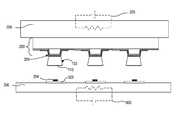
- FIG. 1top and cross-sectional side view illustrations of a carrier substrate and an array of micro LED devices are shown in accordance with an embodiment of the invention.
- an individual micro LED device 150is illustrated as a pair of concentric squares with tapered or rounded corners, with each square having a different width corresponding to the different widths of the top and bottom surfaces of the micro p-n diodes, and the corresponding tapered sidewalls spanning from the top and bottom surfaces.
- embodiments of the inventiondo not require tapered sidewalls, and the top and bottom surfaces of the micro p-n diodes may have the same diameter, or width, and vertical sidewalls.
- the array of micro LED devicesis described as having a pitch (P), spacing (S) between each micro LED device and a maximum width (W) of each micro LED devices.
- Ppitch
- Sspacing
- Wmaximum width
- the array of micro LED devicesmay have a pitch (P) of 1 to 100 ⁇ m, and a maximum width (W) of 1 to 100 ⁇ m.
- the spacing (S)may be minimized so as to maximize the number of micro LED devices that are poised for pick up on a carrier substrate.
- the pitch (P)is 10 ⁇ m, spacing (S) is 2 ⁇ m, and width (W) is 8 ⁇ m. In another embodiment, the pitch (P) is 5 ⁇ m, spacing (S) is 2 ⁇ m, and width (W) is 3 ⁇ m.
- embodiments of the inventionare not limited to these specific dimensions, and any suitable dimension may be utilized.
- the micro deviceis a micro LED device.
- a micro LED device 150may include a micro p-n diode and a top conductive contact layer 130 , a bottom conductive contact layer 120 , with the bottom conductive contact layer 120 between the micro p-n diode and a bonding layer 110 formed on a carrier substrate 101 .
- the micro p-n diodeincludes a top n-doped layer 114 , one or more quantum well layers 116 , and a lower p-doped layer 118 .
- the doping of layers 114 , 116may be reversed.
- the conductive contact layers 120 , 130may include one or more layers.
- the conductive contact layers 120 , 130may include an electrode layer that makes ohmic contact with the micro p-n diode.
- bottom conductive contact layer 120includes an electrode layer and a barrier layer between the electrode layer and the bonding layer 110 .
- the barrier layermay protect against diffusion or alloying between the bonding layer and other layers in the electrode layer, for example during bonding to the receiving substrate.
- the barrier layermay include a material such as Pd, Pt, Ni, Ta, Ti and TiW.
- the conductive contact layers 120 , 130may be transparent to the visible wavelength range (e.g. 380 nm-750 nm) or opaque.
- the conductive contact layers 120 , 130may optionally include a reflective layer such as Ag or Ni.
- the bottom surface of the micro p-n diodeis wider than the top surface of the conductive contact layer 120 . In an embodiment, the bottom surface of the conductive contact layer is wider than a top surface of the bonding layer 110 .
- a conformal dielectric barrier layer(not illustrated) may optionally be formed over the micro p-n diode and other exposed surfaces.
- bonding layer 110may be formed of a variety of materials useful for bonding the micro devices to a receiving substrate upon transfer of energy from the electrostatic transfer head assembly. Thickness of the bonding layer 110 may depend upon the bonding techniques, bonding mechanisms, and materials selections. In an embodiment, bonding layer is between 100 angstroms as 2 ⁇ m thick. In one embodiment the bonding layer 110 may be formed of a low temperature solder material for bonding the micro devices to the receiving substrate at low temperatures. Exemplary low temperature solder materials may be indium, bismuth, or tin based solder, including pure metals and metal alloys. An exemplary list of low melting solder materials which may be utilized with embodiments of the invention are provided in Table 1, in which the chemical compositions are listed by weight percent of the components.
- the bonding layer 110is formed of an electrically conductive adhesive material.
- the adhesivecan be a thermoplastic or thermosetting polymer including conductive particles (e.g. metal particles).
- the bonding layer 110is formed of a material characterized by a liquidus or melting temperature which is above the bonding temperature used to bond the micro device 150 to the receiving substrate or above an ambient liquidus temperature of a receiving substrate bonding layer.
- a bonding layermay be used for bonding mechanisms including eutectic alloy bonding, transient liquid phase bonding, or solid state diffusion bonding with another bonding layer on the receiving substrate.
- the bonding layer 110 materialmay also be selected for its ability to diffuse with a receiving substrate bonding layer material.
- the bonding layermay have a liquidus temperature above 250° C. such as bismuth (271.4° C.), or a liquidus temperature above 350° C.
- the bonding layeris not limited to these exemplary materials, and may include other semiconductor, metal, or metal alloy materials characterized by a liquidus or melting temperature which is above the bonding temperature used to bond the micro device to the receiving substrate.
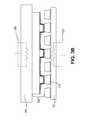
- FIG. 2is a flow chart and FIGS. 3A-3G are cross-sectional side view illustrations of a method of transferring and bonding an array of micro devices to a receiving substrate in accordance with an embodiment of the invention.
- an array of micro devicesis picked up from a carrier substrate with an electrostatic transfer head assembly.
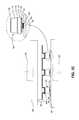
- FIG. 3Ais a cross-sectional side view illustration of an array of electrostatic transfer heads 204 supported by a substrate 200 and positioned over an array of micro LED devices 150 in accordance with an embodiment of the invention.
- the pitch (P) of the array of electrostatic transfer heads 204matches an integer multiple of the pitch of the micro LED devices 150 .
- the array of micro LED devices 150are then contacted with the array of electrostatic transfer heads 204 as illustrated in FIG. 3B .
- the array of electrostatic transfer headmay also be positioned over the array of micro devices with a suitable air gap separating them which does not significantly affect the grip pressure, for example, a 1 nm or 10 nm gap.
- a voltagemay be applied to the array of electrostatic transfer heads 204 .
- the voltagemay be applied from the working circuitry within or connected to an electrostatic transfer head assembly 206 in electrical connection with the array of electrostatic transfer heads 204 .
- the electrostatic transfer heads 204are bipolar electrostatic transfer heads including a pair of electrodes 203 covered by a dielectric layer 209 .
- embodimentsare not limited to a bipolar electrode configuration and other configurations such as monopolar electrodes may be used.
- each electrostatic transfer head 204includes a mesa structure 211 protruding from the substrate 200 .
- each electrostatic transfer head 204is configured to pick up an individual micro device.
- the array of micro devices 150is then picked up with the electrostatic transfer head assembly 206 as illustrated in FIG. 3C .
- the micro device bonding layers 110are also picked up with the array of micro devices 150 .
- energymay be transferred to the bonding layers through the optional heaters 105 , 205 , 305 , illustrated with dotted lines.
- heatmay be transferred through the electrostatic transfer head assembly 206 , through the array of electrostatic transfer heads 204 and the array of micro devices 150 , and to bonding layers 110 with one or more heaters 205 .
- Heatmay be also or alternatively be transferred through a carrier substrate 101 and to the bonding layers 110 with one or more heaters 105 .
- Heatcan be applied in a variety of fashions including infra red heat lamps, lasers, and resistive heating elements, amongst others.
- the pick up operations illustrated in FIS. 3 A- 3 Cmay be performed at a variety of temperatures.
- the substrate 200 supporting the array of electrostatic transfer heads 204is maintained at room temperature during the pick up operations in FIGS. 3A-3C .
- the substrate 200 supporting the array of transfer heads 204is maintained slightly above (e.g. 5 to 25° C. above) room temperature during the pick up operations in FIGS. 3A-3C to compensate for variations in room temperature.
- the substrate 200 supporting the array of electrostatic transfer heads 204is maintained at the same temperature during the pick up operations in FIGS.
- the bonding layer 110may remain in the solid phase during the pick up operations in FIGS. 3A-3C . In this manner, by not liquefying the bonding layer the pick up and transfer process may be simplified by not having to handle a material in liquid phase, and to control the phase of the material during transfer and formation of the micro devices.
- the uniform temperature profilemay protect the structural integrity of the electrostatic transfer head assembly can alignment of system components.
- the substrate 200 supporting the array of electrostatic transfer heads 204is subjected to a thermal cycle, for example ramped up above a liquidus temperature of the bonding layer 110 to pick up the array of micro devices from the carrier substrate.
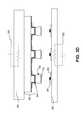
- FIG. 3Dis a cross-sectional side view illustration of an array of electrostatic transfer heads 204 holding an array of micro devices 150 over a receiving substrate 300 .
- the array of micro devices 150may be positioned over contact pads 302 and bonding layers 304 on the receiving substrate.
- heatmay be transferred through the receiving substrate 300 and into the bonding layers with one or more heaters 305 .
- Heatcan be applied in a variety of fashions including infra red heat lamps, lasers, and resistive heating elements, amongst others.
- receiving substrate 300is heated to a temperature below (e.g. 1 to 50° C.
- the receiving substrate 300is heated to a temperature below (e.g. 1 to 50° C. below) the bonding temperature.
- a temperature belowe.g. 1 to 50° C. below
- embodiments of the inventionare not so limited.
- a single bonding layer 304 or single contact pad 302may be present.
- multiple bonding layersmay be used.
- a bonding layer matching the composition of bonding layer 110may be located between bonding layer 304 and contact pad 302 .
- a bonding layer matching the composition of bonding layer 110is formed over bonding layer 304 to protect against oxidation of bonding layer 304 .
- a single bonding layer or contact padmay be used for bonding multiple micro devices, rather than individual micro devices.
- the receiving substrate 300may be, but is not limited to, a display substrate, a lighting substrate, a substrate with functional devices such as transistors or ICs, or a substrate with metal redistribution lines.
- the substrateis a display substrate including thin film transistors.
- substrate 300may be opaque, transparent, or semi-transparent to the visible wavelength (e.g. 380-750 nm wavelength), and substrate 300 may be rigid or flexible.
- substrate 300may be formed of glass or a polymer such as polyethylene terephthalate (PET), polyethelyne naphthalate (PEN), polycarbonate (PC), polyethersulphone (PES), aromatic fluorine-containing polyarylates (PAR), polycyclic olefin (PCO), and polyimide (PI).
- PETpolyethylene terephthalate
- PENpolyethelyne naphthalate
- PCpolycarbonate
- PESpolyethersulphone
- PARaromatic fluorine-containing polyarylates
- PCOpolycyclic olefin
- PIpolyimide
- contact pad 302may be opaque, transparent, or semi-transparent to the visible wavelength.
- Exemplary transparent conductive materialsinclude amorphous silicon, transparent conductive oxides (TCO) such as indium-tin-oxide (ITO) and indium-zinc-oxide (IZO), carbon nanotube film, or a transparent conducting polymer such as poly(3,4-ethylenedioxythiophene) (PEDOT), polyaniline, polyacetylene, polypyrrole, and polythiophene.
- TCOtransparent conductive oxides
- ITOindium-tin-oxide
- IZOindium-zinc-oxide
- PEDOTpoly(3,4-ethylenedioxythiophene)
- PEDOTpoly(3,4-ethylenedioxythiophene)
- PEDOTpolyaniline
- polyacetylenepolyacetylene
- polypyrrolepolythiophene
- contact pad 302is approximately 100 nm-200 nm thick ITO.
- the contact pad 302includes nanoparticles such as silver, gold, aluminum, molybdenum, titanium, tungs
- a contact pad 302comprises a reflective metallic film such as aluminum, molybdenum, titanium, titanium-tungsten, silver, or gold, or alloys thereof.
- contact pad 302functions as an electrode (e.g. anode or cathode) or electrode line.
- a receiving substrate bonding layer 304may optionally be formed over the conductive pad 302 to facilitate bonding of the micro device.
- Bonding layer 304may be formed of any of the materials described above with regard to bonding layer 110 .
- the particular selection of materials for bonding layers 110 , 304may dependent upon the particular bonding mechanism such as eutectic alloy bonding, transient liquid phase bonding, or solid state diffusion bonding described in further detail below.
- contacting the receiving substrate with the array of micro devicesincludes contacting a receiving substrate bonding layer 304 with a micro device bonding layer 110 for each respective micro device.
- each micro device bonding layer 110is wider than a corresponding receiving substrate bonding layer 304 .
- the receiving substrate bonding layers 304may be in the form of posts onto which the micro devices 150 will be placed.
- the receiving substrate bonding layer 304is approximately 1 ⁇ m wide, and is approximately 0.1 ⁇ m to 2 ⁇ m thick. A post structure may be useful in a variety of bonding operations.
- the pressure realized at the interfacemay be higher than the pressure applied to the micro devices 150 from the electrostatic transfer heads 204 .
- the liquefied bonding layer 304may act as a cushion and partially compensate for system uneven leveling (e.g nonplanar surfaces) between the array of micro devices 150 and the receiving substrate 300 during bonding, and for variations in height of the micro devices.
- energyis transferred from the electrostatic transfer head assembly and through the array of micro devices to bond the array of micro devices to the receiving substrate. Transferring energy from the electrostatic transfer head assembly and through the array of micro devices may facilitate several types of bonding mechanisms such as eutectic alloy bonding, transient liquid phase bonding, and solid state diffusion bonding. In an embodiment thermal energy transferred from the electrostatic transfer head assembly is also accompanied by the application of pressure from the electrostatic transfer head assembly.
- FIGS. 3H-3Jare cross-sectional side view illustrations of exemplary types of bonding mechanisms that may occur between a micro device and receiving substrate. It is to be appreciated that the material structures illustrated and described with regard to FIGS. 3H-3J are exemplary in nature and are intended to convey different bonding mechanisms, and that embodiments of the invention are not limited to the simplified examples illustrated and described. Furthermore, as described above embodiments of the invention include alternative layer configurations, and embodiments are not limited to the specific layers illustrated in FIGS. 3H-3J . Referring now to FIG. 3H , in the particular embodiment illustrated a eutectic alloy bonding layer 310 is formed from the micro device bonding layer 110 and receiving substrate bonding layer 304 for each respective micro device.
- the energy transferred from the electrostatic transfer head assemblymay liquefy a eutectic alloy bonding layer 310 formed at the interface of bonding layers 110 , 304 after the formation of an alloy due to diffusion of one or both of the bonding layers.
- the bonding layers 110 , 304may be completely consumed during the formation of the eutectic alloy bonding layer 310 if their volumes are precisely controlled to reflect the eutectic composition. In other embodiments, one or both of the bonding layers 110 , 304 are not completely consumed.
- eutectic alloy bondingis performed by heating bonding layers 110 , 304 to a temperature exceeding the eutectic point by 5-30° C., followed by cooling down to a temperature below the eutectic temperature.
- a low contact pressuree.g. 0.1 MPa to 1 MPa
- the electrostatic transfer head assemblyapplies a low contact pressure (e.g. 0.1 MPa to 1 MPa) during eutectic alloy bonding in order to prevent the liquid phase from excessively squeezing out from between the micro device and receiving substrate.
- the substrate 200 supporting the array of electrostatic transfer heads 204 and the receiving substrate 300may be heated.
- the substrate 200is heated to a temperature below the liquidus temperature of bonding layer 110
- the receiving substrate 300is heated to a temperature below the liquidus temperature of bonding layer 304 .
- the transfer of heat from the electrostatic transfer head assembly 206 though the array of micro devicesis sufficient form the eutectic alloy.
- the electrostatic transfer head assemblymay be held at a temperature of 5-30° C. above the eutectic temperature, while bonding layer 110 is formed of a eutectic alloy component with a liquidus temperature above the eutectic temperature.
- the substrate 200 supporting the array of electrostatic transfer heads 204is held at 150° C.
- bonding layer 110is formed of Ag
- bonding layer 304is formed of In.
- the temperatures of the substrates 200 , 300may be maintained throughout the process, or ramped up during bonding. Upon completion of eutectic alloy bonding, the temperature of one of the substrate 200 or 300 may be reduced to solidify the eutectic alloy.
- transient liquid phase bondingincludes liquefying the receiving substrate bonding layer 304 to interdiffuse the receiving substrate bonding layer 304 with the micro device bonding layer 110 and form an inter-metallic compound layer 312 having an ambient melting temperature higher than an ambient melting temperature of the receiving substrate bonding layer 304 .
- the bonding layers 110 , 304may be completely consumed during the formation of the inter-metallic compound layer 312 . In other embodiments the one or both of bonding layers 110 , 304 are not completely consumed.
- Transient liquid phase bondingmay be accomplished at or above the lowest liquidus temperature of the bonding layers.
- the micro device bonding layer 110includes the higher melting temperature material and the receiving substrate bonding layer 304 includes the lower melting temperature material.
- the micro device bonding layer 110may have a liquidus temperature above 250° C. such as bismuth (271.4° C.), or a liquidus temperature above 350° C. such as gold (1064° C.), copper (1084° C.), silver (962° C.), aluminum (660° C.), zinc (419.5° C.), or nickel (1453° C.).
- the receiving substrate bonding layer 304has a liquidus temperature below the liquidus temperature of bonding layer 110 .
- the receiving substrate bonding layer 304may be any of the low temperature solders listed in Table 1 above.
- the receiving substrate bonding layer 304includes tin (232° C.) or indium (156.7° C.).
- tin232° C.
- indium156.7° C.
- Table 3A list of exemplary materials system for transient liquid phase bonding is provided below in Table 3 along with melting temperatures of some exemplary inter-metallic compounds that may be formed.
- the substrate 200 supporting the array of electrostatic transfer heads 204 and the receiving substrate 300may be heated.
- the substrate 200is heated to a temperature below the liquidus temperature of bonding layer 110
- the receiving substrate 300is heated to a temperature below the liquidus temperature of bonding layer 304 .
- the transfer of heat from the electrostatic transfer head assembly though the array of micro devicesis sufficient to form the transient liquid state of bonding layer 304 with subsequent isothermal solidification as an inter-metallic compound.
- the lower melting temperature materialboth spreads out over the surface and diffuses into a solid solution of the higher melting temperature material or dissolves the higher melting temperature material and solidifies as an inter-metallic compound.
- the substrate 200 supporting the array of electrostatic transfer heads 204may be held at a temperature of 10-70° C., or more particularly 10-30° C., above the liquidus temperature of the receiving substrate bonding layer 304 , while bonding layer 110 is formed of a component with a liquidus temperature above the liquidus temperature of bonding layer 304 .
- the substrate 200 supporting the array of electrostatic transfer heads 204is held at 180° C.
- bonding layer 110is formed of Au
- bonding layer 304is formed of In.
- the electrostatic transfer head assemblyapplies a low contact pressure during initial contact at operation 1020 for transient liquid phase bonding in order to prevent the liquid phase from excessively squeezing out from between the micro device and receiving substrate.
- pressuremay be related to the strength of bonding layers.
- indiumhas a tensile strength of 1.6 MPa at room temperature.
- the applied pressureis below the tensile strength of a metal bonding layer material at room temperature.
- bonding layer 304is indium, the applied pressure may be below 1 MPa.
- eutectic alloy bonding and transient liquid phase bondingcan both provide an additional degree of freedom for system component leveling, such as planarity of the array of micro devices with the receiving substrate, and for variations in height of the micro devices due to the change in height of the liquefied bonding layers as they spread out over the surface.
- solid state diffusion bondingoccurs between the receiving substrate bonding layer 304 and micro device bonding layer 110 to form a metal bond 314 .
- solid state diffusionoccurs at a temperature below the ambient melting temperature of the bonding layers 304 , 110 .
- application of heat at pressuremay aid in diffusion.
- thermocompression bondingTCB
- TCBthermocompression bonding
- Non-limiting examples of materials for layers 110 , 304may include Au—Au, Cu—Cu, Al—Al, though dissimilar metals may also be used.
- the substrate 200 supporting the array of electrostatic transfer heads 204 and the receiving substrate 300may be heated.
- the substrate 200 and receiving substrate 300are both heated to temperatures below the liquidus temperatures of the bonding layers 110 , 304 .
- TCBis performed at a temperature range of 200° C. -500° C.
- pressuremay be higher than pressures used for eutectic alloy bonding and transient liquid phase bonding.
- pressures for TCBmay be from above 1 MPa to 20 MPa.
- the array of micro devicesare released onto the receiving substrate at operation 1040 and illustrated in FIG. 3G .
- the transfer heads 204include bipolar electrodes
- an alternating voltagemay be applied across the pair of electrodes in each transfer head 204 so that at a particular point in time when a negative voltage is applied to one electrode, a positive voltage is applied to the other electrode in the pair, and vice versa to create the pickup pressure.
- Releasing the array of micro device from the transfer heads 204may be accomplished with a variety of methods including turning off the voltage sources, lowering the voltage across the electrostatic transfer head electrodes, changing a waveform of an AC voltage, and grounding the voltage sources.
- Other electrode configurationsmay be used in accordance with embodiments of the invention. For example, monopolar electrode configurations may be used.
- the receiving substrateis further annealed after releasing the array of micro devices onto the receiving substrate to strengthen the bonds.
- a variety of operationscan be performed for transferring energy when contacting micro devices on a carrier substrate, picking up the micro devices, transferring the micro devices, contacting the receiving substrate with the micro devices, bonding the micro devices to the receiving substrate, and releasing the micro devices.
- heaters 105 , 205 , 305may be used to transfer energy to the bonding layers when contacting micro devices on a carrier substrate, picking up the micro devices, transferring the micro devices, contacting the receiving substrate with the micro devices, bonding the micro devices to the receiving substrate, and releasing the micro devices.
- the substrate 200 supporting the array of electrostatic transfer heads 204can be maintained at a uniform elevated temperature during the operations illustrated and described with regard to FIGS. 3A-3G .
- the substrate 200 supporting the array of electrostatic transfer heads 204is maintained at 180° C. during the operations illustrated and described with regard to FIGS. 3A-3G .
- the substrate 200 supporting the array of electrostatic transfer heads 204is subjected to a thermal cycle, for example ramped up above a liquidus temperature of the bonding layer 110 to pick up the array of micro devices from the carrier substrate, ramped up above a eutectic alloy bonding temperature, ramped up above a liquidus temperature of the bonding layer 304 , or ramped up for TCB.
- the temperature of the substrate 200 supporting the array of electrostatic transfer heads 204may be lowered after initial melting to complete bonding.
- the temperature of the substrate 200 supporting the array of electrostatic transfer heads 204may be lowered below a eutectic alloy temperature, or liquidus temperature of a receiving substrate bonding layer.
- the electrostatic transfer head assemblycan be used to transfer a specific contact pressure to the bonding layers when contacting the micro devices on the carrier substrate or receiving substrate, and during bonding the micro devices to the receiving substrate.
Landscapes
- Engineering & Computer Science (AREA)
- Computer Hardware Design (AREA)
- Microelectronics & Electronic Packaging (AREA)
- Power Engineering (AREA)
- Manufacturing & Machinery (AREA)
- Physics & Mathematics (AREA)
- Condensed Matter Physics & Semiconductors (AREA)
- General Physics & Mathematics (AREA)
- Led Device Packages (AREA)
- Micromachines (AREA)
- Wire Bonding (AREA)
Abstract
Description
| TABLE 1 | ||
| Chemical composition | Liquidus | Solidus |
| (weight %) | Temperature (° C.) | Temperature (° C.) |
| 100 In | 156.7 | 156.7 |
| 66.3In33.7Bi | 72 | 72 |
| 51In32.5Bi16.5Sn | 60 | 60 |
| 57Bi26In17Sn | 79 | 79 |
| 54.02Bi29.68In16.3Sn | 81 | 81 |
| 67Bi33In | 109 | 109 |
| 90In10Sn | 151 | 143 |
| 118 | 118 | |
| 50In50Sn | 125 | 118 |
| 52Sn48In | 131 | 118 |
| 58Sn42In | 145 | 118 |
| 97In3Ag | 143 | 143 |
| 94.5 | 200 | — |
| 99.5 | 200 | — |
| 150 | 125 | |
| 99.3 | 150 | 150 |
| 99.4In0.6Ga | 152 | 152 |
| 99.6In0.4Ga | 153 | 153 |
| 99.5In0.5Ga | 154 | 154 |
| 58Bi42Sn | 138 | 138 |
| 60Sn40Bi | 170 | 138 |
| 100Sn | 232 | 232 |
| 95Sn5Sb | 240 | 235 |
| 100Ga | 30 | 30 |
| 200 | — | |
| 98In2Cu | 182 | — |
| 96In4Cu | 253 | — |
| 74In26Cd | 123 | 123 |
| 70In30Pb | 175 | 165 |
| 60In40Pb | 181 | 173 |
| 50In50Pb | 210 | 184 |
| 40In60Pb | 231 | 197 |
| 55.5Bi44.5Pb | 124 | 124 |
| 58Bi42Pb | 126 | 124 |
| 45.5Bi54.5Pb | 160 | 122 |
| 60Bi40Cd | 144 | 144 |
| 67.8Sn32.2Cd | 177 | 177 |
| 45Sn55Pb | 227 | 183 |
| 63Sn37Pb | 183 | 183 |
| 62Sn38Pb | 183 | 183 |
| 65Sn35Pb | 184 | 183 |
| 70Sn30Pb | 186 | 183 |
| 60Sn40Pb | 191 | 183 |
| 75Sn25Pb | 192 | 183 |
| 80Sn20Pb | 199 | 183 |
| 205 | 183 | |
| 90Sn10Pb | 213 | 183 |
| 91Sn9Zn | 199 | 199 |
| 90Sn10Au | 217 | 217 |
| 99Sn1Cu | 227 | 227 |
| 99.3Sn0.7Cu | 227 | 227 |
| TABLE 2 | |||
| Eutectic alloy | Eutectic | Bonding layer | Bonding layer |
| (wt %) | temperature (° C.) | 110 | 304 material |
| Au:Sn (20/80) | 280 | Au | Sn |
| Au:Ge (28/72) | 361 | Au | Ge |
| Al:Ge (49/51) | 419 | Al | Ge |
| Ag:In (3/97) | 143 | Ag | In |
| TABLE 3 | ||
| Bonding layer | Bonding layer | |
| 110 | 304 material | melting temperature (° C.) |
| Cu | Sn | 415 |
| Ag | Sn | 600 |
| Ag | In | 880 |
| Au | Sn | 278 |
| Au | In | 495 |
| Ni | Sn | 400 |
Claims (2)
Priority Applications (5)
| Application Number | Priority Date | Filing Date | Title |
|---|---|---|---|
| US13/749,647US9773750B2 (en) | 2012-02-09 | 2013-01-24 | Method of transferring and bonding an array of micro devices |
| KR1020147021981AKR101653896B1 (en) | 2012-02-09 | 2013-02-06 | Method of transferring and bonding an array of micro devices |
| CN201380008866.0ACN104115266B (en) | 2012-02-09 | 2013-02-06 | Method of transferring and bonding an array of micro devices |
| PCT/US2013/024939WO2013119671A1 (en) | 2012-02-09 | 2013-02-06 | Method of transferring and bonding an array of micro devices |
| TW102104918ATWI562307B (en) | 2012-02-09 | 2013-02-07 | Method of transferring and bonding an array of micro devices |
Applications Claiming Priority (6)
| Application Number | Priority Date | Filing Date | Title |
|---|---|---|---|
| US201261597109P | 2012-02-09 | 2012-02-09 | |
| US201261597658P | 2012-02-10 | 2012-02-10 | |
| US13/372,422US8349116B1 (en) | 2011-11-18 | 2012-02-13 | Micro device transfer head heater assembly and method of transferring a micro device |
| US13/436,260US8573469B2 (en) | 2011-11-18 | 2012-03-30 | Method of forming a micro LED structure and array of micro LED structures with an electrically insulating layer |
| US201361749892P | 2013-01-07 | 2013-01-07 | |
| US13/749,647US9773750B2 (en) | 2012-02-09 | 2013-01-24 | Method of transferring and bonding an array of micro devices |
Related Parent Applications (1)
| Application Number | Title | Priority Date | Filing Date |
|---|---|---|---|
| US13/436,260Continuation-In-PartUS8573469B2 (en) | 2011-11-18 | 2012-03-30 | Method of forming a micro LED structure and array of micro LED structures with an electrically insulating layer |
Publications (2)
| Publication Number | Publication Date |
|---|---|
| US20130210194A1 US20130210194A1 (en) | 2013-08-15 |
| US9773750B2true US9773750B2 (en) | 2017-09-26 |
Family
ID=48945903
Family Applications (1)
| Application Number | Title | Priority Date | Filing Date |
|---|---|---|---|
| US13/749,647Active2034-08-20US9773750B2 (en) | 2012-02-09 | 2013-01-24 | Method of transferring and bonding an array of micro devices |
Country Status (5)
| Country | Link |
|---|---|
| US (1) | US9773750B2 (en) |
| KR (1) | KR101653896B1 (en) |
| CN (1) | CN104115266B (en) |
| TW (1) | TWI562307B (en) |
| WO (1) | WO2013119671A1 (en) |
Cited By (19)
| Publication number | Priority date | Publication date | Assignee | Title |
|---|---|---|---|---|
| US20180151804A1 (en)* | 2016-11-25 | 2018-05-31 | Vuereal Inc. | Integration of micro-devices into system substrate |
| US10121864B2 (en) | 2011-11-18 | 2018-11-06 | Apple Inc. | Micro device transfer head heater assembly and method of transferring a micro device |
| US10439587B2 (en)* | 2016-12-02 | 2019-10-08 | Skyworks Solutions, Inc. | Methods of manufacturing electronic devices formed in a cavity |
| US10541152B2 (en) | 2014-07-31 | 2020-01-21 | Skyworks Solutions, Inc. | Transient liquid phase material bonding and sealing structures and methods of forming same |
| US10568213B2 (en) | 2014-07-31 | 2020-02-18 | Skyworks Solutions, Inc. | Multilayered transient liquid phase bonding |
| US10916523B2 (en) | 2016-11-25 | 2021-02-09 | Vuereal Inc. | Microdevice transfer setup and integration of micro-devices into system substrate |
| US10978530B2 (en) | 2016-11-25 | 2021-04-13 | Vuereal Inc. | Integration of microdevices into system substrate |
| US10998352B2 (en) | 2016-11-25 | 2021-05-04 | Vuereal Inc. | Integration of microdevices into system substrate |
| US11037902B2 (en) | 2019-01-04 | 2021-06-15 | Au Optronics Corporation | Light-emitting apparatus including sacrificial pattern and manufacturing method thereof |
| US11076519B1 (en)* | 2018-03-30 | 2021-07-27 | Facebook Technologies, Llc | Selective inking head for semiconductor devices |
| WO2021148895A1 (en) | 2020-01-22 | 2021-07-29 | King Abdullah University Of Science And Technology | Light processing device array and method for manufacturing thereof |
| US11127890B2 (en)* | 2017-07-10 | 2021-09-21 | Osram Oled Gmbh | Method for assembling a carrier with components, pigment for assembling a carrier with a component and method for producing a pigment |
| US11217464B2 (en)* | 2018-03-30 | 2022-01-04 | Point Engineering Co., Ltd. | System for transferring micro LED |
| US20220093557A1 (en)* | 2020-09-18 | 2022-03-24 | Skiileux Electricity Inc. | Chip-transferring system and chip-transferring method |
| US20220406628A1 (en)* | 2019-11-08 | 2022-12-22 | Aledia | Method for protecting an optoelectronic device against electrostatic discharges |
| US11894350B2 (en) | 2014-10-31 | 2024-02-06 | e Lux, Inc. | Fluidic assembly enabled mass transfer for microLED displays |
| US12132054B2 (en) | 2019-02-28 | 2024-10-29 | Samsung Display Co., Ltd. | Electronic device, manufacturing method of electronic device, and method for attaching a light emitting element to a substrate |
| US12211860B2 (en) | 2016-11-25 | 2025-01-28 | Vuereal Inc. | Integration of microdevices into system substrate |
| US12243955B2 (en) | 2011-11-18 | 2025-03-04 | Apple Inc. | Display and micro device array for transfer to a display substrate |
Families Citing this family (97)
| Publication number | Priority date | Publication date | Assignee | Title |
|---|---|---|---|---|
| US9105492B2 (en) | 2012-05-08 | 2015-08-11 | LuxVue Technology Corporation | Compliant micro device transfer head |
| US9557215B2 (en) | 2012-08-17 | 2017-01-31 | Massachusetts Institute Of Technology | Phonon-recyling light-emitting diodes |
| US9159700B2 (en) | 2012-12-10 | 2015-10-13 | LuxVue Technology Corporation | Active matrix emissive micro LED display |
| US9178123B2 (en) | 2012-12-10 | 2015-11-03 | LuxVue Technology Corporation | Light emitting device reflective bank structure |
| US9029880B2 (en) | 2012-12-10 | 2015-05-12 | LuxVue Technology Corporation | Active matrix display panel with ground tie lines |
| US8791474B1 (en) | 2013-03-15 | 2014-07-29 | LuxVue Technology Corporation | Light emitting diode display with redundancy scheme |
| US9252375B2 (en) | 2013-03-15 | 2016-02-02 | LuxVue Technology Corporation | Method of fabricating a light emitting diode display with integrated defect detection test |
| US9484504B2 (en) | 2013-05-14 | 2016-11-01 | Apple Inc. | Micro LED with wavelength conversion layer |
| EP3008553B1 (en) | 2013-06-12 | 2023-06-07 | Rohinni, Inc. | Keyboard backlighting with deposited light-generating sources |
| US8987765B2 (en) | 2013-06-17 | 2015-03-24 | LuxVue Technology Corporation | Reflective bank structure and method for integrating a light emitting device |
| US9111464B2 (en) | 2013-06-18 | 2015-08-18 | LuxVue Technology Corporation | LED display with wavelength conversion layer |
| EP3033776A4 (en) | 2013-08-16 | 2017-01-25 | Massachusetts Institute of Technology | Thermo-electrically pumped light-emitting diodes |
| US9768345B2 (en) | 2013-12-20 | 2017-09-19 | Apple Inc. | LED with current injection confinement trench |
| US9450147B2 (en) | 2013-12-27 | 2016-09-20 | Apple Inc. | LED with internally confined current injection area |
| US9583466B2 (en)* | 2013-12-27 | 2017-02-28 | Apple Inc. | Etch removal of current distribution layer for LED current confinement |
| US9542638B2 (en) | 2014-02-18 | 2017-01-10 | Apple Inc. | RFID tag and micro chip integration design |
| US10520769B2 (en) | 2014-10-31 | 2019-12-31 | eLux, Inc. | Emissive display with printed light modification structures |
| US10381332B2 (en) | 2014-10-31 | 2019-08-13 | eLux Inc. | Fabrication method for emissive display with light management system |
| US11990453B2 (en)* | 2014-10-31 | 2024-05-21 | eLux Inc. | Fluidic assembly carrier substrate for microLED mass transfer |
| US9825202B2 (en) | 2014-10-31 | 2017-11-21 | eLux, Inc. | Display with surface mount emissive elements |
| US10535640B2 (en) | 2014-10-31 | 2020-01-14 | eLux Inc. | System and method for the fluidic assembly of micro-LEDs utilizing negative pressure |
| US10543486B2 (en) | 2014-10-31 | 2020-01-28 | eLux Inc. | Microperturbation assembly system and method |
| US10319878B2 (en) | 2014-10-31 | 2019-06-11 | eLux, Inc. | Stratified quantum dot phosphor structure |
| US10446728B2 (en)* | 2014-10-31 | 2019-10-15 | eLux, Inc. | Pick-and remove system and method for emissive display repair |
| US10236279B2 (en) | 2014-10-31 | 2019-03-19 | eLux, Inc. | Emissive display with light management system |
| US10418527B2 (en)* | 2014-10-31 | 2019-09-17 | eLux, Inc. | System and method for the fluidic assembly of emissive displays |
| US10242977B2 (en) | 2014-10-31 | 2019-03-26 | eLux, Inc. | Fluid-suspended microcomponent harvest, distribution, and reclamation |
| US10381335B2 (en) | 2014-10-31 | 2019-08-13 | ehux, Inc. | Hybrid display using inorganic micro light emitting diodes (uLEDs) and organic LEDs (OLEDs) |
| US9607907B2 (en) | 2014-12-01 | 2017-03-28 | Industrial Technology Research Institute | Electric-programmable magnetic module and picking-up and placement process for electronic devices |
| EP3029725B1 (en)* | 2014-12-01 | 2019-10-30 | IMEC vzw | Chuck for collective bonding of semiconductor dies, method of making the same and methods of using the same |
| US9478583B2 (en)* | 2014-12-08 | 2016-10-25 | Apple Inc. | Wearable display having an array of LEDs on a conformable silicon substrate |
| CN105789122B (en)* | 2014-12-12 | 2019-05-03 | 财团法人工业技术研究院 | Method for transferring photoelectric element |
| JP6375063B2 (en) | 2015-05-21 | 2018-08-15 | ゴルテック.インク | Micro light-emitting diode transport method, manufacturing method, apparatus, and electronic apparatus |
| US10193012B2 (en) | 2015-05-21 | 2019-01-29 | Goertek, Inc. | Transferring method, manufacturing method, device and electronic apparatus of micro-LED |
| US10297719B2 (en)* | 2015-08-27 | 2019-05-21 | Mikro Mesa Technology Co., Ltd. | Micro-light emitting diode (micro-LED) device |
| US10177127B2 (en) | 2015-09-04 | 2019-01-08 | Hong Kong Beida Jade Bird Display Limited | Semiconductor apparatus and method of manufacturing the same |
| US10032757B2 (en) | 2015-09-04 | 2018-07-24 | Hong Kong Beida Jade Bird Display Limited | Projection display system |
| US10304811B2 (en) | 2015-09-04 | 2019-05-28 | Hong Kong Beida Jade Bird Display Limited | Light-emitting diode display panel with micro lens array |
| WO2017041253A1 (en)* | 2015-09-09 | 2017-03-16 | Goertek. Inc | Repairing method, manufacturing method, device and electronics apparatus of micro-led |
| GB2544335A (en)* | 2015-11-13 | 2017-05-17 | Oculus Vr Llc | A method and apparatus for use in the manufacture of a display element |
| TWI657563B (en)* | 2015-12-15 | 2019-04-21 | 優顯科技股份有限公司 | Opto-electronic apparatus and manufacturing method thereof |
| WO2017107097A1 (en)* | 2015-12-23 | 2017-06-29 | Goertek.Inc | Micro-led transfer method and manufacturing method |
| JP6959697B2 (en) | 2016-01-15 | 2021-11-05 | ロヒンニ リミテッド ライアビリティ カンパニー | Devices and methods that are backlit through a cover on the device |
| KR102442612B1 (en)* | 2016-02-19 | 2022-09-14 | 삼성디스플레이 주식회사 | Light-Emitting Diode Transfer Method |
| CN107305915B (en)* | 2016-04-19 | 2019-04-05 | 财团法人工业技术研究院 | Electron-programmable magnetic transfer module and transfer method for electronic components |
| DE102016109459B4 (en)* | 2016-05-23 | 2019-06-13 | X-Fab Semiconductor Foundries Ag | Optimized transfer print (transfer printing) between carrier substrates as process, carrier substrate and micro-technical component |
| US10217729B2 (en)* | 2016-09-30 | 2019-02-26 | Intel Corporation | Apparatus for micro pick and bond |
| KR101874199B1 (en)* | 2016-11-23 | 2018-07-04 | 광주과학기술원 | Transfer Array of Micro Device based on Magnetic Induction and Method of transferring the Micro Device |
| US10971890B2 (en)* | 2016-12-05 | 2021-04-06 | Goertek, Inc. | Micro laser diode transfer method and manufacturing method |
| US20200006924A1 (en)* | 2016-12-05 | 2020-01-02 | Goertek, Inc. | Micro Laser Diode Display Device and Electronics Apparatus |
| US10089908B2 (en)* | 2017-02-21 | 2018-10-02 | Shenzhen China Star Optoelectronics Technology Co., Ltd | Micro light-emitting diode display panel and manufacturing method |
| JP6918537B2 (en)* | 2017-03-24 | 2021-08-11 | 東レエンジニアリング株式会社 | Pickup method, pickup device, and mounting device |
| US10632727B2 (en)* | 2017-04-10 | 2020-04-28 | PlayNitride Inc. | Method of transferring micro devices |
| TWI681472B (en)* | 2017-04-10 | 2020-01-01 | 英屬開曼群島商錼創科技股份有限公司 | Method of transferring micro devices |
| CN108695412B (en)* | 2017-04-10 | 2021-08-24 | 英属开曼群岛商錼创科技股份有限公司 | Methods of transporting tiny components |
| TWI613488B (en)* | 2017-06-19 | 2018-02-01 | 友達光電股份有限公司 | Display panel and method of forming micro component holder |
| KR102369934B1 (en)* | 2017-06-23 | 2022-03-03 | 삼성전자주식회사 | Chip mounting apparatus and method using the same |
| CN107359175B (en)* | 2017-07-25 | 2020-02-11 | 上海天马微电子有限公司 | Micro light-emitting diode display panel and display device |
| CN109326685B (en)* | 2017-08-01 | 2023-03-03 | 群创光电股份有限公司 | Method for manufacturing display device |
| US20190044023A1 (en)* | 2017-08-01 | 2019-02-07 | Innolux Corporation | Methods for manufacturing semiconductor device |
| DE102017123290A1 (en) | 2017-10-06 | 2019-04-11 | Osram Opto Semiconductors Gmbh | Light-emitting component, display device and method for producing a display device |
| CN107978548B (en)* | 2017-11-20 | 2019-07-05 | 厦门市三安光电科技有限公司 | Mass transfer method for microcomponents |
| CN108389825A (en)* | 2018-02-06 | 2018-08-10 | 中华映管股份有限公司 | transposition device |
| KR102158976B1 (en) | 2018-04-09 | 2020-09-24 | 중앙대학교 산학협력단 | Micro device array substrate and manufacturing method thereof |
| KR102498112B1 (en)* | 2018-04-27 | 2023-02-09 | (주)포인트엔지니어링 | Micro led transfer head |
| US10665573B2 (en) | 2018-04-28 | 2020-05-26 | Shenzhen China Star Optoelectronics Technology Co., Ltd. | Manufacturing method of micro light-emitting diode display panel having elastic conductive layer filled between pixel electrode and micro light-emitting diode and micro light-emitting diode display panel manufactured with the same |
| CN108493154B (en)* | 2018-04-28 | 2020-09-29 | 深圳市华星光电技术有限公司 | Manufacturing method of Micro LED display panel and Micro LED display panel |
| CN108878412A (en)* | 2018-05-07 | 2018-11-23 | 贺俊 | Full-color MicroLEDs display device preparation method |
| KR102527138B1 (en)* | 2018-05-16 | 2023-04-28 | (주)포인트엔지니어링 | Micro led transfer system |
| KR20200015076A (en) | 2018-08-02 | 2020-02-12 | (주)포인트엔지니어링 | Hot air supplying head for transfering micro led and micro led transfer system using the same |
| TWI690079B (en)* | 2018-12-04 | 2020-04-01 | 錼創顯示科技股份有限公司 | Micro semiconductor element structure |
| CN111276505B (en)* | 2018-12-05 | 2023-05-16 | 英属开曼群岛商錼创科技股份有限公司 | Micro light emitting diode display device and manufacturing method thereof |
| KR102145016B1 (en)* | 2019-02-28 | 2020-08-18 | 엘지전자 주식회사 | Assembly apparatus for assembling semiconductor light emitting diode to display panel |
| CN111033737B (en)* | 2019-03-25 | 2024-02-06 | 湖北三安光电有限公司 | Microluminescent component, microluminescent diode and microluminescent diode transfer method |
| CN109980078B (en)* | 2019-04-18 | 2020-06-23 | 京东方科技集团股份有限公司 | Light-emitting module, manufacturing method thereof and display device |
| CN111834239B (en)* | 2019-04-23 | 2024-02-02 | 美科米尚技术有限公司 | Method for transferring microelements |
| CN111834248B (en)* | 2019-04-23 | 2023-11-07 | 美科米尚技术有限公司 | Method for transferring microelements |
| KR102707392B1 (en)* | 2019-04-29 | 2024-09-20 | 삼성전자주식회사 | Bonding head and a bonding apparatus having the same |
| US10964582B2 (en) | 2019-06-24 | 2021-03-30 | Palo Alto Research Center Incorporated | Transfer substrate utilizing selectable surface adhesion transfer elements |
| DE102019118270B4 (en) | 2019-07-05 | 2021-10-07 | X-Fab Semiconductor Foundries Gmbh | Process for the production of semiconductor components to increase the yield in microtransfer printing |
| CN110379758B (en) | 2019-07-05 | 2021-02-02 | 深超光电(深圳)有限公司 | Adsorption device, transfer system and transfer method |
| CN110349989B (en) | 2019-07-17 | 2022-05-03 | 京东方科技集团股份有限公司 | Light emitting diode, display substrate and transfer method |
| CN110444547A (en)* | 2019-07-29 | 2019-11-12 | 南京中电熊猫平板显示科技有限公司 | A kind of micro-led array shows backboard and its manufacturing method |
| KR102279094B1 (en) | 2019-08-05 | 2021-07-19 | 중앙대학교 산학협력단 | Transfer catridge, and method for arraying micro device using the same |
| CN110931393A (en)* | 2019-12-02 | 2020-03-27 | 南京中电熊猫平板显示科技有限公司 | Micro device transfer head, method for manufacturing the same, and method for transferring micro devices |
| CN111048499B (en)* | 2019-12-16 | 2022-05-13 | 业成科技(成都)有限公司 | Micro light-emitting diode display panel and preparation method thereof |
| TWI720772B (en)* | 2020-01-08 | 2021-03-01 | 錼創顯示科技股份有限公司 | Substrate and display device |
| US11347001B2 (en)* | 2020-04-01 | 2022-05-31 | Taiwan Semiconductor Manufacturing Company, Ltd. | Semiconductor structure and method of fabricating the same |
| TWI760230B (en)* | 2020-06-09 | 2022-04-01 | 台灣愛司帝科技股份有限公司 | Chip-detecting method, chip-detecting structure and chip-carrying structure |
| CN112967973B (en)* | 2020-06-16 | 2022-09-27 | 重庆康佳光电技术研究院有限公司 | A transfer method and transfer system |
| TWI775111B (en)* | 2020-07-15 | 2022-08-21 | 歆熾電氣技術股份有限公司 | Chip-carrying structure and chip-bonding method |
| CN114122050A (en)* | 2020-11-23 | 2022-03-01 | 伊乐视有限公司 | Mass transfer method for microscopic light-emitting diode displays based on fluidic assembly |
| KR102443382B1 (en) | 2020-12-01 | 2022-09-15 | 유종우 | Manufacturing method of display module using asymmetric led-chips on transfer catridge, arranged by sound wave energy |
| US20250006873A1 (en)* | 2022-06-20 | 2025-01-02 | Boe Technology Group Co., Ltd. | Chip structure and manufacturing method therefor, display substrate and display device |
| US20240036363A1 (en)* | 2022-07-28 | 2024-02-01 | Palo Alto Research Center Incorporated | Optically activated object mass transfer apparatus |
| CN117326327A (en)* | 2023-10-07 | 2024-01-02 | 香港科技大学(广州) | Component picking mechanism and component transfer system |
| KR102840737B1 (en) | 2023-12-12 | 2025-08-01 | 코스텍시스템(주) | Electrostatic type patterned transfer head, device and method for pattern transfering micro device |
Citations (143)
| Publication number | Priority date | Publication date | Assignee | Title |
|---|---|---|---|---|
| US3717743A (en) | 1970-12-07 | 1973-02-20 | Argus Eng Co | Method and apparatus for heat-bonding in a local area using combined heating techniques |
| US3935986A (en) | 1975-03-03 | 1976-02-03 | Texas Instruments Incorporated | Solid state bonding process employing the isothermal solidification of a liquid interface |
| US5131582A (en) | 1989-06-30 | 1992-07-21 | Trustees Of Boston University | Adhesive metallic alloys and methods of their use |
| JPH0574873A (en)* | 1991-09-13 | 1993-03-26 | Casio Comput Co Ltd | Thermocompression method and device therefor |
| US5378926A (en) | 1991-09-30 | 1995-01-03 | Hughes Aircraft Company | Bonding of integrated circuit chip to carrier using gold/tin eutectic alloy and refractory metal nitride barrier layer to block migration of tin through via holes |
| JPH0760675A (en) | 1993-08-27 | 1995-03-07 | Tokin Corp | Electrostatic attracting hand |
| US5439161A (en)* | 1993-09-08 | 1995-08-08 | Sony Corporation | Thermocompression bonding apparatus, thermocompression bonding method and process of manufacturing liquid crystal display device |
| US5592358A (en) | 1994-07-18 | 1997-01-07 | Applied Materials, Inc. | Electrostatic chuck for magnetic flux processing |
| US5611481A (en)* | 1994-07-20 | 1997-03-18 | Fujitsu Limited | Integrated electronic device having flip-chip connection with circuit board and fabrication method thereof |
| US5740956A (en) | 1995-09-04 | 1998-04-21 | Anam Industrial Co., Ltd | Bonding method for semiconductor chips |
| US5794839A (en) | 1994-08-01 | 1998-08-18 | Nippondenso Co., Ltd. | Bonding material and bonding method for electric element |
| US5839187A (en) | 1995-08-24 | 1998-11-24 | Matsushita Electric Industrial Co., Ltd. | Apparatus and method for mounting a chip |
| US5851664A (en) | 1995-07-11 | 1998-12-22 | Minnesota Mining And Manufacturing Company | Semiconductor wafer processing adhesives and tapes |
| US5857610A (en)* | 1995-11-14 | 1999-01-12 | Nippon Steel Corporation | Process and apparatus for forming ball bumps |
| US5878942A (en)* | 1995-09-22 | 1999-03-09 | International Business Machines Corporation | Soldering method and soldering apparatus |
| US5888847A (en) | 1995-12-08 | 1999-03-30 | Lsi Logic Corporation | Technique for mounting a semiconductor die |
| US5903428A (en) | 1997-09-25 | 1999-05-11 | Applied Materials, Inc. | Hybrid Johnsen-Rahbek electrostatic chuck having highly resistive mesas separating the chuck from a wafer supported thereupon and method of fabricating same |
| JPH11340288A (en)* | 1999-05-11 | 1999-12-10 | Matsushita Electric Ind Co Ltd | Nozzle for thermocompression bonding of chips |
| US6071795A (en) | 1998-01-23 | 2000-06-06 | The Regents Of The University Of California | Separation of thin films from transparent substrates by selective optical processing |
| US6080650A (en) | 1998-02-04 | 2000-06-27 | Texas Instruments Incorporated | Method and apparatus for attaching particles to a substrate |
| US6142356A (en)* | 1998-05-12 | 2000-11-07 | Sharp Kabushiki Kaisha | Die bonding apparatus |
| US6240634B1 (en)* | 1997-09-12 | 2001-06-05 | Fujitsu Limited | Method of producing a multichip package module in which rough-pitch and fine-pitch chips are mounted on a board |
| US20010029088A1 (en) | 1999-03-03 | 2001-10-11 | Hitoshi Odajima | Method and apparatus for separating semiconductor elements, and mounting method of semiconductor elements |
| JP2001298072A (en) | 2000-04-14 | 2001-10-26 | Ulvac Japan Ltd | Electrostatic chucking device and vacuum processing device using the same |
| JP2001353682A (en) | 2000-06-15 | 2001-12-25 | Ulvac Japan Ltd | Electrostatic attraction device, substrate conveyor and evacuation process device |
| US6335263B1 (en) | 2000-03-22 | 2002-01-01 | The Regents Of The University Of California | Method of forming a low temperature metal bond for use in the transfer of bulk and thin film materials |
| JP2002134822A (en) | 2000-10-24 | 2002-05-10 | Sharp Corp | Semiconductor light emitting device and method of manufacturing the same |
| US20020056740A1 (en)* | 2000-11-16 | 2002-05-16 | Mitsubishi Denki Kabushiki Kaisha | Flip chip bonding method |
| JP2002164695A (en) | 2000-11-29 | 2002-06-07 | Mitsubishi Paper Mills Ltd | Electrostatic suction plate for transporting electronic materials |
| US6403985B1 (en) | 1991-01-18 | 2002-06-11 | Kopin Corporation | Method of making light emitting diode displays |
| US20020076848A1 (en) | 2000-12-05 | 2002-06-20 | Spooner Timothy R. | Method and device for protecting micro electromechanical systems structures during dicing of a wafer |
| JP2002176291A (en) | 2000-12-08 | 2002-06-21 | Matsushita Electric Ind Co Ltd | Component mounting apparatus and component mounting method |
| US6427901B2 (en)* | 1999-06-30 | 2002-08-06 | Lucent Technologies Inc. | System and method for forming stable solder bonds |
| JP2002240943A (en) | 2001-02-13 | 2002-08-28 | Ricoh Co Ltd | Electrostatic transport device, developing device, image forming device, and classifying device |
| US20030010975A1 (en) | 2001-07-05 | 2003-01-16 | Gelcore Llc | GaN LED with solderable backside metal |
| US6521511B1 (en) | 1997-07-03 | 2003-02-18 | Seiko Epson Corporation | Thin film device transfer method, thin film device, thin film integrated circuit device, active matrix board, liquid crystal display, and electronic apparatus |
| US6558109B2 (en) | 2000-05-26 | 2003-05-06 | Automation Technology, Inc. | Method and apparatus for separating wafers |
| JP3406207B2 (en) | 1997-11-12 | 2003-05-12 | シャープ株式会社 | Method of forming transistor array panel for display |
| US6613610B2 (en) | 2000-07-18 | 2003-09-02 | Sony Corporation | Image display unit and method of producing image display unit |
| US6621157B1 (en)* | 1999-01-07 | 2003-09-16 | Alphasem Ag | Method and device for encapsulating an electronic component in particular a semiconductor chip |
| US20030177633A1 (en) | 2002-03-25 | 2003-09-25 | Matsushita Electric Industrial Co., Ltd | Electronic component mounting apparatus and electronic component mounting method |
| US6629553B2 (en) | 1997-09-04 | 2003-10-07 | Hitachi, Ltd. | Method and system for mounting semiconductor device, semiconductor device separating system, and method for fabricating IC card |
| US6670038B2 (en) | 1996-04-09 | 2003-12-30 | Delsys Pharmaceutical | Method of depositing particles with an electrostatic chuck |
| US6683368B1 (en) | 2000-06-09 | 2004-01-27 | National Semiconductor Corporation | Lead frame design for chip scale package |
| JP2004095944A (en) | 2002-09-02 | 2004-03-25 | Sharp Corp | Light emitting diode and method of manufacturing the same |
| JP2004096046A (en) | 2002-09-04 | 2004-03-25 | Seiko Epson Corp | IC chip mounting method, IC chip mounting structure, thermocompression bonding device, electro-optical device manufacturing method, electro-optical device, and electronic apparatus |
| US20040100164A1 (en) | 2002-11-26 | 2004-05-27 | Murata Manufacturing Co., Ltd. | Manufacturing method of electronic device |
| US6769469B2 (en)* | 1999-08-09 | 2004-08-03 | Sony Chemicals Corp. | Process for mounting semiconductor device and mounting apparatus |
| US6786390B2 (en) | 2003-02-04 | 2004-09-07 | United Epitaxy Company Ltd. | LED stack manufacturing method and its structure thereof |
| US20040266048A1 (en) | 2002-02-27 | 2004-12-30 | Honeywell International Inc. | Bonding for a micro-electro-mechanical system (MEMS) and MEMS based devices |
| US6918530B2 (en) | 2002-01-25 | 2005-07-19 | Ngk Insulators, Ltd. | Bonded member comprising different materials, and production method thereof |
| US20050224822A1 (en) | 2003-07-04 | 2005-10-13 | Wen-Huang Liu | Light-emitting diode array having an adhesive layer |
| WO2005099310A2 (en) | 2004-03-29 | 2005-10-20 | Articulated Technologies, Llc | Roll-to-roll fabricated light sheet and encapsulated semiconductor circuit devices |
| US20050232728A1 (en) | 2004-03-31 | 2005-10-20 | Rice Michael R | Methods and apparatus for transferring conductive pieces during semiconductor device fabrication |
| US20060055035A1 (en) | 2004-09-13 | 2006-03-16 | Tzu-Han Lin | Bump structure |
| US20060065905A1 (en) | 2002-09-30 | 2006-03-30 | Dominik Eisert | Semiconductor component and production method |
| US20060160276A1 (en) | 2002-12-14 | 2006-07-20 | Brown Thomas M | Electronic devices |
| US20060157721A1 (en) | 2005-01-11 | 2006-07-20 | Tran Chuong A | Systems and methods for producing white-light light emitting diodes |
| KR100610632B1 (en) | 2005-02-07 | 2006-08-09 | 최우범 | Vertical structure light emitting diode manufacturing method |
| US20060214299A1 (en) | 2005-03-23 | 2006-09-28 | Fairchild M Ray | Electronic assembly including multiple substrates |
| US7148127B2 (en) | 2001-06-12 | 2006-12-12 | Sony Corporation | Device mounting substrate and method of repairing defective device |
| US20070000592A1 (en)* | 2005-06-29 | 2007-01-04 | Intel Corporation | Apparatus and method to operate on one or more attach sites in die package assembly |
| US7165711B2 (en)* | 2002-01-31 | 2007-01-23 | Texas Instruments Incorporated | Substrate alignment method and apparatus |
| US20070048902A1 (en) | 2005-08-31 | 2007-03-01 | Micron Technology, Inc. | Microfeature workpieces, carriers, and associated methods |
| KR20070042214A (en) | 2005-10-18 | 2007-04-23 | 김성진 | Nitride Semiconductor Light Emitting Diode and Manufacturing Method Thereof |
| US20070166851A1 (en) | 2005-01-11 | 2007-07-19 | Tran Chuong A | LIGHT EMITTING DIODES (LEDs) WITH IMPROVED LIGHT EXTRACTION BY ROUGHENING |
| US20070194330A1 (en) | 2006-02-23 | 2007-08-23 | Cree, Inc. | High efficiency LEDs with tunnel junctions |
| US20070284409A1 (en)* | 2004-06-30 | 2007-12-13 | Mauro Kobrinsky | Highly compliant plate for wafer bonding |
| US20080048206A1 (en) | 2006-08-23 | 2008-02-28 | Samsung Electro-Mechanics Co., Ltd. | Vertical gallium nitride-based light emitting diode and method of manufacturing the same |
| US7353596B2 (en) | 2003-03-20 | 2008-04-08 | Matsushita Electric Industrial Co., Ltd. | Component mounting method |
| US7358158B2 (en) | 2000-11-22 | 2008-04-15 | Mitsui Chemicals, Inc. | Wafer machining adhesive tape, and its manufacturing method and using method |
| US20080194054A1 (en) | 2007-02-08 | 2008-08-14 | Hung-Yi Lin | Led array package structure having silicon substrate and method of making the same |
| US20080196237A1 (en) | 2007-02-21 | 2008-08-21 | Denso Corporation | Method and apparatus for manufacturing honeycomb compact-body molding die |
| US20080205027A1 (en) | 2007-02-22 | 2008-08-28 | Stmicroelectronics (Crolles 2) Sas | Assembly of two parts of an integrated electronic circuit |
| US7439549B2 (en) | 2000-10-16 | 2008-10-21 | Osram Gmbh | LED module |
| US20080283190A1 (en) | 2007-05-20 | 2008-11-20 | Silverbrook Research Pty Ltd | Method of removing mems devices from a handle substrate |
| US20080283849A1 (en) | 2007-05-16 | 2008-11-20 | Ushiodenki Kabushiki Kaisha | Led device and method by which it is produced |
| US20080303038A1 (en) | 2005-02-28 | 2008-12-11 | Stefan Grotsch | Module Comprising Radiation-Emitting Semiconductor Bodies |
| US20090068774A1 (en) | 2004-04-28 | 2009-03-12 | Slater Jr David Beardsley | LED Bonding Structures and Methods of Fabricating LED Bonding Structures |
| US20090072382A1 (en) | 2007-09-18 | 2009-03-19 | Guzek John S | Microelectronic package and method of forming same |
| US7508065B2 (en)* | 2003-09-15 | 2009-03-24 | Nuvotronics, Llc | Device package and methods for the fabrication and testing thereof |
| US20090125141A1 (en)* | 2005-11-29 | 2009-05-14 | Takahiro Noda | Working apparatus and working method for circuit board |
| US20090127315A1 (en)* | 2007-11-16 | 2009-05-21 | Renesas Technology Corp. | Apparatus and method for manufacturing semiconductor device |
| US20090146303A1 (en) | 2007-09-28 | 2009-06-11 | Tessera, Inc. | Flip Chip Interconnection with double post |
| US7585703B2 (en) | 2002-11-19 | 2009-09-08 | Ishikawa Seisakusho, Ltd. | Pixel control element selection transfer method, pixel control device mounting device used for pixel control element selection transfer method, wiring formation method after pixel control element transfer, and planar display substrate |
| US7628309B1 (en) | 2005-05-03 | 2009-12-08 | Rosemount Aerospace Inc. | Transient liquid phase eutectic bonding |
| US20090303713A1 (en) | 2008-06-10 | 2009-12-10 | Advanced Optoelectronic Technology, Inc. | Light source device |
| US20090314991A1 (en) | 2008-01-14 | 2009-12-24 | Samsung Electronics Co., Ltd. | Quantum dot ink composition for inkjet printing and electronic device using the same |
| US7669210B2 (en)* | 2005-09-29 | 2010-02-23 | Toshiba Samsung Storage Technology Corporation | Optical pickup device and optical disk device using the same |
| US20100046134A1 (en)* | 2002-06-18 | 2010-02-25 | Canon Anelva Corporation | Electrostatic chuck device |
| JP2010056458A (en) | 2008-08-29 | 2010-03-11 | Kyocera Corp | Method of manufacturing light emitting element |
| US20100097738A1 (en) | 2008-10-20 | 2010-04-22 | Samsung Electro-Mechanics Co., Ltd. | Electrostatic chuck and substrate bonding device using the same |
| US20100105172A1 (en) | 2008-10-27 | 2010-04-29 | Ming Li | Direct die attach utilizing heated bond head |
| US20100123164A1 (en) | 2008-11-20 | 2010-05-20 | Toyoda Gosei Co., Ltd. | Light emiting device and method of making same |
| US20100176415A1 (en) | 2009-01-14 | 2010-07-15 | Samsung Electronics Co., Ltd. | Light emitting device with improved light extraction efficiency |
| JP2010161212A (en) | 2009-01-08 | 2010-07-22 | Hitachi Cable Ltd | Method of manufacturing wafer for semiconductor light-emitting element |
| US20100188794A1 (en) | 2009-01-23 | 2010-07-29 | Samsung Mobile Display Co., Ltd. | Electrostatic chuck and device of manufacturing organic light emitting diode having the same |
| KR100973928B1 (en) | 2009-12-10 | 2010-08-03 | (주)옵토니카 | Process for led die bonding |
| US20100203659A1 (en) | 2009-02-10 | 2010-08-12 | Kabushiki Kaisha Toshiba | Method for manufacturing light emitting device |
| US20100200884A1 (en) | 2009-02-10 | 2010-08-12 | Sang Youl Lee | Light emitting device and light emitting device package |
| US20100203661A1 (en) | 2007-06-29 | 2010-08-12 | Showa Denko K.K. | Method for producing light-emitting diode |
| US20100214777A1 (en) | 2009-02-24 | 2010-08-26 | Toyoda Gosei Co., Ltd. | Light-emitting device and method of manufacturing the same |
| US20100213471A1 (en) | 2009-02-24 | 2010-08-26 | Sony Corporation | Light-emitting device and method of manufacturing the same |
| US7795629B2 (en) | 2008-05-12 | 2010-09-14 | Sony Corporation | Light-emitting diode display and method for manufacturing the same |
| US20100248484A1 (en) | 2009-03-26 | 2010-09-30 | Christopher Bower | Methods of Forming Printable Integrated Circuit Devices and Devices Formed Thereby |
| US20100276726A1 (en) | 2009-05-04 | 2010-11-04 | Hyun Kyong Cho | Light emitting device, package, and system |
| US7838410B2 (en) | 2007-07-11 | 2010-11-23 | Sony Corporation | Method of electrically connecting element to wiring, method of producing light-emitting element assembly, and light-emitting element assembly |
| US20110003410A1 (en) | 2009-07-05 | 2011-01-06 | Industrial Technology Research Institute | Method of manufacturing a light emitting diode element |
| US7880315B2 (en) | 2005-06-08 | 2011-02-01 | Imec | Methods for bonding and micro-electronic devices produced according to such methods |
| US7884543B2 (en) | 2006-10-12 | 2011-02-08 | Sony Corporation | Method of forming wiring of light emitting device, substrate for mounting light emitting device, display, back light, illuminating apparatus and electronic appliance |
| US20110049540A1 (en) | 2008-03-26 | 2011-03-03 | Lattice Power (Jiangxi) Corporation | Method for fabricating robust light-emitting diodes |
| US7906787B2 (en) | 2003-08-08 | 2011-03-15 | Sang-Kyu Kang | Nitride micro light emitting diode with high brightness and method for manufacturing the same |
| US7910945B2 (en) | 2006-06-30 | 2011-03-22 | Cree, Inc. | Nickel tin bonding system with barrier layer for semiconductor wafers and devices |
| US7927976B2 (en) | 2008-07-23 | 2011-04-19 | Semprius, Inc. | Reinforced composite stamp for dry transfer printing of semiconductor elements |
| US7928465B2 (en) | 2002-04-09 | 2011-04-19 | Lg Electronics Inc. | Method of fabricating vertical structure LEDs |
| US20110132656A1 (en) | 2008-08-21 | 2011-06-09 | Murata Manufacturing, Co., Ltd. | Electronic Component Device and Method for Manufacturing the Same |
| US20110132655A1 (en) | 2008-08-21 | 2011-06-09 | Murata Manufacturing Co., Ltd. | Electronic Component Device and Method for Manufacturing the Same |
| US20110143467A1 (en) | 2008-08-22 | 2011-06-16 | Lattice Power (Jiangxi) Corporation | Method for fabricating ingaain light emitting device on a combined substrate |
| US20110151602A1 (en) | 2009-12-18 | 2011-06-23 | Cooledge Lighting, Inc. | Method of manufacturing transferable elements incorporating radiation enabled lift off for allowing transfer from host substrate |
| US20110159615A1 (en) | 2009-12-28 | 2011-06-30 | Hon Hai Precision Industry Co., Ltd. | Led units fabrication method |
| US7972875B2 (en) | 2007-01-17 | 2011-07-05 | The Board Of Trustees Of The University Of Illinois | Optical systems fabricated by printing-based assembly |
| KR20110084888A (en) | 2008-10-15 | 2011-07-26 | 가부시키가이샤 크리에이티브 테크놀러지 | Electrostatic chuck and its manufacturing method |
| US7989266B2 (en) | 2009-06-18 | 2011-08-02 | Aptina Imaging Corporation | Methods for separating individual semiconductor devices from a carrier |
| US7999454B2 (en) | 2008-08-14 | 2011-08-16 | Global Oled Technology Llc | OLED device with embedded chip driving |
| US20110210357A1 (en) | 2008-06-06 | 2011-09-01 | Osram Opto Semiconductors Gmbh | Optoelectronic Component and Method for the Production Thereof |
| JP2011181834A (en) | 2010-03-03 | 2011-09-15 | Toshiba Corp | Semiconductor light emitting element and method for manufacturing the same |
| US8023248B2 (en) | 2009-03-02 | 2011-09-20 | Shinko Electric Industries Co., Ltd. | Electrostatic chuck |
| WO2011123285A1 (en) | 2010-03-29 | 2011-10-06 | Semprius, Inc. | Selective transfer of active components |
| US20110291134A1 (en) | 2010-05-25 | 2011-12-01 | Lg Innotek Co., Ltd. | Light emitting device, method for fabricating the light emitting device, light emitting device package, and lighting unit |
| US20110297914A1 (en) | 2010-06-07 | 2011-12-08 | Xiamen Sanan Optoelectronics Technology Co., Ltd. | Gallium nitride-based flip-chip light-emitting diode with double reflective layers on its side and fabrication method thereof |
| US20110312131A1 (en) | 2007-06-29 | 2011-12-22 | Mukul Renavikar | Forming A Semiconductor Package Including A Thermal Interface Material |
| US20120064642A1 (en) | 2010-09-14 | 2012-03-15 | Taiwan Semiconductor Manufacturing Company, Ltd. | Method to remove sapphire substrate |
| US20120134065A1 (en)* | 2010-11-29 | 2012-05-31 | Sumitomo Electric Industries, Ltd. | Electrostatic chuck and method of manufacturing semiconductor device |
| US8317077B2 (en)* | 2010-09-01 | 2012-11-27 | Taiwan Semiconductor Manufacturing Company, Ltd. | Thermal compressive bonding with separate die-attach and reflow processes |
| US8333860B1 (en) | 2011-11-18 | 2012-12-18 | LuxVue Technology Corporation | Method of transferring a micro device |
| US8349116B1 (en) | 2011-11-18 | 2013-01-08 | LuxVue Technology Corporation | Micro device transfer head heater assembly and method of transferring a micro device |
| US20130019996A1 (en) | 2011-07-19 | 2013-01-24 | Rolls-Royce Plc. | Bonding of metal components |
| US20130038416A1 (en) | 2011-08-09 | 2013-02-14 | Taiyo Yuden Co., Ltd. | Laminated inductor and manufacturing method thereof |
| US8383506B1 (en)* | 2012-07-06 | 2013-02-26 | LuxVue Technology Corporation | Method of forming a compliant monopolar micro device transfer head with silicon electrode |
| US8381965B2 (en)* | 2010-07-22 | 2013-02-26 | Taiwan Semiconductor Manufacturing Company, Ltd. | Thermal compress bonding |
| US20130130440A1 (en) | 2011-11-18 | 2013-05-23 | Hsin-Hua Hu | Method of fabricating and transferring a micro device and an array of micro devices utilizing an intermediate electrically conductive bonding layer |
| US20130134591A1 (en) | 2010-08-05 | 2013-05-30 | Yoshitsugu Sakamoto | Bonding Material for Semiconductor Devices |
| US20130161682A1 (en) | 2011-12-21 | 2013-06-27 | Stanley Electric Co., Ltd. | Semiconductor light-emitting element |
Family Cites Families (2)
| Publication number | Priority date | Publication date | Assignee | Title |
|---|---|---|---|---|
| CN101005110A (en)* | 2007-01-12 | 2007-07-25 | 中国科学院上海微系统与信息技术研究所 | Method for realizing gallium nitride ELD vertical structure using metal bounding process |
| US9209059B2 (en)* | 2009-12-17 | 2015-12-08 | Cooledge Lighting, Inc. | Method and eletrostatic transfer stamp for transferring semiconductor dice using electrostatic transfer printing techniques |
- 2013
- 2013-01-24USUS13/749,647patent/US9773750B2/enactiveActive
- 2013-02-06WOPCT/US2013/024939patent/WO2013119671A1/enactiveApplication Filing
- 2013-02-06KRKR1020147021981Apatent/KR101653896B1/ennot_activeExpired - Fee Related
- 2013-02-06CNCN201380008866.0Apatent/CN104115266B/enactiveActive
- 2013-02-07TWTW102104918Apatent/TWI562307B/ennot_activeIP Right Cessation
Patent Citations (164)
| Publication number | Priority date | Publication date | Assignee | Title |
|---|---|---|---|---|
| US3717743A (en) | 1970-12-07 | 1973-02-20 | Argus Eng Co | Method and apparatus for heat-bonding in a local area using combined heating techniques |
| US3935986A (en) | 1975-03-03 | 1976-02-03 | Texas Instruments Incorporated | Solid state bonding process employing the isothermal solidification of a liquid interface |
| US5131582A (en) | 1989-06-30 | 1992-07-21 | Trustees Of Boston University | Adhesive metallic alloys and methods of their use |
| US6403985B1 (en) | 1991-01-18 | 2002-06-11 | Kopin Corporation | Method of making light emitting diode displays |
| JPH0574873A (en)* | 1991-09-13 | 1993-03-26 | Casio Comput Co Ltd | Thermocompression method and device therefor |
| US5378926A (en) | 1991-09-30 | 1995-01-03 | Hughes Aircraft Company | Bonding of integrated circuit chip to carrier using gold/tin eutectic alloy and refractory metal nitride barrier layer to block migration of tin through via holes |
| JPH0760675A (en) | 1993-08-27 | 1995-03-07 | Tokin Corp | Electrostatic attracting hand |
| US5439161A (en)* | 1993-09-08 | 1995-08-08 | Sony Corporation | Thermocompression bonding apparatus, thermocompression bonding method and process of manufacturing liquid crystal display device |
| US5592358A (en) | 1994-07-18 | 1997-01-07 | Applied Materials, Inc. | Electrostatic chuck for magnetic flux processing |
| US5996218A (en) | 1994-07-18 | 1999-12-07 | Applied Materials Inc. | Method of forming an electrostatic chuck suitable for magnetic flux processing |
| US5611481A (en)* | 1994-07-20 | 1997-03-18 | Fujitsu Limited | Integrated electronic device having flip-chip connection with circuit board and fabrication method thereof |
| US5794839A (en) | 1994-08-01 | 1998-08-18 | Nippondenso Co., Ltd. | Bonding material and bonding method for electric element |
| US5851664A (en) | 1995-07-11 | 1998-12-22 | Minnesota Mining And Manufacturing Company | Semiconductor wafer processing adhesives and tapes |
| US5839187A (en) | 1995-08-24 | 1998-11-24 | Matsushita Electric Industrial Co., Ltd. | Apparatus and method for mounting a chip |
| US5740956A (en) | 1995-09-04 | 1998-04-21 | Anam Industrial Co., Ltd | Bonding method for semiconductor chips |
| US5878942A (en)* | 1995-09-22 | 1999-03-09 | International Business Machines Corporation | Soldering method and soldering apparatus |
| US5857610A (en)* | 1995-11-14 | 1999-01-12 | Nippon Steel Corporation | Process and apparatus for forming ball bumps |
| US5888847A (en) | 1995-12-08 | 1999-03-30 | Lsi Logic Corporation | Technique for mounting a semiconductor die |
| US6670038B2 (en) | 1996-04-09 | 2003-12-30 | Delsys Pharmaceutical | Method of depositing particles with an electrostatic chuck |
| US6878607B2 (en) | 1997-07-03 | 2005-04-12 | Seiko Epson Corporation | Thin film device transfer method, thin film device, thin film integrated circuit device, active matrix board, liquid crystal display, and electronic apparatus |
| US6521511B1 (en) | 1997-07-03 | 2003-02-18 | Seiko Epson Corporation | Thin film device transfer method, thin film device, thin film integrated circuit device, active matrix board, liquid crystal display, and electronic apparatus |
| US6629553B2 (en) | 1997-09-04 | 2003-10-07 | Hitachi, Ltd. | Method and system for mounting semiconductor device, semiconductor device separating system, and method for fabricating IC card |
| US6240634B1 (en)* | 1997-09-12 | 2001-06-05 | Fujitsu Limited | Method of producing a multichip package module in which rough-pitch and fine-pitch chips are mounted on a board |
| US5903428A (en) | 1997-09-25 | 1999-05-11 | Applied Materials, Inc. | Hybrid Johnsen-Rahbek electrostatic chuck having highly resistive mesas separating the chuck from a wafer supported thereupon and method of fabricating same |
| JP3406207B2 (en) | 1997-11-12 | 2003-05-12 | シャープ株式会社 | Method of forming transistor array panel for display |
| US6071795A (en) | 1998-01-23 | 2000-06-06 | The Regents Of The University Of California | Separation of thin films from transparent substrates by selective optical processing |
| US6420242B1 (en) | 1998-01-23 | 2002-07-16 | The Regents Of The University Of California | Separation of thin films from transparent substrates by selective optical processing |
| US6080650A (en) | 1998-02-04 | 2000-06-27 | Texas Instruments Incorporated | Method and apparatus for attaching particles to a substrate |
| US6142356A (en)* | 1998-05-12 | 2000-11-07 | Sharp Kabushiki Kaisha | Die bonding apparatus |
| US6621157B1 (en)* | 1999-01-07 | 2003-09-16 | Alphasem Ag | Method and device for encapsulating an electronic component in particular a semiconductor chip |
| US20010029088A1 (en) | 1999-03-03 | 2001-10-11 | Hitoshi Odajima | Method and apparatus for separating semiconductor elements, and mounting method of semiconductor elements |
| JPH11340288A (en)* | 1999-05-11 | 1999-12-10 | Matsushita Electric Ind Co Ltd | Nozzle for thermocompression bonding of chips |
| US6427901B2 (en)* | 1999-06-30 | 2002-08-06 | Lucent Technologies Inc. | System and method for forming stable solder bonds |
| US6769469B2 (en)* | 1999-08-09 | 2004-08-03 | Sony Chemicals Corp. | Process for mounting semiconductor device and mounting apparatus |
| US6335263B1 (en) | 2000-03-22 | 2002-01-01 | The Regents Of The University Of California | Method of forming a low temperature metal bond for use in the transfer of bulk and thin film materials |
| JP2001298072A (en) | 2000-04-14 | 2001-10-26 | Ulvac Japan Ltd | Electrostatic chucking device and vacuum processing device using the same |
| US6558109B2 (en) | 2000-05-26 | 2003-05-06 | Automation Technology, Inc. | Method and apparatus for separating wafers |
| US6683368B1 (en) | 2000-06-09 | 2004-01-27 | National Semiconductor Corporation | Lead frame design for chip scale package |
| JP2001353682A (en) | 2000-06-15 | 2001-12-25 | Ulvac Japan Ltd | Electrostatic attraction device, substrate conveyor and evacuation process device |
| US7888690B2 (en) | 2000-07-18 | 2011-02-15 | Sony Corporation | Image display unit with light emitting devices having a resin surrounding the light emitting devices |
| US7880184B2 (en) | 2000-07-18 | 2011-02-01 | Sony Corporation | Image display unit |
| US6613610B2 (en) | 2000-07-18 | 2003-09-02 | Sony Corporation | Image display unit and method of producing image display unit |
| US7439549B2 (en) | 2000-10-16 | 2008-10-21 | Osram Gmbh | LED module |
| JP2002134822A (en) | 2000-10-24 | 2002-05-10 | Sharp Corp | Semiconductor light emitting device and method of manufacturing the same |
| US20020056740A1 (en)* | 2000-11-16 | 2002-05-16 | Mitsubishi Denki Kabushiki Kaisha | Flip chip bonding method |
| US7358158B2 (en) | 2000-11-22 | 2008-04-15 | Mitsui Chemicals, Inc. | Wafer machining adhesive tape, and its manufacturing method and using method |
| JP2002164695A (en) | 2000-11-29 | 2002-06-07 | Mitsubishi Paper Mills Ltd | Electrostatic suction plate for transporting electronic materials |
| US20020076848A1 (en) | 2000-12-05 | 2002-06-20 | Spooner Timothy R. | Method and device for protecting micro electromechanical systems structures during dicing of a wafer |
| JP2002176291A (en) | 2000-12-08 | 2002-06-21 | Matsushita Electric Ind Co Ltd | Component mounting apparatus and component mounting method |
| JP2002240943A (en) | 2001-02-13 | 2002-08-28 | Ricoh Co Ltd | Electrostatic transport device, developing device, image forming device, and classifying device |
| US7148127B2 (en) | 2001-06-12 | 2006-12-12 | Sony Corporation | Device mounting substrate and method of repairing defective device |
| US7723764B2 (en) | 2001-06-12 | 2010-05-25 | Sony Corporation | Device mounting substrate and image display device |
| US20040232439A1 (en) | 2001-07-05 | 2004-11-25 | Gelcore Llc. | GaN LED with solderable backside metal |
| US20030010975A1 (en) | 2001-07-05 | 2003-01-16 | Gelcore Llc | GaN LED with solderable backside metal |
| US6918530B2 (en) | 2002-01-25 | 2005-07-19 | Ngk Insulators, Ltd. | Bonded member comprising different materials, and production method thereof |
| US7165711B2 (en)* | 2002-01-31 | 2007-01-23 | Texas Instruments Incorporated | Substrate alignment method and apparatus |
| US20040266048A1 (en) | 2002-02-27 | 2004-12-30 | Honeywell International Inc. | Bonding for a micro-electro-mechanical system (MEMS) and MEMS based devices |
| US7033842B2 (en) | 2002-03-25 | 2006-04-25 | Matsushita Electric Industrial Co., Ltd. | Electronic component mounting apparatus and electronic component mounting method |
| US20030177633A1 (en) | 2002-03-25 | 2003-09-25 | Matsushita Electric Industrial Co., Ltd | Electronic component mounting apparatus and electronic component mounting method |
| US7928465B2 (en) | 2002-04-09 | 2011-04-19 | Lg Electronics Inc. | Method of fabricating vertical structure LEDs |
| US20100046134A1 (en)* | 2002-06-18 | 2010-02-25 | Canon Anelva Corporation | Electrostatic chuck device |
| JP2004095944A (en) | 2002-09-02 | 2004-03-25 | Sharp Corp | Light emitting diode and method of manufacturing the same |
| JP2004096046A (en) | 2002-09-04 | 2004-03-25 | Seiko Epson Corp | IC chip mounting method, IC chip mounting structure, thermocompression bonding device, electro-optical device manufacturing method, electro-optical device, and electronic apparatus |
| US20060065905A1 (en) | 2002-09-30 | 2006-03-30 | Dominik Eisert | Semiconductor component and production method |
| US7208337B2 (en) | 2002-09-30 | 2007-04-24 | Osram Opto Semiconductors Gmbh | Method of forming light emitting devices including forming mesas and singulating |
| US7585703B2 (en) | 2002-11-19 | 2009-09-08 | Ishikawa Seisakusho, Ltd. | Pixel control element selection transfer method, pixel control device mounting device used for pixel control element selection transfer method, wiring formation method after pixel control element transfer, and planar display substrate |
| US20040100164A1 (en) | 2002-11-26 | 2004-05-27 | Murata Manufacturing Co., Ltd. | Manufacturing method of electronic device |
| US20060160276A1 (en) | 2002-12-14 | 2006-07-20 | Brown Thomas M | Electronic devices |
| US6786390B2 (en) | 2003-02-04 | 2004-09-07 | United Epitaxy Company Ltd. | LED stack manufacturing method and its structure thereof |
| US7353596B2 (en) | 2003-03-20 | 2008-04-08 | Matsushita Electric Industrial Co., Ltd. | Component mounting method |
| US7797820B2 (en) | 2003-03-20 | 2010-09-21 | Panasonic Corporation | Component mounting apparatus |
| US20080163481A1 (en) | 2003-03-20 | 2008-07-10 | Satoshi Shida | Component mounting apparatus and component mounting method |
| US20050224822A1 (en) | 2003-07-04 | 2005-10-13 | Wen-Huang Liu | Light-emitting diode array having an adhesive layer |
| US7906787B2 (en) | 2003-08-08 | 2011-03-15 | Sang-Kyu Kang | Nitride micro light emitting diode with high brightness and method for manufacturing the same |
| US7508065B2 (en)* | 2003-09-15 | 2009-03-24 | Nuvotronics, Llc | Device package and methods for the fabrication and testing thereof |
| WO2005099310A2 (en) | 2004-03-29 | 2005-10-20 | Articulated Technologies, Llc | Roll-to-roll fabricated light sheet and encapsulated semiconductor circuit devices |
| KR20070006885A (en) | 2004-03-31 | 2007-01-11 | 어플라이드 머티어리얼스, 인코포레이티드 | Apparatus and method for transporting conductive components during semiconductor device manufacturing |
| US20050232728A1 (en) | 2004-03-31 | 2005-10-20 | Rice Michael R | Methods and apparatus for transferring conductive pieces during semiconductor device fabrication |
| US8076670B2 (en) | 2004-04-28 | 2011-12-13 | Cree, Inc. | LED with conductively joined bonding structure |
| US20100052004A1 (en) | 2004-04-28 | 2010-03-04 | Cree, Inc. | LED Bonding Structures and Methods of Fabricating LED Bonding Structures |
| US20090068774A1 (en) | 2004-04-28 | 2009-03-12 | Slater Jr David Beardsley | LED Bonding Structures and Methods of Fabricating LED Bonding Structures |
| US20070284409A1 (en)* | 2004-06-30 | 2007-12-13 | Mauro Kobrinsky | Highly compliant plate for wafer bonding |
| US20060055035A1 (en) | 2004-09-13 | 2006-03-16 | Tzu-Han Lin | Bump structure |
| US20060157721A1 (en) | 2005-01-11 | 2006-07-20 | Tran Chuong A | Systems and methods for producing white-light light emitting diodes |
| KR20070093091A (en) | 2005-01-11 | 2007-09-17 | 세미엘이디즈 코포레이션 | System and method for white light emitting diode production |
| US20070166851A1 (en) | 2005-01-11 | 2007-07-19 | Tran Chuong A | LIGHT EMITTING DIODES (LEDs) WITH IMPROVED LIGHT EXTRACTION BY ROUGHENING |
| KR100610632B1 (en) | 2005-02-07 | 2006-08-09 | 최우범 | Vertical structure light emitting diode manufacturing method |
| US20080303038A1 (en) | 2005-02-28 | 2008-12-11 | Stefan Grotsch | Module Comprising Radiation-Emitting Semiconductor Bodies |
| US20060214299A1 (en) | 2005-03-23 | 2006-09-28 | Fairchild M Ray | Electronic assembly including multiple substrates |
| US7628309B1 (en) | 2005-05-03 | 2009-12-08 | Rosemount Aerospace Inc. | Transient liquid phase eutectic bonding |
| US7880315B2 (en) | 2005-06-08 | 2011-02-01 | Imec | Methods for bonding and micro-electronic devices produced according to such methods |
| US20070000592A1 (en)* | 2005-06-29 | 2007-01-04 | Intel Corporation | Apparatus and method to operate on one or more attach sites in die package assembly |
| US20070048902A1 (en) | 2005-08-31 | 2007-03-01 | Micron Technology, Inc. | Microfeature workpieces, carriers, and associated methods |
| US7669210B2 (en)* | 2005-09-29 | 2010-02-23 | Toshiba Samsung Storage Technology Corporation | Optical pickup device and optical disk device using the same |
| KR20070042214A (en) | 2005-10-18 | 2007-04-23 | 김성진 | Nitride Semiconductor Light Emitting Diode and Manufacturing Method Thereof |
| US20090125141A1 (en)* | 2005-11-29 | 2009-05-14 | Takahiro Noda | Working apparatus and working method for circuit board |
| US20070194330A1 (en) | 2006-02-23 | 2007-08-23 | Cree, Inc. | High efficiency LEDs with tunnel junctions |
| US7910945B2 (en) | 2006-06-30 | 2011-03-22 | Cree, Inc. | Nickel tin bonding system with barrier layer for semiconductor wafers and devices |
| US20080048206A1 (en) | 2006-08-23 | 2008-02-28 | Samsung Electro-Mechanics Co., Ltd. | Vertical gallium nitride-based light emitting diode and method of manufacturing the same |
| US7884543B2 (en) | 2006-10-12 | 2011-02-08 | Sony Corporation | Method of forming wiring of light emitting device, substrate for mounting light emitting device, display, back light, illuminating apparatus and electronic appliance |
| US7972875B2 (en) | 2007-01-17 | 2011-07-05 | The Board Of Trustees Of The University Of Illinois | Optical systems fabricated by printing-based assembly |
| US20080194054A1 (en) | 2007-02-08 | 2008-08-14 | Hung-Yi Lin | Led array package structure having silicon substrate and method of making the same |
| JP2008200821A (en) | 2007-02-21 | 2008-09-04 | Denso Corp | Method for manufacturing honeycomb object molding die |
| US20080196237A1 (en) | 2007-02-21 | 2008-08-21 | Denso Corporation | Method and apparatus for manufacturing honeycomb compact-body molding die |
| US20080205027A1 (en) | 2007-02-22 | 2008-08-28 | Stmicroelectronics (Crolles 2) Sas | Assembly of two parts of an integrated electronic circuit |
| US8186568B2 (en) | 2007-02-22 | 2012-05-29 | Stmicroelectronics (Crolles 2) Sas | Assembly of two parts of an integrated electronic circuit |
| US7714336B2 (en) | 2007-05-16 | 2010-05-11 | Ushiodenki Kabushiki Kaisha | LED device and method by which it is produced |
| US20080283849A1 (en) | 2007-05-16 | 2008-11-20 | Ushiodenki Kabushiki Kaisha | Led device and method by which it is produced |
| US20080283190A1 (en) | 2007-05-20 | 2008-11-20 | Silverbrook Research Pty Ltd | Method of removing mems devices from a handle substrate |
| US20100203661A1 (en) | 2007-06-29 | 2010-08-12 | Showa Denko K.K. | Method for producing light-emitting diode |
| US20110312131A1 (en) | 2007-06-29 | 2011-12-22 | Mukul Renavikar | Forming A Semiconductor Package Including A Thermal Interface Material |
| US7838410B2 (en) | 2007-07-11 | 2010-11-23 | Sony Corporation | Method of electrically connecting element to wiring, method of producing light-emitting element assembly, and light-emitting element assembly |
| US20090072382A1 (en) | 2007-09-18 | 2009-03-19 | Guzek John S | Microelectronic package and method of forming same |
| US20090146303A1 (en) | 2007-09-28 | 2009-06-11 | Tessera, Inc. | Flip Chip Interconnection with double post |
| US20090127315A1 (en)* | 2007-11-16 | 2009-05-21 | Renesas Technology Corp. | Apparatus and method for manufacturing semiconductor device |
| US20090314991A1 (en) | 2008-01-14 | 2009-12-24 | Samsung Electronics Co., Ltd. | Quantum dot ink composition for inkjet printing and electronic device using the same |
| US20110049540A1 (en) | 2008-03-26 | 2011-03-03 | Lattice Power (Jiangxi) Corporation | Method for fabricating robust light-emitting diodes |
| US7795629B2 (en) | 2008-05-12 | 2010-09-14 | Sony Corporation | Light-emitting diode display and method for manufacturing the same |
| US20110210357A1 (en) | 2008-06-06 | 2011-09-01 | Osram Opto Semiconductors Gmbh | Optoelectronic Component and Method for the Production Thereof |
| US20090303713A1 (en) | 2008-06-10 | 2009-12-10 | Advanced Optoelectronic Technology, Inc. | Light source device |
| US7927976B2 (en) | 2008-07-23 | 2011-04-19 | Semprius, Inc. | Reinforced composite stamp for dry transfer printing of semiconductor elements |
| US7999454B2 (en) | 2008-08-14 | 2011-08-16 | Global Oled Technology Llc | OLED device with embedded chip driving |
| US20110132656A1 (en) | 2008-08-21 | 2011-06-09 | Murata Manufacturing, Co., Ltd. | Electronic Component Device and Method for Manufacturing the Same |
| US20110132655A1 (en) | 2008-08-21 | 2011-06-09 | Murata Manufacturing Co., Ltd. | Electronic Component Device and Method for Manufacturing the Same |
| US20110143467A1 (en) | 2008-08-22 | 2011-06-16 | Lattice Power (Jiangxi) Corporation | Method for fabricating ingaain light emitting device on a combined substrate |
| JP2010056458A (en) | 2008-08-29 | 2010-03-11 | Kyocera Corp | Method of manufacturing light emitting element |
| KR20110084888A (en) | 2008-10-15 | 2011-07-26 | 가부시키가이샤 크리에이티브 테크놀러지 | Electrostatic chuck and its manufacturing method |
| US20100097738A1 (en) | 2008-10-20 | 2010-04-22 | Samsung Electro-Mechanics Co., Ltd. | Electrostatic chuck and substrate bonding device using the same |
| US7854365B2 (en) | 2008-10-27 | 2010-12-21 | Asm Assembly Automation Ltd | Direct die attach utilizing heated bond head |
| US20100105172A1 (en) | 2008-10-27 | 2010-04-29 | Ming Li | Direct die attach utilizing heated bond head |
| US20100123164A1 (en) | 2008-11-20 | 2010-05-20 | Toyoda Gosei Co., Ltd. | Light emiting device and method of making same |
| JP2010161212A (en) | 2009-01-08 | 2010-07-22 | Hitachi Cable Ltd | Method of manufacturing wafer for semiconductor light-emitting element |
| US20100176415A1 (en) | 2009-01-14 | 2010-07-15 | Samsung Electronics Co., Ltd. | Light emitting device with improved light extraction efficiency |
| KR101001454B1 (en) | 2009-01-23 | 2010-12-14 | 삼성모바일디스플레이주식회사 | Electrostatic chuck and apparatus for manufacturing organic electroluminescent device having same |
| US20100188794A1 (en) | 2009-01-23 | 2010-07-29 | Samsung Mobile Display Co., Ltd. | Electrostatic chuck and device of manufacturing organic light emitting diode having the same |
| US20100203659A1 (en) | 2009-02-10 | 2010-08-12 | Kabushiki Kaisha Toshiba | Method for manufacturing light emitting device |
| US20100200884A1 (en) | 2009-02-10 | 2010-08-12 | Sang Youl Lee | Light emitting device and light emitting device package |
| JP2010186829A (en) | 2009-02-10 | 2010-08-26 | Toshiba Corp | Method for manufacturing light emitting element |
| US20100214777A1 (en) | 2009-02-24 | 2010-08-26 | Toyoda Gosei Co., Ltd. | Light-emitting device and method of manufacturing the same |
| US20100213471A1 (en) | 2009-02-24 | 2010-08-26 | Sony Corporation | Light-emitting device and method of manufacturing the same |
| US8023248B2 (en) | 2009-03-02 | 2011-09-20 | Shinko Electric Industries Co., Ltd. | Electrostatic chuck |
| US20100248484A1 (en) | 2009-03-26 | 2010-09-30 | Christopher Bower | Methods of Forming Printable Integrated Circuit Devices and Devices Formed Thereby |
| US20100276726A1 (en) | 2009-05-04 | 2010-11-04 | Hyun Kyong Cho | Light emitting device, package, and system |
| US7989266B2 (en) | 2009-06-18 | 2011-08-02 | Aptina Imaging Corporation | Methods for separating individual semiconductor devices from a carrier |
| US20110003410A1 (en) | 2009-07-05 | 2011-01-06 | Industrial Technology Research Institute | Method of manufacturing a light emitting diode element |
| KR100973928B1 (en) | 2009-12-10 | 2010-08-03 | (주)옵토니카 | Process for led die bonding |
| US20110151602A1 (en) | 2009-12-18 | 2011-06-23 | Cooledge Lighting, Inc. | Method of manufacturing transferable elements incorporating radiation enabled lift off for allowing transfer from host substrate |
| US20110159615A1 (en) | 2009-12-28 | 2011-06-30 | Hon Hai Precision Industry Co., Ltd. | Led units fabrication method |
| JP2011181834A (en) | 2010-03-03 | 2011-09-15 | Toshiba Corp | Semiconductor light emitting element and method for manufacturing the same |
| WO2011123285A1 (en) | 2010-03-29 | 2011-10-06 | Semprius, Inc. | Selective transfer of active components |
| US20110291134A1 (en) | 2010-05-25 | 2011-12-01 | Lg Innotek Co., Ltd. | Light emitting device, method for fabricating the light emitting device, light emitting device package, and lighting unit |
| US20110297914A1 (en) | 2010-06-07 | 2011-12-08 | Xiamen Sanan Optoelectronics Technology Co., Ltd. | Gallium nitride-based flip-chip light-emitting diode with double reflective layers on its side and fabrication method thereof |
| US8381965B2 (en)* | 2010-07-22 | 2013-02-26 | Taiwan Semiconductor Manufacturing Company, Ltd. | Thermal compress bonding |
| US20130134591A1 (en) | 2010-08-05 | 2013-05-30 | Yoshitsugu Sakamoto | Bonding Material for Semiconductor Devices |
| US8317077B2 (en)* | 2010-09-01 | 2012-11-27 | Taiwan Semiconductor Manufacturing Company, Ltd. | Thermal compressive bonding with separate die-attach and reflow processes |
| US20120064642A1 (en) | 2010-09-14 | 2012-03-15 | Taiwan Semiconductor Manufacturing Company, Ltd. | Method to remove sapphire substrate |
| US20120134065A1 (en)* | 2010-11-29 | 2012-05-31 | Sumitomo Electric Industries, Ltd. | Electrostatic chuck and method of manufacturing semiconductor device |
| US20130019996A1 (en) | 2011-07-19 | 2013-01-24 | Rolls-Royce Plc. | Bonding of metal components |
| US20130038416A1 (en) | 2011-08-09 | 2013-02-14 | Taiyo Yuden Co., Ltd. | Laminated inductor and manufacturing method thereof |
| US8349116B1 (en) | 2011-11-18 | 2013-01-08 | LuxVue Technology Corporation | Micro device transfer head heater assembly and method of transferring a micro device |
| US20130130440A1 (en) | 2011-11-18 | 2013-05-23 | Hsin-Hua Hu | Method of fabricating and transferring a micro device and an array of micro devices utilizing an intermediate electrically conductive bonding layer |
| US8333860B1 (en) | 2011-11-18 | 2012-12-18 | LuxVue Technology Corporation | Method of transferring a micro device |
| US20130161682A1 (en) | 2011-12-21 | 2013-06-27 | Stanley Electric Co., Ltd. | Semiconductor light-emitting element |
| US8383506B1 (en)* | 2012-07-06 | 2013-02-26 | LuxVue Technology Corporation | Method of forming a compliant monopolar micro device transfer head with silicon electrode |
Non-Patent Citations (26)
| Title |
|---|
| "Characteristics of electrostatic Chuck(ESC)" Advanced Materials Research Group, New Technology Research Laborotory, 2000, pp. 51-53 accessed at http://www.socnb.com/report/ptech-e/2000p51-e.pdf. |
| "Major Research Thrust: Epitaxial Layer Transfer by Laser Lift-off" Purdue University, Heterogeneous Integration Research Group, accessed at https://engineering.purdue.edu/Hetlnt/project-epitaxial-layer-transfer-llo.htm, last updated Aug. 2003. |
| "Principles of Electrostatic Chucks: 1-Techniques for High Performance Grip and Release" ElectroGrip, Principles1 rev3 May 2006, 2 pgs, accessed at www.electrogrip.com. |
| "Characteristics of electrostatic Chuck(ESC)" Advanced Materials Research Group, New Technology Research Laborotory, 2000, pp. 51-53 accessed at http://www.socnb.com/report/ptech—e/2000p51—e.pdf. |
| "Major Research Thrust: Epitaxial Layer Transfer by Laser Lift-off" Purdue University, Heterogeneous Integration Research Group, accessed at https://engineering.purdue.edu/Hetlnt/project—epitaxial—layer—transfer—llo.htm, last updated Aug. 2003. |
| "Principles of Electrostatic Chucks: 1—Techniques for High Performance Grip and Release" ElectroGrip, Principles1 rev3 May 2006, 2 pgs, accessed at www.electrogrip.com. |
| Asano, Kazutoshi, et al., "Fundamental Study of an Electrostatic Chuck for Silicon Wafer Handling" IEEE Transactions on Industry Applications, vol. 38, No. 3, May/Jun. 2002, pp. 840-845. |
| Bower, C.A., et al., "Active-Matrix OLED Display Backplanes Using Transfer-Printed Microscale Integrated Circuits", IEEE, 2010 Electronic Components and Technology Conference, pp. 1339-1343. |
| Dragoi, et al., "Metal Wafer Bonding for MEMS Devices," Romanian Journal of Information Science and Technology, vol. 13, No. 1, 2010, pp. 65-72. |
| Guerre, Roland, et al, "Selective Transfer Technology for Microdevice Distribution" Journal of Microelectromechanical Systems, vol. 17, No. 1, Feb. 2008, pp. 157-165. |
| Han, Min-Koo, "AM backplane for AMOLED" Proc. of ASID '06, Oct. 8-12, New Delhi, pp. 53-58. |
| Harris, Jonathan H., "Sintered Aluminum Nitride Ceramics for High-Power Electronic Applications" Journal of the Minerals, Metals and Materials Society, vol. 50, No. 6, Jun. 1998, p. 56. |
| Horwitz, Chris M., "Electrostatic Chucks: Frequently Asked Questions" Electrogrip, 2006, 10 pgs, accessed at www.electrogrip.com. |
| Hossick-Schott, Joachim, "Prospects for the ultimate energy density of oxide-based capacitor anodes" Medtronic Energy and Components Center, 10 pgs. |
| Lee, San Youl, et al., "Wafer-level fabrication of GAN-based vertical light-emitting diodes using a multi-functional bonding material system" Semicond. Sci. Technol. 24, 2009, 4 pgs. |
| Mei, Zequn, et al., "Low-Temperature Solders" Hewlett-Packard Journal, Article 10, Aug. 1996, pp. 1-10. |
| Mei, Zequn, et al., "Low—Temperature Solders" Hewlett-Packard Journal, Article 10, Aug. 1996, pp. 1-10. |
| Mercado, Lei, L., et al., "A Mechanical Approach to Overcome RF MEMS Switch Stiction Problem" 2003 Electronic Components and Technology Conference, pp. 377-384. |
| Miskys, Claudio R., et al., "Freestanding GaN-substrates and devices" phys. Stat. sol. © 0, No. 6, 2003, pp. 1627-1650. |
| PCT International Search Report and Written Opinion for International Application No. PCT/US2013/024939, dated May 13, 2013, 12 pages. |
| Roman, et al., "Low Stress Die Attach by Low Temperature Transient liquid Phase Bonding," The International Society for Hybrid Microelectronics (ISHM) Symposium Proceedings, Oct. 1992, pp. 1-6. |
| Steigerwald, Daniel, et al., "III-V Nitride Semiconductors for High-Perfromance Blue and Green Light-Emitting Devices" article appears in journal JOM 49 (9) 1997, pp. 18-23. Article accessed Nov. 2, 2011 at http://www.tms.org/pubs/journals/jom/9709/setigerwald-9709.html, 12 pgs. |
| Studnitzky, et al., "Diffusion Soldering for Stable High-Temperature Thin-Film Bonds," JOM, Dec. 2002, pp. 58-63. |
| Sugimoto, English translation of JP 05-074873 A, Mar. 26, 1993.* |
| Welch, et al., "Gold-Indium Transient Liquid Phase (TLP) Wafer Bonding for MEMS Vacuum Packaging," MEMS 2008, Tucson, AZ, Jan. 13-17, 2008, pp. 806-809. |
| Widas, Robert, "Electrostatic Substrate Clamping for Next Generation Semiconductor Devices" Apr. 21, 1999, 4 pgs. |
Cited By (32)
| Publication number | Priority date | Publication date | Assignee | Title |
|---|---|---|---|---|
| US10121864B2 (en) | 2011-11-18 | 2018-11-06 | Apple Inc. | Micro device transfer head heater assembly and method of transferring a micro device |
| US12243955B2 (en) | 2011-11-18 | 2025-03-04 | Apple Inc. | Display and micro device array for transfer to a display substrate |
| US11552046B2 (en) | 2011-11-18 | 2023-01-10 | Apple Inc. | Micro device transfer head assembly |
| US10607961B2 (en) | 2011-11-18 | 2020-03-31 | Apple Inc. | Micro device transfer head heater assembly and method of transferring a micro device |
| US10541152B2 (en) | 2014-07-31 | 2020-01-21 | Skyworks Solutions, Inc. | Transient liquid phase material bonding and sealing structures and methods of forming same |
| US10568213B2 (en) | 2014-07-31 | 2020-02-18 | Skyworks Solutions, Inc. | Multilayered transient liquid phase bonding |
| US20200146155A1 (en)* | 2014-07-31 | 2020-05-07 | Skyworks Solutions, Inc. | Multilayered transient liquid phase bonding |
| US11546998B2 (en)* | 2014-07-31 | 2023-01-03 | Skyworks Solutions, Inc. | Multilayered transient liquid phase bonding |
| US10840108B2 (en) | 2014-07-31 | 2020-11-17 | Skyworks Solutions, Inc. | Transient liquid phase material bonding and sealing structures and methods of forming same |
| US11894350B2 (en) | 2014-10-31 | 2024-02-06 | e Lux, Inc. | Fluidic assembly enabled mass transfer for microLED displays |
| US20180151804A1 (en)* | 2016-11-25 | 2018-05-31 | Vuereal Inc. | Integration of micro-devices into system substrate |
| US12211860B2 (en) | 2016-11-25 | 2025-01-28 | Vuereal Inc. | Integration of microdevices into system substrate |
| US10978530B2 (en) | 2016-11-25 | 2021-04-13 | Vuereal Inc. | Integration of microdevices into system substrate |
| US10998352B2 (en) | 2016-11-25 | 2021-05-04 | Vuereal Inc. | Integration of microdevices into system substrate |
| US12094856B2 (en) | 2016-11-25 | 2024-09-17 | Vuereal Inc. | Integration of microdevices into system substrate |
| US12080685B2 (en) | 2016-11-25 | 2024-09-03 | Vuereal Inc. | Method of placing a micro device to a receiver substrate |
| US12062638B2 (en) | 2016-11-25 | 2024-08-13 | Vuereal Inc. | Microdevice transfer setup and integration of micro-devices into system substrate |
| US10916523B2 (en) | 2016-11-25 | 2021-02-09 | Vuereal Inc. | Microdevice transfer setup and integration of micro-devices into system substrate |
| US10468472B2 (en)* | 2016-11-25 | 2019-11-05 | Vuereal Inc. | Integration of micro-devices into system substrate |
| US10763820B2 (en) | 2016-12-02 | 2020-09-01 | Skyworks Solutions, Inc. | Methods of manufacturing electronic devices formed in a cavity and including a via |
| US11050407B2 (en) | 2016-12-02 | 2021-06-29 | Skyworks Solutions, Inc. | Electronic devices formed in a cavity between substrates |
| US10965269B2 (en) | 2016-12-02 | 2021-03-30 | Skyworks Solutions, Inc. | Electronic devices formed in a cavity between substrates and including a via |
| US10439587B2 (en)* | 2016-12-02 | 2019-10-08 | Skyworks Solutions, Inc. | Methods of manufacturing electronic devices formed in a cavity |
| US11127890B2 (en)* | 2017-07-10 | 2021-09-21 | Osram Oled Gmbh | Method for assembling a carrier with components, pigment for assembling a carrier with a component and method for producing a pigment |
| US11217464B2 (en)* | 2018-03-30 | 2022-01-04 | Point Engineering Co., Ltd. | System for transferring micro LED |
| US11076519B1 (en)* | 2018-03-30 | 2021-07-27 | Facebook Technologies, Llc | Selective inking head for semiconductor devices |
| US11037902B2 (en) | 2019-01-04 | 2021-06-15 | Au Optronics Corporation | Light-emitting apparatus including sacrificial pattern and manufacturing method thereof |
| US12132054B2 (en) | 2019-02-28 | 2024-10-29 | Samsung Display Co., Ltd. | Electronic device, manufacturing method of electronic device, and method for attaching a light emitting element to a substrate |
| US20220406628A1 (en)* | 2019-11-08 | 2022-12-22 | Aledia | Method for protecting an optoelectronic device against electrostatic discharges |
| US12300521B2 (en)* | 2019-11-08 | 2025-05-13 | Aledia | Method for protecting an optoelectronic device against electrostatic discharges |
| WO2021148895A1 (en) | 2020-01-22 | 2021-07-29 | King Abdullah University Of Science And Technology | Light processing device array and method for manufacturing thereof |
| US20220093557A1 (en)* | 2020-09-18 | 2022-03-24 | Skiileux Electricity Inc. | Chip-transferring system and chip-transferring method |
Also Published As
| Publication number | Publication date |
|---|---|
| CN104115266A (en) | 2014-10-22 |
| US20130210194A1 (en) | 2013-08-15 |
| CN104115266B (en) | 2017-02-22 |
| WO2013119671A1 (en) | 2013-08-15 |
| TWI562307B (en) | 2016-12-11 |
| TW201347121A (en) | 2013-11-16 |
| KR20140117497A (en) | 2014-10-07 |
| KR101653896B1 (en) | 2016-09-09 |
Similar Documents
| Publication | Publication Date | Title |
|---|---|---|
| US9773750B2 (en) | Method of transferring and bonding an array of micro devices | |
| TWI653694B (en) | Micro light-emitting element array manufacturing method, transfer carrier plate and micro light-emitting element array | |
| US10181483B2 (en) | Laser assisted transfer welding process | |
| JP6501970B2 (en) | Method of repairing micro light emitting diode, manufacturing method, apparatus and electronic device | |
| JP6159477B2 (en) | Reflective bank structure and method for incorporating a light emitting device | |
| KR102830404B1 (en) | Method of manufacturing display apparatus, display apparatus, and structure for manufacturing display apparatus | |
| US20130126081A1 (en) | Method of forming a micro led structure and array of micro led structures with an electrically insulating layer | |
| US20140175495A1 (en) | Die bonding method and die bonding structure of light emitting diode package | |
| JP7612691B2 (en) | Light emitting diode die transfer method using partial laser lift-off - Patents.com | |
| JP2014519713A (en) | Method of electrically connecting a plurality of solar cells and photovoltaic module | |
| JP5120653B2 (en) | Solder layer, device bonding substrate using the same, and method for manufacturing the device bonding substrate | |
| KR20200136807A (en) | Display apparatus, source substrate structure, driving substrate structure, and method of manufacturing display apparatus | |
| TW201505138A (en) | Electronic device and manufacturing method for same | |
| US10446604B2 (en) | Display apparatus and fabricating method for display apparatus | |
| JP7162240B2 (en) | SOLDER MATERIAL, MOUNTING SUBSTRATE, AND METHOD OF FORMING SOLDER PORTION | |
| Chen et al. | High thermal dissipation of ultra high power light-emitting diodes by copper electroplating | |
| US20240178356A1 (en) | Display device and manufacturing method thereof | |
| CN113808988B (en) | Light-emitting chip supporting structure and manufacturing method thereof | |
| TWI489596B (en) | Chip structure | |
| WO2012081144A1 (en) | Semiconductor device and production method for same | |
| TW200423428A (en) | Light-emitting diodes and method of manufacturing same |
Legal Events
| Date | Code | Title | Description |
|---|---|---|---|
| AS | Assignment | Owner name:LUXVUE TECHNOLOGY CORPORATION, CALIFORNIA Free format text:ASSIGNMENT OF ASSIGNORS INTEREST;ASSIGNORS:BIBL, ANDREAS;HIGGINSON, JOHN A.;HU, HSIN-HUA;AND OTHERS;SIGNING DATES FROM 20130117 TO 20130123;REEL/FRAME:029694/0418 | |
| AS | Assignment | Owner name:COMERICA BANK, MICHIGAN Free format text:SECURITY AGREEMENT;ASSIGNOR:LUXVUE TECHNOLOGY CORPORATION;REEL/FRAME:030058/0305 Effective date:20130313 | |
| AS | Assignment | Owner name:TRIPLEPOINT CAPITAL LLC, CALIFORNIA Free format text:SECURITY AGREEMENT;ASSIGNOR:LUXVUE TECHNOLOGY CORPORATION;REEL/FRAME:030450/0558 Effective date:20130313 | |
| AS | Assignment | Owner name:LUXVUE TECHNOLOGY CORPORATION, CALIFORNIA Free format text:CORRECTIVE ASSIGNMENT TO CORRECT THE ASSIGNMENT DOCUMENT PREVIOUSLY RECORDED ON REEL 029694 FRAME 0418. ASSIGNOR(S) HEREBY CONFIRMS THE ASSIGNMENT OF ASSIGNORS INTEREST;ASSIGNORS:BIBL, ANDREAS;HIGGINSON, JOHN A.;HU, HSIN-HUA;AND OTHERS;SIGNING DATES FROM 20130117 TO 20130123;REEL/FRAME:032714/0481 | |
| AS | Assignment | Owner name:LUXVUE TECHNOLOGY CORPORATION, CALIFORNIA Free format text:RELEASE BY SECURED PARTY;ASSIGNOR:COMERICA BANK;REEL/FRAME:032812/0733 Effective date:20140502 | |
| AS | Assignment | Owner name:APPLE INC., CALIFORNIA Free format text:ASSIGNMENT OF ASSIGNORS INTEREST;ASSIGNOR:LUXVUE TECHNOLOGY CORPORATION;REEL/FRAME:038521/0255 Effective date:20160415 | |
| FEPP | Fee payment procedure | Free format text:PAYOR NUMBER ASSIGNED (ORIGINAL EVENT CODE: ASPN) | |
| STCF | Information on status: patent grant | Free format text:PATENTED CASE | |
| MAFP | Maintenance fee payment | Free format text:PAYMENT OF MAINTENANCE FEE, 4TH YEAR, LARGE ENTITY (ORIGINAL EVENT CODE: M1551); ENTITY STATUS OF PATENT OWNER: LARGE ENTITY Year of fee payment:4 | |
| MAFP | Maintenance fee payment | Free format text:PAYMENT OF MAINTENANCE FEE, 8TH YEAR, LARGE ENTITY (ORIGINAL EVENT CODE: M1552); ENTITY STATUS OF PATENT OWNER: LARGE ENTITY Year of fee payment:8 |