US9768021B2 - Methods of forming semiconductor device structures including metal oxide structures - Google Patents
Methods of forming semiconductor device structures including metal oxide structuresDownload PDFInfo
- Publication number
- US9768021B2 US9768021B2US15/044,713US201615044713AUS9768021B2US 9768021 B2US9768021 B2US 9768021B2US 201615044713 AUS201615044713 AUS 201615044713AUS 9768021 B2US9768021 B2US 9768021B2
- Authority
- US
- United States
- Prior art keywords
- polymer
- domains
- metal oxide
- matrix
- hydrophilic polymer
- Prior art date
- Legal status (The legal status is an assumption and is not a legal conclusion. Google has not performed a legal analysis and makes no representation as to the accuracy of the status listed.)
- Active
Links
Images


Classifications
- C—CHEMISTRY; METALLURGY
- C01—INORGANIC CHEMISTRY
- C01B—NON-METALLIC ELEMENTS; COMPOUNDS THEREOF; METALLOIDS OR COMPOUNDS THEREOF NOT COVERED BY SUBCLASS C01C
- C01B13/00—Oxygen; Ozone; Oxides or hydroxides in general
- C01B13/14—Methods for preparing oxides or hydroxides in general
- H—ELECTRICITY
- H01—ELECTRIC ELEMENTS
- H01L—SEMICONDUCTOR DEVICES NOT COVERED BY CLASS H10
- H01L21/00—Processes or apparatus adapted for the manufacture or treatment of semiconductor or solid state devices or of parts thereof
- H01L21/02—Manufacture or treatment of semiconductor devices or of parts thereof
- H01L21/027—Making masks on semiconductor bodies for further photolithographic processing not provided for in group H01L21/18 or H01L21/34
- H01L21/0271—Making masks on semiconductor bodies for further photolithographic processing not provided for in group H01L21/18 or H01L21/34 comprising organic layers
- B—PERFORMING OPERATIONS; TRANSPORTING
- B82—NANOTECHNOLOGY
- B82Y—SPECIFIC USES OR APPLICATIONS OF NANOSTRUCTURES; MEASUREMENT OR ANALYSIS OF NANOSTRUCTURES; MANUFACTURE OR TREATMENT OF NANOSTRUCTURES
- B82Y10/00—Nanotechnology for information processing, storage or transmission, e.g. quantum computing or single electron logic
- B—PERFORMING OPERATIONS; TRANSPORTING
- B82—NANOTECHNOLOGY
- B82Y—SPECIFIC USES OR APPLICATIONS OF NANOSTRUCTURES; MEASUREMENT OR ANALYSIS OF NANOSTRUCTURES; MANUFACTURE OR TREATMENT OF NANOSTRUCTURES
- B82Y40/00—Manufacture or treatment of nanostructures
- C—CHEMISTRY; METALLURGY
- C08—ORGANIC MACROMOLECULAR COMPOUNDS; THEIR PREPARATION OR CHEMICAL WORKING-UP; COMPOSITIONS BASED THEREON
- C08J—WORKING-UP; GENERAL PROCESSES OF COMPOUNDING; AFTER-TREATMENT NOT COVERED BY SUBCLASSES C08B, C08C, C08F, C08G or C08H
- C08J5/00—Manufacture of articles or shaped materials containing macromolecular substances
- C08J5/18—Manufacture of films or sheets
- C—CHEMISTRY; METALLURGY
- C08—ORGANIC MACROMOLECULAR COMPOUNDS; THEIR PREPARATION OR CHEMICAL WORKING-UP; COMPOSITIONS BASED THEREON
- C08K—Use of inorganic or non-macromolecular organic substances as compounding ingredients
- C08K3/00—Use of inorganic substances as compounding ingredients
- C08K3/18—Oxygen-containing compounds, e.g. metal carbonyls
- C08K3/20—Oxides; Hydroxides
- C08K3/22—Oxides; Hydroxides of metals
- C—CHEMISTRY; METALLURGY
- C08—ORGANIC MACROMOLECULAR COMPOUNDS; THEIR PREPARATION OR CHEMICAL WORKING-UP; COMPOSITIONS BASED THEREON
- C08L—COMPOSITIONS OF MACROMOLECULAR COMPOUNDS
- C08L53/00—Compositions of block copolymers containing at least one sequence of a polymer obtained by reactions only involving carbon-to-carbon unsaturated bonds; Compositions of derivatives of such polymers
- C08L53/005—Modified block copolymers
- C—CHEMISTRY; METALLURGY
- C09—DYES; PAINTS; POLISHES; NATURAL RESINS; ADHESIVES; COMPOSITIONS NOT OTHERWISE PROVIDED FOR; APPLICATIONS OF MATERIALS NOT OTHERWISE PROVIDED FOR
- C09D—COATING COMPOSITIONS, e.g. PAINTS, VARNISHES OR LACQUERS; FILLING PASTES; CHEMICAL PAINT OR INK REMOVERS; INKS; CORRECTING FLUIDS; WOODSTAINS; PASTES OR SOLIDS FOR COLOURING OR PRINTING; USE OF MATERIALS THEREFOR
- C09D153/00—Coating compositions based on block copolymers containing at least one sequence of a polymer obtained by reactions only involving carbon-to-carbon unsaturated bonds; Coating compositions based on derivatives of such polymers
- C09D153/005—Modified block copolymers
- G—PHYSICS
- G03—PHOTOGRAPHY; CINEMATOGRAPHY; ANALOGOUS TECHNIQUES USING WAVES OTHER THAN OPTICAL WAVES; ELECTROGRAPHY; HOLOGRAPHY
- G03F—PHOTOMECHANICAL PRODUCTION OF TEXTURED OR PATTERNED SURFACES, e.g. FOR PRINTING, FOR PROCESSING OF SEMICONDUCTOR DEVICES; MATERIALS THEREFOR; ORIGINALS THEREFOR; APPARATUS SPECIALLY ADAPTED THEREFOR
- G03F7/00—Photomechanical, e.g. photolithographic, production of textured or patterned surfaces, e.g. printing surfaces; Materials therefor, e.g. comprising photoresists; Apparatus specially adapted therefor
- G03F7/0002—Lithographic processes using patterning methods other than those involving the exposure to radiation, e.g. by stamping
- H—ELECTRICITY
- H01—ELECTRIC ELEMENTS
- H01L—SEMICONDUCTOR DEVICES NOT COVERED BY CLASS H10
- H01L21/00—Processes or apparatus adapted for the manufacture or treatment of semiconductor or solid state devices or of parts thereof
- H01L21/02—Manufacture or treatment of semiconductor devices or of parts thereof
- H01L21/02104—Forming layers
- H01L21/02107—Forming insulating materials on a substrate
- H01L21/02296—Forming insulating materials on a substrate characterised by the treatment performed before or after the formation of the layer
- H01L21/02318—Forming insulating materials on a substrate characterised by the treatment performed before or after the formation of the layer post-treatment
- H01L21/02321—Forming insulating materials on a substrate characterised by the treatment performed before or after the formation of the layer post-treatment introduction of substances into an already existing insulating layer
- H01L21/02323—Forming insulating materials on a substrate characterised by the treatment performed before or after the formation of the layer post-treatment introduction of substances into an already existing insulating layer introduction of oxygen
- H—ELECTRICITY
- H01—ELECTRIC ELEMENTS
- H01L—SEMICONDUCTOR DEVICES NOT COVERED BY CLASS H10
- H01L21/00—Processes or apparatus adapted for the manufacture or treatment of semiconductor or solid state devices or of parts thereof
- H01L21/02—Manufacture or treatment of semiconductor devices or of parts thereof
- H01L21/04—Manufacture or treatment of semiconductor devices or of parts thereof the devices having potential barriers, e.g. a PN junction, depletion layer or carrier concentration layer
- H01L21/18—Manufacture or treatment of semiconductor devices or of parts thereof the devices having potential barriers, e.g. a PN junction, depletion layer or carrier concentration layer the devices having semiconductor bodies comprising elements of Group IV of the Periodic Table or AIIIBV compounds with or without impurities, e.g. doping materials
- H01L21/28—Manufacture of electrodes on semiconductor bodies using processes or apparatus not provided for in groups H01L21/20 - H01L21/268
- H—ELECTRICITY
- H01—ELECTRIC ELEMENTS
- H01L—SEMICONDUCTOR DEVICES NOT COVERED BY CLASS H10
- H01L21/00—Processes or apparatus adapted for the manufacture or treatment of semiconductor or solid state devices or of parts thereof
- H01L21/02—Manufacture or treatment of semiconductor devices or of parts thereof
- H01L21/04—Manufacture or treatment of semiconductor devices or of parts thereof the devices having potential barriers, e.g. a PN junction, depletion layer or carrier concentration layer
- H01L21/18—Manufacture or treatment of semiconductor devices or of parts thereof the devices having potential barriers, e.g. a PN junction, depletion layer or carrier concentration layer the devices having semiconductor bodies comprising elements of Group IV of the Periodic Table or AIIIBV compounds with or without impurities, e.g. doping materials
- H01L21/30—Treatment of semiconductor bodies using processes or apparatus not provided for in groups H01L21/20 - H01L21/26
- H01L21/31—Treatment of semiconductor bodies using processes or apparatus not provided for in groups H01L21/20 - H01L21/26 to form insulating layers thereon, e.g. for masking or by using photolithographic techniques; After treatment of these layers; Selection of materials for these layers
- H01L29/06—
- H—ELECTRICITY
- H10—SEMICONDUCTOR DEVICES; ELECTRIC SOLID-STATE DEVICES NOT OTHERWISE PROVIDED FOR
- H10D—INORGANIC ELECTRIC SEMICONDUCTOR DEVICES
- H10D62/00—Semiconductor bodies, or regions thereof, of devices having potential barriers
- H10D62/10—Shapes, relative sizes or dispositions of the regions of the semiconductor bodies; Shapes of the semiconductor bodies
- C—CHEMISTRY; METALLURGY
- C08—ORGANIC MACROMOLECULAR COMPOUNDS; THEIR PREPARATION OR CHEMICAL WORKING-UP; COMPOSITIONS BASED THEREON
- C08L—COMPOSITIONS OF MACROMOLECULAR COMPOUNDS
- C08L2666/00—Composition of polymers characterized by a further compound in the blend, being organic macromolecular compounds, natural resins, waxes or and bituminous materials, non-macromolecular organic substances, inorganic substances or characterized by their function in the composition
- C08L2666/02—Organic macromolecular compounds, natural resins, waxes or and bituminous materials
- Y—GENERAL TAGGING OF NEW TECHNOLOGICAL DEVELOPMENTS; GENERAL TAGGING OF CROSS-SECTIONAL TECHNOLOGIES SPANNING OVER SEVERAL SECTIONS OF THE IPC; TECHNICAL SUBJECTS COVERED BY FORMER USPC CROSS-REFERENCE ART COLLECTIONS [XRACs] AND DIGESTS
- Y10—TECHNICAL SUBJECTS COVERED BY FORMER USPC
- Y10S—TECHNICAL SUBJECTS COVERED BY FORMER USPC CROSS-REFERENCE ART COLLECTIONS [XRACs] AND DIGESTS
- Y10S438/00—Semiconductor device manufacturing: process
- Y10S438/942—Masking
- Y10S438/947—Subphotolithographic processing
- Y—GENERAL TAGGING OF NEW TECHNOLOGICAL DEVELOPMENTS; GENERAL TAGGING OF CROSS-SECTIONAL TECHNOLOGIES SPANNING OVER SEVERAL SECTIONS OF THE IPC; TECHNICAL SUBJECTS COVERED BY FORMER USPC CROSS-REFERENCE ART COLLECTIONS [XRACs] AND DIGESTS
- Y10—TECHNICAL SUBJECTS COVERED BY FORMER USPC
- Y10S—TECHNICAL SUBJECTS COVERED BY FORMER USPC CROSS-REFERENCE ART COLLECTIONS [XRACs] AND DIGESTS
- Y10S977/00—Nanotechnology
- Y10S977/84—Manufacture, treatment, or detection of nanostructure
- Y10S977/888—Shaping or removal of materials, e.g. etching
- Y—GENERAL TAGGING OF NEW TECHNOLOGICAL DEVELOPMENTS; GENERAL TAGGING OF CROSS-SECTIONAL TECHNOLOGIES SPANNING OVER SEVERAL SECTIONS OF THE IPC; TECHNICAL SUBJECTS COVERED BY FORMER USPC CROSS-REFERENCE ART COLLECTIONS [XRACs] AND DIGESTS
- Y10—TECHNICAL SUBJECTS COVERED BY FORMER USPC
- Y10S—TECHNICAL SUBJECTS COVERED BY FORMER USPC CROSS-REFERENCE ART COLLECTIONS [XRACs] AND DIGESTS
- Y10S977/00—Nanotechnology
- Y10S977/84—Manufacture, treatment, or detection of nanostructure
- Y10S977/89—Deposition of materials, e.g. coating, cvd, or ald
Definitions
- the inventionin various embodiments, relates generally to methods for selectively permeating self-assembled block copolymers with metal oxides to form metal oxide structures, to methods of forming semiconductor structures using such metal oxide structures, and to semiconductor structures including the metal oxide structures.
- Block copolymer lithographywhere use is made of polymer masks derived from self-assembly of block copolymers.
- Block copolymersare known to form nano-scale microdomains by microphase separation. When cast on a substrate and annealed, block copolymers form nano-scale periodic patterns that may be useful as an etch mask in semiconductor device fabrication.
- Such ordered patterns of isolated nano-sized structural units formed by the self-assembled block copolymersmay potentially be used for fabricating periodic nano-scale structural units and, therefore, have promising applications in semiconductor, optical, and magnetic devices.
- Dimensions of the structural units so formedare typically in the range of 5 nm to 50 nm, which dimensions are extremely difficult to define using conventional lithographic techniques.
- the size and shape of these domainsmay be controlled by manipulating the molecular weight and composition of the copolymer.
- the interfaces between these domainshave widths on the order of 1 nm to 5 nm and may be controlled by changing the chemical composition of the blocks of the copolymers.
- the domains of the self-assembling block copolymersoften have little or no etch selectivity for one another. Therefore, improving etch selectivity of the self-assembled domains is desirable.
- Buriak et al.“Assembly of Aligned Linear Metallic Patterns on Silicon,” Nature Nanotechnology, 2, 500-506 (August 2007), discloses forming aligned metal lines by metal loading self-assembled monolayers of aligned, horizontal block copolymer cylinders using an aqueous solution of an anionic metal complex.
- FIG. 1is a partial cross-sectional view illustrating an embodiment of a method that may be used to fabricate metal oxide structures on a semiconductor structure
- FIG. 2is a partial cross-sectional view illustrating an embodiment of a method that may be used to fabricate metal oxide structures on a semiconductor structure
- FIG. 3is a partial cross-sectional view illustrating an embodiment of a method that may be used to fabricate metal oxide structures on a semiconductor structure
- FIG. 4is a partial cross-sectional view illustrating an embodiment of a method that may be used to fabricate metal oxide structures on a semiconductor structure
- FIG. 5is a top-down plan view of the embodiment of the semiconductor structure shown in FIG. 4 ;
- FIG. 6is a partial cross-sectional view illustrating an embodiment of a patterning method utilizing metal oxide structures such as those fabricated using the method shown in FIGS. 1-4 ;
- FIG. 7is a scanning electron micrograph showing a top-down plan view of metal oxide lines formed on a semiconductor structure using embodiments of the present invention.
- the present inventioncomprises methods of selective permeation or impregnation of metal oxides into a self-assembled block copolymer and methods of forming metal oxide structures utilizing the controlled formation of block copolymers.
- the present inventionincludes a semiconductor structure including a pattern of such metal oxide structures.
- the term “substrate”means and includes a base material or construction upon which materials are formed.
- the substratemay be a semiconductor substrate, a base semiconductor layer on a supporting structure, a metal electrode or a semiconductor substrate having one or more layers, structures or regions formed thereon.
- the substratemay be a conventional silicon substrate or other bulk substrate comprising a layer of semiconductive material.
- the term “bulk substrate”means and includes not only silicon wafers, but also silicon-on-insulator (“SOI”) substrates, such as silicon-on-sapphire (“SOS”) substrates and silicon-on-glass (“SOG”) substrates, epitaxial layers of silicon on a base semiconductor foundation, and other semiconductor or optoelectronic materials, such as silicon-germanium, germanium, gallium arsenide, gallium nitride, and indium phosphide.
- SOIsilicon-on-insulator
- SOSsilicon-on-sapphire
- SOOGsilicon-on-glass
- epitaxial layers of silicon on a base semiconductor foundationand other semiconductor or optoelectronic materials, such as silicon-germanium, germanium, gallium arsenide, gallium nitride, and indium phosphide.
- the substratemay be doped or undoped.
- block copolymermeans and includes polymers that include one or more long sequences (i.e., “blocks”) of the same monomeric unit(s) covalently bound to one or more long sequences (i.e., “blocks”) of unlike type, for example, including differing monomeric unit(s).
- block copolymersare contemplated herein including diblock copolymers (copolymers having two blocks), triblock copolymers (copolymers having three blocks), multiblock copolymers (copolymers having more than three blocks), and combinations thereof.
- phase separationmeans and includes the properties by which homogenous polymers or homogenous segments of a block copolymer aggregate mutually, and heterogeneous polymers or heterogeneous segments separate into distinct domains.
- annealingmeans and includes treatment of the block copolymer so as to enable sufficient phase separation between the two or more different polymeric block components of the block copolymer to form an ordered pattern defined by repeating structural units.
- Annealing of the block copolymer in the present inventionmay be achieved by various methods known in the art, including, but not limited to: thermal annealing (either in a vacuum or in an inert atmosphere containing nitrogen or argon), solvent vapor-assisted annealing (either at or above room temperature), or supercritical fluid-assisted annealing.
- thermal annealing of the block copolymermay be conducted by exposing the block copolymer to an elevated temperature that is above the glass transition temperature (T g ), but below the degradation temperature (T d ) of the block copolymer, as described in greater detail hereinafter.
- T gglass transition temperature
- T ddegradation temperature
- preferential wettingmeans and includes wetting of a block copolymer wherein one block of the block copolymer will wet a contacting surface at an interface more easily than the other block(s).
- the materials described hereinmay be formed by any suitable technique including, but not limited to, spin coating, blanket coating, chemical vapor deposition (“CVD”), atomic layer deposition (“ALD”), plasma enhanced ALD, or physical vapor deposition (“PVD”). Alternatively, the materials may be grown in situ. Depending on the specific material to be formed, the technique for depositing or growing the material may be selected by a person of ordinary skill in the art. While the materials described and illustrated herein may be formed as layers, the materials are not limited thereto and may be formed in other three-dimensional configurations.
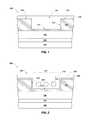
- FIG. 1is a partial cross-sectional schematic view of an embodiment of a semiconductor structure 100 of the present invention.
- the semiconductor structure 100may be provided, which, includes a substrate 102 , a dielectric material 104 , a semiconductive material 106 , and an insulative material 108 .
- the substrate 102may comprise a full or partial wafer of semiconductor material or a material such as glass or sapphire.
- the dielectric material 104may be provided over and in contact with a surface of the substrate 102 .
- the dielectric material 104may include silicon oxynitride (SiON), silicon nitride (Si 3 N 4 ), silicon dioxide (SiO 2 ), another oxide material, or a polymer material, and may be formed using, for example, CVD, PVD, or ALD.
- the semiconductive material 106may include, for example, a doped polysilicon material and may be formed over and in contact with the dielectric material 104 using conventional techniques, which are not described in detail herein.
- the insulative material 108may include an oxide such as silicon dioxide (SiO 2 ), and may be formed by CVD, by decomposing tetraethylorthosilicate (TEOS), or by any other process known in the art of integrated circuit fabrication.
- the semiconductor structure 100may have a trench 110 formed therein, the trench 110 filled with a block copolymer material 112 .
- the trench 110may be defined by a lower surface 111 and sidewalls 113 of the insulative material 108 .
- the semiconductor structure 100 depicted in the following drawingsincludes one trench 110 formed partially through a thickness of the insulative material 108 .
- a plurality of trenches 110may be formed in the semiconductor structure 100 .
- the trenches 110may be formed through a thickness of any of the underlying materials such as the semiconductive material 106 , the dielectric material 104 , and the substrate 102 .
- the trench 110may have a depth sufficient to form a monolayer of the block copolymer material 112 , which is described in further detail below.
- the trench 110may have a depth in a range of from about 15 nm to about 50 nm, and may be formed using, for example, patterning techniques (e.g., masking and etching) known in the art of integrated circuit fabrication.
- another dielectric material(not shown), such as silicon dioxide, may be formed over the sidewalls 113 and the lower surface 111 of the trenches 110 using a process such as atomic layer deposition (ALD).
- ALDatomic layer deposition
- the another dielectric materialmay be a thin, conformal film of a material that preferential wets a minority domain of the block copolymer material 112 , as will be described in further detail herein.
- the block copolymer material 112may be provided over the semiconductor structure 100 (i.e., an exposed surface of the insulative material 108 and within the trench 110 ).
- the block copolymer material 112may be deposited over the semiconductor structure 100 to a thickness sufficient to fill the trench 110 and to overlie surfaces 114 of the insulative material 108 .
- the block polymer material 112 overlying the surfaces 114 of the insulative material 108may be applied to have a thickness of less than or equal to a monolayer of the block copolymer material 112 .
- the block copolymer material 112may be applied by any suitable technique such as, for example, spin casting, spin coating, spraying, ink coating, or dip coating.
- the block copolymer material 112may include at least two copolymer blocks that are substantially immiscible in one another.
- the block copolymer material 112may be a diblock copolymer that includes a hydrophilic block and a hydrophobic block, which may be capable of undergoing phase separation, which is described in further detail below.
- the block copolymer material 112may include the hydrophilic block and the hydrophobic block at a ratio in a range of from about 80:20 by weight to about 50:50 by weight and, more specifically, at a ratio of about 70:30 by weight.
- the hydrophilic blockmay include a polymer formulated for swelling or wetting upon contact with a solvent, such as an alcohol.
- the hydrophilic block polymermay include polyvinylpyridine (PVP), hydroxypropyl methylcellulose (HPMC), polyethylene glycol (PEG), poly(ethylene oxide)-co-poly(propylene oxide) di- or multiblock copolymers, poly(ethylene oxide) (PEO), poly(vinyl alcohol) (PVA), poly(ethylene-co-vinyl alcohol), poly(acrylic acid), poly(ethyloxazoline), a poly(alkylacrylate), poly(acrylamide), a poly(N-alkylacrylamide), a poly(N,N-dialkylacrylamide), poly(propylene glycol) (PPG), poly(propylene oxide), partially or fully hydrolyzed poly(vinyl alcohol), dextran, and copolymers and combinations thereof.
- PVPpolyvinylpyridine
- HPMChydroxypropyl methylcellulose
- the hydrophobic blockmay include a polymer insoluble in the solvent, such as an alcohol, which results in swelling or wetting the hydrophilic block upon contact.
- the hydrophobic blockmay include polystyrene (PS), polyethylene (PE), polypropylene (PP), polychloroprene (CR), a polyvinyl ether, poly(vinyl acetate) (PVA c ), poly(vinyl chloride) (PVC), a polysiloxane, a polyurethane (PU), a polyacrylate, a polyacrylamide, and copolymers and mixtures thereof.
- block copolymer materials 112 that may be used for forming the self-assembled copolymermay include polystyrene-block-polyvinylpyridine (PS-b-PVP), polystyrene-block-polymethylmethacrylate (PS-b-PMMA), polyethyleneoxide-block-polyisoprene (PEO-b-PI), polyethyleneoxide-block-polybutadiene (PEO-b-PBD), polyethyleneoxide-block-polystyrene (PEO-b-PS), polyethyleneoxide-block-polymethylmethacrylate (PEO-b-PMMA), polyethyleneoxide-block-polyethylethylene (PEO-b-PEE), polystyrene-block-polyisoprene (PS-b-PI), polystyrene-block-polybutadiene (PS-b-PBD), polystyrene-block-polyferroceny
- the block copolymermay be a diblock copolymer.
- block copolymers having three (a triblock copolymer) or more (a multiblock copolymer) blocksmay also be used.
- a triblock copolymerincludes, but is not limited to, poly(styrene-block methyl methacrylate-block-ethylene oxide).
- Multiblock copolymersmay have three or more blocks selected from the following: polystyrene, polymethylmethacrylate, polyethyleneoxide, polyisoprene, polybutadiene, poly lactic acid, polyvinylpyridine, and combinations thereof.
- an annealing processmay be used to initiate phase separation between the copolymer blocks of the block copolymer material 112 .
- the block copolymer material 112may be annealed using, for example, thermal annealing, solvent vapor-assisted annealing, supercritical fluid-assisted annealing, or a combination thereof, which is described in further detail below.
- the block copolymer material 112may undergo phase separation wherein the sidewalls 113 of the trench 110 guide self-assembly, or self-registration, of the copolymer blocks of the block copolymer material 112 , which is often referred to as “graphoepitaxy,” so as to form a plurality of ordered domains 118 including at least one copolymer block within a matrix 120 of at least one different copolymer block.
- the ordered domains 118may include repeating structural units having a regular or defined order.
- the lower surface 111 and the sidewalls 113 of the trench 110may be most preferentially wetted by at least the minority block of the at least two copolymer blocks of the block copolymer material 112 .
- the preferential wetting of the minority copolymer block with both the lower surface 111 and sidewalls 113 of the trench 110results in the formation of the ordered domains 118 within the trench 110 .
- Each of the domains 118includes self-aggregated minority block portions of polymer chains held together by a non-covalent bond and is aligned parallel to an axis of the trench 110 .
- phase separation of the block copolymer material 112may result in the formation of a self-assembled film 116 including an ordered array 117 of domains 118 surrounded by the matrix 120 .
- the block copolymer material 112includes the hydrophilic block and the hydrophobic block
- the domains 118may include the hydrophilic block
- the matrix 120may include the hydrophobic block.
- the number of domains 118may be determined by the width of the trench 110 together with the inherent periodicity (Lo).
- the width of the trench 110may be controlled to form a number (n) of trenches determined width/periodicity, which may be for example, sufficient to form a number of domains 118 in a range of from about one to about fifty (50).
- an interface material 122 including the hydrophilic blockmay form at an interface between the matrix 120 and the underlying material of the insulative material 108 .
- the domains 118are shown in FIG. 2 as cylinders having an axis 125 parallel to the substrate 102 and horizontally aligned with sidewalls 113 of the trench 110 (i.e., parallel to a surface 111 of the trench 110 ).
- the domains 118may be cylinders having a diameter in a range of from about 5 nm to about 50 nm.
- the length of the domains 118may be substantially equal to the length of the trench 110 .
- the morphology of the self-assembled film 116may be controlled by the molecular weight and volume fraction of the copolymer blocks of the block copolymer to produce lamellar, cylindrical or spherical morphologies, among others.
- the block copolymer material 112includes polyvinylpyridine and polystyrene at a ratio of between about 80:20 and 60:40
- lamellar domains or alternating cylindersoften referred to as “stripes” of the polyvinylpyridine may be formed.
- the domains 118may be spherical units, hexagonal units, or any other shape that may be formed by the phase separation of the block copolymer material 112 .
- the block copolymer material 112may be heated to a temperature at or above a glass transition temperature and below a decomposition temperature of the copolymer blocks either in a vacuum or in an inert atmosphere, to cause the block copolymer material 112 to phase separate and form the self-assembled film 116 .
- the inert atmospheremay include, by way of non-limiting example, nitrogen or argon.
- the block copolymer material 112may be heated to a temperature in a range of from about 130° C. to about 275° C.
- the block copolymer material 112may be exposed to a solvent vapor to cause phase separation and the formation of ordered domains 118 .
- the solvent vapormay be formed by converting a solvent capable of initiating phase separation to the gas phase.
- the solvent vapormay be formed from toluene, tetrahydrofuran, dimethylformamide, and combinations thereof.
- the block copolymer material 112may be annealed exposing the block copolymer material 112 to toluene vapor at a temperature of greater than or equal to about 24° C.
- the copolymer block material 112is polystyrene-block-polyvinylpyridine
- the polyvinylpyridinemay preferentially wet the lower surface 111 and sidewalls 113 of the trench 110 during the annealing process, while the polystyrene may preferentially wet the air interface, resulting in the formation of the interface material 122 of polyvinylpyridine as well as repeating cylindrical domains 118 including polyvinylpyridine, each having an axis 125 parallel to an axis of the trench 110 and disposed within the matrix 120 including polystyrene.
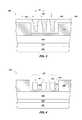
- the self-assembled film 116 shown in FIG. 2may be exposed to a swelling agent, which may permeate at least a portion of the ordered domains 118 ( FIG. 2 ) resulting in the formation of swollen domains 126 .
- the swelling agentmay cause a region of the swollen domains 126 to swell or rupture as shown in FIG. 3 , while remaining regions of the swollen domains 126 may maintain a shape substantially identical to or similar to a shape of the ordered domains 118 ( FIG. 2 ).
- the swelling agentmay laterally permeate the remaining regions of the swollen domains 126 via the intermittent regions that have swollen or ruptured.
- the swelling agentmay include a metal oxide precursor 124 and may be introduced to form swollen domains impregnated with the metal oxide precursor 124 .
- the swelling agentmay be applied to the self-assembled film 116 under anhydrous conditions such as, for example, in an atmosphere of an inert gas.
- the swollen domains 126may have a mushroom-like shape.
- the swollen domains 126may be laterally spaced from one another by a distance d 1 .
- the distance d 1may be, for example, less than or equal to about 50 nm, and more specifically, in a range of from about 5 nm to about 30 nm.
- the swelling agentcomprises polar solvent, such as an alcohol, and may be applied to form the swollen domains 126 prior to exposure to a metal oxide precursor.
- the swelling agentmay include only the metal oxide precursor 124 , or may include a mixture of a solvent, such as a polar solvent, and the metal oxide precursor 124 , and may selectively solubilize or permeate the domains 118 ( FIG. 2 ) without substantially solubilizing or substantially permeating the matrix 120 .
- the metal oxide precursor 124may be a metal-containing compound capable of selectively impregnating the domains 118 such as, for example, a cationic metal, a metal alkoxide, or a metal salt (e.g., a metal halide).
- the metal oxide precursor 124may be an isopropoxide, such as titanium tetraisopropoxide (C 12 H 28 O 4 Ti), tetraethylorthosilicate (TEOS), or poly(dimethylsiloxane) (PDMS).
- the solventmay be a liquid, gas, or vapor capable of swelling or wetting the domains 118 ( FIG. 2 ) without substantially wetting or substantially swelling the matrix 120 .
- the solventmay include, for example, a polar organic solvent, such as an alcohol, or water, or combinations thereof. If the domains 118 are formed from the hydrophilic polymer and the matrix 120 is formed from the hydrophobic polymer, the polar solvent may permeate the hydrophilic polymer without substantially permeating the hydrophobic polymer.
- a polar organic solventsuch as an alcohol, or water, or combinations thereof.
- the self-assembled film 116may be soaked in a solvent so that the domains 118 open and swell to form swollen domains 126 , as shown in FIG. 3 . Thereafter, the polymer material in the swollen domains 126 may be cross-linked in this soaked, extended form. Finally, the swollen domains 126 may be exposed to the metal oxide precursor 124 . By cross-linking the polymer material after formation of the swollen domains 126 , buckling or wrinkling resulting from swelling may be substantially reduced or prevented.
- the swelling agent including the metal oxide precursor 124may be applied to the self-assembled film 116 as a mixture of an alcohol, such as methanol, ethanol, or isopropanol, and titanium tetraisopropoxide having a volumetric ratio of about 2:1.
- the swelling agentmay be poly (dimethylsiloxane) dissolved in a solvent, which may be applied over the domains 118 by, for example, by spin-casting, and may be heated to about 80° C. and soaked for at least 6 hours to selectively permeate the domains 118 .
- the swelling agentmay include a neat metal oxide precursor 124 such as, for example, tetraethylorthosilicate, which may be applied to the self-assembled film 116 in the absence of another solvent.
- a neat metal oxide precursor 124such as, for example, tetraethylorthosilicate, which may be applied to the self-assembled film 116 in the absence of another solvent.
- the metal oxide precursor 124 of the swelling agentmay be absorbed into the domains 118 ( FIG. 2 ), forming the swollen domains 126 impregnated with the metal oxide precursor 124 .
- the self-assembled film 116may be exposed to the metal oxide precursor 124 for an amount of time sufficient for the metal oxide precursor 124 to impregnate the domains 118 , for example, from about 30 minutes to about 5 hours and, more specifically, for about 1 hour.
- the semiconductor structure 100may, optionally, be rinsed using a solution including another solvent such as, for example, a polar organic solvent or
- the swollen domains 126may be exposed to an oxidizing agent (represented by directional arrows 128 ), which converts the metal oxide precursor 124 within the swollen domains 126 to a metal oxide (not shown).
- the oxidizing agent 128may be, for example, air, oxygen, nitrogen dioxide, water, nitrogen tetroxide, ozone, or combinations thereof.
- the metal oxide precursor 124may be exposed to the oxidizing agent 128 in a sealed chamber for a length of time in a range of from about 1 minute to about 30 hours and, more particularly, about 16 hours.
- metal oxide precursor 124when the metal oxide precursor 124 is titanium tetraisopropoxide, water vapor may be applied to the swollen domains 126 in a reaction chamber for about 16 hours to form titanium dioxide.
- metal oxide precursor 124when the metal oxide precursor 124 is tetraethylorthosilicate, water vapor may be applied to the swollen domains 126 in a reaction chamber for about 16 hours to form silicon dioxide.
- a dry etching processsuch as a reactive ion etching (RIE), plasma etching process, a reactive ion beam etching process, or a chemically assisted ion beam etching process, may be performed to remove a portion of the matrix 120 from the semiconductor structure 100 leaving a metal oxide structures 130 .
- a portion of the matrix 120may remain after etching to form a lower region 131 of each of the metal oxide structures 130 .
- the dry etching processmay be performed such that each of the metal oxide structures 130 may have an upper surface below a surface of the insulative material 108 and may include a region 131 that includes the matrix 120 .
- an anisotropic reactive ion (i.e., plasma) etching process using oxygen as the etchantmay be performed to remove the polystyrene.
- the dry etchmay, optionally, remove at least a portion of polymer material remaining in the swollen domains 126 and the interface material 122 .
- the metal oxide structures 130may include a metal oxide material.
- the metal oxide structures 130may be laterally spaced from one another by a distance d 2 (i.e., the center-to-center distance between metal oxide structures 130 ), which may be about one-half the distance d 1 (i.e., the center-to-center distance between swollen domains 126 shown in FIG. 3 ).
- a portion of the insulative material 108may be exposed through apertures 134 between each of the metal oxide structures 130 .
- FIG. 5is a top-down view of the semiconductor structure 100 of FIG. 4 .
- a portion of the matrix 120may be removed using a conventional calcination process in a reactive ambient gas, such as oxygen or ammonia, to remove remaining organic residues.
- the resulting metal oxide structures 130may be densified or hardened in comparison to the swelled domains 126 ( FIG. 3 ).
- a conventional calcination processmay be performed to remove the remaining polymer material from the swollen domains 126 , the matrix 120 , and the interface material 122 .
- the calcination processmay be performed, for example, by exposing the semiconductor structure 100 to temperatures at or above a decomposition temperature of the polymer material.
- the semiconductor structure 100may be exposed to a temperature in a range of from about 300° C. to about 450° C. in a vacuum or in an inert atmosphere, such as argon or nitrogen.
- the semiconductor structure 100maybe exposed to ozone at a temperature in a range of from about 75° C. to about 95° C.
- the resulting semiconductor structure 100includes laterally spaced metal oxide structures (not shown), which may have a similar structure to the metal oxide structures 130 shown in FIG. 4 . Formation of the metal oxide structures 130 provides improved etch selectivity over the underlying materials in comparison to the domains 118 of the array 117 ( FIG. 2 ) and the metal oxide-impregnated swollen domains 126 ( FIG. 3 ). In this way, selective deposition of metal oxides into the specific regions of the self-assembled film 116 ( FIG. 2 ) may be used to form an etching mask having feature sizes of less than or equal to 30 nm.
- the metal oxide structures 130may be used as a mask to pattern the underlying materials using, for example, conventional etching techniques.
- the apertures 134 between the metal oxide structures 130may expose a surface 136 of the insulative material 108 .
- the insulative material 108may be removed using, for example, a dry etching process.
- the particular composition of the etchant used to remove the insulative material 108 exposed between apertures 134 selective to the metal oxide structures 130may be selected based on the materials used for the insulative material 108 and the metal oxide structures 130 .
- insulative material 108is silicon dioxide
- a conventional dry etching processmay be used to selectively remove the insulative material 108 without removing the metal oxide structures 130 , exposing the underlying semiconductive material 106 .
- a portion of the semiconductive material 106 exposed through the apertures 134may be selectively removed with respect to the metal oxide structures 130 using a dry plasma reactive ion etching (RIE) process. Subsequently, the underlying dielectric material 104 exposed through the apertures 134 may be removed using, for example, a dry plasma reactive ion etching (RIE) process. The semiconductive material 106 and the dielectric material 104 exposed through the apertures 134 may be removed using a single dry etching process or multiple dry etching processes.
- RIEdry plasma reactive ion etching
- a sample including a self-assembled film formed within trenches in a silicon dioxide materialwas used.
- a plurality of trenches having a width of about 200 nmwere formed in a silicon dioxide material over and in contact with a polycrystalline silicon substrate using conventional deposition process and patterning processes.
- a polystyrene-block-polyvinylpyridine block (PS-b-PVP) copolymer materialwas spin-cast over the plurality of trenches in the silicon dioxide material to fill each of the trenches.
- the PS-b-PVP block copolymerwas then heated to a temperature of about 200° C.
- PS-b-PVPself-assembled film
- ordered polyvinylpyridine (PVP) domainssurrounded by a polystyrene (PS) matrix within each of the plurality of trenches.
- PVPpolyvinylpyridine
- PSpolystyrene
- Each of the ordered PVP domainsmay have a width of about 20 nm.
- the samplewas immersed in tetraethylorthosilicate for about 2 hours at a temperature of about 25° C. in air ambient while the tetraethylorthosilicate was absorbed into the PVP block polymer without substantially absorbing into the PS matrix, which caused swelling of the PVP block polymer.
- tetraethylorthosilicatei.e., tetraethylorthosilicate which was not absorbed into the PVP block polymer
- tetraethylorthosilicatewhich was not absorbed into the PVP block polymer
- the tetraethylorthosilicate within the PVP block polymerwas immersed and stirred in a deionized water bath for about 10 minutes at a temperature of about 70° C. to form silicon dioxide lines.
- a rapid thermal annealwas performed to develop the silicon dioxide lines exposing the silicon dioxide lines to ozone at a temperature of about 85° C. for about 10 minutes and, thereafter, performing an oxygen plasma etching process for about 20 seconds.
- the samplewas placed in a solution including a mixture of 2 parts by volume ethanol and 1 part by volume titanium tetra(isopropoxide). For about 1 hour, the self-assembled film was exposed to the ethanol/titanium tetra(isopropoxide) solution, which permeated the PVP block copolymer without substantially permeating the PS matrix, causing the ordered PVP domains to swell.
- the self-assembled filmwas rinsed with ethanol to remove residual polymer material and was air dried.
- the samplewas then exposed to water vapor at a temperature of about 25° C. for about 16 hours, which resulted in conversion of titaniumtetra(isopropoxide) to titanium oxide within the ordered PVP domains.
- FIG. 7is an SEM image showing a top-down view of a sample 200 having titanium dioxide lines 202 within trenches 204 thereon. Each of the titanium dioxide lines 202 is horizontally aligned with sidewalls 206 of the trenches 204 .
- the samplewas exposed to a solution of tetraethylorthosilicate at about 24.0° C. for about 1 hour to enable the tetraethylorthosilicate to selectively penetrate the PVP domains.
- the samplewas then exposed to water vapor at a temperature of about 60.0° C. in the sealed reactor chamber for about 16 hours. After exposure to the water vapor, the TEOS within the PVP domains had been converted to silicon dioxide to form a plurality of silicon dioxide lines in the trenches.
- a reactive ion etching processwas performed using oxygen gas at a flow rate of about 20 sccm, a pressure of 50 mTorr, at about 34 Watts for about 120 seconds to remove the PS from the sample revealing silicon dioxide lines.
- a layer of tetraethylorthosilicatewas applied over the self-assembled film for about 2 hours to enable the tetraethylorthosilicate to permeate the PVP domains. Excess tetraethylorthosilicate was removed by spinning the sample at about 3000 rpm for about 3 seconds. Immediately after removal of the tetraethylorthosilicate, the sample was immersed in water at a temperature of about 70.0° C. for about 10 minutes.
- the samplewas dried and exposed to a vapor stream including 10% ozone/oxygen and was heated to a temperature of about 85.0° C. for about 10 minutes.
- the samplewas dried and exposed to an oxygen plasma at a pressure of about 100 mTorr, at about 300 Watts for about 20 seconds. After treatment with the oxygen plasma, silicon dioxide lines were revealed in the PVP domains.
Landscapes
- Chemical & Material Sciences (AREA)
- Engineering & Computer Science (AREA)
- Organic Chemistry (AREA)
- Physics & Mathematics (AREA)
- Chemical Kinetics & Catalysis (AREA)
- General Physics & Mathematics (AREA)
- Manufacturing & Machinery (AREA)
- Nanotechnology (AREA)
- Condensed Matter Physics & Semiconductors (AREA)
- Health & Medical Sciences (AREA)
- Polymers & Plastics (AREA)
- Medicinal Chemistry (AREA)
- Materials Engineering (AREA)
- Power Engineering (AREA)
- Microelectronics & Electronic Packaging (AREA)
- Computer Hardware Design (AREA)
- Wood Science & Technology (AREA)
- Life Sciences & Earth Sciences (AREA)
- Crystallography & Structural Chemistry (AREA)
- Mathematical Physics (AREA)
- Theoretical Computer Science (AREA)
- Inorganic Chemistry (AREA)
- Element Separation (AREA)
- Formation Of Insulating Films (AREA)
- Drying Of Semiconductors (AREA)
- Photosensitive Polymer And Photoresist Processing (AREA)
Abstract
Description
Claims (16)
Priority Applications (1)
| Application Number | Priority Date | Filing Date | Title |
|---|---|---|---|
| US15/044,713US9768021B2 (en) | 2007-04-18 | 2016-02-16 | Methods of forming semiconductor device structures including metal oxide structures |
Applications Claiming Priority (8)
| Application Number | Priority Date | Filing Date | Title |
|---|---|---|---|
| US11/787,928US7959975B2 (en) | 2007-04-18 | 2007-04-18 | Methods of patterning a substrate |
| US11/766,663US8294139B2 (en) | 2007-06-21 | 2007-06-21 | Multilayer antireflection coatings, structures and devices including the same and methods of making the same |
| US12/259,921US8097175B2 (en) | 2008-10-28 | 2008-10-28 | Method for selectively permeating a self-assembled block copolymer, method for forming metal oxide structures, method for forming a metal oxide pattern, and method for patterning a semiconductor structure |
| US13/157,838US8956713B2 (en) | 2007-04-18 | 2011-06-10 | Methods of forming a stamp and a stamp |
| US13/335,107US8669645B2 (en) | 2008-10-28 | 2011-12-22 | Semiconductor structures including polymer material permeated with metal oxide |
| US13/613,358US8551808B2 (en) | 2007-06-21 | 2012-09-13 | Methods of patterning a substrate including multilayer antireflection coatings |
| US14/176,574US9276059B2 (en) | 2007-04-18 | 2014-02-10 | Semiconductor device structures including metal oxide structures |
| US15/044,713US9768021B2 (en) | 2007-04-18 | 2016-02-16 | Methods of forming semiconductor device structures including metal oxide structures |
Related Parent Applications (1)
| Application Number | Title | Priority Date | Filing Date |
|---|---|---|---|
| US14/176,574DivisionUS9276059B2 (en) | 2007-04-18 | 2014-02-10 | Semiconductor device structures including metal oxide structures |
Publications (2)
| Publication Number | Publication Date |
|---|---|
| US20160163536A1 US20160163536A1 (en) | 2016-06-09 |
| US9768021B2true US9768021B2 (en) | 2017-09-19 |
Family
ID=42116662
Family Applications (4)
| Application Number | Title | Priority Date | Filing Date |
|---|---|---|---|
| US12/259,921Active2029-10-22US8097175B2 (en) | 2007-04-18 | 2008-10-28 | Method for selectively permeating a self-assembled block copolymer, method for forming metal oxide structures, method for forming a metal oxide pattern, and method for patterning a semiconductor structure |
| US13/335,107ActiveUS8669645B2 (en) | 2007-04-18 | 2011-12-22 | Semiconductor structures including polymer material permeated with metal oxide |
| US14/176,574ActiveUS9276059B2 (en) | 2007-04-18 | 2014-02-10 | Semiconductor device structures including metal oxide structures |
| US15/044,713ActiveUS9768021B2 (en) | 2007-04-18 | 2016-02-16 | Methods of forming semiconductor device structures including metal oxide structures |
Family Applications Before (3)
| Application Number | Title | Priority Date | Filing Date |
|---|---|---|---|
| US12/259,921Active2029-10-22US8097175B2 (en) | 2007-04-18 | 2008-10-28 | Method for selectively permeating a self-assembled block copolymer, method for forming metal oxide structures, method for forming a metal oxide pattern, and method for patterning a semiconductor structure |
| US13/335,107ActiveUS8669645B2 (en) | 2007-04-18 | 2011-12-22 | Semiconductor structures including polymer material permeated with metal oxide |
| US14/176,574ActiveUS9276059B2 (en) | 2007-04-18 | 2014-02-10 | Semiconductor device structures including metal oxide structures |
Country Status (5)
| Country | Link |
|---|---|
| US (4) | US8097175B2 (en) |
| KR (1) | KR101320287B1 (en) |
| CN (1) | CN102196991B (en) |
| TW (1) | TWI392643B (en) |
| WO (1) | WO2010062568A2 (en) |
Families Citing this family (95)
| Publication number | Priority date | Publication date | Assignee | Title |
|---|---|---|---|---|
| US8394483B2 (en) | 2007-01-24 | 2013-03-12 | Micron Technology, Inc. | Two-dimensional arrays of holes with sub-lithographic diameters formed by block copolymer self-assembly |
| US8083953B2 (en) | 2007-03-06 | 2011-12-27 | Micron Technology, Inc. | Registered structure formation via the application of directed thermal energy to diblock copolymer films |
| US8557128B2 (en) | 2007-03-22 | 2013-10-15 | Micron Technology, Inc. | Sub-10 nm line features via rapid graphoepitaxial self-assembly of amphiphilic monolayers |
| US7959975B2 (en) | 2007-04-18 | 2011-06-14 | Micron Technology, Inc. | Methods of patterning a substrate |
| US8097175B2 (en) | 2008-10-28 | 2012-01-17 | Micron Technology, Inc. | Method for selectively permeating a self-assembled block copolymer, method for forming metal oxide structures, method for forming a metal oxide pattern, and method for patterning a semiconductor structure |
| US8294139B2 (en) | 2007-06-21 | 2012-10-23 | Micron Technology, Inc. | Multilayer antireflection coatings, structures and devices including the same and methods of making the same |
| US8372295B2 (en) | 2007-04-20 | 2013-02-12 | Micron Technology, Inc. | Extensions of self-assembled structures to increased dimensions via a “bootstrap” self-templating method |
| US8404124B2 (en) | 2007-06-12 | 2013-03-26 | Micron Technology, Inc. | Alternating self-assembling morphologies of diblock copolymers controlled by variations in surfaces |
| US8080615B2 (en) | 2007-06-19 | 2011-12-20 | Micron Technology, Inc. | Crosslinkable graft polymer non-preferentially wetted by polystyrene and polyethylene oxide |
| KR101291223B1 (en) | 2007-08-09 | 2013-07-31 | 한국과학기술원 | Method of forming fine pattern using block copolymer |
| US8999492B2 (en) | 2008-02-05 | 2015-04-07 | Micron Technology, Inc. | Method to produce nanometer-sized features with directed assembly of block copolymers |
| US8101261B2 (en) | 2008-02-13 | 2012-01-24 | Micron Technology, Inc. | One-dimensional arrays of block copolymer cylinders and applications thereof |
| US8425982B2 (en) | 2008-03-21 | 2013-04-23 | Micron Technology, Inc. | Methods of improving long range order in self-assembly of block copolymer films with ionic liquids |
| US8426313B2 (en) | 2008-03-21 | 2013-04-23 | Micron Technology, Inc. | Thermal anneal of block copolymer films with top interface constrained to wet both blocks with equal preference |
| US8114300B2 (en) | 2008-04-21 | 2012-02-14 | Micron Technology, Inc. | Multi-layer method for formation of registered arrays of cylindrical pores in polymer films |
| US8114301B2 (en) | 2008-05-02 | 2012-02-14 | Micron Technology, Inc. | Graphoepitaxial self-assembly of arrays of downward facing half-cylinders |
| JP2010115832A (en)* | 2008-11-12 | 2010-05-27 | Panasonic Corp | Method for promoting self-formation of block copolymer and method for forming self-formation pattern of block copolymer using the method for promoting self-formation |
| GB0906680D0 (en)* | 2009-04-17 | 2009-06-03 | Univ Surrey | A low-k material |
| US8178011B2 (en)* | 2009-07-29 | 2012-05-15 | Empire Technology Development Llc | Self-assembled nano-lithographic imprint masks |
| US8071467B2 (en) | 2010-04-07 | 2011-12-06 | Micron Technology, Inc. | Methods of forming patterns, and methods of forming integrated circuits |
| KR101264256B1 (en)* | 2010-05-26 | 2013-05-22 | 이화여자대학교 산학협력단 | Method for preparing nano ring array and metal nanoparticle array |
| US8304493B2 (en) | 2010-08-20 | 2012-11-06 | Micron Technology, Inc. | Methods of forming block copolymers |
| JP5560147B2 (en)* | 2010-09-13 | 2014-07-23 | 東京エレクトロン株式会社 | Film-forming method and semiconductor device manufacturing method |
| US8921183B2 (en)* | 2010-12-08 | 2014-12-30 | Nanya Technology Corporation | Method for fabricating trench isolation structure |
| US8900963B2 (en) | 2011-11-02 | 2014-12-02 | Micron Technology, Inc. | Methods of forming semiconductor device structures, and related structures |
| EP2594995A1 (en)* | 2011-11-16 | 2013-05-22 | University College Cork | A method for providing a nanopattern of metal oxide nanostructures on a substrate |
| JP6020991B2 (en)* | 2012-06-28 | 2016-11-02 | 国立研究開発法人理化学研究所 | Fine pattern forming method, developer |
| EP2679516A1 (en) | 2012-06-29 | 2014-01-01 | University College Cork | An antimicrobial food package |
| WO2014010592A1 (en)* | 2012-07-10 | 2014-01-16 | 株式会社ニコン | Mark formation method and device manufacturing method |
| CN103633029B (en)* | 2012-08-28 | 2016-11-23 | 中国科学院微电子研究所 | Semiconductor structure and manufacturing method thereof |
| US9087699B2 (en) | 2012-10-05 | 2015-07-21 | Micron Technology, Inc. | Methods of forming an array of openings in a substrate, and related methods of forming a semiconductor device structure |
| KR101490405B1 (en) | 2012-10-19 | 2015-02-06 | 주식회사 엘지화학 | Forming method of metal nano-structure of metal nano-wire pattern or metal nano-mesh pattern |
| KR20140087904A (en)* | 2012-12-31 | 2014-07-09 | 삼성전자주식회사 | Methods of patterning block copolymer layers |
| CN103146115A (en)* | 2013-01-24 | 2013-06-12 | 厦门大学 | Polyhedral oligomeric silasesquioxane (POSS)-based load metal nanoparticle and preparation method thereof |
| WO2014124795A1 (en) | 2013-02-14 | 2014-08-21 | Asml Netherlands B.V. | Methods for providing spaced lithography features on a substrate by self-assembly of block copolymers |
| US8859433B2 (en)* | 2013-03-11 | 2014-10-14 | International Business Machines Corporation | DSA grapho-epitaxy process with etch stop material |
| US9229328B2 (en) | 2013-05-02 | 2016-01-05 | Micron Technology, Inc. | Methods of forming semiconductor device structures, and related semiconductor device structures |
| WO2014201396A1 (en)* | 2013-06-13 | 2014-12-18 | Kla-Tencor Corporation | On-product derivation and adjustment of exposure parameters in a directed self-assembly process |
| US9461242B2 (en) | 2013-09-13 | 2016-10-04 | Micron Technology, Inc. | Magnetic memory cells, methods of fabrication, semiconductor devices, memory systems, and electronic systems |
| US9608197B2 (en) | 2013-09-18 | 2017-03-28 | Micron Technology, Inc. | Memory cells, methods of fabrication, and semiconductor devices |
| US9177795B2 (en) | 2013-09-27 | 2015-11-03 | Micron Technology, Inc. | Methods of forming nanostructures including metal oxides |
| US9053923B2 (en)* | 2013-11-05 | 2015-06-09 | GlobalFoundries, Inc. | Methods for fabricating integrated circuits including topographical features for directed self-assembly |
| US10202480B2 (en) | 2013-12-06 | 2019-02-12 | Lg Chem, Ltd. | Block copolymer |
| WO2015084128A1 (en) | 2013-12-06 | 2015-06-11 | 주식회사 엘지화학 | Block copolymer |
| CN105960422B (en) | 2013-12-06 | 2019-01-18 | 株式会社Lg化学 | Block copolymer |
| JP6496318B2 (en) | 2013-12-06 | 2019-04-03 | エルジー・ケム・リミテッド | Block copolymer |
| EP3078690B1 (en) | 2013-12-06 | 2021-01-27 | LG Chem, Ltd. | Block copolymer |
| US20150160072A1 (en)* | 2013-12-06 | 2015-06-11 | Rensselaer Polytechnic Institute | Oriented backscattering wide dynamic-range optical radiation sensor |
| CN105899556B (en) | 2013-12-06 | 2019-04-19 | 株式会社Lg化学 | Block copolymer |
| JP6432846B2 (en) | 2013-12-06 | 2018-12-05 | エルジー・ケム・リミテッド | Block copolymer |
| CN105899560B (en) | 2013-12-06 | 2018-01-12 | 株式会社Lg化学 | Block copolymer |
| CN105934456B (en) | 2013-12-06 | 2018-09-28 | 株式会社Lg化学 | Block copolymer |
| WO2015084120A1 (en) | 2013-12-06 | 2015-06-11 | 주식회사 엘지화학 | Monomer and block copolymer |
| CN105899558B (en) | 2013-12-06 | 2018-09-18 | 株式会社Lg化学 | Block copolymer |
| CN105916904B (en) | 2013-12-06 | 2018-11-09 | 株式会社Lg化学 | block copolymer |
| JP6521975B2 (en) | 2013-12-06 | 2019-05-29 | エルジー・ケム・リミテッド | Block copolymer |
| WO2015084130A1 (en) | 2013-12-06 | 2015-06-11 | 주식회사 엘지화학 | Block copolymer |
| US9221957B2 (en)* | 2013-12-19 | 2015-12-29 | Brookhaven Science Associates, Llc | Patterning by area selective oxidation |
| CN104752188B (en)* | 2013-12-30 | 2019-11-05 | 北京大学 | A kind of in-situ synthetic method of metal oxide semiconductor |
| US10454024B2 (en) | 2014-02-28 | 2019-10-22 | Micron Technology, Inc. | Memory cells, methods of fabrication, and memory devices |
| US9281466B2 (en) | 2014-04-09 | 2016-03-08 | Micron Technology, Inc. | Memory cells, semiconductor structures, semiconductor devices, and methods of fabrication |
| US9269888B2 (en) | 2014-04-18 | 2016-02-23 | Micron Technology, Inc. | Memory cells, methods of fabrication, and semiconductor devices |
| JP6637495B2 (en)* | 2014-09-30 | 2020-01-29 | エルジー・ケム・リミテッド | Manufacturing method of patterned substrate |
| WO2016053011A1 (en) | 2014-09-30 | 2016-04-07 | 주식회사 엘지화학 | Block copolymer |
| CN107075053B (en) | 2014-09-30 | 2019-05-21 | 株式会社Lg化学 | Block copolymer |
| EP3203497B1 (en) | 2014-09-30 | 2023-11-29 | LG Chem, Ltd. | Method for producing patterned substrate |
| CN107075052B (en) | 2014-09-30 | 2020-05-29 | 株式会社Lg化学 | Block copolymer |
| WO2016053010A1 (en) | 2014-09-30 | 2016-04-07 | 주식회사 엘지화학 | Block copolymer |
| US10287429B2 (en) | 2014-09-30 | 2019-05-14 | Lg Chem, Ltd. | Block copolymer |
| JP6394798B2 (en) | 2014-09-30 | 2018-09-26 | エルジー・ケム・リミテッド | Block copolymer |
| KR101832031B1 (en)* | 2014-09-30 | 2018-02-23 | 주식회사 엘지화학 | Bl℃k copolymer |
| EP3202799B1 (en) | 2014-09-30 | 2021-08-25 | LG Chem, Ltd. | Block copolymer |
| CN107075050B (en) | 2014-09-30 | 2019-08-13 | 株式会社Lg化学 | Block copolymer |
| US9349945B2 (en)* | 2014-10-16 | 2016-05-24 | Micron Technology, Inc. | Memory cells, semiconductor devices, and methods of fabrication |
| US9768377B2 (en) | 2014-12-02 | 2017-09-19 | Micron Technology, Inc. | Magnetic cell structures, and methods of fabrication |
| WO2016090286A1 (en) | 2014-12-05 | 2016-06-09 | University Of Florida Research Foundation, Inc. | 3d printing using phase changing materials as support |
| US10439131B2 (en) | 2015-01-15 | 2019-10-08 | Micron Technology, Inc. | Methods of forming semiconductor devices including tunnel barrier materials |
| WO2016130953A1 (en) | 2015-02-13 | 2016-08-18 | University Of Florida Research Foundation, Inc. | High speed 3d printing system for wound and tissue replacement |
| US9530662B2 (en) | 2015-02-25 | 2016-12-27 | GlobalFoundries, Inc. | Methods for fabricating integrated circuits using directed self-assembly including a substantially periodic array of topographical features that includes etch resistant topographical features for transferability control |
| JP6998215B2 (en) | 2015-05-08 | 2022-02-10 | ユニバーシティ オブ フロリダ リサーチ ファンデーション インコーポレーティッド | Growth medium for 3D cell culture |
| US11027483B2 (en) | 2015-09-03 | 2021-06-08 | University Of Florida Research Foundation, Inc. | Valve incorporating temporary phase change material |
| CN105384952B (en)* | 2015-09-15 | 2018-01-23 | 北京航空航天大学 | A kind of regulation and control method being orientated using mechanical shear stress to Self-Assembling of Block Copolymer |
| WO2017096263A1 (en) | 2015-12-04 | 2017-06-08 | University Of Florida Research Foundation, Incorporated | Crosslinkable or functionalizable polymers for 3d printing of soft materials |
| EP3208829A1 (en)* | 2016-02-19 | 2017-08-23 | IMEC vzw | Metal or ceramic material hardened pattern |
| US10204782B2 (en)* | 2016-04-18 | 2019-02-12 | Imec Vzw | Combined anneal and selective deposition process |
| US11124644B2 (en)* | 2016-09-01 | 2021-09-21 | University Of Florida Research Foundation, Inc. | Organic microgel system for 3D printing of silicone structures |
| CN108227412A (en)* | 2016-12-15 | 2018-06-29 | Imec 非营利协会 | Photolithographic mask layer |
| CN108242477B (en)* | 2016-12-27 | 2020-03-24 | 中国科学院上海高等研究院 | Micro-contact wet etching preparation method of seed crystal substrate for layer transfer monocrystalline silicon thin film |
| US11725275B2 (en)* | 2017-07-13 | 2023-08-15 | Uchicago Argonne, Llc | Low refractive index surface layers and related methods |
| JP2019099749A (en)* | 2017-12-06 | 2019-06-24 | 東芝メモリ株式会社 | Pattern formation method, block copolymer, and pattern formation material |
| KR101989414B1 (en)* | 2018-01-02 | 2019-06-14 | 울산과학기술원 | Metal nanowires in micropatterns using block copolymers and preparing method thereof |
| US10586013B2 (en)* | 2018-01-30 | 2020-03-10 | International Business Machines Corporation | Calibration of directed self-assembly models using programmed defects of varying topology |
| WO2021101704A2 (en)* | 2019-11-03 | 2021-05-27 | Cornell University | Asymmetric porous materials, methods of making same, and uses thereof |
| US20240379768A1 (en)* | 2023-05-12 | 2024-11-14 | Applied Materials, Inc. | Method of forming a meol contact structure |
| US12398324B1 (en) | 2024-05-30 | 2025-08-26 | Tokyo Electron Limited | Methods for controlling the pitch of self-assembled ionic liquid crystal (ILC) structures |
Citations (320)
| Publication number | Priority date | Publication date | Assignee | Title |
|---|---|---|---|---|
| US4623674A (en) | 1985-06-21 | 1986-11-18 | Union Carbide Corporation | Polymer/polyols of substituted styrenes and polyurethanes made therefrom |
| US4797357A (en) | 1986-05-30 | 1989-01-10 | Eastman Kodak Company | Light-stable reducible compounds and analytical compositions, elements and methods utilizing same |
| US4818713A (en) | 1987-10-20 | 1989-04-04 | American Telephone And Telegraph Company, At&T Bell Laboratories | Techniques useful in fabricating semiconductor devices having submicron features |
| US4877647A (en) | 1986-04-17 | 1989-10-31 | Kansas State University Research Foundation | Method of coating substrates with solvated clusters of metal particles |
| WO1990007575A1 (en) | 1988-12-30 | 1990-07-12 | Anderson David M | Stabilized microporous materials and hydrogel materials |
| EP0184543B1 (en) | 1984-12-06 | 1991-01-30 | MANNESMANN Aktiengesellschaft | Adjuvant for the construction of roads |
| US5328810A (en) | 1990-05-07 | 1994-07-12 | Micron Technology, Inc. | Method for reducing, by a factor or 2-N, the minimum masking pitch of a photolithographic process |
| US5374367A (en) | 1992-08-07 | 1994-12-20 | Fujikura Kasei Co., Ltd. | Electro-sensitive composition |
| US5382373A (en) | 1992-10-30 | 1995-01-17 | Lord Corporation | Magnetorheological materials based on alloy particles |
| US5482656A (en) | 1993-03-04 | 1996-01-09 | Kabushiki Kaisha Toshiba | Non-linear optical devices employing a polysilane composition and a polysilane composition therefor |
| US5512131A (en) | 1993-10-04 | 1996-04-30 | President And Fellows Of Harvard College | Formation of microstamped patterns on surfaces and derivative articles |
| US5538655A (en) | 1994-06-29 | 1996-07-23 | Arthur D. Little, Inc. | Molecular complexes for use as electrolyte components |
| US5580700A (en) | 1992-11-25 | 1996-12-03 | Hoechst Celanese Corporation | Metal ion reduction in bottom anti-reflective coatings for use in semiconductor device formation |
| WO1997006013A1 (en) | 1995-08-04 | 1997-02-20 | International Business Machines Corporation | Lithographic surface or thin layer modification |
| US5620850A (en) | 1994-09-26 | 1997-04-15 | President And Fellows Of Harvard College | Molecular recognition at surfaces derivatized with self-assembled monolayers |
| US5622668A (en) | 1992-02-07 | 1997-04-22 | The United States Of America As Represented By The Secretary Of The Air Force | Method for preparing oriented polymer structures and said structures |
| US5772905A (en) | 1995-11-15 | 1998-06-30 | Regents Of The University Of Minnesota | Nanoimprint lithography |
| WO1998039645A1 (en) | 1997-03-07 | 1998-09-11 | Beckman Coulter, Inc. | A novel capillary |
| US5834583A (en) | 1995-07-27 | 1998-11-10 | Circe Biomedical, Inc. | Block copolymers |
| US5849810A (en) | 1993-08-06 | 1998-12-15 | Ciba Vision Corporation | Photocrosslinked polymers |
| US5879582A (en) | 1994-08-19 | 1999-03-09 | The Lubrizol Corporation | Electrorheological fluids of polar solids and organic semiconductors |
| US5879853A (en) | 1996-01-18 | 1999-03-09 | Kabushiki Kaisha Toshiba | Top antireflective coating material and its process for DUV and VUV lithography systems |
| JPH1180414A (en) | 1997-08-29 | 1999-03-26 | Res Dev Corp Of Japan | Double structure continuous porous body and method for producing the same |
| US5891356A (en) | 1990-08-30 | 1999-04-06 | Asahi Kasei Kogyo Kabushiki Kaisha | Homogeneous electrorheological fluid |
| US5948470A (en) | 1997-04-28 | 1999-09-07 | Harrison; Christopher | Method of nanoscale patterning and products made thereby |
| WO1999047570A1 (en) | 1998-03-18 | 1999-09-23 | University Of Rochester | Macromolecular self-assembly of microstructures, nanostructures, objects and mesoporous solids |
| US5958704A (en) | 1997-03-12 | 1999-09-28 | Ddx, Inc. | Sensing system for specific substance and molecule detection |
| WO2000002090A2 (en) | 1998-07-02 | 2000-01-13 | Massachusetts Institute Of Technology | Periodic porous and relief nanostructured articles |
| US6051869A (en) | 1996-06-26 | 2000-04-18 | Intel Corporation | Silicon-rich block copolymers to achieve unbalanced vias |
| WO2000031183A1 (en) | 1998-11-24 | 2000-06-02 | The Dow Chemical Company | A composition containing a cross-linkable matrix precursor and a poragen, and a porous matrix prepared therefrom |
| US6111323A (en) | 1997-12-30 | 2000-08-29 | International Business Machines Corporation | Reworkable thermoplastic encapsulant |
| US6153495A (en) | 1998-03-09 | 2000-11-28 | Intersil Corporation | Advanced methods for making semiconductor devices by low temperature direct bonding |
| US6207787B1 (en) | 1994-07-27 | 2001-03-27 | International Business Machines Corporation | Antireflective coating for microlithography |
| US6251791B1 (en) | 1999-07-20 | 2001-06-26 | United Microelectronics Corp. | Eliminating etching microloading effect by in situ deposition and etching |
| US6270946B1 (en) | 1999-03-18 | 2001-08-07 | Luna Innovations, Inc. | Non-lithographic process for producing nanoscale features on a substrate |
| US20010024768A1 (en) | 1996-02-26 | 2001-09-27 | Matsushita Electric Industrial Co., Ltd. | Pattern forming material and pattern forming method |
| US6309580B1 (en) | 1995-11-15 | 2001-10-30 | Regents Of The University Of Minnesota | Release surfaces, particularly for use in nanoimprint lithography |
| US6310138B1 (en) | 1998-06-05 | 2001-10-30 | Asahi Kasei Kabushiki Kaisha | Hydrogenated block copolymer and polypropylene resin composition containing the same |
| US6312971B1 (en) | 1999-08-31 | 2001-11-06 | E Ink Corporation | Solvent annealing process for forming a thin semiconductor film with advantageous properties |
| US20010049195A1 (en) | 2000-02-25 | 2001-12-06 | Chartered Semiconductor Manufacturing Ltd. | Non-metallic barrier formations for copper damascene type interconnects |
| WO2002018080A1 (en) | 2000-08-03 | 2002-03-07 | Upepo & Maji Inc. | Metal colloidal solution composition and conductor or ink for forming semiconductor pattern comprising it and method for forming conductor or semiconductor pattern |
| US6368871B1 (en) | 1997-08-13 | 2002-04-09 | Cepheid | Non-planar microstructures for manipulation of fluid samples |
| US20020055239A1 (en) | 2000-03-22 | 2002-05-09 | Mark Tuominen | Nanocylinder arrays |
| US6403382B1 (en) | 1998-12-08 | 2002-06-11 | Regents Of The University Of Minnesota | Attachment chemistry for organic molecules to silicon |
| US6414164B1 (en) | 2000-07-12 | 2002-07-02 | International Business Machines Corporation | Synthesis of soluble derivatives of sexithiophene and their use as the semiconducting channels in thin-film filed-effect transistors |
| US20020084429A1 (en) | 2000-10-17 | 2002-07-04 | Craighead Harold G. | Electron-beam patterning of functionalized self-assembled monolayers |
| US6423465B1 (en) | 2000-01-28 | 2002-07-23 | International Business Machines Corporation | Process for preparing a patterned continuous polymeric brush on a substrate surface |
| US6423474B1 (en) | 2000-03-21 | 2002-07-23 | Micron Technology, Inc. | Use of DARC and BARC in flash memory processing |
| WO2002081372A2 (en) | 2001-04-06 | 2002-10-17 | Carnegie Mellon University | A process for the preparation of nanostructured materials |
| US20020158342A1 (en) | 2001-03-14 | 2002-10-31 | Mark Tuominen | Nanofabrication |
| US20020158432A1 (en) | 2001-04-30 | 2002-10-31 | Wain Amir Waheed | Infocart |
| US6503841B1 (en) | 2000-07-07 | 2003-01-07 | Agere Systems Inc. | Oxide etch |
| US6506660B2 (en) | 2000-11-15 | 2003-01-14 | International Business Machines Corporation | Semiconductor with nanoscale features |
| US20030010241A1 (en) | 2001-03-28 | 2003-01-16 | Masamichi Fujihira | Patterning method with micro- contact printing and its printed product |
| US6517933B1 (en) | 2000-01-18 | 2003-02-11 | Nano-Tex, Llc | Hybrid polymer materials |
| US6518194B2 (en) | 2000-12-28 | 2003-02-11 | Thomas Andrew Winningham | Intermediate transfer layers for nanoscale pattern transfer and nanostructure formation |
| US6537920B1 (en) | 2001-03-16 | 2003-03-25 | Advanced Micro Devices, Inc. | Formation of vertical transistors using block copolymer lithography |
| US20030068639A1 (en) | 2001-08-31 | 2003-04-10 | Thomas Haneder | Detecting biochemical reactions |
| US6548830B1 (en) | 1996-05-22 | 2003-04-15 | Sony Corporation | Semiconductor device formed of single crystal grains in a grid pattern |
| US20030077452A1 (en) | 2001-07-17 | 2003-04-24 | Guire Patrick E. | Self assembling monolayer compositions |
| US20030080471A1 (en) | 2001-10-29 | 2003-05-01 | Chou Stephen Y. | Lithographic method for molding pattern with nanoscale features |
| US20030091752A1 (en) | 2001-10-05 | 2003-05-15 | Nealey Paul F. | Guided self-assembly of block copolymer films on interferometrically nanopatterned substrates |
| US6565764B2 (en) | 2000-08-11 | 2003-05-20 | Kabushiki Kaisha Toshiba | Method of manufacturing a material having a fine structure |
| US6566248B1 (en) | 2001-01-11 | 2003-05-20 | Advanced Micro Devices, Inc. | Graphoepitaxial conductor cores in integrated circuit interconnects |
| US6565763B1 (en) | 1999-06-07 | 2003-05-20 | Kabushiki Kaisha Toshiba | Method for manufacturing porous structure and method for forming pattern |
| JP2003155365A (en) | 2001-11-22 | 2003-05-27 | Toshiba Corp | Processing method and molded body |
| US6569528B2 (en) | 2001-06-23 | 2003-05-27 | Pacific Corporation | Amphiphilic biodegradable block copolymers and self-assembled polymer aggregates formed from the same in aqueous milieu |
| US20030100822A1 (en) | 2001-09-01 | 2003-05-29 | Seok Lew | Analyte measuring biosensor chip using image scanning system |
| US6573030B1 (en) | 2000-02-17 | 2003-06-03 | Applied Materials, Inc. | Method for depositing an amorphous carbon layer |
| WO2003045840A2 (en) | 2001-11-21 | 2003-06-05 | University Of Massachusetts | Mesoporous materials and methods |
| US20030108879A1 (en) | 2001-01-10 | 2003-06-12 | Symyx Technologies, Inc. | Polymer brushes for immobilizing molecules to a surface or substrate having improved stability |
| US6592764B1 (en) | 1997-12-09 | 2003-07-15 | The Regents Of The University Of California | Block copolymer processing for mesostructured inorganic oxide materials |
| US20030180522A1 (en) | 2002-03-22 | 2003-09-25 | Desimone Joseph M. | Methods of forming polymeric structures using carbon dioxide and polymeric structures formed thereby |
| US20030180966A1 (en) | 2002-03-20 | 2003-09-25 | Wisconsin Alumni Research Foundation | Optical imaging of nanostructured substrates |
| US20030178707A1 (en) | 2002-03-21 | 2003-09-25 | Abbott Donald C. | Preplated stamped small outline no-lead leadframes having etched profiles |
| US6635912B2 (en) | 2000-09-07 | 2003-10-21 | Nec Electronics Corporation | CMOS image sensor and manufacturing method thereof |
| US20030196748A1 (en) | 2002-04-22 | 2003-10-23 | International Business Machines Corporation | Process of fabricating a precision microcontact printing stamp |
| US20030218644A1 (en) | 2002-03-25 | 2003-11-27 | Takamitsu Higuchi | Board for electronic device, electronic device, ferroelectric memory, electronic apparatus, ink-jet recording head, and ink-jet printer |
| US20030235930A1 (en) | 2002-06-25 | 2003-12-25 | Lucent Technologies Inc. | Multi-impression nanofeature production |
| US6679996B1 (en) | 1999-10-05 | 2004-01-20 | Hoya Corporation | Metal oxide pattern forming method |
| US6682660B2 (en) | 1998-09-04 | 2004-01-27 | Mds Proteomics, Inc. | Ultrasonically generated paramagnetic polymer particles |
| US20040023287A1 (en) | 2002-08-02 | 2004-02-05 | Oliver Harnack | Method of attaching hydrophilic species to hydrophilic macromolecules and immobilizing the hydrophilic macromolecules on a hydrophobic surface |
| US20040028875A1 (en) | 2000-12-02 | 2004-02-12 | Van Rijn Cornelis Johannes Maria | Method of making a product with a micro or nano sized structure and product |
| US6699797B1 (en) | 2002-12-17 | 2004-03-02 | Intel Corporation | Method of fabrication of low dielectric constant porous metal silicate films |
| US20040058059A1 (en) | 2001-11-07 | 2004-03-25 | Linford Mathew Richard | Funtionalized patterned surfaces |
| US6713238B1 (en) | 1998-10-09 | 2004-03-30 | Stephen Y. Chou | Microscale patterning and articles formed thereby |
| TW584670B (en) | 2002-10-31 | 2004-04-21 | Academia Sinica | Fabrication of nanocomposite thin films for high density magnetic recording media |
| US20040076757A1 (en) | 2002-07-17 | 2004-04-22 | Jacobson Joseph M. | Templated monolayer polymerization and replication |
| EP1416303A2 (en) | 2002-10-30 | 2004-05-06 | Hitachi, Ltd. | Functioning substrate with a group of columnar micro pillars and its manufacturing method |
| US20040084298A1 (en) | 2002-10-31 | 2004-05-06 | Y.D. Yao | Fabrication of nanocomposite thin films for high density magnetic recording media |
| US20040109263A1 (en) | 2002-03-29 | 2004-06-10 | Shoichi Suda | Manufacturing process of a magnetic head, magnetic head, pattern formation method |
| US20040127001A1 (en) | 2002-12-27 | 2004-07-01 | International Business Machines Corporation | Robust ultra-low k interconnect structures using bridge-then-metallization fabrication sequence |
| US20040124092A1 (en) | 2002-12-30 | 2004-07-01 | Black Charles T. | Inorganic nanoporous membranes and methods to form same |
| US20040142578A1 (en) | 2002-03-28 | 2004-07-22 | Ulrich Wiesner | Thin film nanostructures |
| US6767693B1 (en) | 2002-07-30 | 2004-07-27 | Advanced Micro Devices, Inc. | Materials and methods for sub-lithographic patterning of contact, via, and trench structures in integrated circuit devices |
| US20040159633A1 (en) | 1993-10-04 | 2004-08-19 | President & Fellows Of Harvard University | Methods of etching articles via micro contact printing |
| US6781166B2 (en) | 1999-07-02 | 2004-08-24 | President & Fellows Of Harvard College | Nanoscopic wire-based devices and arrays |
| US6780492B2 (en) | 1999-03-02 | 2004-08-24 | International Business Machines Corporation | Substrates prepared by chemical amplification of self-assembled monolayers with spatially localized polymer brushes |
| US20040163758A1 (en) | 2000-04-21 | 2004-08-26 | International Business Machines Corporation | Patterning solution deposited thin films with self-assembled monolayers |
| US6797202B2 (en) | 1996-09-06 | 2004-09-28 | Bridgestone Corporaton | Particles for electro-rheological fluid |
| US20040192013A1 (en) | 2003-03-31 | 2004-09-30 | Ryu Myung Kwan | Method for fabricating single crystal silicon film |
| US6809210B2 (en) | 2001-06-12 | 2004-10-26 | Lucent Technologies Inc. | Method of solvating a metal in an aromatic organic liquid |
| US6812132B2 (en) | 2003-03-21 | 2004-11-02 | Intel Corporation | Filling small dimension vias using supercritical carbon dioxide |
| US20040222415A1 (en) | 2003-03-11 | 2004-11-11 | Industrial Technology Research Institute | Organic device including semiconducting layer aligned according to microgrooves of photoresist layer |
| JP2004335962A (en) | 2003-05-12 | 2004-11-25 | Seiko Epson Corp | Thin-film pattern forming method, device and manufacturing method thereof, electro-optical device, and electronic apparatus |
| US20040254317A1 (en) | 2003-06-12 | 2004-12-16 | Jinlian Hu | Methods for producing di-block polymers |
| US20040256615A1 (en) | 2001-07-09 | 2004-12-23 | Henning Sirringhaus | Lamellar polymer architecture |
| US20040256662A1 (en) | 2003-06-20 | 2004-12-23 | International Business Machines Corporation | Nonvolatile memory device using semiconductor nanocrystals and method of forming same |
| US20040265548A1 (en) | 2003-05-20 | 2004-12-30 | Rong-Ming Ho | Nanopatterned templates from oriented degradable diblock copolymer thin films |
| CN1562730A (en) | 2004-03-24 | 2005-01-12 | 哈尔滨工业大学 | Method for adjusting and controlling configuration of self-assembling block copolymer template oriented to nano micro machining |
| JP2005008882A (en) | 1999-06-07 | 2005-01-13 | Toshiba Corp | Porous structure manufacturing method, porous structure forming material, pattern forming method, pattern forming material, electrochemical cell, and hollow fiber filter |
| US20050008828A1 (en) | 2002-07-25 | 2005-01-13 | Trustees Of Stevens Institute Of Technology | Patterned polymer microgel and method of forming same |
| JP2005029779A (en) | 1999-06-07 | 2005-02-03 | Toshiba Corp | Pattern forming material, pattern forming method, method for producing porous structure, electrochemical cell, method for producing porous carbon structure, and porous carbon structure |
| TW200511364A (en) | 2003-02-12 | 2005-03-16 | Nantero Inc | Devices having horizontally-disposed nanofabric articles and methods of making the same |
| US20050062165A1 (en) | 2003-09-19 | 2005-03-24 | International Business Machines Corporation | Method of forming closed air gap interconnects and structures formed thereby |
| US20050074706A1 (en) | 2003-10-06 | 2005-04-07 | Robert Bristol | Enhancing photoresist performance using electric fields |
| US20050079486A1 (en) | 2003-09-23 | 2005-04-14 | Wiscnsin Alumni Research Foundation - | Using liquid crystals to detect affinity microcontact printed biomolecules |
| US6884842B2 (en) | 1997-10-14 | 2005-04-26 | Alnis Biosciences, Inc. | Molecular compounds having complementary surfaces to targets |
| US6887332B1 (en) | 2000-04-21 | 2005-05-03 | International Business Machines Corporation | Patterning solution deposited thin films with self-assembled monolayers |
| US6890703B2 (en) | 2002-03-06 | 2005-05-10 | International Business Machines Corporation | Preparation of crosslinked particles from polymers having activatible crosslinking groups |
| US6890624B1 (en) | 2000-04-25 | 2005-05-10 | Nanogram Corporation | Self-assembled structures |
| US20050100830A1 (en) | 2003-10-27 | 2005-05-12 | Molecular Imprints, Inc. | Methods for fabricating patterned features utilizing imprint lithography |
| US20050124135A1 (en) | 2003-11-25 | 2005-06-09 | Farrokh Ayazi | Methods of forming oxide masks with submicron openings and microstructures formed thereby |
| US20050120902A1 (en) | 2001-04-25 | 2005-06-09 | David Adams | Edge transfer lithography |
| US6908861B2 (en) | 2002-07-11 | 2005-06-21 | Molecular Imprints, Inc. | Method for imprint lithography using an electric field |
| US20050133697A1 (en) | 2003-12-23 | 2005-06-23 | Potyrailo Radislav A. | Sensor devices containing co-polymer substrates for analysis of chemical and biological species in water and air |
| US6911400B2 (en) | 2002-11-05 | 2005-06-28 | International Business Machines Corporation | Nonlithographic method to produce self-aligned mask, articles produced by same and compositions for same |
| US6913697B2 (en) | 2001-02-14 | 2005-07-05 | Science & Technology Corporation @ Unm | Nanostructured separation and analysis devices for biological membranes |
| US20050147841A1 (en) | 2002-03-22 | 2005-07-07 | Avto Tavkhelidze | Influence of surface geometry on metal properties |
| US20050159293A1 (en) | 2004-01-16 | 2005-07-21 | General Electric Company | Nanoscale ordered composites of covalent ceramics for high-temperature structural applications via block-copolymer-assisted assembly and method of making |
| US6924341B2 (en) | 2001-03-30 | 2005-08-02 | The Uab Research Foundation | Polymer formation in room temperature ionic liquids |
| US20050167651A1 (en) | 2002-02-06 | 2005-08-04 | Merkulov Vladimir I. | Controlled alignment catalytically grown nanostructures |
| US20050176256A1 (en) | 2004-02-10 | 2005-08-11 | Infineon Technologies Ag | Method for expanding a trench in a semiconductor structure |
| US6940485B2 (en) | 2003-01-15 | 2005-09-06 | Xerox Corporation | Flexible micron-thin display device |
| US6946332B2 (en) | 2002-03-15 | 2005-09-20 | Lucent Technologies Inc. | Forming nanoscale patterned thin film metal layers |
| US20050208752A1 (en) | 2004-03-19 | 2005-09-22 | Colburn Matthew E | Method for fabricating a self-aligned nanocolumnar airbridge and structure produced thereby |
| US6949456B2 (en) | 2002-10-31 | 2005-09-27 | Asm Japan K.K. | Method for manufacturing semiconductor device having porous structure with air-gaps |
| US6952436B2 (en) | 2000-11-14 | 2005-10-04 | Regents Of The University Of California | Inorganic/block copolymer-dye composites and dye doped mesoporous materials for optical and sensing applications |
| US6957608B1 (en) | 2002-08-02 | 2005-10-25 | Kovio, Inc. | Contact print methods |
| US20050238889A1 (en) | 2003-07-10 | 2005-10-27 | Nancy Iwamoto | Layered components, materials, methods of production and uses thereof |
| US20050238967A1 (en) | 2004-04-27 | 2005-10-27 | The Board Of Trustees Of The University Of Illinois | Composite patterning devices for soft lithography |
| US6962823B2 (en) | 2002-04-02 | 2005-11-08 | Nanosys, Inc. | Methods of making, positioning and orienting nanostructures, nanostructure arrays and nanostructure devices |
| US20050250053A1 (en) | 2004-05-06 | 2005-11-10 | Marsh Eugene P | Selective provision of a diblock copolymer material |
| WO2005122285A2 (en) | 2004-06-04 | 2005-12-22 | The Board Of Trustees Of The University Of Illinois | Methods and devices for fabricating and assembling printable semiconductor elements |
| WO2006003594A2 (en) | 2004-06-30 | 2006-01-12 | Koninklijke Philips Electronics N.V. | Soft lithographic stamp with a chemically patterned surface |
| WO2006003592A2 (en) | 2004-06-30 | 2006-01-12 | Koninklijke Philips Electronics N.V. | Soft lithographic stamp with a chemically patterned surface |
| US20060013956A1 (en) | 2004-04-20 | 2006-01-19 | Angelescu Dan E | Method and apparatus for providing shear-induced alignment of nanostructure in thin films |
| US20060014001A1 (en) | 2000-05-26 | 2006-01-19 | Hua Zhang | Fabrication of sub-50 nm solid-state nanostructures based on nanolithography |
| US20060024590A1 (en) | 2004-07-29 | 2006-02-02 | Sandhu Gurtej S | Methods of forming patterns in semiconductor constructions, methods of forming container capacitors, and methods of forming reticles configured for imprint lithography |
| US6995439B1 (en) | 2002-06-12 | 2006-02-07 | Novellus Systems, Inc. | Method of fabricating low dielectric constant dielectric films |
| JP2006036923A (en) | 2004-07-27 | 2006-02-09 | National Institute Of Advanced Industrial & Technology | Highly oriented film of block copolymer-clay nanocomposite and method for producing the same |
| US20060030495A1 (en) | 2004-08-06 | 2006-02-09 | Gregg George L Jr | Bullet lubrication formula |
| US6998152B2 (en) | 1999-12-20 | 2006-02-14 | Micron Technology, Inc. | Chemical vapor deposition methods utilizing ionic liquids |
| US20060035387A1 (en) | 1998-07-14 | 2006-02-16 | Zyomyx, Inc. | Non-specific binding resistant protein arrays and methods for making the same |
| US7001795B2 (en) | 2003-02-27 | 2006-02-21 | Micron Technology, Inc. | Total internal reflection (TIR) CMOS imager |
| US20060046079A1 (en) | 2004-09-01 | 2006-03-02 | Samsung Corning Co., Ltd. | Method for preparing surfactant-templated, mesoporous low dielectric film |
| US20060046484A1 (en) | 2004-09-02 | 2006-03-02 | Abatchev Mirzafer K | Method for integrated circuit fabrication using pitch multiplication |
| US20060046480A1 (en) | 2003-10-16 | 2006-03-02 | Ting Guo | Nanostructures, nanogrooves, and nanowires |
| JP2006055982A (en) | 2004-08-23 | 2006-03-02 | Ind Technol Res Inst | Nanopatterned templates from organized degradation diblock copolymer thin films |
| US7009227B2 (en) | 2003-06-16 | 2006-03-07 | Micron Technology, Inc. | Photodiode structure and image pixel structure |
| US20060060863A1 (en) | 2004-09-22 | 2006-03-23 | Jennifer Lu | System and method for controlling nanostructure growth |
| US20060062867A1 (en) | 2002-07-11 | 2006-03-23 | Molecular Imprints, Inc. | Formation of discontinuous films during an imprint lithography process |
| US20060078681A1 (en) | 2004-10-13 | 2006-04-13 | Kabushiki Kaisha Toshiba | Pattern forming method and method of processing a structure by use of same |
| US7037738B2 (en) | 2002-01-18 | 2006-05-02 | Kabushiki Kaisha Toshiba | Method of manufacturing a semiconductor light-emitting element |
| US20060097134A1 (en) | 2004-11-09 | 2006-05-11 | Rhodes Howard E | Image sensor and pixel having an anti-reflective coating over the photodiode |
| US20060105562A1 (en) | 2004-11-12 | 2006-05-18 | Seagate Technology Llc | Method to make nano structure below 25 nanometer with high uniformity on large scale |
| TWI256110B (en) | 2004-05-18 | 2006-06-01 | Ind Tech Res Inst | Nanopatterned templates from oriented degradable diblock copolymer thin films |
| US7060774B2 (en) | 2002-02-28 | 2006-06-13 | Merck Patent Gesellschaft | Prepolymer material, polymer material, imprinting process and their use |
| US20060128165A1 (en) | 2004-12-13 | 2006-06-15 | 3M Innovative Properties Company | Method for patterning surface modification |
| US20060124467A1 (en) | 2003-05-20 | 2006-06-15 | Industrial Technology Research Institute | Metal nanodot arrays and fabrication methods thereof |
| US20060134556A1 (en) | 2004-11-22 | 2006-06-22 | Wisconsin Alumni Research Foundation | Methods and compositions for forming aperiodic patterned copolymer films |
| US7066801B2 (en) | 2003-02-21 | 2006-06-27 | Dow Global Technologies, Inc. | Method of manufacturing a fixed abrasive material |
| US20060137554A1 (en) | 2004-11-10 | 2006-06-29 | Gregor Kron | Stamp for soft lithography, in particular micro contact printing and a method of preparing the same |
| US20060141245A1 (en) | 2003-10-17 | 2006-06-29 | Francesco Stellacci | Nanocontact printing |
| US20060141222A1 (en) | 2004-12-29 | 2006-06-29 | Fischer Paul B | Introducing nanotubes in trenches and structures formed thereby |
| US20060154466A1 (en) | 2004-01-15 | 2006-07-13 | Seung-Heon Lee | Fabrication method for arranging ultra-fine particles |
| US7077992B2 (en) | 2002-07-11 | 2006-07-18 | Molecular Imprints, Inc. | Step and repeat imprint lithography processes |
| WO2006076016A2 (en) | 2004-05-21 | 2006-07-20 | Krzysztof Matyjaszewski | Conducting polymers |
| WO2006078952A1 (en) | 2005-01-21 | 2006-07-27 | University Of California | Methods for fabricating a long-range ordered periodic array of nano-features, and articles comprising same |
| US7087267B2 (en) | 2001-11-29 | 2006-08-08 | International Business Machines Corporation | Materials and methods for immobilization of catalysts on surfaces and for selective electroless metallization |
| US20060192283A1 (en) | 2004-04-29 | 2006-08-31 | Benson Peter A | Semiconductor wafer assemblies |
| US20060205875A1 (en) | 2005-03-11 | 2006-09-14 | Cha Jennifer N | Materials having predefined morphologies and methods of formation thereof |
| US20060211871A1 (en) | 2003-12-31 | 2006-09-21 | Sheng Dai | Synthesis of ionic liquids |
| US7112617B2 (en) | 2003-04-22 | 2006-09-26 | International Business Machines Corporation | Patterned substrate with hydrophilic/hydrophobic contrast, and method of use |
| US20060217285A1 (en) | 2002-11-07 | 2006-09-28 | Mathias Destarac | Controlled structure copolymer comprising an amphoteric or zwitterionic part |
| TW200633925A (en) | 2004-11-23 | 2006-10-01 | Agilent Technologies Inc | System and method for controlling the size and/or distribution of catalyst nanoparticles for nanostructure growth |
| US7115305B2 (en) | 2002-02-01 | 2006-10-03 | California Institute Of Technology | Method of producing regular arrays of nano-scale objects using nano-structured block-copolymeric materials |
| US7115995B2 (en) | 2000-12-20 | 2006-10-03 | Intel Corporation | Structural reinforcement of highly porous low k dielectric films by Cu diffusion barrier structures |
| US7118784B1 (en) | 2005-06-27 | 2006-10-10 | The Regents Of The University Of California | Method and apparatus for controlling nucleation in self-assembled films |
| US7119321B2 (en) | 2003-07-01 | 2006-10-10 | Micron Technology, Inc. | Optical channels for multi-level metal optical imagers |
| US20060228635A1 (en) | 2005-04-07 | 2006-10-12 | Suleski Thomas J | Method and apparatus for fabricating shaped structures and shaped structures including one- , two- or three-dimensional patterns incorporated therein |
| US7132370B2 (en) | 2003-08-01 | 2006-11-07 | Interuniversitair Microelektronica Centrum (Imec) | Method for selective removal of high-k material |
| US20060249784A1 (en) | 2005-05-06 | 2006-11-09 | International Business Machines Corporation | Field effect transistor device including an array of channel elements and methods for forming |
| US7135241B2 (en) | 2002-05-24 | 2006-11-14 | Board Of Regents, The University Of Texas System | Light-emitting block copolymers composition, process and use |
| US7135523B2 (en) | 2003-03-14 | 2006-11-14 | Industrial Technology Research Institute | Nanoscale helical microstructures and channels from chiral poly(L-lactide) block containing block copolymers |
| US20060258159A1 (en) | 2005-05-16 | 2006-11-16 | International Business Machines Corporation | Process for preparing electronics structures using a sacrificial multilayer hardmask scheme |
| US20060254440A1 (en) | 2005-04-13 | 2006-11-16 | Korea Institute Of Machinery & Materials | Method and apparatus for manufacturing electronic device using roll-to-roll rotary pressing process |
| US20060255505A1 (en) | 2005-05-11 | 2006-11-16 | Micron Technology, Inc. | Imprint templates for imprint lithography, and methods of patterning a plurality of substrates |
| US20060257633A1 (en) | 2005-04-27 | 2006-11-16 | Hitachi Maxell, Ltd. | Method for modifying surface of polymer substrate, method for forming plated film on polymer substrate, method for producing polymer member, and coating member |
| KR20060128378A (en) | 2005-06-10 | 2006-12-14 | 주식회사 하이닉스반도체 | Manufacturing method of phase change memory device |
| US20060281266A1 (en) | 2005-06-09 | 2006-12-14 | Wells David H | Method and apparatus for adjusting feature size and position |
| US20060278158A1 (en) | 2005-06-08 | 2006-12-14 | Tolbert Sarah H | Ordered vertically oriented porous inorganic films produced through solution processing |
| US20060286305A1 (en) | 2003-05-20 | 2006-12-21 | Thies Jens Christoph J | Hydrophobic coatings comprising reactive nano-particles |
| US20060286490A1 (en) | 2005-06-17 | 2006-12-21 | Sandhu Gurtej S | Methods of making templates for use in imprint lithography and related structures |
| US20060292777A1 (en) | 2005-06-27 | 2006-12-28 | 3M Innovative Properties Company | Method for making electronic devices using metal oxide nanoparticles |
| US7163712B2 (en) | 2000-03-03 | 2007-01-16 | Duke University | Microstamping activated polymer surfaces |
| US7166304B2 (en) | 1998-01-07 | 2007-01-23 | Debio Recherche Pharmaceutique S.A. | Degradable heterobifunctional poly(ethylene glycol) acrylates |
| US20070020749A1 (en) | 2005-03-23 | 2007-01-25 | Wisconsin Alumni Research Foundation | Materials and methods for creating imaging layers |
| US20070023247A1 (en) | 2005-07-27 | 2007-02-01 | Ulicny John C | Magnetorheological fluid device |
| US20070023805A1 (en) | 2005-07-26 | 2007-02-01 | Wells David H | Reverse construction memory cell |
| WO2007019439A2 (en) | 2005-08-04 | 2007-02-15 | Angiotech International Ag | Block copolymer compositions and uses thereof |
| WO2007024323A2 (en) | 2005-06-17 | 2007-03-01 | The University Of North Carolina At Chapel Hill | Nanoparticle fabrication methods, systems, and materials |
| WO2007024241A2 (en) | 2004-09-10 | 2007-03-01 | Ut-Battelle Llc | Highly ordered porous carbon materials having well defined nanostructures and method of synthesis |
| US20070045642A1 (en) | 2005-08-25 | 2007-03-01 | Micron Technology, Inc. | Solid-state imager and formation method using anti-reflective film for optical crosstalk reduction |
| US20070045562A1 (en) | 2005-08-29 | 2007-03-01 | Micron Technology, Inc. | Systems and methods for controlling ambient pressure during processing of microfeature workpieces, including during immersion lithography |
| US7186613B2 (en) | 2002-05-30 | 2007-03-06 | Air Products And Chemicals, Inc. | Low dielectric materials and methods for making same |
| US7189430B2 (en) | 2002-02-11 | 2007-03-13 | Rensselaer Polytechnic Institute | Directed assembly of highly-organized carbon nanotube architectures |
| US20070071881A1 (en) | 2003-08-11 | 2007-03-29 | Lay-Lay Chua | Method of making a polymer device |
| US20070072403A1 (en) | 2005-09-27 | 2007-03-29 | Oki Electric Industry Co., Ltd. | Semiconductor device and method for fabricating the same |
| US7202308B2 (en) | 2000-12-21 | 2007-04-10 | Atofina | Hydrogenation method for unsaturated block copolymers and hydrogenated unsaturated block copolymers |
| US7208836B2 (en) | 1996-02-06 | 2007-04-24 | Micron Technology, Inc. | Integrated circuitry and a semiconductor processing method of forming a series of conductive lines |
| WO2007055041A1 (en) | 2005-11-10 | 2007-05-18 | National University Corporation Kyoto Institute Of Technology | Membrane of block copolymer with oriented cylinder structure and process for producing the same |
| US20070122749A1 (en) | 2005-11-30 | 2007-05-31 | Fu Peng F | Method of nanopatterning, a resist film for use therein, and an article including the resist film |
| US20070122932A1 (en) | 2001-10-05 | 2007-05-31 | Cabot Corporation | Methods and compositions for the formation of recessed electrical features on a substrate |
| US20070138131A1 (en) | 2003-11-05 | 2007-06-21 | Dirk Burdinski | Method of forming a patterned layer on a substrate |
| JP2007194175A (en) | 2006-01-23 | 2007-08-02 | Seiko Epson Corp | Conductor pattern ink, conductor pattern, wiring board, electro-optical device, and electronic device |
| US20070175859A1 (en) | 2006-02-02 | 2007-08-02 | International Business Machines Corporation | Methods for forming improved self-assembled patterns of block copolymers |
| US7252791B2 (en) | 2001-09-17 | 2007-08-07 | Peter Wasserscheid | Ionic liquids |
| US20070181870A1 (en) | 2006-01-18 | 2007-08-09 | Consiglio Nazionale Delle Ricerche | Nanometric Device for the Measurement of the Conductivity and Quantum Effects of Individual Molecules and Methods for the Manufacture and Use Thereof |
| US20070183035A1 (en) | 2005-10-31 | 2007-08-09 | Koji Asakawa | Short-wavelength polarizing elements and the manufacture and use thereof |
| US7259101B2 (en) | 2003-01-08 | 2007-08-21 | Kovio, Inc. | Nanoparticles and method for making the same |
| US20070194403A1 (en) | 2006-02-23 | 2007-08-23 | International Business Machines Corporation | Methods for fabricating semiconductor device structures with reduced susceptibility to latch-up and semiconductor device structures formed by the methods |
| US20070208159A1 (en) | 2006-03-02 | 2007-09-06 | General Electric Company | Poly(arylene ether) block copolymer compositions, methods, and articles |
| US20070224819A1 (en) | 2006-03-23 | 2007-09-27 | Micron Technology, Inc. | Topography directed patterning |
| US20070222995A1 (en) | 2006-03-27 | 2007-09-27 | Jennifer Lu | Artifact having a textured metal surface with nanometer-scale features and method for fabricating same |
| US7279396B2 (en) | 2004-04-01 | 2007-10-09 | Micron Technology, Inc. | Methods of forming trench isolation regions with nitride liner |
| US7282240B1 (en) | 1998-04-21 | 2007-10-16 | President And Fellows Of Harvard College | Elastomeric mask and use in fabrication of devices |
| US20070249117A1 (en) | 2006-04-19 | 2007-10-25 | Kang Kyong-Rim | Polymer resin composition, related method for forming a pattern, and related method for fabricating a capacitor |
| KR100771886B1 (en) | 2006-09-27 | 2007-11-01 | 삼성전자주식회사 | Method for forming micro contact hole using block copolymer and method for manufacturing semiconductor device |
| TW200740602A (en) | 2006-01-20 | 2007-11-01 | Plextronics Inc | Electrostatic coatings and articles comprising polythiophenes |
| US20070281220A1 (en) | 2006-06-02 | 2007-12-06 | Sandhu Gurtej S | Topography based patterning |
| US20070293041A1 (en) | 2006-06-19 | 2007-12-20 | International Business Machines Corporation | Sub-lithographic feature patterning using self-aligned self-assembly polymers |
| US20070289943A1 (en) | 2006-06-14 | 2007-12-20 | Jennifer Lu | Block copolymer mask for defining nanometer-scale structures |
| US7326514B2 (en) | 2003-03-12 | 2008-02-05 | Cornell Research Foundation, Inc. | Organoelement resists for EUV lithography and methods of making the same |
| US20080038467A1 (en) | 2006-08-11 | 2008-02-14 | Eastman Kodak Company | Nanostructured pattern method of manufacture |
| US20080038923A1 (en) | 2004-01-30 | 2008-02-14 | International Business Machines Corporation | Device and methodology for reducing effective dielectric constant in semiconductor devices |
| US20080041818A1 (en) | 2006-08-15 | 2008-02-21 | Kabushiki Kaisha Toshiba | Method for pattern formation |
| JP2008036491A (en) | 2006-08-03 | 2008-02-21 | Nippon Telegr & Teleph Corp <Ntt> | Pattern forming method and mold |
| US20080047930A1 (en) | 2006-08-23 | 2008-02-28 | Graciela Beatriz Blanchet | Method to form a pattern of functional material on a substrate |
| US20080064217A1 (en) | 2006-09-11 | 2008-03-13 | Samsung Electronics Company, Ltd. | Methods of Forming Semiconductor Devices Using Di-Block Polymer Layers |
| US20080073743A1 (en) | 2006-02-17 | 2008-03-27 | Lockheed Martin Corporation | Templated growth of semiconductor nanostructures, related devices and methods |
| US20080078999A1 (en) | 2006-10-02 | 2008-04-03 | Han-Chung Lai | Multi-domain vertical alignment pixel structure and fabrication method thereof |
| US20080078982A1 (en) | 2006-09-29 | 2008-04-03 | Min Kyu S | Current focusing memory architecture for use in electrical probe-based memory storage |
| US20080083991A1 (en) | 2006-10-04 | 2008-04-10 | International Business Machines Corporation | Sub-lithographic local interconnects, and methods for forming same |
| US20080093743A1 (en) | 2006-10-19 | 2008-04-24 | International Business Machines Corporation | Sub-lithographic nano interconnect structures, and method for forming same |
| US20080103256A1 (en) | 2006-10-30 | 2008-05-01 | Kim Ho-Cheol | Self-assembled lamellar microdomains and method of alignment |
| US7368314B2 (en) | 2005-02-04 | 2008-05-06 | Infineon Technologies Ag | Method for fabricating a resistive memory |
| WO2008055137A2 (en) | 2006-10-31 | 2008-05-08 | International Business Machines Corporation | Si-containing polymers for nano-pattern device fabrication |
| US20080164558A1 (en) | 2007-01-09 | 2008-07-10 | International Business Machines Corporation | Method for fabricating shallow trench isolation structures using diblock copolymer patterning |
| US20080176767A1 (en) | 2007-01-24 | 2008-07-24 | Micron Technology, Inc. | Two-dimensional arrays of holes with sub-lithographic diameters formed by block copolymer self-assembly |
| US20080174726A1 (en)* | 2007-01-22 | 2008-07-24 | Samsung Electronics Co., Ltd. | Liquid Crystal Display |
| WO2008096335A2 (en) | 2007-02-07 | 2008-08-14 | Yeda Research And Development Co. Ltd. | Producing an array of nanoscale structures on a substrate surface via a self-assembled template |
| WO2008097736A2 (en) | 2007-02-08 | 2008-08-14 | Micron Technology, Inc. | Methods using block copolymer self-assembly for sub-lithographic patterning |
| US20080191200A1 (en) | 2007-02-08 | 2008-08-14 | Regents Of The University Of Minnesota | Ion gels and electronic devices utilizing ion gels |
| US20080217292A1 (en) | 2007-03-06 | 2008-09-11 | Micron Technology, Inc. | Registered structure formation via the application of directed thermal energy to diblock copolymer films |
| US20080233297A1 (en) | 2007-03-23 | 2008-09-25 | Xerox Corporation | Methods of forming a photoreceptor device having a self-assembled patterned binder layer |
| US20080233323A1 (en) | 2007-03-23 | 2008-09-25 | Joy Cheng | Orienting, positioning, and forming nanoscale structures |
| US20080241218A1 (en) | 2007-03-01 | 2008-10-02 | Mcmorrow David | Coated medical devices for abluminal drug delivery |
| WO2008118635A2 (en) | 2007-03-22 | 2008-10-02 | Micron Technology, Inc. | Sub-10 nm line features via rapid graphoepitaxial self-assembly of amphipilic monolayers |
| US20080257187A1 (en) | 2007-04-18 | 2008-10-23 | Micron Technology, Inc. | Methods of forming a stamp, methods of patterning a substrate, and a stamp and a patterning system for same |
| WO2008130847A1 (en) | 2007-04-20 | 2008-10-30 | Micron Technology, Inc. | Extensions of self-assembled structures to increased dimensions via a 'bootstrap' self-templating method |
| WO2008145268A1 (en) | 2007-05-26 | 2008-12-04 | Forschungszentrum Karlsruhe Gmbh | Die for micro-contact printing and method for the production thereof |
| US20080311347A1 (en) | 2007-06-12 | 2008-12-18 | Millward Dan B | Alternating Self-Assembling Morphologies of Diblock Copolymers Controlled by Variations in Surfaces |
| US20080315270A1 (en) | 2007-06-21 | 2008-12-25 | Micron Technology, Inc. | Multilayer antireflection coatings, structures and devices including the same and methods of making the same |
| US20080318005A1 (en) | 2007-06-19 | 2008-12-25 | Millward Dan B | Crosslinkable Graft Polymer Non-Preferentially Wetted by Polystyrene and Polyethylene Oxide |
| US20090062470A1 (en) | 2007-08-31 | 2009-03-05 | Micron Technology, Inc. | Zwitterionic block copolymers and methods |
| US20090087664A1 (en) | 2005-10-14 | 2009-04-02 | Wisconsin Alumni Research Foundation | Directed assembly of triblock copolymers |
| US7521090B1 (en) | 2008-01-12 | 2009-04-21 | International Business Machines Corporation | Method of use of epoxy-containing cycloaliphatic acrylic polymers as orientation control layers for block copolymer thin films |
| US20090148795A1 (en)* | 2007-12-05 | 2009-06-11 | International Business Machines Corporation | Patterning method using a combination of photolithography and copolymer self-assemblying lithography techniques |
| US20090196488A1 (en) | 2007-12-07 | 2009-08-06 | Wisconsin Alumni Research Foundation | Density multiplication and improved lithography by directed block copolymer assembly |
| US20090200646A1 (en) | 2008-02-13 | 2009-08-13 | Millward Dan B | One-Dimensional Arrays of Block Copolymer Cylinders and Applications Thereof |
| WO2009099924A2 (en) | 2008-02-05 | 2009-08-13 | Micron Technology, Inc. | Method to produce nanometer-sized features with directed assembly of block copolymers |
| US20090206489A1 (en) | 2008-02-20 | 2009-08-20 | International Business Machines Corporation | Dual damascene metal interconnect structure having a self-aligned via |
| US20090212016A1 (en) | 2008-02-22 | 2009-08-27 | International Business Machines Corporation | Aligning polymer films |
| US20090218567A1 (en) | 2008-02-29 | 2009-09-03 | Varughese Mathew | Conductive bridge random access memory device and method of making the same |
| US7585741B2 (en) | 2004-07-19 | 2009-09-08 | Micron Technology, Inc. | Methods of forming capacitors |
| US20090240001A1 (en) | 2008-03-21 | 2009-09-24 | Jennifer Kahl Regner | Methods of Improving Long Range Order in Self-Assembly of Block Copolymer Films with Ionic Liquids |
| WO2009117243A1 (en) | 2008-03-21 | 2009-09-24 | Micron Technology, Inc. | Thermal anneal of a block copolymer films with top interface constrained to wet both blocks with equal preference |
| US20090263628A1 (en) | 2008-04-21 | 2009-10-22 | Millward Dan B | Multi-Layer Method for Formation of Registered Arrays of Cylindrical Pores in Polymer Films |
| US20090267058A1 (en) | 2006-05-22 | 2009-10-29 | Ebinazar Benjamin Namdas | Solution-processed inorganic films for organic thin film transistors |
| WO2009134635A2 (en) | 2008-05-02 | 2009-11-05 | Micron Technology, Inc. | Graphoepitaxial self-assembly of arrays of downward facing half-cylinders |
| US20090317540A1 (en) | 2008-06-18 | 2009-12-24 | Gurtej Sandhu | Methods Of Forming A Non-Volatile Resistive Oxide Memory Array |
| US7655383B2 (en) | 2005-09-05 | 2010-02-02 | DWI an der RWTH | Photochemical method for manufacturing nanometrically surface-decorated substrates |
| US7658773B2 (en) | 2006-09-29 | 2010-02-09 | Qimonda Ag | Method for fabricating a solid electrolyte memory device and solid electrolyte memory device |
| US20100092873A1 (en) | 2008-10-09 | 2010-04-15 | Scott Sills | Methods Of Utilizing Block Copolymer To Form Patterns |
| US20100102415A1 (en) | 2008-10-28 | 2010-04-29 | Micron Technology, Inc. | Methods for selective permeation of self-assembled block copolymers with metal oxides, methods for forming metal oxide structures, and semiconductor structures including same |
| US20100124826A1 (en) | 2008-11-17 | 2010-05-20 | Dan Millward | Methods Of Utilizing Block Copolymer To Form Patterns |
| US20100137496A1 (en) | 2008-12-02 | 2010-06-03 | Dan Millward | Block Copolymer-Comprising Compositions and Methods of Purifying PS-b-PXVP |
| EP1593164B1 (en) | 2003-02-12 | 2010-06-30 | Nantero, Inc. | Devices having vertically-disposed nanofabric articles and methods of making the same |
| US7767099B2 (en) | 2007-01-26 | 2010-08-03 | International Business Machines Corporaiton | Sub-lithographic interconnect patterning using self-assembling polymers |
| US20100323096A1 (en) | 2009-06-22 | 2010-12-23 | Scott Sills | Methods Of Utlizing Block Copolymer To Form Patterns |
| US7888228B2 (en) | 2007-04-05 | 2011-02-15 | Adesto Technology Corporation | Method of manufacturing an integrated circuit, an integrated circuit, and a memory module |
| US8039196B2 (en) | 2007-08-09 | 2011-10-18 | Samsung Electronics Co., Ltd. | Method of forming fine patterns using a block copolymer |
| US20120028471A1 (en) | 2010-02-19 | 2012-02-02 | Tokyo Electron Limited | Method of manufacturing a semiconductor device |
| US8114306B2 (en) | 2009-05-22 | 2012-02-14 | International Business Machines Corporation | Method of forming sub-lithographic features using directed self-assembly of polymers |
| US20120135159A1 (en) | 2010-11-30 | 2012-05-31 | Seagate Technology Llc | System and method for imprint-guided block copolymer nano-patterning |
| US20120135146A1 (en) | 2010-11-30 | 2012-05-31 | Jsr Corporation | Methods of forming topographical features using segregating polymer mixtures |
| US8206601B2 (en) | 2009-12-18 | 2012-06-26 | Hitachi Global Storage Technologies Netherlands B.V. | Supporting membranes on nanometer-scale self-assembled films |
| US20120164389A1 (en) | 2010-12-28 | 2012-06-28 | Yang Xiaomin | Imprint template fabrication and repair based on directed block copolymer assembly |
| US20120202017A1 (en) | 2011-02-07 | 2012-08-09 | Wisconsin Alumni Research Foundation | Solvent annealing block copolymers on patterned substrates |
| US20120211871A1 (en) | 2008-09-19 | 2012-08-23 | Russell Thomas P | Method of producing nanopatterned articles, and articles produced thereby |
| US8287749B2 (en) | 2008-12-22 | 2012-10-16 | Hitachi, Ltd. | High-molecular thin film, pattern medium and manufacturing method thereof |
| US20130105755A1 (en) | 2011-11-02 | 2013-05-02 | Micron Technology, Inc. | Methods of forming semiconductor device structures, and related structures |
| US20130330668A1 (en) | 2012-06-08 | 2013-12-12 | Az Electronic Materials (Luxembourg) S.A.R.L. | Neutral layer polymer composition for directed self assembly and processes thereof |
| US20140097520A1 (en) | 2012-10-05 | 2014-04-10 | Micron Technology, Inc. | Methods of forming an array of openings in a substrate, related methods of forming a semiconductor device structure, and a related semiconductor device structure |
| US20140127626A1 (en) | 2010-10-07 | 2014-05-08 | Riken | Resist composition for negative development which is used for formation of guide pattern, guide pattern formation method, and method for forming pattern on layer containing block copolymer |
| US8808557B1 (en) | 2013-02-19 | 2014-08-19 | Kabushiki Kaisha Toshiba | Pattern forming method |
| US20140272723A1 (en) | 2013-03-14 | 2014-09-18 | Tokyo Electron Limited | Chemi-epitaxy in directed self-assembly applications using photo-decomposable agents |
| US20150021293A1 (en) | 2011-11-16 | 2015-01-22 | University College Cork-National University Of Ireland, Cork | Method for providing a nanopattern of metal oxide nanostructures on a substrate |
| US20150091137A1 (en) | 2013-09-27 | 2015-04-02 | Micron Technology, Inc. | Methods of forming nanostructures including metal oxides and semiconductor structures including same |
- 2008
- 2008-10-28USUS12/259,921patent/US8097175B2/enactiveActive
- 2009
- 2009-10-26WOPCT/US2009/062117patent/WO2010062568A2/enactiveApplication Filing
- 2009-10-26CNCN200980143002.3Apatent/CN102196991B/enactiveActive
- 2009-10-26KRKR1020117011737Apatent/KR101320287B1/enactiveActive
- 2009-10-28TWTW098136563Apatent/TWI392643B/enactive
- 2011
- 2011-12-22USUS13/335,107patent/US8669645B2/enactiveActive
- 2014
- 2014-02-10USUS14/176,574patent/US9276059B2/enactiveActive
- 2016
- 2016-02-16USUS15/044,713patent/US9768021B2/enactiveActive
Patent Citations (478)
| Publication number | Priority date | Publication date | Assignee | Title |
|---|---|---|---|---|
| EP0184543B1 (en) | 1984-12-06 | 1991-01-30 | MANNESMANN Aktiengesellschaft | Adjuvant for the construction of roads |
| US4623674A (en) | 1985-06-21 | 1986-11-18 | Union Carbide Corporation | Polymer/polyols of substituted styrenes and polyurethanes made therefrom |
| US4877647A (en) | 1986-04-17 | 1989-10-31 | Kansas State University Research Foundation | Method of coating substrates with solvated clusters of metal particles |
| US4797357A (en) | 1986-05-30 | 1989-01-10 | Eastman Kodak Company | Light-stable reducible compounds and analytical compositions, elements and methods utilizing same |
| US4818713A (en) | 1987-10-20 | 1989-04-04 | American Telephone And Telegraph Company, At&T Bell Laboratories | Techniques useful in fabricating semiconductor devices having submicron features |
| WO1990007575A1 (en) | 1988-12-30 | 1990-07-12 | Anderson David M | Stabilized microporous materials and hydrogel materials |
| US5328810A (en) | 1990-05-07 | 1994-07-12 | Micron Technology, Inc. | Method for reducing, by a factor or 2-N, the minimum masking pitch of a photolithographic process |
| US5891356A (en) | 1990-08-30 | 1999-04-06 | Asahi Kasei Kogyo Kabushiki Kaisha | Homogeneous electrorheological fluid |
| US5622668A (en) | 1992-02-07 | 1997-04-22 | The United States Of America As Represented By The Secretary Of The Air Force | Method for preparing oriented polymer structures and said structures |
| US5374367A (en) | 1992-08-07 | 1994-12-20 | Fujikura Kasei Co., Ltd. | Electro-sensitive composition |
| US5382373A (en) | 1992-10-30 | 1995-01-17 | Lord Corporation | Magnetorheological materials based on alloy particles |
| US5580700A (en) | 1992-11-25 | 1996-12-03 | Hoechst Celanese Corporation | Metal ion reduction in bottom anti-reflective coatings for use in semiconductor device formation |
| US5482656A (en) | 1993-03-04 | 1996-01-09 | Kabushiki Kaisha Toshiba | Non-linear optical devices employing a polysilane composition and a polysilane composition therefor |
| US5849810A (en) | 1993-08-06 | 1998-12-15 | Ciba Vision Corporation | Photocrosslinked polymers |
| US5512131A (en) | 1993-10-04 | 1996-04-30 | President And Fellows Of Harvard College | Formation of microstamped patterns on surfaces and derivative articles |
| US20040159633A1 (en) | 1993-10-04 | 2004-08-19 | President & Fellows Of Harvard University | Methods of etching articles via micro contact printing |
| US5538655A (en) | 1994-06-29 | 1996-07-23 | Arthur D. Little, Inc. | Molecular complexes for use as electrolyte components |
| US6207787B1 (en) | 1994-07-27 | 2001-03-27 | International Business Machines Corporation | Antireflective coating for microlithography |
| US5879582A (en) | 1994-08-19 | 1999-03-09 | The Lubrizol Corporation | Electrorheological fluids of polar solids and organic semiconductors |
| US5620850A (en) | 1994-09-26 | 1997-04-15 | President And Fellows Of Harvard College | Molecular recognition at surfaces derivatized with self-assembled monolayers |
| US5834583A (en) | 1995-07-27 | 1998-11-10 | Circe Biomedical, Inc. | Block copolymers |
| WO1997006013A1 (en) | 1995-08-04 | 1997-02-20 | International Business Machines Corporation | Lithographic surface or thin layer modification |
| US5925259A (en) | 1995-08-04 | 1999-07-20 | International Business Machines Corporation | Lithographic surface or thin layer modification |
| US6309580B1 (en) | 1995-11-15 | 2001-10-30 | Regents Of The University Of Minnesota | Release surfaces, particularly for use in nanoimprint lithography |
| US5772905A (en) | 1995-11-15 | 1998-06-30 | Regents Of The University Of Minnesota | Nanoimprint lithography |
| US5879853A (en) | 1996-01-18 | 1999-03-09 | Kabushiki Kaisha Toshiba | Top antireflective coating material and its process for DUV and VUV lithography systems |
| US7208836B2 (en) | 1996-02-06 | 2007-04-24 | Micron Technology, Inc. | Integrated circuitry and a semiconductor processing method of forming a series of conductive lines |
| US20010024768A1 (en) | 1996-02-26 | 2001-09-27 | Matsushita Electric Industrial Co., Ltd. | Pattern forming material and pattern forming method |
| US20030143375A1 (en) | 1996-05-22 | 2003-07-31 | Takashi Noguchi | Silicon thin film, group of silicon single crystal grains and formation process thereof, and semiconductor device, flash memory cell and fabrication process thereof |
| US6548830B1 (en) | 1996-05-22 | 2003-04-15 | Sony Corporation | Semiconductor device formed of single crystal grains in a grid pattern |
| US6051869A (en) | 1996-06-26 | 2000-04-18 | Intel Corporation | Silicon-rich block copolymers to achieve unbalanced vias |
| US6797202B2 (en) | 1996-09-06 | 2004-09-28 | Bridgestone Corporaton | Particles for electro-rheological fluid |
| US5904824A (en) | 1997-03-07 | 1999-05-18 | Beckman Instruments, Inc. | Microfluidic electrophoresis device |
| WO1998039645A1 (en) | 1997-03-07 | 1998-09-11 | Beckman Coulter, Inc. | A novel capillary |
| US5958704A (en) | 1997-03-12 | 1999-09-28 | Ddx, Inc. | Sensing system for specific substance and molecule detection |
| US5948470A (en) | 1997-04-28 | 1999-09-07 | Harrison; Christopher | Method of nanoscale patterning and products made thereby |
| US6143647A (en) | 1997-07-24 | 2000-11-07 | Intel Corporation | Silicon-rich block copolymers to achieve unbalanced vias |
| US7135144B2 (en) | 1997-08-13 | 2006-11-14 | Cepheid | Method for the manipulation of a fluid sample |
| US6368871B1 (en) | 1997-08-13 | 2002-04-09 | Cepheid | Non-planar microstructures for manipulation of fluid samples |
| JPH1180414A (en) | 1997-08-29 | 1999-03-26 | Res Dev Corp Of Japan | Double structure continuous porous body and method for producing the same |
| US6884842B2 (en) | 1997-10-14 | 2005-04-26 | Alnis Biosciences, Inc. | Molecular compounds having complementary surfaces to targets |
| US6592764B1 (en) | 1997-12-09 | 2003-07-15 | The Regents Of The University Of California | Block copolymer processing for mesostructured inorganic oxide materials |
| US6111323A (en) | 1997-12-30 | 2000-08-29 | International Business Machines Corporation | Reworkable thermoplastic encapsulant |
| US7166304B2 (en) | 1998-01-07 | 2007-01-23 | Debio Recherche Pharmaceutique S.A. | Degradable heterobifunctional poly(ethylene glycol) acrylates |
| US6153495A (en) | 1998-03-09 | 2000-11-28 | Intersil Corporation | Advanced methods for making semiconductor devices by low temperature direct bonding |
| WO1999047570A1 (en) | 1998-03-18 | 1999-09-23 | University Of Rochester | Macromolecular self-assembly of microstructures, nanostructures, objects and mesoporous solids |
| US7282240B1 (en) | 1998-04-21 | 2007-10-16 | President And Fellows Of Harvard College | Elastomeric mask and use in fabrication of devices |
| US6310138B1 (en) | 1998-06-05 | 2001-10-30 | Asahi Kasei Kabushiki Kaisha | Hydrogenated block copolymer and polypropylene resin composition containing the same |
| US20030034329A1 (en) | 1998-06-30 | 2003-02-20 | Chou Stephen Y. | Lithographic method for molding pattern with nanoscale depth |
| US20020167117A1 (en) | 1998-06-30 | 2002-11-14 | Regents Of The University Of Minnesota | Release surfaces, particularly for use in nanoimprint lithography |
| WO2000002090A2 (en) | 1998-07-02 | 2000-01-13 | Massachusetts Institute Of Technology | Periodic porous and relief nanostructured articles |
| US7799416B1 (en) | 1998-07-02 | 2010-09-21 | Massachusetts Institute Of Technology | Periodic porous and relief nanostructured articles |
| US20060035387A1 (en) | 1998-07-14 | 2006-02-16 | Zyomyx, Inc. | Non-specific binding resistant protein arrays and methods for making the same |
| US6682660B2 (en) | 1998-09-04 | 2004-01-27 | Mds Proteomics, Inc. | Ultrasonically generated paramagnetic polymer particles |
| US6713238B1 (en) | 1998-10-09 | 2004-03-30 | Stephen Y. Chou | Microscale patterning and articles formed thereby |
| WO2000031183A1 (en) | 1998-11-24 | 2000-06-02 | The Dow Chemical Company | A composition containing a cross-linkable matrix precursor and a poragen, and a porous matrix prepared therefrom |
| US6630520B1 (en) | 1998-11-24 | 2003-10-07 | Dow Global Technologies Inc. | Composition containing a cross-linkable matrix precursor and a poragen, and a porous matrix prepared therefrom |
| TWI253456B (en) | 1998-11-24 | 2006-04-21 | Dow Global Technologies Inc | A composition containing a cross-linkable matrix precursor and a poragen, and a porous matrix prepared therefrom |
| US6403382B1 (en) | 1998-12-08 | 2002-06-11 | Regents Of The University Of Minnesota | Attachment chemistry for organic molecules to silicon |
| US6780492B2 (en) | 1999-03-02 | 2004-08-24 | International Business Machines Corporation | Substrates prepared by chemical amplification of self-assembled monolayers with spatially localized polymer brushes |
| US6270946B1 (en) | 1999-03-18 | 2001-08-07 | Luna Innovations, Inc. | Non-lithographic process for producing nanoscale features on a substrate |
| JP2005008882A (en) | 1999-06-07 | 2005-01-13 | Toshiba Corp | Porous structure manufacturing method, porous structure forming material, pattern forming method, pattern forming material, electrochemical cell, and hollow fiber filter |
| US7090784B2 (en) | 1999-06-07 | 2006-08-15 | Kabushiki Kaisha Toshiba | Method for manufacturing porous structure and method for forming pattern |
| US20060231525A1 (en) | 1999-06-07 | 2006-10-19 | Koji Asakawa | Method for manufacturing porous structure and method for forming pattern |
| US6565763B1 (en) | 1999-06-07 | 2003-05-20 | Kabushiki Kaisha Toshiba | Method for manufacturing porous structure and method for forming pattern |
| JP2005029779A (en) | 1999-06-07 | 2005-02-03 | Toshiba Corp | Pattern forming material, pattern forming method, method for producing porous structure, electrochemical cell, method for producing porous carbon structure, and porous carbon structure |
| US20030222048A1 (en) | 1999-06-07 | 2003-12-04 | Kabushiki Kaisha Toshiba | Method for manufacturing porous structure and method for forming pattern |
| US7172953B2 (en) | 1999-07-02 | 2007-02-06 | President And Fellows Of Harvard College | Methods of forming nanoscopic wire-based devices and arrays |
| US6781166B2 (en) | 1999-07-02 | 2004-08-24 | President & Fellows Of Harvard College | Nanoscopic wire-based devices and arrays |
| US20070272951A1 (en) | 1999-07-02 | 2007-11-29 | President And Fellows Of Harvard College | Nanoscopic wire-based devices and arrays |
| US20070161237A1 (en) | 1999-07-02 | 2007-07-12 | President And Fellows Of Harvard College | Nanoscopic wired-based devices and arrays |
| US6251791B1 (en) | 1999-07-20 | 2001-06-26 | United Microelectronics Corp. | Eliminating etching microloading effect by in situ deposition and etching |
| US6312971B1 (en) | 1999-08-31 | 2001-11-06 | E Ink Corporation | Solvent annealing process for forming a thin semiconductor film with advantageous properties |
| US6679996B1 (en) | 1999-10-05 | 2004-01-20 | Hoya Corporation | Metal oxide pattern forming method |
| US6998152B2 (en) | 1999-12-20 | 2006-02-14 | Micron Technology, Inc. | Chemical vapor deposition methods utilizing ionic liquids |
| US6517933B1 (en) | 2000-01-18 | 2003-02-11 | Nano-Tex, Llc | Hybrid polymer materials |
| US6423465B1 (en) | 2000-01-28 | 2002-07-23 | International Business Machines Corporation | Process for preparing a patterned continuous polymeric brush on a substrate surface |
| US6573030B1 (en) | 2000-02-17 | 2003-06-03 | Applied Materials, Inc. | Method for depositing an amorphous carbon layer |
| US20010049195A1 (en) | 2000-02-25 | 2001-12-06 | Chartered Semiconductor Manufacturing Ltd. | Non-metallic barrier formations for copper damascene type interconnects |
| US7163712B2 (en) | 2000-03-03 | 2007-01-16 | Duke University | Microstamping activated polymer surfaces |
| US6423474B1 (en) | 2000-03-21 | 2002-07-23 | Micron Technology, Inc. | Use of DARC and BARC in flash memory processing |
| US20020055239A1 (en) | 2000-03-22 | 2002-05-09 | Mark Tuominen | Nanocylinder arrays |
| US7190049B2 (en) | 2000-03-22 | 2007-03-13 | University Of Massachusetts | Nanocylinder arrays |
| US6887332B1 (en) | 2000-04-21 | 2005-05-03 | International Business Machines Corporation | Patterning solution deposited thin films with self-assembled monolayers |
| US20040163758A1 (en) | 2000-04-21 | 2004-08-26 | International Business Machines Corporation | Patterning solution deposited thin films with self-assembled monolayers |
| US20050271805A1 (en) | 2000-04-25 | 2005-12-08 | Nanogram Corporation | Self-assembled structures |
| US6890624B1 (en) | 2000-04-25 | 2005-05-10 | Nanogram Corporation | Self-assembled structures |
| US7291284B2 (en) | 2000-05-26 | 2007-11-06 | Northwestern University | Fabrication of sub-50 nm solid-state nanostructures based on nanolithography |
| US20060014001A1 (en) | 2000-05-26 | 2006-01-19 | Hua Zhang | Fabrication of sub-50 nm solid-state nanostructures based on nanolithography |
| US6503841B1 (en) | 2000-07-07 | 2003-01-07 | Agere Systems Inc. | Oxide etch |
| US6414164B1 (en) | 2000-07-12 | 2002-07-02 | International Business Machines Corporation | Synthesis of soluble derivatives of sexithiophene and their use as the semiconducting channels in thin-film filed-effect transistors |
| US6825358B2 (en) | 2000-07-12 | 2004-11-30 | International Business Machines Corporation | Synthesis of soluble derivatives of sexithiophene and their use as the semiconducting channels in thin-film field-effect transistors |
| WO2002018080A1 (en) | 2000-08-03 | 2002-03-07 | Upepo & Maji Inc. | Metal colloidal solution composition and conductor or ink for forming semiconductor pattern comprising it and method for forming conductor or semiconductor pattern |
| US6565764B2 (en) | 2000-08-11 | 2003-05-20 | Kabushiki Kaisha Toshiba | Method of manufacturing a material having a fine structure |
| US6635912B2 (en) | 2000-09-07 | 2003-10-21 | Nec Electronics Corporation | CMOS image sensor and manufacturing method thereof |
| US20020084429A1 (en) | 2000-10-17 | 2002-07-04 | Craighead Harold G. | Electron-beam patterning of functionalized self-assembled monolayers |
| US6952436B2 (en) | 2000-11-14 | 2005-10-04 | Regents Of The University Of California | Inorganic/block copolymer-dye composites and dye doped mesoporous materials for optical and sensing applications |
| US6506660B2 (en) | 2000-11-15 | 2003-01-14 | International Business Machines Corporation | Semiconductor with nanoscale features |
| US20040028875A1 (en) | 2000-12-02 | 2004-02-12 | Van Rijn Cornelis Johannes Maria | Method of making a product with a micro or nano sized structure and product |
| US7115995B2 (en) | 2000-12-20 | 2006-10-03 | Intel Corporation | Structural reinforcement of highly porous low k dielectric films by Cu diffusion barrier structures |
| US7202308B2 (en) | 2000-12-21 | 2007-04-10 | Atofina | Hydrogenation method for unsaturated block copolymers and hydrogenated unsaturated block copolymers |
| US6518194B2 (en) | 2000-12-28 | 2003-02-11 | Thomas Andrew Winningham | Intermediate transfer layers for nanoscale pattern transfer and nanostructure formation |
| US20030108879A1 (en) | 2001-01-10 | 2003-06-12 | Symyx Technologies, Inc. | Polymer brushes for immobilizing molecules to a surface or substrate having improved stability |
| US6566248B1 (en) | 2001-01-11 | 2003-05-20 | Advanced Micro Devices, Inc. | Graphoepitaxial conductor cores in integrated circuit interconnects |
| US6913697B2 (en) | 2001-02-14 | 2005-07-05 | Science & Technology Corporation @ Unm | Nanostructured separation and analysis devices for biological membranes |
| US7189435B2 (en) | 2001-03-14 | 2007-03-13 | University Of Massachusetts | Nanofabrication |
| US20070200477A1 (en) | 2001-03-14 | 2007-08-30 | University Of Massachusetts | Nanofabrication |
| US20020158342A1 (en) | 2001-03-14 | 2002-10-31 | Mark Tuominen | Nanofabrication |
| US6537920B1 (en) | 2001-03-16 | 2003-03-25 | Advanced Micro Devices, Inc. | Formation of vertical transistors using block copolymer lithography |
| US20030010241A1 (en) | 2001-03-28 | 2003-01-16 | Masamichi Fujihira | Patterning method with micro- contact printing and its printed product |
| US6924341B2 (en) | 2001-03-30 | 2005-08-02 | The Uab Research Foundation | Polymer formation in room temperature ionic liquids |
| WO2002081372A2 (en) | 2001-04-06 | 2002-10-17 | Carnegie Mellon University | A process for the preparation of nanostructured materials |
| US7056455B2 (en) | 2001-04-06 | 2006-06-06 | Carnegie Mellon University | Process for the preparation of nanostructured materials |
| US20030185741A1 (en) | 2001-04-06 | 2003-10-02 | Krzysztof Matyjaszewski | Process for the preparation of nanostructured materials |
| US20050120902A1 (en) | 2001-04-25 | 2005-06-09 | David Adams | Edge transfer lithography |
| US20020158432A1 (en) | 2001-04-30 | 2002-10-31 | Wain Amir Waheed | Infocart |
| US20040242688A1 (en) | 2001-06-12 | 2004-12-02 | Lucent Technologies, Inc. | Compositions comprising a solvated metal |
| US7332627B2 (en) | 2001-06-12 | 2008-02-19 | Lucent Technologies Inc. | Compositions comprising a solvated metal |
| US6809210B2 (en) | 2001-06-12 | 2004-10-26 | Lucent Technologies Inc. | Method of solvating a metal in an aromatic organic liquid |
| US6569528B2 (en) | 2001-06-23 | 2003-05-27 | Pacific Corporation | Amphiphilic biodegradable block copolymers and self-assembled polymer aggregates formed from the same in aqueous milieu |
| US20040256615A1 (en) | 2001-07-09 | 2004-12-23 | Henning Sirringhaus | Lamellar polymer architecture |
| US20030077452A1 (en) | 2001-07-17 | 2003-04-24 | Guire Patrick E. | Self assembling monolayer compositions |
| US6689473B2 (en) | 2001-07-17 | 2004-02-10 | Surmodics, Inc. | Self assembling monolayer compositions |
| US20030068639A1 (en) | 2001-08-31 | 2003-04-10 | Thomas Haneder | Detecting biochemical reactions |
| US20030100822A1 (en) | 2001-09-01 | 2003-05-29 | Seok Lew | Analyte measuring biosensor chip using image scanning system |
| US7252791B2 (en) | 2001-09-17 | 2007-08-07 | Peter Wasserscheid | Ionic liquids |
| US6746825B2 (en) | 2001-10-05 | 2004-06-08 | Wisconsin Alumni Research Foundation | Guided self-assembly of block copolymer films on interferometrically nanopatterned substrates |
| US20040175628A1 (en) | 2001-10-05 | 2004-09-09 | Wisconsin Alumni Research Foundation | Guided self-assembly of block copolymer films on interferometrically nanopatterned substrates |
| US20070122932A1 (en) | 2001-10-05 | 2007-05-31 | Cabot Corporation | Methods and compositions for the formation of recessed electrical features on a substrate |
| US6926953B2 (en) | 2001-10-05 | 2005-08-09 | Wisconsin Alumni Research Foundation | Guided self-assembly of block copolymer films on interferometrically nanopatterned substrates |
| US20030091752A1 (en) | 2001-10-05 | 2003-05-15 | Nealey Paul F. | Guided self-assembly of block copolymer films on interferometrically nanopatterned substrates |
| US20030080472A1 (en) | 2001-10-29 | 2003-05-01 | Chou Stephen Y. | Lithographic method with bonded release layer for molding small patterns |
| US20030080471A1 (en) | 2001-10-29 | 2003-05-01 | Chou Stephen Y. | Lithographic method for molding pattern with nanoscale features |
| US20040058059A1 (en) | 2001-11-07 | 2004-03-25 | Linford Mathew Richard | Funtionalized patterned surfaces |
| US20030157248A1 (en) | 2001-11-21 | 2003-08-21 | Watkins James J. | Mesoporous materials and methods |
| WO2003045840A2 (en) | 2001-11-21 | 2003-06-05 | University Of Massachusetts | Mesoporous materials and methods |
| US7419772B2 (en) | 2001-11-21 | 2008-09-02 | University Of Massachusetts | Mesoporous materials and methods |
| JP2003155365A (en) | 2001-11-22 | 2003-05-27 | Toshiba Corp | Processing method and molded body |
| US7087267B2 (en) | 2001-11-29 | 2006-08-08 | International Business Machines Corporation | Materials and methods for immobilization of catalysts on surfaces and for selective electroless metallization |
| US7037738B2 (en) | 2002-01-18 | 2006-05-02 | Kabushiki Kaisha Toshiba | Method of manufacturing a semiconductor light-emitting element |
| US7700157B2 (en) | 2002-02-01 | 2010-04-20 | California Institute Of Technology | Method of producing regular arrays of nano-scale objects using nano-structured block-copolymeric materials |
| US7115305B2 (en) | 2002-02-01 | 2006-10-03 | California Institute Of Technology | Method of producing regular arrays of nano-scale objects using nano-structured block-copolymeric materials |
| US20060286297A1 (en) | 2002-02-01 | 2006-12-21 | Bronikowski Michael J | Method of producing regular arrays of nano-scale objects using nano-structured block-copolymeric materials |
| US20050167651A1 (en) | 2002-02-06 | 2005-08-04 | Merkulov Vladimir I. | Controlled alignment catalytically grown nanostructures |
| US7408186B2 (en) | 2002-02-06 | 2008-08-05 | Ut-Battelle Llc | Controlled alignment catalytically grown nanostructures |
| US7189430B2 (en) | 2002-02-11 | 2007-03-13 | Rensselaer Polytechnic Institute | Directed assembly of highly-organized carbon nanotube architectures |
| US20070218202A1 (en) | 2002-02-11 | 2007-09-20 | Rensselaer Polytechnic Institute | Directed assembly of highly-organized carbon nanotube architectures |
| US7060774B2 (en) | 2002-02-28 | 2006-06-13 | Merck Patent Gesellschaft | Prepolymer material, polymer material, imprinting process and their use |
| US6992115B2 (en) | 2002-03-06 | 2006-01-31 | International Business Machines Corporation | Preparation of crosslinked particles from polymers having activatible crosslinking groups |
| US6890703B2 (en) | 2002-03-06 | 2005-05-10 | International Business Machines Corporation | Preparation of crosslinked particles from polymers having activatible crosslinking groups |
| US6946332B2 (en) | 2002-03-15 | 2005-09-20 | Lucent Technologies Inc. | Forming nanoscale patterned thin film metal layers |
| US20030180966A1 (en) | 2002-03-20 | 2003-09-25 | Wisconsin Alumni Research Foundation | Optical imaging of nanostructured substrates |
| US20030178707A1 (en) | 2002-03-21 | 2003-09-25 | Abbott Donald C. | Preplated stamped small outline no-lead leadframes having etched profiles |
| TW200400990A (en) | 2002-03-22 | 2004-01-16 | Univ North Carolina | Methods of forming polymeric structures using carbon dioxide and polymeric structures formed thereby |
| US20030180522A1 (en) | 2002-03-22 | 2003-09-25 | Desimone Joseph M. | Methods of forming polymeric structures using carbon dioxide and polymeric structures formed thereby |
| US20050147841A1 (en) | 2002-03-22 | 2005-07-07 | Avto Tavkhelidze | Influence of surface geometry on metal properties |
| US20060249796A1 (en) | 2002-03-22 | 2006-11-09 | Avto Tavkhelidze | Influence of surface geometry on metal properties |
| US20030218644A1 (en) | 2002-03-25 | 2003-11-27 | Takamitsu Higuchi | Board for electronic device, electronic device, ferroelectric memory, electronic apparatus, ink-jet recording head, and ink-jet printer |
| US20040142578A1 (en) | 2002-03-28 | 2004-07-22 | Ulrich Wiesner | Thin film nanostructures |
| US20040109263A1 (en) | 2002-03-29 | 2004-06-10 | Shoichi Suda | Manufacturing process of a magnetic head, magnetic head, pattern formation method |
| US6962823B2 (en) | 2002-04-02 | 2005-11-08 | Nanosys, Inc. | Methods of making, positioning and orienting nanostructures, nanostructure arrays and nanostructure devices |
| US7151209B2 (en) | 2002-04-02 | 2006-12-19 | Nanosys, Inc. | Methods of making, positioning and orienting nanostructures, nanostructure arrays and nanostructure devices |
| US20030196748A1 (en) | 2002-04-22 | 2003-10-23 | International Business Machines Corporation | Process of fabricating a precision microcontact printing stamp |
| US6656308B2 (en) | 2002-04-22 | 2003-12-02 | International Business Machines Corporation | Process of fabricating a precision microcontact printing stamp |
| US7135241B2 (en) | 2002-05-24 | 2006-11-14 | Board Of Regents, The University Of Texas System | Light-emitting block copolymers composition, process and use |
| US7186613B2 (en) | 2002-05-30 | 2007-03-06 | Air Products And Chemicals, Inc. | Low dielectric materials and methods for making same |
| US6995439B1 (en) | 2002-06-12 | 2006-02-07 | Novellus Systems, Inc. | Method of fabricating low dielectric constant dielectric films |
| US20030235930A1 (en) | 2002-06-25 | 2003-12-25 | Lucent Technologies Inc. | Multi-impression nanofeature production |
| US7338275B2 (en) | 2002-07-11 | 2008-03-04 | Molecular Imprints, Inc. | Formation of discontinuous films during an imprint lithography process |
| US6908861B2 (en) | 2002-07-11 | 2005-06-21 | Molecular Imprints, Inc. | Method for imprint lithography using an electric field |
| US7077992B2 (en) | 2002-07-11 | 2006-07-18 | Molecular Imprints, Inc. | Step and repeat imprint lithography processes |
| US20060062867A1 (en) | 2002-07-11 | 2006-03-23 | Molecular Imprints, Inc. | Formation of discontinuous films during an imprint lithography process |
| US20040076757A1 (en) | 2002-07-17 | 2004-04-22 | Jacobson Joseph M. | Templated monolayer polymerization and replication |
| US7311943B2 (en) | 2002-07-17 | 2007-12-25 | Massachusetts Institute Of Technology | Templated monolayer polymerization and replication |
| US20050008828A1 (en) | 2002-07-25 | 2005-01-13 | Trustees Of Stevens Institute Of Technology | Patterned polymer microgel and method of forming same |
| US6767693B1 (en) | 2002-07-30 | 2004-07-27 | Advanced Micro Devices, Inc. | Materials and methods for sub-lithographic patterning of contact, via, and trench structures in integrated circuit devices |
| US6957608B1 (en) | 2002-08-02 | 2005-10-25 | Kovio, Inc. | Contact print methods |
| US20040023287A1 (en) | 2002-08-02 | 2004-02-05 | Oliver Harnack | Method of attaching hydrophilic species to hydrophilic macromolecules and immobilizing the hydrophilic macromolecules on a hydrophobic surface |
| EP1416303A2 (en) | 2002-10-30 | 2004-05-06 | Hitachi, Ltd. | Functioning substrate with a group of columnar micro pillars and its manufacturing method |
| US20040125266A1 (en) | 2002-10-30 | 2004-07-01 | Akihiro Miyauchi | Functioning substrate with a group of columnar micro pillars and its manufacturing method |
| US20040084298A1 (en) | 2002-10-31 | 2004-05-06 | Y.D. Yao | Fabrication of nanocomposite thin films for high density magnetic recording media |
| TW584670B (en) | 2002-10-31 | 2004-04-21 | Academia Sinica | Fabrication of nanocomposite thin films for high density magnetic recording media |
| US6949456B2 (en) | 2002-10-31 | 2005-09-27 | Asm Japan K.K. | Method for manufacturing semiconductor device having porous structure with air-gaps |
| US6911400B2 (en) | 2002-11-05 | 2005-06-28 | International Business Machines Corporation | Nonlithographic method to produce self-aligned mask, articles produced by same and compositions for same |
| US20060217285A1 (en) | 2002-11-07 | 2006-09-28 | Mathias Destarac | Controlled structure copolymer comprising an amphoteric or zwitterionic part |
| US6699797B1 (en) | 2002-12-17 | 2004-03-02 | Intel Corporation | Method of fabrication of low dielectric constant porous metal silicate films |
| US20040127001A1 (en) | 2002-12-27 | 2004-07-01 | International Business Machines Corporation | Robust ultra-low k interconnect structures using bridge-then-metallization fabrication sequence |
| US20040124092A1 (en) | 2002-12-30 | 2004-07-01 | Black Charles T. | Inorganic nanoporous membranes and methods to form same |
| US7259101B2 (en) | 2003-01-08 | 2007-08-21 | Kovio, Inc. | Nanoparticles and method for making the same |
| US6940485B2 (en) | 2003-01-15 | 2005-09-06 | Xerox Corporation | Flexible micron-thin display device |
| EP1593164B1 (en) | 2003-02-12 | 2010-06-30 | Nantero, Inc. | Devices having vertically-disposed nanofabric articles and methods of making the same |
| TW200511364A (en) | 2003-02-12 | 2005-03-16 | Nantero Inc | Devices having horizontally-disposed nanofabric articles and methods of making the same |
| US7066801B2 (en) | 2003-02-21 | 2006-06-27 | Dow Global Technologies, Inc. | Method of manufacturing a fixed abrasive material |
| US7001795B2 (en) | 2003-02-27 | 2006-02-21 | Micron Technology, Inc. | Total internal reflection (TIR) CMOS imager |
| US20040222415A1 (en) | 2003-03-11 | 2004-11-11 | Industrial Technology Research Institute | Organic device including semiconducting layer aligned according to microgrooves of photoresist layer |
| US7326514B2 (en) | 2003-03-12 | 2008-02-05 | Cornell Research Foundation, Inc. | Organoelement resists for EUV lithography and methods of making the same |
| US7135523B2 (en) | 2003-03-14 | 2006-11-14 | Industrial Technology Research Institute | Nanoscale helical microstructures and channels from chiral poly(L-lactide) block containing block copolymers |
| US6812132B2 (en) | 2003-03-21 | 2004-11-02 | Intel Corporation | Filling small dimension vias using supercritical carbon dioxide |
| US7135388B2 (en) | 2003-03-31 | 2006-11-14 | Boe Hydis Technology Co., Ltd. | Method for fabricating single crystal silicon film |
| TW200419017A (en) | 2003-03-31 | 2004-10-01 | Boe Hydis Technology Co Ltd | Method for fabricating single crystal silicon film |
| US20040192013A1 (en) | 2003-03-31 | 2004-09-30 | Ryu Myung Kwan | Method for fabricating single crystal silicon film |
| US7112617B2 (en) | 2003-04-22 | 2006-09-26 | International Business Machines Corporation | Patterned substrate with hydrophilic/hydrophobic contrast, and method of use |
| JP2004335962A (en) | 2003-05-12 | 2004-11-25 | Seiko Epson Corp | Thin-film pattern forming method, device and manufacturing method thereof, electro-optical device, and electronic apparatus |
| US20040265548A1 (en) | 2003-05-20 | 2004-12-30 | Rong-Ming Ho | Nanopatterned templates from oriented degradable diblock copolymer thin films |
| US20060124467A1 (en) | 2003-05-20 | 2006-06-15 | Industrial Technology Research Institute | Metal nanodot arrays and fabrication methods thereof |
| US7632544B2 (en) | 2003-05-20 | 2009-12-15 | Industrial Technology Research Institute | Nanopatterned templates from oriented degradable diblock copolymer thin films |
| US20060286305A1 (en) | 2003-05-20 | 2006-12-21 | Thies Jens Christoph J | Hydrophobic coatings comprising reactive nano-particles |
| US20040254317A1 (en) | 2003-06-12 | 2004-12-16 | Jinlian Hu | Methods for producing di-block polymers |
| US6989426B2 (en) | 2003-06-12 | 2006-01-24 | The Hong Kong Polytechnic University | Methods for producing di-block polymers |
| US7009227B2 (en) | 2003-06-16 | 2006-03-07 | Micron Technology, Inc. | Photodiode structure and image pixel structure |
| US20060163646A1 (en) | 2003-06-20 | 2006-07-27 | International Business Machines Corporation | Nonvolatile memory device using semiconductor nanocrystals and method of forming same |
| US20040256662A1 (en) | 2003-06-20 | 2004-12-23 | International Business Machines Corporation | Nonvolatile memory device using semiconductor nanocrystals and method of forming same |
| CN1799131A (en) | 2003-06-20 | 2006-07-05 | 国际商业机器公司 | Nonvolatile memory device with a floating gate comprising semiconductor nanocrystals |
| US7045851B2 (en) | 2003-06-20 | 2006-05-16 | International Business Machines Corporation | Nonvolatile memory device using semiconductor nanocrystals and method of forming same |
| US7119321B2 (en) | 2003-07-01 | 2006-10-10 | Micron Technology, Inc. | Optical channels for multi-level metal optical imagers |
| US20050238889A1 (en) | 2003-07-10 | 2005-10-27 | Nancy Iwamoto | Layered components, materials, methods of production and uses thereof |
| US7132370B2 (en) | 2003-08-01 | 2006-11-07 | Interuniversitair Microelektronica Centrum (Imec) | Method for selective removal of high-k material |
| US20070071881A1 (en) | 2003-08-11 | 2007-03-29 | Lay-Lay Chua | Method of making a polymer device |
| US20050062165A1 (en) | 2003-09-19 | 2005-03-24 | International Business Machines Corporation | Method of forming closed air gap interconnects and structures formed thereby |
| US20050079486A1 (en) | 2003-09-23 | 2005-04-14 | Wiscnsin Alumni Research Foundation - | Using liquid crystals to detect affinity microcontact printed biomolecules |
| US20050074706A1 (en) | 2003-10-06 | 2005-04-07 | Robert Bristol | Enhancing photoresist performance using electric fields |
| US20060046480A1 (en) | 2003-10-16 | 2006-03-02 | Ting Guo | Nanostructures, nanogrooves, and nanowires |
| US7407887B2 (en) | 2003-10-16 | 2008-08-05 | The Regents Of The University Of California | Nanostructures, nanogrooves, and nanowires |
| US20060141245A1 (en) | 2003-10-17 | 2006-06-29 | Francesco Stellacci | Nanocontact printing |
| US20050100830A1 (en) | 2003-10-27 | 2005-05-12 | Molecular Imprints, Inc. | Methods for fabricating patterned features utilizing imprint lithography |
| US20070138131A1 (en) | 2003-11-05 | 2007-06-21 | Dirk Burdinski | Method of forming a patterned layer on a substrate |
| US20050124135A1 (en) | 2003-11-25 | 2005-06-09 | Farrokh Ayazi | Methods of forming oxide masks with submicron openings and microstructures formed thereby |
| US20050133697A1 (en) | 2003-12-23 | 2005-06-23 | Potyrailo Radislav A. | Sensor devices containing co-polymer substrates for analysis of chemical and biological species in water and air |
| US20060211871A1 (en) | 2003-12-31 | 2006-09-21 | Sheng Dai | Synthesis of ionic liquids |
| US7470954B2 (en) | 2004-01-15 | 2008-12-30 | The Regents Of The University Of California | Fabrication method for arranging ultra-fine particles |
| US20060154466A1 (en) | 2004-01-15 | 2006-07-13 | Seung-Heon Lee | Fabrication method for arranging ultra-fine particles |
| US7056849B2 (en) | 2004-01-16 | 2006-06-06 | General Electric Company | Nanoscale ordered composites of covalent ceramics for high-temperature structural applications via block-copolymer-assisted assembly and method of making |
| US20050159293A1 (en) | 2004-01-16 | 2005-07-21 | General Electric Company | Nanoscale ordered composites of covalent ceramics for high-temperature structural applications via block-copolymer-assisted assembly and method of making |
| US20080038923A1 (en) | 2004-01-30 | 2008-02-14 | International Business Machines Corporation | Device and methodology for reducing effective dielectric constant in semiconductor devices |
| US20050176256A1 (en) | 2004-02-10 | 2005-08-11 | Infineon Technologies Ag | Method for expanding a trench in a semiconductor structure |
| US20050272341A1 (en) | 2004-03-19 | 2005-12-08 | International Business Machines Corp. | Method for fabricating a self-aligned nanocolumnar airbridge and structure produced thereby |
| US7037744B2 (en) | 2004-03-19 | 2006-05-02 | International Business Machines Corporation | Method for fabricating a self-aligned nanocolumnar airbridge and structure produced thereby |
| US7030495B2 (en) | 2004-03-19 | 2006-04-18 | International Business Machines Corporation | Method for fabricating a self-aligned nanocolumnar airbridge and structure produced thereby |
| US20050208752A1 (en) | 2004-03-19 | 2005-09-22 | Colburn Matthew E | Method for fabricating a self-aligned nanocolumnar airbridge and structure produced thereby |
| CN1562730A (en) | 2004-03-24 | 2005-01-12 | 哈尔滨工业大学 | Method for adjusting and controlling configuration of self-assembling block copolymer template oriented to nano micro machining |
| US7279396B2 (en) | 2004-04-01 | 2007-10-09 | Micron Technology, Inc. | Methods of forming trench isolation regions with nitride liner |
| US20060013956A1 (en) | 2004-04-20 | 2006-01-19 | Angelescu Dan E | Method and apparatus for providing shear-induced alignment of nanostructure in thin films |
| US7195733B2 (en) | 2004-04-27 | 2007-03-27 | The Board Of Trustees Of The University Of Illinois | Composite patterning devices for soft lithography |
| US20050238967A1 (en) | 2004-04-27 | 2005-10-27 | The Board Of Trustees Of The University Of Illinois | Composite patterning devices for soft lithography |
| US20060192283A1 (en) | 2004-04-29 | 2006-08-31 | Benson Peter A | Semiconductor wafer assemblies |
| US20050250053A1 (en) | 2004-05-06 | 2005-11-10 | Marsh Eugene P | Selective provision of a diblock copolymer material |
| TWI256110B (en) | 2004-05-18 | 2006-06-01 | Ind Tech Res Inst | Nanopatterned templates from oriented degradable diblock copolymer thin films |
| WO2006076016A2 (en) | 2004-05-21 | 2006-07-20 | Krzysztof Matyjaszewski | Conducting polymers |
| WO2006076016A3 (en) | 2004-05-21 | 2006-10-05 | Krzysztof Matyjaszewski | Conducting polymers |
| US20060038182A1 (en) | 2004-06-04 | 2006-02-23 | The Board Of Trustees Of The University | Stretchable semiconductor elements and stretchable electrical circuits |
| WO2005122285A2 (en) | 2004-06-04 | 2005-12-22 | The Board Of Trustees Of The University Of Illinois | Methods and devices for fabricating and assembling printable semiconductor elements |
| KR20070029762A (en) | 2004-06-30 | 2007-03-14 | 코닌클리케 필립스 일렉트로닉스 엔.브이. | Soft lithography stamps with chemically patterned surfaces |
| US20070227383A1 (en) | 2004-06-30 | 2007-10-04 | Koninklijke Philips Electronics, N.V. | Soft Lithographic Stamp with a Chemically Patterned Surface |
| WO2006003594A2 (en) | 2004-06-30 | 2006-01-12 | Koninklijke Philips Electronics N.V. | Soft lithographic stamp with a chemically patterned surface |
| WO2006003592A2 (en) | 2004-06-30 | 2006-01-12 | Koninklijke Philips Electronics N.V. | Soft lithographic stamp with a chemically patterned surface |
| US7585741B2 (en) | 2004-07-19 | 2009-09-08 | Micron Technology, Inc. | Methods of forming capacitors |
| JP2006036923A (en) | 2004-07-27 | 2006-02-09 | National Institute Of Advanced Industrial & Technology | Highly oriented film of block copolymer-clay nanocomposite and method for producing the same |
| US20060024590A1 (en) | 2004-07-29 | 2006-02-02 | Sandhu Gurtej S | Methods of forming patterns in semiconductor constructions, methods of forming container capacitors, and methods of forming reticles configured for imprint lithography |
| US20060030495A1 (en) | 2004-08-06 | 2006-02-09 | Gregg George L Jr | Bullet lubrication formula |
| JP2006055982A (en) | 2004-08-23 | 2006-03-02 | Ind Technol Res Inst | Nanopatterned templates from organized degradation diblock copolymer thin films |
| US20060046079A1 (en) | 2004-09-01 | 2006-03-02 | Samsung Corning Co., Ltd. | Method for preparing surfactant-templated, mesoporous low dielectric film |
| US7115525B2 (en) | 2004-09-02 | 2006-10-03 | Micron Technology, Inc. | Method for integrated circuit fabrication using pitch multiplication |
| US20060046484A1 (en) | 2004-09-02 | 2006-03-02 | Abatchev Mirzafer K | Method for integrated circuit fabrication using pitch multiplication |
| WO2007024241A2 (en) | 2004-09-10 | 2007-03-01 | Ut-Battelle Llc | Highly ordered porous carbon materials having well defined nanostructures and method of synthesis |
| US20060060863A1 (en) | 2004-09-22 | 2006-03-23 | Jennifer Lu | System and method for controlling nanostructure growth |
| JP2006110434A (en) | 2004-10-13 | 2006-04-27 | Toshiba Corp | Pattern forming method and structure processing method using the same |
| US20060078681A1 (en) | 2004-10-13 | 2006-04-13 | Kabushiki Kaisha Toshiba | Pattern forming method and method of processing a structure by use of same |
| US20060097134A1 (en) | 2004-11-09 | 2006-05-11 | Rhodes Howard E | Image sensor and pixel having an anti-reflective coating over the photodiode |
| US20060137554A1 (en) | 2004-11-10 | 2006-06-29 | Gregor Kron | Stamp for soft lithography, in particular micro contact printing and a method of preparing the same |
| US20060105562A1 (en) | 2004-11-12 | 2006-05-18 | Seagate Technology Llc | Method to make nano structure below 25 nanometer with high uniformity on large scale |
| WO2006112887A2 (en) | 2004-11-22 | 2006-10-26 | Wisconsin Alumni Research Foundation | Methods and compositions for forming aperiodic patterned copolymer films |
| US20060134556A1 (en) | 2004-11-22 | 2006-06-22 | Wisconsin Alumni Research Foundation | Methods and compositions for forming aperiodic patterned copolymer films |
| WO2007013889A2 (en) | 2004-11-23 | 2007-02-01 | Agilent Technologies, Inc. | System and method for controlling the size and/or distribution of catalyst nanoparticles for nanostructure growth |
| TW200633925A (en) | 2004-11-23 | 2006-10-01 | Agilent Technologies Inc | System and method for controlling the size and/or distribution of catalyst nanoparticles for nanostructure growth |
| US20080032238A1 (en) | 2004-11-23 | 2008-02-07 | Lu Jennifer Q | System and method for controlling the size and/or distribution of catalyst nanoparticles for nanostructure growth |
| US20060128165A1 (en) | 2004-12-13 | 2006-06-15 | 3M Innovative Properties Company | Method for patterning surface modification |
| US20060141222A1 (en) | 2004-12-29 | 2006-06-29 | Fischer Paul B | Introducing nanotubes in trenches and structures formed thereby |
| US20080260941A1 (en) | 2005-01-21 | 2008-10-23 | Sungho Jin | Method for Fabricating a Long-Range Ordered Periodic Array of Nano-Features, and Articles Comprising Same |
| WO2006078952A1 (en) | 2005-01-21 | 2006-07-27 | University Of California | Methods for fabricating a long-range ordered periodic array of nano-features, and articles comprising same |
| US7368314B2 (en) | 2005-02-04 | 2008-05-06 | Infineon Technologies Ag | Method for fabricating a resistive memory |
| US20080113169A1 (en) | 2005-03-11 | 2008-05-15 | Cha Jennifer N | Materials having predefined morphologies and methods of formation thereof |
| US20060205875A1 (en) | 2005-03-11 | 2006-09-14 | Cha Jennifer N | Materials having predefined morphologies and methods of formation thereof |
| US20070020749A1 (en) | 2005-03-23 | 2007-01-25 | Wisconsin Alumni Research Foundation | Materials and methods for creating imaging layers |
| US20060228635A1 (en) | 2005-04-07 | 2006-10-12 | Suleski Thomas J | Method and apparatus for fabricating shaped structures and shaped structures including one- , two- or three-dimensional patterns incorporated therein |
| US20060254440A1 (en) | 2005-04-13 | 2006-11-16 | Korea Institute Of Machinery & Materials | Method and apparatus for manufacturing electronic device using roll-to-roll rotary pressing process |
| US20060257633A1 (en) | 2005-04-27 | 2006-11-16 | Hitachi Maxell, Ltd. | Method for modifying surface of polymer substrate, method for forming plated film on polymer substrate, method for producing polymer member, and coating member |
| US20060249784A1 (en) | 2005-05-06 | 2006-11-09 | International Business Machines Corporation | Field effect transistor device including an array of channel elements and methods for forming |
| US20060255505A1 (en) | 2005-05-11 | 2006-11-16 | Micron Technology, Inc. | Imprint templates for imprint lithography, and methods of patterning a plurality of substrates |
| US20060258159A1 (en) | 2005-05-16 | 2006-11-16 | International Business Machines Corporation | Process for preparing electronics structures using a sacrificial multilayer hardmask scheme |
| US20060278158A1 (en) | 2005-06-08 | 2006-12-14 | Tolbert Sarah H | Ordered vertically oriented porous inorganic films produced through solution processing |
| US20060281266A1 (en) | 2005-06-09 | 2006-12-14 | Wells David H | Method and apparatus for adjusting feature size and position |
| US7332370B2 (en) | 2005-06-10 | 2008-02-19 | Hynix Semiconductor Inc. | Method of manufacturing a phase change RAM device utilizing reduced phase change current |
| KR20060128378A (en) | 2005-06-10 | 2006-12-14 | 주식회사 하이닉스반도체 | Manufacturing method of phase change memory device |
| WO2007024323A2 (en) | 2005-06-17 | 2007-03-01 | The University Of North Carolina At Chapel Hill | Nanoparticle fabrication methods, systems, and materials |
| US20060286490A1 (en) | 2005-06-17 | 2006-12-21 | Sandhu Gurtej S | Methods of making templates for use in imprint lithography and related structures |
| WO2007001294A1 (en) | 2005-06-27 | 2007-01-04 | The Regents Of The University Of California | Method and apparatus for controlling nucleation in self-assembled films |
| US7118784B1 (en) | 2005-06-27 | 2006-10-10 | The Regents Of The University Of California | Method and apparatus for controlling nucleation in self-assembled films |
| US20060292777A1 (en) | 2005-06-27 | 2006-12-28 | 3M Innovative Properties Company | Method for making electronic devices using metal oxide nanoparticles |
| US20070023805A1 (en) | 2005-07-26 | 2007-02-01 | Wells David H | Reverse construction memory cell |
| US20070023247A1 (en) | 2005-07-27 | 2007-02-01 | Ulicny John C | Magnetorheological fluid device |
| WO2007019439A3 (en) | 2005-08-04 | 2007-05-03 | Angiotech Int Ag | Block copolymer compositions and uses thereof |
| WO2007019439A2 (en) | 2005-08-04 | 2007-02-15 | Angiotech International Ag | Block copolymer compositions and uses thereof |
| US20070045642A1 (en) | 2005-08-25 | 2007-03-01 | Micron Technology, Inc. | Solid-state imager and formation method using anti-reflective film for optical crosstalk reduction |
| US20070045562A1 (en) | 2005-08-29 | 2007-03-01 | Micron Technology, Inc. | Systems and methods for controlling ambient pressure during processing of microfeature workpieces, including during immersion lithography |
| US7655383B2 (en) | 2005-09-05 | 2010-02-02 | DWI an der RWTH | Photochemical method for manufacturing nanometrically surface-decorated substrates |
| US20070072403A1 (en) | 2005-09-27 | 2007-03-29 | Oki Electric Industry Co., Ltd. | Semiconductor device and method for fabricating the same |
| US20090087664A1 (en) | 2005-10-14 | 2009-04-02 | Wisconsin Alumni Research Foundation | Directed assembly of triblock copolymers |
| US20070183035A1 (en) | 2005-10-31 | 2007-08-09 | Koji Asakawa | Short-wavelength polarizing elements and the manufacture and use thereof |
| WO2007055041A1 (en) | 2005-11-10 | 2007-05-18 | National University Corporation Kyoto Institute Of Technology | Membrane of block copolymer with oriented cylinder structure and process for producing the same |
| US20070122749A1 (en) | 2005-11-30 | 2007-05-31 | Fu Peng F | Method of nanopatterning, a resist film for use therein, and an article including the resist film |
| US20070181870A1 (en) | 2006-01-18 | 2007-08-09 | Consiglio Nazionale Delle Ricerche | Nanometric Device for the Measurement of the Conductivity and Quantum Effects of Individual Molecules and Methods for the Manufacture and Use Thereof |
| TW200740602A (en) | 2006-01-20 | 2007-11-01 | Plextronics Inc | Electrostatic coatings and articles comprising polythiophenes |
| US20090155579A1 (en) | 2006-01-20 | 2009-06-18 | Plextronics, Inc. | Electrostatic coatings and articles comprising polythiophenes |
| JP2007194175A (en) | 2006-01-23 | 2007-08-02 | Seiko Epson Corp | Conductor pattern ink, conductor pattern, wiring board, electro-optical device, and electronic device |
| CN101013662A (en) | 2006-02-02 | 2007-08-08 | 国际商业机器公司 | Methods for forming self-assembled patterns of block copolymers and related semiconductor structure |
| TW200802421A (en) | 2006-02-02 | 2008-01-01 | Ibm | Methods for forming improved self-assembled patterns of block copolymers |
| US20070175859A1 (en) | 2006-02-02 | 2007-08-02 | International Business Machines Corporation | Methods for forming improved self-assembled patterns of block copolymers |
| US20080102252A1 (en) | 2006-02-02 | 2008-05-01 | International Business Machines Corporation | Methods for forming improved self-assembled patterns of block copolymers |
| US7347953B2 (en) | 2006-02-02 | 2008-03-25 | International Business Machines Corporation | Methods for forming improved self-assembled patterns of block copolymers |
| US20080073743A1 (en) | 2006-02-17 | 2008-03-27 | Lockheed Martin Corporation | Templated growth of semiconductor nanostructures, related devices and methods |
| US20070194403A1 (en) | 2006-02-23 | 2007-08-23 | International Business Machines Corporation | Methods for fabricating semiconductor device structures with reduced susceptibility to latch-up and semiconductor device structures formed by the methods |
| US20070208159A1 (en) | 2006-03-02 | 2007-09-06 | General Electric Company | Poly(arylene ether) block copolymer compositions, methods, and articles |
| US20070224819A1 (en) | 2006-03-23 | 2007-09-27 | Micron Technology, Inc. | Topography directed patterning |
| US20070224823A1 (en) | 2006-03-23 | 2007-09-27 | Sandhu Gurtej S | Topography directed patterning |
| US20070222995A1 (en) | 2006-03-27 | 2007-09-27 | Jennifer Lu | Artifact having a textured metal surface with nanometer-scale features and method for fabricating same |
| US20070249117A1 (en) | 2006-04-19 | 2007-10-25 | Kang Kyong-Rim | Polymer resin composition, related method for forming a pattern, and related method for fabricating a capacitor |
| US20090267058A1 (en) | 2006-05-22 | 2009-10-29 | Ebinazar Benjamin Namdas | Solution-processed inorganic films for organic thin film transistors |
| US7723009B2 (en) | 2006-06-02 | 2010-05-25 | Micron Technology, Inc. | Topography based patterning |
| US20070281220A1 (en) | 2006-06-02 | 2007-12-06 | Sandhu Gurtej S | Topography based patterning |
| US20070289943A1 (en) | 2006-06-14 | 2007-12-20 | Jennifer Lu | Block copolymer mask for defining nanometer-scale structures |
| US7605081B2 (en) | 2006-06-19 | 2009-10-20 | International Business Machines Corporation | Sub-lithographic feature patterning using self-aligned self-assembly polymers |
| US20070293041A1 (en) | 2006-06-19 | 2007-12-20 | International Business Machines Corporation | Sub-lithographic feature patterning using self-aligned self-assembly polymers |
| JP2008036491A (en) | 2006-08-03 | 2008-02-21 | Nippon Telegr & Teleph Corp <Ntt> | Pattern forming method and mold |
| US20080038467A1 (en) | 2006-08-11 | 2008-02-14 | Eastman Kodak Company | Nanostructured pattern method of manufacture |
| EP1906237A2 (en) | 2006-08-11 | 2008-04-02 | Rohm and Haas Denmark Finance A/S | Nanostructured pattern method of manufacture |
| JP2008043873A (en) | 2006-08-15 | 2008-02-28 | Toshiba Corp | Pattern formation method |
| US20080041818A1 (en) | 2006-08-15 | 2008-02-21 | Kabushiki Kaisha Toshiba | Method for pattern formation |
| US20080047930A1 (en) | 2006-08-23 | 2008-02-28 | Graciela Beatriz Blanchet | Method to form a pattern of functional material on a substrate |
| US20080064217A1 (en) | 2006-09-11 | 2008-03-13 | Samsung Electronics Company, Ltd. | Methods of Forming Semiconductor Devices Using Di-Block Polymer Layers |
| US20080085601A1 (en) | 2006-09-27 | 2008-04-10 | Sung-Chan Park | Method of forming fine contact hole and method of fabricating semiconductor device using block copolymers |
| KR100771886B1 (en) | 2006-09-27 | 2007-11-01 | 삼성전자주식회사 | Method for forming micro contact hole using block copolymer and method for manufacturing semiconductor device |
| US7658773B2 (en) | 2006-09-29 | 2010-02-09 | Qimonda Ag | Method for fabricating a solid electrolyte memory device and solid electrolyte memory device |
| US20080078982A1 (en) | 2006-09-29 | 2008-04-03 | Min Kyu S | Current focusing memory architecture for use in electrical probe-based memory storage |
| US7569855B2 (en) | 2006-10-02 | 2009-08-04 | Au Optronics Corporation | Multi-domain vertical alignment pixel structure |
| US20080078999A1 (en) | 2006-10-02 | 2008-04-03 | Han-Chung Lai | Multi-domain vertical alignment pixel structure and fabrication method thereof |
| US7592247B2 (en) | 2006-10-04 | 2009-09-22 | International Business Machines Corporation | Sub-lithographic local interconnects, and methods for forming same |
| US20080083991A1 (en) | 2006-10-04 | 2008-04-10 | International Business Machines Corporation | Sub-lithographic local interconnects, and methods for forming same |
| US20080093743A1 (en) | 2006-10-19 | 2008-04-24 | International Business Machines Corporation | Sub-lithographic nano interconnect structures, and method for forming same |
| US7553760B2 (en) | 2006-10-19 | 2009-06-30 | International Business Machines Corporation | Sub-lithographic nano interconnect structures, and method for forming same |
| US20080103256A1 (en) | 2006-10-30 | 2008-05-01 | Kim Ho-Cheol | Self-assembled lamellar microdomains and method of alignment |
| WO2008055137A2 (en) | 2006-10-31 | 2008-05-08 | International Business Machines Corporation | Si-containing polymers for nano-pattern device fabrication |
| US20080164558A1 (en) | 2007-01-09 | 2008-07-10 | International Business Machines Corporation | Method for fabricating shallow trench isolation structures using diblock copolymer patterning |
| US7514339B2 (en) | 2007-01-09 | 2009-04-07 | International Business Machines Corporation | Method for fabricating shallow trench isolation structures using diblock copolymer patterning |
| US20080174726A1 (en)* | 2007-01-22 | 2008-07-24 | Samsung Electronics Co., Ltd. | Liquid Crystal Display |
| US20080176767A1 (en) | 2007-01-24 | 2008-07-24 | Micron Technology, Inc. | Two-dimensional arrays of holes with sub-lithographic diameters formed by block copolymer self-assembly |
| US20120263915A1 (en) | 2007-01-24 | 2012-10-18 | Millward Dan B | Two-Dimensional Arrays of Holes with Sub-Lithographic Diameters Formed by Block Copolymer Self-Assembly |
| WO2008091741A2 (en) | 2007-01-24 | 2008-07-31 | Micron Technology, Inc. | Two-dimensional arrays of holes with sub-lithographic diameters formed by block copolymer self-assembly |
| US8512846B2 (en) | 2007-01-24 | 2013-08-20 | Micron Technology, Inc. | Two-dimensional arrays of holes with sub-lithographic diameters formed by block copolymer self-assembly |
| US8394483B2 (en) | 2007-01-24 | 2013-03-12 | Micron Technology, Inc. | Two-dimensional arrays of holes with sub-lithographic diameters formed by block copolymer self-assembly |
| US7767099B2 (en) | 2007-01-26 | 2010-08-03 | International Business Machines Corporaiton | Sub-lithographic interconnect patterning using self-assembling polymers |
| WO2008096335A2 (en) | 2007-02-07 | 2008-08-14 | Yeda Research And Development Co. Ltd. | Producing an array of nanoscale structures on a substrate surface via a self-assembled template |
| US20080193658A1 (en) | 2007-02-08 | 2008-08-14 | Micron Technology, Inc. | Methods using block copolymer self-assembly for sub-lithographic patterning |
| US20080191200A1 (en) | 2007-02-08 | 2008-08-14 | Regents Of The University Of Minnesota | Ion gels and electronic devices utilizing ion gels |
| WO2008097736A2 (en) | 2007-02-08 | 2008-08-14 | Micron Technology, Inc. | Methods using block copolymer self-assembly for sub-lithographic patterning |
| US7964107B2 (en) | 2007-02-08 | 2011-06-21 | Micron Technology, Inc. | Methods using block copolymer self-assembly for sub-lithographic patterning |
| US20080241218A1 (en) | 2007-03-01 | 2008-10-02 | Mcmorrow David | Coated medical devices for abluminal drug delivery |
| WO2008124219A2 (en) | 2007-03-06 | 2008-10-16 | Micron Technology, Inc. | Registered structure formation via the apllication of directed thermal energy to diblock copolymer films |
| US20130189492A1 (en) | 2007-03-06 | 2013-07-25 | Micron Technology, Inc. | Registered structure formation via the application of directed thermal energy to diblock copolymer films |
| US20080217292A1 (en) | 2007-03-06 | 2008-09-11 | Micron Technology, Inc. | Registered structure formation via the application of directed thermal energy to diblock copolymer films |
| US8753738B2 (en) | 2007-03-06 | 2014-06-17 | Micron Technology, Inc. | Registered structure formation via the application of directed thermal energy to diblock copolymer films |
| US8083953B2 (en) | 2007-03-06 | 2011-12-27 | Micron Technology, Inc. | Registered structure formation via the application of directed thermal energy to diblock copolymer films |
| US8409449B2 (en) | 2007-03-06 | 2013-04-02 | Micron Technology, Inc. | Registered structure formation via the application of directed thermal energy to diblock copolymer films |
| US8801894B2 (en) | 2007-03-22 | 2014-08-12 | Micron Technology, Inc. | Sub-10 NM line features via rapid graphoepitaxial self-assembly of amphiphilic monolayers |
| US20120223051A1 (en) | 2007-03-22 | 2012-09-06 | Millward Dan B | Sub-10 NM Line Features via Rapid Graphoepitaxial Self-Assembly of Amphiphilic Monolayers |
| US20100163180A1 (en) | 2007-03-22 | 2010-07-01 | Millward Dan B | Sub-10 NM Line Features Via Rapid Graphoepitaxial Self-Assembly of Amphiphilic Monolayers |
| US8557128B2 (en) | 2007-03-22 | 2013-10-15 | Micron Technology, Inc. | Sub-10 nm line features via rapid graphoepitaxial self-assembly of amphiphilic monolayers |
| US8784974B2 (en) | 2007-03-22 | 2014-07-22 | Micron Technology, Inc. | Sub-10 NM line features via rapid graphoepitaxial self-assembly of amphiphilic monolayers |
| WO2008118635A2 (en) | 2007-03-22 | 2008-10-02 | Micron Technology, Inc. | Sub-10 nm line features via rapid graphoepitaxial self-assembly of amphipilic monolayers |
| US20080274413A1 (en) | 2007-03-22 | 2008-11-06 | Micron Technology, Inc. | Sub-10 nm line features via rapid graphoepitaxial self-assembly of amphiphilic monolayers |
| US20080233297A1 (en) | 2007-03-23 | 2008-09-25 | Xerox Corporation | Methods of forming a photoreceptor device having a self-assembled patterned binder layer |
| US20080233323A1 (en) | 2007-03-23 | 2008-09-25 | Joy Cheng | Orienting, positioning, and forming nanoscale structures |
| US7888228B2 (en) | 2007-04-05 | 2011-02-15 | Adesto Technology Corporation | Method of manufacturing an integrated circuit, an integrated circuit, and a memory module |
| US8956713B2 (en) | 2007-04-18 | 2015-02-17 | Micron Technology, Inc. | Methods of forming a stamp and a stamp |
| US7959975B2 (en) | 2007-04-18 | 2011-06-14 | Micron Technology, Inc. | Methods of patterning a substrate |
| US20080257187A1 (en) | 2007-04-18 | 2008-10-23 | Micron Technology, Inc. | Methods of forming a stamp, methods of patterning a substrate, and a stamp and a patterning system for same |
| US20110232515A1 (en) | 2007-04-18 | 2011-09-29 | Micron Technology, Inc. | Methods of forming a stamp, a stamp and a patterning system |
| US8372295B2 (en) | 2007-04-20 | 2013-02-12 | Micron Technology, Inc. | Extensions of self-assembled structures to increased dimensions via a “bootstrap” self-templating method |
| US20120225243A1 (en) | 2007-04-20 | 2012-09-06 | Millward Dan B | Extensions of Self-Assembled Structures to Increased Dimensions via a "Bootstrap" Self-Templating Method |
| WO2008130847A1 (en) | 2007-04-20 | 2008-10-30 | Micron Technology, Inc. | Extensions of self-assembled structures to increased dimensions via a 'bootstrap' self-templating method |
| US9142420B2 (en) | 2007-04-20 | 2015-09-22 | Micron Technology, Inc. | Extensions of self-assembled structures to increased dimensions via a “bootstrap” self-templating method |
| US20080286659A1 (en) | 2007-04-20 | 2008-11-20 | Micron Technology, Inc. | Extensions of Self-Assembled Structures to Increased Dimensions via a "Bootstrap" Self-Templating Method |
| WO2008145268A1 (en) | 2007-05-26 | 2008-12-04 | Forschungszentrum Karlsruhe Gmbh | Die for micro-contact printing and method for the production thereof |
| US8609221B2 (en) | 2007-06-12 | 2013-12-17 | Micron Technology, Inc. | Alternating self-assembling morphologies of diblock copolymers controlled by variations in surfaces |
| US20140060736A1 (en) | 2007-06-12 | 2014-03-06 | Micron Technology, Inc. | Templates including self-assembled block copolymer films |
| WO2008156977A2 (en) | 2007-06-12 | 2008-12-24 | Micron Technology, Inc. | Methods of fabricating nanostructures by use of thin films of self-assembling of diblock copolymers, and devices resulting from those methods |
| US20100279062A1 (en) | 2007-06-12 | 2010-11-04 | Millward Dan B | Alternating Self-Assembling Morphologies of Diblock Copolymers Controlled by Variations in Surfaces |
| US20080311347A1 (en) | 2007-06-12 | 2008-12-18 | Millward Dan B | Alternating Self-Assembling Morphologies of Diblock Copolymers Controlled by Variations in Surfaces |
| US8404124B2 (en) | 2007-06-12 | 2013-03-26 | Micron Technology, Inc. | Alternating self-assembling morphologies of diblock copolymers controlled by variations in surfaces |
| US20130295323A1 (en) | 2007-06-19 | 2013-11-07 | Micron Technology, Inc. | Crosslinkable graft polymer non preferentially wetted by polystyrene and polyethylene oxide |
| US20130004707A1 (en) | 2007-06-19 | 2013-01-03 | Micron Technology, Inc. | Crosslinkable graft polymer non preferentially wetted by polystyrene and polyethylene oxide |
| US8785559B2 (en) | 2007-06-19 | 2014-07-22 | Micron Technology, Inc. | Crosslinkable graft polymer non-preferentially wetted by polystyrene and polyethylene oxide |
| US8513359B2 (en) | 2007-06-19 | 2013-08-20 | Micron Technology, Inc. | Crosslinkable graft polymer non preferentially wetted by polystyrene and polyethylene oxide |
| US20080318005A1 (en) | 2007-06-19 | 2008-12-25 | Millward Dan B | Crosslinkable Graft Polymer Non-Preferentially Wetted by Polystyrene and Polyethylene Oxide |
| US8445592B2 (en) | 2007-06-19 | 2013-05-21 | Micron Technology, Inc. | Crosslinkable graft polymer non-preferentially wetted by polystyrene and polyethylene oxide |
| US8080615B2 (en) | 2007-06-19 | 2011-12-20 | Micron Technology, Inc. | Crosslinkable graft polymer non-preferentially wetted by polystyrene and polyethylene oxide |
| US8551808B2 (en) | 2007-06-21 | 2013-10-08 | Micron Technology, Inc. | Methods of patterning a substrate including multilayer antireflection coatings |
| US8294139B2 (en) | 2007-06-21 | 2012-10-23 | Micron Technology, Inc. | Multilayer antireflection coatings, structures and devices including the same and methods of making the same |
| US20130011561A1 (en) | 2007-06-21 | 2013-01-10 | Micron Technology, Inc. | Multilayer antireflection coatings, structures and devices including the same and methods of making the same |
| US20080315270A1 (en) | 2007-06-21 | 2008-12-25 | Micron Technology, Inc. | Multilayer antireflection coatings, structures and devices including the same and methods of making the same |
| US8039196B2 (en) | 2007-08-09 | 2011-10-18 | Samsung Electronics Co., Ltd. | Method of forming fine patterns using a block copolymer |
| US20100204402A1 (en) | 2007-08-31 | 2010-08-12 | Micron Technology, Inc. | Zwitterionic Block Copolymers And Methods |
| US20090062470A1 (en) | 2007-08-31 | 2009-03-05 | Micron Technology, Inc. | Zwitterionic block copolymers and methods |
| US8083958B2 (en)* | 2007-12-05 | 2011-12-27 | International Business Machines Corporation | Patterning method using a combination of photolithography and copolymer self-assemblying lithography techniques |
| US20090148795A1 (en)* | 2007-12-05 | 2009-06-11 | International Business Machines Corporation | Patterning method using a combination of photolithography and copolymer self-assemblying lithography techniques |
| US20090196488A1 (en) | 2007-12-07 | 2009-08-06 | Wisconsin Alumni Research Foundation | Density multiplication and improved lithography by directed block copolymer assembly |
| US7521090B1 (en) | 2008-01-12 | 2009-04-21 | International Business Machines Corporation | Method of use of epoxy-containing cycloaliphatic acrylic polymers as orientation control layers for block copolymer thin films |
| US20100316849A1 (en) | 2008-02-05 | 2010-12-16 | Millward Dan B | Method to Produce Nanometer-Sized Features with Directed Assembly of Block Copolymers |
| US8999492B2 (en) | 2008-02-05 | 2015-04-07 | Micron Technology, Inc. | Method to produce nanometer-sized features with directed assembly of block copolymers |
| WO2009099924A2 (en) | 2008-02-05 | 2009-08-13 | Micron Technology, Inc. | Method to produce nanometer-sized features with directed assembly of block copolymers |
| US8101261B2 (en) | 2008-02-13 | 2012-01-24 | Micron Technology, Inc. | One-dimensional arrays of block copolymer cylinders and applications thereof |
| US20120076978A1 (en) | 2008-02-13 | 2012-03-29 | Millward Dan B | One-Dimensional Arrays of Block Copolymer Cylinders and Applications Thereof |
| WO2009102551A2 (en) | 2008-02-13 | 2009-08-20 | Micron Technology, Inc. | One-dimensional arrays of block copolymer cylinders and applications thereof |
| US8642157B2 (en) | 2008-02-13 | 2014-02-04 | Micron Technology, Inc. | One-dimensional arrays of block copolymer cylinders and applications thereof |
| US20090200646A1 (en) | 2008-02-13 | 2009-08-13 | Millward Dan B | One-Dimensional Arrays of Block Copolymer Cylinders and Applications Thereof |
| US20090206489A1 (en) | 2008-02-20 | 2009-08-20 | International Business Machines Corporation | Dual damascene metal interconnect structure having a self-aligned via |
| US20090212016A1 (en) | 2008-02-22 | 2009-08-27 | International Business Machines Corporation | Aligning polymer films |
| US20090218567A1 (en) | 2008-02-29 | 2009-09-03 | Varughese Mathew | Conductive bridge random access memory device and method of making the same |
| US20090240001A1 (en) | 2008-03-21 | 2009-09-24 | Jennifer Kahl Regner | Methods of Improving Long Range Order in Self-Assembly of Block Copolymer Films with Ionic Liquids |
| WO2009117243A1 (en) | 2008-03-21 | 2009-09-24 | Micron Technology, Inc. | Thermal anneal of a block copolymer films with top interface constrained to wet both blocks with equal preference |
| US8633112B2 (en) | 2008-03-21 | 2014-01-21 | Micron Technology, Inc. | Thermal anneal of block copolymer films with top interface constrained to wet both blocks with equal preference |
| US20120223053A1 (en) | 2008-03-21 | 2012-09-06 | Millward Dan B | Thermal Anneal of Block Copolymer Films with Top Interface Constrained to Wet Both Blocks with Equal Preference |
| US20120223052A1 (en) | 2008-03-21 | 2012-09-06 | Jennifer Kahl Regner | Methods of Improving Long Range Order in Self-Assembly of Block Copolymer Films with Ionic Liquids |
| US8425982B2 (en) | 2008-03-21 | 2013-04-23 | Micron Technology, Inc. | Methods of improving long range order in self-assembly of block copolymer films with ionic liquids |
| US8641914B2 (en) | 2008-03-21 | 2014-02-04 | Micron Technology, Inc. | Methods of improving long range order in self-assembly of block copolymer films with ionic liquids |
| US8426313B2 (en) | 2008-03-21 | 2013-04-23 | Micron Technology, Inc. | Thermal anneal of block copolymer films with top interface constrained to wet both blocks with equal preference |
| WO2009117238A2 (en) | 2008-03-21 | 2009-09-24 | Micron Technology, Inc. | Methods of improving long range order in self-assembly of block copolymer films with ionic liquids |
| US20090236309A1 (en) | 2008-03-21 | 2009-09-24 | Millward Dan B | Thermal Anneal of Block Copolymer Films with Top Interface Constrained to Wet Both Blocks with Equal Preference |
| US8114300B2 (en) | 2008-04-21 | 2012-02-14 | Micron Technology, Inc. | Multi-layer method for formation of registered arrays of cylindrical pores in polymer films |
| US20090263628A1 (en) | 2008-04-21 | 2009-10-22 | Millward Dan B | Multi-Layer Method for Formation of Registered Arrays of Cylindrical Pores in Polymer Films |
| US8455082B2 (en) | 2008-04-21 | 2013-06-04 | Micron Technology, Inc. | Polymer materials for formation of registered arrays of cylindrical pores |
| US20120141741A1 (en) | 2008-04-21 | 2012-06-07 | Millward Dan B | Multi-Layer Method for Formation of Registered Arrays of Cylindrical Pores in Polymer Films |
| US20090274887A1 (en) | 2008-05-02 | 2009-11-05 | Millward Dan B | Graphoepitaxial Self-Assembly of Arrays of Downward Facing Half-Cylinders |
| US8114301B2 (en) | 2008-05-02 | 2012-02-14 | Micron Technology, Inc. | Graphoepitaxial self-assembly of arrays of downward facing half-cylinders |
| WO2009134635A2 (en) | 2008-05-02 | 2009-11-05 | Micron Technology, Inc. | Graphoepitaxial self-assembly of arrays of downward facing half-cylinders |
| US20130285214A1 (en) | 2008-05-02 | 2013-10-31 | Micron Technology, Inc. | Polymeric materials in self-assembled arrays and semiconductor structures comprising polymeric materials |
| US8518275B2 (en) | 2008-05-02 | 2013-08-27 | Micron Technology, Inc. | Graphoepitaxial self-assembly of arrays of downward facing half-cylinders |
| US8993088B2 (en) | 2008-05-02 | 2015-03-31 | Micron Technology, Inc. | Polymeric materials in self-assembled arrays and semiconductor structures comprising polymeric materials |
| US20120138570A1 (en) | 2008-05-02 | 2012-06-07 | Millward Dan B | Graphoepitaxial Self-Assembly of Arrays of Downward Facing Half-Cylinders |
| US20090317540A1 (en) | 2008-06-18 | 2009-12-24 | Gurtej Sandhu | Methods Of Forming A Non-Volatile Resistive Oxide Memory Array |
| US20120122292A1 (en) | 2008-06-18 | 2012-05-17 | Micron Technology | Methods of Forming a Non-Volatile Resistive Oxide Memory Array |
| US20120211871A1 (en) | 2008-09-19 | 2012-08-23 | Russell Thomas P | Method of producing nanopatterned articles, and articles produced thereby |
| US20100092873A1 (en) | 2008-10-09 | 2010-04-15 | Scott Sills | Methods Of Utilizing Block Copolymer To Form Patterns |
| US8669645B2 (en) | 2008-10-28 | 2014-03-11 | Micron Technology, Inc. | Semiconductor structures including polymer material permeated with metal oxide |
| US20120133017A1 (en) | 2008-10-28 | 2012-05-31 | Micron Technology, Inc. | Semiconductor structures including polymer material permeated with metal oxide |
| US20100102415A1 (en) | 2008-10-28 | 2010-04-29 | Micron Technology, Inc. | Methods for selective permeation of self-assembled block copolymers with metal oxides, methods for forming metal oxide structures, and semiconductor structures including same |
| US8097175B2 (en) | 2008-10-28 | 2012-01-17 | Micron Technology, Inc. | Method for selectively permeating a self-assembled block copolymer, method for forming metal oxide structures, method for forming a metal oxide pattern, and method for patterning a semiconductor structure |
| US20100124826A1 (en) | 2008-11-17 | 2010-05-20 | Dan Millward | Methods Of Utilizing Block Copolymer To Form Patterns |
| US20100137496A1 (en) | 2008-12-02 | 2010-06-03 | Dan Millward | Block Copolymer-Comprising Compositions and Methods of Purifying PS-b-PXVP |
| US8287749B2 (en) | 2008-12-22 | 2012-10-16 | Hitachi, Ltd. | High-molecular thin film, pattern medium and manufacturing method thereof |
| US8114306B2 (en) | 2009-05-22 | 2012-02-14 | International Business Machines Corporation | Method of forming sub-lithographic features using directed self-assembly of polymers |
| US20100323096A1 (en) | 2009-06-22 | 2010-12-23 | Scott Sills | Methods Of Utlizing Block Copolymer To Form Patterns |
| US8206601B2 (en) | 2009-12-18 | 2012-06-26 | Hitachi Global Storage Technologies Netherlands B.V. | Supporting membranes on nanometer-scale self-assembled films |
| US20120028471A1 (en) | 2010-02-19 | 2012-02-02 | Tokyo Electron Limited | Method of manufacturing a semiconductor device |
| US20140127626A1 (en) | 2010-10-07 | 2014-05-08 | Riken | Resist composition for negative development which is used for formation of guide pattern, guide pattern formation method, and method for forming pattern on layer containing block copolymer |
| US20120135159A1 (en) | 2010-11-30 | 2012-05-31 | Seagate Technology Llc | System and method for imprint-guided block copolymer nano-patterning |
| US20120135146A1 (en) | 2010-11-30 | 2012-05-31 | Jsr Corporation | Methods of forming topographical features using segregating polymer mixtures |
| US20120164389A1 (en) | 2010-12-28 | 2012-06-28 | Yang Xiaomin | Imprint template fabrication and repair based on directed block copolymer assembly |
| US20120202017A1 (en) | 2011-02-07 | 2012-08-09 | Wisconsin Alumni Research Foundation | Solvent annealing block copolymers on patterned substrates |
| US8900963B2 (en) | 2011-11-02 | 2014-12-02 | Micron Technology, Inc. | Methods of forming semiconductor device structures, and related structures |
| US20130105755A1 (en) | 2011-11-02 | 2013-05-02 | Micron Technology, Inc. | Methods of forming semiconductor device structures, and related structures |
| US20150021293A1 (en) | 2011-11-16 | 2015-01-22 | University College Cork-National University Of Ireland, Cork | Method for providing a nanopattern of metal oxide nanostructures on a substrate |
| US20130330668A1 (en) | 2012-06-08 | 2013-12-12 | Az Electronic Materials (Luxembourg) S.A.R.L. | Neutral layer polymer composition for directed self assembly and processes thereof |
| US20140097520A1 (en) | 2012-10-05 | 2014-04-10 | Micron Technology, Inc. | Methods of forming an array of openings in a substrate, related methods of forming a semiconductor device structure, and a related semiconductor device structure |
| US9087699B2 (en) | 2012-10-05 | 2015-07-21 | Micron Technology, Inc. | Methods of forming an array of openings in a substrate, and related methods of forming a semiconductor device structure |
| US8808557B1 (en) | 2013-02-19 | 2014-08-19 | Kabushiki Kaisha Toshiba | Pattern forming method |
| US20140272723A1 (en) | 2013-03-14 | 2014-09-18 | Tokyo Electron Limited | Chemi-epitaxy in directed self-assembly applications using photo-decomposable agents |
| US20150091137A1 (en) | 2013-09-27 | 2015-04-02 | Micron Technology, Inc. | Methods of forming nanostructures including metal oxides and semiconductor structures including same |
| US9177795B2 (en) | 2013-09-27 | 2015-11-03 | Micron Technology, Inc. | Methods of forming nanostructures including metal oxides |
Non-Patent Citations (211)
| Title |
|---|
| Ali et al., Properties of Self-Assembled ZnO Nanostructures, Solid-State Electronics, vol. 46, (2002), pp. 1639-1642. |
| Arshady et al., The Introduction of Chloromethyl Groups into Styrene-Based Polymers, 1, Makromol. Chem., vol. 177, (1976), pp. 2911-2918. |
| Asakawa et al., Fabrication of Subwavelength Structure for Improvement in Light-Extraction Efficiency of Light-Emitting Devices Using a Self-Assembled Pattern of Block Copolymer, Applied Optics, vol. 44, No. 34, (Dec. 1, 2005), pp. 7475-7482. |
| Bae et al., Surface Modification Using Photo-Crosslinkable Random Copolymers, Abstract submitted for the Mar. 2006 meeting of the American Physical Society, (submitted Nov. 30, 2005) (accessed online Apr. 5, 2010) <http://absimage.aps.org/image/MWS—MAR06-2005-003641.pdf>. |
| Balsara et al., Synthesis and Application of Nanostructured Materials, CPIMA, IRG Technical Programs, Leland Stanford Junior Univ., (2006), <http://www.stanford.edu/group/cpima/irg/irg—1.htm>, 9 pages. |
| Bang et al., The Effect of Humidity on the Ordering of Tri-block Copolymer Thin Films, Abstract submitted for the Mar. 2007 meeting of the American Physical Society, (submitted Nov. 20, 2006), 1 page. |
| Bass et al., Microcontact Printing with Octadecanethiol, Applied Surface Science, vol. 226, No. 4, (Apr. 2004), pp. 335-340. |
| Bearinger et al., Chemisorbed Poly(propylene sulphide)-Based Copolymers Resist Biomolecular Interactions, Nature Materials, vol. 2, (2003), pp. 259-264. |
| Berry et al., Effects of Zone Annealing on Thin Films of Block Copolymers, National Institute of Standards and Technology, Polymers Division, Maryland, USA, (2007), 2 pages. |
| Berry et al., Orientational Order in Block Copolymer Films Zone Annealed Below the Order—Disorder Transition Temperature, Nano Letters, vol. 7, No. 9, (Aug. 2007), pp. 2789-2794. |
| Black et al., High-Capacity, Self-Assembled Metal-Oxide-Semiconductor Decoupling Capacitors, IEEE Electron Device Letters, vol. 25, No. 9, (Sep. 2004), pp. 622-624. |
| Black et al., Integration of Self-Assembled Diblock Copolymers for Semiconductor Capacitor Fabrication, Applied Physics Letters, vol. 79, No. 3, (2001), pp. 409-411. |
| Black et al., Nanometer-Scale Pattern Registration and Alignment by Directed Diblock Copolymer Self-Assembly, IEEE Transactions on Nanotechnology, vol. 3, No. 3, (Sep. 2004), pp. 412-415. |
| Black et al., Polymer Self Assembly in Semiconductor Microelectronics, IBM J. Res. & Dev., vol. 51, No. 5, (Sep. 2007), pp. 605-633. |
| Black et al., Self Assembly in Semiconductor Microelectronics: Self-Aligned Sub-Lithographic Patterning Using Diblock Copolymer Thin Films, Proc. of SPIE, vol. 6153, (2006), pp. 615302-1-615302-11. |
| Black, C. T., Polymer Self-Assembly as a Novel Extension to Optical Lithography, American Chemical Society, ACSNano, vol. 1, No. 3, (2007), pp. 147-150. |
| Black, C. T., Self-Aligned Self-Assembly of Multi-Nanowire Silicon Field Effect Transistors, Appl. Phys. Lett., vol. 87, (2005), pp. 163116-1-163116-3. |
| Black, Integration of Self Assembly for Semiconductor Microelectronics, IEEE 2005 Custom Integrated Circuits Conference, (2005), pp. 87-91. |
| Botelho Do Rego et al., Diblock Copolymer Ultrathin Films Studied by High Resolution Electron Energy Loss Spectroscopy, Surface Science, 482-485, (2001), pp. 1228-1234. |
| Brydson et al. (chapter authors), Generic Methodologies for Nanotechnology: Classification and Fabrication, Nanoscale Science and Technology, John Wiley & Sons, Ltd., (Dec. 20, 2005), pp. 1-55. |
| Bulpitt et al., New Strategy for Chemical Modification of Hyaluronic Acid: Preparation of Functionalized Derivatives and Their Use in the Formation of Novel Biocompatible Hydrogels, Journal of Biomedical Materials Research, vol. 47, Issue 2, (Aug. 1999), pp. 152-169, (Abstract only). |
| Canaria et al., Formation and Removal of Alkylthiolate Self-Assembled Monolayers on Gold in Aqueous Solutions, Royal Society of Chemistry, Lab Chip, vol. 6, (2006), pp. 289-295, (Abstract only). |
| Candau et al., Synthesis and Characterization of Polystyrene-poly(ethylene oxide) Graft Copolymers, Polymer, vol. 18, (1977), pp. 1253-1257. |
| Cavicchi et al., Solvent Annealed Thin Films of Asymmetric Polyisoprene-Polylactide Diblock Copolymers, Macromolecules, vol. 40, (2007), pp. 1181-1186. |
| Cha et al., Biomimetic Approaches for Fabricating High-Density Nanopattemed Arrays, Chem. Mater., vol. 19, (2007), pp. 839-843. |
| Chai et al., Assembly of Aligned Linear Metallic Patterns on Silicon, Nature Nanotechnology, vol. 2, (Aug. 2007), pp. 500-506. |
| Chai et al., Using Cylindrical Domains of Block Copolymers to Self-Assemble and Align Metallic Nanowires, American Chemical Society, www.acsnano.org, (2008), pp. A-M. |
| Chandekar et al., Template-Directed Adsorption of Block Copolymers on Alkanethiol-Patterned Gold Surfaces, (2006), http://www.nano.neu.edu/industry/industry—showcase/industry—day/documents/Chandekar.pdf) (Powerpoint template for scientific posters (Swarthmore College)), 1 page. |
| Chang et al., Diblock Copolymer Directed Self-Assembly for CMOS Device Fabrication, Proc. of SPIE, vol. 6156, (2006), pp. 615611-1-615611-6. |
| Chang, et al., Experimental Demonstration of Aperiodic Patterns of Directed Self-Assembly by Block Copolymer Lithography for Random Logic Circuit Layout, IEEE International Electron Devices Meeting (IEDM), paper 33.2, (Dec. 6-8, 2010), pp. 33.2.1-33.2.4. |
| Chen et al., Highly Ordered Arrays of Mesoporous Silica Nanorods with Tunable Aspect Ratios from Block Copolymer Thin Films, Advanced Materials, vol. 20, (2008), pp. 763-767. |
| Cheng et al., "Templated Self-Assembly of Block Copolymers: Top-Down Helps Bottom-Up," Adv. Mater. (2006), vol. 18, pp. 2505-2521. |
| Cheng et al., Rapid Directed Self Assembly of Lamellar Microdomains from a Block Copolymer Containing Hybrid, Applied Physics Letters, vol. 91, (2007), pp. 143106-1-143106-3. |
| Cheng et al., Self-Assembled One-Dimensional Nanostructure Arrays, Nano Letters, vol. 6, No. 9, (2006), pp. 2099-2103. |
| Cheng et al., Templated Self-Assembly of Block Copolymers: Effect of Substrate Topography, Adv. Mater., vol. 15, No. 19, (2003), pp. 1599-1602. |
| Cho et al., Nanoporous Block Copolymer Micelle/Micelle Multilayer Films with Dual Optical Properties, J. Am. Chem. Soc., vol. 128, No. 30, (2006), pp. 9935-9942. |
| Choi et al., Magnetorheology of Synthesized Core-Shell Structured Nanoparticle, IEEE Transactions on Magnetics, vol. 41, No. 10, (Oct. 2005), pp. 3448-3450. |
| Clark et al., Selective Deposition in Multilayer Assembly: SAMs as Molecular Templates, Supramolecular Science, vol. 4, (1997), pp. 141-146. |
| Daoulas et al., Fabrication of Complex Three-Dimensional Nanostructures from Self-Assembling Block Copolymer Materials on Two-Dimensional Chemically Patterned Templates with Mismatched Symmetry, Physical Review Letters, vol. 96, (Jan. 24, 2006), pp. 036104-1-036104-4. |
| Darling, Directing the Self-Assembly of Block Copolymers, Progress in Polymer Science, vol. 32, No. 10, (Jun. 2, 2007), pp. 1152-1204. |
| Desai et al., Engineered Silicon Surfaces for Biomimetic Interfaces, Business Briefing: Medical Device Manufacturing & Technology, (2002), pp. 1-4. |
| Edwards et al., Mechanism and Kinetics of Ordering in Diblock Copolymer Thin Films on Chemically Nanopatterned Substrates, Journal of Polymer Science: Part B: Polymer Physics, vol. 43, (2005), pp. 3444-3459. |
| Edwards et al., Precise Control over Molecular Dimensions of Block-Copolymer Domains Using the Interfacial Energy of Chemically Nanopatterned Substrates, Advanced Mater., vol. 16, No. 15, (Aug. 4, 2004), pp. 1315-1319. |
| Elisseeff et al., Photoencapsulation of Chondrocytes in Poly(ethylene oxide)-Based Semi-interpenetrating Networks, Journal of Biomedical Materials Research, vol. 51, No. 2, (Aug. 2000), pp. 164-171, (Abstract only). |
| Erlandsson et al., Metallic Zinc Reduction of Disulfide Bonds Between Cysteine Residues in Peptides and Proteins, Int'l J. Peptide Res. & Therapeutics, vol. 11, No. 4, (Dec. 2005), pp. 261-265. |
| Fasolka et al., Block Copolymer Thin Films: Physics and Applications, Annual Review of Materials Res., vol. 31, (Aug. 2001), pp. 323-355. |
| Fasolka et al., Morphology of Ultrathin Supported Diblock Copolymer Films: Theory and Experiment, Macromolecules, vol. 33, No. 15, (2000), pp. 5702-5712. |
| Fujita et al., Thin Silica Film with a Network Structure as Prepared by Surface Sol-Gel Transcription on the Poly (styrene-b-4-vinylpyridine) Polymer Film, Chemistry Letters, vol. 32, No. 4, (Mar. 13, 2003), pp. 352-353. |
| Fukunaga et al., Self-Assembly of Block Copolymer Thin Films Having a Half-Domain-Spacing Thickness: Nonequilibrium Pathways to Achieve Equilibrium Brush Layers Parallel to Substrate, Macromolecules, vol. 39, (Aug. 2006), pp. 6171-6179. |
| Gates et al., Unconventional Nanofabrication, Annu. Rev. Mater. Res., vol. 34, (2004), pp. 339-372. |
| Gates, Nanofabrication with Molds & Stamps, Materials Today, (Feb. 2005), pp. 44-49. |
| Ge et al., Thermal Conductance of Hydrophilic and Hydrophobic Interfaces, Physical Review Letters, vol. 96, (May 8, 2006), pp. 186101-1-186101-4. |
| Gelest, Inc., Silane Coupling Agents: Connecting Across Boundaries, v2.0, ( 2006), pp. 1-56. |
| Genua et al., Functional Patterns Obtained by Nanoimprinting Lithography and Subsequent Growth of Polymer Brushes, Nanotechnology, vol. 18, (2007), pp. 1-7. |
| Gillmor et al., Hydrophilic/Hydrophobic Patterned Surfaces as Templates for DNA Arrays, Langmuir, vol. 16, No. 18, (2000), pp. 7223-7228. |
| Grubbs, Hybrid Metal-Polymer Composites from Functional Block Copolymers, J. of Polymer Sci.: Part A: Polymer Chemistry, vol. 43, Issue 19, (Oct. 1, 2005), pp. 4323-4336. |
| Guarini et al., Nanoscale Patterning Using Self-Assembled Polymers for Semiconductor Applications, J. Vac. Sci. Technol. B 19(6), (Nov./Dec. 2001), pp. 2784-2788. |
| Gudipati et al., Hyperbranched Fluoropolymer and Linear Poly(ethylene glycol) Based Amphiphilic Crosslinked Networks as Efficient Antifouling Coatings: An Insight into the Surface Compositions, Topographies, and Morphologies, Journal of Polymer Science: Part A: Polymer Chemistry, vol. 42, (2004), pp. 6193-6208. |
| Guo et al., Synthesis and Characterization of Novel Biodegradable Unsaturated Poly(ester amide)/Poly(ethylene glycol) Diacrylate Hydrogels, Journal of Polymer Science Part A: Polymer Chemistry, vol. 43, Issue 17, (2005), pp. 3932-3944 (Abstract only). |
| Hadziioannou, Semiconducting Block Copolymers for Self-Assembled Photovoltaic Devices, MRS Bulletin, (Jun. 2002), pp. 456-460. |
| Hamers, Passivation and Activation: How Do Monovalent Atoms Modify the Reactivity of Silicon Surfaces? A Perspective on the Article, "The Mechanism of Amine Formation on Si(100) Activated with Chlorine Atoms", by C.C. Finstad, A.D. Thorsness, and A.J. Muscat, Surface Sci., vol. 600, (2006), pp. 3361-3362. |
| Hamley, I. W., Introduction to Block Copolymers, Developments in Block Copolymers Science and Technology, John Wiley & Sons, Ltd., (2004), pp. 1-29. |
| Hammond et al., Temperature Dependence of Order, Disorder, and Defects in Laterally Confined Diblock Copolymer Cylinder Monolayers, Macromolecules, vol. 38, (Jul. 2005), pp. 6575-6585. |
| Harrison et al., Layer by Layer Imaging of Diblock Copolymer Films with a Scanning Electron Microscope, Polymer, vol. 39, No. 13, (1998), pp. 2733-2744. |
| Hawker et al., Facile Synthesis of Block Copolymers for Nanolithographic Applications, Polymer Preprints, American Chemical Society, vol. 46, No. 2, (2005), pp. 239-240. |
| Hawker et al., Improving the Manufacturability and Structural Control of Block Copolymer Lithography, Abstracts of Papers, 232nd ACS National Meeting, San Francisco, CA, (Sep. 10-14, 2006), 1 page, (Abstract only). |
| Hayward et al., Crosslinked Poly(styrene)-block-Poly(2-vinylpyridine) Thin Films as Swellable Templates for Mesostructured Silica and Titania, Advanced Materials, vol. 17, (2005), pp. 2591-2595. |
| He et al., Self-Assembly of Block Copolymer Micelles in an Ionic Liquid, J. Am. Chem. Soc., vol. 128, (2006), pp. 2745-2750. |
| Helmbold et al., Optical Absorption of Amorphous Hydrogenated Carbon Thin Films, Thin Solid Films, vol. 283, (1996), pp. 196-203. |
| Helmuth et al., High-Speed Microcontact Printing, J. Am. Chem. Soc., vol. 128, No. 29, (2006), pp. 9296-9297. |
| Hermans et al., Application of Solvent-Directed Assembly of Block Copolymers to the Synthesis of Nanostructured Materials with Low Dielectric Constants, Angewandte Chem. Int'l. Ed., vol. 45, Issue 40, (Oct. 13, 2006), pp. 6648-6652. |
| Horiuchi et al., Three-Dimensional Nanoscale Alignment of Metal Nanoparticles Using Block Copolymer Films as Nanoreactors, Langmuir, vol. 19, (2003), pp. 2963-2973. |
| Huang et al., Using Surface Active Random Copolymers to Control the Domain Orientation in Diblock Copolymer Thin Films, Macromolecules, vol. 31, (1998), pp. 7641-7650. |
| Hur et al., Nanotransfer Printing by Use of Noncovalent Surface Forces: Applications to Thin-Film Transistors That Use Single-Walled Carbon Nanotube Networks and Semiconducting Polymers, Applied Physics Letters, vol. 85, No. 23, (Dec. 6, 2004), pp. 5730-5732. |
| Hutchison et al., Polymerizable Living Free Radical Initiators as a Platform to Synthesize Functional Networks, Chem. Mater., vol. 17, No. 19, (2005), pp. 4789-4797. |
| Ikeda et al., Control of Orientation of Thin Films of Organic Semiconductors by Graphoepitaxy, Nanotech Japan Bulletin—NIMS International Center for Nanotechnology Network., vol. 3, No. 3, (Dec. 17, 2010), 23 pages. |
| In et al., Side-Chain-Grafted Random Copolymer Brushes as Neutral Surfaces for Controlling the Orientation of Block Copolymer Microdomains in Thin Films, Langmuir, vol. 22, No. 18, (2006), pp. 7855-7860. |
| International Preliminary Report on Patentability for International Application No. PCT/US2009/062117 dated May 3, 2011, 4 pages. |
| International Search Report for International Application No. PCT/US2009/062117 dated Jun. 1, 2010, 3 pages. |
| International Written Opinion for International Application No. PCT/US2009/062117 dated Jun. 1, 2010. |
| Ji et al., Generalization of the Use of Random Copolymers to Control the Wetting Behaviors of Block Copolymer Films, Macromolecules, vol. 41, No. 23, (2008), pp. 9098-9103. |
| Ji et al., Molecular Transfer Printing Using Block Copolymers, ACS Nano, vol. 4, No. 2, (2010), pp. 599-609. |
| Ji et al., Preparation of Neutral Wetting Brushes for Block Copolymer Films from Homopolymer Blends, submitted to Advanced Materials, vol. 20, No. 16, (Jul. 7, 2008), pp. 3054-3060. |
| Jiang et al., Electrochemical Desorption of Self-Assembled Monolayers Noninvasively Releases Patterned Cells from Geometrical Confinements, J. Am. Chem. Soc., vol. 125, No. 9, (2003), pp. 2366-2367. |
| Johnson et al., Probing the Stability of the Disulfide Radical Intermediate of Thioredoxin Using Direct Electrochemistry, Letters in Peptide Sci., vol. 10, (2003), pp. 495-500. |
| Jun et al., Microcontact Printing Directly on the Silicon Surface, Langmuir, vol. 18, No. 9, (2002), pp. 3415-3417, (Abstract only). |
| Jun et al., Patterning Protein Molecules on Poly(ethylene glycol) Coated Si(111), Biomaterials, vol. 25, (2004), pp. 3503-3509. |
| Karim et al., Control of Ordering Kinetics and Morphology Using Zone Annealing of Thin Block Copolymer Films, Abstract submitted for the Mar. 2007 Meeting of the American Physical Society, (Nov. 20, 2006), 2 pages. |
| Kavakli et al., Single and Double-Layer Antireflection Coatings on Silicon, Turk J. Phys., vol. 26, (2002), pp. 349-354. |
| Kim et al., Epitaxial Self-Assembly of Block Copolymers on Lithographically Defined Nanopatterned Substrates, Nature, vol. 424, (Jul. 24, 2003), pp. 411-414. |
| Kim et al., Highly Oriented and Ordered Arrays from Block Copolymers via Solvent Evaporation, Adv. Mater., vol. 16, No. 3, (Feb. 3, 2004), pp. 226-231. |
| Kim et al., Hybrid Nanofabrication Processes Utilizing Diblock Copolymer Nanotemplate Prepared by Self-Assembled Monolayer Based Surface Neutralization, J. Vac. Sci. Technol. B, vol. 26, No. 1, (Jan./Feb. 2008), pp. 189-194. |
| Kim et al., In Vitro Release Behavior of Dextran-methacrylate Hydrogels Using Doxorubicin and Other Model Compounds, J. Biomater. Appl., vol. 15, No. 1, (Jul. 2000), pp. 23-46, (Abstract only). |
| Kim et al., Novel Complex Nanostructure from Directed Assembly of Block Copolymers on Incommensurate Surface Patterns, Adv. Mater., vol. 19, (2007), pp. 3271-3275. |
| Kim et al., Salt Complexation in Block Copolymer Thin Films, Macromolecules, vol. 39, No. 24, (2006), pp. 8473-3479. |
| Kim et al., Self-Assembled Hydrogel Nanoparticles Composed of Dextran and Poly(ethylene glycol) Macromer, Int. J. Pharm., vol. 205, No. 1-2, (Sep. 15, 2000), pp. 109-116, (Abstract only). |
| Kim et al., Solvent-Induced Ordering in Thin Film Diblock Copolymer/Homopolymer Mixtures, Advanced Mater., vol. 16, No. 23-24, (Dec. 17, 2004), pp. 2119-2123. |
| Kim et al., Synthesis and Characterization of Dextran-methacrylate Hydrogels and Structural Study by SEM, J. Biomater. Res., vol. 49, No. 4, (Mar. 15, 2000), pp. 517-527, (only). |
| Knoll et al., Phase Behavior in Thin Films of Cylinder-Forming Block Copolymers, Physical Review Letters, vol. 39, No. 3, (Jul. 15, 2002), pp. 035501-1-035501-4. |
| Krishnamoorthy et al., Block Copolymer Micelles as Switchable Templates for Nanofabrication, Langmuir, vol. 22, No. 8, (2006), pp. 3450-3452. |
| Krishnamoorthy et al., Nanopattemed Self-Assembled Monolayers by Using Diblock Copolymer Micelles as Nanometer-Scale Adsorption and Etch Masks, Advanced Materials, (2008), pp. 1-4. |
| Krishnamoorthy et al., Nanoscale Patterning with Block Copolymers, Materials Today, vol. 9, No. 9, (Sep. 2006), pp. 40-47. |
| Kuhnline et al., Detecting Thiols in a Microchip Device Using Micromolded Carbon Ink Electrodes Modified with Cobalt Phthalocyanine, Analyst, vol. 131, (2006), pp. 202-207. |
| La et al., Directed Assembly of Cylinder-Forming Block Copolymers into Patterned Structures to Fabricate Arrays of Spherical Domains and Nanoparticles, Chem. Mater., vol. 19, No. 18, (2007), pp. 4538-4544. |
| La et al., Pixelated Chemically Amplified Resists: Investigation of Material Structure on the Spatial Distribution of Photoacids and Line Edge Roughness, J. Vac. Sci. Technol. B, vol. 25, No. 6, (Nov./Dec. 2007), pp. 2508-2513. |
| Lacour et al., Stretchable Gold Conductors on Elastomeric Substrates, Applied Physics Letters, vol. 82, No. 15, (Apr. 14, 2003), pp. 2404-2406. |
| Laracuente et al., Step Structure and Surface Morphology of Hydrogen-Terminated Silicon: (001) to (114), Surface Science, vol. 545, (2003), pp. 70-84. |
| Lentz et al., Whole Wafer Imprint Patterning Using Step and Flash Imprint Lithography: A Manufacturing Solution for Sub 100 nm Patterning, SPIE Emerging Lithographic Technologies, vol. 6517, (Mar. 16, 2007), 10 pages. |
| Li et al., "Ordered Block-Copolymer Assembly Using Nanoimprint Lithography," Nano Lett. (2004), vol. 4, No. 9, pp. 1633-1636. |
| Li et al., A Method for Patterning Multiple Types of Cells by Using Electrochemical Desorption of Self-Assembled Monolayers within Microfluidic Channels, Angew. Chem. Int. Ed., vol. 46, (2007), pp. 1094-1096. |
| Li et al., Block Copolymer Patterns and Templates, Materials Today, vol. 9, No. 9, (Sep. 2006), pp. 30-39. |
| Li et al., Creation of Sub-20-nm Contact Using Diblock Copolymer on a 300 mm Wafer for Complementary Metal Oxide Semiconductor Applications, J. Vac. Sci. Technol. B, vol. 25, No. 6, (Nov./Dec. 2007), pp. 1982-1984. |
| Li et al., Morphology Change of Asymmetric Diblock Copolymer Micellar Films During Solvent Annealing, Polymer, vol. 48, (2007), pp. 2434-2443. |
| Lin et al., A Rapid Route to Arrays of Nanostructures in Thin Films, Adv. Mater., vol. 14, No. 19, (Oct. 2, 2002), pp. 1373-1376. |
| Lin-Gibson et al., Structure—Property Relationships of Photopolymerizable Poly(ethylene glycol) Dimethacrylate Hydrogels, Macromolecules, vol. 38, (2005), pp. 2897-2902. |
| Liu et al., Pattern Transfer Using Poly(styrene-block-methyl methacrylate) Copolymer Films and Reactive Ion Aching, J. Vac. Sci. Technol. B, vol. 25, No. 6, (Nov./Dec. 2007), pp. 1963-1968. |
| Loo et al., Additive, Nanoscale Patterning of Metal Films with a Stamp and a Surface Chemistry Mediated Transfer Process: Applications in Plastic Electronics, Applied Physics Letters, vol. 81, No. 3, (Jul. 15, 2002), pp. 562-564. |
| Lopes et al., Hierarchical Self-Assembly of Metal Nanostructures on Diblock Copolymer Scaffolds, Nature, vol. 414, (Dec. 13, 2001), pp. 735-738. |
| Lutolf et al., Cell-Responsive Synthetic Hydrogels, Adv. Mater., vol. 15, No. 11, (Jun. 2003), pp. 888-892. |
| Lutolf et al., Synthetic Biomaterials as Instructive Extracellular Microenvironments for Morphogenesis in Tissue Engineenng, Nature Biotechnology, vol. 23, (2005), pp. 47-55, (Abstract only). |
| Lutz, 1,3-Dipolar Cycloadditions of Azides and Alkynes: A Universal Ligation Tool in Polymer and Materials Science, Angew. Chem. Int. Ed., vol. 46, (2007), pp. 1018-1025. |
| Malenfant et al., Self-Assembly of an Organic-Inorganic Block Copolymer for Nano-Ordered Ceramics, Nature Nanotechnology, vol. 2, (Jan. 2007), pp. 43-46. |
| Malkoch et al., Synthesis of Well-Defined Hydrogel Networks Using Click Chemistry, Chem. Commun., (2006), pp. 2774-2776. |
| Mansky et al., Controlling Polymer-Surface Interactions with Random Copolymer Brushes, Science, vol. 275, (Mar. 7, 1997), pp. 1458-1460. |
| Martens et al., Characterization of Hydrogels Formed from Acrylate Modified Poly(vinyl alcohol) Macromers, Polymer, vol. 41, No. 21, (Oct. 2000), pp. 7715-7722, (Abstract only). |
| Matsuda et al., Photoinduced Prevention of Tissue Adhesion, ASAIO J, vol. 38, No. 3, (Jul.-Sep. 1992), pp. M154-M157, (Abstract only). |
| Maye et al., Chemical Analysis Using Force Microscopy, Journal of Chemical Education, vol. 79, No. 2, (Feb. 2002), pp. 207-210. |
| Melde et al., Silica Nanostructures Templated by Oriented Block Copolymer Thin Films Using Pore-Filling and Selective-Mineralization Routes, Chem. Mater., vol. 17, No. 18, (Aug. 13, 2005), pp. 4743-4749. |
| Metters et al., Network Formation and Degradation Behavior of Hydrogels Formed by Michael-Type Addition Reactions, Biomacromolecules, vol. 6, (2005), pp. 290-301. |
| Meyer et al., Controlled Dewetting Processes on Microstructured Surfaces—a New Procedure for Thin Film Microstructuring, Macromollecular Mater. Eng., vol. 276/277, (2000), pp. 44-50. |
| Mezzenga et al., On the Role of Block Copolymers in Self-Assembly of Dense Colloidal Polymeric Systems, Langmuir, vol. 19, No. 20, (2003), pp. 8144-8147. |
| Mindel et al., A Study of Bredig Platinum Sols, The Chemical Laboratories of New York University, vol. 65, (Jun. 10, 1943), p. 2112. |
| Naito et al., 2.5-Inch Disk Patterned Media Prepared by an Artificially Assisted Self-Assembling Method, IEEE Transactions on Magnetics, vol. 38, No. 5, (Sep. 2002), pp. 1949-1951. |
| Nealey et al., Self-Assembling Resists for Nanolithography, 2005 Electron Devices Meeting, IEDM Technical Digest, (2005), 2 pages. |
| Nguyen et al., Photopolymerizable Hydrogels for Tissue Engineering Applications, Biomaterials, vol. 23, (2002), pp. 4307-4314. |
| Nishikubo, T., Chemical Modification of Polymers via a Phase-Transfer Catalyst or Organic Strong Base, American Chemical Society Symposium Series, (1997), pp. 214-230. |
| Niu et al., Selective Assembly of Nanoparticles on Block Copolymer by Surface Modification, Nanotechnology, vol. 18, (2007), pp. 1-4. |
| Niu et al., Stability of Order in Solvent-Annealed Block Copolymer Thin Films, Macromolecules, vol. 36, No. 7, (2003), pp. 2428-2440, (Abstract and Figures only). |
| Olayo-Valles et al. Large Area Nanolithographic Templates by Selective Etching of Chemically Stained Block Copolymer Thin Films, J. Mater. Chem., vol. 14, (2004), pp. 2729-2731. |
| Parejo et al., Highly Efficient UV-Absorbing Thin-Film Coatings for Protection of Organic Materials Against Photodegradation, J. Mater. Chem., vol. 16, (2006), pp. 2165-2169. |
| Park et al., Block Copolymer Lithography: Periodic Arrays of˜10 Holes in 1 Square Centimeter, Science, vol. 276, No. 5317, (May 30, 1997), pp. 1401-1404. |
| Park et al., Block Copolymer Lithography: Periodic Arrays of˜10 Holes in 1 Square Centimeter, Science, vol. 276, No. 5317, (May 30, 1997), pp. 1401-1404. |
| Park et al., Block Copolymer Multiple Patterning Integrated with Conventional ArF Lithography, Soft Matter, vol. 6, (2010), pp. 120-125. |
| Park et al., Controlled Ordering of Block Copolymer Thin Films by the Addition of Hydrophilic Nanoparticles, Macromolecules 2007, vol. 40, No. 22, (2007), pp. 8119-8124. |
| Park et al., Directed Assembly of Lamellae-Forming Block Copolymers by Using Chemically and Topographically Patterned Substrates, Advanced Materials, vol. 19, No. 4, (Feb. 2007), pp. 607-611. |
| Park et al., Enabling Nanotechnology with Self Assembled Block Copolymer Patterns, Polymer, vol. 44, No. 22, (2003), pp. 6725-6760. |
| Park et al., Fabrication of Highly Ordered Silicon Oxide Dots and Stripes from Block Copolymer Thin Films, Advanced Materials, vol. 20, (2008), pp. 681-685. |
| Park et al., High-Aspect-Ratio Cylindrical Nanopore Arrays and Their Use for Templating Titania Nanoposts, Advanced Materials, vol. 20, (2008), pp. 738-742. |
| Park et al., The Fabrication of Thin Films with Nanopores and Nanogrooves from Block Copolymer Thin Films on the Neutral Surface of Self-Assembled Monolayers, Nanotechnology, vol. 18, (2007), pp. 1-7. |
| Peng et al., Development of Nanodomain and Fractal Morphologies in Solvent Annealed Block Copolymer Thin Films, Macromol. Rapid Commun., vol. 28, (2007), pp. 1422-1428. |
| Peters et al., Combining Advanced Lithographic Techniques and Self-Assembly of Thin Films of Diblock Copolymers to Produce Templates for Nanofabrication, J. Vac. Sci. Technol. B, vol. 18, No. 6, (Nov./Dec. 2000), pp. 3530-3532. |
| Peters et al., Morphology of Thin Films of Diblock Copolymers on Surfaces Micropattemed with Regions of Different Interfacial Energy, Macromolecules, vol. 35, No. 5, (2002), pp. 1822-1834. |
| Potemkin et al., Effect of the Molecular Weight of AB Diblock Copolymers on the Lamellar Orientation in Thin Films: Theory and Experiment, Macromol. Rapid Commun., vol. 28, (2007), pp. 579-584. |
| Reed et al., Molecular Random Access Memory Cell, Appl. Phys. Lett., vol. 78, No. 23, (Jun. 4, 2001), pp. 3735-3737. |
| Resnick et al., Initial Study of the Fabrication of Step and Flash Imprint Lithography Templates for the Printing of Contact Holes, J. Micro/Nanolithography, MEMS, and MOEMS, vol. 3, No. 2, (Apr. 2004), pp. 316-321. |
| Rogers, J. A., Slice and Dice, Peel and Stick: Emerging Methods for Nanostructure Fabrication, ACS Nano, vol. 1, No. 3, (2007), pp. 151-153. |
| Rozkiewicz et al., "Click" Chemistry by Microcontact Printing, Angew. Chem. Int. Ed., vol. 45, No. 32, (Jul. 12, 2006), pp. 5292-5296. |
| Ruiz et al., Density Multiplication and Improved Lithography by Directed Block Copolymer Assembly, Science, vol. 321, (Aug. 15, 2008), pp. 936-939. |
| Ruiz et al., Induced Orientational Order in Symmetric Diblock Copolymer Thin-Films, Advanced Materials, vol. 19, No. 4, (2007), pp. 587-591. |
| Ryu et a., Surface Modification with Cross-Linked Random Copolymers: Minimum Effective Thickness, Macromolecules, vol. 40, No. 12, (2007), pp. 4296-4300. |
| Saraf et al., Spontaneous Planarization of Nanoscale Phase Separated Thin Film, Applied Physics Letters, vol. 80, No. 23, (Jun. 10, 2002), pp. 4425-4427. |
| Sato et al., Novel Antireflective Layer Using Polysilane for Deep Ultraviolet Lithography, J. Vac. Sci. Technol. B, vol. 17, No. 6, (Nov./Dec. 1999), pp. 3398-3401. |
| Sawhney et al., Bioerodible Hydrogels Based on Photopolymerized Poly(ethylene glycol)-co-poly(a-hydroxy acid) Diacrylate Macromers, Macromolecules 1993, vol. 26, (1993), pp. 581-587, abstract only. |
| Segalman, R. A., Patterning with Block Copolymer Thin Films, Materials Science and Engineering R 48, (2005), pp. 191-226. |
| Shahrjerdi et al., Fabrication of Ni Nanocrystal Flash Memories Using a Polymeric Self-Assembly Approach, IEEE Electron Device Letters, vol. 28, No. 9, (Sep. 2007), pp. 793-796. |
| Sharma et al., Ultrathin Poly(ethylene glycol) Films for Silicon-based Microdevices, Applied Surface Science, vol. 206, (2003), pp. 218-229. |
| Sigma-Aldrich, 312-315 Tutorial regarding Materials for Lithography/Nanopatterning, http://www.sigmaaldrich.com/Area—of—Interest/Chemistry/Materials—Science/Micro—and—Nanoelectronic website, (retrieved Aug. 27, 2007), 8 pages. |
| Sivaniah et al., Observation of Perpendicular Orientation in Symmetric Diblock Copolymer Thin Films on Rough Substrates, Macromolecules 2003, vol. 36, (2003), pp. 5894-5896. |
| Sivaniah et al., Symmetric Diblock Copolymer Thin Films on Rough Substrates, Kinetics and Structure Formation in Pure Block Copolymer Thin Films, Macromolecules 2005, vol. 38, (2005), pp. 1837-1849. |
| Sohn et al., Fabrication of the Multilayered Nanostructure of Alternating Polymers and Gold Nanoparticles with Thin Films of Self-Assembling Diblock Copolymers, Chem. Mater., vol. 13, (2001), pp. 1752-1757. |
| Solak, H. H., Nanolithography with Coherent Extreme Ultraviolet Light, Journal of Physics D: Applied Physics, vol. 39, (2006), pp. R171-R188. |
| Srinvivasan et al., Scanning Electron Microscopy of Nanoscale Chemical Patterns, ACS Nano, vol. 1, No. 3, (2007), pp. 191-201. |
| Stoykovich et al., Directed Assembly of Block Copolymer Blends into Nonregular Device-Oriented Structures, Science, vol. 308, (Jun. 3, 2005), pp. 1442-1446. |
| Stoykovich, M. P., et al., Directed Self-Assembly of Block Copolymers for Nanolithography: Fabrication of Isolated Features and Essential Integrated Circuit Geometries, ACS Nano, vol. 1, No. 3, (2007), pp. 168-175. |
| Sundrani et al., Guiding Polymers to Perfection: Macroscopic Alignment of Nanoscale Domains, Nano Lett., vol. 4, No. 2, (2004), pp. 273-276. |
| Sundrani et al., Hierarchical Assembly and Compliance of Aligned Nanoscale Polymer Cylinders in Confinement, Langmuir 2004, vol. 20, No. 12, (2004), pp. 5091-5099. |
| Tadd et al, Spatial Distribution of Cobalt Nanoclusters in Block Copolymers, Langmuir, vol. 18, (2002), pp. 2378-2384. |
| Tang et al., Evolution of Block Copolymer Lithography to Highly Ordered Square Arrays, Science, vol. 322, No. 5900, (Sep. 25, 2008), pp. 429-432. |
| Trimbach et al., Block Copolymer Thermoplastic Elastomers for Microcontact Printing, Langmuir, vol. 19, (2003), pp. 10957-10961. |
| Truskett et al., Trends in Imprint Lithography for Biological Applications, TRENDS in Biotechnology, vol. 24, No. 1, (Jul. 2006), pp. 312-315. |
| Tseng et al., Enhanced Block Copolymer Lithography Using Sequential Infiltration Synthesis, J. of Physical Chemistry, (Jul. 11, 2011), 16 pgs. |
| Van Poll et al., Self-Assembly Approach to Chemical Micropatterning of Poly(dimethylsiloxane), Angew. Chem. Int. Ed. 2007, vol. 46, (2007), pp. 6634-6637. |
| Wang et al., One Step Fabrication and characterization of Platinum Nanopore Electrode Ensembles formed via Amphiphilic Block Copolymer Self-assembly, Electrochimica Acta 52, (2006), pp. 704-709. |
| Wathier et al., Dendritic Macromers as in Situ Polymerizing Biomaterials for Securing Cataract Incisions, J. Am. Chem. Soc., vol. 126, No. 40, (2004), pp. 12744-12745, abstract only. |
| Winesett et al., Tuning Substrate Surface Energies for Blends of Polystyrene and Poly(methyl methacrylate), Langmuir 2003, vol. 19, (2003), pp. 8526-8535. |
| WIPF, Handbook of Reagents for Organic Synthesis, John Wiley & Sons Ltd., (2005), p. 320. |
| Wu et al., Self-Assembled Two-Dimensional Block Copolymers on Pre-patterned Templates with Laser Interference Lithography, IEEE, (2007), pp. 153-154. |
| Xia et al., An Approach to Lithographically Defined Self-Assembled Nanoparticle Films, Advanced Materials, vol. 18, (2006), pp. 930-933. |
| Xia et al., Soft Lithography, Annu. Rev. Mater. Sci., vol. 28, (1998), pp. 153-184. |
| Xiao et al., Graphoepitaxy of Cylinder-forming Block Copolymers for Use as Templates to Pattern Magnetic Metal Dot Arrays, Nanotechnology 16, IPO Publishing Ltd, UK (2005), pp. S324-S329. |
| Xu et al., Electric Field Alignment of Symmetric Diblock Copolymer Thin Films, Macromolecules, (2003), 5 pgs. |
| Xu et al., Interfacial Interaction Dependence of Microdomain Orientation in Diblock Copolymer Thin Films, Macromolecules, vol. 38, (2005), pp. 2802-2805. |
| Xu et al., Surface-Initiated Atom Transfer Radical Polymerization from Halogen-Terminated Si(111) (Si-X, X = Cl, Br) Surfaces for the Preparation of Well-Defined Polymer-Si Hybrids, Langmuir, vol. 21, No. 8, (2005), pp. 3221-3225. |
| Xu et al., The Influence of Molecular Weight on Nanoporous Polymer Films, Polymer 42, Elsevier Science Ltd., (2001), pp. 9091-9095. |
| Yamaguchi et al., Resist-Pattern Guided Self-Assembly of Symmetric Diblock Copolymer, Journal of Photopolymer Science and Technology, vol. 19, No. 3, (2006), pp. 385-388. |
| Yamaguchi et al., Two-dimensional Arrangement of Vertically Oriented Cylindrical Domains of Diblock Copolymers Using Graphoepitaxy with Artificial Guiding Pattern Layout, Microprocesses and Nanotechnology, 2007, Conference date Nov. 5-8, 2007, pp. 434-435. |
| Yan et al., Preparation and Phase Segregation of Block Copolymer Nanotube Multiblocks, J. Am. Chem. Soc., vol. 126, No. 32, (2004), pp. 10059-10066. |
| Yang et al., Covalently Attached Graft Polymer Monolayer on Organic Polymeric Substrate via Confined Surface Inhibition Reaction, J. Polymer Sci.—A—Polymer Chemistry Ed., vol. 45, Issue 5, (2007), pp. 745-755. |
| Yang et al., Guided Self-Assembly of Symmetric Diblock Copolymer Films on Chemically Nanopattemed Substrates, Macromolecules 2000, vol. 33, No. 26, (2000), pp. 9575-9582. |
| Yang et al., Nanoscopic Templates Using Self-assembled Cylindrical Diblock Copolymers for Patterned Media, J. Vac. Sci. Technol. B 22(6), (Nov./Dec. 2004), pp. 3331-3334. |
| Yu et al., Contact Printing Beyond Surface Roughness: Liquid Supramolecular Nanostamping, Advanced Materials, vol. 19, (2007), pp. 4338-4342. |
| Yurt et al., Scission of Diblock Copolymers into Their Constituent Blocks, Macromolecules 2006, vol. 39, No. 5, (2006), pp. 1670-1672. |
| Zaumseil et al., Three-Dimensional and Multilayer Nanostructures Formed by Nanotransfer Printing, Nano Letters, vol. 3, No. 9,(2003), pp. 1223-1227. |
| Zehner et al., Selective Decoration of a Phase-Separated Diblock Copolymer with Thiol-Passivated Gold Nanocrystals, Langmuir, vol. 14, No. 2, (Jan. 20, 1998), pp. 241-244. |
| Zhang et al., Highly Ordered Nanoporous Thin Films from Cleavable Polystyrene-block-poly(ethylene oxide),Adv. Mater., vol. 19, (2007), pp. 1571-1576. |
| Zhang et al., Phase Change Nanodot Arrays Fabricated Using a Self-Assembly Diblock Copolymer Approach, Applied Physics Letter, vol. 91, (2007), pp. 013104-013104-3. |
| Zhang et al., Self-Assembled Monolayers of Terminal Alkynes on Gold, J. Am. Chem. Soc., vol. 129, No. 16, (2007), pp. 4876-4877. |
| Zhao et al., Colloidal Subwavelength Nanostructures for Antireflection Optical Coatings, Optics Letters, vol. 30, No. 14, (Jul. 15, 2005), pp. 1885-1887. |
| Zhou et al., Nanoscale Metal/Self-Assembled Monolayer/Metal Heterostructures, Appl. Phys. Lett., vol. 71, No. 5, (Aug. 4, 1997), pp. 611-613. |
| Zhu et al., Grafting of High-Density Poly(Ethylene Glycol) Monolayers on Si(111), Langmuir, vol. 17, (2001), pp. 7798-7803. |
| Zhu et al., Molecular Assemblies on Silicon Surfaces via Si-O Linkages, Langmuir, vol. 16, (2000), pp. 6766-6772. |
Also Published As
| Publication number | Publication date |
|---|---|
| US20160163536A1 (en) | 2016-06-09 |
| WO2010062568A3 (en) | 2010-07-22 |
| US8669645B2 (en) | 2014-03-11 |
| US20120133017A1 (en) | 2012-05-31 |
| US20140151843A1 (en) | 2014-06-05 |
| CN102196991B (en) | 2014-04-30 |
| KR20110086834A (en) | 2011-08-01 |
| US8097175B2 (en) | 2012-01-17 |
| US9276059B2 (en) | 2016-03-01 |
| TW201026596A (en) | 2010-07-16 |
| KR101320287B1 (en) | 2013-10-23 |
| US20100102415A1 (en) | 2010-04-29 |
| CN102196991A (en) | 2011-09-21 |
| TWI392643B (en) | 2013-04-11 |
| WO2010062568A2 (en) | 2010-06-03 |
Similar Documents
| Publication | Publication Date | Title |
|---|---|---|
| US9768021B2 (en) | Methods of forming semiconductor device structures including metal oxide structures | |
| US11282741B2 (en) | Methods of forming a semiconductor device using block copolymer materials | |
| US9147574B2 (en) | Topography minimization of neutral layer overcoats in directed self-assembly applications | |
| Gu et al. | High aspect ratio sub‐15 nm silicon trenches from block copolymer templates | |
| US8993088B2 (en) | Polymeric materials in self-assembled arrays and semiconductor structures comprising polymeric materials | |
| KR101254389B1 (en) | Methods of improving long range order in self-assembly of block copolymer films with ionic liquids | |
| Löfstrand et al. | Feature size control using surface reconstruction temperature in block copolymer lithography for InAs nanowire growth | |
| Ghoshal et al. | Development of a facile block copolymer method for creating hard mask patterns integrated into semiconductor manufacturing |
Legal Events
| Date | Code | Title | Description |
|---|---|---|---|
| AS | Assignment | Owner name:U.S. BANK NATIONAL ASSOCIATION, AS COLLATERAL AGENT, CALIFORNIA Free format text:SECURITY INTEREST;ASSIGNOR:MICRON TECHNOLOGY, INC.;REEL/FRAME:038669/0001 Effective date:20160426 Owner name:U.S. BANK NATIONAL ASSOCIATION, AS COLLATERAL AGEN Free format text:SECURITY INTEREST;ASSIGNOR:MICRON TECHNOLOGY, INC.;REEL/FRAME:038669/0001 Effective date:20160426 | |
| AS | Assignment | Owner name:MORGAN STANLEY SENIOR FUNDING, INC., AS COLLATERAL AGENT, MARYLAND Free format text:PATENT SECURITY AGREEMENT;ASSIGNOR:MICRON TECHNOLOGY, INC.;REEL/FRAME:038954/0001 Effective date:20160426 Owner name:MORGAN STANLEY SENIOR FUNDING, INC., AS COLLATERAL Free format text:PATENT SECURITY AGREEMENT;ASSIGNOR:MICRON TECHNOLOGY, INC.;REEL/FRAME:038954/0001 Effective date:20160426 | |
| AS | Assignment | Owner name:U.S. BANK NATIONAL ASSOCIATION, AS COLLATERAL AGENT, CALIFORNIA Free format text:CORRECTIVE ASSIGNMENT TO CORRECT THE REPLACE ERRONEOUSLY FILED PATENT #7358718 WITH THE CORRECT PATENT #7358178 PREVIOUSLY RECORDED ON REEL 038669 FRAME 0001. ASSIGNOR(S) HEREBY CONFIRMS THE SECURITY INTEREST;ASSIGNOR:MICRON TECHNOLOGY, INC.;REEL/FRAME:043079/0001 Effective date:20160426 Owner name:U.S. BANK NATIONAL ASSOCIATION, AS COLLATERAL AGEN Free format text:CORRECTIVE ASSIGNMENT TO CORRECT THE REPLACE ERRONEOUSLY FILED PATENT #7358718 WITH THE CORRECT PATENT #7358178 PREVIOUSLY RECORDED ON REEL 038669 FRAME 0001. ASSIGNOR(S) HEREBY CONFIRMS THE SECURITY INTEREST;ASSIGNOR:MICRON TECHNOLOGY, INC.;REEL/FRAME:043079/0001 Effective date:20160426 | |
| FEPP | Fee payment procedure | Free format text:PAYOR NUMBER ASSIGNED (ORIGINAL EVENT CODE: ASPN) | |
| STCF | Information on status: patent grant | Free format text:PATENTED CASE | |
| AS | Assignment | Owner name:JPMORGAN CHASE BANK, N.A., AS COLLATERAL AGENT, ILLINOIS Free format text:SECURITY INTEREST;ASSIGNORS:MICRON TECHNOLOGY, INC.;MICRON SEMICONDUCTOR PRODUCTS, INC.;REEL/FRAME:047540/0001 Effective date:20180703 Owner name:JPMORGAN CHASE BANK, N.A., AS COLLATERAL AGENT, IL Free format text:SECURITY INTEREST;ASSIGNORS:MICRON TECHNOLOGY, INC.;MICRON SEMICONDUCTOR PRODUCTS, INC.;REEL/FRAME:047540/0001 Effective date:20180703 | |
| AS | Assignment | Owner name:MICRON TECHNOLOGY, INC., IDAHO Free format text:RELEASE BY SECURED PARTY;ASSIGNOR:U.S. BANK NATIONAL ASSOCIATION, AS COLLATERAL AGENT;REEL/FRAME:047243/0001 Effective date:20180629 | |
| AS | Assignment | Owner name:MICRON TECHNOLOGY, INC., IDAHO Free format text:RELEASE BY SECURED PARTY;ASSIGNOR:MORGAN STANLEY SENIOR FUNDING, INC., AS COLLATERAL AGENT;REEL/FRAME:050937/0001 Effective date:20190731 | |
| AS | Assignment | Owner name:MICRON SEMICONDUCTOR PRODUCTS, INC., IDAHO Free format text:RELEASE BY SECURED PARTY;ASSIGNOR:JPMORGAN CHASE BANK, N.A., AS COLLATERAL AGENT;REEL/FRAME:051028/0001 Effective date:20190731 Owner name:MICRON TECHNOLOGY, INC., IDAHO Free format text:RELEASE BY SECURED PARTY;ASSIGNOR:JPMORGAN CHASE BANK, N.A., AS COLLATERAL AGENT;REEL/FRAME:051028/0001 Effective date:20190731 | |
| MAFP | Maintenance fee payment | Free format text:PAYMENT OF MAINTENANCE FEE, 4TH YEAR, LARGE ENTITY (ORIGINAL EVENT CODE: M1551); ENTITY STATUS OF PATENT OWNER: LARGE ENTITY Year of fee payment:4 | |
| MAFP | Maintenance fee payment | Free format text:PAYMENT OF MAINTENANCE FEE, 8TH YEAR, LARGE ENTITY (ORIGINAL EVENT CODE: M1552); ENTITY STATUS OF PATENT OWNER: LARGE ENTITY Year of fee payment:8 |