US9755170B2 - Resistive materials comprising mixed nanoscopic particles and carbon nanotubes - Google Patents
Resistive materials comprising mixed nanoscopic particles and carbon nanotubesDownload PDFInfo
- Publication number
- US9755170B2 US9755170B2US15/095,296US201615095296AUS9755170B2US 9755170 B2US9755170 B2US 9755170B2US 201615095296 AUS201615095296 AUS 201615095296AUS 9755170 B2US9755170 B2US 9755170B2
- Authority
- US
- United States
- Prior art keywords
- volume
- nanotubes
- nanoscopic particles
- resistive material
- particles
- Prior art date
- Legal status (The legal status is an assumption and is not a legal conclusion. Google has not performed a legal analysis and makes no representation as to the accuracy of the status listed.)
- Expired - Fee Related
Links
Images


Classifications
- H01L51/0591—
- B—PERFORMING OPERATIONS; TRANSPORTING
- B82—NANOTECHNOLOGY
- B82Y—SPECIFIC USES OR APPLICATIONS OF NANOSTRUCTURES; MEASUREMENT OR ANALYSIS OF NANOSTRUCTURES; MANUFACTURE OR TREATMENT OF NANOSTRUCTURES
- B82Y10/00—Nanotechnology for information processing, storage or transmission, e.g. quantum computing or single electron logic
- G—PHYSICS
- G11—INFORMATION STORAGE
- G11C—STATIC STORES
- G11C13/00—Digital stores characterised by the use of storage elements not covered by groups G11C11/00, G11C23/00, or G11C25/00
- G11C13/0002—Digital stores characterised by the use of storage elements not covered by groups G11C11/00, G11C23/00, or G11C25/00 using resistive RAM [RRAM] elements
- G11C13/0021—Auxiliary circuits
- G11C13/0069—Writing or programming circuits or methods
- G—PHYSICS
- G11—INFORMATION STORAGE
- G11C—STATIC STORES
- G11C13/00—Digital stores characterised by the use of storage elements not covered by groups G11C11/00, G11C23/00, or G11C25/00
- G11C13/02—Digital stores characterised by the use of storage elements not covered by groups G11C11/00, G11C23/00, or G11C25/00 using elements whose operation depends upon chemical change
- G11C13/025—Digital stores characterised by the use of storage elements not covered by groups G11C11/00, G11C23/00, or G11C25/00 using elements whose operation depends upon chemical change using fullerenes, e.g. C60, or nanotubes, e.g. carbon or silicon nanotubes
- H01L27/285—
- H01L45/04—
- H01L45/06—
- H01L45/1233—
- H01L45/149—
- H01L45/1608—
- H01L51/0048—
- H—ELECTRICITY
- H10—SEMICONDUCTOR DEVICES; ELECTRIC SOLID-STATE DEVICES NOT OTHERWISE PROVIDED FOR
- H10K—ORGANIC ELECTRIC SOLID-STATE DEVICES
- H10K10/00—Organic devices specially adapted for rectifying, amplifying, oscillating or switching; Organic capacitors or resistors having potential barriers
- H10K10/50—Bistable switching devices
- H—ELECTRICITY
- H10—SEMICONDUCTOR DEVICES; ELECTRIC SOLID-STATE DEVICES NOT OTHERWISE PROVIDED FOR
- H10K—ORGANIC ELECTRIC SOLID-STATE DEVICES
- H10K19/00—Integrated devices, or assemblies of multiple devices, comprising at least one organic element specially adapted for rectifying, amplifying, oscillating or switching, covered by group H10K10/00
- H10K19/202—Integrated devices comprising a common active layer
- H—ELECTRICITY
- H10—SEMICONDUCTOR DEVICES; ELECTRIC SOLID-STATE DEVICES NOT OTHERWISE PROVIDED FOR
- H10K—ORGANIC ELECTRIC SOLID-STATE DEVICES
- H10K85/00—Organic materials used in the body or electrodes of devices covered by this subclass
- H10K85/20—Carbon compounds, e.g. carbon nanotubes or fullerenes
- H10K85/221—Carbon nanotubes
- H—ELECTRICITY
- H10—SEMICONDUCTOR DEVICES; ELECTRIC SOLID-STATE DEVICES NOT OTHERWISE PROVIDED FOR
- H10N—ELECTRIC SOLID-STATE DEVICES NOT OTHERWISE PROVIDED FOR
- H10N70/00—Solid-state devices having no potential barriers, and specially adapted for rectifying, amplifying, oscillating or switching
- H10N70/011—Manufacture or treatment of multistable switching devices
- H10N70/021—Formation of switching materials, e.g. deposition of layers
- H—ELECTRICITY
- H10—SEMICONDUCTOR DEVICES; ELECTRIC SOLID-STATE DEVICES NOT OTHERWISE PROVIDED FOR
- H10N—ELECTRIC SOLID-STATE DEVICES NOT OTHERWISE PROVIDED FOR
- H10N70/00—Solid-state devices having no potential barriers, and specially adapted for rectifying, amplifying, oscillating or switching
- H10N70/20—Multistable switching devices, e.g. memristors
- H10N70/231—Multistable switching devices, e.g. memristors based on solid-state phase change, e.g. between amorphous and crystalline phases, Ovshinsky effect
- H—ELECTRICITY
- H10—SEMICONDUCTOR DEVICES; ELECTRIC SOLID-STATE DEVICES NOT OTHERWISE PROVIDED FOR
- H10N—ELECTRIC SOLID-STATE DEVICES NOT OTHERWISE PROVIDED FOR
- H10N70/00—Solid-state devices having no potential barriers, and specially adapted for rectifying, amplifying, oscillating or switching
- H10N70/801—Constructional details of multistable switching devices
- H10N70/821—Device geometry
- H10N70/826—Device geometry adapted for essentially vertical current flow, e.g. sandwich or pillar type devices
- H—ELECTRICITY
- H10—SEMICONDUCTOR DEVICES; ELECTRIC SOLID-STATE DEVICES NOT OTHERWISE PROVIDED FOR
- H10N—ELECTRIC SOLID-STATE DEVICES NOT OTHERWISE PROVIDED FOR
- H10N70/00—Solid-state devices having no potential barriers, and specially adapted for rectifying, amplifying, oscillating or switching
- H10N70/801—Constructional details of multistable switching devices
- H10N70/881—Switching materials
- H10N70/884—Switching materials based on at least one element of group IIIA, IVA or VA, e.g. elemental or compound semiconductors
- H10N70/8845—Carbon or carbides
- G—PHYSICS
- G11—INFORMATION STORAGE
- G11C—STATIC STORES
- G11C13/00—Digital stores characterised by the use of storage elements not covered by groups G11C11/00, G11C23/00, or G11C25/00
- G11C13/0002—Digital stores characterised by the use of storage elements not covered by groups G11C11/00, G11C23/00, or G11C25/00 using resistive RAM [RRAM] elements
- G11C13/0021—Auxiliary circuits
- G11C13/0069—Writing or programming circuits or methods
- G11C2013/009—Write using potential difference applied between cell electrodes
- G—PHYSICS
- G11—INFORMATION STORAGE
- G11C—STATIC STORES
- G11C2213/00—Indexing scheme relating to G11C13/00 for features not covered by this group
- G11C2213/70—Resistive array aspects
- G11C2213/79—Array wherein the access device being a transistor
- H01L27/2436—
- H01L51/0003—
- H01L51/0045—
- H—ELECTRICITY
- H10—SEMICONDUCTOR DEVICES; ELECTRIC SOLID-STATE DEVICES NOT OTHERWISE PROVIDED FOR
- H10B—ELECTRONIC MEMORY DEVICES
- H10B63/00—Resistance change memory devices, e.g. resistive RAM [ReRAM] devices
- H10B63/30—Resistance change memory devices, e.g. resistive RAM [ReRAM] devices comprising selection components having three or more electrodes, e.g. transistors
- H—ELECTRICITY
- H10—SEMICONDUCTOR DEVICES; ELECTRIC SOLID-STATE DEVICES NOT OTHERWISE PROVIDED FOR
- H10K—ORGANIC ELECTRIC SOLID-STATE DEVICES
- H10K71/00—Manufacture or treatment specially adapted for the organic devices covered by this subclass
- H10K71/10—Deposition of organic active material
- H10K71/12—Deposition of organic active material using liquid deposition, e.g. spin coating
- H—ELECTRICITY
- H10—SEMICONDUCTOR DEVICES; ELECTRIC SOLID-STATE DEVICES NOT OTHERWISE PROVIDED FOR
- H10K—ORGANIC ELECTRIC SOLID-STATE DEVICES
- H10K85/00—Organic materials used in the body or electrodes of devices covered by this subclass
- H10K85/20—Carbon compounds, e.g. carbon nanotubes or fullerenes
- Y—GENERAL TAGGING OF NEW TECHNOLOGICAL DEVELOPMENTS; GENERAL TAGGING OF CROSS-SECTIONAL TECHNOLOGIES SPANNING OVER SEVERAL SECTIONS OF THE IPC; TECHNICAL SUBJECTS COVERED BY FORMER USPC CROSS-REFERENCE ART COLLECTIONS [XRACs] AND DIGESTS
- Y10—TECHNICAL SUBJECTS COVERED BY FORMER USPC
- Y10T—TECHNICAL SUBJECTS COVERED BY FORMER US CLASSIFICATION
- Y10T428/00—Stock material or miscellaneous articles
- Y10T428/25—Web or sheet containing structurally defined element or component and including a second component containing structurally defined particles
Definitions
- the present inventionrelates to a spin-coatable material and a method for manufacturing the same for use in the preparation of composite articles and films. More particular, the present invention relates to such a material comprising a first volume of carbon nanotubes and a second volume of nanoscopic particles.
- Nanotube fabric layersare used within a plurality of semiconductor devices.
- U.S. patent application Ser. No. 11/835,856 to Bertin et al.teaches methods of using nanotube fabric layers to realize nonvolatile devices such as, but not limited to, block switches, programmable resistive materials, and programmable logic devices.
- a volume of nanotube fabriccan be placed into at least two nonvolatile resistive states by passing electric currents through said fabric.
- These nonvolatile resistive statescan be used to create, for example, but not limited to, switch elements which behave as nonvolatile memory cells (wherein, typically, two nominal resistive states are used nonvolatile variable resistor dividers for precision voltage supplies (wherein, typically, a pair of nanotube devices, each with a plurality of nominal nonvolatile resistive states, are used), and nonvolatile programmable logic devices wherein, typically, multiple nonvolatile nanotube switch elements are used).
- U.S. Pat. No. 7,335,395 to Ward et aldescribes methods of applying a nanotube fabric layer on a substrate. Said methods include spin coating (wherein a solution of nanotubes is deposited on a substrate which is then spun to evenly distribute said solution across the surface of said substrate), spray coating (wherein a plurality of nanotube are suspended within an aerosol solution which is then disbursed over a substrate), and in situ growth of nanotube fabric (wherein a thin catalyst layer is first deposited over a substrate and then used to form nanotubes).
- spin coatingwherein a solution of nanotubes is deposited on a substrate which is then spun to evenly distribute said solution across the surface of said substrate
- spray coatingwherein a plurality of nanotube are suspended within an aerosol solution which is then disbursed over a substrate
- in situ growth of nanotube fabricwherein a thin catalyst layer is first deposited over a substrate and then used to form nanotubes.
- the inventionprovides an improved nanotube fabric layer over a substrate and a method for manufacturing the same.
- the present inventionprovides a nanotube device comprising a first electrode, a second electrode, and a composite article deposed between said first electrode and said second electrode.
- the composite articleincludes a first volume of nanotubes and a second volume of nanoscopic particles in a predefined ratio relative to the first volume of nanotubes.
- the nanotube block switch of the present inventionis formed over a substrate by first combining a first volume of nanotubes with a second volume of nanoscopic particles in a predefined ratio relative to the first volume of nanotubes to form a mixture material, and thereafter depositing said mixture material over said substrate via a spin coat process.
- the mixturecan be homogeneous. In some other embodiments, the mixture can be heterogeneous.
- the present inventionalso provides a method of forming substantially uniform nanoscopic particles of amorphous carbon from a volume of carbon black material.
- Said methodentails reacting, in a first processing step, said volume of carbon black material with an oxidizing agent to forma carbon slurry. Thereafter, in a second processing step, said method entails removing metallic contaminants from said carbon slurry using a solubilization process. Thereafter, in a third processing step, said method entails filtering said carbon slurry to remove solubilized impurities. Thereafter, in a fourth processing step, said method entails increasing the pH level of the carbon slurry to obtain a colloidal system. In certain embodiments, the colloidal system can be homogeneous and/or stable. And thereafter, in a fifth processing step, said method entails further filtering said colloidal system to remove particles which fall above a predetermined volume threshold.
- the present inventionfurther provides a resistive material comprising a first volume of nano-tubes and a second volume of nanoscopic particles in a predefined ratio relative to the first volume of nanotubes.
- the present inventionfurther provides a method for forming a composite article over a substrate.
- the methodcan include depositing a first volume of nanotubes over said substrate to form a layer of nanotubes; and depositing a second volume of nanoscopic particles, in a predefined ratio relative to the first volume of nanotubes, on the layer of nanotubes.
- the second volume of nanoscopic particlescan be deposited using ion implantation or vapor deposition.
- a first volume of nanotubesis combined with a second volume of nanoscopic particles in a predefined ratio to obtain a mixture.
- the iscan then be applied to a substrate via a spin coat process.
- the amount of said first volume of nanotubes and said second volume of nanoscopic particlesare selected such as to provide a desired volume density of nanotubes within the mixture. In this way, a composite article with a desired nanotube volume density can be realized.
- the nanotubes within the first volume of nanotubesare carbon nanotubes, such as single walled nanotubes.
- the second volume of nanoscopic particlesincludes nanoscopic particles which are other allotropes of carbon, including but not limited to, polyaromatic hydrocarbons, graphite, carbon nanopowder, amorphous carbon, carbon black, and diamond.
- the second volume of nanoscopic particlesincludes nanoscopic particles which are silicon based materials, including, but not limited to, silicon oxide (SiO 2 ) and silicon nitride (Si 3 N 4 ).
- the second volume of nanoscopic particlesincludes nanoscopic particles which are multi-wall nanotubes (MWNTs).
- MWNTsmulti-wall nanotubes
- the nanotube volume density within the composite articleis optimized to the needs of a given application or device.
- said methodcomprise combining a first volume of nanotubes with a second volume of nanoscopic particles in a predefined ratio such as to form a mixture which is well suited for use within a spin coat process.
- said methodprovide a method for applying a relatively thick composite article or film over a substrate within a minimum number of spin coat processes and preferably within a single spin coat process.
- FIG. 1illustrates a nanotube device comprising a composite article formed with only carbon nanotubes
- FIG. 2illustrates a fabrication process suitable for fabricating the nanotube device depicted in FIG. 1 ;
- FIG. 3illustrates a nanotube device comprising a composite article formed in accordance with certain embodiments of the present invention
- FIG. 4illustrates a fabrication process for a nanotube device in accordance with certain embodiments of the present invention
- FIG. 5illustrates a nanotube device in accordance with certain embodiments of the present invention wherein multi-wall nanotubes (MWNTs) are used as nanoscopic particles;
- MWNTsmulti-wall nanotubes
- FIG. 6illustrates a nonvolatile nanotube device in accordance with certain embodiments of the present invention.
- FIG. 7illustrates the improved switching behavior of the nonvolatile nanotube device of FIG. 6 , in accordance with certain embodiments of the present invention.
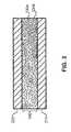
- FIG. 1illustrates a conventional nanotube device (e.g., a block switch) which makes use of a nanotube fabric layer comprising only carbon nanotubes.
- a carbon nanotube fabric layer 130is deposited over a first electrode 110 .
- the carbon nanotube fabric layer 130is comprised of a volume of carbon nanotubes 130 a formed into a cohesive fabric or film through the deposition process (e.g., spin coating, spray coating, or in situ growth).
- a second electrode 120is deposited over the carbon nanotube fabric layer 130 .
- the thickness of the carbon nanotube fabric layer 130is set above a certain threshold such as to prevent the second electrode 120 from becoming electrically connected (shorted) to the first electrode 110 (via the electrode material bleeding through the carbon nanotube layer 130 , for example). As such, a nanotube fabric layer of significant thickness is often required.
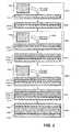
- FIG. 2illustrates a conventional fabrication process suitable for realizing the nanotube block switch depicted in FIG. 1 .
- a first volume of carbon nanotubes 230 ais deposited over a first electrode element 210 via a spin coating process forming a first intermediate nanotube fabric layer 240 a as illustrated by structure 200 b.
- a second volume of carbon nanotubes 230 bis deposited via a spin coating process over the first intermediate nanotube fabric layer 240 a forming a second intermediate nanotube fabric layer 240 b as illustrated by structure 200 d.
- a third volume of carbon nanotubesis deposited via a spin coating process over the second intermediate nanotube fabric layer 240 b forming a third intermediate nanotube fabric layer 240 c as illustrated by structure 200 f.
- a nanotube fabric layer 240(the combination of the first, second, and third intermediate nanotube layers 240 a , 240 b , and 240 c ) of a required thickness is formed over first electrode element 210 .
- a second electrode element 250is deposited over the nanotube fabric layer 240 as illustrated by structure 200 g.
- certain embodiments of the present inventionprovide a resistive material that can be used within a plurality of different applications. Such applications include, hut are not limited to, display elements, solar panels, and semiconductor circuits.
- certain embodiments of the present inventioninclude a plurality of nanotube based switching devices, including, but not limited to, block switches, programmable resistive materials, and programmable logic devices.
- certain embodiments of the present inventionprovide resistive materials, including films and fabrics, with controlled and uniform nanotube densities, significantly reducing the cost and/or improving the performance of applications using such materials.
- FIG. 3illustrates one exemplary device, such as a nanotube block switch, in accordance with certain embodiments of the present invention.
- the devicesuch as the nanotube block switch shown, includes a composite article 330 containing a mixture of nanotubes 330 a and nanoscopic particles 330 b in a predefined ratio (said nanoscopic particles 330 b depicted as circular elements within FIGS. 3 and 4 for clarity).
- FIG. 3depicts the nanoscopic particles 330 b as the discrete phase and the nanotubes 330 a as the matrix phase, the morphology of the nanoscopic particles 330 b and nanotubes 330 a may be different.
- the nanotubes 330 amay form the discrete phase and the nanoscopic particles 330 b may form the matrix phase.
- the nanotubes 330 a and the nanoscopic particles 330 bcan both form interconnected matrix phases.
- the composite article 330can act as a switching material between a first electrode 310 and a second electrode 320 .
- the fabrication, function, and use of nanotube block switchesis discussed in greater detail within U.S. patent application Ser. No. 11/835,856 to Berlin et al., which is incorporated by reference herein in its entirety.
- the nanoscopic particlesare purposefully introduced in a predefined ratio with respect to the nanotubes to control the composition and, consequently, physical, electrical, and thermal aspects of the resulting composite articles.
- the nanoscopic particlesare a deliberately added component, introduced to achieve the desired device performance, such as desired switching attributes.
- the nanoscopic particlesare selectively mixed with nanotubes to form a composite article having a predefined volumetric ratio of nanoscopic particles to nanotubes. The ratio may be pre-selected and tuned to ensure, for example, the desired range of electrical switching or resistive states.
- the attributes of the nanoscopic particlescan all be specifically selected to further tune the desired device characteristics (e.g., electrical switching or resistive characteristics) of the resultant composite article.
- the attributes of the nanoscopic particlesitself may further dictate the predefined ratio of the nanoscopic particles and nanotubes.
- the purposeful and deliberate addition of nanoscopic particlescan have the common effect of allowing inventors additional control in tuning and refining the characteristics (electrical, physical, thermal or otherwise) of the composite article.
- addition of the nanoscopic particles in a predefined ratio with the nanotubesmay decrease the switching voltages of the composite article as compared to switches formed from pristine nanotubes.
- the predefined ratio of the nanoscopic particles to the nanotubescan be any ratio selected by the manufacturer depending on the application, method of combination, or the composition of materials used in the device.
- some suitable and non-limiting predefined ratio of the nanoscopic particles to the nanotubesmay be from about 1:1 (one part nanoscopic particles to about one part nanotubes) to about 1:10 (one part nanoscopic particles to about ten part nanotubes).
- some suitable and non-limiting predefined ratio of the nanoscopic particles to the nanotubesmay be 1:1, 1:2, 1:3, 1:4, 1:5, 1:6, 1:7, 1:8, 1:9, or 1:10.
- the nanoscopic particles 330 bcan take a plurality of forms depending on the needs of an application or structure in which the methods of the present invention are employed.
- the nanoscopic particlesmay be spherical, oblong, square, irregular, or any other shapes as would be readily apparent to ordinary skill in the art.
- the nanoscopic particlesmay have at least one dimension that is in the nanometer size.
- the nanoscopic particlesmay have at least one dimension which is less than 100 nm, 50 nm, 40 ran, 30 nm, 25 nm, 20 nm, 10 nm, 5 nm, or 1 nm.
- the nanoscopic particlesmay have dimensions that are acceptable in semiconductor fabrication facilities, such as a CMOS facility.
- the nanoscopic particlesmay be individual atoms or ions.
- the nanoscopic particlecan interact covalently or non-covalently to another nanoscopic material, for example, carbon nanotubes.
- the nanoscopic particlesmay be miscible with the nanotubes and form a continuous material around the nanotube.
- the nanoscopic particlesmay be inert to the nanotubes and remain in the same form as initially introduced into the mixture and therefore non-miscible.
- the nanoscopic particlesmay be partially miscible with the nanotubes and form a semi-miscible mixture with the nanotubes.
- the nanoscopic particlesmay have the ability to alter the porosity between the carbon nanotubes.
- the nanoscopic particlesmay be introduced to the composite article either before deposition on the substrate or after the nanotube is applied to the substrate.
- the nanoscopic particlescan be combined with the carbon nanotubes by introducing them into the solution containing carbon nanotubes then depositing the combined mixture onto the substrate.
- the nanoscopic particlescan be introduced, for example, by ion implantation, vapor deposition, sputtering, or other methods known in the art after first forming a nanotube layer on the substrate.
- the choice of such nanoscopic particlescan include a material or materials that can be formed with a uniform particle size.
- the choice of a nanoscopic particlecan include a material or materials which can be fabricated as individual particles within certain dimensions. For example, an application may require a nanoscopic particle wherein individual particles are not larger than some fraction of a device feature size.
- the choice of such nanoscopic particlescan include a material or materials which do not adversely affect the switching operation (that is, the changing from one nominal nonvolatile resistive state to another) of the composite article.
- the nanoscopic particles 330 bmay improve switching operation by lowering the voltage needed for the composite article to change its resistance.
- inorganic nanoparticlescan be utilized.
- silicon based materialssuch as, but not limited to silicon oxide and silicon nitride can be used for said nanoscopic particles 330 b.
- one or more allotropes of carboncan be used for said nanoscopic particles 330 b.
- nanoscopic particles 330 bcan include a mixture of different nanoscopic materials, such as any combination of nanoscopic particles 330 b described above.
- the nanoscopic particles 330 bcan be obtained by numerous different ways. For example, carbon particles having of particles of substantially uniform volume can be obtained through the process described below. Methods for obtaining other desired nanoscopic materials 330 b wilt be readily apparent to one of ordinary skilled in the art.
- the resulting colloidal system of processed carbon particlescan then be combined with a carbon nanotube solution at a ratio which will enable the generation of a film or fabric layer which will comprise a desired volume density of carbon nanotubes.
- FIG. 4illustrates a nanotube block switch fabrication process in accordance with certain embodiments of the present invention.
- a first volume 420 of nanotubes 420 ais combined with a second volume 410 of nanoscopic particles 410 a to obtain a mixture 430 .
- the mixture 430can be homogeneous or heterogeneous.
- One of ordinary skill in the artwill readily appreciate the various different ways the mixture 430 can be formed.
- mixture 430can be formed so that the mixture 430 can be utilized in semiconductor fabrication facilities, such as in Class 100, 10, or 1 facilities (e.g., CMOS facilities).
- the mixture 430can be substantially free of undesirable particulate and metal impurities, such as being substantially free of particulate impurities that are greater than 1000 nm, 500 nm, 400 nm, or even 300 nm in diameter.
- the nanotubes 420 a and nanoscopic particles 410 acan be combined in a solvent that is acceptable for use in semiconductor facilities, such as an aqueous (e.g., highly purified water) or non-aqueous solvents that are compatible with semiconductor fabrication processes.
- the mixture 430is deposited over a first electrode element 440 via a spin coating process to form composite article 450 (as illustrated by structure 400 b ).
- the mixture 430allows for the deposition of significantly thicker (as compared to prior art nanotube solutions) layers (or films) within a single spin coat process as compared to nanotube-only liquids. For example, thickness ranging from about a few to hundreds of nanometers may be possible through a single coat. Some non-limiting example thicknesses that can be achieve include 1, 2, 2.5, 5, 10, 20, 30, 40, 50, 60, 70, 80, 90, 100, 150, or 200 nm.
- a sufficiently thick composite article suitable for use within a plurality of nanotube block switching devicessuch as, but not limited to, block switches, programmable resistive materials, and programmable logic devices
- a sufficiently thick composite article suitable for use within a plurality of nanotube block switching devicescan be realized in a minimum number of spin coat process steps. Further, in many applications, such a layer can be realized within a single spin coat process step, significantly reducing process time and cost.
- a second electrode element 460is deposited over the composite article 450 as illustrated by structure 400 c.
- FIG. 5illustrates a nanotube block switch with a composite article 530 formed via an alternate embodiment of the methods of the present invention.
- a first volume of single wall nanotubes (SWNTs) 530 acan be combined with a second volume of multi-wall nanotubes (MWNTs) 530 b to form a mixture.
- said second volume of MWNTs 530 bcan act as the nanoscopic particles white said first volume of SWNTs 530 a are single walled carbon nanotubes.
- the composite article 530can have very low level metal contamination.
- the composite article 530may have less than 10 18 , 10 16 , 10 15 , 10 14 , 10 13 , 10 12 , 5 ⁇ 10 11 , 1 ⁇ 10 11 , 5 ⁇ 10 10 , or even less than 1 ⁇ 10 10 atoms/cm 2 .
- a second electrode 520can be deposited over the composite article 530 .
- FIGS. 4 and 5depict two exemplary fabrication process in order to clearly illustrate the methods of the present invention
- said methodsare not limited to these exemplary embodiments.
- one of ordinary skill in the artwould readily recognize other methods for forming the desired nanotube devices.
- the methods of the present inventionare well suited to forming a relatively thick carbon nanotube films.
- the present inventionis not limited in this regard. Indeed, the methods of the present invention are applicable to a plurality of applications wherein a specific volume density of carbon nanotubes is required within a carbon nanotube film, including, but not limited to, those applications employing very thin films. Accordingly, one of ordinary skill in the art would readily recognize the various different embodiments for fabrication the desired nanotube devices of interest.
- FIG. 6depicts a nonvolatile nanotube switch.
- cell structure 8700 having cell 8705comprises a composite article 8710 containing nanotubes and nanoscopic particles.
- the nanoscopic particlescan include carbon particles having substantially uniform volume as described above.
- the composite article 8750has top/end contact 8765 and bottom 8730 contact.
- the present cell select and control structureincludes conductive plug 8710 connecting bottom contact 8730 to an N+ region embedded in P-type substrate PSUB.
- word line WL 1is used as one portion of the cell select circuitry.
- Cell 8705may be integrated on a 1024 bit array for the purposes of electrical testing to evaluate electrical characteristics of the composite article 8750 .
- testsinclude SET to program the cell (write 1), RESET to erase the cell (write 0) and READ to access the stored state of the cell.
- SET, RESET and READ functionsare known in the art and discussed in greater detail above in relation to 3-D cell structures employing nanotube articles.
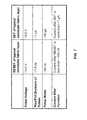
- FIG. 7summarizes typical RESET and SET electrical parameters, according to one or more embodiments. Specifically, typical applied pulse rise and fall times, duration, voltages and currents are listed. Testing has revealed that in certain embodiments and switch structures, the composite article 8710 containing nanotubes and nanoscopic particles enables a lower operating voltage than does the CNT-only material counterpart. For example, various embodiments of the nonvolatile nanotube switch functions at operating voltages less than or equal to approximately 5.0V. As a point of comparison, various switching structures having CNT-only materials to form the carbon nanotube articles typically function at operating voltages between approximately 7.0 and 8.0V.
- the composite article 8710 containing nanotubes and nanoscopic particleswhen used in certain switch configurations, may be faster in performing the SET function than a CNT-only material counterpart.
- the composite article 8710 containing nanotubes and nanoscopic particlesmay, in certain embodiments, be programmable under shorter duration write 1 operations.
Landscapes
- Engineering & Computer Science (AREA)
- Chemical & Material Sciences (AREA)
- Nanotechnology (AREA)
- Materials Engineering (AREA)
- Physics & Mathematics (AREA)
- Mathematical Physics (AREA)
- Theoretical Computer Science (AREA)
- Crystallography & Structural Chemistry (AREA)
- Manufacturing & Machinery (AREA)
- Carbon And Carbon Compounds (AREA)
- Semiconductor Memories (AREA)
Abstract
Description
- In a first processing step, reacting a volume of carbon black material with an oxidizing agent (such as, but not limited to, nitric acid) to forma carbon slurry in order to decrease the size of carbon black particles and further remove any metallic contaminants (via solubilization). The first processing step may be aided by further introducing other acids, such as hydrochloric acid.
- In next processing step, filtering the carbon slurry formed in the first process step at low pH (for example, but not limited to, via cross-flow membranes) to remove any solubilized impurities
- In a next processing step, increasing pH level of the carbon slurry to realize a homogeneous and stable colloidal system (in some operations, a sonication process may be used to improve homogeneity)
- In a next processing step, filtering the realized homogeneous and stable colloidal system through a train of titters to remove any particles which could lead to defects in the spin coated film (in some operations, for example, said system would be passed through filters with pores as small as 10 nm or 5 nm or other filters with the smallest pore size available)
Claims (15)
Priority Applications (2)
| Application Number | Priority Date | Filing Date | Title |
|---|---|---|---|
| US15/095,296US9755170B2 (en) | 2008-11-19 | 2016-04-11 | Resistive materials comprising mixed nanoscopic particles and carbon nanotubes |
| US15/694,174US10181569B2 (en) | 2008-11-19 | 2017-09-01 | Two-terminal switching devices comprising coated nanotube elements |
Applications Claiming Priority (5)
| Application Number | Priority Date | Filing Date | Title |
|---|---|---|---|
| US12/274,033US7915637B2 (en) | 2008-11-19 | 2008-11-19 | Switching materials comprising mixed nanoscopic particles and carbon nanotubes and method of making and using the same |
| US13/074,792US8586424B2 (en) | 2008-11-19 | 2011-03-29 | Switching materials comprising mixed nanoscopic particles and carbon nanotubes and method of making and using the same |
| US14/051,697US8969142B2 (en) | 2008-11-19 | 2013-10-11 | Switching materials comprising mixed nanoscopic particles and carbon nanotubes and methods of making and using the same |
| US14/633,481US9337423B2 (en) | 2008-11-19 | 2015-02-27 | Two-terminal switching device using a composite material of nanoscopic particles and carbon nanotubes |
| US15/095,296US9755170B2 (en) | 2008-11-19 | 2016-04-11 | Resistive materials comprising mixed nanoscopic particles and carbon nanotubes |
Related Parent Applications (1)
| Application Number | Title | Priority Date | Filing Date |
|---|---|---|---|
| US14/633,481DivisionUS9337423B2 (en) | 2008-11-19 | 2015-02-27 | Two-terminal switching device using a composite material of nanoscopic particles and carbon nanotubes |
Related Child Applications (1)
| Application Number | Title | Priority Date | Filing Date |
|---|---|---|---|
| US15/694,174ContinuationUS10181569B2 (en) | 2008-11-19 | 2017-09-01 | Two-terminal switching devices comprising coated nanotube elements |
Publications (2)
| Publication Number | Publication Date |
|---|---|
| US20160226008A1 US20160226008A1 (en) | 2016-08-04 |
| US9755170B2true US9755170B2 (en) | 2017-09-05 |
Family
ID=42171251
Family Applications (6)
| Application Number | Title | Priority Date | Filing Date |
|---|---|---|---|
| US12/274,033Active2029-05-20US7915637B2 (en) | 2008-11-19 | 2008-11-19 | Switching materials comprising mixed nanoscopic particles and carbon nanotubes and method of making and using the same |
| US13/074,792ActiveUS8586424B2 (en) | 2008-11-19 | 2011-03-29 | Switching materials comprising mixed nanoscopic particles and carbon nanotubes and method of making and using the same |
| US14/051,697ActiveUS8969142B2 (en) | 2008-11-19 | 2013-10-11 | Switching materials comprising mixed nanoscopic particles and carbon nanotubes and methods of making and using the same |
| US14/633,481ActiveUS9337423B2 (en) | 2008-11-19 | 2015-02-27 | Two-terminal switching device using a composite material of nanoscopic particles and carbon nanotubes |
| US15/095,296Expired - Fee RelatedUS9755170B2 (en) | 2008-11-19 | 2016-04-11 | Resistive materials comprising mixed nanoscopic particles and carbon nanotubes |
| US15/694,174ActiveUS10181569B2 (en) | 2008-11-19 | 2017-09-01 | Two-terminal switching devices comprising coated nanotube elements |
Family Applications Before (4)
| Application Number | Title | Priority Date | Filing Date |
|---|---|---|---|
| US12/274,033Active2029-05-20US7915637B2 (en) | 2008-11-19 | 2008-11-19 | Switching materials comprising mixed nanoscopic particles and carbon nanotubes and method of making and using the same |
| US13/074,792ActiveUS8586424B2 (en) | 2008-11-19 | 2011-03-29 | Switching materials comprising mixed nanoscopic particles and carbon nanotubes and method of making and using the same |
| US14/051,697ActiveUS8969142B2 (en) | 2008-11-19 | 2013-10-11 | Switching materials comprising mixed nanoscopic particles and carbon nanotubes and methods of making and using the same |
| US14/633,481ActiveUS9337423B2 (en) | 2008-11-19 | 2015-02-27 | Two-terminal switching device using a composite material of nanoscopic particles and carbon nanotubes |
Family Applications After (1)
| Application Number | Title | Priority Date | Filing Date |
|---|---|---|---|
| US15/694,174ActiveUS10181569B2 (en) | 2008-11-19 | 2017-09-01 | Two-terminal switching devices comprising coated nanotube elements |
Country Status (1)
| Country | Link |
|---|---|
| US (6) | US7915637B2 (en) |
Families Citing this family (18)
| Publication number | Priority date | Publication date | Assignee | Title |
|---|---|---|---|---|
| US8941094B2 (en)* | 2010-09-02 | 2015-01-27 | Nantero Inc. | Methods for adjusting the conductivity range of a nanotube fabric layer |
| US8716805B2 (en)* | 2008-06-10 | 2014-05-06 | Toshiba America Research, Inc. | CMOS integrated circuits with bonded layers containing functional electronic devices |
| US7915637B2 (en)* | 2008-11-19 | 2011-03-29 | Nantero, Inc. | Switching materials comprising mixed nanoscopic particles and carbon nanotubes and method of making and using the same |
| US8895950B2 (en)* | 2009-10-23 | 2014-11-25 | Nantero Inc. | Methods for passivating a carbonic nanolayer |
| JP2011171322A (en)* | 2010-02-16 | 2011-09-01 | Toshiba Corp | Nonvolatile semiconductor memory device and method of manufacturing the same |
| US20110203632A1 (en)* | 2010-02-22 | 2011-08-25 | Rahul Sen | Photovoltaic devices using semiconducting nanotube layers |
| JP2012004277A (en)* | 2010-06-16 | 2012-01-05 | Toshiba Corp | Nonvolatile semiconductor memory device and method for manufacturing the same |
| JP5580126B2 (en)* | 2010-07-14 | 2014-08-27 | 株式会社東芝 | Nonvolatile memory device and manufacturing method thereof |
| JP6247211B2 (en)* | 2011-09-13 | 2017-12-13 | ワイルドキャット・ディスカバリー・テクノロジーズ・インコーポレイテッドWildcat Discovery Technologies, Inc. | Battery positive electrode |
| US8735242B2 (en) | 2012-07-31 | 2014-05-27 | International Business Machines Corporation | Graphene-based eFuse device |
| TWI489461B (en)* | 2012-09-04 | 2015-06-21 | Ind Tech Res Inst | Resistive ram, controlling method and manufacturing method |
| US8988937B2 (en)* | 2012-10-24 | 2015-03-24 | Sandisk Technologies Inc. | Pre-charge during programming for 3D memory using gate-induced drain leakage |
| TWI493549B (en)* | 2013-03-05 | 2015-07-21 | Nat Univ Tsing Hua | Resistive random-access memory |
| WO2014144167A1 (en) | 2013-03-15 | 2014-09-18 | Wildcat Discovery Technologies, Inc. | High energy materials for a battery and methods for making and use |
| WO2014144179A1 (en) | 2013-03-15 | 2014-09-18 | Wildcat Discovery Technologies, Inc. | High energy materials for a battery and methods for making and use |
| US10903483B2 (en) | 2015-08-27 | 2021-01-26 | Wildcat Discovery Technologies, Inc | High energy materials for a battery and methods for making and use |
| JP6992768B2 (en)* | 2017-01-30 | 2022-01-13 | 株式会社ニコン | Image sensor and method for manufacturing the image sensor |
| US10355206B2 (en) | 2017-02-06 | 2019-07-16 | Nantero, Inc. | Sealed resistive change elements |
Citations (102)
| Publication number | Priority date | Publication date | Assignee | Title |
|---|---|---|---|---|
| WO1998039250A1 (en) | 1997-03-07 | 1998-09-11 | William Marsh Rice University | Carbon fibers formed from single-wall carbon nanotubes |
| WO1999065821A1 (en) | 1998-06-19 | 1999-12-23 | The Research Foundation Of State University Of New York | Free-standing and aligned carbon nanotubes and synthesis thereof |
| US6057637A (en) | 1996-09-13 | 2000-05-02 | The Regents Of The University Of California | Field emission electron source |
| JP2000203821A (en) | 1999-01-18 | 2000-07-25 | Toshiyuki Tsuboi | Method for forming film of carbon nanotube, carbon nanotube film formed by the method and electric field electron release source using the same |
| WO2000048195A1 (en) | 1999-02-12 | 2000-08-17 | Board Of Trustees Operating Michigan State University | Nanocapsules containing charged particles, their uses and methods of forming the same |
| US6128214A (en) | 1999-03-29 | 2000-10-03 | Hewlett-Packard | Molecular wire crossbar memory |
| WO2001003208A1 (en) | 1999-07-02 | 2001-01-11 | President And Fellows Of Harvard College | Nanoscopic wire-based devices, arrays, and methods of their manufacture |
| JP2001035362A (en) | 1999-07-26 | 2001-02-09 | Futaba Corp | Pattern forming method for carbon nanotube, pattern forming material for the carbon nanotube, electron emitting source and fluorescent type display |
| US20010004979A1 (en) | 1999-12-14 | 2001-06-28 | Lg Electronics Inc. | Field emission display and method for fabricating the same |
| US6256767B1 (en) | 1999-03-29 | 2001-07-03 | Hewlett-Packard Company | Demultiplexer for a molecular wire crossbar network (MWCN DEMUX) |
| US6277318B1 (en) | 1999-08-18 | 2001-08-21 | Agere Systems Guardian Corp. | Method for fabrication of patterned carbon nanotube films |
| US20010023986A1 (en) | 2000-02-07 | 2001-09-27 | Vladimir Mancevski | System and method for fabricating logic devices comprising carbon nanotube transistors |
| US6314019B1 (en) | 1999-03-29 | 2001-11-06 | Hewlett-Packard Company | Molecular-wire crossbar interconnect (MWCI) for signal routing and communications |
| US6342276B1 (en) | 1999-12-10 | 2002-01-29 | Samsung Sdi Co., Ltd. | Method for making a field emission display |
| GB2364933A (en) | 2000-07-18 | 2002-02-13 | Lg Electronics Inc | Method of horizontally growing carbon nanotubes and field effect transistor using the carbon nanotubes grown by the method |
| WO2002045113A1 (en) | 2000-11-29 | 2002-06-06 | Nec Corporation | Pattern forming method for carbon nanotube, and field emission cold cathode and method of manufacturing the cold cathode |
| WO2002048701A2 (en) | 2000-12-11 | 2002-06-20 | President And Fellows Of Harvard College | Nanosensors |
| US6409567B1 (en) | 1997-12-15 | 2002-06-25 | E.I. Du Pont De Nemours And Company | Past-deposited carbon electron emitters |
| US6422450B1 (en) | 1999-03-01 | 2002-07-23 | University Of North Carolina, The Chapel | Nanotube-based high energy material and method |
| US6423583B1 (en) | 2001-01-03 | 2002-07-23 | International Business Machines Corporation | Methodology for electrically induced selective breakdown of nanotubes |
| US6445006B1 (en) | 1995-12-20 | 2002-09-03 | Advanced Technology Materials, Inc. | Microelectronic and microelectromechanical devices comprising carbon nanotube components, and methods of making same |
| US20020160111A1 (en) | 2001-04-25 | 2002-10-31 | Yi Sun | Method for fabrication of field emission devices using carbon nanotube film as a cathode |
| US20020175390A1 (en) | 2001-04-03 | 2002-11-28 | Goldstein Seth Copen | Electronic circuit device, system, and method |
| US6495116B1 (en) | 2000-04-10 | 2002-12-17 | Lockheed Martin Corporation | Net shape manufacturing using carbon nanotubes |
| US6495258B1 (en) | 2000-09-20 | 2002-12-17 | Auburn University | Structures with high number density of carbon nanotubes and 3-dimensional distribution |
| US20030004058A1 (en) | 2001-05-21 | 2003-01-02 | Trustees Of Boston College | Varied morphology carbon nanotubes and method for their manufacture |
| WO2003016901A1 (en) | 2001-08-14 | 2003-02-27 | Samsung Electronics Co., Ltd. | Sensor for detecting biomolecule using carbon nanotubes |
| US6528020B1 (en) | 1998-08-14 | 2003-03-04 | The Board Of Trustees Of The Leland Stanford Junior University | Carbon nanotube devices |
| US6548841B2 (en) | 2000-11-09 | 2003-04-15 | Texas Instruments Incorporated | Nanomechanical switches and circuits |
| WO2003034142A1 (en) | 2001-10-18 | 2003-04-24 | National Institute Of Advanced Industrial Science And Technology | Optical element, and manufacturing method thereof |
| US20030122111A1 (en) | 2001-03-26 | 2003-07-03 | Glatkowski Paul J. | Coatings comprising carbon nanotubes and methods for forming same |
| US20030177450A1 (en) | 2002-03-12 | 2003-09-18 | Alex Nugent | Physical neural network design incorporating nanotechnology |
| US6630772B1 (en) | 1998-09-21 | 2003-10-07 | Agere Systems Inc. | Device comprising carbon nanotube field emitter structure and process for forming device |
| US20030200521A1 (en) | 2002-01-18 | 2003-10-23 | California Institute Of Technology | Array-based architecture for molecular electronics |
| US6645628B2 (en) | 2001-11-13 | 2003-11-11 | The United States Of America As Represented By The Secretary Of The Air Force | Carbon nanotube coated anode |
| US20040005723A1 (en) | 2002-04-02 | 2004-01-08 | Nanosys, Inc. | Methods of making, positioning and orienting nanostructures, nanostructure arrays and nanostructure devices |
| US20040007528A1 (en) | 2002-07-03 | 2004-01-15 | The Regents Of The University Of California | Intertwined, free-standing carbon nanotube mesh for use as separation, concentration, and/or filtration medium |
| US20040023253A1 (en) | 2001-06-11 | 2004-02-05 | Sandeep Kunwar | Device structure for closely spaced electrodes |
| US20040031975A1 (en) | 2002-03-18 | 2004-02-19 | Max-Planck-Gesellschaft Zur Forderung Der Wissenschaften E.V., A German Corporation | Field effect transistor memory cell, memory device and method for manufacturing a field effect transistor memory cell |
| US20040043527A1 (en) | 2002-09-04 | 2004-03-04 | Nanomix, Inc. | Sensitivity control for nanotube sensors |
| US20040041154A1 (en) | 2002-09-04 | 2004-03-04 | Fuji Xerox Co., Ltd. | Electric part and method of manufacturing the same |
| US6706402B2 (en) | 2001-07-25 | 2004-03-16 | Nantero, Inc. | Nanotube films and articles |
| US6707098B2 (en) | 2000-07-04 | 2004-03-16 | Infineon Technologies, Ag | Electronic device and method for fabricating an electronic device |
| US20040071949A1 (en) | 2001-07-27 | 2004-04-15 | Glatkowski Paul J. | Conformal coatings comprising carbon nanotubes |
| US20040099438A1 (en) | 2002-05-21 | 2004-05-27 | Arthur David J. | Method for patterning carbon nanotube coating and carbon nanotube wiring |
| US20040104129A1 (en) | 2002-11-27 | 2004-06-03 | Gang Gu | Nanotube chemical sensor based on work function of electrodes |
| US6759693B2 (en) | 2002-06-19 | 2004-07-06 | Nantero, Inc. | Nanotube permeable base transistor |
| US20040132070A1 (en) | 2002-01-16 | 2004-07-08 | Nanomix, Inc. | Nonotube-based electronic detection of biological molecules |
| US20040181630A1 (en) | 2001-07-25 | 2004-09-16 | Nantero, Inc. | Devices having horizontally-disposed nanofabric articles and methods of making the same |
| US6803840B2 (en) | 2001-03-30 | 2004-10-12 | California Institute Of Technology | Pattern-aligned carbon nanotube growth and tunable resonator apparatus |
| US6809465B2 (en) | 2002-08-23 | 2004-10-26 | Samsung Electronics Co., Ltd. | Article comprising MEMS-based two-dimensional e-beam sources and method for making the same |
| US6808746B1 (en) | 1999-04-16 | 2004-10-26 | Commonwealth Scientific and Industrial Research Organisation Campell | Multilayer carbon nanotube films and method of making the same |
| US20040238887A1 (en) | 2001-07-05 | 2004-12-02 | Fumiyuki Nihey | Field-effect transistor constituting channel by carbon nano tubes |
| US20040253167A1 (en) | 2001-07-27 | 2004-12-16 | Silva Sembukutiarachilage Ravi | Production of carbon nanotubes |
| US6833558B2 (en) | 2000-08-23 | 2004-12-21 | Korea Institute Of Science And Technology | Parallel and selective growth method of carbon nanotube on the substrates for electronic-spintronic device applications |
| US20040266106A1 (en) | 2003-06-30 | 2004-12-30 | Hynix Semiconductor Inc. | Method for forming bit line of flash device |
| US20040265550A1 (en) | 2002-12-06 | 2004-12-30 | Glatkowski Paul J. | Optically transparent nanostructured electrical conductors |
| US6858197B1 (en) | 2002-03-13 | 2005-02-22 | The United States Of America As Represented By The Administrator Of The National Aeronautics And Space Administration | Controlled patterning and growth of single wall and multi-wall carbon nanotubes |
| US20050053525A1 (en) | 2003-05-14 | 2005-03-10 | Nantero, Inc. | Sensor platform using a horizontally oriented nanotube element |
| US20050056877A1 (en) | 2003-03-28 | 2005-03-17 | Nantero, Inc. | Nanotube-on-gate fet structures and applications |
| US20050079659A1 (en) | 2002-09-30 | 2005-04-14 | Nanosys, Inc. | Large-area nanoenabled macroelectronic substrates and uses therefor |
| US6888773B2 (en) | 2002-12-05 | 2005-05-03 | Sharp Kabushiki Kaisha | Semiconductor memory device and erase method for memory array |
| US20050095938A1 (en) | 2003-10-29 | 2005-05-05 | Rosenberger Brian T. | Carbon nanotube fabrics |
| US6890780B2 (en) | 2003-10-10 | 2005-05-10 | General Electric Company | Method for forming an electrostatically-doped carbon nanotube device |
| US6899945B2 (en) | 2002-03-19 | 2005-05-31 | William Marsh Rice University | Entangled single-wall carbon nanotube solid material and methods for making same |
| US6905892B2 (en) | 2001-07-20 | 2005-06-14 | Infineon Technologies Ag | Operating method for a semiconductor component |
| US6919592B2 (en) | 2001-07-25 | 2005-07-19 | Nantero, Inc. | Electromechanical memory array using nanotube ribbons and method for making same |
| US6918284B2 (en) | 2003-03-24 | 2005-07-19 | The United States Of America As Represented By The Secretary Of The Navy | Interconnected networks of single-walled carbon nanotubes |
| US6919740B2 (en) | 2003-01-31 | 2005-07-19 | Hewlett-Packard Development Company, Lp. | Molecular-junction-nanowire-crossbar-based inverter, latch, and flip-flop circuits, and more complex circuits composed, in part, from molecular-junction-nanowire-crossbar-based inverter, latch, and flip-flop circuits |
| US6921575B2 (en) | 2001-05-21 | 2005-07-26 | Fuji Xerox Co., Ltd. | Carbon nanotube structures, carbon nanotube devices using the same and method for manufacturing carbon nanotube structures |
| US6924538B2 (en) | 2001-07-25 | 2005-08-02 | Nantero, Inc. | Devices having vertically-disposed nanofabric articles and methods of making the same |
| US20050181209A1 (en)* | 1999-08-20 | 2005-08-18 | Karandikar Prashant G. | Nanotube-containing composite bodies, and methods for making same |
| US6946410B2 (en) | 2002-04-05 | 2005-09-20 | E. I. Du Pont De Nemours And Company | Method for providing nano-structures of uniform length |
| US20050212014A1 (en) | 2004-03-26 | 2005-09-29 | Masahiro Horibe | Semiconductor device and semiconductor sensor |
| US6990009B2 (en) | 2003-08-13 | 2006-01-24 | Nantero, Inc. | Nanotube-based switching elements with multiple controls |
| US7015500B2 (en) | 2002-02-09 | 2006-03-21 | Samsung Electronics Co., Ltd. | Memory device utilizing carbon nanotubes |
| US20060115640A1 (en)* | 2002-09-10 | 2006-06-01 | Yodh Arjun G | Process and applications of carbon nanotube dispersions |
| US7057402B2 (en) | 2002-03-18 | 2006-06-06 | Honeywell International Inc. | Carbon nanotube sensor |
| US7097906B2 (en) | 2003-06-05 | 2006-08-29 | Lockheed Martin Corporation | Pure carbon isotropic alloy of allotropic forms of carbon including single-walled carbon nanotubes and diamond-like carbon |
| US7115901B2 (en) | 2003-06-09 | 2006-10-03 | Nantero, Inc. | Non-volatile electromechanical field effect devices and circuits using same and methods of forming same |
| US7115960B2 (en) | 2003-08-13 | 2006-10-03 | Nantero, Inc. | Nanotube-based switching elements |
| US20060237537A1 (en) | 2002-09-30 | 2006-10-26 | Nanosys, Inc. | Applications of nano-enabled large area macroelectronic substrates incorporating nanowires and nanowire composites |
| US20060250843A1 (en) | 2005-05-09 | 2006-11-09 | Nantero, Inc. | Non-volatile-shadow latch using a nanotube switch |
| US20060250856A1 (en) | 2005-05-09 | 2006-11-09 | Nantero, Inc. | Memory arrays using nanotube articles with reprogrammable resistance |
| US20060258122A1 (en) | 2005-05-12 | 2006-11-16 | Whitefield Bruce J | Nanotube fuse structure |
| US20060264053A1 (en) | 2005-05-23 | 2006-11-23 | Lsi Logic Corporation | Method of aligning nanotubes and wires with an etched feature |
| US20060281256A1 (en) | 2005-06-08 | 2006-12-14 | Carter Richard J | Self-aligned cell integration scheme |
| US20060281287A1 (en) | 2005-06-09 | 2006-12-14 | Yates Colin D | Method of aligning deposited nanotubes onto an etched feature using a spacer |
| US20060292716A1 (en) | 2005-06-27 | 2006-12-28 | Lsi Logic Corporation | Use selective growth metallization to improve electrical connection between carbon nanotubes and electrodes |
| US20070004191A1 (en) | 2005-06-30 | 2007-01-04 | Lsi Logic Corporation | Novel techniques for precision pattern transfer of carbon nanotubes from photo mask to wafers |
| US7161403B2 (en) | 2004-06-18 | 2007-01-09 | Nantero, Inc. | Storage elements using nanotube switching elements |
| US7335395B2 (en) | 2002-04-23 | 2008-02-26 | Nantero, Inc. | Methods of using pre-formed nanotubes to make carbon nanotube films, layers, fabrics, ribbons, elements and articles |
| US7375369B2 (en) | 2003-09-08 | 2008-05-20 | Nantero, Inc. | Spin-coatable liquid for formation of high purity nanotube films |
| US20080157126A1 (en) | 2005-05-09 | 2008-07-03 | Nantero, Inc. | Nonvolatile nanotube diodes and nonvolatile nanotube blocks and systems using same and methods of making same |
| US7402770B2 (en)* | 2005-06-10 | 2008-07-22 | Lsi Logic Corporation | Nano structure electrode design |
| US20090194839A1 (en)* | 2005-11-15 | 2009-08-06 | Bertin Claude L | Nonvolatile nanotube diodes and nonvolatile nanotube blocks and systems using same and methods of making same |
| US7663911B2 (en)* | 2003-08-13 | 2010-02-16 | Nantero, Inc. | Isolation structure for deflectable nanotube elements |
| US7781862B2 (en) | 2005-05-09 | 2010-08-24 | Nantero, Inc. | Two-terminal nanotube devices and systems and methods of making same |
| US7782650B2 (en)* | 2005-05-09 | 2010-08-24 | Nantero, Inc. | Nonvolatile nanotube diodes and nonvolatile nanotube blocks and systems using same and methods of making same |
| US7835170B2 (en) | 2005-05-09 | 2010-11-16 | Nantero, Inc. | Memory elements and cross point switches and arrays of same using nonvolatile nanotube blocks |
| US7915637B2 (en)* | 2008-11-19 | 2011-03-29 | Nantero, Inc. | Switching materials comprising mixed nanoscopic particles and carbon nanotubes and method of making and using the same |
| US8008745B2 (en) | 2005-05-09 | 2011-08-30 | Nantero, Inc. | Latch circuits and operation circuits having scalable nonvolatile nanotube switches as electronic fuse replacement elements |
Family Cites Families (40)
| Publication number | Priority date | Publication date | Assignee | Title |
|---|---|---|---|---|
| US6010932A (en)* | 1996-12-05 | 2000-01-04 | Micron Technology, Inc. | Fork-like memory structure for ULSI DRAM and method of fabrication |
| US6683783B1 (en) | 1997-03-07 | 2004-01-27 | William Marsh Rice University | Carbon fibers formed from single-wall carbon nanotubes |
| JPH118690A (en) | 1997-06-18 | 1999-01-12 | Nec Corp | Absence answering telephone system |
| JPH11210336A (en) | 1998-01-23 | 1999-08-03 | Daiko:Kk | Attaching method of exterior material |
| US7063712B2 (en)* | 2001-04-27 | 2006-06-20 | Cardica, Inc. | Anastomosis method |
| TW474028B (en)* | 2000-02-18 | 2002-01-21 | Ching-Fu Lin | Light-emitting device based on indirect bandgap material |
| JP2002258885A (en) | 2001-02-27 | 2002-09-11 | Sharp Corp | Text-to-speech synthesizer and program recording medium |
| US6632088B2 (en)* | 2001-04-25 | 2003-10-14 | Orthoarm, Inc. | Powered orthodontic bracket |
| JP2003069151A (en)* | 2001-06-12 | 2003-03-07 | Furukawa Electric Co Ltd:The | Surface emitting semiconductor laser device |
| US7566478B2 (en) | 2001-07-25 | 2009-07-28 | Nantero, Inc. | Methods of making carbon nanotube films, layers, fabrics, ribbons, elements and articles |
| US20030041154A1 (en)* | 2001-08-24 | 2003-02-27 | Tran Trung M. | System and method for controlling UNIX group access using LDAP |
| US6805892B2 (en)* | 2002-01-22 | 2004-10-19 | Rajendra P. Gupta | Production of liquid foods without off-flavors |
| US20040029706A1 (en) | 2002-02-14 | 2004-02-12 | Barrera Enrique V. | Fabrication of reinforced composite material comprising carbon nanotubes, fullerenes, and vapor-grown carbon fibers for thermal barrier materials, structural ceramics, and multifunctional nanocomposite ceramics |
| CN1643840A (en)* | 2002-03-13 | 2005-07-20 | 皇家飞利浦电子股份有限公司 | Polynomial-based multi-user key generation and authentication method and system |
| US7147894B2 (en)* | 2002-03-25 | 2006-12-12 | The University Of North Carolina At Chapel Hill | Method for assembling nano objects |
| AU2003228720A1 (en) | 2002-04-29 | 2003-11-17 | The Trustees Of Boston College | Density controlled carbon nanotube array electrodes |
| US7348298B2 (en) | 2002-05-30 | 2008-03-25 | Ashland Licensing And Intellectual Property, Llc | Enhancing thermal conductivity of fluids with graphite nanoparticles and carbon nanotube |
| US6548313B1 (en) | 2002-05-31 | 2003-04-15 | Intel Corporation | Amorphous carbon insulation and carbon nanotube wires |
| US20050266106A1 (en)* | 2002-07-22 | 2005-12-01 | Mate Hidvegi | Use of fermented wheat germ extract as anti-inflammatory agent |
| US7135728B2 (en) | 2002-09-30 | 2006-11-14 | Nanosys, Inc. | Large-area nanoenabled macroelectronic substrates and uses therefor |
| EP1548057A4 (en) | 2002-09-30 | 2006-02-15 | Bridgestone Corp | Orientated carbon nanotube composite, process for producing orientated carbon nanotube composite, and, produced using orientated carbon nanotube composite, pneumatic tire, wheel for vehicle, tire wheel assembly and disk brake |
| US7416993B2 (en) | 2003-09-08 | 2008-08-26 | Nantero, Inc. | Patterned nanowire articles on a substrate and methods of making the same |
| US6919582B2 (en)* | 2003-11-20 | 2005-07-19 | Solidlite Corporation | Tri-color ZnSe white light emitting diode |
| US7118440B2 (en) | 2004-01-09 | 2006-10-10 | Teco Nanotech Co., Ltd. | Spray with carbon nanotubes and method to spray the same |
| US7563722B2 (en)* | 2004-03-05 | 2009-07-21 | Applied Nanotech Holdings, Inc. | Method of making a textured surface |
| US7778640B2 (en) | 2004-06-25 | 2010-08-17 | Lg Electronics Inc. | Method of communicating data in a wireless mobile communication system |
| US7515010B2 (en) | 2004-10-08 | 2009-04-07 | The Regents Of The University Of California | Nanoscale relaxation oscillator |
| US20060276056A1 (en) | 2005-04-05 | 2006-12-07 | Nantero, Inc. | Nanotube articles with adjustable electrical conductivity and methods of making the same |
| US9911743B2 (en) | 2005-05-09 | 2018-03-06 | Nantero, Inc. | Nonvolatile nanotube diodes and nonvolatile nanotube blocks and systems using same and methods of making same |
| US9196615B2 (en) | 2005-05-09 | 2015-11-24 | Nantero Inc. | Nonvolatile nanotube diodes and nonvolatile nanotube blocks and systems using same and methods of making same |
| US8013363B2 (en) | 2005-05-09 | 2011-09-06 | Nantero, Inc. | Nonvolatile nanotube diodes and nonvolatile nanotube blocks and systems using same and methods of making same |
| US8217490B2 (en) | 2005-05-09 | 2012-07-10 | Nantero Inc. | Nonvolatile nanotube diodes and nonvolatile nanotube blocks and systems using same and methods of making same |
| US7535462B2 (en) | 2005-06-02 | 2009-05-19 | Eastman Kodak Company | Touchscreen with one carbon nanotube conductive layer |
| US7667999B2 (en)* | 2007-03-27 | 2010-02-23 | Sandisk 3D Llc | Method to program a memory cell comprising a carbon nanotube fabric and a steering element |
| US7982209B2 (en)* | 2007-03-27 | 2011-07-19 | Sandisk 3D Llc | Memory cell comprising a carbon nanotube fabric element and a steering element |
| US8558220B2 (en)* | 2007-12-31 | 2013-10-15 | Sandisk 3D Llc | Memory cell that employs a selectively fabricated carbon nano-tube reversible resistance-switching element formed over a bottom conductor and methods of forming the same |
| US20090166610A1 (en)* | 2007-12-31 | 2009-07-02 | April Schricker | Memory cell with planarized carbon nanotube layer and methods of forming the same |
| US8236623B2 (en)* | 2007-12-31 | 2012-08-07 | Sandisk 3D Llc | Memory cell that employs a selectively fabricated carbon nano-tube reversible resistance-switching element and methods of forming the same |
| WO2010059152A1 (en) | 2008-11-19 | 2010-05-27 | Nantero, Inc. | Improved switching materials comprising mixed nanoscopic particles and carbon nanotubes and method of making and using the same |
| US8551806B2 (en)* | 2009-10-23 | 2013-10-08 | Nantero Inc. | Methods for passivating a carbonic nanolayer |
- 2008
- 2008-11-19USUS12/274,033patent/US7915637B2/enactiveActive
- 2011
- 2011-03-29USUS13/074,792patent/US8586424B2/enactiveActive
- 2013
- 2013-10-11USUS14/051,697patent/US8969142B2/enactiveActive
- 2015
- 2015-02-27USUS14/633,481patent/US9337423B2/enactiveActive
- 2016
- 2016-04-11USUS15/095,296patent/US9755170B2/ennot_activeExpired - Fee Related
- 2017
- 2017-09-01USUS15/694,174patent/US10181569B2/enactiveActive
Patent Citations (107)
| Publication number | Priority date | Publication date | Assignee | Title |
|---|---|---|---|---|
| US6445006B1 (en) | 1995-12-20 | 2002-09-03 | Advanced Technology Materials, Inc. | Microelectronic and microelectromechanical devices comprising carbon nanotube components, and methods of making same |
| US6057637A (en) | 1996-09-13 | 2000-05-02 | The Regents Of The University Of California | Field emission electron source |
| WO1998039250A1 (en) | 1997-03-07 | 1998-09-11 | William Marsh Rice University | Carbon fibers formed from single-wall carbon nanotubes |
| US6409567B1 (en) | 1997-12-15 | 2002-06-25 | E.I. Du Pont De Nemours And Company | Past-deposited carbon electron emitters |
| WO1999065821A1 (en) | 1998-06-19 | 1999-12-23 | The Research Foundation Of State University Of New York | Free-standing and aligned carbon nanotubes and synthesis thereof |
| US6863942B2 (en) | 1998-06-19 | 2005-03-08 | The Research Foundation Of State University Of New York | Free-standing and aligned carbon nanotubes and synthesis thereof |
| US6528020B1 (en) | 1998-08-14 | 2003-03-04 | The Board Of Trustees Of The Leland Stanford Junior University | Carbon nanotube devices |
| US6630772B1 (en) | 1998-09-21 | 2003-10-07 | Agere Systems Inc. | Device comprising carbon nanotube field emitter structure and process for forming device |
| JP2000203821A (en) | 1999-01-18 | 2000-07-25 | Toshiyuki Tsuboi | Method for forming film of carbon nanotube, carbon nanotube film formed by the method and electric field electron release source using the same |
| WO2000048195A1 (en) | 1999-02-12 | 2000-08-17 | Board Of Trustees Operating Michigan State University | Nanocapsules containing charged particles, their uses and methods of forming the same |
| US6422450B1 (en) | 1999-03-01 | 2002-07-23 | University Of North Carolina, The Chapel | Nanotube-based high energy material and method |
| US6256767B1 (en) | 1999-03-29 | 2001-07-03 | Hewlett-Packard Company | Demultiplexer for a molecular wire crossbar network (MWCN DEMUX) |
| US6314019B1 (en) | 1999-03-29 | 2001-11-06 | Hewlett-Packard Company | Molecular-wire crossbar interconnect (MWCI) for signal routing and communications |
| US6128214A (en) | 1999-03-29 | 2000-10-03 | Hewlett-Packard | Molecular wire crossbar memory |
| US6808746B1 (en) | 1999-04-16 | 2004-10-26 | Commonwealth Scientific and Industrial Research Organisation Campell | Multilayer carbon nanotube films and method of making the same |
| WO2001003208A1 (en) | 1999-07-02 | 2001-01-11 | President And Fellows Of Harvard College | Nanoscopic wire-based devices, arrays, and methods of their manufacture |
| JP2001035362A (en) | 1999-07-26 | 2001-02-09 | Futaba Corp | Pattern forming method for carbon nanotube, pattern forming material for the carbon nanotube, electron emitting source and fluorescent type display |
| US6277318B1 (en) | 1999-08-18 | 2001-08-21 | Agere Systems Guardian Corp. | Method for fabrication of patterned carbon nanotube films |
| US20050181209A1 (en)* | 1999-08-20 | 2005-08-18 | Karandikar Prashant G. | Nanotube-containing composite bodies, and methods for making same |
| US6342276B1 (en) | 1999-12-10 | 2002-01-29 | Samsung Sdi Co., Ltd. | Method for making a field emission display |
| US20010004979A1 (en) | 1999-12-14 | 2001-06-28 | Lg Electronics Inc. | Field emission display and method for fabricating the same |
| US20010023986A1 (en) | 2000-02-07 | 2001-09-27 | Vladimir Mancevski | System and method for fabricating logic devices comprising carbon nanotube transistors |
| US6495116B1 (en) | 2000-04-10 | 2002-12-17 | Lockheed Martin Corporation | Net shape manufacturing using carbon nanotubes |
| US6707098B2 (en) | 2000-07-04 | 2004-03-16 | Infineon Technologies, Ag | Electronic device and method for fabricating an electronic device |
| GB2364933A (en) | 2000-07-18 | 2002-02-13 | Lg Electronics Inc | Method of horizontally growing carbon nanotubes and field effect transistor using the carbon nanotubes grown by the method |
| US6515339B2 (en) | 2000-07-18 | 2003-02-04 | Lg Electronics Inc. | Method of horizontally growing carbon nanotubes and field effect transistor using the carbon nanotubes grown by the method |
| US6833558B2 (en) | 2000-08-23 | 2004-12-21 | Korea Institute Of Science And Technology | Parallel and selective growth method of carbon nanotube on the substrates for electronic-spintronic device applications |
| US6495258B1 (en) | 2000-09-20 | 2002-12-17 | Auburn University | Structures with high number density of carbon nanotubes and 3-dimensional distribution |
| US6548841B2 (en) | 2000-11-09 | 2003-04-15 | Texas Instruments Incorporated | Nanomechanical switches and circuits |
| WO2002045113A1 (en) | 2000-11-29 | 2002-06-06 | Nec Corporation | Pattern forming method for carbon nanotube, and field emission cold cathode and method of manufacturing the cold cathode |
| WO2002048701A2 (en) | 2000-12-11 | 2002-06-20 | President And Fellows Of Harvard College | Nanosensors |
| US6423583B1 (en) | 2001-01-03 | 2002-07-23 | International Business Machines Corporation | Methodology for electrically induced selective breakdown of nanotubes |
| US20030122111A1 (en) | 2001-03-26 | 2003-07-03 | Glatkowski Paul J. | Coatings comprising carbon nanotubes and methods for forming same |
| US6803840B2 (en) | 2001-03-30 | 2004-10-12 | California Institute Of Technology | Pattern-aligned carbon nanotube growth and tunable resonator apparatus |
| US20020175390A1 (en) | 2001-04-03 | 2002-11-28 | Goldstein Seth Copen | Electronic circuit device, system, and method |
| US20020160111A1 (en) | 2001-04-25 | 2002-10-31 | Yi Sun | Method for fabrication of field emission devices using carbon nanotube film as a cathode |
| US20030004058A1 (en) | 2001-05-21 | 2003-01-02 | Trustees Of Boston College | Varied morphology carbon nanotubes and method for their manufacture |
| US6921575B2 (en) | 2001-05-21 | 2005-07-26 | Fuji Xerox Co., Ltd. | Carbon nanotube structures, carbon nanotube devices using the same and method for manufacturing carbon nanotube structures |
| US20040023253A1 (en) | 2001-06-11 | 2004-02-05 | Sandeep Kunwar | Device structure for closely spaced electrodes |
| US20040238887A1 (en) | 2001-07-05 | 2004-12-02 | Fumiyuki Nihey | Field-effect transistor constituting channel by carbon nano tubes |
| US6905892B2 (en) | 2001-07-20 | 2005-06-14 | Infineon Technologies Ag | Operating method for a semiconductor component |
| US6919592B2 (en) | 2001-07-25 | 2005-07-19 | Nantero, Inc. | Electromechanical memory array using nanotube ribbons and method for making same |
| US6924538B2 (en) | 2001-07-25 | 2005-08-02 | Nantero, Inc. | Devices having vertically-disposed nanofabric articles and methods of making the same |
| US6706402B2 (en) | 2001-07-25 | 2004-03-16 | Nantero, Inc. | Nanotube films and articles |
| US20040181630A1 (en) | 2001-07-25 | 2004-09-16 | Nantero, Inc. | Devices having horizontally-disposed nanofabric articles and methods of making the same |
| US20040253167A1 (en) | 2001-07-27 | 2004-12-16 | Silva Sembukutiarachilage Ravi | Production of carbon nanotubes |
| US20040071949A1 (en) | 2001-07-27 | 2004-04-15 | Glatkowski Paul J. | Conformal coatings comprising carbon nanotubes |
| WO2003016901A1 (en) | 2001-08-14 | 2003-02-27 | Samsung Electronics Co., Ltd. | Sensor for detecting biomolecule using carbon nanotubes |
| WO2003034142A1 (en) | 2001-10-18 | 2003-04-24 | National Institute Of Advanced Industrial Science And Technology | Optical element, and manufacturing method thereof |
| US6645628B2 (en) | 2001-11-13 | 2003-11-11 | The United States Of America As Represented By The Secretary Of The Air Force | Carbon nanotube coated anode |
| US20040132070A1 (en) | 2002-01-16 | 2004-07-08 | Nanomix, Inc. | Nonotube-based electronic detection of biological molecules |
| US20030200521A1 (en) | 2002-01-18 | 2003-10-23 | California Institute Of Technology | Array-based architecture for molecular electronics |
| US7015500B2 (en) | 2002-02-09 | 2006-03-21 | Samsung Electronics Co., Ltd. | Memory device utilizing carbon nanotubes |
| US20030177450A1 (en) | 2002-03-12 | 2003-09-18 | Alex Nugent | Physical neural network design incorporating nanotechnology |
| US6858197B1 (en) | 2002-03-13 | 2005-02-22 | The United States Of America As Represented By The Administrator Of The National Aeronautics And Space Administration | Controlled patterning and growth of single wall and multi-wall carbon nanotubes |
| US7057402B2 (en) | 2002-03-18 | 2006-06-06 | Honeywell International Inc. | Carbon nanotube sensor |
| US20040031975A1 (en) | 2002-03-18 | 2004-02-19 | Max-Planck-Gesellschaft Zur Forderung Der Wissenschaften E.V., A German Corporation | Field effect transistor memory cell, memory device and method for manufacturing a field effect transistor memory cell |
| US6899945B2 (en) | 2002-03-19 | 2005-05-31 | William Marsh Rice University | Entangled single-wall carbon nanotube solid material and methods for making same |
| US20040005723A1 (en) | 2002-04-02 | 2004-01-08 | Nanosys, Inc. | Methods of making, positioning and orienting nanostructures, nanostructure arrays and nanostructure devices |
| US6946410B2 (en) | 2002-04-05 | 2005-09-20 | E. I. Du Pont De Nemours And Company | Method for providing nano-structures of uniform length |
| US7335395B2 (en) | 2002-04-23 | 2008-02-26 | Nantero, Inc. | Methods of using pre-formed nanotubes to make carbon nanotube films, layers, fabrics, ribbons, elements and articles |
| US20040099438A1 (en) | 2002-05-21 | 2004-05-27 | Arthur David J. | Method for patterning carbon nanotube coating and carbon nanotube wiring |
| US6759693B2 (en) | 2002-06-19 | 2004-07-06 | Nantero, Inc. | Nanotube permeable base transistor |
| US20040007528A1 (en) | 2002-07-03 | 2004-01-15 | The Regents Of The University Of California | Intertwined, free-standing carbon nanotube mesh for use as separation, concentration, and/or filtration medium |
| US6809465B2 (en) | 2002-08-23 | 2004-10-26 | Samsung Electronics Co., Ltd. | Article comprising MEMS-based two-dimensional e-beam sources and method for making the same |
| JP2004090208A (en) | 2002-09-04 | 2004-03-25 | Fuji Xerox Co Ltd | Electric component and method for manufacturing the same |
| US6894359B2 (en) | 2002-09-04 | 2005-05-17 | Nanomix, Inc. | Sensitivity control for nanotube sensors |
| US20040041154A1 (en) | 2002-09-04 | 2004-03-04 | Fuji Xerox Co., Ltd. | Electric part and method of manufacturing the same |
| US20040043527A1 (en) | 2002-09-04 | 2004-03-04 | Nanomix, Inc. | Sensitivity control for nanotube sensors |
| US20060115640A1 (en)* | 2002-09-10 | 2006-06-01 | Yodh Arjun G | Process and applications of carbon nanotube dispersions |
| US20060237537A1 (en) | 2002-09-30 | 2006-10-26 | Nanosys, Inc. | Applications of nano-enabled large area macroelectronic substrates incorporating nanowires and nanowire composites |
| US20050079659A1 (en) | 2002-09-30 | 2005-04-14 | Nanosys, Inc. | Large-area nanoenabled macroelectronic substrates and uses therefor |
| US20040104129A1 (en) | 2002-11-27 | 2004-06-03 | Gang Gu | Nanotube chemical sensor based on work function of electrodes |
| US6888773B2 (en) | 2002-12-05 | 2005-05-03 | Sharp Kabushiki Kaisha | Semiconductor memory device and erase method for memory array |
| US20040265550A1 (en) | 2002-12-06 | 2004-12-30 | Glatkowski Paul J. | Optically transparent nanostructured electrical conductors |
| US6919740B2 (en) | 2003-01-31 | 2005-07-19 | Hewlett-Packard Development Company, Lp. | Molecular-junction-nanowire-crossbar-based inverter, latch, and flip-flop circuits, and more complex circuits composed, in part, from molecular-junction-nanowire-crossbar-based inverter, latch, and flip-flop circuits |
| US6918284B2 (en) | 2003-03-24 | 2005-07-19 | The United States Of America As Represented By The Secretary Of The Navy | Interconnected networks of single-walled carbon nanotubes |
| US20050056877A1 (en) | 2003-03-28 | 2005-03-17 | Nantero, Inc. | Nanotube-on-gate fet structures and applications |
| US20050053525A1 (en) | 2003-05-14 | 2005-03-10 | Nantero, Inc. | Sensor platform using a horizontally oriented nanotube element |
| US7097906B2 (en) | 2003-06-05 | 2006-08-29 | Lockheed Martin Corporation | Pure carbon isotropic alloy of allotropic forms of carbon including single-walled carbon nanotubes and diamond-like carbon |
| US7115901B2 (en) | 2003-06-09 | 2006-10-03 | Nantero, Inc. | Non-volatile electromechanical field effect devices and circuits using same and methods of forming same |
| US20040266106A1 (en) | 2003-06-30 | 2004-12-30 | Hynix Semiconductor Inc. | Method for forming bit line of flash device |
| US7115960B2 (en) | 2003-08-13 | 2006-10-03 | Nantero, Inc. | Nanotube-based switching elements |
| US6990009B2 (en) | 2003-08-13 | 2006-01-24 | Nantero, Inc. | Nanotube-based switching elements with multiple controls |
| US7663911B2 (en)* | 2003-08-13 | 2010-02-16 | Nantero, Inc. | Isolation structure for deflectable nanotube elements |
| US7375369B2 (en) | 2003-09-08 | 2008-05-20 | Nantero, Inc. | Spin-coatable liquid for formation of high purity nanotube films |
| US6890780B2 (en) | 2003-10-10 | 2005-05-10 | General Electric Company | Method for forming an electrostatically-doped carbon nanotube device |
| US20050095938A1 (en) | 2003-10-29 | 2005-05-05 | Rosenberger Brian T. | Carbon nanotube fabrics |
| US20050212014A1 (en) | 2004-03-26 | 2005-09-29 | Masahiro Horibe | Semiconductor device and semiconductor sensor |
| US7161403B2 (en) | 2004-06-18 | 2007-01-09 | Nantero, Inc. | Storage elements using nanotube switching elements |
| US20080157126A1 (en) | 2005-05-09 | 2008-07-03 | Nantero, Inc. | Nonvolatile nanotube diodes and nonvolatile nanotube blocks and systems using same and methods of making same |
| US20060250843A1 (en) | 2005-05-09 | 2006-11-09 | Nantero, Inc. | Non-volatile-shadow latch using a nanotube switch |
| US8008745B2 (en) | 2005-05-09 | 2011-08-30 | Nantero, Inc. | Latch circuits and operation circuits having scalable nonvolatile nanotube switches as electronic fuse replacement elements |
| US7835170B2 (en) | 2005-05-09 | 2010-11-16 | Nantero, Inc. | Memory elements and cross point switches and arrays of same using nonvolatile nanotube blocks |
| US7782650B2 (en)* | 2005-05-09 | 2010-08-24 | Nantero, Inc. | Nonvolatile nanotube diodes and nonvolatile nanotube blocks and systems using same and methods of making same |
| US7781862B2 (en) | 2005-05-09 | 2010-08-24 | Nantero, Inc. | Two-terminal nanotube devices and systems and methods of making same |
| US20060250856A1 (en) | 2005-05-09 | 2006-11-09 | Nantero, Inc. | Memory arrays using nanotube articles with reprogrammable resistance |
| US20060258122A1 (en) | 2005-05-12 | 2006-11-16 | Whitefield Bruce J | Nanotube fuse structure |
| US20060264053A1 (en) | 2005-05-23 | 2006-11-23 | Lsi Logic Corporation | Method of aligning nanotubes and wires with an etched feature |
| US20060281256A1 (en) | 2005-06-08 | 2006-12-14 | Carter Richard J | Self-aligned cell integration scheme |
| US20060281287A1 (en) | 2005-06-09 | 2006-12-14 | Yates Colin D | Method of aligning deposited nanotubes onto an etched feature using a spacer |
| US7402770B2 (en)* | 2005-06-10 | 2008-07-22 | Lsi Logic Corporation | Nano structure electrode design |
| US20060292716A1 (en) | 2005-06-27 | 2006-12-28 | Lsi Logic Corporation | Use selective growth metallization to improve electrical connection between carbon nanotubes and electrodes |
| US20070004191A1 (en) | 2005-06-30 | 2007-01-04 | Lsi Logic Corporation | Novel techniques for precision pattern transfer of carbon nanotubes from photo mask to wafers |
| US20090194839A1 (en)* | 2005-11-15 | 2009-08-06 | Bertin Claude L | Nonvolatile nanotube diodes and nonvolatile nanotube blocks and systems using same and methods of making same |
| US7915637B2 (en)* | 2008-11-19 | 2011-03-29 | Nantero, Inc. | Switching materials comprising mixed nanoscopic particles and carbon nanotubes and method of making and using the same |
| US9337423B2 (en)* | 2008-11-19 | 2016-05-10 | Nantero Inc. | Two-terminal switching device using a composite material of nanoscopic particles and carbon nanotubes |
Non-Patent Citations (85)
| Title |
|---|
| Ago, et al., "Workfunction of Purified and Oxidized Carbon Nanotubes," Synthetic Metals, vol. 103, 1999, pp. 2494-2495. |
| Ajayan, et al., "Applications of Carbon Nanotubes," Topics Appl. Phys., vol. 80, 2001, pp. 391-425. |
| Amblard, G., "Development and characterization of carbon nanotube processes for NRAM technology," Proc. of SPIE 2011, vol. 7970, pp. 797017-1-797017-7. |
| Avouris, P., "Carbon Nanotube Electronics," Chemical Physics, 2002, vol. 281, pp. 429-445. |
| Awano, Y., "Graphene for VLSI: FET and Interconnect Applications," IEDM 2009 Technical Digest, pp. 10.1.1-10.1.4. |
| Bachtold, et al., "Logic Circuits Based on Carbon Nanotubes," Physica E 16, 2003, pp. 42-56. |
| Banerjee, et al., "Functionalization of Carbon Nanotubes with a Metal-Containing Molecular Complex," Nano Letters, vol. 2, No. 1, 2002, pp. 49-53. |
| Berhan, et al., "Mechanical Properties of Nanotube Sheets: Alterations in Joint Morphology and Achievable Moduli in Manufacturable Materials," J. Appl. Phys., vol. 95, No. 8, Apr. 2004, pp. 4335-4345. |
| Bonard, et al., "Monodisperse Multiwall Carbon Nanotubes Obtained with Ferritin as Catalyst," Nano Letters, vol. 2, No. 6, 2002, pp. 665-667. |
| Brock, et al., "Carbon Nanotube Memories and Fabrics in a Radiation Hard Semiconductor Foundry," 2005 IEEE Conference, 9 pgs. |
| Brown, K. M., "System in package "The Rebirth of SIP"," 2004 IEEE Custom Integrated Circuits, May 2004, 6 pgs. |
| Cassell, et al., "Large Scale CVD Synthesis of Single-Walled Carbon Nanotubes," J. Phys. Chem. B, vol. 103, 1999, pp. 6484-6492. |
| Chen, et al., "Heterogeneous Single-Walled Carbon Nanotube Catalyst Discovery and Optimization," Chem. Mater., vol. 14, 2002, pp. 1891-1896. |
| Chen, et al., "Self-Aligned Carbon Nanotube Transistors with Charge Transfer Doping," Appl. Phys. Ltrs., 2005, No. 86, pp. 123108-1-123108-3. |
| Chen, et al., "Self-aligned Carbon Nanotube Transistors with Novel Chemical Doping," IEDM 04, 2004, pp. 695-698. |
| Cheng, H.M., "Large-Scale and Low-Cost Synthesis of Single-Walled Carbon Nanotubes by the Catalytic Pyrolysis of Hydrocarbons," Appl. Phys. Ltrs., vol. 72, No. 25, Jun. 1998, pp. 3282-3284. |
| Chiang, et al., "Purification and Characterization of Single-Wall Carbon Nanotubes (SWNTs) Obtained from the Gas-Phase Decomposition of CO (HiPco Process)," J. Phys. Chem. B, vol. 105, 2001, pp. 8297-8301. |
| Collins, et al., "Engineering Carbon Nanotubes and Nanotube Circuits Using Electrical Breakdown," Science, 2001, vol. 292, pp. 706-709. |
| Crowley, et al., "512 Mb PROM with 8 layers of antifuse/Diode cells," IEEE International Solid-State Circuits Conference, vol. XLVI, Feb. 2003, pp. 284-285. |
| Cui, et al., "Carbon Nanotube Memory Devices of High Charge," Applied Phys. Ltrs., vol. 81, No. 17, Oct. 2002, pp. 3260-3262. |
| Dai, et al., "Controlled Chemical Routes to Nanotube Architectures, Physics, and Devices," J. Phys. Chem. B, vol. 103, 1999, pp. 11246-11255. |
| Delzeit, et al., "Multilayered Metal Catalysts for Controlling the Density of Single-Walled Carbon Nanotube Growth," Chem. Phys. Ltrs., vol. 348, 2001, pp. 368-374. |
| Derycke, et al., "Carbon Nanotube Inter- and Intramolecular Logic Gates," Nano Letters, 2001, vol. 1, No. 9, 4 pgs. |
| Derycke, et al., "Controlling Doping and Carrier Injection in Carbon Nanotube Transistors," Appl. Phys. Ltrs., 2002, vol. 80, No. 15, pp. 2773-2775. |
| Desai, et al., "Freestanding Carbon Nanotube Specimen Fabrication," Proceeding 2005 5th IEEE Conference on Nanotechnology, Nagoya, Japan, Jul. 2005, 4 pgs. |
| Duan, et al., "Nonvolatile Memory and Programmable Logic from Molecule-Gates Nanowires," Nano Letters, 2002, XXXX, vol. 0, No. 0, A-D, 4 pgs. |
| Engel, et al., "Thin Film Nanotube Transistors Based on Self-Assembled, Aligned, Semiconducting Carbon Nanotube Arrays," ACS Nano, 2008, vol. 2, No. 12, pp. 2445-2452. |
| Franklin, et al., "An Enhanced CVD Approach to Extensive Nanotube Networks with Directionality," Adv. Mater., vol. 12, No. 12, 2000, pp. 890-894. |
| Fuhrer, et al., "High-Mobility Nanotube Transistor Memory," Nano Letters, vol. 2, No. 7, 2002, pp. 755-759. |
| Haddon, et al., "Purification and Separation of Carbon Nanotubes," MRS Bulletin, Apr. 2004, pp. 252-259 (www.mrs.org/publications/bulletins). |
| Hafner, et al., "Catalytic Growth of Single-Wall Carbon Nanotubes from Metal Particles," Chem. Phys. Ltrs., vol. 296, 1998, pp. 195-202. |
| Heinze, et al., "Carbon Nanotubes as Schottky Barrier Transistors," Phys. Rev. Ltrs., 2002, vol. 89, No. 10, pp. 106801-1-106801-4. |
| Homma, et al., "Single-Walled Carbon Nanotube Growth on Silicon Substrates Using Nanoparticle Catalysts," Jpn, J. Appl. Phys., vol. 41, 2002, pp. L89-L91. |
| Hone, J. "Phonons and Thermal Properties of Carbon Nanotubes," Topics Appl. Phys., 2001, vol. 80, pp. 273-286. |
| Huai, Y., "Spin-Transfet Torque MRAM (STT-MTAM): Challenges and Prospects," AAPS Bulletin, vol. 18, No. 6, Dec. 2008, pp. 33-40. |
| Huang, et al., "Logic Gates and Computation from Assembled Nanowire Building Blocks," Science, 2001, vol. 294, pp. 1313-1317. |
| International Search Report, International Patent Application No. PCT/US05/18467 dated Oct. 1, 2007, 5 pgs. |
| International Search Report, International Patent Application No. PCT/US05/18539 dated Sep. 18, 2006, 4 pgs. |
| International Search Report, International Patent Application No. PCT/US05/45316 dated Sep. 6, 2005, 2 pgs. |
| Javey, et al., "Carbon Nanotube Field-Effect Transistors with Integrated Ohmic Contacts and High-κ Dielectrics," Nano Letters, 2004, vol. 4, No. 3, pp. 447-450. |
| Javey, et al., "Carbon Nanotube Transistor Arrays for Multistage Complementary Logic and ring Oscillators," Nano Letters, 2002, XXXX, vol. 0, No. 0, A-D, 4 pgs. |
| Javey, et al., "High-κ Dielectrics for Advanced Carbon-Nanotube Transistors and Logic Gates," Nature Materials, 2002, vol. 1, pp. 241-246. |
| Jeong, et al., "A Purification Method of Single-Wall Carbon Nanotubes Using H2S and 02 Mixture Gas," Chem. Phys. Ltrs., vol. 344, Aug. 2001, pp. 18-22. |
| Jiang, et al., "Performance Breakthrough in 8nm Gate-All-Around Length Gate-All Around Nanowire Transistors using Metallic Nanowire Contacts," 2008 Symposium on VLSI Technology Digest of Technical Papers, pp. 34-35. |
| Johnson, R.C., IBM fellow unrolls blueprint for nano: EE Times, 3 pgs., Mar. 6, 2006, http://eetimes.com/showArticle.jhtml?-.ArticleID=181500304. |
| Johnson, R.C., IBM fellow unrolls blueprint for nano: EE Times, 3 pgs., Mar. 6, 2006, http://eetimes.com/showArticle.jhtml?—.ArticleID=181500304. |
| Joselevich, et al., "Vectorial Growth of Metallic and Semiconducting Single-Wall Carbon Nanotubes," Nano Letters, vol. 0, No. 0, A-E, 2002. |
| Kahn, et al., "Solubilization of Oxidized Single-Walled Carbon Nanotube in Organic and Aqueous Solvents through Organic Derivatization," Nano Letters, vol. 2, No. 11, 2002, pp. 1215-1218. |
| Kianian, et al., "A 3D Stackable Carbon Nanotube-based Nonvolatile Memory (NRAM)," ESSDERC, Nantero, Inc., Jun. 14, 2010, 4 pgs. |
| Kong, et al., "Chemical Vapor Deposition of Methane for Single-Walled Carbon Nanotubes," Chem. Phys. Ltrs., vol. 292, Aug. 1998, pp. 567-574. |
| Kong, et al., "Nanotube Molecular Wires as Chemical Sensors," Science, vol. 287, Jan. 2000. pp. 622-625. |
| Kong, et al., "Quantum Interference and Ballistic Transmission in Nanotube Electron Wavegrinders," The American Physical Society, 2011, vol. 87, No. 10, pp. 106801-1-106801-4. |
| Langer, et al., "Electrical resistance of a carbon nanotube bundle," J. Mater. Res., 1994, vol. 9, No. 4, pp. 927-932. |
| Li, et al., "Carbon Nanotube Nanoelectrode Array for Ultrasensitive DNA Detection," Nano Letters, vol. 3, No. 5, 2003, pp. 597-602. |
| Li, et al., "Growth of Single-Walled Carbon Nanotubes from Discrete Catalytic Nanoparticles of Various Sizes," J. Phys. Chem. B, vol. 105, 2001, pp. 11424-11431. |
| Li, et al., "Preparation of Monodispersed Fe-Mo Nanoparticles as the Catalyst for CVD Synthesis of Carbon Nanotubes," Chem. Mater., vol. 13, 2001, pp. 1008-1014. |
| Li, et al., "Preparation of Monodispersed Fe—Mo Nanoparticles as the Catalyst for CVD Synthesis of Carbon Nanotubes," Chem. Mater., vol. 13, 2001, pp. 1008-1014. |
| Lin, et al., "Novel Carbon Nanotube FEET Design with Tunable Polarity," IEDM 04-687, 2004, pp. 29.2.1-29.2.4. |
| Martel, et al., "Carbon Nanotube Field-Effect Transistors and Logic Circuits," DAC 2002, New Orleans, Louisiana, 5 pgs. |
| Nerushev, et al., "Carbon Nanotube Films Obtained by Thermal Chemical Vapour Deposition," J. Mater. Chem., vol. 11, 2001, pp. 1122-1132. |
| Niu, et al., "High Power Electrochemical Capacitors Based on Carbon Nanotube Electrodes," Appl. Phys. Ltrs., vol. 70, No. 11, Mar. 1997, pp. 1480-1482. |
| Novak, et al., "Nerve Agent Using Networks of Single-Walled Carbon Nanotubes," Appl. Phys. Ltr, vol. 83, No. 19, Nov. 2003, pp. 4026-4028. |
| Onoa, et al., "Bulk Production of Singly Dispersed Carbon Nanotubes with Prescribed Lengths," Nanotechnology, vol. 16, 2005, pp. 2799-2803. |
| Parikh, et al., "Flexible Vapour Sensors Using Single Walled Carbon Nanotubes," Sensors and Actuators B, vol. 113, 2006, pp. 55-63. |
| Peigney, et al., "A Study of the Formation of Single- and Double-Walled Carbon Nanotubes by a CVD Method," J. Phys. Chem. B, vol. 105, 2001, pp. 9699-9710. |
| Qi, et al., "Toward Large Arrays of Multiplex Functionalized Carbon Nanotube Sensors for Highly Sensitive and Selective Molecular Detection," Nano Letters, vol. 3, No. 3, 2003, pp. 347-351. |
| Radosavijevic, et al., "Nonvolatile Molecular Memory Elements Based on Ambipolar Nanotube Field Effect Transistors," Nano Letters, 2002, vol. 2, No. 7, pp. 761-764. |
| Rosendale, et al., "A 4 Megabit Carbon Nanotube-based Nonvolatile Memory (NRAM)," ESSCIRC 2010 Proceedings, pp. 478-481. |
| Rueckes, et al., "Carbon Nanotube-Based Nonvolatile Random Access Memory for Molecular Computing," Science, 2000, vol. 289, pp. 94-97. |
| Servalli, G., "A 45nm Generation Phase Change Memory Technology," IEDM 2009 Technical Digest, pp. 5.7.1-5.7.4. |
| Shelimov, et al., "Purification of Single-Wall Carbon Nanotubes by Electronically Assisted Filtration," Chem. Phys. Ltrs., vol. 282, 1998, pp. 429-434. |
| Smith, et al., "Contamination Control and Pilot Manufacturing of Commercial Grade Carbon Nanotube Colloidal Formulations," 2013 SEMI Advanced Semiconductor Manufacturing Conference (ASMC 2013), 5 pages. |
| Snow, et al., "Random Networks of Carbon Nanotubes as an Electronic Material," App. Phys. Ltrs., vol. 82, No. 13, Mar. 2003, pp. 2145-2147. |
| Sotiropoulou, et al., "Carbon Nanotube Array-Based Biosensor," Anal Bioanal Chem, vol. 375, 2003, pp. 103-105. |
| Star, et al., "Nanoelectronic Carbon Dioxide Sensors," Adv. Mater., vol. 16, No. 22, 2004, pp. 2049-2052. |
| Star, et al., "Nanotube Optoelectronic Memory Devices," Nano Letters, vol. 4, No. 9, 2004, pp. 1587-1591. |
| Valentini, et al., "Sensors for sub-ppm NO2 Gas Detection Based on Carbon Nanotube Thin Films," Appl. Phys. Ltrs., vol. 82, No. 6, Feb. 2003, pp. 961-963. |
| Ward, et al., "A Non-Volatile Nanoelectromechanical Memory Element Utilizing a Fabric of Carbon Nanotubes," IEEE 2004, pp. 34-38. |
| Wind, et al., "Fabrication and Electrical Characterization of Top Gate Single-Wall Carbon Nanotube Field-Effect Transistors," IBM T. J. Watson Research Ctr., 6A1:1-9 plus figures 1-5, May 2002. |
| Wind, et al., "Vertical Scaling of Carbon Nanotube Field-Effect Transistors using Top Gate Electrodes," Appl. Phys. Ltrs., 2002, vol. 80, No. 20, pp. 3817-3819. |
| Zhang, et al., "Formation of Metal Nanowires on Suspended Single-Walled Carbon Nanotubes," Appl. Phys. Ltrs., vol. 77, No. 19, Nov. 2000, pp. 3015-3017. |
| Zhang, et al., "Metal Coating on Suspended Carbon Nanotubes and its Implications to Metal-tube Interaction," Chem. Phys. Ltrs., vol. 331, 2000, pp. 35-41. |
| Zhang, et al., "Select Pathways to Carbon Nanotube Film Growth," Adv. Mater., vol. 13, No. 23, Dec. 2001, pp. 1767-1770. |
| Zhao, et al., "Frequency-Dependent Electrical Transport in Carbon Nanotubes," Phys. Review B, vol. 64, 2001, pp. 201402-1-201402-4. |
| Zhou, et al., "p-Channel, n-Channel Thin Film Transistors and p-n Diodes Based on Single Wall Carbon Nanotube Networks," Nano Letters, vol. 4, No. 10, 2004, pp. 2031-2035. |
Also Published As
| Publication number | Publication date |
|---|---|
| US10181569B2 (en) | 2019-01-15 |
| US7915637B2 (en) | 2011-03-29 |
| US20160226008A1 (en) | 2016-08-04 |
| US20180013084A1 (en) | 2018-01-11 |
| US9337423B2 (en) | 2016-05-10 |
| US8586424B2 (en) | 2013-11-19 |
| US20140045316A1 (en) | 2014-02-13 |
| US20100123116A1 (en) | 2010-05-20 |
| US20150188049A1 (en) | 2015-07-02 |
| US20110183489A1 (en) | 2011-07-28 |
| US8969142B2 (en) | 2015-03-03 |
Similar Documents
| Publication | Publication Date | Title |
|---|---|---|
| US10181569B2 (en) | Two-terminal switching devices comprising coated nanotube elements | |
| CA2454845C (en) | Nanotube films and articles | |
| US6942921B2 (en) | Nanotube films and articles | |
| US10773960B2 (en) | Low porosity nanotube fabric articles | |
| US20110163290A1 (en) | Methods for passivating a carbonic nanolayer | |
| US10084138B2 (en) | Methods for forming nanotube fabric layers with increased density | |
| US20200262701A1 (en) | Scalable nanotube fabrics and methods for making same | |
| WO2010059152A1 (en) | Improved switching materials comprising mixed nanoscopic particles and carbon nanotubes and method of making and using the same | |
| KR101948638B1 (en) | An oxide-based resistive switching memory device using a single nano-pore structure and method for fabricating the device |
Legal Events
| Date | Code | Title | Description |
|---|---|---|---|
| AS | Assignment | Owner name:NANTERO, INC, MASSACHUSETTS Free format text:ASSIGNMENT OF ASSIGNORS INTEREST;ASSIGNORS:GHENCIU, ELIODOR G;RUECKES, THOMAS;YAO, THEIRRY;AND OTHERS;SIGNING DATES FROM 20150428 TO 20150608;REEL/FRAME:040432/0378 | |
| STCF | Information on status: patent grant | Free format text:PATENTED CASE | |
| AS | Assignment | Owner name:SILICON VALLEY BANK, MASSACHUSETTS Free format text:INTELLECTUAL PROPERTY SECURITY AGREEMENT;ASSIGNOR:NANTERO, INC.;REEL/FRAME:054383/0632 Effective date:20201110 | |
| MAFP | Maintenance fee payment | Free format text:PAYMENT OF MAINTENANCE FEE, 4TH YEAR, LARGE ENTITY (ORIGINAL EVENT CODE: M1551); ENTITY STATUS OF PATENT OWNER: LARGE ENTITY Year of fee payment:4 | |
| AS | Assignment | Owner name:ZEON CORPORATION, JAPAN Free format text:CONFIRMATORY LICENSE;ASSIGNOR:NANTERO, INC.;REEL/FRAME:056032/0549 Effective date:20210422 | |
| AS | Assignment | Owner name:ZEON CORPORATION, JAPAN Free format text:ASSIGNMENT OF ASSIGNORS INTEREST;ASSIGNOR:NANTERO, INC.;REEL/FRAME:056789/0932 Effective date:20210706 Owner name:NANTERO, INC., MASSACHUSETTS Free format text:RELEASE OF SECURITY INTEREST IN PATENTS;ASSIGNOR:SILICON VALLEY BANK;REEL/FRAME:056790/0001 Effective date:20210701 | |
| FEPP | Fee payment procedure | Free format text:MAINTENANCE FEE REMINDER MAILED (ORIGINAL EVENT CODE: REM.); ENTITY STATUS OF PATENT OWNER: LARGE ENTITY |