US9749119B2 - RF front-end with wideband transmitter/receiver isolation - Google Patents
RF front-end with wideband transmitter/receiver isolationDownload PDFInfo
- Publication number
- US9749119B2 US9749119B2US14/546,746US201414546746AUS9749119B2US 9749119 B2US9749119 B2US 9749119B2US 201414546746 AUS201414546746 AUS 201414546746AUS 9749119 B2US9749119 B2US 9749119B2
- Authority
- US
- United States
- Prior art keywords
- node
- coupled
- antenna
- port
- autotransformer
- Prior art date
- Legal status (The legal status is an assumption and is not a legal conclusion. Google has not performed a legal analysis and makes no representation as to the accuracy of the status listed.)
- Active, expires
Links
- 238000002955isolationMethods0.000titleabstractdescription55
- 238000004804windingMethods0.000claimsabstractdescription48
- 238000004891communicationMethods0.000claimsdescription19
- 238000003780insertionMethods0.000claimsdescription6
- 230000037431insertionEffects0.000claimsdescription6
- 238000009738saturatingMethods0.000abstractdescription3
- 239000003990capacitorSubstances0.000description8
- 238000010586diagramMethods0.000description8
- 238000012995silicone-based technologyMethods0.000description7
- 238000000034methodMethods0.000description6
- 230000008878couplingEffects0.000description4
- 238000010168coupling processMethods0.000description4
- 238000005859coupling reactionMethods0.000description4
- 239000000463materialSubstances0.000description4
- 238000010897surface acoustic wave methodMethods0.000description4
- XUIMIQQOPSSXEZ-UHFFFAOYSA-NSiliconChemical compound[Si]XUIMIQQOPSSXEZ-UHFFFAOYSA-N0.000description3
- 230000005540biological transmissionEffects0.000description3
- 229910052710siliconInorganic materials0.000description3
- 239000010703siliconSubstances0.000description3
- 230000001413cellular effectEffects0.000description2
- 239000000919ceramicSubstances0.000description2
- 230000000694effectsEffects0.000description2
- 238000010295mobile communicationMethods0.000description2
- 230000008569processEffects0.000description2
- 230000006978adaptationEffects0.000description1
- 239000000654additiveSubstances0.000description1
- 230000000996additive effectEffects0.000description1
- 230000008901benefitEffects0.000description1
- 230000007850degenerationEffects0.000description1
- 230000005669field effectEffects0.000description1
- 230000001939inductive effectEffects0.000description1
- 239000003550markerSubstances0.000description1
- 238000012986modificationMethods0.000description1
- 230000004048modificationEffects0.000description1
- 230000003071parasitic effectEffects0.000description1
- 239000000126substanceSubstances0.000description1
- 238000012546transferMethods0.000description1
Images


Classifications
- H—ELECTRICITY
- H04—ELECTRIC COMMUNICATION TECHNIQUE
- H04L—TRANSMISSION OF DIGITAL INFORMATION, e.g. TELEGRAPHIC COMMUNICATION
- H04L5/00—Arrangements affording multiple use of the transmission path
- H04L5/14—Two-way operation using the same type of signal, i.e. duplex
- H04L5/143—Two-way operation using the same type of signal, i.e. duplex for modulated signals
- H—ELECTRICITY
- H04—ELECTRIC COMMUNICATION TECHNIQUE
- H04B—TRANSMISSION
- H04B1/00—Details of transmission systems, not covered by a single one of groups H04B3/00 - H04B13/00; Details of transmission systems not characterised by the medium used for transmission
- H04B1/02—Transmitters
- H04B1/04—Circuits
- H—ELECTRICITY
- H04—ELECTRIC COMMUNICATION TECHNIQUE
- H04B—TRANSMISSION
- H04B1/00—Details of transmission systems, not covered by a single one of groups H04B3/00 - H04B13/00; Details of transmission systems not characterised by the medium used for transmission
- H04B1/38—Transceivers, i.e. devices in which transmitter and receiver form a structural unit and in which at least one part is used for functions of transmitting and receiving
- H04B1/40—Circuits
- H04B1/50—Circuits using different frequencies for the two directions of communication
- H04B1/52—Hybrid arrangements, i.e. arrangements for transition from single-path two-direction transmission to single-direction transmission on each of two paths or vice versa
- H04B1/525—Hybrid arrangements, i.e. arrangements for transition from single-path two-direction transmission to single-direction transmission on each of two paths or vice versa with means for reducing leakage of transmitter signal into the receiver
- H—ELECTRICITY
- H04—ELECTRIC COMMUNICATION TECHNIQUE
- H04B—TRANSMISSION
- H04B1/00—Details of transmission systems, not covered by a single one of groups H04B3/00 - H04B13/00; Details of transmission systems not characterised by the medium used for transmission
- H04B1/02—Transmitters
- H04B1/04—Circuits
- H04B2001/0408—Circuits with power amplifiers
- H04B2001/0416—Circuits with power amplifiers having gain or transmission power control
Definitions
- This applicationrelates generally to wireless communication systems, and more particularly to full-duplex radio frequency (RF) transceivers that operate in such systems.
- RFradio frequency
- a duplex communication systemincludes two interconnected transceivers that communicate with each other in both directions.
- duplex communication systemsThere are two specific types of duplex communication systems; namely, half-duplex communication systems and full-duplex communication systems.
- half-duplex communication systemsthe two interconnected transceivers communicate with each other in both directions.
- the communication in a half-duplex systemis limited to one direction at a time; that is, only one of the two interconnected transceivers transmits at any given point in time, while the other receives.
- a full-duplex communication systemdoes not have such a limitation. Rather, in a full-duplex communication system, the two interconnected transceivers can communicate with each other simultaneously in both directions.
- Wireless and/or mobile communication systemsare often full-duplex as specified by the standard(s) that they employ.
- a common full duplex mobile communication standardincludes Universal Mobile Telecommunications System (UMTS).
- UMTSUniversal Mobile Telecommunications System
- the transmittertypically uses one carrier frequency in a given frequency band (e.g., 900 MHz, 1800 MHz, 1900 MHz, 2100 MHz, etc.) and the receiver uses a different carrier frequency in the same frequency band.
- This schemewhere the transmitter and receiver operate over different frequencies, is referred to as frequency division duplexing (FDD).
- FDDfrequency division duplexing
- the signal strength of the transmitted signalis often significantly greater than that of the received signal (e.g., by as much as 130 dB) at the transceiver.
- the receiveris susceptible to interference from the transmitted signal.
- conventional transceiversinclude a duplexer, which utilizes frequency selectivity to provide 50-60 dB of isolation between the transmitter and receiver.
- duplexersshould be built with high quality factor (Q-factor) and low loss materials, which currently cannot be done using silicon-based technology.
- duplexersare fabricated using special materials and processes (e.g., ceramic, surface acoustic wave (SAW), film bulk acoustic wave (FBAR), etc.) that cannot be integrated with a transceiver on a silicon-based IC.
- special materials and processese.g., ceramic, surface acoustic wave (SAW), film bulk acoustic wave (FBAR), etc.
- full-duplex wireless transceiversoperate over multiple frequency bands (e.g., there are 14 frequency bands for FDD-UMTS), which require a separate duplexer for each band in order to meet the isolation requirement.
- each duplexeris off-chip (i.e., not integrated with the transceiver on the silicon based IC), the cost in terms of monetary and size for multi-band transceivers is substantial.
- duplexer functional circuitthat can be fabricated using silicon-based technology such that it can be implemented on the same integrated circuit as the transceiver and that can serve multiple frequency bands if desired.
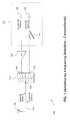
- FIG. 1illustrates a block diagram of an RF front-end that provides isolation by frequency selection.
- FIG. 2illustrates a block diagram of an RF front-end that provides isolation by electrical balance, according to embodiments of the present invention.
- FIG. 3illustrates a schematic block diagram of the RF front-end, illustrated in FIG. 2 , that provides isolation by electrical balance, according to embodiments of the present invention.
- FIG. 4illustrates a schematic block diagram of the RF front-end, illustrated in FIG. 3 , with the antenna replaced by its effective impedance, according to embodiments of the present invention.
- FIG. 5illustrates a schematic block diagram of the RF front-end, illustrated in FIG. 3 , with the power amplifier replaced by its effective impedance, according to embodiments of the present invention.
- FIG. 6illustrates a noise matched INA that can be implemented within the RF front-end illustrated in FIGS. 2-5 , according to embodiments of the present invention.
- references in the specification to “one embodiment,” “an embodiment.” “an example embodiment,” etc.,indicate that the embodiment described may include a particular feature, structure, or characteristic, but every embodiment may not necessarily include the particular feature, structure, or characteristic. Moreover, such phrases are not necessarily referring to the same embodiment. Further, when a particular feature, structure, or characteristic is described in connection with an embodiment, it is submitted that it is within the knowledge of one skilled in the art to effect such feature, structure, or characteristic in connection with other embodiments whether or not explicitly described.
- FIG. 1illustrates a block diagram of an RF front-end 100 configured to provide full-duplex communication.
- RF front-end 100includes an antenna 105 , a duplexer 110 , a low-noise amplifier (LNA) 115 , a power amplifier (PA) 120 , and an integrated-circuit (IC) 125 .
- LNAlow-noise amplifier
- PApower amplifier
- ICintegrated-circuit
- RF front-end 100can be used within a cellular telephone, a laptop computer, a wireless local area network (WLAN) station, and/or any other device that transmits and receives RF signals.
- WLANwireless local area network
- RF front-end 100transmits and receives RF signals over non-overlapping portions of a particular frequency band (e.g., one of the 14 bands specified by FDI)-UMTS, including the 900 MHz, 1800 MHz, and 2100 MHz bands).
- a particular frequency bande.g., one of the 14 bands specified by FDI
- the two signalsdo not interfere with each other and full-duplex communication can be achieved.
- both inbound and outbound signalsare simultaneously coupled between antenna 105 and duplexer 110 over a common signal path 130 .
- duplexer 110is used to couple common signal path 130 to both the input of LNA 115 and to the output of PA 120 .
- Duplexer 110provides the necessary coupling, while preventing strong outbound signals, produced by PA 120 , from being coupled to the input of LNA 115 .
- duplexer 110is a three-port device having an antenna port 135 , a transmit port 140 , and a receive port 145 .
- Antenna port 135is coupled to transmit port 140 through a transmit band-pass filter, included in duplexer 110 , and to receive port 145 through a receive band-pass filter, further included in duplexer 110 .
- the pass band of the transmit filteris centered within the frequency range of the outbound signals, which are received at node 150 from a transmitter (not shown).
- the pass band of the receive filteris centered within the frequency range of the inbound signals, which are passed to a receiver (not shown) at node 155 .
- the transmit and receive band-pass filtersare configured such that their respective stop bands overlap with each others pass bands. In this way, the band-pass filters isolate the input of LNA 115 from the strong outbound signals produced by PA 120 . In typical implementations, duplexer 110 must attenuate the strong outbound signals by about 50-60 dB to prevent the outbound signals from saturating LNA 115 .
- duplexer 110Today's high frequency communication standards (e.g., FDD-UMTS) dictate that frequency selective duplexers, such as duplexer 110 , be built with very high Q-factor and low loss materials, which currently cannot be done using silicon-based technology.
- duplexersare fabricated using special materials and processes (e.g., ceramic, surface acoustic wave (SAW), film bulk acoustic wave (FBAR), etc.) that cannot be integrated with a transceiver on a silicon-based IC.
- IC 125is implemented using silicon-based technology and includes at least portions of LNA 115 , the transmitter (not shown) coupled at node 150 , and the receiver (not shown) coupled at node 155 . Because conventional duplexer 110 typically cannot be integrated on IC 125 , due to the limitations of silicon-based technology, duplexer 110 is provided for off-chip, thereby increasing the size and cost of the radio transceiver.
- full-duplex radio transceiversoperate over multiple frequency bands (e.g., there are 14 frequency bands for FDD-UMTS), which require a separate conventional duplexer 110 for each band.
- each duplexeris off-chip, significantly increasing the size and cost of the radio transceiver.
- duplexer functional circuitthat can be fabricated using silicon-based technology such that it can be implemented on the same integrated circuit as'the radio transceiver.
- FIG. 2illustrates a block diagram of an RF front-end 200 configured to provide full-duplex communication, according to embodiments of the present invention.
- RF front-end 200provides wideband isolation using electrical balance.
- RF front-end 200includes an antenna 205 , an IC 210 , an isolation module 215 , a balancing network 220 , an LNA 225 , and a PA 230 .
- RF front-end 200can be used within a cellular telephone, a laptop computer, a wireless local area network (WLAN) station, and/or any other device that transmits and receives RF signals.
- WLANwireless local area network
- RF front-end 200transmits and receives RF signals over non-overlapping portions of at least one particular frequency band (e.g., one of the 14 bands specified by FDD-UMTS, including the 900 MHz, 1800 MHz. and 2100 MHz bands).
- the two signalsdo not interfere with each other and full-duplex communication can be achieved.
- both inbound and outbound signalsare simultaneously coupled between antenna 205 and isolation module 215 over a common signal path 235 .
- isolation module 215is used to couple common signal path 235 to a differential input 240 of LNA 225 and to an output 245 of PA 230 .
- Isolation module 215provides the necessary coupling, while preventing strong outbound signals that are provided by PA 230 , from saturating LNA 225 .
- Isolation module 215is specifically implemented as a four-port device having an antenna port 250 , a transmit port 255 , a differential receive port 260 , and a balance port 265 .
- Isolation module 215in conjunction with balancing network 220 , is configured to isolate transmit port 255 from differential receive port 260 by electrical balance.
- the energy of the strong outbound signals, provided by PA 230 at transmit port 255 .is split by isolation module 215 , with a first portion of the energy directed towards antenna 205 for transmission, and a second portion of the energy directed towards balancing network 220 , where it is dissipated (as heat).
- balancing network 220is configured to provide an impedance substantially equal to that of antenna 205 such that the first portion and second portion of energy are equal (i.e., each are exactly one-half the energy of the strong outbound signals).
- isolation module 215can effectively isolate differential input 240 of LNA 225 from the strong outbound signals.
- IC 210is implemented using silicon-based technology and can include at least portions of LNA 225 , balancing network 220 , the transmitter (not shown) coupled to node 270 , and the receiver (not shown) coupled to node 275 .
- isolation module 215can be further integrated within IC 210 because isolation by electrical balance does not require high Q-factor components necessary for isolation by frequency selectivity.
- the method of isolation provided by isolation module 215i.e., electrical balance
- isolation module 215is, in general, frequency independent, a single isolation module can be used in a multi-band application that requires full-duplex communication over several frequency bands (e.g., two or more of the 14 bands specified by FDD-UMTS). Stated another way, a single isolation module can be used to provide isolation for multiple different applications that operate over different frequency bands.
- FIG. 3illustrates a schematic block diagram of RF front-end 200 , according to embodiments of the present invention.
- balance network 220includes a tunable capacitor C BAL and a tunable resistor R BAL . These two tunable components can be adjusted such that balance network 220 provides a substantially similar impedance as antenna 205 and, in effect, electrically balances isolation module 215 with antenna 205 .
- Isolation module 215includes a tuning capacitor C TUNE and an autotransformer constructed from two series coupled windings: primary winding W P and secondary winding W S . As indicated by the positioning of the polarity marker for each winding, the autotransformer is a step-up autotransformer with additive polarity.
- isolation module 215can provide greater than 50 dB of isolation between transmit port 255 and differential receive port 260 over a bandwidth of several hundred MHz (e.g., 100-200 MHz).
- isolation module 215isolates differential input 240 of LNA 225 from a strong outbound signal produced by PA 230 .
- antenna 205has been replaced by its equivalent impedance Z ANT .
- isolation module 215receives at transmit port 255 a strong outbound signal produced by PA 230 .
- the strong outbound signalis coupled to a center node of the series coupled windings W P and W S and has an associated current I PA as illustrated in FIG. 4 .
- differential input 240 of LNA 225presents a high impedance
- the entire current I PRsubstantially couples to antenna 205 through antenna port 250 and the entire current I SN substantially couples to balance network 220 through balance port 265 .
- antenna 205 and balance network 220have substantially equal impedances, the voltage produced across each is also substantially equal.
- These two voltage signals, across antenna 205 and balance network 220are each coupled to different ends of differential input 240 of LNA 225 .
- the two voltage signalsare equal in magnitude, they appear common mode to LNA 225 , thereby isolating LNA 225 from the strong outbound signal produced by PA 230 .
- differential receive port 260is effectively isolated from transmit port 255 .
- the turns ratio of the two windings W P and W Scan be skewed away from a value of 1 such that more of the signal energy produced by PA 230 is provided to antenna 205 than to balance network 220 . For example, assuming the primary winding W P has N P turns and the secondary winding W S has N S turns, their turns ratio is given by N P /N S .
- N P /N Sis equal to 1 and the strong outbound signals provided by PA 230 suffer a dissipation loss of around 3.0 dB.
- balance network 220can be adjusted to compensate for the increase in current to antenna 205 .
- the resistive portion of the impedance provided by balance network 220can be set equal to a times the resistive portion of the impedance provided by antenna 205 .
- the turns ratio of the autotransformereffectively increases the insertion loss of isolation module 215 for inbound signals received by antenna 205 .
- the turns ratio of the autotransformercan be skewed to provide a maximal signal to antenna 205 , while maintaining a maximum acceptable insertion loss between antenna port 250 and differential receive port 260 .
- isolation module 215receives at antenna port 250 a weak inbound signal from antenna 205 .
- the weak inbound signalis coupled to a first end of primary winding W P , to a first end of differential input 240 , and to a first end of tuning capacitor C TUNE .
- a current I ANTis produced by antenna 205 and coupled to antenna port 250 of isolation module 215 .
- a first portion I PR of the current I ANTflows through primary winding W P and a second portion I TUNE of the current I ANT flows through tuning capacitor C TUNE .
- N PN S
- the current I SN flowing through secondary winding W Swill be equal in magnitude to I PR .
- a differential voltageis produced across the receive port 260 and LNA 225 senses the weak inbound signal.
- the noise figure of isolation module 215has two main contributors:
- LNA 225can be implemented as a noise-matched LNA to provide a high-input impedance that maximizes the voltage gain from antenna 205 to LNA 225 .
- the use of frequency selective isolationrequires the use of an off-chip duplexer.
- the length of the signal path, coupling the duplexer to the on-chip LNAis typically non-negligible compared to the wavelength of the signals. carried over it. Therefore, in conventional RF front-ends, the signal path is treated as a transmission line that is susceptible to the well known property of reflections.
- the output impedance of the duplexeris impedance matched to the input impedance of the LNA. Typically, this is accomplished by impedance matching the respective ports to a common transmission line of 50 Ohms.
- isolationis provided via electrical balance on-chip with LNA 225 .
- the novel on-chip isolation solutionallows the length of the signal path, coupling isolation module 215 to LNA 225 , to be substantially negligible compared to the wavelength of the signals carried over it. In other words, the voltage on the signal path at any given point in time is substantially the same at all points on the signal path.
- the requirement of impedance matchingis no longer necessary using the on-chip isolation illustrated in FIGS. 2-5 .
- LNA 225can be optimized for noise matching.
- noise matching of LNA 225is achieved by configuring LNA 225 to have an extremely large input impedance; often as large as possible (as opposed to the 50 Ohms commonly required for impedance matching purposes). Configuring LNA 225 for noise-matching provides for a high-input impedance that maximizes the voltage gain from antenna 205 to LNA 225 .
- FIG. 6illustrates an exemplary embodiment of LNA 225 that has been noise-matched, according to embodiments of the present invention.
- LNA 225is configured as a common source amplifier.
- LNA 225receives inbound signals at differential input 240 and provides an amplified version of the inbound signals at differential output 275 .
- the differential input 240is coupled to isolation module 215 via a signal path that has a length which is substantially negligible compared to the wavelength of the signals carried over it.
- LNA 225includes a first field effect transistor (FET) M 1 coupled at its gate to the positive end of differential input 240 .
- the source of M 1is coupled to ground.
- the drain of M 1is coupled to the source of a second FET M 2 at a node 600 in a cascode configuration.
- M 2is biased at its gate via bias voltage Vb 1 .
- M 2is used to maximize gain and provide reverse isolation.
- the drain of M 2is coupled through a load 610 to a supply voltage V DD .
- Load 610includes any one of a resistor, inductor, capacitor, or any combination thereof.
- a positive end of differential output 275is provided at the drain of M 2 .
- LNA 225further includes a third FET M 3 coupled at its gate to the negative end of the differential input 240 .
- the source of M 3is coupled to ground.
- the drain of M 3is coupled to the source of a fourth FET M 4 at a node 605 in a cascode configuration.
- M 4is biased at its gate via bias voltage Vb 2 .
- M 4is used to maximize gain and provide reverse isolation.
- the drain of M 4is coupled through a load 610 to a supply voltage V DD .
- Load 610includes any one of a resistor, inductor, capacitor, or any combination thereof.
- a negative end of a differential output 275is provided at the drain of M 4 .
- LNA 225The theoretical input impedance of LNA 225 as illustrated in FIG. 6 , ignoring parasitic capacitances, is infinite.
- a capacitoris typically coupled in series to each gate of FETs M 1 and M 3 and inductors are coupled between the sources of FETs M 1 and M 3 and ground (i.e., inductive degeneration).
- the noise-matched LNA 225 as illustrated in FIG. 6not only provides improved noise-matching over an impedance matched LNA, but further eliminates the need for the additional capacitors and inductors commonly used to provide impedance matching.
- exemplary LNA 225 illustrated in FIG. 6is provided for the purpose of illustration and not limitation. Other equivalent implementations and/or variations of exemplary LNA 225 are possible as would be understood by a person skilled in the art based on the teachings herein. Equivalent implementations and/or variations may include, for example, variations in transistor type (e.g., PNP, MOSFET, JFET, CMOS, etc.), variations in amplifier configuration (e.g., common-collector, common-base, common-source.
- transistor typee.g., PNP, MOSFET, JFET, CMOS, etc.
- amplifier configuratione.g., common-collector, common-base, common-source.
- amplifier input/output configuratione.g., single-ended, single-input-single-output, single-input-multiple-output, etc.
Landscapes
- Engineering & Computer Science (AREA)
- Signal Processing (AREA)
- Computer Networks & Wireless Communication (AREA)
- Amplifiers (AREA)
- Transceivers (AREA)
Abstract
Description
Claims (20)
Priority Applications (1)
| Application Number | Priority Date | Filing Date | Title |
|---|---|---|---|
| US14/546,746US9749119B2 (en) | 2009-09-11 | 2014-11-18 | RF front-end with wideband transmitter/receiver isolation |
Applications Claiming Priority (3)
| Application Number | Priority Date | Filing Date | Title |
|---|---|---|---|
| US24180209P | 2009-09-11 | 2009-09-11 | |
| US12/567,100US8897722B2 (en) | 2009-09-11 | 2009-09-25 | RF front-end with wideband transmitter/receiver isolation |
| US14/546,746US9749119B2 (en) | 2009-09-11 | 2014-11-18 | RF front-end with wideband transmitter/receiver isolation |
Related Parent Applications (1)
| Application Number | Title | Priority Date | Filing Date |
|---|---|---|---|
| US12/567,100ContinuationUS8897722B2 (en) | 2009-09-11 | 2009-09-25 | RF front-end with wideband transmitter/receiver isolation |
Publications (2)
| Publication Number | Publication Date |
|---|---|
| US20150071132A1 US20150071132A1 (en) | 2015-03-12 |
| US9749119B2true US9749119B2 (en) | 2017-08-29 |
Family
ID=43306393
Family Applications (2)
| Application Number | Title | Priority Date | Filing Date |
|---|---|---|---|
| US12/567,100Active2032-08-10US8897722B2 (en) | 2009-09-11 | 2009-09-25 | RF front-end with wideband transmitter/receiver isolation |
| US14/546,746Active2030-03-29US9749119B2 (en) | 2009-09-11 | 2014-11-18 | RF front-end with wideband transmitter/receiver isolation |
Family Applications Before (1)
| Application Number | Title | Priority Date | Filing Date |
|---|---|---|---|
| US12/567,100Active2032-08-10US8897722B2 (en) | 2009-09-11 | 2009-09-25 | RF front-end with wideband transmitter/receiver isolation |
Country Status (2)
| Country | Link |
|---|---|
| US (2) | US8897722B2 (en) |
| EP (1) | EP2296286B1 (en) |
Cited By (1)
| Publication number | Priority date | Publication date | Assignee | Title |
|---|---|---|---|---|
| US20220150041A1 (en)* | 2020-11-12 | 2022-05-12 | Avago Technologies International Sales Pte.Limited | Capacitive hybrid with pga for full duplex transceivers |
Families Citing this family (32)
| Publication number | Priority date | Publication date | Assignee | Title |
|---|---|---|---|---|
| US8229367B2 (en)* | 2009-04-14 | 2012-07-24 | Qualcomm, Incorporated | Low noise amplifier with combined input matching, balun, and transmit/receive switch |
| US8897722B2 (en) | 2009-09-11 | 2014-11-25 | Broadcom Corporation | RF front-end with wideband transmitter/receiver isolation |
| US8208865B2 (en)* | 2009-09-11 | 2012-06-26 | Broadcom Corporation | RF front-end with on-chip transmitter/receiver isolation and noise-matched LNA |
| US8514035B2 (en)* | 2009-12-30 | 2013-08-20 | Broadcom Corporation | RF front-end with on-chip transmitter/receiver isolation using a gyrator |
| US8599726B2 (en)* | 2010-06-03 | 2013-12-03 | Broadcom Corporation | Front end module with a tunable balancing network |
| US8843081B2 (en) | 2011-05-16 | 2014-09-23 | Qualcomm Incorporated | Receiver with transmit signal cancellation |
| US9083441B2 (en)* | 2011-10-26 | 2015-07-14 | Qualcomm Incorporated | Impedance balancing for transmitter to receiver rejection |
| EP2621098B1 (en) | 2012-01-30 | 2015-07-01 | Telefonaktiebolaget L M Ericsson (Publ) | Transceiver and communication device |
| US8971219B2 (en)* | 2012-03-30 | 2015-03-03 | Qualcomm Incorporated | Hybrid transformer based integrated duplexer for multi-band/multi-mode radio frequency (RF) front end |
| US20130259099A1 (en)* | 2012-03-30 | 2013-10-03 | Qualcomm Incorporated | Tunable notch filter using feedback through an existing feedback receiver |
| EP2672631B1 (en) | 2012-06-07 | 2014-12-24 | Telefonaktiebolaget L M Ericsson (publ) | Duplexer-less transceiver and communication apparatus |
| US9203455B2 (en)* | 2012-08-14 | 2015-12-01 | Broadcom Corporation | Full duplex system with self-interference cancellation |
| EP2733855B1 (en) | 2012-11-15 | 2016-07-27 | Telefonaktiebolaget LM Ericsson (publ) | Transceiver front-end |
| RU2615156C1 (en) | 2013-03-14 | 2017-04-04 | Телефонактиеболагет Л М Эрикссон (Пабл) | Leakage reduction from transmitter to receiver in full-duplex system without using duplexer |
| US20140269449A1 (en)* | 2013-03-15 | 2014-09-18 | Qualcomm Incorporated | Full-duplex wireless transceiver with hybrid circuit and reconfigurable radiation pattern antenna |
| TWI569590B (en)* | 2013-03-25 | 2017-02-01 | Airoha Tech Corp | Radio front end module |
| EP2989724B1 (en) | 2013-04-26 | 2018-08-08 | Telefonaktiebolaget LM Ericsson (publ) | Transceiver arrangement, communication device, method and computer program |
| US9871552B2 (en) | 2013-04-30 | 2018-01-16 | Telefonaktiebolaget Lm Ericsson (Publ) | Transceiver arrangement, communication device, method and computer program |
| CN104577331A (en)* | 2013-10-24 | 2015-04-29 | 展讯通信(上海)有限公司 | Device and method for improving stray isolation among antennas in two-way antennas |
| US9900044B2 (en) | 2014-01-21 | 2018-02-20 | Telefonaktiebolaget Lm Ericsson (Publ) | Transceiver arrangement and communication device |
| EP2903170B1 (en) | 2014-02-04 | 2020-01-08 | U-blox AG | Duplexing apparatus, wireless devices and related methods |
| WO2016066278A1 (en) | 2014-10-29 | 2016-05-06 | Telefonaktiebolaget L M Ericsson (Publ) | Transceiver arrangement and communication device |
| WO2016187782A1 (en)* | 2015-05-25 | 2016-12-01 | 华为技术有限公司 | Duplexer and wireless transceiving system |
| KR102324960B1 (en) | 2015-06-25 | 2021-11-12 | 삼성전자 주식회사 | Communication device and electronic device including the same |
| US11075688B2 (en) | 2016-05-19 | 2021-07-27 | Apple Inc. | In-band full duplex relay to enhance uplink performance in heterogeneous network |
| JP2018050159A (en)* | 2016-09-21 | 2018-03-29 | 株式会社村田製作所 | Transmission reception module |
| JP2018157248A (en)* | 2017-03-15 | 2018-10-04 | 株式会社村田製作所 | Front end module |
| US11005519B1 (en)* | 2020-05-01 | 2021-05-11 | UTVATE Corporation | Isolation methods for full-duplex antenna systems |
| US11171675B1 (en) | 2021-03-17 | 2021-11-09 | Hong Kong Applied Science and Technology Research Institute Company, Limited | Switch-less connection for radio-frequency (RF) transceivers |
| US11942974B2 (en)* | 2021-07-21 | 2024-03-26 | Pharrowtech Bv | Millimeter wave radio calibration circuit |
| CN114793140B (en)* | 2022-06-21 | 2022-09-13 | 深圳粤讯通信科技有限公司 | 5G antenna interface board port isolation measurement system |
| CN116318227B (en)* | 2023-03-16 | 2025-04-29 | 展讯通信(上海)有限公司 | Component parameter determining method, device, equipment and storage medium |
Citations (41)
| Publication number | Priority date | Publication date | Assignee | Title |
|---|---|---|---|---|
| US3047821A (en) | 1960-12-27 | 1962-07-31 | Aircraft Armaments Inc | Isolator using hall effect gyrator |
| US3340463A (en) | 1963-09-27 | 1967-09-05 | Hitachi Wire And Cable Ltd | Power transformer utilizing hall effects |
| US3973088A (en) | 1973-11-28 | 1976-08-03 | Kokusai Denshin Denwa Kabushiki Kaisha | Wide-band hybrid network |
| US4051475A (en) | 1976-07-21 | 1977-09-27 | The United States Ofamerica As Represented By The Secretary Of The Army | Radio receiver isolation system |
| US4278980A (en) | 1978-03-30 | 1981-07-14 | Nippon Gakki Seizo Kabushiki Kaisha | Antenna input circuit for radio receiver |
| US4446395A (en) | 1981-12-30 | 1984-05-01 | Technicare Corporation | Short ring down, ultrasonic transducer suitable for medical applications |
| US4616188A (en) | 1985-06-20 | 1986-10-07 | Burr-Brown Corporation | Hall effect isolation amplifier |
| US6026286A (en) | 1995-08-24 | 2000-02-15 | Nortel Networks Corporation | RF amplifier, RF mixer and RF receiver |
| US6144259A (en)* | 1998-03-18 | 2000-11-07 | Nec Corporation | Low-noise amplifier and circuit for controlling the same |
| US6339265B1 (en)* | 1999-04-09 | 2002-01-15 | 1061933 Ontario, Inc. | Voltage drop compensating reactor |
| US6480553B1 (en) | 1998-04-23 | 2002-11-12 | Winbond Electronics Corp. | Gaussian frequency-shift keying transciever for ISM wideband communication |
| US20020177417A1 (en) | 2001-05-25 | 2002-11-28 | Koninklijke Philips Electronics N.V. | Transmit/receive switch for an RF transceiver |
| US20030095421A1 (en) | 2000-05-23 | 2003-05-22 | Kadatskyy Anatoly F. | Power factor correction circuit |
| US6577212B1 (en) | 1999-07-16 | 2003-06-10 | Telefonaktiebolaget L M Ericsson (Publ) | Integrated circuit |
| US6721544B1 (en) | 2000-11-09 | 2004-04-13 | Intel Corporation | Duplexer structure for coupling a transmitter and a receiver to a common antenna |
| US6735424B1 (en)* | 2000-06-14 | 2004-05-11 | The Regents Of The University Of California | S-band low-noise amplifier with self-adjusting bias for improved power consumption and dynamic range in a mobile environment |
| US20040092285A1 (en) | 2001-02-27 | 2004-05-13 | Walter Kodim | Multiband r f switching device |
| US20040095277A1 (en) | 2002-11-19 | 2004-05-20 | Farrokh Mohamadi | Inductively-coupled antenna array |
| US20040145411A1 (en) | 2001-04-24 | 2004-07-29 | Harvey Geoffrey Philip | Resonant logic driver circuit |
| US7042208B1 (en) | 2002-02-15 | 2006-05-09 | Harris Larry L | Voltage isolation buffer with AC coupled and DC coupled hall effect magnetic field sensors |
| US7065327B1 (en) | 1998-09-10 | 2006-06-20 | Intel Corporation | Single-chip CMOS direct-conversion transceiver |
| US7167688B2 (en) | 2003-07-30 | 2007-01-23 | Chi Mei Communication Systems, Inc. | RF transceiver module formed in multi-layered ceramic |
| US20070117524A1 (en) | 2005-11-23 | 2007-05-24 | Ky-Hien Do | Quasi-circulator for antenna multi-coupler system |
| US20070152904A1 (en) | 2003-10-10 | 2007-07-05 | Broadcom Corporation, A California Corporation | Impedance matched passive radio frequency transmit/receive switch |
| US20070207747A1 (en) | 2006-03-06 | 2007-09-06 | Paul Johnson | Single frequency duplex radio link |
| US20080139149A1 (en) | 2006-12-12 | 2008-06-12 | Fenghao Mu | Method and Apparatus for Receiving Radio Frequency Signals |
| US7460662B2 (en) | 2004-12-02 | 2008-12-02 | Solarflare Communications, Inc. | Isolation of transmit and receive signals in full-duplex communication systems |
| US7489914B2 (en) | 2003-03-28 | 2009-02-10 | Georgia Tech Research Corporation | Multi-band RF transceiver with passive reuse in organic substrates |
| US7515879B2 (en) | 2004-02-05 | 2009-04-07 | Renesas Technology Corp. | Radio frequency circuit module |
| US20100157858A1 (en) | 2008-12-24 | 2010-06-24 | Rayspan Corporation | Rf front-end module and antenna systems |
| US20100210223A1 (en) | 2009-02-17 | 2010-08-19 | Oleksandr Gorbachov | Multi mode radio frequency transceiver front end circuit with inter-stage matching circuit |
| US7839938B2 (en) | 2003-05-29 | 2010-11-23 | Maxim Integrated Products, Inc. | Method and apparatus for cancellation of magnetizing inductance current in a transformer circuit |
| US7844231B2 (en) | 2008-01-29 | 2010-11-30 | Samsung Electronics Co., Ltd. | Apparatus and method for transmit/receive antenna switch in a TDD wireless communication system |
| US20110064005A1 (en) | 2009-09-11 | 2011-03-17 | Broadcom Corporation | RF Front-End with Wideband Transmitter/Receiver Isolation |
| US20110064004A1 (en) | 2009-09-11 | 2011-03-17 | Broadcom Corporation | RF Front-End With On-Chip Transmitter/Receiver Isolation and Noise-Matched LNA |
| US20110158134A1 (en) | 2009-12-30 | 2011-06-30 | Broadcom Corporation | RF Front-End with On-Chip Transmitter/Receiver Isolation Using A Gyrator |
| US8130054B1 (en) | 2008-10-14 | 2012-03-06 | Rf Micro Devices, Inc. | Frequency-adjustable radio frequency isolator circuitry |
| US8208866B2 (en) | 2008-08-05 | 2012-06-26 | Broadcom Corporation | RF transceiver front-end with RX/TX isolation |
| US8232857B1 (en) | 2009-04-15 | 2012-07-31 | Triquint Semiconductor, Inc. | Flux-coupled transformer for power amplifier output matching |
| US8249536B2 (en) | 2009-05-27 | 2012-08-21 | Samsung Techwin Co., Ltd. | Apparatus and method for removing transmission leakage signal |
| US8867999B2 (en)* | 2009-01-26 | 2014-10-21 | Qualcomm Incorporated | Downlink interference cancellation methods |
Family Cites Families (1)
| Publication number | Priority date | Publication date | Assignee | Title |
|---|---|---|---|---|
| US8792836B2 (en)* | 2010-06-03 | 2014-07-29 | Broadcom Corporation | Front end module with compensating duplexer |
- 2009
- 2009-09-25USUS12/567,100patent/US8897722B2/enactiveActive
- 2010
- 2010-09-07EPEP10009280.8Apatent/EP2296286B1/enactiveActive
- 2014
- 2014-11-18USUS14/546,746patent/US9749119B2/enactiveActive
Patent Citations (45)
| Publication number | Priority date | Publication date | Assignee | Title |
|---|---|---|---|---|
| US3047821A (en) | 1960-12-27 | 1962-07-31 | Aircraft Armaments Inc | Isolator using hall effect gyrator |
| US3340463A (en) | 1963-09-27 | 1967-09-05 | Hitachi Wire And Cable Ltd | Power transformer utilizing hall effects |
| US3973088A (en) | 1973-11-28 | 1976-08-03 | Kokusai Denshin Denwa Kabushiki Kaisha | Wide-band hybrid network |
| US4051475A (en) | 1976-07-21 | 1977-09-27 | The United States Ofamerica As Represented By The Secretary Of The Army | Radio receiver isolation system |
| US4278980A (en) | 1978-03-30 | 1981-07-14 | Nippon Gakki Seizo Kabushiki Kaisha | Antenna input circuit for radio receiver |
| US4446395A (en) | 1981-12-30 | 1984-05-01 | Technicare Corporation | Short ring down, ultrasonic transducer suitable for medical applications |
| US4616188A (en) | 1985-06-20 | 1986-10-07 | Burr-Brown Corporation | Hall effect isolation amplifier |
| US6026286A (en) | 1995-08-24 | 2000-02-15 | Nortel Networks Corporation | RF amplifier, RF mixer and RF receiver |
| US6144259A (en)* | 1998-03-18 | 2000-11-07 | Nec Corporation | Low-noise amplifier and circuit for controlling the same |
| US6480553B1 (en) | 1998-04-23 | 2002-11-12 | Winbond Electronics Corp. | Gaussian frequency-shift keying transciever for ISM wideband communication |
| US7065327B1 (en) | 1998-09-10 | 2006-06-20 | Intel Corporation | Single-chip CMOS direct-conversion transceiver |
| US6339265B1 (en)* | 1999-04-09 | 2002-01-15 | 1061933 Ontario, Inc. | Voltage drop compensating reactor |
| US6577212B1 (en) | 1999-07-16 | 2003-06-10 | Telefonaktiebolaget L M Ericsson (Publ) | Integrated circuit |
| US20030095421A1 (en) | 2000-05-23 | 2003-05-22 | Kadatskyy Anatoly F. | Power factor correction circuit |
| US6735424B1 (en)* | 2000-06-14 | 2004-05-11 | The Regents Of The University Of California | S-band low-noise amplifier with self-adjusting bias for improved power consumption and dynamic range in a mobile environment |
| US6721544B1 (en) | 2000-11-09 | 2004-04-13 | Intel Corporation | Duplexer structure for coupling a transmitter and a receiver to a common antenna |
| US20040092285A1 (en) | 2001-02-27 | 2004-05-13 | Walter Kodim | Multiband r f switching device |
| US20040145411A1 (en) | 2001-04-24 | 2004-07-29 | Harvey Geoffrey Philip | Resonant logic driver circuit |
| US20020177417A1 (en) | 2001-05-25 | 2002-11-28 | Koninklijke Philips Electronics N.V. | Transmit/receive switch for an RF transceiver |
| US7042208B1 (en) | 2002-02-15 | 2006-05-09 | Harris Larry L | Voltage isolation buffer with AC coupled and DC coupled hall effect magnetic field sensors |
| US20040095277A1 (en) | 2002-11-19 | 2004-05-20 | Farrokh Mohamadi | Inductively-coupled antenna array |
| US7489914B2 (en) | 2003-03-28 | 2009-02-10 | Georgia Tech Research Corporation | Multi-band RF transceiver with passive reuse in organic substrates |
| US7839938B2 (en) | 2003-05-29 | 2010-11-23 | Maxim Integrated Products, Inc. | Method and apparatus for cancellation of magnetizing inductance current in a transformer circuit |
| US7167688B2 (en) | 2003-07-30 | 2007-01-23 | Chi Mei Communication Systems, Inc. | RF transceiver module formed in multi-layered ceramic |
| US20070152904A1 (en) | 2003-10-10 | 2007-07-05 | Broadcom Corporation, A California Corporation | Impedance matched passive radio frequency transmit/receive switch |
| US7515879B2 (en) | 2004-02-05 | 2009-04-07 | Renesas Technology Corp. | Radio frequency circuit module |
| US7460662B2 (en) | 2004-12-02 | 2008-12-02 | Solarflare Communications, Inc. | Isolation of transmit and receive signals in full-duplex communication systems |
| US20070117524A1 (en) | 2005-11-23 | 2007-05-24 | Ky-Hien Do | Quasi-circulator for antenna multi-coupler system |
| US7801493B2 (en)* | 2005-11-23 | 2010-09-21 | Trex Enterprises Corp. | Quasi-circulator for antenna multi-coupler system |
| US20070207747A1 (en) | 2006-03-06 | 2007-09-06 | Paul Johnson | Single frequency duplex radio link |
| US20080139149A1 (en) | 2006-12-12 | 2008-06-12 | Fenghao Mu | Method and Apparatus for Receiving Radio Frequency Signals |
| US7844231B2 (en) | 2008-01-29 | 2010-11-30 | Samsung Electronics Co., Ltd. | Apparatus and method for transmit/receive antenna switch in a TDD wireless communication system |
| US8208866B2 (en) | 2008-08-05 | 2012-06-26 | Broadcom Corporation | RF transceiver front-end with RX/TX isolation |
| US8130054B1 (en) | 2008-10-14 | 2012-03-06 | Rf Micro Devices, Inc. | Frequency-adjustable radio frequency isolator circuitry |
| US20100157858A1 (en) | 2008-12-24 | 2010-06-24 | Rayspan Corporation | Rf front-end module and antenna systems |
| US8867999B2 (en)* | 2009-01-26 | 2014-10-21 | Qualcomm Incorporated | Downlink interference cancellation methods |
| US20100210223A1 (en) | 2009-02-17 | 2010-08-19 | Oleksandr Gorbachov | Multi mode radio frequency transceiver front end circuit with inter-stage matching circuit |
| US8232857B1 (en) | 2009-04-15 | 2012-07-31 | Triquint Semiconductor, Inc. | Flux-coupled transformer for power amplifier output matching |
| US8249536B2 (en) | 2009-05-27 | 2012-08-21 | Samsung Techwin Co., Ltd. | Apparatus and method for removing transmission leakage signal |
| US20110064005A1 (en) | 2009-09-11 | 2011-03-17 | Broadcom Corporation | RF Front-End with Wideband Transmitter/Receiver Isolation |
| US20110064004A1 (en) | 2009-09-11 | 2011-03-17 | Broadcom Corporation | RF Front-End With On-Chip Transmitter/Receiver Isolation and Noise-Matched LNA |
| US8208865B2 (en) | 2009-09-11 | 2012-06-26 | Broadcom Corporation | RF front-end with on-chip transmitter/receiver isolation and noise-matched LNA |
| US20110158134A1 (en) | 2009-12-30 | 2011-06-30 | Broadcom Corporation | RF Front-End with On-Chip Transmitter/Receiver Isolation Using A Gyrator |
| US20110158135A1 (en) | 2009-12-30 | 2011-06-30 | Broadcom Corporation | RF Front-End with On-Chip Transmitter/Receiver Isolation Using the Hall Effect |
| US20130285764A1 (en) | 2009-12-30 | 2013-10-31 | Broadcom Corporation | Rf front-end with on-chip transmitter/receiver isolation using a gyrator |
Non-Patent Citations (3)
| Title |
|---|
| European Search Report for EP Patent Application No. EP10009280.8, European Patent Office , The Hague, Netherlands, mailed on Feb. 25, 2013. |
| Mikhemar, M., Darabi, H. and Abidi, A., "A Tunable Integrated Duplexer with 50dB Isolation in 40nm CMOS," 2009 IEEE International Solid-State Circuits Conference, Session 22, PA and Antenna Interface 22.7, Feb. 11, 2009, 3 pages. |
| Satori, Eugene F., "Hybrid Transformers," IEEE Transactions on Parts, Materials and Packaging, vol. PMP-4, No. 3, Sep. 1968, pp. 59-66. |
Cited By (4)
| Publication number | Priority date | Publication date | Assignee | Title |
|---|---|---|---|---|
| US20220150041A1 (en)* | 2020-11-12 | 2022-05-12 | Avago Technologies International Sales Pte.Limited | Capacitive hybrid with pga for full duplex transceivers |
| US12058083B2 (en)* | 2020-11-12 | 2024-08-06 | Avago Technologies International Sales Pte. Limited | Capacitive hybrid with PGA for full duplex transceivers |
| US20240356719A1 (en)* | 2020-11-12 | 2024-10-24 | Avago Technologies International Sales Pte. Limited | Capacitive hybrid with pga for full duplex transceivers |
| US12438688B2 (en)* | 2020-11-12 | 2025-10-07 | Avago Technologies International Sales Pte. Limited | Capacitive hybrid with PGA for full duplex transceivers |
Also Published As
| Publication number | Publication date |
|---|---|
| EP2296286A3 (en) | 2013-03-27 |
| EP2296286A2 (en) | 2011-03-16 |
| US8897722B2 (en) | 2014-11-25 |
| US20110064005A1 (en) | 2011-03-17 |
| US20150071132A1 (en) | 2015-03-12 |
| EP2296286B1 (en) | 2016-03-30 |
Similar Documents
| Publication | Publication Date | Title |
|---|---|---|
| US9749119B2 (en) | RF front-end with wideband transmitter/receiver isolation | |
| US8208865B2 (en) | RF front-end with on-chip transmitter/receiver isolation and noise-matched LNA | |
| US9306542B2 (en) | RF front-end with on-chip transmitter/receiver isolation using a gyrator | |
| US10153803B2 (en) | Receiving circuit, wireless communication module, and wireless communication device | |
| US7283793B1 (en) | Package filter and combiner network | |
| US7245887B2 (en) | High speed CMOS transmit-receive antenna switch | |
| CA3096679C (en) | Transmit and receive switch and broadband power amplifier matching network for multi-band millimeter-wave 5g communication | |
| US9853623B2 (en) | High-selectivity low-loss duplexer | |
| US20050107043A1 (en) | Integration of diversity switch in combination with a T/R switch for a radio transceiver on a single chip | |
| US11349469B2 (en) | High power radio frequency switches with low leakage current and low insertion loss | |
| US20240380566A1 (en) | Millimeter-wave fully-integrated full duplexer modules with and without internal low noise amplifier and power amplifier for 5g applications | |
| US20250286580A1 (en) | Ultra-Wide Bandwidth Ultra-Isolation DC-100 Gigahertz Front-End Module with Integrated Duplexer, Low Noise Amplifier, and Power Amplifier for Wireless Communication Applications | |
| US20190229415A1 (en) | Radio-Frequency Apparatus with Integrated Antenna Control and Associated Methods | |
| US11251827B2 (en) | Front-end module | |
| CN105830385A (en) | Signal processing device, amplifier, and method | |
| KR102041655B1 (en) | High frequency switch | |
| US8953502B2 (en) | Receiver for receiving RF-signals in a plurality of different communication bands and transceiver | |
| US20170093032A1 (en) | Radio-Frequency Apparatus With Integrated Antenna Control and Associated Methods |
Legal Events
| Date | Code | Title | Description |
|---|---|---|---|
| AS | Assignment | Owner name:BROADCOM CORPORATION, CALIFORNIA Free format text:ASSIGNMENT OF ASSIGNORS INTEREST;ASSIGNORS:MIKHEMAR, MOHYEE;DARABI, HOOMAN;REEL/FRAME:034418/0064 Effective date:20090918 | |
| AS | Assignment | Owner name:BANK OF AMERICA, N.A., AS COLLATERAL AGENT, NORTH CAROLINA Free format text:PATENT SECURITY AGREEMENT;ASSIGNOR:BROADCOM CORPORATION;REEL/FRAME:037806/0001 Effective date:20160201 Owner name:BANK OF AMERICA, N.A., AS COLLATERAL AGENT, NORTH Free format text:PATENT SECURITY AGREEMENT;ASSIGNOR:BROADCOM CORPORATION;REEL/FRAME:037806/0001 Effective date:20160201 | |
| AS | Assignment | Owner name:AVAGO TECHNOLOGIES GENERAL IP (SINGAPORE) PTE. LTD., SINGAPORE Free format text:ASSIGNMENT OF ASSIGNORS INTEREST;ASSIGNOR:BROADCOM CORPORATION;REEL/FRAME:041706/0001 Effective date:20170120 Owner name:AVAGO TECHNOLOGIES GENERAL IP (SINGAPORE) PTE. LTD Free format text:ASSIGNMENT OF ASSIGNORS INTEREST;ASSIGNOR:BROADCOM CORPORATION;REEL/FRAME:041706/0001 Effective date:20170120 | |
| AS | Assignment | Owner name:BROADCOM CORPORATION, CALIFORNIA Free format text:TERMINATION AND RELEASE OF SECURITY INTEREST IN PATENTS;ASSIGNOR:BANK OF AMERICA, N.A., AS COLLATERAL AGENT;REEL/FRAME:041712/0001 Effective date:20170119 | |
| STCF | Information on status: patent grant | Free format text:PATENTED CASE | |
| AS | Assignment | Owner name:AVAGO TECHNOLOGIES INTERNATIONAL SALES PTE. LIMITE Free format text:MERGER;ASSIGNOR:AVAGO TECHNOLOGIES GENERAL IP (SINGAPORE) PTE. LTD.;REEL/FRAME:047422/0464 Effective date:20180509 | |
| AS | Assignment | Owner name:AVAGO TECHNOLOGIES INTERNATIONAL SALES PTE. LIMITE Free format text:CORRECTIVE ASSIGNMENT TO CORRECT THE EXECUTION DATE PREVIOUSLY RECORDED AT REEL: 047422 FRAME: 0464. ASSIGNOR(S) HEREBY CONFIRMS THE MERGER;ASSIGNOR:AVAGO TECHNOLOGIES GENERAL IP (SINGAPORE) PTE. LTD.;REEL/FRAME:048883/0702 Effective date:20180905 | |
| MAFP | Maintenance fee payment | Free format text:PAYMENT OF MAINTENANCE FEE, 4TH YEAR, LARGE ENTITY (ORIGINAL EVENT CODE: M1551); ENTITY STATUS OF PATENT OWNER: LARGE ENTITY Year of fee payment:4 | |
| MAFP | Maintenance fee payment | Free format text:PAYMENT OF MAINTENANCE FEE, 8TH YEAR, LARGE ENTITY (ORIGINAL EVENT CODE: M1552); ENTITY STATUS OF PATENT OWNER: LARGE ENTITY Year of fee payment:8 |