US9741761B2 - Photosensitive imaging devices and associated methods - Google Patents
Photosensitive imaging devices and associated methodsDownload PDFInfo
- Publication number
- US9741761B2 US9741761B2US14/245,872US201414245872AUS9741761B2US 9741761 B2US9741761 B2US 9741761B2US 201414245872 AUS201414245872 AUS 201414245872AUS 9741761 B2US9741761 B2US 9741761B2
- Authority
- US
- United States
- Prior art keywords
- pixel
- infrared
- light
- laser
- visible light
- Prior art date
- Legal status (The legal status is an assumption and is not a legal conclusion. Google has not performed a legal analysis and makes no representation as to the accuracy of the status listed.)
- Active
Links
Images


Classifications
- H01L27/14649—
- H—ELECTRICITY
- H01—ELECTRIC ELEMENTS
- H01L—SEMICONDUCTOR DEVICES NOT COVERED BY CLASS H10
- H01L25/00—Assemblies consisting of a plurality of semiconductor or other solid state devices
- H01L25/16—Assemblies consisting of a plurality of semiconductor or other solid state devices the devices being of types provided for in two or more different subclasses of H10B, H10D, H10F, H10H, H10K or H10N, e.g. forming hybrid circuits
- H01L25/167—Assemblies consisting of a plurality of semiconductor or other solid state devices the devices being of types provided for in two or more different subclasses of H10B, H10D, H10F, H10H, H10K or H10N, e.g. forming hybrid circuits comprising optoelectronic devices, e.g. LED, photodiodes
- H01L27/1461—
- H01L27/14612—
- H01L27/14625—
- H01L27/1464—
- H01L27/14645—
- H01L27/14647—
- H—ELECTRICITY
- H04—ELECTRIC COMMUNICATION TECHNIQUE
- H04N—PICTORIAL COMMUNICATION, e.g. TELEVISION
- H04N23/00—Cameras or camera modules comprising electronic image sensors; Control thereof
- H04N23/56—Cameras or camera modules comprising electronic image sensors; Control thereof provided with illuminating means
- H—ELECTRICITY
- H04—ELECTRIC COMMUNICATION TECHNIQUE
- H04N—PICTORIAL COMMUNICATION, e.g. TELEVISION
- H04N25/00—Circuitry of solid-state image sensors [SSIS]; Control thereof
- H04N25/70—SSIS architectures; Circuits associated therewith
- H—ELECTRICITY
- H04—ELECTRIC COMMUNICATION TECHNIQUE
- H04N—PICTORIAL COMMUNICATION, e.g. TELEVISION
- H04N25/00—Circuitry of solid-state image sensors [SSIS]; Control thereof
- H04N25/70—SSIS architectures; Circuits associated therewith
- H04N25/76—Addressed sensors, e.g. MOS or CMOS sensors
- H04N25/77—Pixel circuitry, e.g. memories, A/D converters, pixel amplifiers, shared circuits or shared components
- H04N25/771—Pixel circuitry, e.g. memories, A/D converters, pixel amplifiers, shared circuits or shared components comprising storage means other than floating diffusion
- H04N5/2256—
- H04N5/37452—
- H04N5/3765—
- H04N9/045—
- H—ELECTRICITY
- H10—SEMICONDUCTOR DEVICES; ELECTRIC SOLID-STATE DEVICES NOT OTHERWISE PROVIDED FOR
- H10F—INORGANIC SEMICONDUCTOR DEVICES SENSITIVE TO INFRARED RADIATION, LIGHT, ELECTROMAGNETIC RADIATION OF SHORTER WAVELENGTH OR CORPUSCULAR RADIATION
- H10F39/00—Integrated devices, or assemblies of multiple devices, comprising at least one element covered by group H10F30/00, e.g. radiation detectors comprising photodiode arrays
- H10F39/10—Integrated devices
- H10F39/12—Image sensors
- H10F39/18—Complementary metal-oxide-semiconductor [CMOS] image sensors; Photodiode array image sensors
- H10F39/182—Colour image sensors
- H10F39/1825—Multicolour image sensors having stacked structure, e.g. NPN, NPNPN or multiple quantum well [MQW] structures
- H—ELECTRICITY
- H10—SEMICONDUCTOR DEVICES; ELECTRIC SOLID-STATE DEVICES NOT OTHERWISE PROVIDED FOR
- H10F—INORGANIC SEMICONDUCTOR DEVICES SENSITIVE TO INFRARED RADIATION, LIGHT, ELECTROMAGNETIC RADIATION OF SHORTER WAVELENGTH OR CORPUSCULAR RADIATION
- H10F39/00—Integrated devices, or assemblies of multiple devices, comprising at least one element covered by group H10F30/00, e.g. radiation detectors comprising photodiode arrays
- H10F39/10—Integrated devices
- H10F39/12—Image sensors
- H10F39/18—Complementary metal-oxide-semiconductor [CMOS] image sensors; Photodiode array image sensors
- H10F39/184—Infrared image sensors
- H—ELECTRICITY
- H10—SEMICONDUCTOR DEVICES; ELECTRIC SOLID-STATE DEVICES NOT OTHERWISE PROVIDED FOR
- H10F—INORGANIC SEMICONDUCTOR DEVICES SENSITIVE TO INFRARED RADIATION, LIGHT, ELECTROMAGNETIC RADIATION OF SHORTER WAVELENGTH OR CORPUSCULAR RADIATION
- H10F39/00—Integrated devices, or assemblies of multiple devices, comprising at least one element covered by group H10F30/00, e.g. radiation detectors comprising photodiode arrays
- H10F39/10—Integrated devices
- H10F39/12—Image sensors
- H10F39/199—Back-illuminated image sensors
- H—ELECTRICITY
- H10—SEMICONDUCTOR DEVICES; ELECTRIC SOLID-STATE DEVICES NOT OTHERWISE PROVIDED FOR
- H10F—INORGANIC SEMICONDUCTOR DEVICES SENSITIVE TO INFRARED RADIATION, LIGHT, ELECTROMAGNETIC RADIATION OF SHORTER WAVELENGTH OR CORPUSCULAR RADIATION
- H10F39/00—Integrated devices, or assemblies of multiple devices, comprising at least one element covered by group H10F30/00, e.g. radiation detectors comprising photodiode arrays
- H10F39/80—Constructional details of image sensors
- H10F39/803—Pixels having integrated switching, control, storage or amplification elements
- H10F39/8033—Photosensitive area
- H—ELECTRICITY
- H10—SEMICONDUCTOR DEVICES; ELECTRIC SOLID-STATE DEVICES NOT OTHERWISE PROVIDED FOR
- H10F—INORGANIC SEMICONDUCTOR DEVICES SENSITIVE TO INFRARED RADIATION, LIGHT, ELECTROMAGNETIC RADIATION OF SHORTER WAVELENGTH OR CORPUSCULAR RADIATION
- H10F39/00—Integrated devices, or assemblies of multiple devices, comprising at least one element covered by group H10F30/00, e.g. radiation detectors comprising photodiode arrays
- H10F39/80—Constructional details of image sensors
- H10F39/803—Pixels having integrated switching, control, storage or amplification elements
- H10F39/8037—Pixels having integrated switching, control, storage or amplification elements the integrated elements comprising a transistor
- H—ELECTRICITY
- H10—SEMICONDUCTOR DEVICES; ELECTRIC SOLID-STATE DEVICES NOT OTHERWISE PROVIDED FOR
- H10F—INORGANIC SEMICONDUCTOR DEVICES SENSITIVE TO INFRARED RADIATION, LIGHT, ELECTROMAGNETIC RADIATION OF SHORTER WAVELENGTH OR CORPUSCULAR RADIATION
- H10F39/00—Integrated devices, or assemblies of multiple devices, comprising at least one element covered by group H10F30/00, e.g. radiation detectors comprising photodiode arrays
- H10F39/80—Constructional details of image sensors
- H10F39/806—Optical elements or arrangements associated with the image sensors
- H—ELECTRICITY
- H01—ELECTRIC ELEMENTS
- H01L—SEMICONDUCTOR DEVICES NOT COVERED BY CLASS H10
- H01L2924/00—Indexing scheme for arrangements or methods for connecting or disconnecting semiconductor or solid-state bodies as covered by H01L24/00
- H—ELECTRICITY
- H01—ELECTRIC ELEMENTS
- H01L—SEMICONDUCTOR DEVICES NOT COVERED BY CLASS H10
- H01L2924/00—Indexing scheme for arrangements or methods for connecting or disconnecting semiconductor or solid-state bodies as covered by H01L24/00
- H01L2924/0001—Technical content checked by a classifier
- H01L2924/0002—Not covered by any one of groups H01L24/00, H01L24/00 and H01L2224/00
- H—ELECTRICITY
- H04—ELECTRIC COMMUNICATION TECHNIQUE
- H04N—PICTORIAL COMMUNICATION, e.g. TELEVISION
- H04N25/00—Circuitry of solid-state image sensors [SSIS]; Control thereof
- H04N25/10—Circuitry of solid-state image sensors [SSIS]; Control thereof for transforming different wavelengths into image signals
- H04N25/11—Arrangement of colour filter arrays [CFA]; Filter mosaics
- H04N25/13—Arrangement of colour filter arrays [CFA]; Filter mosaics characterised by the spectral characteristics of the filter elements
- H04N25/131—Arrangement of colour filter arrays [CFA]; Filter mosaics characterised by the spectral characteristics of the filter elements including elements passing infrared wavelengths
- H—ELECTRICITY
- H04—ELECTRIC COMMUNICATION TECHNIQUE
- H04N—PICTORIAL COMMUNICATION, e.g. TELEVISION
- H04N25/00—Circuitry of solid-state image sensors [SSIS]; Control thereof
- H04N25/10—Circuitry of solid-state image sensors [SSIS]; Control thereof for transforming different wavelengths into image signals
- H04N25/11—Arrangement of colour filter arrays [CFA]; Filter mosaics
- H04N25/13—Arrangement of colour filter arrays [CFA]; Filter mosaics characterised by the spectral characteristics of the filter elements
- H04N25/135—Arrangement of colour filter arrays [CFA]; Filter mosaics characterised by the spectral characteristics of the filter elements based on four or more different wavelength filter elements
Definitions
- NIRnear infrared
- FPAfocal plane array
- the laserprovides a laser spot on the target and an FPA detects the laser spot with an imager such as an indium gallium arsenide (InGaAs) imager, a mercury cadmium telluride (HgCdTe) imager, a thick-epi CMOS (Complementary metal-oxide-semiconductor) imager, or a charge-couple device (CCD).
- an imagersuch as an indium gallium arsenide (InGaAs) imager, a mercury cadmium telluride (HgCdTe) imager, a thick-epi CMOS (Complementary metal-oxide-semiconductor) imager, or a charge-couple device (CCD).
- InGaAsindium gallium arsenide
- HgCdTemercury cadmium telluride
- CMOSComplementary metal-oxide-semiconductor
- CCDcharge-couple
- a problem with using a conventional imager to provide a see-spot capability for a laser designator systemis capturing the reflected laser pulse energy.
- the imagerIn order for the imager to capture the reflected laser pulse, the imager must be gated in time to coincide with the time of arrival of the reflected laser pulse from the designated target.
- the imagerBy gating the imager to “detect” the laser spot and not allowing the charge wells to charge except when the laser return is expected, the imager sacrifices all surrounding (background) video imagery. In other words, the only thing that is often seen in the video frame is the laser spot itself, and imagery of any surrounding scenery is not captured.
- a resultant sceneis often too dark to discern any details except for the spot because the charge wells within the FPA did not receive sufficient photons from the surrounding scenery to produce a useful image due to the limited gate time allotted to the laser pulse.
- a separate sensoris normally used in the system capable of capturing the normal scene.
- the image output from those two separate sensorsis digitally merged or fused into one composite image. Since the field-of-view (FOV) is not exactly same for the two sensors, there will be registration errors. This could pose serious problems for applications where high accuracy of aiming is desired.
- FOVfield-of-view
- the present disclosureprovides a monolithic sensor for detecting infrared and visible light.
- the sensorcan include a semiconductor substrate and a semiconductor layer coupled to the semiconductor substrate.
- the semiconductor layercan have a device surface opposite the semiconductor substrate.
- a visible light photodiodecan be formed at the device surface.
- An infrared photodiodecan be formed at the device surface in proximity to the visible light photodiode.
- a light diffusing regioncan be coupled to the infrared photodiode and positioned to interact with electromagnetic radiation.
- the present disclosureprovides a system for detecting and combining infrared and visible light.
- the systemcan include a sensor.
- the sensorcan include a semiconductor substrate and a semiconductor layer coupled to the semiconductor substrate.
- the semiconductor layercan have a device surface opposite the semiconductor substrate.
- a visible light photodiodecan be formed at the device surface.
- An infrared photodiodecan be formed at the device surface in proximity to the visible light photodiode.
- a textured regioncan be coupled to the infrared photodiode and positioned to interact with electromagnetic radiation.
- the systemcan further include an infrared light source operable to emit infrared light detectable by the infrared photo diode. The light source and the infrared photodiode can be co-located or separately located.
- the present disclosureprovides a method for creating a composite image of detected infrared and visible light with a monolithic sensor.
- the methodcan include detecting the visible light with the monolithic sensor as a visible light signal.
- the visible light signalcan be transmitted to an image processing device.
- the infrared lightcan be detected with the monolithic sensor as an infrared light signal. Multiple detections of the infrared light can be integrated to create a combined infrared light signal.
- the combined infrared light signalcan be transmitted to the image processing device.
- the methodcan further include integrating the combined infrared light signal and the visible light signal using the image processing device to create a composite image.
- the present disclosureprovides a photodiode pixel device.
- the devicecan include a plurality of rows of photodiodes for detecting impinging electromagnetic radiation and accumulating an electrical charge.
- a global transfer gate transistorcan be coupled to the photodiodes for gating the photodiodes. An open state of the global transfer gate transistor can cause the electrical charge from the photodiodes to accumulate at an accumulation node.
- a transfer gate transistorcan be coupled to the accumulation node for gating the accumulation node. An open state of the transfer gate transistor can cause the electrical charge from the accumulation node to accumulate as a signal at a floating diffusion node.
- a source follower transistorcan be coupled to the floating diffusion node and configured to receive the signal from the floating diffusion node.
- the source follower transistorcan amplify the signal.
- a row select gate transistorcan be coupled to the source follower transistor. The row select gate transistor can read out the signal from successive rows of photodiodes.
- a reset gate transistorcan be coupled between a voltage source and the floating diffusion node. An open state of the reset gate transistor can reset the electrical charge at the floating diffusion node.
- a global reset transistorcan be coupled between the photodiodes and the voltage source. An open state of the global reset transistor can prevent accumulation of the electrical charge at the photodiodes.
- the present disclosureprovides a monolithic sensor for detecting infrared and visible light.
- the sensorcan include a semiconductor substrate.
- a first pixelcan be formed over the semiconductor substrate and a second pixel can be formed over the semiconductor substrate in proximity to the first pixel.
- the first pixel and the second pixelcan have separate control logic and routing in the sensor.
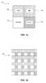
- FIGS. 1 a -1 bare block diagrams illustrating an array of pixels in a pixel color pattern in accordance with one aspect of the present disclosure
- FIG. 2is a schematic diagram of a four transistor diode for use with a photosensitive device in accordance with another aspect of the present disclosure
- FIG. 3is a schematic diagram of a six transistor diode for use with a photosensitive device in accordance with another aspect of the present disclosure
- FIG. 4is a diagram of a timing sequence of a six transistor diode for use with a photosensitive device in accordance with yet another aspect of the present disclosure
- FIG. 5is a diagram of a timing sequence of a four transistor diode for use with a photosensitive device in accordance with a further aspect of the present disclosure
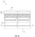
- FIGS. 6 a -6 bare cross-sectional views of semiconductor photosensitive devices in accordance with another aspect of the present disclosure.
- FIG. 7is a block diagram of a system for detecting and processing visible and infrared light in accordance with another aspect of the present disclosure.
- FIGS. 8 a -8 care computer simulated images of laser spot detection, visible light detection, and a composite image in accordance with an aspect of the present disclosure
- FIG. 9is a flow diagram of a method for creating a composite image of detected infrared and visible light with a monolithic sensor in accordance with an aspect of the present disclosure.
- FIG. 10is a block diagram of a system for processing visible and infrared light in accordance with another aspect of the present disclosure.
- the terms “light” and “electromagnetic radiation”can be used interchangeably and can refer to light or electromagnetic radiation in the ultraviolet, visible, near infrared, and infrared spectra.
- the termscan further more broadly include electromagnetic radiation such as radio waves, microwaves, x-rays, and gamma rays.
- the term “light”is not limited to electromagnetic radiation in the visible spectrum.
- Many examples of light described hereinrefer specifically to electromagnetic radiation in the visible and infrared (and/or near infrared) spectra.
- visible range wavelengthsare considered to be from approximately 350 nm to 800 nm and non-visible wavelengths are longer than about 800 nm or shorter than about 350 nm.
- the infrared spectrumincludes a near infrared portion of the spectrum including wavelengths of approximately 800 to 1100 nm, a short wave infrared portion of the spectrum including wavelengths of approximately 1100 nm to 3 micrometers, and a mid to long wave infrared (or thermal infrared) portion of the spectrum including wavelengths greater than about 3 micrometers up to about 30 micrometers. These are generally and collectively referred to herein as “infrared” portions of the electromagnetic spectrum unless otherwise noted.
- surface modifyingand “surface modification” refer to the altering of a surface of a semiconductor material using a variety of surface modification techniques.
- Non-limiting examples of such techniquesinclude plasma etching, reactive ion etching, porous silicon etching, lasing, chemical etching (e.g. anisotropic etching, isotropic etching), nanoimprinting, material deposition, selective epitaxial growth, and the like, including combinations thereof.
- surface modificationcan include processes using primarily laser radiation or laser radiation in combination with a dopant, whereby the laser radiation facilitates the incorporation of the dopant into a surface of the semiconductor material.
- surface modificationincludes doping of a substrate such as a semiconductor material.
- a semiconductor surfacecan be modified to become an absorption enhanced surface.
- a surface modified surfacecan include, for example, a textured surface.
- the term “textured surface”can refer to a surface having a topology with nano- to micron-sized surface variations formed by the irradiation of laser pulses or other texturing methods as are described herein. While the characteristics of such a surface can be variable depending on the materials and techniques employed, in one aspect such a surface can be several hundred nanometers thick and made up of nanocrystallites (e.g. from about 10 to about 50 nanometers) and nanopores. In another aspect, such a surface can include micron-sized structures (e.g. about 2 ⁇ m to about 60 ⁇ m). In yet another aspect, the surface can include nano-sized and/or micron-sized structures from about 5 nm and about 500 ⁇ m.
- fluencerefers to the amount of energy from a single pulse of laser radiation that passes through a unit area. In other words, “fluence” can be described as the energy density of one laser pulse.
- target regionrefers to an area of a substrate that is intended to be doped or surface modified.
- the target region of the substratecan vary as the surface modifying process progresses. For example, after a first target region is doped or surface modified, a second target region may be selected on the same substrate.
- detectionrefers to the sensing, absorption, and/or collection of electromagnetic radiation.
- backside illuminationrefers to a device architecture design whereby electromagnetic radiation is incident on a surface of a semiconductor material that is opposite a surface containing the device circuitry. In other words, electromagnetic radiation is incident upon and passes through a semiconductor material prior to contacting the device circuitry.
- the term “substantially”refers to the complete or nearly complete extent or degree of an action, characteristic, property, state, structure, item, or result.
- an object that is “substantially” enclosedwould mean that the object is either completely enclosed or nearly completely enclosed.
- the exact allowable degree of deviation from absolute completenessmay in some cases depend on the specific context. However, generally speaking the nearness of completion will be so as to have the same overall result as if absolute and total completion were obtained.
- the use of “substantially”is equally applicable when used in a negative connotation to refer to the complete or near complete lack of an action, characteristic, property, state, structure, item, or result.
- compositions that is “substantially free of” particleswould either completely lack particles, or so nearly completely lack particles that the effect would be the same as if it completely lacked particles.
- a composition that is “substantially free of” an ingredient or elementmay still actually contain such item as long as there is no measurable effect thereof.
- the term “about”is used to provide flexibility to a numerical range endpoint by providing that a given value may be “a little above” or “a little below” the endpoint.
- a dual band monolithic imaging devicemay comprise an array of pixels arranged in a pattern.
- the array patternmay include a repeating pattern of a combination of at least one red pixel, green pixel, and blue pixel, as well as at least one absorption enhanced near infrared pixel.
- CMOS imagercomprises a CMOS sensing array having various different color pixels in combination with an infrared pixel arranged in a monolithic configuration.
- the infrared pixelmay include a light diffusing or light scattering region formed on or near a surface of the pixel.
- a light diffusing regionis a textured region, such as a laser-textured region. Throughout this disclosure, the light diffusing region is referred to as a textured region for simplicity and ease of discussion. However, other forms of light diffusing or light scattering regions are also contemplated.
- At least one of the red, green and blue pixelsmay include a textured region formed on or near the surface of the pixels.
- the textured regionmay be formed by a laser process as disclosed, for example, in U.S. Pat. Nos. 7,057,256, 7,354,792, and 7,442,629, which are incorporated by reference herein in their entirety.
- the textured regionmay comprise a semiconductor material, for example silicon, which is irradiated by a short pulse laser or other texturing technique to create modified micro-structured surface morphology.
- the textured semiconductoris made to have advantageous light-absorbing properties. In some cases this type of material has been called “black silicon” due to its visually darkened appearance after the laser processing and because of its enhanced absorption of light and IR radiation compared to other forms of silicon.
- the textured regioncan be a laser processed textured region.
- the wavelength of the irradiating laser pulse for making black silicon, its fluence, and pulse durationcan affect the morphology of the modified surface.
- the laser fluencemay be between about 1.5 kJ/m 2 and 12 kJ/m 2 , but can vary depending on the substrate composition. The choice of the fluence of laser pulses irradiating a silicon wafer to generate a microstructured layer therein can also affect the gettering performance (capacity and/or specificity) of a microstructured substrate.
- the laser pulse fluenceis selected to be greater than about 3 kJ/m 2 . More preferably, the fluence may be chosen to be in a range of about 3 kJ/m 2 to about 10 kJ/m 2 , or a range of about 3 kJ/m 2 to about 8 kJ/m 2 .
- the laser pulse durationcan affect the morphology and absorption properties of the modified semiconductor surface. Irradiation of a substrate can be with femtosecond laser pulses or picosecond or nanosecond pulses. Other factors that can affect surface morphology include laser polarization and laser propagation direction relative to the irradiated semiconductor surface.
- textured regioncan be doped with a dopant, either separately from or during the texturing process.
- the laser radiationcan be directed through a dopant material to incorporate the dopant into the texture region.
- siliconcan be laser textured in the presence of SF 6 in order to incorporate S into the textured region.
- a basic pixel array arrangement 100can include a red pixel (R) 105 , a blue pixel (B) 120 , and a green (G) pixel 110 . with the pixel arrangement can further include a near-infrared (NIR) enhanced pixel 115 .
- RGBred pixel
- Bblue pixel
- Ggreen
- NIRnear-infrared
- Much of the following description of the technologyfocuses on an array pattern including the RGB and NIR pixels for simplicity. However, the number and color configurations of the pixels in an array pattern can vary. Also, the following description focuses primarily on a NIR pixel for simplicity, but the NIR pixel may more broadly be an infrared pixel.
- the near-infrared enhanced pixelmay include a textured region formed on or near a surface of the pixel.
- the enhanced absorbing regionmay formed by the laser processing or other texturing methods referred to herein.
- the pixel arraymay vary in pixel size and number of pixels.
- the four pixels shown in FIG. 1 acan represent a basic repeating pattern for a much larger pixel array 130 , such as that shown in FIG. 1 b .
- For a pixel array with a size of ⁇ 2N> ⁇ 2M>there will be N ⁇ M red pixels, N ⁇ M green pixels, N ⁇ M blue pixels and N ⁇ M NIR absorption enhanced pixels.
- pixel color patterns other than RGBGmay also be modified to include the NIR absorption enhanced pixels.
- RGBEGreen Blue Emerald
- CYYMCyan Yellow Yellow Magenta
- CYGMCyan Yellow Green Magenta
- RGBWRed Green Blue White
- Pixel color patternscan be modified by replacing an existing color pixel with the NIR absorption enhanced pixel or by adding the NIR absorption enhanced pixel to the pattern. Selection of pixel replacement, pixel pattern, and so forth will vary depending on the application.
- the NIR absorption enhanced pixelis configured to detect NIR light.
- an NIR pixelcan be configured to detect electromagnetic radiation at a wavelength of approximately 1064 nm.
- an NIR pixelcan include a 1064 nm narrow band pass filter to limit the light received by the NIR pixel at a wavelength of approximately 1064 nm. It is noted that the narrow band pass filter may not perfectly limit impinging light to 1064 nm wavelength light and that a slightly larger spectrum of wavelengths may impinge on the NIR pixel.
- the filtercan be configured to transmit wavelengths of greater than approximately 1000 nm, greater than approximately 1050 nm, greater than approximately 1064 nm, greater than approximately 1100 nm, etc.
- the NIR pixelis selectively configured to absorb wavelengths corresponding to laser radiation emitted from a laser source.
- the NIR pixelcan be configured to detect only NIR light while the RGB pixels can be configured to detect visible light.
- some security systemsinclude an infrared illumination source to illuminate the scene for improved imaging under low light conditions.
- some systemsinclude laser systems for designating military or law enforcement targets using a NIR 1064 nm laser source.
- the NIR absorption enhanced pixelcan be configured to detect light at least at the wavelength emitted from the laser/light source.
- the NIR pixelcan detect a broad range of wavelengths outside of the visible spectrum.
- Radiation or light from the laser sourcemay be modulated at a desired frequency, such as, for example, with pulse durations as short as 10 ns, pulse repetition rates as high as 20 kHz, and with as little as 25 ⁇ J per pulse.
- a desired frequencysuch as, for example, with pulse durations as short as 10 ns, pulse repetition rates as high as 20 kHz, and with as little as 25 ⁇ J per pulse.
- detection of NIR light by the NIR pixelmay include noise from background electromagnetic radiation and identification of a laser signal out of the noise can be difficult.
- the NIR pixelcan be configured to detect NIR light in substantial synchronization with the laser pulse.
- a time sequencing methodis contemplated.
- a method for sequencing a photo imager and a laser pulseincludes the steps of determining the pulse duration and/or frequency of the laser pulse, synchronizing the imager time clock to capture photons from the laser at approximately the same frequency as the laser pulses, and outputting a readout signal from the imager in response to captured photons.
- a method of synchronizing an imager and an external laser pulse via a global position system (GPS) clockis provided. Sequencing methods and systems will be described in additional detail below.
- GPSglobal position system
- Photosensitive or photo detecting imagersinclude photodiodes or pixels that are capable of absorbing electromagnetic radiation within a given wavelength range.
- Such imagerscan be passive pixel sensors (PPS), active pixel sensors (APS), digital pixel sensor imagers (DPS), or the like, with one difference being the image sensor read out architecture.
- a semiconducting photosensitive imagercan be a three or four transistor active pixel sensor (3T APS or 4T APS).
- 3T APS or 4T APStransistor active pixel sensor
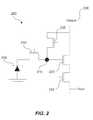
- FIG. 2illustrates a 4-transistor (4T) CMOS (complementary metal-oxide-semiconductor) pixel architecture 200 .
- the 4T architecturemay typically be used in a rolling shutter configuration for the visible light pixel(s) in a pixel array.
- the 4T architecturecan be used in a global shutter configuration.
- a voltage (Vaapix) 230can be supplied to the circuit or photodiode array.
- a photodiode 205can accumulate electrons from the impingement of light on the photodiode. Electrons accumulated in the photodiode can be transferred to a floating diffusion (FD) node 215 by opening a transfer gate (TX) transistor 210 .
- FDfloating diffusion
- TXtransfer gate
- a voltage at the FD nodechanges as a result, and this change can be amplified by a source follower (SF) transistor 220 and read out as a voltage at Vout using a row selector RS transistor 225 .
- the voltage or potential of the FD nodecan be reset using a reset (RST) transistor 235 .
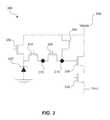
- FIG. 3illustrates a 6-transistor (6T) CMOS pixel architecture 300 that can be used for the NIR pixel to synchronize light detection with a laser pulse.
- the 6T NIR pixelmay have two extra transistors, including a global reset transistor (Global_RST) 350 and a global transfer gate transistor (Global_TX1) 310 , in addition to the 4 transistors included in a 4T architecture (transfer gate (TX2) 320 , reset gate (RST) 345 , source follower (SF) 330 , and row select gate (RS) 335 ).
- the 6T architecturecan also include an accumulation node 315 .
- the 6T architecturecan enable a global shutter for the NIR pixel.
- the global shuttercan expose NIR pixels in a pixel array substantially simultaneously for a predetermined period, which can be configured to substantially correspond with a laser pulse.
- the NIR pixels in a sensorstart gathering light.
- the light-gathering circuitrycan be turned off and the contents of the sensor can be read out to become an image.
- the NIR pixel array and RGB pixel arraycan have separate control logic and routing in the sensor.
- the RGB pixel arraycan have a rolling shutter operation for scene image capture.
- the NIR pixel arraycan use a global shutter to capture very short pulse laser spots even under bright ambient lighting conditions by beginning to integrate light prior to the laser pulse and discontinuing integration right after the laser pulse turns off.
- the NIR pixel arraycan operate globally with an internal device clock. A global shutter can allow simultaneous capture of an entire field of view of the array.
- the NIR pixel arraycan operate as a rolling shutter, as will be further described below, there may be a timing difference in each row of pixels captured when an imaging device is tracking a laser spot if a rolling shutter is used.
- the timing differencein some examples can complicate tracking the laser spot. Because the global shutter simultaneously captures an entire field of view, tracking difficulties in some applications can be avoided.
- FIG. 4illustrates an exemplary timing sequence 400 for a global shutter in a 6T architecture for capturing light from a laser pulse.
- the 0's and 1's next to the timing sequenceindicate a low (0) or high (1) signal for each of the designated signals (i.e., laser pulse, global_RST, etc.).
- the ⁇ n>'s in the list of signalsindicates the row address of a selected row.
- the Global_RST and Global_TX1 transistorscan operate substantially simultaneously on the NIR pixels.
- the Global_RST signalis high in-between the laser pulse and can hold the photodiodes of an NIR pixel at reset so that no signal integration will occur.
- the Global_RST signalchanges to low right before the laser pulse so that the photodiodes of the NIR pixel will start to integrate charges generated by incident light.
- the Global_TX1is set to high to transfer the charge from the photodiodes to the accumulation node. After charge transfer, Global_RST is set to high again to hold the NIR pixel photodiodes at reset between laser pulses.
- the above procedurecan be repeated until the accumulated charge at the photodiodes is read out.
- the chargeis summed at the accumulation node.
- the FDis reset (RST) and a reset signal is sampled as a sample and reset (SHR) signal.
- the chargeis transferred from accumulation node to FD by turning on gate TX2.
- the signalis then sampled as a sample and hold (SHS) signal.
- SHR and SHSsample and hold
- the difference (RS) between SHR and SHSwill be the final signal.
- the differencecan be determined by, for example, a CDS (correlated double sampling) readout to remove kTC (thermal) noise.
- the final signal readoutis operated on a row-by-row basis as with the 4T CMOS sensor architecture described above. After readout of the final signal, the accumulation node is reset by turn on RST and TX2 substantially simultaneously.
- both the NIR pixel and RGB pixelscan operate in a rolling shutter mode.
- the 6T NIR pixelcan operate in a rolling shutter mode by setting the Global_RST to low and constantly holding the Global_RST at low.
- the Global_TX1 gatecan be tied with gate TX2 so that the Global_TX1 and TX2 gates can be operated substantially simultaneously.
- FIG. 5One example of a timing sequence 500 for the RGB 4T pixel array is illustrated in FIG. 5 .
- the steps for readout timingcan be briefly described.
- the signal readoutis operated on a row-by-row basis as with many typical CMOS sensors.
- the FD reset (RST) and the reset signalsare sampled as SHR.
- the charge from the photodiodesis transferred to FD by turning on TX.
- the signalis sampled as SHS.
- the difference between SHR and SHSis the final signal (e.g. CDS readout to remove kTC noise).
- a shutter operationis enabled by turning on RST and TX simultaneously for a given row address.
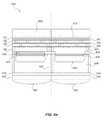
- FIGS. 6A and Ba semiconductor structure forming the pixels in the pixel arrays and methods of manufacturing such a semiconductor structure will be described.
- the pixel devices according to aspects of the present disclosurecan increase the absorption of semiconductor materials for longer wavelengths as compared to traditional materials.
- traditional semiconductor materialslonger wavelength penetrate deep into the material before the photons are absorbed. Therefore, in thin devices these wavelengths are challenging to detect.
- the present disclosureteaches enhanced semiconductor materials that increase the effective absorption resulting in improved detection of longer wavelengths (e.g. >1000 nm for silicon) within a thin semiconductor device layer.
- the response rate or response speedcan also be increased.
- photosensitive imager devices or pixels and associated methodsare contemplated. Such devices provide, among other things, enhanced response in the near infrared light portion of the optical spectrum and improved response and quantum efficiency in converting electromagnetic radiation to electrical signals. Quantum efficiency can be defined as the percentage of photons that are converted into electrons.
- IQEInternal QE
- EQEExternal QE
- the EQEis always lower than the IQE since there will inevitably be recombination effects and optical losses (e.g. transmission and reflection losses).
- One reason for improved performance with photosensitive imager devices, particularly for back side illuminated sensors (BSI)is a higher fill factor or, in other words, the amount of light that can be collected in a single pixel.
- the various metal layers on top of a front side-illuminated sensor (FSI)limit the amount of light that can be collected in a pixel. As pixel sizes get smaller, the fill factor gets worse.
- a BSI photosensitive imager devicecan provide a more direct path for light to travel into the pixel, thus avoiding light blockage by the metal interconnect and dielectric layers on the top-side of the semiconductor substrate.
- a photosensitive diodecan include a semiconductor substrate having multiple doped regions forming at least one junction, and a textured region coupled to the semiconductor substrate and positioned to interact with electromagnetic radiation.
- the semiconductor substrate and the textured regioncan be positioned such that incoming electromagnetic radiation passes through the semiconductor substrate before contacting the textured region.
- the semiconductor substrate and the textured regioncan be positioned such that the incoming electromagnetic radiation contacts the textured region before contacting the semiconductor substrate.
- the multiple doped regionscan include at least one cathode region and at least one anode region.
- doped regionscan include an n-type dopant and/or a p-type dopant, thereby creating a p-n junction.
- a photosensitive devicecan include an i-type region to form a p-i-n junction.
- a photosensitive pixelcan include a semiconductor substrate having multiple doped regions forming at least one junction, and a textured region coupled to the semiconductor substrate and positioned to interact with electromagnetic radiation. The semiconductor substrate and the textured region are positioned such that incoming electromagnetic radiation passes through the semiconductor substrate before contacting the textured region. Additionally, the photosensitive pixel also includes an electrical transfer element coupled to the semiconductor substrate and operable to transfer an electrical signal from the at least one junction.
- a photosensitive imagercan include multiple photosensitive pixels. Additionally, an electrical transfer element can include a variety of devices, including without limitation, transistors, sensing nodes, transfer gates, transfer electrodes, and the like.
- incident lightenters the semiconductor device by first passing by transistors and metal circuitry.
- the lightcan scatter off of the transistors and circuitry prior to entering the light sensing portion of the imager, thus causing optical loss and noise.
- a lenscan be disposed on the topside of a FSI pixel to direct and focus the incident light to the light sensing active region of the device, thus partially avoiding the circuitry.
- the lenscan be a micro-lens.
- BSI imagersare configured to have the depletion region of the junction extending to the opposite side of the device. In one aspect, for example, incident light enters the device via the light sensing portion and is mostly absorbed prior to reaching the circuitry.
- CMOScomplimentary metal-oxide-semiconductor
- CCDcharge-coupled device
- the semiconductor structureincludes a plurality of dielectric layers D1-D4 and a plurality of metal layers M1-M3. Vias 620 can be formed between the layers. Many of the structures in the semiconductor architecture are repeated, and thus each instance of a structure on one or more sides of the architecture is not individually called out.
- a near-infrared pixel semiconductor structureis shown on the left side of the dotted line.
- a handle wafer or support substrate 605can provide a base or support for the NIR pixel.
- the NIR pixelmay comprise a semiconductor material 606 (e.g. a silicon base semiconductor bulk material) with a device surface 610 , a p+ type 630 and an n-type 640 dopant incorporated into the semiconductor material forming at least one junction, an absorption enhanced region 635 formed within the material, a passivation layer 615 , trench isolation regions 645 , a lens 665 , anti-reflective coating 650 , and a narrow band pass filter 655 fabricated on a side of the pixel nearest to impinging light.
- the n-type dopantcan form a pinned photodiode pinned to a transfer gate 625 .
- Another pixelsuch as a red, green or blue pixel for the visible spectrum, may comprise a semiconductor material 606 (e.g. a silicon base semiconductor bulk material), a p+ type 630 and n-type 640 dopant incorporated into the semiconductor material, a passivation layer 615 , trench isolation regions 645 , a lens 665 , anti-reflective coating 650 , and a typical color filter 660 and infrared-cut filter 660 built on top of the pixel.
- a semiconductor material 606e.g. a silicon base semiconductor bulk material
- a p+ type 630 and n-type 640 dopantincorporated into the semiconductor material
- a passivation layer 615e.g. a silicon base semiconductor bulk material
- trench isolation regions 645e.g. a lens 665 , anti-reflective coating 650
- a typical color filter 660 and infrared-cut filter 660e.g. a typical color filter 660 and inf
- the RGB color pixelsmay further comprise an absorption enhanced region 637 formed at an interface on or within the semiconductor material 606 . Also shown in this embodiment is a positioning of the absorption enhanced or textured region 636 on the NIR pixel (left side) and the R, G, or B pixel (right side) on an opposite side of the photodiode from the example shown in FIG. 6 a . It is noted that, although not shown in this figure, the textured regions 636 , 637 can also be positioned adjacent to the junctions or pixels.
- the doped regionscan have the same doping profile or different doping profiles, depending on the device. While the device shown contains multiple doped regions, it should be noted that other aspects containing one or more doped regions are considered to be within the present scope. Additionally, the semiconductor substrate can be doped, and thus can be considered to be a doped region in some aspects.
- the semiconductor substrate and the textured regioncan be positioned such that incoming electromagnetic radiation passes through the semiconductor substrate before contacting the textured region, or can alternatively be positioned such that incoming electromagnetic radiation passes through the textured region before contacting the semiconductor substrate.
- the various devices according to aspects of the present disclosurecan exhibit increased quantum efficiency over traditional photosensitive devices. Any increase in the quantum efficiency makes a large difference in the signal to noise ratio. More complex structures can provide not only increased quantum efficiency but also good uniformity from pixel to pixel.
- devices of the present disclosureexhibit increased responsivity as compared to traditional photosensitive devices.
- the responsivitycan be greater than or equal to 0.3 A/W for wavelengths greater than 1000 nm for semiconductor substrate that is less than 100 ⁇ m thick. In other embodiment the responsivity can be greater than 0.15 A/W for wavelengths greater than 1100 nm for semiconductor substrate that is less than 50 ⁇ m thick.
- semiconductor materialsare contemplated for use with the devices and methods according to aspects of the present disclosure.
- Non-limiting examples of such semiconductor materialscan include group IV materials, compounds and alloys comprised of materials from groups II and VI, compounds and alloys comprised of materials from groups III and V, and combinations thereof.
- exemplary group IV materialscan include silicon, carbon (e.g. diamond), germanium, and combinations thereof.
- Various exemplary combinations of group IV materialscan include silicon carbide (SiC) and silicon germanium (SiGe).
- the semiconductor materialcan be or include silicon.
- Exemplary silicon materialscan include amorphous silicon (a-Si), microcrystalline silicon, multicrystalline silicon, and monocrystalline silicon, as well as other crystal types.
- the semiconductor materialcan include at least one of silicon, carbon, germanium, aluminum nitride, gallium nitride, indium gallium arsenide, aluminum gallium arsenide, and combinations thereof.
- Exemplary combinations of group II-VI materialscan include cadmium selenide (CdSe), cadmium sulfide (CdS), cadmium telluride (CdTe), zinc oxide (ZnO), zinc selenide (ZnSe), zinc sulfide (ZnS), zinc telluride (ZnTe), cadmium zinc telluride (CdZnTe, CZT), mercury cadmium telluride (HgCdTe), mercury zinc telluride (HgZnTe), mercury zinc selenide (HgZnSe), and combinations thereof.
- CdSecadmium selenide
- CdScadmium sulfide
- CdTecadmium telluride
- ZnOzinc oxide
- ZnSezinc selenide
- ZnSzinc sulfide
- ZnTezinc telluride
- CdZnTecadmium zinc telluride
- Exemplary combinations of group III-V materialscan include aluminum antimonide (AlSb), aluminum arsenide (AlAs), aluminum nitride (AlN), aluminum phosphide (AlP), boron nitride (BN), boron phosphide (BP), boron arsenide (BAs), gallium antimonide (GaSb), gallium arsenide (GaAs), gallium nitride (GaN), gallium phosphide (GaP), indium antimonide (InSb), indium arsenide (InAs), indium nitride (InN), indium phosphide (InP), aluminum gallium arsenide (AlGaAs, AlxGal-xAs), indium gallium arsenide (InGaAs, InxGal-xAs), indium gallium phosphide (InGaP), aluminum indium arsenide (AlInAs),
- the semiconductor substratecan be of any thickness that allows electromagnetic radiation detection and conversion functionality, and thus any such thickness of semiconductor material is considered to be within the present scope.
- the textured regionincreases the efficiency of the device such that the semiconductor substrate can be thinner than has previously been possible. Decreasing the thickness of the semiconductor substrate reduces the amount of semiconductor material required to make such a device.
- the semiconductor substratehas a thickness of from about 500 nm to about 50 ⁇ m.
- the semiconductor substratehas a thickness of less than or equal to about 100 ⁇ m.
- the semiconductor substratehas a thickness of from about 1 ⁇ m to about 10 ⁇ m.
- the semiconductor substratecan have a thickness of from about 5 ⁇ m to about 50 ⁇ m.
- the semiconductor substratecan have a thickness of from about 5 ⁇ m to about 10 ⁇ m.
- the semiconductor materialis monocrystalline.
- the semiconductor materialis multicrystalline.
- the semiconductor materialis microcrystalline. It is also contemplated that the semiconductor material can be amorphous. Specific nonlimiting examples include amorphous silicon or amorphous selenium.
- the semiconductor materials of the present disclosurecan also be made using a variety of manufacturing processes. In some cases the manufacturing procedures can affect the efficiency of the device, and may be taken into account in achieving a desired result. Exemplary manufacturing processes can include Czochralski (Cz) processes, magnetic Czochralski (mCz) processes, Float Zone (FZ) processes, epitaxial growth or deposition processes, and the like. It is contemplated that the semiconductor materials used in the present invention can be a combination of monocrystalline material with epitaxially grown layers formed thereon.
- the textured regioncan function to diffuse electromagnetic radiation, to redirect electromagnetic radiation, and to absorb electromagnetic radiation, thus increasing the quantum efficiency of the device.
- electromagnetic radiation passing through the semiconductor substratecan contact the textured region.
- the textured regioncan include surface features to thus increase the effective absorption length of the photosensitive pixel.
- Such surface featurescan be micron-sized and/or nano-sized, and can be any shape or configurations. Non-limiting examples of such shapes and configurations include cones, pillars, pyramids, microlenses, quantum dots, inverted features, gratings, protrusions, and the like, including combinations thereof.
- factors such as manipulating the feature sizes, dimensions, material type, dopant profiles, texture location, etc.can allow the diffusing region to be tunable for a specific wavelength.
- tuning the devicecan allow specific wavelengths or ranges of wavelengths to be absorbed.
- tuning the devicecan allow specific wavelengths or ranges of wavelengths to be reduced or eliminated via filtering.
- Tuningcan also be accomplished through the relative location of the texture region within the device, modifying the dopant profile(s) of regions within the device, dopant selection, and the like. Additionally, material composition near the textured region can create a wavelength specific photosensing pixel device. It should be noted that a wavelength specific photosensing pixel can differ from one pixel to the next, and can be incorporated into an imaging array.
- Textured regionscan allow a photosensitive device to experience multiple passes of incident electromagnetic radiation within the device, particularly at longer wavelengths (i.e. infrared). Such internal reflection increases the effective absorption length to be greater than the thickness of the semiconductor substrate. This increase in absorption length increases the quantum efficiency of the device, leading to an improved signal to noise ratio.
- the materials used for making the textured regioncan vary depending on the design and the desired characteristics of the device. As such, any material that can be utilized in the construction of a textured region is considered to be within the present scope.
- a portion of the semiconductor layercan be textured to form the textured region.
- the texturing processcan texture an entire surface of the semiconductor layer or only a portion of the semiconductor layer surface.
- the textured regioncan have a surface morphology that is designed to focus or otherwise direct electromagnetic radiation.
- the textured regionhas a surface morphology operable to direct electromagnetic radiation into the semiconductor substrate.
- various surface morphologiesinclude sloping, pyramidal, inverted pyramidal, spherical, square, rectangular, parabolic, asymmetric, symmetric, and the like, including combinations thereof.
- the textured regioncan be formed by various techniques, including plasma etching, reactive ion etching, porous silicon etching, lasing, chemical etching (e.g. anisotropic etching, isotropic etching), nanoimprinting, material deposition, selective epitaxial growth, and the like.
- the texturing processcan be performed during the manufacture of the photosensitive device.
- the texturing processcan be performed on a photosensitive device that has previously been made.
- a CMOS, CCD, or other photosensitive elementcan be textured following manufacture. In this case, material layers may be removed from the photosensitive element to expose the semiconductor substrate upon which a textured region can be formed.
- One effective method of producing a textured regionis through laser processing.
- laser processingallows discrete locations of the passivation region or other substrate to be textured.
- a variety of techniques of laser processing to form a textured regionare contemplated, and any technique capable of forming such a region should be considered to be within the present scope.
- Laser treatment or processingcan allow, among other things, enhanced absorption properties and thus increased electromagnetic radiation focusing and detection.
- the laser treated regioncan be associated with the surface nearest the impinging electromagnetic radiation or, in the case of BSI devices, the laser treated surface can be associated with a surface opposite in relation to impinging electromagnetic radiation, thereby allowing the radiation to pass through the semiconductor substrate before it hits the laser treated region.
- a target region of the semiconductor materialcan be irradiated with laser radiation to form a textured region.
- Examples of such processinghave been described in further detail in U.S. Pat. Nos. 7,057,256, 7,354,792 and 7,442,629, which are incorporated herein by reference in their entireties.
- a surface of a substrate materialis irradiated with laser radiation to form a textured or surface modified region.
- Such laser processingcan occur with or without a dopant material.
- the lasercan be directed through a dopant carrier and onto the substrate surface. In this way, dopant from the dopant carrier is introduced into the target region of the substrate material.
- the target regiontypically has a textured surface that increases the surface area of the laser treated region and increases the probability of radiation absorption via the mechanisms described herein.
- such a target regionis a substantially textured surface including micron-sized and/or nano-sized surface features that have been generated by the laser texturing.
- irradiating the surface of the substrate materialincludes exposing the laser radiation to a dopant such that irradiation incorporates the dopant into the substrate.
- dopant materialsare known in the art, and are discussed in more detail herein.
- the surface of the substrate or passivation regionis chemically and/or structurally altered by the laser treatment, which may, in some aspects, result in the formation of surface features appearing as microstructures or patterned areas on the surface and, if a dopant is used, the incorporation of such dopants into the substrate material.
- the features or microstructurescan be on the order of 50 nm to 20 ⁇ m in size and can assist in the absorption of electromagnetic radiation. In other words, the textured surface can increase the probability of incident radiation being absorbed.
- the type of laser radiation used to surface modify a materialcan vary depending on the material and the intended modification. Any laser radiation known in the art can be used with the devices and methods of the present disclosure. There are a number of laser characteristics, however, that can affect the surface modification process and/or the resulting product including, but not limited to the wavelength of the laser radiation, pulse width, pulse fluence, pulse frequency, polarization, laser propagation direction relative to the semiconductor material, etc.
- a lasercan be configured to provide pulsatile lasing of a material.
- a short-pulsed laseris one capable of producing femtosecond, picosecond and/or nanosecond pulse durations.
- Laser pulsescan have a central wavelength in a range of about from about 10 nm to about 8 ⁇ m, and more specifically from about 200 nm to about 1200 nm.
- the pulse width of the laser radiationcan be in a range of from about tens of femtoseconds to about hundreds of nanoseconds.
- laser pulse widthscan be in the range of from about 50 femtoseconds to about 50 picoseconds.
- laser pulse widthscan be in the range of from about 50 picoseconds to 100 nanoseconds.
- laser pulse widthsare in the range of from about 50 to 500 femtoseconds.
- the number of laser pulses irradiating a target regioncan be in a range of from about 1 to about 2000. In one aspect, the number of laser pulses irradiating a target region can be from about 2 to about 1000. Further, the repetition rate or frequency of the pulses can be selected to be in a range of from about 10 Hz to about 10 ⁇ Hz, or in a range of from about 1 kHz to about 1 MHz, or in a range from about 10 Hz to about 1 kHz. Moreover, the fluence of each laser pulse can be in a range of from about 1 kJ/m 2 to about 20 kJ/m 2 , or in a range of from about 3 kJ/m 2 to about 8 kJ/m 2 .
- dopant materialsare contemplated for both the formation of the multiple doped regions and incorporation by a texturing technique, and any such dopant that can be used in such processes to surface modify a material is considered to be within the present scope. It should be noted that the particular dopant utilized can vary depending on the material being doped, as well as the intended use of the resulting material. For example, the selection of potential dopants may differ depending on whether or not tuning of the photosensitive device is desired.
- a dopantcan be either charge donating or accepting dopant species. More specifically, an electron donating or a hole donating species can cause a region to become more positive or negative in polarity as compared to the semiconductor substrate.
- the doped regioncan be p-doped. In another aspect the doped region can be n-doped.
- a highly doped regioncan also be formed on or near the doped region to create a pinned diode.
- the semiconductor substratecan be negative in polarity, and a doped region and a highly doped region can be doped with p+ and n dopants respectively.
- the highly doped regioncan be a textured region.
- textured surface featurescan be formed on or in a highly doped region.
- at least a portion of the textured region, or the material from which the textured region is generatedcan be doped with a dopant to generate a back surface field.
- a back surface fieldcan function to impede the movement of photo-generated carriers from the junction toward the textured region.
- non-limiting examples of dopant materialscan include S, F, B, P, N, As, Se, Te, Ge, Ar, Ga, In, Sb, and combinations thereof.
- the scope of dopant materialsshould include, not only the dopant materials themselves, but also materials in forms that deliver such dopants (i.e. dopant carriers).
- S dopant materialsincludes not only S, but also any material capable being used to dope S into the target region, such as, for example, H 2 S, SF 6 , SO 2 , and the like, including combinations thereof.
- the dopantcan be S.
- Sulfurcan be present at an ion dosage level of between about 5 ⁇ 10 14 and about 1 ⁇ 10 16 ions/cm 2 .
- fluorine-containing compoundscan include ClF 3 , PF 5 , F 2 SF 6 , BF 3 , GeF 4 , WF 6 , SiF 4 , HF, CF 4 , CHF 3 , CH 2 F 2 , CH 3 F, C 2 F 6 , C 2 HF 5 , C 3 F 8 , C 4 F 8 , NF 3 , and the like, including combinations thereof.
- Non-limiting examples of boron-containing compoundscan include B(CH 3 ) 3 , BF 3 , BCl 3 , BN, C 2 B 10 H 12 , borosilica, B 2 H 6 , and the like, including combinations thereof.
- Non-limiting examples of phosphorous-containing compoundscan include PF 5 , PH 3 , and the like, including combinations thereof.
- Non-limiting examples of chlorine-containing compoundscan include Cl 2 , SiH 2 Cl 2 , HCl, SiCl 4 , and the like, including combinations thereof.
- Dopantscan also include arsenic-containing compounds such as AsH 3 and the like, as well as antimony-containing compounds. Additionally, dopant materials can include mixtures or combinations across dopant groups, i.e.
- the dopant materialcan have a density that is greater than air.
- the dopant materialcan include Se, H 2 S, SF 6 , or mixtures thereof.
- the dopantcan be SF 6 and can have a predetermined concentration range of about 5.0 ⁇ 10 ⁇ 8 mol/cm 3 to about 5.0 ⁇ 10 ⁇ 4 mol/cm 3 .
- SF 6 gasis a good carrier for the incorporation of sulfur into the semiconductor material via a laser process without significant adverse effects on the material.
- dopantscan also be liquid solutions of n-type or p-type dopant materials dissolved in a solution such as water, alcohol, or an acid or basic solution. Dopants can also be solid materials applied as a powder or as a suspension dried onto the wafer.
- the semiconductor substratecan be annealed for a variety of reasons, including dopant activation, semiconductor damage repair, and the like.
- the semiconductor substratecan be annealed prior to texturing, following texturing, during texturing, or any combination thereof.
- Annealingcan enhance the semiconductive properties of the device, including increasing the photoresponse properties of the semiconductor materials by reducing any imperfections in the material. Additionally, annealing can reduce damage that may occur during the texturing process.
- any known annealcan be beneficial and would be considered to be within the present scope, annealing at lower temperatures can be particularly useful. Such a “low temperature” anneal can greatly enhance the external quantum efficiency of devices utilizing such materials.
- the semiconductor substratecan be annealed to a temperature of from about 300° C. to about 110° C.°. In another aspect, the semiconductor substrate can be annealed to a temperature of from about 500° C. to about 900° C. In yet another aspect, the semiconductor substrate can be annealed to a temperature of from about 700° C. to about 800° C. In a further aspect, the semiconductor substrate can be annealed to a temperature that is less than or equal to about 850° C.
- the duration of the annealing procedurecan vary according to the specific type of anneal being performed, as well as according to the materials being used. For example, rapid annealing processes can be used, and as such, the duration of the anneal may be shorter as compared to other techniques. Various rapid thermal anneal techniques are known, all of which should be considered to be within the present scope.
- the semiconductor substratecan be annealed by a rapid annealing process for a duration of greater than or equal to about 1 ⁇ s.
- the duration of the rapid annealing processcan be from about 1 ⁇ s to about 1 ms.
- a baking or furnace anneal processcan be used having durations that may be longer compared to a rapid anneal.
- the semiconductor substratecan be annealed by a baking anneal process for a duration of greater than or equal to about 1 ms to several hours.
- passivation regionconfigurations are contemplated, and any configuration that can be incorporated into a photosensitive device is considered to be within the present scope.
- One benefit to such a passivation regionpertains to the isolation provided between the textured region and the doped regions that form the junction.
- the passivation regioncan be positioned to physically isolate the textured region from the junction. In this way, the creation of the textured region can be isolated from the doped regions, thus precluding undesirable effects of the texturing process from affecting the junction.
- the passivation regioncan be a dielectric material, and thus the passivation region could be used to electrically isolate the textured region from the junction.
- the passivation regionis coupled directly to at least one of the doped regions forming the junction.
- the passivation regioncan be made from a variety of materials, and such materials can vary depending on the device design and desired characteristics. Non-limiting examples of such materials can include oxides, nitrides, oxynitrides, and the like, including combinations thereof.
- the passivation regionincludes an oxide.
- the passivation regioncan be of various thicknesses. In one aspect, for example, the passivation region has a thickness of from about 100 nm to about 1 micron. In another aspect, the passivation region has a thickness of from about 5 nm to about 100 nm. In yet another aspect, the passivation region has a thickness of from about 20 nm to about 50 nm.
- a photosensitive imager devicecan include a reflecting region coupled to the textured region.
- the reflecting regioncan be deposited over the entire textured region or only over a portion of the textured region.
- the reflecting regioncan be deposited over a larger area of the device than the textured region.
- the reflecting regioncan be positioned to reflect electromagnetic radiation passing through the texture region back through the textured region. In other words and as an example, as electromagnetic radiation passes into the semiconductor substrate a portion of electromagnetic radiation that is not absorbed contacts the textured region. Of that portion of electromagnetic radiation that contacts the textured region, a smaller portion may pass though the textured region to strike the reflecting region and be reflected back through the textured region toward the semiconductor substrate.
- a variety of reflective materialscan be utilized in constructing the reflecting region, and any such material capable of incorporation into a photosensitive device is considered to be within the present scope.
- Non-limiting examples of such materialsinclude a Bragg reflector, a metal reflector, a metal reflector over a dielectric material, a transparent conductive oxide such as zinc oxide, indium oxide, or tin oxide, and the like, including combinations thereof.
- Non-limiting examples of metal reflector materialscan include silver, aluminum, gold, platinum, reflective metal nitrides, reflective metal oxides, and the like, including combinations thereof.
- the textured surface of a metal on a roughened oxidecan act as a diffusive scattering site for the incident electromagnetic radiation and also as a mirror-like reflector.
- Other aspectscan utilize porous materials for the texturing.
- Porous polysiliconfor example, can be oxidized or oxide deposited and a reflective region such as a metal reflector can be associated therewith to provide a scattering and reflecting surface.
- aluminumcan be subjected to anodic oxidation to provide porous aluminum oxide, a high dielectric constant insulator. This insulator can be coated with aluminum or other metals to provide a scattering and reflecting surface.
- a reflective regioncan include a transparent conductive oxide, an oxide, and a metal layer.
- the transparent oxidecan be textured and a metal reflector deposited thereupon.
- the textured surface of the metal on a roughened transparent conductive oxidecan act as a diffusive scattering site for the incident electromagnetic radiation.
- a Bragg reflectorcan be utilized as a reflective region.
- a Bragg reflectoris a structure formed from multiple layers of alternating materials with varying refractive indexes, or by a periodic variation of some characteristic (e.g. height) of a dielectric waveguide, resulting in periodic variation in the effective refractive index in the guide.
- Each layer boundarycauses a partial reflection of an optical wave.
- the many reflectionscombine with constructive interference, and the layers act as a high-quality reflector.
- the coherent super-positioning of reflected and transmitted light from multiple interfaces in the structureinterfere so as to provide the desired reflective, transmissive, and absorptive behavior.
- the Bragg reflector layerscan be alternating layers of silicon dioxide and silicon. Because of the high refractive index difference between silicon and silicon dioxide, and the thickness of these layers, this structure can be fairly low loss even in regions where bulk silicon absorbs appreciably. Additionally, because of the large refractive index difference, the optical thickness of the entire layer set can be thinner, resulting in a broader-band behavior and fewer fabrications steps.
- Additional scatteringcan be provided by positioning a textured forward scattering layer on the side of the pixel opposing the doped photodiode regions or on the illuminated side.
- These forward scattering layerscan be, without limitation, textured oxides or polysilicon without a reflector. These layers can be spaced away from the back side surface of the pixel and would provide scattering of the light in addition to that provided by layers on the front side of the pixel adjacent to the photodiode and transistor doped regions in the case of BSI architectures, or spaced away from the front side surface of the pixel and would provide scattering of the light in addition to that provided by layers on the back side of the pixel in the case of FSI architectures.
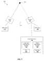
- a system 700may include a sensor 725 having NIR and RGB pixels and a light source 710 for emitting NIR light towards a target 720 .
- the light sourcecomprises a laser diode. If the laser diode and sensor are in a same system, or in other words have a direct communication channel 735 there between, synchronizing of capture of light from the diode by the NIR pixel can be easily accomplished.
- synchronization of timingcan be achieved via one or more global position system (GPS) clocks 715 , 730 .
- GPSglobal position system
- a timing of laser pulses with respect to a GPS clock timecan be determined.
- the timing of the laser pulses with respect to the GPS clock timecan be communicated directly or indirectly to the sensor.
- the sensorcan include a GPS clock and logic for timing light detection with the timing of the laser pulses based on the GPS clock time.
- one problem with conventional imagers in providing a see-spot capability for a laser designator systemis capturing the reflected laser pulse energy.
- many imagerseither image a surrounding background imagery of the target or sacrifice the background imagery and image the laser spot.
- a human operatordoes not have the benefit of both being able to see the background imagery and the laser spot to determine accuracy of the target.
- multiple separate sensorsare used, one for detecting the laser spot and another for detecting the surrounding imagery.
- the image output from the two separate sensorsis digitally merged or fused into one composite image.
- the field-of-view (FOV)is not exactly same for the two sensors and there is a registration error.
- the registration errorcould lead the human operator viewing the composite image to either believe the laser is pointing to a different target than the actual target and/or to act upon an incorrect target, such as by firing a missile, for example.
- the imaging device or sensor described hereincan provide the benefits of imaging both the laser spot and the background imagery without registration errors.
- Image outputs from the NIR and RGB pixels in a same sensorcan be combined into a single composite image by an image processor 740 .
- the image processorcan include a central processing unit (CPU) 755 , memory 760 , and various modules for processing images.
- visible light image datacan pass through a signal interpolation module 750 to estimate the signal level of a missed green pixel (which has been replaced by 1064 nm NIR pixel, at least in a bayer pattern pixel array).
- the image processorcan compensate the visible light for the missed green pixel based on the estimated signal level.
- the visible light image datacan then be similar to that detected by a normal “bayer” pattern pixel array.
- the raw visible light image datacan pass through a CMOS image processing pipeline for final output of a color image. This color image may include the background or scenery surrounding the laser spot.
- the NIR pixel image(image size N ⁇ M) can pass through a laser spot identification module 745 .
- the output of the laser spot identification modulecan be the laser spot center coordinate, spot size, etc.
- the laser spot identification modulecan improve the identification of the laser spot via various types of image processing, such as sharpening, contrast enhancement, etc. Human eye identification may also be possible for low ambient background light conditions without the use of the laser spot identification module.
- the laser spotcan then be rendered on the RGB image to indicate the location of laser spot relative to the visual scene.
- the laser spotcan be extracted from the NIR pixel image and inserted into the color image.
- the laser spotcan be recreated or simulated in or on the color image.
- the laser spotcan be overlayed onto the color image.
- the NIR pixel imagecan be superimposed over the color image. The superimposition can be performed using optics, the sensor device itself, or the image processor. While the RGB and NIR pixels are in a same array and can avoid field of view issues, a detected light signal from the NIR pixel can be processed separately from a detected light signal from the RGB pixels to enhance and/or identify the laser spot before combining with the RGB pixels.
- a signal detected by the NIR pixelmay include the laser spot and surrounding noise.
- an infrared and RGB imagecan be directly combined without any intervening processing steps.
- the above operationscan be performed at the sensor chip level or at a system level. If the operation or operations are done at the chip level, a frame memory (with size N ⁇ M pixel) can be provided for the NIR pixel array. Several rows of line memory can also be provided for the RGB pixels.
- the previous frame's laser spot locationcan be drawn onto the current frame's output color image. A short period of time between color frames may elapse, or one or more color frames may be obtained, while a whole frame of the NIR image is obtained.
- the sensorWith the global shutter and pulsed NIR light acquisition, the sensor will obtain the whole frame of the NIR image before the laser spot identification module can start searching for the laser spot. Therefore, there may be one frame delay on the laser spot. If a human eye is used to identify the laser spot on the image, the system can operate without frame memory and there will not be a one frame lag on the laser spot relative to the normal scene.
- FIGS. 8 a -8 cillustrate computer simulated images output from a NIR pixel and RGB pixels as disclosed herein.
- FIG. 8 adepicts output from a NIR pixel synchronized with a NIR laser pulse.
- a laser spot 805is discernable from background noise in the image. Synchronizing the NIR pixel light capture with the laser pulse can substantially reduce the noise in the image and increase the discernability of the laser spot among any noise, particularly during bright ambient light conditions.
- FIG. 8 bdepicts output from RGB pixels, including a background image 810 .
- FIG. 8 cdepicts a composite image including both the identified laser spot 805 and the background image 810 .
- a flow diagram of an example method 900 for creating a composite image of detected infrared and visible light with a monolithic sensorincludes detecting 910 the visible light with the monolithic sensor as a visible light signal and transmitting 920 the visible light signal to an image processing device.
- the infrared lightis detected 930 with the monolithic sensor as an infrared light signal.
- Multiple detections of the infrared lightare integrated 940 to create a combined infrared light signal.
- the combined infrared light signalis transmitted 950 to the image processing device and is integrated 960 with the visible light signal using the image processing device to create a composite image.
- detecting the visible light with the monolithic sensor as a visible light signalmay comprise substantially continuously detecting the visible light.
- detecting the infrared light with the monolithic sensor as an infrared light signalmay comprise detecting the infrared light substantially synchronously with a pulse of an infrared light source.
- detecting the infrared light with the monolithic sensor as an infrared light signalmay comprise detecting the infrared light substantially synchronously with a pulse of an infrared light source during bright ambient light conditions.
- detecting the infrared light with the monolithic sensor as an infrared light signalmay comprise substantially continuously detecting the infrared light during low ambient light conditions.
- a system 1000 and/or methodcan be implemented using a memory 1010 , processor 1020 , and/or computer readable medium.
- an article of manufacturecan include a memory or computer usable storage medium having computer readable program code or instructions 1015 embodied therein for processing output from NIR and RGB pixels to identify a laser spot and output a composite image including a background and the laser spot.
- the instructionscan further enable synchronization of a NIR pixel with a laser pulse and other control operations of the NIR and RGB pixels (including switching the NIR pixel from global shutter mode to rolling shutter mode).
- the instructionsmay comprise computer readable program code capable of performing the operations of the methods described.
- the memorycan include portable memory containing installation files from which software can be installed or remote memory from which installation filed can be downloaded.
- program instructions stored in the memorycan be embodied in installation files or installed files.
- a methodcan be executed by software or firmware that is stored in a memory and that is executed by a suitable instruction execution system. If implemented in hardware, as in an alternative embodiment, the method can be implemented with any suitable technology that is well known in the art.
- Various techniques, or certain aspects or portions thereof,may take the form of program code (i.e., instructions) embodied in tangible media, such as floppy diskettes, CD-ROMs, DVDs, hard drives, or any other machine-readable storage medium wherein, when the program code is loaded into and executed by a machine, such as a computer, the machine becomes an apparatus for practicing the various techniques.
- the computing devicemay include a processor, a storage medium readable by the processor (including volatile and non-volatile memory and/or storage elements), at least one input device, and at least one output device.
- One or more programs that may implement or utilize the various techniques described hereinmay use an application programming interface (API), reusable controls, and the like.
- APIapplication programming interface
- Such programsmay be implemented in a high level procedural or object oriented programming language to communicate with a computer system.
- the program(s)may be implemented in assembly or machine language, if desired.
- the languagemay be a compiled or interpreted language, and combined with hardware implementations.
- modules, engines, tools, or modules discussed hereinmay be, for example, software, firmware, commands, data files, programs, code, instructions, or the like, and may also include suitable mechanisms.
- a modulemay be implemented as a hardware circuit comprising custom VLSI circuits or gate arrays, off-the-shelf semiconductors such as logic chips, transistors, or other discrete components.
- a modulemay also be implemented in programmable hardware devices such as field programmable gate arrays, programmable array logic, programmable logic devices or the like.
- Modulesmay also be implemented in software for execution by various types of processors.
- An identified module of executable codemay, for instance, comprise one or more blocks of computer instructions, which may be organized as an object, procedure, or function. Nevertheless, the executables of an identified module need not be physically located together, but may comprise disparate instructions stored in different locations which comprise the module and achieve the stated purpose for the module when joined logically together.
- a module of executable codemay be a single instruction, or many instructions, and may even be distributed over several different code segments, among different programs, and across several memory devices.
- operational datamay be identified and illustrated herein within modules, and may be embodied in any suitable form and organized within any suitable type of data structure. The operational data may be collected as a single data set, or may be distributed over different locations including over different storage devices.
- the modulesmay be passive or active, including agents operable to perform desired functions.
- the modulescan also be a combination of hardware and software.
- the hardwarecan be a processor and memory while the software can be instructions stored in the memory.
Landscapes
- Engineering & Computer Science (AREA)
- Multimedia (AREA)
- Signal Processing (AREA)
- Microelectronics & Electronic Packaging (AREA)
- Physics & Mathematics (AREA)
- Condensed Matter Physics & Semiconductors (AREA)
- General Physics & Mathematics (AREA)
- Computer Hardware Design (AREA)
- Power Engineering (AREA)
- Solid State Image Pick-Up Elements (AREA)
- Transforming Light Signals Into Electric Signals (AREA)
Abstract
Description
This application is a continuation of U.S. patent application Ser. No. 13/091,969, filed on Apr. 21, 2011, now patented as U.S. Pat. No. 8,692,198, which claims the benefit of U.S. Provisional Patent Application Ser. No. 61/326,489, filed on Apr. 21, 2010, all of which are incorporated herein by reference.
Many security systems use radiation from light emitting diodes or laser diodes or other laser sources for illuminating objects of interest. In particular, laser designator systems are used to designate targets for many military and law enforcement applications. For a typical laser designator system, a near infrared (NIR) 1064 nm laser diode is often used. The laser is normally modulated at, for example, pulse durations as short as 10 ns, pulse repetition rates as high as 20 kHz, and with as little as 25 μJ per pulse. Various conventional focal plane array (FPA) technologies can be used for detecting the 1064 nm laser from a laser designator system. Typically, the laser provides a laser spot on the target and an FPA detects the laser spot with an imager such as an indium gallium arsenide (InGaAs) imager, a mercury cadmium telluride (HgCdTe) imager, a thick-epi CMOS (Complementary metal-oxide-semiconductor) imager, or a charge-couple device (CCD).
A problem with using a conventional imager to provide a see-spot capability for a laser designator system is capturing the reflected laser pulse energy. In order for the imager to capture the reflected laser pulse, the imager must be gated in time to coincide with the time of arrival of the reflected laser pulse from the designated target. By gating the imager to “detect” the laser spot and not allowing the charge wells to charge except when the laser return is expected, the imager sacrifices all surrounding (background) video imagery. In other words, the only thing that is often seen in the video frame is the laser spot itself, and imagery of any surrounding scenery is not captured. A resultant scene is often too dark to discern any details except for the spot because the charge wells within the FPA did not receive sufficient photons from the surrounding scenery to produce a useful image due to the limited gate time allotted to the laser pulse. In order to overcome this phenomenon, a separate sensor is normally used in the system capable of capturing the normal scene. The image output from those two separate sensors is digitally merged or fused into one composite image. Since the field-of-view (FOV) is not exactly same for the two sensors, there will be registration errors. This could pose serious problems for applications where high accuracy of aiming is desired.
The present disclosure provides a monolithic sensor for detecting infrared and visible light. The sensor can include a semiconductor substrate and a semiconductor layer coupled to the semiconductor substrate. The semiconductor layer can have a device surface opposite the semiconductor substrate. A visible light photodiode can be formed at the device surface. An infrared photodiode can be formed at the device surface in proximity to the visible light photodiode. A light diffusing region can be coupled to the infrared photodiode and positioned to interact with electromagnetic radiation.
The present disclosure provides a system for detecting and combining infrared and visible light. The system can include a sensor. The sensor can include a semiconductor substrate and a semiconductor layer coupled to the semiconductor substrate. The semiconductor layer can have a device surface opposite the semiconductor substrate. A visible light photodiode can be formed at the device surface. An infrared photodiode can be formed at the device surface in proximity to the visible light photodiode. A textured region can be coupled to the infrared photodiode and positioned to interact with electromagnetic radiation. The system can further include an infrared light source operable to emit infrared light detectable by the infrared photo diode. The light source and the infrared photodiode can be co-located or separately located.
The present disclosure provides a method for creating a composite image of detected infrared and visible light with a monolithic sensor. The method can include detecting the visible light with the monolithic sensor as a visible light signal. The visible light signal can be transmitted to an image processing device. The infrared light can be detected with the monolithic sensor as an infrared light signal. Multiple detections of the infrared light can be integrated to create a combined infrared light signal. The combined infrared light signal can be transmitted to the image processing device. The method can further include integrating the combined infrared light signal and the visible light signal using the image processing device to create a composite image.
The present disclosure provides a photodiode pixel device. The device can include a plurality of rows of photodiodes for detecting impinging electromagnetic radiation and accumulating an electrical charge. A global transfer gate transistor can be coupled to the photodiodes for gating the photodiodes. An open state of the global transfer gate transistor can cause the electrical charge from the photodiodes to accumulate at an accumulation node. A transfer gate transistor can be coupled to the accumulation node for gating the accumulation node. An open state of the transfer gate transistor can cause the electrical charge from the accumulation node to accumulate as a signal at a floating diffusion node. A source follower transistor can be coupled to the floating diffusion node and configured to receive the signal from the floating diffusion node. The source follower transistor can amplify the signal. A row select gate transistor can be coupled to the source follower transistor. The row select gate transistor can read out the signal from successive rows of photodiodes. A reset gate transistor can be coupled between a voltage source and the floating diffusion node. An open state of the reset gate transistor can reset the electrical charge at the floating diffusion node. A global reset transistor can be coupled between the photodiodes and the voltage source. An open state of the global reset transistor can prevent accumulation of the electrical charge at the photodiodes.
The present disclosure provides a monolithic sensor for detecting infrared and visible light. The sensor can include a semiconductor substrate. A first pixel can be formed over the semiconductor substrate and a second pixel can be formed over the semiconductor substrate in proximity to the first pixel. The first pixel and the second pixel can have separate control logic and routing in the sensor.
For a fuller understanding of the nature and advantage of the present invention, reference is being made to the following detailed description of preferred embodiments and in connection with the accompanying drawings, in which:
Before the present disclosure is described herein, it is to be understood that this disclosure is not limited to the particular structures, process steps, or materials disclosed herein, but is extended to equivalents thereof as would be recognized by those ordinarily skilled in the relevant arts. It should also be understood that terminology employed herein is used for the purpose of describing particular embodiments only and is not intended to be limiting.
Definitions
The following terminology will be used in accordance with the definitions set forth below.
It should be noted that, as used in this specification and the appended claims, the singular forms “a,” and, “the” include plural referents unless the context clearly dictates otherwise. Thus, for example, reference to “a dopant” includes one or more of such dopants and reference to “the layer” includes reference to one or more of such layers.
As used herein, the terms “light” and “electromagnetic radiation” can be used interchangeably and can refer to light or electromagnetic radiation in the ultraviolet, visible, near infrared, and infrared spectra. The terms can further more broadly include electromagnetic radiation such as radio waves, microwaves, x-rays, and gamma rays. Thus, the term “light” is not limited to electromagnetic radiation in the visible spectrum. Many examples of light described herein refer specifically to electromagnetic radiation in the visible and infrared (and/or near infrared) spectra. For purposes of this disclosure, visible range wavelengths are considered to be from approximately 350 nm to 800 nm and non-visible wavelengths are longer than about 800 nm or shorter than about 350 nm. The infrared spectrum includes a near infrared portion of the spectrum including wavelengths of approximately 800 to 1100 nm, a short wave infrared portion of the spectrum including wavelengths of approximately 1100 nm to 3 micrometers, and a mid to long wave infrared (or thermal infrared) portion of the spectrum including wavelengths greater than about 3 micrometers up to about 30 micrometers. These are generally and collectively referred to herein as “infrared” portions of the electromagnetic spectrum unless otherwise noted.
As used herein, the terms “surface modifying” and “surface modification” refer to the altering of a surface of a semiconductor material using a variety of surface modification techniques. Non-limiting examples of such techniques include plasma etching, reactive ion etching, porous silicon etching, lasing, chemical etching (e.g. anisotropic etching, isotropic etching), nanoimprinting, material deposition, selective epitaxial growth, and the like, including combinations thereof. In one specific aspect, surface modification can include processes using primarily laser radiation or laser radiation in combination with a dopant, whereby the laser radiation facilitates the incorporation of the dopant into a surface of the semiconductor material. Accordingly, in one aspect surface modification includes doping of a substrate such as a semiconductor material. In one aspect, a semiconductor surface can be modified to become an absorption enhanced surface. Also, a surface modified surface can include, for example, a textured surface. As used herein, the term “textured surface” can refer to a surface having a topology with nano- to micron-sized surface variations formed by the irradiation of laser pulses or other texturing methods as are described herein. While the characteristics of such a surface can be variable depending on the materials and techniques employed, in one aspect such a surface can be several hundred nanometers thick and made up of nanocrystallites (e.g. from about 10 to about 50 nanometers) and nanopores. In another aspect, such a surface can include micron-sized structures (e.g. about 2 μm to about 60 μm). In yet another aspect, the surface can include nano-sized and/or micron-sized structures from about 5 nm and about 500 μm.
As used herein, the term “fluence” refers to the amount of energy from a single pulse of laser radiation that passes through a unit area. In other words, “fluence” can be described as the energy density of one laser pulse.
As used herein, the term “target region” refers to an area of a substrate that is intended to be doped or surface modified. The target region of the substrate can vary as the surface modifying process progresses. For example, after a first target region is doped or surface modified, a second target region may be selected on the same substrate.
As used herein, the term “detection” refers to the sensing, absorption, and/or collection of electromagnetic radiation.
As used herein, the term “backside illumination” refers to a device architecture design whereby electromagnetic radiation is incident on a surface of a semiconductor material that is opposite a surface containing the device circuitry. In other words, electromagnetic radiation is incident upon and passes through a semiconductor material prior to contacting the device circuitry.
As used herein, the term “substantially” refers to the complete or nearly complete extent or degree of an action, characteristic, property, state, structure, item, or result. For example, an object that is “substantially” enclosed would mean that the object is either completely enclosed or nearly completely enclosed. The exact allowable degree of deviation from absolute completeness may in some cases depend on the specific context. However, generally speaking the nearness of completion will be so as to have the same overall result as if absolute and total completion were obtained. The use of “substantially” is equally applicable when used in a negative connotation to refer to the complete or near complete lack of an action, characteristic, property, state, structure, item, or result. For example, a composition that is “substantially free of” particles would either completely lack particles, or so nearly completely lack particles that the effect would be the same as if it completely lacked particles. In other words, a composition that is “substantially free of” an ingredient or element may still actually contain such item as long as there is no measurable effect thereof.
As used herein, the term “about” is used to provide flexibility to a numerical range endpoint by providing that a given value may be “a little above” or “a little below” the endpoint.
As used herein, a plurality of items, structural elements, compositional elements, and/or materials may be presented in a common list for convenience. However, these lists should be construed as though each member of the list is individually identified as a separate and unique member. Thus, no individual member of such list should be construed as a de facto equivalent of any other member of the same list solely based on their presentation in a common group without indications to the contrary.
Concentrations, amounts, and other numerical data may be expressed or presented herein in a range format. It is to be understood that such a range format is used merely for convenience and brevity and thus should be interpreted flexibly to include not only the numerical values explicitly recited as the limits of the range, but also to include all the individual numerical values or sub-ranges encompassed within that range as if each numerical value and sub-range is explicitly recited. As an illustration, a numerical range of “about 1 to about 5” should be interpreted to include not only the explicitly recited values of about 1 to about 5, but also include individual values and sub-ranges within the indicated range. Thus, included in this numerical range are individual values such as 2, 3, and 4 and sub-ranges such as from 1-3, from 2-4, and from 3-5, etc., as well as 1, 2, 3, 4, and 5, individually.
This same principle applies to ranges reciting only one numerical value as a minimum or a maximum. Furthermore, such an interpretation should apply regardless of the breadth of the range or the characteristics being described.
The Disclosure
The following disclosure provides electromagnetic imagers capable of detecting visible and infrared wavelengths. More specifically, the present disclosure sets out to resolve the current issue with simultaneously detecting a laser pulse from a laser designator and the surrounding scenery. The disclosure provides dual band monolithic imaging devices and methods of making and using such devices. In a specific implementation, a dual band monolithic imaging device may comprise an array of pixels arranged in a pattern. For example, the array pattern may include a repeating pattern of a combination of at least one red pixel, green pixel, and blue pixel, as well as at least one absorption enhanced near infrared pixel.
A monolithic CMOS imager is provided in one embodiment of the present invention. Such a CMOS imager comprises a CMOS sensing array having various different color pixels in combination with an infrared pixel arranged in a monolithic configuration. The infrared pixel may include a light diffusing or light scattering region formed on or near a surface of the pixel. One example of a light diffusing region is a textured region, such as a laser-textured region. Throughout this disclosure, the light diffusing region is referred to as a textured region for simplicity and ease of discussion. However, other forms of light diffusing or light scattering regions are also contemplated.
At least one of the red, green and blue pixels may include a textured region formed on or near the surface of the pixels. The textured region may be formed by a laser process as disclosed, for example, in U.S. Pat. Nos. 7,057,256, 7,354,792, and 7,442,629, which are incorporated by reference herein in their entirety. The textured region may comprise a semiconductor material, for example silicon, which is irradiated by a short pulse laser or other texturing technique to create modified micro-structured surface morphology. The textured semiconductor is made to have advantageous light-absorbing properties. In some cases this type of material has been called “black silicon” due to its visually darkened appearance after the laser processing and because of its enhanced absorption of light and IR radiation compared to other forms of silicon.
In one example, the textured region can be a laser processed textured region. In this example, the wavelength of the irradiating laser pulse for making black silicon, its fluence, and pulse duration can affect the morphology of the modified surface. In some embodiments, the laser fluence may be between about 1.5 kJ/m2and 12 kJ/m2, but can vary depending on the substrate composition. The choice of the fluence of laser pulses irradiating a silicon wafer to generate a microstructured layer therein can also affect the gettering performance (capacity and/or specificity) of a microstructured substrate. In general, in various embodiments of the invention, the laser pulse fluence is selected to be greater than about 3 kJ/m2. More preferably, the fluence may be chosen to be in a range of about 3 kJ/m2to about 10 kJ/m2, or a range of about 3 kJ/m2to about 8 kJ/m2.
Additionally, the laser pulse duration can affect the morphology and absorption properties of the modified semiconductor surface. Irradiation of a substrate can be with femtosecond laser pulses or picosecond or nanosecond pulses. Other factors that can affect surface morphology include laser polarization and laser propagation direction relative to the irradiated semiconductor surface.
In some embodiments, textured region can be doped with a dopant, either separately from or during the texturing process. For example, in the case of laser texturing, the laser radiation can be directed through a dopant material to incorporate the dopant into the texture region. For example, silicon can be laser textured in the presence of SF6in order to incorporate S into the textured region.
A more detailed description of an exemplary apparatus for detecting electromagnetic radiation or light in at least a range of wavelengths of the electromagnetic spectrum will now be provided. Additional detail regarding monolithic pixels and sensors can also be found in U.S. application Ser. No. 12/235,060, filed on Sep. 22, 2008, the contents of which is incorporated herein by reference in its entirety.
As illustrated inFIG. 1a , a basicpixel array arrangement 100 can include a red pixel (R)105, a blue pixel (B)120, and a green (G)pixel 110. with the pixel arrangement can further include a near-infrared (NIR)enhanced pixel 115. Much of the following description of the technology focuses on an array pattern including the RGB and NIR pixels for simplicity. However, the number and color configurations of the pixels in an array pattern can vary. Also, the following description focuses primarily on a NIR pixel for simplicity, but the NIR pixel may more broadly be an infrared pixel.
The near-infrared enhanced pixel may include a textured region formed on or near a surface of the pixel. The enhanced absorbing region may formed by the laser processing or other texturing methods referred to herein.
The pixel array may vary in pixel size and number of pixels. For example, the four pixels shown inFIG. 1a can represent a basic repeating pattern for a muchlarger pixel array 130, such as that shown inFIG. 1b . For a pixel array with a size of <2N>×<2M>, there will be N×M red pixels, N×M green pixels, N×M blue pixels and N×M NIR absorption enhanced pixels. Different variations of the illustrated pixel arrangement are also possible, depending on the desired application. For example, pixel color patterns other than RGBG may also be modified to include the NIR absorption enhanced pixels. Some specific examples can include RGBE (Red Green Blue Emerald), CYYM (Cyan Yellow Yellow Magenta), CYGM (Cyan Yellow Green Magenta), RGBW (Red Green Blue White), and so forth. Pixel color patterns can be modified by replacing an existing color pixel with the NIR absorption enhanced pixel or by adding the NIR absorption enhanced pixel to the pattern. Selection of pixel replacement, pixel pattern, and so forth will vary depending on the application.
The NIR absorption enhanced pixel is configured to detect NIR light. As one example, an NIR pixel can be configured to detect electromagnetic radiation at a wavelength of approximately 1064 nm. For example, an NIR pixel can include a 1064 nm narrow band pass filter to limit the light received by the NIR pixel at a wavelength of approximately 1064 nm. It is noted that the narrow band pass filter may not perfectly limit impinging light to 1064 nm wavelength light and that a slightly larger spectrum of wavelengths may impinge on the NIR pixel. In one aspect, the filter can be configured to transmit wavelengths of greater than approximately 1000 nm, greater than approximately 1050 nm, greater than approximately 1064 nm, greater than approximately 1100 nm, etc. It should be noted that the presently recited values include a range from the recited value up to the upper bandpass cutoff. In one specific aspect, the NIR pixel is selectively configured to absorb wavelengths corresponding to laser radiation emitted from a laser source. The NIR pixel can be configured to detect only NIR light while the RGB pixels can be configured to detect visible light.
As one example, some security systems include an infrared illumination source to illuminate the scene for improved imaging under low light conditions. Alternatively some systems include laser systems for designating military or law enforcement targets using a NIR 1064 nm laser source. Thus, for such applications, the NIR absorption enhanced pixel can be configured to detect light at least at the wavelength emitted from the laser/light source. In some applications, the NIR pixel can detect a broad range of wavelengths outside of the visible spectrum.
Radiation or light from the laser source may be modulated at a desired frequency, such as, for example, with pulse durations as short as 10 ns, pulse repetition rates as high as 20 kHz, and with as little as 25 μJ per pulse. Particularly during bright ambient light conditions, such as a sunny day, detection of NIR light by the NIR pixel may include noise from background electromagnetic radiation and identification of a laser signal out of the noise can be difficult. Accordingly, the NIR pixel can be configured to detect NIR light in substantial synchronization with the laser pulse.
In one embodiment, a time sequencing method is contemplated. In another embodiment, a method for sequencing a photo imager and a laser pulse is provided that includes the steps of determining the pulse duration and/or frequency of the laser pulse, synchronizing the imager time clock to capture photons from the laser at approximately the same frequency as the laser pulses, and outputting a readout signal from the imager in response to captured photons. In still another embodiment of the present invention, a method of synchronizing an imager and an external laser pulse via a global position system (GPS) clock is provided. Sequencing methods and systems will be described in additional detail below.
Photosensitive or photo detecting imagers include photodiodes or pixels that are capable of absorbing electromagnetic radiation within a given wavelength range. Such imagers can be passive pixel sensors (PPS), active pixel sensors (APS), digital pixel sensor imagers (DPS), or the like, with one difference being the image sensor read out architecture. For example, in one aspect, a semiconducting photosensitive imager can be a three or four transistor active pixel sensor (3T APS or 4T APS). Various additional components are also contemplated, and may vary depending on the particular configuration and intended results.FIG. 2 illustrates a 4-transistor (4T) CMOS (complementary metal-oxide-semiconductor)pixel architecture 200. The 4T architecture may typically be used in a rolling shutter configuration for the visible light pixel(s) in a pixel array. Alternatively, the 4T architecture can be used in a global shutter configuration. A voltage (Vaapix)230 can be supplied to the circuit or photodiode array. Aphotodiode 205 can accumulate electrons from the impingement of light on the photodiode. Electrons accumulated in the photodiode can be transferred to a floating diffusion (FD)node 215 by opening a transfer gate (TX)transistor 210. A voltage at the FD node changes as a result, and this change can be amplified by a source follower (SF)transistor 220 and read out as a voltage at Vout using a rowselector RS transistor 225. The voltage or potential of the FD node can be reset using a reset (RST)transistor 235.
The NIR pixel array and RGB pixel array, or rather the NIR pixels in the array and the RGB pixels in the array, can have separate control logic and routing in the sensor. As described above, the RGB pixel array can have a rolling shutter operation for scene image capture. The NIR pixel array can use a global shutter to capture very short pulse laser spots even under bright ambient lighting conditions by beginning to integrate light prior to the laser pulse and discontinuing integration right after the laser pulse turns off. The NIR pixel array can operate globally with an internal device clock. A global shutter can allow simultaneous capture of an entire field of view of the array. Although the NIR pixel array can operate as a rolling shutter, as will be further described below, there may be a timing difference in each row of pixels captured when an imaging device is tracking a laser spot if a rolling shutter is used. The timing difference in some examples can complicate tracking the laser spot. Because the global shutter simultaneously captures an entire field of view, tracking difficulties in some applications can be avoided.
The 6T architecture and the NIR pixel array operation can be further understood by reference toFIG. 4 and the following description.FIG. 4 illustrates anexemplary timing sequence 400 for a global shutter in a 6T architecture for capturing light from a laser pulse. The 0's and 1's next to the timing sequence indicate a low (0) or high (1) signal for each of the designated signals (i.e., laser pulse, global_RST, etc.). The <n>'s in the list of signals indicates the row address of a selected row.
The Global_RST and Global_TX1 transistors can operate substantially simultaneously on the NIR pixels. The Global_RST signal is high in-between the laser pulse and can hold the photodiodes of an NIR pixel at reset so that no signal integration will occur. The Global_RST signal changes to low right before the laser pulse so that the photodiodes of the NIR pixel will start to integrate charges generated by incident light. After the laser pulse turn off, the Global_TX1 is set to high to transfer the charge from the photodiodes to the accumulation node. After charge transfer, Global_RST is set to high again to hold the NIR pixel photodiodes at reset between laser pulses.
The above procedure can be repeated until the accumulated charge at the photodiodes is read out. The charge is summed at the accumulation node. The FD is reset (RST) and a reset signal is sampled as a sample and reset (SHR) signal. The charge is transferred from accumulation node to FD by turning on gate TX2. The signal is then sampled as a sample and hold (SHS) signal. The difference (RS) between SHR and SHS will be the final signal. The difference can be determined by, for example, a CDS (correlated double sampling) readout to remove kTC (thermal) noise. The final signal readout is operated on a row-by-row basis as with the 4T CMOS sensor architecture described above. After readout of the final signal, the accumulation node is reset by turn on RST and TX2 substantially simultaneously.
While the above method can be used for bright ambient light conditions, a different method may be used in different ambient light conditions, such as very low ambient light conditions or moon lighted conditions. For example, in low ambient light conditions both the NIR pixel and RGB pixels can operate in a rolling shutter mode. The 6T NIR pixel can operate in a rolling shutter mode by setting the Global_RST to low and constantly holding the Global_RST at low. The Global_TX1 gate can be tied with gate TX2 so that the Global_TX1 and TX2 gates can be operated substantially simultaneously.
One example of atiming sequence 500 for the RGB 4T pixel array is illustrated inFIG. 5 . The steps for readout timing can be briefly described. The signal readout is operated on a row-by-row basis as with many typical CMOS sensors. The FD reset (RST) and the reset signals are sampled as SHR. The charge from the photodiodes is transferred to FD by turning on TX. The signal is sampled as SHS. The difference between SHR and SHS is the final signal (e.g. CDS readout to remove kTC noise). After readout, a shutter operation is enabled by turning on RST and TX simultaneously for a given row address.
The foregoing description has generally described pixel arrays and associated circuitry for implementing the pixel arrays. Referring now toFIGS. 6A and B, a semiconductor structure forming the pixels in the pixel arrays and methods of manufacturing such a semiconductor structure will be described.
The pixel devices according to aspects of the present disclosure can increase the absorption of semiconductor materials for longer wavelengths as compared to traditional materials. In traditional semiconductor materials, longer wavelength penetrate deep into the material before the photons are absorbed. Therefore, in thin devices these wavelengths are challenging to detect. But, the present disclosure teaches enhanced semiconductor materials that increase the effective absorption resulting in improved detection of longer wavelengths (e.g. >1000 nm for silicon) within a thin semiconductor device layer. In addition by maintaining detector sensitivity while thinning the detecting thickness the response rate or response speed can also be increased.
Accordingly, photosensitive imager devices or pixels and associated methods are contemplated. Such devices provide, among other things, enhanced response in the near infrared light portion of the optical spectrum and improved response and quantum efficiency in converting electromagnetic radiation to electrical signals. Quantum efficiency can be defined as the percentage of photons that are converted into electrons.
There are two types of QE, internal and external. Internal QE (IQE) describes the percentage of absorbed photons that are converted into electrons within the device. External QE (EQE) is the measurement of this conversion and the electrons that are collected outside of the device. The EQE is always lower than the IQE since there will inevitably be recombination effects and optical losses (e.g. transmission and reflection losses). One reason for improved performance with photosensitive imager devices, particularly for back side illuminated sensors (BSI), is a higher fill factor or, in other words, the amount of light that can be collected in a single pixel. The various metal layers on top of a front side-illuminated sensor (FSI) limit the amount of light that can be collected in a pixel. As pixel sizes get smaller, the fill factor gets worse. A BSI photosensitive imager device can provide a more direct path for light to travel into the pixel, thus avoiding light blockage by the metal interconnect and dielectric layers on the top-side of the semiconductor substrate.
BSI and FSI broadband photosensitive diodes, pixels, and imagers capable of detecting visible as well as infrared electromagnetic radiation are contemplated, including associated methods of making such devices. A photosensitive diode can include a semiconductor substrate having multiple doped regions forming at least one junction, and a textured region coupled to the semiconductor substrate and positioned to interact with electromagnetic radiation. The semiconductor substrate and the textured region can be positioned such that incoming electromagnetic radiation passes through the semiconductor substrate before contacting the textured region. In another example, the semiconductor substrate and the textured region can be positioned such that the incoming electromagnetic radiation contacts the textured region before contacting the semiconductor substrate.
In one aspect the multiple doped regions can include at least one cathode region and at least one anode region. In some aspects, doped regions can include an n-type dopant and/or a p-type dopant, thereby creating a p-n junction. In other aspects, a photosensitive device can include an i-type region to form a p-i-n junction.
A photosensitive pixel can include a semiconductor substrate having multiple doped regions forming at least one junction, and a textured region coupled to the semiconductor substrate and positioned to interact with electromagnetic radiation. The semiconductor substrate and the textured region are positioned such that incoming electromagnetic radiation passes through the semiconductor substrate before contacting the textured region. Additionally, the photosensitive pixel also includes an electrical transfer element coupled to the semiconductor substrate and operable to transfer an electrical signal from the at least one junction. A photosensitive imager can include multiple photosensitive pixels. Additionally, an electrical transfer element can include a variety of devices, including without limitation, transistors, sensing nodes, transfer gates, transfer electrodes, and the like.
In a typical FSI imager, incident light enters the semiconductor device by first passing by transistors and metal circuitry. The light, however, can scatter off of the transistors and circuitry prior to entering the light sensing portion of the imager, thus causing optical loss and noise. A lens can be disposed on the topside of a FSI pixel to direct and focus the incident light to the light sensing active region of the device, thus partially avoiding the circuitry. In one aspect the lens can be a micro-lens. BSI imagers are configured to have the depletion region of the junction extending to the opposite side of the device. In one aspect, for example, incident light enters the device via the light sensing portion and is mostly absorbed prior to reaching the circuitry. BSI designs allow for smaller pixel architecture and a high fill factor for the imager. It should also be understood that devices according to aspects of the present disclosure can be incorporated into complimentary metal-oxide-semiconductor (CMOS) imager architectures or charge-coupled device (CCD) imager architectures.
Referring more specifically now toFIG. 6a , aBSI semiconductor architecture 600 is illustrated. The semiconductor structure includes a plurality of dielectric layers D1-D4 and a plurality of metal layers M1-M3.Vias 620 can be formed between the layers. Many of the structures in the semiconductor architecture are repeated, and thus each instance of a structure on one or more sides of the architecture is not individually called out.
A near-infrared pixel semiconductor structure is shown on the left side of the dotted line. A handle wafer orsupport substrate 605 can provide a base or support for the NIR pixel. The NIR pixel may comprise a semiconductor material606 (e.g. a silicon base semiconductor bulk material) with adevice surface 610, ap+ type 630 and an n-type 640 dopant incorporated into the semiconductor material forming at least one junction, an absorption enhancedregion 635 formed within the material, apassivation layer 615,trench isolation regions 645, alens 665,anti-reflective coating 650, and a narrowband pass filter 655 fabricated on a side of the pixel nearest to impinging light. The n-type dopant can form a pinned photodiode pinned to atransfer gate 625.
Another pixel (as shown on the right), such as a red, green or blue pixel for the visible spectrum, may comprise a semiconductor material606 (e.g. a silicon base semiconductor bulk material), ap+ type 630 and n-type 640 dopant incorporated into the semiconductor material, apassivation layer 615,trench isolation regions 645, alens 665,anti-reflective coating 650, and atypical color filter 660 and infrared-cut filter 660 built on top of the pixel.
In a FSI embodiment shown inFIG. 6b , the RGB color pixels may further comprise an absorption enhancedregion 637 formed at an interface on or within thesemiconductor material 606. Also shown in this embodiment is a positioning of the absorption enhanced ortextured region 636 on the NIR pixel (left side) and the R, G, or B pixel (right side) on an opposite side of the photodiode from the example shown inFIG. 6a . It is noted that, although not shown in this figure, thetextured regions
The doped regions can have the same doping profile or different doping profiles, depending on the device. While the device shown contains multiple doped regions, it should be noted that other aspects containing one or more doped regions are considered to be within the present scope. Additionally, the semiconductor substrate can be doped, and thus can be considered to be a doped region in some aspects.
The semiconductor substrate and the textured region can be positioned such that incoming electromagnetic radiation passes through the semiconductor substrate before contacting the textured region, or can alternatively be positioned such that incoming electromagnetic radiation passes through the textured region before contacting the semiconductor substrate.
The various devices according to aspects of the present disclosure can exhibit increased quantum efficiency over traditional photosensitive devices. Any increase in the quantum efficiency makes a large difference in the signal to noise ratio. More complex structures can provide not only increased quantum efficiency but also good uniformity from pixel to pixel. In addition, devices of the present disclosure exhibit increased responsivity as compared to traditional photosensitive devices. For example, in one aspect the responsivity can be greater than or equal to 0.3 A/W for wavelengths greater than 1000 nm for semiconductor substrate that is less than 100 μm thick. In other embodiment the responsivity can be greater than 0.15 A/W for wavelengths greater than 1100 nm for semiconductor substrate that is less than 50 μm thick.
A variety of semiconductor materials are contemplated for use with the devices and methods according to aspects of the present disclosure. Non-limiting examples of such semiconductor materials can include group IV materials, compounds and alloys comprised of materials from groups II and VI, compounds and alloys comprised of materials from groups III and V, and combinations thereof. More specifically, exemplary group IV materials can include silicon, carbon (e.g. diamond), germanium, and combinations thereof. Various exemplary combinations of group IV materials can include silicon carbide (SiC) and silicon germanium (SiGe). In one specific aspect, the semiconductor material can be or include silicon. Exemplary silicon materials can include amorphous silicon (a-Si), microcrystalline silicon, multicrystalline silicon, and monocrystalline silicon, as well as other crystal types. In another aspect, the semiconductor material can include at least one of silicon, carbon, germanium, aluminum nitride, gallium nitride, indium gallium arsenide, aluminum gallium arsenide, and combinations thereof.
Exemplary combinations of group II-VI materials can include cadmium selenide (CdSe), cadmium sulfide (CdS), cadmium telluride (CdTe), zinc oxide (ZnO), zinc selenide (ZnSe), zinc sulfide (ZnS), zinc telluride (ZnTe), cadmium zinc telluride (CdZnTe, CZT), mercury cadmium telluride (HgCdTe), mercury zinc telluride (HgZnTe), mercury zinc selenide (HgZnSe), and combinations thereof.
Exemplary combinations of group III-V materials can include aluminum antimonide (AlSb), aluminum arsenide (AlAs), aluminum nitride (AlN), aluminum phosphide (AlP), boron nitride (BN), boron phosphide (BP), boron arsenide (BAs), gallium antimonide (GaSb), gallium arsenide (GaAs), gallium nitride (GaN), gallium phosphide (GaP), indium antimonide (InSb), indium arsenide (InAs), indium nitride (InN), indium phosphide (InP), aluminum gallium arsenide (AlGaAs, AlxGal-xAs), indium gallium arsenide (InGaAs, InxGal-xAs), indium gallium phosphide (InGaP), aluminum indium arsenide (AlInAs), aluminum indium antimonide (AlInSb), gallium arsenide nitride (GaAsN), gallium arsenide phosphide (GaAsP), aluminum gallium nitride (AlGaN), aluminum gallium phosphide (AlGaP), indium gallium nitride (InGaN), indium arsenide antimonide (InAsSb), indium gallium antimonide (InGaSb), aluminum gallium indium phosphide (AlGaInP), aluminum gallium arsenide phosphide (AlGaAsP), indium gallium arsenide phosphide (InGaAsP), aluminum indium arsenide phosphide (AlInAsP), aluminum gallium arsenide nitride (AlGaAsN), indium gallium arsenide nitride (InGaAsN), indium aluminum arsenide nitride (InAlAsN), gallium arsenide antimonide nitride (GaAsSbN), gallium indium nitride arsenide antimonide (GaInNAsSb), gallium indium arsenide antimonide phosphide (GaInAsSbP), and combinations thereof.
The semiconductor substrate can be of any thickness that allows electromagnetic radiation detection and conversion functionality, and thus any such thickness of semiconductor material is considered to be within the present scope. In some aspects the textured region increases the efficiency of the device such that the semiconductor substrate can be thinner than has previously been possible. Decreasing the thickness of the semiconductor substrate reduces the amount of semiconductor material required to make such a device. In one aspect, for example, the semiconductor substrate has a thickness of from about 500 nm to about 50 μm. In another aspect, the semiconductor substrate has a thickness of less than or equal to about 100 μm. In yet another aspect, the semiconductor substrate has a thickness of from about 1 μm to about 10 μm. In a further aspect, the semiconductor substrate can have a thickness of from about 5 μm to about 50 μm. In yet a further aspect, the semiconductor substrate can have a thickness of from about 5 μm to about 10 μm.
Additionally, various types of semiconductor materials are contemplated, and any such material that can be incorporated into an electromagnetic radiation detection device is considered to be within the present scope. In one aspect, for example, the semiconductor material is monocrystalline. In another aspect, the semiconductor material is multicrystalline. In yet another aspect, the semiconductor material is microcrystalline. It is also contemplated that the semiconductor material can be amorphous. Specific nonlimiting examples include amorphous silicon or amorphous selenium.
The semiconductor materials of the present disclosure can also be made using a variety of manufacturing processes. In some cases the manufacturing procedures can affect the efficiency of the device, and may be taken into account in achieving a desired result. Exemplary manufacturing processes can include Czochralski (Cz) processes, magnetic Czochralski (mCz) processes, Float Zone (FZ) processes, epitaxial growth or deposition processes, and the like. It is contemplated that the semiconductor materials used in the present invention can be a combination of monocrystalline material with epitaxially grown layers formed thereon.
The textured region can function to diffuse electromagnetic radiation, to redirect electromagnetic radiation, and to absorb electromagnetic radiation, thus increasing the quantum efficiency of the device. In one aspect, electromagnetic radiation passing through the semiconductor substrate can contact the textured region. The textured region can include surface features to thus increase the effective absorption length of the photosensitive pixel. Such surface features can be micron-sized and/or nano-sized, and can be any shape or configurations. Non-limiting examples of such shapes and configurations include cones, pillars, pyramids, microlenses, quantum dots, inverted features, gratings, protrusions, and the like, including combinations thereof. Additionally, factors such as manipulating the feature sizes, dimensions, material type, dopant profiles, texture location, etc. can allow the diffusing region to be tunable for a specific wavelength. In one aspect, tuning the device can allow specific wavelengths or ranges of wavelengths to be absorbed. In another aspect, tuning the device can allow specific wavelengths or ranges of wavelengths to be reduced or eliminated via filtering.
Tuning can also be accomplished through the relative location of the texture region within the device, modifying the dopant profile(s) of regions within the device, dopant selection, and the like. Additionally, material composition near the textured region can create a wavelength specific photosensing pixel device. It should be noted that a wavelength specific photosensing pixel can differ from one pixel to the next, and can be incorporated into an imaging array.
Textured regions according to aspects of the present disclosure can allow a photosensitive device to experience multiple passes of incident electromagnetic radiation within the device, particularly at longer wavelengths (i.e. infrared). Such internal reflection increases the effective absorption length to be greater than the thickness of the semiconductor substrate. This increase in absorption length increases the quantum efficiency of the device, leading to an improved signal to noise ratio.
The materials used for making the textured region can vary depending on the design and the desired characteristics of the device. As such, any material that can be utilized in the construction of a textured region is considered to be within the present scope. In one aspect, a portion of the semiconductor layer can be textured to form the textured region. The texturing process can texture an entire surface of the semiconductor layer or only a portion of the semiconductor layer surface.
In addition to surface features, the textured region can have a surface morphology that is designed to focus or otherwise direct electromagnetic radiation. For example, in one aspect the textured region has a surface morphology operable to direct electromagnetic radiation into the semiconductor substrate. Non-limiting examples of various surface morphologies include sloping, pyramidal, inverted pyramidal, spherical, square, rectangular, parabolic, asymmetric, symmetric, and the like, including combinations thereof.
It should be noted that, while the techniques described herein have been used to enhance the absorption of infrared and red light radiation, they are also applicable to visible light as the thickness of the silicon layer becomes thinner Scattering and multiple internal reflections can also be used to increase the absorption of yellow, green and even blue light that will not be totally absorbed in single passes within thin silicon layers. These techniques can be applied then to visible imagers with thin silicon absorption layers.
The textured region, including surface features as well as surface morphologies, can be formed by various techniques, including plasma etching, reactive ion etching, porous silicon etching, lasing, chemical etching (e.g. anisotropic etching, isotropic etching), nanoimprinting, material deposition, selective epitaxial growth, and the like. In one aspect, the texturing process can be performed during the manufacture of the photosensitive device. In another aspect, the texturing process can be performed on a photosensitive device that has previously been made. For example, a CMOS, CCD, or other photosensitive element can be textured following manufacture. In this case, material layers may be removed from the photosensitive element to expose the semiconductor substrate upon which a textured region can be formed.
One effective method of producing a textured region is through laser processing. Such laser processing allows discrete locations of the passivation region or other substrate to be textured. A variety of techniques of laser processing to form a textured region are contemplated, and any technique capable of forming such a region should be considered to be within the present scope. Laser treatment or processing can allow, among other things, enhanced absorption properties and thus increased electromagnetic radiation focusing and detection. The laser treated region can be associated with the surface nearest the impinging electromagnetic radiation or, in the case of BSI devices, the laser treated surface can be associated with a surface opposite in relation to impinging electromagnetic radiation, thereby allowing the radiation to pass through the semiconductor substrate before it hits the laser treated region.
In one aspect, for example, a target region of the semiconductor material can be irradiated with laser radiation to form a textured region. Examples of such processing have been described in further detail in U.S. Pat. Nos. 7,057,256, 7,354,792 and 7,442,629, which are incorporated herein by reference in their entireties. Briefly, a surface of a substrate material is irradiated with laser radiation to form a textured or surface modified region. Such laser processing can occur with or without a dopant material. In those aspects whereby a dopant is used, the laser can be directed through a dopant carrier and onto the substrate surface. In this way, dopant from the dopant carrier is introduced into the target region of the substrate material. Such a region incorporated into a substrate material can have various benefits in accordance with aspects of the present disclosure. For example, the target region typically has a textured surface that increases the surface area of the laser treated region and increases the probability of radiation absorption via the mechanisms described herein. In one aspect, such a target region is a substantially textured surface including micron-sized and/or nano-sized surface features that have been generated by the laser texturing. In another aspect, irradiating the surface of the substrate material includes exposing the laser radiation to a dopant such that irradiation incorporates the dopant into the substrate. Various dopant materials are known in the art, and are discussed in more detail herein.
Thus the surface of the substrate or passivation region is chemically and/or structurally altered by the laser treatment, which may, in some aspects, result in the formation of surface features appearing as microstructures or patterned areas on the surface and, if a dopant is used, the incorporation of such dopants into the substrate material. In some aspects, the features or microstructures can be on the order of 50 nm to 20 μm in size and can assist in the absorption of electromagnetic radiation. In other words, the textured surface can increase the probability of incident radiation being absorbed.
The type of laser radiation used to surface modify a material can vary depending on the material and the intended modification. Any laser radiation known in the art can be used with the devices and methods of the present disclosure. There are a number of laser characteristics, however, that can affect the surface modification process and/or the resulting product including, but not limited to the wavelength of the laser radiation, pulse width, pulse fluence, pulse frequency, polarization, laser propagation direction relative to the semiconductor material, etc. In one aspect, a laser can be configured to provide pulsatile lasing of a material. A short-pulsed laser is one capable of producing femtosecond, picosecond and/or nanosecond pulse durations. Laser pulses can have a central wavelength in a range of about from about 10 nm to about 8 μm, and more specifically from about 200 nm to about 1200 nm. The pulse width of the laser radiation can be in a range of from about tens of femtoseconds to about hundreds of nanoseconds. In one aspect, laser pulse widths can be in the range of from about 50 femtoseconds to about 50 picoseconds. In another aspect, laser pulse widths can be in the range of from about 50 picoseconds to 100 nanoseconds. In another aspect, laser pulse widths are in the range of from about 50 to 500 femtoseconds.
The number of laser pulses irradiating a target region can be in a range of from about 1 to about 2000. In one aspect, the number of laser pulses irradiating a target region can be from about 2 to about 1000. Further, the repetition rate or frequency of the pulses can be selected to be in a range of from about 10 Hz to about 10 μHz, or in a range of from about 1 kHz to about 1 MHz, or in a range from about 10 Hz to about 1 kHz. Moreover, the fluence of each laser pulse can be in a range of from about 1 kJ/m2to about 20 kJ/m2, or in a range of from about 3 kJ/m2to about 8 kJ/m2.
A variety of dopant materials are contemplated for both the formation of the multiple doped regions and incorporation by a texturing technique, and any such dopant that can be used in such processes to surface modify a material is considered to be within the present scope. It should be noted that the particular dopant utilized can vary depending on the material being doped, as well as the intended use of the resulting material. For example, the selection of potential dopants may differ depending on whether or not tuning of the photosensitive device is desired.
A dopant can be either charge donating or accepting dopant species. More specifically, an electron donating or a hole donating species can cause a region to become more positive or negative in polarity as compared to the semiconductor substrate. In one aspect, for example, the doped region can be p-doped. In another aspect the doped region can be n-doped. A highly doped region can also be formed on or near the doped region to create a pinned diode. In one non-limiting example, the semiconductor substrate can be negative in polarity, and a doped region and a highly doped region can be doped with p+ and n dopants respectively. In some aspects, variations of n(−−), n(−), n(+), n(++), p(−−), p(−), p(+), or p(++) type doping of the regions can be used. It should be noted that in one aspect the highly doped region can be a textured region. In other words, textured surface features can be formed on or in a highly doped region. In another aspect, at least a portion of the textured region, or the material from which the textured region is generated, can be doped with a dopant to generate a back surface field. A back surface field can function to impede the movement of photo-generated carriers from the junction toward the textured region.
In one aspect, non-limiting examples of dopant materials can include S, F, B, P, N, As, Se, Te, Ge, Ar, Ga, In, Sb, and combinations thereof. It should be noted that the scope of dopant materials should include, not only the dopant materials themselves, but also materials in forms that deliver such dopants (i.e. dopant carriers). For example, S dopant materials includes not only S, but also any material capable being used to dope S into the target region, such as, for example, H2S, SF6, SO2, and the like, including combinations thereof. In one specific aspect, the dopant can be S. Sulfur can be present at an ion dosage level of between about 5×10¹⁴and about 1×10¹⁶ions/cm2. Non-limiting examples of fluorine-containing compounds can include ClF3, PF5, F2SF6, BF3, GeF4, WF6, SiF4, HF, CF4, CHF3, CH2F2, CH3F, C2F6, C2HF5, C3F8, C4F8, NF3, and the like, including combinations thereof. Non-limiting examples of boron-containing compounds can include B(CH3)3, BF3, BCl3, BN, C2B10H12, borosilica, B2H6, and the like, including combinations thereof. Non-limiting examples of phosphorous-containing compounds can include PF5, PH3, and the like, including combinations thereof. Non-limiting examples of chlorine-containing compounds can include Cl2, SiH2Cl2, HCl, SiCl4, and the like, including combinations thereof. Dopants can also include arsenic-containing compounds such as AsH3and the like, as well as antimony-containing compounds. Additionally, dopant materials can include mixtures or combinations across dopant groups, i.e. a sulfur-containing compound mixed with a chlorine-containing compound. In one aspect, the dopant material can have a density that is greater than air. In one specific aspect, the dopant material can include Se, H2S, SF6, or mixtures thereof. In yet another specific aspect, the dopant can be SF6and can have a predetermined concentration range of about 5.0×10⁻⁸mol/cm3to about 5.0×10⁻⁴mol/cm3. As one non-limiting example, SF6gas is a good carrier for the incorporation of sulfur into the semiconductor material via a laser process without significant adverse effects on the material. Additionally, it is noted that dopants can also be liquid solutions of n-type or p-type dopant materials dissolved in a solution such as water, alcohol, or an acid or basic solution. Dopants can also be solid materials applied as a powder or as a suspension dried onto the wafer.
As a further processing note, the semiconductor substrate can be annealed for a variety of reasons, including dopant activation, semiconductor damage repair, and the like. The semiconductor substrate can be annealed prior to texturing, following texturing, during texturing, or any combination thereof. Annealing can enhance the semiconductive properties of the device, including increasing the photoresponse properties of the semiconductor materials by reducing any imperfections in the material. Additionally, annealing can reduce damage that may occur during the texturing process. Although any known anneal can be beneficial and would be considered to be within the present scope, annealing at lower temperatures can be particularly useful. Such a “low temperature” anneal can greatly enhance the external quantum efficiency of devices utilizing such materials. In one aspect, for example, the semiconductor substrate can be annealed to a temperature of from about 300° C. to about 110° C.°. In another aspect, the semiconductor substrate can be annealed to a temperature of from about 500° C. to about 900° C. In yet another aspect, the semiconductor substrate can be annealed to a temperature of from about 700° C. to about 800° C. In a further aspect, the semiconductor substrate can be annealed to a temperature that is less than or equal to about 850° C.
The duration of the annealing procedure can vary according to the specific type of anneal being performed, as well as according to the materials being used. For example, rapid annealing processes can be used, and as such, the duration of the anneal may be shorter as compared to other techniques. Various rapid thermal anneal techniques are known, all of which should be considered to be within the present scope. In one aspect, the semiconductor substrate can be annealed by a rapid annealing process for a duration of greater than or equal to about 1 μs. In another aspect, the duration of the rapid annealing process can be from about 1 μs to about 1 ms. As another example, a baking or furnace anneal process can be used having durations that may be longer compared to a rapid anneal. In one aspect, for example, the semiconductor substrate can be annealed by a baking anneal process for a duration of greater than or equal to about 1 ms to several hours.
Various types of passivation region configurations are contemplated, and any configuration that can be incorporated into a photosensitive device is considered to be within the present scope. One benefit to such a passivation region pertains to the isolation provided between the textured region and the doped regions that form the junction. In one aspect, for example, the passivation region can be positioned to physically isolate the textured region from the junction. In this way, the creation of the textured region can be isolated from the doped regions, thus precluding undesirable effects of the texturing process from affecting the junction. In another aspect, the passivation region can be a dielectric material, and thus the passivation region could be used to electrically isolate the textured region from the junction. In some cases, the passivation region is coupled directly to at least one of the doped regions forming the junction.
The passivation region can be made from a variety of materials, and such materials can vary depending on the device design and desired characteristics. Non-limiting examples of such materials can include oxides, nitrides, oxynitrides, and the like, including combinations thereof. In one specific aspect, the passivation region includes an oxide. Additionally, the passivation region can be of various thicknesses. In one aspect, for example, the passivation region has a thickness of from about 100 nm to about 1 micron. In another aspect, the passivation region has a thickness of from about 5 nm to about 100 nm. In yet another aspect, the passivation region has a thickness of from about 20 nm to about 50 nm.
The devices according to aspects of the present disclosure can additionally include one or more reflecting regions. For example, a photosensitive imager device can include a reflecting region coupled to the textured region. The reflecting region can be deposited over the entire textured region or only over a portion of the textured region. In some aspects, the reflecting region can be deposited over a larger area of the device than the textured region. The reflecting region can be positioned to reflect electromagnetic radiation passing through the texture region back through the textured region. In other words and as an example, as electromagnetic radiation passes into the semiconductor substrate a portion of electromagnetic radiation that is not absorbed contacts the textured region. Of that portion of electromagnetic radiation that contacts the textured region, a smaller portion may pass though the textured region to strike the reflecting region and be reflected back through the textured region toward the semiconductor substrate.
A variety of reflective materials can be utilized in constructing the reflecting region, and any such material capable of incorporation into a photosensitive device is considered to be within the present scope. Non-limiting examples of such materials include a Bragg reflector, a metal reflector, a metal reflector over a dielectric material, a transparent conductive oxide such as zinc oxide, indium oxide, or tin oxide, and the like, including combinations thereof. Non-limiting examples of metal reflector materials can include silver, aluminum, gold, platinum, reflective metal nitrides, reflective metal oxides, and the like, including combinations thereof.
The textured surface of a metal on a roughened oxide can act as a diffusive scattering site for the incident electromagnetic radiation and also as a mirror-like reflector. Other aspects can utilize porous materials for the texturing. Porous polysilicon, for example, can be oxidized or oxide deposited and a reflective region such as a metal reflector can be associated therewith to provide a scattering and reflecting surface. In another aspect, aluminum can be subjected to anodic oxidation to provide porous aluminum oxide, a high dielectric constant insulator. This insulator can be coated with aluminum or other metals to provide a scattering and reflecting surface.
In one specific aspect, a reflective region can include a transparent conductive oxide, an oxide, and a metal layer. The transparent oxide can be textured and a metal reflector deposited thereupon. The textured surface of the metal on a roughened transparent conductive oxide can act as a diffusive scattering site for the incident electromagnetic radiation.
In another specific aspect, a Bragg reflector can be utilized as a reflective region. A Bragg reflector is a structure formed from multiple layers of alternating materials with varying refractive indexes, or by a periodic variation of some characteristic (e.g. height) of a dielectric waveguide, resulting in periodic variation in the effective refractive index in the guide. Each layer boundary causes a partial reflection of an optical wave. For waves whose wavelength is close to four times the optical thickness of the layers, the many reflections combine with constructive interference, and the layers act as a high-quality reflector. Thus the coherent super-positioning of reflected and transmitted light from multiple interfaces in the structure interfere so as to provide the desired reflective, transmissive, and absorptive behavior. In one aspect, the Bragg reflector layers can be alternating layers of silicon dioxide and silicon. Because of the high refractive index difference between silicon and silicon dioxide, and the thickness of these layers, this structure can be fairly low loss even in regions where bulk silicon absorbs appreciably. Additionally, because of the large refractive index difference, the optical thickness of the entire layer set can be thinner, resulting in a broader-band behavior and fewer fabrications steps.
Additional scattering can be provided by positioning a textured forward scattering layer on the side of the pixel opposing the doped photodiode regions or on the illuminated side. These forward scattering layers can be, without limitation, textured oxides or polysilicon without a reflector. These layers can be spaced away from the back side surface of the pixel and would provide scattering of the light in addition to that provided by layers on the front side of the pixel adjacent to the photodiode and transistor doped regions in the case of BSI architectures, or spaced away from the front side surface of the pixel and would provide scattering of the light in addition to that provided by layers on the back side of the pixel in the case of FSI architectures. Various features and aspects of BSI and FSI architectures are further described in U.S. patent application Ser. No. 13/050,557, filed on Mar. 17, 2011, which is incorporated herein by reference in its entirety. Additional relevant details are further described in U.S. patent application Ser. No. 12/885,158, filed on Sep. 17, 2010, which is incorporated herein by reference in its entirety.
In consideration of the foregoing description, devices, systems, and methods can be implemented for detecting light with a sensor including NIR and RGB pixels and processing the detected light. For example, as shown inFIG. 7 asystem 700 may include asensor 725 having NIR and RGB pixels and alight source 710 for emitting NIR light towards atarget 720. In one example, the light source comprises a laser diode. If the laser diode and sensor are in a same system, or in other words have adirect communication channel 735 there between, synchronizing of capture of light from the diode by the NIR pixel can be easily accomplished. If, however, the sensor and laser diode are in separate systems and/or in different locations, synchronization of timing can be achieved via one or more global position system (GPS) clocks715,730. Where a GPS clock is used, a timing of laser pulses with respect to a GPS clock time can be determined. The timing of the laser pulses with respect to the GPS clock time can be communicated directly or indirectly to the sensor. The sensor can include a GPS clock and logic for timing light detection with the timing of the laser pulses based on the GPS clock time.
As described above, one problem with conventional imagers in providing a see-spot capability for a laser designator system is capturing the reflected laser pulse energy. Specifically, many imagers either image a surrounding background imagery of the target or sacrifice the background imagery and image the laser spot. As a result, a human operator does not have the benefit of both being able to see the background imagery and the laser spot to determine accuracy of the target. In some instances, multiple separate sensors are used, one for detecting the laser spot and another for detecting the surrounding imagery. The image output from the two separate sensors is digitally merged or fused into one composite image. However, the field-of-view (FOV) is not exactly same for the two sensors and there is a registration error. Particularly where high accuracy aiming or targeting is desired, the registration error could lead the human operator viewing the composite image to either believe the laser is pointing to a different target than the actual target and/or to act upon an incorrect target, such as by firing a missile, for example.
The imaging device or sensor described herein can provide the benefits of imaging both the laser spot and the background imagery without registration errors. Image outputs from the NIR and RGB pixels in a same sensor can be combined into a single composite image by animage processor 740. The image processor can include a central processing unit (CPU)755,memory 760, and various modules for processing images.
In image processing by the image processor, visible light image data can pass through asignal interpolation module 750 to estimate the signal level of a missed green pixel (which has been replaced by 1064 nm NIR pixel, at least in a bayer pattern pixel array). The image processor can compensate the visible light for the missed green pixel based on the estimated signal level. The visible light image data can then be similar to that detected by a normal “bayer” pattern pixel array. The raw visible light image data can pass through a CMOS image processing pipeline for final output of a color image. This color image may include the background or scenery surrounding the laser spot.
After readout of each frame, the NIR pixel image (image size N×M) can pass through a laserspot identification module 745. The output of the laser spot identification module can be the laser spot center coordinate, spot size, etc. The laser spot identification module can improve the identification of the laser spot via various types of image processing, such as sharpening, contrast enhancement, etc. Human eye identification may also be possible for low ambient background light conditions without the use of the laser spot identification module.
The laser spot can then be rendered on the RGB image to indicate the location of laser spot relative to the visual scene. For example, the laser spot can be extracted from the NIR pixel image and inserted into the color image. As another example, the laser spot can be recreated or simulated in or on the color image. As another example, the laser spot can be overlayed onto the color image. More specifically, the NIR pixel image can be superimposed over the color image. The superimposition can be performed using optics, the sensor device itself, or the image processor. While the RGB and NIR pixels are in a same array and can avoid field of view issues, a detected light signal from the NIR pixel can be processed separately from a detected light signal from the RGB pixels to enhance and/or identify the laser spot before combining with the RGB pixels. A signal detected by the NIR pixel may include the laser spot and surrounding noise. Thus, at least in some examples, it may be desirable to identify and select the laser spot for combination with the RGB image without including any noise or other imagery surrounding the laser spot. In some other examples, an infrared and RGB image can be directly combined without any intervening processing steps.
The above operations can be performed at the sensor chip level or at a system level. If the operation or operations are done at the chip level, a frame memory (with size N×M pixel) can be provided for the NIR pixel array. Several rows of line memory can also be provided for the RGB pixels. For real time image data output, the previous frame's laser spot location can be drawn onto the current frame's output color image. A short period of time between color frames may elapse, or one or more color frames may be obtained, while a whole frame of the NIR image is obtained. With the global shutter and pulsed NIR light acquisition, the sensor will obtain the whole frame of the NIR image before the laser spot identification module can start searching for the laser spot. Therefore, there may be one frame delay on the laser spot. If a human eye is used to identify the laser spot on the image, the system can operate without frame memory and there will not be a one frame lag on the laser spot relative to the normal scene.
Referring toFIG. 9 , a flow diagram of anexample method 900 for creating a composite image of detected infrared and visible light with a monolithic sensor is illustrated. The method includes detecting910 the visible light with the monolithic sensor as a visible light signal and transmitting920 the visible light signal to an image processing device. The infrared light is detected930 with the monolithic sensor as an infrared light signal. Multiple detections of the infrared light are integrated940 to create a combined infrared light signal. The combined infrared light signal is transmitted 950 to the image processing device and is integrated960 with the visible light signal using the image processing device to create a composite image.
In an example method, detecting the visible light with the monolithic sensor as a visible light signal may comprise substantially continuously detecting the visible light. In another example method detecting the infrared light with the monolithic sensor as an infrared light signal may comprise detecting the infrared light substantially synchronously with a pulse of an infrared light source. In a more specific example, detecting the infrared light with the monolithic sensor as an infrared light signal may comprise detecting the infrared light substantially synchronously with a pulse of an infrared light source during bright ambient light conditions. In an alternate example, detecting the infrared light with the monolithic sensor as an infrared light signal may comprise substantially continuously detecting the infrared light during low ambient light conditions.
Referring toFIG. 10 , asystem 1000 and/or method can be implemented using amemory 1010,processor 1020, and/or computer readable medium. For example, an article of manufacture can include a memory or computer usable storage medium having computer readable program code orinstructions 1015 embodied therein for processing output from NIR and RGB pixels to identify a laser spot and output a composite image including a background and the laser spot. The instructions can further enable synchronization of a NIR pixel with a laser pulse and other control operations of the NIR and RGB pixels (including switching the NIR pixel from global shutter mode to rolling shutter mode). The instructions may comprise computer readable program code capable of performing the operations of the methods described. In another example, the memory can include portable memory containing installation files from which software can be installed or remote memory from which installation filed can be downloaded. Also, program instructions stored in the memory can be embodied in installation files or installed files.
The methods and systems of certain embodiments may be implemented in hardware, software, firmware, or combinations thereof. In one embodiment, a method can be executed by software or firmware that is stored in a memory and that is executed by a suitable instruction execution system. If implemented in hardware, as in an alternative embodiment, the method can be implemented with any suitable technology that is well known in the art.
Also within the scope of an embodiment is the implementation of a program or code that can be stored in a non-transitory machine-readable medium to permit a computer to perform any of the methods described above.
Various techniques, or certain aspects or portions thereof, may take the form of program code (i.e., instructions) embodied in tangible media, such as floppy diskettes, CD-ROMs, DVDs, hard drives, or any other machine-readable storage medium wherein, when the program code is loaded into and executed by a machine, such as a computer, the machine becomes an apparatus for practicing the various techniques. In the case of program code execution on programmable computers, the computing device may include a processor, a storage medium readable by the processor (including volatile and non-volatile memory and/or storage elements), at least one input device, and at least one output device. One or more programs that may implement or utilize the various techniques described herein may use an application programming interface (API), reusable controls, and the like. Such programs may be implemented in a high level procedural or object oriented programming language to communicate with a computer system. However, the program(s) may be implemented in assembly or machine language, if desired. In any case, the language may be a compiled or interpreted language, and combined with hardware implementations.
Some of the functional units described in this specification have been labeled as modules, in order to more particularly emphasize their implementation independence. The various modules, engines, tools, or modules discussed herein may be, for example, software, firmware, commands, data files, programs, code, instructions, or the like, and may also include suitable mechanisms. For example, a module may be implemented as a hardware circuit comprising custom VLSI circuits or gate arrays, off-the-shelf semiconductors such as logic chips, transistors, or other discrete components. A module may also be implemented in programmable hardware devices such as field programmable gate arrays, programmable array logic, programmable logic devices or the like.
Modules may also be implemented in software for execution by various types of processors. An identified module of executable code may, for instance, comprise one or more blocks of computer instructions, which may be organized as an object, procedure, or function. Nevertheless, the executables of an identified module need not be physically located together, but may comprise disparate instructions stored in different locations which comprise the module and achieve the stated purpose for the module when joined logically together.
Indeed, a module of executable code may be a single instruction, or many instructions, and may even be distributed over several different code segments, among different programs, and across several memory devices. Similarly, operational data may be identified and illustrated herein within modules, and may be embodied in any suitable form and organized within any suitable type of data structure. The operational data may be collected as a single data set, or may be distributed over different locations including over different storage devices. The modules may be passive or active, including agents operable to perform desired functions.
The modules can also be a combination of hardware and software. In an example configuration, the hardware can be a processor and memory while the software can be instructions stored in the memory.
It is to be understood that the above-described arrangements are only illustrative of the application of the principles of the present disclosure. Numerous modifications and alternative arrangements may be devised by those skilled in the art without departing from the spirit and scope of the present disclosure and the appended claims are intended to cover such modifications and arrangements. Thus, while the present disclosure has been described above with particularity and detail in connection with what is presently deemed to be the most practical embodiments of the disclosure, it will be apparent to those of ordinary skill in the art that numerous modifications, including, but not limited to, variations in size, materials, shape, form, function and manner of operation, assembly and use may be made without departing from the principles and concepts set forth herein.
Claims (8)
1. A monolithic sensor for detecting infrared and visible light, comprising
a semiconductor substrate;
a visible light pixel configured to detect visible light, the visible light pixel being formed over the semiconductor substrate and including a first plurality of pixel transistors; and
an infrared pixel configured to detect infrared light, the infrared pixel being formed over the semiconductor substrate, in proximity to the visible light pixel, and including a second plurality of pixel transistors;
wherein the second plurality of pixel transistors includes at least one transfer transistor configured to synchronize detection of the infrared light, at the infrared pixel, with a pulse of an illuminating light, by gating an accumulation node such that:
in an open state of the transfer transistor, electrical charge generated by infrared light incident on the infrared pixel is accumulated for duration of the pulse of the illuminating light; and
in a closed state of the transfer transistor, the infrared pixel is held at reset, while visible light is detected by the visible light pixel.
2. The sensor ofclaim 1 , further comprising a textured region coupled to the second pixel and positioned to interact with electromagnetic radiation.
3. The sensor ofclaim 1 , wherein the second pixel has a pixel architecture that is capable of performing a global shutter operation.
4. The sensor ofclaim 1 , wherein the visible light pixel further comprises a plurality of visible light pixels each being configured to detect a different color of visible light.
5. The sensor ofclaim 1 , wherein the infrared pixel further comprises a pixel configured to detect infrared light having a wavelength of greater than 1000 nm.
6. The sensor ofclaim 1 , further comprising an infrared narrow bandpass filter coupled to the infrared pixel.
7. The sensor ofclaim 1 , further comprising image processing circuitry for combining a first output from the infrared pixel with a second output from the visible light pixel to form a composite image.
8. The sensor ofclaim 1 , further comprising circuitry for synchronizing light capture of the infrared pixel with a pulse frequency of an infrared light source.
Priority Applications (6)
| Application Number | Priority Date | Filing Date | Title |
|---|---|---|---|
| US14/245,872US9741761B2 (en) | 2010-04-21 | 2014-04-04 | Photosensitive imaging devices and associated methods |
| US15/674,136US10229951B2 (en) | 2010-04-21 | 2017-08-10 | Photosensitive imaging devices and associated methods |
| US16/290,756US10748956B2 (en) | 2010-04-21 | 2019-03-01 | Photosensitive imaging devices and associated methods |
| US16/945,136US11264371B2 (en) | 2010-04-21 | 2020-07-31 | Photosensitive imaging devices and associated methods |
| US17/681,252US11728322B2 (en) | 2010-04-21 | 2022-02-25 | Photosensitive imaging devices and associated methods |
| US18/340,231US12080694B2 (en) | 2010-04-21 | 2023-06-23 | Photosensitive imaging devices and associated methods |
Applications Claiming Priority (3)
| Application Number | Priority Date | Filing Date | Title |
|---|---|---|---|
| US32648910P | 2010-04-21 | 2010-04-21 | |
| US13/091,969US8692198B2 (en) | 2010-04-21 | 2011-04-21 | Photosensitive imaging devices and associated methods |
| US14/245,872US9741761B2 (en) | 2010-04-21 | 2014-04-04 | Photosensitive imaging devices and associated methods |
Related Parent Applications (1)
| Application Number | Title | Priority Date | Filing Date |
|---|---|---|---|
| US13/091,969ContinuationUS8692198B2 (en) | 2010-04-21 | 2011-04-21 | Photosensitive imaging devices and associated methods |
Related Child Applications (1)
| Application Number | Title | Priority Date | Filing Date |
|---|---|---|---|
| US15/674,136ContinuationUS10229951B2 (en) | 2010-04-21 | 2017-08-10 | Photosensitive imaging devices and associated methods |
Publications (2)
| Publication Number | Publication Date |
|---|---|
| US20140332665A1 US20140332665A1 (en) | 2014-11-13 |
| US9741761B2true US9741761B2 (en) | 2017-08-22 |
Family
ID=44815013
Family Applications (7)
| Application Number | Title | Priority Date | Filing Date |
|---|---|---|---|
| US13/091,969Active2031-11-04US8692198B2 (en) | 2010-04-21 | 2011-04-21 | Photosensitive imaging devices and associated methods |
| US14/245,872ActiveUS9741761B2 (en) | 2010-04-21 | 2014-04-04 | Photosensitive imaging devices and associated methods |
| US15/674,136ActiveUS10229951B2 (en) | 2010-04-21 | 2017-08-10 | Photosensitive imaging devices and associated methods |
| US16/290,756ActiveUS10748956B2 (en) | 2010-04-21 | 2019-03-01 | Photosensitive imaging devices and associated methods |
| US16/945,136ActiveUS11264371B2 (en) | 2010-04-21 | 2020-07-31 | Photosensitive imaging devices and associated methods |
| US17/681,252ActiveUS11728322B2 (en) | 2010-04-21 | 2022-02-25 | Photosensitive imaging devices and associated methods |
| US18/340,231ActiveUS12080694B2 (en) | 2010-04-21 | 2023-06-23 | Photosensitive imaging devices and associated methods |
Family Applications Before (1)
| Application Number | Title | Priority Date | Filing Date |
|---|---|---|---|
| US13/091,969Active2031-11-04US8692198B2 (en) | 2010-04-21 | 2011-04-21 | Photosensitive imaging devices and associated methods |
Family Applications After (5)
| Application Number | Title | Priority Date | Filing Date |
|---|---|---|---|
| US15/674,136ActiveUS10229951B2 (en) | 2010-04-21 | 2017-08-10 | Photosensitive imaging devices and associated methods |
| US16/290,756ActiveUS10748956B2 (en) | 2010-04-21 | 2019-03-01 | Photosensitive imaging devices and associated methods |
| US16/945,136ActiveUS11264371B2 (en) | 2010-04-21 | 2020-07-31 | Photosensitive imaging devices and associated methods |
| US17/681,252ActiveUS11728322B2 (en) | 2010-04-21 | 2022-02-25 | Photosensitive imaging devices and associated methods |
| US18/340,231ActiveUS12080694B2 (en) | 2010-04-21 | 2023-06-23 | Photosensitive imaging devices and associated methods |
Country Status (1)
| Country | Link |
|---|---|
| US (7) | US8692198B2 (en) |
Cited By (8)
| Publication number | Priority date | Publication date | Assignee | Title |
|---|---|---|---|---|
| US20170025456A1 (en)* | 2015-07-23 | 2017-01-26 | Semiconductor Energy Laboratory Co., Ltd. | Imaging device and electronic device |
| US10594956B2 (en) | 2016-09-27 | 2020-03-17 | Rxsafe Llc | Verification system for a pharmacy packaging system |
| CN111466030A (en)* | 2017-12-21 | 2020-07-28 | 罗伯特·博世有限公司 | Intensity Normalized Image Sensor |
| US10741399B2 (en) | 2004-09-24 | 2020-08-11 | President And Fellows Of Harvard College | Femtosecond laser-induced formation of submicrometer spikes on a semiconductor substrate |
| US10942274B2 (en) | 2018-04-11 | 2021-03-09 | Microsoft Technology Licensing, Llc | Time of flight and picture camera |
| US11454546B2 (en)* | 2020-05-27 | 2022-09-27 | Samsung Electronics Co., Ltd. | Hybrid visible/NIR and LWIR sensor with resistive microbolometer |
| US11595595B2 (en) | 2016-09-27 | 2023-02-28 | Rxsafe Llc | Verification system for a pharmacy packaging system |
| US12134494B2 (en) | 2022-01-03 | 2024-11-05 | Rxsafe, Llc | Verification system for a pharmacy packaging system |
Families Citing this family (73)
| Publication number | Priority date | Publication date | Assignee | Title |
|---|---|---|---|---|
| US7057256B2 (en) | 2001-05-25 | 2006-06-06 | President & Fellows Of Harvard College | Silicon-based visible and near-infrared optoelectric devices |
| US9911781B2 (en) | 2009-09-17 | 2018-03-06 | Sionyx, Llc | Photosensitive imaging devices and associated methods |
| US9673243B2 (en) | 2009-09-17 | 2017-06-06 | Sionyx, Llc | Photosensitive imaging devices and associated methods |
| US8692198B2 (en) | 2010-04-21 | 2014-04-08 | Sionyx, Inc. | Photosensitive imaging devices and associated methods |
| WO2011160130A2 (en) | 2010-06-18 | 2011-12-22 | Sionyx, Inc | High speed photosensitive devices and associated methods |
| US20120056988A1 (en)* | 2010-09-07 | 2012-03-08 | David Stanhill | 3-d camera |
| FR2966978B1 (en)* | 2010-11-03 | 2016-04-01 | Commissariat Energie Atomique | VISIBLE AND NEAR INFRARED RADIATION DETECTOR |
| JP2014514733A (en)* | 2011-03-10 | 2014-06-19 | サイオニクス、インク. | Three-dimensional sensor, system, and related methods |
| US9496308B2 (en) | 2011-06-09 | 2016-11-15 | Sionyx, Llc | Process module for increasing the response of backside illuminated photosensitive imagers and associated methods |
| WO2013010127A2 (en) | 2011-07-13 | 2013-01-17 | Sionyx, Inc. | Biometric imaging devices and associated methods |
| US20130222603A1 (en)* | 2012-02-28 | 2013-08-29 | Aptina Imaging Corporation | Imaging systems for infrared and visible imaging |
| KR102116152B1 (en)* | 2012-03-19 | 2020-05-28 | 루미리즈 홀딩 비.브이. | Light emitting device grown on a silicon substrate |
| US9541386B2 (en)* | 2012-03-21 | 2017-01-10 | Semiconductor Energy Laboratory Co., Ltd. | Distance measurement device and distance measurement system |
| US9064764B2 (en) | 2012-03-22 | 2015-06-23 | Sionyx, Inc. | Pixel isolation elements, devices, and associated methods |
| US9451745B1 (en)* | 2012-09-21 | 2016-09-27 | The United States Of America, As Represented By The Secretary Of Agriculture | Multi-band photodiode sensor |
| KR20140047934A (en)* | 2012-10-15 | 2014-04-23 | 삼성전자주식회사 | 3d depth image sensor and method of fabricating the same |
| EP2920773A4 (en)* | 2012-11-16 | 2016-07-06 | Flir Systems | Synchronized infrared beacon / infrared detection system |
| US9762830B2 (en) | 2013-02-15 | 2017-09-12 | Sionyx, Llc | High dynamic range CMOS image sensor having anti-blooming properties and associated methods |
| WO2014151093A1 (en) | 2013-03-15 | 2014-09-25 | Sionyx, Inc. | Three dimensional imaging utilizing stacked imager devices and associated methods |
| US9209345B2 (en) | 2013-06-29 | 2015-12-08 | Sionyx, Inc. | Shallow trench textured regions and associated methods |
| US9379138B2 (en)* | 2013-07-19 | 2016-06-28 | Semiconductor Energy Laboratory Co., Ltd. | Imaging device with drive voltage dependent on external light intensity |
| US9383259B2 (en)* | 2013-08-29 | 2016-07-05 | Nokia Technologies Oy | Method, apparatus and computer program product for sensing of visible spectrum and near infrared spectrum |
| IL229983A (en)* | 2013-12-17 | 2017-01-31 | Brightway Vision Ltd | System for controlling pixel array sensor with independently controlled sub pixels |
| US9500787B2 (en)* | 2014-04-23 | 2016-11-22 | Goodrich Corporation | Masked pixel arrays |
| KR102191245B1 (en)* | 2014-06-20 | 2020-12-15 | 삼성전자주식회사 | Method of driving an image sensor, image sensor employing the same, and portable electronic device including the same |
| CN104201115A (en)* | 2014-09-12 | 2014-12-10 | 苏州晶方半导体科技股份有限公司 | Wafer-level fingerprint recognition chip packaging structure and method |
| US9374538B2 (en) | 2014-09-15 | 2016-06-21 | Taiwan Semiconductor Manufacturing Co., Ltd. | Image sensor with embedded infrared filter layer |
| US9871065B2 (en)* | 2014-12-22 | 2018-01-16 | Google Inc. | RGBZ pixel unit cell with first and second Z transfer gates |
| US9425233B2 (en)* | 2014-12-22 | 2016-08-23 | Google Inc. | RGBZ pixel cell unit for an RGBZ image sensor |
| US9741755B2 (en) | 2014-12-22 | 2017-08-22 | Google Inc. | Physical layout and structure of RGBZ pixel cell unit for RGBZ image sensor |
| US9743010B1 (en) | 2015-03-04 | 2017-08-22 | Cineo Lighting Inc. | Synchronized lighting and video active lighting tracks (VALT) with synchronized camera to enable multi-scheme motion picture capture |
| US9729810B2 (en)* | 2015-03-23 | 2017-08-08 | Tower Semiconductor Ltd. | Image sensor pixel with memory node having buried channel and diode portions |
| US9865632B2 (en) | 2015-03-23 | 2018-01-09 | Tower Semiconductor Ltd. | Image sensor pixel with memory node having buried channel and diode portions formed on N-type substrate |
| US10515991B2 (en)* | 2015-04-17 | 2019-12-24 | Taiwan Semiconductor Manufacturing Company Ltd. | Semiconductor structure and manufacturing method thereof |
| JP6561571B2 (en)* | 2015-05-12 | 2019-08-21 | ソニー株式会社 | Medical imaging apparatus, imaging method, and imaging apparatus |
| US9431443B1 (en)* | 2015-05-28 | 2016-08-30 | Semiconductor Components Industries, Llc | Image sensor with heating effect and related methods |
| US9674465B2 (en)* | 2015-06-03 | 2017-06-06 | Omnivision Technologies, Inc. | Non-visible illumination scheme |
| FR3038431B1 (en)* | 2015-06-30 | 2017-07-21 | Parrot | HIGH RESOLUTION CAMERA BLOCK FOR DRONE, WITH CORRECTION OF ONDULATING OSCILLATION TYPE INSTABILITIES |
| WO2017004834A1 (en)* | 2015-07-09 | 2017-01-12 | Huawei Technologies Co., Ltd. | Imaging method, image sensor, and imaging device |
| US10896923B2 (en)* | 2015-09-18 | 2021-01-19 | Semiconductor Energy Laboratory Co., Ltd. | Method of operating an imaging device with global shutter system |
| CN105430358B (en)* | 2015-11-26 | 2018-05-11 | 努比亚技术有限公司 | A kind of image processing method and device, terminal |
| KR20170070685A (en)* | 2015-12-14 | 2017-06-22 | 삼성전자주식회사 | Image sensor having hybrid color filter |
| JP2017168822A (en)* | 2016-02-12 | 2017-09-21 | ヴァイアヴィ・ソリューションズ・インコーポレイテッドViavi Solutions Inc. | Manufacturing method of sensor device |
| US9942503B2 (en)* | 2016-02-23 | 2018-04-10 | Semiconductor Components Industries, Llc | Image sensors having high-efficiency charge storage capabilities |
| US11145431B2 (en) | 2016-08-16 | 2021-10-12 | Massachusetts Institute Of Technology | System and method for nanoscale X-ray imaging of biological specimen |
| US9917134B1 (en)* | 2016-09-11 | 2018-03-13 | Himax Technologies Limited | Methods of fabricating an image sensor |
| KR20180040038A (en)* | 2016-10-11 | 2018-04-19 | 삼성전자주식회사 | Quantum dot light emitting device and optical apparatus including the same |
| US10211242B2 (en)* | 2017-02-28 | 2019-02-19 | Himax Technologies Limited | Image sensor |
| US10008620B1 (en)* | 2017-03-16 | 2018-06-26 | United Arab Emirates University | Method of making gallium antimonide near infrared photodetector |
| US10224364B2 (en)* | 2017-07-05 | 2019-03-05 | Omnivision Technologies, Inc. | CMOS image sensor having enhanced near infrared quantum efficiency and modulation transfer function |
| US10522580B2 (en) | 2017-08-23 | 2019-12-31 | Taiwan Semiconductor Manufacturing Co., Ltd. | Structure and formation method of light-sensing device |
| CN107706223B (en)* | 2017-09-29 | 2020-08-14 | 京东方科技集团股份有限公司 | OLED display structure and display, spatial point positioning system and method |
| US10580807B2 (en) | 2017-10-24 | 2020-03-03 | Stmicroelectronics, Inc. | Color pixel and range pixel combination unit |
| BR102017026974A2 (en)* | 2017-12-14 | 2019-06-25 | Gabriel Gelli Checchinato | AUTOMOTIVE FILLING MECHANISM OF VESSELS WITH VARIED SIZES |
| US11156753B2 (en)* | 2017-12-18 | 2021-10-26 | Viavi Solutions Inc. | Optical filters |
| CN108965654B (en)* | 2018-02-11 | 2020-12-25 | 浙江宇视科技有限公司 | Double-spectrum camera system based on single sensor and image processing method |
| CN108333812A (en)* | 2018-02-13 | 2018-07-27 | 京东方科技集团股份有限公司 | Display base plate, display panel and its display control method, display device |
| CN110349981B (en)* | 2018-04-02 | 2022-11-18 | 上海耕岩智能科技有限公司 | A light detection device with display integrated infrared pixels |
| WO2020024603A1 (en) | 2018-08-01 | 2020-02-06 | Oppo广东移动通信有限公司 | Image processing method and apparatus, electronic device, and computer readable storage medium |
| GB201902046D0 (en)* | 2019-02-14 | 2019-04-03 | Teledyne E2V Uk Ltd | Biased idf photodetector |
| FR3093377B1 (en)* | 2019-03-01 | 2021-02-26 | Isorg | COLOR AND INFRARED IMAGE SENSOR |
| FR3093376B1 (en) | 2019-03-01 | 2022-09-02 | Isorg | COLOR AND INFRARED IMAGE SENSOR |
| US10972684B1 (en)* | 2019-08-15 | 2021-04-06 | Facebook Technologies, Llc | Sparse lock-in pixels for high ambient controller tracking |
| US10964744B1 (en)* | 2019-09-13 | 2021-03-30 | Omnivision Technologies, Inc. | Light control for improved near infrared sensitivity and channel separation |
| US11437218B2 (en) | 2019-11-14 | 2022-09-06 | Massachusetts Institute Of Technology | Apparatus and method for nanoscale X-ray imaging |
| CN111129050B (en)* | 2019-12-04 | 2025-07-18 | 暨南大学 | Three-color PIN photodiode array for visible light communication and preparation method thereof |
| EP3849173A1 (en) | 2020-01-13 | 2021-07-14 | ams Sensors Belgium BVBA | Pixel cell, image sensor and method for operating a pixel cell |
| US11302741B2 (en)* | 2020-02-02 | 2022-04-12 | Himax Imaging Limited | Image sensor structure and method of forming the same |
| KR102830278B1 (en)* | 2020-05-27 | 2025-07-04 | 삼성전자주식회사 | Image Sensor integrated with a infrared sensor and electronic device including the image sensor |
| WO2022123985A1 (en)* | 2020-12-08 | 2022-06-16 | ソニーセミコンダクタソリューションズ株式会社 | Imaging device and ranging device |
| US20240006436A1 (en)* | 2022-06-29 | 2024-01-04 | ams Sensors USA Inc. | Image sensor and method of manufacturing an image sensor |
| TWI826139B (en) | 2022-11-22 | 2023-12-11 | 力晶積成電子製造股份有限公司 | Back side illumination image sensor and method of manufacturing the same |
| FR3151958A1 (en)* | 2023-08-03 | 2025-02-07 | Safran Electronics & Defense | METHOD FOR VISUALIZING A LASER SPOT IN A CORRECTED COLOR IMAGE AND IMAGE DETECTION DEVICE IMPLEMENTING THE METHOD |
Citations (505)
| Publication number | Priority date | Publication date | Assignee | Title |
|---|---|---|---|---|
| US3487223A (en) | 1968-07-10 | 1969-12-30 | Us Air Force | Multiple internal reflection structure in a silicon detector which is obtained by sandblasting |
| US3922571A (en) | 1974-06-12 | 1975-11-25 | Bell Telephone Labor Inc | Semiconductor voltage transformer |
| US3973994A (en) | 1974-03-11 | 1976-08-10 | Rca Corporation | Solar cell with grooved surface |
| US3994012A (en) | 1975-05-07 | 1976-11-23 | The Regents Of The University Of Minnesota | Photovoltaic semi-conductor devices |
| US4017887A (en) | 1972-07-25 | 1977-04-12 | The United States Of America As Represented By The Secretary Of The Air Force | Method and means for passivation and isolation in semiconductor devices |
| US4149174A (en) | 1976-03-24 | 1979-04-10 | U.S. Philips Corporation | Majority charge carrier bipolar diode with fully depleted barrier region at zero bias |
| US4176365A (en) | 1978-05-08 | 1979-11-27 | Sperry Rand Corporation | Josephson tunnel junction device with hydrogenated amorphous silicon, germanium or silicon-germanium alloy tunneling barrier |
| GB2030766A (en) | 1978-09-02 | 1980-04-10 | Plessey Co Ltd | Laser treatment of semiconductor material |
| US4201450A (en) | 1978-04-03 | 1980-05-06 | Polaroid Corporation | Rigid electro-optic device using a transparent ferroelectric ceramic element |
| US4242149A (en) | 1979-07-31 | 1980-12-30 | The United States Of America As Represented By The Secretary Of The Army | Method of making photodetectors using ion implantation and laser annealing |
| US4253882A (en) | 1980-02-15 | 1981-03-03 | University Of Delaware | Multiple gap photovoltaic device |
| US4277793A (en) | 1979-07-16 | 1981-07-07 | Rca Corporation | Photodiode having enhanced long wavelength response |
| US4322571A (en) | 1980-07-17 | 1982-03-30 | The Boeing Company | Solar cells and methods for manufacture thereof |
| JPS5771188A (en) | 1980-10-21 | 1982-05-01 | Mitsubishi Electric Corp | Amorphous solar cell |
| JPS57173966A (en) | 1981-04-20 | 1982-10-26 | Fuji Photo Film Co Ltd | Solid state image pickup device |
| US4419533A (en) | 1982-03-03 | 1983-12-06 | Energy Conversion Devices, Inc. | Photovoltaic device having incident radiation directing means for total internal reflection |
| US4452826A (en) | 1980-11-24 | 1984-06-05 | Hughes Aircraft Company | Use of polysilicon for smoothing of liquid crystal MOS displays |
| US4493942A (en) | 1983-01-18 | 1985-01-15 | Exxon Research And Engineering Co. | Solar cell with two-dimensional reflecting diffraction grating |
| US4514582A (en) | 1982-09-17 | 1985-04-30 | Exxon Research And Engineering Co. | Optical absorption enhancement in amorphous silicon deposited on rough substrate |
| AU3666484A (en) | 1983-12-23 | 1985-06-27 | Unisearch Limited | Laser grooved solar cell |
| US4536608A (en) | 1983-04-25 | 1985-08-20 | Exxon Research And Engineering Co. | Solar cell with two-dimensional hexagonal reflecting diffraction grating |
| US4568960A (en) | 1980-10-23 | 1986-02-04 | Rockwell International Corporation | Blocked impurity band detectors |
| US4593303A (en) | 1981-07-10 | 1986-06-03 | Fairchild Camera & Instrument Corporation | Self-aligned antiblooming structure for charge-coupled devices |
| US4593313A (en)* | 1983-09-05 | 1986-06-03 | Olympus Optical Co., Ltd. | Endoscope |
| US4617593A (en)* | 1984-08-07 | 1986-10-14 | Texas Instruments Incorporated | Visible and near infrared imaging system |
| US4630082A (en) | 1979-03-12 | 1986-12-16 | Clarion Co., Ltd. | Semiconductor device with multi-electrode construction equivalent to variable capacitance diode |
| US4648936A (en) | 1985-10-11 | 1987-03-10 | The United States Of America As Represented By The United States Department Of Energy | Dopant type and/or concentration selective dry photochemical etching of semiconductor materials |
| US4663188A (en) | 1982-09-27 | 1987-05-05 | Rca Corporation | Method for making a photodetector with enhanced light absorption |
| US4672206A (en) | 1984-09-25 | 1987-06-09 | Matsushita Electric Works, Ltd. | Passive infrared detector |
| US4673770A (en) | 1985-10-21 | 1987-06-16 | Joseph Mandelkorn | Glass sealed silicon membrane solar cell |
| US4679068A (en) | 1985-07-25 | 1987-07-07 | General Electric Company | Composite visible/thermal-infrared imaging system |
| JPS63116421A (en) | 1986-11-05 | 1988-05-20 | Mitsubishi Electric Corp | Manufacturing method of semiconductor device |
| US4751571A (en)* | 1987-07-29 | 1988-06-14 | General Electric Company | Composite visible/thermal-infrared imaging apparatus |
| US4775425A (en) | 1987-07-27 | 1988-10-04 | Energy Conversion Devices, Inc. | P and n-type microcrystalline semiconductor alloy material including band gap widening elements, devices utilizing same |
| US4777490A (en) | 1986-04-22 | 1988-10-11 | General Electric Company | Monolithic antenna with integral pin diode tuning |
| US4829013A (en) | 1983-01-12 | 1989-05-09 | Semiconductor Energy Laboratory Co., Ltd. | Semiconductor photoelectric conversion device, light-transparent substrate therefor and their manufacturing methods |
| US4883962A (en) | 1979-07-30 | 1989-11-28 | The Secretary Of State For Defence In Her Britannic Majesty's Government Of The United Kingdom Of Great Britain And Northern Ireland | Thermal imaging devices |
| US4887255A (en) | 1986-08-25 | 1989-12-12 | Canon Kabushiki Kaisha | Integrated optical head |
| US4894526A (en) | 1987-01-15 | 1990-01-16 | American Telephone And Telegraph Company, At&T Bell Laboratories | Infrared-radiation detector device |
| US4910568A (en) | 1986-05-26 | 1990-03-20 | Fujitsu Limited | Image sensor |
| US4910588A (en) | 1983-10-13 | 1990-03-20 | Canon Kabushiki Kaisha | Image pick-up apparatus with high resolution and anti-bloom characteristics |
| JPH02152226A (en) | 1988-12-02 | 1990-06-12 | Fujitsu Ltd | Manufacturing method of semiconductor device |
| JPH02237026A (en) | 1989-03-09 | 1990-09-19 | Sony Corp | Manufacture of semiconductor device |
| US4964134A (en) | 1987-02-18 | 1990-10-16 | British Telecommunications Public Limited Company | Semiconductor laser structures |
| US4965784A (en) | 1988-05-31 | 1990-10-23 | Sandia Corporation | Method and apparatus for bistable optical information storage for erasable optical disks |
| US4968372A (en) | 1988-08-12 | 1990-11-06 | Licentia Patent-Verwaltungs-Gmbh | Method of producing a flexible carrier substrate |
| US4999308A (en) | 1987-11-09 | 1991-03-12 | Fuji Electric Co., Ltd. | Method of making thin film solar cell array |
| US5021100A (en) | 1989-03-10 | 1991-06-04 | Mitsubishi Denki Kabushiki Kaisha | Tandem solar cell |
| US5021854A (en) | 1987-12-03 | 1991-06-04 | Xsirius Photonics, Inc. | Silicon avalanche photodiode array |
| JPH03183037A (en) | 1989-12-11 | 1991-08-09 | Nec Corp | Optical memory medium |
| WO1991014284A1 (en) | 1990-03-06 | 1991-09-19 | Unisearch Limited | Schottky junction charge coupled device |
| US5080725A (en) | 1987-12-17 | 1992-01-14 | Unisearch Limited | Optical properties of solar cells using tilted geometrical features |
| US5081049A (en) | 1988-07-18 | 1992-01-14 | Unisearch Limited | Sculpted solar cell surfaces |
| EP0473439A2 (en) | 1990-08-31 | 1992-03-04 | Cooper Industries, Inc. | Electronic switch comprising a photosensitive semiconductor |
| US5100478A (en) | 1989-12-01 | 1992-03-31 | Mitsubishi Denki Kabushiki Kaisha | Solar cell |
| US5101260A (en) | 1989-05-01 | 1992-03-31 | Energy Conversion Devices, Inc. | Multilayer light scattering photovoltaic back reflector and method of making same |
| US5114876A (en) | 1990-12-07 | 1992-05-19 | The United States Of America As Represented By The United States Department Of Energy | Selective epitaxy using the gild process |
| US5127964A (en) | 1981-11-04 | 1992-07-07 | Kanegafuchi Kagaku Kogyo Kabushiki Kaisha | Flexible photovoltaic device |
| JPH04318970A (en) | 1991-04-17 | 1992-11-10 | Mitsubishi Electric Corp | Manufacture of photosensor |
| US5164324A (en) | 1990-03-29 | 1992-11-17 | The United States Of America As Represented By The Secretary Of The Navy | Laser texturing |
| US5208822A (en) | 1990-07-19 | 1993-05-04 | Kokusai Denshin Denwa Co., Ltd. | Semiconductor element having opposite signs of α parameter |
| US5223043A (en) | 1991-02-11 | 1993-06-29 | The United States Of America As Represented By The United States Department Of Energy | Current-matched high-efficiency, multijunction monolithic solar cells |
| US5234790A (en) | 1991-03-04 | 1993-08-10 | E. I. Du Pont De Nemours And Company | Peel-apart photosensitive element |
| US5244817A (en) | 1992-08-03 | 1993-09-14 | Eastman Kodak Company | Method of making backside illuminated image sensors |
| EP0566156A1 (en) | 1992-04-17 | 1993-10-20 | Terumo Kabushiki Kaisha | Infrared sensor and method for production thereof |
| US5296045A (en) | 1992-09-04 | 1994-03-22 | United Solar Systems Corporation | Composite back reflector for photovoltaic device |
| JPH06104414A (en) | 1992-09-18 | 1994-04-15 | Toshiba Corp | Solid-state imaging device |
| US5309275A (en) | 1990-06-21 | 1994-05-03 | Canon Kabushiki Kaisha | Semiconductor optical amplifying apparatus |
| US5322988A (en) | 1990-03-29 | 1994-06-21 | The United States Of America As Represented By The Secretary Of The Navy | Laser texturing |
| JPH06244444A (en) | 1993-02-18 | 1994-09-02 | Hitachi Ltd | Light confining structure and light receiving element using the same |
| US5346850A (en) | 1992-10-29 | 1994-09-13 | Regents Of The University Of California | Crystallization and doping of amorphous silicon on low temperature plastic |
| JPH06267868A (en) | 1993-03-16 | 1994-09-22 | Fuji Electric Co Ltd | Formation of silicon oxide semiconductor film |
| JPH06275641A (en) | 1993-03-22 | 1994-09-30 | Semiconductor Energy Lab Co Ltd | Method of forming thin film transistor |
| US5370747A (en) | 1991-11-25 | 1994-12-06 | Sanyo Electric Co., Ltd. | Photovoltaic device |
| US5373182A (en)* | 1993-01-12 | 1994-12-13 | Santa Barbara Research Center | Integrated IR and visible detector |
| US5381431A (en) | 1993-08-13 | 1995-01-10 | Massachusetts Institute Of Technology | Picosecond Q-switched microlasers |
| US5383217A (en) | 1989-05-09 | 1995-01-17 | Nikon Corporation | Exposure apparatus with laser source requiring new gas introduction |
| US5390201A (en) | 1992-12-04 | 1995-02-14 | Fuji Xerox Co., Ltd. | Self-frequency-doubler laser element |
| US5413100A (en) | 1991-07-17 | 1995-05-09 | Effets Biologiques Exercice | Non-invasive method for the in vivo determination of the oxygen saturation rate of arterial blood, and device for carrying out the method |
| JPH07183484A (en) | 1993-09-24 | 1995-07-21 | Fr Telecom | Monolithic integrated structure, manufacturing method thereof, and monolithic integrated heterodyne receiver circuit |
| US5449626A (en) | 1991-12-27 | 1995-09-12 | Hezel; Rudolf | Method for manufacture of a solar cell |
| US5454347A (en) | 1992-07-03 | 1995-10-03 | Agency Of Industrial Science & Technology | Laser-beam annealing apparatus |
| US5502329A (en) | 1992-01-31 | 1996-03-26 | Sgs-Thomson Microelectronics S.A. | Protection component for automobile circuit |
| US5523570A (en) | 1994-07-15 | 1996-06-04 | Loral Infrared & Imaging Systems, Inc. | Double direct injection dual band sensor readout input circuit |
| US5559361A (en) | 1993-04-13 | 1996-09-24 | Sgs-Thomson Microelectronics S.A. | Monolithic diode assay |
| US5569615A (en) | 1992-10-30 | 1996-10-29 | Semiconductor Energy Laboratory Co., Ltd. | Method for forming a flash memory by forming shallow and deep regions adjacent the gate |
| US5578858A (en) | 1992-10-13 | 1996-11-26 | Fraunhofer-Gesellschaft Zur Foerderung Der Angewandten Forschung E.V. | Infrared radiation absorption device |
| US5580615A (en) | 1983-12-27 | 1996-12-03 | Kabushiki Kaisha Toshiba | Method of forming a conductive film on an insulating region of a substrate |
| US5589704A (en) | 1995-01-27 | 1996-12-31 | Lucent Technologies Inc. | Article comprising a Si-based photodetector |
| US5589008A (en) | 1993-10-11 | 1996-12-31 | Universite De Neuchatel | Photovoltaic cell and method for fabrication of said cell |
| US5597621A (en) | 1995-12-01 | 1997-01-28 | University Of Florida | Method of manufacturing photoluminescing semiconductor material using lasers |
| US5600130A (en) | 1994-06-17 | 1997-02-04 | The Regents Of The University Of Colorado | Two-dimensional optoelectronic array module |
| US5627081A (en) | 1994-11-29 | 1997-05-06 | Midwest Research Institute | Method for processing silicon solar cells |
| US5626687A (en) | 1995-03-29 | 1997-05-06 | The United States Of America As Represented By The United States Department Of Energy | Thermophotovoltaic in-situ mirror cell |
| US5635089A (en) | 1993-07-13 | 1997-06-03 | University Of Florida | Ceramic, metal and composite materials having increased surface area |
| JPH09148594A (en) | 1995-11-27 | 1997-06-06 | Sanyo Electric Co Ltd | Photovoltaic element and its manufacture |
| US5640013A (en) | 1995-04-07 | 1997-06-17 | Mitsubishi Denki Kabushiki Kaisha | Infrared sensor having a heat sensitive semiconductor portion that detects and absorbs infrared rays |
| US5641362A (en) | 1995-11-22 | 1997-06-24 | Ebara Solar, Inc. | Structure and fabrication process for an aluminum alloy junction self-aligned back contact silicon solar cell |
| JPH09298308A (en) | 1996-04-30 | 1997-11-18 | Sharp Corp | Light receiving element and manufacturing method thereof |
| US5705828A (en) | 1991-08-10 | 1998-01-06 | Sanyo Electric Co., Ltd. | Photovoltaic device |
| US5705413A (en) | 1995-10-12 | 1998-01-06 | U.S. Philips Corporation | Method of manufacturing an electronic device using thermally stable mask |
| US5708486A (en) | 1995-09-14 | 1998-01-13 | Canon Kabushiki Kaisha | LCD having a shading layer exhibiting a different reflection characteristic from reflection electrodes |
| US5710442A (en) | 1995-02-03 | 1998-01-20 | Hitachi, Ltd. | Semiconductor device and method of manufacturing same |
| US5714404A (en) | 1993-11-18 | 1998-02-03 | Regents Of The University Of California | Fabrication of polycrystalline thin films by pulsed laser processing |
| US5731213A (en) | 1992-07-28 | 1998-03-24 | Kabushiki Kaisha Toshiba | Semiconductor light receiving device and method of manufacturing the same |
| US5751005A (en) | 1996-12-20 | 1998-05-12 | Raytheon Company | Low-crosstalk column differencing circuit architecture for integrated two-color focal plane arrays |
| US5758644A (en) | 1995-06-07 | 1998-06-02 | Masimo Corporation | Manual and automatic probe calibration |
| US5766127A (en) | 1996-04-15 | 1998-06-16 | Ohmeda Inc. | Method and apparatus for improved photoplethysmographic perfusion-index monitoring |
| US5766964A (en) | 1994-09-09 | 1998-06-16 | Georgia Tech Research Corporation | Processes for producing low cost, high efficiency silicon solar cells |
| US5773820A (en) | 1995-06-12 | 1998-06-30 | Motorola, Inc. | Rotary position sensor with reference and grey scales |
| US5781392A (en) | 1997-05-12 | 1998-07-14 | Tii Industries, Inc. | Balanced overvoltage protector for a dual-wire system |
| US5779631A (en) | 1988-11-02 | 1998-07-14 | Non-Invasive Technology, Inc. | Spectrophotometer for measuring the metabolic condition of a subject |
| US5792280A (en) | 1994-05-09 | 1998-08-11 | Sandia Corporation | Method for fabricating silicon cells |
| US5808350A (en)* | 1997-01-03 | 1998-09-15 | Raytheon Company | Integrated IR, visible and NIR sensor and methods of fabricating same |
| US5859446A (en) | 1996-02-28 | 1999-01-12 | Hitachi, Ltd. | Diode and power converting apparatus |
| US5861639A (en) | 1994-11-25 | 1999-01-19 | Sgs-Thomson Microelectronics S.A. | Breakover-triggered dipole component having a controlled sensitivity |
| JPH1177348A (en) | 1997-08-29 | 1999-03-23 | Canon Inc | Welding method and photovoltaic element |
| JPH1197724A (en) | 1997-09-25 | 1999-04-09 | Citizen Watch Co Ltd | Solar cell and its manufacture |
| US5923071A (en) | 1992-06-12 | 1999-07-13 | Seiko Instruments Inc. | Semiconductor device having a semiconductor film of low oxygen concentration |
| US5935320A (en) | 1996-09-12 | 1999-08-10 | Wacker Siltronic Gesellschaft Fur Halbleitermaterialien Ag | Process for producing silicon semiconductor wafers with low defect density |
| US5943584A (en) | 1996-11-22 | 1999-08-24 | Samsung Electronics Co., Ltd. | Annealing methods of doping electrode surfaces using dopant gases |
| US5942789A (en) | 1996-07-30 | 1999-08-24 | Nec Corporation | Photodetector and method for fabricating same |
| US5963790A (en) | 1992-07-22 | 1999-10-05 | Mitsubshiki Denki Kabushiki Kaisha | Method of producing thin film solar cell |
| US5977603A (en) | 1995-12-18 | 1999-11-02 | Mitsubishi Denki Kabushiki Kaisha | Infrared detector and fabrication method thereof |
| WO2000031679A1 (en) | 1998-11-25 | 2000-06-02 | Iriscan, Inc. | Iris imaging telephone security module and method |
| US6071796A (en) | 1998-10-30 | 2000-06-06 | Sharp Laboratories Of America, Inc. | Method of controlling oxygen incorporation during crystallization of silicon film by excimer laser anneal in air ambient |
| US6072117A (en) | 1996-02-27 | 2000-06-06 | Canon Kabushiki Kaisha | Photovoltaic device provided with an opaque substrate having a specific irregular surface structure |
| JP2000164914A (en) | 1998-09-10 | 2000-06-16 | Electrowatt Technol Innov Ag | Photosensitive semiconductor device, photosensitive semiconductor device, photosensitive circuit, and method for controlling flame using photosensitive semiconductor device or photosensitive semiconductor device |
| US6080988A (en) | 1996-12-20 | 2000-06-27 | Nikon Corporation | Optically readable radiation-displacement-conversion devices and methods, and image-rendering apparatus and methods employing same |
| US6082858A (en) | 1998-04-29 | 2000-07-04 | Carnegie Mellon University | Apparatus and method of monitoring a subject's eyes using two different wavelengths of light |
| US6097031A (en) | 1997-07-25 | 2000-08-01 | Honeywell Inc. | Dual bandwith bolometer |
| US6106689A (en) | 1997-01-20 | 2000-08-22 | Canon Kabushiki Kaisha | Process for forming zinc oxide film and processes for producing semiconductor device substrate and photo-electricity generating device using the film |
| US6107618A (en)* | 1997-07-14 | 2000-08-22 | California Institute Of Technology | Integrated infrared and visible image sensors |
| US6111300A (en) | 1998-12-01 | 2000-08-29 | Agilent Technologies | Multiple color detection elevated pin photo diode active pixel sensor |
| US6147297A (en) | 1995-06-21 | 2000-11-14 | Fraunhofer Gesellschaft Zur Foerderung Der Angewandten Forschung E.V. | Solar cell having an emitter provided with a surface texture and a process for the fabrication thereof |
| US6160833A (en) | 1998-05-06 | 2000-12-12 | Xerox Corporation | Blue vertical cavity surface emitting laser |
| US6168965B1 (en) | 1999-08-12 | 2001-01-02 | Tower Semiconductor Ltd. | Method for making backside illuminated image sensor |
| JP2001007381A (en) | 1999-06-24 | 2001-01-12 | Nippon Hoso Kyokai <Nhk> | Photoelectric conversion film and manufacturing method thereof |
| JP2001024936A (en) | 1999-07-09 | 2001-01-26 | Matsushita Electric Ind Co Ltd | Image capture device |
| US6194722B1 (en) | 1997-03-28 | 2001-02-27 | Interuniversitair Micro-Elektronica Centrum, Imec, Vzw | Method of fabrication of an infrared radiation detector and infrared detector device |
| US6204506B1 (en) | 1997-06-05 | 2001-03-20 | Hamamatsu Photonics K.K. | Back illuminated photodetector and method of fabricating the same |
| US6229192B1 (en) | 1998-01-27 | 2001-05-08 | Ois Optical Imaging Systems, Inc. | Image sensor or LCD including switching pin diodes |
| US6252256B1 (en) | 1992-12-04 | 2001-06-26 | Stmicroelectronics, Inc. | Overvoltage protection circuit |
| KR20010061058A (en) | 1999-12-28 | 2001-07-07 | 박종섭 | Method for manufacturing image sensor |
| JP2001189478A (en) | 1999-12-28 | 2001-07-10 | Sanyo Electric Co Ltd | Semiconductor device and manufacturing method thereof |
| US20010017344A1 (en) | 1999-07-20 | 2001-08-30 | Aebi Verle W. | Electron bombarded passive pixel sensor imaging |
| US6290713B1 (en) | 1999-08-24 | 2001-09-18 | Thomas A. Russell | Flexible illuminators for phototherapy |
| US6291302B1 (en) | 2000-01-14 | 2001-09-18 | Advanced Micro Devices, Inc. | Selective laser anneal process using highly reflective aluminum mask |
| US20010022768A1 (en) | 2000-02-22 | 2001-09-20 | Shinichi Takahashi | Optical pickup apparatus and laser diode chip |
| JP2001257927A (en) | 2000-03-09 | 2001-09-21 | Technosonic:Kk | Object tracking device |
| US6313901B1 (en) | 1999-09-01 | 2001-11-06 | National Semiconductor Corporation | Liquid crystal display fabrication process using a final rapid thermal anneal |
| US6320296B1 (en) | 1997-10-06 | 2001-11-20 | Sumitomo Electric Industries, Ltd. | Diamond wafer, method of estimating a diamond wafer and diamond surface acoustic wave device |
| US20010044175A1 (en) | 1999-04-13 | 2001-11-22 | Howard Ted Barrett | Micro heating of selective regions |
| JP2001339057A (en) | 2000-05-30 | 2001-12-07 | Mitsumasa Koyanagi | Manufacturing method of three-dimensional image processing device |
| US6331445B1 (en) | 1999-05-07 | 2001-12-18 | National Research Council Of Canada | Phototonic device with strain-induced three dimensional growth morphology |
| JP2002043594A (en) | 2000-07-21 | 2002-02-08 | Sharp Corp | Light transmission type thin film solar cell module |
| US20020020893A1 (en) | 1995-06-22 | 2002-02-21 | Andre Lhorte | Monolithic assembly of semiconductor components including a fast diode |
| US20020024618A1 (en)* | 2000-08-31 | 2002-02-28 | Nec Corporation | Field sequential display of color video picture with color breakup prevention |
| US6372591B1 (en) | 1997-12-03 | 2002-04-16 | Nec Corporation | Fabrication method of semiconductor device using ion implantation |
| US6372611B1 (en) | 1997-01-24 | 2002-04-16 | Nec Corporation | Semiconductor manufacturing method including gettering of metal impurities |
| US6379979B1 (en)* | 1998-07-06 | 2002-04-30 | Intel Corporation | Method of making infrared and visible light detector |
| JP2002134640A (en) | 2000-10-11 | 2002-05-10 | United Test Center Inc | Thin photosensitive semiconductor device |
| US20020056845A1 (en) | 2000-11-14 | 2002-05-16 | Yasuhiro Iguchi | Semiconductor photodiode and an optical receiver |
| US20020060322A1 (en) | 2000-11-20 | 2002-05-23 | Hiroshi Tanabe | Thin film transistor having high mobility and high on-current and method for manufacturing the same |
| WO2002041363A2 (en) | 2000-11-16 | 2002-05-23 | Solarflex Technologies, Inc. | System and methods for laser assisted deposition |
| US20020079290A1 (en) | 1998-03-18 | 2002-06-27 | Konstantin Holdermann | Etching solution for wet chemical pyramidal texture etching of silicon surfaces |
| US6420706B1 (en) | 1999-01-08 | 2002-07-16 | Sarnoff Corporation | Optical detectors using nulling for high linearity and large dynamic range |
| US6429037B1 (en) | 1998-06-29 | 2002-08-06 | Unisearch Limited | Self aligning method for forming a selective emitter and metallization in a solar cell |
| US6429036B1 (en) | 1999-01-14 | 2002-08-06 | Micron Technology, Inc. | Backside illumination of CMOS image sensor |
| US20020117699A1 (en) | 2001-02-12 | 2002-08-29 | Roy Francois | High-capacitance photodiode |
| US6465860B2 (en) | 1998-09-01 | 2002-10-15 | Kabushiki Kaisha Toshiba | Multi-wavelength semiconductor image sensor and method of manufacturing the same |
| US20020148964A1 (en) | 2001-04-13 | 2002-10-17 | Mcnc | Electromagnetic radiation detectors having a micromachined electrostatic chopper device |
| US6475839B2 (en) | 1993-11-05 | 2002-11-05 | Semiconductor Energy Laboratory Co., Ltd. | Manufacturing of TFT device by backside laser irradiation |
| US6483116B1 (en) | 2000-04-25 | 2002-11-19 | Innovative Technology Licensing, Llc | High performance ultraviolet imager for operation at room temperature |
| US6483929B1 (en) | 2000-06-08 | 2002-11-19 | Tarian Llc | Method and apparatus for histological and physiological biometric operation and authentication |
| US6486522B1 (en) | 1999-09-28 | 2002-11-26 | Pictos Technologies, Inc. | Light sensing system with high pixel fill factor |
| US20020182769A1 (en) | 2001-01-29 | 2002-12-05 | Xoptix, Inc. | Transparent solar cell and method of fabrication |
| US6493567B1 (en) | 1997-10-14 | 2002-12-10 | Transonic Systems, Inc. | Single light sensor optical probe for monitoring blood parameters and cardiovascular measurements |
| US6498336B1 (en) | 2000-11-15 | 2002-12-24 | Pixim, Inc. | Integrated light sensors with back reflectors for increased quantum efficiency |
| US6500690B1 (en) | 1999-10-27 | 2002-12-31 | Kaneka Corporation | Method of producing a thin-film photovoltaic device |
| US6504178B2 (en) | 1999-07-02 | 2003-01-07 | Digirad Corporation | Indirect back surface contact to semiconductor devices |
| FR2827707A1 (en) | 2001-07-20 | 2003-01-24 | Fr De Detecteurs Infrarouges S | METHOD FOR PRODUCING A BOLOMETRIC DETECTOR AND DETECTOR CARRIED OUT ACCORDING TO THIS METHOD |
| US20030030083A1 (en) | 1998-06-27 | 2003-02-13 | Hyundai Electronics Industries Co., Ltd. | Photodiode having a plurality of PN injections and image sensor having the same |
| US20030045092A1 (en) | 2001-09-05 | 2003-03-06 | Dong Suk Shin | Method of fabricating a semiconductor device having reduced contact resistance |
| US20030057357A1 (en) | 1999-12-29 | 2003-03-27 | Uppal Jack S. | Method of fabricating image sensors using a thin film photodiode above active CMOS circuitry |
| JP2003163360A (en) | 2000-12-07 | 2003-06-06 | Seiko Epson Corp | Photoelectric conversion element |
| US6580053B1 (en) | 2000-08-31 | 2003-06-17 | Sharp Laboratories Of America, Inc. | Apparatus to control the amount of oxygen incorporated into polycrystalline silicon film during excimer laser processing of silicon films |
| US20030111106A1 (en) | 2001-08-24 | 2003-06-19 | Yasue Nagano | Stacked photoelectric conversion device |
| US6583936B1 (en) | 2002-03-11 | 2003-06-24 | Eastman Kodak Company | Patterned roller for the micro-replication of complex lenses |
| US6597025B2 (en) | 2001-03-15 | 2003-07-22 | Koninklijke Philips Electronics N.V. | Light sensitive semiconductor component |
| WO2003059390A1 (en) | 2002-01-16 | 2003-07-24 | Dong Wha Pharm. Ind. Co., Ltd. | Oral mucoadhesive film |
| US6607927B2 (en) | 2001-09-28 | 2003-08-19 | Agere Systems, Inc. | Method and apparatus for monitoring in-line copper contamination |
| JP2003242125A (en) | 2002-02-18 | 2003-08-29 | Canon Inc | Mobile information terminal, authentication auxiliary terminal and personal authentication method |
| US6624049B1 (en) | 1996-07-08 | 2003-09-23 | Semiconductor Energy Laboratory Co., Ltd. | Semiconductor device and method of manufacturing the same |
| US6639253B2 (en) | 2001-04-07 | 2003-10-28 | Bourns Limited | Overvoltage protection device |
| JP2003308130A (en) | 2002-04-15 | 2003-10-31 | Matsushita Electric Ind Co Ltd | Information device |
| US20030210332A1 (en) | 2002-05-08 | 2003-11-13 | Frame Wayne W. | One chip, low light level color camera |
| US20030214595A1 (en) | 2002-05-20 | 2003-11-20 | Keiji Mabuchi | Solid-state image pickup device |
| US6667528B2 (en) | 2002-01-03 | 2003-12-23 | International Business Machines Corporation | Semiconductor-on-insulator lateral p-i-n photodetector with a reflecting mirror and backside contact and method for forming the same |
| WO2003105821A1 (en) | 2002-06-12 | 2003-12-24 | Orva Ilaç Sanayi Ve Ticaret A.S. | A pharmaceutical composition comprising a corticosteroid and a nonsterodial anti-inflammatory agent |
| US6677655B2 (en) | 2000-08-04 | 2004-01-13 | Amberwave Systems Corporation | Silicon wafer with embedded optoelectronic material for monolithic OEIC |
| US20040014307A1 (en) | 2002-07-19 | 2004-01-22 | Shin Dong Suk | Method for fabricating semiconductor device |
| US20040016886A1 (en) | 2002-07-25 | 2004-01-29 | General Electric Company | Flexible imager and digital imaging method |
| US6689209B2 (en) | 2000-11-03 | 2004-02-10 | Memc Electronic Materials, Inc. | Process for preparing low defect density silicon using high growth rates |
| US20040041168A1 (en) | 2002-08-29 | 2004-03-04 | Hembree David R | Test insert with electrostatic discharge structures and associated methods |
| US20040046224A1 (en) | 2000-04-10 | 2004-03-11 | Pierre Rossel | Schottky-diode semiconductor device |
| US20040077117A1 (en) | 2002-10-18 | 2004-04-22 | Xiaoyi Ding | Feedthrough design and method for a hermetically sealed microdevice |
| US20040080638A1 (en) | 2002-10-23 | 2004-04-29 | Won-Ho Lee | CMOS image sensor including photodiodes having different depth accordong to wavelength of light |
| US6753585B1 (en) | 2002-12-05 | 2004-06-22 | National Semiconductor Corporation | Vertical color photo-detector with increased sensitivity and compatible video interface |
| US6759262B2 (en) | 2001-12-18 | 2004-07-06 | Agilent Technologies, Inc. | Image sensor with pixel isolation system and manufacturing method therefor |
| US20040130020A1 (en) | 2002-12-27 | 2004-07-08 | Semiconductor Energy Laboratory Co., Ltd. | Semiconductor device and manufacturing method thereof |
| US20040161868A1 (en) | 2003-02-19 | 2004-08-19 | Hong Sungkwon (Chris) | CMOS image sensor and method of fabrication |
| JP2004273887A (en) | 2003-03-11 | 2004-09-30 | Hitachi Cable Ltd | Crystal thin film semiconductor device and solar cell element |
| JP2004273886A (en) | 2003-03-11 | 2004-09-30 | Hitachi Cable Ltd | Crystal thin film semiconductor device and photovoltaic device |
| US6801799B2 (en) | 2000-10-05 | 2004-10-05 | Cybro Medical, Ltd. | Pulse oximeter and method of operation |
| US6800541B2 (en) | 1999-07-22 | 2004-10-05 | Nec Corporation | Pulse laser irradiation method for forming a semiconductor thin film |
| US6803555B1 (en) | 2001-09-07 | 2004-10-12 | Indigo Systems Corporation | Two-stage auto-zero amplifier circuit for electro-optical arrays |
| US6815685B2 (en) | 1999-12-22 | 2004-11-09 | Photonfocus Ag | Photodetector and method for detecting radiation |
| US6818535B2 (en) | 1999-12-28 | 2004-11-16 | Xerox Corporation | Thin phosphorus nitride film as an n-type doping source used in a laser doping technology |
| US6822313B2 (en) | 2001-03-27 | 2004-11-23 | Kabushiki Kaisha Toshiba | Diode |
| US6825057B1 (en) | 1997-11-25 | 2004-11-30 | Robert Bosch Gmbh | Thermal membrane sensor and method for the production thereof |
| US20040252931A1 (en) | 2001-11-15 | 2004-12-16 | Marc Belleville | Multilayer monolithic electronic device and method for producing such a device |
| US20040256561A1 (en)* | 2003-06-17 | 2004-12-23 | Allyson Beuhler | Wide band light sensing pixel array |
| US6864190B2 (en) | 2002-10-17 | 2005-03-08 | National Research Council Of Canada | Laser chemical fabrication of nanostructures |
| US6864156B1 (en) | 2003-04-04 | 2005-03-08 | Xilinx, Inc. | Semiconductor wafer with well contacts on back side |
| US20050051822A1 (en) | 2003-09-04 | 2005-03-10 | Manning Homer M. | Support for vertically oriented capacitors during the formation of a semiconductor device |
| US6867806B1 (en) | 1999-11-04 | 2005-03-15 | Taiwan Advanced Sensors Corporation | Interlace overlap pixel design for high sensitivity CMOS image sensors |
| US20050062041A1 (en) | 2003-09-24 | 2005-03-24 | Sanyo Electric Co., Ltd. | Photovoltaic cell and method of fabricating the same |
| KR20050039273A (en) | 2003-10-24 | 2005-04-29 | 준 신 이 | Module integrated solar cell and method for manufacturing the same |
| US20050093100A1 (en) | 2003-11-03 | 2005-05-05 | International Business Machines Corporation | Method for fabricating SiGe-on-insulator (SGOI) and Ge-on-insulator (GOI) substrates |
| US20050101100A1 (en) | 2003-11-06 | 2005-05-12 | General Electric Company | Integrated devices with optical and electrical isolation and method for making |
| US20050101160A1 (en) | 2003-11-12 | 2005-05-12 | Diwakar Garg | Silicon thin film transistors and solar cells on plastic substrates |
| US6900839B1 (en) | 2000-09-29 | 2005-05-31 | Rockwell Science Center, Llc | High gain detector amplifier with enhanced dynamic range for single photon read-out of photodetectors |
| US6907135B2 (en) | 1997-03-03 | 2005-06-14 | British Telecommunications Public Limited Company | Security check provision |
| US20050127401A1 (en)* | 2001-05-25 | 2005-06-16 | President & Fellows Of Harvard Coll | Silicon-based visible and near-infrared optoelectric devices |
| US20050134698A1 (en) | 2003-12-18 | 2005-06-23 | Schroeder Dale W. | Color image sensor with imaging elements imaging on respective regions of sensor elements |
| US6911375B2 (en) | 2003-06-02 | 2005-06-28 | International Business Machines Corporation | Method of fabricating silicon devices on sapphire with wafer bonding at low temperature |
| US20050150542A1 (en) | 2004-01-13 | 2005-07-14 | Arun Madan | Stable Three-Terminal and Four-Terminal Solar Cells and Solar Cell Panels Using Thin-Film Silicon Technology |
| US6919587B2 (en) | 2001-12-21 | 2005-07-19 | Stmicroelectronics S.A. | Low-capacitance bidirectional protection device |
| US20050158969A1 (en) | 2001-04-11 | 2005-07-21 | Memc Electronic Materials, Inc. | Control of thermal donor formation in high resistivity CZ silicon |
| US6923625B2 (en) | 2002-01-07 | 2005-08-02 | Integrated Sensing Systems, Inc. | Method of forming a reactive material and article formed thereby |
| US6927432B2 (en) | 2003-08-13 | 2005-08-09 | Motorola, Inc. | Vertically integrated photosensor for CMOS imagers |
| US20050211996A1 (en) | 2003-10-14 | 2005-09-29 | Sanjay Krishna | Intersubband detector with avalanche multiplier region |
| JP2005339425A (en) | 2004-05-31 | 2005-12-08 | Sanyo Electric Co Ltd | Personal identification device |
| US6984816B2 (en) | 2003-08-13 | 2006-01-10 | Motorola, Inc. | Vertically integrated photosensor for CMOS imagers |
| US20060006482A1 (en) | 2002-07-16 | 2006-01-12 | Stmicroelectronics N.V. | Tfa image sensor with stability-optimized photodiode |
| US20060011954A1 (en) | 2004-07-16 | 2006-01-19 | Tetsuzo Ueda | Semiconductor photodetecting device and method of manufacturing the same |
| EP1630871A1 (en) | 2003-11-10 | 2006-03-01 | Matsushita Electric Industrial Co., Ltd. | An imaging device and an imaging method |
| US7008854B2 (en) | 2003-05-21 | 2006-03-07 | Micron Technology, Inc. | Silicon oxycarbide substrates for bonded silicon on insulator |
| US20060060848A1 (en) | 2004-09-23 | 2006-03-23 | Chih-Hsiung Chang | Semiconductor device and method of fabricating a ltps film |
| US20060071254A1 (en) | 2004-09-28 | 2006-04-06 | Rhodes Howard E | High dynamic range image sensor |
| US20060086956A1 (en) | 2004-10-20 | 2006-04-27 | Masakazu Furukawa | Solid-state imaging device |
| US7041525B2 (en) | 2001-08-06 | 2006-05-09 | International Business Machines Corporation | Three-dimensional island pixel photo-sensor |
| US20060097172A1 (en) | 2004-11-09 | 2006-05-11 | Samsung Electronics Co., Ltd. | Imaging apparatus, medium, and method using infrared rays with image discrimination |
| KR20060052278A (en) | 2004-10-28 | 2006-05-19 | 소니 가부시끼 가이샤 | Solid-state image sensor, its manufacturing method, semiconductor device, and its manufacturing method |
| US20060121680A1 (en) | 2004-12-03 | 2006-06-08 | Semiconductor Energy Laboratory Co., Ltd. | Semiconductor device and manufacturing method thereof |
| US20060128087A1 (en) | 2000-11-09 | 2006-06-15 | Canesta, Inc. | Methods and devices for improved charge management for three-dimensional and color sensing |
| US20060132633A1 (en) | 2004-12-16 | 2006-06-22 | Samsung Electronics Co., Ltd. | CMOS image sensors having pixel arrays with uniform light sensitivity |
| JP2006173381A (en) | 2004-12-16 | 2006-06-29 | Toyota Motor Corp | Photovoltaic element |
| US20060138396A1 (en) | 2004-12-29 | 2006-06-29 | Industrial Technology Research Institute | Quantum-dot infrared photodetector |
| US20060145148A1 (en) | 2005-01-05 | 2006-07-06 | Katsura Hirai | Method for forming organic semiconductor layer and organic thin film transistor |
| US20060145176A1 (en) | 2004-12-30 | 2006-07-06 | Dongbuanam Semiconductor Inc. | CMOS image sensor and fabricating method thereof |
| US7075079B2 (en)* | 2001-06-27 | 2006-07-11 | Wood Roland A | Sensor for dual wavelength bands |
| US20060160343A1 (en) | 2005-01-20 | 2006-07-20 | Chong Yung F | Laser activation of implanted contact plug for memory bitline fabrication |
| US20060166475A1 (en) | 2003-03-10 | 2006-07-27 | Siegfried Mantl | Method for the production of stree-relaxed layer structure on a non-lattice adapted substrate and utilization of said layer system in electronic and/or optoelectronic components |
| US20060175529A1 (en) | 2003-11-06 | 2006-08-10 | Harmon Eric S | Large-area detector |
| US7091411B2 (en) | 2000-08-31 | 2006-08-15 | Institut Fur Physikalische Hochtechnologie E.V. | Multicrystalline laser-crystallized silicon thin layer solar cell deposited on a glass substrate and method of producing |
| WO2006086014A2 (en) | 2004-09-24 | 2006-08-17 | President And Fellows Of Harvard College | Method for manufacturing of silicon-based detektors having laser-microstructured sulfur-doped surface layers |
| US20060181627A1 (en) | 2005-01-06 | 2006-08-17 | Recon/Optical, Inc. | Hybrid infrared detector array and CMOS readout integrated circuit with improved dynamic range |
| US7109517B2 (en) | 2001-11-16 | 2006-09-19 | Zaidi Saleem H | Method of making an enhanced optical absorption and radiation tolerance in thin-film solar cells and photodetectors |
| US20060210122A1 (en) | 2005-03-16 | 2006-09-21 | Dixon Cleveland | System and method for eyeball surface topography as a biometric discriminator |
| US20060214121A1 (en)* | 2003-10-29 | 2006-09-28 | Olaf Schrey | Distance sensor and method for detecting a distance |
| US20060228897A1 (en) | 2005-04-08 | 2006-10-12 | Timans Paul J | Rapid thermal processing using energy transfer layers |
| US7126212B2 (en) | 1999-10-01 | 2006-10-24 | Ziptronix, Inc. | Three dimensional device integration method and integrated device |
| US20060238632A1 (en) | 2005-04-26 | 2006-10-26 | Micron Technology, Inc. | Rolling shutter for prevention of blooming |
| US20060244090A1 (en) | 2005-04-11 | 2006-11-02 | Stmicroelectronics S.A. | Method for fabricating an integrated circuit comprising a photodiode and corresponding integrated circuit |
| US7132724B1 (en) | 2000-09-25 | 2006-11-07 | Foveon, Inc. | Complete-charge-transfer vertical color filter detector |
| US20060257140A1 (en)* | 2003-02-07 | 2006-11-16 | Ulrich Seger | Device and method for generating images |
| US20060255340A1 (en) | 2005-05-12 | 2006-11-16 | Venkatesan Manivannan | Surface passivated photovoltaic devices |
| US20070035849A1 (en) | 2005-08-11 | 2007-02-15 | Jin Li | Method and apparatus providing graded-index microlenses |
| US20070035879A1 (en) | 2003-12-29 | 2007-02-15 | Sherwood Information Partners, Inc. | Disk-drive system supporting massively parallel video streams and method |
| US20070051876A1 (en) | 2005-02-25 | 2007-03-08 | Hirofumi Sumi | Imager |
| US20070052050A1 (en) | 2005-09-07 | 2007-03-08 | Bart Dierickx | Backside thinned image sensor with integrated lens stack |
| US20070063219A1 (en)* | 2003-04-21 | 2007-03-22 | Yissum Research Development Company Of The Hebrew University Of Jerusalem | Voltage tunable integrated infrared imager |
| US20070076481A1 (en)* | 2005-10-03 | 2007-04-05 | Rockwell Scientific Licensing, Llc | Multimode focal plane array with electrically isolated commons for independent sub-array biasing |
| US7202102B2 (en) | 2001-11-27 | 2007-04-10 | Jds Uniphase Corporation | Doped absorption for enhanced responsivity for high speed photodiodes |
| US7211501B2 (en) | 2002-12-12 | 2007-05-01 | Intel Corporation | Method and apparatus for laser annealing |
| US20070115554A1 (en) | 2005-11-22 | 2007-05-24 | Breitung Eric M | Antireflective surfaces, methods of manufacture thereof and articles comprising the same |
| US20070123005A1 (en) | 2005-09-27 | 2007-05-31 | Semiconductor Energy Laboratory Co., Ltd. | Film formation apparatus, method for forming film, and method for manufacturing photoelectric conversion device |
| US20070138590A1 (en) | 2005-12-15 | 2007-06-21 | Micron Technology, Inc. | Light sensor having undulating features for CMOS imager |
| US7235812B2 (en) | 2004-09-13 | 2007-06-26 | International Business Machines Corporation | Method of creating defect free high Ge content (>25%) SiGe-on-insulator (SGOI) substrates using wafer bonding techniques |
| JP2007165909A (en) | 2005-12-16 | 2007-06-28 | Icemos Technology Corp | Manufacturing method of backlit photodiode and backlit photo diode auto |
| JP2007180643A (en) | 2005-12-27 | 2007-07-12 | Sony Corp | Switching device, signal transmission circuit device, and switching method |
| JP2007180642A (en) | 2005-12-27 | 2007-07-12 | Swcc Showa Device Technology Co Ltd | High definition image serial data transmission apparatus |
| US7247812B2 (en) | 2002-11-22 | 2007-07-24 | Au Optronics Corporation | Laser annealing apparatus |
| US7247527B2 (en) | 2003-07-31 | 2007-07-24 | Semiconductor Energy Laboratory Co., Ltd. | Method for manufacturing semiconductor device, and laser irradiation apparatus |
| US20070178672A1 (en) | 2004-10-20 | 2007-08-02 | Semiconductor Energy Laboratory Co., Ltd. | Laser irradiation method, laser irradiation apparatus and method for manufacturing semiconductor device |
| US7256102B2 (en) | 2003-10-30 | 2007-08-14 | Nec Corporation | Manufacturing method of thin film device substrate |
| US20070187670A1 (en) | 2006-02-16 | 2007-08-16 | International Business Machines Corporation | Opto-thermal annealing mask and method |
| US20070189583A1 (en) | 2006-02-13 | 2007-08-16 | Smart Wireless Corporation | Infrared face authenticating apparatus, and portable terminal and security apparatus including the same |
| US20070194356A1 (en) | 2006-01-31 | 2007-08-23 | Chang-Rok Moon | Image sensor having improved sensitivity and decreased crosstalk and method of fabricating same |
| US20070195056A1 (en) | 2006-02-17 | 2007-08-23 | Beverly Lloyd | Optical device for producing a virtual image |
| US20070194401A1 (en) | 2006-02-22 | 2007-08-23 | Youichi Nagai | Photodetector |
| US20070200940A1 (en) | 2006-02-28 | 2007-08-30 | Gruhlke Russell W | Vertical tri-color sensor |
| US20070201859A1 (en) | 2006-02-24 | 2007-08-30 | Logitech Europe S.A. | Method and system for use of 3D sensors in an image capture device |
| US7271835B2 (en) | 2002-09-18 | 2007-09-18 | Sony Corporation | Solid-state image pickup device and device driving control method for solid-state image pickup |
| US7271445B2 (en) | 2003-05-21 | 2007-09-18 | Micron Technology, Inc. | Ultra-thin semiconductors bonded on glass substrates |
| US20070237504A1 (en) | 2006-04-11 | 2007-10-11 | Nec Electronics Corporation | Solid state imaging device |
| US20070235827A1 (en) | 2006-04-07 | 2007-10-11 | Micron Technology, Inc. | Method and apparatus providing isolation well for increasing shutter efficiency in global storage pixels |
| US7285482B2 (en) | 2004-01-09 | 2007-10-23 | Matsushita Electric Industrial Co., Ltd. | Method for producing solid-state imaging device |
| US20070247414A1 (en) | 2006-04-21 | 2007-10-25 | Cree, Inc. | Solid state luminaires for general illumination |
| US20070262366A1 (en) | 2004-09-11 | 2007-11-15 | Samsung Electronics Co,. Ltd. | Cmos image sensor and method of manufacturing same |
| JP2007305675A (en) | 2006-05-09 | 2007-11-22 | Sony Corp | Solid-state imaging device, imaging device |
| US20070290283A1 (en) | 2005-12-29 | 2007-12-20 | Sang-Wook Park | Solar cell and manufacturing method thereof |
| US20070296060A1 (en) | 2004-08-06 | 2007-12-27 | Keiichiro Tanabe | Method for Forming P-Type Semiconductor Region, and Semiconductor Element |
| US7314832B2 (en) | 2002-10-03 | 2008-01-01 | Pan Jit Americas, Inc. | Low temperature texturing layer to enhance adhesion of subsequent layers |
| EP1873840A1 (en) | 2006-06-30 | 2008-01-02 | General Electric Company | Photovoltaic device which includes all-back-contact configuration; and related fabrication processes |
| US20080002863A1 (en) | 2004-12-07 | 2008-01-03 | Aoptix Technologies, Inc. | Iris imaging using reflection from the eye |
| US20080020555A1 (en) | 2006-07-21 | 2008-01-24 | Semiconductor Energy Laboratory Co., Ltd. | Method for manufacturing semiconductor device |
| US20080036022A1 (en) | 2006-08-11 | 2008-02-14 | Sung-Ho Hwang | Image sensor and method of manufacturing the same |
| US7354792B2 (en) | 2001-05-25 | 2008-04-08 | President And Fellows Of Harvard College | Manufacture of silicon-based devices having disordered sulfur-doped surface layers |
| US7358498B2 (en) | 2003-08-04 | 2008-04-15 | Technest Holdings, Inc. | System and a method for a smart surveillance system |
| KR100825808B1 (en) | 2007-02-26 | 2008-04-29 | 삼성전자주식회사 | Image sensor of back lighting structure and manufacturing method of image sensor |
| US20080121280A1 (en) | 2005-05-17 | 2008-05-29 | Interuniversitair Microelektronica Centrum (Imec) Vzw | Method for the production of photovoltaic cells |
| US20080121805A1 (en) | 2006-11-04 | 2008-05-29 | Tweet Douglas J | Ge short wavelength infrared imager |
| US7390689B2 (en) | 2001-05-25 | 2008-06-24 | President And Fellows Of Harvard College | Systems and methods for light absorption and field emission using microstructured silicon |
| US20080158398A1 (en) | 2006-06-27 | 2008-07-03 | Transchip, Inc. | CMOS Image Sensor With Increased Dynamic Range |
| US20080170173A1 (en) | 2007-01-11 | 2008-07-17 | Samsung Electronics Co., Ltd. | Compact backlight assembly capable of adjusting light color level |
| US20080174685A1 (en) | 2007-01-22 | 2008-07-24 | Omnivision Technologies, Inc. | Image sensors with blooming reduction mechanisms |
| WO2008091242A2 (en) | 2005-12-21 | 2008-07-31 | Uva Patent Foundation | Systems and methods of laser texturing and crystallization of material surfaces |
| US20080179762A1 (en) | 2007-01-25 | 2008-07-31 | Au Optronics Corporation | Layered structure with laser-induced aggregation silicon nano-dots in a silicon-rich dielectric layer, and applications of the same |
| JP2008187003A (en) | 2007-01-30 | 2008-08-14 | Fujitsu Ltd | Infrared detector |
| US20080191310A1 (en) | 2007-02-12 | 2008-08-14 | Weng-Jin Wu | By-product removal for wafer bonding process |
| US20080192133A1 (en) | 2007-02-08 | 2008-08-14 | Sony Corporation | Solid-state imaging device and image capture apparatus |
| US20080192132A1 (en) | 2007-02-09 | 2008-08-14 | Gentex Corporation | Imaging device |
| US20080198251A1 (en) | 2007-02-15 | 2008-08-21 | Micron Technology, Inc. | Method, apparatus, and system providing multiple pixel integration periods |
| US20080196761A1 (en) | 2007-02-16 | 2008-08-21 | Mitsubishi Heavy Industries, Ltd | Photovoltaic device and process for producing same |
| US20080202576A1 (en) | 2007-02-16 | 2008-08-28 | Henry Hieslmair | Solar cell structures, photovoltaic panels and corresponding processes |
| US20080213936A1 (en) | 2007-01-23 | 2008-09-04 | Sharp Kabushiki Kaisha | Alignment mark forming method, alignment method, semiconductor device manufacturing method, and solid-state image capturing apparatus manufacturing method |
| US20080242005A1 (en) | 2007-03-26 | 2008-10-02 | Semiconductor Energy Laboratory Co., Ltd. | Method for manufacturing semiconductor device |
| US7432148B2 (en) | 2005-08-31 | 2008-10-07 | Micron Technology, Inc. | Shallow trench isolation by atomic-level silicon reconstruction |
| US20080257409A1 (en) | 2007-04-09 | 2008-10-23 | Amberwave Systems Corporation | Photovoltaics on silicon |
| US7442629B2 (en)* | 2004-09-24 | 2008-10-28 | President & Fellows Of Harvard College | Femtosecond laser-induced formation of submicrometer spikes on a semiconductor substrate |
| US20080266434A1 (en) | 2004-04-12 | 2008-10-30 | Shigetoshi Sugawa | Solid-State Imaging Device, Optical Sensor and Method of Operating Solid-State Imaging Device |
| US20080266435A1 (en) | 2005-02-11 | 2008-10-30 | Gennadiy Agranov | Method and apparatus for dark current and hot pixel reduction in active pixel image sensors |
| US7446359B2 (en) | 2004-06-28 | 2008-11-04 | Samsung Electronics Co., Ltd. | Image sensor integrated circuit devices including a photo absorption layer |
| US7446807B2 (en) | 2004-12-03 | 2008-11-04 | Micron Technology, Inc. | Imager pixel with capacitance for boosting reset voltage |
| US20080281174A1 (en) | 2006-06-16 | 2008-11-13 | Thomas Dietiker | System and method for a non-invasive medical sensor |
| US20080284884A1 (en) | 2007-05-17 | 2008-11-20 | Sony Corporation | Image sensor, electronic apparatus, and driving method of electronic apparatus |
| JP2008283219A (en) | 2008-08-14 | 2008-11-20 | Toshiba Corp | Optical device |
| WO2008145097A2 (en) | 2007-05-25 | 2008-12-04 | Fraunhofer-Gesellschaft zur Förderung der angewandten Forschung e.V. | Photosensitive semiconductor component |
| US20080309913A1 (en)* | 2007-06-14 | 2008-12-18 | James John Fallon | Systems and methods for laser radar imaging for the blind and visually impaired |
| US20090002528A1 (en) | 2007-06-29 | 2009-01-01 | Sohei Manabe | High dynamic range sensor with blooming drain |
| US20090014056A1 (en) | 2007-07-09 | 2009-01-15 | Energy Related Devices, Inc. | Micro concentrators elastically coupled with spherical photovoltaic cells |
| US7482532B2 (en) | 2005-01-19 | 2009-01-27 | Massachusetts Institute Of Technology | Light trapping in thin film solar cells using textured photonic crystal |
| JP2009021479A (en) | 2007-07-13 | 2009-01-29 | Omron Corp | CIS solar cell and manufacturing method thereof |
| WO2009016846A1 (en) | 2007-08-02 | 2009-02-05 | Panasonic Corporation | Iris authentication device and iris authentication system |
| US20090039397A1 (en) | 2007-08-09 | 2009-02-12 | Micromedia Technology Corp. | Image sensor structure |
| US20090038669A1 (en) | 2006-09-20 | 2009-02-12 | Translucent Photonics, Inc. | Thin Film Solar Cell III |
| US7498650B2 (en) | 2007-03-08 | 2009-03-03 | Teledyne Licensing, Llc | Backside illuminated CMOS image sensor with pinned photodiode |
| US20090057536A1 (en) | 2007-08-28 | 2009-03-05 | Matsushita Electric Industrial Co., Ltd. | Image sensor and electromagnetic radiation imaging device |
| US20090056797A1 (en) | 2007-08-28 | 2009-03-05 | Blue Square Energy Incorporated | Photovoltaic Thin-Film Solar Cell and Method Of Making The Same |
| US7504325B2 (en) | 2002-11-05 | 2009-03-17 | Semiconductor Energy Laboratory Co., Ltd. | Laser doping processing method and method for manufacturing semiconductor device |
| US7511750B2 (en) | 2003-08-20 | 2009-03-31 | Sony Corporation | Photo-electric converting device and its driving method, and its manufacturing method, solid-state image pickup device and its driving method and its manufacturing method |
| US20090095887A1 (en) | 2007-10-10 | 2009-04-16 | Valeri Saveliev | Avalanche pixel sensors and related methods |
| US20090097290A1 (en) | 2007-03-14 | 2009-04-16 | Sriram Chandrasekaran | Isolated Power Converter |
| US7521737B2 (en) | 2002-09-19 | 2009-04-21 | Quantum Semiconductor Llc | Light-sensing device |
| US20090109305A1 (en) | 2007-10-31 | 2009-04-30 | Tiejun Dai | One-step black level calibration for image sensors |
| US7542085B2 (en) | 2003-11-26 | 2009-06-02 | Aptina Imaging Corporation | Image sensor with a capacitive storage node linked to transfer gate |
| US7547616B2 (en) | 2005-06-01 | 2009-06-16 | International Business Machines Corporation | Laser processing method for trench-edge-defect-free solid phase epitaxy in confined geometrics |
| EP2073270A2 (en) | 2007-12-18 | 2009-06-24 | Sony Corporation | Solid-state imaging device and camera |
| US7560750B2 (en) | 2003-06-26 | 2009-07-14 | Kyocera Corporation | Solar cell device |
| US20090180010A1 (en) | 2008-01-14 | 2009-07-16 | Adkisson James W | Low lag transfer gate device |
| US20090194671A1 (en) | 2008-01-31 | 2009-08-06 | Omnivision Technologies, Inc. | Image sensor reflector |
| WO2009100023A2 (en) | 2008-02-01 | 2009-08-13 | President & Fellows Of Harvard College | A multijunction photovoltaic device |
| US20090200631A1 (en) | 2008-02-08 | 2009-08-13 | Omnivision Technologies, Inc. | Backside illuminated imaging sensor with light attenuating layer |
| US20090200626A1 (en) | 2008-02-08 | 2009-08-13 | Omnivision Technologies Inc. | Backside illuminated imaging sensor with vertical pixel sensor |
| US20090206237A1 (en) | 2004-01-24 | 2009-08-20 | Shannon John M | Phototransistor |
| US20090211627A1 (en) | 2008-02-25 | 2009-08-27 | Suniva, Inc. | Solar cell having crystalline silicon p-n homojunction and amorphous silicon heterojunctions for surface passivation |
| US7582515B2 (en) | 2007-01-18 | 2009-09-01 | Applied Materials, Inc. | Multi-junction solar cells and methods and apparatuses for forming the same |
| US20090218493A1 (en) | 2008-02-29 | 2009-09-03 | Mccaffrey Nathaniel J | Wide spectral range hybrid image detector |
| US20090223561A1 (en) | 2008-02-19 | 2009-09-10 | Lg Electronics Inc. | Method of etching asymmetric wafer, solar cell including the asymmetrically etched wafer, and method of manufacturing the same |
| US20090227061A1 (en) | 2008-03-05 | 2009-09-10 | Nicholas Bateman | Establishing a high phosphorus concentration in solar cells |
| US7592593B2 (en) | 2006-07-26 | 2009-09-22 | Northrop Grumman Corporation | Multi-band focal plane array |
| US7595213B2 (en) | 2005-12-15 | 2009-09-29 | Samsung Electronics Co., Ltd. | Semiconductor devices, CMOS image sensors, and methods of manufacturing same |
| US20090242933A1 (en) | 2008-03-28 | 2009-10-01 | Jds Uniphase Corporation | Semiconductor Photodiode And Method Of Manufacture Thereof |
| US20090242032A1 (en) | 2008-03-28 | 2009-10-01 | Semiconductor Energy Laboratory Co., Ltd. | Photoelectric conversion device and method for manufacturing the same |
| US20090256226A1 (en) | 2008-04-09 | 2009-10-15 | Sony Corporation | Solid-state imaging device, production method thereof, and electronic device |
| US20090256156A1 (en)* | 2008-04-09 | 2009-10-15 | E-Phocus, Inc | Hybrid imaging sensor with approximately equal potential photodiodes |
| US7605397B2 (en) | 2005-08-17 | 2009-10-20 | Digirad Corporation | Capacitive bypass |
| US20090261255A1 (en) | 2004-12-21 | 2009-10-22 | Hitachi Metals, Ltd. | Fluorescent material, a method of manufacturing the fluorescent material, a radiation detector using the fluorescent material, and an X-ray CT scanner |
| US7615808B2 (en) | 2004-09-17 | 2009-11-10 | California Institute Of Technology | Structure for implementation of back-illuminated CMOS or CCD imagers |
| US7618839B2 (en) | 2003-07-02 | 2009-11-17 | Aptina Imaging Corporation | Pinned photodiode structure and method of formation |
| US7619269B2 (en) | 2003-03-19 | 2009-11-17 | Fujitsu Microelectronics Limited | Semiconductor device, manufacturing process thereof and imaging device |
| US20090283807A1 (en) | 2008-05-14 | 2009-11-19 | International Business Machines Corporation | Anti-Reflection Structures For CMOS Image Sensors |
| US20090294787A1 (en) | 2008-06-02 | 2009-12-03 | Mitsubishi Electric Corporation | Optical semiconductor device |
| US7629582B2 (en) | 2006-10-24 | 2009-12-08 | Raytheon Company | Dual band imager with visible or SWIR detectors combined with uncooled LWIR detectors |
| WO2009147085A1 (en) | 2008-06-06 | 2009-12-10 | Robert Bosch Gmbh | Multispectral sensor |
| US20090308450A1 (en) | 2008-06-11 | 2009-12-17 | Solar Implant Technologies Inc. | Solar cell fabrication with faceting and ion implantation |
| US20090308457A1 (en) | 2008-06-12 | 2009-12-17 | Smith David D | Trench Process And Structure For Backside Contact Solar Cells With Polysilicon Doped Regions |
| US20100000597A1 (en) | 2008-07-01 | 2010-01-07 | Peter John Cousins | Front Contact Solar Cell With Formed Electrically Conducting Layers On the Front Side And Backside |
| US7648851B2 (en) | 2006-03-06 | 2010-01-19 | Taiwan Semiconductor Manufacturing Company, Ltd. | Method of fabricating backside illuminated image sensor |
| US7649156B2 (en) | 2003-11-27 | 2010-01-19 | Samsung Mobile Display Co., Ltd. | Laser annealing apparatus for processing semiconductor devices in inline manner |
| US20100013039A1 (en) | 2008-07-21 | 2010-01-21 | Omnivision Technologies, Inc. | Backside-illuminated imaging sensor including backside passivation |
| US20100013036A1 (en) | 2008-07-16 | 2010-01-21 | Carey James E | Thin Sacrificial Masking Films for Protecting Semiconductors From Pulsed Laser Process |
| US20100013593A1 (en) | 2008-07-16 | 2010-01-21 | IP Filepoint, LLC A Delaware LLC | Biometric authentication and verification |
| US20100024871A1 (en) | 2008-07-31 | 2010-02-04 | Min-Seok Oh | Photovoltaic device and method of manufacturing the same |
| US20100032008A1 (en) | 2006-12-11 | 2010-02-11 | Lumenz Llc | Zinc oxide multi-junction photovoltaic cells and optoelectronic devices |
| US20100038542A1 (en) | 2008-08-15 | 2010-02-18 | Sionyx, Inc. | Wideband Semiconducting Light Detector |
| US20100040981A1 (en) | 2007-02-05 | 2010-02-18 | Palo Alto Research Center Incorporated | Tuning Optical Cavities |
| US20100044552A1 (en) | 2008-08-19 | 2010-02-25 | Lockheed Martin Corporation | Automatic simultaneous dual gain readout integrated circuit using threshold voltage shifts of mosfet bulk to source potential |
| US20100053382A1 (en) | 2006-12-26 | 2010-03-04 | Nikon Corporation | Image processing device for correcting signal irregularity, calibration method,imaging device, image processing program, and image processing method |
| US20100051809A1 (en) | 2008-09-02 | 2010-03-04 | Princeton Lightwave, Inc. | Monolithic Dual Band Imager |
| US20100059385A1 (en) | 2008-09-06 | 2010-03-11 | Delin Li | Methods for fabricating thin film solar cells |
| US20100059803A1 (en) | 2008-09-05 | 2010-03-11 | Commissariat A L'energie Atomique | Light reflecting cmos image sensor |
| US20100072349A1 (en)* | 2008-09-22 | 2010-03-25 | Kenton Veeder | Response-enhanced monolithic-hybrid pixel |
| WO2010033127A1 (en) | 2008-09-22 | 2010-03-25 | Sionyx, Inc. | Response-enhanced monolithic-hybrid pixel |
| US20100084009A1 (en) | 2007-03-16 | 2010-04-08 | Bp Corporation North America Inc. | Solar Cells |
| US20100083997A1 (en) | 2008-10-02 | 2010-04-08 | International Business Machines Corporation | QUANTUM WELL GaP/Si TANDEM PHOTOVOLTAIC CELLS |
| US20100097609A1 (en) | 2006-11-30 | 2010-04-22 | Arndt Jaeger | Radiation Detector |
| US20100096718A1 (en) | 2008-10-21 | 2010-04-22 | Jaroslav Hynecek | Backside illuminated image sensor |
| US7705879B2 (en)* | 2006-02-13 | 2010-04-27 | Max-Viz, Inc. | System for and method of synchronous acquisition of pulsed source light in performance of monitoring aircraft flight operation |
| US20100102366A1 (en)* | 2008-10-24 | 2010-04-29 | Jong-Jan Lee | Integrated Infrared and Color CMOS Imager Sensor |
| US20100102206A1 (en)* | 2008-10-27 | 2010-04-29 | Stmicroelectronics S.A. | Near infrared/color image sensor |
| US20100109060A1 (en) | 2008-11-06 | 2010-05-06 | Omnivision Technologies Inc. | Image sensor with backside photodiode implant |
| US20100116312A1 (en) | 2004-06-24 | 2010-05-13 | The Trustees Of Princeton University | Solar cells |
| US20100128937A1 (en) | 2008-11-24 | 2010-05-27 | Electronics And Telecommunications Research Institute | Multi-image acquisition apparatus |
| US7731665B2 (en) | 2005-09-07 | 2010-06-08 | Lg Electronics, Inc. | Apparatus and method for measuring biological information |
| US20100140733A1 (en) | 2008-12-05 | 2010-06-10 | Samsung Electronics Co., Ltd. | Back-side illuminated image sensor |
| US20100143744A1 (en) | 2007-03-09 | 2010-06-10 | University Of Virginia Patent Foundation | Systems and Methods of Laser Texturing of Material Surfaces and their Applications |
| US20100147383A1 (en) | 2008-12-17 | 2010-06-17 | Carey James E | Method and apparatus for laser-processing a semiconductor photovoltaic apparatus |
| US7741666B2 (en) | 2008-02-08 | 2010-06-22 | Omnivision Technologies, Inc. | Backside illuminated imaging sensor with backside P+ doped layer |
| US7745901B1 (en) | 2009-01-29 | 2010-06-29 | Sionyx, Inc. | Highly-depleted laser doped semiconductor volume |
| US7763913B2 (en) | 2006-12-12 | 2010-07-27 | Aptina Imaging Corporation | Imaging method, apparatus, and system providing improved imager quantum efficiency |
| US7772028B2 (en) | 2004-12-23 | 2010-08-10 | International Business Machines Corporation | CMOS imager with Cu wiring and method of eliminating high reflectivity interfaces therefrom |
| US20100200658A1 (en) | 2009-02-11 | 2010-08-12 | Datalogic Scanning, Inc. | High-resolution optical code imaging using a color imager |
| US7800192B2 (en) | 2008-02-08 | 2010-09-21 | Omnivision Technologies, Inc. | Backside illuminated image sensor having deep light reflective trenches |
| US20100245647A1 (en) | 2009-03-24 | 2010-09-30 | Sony Corporation | Solid-state imaging device, driving method of solid-state imaging device, and electronic apparatus |
| US20100258176A1 (en) | 2009-06-04 | 2010-10-14 | Juwan Kang | Solar cell and method of manufacturing the same |
| US7816220B2 (en) | 2008-02-27 | 2010-10-19 | President & Fellows Of Harvard College | Laser-induced structuring of substrate surfaces |
| KR20100118864A (en) | 2009-04-29 | 2010-11-08 | 주식회사 효성 | A fabricating method of buried contact solar cell |
| US7828983B2 (en) | 2001-11-29 | 2010-11-09 | Transform Solar Pty Ltd | Semiconductor texturing process |
| US20100289885A1 (en)* | 2007-10-04 | 2010-11-18 | Yuesheng Lu | Combined RGB and IR Imaging Sensor |
| US20100300507A1 (en) | 2009-06-02 | 2010-12-02 | Sierra Solar Power, Inc. | High efficiency low cost crystalline-si thin film solar module |
| US7847326B2 (en) | 2007-06-29 | 2010-12-07 | Park Sung-Hyung | Backside illuminated image sensor |
| JP2010278472A (en) | 2010-08-30 | 2010-12-09 | Sony Corp | Method of manufacturing solid-state imaging device |
| US20100313932A1 (en) | 2007-12-19 | 2010-12-16 | Oerlikon Solar Ip Ag, Trubbach | Method for obtaining high performance thin film devices deposited on highly textured substrates |
| US7855406B2 (en) | 2006-07-13 | 2010-12-21 | Kabushiki Kaisha Toshiba | Solid-state imaging device and method of manufacturing the same |
| WO2011003871A1 (en) | 2009-07-07 | 2011-01-13 | International Business Machines Corporation | A temperature control device for optoelectronic devices |
| US7875498B2 (en) | 2006-06-30 | 2011-01-25 | Fairchild Semiconductor Corporation | Chip module for complete power train |
| US7880168B2 (en) | 2007-12-19 | 2011-02-01 | Aptina Imaging Corporation | Method and apparatus providing light traps for optical crosstalk reduction |
| US20110056544A1 (en) | 2009-09-04 | 2011-03-10 | Lg Electronics Inc. | Solar cell |
| US7910964B2 (en) | 2005-08-30 | 2011-03-22 | National University Corporation Shizuoka University | Semiconductor range-finding element and solid-state imaging device |
| WO2011035188A2 (en) | 2009-09-17 | 2011-03-24 | Sionyx, Inc. | Photosensitive imaging devices and associated methods |
| US7923801B2 (en) | 2007-04-18 | 2011-04-12 | Invisage Technologies, Inc. | Materials, systems and methods for optoelectronic devices |
| US20110095387A1 (en) | 2009-10-22 | 2011-04-28 | James Carey | Semiconductor devices having an enhanced absorption region and associated methods |
| US20110104850A1 (en) | 2007-11-19 | 2011-05-05 | Weidman Timothy W | Solar cell contact formation process using a patterned etchant material |
| JP2011091128A (en) | 2009-10-21 | 2011-05-06 | Canon Inc | Solid-state image pickup element |
| US20110127567A1 (en) | 2008-06-02 | 2011-06-02 | Korea University Industrial & Academic Collaboration Foundation | Supporting substrate for preparing semiconductor light-emitting device and semiconductor light-emitting device using supporting substrates |
| US20110140221A1 (en) | 2006-10-26 | 2011-06-16 | Omnivision Technologies, Inc. | Image sensor having curved micro-mirrors over the sensing photodiode and method for fabricating |
| US8008205B2 (en) | 2006-03-08 | 2011-08-30 | Sharp Kabushiki Kaisha | Methods for producing a semiconductor device having planarization films |
| US8013411B2 (en) | 2005-03-07 | 2011-09-06 | Micron Technology, Inc. | Method and structure to reduce optical crosstalk in a solid state imager |
| WO2011119618A2 (en) | 2010-03-24 | 2011-09-29 | Sionyx, Inc. | Devices having enhanced electromagnetic radiation detection and associated methods |
| US8035343B2 (en) | 2007-10-15 | 2011-10-11 | Black & Decker Inc. | Method for balancing cells in a battery pack |
| US20110251478A1 (en) | 2007-08-10 | 2011-10-13 | Koninklijke Philips Electronics N.V. | Motion detection in medical systems |
| US20110260059A1 (en) | 2010-04-21 | 2011-10-27 | Sionyx, Inc. | Photosensitive imaging devices and associated methods |
| US20110292380A1 (en) | 2009-02-17 | 2011-12-01 | Canesta, Inc. | CMOS three-dimensional image sensor detectors having reduced inter-gate capacitance, and enhanced modulation contrast |
| US8088219B2 (en) | 2006-07-27 | 2012-01-03 | Siltronic Ag | Monocrystalline semiconductor wafer comprising defect-reduced regions and method for producing it |
| US8093559B1 (en) | 2008-12-02 | 2012-01-10 | Hrl Laboratories, Llc | Methods and apparatus for three-color infrared sensors |
| USRE43169E1 (en) | 1998-10-15 | 2012-02-07 | Masimo Corporation | Universal modular pulse oximeter probe for use with reusable and disposable patient attachment devices |
| US20120038811A1 (en) | 2008-04-23 | 2012-02-16 | International Business Machines Corporation | Methods for enhancing quality of pixel sensor image frames for global shutter imaging |
| US20120043637A1 (en) | 2002-12-18 | 2012-02-23 | Infrared Newco, Inc. | Image sensor comprising isolated germanium photodetectors integrated with a silicon substrate and silicon circuitry |
| US20120049242A1 (en) | 2009-04-21 | 2012-03-01 | The Silanna Group Pty Ltd | Optoelectronic device with lateral pin or pin junction |
| US20120111396A1 (en) | 2010-05-04 | 2012-05-10 | Sionyx, Inc. | Photovoltaic Devices and Associated Methods |
| US8207051B2 (en) | 2009-04-28 | 2012-06-26 | Sionyx, Inc. | Semiconductor surface modification |
| US20120187190A1 (en) | 2005-03-11 | 2012-07-26 | Hand Held Products, Inc. | Image reader having image sensor array |
| US8247259B2 (en) | 2007-12-20 | 2012-08-21 | Osram Opto Semiconductors Gmbh | Method for the production of an optoelectronic component using thin-film technology |
| US8259293B2 (en) | 2007-03-15 | 2012-09-04 | Johns Hopkins University | Deep submicron and nano CMOS single photon photodetector pixel with event based circuits for readout data-rate reduction communication system |
| US20120274744A1 (en)* | 2011-04-26 | 2012-11-01 | Aptina Imaging Corporation | Structured light imaging system |
| US20120291859A1 (en) | 2011-05-17 | 2012-11-22 | Christopher Vineis | Multi-Junction Semiconductor Photovoltaic Apparatus and Methods |
| US20120300037A1 (en) | 2010-02-03 | 2012-11-29 | Battelle Memorial Institute | Three-dimensional imaging system using a single lens system |
| US20120305063A1 (en) | 2009-12-09 | 2012-12-06 | Solexel, Inc. | High-efficiency photovoltaic back-contact solar cell structures and manufacturing methods using thin planar semiconductor absorbers |
| US20120312304A1 (en) | 2005-01-12 | 2012-12-13 | Resmed Limited | Reinforcing member for a patient interface |
| US20120326008A1 (en) | 2010-12-21 | 2012-12-27 | Sionyx, Inc. | Photodetecting imager devices having correlated double sampling and associated methods |
| US20130001553A1 (en) | 2010-12-21 | 2013-01-03 | Sionyx, Inc. | Semiconductor devices having reduced substrate damage and associated methods |
| US20130082343A1 (en) | 2011-10-04 | 2013-04-04 | Canon Kabushiki Kaisha | Photoelectric conversion device, method of manufacturing the same and photoelectric conversion system |
| US8470619B2 (en) | 2008-12-17 | 2013-06-25 | Palo Alto Research Center Incorporated | Selective decomposition of nitride semiconductors to enhance LED light extraction |
| US8476681B2 (en) | 2009-09-17 | 2013-07-02 | Sionyx, Inc. | Photosensitive imaging devices and associated methods |
| US20130168792A1 (en) | 2011-09-16 | 2013-07-04 | Sionyx, Inc. | Three Dimensional Architecture Semiconductor Devices and Associated Methods |
| US20130168803A1 (en) | 2011-09-16 | 2013-07-04 | Sionyx, Inc. | Semiconductor-On-Insulator Devices and Associated Methods |
| US20130200251A1 (en) | 2012-02-07 | 2013-08-08 | Aptina Imaging Corporation | Imaging sensors with optical cavity pixels |
| US20130207214A1 (en) | 2011-09-16 | 2013-08-15 | Sionyx, Inc. | Integrated Visible and Infrared Imager Devices and Associated Methods |
| US8564087B2 (en) | 2009-02-25 | 2013-10-22 | Hamamatsu Photonics K.K. | Photodiode manufacturing method and photodiodes |
| US20130285130A1 (en) | 2012-04-25 | 2013-10-31 | Taiwan Semiconductor Manufacturing Company, Ltd. | Backside illuminated image sensor with negatively charged layer |
| US8603902B2 (en) | 2008-01-31 | 2013-12-10 | President And Fellows Of Harvard College | Engineering flat surfaces on materials doped via pulsed laser irradiation |
| US8629485B2 (en) | 2009-02-24 | 2014-01-14 | Hamamatsu Photonics K.K. | Semiconductor photodetection element |
| US8742528B2 (en) | 2009-02-24 | 2014-06-03 | Hamamatsu Photonics K.K. | Photodiode and photodiode array |
| WO2014110484A2 (en) | 2013-01-11 | 2014-07-17 | Digimarc Corporation | Next generation imaging methods and systems |
| US20140247378A1 (en) | 2013-03-01 | 2014-09-04 | Apple Inc. | Exposure control for image sensors |
| US8884226B2 (en) | 2010-01-25 | 2014-11-11 | Hamamatsu Photonics K.K. | OCT device |
| US8906670B2 (en) | 2009-09-11 | 2014-12-09 | Pacific Bioscience Of California, Inc. | Zero-mode waveguides with non-reflecting walls |
| US8916945B2 (en) | 2009-02-24 | 2014-12-23 | Hamamatsu Photonics K.K. | Semiconductor light-detecting element |
| US9184204B2 (en) | 2010-06-01 | 2015-11-10 | Boly Media Communications (Shenzhen) Co., Ltd. | Multi-spectrum photosensitive device |
| US9190551B2 (en) | 2009-02-24 | 2015-11-17 | Hamamatsu Photonics K.K. | Photodiode and photodiode array |
| US9369641B2 (en) | 2011-06-24 | 2016-06-14 | Boly Media Communications (Shenzhen) Co., Ltd | Multi-depth-of-field light-sensing device, and system and method for use thereof having plural light-sensing pixel layers sense light signals with different wavelength bands from different distances |
Family Cites Families (247)
| Publication number | Priority date | Publication date | Assignee | Title |
|---|---|---|---|---|
| JPS52109884A (en) | 1976-03-11 | 1977-09-14 | Nec Corp | Stripe type hetero junction semoonductor laser |
| US4181538A (en) | 1978-09-26 | 1980-01-01 | The United States Of America As Represented By The United States Department Of Energy | Method for making defect-free zone by laser-annealing of doped silicon |
| US4238760A (en)* | 1978-10-06 | 1980-12-09 | Recognition Equipment Incorporated | Multi-spectrum photodiode devices |
| US4343832A (en) | 1980-10-02 | 1982-08-10 | Motorola, Inc. | Semiconductor devices by laser enhanced diffusion |
| US4346164A (en) | 1980-10-06 | 1982-08-24 | Werner Tabarelli | Photolithographic method for the manufacture of integrated circuits |
| US4546945A (en) | 1981-04-30 | 1985-10-15 | Sea Co Services Limited | Freight-carrying platforms |
| US4703996A (en) | 1984-08-24 | 1987-11-03 | American Telephone And Telegraph Company, At&T Bell Laboratories | Integrated optical device having integral photodetector |
| US4723086A (en) | 1986-10-07 | 1988-02-02 | Micronix Corporation | Coarse and fine motion positioning mechanism |
| US4773944A (en) | 1987-09-08 | 1988-09-27 | Energy Conversion Devices, Inc. | Large area, low voltage, high current photovoltaic modules and method of fabricating same |
| US4886958A (en) | 1988-03-25 | 1989-12-12 | Texas Instruments Incorporated | Autofocus system for scanning laser inspector or writer |
| US5182231A (en) | 1988-04-07 | 1993-01-26 | Hitachi, Ltd. | Method for modifying wiring of semiconductor device |
| US4838952A (en) | 1988-04-29 | 1989-06-13 | Spectrolab, Inc. | Controlled reflectance solar cell |
| US6048588A (en) | 1988-07-08 | 2000-04-11 | Cauldron Limited Partnership | Method for enhancing chemisorption of material |
| JPH03131083A (en) | 1989-10-17 | 1991-06-04 | Mitsubishi Electric Corp | Manufacture of semiconductor laser device |
| US5507881A (en) | 1991-09-30 | 1996-04-16 | Fuji Electric Co., Ltd. | Thin-film solar cell and method of manufacturing same |
| DE4134110A1 (en) | 1991-10-15 | 1993-04-22 | Wacker Chemitronic | METHOD FOR ROTARY SAWING OF SPROEDHARD MATERIALS, ESPECIALLY SUCH WITH DIAMETERS OVER 200 MM IN THIN DISC MEDIA BY MEANS OF INSIDE HOLE SAW, AND DEVICE FOR CARRYING OUT THE METHOD |
| GB2261079B (en) | 1991-10-31 | 1995-06-14 | Asahi Optical Co Ltd | Surface reflecting mirror |
| JPH05267695A (en)* | 1991-11-06 | 1993-10-15 | Mitsubishi Electric Corp | Infrared image sensing device |
| US5236863A (en) | 1992-06-01 | 1993-08-17 | National Semiconductor Corporation | Isolation process for VLSI |
| US5453611A (en)* | 1993-01-01 | 1995-09-26 | Canon Kabushiki Kaisha | Solid-state image pickup device with a plurality of photoelectric conversion elements on a common semiconductor chip |
| US20020037517A1 (en) | 1993-05-28 | 2002-03-28 | Hutchens T. William | Methods for sequencing biopolymers |
| JP2590690B2 (en) | 1993-06-15 | 1997-03-12 | 日本電気株式会社 | Semiconductor device |
| JP3271222B2 (en) | 1994-02-22 | 2002-04-02 | ソニー株式会社 | Solid-state imaging device |
| JP3119090B2 (en) | 1994-10-05 | 2000-12-18 | 株式会社日立製作所 | Underwater laser processing device and underwater construction method using the device |
| FI97186C (en) | 1994-11-11 | 1996-10-25 | Nokia Telecommunications Oy | Overload lock in a node in a data communication network |
| CA2168484C (en) | 1995-03-13 | 2000-12-05 | Mehmet Reha Civanlar | Client-server architecture using internet and public switched networks |
| US5569624A (en) | 1995-06-05 | 1996-10-29 | Regents Of The University Of California | Method for shallow junction formation |
| US5641969A (en) | 1996-03-28 | 1997-06-24 | Applied Materials, Inc. | Ion implantation apparatus |
| US5871826A (en) | 1996-05-30 | 1999-02-16 | Xerox Corporation | Proximity laser doping technique for electronic materials |
| JP2000514005A (en) | 1996-06-14 | 2000-10-24 | 松下電器産業株式会社 | Screen printing method and screen printing apparatus |
| AU5354698A (en)* | 1996-11-01 | 1998-05-29 | Lawrence Berkeley Laboratory | Low-resistivity photon-transparent window attached to photo-sensitive silicon detector |
| US5802091A (en) | 1996-11-27 | 1998-09-01 | Lucent Technologies Inc. | Tantalum-aluminum oxide coatings for semiconductor devices |
| JP3917698B2 (en) | 1996-12-12 | 2007-05-23 | 株式会社半導体エネルギー研究所 | Laser annealing method and laser annealing apparatus |
| JPH10209039A (en) | 1997-01-27 | 1998-08-07 | Nikon Corp | Projection exposure method and projection exposure apparatus |
| US6117499A (en) | 1997-04-09 | 2000-09-12 | Komag, Inc. | Micro-texture media made by polishing of a selectively irradiated surface |
| US5918140A (en) | 1997-06-16 | 1999-06-29 | The Regents Of The University Of California | Deposition of dopant impurities and pulsed energy drive-in |
| DE19729396A1 (en) | 1997-07-09 | 1999-01-14 | Siemens Ag | Electrical contact for a II-VI semiconductor device and method for producing the electrical contact |
| US6107641A (en) | 1997-09-10 | 2000-08-22 | Xerox Corporation | Thin film transistor with reduced parasitic capacitance and reduced feed-through voltage |
| KR100521704B1 (en) | 1997-09-19 | 2005-10-14 | 가부시키가이샤 니콘 | Stage apparatus, a scanning aligner and a scanning exposure method, and a device manufacturing thereby |
| WO1999029095A1 (en) | 1997-12-03 | 1999-06-10 | Telcordia Technologies, Inc. | Intelligent data peripheral systems and methods |
| US6131512A (en) | 1998-02-03 | 2000-10-17 | Agfa-Gevaert, N.V. | Printing master comprising strain gauges |
| JP4208281B2 (en) | 1998-02-26 | 2009-01-14 | キヤノン株式会社 | Multilayer photovoltaic device |
| JP3592075B2 (en) | 1998-04-16 | 2004-11-24 | 松下電器産業株式会社 | Disc-shaped positioning device |
| US6756104B2 (en) | 1998-04-21 | 2004-06-29 | Lsp Technologies, Inc. | Surface finishes on laser rods and slabs for laser peening systems |
| DE19838439C1 (en) | 1998-08-24 | 2000-04-27 | Fraunhofer Ges Forschung | Vertically integrated thin film photodiode, for photodetector used e.g. in optical data storage and transmission, is produced by thinning and reflective coating of a photodiode substrate bonded to a temporary substrate |
| US6121130A (en) | 1998-11-16 | 2000-09-19 | Chartered Semiconductor Manufacturing Ltd. | Laser curing of spin-on dielectric thin films |
| US6333485B1 (en) | 1998-12-11 | 2001-12-25 | International Business Machines Corporation | Method for minimizing sample damage during the ablation of material using a focused ultrashort pulsed beam |
| US6049058A (en) | 1998-12-15 | 2000-04-11 | Lsp Technologies, Inc. | Laser peening process and apparatus with uniform pressure pulse confinement |
| US6876003B1 (en) | 1999-04-15 | 2005-04-05 | Sumitomo Electric Industries, Ltd. | Semiconductor light-emitting device, method of manufacturing transparent conductor film and method of manufacturing compound semiconductor light-emitting device |
| JP2001036054A (en)* | 1999-07-19 | 2001-02-09 | Mitsubishi Electric Corp | Method for manufacturing SOI substrate |
| US7112545B1 (en) | 1999-09-10 | 2006-09-26 | The Board Of Trustees Of The University Of Arkansas | Passivation of material using ultra-fast pulsed laser |
| US6562705B1 (en) | 1999-10-26 | 2003-05-13 | Kabushiki Kaisha Toshiba | Method and apparatus for manufacturing semiconductor element |
| WO2001031842A2 (en) | 1999-10-26 | 2001-05-03 | Telefonaktiebolaget Lm Ericsson (Publ) | System and method for improved resource management in an integrated telecommunications network having a packet-switched network portion and a circuit-switched network portion |
| WO2001035601A1 (en) | 1999-11-10 | 2001-05-17 | Rainfinity, Inc. | Distributed traffic controlling system and method for network data |
| US6272768B1 (en) | 1999-11-12 | 2001-08-14 | Michael J. Danese | Apparatus for treating an object using ultra-violet light |
| US6457478B1 (en) | 1999-11-12 | 2002-10-01 | Michael J. Danese | Method for treating an object using ultra-violet light |
| JP4124396B2 (en) | 1999-12-17 | 2008-07-23 | 独立行政法人科学技術振興機構 | Hologram manufacturing method and apparatus |
| US6366804B1 (en) | 1999-12-29 | 2002-04-02 | Ge Medical Systems Information Technologies, Inc. | Method of and apparatus for Identifying a portion of a waveform representing a physiological event |
| JP3398638B2 (en) | 2000-01-28 | 2003-04-21 | 科学技術振興事業団 | LIGHT EMITTING DIODE, SEMICONDUCTOR LASER AND METHOD FOR MANUFACTURING THE SAME |
| KR20010085722A (en) | 2000-02-29 | 2001-09-07 | 추후제출 | Selective laser anneal on semiconductor material |
| US6830993B1 (en) | 2000-03-21 | 2004-12-14 | The Trustees Of Columbia University In The City Of New York | Surface planarization of thin silicon films during and after processing by the sequential lateral solidification method |
| JP2001326201A (en) | 2000-05-16 | 2001-11-22 | Ebara Corp | Polishing device |
| US6682383B2 (en) | 2000-05-17 | 2004-01-27 | Electronics And Telecommunications Research Institute | Cathode structure for field emission device and method of fabricating the same |
| US7211214B2 (en) | 2000-07-18 | 2007-05-01 | Princeton University | Laser assisted direct imprint lithography |
| US6388204B1 (en) | 2000-08-29 | 2002-05-14 | International Business Machines Corporation | Composite laminate circuit structure and methods of interconnecting the same |
| JP4919546B2 (en) | 2000-09-18 | 2012-04-18 | 東芝モバイルディスプレイ株式会社 | Method for forming polycrystalline silicon film |
| WO2002047917A2 (en)* | 2000-12-15 | 2002-06-20 | E. I. Du Pont De Nemours And Company | Receiver element for adjusting the focus of an imaging laser |
| KR20020077484A (en) | 2000-12-20 | 2002-10-11 | 다이셀 가가꾸 고교 가부시끼가이샤 | Material for Organic Electroluminescence Device and Its Manufacturing Method |
| JP2002190386A (en) | 2000-12-20 | 2002-07-05 | Daicel Chem Ind Ltd | Material for organic electroluminescence element and method for producing the same |
| US6782154B2 (en) | 2001-02-12 | 2004-08-24 | Rensselaer Polytechnic Institute | Ultrafast all-optical switch using carbon nanotube polymer composites |
| US6734455B2 (en) | 2001-03-15 | 2004-05-11 | Micron Technology, Inc. | Agglomeration elimination for metal sputter deposition of chalcogenides |
| JP2002343993A (en) | 2001-03-15 | 2002-11-29 | Canon Inc | Thin film polycrystalline solar cell and method for forming the same |
| US6489616B2 (en)* | 2001-03-19 | 2002-12-03 | The Board Of Governors Of Southwest Missouri State University | Doped, organic carbon-containing sensor for infrared detection and a process for the preparation thereof |
| JP4433131B2 (en) | 2001-03-22 | 2010-03-17 | キヤノン株式会社 | Method for forming silicon-based thin film |
| US6796144B2 (en) | 2001-05-30 | 2004-09-28 | Battelle Memorial Institute | System and method for glass processing and temperature sensing |
| US6735225B2 (en) | 2001-06-07 | 2004-05-11 | Lambda Physik Ag | Chirp compensation method and apparatus |
| JP2003058269A (en) | 2001-08-09 | 2003-02-28 | Mitsubishi Heavy Ind Ltd | Individual authentication system |
| US6777317B2 (en) | 2001-08-29 | 2004-08-17 | Ultratech Stepper, Inc. | Method for semiconductor gate doping |
| JP2003104121A (en) | 2001-09-27 | 2003-04-09 | Matsushita Electric Ind Co Ltd | Rear view display device |
| CA2359269A1 (en) | 2001-10-17 | 2003-04-17 | Biodentity Systems Corporation | Face imaging system for recordal and automated identity confirmation |
| US7436038B2 (en)* | 2002-02-05 | 2008-10-14 | E-Phocus, Inc | Visible/near infrared image sensor array |
| JP2003258285A (en) | 2002-02-27 | 2003-09-12 | Sharp Corp | Method for producing surface uneven structure and solar cell |
| US20050088634A1 (en) | 2002-03-15 | 2005-04-28 | Nikon Corporation | Exposure system and device production process |
| JP2004047682A (en) | 2002-07-11 | 2004-02-12 | Toshiba Corp | Solid-state imaging device |
| GB2392307B8 (en) | 2002-07-26 | 2006-09-20 | Detection Technology Oy | Semiconductor structure for imaging detectors |
| DE10253679A1 (en) | 2002-11-18 | 2004-06-03 | Infineon Technologies Ag | Optical arrangement used in the production of semiconductor components comprises a lens system arranged behind a mask, and a medium having a specified refractive index lying between the mask and the lens system |
| CN100388511C (en) | 2002-12-10 | 2008-05-14 | 北京力诺桑普光伏高科技有限公司 | Surface structure and fabrication method of monocrystalline silicon solar cell |
| JP2004193350A (en) | 2002-12-11 | 2004-07-08 | Sharp Corp | Solar cell and method of manufacturing the same |
| DE10305010B4 (en)* | 2003-02-07 | 2012-06-28 | Robert Bosch Gmbh | Apparatus and method for image formation |
| US7176528B2 (en) | 2003-02-18 | 2007-02-13 | Corning Incorporated | Glass-based SOI structures |
| TWI227913B (en) | 2003-05-02 | 2005-02-11 | Au Optronics Corp | Method of fabricating polysilicon film by excimer laser crystallization process |
| US7161173B2 (en) | 2003-05-20 | 2007-01-09 | Burgener Ii Robert H | P-type group II-VI semiconductor compounds |
| BRPI0413567A (en) | 2003-08-14 | 2006-10-17 | Univ Johannesburg | method for the preparation of ib-iiia-group quaternary or higher alloy semiconductor films |
| TWI246783B (en) | 2003-09-24 | 2006-01-01 | Matsushita Electric Works Ltd | Light-emitting device and its manufacturing method |
| US6897118B1 (en) | 2004-02-11 | 2005-05-24 | Chartered Semiconductor Manufacturing Ltd. | Method of multiple pulse laser annealing to activate ultra-shallow junctions |
| US7663057B2 (en) | 2004-02-19 | 2010-02-16 | Nanosolar, Inc. | Solution-based fabrication of photovoltaic cell |
| US7154136B2 (en) | 2004-02-20 | 2006-12-26 | Micron Technology, Inc. | Isolation structures for preventing photons and carriers from reaching active areas and methods of formation |
| US7492027B2 (en) | 2004-02-20 | 2009-02-17 | Micron Technology, Inc. | Reduced crosstalk sensor and method of formation |
| JP2005241556A (en)* | 2004-02-27 | 2005-09-08 | Optex Co Ltd | Passive-type infrared detector and obstruction detection system used therefor |
| US7242466B2 (en)* | 2004-03-31 | 2007-07-10 | Microsoft Corporation | Remote pointing system, device, and methods for identifying absolute position and relative movement on an encoded surface by remote optical method |
| US7486705B2 (en) | 2004-03-31 | 2009-02-03 | Imra America, Inc. | Femtosecond laser processing system with process parameters, controls and feedback |
| US7419846B2 (en) | 2004-04-13 | 2008-09-02 | The Trustees Of Princeton University | Method of fabricating an optoelectronic device having a bulk heterojunction |
| JP5095073B2 (en) | 2004-04-28 | 2012-12-12 | 株式会社イー・エム・ディー | Method for surface modification of semiconductor material, method for manufacturing semiconductor device |
| JP5110239B2 (en) | 2004-05-11 | 2012-12-26 | Jsr株式会社 | Method for forming organic silica film, composition for film formation |
| US7935941B2 (en) | 2004-06-18 | 2011-05-03 | Electro Scientific Industries, Inc. | Semiconductor structure processing using multiple laser beam spots spaced on-axis on non-adjacent structures |
| US7687740B2 (en) | 2004-06-18 | 2010-03-30 | Electro Scientific Industries, Inc. | Semiconductor structure processing using multiple laterally spaced laser beam spots delivering multiple blows |
| US7629234B2 (en) | 2004-06-18 | 2009-12-08 | Electro Scientific Industries, Inc. | Semiconductor structure processing using multiple laterally spaced laser beam spots with joint velocity profiling |
| US7923306B2 (en) | 2004-06-18 | 2011-04-12 | Electro Scientific Industries, Inc. | Semiconductor structure processing using multiple laser beam spots |
| JP2006033493A (en) | 2004-07-16 | 2006-02-02 | Matsushita Electric Ind Co Ltd | Imaging device |
| US7880255B2 (en) | 2004-07-19 | 2011-02-01 | Micron Technology, Inc. | Pixel cell having a grated interface |
| DE102004036220B4 (en) | 2004-07-26 | 2009-04-02 | Jürgen H. Werner | Method for laser doping of solids with a line-focused laser beam |
| KR20060020400A (en) | 2004-08-31 | 2006-03-06 | 매그나칩 반도체 유한회사 | Manufacturing method of CMOS image sensor with reduced light loss |
| US7633097B2 (en) | 2004-09-23 | 2009-12-15 | Philips Lumileds Lighting Company, Llc | Growth of III-nitride light emitting devices on textured substrates |
| CN100344001C (en) | 2004-09-30 | 2007-10-17 | 无锡尚德太阳能电力有限公司 | Method for preparing polycrystalline silicon suede |
| EP2453481B1 (en) | 2004-11-10 | 2017-01-11 | Canon Kabushiki Kaisha | Field effect transistor with amorphous oxide |
| KR101217108B1 (en) | 2004-11-18 | 2012-12-31 | 가부시키가이샤 한도오따이 에네루기 켄큐쇼 | Method for manufacturing semiconductor device |
| US7645337B2 (en) | 2004-11-18 | 2010-01-12 | The Trustees Of Columbia University In The City Of New York | Systems and methods for creating crystallographic-orientation controlled poly-silicon films |
| EP1820210A4 (en) | 2004-11-24 | 2014-03-05 | Nanosys Inc | CONTACT DOPING AND NANOFIL THIN FILM RECOVERY SYSTEMS AND PROCESSES |
| JP2006147991A (en) | 2004-11-24 | 2006-06-08 | Canon Inc | Solid-state imaging device and optical apparatus having the same |
| US8637340B2 (en) | 2004-11-30 | 2014-01-28 | Solexel, Inc. | Patterning of silicon oxide layers using pulsed laser ablation |
| US20060118781A1 (en) | 2004-12-03 | 2006-06-08 | Omnivision Technologies, Inc. | Image sensor and pixel having a polysilicon layer over the photodiode |
| JP2006210701A (en) | 2005-01-28 | 2006-08-10 | Sanyo Electric Co Ltd | Solid-state imaging device and manufacturing method thereof |
| US20060180885A1 (en) | 2005-02-14 | 2006-08-17 | Omnivision Technologies, Inc. | Image sensor using deep trench isolation |
| JP4826111B2 (en) | 2005-03-17 | 2011-11-30 | ソニー株式会社 | Solid-state imaging device, manufacturing method of solid-state imaging device, and image photographing apparatus |
| DE112005003362T5 (en) | 2005-05-11 | 2008-02-14 | Mitsubishi Denki K.K. | Solar battery and manufacturing process for this |
| EP1896805A4 (en) | 2005-06-14 | 2010-03-31 | Steven M Ebstein | Applications of laser-processed substrate for molecular diagnostics |
| US7307327B2 (en)* | 2005-08-04 | 2007-12-11 | Micron Technology, Inc. | Reduced crosstalk CMOS image sensors |
| US7315014B2 (en) | 2005-08-30 | 2008-01-01 | Micron Technology, Inc. | Image sensors with optical trench |
| US20080173620A1 (en) | 2005-09-26 | 2008-07-24 | Ultratech, Inc. | Apparatuses and methods for irradiating a substrate to avoid substrate edge damage |
| JP2007122237A (en) | 2005-10-26 | 2007-05-17 | Mitsubishi Electric Corp | Imaging device for forgery determination and personal identification device |
| US7732769B2 (en)* | 2005-11-08 | 2010-06-08 | General Atomics | Apparatus and methods for use in flash detection |
| JP4708965B2 (en) | 2005-11-10 | 2011-06-22 | キヤノン株式会社 | Imaging device |
| US11211510B2 (en) | 2005-12-13 | 2021-12-28 | The Boeing Company | Multijunction solar cell with bonded transparent conductive interlayer |
| EP1964165B1 (en) | 2005-12-21 | 2018-03-14 | Sunpower Corporation | Fabrication processes of back side contact solar cells |
| KR100741931B1 (en) | 2005-12-28 | 2007-07-23 | 동부일렉트로닉스 주식회사 | Image sensor and manufacturing method thereof |
| JP4992446B2 (en) | 2006-02-24 | 2012-08-08 | ソニー株式会社 | Solid-state imaging device, manufacturing method thereof, and camera |
| JP2007287860A (en) | 2006-04-14 | 2007-11-01 | Toshiba Corp | Manufacturing method of semiconductor device |
| JP4308220B2 (en) | 2006-04-24 | 2009-08-05 | 富士通株式会社 | Personal recognition device |
| US20100171948A1 (en) | 2006-06-14 | 2010-07-08 | President And Fellows Of Harvard College | Metalized semiconductor substrates for raman spectroscopy |
| US7714368B2 (en) | 2006-06-26 | 2010-05-11 | Aptina Imaging Corporation | Method and apparatus providing imager pixel array with grating structure and imager device containing the same |
| US8355545B2 (en) | 2007-04-10 | 2013-01-15 | Lumidigm, Inc. | Biometric detection using spatial, temporal, and/or spectral techniques |
| KR20080014301A (en) | 2006-08-10 | 2008-02-14 | 삼성전자주식회사 | Back-illumination type CMOS image sensor including a deep trench device isolation film and a method of manufacturing the same |
| WO2008025057A1 (en) | 2006-08-31 | 2008-03-06 | Newsouth Innovations Pty Limited | Thin-film diode structure using a sacrificial doped dielectric layer |
| US8121356B2 (en) | 2006-09-15 | 2012-02-21 | Identix Incorporated | Long distance multimodal biometric system and method |
| FR2906405B1 (en) | 2006-09-22 | 2008-12-19 | Commissariat Energie Atomique | METHOD OF MAKING DOPED REGIONS IN A SUBSTRATE AND PHOTOVOLTAIC CELL |
| CN101536051B (en)* | 2006-09-28 | 2012-08-22 | B.E.A.有限公司 | Sensor for presence detection |
| US9116037B2 (en)* | 2006-10-13 | 2015-08-25 | Fresnel Technologies, Inc. | Passive infrared detector |
| JP4973115B2 (en) | 2006-10-16 | 2012-07-11 | ソニー株式会社 | Solid-state imaging device, driving method of solid-state imaging device, and imaging device |
| JP4894451B2 (en)* | 2006-10-24 | 2012-03-14 | 富士ゼロックス株式会社 | Image processing apparatus and program |
| US20080178932A1 (en) | 2006-11-02 | 2008-07-31 | Guardian Industries Corp. | Front electrode including transparent conductive coating on patterned glass substrate for use in photovoltaic device and method of making same |
| JP5147226B2 (en) | 2006-12-15 | 2013-02-20 | 株式会社日立製作所 | Solid-state image sensor, photodetector, and authentication device using the same |
| JP4609428B2 (en) | 2006-12-27 | 2011-01-12 | ソニー株式会社 | Solid-state imaging device, driving method of solid-state imaging device, and imaging device |
| US7803647B2 (en) | 2007-02-08 | 2010-09-28 | Taiwan Semiconductor Manufacturing Company, Ltd. | Optical transmission improvement on multi-dielectric structure in advance CMOS imager |
| US20080223436A1 (en) | 2007-03-15 | 2008-09-18 | Guardian Industries Corp. | Back reflector for use in photovoltaic device |
| US7728274B2 (en) | 2007-03-30 | 2010-06-01 | Subrahmanyam Pilla | Imaging system with negative electron affinity photocathode |
| US20080251812A1 (en) | 2007-04-16 | 2008-10-16 | Woo Sik Yoo | Heteroepitaxial Crystal Quality Improvement |
| KR20080097709A (en) | 2007-05-03 | 2008-11-06 | 동부일렉트로닉스 주식회사 | Image sensor and manufacturing method thereof |
| TWI413240B (en) | 2007-05-07 | 2013-10-21 | Sony Corp | A solid-state imaging device, a manufacturing method thereof, and an image pickup device |
| JP4325703B2 (en) | 2007-05-24 | 2009-09-02 | ソニー株式会社 | Solid-state imaging device, signal processing device and signal processing method for solid-state imaging device, and imaging device |
| TW200849462A (en) | 2007-06-11 | 2008-12-16 | Taiwan Semiconductor Mfg | Isolation structure for image sensor device |
| JP4910923B2 (en) | 2007-07-20 | 2012-04-04 | ソニー株式会社 | Imaging apparatus, imaging method, and imaging program |
| US8194232B2 (en) | 2007-07-24 | 2012-06-05 | Nikon Corporation | Movable body drive method and movable body drive system, pattern formation method and apparatus, exposure method and apparatus, position control method and position control system, and device manufacturing method |
| JP4379500B2 (en) | 2007-07-30 | 2009-12-09 | ソニー株式会社 | Biological imaging device |
| JP4915314B2 (en)* | 2007-08-23 | 2012-04-11 | オムロン株式会社 | Imaging apparatus and imaging control method |
| US8143514B2 (en) | 2007-09-11 | 2012-03-27 | Silicon China (Hk) Limited | Method and structure for hydrogenation of silicon substrates with shaped covers |
| US20090078316A1 (en) | 2007-09-24 | 2009-03-26 | Qualcomm Incorporated | Interferometric photovoltaic cell |
| US8058663B2 (en)* | 2007-09-26 | 2011-11-15 | Iii-N Technology, Inc. | Micro-emitter array based full-color micro-display |
| JP5151375B2 (en) | 2007-10-03 | 2013-02-27 | ソニー株式会社 | Solid-state imaging device, manufacturing method thereof, and imaging device |
| US20090114630A1 (en) | 2007-11-05 | 2009-05-07 | Hawryluk Andrew M | Minimization of surface reflectivity variations |
| JP5286046B2 (en) | 2007-11-30 | 2013-09-11 | 株式会社半導体エネルギー研究所 | Method for manufacturing photoelectric conversion device |
| JP5248995B2 (en) | 2007-11-30 | 2013-07-31 | 株式会社半導体エネルギー研究所 | Method for manufacturing photoelectric conversion device |
| TWI390008B (en) | 2007-12-12 | 2013-03-21 | Solar cells and their light-emitting conversion layer | |
| CN101465361A (en) | 2007-12-18 | 2009-06-24 | 台湾积体电路制造股份有限公司 | Isolation structure of image sensor element |
| US20090242019A1 (en) | 2007-12-19 | 2009-10-01 | Silexos, Inc | Method to create high efficiency, low cost polysilicon or microcrystalline solar cell on flexible substrates using multilayer high speed inkjet printing and, rapid annealing and light trapping |
| US7897942B1 (en) | 2007-12-20 | 2011-03-01 | Kla-Tencor Corporation | Dynamic tracking of wafer motion and distortion during lithography |
| EP2079229B1 (en) | 2008-01-10 | 2011-09-14 | Stmicroelectronics Sa | Pixel circuit for global electronic shutter |
| KR101387715B1 (en) | 2008-01-10 | 2014-04-22 | 엘지전자 주식회사 | Method for fabricating selar cell having semiconductor wafer substrate with nano texturing structure |
| US7888763B2 (en)* | 2008-02-08 | 2011-02-15 | Omnivision Technologies, Inc. | Backside illuminated imaging sensor with improved infrared sensitivity |
| US7989859B2 (en) | 2008-02-08 | 2011-08-02 | Omnivision Technologies, Inc. | Backside illuminated imaging sensor with silicide light reflecting layer |
| US8183510B2 (en) | 2008-02-12 | 2012-05-22 | Omnivision Technologies, Inc. | Image sensor with buried self aligned focusing element |
| JP2009206356A (en) | 2008-02-28 | 2009-09-10 | Toshiba Corp | Solid-state imaging device and manufacturing method thereof |
| JP4968151B2 (en) | 2008-04-07 | 2012-07-04 | コニカミノルタホールディングス株式会社 | Optical sensor |
| JP4697258B2 (en) | 2008-05-09 | 2011-06-08 | ソニー株式会社 | Solid-state imaging device and electronic equipment |
| US20100074396A1 (en) | 2008-07-07 | 2010-03-25 | Siemens Medical Solutions Usa, Inc. | Medical imaging with black silicon photodetector |
| CN101656273B (en) | 2008-08-18 | 2011-07-13 | 中芯国际集成电路制造(上海)有限公司 | Selective emitter solar battery unit and manufacturing method thereof |
| KR101010286B1 (en) | 2008-08-29 | 2011-01-24 | 엘지전자 주식회사 | Manufacturing method of solar cell |
| US7915154B2 (en) | 2008-09-03 | 2011-03-29 | Piwczyk Bernhard P | Laser diffusion fabrication of solar cells |
| WO2010028177A1 (en) | 2008-09-03 | 2010-03-11 | Sionyx, Inc. | High sensitivity photodetectors, imaging arrays, and high efficiency photovoltaic devices produced using ion implantation and femtosecond laser irradiation |
| CN101404307A (en) | 2008-10-29 | 2009-04-08 | 中山大学 | Production method for polycrystalline silicon solar cell texture surface |
| JP4862878B2 (en) | 2008-10-30 | 2012-01-25 | ソニー株式会社 | Solid-state imaging device, manufacturing method thereof, and imaging device |
| CN101423942B (en) | 2008-11-13 | 2012-09-05 | 蒋冬 | Alkali etch solution and method for preparing monocrystalline silicon pile fabrics |
| US8125042B2 (en) | 2008-11-13 | 2012-02-28 | Samsung Electronics Co., Ltd. | Semiconductor package and method of manufacturing the same |
| US8400537B2 (en) | 2008-11-13 | 2013-03-19 | Omnivision Technologies, Inc. | Image sensors having gratings for color separation |
| JP5353201B2 (en) | 2008-11-21 | 2013-11-27 | ソニー株式会社 | Method for manufacturing solid-state imaging device |
| US8487351B2 (en) | 2008-11-28 | 2013-07-16 | Samsung Electronics Co., Ltd. | Image sensor and image sensing system including the same |
| US20100140768A1 (en) | 2008-12-10 | 2010-06-10 | Zafiropoulo Arthur W | Systems and processes for forming three-dimensional circuits |
| CN101478013A (en) | 2008-12-30 | 2009-07-08 | 无锡尚德太阳能电力有限公司 | Method for producing solar cell silicon wafer suede by reactive ion etching and solar cell produced thereby |
| KR101776955B1 (en) | 2009-02-10 | 2017-09-08 | 소니 주식회사 | Solid-state imaging device, method of manufacturing the same, and electronic apparatus |
| JP4816768B2 (en) | 2009-06-22 | 2011-11-16 | ソニー株式会社 | Solid-state imaging device, manufacturing method thereof, and electronic apparatus |
| DE202010018601U1 (en) | 2009-02-18 | 2018-04-30 | Google LLC (n.d.Ges.d. Staates Delaware) | Automatically collecting information, such as gathering information using a document recognizing device |
| WO2010104842A1 (en) | 2009-03-09 | 2010-09-16 | Sionyx, Inc. | Multi-junction semiconductor photovoltaic apparatus and methods |
| US7964431B2 (en) | 2009-03-19 | 2011-06-21 | Twin Creeks Technologies, Inc. | Method to make electrical contact to a bonded face of a photovoltaic cell |
| US8604405B2 (en) | 2009-03-31 | 2013-12-10 | Taiwan Semiconductor Manufacturing Company, Ltd. | Backside illuminated image sensor device with refractive index dependent layer thicknesses and method of forming the same |
| US20100300505A1 (en) | 2009-05-26 | 2010-12-02 | Chen Yung T | Multiple junction photovolatic devices and process for making the same |
| US8076746B2 (en) | 2009-06-26 | 2011-12-13 | Omnivision Technologies, Inc. | Back-illuminated image sensors having both frontside and backside photodetectors |
| CN101634026A (en) | 2009-08-26 | 2010-01-27 | 北京市太阳能研究所有限公司 | Corrosive liquid for preparing monocrystal silicon textured surface and method thereof |
| CN101634027A (en) | 2009-08-26 | 2010-01-27 | 北京市太阳能研究所有限公司 | Method for preparing monocrystal silicon textured surface |
| CA2772394C (en)* | 2009-08-31 | 2018-02-06 | Intevac, Inc. | Low energy portable low-light camera with wavelength cutoff |
| US9881965B2 (en) | 2009-09-30 | 2018-01-30 | Stmicroelectronics S.A. | Back-side image sensor |
| JP5297997B2 (en) | 2009-12-21 | 2013-09-25 | 株式会社日立メディアエレクトロニクス | Personal authentication device and mobile communication terminal |
| JP5172819B2 (en) | 2009-12-28 | 2013-03-27 | 株式会社東芝 | Solid-state imaging device |
| KR20110079323A (en) | 2009-12-31 | 2011-07-07 | 주식회사 동부하이텍 | Image sensor and its manufacturing method |
| JP5663925B2 (en) | 2010-03-31 | 2015-02-04 | ソニー株式会社 | Solid-state imaging device, manufacturing method thereof, and electronic apparatus |
| US8389377B2 (en) | 2010-04-02 | 2013-03-05 | Taiwan Semiconductor Manufacturing Company, Ltd. | Sensor element isolation in a backside illuminated image sensor |
| CN101818348A (en) | 2010-04-02 | 2010-09-01 | 浙江大学 | Method for preparing texture of monocrystalline-silicon solar cell by one-step process |
| CN102270646A (en) | 2010-06-01 | 2011-12-07 | 格科微电子(上海)有限公司 | Backside illuminated CMOS imaging sensor |
| CN201725796U (en) | 2010-06-01 | 2011-01-26 | 格科微电子(上海)有限公司 | CMOS image sensor with back illumination |
| US20120001841A1 (en) | 2010-06-30 | 2012-01-05 | Jeff Gokingco | Identifying ambient light type and illuminance compensation using a plurality of photodetectors |
| US8390089B2 (en) | 2010-07-27 | 2013-03-05 | Taiwan Semiconductor Manufacturing Company, Ltd. | Image sensor with deep trench isolation structure |
| JP5726005B2 (en) | 2010-08-02 | 2015-05-27 | アイメックImec | Method for manufacturing CMOS imaging device array |
| DE102010038796B4 (en) | 2010-08-02 | 2014-02-20 | Von Ardenne Anlagentechnik Gmbh | Thin-film solar cell and process for its preparation |
| US8625013B2 (en) | 2010-08-23 | 2014-01-07 | Red.Com, Inc. | Multi-exposure imaging |
| JP2012054321A (en) | 2010-08-31 | 2012-03-15 | Sony Corp | Solid state image sensor and method of manufacturing the same, and solid state image pick-up device and image pick-up device |
| US8378398B2 (en) | 2010-09-30 | 2013-02-19 | Omnivision Technologies, Inc. | Photodetector isolation in image sensors |
| FR2969385A1 (en) | 2010-12-21 | 2012-06-22 | St Microelectronics Crolles 2 | IMAGE SENSOR WITH REDUCED INTERMODULATION RATE |
| FR2969384A1 (en) | 2010-12-21 | 2012-06-22 | St Microelectronics Sa | IMAGE SENSOR WITH REDUCED INTERMODULATION |
| JP2012156334A (en) | 2011-01-26 | 2012-08-16 | Sony Corp | Solid state image pickup device, manufacturing method of the solid state image pickup device, and electronic apparatus |
| JP2012169530A (en) | 2011-02-16 | 2012-09-06 | Sony Corp | Solid state image sensor, manufacturing method therefor, and electronic apparatus |
| JP5708025B2 (en) | 2011-02-24 | 2015-04-30 | ソニー株式会社 | Solid-state imaging device, manufacturing method thereof, and electronic apparatus |
| JP5810551B2 (en) | 2011-02-25 | 2015-11-11 | ソニー株式会社 | Solid-state imaging device, manufacturing method thereof, and electronic apparatus |
| JP6299058B2 (en) | 2011-03-02 | 2018-03-28 | ソニー株式会社 | Solid-state imaging device, method for manufacturing solid-state imaging device, and electronic apparatus |
| DE102011013076A1 (en) | 2011-03-04 | 2012-09-06 | Rolls-Royce Deutschland Ltd & Co Kg | Jet engine device with a bypass duct |
| JP2012191005A (en) | 2011-03-10 | 2012-10-04 | Sony Corp | Solid state image sensor, manufacturing method therefor, and imaging device |
| JP2012212349A (en) | 2011-03-31 | 2012-11-01 | Hitachi Solutions Ltd | Biometric authentication device |
| US9496308B2 (en) | 2011-06-09 | 2016-11-15 | Sionyx, Llc | Process module for increasing the response of backside illuminated photosensitive imagers and associated methods |
| US20120313205A1 (en) | 2011-06-10 | 2012-12-13 | Homayoon Haddad | Photosensitive Imagers Having Defined Textures for Light Trapping and Associated Methods |
| CN103022062B (en) | 2011-07-19 | 2016-12-21 | 索尼公司 | Solid-state imaging device, manufacturing method thereof, and electronic device |
| JP5794068B2 (en) | 2011-09-16 | 2015-10-14 | ソニー株式会社 | Solid-state imaging device, manufacturing method, and electronic apparatus |
| KR101853333B1 (en) | 2011-10-21 | 2018-05-02 | 삼성전자주식회사 | Image Sensor of Stabilizing Black Level |
| US9593053B1 (en) | 2011-11-14 | 2017-03-14 | Hypersolar, Inc. | Photoelectrosynthetically active heterostructures |
| JP5768684B2 (en) | 2011-11-29 | 2015-08-26 | 富士通株式会社 | Stereo image generation apparatus, stereo image generation method, and computer program for stereo image generation |
| US9653627B2 (en) | 2012-01-18 | 2017-05-16 | Wostec, Inc. | Arrangements with pyramidal features having at least one nanostructured surface and methods of making and using |
| US8772898B2 (en) | 2012-02-09 | 2014-07-08 | Omnivision Technologies, Inc. | Lateral light shield in backside illuminated imaging sensors |
| JPWO2013154150A1 (en) | 2012-04-13 | 2015-12-17 | 旭化成イーマテリアルズ株式会社 | Light extractor for semiconductor light emitting device and light emitting device |
| KR20140147508A (en) | 2013-06-20 | 2014-12-30 | 삼성전자주식회사 | Image sensor |
| US9209345B2 (en) | 2013-06-29 | 2015-12-08 | Sionyx, Inc. | Shallow trench textured regions and associated methods |
| US9559215B1 (en) | 2015-12-23 | 2017-01-31 | Intel Corporation | Method and apparatus for making p-channel thin film transistors for OLED and LED active matrix flat panel displays |
- 2011
- 2011-04-21USUS13/091,969patent/US8692198B2/enactiveActive
- 2014
- 2014-04-04USUS14/245,872patent/US9741761B2/enactiveActive
- 2017
- 2017-08-10USUS15/674,136patent/US10229951B2/enactiveActive
- 2019
- 2019-03-01USUS16/290,756patent/US10748956B2/enactiveActive
- 2020
- 2020-07-31USUS16/945,136patent/US11264371B2/enactiveActive
- 2022
- 2022-02-25USUS17/681,252patent/US11728322B2/enactiveActive
- 2023
- 2023-06-23USUS18/340,231patent/US12080694B2/enactiveActive
Patent Citations (536)
| Publication number | Priority date | Publication date | Assignee | Title |
|---|---|---|---|---|
| US3487223A (en) | 1968-07-10 | 1969-12-30 | Us Air Force | Multiple internal reflection structure in a silicon detector which is obtained by sandblasting |
| US4017887A (en) | 1972-07-25 | 1977-04-12 | The United States Of America As Represented By The Secretary Of The Air Force | Method and means for passivation and isolation in semiconductor devices |
| US3973994A (en) | 1974-03-11 | 1976-08-10 | Rca Corporation | Solar cell with grooved surface |
| US3922571A (en) | 1974-06-12 | 1975-11-25 | Bell Telephone Labor Inc | Semiconductor voltage transformer |
| US3994012A (en) | 1975-05-07 | 1976-11-23 | The Regents Of The University Of Minnesota | Photovoltaic semi-conductor devices |
| US4149174A (en) | 1976-03-24 | 1979-04-10 | U.S. Philips Corporation | Majority charge carrier bipolar diode with fully depleted barrier region at zero bias |
| US4201450A (en) | 1978-04-03 | 1980-05-06 | Polaroid Corporation | Rigid electro-optic device using a transparent ferroelectric ceramic element |
| US4176365A (en) | 1978-05-08 | 1979-11-27 | Sperry Rand Corporation | Josephson tunnel junction device with hydrogenated amorphous silicon, germanium or silicon-germanium alloy tunneling barrier |
| GB2030766A (en) | 1978-09-02 | 1980-04-10 | Plessey Co Ltd | Laser treatment of semiconductor material |
| US4630082A (en) | 1979-03-12 | 1986-12-16 | Clarion Co., Ltd. | Semiconductor device with multi-electrode construction equivalent to variable capacitance diode |
| US4277793A (en) | 1979-07-16 | 1981-07-07 | Rca Corporation | Photodiode having enhanced long wavelength response |
| US4883962A (en) | 1979-07-30 | 1989-11-28 | The Secretary Of State For Defence In Her Britannic Majesty's Government Of The United Kingdom Of Great Britain And Northern Ireland | Thermal imaging devices |
| US4242149A (en) | 1979-07-31 | 1980-12-30 | The United States Of America As Represented By The Secretary Of The Army | Method of making photodetectors using ion implantation and laser annealing |
| US4253882A (en) | 1980-02-15 | 1981-03-03 | University Of Delaware | Multiple gap photovoltaic device |
| US4322571A (en) | 1980-07-17 | 1982-03-30 | The Boeing Company | Solar cells and methods for manufacture thereof |
| JPS5771188A (en) | 1980-10-21 | 1982-05-01 | Mitsubishi Electric Corp | Amorphous solar cell |
| US4568960A (en) | 1980-10-23 | 1986-02-04 | Rockwell International Corporation | Blocked impurity band detectors |
| US4452826A (en) | 1980-11-24 | 1984-06-05 | Hughes Aircraft Company | Use of polysilicon for smoothing of liquid crystal MOS displays |
| JPS57173966A (en) | 1981-04-20 | 1982-10-26 | Fuji Photo Film Co Ltd | Solid state image pickup device |
| US4593303A (en) | 1981-07-10 | 1986-06-03 | Fairchild Camera & Instrument Corporation | Self-aligned antiblooming structure for charge-coupled devices |
| US5127964A (en) | 1981-11-04 | 1992-07-07 | Kanegafuchi Kagaku Kogyo Kabushiki Kaisha | Flexible photovoltaic device |
| US4419533A (en) | 1982-03-03 | 1983-12-06 | Energy Conversion Devices, Inc. | Photovoltaic device having incident radiation directing means for total internal reflection |
| US4514582A (en) | 1982-09-17 | 1985-04-30 | Exxon Research And Engineering Co. | Optical absorption enhancement in amorphous silicon deposited on rough substrate |
| US4663188A (en) | 1982-09-27 | 1987-05-05 | Rca Corporation | Method for making a photodetector with enhanced light absorption |
| US4829013A (en) | 1983-01-12 | 1989-05-09 | Semiconductor Energy Laboratory Co., Ltd. | Semiconductor photoelectric conversion device, light-transparent substrate therefor and their manufacturing methods |
| US4493942A (en) | 1983-01-18 | 1985-01-15 | Exxon Research And Engineering Co. | Solar cell with two-dimensional reflecting diffraction grating |
| US4536608A (en) | 1983-04-25 | 1985-08-20 | Exxon Research And Engineering Co. | Solar cell with two-dimensional hexagonal reflecting diffraction grating |
| US4593313A (en)* | 1983-09-05 | 1986-06-03 | Olympus Optical Co., Ltd. | Endoscope |
| US4910588A (en) | 1983-10-13 | 1990-03-20 | Canon Kabushiki Kaisha | Image pick-up apparatus with high resolution and anti-bloom characteristics |
| AU3666484A (en) | 1983-12-23 | 1985-06-27 | Unisearch Limited | Laser grooved solar cell |
| US5580615A (en) | 1983-12-27 | 1996-12-03 | Kabushiki Kaisha Toshiba | Method of forming a conductive film on an insulating region of a substrate |
| US4617593A (en)* | 1984-08-07 | 1986-10-14 | Texas Instruments Incorporated | Visible and near infrared imaging system |
| US4672206A (en) | 1984-09-25 | 1987-06-09 | Matsushita Electric Works, Ltd. | Passive infrared detector |
| US4679068A (en) | 1985-07-25 | 1987-07-07 | General Electric Company | Composite visible/thermal-infrared imaging system |
| US4648936A (en) | 1985-10-11 | 1987-03-10 | The United States Of America As Represented By The United States Department Of Energy | Dopant type and/or concentration selective dry photochemical etching of semiconductor materials |
| US4673770A (en) | 1985-10-21 | 1987-06-16 | Joseph Mandelkorn | Glass sealed silicon membrane solar cell |
| US4777490A (en) | 1986-04-22 | 1988-10-11 | General Electric Company | Monolithic antenna with integral pin diode tuning |
| US4910568A (en) | 1986-05-26 | 1990-03-20 | Fujitsu Limited | Image sensor |
| US4887255A (en) | 1986-08-25 | 1989-12-12 | Canon Kabushiki Kaisha | Integrated optical head |
| JPS63116421A (en) | 1986-11-05 | 1988-05-20 | Mitsubishi Electric Corp | Manufacturing method of semiconductor device |
| US4894526A (en) | 1987-01-15 | 1990-01-16 | American Telephone And Telegraph Company, At&T Bell Laboratories | Infrared-radiation detector device |
| US4964134A (en) | 1987-02-18 | 1990-10-16 | British Telecommunications Public Limited Company | Semiconductor laser structures |
| US4775425A (en) | 1987-07-27 | 1988-10-04 | Energy Conversion Devices, Inc. | P and n-type microcrystalline semiconductor alloy material including band gap widening elements, devices utilizing same |
| US4751571A (en)* | 1987-07-29 | 1988-06-14 | General Electric Company | Composite visible/thermal-infrared imaging apparatus |
| US4999308A (en) | 1987-11-09 | 1991-03-12 | Fuji Electric Co., Ltd. | Method of making thin film solar cell array |
| US5021854A (en) | 1987-12-03 | 1991-06-04 | Xsirius Photonics, Inc. | Silicon avalanche photodiode array |
| US5080725A (en) | 1987-12-17 | 1992-01-14 | Unisearch Limited | Optical properties of solar cells using tilted geometrical features |
| US4965784A (en) | 1988-05-31 | 1990-10-23 | Sandia Corporation | Method and apparatus for bistable optical information storage for erasable optical disks |
| US5081049A (en) | 1988-07-18 | 1992-01-14 | Unisearch Limited | Sculpted solar cell surfaces |
| US4968372A (en) | 1988-08-12 | 1990-11-06 | Licentia Patent-Verwaltungs-Gmbh | Method of producing a flexible carrier substrate |
| US5779631A (en) | 1988-11-02 | 1998-07-14 | Non-Invasive Technology, Inc. | Spectrophotometer for measuring the metabolic condition of a subject |
| JPH02152226A (en) | 1988-12-02 | 1990-06-12 | Fujitsu Ltd | Manufacturing method of semiconductor device |
| JPH02237026A (en) | 1989-03-09 | 1990-09-19 | Sony Corp | Manufacture of semiconductor device |
| US5021100A (en) | 1989-03-10 | 1991-06-04 | Mitsubishi Denki Kabushiki Kaisha | Tandem solar cell |
| US5101260A (en) | 1989-05-01 | 1992-03-31 | Energy Conversion Devices, Inc. | Multilayer light scattering photovoltaic back reflector and method of making same |
| US5383217A (en) | 1989-05-09 | 1995-01-17 | Nikon Corporation | Exposure apparatus with laser source requiring new gas introduction |
| US5100478A (en) | 1989-12-01 | 1992-03-31 | Mitsubishi Denki Kabushiki Kaisha | Solar cell |
| JPH03183037A (en) | 1989-12-11 | 1991-08-09 | Nec Corp | Optical memory medium |
| WO1991014284A1 (en) | 1990-03-06 | 1991-09-19 | Unisearch Limited | Schottky junction charge coupled device |
| US5322988A (en) | 1990-03-29 | 1994-06-21 | The United States Of America As Represented By The Secretary Of The Navy | Laser texturing |
| US5164324A (en) | 1990-03-29 | 1992-11-17 | The United States Of America As Represented By The Secretary Of The Navy | Laser texturing |
| US5309275A (en) | 1990-06-21 | 1994-05-03 | Canon Kabushiki Kaisha | Semiconductor optical amplifying apparatus |
| US5208822A (en) | 1990-07-19 | 1993-05-04 | Kokusai Denshin Denwa Co., Ltd. | Semiconductor element having opposite signs of α parameter |
| EP0473439A2 (en) | 1990-08-31 | 1992-03-04 | Cooper Industries, Inc. | Electronic switch comprising a photosensitive semiconductor |
| US5114876A (en) | 1990-12-07 | 1992-05-19 | The United States Of America As Represented By The United States Department Of Energy | Selective epitaxy using the gild process |
| US5223043A (en) | 1991-02-11 | 1993-06-29 | The United States Of America As Represented By The United States Department Of Energy | Current-matched high-efficiency, multijunction monolithic solar cells |
| US5234790A (en) | 1991-03-04 | 1993-08-10 | E. I. Du Pont De Nemours And Company | Peel-apart photosensitive element |
| JPH04318970A (en) | 1991-04-17 | 1992-11-10 | Mitsubishi Electric Corp | Manufacture of photosensor |
| US5413100A (en) | 1991-07-17 | 1995-05-09 | Effets Biologiques Exercice | Non-invasive method for the in vivo determination of the oxygen saturation rate of arterial blood, and device for carrying out the method |
| US5705828A (en) | 1991-08-10 | 1998-01-06 | Sanyo Electric Co., Ltd. | Photovoltaic device |
| US5370747A (en) | 1991-11-25 | 1994-12-06 | Sanyo Electric Co., Ltd. | Photovoltaic device |
| US5449626A (en) | 1991-12-27 | 1995-09-12 | Hezel; Rudolf | Method for manufacture of a solar cell |
| US5502329A (en) | 1992-01-31 | 1996-03-26 | Sgs-Thomson Microelectronics S.A. | Protection component for automobile circuit |
| EP0566156A1 (en) | 1992-04-17 | 1993-10-20 | Terumo Kabushiki Kaisha | Infrared sensor and method for production thereof |
| US5923071A (en) | 1992-06-12 | 1999-07-13 | Seiko Instruments Inc. | Semiconductor device having a semiconductor film of low oxygen concentration |
| US5454347A (en) | 1992-07-03 | 1995-10-03 | Agency Of Industrial Science & Technology | Laser-beam annealing apparatus |
| US5963790A (en) | 1992-07-22 | 1999-10-05 | Mitsubshiki Denki Kabushiki Kaisha | Method of producing thin film solar cell |
| US5731213A (en) | 1992-07-28 | 1998-03-24 | Kabushiki Kaisha Toshiba | Semiconductor light receiving device and method of manufacturing the same |
| US5244817A (en) | 1992-08-03 | 1993-09-14 | Eastman Kodak Company | Method of making backside illuminated image sensors |
| US5296045A (en) | 1992-09-04 | 1994-03-22 | United Solar Systems Corporation | Composite back reflector for photovoltaic device |
| JPH06104414A (en) | 1992-09-18 | 1994-04-15 | Toshiba Corp | Solid-state imaging device |
| US5578858A (en) | 1992-10-13 | 1996-11-26 | Fraunhofer-Gesellschaft Zur Foerderung Der Angewandten Forschung E.V. | Infrared radiation absorption device |
| US5346850A (en) | 1992-10-29 | 1994-09-13 | Regents Of The University Of California | Crystallization and doping of amorphous silicon on low temperature plastic |
| US5569615A (en) | 1992-10-30 | 1996-10-29 | Semiconductor Energy Laboratory Co., Ltd. | Method for forming a flash memory by forming shallow and deep regions adjacent the gate |
| US5390201A (en) | 1992-12-04 | 1995-02-14 | Fuji Xerox Co., Ltd. | Self-frequency-doubler laser element |
| US6252256B1 (en) | 1992-12-04 | 2001-06-26 | Stmicroelectronics, Inc. | Overvoltage protection circuit |
| US5373182A (en)* | 1993-01-12 | 1994-12-13 | Santa Barbara Research Center | Integrated IR and visible detector |
| JPH06244444A (en) | 1993-02-18 | 1994-09-02 | Hitachi Ltd | Light confining structure and light receiving element using the same |
| JPH06267868A (en) | 1993-03-16 | 1994-09-22 | Fuji Electric Co Ltd | Formation of silicon oxide semiconductor film |
| JPH06275641A (en) | 1993-03-22 | 1994-09-30 | Semiconductor Energy Lab Co Ltd | Method of forming thin film transistor |
| US5559361A (en) | 1993-04-13 | 1996-09-24 | Sgs-Thomson Microelectronics S.A. | Monolithic diode assay |
| US5635089A (en) | 1993-07-13 | 1997-06-03 | University Of Florida | Ceramic, metal and composite materials having increased surface area |
| US5381431A (en) | 1993-08-13 | 1995-01-10 | Massachusetts Institute Of Technology | Picosecond Q-switched microlasers |
| US5727096A (en) | 1993-09-24 | 1998-03-10 | France Telecom | Process for making a monolithic integrated structure incorporating opto-electronic components and structure made in this way |
| JPH07183484A (en) | 1993-09-24 | 1995-07-21 | Fr Telecom | Monolithic integrated structure, manufacturing method thereof, and monolithic integrated heterodyne receiver circuit |
| US5589008A (en) | 1993-10-11 | 1996-12-31 | Universite De Neuchatel | Photovoltaic cell and method for fabrication of said cell |
| US6475839B2 (en) | 1993-11-05 | 2002-11-05 | Semiconductor Energy Laboratory Co., Ltd. | Manufacturing of TFT device by backside laser irradiation |
| US5714404A (en) | 1993-11-18 | 1998-02-03 | Regents Of The University Of California | Fabrication of polycrystalline thin films by pulsed laser processing |
| US5792280A (en) | 1994-05-09 | 1998-08-11 | Sandia Corporation | Method for fabricating silicon cells |
| US5600130A (en) | 1994-06-17 | 1997-02-04 | The Regents Of The University Of Colorado | Two-dimensional optoelectronic array module |
| US5523570A (en) | 1994-07-15 | 1996-06-04 | Loral Infrared & Imaging Systems, Inc. | Double direct injection dual band sensor readout input circuit |
| US5766964A (en) | 1994-09-09 | 1998-06-16 | Georgia Tech Research Corporation | Processes for producing low cost, high efficiency silicon solar cells |
| US5861639A (en) | 1994-11-25 | 1999-01-19 | Sgs-Thomson Microelectronics S.A. | Breakover-triggered dipole component having a controlled sensitivity |
| US5627081A (en) | 1994-11-29 | 1997-05-06 | Midwest Research Institute | Method for processing silicon solar cells |
| US5589704A (en) | 1995-01-27 | 1996-12-31 | Lucent Technologies Inc. | Article comprising a Si-based photodetector |
| US5710442A (en) | 1995-02-03 | 1998-01-20 | Hitachi, Ltd. | Semiconductor device and method of manufacturing same |
| US5626687A (en) | 1995-03-29 | 1997-05-06 | The United States Of America As Represented By The United States Department Of Energy | Thermophotovoltaic in-situ mirror cell |
| US5640013A (en) | 1995-04-07 | 1997-06-17 | Mitsubishi Denki Kabushiki Kaisha | Infrared sensor having a heat sensitive semiconductor portion that detects and absorbs infrared rays |
| US5758644A (en) | 1995-06-07 | 1998-06-02 | Masimo Corporation | Manual and automatic probe calibration |
| US5773820A (en) | 1995-06-12 | 1998-06-30 | Motorola, Inc. | Rotary position sensor with reference and grey scales |
| US6147297A (en) | 1995-06-21 | 2000-11-14 | Fraunhofer Gesellschaft Zur Foerderung Der Angewandten Forschung E.V. | Solar cell having an emitter provided with a surface texture and a process for the fabrication thereof |
| US20020020893A1 (en) | 1995-06-22 | 2002-02-21 | Andre Lhorte | Monolithic assembly of semiconductor components including a fast diode |
| US5708486A (en) | 1995-09-14 | 1998-01-13 | Canon Kabushiki Kaisha | LCD having a shading layer exhibiting a different reflection characteristic from reflection electrodes |
| US5705413A (en) | 1995-10-12 | 1998-01-06 | U.S. Philips Corporation | Method of manufacturing an electronic device using thermally stable mask |
| US5641362A (en) | 1995-11-22 | 1997-06-24 | Ebara Solar, Inc. | Structure and fabrication process for an aluminum alloy junction self-aligned back contact silicon solar cell |
| JPH09148594A (en) | 1995-11-27 | 1997-06-06 | Sanyo Electric Co Ltd | Photovoltaic element and its manufacture |
| US5597621A (en) | 1995-12-01 | 1997-01-28 | University Of Florida | Method of manufacturing photoluminescing semiconductor material using lasers |
| US5977603A (en) | 1995-12-18 | 1999-11-02 | Mitsubishi Denki Kabushiki Kaisha | Infrared detector and fabrication method thereof |
| US6072117A (en) | 1996-02-27 | 2000-06-06 | Canon Kabushiki Kaisha | Photovoltaic device provided with an opaque substrate having a specific irregular surface structure |
| US5859446A (en) | 1996-02-28 | 1999-01-12 | Hitachi, Ltd. | Diode and power converting apparatus |
| US5766127A (en) | 1996-04-15 | 1998-06-16 | Ohmeda Inc. | Method and apparatus for improved photoplethysmographic perfusion-index monitoring |
| JPH09298308A (en) | 1996-04-30 | 1997-11-18 | Sharp Corp | Light receiving element and manufacturing method thereof |
| US6624049B1 (en) | 1996-07-08 | 2003-09-23 | Semiconductor Energy Laboratory Co., Ltd. | Semiconductor device and method of manufacturing the same |
| US5942789A (en) | 1996-07-30 | 1999-08-24 | Nec Corporation | Photodetector and method for fabricating same |
| US5935320A (en) | 1996-09-12 | 1999-08-10 | Wacker Siltronic Gesellschaft Fur Halbleitermaterialien Ag | Process for producing silicon semiconductor wafers with low defect density |
| US5943584A (en) | 1996-11-22 | 1999-08-24 | Samsung Electronics Co., Ltd. | Annealing methods of doping electrode surfaces using dopant gases |
| US6080988A (en) | 1996-12-20 | 2000-06-27 | Nikon Corporation | Optically readable radiation-displacement-conversion devices and methods, and image-rendering apparatus and methods employing same |
| US5751005A (en) | 1996-12-20 | 1998-05-12 | Raytheon Company | Low-crosstalk column differencing circuit architecture for integrated two-color focal plane arrays |
| US5808350A (en)* | 1997-01-03 | 1998-09-15 | Raytheon Company | Integrated IR, visible and NIR sensor and methods of fabricating same |
| US6106689A (en) | 1997-01-20 | 2000-08-22 | Canon Kabushiki Kaisha | Process for forming zinc oxide film and processes for producing semiconductor device substrate and photo-electricity generating device using the film |
| US6372611B1 (en) | 1997-01-24 | 2002-04-16 | Nec Corporation | Semiconductor manufacturing method including gettering of metal impurities |
| US6907135B2 (en) | 1997-03-03 | 2005-06-14 | British Telecommunications Public Limited Company | Security check provision |
| US6194722B1 (en) | 1997-03-28 | 2001-02-27 | Interuniversitair Micro-Elektronica Centrum, Imec, Vzw | Method of fabrication of an infrared radiation detector and infrared detector device |
| US5781392A (en) | 1997-05-12 | 1998-07-14 | Tii Industries, Inc. | Balanced overvoltage protector for a dual-wire system |
| US6204506B1 (en) | 1997-06-05 | 2001-03-20 | Hamamatsu Photonics K.K. | Back illuminated photodetector and method of fabricating the same |
| US6107618A (en)* | 1997-07-14 | 2000-08-22 | California Institute Of Technology | Integrated infrared and visible image sensors |
| US6097031A (en) | 1997-07-25 | 2000-08-01 | Honeywell Inc. | Dual bandwith bolometer |
| JPH1177348A (en) | 1997-08-29 | 1999-03-23 | Canon Inc | Welding method and photovoltaic element |
| JPH1197724A (en) | 1997-09-25 | 1999-04-09 | Citizen Watch Co Ltd | Solar cell and its manufacture |
| US6320296B1 (en) | 1997-10-06 | 2001-11-20 | Sumitomo Electric Industries, Ltd. | Diamond wafer, method of estimating a diamond wafer and diamond surface acoustic wave device |
| US6493567B1 (en) | 1997-10-14 | 2002-12-10 | Transonic Systems, Inc. | Single light sensor optical probe for monitoring blood parameters and cardiovascular measurements |
| US6825057B1 (en) | 1997-11-25 | 2004-11-30 | Robert Bosch Gmbh | Thermal membrane sensor and method for the production thereof |
| US6372591B1 (en) | 1997-12-03 | 2002-04-16 | Nec Corporation | Fabrication method of semiconductor device using ion implantation |
| US6229192B1 (en) | 1998-01-27 | 2001-05-08 | Ois Optical Imaging Systems, Inc. | Image sensor or LCD including switching pin diodes |
| US20020079290A1 (en) | 1998-03-18 | 2002-06-27 | Konstantin Holdermann | Etching solution for wet chemical pyramidal texture etching of silicon surfaces |
| US6082858A (en) | 1998-04-29 | 2000-07-04 | Carnegie Mellon University | Apparatus and method of monitoring a subject's eyes using two different wavelengths of light |
| US6160833A (en) | 1998-05-06 | 2000-12-12 | Xerox Corporation | Blue vertical cavity surface emitting laser |
| US20030030083A1 (en) | 1998-06-27 | 2003-02-13 | Hyundai Electronics Industries Co., Ltd. | Photodiode having a plurality of PN injections and image sensor having the same |
| US6429037B1 (en) | 1998-06-29 | 2002-08-06 | Unisearch Limited | Self aligning method for forming a selective emitter and metallization in a solar cell |
| US6379979B1 (en)* | 1998-07-06 | 2002-04-30 | Intel Corporation | Method of making infrared and visible light detector |
| US6790701B2 (en) | 1998-09-01 | 2004-09-14 | Kabushiki Kaisha Toshiba | Method of manufacturing a multi-wavelength semiconductor image sensor |
| US6465860B2 (en) | 1998-09-01 | 2002-10-15 | Kabushiki Kaisha Toshiba | Multi-wavelength semiconductor image sensor and method of manufacturing the same |
| JP2000164914A (en) | 1998-09-10 | 2000-06-16 | Electrowatt Technol Innov Ag | Photosensitive semiconductor device, photosensitive semiconductor device, photosensitive circuit, and method for controlling flame using photosensitive semiconductor device or photosensitive semiconductor device |
| USRE43169E1 (en) | 1998-10-15 | 2012-02-07 | Masimo Corporation | Universal modular pulse oximeter probe for use with reusable and disposable patient attachment devices |
| US6071796A (en) | 1998-10-30 | 2000-06-06 | Sharp Laboratories Of America, Inc. | Method of controlling oxygen incorporation during crystallization of silicon film by excimer laser anneal in air ambient |
| WO2000031679A1 (en) | 1998-11-25 | 2000-06-02 | Iriscan, Inc. | Iris imaging telephone security module and method |
| US6111300A (en) | 1998-12-01 | 2000-08-29 | Agilent Technologies | Multiple color detection elevated pin photo diode active pixel sensor |
| US6420706B1 (en) | 1999-01-08 | 2002-07-16 | Sarnoff Corporation | Optical detectors using nulling for high linearity and large dynamic range |
| US6429036B1 (en) | 1999-01-14 | 2002-08-06 | Micron Technology, Inc. | Backside illumination of CMOS image sensor |
| US20010044175A1 (en) | 1999-04-13 | 2001-11-22 | Howard Ted Barrett | Micro heating of selective regions |
| US6331445B1 (en) | 1999-05-07 | 2001-12-18 | National Research Council Of Canada | Phototonic device with strain-induced three dimensional growth morphology |
| JP2001007381A (en) | 1999-06-24 | 2001-01-12 | Nippon Hoso Kyokai <Nhk> | Photoelectric conversion film and manufacturing method thereof |
| US6504178B2 (en) | 1999-07-02 | 2003-01-07 | Digirad Corporation | Indirect back surface contact to semiconductor devices |
| JP2001024936A (en) | 1999-07-09 | 2001-01-26 | Matsushita Electric Ind Co Ltd | Image capture device |
| US20010017344A1 (en) | 1999-07-20 | 2001-08-30 | Aebi Verle W. | Electron bombarded passive pixel sensor imaging |
| US6800541B2 (en) | 1999-07-22 | 2004-10-05 | Nec Corporation | Pulse laser irradiation method for forming a semiconductor thin film |
| US6168965B1 (en) | 1999-08-12 | 2001-01-02 | Tower Semiconductor Ltd. | Method for making backside illuminated image sensor |
| US6290713B1 (en) | 1999-08-24 | 2001-09-18 | Thomas A. Russell | Flexible illuminators for phototherapy |
| US6313901B1 (en) | 1999-09-01 | 2001-11-06 | National Semiconductor Corporation | Liquid crystal display fabrication process using a final rapid thermal anneal |
| US6486522B1 (en) | 1999-09-28 | 2002-11-26 | Pictos Technologies, Inc. | Light sensing system with high pixel fill factor |
| US7126212B2 (en) | 1999-10-01 | 2006-10-24 | Ziptronix, Inc. | Three dimensional device integration method and integrated device |
| US6500690B1 (en) | 1999-10-27 | 2002-12-31 | Kaneka Corporation | Method of producing a thin-film photovoltaic device |
| US6867806B1 (en) | 1999-11-04 | 2005-03-15 | Taiwan Advanced Sensors Corporation | Interlace overlap pixel design for high sensitivity CMOS image sensors |
| US6815685B2 (en) | 1999-12-22 | 2004-11-09 | Photonfocus Ag | Photodetector and method for detecting radiation |
| US6818535B2 (en) | 1999-12-28 | 2004-11-16 | Xerox Corporation | Thin phosphorus nitride film as an n-type doping source used in a laser doping technology |
| KR20010061058A (en) | 1999-12-28 | 2001-07-07 | 박종섭 | Method for manufacturing image sensor |
| JP2001189478A (en) | 1999-12-28 | 2001-07-10 | Sanyo Electric Co Ltd | Semiconductor device and manufacturing method thereof |
| US20030057357A1 (en) | 1999-12-29 | 2003-03-27 | Uppal Jack S. | Method of fabricating image sensors using a thin film photodiode above active CMOS circuitry |
| US6291302B1 (en) | 2000-01-14 | 2001-09-18 | Advanced Micro Devices, Inc. | Selective laser anneal process using highly reflective aluminum mask |
| US20010022768A1 (en) | 2000-02-22 | 2001-09-20 | Shinichi Takahashi | Optical pickup apparatus and laser diode chip |
| JP2001257927A (en) | 2000-03-09 | 2001-09-21 | Technosonic:Kk | Object tracking device |
| US20040046224A1 (en) | 2000-04-10 | 2004-03-11 | Pierre Rossel | Schottky-diode semiconductor device |
| US6483116B1 (en) | 2000-04-25 | 2002-11-19 | Innovative Technology Licensing, Llc | High performance ultraviolet imager for operation at room temperature |
| JP2001339057A (en) | 2000-05-30 | 2001-12-07 | Mitsumasa Koyanagi | Manufacturing method of three-dimensional image processing device |
| US6483929B1 (en) | 2000-06-08 | 2002-11-19 | Tarian Llc | Method and apparatus for histological and physiological biometric operation and authentication |
| JP2002043594A (en) | 2000-07-21 | 2002-02-08 | Sharp Corp | Light transmission type thin film solar cell module |
| US6677655B2 (en) | 2000-08-04 | 2004-01-13 | Amberwave Systems Corporation | Silicon wafer with embedded optoelectronic material for monolithic OEIC |
| US6580053B1 (en) | 2000-08-31 | 2003-06-17 | Sharp Laboratories Of America, Inc. | Apparatus to control the amount of oxygen incorporated into polycrystalline silicon film during excimer laser processing of silicon films |
| US20020024618A1 (en)* | 2000-08-31 | 2002-02-28 | Nec Corporation | Field sequential display of color video picture with color breakup prevention |
| US7091411B2 (en) | 2000-08-31 | 2006-08-15 | Institut Fur Physikalische Hochtechnologie E.V. | Multicrystalline laser-crystallized silicon thin layer solar cell deposited on a glass substrate and method of producing |
| US7132724B1 (en) | 2000-09-25 | 2006-11-07 | Foveon, Inc. | Complete-charge-transfer vertical color filter detector |
| US6900839B1 (en) | 2000-09-29 | 2005-05-31 | Rockwell Science Center, Llc | High gain detector amplifier with enhanced dynamic range for single photon read-out of photodetectors |
| US6801799B2 (en) | 2000-10-05 | 2004-10-05 | Cybro Medical, Ltd. | Pulse oximeter and method of operation |
| JP2002134640A (en) | 2000-10-11 | 2002-05-10 | United Test Center Inc | Thin photosensitive semiconductor device |
| US6689209B2 (en) | 2000-11-03 | 2004-02-10 | Memc Electronic Materials, Inc. | Process for preparing low defect density silicon using high growth rates |
| US20060128087A1 (en) | 2000-11-09 | 2006-06-15 | Canesta, Inc. | Methods and devices for improved charge management for three-dimensional and color sensing |
| US6683326B2 (en) | 2000-11-14 | 2004-01-27 | Sumitomo Electric Industries, Ltd. | Semiconductor photodiode and an optical receiver |
| US20020056845A1 (en) | 2000-11-14 | 2002-05-16 | Yasuhiro Iguchi | Semiconductor photodiode and an optical receiver |
| US6498336B1 (en) | 2000-11-15 | 2002-12-24 | Pixim, Inc. | Integrated light sensors with back reflectors for increased quantum efficiency |
| WO2002041363A2 (en) | 2000-11-16 | 2002-05-23 | Solarflex Technologies, Inc. | System and methods for laser assisted deposition |
| US20020060322A1 (en) | 2000-11-20 | 2002-05-23 | Hiroshi Tanabe | Thin film transistor having high mobility and high on-current and method for manufacturing the same |
| JP2003163360A (en) | 2000-12-07 | 2003-06-06 | Seiko Epson Corp | Photoelectric conversion element |
| US20020182769A1 (en) | 2001-01-29 | 2002-12-05 | Xoptix, Inc. | Transparent solar cell and method of fabrication |
| US6677656B2 (en) | 2001-02-12 | 2004-01-13 | Stmicroelectronics S.A. | High-capacitance photodiode |
| US20020117699A1 (en) | 2001-02-12 | 2002-08-29 | Roy Francois | High-capacitance photodiode |
| US6597025B2 (en) | 2001-03-15 | 2003-07-22 | Koninklijke Philips Electronics N.V. | Light sensitive semiconductor component |
| US6822313B2 (en) | 2001-03-27 | 2004-11-23 | Kabushiki Kaisha Toshiba | Diode |
| US6639253B2 (en) | 2001-04-07 | 2003-10-28 | Bourns Limited | Overvoltage protection device |
| US20050158969A1 (en) | 2001-04-11 | 2005-07-21 | Memc Electronic Materials, Inc. | Control of thermal donor formation in high resistivity CZ silicon |
| US20020148964A1 (en) | 2001-04-13 | 2002-10-17 | Mcnc | Electromagnetic radiation detectors having a micromachined electrostatic chopper device |
| US8080467B2 (en) | 2001-05-25 | 2011-12-20 | President And Fellows Of Harvard College | Silicon-based visible and near-infrared optoelectric devices |
| US7781856B2 (en) | 2001-05-25 | 2010-08-24 | President And Fellows Of Harvard College | Silicon-based visible and near-infrared optoelectric devices |
| US7884439B2 (en) | 2001-05-25 | 2011-02-08 | President And Fellows Of Harvard College | Silicon-based visible and near-infrared optoelectric devices |
| US20060231914A1 (en) | 2001-05-25 | 2006-10-19 | President & Fellows Of Harvard College | Silicon-based visible and near-infrared optoelectric devices |
| US7504702B2 (en) | 2001-05-25 | 2009-03-17 | President & Fellows Of Harvard College | Silicon-based visible and near-infrared optoelectric devices |
| US7354792B2 (en) | 2001-05-25 | 2008-04-08 | President And Fellows Of Harvard College | Manufacture of silicon-based devices having disordered sulfur-doped surface layers |
| US20050127401A1 (en)* | 2001-05-25 | 2005-06-16 | President & Fellows Of Harvard Coll | Silicon-based visible and near-infrared optoelectric devices |
| US7057256B2 (en)* | 2001-05-25 | 2006-06-06 | President & Fellows Of Harvard College | Silicon-based visible and near-infrared optoelectric devices |
| US7390689B2 (en) | 2001-05-25 | 2008-06-24 | President And Fellows Of Harvard College | Systems and methods for light absorption and field emission using microstructured silicon |
| US20090146240A1 (en) | 2001-05-25 | 2009-06-11 | President And Fellows Of Harvard College | Silicon-based visible and near-infrared optoelectric devices |
| US7075079B2 (en)* | 2001-06-27 | 2006-07-11 | Wood Roland A | Sensor for dual wavelength bands |
| FR2827707A1 (en) | 2001-07-20 | 2003-01-24 | Fr De Detecteurs Infrarouges S | METHOD FOR PRODUCING A BOLOMETRIC DETECTOR AND DETECTOR CARRIED OUT ACCORDING TO THIS METHOD |
| US7041525B2 (en) | 2001-08-06 | 2006-05-09 | International Business Machines Corporation | Three-dimensional island pixel photo-sensor |
| US20030111106A1 (en) | 2001-08-24 | 2003-06-19 | Yasue Nagano | Stacked photoelectric conversion device |
| US20030045092A1 (en) | 2001-09-05 | 2003-03-06 | Dong Suk Shin | Method of fabricating a semiconductor device having reduced contact resistance |
| US6803555B1 (en) | 2001-09-07 | 2004-10-12 | Indigo Systems Corporation | Two-stage auto-zero amplifier circuit for electro-optical arrays |
| US6607927B2 (en) | 2001-09-28 | 2003-08-19 | Agere Systems, Inc. | Method and apparatus for monitoring in-line copper contamination |
| US20040252931A1 (en) | 2001-11-15 | 2004-12-16 | Marc Belleville | Multilayer monolithic electronic device and method for producing such a device |
| US7109517B2 (en) | 2001-11-16 | 2006-09-19 | Zaidi Saleem H | Method of making an enhanced optical absorption and radiation tolerance in thin-film solar cells and photodetectors |
| US7202102B2 (en) | 2001-11-27 | 2007-04-10 | Jds Uniphase Corporation | Doped absorption for enhanced responsivity for high speed photodiodes |
| US7828983B2 (en) | 2001-11-29 | 2010-11-09 | Transform Solar Pty Ltd | Semiconductor texturing process |
| US6759262B2 (en) | 2001-12-18 | 2004-07-06 | Agilent Technologies, Inc. | Image sensor with pixel isolation system and manufacturing method therefor |
| US6919587B2 (en) | 2001-12-21 | 2005-07-19 | Stmicroelectronics S.A. | Low-capacitance bidirectional protection device |
| US6667528B2 (en) | 2002-01-03 | 2003-12-23 | International Business Machines Corporation | Semiconductor-on-insulator lateral p-i-n photodetector with a reflecting mirror and backside contact and method for forming the same |
| US6923625B2 (en) | 2002-01-07 | 2005-08-02 | Integrated Sensing Systems, Inc. | Method of forming a reactive material and article formed thereby |
| WO2003059390A1 (en) | 2002-01-16 | 2003-07-24 | Dong Wha Pharm. Ind. Co., Ltd. | Oral mucoadhesive film |
| JP2003242125A (en) | 2002-02-18 | 2003-08-29 | Canon Inc | Mobile information terminal, authentication auxiliary terminal and personal authentication method |
| US6583936B1 (en) | 2002-03-11 | 2003-06-24 | Eastman Kodak Company | Patterned roller for the micro-replication of complex lenses |
| US20030228883A1 (en) | 2002-04-15 | 2003-12-11 | Takashi Kusakari | Information device |
| JP2003308130A (en) | 2002-04-15 | 2003-10-31 | Matsushita Electric Ind Co Ltd | Information device |
| US20030210332A1 (en) | 2002-05-08 | 2003-11-13 | Frame Wayne W. | One chip, low light level color camera |
| US20030214595A1 (en) | 2002-05-20 | 2003-11-20 | Keiji Mabuchi | Solid-state image pickup device |
| WO2003105821A1 (en) | 2002-06-12 | 2003-12-24 | Orva Ilaç Sanayi Ve Ticaret A.S. | A pharmaceutical composition comprising a corticosteroid and a nonsterodial anti-inflammatory agent |
| US20060006482A1 (en) | 2002-07-16 | 2006-01-12 | Stmicroelectronics N.V. | Tfa image sensor with stability-optimized photodiode |
| US20040014307A1 (en) | 2002-07-19 | 2004-01-22 | Shin Dong Suk | Method for fabricating semiconductor device |
| US20040016886A1 (en) | 2002-07-25 | 2004-01-29 | General Electric Company | Flexible imager and digital imaging method |
| US20040041168A1 (en) | 2002-08-29 | 2004-03-04 | Hembree David R | Test insert with electrostatic discharge structures and associated methods |
| US7271835B2 (en) | 2002-09-18 | 2007-09-18 | Sony Corporation | Solid-state image pickup device and device driving control method for solid-state image pickup |
| US7521737B2 (en) | 2002-09-19 | 2009-04-21 | Quantum Semiconductor Llc | Light-sensing device |
| US7314832B2 (en) | 2002-10-03 | 2008-01-01 | Pan Jit Americas, Inc. | Low temperature texturing layer to enhance adhesion of subsequent layers |
| US6864190B2 (en) | 2002-10-17 | 2005-03-08 | National Research Council Of Canada | Laser chemical fabrication of nanostructures |
| US20040077117A1 (en) | 2002-10-18 | 2004-04-22 | Xiaoyi Ding | Feedthrough design and method for a hermetically sealed microdevice |
| US20040080638A1 (en) | 2002-10-23 | 2004-04-29 | Won-Ho Lee | CMOS image sensor including photodiodes having different depth accordong to wavelength of light |
| US7504325B2 (en) | 2002-11-05 | 2009-03-17 | Semiconductor Energy Laboratory Co., Ltd. | Laser doping processing method and method for manufacturing semiconductor device |
| US7247812B2 (en) | 2002-11-22 | 2007-07-24 | Au Optronics Corporation | Laser annealing apparatus |
| US6753585B1 (en) | 2002-12-05 | 2004-06-22 | National Semiconductor Corporation | Vertical color photo-detector with increased sensitivity and compatible video interface |
| US7211501B2 (en) | 2002-12-12 | 2007-05-01 | Intel Corporation | Method and apparatus for laser annealing |
| US20120043637A1 (en) | 2002-12-18 | 2012-02-23 | Infrared Newco, Inc. | Image sensor comprising isolated germanium photodetectors integrated with a silicon substrate and silicon circuitry |
| US20040130020A1 (en) | 2002-12-27 | 2004-07-08 | Semiconductor Energy Laboratory Co., Ltd. | Semiconductor device and manufacturing method thereof |
| US20060257140A1 (en)* | 2003-02-07 | 2006-11-16 | Ulrich Seger | Device and method for generating images |
| US20040161868A1 (en) | 2003-02-19 | 2004-08-19 | Hong Sungkwon (Chris) | CMOS image sensor and method of fabrication |
| US20090050944A1 (en) | 2003-02-19 | 2009-02-26 | Hong Sungkwon Chris | CMOS image sensor and method of fabrication |
| US20060166475A1 (en) | 2003-03-10 | 2006-07-27 | Siegfried Mantl | Method for the production of stree-relaxed layer structure on a non-lattice adapted substrate and utilization of said layer system in electronic and/or optoelectronic components |
| JP2004273886A (en) | 2003-03-11 | 2004-09-30 | Hitachi Cable Ltd | Crystal thin film semiconductor device and photovoltaic device |
| JP2004273887A (en) | 2003-03-11 | 2004-09-30 | Hitachi Cable Ltd | Crystal thin film semiconductor device and solar cell element |
| US7619269B2 (en) | 2003-03-19 | 2009-11-17 | Fujitsu Microelectronics Limited | Semiconductor device, manufacturing process thereof and imaging device |
| US6864156B1 (en) | 2003-04-04 | 2005-03-08 | Xilinx, Inc. | Semiconductor wafer with well contacts on back side |
| US20070063219A1 (en)* | 2003-04-21 | 2007-03-22 | Yissum Research Development Company Of The Hebrew University Of Jerusalem | Voltage tunable integrated infrared imager |
| US7528463B2 (en) | 2003-05-21 | 2009-05-05 | Micron Technolgy, Inc. | Semiconductor on insulator structure |
| US7271445B2 (en) | 2003-05-21 | 2007-09-18 | Micron Technology, Inc. | Ultra-thin semiconductors bonded on glass substrates |
| US7008854B2 (en) | 2003-05-21 | 2006-03-07 | Micron Technology, Inc. | Silicon oxycarbide substrates for bonded silicon on insulator |
| US6911375B2 (en) | 2003-06-02 | 2005-06-28 | International Business Machines Corporation | Method of fabricating silicon devices on sapphire with wafer bonding at low temperature |
| US20040256561A1 (en)* | 2003-06-17 | 2004-12-23 | Allyson Beuhler | Wide band light sensing pixel array |
| US7560750B2 (en) | 2003-06-26 | 2009-07-14 | Kyocera Corporation | Solar cell device |
| US7618839B2 (en) | 2003-07-02 | 2009-11-17 | Aptina Imaging Corporation | Pinned photodiode structure and method of formation |
| US7247527B2 (en) | 2003-07-31 | 2007-07-24 | Semiconductor Energy Laboratory Co., Ltd. | Method for manufacturing semiconductor device, and laser irradiation apparatus |
| US7358498B2 (en) | 2003-08-04 | 2008-04-15 | Technest Holdings, Inc. | System and a method for a smart surveillance system |
| US6984816B2 (en) | 2003-08-13 | 2006-01-10 | Motorola, Inc. | Vertically integrated photosensor for CMOS imagers |
| US6927432B2 (en) | 2003-08-13 | 2005-08-09 | Motorola, Inc. | Vertically integrated photosensor for CMOS imagers |
| US7511750B2 (en) | 2003-08-20 | 2009-03-31 | Sony Corporation | Photo-electric converting device and its driving method, and its manufacturing method, solid-state image pickup device and its driving method and its manufacturing method |
| US20050051822A1 (en) | 2003-09-04 | 2005-03-10 | Manning Homer M. | Support for vertically oriented capacitors during the formation of a semiconductor device |
| US20050062041A1 (en) | 2003-09-24 | 2005-03-24 | Sanyo Electric Co., Ltd. | Photovoltaic cell and method of fabricating the same |
| US20050211996A1 (en) | 2003-10-14 | 2005-09-29 | Sanjay Krishna | Intersubband detector with avalanche multiplier region |
| KR20050039273A (en) | 2003-10-24 | 2005-04-29 | 준 신 이 | Module integrated solar cell and method for manufacturing the same |
| US20060214121A1 (en)* | 2003-10-29 | 2006-09-28 | Olaf Schrey | Distance sensor and method for detecting a distance |
| US7256102B2 (en) | 2003-10-30 | 2007-08-14 | Nec Corporation | Manufacturing method of thin film device substrate |
| US20050093100A1 (en) | 2003-11-03 | 2005-05-05 | International Business Machines Corporation | Method for fabricating SiGe-on-insulator (SGOI) and Ge-on-insulator (GOI) substrates |
| US20060175529A1 (en) | 2003-11-06 | 2006-08-10 | Harmon Eric S | Large-area detector |
| US20050101100A1 (en) | 2003-11-06 | 2005-05-12 | General Electric Company | Integrated devices with optical and electrical isolation and method for making |
| EP1630871A1 (en) | 2003-11-10 | 2006-03-01 | Matsushita Electric Industrial Co., Ltd. | An imaging device and an imaging method |
| US20050101160A1 (en) | 2003-11-12 | 2005-05-12 | Diwakar Garg | Silicon thin film transistors and solar cells on plastic substrates |
| US7542085B2 (en) | 2003-11-26 | 2009-06-02 | Aptina Imaging Corporation | Image sensor with a capacitive storage node linked to transfer gate |
| US7649156B2 (en) | 2003-11-27 | 2010-01-19 | Samsung Mobile Display Co., Ltd. | Laser annealing apparatus for processing semiconductor devices in inline manner |
| US20050134698A1 (en) | 2003-12-18 | 2005-06-23 | Schroeder Dale W. | Color image sensor with imaging elements imaging on respective regions of sensor elements |
| US20070035879A1 (en) | 2003-12-29 | 2007-02-15 | Sherwood Information Partners, Inc. | Disk-drive system supporting massively parallel video streams and method |
| US7285482B2 (en) | 2004-01-09 | 2007-10-23 | Matsushita Electric Industrial Co., Ltd. | Method for producing solid-state imaging device |
| US20050150542A1 (en) | 2004-01-13 | 2005-07-14 | Arun Madan | Stable Three-Terminal and Four-Terminal Solar Cells and Solar Cell Panels Using Thin-Film Silicon Technology |
| US20090206237A1 (en) | 2004-01-24 | 2009-08-20 | Shannon John M | Phototransistor |
| US20080266434A1 (en) | 2004-04-12 | 2008-10-30 | Shigetoshi Sugawa | Solid-State Imaging Device, Optical Sensor and Method of Operating Solid-State Imaging Device |
| JP2005339425A (en) | 2004-05-31 | 2005-12-08 | Sanyo Electric Co Ltd | Personal identification device |
| US20100116312A1 (en) | 2004-06-24 | 2010-05-13 | The Trustees Of Princeton University | Solar cells |
| US7446359B2 (en) | 2004-06-28 | 2008-11-04 | Samsung Electronics Co., Ltd. | Image sensor integrated circuit devices including a photo absorption layer |
| US20060011954A1 (en) | 2004-07-16 | 2006-01-19 | Tetsuzo Ueda | Semiconductor photodetecting device and method of manufacturing the same |
| US20070296060A1 (en) | 2004-08-06 | 2007-12-27 | Keiichiro Tanabe | Method for Forming P-Type Semiconductor Region, and Semiconductor Element |
| US20070262366A1 (en) | 2004-09-11 | 2007-11-15 | Samsung Electronics Co,. Ltd. | Cmos image sensor and method of manufacturing same |
| US7235812B2 (en) | 2004-09-13 | 2007-06-26 | International Business Machines Corporation | Method of creating defect free high Ge content (>25%) SiGe-on-insulator (SGOI) substrates using wafer bonding techniques |
| US7615808B2 (en) | 2004-09-17 | 2009-11-10 | California Institute Of Technology | Structure for implementation of back-illuminated CMOS or CCD imagers |
| US20060060848A1 (en) | 2004-09-23 | 2006-03-23 | Chih-Hsiung Chang | Semiconductor device and method of fabricating a ltps film |
| WO2006086014A2 (en) | 2004-09-24 | 2006-08-17 | President And Fellows Of Harvard College | Method for manufacturing of silicon-based detektors having laser-microstructured sulfur-doped surface layers |
| US7442629B2 (en)* | 2004-09-24 | 2008-10-28 | President & Fellows Of Harvard College | Femtosecond laser-induced formation of submicrometer spikes on a semiconductor substrate |
| US7884446B2 (en) | 2004-09-24 | 2011-02-08 | President & Fellows Of Harvard College | Femtosecond laser-induced formation of submicrometer spikes on a semiconductor substrate |
| US20060071254A1 (en) | 2004-09-28 | 2006-04-06 | Rhodes Howard E | High dynamic range image sensor |
| US20060086956A1 (en) | 2004-10-20 | 2006-04-27 | Masakazu Furukawa | Solid-state imaging device |
| US20070178672A1 (en) | 2004-10-20 | 2007-08-02 | Semiconductor Energy Laboratory Co., Ltd. | Laser irradiation method, laser irradiation apparatus and method for manufacturing semiconductor device |
| US8030726B2 (en) | 2004-10-28 | 2011-10-04 | Sony Corporation | Solid-state image sensor and method for manufacturing thereof as well as semiconductor device and method for manufacturing thereof |
| KR20060052278A (en) | 2004-10-28 | 2006-05-19 | 소니 가부시끼 가이샤 | Solid-state image sensor, its manufacturing method, semiconductor device, and its manufacturing method |
| US20060097172A1 (en) | 2004-11-09 | 2006-05-11 | Samsung Electronics Co., Ltd. | Imaging apparatus, medium, and method using infrared rays with image discrimination |
| US7446807B2 (en) | 2004-12-03 | 2008-11-04 | Micron Technology, Inc. | Imager pixel with capacitance for boosting reset voltage |
| US20060121680A1 (en) | 2004-12-03 | 2006-06-08 | Semiconductor Energy Laboratory Co., Ltd. | Semiconductor device and manufacturing method thereof |
| US20080002863A1 (en) | 2004-12-07 | 2008-01-03 | Aoptix Technologies, Inc. | Iris imaging using reflection from the eye |
| US20060132633A1 (en) | 2004-12-16 | 2006-06-22 | Samsung Electronics Co., Ltd. | CMOS image sensors having pixel arrays with uniform light sensitivity |
| JP2006173381A (en) | 2004-12-16 | 2006-06-29 | Toyota Motor Corp | Photovoltaic element |
| US20090261255A1 (en) | 2004-12-21 | 2009-10-22 | Hitachi Metals, Ltd. | Fluorescent material, a method of manufacturing the fluorescent material, a radiation detector using the fluorescent material, and an X-ray CT scanner |
| US7772028B2 (en) | 2004-12-23 | 2010-08-10 | International Business Machines Corporation | CMOS imager with Cu wiring and method of eliminating high reflectivity interfaces therefrom |
| US20060138396A1 (en) | 2004-12-29 | 2006-06-29 | Industrial Technology Research Institute | Quantum-dot infrared photodetector |
| US20060145176A1 (en) | 2004-12-30 | 2006-07-06 | Dongbuanam Semiconductor Inc. | CMOS image sensor and fabricating method thereof |
| US20060145148A1 (en) | 2005-01-05 | 2006-07-06 | Katsura Hirai | Method for forming organic semiconductor layer and organic thin film transistor |
| US7551059B2 (en) | 2005-01-06 | 2009-06-23 | Goodrich Corporation | Hybrid infrared detector array and CMOS readout integrated circuit with improved dynamic range |
| US20060181627A1 (en) | 2005-01-06 | 2006-08-17 | Recon/Optical, Inc. | Hybrid infrared detector array and CMOS readout integrated circuit with improved dynamic range |
| US20120312304A1 (en) | 2005-01-12 | 2012-12-13 | Resmed Limited | Reinforcing member for a patient interface |
| US7482532B2 (en) | 2005-01-19 | 2009-01-27 | Massachusetts Institute Of Technology | Light trapping in thin film solar cells using textured photonic crystal |
| US20060160343A1 (en) | 2005-01-20 | 2006-07-20 | Chong Yung F | Laser activation of implanted contact plug for memory bitline fabrication |
| US20080266435A1 (en) | 2005-02-11 | 2008-10-30 | Gennadiy Agranov | Method and apparatus for dark current and hot pixel reduction in active pixel image sensors |
| US20070051876A1 (en) | 2005-02-25 | 2007-03-08 | Hirofumi Sumi | Imager |
| US8013411B2 (en) | 2005-03-07 | 2011-09-06 | Micron Technology, Inc. | Method and structure to reduce optical crosstalk in a solid state imager |
| US20120187190A1 (en) | 2005-03-11 | 2012-07-26 | Hand Held Products, Inc. | Image reader having image sensor array |
| US20060210122A1 (en) | 2005-03-16 | 2006-09-21 | Dixon Cleveland | System and method for eyeball surface topography as a biometric discriminator |
| US20060228897A1 (en) | 2005-04-08 | 2006-10-12 | Timans Paul J | Rapid thermal processing using energy transfer layers |
| US20060244090A1 (en) | 2005-04-11 | 2006-11-02 | Stmicroelectronics S.A. | Method for fabricating an integrated circuit comprising a photodiode and corresponding integrated circuit |
| US20060238632A1 (en) | 2005-04-26 | 2006-10-26 | Micron Technology, Inc. | Rolling shutter for prevention of blooming |
| US20060255340A1 (en) | 2005-05-12 | 2006-11-16 | Venkatesan Manivannan | Surface passivated photovoltaic devices |
| US7375378B2 (en) | 2005-05-12 | 2008-05-20 | General Electric Company | Surface passivated photovoltaic devices |
| US20080121280A1 (en) | 2005-05-17 | 2008-05-29 | Interuniversitair Microelektronica Centrum (Imec) Vzw | Method for the production of photovoltaic cells |
| US7547616B2 (en) | 2005-06-01 | 2009-06-16 | International Business Machines Corporation | Laser processing method for trench-edge-defect-free solid phase epitaxy in confined geometrics |
| US20070035849A1 (en) | 2005-08-11 | 2007-02-15 | Jin Li | Method and apparatus providing graded-index microlenses |
| US7564631B2 (en) | 2005-08-11 | 2009-07-21 | Aptina Imaging Corporation | Method and apparatus providing graded-index microlenses |
| US7605397B2 (en) | 2005-08-17 | 2009-10-20 | Digirad Corporation | Capacitive bypass |
| US7910964B2 (en) | 2005-08-30 | 2011-03-22 | National University Corporation Shizuoka University | Semiconductor range-finding element and solid-state imaging device |
| US7432148B2 (en) | 2005-08-31 | 2008-10-07 | Micron Technology, Inc. | Shallow trench isolation by atomic-level silicon reconstruction |
| US20070052050A1 (en) | 2005-09-07 | 2007-03-08 | Bart Dierickx | Backside thinned image sensor with integrated lens stack |
| US7731665B2 (en) | 2005-09-07 | 2010-06-08 | Lg Electronics, Inc. | Apparatus and method for measuring biological information |
| US20070123005A1 (en) | 2005-09-27 | 2007-05-31 | Semiconductor Energy Laboratory Co., Ltd. | Film formation apparatus, method for forming film, and method for manufacturing photoelectric conversion device |
| US20070076481A1 (en)* | 2005-10-03 | 2007-04-05 | Rockwell Scientific Licensing, Llc | Multimode focal plane array with electrically isolated commons for independent sub-array biasing |
| US20070115554A1 (en) | 2005-11-22 | 2007-05-24 | Breitung Eric M | Antireflective surfaces, methods of manufacture thereof and articles comprising the same |
| US7595213B2 (en) | 2005-12-15 | 2009-09-29 | Samsung Electronics Co., Ltd. | Semiconductor devices, CMOS image sensors, and methods of manufacturing same |
| US20070138590A1 (en) | 2005-12-15 | 2007-06-21 | Micron Technology, Inc. | Light sensor having undulating features for CMOS imager |
| US7456452B2 (en) | 2005-12-15 | 2008-11-25 | Micron Technology, Inc. | Light sensor having undulating features for CMOS imager |
| JP2007165909A (en) | 2005-12-16 | 2007-06-28 | Icemos Technology Corp | Manufacturing method of backlit photodiode and backlit photo diode auto |
| WO2008091242A2 (en) | 2005-12-21 | 2008-07-31 | Uva Patent Foundation | Systems and methods of laser texturing and crystallization of material surfaces |
| JP2007180642A (en) | 2005-12-27 | 2007-07-12 | Swcc Showa Device Technology Co Ltd | High definition image serial data transmission apparatus |
| JP2007180643A (en) | 2005-12-27 | 2007-07-12 | Sony Corp | Switching device, signal transmission circuit device, and switching method |
| US20070290283A1 (en) | 2005-12-29 | 2007-12-20 | Sang-Wook Park | Solar cell and manufacturing method thereof |
| US20070194356A1 (en) | 2006-01-31 | 2007-08-23 | Chang-Rok Moon | Image sensor having improved sensitivity and decreased crosstalk and method of fabricating same |
| US20070189583A1 (en) | 2006-02-13 | 2007-08-16 | Smart Wireless Corporation | Infrared face authenticating apparatus, and portable terminal and security apparatus including the same |
| US7705879B2 (en)* | 2006-02-13 | 2010-04-27 | Max-Viz, Inc. | System for and method of synchronous acquisition of pulsed source light in performance of monitoring aircraft flight operation |
| US20070187670A1 (en) | 2006-02-16 | 2007-08-16 | International Business Machines Corporation | Opto-thermal annealing mask and method |
| US20070195056A1 (en) | 2006-02-17 | 2007-08-23 | Beverly Lloyd | Optical device for producing a virtual image |
| US20070194401A1 (en) | 2006-02-22 | 2007-08-23 | Youichi Nagai | Photodetector |
| US20070201859A1 (en) | 2006-02-24 | 2007-08-30 | Logitech Europe S.A. | Method and system for use of 3D sensors in an image capture device |
| US20070200940A1 (en) | 2006-02-28 | 2007-08-30 | Gruhlke Russell W | Vertical tri-color sensor |
| US7648851B2 (en) | 2006-03-06 | 2010-01-19 | Taiwan Semiconductor Manufacturing Company, Ltd. | Method of fabricating backside illuminated image sensor |
| US8008205B2 (en) | 2006-03-08 | 2011-08-30 | Sharp Kabushiki Kaisha | Methods for producing a semiconductor device having planarization films |
| US20070235827A1 (en) | 2006-04-07 | 2007-10-11 | Micron Technology, Inc. | Method and apparatus providing isolation well for increasing shutter efficiency in global storage pixels |
| US20070237504A1 (en) | 2006-04-11 | 2007-10-11 | Nec Electronics Corporation | Solid state imaging device |
| US20070247414A1 (en) | 2006-04-21 | 2007-10-25 | Cree, Inc. | Solid state luminaires for general illumination |
| JP2007305675A (en) | 2006-05-09 | 2007-11-22 | Sony Corp | Solid-state imaging device, imaging device |
| US7800684B2 (en) | 2006-05-09 | 2010-09-21 | Sony Corporation | Solid-state image pickup device and image pickup apparatus with a low reflective film on the substrate |
| US20080281174A1 (en) | 2006-06-16 | 2008-11-13 | Thomas Dietiker | System and method for a non-invasive medical sensor |
| US20080158398A1 (en) | 2006-06-27 | 2008-07-03 | Transchip, Inc. | CMOS Image Sensor With Increased Dynamic Range |
| US7875498B2 (en) | 2006-06-30 | 2011-01-25 | Fairchild Semiconductor Corporation | Chip module for complete power train |
| EP1873840A1 (en) | 2006-06-30 | 2008-01-02 | General Electric Company | Photovoltaic device which includes all-back-contact configuration; and related fabrication processes |
| US7855406B2 (en) | 2006-07-13 | 2010-12-21 | Kabushiki Kaisha Toshiba | Solid-state imaging device and method of manufacturing the same |
| US20080020555A1 (en) | 2006-07-21 | 2008-01-24 | Semiconductor Energy Laboratory Co., Ltd. | Method for manufacturing semiconductor device |
| US7592593B2 (en) | 2006-07-26 | 2009-09-22 | Northrop Grumman Corporation | Multi-band focal plane array |
| US8088219B2 (en) | 2006-07-27 | 2012-01-03 | Siltronic Ag | Monocrystalline semiconductor wafer comprising defect-reduced regions and method for producing it |
| US20080036022A1 (en) | 2006-08-11 | 2008-02-14 | Sung-Ho Hwang | Image sensor and method of manufacturing the same |
| US20090038669A1 (en) | 2006-09-20 | 2009-02-12 | Translucent Photonics, Inc. | Thin Film Solar Cell III |
| US7629582B2 (en) | 2006-10-24 | 2009-12-08 | Raytheon Company | Dual band imager with visible or SWIR detectors combined with uncooled LWIR detectors |
| US20110140221A1 (en) | 2006-10-26 | 2011-06-16 | Omnivision Technologies, Inc. | Image sensor having curved micro-mirrors over the sensing photodiode and method for fabricating |
| US20080121805A1 (en) | 2006-11-04 | 2008-05-29 | Tweet Douglas J | Ge short wavelength infrared imager |
| US20100097609A1 (en) | 2006-11-30 | 2010-04-22 | Arndt Jaeger | Radiation Detector |
| US20100032008A1 (en) | 2006-12-11 | 2010-02-11 | Lumenz Llc | Zinc oxide multi-junction photovoltaic cells and optoelectronic devices |
| US7763913B2 (en) | 2006-12-12 | 2010-07-27 | Aptina Imaging Corporation | Imaging method, apparatus, and system providing improved imager quantum efficiency |
| US20100053382A1 (en) | 2006-12-26 | 2010-03-04 | Nikon Corporation | Image processing device for correcting signal irregularity, calibration method,imaging device, image processing program, and image processing method |
| US20080170173A1 (en) | 2007-01-11 | 2008-07-17 | Samsung Electronics Co., Ltd. | Compact backlight assembly capable of adjusting light color level |
| US7582515B2 (en) | 2007-01-18 | 2009-09-01 | Applied Materials, Inc. | Multi-junction solar cells and methods and apparatuses for forming the same |
| US20080174685A1 (en) | 2007-01-22 | 2008-07-24 | Omnivision Technologies, Inc. | Image sensors with blooming reduction mechanisms |
| US20080213936A1 (en) | 2007-01-23 | 2008-09-04 | Sharp Kabushiki Kaisha | Alignment mark forming method, alignment method, semiconductor device manufacturing method, and solid-state image capturing apparatus manufacturing method |
| US20080179762A1 (en) | 2007-01-25 | 2008-07-31 | Au Optronics Corporation | Layered structure with laser-induced aggregation silicon nano-dots in a silicon-rich dielectric layer, and applications of the same |
| JP2008187003A (en) | 2007-01-30 | 2008-08-14 | Fujitsu Ltd | Infrared detector |
| US20100040981A1 (en) | 2007-02-05 | 2010-02-18 | Palo Alto Research Center Incorporated | Tuning Optical Cavities |
| US20080192133A1 (en) | 2007-02-08 | 2008-08-14 | Sony Corporation | Solid-state imaging device and image capture apparatus |
| US20080192132A1 (en) | 2007-02-09 | 2008-08-14 | Gentex Corporation | Imaging device |
| US20080191310A1 (en) | 2007-02-12 | 2008-08-14 | Weng-Jin Wu | By-product removal for wafer bonding process |
| US20080198251A1 (en) | 2007-02-15 | 2008-08-21 | Micron Technology, Inc. | Method, apparatus, and system providing multiple pixel integration periods |
| US20080202576A1 (en) | 2007-02-16 | 2008-08-28 | Henry Hieslmair | Solar cell structures, photovoltaic panels and corresponding processes |
| WO2008099524A1 (en) | 2007-02-16 | 2008-08-21 | Mitsubishi Heavy Industries, Ltd. | Photoelectric converter and method for fabricating the same |
| US20080196761A1 (en) | 2007-02-16 | 2008-08-21 | Mitsubishi Heavy Industries, Ltd | Photovoltaic device and process for producing same |
| KR100825808B1 (en) | 2007-02-26 | 2008-04-29 | 삼성전자주식회사 | Image sensor of back lighting structure and manufacturing method of image sensor |
| US8164126B2 (en) | 2007-02-26 | 2012-04-24 | Samsung Electronics Co., Ltd. | CMOS image sensors including backside illumination structure |
| US7498650B2 (en) | 2007-03-08 | 2009-03-03 | Teledyne Licensing, Llc | Backside illuminated CMOS image sensor with pinned photodiode |
| US20100143744A1 (en) | 2007-03-09 | 2010-06-10 | University Of Virginia Patent Foundation | Systems and Methods of Laser Texturing of Material Surfaces and their Applications |
| US20090097290A1 (en) | 2007-03-14 | 2009-04-16 | Sriram Chandrasekaran | Isolated Power Converter |
| US8259293B2 (en) | 2007-03-15 | 2012-09-04 | Johns Hopkins University | Deep submicron and nano CMOS single photon photodetector pixel with event based circuits for readout data-rate reduction communication system |
| US20100084009A1 (en) | 2007-03-16 | 2010-04-08 | Bp Corporation North America Inc. | Solar Cells |
| US20080242005A1 (en) | 2007-03-26 | 2008-10-02 | Semiconductor Energy Laboratory Co., Ltd. | Method for manufacturing semiconductor device |
| US20080257409A1 (en) | 2007-04-09 | 2008-10-23 | Amberwave Systems Corporation | Photovoltaics on silicon |
| US7923801B2 (en) | 2007-04-18 | 2011-04-12 | Invisage Technologies, Inc. | Materials, systems and methods for optoelectronic devices |
| US20080284884A1 (en) | 2007-05-17 | 2008-11-20 | Sony Corporation | Image sensor, electronic apparatus, and driving method of electronic apparatus |
| WO2008145097A2 (en) | 2007-05-25 | 2008-12-04 | Fraunhofer-Gesellschaft zur Förderung der angewandten Forschung e.V. | Photosensitive semiconductor component |
| US20080309913A1 (en)* | 2007-06-14 | 2008-12-18 | James John Fallon | Systems and methods for laser radar imaging for the blind and visually impaired |
| US7847326B2 (en) | 2007-06-29 | 2010-12-07 | Park Sung-Hyung | Backside illuminated image sensor |
| US20090002528A1 (en) | 2007-06-29 | 2009-01-01 | Sohei Manabe | High dynamic range sensor with blooming drain |
| US20090014056A1 (en) | 2007-07-09 | 2009-01-15 | Energy Related Devices, Inc. | Micro concentrators elastically coupled with spherical photovoltaic cells |
| JP2009021479A (en) | 2007-07-13 | 2009-01-29 | Omron Corp | CIS solar cell and manufacturing method thereof |
| WO2009016846A1 (en) | 2007-08-02 | 2009-02-05 | Panasonic Corporation | Iris authentication device and iris authentication system |
| US20090039397A1 (en) | 2007-08-09 | 2009-02-12 | Micromedia Technology Corp. | Image sensor structure |
| US20110251478A1 (en) | 2007-08-10 | 2011-10-13 | Koninklijke Philips Electronics N.V. | Motion detection in medical systems |
| US20090057536A1 (en) | 2007-08-28 | 2009-03-05 | Matsushita Electric Industrial Co., Ltd. | Image sensor and electromagnetic radiation imaging device |
| US20090056797A1 (en) | 2007-08-28 | 2009-03-05 | Blue Square Energy Incorporated | Photovoltaic Thin-Film Solar Cell and Method Of Making The Same |
| US20100289885A1 (en)* | 2007-10-04 | 2010-11-18 | Yuesheng Lu | Combined RGB and IR Imaging Sensor |
| US20090095887A1 (en) | 2007-10-10 | 2009-04-16 | Valeri Saveliev | Avalanche pixel sensors and related methods |
| US8035343B2 (en) | 2007-10-15 | 2011-10-11 | Black & Decker Inc. | Method for balancing cells in a battery pack |
| US20090109305A1 (en) | 2007-10-31 | 2009-04-30 | Tiejun Dai | One-step black level calibration for image sensors |
| US20110104850A1 (en) | 2007-11-19 | 2011-05-05 | Weidman Timothy W | Solar cell contact formation process using a patterned etchant material |
| EP2073270A2 (en) | 2007-12-18 | 2009-06-24 | Sony Corporation | Solid-state imaging device and camera |
| US20100313932A1 (en) | 2007-12-19 | 2010-12-16 | Oerlikon Solar Ip Ag, Trubbach | Method for obtaining high performance thin film devices deposited on highly textured substrates |
| US7880168B2 (en) | 2007-12-19 | 2011-02-01 | Aptina Imaging Corporation | Method and apparatus providing light traps for optical crosstalk reduction |
| US8247259B2 (en) | 2007-12-20 | 2012-08-21 | Osram Opto Semiconductors Gmbh | Method for the production of an optoelectronic component using thin-film technology |
| US20090180010A1 (en) | 2008-01-14 | 2009-07-16 | Adkisson James W | Low lag transfer gate device |
| US8603902B2 (en) | 2008-01-31 | 2013-12-10 | President And Fellows Of Harvard College | Engineering flat surfaces on materials doped via pulsed laser irradiation |
| US20090194671A1 (en) | 2008-01-31 | 2009-08-06 | Omnivision Technologies, Inc. | Image sensor reflector |
| WO2009100023A2 (en) | 2008-02-01 | 2009-08-13 | President & Fellows Of Harvard College | A multijunction photovoltaic device |
| US7741666B2 (en) | 2008-02-08 | 2010-06-22 | Omnivision Technologies, Inc. | Backside illuminated imaging sensor with backside P+ doped layer |
| US20090200631A1 (en) | 2008-02-08 | 2009-08-13 | Omnivision Technologies, Inc. | Backside illuminated imaging sensor with light attenuating layer |
| US20090200626A1 (en) | 2008-02-08 | 2009-08-13 | Omnivision Technologies Inc. | Backside illuminated imaging sensor with vertical pixel sensor |
| US7800192B2 (en) | 2008-02-08 | 2010-09-21 | Omnivision Technologies, Inc. | Backside illuminated image sensor having deep light reflective trenches |
| US20090223561A1 (en) | 2008-02-19 | 2009-09-10 | Lg Electronics Inc. | Method of etching asymmetric wafer, solar cell including the asymmetrically etched wafer, and method of manufacturing the same |
| US20090211627A1 (en) | 2008-02-25 | 2009-08-27 | Suniva, Inc. | Solar cell having crystalline silicon p-n homojunction and amorphous silicon heterojunctions for surface passivation |
| US7816220B2 (en) | 2008-02-27 | 2010-10-19 | President & Fellows Of Harvard College | Laser-induced structuring of substrate surfaces |
| US20090218493A1 (en) | 2008-02-29 | 2009-09-03 | Mccaffrey Nathaniel J | Wide spectral range hybrid image detector |
| US8058615B2 (en) | 2008-02-29 | 2011-11-15 | Sionyx, Inc. | Wide spectral range hybrid image detector |
| US20090227061A1 (en) | 2008-03-05 | 2009-09-10 | Nicholas Bateman | Establishing a high phosphorus concentration in solar cells |
| US20090242933A1 (en) | 2008-03-28 | 2009-10-01 | Jds Uniphase Corporation | Semiconductor Photodiode And Method Of Manufacture Thereof |
| US20090242032A1 (en) | 2008-03-28 | 2009-10-01 | Semiconductor Energy Laboratory Co., Ltd. | Photoelectric conversion device and method for manufacturing the same |
| US20090256226A1 (en) | 2008-04-09 | 2009-10-15 | Sony Corporation | Solid-state imaging device, production method thereof, and electronic device |
| US20090256156A1 (en)* | 2008-04-09 | 2009-10-15 | E-Phocus, Inc | Hybrid imaging sensor with approximately equal potential photodiodes |
| US20120038811A1 (en) | 2008-04-23 | 2012-02-16 | International Business Machines Corporation | Methods for enhancing quality of pixel sensor image frames for global shutter imaging |
| US20090283807A1 (en) | 2008-05-14 | 2009-11-19 | International Business Machines Corporation | Anti-Reflection Structures For CMOS Image Sensors |
| US20090294787A1 (en) | 2008-06-02 | 2009-12-03 | Mitsubishi Electric Corporation | Optical semiconductor device |
| US20110127567A1 (en) | 2008-06-02 | 2011-06-02 | Korea University Industrial & Academic Collaboration Foundation | Supporting substrate for preparing semiconductor light-emitting device and semiconductor light-emitting device using supporting substrates |
| US20110194100A1 (en) | 2008-06-06 | 2011-08-11 | Michael Thiel | Multispectral sensor |
| WO2009147085A1 (en) | 2008-06-06 | 2009-12-10 | Robert Bosch Gmbh | Multispectral sensor |
| US20090308450A1 (en) | 2008-06-11 | 2009-12-17 | Solar Implant Technologies Inc. | Solar cell fabrication with faceting and ion implantation |
| US20090308457A1 (en) | 2008-06-12 | 2009-12-17 | Smith David D | Trench Process And Structure For Backside Contact Solar Cells With Polysilicon Doped Regions |
| US20100000597A1 (en) | 2008-07-01 | 2010-01-07 | Peter John Cousins | Front Contact Solar Cell With Formed Electrically Conducting Layers On the Front Side And Backside |
| US20100013593A1 (en) | 2008-07-16 | 2010-01-21 | IP Filepoint, LLC A Delaware LLC | Biometric authentication and verification |
| US20100013036A1 (en) | 2008-07-16 | 2010-01-21 | Carey James E | Thin Sacrificial Masking Films for Protecting Semiconductors From Pulsed Laser Process |
| US20100013039A1 (en) | 2008-07-21 | 2010-01-21 | Omnivision Technologies, Inc. | Backside-illuminated imaging sensor including backside passivation |
| US20100024871A1 (en) | 2008-07-31 | 2010-02-04 | Min-Seok Oh | Photovoltaic device and method of manufacturing the same |
| JP2008283219A (en) | 2008-08-14 | 2008-11-20 | Toshiba Corp | Optical device |
| US7847253B2 (en) | 2008-08-15 | 2010-12-07 | Sionyx, Inc. | Wideband semiconducting light detector |
| US20100038542A1 (en) | 2008-08-15 | 2010-02-18 | Sionyx, Inc. | Wideband Semiconducting Light Detector |
| US20100044552A1 (en) | 2008-08-19 | 2010-02-25 | Lockheed Martin Corporation | Automatic simultaneous dual gain readout integrated circuit using threshold voltage shifts of mosfet bulk to source potential |
| US20100051809A1 (en) | 2008-09-02 | 2010-03-04 | Princeton Lightwave, Inc. | Monolithic Dual Band Imager |
| US20100059803A1 (en) | 2008-09-05 | 2010-03-11 | Commissariat A L'energie Atomique | Light reflecting cmos image sensor |
| US20100059385A1 (en) | 2008-09-06 | 2010-03-11 | Delin Li | Methods for fabricating thin film solar cells |
| US8288702B2 (en) | 2008-09-22 | 2012-10-16 | Sionyx, Inc. | Response-enhanced monolithic-hybrid pixel |
| US20100072349A1 (en)* | 2008-09-22 | 2010-03-25 | Kenton Veeder | Response-enhanced monolithic-hybrid pixel |
| WO2010033127A1 (en) | 2008-09-22 | 2010-03-25 | Sionyx, Inc. | Response-enhanced monolithic-hybrid pixel |
| US7968834B2 (en) | 2008-09-22 | 2011-06-28 | Sionyx, Inc. | Response-enhanced monolithic-hybrid pixel |
| US20100083997A1 (en) | 2008-10-02 | 2010-04-08 | International Business Machines Corporation | QUANTUM WELL GaP/Si TANDEM PHOTOVOLTAIC CELLS |
| US20100096718A1 (en) | 2008-10-21 | 2010-04-22 | Jaroslav Hynecek | Backside illuminated image sensor |
| US20100102366A1 (en)* | 2008-10-24 | 2010-04-29 | Jong-Jan Lee | Integrated Infrared and Color CMOS Imager Sensor |
| US20100102206A1 (en)* | 2008-10-27 | 2010-04-29 | Stmicroelectronics S.A. | Near infrared/color image sensor |
| US20100109060A1 (en) | 2008-11-06 | 2010-05-06 | Omnivision Technologies Inc. | Image sensor with backside photodiode implant |
| US20100128937A1 (en) | 2008-11-24 | 2010-05-27 | Electronics And Telecommunications Research Institute | Multi-image acquisition apparatus |
| US8093559B1 (en) | 2008-12-02 | 2012-01-10 | Hrl Laboratories, Llc | Methods and apparatus for three-color infrared sensors |
| US20100140733A1 (en) | 2008-12-05 | 2010-06-10 | Samsung Electronics Co., Ltd. | Back-side illuminated image sensor |
| US8470619B2 (en) | 2008-12-17 | 2013-06-25 | Palo Alto Research Center Incorporated | Selective decomposition of nitride semiconductors to enhance LED light extraction |
| US20100147383A1 (en) | 2008-12-17 | 2010-06-17 | Carey James E | Method and apparatus for laser-processing a semiconductor photovoltaic apparatus |
| US7745901B1 (en) | 2009-01-29 | 2010-06-29 | Sionyx, Inc. | Highly-depleted laser doped semiconductor volume |
| US20100200658A1 (en) | 2009-02-11 | 2010-08-12 | Datalogic Scanning, Inc. | High-resolution optical code imaging using a color imager |
| US20110292380A1 (en) | 2009-02-17 | 2011-12-01 | Canesta, Inc. | CMOS three-dimensional image sensor detectors having reduced inter-gate capacitance, and enhanced modulation contrast |
| US8629485B2 (en) | 2009-02-24 | 2014-01-14 | Hamamatsu Photonics K.K. | Semiconductor photodetection element |
| US8742528B2 (en) | 2009-02-24 | 2014-06-03 | Hamamatsu Photonics K.K. | Photodiode and photodiode array |
| US8916945B2 (en) | 2009-02-24 | 2014-12-23 | Hamamatsu Photonics K.K. | Semiconductor light-detecting element |
| US8994135B2 (en) | 2009-02-24 | 2015-03-31 | Hamamatsu Photonics K.K. | Photodiode and photodiode array |
| US9190551B2 (en) | 2009-02-24 | 2015-11-17 | Hamamatsu Photonics K.K. | Photodiode and photodiode array |
| US8564087B2 (en) | 2009-02-25 | 2013-10-22 | Hamamatsu Photonics K.K. | Photodiode manufacturing method and photodiodes |
| US20100245647A1 (en) | 2009-03-24 | 2010-09-30 | Sony Corporation | Solid-state imaging device, driving method of solid-state imaging device, and electronic apparatus |
| US20120049242A1 (en) | 2009-04-21 | 2012-03-01 | The Silanna Group Pty Ltd | Optoelectronic device with lateral pin or pin junction |
| US8207051B2 (en) | 2009-04-28 | 2012-06-26 | Sionyx, Inc. | Semiconductor surface modification |
| KR20100118864A (en) | 2009-04-29 | 2010-11-08 | 주식회사 효성 | A fabricating method of buried contact solar cell |
| US20100300507A1 (en) | 2009-06-02 | 2010-12-02 | Sierra Solar Power, Inc. | High efficiency low cost crystalline-si thin film solar module |
| US20100258176A1 (en) | 2009-06-04 | 2010-10-14 | Juwan Kang | Solar cell and method of manufacturing the same |
| WO2011003871A1 (en) | 2009-07-07 | 2011-01-13 | International Business Machines Corporation | A temperature control device for optoelectronic devices |
| US20110056544A1 (en) | 2009-09-04 | 2011-03-10 | Lg Electronics Inc. | Solar cell |
| US8906670B2 (en) | 2009-09-11 | 2014-12-09 | Pacific Bioscience Of California, Inc. | Zero-mode waveguides with non-reflecting walls |
| WO2011035188A2 (en) | 2009-09-17 | 2011-03-24 | Sionyx, Inc. | Photosensitive imaging devices and associated methods |
| US8680591B2 (en) | 2009-09-17 | 2014-03-25 | Sionyx, Inc. | Photosensitive imaging devices and associated methods |
| US8476681B2 (en) | 2009-09-17 | 2013-07-02 | Sionyx, Inc. | Photosensitive imaging devices and associated methods |
| JP2011091128A (en) | 2009-10-21 | 2011-05-06 | Canon Inc | Solid-state image pickup element |
| US20110095387A1 (en) | 2009-10-22 | 2011-04-28 | James Carey | Semiconductor devices having an enhanced absorption region and associated methods |
| US20120305063A1 (en) | 2009-12-09 | 2012-12-06 | Solexel, Inc. | High-efficiency photovoltaic back-contact solar cell structures and manufacturing methods using thin planar semiconductor absorbers |
| US8884226B2 (en) | 2010-01-25 | 2014-11-11 | Hamamatsu Photonics K.K. | OCT device |
| US20120300037A1 (en) | 2010-02-03 | 2012-11-29 | Battelle Memorial Institute | Three-dimensional imaging system using a single lens system |
| WO2011119618A2 (en) | 2010-03-24 | 2011-09-29 | Sionyx, Inc. | Devices having enhanced electromagnetic radiation detection and associated methods |
| US20110260059A1 (en) | 2010-04-21 | 2011-10-27 | Sionyx, Inc. | Photosensitive imaging devices and associated methods |
| US20120111396A1 (en) | 2010-05-04 | 2012-05-10 | Sionyx, Inc. | Photovoltaic Devices and Associated Methods |
| US9184204B2 (en) | 2010-06-01 | 2015-11-10 | Boly Media Communications (Shenzhen) Co., Ltd. | Multi-spectrum photosensitive device |
| JP2010278472A (en) | 2010-08-30 | 2010-12-09 | Sony Corp | Method of manufacturing solid-state imaging device |
| US20130001553A1 (en) | 2010-12-21 | 2013-01-03 | Sionyx, Inc. | Semiconductor devices having reduced substrate damage and associated methods |
| US20120326008A1 (en) | 2010-12-21 | 2012-12-27 | Sionyx, Inc. | Photodetecting imager devices having correlated double sampling and associated methods |
| US20120274744A1 (en)* | 2011-04-26 | 2012-11-01 | Aptina Imaging Corporation | Structured light imaging system |
| US20120291859A1 (en) | 2011-05-17 | 2012-11-22 | Christopher Vineis | Multi-Junction Semiconductor Photovoltaic Apparatus and Methods |
| US9369641B2 (en) | 2011-06-24 | 2016-06-14 | Boly Media Communications (Shenzhen) Co., Ltd | Multi-depth-of-field light-sensing device, and system and method for use thereof having plural light-sensing pixel layers sense light signals with different wavelength bands from different distances |
| US20130207214A1 (en) | 2011-09-16 | 2013-08-15 | Sionyx, Inc. | Integrated Visible and Infrared Imager Devices and Associated Methods |
| US20130168803A1 (en) | 2011-09-16 | 2013-07-04 | Sionyx, Inc. | Semiconductor-On-Insulator Devices and Associated Methods |
| US20130168792A1 (en) | 2011-09-16 | 2013-07-04 | Sionyx, Inc. | Three Dimensional Architecture Semiconductor Devices and Associated Methods |
| US20130082343A1 (en) | 2011-10-04 | 2013-04-04 | Canon Kabushiki Kaisha | Photoelectric conversion device, method of manufacturing the same and photoelectric conversion system |
| US20130200251A1 (en) | 2012-02-07 | 2013-08-08 | Aptina Imaging Corporation | Imaging sensors with optical cavity pixels |
| US20130285130A1 (en) | 2012-04-25 | 2013-10-31 | Taiwan Semiconductor Manufacturing Company, Ltd. | Backside illuminated image sensor with negatively charged layer |
| US20140198240A1 (en) | 2013-01-11 | 2014-07-17 | Digimarc Corporation | Next generation imaging methods and systems |
| WO2014110484A2 (en) | 2013-01-11 | 2014-07-17 | Digimarc Corporation | Next generation imaging methods and systems |
| US20140247378A1 (en) | 2013-03-01 | 2014-09-04 | Apple Inc. | Exposure control for image sensors |
Non-Patent Citations (144)
| Title |
|---|
| "Infrared Absorption by Sulfur-Doped Silicon formed by Femtosecond Laser Irradiation"; Springer Berline/Heidelberg, vol. 79, Nov. 2004. |
| "Masimo Rainbow SET Pulse CO-Oximetry," 2010, Masimo Corporation, Irvine, California, http://www.masimo.com/Rainbow/about.htm. |
| A. Arndt, J.F. Allison, J.G. Haynos, and A. Meulenberg, Jr., "Optical Properties of the COMSAT Non-reflective Cell," 11th IEEE Photovoltaic Spec. Conf., p. 40, 1975. |
| Asom et al., Interstitial Defect Reactions in Silicon; Appl. Phys. Lett.; Jul. 27, 1987; pp. 256-258; vol. 51(4); American Institute of Physics. |
| Berger, Michael; Moth Eyes Inspire Self-Cleaning Antireflection Nanotechnology Coatings; 2008; 3 pages; Nanowerk LLC. |
| Berger, O., Inns, D. and Aberle, A.E. "Commercial White Paint as Back Surface Reflector for Thin-Film Solar Cells", Solar Energy Materials & Solar Cells, vol. 91, pp. 1215-1221,2007. |
| Bernhard, C.G., "Structural and Functional Adaptation in a Visual System" Endevor vol. 26, pp. 79-84, May 1967. |
| Betta et al.; Si-PIN X-Ray Detector Technology; Nuclear Instruments and Methods in Physics Research; 1997; pp. 344-348; vol. A, No. 395; Elsevier Science B.V. |
| Boden, S.A. et al.; Nanoimprinting for Antireflective Moth-Eye Surfaces; 4 pages; 2008. |
| Bogue: "From bolometers to beetles: the development of the thermal imaging sensors;" sensor Review; 2007; pp. 278-281; Emerald Group Publishing Limited (ISSN 0260-2288). |
| Borghesi et al.; "Oxygen Precipitation in Silicon," J. Appl. Phys., v. 77(9), pp. 4169-4244 (May 1, 1995). |
| Born, M. and E.Wolf, "Princip les of Optics, 7th Ed.", Cambridge University Press, 1999, pp. 246-255. |
| Brieger,S., O.Dubbers, S.Fricker, A.Manzke, C.Pfahler, A.Plettl, and P.Zlemann, "An Approach for the Fabrication of Hexagonally Ordered Arrays of Cylindrical Nanoholes in Crystalline and Amorphous Silicon Based on the Self-Organization of Polymer Micelles", Nanotechnology, vol. 17, pp. 4991-4994, 2006, doi:10.1088/0957-4884/17/19/036. |
| Buttgen, B.; "Demodulation Pixel Based on Static Drift Fields"; IEEE Transactions on Electron Devices, vol. 53, No. 11, Nov. 2006. |
| Carey et al., "Femtosecond-Laser-Assisted Microstructuring of Silicon Surfaces", Optics and Photonics News, 2003. 14, 32-36. |
| Carey, et al. "Femtosecond Laser-Assisted Microstructuring of Silicon for Novel Detector, Sensing and Display Technologies", LEOS 2003, 481-482, Tuscon, AR. |
| Carey, et al. "Femtosecond Laser-Assisted Microstructuring of Silicon for Novel Detector, Sensing and Display Technologies", LEOS; 2002, 97-98, Glasgos, Scotland, 2002. |
| Carey, et al., "Fabrication of Micrometer-Sized Conical Field Emitters Using Femtosecond Laser-Assisted Etching of Silicon," Proc. IVMC 2001, 75-76, UC Davis, Davis, CA. |
| Carey, et al., "Field Emission from Silicon. Microstructures Formed by Femtosecond Laser Assisted Etching," Proc. CLEO 2001 (Baltimore, MD 2001) 555-557. |
| Carey, et al., "High Sensitivity Silicon-Based VIS/NIR Photodetectors", Optical Society of America (2003) 1-2. |
| Carey, III; "Femtosecond-laser Microstructuring of Silicon for Novel Optoelectronic Devices"; Harvard University, Jul. 2004; (Thesis). |
| Chang, S.W., V.P.Chuang, S.T.Boles, and C.V.Thompson, "Metal-Catalyzed Etching of Vertically Aligned Polysilicon and Amorphous Silicon Nanowire Arrays by Etching Direction Confinement", Advanced Functional Materials, vol. 20, No. 24, pp. 4364-4370, 2010. |
| Chen, Q. et al.; Broadband moth-eye antireflection coatings fabricated by low-cost nanoimprinting; Applied Physics Letters 94; pp. 263118-1-263118-3; 2009; American Institute of Physics. |
| Chiang, Wen Jen Et al., "Silicon Nanocrystal-Based Photosensor on Low-Temperature Polycrystalline-Silicone Panels", Applied Physics Letters, 2007, 51120-1-51120-3, Ltt. 91, American Inst. of Physics, Melville, NY. |
| Chichkiv, B.N. et al, "Femtosecond, picosecond and nanosecond laser ablation of solids" Appl. Phys. A 63, 109-115; 1996. |
| Chien et al, "Pulse Width Effect in Ultrafast Laser Processing of Materials," Applied Physics A, 2005, 1257-1263, 81, Springer Berlin, Heidelberg, Germany. |
| Cilingiroglu et al., "An evaluation of MOS Interface-Trap Charge Pump as and Ultralow Constant-Current Generator," IEEE Journal of Solid-State Circuit, 2003, vol. 38, No. 1, Jan. 2003, 71-83. |
| Clapham, P.B. et al, "Reduction of Lens Reflexion by the Moth Eye Principle" Nature, vol. 244. Aug. 1973, pp. 281-282. |
| Cmosis; "Global Shutter Image Sensors for Machine Vision Application"; Image Sensors Europe 2010, Mar. 23-25, 2010; .Copyrgt. copyright 2010. |
| Cotter, Jeffrey E.; Optical intensity of light in layers of silicon with rear diffuse reflectors; Journal of Applied Physics; Jul. 1, 1998; pp. 618-624; vol. 84, No. 1; American Institute of Physics. |
| Crouch et al., "Comparison of Structure and Properties of Femtosecond and Nanosecond Laser-Structured Silicon" Appl. Phys. Lett., 2004, 84,1850-1852. |
| Crouch et al., "Infrared Absorption by Sulfur-Doped Silicon Formed by Femtosecond Laser Irradiation", Appl. Phys. A, 2004, 79, 1635-1641. |
| Despeisse, et al.; "Thin Film Silicon Solar Cell on Highly Textured Substrates for High Conversion Efficiency"; 2004. |
| Detection of X-ray and Gamma-ray Photons Using Silicon Diodes; Dec. 2000; Detection Technology, Inc.; Micropolis, Finland. |
| Dewan, Rahul et al.; Light Trapping in Thin-Film Silicon Solar Cells with Submicron Surface Texture; Optics Express; vol. 17, No. 25; Dec. 7, 2009; Optical Society of America. |
| Deych et al.; Advances in Computed Tomography and Digital Mammography; Power Point; Nov. 18, 2008; Analogic Corp.; Peabody, MA. |
| Dobie, et al.; "Minimization of reflected light in photovoltaic modules"; Mar. 1, 2009. |
| Dobrzanski, L.A. et al.; Laser Surface Treatment of Multicrystalline Silicon for Enhancing Optical Properties; Journal of Materials Processing Technology; p. 291-296; 2007; Elsevier B.V. |
| Dolgaev et al., "Formation of Conical Microstructures Upon Laser Evaporation of Solids", Appl. Phys. A, 2001, 73, 177-181. |
| Duerinckx, et al.; "Optical Path Length Enhancement for >13% Screenprinted Thin Film Silicon Solar Cells"; 2006. |
| Dulinski, Wojciech et al.; Tests of backside illumincated monolithic CMOS pixel sensor in an HPD set-up; Nuclear Instruments and methods in Physics Research; Apr. 19, 2005; pp. 274-280; Elsevier B.V. |
| Forbes, L. and M.Y. Louie, "Backside Nanoscale Texturing to Improve IR Response of Silicon Photodetectors and Solar Cells," Nanotech, vol. 2, pp. 9-12, Jun. 2010. |
| Forbes; "Texturing, reflectivity, diffuse scattering and light trapping in silicon solar cells"; 2012. |
| Fowlkes et al., "Surface Microstructuring and Long-Range Ordering of Silicon Nanoparticles", Appl. Phys. Lett., 2002, 80 (20), 3799-3801. |
| Gjessing, J. et al.; 2D back-side diffraction grating for impored light trapping in thin silicon solar cells; Optics Express; vol. 18, No. 6; pp. 5481-5495; Mar. 15, 2010; Optical Society of America. |
| Gjessing, J. et al.; 2D blazed grating for light trapping in thin silicon solar cells; 3 pages; 2010; Optical Society of America. |
| Gloeckler et al. Band-Gap Grading in CU(In,Ga)Se2 Solar Cells, Journal of Physics and Chemistry of Solids; 2005; pp. 189-194; vol. 66. |
| Goetzberger, et al.; "Solar Energy Materials & Solar Cells"; vol. 92 (2008) pp. 1570-1578. |
| Han et al., "Evaluation of a Small Negative Transfer Gate Bias on the Performance of 4T CMOS Image Sensor Pixels," 2007 International Image Sensor Workshop, 238-240, Ogunquit, Maine. |
| Haug, et al.; "Light Trapping effects in thin film silicon solar cells"; 2009. |
| Her et al., "Microstructuring of Silicon with Femtosecond Laser Pulses," Applied Physics Letters, 1998, 1673-1675, vol. 73, No. 12, American Institute of Physics. |
| Her et al., "Novel Conical Microstructures Created in Silicon With Femtosecond Laser Pulses", CLEO 1998, 511-512, San Francisco, CA. |
| Her, et al., "Femtosecond laser-induced formation of spikes on silicon," Applied Physics A, 2000, 70, 383-385. |
| Hermann, S. et al.; Impact of Surface Topography and Laser Pulse Duration for Laser Ablation of Solar Cell Front Side Passivating SiNx Layers; Journal of Applied Physics; vol. 108, No. 11; pp. 114514-1-114514-8; 2010; American Institute of Physics. |
| High—Performance Technologies for Advanced Biomedical Applications; .Copyrgt. 2004Brochure; pp. 1-46; PerkinElmerOptoelectronics. |
| Holland; Fabrication of Detectors and Transistors on High-Resistivity Silicon; Nuclear Instruments and Methods in Physics Research, vol. A275, pp. 537-541 (1989). |
| Hong et al., "Cryogenic processed metal-semiconductor-metal (MSM) photodetectors on MBE grown ZnSe,", 1999, IEEE Transactions on Electron Devices, vol. 46, No. 6, pp. 1127-1134. |
| Hsieh et al., "Focal-Plane-Arrays and CMOS Readout Techniques of Infrared Imaging Systems," IEE Transactions on Circuits and Systems for Video Technology, 1997, vol. 7, No. 4, Aug. 1997, 594-605. |
| Hu et al., "Solar Cells from Basic to Advanced Systems," McGraw Hill Book Co., 1983, 39, New York, New York. |
| Huang, et al.; "Key Technique for texturing a uniform pyramid structure with a layer of silicon nitride on monocrystalline silicon wafer" Applied Surface Science; 2013 pp. 245-249. |
| Huang, et al.; "Microstructured silicon photodetector"; Applied Physics Letters 89, 033506; 2006 American Institute of Physics; 2006. |
| Hüpkes, J. et al.; Light Scattering and Trapping in Different Thin Film Photovoltaic Devices; 24th European Photovoltaic Solar Energy Conference, Hamburg, Germany (Sep. 21-25, 2009); pp. 2766-2769. |
| Igalson et al. Defect States in the CIGS Solar cells by Photocapacitance and Deep Level Optical Spectroscopy; Bulletin of the Polish Academy of Sciences Technical Sciences; 2005; pp. 157-161; vol. 53(2). |
| Jansen, H. et al., "The Black Silicon Method: a universal method for determining the parameter setting of a flourine-based reactive ion etcher in deep silicon trench etching with profile control",J. Micromech. Microeng. vol. 5, 1995 pp. 115-120. |
| Job et al., "Doping of Oxidized Float Zone Silincon by Thermal Donors—A low Thermal Budget Doping Method for Device Applications?" Mat. Res. Soc. Symp. Pro.; v. 719, F9.5.1-F9.5.6 (2002). |
| Joy, T. et al.; Development of a Production-Ready, Back-Illuminated CMOS Image Sensor with Small Pixels; Electron Devices Meeting; pp. 1007-1010; 2007; IEEE. |
| Juntunen et al.; Advanced Photodiode Detector for Medical CT Imaging: Design and Performance; 2007; pp. 2730-2735; IEEE. |
| Kim et al.; "Strong Sub-Band-Gap Infrared Absorption in Silicon Supersaturated with Sulfur"; 2006 Appl. Phys. Lett. 88, 241902-1-241902-3. |
| Koh et al., "Simple nanostructuring on silicon surfaceby means of focused beam patterning and wet etching", Applied Surface Science, 2000 pp. 599-603. |
| Kolasinski et al., "Laser Assisted and Wet Chemical Etching of Silicon Nanostructures," J. Vac. Sci. Technol., A 24(4), Jul./Aug. 2006, 1474-1479. |
| Konstantatos et al., "Engineering the Temproal Response of Photoconductive Photodetectors via Selective Introduction of Surface Trap States," Nano Letters, v. 8(5), pp. 1446-1450 (Apr. 2, 2008). |
| Konstantatos et al., "PbS Colloidal Quantum Dot Photoconductive Photodetectors: Transport, Traps, and Gain," Appl. Phys. Lett., v. 91, pp. 173505-1-173505-3 (Oct. 23, 2007). |
| Kray, D. et al.; Laser-doped Silicon Soalr Cells by Laser Chemical Processing (LCP) exceeding 20% Efficiency; 33rd IEEE Photovoltaic Specialist Conference; 3 pages; May 2008; IEEE. |
| Kroning et al.; X-ray Imaging Systems for NDT and General Applications; 2002; Fraunhofer Institute for Nondestructive Testing; Saarbrucken and Dresden, Germany. |
| Kryski; A High Speed 4 Megapixel Digital CMOS Sensor; 2007 International Image Sensor Workshop; Jun. 6-10, 2007. |
| Li et al., "Gettering in High Resistive Float Zone Silicon Wafers," Transaction on Nuclear Science, vol. 36(1), pp. 290-294 (Feb. 1, 1989). |
| Li, "Design and Simulation of an Uncooled Double-Cantilever Microbolometer with the Potential for .about.mK NETD," 2004, Sensors and Actuators A, 351-359, vol. 112, Elsevier B.V. |
| Li, Hongsong et al.; An experimental study of the correlation between surface roughness and light scattering for rough metallic surfaces; Advanced Characterization Techniques for Optics, Semiconductors, and Nanotechnologies II; 2005; pp. 25780V-1-25780V-15; vol. 5878; SPIE Bellingham, WA. |
| Lin, A. et al.; Optimization of Random Diffraction Gratings in Thin-Film Solar Cells Using Genetic Algorithms; 2007; 1 page; SSEL Annual Report. |
| Low Dose Technologies; Power Point. |
| Madzharov, et al.; "Light trapping in thin-firm silicon solar cells for superstrate and substrate configuration" Abstract #1614, 218.sup.th ECS Meeting .Copyrgt. 2010 the Electrochemical Society. |
| Mateus; C.F.R. et al.; Ultrabroadband Mirror Using Low-Index Cladded Subwavelength Grating; Photonics Technology Letters; vol. 16, Issue No. 2; pp. 518-520; Feb. 2004; IEEE. |
| Matsuno, Shigeru et al.; Advanced Technologies for High Efficiency Photovoltaic Systems; Mitsubishi Electric Advance; vol. 122; pp. 17-19; Jun. 2008. |
| Meynants, et al.; "Backside illuminated global shutter COMOS image sensors"; 2011 International Image Sensor Workshop; Jun. 11, 2011. |
| Moloney, A.M. et al.; Novel Black Silicon PIN Photodiodes; 8 pages; Jan. 25, 2006; SPIE. |
| Moon et al. Selective emitter using porous silicon for crystalline silicon solar cells. Solar Energy Materials & Solar Cells, v. 93, pp. 846-850 (2009). |
| Moses; Nuclear Medical Imaging—Techniques and Challenges; Power Point; Feb. 9, 2005; Lawrence Berkeley National Laboratory Department of Functional Imaging. |
| Munday, J.N. et al.; Large Integrated Absorption Enhancement in Plasmonic Solar Cells by Combining Metallic Gratings and Antireflection Coatings; Nano Letters; vol. 11, No. 6; pp. 2195-2201; Oct. 14, 2010; American Chemical Society. |
| Murkin, JM and Arangol, M, "Near Infrared spectroscopy as an index of rain and tissue oxygenation," Bri. J. of Anathesia (BJA/PGA Supplement):13-il3 (2009). |
| Myers, Richard et al., "Enhancing Near-IR Avalanche Photodiodes Performance by Femtosecond Laser Microstructuring" Harvard Dept. of Physics. |
| Nauka et al., "New Intrinsic Gettering Process in Silicon Based on Interactions of Silicon Interstitials," J. App. Phys., vol. 60(2), pp. 615-621, Jul. 15, 1986. |
| Nauka et al., Intrinsic Gettering in Oxygen-Free Silicon; App. Phys. Lett., vol. 46(7), Apr. 4, 1985. |
| Nayak et al, "Semiconductor Laesr Crystallization of a—Si:H," SPIE Digital Library, 2003, 277-380, vol. 4977, Bellingham, Washington. 2003. |
| Nayak et al, "Semiconductor Laser Crystallization of a—Si:H on Conducting Tin-Oxide-Coated Glass for Solar Cell and Display Applications," Applied Physics A, 2005, 1077-1080, 80, Springer Berlin, Heidelberg, Germany. |
| Nayak et al, "Ultrafast-Laser-Assisted Chemical Restructuring of Silicon and Germanium Surfaces," Applied Surface Science, 2007, 6580-6583, vol. 253, Issue 15, Elsevier B.V. |
| Nayak, B.K. et al.; Ultrafast Laser Textured Silicon Solar Cells; Mater. Res. Soc. Symp. Proc.; vol. 1123; 6 pages; 2009; Materials Research Society. |
| Nayak, et al.; "Efficient light trapping in silicon solar cells by ultrafast-laser-induced self-assembled micro/nano structures"; Progress in Photovoltaics: Research and Applications; 2011. |
| Oden, et al.; "Optical and Infrared Detection Using Microcantilevers;" SPIE Digital Library on Oct. 13, 2010; vol. 2744; 10 pages. |
| Pain, Bedabrata; "A Back-Illuminated Megapixel CMOS Image Sensor"; http://hdl.handle.net/2014/39312; May 1, 2005. |
| Pain, Bedabrata; Backside Illumination Technology for SOI-CMOS Image Sensors; 2009 IISW Symposium on Backside Illujination of Solid-State Image Sensors, Bergen Norway; Jun. 25, 2009; pp. 1-23. |
| Palm et al. CIGSSe Thin Film PB Modules: From Fundamental Investigators to Advanced Performance and Stability; Thin Solid Films; 2004; pp. 544-551; vol. 451-2. |
| Payne, D.N.R. et al.; Characterization of Experimental Textured ZnO:Al Films for Thin Film Solar Cell Applications and Comparison with Commercial and Plasmonic Alternatives; Photovoltaic Specialists Conference (PVSC); pp. 1560-1564; 2010; IEEE. |
| Pedraza et al., "Silicon Microcolumn Arrays Grown by Nanosecond Pulsed-Excimer Laser Irradiation", Appl. Phys. Lett., 1999, 74 (16), 2322-2324, American Institute of Physics. |
| Pedraza et al., "Surface Nanostructuring of Silicon", Appl. Phys. A, 2003, 77, 277-284. |
| Rashkeev et al., "Hydrogen passivation and Activation of Oxygen Complexes in Silicon," American Institute of Physics, vol. 78(11), pp. 1571-1573 (Mar. 12, 2001). |
| Russell, et al.; "Nanosecond Eximer Laser Processing for Novel Microelectronic Fabrication"; Nanosecond Excimer Laser Processing; 6 pages; 1989. |
| Russell, Ramirez and Kelley, "Nanosecond Excimer Laser Processing for Novel Microelectronic Devices," US Navy, SPAWAR, San Diego, Techical Report, 2003. |
| Russell, Ramirez, Kelley, "Nanosecond Excimer Laser Processing for Novel Microelectronic Fabrication," SSC Pacific Technical Reports , pp. 228-233, 2003, vol. 4, US Navy. |
| Sai, H. et al.; Enhancement of Light Trapping in Thin-Film Hydrogenated Microcrystalline Si Solar Cells Using Back Reflectors with Self-Ordered Dimple Pattern; Applied Physics Letters; vol. 93; 2008; American Institute of Physics. |
| Sanchez et al., "Dynamics of the Hydrodynamical Growth of Columns on Silicon Exposed to ArF Excimer-Laser Irradiation", Appl. Phys. A, 66, 83-86 (1998). |
| Sanchez et al., "Whiskerlike Structure Growth on Silicon Exposed to ArF Excimer Laser Irradiation", Appl. Phys. Lett., 1996, 69 (5), 620-622. |
| Sarnet et al.; "Femtosecond laser for black silicon and photovoltaic cells"; Feb. 21, 2008, Proc. of SPIE; vol. 6881; pp. 1-15. |
| Senoussaoui, N. et al.; Thin-Film Solar Cells with Periodic Grating Coupler; Thin Solid Films; pp. 397-401; 2003; Elsevier B.V. |
| Serpenguzel et al., "Temperature Dependence of Photluminescence in Non-Crystalline Silicon", Photonics West (San Jose, CA, 2004) 454-462. |
| Shen et al., "Formation of Regular Arrays of Silicon Micorspikes by Femotsecond Laser Irradiation Through a Mask", Appl. Phys. Lett., 82, 1715-1717 (2003). |
| Solar Energy Research Institute, "Basic Photovoltaic Principles and Methods," Van Nostrand Reinhold Co., NY 1984, pp. 45-47 and 138-142. |
| Solhusvik, J. et al. "A 1280×960 3.75um pixel CMOS imager with Triple Exposure HDR," Proc. of 2009 International Image Sensor Workshop, Bergen, Norway, Jun. 22-28, 2009. |
| Stone et al.; The X-ray Sensitivity of Amorphous Selenium for Mammography;.Am. Assoc. Phys. Med.; Mar. 2002; pp. 319-324; vol. 29 No. 3; Am. Assoc. Phys. Med. |
| Szlufcik, J. et al.; Simple Integral Screenprinting process for selective emitter polycrystalline silicon solar cells; Applied Physics Letters; vol. 59, No. 13; Sep. 23, 1991; American Institute of Physics. |
| Tabbal et al., "Formation of Single Crystal Sulfur Supersaturated Silicon Based Junctions by Pulsed Laser Melting". 2007, J. Vac. Sci. Technol. B25(6), 1847-1852. |
| Takayanagi, et al.; "A 600.times.600 Pixel, 500, fps CMOS Image Sensor with a 4.4 jum Pinned Photodiode 5-Transistor Global Shutter Pixel"; 2007 International Image Sensor Workshop; Jun. 6-10, 2007. |
| Tower, John R. et al.; Large Format Backside Illuminated CCD Imager for Space Surveillance; IEEE Transactions on Electron Devices, vol. 50, No. 1; Jan. 2003; pp. 218-224. |
| Tull; "Femtosecond Laser Ablation of Silicon: Nanoparticles, Doping and Photovotaics"; Harvard University, Jun. 2007 (Thesis). |
| Uehara et al., "A High-Sensitive Digital Photosensor Using MOS Interface-Trap Charge Pumping," IEICE Electronics Express, 2004, vol. 1, No. 18, 556-561. |
| Wilson, "Depth Distributions of Sulfur Implanted Into Silicon as a Function of Ion energy, Ion Fluence, and Anneal Temperature," 1984, Appl. Phys. 55(10, 3490-3494. |
| Winderbaum, S. et al.; Reactive ion etching (RIE) as a method for texturing polycrystalline silicon solar cells; Solar Energy Materials and Solar Cells; 1997; pp. 239-248; Elsevier Science B.V. |
| Wu et al., "Black Silicon: A New Light Absorber," APS Centennial Meeting (Mar. 23, 1999). |
| Wu et al., "Black Silicon" Harvard UPS 1999. |
| Wu et al., "Femtosecond laser-gas-solid interactions," Thesis presented to the Department of Physics at Harvard University, pp. 1-113, 126-136, Aug. 2000. |
| Wu et al., "Visible Luminescence From Silicon Surfaces Microstructured in Air". Appl. Phys. Lett., vol. 81, No. 11, 1999-2001 (2002). |
| Wu, et al "Near-Unity Below-Band-Gap Absorption by Microstructured Silicon," 2001, Applied Physics Letters, 1850-1852, vol. 78, No. 13, American Institute of Physics. |
| Xu, Y., et al, "Infrared Detection Using Thermally Isolated Diode," Sensors and Actuators A, Elsevier Sequoia S.A., 1993, vol. 36, 209-217, Lausanne, Switzerland. |
| Yablonovitch, et al.; "Intensity Enhancement in Textured Optical Sheets for Solar Cells"; .Copyrgt. 1982 IEEE. |
| Yamamoto, K. et al.; NIR Sensitivity Enhancement by Laser Treatment for Si Detectors; Nuclear Instruments and Methods in Physics Research A; pp. 520-523; Mar. 31, 2010; Elsevier. |
| Yan, B.; Light Trapping Effect from Randomized Textures of Ag/ZnO Back Reflector on Hyrdrogenated Amorphous and Nanocrystalline Silicon Based Solar Cells; Thin Film Solar Technology II; vol. 7771; 2010; SPIE. |
| Yasutomi, et al.; "Two-Stage Charge Transfer Pixel Using Pinned Diodes for Low-Noise Global Shutter Imaging"; 2009 International Image Sensor Workshop; Mar. 28, 2009. |
| Younkin et al., "Infrared Absorption by Conical Silicon Microstructures Made in a Variety of Background Gases Using Femtosecond-Laser Pulses", J. Appl. Phys., 93, 2626-2629 (2003). |
| Younkin, "Surface Studies and Microstructure Fabrication Using Femtosecond Laser Pulses," Thesis presented to the Division of Engineering & Applied sciences at Harvard University (Aug. 2001). |
| Yuan, et al.; "Efficient black silicon solar cell with a density-graded nanoporous surface: Optical properties, performance limitations, and design rules"; American Institute of Physics; Applied Physics Letters 95. 1230501 (2009) 3 pages. |
| Zaidi, S.H. et al.; Diffraction Grating Structures in Solar Cells; Photovoltaic Specialists Conference, 2000; 4 pages; Sep. 2000; IEEE. |
| Zhang et al, "Ultra-Shallow P+-Junction Formation in Silicon by Excimer Laser Doping: a Heat and Mass Transfer Perspective," Int. J. Heat Mass Transfer, 1996, 3835-3844, vol. 39, No. 18, Elsevier Science Ltd., Great Britain. |
| Zhong, S. et al. "Excellent Light Trapping in Ultrathin Solar Cells," AFM-Journal, May 2016 pp. 1-11. |
| Zhu et al., "Evolution of Silicon Surface Microstructures by Picosecond and Femtosecond Laser Irradiations," Applied Surface Science, 2005, 102-108, Elsevie, Amsterdam, NL.Ultra-Shallow P+-Junction Formation in Silicon by Excimer Laser Doping: a Heat and Mass Transfer Perspective, Int. J. Heat Mass Transfer, 1996, 3835-3844, vol. 39, No. 18, Elsevier Science Ltd., Great Britain. |
| Ziou et al., "Depth from defocus using the hermite transform", Image Processing, 1998. ICIP 98. Intl. Conference on Chicago, IL. Oct. 1998 pp. 958-962. |
Cited By (14)
| Publication number | Priority date | Publication date | Assignee | Title |
|---|---|---|---|---|
| US10741399B2 (en) | 2004-09-24 | 2020-08-11 | President And Fellows Of Harvard College | Femtosecond laser-induced formation of submicrometer spikes on a semiconductor substrate |
| US10163948B2 (en)* | 2015-07-23 | 2018-12-25 | Semiconductor Energy Laboratory Co., Ltd. | Imaging device and electronic device |
| US20170025456A1 (en)* | 2015-07-23 | 2017-01-26 | Semiconductor Energy Laboratory Co., Ltd. | Imaging device and electronic device |
| US11595595B2 (en) | 2016-09-27 | 2023-02-28 | Rxsafe Llc | Verification system for a pharmacy packaging system |
| US10594956B2 (en) | 2016-09-27 | 2020-03-17 | Rxsafe Llc | Verification system for a pharmacy packaging system |
| US12230025B2 (en) | 2016-09-27 | 2025-02-18 | Rxsafe Llc | Verification system for a pharmacy packaging system |
| US11039091B2 (en) | 2016-09-27 | 2021-06-15 | Rxsafe Llc | Verification system for a pharmacy packaging system |
| US12154405B2 (en) | 2016-09-27 | 2024-11-26 | Rxsafe Llc | Verification system for a pharmacy packaging system |
| CN111466030A (en)* | 2017-12-21 | 2020-07-28 | 罗伯特·博世有限公司 | Intensity Normalized Image Sensor |
| US11616922B2 (en)* | 2017-12-21 | 2023-03-28 | Robert Bosch Gmbh | Intensity-normalized image sensor |
| CN111466030B (en)* | 2017-12-21 | 2024-02-06 | 罗伯特·博世有限公司 | Intensity normalized image sensor |
| US10942274B2 (en) | 2018-04-11 | 2021-03-09 | Microsoft Technology Licensing, Llc | Time of flight and picture camera |
| US11454546B2 (en)* | 2020-05-27 | 2022-09-27 | Samsung Electronics Co., Ltd. | Hybrid visible/NIR and LWIR sensor with resistive microbolometer |
| US12134494B2 (en) | 2022-01-03 | 2024-11-05 | Rxsafe, Llc | Verification system for a pharmacy packaging system |
Also Published As
| Publication number | Publication date |
|---|---|
| US10229951B2 (en) | 2019-03-12 |
| US10748956B2 (en) | 2020-08-18 |
| US20110260059A1 (en) | 2011-10-27 |
| US20220359481A1 (en) | 2022-11-10 |
| US20200365644A1 (en) | 2020-11-19 |
| US11728322B2 (en) | 2023-08-15 |
| US12080694B2 (en) | 2024-09-03 |
| US20190206923A1 (en) | 2019-07-04 |
| US8692198B2 (en) | 2014-04-08 |
| US20140332665A1 (en) | 2014-11-13 |
| US11264371B2 (en) | 2022-03-01 |
| US20230335544A1 (en) | 2023-10-19 |
| US20170358621A1 (en) | 2017-12-14 |
Similar Documents
| Publication | Publication Date | Title |
|---|---|---|
| US12080694B2 (en) | Photosensitive imaging devices and associated methods | |
| US10484855B2 (en) | Process module for increasing the response of backside illuminated photosensitive imagers and associated methods | |
| US10361232B2 (en) | Photosensitive imaging devices and associated methods | |
| US8476681B2 (en) | Photosensitive imaging devices and associated methods | |
| US8698084B2 (en) | Three dimensional sensors, systems, and associated methods | |
| US8723094B2 (en) | Photodetecting imager devices having correlated double sampling and associated methods | |
| US8680591B2 (en) | Photosensitive imaging devices and associated methods | |
| US20120313205A1 (en) | Photosensitive Imagers Having Defined Textures for Light Trapping and Associated Methods | |
| US12057464B2 (en) | Photosensitive imaging devices and associated methods |
Legal Events
| Date | Code | Title | Description |
|---|---|---|---|
| AS | Assignment | Owner name:SIONYX, INC., MASSACHUSETTS Free format text:ASSIGNMENT OF ASSIGNORS INTEREST;ASSIGNORS:JIANG, JUTAO;MCKEE, JEFFREY;PRALLE, MARTIN U.;SIGNING DATES FROM 20100716 TO 20100730;REEL/FRAME:037346/0608 | |
| AS | Assignment | Owner name:SIONYX, LLC, MASSACHUSETTS Free format text:CHANGE OF NAME;ASSIGNOR:SIONYX, INC.;REEL/FRAME:037449/0544 Effective date:20150802 | |
| STCF | Information on status: patent grant | Free format text:PATENTED CASE | |
| MAFP | Maintenance fee payment | Free format text:PAYMENT OF MAINTENANCE FEE, 4TH YEAR, LARGE ENTITY (ORIGINAL EVENT CODE: M1551); ENTITY STATUS OF PATENT OWNER: LARGE ENTITY Year of fee payment:4 | |
| MAFP | Maintenance fee payment | Free format text:PAYMENT OF MAINTENANCE FEE, 8TH YEAR, LARGE ENTITY (ORIGINAL EVENT CODE: M1552); ENTITY STATUS OF PATENT OWNER: LARGE ENTITY Year of fee payment:8 |