US9741719B2 - Methods, structures, and designs for self-aligning local interconnects used in integrated circuits - Google Patents
Methods, structures, and designs for self-aligning local interconnects used in integrated circuitsDownload PDFInfo
- Publication number
- US9741719B2 US9741719B2US14/995,483US201614995483AUS9741719B2US 9741719 B2US9741719 B2US 9741719B2US 201614995483 AUS201614995483 AUS 201614995483AUS 9741719 B2US9741719 B2US 9741719B2
- Authority
- US
- United States
- Prior art keywords
- conductive structure
- gate electrode
- level conductive
- interconnect
- electrode level
- Prior art date
- Legal status (The legal status is an assumption and is not a legal conclusion. Google has not performed a legal analysis and makes no representation as to the accuracy of the status listed.)
- Expired - Fee Related
Links
Images


Classifications
- H01L27/092—
- H—ELECTRICITY
- H10—SEMICONDUCTOR DEVICES; ELECTRIC SOLID-STATE DEVICES NOT OTHERWISE PROVIDED FOR
- H10D—INORGANIC ELECTRIC SEMICONDUCTOR DEVICES
- H10D84/00—Integrated devices formed in or on semiconductor substrates that comprise only semiconducting layers, e.g. on Si wafers or on GaAs-on-Si wafers
- H10D84/01—Manufacture or treatment
- H10D84/0123—Integrating together multiple components covered by H10D12/00 or H10D30/00, e.g. integrating multiple IGBTs
- H10D84/0126—Integrating together multiple components covered by H10D12/00 or H10D30/00, e.g. integrating multiple IGBTs the components including insulated gates, e.g. IGFETs
- H10D84/0165—Integrating together multiple components covered by H10D12/00 or H10D30/00, e.g. integrating multiple IGBTs the components including insulated gates, e.g. IGFETs the components including complementary IGFETs, e.g. CMOS devices
- G06F17/5077—
- G—PHYSICS
- G06—COMPUTING OR CALCULATING; COUNTING
- G06F—ELECTRIC DIGITAL DATA PROCESSING
- G06F30/00—Computer-aided design [CAD]
- G06F30/30—Circuit design
- G06F30/39—Circuit design at the physical level
- G06F30/394—Routing
- H—ELECTRICITY
- H01—ELECTRIC ELEMENTS
- H01L—SEMICONDUCTOR DEVICES NOT COVERED BY CLASS H10
- H01L21/00—Processes or apparatus adapted for the manufacture or treatment of semiconductor or solid state devices or of parts thereof
- H01L21/02—Manufacture or treatment of semiconductor devices or of parts thereof
- H01L21/04—Manufacture or treatment of semiconductor devices or of parts thereof the devices having potential barriers, e.g. a PN junction, depletion layer or carrier concentration layer
- H01L21/18—Manufacture or treatment of semiconductor devices or of parts thereof the devices having potential barriers, e.g. a PN junction, depletion layer or carrier concentration layer the devices having semiconductor bodies comprising elements of Group IV of the Periodic Table or AIIIBV compounds with or without impurities, e.g. doping materials
- H01L21/28—Manufacture of electrodes on semiconductor bodies using processes or apparatus not provided for in groups H01L21/20 - H01L21/268
- H01L21/283—Deposition of conductive or insulating materials for electrodes conducting electric current
- H01L21/285—Deposition of conductive or insulating materials for electrodes conducting electric current from a gas or vapour, e.g. condensation
- H01L21/28506—Deposition of conductive or insulating materials for electrodes conducting electric current from a gas or vapour, e.g. condensation of conductive layers
- H01L21/28512—Deposition of conductive or insulating materials for electrodes conducting electric current from a gas or vapour, e.g. condensation of conductive layers on semiconductor bodies comprising elements of Group IV of the Periodic Table
- H01L21/28518—Deposition of conductive or insulating materials for electrodes conducting electric current from a gas or vapour, e.g. condensation of conductive layers on semiconductor bodies comprising elements of Group IV of the Periodic Table the conductive layers comprising silicides
- H—ELECTRICITY
- H01—ELECTRIC ELEMENTS
- H01L—SEMICONDUCTOR DEVICES NOT COVERED BY CLASS H10
- H01L21/00—Processes or apparatus adapted for the manufacture or treatment of semiconductor or solid state devices or of parts thereof
- H01L21/70—Manufacture or treatment of devices consisting of a plurality of solid state components formed in or on a common substrate or of parts thereof; Manufacture of integrated circuit devices or of parts thereof
- H01L21/71—Manufacture of specific parts of devices defined in group H01L21/70
- H01L21/768—Applying interconnections to be used for carrying current between separate components within a device comprising conductors and dielectrics
- H01L21/76838—Applying interconnections to be used for carrying current between separate components within a device comprising conductors and dielectrics characterised by the formation and the after-treatment of the conductors
- H01L21/76895—Local interconnects; Local pads, as exemplified by patent document EP0896365
- H—ELECTRICITY
- H01—ELECTRIC ELEMENTS
- H01L—SEMICONDUCTOR DEVICES NOT COVERED BY CLASS H10
- H01L21/00—Processes or apparatus adapted for the manufacture or treatment of semiconductor or solid state devices or of parts thereof
- H01L21/70—Manufacture or treatment of devices consisting of a plurality of solid state components formed in or on a common substrate or of parts thereof; Manufacture of integrated circuit devices or of parts thereof
- H01L21/71—Manufacture of specific parts of devices defined in group H01L21/70
- H01L21/768—Applying interconnections to be used for carrying current between separate components within a device comprising conductors and dielectrics
- H01L21/76897—Formation of self-aligned vias or contact plugs, i.e. involving a lithographically uncritical step
- H01L21/823475—
- H01L21/823828—
- H01L21/823871—
- H—ELECTRICITY
- H01—ELECTRIC ELEMENTS
- H01L—SEMICONDUCTOR DEVICES NOT COVERED BY CLASS H10
- H01L23/00—Details of semiconductor or other solid state devices
- H01L23/52—Arrangements for conducting electric current within the device in operation from one component to another, i.e. interconnections, e.g. wires, lead frames
- H01L23/522—Arrangements for conducting electric current within the device in operation from one component to another, i.e. interconnections, e.g. wires, lead frames including external interconnections consisting of a multilayer structure of conductive and insulating layers inseparably formed on the semiconductor body
- H01L23/528—Layout of the interconnection structure
- H01L27/0207—
- H01L27/088—
- H01L27/105—
- H—ELECTRICITY
- H10—SEMICONDUCTOR DEVICES; ELECTRIC SOLID-STATE DEVICES NOT OTHERWISE PROVIDED FOR
- H10B—ELECTRONIC MEMORY DEVICES
- H10B12/00—Dynamic random access memory [DRAM] devices
- H—ELECTRICITY
- H10—SEMICONDUCTOR DEVICES; ELECTRIC SOLID-STATE DEVICES NOT OTHERWISE PROVIDED FOR
- H10D—INORGANIC ELECTRIC SEMICONDUCTOR DEVICES
- H10D84/00—Integrated devices formed in or on semiconductor substrates that comprise only semiconducting layers, e.g. on Si wafers or on GaAs-on-Si wafers
- H10D84/01—Manufacture or treatment
- H10D84/0123—Integrating together multiple components covered by H10D12/00 or H10D30/00, e.g. integrating multiple IGBTs
- H10D84/0126—Integrating together multiple components covered by H10D12/00 or H10D30/00, e.g. integrating multiple IGBTs the components including insulated gates, e.g. IGFETs
- H10D84/0149—Manufacturing their interconnections or electrodes, e.g. source or drain electrodes
- H—ELECTRICITY
- H10—SEMICONDUCTOR DEVICES; ELECTRIC SOLID-STATE DEVICES NOT OTHERWISE PROVIDED FOR
- H10D—INORGANIC ELECTRIC SEMICONDUCTOR DEVICES
- H10D84/00—Integrated devices formed in or on semiconductor substrates that comprise only semiconducting layers, e.g. on Si wafers or on GaAs-on-Si wafers
- H10D84/01—Manufacture or treatment
- H10D84/0123—Integrating together multiple components covered by H10D12/00 or H10D30/00, e.g. integrating multiple IGBTs
- H10D84/0126—Integrating together multiple components covered by H10D12/00 or H10D30/00, e.g. integrating multiple IGBTs the components including insulated gates, e.g. IGFETs
- H10D84/0165—Integrating together multiple components covered by H10D12/00 or H10D30/00, e.g. integrating multiple IGBTs the components including insulated gates, e.g. IGFETs the components including complementary IGFETs, e.g. CMOS devices
- H10D84/0167—Manufacturing their channels
- H—ELECTRICITY
- H10—SEMICONDUCTOR DEVICES; ELECTRIC SOLID-STATE DEVICES NOT OTHERWISE PROVIDED FOR
- H10D—INORGANIC ELECTRIC SEMICONDUCTOR DEVICES
- H10D84/00—Integrated devices formed in or on semiconductor substrates that comprise only semiconducting layers, e.g. on Si wafers or on GaAs-on-Si wafers
- H10D84/01—Manufacture or treatment
- H10D84/0123—Integrating together multiple components covered by H10D12/00 or H10D30/00, e.g. integrating multiple IGBTs
- H10D84/0126—Integrating together multiple components covered by H10D12/00 or H10D30/00, e.g. integrating multiple IGBTs the components including insulated gates, e.g. IGFETs
- H10D84/0165—Integrating together multiple components covered by H10D12/00 or H10D30/00, e.g. integrating multiple IGBTs the components including insulated gates, e.g. IGFETs the components including complementary IGFETs, e.g. CMOS devices
- H10D84/017—Manufacturing their source or drain regions, e.g. silicided source or drain regions
- H—ELECTRICITY
- H10—SEMICONDUCTOR DEVICES; ELECTRIC SOLID-STATE DEVICES NOT OTHERWISE PROVIDED FOR
- H10D—INORGANIC ELECTRIC SEMICONDUCTOR DEVICES
- H10D84/00—Integrated devices formed in or on semiconductor substrates that comprise only semiconducting layers, e.g. on Si wafers or on GaAs-on-Si wafers
- H10D84/01—Manufacture or treatment
- H10D84/0123—Integrating together multiple components covered by H10D12/00 or H10D30/00, e.g. integrating multiple IGBTs
- H10D84/0126—Integrating together multiple components covered by H10D12/00 or H10D30/00, e.g. integrating multiple IGBTs the components including insulated gates, e.g. IGFETs
- H10D84/0165—Integrating together multiple components covered by H10D12/00 or H10D30/00, e.g. integrating multiple IGBTs the components including insulated gates, e.g. IGFETs the components including complementary IGFETs, e.g. CMOS devices
- H10D84/0172—Manufacturing their gate conductors
- H—ELECTRICITY
- H10—SEMICONDUCTOR DEVICES; ELECTRIC SOLID-STATE DEVICES NOT OTHERWISE PROVIDED FOR
- H10D—INORGANIC ELECTRIC SEMICONDUCTOR DEVICES
- H10D84/00—Integrated devices formed in or on semiconductor substrates that comprise only semiconducting layers, e.g. on Si wafers or on GaAs-on-Si wafers
- H10D84/01—Manufacture or treatment
- H10D84/0123—Integrating together multiple components covered by H10D12/00 or H10D30/00, e.g. integrating multiple IGBTs
- H10D84/0126—Integrating together multiple components covered by H10D12/00 or H10D30/00, e.g. integrating multiple IGBTs the components including insulated gates, e.g. IGFETs
- H10D84/0165—Integrating together multiple components covered by H10D12/00 or H10D30/00, e.g. integrating multiple IGBTs the components including insulated gates, e.g. IGFETs the components including complementary IGFETs, e.g. CMOS devices
- H10D84/0186—Manufacturing their interconnections or electrodes, e.g. source or drain electrodes
- H—ELECTRICITY
- H10—SEMICONDUCTOR DEVICES; ELECTRIC SOLID-STATE DEVICES NOT OTHERWISE PROVIDED FOR
- H10D—INORGANIC ELECTRIC SEMICONDUCTOR DEVICES
- H10D84/00—Integrated devices formed in or on semiconductor substrates that comprise only semiconducting layers, e.g. on Si wafers or on GaAs-on-Si wafers
- H10D84/01—Manufacture or treatment
- H10D84/02—Manufacture or treatment characterised by using material-based technologies
- H10D84/03—Manufacture or treatment characterised by using material-based technologies using Group IV technology, e.g. silicon technology or silicon-carbide [SiC] technology
- H10D84/038—Manufacture or treatment characterised by using material-based technologies using Group IV technology, e.g. silicon technology or silicon-carbide [SiC] technology using silicon technology, e.g. SiGe
- H—ELECTRICITY
- H10—SEMICONDUCTOR DEVICES; ELECTRIC SOLID-STATE DEVICES NOT OTHERWISE PROVIDED FOR
- H10D—INORGANIC ELECTRIC SEMICONDUCTOR DEVICES
- H10D84/00—Integrated devices formed in or on semiconductor substrates that comprise only semiconducting layers, e.g. on Si wafers or on GaAs-on-Si wafers
- H10D84/80—Integrated devices formed in or on semiconductor substrates that comprise only semiconducting layers, e.g. on Si wafers or on GaAs-on-Si wafers characterised by the integration of at least one component covered by groups H10D12/00 or H10D30/00, e.g. integration of IGFETs
- H10D84/82—Integrated devices formed in or on semiconductor substrates that comprise only semiconducting layers, e.g. on Si wafers or on GaAs-on-Si wafers characterised by the integration of at least one component covered by groups H10D12/00 or H10D30/00, e.g. integration of IGFETs of only field-effect components
- H10D84/83—Integrated devices formed in or on semiconductor substrates that comprise only semiconducting layers, e.g. on Si wafers or on GaAs-on-Si wafers characterised by the integration of at least one component covered by groups H10D12/00 or H10D30/00, e.g. integration of IGFETs of only field-effect components of only insulated-gate FETs [IGFET]
- H—ELECTRICITY
- H10—SEMICONDUCTOR DEVICES; ELECTRIC SOLID-STATE DEVICES NOT OTHERWISE PROVIDED FOR
- H10D—INORGANIC ELECTRIC SEMICONDUCTOR DEVICES
- H10D89/00—Aspects of integrated devices not covered by groups H10D84/00 - H10D88/00
- H10D89/10—Integrated device layouts
- G03F1/14—
- G—PHYSICS
- G03—PHOTOGRAPHY; CINEMATOGRAPHY; ANALOGOUS TECHNIQUES USING WAVES OTHER THAN OPTICAL WAVES; ELECTROGRAPHY; HOLOGRAPHY
- G03F—PHOTOMECHANICAL PRODUCTION OF TEXTURED OR PATTERNED SURFACES, e.g. FOR PRINTING, FOR PROCESSING OF SEMICONDUCTOR DEVICES; MATERIALS THEREFOR; ORIGINALS THEREFOR; APPARATUS SPECIALLY ADAPTED THEREFOR
- G03F1/00—Originals for photomechanical production of textured or patterned surfaces, e.g., masks, photo-masks, reticles; Mask blanks or pellicles therefor; Containers specially adapted therefor; Preparation thereof
- G03F1/62—Pellicles, e.g. pellicle assemblies, e.g. having membrane on support frame; Preparation thereof
- H—ELECTRICITY
- H01—ELECTRIC ELEMENTS
- H01L—SEMICONDUCTOR DEVICES NOT COVERED BY CLASS H10
- H01L2924/00—Indexing scheme for arrangements or methods for connecting or disconnecting semiconductor or solid-state bodies as covered by H01L24/00
- H—ELECTRICITY
- H01—ELECTRIC ELEMENTS
- H01L—SEMICONDUCTOR DEVICES NOT COVERED BY CLASS H10
- H01L2924/00—Indexing scheme for arrangements or methods for connecting or disconnecting semiconductor or solid-state bodies as covered by H01L24/00
- H01L2924/0001—Technical content checked by a classifier
- H01L2924/0002—Not covered by any one of groups H01L24/00, H01L24/00 and H01L2224/00
- H—ELECTRICITY
- H10—SEMICONDUCTOR DEVICES; ELECTRIC SOLID-STATE DEVICES NOT OTHERWISE PROVIDED FOR
- H10D—INORGANIC ELECTRIC SEMICONDUCTOR DEVICES
- H10D84/00—Integrated devices formed in or on semiconductor substrates that comprise only semiconducting layers, e.g. on Si wafers or on GaAs-on-Si wafers
- H10D84/80—Integrated devices formed in or on semiconductor substrates that comprise only semiconducting layers, e.g. on Si wafers or on GaAs-on-Si wafers characterised by the integration of at least one component covered by groups H10D12/00 or H10D30/00, e.g. integration of IGFETs
- H10D84/82—Integrated devices formed in or on semiconductor substrates that comprise only semiconducting layers, e.g. on Si wafers or on GaAs-on-Si wafers characterised by the integration of at least one component covered by groups H10D12/00 or H10D30/00, e.g. integration of IGFETs of only field-effect components
- H10D84/83—Integrated devices formed in or on semiconductor substrates that comprise only semiconducting layers, e.g. on Si wafers or on GaAs-on-Si wafers characterised by the integration of at least one component covered by groups H10D12/00 or H10D30/00, e.g. integration of IGFETs of only field-effect components of only insulated-gate FETs [IGFET]
- H10D84/85—Complementary IGFETs, e.g. CMOS
Definitions
- the present inventiongenerally relates to integrated circuits and particularly, but without limitation, to the design and fabrication of self-aligned local interconnects for interconnecting semiconductor devices in an integrated circuit.
- Interconnectprovides connections between NMOS and PMOS transistors and other components such as resistors and capacitors in a semiconductor chip.
- Interconnectsare generally fabricated by first depositing and planarizing dielectric layers on the semiconductor devices and passive components. Next, feed-thrus are formed in the dielectric layers. Finally, conductors are formed and routed over the dielectric layers to connect the feed-thrus. A stack is formed of multiple layers of dielectrics, feed-thrus, and conductors to complete the circuit node interconnection. This process of fabricating interconnects is generally termed “metallization.” As the density of devices on the semiconductor chip is increased, the complexity of metallization has also increased.
- Local interconnectscan be a special form of interconnects. Local interconnects are generally used for short distances, such as within a functional cell. Conventional circuits use the same interconnect levels for both local and global connections.
- Vdd and Vss contactsrequire fabricating L shaped or T shaped bent diffusion regions extending towards Vdd and Vss lines from PMOS and NMOS diffusion regions, respectively.
- the bent regionsare not preferred because they require more costly photolithography equipment to fabricate.
- Vdd and Vss railsmay be extended over rectangular diffusion regions and contacts may be formed to the diffusion regions.
- it is inefficient to have the power rails over the diffusion regionsbecause they occupy tracks that could be used for signals and they are no longer located at a cell boundary so they can not be shared between vertically adjacent cells.
- embodiments of the present inventiondefines methods of fabrication, structures, layouts, design methodologies, and conductive structures to enable the definition of local interconnects of a circuit.
- the local interconnectsin accordance with embodiments of the present invention, are referred to herein as “self-aligned” local interconnects, as they align, in response to the fabrication process, in channels or regions between or beside gate electrodes.
- the local interconnectsare ones defined in the self-aligned orientation that can be patterned to remove some of the material, leaving only those portions that are needed to complete selected local interconnections.
- a circuit layoutcan be done with rectangular or substantially diffusion regions. These rectangular diffusion regions can be fabricated with better fidelity than diffusion regions with bends or extensions. Additionally, the self-aligned local interconnects can be used to make the power connections (i.e., Vdd and Vss) with the source and drains of transistors, without requiring diffusion region extensions. Self-aligned local interconnects can also eliminate the need for certain contacts to transistor diffusion regions. As will be described in greater detail below, the local interconnects make direct and integral contact with the diffusion regions.
- the local interconnectsprovide previously unavailable metal routing on the substrate level, which serves to eliminate the need for certain first metal tracks, certain vias, and in some cases, a second metal track (e.g., for connections between NMOS transistor source/drains and PMOS transistor source/drains).
- the strain layer in the diffusion regionsare not altered. This improves the effectiveness of mobility enhancing strain layers.
- allowing the diffusion contacts to be connected to a wider choice of metal-1 tracksgives more flexibility in circuit design, thus enhancing layout and making for more efficient place & route.
- a method for designing local interconnect structuresincludes designing diffusion regions to be in a substrate. Some of a plurality of gates are designed to be active gates and some of the plurality of gates are designed to be formed over isolation regions. The method includes designing the plurality of gates in a regular and repeating alignment along a same direction, and each of the plurality of gates are designed to have dielectric spacers. The method also includes designing a local interconnect layer between or adjacent to the plurality of gates. The local interconnect layer is conductive and disposed over the substrate to allow electrical contact and interconnection with or to some of the diffusion regions of the active gates. The local interconnect layer is self-aligned by the dielectric spacers of the plurality of gates.
- the advantages of the present inventionsare numerous. Most notably, the self-aligned local interconnects permit diffusion region with fewer bends, extensions, etc.
- the self-aligned local interconnectsalso reduces the number of contacts needed, metal 1 track usage, number of vias needed to make contact to diffusions, and in turn metal 2 track usage. Thus, more tracks are opened up for routing.
- use of the self-aligned local interconnectsreduces use of metal to diffusion contacts, which reduces interference with strain materials on the substrate. Thus, by eliminating most metal to diffusion regions, device efficiency is boosted significantly.
- the self-aligned local interconnectalso provide more flexibility in metal-1 track assignments for connections within a cell or cells, improving density and simplifying subsequent place and route.
- Another advantage of the self-aligning process for the fabrication of local interconnects over photo aligned processis that the fabrication of the self-aligned local interconnects does not require dependence on the lithography for aligning the local interconnects with the side wall spacers of the gates. It is well known that the lithography has a margin of error, hence, even if minor shift in the local interconnect layer towards the side wall spacers of the gates in the integrated circuit may “short” the device or will result in an unwanted outcome.
- a semiconductor devicein one embodiment, includes a substrate portion and a plurality of diffusion regions formed in the substrate portion to define source and drain regions of transistor devices.
- the semiconductor devicealso includes a gate electrode layer including a number of linear-shaped conductive structures each defined to extend lengthwise over the substrate portion in only a single common direction. Portions of some of the linear-shaped conductive structures that extend over the plurality of diffusion regions form a plurality of gate electrode segments of corresponding transistor devices.
- the semiconductor devicealso includes local interconnect metal disposed on the substrate portion between the linear-shaped conductive structures of the gate electrode layer.
- the local interconnect metalis configured to form connections to, from, or between the source and drain regions, or between selected source or drain regions and one or more of the linear-shaped conductive structures that form one or more gate electrode segments.
- the local interconnect metalis disposed beneath an inter-metal dielectric material.
- a semiconductor devicein another embodiment, includes a substrate portion and a number of diffusion regions formed within the substrate portion. The number of diffusion regions are separated from each other by a number of isolation regions formed within the substrate portion.
- the semiconductor devicealso includes a gate electrode layer defined over the substrate portion to include a number of linear-shaped conductive structures each formed to extend in a single common direction over the substrate portion. Portions of some of the linear-shaped conductive structures extend over one or more of the number of diffusion regions formed within the substrate to form gate electrodes.
- the gate electrode layerfurther includes dielectric side spacers formed along side surfaces of the linear-shaped conductive structures. Channels exist within the gate electrode layer between dielectric side spacers formed along facing side surfaces of each pair of adjacently disposed linear-shaped conductive structures.
- the semiconductor devicefurther includes a number of local interconnect structures disposed on the substrate regions within portions of one or more of the channels. Portions of the number of local interconnect structures are self-aligned according to disposal of the linear-shaped conductive structures and have a corresponding linear-shape along the single common direction in which the number of linear-shaped conductive structures extend.
- an integrated circuitin another embodiment, includes a gate electrode level region that includes a plurality of linear-shaped conductive structures.
- Each of the plurality of linear-shaped conductive structuresis defined to extend lengthwise in a first direction.
- Some of the plurality of linear-shaped conductive structuresform one or more gate electrodes of corresponding transistor devices.
- a local interconnect conductive structureis formed between two of the plurality of linear-shaped conductive structures so as to extend in the first direction along the two of the plurality of linear-shaped conductive structures.
- an integrated circuitin another embodiment, includes a gate electrode level region that includes first, second, and third linear-shaped conductive structures positioned in a side-by-side and spaced-apart manner, such that the second linear-shaped conductive structure is positioned between the first and third linear-shaped conductive structures.
- Each of the first, second, and third linear-shaped conductive structuresis formed to extend lengthwise in a first direction.
- the second linear-shaped conductive structureextends over a diffusion region of a first diffusion type to form a gate electrode of a transistor of a first transistor type.
- the second linear-shaped conductive structurealso extends over a diffusion region of a second diffusion type to form a gate electrode of a transistor of a second transistor type.
- a first local interconnect conductive structureis formed between the first and second linear-shaped conductive structures so as to extend in the first direction along the first and second linear-shaped conductive structures.
- a second local interconnect conductive structureis formed between the second and third linear-shaped conductive structures so as to extend in the first direction along the second and third linear-shaped conductive structures.
- FIG. 1shows a generalized stack of layers used to define a dynamic array architecture, in accordance with one embodiment of the present invention.
- FIG. 2Ais shows an exemplary base grid to be projected onto the dynamic array to facilitate definition of the restricted topology, in accordance with one embodiment of the present invention.
- FIG. 2Bshows separate base grids projected across separate regions of the die, in accordance with an exemplary embodiment of the present invention.
- FIG. 3shows a diffusion layer layout of an exemplary dynamic array, in accordance with one embodiment of the present invention.
- FIG. 4Ashows a gate electrode layer and the diffusion layer of FIG. 3 , in accordance with one embodiment of the present invention.
- FIG. 4Bis an illustration showing a gate electrode layer and a diffusion contact layer above and adjacent to the diffusion layer of FIG. 4A , in accordance with one embodiment of the present invention.
- FIG. 4Cis an illustration showing a gate electrode contact layer defined above and adjacent to the gate electrode layer of FIG. 4B , in accordance with one embodiment of the present invention.
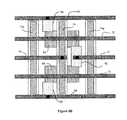
- FIG. 4Dis an illustration showing a semiconductor chip structure, in accordance with one embodiment of the present invention.
- FIG. 4Eshows an example layout architecture defined in accordance with one embodiment of the present invention.
- FIG. 5Aillustrates a circuit representation of a logic inverter using a PMOS and an NMOS transistor, in accordance with one embodiment of the present invention.
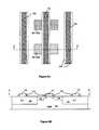
- FIG. 5Billustrates a plan view of an exemplary logic inverter to demonstrate a use of the self-aligned local interconnects, in accordance with one embodiment of the present invention.
- FIG. 6Aillustrates a plan view of an exemplary logic inverter showing transistor source/drains, electrodes, and sidewall spacers surrounding the gate electrodes, in accordance with one embodiment of the present invention.
- FIG. 6Billustrates a cross-section view of cutline A-A′ of the exemplary logic inverter of FIG. 6A showing a transistor well, transistor source/drains, gate electrodes, sidewall spacers, and STI regions, in accordance with one embodiment of the present invention.
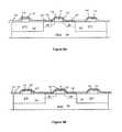
- FIG. 7Ashows a section of an exemplary logic inverter with a local interconnect layer covering the underlying elements shown in FIG. 6A , in accordance with one embodiment of the present invention.
- FIG. 7Bis a cross-section view of a section of an exemplary logic inverter with a local interconnect layer covering the underlying elements shown in FIG. 6B , in accordance with one embodiment of the present invention.
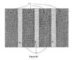
- FIG. 8Aillustrates formation of silicide through annealing of the local interconnect layer, in accordance with one embodiment of the present invention.
- FIG. 8Billustrates depositing a hard mask layer on top of the local interconnect layer over the substrate, in accordance with one embodiment of the present invention.
- FIG. 9Aillustrates a polymer layer covering the elements of FIG. 8B , in accordance with one embodiment of the present invention.
- FIG. 9Billustrates a cross section view of the substrate in which the polymer layer is partially removed through plasma etch, in accordance with one embodiment of the present invention.
- FIG. 9Cillustrates a plan view of the substrate in which the polymer layer is etched back to approximately the top of the gate electrodes, in accordance with one embodiment of the present invention.
- FIG. 10Aillustrates a plan view of the exemplary logic inverter after a wet etch to remove the polymer from the dielectric spacers, in accordance with one embodiment of the present invention.
- FIG. 10Billustrates a cross-section view of the exemplary logic inverter after removal of the polymer covering the dielectric spacers, in accordance with one embodiment of the present invention.
- FIG. 11Aillustrates a cross section view of the exemplary logic inverter after etching the local interconnect layer and the hard mask layer from the gate electrodes and dielectric spacers, in accordance with one embodiment of the present invention.
- FIG. 11Billustrates a cross section view of the exemplary logic inverter after selective etch of the remaining polymer layer and hard mask layer, in accordance with one embodiment of the present invention.
- FIG. 12illustrates a plan view of the exemplary logic inverter after selective etch of the remaining polymer layer and hard mask layer, in accordance with one embodiment of the present invention.
- FIG. 13illustrates a plan view of the exemplary logic inverter after masking portions of the local interconnect layer to protect the local interconnect layer at desired places, in accordance with one embodiment of the present invention.
- FIG. 14illustrates a plan view of the exemplary logic inverter showing remaining regions of silicided and non-silicided local interconnect, in accordance with one embodiment of the present invention.
- FIG. 15illustrates a plan view of an exemplary logic inverter as in FIG. 14 , with contacts and metal lines added to shown a functional interconnection, in accordance with one embodiment of the present invention.
- FIG. 16illustrates a plan view of an exemplary logic inverter showing the self-aligned local interconnect in a gap of a gate line, in accordance with one embodiment of the present invention.
- FIGS. 17A-17Dillustrate cross-sectional views of an exemplary logic inverter, which uses the local interconnect metal to make connections to a gate, in accordance with one embodiment of the present invention.
- FIG. 18illustrates a plan view of an exemplary logic inverter showing the self-aligned local interconnect in a gap of a gate line and making connection to a gate upon “climbing” a spacer, in accordance with one embodiment of the present invention.
- Embodiments of an invention for methods and processes for designing, layout-out, making, fabricating and implementing “self-aligned local interconnects” in integrated circuitsare disclosed.
- numerous specific detailsare set forth in order to provide a thorough understanding of the present invention.
- a process of fabricating self-aligned local interconnectsis provided.
- method and layout techniquesare disclosed, which illustrate ways of using the self-aligned local interconnects.
- the benefits and advantages of using these self-aligned local interconnectsare also outlined below, with specific reference to a particular logic cell. However, it should be understood that the example logic cell is not limiting on the use of local interconnects that are self-aligned.
- the self-aligned local interconnectshave numerous applications in the fabrication of integrated circuits.
- the self-aligning of the local interconnects in integrated circuitseliminates lithography error margins and resulting device loss, as even a minor misalignment of a local interconnect on the integrated circuit may cause an electric short and/or render the device inoperable.
- self-aligned local interconnectsmay be used for various other purposes.
- One such purposeis to use the self-aligned local interconnects to move away metal contacts from the diffusion regions of transistors.
- the process of fabricating “self-aligned” local interconnects in integrated circuitsis advantageous over other techniques, which require precise aligning through lithography processes.
- interference patterns from neighboring shapescan create constructive or destructive interference.
- unwanted shapesmay be inadvertently created.
- desired shapesmay be inadvertently removed.
- a particular shapeis printed in a different manner than intended, possibly causing a device failure.
- Correction methodologiessuch as optical proximity correction (OPC), attempt to predict the impact from neighboring shapes and modify the mask such that the printed shape is fabricated as desired.
- OPCoptical proximity correction
- the methods and structures of the present inventiontake advantage of a consistent feature orientation, which defines a canvas of substantially uniform feature orientations.
- a consistent feature orientationwhich defines a canvas of substantially uniform feature orientations.
- a number of diffusion regionsare defined within the substrate to define active regions for transistor devices.
- the canvasalso includes a number of linear gate electrode segments oriented in a common direction over the substrate. Some of the linear gate electrode segments are disposed over a diffusion region. Each of the linear gate electrode segments that is disposed over a diffusion region includes a necessary active portion defined over the diffusion region and a uniformity extending portion defined to extend over the substrate beyond the diffusion region. Additionally, the linear gate electrode segments are defined to have variable lengths to enable logic gate functionality.
- the canvasfurther includes a number of linear conductor segments disposed within a level over the gate electrode segments, so as to cross the common direction of the gate electrode segments in a substantially perpendicular direction.
- the number of linear conductor segmentsis defined to minimize an end-to-end spacing between adjacent linear conductor segments within a common line over the substrate.
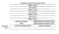
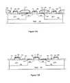
- FIG. 1is an illustration showing a generalized stack of layers used to define a dynamic array architecture, in accordance with one embodiment of the present invention. It should be appreciated that the generalized stack of layers used to define the dynamic array architecture, as described with respect to FIG. 1 , is not intended to represent an exhaustive description of the CMOS manufacturing process. However, the dynamic array is to be built in accordance with standard CMOS manufacturing processes. Generally speaking, the dynamic array architecture includes both the definition of the underlying structure of the dynamic array and the techniques for assembling the dynamic array for optimization of area utilization and manufacturability. Thus, the dynamic array is designed to optimize semiconductor manufacturing capabilities.
- the dynamic arrayis built-up in a layered manner upon a base substrate (e.g. semiconductor wafer) 201 , e.g., upon a silicon substrate, or silicon-on-insulator (SOI) substrate.
- Diffusion regions 203are defined in the base substrate 201 .
- the diffusion regions 203are generally separated by the isolation regions or Shallow Trench Isolation (STI) regions.
- the diffusion regions 203represent selected regions of the base substrate 201 within which impurities are introduced for the purpose of modifying the electrical properties of the base substrate 201 .
- diffusion contacts 205are defined to enable connection between the diffusion regions 203 and conductor lines.
- the diffusion contacts 205are defined to enable connection between source and drain diffusion regions 203 and their respective conductor nets.
- gate electrode features 207are defined above the diffusion regions 203 to form transistor gates.
- Gate electrode contacts 209are defined to enable connection between the gate electrode features 207 and conductor lines.
- the gate electrode contacts 209are defined to enable connection between transistor gates and their respective conductor nets.
- Interconnect layersare defined above the diffusion contact 205 layer and the gate electrode contact layer 209 .
- the interconnect layersinclude a first metal (metal 1) layer 211 , a first via (via 1) layer 213 , a second metal (metal 2) layer 215 , a second via (via 2) layer 217 , a third metal (metal 3) layer 219 , a third via (via 3) layer 221 , and a fourth metal (metal 4) layer 223 .
- the metal and via layersenable definition of the desired circuit connectivity.
- the metal and via layersenable electrical connection of the various diffusion contacts 205 and gate electrode contacts 209 such that the logic function of the circuitry is realized.
- the dynamic array architectureis not limited to a specific number of interconnect layers, i.e., metal and via layers.
- the dynamic arraymay include additional interconnect layers 225 , beyond the fourth metal (metal 4) layer 223 .
- the dynamic arraymay include less than four metal layers.
- the dynamic arrayis defined such that layers (other than the diffusion region layer 203 ) are restricted with regard to layout feature shapes that can be defined therein. Specifically, in each layer other than the diffusion region layer 203 , substantially linear-shaped layout features are allowed.
- a linear-shaped layout feature in a given layeris characterized as having a consistent vertical cross-section shape and extending in a single direction over the substrate. Some minor perpendicular extrusions would be allowed, however, if contacts need to be made to some lines, but these minor perpendicular extrusions should not constitute a substantial change in direction.
- the linear-shaped layout featuresdefine structures that are one-dimensionally varying.
- the diffusion regions 203are not required to be one-dimensionally varying, although they are allowed to be if necessary.
- the diffusion regions 203 within the substratecan be defined to have any two-dimensionally varying shape with respect to a plane coincident with a top surface of the substrate.
- the number of diffusion bend topologiesis limited such that the interaction between the bend in diffusion and the conductive material, e.g., polysilicon, that forms the gate electrode of the transistor is predictable and can be accurately modeled.
- the linear-shaped layout features in a given layerare positioned to be parallel with respect to each other. Thus, the linear-shaped layout features in a given layer extend in a common direction over the substrate and parallel with the substrate.
- the underlying layout methodology of the dynamic arraymay (but does not have to) use constructive light interference of light waves in the lithographic process to reinforce exposure of neighboring shapes in a given layer. Therefore, the spacing of the parallel, linear-shaped layout features in a given layer is designed around the constructive light interference of the standing light waves such that lithographic correction (e.g., OPC/RET) is minimized or eliminated.
- lithographic correctione.g., OPC/RET
- the dynamic array defined hereinexploits the light interaction between neighboring features, rather than attempting to compensate for the light interaction between neighboring features.
- the standing light wave for a given linear-shaped layout featurecan be accurately modeled, it is possible to predict how the standing light waves associated with the neighboring linear-shaped layout features disposed in parallel in a given layer will interact. Therefore, it is possible to predict how the standing light wave used to expose one linear-shaped feature will contribute to the exposure of its neighboring linear-shaped features. Prediction of the light interaction between neighboring linear-shaped features enables the identification of an optimum feature-to-feature spacing such that light used to render a given shape will reinforce its neighboring shapes.
- the feature-to-feature spacing in a given layeris defined as the feature pitch, wherein the pitch is the center-to-center separation distance between adjacent linear-shaped features in a given layer.
- the linear-shaped layout features in a given layerare spaced such that constructive and destructive interference of the light from neighboring features will be optimized to produce the best rendering of all features in the neighborhood.
- the feature-to-feature spacing in a given layeris proportional to the wavelength of the light used to expose the features.
- the light used to expose each feature within about a five light wavelength distance from a given featurewill serve to enhance the exposure of the given feature to some extent.
- the exploitation of constructive interference of the light waves used to expose neighboring featuresenables the manufacturing equipment capability to be maximized and not be limited by concerns regarding light interactions during the lithography process.
- the dynamic arrayincorporates a restricted topology in which the features within each layer (other than diffusion) are required to be substantially linear in shape, and are oriented in a parallel manner to traverse over the substrate in a common direction.
- the restricted topology of the dynamic arraythe light interaction in the photolithography process can be optimized such that an accurate transfer of the layout onto the resist is achieved.
- FIG. 2Ais an illustration showing an exemplary base grid to be projected onto the dynamic array to facilitate definition of the restricted topology, in accordance with one embodiment of the present invention.
- the base gridcan be used to facilitate parallel placement of the linear-shaped features in each layer of the dynamic array at the appropriate optimized pitch.
- the base gridcan be considered as a projection on each layer of the dynamic array. Also, it should be understood that the base grid is projected in a substantially consistent manner with respect to position on each layer of the dynamic array, thus facilitating accurate feature stacking and alignment.
- the base gridis defined as a rectangular grid, i.e., Cartesian grid, in accordance with a first reference direction (x) and a second reference direction (y).
- the gridpoint-to-gridpoint spacing in the first and second reference directionscan be defined as necessary to enable definition of the linear-shaped features at the optimized feature-to-feature spacing.
- the gridpoint spacing in the first reference direction (x)can be different than the gridpoint spacing in the second reference direction (y).
- a single base gridis projected across the entire die to enable location of the various linear-shaped features in each layer across the entire die.
- FIG. 2Bis an illustration showing separate base grids projected across separate regions of the die, in accordance with an exemplary embodiment of the present invention.
- the layout architecture of the dynamic arrayfollows the base grid pattern.
- the pitch of the gridpointsi.e., the gridpoint-to-gridpoint spacing
- the gridpoint spacing in the first reference direction (x)is set by the required gate electrode pitch.
- the gridpoint pitch in the second reference direction (y)is set by the metal 1 pitch.
- the gridpoint pitch in the second reference direction (y)is about 0.24 micron.
- metal 1 and metal 2 layerswill have a common spacing and pitch. A different spacing and pitch may be used above the metal 2 layer.
- the various layers of the dynamic arrayare defined such that the linear-shaped features in adjacent layers extend in a crosswise manner with respect to each other.
- the linear-shaped features of adjacent layersmay extend orthogonally, i.e., perpendicularly with respect to each other.
- the linear-shaped features of one layermay extend across the linear-shaped features of an adjacent layer at an angle, e.g., at about 45 degrees.
- the linear-shaped feature of one layerextend in the first reference direction (x) and the linear-shaped features of the adjacent layer extend diagonally with respect to the first (x) and second (y) reference directions. It should be appreciated that to route a design in the dynamic array having the linear-shaped features positioned in the crosswise manner in adjacent layers, opens can be defined in the linear-shaped features, and contacts and vias can be defined as necessary.
- the dynamic arrayminimizes the use of bends (or substantial changes in direction) in layout shapes to eliminate unpredictable lithographic interactions. Specifically, prior to OPC or other RET processing, the dynamic array allows bends in the diffusion layer to enable control of device sizes, but does not allow substantial bends (or substantial changes in direction) in layers above the diffusion layer.
- FIGS. 3 and 4AAn exemplary buildup of dynamic array layers from diffusion through metal 2 are described with respect to FIGS. 3 and 4A .
- the dynamic arraycan be used in accordance with the principles presented herein to define essentially any integrated circuit design, any logic cell, a base cell, an architecture, or design layouts. Designs can be on physical chips, wafers, substrates or drawn on paper, film, or stored in files. If stored in files, the files can be stored on any computer readable device.
- the computer readable devicecan be stored on a local computer, on a networked computer and the files can be transferred, shared or used over the Internet or local network.
- FIG. 3shows a diffusion layer layout of an exemplary dynamic array, in accordance with one embodiment of the present invention.
- the diffusion layer of FIG. 3shows a p-diffusion region 401 and an n-diffusion region 403 .
- the diffusion regionsare defined according to the underlying base grid, the diffusion regions are not subject to the linear-shaped feature restrictions associated with the layers above the diffusion layer.
- the implant layoutsare simpler than in prior art designs, which would otherwise require more shape extension and bends.
- n+ implant regions ( 412 ) and p+ implant regions ( 414 )are defined as rectangles on the (x), (y) grid with no extraneous jogs or notches. This style permits use of larger implant regions, reduces need for OPC/RET, and enables use of lower resolution and lower cost lithographic systems, e.g., i-line illumination at 365 nm.
- FIG. 4Ais an illustration showing a gate electrode layer above and adjacent to the diffusion layer of FIG. 3 , in accordance with one embodiment of the present invention.
- the gate electrode features 501define the transistor gates.
- the gate electrode features 501are defined as linear shaped features extending in a parallel relationship across the dynamic array in the second reference direction (y).
- the gate electrode features 501are defined to have a common width.
- one or more of the gate electrode featurescan be defined to have a different width.
- the pitch (center-to-center spacing) of the gate electrode features 501is minimized while ensuring optimization of lithographic reinforcement, i.e., resonant imaging, provided by neighboring gate electrode features 501 .
- gate electrode features 501 extending across the dynamic array in a given lineare referred to as a gate electrode track.
- the gate electrode features 501form n-channel and p-channel transistors as they cross the diffusion regions 403 and 401 , respectively.
- Optimal gate electrode feature 501 printingis achieved by drawing gate electrode features 501 at every grid location, even though no diffusion region may be present at some grid locations.
- long continuous gate electrode features 501tend to improve line end shortening effects at the ends of gate electrode features within the interior of the dynamic array. Additionally, gate electrode printing is significantly improved when substantially all bends are removed from the gate electrode features 501 .
- Each of the gate electrode tracksmay be interrupted, i.e., broken, any number of times in linearly traversing across the dynamic array in order to provide required electrical connectivity for a particular logic function to be implemented.
- interruptedi.e., broken
- the separation between ends of the gate electrode track segments at the point of interruptionis minimized to the extent possible taking into consideration the manufacturing capability and electrical effects.
- optimal manufacturabilityis achieved when a common end-to-end spacing is used between features within a particular layer.
- FIG. 4Bis an illustration showing a gate electrode layer and a diffusion contact layer above and adjacent to the diffusion layer of FIG. 4A , in accordance with one embodiment of the present invention.
- the gate electrode features 501define the transistor gates.
- the gate electrode features 501are defined as linear shaped features extending in a parallel relationship across the dynamic array in the second reference direction (y).
- the gate electrode features 501are defined to have a common width.
- one or more of the gate electrode featurescan be defined to have a different width. For example, FIG.
- gate electrode features 501 Athat has a larger width relative to the other gate electrode features 501 .
- the pitch (center-to-center spacing) of the gate electrode features 501is minimized while ensuring optimization of lithographic reinforcement, i.e., resonant imaging, provided by neighboring gate electrode features 501 .
- gate electrode features 501 extending across the dynamic array in a given lineare referred to as a gate electrode track.
- the gate electrode features 501form n-channel and p-channel transistors as they cross the diffusion regions 403 and 401 , respectively.
- Optimal gate electrode feature 501 printingis achieved by drawing gate electrode features 501 at every grid location, even though no diffusion region may be present at some grid locations.
- long continuous gate electrode features 501tend to improve line end shortening effects at the ends of gate electrode features within the interior of the dynamic array. Additionally, gate electrode printing is significantly improved when all bends are removed from the gate electrode features 501 .
- Each of the gate electrode tracksmay be interrupted, i.e., broken, any number of times in linearly traversing across the dynamic array in order to provide required electrical connectivity for a particular logic function to be implemented.
- interruptedi.e., broken
- the separation between ends of the gate electrode track segments at the point of interruptionis minimized to the extent possible taking into consideration the manufacturing capability and electrical effects.
- optimal manufacturabilityis achieved when a common end-to-end spacing is used between features within a particular layer.
- Minimizing the separation between ends of the gate electrode track segments at the points of interruptionserves to maximize the lithographic reinforcement, and uniformity thereof, provided from neighboring gate electrode tracks.
- the interruptions of the adjacent gate electrode tracksare made such that the respective points of interruption are offset from each other so as to avoid, to the extent possible, an occurrence of neighboring points of interruption. More specifically, points of interruption within adjacent gate electrode tracks are respectively positioned such that a line of sight does not exist through the points of interruption, wherein the line of sight is considered to extend perpendicularly to the direction in which the gate electrode tracks extend over the substrate.
- the gate electrodesmay extend through the boundaries at the top and bottom of the cells, i.e., the PMOS or NMOS cells. This embodiment would enable bridging of neighboring cells.
- diffusion contacts 503are defined at each diffusion square 405 to enhance the printing of diffusion contacts via resonant imaging.
- the diffusion squares 405are present around every diffusion contact 503 to enhance the printing of the power and ground connection polygons at the diffusion contacts 503 .
- the gate electrode features 501 and diffusion contacts 503share a common grid spacing. More specifically, the gate electrode feature 501 placement is offset by one-half the grid spacing relative to the diffusion contacts 503 . For example, if the gate electrode features 501 and diffusion contact 503 grid spacing is 0.36 ⁇ m, then the diffusion contacts are placed such that the x-coordinate of their center falls on an integer multiple of 0.36 ⁇ m, while the x-coordinate of the center of each gate electrode feature 501 minus 0.18 ⁇ m should be an integer multiple of 0.36 ⁇ m. In the present example, the x-coordinates are represented by the following:
- the grid based system of the dynamic arrayensures that all contacts (diffusion and gate electrode) will land on a horizontal grid that is equal to a multiple of one-half of the diffusion contact grid and a vertical grid that is set by the metal 1 pitch.
- the gate electrode feature and diffusion contact gridis 0.36 ⁇ m.
- the diffusion contacts and gate electrode contactswill land on a horizontal grid that is a multiple of 0.18 ⁇ m.
- the vertical grid for 90 nm process technologiesis about 0.24 ⁇ m.
- FIG. 4Cis an illustration showing a gate electrode contact layer defined above and adjacent to the gate electrode layer of FIG. 4B , in accordance with one embodiment of the present invention.
- gate electrode contacts 601are drawn to enable connection of the gate electrode features 501 to the overlying metal conduction lines.
- design ruleswill dictate the optimum placement of the gate electrode contacts 601 .
- the gate electrode contactsare drawn on top of the transistor endcap regions. This embodiment minimizes white space in the dynamic array when design rules specify long transistor endcaps. In some process technologies white space may be minimized by placing a number of gate electrode contacts for a cell in the center of the cell.
- the gate electrode contact 601is oversized in the direction perpendicular to the gate electrode feature 501 to ensure overlap between the gate electrode contact 601 and the gate electrode feature 501 .
- FIG. 4Dis an illustration showing a semiconductor chip structure 1400 , in accordance with one embodiment of the present invention.
- the semiconductor chip structure 1400represents an exemplary portion of a semiconductor chip, including a diffusion region 1401 having a number of conductive lines 1403 A- 1403 G defined thereover.
- the diffusion region 1401is defined in a substrate 1405 , to define an active region for at least one transistor device.
- the diffusion region 1401can be defined to cover an area of arbitrary shape relative to the substrate 1405 surface.
- the conductive lines 1403 A- 1403 Gare arranged to extend over the substrate 1405 in a common direction 1407 . It should also be appreciated that each of the number of conductive lines 1403 A- 1403 G are restricted to extending over the diffusion region 1401 in the common direction 1407 .
- the conductive lines 1403 A- 1403 G defined immediately over the substrate 1405are polysilicon lines.
- each of the conductive lines 1403 A- 1403 Gis defined to have essentially the same width 1409 in a direction perpendicular to the common direction 1407 of extension.
- some of the conductive lines 1403 A- 1403 Gare defined to have different widths relative to the other conductive lines. However, regardless of the width of the conductive lines 1403 A- 1403 G, each of the conductive lines 1403 A- 1403 G is spaced apart from adjacent conductive lines according to essentially the same center-to-center pitch 1411 .
- some of the conductive lines ( 1403 B- 1403 E)extend over the diffusion region 1401
- other conductive lines ( 1403 A, 1403 F, 1403 G)extend over non-diffusion portions the substrate 1405 .
- the conductive lines 1403 A- 1403 Gmaintain their width 1409 and pitch 1411 regardless of whether they are defined over diffusion region 1401 or not.
- the conductive lines 1403 A- 1403 Gmaintain essentially the same length 1413 regardless of whether they are defined over diffusion region 1401 or not, thereby maximizing lithographic reinforcement between the conductive lines 1403 A- 1403 G across the substrate.
- some of the conductive lines, e.g., 1403 D, defined over the diffusion region 1401include a necessary active portion 1415 , and one or more uniformity extending portions 1417 .
- the semiconductor chip structure 1400represents a portion of the dynamic array described above with respect to FIGS. 1-4C . Therefore, it should be understood that the uniformity extending portions 1417 of the conductive lines ( 1403 B- 1403 E) are present to provide lithographic reinforcement of neighboring conductive lines 1403 A- 1403 G. Also, although they may not be required for circuit operation, each of conductive lines 1403 A, 1403 F, and 1403 G are present to provide lithographic reinforcement of neighboring conductive lines 1403 A- 1403 G.
- each of the conductive lines within an interconnect layermay include a required portion (necessary active portion) to enable required routing/connectivity, and a non-required portion (uniformity extending portion) to provide lithographic reinforcement to neighboring conductive lines.
- the conductive lines within an interconnect layerextend in a common direction over the substrate, have essentially the same width, and are spaced apart from each other according to an essentially constant pitch.
- conductive lines within an interconnect layerfollow essentially the same ratio between line width and line spacing. For example, at 90 nm the metal 4 pitch is 280 nm with a line width and line spacing equal to 140 nm. Larger conductive lines can be printed on a larger line pitch if the line width is equal to the line spacing.
- FIG. 4Eshows an example layout architecture defined in accordance with one embodiment of the present invention.
- the layout architecturefollows a grid pattern and is based upon a horizontal grid and a vertical grid.
- the horizontal gridis set by the poly gate pitch.
- the vertical pitchis set by the metal 1/metal 3 pitch. All of the rectangular shapes should be centered on a grid point.
- the layout architectureminimizes the use of bends to eliminate unpredictable lithographic interactions. Bends are allowed on the diffusion layer to control transistor device sizes. Other layers should be rectangular in shape and fixed in one dimension.
- FIG. 5Aillustrates a circuit representation of the exemplary logic inverter.
- the logic inerteris only being shown and discussed to convey the process of making the self-aligned local interconnects, which can be implemented any other primitive, cell, logic device, or process methodology.
- the PMOS transistor 110 and the NMOS transistor 112are coupled to make a logic inverter.
- the source of the PMOS transistor 110is connected to Vdd 118 and the drain of the PMOS transistor 112 is connected to the drain of the NMOS transistor 112 .
- the source of the NMOS transistor 112is connected to the ground (Vss) 120 .
- a common input 116is provided to the transistors and the output 114 is provided at the connection of the drain of the PMOS transistor 110 and the drain of the NMOS transistor 112 .
- the inverter logicis used as an example to provide an understanding of the embodiments of the present invention. A person skilled in the art, however, would appreciate that the embodiments may also be employed in the fabrication of any other types of logic cells, devices, and integrated circuits.
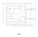
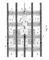
- FIG. 5Billustrates a plan view of an exemplary logic inverter having self-aligned local interconnects 58 / 60 to connect P 64 and N 68 diffusion regions to Vdd 50 and Vss 54 , respectively.
- a self-aligned local interconnect 62is also being used to connect the drain of the PMOS transistor to the drain of the NMOS transistor.
- all self-aligned local interconnects in an integrated circuitrun parallel to the gate electrode channels on the substrate.
- One of many advantages of laying the local interconnects in one directionis that the local interconnect layer can replace one metal layer that would otherwise be needed to make the connections that are being made using the self-aligned local interconnects.
- Metal 1 lines 50 , 72 , 70 , and 54are aligned in one direction that is perpendicular to the gate electrode line 74 . The alignment of metal lines can be different in other embodiments.
- the self-aligned local interconnect 58 connecting P diffusion region 64 to Vdd line 50eliminates the need of fabricating an L shaped diffusion region extending towards the Vdd line 50 .
- the self-aligned local interconnect 58eliminates the need for a metal strap to connect the diffusion region 64 to the Vdd line 50 . Elimination of the metal strap and associated contact increases device performance and reduces device size. Performance is increased because a metal strap connecting to the diffusion regions would require one or more contacts, which interferes with beneficial straining of silicon. Thus, reducing metal contacts to the diffusion regions, unless necessary for some design configurations, will boost device performance.
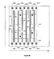
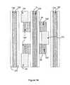
- FIG. 6Aillustrates a plan view of a partially fabricated integrated circuit showing a P diffusion region 64 and a N diffusion region 68 and a gate electrode line 74 over the P diffusion region 64 and the N diffusion region 68 .
- the other gate electrode lines 74 a , 74 bare laid over shallow trench isolation (STI) regions.
- the gate electrodes 74 , 74 a , 74 binclude dielectric spacers (or gate sidewall spacers) on both sides.
- the ends of the gate electrodesmay also have dielectric spacers. Since, by design, the gate electrode lines are uniformly placed on the substrates, some of the gate electrode lines are formed over the STI regions. Thus, gates formed over the STI are inactive gates. An active gate is formed when a gate electrode is placed over a diffusion region, and a transistor can be defined. In one embodiment, the partially fabricated integrated circuit is fabricated using a standard CMOS fabrication process.
- FIG. 6Billustrates a cross-section of a partially fabricated integrated circuit of FIG. 6A .
- the figuresare not meant to provide an exact representation of dimensions or exact relative dimensions.
- the figuresshould be understood to generally convey the placement of features, layers and the example sequence of processing. Additionally, it should be understood that some sequence steps are not pictorially illustrated, as they are known to those skilled in the art, and not important to the process and sequence flows illustrated herein.
- the partially fabricated integrated circuitis formed over a silicon wafer, and includes a well 182 and shallow trench isolation (STI) regions 180 , to provide isolation between adjacent active devices in the integrated circuit.
- the well 182includes diffusion regions 184 and a gate electrode 74 .
- the gate electrodesinclude dielectric spacers (also known as sidewall spacers) 230 formed along the sides of the gate electrode lines.
- the gate electrodesor lines are fabricated in a parallel orientation, relative to each other. As described herein, therefore, “channels” are defined between the respective gate electrodes. The spacing between two adjacent gate electrode channels is therefore dictated by the regular spacing of the gate electrode lines.
- the resulting self-aligned local interconnectswill reside in the channels between adjacent gate electrodes (or beside a gate electrode if no neighboring gate electrode is present). Because they will predominantly remain in the channels, the self-aligned local interconnects will be self-aligning.
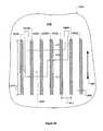
- a local interconnect layer 196is formed over the diffusion regions 184 , the gate electrodes 74 , 74 a , 74 b , and the spacers.
- formation of the local interconnect layer 196can be through a metal deposition process.
- the local interconnect layer 196is shown in FIG. 7A as a semi-transparent layer.
- the cross-section of FIG. 7Bshows the local interconnect layer 196 deposited over the features of FIG. 6B .
- the local interconnect layer 196is generally metallic.
- the metalmay be predominantly nickel (Ni).
- the metalcan be titanium, platinum, or cobalt.
- a combination of nickel and platinumcan be used.
- the purity of the metal used in the local interconnect layershould comply with the industry standard metals.
- the local interconnect layeris deposited using physical vapor deposition (PVD) technique.
- the deposition of the local interconnect layermay be done through chemical vapor deposition (CVD) or atomic layer deposition (ALD).
- the metal of the interconnect layeris reacted with the underlying silicon and if present in the gate electrode, polysilicon.
- the reactionis facilitated through a thermal processing step.
- the reactioncan be carried out under a number of process conditions, but as an example, the temperature can be in a range of between about 200 to 400 degree Celsius, and run for a time in a range of about 5 to about 60 seconds for a nickel layer; higher temperatures may be used for other metals. In another example, the temperature can be set to about 300 degrees Celsius, and processed for about 30 seconds.
- the reaction stepis generally performed in a chamber that uses nitrogen or other inert gases.
- silicide 196 ′is formed over the exposed silicon areas.
- the silicidationi.e. formation of silicide 196 ′
- the silicidationoccurs over the exposed silicon substrate portion and exposed polysilicon gate if present.
- silicide 196 ′provides good conduction even if the layer is thin. Portions of the local interconnect layer 196 metal not touching silicon will, of course, remain as a metal after the reaction process.
- FIG. 8Ashows the silicide 196 ′ as shaded, in contrast to the metal of the local interconnect layer 196 which did not react.
- FIG. 8Billustrates the result after a hard mask layer 199 is deposited over the local interconnect layer 196 .
- the hard mask layer 199is an oxide (e.g., SiO 2 , etc.).
- the hard mask layer 199is a nitride (e.g., silicon nitride, etc.).
- the hard mask layer 199is an amorphous carbon (APF).
- the hard mask layer 199can be formed in a number of ways, and one such exemplary way is by employing one of a CVD, ALD, or PECVD process.
- the hard mask layer 199in this embodiment, is used to protect the local interconnect layer 196 during subsequent removal steps, which remove portions of the local interconnect layer 196 where no conductive connection is needed.
- FIG. 9Ashows the cross-section of FIG. 8B after a polymer layer 210 is formed over the hard mask layer 199 , in accordance with one embodiment of the present invention.
- the polymer layer 210can be applied in a number of ways know in the art.
- the polymer layer 210is preferably spin coated over the surface of the hard mask layer 199 .
- the polymer layer 210can be photoresist material, either positive or negative, depending on the desired development process. Other types of photoresist can include, for example, unsensitized photoresists, polymethyl methacrylate resists (PMMA), etc.
- PMMApolymethyl methacrylate resists
- the removalis preferably performed using a plasma etching operation.
- a plasma etching operationcan take place in an oxygen plasma.
- the etching process, in this step,is preferably anisotropic in nature, so as to achieve a substantially even removal profile down to the first exposed hard mask layer 199 .
- Standard end-point detection techniquesmay be used to determine when to stop the etch operation illustrated in FIG. 9B .
- FIG. 9Cis a plan view, showing the exposed hard mask layer 199 and the remaining polymer layer 210 .
- the gate sidewall spacers (i.e. dielectric spacers) 230are also still covered by the polymer layer 210 .
- the polymer layer 210is defined uniformly, having a substantially equal thickness. Without such uniform spacing, the polymer layer 210 could exhibit variations in thickness, which would not be desired. For example, if the thickness of the polymer layer 210 is not substantially uniform over the substrate, some gate electrodes with relatively less polymer material cover may be exposed first, causing possible over etching of the hard mask over certain gates.
- an isotropic etchis performed.
- the isotropic etchingis designed to remove lateral parts 238 of the polymer layer 210 , such as the polymer layer 210 on the gate electrode dielectric spacers 230 .
- the polymer layer 210should remains in the form of strips between the gate electrodes 74 , 74 a , 74 b , offset and self-aligned to the gate dielectric spacers 230 .
- the polymer layer 210will remain everywhere on the substrate except on the gate electrode lines 74 , 74 a , 74 b and the gate dielectric spacers 230 .
- FIG. 11Aillustrates a cross-section of the substrate after the hard mask layer 199 , which is not covered by the polymer layer 210 , is removed.
- the removalcan be performed using a number of known wet or dry etching processes.
- the etchingcan continue so as to remove part of the local interconnect layer 196 material from over the dielectric spacers 230 . Removal of this part of the local interconnect layer 196 will provide for a slight separation between the local interconnect layer 196 /silicide 196 ′ and the dielectric spacers 230 .
- the remaining local interconnect layer 196 material, silicide 196 ′ material and hard mask layer 199will run in channels between and aligned by the dielectric spacers 230 .
- FIG. 11Billustrates a cross-section of the substrate after another selective etching operation is performed to remove the polymer layer 210 and the hard mask layer 199 , from above the local interconnect layer 196 (including silicide portions 196 ′).
- the local interconnect layer 196 material and the silicide portions 196 ′will be self-aligned between the dielectric spacers 230 .
- FIG. 12shows a plan view of substrate in FIG. 11B .
- the local interconnect layer 196runs in the channels between the gate dielectric spacers 230 .
- the self-aligned local interconnect layer 196is also spaced a distance 231 apart from dielectric spacers 230 .
- FIG. 12also illustrates the P 64 and N 68 diffusion regions (both these regions are illustrated in the cross-section illustrations as diffusion region 184 ).
- FIG. 13illustrates a patterning operation that will facilitate etching, in accordance with one embodiment of the present invention.
- a photoresistcan be spin coated and then exposed using standard photolithography, to define mask 300 .
- the mask 300is defined to cover portions of the local interconnect layer 196 that is to remain after an etching operation is performed.
- the reacted material that forms the silicide 196 ′, over the exposed silicon or polysilicon if present,will also remain after the etch, even though it is not covered by the mask 300 .
- the mask 300can be easily defined without tight layout constraints, as the mask 300 can be defined to loosely lie over the gate electrodes 74 , 74 a , 74 b.
- the local interconnect layer 196 materialonly lies in the channels, and has already been self-aligned between the dielectric spacers 230 .
- the silicide 196 ′ materialwill however remain after the etching that is employed to remove the unprotected portions of the local interconnect layer 196 .
- the local interconnect layer 196 and the silicide 196 ′ materialwill define a conductive link or connection or conductive line, similar to a regular interconnect metallization line.
- FIG. 14illustrates a plan view of the substrate after the etching and subsequent removal of the mask 300 .
- the local interconnect layer 196will remain in the channels, where the mask 300 protected the material, thus forming true self-aligned local interconnect features.
- an annealing operationcan be performed.
- the annealingcould be, for example, a rapid thermal annealing (RTA) process, that is operated at approximately 450 degrees Celsius, for approximately 30 seconds for nickel.
- RTArapid thermal annealing
- metal 1 linescan be fabricated perpendicular to the gate electrode lines 74 , 74 a , 74 b , as shown in FIG. 15 . Furthermore, contacts are formed at desired places, to provide electrical conduction between various layers, that is necessary to form the exemplary logic circuit.
- the metal-1 tracks 702can be fabricated closer to each other, which may enable easier routing and desired connections.
- the pitch between lineswill depend on the manufacturing capability, the particular circuit, layout, and layout constraints for the type of design and/or circuit.
- the self-aligned local interconnects 196are aligned perpendicular to metal-1 tracks 702 , a greater degree of freedom in term of space is available for defining/selecting a contact between the self-aligned local interconnects 196 and selected metal-1 tracks. Therefore, besides the previously discussed advantages of the self-aligned local interconnects, the self-aligned local interconnects also help to provide more freedom in routing metal tracks in levels above, which in turn provide for flexibility in design and fabrication.
- FIG. 16illustrates an exemplary inverter logic cell, which is fabricated using the self-aligned local interconnects of the present invention.
- the circuitis similar to the one illustrated in FIG. 5A , except that the gate electrode line 74 a is broken into two sections, to provide a gate electrode gap 703 . It may be noted that only one gap is shown for the ease of illustration only. In other embodiments, one or more gate electrode lines can have one or more gate electrode gaps. In one embodiment, the gate electrode gap 703 can be used to fabricate the self-aligned local interconnects that are aligned perpendicular to the gate electrode line 74 a .
- the self-aligned local interconnects in these gate electrode gaps 703can be used to connect two or more devices or two self-aligned local interconnects that are parallel to the gate electrode line 74 a .
- the self-aligned local interconnects in the gate electrode gaps 703can also ease metal track routing and eliminate the need for some of the metal-1 tracks.
- FIG. 17A-17Dillustrate process operations used to fabricate a connection using the local interconnect layer 196 , to make contact to a gate electrode 74 , in accordance with another embodiment of the present invention.
- FIG. 17Arepresents a stage in processing that is similar to that described up to FIG. 10B .
- a mask 404is also formed over a region 402 , which lies substantially over the sidewall of the spacer 230 of gate electrode 74 .
- the exact sizingis not particularly important, so long as protection is provided over the material that lies along the spacer 230 . This protects the local interconnect material 196 in this region from later etching.
- the mask 404can be defined from either hard masks or photoresist masks, depending on the chosen fabrication process.
- FIG. 17Bshows the processing after an etching operation is used to remove the exposed hard mask layer 199 .
- the exposed hard mask layer 199 and local interconnect layer 196is removed, similar to the process of FIG. 11A .
- the mask 404 , the polymer layer 210 , and the hard mask 199is removed, leaving the local interconnect layer 196 , as shown in FIG. 17C .
- FIG. 17Calso shows a mask 300 ′ that is used to protect the local interconnect layer 196 in places where it is intended to remain.
- the mask 300 ′is shown protecting up to and over to the local interconnect layer 196 in region 402 .
- the local interconnect layer 106will remain on the side wall of the spacer 230 , thus allowing the resulting connection of the local interconnect layer 196 to the silicide 196 ′ material of the gate electrode 74 .
- the connectionis made at the level of the substrate, without the need for upper metal levels and contacts, for making a connection to the gate electrode 74 .
- FIG. 18shows an example use of a local interconnect layer 196 , which climbs the dielectric spacer 230 to make a connection to the gate electrode 74 in Region 402 .
- the local interconnect layer 196(which goes over the spacer 230 ), makes electrical connection to the gate electrode 74 . It should be understood, however, that the structures and methods used to form the connections that climb up the spacers 230 can be used in many different designs, circuits, cells, and logic interconnections.
- the inventionmay employ other variations in the fabrication process, fabrication steps, sequence of the fabrication steps, chemical used in the fabrication, processes used in the fabrication, configurations and relative positions of the various components. While this invention has been described in terms of several preferable embodiments, it will be appreciated that those skilled in the art upon reading the specifications and studying the drawings will realize various alternation, additions, permutations and equivalents thereof. It is therefore intended that the present invention includes all such alterations, additions, permutations, and equivalents as fall within the true spirit and scope of the invention.
Landscapes
- Engineering & Computer Science (AREA)
- Physics & Mathematics (AREA)
- Computer Hardware Design (AREA)
- General Physics & Mathematics (AREA)
- Condensed Matter Physics & Semiconductors (AREA)
- Microelectronics & Electronic Packaging (AREA)
- Power Engineering (AREA)
- Manufacturing & Machinery (AREA)
- Geometry (AREA)
- Theoretical Computer Science (AREA)
- General Engineering & Computer Science (AREA)
- Computer Networks & Wireless Communication (AREA)
- Evolutionary Computation (AREA)
- Design And Manufacture Of Integrated Circuits (AREA)
- Metal-Oxide And Bipolar Metal-Oxide Semiconductor Integrated Circuits (AREA)
- Internal Circuitry In Semiconductor Integrated Circuit Devices (AREA)
Abstract
Description
- Diffusion contact center x-coordinate=I*0.36 μm, where I is the grid number;
- Gate electrode feature center x-coordinate=0.18 μm+I*0.36 μm, where I is the grid number.
Claims (23)
Priority Applications (1)
| Application Number | Priority Date | Filing Date | Title |
|---|---|---|---|
| US14/995,483US9741719B2 (en) | 2006-03-09 | 2016-01-14 | Methods, structures, and designs for self-aligning local interconnects used in integrated circuits |
Applications Claiming Priority (8)
| Application Number | Priority Date | Filing Date | Title |
|---|---|---|---|
| US78128806P | 2006-03-09 | 2006-03-09 | |
| US11/683,402US7446352B2 (en) | 2006-03-09 | 2007-03-07 | Dynamic array architecture |
| US98309107P | 2007-10-26 | 2007-10-26 | |
| US11/969,854US7763534B2 (en) | 2007-10-26 | 2008-01-04 | Methods, structures and designs for self-aligning local interconnects used in integrated circuits |
| US12/814,411US7994545B2 (en) | 2007-10-26 | 2010-06-11 | Methods, structures, and designs for self-aligning local interconnects used in integrated circuits |
| US13/189,433US8680626B2 (en) | 2007-10-26 | 2011-07-22 | Methods, structures, and designs for self-aligning local interconnects used in integrated circuits |
| US14/188,321US9240413B2 (en) | 2006-03-09 | 2014-02-24 | Methods, structures, and designs for self-aligning local interconnects used in integrated circuits |
| US14/995,483US9741719B2 (en) | 2006-03-09 | 2016-01-14 | Methods, structures, and designs for self-aligning local interconnects used in integrated circuits |
Related Parent Applications (1)
| Application Number | Title | Priority Date | Filing Date |
|---|---|---|---|
| US14/188,321ContinuationUS9240413B2 (en) | 2006-03-09 | 2014-02-24 | Methods, structures, and designs for self-aligning local interconnects used in integrated circuits |
Publications (2)
| Publication Number | Publication Date |
|---|---|
| US20160133626A1 US20160133626A1 (en) | 2016-05-12 |
| US9741719B2true US9741719B2 (en) | 2017-08-22 |
Family
ID=40580283
Family Applications (8)
| Application Number | Title | Priority Date | Filing Date |
|---|---|---|---|
| US11/969,854Expired - Fee RelatedUS7763534B2 (en) | 2006-03-09 | 2008-01-04 | Methods, structures and designs for self-aligning local interconnects used in integrated circuits |
| US12/814,411Expired - Fee RelatedUS7994545B2 (en) | 2006-03-09 | 2010-06-11 | Methods, structures, and designs for self-aligning local interconnects used in integrated circuits |
| US13/189,433Expired - Fee RelatedUS8680626B2 (en) | 2006-03-09 | 2011-07-22 | Methods, structures, and designs for self-aligning local interconnects used in integrated circuits |
| US14/188,321Expired - Fee RelatedUS9240413B2 (en) | 2006-03-09 | 2014-02-24 | Methods, structures, and designs for self-aligning local interconnects used in integrated circuits |
| US14/995,110Expired - Fee RelatedUS9859277B2 (en) | 2006-03-09 | 2016-01-13 | Methods, structures, and designs for self-aligning local interconnects used in integrated circuits |
| US14/995,483Expired - Fee RelatedUS9741719B2 (en) | 2006-03-09 | 2016-01-14 | Methods, structures, and designs for self-aligning local interconnects used in integrated circuits |
| US15/860,046Expired - Fee RelatedUS10734383B2 (en) | 2007-10-26 | 2018-01-02 | Methods, structures, and designs for self-aligning local interconnects used in integrated circuits |
| US16/984,947AbandonedUS20200381429A1 (en) | 2007-10-26 | 2020-08-04 | Methods, Structures, and Designs for Self-Aligning Local Interconnects Used in Integrated Circuits |
Family Applications Before (5)
| Application Number | Title | Priority Date | Filing Date |
|---|---|---|---|
| US11/969,854Expired - Fee RelatedUS7763534B2 (en) | 2006-03-09 | 2008-01-04 | Methods, structures and designs for self-aligning local interconnects used in integrated circuits |
| US12/814,411Expired - Fee RelatedUS7994545B2 (en) | 2006-03-09 | 2010-06-11 | Methods, structures, and designs for self-aligning local interconnects used in integrated circuits |
| US13/189,433Expired - Fee RelatedUS8680626B2 (en) | 2006-03-09 | 2011-07-22 | Methods, structures, and designs for self-aligning local interconnects used in integrated circuits |
| US14/188,321Expired - Fee RelatedUS9240413B2 (en) | 2006-03-09 | 2014-02-24 | Methods, structures, and designs for self-aligning local interconnects used in integrated circuits |
| US14/995,110Expired - Fee RelatedUS9859277B2 (en) | 2006-03-09 | 2016-01-13 | Methods, structures, and designs for self-aligning local interconnects used in integrated circuits |
Family Applications After (2)
| Application Number | Title | Priority Date | Filing Date |
|---|---|---|---|
| US15/860,046Expired - Fee RelatedUS10734383B2 (en) | 2007-10-26 | 2018-01-02 | Methods, structures, and designs for self-aligning local interconnects used in integrated circuits |
| US16/984,947AbandonedUS20200381429A1 (en) | 2007-10-26 | 2020-08-04 | Methods, Structures, and Designs for Self-Aligning Local Interconnects Used in Integrated Circuits |
Country Status (5)
| Country | Link |
|---|---|
| US (8) | US7763534B2 (en) |
| EP (4) | EP2206146B1 (en) |
| KR (7) | KR101588626B1 (en) |
| TW (6) | TW201814835A (en) |
| WO (1) | WO2009054936A2 (en) |
Cited By (2)
| Publication number | Priority date | Publication date | Assignee | Title |
|---|---|---|---|---|
| US10216890B2 (en) | 2004-04-21 | 2019-02-26 | Iym Technologies Llc | Integrated circuits having in-situ constraints |
| US10977412B2 (en) | 2017-12-26 | 2021-04-13 | Samsung Electronics Co., Ltd. | Integrated circuit including load standard cell and method of designing the same |
Families Citing this family (74)
| Publication number | Priority date | Publication date | Assignee | Title |
|---|---|---|---|---|
| US8653857B2 (en) | 2006-03-09 | 2014-02-18 | Tela Innovations, Inc. | Circuitry and layouts for XOR and XNOR logic |
| US7763534B2 (en) | 2007-10-26 | 2010-07-27 | Tela Innovations, Inc. | Methods, structures and designs for self-aligning local interconnects used in integrated circuits |
| US8658542B2 (en) | 2006-03-09 | 2014-02-25 | Tela Innovations, Inc. | Coarse grid design methods and structures |
| US8448102B2 (en) | 2006-03-09 | 2013-05-21 | Tela Innovations, Inc. | Optimizing layout of irregular structures in regular layout context |
| US9563733B2 (en) | 2009-05-06 | 2017-02-07 | Tela Innovations, Inc. | Cell circuit and layout with linear finfet structures |
| US7446352B2 (en) | 2006-03-09 | 2008-11-04 | Tela Innovations, Inc. | Dynamic array architecture |
| US9230910B2 (en) | 2006-03-09 | 2016-01-05 | Tela Innovations, Inc. | Oversized contacts and vias in layout defined by linearly constrained topology |
| US7956421B2 (en) | 2008-03-13 | 2011-06-07 | Tela Innovations, Inc. | Cross-coupled transistor layouts in restricted gate level layout architecture |
| US8541879B2 (en) | 2007-12-13 | 2013-09-24 | Tela Innovations, Inc. | Super-self-aligned contacts and method for making the same |
| US8839175B2 (en) | 2006-03-09 | 2014-09-16 | Tela Innovations, Inc. | Scalable meta-data objects |
| US8667443B2 (en) | 2007-03-05 | 2014-03-04 | Tela Innovations, Inc. | Integrated circuit cell library for multiple patterning |
| US7888705B2 (en) | 2007-08-02 | 2011-02-15 | Tela Innovations, Inc. | Methods for defining dynamic array section with manufacturing assurance halo and apparatus implementing the same |
| US8453094B2 (en) | 2008-01-31 | 2013-05-28 | Tela Innovations, Inc. | Enforcement of semiconductor structure regularity for localized transistors and interconnect |
| US9349738B1 (en)* | 2008-02-04 | 2016-05-24 | Broadcom Corporation | Content addressable memory (CAM) device having substrate array line structure |
| US7939443B2 (en) | 2008-03-27 | 2011-05-10 | Tela Innovations, Inc. | Methods for multi-wire routing and apparatus implementing same |
| US7709301B2 (en)* | 2008-04-23 | 2010-05-04 | Texas Instruments Incorporated | Integrated circuit having efficiently packed decoupling capacitors |
| SG192532A1 (en) | 2008-07-16 | 2013-08-30 | Tela Innovations Inc | Methods for cell phasing and placement in dynamic array architecture and implementation of the same |
| GB2466313A (en) | 2008-12-22 | 2010-06-23 | Cambridge Silicon Radio Ltd | Radio Frequency CMOS Transistor |
| KR101536562B1 (en)* | 2009-02-09 | 2015-07-14 | 삼성전자 주식회사 | Semiconductor integrated circuit device |
| US8661392B2 (en) | 2009-10-13 | 2014-02-25 | Tela Innovations, Inc. | Methods for cell boundary encroachment and layouts implementing the Same |
| US7969199B1 (en) | 2010-05-10 | 2011-06-28 | Pdf Solutions, Inc. | Pattern controlled IC layout |
| US9312260B2 (en) | 2010-05-26 | 2016-04-12 | Taiwan Semiconductor Manufacturing Company, Ltd. | Integrated circuits and manufacturing methods thereof |
| US9159627B2 (en) | 2010-11-12 | 2015-10-13 | Tela Innovations, Inc. | Methods for linewidth modification and apparatus implementing the same |
| DE102011004922B4 (en)* | 2011-03-01 | 2016-12-15 | Globalfoundries Dresden Module One Llc & Co. Kg | Method of fabricating transistors with metal gate stacks with increased integrity |
| US8742464B2 (en) | 2011-03-03 | 2014-06-03 | Synopsys, Inc. | Power routing in standard cells |
| US8612914B2 (en) | 2011-03-23 | 2013-12-17 | Synopsys, Inc. | Pin routing in standard cells |
| US8631374B2 (en) | 2011-03-30 | 2014-01-14 | Synopsys, Inc. | Cell architecture for increasing transistor size |
| US8513978B2 (en) | 2011-03-30 | 2013-08-20 | Synopsys, Inc. | Power routing in standard cell designs |
| KR101294449B1 (en)* | 2011-04-13 | 2013-08-07 | 타이완 세미콘덕터 매뉴팩쳐링 컴퍼니 리미티드 | Integrated circuits and manufacturing methods thereof |
| US8446176B1 (en)* | 2011-12-15 | 2013-05-21 | Freescale Semiconductor, Inc. | Reconfigurable engineering change order base cell |
| US8598633B2 (en)* | 2012-01-16 | 2013-12-03 | GlobalFoundries, Inc. | Semiconductor device having contact layer providing electrical connections |
| US8921136B2 (en)* | 2013-01-17 | 2014-12-30 | Taiwan Semiconductor Manufacturing Co., Ltd. | Self aligned contact formation |
| US20140241055A1 (en)* | 2013-02-25 | 2014-08-28 | Infineon Technologies Ag | Method and System for Reducing the Complexity of Electronically Programmable Nonvolatile Memory |
| US9024418B2 (en)* | 2013-03-14 | 2015-05-05 | Qualcomm Incorporated | Local interconnect structures for high density |
| TWI588596B (en)* | 2013-08-15 | 2017-06-21 | 聯華電子股份有限公司 | Method for generating layout pattern |
| US9761489B2 (en) | 2013-08-20 | 2017-09-12 | Applied Materials, Inc. | Self-aligned interconnects formed using substractive techniques |
| KR102233211B1 (en)* | 2013-10-11 | 2021-03-29 | 삼성전자주식회사 | Semiconductor device |
| KR102224525B1 (en)* | 2014-02-03 | 2021-03-08 | 삼성전자주식회사 | Layout design system, semiconductor device fabricated by using the system and method for fabricating the semiconductor device |
| US9515181B2 (en) | 2014-08-06 | 2016-12-06 | Qualcomm Incorporated | Semiconductor device with self-aligned back side features |
| US9466604B2 (en)* | 2014-11-13 | 2016-10-11 | Globalfoundries Inc. | Metal segments as landing pads and local interconnects in an IC device |
| KR102318410B1 (en)* | 2015-04-01 | 2021-10-28 | 삼성전자주식회사 | Semiconductor device and method for manufacturing the same |
| US9653281B2 (en)* | 2015-06-22 | 2017-05-16 | Qualcomm Incorporated | Structure and method for tunable memory cells including fin field effect transistors |
| US9887210B2 (en) | 2015-08-28 | 2018-02-06 | Samsung Electronics Co., Ltd. | Semiconductor device |
| US10146900B2 (en)* | 2015-09-17 | 2018-12-04 | Qualcomm Incorporated | Hybrid diffusion standard library cells, and related systems and methods |
| US9553088B1 (en)* | 2015-09-24 | 2017-01-24 | International Business Machines Corporation | Forming semiconductor device with close ground rules |
| US9633999B1 (en) | 2015-11-16 | 2017-04-25 | Taiwan Semiconductor Manufacturing Company, Ltd. | Method and structure for semiconductor mid-end-of-line (MEOL) process |
| US10541243B2 (en) | 2015-11-19 | 2020-01-21 | Samsung Electronics Co., Ltd. | Semiconductor device including a gate electrode and a conductive structure |
| US9589847B1 (en)* | 2016-02-18 | 2017-03-07 | International Business Machines Corporation | Metal layer tip to tip short |
| US10056265B2 (en)* | 2016-03-18 | 2018-08-21 | Taiwan Semiconductor Manufacturing Co., Ltd. | Directed self-assembly process with size-restricted guiding patterns |
| KR20170109874A (en)* | 2016-03-22 | 2017-10-10 | 삼성전자주식회사 | Semiconductor dveice and method of manufacturing the same |
| US10366196B2 (en) | 2016-06-22 | 2019-07-30 | Qualcomm Incorporated | Standard cell architecture for diffusion based on fin count |
| KR102493562B1 (en) | 2016-07-01 | 2023-01-30 | 다이이찌 산쿄 가부시키가이샤 | Molecular conjugates containing hANP-Fc |
| KR102699046B1 (en)* | 2016-12-15 | 2024-08-27 | 삼성전자주식회사 | Integrated circuit having vertical transistor and semiconductor device including the same |
| US10347546B2 (en)* | 2016-12-23 | 2019-07-09 | Globalfoundries Inc. | Integrated circuit structure including power rail and tapping wire with method of forming same |
| US11211330B2 (en)* | 2017-05-01 | 2021-12-28 | Advanced Micro Devices, Inc. | Standard cell layout architectures and drawing styles for 5nm and beyond |
| US11347925B2 (en) | 2017-05-01 | 2022-05-31 | Advanced Micro Devices, Inc. | Power grid architecture and optimization with EUV lithography |
| US10747931B2 (en)* | 2017-07-28 | 2020-08-18 | Advanced Micro Devices, Inc. | Shift of circuit periphery layout to leverage optimal use of available metal tracks in periphery logic |
| US10692808B2 (en) | 2017-09-18 | 2020-06-23 | Qualcomm Incorporated | High performance cell design in a technology with high density metal routing |
| US11018157B2 (en)* | 2017-09-28 | 2021-05-25 | Taiwan Semiconductor Manufacturing Co., Ltd. | Local interconnect structure |
| DE102018102685A1 (en) | 2017-11-30 | 2019-06-06 | Taiwan Semiconductor Manufacturing Co., Ltd. | Contact formation process and associated structure |
| US10534888B2 (en)* | 2018-01-03 | 2020-01-14 | International Business Machines Corporation | Hybrid back end of line metallization to balance performance and reliability |
| US10748889B2 (en) | 2018-06-15 | 2020-08-18 | Samsung Electronics Co., Ltd. | Power grid and standard cell co-design structure and methods thereof |
| DE102019125739B4 (en)* | 2018-09-28 | 2025-02-06 | Taiwan Semiconductor Manufacturing Company, Ltd. | SEMICONDUCTOR DEVICE WITH CELL REGION, METHOD FOR GENERATING A LAYOUT DIAGRAM AND SYSTEM FOR THE SAME |
| US10957601B2 (en)* | 2018-10-11 | 2021-03-23 | International Business Machines Corporation | Self-aligned fin recesses in nanosheet field effect transistors |
| JP7401456B2 (en) | 2018-11-14 | 2023-12-19 | 第一三共株式会社 | Anti-CDH6 antibody-pyrrolobenzodiazepine derivative conjugate |
| WO2020196474A1 (en) | 2019-03-25 | 2020-10-01 | 第一三共株式会社 | Antibody-pyrrolobenzodiazepine derivative conjugate |
| EP3949988A4 (en) | 2019-03-27 | 2022-11-16 | Daiichi Sankyo Company, Limited | COMBINATION OF AN ANTIBODY-PYRROLOBENZODIAZEPINE DERIVATIVE CONJUGATE AND A PARP INHIBITOR |
| US11126775B2 (en)* | 2019-04-12 | 2021-09-21 | Taiwan Semiconductor Manufacturing Company, Ltd. | IC layout, method, device, and system |
| US11488947B2 (en)* | 2019-07-29 | 2022-11-01 | Tokyo Electron Limited | Highly regular logic design for efficient 3D integration |
| US10796061B1 (en) | 2019-08-29 | 2020-10-06 | Advanced Micro Devices, Inc. | Standard cell and power grid architectures with EUV lithography |
| US11257827B2 (en) | 2019-12-30 | 2022-02-22 | Taiwan Semiconductor Manufacturing Co., Ltd. | Layout structure including anti-fuse cell |
| US11894263B2 (en)* | 2021-07-09 | 2024-02-06 | Taiwan Semiconductor Manufacturing Company, Ltd. | Local interconnect |
| US12205897B2 (en) | 2021-09-23 | 2025-01-21 | Advanced Micro Devices, Inc. | Standard cell design architecture for reduced voltage droop utilizing reduced contacted gate poly pitch and dual height cells |
| US12322652B2 (en) | 2022-05-09 | 2025-06-03 | International Business Machines Corporation | Local interconnect for cross coupling |
Citations (652)
| Publication number | Priority date | Publication date | Assignee | Title |
|---|---|---|---|---|
| US4069493A (en) | 1970-10-02 | 1978-01-17 | Thomson-Csf | Novel integrated circuit and method of manufacturing same |
| US4197555A (en) | 1975-12-29 | 1980-04-08 | Fujitsu Limited | Semiconductor device |
| JPS58182242A (en) | 1982-04-19 | 1983-10-25 | Nec Corp | Semiconductor integrated circuit device |
| US4417161A (en) | 1980-09-04 | 1983-11-22 | Matsushita Electric Industrial Co., Ltd. | Complementary channel type MOS transistor exclusive OR/NOR logic gate circuit |
| JPS58215827A (en) | 1982-06-09 | 1983-12-15 | Toshiba Corp | logic circuit |
| US4424460A (en) | 1981-07-14 | 1984-01-03 | Rockwell International Corporation | Apparatus and method for providing a logical exclusive OR/exclusive NOR function |
| EP0102644A2 (en) | 1982-09-06 | 1984-03-14 | Hitachi, Ltd. | Semiconductor integrated circuit device |
| US4602270A (en) | 1985-05-17 | 1986-07-22 | United Technologies Corporation | Gate array with reduced isolation |
| JPS61182244A (en) | 1985-02-07 | 1986-08-14 | Mitsubishi Electric Corp | Semiconductor device |
| US4613940A (en) | 1982-11-09 | 1986-09-23 | International Microelectronic Products | Method and structure for use in designing and building electronic systems in integrated circuits |
| US4657628A (en) | 1985-05-01 | 1987-04-14 | Texas Instruments Incorporated | Process for patterning local interconnects |
| US4682202A (en) | 1983-07-29 | 1987-07-21 | Fujitsu Limited | Master slice IC device |
| US4745084A (en) | 1986-11-12 | 1988-05-17 | Vlsi Technology, Inc. | Method of making a customized semiconductor integrated device |
| US4780753A (en) | 1982-03-03 | 1988-10-25 | Mitsubishi Denki Kabushiki Kaisha | Semiconductor integrated circuit device |
| JPS63310136A (en) | 1987-06-12 | 1988-12-19 | Nippon Telegr & Teleph Corp <Ntt> | Complementary mis master slice logic integrated circuit |
| JPS64997A (en) | 1987-06-24 | 1989-01-05 | A T R Jido Honyaku Denwa Kenkyusho:Kk | Speech recognition system using vector quantization |
| US4801986A (en) | 1987-04-03 | 1989-01-31 | General Electric Company | Vertical double diffused metal oxide semiconductor VDMOS device with increased safe operating area and method |
| US4804636A (en) | 1985-05-01 | 1989-02-14 | Texas Instruments Incorporated | Process for making integrated circuits having titanium nitride triple interconnect |
| US4812688A (en) | 1987-12-30 | 1989-03-14 | International Business Machines Corporation | Transistor delay circuits |
| JPH01284115A (en) | 1988-05-11 | 1989-11-15 | Sharp Corp | Logical circuit |
| US4884115A (en) | 1987-02-27 | 1989-11-28 | Siemens Aktiengesellschaft | Basic cell for a gate array arrangement in CMOS Technology |
| US4928160A (en) | 1989-01-17 | 1990-05-22 | Ncr Corporation | Gate isolated base cell structure with off-grid gate polysilicon pattern |
| US4975756A (en) | 1985-05-01 | 1990-12-04 | Texas Instruments Incorporated | SRAM with local interconnect |
| JPH03165061A (en) | 1989-11-22 | 1991-07-17 | Hitachi Ltd | Semiconductor integrated circuit device |
| US5047979A (en) | 1990-06-15 | 1991-09-10 | Integrated Device Technology, Inc. | High density SRAM circuit with ratio independent memory cells |
| US5068603A (en) | 1987-10-07 | 1991-11-26 | Xilinx, Inc. | Structure and method for producing mask-programmed integrated circuits which are pin compatible substitutes for memory-configured logic arrays |
| US5079614A (en) | 1990-09-26 | 1992-01-07 | S-Mos Systems, Inc. | Gate array architecture with basic cell interleaved gate electrodes |
| US5097422A (en) | 1986-10-10 | 1992-03-17 | Cascade Design Automation Corporation | Method and apparatus for designing integrated circuits |
| US5117277A (en) | 1989-01-27 | 1992-05-26 | Hitachi, Ltd. | Semiconductor integrated circuit device with improved connection pattern of signal wirings |
| US5121186A (en) | 1984-06-15 | 1992-06-09 | Hewlett-Packard Company | Integrated circuit device having improved junction connections |
| US5208765A (en) | 1990-07-20 | 1993-05-04 | Advanced Micro Devices, Inc. | Computer-based method and system for product development |
| JPH05152937A (en) | 1991-11-26 | 1993-06-18 | Hitachi Ltd | Logic gate circuit |
| US5224057A (en) | 1989-02-28 | 1993-06-29 | Kabushiki Kaisha Toshiba | Arrangement method for logic cells in semiconductor IC device |
| JPH05211437A (en) | 1992-01-20 | 1993-08-20 | Nec Corp | Logic circuit |
| JPH05218362A (en) | 1992-02-04 | 1993-08-27 | Sharp Corp | Basic cells of gate array |
| US5242770A (en) | 1992-01-16 | 1993-09-07 | Microunity Systems Engineering, Inc. | Mask for photolithography |
| US5268319A (en) | 1988-06-08 | 1993-12-07 | Eliyahou Harari | Highly compact EPROM and flash EEPROM devices |
| US5298774A (en) | 1990-01-11 | 1994-03-29 | Mitsubishi Denki Kabushiki Kaisha | Gate array system semiconductor integrated circuit device |
| US5313426A (en) | 1991-12-09 | 1994-05-17 | Oki Electric Industry Co., Ltd. | Semiconductor memory device |
| US5338963A (en) | 1993-04-05 | 1994-08-16 | International Business Machines Corporation | Soft error immune CMOS static RAM cell |
| US5351197A (en) | 1989-04-13 | 1994-09-27 | Cascade Design Automation Corporation | Method and apparatus for designing the layout of a subcircuit in an integrated circuit |
| US5359226A (en) | 1993-02-02 | 1994-10-25 | Paradigm Technology, Inc. | Static memory with self aligned contacts and split word lines |
| US5365454A (en) | 1990-10-18 | 1994-11-15 | Mitsubishi Denki Kabushiki Kaisha | Layout designing method for a semiconductor integrated circuit device |
| US5367187A (en) | 1992-12-22 | 1994-11-22 | Quality Semiconductor, Inc. | Master slice gate array integrated circuits with basic cells adaptable for both input/output and logic functions |
| US5378649A (en) | 1994-04-08 | 1995-01-03 | United Microelectronics Corporation | Process for producing non-volatile memory devices having closely spaced buried bit lines and non-overlapping code implant areas |
| US5396128A (en) | 1993-09-13 | 1995-03-07 | Motorola, Inc. | Output circuit for interfacing integrated circuits having different power supply potentials |
| US5420447A (en) | 1993-01-29 | 1995-05-30 | Sgs-Thomson Microelectronics, Inc. | Double buffer base gate array cell |
| JPH07153927A (en) | 1993-12-01 | 1995-06-16 | Nec Corp | Semiconductor integrated circuit |
| US5461577A (en) | 1987-08-04 | 1995-10-24 | Texas Instruments Incorporated | Comprehensive logic circuit layout system |
| JPH07302706A (en) | 1994-05-02 | 1995-11-14 | Tokin Corp | Magnetic garnet oxide powder and its manufacture |
| US5471403A (en) | 1991-03-08 | 1995-11-28 | Mitsubishi Denki Kabushiki Kaisha | Method for predicting the three-dimensional topography of surfaces of semiconductor devices after reflow processing |
| US5497337A (en) | 1994-10-21 | 1996-03-05 | International Business Machines Corporation | Method for designing high-Q inductors in silicon technology without expensive metalization |
| US5497334A (en) | 1993-02-19 | 1996-03-05 | International Business Machines Corporation | Application generator for use in verifying a hierarchical circuit design |
| US5526307A (en) | 1992-01-22 | 1996-06-11 | Macronix International Co., Ltd. | Flash EPROM integrated circuit architecture |
| US5536955A (en) | 1993-03-29 | 1996-07-16 | Toppan Electronics (Usa) Inc. | Electronic devices for use in generating integrated circuit structures and method therefor |
| US5545904A (en) | 1986-01-17 | 1996-08-13 | Quick Technologies Ltd. | Personalizable gate array devices |
| US5581098A (en) | 1995-05-05 | 1996-12-03 | Circuit Integration Technology, Inc. | Circuit routing structure using fewer variable masks |
| US5581202A (en) | 1993-11-08 | 1996-12-03 | Hitachi, Ltd. | Semiconductor integrated circuit device and production method thereof |
| US5612893A (en) | 1993-12-22 | 1997-03-18 | Vlsi Technology, Inc. | Method and apparatus for compacting integrataed circuits with transistor sizing |
| US5636002A (en) | 1994-04-29 | 1997-06-03 | Lucent Technologies Inc. | Auxiliary mask features for enhancing the resolution of photolithography |
| EP0788166A2 (en) | 1996-01-31 | 1997-08-06 | International Business Machines Corporation | Integrated circuit chip having gate array book personalisation using local interconnect |
| US5656861A (en) | 1990-01-12 | 1997-08-12 | Paradigm Technology, Inc. | Self-aligning contact and interconnect structure |
| US5682323A (en) | 1995-03-06 | 1997-10-28 | Lsi Logic Corporation | System and method for performing optical proximity correction on macrocell libraries |
| US5684311A (en) | 1994-05-10 | 1997-11-04 | Texas Instruments Incorporated | Base cell for BiCMOS and CMOS gate arrays |
| US5684733A (en) | 1996-09-30 | 1997-11-04 | Holtek Microelectronics, Inc. | Fixed resistance high density parallel ROM device |
| JP2684980B2 (en) | 1993-12-24 | 1997-12-03 | 日本電気株式会社 | Semiconductor memory device and manufacturing method thereof |
| US5698873A (en) | 1996-03-08 | 1997-12-16 | Lsi Logic Corporation | High density gate array base cell architecture |
| US5705301A (en) | 1996-02-27 | 1998-01-06 | Lsi Logic Corporation | Performing optical proximity correction with the aid of design rule checkers |
| US5723883A (en) | 1995-11-14 | 1998-03-03 | In-Chip | Gate array cell architecture and routing scheme |
| US5723908A (en) | 1993-03-11 | 1998-03-03 | Kabushiki Kaisha Toshiba | Multilayer wiring structure |
| US5740068A (en) | 1996-05-30 | 1998-04-14 | International Business Machines Corporation | Fidelity enhancement of lithographic and reactive-ion-etched images by optical proximity correction |
| US5745374A (en) | 1994-07-22 | 1998-04-28 | Kabushiki Kaisha Toshiba | Layout method for semiconductor integrated circuit and layout apparatus for semiconductor integrated circuit |
| JPH10116911A (en) | 1996-10-09 | 1998-05-06 | Toshiba Corp | Semiconductor integrated circuit re-layout method and medium recording re-layout program for semiconductor integrated circuit |
| US5764533A (en) | 1995-08-01 | 1998-06-09 | Sun Microsystems, Inc. | Apparatus and methods for generating cell layouts |
| US5774367A (en) | 1995-07-24 | 1998-06-30 | Motorola, Inc. | Method of selecting device threshold voltages for high speed and low power |
| US5780909A (en) | 1995-02-28 | 1998-07-14 | Nec Corporation | Semiconductor memory device with a two-layer top gate |
| US5789776A (en) | 1995-09-22 | 1998-08-04 | Nvx Corporation | Single poly memory cell and array |
| US5790417A (en) | 1996-09-25 | 1998-08-04 | Taiwan Semiconductor Manufacturing Company Ltd. | Method of automatic dummy layout generation |
| US5796128A (en) | 1996-07-25 | 1998-08-18 | Translogic Technology, Inc. | Gate array with fully wired multiplexer circuits |
| US5796624A (en) | 1994-09-16 | 1998-08-18 | Research Foundation Of State University Of New York | Method and apparatus for designing circuits for wave pipelining |
| US5798298A (en) | 1996-02-09 | 1998-08-25 | United Microelectronics Corporation | Method of automatically generating dummy metals for multilevel interconnection |
| US5814844A (en) | 1995-09-28 | 1998-09-29 | Nippondenso Co., Ltd. | Gate array having highly flexible interconnection structure |
| US5825203A (en) | 1995-11-28 | 1998-10-20 | Hitachi, Ltd. | Variable logic integrated circuit device having connections through switch matrix and top layers for inter-cell connections |
| US5834851A (en) | 1990-02-09 | 1998-11-10 | Hitachi, Ltd. | SRAM having load transistor formed above driver transistor |
| US5838594A (en) | 1995-02-24 | 1998-11-17 | Fujitsu Limited | Method and apparatus for generating finite element meshes, and analyzing method and apparatus |
| US5841663A (en) | 1995-09-14 | 1998-11-24 | Vlsi Technology, Inc. | Apparatus and method for synthesizing integrated circuits using parameterized HDL modules |
| KR19980084215A (en) | 1997-05-22 | 1998-12-05 | 김영환 | Method of manufacturing transistor of semiconductor device |
| KR19980087485A (en) | 1997-05-30 | 1998-12-05 | 아치 케이. 말론 | Layout for SRAM Structure |
| US5847421A (en) | 1996-07-15 | 1998-12-08 | Kabushiki Kaisha Toshiba | Logic cell having efficient optical proximity effect correction |
| US5852562A (en) | 1994-12-13 | 1998-12-22 | Matsushita Electric Industrial Co., Ltd. | Method and apparatus for designing an LSI layout utilizing cells having a predetermined wiring height in order to reduce wiring zones |
| US5858580A (en) | 1997-09-17 | 1999-01-12 | Numerical Technologies, Inc. | Phase shifting circuit manufacture method and apparatus |
| US5900340A (en) | 1997-03-03 | 1999-05-04 | Motorola, Inc. | One dimensional lithographic proximity correction using DRC shape functions |
| US5905287A (en) | 1996-04-25 | 1999-05-18 | Nec Corporation | Semiconductor device with high voltage protection |
| US5908827A (en) | 1992-12-22 | 1999-06-01 | Applied Research Systems Ars Holding N.V. | Protein from urine named component B |
| US5915199A (en) | 1998-06-04 | 1999-06-22 | Sharp Microelectronics Technology, Inc. | Method for manufacturing a CMOS self-aligned strapped interconnection |
| US5917207A (en) | 1993-07-01 | 1999-06-29 | Lsi Logic Corporation | Programmable polysilicon gate array base cell architecture |
| US5920486A (en) | 1996-08-16 | 1999-07-06 | International Business Machines Corporation | Parameterized cells for generating dense layouts of VLSI circuits |
| US5923060A (en) | 1996-09-27 | 1999-07-13 | In-Chip Systems, Inc. | Reduced area gate array cell design based on shifted placement of alternate rows of cells |
| KR19990057943A (en) | 1997-12-30 | 1999-07-15 | 김영환 | Contact hole formation method of semiconductor device |
| US5930163A (en) | 1996-12-19 | 1999-07-27 | Kabushiki Kaisha Toshiba | Semiconductor memory device having two P-well layout structure |
| US5929469A (en) | 1996-12-25 | 1999-07-27 | Kabushiki Kaisha Toshiba | Contact holes of a different pitch in an application specific integrated circuit |
| US5935763A (en) | 1996-06-11 | 1999-08-10 | International Business Machines Corporation | Self-aligned pattern over a reflective layer |
| US5949101A (en) | 1994-08-31 | 1999-09-07 | Kabushiki Kaisha Toshiba | Semiconductor memory device comprising multi-level logic value of the threshold voltage |
| US5973369A (en)* | 1997-03-11 | 1999-10-26 | Nec Corporation | SRAM having P-channel TFT as load element with less series-connected high resistance |
| US5973507A (en) | 1995-06-13 | 1999-10-26 | Fujitsu Limited | Exclusive-or gate for use in delay using transmission gate circuitry |
| US5977305A (en) | 1990-04-20 | 1999-11-02 | Cold Spring Harbor Laboratories | Cloning by complementation and related processes |
| US5977574A (en) | 1997-03-28 | 1999-11-02 | Lsi Logic Corporation | High density gate array cell architecture with sharing of well taps between cells |
| US5998879A (en) | 1997-02-03 | 1999-12-07 | Nec Corporation | Semiconductor memory device |
| US6009251A (en) | 1997-09-30 | 1999-12-28 | Synopsys, Inc. | Method and system for layout verification of an integrated circuit design with reusable subdesigns |
| US6026223A (en) | 1996-06-28 | 2000-02-15 | Scepanovic; Ranko | Advanced modular cell placement system with overlap remover with minimal noise |
| US6037613A (en) | 1997-02-24 | 2000-03-14 | Sharp Kabushiki Kaisha | Bidirectional thyristor device |
| US6037617A (en) | 1997-02-03 | 2000-03-14 | Nec Corporation | SOI IGFETs having raised integration level |
| US6044007A (en) | 1999-03-24 | 2000-03-28 | Advanced Micro Devices, Inc. | Modification of mask layout data to improve writeability of OPC |
| TW386288B (en) | 1997-04-14 | 2000-04-01 | Ibm | New structure for low cost mixed memory integration, new nvram structure, and process for forming the mixed memory and nvram structures |
| US6054872A (en) | 1996-12-27 | 2000-04-25 | Kabushiki Kaisha Toshiba | Semiconductor integrated circuit with mixed gate array and standard cell |
| US6063132A (en) | 1998-06-26 | 2000-05-16 | International Business Machines Corporation | Method for verifying design rule checking software |
| KR20000028830A (en) | 1998-10-05 | 2000-05-25 | 니시무로 타이죠 | A semiconductor device and a method of making thereof |
| US6077310A (en) | 1995-12-22 | 2000-06-20 | Kabushiki Kaisha Toshiba | Optical proximity correction system |
| US6080206A (en) | 1996-12-27 | 2000-06-27 | Oki Electric Industry Co., Ltd. | Method of laying out interconnections |
| US6084437A (en) | 1995-09-22 | 2000-07-04 | Kawasaki Steel Corporation | Logic circuit utilizing pass transistors and logic gate |
| US6084255A (en) | 1998-01-29 | 2000-07-04 | Mitsubishi Denki Kabushiki Kaisha | Gate array semiconductor device |
| US6091845A (en) | 1998-02-24 | 2000-07-18 | Micron Technology, Inc. | Inspection technique of photomask |
| US6099584A (en) | 1996-12-06 | 2000-08-08 | Vsli Technology, Inc. | System to fix post-layout timing and design rules violations |
| US6100025A (en) | 1990-04-20 | 2000-08-08 | Cold Spring Harbor Laboratory | Cloning by complementation and related processes |
| US6114071A (en) | 1997-11-24 | 2000-09-05 | Asml Masktools Netherlands B.V. | Method of fine feature edge tuning with optically-halftoned mask |
| US6144227A (en) | 1997-04-18 | 2000-11-07 | Sharp Kabushiki Kaisha | MOS logic circuit and semiconductor apparatus including the same |
| US6159839A (en) | 1999-02-11 | 2000-12-12 | Vanguard International Semiconductor Corporation | Method for fabricating borderless and self-aligned polysilicon and metal contact landing plugs for multilevel interconnections |
| US6166560A (en) | 1996-09-09 | 2000-12-26 | Sanyo Electric Co., Ltd. | Basic cell structure having a plurality of transistors for master slice type semiconductor integrated circuit device |
| US6166415A (en) | 1998-11-02 | 2000-12-26 | Mitsubishi Denki Kabushiki Kaisha | Semiconductor device with improved noise resistivity |
| US6174742B1 (en) | 1998-10-30 | 2001-01-16 | Lsi Logic Corporation | Off-grid metal layer utilization |
| US6182272B1 (en) | 1998-07-16 | 2001-01-30 | Lsi Logic Corporation | Metal layer assignment |
| JP2001056463A (en) | 1999-08-20 | 2001-02-27 | Casio Comput Co Ltd | Liquid crystal display |
| US6194912B1 (en) | 1999-03-11 | 2001-02-27 | Easic Corporation | Integrated circuit device |
| US6194104B1 (en) | 1999-10-12 | 2001-02-27 | Taiwan Semiconductor Manufacturing Company | Optical proximity correction (OPC) method for improving lithography process window |
| JP2001068558A (en) | 1999-08-30 | 2001-03-16 | Hitachi Ltd | Semiconductor integrated circuit device |
| US6209123B1 (en) | 1996-11-01 | 2001-03-27 | Motorola, Inc. | Methods of placing transistors in a circuit layout and semiconductor device with automatically placed transistors |
| US6230299B1 (en) | 1998-03-31 | 2001-05-08 | Mentor Graphics Corporation | Method and apparatus for extracting and storing connectivity and geometrical data for a deep sub-micron integrated circuit design |
| US6240542B1 (en) | 1998-07-14 | 2001-05-29 | Lsi Logic Corporation | Poly routing for chip interconnects with minimal impact on chip performance |
| US6249902B1 (en) | 1998-01-09 | 2001-06-19 | Silicon Perspective Corporation | Design hierarchy-based placement |
| JP2001168707A (en) | 1999-12-03 | 2001-06-22 | Sony Corp | Logic circuit and full adder using the same |
| US6255600B1 (en) | 1993-03-01 | 2001-07-03 | The Board Of Trustees Of The University Of Arkansas | Electronic interconnection medium having offset electrical mesh plane |
| US6255845B1 (en) | 1999-11-16 | 2001-07-03 | Advanced Micro Devices, Inc. | Efficient use of spare gates for post-silicon debug and enhancements |
| US6262487B1 (en) | 1998-06-23 | 2001-07-17 | Kabushiki Kaisha Toshiba | Semiconductor integrated circuit device, semiconductor integrated circuit wiring method, and cell arranging method |
| US6269472B1 (en) | 1996-02-27 | 2001-07-31 | Lsi Logic Corporation | Optical proximity correction method and apparatus |
| US6275973B1 (en) | 1998-10-30 | 2001-08-14 | Lsi Logic Corporation | Integrated circuit design with delayed cell selection |
| US6282696B1 (en) | 1997-08-15 | 2001-08-28 | Lsi Logic Corporation | Performing optical proximity correction with the aid of design rule checkers |
| US6291276B1 (en) | 1995-11-20 | 2001-09-18 | Micron Technology, Inc. | Cross coupled thin film transistors and static random access memory cell |
| US6297668B1 (en) | 1998-11-25 | 2001-10-02 | Manopower Technologies, Inc. | Serial device compaction for improving integrated circuit layouts |
| US6297674B1 (en) | 1998-11-10 | 2001-10-02 | Hitachi, Ltd. | Semiconductor integrated circuit for low power and high speed operation |
| JP2001272228A (en) | 2000-03-24 | 2001-10-05 | Railway Technical Res Inst | Relative displacement measurement system and relative displacement measurement method |
| US6303252B1 (en) | 1999-12-27 | 2001-10-16 | United Microelectronics Corp. | Reticle having assist feature between semi-dense lines |
| US20010049813A1 (en) | 1998-06-29 | 2001-12-06 | Chun Chan | Integrated circuit incorporating a power mesh |
| US6331791B1 (en) | 1999-10-06 | 2001-12-18 | Industrial Technology Research Institute | Charge-redistribution low-swing differential logic circuit |
| US6331733B1 (en) | 1999-08-10 | 2001-12-18 | Easic Corporation | Semiconductor device |
| US20020003270A1 (en) | 2000-07-10 | 2002-01-10 | Mitsubishi Denki Kabushiki Kaisha | Semiconductor device |
| JP2002026296A (en) | 2000-06-22 | 2002-01-25 | Internatl Business Mach Corp <Ibm> | Semiconductor integrated circuit device |
| US20020015899A1 (en) | 2000-05-01 | 2002-02-07 | Chen Jang Fung | Hybrid phase-shift mask |
| US6347062B2 (en) | 2000-05-16 | 2002-02-12 | Mitsubishi Denki Kabushiki Kaisha | Semiconductor memory device |
| US6356112B1 (en) | 2000-03-28 | 2002-03-12 | Translogic Technology, Inc. | Exclusive or/nor circuit |
| US6359804B2 (en) | 1998-04-16 | 2002-03-19 | Mitsubishi Denki Kabushiki Kaisha | Static semiconductor memory cell formed in an n-well and p-well |
| US6370679B1 (en) | 1997-09-17 | 2002-04-09 | Numerical Technologies, Inc. | Data hierarchy layout correction and verification method and apparatus |
| US6378110B1 (en) | 1998-03-31 | 2002-04-23 | Synopsys, Inc. | Layer-based rule checking for an integrated circuit layout |
| US6380592B2 (en) | 1997-11-28 | 2002-04-30 | Stmicroelectronics S.R.L. | Low power RAM memory cell using a precharge line pulse during write operation |
| KR20020034313A (en) | 2000-10-31 | 2002-05-09 | 박종섭 | Method of manufacturing sram cell |
| US6393601B1 (en) | 1997-04-14 | 2002-05-21 | Matsushita Electric Industrial Co., Ltd. | Layout designing apparatus for integrated circuit, transistor size determining apparatus, circuit characteristic evaluating method, and transistor size determining method |
| US20020063582A1 (en) | 1999-04-16 | 2002-05-30 | Kunihito Rikino | Semiconductor integrated circuit device |
| US6399972B1 (en) | 2000-03-13 | 2002-06-04 | Oki Electric Industry Co., Ltd. | Cell based integrated circuit and unit cell architecture therefor |
| US6400183B2 (en) | 1997-11-28 | 2002-06-04 | Hitachi, Ltd. | Logic circuit and its forming method |
| US20020068423A1 (en) | 2000-10-04 | 2002-06-06 | Park Young-Hoon | Contact forming method for semiconductor device |
| US6408427B1 (en) | 2000-02-22 | 2002-06-18 | The Regents Of The University Of California | Wire width planning and performance optimization for VLSI interconnects |
| US20020079927A1 (en) | 1997-12-26 | 2002-06-27 | Hitachi Ltd. | Semiconductor integrated circuit device, storage medium on which cell library is stored and designing method for semiconductor integrated circuit |
| JP2002184870A (en) | 2000-12-18 | 2002-06-28 | Mitsubishi Electric Corp | Static semiconductor memory device |
| US6415421B2 (en) | 2000-06-13 | 2002-07-02 | Mentor Graphics Corporation | Integrated verification and manufacturability tool |
| US6416907B1 (en) | 2000-04-27 | 2002-07-09 | Micron Technology, Inc. | Method for designing photolithographic reticle layout, reticle, and photolithographic process |
| US6417549B1 (en) | 2000-01-12 | 2002-07-09 | Samsung Electronics Co., Ltd. | Static random access memory device and method for manufacturing the same |
| US6421820B1 (en) | 1999-12-13 | 2002-07-16 | Infineon Technologies Ag | Semiconductor device fabrication using a photomask with assist features |
| US6425112B1 (en) | 1999-06-17 | 2002-07-23 | International Business Machines Corporation | Auto correction of error checked simulated printed images |
| US6426269B1 (en) | 1999-10-21 | 2002-07-30 | International Business Machines Corporation | Dummy feature reduction using optical proximity effect correction |
| US6436805B1 (en) | 1999-09-01 | 2002-08-20 | Micron Technology, Inc. | Local interconnect structures and methods for making the same |
| US6445065B1 (en) | 2000-06-06 | 2002-09-03 | In-Chip Systems, Inc. | Routing driven, metal programmable integrated circuit architecture with multiple types of core cells |
| US6445049B1 (en) | 1997-06-30 | 2002-09-03 | Artisan Components, Inc. | Cell based array comprising logic, transfer and drive cells |
| KR20020070777A (en) | 2001-03-01 | 2002-09-11 | 가부시키가이샤 히타치세이사쿠쇼 | A semiconductor device |
| JP2002258463A (en) | 2001-03-05 | 2002-09-11 | Dainippon Printing Co Ltd | Photomask pattern defect inspection method and fine figure pattern detection method |
| JP2002289703A (en) | 2001-01-22 | 2002-10-04 | Nec Corp | Semiconductor memory and its manufacturing method |
| US6467072B1 (en) | 1998-11-20 | 2002-10-15 | Via Technologies, Inc. | Method of placement and routing for an array device |
| US20020149392A1 (en) | 1999-11-18 | 2002-10-17 | Shizuo Cho | Level adjustment circuit and data output circuit thereof |
| US6469328B2 (en) | 1998-10-27 | 2002-10-22 | Fujitsu Limited | Semiconductor memory device |
| US6470489B1 (en) | 1997-09-17 | 2002-10-22 | Numerical Technologies, Inc. | Design rule checking system and method |
| US6477695B1 (en) | 1998-12-09 | 2002-11-05 | Artisan Components, Inc. | Methods for designing standard cell transistor structures |
| US20020166107A1 (en) | 2001-05-04 | 2002-11-07 | Luigi Capodieci | Method and apparatus for generating masks utilized in conjunction with dipole illumination techniques |
| US6480032B1 (en) | 1999-03-04 | 2002-11-12 | Intel Corporation | Gate array architecture |
| US6492066B1 (en) | 1999-05-28 | 2002-12-10 | Advanced Micro Devices, Inc. | Characterization and synthesis of OPC structures by fourier space analysis and/or wavelet transform expansion |
| US6496965B1 (en) | 1999-09-20 | 2002-12-17 | Magma Design Automation, Inc. | Automated design of parallel drive standard cells |
| US20020194575A1 (en) | 2001-04-12 | 2002-12-19 | Allen Robert J. | Hierarchical layout method for integrated circuits |
| US6505327B2 (en) | 2001-04-13 | 2003-01-07 | Numerical Technologies, Inc. | Generating an instance-based representation of a design hierarchy |
| US6505328B1 (en) | 1999-04-27 | 2003-01-07 | Magma Design Automation, Inc. | Method for storing multiple levels of design data in a common database |
| US6504186B2 (en) | 1997-12-24 | 2003-01-07 | Mitsubishi Denki Kabushiki Kaisha | Semiconductor device having a library of standard cells and method of designing the same |
| US6507941B1 (en) | 1999-04-28 | 2003-01-14 | Magma Design Automation, Inc. | Subgrid detailed routing |
| US6509952B1 (en) | 2000-05-23 | 2003-01-21 | Silicon Valley Group, Inc. | Method and system for selective linewidth optimization during a lithographic process |
| US6514849B1 (en) | 2001-04-02 | 2003-02-04 | Advanced Micro Devices, Inc. | Method of forming smaller contact size using a spacer hard mask |
| US6516459B1 (en) | 2000-07-10 | 2003-02-04 | Mentor Graphics Corporation | Integrated circuit design correction using fragment correspondence |
| US6523156B2 (en) | 2001-06-08 | 2003-02-18 | Library Technologies, Inc. | Apparatus and methods for wire load independent logic synthesis and timing closure with constant replacement delay cell libraries |
| US6525350B1 (en) | 1999-07-16 | 2003-02-25 | Kawasaki Steel Corporation | Semiconductor integrated circuit basic cell semiconductor integrated circuit using the same |
| US20030042930A1 (en) | 2001-09-05 | 2003-03-06 | Larry Pileggi | Programmable gate array based on configurable metal interconnect vias |
| US20030046653A1 (en) | 2001-08-31 | 2003-03-06 | Numerical Technologies, Inc. | Microloading effect correction |
| KR20030022006A (en) | 2001-09-07 | 2003-03-15 | 후지쯔 가부시끼가이샤 | Method for designing wiring connecting section and semiconductor device |
| US6536028B1 (en) | 2000-03-14 | 2003-03-18 | Ammocore Technologies, Inc. | Standard block architecture for integrated circuit design |
| US20030061592A1 (en) | 2000-08-02 | 2003-03-27 | Numerical Technologies, Inc. | General purpose shape-based layout processing scheme for IC layout modifications |
| US6543039B1 (en) | 1998-09-29 | 2003-04-01 | Kabushiki Kaisha Toshiba | Method of designing integrated circuit and apparatus for designing integrated circuit |
| JP2003100872A (en) | 2001-09-25 | 2003-04-04 | Sharp Corp | Pass transistor logic circuit |
| US6553559B2 (en) | 2001-01-05 | 2003-04-22 | International Business Machines Corporation | Method to determine optical proximity correction and assist feature rules which account for variations in mask dimensions |
| US6553544B2 (en) | 2000-04-04 | 2003-04-22 | Matsushita Electric Industrial Co., Ltd. | Method for design of partial circuit |
| US6566720B2 (en) | 2000-10-05 | 2003-05-20 | United Memories, Inc. | Base cell layout permitting rapid layout with minimum clock line capacitance on CMOS standard-cell and gate-array integrated circuits |
| US6570234B1 (en) | 1999-11-17 | 2003-05-27 | Aeroflex Utmc Microelectronic Systems, Inc. | Radiation resistant integrated circuit design |
| US6571140B1 (en) | 1998-01-15 | 2003-05-27 | Eutech Cybernetics Pte Ltd. | Service-oriented community agent |
| US6571379B2 (en) | 2000-06-26 | 2003-05-27 | Nec Electronics Corporation | Semiconductor integrated circuit and semiconductor integrated circuit wiring layout method |
| US6574786B1 (en) | 2000-07-21 | 2003-06-03 | Aeroflex UTMC Microelectronics Systems, Inc. | Gate array cell generator using cadence relative object design |
| US20030106037A1 (en) | 2001-12-03 | 2003-06-05 | Hitachi, Ltd. | Method for fabricating a semiconductor device |
| US20030103176A1 (en) | 2001-11-30 | 2003-06-05 | Makoto Abe | Reflection type liquid crystal display device and process for producing the same |
| US6578190B2 (en) | 2001-01-11 | 2003-06-10 | International Business Machines Corporation | Process window based optical proximity correction of lithographic images |
| US6583041B1 (en) | 2000-05-01 | 2003-06-24 | Advanced Micro Devices, Inc. | Microdevice fabrication method using regular arrays of lines and spaces |
| US20030117168A1 (en) | 2001-12-20 | 2003-06-26 | Mitsubishi Denki Kabushiki Kaisha | Semiconductor integrated circuit having a gate array structure |
| US6588005B1 (en) | 1998-12-11 | 2003-07-01 | Hitachi, Ltd. | Method of manufacturing semiconductor integrated circuit device |
| US20030125917A1 (en) | 2002-01-02 | 2003-07-03 | International Business Machines Corporation | Size reduction techniques for vital compliant VHDL simulation models |
| US20030124847A1 (en) | 2001-12-28 | 2003-07-03 | Houston Theodore W. | Double pattern and etch of poly with hard mask |
| US20030126569A1 (en) | 2002-01-02 | 2003-07-03 | International Business Machines Corporation | Delay correlation analysis and representation for vital compliant VHDL models |
| US6591207B2 (en) | 2001-02-23 | 2003-07-08 | Hitachi, Ltd. | Semiconductor production system |
| US6590289B2 (en) | 2001-05-17 | 2003-07-08 | Lsi Logic Corporation | Hexadecagonal routing |
| US20030145299A1 (en) | 2002-01-28 | 2003-07-31 | Fried David M. | Finfet layout generation |
| US20030145288A1 (en) | 2002-01-25 | 2003-07-31 | Xinning Wang | Method and apparatus for improving digital circuit design |
| US6609235B2 (en) | 2001-06-22 | 2003-08-19 | Bae Systems Information And Electronic Systems Integration, Inc. | Method for providing a fill pattern for an integrated circuit design |
| US6610607B1 (en) | 2000-05-25 | 2003-08-26 | International Business Machines Corporation | Method to define and tailor process limited lithographic features using a modified hard mask process |
| US6617621B1 (en) | 2000-06-06 | 2003-09-09 | Virage Logic Corporation | Gate array architecture using elevated metal levels for customization |
| US6621132B2 (en) | 2000-09-05 | 2003-09-16 | Fuji Electric Co., Ltds. | Semiconductor device |
| US20030177465A1 (en) | 2002-03-15 | 2003-09-18 | Numerical Technologies, Inc. | Using a suggested solution to speed up a process for simulating and correcting an integrated circuit layout |
| JP2003264231A (en) | 2002-03-11 | 2003-09-19 | Mitsubishi Electric Corp | Layout design method and semiconductor device |
| US20030185076A1 (en) | 2002-03-29 | 2003-10-02 | Worley James L. | Sense amplifying circuit and method |
| US6632741B1 (en) | 2000-07-19 | 2003-10-14 | International Business Machines Corporation | Self-trimming method on looped patterns |
| US20030203287A1 (en) | 2002-04-24 | 2003-10-30 | Nec Electronics Corporation | Preparation method of exposure original plate |
| US6642744B2 (en) | 2000-03-10 | 2003-11-04 | Easic Corporation | Customizable and programmable cell array |
| US6643831B2 (en) | 1999-07-09 | 2003-11-04 | Sequence Design, Inc. | Method and system for extraction of parasitic interconnect impedance including inductance |
| US6650014B2 (en) | 2001-06-19 | 2003-11-18 | Nec Electronics Corporation | Semiconductor device |
| US6661041B2 (en) | 1996-01-26 | 2003-12-09 | Micron Technology, Inc. | Digitline architecture for dynamic memory |
| US20030229875A1 (en) | 2002-06-07 | 2003-12-11 | Smith Taber H. | Use of models in integrated circuit fabrication |
| US20030229868A1 (en) | 2002-06-07 | 2003-12-11 | David White | Electronic design for integrated circuits based process related variations |
| US6664587B2 (en) | 1996-02-28 | 2003-12-16 | Sandisk Corporation | EEPROM cell array structure with specific floating gate shape |
| US6673638B1 (en) | 2001-11-14 | 2004-01-06 | Kla-Tencor Corporation | Method and apparatus for the production of process sensitive lithographic features |
| US6677649B2 (en) | 1999-05-12 | 2004-01-13 | Hitachi, Ltd. | SRAM cells with two P-well structure |
| JP2004013920A (en) | 2002-06-03 | 2004-01-15 | Mitsubishi Electric Corp | Semiconductor storage device |
| KR20040005609A (en) | 2002-07-08 | 2004-01-16 | 후지쯔 가부시끼가이샤 | Semiconductor storage device with signal wiring lines formed above memory cells |
| US6687895B2 (en) | 2002-07-03 | 2004-02-03 | Numerical Technologies Inc. | Method and apparatus for reducing optical proximity correction output file size |
| US6691297B1 (en) | 1999-03-04 | 2004-02-10 | Matsushita Electric Industrial Co., Ltd. | Method for planning layout for LSI pattern, method for forming LSI pattern and method for generating mask data for LSI |
| US20040029372A1 (en) | 2002-08-07 | 2004-02-12 | Se-Myeong Jang | Semiconductor memory devices having contact pads with silicide caps thereon and related methods |
| EP1394858A2 (en) | 2002-08-29 | 2004-03-03 | Fujitsu Limited | Semiconductor device for reading signal from photodiode via transistors |
| US6703170B1 (en) | 2000-12-13 | 2004-03-09 | Dupont Photomasks, Inc. | Method and apparatus for reducing loading effects on a semiconductor manufacturing component during an etch process |
| US20040049754A1 (en) | 2002-09-06 | 2004-03-11 | Sun Microsystems, Inc. | Method and apparatus for filling and connecting filler material in a layout |
| US6709880B2 (en) | 2001-09-18 | 2004-03-23 | Hitachi, Ltd. | Semiconductor device and a manufacturing method of the same |
| US6714903B1 (en) | 1998-07-10 | 2004-03-30 | Lsi Logic Corporation | Placement and routing of circuits using a combined processing/buffer cell |
| US20040063038A1 (en) | 2002-04-18 | 2004-04-01 | Taiwan Semiconductor Manufacturing Co. | New method to reduce CD non-uniformity in IC manufacturing |
| US6732338B2 (en) | 2002-03-20 | 2004-05-04 | International Business Machines Corporation | Method for comprehensively verifying design rule checking runsets |
| US6732344B2 (en) | 2001-10-29 | 2004-05-04 | Kabushiki Kaisha Toshiba | Semiconductor integrated circuit device and standard cell placement design method |
| US6732334B2 (en) | 2001-04-02 | 2004-05-04 | Matsushita Electric Industrial Co., Ltd. | Analog MOS semiconductor device, manufacturing method therefor, manufacturing program therefor, and program device therefor |
| US6734506B2 (en) | 2001-10-11 | 2004-05-11 | Kabushiki Kaisha Toshiba | Semiconductor device including a plurality of kinds of MOS transistors having different gate widths and method of manufacturing the same |
| US6737347B1 (en) | 1999-10-20 | 2004-05-18 | Texas Instruments Incorporated | Semiconductor device with fully self-aligned local interconnects, and method for fabricating the device |
| US6737318B2 (en) | 1987-09-19 | 2004-05-18 | Hitachi, Ltd. | Semiconductor integrated circuit device having switching misfet and capacitor element and method of producing the same, including wiring therefor and method of producing such wiring |
| US6737199B1 (en) | 2000-01-31 | 2004-05-18 | Taiwan Semiconductor Manufacturing Company | Using new pattern fracturing rules for optical proximity correction mask-making to improve critical dimension uniformity |
| US6745380B2 (en) | 2001-08-31 | 2004-06-01 | Infineon Technologies Ag | Method for optimizing and method for producing a layout for a mask, preferably for use in semiconductor production, and computer program therefor |
| US6745372B2 (en) | 2002-04-05 | 2004-06-01 | Numerical Technologies, Inc. | Method and apparatus for facilitating process-compliant layout optimization |
| US6750555B2 (en) | 2001-10-05 | 2004-06-15 | Matsushita Electric Industrial Co., Ltd. | Semiconductor SRAM having linear diffusion regions |
| US6749972B2 (en) | 2002-01-15 | 2004-06-15 | Taiwan Semiconductor Manufacturing Co., Ltd. | Optical proximity correction common process window maximization over varying feature pitch |
| US20040115539A1 (en) | 2002-09-11 | 2004-06-17 | Broeke Doug Van Den | Method of achieving CD linearity control for full-chip CPL manufacturing |
| US6760269B2 (en) | 2002-06-17 | 2004-07-06 | Renesas Technology Corp. | Semiconductor memory device capable of generating internal data read timing precisely |
| JP2004200300A (en) | 2002-12-17 | 2004-07-15 | Toshiba Corp | SRAM cell and memory integrated circuit using the same |
| US20040139412A1 (en) | 2002-08-06 | 2004-07-15 | Mitsumi Ito | Semiconductor device, method of generating pattern for semiconductor device, method of manufacturing semiconductor device and device of generating pattern used for semiconductor device |
| US6765245B2 (en) | 2002-03-25 | 2004-07-20 | Bae Systems Information And Electronic Systems Integration Inc. | Gate array core cell for VLSI ASIC devices |
| US20040145028A1 (en) | 2003-01-29 | 2004-07-29 | Nec Electronics Corporation | Semiconductor device and method of fabricating semiconductor device with high CMP uniformity and resistance to loss that occurs in dicing |
| US20040153979A1 (en) | 2003-01-30 | 2004-08-05 | Numerical Technologies, Inc. | System and method for generating a two-dimensional yield map for a full layout |
| US6777146B1 (en) | 2003-02-21 | 2004-08-17 | International Business Machines Corporation | Method of optical proximity correction with sub-resolution assists |
| US6777138B2 (en) | 2000-09-29 | 2004-08-17 | Numerical Technologies, Inc. | Mask product made by selection of evaluation point locations based on proximity effects model amplitudes for correcting proximity effects in a fabricat layout |
| US20040161878A1 (en) | 2002-12-18 | 2004-08-19 | Easic Corporation | Method for fabrication of semiconductor device |
| JP2004241529A (en) | 2003-02-05 | 2004-08-26 | Matsushita Electric Ind Co Ltd | Semiconductor circuit device and circuit simulation method thereof |
| US20040164360A1 (en) | 2003-02-21 | 2004-08-26 | Akio Nishida | Semiconductor integrated circuit device and a method of manufacturing the same |
| US20040169201A1 (en) | 2003-02-27 | 2004-09-02 | Nec Electronics Corporation | Layout structure of multiplexer cells |
| US6789246B1 (en) | 2002-04-07 | 2004-09-07 | Barcelona Design, Inc. | Method and apparatus for automatic layout of circuit structures |
| US6787823B2 (en) | 2002-07-19 | 2004-09-07 | Renesas Technology Corp. | Semiconductor device having cell-based basic element aggregate having protruding part in active region |
| US6789244B1 (en) | 2002-08-08 | 2004-09-07 | Xilinx, Inc. | Placement of clock objects under constraints |
| US6792593B2 (en) | 2001-04-26 | 2004-09-14 | Kabushiki Kaisha Toshiba | Pattern correction method, apparatus, and program |
| US6792591B2 (en) | 2001-02-28 | 2004-09-14 | Asml Masktools B.V. | Method of identifying an extreme interaction pitch region, methods of designing mask patterns and manufacturing masks, device manufacturing methods and computer programs |
| US6795332B2 (en) | 2001-06-12 | 2004-09-21 | Hitachi, Ltd. | Semiconductor memory device with memory cells operated by boosted voltage |
| US6794677B2 (en) | 2000-10-02 | 2004-09-21 | Matsushita Electric Industrial Co., Ltd. | Semiconductor integrated circuit device and method for fabricating the same |
| US6795953B2 (en) | 2002-06-11 | 2004-09-21 | Hpl Technologies, Inc. | Method for avoiding false failures attributable to dummy interconnects during defect analysis of an integrated circuit design |
| US6795952B1 (en) | 1999-11-18 | 2004-09-21 | Pdf Solutions, Inc. | System and method for product yield prediction using device and process neighborhood characterization vehicle |
| US6794914B2 (en) | 2002-05-24 | 2004-09-21 | Qualcomm Incorporated | Non-volatile multi-threshold CMOS latch with leakage control |
| US6795358B2 (en) | 2002-06-24 | 2004-09-21 | Hitachi, Ltd. | Semiconductor integrated circuit device |
| US20040194050A1 (en) | 2002-07-11 | 2004-09-30 | Jiunn-Ren Hwang | Optical proximity correction method |
| US6800883B2 (en) | 2000-09-21 | 2004-10-05 | Matsushita Electric Industrial Co., Ltd. | CMOS basic cell and method for fabricating semiconductor integrated circuit using the same |
| US20040196705A1 (en) | 2003-04-04 | 2004-10-07 | Matsushita Electric Industrial Co., Ltd. | Semiconductor memory device |
| US6807663B2 (en) | 2002-09-23 | 2004-10-19 | Numerical Technologies, Inc. | Accelerated layout processing using OPC pre-processing |
| US6806180B2 (en) | 2002-07-26 | 2004-10-19 | Samsung Electronics Co., Ltd. | Unitary interconnection structures integral with a dielectric layer |
| US6809399B2 (en) | 1994-05-27 | 2004-10-26 | Renesas Technology Corp. | Semiconductor integrated circuit device and process for manufacturing the same |
| US6812574B2 (en) | 2002-01-10 | 2004-11-02 | Renesas Technology Corp. | Semiconductor storage device and method of fabricating the same |
| US6818389B2 (en) | 2000-09-13 | 2004-11-16 | Massachusetts Institute Of Technology | Method of design and fabrication of integrated circuits using regular arrays and gratings |
| US6820248B1 (en) | 2002-02-14 | 2004-11-16 | Xilinx, Inc. | Method and apparatus for routing interconnects to devices with dissimilar pitches |
| US6819136B2 (en) | 2000-03-10 | 2004-11-16 | Easic Corporation | Customizable and programmable cell array |
| US6818929B2 (en) | 2002-06-18 | 2004-11-16 | Matsushita Electric Industrial Co., Ltd. | Standard cell for plural power supplies and related technologies |
| US20040229135A1 (en) | 2003-02-27 | 2004-11-18 | Jun Wang | Multiple exposure method for circuit performance improvement |
| US20040232444A1 (en) | 2003-05-21 | 2004-11-25 | Renesas Technology Corp. | Semiconductor device with dummy electrode |
| US6826738B2 (en) | 2002-05-10 | 2004-11-30 | Pdf Solutions, Inc. | Optimization of die placement on wafers |
| US20040243966A1 (en) | 2003-05-28 | 2004-12-02 | Eric Dellinger | Modular array defined by standard cell logic |
| JP2004342757A (en) | 2003-05-14 | 2004-12-02 | Toshiba Corp | Semiconductor integrated circuit and design method thereof |
| US20040262640A1 (en) | 2003-06-25 | 2004-12-30 | Fujitsu Limited | Semiconductor integrated circuit device having diagonal direction wiring and layout method therefor |
| US20050009344A1 (en) | 2002-07-11 | 2005-01-13 | Jiunn-Ren Hwang | Optical proximity correction method |
| US20050009312A1 (en) | 2003-06-26 | 2005-01-13 | International Business Machines Corporation | Gate length proximity corrected device |
| US20050012157A1 (en) | 2003-07-15 | 2005-01-20 | Man-Hyoung Ryoo | Semiconductor device having sufficient process margin and method of forming same |
| US6854100B1 (en) | 2002-08-27 | 2005-02-08 | Taiwan Semiconductor Manufacturing Company | Methodology to characterize metal sheet resistance of copper damascene process |
| US6854096B2 (en) | 2002-08-15 | 2005-02-08 | Fulcrum Microsystems, Inc. | Optimization of cell subtypes in a hierarchical design flow |
| US20050044522A1 (en) | 2003-08-21 | 2005-02-24 | Kawasaki Microelectronics, Inc. | Layout method of semiconductor integrated circuit, layout structure thereof, and photomask for forming the layout structure |
| US6867073B1 (en) | 2003-10-21 | 2005-03-15 | Ziptronix, Inc. | Single mask via method and device |
| US20050055828A1 (en) | 2003-09-17 | 2005-03-17 | Hsin-Shih Wang | Method for programming a routing layout design through one via layer |
| US6871338B2 (en) | 2001-11-05 | 2005-03-22 | Matsushita Electric Industrial Co., Ltd. | Semiconductor integrated circuit device and method for designing the same |
| US6872990B1 (en) | 1998-12-31 | 2005-03-29 | Samsung Electronics Co., Ltd. | Layout method of semiconductor device |
| KR20050030347A (en) | 2003-09-25 | 2005-03-30 | 동부아남반도체 주식회사 | Cell for test of sram cell and method for test sram cell |
| US6877144B1 (en) | 2002-02-28 | 2005-04-05 | Dupont Photomasks, Inc. | System and method for generating a mask layout file to reduce power supply voltage fluctuations in an integrated circuit |
| US20050076320A1 (en) | 2003-10-02 | 2005-04-07 | Kawasaki Microelectronics, Inc. | Layout structure of semiconductor integrated circuit and method for forming the same |
| FR2860920A1 (en) | 2003-10-14 | 2005-04-15 | St Microelectronics Sa | Multiple short local electrical connections for selective linkage of integrated circuit elements comprise masked selective humid attack of deposited metal |
| US6881523B2 (en) | 2001-03-14 | 2005-04-19 | Asml Masktools B.V. | Optical proximity correction method utilizing ruled ladder bars as sub-resolution assist features |
| KR20050037965A (en) | 2003-10-20 | 2005-04-25 | 가부시끼가이샤 도시바 | Semiconductor device and manufacturing method thereof |
| US6884712B2 (en) | 2003-02-07 | 2005-04-26 | Chartered Semiconductor Manufacturing, Ltd. | Method of manufacturing semiconductor local interconnect and contact |
| JP2005114752A (en) | 2003-10-02 | 2005-04-28 | Yamaha Corp | Music player |
| US20050087806A1 (en) | 2001-12-25 | 2005-04-28 | Akira Hokazono | Semiconductor device having active regions connected together by interconnect layer and method of manufacture thereof |
| US6889370B1 (en) | 2000-06-20 | 2005-05-03 | Unisys Corporation | Method and apparatus for selecting and aligning cells using a placement tool |
| US20050093147A1 (en) | 2003-10-29 | 2005-05-05 | Taiwan Semiconductor Manufacturing Co. | Structure for reducing leakage currents and high contact resistance for embedded memory and method for making same |
| US20050101112A1 (en) | 2001-07-25 | 2005-05-12 | Nantero, Inc. | Methods of nanotubes films and articles |
| US6898770B2 (en) | 2003-01-09 | 2005-05-24 | Lsi Logic Corporation | Split and merge design flow concept for fast turnaround time of circuit layout design |
| US6897517B2 (en) | 2002-06-24 | 2005-05-24 | Interuniversitair Microelektronica Centrum (Imec) | Multibit non-volatile memory and method |
| US6897536B2 (en) | 2002-06-11 | 2005-05-24 | Fujitsu Limited | ESD protection circuit |
| US20050110130A1 (en) | 2003-10-28 | 2005-05-26 | Kabushiki Kaisha Toshiba | Semiconductor integrated circuit wiring design method and semiconductor integrated circuit |
| JP2005149265A (en) | 2003-11-18 | 2005-06-09 | Olympus Corp | Arithmetic processing system and arithmetic processor |
| US20050138598A1 (en) | 2003-12-22 | 2005-06-23 | Nec Electronics Corporation | Method for providing layout design and photo mask |
| US20050135134A1 (en) | 2003-06-30 | 2005-06-23 | Ting-Pwu Yen | Ternary content addressable memory (tcam) cells with small footprint size and efficient layout aspect ratio |
| US20050136340A1 (en) | 2000-07-21 | 2005-06-23 | Asml Netherlands B.V. | Lithographic apparatus and methods, patterning structure and method for making a patterning structure, device manufacturing method, and device manufactured thereby |
| US6918104B2 (en) | 2000-09-29 | 2005-07-12 | Synopsys, Inc. | Dissection of printed edges from a fabrication layout for correcting proximity effects |
| US6920079B2 (en) | 2003-08-08 | 2005-07-19 | Matsushita Electric Industrial Co., Ltd. | Semiconductor device and semiconductor memory device |
| US20050156200A1 (en) | 2004-01-13 | 2005-07-21 | Kabushiki Kaisha Toshiba | Semiconductor integrated circuit, semiconductor integrated circuit design system, and a method for designing semiconductor integrated circuits |
| US6921982B2 (en) | 2003-07-21 | 2005-07-26 | International Business Machines Corporation | FET channel having a strained lattice structure along multiple surfaces |
| US6924560B2 (en) | 2003-08-08 | 2005-08-02 | Taiwan Semiconductor Manufacturing Co., Ltd. | Compact SRAM cell with FinFET |
| US6928635B2 (en) | 2002-09-25 | 2005-08-09 | Numerical Technologies, Inc. | Selectively applying resolution enhancement techniques to improve performance and manufacturing cost of integrated circuits |
| US6931617B2 (en) | 2003-04-21 | 2005-08-16 | Synopsys, Inc. | Mask cost driven logic optimization and synthesis |
| US20050185325A1 (en) | 2004-02-19 | 2005-08-25 | Samsung Electronics Co., Ltd. | Hard disk drive |
| US20050189614A1 (en) | 2004-02-26 | 2005-09-01 | David Ihme | Configurable integrated circuit capacitor array using via mask layers |
| US20050189604A1 (en) | 2004-02-26 | 2005-09-01 | Puneet Gupta | Integrated circuit logic with self compensating block delays |
| US20050196685A1 (en) | 2004-02-24 | 2005-09-08 | Jun Wang | Rectangular contact lithography for circuit performance improvement and manufacture cost reduction |
| US20050205894A1 (en) | 2004-03-19 | 2005-09-22 | Matsushita Electric Industrial Co., Ltd. | Method for variability constraints in design of integrated circuits especially digital circuits which includes timing closure upon placement and routing of digital circuit or network |
| US20050212018A1 (en) | 2003-07-30 | 2005-09-29 | Stmicroelectronics S.A. | Conductive lines buried in insulating areas |
| US6954918B2 (en) | 2002-08-30 | 2005-10-11 | Texas Instruments Incorporated | Integrated circuit cells |
| US20050229130A1 (en) | 2004-04-07 | 2005-10-13 | Aprio Technologies, Inc. | Method and apparatus for selective, incremental, reconfigurable and reusable semiconductor manufacturing resolution-enhancements |
| US20050224982A1 (en) | 2004-04-02 | 2005-10-13 | Kemerling James C | Via configurable architecture for customization of analog circuitry in a semiconductor device |
| US6957402B2 (en) | 2003-09-24 | 2005-10-18 | Artisan Components, Inc. | Yield maximization in the manufacture of integrated circuits |
| WO2005104356A1 (en) | 2004-04-20 | 2005-11-03 | Koninklijke Philips Electronics N.V. | High speed differential receiver with rail to rail common mode operation having a symmetrical differential output signal with low skew |
| US20050251771A1 (en) | 2004-05-07 | 2005-11-10 | Mentor Graphics Corporation | Integrated circuit layout design methodology with process variation bands |
| US6968527B2 (en) | 2000-09-29 | 2005-11-22 | Synopsys Inc. | High yield reticle with proximity effect halos |
| US20050268256A1 (en) | 2004-04-02 | 2005-12-01 | Chi-Ming Tsai | Modeling resolution enhancement processes in integrated circuit fabrication |
| US20050266621A1 (en) | 2004-06-01 | 2005-12-01 | Kim Kee-Yong | Gate electrodes of semiconductor devices and methods of manufacturing the same |
| US20050264324A1 (en) | 2004-05-25 | 2005-12-01 | Takaaki Nakazato | SOI sense amplifier with cross-coupled body terminal |
| US20050264320A1 (en) | 2004-05-27 | 2005-12-01 | International Business Machines Corporation | Logic circuits having linear and cellular gate transistors |
| US6974978B1 (en) | 1999-03-04 | 2005-12-13 | Intel Corporation | Gate array architecture |
| US20050278673A1 (en) | 2004-06-10 | 2005-12-15 | Genshiro Kawachi | Thin-film transistor circuit, design method for thin-film transistor, design program for thin-film transistor circuit, design program recording medium, design library database, and display device |
| US6978436B2 (en) | 2000-07-05 | 2005-12-20 | Synopsys, Inc. | Design data format and hierarchy management for phase processing |
| US6978437B1 (en) | 2000-10-10 | 2005-12-20 | Toppan Photomasks, Inc. | Photomask for eliminating antenna effects in an integrated circuit and integrated circuit manufacture with same |
| US20050280031A1 (en) | 2004-06-16 | 2005-12-22 | Matsushita Electric Industrial Co., Ltd. | Standard cell, standard cell library, and semiconductor integrated circuit |
| US6980211B2 (en) | 2002-06-04 | 2005-12-27 | Springsoft, Inc. | Automatic schematic diagram generation using topology information |
| US6993741B2 (en) | 2003-07-15 | 2006-01-31 | International Business Machines Corporation | Generating mask patterns for alternating phase-shift mask lithography |
| US6992925B2 (en) | 2002-04-26 | 2006-01-31 | Kilopass Technologies, Inc. | High density semiconductor memory cell and memory array using a single transistor and having counter-doped poly and buried diffusion wordline |
| US6992394B2 (en) | 2000-12-28 | 2006-01-31 | Infineon Technologies Ag | Multi-level conductive lines with reduced pitch |
| US6994939B1 (en) | 2002-10-29 | 2006-02-07 | Advanced Micro Devices, Inc. | Semiconductor manufacturing resolution enhancement system and method for simultaneously patterning different feature types |
| WO2006014849A2 (en) | 2004-07-27 | 2006-02-09 | Easic Corporation | Structured integrated circuit device |
| US6998722B2 (en) | 2002-07-08 | 2006-02-14 | Viciciv Technology | Semiconductor latches and SRAM devices |
| US7003068B2 (en) | 2004-06-21 | 2006-02-21 | Kenet, Inc. | Device for subtracting or adding a constant amount of charge in a charge-coupled device at high operating frequencies |
| US20060038234A1 (en) | 2004-08-23 | 2006-02-23 | Jhon-Jhy Liaw | Memory cell structure |
| US7009862B2 (en) | 2004-01-05 | 2006-03-07 | Hitachi, Ltd. | Semiconductor device |
| JP2006073696A (en) | 2004-09-01 | 2006-03-16 | Matsushita Electric Ind Co Ltd | Semiconductor integrated circuit using standard cell and its design method |
| US7016214B2 (en) | 2003-10-06 | 2006-03-21 | Hitachi, Ltd. | Semiconductor integrated circuit device |
| US20060063334A1 (en) | 2004-09-17 | 2006-03-23 | International Business Machines Corporation | Fin FET diode structures and methods for building |
| US20060070018A1 (en) | 2004-09-24 | 2006-03-30 | Armin Semmler | Method for producing a mask layout avoiding imaging errors for a mask |
| US7022559B2 (en) | 1998-09-30 | 2006-04-04 | Intel Corporation | MOSFET gate electrodes having performance tuned work functions and methods of making same |
| US7028285B2 (en) | 2000-07-05 | 2006-04-11 | Synopsys, Inc. | Standard cell design incorporating phase information |
| US20060084261A1 (en) | 2004-10-19 | 2006-04-20 | Nec Electronics Corporation | Interconnect layout method |
| US20060091550A1 (en) | 2004-09-30 | 2006-05-04 | Matsushita Electric Industrial Co., Ltd. | Method of analyzing operation of semiconductor integrated circuit device, analyzing apparatus used in the same, and optimization designing method using the same |
| US20060095872A1 (en) | 2002-07-29 | 2006-05-04 | Mcelvain Kenneth S | Integrated circuit devices and methods and apparatuses for designing integrated circuit devices |
| US7041568B2 (en) | 2001-08-02 | 2006-05-09 | Infineon Technologies Ag | Method for the production of a self-adjusted structure on a semiconductor wafer |
| US20060101370A1 (en) | 2004-11-05 | 2006-05-11 | International Business Machines Corporation | Method for improving optical proximity correction |
| WO2006052738A2 (en) | 2004-11-04 | 2006-05-18 | Fabbrix, Inc. | A method and process for design of integrated circuits using regular geometry patterns to obtain geometrically consistent component features |
| US7052972B2 (en) | 2003-12-19 | 2006-05-30 | Micron Technology, Inc. | Method for forming sublithographic features during the manufacture of a semiconductor device and a resulting in-process apparatus |
| US7053424B2 (en) | 2002-10-31 | 2006-05-30 | Yamaha Corporation | Semiconductor integrated circuit device and its manufacture using automatic layout |
| US20060113567A1 (en) | 2004-10-14 | 2006-06-01 | Sony Corporation | Semiconductor integrated circuit and method of producing same |
| US20060113533A1 (en) | 2004-11-30 | 2006-06-01 | Yasuhiro Tamaki | Semiconductor device and layout design method for the same |
| US20060123376A1 (en) | 2004-12-03 | 2006-06-08 | Lsi Logic Corporation | Power mesh for multiple frequency operation of semiconductor products |
| US20060120143A1 (en) | 2003-06-13 | 2006-06-08 | Taiwan Semiconductor Manufacturing Co., Ltd. | SRAM cell design with high resistor CMOS gate structure for soft error rate improvement |
| US20060121715A1 (en) | 2004-12-03 | 2006-06-08 | International Business Machines Corporation | Integrated circuit having gates and active regions forming a regular grating |
| EP1670062A1 (en) | 2004-12-09 | 2006-06-14 | OmniVision Technologies, Inc. | Local interconnect structure for a CMOS image sensor and its manufacturing method |
| US20060125024A1 (en) | 2004-12-09 | 2006-06-15 | Yoshiyuki Ishigaki | Semiconductor device and a method of manufacturing the same |
| US7063920B2 (en) | 2003-05-16 | 2006-06-20 | Asml Holding, N.V. | Method for the generation of variable pitch nested lines and/or contact holes using fixed size pixels for direct-write lithographic systems |
| US7065731B2 (en) | 2003-05-07 | 2006-06-20 | Cadence Design Systems, Inc. | Removal of acute angles in a design layout |
| US7064068B2 (en) | 2004-01-23 | 2006-06-20 | Taiwan Semiconductor Manufacturing Company, Ltd. | Method to improve planarity of electroplated copper |
| US20060131609A1 (en) | 2004-12-17 | 2006-06-22 | Koichi Kinoshita | Semiconductor integrated circuit device formed by automatic layout wiring by use of standard cells and design method of fixing its well potential |
| US20060136848A1 (en) | 2004-12-20 | 2006-06-22 | Matsushita Electric Industrial Co., Ltd. | Cell, standard cell, standard cell library, a placement method using standard cell, and a semiconductor integrated circuit |
| US20060146638A1 (en) | 2004-12-30 | 2006-07-06 | International Business Machines Corporation | Memory cell having improved read stability |
| US20060151810A1 (en) | 2005-01-12 | 2006-07-13 | Nec Electronics Corporation | Semiconductor device and computer program product for designing the same |
| US7079989B2 (en) | 2001-06-29 | 2006-07-18 | Shmuel Wimer | Arrangements for automatic re-legging of transistors |
| US7079413B2 (en) | 2003-03-31 | 2006-07-18 | Renesas Technology Corp. | Semiconductor memory device with back gate potential control circuit for transistor in memory cell |
| US20060158270A1 (en) | 2004-12-20 | 2006-07-20 | Atmel Nantes Sa | Electronic circuit including at least one first and one second differential pair with the transistors sharing one and the same well |
| US20060177744A1 (en) | 2005-01-14 | 2006-08-10 | Christof Bodendorf | Method for producing a mask layout avoiding imaging errors for a mask |
| US7093228B2 (en) | 2002-12-20 | 2006-08-15 | Lsi Logic Corporation | Method and system for classifying an integrated circuit for optical proximity correction |
| US7093208B2 (en) | 2003-05-12 | 2006-08-15 | International Business Machines Corporation | Method for tuning a digital design for synthesized random logic circuit macros in a continuous design space with optional insertion of multiple threshold voltage devices |
| US20060181310A1 (en) | 2005-02-17 | 2006-08-17 | Young-Chul Rhee | Exclusive-or and/or exclusive-nor circuits including output switches and related methods |
| WO2006090445A1 (en) | 2005-02-23 | 2006-08-31 | Fujitsu Limited | Semiconductor circuit device, and method for manufacturing the semiconductor circuit device |
| US20060195809A1 (en) | 2005-02-25 | 2006-08-31 | International Business Machines Corporation | Circuit layout methodology |
| US20060195810A1 (en) | 2005-02-24 | 2006-08-31 | Icera Inc. | Aligned logic cell grid and interconnect routing architecture |
| US20060197557A1 (en) | 2005-03-07 | 2006-09-07 | Yuan-Hung Chung | Self dc-bias high frequency logic gate, high frequency nand gate and high frequency nor gate |
| US7107551B1 (en) | 2003-05-30 | 2006-09-12 | Prolific, Inc. | Optimization of circuit designs using a continuous spectrum of library cells |
| US20060206854A1 (en) | 2005-02-24 | 2006-09-14 | Barnes Levi D | Assist feature placement using a process-sensitivity model |
| US7115343B2 (en) | 2004-03-10 | 2006-10-03 | International Business Machines Corporation | Pliant SRAF for improved performance and manufacturability |
| US7115920B2 (en) | 2004-04-12 | 2006-10-03 | International Business Machines Corporation | FinFET transistor and circuit |
| US20060223302A1 (en) | 2005-03-31 | 2006-10-05 | Chang Peter L | Self-aligned contacts for transistors |
| US7120882B2 (en) | 2002-03-12 | 2006-10-10 | Kabushiki Kaisha Toshiba | Method of setting process parameter and method of setting process parameter and/or design rule |
| US7124386B2 (en) | 2002-06-07 | 2006-10-17 | Praesagus, Inc. | Dummy fill for integrated circuits |
| KR20060108233A (en) | 2005-04-12 | 2006-10-17 | 가부시끼가이샤 도시바 | Pattern layout of integrated circuits, photomasks, semiconductor device manufacturing methods, and data creation methods |
| US7126837B1 (en) | 2004-03-26 | 2006-10-24 | Netlogic Microsystems, Inc. | Interlocking memory/logic cell layout and method of manufacture |
| JP2006303022A (en) | 2005-04-18 | 2006-11-02 | Toshiba Corp | Manufacturing method of semiconductor device |
| US20060248495A1 (en) | 2005-04-29 | 2006-11-02 | Invarium, Inc. | Method and apparatus of model-based photomask synthesis |
| US7132203B2 (en) | 2000-07-05 | 2006-11-07 | Synopsys, Inc. | Phase shift masking for complex patterns with proximity adjustments |
| US20060261417A1 (en) | 2005-05-17 | 2006-11-23 | Nec Electronics Corporation | Semiconductor device with NMOS transistors arranged continuously |
| US7143380B1 (en) | 2002-08-08 | 2006-11-28 | Xilinx, Inc. | Method for application of network flow techniques under constraints |
| US7141853B2 (en) | 2001-06-12 | 2006-11-28 | International Business Machines Corporation | Method and structure for buried circuits and devices |
| US20060277521A1 (en) | 2005-04-12 | 2006-12-07 | Chen Jang F | Method, program product and apparatus for performing double exposure lithography |
| US7149999B2 (en) | 2003-02-25 | 2006-12-12 | The Regents Of The University Of California | Method for correcting a mask design layout |
| EP1730777A1 (en) | 2004-04-01 | 2006-12-13 | Soisic | Improved layout of a sram memory cell |
| US7152215B2 (en) | 2002-06-07 | 2006-12-19 | Praesagus, Inc. | Dummy fill for integrated circuits |
| US7155689B2 (en) | 2003-10-07 | 2006-12-26 | Magma Design Automation, Inc. | Design-manufacturing interface via a unified model |
| US7155685B2 (en) | 2002-12-27 | 2006-12-26 | Sipec Corporation | Optimizing designing apparatus of integrated circuit, optimizing designing method of integrated circuit, and storing medium in which program for carrying out optimizing designing method of integrated circuit is stored |
| US7159197B2 (en) | 2001-12-31 | 2007-01-02 | Synopsys, Inc. | Shape-based geometry engine to perform smoothing and other layout beautification operations |
| US20070001304A1 (en) | 2005-06-29 | 2007-01-04 | Taiwan Semiconductor Manufacturing Co. | Interconnect structure for integrated circuits |
| US20070004147A1 (en) | 2005-06-30 | 2007-01-04 | Tetsurou Toubou | Semiconductor integrated circuit, standard cell, standard cell library, semiconductor integrated circuit designing method, and semiconductor integrated circuit designing equipment |
| US20070002617A1 (en) | 2005-06-30 | 2007-01-04 | Texas Instruments Incorporated | Area efficient implementation of small blocks in an SRAM array |
| US20070007574A1 (en) | 2005-07-06 | 2007-01-11 | Kabushiki Kaisha Toshiba | Semiconductor memory device and driving method of the same |
| JP2007013060A (en) | 2005-07-04 | 2007-01-18 | Matsushita Electric Ind Co Ltd | Semiconductor device |
| WO2007014053A2 (en) | 2005-07-22 | 2007-02-01 | Nanopower Technologies, Inc. | High sensitivity rfid tag integrated circuits |
| US7175940B2 (en) | 2001-10-09 | 2007-02-13 | Asml Masktools B.V. | Method of two dimensional feature model calibration and optimization |
| US7176508B2 (en) | 2004-07-27 | 2007-02-13 | International Business Machines Corporation | Temperature sensor for high power very large scale integration circuits |
| US20070038973A1 (en) | 2005-02-24 | 2007-02-15 | Jianliang Li | Method and apparatus for quickly determining the effect of placing an assist feature at a location in a layout |
| US7183611B2 (en) | 2003-06-03 | 2007-02-27 | Micron Technology, Inc. | SRAM constructions, and electronic systems comprising SRAM constructions |
| US7185294B2 (en) | 2004-09-23 | 2007-02-27 | Verisilicon Holdings, Co Ltd | Standard cell library having globally scalable transistor channel length |
| TW200709565A (en) | 2006-06-16 | 2007-03-01 | Via Tech Inc | N-domino register with accelerated non-discharge path |
| TW200709309A (en) | 2002-12-27 | 2007-03-01 | Semiconductor Energy Lab Co Ltd | Semiconductor device and manufacturing method thereof |
| US7194712B2 (en) | 2004-05-12 | 2007-03-20 | Synopsys, Inc. | Method and apparatus for identifying line-end features for lithography verification |
| US20070074145A1 (en) | 2005-09-28 | 2007-03-29 | Renesas Technology Corp. | Mask pattern design method and manufacturing method of semiconductor device |
| US7200835B2 (en) | 2005-02-24 | 2007-04-03 | Texas Instruments Incorporated | Method of locating sub-resolution assist feature(s) |
| US7202517B2 (en) | 2003-07-18 | 2007-04-10 | Interuniversitair Microelektronica Centrum (Imec Vzw) | Multiple gate semiconductor device and method for forming same |
| US7208794B2 (en) | 2002-09-05 | 2007-04-24 | Infineon Technologies Ag | High-density NROM-FINFET |
| US20070094634A1 (en) | 2005-08-19 | 2007-04-26 | Abdurrahman Seizginer | Method for checking printability of a lithography target |
| US7214579B2 (en) | 2002-10-24 | 2007-05-08 | Nxp Bv. | Self-aligned 2-bit “double poly CMP” flash memory cell |
| US20070105023A1 (en) | 2005-11-10 | 2007-05-10 | Wen-Zhan Zhou | Reticle and optical proximity correction method |
| US20070106971A1 (en) | 2005-11-04 | 2007-05-10 | Lizotech, Inc. | Apparatus for a routing system |
| US7219326B2 (en) | 2002-12-16 | 2007-05-15 | Intrinsity, Inc. | Physical realization of dynamic logic using parameterized tile partitioning |
| US20070113216A1 (en) | 2005-11-14 | 2007-05-17 | Youping Zhang | Photolithographic mask correction |
| US7225423B2 (en) | 2000-06-30 | 2007-05-29 | Zenasis Technologies, Inc. | Method for automated design of integrated circuits with targeted quality objectives using dynamically generated building blocks |
| US7227183B2 (en) | 2004-09-17 | 2007-06-05 | International Business Machines Corporation | Polysilicon conductor width measurement for 3-dimensional FETs |
| JP2007141971A (en) | 2005-11-15 | 2007-06-07 | Matsushita Electric Ind Co Ltd | Semiconductor integrated circuit design method |
| US7231628B2 (en) | 2002-07-12 | 2007-06-12 | Cadence Design Systems, Inc. | Method and system for context-specific mask inspection |
| US7235424B2 (en) | 2005-07-14 | 2007-06-26 | Taiwan Semiconductor Manufacturing Co., Ltd. | Method and apparatus for enhanced CMP planarization using surrounded dummy design |
| US20070172770A1 (en) | 2005-12-29 | 2007-07-26 | Liesbeth Witters | Methods for manufacturing dense integrated circuits |
| US20070186196A1 (en) | 2006-02-07 | 2007-08-09 | Masakazu Tanaka | Position-dependent variation amount computation method and circuit analysis method |
| US7257017B2 (en) | 2004-05-28 | 2007-08-14 | Taiwan Semiconductor Manufacturing Company, Ltd. | SRAM cell for soft-error rate reduction and cell stability improvement |
| US20070196958A1 (en) | 2006-02-22 | 2007-08-23 | International Business Machines Corporation | Method for using partitioned masks to build a chip |
| US7266787B2 (en) | 2005-02-24 | 2007-09-04 | Icera, Inc. | Method for optimising transistor performance in integrated circuits |
| US20070209029A1 (en) | 2005-08-08 | 2007-09-06 | Micronic Laser Systems Ab | SLM Lithography: Printing to below K1=.30 without previous OPC processing |
| US7269803B2 (en) | 2003-12-18 | 2007-09-11 | Lsi Corporation | System and method for mapping logical components to physical locations in an integrated circuit design environment |
| EP1833091A1 (en) | 2004-12-28 | 2007-09-12 | Spansion LLC | Semiconductor device and operation control method for same |
| US20070210391A1 (en) | 2006-03-09 | 2007-09-13 | Tela Innovations, Inc. | Dynamic Array Architecture |
| US20070234252A1 (en) | 2006-02-21 | 2007-10-04 | Chandramouli Visweswariah | Method, system, and program product for computing a yield gradient from statistical timing |
| US20070234262A1 (en) | 2006-03-29 | 2007-10-04 | Fujitsu Limited | Method and apparatus for inspecting element layout in semiconductor device |
| US7279727B2 (en) | 2004-07-22 | 2007-10-09 | Matsushita Electric Industrial Co., Ltd. | Semiconductor device |
| US20070241810A1 (en) | 2006-04-18 | 2007-10-18 | Elpida Memory, Inc., | Semiconductor device |
| US20070256039A1 (en) | 2002-06-07 | 2007-11-01 | Cadence Design Systems, Inc. | Dummy fill for integrated circuits |
| US20070257277A1 (en) | 2004-06-04 | 2007-11-08 | Nec Corporation | Semiconductor Device and Method for Manufacturing the Same |
| US20070264758A1 (en) | 2005-06-27 | 2007-11-15 | International Business Machines Corporation | Systems and arrangements to interconnect components of a semiconductor device |
| US7302651B2 (en) | 2004-10-29 | 2007-11-27 | International Business Machines Corporation | Technology migration for integrated circuits with radical design restrictions |
| US20070274140A1 (en) | 2006-05-24 | 2007-11-29 | International Business Machines Corporation | A novel sram cell design to improve stability |
| US7308669B2 (en) | 2005-05-18 | 2007-12-11 | International Business Machines Corporation | Use of redundant routes to increase the yield and reliability of a VLSI layout |
| US20070288882A1 (en) | 2006-06-13 | 2007-12-13 | Kniffin Margaret L | Methods and apparatus for simulating distributed effects |
| US20070290361A1 (en) | 2006-06-19 | 2007-12-20 | Taiwan Semiconductor Manufacturing Co., Ltd. | Via layout with via groups placed in interlocked arrangement |
| US20070294652A1 (en) | 2006-06-20 | 2007-12-20 | Bowen C T | System and method for designing a common centroid layout for an integrated circuit |
| US7312003B2 (en) | 2000-07-05 | 2007-12-25 | Synopsys, Inc. | Design and layout of phase shifting photolithographic masks |
| US20070297249A1 (en) | 2003-09-24 | 2007-12-27 | Yen-Jen Chang | Low-power SRAM memory cell |
| US7315994B2 (en) | 2003-12-22 | 2008-01-01 | International Business Machines Corporation | Method and device for automated layer generation for double-gate FinFET designs |
| US20080001176A1 (en) | 2006-06-29 | 2008-01-03 | Kailash Gopalakrishnan | Multi-bit high-density memory device and architecture and method of fabricating multi-bit high-density memory devices |
| US20080005712A1 (en) | 2006-06-29 | 2008-01-03 | Charlebois Steven E | Method of optimizing customizable filler cells in an integrated circuit physical design process |
| US20080022247A1 (en) | 2006-06-23 | 2008-01-24 | Tomokazu Kojima | Layout method and semiconductor device |
| US20080021689A1 (en) | 2006-07-18 | 2008-01-24 | Kyoji Yamashita | Method for designing semiconductor integrated circuit and method of circuit simulation |
| US7327591B2 (en) | 2004-06-17 | 2008-02-05 | Texas Instruments Incorporated | Staggered memory cell array |
| US20080046846A1 (en) | 2006-08-15 | 2008-02-21 | Chew Marko P | System and method of maximizing integrated circuit manufacturing yield with fabrication process simulation driven layout optimization |
| US7337421B2 (en) | 2004-09-30 | 2008-02-26 | Cadence Design Systems, Inc. | Method and system for managing design corrections for optical and process effects based on feature tolerances |
| TW200811704A (en) | 2006-08-31 | 2008-03-01 | Univ Nat Yunlin Sci & Tech | Full adder of complementary type carry logic voltage compensator |
| US7338896B2 (en) | 2004-12-17 | 2008-03-04 | Interuniversitair Microelektronica Centrum (Imec) | Formation of deep via airgaps for three dimensional wafer to wafer interconnect |
| US20080073717A1 (en)* | 2006-09-26 | 2008-03-27 | Tae-Hong Ha | Semiconductor devices having substrate plug and methods of forming the same |
| US7353492B2 (en) | 2004-02-26 | 2008-04-01 | International Business Machines Corporation | Method of IC fabrication, IC mask fabrication and program product therefor |
| US20080081472A1 (en) | 2006-09-28 | 2008-04-03 | Elpida Memory, Inc. | Manufacturing method of semiconductor device |
| US20080082952A1 (en) | 2006-09-29 | 2008-04-03 | Texas Instruments Incorporated | Method of inclusion of sub-resolution assist feature(s) |
| US20080086712A1 (en) | 2006-10-05 | 2008-04-10 | Nec Electronics Corporation | Method of designing a pattern |
| US7360198B2 (en) | 2002-06-17 | 2008-04-15 | Amar Pal Singh Rana | Technology dependent transformations for CMOS in digital design synthesis |
| US20080097641A1 (en) | 2006-10-20 | 2008-04-24 | Hirofumi Miyashita | Interconnect structure of semiconductor integrated circuit, and design method and device therefor |
| US20080098341A1 (en) | 2006-10-20 | 2008-04-24 | Sachiko Kobayashi | Design layout generating method for semiconductor integrated circuits |
| US7366997B1 (en) | 2005-01-11 | 2008-04-29 | Synplicity, Inc. | Methods and apparatuses for thermal analysis based circuit design |
| US20080127000A1 (en) | 2006-05-26 | 2008-05-29 | Open-Silicon, Inc. | Method of IC design optimization via creation of design-specific cells from post-layout patterns |
| US20080127029A1 (en) | 2006-10-31 | 2008-05-29 | International Business Machines Corporation | Closed-loop design for manufacturability process |
| US7383521B2 (en) | 2002-06-07 | 2008-06-03 | Cadence Design Systems, Inc. | Characterization and reduction of variation for integrated circuits |
| US20080134128A1 (en) | 2006-11-30 | 2008-06-05 | James Walter Blatchford | Maximum/variable shifter widths to allow alternating phase-shift implementation for dense or existing layouts |
| US20080148216A1 (en) | 2006-12-18 | 2008-06-19 | Cadence Design Systems, Inc. | Method and system for mask optimization |
| US20080144361A1 (en) | 2002-10-02 | 2008-06-19 | Cisco Technology, Inc. | Static random access memory architecture |
| US20080163141A1 (en) | 2006-12-29 | 2008-07-03 | Cadence Design Systems, Inc. | Supplant design rules in electronic designs |
| US7397260B2 (en) | 2005-11-04 | 2008-07-08 | International Business Machines Corporation | Structure and method for monitoring stress-induced degradation of conductive interconnects |
| US7400627B2 (en) | 2003-06-05 | 2008-07-15 | Brooktree Broadband Holding, Inc. | ATM header compression using hash tables |
| US7404173B2 (en) | 2004-04-07 | 2008-07-22 | Aprio Technologies, Inc. | Intermediate layout for resolution enhancement in semiconductor fabrication |
| US7404154B1 (en) | 2005-07-25 | 2008-07-22 | Lsi Corporation | Basic cell architecture for structured application-specific integrated circuits |
| US7411252B2 (en) | 2005-06-21 | 2008-08-12 | International Business Machines Corporation | Substrate backgate for trigate FET |
| US20080211028A1 (en) | 2007-02-20 | 2008-09-04 | Fujitsu Limited | Electro-static discharge protection device, semiconductor device, and method for manufacturing electro-static discharge protection device |
| US7424695B2 (en) | 2005-02-17 | 2008-09-09 | Kabushiki Kaisha Toshiba | Method of manufacturing a semiconductor integrated circuit, a program for a computer automated design system, and a semiconductor integrated circuit |
| US7424694B2 (en) | 2005-12-26 | 2008-09-09 | Fujitsu Limited | Integrated circuit layout device, method thereof and program thereof |
| US7423298B2 (en) | 2004-03-17 | 2008-09-09 | Sharp Kabushiki Kaisha | Bidirectional photothyristor chip, optical lighting coupler, and solid state relay |
| US20080216207A1 (en) | 2007-03-09 | 2008-09-11 | Shen-Hai Tsai | Finger pressing massage glove |
| US7426710B2 (en) | 2004-05-27 | 2008-09-16 | Verisilicon Holdings, Co. Ltd. | Standard cell library having cell drive strengths selected according to delay |
| US20080244494A1 (en) | 2007-03-28 | 2008-10-02 | Mccullen Kevin W | Migration of integrated circuit layout for alternating phase shift masks |
| US7434185B2 (en) | 2006-09-27 | 2008-10-07 | International Business Machines Corporation | Method and apparatus for parallel data preparation and processing of integrated circuit graphical design data |
| US20080251779A1 (en) | 2007-04-11 | 2008-10-16 | Infineon Technologies Ag | Apparatus of memory array using finfets |
| US7441211B1 (en) | 2005-05-06 | 2008-10-21 | Blaze Dfm, Inc. | Gate-length biasing for digital circuit optimization |
| US7442630B2 (en) | 2001-05-03 | 2008-10-28 | Ixys Corporation | Method for fabricating forward and reverse blocking devices |
| US20080265290A1 (en) | 2007-04-24 | 2008-10-30 | Infineon Technologies Ag | Double mesh finfet |
| US20080276105A1 (en) | 2003-05-07 | 2008-11-06 | Mosaid Technologies Corporation | Power managers for an integrated circuit |
| US20080285331A1 (en) | 2007-05-17 | 2008-11-20 | Integrated Magnetoelectronics Corp. | Scalable nonvolatile memory |
| US20080283910A1 (en) | 2007-05-15 | 2008-11-20 | Qimonda Ag | Integrated circuit and method of forming an integrated circuit |
| US7458045B2 (en) | 2004-10-29 | 2008-11-25 | Synopsys, Inc. | Silicon tolerance specification using shapes as design intent markers |
| US7466607B2 (en) | 2004-09-30 | 2008-12-16 | Analog Devices, Inc. | Memory access system and method using de-coupled read and write circuits |
| US20080308880A1 (en) | 2007-06-15 | 2008-12-18 | Kabushiki Kaisha Toshiba | Semiconductor device |
| US20080308848A1 (en) | 2007-05-15 | 2008-12-18 | Satoshi Inaba | Semiconductor device |
| US7469396B2 (en) | 2004-06-11 | 2008-12-23 | Panasonic Corporation | Semiconductor device and layout design method therefor |
| US20090024974A1 (en) | 2007-07-17 | 2009-01-22 | Nec Electronics Corporation | Method and program for designing semiconductor integrated circuit |
| US7484197B2 (en) | 2006-04-14 | 2009-01-27 | International Business Machines Corporation | Minimum layout perturbation-based artwork legalization with grid constraints for hierarchical designs |
| US7487475B1 (en) | 2004-10-15 | 2009-02-03 | Cadence Design Systems, Inc. | Systems, methods, and apparatus to perform statistical static timing analysis |
| US7485934B2 (en) | 2005-10-25 | 2009-02-03 | Taiwan Semiconductor Manufacturing Co., Ltd. | Integrated semiconductor structure for SRAM cells |
| US20090032898A1 (en) | 2007-08-02 | 2009-02-05 | Tela Innovations, Inc. | Methods for Defining Dynamic Array Section with Manufacturing Assurance Halo and Apparatus Implementing the Same |
| US7500211B2 (en) | 2006-03-31 | 2009-03-03 | Fujitsu Microelectronics Limited | Unit cell of semiconductor integrated circuit and wiring method and wiring program using unit cell |
| US20090057780A1 (en) | 2007-08-27 | 2009-03-05 | International Business Machines Corporation | Finfet structure including multiple semiconductor fin channel heights |
| US7502275B2 (en) | 2005-05-23 | 2009-03-10 | Renesas Technology Corp. | Semiconductor memory device |
| US7506300B2 (en) | 2005-04-29 | 2009-03-17 | Cadence Design Systems, Inc. | Apparatus and method for breaking up and merging polygons |
| US7504184B2 (en) | 2005-04-20 | 2009-03-17 | Nanya Technology Corp. | Phase-shifting mask for equal line/space dense line patterns |
| US20090075485A1 (en) | 2007-09-18 | 2009-03-19 | Hynix Semiconductor Inc | Method for forming pattern of semiconductor device |
| US20090077524A1 (en) | 2007-09-14 | 2009-03-19 | Renesas Technology Corp. | Method of manufacturing photomask |
| US7509621B2 (en) | 2005-01-03 | 2009-03-24 | Synopsys, Inc. | Method and apparatus for placing assist features by identifying locations of constructive and destructive interference |
| US7508238B2 (en) | 2004-08-09 | 2009-03-24 | Elpida Memory, Inc. | Semiconductor integrated circuit device |
| US7509622B2 (en) | 2006-04-17 | 2009-03-24 | Synopsys, Inc. | Dummy filling technique for improved planarization of chip surface topography |
| US7512017B2 (en) | 2005-12-21 | 2009-03-31 | Intel Corporation | Integration of planar and tri-gate devices on the same substrate |
| US7512921B2 (en) | 2002-10-10 | 2009-03-31 | Fujitsu Limited | Method and apparatus for designing integrated circuit enabling the yield of integrated circuit to be improved by considering random errors |
| US20090087991A1 (en) | 2007-09-28 | 2009-04-02 | Tokyo Electron Limited | Manufacturing method, manufacturing apparatus, control program and program recording medium of semicontructor device |
| US7514355B2 (en) | 2004-06-24 | 2009-04-07 | Fujitsu Microelectronics Limited | Multilayer interconnection structure and method for forming the same |
| US7523429B2 (en) | 2004-02-20 | 2009-04-21 | Takumi Technology Corporation | System for designing integrated circuits with enhanced manufacturability |
| US20090106714A1 (en) | 2007-10-23 | 2009-04-23 | International Business Machines Corporation | Methods and system for analysis and management of parametric yield |
| US20090101940A1 (en) | 2007-10-19 | 2009-04-23 | Barrows Corey K | Dual gate fet structures for flexible gate array design methodologies |
| US7543262B2 (en) | 2005-12-06 | 2009-06-02 | Cadence Design Systems, Inc. | Analog layout module generator and method |
| US20090155990A1 (en) | 2007-12-12 | 2009-06-18 | Kabushiki Kaisha Toshiba | Manufacturing method of a semiconductor device and method for creating a layout thereof |
| US20090181314A1 (en) | 2008-01-14 | 2009-07-16 | Jiing-Shin Shyu | Reverse Dummy Insertion Algorithm |
| US7564134B2 (en) | 2004-11-05 | 2009-07-21 | Samsung Electronics Co., Ltd. | Circuit wiring layout in semiconductor memory device and layout method |
| US20090187871A1 (en) | 2008-01-17 | 2009-07-23 | Synopsys, Inc. | Hierarchical Compression For Metal One Logic Layer |
| US7569310B2 (en) | 2005-12-07 | 2009-08-04 | Intel Corporation | Sub-resolution assist features for photolithography with trim ends |
| US7569309B2 (en) | 2005-11-09 | 2009-08-04 | Texas Instruments Incorporated | Gate critical dimension variation by use of ghost features |
| US7575973B2 (en) | 2007-03-27 | 2009-08-18 | Sandisk 3D Llc | Method of making three dimensional NAND memory |
| US20090206443A1 (en) | 2008-02-19 | 2009-08-20 | Micron Technology, Inc. | Devices including fin transistors robust to gate shorts and methods of making the same |
| US20090224408A1 (en) | 2008-03-27 | 2009-09-10 | Tela Innovations, Inc. | Methods for Multi-Wire Routing and Apparatus Implementing Same |
| US20090228857A1 (en) | 2008-01-31 | 2009-09-10 | Tela Innovations, Inc. | Enforcement of Semiconductor Structure Regularity for Localized Transistors and Interconnect |
| US20090228853A1 (en) | 2006-03-09 | 2009-09-10 | Tela Innovations, Inc. | Methods for Defining Contact Grid in Dynamic Array Architecture |
| US20090235215A1 (en) | 2008-03-13 | 2009-09-17 | International Business Machines Corporation | Gridded glyph geometric objects (l3go) design method |
| US7598558B2 (en) | 1995-07-18 | 2009-10-06 | Renesas Technology Corp. | Method of manufacturing semiconductor integrated circuit device having capacitor element |
| US7598541B2 (en) | 2004-02-26 | 2009-10-06 | Fujitsu Microelectronics Limited | Semiconductor device comprising transistor pair isolated by trench isolation |
| US7614030B2 (en) | 2006-01-17 | 2009-11-03 | Taiwan Semiconductor Manufacturing Co., Ltd. | Scattering bar OPC application method for mask ESD prevention |
| US20090273100A1 (en) | 2008-05-02 | 2009-11-05 | Texas Instruments Inc. | Integrated circuit having interleaved gridded features, mask set and method for printing |
| US20090280582A1 (en) | 2008-05-09 | 2009-11-12 | Interuniversitair Microelektronica Centrum | Design Methodology for MuGFET ESD Protection Devices |
| US7625790B2 (en) | 2007-07-26 | 2009-12-01 | International Business Machines Corporation | FinFET with sublithographic fin width |
| US20090302372A1 (en) | 2007-06-20 | 2009-12-10 | International Business Machines Corporation | Fin Field Effect Transistor Devices with Self-Aligned Source and Drain Regions |
| US7632610B2 (en) | 2004-09-02 | 2009-12-15 | Intel Corporation | Sub-resolution assist features |
| US20090319977A1 (en) | 2008-06-24 | 2009-12-24 | Synopsys, Inc. | Interconnect-Driven Physical Synthesis Using Persistent Virtual Routing |
| US7640522B2 (en) | 2006-01-14 | 2009-12-29 | Tela Innovations, Inc. | Method and system for placing layout objects in a standard-cell layout |
| US7646651B2 (en) | 2007-03-13 | 2010-01-12 | Hynix Semiconductor Inc. | Latch structure and bit line sense amplifier structure including the same |
| US20100006901A1 (en) | 2006-03-09 | 2010-01-14 | Tela Innovations, Inc. | Semiconductor Device Portion Having Gate Electrode Conductive Structures Formed from Rectangular Shaped Gate Electrode Layout Features Defined Along At Least Four Gate Electrode Tracks and Having Corresponding Non-Symmetric Diffusion Regions |
| US20100006951A1 (en) | 2006-03-09 | 2010-01-14 | Tela Innovations, Inc. | Semiconductor Device Portion Having Sub-193 Nanometers -Sized Gate Electrode Conductive Structures Formed from Rectangular Shaped Gate Electrode Layout Features and Having Equal Number of PMOS and NMOS Transistors |
| US7653884B2 (en) | 2005-06-29 | 2010-01-26 | Geoffrey Mark Furnish | Methods and systems for placement |
| US20100019308A1 (en) | 2008-07-25 | 2010-01-28 | Semiconductor Manufacturing International (Shanghai) Corporation | Electrically programmable device with embedded eeprom and method for making thereof |
| US7665051B2 (en) | 2006-08-01 | 2010-02-16 | Qimonda Ag | Method and device for classifying cells in a layout into a same environment and their use for checking the layout of an electronic circuit |
| US7700466B2 (en) | 2007-07-26 | 2010-04-20 | International Business Machines Corporation | Tunneling effect transistor with self-aligned gate |
| US7712056B2 (en) | 2002-06-07 | 2010-05-04 | Cadence Design Systems, Inc. | Characterization and verification for integrated circuit designs |
| US20100115484A1 (en) | 2008-11-03 | 2010-05-06 | Arm Limited | Standard cell placement |
| US7739627B2 (en) | 2006-07-05 | 2010-06-15 | Chew Marko P | System and method of maximizing integrated circuit manufacturing yield with context-dependent yield cells |
| US7749662B2 (en) | 2005-10-07 | 2010-07-06 | Globalfoundries Inc. | Process margin using discrete assist features |
| US7755110B2 (en) | 2004-03-24 | 2010-07-13 | Infineon Technologies Ag | Architecture of function blocks and wirings in a structured ASIC and configurable driver cell of a logic cell zone |
| US7791109B2 (en) | 2007-03-29 | 2010-09-07 | International Business Machines Corporation | Metal silicide alloy local interconnect |
| US20100229140A1 (en) | 2006-08-04 | 2010-09-09 | Sagantec Israel Ltd | Method and system for adapting a circuit layout to a predefined grid |
| US20100224943A1 (en) | 2009-03-06 | 2010-09-09 | Toshiba America Electronic Components, Inc. | Semiconductor device and manufacturing methods with using non-planar type of transistors |
| US20100232212A1 (en) | 2009-03-13 | 2010-09-16 | International Business Machines Corporation | Split-gate dram with lateral control-gate mugfet |
| US7802219B2 (en) | 2006-11-30 | 2010-09-21 | Cadence Design Systems, Inc. | Flat placement of cells on non-integer multiple height rows in a digital integrated circuit layout |
| US20100252896A1 (en) | 2007-10-26 | 2010-10-07 | Tela Innovations, Inc. | Methods, Structures, and Designs for Self-Aligning Local Interconnects used in Integrated Circuits |
| US20100252865A1 (en) | 2005-05-26 | 2010-10-07 | Nxp B.V. | Electronic device |
| US20100264468A1 (en) | 2009-04-17 | 2010-10-21 | Taiwan Semiconductor Manufacturing Company, Ltd. | Method Of Fabrication Of A FinFET Element |
| US20100270681A1 (en) | 2007-04-04 | 2010-10-28 | Bird Steven C | Optimizing application specific integrated circuit pinouts for high density interconnect printed circuit boards |
| US7825437B2 (en) | 2007-12-28 | 2010-11-02 | Intel Corporation | Unity beta ratio tri-gate transistor static random access memory (SRAM) |
| US20100287518A1 (en) | 2009-05-06 | 2010-11-11 | Tela Innovations, Inc. | Cell Circuit and Layout with Linear Finfet Structures |
| EP2251901A1 (en) | 2007-12-14 | 2010-11-17 | Fujitsu Limited | Semiconductor device |
| US20100301482A1 (en) | 2009-06-01 | 2010-12-02 | Globalfoundries Inc. | Sram bit cell with self-aligned bidirectional local interconnects |
| US7873929B2 (en) | 2006-08-14 | 2011-01-18 | The Regents Of The University Of California | Method, apparatus and system for designing an integrated circuit including generating at least one auxiliary pattern for cell-based optical proximity correction |
| US20110016909A1 (en) | 2007-12-31 | 2011-01-27 | Alper Mirza | Cooling Device |
| US7882456B2 (en) | 2005-04-09 | 2011-02-01 | Cadence Design Systems, Inc. | Optical lithography correction process |
| US7898040B2 (en) | 2007-06-18 | 2011-03-01 | Infineon Technologies Ag | Dual gate FinFET |
| US7917877B2 (en) | 2008-05-09 | 2011-03-29 | Cadence Design Systems, Inc. | System and method for circuit schematic generation |
| US7926001B2 (en) | 2008-01-16 | 2011-04-12 | Cadence Design Systems, Inc. | Uniformity for semiconductor patterning operations |
| JP2011515841A (en) | 2008-03-13 | 2011-05-19 | テラ イノヴェイションズ インコーポレイテッド | Cross-coupled transistor layout in constrained gate level layout architecture |
| US7958465B2 (en) | 2008-05-08 | 2011-06-07 | Taiwan Semiconductor Manufacturing Company, Ltd. | Dummy pattern design for reducing device performance drift |
| US7962879B2 (en) | 2006-04-11 | 2011-06-14 | International Business Machines Corporation | VLSI artwork legalization for hierarchical designs with multiple grid constraints |
| US7964267B1 (en) | 2007-04-13 | 2011-06-21 | Bae Systems Tensylon H.P.M., Inc. | Ballistic-resistant panel including high modulus ultra high molecular weight polyethylene tape |
| US7971160B2 (en) | 2005-07-22 | 2011-06-28 | Fujitsu Semiconductor Limited | Creating method of photomask pattern data, photomask created by using the photomask pattern data, and manufacturing method of semiconductor apparatus using the photomask |
| US7992122B1 (en) | 2005-03-25 | 2011-08-02 | Gg Technology, Inc. | Method of placing and routing for power optimization and timing closure |
| US8004042B2 (en) | 2009-03-20 | 2011-08-23 | Taiwan Semiconductor Manufacturing Company, Ltd. | Static random access memory (SRAM) cell and method for forming same |
| US20110207298A1 (en) | 2005-06-24 | 2011-08-25 | International Business Machines Corporation | Dense pitch bulk finfet process by selective epi and etch |
| US8044437B1 (en) | 2005-05-16 | 2011-10-25 | Lsi Logic Corporation | Integrated circuit cell architecture configurable for memory or logic elements |
| US8072053B2 (en) | 2009-03-06 | 2011-12-06 | Kaixin Inc. | Leadless integrated circuit package having electrically routed contacts |
| US20110298025A1 (en) | 2010-06-03 | 2011-12-08 | International Business Machines Corporation | Finfet-compatible metal-insulator-metal capacitor |
| US20110317477A1 (en) | 2010-06-25 | 2011-12-29 | Taiwan Semiconductor Manufacturing Company, Ltd. | Cell structure for dual-port sram |
| US20120012932A1 (en) | 2010-07-15 | 2012-01-19 | Taiwan Semiconductor Manufacturing Company, Ltd. | Fin-like field effect transistor (finfet) device and method of manufacturing same |
| US8130529B2 (en) | 2007-11-27 | 2012-03-06 | Fujitsu Semiconductor Limited | Semiconductor device |
| US8161427B2 (en) | 2002-08-29 | 2012-04-17 | Technion Research & Development Foundation Ltd. | Logic circuit and method of logic circuit design |
| US8178905B2 (en) | 2007-01-12 | 2012-05-15 | Panasonic Corporation | Layout structure of semiconductor device |
| US20120118854A1 (en) | 2010-11-12 | 2012-05-17 | Tela Innovations, Inc. | Methods for linewidth modification and apparatus implementing the same |
| US8214778B2 (en) | 2007-08-02 | 2012-07-03 | Tela Innovations, Inc. | Methods for cell phasing and placement in dynamic array architecture and implementation of the same |
| US8225239B2 (en) | 2006-03-09 | 2012-07-17 | Tela Innovations, Inc. | Methods for defining and utilizing sub-resolution features in linear topology |
| US8245180B2 (en) | 2006-03-09 | 2012-08-14 | Tela Innovations, Inc. | Methods for defining and using co-optimized nanopatterns for integrated circuit design and apparatus implementing same |
| US8247846B2 (en) | 2006-03-09 | 2012-08-21 | Tela Innovations, Inc. | Oversized contacts and vias in semiconductor chip defined by linearly constrained topology |
| US8294212B2 (en) | 2009-09-18 | 2012-10-23 | Taiwan Semiconductor Manufacturing Company, Ltd. | Methods and apparatus for SRAM bit cell with low standby current, low supply voltage and high speed |
| US8316327B2 (en) | 2006-08-04 | 2012-11-20 | Infineon Technologies Ag | Methods of optical proximity correction |
| US8378407B2 (en) | 2006-12-07 | 2013-02-19 | Tower Semiconductor, Ltd. | Floating gate inverter type memory cell and array |
| US8402397B2 (en) | 2011-07-26 | 2013-03-19 | Mentor Graphics Corporation | Hotspot detection based on machine learning |
| US20130097574A1 (en) | 2011-10-18 | 2013-04-18 | National Taiwan University | Method of analytical placement with weighted-average wirelength model |
| US20130207199A1 (en) | 2009-05-06 | 2013-08-15 | Scott T. Becker | Finfet Transistor Circuit |
| US8667443B2 (en) | 2007-03-05 | 2014-03-04 | Tela Innovations, Inc. | Integrated circuit cell library for multiple patterning |
| US8839175B2 (en) | 2006-03-09 | 2014-09-16 | Tela Innovations, Inc. | Scalable meta-data objects |
| US8839162B2 (en) | 2010-07-14 | 2014-09-16 | International Business Machines Corporation | Specifying circuit level connectivity during circuit design synthesis |
| US9336344B2 (en) | 2006-03-09 | 2016-05-10 | Tela Innovations, Inc. | Coarse grid design methods and structures |
Family Cites Families (81)
| Publication number | Priority date | Publication date | Assignee | Title |
|---|---|---|---|---|
| US3521242A (en) | 1967-05-02 | 1970-07-21 | Rca Corp | Complementary transistor write and ndro for memory cell |
| JPS58182242U (en) | 1982-05-28 | 1983-12-05 | パイオニア株式会社 | Push button with slide lock |
| US4575648A (en) | 1983-12-23 | 1986-03-11 | At&T Bell Laboratories | Complementary field effect transistor EXCLUSIVE OR logic gates |
| KR940002772B1 (en) | 1984-08-31 | 1994-04-02 | 가부시기가이샤 히다찌세이사꾸쇼 | Semiconductor integrated circuit and its manufacturing method |
| JPS61202451A (en) | 1985-03-05 | 1986-09-08 | Nec Corp | Wiring structure of semiconductor integrated circuit |
| JPH0216605Y2 (en) | 1985-05-02 | 1990-05-08 | ||
| JPS6247148A (en) | 1985-08-27 | 1987-02-28 | Toshiba Corp | Semiconductor integrated circuit device |
| JPS62169472A (en) | 1986-01-22 | 1987-07-25 | Hitachi Ltd | Semiconductor integrated circuit device |
| US5057895A (en) | 1990-08-06 | 1991-10-15 | Harris Corporation | Trench conductor and crossunder architecture |
| US5183769A (en)* | 1991-05-06 | 1993-02-02 | Motorola, Inc. | Vertical current flow semiconductor device utilizing wafer bonding |
| JP3248749B2 (en)* | 1992-03-19 | 2002-01-21 | ジヤトコ・トランステクノロジー株式会社 | Spring retainer for clutch piston |
| JP3285438B2 (en) | 1993-10-29 | 2002-05-27 | 三菱電機株式会社 | Semiconductor storage device |
| US6675361B1 (en) | 1993-12-27 | 2004-01-06 | Hyundai Electronics America | Method of constructing an integrated circuit comprising an embedded macro |
| US5756385A (en) | 1994-03-30 | 1998-05-26 | Sandisk Corporation | Dense flash EEPROM cell array and peripheral supporting circuits formed in deposited field oxide with the use of spacers |
| US5754826A (en) | 1995-08-04 | 1998-05-19 | Synopsys, Inc. | CAD and simulation system for targeting IC designs to multiple fabrication processes |
| JP3400215B2 (en) | 1995-11-21 | 2003-04-28 | 沖電気工業株式会社 | Semiconductor device |
| JPH09282349A (en) | 1996-04-17 | 1997-10-31 | Shinko Electric Ind Co Ltd | Data convesion processor |
| JPH09289251A (en) | 1996-04-23 | 1997-11-04 | Matsushita Electric Ind Co Ltd | Layout structure of semiconductor integrated circuit and its verification method |
| JP2809200B2 (en) | 1996-06-03 | 1998-10-08 | 日本電気株式会社 | Method for manufacturing semiconductor device |
| JP2918101B2 (en) | 1996-07-25 | 1999-07-12 | 日本電気株式会社 | Layout method of semiconductor integrated circuit |
| US5717635A (en) | 1996-08-27 | 1998-02-10 | International Business Machines Corporation | High density EEPROM for solid state file |
| US5984510A (en) | 1996-11-01 | 1999-11-16 | Motorola Inc. | Automatic synthesis of standard cell layouts |
| US6034433A (en) | 1997-12-23 | 2000-03-07 | Intel Corporation | Interconnect structure for protecting a transistor gate from charge damage |
| TWI240372B (en)* | 1998-04-17 | 2005-09-21 | Taiwan Semiconductor Mfg | Fabrication method for self-aligned passivation of damascene interconnect structure |
| US6430805B1 (en)* | 1998-11-06 | 2002-08-13 | Raytheon Company | Method of fabricating a true-time-delay continuous transverse stub array antenna |
| JP4437565B2 (en) | 1998-11-26 | 2010-03-24 | 富士通マイクロエレクトロニクス株式会社 | Semiconductor integrated circuit device, semiconductor integrated circuit device design method, and recording medium |
| TW444335B (en)* | 1999-02-05 | 2001-07-01 | Vanguard Int Semiconduct Corp | Process for forming self-aligned multi-level interconnect structure |
| US6207479B1 (en) | 1999-06-14 | 2001-03-27 | Taiwan Semiconductor Manufacturing Co., Ltd. | Place and route method for integrated circuit design |
| US6295224B1 (en) | 1999-12-30 | 2001-09-25 | Stmicroelectronics, Inc. | Circuit and method of fabricating a memory cell for a static random access memory |
| TW436992B (en)* | 1999-12-30 | 2001-05-28 | Taiwan Semiconductor Mfg | Manufacturing method of self-aligned source connection lines used in memory array |
| JP2001306641A (en) | 2000-04-27 | 2001-11-02 | Victor Co Of Japan Ltd | Automatic arranging and wiring method for semiconductor integrated circuit |
| DE10040458B4 (en)* | 2000-08-18 | 2015-08-27 | Infineon Technologies Ag | Vertical field effect transistor and method for its production |
| JP4357101B2 (en) | 2000-08-23 | 2009-11-04 | 株式会社ルネサステクノロジ | Semiconductor memory device |
| US6498088B1 (en)* | 2000-11-09 | 2002-12-24 | Micron Technology, Inc. | Stacked local interconnect structure and method of fabricating same |
| KR100355036B1 (en) | 2000-12-22 | 2002-10-05 | 삼성전자 주식회사 | Layout method of cross-coupled transistor pair |
| US6534805B1 (en) | 2001-04-09 | 2003-03-18 | Cypress Semiconductor Corp. | SRAM cell design |
| US6524870B2 (en) | 2001-04-24 | 2003-02-25 | Pell, Iii Edwin A. | Method and apparatus for improving resolution of objects in a semiconductor wafer |
| US6833593B2 (en) | 2001-11-09 | 2004-12-21 | Thin Film Electronics Asa | Electrode means, a method for its manufacture, an apparatus comprising the electrode means as well as use of the latter |
| JP2003218238A (en) | 2001-11-14 | 2003-07-31 | Mitsubishi Electric Corp | Semiconductor storage device |
| TW543147B (en)* | 2002-04-23 | 2003-07-21 | Chartered Semiconductor Mfg | Integrated circuit with self-aligned line and via and manufacturing method therefor |
| FR2843481B1 (en) | 2002-08-08 | 2005-09-16 | Soisic | MEMORY ON SUBSTRATE OF THE SILICON TYPE ON INSULATION |
| US7378710B2 (en) | 2002-12-19 | 2008-05-27 | International Business Machines Corporation | FinFET SRAM cell using inverted FinFET thin film transistors |
| TW594991B (en) | 2003-04-29 | 2004-06-21 | Faraday Tech Corp | Integrated circuit with one metal layer for programming functionality of a logic operation module |
| US7062740B2 (en) | 2003-05-22 | 2006-06-13 | Taiwan Semiconductor Manufacturing Co., Ltd. | System and method for reducing design cycle time for designing input/output cells |
| US7291878B2 (en) | 2003-06-03 | 2007-11-06 | Hitachi Global Storage Technologies Netherlands B.V. | Ultra low-cost solid-state memory |
| JP2005059375A (en) | 2003-08-12 | 2005-03-10 | Fuji Xerox Co Ltd | Inkjet recording head, inkjet head cartridge, and inkjet recorder |
| JP2005123537A (en) | 2003-10-20 | 2005-05-12 | Sony Corp | Semiconductor device and its manufacturing method |
| US7614484B2 (en) | 2003-12-26 | 2009-11-10 | Tan-Cheng Huang | Hydraulic disc brake device |
| JP4317777B2 (en) | 2004-03-10 | 2009-08-19 | パナソニック株式会社 | Semiconductor integrated circuit |
| TWI297446B (en) | 2004-04-02 | 2008-06-01 | Clear Shape Technologies Inc | Delta information design closure in integrated circuit fabrication |
| US7093213B2 (en) | 2004-08-13 | 2006-08-15 | International Business Machines Corporation | Method for designing an integrated circuit defect monitor |
| KR100594295B1 (en) | 2004-09-24 | 2006-06-30 | 삼성전자주식회사 | Gate Forming Method Using Layer Growth and Its Gate Structure |
| US7335583B2 (en) | 2004-09-30 | 2008-02-26 | Intel Corporation | Isolating semiconductor device structures |
| JP4768251B2 (en) | 2004-11-01 | 2011-09-07 | 株式会社東芝 | Semiconductor integrated circuit design method, semiconductor integrated circuit design system, and semiconductor integrated circuit manufacturing method |
| WO2006076151A2 (en) | 2004-12-21 | 2006-07-20 | Carnegie Mellon University | Lithography and associated methods, devices, and systems |
| US7743349B2 (en) | 2004-12-31 | 2010-06-22 | Tela Innovations, Inc. | Method and system for finding an equivalent circuit representation for one or more elements in an integrated circuit |
| JP4455356B2 (en) | 2005-01-28 | 2010-04-21 | Necエレクトロニクス株式会社 | Semiconductor device |
| US7304874B2 (en) | 2005-03-08 | 2007-12-04 | Lsi Corporation | Compact ternary and binary CAM bitcell architecture with no enclosed diffusion areas |
| JP4796817B2 (en) | 2005-10-31 | 2011-10-19 | エルピーダメモリ株式会社 | Basic cell design method, layout design method, design apparatus, and program |
| DE102006027178A1 (en) | 2005-11-21 | 2007-07-05 | Infineon Technologies Ag | A multi-fin device array and method of fabricating a multi-fin device array |
| WO2007063990A1 (en) | 2005-12-02 | 2007-06-07 | Nec Corporation | Semiconductor device and method for manufacturing same |
| JP5091462B2 (en) | 2006-01-19 | 2012-12-05 | パナソニック株式会社 | Cell and semiconductor device |
| JP4644614B2 (en) | 2006-02-27 | 2011-03-02 | 富士通セミコンダクター株式会社 | Layout editor device, wiring display method, and wiring display program |
| JP4791855B2 (en) | 2006-02-28 | 2011-10-12 | 株式会社東芝 | Semiconductor memory device |
| US9035359B2 (en) | 2006-03-09 | 2015-05-19 | Tela Innovations, Inc. | Semiconductor chip including region including linear-shaped conductive structures forming gate electrodes and having electrical connection areas arranged relative to inner region between transistors of different types and associated methods |
| US20070218685A1 (en) | 2006-03-17 | 2007-09-20 | Swaminathan Sivakumar | Method of forming trench contacts for MOS transistors |
| US7382054B2 (en)* | 2006-04-07 | 2008-06-03 | Macronix International Co., Ltd. | Method for forming self-aligned contacts and local interconnects simultaneously |
| US7407890B2 (en) | 2006-04-21 | 2008-08-05 | International Business Machines Corporation | Patterning sub-lithographic features with variable widths |
| US7592247B2 (en) | 2006-10-04 | 2009-09-22 | International Business Machines Corporation | Sub-lithographic local interconnects, and methods for forming same |
| US7535751B2 (en) | 2007-02-12 | 2009-05-19 | Taiwan Semioconductor Manufacturing Co., Ltd. | Dual-port SRAM device |
| JP2009152368A (en) | 2007-12-20 | 2009-07-09 | Hitachi Ltd | Semiconductor device and manufacturing method thereof |
| US7983071B2 (en) | 2008-01-04 | 2011-07-19 | Texas Instruments Incorporated | Dual node access storage cell having buffer circuits |
| US7962878B2 (en) | 2008-02-26 | 2011-06-14 | Infineon Technologies Ag | Method of making an integrated circuit using pre-defined interconnect wiring |
| US7830025B2 (en) | 2008-05-19 | 2010-11-09 | United Microelectronics Corp. | Contact layout structure |
| US8363455B2 (en) | 2008-12-04 | 2013-01-29 | David Rennie | Eight transistor soft error robust storage cell |
| JP2010141047A (en) | 2008-12-10 | 2010-06-24 | Renesas Technology Corp | Semiconductor integrated circuit device and method of manufacturing the same |
| US20100187609A1 (en) | 2009-01-27 | 2010-07-29 | Synopsys, Inc. | Boosting transistor performance with non-rectangular channels |
| US8782586B2 (en) | 2009-07-16 | 2014-07-15 | Cadence Design Systems, Inc. | Method, system, and program product for routing an integrated circuit to be manufactured by doubled patterning |
| US8418111B2 (en) | 2010-11-24 | 2013-04-09 | Taiwan Semiconductor Manufacturing Company, Ltd. | Method and apparatus for achieving multiple patterning technology compliant design layout |
| US9006841B2 (en) | 2011-12-30 | 2015-04-14 | Stmicroelectronics International N.V. | Dual port SRAM having reduced cell size and rectangular shape |
| FR2996950B1 (en) | 2012-10-11 | 2016-01-01 | Dolphin Integration Sa | MEMORY NETWORK BASED ON ROCKETS |
- 2008
- 2008-01-04USUS11/969,854patent/US7763534B2/ennot_activeExpired - Fee Related
- 2008-10-20KRKR1020147035229Apatent/KR101588626B1/ennot_activeExpired - Fee Related
- 2008-10-20KRKR1020107011446Apatent/KR101530736B1/ennot_activeExpired - Fee Related
- 2008-10-20KRKR1020167001612Apatent/KR101669395B1/ennot_activeExpired - Fee Related
- 2008-10-20EPEP08842026.0Apatent/EP2206146B1/ennot_activeNot-in-force
- 2008-10-20WOPCT/US2008/011961patent/WO2009054936A2/enactiveApplication Filing
- 2008-10-20EPEP13154840.6Apatent/EP2592648A1/ennot_activeWithdrawn
- 2008-10-20EPEP17151880.6Apatent/EP3188217A3/ennot_activeWithdrawn
- 2008-10-20KRKR1020177007024Apatent/KR20170032487A/ennot_activeCeased
- 2008-10-20KRKR1020167027349Apatent/KR101749881B1/ennot_activeExpired - Fee Related
- 2008-10-20KRKR1020167017272Apatent/KR101718676B1/ennot_activeExpired - Fee Related
- 2008-10-20EPEP20130154842patent/EP2592649B1/ennot_activeNot-in-force
- 2008-10-20KRKR1020157014833Apatent/KR101669383B1/ennot_activeExpired - Fee Related
- 2008-10-24TWTW106145373Apatent/TW201814835A/enunknown
- 2008-10-24TWTW106120372Apatent/TWI619204B/ennot_activeIP Right Cessation
- 2008-10-24TWTW105134374Apatent/TWI598998B/ennot_activeIP Right Cessation
- 2008-10-24TWTW102123005Apatent/TWI552267B/ennot_activeIP Right Cessation
- 2008-10-24TWTW097141040Apatent/TWI402940B/ennot_activeIP Right Cessation
- 2008-10-24TWTW105111571Apatent/TWI569369B/ennot_activeIP Right Cessation
- 2010
- 2010-06-11USUS12/814,411patent/US7994545B2/ennot_activeExpired - Fee Related
- 2011
- 2011-07-22USUS13/189,433patent/US8680626B2/ennot_activeExpired - Fee Related
- 2014
- 2014-02-24USUS14/188,321patent/US9240413B2/ennot_activeExpired - Fee Related
- 2016
- 2016-01-13USUS14/995,110patent/US9859277B2/ennot_activeExpired - Fee Related
- 2016-01-14USUS14/995,483patent/US9741719B2/ennot_activeExpired - Fee Related
- 2018
- 2018-01-02USUS15/860,046patent/US10734383B2/ennot_activeExpired - Fee Related
- 2020
- 2020-08-04USUS16/984,947patent/US20200381429A1/ennot_activeAbandoned
Patent Citations (907)
| Publication number | Priority date | Publication date | Assignee | Title |
|---|---|---|---|---|
| US4069493A (en) | 1970-10-02 | 1978-01-17 | Thomson-Csf | Novel integrated circuit and method of manufacturing same |
| US4197555A (en) | 1975-12-29 | 1980-04-08 | Fujitsu Limited | Semiconductor device |
| US4417161A (en) | 1980-09-04 | 1983-11-22 | Matsushita Electric Industrial Co., Ltd. | Complementary channel type MOS transistor exclusive OR/NOR logic gate circuit |
| US4424460A (en) | 1981-07-14 | 1984-01-03 | Rockwell International Corporation | Apparatus and method for providing a logical exclusive OR/exclusive NOR function |
| US4780753A (en) | 1982-03-03 | 1988-10-25 | Mitsubishi Denki Kabushiki Kaisha | Semiconductor integrated circuit device |
| JPS58182242A (en) | 1982-04-19 | 1983-10-25 | Nec Corp | Semiconductor integrated circuit device |
| JPS58215827A (en) | 1982-06-09 | 1983-12-15 | Toshiba Corp | logic circuit |
| EP0102644A2 (en) | 1982-09-06 | 1984-03-14 | Hitachi, Ltd. | Semiconductor integrated circuit device |
| US4613940A (en) | 1982-11-09 | 1986-09-23 | International Microelectronic Products | Method and structure for use in designing and building electronic systems in integrated circuits |
| US4682202A (en) | 1983-07-29 | 1987-07-21 | Fujitsu Limited | Master slice IC device |
| US5121186A (en) | 1984-06-15 | 1992-06-09 | Hewlett-Packard Company | Integrated circuit device having improved junction connections |
| JPS61182244A (en) | 1985-02-07 | 1986-08-14 | Mitsubishi Electric Corp | Semiconductor device |
| US4975756A (en) | 1985-05-01 | 1990-12-04 | Texas Instruments Incorporated | SRAM with local interconnect |
| US4657628A (en) | 1985-05-01 | 1987-04-14 | Texas Instruments Incorporated | Process for patterning local interconnects |
| US4804636A (en) | 1985-05-01 | 1989-02-14 | Texas Instruments Incorporated | Process for making integrated circuits having titanium nitride triple interconnect |
| US4602270A (en) | 1985-05-17 | 1986-07-22 | United Technologies Corporation | Gate array with reduced isolation |
| US5545904A (en) | 1986-01-17 | 1996-08-13 | Quick Technologies Ltd. | Personalizable gate array devices |
| US5097422A (en) | 1986-10-10 | 1992-03-17 | Cascade Design Automation Corporation | Method and apparatus for designing integrated circuits |
| US4745084A (en) | 1986-11-12 | 1988-05-17 | Vlsi Technology, Inc. | Method of making a customized semiconductor integrated device |
| US4884115A (en) | 1987-02-27 | 1989-11-28 | Siemens Aktiengesellschaft | Basic cell for a gate array arrangement in CMOS Technology |
| US4801986A (en) | 1987-04-03 | 1989-01-31 | General Electric Company | Vertical double diffused metal oxide semiconductor VDMOS device with increased safe operating area and method |
| JPS63310136A (en) | 1987-06-12 | 1988-12-19 | Nippon Telegr & Teleph Corp <Ntt> | Complementary mis master slice logic integrated circuit |
| JPS64997A (en) | 1987-06-24 | 1989-01-05 | A T R Jido Honyaku Denwa Kenkyusho:Kk | Speech recognition system using vector quantization |
| US5461577A (en) | 1987-08-04 | 1995-10-24 | Texas Instruments Incorporated | Comprehensive logic circuit layout system |
| US6737318B2 (en) | 1987-09-19 | 2004-05-18 | Hitachi, Ltd. | Semiconductor integrated circuit device having switching misfet and capacitor element and method of producing the same, including wiring therefor and method of producing such wiring |
| US5068603A (en) | 1987-10-07 | 1991-11-26 | Xilinx, Inc. | Structure and method for producing mask-programmed integrated circuits which are pin compatible substitutes for memory-configured logic arrays |
| US4812688A (en) | 1987-12-30 | 1989-03-14 | International Business Machines Corporation | Transistor delay circuits |
| JPH01284115A (en) | 1988-05-11 | 1989-11-15 | Sharp Corp | Logical circuit |
| US5268319A (en) | 1988-06-08 | 1993-12-07 | Eliyahou Harari | Highly compact EPROM and flash EEPROM devices |
| US4928160A (en) | 1989-01-17 | 1990-05-22 | Ncr Corporation | Gate isolated base cell structure with off-grid gate polysilicon pattern |
| US5117277A (en) | 1989-01-27 | 1992-05-26 | Hitachi, Ltd. | Semiconductor integrated circuit device with improved connection pattern of signal wirings |
| US5224057A (en) | 1989-02-28 | 1993-06-29 | Kabushiki Kaisha Toshiba | Arrangement method for logic cells in semiconductor IC device |
| US5351197A (en) | 1989-04-13 | 1994-09-27 | Cascade Design Automation Corporation | Method and apparatus for designing the layout of a subcircuit in an integrated circuit |
| JPH03165061A (en) | 1989-11-22 | 1991-07-17 | Hitachi Ltd | Semiconductor integrated circuit device |
| US5298774A (en) | 1990-01-11 | 1994-03-29 | Mitsubishi Denki Kabushiki Kaisha | Gate array system semiconductor integrated circuit device |
| US5656861A (en) | 1990-01-12 | 1997-08-12 | Paradigm Technology, Inc. | Self-aligning contact and interconnect structure |
| US5834851A (en) | 1990-02-09 | 1998-11-10 | Hitachi, Ltd. | SRAM having load transistor formed above driver transistor |
| US6100025A (en) | 1990-04-20 | 2000-08-08 | Cold Spring Harbor Laboratory | Cloning by complementation and related processes |
| US5977305A (en) | 1990-04-20 | 1999-11-02 | Cold Spring Harbor Laboratories | Cloning by complementation and related processes |
| US5047979A (en) | 1990-06-15 | 1991-09-10 | Integrated Device Technology, Inc. | High density SRAM circuit with ratio independent memory cells |
| US5208765A (en) | 1990-07-20 | 1993-05-04 | Advanced Micro Devices, Inc. | Computer-based method and system for product development |
| US5079614A (en) | 1990-09-26 | 1992-01-07 | S-Mos Systems, Inc. | Gate array architecture with basic cell interleaved gate electrodes |
| US5365454A (en) | 1990-10-18 | 1994-11-15 | Mitsubishi Denki Kabushiki Kaisha | Layout designing method for a semiconductor integrated circuit device |
| US5471403A (en) | 1991-03-08 | 1995-11-28 | Mitsubishi Denki Kabushiki Kaisha | Method for predicting the three-dimensional topography of surfaces of semiconductor devices after reflow processing |
| JPH05152937A (en) | 1991-11-26 | 1993-06-18 | Hitachi Ltd | Logic gate circuit |
| US5313426A (en) | 1991-12-09 | 1994-05-17 | Oki Electric Industry Co., Ltd. | Semiconductor memory device |
| US5850362A (en) | 1991-12-09 | 1998-12-15 | Oki Electric Industry Co., Ltd. | Semiconductor memory device employing an improved layout of sense amplifiers |
| US5242770A (en) | 1992-01-16 | 1993-09-07 | Microunity Systems Engineering, Inc. | Mask for photolithography |
| JPH05211437A (en) | 1992-01-20 | 1993-08-20 | Nec Corp | Logic circuit |
| US5526307A (en) | 1992-01-22 | 1996-06-11 | Macronix International Co., Ltd. | Flash EPROM integrated circuit architecture |
| JPH05218362A (en) | 1992-02-04 | 1993-08-27 | Sharp Corp | Basic cells of gate array |
| US5367187A (en) | 1992-12-22 | 1994-11-22 | Quality Semiconductor, Inc. | Master slice gate array integrated circuits with basic cells adaptable for both input/output and logic functions |
| US5908827A (en) | 1992-12-22 | 1999-06-01 | Applied Research Systems Ars Holding N.V. | Protein from urine named component B |
| US5420447A (en) | 1993-01-29 | 1995-05-30 | Sgs-Thomson Microelectronics, Inc. | Double buffer base gate array cell |
| US5359226A (en) | 1993-02-02 | 1994-10-25 | Paradigm Technology, Inc. | Static memory with self aligned contacts and split word lines |
| US5497334A (en) | 1993-02-19 | 1996-03-05 | International Business Machines Corporation | Application generator for use in verifying a hierarchical circuit design |
| US6255600B1 (en) | 1993-03-01 | 2001-07-03 | The Board Of Trustees Of The University Of Arkansas | Electronic interconnection medium having offset electrical mesh plane |
| US5723908A (en) | 1993-03-11 | 1998-03-03 | Kabushiki Kaisha Toshiba | Multilayer wiring structure |
| US5536955A (en) | 1993-03-29 | 1996-07-16 | Toppan Electronics (Usa) Inc. | Electronic devices for use in generating integrated circuit structures and method therefor |
| US5338963A (en) | 1993-04-05 | 1994-08-16 | International Business Machines Corporation | Soft error immune CMOS static RAM cell |
| US5917207A (en) | 1993-07-01 | 1999-06-29 | Lsi Logic Corporation | Programmable polysilicon gate array base cell architecture |
| US5396128A (en) | 1993-09-13 | 1995-03-07 | Motorola, Inc. | Output circuit for interfacing integrated circuits having different power supply potentials |
| US5581202A (en) | 1993-11-08 | 1996-12-03 | Hitachi, Ltd. | Semiconductor integrated circuit device and production method thereof |
| JPH07153927A (en) | 1993-12-01 | 1995-06-16 | Nec Corp | Semiconductor integrated circuit |
| US5612893A (en) | 1993-12-22 | 1997-03-18 | Vlsi Technology, Inc. | Method and apparatus for compacting integrataed circuits with transistor sizing |
| JP2684980B2 (en) | 1993-12-24 | 1997-12-03 | 日本電気株式会社 | Semiconductor memory device and manufacturing method thereof |
| US5378649A (en) | 1994-04-08 | 1995-01-03 | United Microelectronics Corporation | Process for producing non-volatile memory devices having closely spaced buried bit lines and non-overlapping code implant areas |
| US5636002A (en) | 1994-04-29 | 1997-06-03 | Lucent Technologies Inc. | Auxiliary mask features for enhancing the resolution of photolithography |
| JPH07302706A (en) | 1994-05-02 | 1995-11-14 | Tokin Corp | Magnetic garnet oxide powder and its manufacture |
| US5684311A (en) | 1994-05-10 | 1997-11-04 | Texas Instruments Incorporated | Base cell for BiCMOS and CMOS gate arrays |
| US6809399B2 (en) | 1994-05-27 | 2004-10-26 | Renesas Technology Corp. | Semiconductor integrated circuit device and process for manufacturing the same |
| US5745374A (en) | 1994-07-22 | 1998-04-28 | Kabushiki Kaisha Toshiba | Layout method for semiconductor integrated circuit and layout apparatus for semiconductor integrated circuit |
| US5949101A (en) | 1994-08-31 | 1999-09-07 | Kabushiki Kaisha Toshiba | Semiconductor memory device comprising multi-level logic value of the threshold voltage |
| US5796624A (en) | 1994-09-16 | 1998-08-18 | Research Foundation Of State University Of New York | Method and apparatus for designing circuits for wave pipelining |
| US5497337A (en) | 1994-10-21 | 1996-03-05 | International Business Machines Corporation | Method for designing high-Q inductors in silicon technology without expensive metalization |
| US5852562A (en) | 1994-12-13 | 1998-12-22 | Matsushita Electric Industrial Co., Ltd. | Method and apparatus for designing an LSI layout utilizing cells having a predetermined wiring height in order to reduce wiring zones |
| US5838594A (en) | 1995-02-24 | 1998-11-17 | Fujitsu Limited | Method and apparatus for generating finite element meshes, and analyzing method and apparatus |
| US5780909A (en) | 1995-02-28 | 1998-07-14 | Nec Corporation | Semiconductor memory device with a two-layer top gate |
| US5682323A (en) | 1995-03-06 | 1997-10-28 | Lsi Logic Corporation | System and method for performing optical proximity correction on macrocell libraries |
| US6425117B1 (en) | 1995-03-06 | 2002-07-23 | Lsi Logic Corporation | System and method for performing optical proximity correction on the interface between optical proximity corrected cells |
| US5581098A (en) | 1995-05-05 | 1996-12-03 | Circuit Integration Technology, Inc. | Circuit routing structure using fewer variable masks |
| US5973507A (en) | 1995-06-13 | 1999-10-26 | Fujitsu Limited | Exclusive-or gate for use in delay using transmission gate circuitry |
| US7598558B2 (en) | 1995-07-18 | 2009-10-06 | Renesas Technology Corp. | Method of manufacturing semiconductor integrated circuit device having capacitor element |
| US5774367A (en) | 1995-07-24 | 1998-06-30 | Motorola, Inc. | Method of selecting device threshold voltages for high speed and low power |
| US5764533A (en) | 1995-08-01 | 1998-06-09 | Sun Microsystems, Inc. | Apparatus and methods for generating cell layouts |
| US5841663A (en) | 1995-09-14 | 1998-11-24 | Vlsi Technology, Inc. | Apparatus and method for synthesizing integrated circuits using parameterized HDL modules |
| US5789776A (en) | 1995-09-22 | 1998-08-04 | Nvx Corporation | Single poly memory cell and array |
| US6084437A (en) | 1995-09-22 | 2000-07-04 | Kawasaki Steel Corporation | Logic circuit utilizing pass transistors and logic gate |
| US5814844A (en) | 1995-09-28 | 1998-09-29 | Nippondenso Co., Ltd. | Gate array having highly flexible interconnection structure |
| US5898194A (en) | 1995-11-14 | 1999-04-27 | Inchip Systems, Inc. | Integrated circuit cell architecture and routing scheme |
| US5723883A (en) | 1995-11-14 | 1998-03-03 | In-Chip | Gate array cell architecture and routing scheme |
| US5923059A (en) | 1995-11-14 | 1999-07-13 | In-Chip Systems, Inc. | Integrated circuit cell architecture and routing scheme |
| US6291276B1 (en) | 1995-11-20 | 2001-09-18 | Micron Technology, Inc. | Cross coupled thin film transistors and static random access memory cell |
| US5825203A (en) | 1995-11-28 | 1998-10-20 | Hitachi, Ltd. | Variable logic integrated circuit device having connections through switch matrix and top layers for inter-cell connections |
| US6077310A (en) | 1995-12-22 | 2000-06-20 | Kabushiki Kaisha Toshiba | Optical proximity correction system |
| US6661041B2 (en) | 1996-01-26 | 2003-12-09 | Micron Technology, Inc. | Digitline architecture for dynamic memory |
| EP0788166A2 (en) | 1996-01-31 | 1997-08-06 | International Business Machines Corporation | Integrated circuit chip having gate array book personalisation using local interconnect |
| US5798298A (en) | 1996-02-09 | 1998-08-25 | United Microelectronics Corporation | Method of automatically generating dummy metals for multilevel interconnection |
| US6269472B1 (en) | 1996-02-27 | 2001-07-31 | Lsi Logic Corporation | Optical proximity correction method and apparatus |
| US5705301A (en) | 1996-02-27 | 1998-01-06 | Lsi Logic Corporation | Performing optical proximity correction with the aid of design rule checkers |
| US6664587B2 (en) | 1996-02-28 | 2003-12-16 | Sandisk Corporation | EEPROM cell array structure with specific floating gate shape |
| US5698873A (en) | 1996-03-08 | 1997-12-16 | Lsi Logic Corporation | High density gate array base cell architecture |
| US5905287A (en) | 1996-04-25 | 1999-05-18 | Nec Corporation | Semiconductor device with high voltage protection |
| US5740068A (en) | 1996-05-30 | 1998-04-14 | International Business Machines Corporation | Fidelity enhancement of lithographic and reactive-ion-etched images by optical proximity correction |
| US5935763A (en) | 1996-06-11 | 1999-08-10 | International Business Machines Corporation | Self-aligned pattern over a reflective layer |
| US6026223A (en) | 1996-06-28 | 2000-02-15 | Scepanovic; Ranko | Advanced modular cell placement system with overlap remover with minimal noise |
| US6194252B1 (en) | 1996-07-15 | 2001-02-27 | Kabushiki Kaisha Toshiba | Semiconductor device and manufacturing method for the same, basic cell library and manufacturing method for the same, and mask |
| US5847421A (en) | 1996-07-15 | 1998-12-08 | Kabushiki Kaisha Toshiba | Logic cell having efficient optical proximity effect correction |
| US5796128A (en) | 1996-07-25 | 1998-08-18 | Translogic Technology, Inc. | Gate array with fully wired multiplexer circuits |
| US5920486A (en) | 1996-08-16 | 1999-07-06 | International Business Machines Corporation | Parameterized cells for generating dense layouts of VLSI circuits |
| US6166560A (en) | 1996-09-09 | 2000-12-26 | Sanyo Electric Co., Ltd. | Basic cell structure having a plurality of transistors for master slice type semiconductor integrated circuit device |
| US5790417A (en) | 1996-09-25 | 1998-08-04 | Taiwan Semiconductor Manufacturing Company Ltd. | Method of automatic dummy layout generation |
| US5923060A (en) | 1996-09-27 | 1999-07-13 | In-Chip Systems, Inc. | Reduced area gate array cell design based on shifted placement of alternate rows of cells |
| US5684733A (en) | 1996-09-30 | 1997-11-04 | Holtek Microelectronics, Inc. | Fixed resistance high density parallel ROM device |
| JPH10116911A (en) | 1996-10-09 | 1998-05-06 | Toshiba Corp | Semiconductor integrated circuit re-layout method and medium recording re-layout program for semiconductor integrated circuit |
| US6209123B1 (en) | 1996-11-01 | 2001-03-27 | Motorola, Inc. | Methods of placing transistors in a circuit layout and semiconductor device with automatically placed transistors |
| US6099584A (en) | 1996-12-06 | 2000-08-08 | Vsli Technology, Inc. | System to fix post-layout timing and design rules violations |
| US5930163A (en) | 1996-12-19 | 1999-07-27 | Kabushiki Kaisha Toshiba | Semiconductor memory device having two P-well layout structure |
| US5929469A (en) | 1996-12-25 | 1999-07-27 | Kabushiki Kaisha Toshiba | Contact holes of a different pitch in an application specific integrated circuit |
| US6054872A (en) | 1996-12-27 | 2000-04-25 | Kabushiki Kaisha Toshiba | Semiconductor integrated circuit with mixed gate array and standard cell |
| US6080206A (en) | 1996-12-27 | 2000-06-27 | Oki Electric Industry Co., Ltd. | Method of laying out interconnections |
| US6037617A (en) | 1997-02-03 | 2000-03-14 | Nec Corporation | SOI IGFETs having raised integration level |
| US5998879A (en) | 1997-02-03 | 1999-12-07 | Nec Corporation | Semiconductor memory device |
| US6037613A (en) | 1997-02-24 | 2000-03-14 | Sharp Kabushiki Kaisha | Bidirectional thyristor device |
| US5900340A (en) | 1997-03-03 | 1999-05-04 | Motorola, Inc. | One dimensional lithographic proximity correction using DRC shape functions |
| US5973369A (en)* | 1997-03-11 | 1999-10-26 | Nec Corporation | SRAM having P-channel TFT as load element with less series-connected high resistance |
| US5977574A (en) | 1997-03-28 | 1999-11-02 | Lsi Logic Corporation | High density gate array cell architecture with sharing of well taps between cells |
| TW386288B (en) | 1997-04-14 | 2000-04-01 | Ibm | New structure for low cost mixed memory integration, new nvram structure, and process for forming the mixed memory and nvram structures |
| US6232173B1 (en) | 1997-04-14 | 2001-05-15 | International Business Machines Corporation | Process for forming a memory structure that includes NVRAM, DRAM, and/or SRAM memory structures on one substrate and process for forming a new NVRAM cell structure |
| US6393601B1 (en) | 1997-04-14 | 2002-05-21 | Matsushita Electric Industrial Co., Ltd. | Layout designing apparatus for integrated circuit, transistor size determining apparatus, circuit characteristic evaluating method, and transistor size determining method |
| US6144227A (en) | 1997-04-18 | 2000-11-07 | Sharp Kabushiki Kaisha | MOS logic circuit and semiconductor apparatus including the same |
| KR19980084215A (en) | 1997-05-22 | 1998-12-05 | 김영환 | Method of manufacturing transistor of semiconductor device |
| JPH1145948A (en) | 1997-05-30 | 1999-02-16 | St Microelectron Inc | Layout for SRAM structure |
| KR19980087485A (en) | 1997-05-30 | 1998-12-05 | 아치 케이. 말론 | Layout for SRAM Structure |
| US6445049B1 (en) | 1997-06-30 | 2002-09-03 | Artisan Components, Inc. | Cell based array comprising logic, transfer and drive cells |
| US6282696B1 (en) | 1997-08-15 | 2001-08-28 | Lsi Logic Corporation | Performing optical proximity correction with the aid of design rule checkers |
| US5858580A (en) | 1997-09-17 | 1999-01-12 | Numerical Technologies, Inc. | Phase shifting circuit manufacture method and apparatus |
| US6370679B1 (en) | 1997-09-17 | 2002-04-09 | Numerical Technologies, Inc. | Data hierarchy layout correction and verification method and apparatus |
| US6470489B1 (en) | 1997-09-17 | 2002-10-22 | Numerical Technologies, Inc. | Design rule checking system and method |
| US6009251A (en) | 1997-09-30 | 1999-12-28 | Synopsys, Inc. | Method and system for layout verification of an integrated circuit design with reusable subdesigns |
| US6114071A (en) | 1997-11-24 | 2000-09-05 | Asml Masktools Netherlands B.V. | Method of fine feature edge tuning with optically-halftoned mask |
| US6400183B2 (en) | 1997-11-28 | 2002-06-04 | Hitachi, Ltd. | Logic circuit and its forming method |
| US6380592B2 (en) | 1997-11-28 | 2002-04-30 | Stmicroelectronics S.R.L. | Low power RAM memory cell using a precharge line pulse during write operation |
| US6504186B2 (en) | 1997-12-24 | 2003-01-07 | Mitsubishi Denki Kabushiki Kaisha | Semiconductor device having a library of standard cells and method of designing the same |
| US20020079927A1 (en) | 1997-12-26 | 2002-06-27 | Hitachi Ltd. | Semiconductor integrated circuit device, storage medium on which cell library is stored and designing method for semiconductor integrated circuit |
| KR19990057943A (en) | 1997-12-30 | 1999-07-15 | 김영환 | Contact hole formation method of semiconductor device |
| US6249902B1 (en) | 1998-01-09 | 2001-06-19 | Silicon Perspective Corporation | Design hierarchy-based placement |
| US6571140B1 (en) | 1998-01-15 | 2003-05-27 | Eutech Cybernetics Pte Ltd. | Service-oriented community agent |
| US6084255A (en) | 1998-01-29 | 2000-07-04 | Mitsubishi Denki Kabushiki Kaisha | Gate array semiconductor device |
| US6091845A (en) | 1998-02-24 | 2000-07-18 | Micron Technology, Inc. | Inspection technique of photomask |
| US6230299B1 (en) | 1998-03-31 | 2001-05-08 | Mentor Graphics Corporation | Method and apparatus for extracting and storing connectivity and geometrical data for a deep sub-micron integrated circuit design |
| US6378110B1 (en) | 1998-03-31 | 2002-04-23 | Synopsys, Inc. | Layer-based rule checking for an integrated circuit layout |
| US6359804B2 (en) | 1998-04-16 | 2002-03-19 | Mitsubishi Denki Kabushiki Kaisha | Static semiconductor memory cell formed in an n-well and p-well |
| US6388296B1 (en) | 1998-06-04 | 2002-05-14 | Sharp Laboratories Of America, Inc. | CMOS self-aligned strapped interconnection |
| US5915199A (en) | 1998-06-04 | 1999-06-22 | Sharp Microelectronics Technology, Inc. | Method for manufacturing a CMOS self-aligned strapped interconnection |
| KR20000005660A (en) | 1998-06-04 | 2000-01-25 | 마찌다 가쯔히꼬 | Cmos self-aligned strapped interconnection and method for same |
| US6262487B1 (en) | 1998-06-23 | 2001-07-17 | Kabushiki Kaisha Toshiba | Semiconductor integrated circuit device, semiconductor integrated circuit wiring method, and cell arranging method |
| US6063132A (en) | 1998-06-26 | 2000-05-16 | International Business Machines Corporation | Method for verifying design rule checking software |
| US6480989B2 (en) | 1998-06-29 | 2002-11-12 | Lsi Logic Corporation | Integrated circuit design incorporating a power mesh |
| US20010049813A1 (en) | 1998-06-29 | 2001-12-06 | Chun Chan | Integrated circuit incorporating a power mesh |
| US6714903B1 (en) | 1998-07-10 | 2004-03-30 | Lsi Logic Corporation | Placement and routing of circuits using a combined processing/buffer cell |
| US6240542B1 (en) | 1998-07-14 | 2001-05-29 | Lsi Logic Corporation | Poly routing for chip interconnects with minimal impact on chip performance |
| US6182272B1 (en) | 1998-07-16 | 2001-01-30 | Lsi Logic Corporation | Metal layer assignment |
| US6543039B1 (en) | 1998-09-29 | 2003-04-01 | Kabushiki Kaisha Toshiba | Method of designing integrated circuit and apparatus for designing integrated circuit |
| US20030088839A1 (en) | 1998-09-29 | 2003-05-08 | Kabushiki Kaisha Toshiba | Method of designing integrated circuit and apparatus for designing integrated circuit |
| US7022559B2 (en) | 1998-09-30 | 2006-04-04 | Intel Corporation | MOSFET gate electrodes having performance tuned work functions and methods of making same |
| US6335250B1 (en) | 1998-10-05 | 2002-01-01 | Kabushiki Kaisha Toshiba | Semiconductor device and method for the manufacture thereof |
| KR20000028830A (en) | 1998-10-05 | 2000-05-25 | 니시무로 타이죠 | A semiconductor device and a method of making thereof |
| US6469328B2 (en) | 1998-10-27 | 2002-10-22 | Fujitsu Limited | Semiconductor memory device |
| US6338972B1 (en) | 1998-10-30 | 2002-01-15 | Lsi Logic Corporation | Off-grid metal layer utilization |
| US6275973B1 (en) | 1998-10-30 | 2001-08-14 | Lsi Logic Corporation | Integrated circuit design with delayed cell selection |
| US6174742B1 (en) | 1998-10-30 | 2001-01-16 | Lsi Logic Corporation | Off-grid metal layer utilization |
| US6166415A (en) | 1998-11-02 | 2000-12-26 | Mitsubishi Denki Kabushiki Kaisha | Semiconductor device with improved noise resistivity |
| US20020030510A1 (en) | 1998-11-10 | 2002-03-14 | Hitachi, Ltd. | Semiconductor integrated circuit for low power and high speed operation |
| US6297674B1 (en) | 1998-11-10 | 2001-10-02 | Hitachi, Ltd. | Semiconductor integrated circuit for low power and high speed operation |
| US6467072B1 (en) | 1998-11-20 | 2002-10-15 | Via Technologies, Inc. | Method of placement and routing for an array device |
| US6297668B1 (en) | 1998-11-25 | 2001-10-02 | Manopower Technologies, Inc. | Serial device compaction for improving integrated circuit layouts |
| US6477695B1 (en) | 1998-12-09 | 2002-11-05 | Artisan Components, Inc. | Methods for designing standard cell transistor structures |
| US6588005B1 (en) | 1998-12-11 | 2003-07-01 | Hitachi, Ltd. | Method of manufacturing semiconductor integrated circuit device |
| US6872990B1 (en) | 1998-12-31 | 2005-03-29 | Samsung Electronics Co., Ltd. | Layout method of semiconductor device |
| US6159839A (en) | 1999-02-11 | 2000-12-12 | Vanguard International Semiconductor Corporation | Method for fabricating borderless and self-aligned polysilicon and metal contact landing plugs for multilevel interconnections |
| US6974978B1 (en) | 1999-03-04 | 2005-12-13 | Intel Corporation | Gate array architecture |
| US6480032B1 (en) | 1999-03-04 | 2002-11-12 | Intel Corporation | Gate array architecture |
| US7103870B2 (en) | 1999-03-04 | 2006-09-05 | Matsushita Electric Industrial Co., Ltd. | Method for planning layout for LSI pattern, method for forming LSI pattern and method for generating mask data for LSI |
| US6691297B1 (en) | 1999-03-04 | 2004-02-10 | Matsushita Electric Industrial Co., Ltd. | Method for planning layout for LSI pattern, method for forming LSI pattern and method for generating mask data for LSI |
| US6194912B1 (en) | 1999-03-11 | 2001-02-27 | Easic Corporation | Integrated circuit device |
| US6044007A (en) | 1999-03-24 | 2000-03-28 | Advanced Micro Devices, Inc. | Modification of mask layout data to improve writeability of OPC |
| US20020063582A1 (en) | 1999-04-16 | 2002-05-30 | Kunihito Rikino | Semiconductor integrated circuit device |
| US6690206B2 (en) | 1999-04-16 | 2004-02-10 | Renesas Technology Corporation | Semiconductor integrated circuit device |
| US6505328B1 (en) | 1999-04-27 | 2003-01-07 | Magma Design Automation, Inc. | Method for storing multiple levels of design data in a common database |
| US6507941B1 (en) | 1999-04-28 | 2003-01-14 | Magma Design Automation, Inc. | Subgrid detailed routing |
| US6677649B2 (en) | 1999-05-12 | 2004-01-13 | Hitachi, Ltd. | SRAM cells with two P-well structure |
| US6492066B1 (en) | 1999-05-28 | 2002-12-10 | Advanced Micro Devices, Inc. | Characterization and synthesis of OPC structures by fourier space analysis and/or wavelet transform expansion |
| US6425112B1 (en) | 1999-06-17 | 2002-07-23 | International Business Machines Corporation | Auto correction of error checked simulated printed images |
| US6643831B2 (en) | 1999-07-09 | 2003-11-04 | Sequence Design, Inc. | Method and system for extraction of parasitic interconnect impedance including inductance |
| US6525350B1 (en) | 1999-07-16 | 2003-02-25 | Kawasaki Steel Corporation | Semiconductor integrated circuit basic cell semiconductor integrated circuit using the same |
| US6331733B1 (en) | 1999-08-10 | 2001-12-18 | Easic Corporation | Semiconductor device |
| US6476493B2 (en) | 1999-08-10 | 2002-11-05 | Easic Corp | Semiconductor device |
| JP2001056463A (en) | 1999-08-20 | 2001-02-27 | Casio Comput Co Ltd | Liquid crystal display |
| JP2001068558A (en) | 1999-08-30 | 2001-03-16 | Hitachi Ltd | Semiconductor integrated circuit device |
| US6436805B1 (en) | 1999-09-01 | 2002-08-20 | Micron Technology, Inc. | Local interconnect structures and methods for making the same |
| US6496965B1 (en) | 1999-09-20 | 2002-12-17 | Magma Design Automation, Inc. | Automated design of parallel drive standard cells |
| US6331791B1 (en) | 1999-10-06 | 2001-12-18 | Industrial Technology Research Institute | Charge-redistribution low-swing differential logic circuit |
| US6194104B1 (en) | 1999-10-12 | 2001-02-27 | Taiwan Semiconductor Manufacturing Company | Optical proximity correction (OPC) method for improving lithography process window |
| US6737347B1 (en) | 1999-10-20 | 2004-05-18 | Texas Instruments Incorporated | Semiconductor device with fully self-aligned local interconnects, and method for fabricating the device |
| US6426269B1 (en) | 1999-10-21 | 2002-07-30 | International Business Machines Corporation | Dummy feature reduction using optical proximity effect correction |
| US6255845B1 (en) | 1999-11-16 | 2001-07-03 | Advanced Micro Devices, Inc. | Efficient use of spare gates for post-silicon debug and enhancements |
| US6570234B1 (en) | 1999-11-17 | 2003-05-27 | Aeroflex Utmc Microelectronic Systems, Inc. | Radiation resistant integrated circuit design |
| US6795952B1 (en) | 1999-11-18 | 2004-09-21 | Pdf Solutions, Inc. | System and method for product yield prediction using device and process neighborhood characterization vehicle |
| US20020149392A1 (en) | 1999-11-18 | 2002-10-17 | Shizuo Cho | Level adjustment circuit and data output circuit thereof |
| US6834375B1 (en) | 1999-11-18 | 2004-12-21 | Pdf Solutions, Inc. | System and method for product yield prediction using a logic characterization vehicle |
| US6700405B1 (en) | 1999-12-03 | 2004-03-02 | Sony Corporation | Logic circuit and full adder using the same |
| JP2001168707A (en) | 1999-12-03 | 2001-06-22 | Sony Corp | Logic circuit and full adder using the same |
| US6421820B1 (en) | 1999-12-13 | 2002-07-16 | Infineon Technologies Ag | Semiconductor device fabrication using a photomask with assist features |
| US6303252B1 (en) | 1999-12-27 | 2001-10-16 | United Microelectronics Corp. | Reticle having assist feature between semi-dense lines |
| US6417549B1 (en) | 2000-01-12 | 2002-07-09 | Samsung Electronics Co., Ltd. | Static random access memory device and method for manufacturing the same |
| US6737199B1 (en) | 2000-01-31 | 2004-05-18 | Taiwan Semiconductor Manufacturing Company | Using new pattern fracturing rules for optical proximity correction mask-making to improve critical dimension uniformity |
| US6408427B1 (en) | 2000-02-22 | 2002-06-18 | The Regents Of The University Of California | Wire width planning and performance optimization for VLSI interconnects |
| US6642744B2 (en) | 2000-03-10 | 2003-11-04 | Easic Corporation | Customizable and programmable cell array |
| US6819136B2 (en) | 2000-03-10 | 2004-11-16 | Easic Corporation | Customizable and programmable cell array |
| US6399972B1 (en) | 2000-03-13 | 2002-06-04 | Oki Electric Industry Co., Ltd. | Cell based integrated circuit and unit cell architecture therefor |
| US20080315258A1 (en) | 2000-03-13 | 2008-12-25 | Oki Electric Industry Co., Ltd. | Cell based integrated circuit and unit cell architecture therefor |
| US6536028B1 (en) | 2000-03-14 | 2003-03-18 | Ammocore Technologies, Inc. | Standard block architecture for integrated circuit design |
| JP2001272228A (en) | 2000-03-24 | 2001-10-05 | Railway Technical Res Inst | Relative displacement measurement system and relative displacement measurement method |
| US6356112B1 (en) | 2000-03-28 | 2002-03-12 | Translogic Technology, Inc. | Exclusive or/nor circuit |
| US6553544B2 (en) | 2000-04-04 | 2003-04-22 | Matsushita Electric Industrial Co., Ltd. | Method for design of partial circuit |
| US6620561B2 (en) | 2000-04-27 | 2003-09-16 | Micron Technology Inc | Method for designing photolithographic reticle layout, reticle, and photolithographic process |
| US6416907B1 (en) | 2000-04-27 | 2002-07-09 | Micron Technology, Inc. | Method for designing photolithographic reticle layout, reticle, and photolithographic process |
| US6583041B1 (en) | 2000-05-01 | 2003-06-24 | Advanced Micro Devices, Inc. | Microdevice fabrication method using regular arrays of lines and spaces |
| US20020015899A1 (en) | 2000-05-01 | 2002-02-07 | Chen Jang Fung | Hybrid phase-shift mask |
| US6347062B2 (en) | 2000-05-16 | 2002-02-12 | Mitsubishi Denki Kabushiki Kaisha | Semiconductor memory device |
| US6509952B1 (en) | 2000-05-23 | 2003-01-21 | Silicon Valley Group, Inc. | Method and system for selective linewidth optimization during a lithographic process |
| US6610607B1 (en) | 2000-05-25 | 2003-08-26 | International Business Machines Corporation | Method to define and tailor process limited lithographic features using a modified hard mask process |
| US6617621B1 (en) | 2000-06-06 | 2003-09-09 | Virage Logic Corporation | Gate array architecture using elevated metal levels for customization |
| US6445065B1 (en) | 2000-06-06 | 2002-09-03 | In-Chip Systems, Inc. | Routing driven, metal programmable integrated circuit architecture with multiple types of core cells |
| US6415421B2 (en) | 2000-06-13 | 2002-07-02 | Mentor Graphics Corporation | Integrated verification and manufacturability tool |
| US6889370B1 (en) | 2000-06-20 | 2005-05-03 | Unisys Corporation | Method and apparatus for selecting and aligning cells using a placement tool |
| JP2002026296A (en) | 2000-06-22 | 2002-01-25 | Internatl Business Mach Corp <Ibm> | Semiconductor integrated circuit device |
| US6571379B2 (en) | 2000-06-26 | 2003-05-27 | Nec Electronics Corporation | Semiconductor integrated circuit and semiconductor integrated circuit wiring layout method |
| US7225423B2 (en) | 2000-06-30 | 2007-05-29 | Zenasis Technologies, Inc. | Method for automated design of integrated circuits with targeted quality objectives using dynamically generated building blocks |
| US6978436B2 (en) | 2000-07-05 | 2005-12-20 | Synopsys, Inc. | Design data format and hierarchy management for phase processing |
| US7312003B2 (en) | 2000-07-05 | 2007-12-25 | Synopsys, Inc. | Design and layout of phase shifting photolithographic masks |
| US7028285B2 (en) | 2000-07-05 | 2006-04-11 | Synopsys, Inc. | Standard cell design incorporating phase information |
| US7132203B2 (en) | 2000-07-05 | 2006-11-07 | Synopsys, Inc. | Phase shift masking for complex patterns with proximity adjustments |
| US20020003270A1 (en) | 2000-07-10 | 2002-01-10 | Mitsubishi Denki Kabushiki Kaisha | Semiconductor device |
| US6635935B2 (en) | 2000-07-10 | 2003-10-21 | Mitsubishi Denki Kabushiki Kaisha | Semiconductor device cell having regularly sized and arranged features |
| US6516459B1 (en) | 2000-07-10 | 2003-02-04 | Mentor Graphics Corporation | Integrated circuit design correction using fragment correspondence |
| JP2002026125A (en) | 2000-07-10 | 2002-01-25 | Mitsubishi Electric Corp | Semiconductor device |
| US6632741B1 (en) | 2000-07-19 | 2003-10-14 | International Business Machines Corporation | Self-trimming method on looped patterns |
| US20050136340A1 (en) | 2000-07-21 | 2005-06-23 | Asml Netherlands B.V. | Lithographic apparatus and methods, patterning structure and method for making a patterning structure, device manufacturing method, and device manufactured thereby |
| US6574786B1 (en) | 2000-07-21 | 2003-06-03 | Aeroflex UTMC Microelectronics Systems, Inc. | Gate array cell generator using cadence relative object design |
| US20030061592A1 (en) | 2000-08-02 | 2003-03-27 | Numerical Technologies, Inc. | General purpose shape-based layout processing scheme for IC layout modifications |
| US6621132B2 (en) | 2000-09-05 | 2003-09-16 | Fuji Electric Co., Ltds. | Semiconductor device |
| US6818389B2 (en) | 2000-09-13 | 2004-11-16 | Massachusetts Institute Of Technology | Method of design and fabrication of integrated circuits using regular arrays and gratings |
| US6800883B2 (en) | 2000-09-21 | 2004-10-05 | Matsushita Electric Industrial Co., Ltd. | CMOS basic cell and method for fabricating semiconductor integrated circuit using the same |
| US6918104B2 (en) | 2000-09-29 | 2005-07-12 | Synopsys, Inc. | Dissection of printed edges from a fabrication layout for correcting proximity effects |
| US6968527B2 (en) | 2000-09-29 | 2005-11-22 | Synopsys Inc. | High yield reticle with proximity effect halos |
| US6777138B2 (en) | 2000-09-29 | 2004-08-17 | Numerical Technologies, Inc. | Mask product made by selection of evaluation point locations based on proximity effects model amplitudes for correcting proximity effects in a fabricat layout |
| US6794677B2 (en) | 2000-10-02 | 2004-09-21 | Matsushita Electric Industrial Co., Ltd. | Semiconductor integrated circuit device and method for fabricating the same |
| US20020068423A1 (en) | 2000-10-04 | 2002-06-06 | Park Young-Hoon | Contact forming method for semiconductor device |
| US6566720B2 (en) | 2000-10-05 | 2003-05-20 | United Memories, Inc. | Base cell layout permitting rapid layout with minimum clock line capacitance on CMOS standard-cell and gate-array integrated circuits |
| US6978437B1 (en) | 2000-10-10 | 2005-12-20 | Toppan Photomasks, Inc. | Photomask for eliminating antenna effects in an integrated circuit and integrated circuit manufacture with same |
| KR20020034313A (en) | 2000-10-31 | 2002-05-09 | 박종섭 | Method of manufacturing sram cell |
| US6703170B1 (en) | 2000-12-13 | 2004-03-09 | Dupont Photomasks, Inc. | Method and apparatus for reducing loading effects on a semiconductor manufacturing component during an etch process |
| JP2002184870A (en) | 2000-12-18 | 2002-06-28 | Mitsubishi Electric Corp | Static semiconductor memory device |
| US6992394B2 (en) | 2000-12-28 | 2006-01-31 | Infineon Technologies Ag | Multi-level conductive lines with reduced pitch |
| US6553559B2 (en) | 2001-01-05 | 2003-04-22 | International Business Machines Corporation | Method to determine optical proximity correction and assist feature rules which account for variations in mask dimensions |
| US6578190B2 (en) | 2001-01-11 | 2003-06-10 | International Business Machines Corporation | Process window based optical proximity correction of lithographic images |
| JP2002289703A (en) | 2001-01-22 | 2002-10-04 | Nec Corp | Semiconductor memory and its manufacturing method |
| US6591207B2 (en) | 2001-02-23 | 2003-07-08 | Hitachi, Ltd. | Semiconductor production system |
| US6850854B2 (en) | 2001-02-23 | 2005-02-01 | Hitachi, Ltd. | Semiconductor production system |
| US6792591B2 (en) | 2001-02-28 | 2004-09-14 | Asml Masktools B.V. | Method of identifying an extreme interaction pitch region, methods of designing mask patterns and manufacturing masks, device manufacturing methods and computer programs |
| KR20020070777A (en) | 2001-03-01 | 2002-09-11 | 가부시키가이샤 히타치세이사쿠쇼 | A semiconductor device |
| JP2002258463A (en) | 2001-03-05 | 2002-09-11 | Dainippon Printing Co Ltd | Photomask pattern defect inspection method and fine figure pattern detection method |
| US6881523B2 (en) | 2001-03-14 | 2005-04-19 | Asml Masktools B.V. | Optical proximity correction method utilizing ruled ladder bars as sub-resolution assist features |
| US6514849B1 (en) | 2001-04-02 | 2003-02-04 | Advanced Micro Devices, Inc. | Method of forming smaller contact size using a spacer hard mask |
| US6732334B2 (en) | 2001-04-02 | 2004-05-04 | Matsushita Electric Industrial Co., Ltd. | Analog MOS semiconductor device, manufacturing method therefor, manufacturing program therefor, and program device therefor |
| US20020194575A1 (en) | 2001-04-12 | 2002-12-19 | Allen Robert J. | Hierarchical layout method for integrated circuits |
| US6505327B2 (en) | 2001-04-13 | 2003-01-07 | Numerical Technologies, Inc. | Generating an instance-based representation of a design hierarchy |
| US6792593B2 (en) | 2001-04-26 | 2004-09-14 | Kabushiki Kaisha Toshiba | Pattern correction method, apparatus, and program |
| US7442630B2 (en) | 2001-05-03 | 2008-10-28 | Ixys Corporation | Method for fabricating forward and reverse blocking devices |
| US6553562B2 (en) | 2001-05-04 | 2003-04-22 | Asml Masktools B.V. | Method and apparatus for generating masks utilized in conjunction with dipole illumination techniques |
| US20020166107A1 (en) | 2001-05-04 | 2002-11-07 | Luigi Capodieci | Method and apparatus for generating masks utilized in conjunction with dipole illumination techniques |
| US6590289B2 (en) | 2001-05-17 | 2003-07-08 | Lsi Logic Corporation | Hexadecagonal routing |
| US20030088842A1 (en) | 2001-06-08 | 2003-05-08 | Library Technologies, Inc. | Apparatus and methods for wire load independent logic synthesis and timing closure with constant replacement delay cell libraries |
| US6523156B2 (en) | 2001-06-08 | 2003-02-18 | Library Technologies, Inc. | Apparatus and methods for wire load independent logic synthesis and timing closure with constant replacement delay cell libraries |
| US6795332B2 (en) | 2001-06-12 | 2004-09-21 | Hitachi, Ltd. | Semiconductor memory device with memory cells operated by boosted voltage |
| US7141853B2 (en) | 2001-06-12 | 2006-11-28 | International Business Machines Corporation | Method and structure for buried circuits and devices |
| US6650014B2 (en) | 2001-06-19 | 2003-11-18 | Nec Electronics Corporation | Semiconductor device |
| US6609235B2 (en) | 2001-06-22 | 2003-08-19 | Bae Systems Information And Electronic Systems Integration, Inc. | Method for providing a fill pattern for an integrated circuit design |
| US7079989B2 (en) | 2001-06-29 | 2006-07-18 | Shmuel Wimer | Arrangements for automatic re-legging of transistors |
| US20050101112A1 (en) | 2001-07-25 | 2005-05-12 | Nantero, Inc. | Methods of nanotubes films and articles |
| US7264990B2 (en) | 2001-07-25 | 2007-09-04 | Nantero, Inc. | Methods of nanotubes films and articles |
| US7041568B2 (en) | 2001-08-02 | 2006-05-09 | Infineon Technologies Ag | Method for the production of a self-adjusted structure on a semiconductor wafer |
| US6745380B2 (en) | 2001-08-31 | 2004-06-01 | Infineon Technologies Ag | Method for optimizing and method for producing a layout for a mask, preferably for use in semiconductor production, and computer program therefor |
| US20030046653A1 (en) | 2001-08-31 | 2003-03-06 | Numerical Technologies, Inc. | Microloading effect correction |
| US20030042930A1 (en) | 2001-09-05 | 2003-03-06 | Larry Pileggi | Programmable gate array based on configurable metal interconnect vias |
| US6633182B2 (en) | 2001-09-05 | 2003-10-14 | Carnegie Mellon University | Programmable gate array based on configurable metal interconnect vias |
| KR20030022006A (en) | 2001-09-07 | 2003-03-15 | 후지쯔 가부시끼가이샤 | Method for designing wiring connecting section and semiconductor device |
| US6709880B2 (en) | 2001-09-18 | 2004-03-23 | Hitachi, Ltd. | Semiconductor device and a manufacturing method of the same |
| JP2003100872A (en) | 2001-09-25 | 2003-04-04 | Sharp Corp | Pass transistor logic circuit |
| US6750555B2 (en) | 2001-10-05 | 2004-06-15 | Matsushita Electric Industrial Co., Ltd. | Semiconductor SRAM having linear diffusion regions |
| US7175940B2 (en) | 2001-10-09 | 2007-02-13 | Asml Masktools B.V. | Method of two dimensional feature model calibration and optimization |
| US6734506B2 (en) | 2001-10-11 | 2004-05-11 | Kabushiki Kaisha Toshiba | Semiconductor device including a plurality of kinds of MOS transistors having different gate widths and method of manufacturing the same |
| US6732344B2 (en) | 2001-10-29 | 2004-05-04 | Kabushiki Kaisha Toshiba | Semiconductor integrated circuit device and standard cell placement design method |
| US6871338B2 (en) | 2001-11-05 | 2005-03-22 | Matsushita Electric Industrial Co., Ltd. | Semiconductor integrated circuit device and method for designing the same |
| US6673638B1 (en) | 2001-11-14 | 2004-01-06 | Kla-Tencor Corporation | Method and apparatus for the production of process sensitive lithographic features |
| US20030103176A1 (en) | 2001-11-30 | 2003-06-05 | Makoto Abe | Reflection type liquid crystal display device and process for producing the same |
| US20030106037A1 (en) | 2001-12-03 | 2003-06-05 | Hitachi, Ltd. | Method for fabricating a semiconductor device |
| US20030117168A1 (en) | 2001-12-20 | 2003-06-26 | Mitsubishi Denki Kabushiki Kaisha | Semiconductor integrated circuit having a gate array structure |
| US20050087806A1 (en) | 2001-12-25 | 2005-04-28 | Akira Hokazono | Semiconductor device having active regions connected together by interconnect layer and method of manufacture thereof |
| US20030124847A1 (en) | 2001-12-28 | 2003-07-03 | Houston Theodore W. | Double pattern and etch of poly with hard mask |
| US7159197B2 (en) | 2001-12-31 | 2007-01-02 | Synopsys, Inc. | Shape-based geometry engine to perform smoothing and other layout beautification operations |
| US20030125917A1 (en) | 2002-01-02 | 2003-07-03 | International Business Machines Corporation | Size reduction techniques for vital compliant VHDL simulation models |
| US20030126569A1 (en) | 2002-01-02 | 2003-07-03 | International Business Machines Corporation | Delay correlation analysis and representation for vital compliant VHDL models |
| US8422274B2 (en) | 2002-01-10 | 2013-04-16 | Renesas Electronics Corporation | Semiconductor storage device and method of fabricating the same |
| US6812574B2 (en) | 2002-01-10 | 2004-11-02 | Renesas Technology Corp. | Semiconductor storage device and method of fabricating the same |
| US6749972B2 (en) | 2002-01-15 | 2004-06-15 | Taiwan Semiconductor Manufacturing Co., Ltd. | Optical proximity correction common process window maximization over varying feature pitch |
| US20030145288A1 (en) | 2002-01-25 | 2003-07-31 | Xinning Wang | Method and apparatus for improving digital circuit design |
| US6662350B2 (en) | 2002-01-28 | 2003-12-09 | International Business Machines Corporation | FinFET layout generation |
| US20030145299A1 (en) | 2002-01-28 | 2003-07-31 | Fried David M. | Finfet layout generation |
| US6820248B1 (en) | 2002-02-14 | 2004-11-16 | Xilinx, Inc. | Method and apparatus for routing interconnects to devices with dissimilar pitches |
| US6877144B1 (en) | 2002-02-28 | 2005-04-05 | Dupont Photomasks, Inc. | System and method for generating a mask layout file to reduce power supply voltage fluctuations in an integrated circuit |
| US6904582B1 (en) | 2002-02-28 | 2005-06-07 | Dupont Photomasks, Inc. | Photomask for reducing power supply voltage fluctuations in an integrated circuit and integrated circuit manufactured with the same |
| JP2003264231A (en) | 2002-03-11 | 2003-09-19 | Mitsubishi Electric Corp | Layout design method and semiconductor device |
| US7120882B2 (en) | 2002-03-12 | 2006-10-10 | Kabushiki Kaisha Toshiba | Method of setting process parameter and method of setting process parameter and/or design rule |
| US20030177465A1 (en) | 2002-03-15 | 2003-09-18 | Numerical Technologies, Inc. | Using a suggested solution to speed up a process for simulating and correcting an integrated circuit layout |
| US6732338B2 (en) | 2002-03-20 | 2004-05-04 | International Business Machines Corporation | Method for comprehensively verifying design rule checking runsets |
| US6765245B2 (en) | 2002-03-25 | 2004-07-20 | Bae Systems Information And Electronic Systems Integration Inc. | Gate array core cell for VLSI ASIC devices |
| US20030185076A1 (en) | 2002-03-29 | 2003-10-02 | Worley James L. | Sense amplifying circuit and method |
| US6745372B2 (en) | 2002-04-05 | 2004-06-01 | Numerical Technologies, Inc. | Method and apparatus for facilitating process-compliant layout optimization |
| US6789246B1 (en) | 2002-04-07 | 2004-09-07 | Barcelona Design, Inc. | Method and apparatus for automatic layout of circuit structures |
| US20040063038A1 (en) | 2002-04-18 | 2004-04-01 | Taiwan Semiconductor Manufacturing Co. | New method to reduce CD non-uniformity in IC manufacturing |
| US7252909B2 (en) | 2002-04-18 | 2007-08-07 | Taiwan Semiconductor Manufacturing Co., Ltd. | Method to reduce CD non-uniformity in IC manufacturing |
| US20030203287A1 (en) | 2002-04-24 | 2003-10-30 | Nec Electronics Corporation | Preparation method of exposure original plate |
| US6992925B2 (en) | 2002-04-26 | 2006-01-31 | Kilopass Technologies, Inc. | High density semiconductor memory cell and memory array using a single transistor and having counter-doped poly and buried diffusion wordline |
| US6826738B2 (en) | 2002-05-10 | 2004-11-30 | Pdf Solutions, Inc. | Optimization of die placement on wafers |
| US6794914B2 (en) | 2002-05-24 | 2004-09-21 | Qualcomm Incorporated | Non-volatile multi-threshold CMOS latch with leakage control |
| JP2004013920A (en) | 2002-06-03 | 2004-01-15 | Mitsubishi Electric Corp | Semiconductor storage device |
| US6980211B2 (en) | 2002-06-04 | 2005-12-27 | Springsoft, Inc. | Automatic schematic diagram generation using topology information |
| US7124386B2 (en) | 2002-06-07 | 2006-10-17 | Praesagus, Inc. | Dummy fill for integrated circuits |
| US7243316B2 (en) | 2002-06-07 | 2007-07-10 | Praesagus, Inc. | Test masks for lithographic and etch processes |
| US20030229868A1 (en) | 2002-06-07 | 2003-12-11 | David White | Electronic design for integrated circuits based process related variations |
| US7712056B2 (en) | 2002-06-07 | 2010-05-04 | Cadence Design Systems, Inc. | Characterization and verification for integrated circuit designs |
| US20070256039A1 (en) | 2002-06-07 | 2007-11-01 | Cadence Design Systems, Inc. | Dummy fill for integrated circuits |
| US7383521B2 (en) | 2002-06-07 | 2008-06-03 | Cadence Design Systems, Inc. | Characterization and reduction of variation for integrated circuits |
| US20030229875A1 (en) | 2002-06-07 | 2003-12-11 | Smith Taber H. | Use of models in integrated circuit fabrication |
| US7152215B2 (en) | 2002-06-07 | 2006-12-19 | Praesagus, Inc. | Dummy fill for integrated circuits |
| US7174520B2 (en) | 2002-06-07 | 2007-02-06 | Praesagus, Inc. | Characterization and verification for integrated circuit designs |
| US7962867B2 (en) | 2002-06-07 | 2011-06-14 | Cadence Design Systems, Inc. | Electronic design for integrated circuits based on process related variations |
| US7367008B2 (en) | 2002-06-07 | 2008-04-29 | Cadence Design Systems, Inc. | Adjustment of masks for integrated circuit fabrication |
| US20090031261A1 (en) | 2002-06-07 | 2009-01-29 | Cadence Design Systems, Inc. | Characterization and reduction of variation for integrated circuits |
| US7360179B2 (en) | 2002-06-07 | 2008-04-15 | Cadence Design Systems, Inc. | Use of models in integrated circuit fabrication |
| US20070101305A1 (en) | 2002-06-07 | 2007-05-03 | Praesagus, Inc. | Methods and systems for implementing dummy fill for integrated circuits |
| US6897536B2 (en) | 2002-06-11 | 2005-05-24 | Fujitsu Limited | ESD protection circuit |
| US6795953B2 (en) | 2002-06-11 | 2004-09-21 | Hpl Technologies, Inc. | Method for avoiding false failures attributable to dummy interconnects during defect analysis of an integrated circuit design |
| US6760269B2 (en) | 2002-06-17 | 2004-07-06 | Renesas Technology Corp. | Semiconductor memory device capable of generating internal data read timing precisely |
| US7360198B2 (en) | 2002-06-17 | 2008-04-15 | Amar Pal Singh Rana | Technology dependent transformations for CMOS in digital design synthesis |
| US6818929B2 (en) | 2002-06-18 | 2004-11-16 | Matsushita Electric Industrial Co., Ltd. | Standard cell for plural power supplies and related technologies |
| US6795358B2 (en) | 2002-06-24 | 2004-09-21 | Hitachi, Ltd. | Semiconductor integrated circuit device |
| US6977856B2 (en) | 2002-06-24 | 2005-12-20 | Hitachi, Ltd. | Semiconductor integrated circuit device operating at high speed and low power consumption |
| US7177215B2 (en) | 2002-06-24 | 2007-02-13 | Hitachi, Ltd. | Semiconductor memory device operating at high speed and low power consumption |
| US6897517B2 (en) | 2002-06-24 | 2005-05-24 | Interuniversitair Microelektronica Centrum (Imec) | Multibit non-volatile memory and method |
| US6687895B2 (en) | 2002-07-03 | 2004-02-03 | Numerical Technologies Inc. | Method and apparatus for reducing optical proximity correction output file size |
| US6998722B2 (en) | 2002-07-08 | 2006-02-14 | Viciciv Technology | Semiconductor latches and SRAM devices |
| KR20040005609A (en) | 2002-07-08 | 2004-01-16 | 후지쯔 가부시끼가이샤 | Semiconductor storage device with signal wiring lines formed above memory cells |
| US20040194050A1 (en) | 2002-07-11 | 2004-09-30 | Jiunn-Ren Hwang | Optical proximity correction method |
| US20050009344A1 (en) | 2002-07-11 | 2005-01-13 | Jiunn-Ren Hwang | Optical proximity correction method |
| US7231628B2 (en) | 2002-07-12 | 2007-06-12 | Cadence Design Systems, Inc. | Method and system for context-specific mask inspection |
| US6787823B2 (en) | 2002-07-19 | 2004-09-07 | Renesas Technology Corp. | Semiconductor device having cell-based basic element aggregate having protruding part in active region |
| US6806180B2 (en) | 2002-07-26 | 2004-10-19 | Samsung Electronics Co., Ltd. | Unitary interconnection structures integral with a dielectric layer |
| US20060095872A1 (en) | 2002-07-29 | 2006-05-04 | Mcelvain Kenneth S | Integrated circuit devices and methods and apparatuses for designing integrated circuit devices |
| US20040139412A1 (en) | 2002-08-06 | 2004-07-15 | Mitsumi Ito | Semiconductor device, method of generating pattern for semiconductor device, method of manufacturing semiconductor device and device of generating pattern used for semiconductor device |
| US20040029372A1 (en) | 2002-08-07 | 2004-02-12 | Se-Myeong Jang | Semiconductor memory devices having contact pads with silicide caps thereon and related methods |
| US7143380B1 (en) | 2002-08-08 | 2006-11-28 | Xilinx, Inc. | Method for application of network flow techniques under constraints |
| US6789244B1 (en) | 2002-08-08 | 2004-09-07 | Xilinx, Inc. | Placement of clock objects under constraints |
| US6854096B2 (en) | 2002-08-15 | 2005-02-08 | Fulcrum Microsystems, Inc. | Optimization of cell subtypes in a hierarchical design flow |
| US6854100B1 (en) | 2002-08-27 | 2005-02-08 | Taiwan Semiconductor Manufacturing Company | Methodology to characterize metal sheet resistance of copper damascene process |
| US8161427B2 (en) | 2002-08-29 | 2012-04-17 | Technion Research & Development Foundation Ltd. | Logic circuit and method of logic circuit design |
| EP1394858A2 (en) | 2002-08-29 | 2004-03-03 | Fujitsu Limited | Semiconductor device for reading signal from photodiode via transistors |
| US6954918B2 (en) | 2002-08-30 | 2005-10-11 | Texas Instruments Incorporated | Integrated circuit cells |
| US7208794B2 (en) | 2002-09-05 | 2007-04-24 | Infineon Technologies Ag | High-density NROM-FINFET |
| US20040049754A1 (en) | 2002-09-06 | 2004-03-11 | Sun Microsystems, Inc. | Method and apparatus for filling and connecting filler material in a layout |
| US20040115539A1 (en) | 2002-09-11 | 2004-06-17 | Broeke Doug Van Den | Method of achieving CD linearity control for full-chip CPL manufacturing |
| US6807663B2 (en) | 2002-09-23 | 2004-10-19 | Numerical Technologies, Inc. | Accelerated layout processing using OPC pre-processing |
| US6928635B2 (en) | 2002-09-25 | 2005-08-09 | Numerical Technologies, Inc. | Selectively applying resolution enhancement techniques to improve performance and manufacturing cost of integrated circuits |
| US20080144361A1 (en) | 2002-10-02 | 2008-06-19 | Cisco Technology, Inc. | Static random access memory architecture |
| US7512921B2 (en) | 2002-10-10 | 2009-03-31 | Fujitsu Limited | Method and apparatus for designing integrated circuit enabling the yield of integrated circuit to be improved by considering random errors |
| US7214579B2 (en) | 2002-10-24 | 2007-05-08 | Nxp Bv. | Self-aligned 2-bit “double poly CMP” flash memory cell |
| US6994939B1 (en) | 2002-10-29 | 2006-02-07 | Advanced Micro Devices, Inc. | Semiconductor manufacturing resolution enhancement system and method for simultaneously patterning different feature types |
| US7053424B2 (en) | 2002-10-31 | 2006-05-30 | Yamaha Corporation | Semiconductor integrated circuit device and its manufacture using automatic layout |
| US7228510B2 (en) | 2002-10-31 | 2007-06-05 | Yamaha Corporation | Semiconductor integrated circuit device and its manufacture using automatic layout |
| US7219326B2 (en) | 2002-12-16 | 2007-05-15 | Intrinsity, Inc. | Physical realization of dynamic logic using parameterized tile partitioning |
| JP2004200300A (en) | 2002-12-17 | 2004-07-15 | Toshiba Corp | SRAM cell and memory integrated circuit using the same |
| US6953956B2 (en) | 2002-12-18 | 2005-10-11 | Easic Corporation | Semiconductor device having borderless logic array and flexible I/O |
| US20040161878A1 (en) | 2002-12-18 | 2004-08-19 | Easic Corporation | Method for fabrication of semiconductor device |
| US7105871B2 (en) | 2002-12-18 | 2006-09-12 | Easic Corporation | Semiconductor device |
| US7093228B2 (en) | 2002-12-20 | 2006-08-15 | Lsi Logic Corporation | Method and system for classifying an integrated circuit for optical proximity correction |
| TW200709309A (en) | 2002-12-27 | 2007-03-01 | Semiconductor Energy Lab Co Ltd | Semiconductor device and manufacturing method thereof |
| US7155685B2 (en) | 2002-12-27 | 2006-12-26 | Sipec Corporation | Optimizing designing apparatus of integrated circuit, optimizing designing method of integrated circuit, and storing medium in which program for carrying out optimizing designing method of integrated circuit is stored |
| US6898770B2 (en) | 2003-01-09 | 2005-05-24 | Lsi Logic Corporation | Split and merge design flow concept for fast turnaround time of circuit layout design |
| US20040145028A1 (en) | 2003-01-29 | 2004-07-29 | Nec Electronics Corporation | Semiconductor device and method of fabricating semiconductor device with high CMP uniformity and resistance to loss that occurs in dicing |
| US6841880B2 (en) | 2003-01-29 | 2005-01-11 | Nec Electronics Corporation | Semiconductor device and method of fabricating semiconductor device with high CMP uniformity and resistance to loss that occurs in dicing |
| US20040153979A1 (en) | 2003-01-30 | 2004-08-05 | Numerical Technologies, Inc. | System and method for generating a two-dimensional yield map for a full layout |
| JP2004241529A (en) | 2003-02-05 | 2004-08-26 | Matsushita Electric Ind Co Ltd | Semiconductor circuit device and circuit simulation method thereof |
| US6884712B2 (en) | 2003-02-07 | 2005-04-26 | Chartered Semiconductor Manufacturing, Ltd. | Method of manufacturing semiconductor local interconnect and contact |
| US6777146B1 (en) | 2003-02-21 | 2004-08-17 | International Business Machines Corporation | Method of optical proximity correction with sub-resolution assists |
| US20040164360A1 (en) | 2003-02-21 | 2004-08-26 | Akio Nishida | Semiconductor integrated circuit device and a method of manufacturing the same |
| US7149999B2 (en) | 2003-02-25 | 2006-12-12 | The Regents Of The University Of California | Method for correcting a mask design layout |
| US6885045B2 (en) | 2003-02-27 | 2005-04-26 | Nec Electronics Corporation | Layout structure of multiplexer cells |
| US20040169201A1 (en) | 2003-02-27 | 2004-09-02 | Nec Electronics Corporation | Layout structure of multiplexer cells |
| US20040229135A1 (en) | 2003-02-27 | 2004-11-18 | Jun Wang | Multiple exposure method for circuit performance improvement |
| US7079413B2 (en) | 2003-03-31 | 2006-07-18 | Renesas Technology Corp. | Semiconductor memory device with back gate potential control circuit for transistor in memory cell |
| US6922354B2 (en) | 2003-04-04 | 2005-07-26 | Matsushita Electric Industrial Co., Ltd. | Semiconductor memory device |
| US20040196705A1 (en) | 2003-04-04 | 2004-10-07 | Matsushita Electric Industrial Co., Ltd. | Semiconductor memory device |
| US6931617B2 (en) | 2003-04-21 | 2005-08-16 | Synopsys, Inc. | Mask cost driven logic optimization and synthesis |
| US7065731B2 (en) | 2003-05-07 | 2006-06-20 | Cadence Design Systems, Inc. | Removal of acute angles in a design layout |
| US20080276105A1 (en) | 2003-05-07 | 2008-11-06 | Mosaid Technologies Corporation | Power managers for an integrated circuit |
| US7093208B2 (en) | 2003-05-12 | 2006-08-15 | International Business Machines Corporation | Method for tuning a digital design for synthesized random logic circuit macros in a continuous design space with optional insertion of multiple threshold voltage devices |
| US7205191B2 (en) | 2003-05-14 | 2007-04-17 | Kabushiki Kaisha Toshiba | Semiconductor integrated circuit and method of designing the same |
| JP2004342757A (en) | 2003-05-14 | 2004-12-02 | Toshiba Corp | Semiconductor integrated circuit and design method thereof |
| US7063920B2 (en) | 2003-05-16 | 2006-06-20 | Asml Holding, N.V. | Method for the generation of variable pitch nested lines and/or contact holes using fixed size pixels for direct-write lithographic systems |
| US20040232444A1 (en) | 2003-05-21 | 2004-11-25 | Renesas Technology Corp. | Semiconductor device with dummy electrode |
| US20040243966A1 (en) | 2003-05-28 | 2004-12-02 | Eric Dellinger | Modular array defined by standard cell logic |
| US7770144B2 (en) | 2003-05-28 | 2010-08-03 | Eric Dellinger | Modular array defined by standard cell logic |
| US7107551B1 (en) | 2003-05-30 | 2006-09-12 | Prolific, Inc. | Optimization of circuit designs using a continuous spectrum of library cells |
| US7432562B2 (en) | 2003-06-03 | 2008-10-07 | Micron Technology, Inc. | SRAM devices, and electronic systems comprising SRAM devices |
| US7358131B2 (en) | 2003-06-03 | 2008-04-15 | Micron Technology, Inc. | Methods of forming SRAM constructions |
| US7183611B2 (en) | 2003-06-03 | 2007-02-27 | Micron Technology, Inc. | SRAM constructions, and electronic systems comprising SRAM constructions |
| US7400627B2 (en) | 2003-06-05 | 2008-07-15 | Brooktree Broadband Holding, Inc. | ATM header compression using hash tables |
| US20060120143A1 (en) | 2003-06-13 | 2006-06-08 | Taiwan Semiconductor Manufacturing Co., Ltd. | SRAM cell design with high resistor CMOS gate structure for soft error rate improvement |
| US20040262640A1 (en) | 2003-06-25 | 2004-12-30 | Fujitsu Limited | Semiconductor integrated circuit device having diagonal direction wiring and layout method therefor |
| JP2005020008A (en) | 2003-06-26 | 2005-01-20 | Internatl Business Mach Corp <Ibm> | Device with gate length proximity correction |
| US20050009312A1 (en) | 2003-06-26 | 2005-01-13 | International Business Machines Corporation | Gate length proximity corrected device |
| US20050135134A1 (en) | 2003-06-30 | 2005-06-23 | Ting-Pwu Yen | Ternary content addressable memory (tcam) cells with small footprint size and efficient layout aspect ratio |
| US20050012157A1 (en) | 2003-07-15 | 2005-01-20 | Man-Hyoung Ryoo | Semiconductor device having sufficient process margin and method of forming same |
| US7221031B2 (en) | 2003-07-15 | 2007-05-22 | Samsung Electronics Co., Ltd. | Semiconductor device having sufficient process margin and method of forming same |
| US6993741B2 (en) | 2003-07-15 | 2006-01-31 | International Business Machines Corporation | Generating mask patterns for alternating phase-shift mask lithography |
| US7202517B2 (en) | 2003-07-18 | 2007-04-10 | Interuniversitair Microelektronica Centrum (Imec Vzw) | Multiple gate semiconductor device and method for forming same |
| US6921982B2 (en) | 2003-07-21 | 2005-07-26 | International Business Machines Corporation | FET channel having a strained lattice structure along multiple surfaces |
| US20050212018A1 (en) | 2003-07-30 | 2005-09-29 | Stmicroelectronics S.A. | Conductive lines buried in insulating areas |
| US6924560B2 (en) | 2003-08-08 | 2005-08-02 | Taiwan Semiconductor Manufacturing Co., Ltd. | Compact SRAM cell with FinFET |
| US6920079B2 (en) | 2003-08-08 | 2005-07-19 | Matsushita Electric Industrial Co., Ltd. | Semiconductor device and semiconductor memory device |
| US20050044522A1 (en) | 2003-08-21 | 2005-02-24 | Kawasaki Microelectronics, Inc. | Layout method of semiconductor integrated circuit, layout structure thereof, and photomask for forming the layout structure |
| US7137092B2 (en) | 2003-08-21 | 2006-11-14 | Kawasaki Microelectronics, Inc. | Layout method of semiconductor integrated circuit, layout structure thereof, and photomask for forming the layout structure |
| US20050055828A1 (en) | 2003-09-17 | 2005-03-17 | Hsin-Shih Wang | Method for programming a routing layout design through one via layer |
| US7287320B2 (en) | 2003-09-17 | 2007-10-30 | Faraday Technology Corp. | Method for programming a routing layout design through one via layer |
| US7345909B2 (en) | 2003-09-24 | 2008-03-18 | Yen-Jen Chang | Low-power SRAM memory cell |
| US20070297249A1 (en) | 2003-09-24 | 2007-12-27 | Yen-Jen Chang | Low-power SRAM memory cell |
| US6957402B2 (en) | 2003-09-24 | 2005-10-18 | Artisan Components, Inc. | Yield maximization in the manufacture of integrated circuits |
| KR20050030347A (en) | 2003-09-25 | 2005-03-30 | 동부아남반도체 주식회사 | Cell for test of sram cell and method for test sram cell |
| US20050076320A1 (en) | 2003-10-02 | 2005-04-07 | Kawasaki Microelectronics, Inc. | Layout structure of semiconductor integrated circuit and method for forming the same |
| JP2005114752A (en) | 2003-10-02 | 2005-04-28 | Yamaha Corp | Music player |
| US7016214B2 (en) | 2003-10-06 | 2006-03-21 | Hitachi, Ltd. | Semiconductor integrated circuit device |
| US7155689B2 (en) | 2003-10-07 | 2006-12-26 | Magma Design Automation, Inc. | Design-manufacturing interface via a unified model |
| FR2860920A1 (en) | 2003-10-14 | 2005-04-15 | St Microelectronics Sa | Multiple short local electrical connections for selective linkage of integrated circuit elements comprise masked selective humid attack of deposited metal |
| KR20050037965A (en) | 2003-10-20 | 2005-04-25 | 가부시끼가이샤 도시바 | Semiconductor device and manufacturing method thereof |
| US6867073B1 (en) | 2003-10-21 | 2005-03-15 | Ziptronix, Inc. | Single mask via method and device |
| JP2005135971A (en) | 2003-10-28 | 2005-05-26 | Toshiba Microelectronics Corp | Wiring design method for semiconductor integrated circuit and semiconductor integrated circuit |
| US20050110130A1 (en) | 2003-10-28 | 2005-05-26 | Kabushiki Kaisha Toshiba | Semiconductor integrated circuit wiring design method and semiconductor integrated circuit |
| US20050093147A1 (en) | 2003-10-29 | 2005-05-05 | Taiwan Semiconductor Manufacturing Co. | Structure for reducing leakage currents and high contact resistance for embedded memory and method for making same |
| JP2005149265A (en) | 2003-11-18 | 2005-06-09 | Olympus Corp | Arithmetic processing system and arithmetic processor |
| US7269803B2 (en) | 2003-12-18 | 2007-09-11 | Lsi Corporation | System and method for mapping logical components to physical locations in an integrated circuit design environment |
| US7052972B2 (en) | 2003-12-19 | 2006-05-30 | Micron Technology, Inc. | Method for forming sublithographic features during the manufacture of a semiconductor device and a resulting in-process apparatus |
| US20050138598A1 (en) | 2003-12-22 | 2005-06-23 | Nec Electronics Corporation | Method for providing layout design and photo mask |
| US7315994B2 (en) | 2003-12-22 | 2008-01-01 | International Business Machines Corporation | Method and device for automated layer generation for double-gate FinFET designs |
| JP2005183793A (en) | 2003-12-22 | 2005-07-07 | Nec Electronics Corp | Layout design method and photomask |
| US7376931B2 (en) | 2003-12-22 | 2008-05-20 | Nec Electronics Corporation | Method for providing layout design and photo mask |
| US7009862B2 (en) | 2004-01-05 | 2006-03-07 | Hitachi, Ltd. | Semiconductor device |
| US7329938B2 (en) | 2004-01-13 | 2008-02-12 | Kabushiki Kaisha Toshiba | Semiconductor integrated circuit |
| US20050156200A1 (en) | 2004-01-13 | 2005-07-21 | Kabushiki Kaisha Toshiba | Semiconductor integrated circuit, semiconductor integrated circuit design system, and a method for designing semiconductor integrated circuits |
| JP2005203447A (en) | 2004-01-13 | 2005-07-28 | Toshiba Corp | Semiconductor integrated circuit, semiconductor integrated circuit design system, and semiconductor integrated circuit design method |
| US7064068B2 (en) | 2004-01-23 | 2006-06-20 | Taiwan Semiconductor Manufacturing Company, Ltd. | Method to improve planarity of electroplated copper |
| US20050185325A1 (en) | 2004-02-19 | 2005-08-25 | Samsung Electronics Co., Ltd. | Hard disk drive |
| US7523429B2 (en) | 2004-02-20 | 2009-04-21 | Takumi Technology Corporation | System for designing integrated circuits with enhanced manufacturability |
| US20050196685A1 (en) | 2004-02-24 | 2005-09-08 | Jun Wang | Rectangular contact lithography for circuit performance improvement and manufacture cost reduction |
| US7335966B2 (en) | 2004-02-26 | 2008-02-26 | Triad Semiconductor, Inc. | Configurable integrated circuit capacitor array using via mask layers |
| US7598541B2 (en) | 2004-02-26 | 2009-10-06 | Fujitsu Microelectronics Limited | Semiconductor device comprising transistor pair isolated by trench isolation |
| US20050189604A1 (en) | 2004-02-26 | 2005-09-01 | Puneet Gupta | Integrated circuit logic with self compensating block delays |
| US7353492B2 (en) | 2004-02-26 | 2008-04-01 | International Business Machines Corporation | Method of IC fabrication, IC mask fabrication and program product therefor |
| US20050189614A1 (en) | 2004-02-26 | 2005-09-01 | David Ihme | Configurable integrated circuit capacitor array using via mask layers |
| US7115343B2 (en) | 2004-03-10 | 2006-10-03 | International Business Machines Corporation | Pliant SRAF for improved performance and manufacturability |
| US7423298B2 (en) | 2004-03-17 | 2008-09-09 | Sharp Kabushiki Kaisha | Bidirectional photothyristor chip, optical lighting coupler, and solid state relay |
| JP2005268610A (en) | 2004-03-19 | 2005-09-29 | Matsushita Electric Ind Co Ltd | Standard cell design method and semiconductor integrated circuit |
| US20050205894A1 (en) | 2004-03-19 | 2005-09-22 | Matsushita Electric Industrial Co., Ltd. | Method for variability constraints in design of integrated circuits especially digital circuits which includes timing closure upon placement and routing of digital circuit or network |
| US7755110B2 (en) | 2004-03-24 | 2010-07-13 | Infineon Technologies Ag | Architecture of function blocks and wirings in a structured ASIC and configurable driver cell of a logic cell zone |
| US7126837B1 (en) | 2004-03-26 | 2006-10-24 | Netlogic Microsystems, Inc. | Interlocking memory/logic cell layout and method of manufacture |
| EP1730777A1 (en) | 2004-04-01 | 2006-12-13 | Soisic | Improved layout of a sram memory cell |
| US20050224982A1 (en) | 2004-04-02 | 2005-10-13 | Kemerling James C | Via configurable architecture for customization of analog circuitry in a semiconductor device |
| US7449371B2 (en) | 2004-04-02 | 2008-11-11 | Triad Semiconductor | VIA configurable architecture for customization of analog circuitry in a semiconductor device |
| US20050268256A1 (en) | 2004-04-02 | 2005-12-01 | Chi-Ming Tsai | Modeling resolution enhancement processes in integrated circuit fabrication |
| US20050229130A1 (en) | 2004-04-07 | 2005-10-13 | Aprio Technologies, Inc. | Method and apparatus for selective, incremental, reconfigurable and reusable semiconductor manufacturing resolution-enhancements |
| US7404173B2 (en) | 2004-04-07 | 2008-07-22 | Aprio Technologies, Inc. | Intermediate layout for resolution enhancement in semiconductor fabrication |
| US20100203689A1 (en) | 2004-04-12 | 2010-08-12 | International Business Machines Corporation | finFET TRANSISTOR AND CIRCUIT |
| US20080099795A1 (en) | 2004-04-12 | 2008-05-01 | Kerry Bernstein | FinFET TRANSISTOR AND CIRCUIT |
| US7115920B2 (en) | 2004-04-12 | 2006-10-03 | International Business Machines Corporation | FinFET transistor and circuit |
| WO2005104356A1 (en) | 2004-04-20 | 2005-11-03 | Koninklijke Philips Electronics N.V. | High speed differential receiver with rail to rail common mode operation having a symmetrical differential output signal with low skew |
| US20050251771A1 (en) | 2004-05-07 | 2005-11-10 | Mentor Graphics Corporation | Integrated circuit layout design methodology with process variation bands |
| US7194712B2 (en) | 2004-05-12 | 2007-03-20 | Synopsys, Inc. | Method and apparatus for identifying line-end features for lithography verification |
| US20050264324A1 (en) | 2004-05-25 | 2005-12-01 | Takaaki Nakazato | SOI sense amplifier with cross-coupled body terminal |
| US7426710B2 (en) | 2004-05-27 | 2008-09-16 | Verisilicon Holdings, Co. Ltd. | Standard cell library having cell drive strengths selected according to delay |
| US20050264320A1 (en) | 2004-05-27 | 2005-12-01 | International Business Machines Corporation | Logic circuits having linear and cellular gate transistors |
| US7257017B2 (en) | 2004-05-28 | 2007-08-14 | Taiwan Semiconductor Manufacturing Company, Ltd. | SRAM cell for soft-error rate reduction and cell stability improvement |
| US20050266621A1 (en) | 2004-06-01 | 2005-12-01 | Kim Kee-Yong | Gate electrodes of semiconductor devices and methods of manufacturing the same |
| US20070257277A1 (en) | 2004-06-04 | 2007-11-08 | Nec Corporation | Semiconductor Device and Method for Manufacturing the Same |
| US20050278673A1 (en) | 2004-06-10 | 2005-12-15 | Genshiro Kawachi | Thin-film transistor circuit, design method for thin-film transistor, design program for thin-film transistor circuit, design program recording medium, design library database, and display device |
| US20090085067A1 (en) | 2004-06-11 | 2009-04-02 | Panasonic Corporation | Semiconductor device and layout design method therefor |
| US7469396B2 (en) | 2004-06-11 | 2008-12-23 | Panasonic Corporation | Semiconductor device and layout design method therefor |
| US7538368B2 (en) | 2004-06-16 | 2009-05-26 | Panasonic Corporation | Standard cell, standard cell library, and semiconductor integrated circuit with suppressed variation in characteristics |
| US20050280031A1 (en) | 2004-06-16 | 2005-12-22 | Matsushita Electric Industrial Co., Ltd. | Standard cell, standard cell library, and semiconductor integrated circuit |
| US7327591B2 (en) | 2004-06-17 | 2008-02-05 | Texas Instruments Incorporated | Staggered memory cell array |
| US7003068B2 (en) | 2004-06-21 | 2006-02-21 | Kenet, Inc. | Device for subtracting or adding a constant amount of charge in a charge-coupled device at high operating frequencies |
| US7514355B2 (en) | 2004-06-24 | 2009-04-07 | Fujitsu Microelectronics Limited | Multilayer interconnection structure and method for forming the same |
| US7279727B2 (en) | 2004-07-22 | 2007-10-09 | Matsushita Electric Industrial Co., Ltd. | Semiconductor device |
| WO2006014849A2 (en) | 2004-07-27 | 2006-02-09 | Easic Corporation | Structured integrated circuit device |
| US7176508B2 (en) | 2004-07-27 | 2007-02-13 | International Business Machines Corporation | Temperature sensor for high power very large scale integration circuits |
| US7514959B2 (en) | 2004-07-27 | 2009-04-07 | Easic Corporation | Structured integrated circuit device |
| US7508238B2 (en) | 2004-08-09 | 2009-03-24 | Elpida Memory, Inc. | Semiconductor integrated circuit device |
| US20060038234A1 (en) | 2004-08-23 | 2006-02-23 | Jhon-Jhy Liaw | Memory cell structure |
| JP2006073696A (en) | 2004-09-01 | 2006-03-16 | Matsushita Electric Ind Co Ltd | Semiconductor integrated circuit using standard cell and its design method |
| US7632610B2 (en) | 2004-09-02 | 2009-12-15 | Intel Corporation | Sub-resolution assist features |
| US7227183B2 (en) | 2004-09-17 | 2007-06-05 | International Business Machines Corporation | Polysilicon conductor width measurement for 3-dimensional FETs |
| US20060063334A1 (en) | 2004-09-17 | 2006-03-23 | International Business Machines Corporation | Fin FET diode structures and methods for building |
| US7185294B2 (en) | 2004-09-23 | 2007-02-27 | Verisilicon Holdings, Co Ltd | Standard cell library having globally scalable transistor channel length |
| US7346885B2 (en) | 2004-09-24 | 2008-03-18 | Qimonda Ag | Method for producing a mask layout avoiding imaging errors for a mask |
| US20060070018A1 (en) | 2004-09-24 | 2006-03-30 | Armin Semmler | Method for producing a mask layout avoiding imaging errors for a mask |
| US20060091550A1 (en) | 2004-09-30 | 2006-05-04 | Matsushita Electric Industrial Co., Ltd. | Method of analyzing operation of semiconductor integrated circuit device, analyzing apparatus used in the same, and optimization designing method using the same |
| US7337421B2 (en) | 2004-09-30 | 2008-02-26 | Cadence Design Systems, Inc. | Method and system for managing design corrections for optical and process effects based on feature tolerances |
| US7466607B2 (en) | 2004-09-30 | 2008-12-16 | Analog Devices, Inc. | Memory access system and method using de-coupled read and write circuits |
| US20060113567A1 (en) | 2004-10-14 | 2006-06-01 | Sony Corporation | Semiconductor integrated circuit and method of producing same |
| US7487475B1 (en) | 2004-10-15 | 2009-02-03 | Cadence Design Systems, Inc. | Systems, methods, and apparatus to perform statistical static timing analysis |
| US7294534B2 (en) | 2004-10-19 | 2007-11-13 | Nec Electronics Corporation | Interconnect layout method |
| US20060084261A1 (en) | 2004-10-19 | 2006-04-20 | Nec Electronics Corporation | Interconnect layout method |
| US20070277129A1 (en) | 2004-10-29 | 2007-11-29 | Allen Robert J | Technology migration for integrated circuits with radical design restrictions |
| US7458045B2 (en) | 2004-10-29 | 2008-11-25 | Synopsys, Inc. | Silicon tolerance specification using shapes as design intent markers |
| US7302651B2 (en) | 2004-10-29 | 2007-11-27 | International Business Machines Corporation | Technology migration for integrated circuits with radical design restrictions |
| US7278118B2 (en) | 2004-11-04 | 2007-10-02 | Pdf Solutions, Inc. | Method and process for design of integrated circuits using regular geometry patterns to obtain geometrically consistent component features |
| WO2006052738A2 (en) | 2004-11-04 | 2006-05-18 | Fabbrix, Inc. | A method and process for design of integrated circuits using regular geometry patterns to obtain geometrically consistent component features |
| US20060112355A1 (en) | 2004-11-04 | 2006-05-25 | Fabbrix, Inc. | Method and process for design of integrated circuits using regular geometry patterns to obtain geometrically consistent component features |
| US20080098334A1 (en) | 2004-11-04 | 2008-04-24 | Pileggi Lawrence T | Method and process for design of integrated circuits using regular geometry patterns to obtain geometrically consistent component features |
| US20060101370A1 (en) | 2004-11-05 | 2006-05-11 | International Business Machines Corporation | Method for improving optical proximity correction |
| US7350183B2 (en) | 2004-11-05 | 2008-03-25 | International Business Machines Corporation | Method for improving optical proximity correction |
| US7564134B2 (en) | 2004-11-05 | 2009-07-21 | Samsung Electronics Co., Ltd. | Circuit wiring layout in semiconductor memory device and layout method |
| US20060113533A1 (en) | 2004-11-30 | 2006-06-01 | Yasuhiro Tamaki | Semiconductor device and layout design method for the same |
| US20060121715A1 (en) | 2004-12-03 | 2006-06-08 | International Business Machines Corporation | Integrated circuit having gates and active regions forming a regular grating |
| US20060123376A1 (en) | 2004-12-03 | 2006-06-08 | Lsi Logic Corporation | Power mesh for multiple frequency operation of semiconductor products |
| US7402848B2 (en) | 2004-12-03 | 2008-07-22 | International Business Machines Corporation | Integrated circuit having gates and active regions forming a regular grating |
| US7424696B2 (en) | 2004-12-03 | 2008-09-09 | Lsi Corporation | Power mesh for multiple frequency operation of semiconductor products |
| US7465973B2 (en) | 2004-12-03 | 2008-12-16 | International Business Machines Corporation | Integrated circuit having gates and active regions forming a regular grating |
| EP1670062A1 (en) | 2004-12-09 | 2006-06-14 | OmniVision Technologies, Inc. | Local interconnect structure for a CMOS image sensor and its manufacturing method |
| US20060125024A1 (en) | 2004-12-09 | 2006-06-15 | Yoshiyuki Ishigaki | Semiconductor device and a method of manufacturing the same |
| US20060131609A1 (en) | 2004-12-17 | 2006-06-22 | Koichi Kinoshita | Semiconductor integrated circuit device formed by automatic layout wiring by use of standard cells and design method of fixing its well potential |
| US7338896B2 (en) | 2004-12-17 | 2008-03-04 | Interuniversitair Microelektronica Centrum (Imec) | Formation of deep via airgaps for three dimensional wafer to wafer interconnect |
| JP2007043049A (en) | 2004-12-20 | 2007-02-15 | Matsushita Electric Ind Co Ltd | Cell, standard cell, standard cell arrangement method, standard cell library, and semiconductor integrated circuit |
| US20060136848A1 (en) | 2004-12-20 | 2006-06-22 | Matsushita Electric Industrial Co., Ltd. | Cell, standard cell, standard cell library, a placement method using standard cell, and a semiconductor integrated circuit |
| US20060158270A1 (en) | 2004-12-20 | 2006-07-20 | Atmel Nantes Sa | Electronic circuit including at least one first and one second differential pair with the transistors sharing one and the same well |
| US7503026B2 (en) | 2004-12-20 | 2009-03-10 | Panasonic Corporation | Cell, standard cell, standard cell library, a placement method using standard cell, and a semiconductor integrated circuit |
| EP1833091A1 (en) | 2004-12-28 | 2007-09-12 | Spansion LLC | Semiconductor device and operation control method for same |
| US20060146638A1 (en) | 2004-12-30 | 2006-07-06 | International Business Machines Corporation | Memory cell having improved read stability |
| US7509621B2 (en) | 2005-01-03 | 2009-03-24 | Synopsys, Inc. | Method and apparatus for placing assist features by identifying locations of constructive and destructive interference |
| US7366997B1 (en) | 2005-01-11 | 2008-04-29 | Synplicity, Inc. | Methods and apparatuses for thermal analysis based circuit design |
| US20080168406A1 (en) | 2005-01-11 | 2008-07-10 | Khalid Rahmat | Methods and apparatuses for thermal analysis based circuit design |
| US20060151810A1 (en) | 2005-01-12 | 2006-07-13 | Nec Electronics Corporation | Semiconductor device and computer program product for designing the same |
| US20060177744A1 (en) | 2005-01-14 | 2006-08-10 | Christof Bodendorf | Method for producing a mask layout avoiding imaging errors for a mask |
| US20060181310A1 (en) | 2005-02-17 | 2006-08-17 | Young-Chul Rhee | Exclusive-or and/or exclusive-nor circuits including output switches and related methods |
| US7424695B2 (en) | 2005-02-17 | 2008-09-09 | Kabushiki Kaisha Toshiba | Method of manufacturing a semiconductor integrated circuit, a program for a computer automated design system, and a semiconductor integrated circuit |
| WO2006090445A1 (en) | 2005-02-23 | 2006-08-31 | Fujitsu Limited | Semiconductor circuit device, and method for manufacturing the semiconductor circuit device |
| US20070038973A1 (en) | 2005-02-24 | 2007-02-15 | Jianliang Li | Method and apparatus for quickly determining the effect of placing an assist feature at a location in a layout |
| US7266787B2 (en) | 2005-02-24 | 2007-09-04 | Icera, Inc. | Method for optimising transistor performance in integrated circuits |
| US20060206854A1 (en) | 2005-02-24 | 2006-09-14 | Barnes Levi D | Assist feature placement using a process-sensitivity model |
| US7421678B2 (en) | 2005-02-24 | 2008-09-02 | Synopsys, Inc. | Assist feature placement using a process-sensitivity model |
| US20060195810A1 (en) | 2005-02-24 | 2006-08-31 | Icera Inc. | Aligned logic cell grid and interconnect routing architecture |
| US7200835B2 (en) | 2005-02-24 | 2007-04-03 | Texas Instruments Incorporated | Method of locating sub-resolution assist feature(s) |
| US20060195809A1 (en) | 2005-02-25 | 2006-08-31 | International Business Machines Corporation | Circuit layout methodology |
| US7188322B2 (en) | 2005-02-25 | 2007-03-06 | International Business Machines Corporation | Circuit layout methodology using a shape processing application |
| US20060197557A1 (en) | 2005-03-07 | 2006-09-07 | Yuan-Hung Chung | Self dc-bias high frequency logic gate, high frequency nand gate and high frequency nor gate |
| US7992122B1 (en) | 2005-03-25 | 2011-08-02 | Gg Technology, Inc. | Method of placing and routing for power optimization and timing closure |
| US20060223302A1 (en) | 2005-03-31 | 2006-10-05 | Chang Peter L | Self-aligned contacts for transistors |
| US7563701B2 (en) | 2005-03-31 | 2009-07-21 | Intel Corporation | Self-aligned contacts for transistors |
| US7882456B2 (en) | 2005-04-09 | 2011-02-01 | Cadence Design Systems, Inc. | Optical lithography correction process |
| US20110154281A1 (en) | 2005-04-09 | 2011-06-23 | Invarium, Inc. | Optical lithography correction process |
| KR20060108233A (en) | 2005-04-12 | 2006-10-17 | 가부시끼가이샤 도시바 | Pattern layout of integrated circuits, photomasks, semiconductor device manufacturing methods, and data creation methods |
| US20060277521A1 (en) | 2005-04-12 | 2006-12-07 | Chen Jang F | Method, program product and apparatus for performing double exposure lithography |
| JP2006303022A (en) | 2005-04-18 | 2006-11-02 | Toshiba Corp | Manufacturing method of semiconductor device |
| US7504184B2 (en) | 2005-04-20 | 2009-03-17 | Nanya Technology Corp. | Phase-shifting mask for equal line/space dense line patterns |
| US7506300B2 (en) | 2005-04-29 | 2009-03-17 | Cadence Design Systems, Inc. | Apparatus and method for breaking up and merging polygons |
| US20060248495A1 (en) | 2005-04-29 | 2006-11-02 | Invarium, Inc. | Method and apparatus of model-based photomask synthesis |
| US7480891B2 (en) | 2005-04-29 | 2009-01-20 | Cadence Design Systems, Inc. | Method and apparatus of model-based photomask synthesis |
| US7441211B1 (en) | 2005-05-06 | 2008-10-21 | Blaze Dfm, Inc. | Gate-length biasing for digital circuit optimization |
| US8178909B2 (en) | 2005-05-16 | 2012-05-15 | Lsi Corporation | Integrated circuit cell architecture configurable for memory or logic elements |
| US8044437B1 (en) | 2005-05-16 | 2011-10-25 | Lsi Logic Corporation | Integrated circuit cell architecture configurable for memory or logic elements |
| US20060261417A1 (en) | 2005-05-17 | 2006-11-23 | Nec Electronics Corporation | Semiconductor device with NMOS transistors arranged continuously |
| US7569894B2 (en) | 2005-05-17 | 2009-08-04 | Nec Electronics Corporation | Semiconductor device with NMOS transistors arranged continuously |
| US7308669B2 (en) | 2005-05-18 | 2007-12-11 | International Business Machines Corporation | Use of redundant routes to increase the yield and reliability of a VLSI layout |
| US7502275B2 (en) | 2005-05-23 | 2009-03-10 | Renesas Technology Corp. | Semiconductor memory device |
| US20100252865A1 (en) | 2005-05-26 | 2010-10-07 | Nxp B.V. | Electronic device |
| US7411252B2 (en) | 2005-06-21 | 2008-08-12 | International Business Machines Corporation | Substrate backgate for trigate FET |
| US20110207298A1 (en) | 2005-06-24 | 2011-08-25 | International Business Machines Corporation | Dense pitch bulk finfet process by selective epi and etch |
| US7492013B2 (en) | 2005-06-27 | 2009-02-17 | International Business Machines Corporation | Systems and arrangements to interconnect components of a semiconductor device |
| US20070264758A1 (en) | 2005-06-27 | 2007-11-15 | International Business Machines Corporation | Systems and arrangements to interconnect components of a semiconductor device |
| US20070001304A1 (en) | 2005-06-29 | 2007-01-04 | Taiwan Semiconductor Manufacturing Co. | Interconnect structure for integrated circuits |
| US7653884B2 (en) | 2005-06-29 | 2010-01-26 | Geoffrey Mark Furnish | Methods and systems for placement |
| US20070004147A1 (en) | 2005-06-30 | 2007-01-04 | Tetsurou Toubou | Semiconductor integrated circuit, standard cell, standard cell library, semiconductor integrated circuit designing method, and semiconductor integrated circuit designing equipment |
| JP2007012855A (en) | 2005-06-30 | 2007-01-18 | Matsushita Electric Ind Co Ltd | Semiconductor integrated circuit, standard cell, standard cell library, semiconductor integrated circuit design method, and semiconductor integrated circuit design apparatus |
| US20070002617A1 (en) | 2005-06-30 | 2007-01-04 | Texas Instruments Incorporated | Area efficient implementation of small blocks in an SRAM array |
| JP2007013060A (en) | 2005-07-04 | 2007-01-18 | Matsushita Electric Ind Co Ltd | Semiconductor device |
| US20070007574A1 (en) | 2005-07-06 | 2007-01-11 | Kabushiki Kaisha Toshiba | Semiconductor memory device and driving method of the same |
| US7235424B2 (en) | 2005-07-14 | 2007-06-26 | Taiwan Semiconductor Manufacturing Co., Ltd. | Method and apparatus for enhanced CMP planarization using surrounded dummy design |
| WO2007014053A2 (en) | 2005-07-22 | 2007-02-01 | Nanopower Technologies, Inc. | High sensitivity rfid tag integrated circuits |
| US7971160B2 (en) | 2005-07-22 | 2011-06-28 | Fujitsu Semiconductor Limited | Creating method of photomask pattern data, photomask created by using the photomask pattern data, and manufacturing method of semiconductor apparatus using the photomask |
| US7404154B1 (en) | 2005-07-25 | 2008-07-22 | Lsi Corporation | Basic cell architecture for structured application-specific integrated circuits |
| US20070209029A1 (en) | 2005-08-08 | 2007-09-06 | Micronic Laser Systems Ab | SLM Lithography: Printing to below K1=.30 without previous OPC processing |
| US7568174B2 (en) | 2005-08-19 | 2009-07-28 | Cadence Design Systems, Inc. | Method for checking printability of a lithography target |
| US20070094634A1 (en) | 2005-08-19 | 2007-04-26 | Abdurrahman Seizginer | Method for checking printability of a lithography target |
| US20070074145A1 (en) | 2005-09-28 | 2007-03-29 | Renesas Technology Corp. | Mask pattern design method and manufacturing method of semiconductor device |
| US7749662B2 (en) | 2005-10-07 | 2010-07-06 | Globalfoundries Inc. | Process margin using discrete assist features |
| US7485934B2 (en) | 2005-10-25 | 2009-02-03 | Taiwan Semiconductor Manufacturing Co., Ltd. | Integrated semiconductor structure for SRAM cells |
| US20070106971A1 (en) | 2005-11-04 | 2007-05-10 | Lizotech, Inc. | Apparatus for a routing system |
| US7397260B2 (en) | 2005-11-04 | 2008-07-08 | International Business Machines Corporation | Structure and method for monitoring stress-induced degradation of conductive interconnects |
| US7569309B2 (en) | 2005-11-09 | 2009-08-04 | Texas Instruments Incorporated | Gate critical dimension variation by use of ghost features |
| US20070105023A1 (en) | 2005-11-10 | 2007-05-10 | Wen-Zhan Zhou | Reticle and optical proximity correction method |
| US7527900B2 (en) | 2005-11-10 | 2009-05-05 | United Microelectronics Corp. | Reticle and optical proximity correction method |
| US7934184B2 (en) | 2005-11-14 | 2011-04-26 | Takumi Technology Corporation | Integrated circuit design using modified cells |
| US20070113216A1 (en) | 2005-11-14 | 2007-05-17 | Youping Zhang | Photolithographic mask correction |
| JP2007141971A (en) | 2005-11-15 | 2007-06-07 | Matsushita Electric Ind Co Ltd | Semiconductor integrated circuit design method |
| US7543262B2 (en) | 2005-12-06 | 2009-06-02 | Cadence Design Systems, Inc. | Analog layout module generator and method |
| US7569310B2 (en) | 2005-12-07 | 2009-08-04 | Intel Corporation | Sub-resolution assist features for photolithography with trim ends |
| US7512017B2 (en) | 2005-12-21 | 2009-03-31 | Intel Corporation | Integration of planar and tri-gate devices on the same substrate |
| US8058690B2 (en) | 2005-12-21 | 2011-11-15 | Intel Corporation | Integration of planar and tri-gate devices on the same substrate |
| US7424694B2 (en) | 2005-12-26 | 2008-09-09 | Fujitsu Limited | Integrated circuit layout device, method thereof and program thereof |
| US20070172770A1 (en) | 2005-12-29 | 2007-07-26 | Liesbeth Witters | Methods for manufacturing dense integrated circuits |
| US7640522B2 (en) | 2006-01-14 | 2009-12-29 | Tela Innovations, Inc. | Method and system for placing layout objects in a standard-cell layout |
| US7614030B2 (en) | 2006-01-17 | 2009-11-03 | Taiwan Semiconductor Manufacturing Co., Ltd. | Scattering bar OPC application method for mask ESD prevention |
| US20070186196A1 (en) | 2006-02-07 | 2007-08-09 | Masakazu Tanaka | Position-dependent variation amount computation method and circuit analysis method |
| US7480880B2 (en) | 2006-02-21 | 2009-01-20 | International Business Machines Corporation | Method, system, and program product for computing a yield gradient from statistical timing |
| US20070234252A1 (en) | 2006-02-21 | 2007-10-04 | Chandramouli Visweswariah | Method, system, and program product for computing a yield gradient from statistical timing |
| US20070196958A1 (en) | 2006-02-22 | 2007-08-23 | International Business Machines Corporation | Method for using partitioned masks to build a chip |
| US20100025732A1 (en) | 2006-03-09 | 2010-02-04 | Tela Innovations, Inc. | Cell of Semiconductor Device Having Sub-Wavelength-Sized Gate Electrode Conductive Structures Formed from Linear Shaped Gate Electrode Layout Features Defined with Minimum End-to-End Spacing and At Least Eight Transistors |
| US8129756B2 (en) | 2006-03-09 | 2012-03-06 | Tela Innovations, Inc. | Integrated circuit including at least six linear-shaped conductive structures forming gate electrodes of transistors with at least two different extension distances beyond conductive contacting structures |
| US9336344B2 (en) | 2006-03-09 | 2016-05-10 | Tela Innovations, Inc. | Coarse grid design methods and structures |
| US20150270218A1 (en) | 2006-03-09 | 2015-09-24 | Tela Innovations, Inc. | Semiconductor Chip Including Integrated Circuit Including Four Transistors of First Transistor Type and Four Transistors of Second Transistor Type with Electrical Connections Between Various Transistors and Methods for Manufacturing the Same |
| US20150249041A1 (en) | 2006-03-09 | 2015-09-03 | Tela Innovations, Inc. | Semiconductor Chip Including Region Having Integrated Circuit Transistor Gate Electrodes Formed by Various Conductive Structures of Specified Shape and Position and Method for Manufacturing the Same |
| US8839175B2 (en) | 2006-03-09 | 2014-09-16 | Tela Innovations, Inc. | Scalable meta-data objects |
| US8436400B2 (en) | 2006-03-09 | 2013-05-07 | Tela Innovations, Inc. | Semiconductor device with gate level including gate electrode conductors for transistors of first type and transistors of second type with some gate electrode conductors of different length |
| US8264007B2 (en) | 2006-03-09 | 2012-09-11 | Tela Innovations, Inc. | Semiconductor device including at least six transistor forming linear shapes including at least two different gate contact connection distances |
| US8264008B2 (en) | 2006-03-09 | 2012-09-11 | Tela Innovations, Inc. | Semiconductor device including transistor forming linear shapes including gate portions and extending portions of different size |
| US8264009B2 (en) | 2006-03-09 | 2012-09-11 | Tela Innovations, Inc. | Semiconductor device with linearly restricted gate level region including four transistors of first type and four transistors of second type with gate defining shapes of different length |
| US8258549B2 (en) | 2006-03-09 | 2012-09-04 | Tela Innovations, Inc. | Semiconductor device including two transistors of first type having gates formed by conductors of different length respectively aligned with two transistors of second type having gates formed by conductors of different length |
| US8258547B2 (en) | 2006-03-09 | 2012-09-04 | Tela Innovations, Inc. | Semiconductor device with linearly restricted gate level region including two transistors of first type and two transistors of second type with offset gate contacts |
| US20090014811A1 (en) | 2006-03-09 | 2009-01-15 | Tela Innovations, Inc. | Dynamic Array Architecture |
| US8258551B2 (en) | 2006-03-09 | 2012-09-04 | Tela Innovations, Inc. | Semiconductor device with gate level including transistors of first type and transistors of second type with corresponding gate contact placement restriction |
| US8258550B2 (en) | 2006-03-09 | 2012-09-04 | Tela Innovations, Inc. | Semiconductor device including at least six transistor forming linear shapes including at least two transistor forming linear shapes having different extension distances beyond gate contact |
| US8258552B2 (en) | 2006-03-09 | 2012-09-04 | Tela Innovations, Inc. | Semiconductor device including at least six transistor forming linear shapes with at least two transistor forming linear shapes having offset ends |
| US8258548B2 (en) | 2006-03-09 | 2012-09-04 | Tela Innovations, Inc. | Semiconductor device with gate level including four transistors of first type and four transistors of second type separated by non-diffusion region with restricted gate contact placement over separating non-diffusion region |
| US8253172B2 (en) | 2006-03-09 | 2012-08-28 | Tela Innovations, Inc. | Semiconductor device with linearly restricted gate level region including four serially connected transistors of first type and four serially connected transistors of second type separated by non-diffusion region |
| US8253173B2 (en) | 2006-03-09 | 2012-08-28 | Tela Innovations, Inc. | Semiconductor device with gate level including four transistors of first type and four transistors of second type separated by non-diffusion region and having at least two gate contacts positioned outside separating non-diffusion region |
| US8247846B2 (en) | 2006-03-09 | 2012-08-21 | Tela Innovations, Inc. | Oversized contacts and vias in semiconductor chip defined by linearly constrained topology |
| US8245180B2 (en) | 2006-03-09 | 2012-08-14 | Tela Innovations, Inc. | Methods for defining and using co-optimized nanopatterns for integrated circuit design and apparatus implementing same |
| US7446352B2 (en) | 2006-03-09 | 2008-11-04 | Tela Innovations, Inc. | Dynamic array architecture |
| US8225239B2 (en) | 2006-03-09 | 2012-07-17 | Tela Innovations, Inc. | Methods for defining and utilizing sub-resolution features in linear topology |
| US8225261B2 (en) | 2006-03-09 | 2012-07-17 | Tela Innovations, Inc. | Methods for defining contact grid in dynamic array architecture |
| US8217428B2 (en) | 2006-03-09 | 2012-07-10 | Tela Innovations, Inc. | Integrated circuit including gate electrode level region including at least three linear-shaped conductive structures of equal length having aligned ends and positioned at equal pitch and forming multiple gate electrodes of transistors of different type |
| US8207053B2 (en) | 2006-03-09 | 2012-06-26 | Tela Innovations, Inc. | Electrodes of transistors with at least two linear-shaped conductive structures of different length |
| US8198656B2 (en) | 2006-03-09 | 2012-06-12 | Tela Innovations, Inc. | Integrated circuit including gate electrode level region including at least four linear-shaped conductive structures of equal length having aligned ends and positioned at equal pitch and forming multiple gate electrodes of transistors of different type |
| US8138525B2 (en) | 2006-03-09 | 2012-03-20 | Tela Innovations, Inc. | Integrated circuit including at least three linear-shaped conductive structures of different length each forming gate of different transistor |
| US8134186B2 (en) | 2006-03-09 | 2012-03-13 | Tela Innovations, Inc. | Integrated circuit including at least three linear-shaped conductive structures at equal pitch including linear-shaped conductive structure having non-gate portion length greater than gate portion length |
| US8134184B2 (en) | 2006-03-09 | 2012-03-13 | Tela Innovations, Inc. | Integrated circuit having gate electrode level region including at least four linear-shaped conductive structures with some outer-contacted linear-shaped conductive structures having larger outer extending portion than inner extending portion |
| US8134183B2 (en) | 2006-03-09 | 2012-03-13 | Tela Innovations, Inc. | Integrated circuit including linear-shaped conductive structures that have gate portions and extending portions of different size |
| US8134185B2 (en) | 2006-03-09 | 2012-03-13 | Tela Innovations, Inc. | Integrated circuit having gate electrode level region including at least seven linear-shaped conductive structures at equal pitch including linear-shaped conductive structure forming transistors of two different types and at least three linear-shaped conductive structures having aligned ends |
| US8129751B2 (en) | 2006-03-09 | 2012-03-06 | Tela Innovations, Inc. | Integrated circuit including at least six linear-shaped conductive structures forming gate electrodes and including four conductive contacting structures having at least two different connection distances |
| US8129752B2 (en) | 2006-03-09 | 2012-03-06 | Tela Innovations, Inc. | Integrated circuit including a linear-shaped conductive structure forming one gate electrode and having length greater than or equal to one-half the length of linear-shaped conductive structure forming two gate electrodes |
| US8129819B2 (en) | 2006-03-09 | 2012-03-06 | Tela Innovations, Inc. | Method of fabricating integrated circuit including at least six linear-shaped conductive structures at equal pitch including at least two linear-shaped conductive structures having non-gate portions of different length |
| US8129750B2 (en) | 2006-03-09 | 2012-03-06 | Tela Innovations, Inc. | Integrated circuit including at least six linear-shaped conductive structures forming gate electrodes of transistors with at least two linear-shaped conductive structures of different length |
| US20090228853A1 (en) | 2006-03-09 | 2009-09-10 | Tela Innovations, Inc. | Methods for Defining Contact Grid in Dynamic Array Architecture |
| US8129757B2 (en) | 2006-03-09 | 2012-03-06 | Tela Innovations, Inc. | Integrated circuit including at least six linear-shaped conductive structive structures at equal pitch including at least two linear-shaped conductive structures having non-gate portions of different length |
| US20070210391A1 (en) | 2006-03-09 | 2007-09-13 | Tela Innovations, Inc. | Dynamic Array Architecture |
| WO2007103587A2 (en) | 2006-03-09 | 2007-09-13 | Tela Innovations, Inc. | Dynamic array architecture |
| US8129755B2 (en) | 2006-03-09 | 2012-03-06 | Tela Innovations, Inc. | Integrated circuit with gate electrode level including at least four linear-shaped conductive structures of equal length and equal pitch with linear-shaped conductive structure forming one transistor |
| US8129754B2 (en) | 2006-03-09 | 2012-03-06 | Tela Innovations, Inc. | Integrated circuit with gate electrode level including at least six linear-shaped conductive structures forming gate electrodes of transisters with at least one pair of linear-shaped conductive structures having offset ends |
| US8110854B2 (en) | 2006-03-09 | 2012-02-07 | Tela Innovations, Inc. | Integrated circuit device with linearly defined gate electrode level region and shared diffusion region of first type connected to shared diffusion region of second type through at least two interconnect levels |
| US8101975B2 (en) | 2006-03-09 | 2012-01-24 | Tela Innovations, Inc. | Integrated circuit device with gate level region including non-gate linear conductive segment positioned within 965 nanometers of four transistors of first type and four transistors of second type |
| US8088680B2 (en) | 2006-03-09 | 2012-01-03 | Tela Innovations, Inc. | Method for fabricating integrated circuit having at least three linear-shaped gate electrode level conductive features of equal length positioned side-by-side at equal pitch |
| US8089104B2 (en) | 2006-03-09 | 2012-01-03 | Tela Innovations, Inc. | Integrated circuit with gate electrode level region including multiple linear-shaped conductive structures forming gate electrodes of transistors and including uniformity extending portions of different size |
| US8088679B2 (en) | 2006-03-09 | 2012-01-03 | Tela Innovations, Inc. | Method for fabricating integrated circuit with gate electrode level portion including at least two complementary transistor forming linear conductive segments and at least one non-gate linear conductive segment |
| US8089103B2 (en) | 2006-03-09 | 2012-01-03 | Tela Innovations, Inc. | Integrated circuit device with gate level region including at least three linear-shaped conductive segments having offset line ends and forming three transistors of first type and one transistor of second type |
| US8089102B2 (en) | 2006-03-09 | 2012-01-03 | Tela Innovations, Inc. | Method for fabricating integrated circuit having three or more linear-shaped gate electrode level conductive segments of both equal length and equal pitch |
| US20100001321A1 (en) | 2006-03-09 | 2010-01-07 | Tela Innovations, Inc. | Semiconductor Device Layout Having Restricted Layout Region Including Rectangular Shaped Gate Electrode Layout Features Defined Along At Least Four Gate Electrode Tracks with Corresponding Non-Symmetric Diffusion Regions |
| US8089099B2 (en) | 2006-03-09 | 2012-01-03 | Tela Innovations, Inc, | Integrated circuit device and associated layout including gate electrode level region of 965 NM radius with linear-shaped conductive segments on fixed pitch |
| US20100011333A1 (en) | 2006-03-09 | 2010-01-14 | Tela Innovations, Inc. | Semiconductor Device Layout Having Restricted Layout Region Including Linear Shaped Gate Electrode Layout Features Defined with Minimum End-to-End Spacing and At Least Eight Transistors |
| US20100006903A1 (en) | 2006-03-09 | 2010-01-14 | Tela Innovations, Inc. | Semiconductor Device Portion Having Sub-193 Nanometers-Sized Gate Electrode Conductive Structures Formed from Rectangular Shaped Gate Electrode Layout Features Defined Along At Least Four Gate Electrode Tracks and Having Corresponding Non-Symmetric Diffusion Regions |
| US20100011331A1 (en) | 2006-03-09 | 2010-01-14 | Tela Innovations, Inc. | Semiconductor Device Layout Including Cell Layout Having Restricted Gate Electrode Level Layout with Linear Shaped Gate Electrode Layout Features Defined Along At Least Four Gate Electrode Tracks with Minimum End-to-End Spacing with Corresponding Non-Symmetric Diffusion Regions |
| US20100011330A1 (en) | 2006-03-09 | 2010-01-14 | Tela Innovations, Inc. | Semiconductor Device Layout Having Restricted Layout Region Including Linear Shaped Gate Electrode Layout Features Defined Along At Least Four Gate Electrode Tracks with Minimum End-to-End Spacing with Corresponding Non-Symmetric Diffusion Regions |
| US20100011329A1 (en) | 2006-03-09 | 2010-01-14 | Tela Innovations, Inc. | Semiconductor Device Layout Including Cell Layout Having Restricted Gate Electrode Level Layout with Rectangular Shaped Gate Electrode Layout Features and Equal Number of PMOS and NMOS Transistors |
| US20100006950A1 (en) | 2006-03-09 | 2010-01-14 | Tela Innovations, Inc. | Semiconductor Device Portion Having Gate Electrode Conductive Structures Formed from Rectangular Shaped Gate Electrode Layout Features and Having At Least Eight Transistors |
| US20100011327A1 (en) | 2006-03-09 | 2010-01-14 | Tela Innovations, Inc. | Semiconductor Device Layout Having Restricted Layout Region Including Rectangular Shaped Gate Electrode Layout Features and At Least Eight Transistors |
| US20100006948A1 (en) | 2006-03-09 | 2010-01-14 | Tela Innovations, Inc. | Semiconductor Device Portion Having Sub-193 Nanometers -Sized Gate Electrode Conductive Structures Formed from Rectangular Shaped Gate Electrode Layout Features and Having At Least Eight Transistors |
| US20100006986A1 (en) | 2006-03-09 | 2010-01-14 | Tela Innovations, Inc. | Semiconductor Device Layout Including Cell Layout Having Restricted Gate Electrode Level Layout with Rectangular Shaped Gate Electrode Layout Features Defined Along At Least Four Gate Electrode Tracks with Corresponding Non-Symmetric Diffusion Regions |
| US20100006899A1 (en) | 2006-03-09 | 2010-01-14 | Tela Innovations, Inc. | Semiconductor Device Portion Having Gate Electrode Conductive Structures Formed from Rectangular Shaped Gate Electrode Layout Features and Having Equal Number of PMOS and NMOS Transistors |
| US20100006901A1 (en) | 2006-03-09 | 2010-01-14 | Tela Innovations, Inc. | Semiconductor Device Portion Having Gate Electrode Conductive Structures Formed from Rectangular Shaped Gate Electrode Layout Features Defined Along At Least Four Gate Electrode Tracks and Having Corresponding Non-Symmetric Diffusion Regions |
| US20100006898A1 (en) | 2006-03-09 | 2010-01-14 | Tela Innovations, Inc. | Semiconductor Device Layout Including Cell Layout Having Restricted Gate Electrode Level Layout with Rectangular Shaped Gate Electrode Layout Features and At Least Eight Transistors |
| US20100006947A1 (en) | 2006-03-09 | 2010-01-14 | Tela Innovations, Inc. | Semiconductor Device Portion Having Sub-Wavelength-Sized Gate Electrode Conductive Structures Formed from Rectangular Shaped Gate Electrode Layout Features and Having At Least Eight Transistors |
| US20100011332A1 (en) | 2006-03-09 | 2010-01-14 | Tela Innovations, Inc. | Semiconductor Device Layout Having Restricted Layout Region Including Linear Shaped Gate Electrode Layout Features Defined with Minimum End-to-End Spacing and Equal Number of PMOS and NMOS Transistors |
| US20100006902A1 (en) | 2006-03-09 | 2010-01-14 | Tela Innovations, Inc. | Semiconductor Device Portion Having Sub-Wavelength-Sized Gate Electrode Conductive Structures Formed from Rectangular Shaped Gate Electrode Layout Features Defined Along At Least Four Gate Electrode Tracks and Having Corresponding Non-Symmetric Diffusion Regions |
| US20100006900A1 (en) | 2006-03-09 | 2010-01-14 | Tela Innovations, Inc. | Semiconductor Device Portion Having Sub-Wavelength-Sized Gate Electrode Conductive Structures Formed from Rectangular Shaped Gate Electrode Layout Features and Having Equal Number of PMOS and NMOS Transistors |
| US20100011328A1 (en) | 2006-03-09 | 2010-01-14 | Tela Innovations, Inc. | Semiconductor Device Layout Including Cell Layout Having Restricted Gate Electrode Level Layout with Linear Shaped Gate Electrode Layout Features Defined with Minimum End-to-End Spacing and Equal Number of PMOS and NMOS Transistors |
| US20100006897A1 (en) | 2006-03-09 | 2010-01-14 | Tela Innovations. Inc. | Semiconductor Device Layout Having Restricted Layout Region Including Rectangular Shaped Gate Electrode Layout Features and Equal Number of PMOS and NMOS Transistors |
| US20100006951A1 (en) | 2006-03-09 | 2010-01-14 | Tela Innovations, Inc. | Semiconductor Device Portion Having Sub-193 Nanometers -Sized Gate Electrode Conductive Structures Formed from Rectangular Shaped Gate Electrode Layout Features and Having Equal Number of PMOS and NMOS Transistors |
| US20100017767A1 (en) | 2006-03-09 | 2010-01-21 | Tela Innovations, Inc. | Layout of Cell of Semiconductor Device Having Rectangular Shaped Gate Electrode Layout Features Defined Along At Least Four Gate Electrode Tracks |
| US20100017769A1 (en) | 2006-03-09 | 2010-01-21 | Tela Innovations, Inc. | Layout of Cell of Semiconductor Device Having Rectangular Shaped Gate Electrode Layout Features and Equal Number of PMOS and NMOS Transistors |
| US20100012981A1 (en) | 2006-03-09 | 2010-01-21 | Tela Innovations, Inc. | Semiconductor Device Portion Having Gate Electrode Conductive Structures Formed from Linear Shaped Gate Electrode Layout Features Defined Along At Least Four Gate Electrode Tracks with Minimum End-to-End Spacing and Having Corresponding Non-Symmetric Diffusion Regions |
| US20100017771A1 (en) | 2006-03-09 | 2010-01-21 | Tela Innovations, Inc. | Layout of Cell of Semiconductor Device Having Rectangular Shaped Gate Electrode Layout Features and At Least Eight Transistors |
| US20100012984A1 (en) | 2006-03-09 | 2010-01-21 | Tela Innovations, Inc. | Semiconductor Device Portion Having Sub-Wavelength-Sized Gate Electrode Conductive Structures Formed from Linear Shaped Gate Electrode Layout Features Defined with Minimum End-to-End Spacing and Having Equal Number of PMOS and NMOS Transistors |
| US20100017768A1 (en) | 2006-03-09 | 2010-01-21 | Tela Innovations, Inc. | Layout of Cell of Semiconductor Device Having Rectangular Shaped Gate Electrode Layout Features Defined Along At Least Four Gate Electrode Tracks with Corresponding p-type and n-type Diffusion Regions Separated by Central Inactive Region |
| US20100017766A1 (en) | 2006-03-09 | 2010-01-21 | Tela Innovations, Inc. | Semiconductor Device Layout Including Cell Layout Having Restricted Gate Electrode Level Layout with Linear Shaped Gate Electrode Layout Features Defined with Minimum End-to-End Spacing and At Least Eight Transistors |
| US20100012982A1 (en) | 2006-03-09 | 2010-01-21 | Tela Innovations, Inc. | Semiconductor Device Portion Having Sub-Wavelength-Sized Gate Electrode Conductive Structures Formed from Linear Shaped Gate Electrode Layout Features Defined Along At Least Four Gate Electrode Tracks with Minimum End-to-End Spacing and Having Corresponding Non-Symmetric Diffusion Regions |
| US20100012983A1 (en) | 2006-03-09 | 2010-01-21 | Tela Innovations, Inc. | Semiconductor Device Portion Having Gate Electrode Conductive Structures Formed from Linear Shaped Gate Electrode Layout Features Defined with Minimum End-to-End Spacing and Having Equal Number of PMOS and NMOS Transistors |
| US20100017770A1 (en) | 2006-03-09 | 2010-01-21 | Tela Innovations, Inc. | Layout of Cell of Semiconductor Device Having Rectangular Shaped Gate Electrode Layout Features and Equal Number of PMOS and NMOS Transistors with Corresponding p-type and n-type Diffusion Regions Separated by Central Inactive Region |
| US20100017772A1 (en) | 2006-03-09 | 2010-01-21 | Tela Innovations, Inc. | Layout of Cell of Semiconductor Device Having Rectangular Shaped Gate Electrode Layout Features and At Least Eight Transistors with Corresponding p-type and n-type Diffusion Regions Separated by Central Inactive Region |
| US20100012986A1 (en) | 2006-03-09 | 2010-01-21 | Tela Innovations, Inc. | Cell of Semiconductor Device Having Gate Electrode Conductive Structures Formed from Rectangular Shaped Gate Electrode Layout Features and Equal Number of PMOS and NMOS Transistors |
| US20100012985A1 (en) | 2006-03-09 | 2010-01-21 | Tela Innovations, Inc. | Semiconductor Device Portion Having Sub-193 Nanometers -Sized Gate Electrode Conductive Structures Formed from Linear Shaped Gate Electrode Layout Features Defined with Minimum End-to-End Spacing and Having At Least Eight Transistors |
| US8088682B2 (en) | 2006-03-09 | 2012-01-03 | Tela Innovations, Inc. | Method for fabricating integrated circuit with gate electrode level region including two side-by-side ones of at least three linear-shaped conductive structures electrically connected to each other through non-gate level |
| US20100019287A1 (en) | 2006-03-09 | 2010-01-28 | Tela Innovations, Inc. | Cell of Semiconductor Device Having Sub-193 Nanometers-Sized Gate Electrode Conductive Structures Formed from Linear Shaped Gate Electrode Layout Features Defined Along At Least Four Gate Electrode Tracks with Minimum End-to-End Spacing |
| US20100023907A1 (en) | 2006-03-09 | 2010-01-28 | Tela Innovations, Inc. | Layout of Cell of Semiconductor Device Having Linear Shaped Gate Electrode Layout Features Defined Along At Least Four Gate Electrode Tracks with Minimum End-to-End Spacing and Having Corresponding p-type and n-type Diffusion Regions Separated by Central Inactive Region |
| US20100019280A1 (en) | 2006-03-09 | 2010-01-28 | Tela Innovations, Inc. | Cell of Semiconductor Device Having Gate Electrode Conductive Structures Formed from Rectangular Shaped Gate Electrode Layout Features Defined Along At Least Four Gate Electrode Tracks |
| US20100019288A1 (en) | 2006-03-09 | 2010-01-28 | Tela Innovations, Inc. | Cell of Semiconductor Device Having Sub-Wavelength-Sized Gate Electrode Conductive Structures Formed from Linear Shaped Gate Electrode Layout Features Defined Along At Least Four Gate Electrode Tracks with Minimum End-to-End Spacing |
| US20100023906A1 (en) | 2006-03-09 | 2010-01-28 | Tela Innovations, Inc. | Layout of Cell of Semiconductor Device Having Linear Shaped Gate Electrode Layout Features Defined Along At Least Four Gate Electrode Tracks with Minimum End-to-End Spacing |
| US20100019284A1 (en) | 2006-03-09 | 2010-01-28 | Tela Innovations, Inc. | Cell of Semiconductor Device Having Sub-Wavelength-Sized Gate Electrode Conductive Structures Formed from Rectangular Shaped Gate Electrode Layout Features and At Least Eight Transistors |
| US20100019283A1 (en) | 2006-03-09 | 2010-01-28 | Tela Innovations, Inc. | Cell of Semiconductor Device Having Sub-Wavelength-Sized Gate Electrode Conductive Structures Formed from Rectangular Shaped Gate Electrode Layout Features and Equal Number of PMOS and NMOS Transistors |
| US20100019285A1 (en) | 2006-03-09 | 2010-01-28 | Tela Innovations, Inc. | Cell of Semiconductor Device Having Sub-193 Nanometers-Sized Gate Electrode Conductive Structures Formed from Rectangular Shaped Gate Electrode Layout Features and At Least Eight Transistors |
| US20100023908A1 (en) | 2006-03-09 | 2010-01-28 | Tela Innovations, Inc. | Layout of Cell of Semiconductor Device Having Linear Shaped Gate Electrode Layout Features Defined with Minimum End-to-End Spacing and Having At Least Eight Transistors and Having Corresponding p-type and n-type Diffusion Regions Separated by Central Inactive Region |
| US20100019282A1 (en) | 2006-03-09 | 2010-01-28 | Tela Innovations, Inc. | Cell of Semiconductor Device Having Sub-193 Nanometers-Sized Gate Electrode Conductive Structures Formed from Rectangular Shaped Gate Electrode Layout Features Defined Along At Least Four Gate Electrode Tracks |
| US20100019286A1 (en) | 2006-03-09 | 2010-01-28 | Tela Innovations, Inc. | Cell of Semiconductor Device Having Gate Electrode Conductive Structures Formed from Linear Shaped Gate Electrode Layout Features Defined Along At Least Four Gate Electrode Tracks with Minimum End-to-End Spacing |
| US20100019281A1 (en) | 2006-03-09 | 2010-01-28 | Tela Innovations, Inc. | Cell of Semiconductor Device Having Sub-Wavelength-Sized Gate Electrode Conductive Structures Formed from Rectangular Shaped Gate Electrode Layout Features Defined Along At Least Four Gate Electrode Tracks |
| US8088681B2 (en) | 2006-03-09 | 2012-01-03 | Tela Innovations, Inc. | Method for fabricating integrated circuit including separated diffusion regions of different type each having four gate electrodes with each of two complementary gate electrode pairs formed from respective linear condcutive segment |
| US20100023911A1 (en) | 2006-03-09 | 2010-01-28 | Tela Innovations, Inc. | Layout of Cell of Semiconductor Device Having Linear Shaped Gate Electrode Layout Features Defined with Minimum End-to-End Spacing and Having At Least Eight Transistors |
| US8089098B2 (en) | 2006-03-09 | 2012-01-03 | Tela Innovations, Inc. | Integrated circuit device and associated layout including linear gate electrodes of different transistor types next to linear-shaped non-gate conductive segment |
| US20100025734A1 (en) | 2006-03-09 | 2010-02-04 | Tela Innovations, Inc. | Cell of Semiconductor Device Having Sub-Wavelength-Sized Gate Electrode Conductive Structures Formed from Linear Shaped Gate Electrode Layout Features Defined with Minimum End-to-End Spacing and Equal Number of PMOS and NMOS Transistors |
| US20100025733A1 (en) | 2006-03-09 | 2010-02-04 | Tela Innovations, Inc. | Cell of Semiconductor Device Having Sub-193 Nanometers-Sized Gate Electrode Conductive Structures Formed from Linear Shaped Gate Electrode Layout Features Defined with Minimum End-to-End Spacing and At Least Eight Transistors |
| US20100025735A1 (en) | 2006-03-09 | 2010-02-04 | Tela Innovations, Inc. | Cell of Semiconductor Device Having Sub-193 Nanometers-Sized Gate Electrode Conductive Structures Formed from Linear Shaped Gate Electrode Layout Features Defined with Minimum End-to-End Spacing and Equal Number of PMOS and NMOS Transistors |
| US20100025736A1 (en) | 2006-03-09 | 2010-02-04 | Tela Innovations, Inc. | Cell of Semiconductor Device Having Gate Electrode Conductive Structures Formed from Linear Shaped Gate Electrode Layout Features Defined with Minimum End-to-End Spacing and At Least Eight Transistors |
| US20100025731A1 (en) | 2006-03-09 | 2010-02-04 | Tela Innovations, Inc. | Cell of Semiconductor Device Having Gate Electrode Conductive Structures Formed from Linear Shaped Gate Electrode Layout Features Defined with Minimum End-to-End Spacing and Equal Number of PMOS and NMOS Transistors |
| US20100032724A1 (en) | 2006-03-09 | 2010-02-11 | Tela Innovations, Inc. | Cell of Semiconductor Device Having Sub-193 Nanometers-Sized Gate Electrode Conductive Structures Formed from Rectangular Shaped Gate Electrode Layout Features and Equal Number of PMOS and NMOS Transistors |
| US20100037195A1 (en) | 2006-03-09 | 2010-02-11 | Tela Innovations, Inc. | Layout of Cell of Semiconductor Device Having Linear Shaped Gate Electrode Layout Features Defined with Minimum End-to-End Spacing and Having Equal Number of PMOS and NMOS Transistors and Having Corresponding p-type and n-type Diffusion Regions Separated by Central Inactive Region |
| US20100032723A1 (en) | 2006-03-09 | 2010-02-11 | Tela Innovations, Inc. | Semiconductor Device Portion Having Sub-Wavelength-Sized Gate Electrode Conductive Structures Formed from Linear Shaped Gate Electrode Layout Features Defined with Minimum End-to-End Spacing and Having At Least Eight Transistors |
| US20100032722A1 (en) | 2006-03-09 | 2010-02-11 | Tela Innovations, Inc. | Semiconductor Device Portion Having Gate Electrode Conductive Structures Formed from Linear Shaped Gate Electrode Layout Features Defined with Minimum End-to-End Spacing and Having At Least Eight Transistors |
| US20100032726A1 (en) | 2006-03-09 | 2010-02-11 | Tela Innovations, Inc. | Semiconductor Device Portion Having Sub-193 Nanometers -Sized Gate Electrode Conductive Structures Formed from Linear Shaped Gate Electrode Layout Features Defined Along At Least Four Gate Electrode Tracks with Minimum End-to-End Spacing and Having Corresponding Non-Symmetric Diffusion Regions |
| US20100037194A1 (en) | 2006-03-09 | 2010-02-11 | Tela Innovations, Inc. | Layout of Cell of Semiconductor Device Having Linear Shaped Gate Electrode Layout Features Defined with Minimum End-to-End Spacing and Having Equal Number of PMOS and NMOS Transistors |
| US8089101B2 (en) | 2006-03-09 | 2012-01-03 | Tela Innovations, Inc. | Integrated circuit device with gate electrode level region including two side-by-side ones of at least three linear-shaped conductive structures electrically connected to each other through non-gate level |
| US8089100B2 (en) | 2006-03-09 | 2012-01-03 | Tela Innovations, Inc. | Integrated circuit with gate electrode level region including at least four linear-shaped conductive structures forming gate electrodes of transistors and including extending portions of at least two different sizes |
| US20100096671A1 (en) | 2006-03-09 | 2010-04-22 | Tela Innovations, Inc. | Cell of Semiconductor Device Having Gate Electrode Conductive Structures Formed from Rectangular Shaped Gate Electrode Layout Features and At Least Eight Transistors |
| US8072003B2 (en) | 2006-03-09 | 2011-12-06 | Tela Innovations, Inc. | Integrated circuit device and associated layout including two pairs of co-aligned complementary gate electrodes with offset gate contact structures |
| US8058671B2 (en) | 2006-03-09 | 2011-11-15 | Tela Innovations, Inc. | Semiconductor device having at least three linear-shaped electrode level conductive features of equal length positioned side-by-side at equal pitch |
| US8035133B2 (en) | 2006-03-09 | 2011-10-11 | Tela Innovations, Inc. | Semiconductor device having two pairs of transistors of different types formed from shared linear-shaped conductive features with intervening transistors of common type on equal pitch |
| US8030689B2 (en) | 2006-03-09 | 2011-10-04 | Tela Innovations, Inc. | Integrated circuit device and associated layout including separated diffusion regions of different type each having four gate electrodes with each of two complementary gate electrode pairs formed from respective linear conductive segment |
| US8022441B2 (en) | 2006-03-09 | 2011-09-20 | Tela Innovations, Inc. | Semiconductor device and associated layouts having transistors formed from six linear conductive segments with gate electrode-to-gate electrode connection through single interconnect level and common node connection through different interconnect level |
| US7989848B2 (en) | 2006-03-09 | 2011-08-02 | Tela Innovations, Inc. | Semiconductor device having at least four side-by-side electrodes of equal length and equal pitch with at least two transistor connections to power or ground |
| US7989847B2 (en) | 2006-03-09 | 2011-08-02 | Tela Innovations, Inc. | Semiconductor device having linear-shaped gate electrodes of different transistor types with uniformity extending portions of different lengths |
| US7952119B2 (en) | 2006-03-09 | 2011-05-31 | Tela Innovations, Inc. | Semiconductor device and associated layout having three or more linear-shaped gate electrode level conductive segments of both equal length and equal pitch |
| US7948013B2 (en) | 2006-03-09 | 2011-05-24 | Tela Innovations, Inc. | Semiconductor device and associated layouts having linear shaped gate electrodes defined along at least five adjacent gate electrode tracks of equal pitch |
| US7948012B2 (en) | 2006-03-09 | 2011-05-24 | Tela Innovations, Inc. | Semiconductor device having 1965 nm gate electrode level region including at least four active linear conductive segments and at least one non-gate linear conductive segment |
| US7943967B2 (en) | 2006-03-09 | 2011-05-17 | Tela Innovations, Inc. | Semiconductor device and associated layouts including diffusion contact placement restriction based on relation to linear conductive segments |
| US7943966B2 (en) | 2006-03-09 | 2011-05-17 | Tela Innovations, Inc. | Integrated circuit and associated layout with gate electrode level portion including at least two complimentary transistor forming linear conductive segments and at least one non-gate linear conductive segment |
| US7932544B2 (en) | 2006-03-09 | 2011-04-26 | Tela Innovations, Inc. | Semiconductor device and associated layouts including linear conductive segments having non-gate extension portions |
| US7932545B2 (en) | 2006-03-09 | 2011-04-26 | Tela Innovations, Inc. | Semiconductor device and associated layouts including gate electrode level region having arrangement of six linear conductive segments with side-to-side spacing less than 360 nanometers |
| US7923757B2 (en) | 2006-03-09 | 2011-04-12 | Tela Innovations, Inc. | Semiconductor device and associated layouts having linear shaped gate electrodes defined along at least five adjacent gate electrode tracks of equal pitch with gate electrode connection through single interconnect level |
| US7910959B2 (en) | 2006-03-09 | 2011-03-22 | Tela Innovations, Inc. | Semiconductor device and associated layouts having transistors formed from six linear conductive segments with gate electrode connection through single interconnect level |
| US7910958B2 (en) | 2006-03-09 | 2011-03-22 | Tela Innovations, Inc. | Semiconductor device and associated layouts having transistors formed from linear conductive segment with non-active neighboring linear conductive segment |
| US7906801B2 (en) | 2006-03-09 | 2011-03-15 | Tela Innovations, Inc. | Semiconductor device and associated layouts having transistors formed from six linear conductive segments with intervening diffusion contact restrictions |
| US7842975B2 (en) | 2006-03-09 | 2010-11-30 | Tela Innovations, Inc. | Dynamic array architecture |
| US20070234262A1 (en) | 2006-03-29 | 2007-10-04 | Fujitsu Limited | Method and apparatus for inspecting element layout in semiconductor device |
| US7500211B2 (en) | 2006-03-31 | 2009-03-03 | Fujitsu Microelectronics Limited | Unit cell of semiconductor integrated circuit and wiring method and wiring program using unit cell |
| US7962879B2 (en) | 2006-04-11 | 2011-06-14 | International Business Machines Corporation | VLSI artwork legalization for hierarchical designs with multiple grid constraints |
| US7484197B2 (en) | 2006-04-14 | 2009-01-27 | International Business Machines Corporation | Minimum layout perturbation-based artwork legalization with grid constraints for hierarchical designs |
| US7509622B2 (en) | 2006-04-17 | 2009-03-24 | Synopsys, Inc. | Dummy filling technique for improved planarization of chip surface topography |
| US20070241810A1 (en) | 2006-04-18 | 2007-10-18 | Elpida Memory, Inc., | Semiconductor device |
| US20070274140A1 (en) | 2006-05-24 | 2007-11-29 | International Business Machines Corporation | A novel sram cell design to improve stability |
| US20080127000A1 (en) | 2006-05-26 | 2008-05-29 | Open-Silicon, Inc. | Method of IC design optimization via creation of design-specific cells from post-layout patterns |
| US20070288882A1 (en) | 2006-06-13 | 2007-12-13 | Kniffin Margaret L | Methods and apparatus for simulating distributed effects |
| TW200709565A (en) | 2006-06-16 | 2007-03-01 | Via Tech Inc | N-domino register with accelerated non-discharge path |
| US7459792B2 (en) | 2006-06-19 | 2008-12-02 | Taiwan Semiconductor Manufacturing Co., Ltd. | Via layout with via groups placed in interlocked arrangement |
| US20070290361A1 (en) | 2006-06-19 | 2007-12-20 | Taiwan Semiconductor Manufacturing Co., Ltd. | Via layout with via groups placed in interlocked arrangement |
| US20070294652A1 (en) | 2006-06-20 | 2007-12-20 | Bowen C T | System and method for designing a common centroid layout for an integrated circuit |
| US20080022247A1 (en) | 2006-06-23 | 2008-01-24 | Tomokazu Kojima | Layout method and semiconductor device |
| US20080005712A1 (en) | 2006-06-29 | 2008-01-03 | Charlebois Steven E | Method of optimizing customizable filler cells in an integrated circuit physical design process |
| US7444609B2 (en) | 2006-06-29 | 2008-10-28 | International Business Machines Corporation | Method of optimizing customizable filler cells in an integrated circuit physical design process |
| US20080001176A1 (en) | 2006-06-29 | 2008-01-03 | Kailash Gopalakrishnan | Multi-bit high-density memory device and architecture and method of fabricating multi-bit high-density memory devices |
| US7739627B2 (en) | 2006-07-05 | 2010-06-15 | Chew Marko P | System and method of maximizing integrated circuit manufacturing yield with context-dependent yield cells |
| US20080021689A1 (en) | 2006-07-18 | 2008-01-24 | Kyoji Yamashita | Method for designing semiconductor integrated circuit and method of circuit simulation |
| US7665051B2 (en) | 2006-08-01 | 2010-02-16 | Qimonda Ag | Method and device for classifying cells in a layout into a same environment and their use for checking the layout of an electronic circuit |
| US8316327B2 (en) | 2006-08-04 | 2012-11-20 | Infineon Technologies Ag | Methods of optical proximity correction |
| US20100229140A1 (en) | 2006-08-04 | 2010-09-09 | Sagantec Israel Ltd | Method and system for adapting a circuit layout to a predefined grid |
| US7873929B2 (en) | 2006-08-14 | 2011-01-18 | The Regents Of The University Of California | Method, apparatus and system for designing an integrated circuit including generating at least one auxiliary pattern for cell-based optical proximity correction |
| US20080046846A1 (en) | 2006-08-15 | 2008-02-21 | Chew Marko P | System and method of maximizing integrated circuit manufacturing yield with fabrication process simulation driven layout optimization |
| TW200811704A (en) | 2006-08-31 | 2008-03-01 | Univ Nat Yunlin Sci & Tech | Full adder of complementary type carry logic voltage compensator |
| US20080073717A1 (en)* | 2006-09-26 | 2008-03-27 | Tae-Hong Ha | Semiconductor devices having substrate plug and methods of forming the same |
| US7434185B2 (en) | 2006-09-27 | 2008-10-07 | International Business Machines Corporation | Method and apparatus for parallel data preparation and processing of integrated circuit graphical design data |
| US20080081472A1 (en) | 2006-09-28 | 2008-04-03 | Elpida Memory, Inc. | Manufacturing method of semiconductor device |
| US20080082952A1 (en) | 2006-09-29 | 2008-04-03 | Texas Instruments Incorporated | Method of inclusion of sub-resolution assist feature(s) |
| US20080086712A1 (en) | 2006-10-05 | 2008-04-10 | Nec Electronics Corporation | Method of designing a pattern |
| US20080098341A1 (en) | 2006-10-20 | 2008-04-24 | Sachiko Kobayashi | Design layout generating method for semiconductor integrated circuits |
| US20080097641A1 (en) | 2006-10-20 | 2008-04-24 | Hirofumi Miyashita | Interconnect structure of semiconductor integrated circuit, and design method and device therefor |
| US20080127029A1 (en) | 2006-10-31 | 2008-05-29 | International Business Machines Corporation | Closed-loop design for manufacturability process |
| US20080134128A1 (en) | 2006-11-30 | 2008-06-05 | James Walter Blatchford | Maximum/variable shifter widths to allow alternating phase-shift implementation for dense or existing layouts |
| US7802219B2 (en) | 2006-11-30 | 2010-09-21 | Cadence Design Systems, Inc. | Flat placement of cells on non-integer multiple height rows in a digital integrated circuit layout |
| US8378407B2 (en) | 2006-12-07 | 2013-02-19 | Tower Semiconductor, Ltd. | Floating gate inverter type memory cell and array |
| US20080148216A1 (en) | 2006-12-18 | 2008-06-19 | Cadence Design Systems, Inc. | Method and system for mask optimization |
| US20080163141A1 (en) | 2006-12-29 | 2008-07-03 | Cadence Design Systems, Inc. | Supplant design rules in electronic designs |
| US8178905B2 (en) | 2007-01-12 | 2012-05-15 | Panasonic Corporation | Layout structure of semiconductor device |
| US20080211028A1 (en) | 2007-02-20 | 2008-09-04 | Fujitsu Limited | Electro-static discharge protection device, semiconductor device, and method for manufacturing electro-static discharge protection device |
| US8667443B2 (en) | 2007-03-05 | 2014-03-04 | Tela Innovations, Inc. | Integrated circuit cell library for multiple patterning |
| US20080216207A1 (en) | 2007-03-09 | 2008-09-11 | Shen-Hai Tsai | Finger pressing massage glove |
| US7646651B2 (en) | 2007-03-13 | 2010-01-12 | Hynix Semiconductor Inc. | Latch structure and bit line sense amplifier structure including the same |
| US7575973B2 (en) | 2007-03-27 | 2009-08-18 | Sandisk 3D Llc | Method of making three dimensional NAND memory |
| US20080244494A1 (en) | 2007-03-28 | 2008-10-02 | Mccullen Kevin W | Migration of integrated circuit layout for alternating phase shift masks |
| US7791109B2 (en) | 2007-03-29 | 2010-09-07 | International Business Machines Corporation | Metal silicide alloy local interconnect |
| US20100270681A1 (en) | 2007-04-04 | 2010-10-28 | Bird Steven C | Optimizing application specific integrated circuit pinouts for high density interconnect printed circuit boards |
| US20080251779A1 (en) | 2007-04-11 | 2008-10-16 | Infineon Technologies Ag | Apparatus of memory array using finfets |
| US7964267B1 (en) | 2007-04-13 | 2011-06-21 | Bae Systems Tensylon H.P.M., Inc. | Ballistic-resistant panel including high modulus ultra high molecular weight polyethylene tape |
| US20080265290A1 (en) | 2007-04-24 | 2008-10-30 | Infineon Technologies Ag | Double mesh finfet |
| US20080308848A1 (en) | 2007-05-15 | 2008-12-18 | Satoshi Inaba | Semiconductor device |
| US20110260253A1 (en) | 2007-05-15 | 2011-10-27 | Satoshi Inaba | Semiconductor device |
| US7994583B2 (en) | 2007-05-15 | 2011-08-09 | Kabushiki Kaisha Toshiba | Semiconductor device including n-type and p-type FinFET's constituting an inverter structure |
| US20080283910A1 (en) | 2007-05-15 | 2008-11-20 | Qimonda Ag | Integrated circuit and method of forming an integrated circuit |
| US20080285331A1 (en) | 2007-05-17 | 2008-11-20 | Integrated Magnetoelectronics Corp. | Scalable nonvolatile memory |
| US20080308880A1 (en) | 2007-06-15 | 2008-12-18 | Kabushiki Kaisha Toshiba | Semiconductor device |
| US7898040B2 (en) | 2007-06-18 | 2011-03-01 | Infineon Technologies Ag | Dual gate FinFET |
| US20090302372A1 (en) | 2007-06-20 | 2009-12-10 | International Business Machines Corporation | Fin Field Effect Transistor Devices with Self-Aligned Source and Drain Regions |
| US7923337B2 (en) | 2007-06-20 | 2011-04-12 | International Business Machines Corporation | Fin field effect transistor devices with self-aligned source and drain regions |
| US20090024974A1 (en) | 2007-07-17 | 2009-01-22 | Nec Electronics Corporation | Method and program for designing semiconductor integrated circuit |
| US7700466B2 (en) | 2007-07-26 | 2010-04-20 | International Business Machines Corporation | Tunneling effect transistor with self-aligned gate |
| US7625790B2 (en) | 2007-07-26 | 2009-12-01 | International Business Machines Corporation | FinFET with sublithographic fin width |
| US7888705B2 (en) | 2007-08-02 | 2011-02-15 | Tela Innovations, Inc. | Methods for defining dynamic array section with manufacturing assurance halo and apparatus implementing the same |
| US20090032967A1 (en) | 2007-08-02 | 2009-02-05 | Tela Innovations, Inc. | Semiconductor Device with Dynamic Array Section |
| US20110108890A1 (en) | 2007-08-02 | 2011-05-12 | Tela Innovations, Inc. | Semiconductor Device with Dynamic Array Sections Defined and Placed According to Manufacturing Assurance Halos |
| US8214778B2 (en) | 2007-08-02 | 2012-07-03 | Tela Innovations, Inc. | Methods for cell phasing and placement in dynamic array architecture and implementation of the same |
| US20090037864A1 (en) | 2007-08-02 | 2009-02-05 | Tela Innovations, Inc. | Methods for Designing Semiconductor Device with Dynamic Array Section |
| US8756551B2 (en) | 2007-08-02 | 2014-06-17 | Tela Innovations, Inc. | Methods for designing semiconductor device with dynamic array section |
| US8356268B2 (en) | 2007-08-02 | 2013-01-15 | Tela Innovations, Inc. | Integrated circuit device including dynamic array section with gate level having linear conductive features on at least three side-by-side lines and uniform line end spacings |
| US20120273841A1 (en) | 2007-08-02 | 2012-11-01 | Tela Innovations, Inc. | Methods for Cell Phasing and Placement in Dynamic Array Architecture and Implementation of the Same |
| US20110108891A1 (en) | 2007-08-02 | 2011-05-12 | Tela Innovations, Inc. | Semiconductor Device with Dynamic Array Sections Defined and Placed According to Manufacturing Assurance Halos |
| US7917879B2 (en) | 2007-08-02 | 2011-03-29 | Tela Innovations, Inc. | Semiconductor device with dynamic array section |
| US7908578B2 (en) | 2007-08-02 | 2011-03-15 | Tela Innovations, Inc. | Methods for designing semiconductor device with dynamic array section |
| US20090032898A1 (en) | 2007-08-02 | 2009-02-05 | Tela Innovations, Inc. | Methods for Defining Dynamic Array Section with Manufacturing Assurance Halo and Apparatus Implementing the Same |
| US8283701B2 (en) | 2007-08-02 | 2012-10-09 | Tela Innovations, Inc. | Semiconductor device with dynamic array sections defined and placed according to manufacturing assurance halos |
| US20090057780A1 (en) | 2007-08-27 | 2009-03-05 | International Business Machines Corporation | Finfet structure including multiple semiconductor fin channel heights |
| US20090077524A1 (en) | 2007-09-14 | 2009-03-19 | Renesas Technology Corp. | Method of manufacturing photomask |
| US20090075485A1 (en) | 2007-09-18 | 2009-03-19 | Hynix Semiconductor Inc | Method for forming pattern of semiconductor device |
| US20090087991A1 (en) | 2007-09-28 | 2009-04-02 | Tokyo Electron Limited | Manufacturing method, manufacturing apparatus, control program and program recording medium of semicontructor device |
| US20090101940A1 (en) | 2007-10-19 | 2009-04-23 | Barrows Corey K | Dual gate fet structures for flexible gate array design methodologies |
| US20090106714A1 (en) | 2007-10-23 | 2009-04-23 | International Business Machines Corporation | Methods and system for analysis and management of parametric yield |
| US20100252896A1 (en) | 2007-10-26 | 2010-10-07 | Tela Innovations, Inc. | Methods, Structures, and Designs for Self-Aligning Local Interconnects used in Integrated Circuits |
| US8130529B2 (en) | 2007-11-27 | 2012-03-06 | Fujitsu Semiconductor Limited | Semiconductor device |
| US20090155990A1 (en) | 2007-12-12 | 2009-06-18 | Kabushiki Kaisha Toshiba | Manufacturing method of a semiconductor device and method for creating a layout thereof |
| EP2251901A1 (en) | 2007-12-14 | 2010-11-17 | Fujitsu Limited | Semiconductor device |
| US7825437B2 (en) | 2007-12-28 | 2010-11-02 | Intel Corporation | Unity beta ratio tri-gate transistor static random access memory (SRAM) |
| US20110016909A1 (en) | 2007-12-31 | 2011-01-27 | Alper Mirza | Cooling Device |
| US20090181314A1 (en) | 2008-01-14 | 2009-07-16 | Jiing-Shin Shyu | Reverse Dummy Insertion Algorithm |
| US7926001B2 (en) | 2008-01-16 | 2011-04-12 | Cadence Design Systems, Inc. | Uniformity for semiconductor patterning operations |
| US20090187871A1 (en) | 2008-01-17 | 2009-07-23 | Synopsys, Inc. | Hierarchical Compression For Metal One Logic Layer |
| US20090228857A1 (en) | 2008-01-31 | 2009-09-10 | Tela Innovations, Inc. | Enforcement of Semiconductor Structure Regularity for Localized Transistors and Interconnect |
| US8453094B2 (en) | 2008-01-31 | 2013-05-28 | Tela Innovations, Inc. | Enforcement of semiconductor structure regularity for localized transistors and interconnect |
| US20130254732A1 (en) | 2008-01-31 | 2013-09-26 | Tela Innovations, Inc. | Enforcement of Semiconductor Structure Regularity for Localized Transistors and Interconnect |
| US8701071B2 (en) | 2008-01-31 | 2014-04-15 | Tela Innovations, Inc. | Enforcement of semiconductor structure regularity for localized transistors and interconnect |
| US20140197543A1 (en) | 2008-01-31 | 2014-07-17 | Tela Innovations, Inc. | Enforcement of Semiconductor Structure Regularity for Localized Transistors and Interconnect |
| US9202779B2 (en) | 2008-01-31 | 2015-12-01 | Tela Innovations, Inc. | Enforcement of semiconductor structure regularity for localized transistors and interconnect |
| TW200947567A (en) | 2008-02-19 | 2009-11-16 | Micron Technology Inc | Devices including fin transistors robust to gate shorts and methods of making the same |
| US20090206443A1 (en) | 2008-02-19 | 2009-08-20 | Micron Technology, Inc. | Devices including fin transistors robust to gate shorts and methods of making the same |
| US8575706B2 (en) | 2008-03-13 | 2013-11-05 | Tela Innovations, Inc. | Integrated circuit including cross-coupled transistors having gate electrodes formed within gate level feature layout channels with at least two different gate level features inner extensions beyond gate electrode |
| US8395224B2 (en) | 2008-03-13 | 2013-03-12 | Tela Innovations, Inc. | Linear gate level cross-coupled transistor device with non-overlapping PMOS transistors and non-overlapping NMOS transistors relative to directions of gate electrodes |
| US20130200469A1 (en) | 2008-03-13 | 2013-08-08 | Scott T. Becker | Cross-Coupled Transistor Circuit Defined on Three Gate Electrode Tracks With Diffusion Regions of Common Node on Opposing Sides of Same Gate Electrode Track |
| US20090235215A1 (en) | 2008-03-13 | 2009-09-17 | International Business Machines Corporation | Gridded glyph geometric objects (l3go) design method |
| US8258581B2 (en) | 2008-03-13 | 2012-09-04 | Tela Innovations, Inc. | Integrated circuit including cross-coupled transistors with two transistors of different type formed by same gate level structure and two transistors of different type formed by separate gate level structures |
| US8847329B2 (en) | 2008-03-13 | 2014-09-30 | Tela Innovations, Inc. | Cross-coupled transistor circuit defined having diffusion regions of common node on opposing sides of same gate electrode track with at least two non-inner positioned gate contacts |
| US20130207198A1 (en) | 2008-03-13 | 2013-08-15 | Scott T. Becker | Cross-Coupled Transistor Circuit Having Diffusion Regions of Common Node on Opposing Sides of Same Gate Electrode Track |
| US8836045B2 (en) | 2008-03-13 | 2014-09-16 | Tela Innovations, Inc. | Cross-coupled transistor circuit having diffusion regions of common node on opposing sides of same gate electrode track |
| JP2011515841A (en) | 2008-03-13 | 2011-05-19 | テラ イノヴェイションズ インコーポレイテッド | Cross-coupled transistor layout in constrained gate level layout architecture |
| US8405163B2 (en) | 2008-03-13 | 2013-03-26 | Tela Innovations, Inc. | Integrated circuit including cross-coupled transistors having gate electrodes formed within gate level feature layout channels with shared diffusion regions on opposite sides of two-transistor-forming gate level feature |
| US8735995B2 (en) | 2008-03-13 | 2014-05-27 | Tela Innovations, Inc. | Cross-coupled transistor circuit defined on three gate electrode tracks with diffusion regions of common node on opposing sides of same gate electrode track |
| US7956421B2 (en) | 2008-03-13 | 2011-06-07 | Tela Innovations, Inc. | Cross-coupled transistor layouts in restricted gate level layout architecture |
| US20130200465A1 (en) | 2008-03-13 | 2013-08-08 | Scott T. Becker | Cross-Coupled Transistor Circuit Defined Having Diffusion Regions of Common Node on Opposing Sides of Same Gate Electrode Track with At Least Two Non-Inner Positioned Gate Contacts |
| US7939443B2 (en) | 2008-03-27 | 2011-05-10 | Tela Innovations, Inc. | Methods for multi-wire routing and apparatus implementing same |
| US20090224408A1 (en) | 2008-03-27 | 2009-09-10 | Tela Innovations, Inc. | Methods for Multi-Wire Routing and Apparatus Implementing Same |
| US20090273100A1 (en) | 2008-05-02 | 2009-11-05 | Texas Instruments Inc. | Integrated circuit having interleaved gridded features, mask set and method for printing |
| US7958465B2 (en) | 2008-05-08 | 2011-06-07 | Taiwan Semiconductor Manufacturing Company, Ltd. | Dummy pattern design for reducing device performance drift |
| US7917877B2 (en) | 2008-05-09 | 2011-03-29 | Cadence Design Systems, Inc. | System and method for circuit schematic generation |
| US20090280582A1 (en) | 2008-05-09 | 2009-11-12 | Interuniversitair Microelektronica Centrum | Design Methodology for MuGFET ESD Protection Devices |
| US7923266B2 (en) | 2008-05-09 | 2011-04-12 | Imec | Design methodology for MuGFET ESD protection devices |
| US20090319977A1 (en) | 2008-06-24 | 2009-12-24 | Synopsys, Inc. | Interconnect-Driven Physical Synthesis Using Persistent Virtual Routing |
| US20100019308A1 (en) | 2008-07-25 | 2010-01-28 | Semiconductor Manufacturing International (Shanghai) Corporation | Electrically programmable device with embedded eeprom and method for making thereof |
| US20100115484A1 (en) | 2008-11-03 | 2010-05-06 | Arm Limited | Standard cell placement |
| US20100224943A1 (en) | 2009-03-06 | 2010-09-09 | Toshiba America Electronic Components, Inc. | Semiconductor device and manufacturing methods with using non-planar type of transistors |
| US8072053B2 (en) | 2009-03-06 | 2011-12-06 | Kaixin Inc. | Leadless integrated circuit package having electrically routed contacts |
| US20100232212A1 (en) | 2009-03-13 | 2010-09-16 | International Business Machines Corporation | Split-gate dram with lateral control-gate mugfet |
| US8004042B2 (en) | 2009-03-20 | 2011-08-23 | Taiwan Semiconductor Manufacturing Company, Ltd. | Static random access memory (SRAM) cell and method for forming same |
| US20100264468A1 (en) | 2009-04-17 | 2010-10-21 | Taiwan Semiconductor Manufacturing Company, Ltd. | Method Of Fabrication Of A FinFET Element |
| US8863063B2 (en) | 2009-05-06 | 2014-10-14 | Tela Innovations, Inc. | Finfet transistor circuit |
| US20130207199A1 (en) | 2009-05-06 | 2013-08-15 | Scott T. Becker | Finfet Transistor Circuit |
| US20100287518A1 (en) | 2009-05-06 | 2010-11-11 | Tela Innovations, Inc. | Cell Circuit and Layout with Linear Finfet Structures |
| US20100301482A1 (en) | 2009-06-01 | 2010-12-02 | Globalfoundries Inc. | Sram bit cell with self-aligned bidirectional local interconnects |
| US8294212B2 (en) | 2009-09-18 | 2012-10-23 | Taiwan Semiconductor Manufacturing Company, Ltd. | Methods and apparatus for SRAM bit cell with low standby current, low supply voltage and high speed |
| US20110298025A1 (en) | 2010-06-03 | 2011-12-08 | International Business Machines Corporation | Finfet-compatible metal-insulator-metal capacitor |
| US20110317477A1 (en) | 2010-06-25 | 2011-12-29 | Taiwan Semiconductor Manufacturing Company, Ltd. | Cell structure for dual-port sram |
| US8839162B2 (en) | 2010-07-14 | 2014-09-16 | International Business Machines Corporation | Specifying circuit level connectivity during circuit design synthesis |
| US20120012932A1 (en) | 2010-07-15 | 2012-01-19 | Taiwan Semiconductor Manufacturing Company, Ltd. | Fin-like field effect transistor (finfet) device and method of manufacturing same |
| US20120118854A1 (en) | 2010-11-12 | 2012-05-17 | Tela Innovations, Inc. | Methods for linewidth modification and apparatus implementing the same |
| US8402397B2 (en) | 2011-07-26 | 2013-03-19 | Mentor Graphics Corporation | Hotspot detection based on machine learning |
| US20130097574A1 (en) | 2011-10-18 | 2013-04-18 | National Taiwan University | Method of analytical placement with weighted-average wirelength model |
Non-Patent Citations (210)
Cited By (4)
| Publication number | Priority date | Publication date | Assignee | Title |
|---|---|---|---|---|
| US10216890B2 (en) | 2004-04-21 | 2019-02-26 | Iym Technologies Llc | Integrated circuits having in-situ constraints |
| US10846454B2 (en) | 2004-04-21 | 2020-11-24 | Iym Technologies Llc | Integrated circuits having in-situ constraints |
| US10860773B2 (en) | 2004-04-21 | 2020-12-08 | Iym Technologies Llc | Integrated circuits having in-situ constraints |
| US10977412B2 (en) | 2017-12-26 | 2021-04-13 | Samsung Electronics Co., Ltd. | Integrated circuit including load standard cell and method of designing the same |
Also Published As
Similar Documents
| Publication | Publication Date | Title |
|---|---|---|
| US10734383B2 (en) | Methods, structures, and designs for self-aligning local interconnects used in integrated circuits | |
| US8258549B2 (en) | Semiconductor device including two transistors of first type having gates formed by conductors of different length respectively aligned with two transistors of second type having gates formed by conductors of different length |
Legal Events
| Date | Code | Title | Description |
|---|---|---|---|
| STCF | Information on status: patent grant | Free format text:PATENTED CASE | |
| FEPP | Fee payment procedure | Free format text:SURCHARGE FOR LATE PAYMENT, LARGE ENTITY (ORIGINAL EVENT CODE: M1554); ENTITY STATUS OF PATENT OWNER: LARGE ENTITY | |
| MAFP | Maintenance fee payment | Free format text:PAYMENT OF MAINTENANCE FEE, 4TH YEAR, LARGE ENTITY (ORIGINAL EVENT CODE: M1551); ENTITY STATUS OF PATENT OWNER: LARGE ENTITY Year of fee payment:4 | |
| AS | Assignment | Owner name:RPX CORPORATION, CALIFORNIA Free format text:ASSIGNMENT OF ASSIGNORS INTEREST;ASSIGNOR:TELA INNOVATIONS, INC.;REEL/FRAME:056602/0001 Effective date:20210604 | |
| AS | Assignment | Owner name:BARINGS FINANCE LLC, AS COLLATERAL AGENT, NORTH CAROLINA Free format text:PATENT SECURITY AGREEMENT;ASSIGNOR:RPX CORPORATION;REEL/FRAME:063424/0569 Effective date:20210706 | |
| AS | Assignment | Owner name:RPX CORPORATION, CALIFORNIA Free format text:RELEASE OF LIEN ON PATENTS;ASSIGNOR:BARINGS FINANCE LLC;REEL/FRAME:068328/0278 Effective date:20240802 | |
| AS | Assignment | Owner name:BARINGS FINANCE LLC, AS COLLATERAL AGENT, NORTH CAROLINA Free format text:PATENT SECURITY AGREEMENT;ASSIGNORS:RPX CORPORATION;RPX CLEARINGHOUSE LLC;REEL/FRAME:068328/0674 Effective date:20240802 | |
| FEPP | Fee payment procedure | Free format text:MAINTENANCE FEE REMINDER MAILED (ORIGINAL EVENT CODE: REM.); ENTITY STATUS OF PATENT OWNER: LARGE ENTITY | |
| LAPS | Lapse for failure to pay maintenance fees | Free format text:PATENT EXPIRED FOR FAILURE TO PAY MAINTENANCE FEES (ORIGINAL EVENT CODE: EXP.); ENTITY STATUS OF PATENT OWNER: LARGE ENTITY | |
| STCH | Information on status: patent discontinuation | Free format text:PATENT EXPIRED DUE TO NONPAYMENT OF MAINTENANCE FEES UNDER 37 CFR 1.362 |