US9735198B2 - Substrate based light emitter devices, components, and related methods - Google Patents
Substrate based light emitter devices, components, and related methodsDownload PDFInfo
- Publication number
- US9735198B2 US9735198B2US13/834,195US201313834195AUS9735198B2US 9735198 B2US9735198 B2US 9735198B2US 201313834195 AUS201313834195 AUS 201313834195AUS 9735198 B2US9735198 B2US 9735198B2
- Authority
- US
- United States
- Prior art keywords
- substrate
- aspects
- light emitter
- side wall
- devices
- Prior art date
- Legal status (The legal status is an assumption and is not a legal conclusion. Google has not performed a legal analysis and makes no representation as to the accuracy of the status listed.)
- Active
Links
Images


Classifications
- H01L27/15—
- H—ELECTRICITY
- H10—SEMICONDUCTOR DEVICES; ELECTRIC SOLID-STATE DEVICES NOT OTHERWISE PROVIDED FOR
- H10H—INORGANIC LIGHT-EMITTING SEMICONDUCTOR DEVICES HAVING POTENTIAL BARRIERS
- H10H29/00—Integrated devices, or assemblies of multiple devices, comprising at least one light-emitting semiconductor element covered by group H10H20/00
- H10H29/10—Integrated devices comprising at least one light-emitting semiconductor component covered by group H10H20/00
- H—ELECTRICITY
- H01—ELECTRIC ELEMENTS
- H01L—SEMICONDUCTOR DEVICES NOT COVERED BY CLASS H10
- H01L24/00—Arrangements for connecting or disconnecting semiconductor or solid-state bodies; Methods or apparatus related thereto
- H01L24/93—Batch processes
- H01L24/95—Batch processes at chip-level, i.e. with connecting carried out on a plurality of singulated devices, i.e. on diced chips
- H01L24/97—Batch processes at chip-level, i.e. with connecting carried out on a plurality of singulated devices, i.e. on diced chips the devices being connected to a common substrate, e.g. interposer, said common substrate being separable into individual assemblies after connecting
- H01L33/486—
- H01L33/505—
- H01L33/60—
- H—ELECTRICITY
- H10—SEMICONDUCTOR DEVICES; ELECTRIC SOLID-STATE DEVICES NOT OTHERWISE PROVIDED FOR
- H10H—INORGANIC LIGHT-EMITTING SEMICONDUCTOR DEVICES HAVING POTENTIAL BARRIERS
- H10H20/00—Individual inorganic light-emitting semiconductor devices having potential barriers, e.g. light-emitting diodes [LED]
- H10H20/80—Constructional details
- H10H20/85—Packages
- H10H20/8506—Containers
- H—ELECTRICITY
- H10—SEMICONDUCTOR DEVICES; ELECTRIC SOLID-STATE DEVICES NOT OTHERWISE PROVIDED FOR
- H10H—INORGANIC LIGHT-EMITTING SEMICONDUCTOR DEVICES HAVING POTENTIAL BARRIERS
- H10H20/00—Individual inorganic light-emitting semiconductor devices having potential barriers, e.g. light-emitting diodes [LED]
- H10H20/80—Constructional details
- H10H20/85—Packages
- H10H20/851—Wavelength conversion means
- H10H20/8514—Wavelength conversion means characterised by their shape, e.g. plate or foil
- H—ELECTRICITY
- H10—SEMICONDUCTOR DEVICES; ELECTRIC SOLID-STATE DEVICES NOT OTHERWISE PROVIDED FOR
- H10H—INORGANIC LIGHT-EMITTING SEMICONDUCTOR DEVICES HAVING POTENTIAL BARRIERS
- H10H20/00—Individual inorganic light-emitting semiconductor devices having potential barriers, e.g. light-emitting diodes [LED]
- H10H20/80—Constructional details
- H10H20/85—Packages
- H10H20/855—Optical field-shaping means, e.g. lenses
- H10H20/856—Reflecting means
- H—ELECTRICITY
- H01—ELECTRIC ELEMENTS
- H01L—SEMICONDUCTOR DEVICES NOT COVERED BY CLASS H10
- H01L2224/00—Indexing scheme for arrangements for connecting or disconnecting semiconductor or solid-state bodies and methods related thereto as covered by H01L24/00
- H01L2224/01—Means for bonding being attached to, or being formed on, the surface to be connected, e.g. chip-to-package, die-attach, "first-level" interconnects; Manufacturing methods related thereto
- H01L2224/42—Wire connectors; Manufacturing methods related thereto
- H01L2224/47—Structure, shape, material or disposition of the wire connectors after the connecting process
- H01L2224/48—Structure, shape, material or disposition of the wire connectors after the connecting process of an individual wire connector
- H01L2224/4805—Shape
- H01L2224/4809—Loop shape
- H01L2224/48091—Arched
- H—ELECTRICITY
- H01—ELECTRIC ELEMENTS
- H01L—SEMICONDUCTOR DEVICES NOT COVERED BY CLASS H10
- H01L2224/00—Indexing scheme for arrangements for connecting or disconnecting semiconductor or solid-state bodies and methods related thereto as covered by H01L24/00
- H01L2224/01—Means for bonding being attached to, or being formed on, the surface to be connected, e.g. chip-to-package, die-attach, "first-level" interconnects; Manufacturing methods related thereto
- H01L2224/42—Wire connectors; Manufacturing methods related thereto
- H01L2224/47—Structure, shape, material or disposition of the wire connectors after the connecting process
- H01L2224/48—Structure, shape, material or disposition of the wire connectors after the connecting process of an individual wire connector
- H01L2224/481—Disposition
- H01L2224/48151—Connecting between a semiconductor or solid-state body and an item not being a semiconductor or solid-state body, e.g. chip-to-substrate, chip-to-passive
- H01L2224/48221—Connecting between a semiconductor or solid-state body and an item not being a semiconductor or solid-state body, e.g. chip-to-substrate, chip-to-passive the body and the item being stacked
- H01L2224/48225—Connecting between a semiconductor or solid-state body and an item not being a semiconductor or solid-state body, e.g. chip-to-substrate, chip-to-passive the body and the item being stacked the item being non-metallic, e.g. insulating substrate with or without metallisation
- H01L2224/48227—Connecting between a semiconductor or solid-state body and an item not being a semiconductor or solid-state body, e.g. chip-to-substrate, chip-to-passive the body and the item being stacked the item being non-metallic, e.g. insulating substrate with or without metallisation connecting the wire to a bond pad of the item
- H—ELECTRICITY
- H01—ELECTRIC ELEMENTS
- H01L—SEMICONDUCTOR DEVICES NOT COVERED BY CLASS H10
- H01L2224/00—Indexing scheme for arrangements for connecting or disconnecting semiconductor or solid-state bodies and methods related thereto as covered by H01L24/00
- H01L2224/80—Methods for connecting semiconductor or other solid state bodies using means for bonding being attached to, or being formed on, the surface to be connected
- H01L2224/85—Methods for connecting semiconductor or other solid state bodies using means for bonding being attached to, or being formed on, the surface to be connected using a wire connector
- H—ELECTRICITY
- H01—ELECTRIC ELEMENTS
- H01L—SEMICONDUCTOR DEVICES NOT COVERED BY CLASS H10
- H01L2224/00—Indexing scheme for arrangements for connecting or disconnecting semiconductor or solid-state bodies and methods related thereto as covered by H01L24/00
- H01L2224/93—Batch processes
- H01L2224/95—Batch processes at chip-level, i.e. with connecting carried out on a plurality of singulated devices, i.e. on diced chips
- H01L2224/97—Batch processes at chip-level, i.e. with connecting carried out on a plurality of singulated devices, i.e. on diced chips the devices being connected to a common substrate, e.g. interposer, said common substrate being separable into individual assemblies after connecting
- H—ELECTRICITY
- H01—ELECTRIC ELEMENTS
- H01L—SEMICONDUCTOR DEVICES NOT COVERED BY CLASS H10
- H01L2924/00—Indexing scheme for arrangements or methods for connecting or disconnecting semiconductor or solid-state bodies as covered by H01L24/00
- H—ELECTRICITY
- H01—ELECTRIC ELEMENTS
- H01L—SEMICONDUCTOR DEVICES NOT COVERED BY CLASS H10
- H01L2924/00—Indexing scheme for arrangements or methods for connecting or disconnecting semiconductor or solid-state bodies as covered by H01L24/00
- H01L2924/0001—Technical content checked by a classifier
- H01L2924/00014—Technical content checked by a classifier the subject-matter covered by the group, the symbol of which is combined with the symbol of this group, being disclosed without further technical details
- H—ELECTRICITY
- H01—ELECTRIC ELEMENTS
- H01L—SEMICONDUCTOR DEVICES NOT COVERED BY CLASS H10
- H01L2924/00—Indexing scheme for arrangements or methods for connecting or disconnecting semiconductor or solid-state bodies as covered by H01L24/00
- H01L2924/013—Alloys
- H01L2924/0132—Binary Alloys
- H01L2924/01322—Eutectic Alloys, i.e. obtained by a liquid transforming into two solid phases
- H—ELECTRICITY
- H01—ELECTRIC ELEMENTS
- H01L—SEMICONDUCTOR DEVICES NOT COVERED BY CLASS H10
- H01L2924/00—Indexing scheme for arrangements or methods for connecting or disconnecting semiconductor or solid-state bodies as covered by H01L24/00
- H01L2924/10—Details of semiconductor or other solid state devices to be connected
- H01L2924/11—Device type
- H01L2924/12—Passive devices, e.g. 2 terminal devices
- H01L2924/1203—Rectifying Diode
- H01L2924/12035—Zener diode
- H—ELECTRICITY
- H01—ELECTRIC ELEMENTS
- H01L—SEMICONDUCTOR DEVICES NOT COVERED BY CLASS H10
- H01L2924/00—Indexing scheme for arrangements or methods for connecting or disconnecting semiconductor or solid-state bodies as covered by H01L24/00
- H01L2924/10—Details of semiconductor or other solid state devices to be connected
- H01L2924/11—Device type
- H01L2924/12—Passive devices, e.g. 2 terminal devices
- H01L2924/1204—Optical Diode
- H01L2924/12041—LED
- H—ELECTRICITY
- H01—ELECTRIC ELEMENTS
- H01L—SEMICONDUCTOR DEVICES NOT COVERED BY CLASS H10
- H01L2924/00—Indexing scheme for arrangements or methods for connecting or disconnecting semiconductor or solid-state bodies as covered by H01L24/00
- H01L2924/10—Details of semiconductor or other solid state devices to be connected
- H01L2924/11—Device type
- H01L2924/12—Passive devices, e.g. 2 terminal devices
- H01L2924/1204—Optical Diode
- H01L2924/12042—LASER
- H—ELECTRICITY
- H01—ELECTRIC ELEMENTS
- H01L—SEMICONDUCTOR DEVICES NOT COVERED BY CLASS H10
- H01L2924/00—Indexing scheme for arrangements or methods for connecting or disconnecting semiconductor or solid-state bodies as covered by H01L24/00
- H01L2924/15—Details of package parts other than the semiconductor or other solid state devices to be connected
- H01L2924/151—Die mounting substrate
- H01L2924/156—Material
- H01L2924/15786—Material with a principal constituent of the material being a non metallic, non metalloid inorganic material
- H01L2924/15787—Ceramics, e.g. crystalline carbides, nitrides or oxides
- H—ELECTRICITY
- H01—ELECTRIC ELEMENTS
- H01L—SEMICONDUCTOR DEVICES NOT COVERED BY CLASS H10
- H01L2924/00—Indexing scheme for arrangements or methods for connecting or disconnecting semiconductor or solid-state bodies as covered by H01L24/00
- H01L2924/15—Details of package parts other than the semiconductor or other solid state devices to be connected
- H01L2924/181—Encapsulation
- H01L2924/1815—Shape
- H01L33/507—
- H—ELECTRICITY
- H10—SEMICONDUCTOR DEVICES; ELECTRIC SOLID-STATE DEVICES NOT OTHERWISE PROVIDED FOR
- H10H—INORGANIC LIGHT-EMITTING SEMICONDUCTOR DEVICES HAVING POTENTIAL BARRIERS
- H10H20/00—Individual inorganic light-emitting semiconductor devices having potential barriers, e.g. light-emitting diodes [LED]
- H10H20/80—Constructional details
- H10H20/85—Packages
- H10H20/851—Wavelength conversion means
- H10H20/8515—Wavelength conversion means not being in contact with the bodies
Definitions
- the subject matter disclosed hereinrelates generally to substrate based light emitter devices, components, and related methods. More particularly, the subject matter disclosed herein relates to batch processed substrate based devices components, and related methods.
- Light emitting diodesor LED chips are solid state devices that convert electrical energy into light. LED chips can be utilized in light emitter devices or components for providing different colors and patterns of light useful in various lighting and optoelectronic applications.
- Light emitter devicescan include surface mount devices (SMDs) which can be mounted directly onto the surface of an underlying circuit component or heat sink, such as a printed circuit board (PCB) or metal core printed circuit board (MCPCB). SMDs can comprise bottom electrical contacts or leads configured to directly mount to the underlying circuit component. SMDs can be used in various LED light bulb and light fixture applications and are developing as replacements for incandescent, fluorescent, and metal halide high-intensity discharge (HID) lighting applications.
- SMDssurface mount devices
- PCBprinted circuit board
- MCPCBmetal core printed circuit board
- LED lighting productsare constantly seeking ways to reduce their cost in order to provide a lower initial cost to customers, and encourage the adoption of LED products.
- Devices and components incorporating fewer raw materials at sustained or increased brightness levels using the same or less powerare becoming more desirable.
- Conventional light emitter devices, components, and methodsutilize one or more LED chips individually mounted within a molded component body and/or individually mounted and individually encapsulated over a ceramic body.
- Individually molding, individually encapsulating, and/or individually processing devicescan be both expensive and time-consuming.
- problems associated with individually encapsulating LED chipsincludes sticking, inconsistent dispenses (e.g., over/under fills), and the increased time associated with individually encapsulating LED chips can cause phosphors to settle.
- obtaining consistent color targetinghas been a problem.
- substrate based devices and componentscan allow for customized light emitter products having different trace patterns, different via placement, different LED chip connectivity, different dimensions, and/or different optical properties.
- Devices and componentscan be single or multi-chip components, and can make it easier for end-users to justify switching to LED products from a return on investment or payback perspective.
- substrate based light emitter devices, components, and related methodshaving improved manufacturability and customization are provided and described herein.
- Devices, components, and methods described hereincan advantageously exhibit improved processing times, ease of manufacture, and/or lower processing costs.
- Devices, components, and related methods described hereincan be well suited for a variety of applications such as personal, industrial, and commercial lighting applications including, for example, light bulbs and light fixture products and/or applications.
- devices, components, and related methods described hereincan comprise improved (e.g., less expensive and more efficient) manufacturing processes and/or improved optical properties including consistent color targeting and improved reflection. This can provide devices and components having excellent brightness with a smaller footprint. It is, therefore, an object of the present disclosure to provide light emitter devices, components, and methods that are substrate based, in some aspects, by allowing a multitude of different devices to be created over a substrate component, without incurring the expense associated with custom fabricated packages.
- FIGS. 1A to 1Dare perspective views illustrating substrate based light emitter devices and components according to aspects of the disclosure herein;
- FIGS. 2A to 2Fare side views illustrating portions of substrate based light emitter devices and components according to aspects of the disclosure herein;
- FIGS. 3A to 3Eare side views illustrating portions of substrate based light emitter devices and components according to aspects of the disclosure herein;
- FIGS. 4A and 4Dare side views illustrating portions of substrate based light emitter devices and components according to aspects of the disclosure herein;
- FIG. 5is a side view illustrating a substrate based light emitting device according to aspects of the disclosure herein;
- FIGS. 6A and 6Bare top and bottom views, respectively, illustrating a substrate based light emitting device according to aspects of the disclosure herein;
- FIG. 7is a flow chart illustrating exemplary steps for providing substrate based light emitter devices and components according to aspects of the disclosure herein;
- FIG. 8is a side view illustrating portions of substrate based light emitter devices and components according to aspects of the disclosure herein;
- FIG. 9is a graphical illustration of exemplary color targeting and color consistency associated with substrate based light emitter devices and components according to aspects of the disclosure herein;
- FIG. 10is a further embodiment of substrate based light emitter devices and components according to aspects of the disclosure herein.
- the subject matter disclosed hereinis directed to substrate based light emitter devices, components, and related methods, for use with light emitting diode (LED) chips.
- Devices, components, and methods provided hereincan exhibit improved manufacturability as well as provide for customized devices and components for supporting LED chips and allowing electrically connectivity thereof, without incurring the expense associated with custom fabricated ceramic or plastic packages.
- substrate based devicescan be processed as a batch. That is, multiple LED chips can be die attached proximate a same time, wirebonded proximate a same time, encapsulated proximate a same time via one large application of encapsulant, among other processes. Such processing techniques can unexpectedly provide for a more consistent color across multiple devices, thus, there can be less waste.
- devices, components, and methods described hereincan include ablating material between adjacent devices on a given component during a batch process such as scribing.
- a reflective materialcan be provided in the ablated regions.
- devicescan be singulated without filling the ablated regions.
- each layercan comprise a same or a different composition and/or color of phosphor.
- some layerscan comprise a phosphor and some layers can be optically clear and/or be devoid of phosphor.
- each layercan be devoid of phosphor.
- encapsulantcan be applied in one continuous layer over the substrate and devices, prior to encapsulation.
- devices, components, and related methods described hereincan provide efficient and cost-effective light emitter products, which can be easily customized and provide a consistent, predictable desired color point without resulting in wasted product.
- Devices and components provided hereincan comprise a reflective lateral side wall comprised of a reflective material.
- the reflective materialcan be applied during a batch processing step, and can be dispensed.
- the reflective lateral side wallcan comprise a reflector inserted into one or more ablated regions of material formed during a scribing process.
- the wallcan be disposed over a lower recessed portion or ledge of substrate at least partially above a height or upper surface of a light emitter chip. Another portion of the wall can be disposed below a level, such as a bottom surface level, of the light emitter chip. This can be advantageous, as light emitted below the LED chip can be reflected out by lower portion of the wall.
- devices and components provided hereincan comprise and/or at least partially comprise a non-reflective lateral side wall. That is, in some aspects, a side wall can be provided when material is provided within scribe marks, and when devices are singulated from a component. Material can be applied into scribe marks during a batch processing step, and can be dispensed. In other aspects, the material forming the lateral side wall can comprise a body of material that can be inserted into one or more ablated regions of material formed during a scribing process.
- the side wallcan comprise a material adapted to block light, a material adapted to absorb light, a material adapted to filter light, a material adapted to diffuse light, combinations thereof, and/or any of the aforementioned materials can be used in combination with a reflector or reflective material.
- the wallcan be disposed over a lower recessed portion or ledge of substrate below or partially above a height or upper surface of a light emitter chip.
- devices described hereincan be devoid of an outer reflector, an outer layer of reflective material, and/or a reflective wall.
- a devicecan comprise an ablated edge.
- the ablated edge of the devicecan comprise a portion of encapsulant disposed flush against one side of the substrate.
- a lower recessed portion or ledge of the substratecan extend below the ablated edge. This can be advantageous, as light emitted by the LED chip can be reflected back up via the ledge of substrate, as substrate can comprise a highly reflective ceramic material.
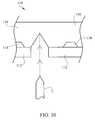
- devices described hereincan have the reflective wall added from the backside of the substrate. Ablation or removal of material from the backside of the substrate, relative to the LED, and extending into the encapsulated region of the LED side is advantageous as this allows angles to be easily formed which are advantageous to light output. The created region is then filled with reflective material to form a reflective cavity for the light. (See picture at end of this document).
- batch processingor processing as a “batch” refer to performing a particular operation on a group of devices or components all at once rather than manually operating on each device or component, one at a time.
- references to a structure being formed “on” or “above” another structure or portioncontemplates that additional structure, portion, or both may intervene. References to a structure or a portion being formed “on” another structure or portion without an intervening structure or portion are described herein as being formed “directly on” the structure or portion.
- relative terms such as “on”, “above”, “upper”, “top”, “lower”, or “bottom”are used herein to describe one structure's or portion's relationship to another structure or portion as illustrated in the figures. It will be understood that relative terms such as “on”, “above”, “upper”, “top”, “lower” or “bottom” are intended to encompass different orientations of the device or component in addition to the orientation depicted in the figures. For example, if the device or component in the figures is turned over, structure or portion described as “above” other structures or portions would now be oriented “below” the other structures or portions. Likewise, if devices or components in the figures are rotated along an axis, structure or portion described as “above”, other structures or portions would be oriented “next to” or “left of” the other structures or portions. Like numbers refer to like elements throughout.
- the terms “through-hole”, “thru-hole”, and/or “via”are synonymous and refer an opening in the panel substrate and/or a submount, often filled and/or lined (e.g., along one or more side walls) with an electrically conductive material that allows for an electrically conductive conduit or pathway between different layers, surfaces, or features of the devices or components.
- the term “exposing” a thru-hole or viarefers to sawing, cutting, dicing, breaking, etching, uncovering, displacing, or otherwise causing the metal disposed inside the via to be exposed on an external surface of the panel substrate or submount.
- the conductive materialwill be “exposed” outside of and/or along an exterior, outer surface of the device, component, panel substrate, or submount.
- a “ceramic based material” or the term “ceramic based”includes a material that consists primarily of a ceramic material, such as an inorganic, non-metallic material made from compounds of a metal or metalloid and a non-metal (e.g., aluminum nitride, aluminum oxide, beryllium oxide, silicon carbide).
- a “non-ceramic based material”consists primarily a metallic material, a primarily organic (e.g., polymeric) material, and/or a primarily synthetic or semi-synthetic organic solid that can be dispensed or molded (e.g., plastic).
- Light emitter devices and components according to embodiments described hereincan comprise group III-V nitride (e.g., gallium nitride (GaN)) based LED chips or lasers. Fabrication of LED chips and lasers is generally known and only briefly described herein. LED chips or lasers can be fabricated on a growth substrate, for example, a silicon carbide (SiC) substrate, such as those devices manufactured and sold by Cree, Inc. of Durham, N.C. Other growth substrates are also contemplated herein, for example and not limited to sapphire, silicon (Si), and GaN. In some aspects, SiC substrates/layers can be 4H polytype silicon carbide substrates/layers.
- group III-V nitridee.g., gallium nitride (GaN)
- GaNgallium nitride
- SiC candidate polytypessuch as 3C, 6H, and 15R polytypes, however, can be used.
- Appropriate SiC substratesare available from Cree, Inc., of Durham, N.C., the assignee of the present subject matter, and the methods for producing such substrates are set forth in the scientific literature as well as in a number of commonly assigned U.S. patents, including but not limited to U.S. Pat. No. Re. 34,861, U.S. Pat. No. 4,946,547, and U.S. Pat. No. 5,200,022, the disclosures of which are incorporated by reference herein in their entireties. Any other suitable growth substrates are contemplated herein.
- Group III nitriderefers to those semiconducting compounds formed between nitrogen and one or more elements in Group III of the periodic table, usually aluminum (Al), gallium (Ga), and indium (In).
- the termalso refers to binary, ternary, and quaternary compounds such as GaN, AlGaN and AlInGaN.
- the Group III elementscan combine with nitrogen to form binary (e.g., GaN), ternary (e.g., AlGaN), and quaternary (e.g., AlInGaN) compounds. These compounds may have empirical formulas in which one mole of nitrogen is combined with a total of one mole of the Group III elements. Accordingly, formulas such as AlxGa1-xN where 1>x>0 are often used to describe these compounds. Techniques for epitaxial growth of Group III nitrides have become reasonably well developed and reported in the appropriate scientific literature.
- LED chips disclosed hereincan comprise a growth substrate
- the crystalline epitaxial growth substrate on which the epitaxial layers comprising an LED chip are growncan be removed, and the freestanding epitaxial layers can be mounted on a substitute carrier substrate or substrate which can have different thermal, electrical, structural and/or optical characteristics than the original substrate.
- the subject matter described hereinis not limited to structures having crystalline epitaxial growth substrates and can be used in connection with structures in which the epitaxial layers have been removed from their original growth substrates and bonded to substitute carrier substrates.
- Group III nitride based LED chipscan be fabricated on growth substrates (e.g., Si, SiC, or sapphire substrates) to provide horizontal devices (with at least two electrical contacts on a same side of the LED chip) or vertical devices (with electrical contacts on opposing sides of the LED chip).
- the growth substratecan be maintained on the LED chip after fabrication or removed (e.g., by etching, grinding, polishing, etc.). The growth substrate can be removed, for example, to reduce a thickness of the resulting LED chip and/or to reduce a forward voltage through a vertical LED chip.
- a horizontal device(with or without the growth substrate), for example, can be flip chip bonded (e.g., using solder) to a carrier substrate or printed circuit board (PCB), or wirebonded.
- a vertical device(with or without the growth substrate) can have a first terminal (e.g., anode or cathode) solder bonded to a carrier substrate, mounting pad, or PCB and a second terminal (e.g., the opposing anode or cathode) wirebonded to the carrier substrate, electrical element, or PCB.
- first terminale.g., anode or cathode
- a second terminale.g., the opposing anode or cathode
- Examples of vertical and horizontal LED chip structuresare discussed by way of example in U.S. Publication No. 2008/0258130 to Bergmann et al. and in U.S. Pat. No. 7,791,061 to Edmond et al.
- LED chips used and/or described hereincan be configured to emit blue light, cyan light, green light, yellow light, red light, amber light, red-orange light, and/or any combination(s) thereof.
- one or more LED chipscan be at least partially coated with one or more phosphors and/or one or more layers of phosphors.
- Phosphorscan be adapted to emit blue light, yellow light, green light, red light, or any combination(s) thereof upon being impinged with light emitted via one or more LED chips. That is, in some aspects one or more phosphors can absorb a portion of light emitted by the LED chip and in-turn reemit the absorbed light at a different wavelength such that the light emitter device or component emits a combination of light from each of the LED chip(s) and the phosphor(s).
- the light emitter devices and components described hereincan emit what is perceived as white light resulting from a combination of light emission from the LED chip and the phosphor.
- white emitting devices and componentscan consist of an LED chip that emits light in the blue wavelength spectrum and a phosphor that absorbs some of the blue light and re-emits light in the green, yellow, and/or red wavelength spectrum. The devices and components can therefore emit a white light combination across the visible spectrum of light.
- the LED chipscan emit a non-white light combination of blue and yellow light as described in U.S. Pat. No. 7,213,940. LED chips emitting red light or LED chips covered by a phosphor that absorbs LED light and emits a red light is also contemplated herein.
- LED chipscan be coated with a phosphor using many different methods, with one suitable method being described in U.S. patent application Ser. Nos. 11/656,759 and 11/899,790, both entitled “Wafer Level Phosphor Coating Method and Devices Fabricated Utilizing Method”, and both of which are incorporated herein by reference in their entireties.
- Other suitable methods for coating one or more LED chipsare described for example in U.S. Pat. No. 8,058,088 entitled “Phosphor Coating Systems and Methods for Light Emitting Structures and Packaged Light Emitting Diodes Including Phosphor Coating” which issued on Nov. 15, 2011, and the continuation-in-part application U.S. patent application Ser. No.
- LED chipscan also be coated using other methods such as electrophoretic deposition (EPD), with a suitable EPD method described in U.S. patent application Ser. No. 11/473,089 entitled “Close Loop Electrophoretic Deposition of Semiconductor Devices”, which is also incorporated herein by reference in its entirety. It is understood that light emitter devices, components, and methods according to the present subject matter can also have multiple LED chips of different colors, one or more of which can be white emitting.
- EPDelectrophoretic deposition
- FIGS. 1A through 9illustrate embodiments of substrate based light emitter devices, components, and related methods according to the present subject matter as disclosed and described herein.
- light emitter devices described hereincan comprise surface mount devices (SMDs).
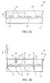
- FIGS. 1A to 1Dillustrate a substrate based light emitter component, generally designated 10 , from which one or more light emitter devices (e.g., FIG. 5 ) can be singulated.
- FIGS. 1A to 1Dcan be illustrative of component 10 as it is subjected to various batch processing steps and/or manufacturing stages.
- a plurality of components 10can be processed together as a batch. This can provide consistent color targeting across a plurality of devices which can be singulated therefrom, improve processing time, and reduce processing costs.
- component 10can comprise a panel or panel substrate 12 from which multiple individual substrate based devices can be singulated (e.g., 50 , FIG. 5 ).
- substrate 12can provide a base or support for devices which can be customized per consumer and/or customer needs or requirements.
- substrate 12can be customized in regards to a type, size, build, structure, number and/or color of LED chip(s), a size and shape of customized traces, provision of customized reflectors, provision of customized optical elements, and/or provision of vias, prior to singulation into individual devices.
- Other aspectscan be customized as well, including the ultimate size of each device to be singulated.
- individually customized components 10can be provided over and/or supported via substrate 12 , and can be referred to as comprising “substrate based” components.
- substrate 12can comprise a metallic material, a non-metallic material, a ceramic material, a plastic material, a composite material, a flame retardant (e.g., FR-4) composite material, combinations thereof, or any other type of material.
- substrate 12can comprise a highly reflective and/or optionally transparent ceramic based material for maximizing light extraction and reflectance from light emitters.
- substrate 12can comprise aluminum oxide (e.g., alumina or Al 2 O 3 ) or derivatives thereof, aluminum nitride (AlN) or derivatives thereof, zirconium dioxide (ZrO 2 ) or derivatives thereof, or any other ceramic based material.
- substrate 12can comprise a ceramic body that can be cast from low temperature co-fired ceramic (LTCC) materials or high temperature co-fired ceramic (HTCC) materials and/or via related processes.
- substrate 12can be cast from a thin green ceramic tape and subsequently fired.
- the ceramic tapecan comprise any ceramic filler material known in the art, for example, substrate 12 can comprise a glass ceramic, such as Al 2 O 3 or aluminum nitride (AlN) having approximately 0.3 to 0.5 weight percent of glass frits. The glass frits can be used as a binder and/or sintering inhibitor within the ceramic tape when the tape is fired.
- substrate 12can advantageously provide a substrate having any desired thickness, thus contributing to thinner or thicker sizes, where required. Such features can be easily customized, where desired.
- substrate 12can comprise a ceramic material having any of a variety of light scattering particles contained therein. Examples of suitable scattering particles can, for example, comprise particles of Al 2 O 3 , TiO 2 , BaSO 4 , and/or AlN.
- substrate 12can optionally be produced by thin- or thick-film processing techniques available at and including products available from CoorsTek, headquartered in Golden, Colo. Such substrate 12 can optionally be fired along with other materials (e.g., zirconia, ZrO 2 ) to further improve optical and mechanical properties.
- Substrate 12can comprise a panel of any suitable size, shape, orientation, and/or configuration.
- a substantially square or rectangular shaped substrate 12is shown, however, any shape of substrate is contemplated herein.
- any one of a substantially rectangular, circular, oval, rounded, regular, irregular, or asymmetrically shaped substrateis also contemplated herein.
- Substrate 12can for example comprise a substantially square or rectangular shape having at least one side of at least approximately 2 inches (′′) or more; 4′′ or more; 8′′ or more, or more than 12′′.
- substrate 12can be provided as a long material (e.g., on a reel).
- Substrate 12can comprise any suitable thickness, for example, a thickness of approximately 2 mm or less, such as approximately 1 mm or less, approximately 0.5 mm or less, or approximately 0.25 mm or less. In some aspects, substrate 12 comprises a thickness of about 0.635 mm.
- the size, shape, and/or thickness of substrate 12can each be customized, where necessary, and can obviate the need for providing individually molded and/or individually pressed ceramic substrates.
- substrate 12can optionally comprise one or more openings, through-holes or vias, generally designated 14 .
- openingsthrough-holes or vias, generally designated 14 .
- a plurality of substantially circular shaped vias 14are illustrated, however, any size, shape, and/or cross-sectional shape of vias 14 can be provided.
- Vias 14are illustrated in broken lines as they are optional and/or may not be visible (e.g., very small). Where used, vias 14 can be drilled, punched, machined, etched, formed with a laser, or any other processing technique.
- An electrically conductive materialsuch as a metal or metal alloy, can be provided inside portions of vias 14 for creating electrically conductive conduits through substrate 12 .
- vias 14can be filled with and/or have side walls at least partially coated with a metal and/or a conductive material such as silver (Ag), copper (Cu), gold (Au), tin (Sn), platinum (Pt), and/or Ag, Cu, Au, Sn, or Pt alloys for electrically connecting top electrical contacts with bottom electrical contacts of an SMD type device or component.
- conductive material disposed within vias 14can be exposed during singulation (e.g. sawn, diced, broken, etc.) thereby providing vias 14 along one or more sides to form novel electrical contacts disposed on three surfaces of the component (e.g., a top surface, a bottom surface, and a lateral side surface).
- Vias 14where used, can be customized with respect to size, shape, number, and placement.
- FIG. 1Billustrates one or more electrically conductive contacts or traces 16 disposed over a first surface of substrate 12 .
- electrical traces 16can be at least partially disposed over and/or cover vias 14 such that they may not be visible. Traces 16 can be customized with respect to size, shape, and/or placement over substrate 12 .
- traces 16can be coated or deposited over substrate 12 via physical deposition techniques, chemical deposition techniques, vapor deposition techniques, electroless plating techniques, electroplating techniques, or any other coating technique.
- an optional mask M having a plurality of openings Ocan be applied prior to deposition of traces 16 , such that traces can be printed, stenciled, or screen-printed over substrate. That is, mask M allows traces 16 to only be applied or deposited over substrate 12 within the boundaries of openings O. Mask M can advantageously cover portions of substrate 16 and protect the reflectivity or “whiteness” of substrate 16 by preventing metal deposition within such areas. Thus, in some aspects, traces 16 can be applied via shadow, stenciling, mask, printing, screen printing, lithography, or any other similar masking/covering technique.
- traces 16can comprise one more layers of Cu, titanium (Ti), nickel (Ni), Ag, electroless Ag, Au, electroless nickel immersion gold (ENIG), Sn, palladium (Pd), electrolytic or immersion Au, combinations thereof, and/or any other material which can be applied via a deposition process, such as physical deposition, sputtering, e-beam, electroplating, and/or electroless plating processes noted above.
- traces 16can comprise multiple different layers of metals or materials applied or coated in layers over each other. For example, one or more layers of Ti, Ag, and/or Cu can be applied over substrate 12 . In some aspects, a layer of Ti can be directly deposited directly over substrate 16 .
- the Ti layercan be coated with one or more layers of Ag and/or Cu.
- one or more alternating layers of metale.g., alternating layers of Ti, Ag, and/or Cu
- traces 16can comprise at least one layer of Ag, either alone or in combination with layers of electroplated Ti, Ni, Cu, and/or Au.
- traces 16can comprise at least one layer of Cu, either alone or in combination with layers of electroless or electroplated Ti, Ag, Ni, and/or Au.
- each trace 16 of the plurality of tracescan comprise an overall thickness of approximately 10 ⁇ m or more, approximately 20 ⁇ m or more, approximately 50 ⁇ m or more, or more than approximately 80 ⁇ m.
- Traces 16 of component 10can be disposed along a front side corresponding to top surface of substrate 12 and spaced apart from LED chips 18 . Together, two traces 16 can comprise an anode/cathode pair adapted to transfer electrical current into and out of LED chips 18 , causing the illumination thereof, when subjected to electrical current. In some aspects, each trace 16 can be fully disposed on a top side or top surface of substrate 12 . In other aspects traces which wrap around sides of substrate 12 can be provided. In some aspects, vias 14 ( FIG. 1A ) can allow traces 16 to electrically communicate with bottom contacts (e.g., 72 , 74 , FIG. 6B ).
- bottom contactse.g., 72 , 74 , FIG. 6B
- a plurality of LED chips 18can be die attached to and/or mounted over front side of substrate 12 , adjacent traces 16 .
- LED chips 18can be disposed between one or more traces 16 and wirebonded thereto.
- LED chips 18can be directly attached over portions of one or more traces, for example, where the LED chips 18 have electrical contacts on a bottom surface of the chip.
- LED chips 18can be vertically structured (e.g., contacts on two opposing surfaces) or horizontally structured (e.g., both contacts on a same surface, such as an upper or lower surface).
- LED chips 18can comprise substantially straight cut and/or bevel cut (e.g., sloped or inclined) lateral sides and can comprise any shape, size, dimension, structure, build, and/or color.
- devices, components, and methods described hereincan be customized using any type and/or number of LED chips 18 , as desired.
- each LED chip 18 of the plurality of die attached chipscan comprise a same shape, size, dimension, structure, build, and/or color.
- some LED chips 18 of the plurality of LED chips 18can comprise different shapes, sizes, dimensions, structures, builds and/or colors.
- multiple components 10can be processed at a same time, and can contain different numbers, sizes, shapes, etc. of LED chips 18 .
- LED chips 18can comprise a growth substrate or a carrier substrate, and can comprise a vertically structured chip (e.g., anode and cathode on opposing surfaces of LED chip 18 ) or a horizontally structured chip (e.g., anode and cathode on a same surface).
- a vertically structured chipe.g., anode and cathode on opposing surfaces of LED chip 18
- a horizontally structured chipe.g., anode and cathode on a same surface
- LED chips 18can comprise any size and/or shape.
- LED chips 18can be substantially square, rectangular, regular, irregular, or asymmetrical in shape.
- LED chips 18can, for example, comprise a footprint where at least one side measures approximately 2000 ⁇ m or less, such as approximately 1150 ⁇ m or less, approximately 900 ⁇ m or less, approximately 700 ⁇ m or less, approximately 600 ⁇ m or less, approximately 500 ⁇ m or less, approximately 400 ⁇ m or less, approximately 300 ⁇ m or less, approximately 200 ⁇ m or less, approximately 100 ⁇ m or less, and/or combinations thereof where multiple LED chips 18 are used. Any dimension of LED chip 18 is contemplated.
- LED chips 18can be electrically connected to traces 16 via wirebonds 20 .
- horizontally structured LED chips 18are illustrated, where both the anode and the cathode can be disposed on the upper surface of each chip 18 in the form of two bond pads, each connected to a different trace 16 via wirebonds 20 .
- both contactse.g., the anode and cathode
- both contactscould be disposed on a bottom surface of LED chips 18 and/or on opposing top and bottom surfaces as well.
- wirebonds 20can comprise any suitable electrically conductive material such as Au, Ag, Al, Sn, Cu, alloys thereof, and/or combinations thereof. It is understood that in other aspects, a component according to the present subject matter can be provided with an optional electrostatic discharge (ESD) protection device (not shown) reversed biased with respect to LED chips 18 . Where used, the ESD protection device can comprise a Zener diode, a surface mount varistor, a lateral Si diode, and/or another LED chip that can be reversed biased with respect to one or more other LED chips 18 .
- ESDelectrostatic discharge
- an optical element or optical materialcan be provided over component 10 .
- an optical element or materialcan comprise encapsulant 22 that can be provided and applied substantially entirely over substrate 12 , traces 16 , LED chips 18 , and wirebonds 20 as further illustrated by FIG. 1D . That is, LED chips 18 supported thereon can be encapsulated in one batch encapsulation process rather than by a single encapsulation process and substrate 12 can be substantially covered with at least one large optical element or layer of encapsulant 22 .
- encapsulant 22can comprise a single and continuous layer or layers of material over substrate 12 , prior to singulation of component 10 into individual devices. That is, the volume of encapsulant 22 can be large upon application.
- an application of encapsulant 22can be anywhere from just covering the surface of the LED chips 16 and wirebonds (e.g., the thinnest possible layer for providing mechanical protection).
- encapsulant 22can be applied for low profile applications to aspect ratios of approximately 15 ⁇ the height of the chip which has been shown to improve light extraction. Height of encapsulation 22 can affect beam shaping of the final product so there could be applications that require approximately a 30 ⁇ aspect ratio. In general, about 800 ⁇ m of encapsulation 22 height is considered typical.
- encapsulant 22can provide both environmental and/or mechanical protection of LED chips 18 , wirebonds 20 , and traces 16 .
- An optional layer of wavelength conversion materialsuch as one or more phosphoric or lumiphoric materials can be applied directly over the one or more LED chips 18 and/or over one or more portions of substrate 12 and traces 16 prior to application of encapsulant 22 .
- the wavelength conversion materialcan be provided and/or mixed within encapsulant 22 , such that upon depositing encapsulant the wavelength conversion material is also deposited.
- encapsulant 22can be devoid of a wavelength conversion material.
- wavelength conversion materialcan be provided in a reflective material (e.g., 26 FIG.
- wavelength conversion materialcan be applied in encapsulant 22 and/or the reflective material ( 26 , FIG. 2E ), where reflective material is used.
- a wavelength conversion materialsuch as one more phosphors or lumiphors can provide for improved color mixing and provision of truer neutral white light having a truer, improved color rendering, and/or and what is perceived as a true or neutral white color output, where desired.
- batch processing and batch encapsulating multiple LED chips 18 of substrate 12 , prior to singulationcan improve both the cost and the ease of production with regard to components 10 .
- costcan be improved as the time, tools, materials, and/or other costs associated with individually molding lenses over substrate 12 can be obviated.
- any potential sticking and/or other processing defects associated with individually dispensing encapsulant multiple times over multiple LED chipscan be eliminated.
- dispensing encapsulant in at least one single layer over substrate 12 and LED chips 18 supported thereoncan advantageously improve (e.g., decrease) a manufacturing time as well.
- encapsulant 22can be cured after dispensing over substrate 12 and LED chips 16 disposed thereon. As described below, more than one layer of encapsulant 22 can be provided.
- FIGS. 2A to 2Fillustrate side views of device 10 , and illustrate one or more processing steps occurring just prior to, or just after applying and curing encapsulant 22 .
- substrate 12is shown as comprising a substantially square or rectangular cross-sectional shape. However, any other non-rectangular shape is also contemplated herein.
- substrates 12 described hereincan comprise the building block of customized SMD type emitter components and/or devices described herein.
- a multitude of different customized componentshaving, for example, customized reflectors, customized side walls, shaped or faceted encapsulant or optical elements provided thereon, and any type/shape/size/number/color of LED chips for producing a desired color point can be provided and/or easily modified without the time and/or expense associated with creating custom fabricated or molded components.
- encapsulant 22can optionally comprise one or more multiple layers, such as layers I, II, and III.
- each layercan be substantially optically clear.
- each different layercan comprise a different concentration and/or color of a wavelength conversion material (e.g., a phosphor or lumiphor).
- the layers I, II, and IIIcan comprise one or more combinations of any number of optically clear layers and any number of layers containing phosphor.
- one or more layers I, II, and IIIcan comprise filtering particles or materials, diffusing particles or materials, and/or reflective particles or materials.
- each layer I, II, and IIIcan be individually applied/deposited and individually cured.
- each layer within the stack of layerscan be cured at the same time.
- the broken linesindicate three different layers I, II, and III, however, a single layer, two layers, or more than three layers of encapsulant, with or without phosphor(s) or other materials, can be provided and are contemplated herein.
- the large area of encapsulant 22which extends substantially to outermost edges of substrate 12 , can be dispensed, molded in one large mold, or applied via spray techniques.
- encapsulant 22can be applied in via a coating method such as, for example, via spin coating.
- batch encapsulationcan minimize color scattering and improve color consistency by reducing “settling” or “settling down” of the phosphors contained therein. Settling can occur in conventional components over time where encapsulant is individually applied over a plurality of LED chips prior to curing.
- batch encapsulationcan advantageously result in quicker processing times, contributing to higher production yields, lower production cost, and higher brightness within devices singulated from substrate 12 ( 50 , FIG. 5 ).
- Batch encapsulationcan also provide for a stable color targeting and/or stable color across individual devices (e.g., FIG. 5 ) upon singulation from substrate.
- FIG. 2Billustrates another novel aspect of light emitter devices, components, and related methods described herein.
- an ablation tool Tcan be used to ablate material from component 10 after encapsulant 22 has hardened or cured.
- material of component 10can be scribed, where ablation tool T can provide scribe marks 24 in portions of component 10 . Scribe marks 24 can penetrate and remove portions of encapsulant 22 . Notably, scribe marks 24 can also penetrate portions of substrate 12 , forming one or more recessed portions or ledges L in substrate 12 .
- ledges Lprovide a space for one or more portions of reflective material (e.g., a reflector or reflective wall) to be attached as described in FIG. 5 .
- reflective materiale.g., a reflector or reflective wall
- ablation tool Tcan form a plurality if trenches, gaps, or scribe marks 24 between adjacent LED chips 18 supported by and/or mounted to substrate 12 .
- scribe marks 24can be formed between what will be individual light emitter devices (e.g., 50 , FIG. 5 ), upon singulation.
- devices described hereincan be devoid of an outer reflector, an outer layer of reflective material, and/or a reflective wall. That is, in some aspects devices can be singulated without using a reflective material, for example, individual devices can be singulated from component 10 along the broken lines denoted X in FIG. 2B .
- components and devicesprior to and after singulation, can comprise an ablated edge, generally designated 28 .
- Ablated edge 28 of devices and componentscan comprise a portion of encapsulant 22 and a portion of substrate 12 , where encapsulant 22 is flush against the surface or side of substrate 12 over which LED chip 18 is mounted.
- lower recessed portion or ledge L of the substratecan extend below ablated edge 28 .
- substrate 12can comprise a highly reflective ceramic material. In some aspects, substrate can comprise a highly reflective white material.
- ablation tool Tcan comprise any suitable tool for removing and/or ablating material.
- ablation tool Tcomprises at least one dicing blade, a saw blade, a laser tool for laser scribing, or a tool for performing laser ablation technology.
- a kerf width of ablation tool T for scribingshould be larger than a kerf width of a singulation tool for singulating devices (T 2 , FIG. 2F ). For example, if a singulation tool has a kerf width of approximately 0.2 mm, then the kerf width of ablation tool T should be at least approximately 0.6 mm.
- the kerf width of ablation T toolcan correspond to a width of scribe marks 24 .
- scribe marks 24can be larger in width, and have more material removed than during singulation of individual packages, which will remove minimal material of negligible width.
- Ablation tool Tcan comprise any size and/or shape, and can be configured to provide scribe marks 24 having substantially straight side walls, substantially parallel side walls, or substantially beveled/tapered side walls.
- scribe marksmay have a shallower depth than that shown in FIG. 2B . That is, in some aspects scribe marks may only penetrate portions of encapsulant 22 (e.g., cured) and without extending into portions of substrate 12 . A depth and/or thickness of scribe marks 24 , which can ultimately form side walls of devices upon singulation, can be customized, where desired.
- FIG. 2Dillustrates an example of an ablation tool T having tapered sides which can provide scribe marks 24 having substantially tapered inner walls.
- inner walls of scribe marks 24can taper inwardly and/or outwardly away from each other forming a substantially V-shaped trench between adjacent LED chips 18 .
- devices having specific beam patternsare desired. This can be achieved in part by providing non-parallel scribe marks 24 .
- Scribe marks 24can be customized in shape, where desired.
- scribe marks 24can be tapered, shaped, partially curved, and/or multi-faceted. Any sectional shape of scribe marks 24 can be produced and is contemplated herein.
- individual packages or devicescan be singulated from substrate 12 directly after formation of scribe marks 24 .
- scribe marks 24can be at least partially filled with a reflective material and/or a reflector. That is, scribe marks 24 of component 10 can be at least partially filled and component 10 can be subsequently be diced, sawn, or separated via a laser, for singulation of individual devices ( 50 , FIG. 5 ) after providing the reflective material.
- FIG. 2Eillustrates an optional step of applying or providing a reflective material 26 and/or a reflector to at least partially or fully fill portions of scribe marks 24 .
- a small walle.g., a small amount
- reflective material 26can be added first via a screen printing process.
- reflective material 26can comprise a reflective wall at least partially aligned over and/or attached to recessed portions or ledges L of substrate 12 . At least a portion of the reflective material can be disposed above a height or upper surface of LED chip 18 and at least a portion can be disposed below a level, such as the bottom surface level, of LED chip 18 . This can be advantageous, as any light emitted below LED chip can be reflected back out via lower portion of material 26 .
- reflective material 26can comprise a highly reflective material which can be white, transparent, optically clear, silver, and/or silver-white in color.
- reflective material 26can comprise silicone, a high refractive index silicone material, or any suitable thermoplastic material such as polyphthalamide (PPA), a liquid crystal polymer (LCP), titanium dioxide (TiO 2 ), a silicone having reflective particles dispersed there such as, for example, particles of Al 2 O 3 , TiO 2 , BaSO 4 , ZrO 2 , and/or AlN.
- a wavelength conversion materialsuch as a phosphor or lumiphor can be contained within reflective material 26 .
- reflective materialcan comprise a very hard silicone or epoxy, as portions of reflector material 26 can form a side wall of singulated devices (e.g., FIG. 5 ).
- filtering particles or materials and/or diffusing particles or materialscan be provided within portions of scribe marks 24 , such that singulated devices emit filtered or diffused light of any desired wavelength or color point.
- reflective material 26can be customized, where desired, to contain any amount or composition of reflective, wavelength conversion, filtering, and/or diffusing materials.
- wavelength conversion materialcan be contained either in encapsulant 22 and/or reflective material 24 , or both.
- wavelength conversion materialcan comprise one or more phosphors or lumiphors (e.g., yellow, red, and/or green phosphor) which can be activated by light emitted from the one or more LED chips 18 .
- wavelength conversion materialcan be provided when encapsulant 22 and/or reflective material 26 are in liquid form, and can be dispersed therein as such materials harden or cure.
- reflective material 26can be applied in liquid form and allowed to cure or harden.
- reflective material 26can comprise a solid material which can be inserted into scribe marks 24 , and fixedly held therein via silicone or an adhesive.
- a non-reflective materialcan be applied in scribe marks 24 over recessed portions or ledges L.
- the non-reflective material disposed in scribe marks 24can form a lateral side wall of a device upon singulation, similar to that described in FIG. 5 .
- the material applied, dispensed, inserted, or otherwise deposited within portions of scribe marks 24can be customized.
- the material applied or deposited in scribe markscan be adapted to block light, adapted to absorb light, adapted to filter light, comprise a dichroic filter (e.g., for selectively passing select wavelengths of light), a diffuser, or a material adapted to diffuse light.
- scribe marks 24can be devoid of any material, and devices can be singulated from component 10 after scribing and/or encapsulating.
- a non-reflective materialcan be combined with a reflective material and applied or inserted within scribe marks 24 over recessed portions or ledges L.
- a singulation tool T 2can be used to singulate individual devices along lines designated 1 to N, where N is any integer>1.
- Singulation tool T 2can comprise a dicing (e.g., saw) blade or a laser tool which can comprise a fine width and/or a smaller kerf width than the width of reflective material 26 and/or scribe marks ( 24 , FIG. 2C ).
- reflective material 26can form exterior walls of each device upon singulation.
- encapsulant 22can at least partially form exterior walls of singulated devices. As indicated in FIG. 2D , encapsulant 22 can be provided with shaped walls for producing or shaping light into a desired beam pattern.
- Singulation tool T 2can be used to singulate individual devices ( 50 , FIG. 5 ) from component 10 , and from large panel substrate 12 .
- singulated light emitter devices50 , FIG. 5
- singulated light emitter devicesare shown as containing one LED chip 18 , however, devices containing two or more LED chips 18 are also contemplated and can be provided herein and subjected to batch encapsulation and/or any other substrate based batch processing techniques described herein.
- the broken lines along and through substrate 12 in FIG. 2Findicate lines along which component 10 can be scribed, sawn, cut, etched, broken, and/or otherwise physically separated, for providing or forming individual packages or devices (e.g., 50 , FIG. 5 ).
- Individual substrate based packages or devicescan be customized with respect to the size, shape, or number of LED chips 18 , the shape of exterior walls and/or shape of encapsulant 22 , a number of encapsulant 22 layers, materials provided within encapsulant 22 and/or reflective material 26 .
- component 10 and resultant devices described hereincan be devoid of reflective material 26 .
- components described hereincan provide customized devices that are substrate based and can be provided at improved costs, lower processing times, fewer processing steps, and/or via batch processing techniques.
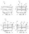
- FIGS. 3A to 3Eillustrate another substrate based component, generally designated 30 .
- Component 30can be similar to component 10 , however, FIGS. 3A to 3E illustrate different aspects and/or features associated with components and devices provided herein.
- FIG. 3Aillustrates component 30 comprising a substrate 32 , a plurality of LED chips 34 disposed over substrate 32 , and the plurality of LED chips 34 being wirebonded to traces ( FIG. 1B ) via wirebonds 36 . Traces can be present in device 30 but may not be visible in the side views; as such features can be very thin compared to substrate 32 .
- a plurality of pairs of bottom contacts 35can be disposed over a backside or bottom surface of substrate 32 . In some aspects, bottom contacts 35 can comprise a metal or metal alloy.
- bottom contacts 35can be configured for surface mounting and/or directly connecting to and/or electrically and thermally connecting with external heat sinks or circuit components such as a PCB or a MCPCB (not shown). In some aspects, bottom contacts 35 can electrically communicate with traces using vias (e.g., conduits) through substrate 32 .
- Substrate 32can comprise a panel substrate of material. In some aspects, it is desirable to provide a substrate 32 that is highly reflective to visible light (e.g., greater than about 90%), and which can provide conduction of heat as well provide as mechanical support. In some aspects, non-metallic and/or ceramic (e.g., HTCC and LTCC) materials containing Al 2 O 3 exhibit such desirable qualities. Accordingly, substrate 32 can comprise a ceramic based body of material such as Al 2 O 3 and/or containing Al 2 O 3 . However, metallic, composite, plastic, and flame retardant substrates 32 can also be provided.
- substrate 32can comprise a ceramic body that can be cast from LTCC materials or HTCC materials and/or using related processes.
- substrate 32can be cast from a thin green ceramic tape and subsequently fired.
- the ceramic tapecan comprise any ceramic filler material known in the art, for example, substrate 33 can comprise a glass ceramic, such as Al 2 O 3 or AlN having 0.3 to 0.5 weight percent of glass frits, as described above. The glass frits can be used as a binder and/or sintering inhibitor within the ceramic tape when the tape is fired.
- substrate 32can be produced by thin- or thick-film processing techniques available at and including products available from CoorsTek, headquartered in Golden, Colo. Such substrates 32 can optionally be fired along with other materials (e.g., zirconia, ZrO 2 ) to further improve optical and mechanical properties.
- substrates 32can optionally be fired along with other materials (e.g., zirconia, ZrO 2 ) to further improve optical and mechanical properties.
- LED chips 34can be mounted (e.g., die attached) over substrate 32 after firing and/or sintering. LED chips 34 can be die attached using any suitable material capable of causing LED chips 34 to adhere to substrate 32 .
- LED chips 34can be die attached using solder, epoxy, paste, glue, silicone, flux materials, eutectic materials, or any other suitable adhesive materials.
- LED chips 34can be electrically connected to traces via wirebonds 36 proximate a same time. LED chips 34 can also be encapsulated proximate a same time via a batch encapsulation process as previously described.
- An encapsulant 38can be applied via spraying, dispensing, or using one large, single mold. In some aspects, encapsulant 38 can form a continuous layer over LED chips 34 , wirebonds 36 , traces (e.g., FIG. 1A , may not be visible in side view) substrate 32 , and bottom contacts 35 .
- Encapsulant 38can be devoid of a phosphor, or one or more phosphors can be dispersed within encapsulant 38 . More than one layer of encapsulant 38 can be provided. In some aspects, a phosphor layer can be sprayed or applied to component 30 prior to encapsulation, where desired.
- a tape, mask, or masking layercan be applied after formation an initial layer of encapsulant. That is, a mask 40 can be applied over encapsulant 38 after encapsulant has been allowed to harden or cure.
- mask 40can be formed and/or applied via hot lamination technology.
- mask 40can comprise a polymer tape, a sticker, or an adhesive material.
- Mask 40can comprise any polymer material such as polyimide (PI), with or without adhesive materials.
- Mask 40can be adapted to provide a barrier over encapsulant 38 during subsequent processing steps, and can provide a place holder for one or more subsequent layers applied over encapsulant 38 .
- the subsequent layer(s)may be brittle and/or susceptible to peeling or degrading during scribing.
- mask 40can assist and/or improve application of reflective layer 44 as described below.
- one or more scribe marks 42can be provided in portions of mask 40 . Scribe marks 42 can penetrate portions of encapsulant 38 and optionally portions of substrate 32 . Scribe marks 42 can be formed with a saw blade, a laser beam, or using any other dicing, separating, or ablation techniques.
- FIG. 3Aillustrates formation and/or application of a reflective material 44 within previously provided scribe marks.
- reflective material 44can completely fill the area created by scribe marks.
- reflective material 44can only partially coat portions of scribe marks (e.g. FIG. 4A ).
- more than one reflective material 44can be applied within scribe marks 42 .
- provision of reflective material 44can also be performed via a batch process, where multiple reflective walls can be created, provided, or established at a same time.
- mask 40can prevent filling material from being disposed over, from sticking to, and/or from being adhesively applied over portions of encapsulant 38 .
- mask 40can be applied over encapsulant 38 after encapsulant 38 has hardened.
- component 30can be placed under a vacuum.
- Silicone or other reflective material 44can be applied over entire component 10 , and a vacuum can be applied.
- the silicone or reflective material 44can flow into and fill scribe marks 42 via capillary action.
- reflective material 44can be applied over entire component (e.g., as a batch) and a vacuum can be used to pull, place, or cause material 44 to become disposed within portions of scribe marks ( 42 , FIG. 3B ).
- mask 40can be removed after optional formation of side walls comprised of reflective material 44 .
- One or more gaps 46 having a thickness tcan be provided upon removal of mask 40 .
- a second layer of material 48can be provided in gaps 46 ( FIG. 3D ).
- Second layer of material 48can comprise an optically clear layer of material, or it can contain one or more phosphors, filtering materials, reflective materials, scattering material, or diffusing material as denoted by the shaded appearance.
- Second layer of material 48can be the same material as encapsulant 38 or second layer of material 48 can comprise a different material or materials than encapsulant 38 .
- second layer of material 48can be sprayed, dispensed, or applied to component 30 at a same time and over the multiple LED chips 34 as a batch or in a batch application or process.
- Application of multiple sections of second layer of material 48 at the same over component 30can advantageously be performed in less time than application of multiple single portions.
- the decreased processing timecan be advantageous as phosphor, where used within layer 48 , can be prevented from settling over time.
- LED chips 34can be configured to activate a yellow, a red, a blue, and/or green phosphor (not shown) disposed either directly over each LED chip 34 , disposed within reflective material 44 , disposed within encapsulant 36 , and/or disposed within second layer of material 48 for producing neutral, cool, and/or warm white output.
- Single or multiple LED chips 34can be used alone or in combination with devices and components described herein.
- reflective material 44can be configured to fully fill scribe marks ( 42 , FIG. 3B ) or only partially fill scribe marks 42 .
- FIGS. 4A to 4Dillustrate various configurations of reflective material within scribe mark 42 .
- the placement, amount, thickness, concentration, and/or other aspects pertaining to reflective marital 44can be customized in some aspects.
- reflective material 44can be configured to coat only a portion of scribe mark 42 .
- Reflective material 44can comprise a thin layer and may contain a phosphor or phosphors, scattering particles, diffusing particles, filtering particles, etc.
- FIG. 4Billustrates in some aspects, reflective material 44 can comprise more than one portion, layer, or material. That is, reflective material 44 can comprise a composite layer or structure.
- a first layer of reflective material 44 Acan comprise a coating applied over inner walls of and/or a bottom surface of scribe mark.
- a second layer of material 44 Bcan be applied inside of and/or adjacent first layer 44 A.
- second layer of reflective material 44 Bcan be at least partially nested in first layer of reflective material 44 A.
- the materials forming the first and second layers 44 A and 44 Bcan comprise multiple layers of a same material, or layers 44 A and 44 B can comprise different materials. More than two layers and/or materials are also contemplated. In some aspects, more than two layers of material can be vertically stacked within scribe marks. Material 44 can comprise any material(s), any number of layers, and any configuration. Notably, reflective material 44 can be varied, and therefore, can provide easy to manufacture customized devices at a lower cost than other known devices.
- reflective material 44can comprise a single layer having a substantially uniform amount of reflective particles and/or phosphor materials disposed therein as indicated by the shading.
- FIG. 4Dillustrates a concentration of reflective particles and/or phosphor materials can be varied.
- a more dense region 44 C of phosphors or particlescan be applied over a less dense region 44 D. Concentrations can be varied along a length of reflector material 44 to provide any desired light output, color point, and beam shape.
- phosphors disposed within reflective materialcan comprise phosphors or lumiphors (e.g., yellow, red, blue, and/or green phosphor) which can be activated by light emitted from the one or more LED chips 34 ( FIG. 3E ).
- wavelength conversion materiale.g., phosphor
- reflector material 44can be provided when reflector material 44 is in a liquid form, and can be uniformly or non-uniformly dispersed therein. After application, reflector material 44 can be allowed to harden and cure. After hardening, reflector material 44 and substrate 32 can be diced and individual packages or devices can be singulated.
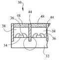
- FIG. 5illustrates a light emitter device generally designated 50 , which can be provided and produced according to components and methods described herein.
- Singulated device 50can be substrate based, that is, fully processed over a large panel substrate 12 ( FIG. 1A ) and then subsequently singulated into individual devices 50 over individual smaller portions of substrate 12 .
- a plurality of devicescan be die-attached, wirebonded, and encapsulated as a batches for reducing processing times and lowering production costs. This has also unexpectedly led to a significantly more stable color point for individual devices singulated from components described herein, as the reduced processing times prevent sticking of the encapsulant and/or prevent settling of phosphors contained within the encapsulant.
- reflective material 26can comprise a reflective lateral side wall of device 50 .
- Reflective material 26can be at least partially disposed in and on recessed portion or ledge L of the substrate 12 .
- the ledge Lcan be provided below a level of LED chip 18 .
- a first portion of the reflective lateral side wall or reflective material, denoted 46 ′can be disposed above a height of LED chip 18
- a second portion of the reflective material denoted 46 ′′can be disposed below a level of LED chip 18 , and flush against ledge L.
- LED chips 18can emit Lambertian patterns of light, thus, any light emitted below LED chip can be reflected back out via lower portion of material 46 ′′.
- such devicecan comprise minimal features batch processed in minimal steps, resulting in a superior, improved lighting device.
- LED chips 18can be configured to activate a yellow, a red, a blue, and/or green phosphor (not shown) disposed either directly over each LED chip 18 , disposed within encapsulant 22 , and/or disposed within reflective material 26 for producing neutral, cool, and/or warm white output.
- one LED chip 18is indicated per device 50 .
- two or more LED chips 18can be provided in one device 50 .
- each LED chip 18can comprise a same color.
- each LED chip 18can comprise a different color selected from the group of blue, blue shifted yellow (BSY), cyan, green, red, yellow, red-orange, or amber. Any color and/or colors of LED chip 18 can be provided.
- LED chips 18can be primarily blue and configured to activate a yellow phosphor. In other aspects, LED chips 18 can be primarily red. LED chips 18 can be used together within device 50 , for example, a primarily blue LED chip or chips 18 can be used in combination with a primarily red LED chip or chips 18 . In some aspects, a primarily red LED chip 18 can be disposed below a phosphor (e.g., sprayed over chip or disposed within encapsulant or reflective material) for mixing with light of other LED chips and/or phosphors to produce warm white output.
- a phosphore.g., sprayed over chip or disposed within encapsulant or reflective material
- encapsulant 22does not require molding. That is, in some aspects, encapsulant 22 can comprise a silicone matrix, encapsulant, or plastic material which can be deposited or dispensed directly over substrate 12 over entire component and over multiple devices at approximately the same time. In some aspects, a single large mold can be used. In other aspects, encapsulant 22 can be dispensed or sprayed. Thus, encapsulant can be provided as a batch over devices 50 , prior to singulation, without the time or expense of having to overmold multiple lenses.
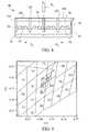
- FIGS. 6A and 6Billustrate further light emitter packages or devices, generally designated 60 , which can be produced from components and related methods described herein.
- Device 60can be processed over a large panel substrate 62 and individually singulated at the end of a process via dicing, sawing, breaking, using a laser beam, etc.
- Device 60can comprise an LED chip 64 electrically connected to one or more vias 68 using wirebonds 66 .
- multiple vias 68can be provided in a component substrate 62 , prior to singulation of the component substrate 62 into multiple devices.
- At least one electrical trace 70can be optionally plated over vias 68 .
- FIG. 6Billustrates a backside of device 60 , which opposes the side to which LED chip 64 is attached.
- first and second bottom contacts 72 and 74can be applied to a bottom surface of substrate 62 prior to singulation.
- First and second bottom contacts 72 and 74can connected to upper traces 16 (e.g., FIG. 1B ) using vias, wrap-around (side) traces or contacts, flexible circuitry, or any other desired configuration.
- First and second bottom contacts 72 and 74can transmit electrical current into top traces using vias 68 , which can transmit electrical current into LED chip 64 via wirebonds 66 .
- a plurality of bottom contactscan be applied as a batch over substrate 62 using a mask (M, FIG. 1B ), stencil, etc., similar to applying traces 16 ( FIG. 1B ), as previously described.
- bottom contacts 72 and 74can comprise a metal or metal alloy.
- light emitter device 60can comprise a substrate based device configured for surface mount device (SMD) applications. SMDs can comprise at least two bottom contacts for directly connecting to and/or electrically and thermally connecting with external heat sinks or circuit components such as a PCB or a MCPCB.
- device 60can be singulated from a large a non-metallic substrate, similar to previously described substrate 12 ( FIG. 1A ).
- substrates according to any of the previously described embodimentscan have a desirable thermal conductivity.
- substrates described hereincan comprise a thermal conductivity of greater than 5 W/mK, greater than 10 W/mK, greater than 50 W/mK, greater than 100 W/mK, greater than 150 W/mK, or greater than 200 W/mK.
- the thermal conductivity of the substratecan be approximately 20 W/mK (+ or ⁇ 5 W/mK), such as for when the substrate comprises alumina, or the thermal conductivity of the substrate can be approximately 170 W/mK (+ or ⁇ 5 W/mK), such as for when the substrate comprises AlN.
- metallic, polymeric, plastic, or composite substratescan be provided.
- first and second bottom electrical contacts 72 and 74can electrically communicate to respective LED chip 64 using one or more internally disposed thru-holes or vias 68 .
- Vias 68can extend internally within a portion of substrate 62 depending on how placed within panel (e.g., FIG. 1A ) and how panel is subdivided into individual devices.
- vias 68can be fully internal to, intact, and/or fully contained within portions of substrate 62 as shown, or in other aspects, vias 68 can be apportioned and exposed such that they are disposed along one or more external sides of substrate 62 .
- Vias 68can comprise conduits for transferring electrical current about substrate and into respective LED chip 64 within devices 60 .
- first and second electrical contacts 72 and 74can be deposited via electroplating and/or electroless plating processes.
- first and second electrical contacts 72 and 74can comprise one or more layers of material, such as one or more layers of Au, Sn, Ti, Ag, Cu, Pd, ENIG, and/or any alloy or combination thereof.
- First and second electrical contacts 72 and 74can also be deposited via physical deposition methods, sputtering, screen-printing, and/or any other methods previously described above.
- first and second electrical contacts 72 and 74can comprise different sizes and/or shapes.
- first electrical contact 72can comprise a V-shaped notch for indicating electrical polarity.
- the V-shaped notchindicates a cathode.
- the V-shaped notchcan indicate an anode.
- top trace 70 ( FIG. 6A ) and/or first and second electrical contacts 72 and 74can comprise metallic bodies or portions of material that can be attached to substrate 62 via adhesive, solder, glue, epoxy, paste, silicone, or any other material.
- Substrate 62can comprise ceramic, metallic, polymeric, composite, FR4, or any other suitable substrate having traces attached thereto.
- top trace 70 and first and second electrical contacts 72 and 74can comprise metallic bodies or portions of material that can be pressed into a green ceramic tape and then co-fired with substrate 62 , as a batch (e.g., as an un-singulated substrate panel, FIG. 1A ).
- first and second electrical contacts 72 and 74 and/or top trace 70be applied via a conductive paste screen-printed over an HTCC or LTCC panel substrate and fired.
- a conductive Ag pastecan be used such as silver paste #7095 available from DuPont Electronics.
- first and second electrical contacts 72 and 74can be mounted over and electrically or thermally communicate with an external heat sink or power source (not shown). In some aspects, first and second electrical contacts 72 and 74 can be configured to pass electrical signal or current from the outside power source (not shown) such as a circuit board, a PCB, a MCPCB, or other electrical source into the one or more LED chips 64 by passing electrical current about or through substrate 62 using vias 68 .
- the outside power sourcesuch as a circuit board, a PCB, a MCPCB, or other electrical source into the one or more LED chips 64 by passing electrical current about or through substrate 62 using vias 68 .
- first and second electrical contacts 72 and 74can be soldered, welded, glued, or otherwise physically, electrically, and/or thermally attached to the external power source (not shown).
- LED chips 64can illuminate upon receiving electrical current passed between respective top and bottom electrical contacts or traces.
- singulated devicescan have a submount or substrate 62 having a length and a width of approximately 5 mm ⁇ 5 mm or less, approximately 4 mm ⁇ 4 mm or less, or approximately 3 mm ⁇ 3 mm or less. In some aspects, however, any customized size of device having any number of LED chips 64 can be provided
- device 60can comprise an optional reflector (e.g., 26 , FIG. 5 ) and an optical element including one, two, or more than two layers of encapsulant ( 22 , FIG. 5 ).
- an optional reflectore.g., 26 , FIG. 5
- an optical elementincluding one, two, or more than two layers of encapsulant ( 22 , FIG. 5 ).
- the technology described hereinallows for a substantially flat panel substrate to be formed into a multitude of different and/or customized packages or components without having to incur expenses associated with custom fabricated packages.
- this technologyalso allows for provision of optical elements or encapsulant which do not require formation of and/or individually molding such components.
- varying the size, shape, number, placement, and/or location of any one of the traces, vias 68 , LED chips 64 , reflectors, and/or layers/composition of encapsulantcan allow for a multitude of differently sized, shaped, and/or customized color components and devices to be formed over substrates described herein.
- one or more optional ESD protection devicescan be provided in any configuration over devices and components described herein, where desired.
- FIG. 7is a flow chart 80 illustrating exemplary steps that can be utilized for providing substrate based light emitter components and devices according to the disclosure herein.
- Step 82comprises providing a panel or substrate.
- Substratecan comprise any size or dimension and any shape.
- substratecan be contained on a reel, and devices can subsequently be built (e.g., batch processed) and singulated therefrom.
- Substrates described hereincan comprise any suitable size, shape, and/or thickness, and such dimensions can be customized where desired.
- the substratecan comprise a metallic, plastic, polymeric, composite, flame retardant (e.g., FR-4), non-metallic, or ceramic material. Combinations of such materials can also be used and provided as a substrate.
- a highly reflective, white, substantially non-absorbing substrateis desired.
- a ceramic substrateis desired.
- substrates provided hereincan comprise AlN or Al 2 O 3 .
- a substrate that is approximately 2 inches (′′) ⁇ 4′′can be provided such that approximately 420 devices (e.g., having a substrate of approximately 3 mm ⁇ 3 mm) can be formed or singulated therefrom. In other aspects, a size of individual devices singulated therefrom can be customized.
- One or more optional stepscan be performed after provision of a panel or substrate.
- one or more viascan be formed in the substrate and multiple traces or contacts can be formed on opposing surfaces.
- top traces and bottom contactscan be provided via sputtering, plating, masking, screen-printing, stenciling, physical deposition, or electroless deposition techniques.
- a plurality of light emitter chipssuch as LED chips
- LED chipscan comprise any size, shape, build, structure, number, and/or color.
- a plurality of LED chipscan be provided in an array over the panel.
- at least one LED chipcan be provided between at least two formed vias and/or between at least two traces.
- each LED chipcan be directly attached over vias and/or traces.
- each LED chipcan be attached to the substrate via a bonding material such as one comprising epoxy, silicone, solder, flux, paste, etc., or combinations thereof.
- step 84can be repeated for die attaching optional ESD chips, where desired.
- a plurality of devicescan be provided over the substrate.
- the plurality of devicescan each include die attached LED chips provided in step 84 .
- the devicescan further comprise traces and/or bottom contacts adapted to be surface mounted to an external heat sink or substrate (e.g., MCPCB or PCB).
- the LED chips and/or ESD chipscan be wirebonded to traces, such as deposited electrical contacts or exposed metallic vias.
- direct attached LED chipscan be provided or mounted directly over traces such that wirebonds are not required.
- wirebondscan comprise a positive loop which curves upwardly between LED chip and traces. In other aspects, wirebonds can comprise a negative loop which curves at least partially downwards between LED chips and traces.
- the panel or substratecan be encapsulated such that each LED chip is encapsulated as a batch.
- a top surface of the panel or substratecan be encapsulated.
- Encapsulantcan be sprayed, dispensed, molded via a large mold, etc., such that the need to individually mold one lens over each LED chip is obviated.
- Encapsulantcan be applied in one or more layers.
- a phosphorcan be sprayed or applied over LED chips and/or portions of components prior to encapsulating.
- encapsulantcan comprise one or more phosphors.
- the number of layers and composition of encapsulantcan be customized depending upon a desired color point.
- encapsulantcan comprise reflective particles, filtering materials, or diffusing materials, where desired. The encapsulant can subsequently be hardened or cured.
- a lateral side wallcan be created, and can comprise either ablating or scribing material (e.g., substrate only, encapsulant only, or a combination thereof, or any other portion of components described herein) from a front side or a back side.
- ablating or scribing materiale.g., substrate only, encapsulant only, or a combination thereof, or any other portion of components described herein
- One or more optional stepscan be performed after the encapsulation has hardened.
- a tape or maskcan be applied prior to scribing.
- the substrate based componentcan be scribed through a portion of the encapsulant, through a portion of the optional tape or mask, and optionally through a portion of the substrate.
- a reflective materialcan, but does not have to be provided in the trenches or scribe marks resultant from scribing.
- the reflective materialcan include reflective particles, filtering particles, diffusing particles, or phosphoric material(s).
- the reflective materialcan be dispensed or applied as a batch over the substrate component using a vacuum where a tape or mask is used. In other aspects, reflective material can be dispensed or coated within scribe marks.
- individual packages or devicescan be singulated from the panel or substrate into individual substrate based devices for example, by sawing, cutting, shearing, dicing, or breaking portions of the substrate component.
- singulating individual packages or devicescan comprise sawing through a portion of the reflective material, providing an exterior, lateral side wall comprised of reflective material.
- the substratecan be sawn through or otherwise singulated, as a reflective side wall is not required.
- the encapsulantcan be formed via tapered blades, which are not bounded or encased by a portion of the reflective material.
- the reflective materialcan at least partially harden about encapsulant and/or other phosphoric layers.
- the panelcan be singulated along lines substantially orthogonal to a longitudinal axis or centerline of the panel.
- FIG. 8illustrates further aspects of components and devices described herein.
- a light emitter component 90can comprise a substrate 92 provided over a carrying member or substrate holder, H.
- holder Hcomprises a layer of tape.
- LED chips 94can be electrically attached to traces (not shown) disposed over substrate 92 via wirebonds 96 .
- Multiple encapsulant layers 98 and 100can be provided over LED chips as desired.
- Reflector walls 102can be provided, where desired.
- a singulation tool T 2can be used to singulate individual packages or devices from component 90 .
- singulation tool T 2can cut through the substrate 92 into a portion of holder H. Singulation tool T 2 can at least partially cut into holder H, but may not fully penetrate holder H.
- Holder Hcan then be stretched or pulled in directions D 1 and D 2 .
- the substratescan be easily separated from each other when holder H is stretched, and can also be easily separated from holder H.
- singulation tool T 2can also be used to provide an easier method of removal.
- FIG. 9is a graphical illustration of exemplary optical properties associated with substrate based light emitter devices and components according to aspects of the disclosure herein.
- FIG. 9illustrates how superior color control can be achieved via devices singulated from a batch processed component.
- FIG. 9is a graph of white chromaticity regions plotted on the CIE 1931 Curve. The targeted color bins are indicated in diamonds.
- devices singulated from a single componentcan comprise a tight, stable, and consistent color range. This is also possible across other chromaticity bins, and is not limited to the 3 A to 3 D bins which are consistent with a color temperature of about 5000 K.
- FIG. 10illustrates a further embodiment of substrate based light emitter devices and components according to aspects of the disclosure herein.
- side wallscan be created via scribing and/or ablating material from a front side of a component (e.g., where ablation tool T moves directionally from a front side of substrate component, in a direction from above LED chips).
- Individual devicescan be provided via singulation.
- the scribe markscan be at least partially coated and/or filled with a reflective material, a light absorbing or blocking material, silicone, a filtering material, phosphor, or any other type of optical madeira can be provided. In some aspects, scribe marks can be left devoid of material.
- ablation tool Tcan move directionally from the back side of substrate component (e.g., opposing a surface upon which LED chips are mounted) in a direction from under or below the LED chips.
- a light emitter component generally designated 100can comprise a substrate 112 and multiple LED chips 114 disposed over a front surface of substrate 112 as previously described.
- An encapsulant material 118can be applied in a single volume over each of the LED chips 114 and substrate 112 portions at a same time in a batch encapsulation step.
- ablation tool Tcan be used to ablate material that is disposed below each LED chip on a back side of substrate 112 that opposes the surface upon which LED chips 114 are mounted. That is, ablation tool T can create a scribe mark extending through portions of substrate 112 and encapsulant. As the broken line indicates, tool T can be used to create a scribe mark of any depth.
- the scribe mark created by tool Tcan have tapered walls. In some aspects, the scribe mark can be filled with a reflective, light absorbing, light blocking, light filtering, silicone, or any other type of material desired. In some aspects, the scribe mark created by tool T can be left devoid of any material when singulating individual devices.
- Substrate based componentscan be singulated into a plurality of individual substrate (or submount) based devices by dicing, cutting, sawing, or otherwise separating components along singulation lines (e.g. FIG. 2F ) after curing or after hardening of the encapsulant and/or reflective material or reflective side walls.
- singulation linese.g. FIG. 2F
- componentscan be diced and/or singulated in a direction substantially orthogonal to a longitudinal axis of a panel substrate.
- panel substratescan comprise the building blocks of customized SMD type emitter components and devices described herein.
- single or multi-chip componentscan be provided, components having any size, shape, and/or pattern of traces can be provided, and components having the same or differently colored LED chips can be provided over and/or around portions of the substrate.
- customized packagesdo not require formation of individual lenses or require individually dispensed encapsulant over the LED chips, which can advantageously reduce manufacturing costs, time, and/or materials associated with providing components and packages descried herein.
- a multitude of different customized componentscan be provided without the expense of creating custom fabricated ceramic components and/or custom molded plastic components.
- devices and components described hereincan advantageously provide reflective side walls, where desired.
- Embodiments as disclosed hereinmay provide one or more of the following beneficial technical effects: reduced production costs; reduced processing time; stable color targeting; improved manufacturability; improved ability to customize component and/or device features, such as for example, trace design, substrate thickness, number/type/size/color of LED chips, encapsulant layers, reflective material, size/shape of singulated devices, among others.
Landscapes
- Engineering & Computer Science (AREA)
- Computer Hardware Design (AREA)
- Microelectronics & Electronic Packaging (AREA)
- Power Engineering (AREA)
- Led Device Packages (AREA)
Abstract
Description
Claims (18)
Priority Applications (2)
| Application Number | Priority Date | Filing Date | Title |
|---|---|---|---|
| US13/834,195US9735198B2 (en) | 2012-03-30 | 2013-03-15 | Substrate based light emitter devices, components, and related methods |
| US15/676,961US11004890B2 (en) | 2012-03-30 | 2017-08-14 | Substrate based light emitter devices, components, and related methods |
Applications Claiming Priority (4)
| Application Number | Priority Date | Filing Date | Title |
|---|---|---|---|
| US201261618327P | 2012-03-30 | 2012-03-30 | |
| US201261642995P | 2012-05-04 | 2012-05-04 | |
| US13/755,993US9780268B2 (en) | 2006-04-04 | 2013-01-31 | Submount based surface mount device (SMD) light emitter components and methods |
| US13/834,195US9735198B2 (en) | 2012-03-30 | 2013-03-15 | Substrate based light emitter devices, components, and related methods |
Related Parent Applications (1)
| Application Number | Title | Priority Date | Filing Date |
|---|---|---|---|
| US13/755,993Continuation-In-PartUS9780268B2 (en) | 2006-04-04 | 2013-01-31 | Submount based surface mount device (SMD) light emitter components and methods |
Related Child Applications (1)
| Application Number | Title | Priority Date | Filing Date |
|---|---|---|---|
| US15/676,961ContinuationUS11004890B2 (en) | 2012-03-30 | 2017-08-14 | Substrate based light emitter devices, components, and related methods |
Publications (2)
| Publication Number | Publication Date |
|---|---|
| US20130256711A1 US20130256711A1 (en) | 2013-10-03 |
| US9735198B2true US9735198B2 (en) | 2017-08-15 |
Family
ID=49233701
Family Applications (2)
| Application Number | Title | Priority Date | Filing Date |
|---|---|---|---|
| US13/834,195ActiveUS9735198B2 (en) | 2012-03-30 | 2013-03-15 | Substrate based light emitter devices, components, and related methods |
| US15/676,961ActiveUS11004890B2 (en) | 2012-03-30 | 2017-08-14 | Substrate based light emitter devices, components, and related methods |
Family Applications After (1)
| Application Number | Title | Priority Date | Filing Date |
|---|---|---|---|
| US15/676,961ActiveUS11004890B2 (en) | 2012-03-30 | 2017-08-14 | Substrate based light emitter devices, components, and related methods |
Country Status (1)
| Country | Link |
|---|---|
| US (2) | US9735198B2 (en) |
Cited By (14)
| Publication number | Priority date | Publication date | Assignee | Title |
|---|---|---|---|---|
| US20160380166A1 (en)* | 2012-08-31 | 2016-12-29 | Osram Gmbh | Method for Producing an LED Module and LED Module |
| US10134961B2 (en) | 2012-03-30 | 2018-11-20 | Cree, Inc. | Submount based surface mount device (SMD) light emitter components and methods |
| US10222032B2 (en) | 2012-03-30 | 2019-03-05 | Cree, Inc. | Light emitter components and methods having improved electrical contacts |
| US10295157B2 (en)* | 2017-01-24 | 2019-05-21 | Lg Electronics Inc. | Mobile terminal |
| US20190312188A1 (en)* | 2018-04-10 | 2019-10-10 | Nichia Corporation | Base member, and method of manufacturing light emitting device using same |
| US20190363223A1 (en)* | 2018-05-25 | 2019-11-28 | Cree, Inc. | Light-emitting diode packages |
| US10672957B2 (en) | 2017-07-19 | 2020-06-02 | Cree, Inc. | LED apparatuses and methods for high lumen output density |
| US10753597B1 (en) | 2019-07-29 | 2020-08-25 | Haier Us Appliance Solutions, Inc. | Light blocking features for indicator lights in an appliance |
| US10824054B2 (en) | 2017-01-24 | 2020-11-03 | Lg Electronics Inc. | Mobile terminal |
| US10952315B2 (en)* | 2019-07-29 | 2021-03-16 | Haier Us Appliance Solutions, Inc. | Light blocking features for indicator lights in an appliance |
| US11004890B2 (en) | 2012-03-30 | 2021-05-11 | Creeled, Inc. | Substrate based light emitter devices, components, and related methods |
| US12142711B2 (en) | 2016-07-26 | 2024-11-12 | Creeled, Inc. | Light emitting diodes, components and related methods |
| US12294042B2 (en) | 2015-03-31 | 2025-05-06 | Creeled, Inc. | Light emitting diodes and methods with encapsulation |
| US12364074B2 (en) | 2015-03-31 | 2025-07-15 | Creeled, Inc. | Light emitting diodes and methods |
Families Citing this family (63)
| Publication number | Priority date | Publication date | Assignee | Title |
|---|---|---|---|---|
| US9780268B2 (en) | 2006-04-04 | 2017-10-03 | Cree, Inc. | Submount based surface mount device (SMD) light emitter components and methods |
| USD738832S1 (en) | 2006-04-04 | 2015-09-15 | Cree, Inc. | Light emitting diode (LED) package |
| US9385285B2 (en)* | 2009-09-17 | 2016-07-05 | Koninklijke Philips N.V. | LED module with high index lens |
| USD712850S1 (en) | 2010-11-18 | 2014-09-09 | Cree, Inc. | Light emitter device |
| US8564000B2 (en) | 2010-11-22 | 2013-10-22 | Cree, Inc. | Light emitting devices for light emitting diodes (LEDs) |
| USD707192S1 (en) | 2010-11-18 | 2014-06-17 | Cree, Inc. | Light emitting device |
| US9000470B2 (en) | 2010-11-22 | 2015-04-07 | Cree, Inc. | Light emitter devices |
| US8624271B2 (en) | 2010-11-22 | 2014-01-07 | Cree, Inc. | Light emitting devices |
| USD706231S1 (en) | 2010-12-03 | 2014-06-03 | Cree, Inc. | Light emitting device |
| US8455908B2 (en) | 2011-02-16 | 2013-06-04 | Cree, Inc. | Light emitting devices |
| USD702653S1 (en) | 2011-10-26 | 2014-04-15 | Cree, Inc. | Light emitting device component |
| US8809880B2 (en)* | 2011-02-16 | 2014-08-19 | Cree, Inc. | Light emitting diode (LED) chips and devices for providing failure mitigation in LED arrays |
| USD705181S1 (en) | 2011-10-26 | 2014-05-20 | Cree, Inc. | Light emitting device component |
| KR20140097284A (en) | 2011-11-07 | 2014-08-06 | 크리,인코포레이티드 | High voltage array light emitting diode(led) devices, fixtures and methods |
| US9847445B2 (en)* | 2012-04-05 | 2017-12-19 | Koninklijke Philips N.V. | LED thin-film device partial singulation prior to substrate thinning or removal |
| JP2014135471A (en)* | 2012-12-10 | 2014-07-24 | Nitto Denko Corp | Light emitting device, light emitting device assembly, and substrate with electrode |
| DE102012109905B4 (en)* | 2012-10-17 | 2021-11-11 | OSRAM Opto Semiconductors Gesellschaft mit beschränkter Haftung | Process for the production of a large number of optoelectronic semiconductor components |
| JP2014135470A (en)* | 2012-12-10 | 2014-07-24 | Nitto Denko Corp | Light emitting device, light emitting device assembly, and substrate with electrode |
| US20140160751A1 (en)* | 2012-12-11 | 2014-06-12 | Vixar Inc. | Low cost optical package |
| USD728491S1 (en)* | 2012-12-12 | 2015-05-05 | Nichia Corporation | Light emitting diode |
| USD731987S1 (en)* | 2012-12-28 | 2015-06-16 | Nichia Corporation | Light emitting diode |
| JP6186904B2 (en)* | 2013-06-05 | 2017-08-30 | 日亜化学工業株式会社 | Light emitting device |
| USD739565S1 (en) | 2013-06-27 | 2015-09-22 | Cree, Inc. | Light emitter unit |
| USD740453S1 (en) | 2013-06-27 | 2015-10-06 | Cree, Inc. | Light emitter unit |
| DE102013212928A1 (en)* | 2013-07-03 | 2015-01-08 | Osram Opto Semiconductors Gmbh | Method for producing an optoelectronic component |
| KR20150074649A (en)* | 2013-12-24 | 2015-07-02 | 삼성전기주식회사 | Semiconductor package and manufacturing method thereof |
| US10833054B2 (en)* | 2014-02-08 | 2020-11-10 | Cree Huizhou Solid State Lighting Company Limited | Smart pixel surface mount device package |
| CN103928594A (en) | 2014-03-21 | 2014-07-16 | 京东方科技集团股份有限公司 | a lighting device |
| US9997676B2 (en) | 2014-05-14 | 2018-06-12 | Genesis Photonics Inc. | Light emitting device and manufacturing method thereof |
| US10439111B2 (en) | 2014-05-14 | 2019-10-08 | Genesis Photonics Inc. | Light emitting device and manufacturing method thereof |
| TWI557952B (en) | 2014-06-12 | 2016-11-11 | 新世紀光電股份有限公司 | Light-emitting element |
| KR102271161B1 (en)* | 2015-03-11 | 2021-07-05 | 엘지이노텍 주식회사 | Light emitting module and lighting apparatus having thereof |
| JP6762736B2 (en) | 2015-03-16 | 2020-09-30 | 晶元光電股▲ふん▼有限公司Epistar Corporation | A method for manufacturing an optical semiconductor device with a light reflecting layer and an optical semiconductor element with a light reflecting layer and a phosphor layer. |
| CN106549092A (en) | 2015-09-18 | 2017-03-29 | 新世纪光电股份有限公司 | Light emitting device and method for manufacturing the same |
| EP3378096B1 (en)* | 2015-11-17 | 2021-08-11 | Heptagon Micro Optics Pte. Ltd. | Thin optoelectronic modules with apertures and their manufacture |
| TW201721906A (en)* | 2015-12-14 | 2017-06-16 | 億光電子工業股份有限公司 | Light-emitting diode package structure and manufacturing method thereof |
| JP6734654B2 (en)* | 2016-01-21 | 2020-08-05 | 浜松ホトニクス株式会社 | Light receiving module and method of manufacturing light receiving module |
| WO2017146645A1 (en)* | 2016-02-22 | 2017-08-31 | Heptagon Micro Optics Pte. Ltd. | Thin optoelectronic modules with apertures and their manufacture |
| KR20170129983A (en) | 2016-05-17 | 2017-11-28 | 삼성전자주식회사 | Led lighting device package, display apparatus using the same and method of manufacuring process the same |
| USD823492S1 (en) | 2016-10-04 | 2018-07-17 | Cree, Inc. | Light emitting device |
| CN107968142A (en) | 2016-10-19 | 2018-04-27 | 新世纪光电股份有限公司 | Light-emitting device and its manufacture method |
| US10651103B2 (en)* | 2016-10-28 | 2020-05-12 | Qorvo Us, Inc. | Environmental protection for wafer level and package level applications |
| CN106876536B (en)* | 2017-02-16 | 2019-07-26 | 安徽芯瑞达科技股份有限公司 | A single LED chip miniaturized multi-color light-emitting processing method |
| US20180335667A1 (en)* | 2017-05-19 | 2018-11-22 | Innolux Corporation | Backlight module and display device containing the same |
| US10361349B2 (en) | 2017-09-01 | 2019-07-23 | Cree, Inc. | Light emitting diodes, components and related methods |
| KR102297644B1 (en)* | 2017-09-28 | 2021-09-02 | 엘지디스플레이 주식회사 | Backlight unit and liquid crystal display device including the same |
| CN109994458B (en) | 2017-11-05 | 2022-07-01 | 新世纪光电股份有限公司 | light-emitting device |
| TW202249306A (en) | 2017-11-05 | 2022-12-16 | 新世紀光電股份有限公司 | Light emitting apparatus |
| JP6665872B2 (en) | 2018-01-15 | 2020-03-13 | 日亜化学工業株式会社 | Light emitting device and method of manufacturing light emitting device |
| US10453827B1 (en) | 2018-05-30 | 2019-10-22 | Cree, Inc. | LED apparatuses and methods |
| US11233183B2 (en) | 2018-08-31 | 2022-01-25 | Creeled, Inc. | Light-emitting diodes, light-emitting diode arrays and related devices |
| US11335833B2 (en) | 2018-08-31 | 2022-05-17 | Creeled, Inc. | Light-emitting diodes, light-emitting diode arrays and related devices |
| US11101411B2 (en) | 2019-06-26 | 2021-08-24 | Creeled, Inc. | Solid-state light emitting devices including light emitting diodes in package structures |
| CN112435999A (en)* | 2019-08-26 | 2021-03-02 | 中国科学院半导体研究所 | Surface-mounted LED packaging light source and preparation method |
| US12027501B2 (en)* | 2020-04-02 | 2024-07-02 | Nichia Corporation | Surface light source and method of manufacturing surface light source |
| GB2597100B (en)* | 2020-07-15 | 2024-01-31 | Design Led Products Ltd | Pixelated lighting device |
| US11877505B2 (en) | 2020-10-15 | 2024-01-16 | Qorvo Us, Inc. | Fluorinated polymers with low dielectric loss for environmental protection in semiconductor devices |
| WO2022097339A1 (en)* | 2020-11-04 | 2022-05-12 | 株式会社ジャパンディスプレイ | Display device |
| US20230178690A1 (en)* | 2021-12-06 | 2023-06-08 | Lumileds Llc | Monolithic LED Array And Method Of Manufacturing Thereof |
| US20230246003A1 (en)* | 2022-02-03 | 2023-08-03 | Creeled, Inc. | Light-emitting devices with reinforcement materials and related methods |
| USD996377S1 (en)* | 2022-02-17 | 2023-08-22 | Creeled, Inc. | Light-emitting diode package |
| CN114695606A (en)* | 2022-04-18 | 2022-07-01 | 东莞市中麒光电技术有限公司 | Light-emitting chip manufacturing method and light-emitting chip |
| US12264817B1 (en)* | 2024-01-16 | 2025-04-01 | QDlux Inc. | Manufacturing method of optical device, optical device with quantum dots, and illumination apparatus with quantum dots |
Citations (108)
| Publication number | Priority date | Publication date | Assignee | Title |
|---|---|---|---|---|
| US4946547A (en) | 1989-10-13 | 1990-08-07 | Cree Research, Inc. | Method of preparing silicon carbide surfaces for crystal growth |
| US5200022A (en) | 1990-10-03 | 1993-04-06 | Cree Research, Inc. | Method of improving mechanically prepared substrate surfaces of alpha silicon carbide for deposition of beta silicon carbide thereon and resulting product |
| USRE34861E (en) | 1987-10-26 | 1995-02-14 | North Carolina State University | Sublimation of silicon carbide to produce large, device quality single crystals of silicon carbide |
| JP2000022218A (en) | 1998-07-01 | 2000-01-21 | Matsushita Electron Corp | Chip-type electronic component and its manufacture |
| JP2001160630A (en) | 1999-12-03 | 2001-06-12 | Rohm Co Ltd | Chip type semiconductor device |
| US6503780B1 (en) | 2000-07-05 | 2003-01-07 | Amkor Technology, Inc. | Wafer scale image sensor package fabrication method |
| US20030067761A1 (en) | 2001-10-09 | 2003-04-10 | Citizen Electronics Co., Ltd. | Edge light for a lighting panel |
| US6686609B1 (en) | 2002-10-01 | 2004-02-03 | Ultrastar Limited | Package structure of surface mounting led and method of manufacturing the same |
| US20040056265A1 (en) | 2000-08-24 | 2004-03-25 | Karlheinz Arndt | Component comprising a large number of light-emitting-diode chips |
| US20040069993A1 (en)* | 2001-06-11 | 2004-04-15 | Citizen Electronics Co., Ltd. | Light emitting device and manufacturing method thereof |
| US20050093005A1 (en) | 2002-06-28 | 2005-05-05 | Osram Opto Semiconductors Gmbh | Optoelectronic component and method for producing it |
| US20050184387A1 (en)* | 2004-02-25 | 2005-08-25 | Collins William D.Iii | Ceramic substrate for a light emitting diode where the substrate incorporates ESD protection |
| US6936855B1 (en) | 2002-01-16 | 2005-08-30 | Shane Harrah | Bendable high flux LED array |
| US20050221519A1 (en) | 2004-03-31 | 2005-10-06 | Michael Leung | Semiconductor light emitting devices including a luminescent conversion element and methods for packaging the same |
| US20050219835A1 (en) | 2004-03-25 | 2005-10-06 | Citizen Electronics Co. Ltd. | Light-emitting diode |
| USD511328S1 (en) | 2004-06-23 | 2005-11-08 | Harvatek Corporation | Light-emitting diode |
| US20060012299A1 (en) | 2003-07-17 | 2006-01-19 | Yoshinobu Suehiro | Light emitting device |
| JP2006093435A (en) | 2004-09-24 | 2006-04-06 | Stanley Electric Co Ltd | LED device |
| US20060113906A1 (en) | 2004-11-29 | 2006-06-01 | Satoru Ogawa | Light emitting device and method for manufacturing thereof |
| US7066626B2 (en) | 2003-04-09 | 2006-06-27 | Citizen Electronics Co., Ltd. | LED lamp |
| US20060145172A1 (en)* | 2004-12-30 | 2006-07-06 | Jung-Chieh Su | Light emitting diode with a quasi-omnidirectional reflector |
| US20060157722A1 (en) | 2004-12-03 | 2006-07-20 | Kabushiki Kaisha Toshiba | Semiconductor light emitting device |
| CN1815766A (en) | 2004-12-03 | 2006-08-09 | 株式会社东芝 | Semiconductor light emitting device |
| US20060220046A1 (en) | 2005-03-04 | 2006-10-05 | Chuan-Pei Yu | Led |
| US7213940B1 (en) | 2005-12-21 | 2007-05-08 | Led Lighting Fixtures, Inc. | Lighting device and lighting method |
| US20070161211A1 (en)* | 2006-01-06 | 2007-07-12 | Masahiro Sunohara | Method for manufacturing semiconductor device |
| JP2007189006A (en) | 2006-01-12 | 2007-07-26 | Hitachi Aic Inc | Printed wiring board, and led device using it |
| US20070228387A1 (en) | 2006-04-04 | 2007-10-04 | Gerald Negley | Uniform emission LED package |
| CN101056960A (en) | 2004-11-11 | 2007-10-17 | 株式会社东芝 | Phosphor and method for producing same, and light-emitting device using same and method for manufacturing such device |
| US20080012036A1 (en) | 2006-07-13 | 2008-01-17 | Loh Ban P | Leadframe-based packages for solid state light emitting devices and methods of forming leadframe-based packages for solid state light emitting devices |
| US20080036362A1 (en) | 2004-11-22 | 2008-02-14 | Matsushita Electric Industrial Co., Ltd. | Light-Emitting Device, Light-Emitting Module, Display Unit, Lighting Unit and Method for Manufacturing Light-Emitting Device |
| KR100829910B1 (en) | 2006-10-02 | 2008-05-19 | 주식회사 이노칩테크놀로지 | Ceramic package and its manufacturing method |
| USD572210S1 (en) | 2006-11-01 | 2008-07-01 | Lg Innotek Co., Ltd. | Light-emitting diode (LED) |
| US20080173884A1 (en) | 2007-01-22 | 2008-07-24 | Cree, Inc. | Wafer level phosphor coating method and devices fabricated utilizing method |
| US20080179611A1 (en) | 2007-01-22 | 2008-07-31 | Cree, Inc. | Wafer level phosphor coating method and devices fabricated utilizing method |
| US20080203417A1 (en) | 2007-02-22 | 2008-08-28 | Sharp Kabushiki Kaisha | Surface mounting type light emitting diode and method for manufacturing the same |
| US20080224608A1 (en)* | 2007-03-15 | 2008-09-18 | Sharp Kabushiki Kaisha | Light emitting device and method for manufacturing the same |
| US20090057690A1 (en)* | 2007-01-22 | 2009-03-05 | Cree, Inc. | Wafer level phosphor coating technique for warm light emitting diodes |
| US20090057901A1 (en) | 2001-09-17 | 2009-03-05 | Megica Corporation | Structure of high performance combo chip and processing method |
| US20090057699A1 (en) | 2007-09-04 | 2009-03-05 | Philips Lumileds Lighting Company, Llc | LED with Particles in Encapsulant for Increased Light Extraction and Non-Yellow Off-State Color |
| US20090108281A1 (en) | 2007-10-31 | 2009-04-30 | Cree, Inc. | Light emitting diode package and method for fabricating same |
| US20090115313A1 (en)* | 2007-11-07 | 2009-05-07 | Industrial Technology Research Institute | Light emitting device and fabricating method thereof |
| US20090140271A1 (en) | 2007-11-30 | 2009-06-04 | Wen-Jyh Sah | Light emitting unit |
| US20090146176A1 (en)* | 2007-12-11 | 2009-06-11 | Citizen Electronics Co,. Ltd. | Light emitting diode |
| US20090315057A1 (en) | 2008-06-24 | 2009-12-24 | Sharp Kabushiki Kaisha | Light-emitting apparatus, surface light source, and method for manufacturing package for light-emitting apparatus |
| KR100933920B1 (en) | 2009-06-05 | 2009-12-28 | 주식회사 케이아이자이맥스 | Light emitting unit and manufacturing method |
| KR20100008509A (en) | 2008-07-16 | 2010-01-26 | 주식회사 이츠웰 | A surface mount device type light emmitting diode and backlight unit uusing the same |
| US20100022040A1 (en) | 2008-07-23 | 2010-01-28 | Masahiro Konishi | Method for producing light-emitting device |
| USD615505S1 (en) | 2009-07-27 | 2010-05-11 | Koninklijke Philips Electronics N.V. | LED package |
| USD615504S1 (en) | 2007-10-31 | 2010-05-11 | Cree, Inc. | Emitter package |
| US20100155763A1 (en) | 2008-01-15 | 2010-06-24 | Cree, Inc. | Systems and methods for application of optical materials to optical elements |
| US20100212942A1 (en) | 2008-02-07 | 2010-08-26 | Wei-Hsing Tuan | Fully reflective and highly thermoconductive electronic module and method of manufacturing the same |
| US7791061B2 (en) | 2004-05-18 | 2010-09-07 | Cree, Inc. | External extraction light emitting diode based upon crystallographic faceted surfaces |
| US20100237375A1 (en)* | 2007-12-07 | 2010-09-23 | Panasonic Electric Works Co., Ltd. | Light Emitting Device |
| US20100252851A1 (en) | 2007-10-31 | 2010-10-07 | Cree, Inc. | Led package with increased feature sizes |
| US20100259706A1 (en) | 2008-06-23 | 2010-10-14 | Takashi Kuwaharada | Light-emitting device, surface light-emitting apparatus, display system |
| US20100258830A1 (en)* | 2007-11-19 | 2010-10-14 | Yoshiyuki Ide | Semiconductor light-emitting device and manufacturing method of the same |
| US20100301367A1 (en) | 2009-06-01 | 2010-12-02 | Nitto Denko Corporation | Light-emitting device comprising a dome-shaped ceramic phosphor |
| USD628966S1 (en) | 2009-12-22 | 2010-12-14 | Panasonic Corporation | Light-emitting diode |
| US20110001156A1 (en) | 2009-07-01 | 2011-01-06 | Makoto Matsuda | Light emitting device and method for manufacturing same |
| US20110006334A1 (en)* | 2008-02-25 | 2011-01-13 | Kabushiki Kaisha Toshiba | White led lamp, backlight, light emitting device, display device and illumination device |
| USD631020S1 (en) | 2010-04-29 | 2011-01-18 | Edison Opto Corporation | LED package |
| US20110018017A1 (en) | 2009-07-23 | 2011-01-27 | Koninklijke Philips Electronics N.V. | Led with molded reflective sidewall coating |
| US20110031524A1 (en)* | 2009-08-06 | 2011-02-10 | Everlight Electronics., Ltd. | Light emitting diode |
| USD633631S1 (en) | 2007-12-14 | 2011-03-01 | Cree Hong Kong Limited | Light source of light emitting diode |
| US20110062471A1 (en) | 2009-09-17 | 2011-03-17 | Koninklijke Philips Electronics N.V. | Led module with high index lens |
| US20110079801A1 (en) | 2009-10-01 | 2011-04-07 | Zhang Xianzhu | Optoelectronic devices with laminate leadless carrier packaging in side-looker or top-looker device orientation |
| US20110089465A1 (en) | 2008-03-25 | 2011-04-21 | Lin Charles W C | Semiconductor chip assembly with post/base heat spreader with esd protection layer |
| TWD140389S1 (en) | 2009-10-16 | 2011-05-01 | 東芝股份有限公司 | Light-emitting diode |
| USD637565S1 (en) | 2010-11-02 | 2011-05-10 | Silitek Electronic (Guangzhou) Co., Ltd. | Light emitting diode |
| US20110127903A1 (en) | 2009-12-01 | 2011-06-02 | Au Optronics Corporation | Illumination Device with Wide Output Angle and Manufacture Method Thereof |
| US7982709B2 (en) | 2005-11-11 | 2011-07-19 | Hitachi Displays, Ltd. | Illuminating device and liquid-crystal display device using the same |
| USD642143S1 (en) | 2010-07-07 | 2011-07-26 | Panasonic Corporation | Light emitting diode |
| US20110220929A1 (en) | 2010-03-09 | 2011-09-15 | Cree, Inc. | Warm white leds having high color rendering index values and related luminophoric mediums |
| USD645416S1 (en) | 2009-12-22 | 2011-09-20 | Panasonic Corporation | Light-emitting diode |
| US20110273079A1 (en) | 2006-01-20 | 2011-11-10 | Paul Pickard | Lighting Devices Having Remote Lumiphors that are Excited by Lumiphor-Converted Semiconductor Excitation Sources |
| US8058088B2 (en) | 2008-01-15 | 2011-11-15 | Cree, Inc. | Phosphor coating systems and methods for light emitting structures and packaged light emitting diodes including phosphor coating |
| USD649943S1 (en) | 2010-07-07 | 2011-12-06 | Panasonic Corporation | Light emitting diode |
| USD649944S1 (en) | 2010-07-07 | 2011-12-06 | Panasonic Corporation | Light emitting diode |
| CN102280567A (en) | 2005-08-04 | 2011-12-14 | 克里公司 | Packages for semiconductor light emitting devices utilizing dispensed encapsulants and methods of packaging the same |
| US20110309396A1 (en) | 2008-04-18 | 2011-12-22 | Ledon Lighting Jennersdorf Gmbh | Led Module having a Platform with a Central Recession |
| US20110316024A1 (en)* | 2010-06-29 | 2011-12-29 | Advanced Optoelectronic Technology, Inc. | Led package |
| USD656906S1 (en) | 2008-01-10 | 2012-04-03 | Cree Hong Kong Limited | LED package |
| USD660813S1 (en) | 2010-08-26 | 2012-05-29 | Citizen Electronics Co., Ltd. | Light-emitting diode |
| US20120153340A1 (en)* | 2009-06-05 | 2012-06-21 | Advanced Photonics, Inc. | Submount, optical module provided therewith, and submount manufacturing method |
| US8267550B2 (en) | 2010-06-09 | 2012-09-18 | Chin-Wen Wang | LED lamp for easy assembly and fixation |
| USD667802S1 (en) | 2011-03-09 | 2012-09-25 | Citizen Electronics Co., Ltd. | Light-emitting diode |
| USD670010S1 (en) | 2010-07-23 | 2012-10-30 | Everlight Electronics Co., Ltd. | Light emitting diode |
| US20120299022A1 (en) | 2011-02-16 | 2012-11-29 | Hussell Christopher P | Light emitting devices and methods |
| US20120305949A1 (en) | 2011-01-31 | 2012-12-06 | Matthew Donofrio | Light Emitting Diode (LED) Arrays Including Direct Die Attach And Related Assemblies |
| US20120319150A1 (en)* | 2011-06-17 | 2012-12-20 | Kabushiki Kaisha Toshiba | Semiconductor light emitting device and method for manufacturing the same |
| US20130087822A1 (en) | 2011-10-06 | 2013-04-11 | Samsung Electronics Co., Ltd. | Light emitting diode package and fabrication method thereof |
| USD680504S1 (en) | 2010-07-30 | 2013-04-23 | Nichia Corporation | Light emitting diode |
| US20130099265A1 (en) | 2011-10-24 | 2013-04-25 | Sungmin HWANG | Light emitting device |
| US20130193468A1 (en) | 2006-04-04 | 2013-08-01 | Cree, Inc. | Submount based surface mount device (smd) light emitter components and methods |
| WO2013148823A1 (en) | 2012-03-30 | 2013-10-03 | Cree, Inc. | Light emitter components and methods having improved electrical contacts |
| WO2013148826A1 (en) | 2012-03-30 | 2013-10-03 | Cree, Inc. | Submount based surface mount device (smd) light emitter components and methods |
| US8563339B2 (en) | 2005-08-25 | 2013-10-22 | Cree, Inc. | System for and method for closed loop electrophoretic deposition of phosphor materials on semiconductor devices |
| USD698741S1 (en) | 2012-05-29 | 2014-02-04 | Kabushiki Kaisha Toshiba | Light-emitting diode |
| CN302817030S (en) | 2014-05-07 | |||
| US8748915B2 (en) | 2006-04-24 | 2014-06-10 | Cree Hong Kong Limited | Emitter package with angled or vertical LED |
| TWD162119S (en) | 2013-01-31 | 2014-08-01 | 克里股份有限公司 | Portion of a light emitting diode (led) package |
| WO2014120256A1 (en) | 2013-01-31 | 2014-08-07 | Cree, Inc. | Submount based surface mount device (smd) light emitter components and methods |
| USD711840S1 (en) | 2012-06-11 | 2014-08-26 | Cree, Inc. | LED package |
| US20140291715A1 (en) | 2012-06-11 | 2014-10-02 | Cree, Inc. | Compact led package with reflectivity layer |
| USD718258S1 (en) | 2012-09-02 | 2014-11-25 | Cree, Inc. | LED package |
| USD718725S1 (en) | 2013-08-01 | 2014-12-02 | Cree, Inc. | LED package with encapsulant |
| USD738832S1 (en) | 2006-04-04 | 2015-09-15 | Cree, Inc. | Light emitting diode (LED) package |
Family Cites Families (262)
| Publication number | Priority date | Publication date | Assignee | Title |
|---|---|---|---|---|
| US570506A (en) | 1896-11-03 | Flue-cleaner | ||
| US707192A (en) | 1901-05-13 | 1902-08-19 | Joseph D Aiken | Trousers-supporter. |
| US4855194A (en) | 1988-02-05 | 1989-08-08 | The United States Of America As Represented By The United States Department Of Energy | Fuel cell having electrolyte inventory control volume |
| US5027168A (en) | 1988-12-14 | 1991-06-25 | Cree Research, Inc. | Blue light emitting diode formed in silicon carbide |
| US4966862A (en) | 1989-08-28 | 1990-10-30 | Cree Research, Inc. | Method of production of light emitting diodes |
| US5210051A (en) | 1990-03-27 | 1993-05-11 | Cree Research, Inc. | High efficiency light emitting diodes from bipolar gallium nitride |
| US5359345A (en) | 1992-08-05 | 1994-10-25 | Cree Research, Inc. | Shuttered and cycled light emitting diode display and method of producing the same |
| US5416342A (en) | 1993-06-23 | 1995-05-16 | Cree Research, Inc. | Blue light-emitting diode with high external quantum efficiency |
| JP3231903B2 (en) | 1993-07-22 | 2001-11-26 | 日本電信電話株式会社 | Channel assignment method |
| US5338944A (en) | 1993-09-22 | 1994-08-16 | Cree Research, Inc. | Blue light-emitting diode with degenerate junction structure |
| US5393993A (en) | 1993-12-13 | 1995-02-28 | Cree Research, Inc. | Buffer structure between silicon carbide and gallium nitride and resulting semiconductor devices |
| US5604135A (en) | 1994-08-12 | 1997-02-18 | Cree Research, Inc. | Method of forming green light emitting diode in silicon carbide |
| US5523589A (en) | 1994-09-20 | 1996-06-04 | Cree Research, Inc. | Vertical geometry light emitting diode with group III nitride active layer and extended lifetime |
| US5631190A (en) | 1994-10-07 | 1997-05-20 | Cree Research, Inc. | Method for producing high efficiency light-emitting diodes and resulting diode structures |
| US5739554A (en) | 1995-05-08 | 1998-04-14 | Cree Research, Inc. | Double heterojunction light emitting diode with gallium nitride active layer |
| US6600175B1 (en) | 1996-03-26 | 2003-07-29 | Advanced Technology Materials, Inc. | Solid state white light emitter and display using same |
| JPH10311937A (en) | 1997-05-14 | 1998-11-24 | Japan Aviation Electron Ind Ltd | Edge light emitting element or light receiving element mounting structure |
| JP3862870B2 (en) | 1997-09-25 | 2006-12-27 | 北陸電気工業株式会社 | Electrical components with solderless terminal fittings |
| US6201262B1 (en) | 1997-10-07 | 2001-03-13 | Cree, Inc. | Group III nitride photonic devices on silicon carbide substrates with conductive buffer interlay structure |
| JP2000251977A (en) | 1999-02-26 | 2000-09-14 | Fujitsu Ltd | Power supply terminal |
| US6442832B1 (en) | 1999-04-26 | 2002-09-03 | Agilent Technologies, Inc. | Method for coupling a circuit board to a transmission line that includes a heat sensitive dielectric |
| JP2000353826A (en) | 1999-06-09 | 2000-12-19 | Sanyo Electric Co Ltd | Hybrid integrated circuit device and light irradiating device |
| US6548832B1 (en) | 1999-06-09 | 2003-04-15 | Sanyo Electric Co., Ltd. | Hybrid integrated circuit device |
| JP2001237462A (en) | 2000-02-22 | 2001-08-31 | Sanyo Electric Co Ltd | Light-emitting device |
| DE10016817A1 (en) | 2000-04-05 | 2001-10-18 | Mannesmann Vdo Ag | Color head-up display, especially for a vehicle |
| JP2001294083A (en) | 2000-04-14 | 2001-10-23 | Yazaki Corp | Vehicle interior lighting system |
| US6492699B1 (en) | 2000-05-22 | 2002-12-10 | Amkor Technology, Inc. | Image sensor package having sealed cavity over active area |
| US6791119B2 (en) | 2001-02-01 | 2004-09-14 | Cree, Inc. | Light emitting diodes including modifications for light extraction |
| US6547249B2 (en) | 2001-03-29 | 2003-04-15 | Lumileds Lighting U.S., Llc | Monolithic series/parallel led arrays formed on highly resistive substrates |
| US6958497B2 (en) | 2001-05-30 | 2005-10-25 | Cree, Inc. | Group III nitride based light emitting diode structures with a quantum well and superlattice, group III nitride based quantum well structures and group III nitride based superlattice structures |
| JP3844196B2 (en) | 2001-06-12 | 2006-11-08 | シチズン電子株式会社 | Manufacturing method of light emitting diode |
| US6737681B2 (en)* | 2001-08-22 | 2004-05-18 | Nichia Corporation | Light emitting device with fluorescent member excited by semiconductor light emitting element |
| EP1451872B1 (en) | 2001-09-13 | 2007-03-07 | Lucea AG | Light emitting diode-based luminous panel and carrier plate |
| JP2003192442A (en) | 2001-12-26 | 2003-07-09 | Toshiba Corp | Aluminum nitride substrate, aluminum nitride substrate with thin film, and submount material for laser light emitting device comprising the same |
| JP2003234509A (en) | 2002-02-08 | 2003-08-22 | Citizen Electronics Co Ltd | Light emitting diode |
| JP2003303504A (en) | 2002-04-10 | 2003-10-24 | Meiji Natl Ind Co Ltd | Illumination apparatus using light emitting diode |
| US7224000B2 (en) | 2002-08-30 | 2007-05-29 | Lumination, Llc | Light emitting diode component |
| US7244965B2 (en) | 2002-09-04 | 2007-07-17 | Cree Inc, | Power surface mount light emitting die package |
| KR101182041B1 (en) | 2002-09-19 | 2012-09-11 | 크리 인코포레이티드 | Phosphor-coated light emitting diodes including tapered sidewalls, and fabrication methods therefor |
| US6998777B2 (en) | 2002-12-24 | 2006-02-14 | Toyoda Gosei Co., Ltd. | Light emitting diode and light emitting diode array |
| JP4383059B2 (en) | 2003-01-24 | 2009-12-16 | 京セラ株式会社 | Light emitting element storage package and light emitting device |
| JP2004265986A (en) | 2003-02-28 | 2004-09-24 | Citizen Electronics Co Ltd | High brightness light emitting element, light emitting device using the same, and method of manufacturing high brightness light emitting element |
| CN101789482B (en)* | 2003-03-10 | 2013-04-17 | 丰田合成株式会社 | Solid element device and method for manufacture thereof |
| DE602004027890D1 (en) | 2003-03-18 | 2010-08-12 | Sumitomo Electric Industries | HOUSING FOR LIGHT-EMITTING ELEMENT AND USE OF SEMI-FINISHED COMPONENT |
| JP2004311948A (en) | 2003-03-27 | 2004-11-04 | Seiko Epson Corp | Semiconductor device, semiconductor device, electronic device, and method of manufacturing semiconductor device |
| JP2004311101A (en) | 2003-04-03 | 2004-11-04 | Koito Mfg Co Ltd | Vehicle headlights and semiconductor light emitting devices |
| US7279355B2 (en) | 2003-06-27 | 2007-10-09 | Avago Technologies Ecbuip (Singapore) Pte Ltd | Method for fabricating a packaging device for semiconductor die and semiconductor device incorporating same |
| US7256486B2 (en) | 2003-06-27 | 2007-08-14 | Avago Technologies Ecbu Ip (Singapore) Pte. Ltd. | Packaging device for semiconductor die, semiconductor device incorporating same and method of making same |
| US7919787B2 (en) | 2003-06-27 | 2011-04-05 | Avago Technologies Ecbu Ip (Singapore) Pte. Ltd. | Semiconductor device with a light emitting semiconductor die |
| US7473934B2 (en) | 2003-07-30 | 2009-01-06 | Panasonic Corporation | Semiconductor light emitting device, light emitting module and lighting apparatus |
| WO2005018008A1 (en) | 2003-08-19 | 2005-02-24 | Nichia Corporation | Semiconductor device |
| US20050152145A1 (en) | 2003-08-28 | 2005-07-14 | Currie Robert M. | Vehicle lighting system having an electronic module circuit and light emitting diodes |
| KR100541395B1 (en) | 2003-09-09 | 2006-01-11 | 삼성전자주식회사 | Semiconductor chip stacking device, manufacturing method of semiconductor package using same, and semiconductor package manufactured by such method |
| EP1670073B1 (en) | 2003-09-30 | 2014-07-02 | Kabushiki Kaisha Toshiba | Light emitting device |
| US6982518B2 (en) | 2003-10-01 | 2006-01-03 | Enertron, Inc. | Methods and apparatus for an LED light |
| WO2005038935A1 (en) | 2003-10-15 | 2005-04-28 | Nichia Corporation | Light-emitting device |
| US7095056B2 (en) | 2003-12-10 | 2006-08-22 | Sensor Electronic Technology, Inc. | White light emitting device and method |
| JP2005183148A (en) | 2003-12-18 | 2005-07-07 | Tsubakimoto Chain Co | Lighting system and sorting system |
| US20050199899A1 (en) | 2004-03-11 | 2005-09-15 | Ming-Der Lin | Package array and package unit of flip chip LED |
| JP2005266117A (en) | 2004-03-17 | 2005-09-29 | Rohm Co Ltd | Plane display |
| JP2005276979A (en) | 2004-03-24 | 2005-10-06 | Matsushita Electric Ind Co Ltd | LED light source |
| CN1947266A (en) | 2004-03-31 | 2007-04-11 | 克里公司 | Semiconductor light emitting devices including a luminescent conversion element and methods for packaging the same |
| US7683391B2 (en) | 2004-05-26 | 2010-03-23 | Lockheed Martin Corporation | UV emitting LED having mesa structure |
| US7456499B2 (en) | 2004-06-04 | 2008-11-25 | Cree, Inc. | Power light emitting die package with reflecting lens and the method of making the same |
| WO2006019090A1 (en) | 2004-08-18 | 2006-02-23 | Tokuyama Corporation | Ceramic substrate for mounting light-emitting device and method for producing same |
| JP2006066786A (en) | 2004-08-30 | 2006-03-09 | Seiwa Electric Mfg Co Ltd | Light emitting diode |
| KR101095637B1 (en) | 2004-09-23 | 2011-12-19 | 삼성전자주식회사 | Light generating device, backlight assembly having same, and display device having backlight assembly |
| DE102004047260B4 (en) | 2004-09-24 | 2006-08-03 | Siemens Ag | Insulating housing with ventilation shaft |
| US7812360B2 (en) | 2004-10-04 | 2010-10-12 | Kabushiki Kaisha Toshiba | Light emitting device, lighting equipment or liquid crystal display device using such light emitting device |
| TWD110201S1 (en) | 2004-10-14 | 2006-04-11 | 東芝照明技術股份有限公司 | Light emitting diode module |
| KR101154801B1 (en) | 2004-12-03 | 2012-07-03 | 엔지케이 스파크 플러그 캄파니 리미티드 | Ceramic package for receiving ceramic substrate and light emitting device |
| US7352440B2 (en) | 2004-12-10 | 2008-04-01 | Asml Netherlands B.V. | Substrate placement in immersion lithography |
| US20060139595A1 (en) | 2004-12-27 | 2006-06-29 | Asml Netherlands B.V. | Lithographic apparatus and method for determining Z position errors/variations and substrate table flatness |
| US9793247B2 (en) | 2005-01-10 | 2017-10-17 | Cree, Inc. | Solid state lighting component |
| US8125137B2 (en) | 2005-01-10 | 2012-02-28 | Cree, Inc. | Multi-chip light emitting device lamps for providing high-CRI warm white light and light fixtures including the same |
| US7821023B2 (en) | 2005-01-10 | 2010-10-26 | Cree, Inc. | Solid state lighting component |
| US7564180B2 (en) | 2005-01-10 | 2009-07-21 | Cree, Inc. | Light emission device and method utilizing multiple emitters and multiple phosphors |
| US7939842B2 (en) | 2005-01-27 | 2011-05-10 | Cree, Inc. | Light emitting device packages, light emitting diode (LED) packages and related methods |
| USD528672S1 (en) | 2005-01-28 | 2006-09-19 | Matsushita Electric Industrial Co., Ltd. | LED module |
| KR100663906B1 (en) | 2005-03-14 | 2007-01-02 | 서울반도체 주식회사 | Light emitting device |
| US20060221272A1 (en) | 2005-04-04 | 2006-10-05 | Negley Gerald H | Light emitting diode backlighting systems and methods that use more colors than display picture elements |
| JP2006294898A (en) | 2005-04-12 | 2006-10-26 | Sumitomo Metal Electronics Devices Inc | Package for housing light emitting element |
| USD535262S1 (en) | 2005-06-08 | 2007-01-16 | Matsushita Electric Industrial Co., Ltd. | Light emitting diode module |
| KR100638868B1 (en)* | 2005-06-20 | 2006-10-27 | 삼성전기주식회사 | LED package having a metal reflective layer and a method of manufacturing the same |
| US8901575B2 (en) | 2005-08-09 | 2014-12-02 | Seoul Viosys Co., Ltd. | AC light emitting diode and method for fabricating the same |
| US7550319B2 (en) | 2005-09-01 | 2009-06-23 | E. I. Du Pont De Nemours And Company | Low temperature co-fired ceramic (LTCC) tape compositions, light emitting diode (LED) modules, lighting devices and method of forming thereof |
| US7479660B2 (en) | 2005-10-21 | 2009-01-20 | Perkinelmer Elcos Gmbh | Multichip on-board LED illumination device |
| WO2007056685A2 (en) | 2005-11-04 | 2007-05-18 | Wm. Wrigley Jr. Company | Apparatus for producing a center-filled confectionery and method |
| WO2007075742A2 (en) | 2005-12-21 | 2007-07-05 | Cree Led Lighting Solutions, Inc. | Lighting device |
| US8264138B2 (en) | 2006-01-20 | 2012-09-11 | Cree, Inc. | Shifting spectral content in solid state light emitters by spatially separating lumiphor films |
| US7521728B2 (en) | 2006-01-20 | 2009-04-21 | Cree, Inc. | Packages for semiconductor light emitting devices utilizing dispensed reflectors and methods of forming the same |
| JP4049186B2 (en) | 2006-01-26 | 2008-02-20 | ソニー株式会社 | Light source device |
| JP2007207921A (en)* | 2006-01-31 | 2007-08-16 | Stanley Electric Co Ltd | Manufacturing method of surface mount type optical semiconductor device |
| KR100819883B1 (en) | 2006-02-17 | 2008-04-07 | 삼성전자주식회사 | Light emitting device package and its manufacturing method |
| JP5027427B2 (en) | 2006-02-23 | 2012-09-19 | パナソニック株式会社 | White illumination device using light emitting diode |
| CN100459193C (en) | 2006-02-23 | 2009-02-04 | 亿光电子工业股份有限公司 | White light LED packaging structure |
| KR100793338B1 (en) | 2006-02-23 | 2008-01-11 | 삼성전기주식회사 | Light emitting diode module |
| JP4992250B2 (en) | 2006-03-01 | 2012-08-08 | 日亜化学工業株式会社 | Light emitting device |
| KR100738933B1 (en) | 2006-03-17 | 2007-07-12 | (주)대신엘이디 | LED module for lighting |
| JP4789672B2 (en) | 2006-03-29 | 2011-10-12 | 京セラ株式会社 | Light emitting device and lighting device |
| CN2917018Y (en) | 2006-04-10 | 2007-06-27 | 富士康(昆山)电脑接插件有限公司 | Cable Connector Assembly |
| TWI301679B (en) | 2006-04-14 | 2008-10-01 | High Power Optoelectronics Inc | Semiconductor light emitting device and method of fabricating the same |
| KR20090005194A (en) | 2006-04-18 | 2009-01-12 | 라미나 라이팅, 인크. | Optical device for controlled color mixing |
| US7828460B2 (en) | 2006-04-18 | 2010-11-09 | Cree, Inc. | Lighting device and lighting method |
| US7655957B2 (en) | 2006-04-27 | 2010-02-02 | Cree, Inc. | Submounts for semiconductor light emitting device packages and semiconductor light emitting device packages including the same |
| US9502624B2 (en) | 2006-05-18 | 2016-11-22 | Nichia Corporation | Resin molding, surface mounted light emitting apparatus and methods for manufacturing the same |
| JP4605096B2 (en) | 2006-05-30 | 2011-01-05 | ソニー株式会社 | Backlight device and color image display device |
| JP2007335371A (en) | 2006-06-19 | 2007-12-27 | Harison Toshiba Lighting Corp | Surface lighting device |
| USD570506S1 (en) | 2006-06-20 | 2008-06-03 | Matsushita Electric Industrial Co., Ltd. | Lighting apparatus |
| US7960819B2 (en) | 2006-07-13 | 2011-06-14 | Cree, Inc. | Leadframe-based packages for solid state emitting devices |
| TWD128277S1 (en) | 2006-07-14 | 2009-04-11 | 三星電機股份有限公司 | Light-emitting diode |
| USD593043S1 (en) | 2006-07-14 | 2009-05-26 | Samsung Electro-Mechanics Co., Ltd. | Light emitting diode |
| US20080019130A1 (en) | 2006-07-24 | 2008-01-24 | Pei-Choa Wang | Arrangement of Light-Emitting Diodes Of LED Lamp |
| US7804147B2 (en) | 2006-07-31 | 2010-09-28 | Cree, Inc. | Light emitting diode package element with internal meniscus for bubble free lens placement |
| US7943952B2 (en) | 2006-07-31 | 2011-05-17 | Cree, Inc. | Method of uniform phosphor chip coating and LED package fabricated using method |
| KR100793581B1 (en) | 2006-08-29 | 2008-01-14 | 엘지이노텍 주식회사 | Backlight unit and display device using same |
| US8425271B2 (en) | 2006-09-01 | 2013-04-23 | Cree, Inc. | Phosphor position in light emitting diodes |
| US7910938B2 (en) | 2006-09-01 | 2011-03-22 | Cree, Inc. | Encapsulant profile for light emitting diodes |
| DE102006046678A1 (en) | 2006-09-29 | 2008-04-03 | Osram Opto Semiconductors Gmbh | Housing for use with semiconductor body of e.g. LED unit, has plastic-base body with plastic components, where one plastic component is made of material differing from that of other component in optical characteristic |
| US20080089072A1 (en) | 2006-10-11 | 2008-04-17 | Alti-Electronics Co., Ltd. | High Power Light Emitting Diode Package |
| US8088635B2 (en) | 2006-10-17 | 2012-01-03 | C.I. Kasei Company, Limited | Vertical geometry light emitting diode package aggregate and production method of light emitting device using the same |
| USD575246S1 (en) | 2006-11-15 | 2008-08-19 | Citizen Electronics Co., Ltd. | Light-emitting diode unit for illuminating an object |
| TW200845423A (en) | 2006-12-04 | 2008-11-16 | Alps Electric Co Ltd | Light emitting device and projector |
| US7513793B2 (en) | 2006-12-22 | 2009-04-07 | Tyco Electronics Corporation | Surface mount poke in connector |
| USD573553S1 (en) | 2007-02-09 | 2008-07-22 | Matsushita Electric Industrial Co., Ltd. | Light source of light-emitting diode |
| US9061450B2 (en) | 2007-02-12 | 2015-06-23 | Cree, Inc. | Methods of forming packaged semiconductor light emitting devices having front contacts by compression molding |
| US7952544B2 (en) | 2007-02-15 | 2011-05-31 | Cree, Inc. | Partially filterless liquid crystal display devices and methods of operating the same |
| US8610143B2 (en) | 2007-03-12 | 2013-12-17 | Nichia Corporation | High output power light emitting device and package used therefor |
| US7510400B2 (en) | 2007-03-14 | 2009-03-31 | Visteon Global Technologies, Inc. | LED interconnect spring clip assembly |
| EP2127046B1 (en) | 2007-03-16 | 2010-11-03 | Philips Intellectual Property & Standards GmbH | Vertical extended cavity surface emission laser and method for manufacturing a light emitting component of the same |
| JP5089212B2 (en) | 2007-03-23 | 2012-12-05 | シャープ株式会社 | LIGHT EMITTING DEVICE, LED LAMP USING THE SAME, AND METHOD FOR MANUFACTURING LIGHT EMITTING DEVICE |
| JP4879794B2 (en) | 2007-03-27 | 2012-02-22 | シャープ株式会社 | Light emitting device |
| US7656518B2 (en) | 2007-03-30 | 2010-02-02 | Asml Netherlands B.V. | Method of measuring asymmetry in a scatterometer, a method of measuring an overlay error in a substrate and a metrology apparatus |
| US20080258130A1 (en) | 2007-04-23 | 2008-10-23 | Bergmann Michael J | Beveled LED Chip with Transparent Substrate |
| TWD125589S (en) | 2007-05-25 | 2008-10-21 | 松下電器產業股份有限公司 | Light source of light emitting diode |
| USD576576S1 (en) | 2007-05-25 | 2008-09-09 | Matsushita Electric Industrial Co., Ltd. | Light source of light emitting diode |
| US7999283B2 (en) | 2007-06-14 | 2011-08-16 | Cree, Inc. | Encapsulant with scatterer to tailor spatial emission pattern and color uniformity in light emitting diodes |
| US7614771B2 (en) | 2007-07-05 | 2009-11-10 | Tyco Electronics Corporation | Wireless controlled light emitting assembly |
| US7621752B2 (en) | 2007-07-17 | 2009-11-24 | Visteon Global Technologies, Inc. | LED interconnection integrated connector holder package |
| KR101283282B1 (en) | 2007-07-25 | 2013-07-11 | 엘지이노텍 주식회사 | Light emitting device package and method for manufacturing the same |
| WO2009022457A1 (en) | 2007-08-10 | 2009-02-19 | Nikon Corporation | Substrate bonding apparatus and substrate bonding method |
| JP2009044055A (en) | 2007-08-10 | 2009-02-26 | Toshiba Lighting & Technology Corp | LED module and LED lighting apparatus |
| FR2921537A1 (en) | 2007-09-20 | 2009-03-27 | Stephane Jebabli | Power LED lighting device for e.g. tropical freshwater aquarium, has light part integrating series of power LEDs permitting combination of different color temperatures to simulate luminous environment of aquatic medium for aquarium |
| US7802901B2 (en) | 2007-09-25 | 2010-09-28 | Cree, Inc. | LED multi-chip lighting units and related methods |
| JP2011501417A (en) | 2007-10-10 | 2011-01-06 | クリー エル イー ディー ライティング ソリューションズ インコーポレイテッド | Lighting device and manufacturing method |
| US7611376B2 (en) | 2007-11-20 | 2009-11-03 | Tyco Electronics Corporation | LED socket |
| US8866410B2 (en) | 2007-11-28 | 2014-10-21 | Cree, Inc. | Solid state lighting devices and methods of manufacturing the same |
| USD607420S1 (en) | 2007-12-05 | 2010-01-05 | Citizen Electronics Co., Ltd. | Light-emitting diode for illuminating an object |
| TWD128525S1 (en) | 2007-12-05 | 2009-05-01 | 西鐵城電子股份有限公司 | Light-emitting diode for illuminating an object |
| TWD128709S1 (en) | 2007-12-05 | 2009-05-11 | 西鐵城電子股份有限公司 | Light-emitting diode for illuminating an object |
| CN101459211B (en) | 2007-12-11 | 2011-03-02 | 富士迈半导体精密工业(上海)有限公司 | Solid illuminating device |
| US8167674B2 (en) | 2007-12-14 | 2012-05-01 | Cree, Inc. | Phosphor distribution in LED lamps using centrifugal force |
| US8049237B2 (en) | 2007-12-28 | 2011-11-01 | Nichia Corporation | Light emitting device |
| TWD125932S1 (en) | 2008-02-01 | 2008-11-11 | 新燈源科技有限公司 | Light-emitting module |
| TWI360239B (en) | 2008-03-19 | 2012-03-11 | E Pin Optical Industry Co Ltd | Package structure for light emitting diode |
| US7833045B2 (en) | 2008-03-24 | 2010-11-16 | Avx Corporation | Insulation displacement connector (IDC) |
| TW200945570A (en) | 2008-04-18 | 2009-11-01 | Top Crystal Technology Inc | High-voltage LED circuit with multi-staged threshold voltage and diode light-emitting device thereof |
| USD622876S1 (en) | 2008-04-25 | 2010-08-31 | Toshiba Lighting & Technology Corporation | Light emitting diode module |
| WO2009133615A1 (en) | 2008-05-01 | 2009-11-05 | 株式会社グローバル・アイ | Lighting apparatus using led |
| JP5390516B2 (en) | 2008-05-19 | 2014-01-15 | 株式会社東芝 | LINEAR WHITE LIGHT SOURCE, BACKLIGHT AND LIQUID CRYSTAL DISPLAY DEVICE USING THE SAME |
| CA128592S (en) | 2008-05-20 | 2009-11-30 | Philips Electronics Ltd | Led module |
| US7667169B2 (en) | 2008-05-22 | 2010-02-23 | Omnivision Technologies, Inc. | Image sensor with simultaneous auto-focus and image preview |
| US8461613B2 (en) | 2008-05-27 | 2013-06-11 | Interlight Optotech Corporation | Light emitting device |
| JP2009289918A (en) | 2008-05-28 | 2009-12-10 | Alps Electric Co Ltd | Semiconductor light-emitting device |
| US8014113B2 (en) | 2008-06-23 | 2011-09-06 | Oracle America, Inc. | Protection for proximity electronics against electrostatic discharge |
| US9147812B2 (en) | 2008-06-24 | 2015-09-29 | Cree, Inc. | Methods of assembly for a semiconductor light emitting device package |
| JP2010009972A (en) | 2008-06-27 | 2010-01-14 | Toshiba Lighting & Technology Corp | Light emitting module and light emitting device |
| US8159131B2 (en) | 2008-06-30 | 2012-04-17 | Bridgelux, Inc. | Light emitting device having a transparent thermally conductive layer |
| US7859190B2 (en) | 2008-09-10 | 2010-12-28 | Bridgelux, Inc. | Phosphor layer arrangement for use with light emitting diodes |
| US8022626B2 (en) | 2008-09-16 | 2011-09-20 | Osram Sylvania Inc. | Lighting module |
| US8247827B2 (en) | 2008-09-30 | 2012-08-21 | Bridgelux, Inc. | LED phosphor deposition |
| USD603813S1 (en) | 2008-10-01 | 2009-11-10 | Toshiba Lighting & Technology Corporation | Light emitting diode module |
| US20100096642A1 (en) | 2008-10-20 | 2010-04-22 | Brilliant Technology Co., Ltd. | Packaging struture for high power light emitting diode(led) chip |
| US9425172B2 (en) | 2008-10-24 | 2016-08-23 | Cree, Inc. | Light emitter array |
| US7854365B2 (en) | 2008-10-27 | 2010-12-21 | Asm Assembly Automation Ltd | Direct die attach utilizing heated bond head |
| JP5379465B2 (en) | 2008-12-17 | 2013-12-25 | パナソニック株式会社 | Light emitting device |
| JP2010199547A (en) | 2009-01-30 | 2010-09-09 | Nichia Corp | Light emitting device and method of manufacturing same |
| CN101865372A (en) | 2009-04-20 | 2010-10-20 | 富准精密工业(深圳)有限公司 | Light-emitting diode lamp |
| US8957435B2 (en) | 2009-04-28 | 2015-02-17 | Cree, Inc. | Lighting device |
| USD615051S1 (en) | 2009-05-05 | 2010-05-04 | Prolight Opto Technology Corporation | LED package |
| US20100289055A1 (en) | 2009-05-14 | 2010-11-18 | Avago Technologies Ecbu Ip (Singapore) Pte. Ltd. | Silicone leaded chip carrier |
| JP2011009298A (en) | 2009-06-23 | 2011-01-13 | Citizen Electronics Co Ltd | Light-emitting diode light source device |
| KR101061246B1 (en) | 2009-07-08 | 2011-08-31 | 한성엘컴텍 주식회사 | Socket-type LED lamp |
| JP5366688B2 (en) | 2009-07-16 | 2013-12-11 | 日本航空電子工業株式会社 | Socket, substrate assembly, and apparatus including the same |
| US8901829B2 (en) | 2009-09-24 | 2014-12-02 | Cree Led Lighting Solutions, Inc. | Solid state lighting apparatus with configurable shunts |
| JP2011071242A (en) | 2009-09-24 | 2011-04-07 | Toshiba Lighting & Technology Corp | Light emitting device and illuminating device |
| US9713211B2 (en) | 2009-09-24 | 2017-07-18 | Cree, Inc. | Solid state lighting apparatus with controllable bypass circuits and methods of operation thereof |
| CN102032481B (en) | 2009-09-25 | 2014-01-08 | 东芝照明技术株式会社 | Lighting lamps and lighting fixtures with sockets |
| USD630171S1 (en) | 2009-10-16 | 2011-01-04 | Everlight Electronics Co., Ltd. | Light emitting diode |
| CN102044602A (en) | 2009-10-23 | 2011-05-04 | 亿光电子工业股份有限公司 | Light emitting diode packaging structure |
| USD615052S1 (en) | 2009-10-27 | 2010-05-04 | Citizen Electronics Co. Ltd. | Light-emitting diode |
| US8337214B2 (en) | 2009-11-13 | 2012-12-25 | Cree, Inc. | Electrical connectors and light emitting device package and methods of assembling the same |
| TWM379717U (en) | 2009-11-26 | 2010-05-01 | Alliance Optotek Corp | Modular illuminating device |
| TWM379163U (en) | 2009-11-26 | 2010-04-21 | Truelight Corp | Packaging apparatus for high power and high orientation matrix semiconductor light-emitting devices |
| KR101619832B1 (en) | 2009-11-30 | 2016-05-13 | 삼성전자주식회사 | Light emitting diode package, light emitting diode package module having the same and manufacturing method thereof, and head lamp module having the same and control method thereof |
| US7993025B2 (en) | 2009-12-01 | 2011-08-09 | Davinci Industrial Inc. | LED lamp |
| US8241044B2 (en) | 2009-12-09 | 2012-08-14 | Tyco Electronics Corporation | LED socket assembly |
| CN101876406A (en) | 2009-12-14 | 2010-11-03 | 东莞市光宇新能源科技有限公司 | Manufacturing process of high-power LED lamp |
| USD636899S1 (en) | 2010-01-28 | 2011-04-26 | Toshiba Lighting & Technology Corporation | Light emitting diode module |
| US8508127B2 (en) | 2010-03-09 | 2013-08-13 | Cree, Inc. | High CRI lighting device with added long-wavelength blue color |
| US7955147B1 (en) | 2010-03-15 | 2011-06-07 | Zierick Manufacturing Corporation | Surface mount (SMT) crimp terminal and method of securing wire to same |
| USD640997S1 (en) | 2010-04-01 | 2011-07-05 | Citizen Electronics Co., Ltd. | Light-emitting diode |
| USD645417S1 (en) | 2010-04-01 | 2011-09-20 | Citizen Electronics Co., Ltd. | Light-emitting diode |
| KR101647796B1 (en) | 2010-04-06 | 2016-08-12 | 엘지이노텍 주식회사 | Light emitting device and method for fabricating the same |
| JP2013140823A (en) | 2010-04-16 | 2013-07-18 | Nichia Chem Ind Ltd | Light-emitting device |
| JP5781741B2 (en) | 2010-04-16 | 2015-09-24 | 日亜化学工業株式会社 | Light emitting device |
| BR112012026371B1 (en) | 2010-04-16 | 2020-12-15 | Nichia Corporation | LIGHT-EMITTING DEVICE AND METHOD FOR ITS MANUFACTURING |
| WO2011132402A1 (en) | 2010-04-19 | 2011-10-27 | パナソニック株式会社 | Glass composition, light source device and illumination device |
| US8517572B2 (en) | 2010-05-06 | 2013-08-27 | Heathco, Llc | Method and apparatus pertaining to a cone-shaped lens in combination with a lateral member |
| JP5846408B2 (en) | 2010-05-26 | 2016-01-20 | 東芝ライテック株式会社 | Light emitting device and lighting device |
| JP4676565B2 (en) | 2010-06-08 | 2011-04-27 | シャープ株式会社 | Recording device |
| USD658602S1 (en) | 2010-06-15 | 2012-05-01 | Toshiba Lighting & Technology Corporation | Light emitting diode module |
| USD658603S1 (en) | 2010-06-15 | 2012-05-01 | Toshiba Lighting & Technology Corporation | Light emitting diode module |
| USD658601S1 (en) | 2010-06-15 | 2012-05-01 | Toshiba Lighting & Technology Corporation | Light emitting diode module |
| US20110140148A1 (en) | 2010-07-15 | 2011-06-16 | Pinecone Energies, Inc. | Optical device for semiconductor based lamp |
| WO2012029360A1 (en) | 2010-08-30 | 2012-03-08 | シャープ株式会社 | Illumination device and display device |
| US8410679B2 (en) | 2010-09-21 | 2013-04-02 | Cree, Inc. | Semiconductor light emitting devices with densely packed phosphor layer at light emitting surface |
| JP5612991B2 (en) | 2010-09-30 | 2014-10-22 | シャープ株式会社 | LIGHT EMITTING DEVICE AND LIGHTING DEVICE HAVING THE SAME |
| USD669041S1 (en) | 2010-10-05 | 2012-10-16 | Citizen Electronics Co., Ltd. | Light-emitting diode |
| USD637564S1 (en) | 2010-10-19 | 2011-05-10 | Edison Opto Corporation | Light emitting diode |
| USD712850S1 (en) | 2010-11-18 | 2014-09-09 | Cree, Inc. | Light emitter device |
| USD721339S1 (en) | 2010-12-03 | 2015-01-20 | Cree, Inc. | Light emitter device |
| US8564000B2 (en) | 2010-11-22 | 2013-10-22 | Cree, Inc. | Light emitting devices for light emitting diodes (LEDs) |
| USD676000S1 (en) | 2010-11-22 | 2013-02-12 | Cree, Inc. | Light emitting device package |
| US8624271B2 (en) | 2010-11-22 | 2014-01-07 | Cree, Inc. | Light emitting devices |
| US9490235B2 (en) | 2010-11-22 | 2016-11-08 | Cree, Inc. | Light emitting devices, systems, and methods |
| US9300062B2 (en) | 2010-11-22 | 2016-03-29 | Cree, Inc. | Attachment devices and methods for light emitting devices |
| USD650760S1 (en) | 2010-11-22 | 2011-12-20 | Cree, Inc. | Light emitting device package |
| US20150257211A1 (en) | 2014-03-05 | 2015-09-10 | Cree, Inc. | Solid state lighting apparatuses and related methods |
| US9000470B2 (en) | 2010-11-22 | 2015-04-07 | Cree, Inc. | Light emitter devices |
| USD706231S1 (en) | 2010-12-03 | 2014-06-03 | Cree, Inc. | Light emitting device |
| USD683708S1 (en) | 2010-12-09 | 2013-06-04 | Nichia Corporation | Light emitting diode |
| US8354684B2 (en) | 2011-01-09 | 2013-01-15 | Bridgelux, Inc. | Packaging photon building blocks having only top side connections in an interconnect structure |
| US8809880B2 (en) | 2011-02-16 | 2014-08-19 | Cree, Inc. | Light emitting diode (LED) chips and devices for providing failure mitigation in LED arrays |
| USD702653S1 (en) | 2011-10-26 | 2014-04-15 | Cree, Inc. | Light emitting device component |
| US8455908B2 (en) | 2011-02-16 | 2013-06-04 | Cree, Inc. | Light emitting devices |
| US8272766B2 (en) | 2011-03-18 | 2012-09-25 | Abl Ip Holding Llc | Semiconductor lamp with thermal handling system |
| EP2503214B1 (en) | 2011-03-24 | 2016-05-18 | OSRAM GmbH | Mounting structure for solid-state light sources |
| US9653643B2 (en) | 2012-04-09 | 2017-05-16 | Cree, Inc. | Wafer level packaging of light emitting diodes (LEDs) |
| US9277605B2 (en) | 2011-09-16 | 2016-03-01 | Cree, Inc. | Solid-state lighting apparatus and methods using current diversion controlled by lighting device bias states |
| US9131561B2 (en) | 2011-09-16 | 2015-09-08 | Cree, Inc. | Solid-state lighting apparatus and methods using energy storage |
| US20130058099A1 (en) | 2011-09-02 | 2013-03-07 | Soraa, Inc. | High Intensity Light Source with Interchangeable Optics |
| KR20140097284A (en) | 2011-11-07 | 2014-08-06 | 크리,인코포레이티드 | High voltage array light emitting diode(led) devices, fixtures and methods |
| JP5934803B2 (en) | 2011-11-24 | 2016-06-15 | クリー フイツォー ソリッド ステイト ライティング カンパニー リミテッド | Waterproof LED device and LED display having waterproof LED device |
| US9496466B2 (en) | 2011-12-06 | 2016-11-15 | Cree, Inc. | Light emitter devices and methods, utilizing light emitting diodes (LEDs), for improved light extraction |
| USD689451S1 (en) | 2012-01-24 | 2013-09-10 | Toyoda Gosei Co., Ltd. | Light emitting diode |
| CN104115291A (en) | 2012-02-13 | 2014-10-22 | 克利公司 | Improved light emitting device and method |
| US8946747B2 (en) | 2012-02-13 | 2015-02-03 | Cree, Inc. | Lighting device including multiple encapsulant material layers |
| US9240530B2 (en) | 2012-02-13 | 2016-01-19 | Cree, Inc. | Light emitter devices having improved chemical and physical resistance and related methods |
| US9343441B2 (en) | 2012-02-13 | 2016-05-17 | Cree, Inc. | Light emitter devices having improved light output and related methods |
| TWI473264B (en) | 2012-03-02 | 2015-02-11 | Au Optronics Corp | Organic electroluminescent apparatus |
| US9735198B2 (en) | 2012-03-30 | 2017-08-15 | Cree, Inc. | Substrate based light emitter devices, components, and related methods |
| TWD159851S (en) | 2012-03-30 | 2014-04-11 | 克里股份有限公司 | Portion of a light emitting device (5) |
| JP5980577B2 (en)* | 2012-05-31 | 2016-08-31 | シチズン電子株式会社 | Side-illuminated LED light-emitting device and method for manufacturing side-illuminated LED light-emitting device |
| TWD159325S (en) | 2012-06-27 | 2014-03-11 | 克里股份有限公司 | Portion of light emitter device (2) |
| US20140070235A1 (en) | 2012-09-07 | 2014-03-13 | Peter Scott Andrews | Wire bonds and light emitter devices and related methods |
| CN103855142B (en) | 2012-12-04 | 2017-12-29 | 东芝照明技术株式会社 | Light-emitting device and lighting device |
| US9414454B2 (en) | 2013-02-15 | 2016-08-09 | Cree, Inc. | Solid state lighting apparatuses and related methods |
| US8970131B2 (en) | 2013-02-15 | 2015-03-03 | Cree, Inc. | Solid state lighting apparatuses and related methods |
| JP6592902B2 (en) | 2014-03-28 | 2019-10-23 | 日亜化学工業株式会社 | Light emitting device |
| US12364074B2 (en) | 2015-03-31 | 2025-07-15 | Creeled, Inc. | Light emitting diodes and methods |
| US10672957B2 (en) | 2017-07-19 | 2020-06-02 | Cree, Inc. | LED apparatuses and methods for high lumen output density |
- 2013
- 2013-03-15USUS13/834,195patent/US9735198B2/enactiveActive
- 2017
- 2017-08-14USUS15/676,961patent/US11004890B2/enactiveActive
Patent Citations (117)
| Publication number | Priority date | Publication date | Assignee | Title |
|---|---|---|---|---|
| CN302817030S (en) | 2014-05-07 | |||
| USRE34861E (en) | 1987-10-26 | 1995-02-14 | North Carolina State University | Sublimation of silicon carbide to produce large, device quality single crystals of silicon carbide |
| US4946547A (en) | 1989-10-13 | 1990-08-07 | Cree Research, Inc. | Method of preparing silicon carbide surfaces for crystal growth |
| US5200022A (en) | 1990-10-03 | 1993-04-06 | Cree Research, Inc. | Method of improving mechanically prepared substrate surfaces of alpha silicon carbide for deposition of beta silicon carbide thereon and resulting product |
| JP2000022218A (en) | 1998-07-01 | 2000-01-21 | Matsushita Electron Corp | Chip-type electronic component and its manufacture |
| JP2001160630A (en) | 1999-12-03 | 2001-06-12 | Rohm Co Ltd | Chip type semiconductor device |
| US6503780B1 (en) | 2000-07-05 | 2003-01-07 | Amkor Technology, Inc. | Wafer scale image sensor package fabrication method |
| US20040056265A1 (en) | 2000-08-24 | 2004-03-25 | Karlheinz Arndt | Component comprising a large number of light-emitting-diode chips |
| US20040069993A1 (en)* | 2001-06-11 | 2004-04-15 | Citizen Electronics Co., Ltd. | Light emitting device and manufacturing method thereof |
| US20090057901A1 (en) | 2001-09-17 | 2009-03-05 | Megica Corporation | Structure of high performance combo chip and processing method |
| US6953255B2 (en) | 2001-10-09 | 2005-10-11 | Citizen Electronics Co., Ltd. | Edge light for a lighting panel |
| US20030067761A1 (en) | 2001-10-09 | 2003-04-10 | Citizen Electronics Co., Ltd. | Edge light for a lighting panel |
| US6936855B1 (en) | 2002-01-16 | 2005-08-30 | Shane Harrah | Bendable high flux LED array |
| US20050093005A1 (en) | 2002-06-28 | 2005-05-05 | Osram Opto Semiconductors Gmbh | Optoelectronic component and method for producing it |
| US6686609B1 (en) | 2002-10-01 | 2004-02-03 | Ultrastar Limited | Package structure of surface mounting led and method of manufacturing the same |
| US7066626B2 (en) | 2003-04-09 | 2006-06-27 | Citizen Electronics Co., Ltd. | LED lamp |
| US20060012299A1 (en) | 2003-07-17 | 2006-01-19 | Yoshinobu Suehiro | Light emitting device |
| US20050184387A1 (en)* | 2004-02-25 | 2005-08-25 | Collins William D.Iii | Ceramic substrate for a light emitting diode where the substrate incorporates ESD protection |
| US20050219835A1 (en) | 2004-03-25 | 2005-10-06 | Citizen Electronics Co. Ltd. | Light-emitting diode |
| US20050221519A1 (en) | 2004-03-31 | 2005-10-06 | Michael Leung | Semiconductor light emitting devices including a luminescent conversion element and methods for packaging the same |
| US7791061B2 (en) | 2004-05-18 | 2010-09-07 | Cree, Inc. | External extraction light emitting diode based upon crystallographic faceted surfaces |
| USD511328S1 (en) | 2004-06-23 | 2005-11-08 | Harvatek Corporation | Light-emitting diode |
| JP2006093435A (en) | 2004-09-24 | 2006-04-06 | Stanley Electric Co Ltd | LED device |
| CN101056960A (en) | 2004-11-11 | 2007-10-17 | 株式会社东芝 | Phosphor and method for producing same, and light-emitting device using same and method for manufacturing such device |
| US20080036362A1 (en) | 2004-11-22 | 2008-02-14 | Matsushita Electric Industrial Co., Ltd. | Light-Emitting Device, Light-Emitting Module, Display Unit, Lighting Unit and Method for Manufacturing Light-Emitting Device |
| US20060113906A1 (en) | 2004-11-29 | 2006-06-01 | Satoru Ogawa | Light emitting device and method for manufacturing thereof |
| US20060157722A1 (en) | 2004-12-03 | 2006-07-20 | Kabushiki Kaisha Toshiba | Semiconductor light emitting device |
| CN1815766A (en) | 2004-12-03 | 2006-08-09 | 株式会社东芝 | Semiconductor light emitting device |
| US20060145172A1 (en)* | 2004-12-30 | 2006-07-06 | Jung-Chieh Su | Light emitting diode with a quasi-omnidirectional reflector |
| US20060220046A1 (en) | 2005-03-04 | 2006-10-05 | Chuan-Pei Yu | Led |
| US8202745B2 (en) | 2005-08-04 | 2012-06-19 | Cree, Inc. | Submounts for semiconductor light emitting devices and methods of forming packaged light emitting devices including dispensed encapsulants |
| CN102280567A (en) | 2005-08-04 | 2011-12-14 | 克里公司 | Packages for semiconductor light emitting devices utilizing dispensed encapsulants and methods of packaging the same |
| US8563339B2 (en) | 2005-08-25 | 2013-10-22 | Cree, Inc. | System for and method for closed loop electrophoretic deposition of phosphor materials on semiconductor devices |
| US7982709B2 (en) | 2005-11-11 | 2011-07-19 | Hitachi Displays, Ltd. | Illuminating device and liquid-crystal display device using the same |
| US7213940B1 (en) | 2005-12-21 | 2007-05-08 | Led Lighting Fixtures, Inc. | Lighting device and lighting method |
| US20070161211A1 (en)* | 2006-01-06 | 2007-07-12 | Masahiro Sunohara | Method for manufacturing semiconductor device |
| JP2007189006A (en) | 2006-01-12 | 2007-07-26 | Hitachi Aic Inc | Printed wiring board, and led device using it |
| US20110273079A1 (en) | 2006-01-20 | 2011-11-10 | Paul Pickard | Lighting Devices Having Remote Lumiphors that are Excited by Lumiphor-Converted Semiconductor Excitation Sources |
| USD738832S1 (en) | 2006-04-04 | 2015-09-15 | Cree, Inc. | Light emitting diode (LED) package |
| US20130193468A1 (en) | 2006-04-04 | 2013-08-01 | Cree, Inc. | Submount based surface mount device (smd) light emitter components and methods |
| US20070228387A1 (en) | 2006-04-04 | 2007-10-04 | Gerald Negley | Uniform emission LED package |
| US8969908B2 (en) | 2006-04-04 | 2015-03-03 | Cree, Inc. | Uniform emission LED package |
| US8748915B2 (en) | 2006-04-24 | 2014-06-10 | Cree Hong Kong Limited | Emitter package with angled or vertical LED |
| US20080012036A1 (en) | 2006-07-13 | 2008-01-17 | Loh Ban P | Leadframe-based packages for solid state light emitting devices and methods of forming leadframe-based packages for solid state light emitting devices |
| KR100829910B1 (en) | 2006-10-02 | 2008-05-19 | 주식회사 이노칩테크놀로지 | Ceramic package and its manufacturing method |
| USD572210S1 (en) | 2006-11-01 | 2008-07-01 | Lg Innotek Co., Ltd. | Light-emitting diode (LED) |
| US20080173884A1 (en) | 2007-01-22 | 2008-07-24 | Cree, Inc. | Wafer level phosphor coating method and devices fabricated utilizing method |
| US20080179611A1 (en) | 2007-01-22 | 2008-07-31 | Cree, Inc. | Wafer level phosphor coating method and devices fabricated utilizing method |
| US20090057690A1 (en)* | 2007-01-22 | 2009-03-05 | Cree, Inc. | Wafer level phosphor coating technique for warm light emitting diodes |
| US20080203417A1 (en) | 2007-02-22 | 2008-08-28 | Sharp Kabushiki Kaisha | Surface mounting type light emitting diode and method for manufacturing the same |
| US20080224608A1 (en)* | 2007-03-15 | 2008-09-18 | Sharp Kabushiki Kaisha | Light emitting device and method for manufacturing the same |
| US20090057699A1 (en) | 2007-09-04 | 2009-03-05 | Philips Lumileds Lighting Company, Llc | LED with Particles in Encapsulant for Increased Light Extraction and Non-Yellow Off-State Color |
| US20100252851A1 (en) | 2007-10-31 | 2010-10-07 | Cree, Inc. | Led package with increased feature sizes |
| US20090108281A1 (en) | 2007-10-31 | 2009-04-30 | Cree, Inc. | Light emitting diode package and method for fabricating same |
| USD615504S1 (en) | 2007-10-31 | 2010-05-11 | Cree, Inc. | Emitter package |
| US20090115313A1 (en)* | 2007-11-07 | 2009-05-07 | Industrial Technology Research Institute | Light emitting device and fabricating method thereof |
| US20100258830A1 (en)* | 2007-11-19 | 2010-10-14 | Yoshiyuki Ide | Semiconductor light-emitting device and manufacturing method of the same |
| US20090140271A1 (en) | 2007-11-30 | 2009-06-04 | Wen-Jyh Sah | Light emitting unit |
| US20100237375A1 (en)* | 2007-12-07 | 2010-09-23 | Panasonic Electric Works Co., Ltd. | Light Emitting Device |
| JP2009146935A (en) | 2007-12-11 | 2009-07-02 | Citizen Electronics Co Ltd | Light emitting diode |
| US20090146176A1 (en)* | 2007-12-11 | 2009-06-11 | Citizen Electronics Co,. Ltd. | Light emitting diode |
| USD662902S1 (en) | 2007-12-14 | 2012-07-03 | Cree Hong Kong Limited | LED package |
| USD633631S1 (en) | 2007-12-14 | 2011-03-01 | Cree Hong Kong Limited | Light source of light emitting diode |
| USD656906S1 (en) | 2008-01-10 | 2012-04-03 | Cree Hong Kong Limited | LED package |
| US20100155763A1 (en) | 2008-01-15 | 2010-06-24 | Cree, Inc. | Systems and methods for application of optical materials to optical elements |
| US8058088B2 (en) | 2008-01-15 | 2011-11-15 | Cree, Inc. | Phosphor coating systems and methods for light emitting structures and packaged light emitting diodes including phosphor coating |
| US20100212942A1 (en) | 2008-02-07 | 2010-08-26 | Wei-Hsing Tuan | Fully reflective and highly thermoconductive electronic module and method of manufacturing the same |
| US20110006334A1 (en)* | 2008-02-25 | 2011-01-13 | Kabushiki Kaisha Toshiba | White led lamp, backlight, light emitting device, display device and illumination device |
| US20110089465A1 (en) | 2008-03-25 | 2011-04-21 | Lin Charles W C | Semiconductor chip assembly with post/base heat spreader with esd protection layer |
| US20110309396A1 (en) | 2008-04-18 | 2011-12-22 | Ledon Lighting Jennersdorf Gmbh | Led Module having a Platform with a Central Recession |
| US20100259706A1 (en) | 2008-06-23 | 2010-10-14 | Takashi Kuwaharada | Light-emitting device, surface light-emitting apparatus, display system |
| US20090315057A1 (en) | 2008-06-24 | 2009-12-24 | Sharp Kabushiki Kaisha | Light-emitting apparatus, surface light source, and method for manufacturing package for light-emitting apparatus |
| KR20100008509A (en) | 2008-07-16 | 2010-01-26 | 주식회사 이츠웰 | A surface mount device type light emmitting diode and backlight unit uusing the same |
| US20100022040A1 (en) | 2008-07-23 | 2010-01-28 | Masahiro Konishi | Method for producing light-emitting device |
| US20100301367A1 (en) | 2009-06-01 | 2010-12-02 | Nitto Denko Corporation | Light-emitting device comprising a dome-shaped ceramic phosphor |
| KR100933920B1 (en) | 2009-06-05 | 2009-12-28 | 주식회사 케이아이자이맥스 | Light emitting unit and manufacturing method |
| US20120153340A1 (en)* | 2009-06-05 | 2012-06-21 | Advanced Photonics, Inc. | Submount, optical module provided therewith, and submount manufacturing method |
| US20110001156A1 (en) | 2009-07-01 | 2011-01-06 | Makoto Matsuda | Light emitting device and method for manufacturing same |
| US20110018017A1 (en) | 2009-07-23 | 2011-01-27 | Koninklijke Philips Electronics N.V. | Led with molded reflective sidewall coating |
| USD615505S1 (en) | 2009-07-27 | 2010-05-11 | Koninklijke Philips Electronics N.V. | LED package |
| US20110031524A1 (en)* | 2009-08-06 | 2011-02-10 | Everlight Electronics., Ltd. | Light emitting diode |
| US20110062471A1 (en) | 2009-09-17 | 2011-03-17 | Koninklijke Philips Electronics N.V. | Led module with high index lens |
| US20110079801A1 (en) | 2009-10-01 | 2011-04-07 | Zhang Xianzhu | Optoelectronic devices with laminate leadless carrier packaging in side-looker or top-looker device orientation |
| TWD140389S1 (en) | 2009-10-16 | 2011-05-01 | 東芝股份有限公司 | Light-emitting diode |
| US20110127903A1 (en) | 2009-12-01 | 2011-06-02 | Au Optronics Corporation | Illumination Device with Wide Output Angle and Manufacture Method Thereof |
| USD628966S1 (en) | 2009-12-22 | 2010-12-14 | Panasonic Corporation | Light-emitting diode |
| USD645416S1 (en) | 2009-12-22 | 2011-09-20 | Panasonic Corporation | Light-emitting diode |
| US20110220929A1 (en) | 2010-03-09 | 2011-09-15 | Cree, Inc. | Warm white leds having high color rendering index values and related luminophoric mediums |
| USD631020S1 (en) | 2010-04-29 | 2011-01-18 | Edison Opto Corporation | LED package |
| US8267550B2 (en) | 2010-06-09 | 2012-09-18 | Chin-Wen Wang | LED lamp for easy assembly and fixation |
| US20110316024A1 (en)* | 2010-06-29 | 2011-12-29 | Advanced Optoelectronic Technology, Inc. | Led package |
| USD649943S1 (en) | 2010-07-07 | 2011-12-06 | Panasonic Corporation | Light emitting diode |
| USD649944S1 (en) | 2010-07-07 | 2011-12-06 | Panasonic Corporation | Light emitting diode |
| USD642143S1 (en) | 2010-07-07 | 2011-07-26 | Panasonic Corporation | Light emitting diode |
| USD670010S1 (en) | 2010-07-23 | 2012-10-30 | Everlight Electronics Co., Ltd. | Light emitting diode |
| USD710810S1 (en) | 2010-07-30 | 2014-08-12 | Nichia Corporation | Light emitting diode |
| USD680504S1 (en) | 2010-07-30 | 2013-04-23 | Nichia Corporation | Light emitting diode |
| USD698323S1 (en) | 2010-07-30 | 2014-01-28 | Nichia Corporation | Light emitting diode |
| USD660813S1 (en) | 2010-08-26 | 2012-05-29 | Citizen Electronics Co., Ltd. | Light-emitting diode |
| USD637565S1 (en) | 2010-11-02 | 2011-05-10 | Silitek Electronic (Guangzhou) Co., Ltd. | Light emitting diode |
| US20120305949A1 (en) | 2011-01-31 | 2012-12-06 | Matthew Donofrio | Light Emitting Diode (LED) Arrays Including Direct Die Attach And Related Assemblies |
| US20120299022A1 (en) | 2011-02-16 | 2012-11-29 | Hussell Christopher P | Light emitting devices and methods |
| USD667802S1 (en) | 2011-03-09 | 2012-09-25 | Citizen Electronics Co., Ltd. | Light-emitting diode |
| US20120319150A1 (en)* | 2011-06-17 | 2012-12-20 | Kabushiki Kaisha Toshiba | Semiconductor light emitting device and method for manufacturing the same |
| US20130087822A1 (en) | 2011-10-06 | 2013-04-11 | Samsung Electronics Co., Ltd. | Light emitting diode package and fabrication method thereof |
| US20130099265A1 (en) | 2011-10-24 | 2013-04-25 | Sungmin HWANG | Light emitting device |
| US20130279169A1 (en) | 2012-03-30 | 2013-10-24 | Cree, Inc. | Light emitter components and methods having improved electrical contacts |
| US20130270592A1 (en) | 2012-03-30 | 2013-10-17 | Cree, Inc. | Submount based surface mount device (smd) light emitter components and methods |
| WO2013148826A1 (en) | 2012-03-30 | 2013-10-03 | Cree, Inc. | Submount based surface mount device (smd) light emitter components and methods |
| WO2013148823A1 (en) | 2012-03-30 | 2013-10-03 | Cree, Inc. | Light emitter components and methods having improved electrical contacts |
| USD698741S1 (en) | 2012-05-29 | 2014-02-04 | Kabushiki Kaisha Toshiba | Light-emitting diode |
| USD711840S1 (en) | 2012-06-11 | 2014-08-26 | Cree, Inc. | LED package |
| US20140291715A1 (en) | 2012-06-11 | 2014-10-02 | Cree, Inc. | Compact led package with reflectivity layer |
| USD718258S1 (en) | 2012-09-02 | 2014-11-25 | Cree, Inc. | LED package |
| TWD162119S (en) | 2013-01-31 | 2014-08-01 | 克里股份有限公司 | Portion of a light emitting diode (led) package |
| WO2014120256A1 (en) | 2013-01-31 | 2014-08-07 | Cree, Inc. | Submount based surface mount device (smd) light emitter components and methods |
| USD718725S1 (en) | 2013-08-01 | 2014-12-02 | Cree, Inc. | LED package with encapsulant |
Non-Patent Citations (40)
| Title |
|---|
| Advisory Action for U.S. Appl. No. 13/755,993 dated Jun. 16, 2016. |
| Advisory Action for U.S. Appl. No. 13/800,260 dated Oct. 14, 2015. |
| Advisory Action for U.S. Appl. No. 13/800,284 dated Jan. 4, 2016. |
| Advisory Action for U.S. Appl. No. 13/800,284 dated Mar. 13, 2015. |
| Chinese Correction of Deficiencies for Application No. 201330359083.X dated Nov. 5, 2013. |
| Chinese Notice of Grant for Application No. 201330359083.X dated Jan. 26, 2014. |
| Chinese Office Action for Application No. 2013800181871 dated Apr. 20, 2017. |
| Chinese Office Action for Application No. 2013800181871 dated Apr. 25, 2016. |
| Chinese Office Action for Application No. 2013800181871 dated Oct. 17, 2016. |
| Chinese Office Action for Application No. 201380018673 dated Jun. 21, 2016. |
| Final Office Action for U.S. Appl. No. 13/755,993 dated Apr. 8, 2016. |
| Final Office Action for U.S. Appl. No. 13/755,993 dated Mar. 13, 2017. |
| Final Office Action for U.S. Appl. No. 13/755,993 dated Mar. 6, 2015. |
| Final Office Action for U.S. Appl. No. 13/800,260 dated Jul. 23, 2015. |
| Final Office Action for U.S. Appl. No. 13/800,284 dated Dec. 16, 2014. |
| International Search Report and Written Opinion for Application No. PCT/US2013/034084 dated Jul. 25, 2013. |
| International Search Report and Written Opinion for Application No. PCT/US2013/034087 dated Jul. 25, 2013. |
| International Search Report and Written Opinion for Application No. PCT/US2013/035411 dated Oct. 15, 2013. |
| Interview Summary for U.S. Appl. No. 13/755,993 dated Apr. 25, 2017. |
| Interview Summary for U.S. Appl. No. 13/800,284 dated Mar. 19, 2015. |
| Machine translation of JP 200-022218 A published Jan. 21, 2000 Tadaaki. |
| Machine translation of KR 10-2009-0049979 published Dec. 28, 2009 Kim et al. |
| Non-Final Office Action for Application 13755993 dated Sep. 22, 2016. |
| Non-Final Office Action for U.S. Appl. No. 13/755,993 dated Nov. 27, 2015. |
| Non-Final Office Action for U.S. Appl. No. 13/755,993 dated Nov. 5, 2014. |
| Non-Final Office Action for U.S. Appl. No. 13/800,260 dated Feb. 5, 2015. |
| Non-Final Office Action for U.S. Appl. No. 13/800,260 dated Jun. 15, 2016. |
| Non-Final Office Action for U.S. Appl. No. 13/800,284 dated Jun. 30, 2014. |
| Non-Final Office Action for U.S. Appl. No. 13/800,284 dated Jun. 4, 2015. |
| Non-Final Office Action for U.S. Appl. No. 13/800,284 dated May 1, 2017. |
| Non-Final Office Action for U.S. Appl. No. 13/800,284 dated May 19, 2016. |
| Notice of Allowance and After Final Consideration Program Decision for U.S. Appl. No. 13/755,993 dated Jun. 1, 2017. |
| Notice of Allowance for U.S. Appl. No. 29/444,591 dated May 12, 2015. |
| Notice of Issuance for Chinese Application No. 201380071952.6 dated Jun. 2, 2017. |
| Restriction Requirement for U.S. Appl. No. 13/755,993 dated Jul. 10, 2014. |
| Restriction Requirement for U.S. Appl. No. 13/800,284 dated Mar. 31, 2014. |
| Restriction Requirement for U.S. Appl. No. 29/444,591 dated Jan. 30, 2015. |
| Taiwanese Notice of Allowance for Application No. 102302923 dated Apr. 7, 2014. |
| Taiwanese Office Action and Search Report for Application No. 102302923 dated Dec. 30, 2013. |
| U.S Appl. No. 13/607,217 dated Sep. 7, 2012. |
Cited By (18)
| Publication number | Priority date | Publication date | Assignee | Title |
|---|---|---|---|---|
| US11004890B2 (en) | 2012-03-30 | 2021-05-11 | Creeled, Inc. | Substrate based light emitter devices, components, and related methods |
| US10134961B2 (en) | 2012-03-30 | 2018-11-20 | Cree, Inc. | Submount based surface mount device (SMD) light emitter components and methods |
| US10222032B2 (en) | 2012-03-30 | 2019-03-05 | Cree, Inc. | Light emitter components and methods having improved electrical contacts |
| US9923129B2 (en)* | 2012-08-31 | 2018-03-20 | Osram Gmbh | Method for producing an LED module and LED module |
| US20160380166A1 (en)* | 2012-08-31 | 2016-12-29 | Osram Gmbh | Method for Producing an LED Module and LED Module |
| US12364074B2 (en) | 2015-03-31 | 2025-07-15 | Creeled, Inc. | Light emitting diodes and methods |
| US12294042B2 (en) | 2015-03-31 | 2025-05-06 | Creeled, Inc. | Light emitting diodes and methods with encapsulation |
| US12142711B2 (en) | 2016-07-26 | 2024-11-12 | Creeled, Inc. | Light emitting diodes, components and related methods |
| US10295157B2 (en)* | 2017-01-24 | 2019-05-21 | Lg Electronics Inc. | Mobile terminal |
| US10824054B2 (en) | 2017-01-24 | 2020-11-03 | Lg Electronics Inc. | Mobile terminal |
| US10672957B2 (en) | 2017-07-19 | 2020-06-02 | Cree, Inc. | LED apparatuses and methods for high lumen output density |
| US10777719B2 (en)* | 2018-04-10 | 2020-09-15 | Nichia Corporation | Base member, and method of manufacturing light emitting device using same |
| US20190312188A1 (en)* | 2018-04-10 | 2019-10-10 | Nichia Corporation | Base member, and method of manufacturing light emitting device using same |
| US11024785B2 (en)* | 2018-05-25 | 2021-06-01 | Creeled, Inc. | Light-emitting diode packages |
| US12176472B2 (en) | 2018-05-25 | 2024-12-24 | Creeled, Inc. | Light-emitting diode packages |
| US20190363223A1 (en)* | 2018-05-25 | 2019-11-28 | Cree, Inc. | Light-emitting diode packages |
| US10952315B2 (en)* | 2019-07-29 | 2021-03-16 | Haier Us Appliance Solutions, Inc. | Light blocking features for indicator lights in an appliance |
| US10753597B1 (en) | 2019-07-29 | 2020-08-25 | Haier Us Appliance Solutions, Inc. | Light blocking features for indicator lights in an appliance |
Also Published As
| Publication number | Publication date |
|---|---|
| US20170345866A1 (en) | 2017-11-30 |
| US11004890B2 (en) | 2021-05-11 |
| US20130256711A1 (en) | 2013-10-03 |
Similar Documents
| Publication | Publication Date | Title |
|---|---|---|
| US11004890B2 (en) | Substrate based light emitter devices, components, and related methods | |
| US9691949B2 (en) | Submount based light emitter components and methods | |
| US9780268B2 (en) | Submount based surface mount device (SMD) light emitter components and methods | |
| CN104205380B (en) | Light-emitter assembly with improved electric contact piece and method | |
| US10134961B2 (en) | Submount based surface mount device (SMD) light emitter components and methods | |
| US11769757B2 (en) | Light emitting diode (LED) components and methods | |
| US9172012B2 (en) | Multi-chip light emitter packages and related methods | |
| US11101408B2 (en) | Components and methods for light emitting diode (LED) lighting | |
| US9496466B2 (en) | Light emitter devices and methods, utilizing light emitting diodes (LEDs), for improved light extraction | |
| CN110611025A (en) | Optical Transmitter Package | |
| CN104969368B (en) | Surface mount device (SMD) luminescence component and method based on substrate | |
| US10797204B2 (en) | Submount based light emitter components and methods | |
| US10957736B2 (en) | Light emitting diode (LED) components and methods | |
| KR20150110910A (en) | Light emitting device package, backlight unit, lighting device and its manufacturing method | |
| JP2008042149A (en) | High-current, high-efficiency surface-mount light-emitting diode lamp and method for manufacturing the same | |
| TW201436299A (en) | Light emitter packages and methods | |
| KR101606818B1 (en) | Light emitting device package, backlight unit, lighting device and its manufacturing method | |
| JP7193698B2 (en) | Light-emitting device and method for manufacturing light-emitting device | |
| US8878204B2 (en) | Submount based light emitter components and methods |
Legal Events
| Date | Code | Title | Description |
|---|---|---|---|
| AS | Assignment | Owner name:CREE, INC., NORTH CAROLINA Free format text:ASSIGNMENT OF ASSIGNORS INTEREST;ASSIGNORS:JOO, SUNG CHUL;ANDREWS, PETER SCOTT;WELCH, ERIN;REEL/FRAME:042977/0434 Effective date:20170707 | |
| STCF | Information on status: patent grant | Free format text:PATENTED CASE | |
| MAFP | Maintenance fee payment | Free format text:PAYMENT OF MAINTENANCE FEE, 4TH YEAR, LARGE ENTITY (ORIGINAL EVENT CODE: M1551); ENTITY STATUS OF PATENT OWNER: LARGE ENTITY Year of fee payment:4 | |
| AS | Assignment | Owner name:CREELED, INC., CALIFORNIA Free format text:ASSIGNMENT OF ASSIGNORS INTEREST;ASSIGNOR:CREE, INC.;REEL/FRAME:055780/0121 Effective date:20210301 | |
| AS | Assignment | Owner name:CITIZENS BANK, N.A., MASSACHUSETTS Free format text:SECURITY INTEREST;ASSIGNORS:SMART MODULAR TECHNOLOGIES, INC.;SMART HIGH RELIABILITY SOLUTIONS, LLC;SMART EMBEDDED COMPUTING, INC.;AND OTHERS;REEL/FRAME:058983/0001 Effective date:20220207 | |
| MAFP | Maintenance fee payment | Free format text:PAYMENT OF MAINTENANCE FEE, 8TH YEAR, LARGE ENTITY (ORIGINAL EVENT CODE: M1552); ENTITY STATUS OF PATENT OWNER: LARGE ENTITY Year of fee payment:8 | |
| AS | Assignment | Owner name:SMART MODULAR TECHNOLOGIES, INC., CALIFORNIA Free format text:RELEASE OF PATENT SECURITY INTEREST RECORDED AT R/F 058983/0001;ASSIGNOR:CITIZENS BANK, N.A.;REEL/FRAME:071725/0207 Effective date:20250624 Owner name:SMART EMBEDDED COMPUTING, INC., ARIZONA Free format text:RELEASE OF PATENT SECURITY INTEREST RECORDED AT R/F 058983/0001;ASSIGNOR:CITIZENS BANK, N.A.;REEL/FRAME:071725/0207 Effective date:20250624 Owner name:SMART HIGH RELIABILITY SOLUTIONS LLC, CALIFORNIA Free format text:RELEASE OF PATENT SECURITY INTEREST RECORDED AT R/F 058983/0001;ASSIGNOR:CITIZENS BANK, N.A.;REEL/FRAME:071725/0207 Effective date:20250624 Owner name:CREELED, INC., CALIFORNIA Free format text:RELEASE OF PATENT SECURITY INTEREST RECORDED AT R/F 058983/0001;ASSIGNOR:CITIZENS BANK, N.A.;REEL/FRAME:071725/0207 Effective date:20250624 | |
| AS | Assignment | Owner name:JPMORGAN CHASE BANK, N.A., ILLINOIS Free format text:PATENT SECURITY AGREEMENT;ASSIGNORS:CREELED, INC.;PENGUIN SOLUTIONS CORPORATION (DE);SMART EMBEDDED COMPUTING, INC.;AND OTHERS;REEL/FRAME:071755/0001 Effective date:20250624 |