US9734117B2 - Data storage device and method for integrated bridge firmware to be retrieved from a storage system on chip (SOC) - Google Patents
Data storage device and method for integrated bridge firmware to be retrieved from a storage system on chip (SOC)Download PDFInfo
- Publication number
- US9734117B2 US9734117B2US14/605,910US201514605910AUS9734117B2US 9734117 B2US9734117 B2US 9734117B2US 201514605910 AUS201514605910 AUS 201514605910AUS 9734117 B2US9734117 B2US 9734117B2
- Authority
- US
- United States
- Prior art keywords
- data
- volatile memory
- protocol bridge
- instructions
- soc
- Prior art date
- Legal status (The legal status is an assumption and is not a legal conclusion. Google has not performed a legal analysis and makes no representation as to the accuracy of the status listed.)
- Expired - Fee Related, expires
Links
Images


Classifications
- G—PHYSICS
- G06—COMPUTING OR CALCULATING; COUNTING
- G06F—ELECTRIC DIGITAL DATA PROCESSING
- G06F13/00—Interconnection of, or transfer of information or other signals between, memories, input/output devices or central processing units
- G06F13/38—Information transfer, e.g. on bus
- G06F13/40—Bus structure
- G06F13/4063—Device-to-bus coupling
- G06F13/4068—Electrical coupling
- G—PHYSICS
- G06—COMPUTING OR CALCULATING; COUNTING
- G06F—ELECTRIC DIGITAL DATA PROCESSING
- G06F13/00—Interconnection of, or transfer of information or other signals between, memories, input/output devices or central processing units
- G06F13/38—Information transfer, e.g. on bus
- G06F13/42—Bus transfer protocol, e.g. handshake; Synchronisation
- G06F13/4204—Bus transfer protocol, e.g. handshake; Synchronisation on a parallel bus
- G06F13/4234—Bus transfer protocol, e.g. handshake; Synchronisation on a parallel bus being a memory bus
- G—PHYSICS
- G06—COMPUTING OR CALCULATING; COUNTING
- G06F—ELECTRIC DIGITAL DATA PROCESSING
- G06F12/00—Accessing, addressing or allocating within memory systems or architectures
- G06F12/02—Addressing or allocation; Relocation
- G06F12/0223—User address space allocation, e.g. contiguous or non contiguous base addressing
- G06F12/023—Free address space management
- G06F12/0238—Memory management in non-volatile memory, e.g. resistive RAM or ferroelectric memory
- G06F12/0246—Memory management in non-volatile memory, e.g. resistive RAM or ferroelectric memory in block erasable memory, e.g. flash memory
- G—PHYSICS
- G06—COMPUTING OR CALCULATING; COUNTING
- G06F—ELECTRIC DIGITAL DATA PROCESSING
- G06F13/00—Interconnection of, or transfer of information or other signals between, memories, input/output devices or central processing units
- G06F13/38—Information transfer, e.g. on bus
- G06F13/40—Bus structure
- G06F13/4063—Device-to-bus coupling
- G—PHYSICS
- G06—COMPUTING OR CALCULATING; COUNTING
- G06F—ELECTRIC DIGITAL DATA PROCESSING
- G06F13/00—Interconnection of, or transfer of information or other signals between, memories, input/output devices or central processing units
- G06F13/38—Information transfer, e.g. on bus
- G06F13/42—Bus transfer protocol, e.g. handshake; Synchronisation
- G06F13/4282—Bus transfer protocol, e.g. handshake; Synchronisation on a serial bus, e.g. I2C bus, SPI bus
- G—PHYSICS
- G06—COMPUTING OR CALCULATING; COUNTING
- G06F—ELECTRIC DIGITAL DATA PROCESSING
- G06F2212/00—Indexing scheme relating to accessing, addressing or allocation within memory systems or architectures
- G06F2212/72—Details relating to flash memory management
- G06F2212/7208—Multiple device management, e.g. distributing data over multiple flash devices
- G—PHYSICS
- G06—COMPUTING OR CALCULATING; COUNTING
- G06F—ELECTRIC DIGITAL DATA PROCESSING
- G06F2213/00—Indexing scheme relating to interconnection of, or transfer of information or other signals between, memories, input/output devices or central processing units
- G06F2213/0038—System on Chip
- G—PHYSICS
- G06—COMPUTING OR CALCULATING; COUNTING
- G06F—ELECTRIC DIGITAL DATA PROCESSING
- G06F2213/00—Indexing scheme relating to interconnection of, or transfer of information or other signals between, memories, input/output devices or central processing units
- G06F2213/38—Universal adapter
- G06F2213/3852—Converter between protocols
- Y02B60/1228—
- Y02B60/1235—
- Y—GENERAL TAGGING OF NEW TECHNOLOGICAL DEVELOPMENTS; GENERAL TAGGING OF CROSS-SECTIONAL TECHNOLOGIES SPANNING OVER SEVERAL SECTIONS OF THE IPC; TECHNICAL SUBJECTS COVERED BY FORMER USPC CROSS-REFERENCE ART COLLECTIONS [XRACs] AND DIGESTS
- Y02—TECHNOLOGIES OR APPLICATIONS FOR MITIGATION OR ADAPTATION AGAINST CLIMATE CHANGE
- Y02D—CLIMATE CHANGE MITIGATION TECHNOLOGIES IN INFORMATION AND COMMUNICATION TECHNOLOGIES [ICT], I.E. INFORMATION AND COMMUNICATION TECHNOLOGIES AIMING AT THE REDUCTION OF THEIR OWN ENERGY USE
- Y02D10/00—Energy efficient computing, e.g. low power processors, power management or thermal management
Definitions
- Embodimentsare related to data storage devices.
- embodimentsare related to methods for integrated protocol bridge firmware to be retrieved from a storage System on Chip (SOC), and corresponding methods.
- SOCStorage System on Chip
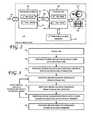
- FIG. 1Ais a block diagram of a protocol bridge and a storage SOC and ancillary Flash storage.
- FIG. 1Bis a block diagram of a protocol bridge.
- FIG. 2is a block diagram of a portion of a data storage device, according to one embodiment.
- FIG. 3is a flowchart illustrating aspects of one embodiment.
- FIG. 4is a flowchart illustrating aspects of one embodiment.
- FIG. 5is a flowchart of a method according to another embodiment.
- a protocol bridgemay comprise two parts; namely, a front-end that connects to initiator devices and a back-end that connects to target devices.
- the back-endmay be configured to use a data protocol designed for target devices while the front-end may be configured to use a protocol designed for initiator devices.
- the front-end and back-endneed to use the same protocol; rather, each system component may use whatever protocol is best suited to the attached devices.
- the front-sendcould use Fibre Channel over Ethernet (FCoE) or Universal Serial Bus (USB) while the back end could use Serial Attached SCSI (SAS) or Serial ATA (SATA).
- a bridge controllerconverts and transports data traffic from one protocol to another so that devices using different protocols may effectively communicate.
- Data storage devicessuch as hard disk drives (HDDs) comprising rotary storage media and hybrid disk drives comprising both rotary and solid state storage media may comprise a protocol bridge such as a USB to SATA protocol bridge.
- HDDshard disk drives
- hybrid disk drivescomprising both rotary and solid state storage media
- FIG. 1Ais a block diagram of a protocol bridge 102 .
- the protocol bridge 102may comprise a controller 116 that may be coupled to a, for example, USB interface 112 and to a, for example, SATA interface 114 .
- a power supply 118provides regulated power to the protocol bridge 102 .
- the controller 116is coupled to non-volatile memory 108 , for purposes developed hereunder.
- FIG. 1Bis a block diagram of a protocol bridge and a storage SOC and ancillary Flash storage.
- a protocol bridge 102may be configured to couple to a host 104 via, for example, a USB interface.
- the protocol bridge 102may also be configured to couple to a storage SOC 106 via a, for example, SATA bus 702 .
- the protocol bridge 102is coupled to a protocol bridge Serial Peripheral Interface (SPI) Flash memory 108 .
- the storage SOC 106is coupled to a storage SOC SPI Flash memory 110 .
- SPISerial Peripheral Interface
- This codeis functionally effective to enable the protocol bridge 102 to access its protocol bridge SPI Flash 108 to retrieve code and data therefrom to enable the protocol bridge 102 to initialize to a fully functional state.
- the storage SOC 106comprises internal ROM that is also accessed at power up. Code and data stored therein is accessed and used to enable the storage SOC 106 to access the storage SOC SPI Flash 110 and retrieve code and data therefrom. This retrieved code and data enables the storage SOC to initialize to a fully functional state.
- the protocol bridge 102 and the storage SOC 106may then enable the bus 114 and implement the SATA protocol thereon.
- the presence of both SPI Flash memories 108 and 110 , one for the protocol bridge 102 and the other for the storage SOCis costly and presents a barrier to further size reductions in the data storage device electronics and to reducing power consumption and heat dissipation.
- the data storage device 200may comprise a protocol bridge 202 , which may be configured to couple to a host 204 .
- the protocol bridge 202may be configured to translate between a first and a second communication protocol.
- the first protocolmay comprise USB and the second protocol may comprise SATA.
- the protocol bridge 202may be configured to translate between other protocols, as called for by the particular implementation.
- a storage SOC 206may be coupled to the protocol bridge 202 over a bus 208 .
- the bus 208may conform to, for example, the SATA protocol. Other protocols may be implemented by bus 208 .
- the storage SOC 206may be configured to control the data storage device 200 and may comprise, without limitation, circuitry configured as a read channel, hard disk controller, microprocessor, Error Correction Code (ECC), high-speed interface I/O, and system memory functions, all disposed on a single piece of silicon.
- ECCError Correction Code
- a first non-volatile memory 210may be coupled to the storage SOC 206 .
- the first non-volatile memory 210may comprise Flash memory and may be configured to store storage SOC data including, for example, storage SOC code, storage SOC configuration and other data.
- the data storage device 200further may comprise one or more hard disk drives (HDDs) each comprising one or more spinning magnetic disks, as shown at 237 .
- the data storage 200may alternatively comprise non-volatile (e.g., Flash-based) memories 242 .
- the data storage 200may comprise one or more hybrid storage devices, each comprising both magnetic disks 237 and non-volatile semiconductor memory 242 , as suggested at 240 .
- the data storage 200may also comprise one or more network interfaces, enabling the data storage 200 to communicate with a network and/or other external devices through communication ports.
- the first non-volatile memory(“non-volatile memory”, at times, being abbreviated as “NV MEM” in FIG. 2 ) may also be configured to store protocol bridge data including, for example, protocol bridge code, protocol bridge configuration and other data.
- the storage SOC datamay be stored beginning at a first Logical Block Address (LBA) in the first non-volatile memory 210 and the protocol bridge data may be stored away from the storage SOC data, beginning at a second LBA in the first non-volatile memory 210 .
- LBALogical Block Address
- the data storage device 200need not be provided with a non-volatile memory dedicated to storing protocol bridge data. This saves circuit real estate, lowers costs, power consumption and dissipated heat.
- the data storage device 200may be configured such that, upon power-on thereof, the storage SOC 206 retrieves its storage SOC code/data from the first non-volatile memory 210 and configures itself according to the retrieved storage SOC code/data.
- Such configurationmay include an initialization of the storage SOC 206 , rendering it fully operational for its intended purpose as well as making the bus 208 active, together with protocol bridge 202 .
- the data storage device 200may be configured such that, upon power-on thereof, the protocol bridge 202 also retrieves its protocol bridge code/data from the first non-volatile memory 210 and configures itself according to the retrieved protocol bridge code/data.
- Such configurationmay include an initialization of the protocol bridge 202 , rendering it fully operational for its intended purpose as well as making the bus (e.g., SATA or other protocol) 208 active, together with storage SOC 206 .
- the storage SOC 206may comprise first volatile memory 209 .
- the storage SOC 206may also comprise second non-volatile memory 207 that may be configured to store storage SOC instructions that, when executed, enable the storage SOC 206 to load the storage SOC code/data from the first non-volatile memory 210 upon power-on. That is, the storage SOC 206 may be configured, upon power on, to retrieve the stored code/data from the second non-volatile memory 207 , load them into the first volatile memory 209 and cause their execution. Such code/data, loaded into the first volatile memory 209 , are effective to enable the storage SOC 206 to retrieve the storage SOC data from the first non-volatile memory 210 and to configure itself therewith.
- the protocol bridge 202may comprise second volatile memory 207 .
- the protocol bridge 202may also comprise third non-volatile memory 205 that may be configured to store protocol bridge instructions that, when executed, enable the protocol bridge 202 to load the protocol bridge code/data from the first non-volatile memory 210 upon power-on, via the bus 208 and via the storage SOC 206 . That is, the protocol bridge 202 may be configured, upon power on, to retrieve the stored instructions from the third non-volatile memory 205 , load them into the second volatile memory 207 and cause their execution.
- Such instructionsloaded into the second volatile memory 207 , are effective to enable the protocol bridge 202 to request protocol bridge code/data from the storage SOC 206 , which may retrieve the requested protocol bridge code/data from the first non-volatile memory 210 and provide the same to the protocol bridge 202 via the bus 208 , thereby enabling the protocol bridge 202 to configure itself therewith.
- the first non-volatile memory 210may comprise Flash memory and/or non-volatile memory using some other technology.
- the first non-volatile memory 210 and the non-volatile memory 242may be separate and distinct, as suggested in FIG. 2 .
- the first non-volatile memory 210may form part of the non-volatile memory 242 ; that is, may form part of the primary memory of the data storage device, albeit preferably in a fixed non-user accessible portion thereof.
- a portion of the first non-volatile memory 210may itself be user-accessible.
- the protocol bridge 202may be configured to repeatedly retrieve portions of the protocol bridge code/data from the first non-volatile memory 210 in blocks of a predetermined size.
- the block sizemay be 4 KB in size. Other block sizes may be accommodated.
- Suchmay be carried out by fetching a first block at some offset (e.g., 0) in the first non-volatile memory 210 , validating it (checking for errors, etc.), loading the validated block into the second volatile memory 207 , updating the offset and fetching a second block of protocol bridge code/data at the updated offset and so on until all blocks of the protocol bridge code/data have been retrieved from the first non-volatile memory 210 , validated and loaded into the second volatile memory 207 .
- Another validation of the complete code/data sequence loaded into the second volatile memory 207may then be carried out, whereupon the loaded code may be executed to configure the protocol bridge 202 .
- FIG. 3is a flowchart that illustrates a method for a protocol bridge to load protocol data (code, instructions, configuration information) according to one embodiment.
- Block B 31denotes a power-on event, such as when the data storage device is first energized or awaken from a less than fully operational condition.
- the protocol bridgemay then retrieve the code/data stored in its non-volatile memory or read-only memory (ROM), such as third non-volatile memory 205 in FIG. 2 .
- ROMread-only memory
- the retrieved codemay then be loaded in its volatile memory (e.g., dynamic random access memory (DRAM)), such as shown at 207 in FIG. 2 .
- DRAMdynamic random access memory
- the protocol bridge 202may then execute this code.
- the storage SOC 206may be in the process of retrieving code/data from its second non-volatile memory 207 , loading it into its first volatile memory 209 .
- a portion of the protocol code being executed in the protocol bridge 202 and a portion of the storage SOC code being executed in the storage SOC 206may be effective to activate the bus 208 .
- the protocol bridgemay now request protocol bridge code/data from the storage SOC 206 .
- the storage SOC 206may then retrieve the requested protocol bridge code/data from the first non-volatile memory 210 and send it to the protocol bridge 202 , where it is received, as shown at B 35 in FIG. 3 .
- the received protocol bridge code/datamay now be validated (e.g., checked for errors) and the validated protocol bridge code/data may be stored in the second volatile memory 207 of the protocol bridge 202 , as shown at B 36 .
- the protocol bridge code/data or portions thereofmay be iteratively requested by the protocol bridge 202 , sent by the storage SOC 206 and received and validated by the protocol bridge 202 and until all of the protocol bridge code/data previously stored in the first non-volatile memory 210 has been stored in the second volatile memory 207 .
- the portions or blocks of protocol bridge code/data iteratively received from the storage SOC 206 datamay be, for example, 4 KB in size, although other sizes (16 KB, 32 KB or other) may be used as well. This iteration is shown in FIG. 3 as the repeated blocks B 34 , B 35 and B 36 .
- protocol bridge code/datamay be stored in the second volatile memory 207 .
- one or more additional validation operationsmay be carried out, to ensure the protocol bridge code/data has been received without errors.
- the protocol bridge's controllermay then execute the code contained in the loaded protocol bridge code/data to configure the protocol bridge 202 to its intended operational state.
- the controller in a protocol bridgemay be configured as a 16-bit controller whose addressing space may span only about 64,000 discrete physical addresses.
- the totality of the code used by the protocol bridgemay, however, not fit within the controller's address space, especially in infrequent and transient situations, such as the receipt of selected commands from a host.
- overlay codemay be retrieved from the first non-volatile memory 210 and sent by the storage SOC 206 to the protocol bridge 202 for loading into its second volatile memory 207 for execution.
- the code previously stored thereinmay be erased or the overlay code may overwrite the protocol bridge code previously stored in the second volatile memory 207 .
- the protocol bridge 202may then execute the overlay protocol bridge code to address the infrequent and/or transient situation, whereupon the overlay code may be erased or overwritten by the protocol bridge code/data previously stored in the second volatile memory 207 that it had replaced.
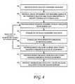
- FIG. 4is a flowchart illustrating a method of loading overlay code in a protocol bridge of a data storage device according to one embodiment.
- block B 41calls for the protocol bridge 202 to receive a command from the host 204 .
- the protocol bridgedetermines that execution of the received command necessitate the execution of overlay code/data not currently resident in the second volatile memory 207 and causes the generation of a request for (at least a portion of) the required overlay code from first non-volatile memory 210 via the storage SOC 206 .
- Block B 43calls for the protocol bridge to request the required overlay code/data from the storage SOC 206 , through the sending of the generated request thereto.
- the storage SOC 206retrieves the requested overlay code/data from the first non-volatile memory 210 and sends it to the protocol bridge 202 , as shown at B 45 .
- the protocol bridgemay then validate the received protocol bridge overlay code/data and store it in the second volatile memory 207 .
- the overlay code/datamay be requested, sent and received iteratively, block by block until all overlay code/data has been received by the protocol bridge 202 by repeating blocks B 43 , B 44 , B 45 and B 46 until all blocks of the overlay code/data have been received and stored.
- the protocol bridge 202may validate the overlay code/data, whereupon the protocol bridge 202 may begin execution of the validated overlay code/data, to carry out the command received from the host 204 .
- the overlay code/datamay be replaced by other protocol bridge code/data in the manner described previously.
- FIG. 5is a flowchart of a method according to one embodiment.
- storage SOC datae.g., storage SOC code, storage SOC configuration data and other storage SOC data
- protocol bridge datae.g., protocol bridge code, protocol bridge configuration data and other protocol bridge data
- storage SOC datae.g., storage SOC code, storage SOC configuration data and other storage SOC data
- protocol bridge datae.g., protocol bridge code, protocol bridge configuration data and other protocol bridge data
- block B 53calls for retrieving the storage SOC code/data from the first non-volatile memory 210 (comprising SPI Flash memory, for example) and configuring the storage SOC 206 according to the retrieved storage SOC code/data.
- code/datamay be retrieved from the second non-volatile memory 207 and stored in the first volatile memory 209 for execution.
- the protocol bridge 202may have similarly retrieved code/data from its internal third non-volatile memory 205 and stored in the second volatile memory 207 for execution.
- the code/data stored in the first volatile memory 209 and the second volatile memory 207may also be effective to enable the bus protocol 208 , to enable bi-directional communication between the protocol bridge 202 and the storage SOC 206 .
- the protocol bridge 202may retrieve bridge protocol code/data from the first non-volatile memory 210 , via the storage SOC 206 and the bus 208 .
- the protocol bridge 202may then be configured according to the retrieved protocol bridge code/data, to render the protocol bridge 202 to its fully operational state.
- the protocol bridge code/datamay be stored in the first non-volatile memory 210 .
- the protocol bridge code/dataneed not be stored therein.
- the protocol data/codemay be stored in the rotating media 237 .
- storing the protocol bridge code/data in the rotating mediamay cause an unacceptably long delay upon power-on as the platters containing the recording media spin up to their nominal operating speed.
- Storing at least a portion of the protocol bridge code/data in the solid state memory 242avoids such latency and spin-up issues.
- the command used to retrieve this protocol bridge code/dataideally would not cause a spin-up of the HDD's platters, for both completion time and power consumption considerations.
- the command to retrieve the execution imagemay be a log page command that maps to the first non-volatile memory 210 .
- Implementation of an embodimentmay reduce the Bill of Materials (BOM) cost by eliminating the need for a non-volatile memory dedicated to the protocol bridge 202 .
- BOMBill of Materials
- Storing both the storage SOC and the protocol bridge code/data in a same non-volatile memorymay require a comparatively larger-size first non-volatile memory 210 .
- such a larger non-volatile memory 210is likely less costly than providing a dedicated first non-volatile memory to store the storage SOC code/data and a dedicated second non-volatile memory to store the protocol bridge code/data.
- providing one non-volatile memory 210 for both the protocol bridge code/data and the storage SOC code/dataalso reduces space requirements, power consumption and heat dissipation and associated structures.
Landscapes
- Engineering & Computer Science (AREA)
- Theoretical Computer Science (AREA)
- General Engineering & Computer Science (AREA)
- Physics & Mathematics (AREA)
- General Physics & Mathematics (AREA)
- Computer Hardware Design (AREA)
- Power Sources (AREA)
- Information Transfer Systems (AREA)
- Bus Control (AREA)
Abstract
Description
Claims (15)
Priority Applications (2)
| Application Number | Priority Date | Filing Date | Title |
|---|---|---|---|
| US14/605,910US9734117B2 (en) | 2015-01-26 | 2015-01-26 | Data storage device and method for integrated bridge firmware to be retrieved from a storage system on chip (SOC) |
| CN201610052680.0ACN106126457B (en) | 2015-01-26 | 2016-01-26 | Data storage device and method of configuring and operating the same |
Applications Claiming Priority (1)
| Application Number | Priority Date | Filing Date | Title |
|---|---|---|---|
| US14/605,910US9734117B2 (en) | 2015-01-26 | 2015-01-26 | Data storage device and method for integrated bridge firmware to be retrieved from a storage system on chip (SOC) |
Publications (2)
| Publication Number | Publication Date |
|---|---|
| US20160217099A1 US20160217099A1 (en) | 2016-07-28 |
| US9734117B2true US9734117B2 (en) | 2017-08-15 |
Family
ID=56432679
Family Applications (1)
| Application Number | Title | Priority Date | Filing Date |
|---|---|---|---|
| US14/605,910Expired - Fee RelatedUS9734117B2 (en) | 2015-01-26 | 2015-01-26 | Data storage device and method for integrated bridge firmware to be retrieved from a storage system on chip (SOC) |
Country Status (2)
| Country | Link |
|---|---|
| US (1) | US9734117B2 (en) |
| CN (1) | CN106126457B (en) |
Cited By (1)
| Publication number | Priority date | Publication date | Assignee | Title |
|---|---|---|---|---|
| US11237838B2 (en) | 2020-01-02 | 2022-02-01 | Western Digital Technologies, Inc. | Storage system and method for enabling a direct accessible boot block in a memory die |
Families Citing this family (3)
| Publication number | Priority date | Publication date | Assignee | Title |
|---|---|---|---|---|
| US10346071B2 (en) | 2016-12-29 | 2019-07-09 | Western Digital Technologies, Inc. | Validating firmware for data storage devices |
| US20220345414A1 (en)* | 2019-08-30 | 2022-10-27 | Unitex Corporation | Interface Conversion Device |
| CN114303137A (en)* | 2020-08-07 | 2022-04-08 | 美光科技公司 | Memory overlay using host memory buffers |
Citations (44)
| Publication number | Priority date | Publication date | Assignee | Title |
|---|---|---|---|---|
| US5606660A (en)* | 1994-10-21 | 1997-02-25 | Lexar Microsystems, Inc. | Method and apparatus for combining controller firmware storage and controller logic in a mass storage system |
| US5819087A (en) | 1996-07-19 | 1998-10-06 | Compaq Computer Corporation | Flash ROM sharing between processor and microcontroller during booting and handling warm-booting events |
| US6499054B1 (en) | 1999-12-02 | 2002-12-24 | Senvid, Inc. | Control and observation of physical devices, equipment and processes by multiple users over computer networks |
| US6711059B2 (en)* | 2001-09-28 | 2004-03-23 | Lexar Media, Inc. | Memory controller |
| US20050060478A1 (en)* | 2003-09-15 | 2005-03-17 | Yuan-Ting Wu | Method of function activation on a bridge system |
| US20050144200A1 (en) | 1999-12-02 | 2005-06-30 | Lambertus Hesselink | Managed peer-to-peer applications, systems and methods for distributed data access and storage |
| US20050144195A1 (en) | 1999-12-02 | 2005-06-30 | Lambertus Hesselink | Managed peer-to-peer applications, systems and methods for distributed data access and storage |
| US20050251617A1 (en)* | 2004-05-07 | 2005-11-10 | Sinclair Alan W | Hybrid non-volatile memory system |
| US6968450B1 (en)* | 2002-06-01 | 2005-11-22 | Western Digital Technologies, Inc. | Disk drive caching initial host requested data in non-volatile semiconductor memory to reduce start-up time of a host computer |
| US7028174B1 (en)* | 2002-09-30 | 2006-04-11 | Western Digital Technologies, Inc. | Disk drive employing a non-volatile serial semiconductor memory for storing a control program for a microprocessor |
| US7120692B2 (en) | 1999-12-02 | 2006-10-10 | Senvid, Inc. | Access and control system for network-enabled devices |
| US20070088940A1 (en)* | 2005-10-13 | 2007-04-19 | Sandisk Corporation | Initialization of flash storage via an embedded controller |
| US20070260914A1 (en)* | 2006-04-25 | 2007-11-08 | Dmitry Pogrebinsky | Personal computer bus protocol with error correction mode |
| US7454443B2 (en) | 2003-08-26 | 2008-11-18 | Tamir Ram | Method, system, and program for personal data management using content-based replication |
| US7546353B2 (en) | 1999-12-02 | 2009-06-09 | Western Digital Technologies, Inc. | Managed peer-to-peer applications, systems and methods for distributed data access and storage |
| US7587467B2 (en) | 1999-12-02 | 2009-09-08 | Western Digital Technologies, Inc. | Managed peer-to-peer applications, systems and methods for distributed data access and storage |
| US20110072185A1 (en) | 2009-09-23 | 2011-03-24 | Sandisk Il Ltd. | Multi-protocol storage device bridge |
| US7917628B2 (en) | 1999-12-02 | 2011-03-29 | Western Digital Technologies, Inc. | Managed peer-to-peer applications, systems and methods for distributed data access and storage |
| US7934251B2 (en) | 1999-12-02 | 2011-04-26 | Western Digital Technologies, Inc. | Managed peer-to-peer applications, systems and methods for distributed data access and storage |
| US7949564B1 (en) | 2000-05-31 | 2011-05-24 | Western Digital Technologies, Inc. | System and method of receiving advertisement content from advertisers and distributing the advertising content to a network of personal computers |
| US20110154023A1 (en)* | 2009-12-21 | 2011-06-23 | Smith Ned M | Protected device management |
| US8004791B2 (en) | 2008-02-22 | 2011-08-23 | Western Digital Technologies, Inc. | Information storage device with a bridge controller and a plurality of electrically coupled conductive shields |
| US20120036041A1 (en) | 2010-08-09 | 2012-02-09 | Western Digital Technologies, Inc. | Methods and systems for a personal multimedia content archive |
| US20120166828A1 (en)* | 2010-12-23 | 2012-06-28 | Western Digital Technologies, Inc. | Method and system for power control to minimize power consumption |
| US8255661B2 (en) | 2009-11-13 | 2012-08-28 | Western Digital Technologies, Inc. | Data storage system comprising a mapping bridge for aligning host block size with physical block size of a data storage device |
| US8285965B2 (en) | 2009-11-20 | 2012-10-09 | Western Digital Technologies, Inc. | Aligning data storage device partition to boundary of physical data sector |
| US8352567B2 (en) | 1999-12-02 | 2013-01-08 | Western Digital Technologies, Inc. | VCR webification |
| US20130212401A1 (en) | 2012-02-14 | 2013-08-15 | Western Digital Technologies, Inc. | Methods and devices for authentication and data encryption |
| US8526798B2 (en) | 2009-12-23 | 2013-09-03 | Western Digital Technologies, Inc. | Portable content container displaying A/V files in response to a command received from a consumer device |
| US20130259062A1 (en) | 2012-03-30 | 2013-10-03 | Lsi Corporation | Multi-protocol bridge with integrated performance accelerating cache |
| US20130268759A1 (en) | 2012-04-10 | 2013-10-10 | Western Digital Technologies, Inc. | Digital rights management system transfer of content and distribution |
| US20130268749A1 (en) | 2012-04-10 | 2013-10-10 | Western Digital Technologies, Inc. | Digital rights management system and methods for provisioning content to an intelligent storage |
| US8631284B2 (en) | 2010-04-30 | 2014-01-14 | Western Digital Technologies, Inc. | Method for providing asynchronous event notification in systems |
| US8646054B1 (en) | 2012-03-23 | 2014-02-04 | Western Digital Technologies, Inc. | Mechanism to manage access to user data area with bridged direct-attached storage devices |
| US8688797B2 (en) | 1999-12-02 | 2014-04-01 | Western Digital Technologies, Inc. | Managed peer-to-peer applications, systems and methods for distributed data access and storage |
| US20140095855A1 (en) | 2012-09-28 | 2014-04-03 | Hung Huynh | Secure system flash sharing |
| US20140095439A1 (en) | 2012-10-01 | 2014-04-03 | Western Digital Technologies, Inc. | Optimizing data block size for deduplication |
| US8713265B1 (en) | 2010-09-21 | 2014-04-29 | Western Digital Technologies, Inc. | Visual indicator of online backup |
| US20140173215A1 (en) | 2012-12-13 | 2014-06-19 | Western Digital Technologies, Inc. | Methods and systems for provisioning a bootable image on to an external drive |
| US20140169921A1 (en) | 2012-12-19 | 2014-06-19 | Mark Carey | Cargo carrier |
| US8762682B1 (en) | 2010-07-02 | 2014-06-24 | Western Digital Technologies, Inc. | Data storage apparatus providing host full duplex operations using half duplex storage devices |
| US20140189197A1 (en) | 2012-12-27 | 2014-07-03 | Ramamurthy Krithivas | Sharing serial peripheral interface flash memory in a multi-node server system on chip platform environment |
| US8780004B1 (en) | 2012-01-31 | 2014-07-15 | Western Digital Technologies, Inc. | Dual configuration enclosure with optional shielding |
| US8909889B1 (en)* | 2011-10-10 | 2014-12-09 | Western Digital Technologies, Inc. | Method and apparatus for servicing host commands by a disk drive |
Family Cites Families (2)
| Publication number | Priority date | Publication date | Assignee | Title |
|---|---|---|---|---|
| CN101650689B (en)* | 2009-09-16 | 2011-10-26 | 中兴通讯股份有限公司 | Nonvolatile data storage and search method and device |
| KR101975027B1 (en)* | 2012-05-04 | 2019-05-03 | 삼성전자주식회사 | System on chip, operation method thereof, and devices having the same |
- 2015
- 2015-01-26USUS14/605,910patent/US9734117B2/ennot_activeExpired - Fee Related
- 2016
- 2016-01-26CNCN201610052680.0Apatent/CN106126457B/enactiveActive
Patent Citations (57)
| Publication number | Priority date | Publication date | Assignee | Title |
|---|---|---|---|---|
| US5606660A (en)* | 1994-10-21 | 1997-02-25 | Lexar Microsystems, Inc. | Method and apparatus for combining controller firmware storage and controller logic in a mass storage system |
| US5819087A (en) | 1996-07-19 | 1998-10-06 | Compaq Computer Corporation | Flash ROM sharing between processor and microcontroller during booting and handling warm-booting events |
| US7600036B2 (en) | 1999-12-02 | 2009-10-06 | Western Digital Technologies, Inc. | Access and control system for network-enabled devices |
| US7120692B2 (en) | 1999-12-02 | 2006-10-10 | Senvid, Inc. | Access and control system for network-enabled devices |
| US6732158B1 (en) | 1999-12-02 | 2004-05-04 | Senvid, Inc. | VCR webification |
| US8341275B1 (en) | 1999-12-02 | 2012-12-25 | Western Digital Technologies, Inc. | Access and control system for network-enabled devices |
| US20050144200A1 (en) | 1999-12-02 | 2005-06-30 | Lambertus Hesselink | Managed peer-to-peer applications, systems and methods for distributed data access and storage |
| US7917628B2 (en) | 1999-12-02 | 2011-03-29 | Western Digital Technologies, Inc. | Managed peer-to-peer applications, systems and methods for distributed data access and storage |
| US8352567B2 (en) | 1999-12-02 | 2013-01-08 | Western Digital Technologies, Inc. | VCR webification |
| US8793374B2 (en) | 1999-12-02 | 2014-07-29 | Western Digital Technologies, Inc. | Managed peer-to-peer applications, systems and methods for distributed data access and storage |
| US6499054B1 (en) | 1999-12-02 | 2002-12-24 | Senvid, Inc. | Control and observation of physical devices, equipment and processes by multiple users over computer networks |
| US7788404B2 (en) | 1999-12-02 | 2010-08-31 | Western Digital Technologies, Inc. | Access and control system for network-enabled devices |
| US8688797B2 (en) | 1999-12-02 | 2014-04-01 | Western Digital Technologies, Inc. | Managed peer-to-peer applications, systems and methods for distributed data access and storage |
| US7934251B2 (en) | 1999-12-02 | 2011-04-26 | Western Digital Technologies, Inc. | Managed peer-to-peer applications, systems and methods for distributed data access and storage |
| US20050144195A1 (en) | 1999-12-02 | 2005-06-30 | Lambertus Hesselink | Managed peer-to-peer applications, systems and methods for distributed data access and storage |
| US7467187B2 (en) | 1999-12-02 | 2008-12-16 | Western Digital Technologies, Inc. | Control and observation of physical devices, equipment and processes by multiple users over computer networks |
| US7546353B2 (en) | 1999-12-02 | 2009-06-09 | Western Digital Technologies, Inc. | Managed peer-to-peer applications, systems and methods for distributed data access and storage |
| US7587467B2 (en) | 1999-12-02 | 2009-09-08 | Western Digital Technologies, Inc. | Managed peer-to-peer applications, systems and methods for distributed data access and storage |
| US8661507B1 (en) | 1999-12-02 | 2014-02-25 | Western Digital Technologies, Inc. | Managed peer-to-peer applications, systems and methods for distributed data access and storage |
| US7949564B1 (en) | 2000-05-31 | 2011-05-24 | Western Digital Technologies, Inc. | System and method of receiving advertisement content from advertisers and distributing the advertising content to a network of personal computers |
| US6711059B2 (en)* | 2001-09-28 | 2004-03-23 | Lexar Media, Inc. | Memory controller |
| US6968450B1 (en)* | 2002-06-01 | 2005-11-22 | Western Digital Technologies, Inc. | Disk drive caching initial host requested data in non-volatile semiconductor memory to reduce start-up time of a host computer |
| US7028174B1 (en)* | 2002-09-30 | 2006-04-11 | Western Digital Technologies, Inc. | Disk drive employing a non-volatile serial semiconductor memory for storing a control program for a microprocessor |
| US7454443B2 (en) | 2003-08-26 | 2008-11-18 | Tamir Ram | Method, system, and program for personal data management using content-based replication |
| US8341117B2 (en) | 2003-08-26 | 2012-12-25 | Arkeia Software, Inc. | Method, system, and program for personal data management using content-based replication |
| US20050060478A1 (en)* | 2003-09-15 | 2005-03-17 | Yuan-Ting Wu | Method of function activation on a bridge system |
| US20050251617A1 (en)* | 2004-05-07 | 2005-11-10 | Sinclair Alan W | Hybrid non-volatile memory system |
| US20100070693A1 (en)* | 2005-10-13 | 2010-03-18 | Sandisk Corporation | Initialization of flash storage via an embedded controller |
| US20070088940A1 (en)* | 2005-10-13 | 2007-04-19 | Sandisk Corporation | Initialization of flash storage via an embedded controller |
| US20070260914A1 (en)* | 2006-04-25 | 2007-11-08 | Dmitry Pogrebinsky | Personal computer bus protocol with error correction mode |
| US8004791B2 (en) | 2008-02-22 | 2011-08-23 | Western Digital Technologies, Inc. | Information storage device with a bridge controller and a plurality of electrically coupled conductive shields |
| US20110072185A1 (en) | 2009-09-23 | 2011-03-24 | Sandisk Il Ltd. | Multi-protocol storage device bridge |
| US8301822B2 (en) | 2009-09-23 | 2012-10-30 | Sandisk Il Ltd. | Multi-protocol storage device bridge |
| US8255661B2 (en) | 2009-11-13 | 2012-08-28 | Western Digital Technologies, Inc. | Data storage system comprising a mapping bridge for aligning host block size with physical block size of a data storage device |
| US8285965B2 (en) | 2009-11-20 | 2012-10-09 | Western Digital Technologies, Inc. | Aligning data storage device partition to boundary of physical data sector |
| US20110154023A1 (en)* | 2009-12-21 | 2011-06-23 | Smith Ned M | Protected device management |
| US8526798B2 (en) | 2009-12-23 | 2013-09-03 | Western Digital Technologies, Inc. | Portable content container displaying A/V files in response to a command received from a consumer device |
| US8631284B2 (en) | 2010-04-30 | 2014-01-14 | Western Digital Technologies, Inc. | Method for providing asynchronous event notification in systems |
| US8762682B1 (en) | 2010-07-02 | 2014-06-24 | Western Digital Technologies, Inc. | Data storage apparatus providing host full duplex operations using half duplex storage devices |
| US20120036041A1 (en) | 2010-08-09 | 2012-02-09 | Western Digital Technologies, Inc. | Methods and systems for a personal multimedia content archive |
| US8713265B1 (en) | 2010-09-21 | 2014-04-29 | Western Digital Technologies, Inc. | Visual indicator of online backup |
| US20120166828A1 (en)* | 2010-12-23 | 2012-06-28 | Western Digital Technologies, Inc. | Method and system for power control to minimize power consumption |
| US8909889B1 (en)* | 2011-10-10 | 2014-12-09 | Western Digital Technologies, Inc. | Method and apparatus for servicing host commands by a disk drive |
| US8780004B1 (en) | 2012-01-31 | 2014-07-15 | Western Digital Technologies, Inc. | Dual configuration enclosure with optional shielding |
| US8819443B2 (en) | 2012-02-14 | 2014-08-26 | Western Digital Technologies, Inc. | Methods and devices for authentication and data encryption |
| US20130212401A1 (en) | 2012-02-14 | 2013-08-15 | Western Digital Technologies, Inc. | Methods and devices for authentication and data encryption |
| US8646054B1 (en) | 2012-03-23 | 2014-02-04 | Western Digital Technologies, Inc. | Mechanism to manage access to user data area with bridged direct-attached storage devices |
| US20130259062A1 (en) | 2012-03-30 | 2013-10-03 | Lsi Corporation | Multi-protocol bridge with integrated performance accelerating cache |
| US20130268759A1 (en) | 2012-04-10 | 2013-10-10 | Western Digital Technologies, Inc. | Digital rights management system transfer of content and distribution |
| US20130266137A1 (en) | 2012-04-10 | 2013-10-10 | Western Digital Technologies, Inc. | Digital rights managment system, devices, and methods for binding content to an intelligent storage device |
| US20130268749A1 (en) | 2012-04-10 | 2013-10-10 | Western Digital Technologies, Inc. | Digital rights management system and methods for provisioning content to an intelligent storage |
| US20130268771A1 (en) | 2012-04-10 | 2013-10-10 | Western Digital Technologies, Inc. | Digital rights management system and methods for accessingcontent from an intelligent storag |
| US20140095855A1 (en) | 2012-09-28 | 2014-04-03 | Hung Huynh | Secure system flash sharing |
| US20140095439A1 (en) | 2012-10-01 | 2014-04-03 | Western Digital Technologies, Inc. | Optimizing data block size for deduplication |
| US20140173215A1 (en) | 2012-12-13 | 2014-06-19 | Western Digital Technologies, Inc. | Methods and systems for provisioning a bootable image on to an external drive |
| US20140169921A1 (en) | 2012-12-19 | 2014-06-19 | Mark Carey | Cargo carrier |
| US20140189197A1 (en) | 2012-12-27 | 2014-07-03 | Ramamurthy Krithivas | Sharing serial peripheral interface flash memory in a multi-node server system on chip platform environment |
Non-Patent Citations (2)
| Title |
|---|
| Arora, Mohit, and Varun Jain. "Understanding embedded-system-boot techniques." EDN-Electronic Design News 56.3 (2011): 18.* |
| Shanahan, D. "Tech Bits. On Chip Rom Code used in SOC Designs." EE Times (2001).* |
Cited By (1)
| Publication number | Priority date | Publication date | Assignee | Title |
|---|---|---|---|---|
| US11237838B2 (en) | 2020-01-02 | 2022-02-01 | Western Digital Technologies, Inc. | Storage system and method for enabling a direct accessible boot block in a memory die |
Also Published As
| Publication number | Publication date |
|---|---|
| US20160217099A1 (en) | 2016-07-28 |
| CN106126457B (en) | 2021-01-01 |
| CN106126457A (en) | 2016-11-16 |
Similar Documents
| Publication | Publication Date | Title |
|---|---|---|
| US11656963B2 (en) | Storage device and method for operating storage device | |
| US9817652B2 (en) | Data storage device and method for reducing firmware update time and data processing system including the device | |
| TWI437494B (en) | Memory card, memory system including the same, and operating method thereof | |
| US20140310449A1 (en) | Virtualization of Storage Devices | |
| US10209897B2 (en) | Storage device and control method of the same | |
| KR20150074550A (en) | Data storage device and data processing system including the same | |
| US8433847B2 (en) | Memory drive that can be operated like optical disk drive and method for virtualizing memory drive as optical disk drive | |
| US9734117B2 (en) | Data storage device and method for integrated bridge firmware to be retrieved from a storage system on chip (SOC) | |
| US20150039948A1 (en) | Data storage device and operating method thereof | |
| US20110231621A1 (en) | System recovery method, and storage medium controller and storage system using the same | |
| KR20210060867A (en) | Data storage device and operating method thereof | |
| US20140365713A1 (en) | Electronic system and operating method thereof | |
| KR20190106005A (en) | Memory system, operating method thereof and electronic apparatus | |
| KR20190091035A (en) | Memory system and operating method thereof | |
| US20110022793A1 (en) | Systems And Methods For Accessing Hard Disk Drives | |
| US10162573B2 (en) | Storage management system, storage management method, storage medium and information processing system | |
| JP4972212B2 (en) | Bridge circuit | |
| US11366775B2 (en) | Data storage device with an exclusive channel for flag checking of read data, and non-volatile memory control method | |
| US11740799B2 (en) | Storage system and input and output control method | |
| US20170083235A1 (en) | Device capable of using external volatile memory and device capable of releasing internal volatile memory | |
| US10884642B2 (en) | Method and apparatus for performing data-accessing management in a storage server | |
| KR102423278B1 (en) | Memory system and operating method thereof | |
| JP7242928B2 (en) | Storage system and input/output control method | |
| JP2007293564A (en) | Memory device and information storage system | |
| CN104956350A (en) | Initialization of the storage device |
Legal Events
| Date | Code | Title | Description |
|---|---|---|---|
| AS | Assignment | Owner name:WESTERN DIGITAL TECHNOLOGIES, INC., CALIFORNIA Free format text:ASSIGNMENT OF ASSIGNORS INTEREST;ASSIGNORS:MCCABE, TIMOTHY J.;MARONEY, JOHN E.;SIGNING DATES FROM 20151201 TO 20151206;REEL/FRAME:037271/0680 | |
| AS | Assignment | Owner name:U.S. BANK NATIONAL ASSOCIATION, AS COLLATERAL AGENT, CALIFORNIA Free format text:SECURITY AGREEMENT;ASSIGNOR:WESTERN DIGITAL TECHNOLOGIES, INC.;REEL/FRAME:038744/0281 Effective date:20160512 Owner name:JPMORGAN CHASE BANK, N.A., AS COLLATERAL AGENT, ILLINOIS Free format text:SECURITY AGREEMENT;ASSIGNOR:WESTERN DIGITAL TECHNOLOGIES, INC.;REEL/FRAME:038722/0229 Effective date:20160512 Owner name:JPMORGAN CHASE BANK, N.A., AS COLLATERAL AGENT, ILLINOIS Free format text:SECURITY AGREEMENT;ASSIGNOR:WESTERN DIGITAL TECHNOLOGIES, INC.;REEL/FRAME:038744/0481 Effective date:20160512 Owner name:U.S. BANK NATIONAL ASSOCIATION, AS COLLATERAL AGEN Free format text:SECURITY AGREEMENT;ASSIGNOR:WESTERN DIGITAL TECHNOLOGIES, INC.;REEL/FRAME:038744/0281 Effective date:20160512 Owner name:JPMORGAN CHASE BANK, N.A., AS COLLATERAL AGENT, IL Free format text:SECURITY AGREEMENT;ASSIGNOR:WESTERN DIGITAL TECHNOLOGIES, INC.;REEL/FRAME:038744/0481 Effective date:20160512 Owner name:JPMORGAN CHASE BANK, N.A., AS COLLATERAL AGENT, IL Free format text:SECURITY AGREEMENT;ASSIGNOR:WESTERN DIGITAL TECHNOLOGIES, INC.;REEL/FRAME:038722/0229 Effective date:20160512 | |
| STCF | Information on status: patent grant | Free format text:PATENTED CASE | |
| AS | Assignment | Owner name:WESTERN DIGITAL TECHNOLOGIES, INC., CALIFORNIA Free format text:RELEASE BY SECURED PARTY;ASSIGNOR:U.S. BANK NATIONAL ASSOCIATION, AS COLLATERAL AGENT;REEL/FRAME:045501/0714 Effective date:20180227 | |
| MAFP | Maintenance fee payment | Free format text:PAYMENT OF MAINTENANCE FEE, 4TH YEAR, LARGE ENTITY (ORIGINAL EVENT CODE: M1551); ENTITY STATUS OF PATENT OWNER: LARGE ENTITY Year of fee payment:4 | |
| AS | Assignment | Owner name:WESTERN DIGITAL TECHNOLOGIES, INC., CALIFORNIA Free format text:RELEASE OF SECURITY INTEREST AT REEL 038744 FRAME 0481;ASSIGNOR:JPMORGAN CHASE BANK, N.A.;REEL/FRAME:058982/0556 Effective date:20220203 | |
| AS | Assignment | Owner name:JPMORGAN CHASE BANK, N.A., ILLINOIS Free format text:PATENT COLLATERAL AGREEMENT - A&R LOAN AGREEMENT;ASSIGNOR:WESTERN DIGITAL TECHNOLOGIES, INC.;REEL/FRAME:064715/0001 Effective date:20230818 Owner name:JPMORGAN CHASE BANK, N.A., ILLINOIS Free format text:PATENT COLLATERAL AGREEMENT - DDTL LOAN AGREEMENT;ASSIGNOR:WESTERN DIGITAL TECHNOLOGIES, INC.;REEL/FRAME:067045/0156 Effective date:20230818 | |
| FEPP | Fee payment procedure | Free format text:MAINTENANCE FEE REMINDER MAILED (ORIGINAL EVENT CODE: REM.); ENTITY STATUS OF PATENT OWNER: LARGE ENTITY | |
| LAPS | Lapse for failure to pay maintenance fees | Free format text:PATENT EXPIRED FOR FAILURE TO PAY MAINTENANCE FEES (ORIGINAL EVENT CODE: EXP.); ENTITY STATUS OF PATENT OWNER: LARGE ENTITY | |
| STCH | Information on status: patent discontinuation | Free format text:PATENT EXPIRED DUE TO NONPAYMENT OF MAINTENANCE FEES UNDER 37 CFR 1.362 |