US9728935B2 - Chip-scale package and semiconductor device assembly - Google Patents
Chip-scale package and semiconductor device assemblyDownload PDFInfo
- Publication number
- US9728935B2 US9728935B2US14/731,510US201514731510AUS9728935B2US 9728935 B2US9728935 B2US 9728935B2US 201514731510 AUS201514731510 AUS 201514731510AUS 9728935 B2US9728935 B2US 9728935B2
- Authority
- US
- United States
- Prior art keywords
- chip
- submount
- semiconductor device
- edge
- area
- Prior art date
- Legal status (The legal status is an assumption and is not a legal conclusion. Google has not performed a legal analysis and makes no representation as to the accuracy of the status listed.)
- Active
Links
- 239000004065semiconductorSubstances0.000titleclaimsabstractdescription56
- 229910000679solderInorganic materials0.000claimsdescription15
- 239000004593EpoxySubstances0.000claimsdescription7
- 238000001465metallisationMethods0.000claimsdescription7
- 239000004020conductorSubstances0.000claimsdescription5
- 229910001080W alloyInorganic materials0.000claimsdescription4
- SBYXRAKIOMOBFF-UHFFFAOYSA-Ncopper tungstenChemical compound[Cu].[W]SBYXRAKIOMOBFF-UHFFFAOYSA-N0.000claimsdescription4
- HBMJWWWQQXIZIP-UHFFFAOYSA-Nsilicon carbideChemical compound[Si+]#[C-]HBMJWWWQQXIZIP-UHFFFAOYSA-N0.000claimsdescription4
- 229910052751metalInorganic materials0.000claimsdescription3
- 239000002184metalSubstances0.000claimsdescription3
- PMHQVHHXPFUNSP-UHFFFAOYSA-Mcopper(1+);methylsulfanylmethane;bromideChemical compoundBr[Cu].CSCPMHQVHHXPFUNSP-UHFFFAOYSA-M0.000claimsdescription2
- 229910010271silicon carbideInorganic materials0.000claimsdescription2
- 238000000034methodMethods0.000description5
- 230000003287optical effectEffects0.000description3
- PIGFYZPCRLYGLF-UHFFFAOYSA-NAluminum nitrideChemical compound[Al]#NPIGFYZPCRLYGLF-UHFFFAOYSA-N0.000description2
- PCHJSUWPFVWCPO-UHFFFAOYSA-NgoldChemical compound[Au]PCHJSUWPFVWCPO-UHFFFAOYSA-N0.000description2
- 239000010931goldSubstances0.000description2
- 229910052737goldInorganic materials0.000description2
- JVPLOXQKFGYFMN-UHFFFAOYSA-Ngold tinChemical compound[Sn].[Au]JVPLOXQKFGYFMN-UHFFFAOYSA-N0.000description2
- 238000012986modificationMethods0.000description2
- 230000004048modificationEffects0.000description2
- 230000001681protective effectEffects0.000description2
- JBRZTFJDHDCESZ-UHFFFAOYSA-NAsGaChemical compound[As]#[Ga]JBRZTFJDHDCESZ-UHFFFAOYSA-N0.000description1
- 230000000903blocking effectEffects0.000description1
- 238000004519manufacturing processMethods0.000description1
- 239000000463materialSubstances0.000description1
- 239000012811non-conductive materialSubstances0.000description1
Images


Classifications
- H—ELECTRICITY
- H01—ELECTRIC ELEMENTS
- H01S—DEVICES USING THE PROCESS OF LIGHT AMPLIFICATION BY STIMULATED EMISSION OF RADIATION [LASER] TO AMPLIFY OR GENERATE LIGHT; DEVICES USING STIMULATED EMISSION OF ELECTROMAGNETIC RADIATION IN WAVE RANGES OTHER THAN OPTICAL
- H01S5/00—Semiconductor lasers
- H01S5/02—Structural details or components not essential to laser action
- H01S5/022—Mountings; Housings
- H01S5/0235—Method for mounting laser chips
- H01S5/02355—Fixing laser chips on mounts
- H01S5/0237—Fixing laser chips on mounts by soldering
- H01S5/02272—
- H—ELECTRICITY
- H10—SEMICONDUCTOR DEVICES; ELECTRIC SOLID-STATE DEVICES NOT OTHERWISE PROVIDED FOR
- H10H—INORGANIC LIGHT-EMITTING SEMICONDUCTOR DEVICES HAVING POTENTIAL BARRIERS
- H10H20/00—Individual inorganic light-emitting semiconductor devices having potential barriers, e.g. light-emitting diodes [LED]
- H10H20/80—Constructional details
- H10H20/85—Packages
- H10H20/852—Encapsulations
- H—ELECTRICITY
- H01—ELECTRIC ELEMENTS
- H01S—DEVICES USING THE PROCESS OF LIGHT AMPLIFICATION BY STIMULATED EMISSION OF RADIATION [LASER] TO AMPLIFY OR GENERATE LIGHT; DEVICES USING STIMULATED EMISSION OF ELECTROMAGNETIC RADIATION IN WAVE RANGES OTHER THAN OPTICAL
- H01S5/00—Semiconductor lasers
- H01S5/02—Structural details or components not essential to laser action
- H01S5/022—Mountings; Housings
- H01S5/02256—
- H01S5/02268—
- H—ELECTRICITY
- H01—ELECTRIC ELEMENTS
- H01S—DEVICES USING THE PROCESS OF LIGHT AMPLIFICATION BY STIMULATED EMISSION OF RADIATION [LASER] TO AMPLIFY OR GENERATE LIGHT; DEVICES USING STIMULATED EMISSION OF ELECTROMAGNETIC RADIATION IN WAVE RANGES OTHER THAN OPTICAL
- H01S5/00—Semiconductor lasers
- H01S5/02—Structural details or components not essential to laser action
- H01S5/022—Mountings; Housings
- H01S5/023—Mount members, e.g. sub-mount members
- H01S5/02315—Support members, e.g. bases or carriers
- H—ELECTRICITY
- H01—ELECTRIC ELEMENTS
- H01S—DEVICES USING THE PROCESS OF LIGHT AMPLIFICATION BY STIMULATED EMISSION OF RADIATION [LASER] TO AMPLIFY OR GENERATE LIGHT; DEVICES USING STIMULATED EMISSION OF ELECTROMAGNETIC RADIATION IN WAVE RANGES OTHER THAN OPTICAL
- H01S5/00—Semiconductor lasers
- H01S5/02—Structural details or components not essential to laser action
- H01S5/022—Mountings; Housings
- H01S5/0235—Method for mounting laser chips
- H01S5/02355—Fixing laser chips on mounts
- H—ELECTRICITY
- H01—ELECTRIC ELEMENTS
- H01S—DEVICES USING THE PROCESS OF LIGHT AMPLIFICATION BY STIMULATED EMISSION OF RADIATION [LASER] TO AMPLIFY OR GENERATE LIGHT; DEVICES USING STIMULATED EMISSION OF ELECTROMAGNETIC RADIATION IN WAVE RANGES OTHER THAN OPTICAL
- H01S5/00—Semiconductor lasers
- H01S5/02—Structural details or components not essential to laser action
- H01S5/022—Mountings; Housings
- H01S5/0235—Method for mounting laser chips
- H01S5/02375—Positioning of the laser chips
- H01S5/0238—Positioning of the laser chips using marks
- H—ELECTRICITY
- H01—ELECTRIC ELEMENTS
- H01S—DEVICES USING THE PROCESS OF LIGHT AMPLIFICATION BY STIMULATED EMISSION OF RADIATION [LASER] TO AMPLIFY OR GENERATE LIGHT; DEVICES USING STIMULATED EMISSION OF ELECTROMAGNETIC RADIATION IN WAVE RANGES OTHER THAN OPTICAL
- H01S5/00—Semiconductor lasers
- H01S5/02—Structural details or components not essential to laser action
- H01S5/024—Arrangements for thermal management
- H01S5/02476—Heat spreaders, i.e. improving heat flow between laser chip and heat dissipating elements
- H—ELECTRICITY
- H10—SEMICONDUCTOR DEVICES; ELECTRIC SOLID-STATE DEVICES NOT OTHERWISE PROVIDED FOR
- H10H—INORGANIC LIGHT-EMITTING SEMICONDUCTOR DEVICES HAVING POTENTIAL BARRIERS
- H10H20/00—Individual inorganic light-emitting semiconductor devices having potential barriers, e.g. light-emitting diodes [LED]
- H10H20/80—Constructional details
- H10H20/85—Packages
- H10H20/857—Interconnections, e.g. lead-frames, bond wires or solder balls
- H—ELECTRICITY
- H01—ELECTRIC ELEMENTS
- H01L—SEMICONDUCTOR DEVICES NOT COVERED BY CLASS H10
- H01L2224/00—Indexing scheme for arrangements for connecting or disconnecting semiconductor or solid-state bodies and methods related thereto as covered by H01L24/00
- H01L2224/01—Means for bonding being attached to, or being formed on, the surface to be connected, e.g. chip-to-package, die-attach, "first-level" interconnects; Manufacturing methods related thereto
- H01L2224/42—Wire connectors; Manufacturing methods related thereto
- H01L2224/47—Structure, shape, material or disposition of the wire connectors after the connecting process
- H01L2224/48—Structure, shape, material or disposition of the wire connectors after the connecting process of an individual wire connector
- H01L2224/4805—Shape
- H01L2224/4809—Loop shape
- H01L2224/48091—Arched
- H—ELECTRICITY
- H01—ELECTRIC ELEMENTS
- H01L—SEMICONDUCTOR DEVICES NOT COVERED BY CLASS H10
- H01L2224/00—Indexing scheme for arrangements for connecting or disconnecting semiconductor or solid-state bodies and methods related thereto as covered by H01L24/00
- H01L2224/01—Means for bonding being attached to, or being formed on, the surface to be connected, e.g. chip-to-package, die-attach, "first-level" interconnects; Manufacturing methods related thereto
- H01L2224/42—Wire connectors; Manufacturing methods related thereto
- H01L2224/47—Structure, shape, material or disposition of the wire connectors after the connecting process
- H01L2224/48—Structure, shape, material or disposition of the wire connectors after the connecting process of an individual wire connector
- H01L2224/481—Disposition
- H01L2224/48151—Connecting between a semiconductor or solid-state body and an item not being a semiconductor or solid-state body, e.g. chip-to-substrate, chip-to-passive
- H01L2224/48221—Connecting between a semiconductor or solid-state body and an item not being a semiconductor or solid-state body, e.g. chip-to-substrate, chip-to-passive the body and the item being stacked
- H01L2224/48225—Connecting between a semiconductor or solid-state body and an item not being a semiconductor or solid-state body, e.g. chip-to-substrate, chip-to-passive the body and the item being stacked the item being non-metallic, e.g. insulating substrate with or without metallisation
- H01L2224/48227—Connecting between a semiconductor or solid-state body and an item not being a semiconductor or solid-state body, e.g. chip-to-substrate, chip-to-passive the body and the item being stacked the item being non-metallic, e.g. insulating substrate with or without metallisation connecting the wire to a bond pad of the item
- H—ELECTRICITY
- H01—ELECTRIC ELEMENTS
- H01L—SEMICONDUCTOR DEVICES NOT COVERED BY CLASS H10
- H01L2224/00—Indexing scheme for arrangements for connecting or disconnecting semiconductor or solid-state bodies and methods related thereto as covered by H01L24/00
- H01L2224/01—Means for bonding being attached to, or being formed on, the surface to be connected, e.g. chip-to-package, die-attach, "first-level" interconnects; Manufacturing methods related thereto
- H01L2224/42—Wire connectors; Manufacturing methods related thereto
- H01L2224/47—Structure, shape, material or disposition of the wire connectors after the connecting process
- H01L2224/48—Structure, shape, material or disposition of the wire connectors after the connecting process of an individual wire connector
- H01L2224/484—Connecting portions
- H01L2224/48463—Connecting portions the connecting portion on the bonding area of the semiconductor or solid-state body being a ball bond
- H01L2224/48464—Connecting portions the connecting portion on the bonding area of the semiconductor or solid-state body being a ball bond the other connecting portion not on the bonding area also being a ball bond, i.e. ball-to-ball
- H—ELECTRICITY
- H01—ELECTRIC ELEMENTS
- H01L—SEMICONDUCTOR DEVICES NOT COVERED BY CLASS H10
- H01L2224/00—Indexing scheme for arrangements for connecting or disconnecting semiconductor or solid-state bodies and methods related thereto as covered by H01L24/00
- H01L2224/73—Means for bonding being of different types provided for in two or more of groups H01L2224/10, H01L2224/18, H01L2224/26, H01L2224/34, H01L2224/42, H01L2224/50, H01L2224/63, H01L2224/71
- H01L2224/732—Location after the connecting process
- H01L2224/73251—Location after the connecting process on different surfaces
- H01L2224/73265—Layer and wire connectors
- H—ELECTRICITY
- H01—ELECTRIC ELEMENTS
- H01L—SEMICONDUCTOR DEVICES NOT COVERED BY CLASS H10
- H01L2924/00—Indexing scheme for arrangements or methods for connecting or disconnecting semiconductor or solid-state bodies as covered by H01L24/00
- H01L2924/0001—Technical content checked by a classifier
- H01L2924/00014—Technical content checked by a classifier the subject-matter covered by the group, the symbol of which is combined with the symbol of this group, being disclosed without further technical details
- H—ELECTRICITY
- H01—ELECTRIC ELEMENTS
- H01L—SEMICONDUCTOR DEVICES NOT COVERED BY CLASS H10
- H01L2924/00—Indexing scheme for arrangements or methods for connecting or disconnecting semiconductor or solid-state bodies as covered by H01L24/00
- H01L2924/15—Details of package parts other than the semiconductor or other solid state devices to be connected
- H01L2924/161—Cap
- H01L2924/1615—Shape
- H01L2924/16151—Cap comprising an aperture, e.g. for pressure control, encapsulation
- H—ELECTRICITY
- H01—ELECTRIC ELEMENTS
- H01L—SEMICONDUCTOR DEVICES NOT COVERED BY CLASS H10
- H01L2924/00—Indexing scheme for arrangements or methods for connecting or disconnecting semiconductor or solid-state bodies as covered by H01L24/00
- H01L2924/15—Details of package parts other than the semiconductor or other solid state devices to be connected
- H01L2924/161—Cap
- H01L2924/1615—Shape
- H01L2924/16152—Cap comprising a cavity for hosting the device, e.g. U-shaped cap
- H01S5/02236—
- H—ELECTRICITY
- H01—ELECTRIC ELEMENTS
- H01S—DEVICES USING THE PROCESS OF LIGHT AMPLIFICATION BY STIMULATED EMISSION OF RADIATION [LASER] TO AMPLIFY OR GENERATE LIGHT; DEVICES USING STIMULATED EMISSION OF ELECTROMAGNETIC RADIATION IN WAVE RANGES OTHER THAN OPTICAL
- H01S5/00—Semiconductor lasers
- H01S5/02—Structural details or components not essential to laser action
- H01S5/022—Mountings; Housings
- H01S5/0225—Out-coupling of light
- H01S5/02257—Out-coupling of light using windows, e.g. specially adapted for back-reflecting light to a detector inside the housing
- H01S5/02276—
- H01S5/02296—
- H—ELECTRICITY
- H01—ELECTRIC ELEMENTS
- H01S—DEVICES USING THE PROCESS OF LIGHT AMPLIFICATION BY STIMULATED EMISSION OF RADIATION [LASER] TO AMPLIFY OR GENERATE LIGHT; DEVICES USING STIMULATED EMISSION OF ELECTROMAGNETIC RADIATION IN WAVE RANGES OTHER THAN OPTICAL
- H01S5/00—Semiconductor lasers
- H01S5/02—Structural details or components not essential to laser action
- H01S5/022—Mountings; Housings
- H01S5/0233—Mounting configuration of laser chips
- H01S5/02345—Wire-bonding
- H—ELECTRICITY
- H01—ELECTRIC ELEMENTS
- H01S—DEVICES USING THE PROCESS OF LIGHT AMPLIFICATION BY STIMULATED EMISSION OF RADIATION [LASER] TO AMPLIFY OR GENERATE LIGHT; DEVICES USING STIMULATED EMISSION OF ELECTROMAGNETIC RADIATION IN WAVE RANGES OTHER THAN OPTICAL
- H01S5/00—Semiconductor lasers
- H01S5/02—Structural details or components not essential to laser action
- H01S5/022—Mountings; Housings
- H01S5/0235—Method for mounting laser chips
- H—ELECTRICITY
- H01—ELECTRIC ELEMENTS
- H01S—DEVICES USING THE PROCESS OF LIGHT AMPLIFICATION BY STIMULATED EMISSION OF RADIATION [LASER] TO AMPLIFY OR GENERATE LIGHT; DEVICES USING STIMULATED EMISSION OF ELECTROMAGNETIC RADIATION IN WAVE RANGES OTHER THAN OPTICAL
- H01S5/00—Semiconductor lasers
- H01S5/02—Structural details or components not essential to laser action
- H01S5/024—Arrangements for thermal management
- H01S5/02469—Passive cooling, e.g. where heat is removed by the housing as a whole or by a heat pipe without any active cooling element like a TEC
Definitions
- the present disclosurerelates to a chip-scale package for a semiconductor device and a semiconductor device assembly including such a chip-scale package. More particularly, the present disclosure relates to a chip-scale package for an edge-emitting semiconductor device and a semiconductor device assembly including such a chip-scale package.
- a conventional chip-on-submount (COS) package 100 for an edge-emitting laser diodeis shown in FIG. 1 .
- the COS package 100includes an edge-emitting laser diode chip 110 and a submount 120 .
- the submount 120may be formed of aluminum nitride (AlN), silicon carbide (SiC), or a copper-tungsten alloy (CuW).
- An anode pad 130 and a cathode pad 131are defined on the submount 120 by patterned metallization, e.g., gold metallization.
- a bottom, p-side surface of the chip 110is attached and electrically connected to the anode pad 130 with solder 140 , e.g., a gold-tin (AuSn) solder, and wire bonds 141 , e.g., gold wire bonds, are used to electrically connect a top, n-side surface of the chip 110 to the cathode pad 131 .
- solder 140e.g., a gold-tin (AuSn) solder
- wire bonds 141e.g., gold wire bonds
- the area of the COS package 100is often relatively large, e.g., about 5 mm 2 , to provide space on the COS package 100 for electrical connections during burn-in and testing.
- a package having a smaller areawould be desirable, especially for mobile applications.
- an aspect of the present disclosurerelates to a chip-scale package comprising: an edge-emitting semiconductor device chip, having a chip area, comprising a top surface and an opposite bottom surface; a top submount, having a top-submount area, disposed on the top surface of the chip; and a bottom submount, having a bottom-submount area, disposed on the bottom surface of the chip; wherein the top-submount area and the bottom-submount area are each greater than the chip area and less than or equal to about 1.2 times the chip area.
- a semiconductor device assemblycomprising: a chip-scale package comprising: an edge-emitting semiconductor device chip, having a chip area, comprising a top surface and an opposite bottom surface; a top submount, having a top-submount area, disposed on the top surface of the chip; and a bottom submount, having a bottom-submount area, disposed on the bottom surface of the chip; wherein the top-submount area and the bottom-submount area are each greater than the chip area and less than or equal to about 1.2 times the chip area; and a printed circuit board (PCB); wherein the chip-scale package is mounted on the PCB so that the top submount and the bottom submount are each electrically connected to the PCB.
- a chip-scale packagecomprising: an edge-emitting semiconductor device chip, having a chip area, comprising a top surface and an opposite bottom surface; a top submount, having a top-submount area, disposed on the top surface of the chip; and a bottom submount, having a bottom-submount
- FIG. 1is a perspective view of a conventional chip-on-submount (COS) package
- FIG. 2Ais a schematic illustration of a front view of a chip-scale package
- FIG. 2Bis a schematic illustration of a side view of the chip-scale package of FIG. 2A ;
- FIG. 3Ais a schematic illustration of a top view of a submount
- FIG. 3Bis a schematic illustration of a bottom view of the submount of FIG. 3A ;
- FIG. 4Ais a schematic illustration of a front view of a semiconductor device assembly including a chip-scale package mounted horizontally on a printed circuit board (PCB) for emission parallel to the PCB;
- PCBprinted circuit board
- FIG. 4Bis a schematic illustration of a side view of the semiconductor device assembly of FIG. 4A ;
- FIG. 5is a schematic illustration of a side view of a semiconductor device assembly including a chip-scale package mounted vertically on a PCB for emission parallel to the PCB;
- FIG. 6is a schematic illustration of a side view of a semiconductor device assembly including a chip-scale package mounted horizontally on a PCB for emission perpendicular to the PCB.
- the present disclosureprovides a chip-scale package for an edge-emitting semiconductor device chip.
- a chip-scale packagemay be defined as a package having a package area that is less than or equal to about 1.2 times a chip area of the semiconductor device chip it contains.
- a chip-scale packagemay be advantageous for applications requiring a small form factor, such as mobile applications.
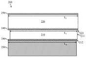
- the chip-scale package 200 of the present disclosuremay include an edge-emitting semiconductor device chip 210 , a top submount 220 , and a bottom submount 230 .
- the chip 210may include a single edge-emitting semiconductor device.
- the edge-emitting semiconductor devicemay be an edge-emitting laser diode or an edge-emitting light-emitting diode (LED).
- the chip 210may emit an output beam from a front facet 211 of the chip 210 .
- the chip 210may have a chip area, defined by a chip length L C and a chip width W C , and a chip thickness T C .
- the chip lengthmay be about 1000 ⁇ m
- the chip widthmay be about 225 ⁇ m
- the chip thicknessmay be about 90 ⁇ m to about 140 ⁇ m.
- a top surface of the chip 210 and an opposite bottom surface of the chip 210may each have the same chip area and may be separated by the chip thickness.
- the chip 210may include an active layer, e.g., a p-n junction, substantially parallel to the top and bottom surfaces of the chip 210 , between an n-type region, i.e., an n side, and a p-type region, i.e., a p side, of the chip 210 .
- the top surface of the chip 210may be an n-side surface
- the bottom surface of the chip 210may be a p-side surface.
- the top submount 220may be disposed on the top surface of the chip 210
- the bottom submount 230may be disposed on the bottom surface of the chip 210 .
- the chip 210may be sandwiched between the top submount 220 and the bottom submount 230 , as shown in FIG. 2 .
- the bottom submount 230 , the chip 210 , and the top submount 220may be vertically stacked, i.e., stacked along a vertical axis of the chip-scale package 200 .
- the top submount 220may be attached to the top surface of the chip 210 with solder 240 , e.g., a gold-tin (AuSn) solder, and the bottom submount 230 may be attached to the bottom surface of the chip 210 with solder 240 .
- a single-step reflow attachment processmay be used to simultaneously attach the top submount 220 and the bottom submount 230 to the chip 210 , allowing a high placement accuracy.
- the chip-scale package 200may be fabricated by a chip-level process using singulated submounts 220 and 230 and chip 210 .
- the bottom submount 230may be disposed so that the front facet 211 of the chip 210 overhangs the bottom submount 230 , e.g., by about 5 ⁇ m to about 25 ⁇ m.
- the overhang 212 of the chip 210may prevent the solder 240 from electrically shorting the p-n junction and/or blocking the front facet 211 .
- the top submount 220 and the bottom submount 230may each be formed of a thermally conductive material, e.g., having a thermal conductivity of greater than about 200 W/m ⁇ K. Also, the top submount 220 and the bottom submount 230 may each be formed of a material having a coefficient of thermal expansion (CTE) that is substantially matched to a CTE of the chip 210 , improving the reliability of the chip-scale package 200 ; e.g., the submounts 220 and 230 and the chip 210 may have CTEs of about 4 ppm/K to about 6 ppm/K.
- CTEcoefficient of thermal expansion
- the top submount 220 and the bottom submount 230may each be formed of aluminum nitride (AlN), silicon carbide (SiC), or a copper-tungsten alloy (CuW), and the chip 210 may be based on gallium arsenide (GaAs).
- AlNaluminum nitride
- SiCsilicon carbide
- CuWcopper-tungsten alloy
- GaAsgallium arsenide
- top submount 220 and the bottom submount 230are formed of an electrically non-conductive material, e.g., aluminum nitride, they may be provided with wrap-around metallization 250 , e.g., gold metallization, as shown in FIG. 2 .
- the wrap-around metallization 250may be formed on a top surface, a side surface, and a bottom surface of each submount 220 or 230 .
- the wrap-around metallization 250may be omitted.
- the top submount 220 and/or the bottom submount 230may have a notch 260 or fiducial mark 261 to facilitate alignment, e.g., by identifying the location of the output beam.
- the top submount 220may have a top-submount area, defined by a top-submount length L T and a top-submount width W T , and a top-submount thickness T T .
- the top-submount lengthmay be about 1110 ⁇ m
- the top-submount widthmay be about 275 ⁇ m
- the top-submount thicknessmay be about 100 ⁇ m to about 300 ⁇ m, e.g., about 230 ⁇ m.
- the bottom submount 230may have a bottom-submount area, defined by a bottom-submount length L B and a bottom-submount width W B , and a bottom-submount thickness T B .
- the bottom-submount lengthmay be about 1100 ⁇ m
- the bottom-submount widthmay be about 275 ⁇ m
- the bottom-submount thicknessmay be about 100 ⁇ m to about 300 ⁇ m, e.g., about 230 ⁇ m.
- the top-submount thickness and the bottom-submount thicknessmay be substantially equal.
- the submount thicknessesmay be selected on the basis of the ease of manufacturing, cost, reliability, and form factor. Typically, the submount thicknesses may be from about 100 ⁇ m to about 300 ⁇ m. Accordingly, a package height of the chip-scale package 200 may be less than or equal to about 1 mm, in some instances, less than or equal to about 300 ⁇ m.
- the directions of the chip thickness, the top-submount thickness, and the bottom-submount thicknessmay be substantially parallel to one another and to the vertical axis of the chip-scale package 200 .
- the top-submount areamay be greater than or equal to the bottom-submount area.
- the top-submount lengthmay be greater than the bottom-submount length to allow the top submount 220 to overhang the front facet 211 of the chip 210 , e.g., by about 5 ⁇ m to about 25 ⁇ m.
- the overhang 221may provide mechanical protection for the front facet 211 .
- the top-submount length and the bottom-submount lengthmay be substantially equal.
- the top-submount width and the bottom-submount widthmay be substantially equal.
- the planes of the chip area, the top-submount area, and the bottom-submount areamay be substantially parallel to one another and substantially perpendicular to the vertical axis of the chip-scale package 200 .
- the top-submount area and the bottom-submount areamay each be greater than the chip area to account for pick-and-place accuracy during the reflow attachment process.
- the submount lengthsmay be at least about 50 ⁇ m greater, e.g., about 100 ⁇ m greater, than the chip length
- the submount widthsmay be at least about 25 ⁇ m greater, e.g., about 50 ⁇ m, greater than the chip width.
- the top-submount area and the bottom-submount areamay each be less than or equal to about 1.2 times the chip area.
- the package area of the chip-scale package 200which may, typically, correspond to the top-submount area, may be less than or equal to 1.2 times the chip area.
- the package area of the chip-scale package 200may be less than or equal to about 1 mm 2 , in some instances, less than or equal to about 0.3 mm 2 .
- the small package areamay be particularly advantageous for mobile applications.
- the chip-scale package 200may be included in a semiconductor device assembly, which may also include a printed circuit board (PCB), a housing, an optical element, and/or other components.
- the chip-scale package 200may be mounted on the PCB so that the top submount 220 and the bottom submount 230 are each electrically connected to the PCB.
- the top submount 220 and the bottom submount 230may each be electrically connected to the PCB through solder, conductive epoxy, a wire bond, or a metal clip.
- the chip-scale package 200may be surface mounted on the PCB, i.e., attached by surface mount technology (SMT).
- SMTsurface mount technology
- the chip-scale package 200may be mounted horizontally on a PCB 470 for emission parallel to the PCB 470 .
- the vertical axis of the chip-scale package 200 and the output beam 480may each be parallel to the PCB 470 .
- the top submount 220 and the bottom submount 230may each be attached and electrically connected to the PCB 470 with solder 471 or conductive epoxy.
- the chip-scale package 200may be mounted vertically on a PCB 570 for emission parallel to the PCB 570 .
- the vertical axis of the chip-scale package 200may be perpendicular to the PCB 570
- the output beam 580may be parallel to the PCB 570 .
- the bottom submount 230may be attached and electrically connected to the PCB 570 with solder 571 or conductive epoxy, and the top submount 220 may be electrically connected to the PCB 570 through a wire bond 572 , e.g., formed in a post-SMT process, or a metal clip, e.g., formed in an SMT process, with solder 571 or conductive epoxy at both ends.
- the chip-scale package 200 and the PCB 570may be covered with a protective housing 590 , which may include an optical element 591 , such as a lens, a diffuser, or a prism.
- the chip-scale package 200may be mounted horizontally on a PCB 670 for emission parallel to the PCB 670 .
- the vertical axis of the chip-scale package 200may be parallel to the PCB 670
- the output beam 680may be perpendicular to the PCB 670 .
- the chip-scale package 200 and the PCB 670may be covered with a protective housing 690 , which may include an optical element 691 , such as a lens, a diffuser, or a prism.
- the top submount 220 and the bottom submount 230may each be attached and electrically connected to the PCB 670 with solder 671 or conductive epoxy.
Landscapes
- Physics & Mathematics (AREA)
- Condensed Matter Physics & Semiconductors (AREA)
- General Physics & Mathematics (AREA)
- Electromagnetism (AREA)
- Optics & Photonics (AREA)
- Led Device Packages (AREA)
- Semiconductor Lasers (AREA)
- Wire Bonding (AREA)
Abstract
Description
Claims (20)
Priority Applications (3)
| Application Number | Priority Date | Filing Date | Title |
|---|---|---|---|
| US14/731,510US9728935B2 (en) | 2015-06-05 | 2015-06-05 | Chip-scale package and semiconductor device assembly |
| TW105114297ATWI604584B (en) | 2015-06-05 | 2016-05-09 | Wafer size package and semiconductor device components |
| CN201610382276.XACN106252493B (en) | 2015-06-05 | 2016-06-01 | Chip Scale Packaging and Semiconductor Device Assemblies |
Applications Claiming Priority (1)
| Application Number | Priority Date | Filing Date | Title |
|---|---|---|---|
| US14/731,510US9728935B2 (en) | 2015-06-05 | 2015-06-05 | Chip-scale package and semiconductor device assembly |
Publications (2)
| Publication Number | Publication Date |
|---|---|
| US20160359295A1 US20160359295A1 (en) | 2016-12-08 |
| US9728935B2true US9728935B2 (en) | 2017-08-08 |
Family
ID=57452266
Family Applications (1)
| Application Number | Title | Priority Date | Filing Date |
|---|---|---|---|
| US14/731,510ActiveUS9728935B2 (en) | 2015-06-05 | 2015-06-05 | Chip-scale package and semiconductor device assembly |
Country Status (3)
| Country | Link |
|---|---|
| US (1) | US9728935B2 (en) |
| CN (1) | CN106252493B (en) |
| TW (1) | TWI604584B (en) |
Families Citing this family (5)
| Publication number | Priority date | Publication date | Assignee | Title |
|---|---|---|---|---|
| JP6988268B2 (en)* | 2017-03-27 | 2022-01-05 | ウシオ電機株式会社 | Semiconductor laser device |
| US10833474B2 (en)* | 2017-08-02 | 2020-11-10 | Nlight, Inc. | CTE-matched silicon-carbide submount with high thermal conductivity contacts |
| WO2019205153A1 (en)* | 2018-04-28 | 2019-10-31 | 深圳市大疆创新科技有限公司 | Laser diode packaging module, transmitting apparatus, ranging apparatus, and electronic device |
| CN112074759B (en) | 2018-04-28 | 2024-11-05 | 深圳市大疆创新科技有限公司 | Light detection and ranging sensor with multiple transmitters and multiple receivers and associated systems and methods |
| DE102023124035A1 (en)* | 2023-09-06 | 2025-03-06 | Jenoptik Optical Systems Gmbh | Method for producing a laser diode module and multilayer substrate and laser composite for use in a method for producing a laser diode module |
Citations (12)
| Publication number | Priority date | Publication date | Assignee | Title |
|---|---|---|---|---|
| US5479029A (en)* | 1991-10-26 | 1995-12-26 | Rohm Co., Ltd. | Sub-mount type device for emitting light |
| US5835518A (en) | 1997-01-31 | 1998-11-10 | Star Medical Technologies, Inc. | Laser diode array packaging |
| US6195376B1 (en) | 1998-03-31 | 2001-02-27 | Opto Power Corporation | Semiconductor laser array stack package & method of fabrication |
| US6281096B1 (en)* | 1999-04-22 | 2001-08-28 | International Rectifier Corp. | Chip scale packaging process |
| US6326646B1 (en)* | 1999-11-24 | 2001-12-04 | Lucent Technologies, Inc. | Mounting technology for intersubband light emitters |
| US20050087848A1 (en)* | 2002-03-18 | 2005-04-28 | Samsung Electro-Mechanics Co., Ltd. | Chip scale package and method of fabricating the same |
| JP2006032406A (en)* | 2004-07-12 | 2006-02-02 | Sony Corp | Semiconductor laser device |
| US8068524B1 (en)* | 2009-12-28 | 2011-11-29 | Pranalytica, Inc. | Submounts for Semiconductor Lasers |
| US8130807B2 (en) | 2007-02-13 | 2012-03-06 | Laserline Gesellschaft fur Entwicklung und Vertrieb Von Diddenlasern GmbH | Diode laser array and method for manufacturing such an array |
| US8475056B2 (en) | 2009-07-28 | 2013-07-02 | Jds Uniphase Corporation | Semiconductor device assembly |
| US8537873B2 (en) | 2011-07-20 | 2013-09-17 | Jds Uniphase Corporation | High power surface mount technology package for side emitting laser diode |
| US9008139B2 (en) | 2013-06-28 | 2015-04-14 | Jds Uniphase Corporation | Structure and method for edge-emitting diode package having deflectors and diffusers |
- 2015
- 2015-06-05USUS14/731,510patent/US9728935B2/enactiveActive
- 2016
- 2016-05-09TWTW105114297Apatent/TWI604584B/enactive
- 2016-06-01CNCN201610382276.XApatent/CN106252493B/enactiveActive
Patent Citations (13)
| Publication number | Priority date | Publication date | Assignee | Title |
|---|---|---|---|---|
| US5479029A (en)* | 1991-10-26 | 1995-12-26 | Rohm Co., Ltd. | Sub-mount type device for emitting light |
| US5835518A (en) | 1997-01-31 | 1998-11-10 | Star Medical Technologies, Inc. | Laser diode array packaging |
| US6195376B1 (en) | 1998-03-31 | 2001-02-27 | Opto Power Corporation | Semiconductor laser array stack package & method of fabrication |
| US6281096B1 (en)* | 1999-04-22 | 2001-08-28 | International Rectifier Corp. | Chip scale packaging process |
| US6326646B1 (en)* | 1999-11-24 | 2001-12-04 | Lucent Technologies, Inc. | Mounting technology for intersubband light emitters |
| US7176058B2 (en) | 2002-03-18 | 2007-02-13 | Samsung Electro-Mechanics Co., Ltd. | Chip scale package and method of fabricating the same |
| US20050087848A1 (en)* | 2002-03-18 | 2005-04-28 | Samsung Electro-Mechanics Co., Ltd. | Chip scale package and method of fabricating the same |
| JP2006032406A (en)* | 2004-07-12 | 2006-02-02 | Sony Corp | Semiconductor laser device |
| US8130807B2 (en) | 2007-02-13 | 2012-03-06 | Laserline Gesellschaft fur Entwicklung und Vertrieb Von Diddenlasern GmbH | Diode laser array and method for manufacturing such an array |
| US8475056B2 (en) | 2009-07-28 | 2013-07-02 | Jds Uniphase Corporation | Semiconductor device assembly |
| US8068524B1 (en)* | 2009-12-28 | 2011-11-29 | Pranalytica, Inc. | Submounts for Semiconductor Lasers |
| US8537873B2 (en) | 2011-07-20 | 2013-09-17 | Jds Uniphase Corporation | High power surface mount technology package for side emitting laser diode |
| US9008139B2 (en) | 2013-06-28 | 2015-04-14 | Jds Uniphase Corporation | Structure and method for edge-emitting diode package having deflectors and diffusers |
Also Published As
| Publication number | Publication date |
|---|---|
| CN106252493B (en) | 2019-08-27 |
| CN106252493A (en) | 2016-12-21 |
| TWI604584B (en) | 2017-11-01 |
| TW201709454A (en) | 2017-03-01 |
| US20160359295A1 (en) | 2016-12-08 |
Similar Documents
| Publication | Publication Date | Title |
|---|---|---|
| US9728935B2 (en) | Chip-scale package and semiconductor device assembly | |
| US9123874B2 (en) | Light emitting device packages with improved heat transfer | |
| US8897328B2 (en) | Semiconductor laser apparatus and method for manufacturing same | |
| US9058971B2 (en) | Electro-optical module | |
| US11728617B2 (en) | Semiconductor laser device | |
| JP2012084900A (en) | Light emitting diode package and manufacturing method thereof | |
| US20100224890A1 (en) | Light emitting diode chip with electrical insulation element | |
| US10748836B2 (en) | Semiconductor laser module and method for manufacturing the same | |
| JP2013532894A (en) | Optoelectronic light emitting module and automotive headlight | |
| US12374857B2 (en) | Optical assembly with a microlens component and contacts on a same surface of a vertical cavity surface emitting laser device | |
| KR100568275B1 (en) | Semiconductor Laser Diode Device with PCC Type Lead Frame | |
| US20080191365A1 (en) | Optical semiconductor device | |
| US10985527B2 (en) | Laser diode surface mounting structure | |
| US6807218B1 (en) | Laser module and optical subassembly | |
| US20110222567A1 (en) | optoelectronic transistor outline (to)-can header assembly having a configuration that improves heat dissipation and reduces thermal resistance | |
| KR20160026604A (en) | Method for microsoldering led of flip chip type | |
| US10680405B2 (en) | Semiconductor light-emitting device | |
| JP6552710B2 (en) | Laser light source device and method of manufacturing laser light source device | |
| KR102669828B1 (en) | Laser Diode package | |
| US12374856B2 (en) | Semiconductor-laser-chip-on-submount, manufacturing method thereof, and semiconductor laser module | |
| JP2016111240A (en) | Housing for accommodating semiconductor device, semiconductor module, and method for manufacturing housing for accommodating semiconductor device | |
| WO2023089059A2 (en) | Laser package and method for manufacturing a laser package | |
| US10763639B2 (en) | Emitter-on-sub-mount device | |
| US10916914B2 (en) | Light module | |
| US20250141180A1 (en) | Optoelectronic semiconductor component and optoelectronic module |
Legal Events
| Date | Code | Title | Description |
|---|---|---|---|
| AS | Assignment | Owner name:JDS UNIPHASE CORPORATION, CALIFORNIA Free format text:ASSIGNMENT OF ASSIGNORS INTEREST;ASSIGNORS:LEE, KONG WENG;WONG, VINCENT V.;SKIDMORE, JAY A.;AND OTHERS;REEL/FRAME:035859/0022 Effective date:20150605 | |
| AS | Assignment | Owner name:LUMENTUM OPERATIONS LLC, CALIFORNIA Free format text:ASSIGNMENT OF ASSIGNORS INTEREST;ASSIGNOR:JDS UNIPHASE CORPORATION;REEL/FRAME:036420/0340 Effective date:20150731 | |
| AS | Assignment | Owner name:LUMENTUM OPERATIONS LLC, CALIFORNIA Free format text:CORRECTIVE ASSIGNMENT TO CORRECT INCORRECT PATENTS 7,868,247 AND 6,476,312 ON PAGE A-A33 PREVIOUSLY RECORDED ON REEL 036420 FRAME 0340. ASSIGNOR(S) HEREBY CONFIRMS THE ASSIGNMENT;ASSIGNOR:JDS UNIPHASE CORPORATION;REEL/FRAME:037562/0513 Effective date:20150731 | |
| AS | Assignment | Owner name:LUMENTUM OPERATIONS LLC, CALIFORNIA Free format text:CORRECTIVE ASSIGNMENT TO CORRECT PATENTS 7,868,247 AND 6,476,312 LISTED ON PAGE A-A33 PREVIOUSLY RECORDED ON REEL 036420 FRAME 0340. ASSIGNOR(S) HEREBY CONFIRMS THE ASSIGNMENT;ASSIGNOR:JDS UNIPHASE CORPORATION;REEL/FRAME:037627/0641 Effective date:20150731 | |
| FEPP | Fee payment procedure | Free format text:PAYOR NUMBER ASSIGNED (ORIGINAL EVENT CODE: ASPN); ENTITY STATUS OF PATENT OWNER: LARGE ENTITY | |
| STCF | Information on status: patent grant | Free format text:PATENTED CASE | |
| AS | Assignment | Owner name:DEUTSCHE BANK AG NEW YORK BRANCH, AS COLLATERAL AGENT, NEW YORK Free format text:PATENT SECURITY AGREEMENT;ASSIGNORS:LUMENTUM OPERATIONS LLC;OCLARO FIBER OPTICS, INC.;OCLARO, INC.;REEL/FRAME:047788/0511 Effective date:20181210 Owner name:DEUTSCHE BANK AG NEW YORK BRANCH, AS COLLATERAL AG Free format text:PATENT SECURITY AGREEMENT;ASSIGNORS:LUMENTUM OPERATIONS LLC;OCLARO FIBER OPTICS, INC.;OCLARO, INC.;REEL/FRAME:047788/0511 Effective date:20181210 | |
| AS | Assignment | Owner name:LUMENTUM OPERATIONS LLC, CALIFORNIA Free format text:RELEASE BY SECURED PARTY;ASSIGNOR:DEUTSCHE AG NEW YORK BRANCH;REEL/FRAME:051287/0556 Effective date:20191212 Owner name:OCLARO, INC., CALIFORNIA Free format text:RELEASE BY SECURED PARTY;ASSIGNOR:DEUTSCHE AG NEW YORK BRANCH;REEL/FRAME:051287/0556 Effective date:20191212 Owner name:OCLARO FIBER OPTICS, INC., CALIFORNIA Free format text:RELEASE BY SECURED PARTY;ASSIGNOR:DEUTSCHE AG NEW YORK BRANCH;REEL/FRAME:051287/0556 Effective date:20191212 | |
| MAFP | Maintenance fee payment | Free format text:PAYMENT OF MAINTENANCE FEE, 4TH YEAR, LARGE ENTITY (ORIGINAL EVENT CODE: M1551); ENTITY STATUS OF PATENT OWNER: LARGE ENTITY Year of fee payment:4 | |
| MAFP | Maintenance fee payment | Free format text:PAYMENT OF MAINTENANCE FEE, 8TH YEAR, LARGE ENTITY (ORIGINAL EVENT CODE: M1552); ENTITY STATUS OF PATENT OWNER: LARGE ENTITY Year of fee payment:8 |