US9723711B2 - Method for fabricating a flexible electronic structure and a flexible electronic structure - Google Patents
Method for fabricating a flexible electronic structure and a flexible electronic structureDownload PDFInfo
- Publication number
- US9723711B2 US9723711B2US14/819,040US201514819040AUS9723711B2US 9723711 B2US9723711 B2US 9723711B2US 201514819040 AUS201514819040 AUS 201514819040AUS 9723711 B2US9723711 B2US 9723711B2
- Authority
- US
- United States
- Prior art keywords
- layer
- substrate
- polymer layer
- electronic device
- anchors
- Prior art date
- Legal status (The legal status is an assumption and is not a legal conclusion. Google has not performed a legal analysis and makes no representation as to the accuracy of the status listed.)
- Active, expires
Links
Images


Classifications
- H—ELECTRICITY
- H05—ELECTRIC TECHNIQUES NOT OTHERWISE PROVIDED FOR
- H05K—PRINTED CIRCUITS; CASINGS OR CONSTRUCTIONAL DETAILS OF ELECTRIC APPARATUS; MANUFACTURE OF ASSEMBLAGES OF ELECTRICAL COMPONENTS
- H05K1/00—Printed circuits
- H05K1/02—Details
- H05K1/0277—Bendability or stretchability details
- H05K1/0278—Rigid circuit boards or rigid supports of circuit boards locally made bendable, e.g. by removal or replacement of material
- H—ELECTRICITY
- H05—ELECTRIC TECHNIQUES NOT OTHERWISE PROVIDED FOR
- H05K—PRINTED CIRCUITS; CASINGS OR CONSTRUCTIONAL DETAILS OF ELECTRIC APPARATUS; MANUFACTURE OF ASSEMBLAGES OF ELECTRICAL COMPONENTS
- H05K1/00—Printed circuits
- H05K1/02—Details
- H—ELECTRICITY
- H01—ELECTRIC ELEMENTS
- H01L—SEMICONDUCTOR DEVICES NOT COVERED BY CLASS H10
- H01L21/00—Processes or apparatus adapted for the manufacture or treatment of semiconductor or solid state devices or of parts thereof
- H01L21/67—Apparatus specially adapted for handling semiconductor or electric solid state devices during manufacture or treatment thereof; Apparatus specially adapted for handling wafers during manufacture or treatment of semiconductor or electric solid state devices or components ; Apparatus not specifically provided for elsewhere
- H01L21/683—Apparatus specially adapted for handling semiconductor or electric solid state devices during manufacture or treatment thereof; Apparatus specially adapted for handling wafers during manufacture or treatment of semiconductor or electric solid state devices or components ; Apparatus not specifically provided for elsewhere for supporting or gripping
- H01L21/6835—Apparatus specially adapted for handling semiconductor or electric solid state devices during manufacture or treatment thereof; Apparatus specially adapted for handling wafers during manufacture or treatment of semiconductor or electric solid state devices or components ; Apparatus not specifically provided for elsewhere for supporting or gripping using temporarily an auxiliary support
- H—ELECTRICITY
- H01—ELECTRIC ELEMENTS
- H01L—SEMICONDUCTOR DEVICES NOT COVERED BY CLASS H10
- H01L23/00—Details of semiconductor or other solid state devices
- H01L23/12—Mountings, e.g. non-detachable insulating substrates
- H01L23/13—Mountings, e.g. non-detachable insulating substrates characterised by the shape
- H—ELECTRICITY
- H01—ELECTRIC ELEMENTS
- H01L—SEMICONDUCTOR DEVICES NOT COVERED BY CLASS H10
- H01L23/00—Details of semiconductor or other solid state devices
- H01L23/48—Arrangements for conducting electric current to or from the solid state body in operation, e.g. leads, terminal arrangements ; Selection of materials therefor
- H01L23/488—Arrangements for conducting electric current to or from the solid state body in operation, e.g. leads, terminal arrangements ; Selection of materials therefor consisting of soldered or bonded constructions
- H01L23/498—Leads, i.e. metallisations or lead-frames on insulating substrates, e.g. chip carriers
- H01L23/4985—Flexible insulating substrates
- H—ELECTRICITY
- H01—ELECTRIC ELEMENTS
- H01L—SEMICONDUCTOR DEVICES NOT COVERED BY CLASS H10
- H01L25/00—Assemblies consisting of a plurality of semiconductor or other solid state devices
- H01L25/03—Assemblies consisting of a plurality of semiconductor or other solid state devices all the devices being of a type provided for in a single subclass of subclasses H10B, H10D, H10F, H10H, H10K or H10N, e.g. assemblies of rectifier diodes
- H01L25/04—Assemblies consisting of a plurality of semiconductor or other solid state devices all the devices being of a type provided for in a single subclass of subclasses H10B, H10D, H10F, H10H, H10K or H10N, e.g. assemblies of rectifier diodes the devices not having separate containers
- H01L25/065—Assemblies consisting of a plurality of semiconductor or other solid state devices all the devices being of a type provided for in a single subclass of subclasses H10B, H10D, H10F, H10H, H10K or H10N, e.g. assemblies of rectifier diodes the devices not having separate containers the devices being of a type provided for in group H10D89/00
- H01L25/0655—Assemblies consisting of a plurality of semiconductor or other solid state devices all the devices being of a type provided for in a single subclass of subclasses H10B, H10D, H10F, H10H, H10K or H10N, e.g. assemblies of rectifier diodes the devices not having separate containers the devices being of a type provided for in group H10D89/00 the devices being arranged next to each other
- H—ELECTRICITY
- H01—ELECTRIC ELEMENTS
- H01L—SEMICONDUCTOR DEVICES NOT COVERED BY CLASS H10
- H01L25/00—Assemblies consisting of a plurality of semiconductor or other solid state devices
- H01L25/03—Assemblies consisting of a plurality of semiconductor or other solid state devices all the devices being of a type provided for in a single subclass of subclasses H10B, H10D, H10F, H10H, H10K or H10N, e.g. assemblies of rectifier diodes
- H01L25/04—Assemblies consisting of a plurality of semiconductor or other solid state devices all the devices being of a type provided for in a single subclass of subclasses H10B, H10D, H10F, H10H, H10K or H10N, e.g. assemblies of rectifier diodes the devices not having separate containers
- H01L25/07—Assemblies consisting of a plurality of semiconductor or other solid state devices all the devices being of a type provided for in a single subclass of subclasses H10B, H10D, H10F, H10H, H10K or H10N, e.g. assemblies of rectifier diodes the devices not having separate containers the devices being of a type provided for in group subclass H10D
- H01L25/072—Assemblies consisting of a plurality of semiconductor or other solid state devices all the devices being of a type provided for in a single subclass of subclasses H10B, H10D, H10F, H10H, H10K or H10N, e.g. assemblies of rectifier diodes the devices not having separate containers the devices being of a type provided for in group subclass H10D the devices being arranged next to each other
- H—ELECTRICITY
- H01—ELECTRIC ELEMENTS
- H01L—SEMICONDUCTOR DEVICES NOT COVERED BY CLASS H10
- H01L25/00—Assemblies consisting of a plurality of semiconductor or other solid state devices
- H01L25/50—Multistep manufacturing processes of assemblies consisting of devices, the devices being individual devices of subclass H10D or integrated devices of class H10
- H—ELECTRICITY
- H05—ELECTRIC TECHNIQUES NOT OTHERWISE PROVIDED FOR
- H05K—PRINTED CIRCUITS; CASINGS OR CONSTRUCTIONAL DETAILS OF ELECTRIC APPARATUS; MANUFACTURE OF ASSEMBLAGES OF ELECTRICAL COMPONENTS
- H05K1/00—Printed circuits
- H05K1/02—Details
- H05K1/03—Use of materials for the substrate
- H05K1/0313—Organic insulating material
- H05K1/032—Organic insulating material consisting of one material
- H05K1/0326—Organic insulating material consisting of one material containing O
- H—ELECTRICITY
- H05—ELECTRIC TECHNIQUES NOT OTHERWISE PROVIDED FOR
- H05K—PRINTED CIRCUITS; CASINGS OR CONSTRUCTIONAL DETAILS OF ELECTRIC APPARATUS; MANUFACTURE OF ASSEMBLAGES OF ELECTRICAL COMPONENTS
- H05K1/00—Printed circuits
- H05K1/02—Details
- H05K1/03—Use of materials for the substrate
- H05K1/0313—Organic insulating material
- H05K1/032—Organic insulating material consisting of one material
- H05K1/0346—Organic insulating material consisting of one material containing N
- H—ELECTRICITY
- H05—ELECTRIC TECHNIQUES NOT OTHERWISE PROVIDED FOR
- H05K—PRINTED CIRCUITS; CASINGS OR CONSTRUCTIONAL DETAILS OF ELECTRIC APPARATUS; MANUFACTURE OF ASSEMBLAGES OF ELECTRICAL COMPONENTS
- H05K1/00—Printed circuits
- H05K1/02—Details
- H05K1/11—Printed elements for providing electric connections to or between printed circuits
- H05K1/115—Via connections; Lands around holes or via connections
- H—ELECTRICITY
- H05—ELECTRIC TECHNIQUES NOT OTHERWISE PROVIDED FOR
- H05K—PRINTED CIRCUITS; CASINGS OR CONSTRUCTIONAL DETAILS OF ELECTRIC APPARATUS; MANUFACTURE OF ASSEMBLAGES OF ELECTRICAL COMPONENTS
- H05K3/00—Apparatus or processes for manufacturing printed circuits
- H05K3/02—Apparatus or processes for manufacturing printed circuits in which the conductive material is applied to the surface of the insulating support and is thereafter removed from such areas of the surface which are not intended for current conducting or shielding
- H05K3/06—Apparatus or processes for manufacturing printed circuits in which the conductive material is applied to the surface of the insulating support and is thereafter removed from such areas of the surface which are not intended for current conducting or shielding the conductive material being removed chemically or electrolytically, e.g. by photo-etch process
- H05K3/067—Etchants
- H—ELECTRICITY
- H05—ELECTRIC TECHNIQUES NOT OTHERWISE PROVIDED FOR
- H05K—PRINTED CIRCUITS; CASINGS OR CONSTRUCTIONAL DETAILS OF ELECTRIC APPARATUS; MANUFACTURE OF ASSEMBLAGES OF ELECTRICAL COMPONENTS
- H05K3/00—Apparatus or processes for manufacturing printed circuits
- H05K3/46—Manufacturing multilayer circuits
- H05K3/4644—Manufacturing multilayer circuits by building the multilayer layer by layer, i.e. build-up multilayer circuits
- H—ELECTRICITY
- H01—ELECTRIC ELEMENTS
- H01L—SEMICONDUCTOR DEVICES NOT COVERED BY CLASS H10
- H01L2221/00—Processes or apparatus adapted for the manufacture or treatment of semiconductor or solid state devices or of parts thereof covered by H01L21/00
- H01L2221/67—Apparatus for handling semiconductor or electric solid state devices during manufacture or treatment thereof; Apparatus for handling wafers during manufacture or treatment of semiconductor or electric solid state devices or components; Apparatus not specifically provided for elsewhere
- H01L2221/683—Apparatus for handling semiconductor or electric solid state devices during manufacture or treatment thereof; Apparatus for handling wafers during manufacture or treatment of semiconductor or electric solid state devices or components; Apparatus not specifically provided for elsewhere for supporting or gripping
- H01L2221/68304—Apparatus for handling semiconductor or electric solid state devices during manufacture or treatment thereof; Apparatus for handling wafers during manufacture or treatment of semiconductor or electric solid state devices or components; Apparatus not specifically provided for elsewhere for supporting or gripping using temporarily an auxiliary support
- H01L2221/68318—Auxiliary support including means facilitating the separation of a device or wafer from the auxiliary support
- H—ELECTRICITY
- H01—ELECTRIC ELEMENTS
- H01L—SEMICONDUCTOR DEVICES NOT COVERED BY CLASS H10
- H01L2221/00—Processes or apparatus adapted for the manufacture or treatment of semiconductor or solid state devices or of parts thereof covered by H01L21/00
- H01L2221/67—Apparatus for handling semiconductor or electric solid state devices during manufacture or treatment thereof; Apparatus for handling wafers during manufacture or treatment of semiconductor or electric solid state devices or components; Apparatus not specifically provided for elsewhere
- H01L2221/683—Apparatus for handling semiconductor or electric solid state devices during manufacture or treatment thereof; Apparatus for handling wafers during manufacture or treatment of semiconductor or electric solid state devices or components; Apparatus not specifically provided for elsewhere for supporting or gripping
- H01L2221/68304—Apparatus for handling semiconductor or electric solid state devices during manufacture or treatment thereof; Apparatus for handling wafers during manufacture or treatment of semiconductor or electric solid state devices or components; Apparatus not specifically provided for elsewhere for supporting or gripping using temporarily an auxiliary support
- H01L2221/6835—Apparatus for handling semiconductor or electric solid state devices during manufacture or treatment thereof; Apparatus for handling wafers during manufacture or treatment of semiconductor or electric solid state devices or components; Apparatus not specifically provided for elsewhere for supporting or gripping using temporarily an auxiliary support used as a support during build up manufacturing of active devices
- H—ELECTRICITY
- H01—ELECTRIC ELEMENTS
- H01L—SEMICONDUCTOR DEVICES NOT COVERED BY CLASS H10
- H01L2221/00—Processes or apparatus adapted for the manufacture or treatment of semiconductor or solid state devices or of parts thereof covered by H01L21/00
- H01L2221/67—Apparatus for handling semiconductor or electric solid state devices during manufacture or treatment thereof; Apparatus for handling wafers during manufacture or treatment of semiconductor or electric solid state devices or components; Apparatus not specifically provided for elsewhere
- H01L2221/683—Apparatus for handling semiconductor or electric solid state devices during manufacture or treatment thereof; Apparatus for handling wafers during manufacture or treatment of semiconductor or electric solid state devices or components; Apparatus not specifically provided for elsewhere for supporting or gripping
- H01L2221/68304—Apparatus for handling semiconductor or electric solid state devices during manufacture or treatment thereof; Apparatus for handling wafers during manufacture or treatment of semiconductor or electric solid state devices or components; Apparatus not specifically provided for elsewhere for supporting or gripping using temporarily an auxiliary support
- H01L2221/68368—Apparatus for handling semiconductor or electric solid state devices during manufacture or treatment thereof; Apparatus for handling wafers during manufacture or treatment of semiconductor or electric solid state devices or components; Apparatus not specifically provided for elsewhere for supporting or gripping using temporarily an auxiliary support used in a transfer process involving at least two transfer steps, i.e. including an intermediate handle substrate
- H—ELECTRICITY
- H01—ELECTRIC ELEMENTS
- H01L—SEMICONDUCTOR DEVICES NOT COVERED BY CLASS H10
- H01L2221/00—Processes or apparatus adapted for the manufacture or treatment of semiconductor or solid state devices or of parts thereof covered by H01L21/00
- H01L2221/67—Apparatus for handling semiconductor or electric solid state devices during manufacture or treatment thereof; Apparatus for handling wafers during manufacture or treatment of semiconductor or electric solid state devices or components; Apparatus not specifically provided for elsewhere
- H01L2221/683—Apparatus for handling semiconductor or electric solid state devices during manufacture or treatment thereof; Apparatus for handling wafers during manufacture or treatment of semiconductor or electric solid state devices or components; Apparatus not specifically provided for elsewhere for supporting or gripping
- H01L2221/68304—Apparatus for handling semiconductor or electric solid state devices during manufacture or treatment thereof; Apparatus for handling wafers during manufacture or treatment of semiconductor or electric solid state devices or components; Apparatus not specifically provided for elsewhere for supporting or gripping using temporarily an auxiliary support
- H01L2221/68381—Details of chemical or physical process used for separating the auxiliary support from a device or wafer
- H—ELECTRICITY
- H01—ELECTRIC ELEMENTS
- H01L—SEMICONDUCTOR DEVICES NOT COVERED BY CLASS H10
- H01L2224/00—Indexing scheme for arrangements for connecting or disconnecting semiconductor or solid-state bodies and methods related thereto as covered by H01L24/00
- H01L2224/01—Means for bonding being attached to, or being formed on, the surface to be connected, e.g. chip-to-package, die-attach, "first-level" interconnects; Manufacturing methods related thereto
- H01L2224/18—High density interconnect [HDI] connectors; Manufacturing methods related thereto
- H01L2224/23—Structure, shape, material or disposition of the high density interconnect connectors after the connecting process
- H01L2224/24—Structure, shape, material or disposition of the high density interconnect connectors after the connecting process of an individual high density interconnect connector
- H01L2224/241—Disposition
- H01L2224/24135—Connecting between different semiconductor or solid-state bodies, i.e. chip-to-chip
- H01L2224/24137—Connecting between different semiconductor or solid-state bodies, i.e. chip-to-chip the bodies being arranged next to each other, e.g. on a common substrate
- H—ELECTRICITY
- H01—ELECTRIC ELEMENTS
- H01L—SEMICONDUCTOR DEVICES NOT COVERED BY CLASS H10
- H01L2224/00—Indexing scheme for arrangements for connecting or disconnecting semiconductor or solid-state bodies and methods related thereto as covered by H01L24/00
- H01L2224/73—Means for bonding being of different types provided for in two or more of groups H01L2224/10, H01L2224/18, H01L2224/26, H01L2224/34, H01L2224/42, H01L2224/50, H01L2224/63, H01L2224/71
- H01L2224/732—Location after the connecting process
- H01L2224/73251—Location after the connecting process on different surfaces
- H01L2224/73267—Layer and HDI connectors
- H—ELECTRICITY
- H01—ELECTRIC ELEMENTS
- H01L—SEMICONDUCTOR DEVICES NOT COVERED BY CLASS H10
- H01L2224/00—Indexing scheme for arrangements for connecting or disconnecting semiconductor or solid-state bodies and methods related thereto as covered by H01L24/00
- H01L2224/91—Methods for connecting semiconductor or solid state bodies including different methods provided for in two or more of groups H01L2224/80 - H01L2224/90
- H01L2224/92—Specific sequence of method steps
- H01L2224/922—Connecting different surfaces of the semiconductor or solid-state body with connectors of different types
- H01L2224/9222—Sequential connecting processes
- H01L2224/92242—Sequential connecting processes the first connecting process involving a layer connector
- H01L2224/92244—Sequential connecting processes the first connecting process involving a layer connector the second connecting process involving a build-up interconnect
- H—ELECTRICITY
- H01—ELECTRIC ELEMENTS
- H01L—SEMICONDUCTOR DEVICES NOT COVERED BY CLASS H10
- H01L23/00—Details of semiconductor or other solid state devices
- H01L23/52—Arrangements for conducting electric current within the device in operation from one component to another, i.e. interconnections, e.g. wires, lead frames
- H01L23/538—Arrangements for conducting electric current within the device in operation from one component to another, i.e. interconnections, e.g. wires, lead frames the interconnection structure between a plurality of semiconductor chips being formed on, or in, insulating substrates
- H01L23/5389—Arrangements for conducting electric current within the device in operation from one component to another, i.e. interconnections, e.g. wires, lead frames the interconnection structure between a plurality of semiconductor chips being formed on, or in, insulating substrates the chips being integrally enclosed by the interconnect and support structures
- H—ELECTRICITY
- H01—ELECTRIC ELEMENTS
- H01L—SEMICONDUCTOR DEVICES NOT COVERED BY CLASS H10
- H01L2924/00—Indexing scheme for arrangements or methods for connecting or disconnecting semiconductor or solid-state bodies as covered by H01L24/00
- H—ELECTRICITY
- H01—ELECTRIC ELEMENTS
- H01L—SEMICONDUCTOR DEVICES NOT COVERED BY CLASS H10
- H01L2924/00—Indexing scheme for arrangements or methods for connecting or disconnecting semiconductor or solid-state bodies as covered by H01L24/00
- H01L2924/10—Details of semiconductor or other solid state devices to be connected
- H01L2924/146—Mixed devices
- H01L2924/1461—MEMS
- H—ELECTRICITY
- H05—ELECTRIC TECHNIQUES NOT OTHERWISE PROVIDED FOR
- H05K—PRINTED CIRCUITS; CASINGS OR CONSTRUCTIONAL DETAILS OF ELECTRIC APPARATUS; MANUFACTURE OF ASSEMBLAGES OF ELECTRICAL COMPONENTS
- H05K2201/00—Indexing scheme relating to printed circuits covered by H05K1/00
- H05K2201/01—Dielectrics
- H05K2201/0137—Materials
- H05K2201/0141—Liquid crystal polymer [LCP]
- H—ELECTRICITY
- H05—ELECTRIC TECHNIQUES NOT OTHERWISE PROVIDED FOR
- H05K—PRINTED CIRCUITS; CASINGS OR CONSTRUCTIONAL DETAILS OF ELECTRIC APPARATUS; MANUFACTURE OF ASSEMBLAGES OF ELECTRICAL COMPONENTS
- H05K2201/00—Indexing scheme relating to printed circuits covered by H05K1/00
- H05K2201/01—Dielectrics
- H05K2201/0137—Materials
- H05K2201/0145—Polyester, e.g. polyethylene terephthalate [PET], polyethylene naphthalate [PEN]
- H—ELECTRICITY
- H05—ELECTRIC TECHNIQUES NOT OTHERWISE PROVIDED FOR
- H05K—PRINTED CIRCUITS; CASINGS OR CONSTRUCTIONAL DETAILS OF ELECTRIC APPARATUS; MANUFACTURE OF ASSEMBLAGES OF ELECTRICAL COMPONENTS
- H05K2201/00—Indexing scheme relating to printed circuits covered by H05K1/00
- H05K2201/01—Dielectrics
- H05K2201/0137—Materials
- H05K2201/0154—Polyimide
Definitions
- Flexible electronicsare expected to revolutionize the next generation of devices. Due to the high degree of flexibility of flexible electronics, they can be integrated into many different shapes. This flexibility and diverse integration options can provide for a large number of useful device configurations that would not be possible with the more rigid electronics that are fabricated based on silicon. Applications envisioned for flexible electronics include thin, flexible mobile devices, bendable and conformable displays, rollable and foldable flexible displays, and paper-like displays. Additionally, new forms of flexible electronic enable significant strain or stretch.
- flexible electronicsmay be fabricated in solution.
- flexible substratesmay be used in the fabrication of the flexible electronics.
- the flexible substratesenable fabrication by high speed printing techniques capable of generating electronic devices over large substrate at low cost.
- the flexible electronicsalso may be fabricated using independent fabricated components followed by assembly onto a single device substrate.
- fabricating flexible electronics that exhibit good electronic performancecan be challenging.
- fabrication techniques developed for the semiconductor fabrication industryare incompatible with some flexible materials.
- the temperatures used to generate high quality inorganic semiconductor componentsare incompatible with many polymers, plastics and elastomeric materials.
- inorganic semiconductorsare poorly soluble in the types of solvents that facilitate formation of the flexible electronics. While amorphous forms of silicon are fabricated using lower temperatures, it may not be compatible with the flexible electronic structure.
- Organic or hybrid organic-inorganic semiconductorscan be processed at relatively low temperatures; however these materials do not form electronic structures with the performance capability needed for the next generation of flexible, foldable and bendable products.
- Flexible electronicsmay be formed through incorporating inorganic semiconductor components into a polymer-based matrix.
- the flexible electronicscan be fabricated on a rigid substrate or a flexible substrate. At one or more stages in the fabrication process, the flexible electronics is subjected to processing in solvents that are incompatible with the inorganic components. Therefore, polymer encapsulation of the inorganic device components has been suggested.
- a challenge to large-scale production of the flexible electronicsis the difficulty with separating the fabricated flexible electronics from the substrate on which the flexible electronics are fabricated. Mechanical removal may damage the flexible electronics by introducing stresses in the structure. Many chemical-based methods of separating the fabricated flexible electronics from the support substrate can cause damage to the flexible electronics.
- the Inventorshave recognized and appreciated various significant improvements to fabrication processes for flexible electronics that facilitate higher yield and generally improve the integrity of electronics devices resulting from the fabrication process.
- One example of such an improvementinvolves a “sacrificial release layer” disposed on a substrate on which some portion of the flexible electronics are fabricated.
- the Inventorshave recognized and appreciated that, when fabricating electronic, optical, or mechanical systems, it is desirable to construct the system over a substrate that has a sacrificial release layer disposed on its surface.
- such an electronic, optical and/or mechanical systemis built (i.e., fabricated) on top of the sacrificial release layer, and the sacrificial release layer is then selectively removed (by etching) so that the system is either free-standing, floating or sufficiently de-adhered from the substrate, such that it can be separated from the substrate.
- Fabrication processes according to various embodiments of the present invention involving such a sacrificial release layermay be used in the fabrication of stretchable electronic systems.
- the deformable electronicscan be manufactured in a highly planar format, after which the deformable electronics may be separated from the original support substrate via removal of a sacrificial release layer (e.g., by an etch process).
- the removal process involving the sacrificial release layermay be difficult to control and may lead to loss of the deformable electronics upon separation from the original support substrate (e.g., the deformable electronics may float away in an etchant and become twisted, tangled or broken as a result).
- various embodiments of the invention disclosed hereinrelate generally to fabrication methods in which a loss of deformable electronics arising from separation of the deformable electronics from their original support substrate (e.g., by over etching) is significantly reduced or substantially prevented.
- systems and devices fabricated using these inventive processesare also provided.
- a plurality of anchorsis formed between an encapsulated electronic device array and a substrate.
- the anchorsserve to adhere the encapsulated electronic device array to the substrate, and keep the encapsulated electronic device array substantially attached to the substrate when the sacrificial layer is removed.
- the encapsulated electronic device arraycan be separated from the substrate when a force is applied.
- the forceis applied using an elastomeric transfer stamp, as disclosed in U.S. Publication No. 20090199960 entitled “Pattern Transfer Printing by Kinetic Control of Adhesion to an Elastomeric Stamp” filed Jun. 9, 2006, which publication is hereby incorporated herein by reference it is entirety.
- An example method for fabricating the flexible electronic structurescan include applying a first layer to a portion of a substrate, removing selected portions of the first layer to provide a plurality of vias such that a portion of the vias extend substantially to a surface of the substrate, and disposing a second polymer layer, such that portions of the second polymer layer conform to a dimension of at least one of the plurality of vias and forms a plurality of anchors that contact at least a portion of the substrate.
- the second polymer layeris more resistant to a selective etchant than the first layer.
- the example methodcan further include disposing at least one electronic device layer above a portion of the first layer and/or the second polymer layer, forming at least one trench through the second polymer layer and the at least one electronic device layer to expose at least a portion of the first layer, exposing at least a portion of the first layer to the selective etchant through the at least one trench, and removing, by the selective etchant, portions of the first layer, thereby providing the flexible electronic structure.
- At least one anchor of the plurality of anchorscan remains in contact with at least a portion of the substrate.
- a method for fabricating the flexible electronic structurecan further include applying a third polymer layer to at least a portion of the at least one electronic device layer; and forming the at least one trench through the third polymer layer, the second polymer layer, and the at least one electronic device layer to expose at least a portion of the first layer.
- the first layercan include polymethylmethacrylate, silicon dioxide, chromium, or titanium.
- the second polymer layercan include polyimide, polyethylene naphthalate, polybenzobisoxazole, benzocyclobutene, siloxane, or a liquid crystal polymer.
- an average width of each of the plurality of viascan be in a range from about 10 ⁇ m to about 50 ⁇ m. In another example, an average width of each of the plurality of vias is in a range from about 0.1 ⁇ m to about 1000 ⁇ m.
- respective ones of the plurality of viascan be spaced apart by an average separation ranging from about 50 ⁇ m to about 1,000 ⁇ m. In another example, respective ones of the plurality of vias are spaced apart by an average separation ranging from about 0.2 to about 10,000 ⁇ m. In yet another example, respective ones of the plurality of vias are spaced apart by an average separation ranging from about 200 to about 800 ⁇ m.
- a method for fabricating the flexible electronic structurescan include applying a first layer to a portion of a substrate, removing selected portions of the first layer to provide a plurality of vias such that a portion of the vias extend substantially to a surface of the substrate, and disposing a second polymer layer, such that portions of the second polymer layer conform to a dimension of at least one of the plurality of vias and forms a plurality of anchors that contact at least a portion of the substrate.
- the second polymer layeris more resistant to a selective etchant than the first layer.
- the example methodcan further include disposing at least one electronic device layer above a portion of the first layer and/or the second polymer layer, forming at least one trench through the second polymer layer and the at least one electronic device layer to expose at least a portion of the first layer, exposing at least a portion of the first layer to the selective etchant through the at least one trench, and removing, by the selective etchant, portions of the first layer, thereby providing the flexible electronic structure.
- At least one anchor of the plurality of anchorscan remain in contact with at least a portion of the substrate.
- the example methodcan further include separating the flexible electronic structure from the substrate.
- a flexible electronic structure fabricated according to one embodiment of an inventive fabrication processcan include a second polymer layer having a first surface and a second surface, where the first surface includes a plurality of anchors, and at least one electronic device layer disposed above the second surface of the second polymer layer.
- the flexible electronic structurecan include a base polymer layer having a first surface and a second surface, where the first surface includes a plurality of anchors, and at least one electronic device layer disposed above a portion of the second surface of the base polymer.
- the flexible electronic structurecan include a base polymer layer having a first surface and a second surface, where the first surface includes a plurality of anchors, at least one electronic device layer disposed above a portion of the second surface of the base polymer, and a top polymer layer that is disposed above at least a portion of the at least one electronic device layer.
- the flexible electronic structurecan include a base polymer layer having a first surface and a second surface, where the first surface includes a plurality of anchors, and wherein at least one of the plurality of anchors contacts a substrate, and at least one electronic device layer disposed above a portion of the second surface of the base polymer.
- the flexible electronic structurecan include a base polymer layer having a first surface and a second surface, where the first surface includes a plurality of anchors, and wherein at least one of the plurality of anchors contacts a substrate, at least one electronic device layer disposed above a portion of the second surface of the base polymer, and a top polymer layer that is disposed above at least a portion of the at least one electronic device layer.
- a flexible electronic structure disposed on a substratecan include a first layer disposed on a portion of the substrate and a second polymer layer having a first surface and a second surface.
- the first surfacecan include a plurality of anchors.
- the plurality of anchorscan extend through selected portions of the first layer and contact at least a portion of the substrate.
- the flexible electronic structurecan further include at least one electronic device layer disposed above the second surface of the second polymer layer.
- a flexible electronic structure disposed on a substratecan include a first layer disposed on a portion of the substrate, a second polymer layer having a first surface and a second surface, at least one electronic device layer disposed above the second surface of the second polymer layer, and a third polymer layer disposed above at least a portion of the at least one electronic device layer.
- the first surface of the second layercan include a plurality of anchors. The plurality of anchors extends through selected portions of the first layer and contact at least a portion of the substrate.
- a flexible electronic structure disposed on a substrate and fabricated according to one embodiment of an inventive fabrication process hereincan include a first layer disposed on a portion of the substrate, a second polymer layer having a first surface and a second surface, and at least one electronic device layer disposed above the second surface of the second polymer layer.
- the first surface of the second polymercan include a plurality of anchors, and the plurality of anchors can extend through selected portions of the first layer and contact at least a portion of the substrate.
- the plurality of anchorscan have a diameter of about 50 ⁇ m and have a pitch ranging from about 200 ⁇ m to about 800 ⁇ m.
- a flexible electronic structure fabricated according to one embodiment of an inventive fabrication process hereincan include a base polymer layer having a first surface and a second surface and at least one electronic device layer disposed above the second surface of the base polymer layer.
- the first surfacecan include a plurality of anchors that have a diameter of about 50 ⁇ m and have a pitch ranging from about 200 ⁇ m to about 800 ⁇ m.
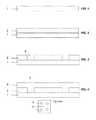
- FIG. 1shows a cross-sectional view of an example substrate used in an example method for manufacturing an electronic structure.
- FIG. 2shows a cross-sectional view of an example structure formed in an example process for manufacturing an electronic structure.
- FIG. 3shows a cross-sectional view of another example structure formed in an example process for manufacturing an electronic structure.
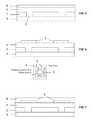
- FIG. 4shows cross-sectional and top views of another example structure formed in an example process for manufacturing an electronic structure.
- FIG. 5shows a cross-sectional view of another example structure formed in an example process for manufacturing an electronic structure.
- FIG. 6shows cross-sectional and top views of another example structure formed in an example process for manufacturing an electronic structure.
- FIG. 7shows a cross-sectional view of another example structure formed in an example process for manufacturing an electronic structure
- FIG. 8shows cross-sectional and top views of another example structure formed in an example process for manufacturing an electronic structure
- FIG. 9shows a cross-sectional view of another example structure formed in an example process for manufacturing an electronic structure.
- FIG. 10shows a cross-sectional view of an example electronic structure formed in an example process.
- FIG. 11shows a cross-sectional view of another example electronic structure formed in an example process.
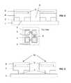
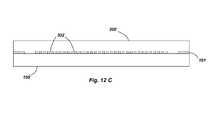
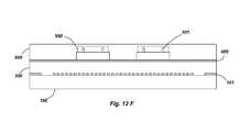
- FIG. 12A-12Lshow cross-sectional views of an example process for manufacturing of an electronic structure.
- FIG. 13shows an example substrate with a fabricated array of electronic structures.
- FIG. 14shows an example of the application of a removable medium to a substrate with a fabricated array of electronic structures.
- FIG. 15shows an example of the removal of an array of electronic structures from a substrate using a removable medium.
- FIG. 16shows an example of the exposure of a removable medium to an oxygen plasma.
- FIG. 17shows an example of the deposition of a metal followed by an oxide using a shadow mask.
- FIG. 18shows an example process for exposing an array of electronic structures, a medium, and a second substrate to an oxygen plasma.
- FIG. 19shows an example application of a removable medium and an array of electronic structures to a second substrate.
- FIG. 20shows an example of the removal of a removable medium from an array of electronic structures.
- the term “includes”means includes but not limited to, the term “including” means including but not limited to.
- the term “based on”means based at least in part on.
- any references to “top” surface and “bottom” surfaceare used primarily to indicate relative position, alignment and/or orientation of various elements/components with respect to the substrate and each other, and these terms do not necessarily indicate any particular frame of reference (e.g., a gravitational frame of reference).
- reference to a “bottom surface of a substrate”does not necessarily require that the indicated surface be facing a ground surface.
- a methodincludes providing a sacrificial layer on the supporting substrate, patterning trenches in the sacrificial layer, and providing a first encapsulating layer to support the array of electronic devices whereby the first encapsulating layer comes into contact with the supporting substrate via the trenches.
- An array of electronic devicesis fabricated on the first encapsulating layer.
- the array of electronic devicesare sealed with a second encapsulating layer.
- the sacrificial layeris removed by immersion in a suitable solvent.
- the encapsulated electronic devicescan remain adhered to the support substrate due to forces of adhesion between the encapsulating layer and the support substrate.
- the electronic structureis a flexible electronic structure.
- FIG. 1shows an example substrate that can be used to fabricate an example electronic structure.
- FIGS. 2 to 10show example structures that are formed in the fabrication of the example electronic structure.
- a first layer 2is applied to the substrate 1 .
- selected portions of the first layer 2are removed to provide a plurality of vias 6 that extend through the first polymer 2 layer substantially to the substrate 1 .
- a second polymer layer 4is applied to the first layer. As shown in the cross-sectional view of FIG. 4 , in an example, portions of the second polymer layer 4 can be caused to conform to a dimension of a number of the vias 6 and to form anchors 3 that contact at least a portion of the substrate 1 .
- a different polymer materialcan be caused to conform to a dimension of a number of the vias 6 and form the anchors 3 , and the second polymer layer 4 is disposed above the first layer 2 interspersed with the anchors 5 .
- the anchorscan be formed in a pattern.
- At least one electronic device layer 5is disposed on a portion of the second polymer layer.
- the electronic device layer 5may be subjected to further processing steps to fabricate differing types of electronic device components based on the at least one electronic device layer 5 .
- portions of the at least one electronic device layer 5can be removed, e.g., by an etching process, to form electronic device components.
- portions of the at least one electronic device layer 5may be positioned above the anchors 3 . As shown in FIG.
- a third polymer layer 8is applied to at least a portion of the at least one electronic device layer 5 .
- the second polymer layer 4 and the third polymer layer 8are selected so that they are more resistant to a selective etchant than the first layer 2 .
- the third polymer layeris the top layer of the electronic structure.
- the thickness of the third polymer layer(or, in an example, the top layer) is configured to cause the location of a resultant neutral mechanical plane of the electronic structure to correspond to strain-sensitive layers of the electronic structure.
- the neutral mechanical planeis a region of the electronic structure where a strain-sensitive layer can be isolated from stresses and strains applied to the electronic structure, e.g., from bending, rolling, or folding.
- the thickness of the third polymer layer (or, in an example, the top layer)can be selected such that the at least one electronic device layer is located at or near a neutral mechanical plane of the electronic structure.
- At least one trench 9is formed through the third polymer layer 8 and the second polymer layer 4 to expose at least a portion of the first layer 2 (see cross-sectional view of FIG. 8 ).
- the least one trench 9can be formed through sections of the structure that does not include portions of the electronic device layer 5 .
- the at least one trench 9may be formed through sections of the structure that include portions of the electronic device layer 5 .
- the at least one trench 9can be formed through portions of the electronic device layer 5 that are not functional or structural components of the electronic device.
- FIG. 8can be exposed to the selective etchant to provide the structure of FIG. 9 .
- portions of the first layer that are exposed to the selective etchant through the trench 9may be selectively removed by the selective etchant.
- the anchors 3remain in contact with the substrate 1 after the etching using the selective etchant.
- FIG. 9shows an example of an electronic structure 10 that can be formed according to the methods described herein.
- the electronic structure 10can be a flexible electronic structure.
- the flexible electronic structurecan include an integrated circuit, a semiconductor, a transistor, a diode, a logic gate, arrays of electronic components, an optical system, a temperature sensors, a pressure sensor, electrical-conductivity sensors, electrodes for pH sensors, chemical sensors, sensors for enzymatic activity, resistors, capacitors, passive devices, light emitting diodes (LEDs), photodiodes (PDs), photodetectors, a battery, a transducer, an emitter, a receiver, or a transceiver.
- LEDslight emitting diodes
- PDsphotodiodes
- the at least one electronic device layerincludes at least one of a multifunctional sensor (including a temperature, strain, and/or electrophysiological sensor), a microscale light-emitting diode (LED), an active to passive circuit elements (including a transistor, a diode, a resistor, and/or a memristor), wireless power coils, and devices for radio frequency (RF) communications (including a high-frequency inductor, capacitor, oscillator, and/or antenna).
- the active elements of the at least one electronic device layercan include electronic materials such as silicon and gallium arsenide in the form of filamentary serpentine nanoribbons and micro- and nano-membranes.
- the at least one electronic device layerincludes may be configured to provide solar cells and/or wireless coils to serve as a power supply.
- the electronic structures hereinwhich can include interconnects, can exhibit ultrathin layouts, and employ neutral mechanical plane configurations and optimized geometrical designs.
- the electronic structure 10is contacted with the substrate 1 via the anchors 3 .
- the electronic structure 10is separated from the substrate 1 .
- the electronic structure 10may be removed using a removable medium.
- the electronic device layer 5may be formed with multiple layers, including several layers and/or several portions of metal, electronic devices, polymers, semiconductor material, dielectric material, and any other material used for creating electronic devices.
- a multiple layered electronic device layer 5 acan be fabricated above the second polymer layer 4 .
- the different layers of the electronic device layer 5 acan be connected by conduits 7 .
- the conduits 7may be created using any applicable technique in the art, including an oxygen plasma etch.
- the oxygen plasma etchcan be an oxygen reactive ion etch.
- the third polymer layer 8can be applied to the electronic device layer 5 a .
- the third polymer layer 8can be applied through spin coating.
- other techniquesincluding, e.g., spray coating, lamination, casting, or vapor deposition may be used to apply the third polymer layer.
- a conduit 7also can be formed in the third polymer layer 8 .
- at least one trenchcan be formed in structures of FIGS. 10 and 11 to expose at least one portion of the first layer, and a selective etchant can be used to remove the remaining portions of the first layer, forming an electronic structure that is in contact with the substrate 1 .
- the electronic structuremay be removed using a removable medium.
- the first polymer 2is a sacrificial release layer. Removal of the sacrificial release facilitates the fabrication of the electronic structure.
- the electronic structure 10is a stretchable electronic system. In the manufacture of a stretchable electronic system, deformable electronics can fabricated initially in a planar format and are released from the original substrate 1 by an etch process. This etch process can be difficult to control and may lead to loss of electronic arrays that may float away in the etchant, and become twisted, tangled or broken as a result. The processes, systems and devices described herein can prevent this loss of devices by preventing over etching.
- the anchors 3can be created from portions of the second polymer layer 4 or can be formed from a different polymer material.
- the second polymer layer 4can be an electric/electronic array encapsulation.
- the anchors 3provide enough adhesion to keep the stretchable electronic system arrays attached to the support substrate 1 when the sacrificial layer is removed.
- the stretchable electronic system arraysmay be readily separated from the support substrate 1 when an external force is applied (as a non-limiting example, a force applied by elastomeric transfer stamp as disclosed in United States Published Patent Application No. 20090199960 entitled “Pattern Transfer Printing by Kinetic Control of Adhesion to an Elastomeric Stamp” filed Jun. 9, 2006, which is incorporated herein by reference it is entirety).
- vias 6are patterned in the sacrificial layer 2 prior to fabrication of the electronic device layer 5 .
- the vias 6may begin at the surface of the sacrificial layer and end at the interface with the support substrate 1 .
- the support substrate 1may be a silicon wafer in an example.
- a non-limiting example of a suitable material to form a first layer, and in some examples, to serve as a sacrificial layer,is polymethylmethacrylate (PMMA).
- the first layeris formed from silicon dioxide, chromium, or titanium.
- a non-limiting example of a suitable material to form a second polymer layer, and in some examples, to serve as an encapsulation layeris polyimide.
- the second polymer layercan be formed from polyethylene naphthalate, polybenzobisoxazole, benzocyclobutene, siloxane, or a liquid crystal polymer
- the Young's modulus of the substratecan be greater than that of the first layer (e.g., PMMA with a Young's modulus of 1800-3100 MPa) and the second polymer layer (e.g., polyimide with a Young's modulus of 2.5 GPa).
- the first layere.g., PMMA with a Young's modulus of 1800-3100 MPa
- the second polymer layere.g., polyimide with a Young's modulus of 2.5 GPa
- the PMMAcan be selectively etched in acetone without affecting the polyimide.
- the vias 6may be etched into the first layer of the PMMA by using an oxygen plasma etch through a stencil hardmask or a photolithographically patterned mask.
- Other applicable techniques in the artcan be used to pattern the PMMA to form the vias 6 . For example, direct exposure with a 220-250 nm wavelength laser light source through a mask followed by development (e.g., in a solvent).
- the vias 6provide a path for the second polymer layer 4 material, e.g., the encapsulation layer material (including a polyimide) to come in contact with the support substrate 1 , creating the anchors 6 .
- the anchors 6provide the anchoring force to retain the electronic structure substantially in contact with the substrate during the release step.
- the second polymer material(the encapsulation material) is spun-on.
- the second polymer material(the encapsulation material) may be deposited by spray coating or vapor deposition.
- the vias or anchorsmay be in any two-dimensional geometry. As a non-limiting example, they can be formed as a circular cross-section, which may be easier to fabricate. Any other cross-sectional geometry of the vias or anchors is within the scope of this disclosure, such as but not limited to a hexagonal, oval or rectangular cross-section, or any polygonal or non-polygonal shape. In an example, the diameter of this circular cross-section can be between about 10 ⁇ m and about 50 ⁇ m. In an example, the width of the vias (or anchors) is selected such that the anchors provide sufficient adhesive force with the substrate to not separate during the etching of the first layer.
- the width of the vias (or anchors)also can be selected such that the anchors do not generate an adhesive force that prevents the array of electronics structure from being separated from the substrate, such as but not limited to in a transfer printing step, after the sacrificial release layer is removed.
- the range of the width of the vias or anchorscan be between about 10 ⁇ m and about 50 ⁇ m, smaller diameters and larger diameters can be used.
- the width of the vias or anchorscan be selected based on the adhesive strength between the material of the anchor (such as but not limited to polyimide) and the substrate (such as but not limited to silicon). In an example, the width of the vias or anchors can range from about 0.1 ⁇ m to about 1000 ⁇ m.
- the spacing of the vias or anchorsalso can be selected based on the intended adhesive strength between the anchors and the substrate.
- the number and spacing of vias or anchorscan be determined based on the adhesive force to maintain the geometry of the array of electronic structures, and to substantially prevent distorting during the etching to remove the first layer (e.g., a sacrificial release layer).
- the number and spacing of vias or anchorsis determined such that the total adhesive force of the anchors does not prevent separation of the array of electronic structures from the substrate, e.g., in a later transfer printing after the sacrificial etch.
- the vias or anchorscan depend on the geometry of the array of electronic structures (including on the geometry of the array of electronic device layer 5 ). As a non-limiting example, the vias or anchors may be placed along the pattern of interconnected device islands. In an example, the vias or anchors can have a pitch between about 50 ⁇ m and about 1000 ⁇ m, i.e., they vias or anchors can be spaced apart by an average distance of between about 50 ⁇ m and about 1000 ⁇ m. In another example, the vias or anchors can be spaced apart by an average distance (a pitch) of between about 0.2 ⁇ m and about 10000 ⁇ m.
- the vias or anchorsare cylindrical in shape, have a diameter of about 50 ⁇ m, and are spaced apart with spacing (a pitch) ranging from about 200 ⁇ m to about 800 ⁇ m. These anchors may be positioned along the pattern of interconnected device islands.
- a second polymer layer materialWhen a second polymer layer material is deposited onto the first layer, it can conform to the dimensions of the vias and contact the support substrate to form the anchor 3 (see, for example, FIG. 4 ). Any number of metal, semiconductor, dielectric, and device layers can be disposed above the second polymer layer of the second polymer layer using any applicable technique in the art.
- a third polymer layer 8may be disposed above the electronic device layer 5 .
- the third polymer layer 8may be an encapsulation layer that protects the electronic device layer 5 during a later etching process or other processing.
- the at least one electronic device layer 5is formed a multiple electronic device layers. Each of the multiple electronic device layers can include electronic devices and electronic device components.
- conduits 7may be formed, e.g., by etching, and used to create contact pads to the functional portions of at least one of the electronic device layers.
- a maskmay be deposited onto the topmost layer of the electronic structure before further processing.
- the maskis created using a photolithographic patterning and etching process.
- the maskis an oxide layer.
- the maskcan be used to control the further processing.
- the maskcan be used to prevent over-etching of an encapsulant polymer region that is being used to protecting the electronic devices and interconnects of the at least one electronic device layer 5 .
- an adhesion-promoting layercan be included between the first layer and the substrate (e.g., when it is used as a sacrificial layer).
- the first layeris PMMA
- adhesion-promoting layercan be included between the PMMA and the substrate to ensure adequate bonding of the PMMA to the substrate.
- the substrateis a Si support substrate.
- the vias patterned into the PMMAmay distort.
- the width of the vias in the PMMAmay expand by a factor of about 5 to about 10 when the second polymer layer material is subjected to further processing.
- the coefficient of thermal expansion of PMMAis higher than polyimide or silicon; therefore it may undergo greater dimensions or volume changes than the polyimide or the silicon with temperature. As a result, portions of the structure may delaminate from the silicon substrate.
- the second polymer layeris a polyimide encapsulation layer
- the viasare formed in PMMA
- curing the polyimidee.g., at greater than 140° C., and more typically about 200-250° C.
- the adhesion-promoting layercan be formed from hexamethyldisilazane (HMDS).
- the second layeris cured at a higher temperature than the first layer
- precautionscan be taken to avoid out gassing, which can induce roughness in the encapsulating layer.
- polyimidewhich can be used to form the second polymer layer
- PMMAwhich can be used to form the first layer
- the first layer firstmay be cured at the cure temperature of the second polymer layer to evolve the more volatile components that may evaporate at the higher temperature. As a result, little or no out-gassing can occur from the first layer.
- a slow ramped bakinge.g., about 100° C. per hour
- the cure temperature of the second polymer layere.g., 250° C. for polyimide
- the first layercan then be removed using a selective etchant.
- the selective etchantis selected such that the other polymer materials in the structure are more resistant to the selective etchant than the first layer.
- the selective etchantcan be a solvent, a mixture of solvents, a plasma technique, or any other applicable technique in the art that can be used to selectively remove the first layer.
- the selective etchantcan include hydroflouric acid.
- the selective etchantcan include cerric ammonium nitrate.
- the selective etchantcan include hydroflouric acid or hydrochloric acid.
- the structurescan be subjected to a longer process for removing the first layer.
- the structuresmay be left in a release bath for a long time the array of electronic structures being separated from the substrate or losing registration with the substrate.
- This process of preparing flexible electronics structureswhich in an example includes stretchable electronics structures, is suited for subsequent transfer printing using any applicable technique in the art.
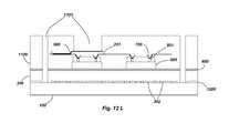
- FIGS. 12A-12Lshow another non-limiting example process for fabricating an array of electronic structures on a substrate.
- a first layer 101is applied to a substrate 100 .
- An example of the first layercan be a PMMA sacrificial layer.
- the first layer 101can be patterned using any number of techniques in the art and depending on the type of material in the first layer. The patterning facilitates the selective removal of portions of the first layer to form the vias 201 (shown in FIG. 12 B).
- the vias 201may be formed in the PMMA using an oxygen plasma etch through a stencil hardmask or a photolithographically patterned mask.
- the vias 201can extend substantially from a surface of the first layer to the substrate 100 .
- the second polymer layercan be applied such that it substantially fills a number of the vias 201 and make contact with the substrate 100 .
- the size (i.e., cross-sectional width) and density (based on the average spacing) of the viascan be varied to derive the desired degree of adhesion of formed anchors to the substrate.
- the degree of adhesioncan be selected such that the array of electronic structures maintain contact with the surface during removal of the first layer.
- a second polymer layer(e.g., of an encapsulating polymer 300 ) can be applied to the structure.
- the second polymer materialis applied to fill a number of the vias 201 and create anchors 302 (shown in FIG. 12C ).
- the second polymer layeris applied through spin coating.
- other techniquesincluding, e.g., spray coating, lamination, casting, or vapor deposition may be used to apply the second polymer layer.
- the second polymer layercan be applied such that it conforms to a dimension of the vias, including filling the width and/or depth of the vias, to forming anchors 302 in contact with the substrate.
- At least one electronic device layerincluding any number of metal, semiconductor, dielectric, and device layers, can be disposed on top of the second polymer layer. The topmost electronic device layer may be protected by a third polymer layer.
- the vias 201 or anchors 302may be in any two-dimensional geometry.
- the vias 201may be formed in a two-dimensional grid pattern. Other patterns of arrangement of the vias are applicable.
- the vias 201 or anchors 302may be formed with a circular cross-section for easier fabrication, but any other cross-sectional geometry is within the scope of this disclosure.
- the diameter of the vias 201 or anchors 302can be between about 10 ⁇ m and about 50 ⁇ m.
- the width of the vias 201 (or anchors 302 )is selected such that the anchors 302 provide sufficient adhesive force with the substrate 100 to not separate during the etching of the first layer.
- the width of the vias 201also can be selected such that the anchors 302 do not generate an adhesive force that prevents the array of electronics structures from being separated from the substrate after the sacrificial release layer is removed.
- the further processingcan be, but not limited to, transfer printing step.
- the width of the vias 201 (or anchors 302 )can be selected based on the adhesive strength between the material of the anchor 302 and the material of the substrate 100 .
- the width of the vias 201 (or anchors 302 )can range from about 0.1 ⁇ m to about 1000 ⁇ m.
- the spacing of the vias 201also can be selected based on the intended adhesive strength between the anchors 302 and the substrate 100 .
- the number and spacing of vias 201 (or anchors 302 )can be selected to provide sufficient adhesive force to maintain the geometry of the array of electronic structures, and to substantially prevent distortion during removal of the first layer 101 .
- the number and spacing of vias 201 (or anchors 302 )is determined such that the total adhesive force of the anchors 302 does not impede separation of the array of electronic structures from the substrate 100 .
- the pattern and placement of the vias 201 (or anchors 302 )can depend on the geometry of the array of electronic structures.
- the vias 201may be placed along the pattern of interconnected device islands.
- the vias 201may be spaced apart (i.e., have a pitch) by an average distance of between about 50 ⁇ m and about 1000 ⁇ m.
- the vias 201may be spaced apart by an average distance of between about 0.2 ⁇ m and about 10000 ⁇ m.
- the vias 201are cylindrical in shape, have a diameter of about 50 ⁇ m, and are spaced apart with spacing ranging from about 200 ⁇ m to about 800 ⁇ m.
- an adhesion-promoting layermay be applied to ensure adequate bonding of the first layer 101 to the substrate 100 .
- the adhesion-promoting layercan be formed from a polymeric material.
- the adhesion-promoting layercan be formed from hexamethyldisilazane (HMDS).
- the first layercan be cured at the cure temperature of the second polymer layer material prior to application of the second polymer layer.
- an adhesive layer 400can be applied to prior to disposing the electronic device layer above the first layer and the second polymer layer.
- the adhesive layermay be formed from a dilute polyimide or a similar polymeric material.
- the adhesive layer 400may be applied by a spin-coating or spray coating.
- Adhesive layer 400assists in securing components of the at least one electronic device layer.
- adhesive layer 400assists in securing components 500 .
- the structuremay be cured to set the placement of the components 500 .
- the at least one electronic device layercan include a metal, a semiconductor, a dielectric, a micro electro mechanical system (MEMS) component, and any other device component.
- FIGS. 12E to 12Jshow cross-sectional views of the structure as different electronic device layers are disposed on the structure.
- the electronic device layersinclude device islands 500 (with electronic component 501 ), interconnects 701 , and contacts 900 .
- layers 600 and 800 of an encapsulant materiale.g., a polymer layer or an oxide layer, may be applied in regions of the electronic device layer prior to disposing another component of the layer. Layers 600 and 800 also may be used to planarize portions of the electronic device layer prior to addition of other components of the electronic device layer.
- An oxide or polymer layersuch as layer 600 or layer 800 , can be deposited prior to photolithographic patterning and etching, or other processing.
- the oxide or polymer layerhelps to control the etch process and prevents over etching of the encapsulating regions of the electronic device layer, thus protecting the electronic devices and interconnects that are part of the electronic device layer.
- FIGS. 12F and 12Hspecific portions of the polymer can be removed to allow for fabrication of device interconnects.
- an etching techniquesuch as oxygen plasma etching
- electrical vias 700can be created in polymer layer 800 . These electrical vias 700 can be used to expose a bare conductive pad 501 of a component. Once the conductive pads 501 are exposed, the interconnects 701 can be deposited using any applicable technique in the art, including physical vapor deposition, lithography, etching, plating, and direct platting.
- FIGS. 12H to 121show the multilevel interconnects that can be created in an electronic device layer by applying additional layers of polymer 800 , creating electrical vias 700 , and then depositing electrical interconnects 701 . The process of applying additional layers of electrical interconnects may be repeated as many times as needed to fully interconnect the components of the at least one electronic device layers.
- polymer layer 1000may be applied.
- polymer layer 1000can be the third polymer layer.
- Polymer layer 1000can serve to encapsulate the at least one electronic device layers.
- trenches 1101can be created in polymer layer 1000 to provide access to the contact pads and facilitate segmentation.
- trenches 1101may be created by lithography and etching, using laser ablation, by mechanical cutting or using pure photopatterning.
- trenches 1101could be created by photodefining one or more layers as the system is additively manufactured.
- the segmentation process, creating trenches 1101allows for direct access of the selective etchant to the first layer 101 .
- the etching time to remove the first layermay be greatly reduced by creating multiple access holes (including other trenches) throughout the device.
- the selective etchantcan act to remove remaining portions of the first layer. This results in cavities 1200 being formed beneath the electronic structure and exposing the anchors 302 (see FIG. 12L ).
- the selective etchantremoves much of the remaining portions of the first layer without harming the materials exposed in the electronic structure.
- hot acetonecan be used as the selective etchant to effectively separate the electronic structure (i.e., the encapsulated devices) from the substrate.
- the anchors 302remain substantially undisturbed and effectively maintain the encapsulated electronic devices in substantially the same position relative to each other and to the substrate.
- Transfer printingmay be performed using any applicable technique in the art to separate the electronic structure described herein from the substrate after removal of the remaining portions of the first layer.
- the transfer printingcan be performed using a removable medium, including an elastomeric stamp or cylinder, a selectively adhesive tape, or a tape that can be removed, after transfer, with an oxygen plasma etch, UV light, application of heat, or dissolving in a solvent or mixture of solvents (including water).
- regions of the electronic structure where large bulk areas of the polymer layer are in contact with the substratemay not be removed during a transfer process.
- the transfer printingcan be performed to transfer the arrays of the electronic structures from one substrate to another, e.g, from a carrier substrate to a final device substrate.
- the arrays of the electronic structuresmay be fabricated on a rigid substrate and then transferred using transfer printing to a soft, flexible, and or stretchable substrate (including polydimethylsiloxane (PDMS,), ECOFLEX® (BASF Chemical Company, Florham Park, N.J.), or any other elastomer, rubber, plastic, fabric or polymer material).
- the transfer processmay introduce additional defects (including breakage and incomplete transfer), resulting in low yield.
- the operationcan be sensitive to differences in the adhesive forces between the array-to-stamp interface and the anchor-to-substrate interface.
- transferring the array from the stamp to the second (stretchable) substratemay require that the adhesive forces for the array-to-second substrate contact are greater than the forces at the array-to-stamp contact.
- the stamp-to-second substrate adhesive forcescan be small enough to remove the stamp without damaging the second substrate.
- Covalent bonding forcesmay be used between a silicon dioxide layer on the array and an oxygen-terminated surface of the second (stretchable) substrate to obtain a strong bond for device mechanical durability. This process can result in the stamp becoming too strongly bonded to the second (stretchable) substrate, and as a result, removing the stamp can damage the array.
- a removable mediumcan be used to separate the array of electronic structure from the support substrate.
- the removable mediumcan present a large adhesion force.
- the removable medium to array adhesive forcescan be greater than the pattern to substrate forces. Therefore, the removable medium can be used to separate the array from the substrate.
- the removable mediumis a water-dissolvable medium, it can be dissolved in water. Therefore, the second transfer process (i.e., from removable medium to ECOFLEX® substrate may not depend on any difference in forces whatsoever.
- a strong bondi.e., oxygen bonding as described above
- the removable mediumis removed easily and substantially without residue, using only water regardless of the strength of the removable medium to second substrate bond strength.
- the arrays of the electronic structuresmay be removed from the substrate using a removable medium.
- the removable mediummay be a selectively adhesive tape, a tape that can be removed by exposure to UV light, with application of heat, using an oxygen plasma etch, or by dissolving in a solvent or mixture of solvents (including water).
- the removable mediummay be an elastomeric stamp or cylinder.
- the removable mediumis a water-dissolvable tape.
- the electronic structuresare separated from the substrate by applying a removable medium on a portion of the top layer of the electronic structure, and applying a force to the removable medium to separate the anchors of the electronic structure from the substrate.
- the removable mediumcan be selected such that its adhesion strength to the top layer of the electronic structure is greater than the adhesion strength of the anchors to the substrate.
- FIGS. 13-20show non-limiting examples of the use of a removable medium.
- FIG. 13shows an array of electronic structures 1303 that are formed according to a principle herein. Anchors 1304 of an array of the electronic structures 1303 maintains contact with a substrate 1200 .
- the array of the electronic structures 1303can include electronic device layers 1302 encapsulated in a polymer 1301 .
- a removable medium 1400 with an adhesive layer 1401is applied to the arrays of the electronic structures (as shown in FIG. 14 ). After securing the removable medium 1400 to the array of electronic structures 1400 , force is applied to the removable medium to detach the array of electronic structures from the substrate (as shown in FIG. 15 ).
- a removable medium 1400can be selected based on its adhesion characteristics for a specific layer material. For example, removable medium 1400 can be selected based on its adhesion characteristics such that the removable medium to electronic structure adhesion force is greater than the anchors to substrate force.
- the arrays of electronic structures 1303may be removed from the substrate, and remain contacted with the removable medium 1400 , without causing defects in the electronic devices of the electronic structure or causing breakage.
- the removable medium 1400 and the electronic structures 1303can be exposed to an oxygen plasma to remove the portions of the adhesive layer 1401 from the areas not covered by the arrays of the electronic structures 1303 .
- the oxygen plasmacan be applied at a 40-sccm oxygen flow rate, with 100-W rf power, and a 30-sec treatment.
- the oxygen plasmaremoves the portions of the adhesive layer 1401 that are not contacting the electronic structure 1303 .
- a metal layer and/or an oxide layermay be deposited on the electronic structure.
- the metal layeris a 3-nm Titanium layer
- the oxide layeris a 30-nm SiO 2 layer.
- the metal layer and/or oxide layercan be evaporated onto the surface of the arrays of the electronic structures 1303 that is away from the removable medium 1400 .
- a shadow mask 1601is used to confine the evaporation to solely the arrays of the electronic structures.
- the removable medium 1400 , arrays of the electronic structures 1303 , and a second substrate 1700are exposed to an oxygen plasma to create highly oxygen-terminated surfaces.
- the oxygen plasmais applied at a 40-sccm oxygen flow rate, and using 100-W rf power, for a 30-sec treatment.
- the second substrate 1700may be a flexible material or a stretchable material.
- the second substrate 1700can be a polymer, including but not limited to ECOFLEX®.
- the highly oxygen-terminated surface of the second surfaceis contacted with the highly oxygen-terminated surface of the electronic structure, to provide a component 1800 .
- a pressureis applied to ensure contact between second substrate 1700 and the electronic structures 1303 .
- FIG. 20shows an example of the removal of the removable medium 1400 .
- the removable medium 1400is a water-dissolvable tape.
- the arrays of the electronic structures 1303 , the removable medium 1400 , and the second substrateare placed in a containment vessel 901 with 100° C. water 900 for 30 minutes.
- exposure of the removable medium to waterdissolves the removable medium and removes any residue left on the arrays of the electronic structures.
- a non-limiting example of a process for fabricating an electronic structure that is contacted to a substrate using anchorsis as follows:
- inventive embodimentsare presented by way of example only and that, within the scope of the appended claims and equivalents thereto, inventive embodiments may be practiced otherwise than as specifically described and claimed.
- inventive embodiments of the present disclosureare directed to each individual feature, system, article, material, kit, and/or method described herein.
- various aspects of the inventionmay be embodied at least in part as a computer readable storage medium (or multiple computer readable storage media) (e.g., a computer memory, one or more floppy disks, compact disks, optical disks, magnetic tapes, flash memories, circuit configurations in Field Programmable Gate Arrays or other semiconductor devices, or other tangible computer storage medium or non-transitory medium) encoded with one or more programs that, when executed on one or more computers or other processors, perform methods that implement the various embodiments of the technology described above.
- the computer readable medium or mediacan be transportable, such that the program or programs stored thereon can be loaded onto one or more different computers or other processors to implement various aspects of the present technology as described above.
- programor “software” are used herein in a generic sense to refer to any type of computer code or set of computer-executable instructions that can be employed to program a computer or other processor to implement various aspects of the present technology as described above. Additionally, it should be appreciated that according to one aspect of this embodiment, one or more computer programs that when executed perform methods of the present technology need not reside on a single computer or processor, but may be distributed in a modular fashion amongst a number of different computers or processors to implement various aspects of the present technology.
- Computer-executable instructionsmay be in many forms, such as program modules, executed by one or more computers or other devices.
- program modulesinclude routines, programs, objects, components, data structures, etc. that perform particular tasks or implement particular abstract data types.
- functionality of the program modulesmay be combined or distributed as desired in various embodiments.
- the technology described hereinmay be embodied as a method, of which at least one example has been provided.
- the acts performed as part of the methodmay be ordered in any suitable way. Accordingly, embodiments may be constructed in which acts are performed in an order different than illustrated, which may include performing some acts simultaneously, even though shown as sequential acts in illustrative embodiments.
- a reference to “A and/or B”, when used in conjunction with open-ended language such as “comprising”can refer, in one embodiment, to A only (optionally including elements other than B); in another embodiment, to B only (optionally including elements other than A); in yet another embodiment, to both A and B (optionally including other elements); etc.
- the phrase “at least one,” in reference to a list of one or more elements,should be understood to mean at least one element selected from any one or more of the elements in the list of elements, but not necessarily including at least one of each and every element specifically listed within the list of elements and not excluding any combinations of elements in the list of elements.
- This definitionalso allows that elements may optionally be present other than the elements specifically identified within the list of elements to which the phrase “at least one” refers, whether related or unrelated to those elements specifically identified.
- “at least one of A and B”can refer, in one embodiment, to at least one, optionally including more than one, A, with no B present (and optionally including elements other than B); in another embodiment, to at least one, optionally including more than one, B, with no A present (and optionally including elements other than A); in yet another embodiment, to at least one, optionally including more than one, A, and at least one, optionally including more than one, B (and optionally including other elements); etc.
Landscapes
- Engineering & Computer Science (AREA)
- Microelectronics & Electronic Packaging (AREA)
- Power Engineering (AREA)
- Computer Hardware Design (AREA)
- General Physics & Mathematics (AREA)
- Condensed Matter Physics & Semiconductors (AREA)
- Physics & Mathematics (AREA)
- Manufacturing & Machinery (AREA)
- Structure Of Printed Boards (AREA)
- Thin Film Transistor (AREA)
- Micromachines (AREA)
- Electroluminescent Light Sources (AREA)
- Internal Circuitry In Semiconductor Integrated Circuit Devices (AREA)
Abstract
Description
- Embedding active devices
- Multiple layers of interconnects
Claims (54)
Priority Applications (1)
| Application Number | Priority Date | Filing Date | Title |
|---|---|---|---|
| US14/819,040US9723711B2 (en) | 2011-05-27 | 2015-08-05 | Method for fabricating a flexible electronic structure and a flexible electronic structure |
Applications Claiming Priority (3)
| Application Number | Priority Date | Filing Date | Title |
|---|---|---|---|
| US201161490826P | 2011-05-27 | 2011-05-27 | |
| US13/481,843US9159635B2 (en) | 2011-05-27 | 2012-05-27 | Flexible electronic structure |
| US14/819,040US9723711B2 (en) | 2011-05-27 | 2015-08-05 | Method for fabricating a flexible electronic structure and a flexible electronic structure |
Related Parent Applications (1)
| Application Number | Title | Priority Date | Filing Date |
|---|---|---|---|
| US13/481,843ContinuationUS9159635B2 (en) | 2011-05-27 | 2012-05-27 | Flexible electronic structure |
Publications (2)
| Publication Number | Publication Date |
|---|---|
| US20150342036A1 US20150342036A1 (en) | 2015-11-26 |
| US9723711B2true US9723711B2 (en) | 2017-08-01 |
Family
ID=47260237
Family Applications (2)
| Application Number | Title | Priority Date | Filing Date |
|---|---|---|---|
| US13/481,843ActiveUS9159635B2 (en) | 2011-05-27 | 2012-05-27 | Flexible electronic structure |
| US14/819,040Active2032-06-12US9723711B2 (en) | 2011-05-27 | 2015-08-05 | Method for fabricating a flexible electronic structure and a flexible electronic structure |
Family Applications Before (1)
| Application Number | Title | Priority Date | Filing Date |
|---|---|---|---|
| US13/481,843ActiveUS9159635B2 (en) | 2011-05-27 | 2012-05-27 | Flexible electronic structure |
Country Status (5)
| Country | Link |
|---|---|
| US (2) | US9159635B2 (en) |
| EP (1) | EP2712491B1 (en) |
| JP (4) | JP2014523633A (en) |
| KR (1) | KR102000302B1 (en) |
| WO (1) | WO2012166686A2 (en) |
Cited By (20)
| Publication number | Priority date | Publication date | Assignee | Title |
|---|---|---|---|---|
| US20170271398A1 (en)* | 2016-03-18 | 2017-09-21 | Samsung Display Co., Ltd. | Stretchable display apparatus |
| USD825537S1 (en) | 2014-10-15 | 2018-08-14 | Mc10, Inc. | Electronic device having antenna |
| US10186546B2 (en) | 2008-10-07 | 2019-01-22 | Mc10, Inc. | Systems, methods, and devices having stretchable integrated circuitry for sensing and delivering therapy |
| US10258282B2 (en) | 2013-11-22 | 2019-04-16 | Mc10, Inc. | Conformal sensor systems for sensing and analysis of cardiac activity |
| US10277386B2 (en) | 2016-02-22 | 2019-04-30 | Mc10, Inc. | System, devices, and method for on-body data and power transmission |
| US10296819B2 (en) | 2012-10-09 | 2019-05-21 | Mc10, Inc. | Conformal electronics integrated with apparel |
| US10325951B2 (en) | 2008-10-07 | 2019-06-18 | Mc10, Inc. | Methods and applications of non-planar imaging arrays |
| US10334724B2 (en) | 2013-05-14 | 2019-06-25 | Mc10, Inc. | Conformal electronics including nested serpentine interconnects |
| US10383219B2 (en) | 2008-10-07 | 2019-08-13 | Mc10, Inc. | Extremely stretchable electronics |
| US10447347B2 (en) | 2016-08-12 | 2019-10-15 | Mc10, Inc. | Wireless charger and high speed data off-loader |
| US10673280B2 (en) | 2016-02-22 | 2020-06-02 | Mc10, Inc. | System, device, and method for coupled hub and sensor node on-body acquisition of sensor information |
| US10986465B2 (en) | 2015-02-20 | 2021-04-20 | Medidata Solutions, Inc. | Automated detection and configuration of wearable devices based on on-body status, location, and/or orientation |
| US11154235B2 (en) | 2016-04-19 | 2021-10-26 | Medidata Solutions, Inc. | Method and system for measuring perspiration |
| WO2022197747A1 (en)* | 2021-03-15 | 2022-09-22 | SDK New Materials, Inc. | Encapsulated electronic device with improved protective barrier layer and method of manufacture thereof |
| US11529801B2 (en)* | 2018-04-28 | 2022-12-20 | Chengdu Boe Optoelectronics Technology Co., Ltd. | Method of fabricating stretchable electronic device, stretchable electronic device, and stretchable display apparatus |
| US11660005B1 (en) | 2021-06-04 | 2023-05-30 | Huxley Medical, Inc. | Processing and analyzing biometric data |
| US11717221B1 (en) | 2020-03-11 | 2023-08-08 | Huxley Medical, Inc. | Patch for improved biometric data capture and related processes |
| US12109010B1 (en) | 2021-08-24 | 2024-10-08 | Huxley Medical, Inc. | Photoplethysmography sensors and processes |
| US12114980B1 (en) | 2021-08-24 | 2024-10-15 | Huxley Medical, Inc. | Photoplethysmography sensors and processes |
| US12178552B1 (en) | 2021-06-04 | 2024-12-31 | Huxley Medical, Inc. | Systems and processes for detecting oxygen saturation and compensating for skin tone variation |
Families Citing this family (73)
| Publication number | Priority date | Publication date | Assignee | Title |
|---|---|---|---|---|
| US8886334B2 (en) | 2008-10-07 | 2014-11-11 | Mc10, Inc. | Systems, methods, and devices using stretchable or flexible electronics for medical applications |
| US9119533B2 (en) | 2008-10-07 | 2015-09-01 | Mc10, Inc. | Systems, methods, and devices having stretchable integrated circuitry for sensing and delivering therapy |
| JP5646492B2 (en) | 2008-10-07 | 2014-12-24 | エムシー10 インコーポレイテッドMc10,Inc. | Stretchable integrated circuit and device with sensor array |
| US9545216B2 (en) | 2011-08-05 | 2017-01-17 | Mc10, Inc. | Catheter balloon methods and apparatus employing sensing elements |
| WO2011041727A1 (en) | 2009-10-01 | 2011-04-07 | Mc10, Inc. | Protective cases with integrated electronics |
| US9702839B2 (en) | 2011-03-11 | 2017-07-11 | Mc10, Inc. | Integrated devices to facilitate quantitative assays and diagnostics |
| JP2014523633A (en) | 2011-05-27 | 2014-09-11 | エムシー10 インコーポレイテッド | Electronic, optical and / or mechanical devices and systems and methods of manufacturing these devices and systems |
| US9757050B2 (en) | 2011-08-05 | 2017-09-12 | Mc10, Inc. | Catheter balloon employing force sensing elements |
| JP6129838B2 (en) | 2011-09-01 | 2017-05-17 | エムシー10 インコーポレイテッドMc10,Inc. | Electronic device that detects the condition of the tissue |
| JP6277130B2 (en) | 2011-10-05 | 2018-02-14 | エムシーテン、インコーポレイテッド | Medical device and method of manufacturing the same |
| US9226402B2 (en) | 2012-06-11 | 2015-12-29 | Mc10, Inc. | Strain isolation structures for stretchable electronics |
| US9247637B2 (en) | 2012-06-11 | 2016-01-26 | Mc10, Inc. | Strain relief structures for stretchable interconnects |
| US9168094B2 (en) | 2012-07-05 | 2015-10-27 | Mc10, Inc. | Catheter device including flow sensing |
| US9295842B2 (en) | 2012-07-05 | 2016-03-29 | Mc10, Inc. | Catheter or guidewire device including flow sensing and use thereof |
| US9171794B2 (en) | 2012-10-09 | 2015-10-27 | Mc10, Inc. | Embedding thin chips in polymer |
| DE102012110358B4 (en)* | 2012-10-30 | 2016-04-07 | Leibniz-Institut für Neurobiologie Magdeburg | Microelectrode array |
| US8921236B1 (en)* | 2013-06-21 | 2014-12-30 | Eastman Kodak Company | Patterning for selective area deposition |
| CA2920485A1 (en) | 2013-08-05 | 2015-02-12 | Mc10, Inc. | Flexible temperature sensor including conformable electronics |
| KR20160065948A (en) | 2013-10-07 | 2016-06-09 | 엠씨10, 인크 | Conformal sensor systems for sensing and analysis |
| CN105874606B (en) | 2014-01-06 | 2021-01-12 | Mc10股份有限公司 | Encapsulated conformal electronic systems and devices and methods of making and using the same |
| WO2015156891A2 (en)* | 2014-01-23 | 2015-10-15 | Arizona Board Of Regents, Acting For And On Behalf Of Arizona State University | Method of providing a flexible semiconductor device and flexible semiconductor device thereof |
| US10485118B2 (en) | 2014-03-04 | 2019-11-19 | Mc10, Inc. | Multi-part flexible encapsulation housing for electronic devices and methods of making the same |
| EP3117206A4 (en) | 2014-03-12 | 2017-11-15 | Mc10, Inc. | Quantification of a change in assay |
| TWI549259B (en)* | 2014-05-15 | 2016-09-11 | 國立清華大學 | Fully integrated active and passive integrated optical body in 矽 base integrated circuit and manufacturing method thereof |
| WO2016022906A1 (en)* | 2014-08-07 | 2016-02-11 | The Regents Of The University Of California | Flexible penetrating cortical multielectrode arrays, sensor devices and manufacturing methods |
| US9899330B2 (en) | 2014-10-03 | 2018-02-20 | Mc10, Inc. | Flexible electronic circuits with embedded integrated circuit die |
| US10297572B2 (en)* | 2014-10-06 | 2019-05-21 | Mc10, Inc. | Discrete flexible interconnects for modules of integrated circuits |
| US9433101B2 (en)* | 2014-10-16 | 2016-08-30 | International Business Machines Corporation | Substrate via filling |
| US9734779B2 (en) | 2015-02-12 | 2017-08-15 | Qualcomm Incorporated | Efficient operation of wearable displays |
| US9747015B2 (en)* | 2015-02-12 | 2017-08-29 | Qualcomm Incorporated | Efficient display of content on wearable displays |
| WO2016140961A1 (en) | 2015-03-02 | 2016-09-09 | Mc10, Inc. | Perspiration sensor |
| US10182284B2 (en)* | 2015-06-11 | 2019-01-15 | Facebook Technologies, Llc | Connector assembly for detachable audio system |
| WO2017015000A1 (en) | 2015-07-17 | 2017-01-26 | Mc10, Inc. | Conductive stiffener, method of making a conductive stiffener, and conductive adhesive and encapsulation layers |
| US10709384B2 (en) | 2015-08-19 | 2020-07-14 | Mc10, Inc. | Wearable heat flux devices and methods of use |
| US10393685B2 (en)* | 2015-08-19 | 2019-08-27 | Research Foundation Of The City University Of New York | Cell-on-chip stretchable platform for mammalian cells with integrated impedance spectroscpy technique |
| EP4079383A3 (en) | 2015-10-01 | 2023-02-22 | Medidata Solutions, Inc. | Method and system for interacting with a virtual environment |
| US10532211B2 (en) | 2015-10-05 | 2020-01-14 | Mc10, Inc. | Method and system for neuromodulation and stimulation |
| WO2017070030A1 (en) | 2015-10-21 | 2017-04-27 | Massachusetts Institute Of Technology | Nanowire fet imaging system and related techniques |
| FR3045935B1 (en)* | 2015-12-22 | 2018-02-16 | Commissariat A L'energie Atomique Et Aux Energies Alternatives | METHOD FOR MANUFACTURING A STACK OF ELECTRONIC DEVICES |
| US9853011B2 (en)* | 2016-03-29 | 2017-12-26 | Advanced Semiconductor Engineering, Inc. | Semiconductor package structure and method for manufacturing the same |
| WO2018013447A1 (en) | 2016-07-14 | 2018-01-18 | Lifelens Technologies, Llc | Thin film support structures |
| EP3515524B1 (en) | 2016-09-23 | 2020-12-30 | Heartware, Inc. | Blood pump with sensors on housing surface |
| US10418237B2 (en)* | 2016-11-23 | 2019-09-17 | United States Of America As Represented By The Secretary Of The Air Force | Amorphous boron nitride dielectric |
| US11138490B2 (en) | 2016-12-14 | 2021-10-05 | Ajay Khoche | Hierarchical combination of distributed statistics in a monitoring network |
| US10885420B2 (en) | 2016-12-14 | 2021-01-05 | Ajay Khoche | Package sealing tape types with varied transducer sampling densities |
| US10902310B2 (en) | 2016-12-14 | 2021-01-26 | Trackonomy Systems, Inc. | Wireless communications and transducer based event detection platform |
| US10445634B2 (en) | 2016-12-14 | 2019-10-15 | Trackonomy Systems, Inc. | Fabricating multifunction adhesive product for ubiquitous realtime tracking |
| US11003978B2 (en) | 2016-12-14 | 2021-05-11 | Ajay Khoche | Programmable network node roles in hierarchical communications network |
| WO2018213542A1 (en) | 2017-05-17 | 2018-11-22 | Apple Inc. | Wearable bands with embedded circuitry |
| US20190186041A1 (en) | 2017-12-20 | 2019-06-20 | International Business Machines Corporation | Three-dimensionally stretchable single crystalline semiconductor membrane |
| US10593827B2 (en) | 2018-01-24 | 2020-03-17 | X-Celeprint Limited | Device source wafers with patterned dissociation interfaces |
| CN108507678A (en)* | 2018-03-01 | 2018-09-07 | 东南大学 | A kind of adjustable ultraphotic spectrum detection chip of phasmon multi-resonant mechanism enhancing |
| KR102039990B1 (en) | 2018-03-15 | 2019-11-04 | 광주과학기술원 | Three-dimensional elctron device of polymer frame through organic solvent assisted plasticization and manufacturing method comprising the same |
| US11768262B2 (en) | 2019-03-14 | 2023-09-26 | Massachusetts Institute Of Technology | Interface responsive to two or more sensor modalities |
| WO2020247354A1 (en) | 2019-06-05 | 2020-12-10 | Trackonomy Systems, Inc. | Temperature monitoring in cold supply chains |
| US11328942B1 (en)* | 2019-09-10 | 2022-05-10 | Facebook Technologies, Llc | Liquid crystalline elastomer for pick and place of semiconductor devices |
| US11317516B2 (en) | 2019-09-13 | 2022-04-26 | Trackonomy Systems, Inc. | Roll-to-roll additive manufacturing method and device |
| JP2021097097A (en)* | 2019-12-16 | 2021-06-24 | 株式会社ジャパンディスプレイ | Flexible substrate |
| US11123011B1 (en) | 2020-03-23 | 2021-09-21 | Nix, Inc. | Wearable systems, devices, and methods for measurement and analysis of body fluids |
| US11864058B1 (en) | 2020-10-04 | 2024-01-02 | Trackonomy Systems, Inc. | Flexible tracking device for cables and equipment |
| EP4186053A4 (en) | 2020-07-24 | 2024-09-04 | Trackonomy Systems, Inc. | TEAR OFF TO POWER ON A WIRELESS NODE WITH MULTIPLE CUTOUTS FOR REUSE |
| US12124904B2 (en) | 2020-09-05 | 2024-10-22 | Trackonomy Systems, Inc. | Wireless sensor device with an attachable external sensor probe |
| US12047841B2 (en) | 2020-09-21 | 2024-07-23 | Trackonomy Systems, Inc. | Detecting special events and strategically important areas in an IoT tracking system |
| US11527148B1 (en) | 2020-10-04 | 2022-12-13 | Trackonomy Systems, Inc. | Augmented reality for guiding users to assets in IOT applications |
| US12051916B1 (en) | 2020-10-05 | 2024-07-30 | Trackonomy Systems, Inc. | Method for recharging wireless IOT devices and system thereof |
| WO2022126020A1 (en) | 2020-12-12 | 2022-06-16 | Trackonomy Systems, Inc. | Flexible solar-powered wireless communication device |
| US12225638B2 (en)* | 2021-02-12 | 2025-02-11 | William Marsh Rice University | Integrated microheater array for efficient and localized heating of magnetic nanoparticles at microwave frequencies |
| US11749668B2 (en)* | 2021-06-09 | 2023-09-05 | STATS ChipPAC Pte. Ltd | PSPI-based patterning method for RDL |
| US12350054B2 (en)* | 2021-06-24 | 2025-07-08 | City University Of Hong Kong | Stretchable and wearable wireless 3-leads ECG monitoring apparatus |
| JP7739964B2 (en) | 2021-11-17 | 2025-09-17 | 沖電気工業株式会社 | Method for manufacturing electronic structure and electronic circuit |
| JP2023123268A (en) | 2022-02-24 | 2023-09-05 | 沖電気工業株式会社 | Electronic structure and manufacturing method of electronic structure |
| CN114709711A (en)* | 2022-04-27 | 2022-07-05 | 福建慧芯激光科技有限公司 | Vertical cavity surface emitting laser epitaxial layer and bonding pad connecting structure and manufacturing method thereof |
| CN116281846B (en)* | 2023-05-12 | 2023-08-01 | 润芯感知科技(南昌)有限公司 | Semiconductor device and manufacturing method thereof |
Citations (217)
| Publication number | Priority date | Publication date | Assignee | Title |
|---|---|---|---|---|
| US3716861A (en) | 1971-03-22 | 1973-02-13 | J Root | Serpentine antenna mounted on a rotatable capacitive coupler |
| US3805427A (en) | 1972-12-18 | 1974-04-23 | H Epstein | Medical alarm bracelet |
| US4304235A (en) | 1978-09-12 | 1981-12-08 | Kaufman John George | Electrosurgical electrode |
| US4416288A (en) | 1980-08-14 | 1983-11-22 | The Regents Of The University Of California | Apparatus and method for reconstructing subsurface electrophysiological patterns |
| US4658153A (en) | 1984-06-18 | 1987-04-14 | Amnon Brosh | Planar coil apparatus for providing a frequency output vs. position |
| US4900878A (en) | 1988-10-03 | 1990-02-13 | Hughes Aircraft Company | Circuit terminations having improved electrical and structural integrity |
| JPH0587511A (en) | 1991-07-24 | 1993-04-06 | Yamaha Corp | Bending detection device |
| EP0585670A2 (en) | 1992-08-12 | 1994-03-09 | Reliant Laser Corporation | Electro-optical system for measuring and analying accumulated short-wave and long-wave ultraviolet radiation exposure |
| US5326521A (en) | 1993-05-26 | 1994-07-05 | East Douglas A | Method for preparing silicone mold tooling |
| US5331966A (en) | 1991-04-05 | 1994-07-26 | Medtronic, Inc. | Subcutaneous multi-electrode sensing system, method and pacer |
| US5360987A (en) | 1993-11-17 | 1994-11-01 | At&T Bell Laboratories | Semiconductor photodiode device with isolation region |
| US5454270A (en) | 1994-06-06 | 1995-10-03 | Motorola, Inc. | Hermetically sealed pressure sensor and method thereof |
| US5491651A (en) | 1992-05-15 | 1996-02-13 | Key, Idea Development | Flexible wearable computer |
| US5567975A (en) | 1994-06-30 | 1996-10-22 | Santa Barbara Research Center | Group II-VI radiation detector for simultaneous visible and IR detection |
| US5617870A (en) | 1993-04-29 | 1997-04-08 | Scimed Life Systems, Inc. | Intravascular flow measurement system |
| US5811790A (en) | 1996-02-22 | 1998-09-22 | Canon Kabushiki Kaisha | Photoelectric conversion device having thermal conductive member |
| US5817008A (en) | 1996-10-31 | 1998-10-06 | Spacelabs Medical, Inc. | Conformal pulse oximetry sensor and monitor |
| US5907477A (en) | 1995-09-19 | 1999-05-25 | Micron Communications, Inc. | Substrate assembly including a compartmental dam for use in the manufacturing of an enclosed electrical circuit using an encapsulant |
| US6063046A (en) | 1997-04-11 | 2000-05-16 | Allum; John H. | Method and apparatus for the diagnosis and rehabilitation of balance disorders |
| US20010012918A1 (en) | 1995-07-28 | 2001-08-09 | Swanson David K. | Systems and methods for conducting electrophysiological testing using high-voltage energy pulses to stun tissue |
| US6282960B1 (en) | 1996-03-15 | 2001-09-04 | Analog Devices, Inc. | Micromachined device with enhanced dimensional control |
| US6287517B1 (en) | 1993-11-01 | 2001-09-11 | Nanogen, Inc. | Laminated assembly for active bioelectronic devices |
| US20010021867A1 (en) | 1993-03-16 | 2001-09-13 | Kordis Thomas F. | Cardiac mapping and ablation systems |
| US6343514B1 (en) | 1996-01-30 | 2002-02-05 | Radi Medical Systems Ab | Combined flow, pressure and temperature sensor |
| US20020026127A1 (en) | 2000-03-23 | 2002-02-28 | Balbierz Daniel J. | Tissue biopsy and treatment apparatus and method |
| US6387052B1 (en) | 1991-01-29 | 2002-05-14 | Edwards Lifesciences Corporation | Thermodilution catheter having a safe, flexible heating element |
| US20020082515A1 (en) | 1999-07-01 | 2002-06-27 | Campbell Thomas H. | Thermography catheter |
| US6421016B1 (en) | 2000-10-23 | 2002-07-16 | Motorola, Inc. | Antenna system with channeled RF currents |
| US20020094701A1 (en) | 2000-11-29 | 2002-07-18 | Biegelsen David Kalman | Stretchable interconnects using stress gradient films |
| US20020113739A1 (en) | 2000-12-14 | 2002-08-22 | Howard David Amundson | Arrayed-segment loop antenna |
| US20020128700A1 (en) | 2001-03-08 | 2002-09-12 | Cross Thomas E. | Lead with adjustable angular and spatial relationships between electrodes |
| US20020151934A1 (en) | 2001-04-12 | 2002-10-17 | Levine Paul A. | System and method for programmably controlling electrode activation sequence in a multi-site cardiac stimulation device |
| US20020158330A1 (en) | 2001-04-30 | 2002-10-31 | Ho-Jeong Moon | Circuit board having a heating means and a hermetically sealed multi-chip package |
| US20030017848A1 (en) | 2001-07-17 | 2003-01-23 | Engstrom G. Eric | Personalizing electronic devices and smart covering |
| US20030045025A1 (en) | 2000-01-26 | 2003-03-06 | Coyle Anthony L. | Method of fabricating a molded package for micromechanical devices |
| US6567158B1 (en) | 1999-01-26 | 2003-05-20 | Consiglio Nazionale Delle Ricerche | Fiber optic sensor with photochromic transducer, and corresponding method |
| US20030097165A1 (en) | 2001-11-16 | 2003-05-22 | The Regents Of The University Of California. | Flexible electrode array for artificial vision |
| US20030162507A1 (en) | 2002-02-20 | 2003-08-28 | Vatt Gregory B. | Semiconductor structure for high speed digital and radio frequency processing |
| US6641860B1 (en) | 2000-01-03 | 2003-11-04 | T-Ink, L.L.C. | Method of manufacturing printed circuit boards |
| US20030214408A1 (en) | 2002-05-14 | 2003-11-20 | Motorola, Inc. | Apparel having multiple alternative sensors and corresponding method |
| US20030236455A1 (en) | 2000-10-05 | 2003-12-25 | Scimed Life Systems, Inc. | Probe assembly for mapping and ablating pulmonary vein tissue and method of using same |
| US20040006264A1 (en) | 2001-11-20 | 2004-01-08 | Mojarradi Mohammad M. | Neural prosthetic micro system |
| US20040092806A1 (en) | 2001-12-11 | 2004-05-13 | Sagon Stephen W | Microelectrode catheter for mapping and ablation |
| US20040106334A1 (en) | 2000-06-14 | 2004-06-03 | Tatsuo Suzuki | Microparticle arrangement film, electrical connection film, electrical connection structure, and microparticle arrangement method |
| US20040138558A1 (en) | 2002-11-14 | 2004-07-15 | Dunki-Jacobs Robert J | Methods and devices for detecting tissue cells |
| US20040135094A1 (en) | 2002-11-25 | 2004-07-15 | Hamamatsu Photonics K.K. | UV sensor |
| US20040149921A1 (en) | 2003-02-05 | 2004-08-05 | Alexander Smyk | Personal solar adviser |
| US6784844B1 (en) | 1999-10-08 | 2004-08-31 | Nokia Mobile Phone Limited | Antenna assembly and method of construction |
| US20040178466A1 (en) | 2003-01-31 | 2004-09-16 | Foveon, Inc. | Vertical color filter sensor group and semiconductor integrated circuit fabrication method for fabricating same |
| US20040203486A1 (en) | 2002-07-31 | 2004-10-14 | Robert Shepherd | Smart pouch cover for mobile device |
| US20040201134A1 (en) | 2001-08-01 | 2004-10-14 | Hideharu Kawai | Forming method of magnetic body, magnetic body, and printed circuit board |
| US20040221370A1 (en) | 2002-10-01 | 2004-11-11 | Nellcor Puritan Bennett Incorporated | Headband with tension indicator |
| US20040243204A1 (en) | 2003-04-30 | 2004-12-02 | The Regents Of The University Of California | Stretchable polymer-based electronic device |
| US20050021103A1 (en) | 1998-08-05 | 2005-01-27 | Dilorenzo Daniel John | Apparatus and method for closed-loop intracranial stimulation for optimal control of neurological disease |
| US20050067293A1 (en) | 2003-09-29 | 2005-03-31 | Toshiki Naito | Producing method of flexible wired circuit board |
| US20050070778A1 (en) | 2003-08-20 | 2005-03-31 | Lackey Robert P. | Hydration monitoring |
| US20050096513A1 (en) | 1997-11-11 | 2005-05-05 | Irvine Sensors Corporation | Wearable biomonitor with flexible thinned integrated circuit |
| US20050113744A1 (en) | 2003-11-21 | 2005-05-26 | Cyberkinetics, Inc. | Agent delivery systems and related methods under control of biological electrical signals |
| US20050139683A1 (en) | 2003-12-26 | 2005-06-30 | Curitel Communications, Inc. | Communication terminal equipped with a replaceable cover and method of changing themes of communication terminal using the same |
| US20050171524A1 (en) | 2004-01-09 | 2005-08-04 | Barrx, Inc. | Devices and methods for treatment of luminal tissue |
| US20050203366A1 (en) | 2004-03-12 | 2005-09-15 | Donoghue John P. | Neurological event monitoring and therapy systems and related methods |
| US6965160B2 (en) | 2002-08-15 | 2005-11-15 | Micron Technology, Inc. | Semiconductor dice packages employing at least one redistribution layer |
| WO2005122285A2 (en) | 2004-06-04 | 2005-12-22 | The Board Of Trustees Of The University Of Illinois | Methods and devices for fabricating and assembling printable semiconductor elements |
| US20060003709A1 (en) | 2004-06-30 | 2006-01-05 | Nokia Corporation | Protective enclosure for a mobile terminal |
| US6987314B1 (en) | 2004-06-08 | 2006-01-17 | Amkor Technology, Inc. | Stackable semiconductor package with solder on pads on which second semiconductor package is stacked |
| US20060084394A1 (en) | 2001-01-22 | 2006-04-20 | Engstrom G E | Visualization supplemented wireless wireless mobile telephony |
| US20060106321A1 (en) | 2003-01-16 | 2006-05-18 | Galil Medical Ltd. | Device, system, and method for detecting, localizing, and characterizing plaque-induced stenosis of a blood vessel |
| US20060128346A1 (en) | 2004-12-13 | 2006-06-15 | Nec Corporation | Flexible circuit board, electronic circuit device, and mobile communication terminal |
| US20060154398A1 (en) | 2003-06-20 | 2006-07-13 | Acellent Technologies, Inc. | Method of manufacturing a structural health monitoring layer |
| US20060160560A1 (en) | 2003-06-12 | 2006-07-20 | Michael Josenhans | Mobile communication device cover and method for its operation |
| US20060248946A1 (en) | 2004-12-20 | 2006-11-09 | Howell Thomas A | Moisture sensor for skin |
| US20060257945A1 (en) | 2005-05-02 | 2006-11-16 | Bioscale, Inc. | Methods and apparatus for detecting cardiac injury markers using an acoustic device |
| US20060264767A1 (en) | 2005-05-17 | 2006-11-23 | Cardiovu, Inc. | Programmable ECG sensor patch |
| US20060286785A1 (en) | 2004-06-04 | 2006-12-21 | The Board Of Trustees Of The University Of Illinois | A Stretchable Form of Single Crystal Silicon for High Performance Electronics on Rubber Substrates |
| WO2007003019A2 (en) | 2005-07-01 | 2007-01-11 | K.U. Leuven Research & Development | Means for functional restoration of a damaged nervous system |
| US20070027514A1 (en) | 2005-07-29 | 2007-02-01 | Medtronic, Inc. | Electrical stimulation lead with conformable array of electrodes |
| US20070031283A1 (en) | 2005-06-23 | 2007-02-08 | Davis Charles Q | Assay cartridges and methods for point of care instruments |
| US20070108389A1 (en) | 2005-11-15 | 2007-05-17 | Nokia Corporation | UV radiation meter using visible light sensors |
| US20070113399A1 (en) | 2005-05-24 | 2007-05-24 | American Standard Circuits, Inc. | Thermally Conductive Interface |
| US20070123756A1 (en) | 2005-10-14 | 2007-05-31 | Konica Minolta Sensing, Inc. | Vital information measuring device |
| US7259030B2 (en) | 2004-03-29 | 2007-08-21 | Articulated Technologies, Llc | Roll-to-roll fabricated light sheet and encapsulated semiconductor circuit devices |
| US7265298B2 (en) | 2003-05-30 | 2007-09-04 | The Regents Of The University Of California | Serpentine and corduroy circuits to enhance the stretchability of a stretchable electronic device |
| US20070270672A1 (en) | 2004-08-31 | 2007-11-22 | Hayter Paul G | Wearable Sensor Device and System |
| WO2007136726A2 (en) | 2006-05-18 | 2007-11-29 | Ndi Medical, Llc | Portable assemblies, systems, and methods for providing functional or therapeutic neurostimulation |
| US7302751B2 (en) | 2004-04-30 | 2007-12-04 | Hewlett-Packard Development Company, L.P. | Method of fabricating a rat's nest RFID antenna |
| JP2008004795A (en) | 2006-06-23 | 2008-01-10 | Seiko Epson Corp | Manufacturing method of semiconductor device |
| US20080046080A1 (en) | 2006-07-07 | 2008-02-21 | Interuniversitair Microelektronica Centrum (Imec) | Method for forming packaged microelectronic devices and devices thus obtained |
| WO2008030960A2 (en) | 2006-09-06 | 2008-03-13 | The Board Of Trustees Of The University Of Illinois | Controlled buckling structures in semiconductor interconnects and nanomembranes for stretchable electronics |
| US20080074383A1 (en) | 2006-09-27 | 2008-03-27 | Dean Kenneth A | Portable electronic device having appearance customizable housing |
| US20080096620A1 (en) | 2006-10-20 | 2008-04-24 | Lee Min-Soo | Mobile terminal and case for mobile terminal |
| US20080139894A1 (en) | 2006-12-08 | 2008-06-12 | Joanna Szydlo-Moore | Devices and systems for remote physiological monitoring |
| US20080157235A1 (en) | 2004-06-04 | 2008-07-03 | Rogers John A | Controlled buckling structures in semiconductor interconnects and nanomembranes for stretchable electronics |
| US20080193749A1 (en) | 2007-02-13 | 2008-08-14 | Thompson D Scott | Molded optical articles and methods of making same |
| US20080204021A1 (en) | 2004-06-17 | 2008-08-28 | Koninklijke Philips Electronics N.V. | Flexible and Wearable Radio Frequency Coil Garments for Magnetic Resonance Imaging |
| US20080211087A1 (en) | 2006-12-20 | 2008-09-04 | Infineon Technologies Ag | Chip module and method for producing a chip module |
| US20080237840A1 (en) | 2007-03-26 | 2008-10-02 | Endicott Interconnect Technologies, Inc. | Flexible circuit electronic package with standoffs |
| US20080259576A1 (en) | 2005-10-13 | 2008-10-23 | Nxp B.V. | Electronic Device or Circuit and Method for Fabricating the Same |
| US20080287167A1 (en) | 2007-04-04 | 2008-11-20 | Motorola, Inc. | Method and apparatus for controlling a skin texture surface on a device |
| WO2008143635A1 (en) | 2007-01-17 | 2008-11-27 | The Board Of Trustees Of The University Of Illinois | Optical systems fabricated by printing-based assembly |
| US20080313552A1 (en) | 2005-05-13 | 2008-12-18 | Imbibo Ncorporated | Method for Customizing Cover for Electronic Device |
| US20090001550A1 (en) | 2007-06-28 | 2009-01-01 | Yonggang Li | Method of Forming a Multilayer Substrate Core Structure Using Sequential Microvia Laser Drilling And Substrate Core Structure Formed According to the Method |
| US20090000377A1 (en) | 2007-06-29 | 2009-01-01 | Shipps J Clay | Brain impact measurement system |
| US20090017884A1 (en) | 2006-03-09 | 2009-01-15 | Carmel Rotschild | Method and system for using a cellular phone in water activities |
| US20090015560A1 (en) | 2007-07-13 | 2009-01-15 | Motorola, Inc. | Method and apparatus for controlling a display of a device |
| US7487587B2 (en) | 2005-03-22 | 2009-02-10 | Interuniversitair Microelektronica Centrum Vzw (Imec) | Methods of producing a composite substrate |
| US7491892B2 (en) | 2003-03-28 | 2009-02-17 | Princeton University | Stretchable and elastic interconnects |
| US20090048556A1 (en) | 2007-08-17 | 2009-02-19 | Isis Biopolymer Llc | Iontophoretic drug delivery system |
| US20090088750A1 (en) | 2007-09-28 | 2009-04-02 | Tyco Healthcare Group Lp | Insulating Boot with Silicone Overmold for Electrosurgical Forceps |
| US20090154736A1 (en) | 2007-12-17 | 2009-06-18 | Electronics And Telecommunications Research Institute | Apparatus for generating directional sound and mobile terminal using the same |
| US20090184254A1 (en) | 2008-01-22 | 2009-07-23 | Noriyuki Miura | Ultraviolet sensor and method of manufacturing ultraviolet sensor |
| JP2009170173A (en) | 2008-01-11 | 2009-07-30 | Denso Corp | El element, and manufacturing method thereof |
| US20090215385A1 (en) | 2005-02-15 | 2009-08-27 | Vodafone Group Pic | Security for wireless communication |
| US20090225751A1 (en) | 2007-05-22 | 2009-09-10 | Koenck Steven E | Mobile nodal based communication system, method and apparatus |
| WO2009111641A1 (en) | 2008-03-05 | 2009-09-11 | The Board Of Trustees Of The University Of Illinois | Stretchable and foldable electronic devices |
| WO2009114689A1 (en) | 2008-03-12 | 2009-09-17 | The Trustees Of The University Of Pennsylvania | Flexible and scalable sensor arrays for recording and modulating physiologic activity |
| US20090261828A1 (en) | 2008-04-17 | 2009-10-22 | Universitat Zurich | Coil assembly and multiple coil arrangement for magnetic resonance imaging |
| US20090264972A1 (en) | 2007-06-27 | 2009-10-22 | David Daomin Zhou | Flexible Circuit Electrode Array |
| US20090273909A1 (en) | 2004-09-10 | 2009-11-05 | Samsung Electronics Co., Ltd. | Flexible device, flexible pressure sensor, and fabrication method thereof |
| US7618260B2 (en) | 2004-02-27 | 2009-11-17 | Daniel Simon R | Wearable modular interface strap |
| US20090291508A1 (en) | 2008-05-20 | 2009-11-26 | Rapid Pathogen Screening Inc. | Nanoparticles in diagnostic tests |
| US20090322480A1 (en) | 2008-06-30 | 2009-12-31 | Robert Leon Benedict | Rfid tag and method of vehicle attachment thereof |
| US20100073669A1 (en) | 2008-09-19 | 2010-03-25 | Sensors For Medicine & Science, Inc. | Optical sensor assembly |
| WO2010036807A1 (en) | 2008-09-24 | 2010-04-01 | The Board Of Trustees Of The University Of Illinois | Arrays of ultrathin silicon solar microcells |
| US20100087782A1 (en) | 2008-10-07 | 2010-04-08 | Roozbeh Ghaffari | Catheter balloon having stretchable integrated circuitry and sensor array |
| US20100090781A1 (en) | 2005-09-30 | 2010-04-15 | Kenichi Yamamoto | Sheet-like composite electronic component and method for manufacturing same |
| WO2010042957A2 (en) | 2008-10-07 | 2010-04-15 | Mc10, Inc. | Systems, devices, and methods utilizing stretchable electronics to measure tire or road surface conditions |
| US20100090824A1 (en) | 2008-10-14 | 2010-04-15 | Hong Kong Applied Science And Technology Research Institute Co., Ltd. | Miniature and Multi-Band RF Coil Design |
| WO2010046883A1 (en) | 2008-10-23 | 2010-04-29 | L'oreal | A device for dispensing a preparation, with automatic or semi-automatic adjustment of the properties of the preparation by means of an integrated sensor of the surroundings |
| US20100116526A1 (en) | 2008-10-07 | 2010-05-13 | Arora William J | Extremely stretchable electronics |
| US20100117660A1 (en) | 2007-01-19 | 2010-05-13 | Douglas Malcolm F | Cable for a capacitive proximity sensor |
| WO2010056857A2 (en) | 2008-11-12 | 2010-05-20 | Mc10, Inc. | Extremely stretchable electronics |
| US7727228B2 (en) | 2004-03-23 | 2010-06-01 | Medtronic Cryocath Lp | Method and apparatus for inflating and deflating balloon catheters |
| US7739791B2 (en) | 2007-10-26 | 2010-06-22 | Delphi Technologies, Inc. | Method of producing an overmolded electronic module with a flexible circuit pigtail |
| WO2010081137A2 (en) | 2009-01-12 | 2010-07-15 | Mc10, Inc. | Methods and applications of non-planar imaging arrays |
| US20100178722A1 (en) | 2008-10-07 | 2010-07-15 | De Graff Bassel | Methods and applications of non-planar imaging arrays |
| US7759167B2 (en) | 2005-11-23 | 2010-07-20 | Imec | Method for embedding dies |
| WO2010082993A2 (en) | 2008-12-11 | 2010-07-22 | Mc10, Inc. | Systems, methods, and devices using stretchable or flexible electronics for medical applications |
| WO2010102310A2 (en) | 2009-03-03 | 2010-09-10 | Mc10, Inc. | Systems, methods, and devices having stretchable integrated circuitry for sensing and delivering therapy |
| US20100245011A1 (en) | 2009-01-16 | 2010-09-30 | Alkiviades Chatzopoulos | Integrated or printed margarita shaped inductor |
| JP2010225668A (en) | 2009-03-19 | 2010-10-07 | Sony Corp | Electronic device manufacturing method and display device |
| US20100271191A1 (en) | 2008-10-07 | 2010-10-28 | De Graff Bassel | Systems, devices, and methods utilizing stretchable electronics to measure tire or road surface conditions |
| WO2010132552A1 (en) | 2009-05-12 | 2010-11-18 | The Board Of Trustees Of The University Of Illinois | Printed assemblies of ultrathin, microscale inorganic light emitting diodes for deformable and semitransparent displays |
| US20100298895A1 (en) | 2008-10-07 | 2010-11-25 | Roozbeh Ghaffari | Systems, methods, and devices using stretchable or flexible electronics for medical applications |
| EP2259062A2 (en) | 2005-11-21 | 2010-12-08 | Universal Biosensors, Pty. Ltd. | Biosensor apparatus and methods of use |
| US20100321161A1 (en) | 2009-06-23 | 2010-12-23 | Avery Dennison Corporation | Washable rfid device for apparel tracking |
| US20100327387A1 (en) | 2009-06-26 | 2010-12-30 | Ichiro Kasai | Avalanche Photodiode |
| WO2011003181A1 (en) | 2009-07-06 | 2011-01-13 | Autonomous Identity Management Systems Inc. - Aims | Gait-based authentication system |
| US20110011179A1 (en) | 2009-07-16 | 2011-01-20 | Gustafsson Goeran | Moister sensor |
| US20110034912A1 (en) | 2008-10-07 | 2011-02-10 | Mc10, Inc. | Systems,methods, and devices having stretchable integrated circuitry for sensing and delivering therapy |
| US20110051384A1 (en) | 2006-02-02 | 2011-03-03 | Arno Kriechbaum | Printed circuit board element having at least one component embedded therein and method for embedding at least one component in a printed circuit board element |
| WO2011041727A1 (en) | 2009-10-01 | 2011-04-07 | Mc10, Inc. | Protective cases with integrated electronics |
| US20110101789A1 (en) | 2008-12-01 | 2011-05-05 | Salter Jr Thomas Steven | Rf power harvesting circuit |
| US20110121822A1 (en) | 2009-11-23 | 2011-05-26 | Harris Corporation | Planar communications antenna having an epicyclic structure and isotropic radiation, and associated methods |
| US7960246B2 (en) | 2004-06-04 | 2011-06-14 | Imec | Method for the manufacture of electronic devices on substrates and devices related thereto |
| US20110140897A1 (en) | 2011-02-16 | 2011-06-16 | Connor Kent Purks | Circuits, systems, and methods for monitoring and reporting foot impact, foot placement, shoe life, and other running/walking characteristics |
| WO2011084450A1 (en) | 2009-12-16 | 2011-07-14 | The Board Of Trustees Of The University Of Illinois | Electrophysiology in-vivo using conformal electronics |
| WO2011084709A2 (en) | 2009-12-17 | 2011-07-14 | Mc10, Inc. | Methods and apparatus for conformal sensing of force and/or change in motion |
| US20110175735A1 (en) | 2010-01-19 | 2011-07-21 | Avery Dennison Corporation | Medication regimen compliance monitoring systems and methods |
| US20110184320A1 (en) | 2010-01-26 | 2011-07-28 | Shipps J Clay | Measurement system using body mounted physically decoupled sensor |
| US20110218757A1 (en) | 2009-10-01 | 2011-09-08 | Mc10, Inc. | Methods and apparatus having power control features for conformal sensing of change in motion of a body part |
| WO2011127331A2 (en) | 2010-04-07 | 2011-10-13 | Mc10, Inc. | Methods and apparatus for measuring technical parameters of equipment, tools and components via conformal electronics |
| US20110306851A1 (en) | 2011-08-26 | 2011-12-15 | Jie Wang | Mapping sympathetic nerve distribution for renal ablation and catheters for same |
| US20120016258A1 (en) | 2010-07-14 | 2012-01-19 | Prima-Temp, Inc. | Wireless vaginal sensor probe |
| US20120051005A1 (en) | 2009-01-30 | 2012-03-01 | Universiteit Gent | Stretchable electronic device |
| US20120052268A1 (en) | 2009-01-30 | 2012-03-01 | Universiteit Gent | Stretchable electronic device |
| US20120065937A1 (en) | 2009-10-01 | 2012-03-15 | Mc10, Inc. | Methods and apparatus for measuring technical parameters of equipment, tools and components via conformal electronics |
| US20120074546A1 (en) | 2010-09-24 | 2012-03-29 | Chooi Mei Chong | Multi-chip Semiconductor Packages and Assembly Thereof |
| US20120087216A1 (en) | 2010-10-12 | 2012-04-12 | P.S.L. Limited | Watch |
| US20120092222A1 (en) | 2009-07-03 | 2012-04-19 | Murata Manufacturing Co., Ltd. | Antenna and antenna module |
| US20120091594A1 (en) | 2010-10-18 | 2012-04-19 | Christof Landesberger | Method of Producing a Chip Package, and Chip Package |
| US20120101538A1 (en) | 2010-10-25 | 2012-04-26 | Medtronic Ardian Luxembourg S.A.R.L. | Devices, systems and methods for evaluation and feedback of neuromodulation treatment |
| US20120101413A1 (en) | 2010-10-20 | 2012-04-26 | Medtronic Ardian Luxembourg S.a.r.I. | Catheter apparatuses having expandable mesh structures for renal neuromodulation and associated systems and methods |
| US20120108012A1 (en) | 2009-07-09 | 2012-05-03 | Hiroyuki Yasuda | Film for semiconductor and semiconductor device manufacturing method |
| US8207473B2 (en) | 2008-06-24 | 2012-06-26 | Imec | Method for manufacturing a stretchable electronic device |
| US20120172697A1 (en) | 2010-12-30 | 2012-07-05 | Roy Urman | Catheter with sheet array of electrodes |
| WO2012125494A2 (en) | 2011-03-11 | 2012-09-20 | Mc10, Inc. | Integrated devices to facilitate quantitative assays and diagnostics |
| US20120256308A1 (en) | 2011-04-11 | 2012-10-11 | Imec | Method for Sealing a Micro-Cavity |
| WO2012166686A2 (en) | 2011-05-27 | 2012-12-06 | Mc10, Inc. | Electronic, optical and/or mechanical apparatus and systems and methods for fabricating same |
| US20120316455A1 (en) | 2011-06-10 | 2012-12-13 | Aliphcom | Wearable device and platform for sensory input |
| WO2013010171A1 (en) | 2011-07-14 | 2013-01-17 | Mc10, Inc. | Detection of a force on a foot or footwear |
| WO2013022853A1 (en) | 2011-08-05 | 2013-02-14 | Mc10, Inc. | Catheter balloon methods and apparatus employing sensing elements |
| US20130041235A1 (en) | 2009-12-16 | 2013-02-14 | John A. Rogers | Flexible and Stretchable Electronic Systems for Epidermal Electronics |
| WO2013033724A1 (en) | 2011-09-01 | 2013-03-07 | Mc10, Inc. | Electronics for detection of a condition of tissue |
| WO2013034987A2 (en) | 2011-09-08 | 2013-03-14 | Offshore Incorporations (Cayman) Limited, | Sensor device and system for fitness equipment |
| WO2013049716A1 (en) | 2011-09-28 | 2013-04-04 | Mc10, Inc. | Electronics for detection of a property of a surface |
| WO2013052919A2 (en) | 2011-10-05 | 2013-04-11 | Mc10, Inc. | Cardiac catheter employing conformal electronics for mapping |
| US20130192356A1 (en) | 2009-10-01 | 2013-08-01 | Mc10, Inc. | Methods and apparatus for measuring technical parameters of equipment, tools, and components via conformal electronics |
| US20130211761A1 (en) | 2012-02-10 | 2013-08-15 | Nxp B.V. | Calibration method, calibration device and measurement device |
| US20130215467A1 (en) | 2012-02-21 | 2013-08-22 | Zih Corp. | Method and apparatus for implementing near field communications with a printer |
| US20130214300A1 (en) | 2010-08-27 | 2013-08-22 | Quarkstar Llc | Solid State Light Sheet Having Wide Support Substrate and Narrow Strips Enclosing LED Dies in Series |
| US20130237150A1 (en) | 2012-03-12 | 2013-09-12 | Broadcom Corporation | Near field communications (nfc) device having adjustable gain |
| WO2013170032A2 (en) | 2012-05-09 | 2013-11-14 | Aliphcom | System and method for monitoring the health of a user |
| US20130316487A1 (en) | 2008-10-07 | 2013-11-28 | Bassel de Graff | Methods and applications of non-planar imaging arrays |
| US20130316442A1 (en) | 2011-02-07 | 2013-11-28 | Ecole Polytechnique Federale De Lausanne (Epfl) | Monitoring system for cell culture |
| US20130321373A1 (en) | 2012-05-31 | 2013-12-05 | Semiconductor Energy Laboratory Co., Ltd. | Electronic device, program, and recording medium |
| WO2014007871A1 (en) | 2012-07-05 | 2014-01-09 | Mc10, Inc. | Catheter device including flow sensing |
| US20140012160A1 (en) | 2011-08-05 | 2014-01-09 | Mc10, Inc. | Catheter balloon employing force sensing elements |
| US20140022746A1 (en) | 2012-06-11 | 2014-01-23 | MC10 ,Inc. | Strain relief structures for stretachble interconnects |
| US20140097944A1 (en) | 2012-10-09 | 2014-04-10 | Mc10, Inc. | Conformal electronics integrated with apparel |
| WO2014059032A1 (en) | 2012-10-09 | 2014-04-17 | Mc10, Inc. | Embedding thin chips in polymer |
| US20140188426A1 (en) | 2012-12-27 | 2014-07-03 | Steven FASTERT | Monitoring hit count for impact events |
| WO2014110176A1 (en) | 2013-01-08 | 2014-07-17 | Fastert Steven | Application for monitoring a property of a surface |
| US20140240932A1 (en) | 2012-06-11 | 2014-08-28 | Mc10, Inc. | Strain isolation structures for stretchable electronics |
| US20140249520A1 (en) | 2012-07-05 | 2014-09-04 | Mc10, Inc. | Catheter or guidewire device including flow sensing and use thereof |
| US20140303452A1 (en) | 2008-10-07 | 2014-10-09 | Roozbeh Ghaffari | Systems, Methods, and Devices Having Stretchable Integrated Circuitry for Sensing and Delivering Therapy |
| WO2014186467A2 (en) | 2013-05-14 | 2014-11-20 | Yung-Yu Hsu | Conformal electronics including nested serpentine interconnects |
| WO2014197443A1 (en) | 2013-06-03 | 2014-12-11 | Kacyvenski Isaiah | Motion sensor and analysis |
| WO2014205434A2 (en) | 2013-06-21 | 2014-12-24 | Mc10, Inc. | Band with conformable electronics |
| US20150035680A1 (en) | 2013-08-05 | 2015-02-05 | Mc10, Inc. | Flexible temperature sensor including conformable electronics |
| US20150100135A1 (en) | 2013-10-09 | 2015-04-09 | Mc10, Inc. | Utility gear including conformal sensors |
| WO2015077559A1 (en) | 2013-11-22 | 2015-05-28 | Mc10, Inc. | Conformal sensor systems for sensing and analysis of cardiac activity |
| US20150194817A1 (en) | 2014-01-03 | 2015-07-09 | Mc10, Inc. | Integrated devices for low power quantitative measurements |
| WO2015103580A2 (en) | 2014-01-06 | 2015-07-09 | Mc10, Inc. | Encapsulated conformal electronic systems and devices, and methods of making and using the same |
| WO2015102951A2 (en) | 2014-01-03 | 2015-07-09 | Mc10, Inc. | Catheter or guidewire device including flow sensing and use thereof |
| WO2015127458A1 (en) | 2014-02-24 | 2015-08-27 | Mc10, Inc. | Conformal electronics with deformation indicators |
| WO2015134588A1 (en) | 2014-03-04 | 2015-09-11 | Mc10, Inc. | Multi-part flexible encapsulation housing for electronic devices |
| WO2015138712A1 (en) | 2014-03-12 | 2015-09-17 | Mc10, Inc. | Quantification of a change in assay |
Family Cites Families (459)
| Publication number | Priority date | Publication date | Assignee | Title |
|---|---|---|---|---|
| US4058418A (en) | 1974-04-01 | 1977-11-15 | Solarex Corporation | Fabrication of thin film solar cells utilizing epitaxial deposition onto a liquid surface to obtain lateral growth |
| US3949410A (en) | 1975-01-23 | 1976-04-06 | International Business Machines Corporation | Jet nozzle structure for electrohydrodynamic droplet formation and ink jet printing system therewith |
| US4487162A (en) | 1980-11-25 | 1984-12-11 | Cann Gordon L | Magnetoplasmadynamic apparatus for the separation and deposition of materials |
| US4471003A (en) | 1980-11-25 | 1984-09-11 | Cann Gordon L | Magnetoplasmadynamic apparatus and process for the separation and deposition of materials |
| US4392451A (en) | 1980-12-31 | 1983-07-12 | The Boeing Company | Apparatus for forming thin-film heterojunction solar cells employing materials selected from the class of I-III-VI2 chalcopyrite compounds |
| US4761335A (en) | 1985-03-07 | 1988-08-02 | National Starch And Chemical Corporation | Alpha-particle protection of semiconductor devices |
| US4784720A (en) | 1985-05-03 | 1988-11-15 | Texas Instruments Incorporated | Trench etch process for a single-wafer RIE dry etch reactor |
| US4855017A (en) | 1985-05-03 | 1989-08-08 | Texas Instruments Incorporated | Trench etch process for a single-wafer RIE dry etch reactor |
| US4663828A (en) | 1985-10-11 | 1987-05-12 | Energy Conversion Devices, Inc. | Process and apparatus for continuous production of lightweight arrays of photovoltaic cells |
| US4763275A (en) | 1986-02-20 | 1988-08-09 | Carlin John A | Force accumulating device for sporting protective gear |
| US4766670A (en) | 1987-02-02 | 1988-08-30 | International Business Machines Corporation | Full panel electronic packaging structure and method of making same |
| JPH01223064A (en) | 1988-03-02 | 1989-09-06 | Hitachi Ltd | Drive wheel slip prevention device |
| US5439575A (en) | 1988-06-30 | 1995-08-08 | Board Of Trustees Of The University Of Illinois | Hybrid method for depositing semi-conductive materials |
| CA1292572C (en) | 1988-10-25 | 1991-11-26 | Fernando C. Lebron | Cardiac mapping system simulator |
| US5178957A (en) | 1989-05-02 | 1993-01-12 | Minnesota Mining And Manufacturing Company | Noble metal-polymer composites and flexible thin-film conductors prepared therefrom |
| US5250903A (en) | 1989-05-31 | 1993-10-05 | Amoco Corporation | Method and apparatus using oscillatory magnetic field to determine state of charge of an electrolytic storage cell |
| US5086785A (en) | 1989-08-10 | 1992-02-11 | Abrams/Gentille Entertainment Inc. | Angular displacement sensors |
| US5118400A (en) | 1990-01-29 | 1992-06-02 | Spire Corporation | Method of making biocompatible electrodes |
| US5108819A (en) | 1990-02-14 | 1992-04-28 | Eli Lilly And Company | Thin film electrical component |
| EP0455067B1 (en) | 1990-05-03 | 2003-02-26 | F. Hoffmann-La Roche Ag | Micro-optical sensor |
| US5147519A (en) | 1990-07-27 | 1992-09-15 | Motorola, Inc. | Method of manufacturing elastomers containing fine line conductors |
| US5206749A (en) | 1990-12-31 | 1993-04-27 | Kopin Corporation | Liquid crystal display having essentially single crystal transistors pixels and driving circuits |
| US5475514A (en) | 1990-12-31 | 1995-12-12 | Kopin Corporation | Transferred single crystal arrayed devices including a light shield for projection displays |
| US5560974A (en) | 1991-03-22 | 1996-10-01 | Kappler Safety Group, Inc. | Breathable non-woven composite barrier fabric and fabrication process |
| US5204144A (en) | 1991-05-10 | 1993-04-20 | Celestech, Inc. | Method for plasma deposition on apertured substrates |
| US5455430A (en) | 1991-08-01 | 1995-10-03 | Sanyo Electric Co., Ltd. | Photovoltaic device having a semiconductor grade silicon layer formed on a metallurgical grade substrate |
| US5246003A (en) | 1991-08-28 | 1993-09-21 | Nellcor Incorporated | Disposable pulse oximeter sensor |
| US5539935A (en) | 1992-01-10 | 1996-07-30 | Rush, Iii; Gus A. | Sports helmet |
| US5313094A (en) | 1992-01-28 | 1994-05-17 | International Business Machines Corportion | Thermal dissipation of integrated circuits using diamond paths |
| US5309910A (en) | 1992-09-25 | 1994-05-10 | Ep Technologies, Inc. | Cardiac mapping and ablation systems |
| US5549108A (en) | 1992-09-25 | 1996-08-27 | Ep Technologies, Inc. | Cardiac mapping and ablation systems |
| US5687737A (en) | 1992-10-09 | 1997-11-18 | Washington University | Computerized three-dimensional cardiac mapping with interactive visual displays |
| DE4241045C1 (en) | 1992-12-05 | 1994-05-26 | Bosch Gmbh Robert | Process for anisotropic etching of silicon |
| AU676711B2 (en) | 1992-12-31 | 1997-03-20 | Alza Corporation | Electrotransport system having flexible means |
| US5746207A (en) | 1993-03-23 | 1998-05-05 | Mclaughlin; James Andrew | Profiled biosignal electrode device |
| US5477088A (en) | 1993-05-12 | 1995-12-19 | Rockett; Angus A. | Multi-phase back contacts for CIS solar cells |
| US5860974A (en) | 1993-07-01 | 1999-01-19 | Boston Scientific Corporation | Heart ablation catheter with expandable electrode and method of coupling energy to an electrode on a catheter shaft |
| US5837546A (en) | 1993-08-24 | 1998-11-17 | Metrika, Inc. | Electronic assay device and method |
| US5591941A (en) | 1993-10-28 | 1997-01-07 | International Business Machines Corporation | Solder ball interconnected assembly |
| US5793107A (en) | 1993-10-29 | 1998-08-11 | Vlsi Technology, Inc. | Polysilicon pillar heat sinks for semiconductor on insulator circuits |
| US5427096A (en) | 1993-11-19 | 1995-06-27 | Cmc Assemblers, Inc. | Water-degradable electrode |
| US6864570B2 (en) | 1993-12-17 | 2005-03-08 | The Regents Of The University Of California | Method and apparatus for fabricating self-assembling microstructures |
| US5824186A (en) | 1993-12-17 | 1998-10-20 | The Regents Of The University Of California | Method and apparatus for fabricating self-assembling microstructures |
| US5904545A (en) | 1993-12-17 | 1999-05-18 | The Regents Of The University Of California | Apparatus for fabricating self-assembling microstructures |
| US5545291A (en) | 1993-12-17 | 1996-08-13 | The Regents Of The University Of California | Method for fabricating self-assembling microstructures |
| US5514242A (en) | 1993-12-30 | 1996-05-07 | Saint Gobain/Norton Industrial Ceramics Corporation | Method of forming a heat-sinked electronic component |
| DE69534888T2 (en) | 1994-04-06 | 2006-11-02 | Denso Corp., Kariya | Manufacturing method for semiconductor device with trench |
| US5434751A (en) | 1994-04-11 | 1995-07-18 | Martin Marietta Corporation | Reworkable high density interconnect structure incorporating a release layer |
| US5753529A (en) | 1994-05-05 | 1998-05-19 | Siliconix Incorporated | Surface mount and flip chip technology for total integrated circuit isolation |
| US5525815A (en) | 1994-10-03 | 1996-06-11 | General Electric Company | Diamond film structure with high thermal conductivity |
| US5767578A (en) | 1994-10-12 | 1998-06-16 | Siliconix Incorporated | Surface mount and flip chip technology with diamond film passivation for total integated circuit isolation |
| US5625471A (en) | 1994-11-02 | 1997-04-29 | Litel Instruments | Dual plate holographic imaging technique and masks |
| US6266623B1 (en) | 1994-11-21 | 2001-07-24 | Phatrat Technology, Inc. | Sport monitoring apparatus for determining loft time, speed, power absorbed and other factors such as height |
| US8280682B2 (en) | 2000-12-15 | 2012-10-02 | Tvipr, Llc | Device for monitoring movement of shipped goods |
| US5686697A (en) | 1995-01-06 | 1997-11-11 | Metatech Corporation | Electrical circuit suspension system |
| US6176842B1 (en) | 1995-03-08 | 2001-01-23 | Ekos Corporation | Ultrasound assembly for use with light activated drugs |
| US5917534A (en) | 1995-06-29 | 1999-06-29 | Eastman Kodak Company | Light-emitting diode arrays with integrated photodetectors formed as a monolithic device and methods and apparatus for using same |
| US6459418B1 (en) | 1995-07-20 | 2002-10-01 | E Ink Corporation | Displays combining active and non-active inks |
| US6639578B1 (en) | 1995-07-20 | 2003-10-28 | E Ink Corporation | Flexible displays |
| US5872051A (en) | 1995-08-02 | 1999-02-16 | International Business Machines Corporation | Process for transferring material to semiconductor chip conductive pads using a transfer substrate |
| GB9611437D0 (en) | 1995-08-03 | 1996-08-07 | Secr Defence | Biomaterial |
| JP3372258B2 (en) | 1995-08-04 | 2003-01-27 | インターナシヨナル・ビジネス・マシーンズ・コーポレーシヨン | Stamps for lithography processes |
| AU6774996A (en) | 1995-08-18 | 1997-03-12 | President And Fellows Of Harvard College | Self-assembled monolayer directed patterning of surfaces |
| US5772905A (en) | 1995-11-15 | 1998-06-30 | Regents Of The University Of Minnesota | Nanoimprint lithography |
| WO1997024059A1 (en) | 1995-12-28 | 1997-07-10 | Cygnus, Inc. | Continuous monitoring of physiological analyte |
| GB9601289D0 (en) | 1996-01-23 | 1996-03-27 | Nimbus Manufacturing Uk Limite | Manufacture of optical data storage disc |
| US5790151A (en) | 1996-03-27 | 1998-08-04 | Imaging Technology International Corp. | Ink jet printhead and method of making |
| US5968839A (en) | 1996-05-13 | 1999-10-19 | Metrika, Inc. | Method and device producing a predetermined distribution of detectable change in assays |
| US6784023B2 (en) | 1996-05-20 | 2004-08-31 | Micron Technology, Inc. | Method of fabrication of stacked semiconductor devices |
| US5978972A (en) | 1996-06-14 | 1999-11-09 | Johns Hopkins University | Helmet system including at least three accelerometers and mass memory and method for recording in real-time orthogonal acceleration data of a head |
| DE19643550A1 (en) | 1996-10-24 | 1998-05-14 | Leybold Systems Gmbh | Light-transparent, heat radiation reflecting layer system |
| US5691245A (en) | 1996-10-28 | 1997-11-25 | He Holdings, Inc. | Methods of forming two-sided HDMI interconnect structures |
| GB9704737D0 (en) | 1997-03-07 | 1997-04-23 | Optel Instr Limited | Biological measurement system |
| US6980196B1 (en) | 1997-03-18 | 2005-12-27 | Massachusetts Institute Of Technology | Printable electronic display |
| US5998291A (en) | 1997-04-07 | 1999-12-07 | Raytheon Company | Attachment method for assembly of high density multiple interconnect structures |
| AUPO662497A0 (en) | 1997-05-05 | 1997-05-29 | Cardiac Crc Nominees Pty Limited | An epicardial electrode array |
| US5907189A (en) | 1997-05-29 | 1999-05-25 | Lsi Logic Corporation | Conformal diamond coating for thermal improvement of electronic packages |
| DE19829309B4 (en) | 1997-07-04 | 2008-02-07 | Fuji Electric Co., Ltd., Kawasaki | Process for producing a thermal oxide film on silicon carbide |
| US6024702A (en) | 1997-09-03 | 2000-02-15 | Pmt Corporation | Implantable electrode manufactured with flexible printed circuit |
| US5928001A (en) | 1997-09-08 | 1999-07-27 | Motorola, Inc. | Surface mountable flexible interconnect |
| FR2769640B1 (en) | 1997-10-15 | 1999-12-17 | Sgs Thomson Microelectronics | IMPROVING THE MECHANICAL STRENGTH OF A MONOCRYSTALLINE SILICON WAFER |
| US6730047B2 (en) | 1997-10-24 | 2004-05-04 | Creative Sports Technologies, Inc. | Head gear including a data augmentation unit for detecting head motion and providing feedback relating to the head motion |
| DE19748173A1 (en) | 1997-10-31 | 1999-05-06 | Ahlers Horst Dr Ing Habil | Biodegradable electronic components |
| US6171730B1 (en) | 1997-11-07 | 2001-01-09 | Canon Kabushiki Kaisha | Exposure method and exposure apparatus |
| US6009632A (en) | 1997-12-12 | 2000-01-04 | Mercury Diagnostics, Inc. | Alignment system for optical analyte testing meter components |
| JP3219043B2 (en) | 1998-01-07 | 2001-10-15 | 日本電気株式会社 | Semiconductor device packaging method and semiconductor device |
| US5955781A (en) | 1998-01-13 | 1999-09-21 | International Business Machines Corporation | Embedded thermal conductors for semiconductor chips |
| GB9805214D0 (en) | 1998-03-11 | 1998-05-06 | Univ Glasgow | Cell adhesion |
| US6316283B1 (en) | 1998-03-25 | 2001-11-13 | Asulab Sa | Batch manufacturing method for photovoltaic cells |
| WO1999052588A1 (en) | 1998-04-14 | 1999-10-21 | Koninklijke Philips Electronics N.V. | Electro-stimulation apparatus |
| US6181551B1 (en) | 1998-04-15 | 2001-01-30 | Dell Usa, L.P. | Pin soldering enhancement and method |
| US6338727B1 (en) | 1998-08-13 | 2002-01-15 | Alsius Corporation | Indwelling heat exchange catheter and method of using same |
| US6057212A (en) | 1998-05-04 | 2000-05-02 | International Business Machines Corporation | Method for making bonded metal back-plane substrates |
| KR100275730B1 (en) | 1998-05-11 | 2000-12-15 | 윤종용 | Trench isolating method |
| US6322963B1 (en) | 1998-06-15 | 2001-11-27 | Biosensor Systems Design., Inc. | Sensor for analyte detection |
| US6148127A (en) | 1998-09-23 | 2000-11-14 | Lucent Technologies Inc. | Tunable dispersion compensator and optical system comprising same |
| AU1722700A (en) | 1998-11-16 | 2000-06-05 | Cambridge Scientific, Inc. | Biopolymer-based holographic optical element |
| US6097984A (en) | 1998-11-25 | 2000-08-01 | Medtronic, Inc. | System and method of stimulation for treating gastro-esophageal reflux disease |
| US6236883B1 (en) | 1999-02-03 | 2001-05-22 | The Trustees Of Columbia University In The City Of New York | Methods and systems for localizing reentrant circuits from electrogram features |
| WO2000046854A1 (en) | 1999-02-05 | 2000-08-10 | Alien Technology Corporation | Apparatuses and methods for forming assemblies |
| US6850312B2 (en) | 1999-03-16 | 2005-02-01 | Alien Technology Corporation | Apparatuses and methods for flexible displays |
| US6683663B1 (en) | 1999-02-05 | 2004-01-27 | Alien Technology Corporation | Web fabrication of devices |
| US6274508B1 (en) | 1999-02-05 | 2001-08-14 | Alien Technology Corporation | Apparatuses and methods used in forming assemblies |
| US6281038B1 (en) | 1999-02-05 | 2001-08-28 | Alien Technology Corporation | Methods for forming assemblies |
| US6555408B1 (en) | 1999-02-05 | 2003-04-29 | Alien Technology Corporation | Methods for transferring elements from a template to a substrate |
| US6380729B1 (en) | 1999-02-16 | 2002-04-30 | Alien Technology Corporation | Testing integrated circuit dice |
| US6291896B1 (en) | 1999-02-16 | 2001-09-18 | Alien Technology Corporation | Functionally symmetric integrated circuit die |
| US6606079B1 (en) | 1999-02-16 | 2003-08-12 | Alien Technology Corporation | Pixel integrated circuit |
| US6752505B2 (en) | 1999-02-23 | 2004-06-22 | Solid State Opto Limited | Light redirecting films and film systems |
| US6334960B1 (en) | 1999-03-11 | 2002-01-01 | Board Of Regents, The University Of Texas System | Step and flash imprint lithography |
| US6468638B2 (en) | 1999-03-16 | 2002-10-22 | Alien Technology Corporation | Web process interconnect in electronic assemblies |
| US6316278B1 (en) | 1999-03-16 | 2001-11-13 | Alien Technology Corporation | Methods for fabricating a multiple modular assembly |
| KR100434537B1 (en) | 1999-03-31 | 2004-06-05 | 삼성전자주식회사 | Multi layer wafer with thick sacrificial layer and fabricating method thereof |
| US6433401B1 (en) | 1999-04-06 | 2002-08-13 | Analog Devices Imi, Inc. | Microfabricated structures with trench-isolation using bonded-substrates and cavities |
| EE04249B1 (en) | 1999-04-21 | 2004-02-16 | Asper O� | Method for reading biopolymer matrix and fluorescence detector |
| US6276775B1 (en) | 1999-04-29 | 2001-08-21 | Hewlett-Packard Company | Variable drop mass inkjet drop generator |
| US6225149B1 (en) | 1999-05-03 | 2001-05-01 | Feng Yuan Gan | Methods to fabricate thin film transistors and circuits |
| US6150602A (en) | 1999-05-25 | 2000-11-21 | Hughes Electronics Corporation | Large area solar cell extended life interconnect |
| US7426409B2 (en) | 1999-06-25 | 2008-09-16 | Board Of Regents, The University Of Texas System | Method and apparatus for detecting vulnerable atherosclerotic plaque |
| JP3419348B2 (en) | 1999-06-28 | 2003-06-23 | 日本電気株式会社 | Cable for connecting integrated circuit element and method of manufacturing the same |
| AU7137800A (en) | 1999-07-21 | 2001-02-13 | E-Ink Corporation | Preferred methods for producing electrical circuit elements used to control an electronic display |
| US6517995B1 (en) | 1999-09-14 | 2003-02-11 | Massachusetts Institute Of Technology | Fabrication of finely featured devices by liquid embossing |
| WO2001031082A1 (en) | 1999-10-28 | 2001-05-03 | P1 Diamond, Inc. | Improved diamond thermal management components |
| US6479395B1 (en) | 1999-11-02 | 2002-11-12 | Alien Technology Corporation | Methods for forming openings in a substrate and apparatuses with these openings and methods for creating assemblies with openings |
| US6527964B1 (en) | 1999-11-02 | 2003-03-04 | Alien Technology Corporation | Methods and apparatuses for improved flow in performing fluidic self assembly |
| US6623579B1 (en) | 1999-11-02 | 2003-09-23 | Alien Technology Corporation | Methods and apparatus for fluidic self assembly |
| US6420266B1 (en) | 1999-11-02 | 2002-07-16 | Alien Technology Corporation | Methods for creating elements of predetermined shape and apparatuses using these elements |
| US6451191B1 (en) | 1999-11-18 | 2002-09-17 | 3M Innovative Properties Company | Film based addressable programmable electronic matrix articles and methods of manufacturing and using the same |
| US6533905B2 (en)* | 2000-01-24 | 2003-03-18 | Tini Alloy Company | Method for sputtering tini shape-memory alloys |
| WO2001066833A1 (en) | 2000-03-06 | 2001-09-13 | University Of Connecticut | Apparatus and method for fabrication of photonic crystals |
| JP4360015B2 (en) | 2000-03-17 | 2009-11-11 | セイコーエプソン株式会社 | Method for manufacturing organic EL display, method for arranging semiconductor element, method for manufacturing semiconductor device |
| US7252664B2 (en) | 2000-05-12 | 2007-08-07 | Cardima, Inc. | System and method for multi-channel RF energy delivery with coagulum reduction |
| EP1296833A4 (en) | 2000-05-24 | 2006-01-18 | Silverbrook Res Pty Ltd | Printed page tag encoder |
| US6360615B1 (en) | 2000-06-06 | 2002-03-26 | Technoskin, Llc | Wearable effect-emitting strain gauge device |
| US6787052B1 (en) | 2000-06-19 | 2004-09-07 | Vladimir Vaganov | Method for fabricating microstructures with deep anisotropic etching of thick silicon wafers |
| CN1214286C (en) | 2000-06-22 | 2005-08-10 | 皇家菲利浦电子有限公司 | Method for forming an optical image, mask for the method, method for manufacturing a device by the method, and equipment for implementing the method |
| US6403397B1 (en) | 2000-06-28 | 2002-06-11 | Agere Systems Guardian Corp. | Process for fabricating organic semiconductor device involving selective patterning |
| WO2002003142A2 (en) | 2000-06-30 | 2002-01-10 | President And Fellows Of Harvard College | Electric microcontact printing method and apparatus |
| US6723576B2 (en) | 2000-06-30 | 2004-04-20 | Seiko Epson Corporation | Disposing method for semiconductor elements |
| US6730990B2 (en) | 2000-06-30 | 2004-05-04 | Seiko Epson Corporation | Mountable microstructure and optical transmission apparatus |
| US6511478B1 (en) | 2000-06-30 | 2003-01-28 | Scimed Life Systems, Inc. | Medical probe with reduced number of temperature sensor wires |
| WO2002008810A2 (en) | 2000-07-21 | 2002-01-31 | Micro Managed Photons A/S | Surface plasmon polariton band gap structures |
| DE10037715A1 (en) | 2000-08-02 | 2002-02-14 | Endress Hauser Gmbh Co | Device for measuring the level of a product in a container |
| US6836744B1 (en) | 2000-08-18 | 2004-12-28 | Fareid A. Asphahani | Portable system for analyzing human gait |
| US6780696B1 (en) | 2000-09-12 | 2004-08-24 | Alien Technology Corporation | Method and apparatus for self-assembly of functional blocks on a substrate facilitated by electrode pairs |
| JP2002092984A (en) | 2000-09-18 | 2002-03-29 | Hitachi Maxell Ltd | Stamper, manufacturing method thereof, and plastic substrate |
| US6980184B1 (en) | 2000-09-27 | 2005-12-27 | Alien Technology Corporation | Display devices and integrated circuits |
| US7526389B2 (en) | 2000-10-11 | 2009-04-28 | Riddell, Inc. | Power management of a system for measuring the acceleration of a body part |
| US6826509B2 (en) | 2000-10-11 | 2004-11-30 | Riddell, Inc. | System and method for measuring the linear and rotational acceleration of a body part |
| US6814898B1 (en) | 2000-10-17 | 2004-11-09 | Seagate Technology Llc | Imprint lithography utilizing room temperature embossing |
| AU2002239286A1 (en) | 2000-11-21 | 2002-06-03 | Alien Technology Corporation | Display device and methods of manufacture and control |
| WO2002043155A2 (en) | 2000-11-27 | 2002-05-30 | Kopin Corporation | Bipolar transistor with lattice matched base layer |
| AU2002239360A1 (en) | 2000-11-28 | 2002-06-11 | Allez Physionix Limited | Systems and methods for making non-invasive physiological assessments |
| US7312485B2 (en) | 2000-11-29 | 2007-12-25 | Intel Corporation | CMOS fabrication process utilizing special transistor orientation |
| AUPR174800A0 (en) | 2000-11-29 | 2000-12-21 | Australian National University, The | Semiconductor processing |
| US6608360B2 (en) | 2000-12-15 | 2003-08-19 | University Of Houston | One-chip micro-integrated optoelectronic sensor |
| US20070031607A1 (en) | 2000-12-19 | 2007-02-08 | Alexander Dubson | Method and apparatus for coating medical implants |
| US6666821B2 (en) | 2001-01-08 | 2003-12-23 | Medtronic, Inc. | Sensor system |
| EP1372602B1 (en) | 2001-01-09 | 2007-04-18 | Microchips, Inc. | Flexible microchip devices for ophthalmic and other applications |
| US6655286B2 (en) | 2001-01-19 | 2003-12-02 | Lucent Technologies Inc. | Method for preventing distortions in a flexibly transferred feature pattern |
| US20020110766A1 (en) | 2001-02-09 | 2002-08-15 | Industrial Technology Research Institute | Process method of using excimer laser for forming micro spherical and non-spherical polymeric structure array |
| JP3665579B2 (en) | 2001-02-26 | 2005-06-29 | ソニーケミカル株式会社 | Electrical device manufacturing method |
| WO2002071137A1 (en) | 2001-03-06 | 2002-09-12 | Koninklijke Philips Electronics N.V. | Display device |
| JP2004527905A (en) | 2001-03-14 | 2004-09-09 | ユニバーシティー オブ マサチューセッツ | Nano manufacturing |
| US6417025B1 (en) | 2001-04-02 | 2002-07-09 | Alien Technology Corporation | Integrated circuit packages assembled utilizing fluidic self-assembly |
| US6667548B2 (en) | 2001-04-06 | 2003-12-23 | Intel Corporation | Diamond heat spreading and cooling technique for integrated circuits |
| US6864435B2 (en) | 2001-04-25 | 2005-03-08 | Alien Technology Corporation | Electrical contacts for flexible displays |
| US7232460B2 (en) | 2001-04-25 | 2007-06-19 | Xillus, Inc. | Nanodevices, microdevices and sensors on in-vivo structures and method for the same |
| DE10122324A1 (en) | 2001-05-08 | 2002-11-14 | Philips Corp Intellectual Pty | Flexible integrated monolithic circuit |
| US20020173033A1 (en) | 2001-05-17 | 2002-11-21 | Kyle Hammerick | Device and method or three-dimensional spatial localization and functional interconnection of different types of cells |
| US6988667B2 (en) | 2001-05-31 | 2006-01-24 | Alien Technology Corporation | Methods and apparatuses to identify devices |
| US6606247B2 (en) | 2001-05-31 | 2003-08-12 | Alien Technology Corporation | Multi-feature-size electronic structures |
| AU2002322105A1 (en) | 2001-06-14 | 2003-01-02 | Amberware Systems Corporation | Method of selective removal of sige alloys |
| US20030006527A1 (en) | 2001-06-22 | 2003-01-09 | Rabolt John F. | Method of fabricating micron-and submicron-scale elastomeric templates for surface patterning |
| US6984934B2 (en) | 2001-07-10 | 2006-01-10 | The Trustees Of Princeton University | Micro-lens arrays for display intensity enhancement |
| US6657289B1 (en) | 2001-07-13 | 2003-12-02 | Alien Technology Corporation | Apparatus relating to block configurations and fluidic self-assembly processes |
| US6590346B1 (en) | 2001-07-16 | 2003-07-08 | Alien Technology Corporation | Double-metal background driven displays |
| US6856830B2 (en) | 2001-07-19 | 2005-02-15 | Bin He | Method and apparatus of three dimension electrocardiographic imaging |
| US6917061B2 (en) | 2001-07-20 | 2005-07-12 | Microlink Devices, Inc. | AlGaAs or InGaP low turn-on voltage GaAs-based heterojunction bipolar transistor |
| US6661037B2 (en) | 2001-07-20 | 2003-12-09 | Microlink Devices, Inc. | Low emitter resistance contacts to GaAs high speed HBT |
| WO2003009339A2 (en) | 2001-07-20 | 2003-01-30 | Microlink Devices, Inc. | Graded base gaassb for high speed gaas hbt |
| US6706402B2 (en) | 2001-07-25 | 2004-03-16 | Nantero, Inc. | Nanotube films and articles |
| US6949199B1 (en) | 2001-08-16 | 2005-09-27 | Seagate Technology Llc | Heat-transfer-stamp process for thermal imprint lithography |
| US6731353B1 (en) | 2001-08-17 | 2004-05-04 | Alien Technology Corporation | Method and apparatus for transferring blocks |
| US6863219B1 (en) | 2001-08-17 | 2005-03-08 | Alien Technology Corporation | Apparatuses and methods for forming electronic assemblies |
| AU2002330718A1 (en) | 2001-09-03 | 2003-03-18 | National Microelectronic Research Centre University College Cork - National University Of Ireland Co | Integrated circuit structure and a method of making an integrated circuit structure |
| JP2003077940A (en) | 2001-09-06 | 2003-03-14 | Sony Corp | Device transfer method, device array method using the same, and image display device manufacturing method |
| AUPR795401A0 (en) | 2001-09-28 | 2001-10-18 | University Of Queensland, The | Components based on melanin and melanin-like bio-molecules and processes for their production |
| US7193504B2 (en) | 2001-10-09 | 2007-03-20 | Alien Technology Corporation | Methods and apparatuses for identification |
| US6936181B2 (en) | 2001-10-11 | 2005-08-30 | Kovio, Inc. | Methods for patterning using liquid embossing |
| KR100944886B1 (en) | 2001-10-30 | 2010-03-03 | 가부시키가이샤 한도오따이 에네루기 켄큐쇼 | Method for manufacturing semiconductor device |
| JP4301950B2 (en) | 2001-12-04 | 2009-07-22 | オリジン エナジー ソーラー ピーティーワイ リミテッド | Method for producing thin silicon sheets for solar cells |
| US6844673B1 (en) | 2001-12-06 | 2005-01-18 | Alien Technology Corporation | Split-fabrication for light emitting display structures |
| JP4263400B2 (en) | 2001-12-21 | 2009-05-13 | 株式会社ブリヂストン | Road friction coefficient estimation method and road friction coefficient estimation device |
| US6887450B2 (en) | 2002-01-02 | 2005-05-03 | Zyvex Corporation | Directional assembly of carbon nanotube strings |
| US7998080B2 (en) | 2002-01-15 | 2011-08-16 | Orsan Medical Technologies Ltd. | Method for monitoring blood flow to brain |
| US6653030B2 (en) | 2002-01-23 | 2003-11-25 | Hewlett-Packard Development Company, L.P. | Optical-mechanical feature fabrication during manufacture of semiconductors and other micro-devices and nano-devices that include micron and sub-micron features |
| KR20040105705A (en) | 2002-01-23 | 2004-12-16 | 에이리언 테크놀로지 코포레이션 | Apparatus incorporating small-feature-size and large-feature-size components and method for making same |
| US6608370B1 (en) | 2002-01-28 | 2003-08-19 | Motorola, Inc. | Semiconductor wafer having a thin die and tethers and methods of making the same |
| US6693384B1 (en) | 2002-02-01 | 2004-02-17 | Alien Technology Corporation | Interconnect structure for electronic devices |
| US20030149456A1 (en) | 2002-02-01 | 2003-08-07 | Rottenberg William B. | Multi-electrode cardiac lead adapter with multiplexer |
| JP3975272B2 (en) | 2002-02-21 | 2007-09-12 | 独立行政法人産業技術総合研究所 | Ultrafine fluid jet device |
| EP1340622B1 (en) | 2002-03-01 | 2006-12-13 | Dai Nippon Printing Co., Ltd. | Thermally transferable image protective sheet, method for protective layer formation, and record produced by said method |
| AU2003212753A1 (en) | 2002-03-07 | 2003-09-16 | Acreo Ab | Electrochemical device |
| JP3889700B2 (en) | 2002-03-13 | 2007-03-07 | 三井金属鉱業株式会社 | COF film carrier tape manufacturing method |
| US6950220B2 (en) | 2002-03-18 | 2005-09-27 | E Ink Corporation | Electro-optic displays, and methods for driving same |
| JP3980918B2 (en) | 2002-03-28 | 2007-09-26 | 株式会社東芝 | Active matrix substrate, method for manufacturing the same, and display device |
| JP2003297974A (en) | 2002-03-29 | 2003-10-17 | Seiko Epson Corp | Semiconductor device, electro-optical device, and method of manufacturing semiconductor device |
| US20040026684A1 (en) | 2002-04-02 | 2004-02-12 | Nanosys, Inc. | Nanowire heterostructures for encoding information |
| US6872645B2 (en) | 2002-04-02 | 2005-03-29 | Nanosys, Inc. | Methods of positioning and/or orienting nanostructures |
| EP1498456A4 (en) | 2002-04-22 | 2009-06-10 | Konica Corp | Organic semiconductor composition, organic semiconductor element, and process for producing the same |
| US8328420B2 (en) | 2003-04-22 | 2012-12-11 | Marcio Marc Abreu | Apparatus and method for measuring biologic parameters |
| US7116318B2 (en) | 2002-04-24 | 2006-10-03 | E Ink Corporation | Backplanes for display applications, and components for use therein |
| US6946205B2 (en) | 2002-04-25 | 2005-09-20 | Matsushita Electric Industrial Co., Ltd. | Wiring transfer sheet and method for producing the same, and wiring board and method for producing the same |
| DE10219120A1 (en) | 2002-04-29 | 2003-11-20 | Infineon Technologies Ag | Semiconductor device, e.g. transistor or diode, has semiconductor zone(s) of semiconductor particles surface-modified with monomolecular ligand layer and contacts for injecting and extracting charge carriers into and from the zone |
| AU2003223783A1 (en) | 2002-04-29 | 2003-11-17 | Silicon Pipe, Inc. | Direct-connect signaling system |
| JP4052631B2 (en) | 2002-05-17 | 2008-02-27 | 株式会社東芝 | Active matrix display device |
| JP2003332523A (en)* | 2002-05-17 | 2003-11-21 | Sony Corp | Transferring method and arraying method for element, and manufacturing method for image display device |
| WO2004001103A2 (en) | 2002-06-24 | 2003-12-31 | Tufts University | Silk biomaterials and methods of use thereof |
| EP3351376B1 (en) | 2002-06-24 | 2023-04-12 | Tufts University | Silk biomaterials and methods of use thereof |
| US20040136866A1 (en) | 2002-06-27 | 2004-07-15 | Nanosys, Inc. | Planar nanowire based sensor elements, devices, systems and methods for using and making same |
| US7371963B2 (en) | 2002-07-31 | 2008-05-13 | Kyocera Corporation | Photovoltaic power generation system |
| EP1594841A1 (en) | 2002-07-31 | 2005-11-16 | Schering Aktiengesellschaft | Vegfr-2 and vegfr-3 inhibitory anthranylamidopyridines |
| US6915551B2 (en) | 2002-08-02 | 2005-07-12 | Matrics, Inc. | Multi-barrel die transfer apparatus and method for transferring dies therewith |
| NL1021298C2 (en) | 2002-08-19 | 2004-02-20 | Tno | Vehicle operation that uses a road surface-tire interaction model. |
| EP1530510A1 (en) | 2002-08-27 | 2005-05-18 | Nanosys GMBH | Method for applying a hydrophobic coating to the surface of a porous substrate, maintaining its porosity |
| US6805809B2 (en) | 2002-08-28 | 2004-10-19 | Board Of Trustees Of University Of Illinois | Decal transfer microfabrication |
| AU2003298998A1 (en) | 2002-09-05 | 2004-04-08 | Nanosys, Inc. | Oriented nanostructures and methods of preparing |
| WO2004022714A2 (en) | 2002-09-05 | 2004-03-18 | Nanosys, Inc. | Organic species that facilitate charge transfer to or from nanostructures |
| WO2004022637A2 (en) | 2002-09-05 | 2004-03-18 | Nanosys, Inc. | Nanocomposites |
| TW200425530A (en) | 2002-09-05 | 2004-11-16 | Nanosys Inc | Nanostructure and nanocomposite based compositions and photovoltaic devices |
| KR100512960B1 (en) | 2002-09-26 | 2005-09-07 | 삼성전자주식회사 | Flexible MEMS transducer and its manufacturing method, and flexible MEMS wireless microphone |
| JP2006501690A (en) | 2002-09-30 | 2006-01-12 | ナノシス・インコーポレイテッド | Applications of large-area macroelectronic substrates incorporating nano-enabled, nanowires and nanowire hybrids |
| US7102605B2 (en) | 2002-09-30 | 2006-09-05 | Nanosys, Inc. | Integrated displays using nanowire transistors |
| US7051945B2 (en) | 2002-09-30 | 2006-05-30 | Nanosys, Inc | Applications of nano-enabled large area macroelectronic substrates incorporating nanowires and nanowire composites |
| WO2004032193A2 (en) | 2002-09-30 | 2004-04-15 | Nanosys, Inc. | Large-area nanoenabled macroelectronic substrates and uses therefor |
| US7303875B1 (en) | 2002-10-10 | 2007-12-04 | Nanosys, Inc. | Nano-chem-FET based biosensors |
| US20040081384A1 (en) | 2002-10-25 | 2004-04-29 | Datesman Aaron M. | Multiple-mode planar-waveguide sensor, fabrication materials and techniques |
| US20040085469A1 (en) | 2002-10-30 | 2004-05-06 | Eastman Kodak Company | Method to eliminate bus voltage drop effects for pixel source follower amplifiers |
| US7067903B2 (en) | 2002-11-07 | 2006-06-27 | Kabushiki Kaisha Kobe Seiko Sho | Heat spreader and semiconductor device and package using the same |
| US7204130B2 (en) | 2002-12-03 | 2007-04-17 | Ppg Industries Ohio, Inc. | Windshield moisture detector |
| US20040200734A1 (en) | 2002-12-19 | 2004-10-14 | Co Man Sung | Nanotube-based sensors for biomolecules |
| US7842780B2 (en) | 2003-01-07 | 2010-11-30 | Trustees Of Tufts College | Silk fibroin materials and use thereof |
| US7190051B2 (en) | 2003-01-17 | 2007-03-13 | Second Sight Medical Products, Inc. | Chip level hermetic and biocompatible electronics package using SOI wafers |
| EP1601612A2 (en) | 2003-03-11 | 2005-12-07 | Nanosys, Inc. | Process for producing nanocrystals and nanocrystals produced thereby |
| US7253735B2 (en) | 2003-03-24 | 2007-08-07 | Alien Technology Corporation | RFID tags and processes for producing RFID tags |
| US6855638B2 (en) | 2003-03-24 | 2005-02-15 | Union Semiconductor Technology Corporation | Process to pattern thick TiW metal layers using uniform and selective etching |
| US7465678B2 (en) | 2003-03-28 | 2008-12-16 | The Trustees Of Princeton University | Deformable organic devices |
| US20050227389A1 (en) | 2004-04-13 | 2005-10-13 | Rabin Bhattacharya | Deformable organic devices |
| EP1467224A1 (en) | 2003-04-07 | 2004-10-13 | CSEM Centre Suisse d'Electronique et de Microtechnique SA | Optical proximity detector |
| CA2562415C (en) | 2003-04-10 | 2015-10-27 | Tufts University | Concentrated aqueous silk fibroin solutions free of organic solvents and uses thereof |
| US20050038498A1 (en) | 2003-04-17 | 2005-02-17 | Nanosys, Inc. | Medical device applications of nanostructured surfaces |
| US7056409B2 (en) | 2003-04-17 | 2006-06-06 | Nanosys, Inc. | Structures, systems and methods for joining articles and materials and uses therefor |
| US7074294B2 (en) | 2003-04-17 | 2006-07-11 | Nanosys, Inc. | Structures, systems and methods for joining articles and materials and uses therefor |
| WO2005005679A2 (en) | 2003-04-28 | 2005-01-20 | Nanosys, Inc. | Super-hydrophobic surfaces, methods of their construction and uses therefor |
| US20040211458A1 (en) | 2003-04-28 | 2004-10-28 | General Electric Company | Tandem photovoltaic cell stacks |
| US7803574B2 (en) | 2003-05-05 | 2010-09-28 | Nanosys, Inc. | Medical device applications of nanostructured surfaces |
| TWI427709B (en) | 2003-05-05 | 2014-02-21 | Nanosys Inc | Nanofiber surfaces for use in enhanced surface area applications |
| AU2003902270A0 (en) | 2003-05-09 | 2003-05-29 | Origin Energy Solar Pty Ltd | Separating and assembling semiconductor strips |
| US7244326B2 (en) | 2003-05-16 | 2007-07-17 | Alien Technology Corporation | Transfer assembly for manufacturing electronic devices |
| US7374949B2 (en) | 2003-05-29 | 2008-05-20 | Bayer Healthcare Llc | Diagnostic test strip for collecting and detecting an analyte in a fluid sample |
| US7129935B2 (en) | 2003-06-02 | 2006-10-31 | Synaptics Incorporated | Sensor patterns for a capacitive sensing apparatus |
| US7317532B2 (en) | 2003-06-04 | 2008-01-08 | Inverness Medical Switzerland Gmbh | Flow sensing for determination of assay results |
| WO2005000483A1 (en) | 2003-06-06 | 2005-01-06 | Tufts University | Method for forming inorganic coatings |
| US7494896B2 (en) | 2003-06-12 | 2009-02-24 | International Business Machines Corporation | Method of forming magnetic random access memory (MRAM) devices on thermally-sensitive substrates using laser transfer |
| US7033961B1 (en) | 2003-07-15 | 2006-04-25 | Rf Micro Devices, Inc. | Epitaxy/substrate release layer |
| US7439158B2 (en) | 2003-07-21 | 2008-10-21 | Micron Technology, Inc. | Strained semiconductor by full wafer bonding |
| US20080119703A1 (en) | 2006-10-04 | 2008-05-22 | Mark Brister | Analyte sensor |
| WO2005017962A2 (en) | 2003-08-04 | 2005-02-24 | Nanosys, Inc. | System and process for producing nanowire composites and electronic substrates therefrom |
| EP1665120B1 (en) | 2003-08-09 | 2013-04-17 | Alien Technology Corporation | Methods and apparatuses to identify devices |
| US7223609B2 (en) | 2003-08-14 | 2007-05-29 | Agilent Technologies, Inc. | Arrays for multiplexed surface plasmon resonance detection of biological molecules |
| JP4554176B2 (en) | 2003-08-19 | 2010-09-29 | 株式会社ブリヂストン | Road surface condition estimation method |
| JP2005072528A (en) | 2003-08-28 | 2005-03-17 | Shin Etsu Chem Co Ltd | Thin-layer field effect transistor and manufacturing method thereof |
| JP4310685B2 (en)* | 2003-09-03 | 2009-08-12 | セイコーエプソン株式会社 | Transfer device |
| DE202004021953U1 (en) | 2003-09-12 | 2013-06-19 | Vessix Vascular, Inc. | Selectable eccentric remodeling and / or ablation of atherosclerotic material |
| US7029951B2 (en) | 2003-09-12 | 2006-04-18 | International Business Machines Corporation | Cooling system for a semiconductor device and method of fabricating same |
| KR20060098432A (en) | 2003-09-24 | 2006-09-18 | 코닌클리즈케 필립스 일렉트로닉스 엔.브이. | Semiconductor device, identification label, information transfer medium and semiconductor device manufacturing method |
| EP1519220A1 (en) | 2003-09-27 | 2005-03-30 | 3M Innovative Properties Company | Electrochemical display device |
| GB0323286D0 (en) | 2003-10-04 | 2003-11-05 | Koninkl Philips Electronics Nv | Device and method of making a device having a flexible layer structure |
| GB0323285D0 (en) | 2003-10-04 | 2003-11-05 | Koninkl Philips Electronics Nv | Device and method of making a device having a patterned layer on a flexible substrate |
| US20050082526A1 (en) | 2003-10-15 | 2005-04-21 | International Business Machines Corporation | Techniques for layer transfer processing |
| DE10349963A1 (en) | 2003-10-24 | 2005-06-02 | Leonhard Kurz Gmbh & Co. Kg | Process for producing a film |
| JP2005126595A (en) | 2003-10-24 | 2005-05-19 | Dainippon Ink & Chem Inc | Polyurethane resin composition and hot melt adhesive comprising the same |
| WO2005046470A1 (en) | 2003-11-06 | 2005-05-26 | The Regents Of The University Of Colorado, A Body Corporate | Shape-memory polymer coated electrodes |
| DE112004001974T5 (en) | 2003-11-11 | 2006-08-24 | Tae Ii Kim | Advertising film with retroreflective microprism film and method of making the same |
| US20050107716A1 (en) | 2003-11-14 | 2005-05-19 | Media Lab Europe | Methods and apparatus for positioning and retrieving information from a plurality of brain activity sensors |
| JP2007523468A (en) | 2003-12-01 | 2007-08-16 | ザ ボード オブ トラスティーズ オブ ザ ユニヴァーシティー オブ イリノイ | Method and apparatus for forming a three-dimensional nanoscale structure |
| US20050124712A1 (en) | 2003-12-05 | 2005-06-09 | 3M Innovative Properties Company | Process for producing photonic crystals |
| WO2005058083A2 (en) | 2003-12-12 | 2005-06-30 | Beck Gregory S | Safety helmet with shock detector, helmet attachement device with shock detector & methods |
| US20090198293A1 (en) | 2003-12-19 | 2009-08-06 | Lawrence Cauller | Microtransponder Array for Implant |
| US7632087B2 (en) | 2003-12-19 | 2009-12-15 | Wd Media, Inc. | Composite stamper for imprint lithography |
| EP3242318A1 (en) | 2003-12-19 | 2017-11-08 | The University of North Carolina at Chapel Hill | Monodisperse micro-structure or nano-structure product |
| DE10361940A1 (en) | 2003-12-24 | 2005-07-28 | Restate Patent Ag | Degradation control of biodegradable implants by coating |
| WO2005088759A2 (en) | 2004-03-08 | 2005-09-22 | The Board Of Trustees Of The University Of Illinois | Microfluidic electrochemical reactors |
| TWI299358B (en) | 2004-03-12 | 2008-08-01 | Hon Hai Prec Ind Co Ltd | Thermal interface material and method for making same |
| US7052924B2 (en) | 2004-03-29 | 2006-05-30 | Articulated Technologies, Llc | Light active sheet and methods for making the same |
| MXPA06011114A (en) | 2004-03-29 | 2007-01-25 | Articulated Technologies Llc | Roll-to-roll fabricated light sheet and encapsulated semiconductor circuit devices. |
| CN100383213C (en) | 2004-04-02 | 2008-04-23 | 清华大学 | A kind of thermal interface material and its manufacturing method |
| CN101427182B (en) | 2004-04-27 | 2011-10-19 | 伊利诺伊大学评议会 | Composite patterning equipment for soft lithography |
| US20080055581A1 (en) | 2004-04-27 | 2008-03-06 | Rogers John A | Devices and methods for pattern generation by ink lithography |
| JP4814873B2 (en) | 2004-04-28 | 2011-11-16 | アイユーシーエフ‐エイチワイユー | Flexible electro-optical device and manufacturing method thereof |
| JP2005322858A (en) | 2004-05-11 | 2005-11-17 | Shinko Electric Ind Co Ltd | Method for manufacturing semiconductor device |
| US20050261561A1 (en) | 2004-05-24 | 2005-11-24 | Christopher W. Jones | Blood testing and therapeutic compound delivery system |
| US7799699B2 (en) | 2004-06-04 | 2010-09-21 | The Board Of Trustees Of The University Of Illinois | Printable semiconductor structures and related methods of making and assembling |
| US7943491B2 (en) | 2004-06-04 | 2011-05-17 | The Board Of Trustees Of The University Of Illinois | Pattern transfer printing by kinetic control of adhesion to an elastomeric stamp |
| CA3075158A1 (en) | 2004-06-11 | 2005-12-29 | Trustees Of Tufts College | Silk-based drug delivery system |
| US7629691B2 (en) | 2004-06-16 | 2009-12-08 | Honeywell International Inc. | Conductor geometry for electronic circuits fabricated on flexible substrates |
| US7732012B2 (en) | 2004-06-22 | 2010-06-08 | Shin-Etsu Film Co., Ltd | Method for manufacturing polycrystalline silicon, and polycrystalline silicon for solar cells manufactured by the method |
| US7425523B2 (en) | 2004-07-05 | 2008-09-16 | Dai Nippon Printing Co., Ltd. | Thermal transfer recording material and thermal transfer recording method |
| JP5041686B2 (en)* | 2004-07-30 | 2012-10-03 | 株式会社半導体エネルギー研究所 | Method for peeling thin film integrated circuit and method for manufacturing semiconductor device |
| JP2006044383A (en) | 2004-08-02 | 2006-02-16 | Fuji Heavy Ind Ltd | Vehicle tire information display device |
| US7687886B2 (en) | 2004-08-19 | 2010-03-30 | Microlink Devices, Inc. | High on-state breakdown heterojunction bipolar transistor |
| WO2006029090A2 (en) | 2004-09-02 | 2006-03-16 | Proteus Biomedical, Inc. | Methods and apparatus for tissue activation and monitoring |
| WO2006028996A2 (en) | 2004-09-03 | 2006-03-16 | Trustees Of Tufts College | Emulsan-alginate microspheres and methods of use thereof |
| JP4801337B2 (en)* | 2004-09-21 | 2011-10-26 | 株式会社半導体エネルギー研究所 | Method for manufacturing semiconductor device |
| US20060068576A1 (en) | 2004-09-30 | 2006-03-30 | Burdick William E Jr | Lithography transfer for high density interconnect circuits |
| US20080280360A1 (en) | 2004-10-12 | 2008-11-13 | Trustees Of Tufts College | Method for Producing Biomaterial Scaffolds |
| US7662545B2 (en) | 2004-10-14 | 2010-02-16 | The Board Of Trustees Of The University Of Illinois | Decal transfer lithography |
| JP2006118441A (en) | 2004-10-21 | 2006-05-11 | Toyota Motor Corp | Control device for internal combustion engine |
| US7621044B2 (en) | 2004-10-22 | 2009-11-24 | Formfactor, Inc. | Method of manufacturing a resilient contact |
| US20060095121A1 (en) | 2004-10-28 | 2006-05-04 | Medtronic Vascular, Inc. | Autologous platelet gel on a stent graft |
| US7896807B2 (en) | 2004-10-29 | 2011-03-01 | Worcester Polytechnic Institute | Multi-channel electrophysiologic signal data acquisition system on an integrated circuit |
| GB2419940B (en) | 2004-11-04 | 2007-03-07 | Mesophotonics Ltd | Metal nano-void photonic crystal for enhanced raman spectroscopy |
| JP4825488B2 (en) | 2004-11-09 | 2011-11-30 | 株式会社リコー | Image forming apparatus |
| US7695602B2 (en) | 2004-11-12 | 2010-04-13 | Xerox Corporation | Systems and methods for transporting particles |
| JP2006186294A (en) | 2004-12-03 | 2006-07-13 | Toppan Printing Co Ltd | Thin film transistor and manufacturing method thereof |
| US20060127817A1 (en) | 2004-12-10 | 2006-06-15 | Eastman Kodak Company | In-line fabrication of curved surface transistors |
| US20060129056A1 (en) | 2004-12-10 | 2006-06-15 | Washington University | Electrocorticography telemitter |
| US7229901B2 (en) | 2004-12-16 | 2007-06-12 | Wisconsin Alumni Research Foundation | Fabrication of strained heterojunction structures |
| US8195308B2 (en) | 2004-12-22 | 2012-06-05 | Proteus Biomedical, Inc. | Implantable hermetically sealed structures |
| US7960509B2 (en) | 2005-01-14 | 2011-06-14 | Trustees Of Tufts College | Fibrous protein fusions and use thereof in the formation of advanced organic/inorganic composite materials |
| KR100688826B1 (en) | 2005-01-20 | 2007-03-02 | 삼성전기주식회사 | Rigid-Flexible Printed Circuit Board Manufacturing Method |
| US7374968B2 (en) | 2005-01-28 | 2008-05-20 | Hewlett-Packard Development Company, L.P. | Method of utilizing a contact printing stamp |
| US7794742B2 (en) | 2005-02-08 | 2010-09-14 | University Of Washington | Devices for promoting epithelial cell differentiation and keratinization |
| DK1854342T3 (en) | 2005-02-28 | 2014-09-22 | Commw Scient Ind Res Org | FLEXIBLE ELECTRONIC DEVICE |
| WO2006104069A1 (en) | 2005-03-28 | 2006-10-05 | Pioneer Corporation | Gate insulating film, organic transistor, method for manufacturing organic el display, and display |
| EP2438877B1 (en) | 2005-03-28 | 2016-02-17 | Vessix Vascular, Inc. | Intraluminal electrical tissue characterization and tuned RF energy for selective treatment of atheroma and other target tissues |
| US9290579B2 (en) | 2005-04-20 | 2016-03-22 | Trustees Of Tufts College | Covalently immobilized protein gradients in three-dimensional porous scaffolds |
| JP5364368B2 (en) | 2005-04-21 | 2013-12-11 | エイオーネックス・テクノロジーズ・インコーポレイテッド | Substrate manufacturing method |
| US8180460B2 (en) | 2005-04-28 | 2012-05-15 | Second Sight Medical Products, Inc. | Flexible circuit electrode array |
| EP1891479B1 (en) | 2005-05-10 | 2014-04-09 | Dow Corning Corporation | Sub-micron decal transfer lithography |
| US8024022B2 (en) | 2005-05-25 | 2011-09-20 | Alfred E. Mann Foundation For Scientific Research | Hermetically sealed three-dimensional electrode array |
| WO2006130558A2 (en) | 2005-06-01 | 2006-12-07 | The Board Of Trustees Of The University Of Illinois | Flexible structures for sensors and electronics |
| EP1915774B1 (en) | 2005-06-02 | 2015-05-20 | The Board Of Trustees Of The University Of Illinois | Printable semiconductor structures and related methods of making and assembling |
| MY151572A (en) | 2005-06-02 | 2014-06-13 | Univ Illinois | Printable semiconductor structures and related methods of making and assembling |
| US7763353B2 (en) | 2005-06-10 | 2010-07-27 | Ut-Battelle, Llc | Fabrication of high thermal conductivity arrays of carbon nanotubes and their composites |
| WO2007000037A1 (en) | 2005-06-29 | 2007-01-04 | Mitchell, Richard, J. | Bendable high flux led array |
| US7479404B2 (en) | 2005-07-08 | 2009-01-20 | The Board Of Trustees Of The University Of Illinois | Photonic crystal biosensor structure and fabrication method |
| CN101061430A (en)* | 2005-07-15 | 2007-10-24 | 爱发科成膜株式会社 | Blanks for gray tone mask, gray tone mask using said blanks, and process for producing said blanks |
| US20070027485A1 (en) | 2005-07-29 | 2007-02-01 | Kallmyer Todd A | Implantable medical device bus system and method |
| US8354501B2 (en) | 2005-08-02 | 2013-01-15 | Trustees Of Tufts College | Methods for stepwise deposition of silk fibroin coatings |
| US20070043416A1 (en) | 2005-08-19 | 2007-02-22 | Cardiac Pacemakers, Inc. | Implantable electrode array |
| KR100758699B1 (en) | 2005-08-29 | 2007-09-14 | 재단법인서울대학교산학협력재단 | High aspect ratio nanostructure formation method and fine pattern formation method using the same |
| US8005526B2 (en) | 2005-08-31 | 2011-08-23 | The Regents Of The University Of Michigan | Biologically integrated electrode devices |
| KR100730152B1 (en) | 2005-10-14 | 2007-06-19 | 삼성에스디아이 주식회사 | Flexible flat panel display |
| US20070213616A1 (en) | 2005-10-20 | 2007-09-13 | Thomas Anderson | Systems and methods for arteriotomy localization |
| EP1949437B2 (en) | 2005-11-02 | 2021-08-04 | Second Sight Medical Products, Inc. | Implantable microelectronic device and method of manufacture |
| US8771805B2 (en) | 2005-11-10 | 2014-07-08 | Second Sight Medical Products, Inc. | Polymer layer comprising silicone and at least one metal trace and a process of manufacturing the same |
| US20070122819A1 (en) | 2005-11-25 | 2007-05-31 | Industrial Technology Research Institute | Analyte assay structure in microfluidic chip for quantitative analysis and method for using the same |
| KR101199250B1 (en) | 2005-12-12 | 2012-11-09 | 삼성디스플레이 주식회사 | Flexible printed circuit board and display panel assembly having the same |
| DE102006008501B3 (en) | 2006-02-23 | 2007-10-25 | Albert-Ludwigs-Universität Freiburg | Probe and method for data transfer between a brain and a data processing device |
| EP1991723A2 (en) | 2006-03-03 | 2008-11-19 | The Board Of Trustees Of The University Of Illinois | Methods of making spatially aligned nanotubes and nanotube arrays |
| WO2007103442A1 (en) | 2006-03-06 | 2007-09-13 | Board Of Supervisors Of Louisiana State Universityand Agricultural And Mechanical College | Biocompatible scaffolds and adipose-derived stem cells |
| US20070233208A1 (en) | 2006-03-28 | 2007-10-04 | Eastman Kodak Company | Light therapy bandage with imbedded emitters |
| US20070227586A1 (en) | 2006-03-31 | 2007-10-04 | Kla-Tencor Technologies Corporation | Detection and ablation of localized shunting defects in photovoltaics |
| TWI288067B (en) | 2006-06-22 | 2007-10-11 | Univ Chung Hua | Microarray bioprobe device integrated with a semiconductor amplifier |
| US8008575B2 (en) | 2006-07-24 | 2011-08-30 | Sunpower Corporation | Solar cell with reduced base diffusion area |
| WO2008030666A2 (en) | 2006-07-25 | 2008-03-13 | The Board Of Trustees Of The University Of Illinois | Multispectral plasmonic crystal sensors |
| KR101272332B1 (en) | 2006-07-26 | 2013-06-07 | 삼성디스플레이 주식회사 | Organic light emitting diode display |
| US7368930B2 (en) | 2006-08-04 | 2008-05-06 | Formfactor, Inc. | Adjustment mechanism |
| DE102006037433B4 (en) | 2006-08-09 | 2010-08-19 | Ovd Kinegram Ag | Method for producing a multilayer body and multilayer body |
| TWI378747B (en) | 2006-08-18 | 2012-12-01 | Ind Tech Res Inst | Flexible electronic assembly |
| US8786033B2 (en) | 2006-09-01 | 2014-07-22 | IVI Holdings, Ltd. | Biometric sensor and sensor panel, method for detecting biometric pattern using the same, and method for manufacturing the same |
| US7820983B2 (en) | 2006-09-01 | 2010-10-26 | Pacific Biosciences Of California, Inc. | Substrates, systems and methods for analyzing materials |
| KR101588019B1 (en) | 2006-09-20 | 2016-02-12 | 더 보오드 오브 트러스티스 오브 더 유니버시티 오브 일리노이즈 | Release strategies for making transferable semiconductor structures, devices and device components |
| US20080077225A1 (en) | 2006-09-22 | 2008-03-27 | Carlin Donald B | Accuracy lumen sizing and stent expansion |
| EP1903000B1 (en) | 2006-09-25 | 2019-09-18 | Sorin CRM SAS | Implantable biocompatible component including an integrated active element such as a sensor for measuring a physiological parameter, electromechanical microsystem or electronic circuit |
| WO2008118133A2 (en) | 2006-09-26 | 2008-10-02 | Trustees Of Tufts College | Silk microspheres for encapsulation and controlled release |
| EP2455036B1 (en) | 2006-10-18 | 2015-07-15 | Vessix Vascular, Inc. | Tuned RF energy and electrical tissue characterization for selective treatment of target tissues |
| EP2076198A4 (en) | 2006-10-18 | 2009-12-09 | Minnow Medical Inc | Inducing desirable temperature effects on body tissue |
| JP5559539B2 (en) | 2006-10-18 | 2014-07-23 | べシックス・バスキュラー・インコーポレイテッド | System that induces desirable temperature effects on body tissue |
| EP2650112B1 (en) | 2006-11-03 | 2016-08-24 | Trustees Of Tufts College | Nanopatterned biopolymer optical device and method of manufacturing the same |
| WO2008127401A2 (en) | 2006-11-03 | 2008-10-23 | Trustees Of Tufts College | Biopolymer optical waveguide and method of manufacturing the same |
| US20100046902A1 (en) | 2006-11-03 | 2010-02-25 | Trustees Of Tufts College | Biopolymer photonic crystals and method of manufacturing the same |
| JP2010509593A (en) | 2006-11-03 | 2010-03-25 | トラスティーズ オブ タフツ カレッジ | Biopolymer sensor and manufacturing method thereof |
| WO2008127405A2 (en) | 2006-11-03 | 2008-10-23 | Trustees Of Tufts College | Microfluidic device with a cylindrical microchannel and a method for fabricating same |
| JP2008117997A (en)* | 2006-11-07 | 2008-05-22 | Seiko Epson Corp | Manufacturing method of electronic substrate |
| US7868354B2 (en) | 2006-11-08 | 2011-01-11 | Duke University | GaN-based nitric oxide sensors and methods of making and using the same |
| US8975073B2 (en) | 2006-11-21 | 2015-03-10 | The Charles Stark Draper Laboratory, Inc. | Microfluidic device comprising silk films coupled to form a microchannel |
| US9314618B2 (en) | 2006-12-06 | 2016-04-19 | Spinal Modulation, Inc. | Implantable flexible circuit leads and methods of use |
| KR100849363B1 (en) | 2006-12-27 | 2008-07-29 | 동부일렉트로닉스 주식회사 | Semiconductor device and method of manufacturing the same |
| WO2008085904A1 (en) | 2007-01-05 | 2008-07-17 | Charles Stark Draper Laboratory, Inc. | Biodegradable electronic devices |
| JP2008202022A (en) | 2007-01-23 | 2008-09-04 | Fujifilm Corp | Curable composition for optical nanoimprint lithography and pattern forming method using the same |
| US8057390B2 (en) | 2007-01-26 | 2011-11-15 | The Regents Of The University Of Michigan | High-resolution mapping of bio-electric fields |
| JP2010522583A (en) | 2007-02-27 | 2010-07-08 | トラスティーズ オブ タフツ カレッジ | Silk organs made by tissue engineering |
| TWI339087B (en) | 2007-04-18 | 2011-03-11 | Ind Tech Res Inst | Stretchable flexible printed circuit (fpc) and fabricating method thereof |
| WO2008136958A1 (en) | 2007-04-30 | 2008-11-13 | Opthera, Inc. | Uva1-led phototherapy device and method |
| US7525304B1 (en) | 2007-05-14 | 2009-04-28 | Kla-Tencor Corporation | Measurement of effective capacitance |
| CA2688431C (en) | 2007-05-29 | 2016-07-05 | Trustees Of Tufts College | Method for silk fibroin gelation using sonication |
| WO2008149276A1 (en) | 2007-06-08 | 2008-12-11 | Koninklijke Philips Electronics N.V. | Light output device |
| WO2009011709A1 (en) | 2007-07-19 | 2009-01-22 | The Board Of Trustees Of The University Of Illinois | High resolution electrohydrodynamic jet printing for manufacturing systems |
| US9808557B2 (en) | 2007-08-10 | 2017-11-07 | Trustees Of Tufts College | Tubular silk compositions and methods of use thereof |
| US8764653B2 (en) | 2007-08-22 | 2014-07-01 | Bozena Kaminska | Apparatus for signal detection, processing and communication |
| US9599891B2 (en) | 2007-11-05 | 2017-03-21 | Trustees Of Tufts College | Fabrication of silk fibroin photonic structures by nanocontact imprinting |
| US20090149930A1 (en) | 2007-12-07 | 2009-06-11 | Thermage, Inc. | Apparatus and methods for cooling a treatment apparatus configured to non-invasively deliver electromagnetic energy to a patient's tissue |
| KR101526288B1 (en) | 2007-12-10 | 2015-06-10 | 뉴로나노 아베 | Medical electrode, electrode bundle and electrode bundle array |
| US8290557B2 (en) | 2007-12-12 | 2012-10-16 | Medtronic, Inc. | Implantable optical sensor and method for use |
| JP2009152387A (en)* | 2007-12-20 | 2009-07-09 | Sony Corp | Method of manufacturing electronic device, electronic device substrate for transfer, and display device |
| GB0800797D0 (en) | 2008-01-16 | 2008-02-27 | Cambridge Entpr Ltd | Neural interface |
| JP2011511668A (en) | 2008-02-07 | 2011-04-14 | トラスティーズ オブ タフツ カレッジ | Three-dimensional silk hydroxyapatite composition |
| US7838964B2 (en) | 2008-02-25 | 2010-11-23 | Fairchild Semiconductor Corporation | Micromodules including integrated thin film inductors |
| US8728025B2 (en) | 2008-03-10 | 2014-05-20 | S.E.A. Medical Systems, Inc. | Intravenous fluid monitoring |
| US8206774B2 (en) | 2008-03-13 | 2012-06-26 | Trustees Of Tufts College | Diazonium salt modification of silk polymer |
| US8152744B2 (en) | 2008-03-25 | 2012-04-10 | Comfort Lab. Inc. | Shoe or insole fitting navigation system |
| KR20110000744A (en) | 2008-03-26 | 2011-01-05 | 코닌클리즈케 필립스 일렉트로닉스 엔.브이. | Light emitting diode devices |
| US8470701B2 (en) | 2008-04-03 | 2013-06-25 | Advanced Diamond Technologies, Inc. | Printable, flexible and stretchable diamond for thermal management |
| US9068282B2 (en) | 2008-04-08 | 2015-06-30 | Trustees Of Tufts College | System and method for making biomaterial structures |
| US7887633B2 (en) | 2008-06-16 | 2011-02-15 | Calisolar, Inc. | Germanium-enriched silicon material for making solar cells |
| US8946683B2 (en) | 2008-06-16 | 2015-02-03 | The Board Of Trustees Of The University Of Illinois | Medium scale carbon nanotube thin film integrated circuits on flexible plastic substrates |
| WO2010036992A2 (en) | 2008-09-26 | 2010-04-01 | Trustees Of Tufts College | Active silk muco-adhesives, silk electrogelation process, and devices |
| MX2011003618A (en) | 2008-10-09 | 2011-06-16 | Tufts College | Modified silk films containing glycerol. |
| US9750592B2 (en) | 2008-10-10 | 2017-09-05 | Carsten Nils Gutt | Arrangement for implanting and method for implanting |
| EP2345069B1 (en) | 2008-10-27 | 2016-02-17 | Nxp B.V. | Method of manufacturing a biocompatible electrode |
| WO2010057142A2 (en) | 2008-11-17 | 2010-05-20 | Trustees Of Tufts College | Surface modification of silk fibroin matrices with poly(ethylene glycol) useful as anti adhesion barriers and anti thrombotic materials |
| WO2010065957A2 (en) | 2008-12-05 | 2010-06-10 | Trustees Of Tufts College | Vascularized living skin constructs and methods of use thereof |
| KR101046064B1 (en)* | 2008-12-11 | 2011-07-01 | 삼성전기주식회사 | Thin Film Device Manufacturing Method |
| US20100152619A1 (en) | 2008-12-16 | 2010-06-17 | 24/8 Llc | System, method, and computer-program product for measuring pressure points |
| US20100188799A1 (en)* | 2009-01-28 | 2010-07-29 | Avx Corporation | Controlled esr low inductance capacitor |
| KR100992411B1 (en) | 2009-02-06 | 2010-11-05 | (주)실리콘화일 | Image sensor to determine whether subject is close |
| CA2789009C (en) | 2009-02-12 | 2017-03-21 | Trustees Of Tufts College | Nanoimprinting of silk fibroin structures for biomedical and biophotonic applications |
| AU2010257120A1 (en) | 2009-03-04 | 2011-10-27 | Trustees Of Tufts College | Silk fibroin systems for antibiotic delivery |
| US8476668B2 (en) | 2009-04-06 | 2013-07-02 | Cree, Inc. | High voltage low current surface emitting LED |
| US20120070427A1 (en) | 2009-06-01 | 2012-03-22 | Trustees Of Tufts College | Vortex-induced silk fibroin gelation for encapsulation and delivery |
| CA2766794A1 (en) | 2009-06-30 | 2011-01-06 | Abbott Laboratories | Markers of xmrv infection and uses thereof |
| JP2012532614A (en) | 2009-07-10 | 2012-12-20 | タフツ ユニバーシティー/トラスティーズ オブ タフツ カレッジ | Biosilk protein-based nucleic acid delivery system |
| EP2453931A4 (en) | 2009-07-14 | 2014-04-30 | Tufts College | ELECTROFILIATED SILK MATERIAL SYSTEMS FOR HEALING |
| WO2011046652A2 (en) | 2009-07-20 | 2011-04-21 | Trustees Of Tufts College | All-protein implantable, resorbable reflectors |
| US8293486B2 (en) | 2009-07-21 | 2012-10-23 | Trustees Of Tufts College | Functionalization of silk material by avidin-biotin interaction |
| TW201104540A (en) | 2009-07-22 | 2011-02-01 | Ritdisplay Corp | Capacitive type touch sensor |
| JP2011049210A (en)* | 2009-08-25 | 2011-03-10 | Seiko Epson Corp | Method for transferring thin-film element group |
| EP2474054A4 (en) | 2009-08-31 | 2013-03-13 | Tufts University Trustees Of Tufts College | SILK-BASED TRANSISTOR DEVICES |
| JP2013506058A (en) | 2009-09-28 | 2013-02-21 | タフツ ユニバーシティー/トラスティーズ オブ タフツ カレッジ | Stretched silk egel fiber and method for producing the same |
| JP5730317B2 (en) | 2009-09-29 | 2015-06-10 | タフツ ユニバーシティー/トラスティーズ オブ タフツ カレッジ | Silk nanospheres and silk microspheres and methods for producing them |
| KR100940233B1 (en) | 2009-10-06 | 2010-02-04 | 한국에너지기술연구원 | Apparatus for detecting leak in fuel cells |
| KR101611422B1 (en) | 2009-11-17 | 2016-04-12 | 삼성전자주식회사 | Composite structure of graphene and nanostructure and method of manufacturing the same |
| US9936574B2 (en) | 2009-12-16 | 2018-04-03 | The Board Of Trustees Of The University Of Illinois | Waterproof stretchable optoelectronics |
| US9057994B2 (en) | 2010-01-08 | 2015-06-16 | The Board Of Trustees Of The University Of Illinois | High resolution printing of charge |
| KR101732178B1 (en) | 2010-01-15 | 2017-05-04 | 삼성전자주식회사 | Nanofiber-nanowire composite and fabrication method thereof |
| WO2011112931A1 (en) | 2010-03-12 | 2011-09-15 | The Board Of Trustees Of The University Of Illinois | Waterproof stretchable optoelectronics |
| EP2547258B1 (en) | 2010-03-17 | 2015-08-05 | The Board of Trustees of the University of Illionis | Implantable biomedical devices on bioresorbable substrates |
| KR101130697B1 (en) | 2010-05-07 | 2012-04-02 | 삼성전자주식회사 | Multilayer stretchable cable |
| US8035284B2 (en) | 2010-09-22 | 2011-10-11 | Bridgelux, Inc. | Distributed LED-based light source |
| US8562095B2 (en) | 2010-11-01 | 2013-10-22 | The Board Of Trustees Of The University Of Illinois | High resolution sensing and control of electrohydrodynamic jet printing |
| US9442285B2 (en) | 2011-01-14 | 2016-09-13 | The Board Of Trustees Of The University Of Illinois | Optical component array having adjustable curvature |
| KR20120111661A (en) | 2011-04-01 | 2012-10-10 | 삼성전자주식회사 | Strechable conductive nano fiber, strechable fiber electrode using the same and method for producing the same |
| US20120279762A1 (en) | 2011-05-03 | 2012-11-08 | Industry-Academic Cooperation Foundation, Yonsei University | Composition for forming stretchable conductive pattern, method of producing the stretchable conductive pattern using the composition, and electronic device including stretchable conductive electrode |
| US9765934B2 (en) | 2011-05-16 | 2017-09-19 | The Board Of Trustees Of The University Of Illinois | Thermally managed LED arrays assembled by printing |
| WO2012167096A2 (en) | 2011-06-03 | 2012-12-06 | The Board Of Trustees Of The University Of Illinois | Conformable actively multiplexed high-density surface electrode array for brain interfacing |
| US9555644B2 (en) | 2011-07-14 | 2017-01-31 | The Board Of Trustees Of The University Of Illinois | Non-contact transfer printing |
- 2012
- 2012-05-27JPJP2014512179Apatent/JP2014523633A/enactivePending
- 2012-05-27WOPCT/US2012/039779patent/WO2012166686A2/enactiveApplication Filing
- 2012-05-27KRKR1020137034542Apatent/KR102000302B1/enactiveActive
- 2012-05-27EPEP12793583.1Apatent/EP2712491B1/enactiveActive
- 2012-05-27USUS13/481,843patent/US9159635B2/enactiveActive
- 2015
- 2015-08-05USUS14/819,040patent/US9723711B2/enactiveActive
- 2016
- 2016-05-31JPJP2016108852Apatent/JP2016165013A/enactivePending
- 2017
- 2017-02-17JPJP2017027999Apatent/JP6423469B2/enactiveActive
- 2018
- 2018-10-18JPJP2018196278Apatent/JP2019016814A/enactivePending
Patent Citations (305)
| Publication number | Priority date | Publication date | Assignee | Title |
|---|---|---|---|---|
| US3716861A (en) | 1971-03-22 | 1973-02-13 | J Root | Serpentine antenna mounted on a rotatable capacitive coupler |
| US3805427A (en) | 1972-12-18 | 1974-04-23 | H Epstein | Medical alarm bracelet |
| US4304235A (en) | 1978-09-12 | 1981-12-08 | Kaufman John George | Electrosurgical electrode |
| US4416288A (en) | 1980-08-14 | 1983-11-22 | The Regents Of The University Of California | Apparatus and method for reconstructing subsurface electrophysiological patterns |
| US4658153A (en) | 1984-06-18 | 1987-04-14 | Amnon Brosh | Planar coil apparatus for providing a frequency output vs. position |
| US4900878A (en) | 1988-10-03 | 1990-02-13 | Hughes Aircraft Company | Circuit terminations having improved electrical and structural integrity |
| US6387052B1 (en) | 1991-01-29 | 2002-05-14 | Edwards Lifesciences Corporation | Thermodilution catheter having a safe, flexible heating element |
| US5331966A (en) | 1991-04-05 | 1994-07-26 | Medtronic, Inc. | Subcutaneous multi-electrode sensing system, method and pacer |
| JPH0587511A (en) | 1991-07-24 | 1993-04-06 | Yamaha Corp | Bending detection device |
| US5491651A (en) | 1992-05-15 | 1996-02-13 | Key, Idea Development | Flexible wearable computer |
| US5306917A (en) | 1992-08-12 | 1994-04-26 | Reliant Laser Corporation | Electro-optical system for measuring and analyzing accumulated short-wave and long-wave ultraviolet radiation exposure |
| EP0585670A2 (en) | 1992-08-12 | 1994-03-09 | Reliant Laser Corporation | Electro-optical system for measuring and analying accumulated short-wave and long-wave ultraviolet radiation exposure |
| US20010021867A1 (en) | 1993-03-16 | 2001-09-13 | Kordis Thomas F. | Cardiac mapping and ablation systems |
| US5617870A (en) | 1993-04-29 | 1997-04-08 | Scimed Life Systems, Inc. | Intravascular flow measurement system |
| US5326521A (en) | 1993-05-26 | 1994-07-05 | East Douglas A | Method for preparing silicone mold tooling |
| US6287517B1 (en) | 1993-11-01 | 2001-09-11 | Nanogen, Inc. | Laminated assembly for active bioelectronic devices |
| US5360987A (en) | 1993-11-17 | 1994-11-01 | At&T Bell Laboratories | Semiconductor photodiode device with isolation region |
| US5454270A (en) | 1994-06-06 | 1995-10-03 | Motorola, Inc. | Hermetically sealed pressure sensor and method thereof |
| US5567975A (en) | 1994-06-30 | 1996-10-22 | Santa Barbara Research Center | Group II-VI radiation detector for simultaneous visible and IR detection |
| US20010012918A1 (en) | 1995-07-28 | 2001-08-09 | Swanson David K. | Systems and methods for conducting electrophysiological testing using high-voltage energy pulses to stun tissue |
| US5907477A (en) | 1995-09-19 | 1999-05-25 | Micron Communications, Inc. | Substrate assembly including a compartmental dam for use in the manufacturing of an enclosed electrical circuit using an encapsulant |
| US6343514B1 (en) | 1996-01-30 | 2002-02-05 | Radi Medical Systems Ab | Combined flow, pressure and temperature sensor |
| US5811790A (en) | 1996-02-22 | 1998-09-22 | Canon Kabushiki Kaisha | Photoelectric conversion device having thermal conductive member |
| US6282960B1 (en) | 1996-03-15 | 2001-09-04 | Analog Devices, Inc. | Micromachined device with enhanced dimensional control |
| US5817008A (en) | 1996-10-31 | 1998-10-06 | Spacelabs Medical, Inc. | Conformal pulse oximetry sensor and monitor |
| US6063046A (en) | 1997-04-11 | 2000-05-16 | Allum; John H. | Method and apparatus for the diagnosis and rehabilitation of balance disorders |
| US20050096513A1 (en) | 1997-11-11 | 2005-05-05 | Irvine Sensors Corporation | Wearable biomonitor with flexible thinned integrated circuit |
| US20050021103A1 (en) | 1998-08-05 | 2005-01-27 | Dilorenzo Daniel John | Apparatus and method for closed-loop intracranial stimulation for optimal control of neurological disease |
| US6567158B1 (en) | 1999-01-26 | 2003-05-20 | Consiglio Nazionale Delle Ricerche | Fiber optic sensor with photochromic transducer, and corresponding method |
| US20020082515A1 (en) | 1999-07-01 | 2002-06-27 | Campbell Thomas H. | Thermography catheter |
| US6784844B1 (en) | 1999-10-08 | 2004-08-31 | Nokia Mobile Phone Limited | Antenna assembly and method of construction |
| US6641860B1 (en) | 2000-01-03 | 2003-11-04 | T-Ink, L.L.C. | Method of manufacturing printed circuit boards |
| US20030045025A1 (en) | 2000-01-26 | 2003-03-06 | Coyle Anthony L. | Method of fabricating a molded package for micromechanical devices |
| US20020026127A1 (en) | 2000-03-23 | 2002-02-28 | Balbierz Daniel J. | Tissue biopsy and treatment apparatus and method |
| US20040106334A1 (en) | 2000-06-14 | 2004-06-03 | Tatsuo Suzuki | Microparticle arrangement film, electrical connection film, electrical connection structure, and microparticle arrangement method |
| US20030236455A1 (en) | 2000-10-05 | 2003-12-25 | Scimed Life Systems, Inc. | Probe assembly for mapping and ablating pulmonary vein tissue and method of using same |
| US6421016B1 (en) | 2000-10-23 | 2002-07-16 | Motorola, Inc. | Antenna system with channeled RF currents |
| US20020094701A1 (en) | 2000-11-29 | 2002-07-18 | Biegelsen David Kalman | Stretchable interconnects using stress gradient films |
| US6743982B2 (en) | 2000-11-29 | 2004-06-01 | Xerox Corporation | Stretchable interconnects using stress gradient films |
| US20020113739A1 (en) | 2000-12-14 | 2002-08-22 | Howard David Amundson | Arrayed-segment loop antenna |
| US20060084394A1 (en) | 2001-01-22 | 2006-04-20 | Engstrom G E | Visualization supplemented wireless wireless mobile telephony |
| US20020128700A1 (en) | 2001-03-08 | 2002-09-12 | Cross Thomas E. | Lead with adjustable angular and spatial relationships between electrodes |
| US20020151934A1 (en) | 2001-04-12 | 2002-10-17 | Levine Paul A. | System and method for programmably controlling electrode activation sequence in a multi-site cardiac stimulation device |
| US20020158330A1 (en) | 2001-04-30 | 2002-10-31 | Ho-Jeong Moon | Circuit board having a heating means and a hermetically sealed multi-chip package |
| US20030017848A1 (en) | 2001-07-17 | 2003-01-23 | Engstrom G. Eric | Personalizing electronic devices and smart covering |
| US20040201134A1 (en) | 2001-08-01 | 2004-10-14 | Hideharu Kawai | Forming method of magnetic body, magnetic body, and printed circuit board |
| US20030097165A1 (en) | 2001-11-16 | 2003-05-22 | The Regents Of The University Of California. | Flexible electrode array for artificial vision |
| US20040006264A1 (en) | 2001-11-20 | 2004-01-08 | Mojarradi Mohammad M. | Neural prosthetic micro system |
| US20040092806A1 (en) | 2001-12-11 | 2004-05-13 | Sagon Stephen W | Microelectrode catheter for mapping and ablation |
| US20030162507A1 (en) | 2002-02-20 | 2003-08-28 | Vatt Gregory B. | Semiconductor structure for high speed digital and radio frequency processing |
| US20030214408A1 (en) | 2002-05-14 | 2003-11-20 | Motorola, Inc. | Apparel having multiple alternative sensors and corresponding method |
| US20040203486A1 (en) | 2002-07-31 | 2004-10-14 | Robert Shepherd | Smart pouch cover for mobile device |
| US6965160B2 (en) | 2002-08-15 | 2005-11-15 | Micron Technology, Inc. | Semiconductor dice packages employing at least one redistribution layer |
| US20040221370A1 (en) | 2002-10-01 | 2004-11-11 | Nellcor Puritan Bennett Incorporated | Headband with tension indicator |
| US20040138558A1 (en) | 2002-11-14 | 2004-07-15 | Dunki-Jacobs Robert J | Methods and devices for detecting tissue cells |
| US20040135094A1 (en) | 2002-11-25 | 2004-07-15 | Hamamatsu Photonics K.K. | UV sensor |
| US20060106321A1 (en) | 2003-01-16 | 2006-05-18 | Galil Medical Ltd. | Device, system, and method for detecting, localizing, and characterizing plaque-induced stenosis of a blood vessel |
| US20040178466A1 (en) | 2003-01-31 | 2004-09-16 | Foveon, Inc. | Vertical color filter sensor group and semiconductor integrated circuit fabrication method for fabricating same |
| US20040149921A1 (en) | 2003-02-05 | 2004-08-05 | Alexander Smyk | Personal solar adviser |
| US7491892B2 (en) | 2003-03-28 | 2009-02-17 | Princeton University | Stretchable and elastic interconnects |
| US7337012B2 (en) | 2003-04-30 | 2008-02-26 | Lawrence Livermore National Security, Llc | Stretchable polymer-based electronic device |
| US20040243204A1 (en) | 2003-04-30 | 2004-12-02 | The Regents Of The University Of California | Stretchable polymer-based electronic device |
| US7265298B2 (en) | 2003-05-30 | 2007-09-04 | The Regents Of The University Of California | Serpentine and corduroy circuits to enhance the stretchability of a stretchable electronic device |
| US20060160560A1 (en) | 2003-06-12 | 2006-07-20 | Michael Josenhans | Mobile communication device cover and method for its operation |
| US20060154398A1 (en) | 2003-06-20 | 2006-07-13 | Acellent Technologies, Inc. | Method of manufacturing a structural health monitoring layer |
| US20050070778A1 (en) | 2003-08-20 | 2005-03-31 | Lackey Robert P. | Hydration monitoring |
| US20050067293A1 (en) | 2003-09-29 | 2005-03-31 | Toshiki Naito | Producing method of flexible wired circuit board |
| US20050113744A1 (en) | 2003-11-21 | 2005-05-26 | Cyberkinetics, Inc. | Agent delivery systems and related methods under control of biological electrical signals |
| US20050139683A1 (en) | 2003-12-26 | 2005-06-30 | Curitel Communications, Inc. | Communication terminal equipped with a replaceable cover and method of changing themes of communication terminal using the same |
| US20050171524A1 (en) | 2004-01-09 | 2005-08-04 | Barrx, Inc. | Devices and methods for treatment of luminal tissue |
| US7618260B2 (en) | 2004-02-27 | 2009-11-17 | Daniel Simon R | Wearable modular interface strap |
| US20050203366A1 (en) | 2004-03-12 | 2005-09-15 | Donoghue John P. | Neurological event monitoring and therapy systems and related methods |
| US7727228B2 (en) | 2004-03-23 | 2010-06-01 | Medtronic Cryocath Lp | Method and apparatus for inflating and deflating balloon catheters |
| US7259030B2 (en) | 2004-03-29 | 2007-08-21 | Articulated Technologies, Llc | Roll-to-roll fabricated light sheet and encapsulated semiconductor circuit devices |
| US7302751B2 (en) | 2004-04-30 | 2007-12-04 | Hewlett-Packard Development Company, L.P. | Method of fabricating a rat's nest RFID antenna |
| US8217381B2 (en) | 2004-06-04 | 2012-07-10 | The Board Of Trustees Of The University Of Illinois | Controlled buckling structures in semiconductor interconnects and nanomembranes for stretchable electronics |
| US20130100618A1 (en) | 2004-06-04 | 2013-04-25 | The Board Of Trustees Of The University Of Illinoi | Stretchable Form of Single Crystal Silicon for High Performance Electronics on Rubber Substrates |
| US20100059863A1 (en) | 2004-06-04 | 2010-03-11 | The Board Of Trustees Of The University Of Illinois | Stretchable Form of Single Crystal Silicon for High Performance Electronics on Rubber Substrates |
| US20100072577A1 (en) | 2004-06-04 | 2010-03-25 | The Board Of Trustees Of The University Of Illinois | Methods and Devices for Fabricating and Assembling Printable Semiconductor Elements |
| US20090294803A1 (en) | 2004-06-04 | 2009-12-03 | The Board Of Trustees Of The University Of Illinois | Methods and devices for fabricating and assembling printable semiconductor elements |
| US7557367B2 (en) | 2004-06-04 | 2009-07-07 | The Board Of Trustees Of The University Of Illinois | Stretchable semiconductor elements and stretchable electrical circuits |
| US20120327608A1 (en) | 2004-06-04 | 2012-12-27 | Rogers John A | Controlled Buckling Structures in Semiconductor Interconnects and Nanomembranes for Stretchable Electronics |
| US7521292B2 (en) | 2004-06-04 | 2009-04-21 | The Board Of Trustees Of The University Of Illinois | Stretchable form of single crystal silicon for high performance electronics on rubber substrates |
| US7622367B1 (en) | 2004-06-04 | 2009-11-24 | The Board Of Trustees Of The University Of Illinois | Methods and devices for fabricating and assembling printable semiconductor elements |
| US7982296B2 (en) | 2004-06-04 | 2011-07-19 | The Board Of Trustees Of The University Of Illinois | Methods and devices for fabricating and assembling printable semiconductor elements |
| US9105555B2 (en) | 2004-06-04 | 2015-08-11 | The Board Of Trustees Of The University Of Illinois | Stretchable form of single crystal silicon for high performance electronics on rubber substrates |
| US20140374872A1 (en) | 2004-06-04 | 2014-12-25 | The Board Of Trustees Of The University Of Illinois | Controlled Buckling Structures in Semiconductor Interconnects and Nanomembranes for Stretchable Electronics |
| US20060038182A1 (en) | 2004-06-04 | 2006-02-23 | The Board Of Trustees Of The University | Stretchable semiconductor elements and stretchable electrical circuits |
| US20060286785A1 (en) | 2004-06-04 | 2006-12-21 | The Board Of Trustees Of The University Of Illinois | A Stretchable Form of Single Crystal Silicon for High Performance Electronics on Rubber Substrates |
| US8198621B2 (en) | 2004-06-04 | 2012-06-12 | The Board Of Trustees Of The University Of Illinois | Stretchable form of single crystal silicon for high performance electronics on rubber substrates |
| WO2005122285A2 (en) | 2004-06-04 | 2005-12-22 | The Board Of Trustees Of The University Of Illinois | Methods and devices for fabricating and assembling printable semiconductor elements |
| US20150001462A1 (en) | 2004-06-04 | 2015-01-01 | The Board Of Trustees Of The University Of Illinois | Stretchable Form of Single Crystal Silicon for High Performance Electronics on Rubber Substrates |
| US8440546B2 (en) | 2004-06-04 | 2013-05-14 | The Board Of Trustees Of The University Of Illinois | Methods and devices for fabricating and assembling printable semiconductor elements |
| US20130320503A1 (en) | 2004-06-04 | 2013-12-05 | The Board Of Trustees Of The University Of Illinois | Methods and devices for fabricating and assembling printable semiconductor elements |
| US8664699B2 (en) | 2004-06-04 | 2014-03-04 | The Board Of Trustees Of The University Of Illinois | Methods and devices for fabricating and assembling printable semiconductor elements |
| US20080157235A1 (en) | 2004-06-04 | 2008-07-03 | Rogers John A | Controlled buckling structures in semiconductor interconnects and nanomembranes for stretchable electronics |
| US8729524B2 (en) | 2004-06-04 | 2014-05-20 | The Board Of Trustees Of The University Of Illinois | Controlled buckling structures in semiconductor interconnects and nanomembranes for stretchable electronics |
| US20140191236A1 (en) | 2004-06-04 | 2014-07-10 | The Board Of Trustees Of The University Of Iiiinois | Methods and Devices for Fabricating and Assembling Printable Semiconductor Elements |
| US20110220890A1 (en) | 2004-06-04 | 2011-09-15 | The Board Of Trustees Of The University Of Illinois | Methods and Devices for Fabricating and Assembling Printable Semiconductor Elements |
| US8754396B2 (en) | 2004-06-04 | 2014-06-17 | The Board Of Trustees Of The University Of Illinois | Stretchable form of single crystal silicon for high performance electronics on rubber substrates |
| US7960246B2 (en) | 2004-06-04 | 2011-06-14 | Imec | Method for the manufacture of electronic devices on substrates and devices related thereto |
| US6987314B1 (en) | 2004-06-08 | 2006-01-17 | Amkor Technology, Inc. | Stackable semiconductor package with solder on pads on which second semiconductor package is stacked |
| US20080204021A1 (en) | 2004-06-17 | 2008-08-28 | Koninklijke Philips Electronics N.V. | Flexible and Wearable Radio Frequency Coil Garments for Magnetic Resonance Imaging |
| US20060003709A1 (en) | 2004-06-30 | 2006-01-05 | Nokia Corporation | Protective enclosure for a mobile terminal |
| US20070270672A1 (en) | 2004-08-31 | 2007-11-22 | Hayter Paul G | Wearable Sensor Device and System |
| US20090273909A1 (en) | 2004-09-10 | 2009-11-05 | Samsung Electronics Co., Ltd. | Flexible device, flexible pressure sensor, and fabrication method thereof |
| US20060128346A1 (en) | 2004-12-13 | 2006-06-15 | Nec Corporation | Flexible circuit board, electronic circuit device, and mobile communication terminal |
| US20060248946A1 (en) | 2004-12-20 | 2006-11-09 | Howell Thomas A | Moisture sensor for skin |
| US20090215385A1 (en) | 2005-02-15 | 2009-08-27 | Vodafone Group Pic | Security for wireless communication |
| US8431828B2 (en) | 2005-03-22 | 2013-04-30 | Imec | Composite substrate |
| US7487587B2 (en) | 2005-03-22 | 2009-02-10 | Interuniversitair Microelektronica Centrum Vzw (Imec) | Methods of producing a composite substrate |
| US20090107704A1 (en) | 2005-03-22 | 2009-04-30 | Interuniversitair Microelektronica Centrum Vzw (Imec) | Composite substrate |
| US20060257945A1 (en) | 2005-05-02 | 2006-11-16 | Bioscale, Inc. | Methods and apparatus for detecting cardiac injury markers using an acoustic device |
| US20080313552A1 (en) | 2005-05-13 | 2008-12-18 | Imbibo Ncorporated | Method for Customizing Cover for Electronic Device |
| US20060264767A1 (en) | 2005-05-17 | 2006-11-23 | Cardiovu, Inc. | Programmable ECG sensor patch |
| US20070113399A1 (en) | 2005-05-24 | 2007-05-24 | American Standard Circuits, Inc. | Thermally Conductive Interface |
| US20070031283A1 (en) | 2005-06-23 | 2007-02-08 | Davis Charles Q | Assay cartridges and methods for point of care instruments |
| WO2007003019A2 (en) | 2005-07-01 | 2007-01-11 | K.U. Leuven Research & Development | Means for functional restoration of a damaged nervous system |
| US20070027514A1 (en) | 2005-07-29 | 2007-02-01 | Medtronic, Inc. | Electrical stimulation lead with conformable array of electrodes |
| US20100090781A1 (en) | 2005-09-30 | 2010-04-15 | Kenichi Yamamoto | Sheet-like composite electronic component and method for manufacturing same |
| US20080259576A1 (en) | 2005-10-13 | 2008-10-23 | Nxp B.V. | Electronic Device or Circuit and Method for Fabricating the Same |
| US20070123756A1 (en) | 2005-10-14 | 2007-05-31 | Konica Minolta Sensing, Inc. | Vital information measuring device |
| US20070108389A1 (en) | 2005-11-15 | 2007-05-17 | Nokia Corporation | UV radiation meter using visible light sensors |
| EP2259062A2 (en) | 2005-11-21 | 2010-12-08 | Universal Biosensors, Pty. Ltd. | Biosensor apparatus and methods of use |
| US7759167B2 (en) | 2005-11-23 | 2010-07-20 | Imec | Method for embedding dies |
| US20110051384A1 (en) | 2006-02-02 | 2011-03-03 | Arno Kriechbaum | Printed circuit board element having at least one component embedded therein and method for embedding at least one component in a printed circuit board element |
| US20090017884A1 (en) | 2006-03-09 | 2009-01-15 | Carmel Rotschild | Method and system for using a cellular phone in water activities |
| WO2007136726A2 (en) | 2006-05-18 | 2007-11-29 | Ndi Medical, Llc | Portable assemblies, systems, and methods for providing functional or therapeutic neurostimulation |
| JP2008004795A (en) | 2006-06-23 | 2008-01-10 | Seiko Epson Corp | Manufacturing method of semiconductor device |
| US20080046080A1 (en) | 2006-07-07 | 2008-02-21 | Interuniversitair Microelektronica Centrum (Imec) | Method for forming packaged microelectronic devices and devices thus obtained |
| WO2008030960A2 (en) | 2006-09-06 | 2008-03-13 | The Board Of Trustees Of The University Of Illinois | Controlled buckling structures in semiconductor interconnects and nanomembranes for stretchable electronics |
| US20080074383A1 (en) | 2006-09-27 | 2008-03-27 | Dean Kenneth A | Portable electronic device having appearance customizable housing |
| US20080096620A1 (en) | 2006-10-20 | 2008-04-24 | Lee Min-Soo | Mobile terminal and case for mobile terminal |
| US20080139894A1 (en) | 2006-12-08 | 2008-06-12 | Joanna Szydlo-Moore | Devices and systems for remote physiological monitoring |
| US20080211087A1 (en) | 2006-12-20 | 2008-09-04 | Infineon Technologies Ag | Chip module and method for producing a chip module |
| JP2010517265A (en) | 2007-01-17 | 2010-05-20 | ザ ボード オブ トラスティーズ オブ ザ ユニヴァーシティー オブ イリノイ | Optical system manufactured by printing base assembly |
| WO2008143635A1 (en) | 2007-01-17 | 2008-11-27 | The Board Of Trustees Of The University Of Illinois | Optical systems fabricated by printing-based assembly |
| US20100117660A1 (en) | 2007-01-19 | 2010-05-13 | Douglas Malcolm F | Cable for a capacitive proximity sensor |
| US20080193749A1 (en) | 2007-02-13 | 2008-08-14 | Thompson D Scott | Molded optical articles and methods of making same |
| US20080237840A1 (en) | 2007-03-26 | 2008-10-02 | Endicott Interconnect Technologies, Inc. | Flexible circuit electronic package with standoffs |
| US20080287167A1 (en) | 2007-04-04 | 2008-11-20 | Motorola, Inc. | Method and apparatus for controlling a skin texture surface on a device |
| US20090225751A1 (en) | 2007-05-22 | 2009-09-10 | Koenck Steven E | Mobile nodal based communication system, method and apparatus |
| US20090264972A1 (en) | 2007-06-27 | 2009-10-22 | David Daomin Zhou | Flexible Circuit Electrode Array |
| US20090001550A1 (en) | 2007-06-28 | 2009-01-01 | Yonggang Li | Method of Forming a Multilayer Substrate Core Structure Using Sequential Microvia Laser Drilling And Substrate Core Structure Formed According to the Method |
| US20090000377A1 (en) | 2007-06-29 | 2009-01-01 | Shipps J Clay | Brain impact measurement system |
| US20090015560A1 (en) | 2007-07-13 | 2009-01-15 | Motorola, Inc. | Method and apparatus for controlling a display of a device |
| US20090048556A1 (en) | 2007-08-17 | 2009-02-19 | Isis Biopolymer Llc | Iontophoretic drug delivery system |
| US20090088750A1 (en) | 2007-09-28 | 2009-04-02 | Tyco Healthcare Group Lp | Insulating Boot with Silicone Overmold for Electrosurgical Forceps |
| US7739791B2 (en) | 2007-10-26 | 2010-06-22 | Delphi Technologies, Inc. | Method of producing an overmolded electronic module with a flexible circuit pigtail |
| US20090154736A1 (en) | 2007-12-17 | 2009-06-18 | Electronics And Telecommunications Research Institute | Apparatus for generating directional sound and mobile terminal using the same |
| JP2009170173A (en) | 2008-01-11 | 2009-07-30 | Denso Corp | El element, and manufacturing method thereof |
| US20090184254A1 (en) | 2008-01-22 | 2009-07-23 | Noriyuki Miura | Ultraviolet sensor and method of manufacturing ultraviolet sensor |
| US20140140020A1 (en) | 2008-03-05 | 2014-05-22 | John A. Rogers | Stretchable and Foldable Electronic Devices |
| US8552299B2 (en) | 2008-03-05 | 2013-10-08 | The Board Of Trustees Of The University Of Illinois | Stretchable and foldable electronic devices |
| WO2009111641A1 (en) | 2008-03-05 | 2009-09-11 | The Board Of Trustees Of The University Of Illinois | Stretchable and foldable electronic devices |
| US20150237711A1 (en) | 2008-03-05 | 2015-08-20 | The Board Of Trustees Of The University Of Illinois | Stretchable and Foldable Electronic Devices |
| US20100002402A1 (en) | 2008-03-05 | 2010-01-07 | Rogers John A | Stretchable and Foldable Electronic Devices |
| US8905772B2 (en) | 2008-03-05 | 2014-12-09 | The Board Of Trustees Of The University Of Illinois | Stretchable and foldable electronic devices |
| WO2009114689A1 (en) | 2008-03-12 | 2009-09-17 | The Trustees Of The University Of Pennsylvania | Flexible and scalable sensor arrays for recording and modulating physiologic activity |
| US20110054583A1 (en) | 2008-03-12 | 2011-03-03 | Brian Litt | Flexible and Scalable Sensor Arrays for Recording and Modulating Physiologic Activity |
| US20090261828A1 (en) | 2008-04-17 | 2009-10-22 | Universitat Zurich | Coil assembly and multiple coil arrangement for magnetic resonance imaging |
| US20090291508A1 (en) | 2008-05-20 | 2009-11-26 | Rapid Pathogen Screening Inc. | Nanoparticles in diagnostic tests |
| US8207473B2 (en) | 2008-06-24 | 2012-06-26 | Imec | Method for manufacturing a stretchable electronic device |
| US20090322480A1 (en) | 2008-06-30 | 2009-12-31 | Robert Leon Benedict | Rfid tag and method of vehicle attachment thereof |
| US20100073669A1 (en) | 2008-09-19 | 2010-03-25 | Sensors For Medicine & Science, Inc. | Optical sensor assembly |
| US8679888B2 (en) | 2008-09-24 | 2014-03-25 | The Board Of Trustees Of The University Of Illinois | Arrays of ultrathin silicon solar microcells |
| US9105782B2 (en) | 2008-09-24 | 2015-08-11 | The Board Of Trustees Of The University Of Illinois | Arrays of ultrathin silicon solar microcells |
| WO2010036807A1 (en) | 2008-09-24 | 2010-04-01 | The Board Of Trustees Of The University Of Illinois | Arrays of ultrathin silicon solar microcells |
| US20110277813A1 (en) | 2008-09-24 | 2011-11-17 | Rogers John A | Arrays of Ultrathin Silicon Solar Microcells |
| US20140216524A1 (en) | 2008-09-24 | 2014-08-07 | John A. Rogers | Arrays of ultrathin silicon solar microcells |
| US20130225965A1 (en) | 2008-10-07 | 2013-08-29 | MC10, Inc | Catheter balloon having stretchable integrated circuitry and sensor array |
| US20110034912A1 (en) | 2008-10-07 | 2011-02-10 | Mc10, Inc. | Systems,methods, and devices having stretchable integrated circuitry for sensing and delivering therapy |
| US8886334B2 (en) | 2008-10-07 | 2014-11-11 | Mc10, Inc. | Systems, methods, and devices using stretchable or flexible electronics for medical applications |
| US20100298895A1 (en) | 2008-10-07 | 2010-11-25 | Roozbeh Ghaffari | Systems, methods, and devices using stretchable or flexible electronics for medical applications |
| US20140303452A1 (en) | 2008-10-07 | 2014-10-09 | Roozbeh Ghaffari | Systems, Methods, and Devices Having Stretchable Integrated Circuitry for Sensing and Delivering Therapy |
| US20150099976A1 (en) | 2008-10-07 | 2015-04-09 | Mc10 Inc. | Systems, methods, and devices using stretchable or flexible electronics for medical applications |
| US9119533B2 (en) | 2008-10-07 | 2015-09-01 | Mc10, Inc. | Systems, methods, and devices having stretchable integrated circuitry for sensing and delivering therapy |
| US20100271191A1 (en) | 2008-10-07 | 2010-10-28 | De Graff Bassel | Systems, devices, and methods utilizing stretchable electronics to measure tire or road surface conditions |
| US9123614B2 (en) | 2008-10-07 | 2015-09-01 | Mc10, Inc. | Methods and applications of non-planar imaging arrays |
| US8372726B2 (en) | 2008-10-07 | 2013-02-12 | Mc10, Inc. | Methods and applications of non-planar imaging arrays |
| US20120226130A1 (en) | 2008-10-07 | 2012-09-06 | Mc10, Inc. | Systems, methods, and devices having stretchable integrated circuitry for sensing and delivering therapy |
| US9012784B2 (en) | 2008-10-07 | 2015-04-21 | Mc10, Inc. | Extremely stretchable electronics |
| US20100178722A1 (en) | 2008-10-07 | 2010-07-15 | De Graff Bassel | Methods and applications of non-planar imaging arrays |
| US8097926B2 (en) | 2008-10-07 | 2012-01-17 | Mc10, Inc. | Systems, methods, and devices having stretchable integrated circuitry for sensing and delivering therapy |
| US8389862B2 (en) | 2008-10-07 | 2013-03-05 | Mc10, Inc. | Extremely stretchable electronics |
| US20100087782A1 (en) | 2008-10-07 | 2010-04-08 | Roozbeh Ghaffari | Catheter balloon having stretchable integrated circuitry and sensor array |
| WO2010042653A1 (en) | 2008-10-07 | 2010-04-15 | Mc10, Inc. | Catheter balloon having stretchable integrated circuitry and sensor array |
| US20140039290A1 (en) | 2008-10-07 | 2014-02-06 | Bassel de Graff | Systems, Methods and Devices Having Stretchable Integrated Circuitry for Sensing and Delivering Therapy |
| WO2010042957A2 (en) | 2008-10-07 | 2010-04-15 | Mc10, Inc. | Systems, devices, and methods utilizing stretchable electronics to measure tire or road surface conditions |
| US20130313713A1 (en) | 2008-10-07 | 2013-11-28 | Mc10, Inc. | Extremely stretchable electronics |
| US20130316487A1 (en) | 2008-10-07 | 2013-11-28 | Bassel de Graff | Methods and applications of non-planar imaging arrays |
| US20100116526A1 (en) | 2008-10-07 | 2010-05-13 | Arora William J | Extremely stretchable electronics |
| US8536667B2 (en) | 2008-10-07 | 2013-09-17 | Mc10, Inc. | Systems, methods, and devices having stretchable integrated circuitry for sensing and delivering therapy |
| US20150069617A1 (en) | 2008-10-07 | 2015-03-12 | Mc10, Inc. | Extremely stretchable electronics |
| US20100090824A1 (en) | 2008-10-14 | 2010-04-15 | Hong Kong Applied Science And Technology Research Institute Co., Ltd. | Miniature and Multi-Band RF Coil Design |
| WO2010046883A1 (en) | 2008-10-23 | 2010-04-29 | L'oreal | A device for dispensing a preparation, with automatic or semi-automatic adjustment of the properties of the preparation by means of an integrated sensor of the surroundings |
| WO2010056857A2 (en) | 2008-11-12 | 2010-05-20 | Mc10, Inc. | Extremely stretchable electronics |
| US20110101789A1 (en) | 2008-12-01 | 2011-05-05 | Salter Jr Thomas Steven | Rf power harvesting circuit |
| WO2010082993A2 (en) | 2008-12-11 | 2010-07-22 | Mc10, Inc. | Systems, methods, and devices using stretchable or flexible electronics for medical applications |
| WO2010081137A2 (en) | 2009-01-12 | 2010-07-15 | Mc10, Inc. | Methods and applications of non-planar imaging arrays |
| US20100245011A1 (en) | 2009-01-16 | 2010-09-30 | Alkiviades Chatzopoulos | Integrated or printed margarita shaped inductor |
| US20120052268A1 (en) | 2009-01-30 | 2012-03-01 | Universiteit Gent | Stretchable electronic device |
| US20120051005A1 (en) | 2009-01-30 | 2012-03-01 | Universiteit Gent | Stretchable electronic device |
| WO2010102310A2 (en) | 2009-03-03 | 2010-09-10 | Mc10, Inc. | Systems, methods, and devices having stretchable integrated circuitry for sensing and delivering therapy |
| JP2010225668A (en) | 2009-03-19 | 2010-10-07 | Sony Corp | Electronic device manufacturing method and display device |
| WO2010132552A1 (en) | 2009-05-12 | 2010-11-18 | The Board Of Trustees Of The University Of Illinois | Printed assemblies of ultrathin, microscale inorganic light emitting diodes for deformable and semitransparent displays |
| US8865489B2 (en) | 2009-05-12 | 2014-10-21 | The Board Of Trustees Of The University Of Illinois | Printed assemblies of ultrathin, microscale inorganic light emitting diodes for deformable and semitransparent displays |
| US20100317132A1 (en) | 2009-05-12 | 2010-12-16 | Rogers John A | Printed Assemblies of Ultrathin, Microscale Inorganic Light Emitting Diodes for Deformable and Semitransparent Displays |
| US20100321161A1 (en) | 2009-06-23 | 2010-12-23 | Avery Dennison Corporation | Washable rfid device for apparel tracking |
| US20100327387A1 (en) | 2009-06-26 | 2010-12-30 | Ichiro Kasai | Avalanche Photodiode |
| US20120092222A1 (en) | 2009-07-03 | 2012-04-19 | Murata Manufacturing Co., Ltd. | Antenna and antenna module |
| WO2011003181A1 (en) | 2009-07-06 | 2011-01-13 | Autonomous Identity Management Systems Inc. - Aims | Gait-based authentication system |
| US20120108012A1 (en) | 2009-07-09 | 2012-05-03 | Hiroyuki Yasuda | Film for semiconductor and semiconductor device manufacturing method |
| US20110011179A1 (en) | 2009-07-16 | 2011-01-20 | Gustafsson Goeran | Moister sensor |
| US20110215931A1 (en) | 2009-10-01 | 2011-09-08 | Mc10, Inc. | Methods and apparatus for assessing head trauma based on conformal sensing of force and/or change in motion of a person's head |
| WO2011041727A1 (en) | 2009-10-01 | 2011-04-07 | Mc10, Inc. | Protective cases with integrated electronics |
| US20130192356A1 (en) | 2009-10-01 | 2013-08-01 | Mc10, Inc. | Methods and apparatus for measuring technical parameters of equipment, tools, and components via conformal electronics |
| US20110218756A1 (en) | 2009-10-01 | 2011-09-08 | Mc10, Inc. | Methods and apparatus for conformal sensing of force and/or acceleration at a person's head |
| US20120065937A1 (en) | 2009-10-01 | 2012-03-15 | Mc10, Inc. | Methods and apparatus for measuring technical parameters of equipment, tools and components via conformal electronics |
| US20120092178A1 (en) | 2009-10-01 | 2012-04-19 | Mc10, Inc. | Methods and apparatus for conformal sensing of change in motion at an arbitrarily-shaped surface |
| US20110218757A1 (en) | 2009-10-01 | 2011-09-08 | Mc10, Inc. | Methods and apparatus having power control features for conformal sensing of change in motion of a body part |
| US20120244848A1 (en) | 2009-10-01 | 2012-09-27 | Mc10, Inc. | Protective cases with integrated electronics |
| US20110121822A1 (en) | 2009-11-23 | 2011-05-26 | Harris Corporation | Planar communications antenna having an epicyclic structure and isotropic radiation, and associated methods |
| US20120157804A1 (en) | 2009-12-16 | 2012-06-21 | Rogers John A | High-Speed, High-Resolution Electrophysiology In-Vivo Using Conformal Electronics |
| WO2011084450A1 (en) | 2009-12-16 | 2011-07-14 | The Board Of Trustees Of The University Of Illinois | Electrophysiology in-vivo using conformal electronics |
| US20130041235A1 (en) | 2009-12-16 | 2013-02-14 | John A. Rogers | Flexible and Stretchable Electronic Systems for Epidermal Electronics |
| US20130118255A1 (en) | 2009-12-17 | 2013-05-16 | Gilman Callsen | Methods and apparatus for conformal sensing of force and/or change in motion |
| WO2011084709A2 (en) | 2009-12-17 | 2011-07-14 | Mc10, Inc. | Methods and apparatus for conformal sensing of force and/or change in motion |
| US20110175735A1 (en) | 2010-01-19 | 2011-07-21 | Avery Dennison Corporation | Medication regimen compliance monitoring systems and methods |
| US20110184320A1 (en) | 2010-01-26 | 2011-07-28 | Shipps J Clay | Measurement system using body mounted physically decoupled sensor |
| WO2011127331A2 (en) | 2010-04-07 | 2011-10-13 | Mc10, Inc. | Methods and apparatus for measuring technical parameters of equipment, tools and components via conformal electronics |
| US20120016258A1 (en) | 2010-07-14 | 2012-01-19 | Prima-Temp, Inc. | Wireless vaginal sensor probe |
| US20130214300A1 (en) | 2010-08-27 | 2013-08-22 | Quarkstar Llc | Solid State Light Sheet Having Wide Support Substrate and Narrow Strips Enclosing LED Dies in Series |
| US20120074546A1 (en) | 2010-09-24 | 2012-03-29 | Chooi Mei Chong | Multi-chip Semiconductor Packages and Assembly Thereof |
| US20120087216A1 (en) | 2010-10-12 | 2012-04-12 | P.S.L. Limited | Watch |
| US20120091594A1 (en) | 2010-10-18 | 2012-04-19 | Christof Landesberger | Method of Producing a Chip Package, and Chip Package |
| US20120101413A1 (en) | 2010-10-20 | 2012-04-26 | Medtronic Ardian Luxembourg S.a.r.I. | Catheter apparatuses having expandable mesh structures for renal neuromodulation and associated systems and methods |
| US20120101538A1 (en) | 2010-10-25 | 2012-04-26 | Medtronic Ardian Luxembourg S.A.R.L. | Devices, systems and methods for evaluation and feedback of neuromodulation treatment |
| US20120172697A1 (en) | 2010-12-30 | 2012-07-05 | Roy Urman | Catheter with sheet array of electrodes |
| US20130316442A1 (en) | 2011-02-07 | 2013-11-28 | Ecole Polytechnique Federale De Lausanne (Epfl) | Monitoring system for cell culture |
| US20110140897A1 (en) | 2011-02-16 | 2011-06-16 | Connor Kent Purks | Circuits, systems, and methods for monitoring and reporting foot impact, foot placement, shoe life, and other running/walking characteristics |
| WO2012125494A2 (en) | 2011-03-11 | 2012-09-20 | Mc10, Inc. | Integrated devices to facilitate quantitative assays and diagnostics |
| US20140001058A1 (en) | 2011-03-11 | 2014-01-02 | Mc10, Inc. | Integrated devices to facilitate quantitative assays and diagnostics |
| US20120256308A1 (en) | 2011-04-11 | 2012-10-11 | Imec | Method for Sealing a Micro-Cavity |
| WO2012166686A2 (en) | 2011-05-27 | 2012-12-06 | Mc10, Inc. | Electronic, optical and/or mechanical apparatus and systems and methods for fabricating same |
| US20130099358A1 (en) | 2011-05-27 | 2013-04-25 | Mc10, Inc. | Electronic, optical and/or mechanical apparatus and systems and methods for fabricating same |
| US9159635B2 (en) | 2011-05-27 | 2015-10-13 | Mc10, Inc. | Flexible electronic structure |
| US20120316455A1 (en) | 2011-06-10 | 2012-12-13 | Aliphcom | Wearable device and platform for sensory input |
| WO2013010171A1 (en) | 2011-07-14 | 2013-01-17 | Mc10, Inc. | Detection of a force on a foot or footwear |
| US20130185003A1 (en) | 2011-07-14 | 2013-07-18 | Mc10, Inc. | Detection of a force on a foot or footwear |
| US20140012160A1 (en) | 2011-08-05 | 2014-01-09 | Mc10, Inc. | Catheter balloon employing force sensing elements |
| WO2013022853A1 (en) | 2011-08-05 | 2013-02-14 | Mc10, Inc. | Catheter balloon methods and apparatus employing sensing elements |
| US20130150693A1 (en) | 2011-08-05 | 2013-06-13 | Robert D'Angelo | Catheter balloon methods and apparatus employing sensing elements |
| US20110306851A1 (en) | 2011-08-26 | 2011-12-15 | Jie Wang | Mapping sympathetic nerve distribution for renal ablation and catheters for same |
| WO2013033724A1 (en) | 2011-09-01 | 2013-03-07 | Mc10, Inc. | Electronics for detection of a condition of tissue |
| US20130245388A1 (en) | 2011-09-01 | 2013-09-19 | Mc10, Inc. | Electronics for detection of a condition of tissue |
| WO2013034987A2 (en) | 2011-09-08 | 2013-03-14 | Offshore Incorporations (Cayman) Limited, | Sensor device and system for fitness equipment |
| WO2013034987A3 (en) | 2011-09-08 | 2013-08-22 | Offshore Incorporations (Cayman) Limited, | Sensor device and system for fitness equipment |
| WO2013049716A1 (en) | 2011-09-28 | 2013-04-04 | Mc10, Inc. | Electronics for detection of a property of a surface |
| US20130200268A1 (en) | 2011-09-28 | 2013-08-08 | Mc10, Inc. | Electronics for detection of a property of a surface |
| WO2013052919A2 (en) | 2011-10-05 | 2013-04-11 | Mc10, Inc. | Cardiac catheter employing conformal electronics for mapping |
| US20130274562A1 (en) | 2011-10-05 | 2013-10-17 | Mc10, Inc. | Cardiac catheter employing conformal electronics for mapping |
| US20130211761A1 (en) | 2012-02-10 | 2013-08-15 | Nxp B.V. | Calibration method, calibration device and measurement device |
| US20130215467A1 (en) | 2012-02-21 | 2013-08-22 | Zih Corp. | Method and apparatus for implementing near field communications with a printer |
| US20130237150A1 (en) | 2012-03-12 | 2013-09-12 | Broadcom Corporation | Near field communications (nfc) device having adjustable gain |
| WO2013170032A2 (en) | 2012-05-09 | 2013-11-14 | Aliphcom | System and method for monitoring the health of a user |
| US20130321373A1 (en) | 2012-05-31 | 2013-12-05 | Semiconductor Energy Laboratory Co., Ltd. | Electronic device, program, and recording medium |
| US20140240932A1 (en) | 2012-06-11 | 2014-08-28 | Mc10, Inc. | Strain isolation structures for stretchable electronics |
| US20140022746A1 (en) | 2012-06-11 | 2014-01-23 | MC10 ,Inc. | Strain relief structures for stretachble interconnects |
| US20140249520A1 (en) | 2012-07-05 | 2014-09-04 | Mc10, Inc. | Catheter or guidewire device including flow sensing and use thereof |
| WO2014007871A1 (en) | 2012-07-05 | 2014-01-09 | Mc10, Inc. | Catheter device including flow sensing |
| US9168094B2 (en) | 2012-07-05 | 2015-10-27 | Mc10, Inc. | Catheter device including flow sensing |
| US20140012242A1 (en) | 2012-07-05 | 2014-01-09 | Mc10, Inc. | Catheter device including flow sensing |
| WO2014058473A1 (en) | 2012-10-09 | 2014-04-17 | Mc10, Inc. | Conformal electronics integrated with apparel |
| WO2014059032A1 (en) | 2012-10-09 | 2014-04-17 | Mc10, Inc. | Embedding thin chips in polymer |
| US20140097944A1 (en) | 2012-10-09 | 2014-04-10 | Mc10, Inc. | Conformal electronics integrated with apparel |
| US9171794B2 (en) | 2012-10-09 | 2015-10-27 | Mc10, Inc. | Embedding thin chips in polymer |
| US20140110859A1 (en) | 2012-10-09 | 2014-04-24 | Mc10, Inc. | Embedding thin chips in polymer |
| US9082025B2 (en) | 2012-10-09 | 2015-07-14 | Mc10, Inc. | Conformal electronics integrated with apparel |
| US20140188426A1 (en) | 2012-12-27 | 2014-07-03 | Steven FASTERT | Monitoring hit count for impact events |
| WO2014106041A1 (en) | 2012-12-27 | 2014-07-03 | Fastert Steven | Monitoring hit count from impact events |
| WO2014110176A1 (en) | 2013-01-08 | 2014-07-17 | Fastert Steven | Application for monitoring a property of a surface |
| WO2014130931A1 (en) | 2013-02-25 | 2014-08-28 | Yung-Yu Hsu | Strain relief structures for stretchable interconnects |
| WO2014130928A2 (en) | 2013-02-25 | 2014-08-28 | Yung-Yu Hsu | Strain isolation structures for stretchable electronics |
| WO2014186467A2 (en) | 2013-05-14 | 2014-11-20 | Yung-Yu Hsu | Conformal electronics including nested serpentine interconnects |
| US20140340857A1 (en) | 2013-05-14 | 2014-11-20 | Mc10, Inc. | Conformal electronics including nested serpentine interconnects |
| WO2015054312A1 (en) | 2013-06-03 | 2015-04-16 | Mc10, Inc. | Conformal sensor systems for sensing and analysis |
| WO2014197443A1 (en) | 2013-06-03 | 2014-12-11 | Kacyvenski Isaiah | Motion sensor and analysis |
| US20150019135A1 (en) | 2013-06-03 | 2015-01-15 | Mc10, Inc. | Motion sensor and analysis |
| US20140375465A1 (en) | 2013-06-21 | 2014-12-25 | Mc10, Inc. | Band with conformable electronics |
| WO2014205434A2 (en) | 2013-06-21 | 2014-12-24 | Mc10, Inc. | Band with conformable electronics |
| US20150035680A1 (en) | 2013-08-05 | 2015-02-05 | Mc10, Inc. | Flexible temperature sensor including conformable electronics |
| WO2015021039A1 (en) | 2013-08-05 | 2015-02-12 | Xia Li | Flexible temperature sensor including conformable electronics |
| US20150100135A1 (en) | 2013-10-09 | 2015-04-09 | Mc10, Inc. | Utility gear including conformal sensors |
| WO2015077559A1 (en) | 2013-11-22 | 2015-05-28 | Mc10, Inc. | Conformal sensor systems for sensing and analysis of cardiac activity |
| WO2015080991A1 (en) | 2013-11-29 | 2015-06-04 | Mc10, Inc. | Systems, methods, and devices having stretchable integrated circuitry for sensing and delivering therapy |
| WO2015103483A1 (en) | 2014-01-03 | 2015-07-09 | Mc10, Inc. | Integrated devices for low power quantitative measurements |
| WO2015102951A2 (en) | 2014-01-03 | 2015-07-09 | Mc10, Inc. | Catheter or guidewire device including flow sensing and use thereof |
| US20150194817A1 (en) | 2014-01-03 | 2015-07-09 | Mc10, Inc. | Integrated devices for low power quantitative measurements |
| WO2015103580A2 (en) | 2014-01-06 | 2015-07-09 | Mc10, Inc. | Encapsulated conformal electronic systems and devices, and methods of making and using the same |
| WO2015127458A1 (en) | 2014-02-24 | 2015-08-27 | Mc10, Inc. | Conformal electronics with deformation indicators |
| US20150241288A1 (en) | 2014-02-24 | 2015-08-27 | Mc10. Inc. | Conformal electronics with deformation indicators |
| WO2015134588A1 (en) | 2014-03-04 | 2015-09-11 | Mc10, Inc. | Multi-part flexible encapsulation housing for electronic devices |
| US20150260713A1 (en) | 2014-03-12 | 2015-09-17 | Mc10, Inc. | Quantification of a change in assay |
| WO2015138712A1 (en) | 2014-03-12 | 2015-09-17 | Mc10, Inc. | Quantification of a change in assay |
Non-Patent Citations (15)
| Title |
|---|
| Demura et al., "Immobilization of Glucose Oxidase with Bombyx mori Silk Fibroin by Only Stretching Treatment and its Application to Glucose Sensor," Biotechnology and Bioengineering, vol. 33, 598-603 (6 pages) (1989). |
| European Search Report corresponding to co-pending European Patent Application Serial No. 12793583.1, European Patent Office, dated Aug. 8, 2015; (8 pages). |
| Halsted, "Ligature and Suture Material," Journal of the American Medical Association, vol. LX, No. 15, 1119-1126, (8 pages) (Apr. 12, 1913). |
| Kim et al., "Complementary Metal Oxide Silicon Integrated Circuits Incorporating Monolithically Integrated Stretchable Wavy Interconnects," Applied Physics Letters, vol. 93, 044102-044102.3 (3 pages) (Jul. 31, 2008). |
| Kim et al., "Dissolvable Films of Silk Fibroin for Ultrathin Conformal Bio-Integrated Electronics," Nature, 1-8 (8 pages) (Apr. 18, 2010). |
| Kim et al., "Materials and Noncoplanar Mesh Designs for Integrated Circuits with Linear Elastic Responses to Extreme Mechanical Deformations," PNAS, vol. 105, No. 48, 18675-18680 (6 pages) (Dec. 2, 2008). |
| Kim et al., "Stretchable and Foldable Silicon Integrated Circuits," Science, vol. 320, 507-511 (5 pages) (Apr. 25, 2008). |
| Ko et al., "A Hemispherical Electronic Eye Camera Based on Compressible Silicon Optoelectronics," Nature, vol. 454, 748-753 (6 pages) (Aug. 7, 2008). |
| Lawrence et al., "Bioactive Silk Protein Biomaterial Systems for Optical Devices," Biomacromolecules, vol. 9, 1214-1220 (7 pages) (Nov. 4, 2008). |
| Meitl et al., "Transfer Printing by Kinetic Control of Adhesion to an Elastomeric Stamp," Nature, vol. 5, 33-38 (6 pages) (Jan. 2006). |
| Office Action in Japanese Patent Application No. JP 2014-512179 dated Mar. 1, 2016 (9 pages with English Translation). |
| Omenetto et al., "A New Route for Silk," Nature Photonics, vol. 2, 641-643 (3 pages) (Nov. 2008). |
| Omenetto et al., "New Opportunities for an Ancient Material," Science, vol. 329, 528-531 (5 pages) (Jul. 30, 2010). |
| Tsukada et al., "Structural Changes of Silk Fibroin Membranes Induced by Immersion in Methanol Aqueous Solutions," Journal of Polymer Science, vol. 32, 961-968 (8 pages) (1994). |
| Wang et al., "Controlled Release From Multilayer Silk Biomaterial Coatings to Modulate Vascular Cell Responses" Biomaterials, 29, 894-903 (10 pages) (Nov. 28, 2008). |
Cited By (32)
| Publication number | Priority date | Publication date | Assignee | Title |
|---|---|---|---|---|
| US10325951B2 (en) | 2008-10-07 | 2019-06-18 | Mc10, Inc. | Methods and applications of non-planar imaging arrays |
| US10383219B2 (en) | 2008-10-07 | 2019-08-13 | Mc10, Inc. | Extremely stretchable electronics |
| US10186546B2 (en) | 2008-10-07 | 2019-01-22 | Mc10, Inc. | Systems, methods, and devices having stretchable integrated circuitry for sensing and delivering therapy |
| US10296819B2 (en) | 2012-10-09 | 2019-05-21 | Mc10, Inc. | Conformal electronics integrated with apparel |
| US10334724B2 (en) | 2013-05-14 | 2019-06-25 | Mc10, Inc. | Conformal electronics including nested serpentine interconnects |
| US10258282B2 (en) | 2013-11-22 | 2019-04-16 | Mc10, Inc. | Conformal sensor systems for sensing and analysis of cardiac activity |
| USD825537S1 (en) | 2014-10-15 | 2018-08-14 | Mc10, Inc. | Electronic device having antenna |
| US10986465B2 (en) | 2015-02-20 | 2021-04-20 | Medidata Solutions, Inc. | Automated detection and configuration of wearable devices based on on-body status, location, and/or orientation |
| US10277386B2 (en) | 2016-02-22 | 2019-04-30 | Mc10, Inc. | System, devices, and method for on-body data and power transmission |
| US10567152B2 (en) | 2016-02-22 | 2020-02-18 | Mc10, Inc. | System, devices, and method for on-body data and power transmission |
| US10673280B2 (en) | 2016-02-22 | 2020-06-02 | Mc10, Inc. | System, device, and method for coupled hub and sensor node on-body acquisition of sensor information |
| US20180358403A1 (en)* | 2016-03-18 | 2018-12-13 | Samsung Display Co., Ltd. | Stretchable display apparatus |
| US10115766B2 (en)* | 2016-03-18 | 2018-10-30 | Samsung Display Co., Ltd. | Stretchable display apparatus |
| US20170271398A1 (en)* | 2016-03-18 | 2017-09-21 | Samsung Display Co., Ltd. | Stretchable display apparatus |
| US10804317B2 (en)* | 2016-03-18 | 2020-10-13 | Samsung Display Co., Ltd. | Stretchable display apparatus |
| US11154235B2 (en) | 2016-04-19 | 2021-10-26 | Medidata Solutions, Inc. | Method and system for measuring perspiration |
| US11992326B2 (en) | 2016-04-19 | 2024-05-28 | Medidata Solutions, Inc. | Method and system for measuring perspiration |
| US10447347B2 (en) | 2016-08-12 | 2019-10-15 | Mc10, Inc. | Wireless charger and high speed data off-loader |
| US11529801B2 (en)* | 2018-04-28 | 2022-12-20 | Chengdu Boe Optoelectronics Technology Co., Ltd. | Method of fabricating stretchable electronic device, stretchable electronic device, and stretchable display apparatus |
| US20230093498A1 (en)* | 2018-04-28 | 2023-03-23 | Chengdu Boe Optoelectronics Technology Co., Ltd. | Method of fabricating stretchable electronic device, stretchable electronic device, and stretchable display apparatus |
| US11958280B2 (en)* | 2018-04-28 | 2024-04-16 | Chengdu Boe Optoelectronics Technology Co., Ltd. | Method of fabricating stretchable electronic device, stretchable electronic device, and stretchable display apparatus |
| US12171576B1 (en) | 2020-03-11 | 2024-12-24 | Huxley Medical, Inc. | Patch for improved biometric data capture and related processes |
| US11717221B1 (en) | 2020-03-11 | 2023-08-08 | Huxley Medical, Inc. | Patch for improved biometric data capture and related processes |
| WO2022197747A1 (en)* | 2021-03-15 | 2022-09-22 | SDK New Materials, Inc. | Encapsulated electronic device with improved protective barrier layer and method of manufacture thereof |
| US12076117B1 (en) | 2021-06-04 | 2024-09-03 | Huxley Medical, Inc. | Processing and analyzing biometric data |
| US11660005B1 (en) | 2021-06-04 | 2023-05-30 | Huxley Medical, Inc. | Processing and analyzing biometric data |
| US12178552B1 (en) | 2021-06-04 | 2024-12-31 | Huxley Medical, Inc. | Systems and processes for detecting oxygen saturation and compensating for skin tone variation |
| US12329497B1 (en) | 2021-06-04 | 2025-06-17 | Huxley Medical, Inc. | Processing and analyzing biometric data |
| US12109010B1 (en) | 2021-08-24 | 2024-10-08 | Huxley Medical, Inc. | Photoplethysmography sensors and processes |
| US12114980B1 (en) | 2021-08-24 | 2024-10-15 | Huxley Medical, Inc. | Photoplethysmography sensors and processes |
| US12279853B1 (en) | 2021-08-24 | 2025-04-22 | Huxley Medical, Inc. | Photoplethysmography sensors and processes |
| US12414699B1 (en) | 2021-08-24 | 2025-09-16 | Huxley Medical, Inc. | Photoplethysmography sensors and processes |
Also Published As
| Publication number | Publication date |
|---|---|
| JP2017108160A (en) | 2017-06-15 |
| EP2712491B1 (en) | 2019-12-04 |
| JP2014523633A (en) | 2014-09-11 |
| WO2012166686A3 (en) | 2013-04-25 |
| US9159635B2 (en) | 2015-10-13 |
| US20130099358A1 (en) | 2013-04-25 |
| KR102000302B1 (en) | 2019-07-15 |
| JP2016165013A (en) | 2016-09-08 |
| KR20140071284A (en) | 2014-06-11 |
| US20150342036A1 (en) | 2015-11-26 |
| WO2012166686A2 (en) | 2012-12-06 |
| JP6423469B2 (en) | 2018-11-14 |
| JP2019016814A (en) | 2019-01-31 |
| EP2712491A2 (en) | 2014-04-02 |
| EP2712491A4 (en) | 2015-09-09 |
Similar Documents
| Publication | Publication Date | Title |
|---|---|---|
| US9723711B2 (en) | Method for fabricating a flexible electronic structure and a flexible electronic structure | |
| US8389862B2 (en) | Extremely stretchable electronics | |
| EP2902293B1 (en) | Methods of making extremely stretchable electronics | |
| US10629744B2 (en) | Electronic device and method for fabricating the same | |
| US9496155B2 (en) | Methods of selectively transferring active components | |
| TWI715055B (en) | Fan-out-like multi-element hybrid integrated soft microsystem and preparation method thereof | |
| EP2902294B1 (en) | Extremely stretchable electronics | |
| US9656502B2 (en) | Method for fabricating transfer printing substrate using concave-convex structure, transfer printing substrate fabricated thereby and application thereof | |
| JP7742177B2 (en) | Stretchable ACF, its manufacturing method, and interface bonding member and element including same | |
| ITVI20110169A1 (en) | FLEXIBLE ELECTRONIC DEVICE AND METHOD FOR MANUFACTURING THE SAME | |
| KR101812217B1 (en) | Rectifying circuit using stretchable hybrid substrate, contact lens including the same and manufacturing method of the same | |
| KR101339291B1 (en) | Flexible interated circuit and method of manufacturing the flexible interated circuit | |
| Khan et al. | Si microwires based FETs on flexible substrates | |
| US20200357745A1 (en) | Flexible three-dimensional electronic device | |
| CN114783864A (en) | Method for preparing flexible monocrystalline silicon thin film semiconductor device and flexible monocrystalline silicon thin film | |
| HK1161421B (en) | Extremely stretchable electronics |
Legal Events
| Date | Code | Title | Description |
|---|---|---|---|
| AS | Assignment | Owner name:MC10, INC., MASSACHUSETTS Free format text:ASSIGNMENT OF ASSIGNORS INTEREST;ASSIGNORS:ELOLAMPI, BRIAN DAVID;GHAFFARI, ROOZBEH;DE GRAFF, BASSEL;AND OTHERS;SIGNING DATES FROM 20091120 TO 20120619;REEL/FRAME:036260/0891 | |
| STCF | Information on status: patent grant | Free format text:PATENTED CASE | |
| AS | Assignment | Owner name:WINDHAM-MC INVESTMENT I, LLC, MARYLAND Free format text:SECURITY INTEREST;ASSIGNOR:MC10, INC.;REEL/FRAME:052296/0969 Effective date:20191112 Owner name:ABERDARE VENTURES IV, LP, CALIFORNIA Free format text:SECURITY INTEREST;ASSIGNOR:MC10, INC.;REEL/FRAME:052296/0969 Effective date:20191112 Owner name:NORTH BRIDGE VENTURE PARTNERS VI, L.P., MASSACHUSETTS Free format text:SECURITY INTEREST;ASSIGNOR:MC10, INC.;REEL/FRAME:052296/0969 Effective date:20191112 Owner name:WINDHAM LIFE SCIENCES PARTNERS, LP, MARYLAND Free format text:SECURITY INTEREST;ASSIGNOR:MC10, INC.;REEL/FRAME:052296/0969 Effective date:20191112 Owner name:BRAEMAR ENERGY VENTURES III, L.P., NEW YORK Free format text:SECURITY INTEREST;ASSIGNOR:MC10, INC.;REEL/FRAME:052296/0969 Effective date:20191112 Owner name:LABORATORY CORPORATION OF AMERICA HOLDINGS, NORTH CAROLINA Free format text:SECURITY INTEREST;ASSIGNOR:MC10, INC.;REEL/FRAME:052296/0969 Effective date:20191112 Owner name:NORTH BRIDGE VENTURE PARTNERS 7, L.P., MASSACHUSETTS Free format text:SECURITY INTEREST;ASSIGNOR:MC10, INC.;REEL/FRAME:052296/0969 Effective date:20191112 Owner name:ABERDARE PARTNERS IV, LP, CALIFORNIA Free format text:SECURITY INTEREST;ASSIGNOR:MC10, INC.;REEL/FRAME:052296/0969 Effective date:20191112 | |
| AS | Assignment | Owner name:MC10, INC., MASSACHUSETTS Free format text:RELEASE BY SECURED PARTY;ASSIGNORS:BRAEMAR ENERGY VENTURES III, L.P.;NORTH BRIDGE VENTURE PARTNERS VI, L.P.;NORTH BRIDGE VENTURE PARTNERS 7, L.P.;AND OTHERS;REEL/FRAME:054456/0903 Effective date:20200930 Owner name:MEDIDATA SOLUTIONS, INC., NEW YORK Free format text:ASSIGNMENT OF ASSIGNORS INTEREST;ASSIGNOR:MC10, INC.;REEL/FRAME:054476/0075 Effective date:20200930 | |
| FEPP | Fee payment procedure | Free format text:ENTITY STATUS SET TO UNDISCOUNTED (ORIGINAL EVENT CODE: BIG.); ENTITY STATUS OF PATENT OWNER: LARGE ENTITY | |
| MAFP | Maintenance fee payment | Free format text:PAYMENT OF MAINTENANCE FEE, 4TH YEAR, LARGE ENTITY (ORIGINAL EVENT CODE: M1551); ENTITY STATUS OF PATENT OWNER: LARGE ENTITY Year of fee payment:4 | |
| MAFP | Maintenance fee payment | Free format text:PAYMENT OF MAINTENANCE FEE, 8TH YEAR, LARGE ENTITY (ORIGINAL EVENT CODE: M1552); ENTITY STATUS OF PATENT OWNER: LARGE ENTITY Year of fee payment:8 |