US9722046B2 - Semiconductor device including a superlattice and replacement metal gate structure and related methods - Google Patents
Semiconductor device including a superlattice and replacement metal gate structure and related methodsDownload PDFInfo
- Publication number
- US9722046B2 US9722046B2US14/948,547US201514948547AUS9722046B2US 9722046 B2US9722046 B2US 9722046B2US 201514948547 AUS201514948547 AUS 201514948547AUS 9722046 B2US9722046 B2US 9722046B2
- Authority
- US
- United States
- Prior art keywords
- semiconductor
- superlattice
- substrate
- forming
- channel
- Prior art date
- Legal status (The legal status is an assumption and is not a legal conclusion. Google has not performed a legal analysis and makes no representation as to the accuracy of the status listed.)
- Active
Links
- 239000004065semiconductorSubstances0.000titleclaimsabstractdescription108
- 238000000034methodMethods0.000titleclaimsdescription22
- 229910052751metalInorganic materials0.000titleclaimsdescription10
- 239000002184metalSubstances0.000titleclaimsdescription10
- 239000010410layerSubstances0.000claimsabstractdescription80
- 239000000758substrateSubstances0.000claimsabstractdescription30
- 239000002356single layerSubstances0.000claimsabstractdescription22
- 239000013078crystalSubstances0.000claimsabstractdescription6
- 238000002955isolationMethods0.000claimsabstractdescription5
- 229910052710siliconInorganic materials0.000claimsdescription39
- 239000010703siliconSubstances0.000claimsdescription39
- QVGXLLKOCUKJST-UHFFFAOYSA-Natomic oxygenChemical compound[O]QVGXLLKOCUKJST-UHFFFAOYSA-N0.000claimsdescription13
- 239000001301oxygenSubstances0.000claimsdescription13
- 229910052760oxygenInorganic materials0.000claimsdescription13
- IJGRMHOSHXDMSA-UHFFFAOYSA-NAtomic nitrogenChemical compoundN#NIJGRMHOSHXDMSA-UHFFFAOYSA-N0.000claimsdescription8
- 229910052732germaniumInorganic materials0.000claimsdescription4
- GNPVGFCGXDBREM-UHFFFAOYSA-Ngermanium atomChemical compound[Ge]GNPVGFCGXDBREM-UHFFFAOYSA-N0.000claimsdescription4
- 229910052757nitrogenInorganic materials0.000claimsdescription4
- PXGOKWXKJXAPGV-UHFFFAOYSA-NFluorineChemical compoundFFPXGOKWXKJXAPGV-UHFFFAOYSA-N0.000claimsdescription3
- 229910052731fluorineInorganic materials0.000claimsdescription3
- 239000011737fluorineSubstances0.000claimsdescription3
- 239000007943implantSubstances0.000claimsdescription3
- CSJDCSCTVDEHRN-UHFFFAOYSA-Nmethane;molecular oxygenChemical compoundC.O=OCSJDCSCTVDEHRN-UHFFFAOYSA-N0.000claimsdescription3
- XUIMIQQOPSSXEZ-UHFFFAOYSA-NSiliconChemical compound[Si]XUIMIQQOPSSXEZ-UHFFFAOYSA-N0.000description38
- 239000000463materialSubstances0.000description32
- 230000037230mobilityEffects0.000description16
- 239000002800charge carrierSubstances0.000description8
- 230000004888barrier functionEffects0.000description7
- 238000012545processingMethods0.000description7
- 125000004429atomChemical group0.000description6
- 230000008901benefitEffects0.000description6
- 238000010586diagramMethods0.000description6
- 230000015572biosynthetic processEffects0.000description5
- 238000000151depositionMethods0.000description5
- VYPSYNLAJGMNEJ-UHFFFAOYSA-NSilicium dioxideChemical compoundO=[Si]=OVYPSYNLAJGMNEJ-UHFFFAOYSA-N0.000description4
- 230000008021depositionEffects0.000description4
- 230000006872improvementEffects0.000description4
- OKTJSMMVPCPJKN-UHFFFAOYSA-NCarbonChemical compound[C]OKTJSMMVPCPJKN-UHFFFAOYSA-N0.000description3
- 238000003775Density Functional TheoryMethods0.000description3
- 229910052799carbonInorganic materials0.000description3
- 230000010354integrationEffects0.000description3
- 238000004364calculation methodMethods0.000description2
- 229910052681coesiteInorganic materials0.000description2
- 150000001875compoundsChemical class0.000description2
- 229910052906cristobaliteInorganic materials0.000description2
- 230000007547defectEffects0.000description2
- 238000009792diffusion processMethods0.000description2
- 239000002019doping agentSubstances0.000description2
- 238000012986modificationMethods0.000description2
- 230000004048modificationEffects0.000description2
- 239000002052molecular layerSubstances0.000description2
- 239000000377silicon dioxideSubstances0.000description2
- 229910052682stishoviteInorganic materials0.000description2
- 229910052905tridymiteInorganic materials0.000description2
- 241001496863CandelariaSpecies0.000description1
- UFHFLCQGNIYNRP-UHFFFAOYSA-NHydrogenChemical compound[H][H]UFHFLCQGNIYNRP-UHFFFAOYSA-N0.000description1
- 229910000676Si alloyInorganic materials0.000description1
- 229910000577Silicon-germaniumInorganic materials0.000description1
- 229910008310Si—GeInorganic materials0.000description1
- LEVVHYCKPQWKOP-UHFFFAOYSA-N[Si].[Ge]Chemical compound[Si].[Ge]LEVVHYCKPQWKOP-UHFFFAOYSA-N0.000description1
- 239000002099adlayerSubstances0.000description1
- 229910045601alloyInorganic materials0.000description1
- 239000000956alloySubstances0.000description1
- 229910052787antimonyInorganic materials0.000description1
- WATWJIUSRGPENY-UHFFFAOYSA-Nantimony atomChemical compound[Sb]WATWJIUSRGPENY-UHFFFAOYSA-N0.000description1
- 238000013459approachMethods0.000description1
- 229910052785arsenicInorganic materials0.000description1
- RQNWIZPPADIBDY-UHFFFAOYSA-Narsenic atomChemical compound[As]RQNWIZPPADIBDY-UHFFFAOYSA-N0.000description1
- 238000000231atomic layer depositionMethods0.000description1
- 230000009286beneficial effectEffects0.000description1
- 230000015556catabolic processEffects0.000description1
- 238000012937correctionMethods0.000description1
- 238000006731degradation reactionMethods0.000description1
- 238000013461designMethods0.000description1
- 238000011161developmentMethods0.000description1
- 230000018109developmental processEffects0.000description1
- 239000003989dielectric materialSubstances0.000description1
- 238000009826distributionMethods0.000description1
- 230000000694effectsEffects0.000description1
- 230000005684electric fieldEffects0.000description1
- 238000005516engineering processMethods0.000description1
- 230000002708enhancing effectEffects0.000description1
- 238000005530etchingMethods0.000description1
- BHEPBYXIRTUNPN-UHFFFAOYSA-Nhydridophosphorus(.) (triplet)Chemical compound[PH]BHEPBYXIRTUNPN-UHFFFAOYSA-N0.000description1
- 239000001257hydrogenSubstances0.000description1
- 229910052739hydrogenInorganic materials0.000description1
- 239000012212insulatorSubstances0.000description1
- 238000004519manufacturing processMethods0.000description1
- 239000011159matrix materialSubstances0.000description1
- 239000002086nanomaterialSubstances0.000description1
- 230000003287optical effectEffects0.000description1
- 230000005693optoelectronicsEffects0.000description1
- 125000004430oxygen atomChemical groupO*0.000description1
- 238000000059patterningMethods0.000description1
- 230000035699permeabilityEffects0.000description1
- 229910021420polycrystalline siliconInorganic materials0.000description1
- 229920005591polysiliconPolymers0.000description1
- 238000002360preparation methodMethods0.000description1
- 238000012552reviewMethods0.000description1
- 241000894007speciesSpecies0.000description1
- 239000000126substanceSubstances0.000description1
- 230000007704transitionEffects0.000description1
Images


Classifications
- H—ELECTRICITY
- H10—SEMICONDUCTOR DEVICES; ELECTRIC SOLID-STATE DEVICES NOT OTHERWISE PROVIDED FOR
- H10D—INORGANIC ELECTRIC SEMICONDUCTOR DEVICES
- H10D62/00—Semiconductor bodies, or regions thereof, of devices having potential barriers
- H10D62/80—Semiconductor bodies, or regions thereof, of devices having potential barriers characterised by the materials
- H10D62/81—Semiconductor bodies, or regions thereof, of devices having potential barriers characterised by the materials of structures exhibiting quantum-confinement effects, e.g. single quantum wells; of structures having periodic or quasi-periodic potential variation
- H10D62/815—Semiconductor bodies, or regions thereof, of devices having potential barriers characterised by the materials of structures exhibiting quantum-confinement effects, e.g. single quantum wells; of structures having periodic or quasi-periodic potential variation of structures having periodic or quasi-periodic potential variation, e.g. superlattices or multiple quantum wells [MQW]
- H10D62/8161—Semiconductor bodies, or regions thereof, of devices having potential barriers characterised by the materials of structures exhibiting quantum-confinement effects, e.g. single quantum wells; of structures having periodic or quasi-periodic potential variation of structures having periodic or quasi-periodic potential variation, e.g. superlattices or multiple quantum wells [MQW] potential variation due to variations in composition or crystallinity, e.g. heterojunction superlattices
- H10D62/8162—Semiconductor bodies, or regions thereof, of devices having potential barriers characterised by the materials of structures exhibiting quantum-confinement effects, e.g. single quantum wells; of structures having periodic or quasi-periodic potential variation of structures having periodic or quasi-periodic potential variation, e.g. superlattices or multiple quantum wells [MQW] potential variation due to variations in composition or crystallinity, e.g. heterojunction superlattices having quantum effects only in the vertical direction, i.e. layered structures having quantum effects solely resulting from vertical potential variation
- H10D62/8163—Semiconductor bodies, or regions thereof, of devices having potential barriers characterised by the materials of structures exhibiting quantum-confinement effects, e.g. single quantum wells; of structures having periodic or quasi-periodic potential variation of structures having periodic or quasi-periodic potential variation, e.g. superlattices or multiple quantum wells [MQW] potential variation due to variations in composition or crystallinity, e.g. heterojunction superlattices having quantum effects only in the vertical direction, i.e. layered structures having quantum effects solely resulting from vertical potential variation comprising long-range structurally-disordered materials, e.g. one-dimensional vertical amorphous superlattices
- H01L29/66621—
- H01L29/0642—
- H01L29/1054—
- H01L29/152—
- H01L29/155—
- H01L29/66431—
- H01L29/66545—
- H01L29/7782—
- H—ELECTRICITY
- H10—SEMICONDUCTOR DEVICES; ELECTRIC SOLID-STATE DEVICES NOT OTHERWISE PROVIDED FOR
- H10D—INORGANIC ELECTRIC SEMICONDUCTOR DEVICES
- H10D30/00—Field-effect transistors [FET]
- H10D30/01—Manufacture or treatment
- H10D30/015—Manufacture or treatment of FETs having heterojunction interface channels or heterojunction gate electrodes, e.g. HEMT
- H—ELECTRICITY
- H10—SEMICONDUCTOR DEVICES; ELECTRIC SOLID-STATE DEVICES NOT OTHERWISE PROVIDED FOR
- H10D—INORGANIC ELECTRIC SEMICONDUCTOR DEVICES
- H10D30/00—Field-effect transistors [FET]
- H10D30/40—FETs having zero-dimensional [0D], one-dimensional [1D] or two-dimensional [2D] charge carrier gas channels
- H10D30/47—FETs having zero-dimensional [0D], one-dimensional [1D] or two-dimensional [2D] charge carrier gas channels having 2D charge carrier gas channels, e.g. nanoribbon FETs or high electron mobility transistors [HEMT]
- H10D30/471—High electron mobility transistors [HEMT] or high hole mobility transistors [HHMT]
- H10D30/473—High electron mobility transistors [HEMT] or high hole mobility transistors [HHMT] having confinement of carriers by multiple heterojunctions, e.g. quantum well HEMT
- H—ELECTRICITY
- H10—SEMICONDUCTOR DEVICES; ELECTRIC SOLID-STATE DEVICES NOT OTHERWISE PROVIDED FOR
- H10D—INORGANIC ELECTRIC SEMICONDUCTOR DEVICES
- H10D30/00—Field-effect transistors [FET]
- H10D30/60—Insulated-gate field-effect transistors [IGFET]
- H10D30/751—Insulated-gate field-effect transistors [IGFET] having composition variations in the channel regions
- H—ELECTRICITY
- H10—SEMICONDUCTOR DEVICES; ELECTRIC SOLID-STATE DEVICES NOT OTHERWISE PROVIDED FOR
- H10D—INORGANIC ELECTRIC SEMICONDUCTOR DEVICES
- H10D62/00—Semiconductor bodies, or regions thereof, of devices having potential barriers
- H10D62/10—Shapes, relative sizes or dispositions of the regions of the semiconductor bodies; Shapes of the semiconductor bodies
- H10D62/113—Isolations within a component, i.e. internal isolations
- H10D62/115—Dielectric isolations, e.g. air gaps
- H10D62/116—Dielectric isolations, e.g. air gaps adjoining the input or output regions of field-effect devices, e.g. adjoining source or drain regions
- H—ELECTRICITY
- H10—SEMICONDUCTOR DEVICES; ELECTRIC SOLID-STATE DEVICES NOT OTHERWISE PROVIDED FOR
- H10D—INORGANIC ELECTRIC SEMICONDUCTOR DEVICES
- H10D62/00—Semiconductor bodies, or regions thereof, of devices having potential barriers
- H10D62/10—Shapes, relative sizes or dispositions of the regions of the semiconductor bodies; Shapes of the semiconductor bodies
- H10D62/17—Semiconductor regions connected to electrodes not carrying current to be rectified, amplified or switched, e.g. channel regions
- H10D62/351—Substrate regions of field-effect devices
- H10D62/357—Substrate regions of field-effect devices of FETs
- H10D62/364—Substrate regions of field-effect devices of FETs of IGFETs
- H10D62/371—Inactive supplementary semiconductor regions, e.g. for preventing punch-through, improving capacity effect or leakage current
- H—ELECTRICITY
- H10—SEMICONDUCTOR DEVICES; ELECTRIC SOLID-STATE DEVICES NOT OTHERWISE PROVIDED FOR
- H10D—INORGANIC ELECTRIC SEMICONDUCTOR DEVICES
- H10D62/00—Semiconductor bodies, or regions thereof, of devices having potential barriers
- H10D62/80—Semiconductor bodies, or regions thereof, of devices having potential barriers characterised by the materials
- H10D62/81—Semiconductor bodies, or regions thereof, of devices having potential barriers characterised by the materials of structures exhibiting quantum-confinement effects, e.g. single quantum wells; of structures having periodic or quasi-periodic potential variation
- H10D62/815—Semiconductor bodies, or regions thereof, of devices having potential barriers characterised by the materials of structures exhibiting quantum-confinement effects, e.g. single quantum wells; of structures having periodic or quasi-periodic potential variation of structures having periodic or quasi-periodic potential variation, e.g. superlattices or multiple quantum wells [MQW]
- H10D62/8161—Semiconductor bodies, or regions thereof, of devices having potential barriers characterised by the materials of structures exhibiting quantum-confinement effects, e.g. single quantum wells; of structures having periodic or quasi-periodic potential variation of structures having periodic or quasi-periodic potential variation, e.g. superlattices or multiple quantum wells [MQW] potential variation due to variations in composition or crystallinity, e.g. heterojunction superlattices
- H10D62/8162—Semiconductor bodies, or regions thereof, of devices having potential barriers characterised by the materials of structures exhibiting quantum-confinement effects, e.g. single quantum wells; of structures having periodic or quasi-periodic potential variation of structures having periodic or quasi-periodic potential variation, e.g. superlattices or multiple quantum wells [MQW] potential variation due to variations in composition or crystallinity, e.g. heterojunction superlattices having quantum effects only in the vertical direction, i.e. layered structures having quantum effects solely resulting from vertical potential variation
- H10D62/8164—Semiconductor bodies, or regions thereof, of devices having potential barriers characterised by the materials of structures exhibiting quantum-confinement effects, e.g. single quantum wells; of structures having periodic or quasi-periodic potential variation of structures having periodic or quasi-periodic potential variation, e.g. superlattices or multiple quantum wells [MQW] potential variation due to variations in composition or crystallinity, e.g. heterojunction superlattices having quantum effects only in the vertical direction, i.e. layered structures having quantum effects solely resulting from vertical potential variation comprising only semiconductor materials
- H—ELECTRICITY
- H10—SEMICONDUCTOR DEVICES; ELECTRIC SOLID-STATE DEVICES NOT OTHERWISE PROVIDED FOR
- H10D—INORGANIC ELECTRIC SEMICONDUCTOR DEVICES
- H10D62/00—Semiconductor bodies, or regions thereof, of devices having potential barriers
- H10D62/80—Semiconductor bodies, or regions thereof, of devices having potential barriers characterised by the materials
- H10D62/82—Heterojunctions
- H10D62/822—Heterojunctions comprising only Group IV materials heterojunctions, e.g. Si/Ge heterojunctions
- H—ELECTRICITY
- H10—SEMICONDUCTOR DEVICES; ELECTRIC SOLID-STATE DEVICES NOT OTHERWISE PROVIDED FOR
- H10D—INORGANIC ELECTRIC SEMICONDUCTOR DEVICES
- H10D64/00—Electrodes of devices having potential barriers
- H10D64/01—Manufacture or treatment
- H10D64/017—Manufacture or treatment using dummy gates in processes wherein at least parts of the final gates are self-aligned to the dummy gates, i.e. replacement gate processes
- H—ELECTRICITY
- H10—SEMICONDUCTOR DEVICES; ELECTRIC SOLID-STATE DEVICES NOT OTHERWISE PROVIDED FOR
- H10D—INORGANIC ELECTRIC SEMICONDUCTOR DEVICES
- H10D64/00—Electrodes of devices having potential barriers
- H10D64/01—Manufacture or treatment
- H10D64/025—Manufacture or treatment forming recessed gates, e.g. by using local oxidation
- H10D64/027—Manufacture or treatment forming recessed gates, e.g. by using local oxidation by etching at gate locations
Definitions
- the present inventionrelates to the field of semiconductors, and, more particularly, to semiconductor devices comprising superlattices and associated methods.
- U.S. Pat. No. 6,472,685 B2 to Takagidiscloses a semiconductor device including a silicon and carbon layer sandwiched between silicon layers so that the conduction band and valence band of the second silicon layer receive a tensile strain. Electrons having a smaller effective mass, and which have been induced by an electric field applied to the gate electrode, are confined in the second silicon layer, thus, an n-channel MOSFET is asserted to have a higher mobility.
- U.S. Pat. No. 4,937,204 to Ishibashi et al.discloses a superlattice in which a plurality of layers, less than eight monolayers, and containing a fractional or binary or a binary compound semiconductor layer, are alternately and epitaxially grown. The direction of main current flow is perpendicular to the layers of the superlattice.
- U.S. Pat. No. 5,357,119 to Wang et al.discloses a Si—Ge short period superlattice with higher mobility achieved by reducing alloy scattering in the superlattice.
- U.S. Pat. No. 5,683,934 to Candelariadiscloses an enhanced mobility MOSFET including a channel layer comprising an alloy of silicon and a second material substitutionally present in the silicon lattice at a percentage that places the channel layer under tensile stress.
- U.S. Pat. No. 5,216,262 to Tsudiscloses a quantum well structure comprising two barrier regions and a thin epitaxially grown semiconductor layer sandwiched between the barriers.
- Each barrier regionconsists of alternate layers of SiO 2 /Si with a thickness generally in a range of two to six monolayers. A much thicker section of silicon is sandwiched between the barriers.
- An article entitled “Phenomena in silicon nanostructure devices” also to Tsu and published online Sep. 6, 2000 by Applied Physics and Materials Science & Processing, pp. 391-402discloses a semiconductor-atomic superlattice (SAS) of silicon and oxygen.
- the Si/0 superlatticeis disclosed as useful in a silicon quantum and light-emitting devices.
- a green electromuminescence diode structurewas constructed and tested. Current flow in the diode structure is vertical, that is, perpendicular to the layers of the SAS.
- the disclosed SASmay include semiconductor layers separated by adsorbed species such as oxygen atoms, and CO molecules. The silicon growth beyond the adsorbed monolayer of oxygen is described as epitaxial with a fairly low defect density.
- One SAS structureincluded a 1.1 nm thick silicon portion that is about eight atomic layers of silicon, and another structure had twice this thickness of silicon.
- An article to Luo et al. entitled “Chemical Design of Direct-Gap Light-Emitting Silicon” published in Physical Review Letters, Vol. 89, No. 7 (Aug. 12, 2002)further discusses the light emitting SAS structures of Tsu.
- APBGAperiodic Photonic Band-Gap
- material parametersfor example, the location of band minima, effective mass, etc, can be tailored to yield new aperiodic materials with desirable band-structure characteristics.
- Other parameterssuch as electrical conductivity, thermal conductivity and dielectric permittivity or magnetic permeability are disclosed as also possible to be designed into the material.
- a method for making a semiconductor devicemay include forming a plurality of spaced apart shallow trench isolation (STI) regions in a substrate, forming a dummy gate on the substrate between a pair of the STI regions, forming source and drain regions in the substrate on opposing sides of the dummy gate and between the pair of STI regions, and forming a dielectric layer on the substrate surrounding the dummy gate.
- the methodmay further include removing the dummy gate and portions of the substrate beneath the dummy gate to define a channel recess in the substrate between the source and drain regions, and forming a superlattice channel in the channel recess including a plurality of stacked group of layers.
- STIshallow trench isolation
- Each group of layers of the superlattice channelmay include a plurality of stacked base semiconductor monolayers defining a base semiconductor portion and at least one non-semiconductor monolayer constrained within a crystal lattice of adjacent base semiconductor portions.
- the methodmay also include forming a replacement gate over the superlattice channel and removing the dielectric layer.
- the methodmay further include performing a well implant in the substrate between the pair of STI regions.
- forming the replacement gatemay include forming a high K dielectric layer over the superlattice channel, and forming a metal gate electrode over the high K dielectric layer.
- each base semiconductor portionmay comprise silicon, germanium, etc.
- the at least one non-semiconductor monolayermay comprise a non-semiconductor selected from the group consisting of oxygen, nitrogen, fluorine, and carbon-oxygen.
- the superlattice channelmay further include a base semiconductor cap layer on an uppermost group of layers.
- at least some semiconductor atoms from opposing base semiconductor portionsmay be chemically bound together through the at least one non-semiconductor monolayer therebetween.
- a related semiconductor devicemay include a substrate having a channel recess therein, a plurality of spaced apart shallow trench isolation (STI) regions in the substrate, and source and drain regions spaced apart in the substrate and between a pair of the STI regions.
- a superlattice channelmay be in the channel recess of the substrate and extend between the source and drain regions, with the superlattice channel including a plurality of stacked group of layers, and each group of layers of the superlattice channel comprising a plurality of stacked base semiconductor monolayers defining a base semiconductor portion and at least one non-semiconductor monolayer constrained within a crystal lattice of adjacent base semiconductor portions.
- a replacement gatemay be over the superlattice channel.
- FIG. 1is a greatly enlarged schematic cross-sectional view of a superlattice for use in a semiconductor device in accordance with the present invention.
- FIG. 2is a perspective schematic atomic diagram of a portion of the superlattice shown in FIG. 1 .
- FIG. 3is a greatly enlarged schematic cross-sectional view of another embodiment of a superlattice in accordance with the invention.
- FIG. 4Ais a graph of the calculated band structure from the gamma point (G) for both bulk silicon as in the prior art, and for the 4/1 Si/O superlattice as shown in FIGS. 1-2 .
- FIG. 4Bis a graph of the calculated band structure from the Z point for both bulk silicon as in the prior art, and for the 4/1 Si/O superlattice as shown in FIGS. 1-2 .
- FIG. 4Cis a graph of the calculated band structure from both the gamma and Z points for both bulk silicon as in the prior art, and for the 5/1/3/1 Si/O superlattice as shown in FIG. 3 .
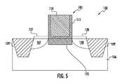
- FIG. 5is a cross-sectional diagram of a semiconductor device in accordance with an example embodiment including a replacement metal gate overlying a superlattice channel layer.
- FIGS. 6-13are a series of cross-sectional diagrams illustrating a method for making the semiconductor device of FIG. 5 .
- FIG. 14is a flow diagram corresponding to the method illustrated in FIGS. 5-13 .
- the present inventionrelates to controlling the properties of semiconductor materials at the atomic or molecular level. Further, the invention relates to the identification, creation, and use of improved materials for use in semiconductor devices.
- fis the Fermi-Dirac distribution
- E Fis the Fermi energy
- Tis the temperature
- E(k,n)is the energy of an electron in the state corresponding to wave vector k and the n th energy band
- the indices i and jrefer to Cartesian coordinates x, y and z
- the integralsare taken over the Brillouin zone (B.Z.)
- the summationsare taken over bands with energies above and below the Fermi energy for electrons and holes respectively.
- the conductivity reciprocal effective mass tensoris such that a tensorial component of the conductivity of the material is greater for greater values of the corresponding component of the conductivity reciprocal effective mass tensor.
- the superlattices described hereinset the values of the conductivity reciprocal effective mass tensor so as to enhance the conductive properties of the material, such as typically for a preferred direction of charge carrier transport.
- the inverse of the appropriate tensor elementis referred to as the conductivity effective mass.
- the conductivity effective mass for electrons/holes as described above and calculated in the direction of intended carrier transportis used to distinguish improved materials.
- the Applicantshave identified improved materials or structures for use in semiconductor devices. More specifically, the Applicants have identified materials or structures having energy band structures for which the appropriate conductivity effective masses for electrons and/or holes are substantially less than the corresponding values for silicon. In addition to the enhanced mobility characteristics of these structures, they may also be formed or used in such a manner that they provide piezoelectric, pyroelectric, and/or ferroelectric properties that are advantageous for use in a variety of different types of devices, as will be discussed further below.
- the materials or structuresare in the form of a superlattice 25 whose structure is controlled at the atomic or molecular level and may be formed using known techniques of atomic or molecular layer deposition.
- the superlattice 25includes a plurality of layer groups 45 a - 45 n arranged in stacked relation, as perhaps best understood with specific reference to the schematic cross-sectional view of FIG. 1 .
- Each group of layers 45 a - 45 n of the superlattice 25illustratively includes a plurality of stacked base semiconductor monolayers 46 defining a respective base semiconductor portion 46 a - 46 n and an energy band-modifying layer 50 thereon.
- the energy band-modifying layers 50are indicated by stippling in FIG. 1 for clarity of illustration.
- the energy band-modifying layer 50illustratively includes one non-semiconductor monolayer constrained within a crystal lattice of adjacent base semiconductor portions.
- constrained within a crystal lattice of adjacent base semiconductor portionsit is meant that at least some semiconductor atoms from opposing base semiconductor portions 46 a - 46 n are chemically bound together through the non-semiconductor monolayer 50 therebetween, as seen in FIG. 2 .
- this configurationis made possible by controlling the amount of non-semiconductor material that is deposited on semiconductor portions 46 a - 46 n through atomic layer deposition techniques so that not all (i.e., less than full or 100% coverage) of the available semiconductor bonding sites are populated with bonds to non-semiconductor atoms, as will be discussed further below.
- the newly deposited semiconductor atomswill populate the remaining vacant bonding sites of the semiconductor atoms below the non-semiconductor monolayer.
- non-semiconductor monolayermay be possible.
- reference herein to a non-semiconductor or semiconductor monolayermeans that the material used for the monolayer would be a non-semiconductor or semiconductor if formed in bulk. That is, a single monolayer of a material, such as silicon, may not necessarily exhibit the same properties that it would if formed in bulk or in a relatively thick layer, as will be appreciated by those skilled in the art.
- energy band-modifying layers 50 and adjacent base semiconductor portions 46 a - 46 ncause the superlattice 25 to have a lower appropriate conductivity effective mass for the charge carriers in the parallel layer direction than would otherwise be present.
- this parallel directionis orthogonal to the stacking direction.
- the band modifying layers 50may also cause the superlattice 25 to have a common energy band structure, while also advantageously functioning as an insulator between layers or regions vertically above and below the superlattice.
- this superlattice structuremay also advantageously act as a barrier to dopant and/or material diffusion between layers vertically above and below the superlattice 25 .
- These propertiesmay thus advantageously allow the superlattice 25 to provide an interface for high-K dielectrics which not only reduces diffusion of the high-K material into the channel region, but which may also advantageously reduce unwanted scattering effects and improve device mobility, as will be appreciated by those skilled in the art.
- the superlattice 25may enjoy a higher charge carrier mobility based upon the lower conductivity effective mass than would otherwise be present.
- the superlattice 25may further have a substantially direct energy bandgap that may be particularly advantageous for opto-electronic devices, for example.
- the superlattice 25also illustratively includes a cap layer 52 on an upper layer group 45 n .
- the cap layer 52may comprise a plurality of base semiconductor monolayers 46 .
- the cap layer 52may have between 2 to 100 monolayers of the base semiconductor, and, more preferably between 10 to 50 monolayers.
- Each base semiconductor portion 46 a - 46 nmay comprise a base semiconductor selected from the group consisting of Group IV semiconductors, Group III-V semiconductors, and Group II-VI semiconductors.
- Group IV semiconductorsalso includes Group IV-IV semiconductors, as will be appreciated by those skilled in the art.
- the base semiconductormay comprise at least one of silicon and germanium, for example.
- Each energy band-modifying layer 50may comprise a non-semiconductor selected from the group consisting of oxygen, nitrogen, fluorine, carbon and carbon-oxygen, for example.
- the non-semiconductoris also desirably thermally stable through deposition of a next layer to thereby facilitate manufacturing.
- the non-semiconductormay be another inorganic or organic element or compound that is compatible with the given semiconductor processing as will be appreciated by those skilled in the art.
- the base semiconductormay comprise at least one of silicon and germanium, for example
- the term monolayeris meant to include a single atomic layer and also a single molecular layer.
- the energy band-modifying layer 50 provided by a single monolayeris also meant to include a monolayer wherein not all of the possible sites are occupied (i.e., there is less than full or 100% coverage).
- a 4/1 repeating structureis illustrated for silicon as the base semiconductor material, and oxygen as the energy band-modifying material. Only half of the possible sites for oxygen are occupied in the illustrated example.
- this one-half occupationwould not necessarily be the case as will be appreciated by those skilled in the art. Indeed it can be seen even in this schematic diagram, that individual atoms of oxygen in a given monolayer are not precisely aligned along a flat plane as will also be appreciated by those of skill in the art of atomic deposition.
- a preferred occupation rangeis from about one-eighth to one-half of the possible oxygen sites being full, although other numbers may be used in certain embodiments.
- Silicon and oxygenare currently widely used in conventional semiconductor processing, and, hence, manufacturers will be readily able to use these materials as described herein.
- Atomic or monolayer depositionis also now widely used. Accordingly, semiconductor devices incorporating the superlattice 25 in accordance with the invention may be readily adopted and implemented, as will be appreciated by those skilled in the art.
- the number of silicon monolayersshould desirably be seven or less so that the energy band of the superlattice is common or relatively uniform throughout to achieve the desired advantages.
- the 4/1 repeating structure shown in FIGS. 1 and 2for Si/O has been modeled to indicate an enhanced mobility for electrons and holes in the X direction.
- the calculated conductivity effective mass for electronsis 0.26 and for the 4/1 SiO superlattice in the X direction it is 0.12 resulting in a ratio of 0.46.
- the calculation for holesyields values of 0.36 for bulk silicon and 0.16 for the 4/1 Si/O superlattice resulting in a ratio of 0.44.
- While such a directionally preferential featuremay be desired in certain semiconductor devices, other devices may benefit from a more uniform increase in mobility in any direction parallel to the groups of layers. It may also be beneficial to have an increased mobility for both electrons or holes, or just one of these types of charge carriers as will be appreciated by those skilled in the art.
- the lower conductivity effective mass for the 4/1 Si/O embodiment of the superlattice 25may be less than two-thirds the conductivity effective mass than would otherwise occur, and this applies for both electrons and holes.
- the superlattice 25may further comprise at least one type of conductivity dopant therein, as will also be appreciated by those skilled in the art.
- FIG. 3another embodiment of a superlattice 25 ′ in accordance with the invention having different properties is now described.
- a repeating pattern of 3/1/5/1is illustrated. More particularly, the lowest base semiconductor portion 46 a ′ has three monolayers, and the second lowest base semiconductor portion 46 b ′ has five monolayers. This pattern repeats throughout the superlattice 25 ′.
- the energy band-modifying layers 50 ′may each include a single monolayer.
- the enhancement of charge carrier mobilityis independent of orientation in the plane of the layers.
- all of the base semiconductor portions of a superlatticemay be a same number of monolayers thick. In other embodiments, at least some of the base semiconductor portions may be a different number of monolayers thick. In still other embodiments, all of the base semiconductor portions may be a different number of monolayers thick.
- FIGS. 4A-4Cband structures calculated using Density Functional Theory (DFT) are presented. It is well known in the art that DFT underestimates the absolute value of the bandgap. Hence all bands above the gap may be shifted by an appropriate “scissors correction.” However the shape of the band is known to be much more reliable. The vertical energy axes should be interpreted in this light.
- DFTDensity Functional Theory
- FIG. 4Ashows the calculated band structure from the gamma point (G) for both bulk silicon (represented by continuous lines) and for the 4/1 Si/O superlattice 25 shown in FIG. 1 (represented by dotted lines).
- the directionsrefer to the unit cell of the 4/1 Si/O structure and not to the conventional unit cell of Si, although the (001) direction in the figure does correspond to the (001) direction of the conventional unit cell of Si, and, hence, shows the expected location of the Si conduction band minimum.
- the (100) and (010) directions in the figurecorrespond to the (110) and ( ⁇ 110) directions of the conventional Si unit cell.
- the bands of Si on the figureare folded to represent them on the appropriate reciprocal lattice directions for the 4/1 Si/O structure.
- the conduction band minimum for the 4/1 Si/O structureis located at the gamma point in contrast to bulk silicon (Si), whereas the valence band minimum occurs at the edge of the Brillouin zone in the (001) direction which we refer to as the Z point.
- the greater curvature of the conduction band minimum for the 4/1 Si/O structurecompared to the curvature of the conduction band minimum for Si owing to the band splitting due to the perturbation introduced by the additional oxygen layer.
- FIG. 4Bshows the calculated band structure from the Z point for both bulk silicon (continuous lines) and for the 4/1 Si/O superlattice 25 (dotted lines). This figure illustrates the enhanced curvature of the valence band in the (100) direction.
- FIG. 4Cshows the calculated band structure from both the gamma and Z point for both bulk silicon (continuous lines) and for the 5/1/3/1 Si/O structure of the superlattice 25 ′ of FIG. 3 (dotted lines). Due to the symmetry of the 5/1/3/1 Si/O structure, the calculated band structures in the (100) and (010) directions are equivalent. Thus the conductivity effective mass and mobility are expected to be isotropic in the plane parallel to the layers, i.e. perpendicular to the (001) stacking direction. Note that in the 5/1/3/1 Si/O example the conduction band minimum and the valence band maximum are both at or close to the Z point.
- the appropriate comparison and discriminationmay be made via the conductivity reciprocal effective mass tensor calculation. This leads Applicants to further theorize that the 5/1/3/1 superlattice 25 ′ should be substantially direct bandgap. As will be understood by those skilled in the art, the appropriate matrix element for optical transition is another indicator of the distinction between direct and indirect bandgap behavior.
- the above-described quantum confinement properties of the superlattice material layer 125 when utilized in the channel region of the semiconductor device 100may provide significant advantages, such as bias temperature instability (BTI) reliability improvement, as well as carrier mobility boost (and, accordingly, NMOS performance improvement), as well as providing a “channel last” integration option, meaning that the channel is formed after the source/drain and dummy gate formation, as will be discussed further below.
- BTIbias temperature instability
- carrier mobility boostand, accordingly, NMOS performance improvement
- the superlattice materialmay also help reduce leakage in the channel region as well.
- the semiconductor device 100is a planar MOSFET device, which may be used for NMOS, PMOS, or CMOS devices, for example.
- the superlattice/gate structure shown in FIG. 5may be used in other configurations as well, such as vertical devices (e.g., FINFETs, etc.).
- the semiconductor device 100illustratively includes a silicon substrate 106 , spaced apart source and drain regions 107 , 108 in the substrate, and the superlattice material layer 125 which is positioned between the source and drain regions in the channel recess 104 of the substrate.
- Shallow trench isolation (STI) regions 109may be included to insulate the source and drain regions 107 , 108 from other devices on the substrate 106 , as will be appreciated by those skilled in the art.
- the gate 105is a high K replacement metal gate including a metal gate electrode 110 and a high K dielectric layer 111 , and is positioned over the superlattice channel layer 125 laterally between the source and drain regions 107 , 108 , as shown.
- the channel of the device 100may be defined fully or partially within the superlattice channel layer 125 , or it may also extend beneath the superlattice channel layer in some embodiments.
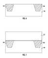
- STI and well module preparationmay be performed at Blocks 201 - 202 to form the starting substrate or wafer ( FIG. 6 ), as will be appreciated by those skilled in the art.
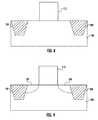
- a “dummy gate” 113may then be formed on the substrate 106 overlying what is to become the channel region, at Block 203 ( FIG. 6 ). More particularly, the dummy gate 113 formation may include forming a blanket polycrystalline semiconductor layer 112 (e.g., polysilicon) over the substrate 106 and STI regions 109 ( FIG. 7 ), and then patterning the polycrystalline layer to define the dummy gate 113 ( FIG. 8 ). The dummy gate 113 may then be used to align the source and drain 107 , 108 implants, at Block 204 ( FIG. 9 ).
- a blanket polycrystalline semiconductor layer 112e.g., polysilicon
- a dielectric layer 114(e.g., SiO 2 ) may be formed overlying the source and drain regions 107 , 108 and the STI regions 109 and surrounding the dummy gate 113 , as seen in FIG. 10 .
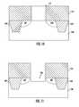
- the dummy gate 113may then be removed (Block 205 ) to make way for the replacement metal gate 105 .
- etching of the dummy gate 113may extend down into the substrate 106 to create the channel recess 104 , as seen in FIG. 11 .
- the superlattice layer 125may then be formed in the channel recess 104 using the above-described techniques and configurations, at Block 206 , as seen in FIG. 12 .
- the replacement metal gate 105may then be formed by depositing the high K dielectric layer 111 , and the metal gate electrode 110 , as seen in FIG. 13 (Block 207 ), as will be appreciated by those skilled in the art. Further semiconductor device processing may then be performed as appropriate for the given device type, as will be appreciated by those skilled in the art. For example, the dielectric layer 114 may be removed, and respective source/drain contacts 127 , 128 may be formed, as seen in FIG. 5 , for example.
- the foregoing metal gate implementationmay accordingly not only provide the above-noted advantages of BTI reliability improvement and carrier mobility boost, but it may also provide integration flexibility in terms of gate formation and channel integration.
- the superlattice channel layer 125may advantageously be formed after the source and drain 107 , 108 formation, which may be desirable in that the superlattice channel layer is not subjected to the various processing steps associated with the source/drain formation and dummy gate 113 processing.
- the above-described stepscould be re-ordered to provide for a “gate first” option, rather than the exemplary “gate last” approach set forth above.
- Such processing flexibilitymay be advantageous for CMOS implementations at 32 nm nodes or below, for example, although the configurations described herein may be used with other device sizes as well.
Landscapes
- Insulated Gate Type Field-Effect Transistor (AREA)
Abstract
Description
for electrons and:
for holes, where f is the Fermi-Dirac distribution, EFis the Fermi energy, T is the temperature, E(k,n) is the energy of an electron in the state corresponding to wave vector k and the nthenergy band, the indices i and j refer to Cartesian coordinates x, y and z, the integrals are taken over the Brillouin zone (B.Z.), and the summations are taken over bands with energies above and below the Fermi energy for electrons and holes respectively.
Claims (9)
Priority Applications (5)
| Application Number | Priority Date | Filing Date | Title |
|---|---|---|---|
| US14/948,547US9722046B2 (en) | 2014-11-25 | 2015-11-23 | Semiconductor device including a superlattice and replacement metal gate structure and related methods |
| EP15805702.6AEP3218937B1 (en) | 2014-11-25 | 2015-11-24 | Method of manufacturing a semiconductor device including a superlattice and replacement metal gate structure |
| PCT/US2015/062305WO2016085918A1 (en) | 2014-11-25 | 2015-11-24 | Semiconductor device including a superlattice and replacement metal gate structure and related methods |
| CN201580071385.3ACN107112354B (en) | 2014-11-25 | 2015-11-24 | Semiconductor device including superlattice and replacement metal gate structures and related methods |
| US15/633,918US10084045B2 (en) | 2014-11-25 | 2017-06-27 | Semiconductor device including a superlattice and replacement metal gate structure and related methods |
Applications Claiming Priority (2)
| Application Number | Priority Date | Filing Date | Title |
|---|---|---|---|
| US201462083994P | 2014-11-25 | 2014-11-25 | |
| US14/948,547US9722046B2 (en) | 2014-11-25 | 2015-11-23 | Semiconductor device including a superlattice and replacement metal gate structure and related methods |
Related Child Applications (1)
| Application Number | Title | Priority Date | Filing Date |
|---|---|---|---|
| US15/633,918DivisionUS10084045B2 (en) | 2014-11-25 | 2017-06-27 | Semiconductor device including a superlattice and replacement metal gate structure and related methods |
Publications (2)
| Publication Number | Publication Date |
|---|---|
| US20160149023A1 US20160149023A1 (en) | 2016-05-26 |
| US9722046B2true US9722046B2 (en) | 2017-08-01 |
Family
ID=56011024
Family Applications (2)
| Application Number | Title | Priority Date | Filing Date |
|---|---|---|---|
| US14/948,547ActiveUS9722046B2 (en) | 2014-11-25 | 2015-11-23 | Semiconductor device including a superlattice and replacement metal gate structure and related methods |
| US15/633,918ActiveUS10084045B2 (en) | 2014-11-25 | 2017-06-27 | Semiconductor device including a superlattice and replacement metal gate structure and related methods |
Family Applications After (1)
| Application Number | Title | Priority Date | Filing Date |
|---|---|---|---|
| US15/633,918ActiveUS10084045B2 (en) | 2014-11-25 | 2017-06-27 | Semiconductor device including a superlattice and replacement metal gate structure and related methods |
Country Status (4)
| Country | Link |
|---|---|
| US (2) | US9722046B2 (en) |
| EP (1) | EP3218937B1 (en) |
| CN (1) | CN107112354B (en) |
| WO (1) | WO2016085918A1 (en) |
Cited By (8)
| Publication number | Priority date | Publication date | Assignee | Title |
|---|---|---|---|---|
| US20180122646A1 (en)* | 2016-09-08 | 2018-05-03 | International Business Machines Corporation | Low resistance source-drain contacts using high temperature silicides |
| US11978771B2 (en) | 2020-07-02 | 2024-05-07 | Atomera Incorporated | Gate-all-around (GAA) device including a superlattice |
| US12142662B2 (en) | 2023-03-24 | 2024-11-12 | Atomera Incorporated | Method for making nanostructure transistors with offset source/drain dopant blocking structures including a superlattice |
| US12267996B2 (en) | 2022-05-04 | 2025-04-01 | Atomera Incorporated | DRAM sense amplifier architecture with reduced power consumption and related methods |
| US12308229B2 (en) | 2023-07-03 | 2025-05-20 | Atomera Incorporated | Method for making memory device including a superlattice gettering layer |
| US12315722B2 (en) | 2023-03-14 | 2025-05-27 | Atomera Incorporated | Method for making a radio frequency silicon-on-insulator (RFSOI) wafer including a superlattice |
| US12382689B2 (en) | 2023-05-08 | 2025-08-05 | Atomera Incorporated | Method for making DMOS devices including a superlattice and field plate for drift region diffusion |
| US12439658B2 (en) | 2021-05-18 | 2025-10-07 | Atomera Incorporated | Semiconductor device including a superlattice providing metal work function tuning |
Families Citing this family (65)
| Publication number | Priority date | Publication date | Assignee | Title |
|---|---|---|---|---|
| US9812323B2 (en)* | 2014-09-08 | 2017-11-07 | Internaitonal Business Machines Corporation | Low external resistance channels in III-V semiconductor devices |
| US9941359B2 (en) | 2015-05-15 | 2018-04-10 | Atomera Incorporated | Semiconductor devices with superlattice and punch-through stop (PTS) layers at different depths and related methods |
| US9721790B2 (en) | 2015-06-02 | 2017-08-01 | Atomera Incorporated | Method for making enhanced semiconductor structures in single wafer processing chamber with desired uniformity control |
| US10109342B2 (en) | 2016-05-11 | 2018-10-23 | Atomera Incorporated | Dram architecture to reduce row activation circuitry power and peripheral leakage and related methods |
| US9893070B2 (en) | 2016-06-10 | 2018-02-13 | Taiwan Semiconductor Manufacturing Company, Ltd. | Semiconductor device and fabrication method therefor |
| US10170603B2 (en) | 2016-08-08 | 2019-01-01 | Atomera Incorporated | Semiconductor device including a resonant tunneling diode structure with electron mean free path control layers |
| US10107854B2 (en) | 2016-08-17 | 2018-10-23 | Atomera Incorporated | Semiconductor device including threshold voltage measurement circuitry |
| US10381242B2 (en) | 2017-05-16 | 2019-08-13 | Atomera Incorporated | Method for making a semiconductor device including a superlattice as a gettering layer |
| US10367064B2 (en) | 2017-06-13 | 2019-07-30 | Atomera Incorporated | Semiconductor device with recessed channel array transistor (RCAT) including a superlattice |
| US10109479B1 (en) | 2017-07-31 | 2018-10-23 | Atomera Incorporated | Method of making a semiconductor device with a buried insulating layer formed by annealing a superlattice |
| WO2019036572A1 (en) | 2017-08-18 | 2019-02-21 | Atomera Incorporated | Semiconductor device and method including non-monocrystalline stringer adjacent a superlattice-sti interface |
| US10608027B2 (en) | 2017-12-15 | 2020-03-31 | Atomera Incorporated | Method for making CMOS image sensor including stacked semiconductor chips and image processing circuitry including a superlattice |
| US10304881B1 (en) | 2017-12-15 | 2019-05-28 | Atomera Incorporated | CMOS image sensor with buried superlattice layer to reduce crosstalk |
| US10608043B2 (en) | 2017-12-15 | 2020-03-31 | Atomera Incorporation | Method for making CMOS image sensor including stacked semiconductor chips and readout circuitry including a superlattice |
| US10615209B2 (en)* | 2017-12-15 | 2020-04-07 | Atomera Incorporated | CMOS image sensor including stacked semiconductor chips and readout circuitry including a superlattice |
| US10367028B2 (en) | 2017-12-15 | 2019-07-30 | Atomera Incorporated | CMOS image sensor including stacked semiconductor chips and image processing circuitry including a superlattice |
| US10529757B2 (en) | 2017-12-15 | 2020-01-07 | Atomera Incorporated | CMOS image sensor including pixels with read circuitry having a superlattice |
| US10355151B2 (en) | 2017-12-15 | 2019-07-16 | Atomera Incorporated | CMOS image sensor including photodiodes with overlying superlattices to reduce crosstalk |
| US10361243B2 (en) | 2017-12-15 | 2019-07-23 | Atomera Incorporated | Method for making CMOS image sensor including superlattice to enhance infrared light absorption |
| US10529768B2 (en) | 2017-12-15 | 2020-01-07 | Atomera Incorporated | Method for making CMOS image sensor including pixels with read circuitry having a superlattice |
| US10276625B1 (en) | 2017-12-15 | 2019-04-30 | Atomera Incorporated | CMOS image sensor including superlattice to enhance infrared light absorption |
| US10396223B2 (en) | 2017-12-15 | 2019-08-27 | Atomera Incorporated | Method for making CMOS image sensor with buried superlattice layer to reduce crosstalk |
| US10461118B2 (en) | 2017-12-15 | 2019-10-29 | Atomera Incorporated | Method for making CMOS image sensor including photodiodes with overlying superlattices to reduce crosstalk |
| CN111937119B (en) | 2018-03-08 | 2024-07-23 | 阿托梅拉公司 | Semiconductor device including enhanced contact structure with superlattice and related methods |
| US10727049B2 (en) | 2018-03-09 | 2020-07-28 | Atomera Incorporated | Method for making a semiconductor device including compound semiconductor materials and an impurity and point defect blocking superlattice |
| US10468245B2 (en) | 2018-03-09 | 2019-11-05 | Atomera Incorporated | Semiconductor device including compound semiconductor materials and an impurity and point defect blocking superlattice |
| US11355667B2 (en) | 2018-04-12 | 2022-06-07 | Atomera Incorporated | Method for making semiconductor device including vertically integrated optical and electronic devices and comprising a superlattice |
| US11664459B2 (en) | 2018-04-12 | 2023-05-30 | Atomera Incorporated | Method for making an inverted T channel field effect transistor (ITFET) including a superlattice |
| US10811498B2 (en) | 2018-08-30 | 2020-10-20 | Atomera Incorporated | Method for making superlattice structures with reduced defect densities |
| US10566191B1 (en) | 2018-08-30 | 2020-02-18 | Atomera Incorporated | Semiconductor device including superlattice structures with reduced defect densities |
| US20200135489A1 (en)* | 2018-10-31 | 2020-04-30 | Atomera Incorporated | Method for making a semiconductor device including a superlattice having nitrogen diffused therein |
| US10593761B1 (en) | 2018-11-16 | 2020-03-17 | Atomera Incorporated | Method for making a semiconductor device having reduced contact resistance |
| EP3871270A1 (en)* | 2018-11-16 | 2021-09-01 | Atomera Incorporated | Finfet including source and drain regions with dopant diffusion blocking superlattice layers to reduce contact resistance and associated methods |
| US10580866B1 (en) | 2018-11-16 | 2020-03-03 | Atomera Incorporated | Semiconductor device including source/drain dopant diffusion blocking superlattices to reduce contact resistance |
| US10840335B2 (en) | 2018-11-16 | 2020-11-17 | Atomera Incorporated | Method for making semiconductor device including body contact dopant diffusion blocking superlattice to reduce contact resistance |
| US10580867B1 (en) | 2018-11-16 | 2020-03-03 | Atomera Incorporated | FINFET including source and drain regions with dopant diffusion blocking superlattice layers to reduce contact resistance |
| US10854717B2 (en) | 2018-11-16 | 2020-12-01 | Atomera Incorporated | Method for making a FINFET including source and drain dopant diffusion blocking superlattices to reduce contact resistance |
| US10840336B2 (en) | 2018-11-16 | 2020-11-17 | Atomera Incorporated | Semiconductor device with metal-semiconductor contacts including oxygen insertion layer to constrain dopants and related methods |
| US10818755B2 (en) | 2018-11-16 | 2020-10-27 | Atomera Incorporated | Method for making semiconductor device including source/drain dopant diffusion blocking superlattices to reduce contact resistance |
| US10847618B2 (en) | 2018-11-16 | 2020-11-24 | Atomera Incorporated | Semiconductor device including body contact dopant diffusion blocking superlattice having reduced contact resistance |
| US10840337B2 (en)* | 2018-11-16 | 2020-11-17 | Atomera Incorporated | Method for making a FINFET having reduced contact resistance |
| US11094818B2 (en) | 2019-04-23 | 2021-08-17 | Atomera Incorporated | Method for making a semiconductor device including a superlattice and an asymmetric channel and related methods |
| US10937868B2 (en) | 2019-07-17 | 2021-03-02 | Atomera Incorporated | Method for making semiconductor devices with hyper-abrupt junction region including spaced-apart superlattices |
| US10937888B2 (en) | 2019-07-17 | 2021-03-02 | Atomera Incorporated | Method for making a varactor with a hyper-abrupt junction region including spaced-apart superlattices |
| US10868120B1 (en) | 2019-07-17 | 2020-12-15 | Atomera Incorporated | Method for making a varactor with hyper-abrupt junction region including a superlattice |
| US10825902B1 (en) | 2019-07-17 | 2020-11-03 | Atomera Incorporated | Varactor with hyper-abrupt junction region including spaced-apart superlattices |
| US10840388B1 (en) | 2019-07-17 | 2020-11-17 | Atomera Incorporated | Varactor with hyper-abrupt junction region including a superlattice |
| US10825901B1 (en) | 2019-07-17 | 2020-11-03 | Atomera Incorporated | Semiconductor devices including hyper-abrupt junction region including a superlattice |
| US11183565B2 (en) | 2019-07-17 | 2021-11-23 | Atomera Incorporated | Semiconductor devices including hyper-abrupt junction region including spaced-apart superlattices and related methods |
| US10879357B1 (en) | 2019-07-17 | 2020-12-29 | Atomera Incorporated | Method for making a semiconductor device having a hyper-abrupt junction region including a superlattice |
| US11437487B2 (en) | 2020-01-14 | 2022-09-06 | Atomera Incorporated | Bipolar junction transistors including emitter-base and base-collector superlattices |
| US11302823B2 (en) | 2020-02-26 | 2022-04-12 | Atomera Incorporated | Method for making semiconductor device including a superlattice with different non-semiconductor material monolayers |
| US11177351B2 (en) | 2020-02-26 | 2021-11-16 | Atomera Incorporated | Semiconductor device including a superlattice with different non-semiconductor material monolayers |
| US11075078B1 (en) | 2020-03-06 | 2021-07-27 | Atomera Incorporated | Method for making a semiconductor device including a superlattice within a recessed etch |
| KR102812354B1 (en) | 2020-04-29 | 2025-05-27 | 삼성전자주식회사 | Semiconductor device |
| US11569368B2 (en) | 2020-06-11 | 2023-01-31 | Atomera Incorporated | Method for making semiconductor device including a superlattice and providing reduced gate leakage |
| US11469302B2 (en)* | 2020-06-11 | 2022-10-11 | Atomera Incorporated | Semiconductor device including a superlattice and providing reduced gate leakage |
| WO2022006396A1 (en) | 2020-07-02 | 2022-01-06 | Atomera Incorporated | Method for making a semiconductor device using superlattices with different non-semiconductor thermal stabilities |
| TWI803219B (en) | 2021-03-03 | 2023-05-21 | 美商安托梅拉公司 | Radio frequency (rf) semiconductor devices including a ground plane layer having a superlattice and associated methods |
| US11923418B2 (en) | 2021-04-21 | 2024-03-05 | Atomera Incorporated | Semiconductor device including a superlattice and enriched silicon 28 epitaxial layer |
| US11810784B2 (en) | 2021-04-21 | 2023-11-07 | Atomera Incorporated | Method for making semiconductor device including a superlattice and enriched silicon 28 epitaxial layer |
| US11682712B2 (en) | 2021-05-26 | 2023-06-20 | Atomera Incorporated | Method for making semiconductor device including superlattice with O18 enriched monolayers |
| US11728385B2 (en) | 2021-05-26 | 2023-08-15 | Atomera Incorporated | Semiconductor device including superlattice with O18 enriched monolayers |
| US11721546B2 (en) | 2021-10-28 | 2023-08-08 | Atomera Incorporated | Method for making semiconductor device with selective etching of superlattice to accumulate non-semiconductor atoms |
| US11631584B1 (en) | 2021-10-28 | 2023-04-18 | Atomera Incorporated | Method for making semiconductor device with selective etching of superlattice to define etch stop layer |
Citations (129)
| Publication number | Priority date | Publication date | Assignee | Title |
|---|---|---|---|---|
| US4485128A (en) | 1981-11-20 | 1984-11-27 | Chronar Corporation | Bandgap control in amorphous semiconductors |
| JPS6127681A (en) | 1984-07-17 | 1986-02-07 | Res Dev Corp Of Japan | Field effect transistor with superlattice structure channel part |
| US4590399A (en) | 1984-02-28 | 1986-05-20 | Exxon Research And Engineering Co. | Superlattice piezoelectric devices |
| US4594603A (en) | 1982-04-22 | 1986-06-10 | Board Of Trustees Of The University Of Illinois | Semiconductor device with disordered active region |
| JPS61145820A (en) | 1984-12-20 | 1986-07-03 | Seiko Epson Corp | Semiconductor thin film material |
| JPS61220339A (en) | 1985-03-26 | 1986-09-30 | Nippon Telegr & Teleph Corp <Ntt> | Control of characteristics of semiconductor material |
| JPS62219665A (en) | 1986-03-20 | 1987-09-26 | Fujitsu Ltd | Superlattice thin-film transistor |
| US4882609A (en) | 1984-11-19 | 1989-11-21 | Max-Planck Gesellschaft Zur Forderung Der Wissenschafter E.V. | Semiconductor devices with at least one monoatomic layer of doping atoms |
| US4908678A (en) | 1986-10-08 | 1990-03-13 | Semiconductor Energy Laboratory Co., Ltd. | FET with a super lattice channel |
| US4937204A (en) | 1985-03-15 | 1990-06-26 | Sony Corporation | Method of making a superlattice heterojunction bipolar device |
| US4969031A (en) | 1982-02-03 | 1990-11-06 | Hitachi, Ltd. | Semiconductor devices and method for making the same |
| US5081513A (en) | 1991-02-28 | 1992-01-14 | Xerox Corporation | Electronic device with recovery layer proximate to active layer |
| US5216262A (en) | 1992-03-02 | 1993-06-01 | Raphael Tsu | Quantum well structures useful for semiconductor devices |
| US5357119A (en) | 1993-02-19 | 1994-10-18 | Board Of Regents Of The University Of California | Field effect devices having short period superlattice structures using Si and Ge |
| WO1996029728A1 (en) | 1995-03-17 | 1996-09-26 | Matsushita Electronics Corporation | Integrated circuits having mixed layered superlattice materials and precursor solutions for use in a process of making the same |
| US5577061A (en) | 1994-12-16 | 1996-11-19 | Hughes Aircraft Company | Superlattice cladding layers for mid-infrared lasers |
| US5594567A (en) | 1992-07-24 | 1997-01-14 | Matsushita Electric Industrial Co., Ltd. | Spatial light modulator with a photoconductor having uneven conductivity in a lateral direction and a method for fabricating the same |
| US5606177A (en) | 1993-10-29 | 1997-02-25 | Texas Instruments Incorporated | Silicon oxide resonant tunneling diode structure |
| US5616515A (en) | 1994-08-04 | 1997-04-01 | Texas Instruments Incorporated | Silicon oxide germanium resonant tunneling |
| US5627386A (en) | 1994-08-11 | 1997-05-06 | The United States Of America As Represented By The Secretary Of The Army | Silicon nanostructure light-emitting diode |
| US5684817A (en) | 1995-05-12 | 1997-11-04 | Thomson-Csf | Semiconductor laser having a structure of photonic bandgap material |
| US5683934A (en) | 1994-09-26 | 1997-11-04 | Motorola, Inc. | Enhanced mobility MOSFET device and method |
| EP0843361A1 (en) | 1996-11-15 | 1998-05-20 | Hitachi Europe Limited | Memory device |
| US5994164A (en) | 1997-03-18 | 1999-11-30 | The Penn State Research Foundation | Nanostructure tailoring of material properties using controlled crystallization |
| WO1999063580A2 (en) | 1998-05-29 | 1999-12-09 | Massachusetts Institute Of Technology | Compound semiconductor structure with lattice and polarity matched heteroepitaxial layers |
| US6058127A (en) | 1996-12-13 | 2000-05-02 | Massachusetts Institute Of Technology | Tunable microcavity and method of using nonlinear materials in a photonic crystal |
| GB2347520A (en) | 1999-03-05 | 2000-09-06 | Fujitsu Telecommunications Eur | Aperiodic gratings |
| US6255150B1 (en) | 1997-10-23 | 2001-07-03 | Texas Instruments Incorporated | Use of crystalline SiOx barriers for Si-based resonant tunneling diodes |
| US6274007B1 (en) | 1999-11-25 | 2001-08-14 | Sceptre Electronics Limited | Methods of formation of a silicon nanostructure, a silicon quantum wire array and devices based thereon |
| US6281518B1 (en) | 1997-12-04 | 2001-08-28 | Ricoh Company, Ltd. | Layered III-V semiconductor structures and light emitting devices including the structures |
| US6281532B1 (en) | 1999-06-28 | 2001-08-28 | Intel Corporation | Technique to obtain increased channel mobilities in NMOS transistors by gate electrode engineering |
| US6326311B1 (en) | 1998-03-30 | 2001-12-04 | Sharp Kabushiki Kaisha | Microstructure producing method capable of controlling growth position of minute particle or thin and semiconductor device employing the microstructure |
| US6344271B1 (en) | 1998-11-06 | 2002-02-05 | Nanoenergy Corporation | Materials and products using nanostructured non-stoichiometric substances |
| US6350993B1 (en) | 1999-03-12 | 2002-02-26 | International Business Machines Corporation | High speed composite p-channel Si/SiGe heterostructure for field effect devices |
| US6376337B1 (en) | 1997-11-10 | 2002-04-23 | Nanodynamics, Inc. | Epitaxial SiOx barrier/insulation layer |
| US20020094003A1 (en) | 1999-09-29 | 2002-07-18 | Xerox Corporation | Structure and method for index-guided buried heterostructure AlGalnN laser diodes |
| US6436784B1 (en) | 1995-08-03 | 2002-08-20 | Hitachi Europe Limited | Method of forming semiconductor structure |
| US6472685B2 (en) | 1997-12-03 | 2002-10-29 | Matsushita Electric Industrial Co., Ltd. | Semiconductor device |
| US6498359B2 (en) | 2000-05-22 | 2002-12-24 | Max-Planck-Gesellschaft Zur Foerderung Der Wissenschaften E.V. | Field-effect transistor based on embedded cluster structures and process for its production |
| US6501092B1 (en) | 1999-10-25 | 2002-12-31 | Intel Corporation | Integrated semiconductor superlattice optical modulator |
| US6521549B1 (en) | 2000-11-28 | 2003-02-18 | Lsi Logic Corporation | Method of reducing silicon oxynitride gate insulator thickness in some transistors of a hybrid integrated circuit to obtain increased differential in gate insulator thickness with other transistors of the hybrid circuit |
| US20030034529A1 (en) | 2000-12-04 | 2003-02-20 | Amberwave Systems Corporation | CMOS inverter and integrated circuits utilizing strained silicon surface channel MOSFETs |
| US20030057416A1 (en) | 2001-09-21 | 2003-03-27 | Amberwave Systems Corporation | Semiconductor structures employing strained material layers with defined impurity gradients and methods for fabricating same |
| US20030089899A1 (en) | 2000-08-22 | 2003-05-15 | Lieber Charles M. | Nanoscale wires and related devices |
| US6608327B1 (en) | 1998-02-27 | 2003-08-19 | North Carolina State University | Gallium nitride semiconductor structure including laterally offset patterned layers |
| US20030162335A1 (en) | 1999-01-14 | 2003-08-28 | Matsushita Electric Industrial Co., Ltd. | Semiconductor device and method for fabricating the same |
| US6638838B1 (en) | 2000-10-02 | 2003-10-28 | Motorola, Inc. | Semiconductor structure including a partially annealed layer and method of forming the same |
| US6646293B2 (en) | 2001-07-18 | 2003-11-11 | Motorola, Inc. | Structure for fabricating high electron mobility transistors utilizing the formation of complaint substrates |
| US20030215990A1 (en) | 2002-03-14 | 2003-11-20 | Eugene Fitzgerald | Methods for fabricating strained layers on semiconductor substrates |
| US6673646B2 (en) | 2001-02-28 | 2004-01-06 | Motorola, Inc. | Growth of compound semiconductor structures on patterned oxide films and process for fabricating same |
| US6690699B2 (en) | 2001-03-02 | 2004-02-10 | Lucent Technologies Inc | Quantum cascade laser with relaxation-stabilized injection |
| US6711191B1 (en) | 1999-03-04 | 2004-03-23 | Nichia Corporation | Nitride semiconductor laser device |
| US20040084781A1 (en) | 1998-08-31 | 2004-05-06 | Micron Technology, Inc. | Compact system module with built-in thermoelectric cooling |
| US6741624B2 (en) | 1999-03-05 | 2004-05-25 | R J Mears Llc | Fabry-Perot laser with wavelength control |
| US6748002B2 (en) | 1998-08-10 | 2004-06-08 | D-Led Corporation | Injection laser |
| US6816530B2 (en) | 2002-09-30 | 2004-11-09 | Lucent Technologies Inc. | Nonlinear semiconductor light sources |
| US20040227165A1 (en) | 2003-04-21 | 2004-11-18 | Nanodynamics, Inc. | Si/C superlattice useful for semiconductor devices |
| US6830964B1 (en) | 2003-06-26 | 2004-12-14 | Rj Mears, Llc | Method for making semiconductor device including band-engineered superlattice |
| US6833294B1 (en) | 2003-06-26 | 2004-12-21 | Rj Mears, Llc | Method for making semiconductor device including band-engineered superlattice |
| US20040266116A1 (en) | 2003-06-26 | 2004-12-30 | Rj Mears, Llc | Methods of fabricating semiconductor structures having improved conductivity effective mass |
| US20040262594A1 (en) | 2003-06-26 | 2004-12-30 | Rj Mears, Llc | Semiconductor structures having improved conductivity effective mass and methods for fabricating same |
| US20050032247A1 (en) | 2003-06-26 | 2005-02-10 | Rj Mears, Llp | Method for making an integrated circuit comprising an active optical device having an energy band engineered superlattice |
| WO2005034325A1 (en) | 2003-09-30 | 2005-04-14 | Sanken Electric Co., Ltd. | Switching power source device |
| US20050163692A1 (en) | 2000-08-08 | 2005-07-28 | Atanackovic Petar B. | Rare earth-oxides, rare earth -nitrides, rare earth -phosphides and ternary alloys with silicon |
| US20050208715A1 (en) | 2004-03-17 | 2005-09-22 | Hyeoung-Won Seo | Method of fabricating fin field effect transistor using isotropic etching technique |
| US20050282330A1 (en) | 2003-06-26 | 2005-12-22 | Rj Mears, Llc | Method for making a semiconductor device including a superlattice having at least one group of substantially undoped layers |
| US20050279991A1 (en) | 2003-06-26 | 2005-12-22 | Rj Mears, Llc | Semiconductor device including a superlattice having at least one group of substantially undoped layers |
| US20060011905A1 (en) | 2003-06-26 | 2006-01-19 | Rj Mears, Llc | Semiconductor device comprising a superlattice dielectric interface layer |
| US6993222B2 (en) | 1999-03-03 | 2006-01-31 | Rj Mears, Llc | Optical filter device with aperiodically arranged grating elements |
| US7045377B2 (en) | 2003-06-26 | 2006-05-16 | Rj Mears, Llc | Method for making a semiconductor device including a superlattice and adjacent semiconductor layer with doped regions defining a semiconductor junction |
| US7045813B2 (en) | 2003-06-26 | 2006-05-16 | Rj Mears, Llc | Semiconductor device including a superlattice with regions defining a semiconductor junction |
| US20060220118A1 (en) | 2003-06-26 | 2006-10-05 | Rj Mears, Llc | Semiconductor device including a dopant blocking superlattice |
| US20060223215A1 (en) | 2003-06-26 | 2006-10-05 | Rj Mears, Llc | Method for Making a Microelectromechanical Systems (MEMS) Device Including a Superlattice |
| US20060226502A1 (en) | 2003-06-26 | 2006-10-12 | Rj Mears, Llc | Microelectromechanical Systems (MEMS) Device Including a Superlattice |
| US20060231857A1 (en) | 2003-06-26 | 2006-10-19 | Rj Mears, Llc | Method for making a semiconductor device including a memory cell with a negative differential resistance (ndr) device |
| US20060243964A1 (en) | 2003-06-26 | 2006-11-02 | Rj Mears, Llc | Method for making a semiconductor device having a semiconductor-on-insulator configuration and a superlattice |
| US20060263980A1 (en) | 2003-06-26 | 2006-11-23 | Rj Mears, Llc, State Of Incorporation: Delaware | Method for making a semiconductor device including a floating gate memory cell with a superlattice channel |
| US20060267130A1 (en) | 2003-06-26 | 2006-11-30 | Rj Mears, Llc | Semiconductor Device Including Shallow Trench Isolation (STI) Regions with a Superlattice Therebetween |
| US20060273299A1 (en) | 2003-06-26 | 2006-12-07 | Rj Mears, Llc | Method for making a semiconductor device including a dopant blocking superlattice |
| US7153763B2 (en) | 2003-06-26 | 2006-12-26 | Rj Mears, Llc | Method for making a semiconductor device including band-engineered superlattice using intermediate annealing |
| US20060289049A1 (en) | 2003-06-26 | 2006-12-28 | Rj Mears, Llc | Semiconductor Device Having a Semiconductor-on-Insulator (SOI) Configuration and Including a Superlattice on a Thin Semiconductor Layer |
| US20060292765A1 (en) | 2003-06-26 | 2006-12-28 | Rj Mears, Llc | Method for Making a FINFET Including a Superlattice |
| US20070010040A1 (en) | 2003-06-26 | 2007-01-11 | Rj Mears, Llc | Method for Making a Semiconductor Device Including a Strained Superlattice Layer Above a Stress Layer |
| US20070012910A1 (en) | 2003-06-26 | 2007-01-18 | Rj Mears, Llc | Semiconductor Device Including a Channel with a Non-Semiconductor Layer Monolayer |
| US20070015344A1 (en) | 2003-06-26 | 2007-01-18 | Rj Mears, Llc | Method for Making a Semiconductor Device Including a Strained Superlattice Between at Least One Pair of Spaced Apart Stress Regions |
| US20070020860A1 (en) | 2003-06-26 | 2007-01-25 | Rj Mears, Llc | Method for Making Semiconductor Device Including a Strained Superlattice and Overlying Stress Layer and Related Methods |
| WO2007011790A1 (en) | 2005-07-15 | 2007-01-25 | Mears Technologies, Inc. | Semiconductor device including a channel with a non-semiconductor monolayer and associated methods |
| US20070020833A1 (en) | 2003-06-26 | 2007-01-25 | Rj Mears, Llc | Method for Making a Semiconductor Device Including a Channel with a Non-Semiconductor Layer Monolayer |
| US20070063185A1 (en) | 2003-06-26 | 2007-03-22 | Rj Mears, Llc | Semiconductor device including a front side strained superlattice layer and a back side stress layer |
| US20070063186A1 (en) | 2003-06-26 | 2007-03-22 | Rj Mears, Llc | Method for making a semiconductor device including a front side strained superlattice layer and a back side stress layer |
| US7202494B2 (en) | 2003-06-26 | 2007-04-10 | Rj Mears, Llc | FINFET including a superlattice |
| US7227174B2 (en) | 2003-06-26 | 2007-06-05 | Rj Mears, Llc | Semiconductor device including a superlattice and adjacent semiconductor layer with doped regions defining a semiconductor junction |
| US7229902B2 (en) | 2003-06-26 | 2007-06-12 | Rj Mears, Llc | Method for making a semiconductor device including a superlattice with regions defining a semiconductor junction |
| US20070158640A1 (en) | 2005-12-22 | 2007-07-12 | Rj Mears, Llc | Electronic device including a poled superlattice having a net electrical dipole moment |
| US20080012004A1 (en) | 2006-03-17 | 2008-01-17 | Mears Technologies, Inc. | Spintronic devices with constrained spintronic dopant |
| US20080197340A1 (en) | 2007-02-16 | 2008-08-21 | Rj Mears, Llc | Multiple-wavelength opto-electronic device including a superlattice |
| WO2008130899A1 (en) | 2007-04-23 | 2008-10-30 | Mears Technologies, Inc. | Semiconductor device including sti regions and methods of manufacturing the same |
| US7446002B2 (en) | 2003-06-26 | 2008-11-04 | Mears Technologies, Inc. | Method for making a semiconductor device comprising a superlattice dielectric interface layer |
| US7491587B2 (en) | 2003-06-26 | 2009-02-17 | Mears Technologies, Inc. | Method for making a semiconductor device having a semiconductor-on-insulator (SOI) configuration and including a superlattice on a thin semiconductor layer |
| US20090072276A1 (en) | 2007-08-24 | 2009-03-19 | Kabushiki Kaisha Toshiba | Semiconductor wafer, semiconductor device and method of fabricating the same |
| US7514328B2 (en) | 2003-06-26 | 2009-04-07 | Mears Technologies, Inc. | Method for making a semiconductor device including shallow trench isolation (STI) regions with a superlattice therebetween |
| US7517702B2 (en) | 2005-12-22 | 2009-04-14 | Mears Technologies, Inc. | Method for making an electronic device including a poled superlattice having a net electrical dipole moment |
| US7531829B2 (en) | 2003-06-26 | 2009-05-12 | Mears Technologies, Inc. | Semiconductor device including regions of band-engineered semiconductor superlattice to reduce device-on resistance |
| US7531828B2 (en) | 2003-06-26 | 2009-05-12 | Mears Technologies, Inc. | Semiconductor device including a strained superlattice between at least one pair of spaced apart stress regions |
| US7531850B2 (en) | 2003-06-26 | 2009-05-12 | Mears Technologies, Inc. | Semiconductor device including a memory cell with a negative differential resistance (NDR) device |
| US7535041B2 (en) | 2003-06-26 | 2009-05-19 | Mears Technologies, Inc. | Method for making a semiconductor device including regions of band-engineered semiconductor superlattice to reduce device-on resistance |
| US7586116B2 (en) | 2003-06-26 | 2009-09-08 | Mears Technologies, Inc. | Semiconductor device having a semiconductor-on-insulator configuration and a superlattice |
| US7598515B2 (en) | 2003-06-26 | 2009-10-06 | Mears Technologies, Inc. | Semiconductor device including a strained superlattice and overlying stress layer and related methods |
| US20090267155A1 (en) | 2008-04-24 | 2009-10-29 | Kabushiki Kaisha Toshiba | Semiconductor device and method for manufacturing the same |
| US7612366B2 (en) | 2003-06-26 | 2009-11-03 | Mears Technologies, Inc. | Semiconductor device including a strained superlattice layer above a stress layer |
| US7625767B2 (en) | 2006-03-17 | 2009-12-01 | Mears Technologies, Inc. | Methods of making spintronic devices with constrained spintronic dopant |
| US20090321820A1 (en)* | 2008-06-30 | 2009-12-31 | Sony Corporation | Semiconductor device and method for production of semiconductor device |
| US7659539B2 (en) | 2003-06-26 | 2010-02-09 | Mears Technologies, Inc. | Semiconductor device including a floating gate memory cell with a superlattice channel |
| US7700447B2 (en) | 2006-02-21 | 2010-04-20 | Mears Technologies, Inc. | Method for making a semiconductor device comprising a lattice matching layer |
| US7781827B2 (en) | 2007-01-24 | 2010-08-24 | Mears Technologies, Inc. | Semiconductor device with a vertical MOSFET including a superlattice and related methods |
| US7804130B1 (en)* | 2008-08-26 | 2010-09-28 | Taiwan Semiconductor Manufacturing Co., Ltd. | Self-aligned V-channel MOSFET |
| US7863066B2 (en) | 2007-02-16 | 2011-01-04 | Mears Technologies, Inc. | Method for making a multiple-wavelength opto-electronic device including a superlattice |
| US20110042758A1 (en)* | 2009-08-24 | 2011-02-24 | Sony Corporation | Semiconductor device and manufacturing method thereof |
| US7928425B2 (en) | 2007-01-25 | 2011-04-19 | Mears Technologies, Inc. | Semiconductor device including a metal-to-semiconductor superlattice interface layer and related methods |
| US20110215299A1 (en)* | 2010-03-08 | 2011-09-08 | Mears Technologies, Inc. | Semiconductor device including a superlattice and dopant diffusion retarding implants and related methods |
| US20120261716A1 (en) | 2011-04-15 | 2012-10-18 | Sanken Electric Co., Ltd. | Semiconductor device |
| US20120261754A1 (en) | 2011-04-14 | 2012-10-18 | International Business Machines Corporation | MOSFET with Recessed channel FILM and Abrupt Junctions |
| US20130005096A1 (en)* | 2011-07-01 | 2013-01-03 | Samsung Electronics Co., Ltd. | Semiconductor device and method of fabricating the same |
| US20130026486A1 (en) | 2010-04-28 | 2013-01-31 | Ngk Insulators, Ltd. | Epitaxial substrate and method for manufacturing epitaxial substrate |
| US8497171B1 (en) | 2012-07-05 | 2013-07-30 | Taiwan Semiconductor Manufacturing Co., Ltd. | FinFET method and structure with embedded underlying anti-punch through layer |
| US20130240836A1 (en) | 2012-03-16 | 2013-09-19 | Taiwan Semiconductor Manufacturing Company, Ltd. | FinFET Having Superlattice Stressor |
| US20150035055A1 (en)* | 2011-12-01 | 2015-02-05 | Institute Of Microelectornics, Chinese Academy Of Sciences | Semiconductor device and manufacturing method therefor |
| US20150144877A1 (en) | 2013-11-22 | 2015-05-28 | Mears Technologies, Inc. | Vertical semiconductor devices including superlattice punch through stop layer and related methods |
| US20150144878A1 (en) | 2013-11-22 | 2015-05-28 | Mears Technologies, Inc. | Semiconductor devices including superlattice depletion layer stack and related methods |
Family Cites Families (6)
| Publication number | Priority date | Publication date | Assignee | Title |
|---|---|---|---|---|
| GB8328474D0 (en) | 1983-10-25 | 1983-11-23 | Plessey Co Plc | Diamond heatsink assemblies |
| JPH10173177A (en) | 1996-12-10 | 1998-06-26 | Mitsubishi Electric Corp | Method for manufacturing MIS transistor |
| JP3225948B2 (en)* | 1999-02-17 | 2001-11-05 | 日本電気株式会社 | Field effect transistor and method of manufacturing the same |
| KR100675316B1 (en) | 1999-12-22 | 2007-01-26 | 엘지.필립스 엘시디 주식회사 | Cleaning equipment integrated etch / strip device |
| CN101288174A (en)* | 2005-07-15 | 2008-10-15 | 梅尔斯科技公司 | Semiconductor device including a strained superlattice and overlying stress layer and related methods |
| US9953874B2 (en)* | 2016-04-28 | 2018-04-24 | Taiwan Semiconductor Manufacturing Company, Ltd. | FinFETs and methods of forming FinFETs |
- 2015
- 2015-11-23USUS14/948,547patent/US9722046B2/enactiveActive
- 2015-11-24CNCN201580071385.3Apatent/CN107112354B/enactiveActive
- 2015-11-24EPEP15805702.6Apatent/EP3218937B1/enactiveActive
- 2015-11-24WOPCT/US2015/062305patent/WO2016085918A1/enactiveApplication Filing
- 2017
- 2017-06-27USUS15/633,918patent/US10084045B2/enactiveActive
Patent Citations (167)
| Publication number | Priority date | Publication date | Assignee | Title |
|---|---|---|---|---|
| US4485128A (en) | 1981-11-20 | 1984-11-27 | Chronar Corporation | Bandgap control in amorphous semiconductors |
| US4969031A (en) | 1982-02-03 | 1990-11-06 | Hitachi, Ltd. | Semiconductor devices and method for making the same |
| US4594603A (en) | 1982-04-22 | 1986-06-10 | Board Of Trustees Of The University Of Illinois | Semiconductor device with disordered active region |
| US4590399A (en) | 1984-02-28 | 1986-05-20 | Exxon Research And Engineering Co. | Superlattice piezoelectric devices |
| JPS6127681A (en) | 1984-07-17 | 1986-02-07 | Res Dev Corp Of Japan | Field effect transistor with superlattice structure channel part |
| US4882609A (en) | 1984-11-19 | 1989-11-21 | Max-Planck Gesellschaft Zur Forderung Der Wissenschafter E.V. | Semiconductor devices with at least one monoatomic layer of doping atoms |
| JPS61145820A (en) | 1984-12-20 | 1986-07-03 | Seiko Epson Corp | Semiconductor thin film material |
| US4937204A (en) | 1985-03-15 | 1990-06-26 | Sony Corporation | Method of making a superlattice heterojunction bipolar device |
| JPS61220339A (en) | 1985-03-26 | 1986-09-30 | Nippon Telegr & Teleph Corp <Ntt> | Control of characteristics of semiconductor material |
| JPS62219665A (en) | 1986-03-20 | 1987-09-26 | Fujitsu Ltd | Superlattice thin-film transistor |
| US4908678A (en) | 1986-10-08 | 1990-03-13 | Semiconductor Energy Laboratory Co., Ltd. | FET with a super lattice channel |
| US5055887A (en) | 1986-10-08 | 1991-10-08 | Semiconductor Energy Laboratory Co., Ltd. | Fet with a super lattice channel |
| US5081513A (en) | 1991-02-28 | 1992-01-14 | Xerox Corporation | Electronic device with recovery layer proximate to active layer |
| US5216262A (en) | 1992-03-02 | 1993-06-01 | Raphael Tsu | Quantum well structures useful for semiconductor devices |
| US5594567A (en) | 1992-07-24 | 1997-01-14 | Matsushita Electric Industrial Co., Ltd. | Spatial light modulator with a photoconductor having uneven conductivity in a lateral direction and a method for fabricating the same |
| US5357119A (en) | 1993-02-19 | 1994-10-18 | Board Of Regents Of The University Of California | Field effect devices having short period superlattice structures using Si and Ge |
| US5606177A (en) | 1993-10-29 | 1997-02-25 | Texas Instruments Incorporated | Silicon oxide resonant tunneling diode structure |
| US5616515A (en) | 1994-08-04 | 1997-04-01 | Texas Instruments Incorporated | Silicon oxide germanium resonant tunneling |
| US5627386A (en) | 1994-08-11 | 1997-05-06 | The United States Of America As Represented By The Secretary Of The Army | Silicon nanostructure light-emitting diode |
| US5683934A (en) | 1994-09-26 | 1997-11-04 | Motorola, Inc. | Enhanced mobility MOSFET device and method |
| US5577061A (en) | 1994-12-16 | 1996-11-19 | Hughes Aircraft Company | Superlattice cladding layers for mid-infrared lasers |
| WO1996029728A1 (en) | 1995-03-17 | 1996-09-26 | Matsushita Electronics Corporation | Integrated circuits having mixed layered superlattice materials and precursor solutions for use in a process of making the same |
| US5684817A (en) | 1995-05-12 | 1997-11-04 | Thomson-Csf | Semiconductor laser having a structure of photonic bandgap material |
| US6436784B1 (en) | 1995-08-03 | 2002-08-20 | Hitachi Europe Limited | Method of forming semiconductor structure |
| EP0843361A1 (en) | 1996-11-15 | 1998-05-20 | Hitachi Europe Limited | Memory device |
| US6058127A (en) | 1996-12-13 | 2000-05-02 | Massachusetts Institute Of Technology | Tunable microcavity and method of using nonlinear materials in a photonic crystal |
| US5994164A (en) | 1997-03-18 | 1999-11-30 | The Penn State Research Foundation | Nanostructure tailoring of material properties using controlled crystallization |
| US6255150B1 (en) | 1997-10-23 | 2001-07-03 | Texas Instruments Incorporated | Use of crystalline SiOx barriers for Si-based resonant tunneling diodes |
| US6376337B1 (en) | 1997-11-10 | 2002-04-23 | Nanodynamics, Inc. | Epitaxial SiOx barrier/insulation layer |
| US6472685B2 (en) | 1997-12-03 | 2002-10-29 | Matsushita Electric Industrial Co., Ltd. | Semiconductor device |
| US6281518B1 (en) | 1997-12-04 | 2001-08-28 | Ricoh Company, Ltd. | Layered III-V semiconductor structures and light emitting devices including the structures |
| US6608327B1 (en) | 1998-02-27 | 2003-08-19 | North Carolina State University | Gallium nitride semiconductor structure including laterally offset patterned layers |
| US6326311B1 (en) | 1998-03-30 | 2001-12-04 | Sharp Kabushiki Kaisha | Microstructure producing method capable of controlling growth position of minute particle or thin and semiconductor device employing the microstructure |
| WO1999063580A2 (en) | 1998-05-29 | 1999-12-09 | Massachusetts Institute Of Technology | Compound semiconductor structure with lattice and polarity matched heteroepitaxial layers |
| US6748002B2 (en) | 1998-08-10 | 2004-06-08 | D-Led Corporation | Injection laser |
| US20040084781A1 (en) | 1998-08-31 | 2004-05-06 | Micron Technology, Inc. | Compact system module with built-in thermoelectric cooling |
| US6344271B1 (en) | 1998-11-06 | 2002-02-05 | Nanoenergy Corporation | Materials and products using nanostructured non-stoichiometric substances |
| WO2002103767A1 (en) | 1998-11-09 | 2002-12-27 | Nanodynamics, Inc. | Epitaxial siox barrier/insulation layer______________________ |
| US20030162335A1 (en) | 1999-01-14 | 2003-08-28 | Matsushita Electric Industrial Co., Ltd. | Semiconductor device and method for fabricating the same |
| US6993222B2 (en) | 1999-03-03 | 2006-01-31 | Rj Mears, Llc | Optical filter device with aperiodically arranged grating elements |
| US6711191B1 (en) | 1999-03-04 | 2004-03-23 | Nichia Corporation | Nitride semiconductor laser device |
| GB2347520A (en) | 1999-03-05 | 2000-09-06 | Fujitsu Telecommunications Eur | Aperiodic gratings |
| US7123792B1 (en) | 1999-03-05 | 2006-10-17 | Rj Mears, Llc | Configurable aperiodic grating device |
| US6741624B2 (en) | 1999-03-05 | 2004-05-25 | R J Mears Llc | Fabry-Perot laser with wavelength control |
| US6350993B1 (en) | 1999-03-12 | 2002-02-26 | International Business Machines Corporation | High speed composite p-channel Si/SiGe heterostructure for field effect devices |
| US6281532B1 (en) | 1999-06-28 | 2001-08-28 | Intel Corporation | Technique to obtain increased channel mobilities in NMOS transistors by gate electrode engineering |
| US20020094003A1 (en) | 1999-09-29 | 2002-07-18 | Xerox Corporation | Structure and method for index-guided buried heterostructure AlGalnN laser diodes |
| US6621097B2 (en) | 1999-10-25 | 2003-09-16 | Intel Corporation | Integrated semiconductor superlattice optical modulator |
| US6566679B2 (en) | 1999-10-25 | 2003-05-20 | Intel Corporation | Integrated semiconductor superlattice optical modulator |
| US6501092B1 (en) | 1999-10-25 | 2002-12-31 | Intel Corporation | Integrated semiconductor superlattice optical modulator |
| US6274007B1 (en) | 1999-11-25 | 2001-08-14 | Sceptre Electronics Limited | Methods of formation of a silicon nanostructure, a silicon quantum wire array and devices based thereon |
| US6498359B2 (en) | 2000-05-22 | 2002-12-24 | Max-Planck-Gesellschaft Zur Foerderung Der Wissenschaften E.V. | Field-effect transistor based on embedded cluster structures and process for its production |
| US20050163692A1 (en) | 2000-08-08 | 2005-07-28 | Atanackovic Petar B. | Rare earth-oxides, rare earth -nitrides, rare earth -phosphides and ternary alloys with silicon |
| US20030089899A1 (en) | 2000-08-22 | 2003-05-15 | Lieber Charles M. | Nanoscale wires and related devices |
| US6638838B1 (en) | 2000-10-02 | 2003-10-28 | Motorola, Inc. | Semiconductor structure including a partially annealed layer and method of forming the same |
| US6521549B1 (en) | 2000-11-28 | 2003-02-18 | Lsi Logic Corporation | Method of reducing silicon oxynitride gate insulator thickness in some transistors of a hybrid integrated circuit to obtain increased differential in gate insulator thickness with other transistors of the hybrid circuit |
| US20030034529A1 (en) | 2000-12-04 | 2003-02-20 | Amberwave Systems Corporation | CMOS inverter and integrated circuits utilizing strained silicon surface channel MOSFETs |
| US6673646B2 (en) | 2001-02-28 | 2004-01-06 | Motorola, Inc. | Growth of compound semiconductor structures on patterned oxide films and process for fabricating same |
| US6690699B2 (en) | 2001-03-02 | 2004-02-10 | Lucent Technologies Inc | Quantum cascade laser with relaxation-stabilized injection |
| US6646293B2 (en) | 2001-07-18 | 2003-11-11 | Motorola, Inc. | Structure for fabricating high electron mobility transistors utilizing the formation of complaint substrates |
| US20030057416A1 (en) | 2001-09-21 | 2003-03-27 | Amberwave Systems Corporation | Semiconductor structures employing strained material layers with defined impurity gradients and methods for fabricating same |
| US20030215990A1 (en) | 2002-03-14 | 2003-11-20 | Eugene Fitzgerald | Methods for fabricating strained layers on semiconductor substrates |
| US6816530B2 (en) | 2002-09-30 | 2004-11-09 | Lucent Technologies Inc. | Nonlinear semiconductor light sources |
| US20040227165A1 (en) | 2003-04-21 | 2004-11-18 | Nanodynamics, Inc. | Si/C superlattice useful for semiconductor devices |
| US20050279991A1 (en) | 2003-06-26 | 2005-12-22 | Rj Mears, Llc | Semiconductor device including a superlattice having at least one group of substantially undoped layers |
| US7598515B2 (en) | 2003-06-26 | 2009-10-06 | Mears Technologies, Inc. | Semiconductor device including a strained superlattice and overlying stress layer and related methods |
| US20040262594A1 (en) | 2003-06-26 | 2004-12-30 | Rj Mears, Llc | Semiconductor structures having improved conductivity effective mass and methods for fabricating same |
| US20040266045A1 (en) | 2003-06-26 | 2004-12-30 | Rj Mears Llc. | Method for making semiconductor device including band-engineered superlattice |
| US20050032247A1 (en) | 2003-06-26 | 2005-02-10 | Rj Mears, Llp | Method for making an integrated circuit comprising an active optical device having an energy band engineered superlattice |
| US20050029510A1 (en) | 2003-06-26 | 2005-02-10 | Rj Mears, Llc | Method for making electronic device comprising active optical devices with an energy band engineered superlattice |
| WO2005018005A1 (en) | 2003-06-26 | 2005-02-24 | Rj Mears, Llc | Semiconductor device including mosfet having band-engineered superlattice |
| US6878576B1 (en) | 2003-06-26 | 2005-04-12 | Rj Mears, Llc | Method for making semiconductor device including band-engineered superlattice |
| US7659539B2 (en) | 2003-06-26 | 2010-02-09 | Mears Technologies, Inc. | Semiconductor device including a floating gate memory cell with a superlattice channel |
| US6891188B2 (en) | 2003-06-26 | 2005-05-10 | Rj Mears, Llc | Semiconductor device including band-engineered superlattice |
| US6897472B2 (en) | 2003-06-26 | 2005-05-24 | Rj Mears, Llc | Semiconductor device including MOSFET having band-engineered superlattice |
| US20040266046A1 (en) | 2003-06-26 | 2004-12-30 | Rj Mears, Llc | Method for making semiconductor device including band-engineered superlattice |
| US6927413B2 (en) | 2003-06-26 | 2005-08-09 | Rj Mears, Llc | Semiconductor device including band-engineered superlattice |
| US7612366B2 (en) | 2003-06-26 | 2009-11-03 | Mears Technologies, Inc. | Semiconductor device including a strained superlattice layer above a stress layer |
| US6952018B2 (en) | 2003-06-26 | 2005-10-04 | Rj Mears, Llc | Semiconductor device including band-engineered superlattice |
| US6958486B2 (en) | 2003-06-26 | 2005-10-25 | Rj Mears, Llc | Semiconductor device including band-engineered superlattice |
| US20050282330A1 (en) | 2003-06-26 | 2005-12-22 | Rj Mears, Llc | Method for making a semiconductor device including a superlattice having at least one group of substantially undoped layers |
| US20040262597A1 (en) | 2003-06-26 | 2004-12-30 | Rj Mears, Llc | Semiconductor device including mosfet having band-engineered superlattice |
| US20060011905A1 (en) | 2003-06-26 | 2006-01-19 | Rj Mears, Llc | Semiconductor device comprising a superlattice dielectric interface layer |
| US6833294B1 (en) | 2003-06-26 | 2004-12-21 | Rj Mears, Llc | Method for making semiconductor device including band-engineered superlattice |
| US7018900B2 (en) | 2003-06-26 | 2006-03-28 | Rj Mears, Llc | Method for making a semiconductor device comprising a superlattice channel vertically stepped above source and drain regions |
| US7034329B2 (en) | 2003-06-26 | 2006-04-25 | Rj Mears, Llc | Semiconductor device including band-engineered superlattice having 3/1-5/1 germanium layer structure |
| US7033437B2 (en) | 2003-06-26 | 2006-04-25 | Rj Mears, Llc | Method for making semiconductor device including band-engineered superlattice |
| US7045377B2 (en) | 2003-06-26 | 2006-05-16 | Rj Mears, Llc | Method for making a semiconductor device including a superlattice and adjacent semiconductor layer with doped regions defining a semiconductor junction |
| US7045813B2 (en) | 2003-06-26 | 2006-05-16 | Rj Mears, Llc | Semiconductor device including a superlattice with regions defining a semiconductor junction |
| US7071119B2 (en) | 2003-06-26 | 2006-07-04 | Rj Mears, Llc | Method for making a semiconductor device including band-engineered superlattice having 3/1-5/1 germanium layer structure |
| US7109052B2 (en) | 2003-06-26 | 2006-09-19 | Rj Mears, Llc | Method for making an integrated circuit comprising a waveguide having an energy band engineered superlattice |
| US20060220118A1 (en) | 2003-06-26 | 2006-10-05 | Rj Mears, Llc | Semiconductor device including a dopant blocking superlattice |
| US20060223215A1 (en) | 2003-06-26 | 2006-10-05 | Rj Mears, Llc | Method for Making a Microelectromechanical Systems (MEMS) Device Including a Superlattice |
| US20060226502A1 (en) | 2003-06-26 | 2006-10-12 | Rj Mears, Llc | Microelectromechanical Systems (MEMS) Device Including a Superlattice |
| US6830964B1 (en) | 2003-06-26 | 2004-12-14 | Rj Mears, Llc | Method for making semiconductor device including band-engineered superlattice |
| US20060231857A1 (en) | 2003-06-26 | 2006-10-19 | Rj Mears, Llc | Method for making a semiconductor device including a memory cell with a negative differential resistance (ndr) device |
| US20060243964A1 (en) | 2003-06-26 | 2006-11-02 | Rj Mears, Llc | Method for making a semiconductor device having a semiconductor-on-insulator configuration and a superlattice |
| US20060263980A1 (en) | 2003-06-26 | 2006-11-23 | Rj Mears, Llc, State Of Incorporation: Delaware | Method for making a semiconductor device including a floating gate memory cell with a superlattice channel |
| US20060267130A1 (en) | 2003-06-26 | 2006-11-30 | Rj Mears, Llc | Semiconductor Device Including Shallow Trench Isolation (STI) Regions with a Superlattice Therebetween |
| US20060273299A1 (en) | 2003-06-26 | 2006-12-07 | Rj Mears, Llc | Method for making a semiconductor device including a dopant blocking superlattice |
| US7153763B2 (en) | 2003-06-26 | 2006-12-26 | Rj Mears, Llc | Method for making a semiconductor device including band-engineered superlattice using intermediate annealing |
| US20060289049A1 (en) | 2003-06-26 | 2006-12-28 | Rj Mears, Llc | Semiconductor Device Having a Semiconductor-on-Insulator (SOI) Configuration and Including a Superlattice on a Thin Semiconductor Layer |
| US20060292765A1 (en) | 2003-06-26 | 2006-12-28 | Rj Mears, Llc | Method for Making a FINFET Including a Superlattice |
| US20070010040A1 (en) | 2003-06-26 | 2007-01-11 | Rj Mears, Llc | Method for Making a Semiconductor Device Including a Strained Superlattice Layer Above a Stress Layer |
| US20070012910A1 (en) | 2003-06-26 | 2007-01-18 | Rj Mears, Llc | Semiconductor Device Including a Channel with a Non-Semiconductor Layer Monolayer |
| US20070015344A1 (en) | 2003-06-26 | 2007-01-18 | Rj Mears, Llc | Method for Making a Semiconductor Device Including a Strained Superlattice Between at Least One Pair of Spaced Apart Stress Regions |
| US20070020860A1 (en) | 2003-06-26 | 2007-01-25 | Rj Mears, Llc | Method for Making Semiconductor Device Including a Strained Superlattice and Overlying Stress Layer and Related Methods |
| US20040266116A1 (en) | 2003-06-26 | 2004-12-30 | Rj Mears, Llc | Methods of fabricating semiconductor structures having improved conductivity effective mass |
| US20070020833A1 (en) | 2003-06-26 | 2007-01-25 | Rj Mears, Llc | Method for Making a Semiconductor Device Including a Channel with a Non-Semiconductor Layer Monolayer |
| US20070063185A1 (en) | 2003-06-26 | 2007-03-22 | Rj Mears, Llc | Semiconductor device including a front side strained superlattice layer and a back side stress layer |
| US20070063186A1 (en) | 2003-06-26 | 2007-03-22 | Rj Mears, Llc | Method for making a semiconductor device including a front side strained superlattice layer and a back side stress layer |
| US7202494B2 (en) | 2003-06-26 | 2007-04-10 | Rj Mears, Llc | FINFET including a superlattice |
| US7227174B2 (en) | 2003-06-26 | 2007-06-05 | Rj Mears, Llc | Semiconductor device including a superlattice and adjacent semiconductor layer with doped regions defining a semiconductor junction |
| US7229902B2 (en) | 2003-06-26 | 2007-06-12 | Rj Mears, Llc | Method for making a semiconductor device including a superlattice with regions defining a semiconductor junction |
| US7586116B2 (en) | 2003-06-26 | 2009-09-08 | Mears Technologies, Inc. | Semiconductor device having a semiconductor-on-insulator configuration and a superlattice |
| US7586165B2 (en) | 2003-06-26 | 2009-09-08 | Mears Technologies, Inc. | Microelectromechanical systems (MEMS) device including a superlattice |
| US7535041B2 (en) | 2003-06-26 | 2009-05-19 | Mears Technologies, Inc. | Method for making a semiconductor device including regions of band-engineered semiconductor superlattice to reduce device-on resistance |
| US7265002B2 (en) | 2003-06-26 | 2007-09-04 | Rj Mears, Llc | Method for making a semiconductor device including a MOSFET having a band-engineered superlattice with a semiconductor cap layer providing a channel |
| US7279701B2 (en) | 2003-06-26 | 2007-10-09 | Rj Mears, Llc | Semiconductor device comprising a superlattice with upper portions extending above adjacent upper portions of source and drain regions |
| US7279699B2 (en) | 2003-06-26 | 2007-10-09 | Rj Mears, Llc | Integrated circuit comprising a waveguide having an energy band engineered superlattice |
| US7288457B2 (en) | 2003-06-26 | 2007-10-30 | Rj Mears, Llc | Method for making semiconductor device comprising a superlattice with upper portions extending above adjacent upper portions of source and drain regions |
| US7303948B2 (en) | 2003-06-26 | 2007-12-04 | Mears Technologies, Inc. | Semiconductor device including MOSFET having band-engineered superlattice |
| US7531850B2 (en) | 2003-06-26 | 2009-05-12 | Mears Technologies, Inc. | Semiconductor device including a memory cell with a negative differential resistance (NDR) device |
| US7531828B2 (en) | 2003-06-26 | 2009-05-12 | Mears Technologies, Inc. | Semiconductor device including a strained superlattice between at least one pair of spaced apart stress regions |
| US7432524B2 (en) | 2003-06-26 | 2008-10-07 | Mears Technologies, Inc. | Integrated circuit comprising an active optical device having an energy band engineered superlattice |
| US7436026B2 (en) | 2003-06-26 | 2008-10-14 | Mears Technologies, Inc. | Semiconductor device comprising a superlattice channel vertically stepped above source and drain regions |
| US7435988B2 (en) | 2003-06-26 | 2008-10-14 | Mears Technologies, Inc. | Semiconductor device including a MOSFET having a band-engineered superlattice with a semiconductor cap layer providing a channel |
| US7531829B2 (en) | 2003-06-26 | 2009-05-12 | Mears Technologies, Inc. | Semiconductor device including regions of band-engineered semiconductor superlattice to reduce device-on resistance |
| US7446002B2 (en) | 2003-06-26 | 2008-11-04 | Mears Technologies, Inc. | Method for making a semiconductor device comprising a superlattice dielectric interface layer |
| US7446334B2 (en) | 2003-06-26 | 2008-11-04 | Mears Technologies, Inc. | Electronic device comprising active optical devices with an energy band engineered superlattice |
| US7491587B2 (en) | 2003-06-26 | 2009-02-17 | Mears Technologies, Inc. | Method for making a semiconductor device having a semiconductor-on-insulator (SOI) configuration and including a superlattice on a thin semiconductor layer |
| US7514328B2 (en) | 2003-06-26 | 2009-04-07 | Mears Technologies, Inc. | Method for making a semiconductor device including shallow trench isolation (STI) regions with a superlattice therebetween |
| WO2005034325A1 (en) | 2003-09-30 | 2005-04-14 | Sanken Electric Co., Ltd. | Switching power source device |
| US20050208715A1 (en) | 2004-03-17 | 2005-09-22 | Hyeoung-Won Seo | Method of fabricating fin field effect transistor using isotropic etching technique |
| WO2007011790A1 (en) | 2005-07-15 | 2007-01-25 | Mears Technologies, Inc. | Semiconductor device including a channel with a non-semiconductor monolayer and associated methods |
| US7517702B2 (en) | 2005-12-22 | 2009-04-14 | Mears Technologies, Inc. | Method for making an electronic device including a poled superlattice having a net electrical dipole moment |
| US20100270535A1 (en) | 2005-12-22 | 2010-10-28 | Mears Technologies, Inc. | Electronic device including an electrically polled superlattice and related methods |
| US20070187667A1 (en) | 2005-12-22 | 2007-08-16 | Rj Mears, Llc | Electronic device including a selectively polable superlattice |
| US20070166928A1 (en) | 2005-12-22 | 2007-07-19 | Rj Mears, Llc | Method for making an electronic device including a selectively polable superlattice |
| US20070158640A1 (en) | 2005-12-22 | 2007-07-12 | Rj Mears, Llc | Electronic device including a poled superlattice having a net electrical dipole moment |
| US7718996B2 (en) | 2006-02-21 | 2010-05-18 | Mears Technologies, Inc. | Semiconductor device comprising a lattice matching layer |
| US7700447B2 (en) | 2006-02-21 | 2010-04-20 | Mears Technologies, Inc. | Method for making a semiconductor device comprising a lattice matching layer |
| US20080012004A1 (en) | 2006-03-17 | 2008-01-17 | Mears Technologies, Inc. | Spintronic devices with constrained spintronic dopant |
| US7625767B2 (en) | 2006-03-17 | 2009-12-01 | Mears Technologies, Inc. | Methods of making spintronic devices with constrained spintronic dopant |
| US7781827B2 (en) | 2007-01-24 | 2010-08-24 | Mears Technologies, Inc. | Semiconductor device with a vertical MOSFET including a superlattice and related methods |
| US7928425B2 (en) | 2007-01-25 | 2011-04-19 | Mears Technologies, Inc. | Semiconductor device including a metal-to-semiconductor superlattice interface layer and related methods |
| US7863066B2 (en) | 2007-02-16 | 2011-01-04 | Mears Technologies, Inc. | Method for making a multiple-wavelength opto-electronic device including a superlattice |
| US8389974B2 (en) | 2007-02-16 | 2013-03-05 | Mears Technologies, Inc. | Multiple-wavelength opto-electronic device including a superlattice |
| US20080197340A1 (en) | 2007-02-16 | 2008-08-21 | Rj Mears, Llc | Multiple-wavelength opto-electronic device including a superlattice |
| US7880161B2 (en) | 2007-02-16 | 2011-02-01 | Mears Technologies, Inc. | Multiple-wavelength opto-electronic device including a superlattice |
| US7812339B2 (en) | 2007-04-23 | 2010-10-12 | Mears Technologies, Inc. | Method for making a semiconductor device including shallow trench isolation (STI) regions with maskless superlattice deposition following STI formation and related structures |
| WO2008130899A1 (en) | 2007-04-23 | 2008-10-30 | Mears Technologies, Inc. | Semiconductor device including sti regions and methods of manufacturing the same |
| US20090072276A1 (en) | 2007-08-24 | 2009-03-19 | Kabushiki Kaisha Toshiba | Semiconductor wafer, semiconductor device and method of fabricating the same |
| US20090267155A1 (en) | 2008-04-24 | 2009-10-29 | Kabushiki Kaisha Toshiba | Semiconductor device and method for manufacturing the same |
| US20090321820A1 (en)* | 2008-06-30 | 2009-12-31 | Sony Corporation | Semiconductor device and method for production of semiconductor device |
| US7804130B1 (en)* | 2008-08-26 | 2010-09-28 | Taiwan Semiconductor Manufacturing Co., Ltd. | Self-aligned V-channel MOSFET |
| US20110042758A1 (en)* | 2009-08-24 | 2011-02-24 | Sony Corporation | Semiconductor device and manufacturing method thereof |
| US20110215299A1 (en)* | 2010-03-08 | 2011-09-08 | Mears Technologies, Inc. | Semiconductor device including a superlattice and dopant diffusion retarding implants and related methods |
| US20130026486A1 (en) | 2010-04-28 | 2013-01-31 | Ngk Insulators, Ltd. | Epitaxial substrate and method for manufacturing epitaxial substrate |
| US20120261754A1 (en) | 2011-04-14 | 2012-10-18 | International Business Machines Corporation | MOSFET with Recessed channel FILM and Abrupt Junctions |
| US20120261716A1 (en) | 2011-04-15 | 2012-10-18 | Sanken Electric Co., Ltd. | Semiconductor device |
| US20130005096A1 (en)* | 2011-07-01 | 2013-01-03 | Samsung Electronics Co., Ltd. | Semiconductor device and method of fabricating the same |
| US20150035055A1 (en)* | 2011-12-01 | 2015-02-05 | Institute Of Microelectornics, Chinese Academy Of Sciences | Semiconductor device and manufacturing method therefor |
| US20130240836A1 (en) | 2012-03-16 | 2013-09-19 | Taiwan Semiconductor Manufacturing Company, Ltd. | FinFET Having Superlattice Stressor |
| US8497171B1 (en) | 2012-07-05 | 2013-07-30 | Taiwan Semiconductor Manufacturing Co., Ltd. | FinFET method and structure with embedded underlying anti-punch through layer |
| US20150144877A1 (en) | 2013-11-22 | 2015-05-28 | Mears Technologies, Inc. | Vertical semiconductor devices including superlattice punch through stop layer and related methods |
| US20150144878A1 (en) | 2013-11-22 | 2015-05-28 | Mears Technologies, Inc. | Semiconductor devices including superlattice depletion layer stack and related methods |
Non-Patent Citations (14)
| Title |
|---|
| Ball, Striped Nanowires Shrink Electronics, news@nature.com, Feb. 7, 2002; 2 pgs. |
| Bu, "FINFET Technology, a substrate prospective", IBM Research, PreT0 Alliance, SOI Conference, 2011, pp. 1-28. |
| Fan et al., N- and P-Type SiGe/Si Superlattice Coolers, the Seventeenth Intersociety Conference on Thermomechanical Phenomena in Electronic Systems (ITherm 2000), vol. 1, pp. 304-307, Las Vegas, NV, May 2000; 4 pgs. |
| Fiory et al., Light Emission from Silicon: Some Perspectives and Applications, Journal of Electronic Materials, vol. 32, No. 10, 2003; pp. 1043-1051. |
| Harvard University Professor and Nanosys Co-Founder, Charlie Lieber, Raises the Stakes in the Development of Nanoscale Superlattice Structures and Nanodevices, Feb. 8, 2002, Nanosys, Inc.; 2 pgs. |
| Lecture 6: Light Emitting and Detecting Devices, MSE 6001, Semiconductor Materials Lectures, Fall 2004; 4 pgs. |
| Luo et al., "Chemical Design of Direct-Gap Light-Emitting Silicon", published in Physical Review Letters, vol. 89, No. 7 (Aug. 12, 2002) 4 pgs. |
| Novikov et al., Silicon-based Optoelectronics, 1999-2003, pp. 1-6. |
| R. Tsu "Phenomena in silicon nanostructure devices" published online Sep. 6, 2000 by Applied Physics and Materials Science & Processing, pp. 391-402. |
| Raphael Tsu "Si Based Green ELD: Si-Oxygen Superlattice" wysiwyg://l/http://www3.interscience.wiley.com/cgi-bin/abstract/72512946/start: published online Jul. 21, 2000; 2 pgs. Abstract Only. |
| Shah et al., Experimental Analysis and Theoretical Model for Anomalously High Ideality Factors (n>2,0) in AlGaN/GaN P-N Junction Diodes, Journal of Applied Physics, vol. 94, No. 4, Aug. 15, 2003; 4 pgs. |
| Shinada et al., Nature 437, 1128 (2005)) Retrieved from internet Jun. 19, 2015; 3 pgs. |
| Xu et al., "MOSFET performance and scalability enhancement by insertion of oxygen layers", Department of Electrical Engineering and Computer Science, University of California, Berkeley, 2012, pp. 1-4. |
| Yu et al., GaAs MOSFET with Oxide Gate Dielectric Grown by Atomic Layer Deposition, Agere Systems, Mar. 2003; 7 pgs. |
Cited By (12)
| Publication number | Priority date | Publication date | Assignee | Title |
|---|---|---|---|---|
| US20180122646A1 (en)* | 2016-09-08 | 2018-05-03 | International Business Machines Corporation | Low resistance source-drain contacts using high temperature silicides |
| US10825740B2 (en)* | 2016-09-08 | 2020-11-03 | International Business Machines Corporation | Low resistance source-drain contacts using high temperature silicides |
| US11978771B2 (en) | 2020-07-02 | 2024-05-07 | Atomera Incorporated | Gate-all-around (GAA) device including a superlattice |
| US12142641B2 (en) | 2020-07-02 | 2024-11-12 | Atomera Incorporated | Method for making gate-all-around (GAA) device including a superlattice |
| US12439658B2 (en) | 2021-05-18 | 2025-10-07 | Atomera Incorporated | Semiconductor device including a superlattice providing metal work function tuning |
| US12267996B2 (en) | 2022-05-04 | 2025-04-01 | Atomera Incorporated | DRAM sense amplifier architecture with reduced power consumption and related methods |
| US12315722B2 (en) | 2023-03-14 | 2025-05-27 | Atomera Incorporated | Method for making a radio frequency silicon-on-insulator (RFSOI) wafer including a superlattice |
| US12142662B2 (en) | 2023-03-24 | 2024-11-12 | Atomera Incorporated | Method for making nanostructure transistors with offset source/drain dopant blocking structures including a superlattice |
| US12142669B2 (en) | 2023-03-24 | 2024-11-12 | Atomera Incorporated | Method for making nanostructure transistors with flush source/drain dopant blocking structures including a superlattice |
| US12230694B2 (en) | 2023-03-24 | 2025-02-18 | Atomera Incorporated | Method for making nanostructure transistors with source/drain trench contact liners |
| US12382689B2 (en) | 2023-05-08 | 2025-08-05 | Atomera Incorporated | Method for making DMOS devices including a superlattice and field plate for drift region diffusion |
| US12308229B2 (en) | 2023-07-03 | 2025-05-20 | Atomera Incorporated | Method for making memory device including a superlattice gettering layer |
Also Published As
| Publication number | Publication date |
|---|---|
| CN107112354A (en) | 2017-08-29 |
| US20160149023A1 (en) | 2016-05-26 |
| EP3218937A1 (en) | 2017-09-20 |
| WO2016085918A1 (en) | 2016-06-02 |
| EP3218937B1 (en) | 2022-06-29 |
| CN107112354B (en) | 2021-01-05 |
| US20170301757A1 (en) | 2017-10-19 |
| US10084045B2 (en) | 2018-09-25 |
Similar Documents
| Publication | Publication Date | Title |
|---|---|---|
| US10084045B2 (en) | Semiconductor device including a superlattice and replacement metal gate structure and related methods | |
| US11664427B2 (en) | Vertical semiconductor device with enhanced contact structure and associated methods | |
| EP3662516B1 (en) | Method of making a semiconductor device with a buried insulating layer formed by annealing a superlattice | |
| US9972685B2 (en) | Vertical semiconductor devices including superlattice punch through stop layer and related methods | |
| US10170560B2 (en) | Semiconductor devices with enhanced deterministic doping and related methods | |
| US9406753B2 (en) | Semiconductor devices including superlattice depletion layer stack and related methods | |
| US10825901B1 (en) | Semiconductor devices including hyper-abrupt junction region including a superlattice | |
| US10840388B1 (en) | Varactor with hyper-abrupt junction region including a superlattice | |
| US10868120B1 (en) | Method for making a varactor with hyper-abrupt junction region including a superlattice | |
| US10825902B1 (en) | Varactor with hyper-abrupt junction region including spaced-apart superlattices | |
| US7781827B2 (en) | Semiconductor device with a vertical MOSFET including a superlattice and related methods | |
| US10937868B2 (en) | Method for making semiconductor devices with hyper-abrupt junction region including spaced-apart superlattices | |
| US10879357B1 (en) | Method for making a semiconductor device having a hyper-abrupt junction region including a superlattice | |
| US11183565B2 (en) | Semiconductor devices including hyper-abrupt junction region including spaced-apart superlattices and related methods | |
| US11177351B2 (en) | Semiconductor device including a superlattice with different non-semiconductor material monolayers | |
| US12439658B2 (en) | Semiconductor device including a superlattice providing metal work function tuning | |
| US11302823B2 (en) | Method for making semiconductor device including a superlattice with different non-semiconductor material monolayers | |
| US20210020759A1 (en) | Method for making a varactor with a hyper-abrupt junction region including spaced-apart superlattices |
Legal Events
| Date | Code | Title | Description |
|---|---|---|---|
| AS | Assignment | Owner name:MEARS TECHNOLOGIES, INC., MASSACHUSETTS Free format text:ASSIGNMENT OF ASSIGNORS INTEREST;ASSIGNORS:MEARS, ROBERT J.;LIU, TSU-JAE KING;TAKEUCHI, HIDEKI;SIGNING DATES FROM 20150331 TO 20160107;REEL/FRAME:037491/0201 | |
| AS | Assignment | Owner name:ATOMERA INCORPORATED, CALIFORNIA Free format text:CHANGE OF NAME;ASSIGNOR:MEARS TECHNOLOGIES, INC.;REEL/FRAME:038400/0349 Effective date:20160112 | |
| STCF | Information on status: patent grant | Free format text:PATENTED CASE | |
| FEPP | Fee payment procedure | Free format text:ENTITY STATUS SET TO UNDISCOUNTED (ORIGINAL EVENT CODE: BIG.); ENTITY STATUS OF PATENT OWNER: LARGE ENTITY | |
| MAFP | Maintenance fee payment | Free format text:PAYMENT OF MAINTENANCE FEE, 4TH YEAR, LARGE ENTITY (ORIGINAL EVENT CODE: M1551); ENTITY STATUS OF PATENT OWNER: LARGE ENTITY Year of fee payment:4 | |
| MAFP | Maintenance fee payment | Free format text:PAYMENT OF MAINTENANCE FEE, 8TH YEAR, LARGE ENTITY (ORIGINAL EVENT CODE: M1552); ENTITY STATUS OF PATENT OWNER: LARGE ENTITY Year of fee payment:8 |