US9711350B2 - Methods for semiconductor passivation by nitridation - Google Patents
Methods for semiconductor passivation by nitridationDownload PDFInfo
- Publication number
- US9711350B2 US9711350B2US14/729,510US201514729510AUS9711350B2US 9711350 B2US9711350 B2US 9711350B2US 201514729510 AUS201514729510 AUS 201514729510AUS 9711350 B2US9711350 B2US 9711350B2
- Authority
- US
- United States
- Prior art keywords
- semiconductor
- precursor
- substrate
- oxide
- germanium
- Prior art date
- Legal status (The legal status is an assumption and is not a legal conclusion. Google has not performed a legal analysis and makes no representation as to the accuracy of the status listed.)
- Active
Links
- 239000004065semiconductorSubstances0.000titleclaimsabstractdescription182
- 238000002161passivationMethods0.000titleclaimsabstractdescription22
- 238000000034methodMethods0.000titleclaimsdescription44
- IJGRMHOSHXDMSA-UHFFFAOYSA-NAtomic nitrogenChemical compoundN#NIJGRMHOSHXDMSA-UHFFFAOYSA-N0.000claimsabstractdescription62
- OAKJQQAXSVQMHS-UHFFFAOYSA-NHydrazineChemical compoundNNOAKJQQAXSVQMHS-UHFFFAOYSA-N0.000claimsabstractdescription50
- 238000000231atomic layer depositionMethods0.000claimsabstractdescription33
- 229910052757nitrogenInorganic materials0.000claimsabstractdescription31
- 150000002429hydrazinesChemical class0.000claimsabstractdescription9
- 239000002243precursorSubstances0.000claimsdescription84
- 239000000758substrateSubstances0.000claimsdescription79
- 229910052732germaniumInorganic materials0.000claimsdescription56
- GNPVGFCGXDBREM-UHFFFAOYSA-Ngermanium atomChemical compound[Ge]GNPVGFCGXDBREM-UHFFFAOYSA-N0.000claimsdescription52
- 238000000151depositionMethods0.000claimsdescription44
- 230000008021depositionEffects0.000claimsdescription40
- 229910052760oxygenInorganic materials0.000claimsdescription25
- 239000001301oxygenSubstances0.000claimsdescription25
- QVGXLLKOCUKJST-UHFFFAOYSA-Natomic oxygenChemical compound[O]QVGXLLKOCUKJST-UHFFFAOYSA-N0.000claimsdescription23
- 230000001590oxidative effectEffects0.000claimsdescription10
- 150000001875compoundsChemical class0.000claimsdescription9
- 150000004767nitridesChemical class0.000claimsdescription9
- 238000005121nitridingMethods0.000claimsdescription9
- 239000007789gasSubstances0.000claimsdescription7
- -1germanium alkoxidesChemical class0.000claimsdescription7
- 238000004519manufacturing processMethods0.000claimsdescription4
- QHGIKMVOLGCZIP-UHFFFAOYSA-Ngermanium dichlorideChemical classCl[Ge]ClQHGIKMVOLGCZIP-UHFFFAOYSA-N0.000claims1
- 239000010410layerSubstances0.000description67
- 239000000376reactantSubstances0.000description28
- 239000000463materialSubstances0.000description19
- YBMRDBCBODYGJE-UHFFFAOYSA-Ngermanium dioxideChemical compoundO=[Ge]=OYBMRDBCBODYGJE-UHFFFAOYSA-N0.000description17
- 230000008569processEffects0.000description14
- BASFCYQUMIYNBI-UHFFFAOYSA-NplatinumChemical compound[Pt]BASFCYQUMIYNBI-UHFFFAOYSA-N0.000description12
- 238000006243chemical reactionMethods0.000description11
- 239000003990capacitorSubstances0.000description10
- 229910000449hafnium oxideInorganic materials0.000description9
- WIHZLLGSGQNAGK-UHFFFAOYSA-Nhafnium(4+);oxygen(2-)Chemical compound[O-2].[O-2].[Hf+4]WIHZLLGSGQNAGK-UHFFFAOYSA-N0.000description9
- XUIMIQQOPSSXEZ-UHFFFAOYSA-NSiliconChemical compound[Si]XUIMIQQOPSSXEZ-UHFFFAOYSA-N0.000description7
- 239000011229interlayerSubstances0.000description7
- 229910052710siliconInorganic materials0.000description7
- 239000010703siliconSubstances0.000description7
- PVADDRMAFCOOPC-UHFFFAOYSA-NoxogermaniumChemical compound[Ge]=OPVADDRMAFCOOPC-UHFFFAOYSA-N0.000description6
- 229910052697platinumInorganic materials0.000description6
- 238000013459approachMethods0.000description5
- 239000002800charge carrierSubstances0.000description5
- 238000005229chemical vapour depositionMethods0.000description5
- 229910044991metal oxideInorganic materials0.000description5
- 150000004706metal oxidesChemical class0.000description5
- QJGQUHMNIGDVPM-UHFFFAOYSA-Nnitrogen groupChemical group[N]QJGQUHMNIGDVPM-UHFFFAOYSA-N0.000description5
- TWNQGVIAIRXVLR-UHFFFAOYSA-Noxo(oxoalumanyloxy)alumaneChemical compoundO=[Al]O[Al]=OTWNQGVIAIRXVLR-UHFFFAOYSA-N0.000description5
- 238000010926purgeMethods0.000description5
- 239000000203mixtureSubstances0.000description3
- 239000007800oxidant agentSubstances0.000description3
- 238000003949trap density measurementMethods0.000description3
- 229910005542GaSbInorganic materials0.000description2
- 229910001218Gallium arsenideInorganic materials0.000description2
- 229910000530Gallium indium arsenideInorganic materials0.000description2
- 229910000673Indium arsenideInorganic materials0.000description2
- 229910000577Silicon-germaniumInorganic materials0.000description2
- LEVVHYCKPQWKOP-UHFFFAOYSA-N[Si].[Ge]Chemical compound[Si].[Ge]LEVVHYCKPQWKOP-UHFFFAOYSA-N0.000description2
- 239000006227byproductSubstances0.000description2
- 230000008859changeEffects0.000description2
- 238000005137deposition processMethods0.000description2
- UCXUKTLCVSGCNR-UHFFFAOYSA-NdiethylsilaneChemical compoundCC[SiH2]CCUCXUKTLCVSGCNR-UHFFFAOYSA-N0.000description2
- 239000006185dispersionSubstances0.000description2
- 230000006872improvementEffects0.000description2
- RPQDHPTXJYYUPQ-UHFFFAOYSA-Nindium arsenideChemical compound[In]#[As]RPQDHPTXJYYUPQ-UHFFFAOYSA-N0.000description2
- 238000012986modificationMethods0.000description2
- 230000004048modificationEffects0.000description2
- 239000002070nanowireSubstances0.000description2
- 230000003647oxidationEffects0.000description2
- 238000007254oxidation reactionMethods0.000description2
- 239000002356single layerSubstances0.000description2
- 238000006557surface reactionMethods0.000description2
- RHUYHJGZWVXEHW-UHFFFAOYSA-N1,1-DimethyhydrazineChemical compoundCN(C)NRHUYHJGZWVXEHW-UHFFFAOYSA-N0.000description1
- DIIIISSCIXVANO-UHFFFAOYSA-N1,2-DimethylhydrazineChemical compoundCNNCDIIIISSCIXVANO-UHFFFAOYSA-N0.000description1
- OKTJSMMVPCPJKN-UHFFFAOYSA-NCarbonChemical compound[C]OKTJSMMVPCPJKN-UHFFFAOYSA-N0.000description1
- 230000004913activationEffects0.000description1
- 238000007792additionMethods0.000description1
- 150000004703alkoxidesChemical class0.000description1
- 150000003973alkyl aminesChemical class0.000description1
- 230000015572biosynthetic processEffects0.000description1
- 239000012159carrier gasSubstances0.000description1
- 230000000295complement effectEffects0.000description1
- 238000009833condensationMethods0.000description1
- 230000005494condensationEffects0.000description1
- 239000004020conductorSubstances0.000description1
- 238000012937correctionMethods0.000description1
- 238000000354decomposition reactionMethods0.000description1
- 239000003989dielectric materialSubstances0.000description1
- 230000008020evaporationEffects0.000description1
- 238000001704evaporationMethods0.000description1
- 238000010574gas phase reactionMethods0.000description1
- 229910021389grapheneInorganic materials0.000description1
- CJNBYAVZURUTKZ-UHFFFAOYSA-Nhafnium(IV) oxideInorganic materialsO=[Hf]=OCJNBYAVZURUTKZ-UHFFFAOYSA-N0.000description1
- 239000012535impuritySubstances0.000description1
- 229910052751metalInorganic materials0.000description1
- 239000002184metalSubstances0.000description1
- JKUUTODNPMRHHZ-UHFFFAOYSA-Nn-methyl-n-[tris(dimethylamino)germyl]methanamineChemical compoundCN(C)[Ge](N(C)C)(N(C)C)N(C)CJKUUTODNPMRHHZ-UHFFFAOYSA-N0.000description1
- DFIYWQBRYUCBMH-UHFFFAOYSA-NoxogermaneChemical compound[GeH2]=ODFIYWQBRYUCBMH-UHFFFAOYSA-N0.000description1
- 239000012071phaseSubstances0.000description1
- 230000000704physical effectEffects0.000description1
- 238000012545processingMethods0.000description1
- 239000012713reactive precursorSubstances0.000description1
- MUQNAPSBHXFMHT-UHFFFAOYSA-Ntert-butylhydrazineChemical compoundCC(C)(C)NNMUQNAPSBHXFMHT-UHFFFAOYSA-N0.000description1
- IEXRMSFAVATTJX-UHFFFAOYSA-NtetrachlorogermaneChemical compoundCl[Ge](Cl)(Cl)ClIEXRMSFAVATTJX-UHFFFAOYSA-N0.000description1
- GXMNGLIMQIPFEB-UHFFFAOYSA-NtetraethoxygermaneChemical compoundCCO[Ge](OCC)(OCC)OCCGXMNGLIMQIPFEB-UHFFFAOYSA-N0.000description1
- 238000005979thermal decomposition reactionMethods0.000description1
- 238000005019vapor deposition processMethods0.000description1
- 239000012808vapor phaseSubstances0.000description1
Images


Classifications
- H—ELECTRICITY
- H01—ELECTRIC ELEMENTS
- H01L—SEMICONDUCTOR DEVICES NOT COVERED BY CLASS H10
- H01L21/00—Processes or apparatus adapted for the manufacture or treatment of semiconductor or solid state devices or of parts thereof
- H01L21/02—Manufacture or treatment of semiconductor devices or of parts thereof
- H01L21/02104—Forming layers
- H01L21/02107—Forming insulating materials on a substrate
- H01L21/02225—Forming insulating materials on a substrate characterised by the process for the formation of the insulating layer
- H01L21/02227—Forming insulating materials on a substrate characterised by the process for the formation of the insulating layer formation by a process other than a deposition process
- H01L21/02247—Forming insulating materials on a substrate characterised by the process for the formation of the insulating layer formation by a process other than a deposition process formation by nitridation, e.g. nitridation of the substrate
- H—ELECTRICITY
- H01—ELECTRIC ELEMENTS
- H01L—SEMICONDUCTOR DEVICES NOT COVERED BY CLASS H10
- H01L21/00—Processes or apparatus adapted for the manufacture or treatment of semiconductor or solid state devices or of parts thereof
- H01L21/02—Manufacture or treatment of semiconductor devices or of parts thereof
- H01L21/02104—Forming layers
- H01L21/02107—Forming insulating materials on a substrate
- H01L21/02109—Forming insulating materials on a substrate characterised by the type of layer, e.g. type of material, porous/non-porous, pre-cursors, mixtures or laminates
- H01L21/02112—Forming insulating materials on a substrate characterised by the type of layer, e.g. type of material, porous/non-porous, pre-cursors, mixtures or laminates characterised by the material of the layer
- H—ELECTRICITY
- H01—ELECTRIC ELEMENTS
- H01L—SEMICONDUCTOR DEVICES NOT COVERED BY CLASS H10
- H01L21/00—Processes or apparatus adapted for the manufacture or treatment of semiconductor or solid state devices or of parts thereof
- H01L21/02—Manufacture or treatment of semiconductor devices or of parts thereof
- H01L21/02104—Forming layers
- H01L21/02107—Forming insulating materials on a substrate
- H01L21/02109—Forming insulating materials on a substrate characterised by the type of layer, e.g. type of material, porous/non-porous, pre-cursors, mixtures or laminates
- H01L21/02205—Forming insulating materials on a substrate characterised by the type of layer, e.g. type of material, porous/non-porous, pre-cursors, mixtures or laminates the layer being characterised by the precursor material for deposition
- H—ELECTRICITY
- H01—ELECTRIC ELEMENTS
- H01L—SEMICONDUCTOR DEVICES NOT COVERED BY CLASS H10
- H01L21/00—Processes or apparatus adapted for the manufacture or treatment of semiconductor or solid state devices or of parts thereof
- H01L21/02—Manufacture or treatment of semiconductor devices or of parts thereof
- H01L21/02104—Forming layers
- H01L21/02107—Forming insulating materials on a substrate
- H01L21/02225—Forming insulating materials on a substrate characterised by the process for the formation of the insulating layer
- H01L21/02227—Forming insulating materials on a substrate characterised by the process for the formation of the insulating layer formation by a process other than a deposition process
- H01L21/02249—Forming insulating materials on a substrate characterised by the process for the formation of the insulating layer formation by a process other than a deposition process formation by combined oxidation and nitridation performed simultaneously
- H—ELECTRICITY
- H01—ELECTRIC ELEMENTS
- H01L—SEMICONDUCTOR DEVICES NOT COVERED BY CLASS H10
- H01L21/00—Processes or apparatus adapted for the manufacture or treatment of semiconductor or solid state devices or of parts thereof
- H01L21/02—Manufacture or treatment of semiconductor devices or of parts thereof
- H01L21/02104—Forming layers
- H01L21/02107—Forming insulating materials on a substrate
- H01L21/02225—Forming insulating materials on a substrate characterised by the process for the formation of the insulating layer
- H01L21/02227—Forming insulating materials on a substrate characterised by the process for the formation of the insulating layer formation by a process other than a deposition process
- H01L21/02255—Forming insulating materials on a substrate characterised by the process for the formation of the insulating layer formation by a process other than a deposition process formation by thermal treatment
- H—ELECTRICITY
- H01—ELECTRIC ELEMENTS
- H01L—SEMICONDUCTOR DEVICES NOT COVERED BY CLASS H10
- H01L21/00—Processes or apparatus adapted for the manufacture or treatment of semiconductor or solid state devices or of parts thereof
- H01L21/02—Manufacture or treatment of semiconductor devices or of parts thereof
- H01L21/02104—Forming layers
- H01L21/02107—Forming insulating materials on a substrate
- H01L21/02225—Forming insulating materials on a substrate characterised by the process for the formation of the insulating layer
- H01L21/0226—Forming insulating materials on a substrate characterised by the process for the formation of the insulating layer formation by a deposition process
- H01L21/02263—Forming insulating materials on a substrate characterised by the process for the formation of the insulating layer formation by a deposition process deposition from the gas or vapour phase
- H01L21/02271—Forming insulating materials on a substrate characterised by the process for the formation of the insulating layer formation by a deposition process deposition from the gas or vapour phase deposition by decomposition or reaction of gaseous or vapour phase compounds, i.e. chemical vapour deposition
- H01L21/0228—Forming insulating materials on a substrate characterised by the process for the formation of the insulating layer formation by a deposition process deposition from the gas or vapour phase deposition by decomposition or reaction of gaseous or vapour phase compounds, i.e. chemical vapour deposition deposition by cyclic CVD, e.g. ALD, ALE, pulsed CVD
- H—ELECTRICITY
- H01—ELECTRIC ELEMENTS
- H01L—SEMICONDUCTOR DEVICES NOT COVERED BY CLASS H10
- H01L21/00—Processes or apparatus adapted for the manufacture or treatment of semiconductor or solid state devices or of parts thereof
- H01L21/02—Manufacture or treatment of semiconductor devices or of parts thereof
- H01L21/02104—Forming layers
- H01L21/02107—Forming insulating materials on a substrate
- H01L21/02296—Forming insulating materials on a substrate characterised by the treatment performed before or after the formation of the layer
- H01L21/02299—Forming insulating materials on a substrate characterised by the treatment performed before or after the formation of the layer pre-treatment
- H01L21/02301—Forming insulating materials on a substrate characterised by the treatment performed before or after the formation of the layer pre-treatment in-situ cleaning
- H—ELECTRICITY
- H01—ELECTRIC ELEMENTS
- H01L—SEMICONDUCTOR DEVICES NOT COVERED BY CLASS H10
- H01L21/00—Processes or apparatus adapted for the manufacture or treatment of semiconductor or solid state devices or of parts thereof
- H01L21/02—Manufacture or treatment of semiconductor devices or of parts thereof
- H01L21/04—Manufacture or treatment of semiconductor devices or of parts thereof the devices having potential barriers, e.g. a PN junction, depletion layer or carrier concentration layer
- H01L21/18—Manufacture or treatment of semiconductor devices or of parts thereof the devices having potential barriers, e.g. a PN junction, depletion layer or carrier concentration layer the devices having semiconductor bodies comprising elements of Group IV of the Periodic Table or AIIIBV compounds with or without impurities, e.g. doping materials
- H01L21/28—Manufacture of electrodes on semiconductor bodies using processes or apparatus not provided for in groups H01L21/20 - H01L21/268
- H01L21/28008—Making conductor-insulator-semiconductor electrodes
- H01L21/28017—Making conductor-insulator-semiconductor electrodes the insulator being formed after the semiconductor body, the semiconductor being silicon
- H01L21/28026—Making conductor-insulator-semiconductor electrodes the insulator being formed after the semiconductor body, the semiconductor being silicon characterised by the conductor
- H01L21/2807—Making conductor-insulator-semiconductor electrodes the insulator being formed after the semiconductor body, the semiconductor being silicon characterised by the conductor the final conductor layer next to the insulator being Si or Ge or C and their alloys except Si
- H01L29/1033—
- H01L29/16—
- H01L29/20—
- H01L29/518—
- H—ELECTRICITY
- H10—SEMICONDUCTOR DEVICES; ELECTRIC SOLID-STATE DEVICES NOT OTHERWISE PROVIDED FOR
- H10D—INORGANIC ELECTRIC SEMICONDUCTOR DEVICES
- H10D62/00—Semiconductor bodies, or regions thereof, of devices having potential barriers
- H10D62/10—Shapes, relative sizes or dispositions of the regions of the semiconductor bodies; Shapes of the semiconductor bodies
- H10D62/17—Semiconductor regions connected to electrodes not carrying current to be rectified, amplified or switched, e.g. channel regions
- H10D62/213—Channel regions of field-effect devices
- H10D62/221—Channel regions of field-effect devices of FETs
- H10D62/235—Channel regions of field-effect devices of FETs of IGFETs
- H—ELECTRICITY
- H10—SEMICONDUCTOR DEVICES; ELECTRIC SOLID-STATE DEVICES NOT OTHERWISE PROVIDED FOR
- H10D—INORGANIC ELECTRIC SEMICONDUCTOR DEVICES
- H10D62/00—Semiconductor bodies, or regions thereof, of devices having potential barriers
- H10D62/80—Semiconductor bodies, or regions thereof, of devices having potential barriers characterised by the materials
- H10D62/83—Semiconductor bodies, or regions thereof, of devices having potential barriers characterised by the materials being Group IV materials, e.g. B-doped Si or undoped Ge
- H—ELECTRICITY
- H10—SEMICONDUCTOR DEVICES; ELECTRIC SOLID-STATE DEVICES NOT OTHERWISE PROVIDED FOR
- H10D—INORGANIC ELECTRIC SEMICONDUCTOR DEVICES
- H10D62/00—Semiconductor bodies, or regions thereof, of devices having potential barriers
- H10D62/80—Semiconductor bodies, or regions thereof, of devices having potential barriers characterised by the materials
- H10D62/85—Semiconductor bodies, or regions thereof, of devices having potential barriers characterised by the materials being Group III-V materials, e.g. GaAs
- H—ELECTRICITY
- H10—SEMICONDUCTOR DEVICES; ELECTRIC SOLID-STATE DEVICES NOT OTHERWISE PROVIDED FOR
- H10D—INORGANIC ELECTRIC SEMICONDUCTOR DEVICES
- H10D64/00—Electrodes of devices having potential barriers
- H10D64/60—Electrodes characterised by their materials
- H10D64/66—Electrodes having a conductor capacitively coupled to a semiconductor by an insulator, e.g. MIS electrodes
- H10D64/68—Electrodes having a conductor capacitively coupled to a semiconductor by an insulator, e.g. MIS electrodes characterised by the insulator, e.g. by the gate insulator
- H10D64/693—Electrodes having a conductor capacitively coupled to a semiconductor by an insulator, e.g. MIS electrodes characterised by the insulator, e.g. by the gate insulator the insulator comprising nitrogen, e.g. nitrides, oxynitrides or nitrogen-doped materials
Definitions
- This disclosurerelates generally to semiconductor processing and, more particularly, to passivation of semiconductor substrates, including passivation of channel regions of transistors.
- High charge-carrier mobility materialshave a higher charge-carrier mobility than silicon, and may improve the performance of these electronic devices, relative to forming the devices using silicon as the only semiconductor.
- Examples of high charge-carrier mobility semiconductor materialsinclude silicon germanium, germanium and group III-V semiconductor materials, such as GaAs, InP, InGaAs, InAs, and GaSb.
- the passivation of semiconductor materialscan improve the electrical properties of devices formed with these materials, and may also improve the physical properties and physical stability of those materials, which can provide benefits for device reliability. For example, passivating the surface of a transistor channel region before forming a gate dielectric can improve the performance of the resulting transistor.
- the passivation of high mobility semiconductorsfaces various challenges and work continues on developing suitable passivation techniques for these materials.
- a method for integrated circuit fabricationcomprises passivating the surface of a substrate comprising a high mobility semiconductor by removing native semiconductor oxide from the surface; subsequently forming a semiconductor oxide-containing film on the surface; and thermally nitriding the semiconductor oxide-containing film by exposing the semiconductor oxide-containing film to at least one of hydrazine and a hydrazine derivative.
- a method for integrated circuit fabricationcomprises providing a transistor channel region having an exposed semiconductor surface, and passivating the exposed semiconductor surface by nitriding the exposed semiconductor surface using a nitrogen precursor comprising at least one of hydrazine and a hydrazine derivative.
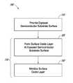
- FIG. 1is a flow chart generally illustrating a process for semiconductor passivation, according to some embodiments.
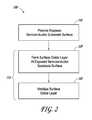
- FIG. 2is a flow chart illustrating further details of some embodiments of the process of FIG. 1 .
- FIG. 3shows a plot of capacitance vs. voltage with a frequency range from 100 Hz to 1 MHz for a metal oxide semiconductor capacitor having a hydrazine treated germanium surface, according to some embodiments.
- FIGS. 4A and 4Bshow plots illustrating voltage accelerator gamma and N eff , according to some embodiments.
- FIG. 5shows plots of capacitance vs. voltage with a frequency dispersion range from 100 Hz to 1 MHz for hydrazine treated interlayers on p and n-doped germanium substrates, according to some embodiments.
- passivation using siliconis not believed to be suitable for n-doped germanium transistor devices due to a high interface state density (Dit) at the germanium conduction band edge, as well as having no electron confinement for silicon with respect to germanium.
- itinterface state density
- the atomic layer deposition (ALD) of GeO 2has been proposed as another approach for forming a passivation layer for germanium transistor devices, and may also be suitable for CMOS devices by providing low Dit for both p-doped and n-doped germanium devices.
- ALDatomic layer deposition
- the physical instability of GeO 2may not be compatible with process flows for fabricating transistors.
- GeO 2exhibits undesirably high oxide trap density and may cause device reliability issues.
- a semiconductor surface having a high mobility semiconductormay be effectively passivated by nitridation, preferably using hydrazine, a hydrazine derivative, or a combination thereof. More preferably, the passivation is accomplished by forming a semiconductor oxynitride layer on the surface, with the oxynitride layer formed by nitridation using hydrazine, a hydrazine derivative, or a combination thereof.
- the surfacemay be the surface of a transistor channel region.
- the surface of the high mobility semiconductorhas a semiconductor oxide-containing film or layer (e.g., a surface oxide), which may be nitrided to form an oxynitride compound.
- a semiconductor oxide-containing filmmay be formed by oxidizing the semiconductor surface, by deposition of a semiconductor oxide-containing film on and in contact with the semiconductor surface, or a combination thereof.
- the semiconductor oxide-containing filmis deposited by atomic layer deposition (ALD).
- ALDatomic layer deposition
- a semiconductor oxide-containing filmis a film or layer that comprises the oxide of a semiconductor.
- a semiconductor oxynitride compoundis deposited on the high mobility semiconductor.
- the semiconductor oxynitridemay be deposited by ALD, using temporally-separated pulses of a semiconductor precursor, an oxygen precursor, and a nitrogen precursor.
- a gate stackis formed over the passivated high mobility semiconductor and the semiconductor oxynitride layer may be an interface layer or interlayer disposed, for example, between the semiconductor substrate and a dielectric layer, e.g., a gate dielectric layer.
- the semiconductor oxynitride layerforms a part of the gate stack.
- passivation by nitridation using hydrazine or its derivativescan provide various benefits.
- such nitridatione.g., nitridation of germanium substrates
- using such nitridatione.g., nitridation of germanium substrates
- to form a nitrogen containing layere.g., a semiconductor oxynitride
- the nitrogen containing layeris highly stable, which advantageously can provide good device reliability.
- FIG. 1is a flow chart generally illustrating a process 100 for semiconductor passivation, according to some embodiments.
- an exposed semiconductor substrate surfaceis provided.
- the exposed semiconductor surfacemay be part of a semiconductor substrate.
- a semiconductor substrateis a substrate that is at least partially formed of semiconductor material.
- the semiconductor substratemay be a semiconductor wafer, or may be a semiconductor wafer having overlying conductive and/or dielectric materials.
- the exposed semiconductor substrate surfacecomprises a high mobility semiconductor.
- the semiconductor at the exposed surfacecomprises germanium, silicon germanium, a group III-V semiconductor, a group II-VI semiconductor, or a 2D material such as MoS and graphene.
- the semiconductorcomprises InGaAs.
- Other suitable substrate surfacesinclude, GaAs, InP, InAs, and GaSb.
- the substratemay be a 300 mm or a 450 mm wafer.
- the substrate surfacecomprises multiple materials, including multiple semiconductor materials.
- the exposed surfacemay include the surface of a channel region of a transistor.
- the transistormay be, for example, a planar transistor, or may be a non-planar transistor, including a FinFET device or a vertical nanowire/gate-all-around (GAA) device.
- the transistorsmay be implemented as part of a complementary metal oxide semiconductor (CMOS) type integrated circuit. These CMOS integrated circuits utilize transistors having different doping types.
- CMOS integrated circuitsutilize transistors having different doping types.
- the transistorsmay be formed in pairs, with one member of each pair having a channel region that is N-doped, and another member of the pair having a channel region that is P-doped. It will be appreciated that the exposed surface may extend horizontally, vertically, or at an angle.
- the exposed semiconductor substrate surface provided at block 110is preferably substantially oxygen free.
- the substantially oxygen-free substrate surfaceis formed by subjecting the substrate to a native oxide removal process, to remove native oxide of the substrate surface.
- the exposed semiconductor substrate surfaceis passivated by nitridation.
- the semiconductor surfaceis exposed to a nitrogen precursor, which reacts with the surface to form a nitrogen-containing film at the surface.
- the nitrogen precursoris hydrazine (N 2 H 4 ), a hydrazine derivative or variant, or a combination thereof.
- hydrazine variants or derivativesinclude dimethylhydrazine (Me 2 NNH 2 ), tert-butylhydrazine (t-BuNHNH 2 ), bis(tertbutylhydrazido)diethylsilane, and bis(N,N-dimethylhydrazido)diethylsilane.
- the nitrogen precursor exposureis preferably performed for a duration ranging from about 10 seconds to about 5 minutes, more preferably from about 20 seconds to about 2 minutes.
- the process temperature during the nitrogen precursor exposuree.g., the temperature of the substrate, is preferably in the range from about 150° C. to about 400° C., more preferably about 200° C. to about 300° C.
- the nitrogen precursor exposuremay be accomplished by flowing nitrogen precursor into a process chamber into which the substrate is loaded.
- exposing the semiconductor surface to the nitrogen precursorforms a semiconductor oxynitride compound.
- surface oxidemay be formed at the semiconductor surface, e.g., by oxidizing the surface and/or by depositing a semiconductor oxide on and in contact with the surface, and the surface oxide may be nitrided by exposure to the nitrogen precursor, thereby forming the semiconductor oxynitride compound.
- the exposures to a semiconductor precursor, an oxygen precursor, and a nitrogen precursormay be cycled to form a semiconductor oxynitride layer.
- an exposed semiconductor surfaceis provided.
- the details of block 110are identical to that for block 110 of FIG. 1 , discussed above.
- the substrate surfacemay be subjected to a pretreatment process at block 110 , which may comprise one or more steps.
- the substrate surfacemay be exposed to one or more pretreatment reactants and/or to specific conditions, such as temperature or pressure.
- a pretreatmentmay be used for any number of reasons including to clean the substrate surface, remove impurities, remove native oxide, and provide desirable surface terminations.
- the pretreatmentremoves native oxide, to leave a substantially oxygen-free semiconductor surface.
- a pretreatmentcomprises exposing the substrate surface to one or more pretreatment reactant, such as (NH 4 ) 2 S, H 2 S, HCl, HBr, Cl 2 , HF, or combinations thereof.
- pretreatment reactantsuch as (NH 4 ) 2 S, H 2 S, HCl, HBr, Cl 2 , HF, or combinations thereof.
- HClmay be used as the pretreatment reactant.
- HFmay be used as the pretreatment reactant.
- multiple pretreatment reactantsare used sequentially or simultaneously.
- block 115corresponds to the nitridation block 115 of FIG. 1 .
- a surface oxide layeris formed and nitrided in the embodiments of FIG. 2 .
- an oxide layeris formed on and in contact with the exposed high mobility semiconductor.
- the oxideis preferably a semiconductor oxide, which forms a semiconductor oxide-containing film (which may also be referred to as a semiconductor oxide layer).
- the semiconductor oxidemay be formed by oxidizing the exposed high mobility semiconductor.
- the substratemay be thermally oxidized by contacting the substrate with oxidant, such as O 2 , O 3 , H 2 O, H 2 O 2 , N 2 O, NO, NO 2 , or combinations thereof.
- oxidantsuch as O 2 , O 3 , H 2 O, H 2 O 2 , N 2 O, NO, NO 2 , or combinations thereof.
- the thermal oxidationis performed without plasma-activating the oxidant.
- the oxidantmay be plasma-activated.
- the duration and temperature of the oxidationmay be selected to form an oxide layer of a desired thickness.
- the thickness of the oxide layermay be about 0.1 nm to about 1.5 nm, preferably about 0.1 nm to about 1.0 nm.
- the semiconductor oxide layeris formed by a deposition process, including vapor deposition processes such as chemical vapor deposition (CVD).
- CVDchemical vapor deposition
- the substrateis exposed to mutually reactive precursors that react, e.g. in the gas phase, to deposit a compound comprising elements of those precursors on the substrate. Reaction conditions may be established to decompose the precursors before and/or upon contact with the substrate.
- the semiconductor oxide layeris deposited by atomic layer deposition (ALD).
- ALDatomic layer deposition
- Gas phase reactionsare avoided by contacting, or exposing, the substrate alternately and sequentially with reactants. Vapor phase reactants are separated from each other in the reaction chamber, for example, by removing excess reactants and/or reactant byproducts from the reaction chamber between reactant pulses. Removing excess reactants and/or reactant byproducts may be achieved, for example, by purging the reaction space after each pulse of reactant gas using a vacuum and/or a purge gas.
- a purge gasmay also be flowed continuously before, during, and after each pulse of reactant gas.
- the purge gasmay also serve as a carrier gas for one or more of the reactants.
- the alternating reactant exposuresmay be accomplished by movement of the substrate and/or reactor parts, without stopping and starting the flow of precursors into the deposition chamber to accomplish the alternating exposures.
- an exposure to a particular reactantmay also be referred to as a “pulse,” and “reactants” may also be referred to as “precursors.” Exposure of the substrate to a sequence including each reactant for the deposition constitutes a deposition cycle; for example, where two reactants are utilized, exposing the substrate to a first and then a second reactant can constitute one deposition cycle.
- Each reactant pulseis preferably self-limiting.
- An excess of reactantis supplied during the pulse to saturate the susceptible structure surfaces.
- surface saturationensures reactant occupation of all available reactive sites (subject, for example, to physical size or “steric hindrance” restraints) and thus provides excellent step coverage.
- the degree of self-limiting behaviorcan be adjusted by, e.g., allowing some overlap of reactant pulses to trade off deposition speed (by allowing some CVD-type reactions) against conformality.
- Ideal ALD conditions with reactants well separated in time and spaceprovide self-limiting behavior and thus maximum conformality.
- less than a complete monolayeris deposited in one or more cycles, for example due to steric hindrance.
- more than one monolayermay be deposited by, for example, adjusting the deposition conditions to achieve some decomposition reaction, such as would occur in CVD or CVD-like processes.
- Limited CVD reactions mixed with the self-limiting ALD reactionscan raise the deposition rate.
- the deposition cyclesare repeated a desired number of times to form a layer of a desired thickness.
- Deposition temperaturesare preferably maintained below the precursor thermal decomposition temperature but at a high enough level to avoid condensation of reactants and to provide the activation energy for the desired surface reactions.
- the appropriate temperature window for any given ALD reactionwill depend upon the surface termination and reactant species involved.
- the reaction temperature for the various atomic layer depositions hereinmay be in a range from about room temperature to about 500° C., including from about 20° C. to about 500° C., from about 150° C. to about 400° C., from about 200° C. to about 350° C., and from about 250° C. to about 300° C. in some embodiments.
- the reaction pressuremay be from about 0.1 Torr to about 760 Torr. In some embodiments, the reaction pressure may be from about 0.5 Torr to about atmospheric pressure.
- a semiconductor oxide-containing layeris formed.
- the oxide-containing layeris preferably formed by ALD, by exposing the substrate to temporally separated pulses of a semiconductor precursor and an oxygen precursor.
- the semiconductor precursordeposits the same semiconductor as present in the underlying substrate.
- a germanium precursormay be used to deposit a germanium oxide over an exposed germanium-containing substrate surface.
- the semiconductor precursormay be a semiconductor-organic or a semiconductor halide compound.
- the semiconductor precursormay be a semiconductor alkoxide or alkylamine.
- suitable germanium precursorsinclude a germanium alkoxide (e.g., germanium ethoxide), a germanium alkylamine, germanium chloride, and cyclic germylene.
- the semiconductor precursorUpon contacting the substrate, the semiconductor precursor preferably absorbs on the substrate.
- the substrateis subsequently exposed to an oxygen precursor, which reacts with the semiconductor precursor to form an oxide of the semiconductor, e.g., germanium oxide.
- oxygen precursorsinclude O 2 , O 3 , H 2 O, H 2 O 2 , N 2 O, NO, NO 2 , and combinations thereof.
- the oxygen precursoris not part of a plasma and forms a thermal oxide with the semiconductor.
- the oxygen precursorcomprises oxygen radicals, for example oxygen radicals made by plasma. It will be appreciated that sequential and alternating exposure to the semiconductor precursor and an oxygen precursor constitute a deposition cycle, which may be repeated until an oxide layer of a desired thickness is deposited.
- the oxide layeris nitrided, by exposing the oxide containing layer to a nitrogen-containing precursor.
- the nitridationis performed as discussed above regarding block 115 of FIG. 1 .
- the nitridingis performed thermally, without exposing the nitrogen containing precursor to a plasma or excited species generated from a plasma.
- blocks 120 and 130may be performed during an atomic layer deposition that cycles through multiple performances of blocks 120 or 130 .
- block 130is performed intermittently during the deposition of the semiconductor oxide layer, and blocks 120 and 130 may be sequentially repeated multiple times.
- block 130may alternate with one or more ALD deposition cycles for depositing the semiconductor oxide at block 120 , thereby forming a semiconductor oxynitride compound.
- the block 115may be considered to be a semiconductor oxynitride deposition cycle in some embodiments, and block 115 may be repeated until a desired semiconductor oxynitride layer thickness is formed.
- each semiconductor oxynitride deposition cycleincludes a nitridation step.
- ALD deposition sub-cycles in block 120 for the semiconductor oxidee.g., GeO deposition cycles
- nitridation sub-cycles in bloc 130that include exposures to a semiconductor precursor and the nitrogen precursor.
- one or more ALD deposition sub-cycles in block 120 for the semiconductor oxidemay be alternated with one or more sub-cycles in block 130 that include exposure to a semiconductor precursor and a subsequent exposure to the nitrogen precursor.
- each deposition cycle or sub-cyclemay include one or more pulses of the same precursor.
- an oxide depositionmay include a plurality of semiconductor precursor exposures per one oxygen precursor exposure, or a plurality of oxygen precursor exposures per semiconductor precursor exposure.
- a nitridationmay include a plurality of nitrogen precursor exposures per one semiconductor precursor exposure, or a plurality of semiconductor precursor exposures per nitrogen precursor exposure. For example, if increasing the amount of semiconductor or nitrogen in a film is desired, at least one ALD cycle, every other ALD cycle, or every third, fourth, fifth, sixth cycle, etc.
- At least one ALD cycle, every other ALD cycle, or every third, fourth, fifth, sixth cycle, etc.could include one or more additional oxygen or semiconductor precursor pulses, respectively.
- the semiconductor oxynitride deposition cyclemay include a semiconductor oxide deposition sub-cycle and a semiconductor nitride deposition sub-cycle.
- the semiconductor oxide deposition sub-cyclemay include exposure to a semiconductor precursor and an oxygen precursor (ratios of which may vary, as discussed above), and the semiconductor nitride sub-cycle may include exposure to a semiconductor precursor and a nitrogen precursor (ratios of which may vary, as discussed above).
- the ratios of the semiconductor oxide deposition sub-cycle to the semiconductor nitride deposition sub-cyclemay vary, for example from about 2:1 to about 1:5.
- the relative ratios of the precursorsmay vary over the course of the interlayer deposition to form an interlayer with a graded composition.
- the ratio of semiconductor precursor to oxygen precursor or nitrogen precursor to semiconductor precursormay change with time.
- the ratio of the semiconductor oxide deposition sub-cycle 120 to the semiconductor nitride deposition sub-cycle 130may change with time, e.g., increase with time to form an oxynitride layer with an increasingly higher oxygen concentration with increasing thickness.
- the degree of nitridationmay be varied, e.g., by varying the number and/or duration of the pulses of the nitrogen precursor over the course of the deposition of the semiconductor oxynitride layer to form an oxynitride layer with e.g. an increasingly higher nitrogen concentration with increasing thickness.
- various additional layers of materialmay be formed on the semiconductor oxynitride layer.
- a dielectric layere.g., a high-k dielectric such as HfO 2
- a conductive gate materialmay be deposited over the dielectric layer to form a gate stack.
- the conductive gate materialmay be a metal. It will be appreciated that other layers of material may also be provided between the semiconductor oxynitride layer and the dielectric layer, or between the dielectric layer and the conductive gate material, to provide desired physical and/or electrical properties in some embodiments.
- MOSmetal oxide semiconductor
- the germaniumwas part of a 1.5 ⁇ m germanium layer grown epitaxially on a silicon wafer and p-doped.
- the substratewas then pre-treated by being dipped in HF.
- the pre-treated p-doped germanium-containing substrate surfacewas then passivated by exposure to hydrazine in a Pulsar® ALD reactor available from ASM International N.V. of Almere, the Netherlands. The exposure duration was 1 minute, at a process temperature of 250° C.
- a 2 nm aluminum oxide layer and then a 2 nm hafnium oxide layerwere deposited to form a dielectric stack over and contacting the hydrazine-treated surface.
- Platinumwas deposited on the dielectric stack as a gate electrode, thereby forming the MOS capacitor.
- the platinumwas deposited by evaporation, which included depositing platinum dots on one side of the substrate and a blanket platinum layer on the back side.
- the resulting structureprovided a V FB (flat band voltage) of roughly 0.7V, indicating an effective work function for the platinum of about 5.27 eV and low fixed charges.
- FIG. 3shows a plot of capacitance vs. voltage with a frequency range from 100 Hz to 1 MHz for the metal oxide semiconductor capacitor having the hydrazine treated germanium surface.
- CETis the capacitance effective thickness, which is equal to the effective oxide thickness (EOT) plus a quantum mechanical correction and Dit is the interface state density.
- EOTeffective oxide thickness
- Ditis the interface state density.
- FIG. 4Ashows plots illustrating voltage accelerator gamma and N eff (equivalent sheet charge) for the MOS capacitor, formed by a p-doped germanium substrate having a hydrazine treated surface with an overlying dielectric stack of a 2 nm hafnium oxide layer overlying a 2 nm aluminum oxide layer.
- N effis advantageously low
- the voltage accelerator gamma ( ⁇ )is advantageously high for the hydrazine treated germanium substrate.
- the targetwas set at 5e10/cm 2 @3.5 MV/cm, which presented a reliability specification for a device able to sustain 0.5V overdrive at 1.4 nm CET. Notably, the hydrazine treated germanium substrate exceeded the target.
- Example 2Passivation of p-doped and n-doped germanium using a germanium oxynitride layer was investigated in a MOS capacitor.
- the germaniumwas part of a 1.5 ⁇ m germanium layer grown epitaxially on a silicon wafer and p-doped and n-doped.
- the substratewas then pre-treated by being dipped in HF.
- a germanium oxynitride layerwas deposited on each of a p-doped and n-doped germanium substrate.
- the depositionwas performed a Pulsar® ALD reactor available from ASM International N.V. of Almere, the Netherlands.
- TDMAGetetrakis(dimethylamino)germanium
- H 2 Othe oxygen precursor
- N 2 H 4hydrazine
- the durations of the precursor pulses and intervening purgeswere, in order, as follows: TDMAGe—3 s; Purge—4 s; H2O—3 s; Purge—6 s; TDMAGe—3 s; Purge—4 s; N2H4—3 s; Purge—6 s.
- the deposition cycleswere repeated until a layer 1 nm thick was deposited.
- a 3 nm hafnium oxide layerwas next deposited on the germanium oxynitride layer.
- a platinum gate electrodewas then formed on the hafnium oxide layer.
- FIG. 4Bshows a plot illustrating voltage accelerator gamma and N eff (equivalent sheet charge) for a MOS capacitor formed by a p-doped germanium substrate having a 1 nm ALD germanium oxynitride layer formed between the substrate and a dielectric stack of a 3 nm hafnium oxide layer overlaying a 1 nm aluminum oxide layer.
- Example 1included for comparison are i) a p-doped germanium substrate having a germanium oxide formed between the substrate and a hafnium oxide layer, and ii) a p-doped germanium substrate having a germanium oxide formed between the substrate and a dielectric stack of a 2 nm hafnium oxide layer overlying a 2 nm aluminum oxide layer.
- N eff and gamma ( ⁇ )are both improved over comparison MOS capacitors i) and ii).
- the performance in terms of N eff and gamma ( ⁇ )is lower than for the nitrided pGe surface discussed in Example 1, this performance still meets the target and advantageously has a lower D it value than the sample that had the hydrazine treated p-doped germanium surface. Therefore, the germanium oxynitride provides an advantageous mix of performance parameters. It is expected that adjustments to the process of passivation using hydrazine or a hydrazine derivative could provide further increases in performance.
- FIG. 5shows a plot of capacitance vs. voltage with a frequency range from 100 Hz to 1 MHz for the metal oxide semiconductor capacitor using the ALD oxynitride passivation layers described above.
- the germanium oxynitride (GeON)improved N eff by a factor of 3.5 on the p-doped germanium substrate and a factor of 2.5 on the n-doped germanium substrate.
- a lower N effis indicative of better stability and reliability.
- the GeON layerprovided better stability than GeO 2 .
- the GeON layerprovided a clear reliability improvement on n-doped germanium substrates compared to a GeO 2 baseline reference ( ⁇ 2.5 times lower N eff ). It will be appreciated that such improvements on n-doped germanium substrates are particularly challenging to achieve.
Landscapes
- Engineering & Computer Science (AREA)
- Physics & Mathematics (AREA)
- Condensed Matter Physics & Semiconductors (AREA)
- General Physics & Mathematics (AREA)
- Computer Hardware Design (AREA)
- Microelectronics & Electronic Packaging (AREA)
- Power Engineering (AREA)
- Manufacturing & Machinery (AREA)
- Chemical & Material Sciences (AREA)
- Chemical Kinetics & Catalysis (AREA)
- Formation Of Insulating Films (AREA)
- Insulated Gate Type Field-Effect Transistor (AREA)
Abstract
Description
Field
This disclosure relates generally to semiconductor processing and, more particularly, to passivation of semiconductor substrates, including passivation of channel regions of transistors.
Description of the Related Art
Semiconductor materials that exhibit high charge-carrier mobility have gained interest as possible materials for use in various electronic devices, such as transistors in integrated circuits. High charge-carrier mobility materials have a higher charge-carrier mobility than silicon, and may improve the performance of these electronic devices, relative to forming the devices using silicon as the only semiconductor. Examples of high charge-carrier mobility semiconductor materials include silicon germanium, germanium and group III-V semiconductor materials, such as GaAs, InP, InGaAs, InAs, and GaSb.
The passivation of semiconductor materials can improve the electrical properties of devices formed with these materials, and may also improve the physical properties and physical stability of those materials, which can provide benefits for device reliability. For example, passivating the surface of a transistor channel region before forming a gate dielectric can improve the performance of the resulting transistor. However, the passivation of high mobility semiconductors faces various challenges and work continues on developing suitable passivation techniques for these materials.
In some embodiments, a method for integrated circuit fabrication is provided. The method comprises passivating the surface of a substrate comprising a high mobility semiconductor by removing native semiconductor oxide from the surface; subsequently forming a semiconductor oxide-containing film on the surface; and thermally nitriding the semiconductor oxide-containing film by exposing the semiconductor oxide-containing film to at least one of hydrazine and a hydrazine derivative.
In some other embodiments, a method for integrated circuit fabrication is provided. The method comprises providing a transistor channel region having an exposed semiconductor surface, and passivating the exposed semiconductor surface by nitriding the exposed semiconductor surface using a nitrogen precursor comprising at least one of hydrazine and a hydrazine derivative.
Various approaches have been proposed for passivating semiconductors having high charge-carrier mobility (also referred to as high mobility semiconductors), but these approaches have been found to have significant drawbacks. Passivation of a channel region surface using deposited silicon is one approach that has been developed for p-doped germanium-based MOSFETs. However, this approach may have a high cost and low throughput since it relies on a low temperature epitaxial deposition process, and may also have an undesirable inversion thickness and conformality issues, particularly in FinFET/vertical nanowire devices. In addition, without being limited by theory, passivation using silicon is not believed to be suitable for n-doped germanium transistor devices due to a high interface state density (Dit) at the germanium conduction band edge, as well as having no electron confinement for silicon with respect to germanium.
The atomic layer deposition (ALD) of GeO2has been proposed as another approach for forming a passivation layer for germanium transistor devices, and may also be suitable for CMOS devices by providing low Dit for both p-doped and n-doped germanium devices. However, the physical instability of GeO2may not be compatible with process flows for fabricating transistors. In addition, GeO2exhibits undesirably high oxide trap density and may cause device reliability issues.
In accordance with some embodiments, a semiconductor surface having a high mobility semiconductor may be effectively passivated by nitridation, preferably using hydrazine, a hydrazine derivative, or a combination thereof. More preferably, the passivation is accomplished by forming a semiconductor oxynitride layer on the surface, with the oxynitride layer formed by nitridation using hydrazine, a hydrazine derivative, or a combination thereof. The surface may be the surface of a transistor channel region.
In some embodiments, the surface of the high mobility semiconductor has a semiconductor oxide-containing film or layer (e.g., a surface oxide), which may be nitrided to form an oxynitride compound. For example, a semiconductor oxide-containing film may be formed by oxidizing the semiconductor surface, by deposition of a semiconductor oxide-containing film on and in contact with the semiconductor surface, or a combination thereof. Preferably, the semiconductor oxide-containing film is deposited by atomic layer deposition (ALD). As used herein, a semiconductor oxide-containing film is a film or layer that comprises the oxide of a semiconductor.
In some other embodiments, a semiconductor oxynitride compound is deposited on the high mobility semiconductor. For example, the semiconductor oxynitride may be deposited by ALD, using temporally-separated pulses of a semiconductor precursor, an oxygen precursor, and a nitrogen precursor.
In some embodiments, a gate stack is formed over the passivated high mobility semiconductor and the semiconductor oxynitride layer may be an interface layer or interlayer disposed, for example, between the semiconductor substrate and a dielectric layer, e.g., a gate dielectric layer. In some embodiments, the semiconductor oxynitride layer forms a part of the gate stack.
Advantageously, passivation by nitridation using hydrazine or its derivatives can provide various benefits. In some embodiments, such nitridation (e.g., nitridation of germanium substrates) can provide exceptionally low oxide trap density levels. In some embodiments, using such nitridation (e.g., nitridation of germanium substrates) to form a nitrogen containing layer (e.g., a semiconductor oxynitride) can provide both low oxide trap densities and low Dit. The nitrogen containing layer is highly stable, which advantageously can provide good device reliability.
Reference will now be made to the Figures Like numerals refer to like features throughout.
Preferably, the exposed semiconductor substrate surface comprises a high mobility semiconductor. In some embodiments, the semiconductor at the exposed surface comprises germanium, silicon germanium, a group III-V semiconductor, a group II-VI semiconductor, or a 2D material such as MoS and graphene. In some embodiments, the semiconductor comprises InGaAs. Other suitable substrate surfaces include, GaAs, InP, InAs, and GaSb. In some embodiments the substrate may be a 300 mm or a 450 mm wafer. In some embodiments, the substrate surface comprises multiple materials, including multiple semiconductor materials.
The exposed surface may include the surface of a channel region of a transistor. The transistor may be, for example, a planar transistor, or may be a non-planar transistor, including a FinFET device or a vertical nanowire/gate-all-around (GAA) device. In some embodiments, the transistors may be implemented as part of a complementary metal oxide semiconductor (CMOS) type integrated circuit. These CMOS integrated circuits utilize transistors having different doping types. For example, the transistors may be formed in pairs, with one member of each pair having a channel region that is N-doped, and another member of the pair having a channel region that is P-doped. It will be appreciated that the exposed surface may extend horizontally, vertically, or at an angle.
With continued reference toFIG. 1 , the exposed semiconductor substrate surface provided atblock 110 is preferably substantially oxygen free. In some embodiments, atblock 110, the substantially oxygen-free substrate surface is formed by subjecting the substrate to a native oxide removal process, to remove native oxide of the substrate surface.
Atblock 115, the exposed semiconductor substrate surface is passivated by nitridation. In some embodiments, the semiconductor surface is exposed to a nitrogen precursor, which reacts with the surface to form a nitrogen-containing film at the surface. Preferably, the nitrogen precursor is hydrazine (N2H4), a hydrazine derivative or variant, or a combination thereof. Examples of hydrazine variants or derivatives include dimethylhydrazine (Me2NNH2), tert-butylhydrazine (t-BuNHNH2), bis(tertbutylhydrazido)diethylsilane, and bis(N,N-dimethylhydrazido)diethylsilane. The nitrogen precursor exposure is preferably performed for a duration ranging from about 10 seconds to about 5 minutes, more preferably from about 20 seconds to about 2 minutes. The process temperature during the nitrogen precursor exposure, e.g., the temperature of the substrate, is preferably in the range from about 150° C. to about 400° C., more preferably about 200° C. to about 300° C. The nitrogen precursor exposure may be accomplished by flowing nitrogen precursor into a process chamber into which the substrate is loaded.
In some embodiments, exposing the semiconductor surface to the nitrogen precursor forms a semiconductor oxynitride compound. For example, surface oxide may be formed at the semiconductor surface, e.g., by oxidizing the surface and/or by depositing a semiconductor oxide on and in contact with the surface, and the surface oxide may be nitrided by exposure to the nitrogen precursor, thereby forming the semiconductor oxynitride compound. In some embodiments, as discussed herein, the exposures to a semiconductor precursor, an oxygen precursor, and a nitrogen precursor may be cycled to form a semiconductor oxynitride layer.
With reference now toFIG. 2 , a flow chart further illustrating details of some embodiments of theprocess 100 ofFIG. 1 is shown. Atblock 110, an exposed semiconductor surface is provided. The details ofblock 110 are identical to that forblock 110 ofFIG. 1 , discussed above. For example, in some embodiments the substrate surface may be subjected to a pretreatment process atblock 110, which may comprise one or more steps. In the pretreatment, the substrate surface may be exposed to one or more pretreatment reactants and/or to specific conditions, such as temperature or pressure. A pretreatment may be used for any number of reasons including to clean the substrate surface, remove impurities, remove native oxide, and provide desirable surface terminations. Preferably, the pretreatment removes native oxide, to leave a substantially oxygen-free semiconductor surface. In some embodiments, a pretreatment comprises exposing the substrate surface to one or more pretreatment reactant, such as (NH4)2S, H2S, HCl, HBr, Cl2, HF, or combinations thereof. In some embodiments, such as where a III-V material is used, HCl may be used as the pretreatment reactant. In some embodiments, such as where a germanium substrate is used, HF may be used as the pretreatment reactant. In some embodiments, multiple pretreatment reactants are used sequentially or simultaneously.
With continued reference toFIG. 2 , block115 corresponds to thenitridation block 115 ofFIG. 1 . However, rather than nitriding the exposed high mobility semiconductor itself, a surface oxide layer is formed and nitrided in the embodiments ofFIG. 2 . Atblock 120, an oxide layer is formed on and in contact with the exposed high mobility semiconductor.
In some embodiments, the oxide is preferably a semiconductor oxide, which forms a semiconductor oxide-containing film (which may also be referred to as a semiconductor oxide layer). The semiconductor oxide may be formed by oxidizing the exposed high mobility semiconductor. For example, the substrate may be thermally oxidized by contacting the substrate with oxidant, such as O2, O3, H2O, H2O2, N2O, NO, NO2, or combinations thereof. It will be appreciated that the thermal oxidation is performed without plasma-activating the oxidant. In some other embodiments, the oxidant may be plasma-activated. Among other things, the duration and temperature of the oxidation may be selected to form an oxide layer of a desired thickness. For example, the thickness of the oxide layer may be about 0.1 nm to about 1.5 nm, preferably about 0.1 nm to about 1.0 nm.
In some other embodiments, the semiconductor oxide layer is formed by a deposition process, including vapor deposition processes such as chemical vapor deposition (CVD). It will be appreciated that, for CVD, the substrate is exposed to mutually reactive precursors that react, e.g. in the gas phase, to deposit a compound comprising elements of those precursors on the substrate. Reaction conditions may be established to decompose the precursors before and/or upon contact with the substrate.
More preferably, the semiconductor oxide layer is deposited by atomic layer deposition (ALD). It will be appreciated that the ALD-type processes for forming the various layers described herein are based on controlled, self-limiting surface reactions and can provide precise control of the film composition and layer thickness, and high conformality. Gas phase reactions are avoided by contacting, or exposing, the substrate alternately and sequentially with reactants. Vapor phase reactants are separated from each other in the reaction chamber, for example, by removing excess reactants and/or reactant byproducts from the reaction chamber between reactant pulses. Removing excess reactants and/or reactant byproducts may be achieved, for example, by purging the reaction space after each pulse of reactant gas using a vacuum and/or a purge gas. A purge gas may also be flowed continuously before, during, and after each pulse of reactant gas. For example, in some embodiments the purge gas may also serve as a carrier gas for one or more of the reactants. In some other embodiments, the alternating reactant exposures may be accomplished by movement of the substrate and/or reactor parts, without stopping and starting the flow of precursors into the deposition chamber to accomplish the alternating exposures. It will be appreciated that, as used herein, an exposure to a particular reactant may also be referred to as a “pulse,” and “reactants” may also be referred to as “precursors.” Exposure of the substrate to a sequence including each reactant for the deposition constitutes a deposition cycle; for example, where two reactants are utilized, exposing the substrate to a first and then a second reactant can constitute one deposition cycle.
Each reactant pulse is preferably self-limiting. An excess of reactant is supplied during the pulse to saturate the susceptible structure surfaces. In theory, surface saturation ensures reactant occupation of all available reactive sites (subject, for example, to physical size or “steric hindrance” restraints) and thus provides excellent step coverage. In some arrangements, the degree of self-limiting behavior can be adjusted by, e.g., allowing some overlap of reactant pulses to trade off deposition speed (by allowing some CVD-type reactions) against conformality. Ideal ALD conditions with reactants well separated in time and space provide self-limiting behavior and thus maximum conformality. In some embodiments, less than a complete monolayer is deposited in one or more cycles, for example due to steric hindrance. In some embodiments, more than one monolayer may be deposited by, for example, adjusting the deposition conditions to achieve some decomposition reaction, such as would occur in CVD or CVD-like processes. Limited CVD reactions mixed with the self-limiting ALD reactions can raise the deposition rate. The deposition cycles are repeated a desired number of times to form a layer of a desired thickness.
Deposition temperatures are preferably maintained below the precursor thermal decomposition temperature but at a high enough level to avoid condensation of reactants and to provide the activation energy for the desired surface reactions. The appropriate temperature window for any given ALD reaction will depend upon the surface termination and reactant species involved. The reaction temperature for the various atomic layer depositions herein may be in a range from about room temperature to about 500° C., including from about 20° C. to about 500° C., from about 150° C. to about 400° C., from about 200° C. to about 350° C., and from about 250° C. to about 300° C. in some embodiments.
The reaction pressure may be from about 0.1 Torr to about 760 Torr. In some embodiments, the reaction pressure may be from about 0.5 Torr to about atmospheric pressure.
With continued reference toFIG. 2 , atblock 120, as discussed above, a semiconductor oxide-containing layer is formed. The oxide-containing layer is preferably formed by ALD, by exposing the substrate to temporally separated pulses of a semiconductor precursor and an oxygen precursor. In some embodiments, the semiconductor precursor deposits the same semiconductor as present in the underlying substrate. For example, a germanium precursor may be used to deposit a germanium oxide over an exposed germanium-containing substrate surface.
In some embodiments, the semiconductor precursor may be a semiconductor-organic or a semiconductor halide compound. For example, the semiconductor precursor may be a semiconductor alkoxide or alkylamine. Where the semiconductor is germanium, suitable germanium precursors include a germanium alkoxide (e.g., germanium ethoxide), a germanium alkylamine, germanium chloride, and cyclic germylene.
Upon contacting the substrate, the semiconductor precursor preferably absorbs on the substrate. In some embodiments, the substrate is subsequently exposed to an oxygen precursor, which reacts with the semiconductor precursor to form an oxide of the semiconductor, e.g., germanium oxide. Examples of oxygen precursors include O2, O3, H2O, H2O2, N2O, NO, NO2, and combinations thereof. In some embodiments, the oxygen precursor is not part of a plasma and forms a thermal oxide with the semiconductor. In some embodiments, the oxygen precursor comprises oxygen radicals, for example oxygen radicals made by plasma. It will be appreciated that sequential and alternating exposure to the semiconductor precursor and an oxygen precursor constitute a deposition cycle, which may be repeated until an oxide layer of a desired thickness is deposited.
With continued reference toFIG. 2 , atblock 130, the oxide layer is nitrided, by exposing the oxide containing layer to a nitrogen-containing precursor. Preferably, the nitridation is performed as discussed above regardingblock 115 ofFIG. 1 . Preferably, the nitriding is performed thermally, without exposing the nitrogen containing precursor to a plasma or excited species generated from a plasma.
With continued reference toFIG. 2 , in some embodiments, blocks120 and130 may be performed during an atomic layer deposition that cycles through multiple performances ofblocks block 120, thereby forming a semiconductor oxynitride compound. As a result, theblock 115 may be considered to be a semiconductor oxynitride deposition cycle in some embodiments, and block115 may be repeated until a desired semiconductor oxynitride layer thickness is formed. In some embodiments, each semiconductor oxynitride deposition cycle includes a nitridation step. In some other embodiments, ALD deposition sub-cycles inblock 120 for the semiconductor oxide (e.g., GeO deposition cycles) may be alternated with nitridation sub-cycles inbloc 130 that include exposures to a semiconductor precursor and the nitrogen precursor. For example, one or more ALD deposition sub-cycles inblock 120 for the semiconductor oxide may be alternated with one or more sub-cycles inblock 130 that include exposure to a semiconductor precursor and a subsequent exposure to the nitrogen precursor.
It will be appreciated that for any of the atomic layer depositions herein, the relative ratios of pulses of precursors may deviate from a 1:1 ratio. For example, each deposition cycle or sub-cycle may include one or more pulses of the same precursor. For example, an oxide deposition may include a plurality of semiconductor precursor exposures per one oxygen precursor exposure, or a plurality of oxygen precursor exposures per semiconductor precursor exposure. Similarly, a nitridation may include a plurality of nitrogen precursor exposures per one semiconductor precursor exposure, or a plurality of semiconductor precursor exposures per nitrogen precursor exposure. For example, if increasing the amount of semiconductor or nitrogen in a film is desired, at least one ALD cycle, every other ALD cycle, or every third, fourth, fifth, sixth cycle, etc. could include one or more additional semiconductor or nitrogen precursor pulses, respectively. Similarly, if increasing the amount of oxygen or semiconductor in the semiconductor oxynitride film is desired, at least one ALD cycle, every other ALD cycle, or every third, fourth, fifth, sixth cycle, etc. could include one or more additional oxygen or semiconductor precursor pulses, respectively.
In some embodiments, as discussed herein, the semiconductor oxynitride deposition cycle may include a semiconductor oxide deposition sub-cycle and a semiconductor nitride deposition sub-cycle. For example, the semiconductor oxide deposition sub-cycle may include exposure to a semiconductor precursor and an oxygen precursor (ratios of which may vary, as discussed above), and the semiconductor nitride sub-cycle may include exposure to a semiconductor precursor and a nitrogen precursor (ratios of which may vary, as discussed above). In some embodiments, the ratios of the semiconductor oxide deposition sub-cycle to the semiconductor nitride deposition sub-cycle may vary, for example from about 2:1 to about 1:5.
In addition, the relative ratios of the precursors may vary over the course of the interlayer deposition to form an interlayer with a graded composition. For example, the ratio of semiconductor precursor to oxygen precursor or nitrogen precursor to semiconductor precursor may change with time. In some embodiments, the ratio of the semiconductor oxide deposition sub-cycle120 to the semiconductornitride deposition sub-cycle 130 may change with time, e.g., increase with time to form an oxynitride layer with an increasingly higher oxygen concentration with increasing thickness. In some other embodiments, the degree of nitridation may be varied, e.g., by varying the number and/or duration of the pulses of the nitrogen precursor over the course of the deposition of the semiconductor oxynitride layer to form an oxynitride layer with e.g. an increasingly higher nitrogen concentration with increasing thickness.
After the formation of the semiconductor oxynitride layer is completed, various additional layers of material may be formed on the semiconductor oxynitride layer. For example, a dielectric layer, e.g., a high-k dielectric such as HfO2, may be deposited over the interlayer and a conductive gate material may be deposited over the dielectric layer to form a gate stack. In some embodiments, the conductive gate material may be a metal. It will be appreciated that other layers of material may also be provided between the semiconductor oxynitride layer and the dielectric layer, or between the dielectric layer and the conductive gate material, to provide desired physical and/or electrical properties in some embodiments.
Hydrazine passivation of germanium was investigated in a metal oxide semiconductor (MOS) capacitor, which has a structure similar to a MOS transistor, except that PN junctions (and source/drain regions) are absent. The germanium was part of a 1.5 μm germanium layer grown epitaxially on a silicon wafer and p-doped. The substrate was then pre-treated by being dipped in HF. The pre-treated p-doped germanium-containing substrate surface was then passivated by exposure to hydrazine in a Pulsar® ALD reactor available from ASM International N.V. of Almere, the Netherlands. The exposure duration was 1 minute, at a process temperature of 250° C. A 2 nm aluminum oxide layer and then a 2 nm hafnium oxide layer were deposited to form a dielectric stack over and contacting the hydrazine-treated surface. Platinum was deposited on the dielectric stack as a gate electrode, thereby forming the MOS capacitor. The platinum was deposited by evaporation, which included depositing platinum dots on one side of the substrate and a blanket platinum layer on the back side. The resulting structure provided a VFB(flat band voltage) of roughly 0.7V, indicating an effective work function for the platinum of about 5.27 eV and low fixed charges.
Passivation of p-doped and n-doped germanium using a germanium oxynitride layer was investigated in a MOS capacitor. As in Example 1, the germanium was part of a 1.5 μm germanium layer grown epitaxially on a silicon wafer and p-doped and n-doped. The substrate was then pre-treated by being dipped in HF. A germanium oxynitride layer was deposited on each of a p-doped and n-doped germanium substrate. The deposition was performed a Pulsar® ALD reactor available from ASM International N.V. of Almere, the Netherlands. The germanium oxynitride interlayer as deposited by ALD using tetrakis(dimethylamino)germanium (TDMAGe) as the germanium precursor, H2O as the oxygen precursor, and hydrazine (N2H4) as the nitrogen precursor. Each deposition cycle included the following sequence of pulses:
TDMAGe
H2O
TDMAGe
N2H4
Ten cycles were performed, with N2H4exposure durations of a few second each time. The durations of the precursor pulses and intervening purges were, in order, as follows: TDMAGe—3 s; Purge—4 s; H2O—3 s; Purge—6 s; TDMAGe—3 s; Purge—4 s; N2H4—3 s; Purge—6 s. The deposition cycles were repeated until alayer 1 nm thick was deposited. A 3 nm hafnium oxide layer was next deposited on the germanium oxynitride layer. A platinum gate electrode was then formed on the hafnium oxide layer.
It will be appreciated by those skilled in the art that various omissions, additions and modifications can be made to the processes and structures described above without departing from the scope of the invention. It is contemplated that various combinations or sub-combinations of the specific features and aspects of the embodiments may be made and still fall within the scope of the description. Various features and aspects of the disclosed embodiments can be combined with, or substituted for, one another in order. All such modifications and changes are intended to fall within the scope of the invention, as defined by the appended claims.
Claims (24)
1. A method for integrated circuit fabrication, comprising:
passivating a surface of a substrate, the surface comprising a high-mobility semiconductor, wherein passivating comprises:
removing native semiconductor oxide from the surface;
subsequently forming a semiconductor oxide-containing film on the surface, wherein the semiconductor oxide-containing film is an oxide of the high-mobility semiconductor; and
thermally nitriding the semiconductor oxide-containing film by exposing the semiconductor oxide-containing film to at least one of hydrazine and a hydrazine derivative.
2. The method ofclaim 1 , wherein the surface comprising the high mobility semiconductor is part of a transistor channel region.
3. The method ofclaim 1 , wherein the high mobility semiconductor comprises germanium.
4. The method ofclaim 3 , wherein the germanium is n-doped germanium.
5. The method ofclaim 1 , wherein the high mobility semiconductor comprises a compound semiconductor.
6. The method ofclaim 5 , wherein the compound semiconductor is a group III-V semiconductor.
7. The method ofclaim 1 , wherein nitriding the semiconductor oxide-containing film converts the semiconductor oxide into an oxynitride layer.
8. The method ofclaim 1 , wherein forming the semiconductor oxide-containing film comprises performing an atomic layer deposition, the atomic layer deposition comprising a plurality of deposition cycles, each deposition cycle comprising:
subjecting the substrate to temporally separated exposures to a semiconductor precursor comprising the high mobility semiconductor and an oxygen precursor.
9. The method ofclaim 8 , wherein forming the semiconductor oxide-containing film and thermally nitriding the semiconductor oxide-containing film are part of a same deposition cycle of the plurality of deposition cycles, wherein each deposition cycle further comprises:
subjecting the substrate to an exposure to a nitrogen precursor temporally separated from the exposures to the semiconductor precursor and the oxygen precursor.
10. The method ofclaim 9 , wherein subjecting the substrate to an exposure to a nitrogen precursor is part of performing a plurality of deposition subcycles, each subcycle comprising:
subjecting the substrate to temporally separated exposures to a semiconductor precursor and the nitrogen precursor.
11. The method ofclaim 10 , wherein the semiconductor precursor used in each deposition cycle is the same.
12. The method ofclaim 9 , wherein subjecting the substrate to the exposure to the nitrogen precursor is performed after subjecting the substrate to an exposure to the semiconductor precursor and before subjecting the substrate to an exposure to the oxygen precursor.
13. The method ofclaim 8 , wherein the semiconductor precursor is selected from the group consisting of germanium alkoxides, germanium alkylamines, germanium chlorides, and cyclic germylenes, and combinations thereof.
14. The method ofclaim 8 , wherein the oxygen precursor is selected from the group consisting of O2, O3, H2O, H2O2, and combinations thereof.
15. The method ofclaim 1 , wherein forming the semiconductor oxide-containing film comprises oxidizing the substrate surface.
16. The method ofclaim 15 , wherein oxidizing the substrate surface comprises exposing the substrate surface to an oxygen plasma or to H2O2.
17. The method ofclaim 15 , wherein oxidizing the substrate surface comprises exposing the substrate surface to H2O2.
18. A method for integrated circuit fabrication, comprising:
providing a transistor channel region having an exposed semiconductor surface; and
forming a passivation layer comprising a nitride of a same semiconductor species as the exposed semiconductor surface, wherein forming the passivation layer comprises nitriding the exposed semiconductor surface using a nitrogen precursor comprising at least one of hydrazine and a hydrazine derivative.
19. The method ofclaim 18 , wherein nitriding the exposed semiconductor surface forms a semiconductor nitride-containing layer.
20. The method ofclaim 19 , wherein forming the passivation layer comprises exposing the substrate surface to an oxidizing gas and wherein the semiconductor nitride-containing layer is a semiconductor oxynitride-containing layer.
21. The method ofclaim 18 , wherein forming the semiconductor nitride-containing layer comprises performing an atomic layer deposition.
22. The method ofclaim 21 , wherein the atomic layer deposition comprises subjecting the substrate to temporally separated exposures to a semiconductor precursor and an oxygen precursor and wherein the semiconductor nitride-containing layer is a semiconductor oxynitride-containing layer.
23. The method ofclaim 18 , further comprising depositing a gate dielectric layer over the passivated semiconductor surface.
24. The method ofclaim 18 , wherein the exposed semiconductor surface comprises germanium or a group III-V semiconductor, and wherein the passivation layer comprises a compound comprising: nitrogen and germanium, or nitrogen and the group III-V semiconductor.
Priority Applications (4)
| Application Number | Priority Date | Filing Date | Title |
|---|---|---|---|
| US14/729,510US9711350B2 (en) | 2015-06-03 | 2015-06-03 | Methods for semiconductor passivation by nitridation |
| US15/169,430US10490475B2 (en) | 2015-06-03 | 2016-05-31 | Methods for semiconductor passivation by nitridation after oxide removal |
| TW105117329ATWI744233B (en) | 2015-06-03 | 2016-06-02 | Integrated circuit fabrication method and semiconductor processing reactor system |
| KR1020160069760AKR102375116B1 (en) | 2015-06-03 | 2016-06-03 | Methods for semiconductor passivation by nitridation after oxide removal |
Applications Claiming Priority (1)
| Application Number | Priority Date | Filing Date | Title |
|---|---|---|---|
| US14/729,510US9711350B2 (en) | 2015-06-03 | 2015-06-03 | Methods for semiconductor passivation by nitridation |
Related Child Applications (1)
| Application Number | Title | Priority Date | Filing Date |
|---|---|---|---|
| US15/169,430Continuation-In-PartUS10490475B2 (en) | 2015-06-03 | 2016-05-31 | Methods for semiconductor passivation by nitridation after oxide removal |
Publications (2)
| Publication Number | Publication Date |
|---|---|
| US20160358772A1 US20160358772A1 (en) | 2016-12-08 |
| US9711350B2true US9711350B2 (en) | 2017-07-18 |
Family
ID=57452050
Family Applications (1)
| Application Number | Title | Priority Date | Filing Date |
|---|---|---|---|
| US14/729,510ActiveUS9711350B2 (en) | 2015-06-03 | 2015-06-03 | Methods for semiconductor passivation by nitridation |
Country Status (1)
| Country | Link |
|---|---|
| US (1) | US9711350B2 (en) |
Families Citing this family (359)
| Publication number | Priority date | Publication date | Assignee | Title |
|---|---|---|---|---|
| US10378106B2 (en) | 2008-11-14 | 2019-08-13 | Asm Ip Holding B.V. | Method of forming insulation film by modified PEALD |
| US9394608B2 (en) | 2009-04-06 | 2016-07-19 | Asm America, Inc. | Semiconductor processing reactor and components thereof |
| US8802201B2 (en) | 2009-08-14 | 2014-08-12 | Asm America, Inc. | Systems and methods for thin-film deposition of metal oxides using excited nitrogen-oxygen species |
| US9312155B2 (en) | 2011-06-06 | 2016-04-12 | Asm Japan K.K. | High-throughput semiconductor-processing apparatus equipped with multiple dual-chamber modules |
| US10364496B2 (en) | 2011-06-27 | 2019-07-30 | Asm Ip Holding B.V. | Dual section module having shared and unshared mass flow controllers |
| US10854498B2 (en) | 2011-07-15 | 2020-12-01 | Asm Ip Holding B.V. | Wafer-supporting device and method for producing same |
| US20130023129A1 (en) | 2011-07-20 | 2013-01-24 | Asm America, Inc. | Pressure transmitter for a semiconductor processing environment |
| US9017481B1 (en) | 2011-10-28 | 2015-04-28 | Asm America, Inc. | Process feed management for semiconductor substrate processing |
| US9659799B2 (en) | 2012-08-28 | 2017-05-23 | Asm Ip Holding B.V. | Systems and methods for dynamic semiconductor process scheduling |
| US9021985B2 (en) | 2012-09-12 | 2015-05-05 | Asm Ip Holdings B.V. | Process gas management for an inductively-coupled plasma deposition reactor |
| US10714315B2 (en) | 2012-10-12 | 2020-07-14 | Asm Ip Holdings B.V. | Semiconductor reaction chamber showerhead |
| US20160376700A1 (en) | 2013-02-01 | 2016-12-29 | Asm Ip Holding B.V. | System for treatment of deposition reactor |
| US9484191B2 (en) | 2013-03-08 | 2016-11-01 | Asm Ip Holding B.V. | Pulsed remote plasma method and system |
| US9589770B2 (en) | 2013-03-08 | 2017-03-07 | Asm Ip Holding B.V. | Method and systems for in-situ formation of intermediate reactive species |
| US9240412B2 (en) | 2013-09-27 | 2016-01-19 | Asm Ip Holding B.V. | Semiconductor structure and device and methods of forming same using selective epitaxial process |
| US10683571B2 (en) | 2014-02-25 | 2020-06-16 | Asm Ip Holding B.V. | Gas supply manifold and method of supplying gases to chamber using same |
| US10167557B2 (en) | 2014-03-18 | 2019-01-01 | Asm Ip Holding B.V. | Gas distribution system, reactor including the system, and methods of using the same |
| US11015245B2 (en) | 2014-03-19 | 2021-05-25 | Asm Ip Holding B.V. | Gas-phase reactor and system having exhaust plenum and components thereof |
| US10858737B2 (en) | 2014-07-28 | 2020-12-08 | Asm Ip Holding B.V. | Showerhead assembly and components thereof |
| US9890456B2 (en) | 2014-08-21 | 2018-02-13 | Asm Ip Holding B.V. | Method and system for in situ formation of gas-phase compounds |
| US9657845B2 (en) | 2014-10-07 | 2017-05-23 | Asm Ip Holding B.V. | Variable conductance gas distribution apparatus and method |
| US10941490B2 (en) | 2014-10-07 | 2021-03-09 | Asm Ip Holding B.V. | Multiple temperature range susceptor, assembly, reactor and system including the susceptor, and methods of using the same |
| KR102263121B1 (en) | 2014-12-22 | 2021-06-09 | 에이에스엠 아이피 홀딩 비.브이. | Semiconductor device and manufacuring method thereof |
| US10529542B2 (en) | 2015-03-11 | 2020-01-07 | Asm Ip Holdings B.V. | Cross-flow reactor and method |
| US10276355B2 (en) | 2015-03-12 | 2019-04-30 | Asm Ip Holding B.V. | Multi-zone reactor, system including the reactor, and method of using the same |
| US10458018B2 (en) | 2015-06-26 | 2019-10-29 | Asm Ip Holding B.V. | Structures including metal carbide material, devices including the structures, and methods of forming same |
| US10600673B2 (en) | 2015-07-07 | 2020-03-24 | Asm Ip Holding B.V. | Magnetic susceptor to baseplate seal |
| US10083836B2 (en) | 2015-07-24 | 2018-09-25 | Asm Ip Holding B.V. | Formation of boron-doped titanium metal films with high work function |
| US9960072B2 (en) | 2015-09-29 | 2018-05-01 | Asm Ip Holding B.V. | Variable adjustment for precise matching of multiple chamber cavity housings |
| US10211308B2 (en) | 2015-10-21 | 2019-02-19 | Asm Ip Holding B.V. | NbMC layers |
| US10322384B2 (en) | 2015-11-09 | 2019-06-18 | Asm Ip Holding B.V. | Counter flow mixer for process chamber |
| US11139308B2 (en) | 2015-12-29 | 2021-10-05 | Asm Ip Holding B.V. | Atomic layer deposition of III-V compounds to form V-NAND devices |
| US10468251B2 (en) | 2016-02-19 | 2019-11-05 | Asm Ip Holding B.V. | Method for forming spacers using silicon nitride film for spacer-defined multiple patterning |
| US10529554B2 (en) | 2016-02-19 | 2020-01-07 | Asm Ip Holding B.V. | Method for forming silicon nitride film selectively on sidewalls or flat surfaces of trenches |
| US10501866B2 (en) | 2016-03-09 | 2019-12-10 | Asm Ip Holding B.V. | Gas distribution apparatus for improved film uniformity in an epitaxial system |
| US10343920B2 (en) | 2016-03-18 | 2019-07-09 | Asm Ip Holding B.V. | Aligned carbon nanotubes |
| US9892913B2 (en) | 2016-03-24 | 2018-02-13 | Asm Ip Holding B.V. | Radial and thickness control via biased multi-port injection settings |
| US11152214B2 (en)* | 2016-04-20 | 2021-10-19 | International Business Machines Corporation | Structures and methods for equivalent oxide thickness scaling on silicon germanium channel or III-V channel of semiconductor device |
| US10865475B2 (en) | 2016-04-21 | 2020-12-15 | Asm Ip Holding B.V. | Deposition of metal borides and silicides |
| US10087522B2 (en) | 2016-04-21 | 2018-10-02 | Asm Ip Holding B.V. | Deposition of metal borides |
| US10190213B2 (en) | 2016-04-21 | 2019-01-29 | Asm Ip Holding B.V. | Deposition of metal borides |
| US10367080B2 (en)* | 2016-05-02 | 2019-07-30 | Asm Ip Holding B.V. | Method of forming a germanium oxynitride film |
| US10032628B2 (en) | 2016-05-02 | 2018-07-24 | Asm Ip Holding B.V. | Source/drain performance through conformal solid state doping |
| KR102592471B1 (en) | 2016-05-17 | 2023-10-20 | 에이에스엠 아이피 홀딩 비.브이. | Method of forming metal interconnection and method of fabricating semiconductor device using the same |
| US11453943B2 (en) | 2016-05-25 | 2022-09-27 | Asm Ip Holding B.V. | Method for forming carbon-containing silicon/metal oxide or nitride film by ALD using silicon precursor and hydrocarbon precursor |
| US10388509B2 (en) | 2016-06-28 | 2019-08-20 | Asm Ip Holding B.V. | Formation of epitaxial layers via dislocation filtering |
| US9859151B1 (en) | 2016-07-08 | 2018-01-02 | Asm Ip Holding B.V. | Selective film deposition method to form air gaps |
| US10612137B2 (en) | 2016-07-08 | 2020-04-07 | Asm Ip Holdings B.V. | Organic reactants for atomic layer deposition |
| US10714385B2 (en) | 2016-07-19 | 2020-07-14 | Asm Ip Holding B.V. | Selective deposition of tungsten |
| KR102354490B1 (en) | 2016-07-27 | 2022-01-21 | 에이에스엠 아이피 홀딩 비.브이. | Method of processing a substrate |
| US10395919B2 (en) | 2016-07-28 | 2019-08-27 | Asm Ip Holding B.V. | Method and apparatus for filling a gap |
| US10177025B2 (en) | 2016-07-28 | 2019-01-08 | Asm Ip Holding B.V. | Method and apparatus for filling a gap |
| KR102532607B1 (en) | 2016-07-28 | 2023-05-15 | 에이에스엠 아이피 홀딩 비.브이. | Substrate processing apparatus and method of operating the same |
| US9887082B1 (en) | 2016-07-28 | 2018-02-06 | Asm Ip Holding B.V. | Method and apparatus for filling a gap |
| US9812320B1 (en) | 2016-07-28 | 2017-11-07 | Asm Ip Holding B.V. | Method and apparatus for filling a gap |
| US10410943B2 (en) | 2016-10-13 | 2019-09-10 | Asm Ip Holding B.V. | Method for passivating a surface of a semiconductor and related systems |
| US10643826B2 (en) | 2016-10-26 | 2020-05-05 | Asm Ip Holdings B.V. | Methods for thermally calibrating reaction chambers |
| US11532757B2 (en) | 2016-10-27 | 2022-12-20 | Asm Ip Holding B.V. | Deposition of charge trapping layers |
| US10229833B2 (en) | 2016-11-01 | 2019-03-12 | Asm Ip Holding B.V. | Methods for forming a transition metal nitride film on a substrate by atomic layer deposition and related semiconductor device structures |
| US10643904B2 (en) | 2016-11-01 | 2020-05-05 | Asm Ip Holdings B.V. | Methods for forming a semiconductor device and related semiconductor device structures |
| US10714350B2 (en) | 2016-11-01 | 2020-07-14 | ASM IP Holdings, B.V. | Methods for forming a transition metal niobium nitride film on a substrate by atomic layer deposition and related semiconductor device structures |
| US10435790B2 (en) | 2016-11-01 | 2019-10-08 | Asm Ip Holding B.V. | Method of subatmospheric plasma-enhanced ALD using capacitively coupled electrodes with narrow gap |
| US10134757B2 (en) | 2016-11-07 | 2018-11-20 | Asm Ip Holding B.V. | Method of processing a substrate and a device manufactured by using the method |
| KR102546317B1 (en) | 2016-11-15 | 2023-06-21 | 에이에스엠 아이피 홀딩 비.브이. | Gas supply unit and substrate processing apparatus including the same |
| US10340135B2 (en) | 2016-11-28 | 2019-07-02 | Asm Ip Holding B.V. | Method of topologically restricted plasma-enhanced cyclic deposition of silicon or metal nitride |
| KR102762543B1 (en) | 2016-12-14 | 2025-02-05 | 에이에스엠 아이피 홀딩 비.브이. | Substrate processing apparatus |
| US9916980B1 (en) | 2016-12-15 | 2018-03-13 | Asm Ip Holding B.V. | Method of forming a structure on a substrate |
| US11447861B2 (en) | 2016-12-15 | 2022-09-20 | Asm Ip Holding B.V. | Sequential infiltration synthesis apparatus and a method of forming a patterned structure |
| US11581186B2 (en) | 2016-12-15 | 2023-02-14 | Asm Ip Holding B.V. | Sequential infiltration synthesis apparatus |
| KR102700194B1 (en) | 2016-12-19 | 2024-08-28 | 에이에스엠 아이피 홀딩 비.브이. | Substrate processing apparatus |
| US10269558B2 (en) | 2016-12-22 | 2019-04-23 | Asm Ip Holding B.V. | Method of forming a structure on a substrate |
| US10867788B2 (en) | 2016-12-28 | 2020-12-15 | Asm Ip Holding B.V. | Method of forming a structure on a substrate |
| US11390950B2 (en) | 2017-01-10 | 2022-07-19 | Asm Ip Holding B.V. | Reactor system and method to reduce residue buildup during a film deposition process |
| US10655221B2 (en) | 2017-02-09 | 2020-05-19 | Asm Ip Holding B.V. | Method for depositing oxide film by thermal ALD and PEALD |
| US10468261B2 (en) | 2017-02-15 | 2019-11-05 | Asm Ip Holding B.V. | Methods for forming a metallic film on a substrate by cyclical deposition and related semiconductor device structures |
| US10283353B2 (en) | 2017-03-29 | 2019-05-07 | Asm Ip Holding B.V. | Method of reforming insulating film deposited on substrate with recess pattern |
| US10529563B2 (en) | 2017-03-29 | 2020-01-07 | Asm Ip Holdings B.V. | Method for forming doped metal oxide films on a substrate by cyclical deposition and related semiconductor device structures |
| US10103040B1 (en) | 2017-03-31 | 2018-10-16 | Asm Ip Holding B.V. | Apparatus and method for manufacturing a semiconductor device |
| KR102457289B1 (en) | 2017-04-25 | 2022-10-21 | 에이에스엠 아이피 홀딩 비.브이. | Method for depositing a thin film and manufacturing a semiconductor device |
| US10770286B2 (en) | 2017-05-08 | 2020-09-08 | Asm Ip Holdings B.V. | Methods for selectively forming a silicon nitride film on a substrate and related semiconductor device structures |
| US10892156B2 (en) | 2017-05-08 | 2021-01-12 | Asm Ip Holding B.V. | Methods for forming a silicon nitride film on a substrate and related semiconductor device structures |
| US10446393B2 (en) | 2017-05-08 | 2019-10-15 | Asm Ip Holding B.V. | Methods for forming silicon-containing epitaxial layers and related semiconductor device structures |
| US10504742B2 (en) | 2017-05-31 | 2019-12-10 | Asm Ip Holding B.V. | Method of atomic layer etching using hydrogen plasma |
| US10886123B2 (en) | 2017-06-02 | 2021-01-05 | Asm Ip Holding B.V. | Methods for forming low temperature semiconductor layers and related semiconductor device structures |
| US12040200B2 (en) | 2017-06-20 | 2024-07-16 | Asm Ip Holding B.V. | Semiconductor processing apparatus and methods for calibrating a semiconductor processing apparatus |
| US11306395B2 (en) | 2017-06-28 | 2022-04-19 | Asm Ip Holding B.V. | Methods for depositing a transition metal nitride film on a substrate by atomic layer deposition and related deposition apparatus |
| US10685834B2 (en) | 2017-07-05 | 2020-06-16 | Asm Ip Holdings B.V. | Methods for forming a silicon germanium tin layer and related semiconductor device structures |
| KR20190009245A (en) | 2017-07-18 | 2019-01-28 | 에이에스엠 아이피 홀딩 비.브이. | Methods for forming a semiconductor device structure and related semiconductor device structures |
| US10541333B2 (en) | 2017-07-19 | 2020-01-21 | Asm Ip Holding B.V. | Method for depositing a group IV semiconductor and related semiconductor device structures |
| US11374112B2 (en) | 2017-07-19 | 2022-06-28 | Asm Ip Holding B.V. | Method for depositing a group IV semiconductor and related semiconductor device structures |
| US11018002B2 (en) | 2017-07-19 | 2021-05-25 | Asm Ip Holding B.V. | Method for selectively depositing a Group IV semiconductor and related semiconductor device structures |
| US10590535B2 (en) | 2017-07-26 | 2020-03-17 | Asm Ip Holdings B.V. | Chemical treatment, deposition and/or infiltration apparatus and method for using the same |
| US10605530B2 (en) | 2017-07-26 | 2020-03-31 | Asm Ip Holding B.V. | Assembly of a liner and a flange for a vertical furnace as well as the liner and the vertical furnace |
| US10312055B2 (en) | 2017-07-26 | 2019-06-04 | Asm Ip Holding B.V. | Method of depositing film by PEALD using negative bias |
| TWI815813B (en) | 2017-08-04 | 2023-09-21 | 荷蘭商Asm智慧財產控股公司 | Showerhead assembly for distributing a gas within a reaction chamber |
| US10770336B2 (en) | 2017-08-08 | 2020-09-08 | Asm Ip Holding B.V. | Substrate lift mechanism and reactor including same |
| US10692741B2 (en) | 2017-08-08 | 2020-06-23 | Asm Ip Holdings B.V. | Radiation shield |
| US11139191B2 (en) | 2017-08-09 | 2021-10-05 | Asm Ip Holding B.V. | Storage apparatus for storing cassettes for substrates and processing apparatus equipped therewith |
| US11769682B2 (en) | 2017-08-09 | 2023-09-26 | Asm Ip Holding B.V. | Storage apparatus for storing cassettes for substrates and processing apparatus equipped therewith |
| US10249524B2 (en) | 2017-08-09 | 2019-04-02 | Asm Ip Holding B.V. | Cassette holder assembly for a substrate cassette and holding member for use in such assembly |
| US10236177B1 (en) | 2017-08-22 | 2019-03-19 | ASM IP Holding B.V.. | Methods for depositing a doped germanium tin semiconductor and related semiconductor device structures |
| USD900036S1 (en) | 2017-08-24 | 2020-10-27 | Asm Ip Holding B.V. | Heater electrical connector and adapter |
| US11830730B2 (en) | 2017-08-29 | 2023-11-28 | Asm Ip Holding B.V. | Layer forming method and apparatus |
| US11056344B2 (en) | 2017-08-30 | 2021-07-06 | Asm Ip Holding B.V. | Layer forming method |
| KR102491945B1 (en) | 2017-08-30 | 2023-01-26 | 에이에스엠 아이피 홀딩 비.브이. | Substrate processing apparatus |
| US11295980B2 (en) | 2017-08-30 | 2022-04-05 | Asm Ip Holding B.V. | Methods for depositing a molybdenum metal film over a dielectric surface of a substrate by a cyclical deposition process and related semiconductor device structures |
| KR102401446B1 (en) | 2017-08-31 | 2022-05-24 | 에이에스엠 아이피 홀딩 비.브이. | Substrate processing apparatus |
| US10607895B2 (en) | 2017-09-18 | 2020-03-31 | Asm Ip Holdings B.V. | Method for forming a semiconductor device structure comprising a gate fill metal |
| KR102630301B1 (en) | 2017-09-21 | 2024-01-29 | 에이에스엠 아이피 홀딩 비.브이. | Method of sequential infiltration synthesis treatment of infiltrateable material and structures and devices formed using same |
| US10844484B2 (en) | 2017-09-22 | 2020-11-24 | Asm Ip Holding B.V. | Apparatus for dispensing a vapor phase reactant to a reaction chamber and related methods |
| US10658205B2 (en) | 2017-09-28 | 2020-05-19 | Asm Ip Holdings B.V. | Chemical dispensing apparatus and methods for dispensing a chemical to a reaction chamber |
| US10403504B2 (en) | 2017-10-05 | 2019-09-03 | Asm Ip Holding B.V. | Method for selectively depositing a metallic film on a substrate |
| US10319588B2 (en) | 2017-10-10 | 2019-06-11 | Asm Ip Holding B.V. | Method for depositing a metal chalcogenide on a substrate by cyclical deposition |
| US10923344B2 (en) | 2017-10-30 | 2021-02-16 | Asm Ip Holding B.V. | Methods for forming a semiconductor structure and related semiconductor structures |
| KR102443047B1 (en) | 2017-11-16 | 2022-09-14 | 에이에스엠 아이피 홀딩 비.브이. | Method of processing a substrate and a device manufactured by the same |
| US10910262B2 (en) | 2017-11-16 | 2021-02-02 | Asm Ip Holding B.V. | Method of selectively depositing a capping layer structure on a semiconductor device structure |
| US11022879B2 (en) | 2017-11-24 | 2021-06-01 | Asm Ip Holding B.V. | Method of forming an enhanced unexposed photoresist layer |
| CN111344522B (en) | 2017-11-27 | 2022-04-12 | 阿斯莫Ip控股公司 | Including clean mini-environment device |
| WO2019103613A1 (en) | 2017-11-27 | 2019-05-31 | Asm Ip Holding B.V. | A storage device for storing wafer cassettes for use with a batch furnace |
| US10290508B1 (en) | 2017-12-05 | 2019-05-14 | Asm Ip Holding B.V. | Method for forming vertical spacers for spacer-defined patterning |
| US10872771B2 (en) | 2018-01-16 | 2020-12-22 | Asm Ip Holding B. V. | Method for depositing a material film on a substrate within a reaction chamber by a cyclical deposition process and related device structures |
| TWI799494B (en) | 2018-01-19 | 2023-04-21 | 荷蘭商Asm 智慧財產控股公司 | Deposition method |
| KR102695659B1 (en) | 2018-01-19 | 2024-08-14 | 에이에스엠 아이피 홀딩 비.브이. | Method for depositing a gap filling layer by plasma assisted deposition |
| USD903477S1 (en) | 2018-01-24 | 2020-12-01 | Asm Ip Holdings B.V. | Metal clamp |
| US11018047B2 (en) | 2018-01-25 | 2021-05-25 | Asm Ip Holding B.V. | Hybrid lift pin |
| US10535516B2 (en) | 2018-02-01 | 2020-01-14 | Asm Ip Holdings B.V. | Method for depositing a semiconductor structure on a surface of a substrate and related semiconductor structures |
| USD880437S1 (en) | 2018-02-01 | 2020-04-07 | Asm Ip Holding B.V. | Gas supply plate for semiconductor manufacturing apparatus |
| US11081345B2 (en) | 2018-02-06 | 2021-08-03 | Asm Ip Holding B.V. | Method of post-deposition treatment for silicon oxide film |
| WO2019158960A1 (en) | 2018-02-14 | 2019-08-22 | Asm Ip Holding B.V. | A method for depositing a ruthenium-containing film on a substrate by a cyclical deposition process |
| US10896820B2 (en) | 2018-02-14 | 2021-01-19 | Asm Ip Holding B.V. | Method for depositing a ruthenium-containing film on a substrate by a cyclical deposition process |
| US10731249B2 (en) | 2018-02-15 | 2020-08-04 | Asm Ip Holding B.V. | Method of forming a transition metal containing film on a substrate by a cyclical deposition process, a method for supplying a transition metal halide compound to a reaction chamber, and related vapor deposition apparatus |
| KR102636427B1 (en) | 2018-02-20 | 2024-02-13 | 에이에스엠 아이피 홀딩 비.브이. | Substrate processing method and apparatus |
| US10658181B2 (en) | 2018-02-20 | 2020-05-19 | Asm Ip Holding B.V. | Method of spacer-defined direct patterning in semiconductor fabrication |
| US10975470B2 (en) | 2018-02-23 | 2021-04-13 | Asm Ip Holding B.V. | Apparatus for detecting or monitoring for a chemical precursor in a high temperature environment |
| US11473195B2 (en) | 2018-03-01 | 2022-10-18 | Asm Ip Holding B.V. | Semiconductor processing apparatus and a method for processing a substrate |
| US11629406B2 (en) | 2018-03-09 | 2023-04-18 | Asm Ip Holding B.V. | Semiconductor processing apparatus comprising one or more pyrometers for measuring a temperature of a substrate during transfer of the substrate |
| US11114283B2 (en) | 2018-03-16 | 2021-09-07 | Asm Ip Holding B.V. | Reactor, system including the reactor, and methods of manufacturing and using same |
| KR102646467B1 (en) | 2018-03-27 | 2024-03-11 | 에이에스엠 아이피 홀딩 비.브이. | Method of forming an electrode on a substrate and a semiconductor device structure including an electrode |
| US11088002B2 (en) | 2018-03-29 | 2021-08-10 | Asm Ip Holding B.V. | Substrate rack and a substrate processing system and method |
| US11230766B2 (en) | 2018-03-29 | 2022-01-25 | Asm Ip Holding B.V. | Substrate processing apparatus and method |
| US10510536B2 (en) | 2018-03-29 | 2019-12-17 | Asm Ip Holding B.V. | Method of depositing a co-doped polysilicon film on a surface of a substrate within a reaction chamber |
| KR102501472B1 (en) | 2018-03-30 | 2023-02-20 | 에이에스엠 아이피 홀딩 비.브이. | Substrate processing method |
| KR102600229B1 (en) | 2018-04-09 | 2023-11-10 | 에이에스엠 아이피 홀딩 비.브이. | Substrate supporting device, substrate processing apparatus including the same and substrate processing method |
| TWI811348B (en) | 2018-05-08 | 2023-08-11 | 荷蘭商Asm 智慧財產控股公司 | Methods for depositing an oxide film on a substrate by a cyclical deposition process and related device structures |
| US12025484B2 (en) | 2018-05-08 | 2024-07-02 | Asm Ip Holding B.V. | Thin film forming method |
| US12272527B2 (en) | 2018-05-09 | 2025-04-08 | Asm Ip Holding B.V. | Apparatus for use with hydrogen radicals and method of using same |
| KR20190129718A (en) | 2018-05-11 | 2019-11-20 | 에이에스엠 아이피 홀딩 비.브이. | Methods for forming a doped metal carbide film on a substrate and related semiconductor device structures |
| KR102596988B1 (en) | 2018-05-28 | 2023-10-31 | 에이에스엠 아이피 홀딩 비.브이. | Method of processing a substrate and a device manufactured by the same |
| TWI840362B (en) | 2018-06-04 | 2024-05-01 | 荷蘭商Asm Ip私人控股有限公司 | Wafer handling chamber with moisture reduction |
| US11718913B2 (en) | 2018-06-04 | 2023-08-08 | Asm Ip Holding B.V. | Gas distribution system and reactor system including same |
| US11286562B2 (en) | 2018-06-08 | 2022-03-29 | Asm Ip Holding B.V. | Gas-phase chemical reactor and method of using same |
| US10797133B2 (en) | 2018-06-21 | 2020-10-06 | Asm Ip Holding B.V. | Method for depositing a phosphorus doped silicon arsenide film and related semiconductor device structures |
| KR102568797B1 (en) | 2018-06-21 | 2023-08-21 | 에이에스엠 아이피 홀딩 비.브이. | Substrate processing system |
| TWI873894B (en) | 2018-06-27 | 2025-02-21 | 荷蘭商Asm Ip私人控股有限公司 | Cyclic deposition methods for forming metal-containing material and films and structures including the metal-containing material |
| KR102854019B1 (en) | 2018-06-27 | 2025-09-02 | 에이에스엠 아이피 홀딩 비.브이. | Periodic deposition method for forming a metal-containing material and films and structures comprising the metal-containing material |
| US10612136B2 (en) | 2018-06-29 | 2020-04-07 | ASM IP Holding, B.V. | Temperature-controlled flange and reactor system including same |
| KR102686758B1 (en) | 2018-06-29 | 2024-07-18 | 에이에스엠 아이피 홀딩 비.브이. | Method for depositing a thin film and manufacturing a semiconductor device |
| US10755922B2 (en) | 2018-07-03 | 2020-08-25 | Asm Ip Holding B.V. | Method for depositing silicon-free carbon-containing film as gap-fill layer by pulse plasma-assisted deposition |
| US10388513B1 (en) | 2018-07-03 | 2019-08-20 | Asm Ip Holding B.V. | Method for depositing silicon-free carbon-containing film as gap-fill layer by pulse plasma-assisted deposition |
| US10767789B2 (en) | 2018-07-16 | 2020-09-08 | Asm Ip Holding B.V. | Diaphragm valves, valve components, and methods for forming valve components |
| US10483099B1 (en) | 2018-07-26 | 2019-11-19 | Asm Ip Holding B.V. | Method for forming thermally stable organosilicon polymer film |
| US11053591B2 (en) | 2018-08-06 | 2021-07-06 | Asm Ip Holding B.V. | Multi-port gas injection system and reactor system including same |
| US10883175B2 (en) | 2018-08-09 | 2021-01-05 | Asm Ip Holding B.V. | Vertical furnace for processing substrates and a liner for use therein |
| US10829852B2 (en) | 2018-08-16 | 2020-11-10 | Asm Ip Holding B.V. | Gas distribution device for a wafer processing apparatus |
| US11430674B2 (en) | 2018-08-22 | 2022-08-30 | Asm Ip Holding B.V. | Sensor array, apparatus for dispensing a vapor phase reactant to a reaction chamber and related methods |
| KR102707956B1 (en) | 2018-09-11 | 2024-09-19 | 에이에스엠 아이피 홀딩 비.브이. | Method for deposition of a thin film |
| US11024523B2 (en) | 2018-09-11 | 2021-06-01 | Asm Ip Holding B.V. | Substrate processing apparatus and method |
| US11049751B2 (en) | 2018-09-14 | 2021-06-29 | Asm Ip Holding B.V. | Cassette supply system to store and handle cassettes and processing apparatus equipped therewith |
| CN110970344B (en) | 2018-10-01 | 2024-10-25 | Asmip控股有限公司 | Substrate holding apparatus, system comprising the same and method of using the same |
| US11232963B2 (en) | 2018-10-03 | 2022-01-25 | Asm Ip Holding B.V. | Substrate processing apparatus and method |
| KR102592699B1 (en) | 2018-10-08 | 2023-10-23 | 에이에스엠 아이피 홀딩 비.브이. | Substrate support unit and apparatuses for depositing thin film and processing the substrate including the same |
| US10847365B2 (en) | 2018-10-11 | 2020-11-24 | Asm Ip Holding B.V. | Method of forming conformal silicon carbide film by cyclic CVD |
| US10811256B2 (en) | 2018-10-16 | 2020-10-20 | Asm Ip Holding B.V. | Method for etching a carbon-containing feature |
| KR102605121B1 (en) | 2018-10-19 | 2023-11-23 | 에이에스엠 아이피 홀딩 비.브이. | Substrate processing apparatus and substrate processing method |
| KR102546322B1 (en) | 2018-10-19 | 2023-06-21 | 에이에스엠 아이피 홀딩 비.브이. | Substrate processing apparatus and substrate processing method |
| USD948463S1 (en) | 2018-10-24 | 2022-04-12 | Asm Ip Holding B.V. | Susceptor for semiconductor substrate supporting apparatus |
| US10381219B1 (en) | 2018-10-25 | 2019-08-13 | Asm Ip Holding B.V. | Methods for forming a silicon nitride film |
| US12378665B2 (en) | 2018-10-26 | 2025-08-05 | Asm Ip Holding B.V. | High temperature coatings for a preclean and etch apparatus and related methods |
| US11087997B2 (en) | 2018-10-31 | 2021-08-10 | Asm Ip Holding B.V. | Substrate processing apparatus for processing substrates |
| KR102748291B1 (en) | 2018-11-02 | 2024-12-31 | 에이에스엠 아이피 홀딩 비.브이. | Substrate support unit and substrate processing apparatus including the same |
| US11572620B2 (en) | 2018-11-06 | 2023-02-07 | Asm Ip Holding B.V. | Methods for selectively depositing an amorphous silicon film on a substrate |
| US11031242B2 (en) | 2018-11-07 | 2021-06-08 | Asm Ip Holding B.V. | Methods for depositing a boron doped silicon germanium film |
| US10818758B2 (en) | 2018-11-16 | 2020-10-27 | Asm Ip Holding B.V. | Methods for forming a metal silicate film on a substrate in a reaction chamber and related semiconductor device structures |
| US10847366B2 (en) | 2018-11-16 | 2020-11-24 | Asm Ip Holding B.V. | Methods for depositing a transition metal chalcogenide film on a substrate by a cyclical deposition process |
| US10559458B1 (en) | 2018-11-26 | 2020-02-11 | Asm Ip Holding B.V. | Method of forming oxynitride film |
| US12040199B2 (en) | 2018-11-28 | 2024-07-16 | Asm Ip Holding B.V. | Substrate processing apparatus for processing substrates |
| US11217444B2 (en) | 2018-11-30 | 2022-01-04 | Asm Ip Holding B.V. | Method for forming an ultraviolet radiation responsive metal oxide-containing film |
| KR102636428B1 (en) | 2018-12-04 | 2024-02-13 | 에이에스엠 아이피 홀딩 비.브이. | A method for cleaning a substrate processing apparatus |
| US11158513B2 (en) | 2018-12-13 | 2021-10-26 | Asm Ip Holding B.V. | Methods for forming a rhenium-containing film on a substrate by a cyclical deposition process and related semiconductor device structures |
| TWI874340B (en) | 2018-12-14 | 2025-03-01 | 荷蘭商Asm Ip私人控股有限公司 | Method of forming device structure, structure formed by the method and system for performing the method |
| TWI866480B (en) | 2019-01-17 | 2024-12-11 | 荷蘭商Asm Ip 私人控股有限公司 | Methods of forming a transition metal containing film on a substrate by a cyclical deposition process |
| KR102727227B1 (en) | 2019-01-22 | 2024-11-07 | 에이에스엠 아이피 홀딩 비.브이. | Semiconductor processing device |
| CN111524788B (en) | 2019-02-01 | 2023-11-24 | Asm Ip私人控股有限公司 | Method for forming topologically selective films of silicon oxide |
| TWI838458B (en) | 2019-02-20 | 2024-04-11 | 荷蘭商Asm Ip私人控股有限公司 | Apparatus and methods for plug fill deposition in 3-d nand applications |
| KR102626263B1 (en) | 2019-02-20 | 2024-01-16 | 에이에스엠 아이피 홀딩 비.브이. | Cyclical deposition method including treatment step and apparatus for same |
| TWI873122B (en) | 2019-02-20 | 2025-02-21 | 荷蘭商Asm Ip私人控股有限公司 | Method of filling a recess formed within a surface of a substrate, semiconductor structure formed according to the method, and semiconductor processing apparatus |
| TWI845607B (en) | 2019-02-20 | 2024-06-21 | 荷蘭商Asm Ip私人控股有限公司 | Cyclical deposition method and apparatus for filling a recess formed within a substrate surface |
| TWI842826B (en) | 2019-02-22 | 2024-05-21 | 荷蘭商Asm Ip私人控股有限公司 | Substrate processing apparatus and method for processing substrate |
| KR102782593B1 (en) | 2019-03-08 | 2025-03-14 | 에이에스엠 아이피 홀딩 비.브이. | Structure Including SiOC Layer and Method of Forming Same |
| KR102858005B1 (en) | 2019-03-08 | 2025-09-09 | 에이에스엠 아이피 홀딩 비.브이. | Method for Selective Deposition of Silicon Nitride Layer and Structure Including Selectively-Deposited Silicon Nitride Layer |
| US11742198B2 (en) | 2019-03-08 | 2023-08-29 | Asm Ip Holding B.V. | Structure including SiOCN layer and method of forming same |
| JP2020167398A (en) | 2019-03-28 | 2020-10-08 | エーエスエム・アイピー・ホールディング・ベー・フェー | Door openers and substrate processing equipment provided with door openers |
| KR102809999B1 (en) | 2019-04-01 | 2025-05-19 | 에이에스엠 아이피 홀딩 비.브이. | Method of manufacturing semiconductor device |
| US10961624B2 (en)* | 2019-04-02 | 2021-03-30 | Gelest Technologies, Inc. | Process for pulsed thin film deposition |
| KR20200123380A (en) | 2019-04-19 | 2020-10-29 | 에이에스엠 아이피 홀딩 비.브이. | Layer forming method and apparatus |
| KR20200125453A (en) | 2019-04-24 | 2020-11-04 | 에이에스엠 아이피 홀딩 비.브이. | Gas-phase reactor system and method of using same |
| KR20200130121A (en) | 2019-05-07 | 2020-11-18 | 에이에스엠 아이피 홀딩 비.브이. | Chemical source vessel with dip tube |
| US11289326B2 (en) | 2019-05-07 | 2022-03-29 | Asm Ip Holding B.V. | Method for reforming amorphous carbon polymer film |
| KR20200130652A (en) | 2019-05-10 | 2020-11-19 | 에이에스엠 아이피 홀딩 비.브이. | Method of depositing material onto a surface and structure formed according to the method |
| JP7612342B2 (en) | 2019-05-16 | 2025-01-14 | エーエスエム・アイピー・ホールディング・ベー・フェー | Wafer boat handling apparatus, vertical batch furnace and method |
| JP7598201B2 (en) | 2019-05-16 | 2024-12-11 | エーエスエム・アイピー・ホールディング・ベー・フェー | Wafer boat handling apparatus, vertical batch furnace and method |
| USD947913S1 (en) | 2019-05-17 | 2022-04-05 | Asm Ip Holding B.V. | Susceptor shaft |
| USD975665S1 (en) | 2019-05-17 | 2023-01-17 | Asm Ip Holding B.V. | Susceptor shaft |
| USD935572S1 (en) | 2019-05-24 | 2021-11-09 | Asm Ip Holding B.V. | Gas channel plate |
| USD922229S1 (en) | 2019-06-05 | 2021-06-15 | Asm Ip Holding B.V. | Device for controlling a temperature of a gas supply unit |
| KR20200141002A (en) | 2019-06-06 | 2020-12-17 | 에이에스엠 아이피 홀딩 비.브이. | Method of using a gas-phase reactor system including analyzing exhausted gas |
| KR20200141931A (en) | 2019-06-10 | 2020-12-21 | 에이에스엠 아이피 홀딩 비.브이. | Method for cleaning quartz epitaxial chambers |
| KR20200143254A (en) | 2019-06-11 | 2020-12-23 | 에이에스엠 아이피 홀딩 비.브이. | Method of forming an electronic structure using an reforming gas, system for performing the method, and structure formed using the method |
| USD944946S1 (en) | 2019-06-14 | 2022-03-01 | Asm Ip Holding B.V. | Shower plate |
| USD931978S1 (en) | 2019-06-27 | 2021-09-28 | Asm Ip Holding B.V. | Showerhead vacuum transport |
| KR20210005515A (en) | 2019-07-03 | 2021-01-14 | 에이에스엠 아이피 홀딩 비.브이. | Temperature control assembly for substrate processing apparatus and method of using same |
| JP7499079B2 (en) | 2019-07-09 | 2024-06-13 | エーエスエム・アイピー・ホールディング・ベー・フェー | Plasma device using coaxial waveguide and substrate processing method |
| CN112216646A (en) | 2019-07-10 | 2021-01-12 | Asm Ip私人控股有限公司 | Substrate supporting assembly and substrate processing device comprising same |
| KR20210010307A (en) | 2019-07-16 | 2021-01-27 | 에이에스엠 아이피 홀딩 비.브이. | Substrate processing apparatus |
| KR20210010816A (en) | 2019-07-17 | 2021-01-28 | 에이에스엠 아이피 홀딩 비.브이. | Radical assist ignition plasma system and method |
| KR102860110B1 (en) | 2019-07-17 | 2025-09-16 | 에이에스엠 아이피 홀딩 비.브이. | Methods of forming silicon germanium structures |
| US11643724B2 (en) | 2019-07-18 | 2023-05-09 | Asm Ip Holding B.V. | Method of forming structures using a neutral beam |
| KR20210010817A (en) | 2019-07-19 | 2021-01-28 | 에이에스엠 아이피 홀딩 비.브이. | Method of Forming Topology-Controlled Amorphous Carbon Polymer Film |
| TWI839544B (en) | 2019-07-19 | 2024-04-21 | 荷蘭商Asm Ip私人控股有限公司 | Method of forming topology-controlled amorphous carbon polymer film |
| TWI851767B (en) | 2019-07-29 | 2024-08-11 | 荷蘭商Asm Ip私人控股有限公司 | Methods for selective deposition utilizing n-type dopants and/or alternative dopants to achieve high dopant incorporation |
| CN112309900A (en) | 2019-07-30 | 2021-02-02 | Asm Ip私人控股有限公司 | Substrate processing apparatus |
| US12169361B2 (en) | 2019-07-30 | 2024-12-17 | Asm Ip Holding B.V. | Substrate processing apparatus and method |
| CN112309899A (en) | 2019-07-30 | 2021-02-02 | Asm Ip私人控股有限公司 | Substrate processing apparatus |
| US11227782B2 (en) | 2019-07-31 | 2022-01-18 | Asm Ip Holding B.V. | Vertical batch furnace assembly |
| US11587814B2 (en) | 2019-07-31 | 2023-02-21 | Asm Ip Holding B.V. | Vertical batch furnace assembly |
| US11587815B2 (en) | 2019-07-31 | 2023-02-21 | Asm Ip Holding B.V. | Vertical batch furnace assembly |
| CN112323048B (en) | 2019-08-05 | 2024-02-09 | Asm Ip私人控股有限公司 | Liquid level sensor for chemical source container |
| CN112342526A (en) | 2019-08-09 | 2021-02-09 | Asm Ip私人控股有限公司 | Heater assembly including cooling device and method of using same |
| USD965044S1 (en) | 2019-08-19 | 2022-09-27 | Asm Ip Holding B.V. | Susceptor shaft |
| USD965524S1 (en) | 2019-08-19 | 2022-10-04 | Asm Ip Holding B.V. | Susceptor support |
| JP2021031769A (en) | 2019-08-21 | 2021-03-01 | エーエスエム アイピー ホールディング ビー.ブイ. | Production apparatus of mixed gas of film deposition raw material and film deposition apparatus |
| USD930782S1 (en) | 2019-08-22 | 2021-09-14 | Asm Ip Holding B.V. | Gas distributor |
| USD940837S1 (en) | 2019-08-22 | 2022-01-11 | Asm Ip Holding B.V. | Electrode |
| KR20210024423A (en) | 2019-08-22 | 2021-03-05 | 에이에스엠 아이피 홀딩 비.브이. | Method for forming a structure with a hole |
| USD979506S1 (en) | 2019-08-22 | 2023-02-28 | Asm Ip Holding B.V. | Insulator |
| USD949319S1 (en) | 2019-08-22 | 2022-04-19 | Asm Ip Holding B.V. | Exhaust duct |
| US11286558B2 (en) | 2019-08-23 | 2022-03-29 | Asm Ip Holding B.V. | Methods for depositing a molybdenum nitride film on a surface of a substrate by a cyclical deposition process and related semiconductor device structures including a molybdenum nitride film |
| KR20210024420A (en) | 2019-08-23 | 2021-03-05 | 에이에스엠 아이피 홀딩 비.브이. | Method for depositing silicon oxide film having improved quality by peald using bis(diethylamino)silane |
| KR102806450B1 (en) | 2019-09-04 | 2025-05-12 | 에이에스엠 아이피 홀딩 비.브이. | Methods for selective deposition using a sacrificial capping layer |
| KR102733104B1 (en) | 2019-09-05 | 2024-11-22 | 에이에스엠 아이피 홀딩 비.브이. | Substrate processing apparatus |
| US11562901B2 (en) | 2019-09-25 | 2023-01-24 | Asm Ip Holding B.V. | Substrate processing method |
| CN112593212B (en) | 2019-10-02 | 2023-12-22 | Asm Ip私人控股有限公司 | Method for forming topologically selective silicon oxide film by cyclic plasma enhanced deposition process |
| TWI846953B (en) | 2019-10-08 | 2024-07-01 | 荷蘭商Asm Ip私人控股有限公司 | Substrate processing device |
| KR20210042810A (en) | 2019-10-08 | 2021-04-20 | 에이에스엠 아이피 홀딩 비.브이. | Reactor system including a gas distribution assembly for use with activated species and method of using same |
| TW202128273A (en) | 2019-10-08 | 2021-08-01 | 荷蘭商Asm Ip私人控股有限公司 | Gas injection system, reactor system, and method of depositing material on surface of substratewithin reaction chamber |
| TWI846966B (en) | 2019-10-10 | 2024-07-01 | 荷蘭商Asm Ip私人控股有限公司 | Method of forming a photoresist underlayer and structure including same |
| US12009241B2 (en) | 2019-10-14 | 2024-06-11 | Asm Ip Holding B.V. | Vertical batch furnace assembly with detector to detect cassette |
| TWI834919B (en) | 2019-10-16 | 2024-03-11 | 荷蘭商Asm Ip私人控股有限公司 | Method of topology-selective film formation of silicon oxide |
| US11637014B2 (en) | 2019-10-17 | 2023-04-25 | Asm Ip Holding B.V. | Methods for selective deposition of doped semiconductor material |
| KR102845724B1 (en) | 2019-10-21 | 2025-08-13 | 에이에스엠 아이피 홀딩 비.브이. | Apparatus and methods for selectively etching films |
| KR20210050453A (en) | 2019-10-25 | 2021-05-07 | 에이에스엠 아이피 홀딩 비.브이. | Methods for filling a gap feature on a substrate surface and related semiconductor structures |
| US11646205B2 (en) | 2019-10-29 | 2023-05-09 | Asm Ip Holding B.V. | Methods of selectively forming n-type doped material on a surface, systems for selectively forming n-type doped material, and structures formed using same |
| KR20210054983A (en) | 2019-11-05 | 2021-05-14 | 에이에스엠 아이피 홀딩 비.브이. | Structures with doped semiconductor layers and methods and systems for forming same |
| US11501968B2 (en) | 2019-11-15 | 2022-11-15 | Asm Ip Holding B.V. | Method for providing a semiconductor device with silicon filled gaps |
| KR102861314B1 (en) | 2019-11-20 | 2025-09-17 | 에이에스엠 아이피 홀딩 비.브이. | Method of depositing carbon-containing material on a surface of a substrate, structure formed using the method, and system for forming the structure |
| CN112951697B (en) | 2019-11-26 | 2025-07-29 | Asmip私人控股有限公司 | Substrate processing apparatus |
| US11450529B2 (en) | 2019-11-26 | 2022-09-20 | Asm Ip Holding B.V. | Methods for selectively forming a target film on a substrate comprising a first dielectric surface and a second metallic surface |
| CN120432376A (en) | 2019-11-29 | 2025-08-05 | Asm Ip私人控股有限公司 | Substrate processing apparatus |
| CN112885692B (en) | 2019-11-29 | 2025-08-15 | Asmip私人控股有限公司 | Substrate processing apparatus |
| JP7527928B2 (en) | 2019-12-02 | 2024-08-05 | エーエスエム・アイピー・ホールディング・ベー・フェー | Substrate processing apparatus and substrate processing method |
| KR20210070898A (en) | 2019-12-04 | 2021-06-15 | 에이에스엠 아이피 홀딩 비.브이. | Substrate processing apparatus |
| KR20210078405A (en) | 2019-12-17 | 2021-06-28 | 에이에스엠 아이피 홀딩 비.브이. | Method of forming vanadium nitride layer and structure including the vanadium nitride layer |
| KR20210080214A (en) | 2019-12-19 | 2021-06-30 | 에이에스엠 아이피 홀딩 비.브이. | Methods for filling a gap feature on a substrate and related semiconductor structures |
| JP7730637B2 (en) | 2020-01-06 | 2025-08-28 | エーエスエム・アイピー・ホールディング・ベー・フェー | Gas delivery assembly, components thereof, and reactor system including same |
| JP7636892B2 (en) | 2020-01-06 | 2025-02-27 | エーエスエム・アイピー・ホールディング・ベー・フェー | Channeled Lift Pins |
| US11993847B2 (en) | 2020-01-08 | 2024-05-28 | Asm Ip Holding B.V. | Injector |
| KR20210093163A (en) | 2020-01-16 | 2021-07-27 | 에이에스엠 아이피 홀딩 비.브이. | Method of forming high aspect ratio features |
| KR102675856B1 (en) | 2020-01-20 | 2024-06-17 | 에이에스엠 아이피 홀딩 비.브이. | Method of forming thin film and method of modifying surface of thin film |
| TWI889744B (en) | 2020-01-29 | 2025-07-11 | 荷蘭商Asm Ip私人控股有限公司 | Contaminant trap system, and baffle plate stack |
| TW202513845A (en) | 2020-02-03 | 2025-04-01 | 荷蘭商Asm Ip私人控股有限公司 | Semiconductor structures and methods for forming the same |
| KR20210100010A (en) | 2020-02-04 | 2021-08-13 | 에이에스엠 아이피 홀딩 비.브이. | Method and apparatus for transmittance measurements of large articles |
| US11776846B2 (en) | 2020-02-07 | 2023-10-03 | Asm Ip Holding B.V. | Methods for depositing gap filling fluids and related systems and devices |
| KR20210103956A (en) | 2020-02-13 | 2021-08-24 | 에이에스엠 아이피 홀딩 비.브이. | Substrate processing apparatus including light receiving device and calibration method of light receiving device |
| TW202146691A (en) | 2020-02-13 | 2021-12-16 | 荷蘭商Asm Ip私人控股有限公司 | Gas distribution assembly, shower plate assembly, and method of adjusting conductance of gas to reaction chamber |
| TWI855223B (en) | 2020-02-17 | 2024-09-11 | 荷蘭商Asm Ip私人控股有限公司 | Method for growing phosphorous-doped silicon layer |
| CN113410160A (en) | 2020-02-28 | 2021-09-17 | Asm Ip私人控股有限公司 | System specially used for cleaning parts |
| KR20210113043A (en) | 2020-03-04 | 2021-09-15 | 에이에스엠 아이피 홀딩 비.브이. | Alignment fixture for a reactor system |
| US11876356B2 (en) | 2020-03-11 | 2024-01-16 | Asm Ip Holding B.V. | Lockout tagout assembly and system and method of using same |
| KR20210116240A (en) | 2020-03-11 | 2021-09-27 | 에이에스엠 아이피 홀딩 비.브이. | Substrate handling device with adjustable joints |
| KR102775390B1 (en) | 2020-03-12 | 2025-02-28 | 에이에스엠 아이피 홀딩 비.브이. | Method for Fabricating Layer Structure Having Target Topological Profile |
| US12173404B2 (en) | 2020-03-17 | 2024-12-24 | Asm Ip Holding B.V. | Method of depositing epitaxial material, structure formed using the method, and system for performing the method |
| KR102755229B1 (en) | 2020-04-02 | 2025-01-14 | 에이에스엠 아이피 홀딩 비.브이. | Thin film forming method |
| TWI887376B (en) | 2020-04-03 | 2025-06-21 | 荷蘭商Asm Ip私人控股有限公司 | Method for manufacturing semiconductor device |
| TWI888525B (en) | 2020-04-08 | 2025-07-01 | 荷蘭商Asm Ip私人控股有限公司 | Apparatus and methods for selectively etching silcon oxide films |
| US11821078B2 (en) | 2020-04-15 | 2023-11-21 | Asm Ip Holding B.V. | Method for forming precoat film and method for forming silicon-containing film |
| KR20210128343A (en) | 2020-04-15 | 2021-10-26 | 에이에스엠 아이피 홀딩 비.브이. | Method of forming chromium nitride layer and structure including the chromium nitride layer |
| US11996289B2 (en) | 2020-04-16 | 2024-05-28 | Asm Ip Holding B.V. | Methods of forming structures including silicon germanium and silicon layers, devices formed using the methods, and systems for performing the methods |
| KR20210130646A (en) | 2020-04-21 | 2021-11-01 | 에이에스엠 아이피 홀딩 비.브이. | Method for processing a substrate |
| CN113555279A (en) | 2020-04-24 | 2021-10-26 | Asm Ip私人控股有限公司 | Methods of forming vanadium nitride-containing layers and structures comprising the same |
| KR102866804B1 (en) | 2020-04-24 | 2025-09-30 | 에이에스엠 아이피 홀딩 비.브이. | Vertical batch furnace assembly comprising a cooling gas supply |
| KR20210132612A (en) | 2020-04-24 | 2021-11-04 | 에이에스엠 아이피 홀딩 비.브이. | Methods and apparatus for stabilizing vanadium compounds |
| TW202208671A (en) | 2020-04-24 | 2022-03-01 | 荷蘭商Asm Ip私人控股有限公司 | Methods of forming structures including vanadium boride and vanadium phosphide layers |
| KR20210132600A (en) | 2020-04-24 | 2021-11-04 | 에이에스엠 아이피 홀딩 비.브이. | Methods and systems for depositing a layer comprising vanadium, nitrogen, and a further element |
| KR102783898B1 (en) | 2020-04-29 | 2025-03-18 | 에이에스엠 아이피 홀딩 비.브이. | Solid source precursor vessel |
| KR20210134869A (en) | 2020-05-01 | 2021-11-11 | 에이에스엠 아이피 홀딩 비.브이. | Fast FOUP swapping with a FOUP handler |
| JP7726664B2 (en) | 2020-05-04 | 2025-08-20 | エーエスエム・アイピー・ホールディング・ベー・フェー | Substrate processing system for processing a substrate |
| KR102788543B1 (en) | 2020-05-13 | 2025-03-27 | 에이에스엠 아이피 홀딩 비.브이. | Laser alignment fixture for a reactor system |
| TW202146699A (en) | 2020-05-15 | 2021-12-16 | 荷蘭商Asm Ip私人控股有限公司 | Method of forming a silicon germanium layer, semiconductor structure, semiconductor device, method of forming a deposition layer, and deposition system |
| KR20210143653A (en) | 2020-05-19 | 2021-11-29 | 에이에스엠 아이피 홀딩 비.브이. | Substrate processing apparatus |
| KR102795476B1 (en) | 2020-05-21 | 2025-04-11 | 에이에스엠 아이피 홀딩 비.브이. | Structures including multiple carbon layers and methods of forming and using same |
| KR20210145079A (en) | 2020-05-21 | 2021-12-01 | 에이에스엠 아이피 홀딩 비.브이. | Flange and apparatus for processing substrates |
| TWI873343B (en) | 2020-05-22 | 2025-02-21 | 荷蘭商Asm Ip私人控股有限公司 | Reaction system for forming thin film on substrate |
| KR20210146802A (en) | 2020-05-26 | 2021-12-06 | 에이에스엠 아이피 홀딩 비.브이. | Method for depositing boron and gallium containing silicon germanium layers |
| EP4158078A1 (en) | 2020-05-27 | 2023-04-05 | Gelest, Inc. | Silicon-based thin films from n-alkyl substituted perhydridocyclotrisilazanes |
| TWI876048B (en) | 2020-05-29 | 2025-03-11 | 荷蘭商Asm Ip私人控股有限公司 | Substrate processing device |
| TW202212620A (en) | 2020-06-02 | 2022-04-01 | 荷蘭商Asm Ip私人控股有限公司 | Apparatus for processing substrate, method of forming film, and method of controlling apparatus for processing substrate |
| TW202208659A (en) | 2020-06-16 | 2022-03-01 | 荷蘭商Asm Ip私人控股有限公司 | Method for depositing boron containing silicon germanium layers |
| TW202218133A (en) | 2020-06-24 | 2022-05-01 | 荷蘭商Asm Ip私人控股有限公司 | Method for forming a layer provided with silicon |
| TWI873359B (en) | 2020-06-30 | 2025-02-21 | 荷蘭商Asm Ip私人控股有限公司 | Substrate processing method |
| US12431354B2 (en) | 2020-07-01 | 2025-09-30 | Asm Ip Holding B.V. | Silicon nitride and silicon oxide deposition methods using fluorine inhibitor |
| TW202202649A (en) | 2020-07-08 | 2022-01-16 | 荷蘭商Asm Ip私人控股有限公司 | Substrate processing method |
| KR20220010438A (en) | 2020-07-17 | 2022-01-25 | 에이에스엠 아이피 홀딩 비.브이. | Structures and methods for use in photolithography |
| KR20220011092A (en) | 2020-07-20 | 2022-01-27 | 에이에스엠 아이피 홀딩 비.브이. | Method and system for forming structures including transition metal layers |
| TWI878570B (en) | 2020-07-20 | 2025-04-01 | 荷蘭商Asm Ip私人控股有限公司 | Method and system for depositing molybdenum layers |
| US12322591B2 (en) | 2020-07-27 | 2025-06-03 | Asm Ip Holding B.V. | Thin film deposition process |
| KR20220021863A (en) | 2020-08-14 | 2022-02-22 | 에이에스엠 아이피 홀딩 비.브이. | Method for processing a substrate |
| US12040177B2 (en) | 2020-08-18 | 2024-07-16 | Asm Ip Holding B.V. | Methods for forming a laminate film by cyclical plasma-enhanced deposition processes |
| TW202228863A (en) | 2020-08-25 | 2022-08-01 | 荷蘭商Asm Ip私人控股有限公司 | Method for cleaning a substrate, method for selectively depositing, and reaction system |
| US11725280B2 (en) | 2020-08-26 | 2023-08-15 | Asm Ip Holding B.V. | Method for forming metal silicon oxide and metal silicon oxynitride layers |
| TW202229601A (en) | 2020-08-27 | 2022-08-01 | 荷蘭商Asm Ip私人控股有限公司 | Method of forming patterned structures, method of manipulating mechanical property, device structure, and substrate processing system |
| TW202217045A (en) | 2020-09-10 | 2022-05-01 | 荷蘭商Asm Ip私人控股有限公司 | Methods for depositing gap filing fluids and related systems and devices |
| USD990534S1 (en) | 2020-09-11 | 2023-06-27 | Asm Ip Holding B.V. | Weighted lift pin |
| KR20220036866A (en) | 2020-09-16 | 2022-03-23 | 에이에스엠 아이피 홀딩 비.브이. | Silicon oxide deposition method |
| USD1012873S1 (en) | 2020-09-24 | 2024-01-30 | Asm Ip Holding B.V. | Electrode for semiconductor processing apparatus |
| TWI889903B (en) | 2020-09-25 | 2025-07-11 | 荷蘭商Asm Ip私人控股有限公司 | Semiconductor processing method |
| US12009224B2 (en) | 2020-09-29 | 2024-06-11 | Asm Ip Holding B.V. | Apparatus and method for etching metal nitrides |
| KR20220045900A (en) | 2020-10-06 | 2022-04-13 | 에이에스엠 아이피 홀딩 비.브이. | Deposition method and an apparatus for depositing a silicon-containing material |
| CN114293174A (en) | 2020-10-07 | 2022-04-08 | Asm Ip私人控股有限公司 | Gas supply unit and substrate processing apparatus including the same |
| TW202229613A (en) | 2020-10-14 | 2022-08-01 | 荷蘭商Asm Ip私人控股有限公司 | Method of depositing material on stepped structure |
| TW202232565A (en) | 2020-10-15 | 2022-08-16 | 荷蘭商Asm Ip私人控股有限公司 | Method of manufacturing semiconductor device, and substrate treatment apparatus using ether-cat |
| TW202217037A (en) | 2020-10-22 | 2022-05-01 | 荷蘭商Asm Ip私人控股有限公司 | Method of depositing vanadium metal, structure, device and a deposition assembly |
| TW202223136A (en) | 2020-10-28 | 2022-06-16 | 荷蘭商Asm Ip私人控股有限公司 | Method for forming layer on substrate, and semiconductor processing system |
| TW202229620A (en) | 2020-11-12 | 2022-08-01 | 特文特大學 | Deposition system, method for controlling reaction condition, method for depositing |
| TW202229795A (en) | 2020-11-23 | 2022-08-01 | 荷蘭商Asm Ip私人控股有限公司 | A substrate processing apparatus with an injector |
| TW202235649A (en) | 2020-11-24 | 2022-09-16 | 荷蘭商Asm Ip私人控股有限公司 | Methods for filling a gap and related systems and devices |
| TW202235675A (en) | 2020-11-30 | 2022-09-16 | 荷蘭商Asm Ip私人控股有限公司 | Injector, and substrate processing apparatus |
| US12255053B2 (en) | 2020-12-10 | 2025-03-18 | Asm Ip Holding B.V. | Methods and systems for depositing a layer |
| TW202233884A (en) | 2020-12-14 | 2022-09-01 | 荷蘭商Asm Ip私人控股有限公司 | Method of forming structures for threshold voltage control |
| US11946137B2 (en) | 2020-12-16 | 2024-04-02 | Asm Ip Holding B.V. | Runout and wobble measurement fixtures |
| TW202232639A (en) | 2020-12-18 | 2022-08-16 | 荷蘭商Asm Ip私人控股有限公司 | Wafer processing apparatus with a rotatable table |
| TW202242184A (en) | 2020-12-22 | 2022-11-01 | 荷蘭商Asm Ip私人控股有限公司 | Precursor capsule, precursor vessel, vapor deposition assembly, and method of loading solid precursor into precursor vessel |
| TW202226899A (en) | 2020-12-22 | 2022-07-01 | 荷蘭商Asm Ip私人控股有限公司 | Plasma treatment device having matching box |
| TW202231903A (en) | 2020-12-22 | 2022-08-16 | 荷蘭商Asm Ip私人控股有限公司 | Transition metal deposition method, transition metal layer, and deposition assembly for depositing transition metal on substrate |
| USD1023959S1 (en) | 2021-05-11 | 2024-04-23 | Asm Ip Holding B.V. | Electrode for substrate processing apparatus |
| USD981973S1 (en) | 2021-05-11 | 2023-03-28 | Asm Ip Holding B.V. | Reactor wall for substrate processing apparatus |
| USD980814S1 (en) | 2021-05-11 | 2023-03-14 | Asm Ip Holding B.V. | Gas distributor for substrate processing apparatus |
| USD980813S1 (en) | 2021-05-11 | 2023-03-14 | Asm Ip Holding B.V. | Gas flow control plate for substrate processing apparatus |
| USD990441S1 (en) | 2021-09-07 | 2023-06-27 | Asm Ip Holding B.V. | Gas flow control plate |
| USD1060598S1 (en) | 2021-12-03 | 2025-02-04 | Asm Ip Holding B.V. | Split showerhead cover |
Citations (73)
| Publication number | Priority date | Publication date | Assignee | Title |
|---|---|---|---|---|
| US4354198A (en) | 1980-05-30 | 1982-10-12 | International Business Machines Corporation | Zinc-sulphide capping layer for gallium-arsenide device |
| EP0265314A1 (en) | 1986-10-06 | 1988-04-27 | France Telecom | Method of forming an insulating layer of a sulphide, sulphur compounds obtained and device to carry out the method |
| US4751200A (en) | 1987-03-04 | 1988-06-14 | Bell Communications Research, Inc. | Passivation of gallium arsenide surfaces with sodium sulfide |
| JPH03278584A (en) | 1990-03-28 | 1991-12-10 | Matsushita Electric Ind Co Ltd | Hetero-junction device and manufacture thereof |
| US5124278A (en) | 1990-09-21 | 1992-06-23 | Air Products And Chemicals, Inc. | Amino replacements for arsine, antimony and phosphine |
| US5168077A (en) | 1989-03-31 | 1992-12-01 | Kabushiki Kaisha Toshiba | Method of manufacturing a p-type compound semiconductor thin film containing a iii-group element and a v-group element by metal organics chemical vapor deposition |
| US5393680A (en) | 1990-08-01 | 1995-02-28 | Sumitomo Electric Industries, Ltd. | MIS electrode forming process |
| US5451542A (en) | 1994-06-21 | 1995-09-19 | Sandia Corporation | Surface passivation process of compound semiconductor material using UV photosulfidation |
| US5616947A (en) | 1994-02-01 | 1997-04-01 | Matsushita Electric Industrial Co., Ltd. | Semiconductor device having an MIS structure |
| US5646419A (en) | 1995-04-07 | 1997-07-08 | California Institute Of Technology | n-type wide bandgap semiconductors grown on a p-type layer to form hole injection pn heterojunctions and methods of fabricating the same |
| WO1997048499A1 (en) | 1996-06-19 | 1997-12-24 | The Board Of Trustees Of Southern Illinois University | GaAs SUBSTRATE WITH A PASSIVATING EPITAXIAL GALLIUM SULFIDE FILM AND METHODS FOR FORMING SAME |
| US5760462A (en) | 1995-01-06 | 1998-06-02 | President And Fellows Of Harvard College | Metal, passivating layer, semiconductor, field-effect transistor |
| US6071780A (en) | 1996-09-19 | 2000-06-06 | Fujitsu Limited | Compound semiconductor apparatus and method for manufacturing the apparatus |
| US6112013A (en) | 1998-08-26 | 2000-08-29 | United Microelectronics Corp. | Apparatus for detecting a crack in a heater of an acid and rinse bath and a method of crack detection of the same |
| US6117720A (en) | 1995-06-07 | 2000-09-12 | Micron Technology, Inc. | Method of making an integrated circuit electrode having a reduced contact area |
| US6126996A (en) | 1990-07-06 | 2000-10-03 | Advanced Technology Materials, Inc. | Metal complex source reagents for chemical vapor deposition |
| US6150253A (en) | 1996-10-02 | 2000-11-21 | Micron Technology, Inc. | Controllable ovonic phase-change semiconductor memory device and methods of fabricating the same |
| US6207976B1 (en) | 1997-12-17 | 2001-03-27 | Fujitsu Limited | Semiconductor device with ohmic contacts on compound semiconductor and manufacture thereof |
| US6248605B1 (en) | 1998-06-03 | 2001-06-19 | Planar Systems Inc. | Method of growing thin film electroluminescent structures |
| WO2002015285A1 (en) | 2000-08-11 | 2002-02-21 | Walter David Braddock Iv | Metal sulfide semiconductor transistor devices |
| US20020041931A1 (en) | 1994-11-28 | 2002-04-11 | Tuomo Suntola | Method for growing thin films |
| US6380097B1 (en) | 1998-05-11 | 2002-04-30 | The United States Of America As Represented By The Secretary Of The Air Force | Method for obtaining a sulfur-passivated semiconductor surface |
| US20020106849A1 (en) | 2001-02-08 | 2002-08-08 | Moore John T. | Method of forming non-volatile resistance variable devices, method of precluding diffusion of a metal into adjacent chalcogenide material, and non-volatile resistance variable devices |
| WO2003019691A2 (en) | 2001-08-29 | 2003-03-06 | Micron Technology, Inc. | Manufacturing of non-volatile resistance variable devices and programmable memory cells |
| US6534368B2 (en) | 1997-01-28 | 2003-03-18 | Micron Technology, Inc. | Integrated circuit memory cell having a small active area and method of forming same |
| US6635951B1 (en) | 1996-07-22 | 2003-10-21 | Micron Technology, Inc. | Small electrode for chalcogenide memories |
| US6670651B1 (en) | 2000-05-04 | 2003-12-30 | Osemi, Inc. | Metal sulfide-oxide semiconductor transistor devices |
| US6710423B2 (en) | 2001-03-01 | 2004-03-23 | Micron Technology, Inc. | Chalcogenide comprising device |
| US6709958B2 (en) | 2001-08-30 | 2004-03-23 | Micron Technology, Inc. | Integrated circuit device and fabrication using metal-doped chalcogenide materials |
| WO2004032242A1 (en) | 2002-09-30 | 2004-04-15 | Freescale Semiconductor, Inc. | Semiconductor device structures which utilize metal sulfides |
| KR20040038514A (en) | 2002-11-01 | 2004-05-08 | 한국전자통신연구원 | Processing method of Ⅱ family sulfide phosphor doped with lanthanide ion |
| US6734455B2 (en) | 2001-03-15 | 2004-05-11 | Micron Technology, Inc. | Agglomeration elimination for metal sputter deposition of chalcogenides |
| US6812087B2 (en) | 2002-01-31 | 2004-11-02 | Micron Technology, Inc. | Methods of forming non-volatile resistance variable devices and methods of forming silver selenide comprising structures |
| US20050257824A1 (en) | 2004-05-24 | 2005-11-24 | Maltby Michael G | Photovoltaic cell including capping layer |
| US7094651B2 (en) | 2003-07-10 | 2006-08-22 | International Business Machines Corporation | Hydrazine-free solution deposition of chalcogenide films |
| US7094700B2 (en) | 2002-08-29 | 2006-08-22 | Micron Technology, Inc. | Plasma etching methods and methods of forming memory devices comprising a chalcogenide comprising layer received operably proximate conductive electrodes |
| US20070111429A1 (en) | 2005-11-14 | 2007-05-17 | Macronix International Co., Ltd. | Method of manufacturing a pipe shaped phase change memory |
| US7259106B2 (en) | 2004-09-10 | 2007-08-21 | Versatilis Llc | Method of making a microelectronic and/or optoelectronic circuitry sheet |
| US7307277B2 (en) | 2001-11-07 | 2007-12-11 | Cambridge University Technical Services Ltd. | Organic field effect transistors |
| US7317206B2 (en) | 2003-03-12 | 2008-01-08 | Samsung Sdi Co., Ltd. | Conductive elements for thin film transistors used in a flat panel display |
| US20080006930A1 (en) | 2006-06-22 | 2008-01-10 | Kabushiki Kaisha Toshiba | Semiconductor package |
| US20080023703A1 (en) | 2006-07-31 | 2008-01-31 | Randy Hoffman | System and method for manufacturing a thin-film device |
| US7341960B2 (en) | 2005-11-10 | 2008-03-11 | National Sun Yat-Sen University | Method for making a metal oxide semiconductor device |
| US20080083924A1 (en) | 2006-10-09 | 2008-04-10 | Kibong Song | Thin film transistor having chalcogenide layer and method of fabricating the thin film transistor |
| US20080153039A1 (en) | 2006-12-20 | 2008-06-26 | Semiconductor Energy Laboratory Co., Ltd. | Manufacturing Method of Semiconductor Device |
| US7394088B2 (en) | 2005-11-15 | 2008-07-01 | Macronix International Co., Ltd. | Thermally contained/insulated phase change memory device and method (combined) |
| US20080272355A1 (en) | 2007-05-04 | 2008-11-06 | Samsung Electronics Co., Ltd. | Phase change memory device and method for forming the same |
| EP2068368A2 (en) | 2007-12-06 | 2009-06-10 | Electronics and Telecommunications Research Institute | Method for manufacturing n-type and p-type chalcogenide material, doped homojunction chalcogenide thin film transistor and method of fabricating the same |
| US20090179254A1 (en)* | 2005-09-23 | 2009-07-16 | Nxp B.V. | Memory Device With Improved Performance And Method Of Manufacturing Such A Memory Device |
| US7619248B1 (en) | 2005-03-18 | 2009-11-17 | Kovio, Inc. | MOS transistor with self-aligned source and drain, and method for making the same |
| US20100059820A1 (en) | 2006-12-21 | 2010-03-11 | National University Corporation Tohoku University | Semiconductor device and method for manufacturing semiconductor device |
| US7678708B2 (en) | 2003-04-29 | 2010-03-16 | Micron Technology, Inc. | Systems and methods for forming metal oxide layers |
| US20100072451A1 (en) | 2006-07-21 | 2010-03-25 | Motoyasu Terao | Semiconductor device |
| US20100159135A1 (en) | 2008-12-19 | 2010-06-24 | The Board Of Trustees Of The Leland Stanford Junior University | Process for in situ generation of hydrogen sulfide or hydrogen selenide gas using a solid precursor |
| US7763727B2 (en) | 2004-03-29 | 2010-07-27 | Mitsui Chemicals, Inc. | Compound and organic electronic device using the same |
| US20100203672A1 (en) | 2009-02-09 | 2010-08-12 | Samsung Electronics Co., Ltd. | Methods of manufacturing phase change memory devices |
| US20100291299A1 (en) | 2007-08-08 | 2010-11-18 | Advanced Technology Materials, Inc. | Strontium and barium precursors for use in chemical vapor deposition, atomic layer deposition and rapid vapor deposition |
| US20100300524A1 (en) | 2009-05-26 | 2010-12-02 | Uchicago Argonne, Llc | Atomic layer deposition of metal sulfide thin films using non-halogenated precursors |
| US20110006354A1 (en) | 2009-07-08 | 2011-01-13 | Taiwan Semiconductor Manufacturing Company, Ltd. | Metal gate structure of a semiconductor device |
| US20110124141A1 (en) | 2008-02-27 | 2011-05-26 | Osram Opto Semiconductors Gmbh | Method for Producing a Doped Organic Semiconducting Layer |
| US7964490B2 (en) | 2008-12-31 | 2011-06-21 | Intel Corporation | Methods of forming nickel sulfide film on a semiconductor device |
| US20110147795A1 (en) | 2009-12-23 | 2011-06-23 | Willy Rachmady | Materials for interfacing high-k dielectric layers with iii-v semiconductors |
| US20110156174A1 (en) | 2005-12-30 | 2011-06-30 | Gilbert Dewey | Gate electrode having a capping layer |
| US7972898B2 (en) | 2007-09-26 | 2011-07-05 | Eastman Kodak Company | Process for making doped zinc oxide |
| US8183559B2 (en) | 2002-05-21 | 2012-05-22 | Semiconductor Energy Laboratory Co., Ltd. | Organic field effect transistor |
| US20130157405A1 (en) | 2011-12-19 | 2013-06-20 | General Electric Company | Manufacturing methods for semiconductor devices |
| US20130270505A1 (en) | 2011-10-10 | 2013-10-17 | Altis Semiconductor | Microelectronic device with programmable memory, including a layer of doped chalcogenide that withstands high temperatures |
| US20140027884A1 (en) | 2012-07-27 | 2014-01-30 | Asm Ip Holding B.V. | System and method for gas-phase sulfur passivation of a semiconductor surface |
| US20140120738A1 (en)* | 2012-11-01 | 2014-05-01 | Asm Ip Holding B.V. | Method of depositing thin film |
| US8766330B2 (en) | 2011-10-28 | 2014-07-01 | Georgetown University | Method and system for generating a photo-response from MoS2 Schottky junctions |
| US8796125B2 (en) | 2006-06-12 | 2014-08-05 | Kovio, Inc. | Printed, self-aligned, top gate thin film transistor |
| US20150340228A1 (en)* | 2014-05-14 | 2015-11-26 | Tokyo Electron Limited | Germanium-containing semiconductor device and method of forming |
| US9478419B2 (en) | 2013-12-18 | 2016-10-25 | Asm Ip Holding B.V. | Sulfur-containing thin films |
- 2015
- 2015-06-03USUS14/729,510patent/US9711350B2/enactiveActive
Patent Citations (77)
| Publication number | Priority date | Publication date | Assignee | Title |
|---|---|---|---|---|
| US4354198A (en) | 1980-05-30 | 1982-10-12 | International Business Machines Corporation | Zinc-sulphide capping layer for gallium-arsenide device |
| EP0265314A1 (en) | 1986-10-06 | 1988-04-27 | France Telecom | Method of forming an insulating layer of a sulphide, sulphur compounds obtained and device to carry out the method |
| US4751200A (en) | 1987-03-04 | 1988-06-14 | Bell Communications Research, Inc. | Passivation of gallium arsenide surfaces with sodium sulfide |
| US5168077A (en) | 1989-03-31 | 1992-12-01 | Kabushiki Kaisha Toshiba | Method of manufacturing a p-type compound semiconductor thin film containing a iii-group element and a v-group element by metal organics chemical vapor deposition |
| JPH03278584A (en) | 1990-03-28 | 1991-12-10 | Matsushita Electric Ind Co Ltd | Hetero-junction device and manufacture thereof |
| US6126996A (en) | 1990-07-06 | 2000-10-03 | Advanced Technology Materials, Inc. | Metal complex source reagents for chemical vapor deposition |
| US5393680A (en) | 1990-08-01 | 1995-02-28 | Sumitomo Electric Industries, Ltd. | MIS electrode forming process |
| US5124278A (en) | 1990-09-21 | 1992-06-23 | Air Products And Chemicals, Inc. | Amino replacements for arsine, antimony and phosphine |
| US5616947A (en) | 1994-02-01 | 1997-04-01 | Matsushita Electric Industrial Co., Ltd. | Semiconductor device having an MIS structure |
| US5451542A (en) | 1994-06-21 | 1995-09-19 | Sandia Corporation | Surface passivation process of compound semiconductor material using UV photosulfidation |
| US20020041931A1 (en) | 1994-11-28 | 2002-04-11 | Tuomo Suntola | Method for growing thin films |
| US5760462A (en) | 1995-01-06 | 1998-06-02 | President And Fellows Of Harvard College | Metal, passivating layer, semiconductor, field-effect transistor |
| US5646419A (en) | 1995-04-07 | 1997-07-08 | California Institute Of Technology | n-type wide bandgap semiconductors grown on a p-type layer to form hole injection pn heterojunctions and methods of fabricating the same |
| US6117720A (en) | 1995-06-07 | 2000-09-12 | Micron Technology, Inc. | Method of making an integrated circuit electrode having a reduced contact area |
| WO1997048499A1 (en) | 1996-06-19 | 1997-12-24 | The Board Of Trustees Of Southern Illinois University | GaAs SUBSTRATE WITH A PASSIVATING EPITAXIAL GALLIUM SULFIDE FILM AND METHODS FOR FORMING SAME |
| US6635951B1 (en) | 1996-07-22 | 2003-10-21 | Micron Technology, Inc. | Small electrode for chalcogenide memories |
| US6071780A (en) | 1996-09-19 | 2000-06-06 | Fujitsu Limited | Compound semiconductor apparatus and method for manufacturing the apparatus |
| US6150253A (en) | 1996-10-02 | 2000-11-21 | Micron Technology, Inc. | Controllable ovonic phase-change semiconductor memory device and methods of fabricating the same |
| US6534368B2 (en) | 1997-01-28 | 2003-03-18 | Micron Technology, Inc. | Integrated circuit memory cell having a small active area and method of forming same |
| US6207976B1 (en) | 1997-12-17 | 2001-03-27 | Fujitsu Limited | Semiconductor device with ohmic contacts on compound semiconductor and manufacture thereof |
| US6380097B1 (en) | 1998-05-11 | 2002-04-30 | The United States Of America As Represented By The Secretary Of The Air Force | Method for obtaining a sulfur-passivated semiconductor surface |
| US6248605B1 (en) | 1998-06-03 | 2001-06-19 | Planar Systems Inc. | Method of growing thin film electroluminescent structures |
| US6112013A (en) | 1998-08-26 | 2000-08-29 | United Microelectronics Corp. | Apparatus for detecting a crack in a heater of an acid and rinse bath and a method of crack detection of the same |
| US6670651B1 (en) | 2000-05-04 | 2003-12-30 | Osemi, Inc. | Metal sulfide-oxide semiconductor transistor devices |
| US6445015B1 (en) | 2000-05-04 | 2002-09-03 | Osemi, Incorporated | Metal sulfide semiconductor transistor devices |
| WO2002015285A1 (en) | 2000-08-11 | 2002-02-21 | Walter David Braddock Iv | Metal sulfide semiconductor transistor devices |
| US20020106849A1 (en) | 2001-02-08 | 2002-08-08 | Moore John T. | Method of forming non-volatile resistance variable devices, method of precluding diffusion of a metal into adjacent chalcogenide material, and non-volatile resistance variable devices |
| US6727192B2 (en) | 2001-03-01 | 2004-04-27 | Micron Technology, Inc. | Methods of metal doping a chalcogenide material |
| US6710423B2 (en) | 2001-03-01 | 2004-03-23 | Micron Technology, Inc. | Chalcogenide comprising device |
| US6734455B2 (en) | 2001-03-15 | 2004-05-11 | Micron Technology, Inc. | Agglomeration elimination for metal sputter deposition of chalcogenides |
| WO2003019691A2 (en) | 2001-08-29 | 2003-03-06 | Micron Technology, Inc. | Manufacturing of non-volatile resistance variable devices and programmable memory cells |
| US6730547B2 (en) | 2001-08-30 | 2004-05-04 | Micron Technology, Inc. | Integrated circuit device and fabrication using metal-doped chalcogenide materials |
| US6709958B2 (en) | 2001-08-30 | 2004-03-23 | Micron Technology, Inc. | Integrated circuit device and fabrication using metal-doped chalcogenide materials |
| US7307277B2 (en) | 2001-11-07 | 2007-12-11 | Cambridge University Technical Services Ltd. | Organic field effect transistors |
| US6812087B2 (en) | 2002-01-31 | 2004-11-02 | Micron Technology, Inc. | Methods of forming non-volatile resistance variable devices and methods of forming silver selenide comprising structures |
| US8183559B2 (en) | 2002-05-21 | 2012-05-22 | Semiconductor Energy Laboratory Co., Ltd. | Organic field effect transistor |
| US7094700B2 (en) | 2002-08-29 | 2006-08-22 | Micron Technology, Inc. | Plasma etching methods and methods of forming memory devices comprising a chalcogenide comprising layer received operably proximate conductive electrodes |
| WO2004032242A1 (en) | 2002-09-30 | 2004-04-15 | Freescale Semiconductor, Inc. | Semiconductor device structures which utilize metal sulfides |
| US6791125B2 (en) | 2002-09-30 | 2004-09-14 | Freescale Semiconductor, Inc. | Semiconductor device structures which utilize metal sulfides |
| KR20040038514A (en) | 2002-11-01 | 2004-05-08 | 한국전자통신연구원 | Processing method of Ⅱ family sulfide phosphor doped with lanthanide ion |
| US7317206B2 (en) | 2003-03-12 | 2008-01-08 | Samsung Sdi Co., Ltd. | Conductive elements for thin film transistors used in a flat panel display |
| US7678708B2 (en) | 2003-04-29 | 2010-03-16 | Micron Technology, Inc. | Systems and methods for forming metal oxide layers |
| US7094651B2 (en) | 2003-07-10 | 2006-08-22 | International Business Machines Corporation | Hydrazine-free solution deposition of chalcogenide films |
| US7763727B2 (en) | 2004-03-29 | 2010-07-27 | Mitsui Chemicals, Inc. | Compound and organic electronic device using the same |
| US20050257824A1 (en) | 2004-05-24 | 2005-11-24 | Maltby Michael G | Photovoltaic cell including capping layer |
| US7259106B2 (en) | 2004-09-10 | 2007-08-21 | Versatilis Llc | Method of making a microelectronic and/or optoelectronic circuitry sheet |
| US7619248B1 (en) | 2005-03-18 | 2009-11-17 | Kovio, Inc. | MOS transistor with self-aligned source and drain, and method for making the same |
| US20090179254A1 (en)* | 2005-09-23 | 2009-07-16 | Nxp B.V. | Memory Device With Improved Performance And Method Of Manufacturing Such A Memory Device |
| US7341960B2 (en) | 2005-11-10 | 2008-03-11 | National Sun Yat-Sen University | Method for making a metal oxide semiconductor device |
| US20070111429A1 (en) | 2005-11-14 | 2007-05-17 | Macronix International Co., Ltd. | Method of manufacturing a pipe shaped phase change memory |
| US7394088B2 (en) | 2005-11-15 | 2008-07-01 | Macronix International Co., Ltd. | Thermally contained/insulated phase change memory device and method (combined) |
| US20110156174A1 (en) | 2005-12-30 | 2011-06-30 | Gilbert Dewey | Gate electrode having a capping layer |
| US8796125B2 (en) | 2006-06-12 | 2014-08-05 | Kovio, Inc. | Printed, self-aligned, top gate thin film transistor |
| US20080006930A1 (en) | 2006-06-22 | 2008-01-10 | Kabushiki Kaisha Toshiba | Semiconductor package |
| US20100072451A1 (en) | 2006-07-21 | 2010-03-25 | Motoyasu Terao | Semiconductor device |
| US20080023703A1 (en) | 2006-07-31 | 2008-01-31 | Randy Hoffman | System and method for manufacturing a thin-film device |
| US20080083924A1 (en) | 2006-10-09 | 2008-04-10 | Kibong Song | Thin film transistor having chalcogenide layer and method of fabricating the thin film transistor |
| US20080153039A1 (en) | 2006-12-20 | 2008-06-26 | Semiconductor Energy Laboratory Co., Ltd. | Manufacturing Method of Semiconductor Device |
| US20100059820A1 (en) | 2006-12-21 | 2010-03-11 | National University Corporation Tohoku University | Semiconductor device and method for manufacturing semiconductor device |
| US20080272355A1 (en) | 2007-05-04 | 2008-11-06 | Samsung Electronics Co., Ltd. | Phase change memory device and method for forming the same |
| US20100291299A1 (en) | 2007-08-08 | 2010-11-18 | Advanced Technology Materials, Inc. | Strontium and barium precursors for use in chemical vapor deposition, atomic layer deposition and rapid vapor deposition |
| US7972898B2 (en) | 2007-09-26 | 2011-07-05 | Eastman Kodak Company | Process for making doped zinc oxide |
| EP2068368A2 (en) | 2007-12-06 | 2009-06-10 | Electronics and Telecommunications Research Institute | Method for manufacturing n-type and p-type chalcogenide material, doped homojunction chalcogenide thin film transistor and method of fabricating the same |
| US20110124141A1 (en) | 2008-02-27 | 2011-05-26 | Osram Opto Semiconductors Gmbh | Method for Producing a Doped Organic Semiconducting Layer |
| US20100159135A1 (en) | 2008-12-19 | 2010-06-24 | The Board Of Trustees Of The Leland Stanford Junior University | Process for in situ generation of hydrogen sulfide or hydrogen selenide gas using a solid precursor |
| US7964490B2 (en) | 2008-12-31 | 2011-06-21 | Intel Corporation | Methods of forming nickel sulfide film on a semiconductor device |
| US20100203672A1 (en) | 2009-02-09 | 2010-08-12 | Samsung Electronics Co., Ltd. | Methods of manufacturing phase change memory devices |
| US20100300524A1 (en) | 2009-05-26 | 2010-12-02 | Uchicago Argonne, Llc | Atomic layer deposition of metal sulfide thin films using non-halogenated precursors |
| US20110006354A1 (en) | 2009-07-08 | 2011-01-13 | Taiwan Semiconductor Manufacturing Company, Ltd. | Metal gate structure of a semiconductor device |
| US20110147795A1 (en) | 2009-12-23 | 2011-06-23 | Willy Rachmady | Materials for interfacing high-k dielectric layers with iii-v semiconductors |
| US20130270505A1 (en) | 2011-10-10 | 2013-10-17 | Altis Semiconductor | Microelectronic device with programmable memory, including a layer of doped chalcogenide that withstands high temperatures |
| US8766330B2 (en) | 2011-10-28 | 2014-07-01 | Georgetown University | Method and system for generating a photo-response from MoS2 Schottky junctions |
| US20130157405A1 (en) | 2011-12-19 | 2013-06-20 | General Electric Company | Manufacturing methods for semiconductor devices |
| US20140027884A1 (en) | 2012-07-27 | 2014-01-30 | Asm Ip Holding B.V. | System and method for gas-phase sulfur passivation of a semiconductor surface |
| US20140120738A1 (en)* | 2012-11-01 | 2014-05-01 | Asm Ip Holding B.V. | Method of depositing thin film |
| US9478419B2 (en) | 2013-12-18 | 2016-10-25 | Asm Ip Holding B.V. | Sulfur-containing thin films |
| US20150340228A1 (en)* | 2014-05-14 | 2015-11-26 | Tokyo Electron Limited | Germanium-containing semiconductor device and method of forming |
Non-Patent Citations (16)
| Title |
|---|
| Alian, et al., "Ammonium sulfide vapor passivation of / In0.53Ga0.47As and InP surfaces," Applied Physics Letters, vol. 99, Issue 11, pp. 112114-112114-3, Sep. 2011. |
| Alian, et al., "Oxide trapping in InGaAs-Al2O3 system and the role of sulfur in reducing the Al2O3 trap density," Electron Device Letters, vol. 33, Issue 11, pp. 1544-1546, Sep. 21, 2012. |
| Alian, et al., "Oxide trapping in InGaAs—Al2O3 system and the role of sulfur in reducing the Al2O3 trap density," Electron Device Letters, vol. 33, Issue 11, pp. 1544-1546, Sep. 21, 2012. |
| Brennan, B.Sc., "Surface and interface characterization of high-k dielectric materials on silicon and III-V semiconductor substrates," Dublin City University, School of Physical Sciences, Dec. 2009. |
| Genevee, et al. "Atomic layer deposition of zinc indium sulfide films: Mechanistic studies and evidence of surface exchange reactions and diffusion processes," Journal of Vacuum Science & Technology A., vol. 31, Issue 1, Jan./Feb. 2013. |
| Hsueh, C., "Alternative Materials for Next-Generation Transistors: High-k/Ge based MOSFET", A dissertation submitted to the Graduate School-New Brunswick Rutgers, 2008, 139 pages. |
| Ihanus, et al., "Atomic Layer Deposition of SrS and BaS Thin Films Using Cyclopentadienyl Precursors," Chemistry of Materials, vol. 14, Issue 5, pp. 1937-1944, May 2002. |
| International Search Report and Written Opinion for International Application No. PCT/US2014/066310, Notification mailed Sep. 2, 2015. |
| International Search Reporting for International Application No. PCT/US2014/066316, Notification mailed Mar. 3, 2015. |
| Kukli, et al., "Controlled Growth of Yttrium Oxysulphide Thin Films by Atomic Layer Deposition," Materials Science Forum, vols. 315-317, pp. 216-221, dated 1999. |
| Leskela et al., "Atomic layer deposition (ALD): from precursors to thin film structures", Thin Solid Firms, vol. 409, (2002), pp. 138-146. |
| Lin, J., "Low Resistance Contacts to N-Type Germanium", A dissertation submitted to the Department of Electrical Engineering, Jun. 2013, 136 pages. |
| Misra, "High k dielectrics on High-Mobility Substrates: The Interface!" The Electrochemical Society, pp. 47-51, Winter 2011. |
| O'Connor, et al., "A systematic study of (NH4)2S passivation (22%, 10%, 5%, or 1%) on the interface properties of Al2O3/ In0.53Ga0.47As/ InP system for n-type and p-type In0.53Ga0.47As epitaxial layers," Journal of Applied Physics, vol. 109, Issue 2, pp. 024101-024101-10, dated 2011. |
| O'Connor, et. al., "Analysis of the minority carrier response of n-type and p-type Au/ Ni/ Al2O3/In0.53Ga0.47/InP capacitors following an optimized (NH4)2S treatment," Applied Physicas Letters, vol. 99, Issue 21, pp. 212901-212901-3, dated 2011. |
| U.S. Patent Application entitled "Method for Forming Metal Chalcogenide Thin Films on a Semiconductor Device" as U.S. Appl. No. 14/741,249, filed Jun. 16, 2015. |
Also Published As
| Publication number | Publication date |
|---|---|
| US20160358772A1 (en) | 2016-12-08 |
Similar Documents
| Publication | Publication Date | Title |
|---|---|---|
| US9711350B2 (en) | Methods for semiconductor passivation by nitridation | |
| US11885013B2 (en) | Method of forming vanadium nitride layer and structure including the vanadium nitride layer | |
| US11784043B2 (en) | Formation of SiN thin films | |
| US11069522B2 (en) | Si precursors for deposition of SiN at low temperatures | |
| US11289327B2 (en) | Si precursors for deposition of SiN at low temperatures | |
| US10867788B2 (en) | Method of forming a structure on a substrate | |
| US9981286B2 (en) | Selective formation of metal silicides | |
| US8809152B2 (en) | Germanium oxide free atomic layer deposition of silicon oxide and high-k gate dielectric on germanium containing channel for CMOS devices | |
| US10490475B2 (en) | Methods for semiconductor passivation by nitridation after oxide removal | |
| US20060199384A1 (en) | Method of forming thin film, and method of manufacturing semiconductor device | |
| KR102796184B1 (en) | Methods for depositing a hafnium lanthanum oxide film on a substrate by a cyclical deposition process in a reaction chamber | |
| KR102445474B1 (en) | Methods for forming semiconductors by diffusion | |
| US20220285146A1 (en) | Methods and systems for forming a layer comprising vanadium and nitrogen | |
| CN113555279A (en) | Methods of forming vanadium nitride-containing layers and structures comprising the same | |
| US20170040158A1 (en) | Low temperature ald on semiconductor and metallic surfaces | |
| TWI754684B (en) | System and method for gas-phase passivation of a semiconductor surface | |
| TW202331841A (en) | Semiconductor structures, methods for forming the semiconductor structures, and apparatuses for performing the methods |
Legal Events
| Date | Code | Title | Description |
|---|---|---|---|
| AS | Assignment | Owner name:ASM IP HOLDING B.V., NETHERLANDS Free format text:ASSIGNMENT OF ASSIGNORS INTEREST;ASSIGNORS:XIE, QI;TANG, FU;GIVENS, MICHAEL;AND OTHERS;REEL/FRAME:035781/0072 Effective date:20150601 | |
| STCF | Information on status: patent grant | Free format text:PATENTED CASE | |
| MAFP | Maintenance fee payment | Free format text:PAYMENT OF MAINTENANCE FEE, 4TH YEAR, LARGE ENTITY (ORIGINAL EVENT CODE: M1551); ENTITY STATUS OF PATENT OWNER: LARGE ENTITY Year of fee payment:4 | |
| MAFP | Maintenance fee payment | Free format text:PAYMENT OF MAINTENANCE FEE, 8TH YEAR, LARGE ENTITY (ORIGINAL EVENT CODE: M1552); ENTITY STATUS OF PATENT OWNER: LARGE ENTITY Year of fee payment:8 |