US9711168B1 - Method for providing a magnetic recording write apparatus by predefining side shields - Google Patents
Method for providing a magnetic recording write apparatus by predefining side shieldsDownload PDFInfo
- Publication number
- US9711168B1 US9711168B1US15/156,877US201615156877AUS9711168B1US 9711168 B1US9711168 B1US 9711168B1US 201615156877 AUS201615156877 AUS 201615156877AUS 9711168 B1US9711168 B1US 9711168B1
- Authority
- US
- United States
- Prior art keywords
- layer
- location
- side shield
- pole
- providing
- Prior art date
- Legal status (The legal status is an assumption and is not a legal conclusion. Google has not performed a legal analysis and makes no representation as to the accuracy of the status listed.)
- Expired - Fee Related
Links
Images


Classifications
- G—PHYSICS
- G11—INFORMATION STORAGE
- G11B—INFORMATION STORAGE BASED ON RELATIVE MOVEMENT BETWEEN RECORD CARRIER AND TRANSDUCER
- G11B5/00—Recording by magnetisation or demagnetisation of a record carrier; Reproducing by magnetic means; Record carriers therefor
- G11B5/127—Structure or manufacture of heads, e.g. inductive
- G11B5/31—Structure or manufacture of heads, e.g. inductive using thin films
- G11B5/3109—Details
- G11B5/3116—Shaping of layers, poles or gaps for improving the form of the electrical signal transduced, e.g. for shielding, contour effect, equalizing, side flux fringing, cross talk reduction between heads or between heads and information tracks
- G—PHYSICS
- G11—INFORMATION STORAGE
- G11B—INFORMATION STORAGE BASED ON RELATIVE MOVEMENT BETWEEN RECORD CARRIER AND TRANSDUCER
- G11B5/00—Recording by magnetisation or demagnetisation of a record carrier; Reproducing by magnetic means; Record carriers therefor
- G11B5/10—Structure or manufacture of housings or shields for heads
- G11B5/11—Shielding of head against electric or magnetic fields
- G11B5/112—Manufacture of shielding device
- G—PHYSICS
- G11—INFORMATION STORAGE
- G11B—INFORMATION STORAGE BASED ON RELATIVE MOVEMENT BETWEEN RECORD CARRIER AND TRANSDUCER
- G11B5/00—Recording by magnetisation or demagnetisation of a record carrier; Reproducing by magnetic means; Record carriers therefor
- G11B5/127—Structure or manufacture of heads, e.g. inductive
- G11B5/1278—Structure or manufacture of heads, e.g. inductive specially adapted for magnetisations perpendicular to the surface of the record carrier
- G—PHYSICS
- G11—INFORMATION STORAGE
- G11B—INFORMATION STORAGE BASED ON RELATIVE MOVEMENT BETWEEN RECORD CARRIER AND TRANSDUCER
- G11B5/00—Recording by magnetisation or demagnetisation of a record carrier; Reproducing by magnetic means; Record carriers therefor
- G11B5/127—Structure or manufacture of heads, e.g. inductive
- G11B5/187—Structure or manufacture of the surface of the head in physical contact with, or immediately adjacent to the recording medium; Pole pieces; Gap features
- G—PHYSICS
- G11—INFORMATION STORAGE
- G11B—INFORMATION STORAGE BASED ON RELATIVE MOVEMENT BETWEEN RECORD CARRIER AND TRANSDUCER
- G11B5/00—Recording by magnetisation or demagnetisation of a record carrier; Reproducing by magnetic means; Record carriers therefor
- G11B5/127—Structure or manufacture of heads, e.g. inductive
- G11B5/31—Structure or manufacture of heads, e.g. inductive using thin films
- G11B5/3109—Details
- G11B5/313—Disposition of layers
- G11B5/3143—Disposition of layers including additional layers for improving the electromagnetic transducing properties of the basic structure, e.g. for flux coupling, guiding or shielding
- G11B5/3146—Disposition of layers including additional layers for improving the electromagnetic transducing properties of the basic structure, e.g. for flux coupling, guiding or shielding magnetic layers
- G11B5/315—Shield layers on both sides of the main pole, e.g. in perpendicular magnetic heads
Definitions
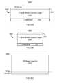
- FIGS. 1A and 1Bdepict ABS and top views of a conventional magnetic recording apparatus 10 .
- the magnetic recording apparatus 10may be a perpendicular magnetic recording (PMR) apparatus or other magnetic write apparatus.
- the conventional magnetic recording apparatus 10may be a part of a merged head including the write apparatus 10 and a read apparatus (not shown). Alternatively, the magnetic recording head may only include the write apparatus 10 .
- the write apparatus 10includes a leading shield 12 , a nonmagnetic gap layer 14 , side shield(s) 15 , a pole 20 and a trailing shield 30 .
- the apparatus 10may also include other components including but not limited to coils for energizing the pole 20 .
- the trailing surface (top) of the pole 20is wider than the leading surface (bottom) of the pole 20 .
- the side shields 16may have tails 17 developed during fabrication. These tails 17 cause the side shields 16 to have a longer effective throat height (distance from the ABS). The tails 17 also result in additional shunting of magnetic flux from the pole 20 . Thus, performance may be adversely affected. Accordingly, what is needed is a system and method for improving the performance of a magnetic recording write apparatus 10 .
- FIGS. 1A-1Bdepict ABS and top views of a conventional magnetic recording apparatus.
- FIG. 2is a flow chart depicting an exemplary embodiment of a method for providing a magnetic recording apparatus.
- FIGS. 3A, 3B and 3Cdepict side, FS and top views of an exemplary embodiment of a magnetic recording apparatus.
- FIG. 4is a flow chart depicting an exemplary embodiment of a method for providing magnetic recording apparatus.
- FIGS. 5A, 5B and 5C through FIGS. 18A, 18B, 18C and 18Ddepict various views of a magnetic recording apparatus during fabrication.
- FIG. 19is a flow chart depicting an exemplary embodiment of a method for providing magnetic recording apparatus.
- FIGS. 20A, 20B and 20C through FIGS. 25A, 25B, 25C and 25Ddepict apex, ABS and top views of a magnetic recording apparatus during fabrication.
- FIG. 2is a flow chart depicting an exemplary embodiment of a method 100 for providing a magnetic recording apparatus. For simplicity, some steps may be omitted, interleaved, combined and/or include substeps.
- the method 100is also described in the context of providing a particular data storage device and magnetic recording apparatus. The method 100 may also be used to fabricate other magnetic recording apparatuses. The method 100 may be used to fabricate multiple magnetic recording apparatuses at substantially the same time.
- the method 100is also described in the context of particular layers. A particular layer may include multiple materials and/or multiple sub-layers.
- the method 100also may start after formation of other portions of the magnetic recording head. For example, the method 100 may start after a read apparatus, return pole/leading shield and/or other structure have been fabricated.
- a side shield location layeris provided, via step 102 .
- This layeris a sacrificial layer and occupies the region in which the side shields are to be formed. Consequently, some or all of the side shield location layer is removed later in fabrication.
- the side shield location layerhas a back surface, at least a portion of which corresponds to the back surface of the side shields to be formed. For example, if the side gap between the pole and the side shields is desired to have different thicknesses, then the back surface of the side shield location layer may be shaped to match the desired profile of the side shields.
- the side shield location layeralso includes at least one side surface.
- Step 102may include full film depositing the material for the side shield location layer, covering the portion which will form the side shield location layer, and then removing the exposed portion.
- the mask usedmay be a hard mask.
- the exposed portionmay be removed by an etch such as a reactive ion etch (RIE).
- the side shield location layermay include one or more of aluminum oxide and NiFe.
- the side shield location layerconsists of aluminum oxide. In other embodiments, the side shield location layer consists of NiFe.
- a nonmagnetic layeris provided, via step 104 .
- the nonmagnetic layermay include silicon dioxide.
- the nonmagnetic layerconsists of silicon dioxide.
- the nonmagnetic layeradjoins (shares an interface with) the back surface and the side surface(s) of the side shield location layer.
- Step 104may include depositing the nonmagnetic layer over the preexisting side shield location layer and planarizing the magnetic write apparatus. For example, a chemical-mechanical planarization (CMP) may be used. In such a case, step 102 is performed before step 104 .
- the nonmagnetic layermay be deposited first as part of step 104 . In such a case, a portion of the nonmagnetic layer is removed, for example via an RIE.
- CMPchemical-mechanical planarization
- step 102A refill step is then performed in step 102 to provide the side shield location layer in this region.
- step 102may be performed after step 104 .
- the nonmagnetic layer and the side shield location layertogether form an intermediate layer in which the pole and side shields are to be formed.
- a pole trenchis provided in the intermediate layer using a first etch process, via step 106 .
- the pole trenchhas a shape and a location corresponding to the pole.
- the pole trenchhas portions in both the nonmagnetic layer and the side shield location layer.
- the nonmagnetic layer and the side shield location layerhave an etch selectivity of at least 0.9 and not more than 1.1 for the first etch.
- the removal rate of the nonmagnetic layer divided by the removal rate of the side shield location layer for the first etchis at least 0.9 and not more than 1.1.
- the side shield location layer and nonmagnetic layerare removed at approximately the same rate by the first etch.
- a poleis provided in the pole trench, via step 108 .
- Step 108may include depositing a seed layer, such as Ru, and providing the materials for the pole.
- a seed layersuch as Ru
- high saturation magnetization materials for the polemay be plated.
- a planarization stepmay also be performed.
- leading and/or trailing bevelsmight be formed.
- the top and/or bottom of the polemay not be perpendicular to the media-facing surface, such as an ABS.
- a remaining portion of the side shield location layeris removed using a wet etch, via step 110 .
- the side shield location layeris removable by this wet etch.
- the nonmagnetic layeris nonremovable by the wet etch.
- the selectivity for this etchis not close to one.
- at least part of the region previously occupied by the side shield location layermay be empty.
- Step 112may include depositing a seed layer and plating the material(s) for the side shield(s). Other deposition methods might be used.
- the side shield material(s)fill the region previously occupied by the side shield location layer.
- a deposition and planarizationsuch as a CMP are performed.
- the back surface of the side shield(s)are substantially the same as at least a portion of the back surface of the side shield location layer.
- the coil(s) for energizing the poleare provided, via step 114 .
- the coil provided in step 114may be a helical coil surrounding the pole, or a spiral coil.
- portions of step 114may be performed before steps 102 through 112 .
- the shape of the side shieldsmay be predefined using the side shield location layer.
- the side shieldshave the desired shape and location. For example, undesirable side effects such as tails 17 may be avoided. Consequently, performance of a magnetic recording apparatus fabricated using the method 100 may be improved.
- FIGS. 3A, 3B and 3Cdepict side, media-facing surface (MFS) and top views of an exemplary embodiment of a portion of a data storage device 200 including a write apparatus 210 .
- FIGS. 2A, 2B and 2Care not to scale.
- the MFSis an air-bearing surface (ABS).
- ABSair-bearing surface
- FIGS. 2A, 2B and 2Care not to scale.
- the MFSis an air-bearing surface (ABS).
- ABSair-bearing surface
- the disk drive 200 and write apparatus 210are depicted in the context of particular components other and/or different components may be used.
- circuitry used to drive and control various portions of the disk drive 200is not shown.
- only single componentsare shown. However, multiples of each components and/or and their sub-components, might be used.
- the disk drive 200may be a PMR disk drive. However, in other embodiments, the disk drive 200 may be configured for other types of magnetic recording
- the disk drive 200includes media 202 , a slider 204 and a write apparatus 210 .
- the write apparatus 210is fabricated on the slider 110 and includes a MFS. In the embodiment shown, the MFS is proximate to the media 202 during use. Although not shown, the slider 204 and thus the apparatus 210 are generally attached to a suspension.
- the disk drive 200includes a write apparatus 210 and a read apparatus (not shown). However, for clarity, only the write apparatus 210 is shown.
- the write apparatus 210includes coils 212 , optional leading shield 214 , side gap 216 , side shields 218 , write pole 220 , top (write) gap 222 , and optional trailing shield 230 .
- the side gap 216is also a bottom gap.
- Multiple structures on which the leading shield 214 and pole 220 are fabricatedmay reside below the components shown.
- portions of the components 210 , 212 , 214 , 216 , 218 , 220 , 222 and 230may include multiple layers. In other embodiments, different and/or additional components may be used in the write apparatus 210 .
- the coil(s) 212are used to energize the pole 220 . Two turns 212 are depicted in FIG. 3A . Another number of turns may, however, be used. Note that only a portion of the coil(s) 212 is shown in FIG. 3A . Additional turns and/or additional layers of coils may be used. If, for example, the coil(s) 212 form a spiral, coil, then additional portions of the coil(s) 212 may be located further from the ABS.
- the coil(s) 212may also be a helical coil.
- the pole 220is ferromagnetic and may have a high saturation magnetization in excess of 2.0 T.
- the front of the pole 220occupies a portion of the MFS. This is shown in FIGS. 3A-3C .
- the pole 220also includes sidewalls in the cross track direction.
- the sidewallsare generally configured such that the pole 220 has a bottom and a top wider than the bottom.
- the sidewallsare oriented at a flare angle from a direction parallel to the MFS.
- the flare angleis generally greater than zero and less than ninety degrees. In some embodiments, the flare angle is at least forty-five degrees and not more than seventy degrees.
- the side gap 216is shown as having two widths, d 1 and d 2 . This is because the back surfaces 219 of side shields 218 have been configured with two sections that are parallel to the MFS and two sections that are conformal with the sidewalls of the pole 220 . In the embodiment shown, the side shields 218 are conformal with the main pole 220 and at a side gap 216 distance d 1 until a first throat height, TH 1 , from the MFS. The back surface 219 of the side shields 218 has a portion that extends parallel to the MFS at the distance TH 1 from the MFS.
- the back surface 219has another portion that is conformal with the main pole 220 at a distance d 2 until a desired height TH 2 in the yoke direction (perpendicular to the MFS).
- the height TH 2is a second throat height and the depth of the side shields 218 in the embodiment shown in FIGS. 3A-3C .
- the side shields 218have the desired configuration.
- the back surface 219 of the side shields 218 and thus the side gap 216have the desired configuration because the side shield location layer predefined the region in which the side shields 218 were formed.
- the desired throat heights TH 1 and TH 2are achieved without tails or other undesirable artifacts of fabrication. Consequently, the magnetic data storage device 200 may exhibit improved performance.
- FIG. 4depicts an exemplary embodiment of a method 110 for providing a magnetic recording apparatus such as the magnetic recording apparatus 210 .
- FIGS. 5A-5C through FIGS. 18A-18Ddepict various views of an exemplary embodiment of a magnetic recording apparatus 250 during fabrication using the method 110 .
- the method 110is thus described in the context of providing the magnetic recording apparatus 250 .
- the method 110may also be used to fabricate other magnetic recording apparatuses including but not limited to the data storage device 250 .
- the method 110is described in the context of a single device but may be used to fabricate multiple magnetic storage apparatuses at substantially the same time.
- the method 110is also described in the context of particular layers. A particular layer may include multiple materials and/or multiple sub-layers.
- the method 110also may start after formation of other portions of the magnetic recording apparatus. For example, the method 110 may start after a read apparatus, return pole/leading shield and/or other structure have been fabricated.
- a first layeris full-film deposited, via step 112 .
- the first layeris a nonmagnetic layer, such as a silicon dioxide layer.
- At least one hard mask layeris deposited on the first layer, via step 114 .
- a Cr/Ta bilayermay be deposited in step 114 .
- FIGS. 5A, 5B and 5Cdepict apex, MFS and top views of the magnetic write apparatus 250 after step 114 is completed.
- the first nonmagnetic layer 262has been provided on an underlayer 252 .
- the nonmagnetic layer 262is part of an intermediate layer 260 that is being formed.
- the hard mask layer(s) 264are also shown.
- FIGS. 5A and 5Cindicate an MFS location, where the MFS will be located.
- an ABSmay be formed at the MFS location after lapping.
- FIGS. 6A, 6B and 6Cdepict apex, MFS and top views of the magnetic write apparatus 250 after step 116 is completed.
- a photoresist mask 266has been formed.
- the mask 266includes an aperture in the region corresponding to the side shields.
- Step 118may include performing a Ta RIE and a Cr RIE to remove the hard mask layers 264 in the region exposed by the photoresist mask 266 .
- a portion of the nonmagnetic layer 262 exposed by the hard mask 264is removed, via step 120 .
- Step 120may be performed using a silicon dioxide RIE.
- the underlayer 252is aluminum oxide.
- the silicon oxide RIEmay stop at the underlayer 252 .
- FIGS. 7A, 7B and 7Cdepict apex, MFS and top views of the magnetic write apparatus 250 after step 120 is performed.
- a trench having a shape and location corresponding to the side shieldsis formed in the first layer 252 .
- the trenchhas a back surface and at least one side surface. A portion of the back surface corresponds to the back surface of the side shield(s).
- the hard mask 262is removed, via step 122 .
- a second layeris deposited, via step 124 .
- Step 124include performing a full film deposition.
- FIGS. 8A, 8B and 8Cdepict apex, MFS and top views of the magnetic write apparatus 250 after step 124 is performed.
- the second layer 268is present.
- the second layer 268may be selected from aluminum oxide and NiFe.
- the second layer 268is planarized, via step 126 .
- the portion of the second layer 268 covering the nonmagnetic layer 262is removed.
- the nonmagnetic layer 262 and the side shield location layer 268form an intermediate layer 260 ′.
- a pole trenchis formed in the intermediate layer 260 ′, via step 128 .
- Step 128includes forming a mask for the pole trench.
- the mask to be formedis a hard mask.
- a Cr hard mask layermay be deposited and a photoresist mask formed on the Cr layer.
- a Ta hard mask layeris deposited on the resist mask.
- FIGS. 10A, 10B and 10Cdepict apex, MFS and top views of the magnetic write apparatus 250 after deposition of the Ta layer.
- a Cr layer 272 , a photoresist mask 274 and Ta layer 276are formed.
- a lift off processremoves the photoresist mask 274 .
- the Ta layer 276thus has an aperture in the region formerly occupied by the photoresist mask 274 .
- a Cr RIEmay be used to remove the underlying Cr layer 272 exposed by the Ta layer 276 .
- a hard maskmay be formed.
- hard mask 270includes hard mask layers 272 and 276 .
- the hard mask 270also has an aperture over the region in which the pole is to be formed.
- an RIEis performed as part of step 128 to provide a pole trench in the intermediate layer 260 ′.
- a trench 277has been formed in the intermediate layer 260 ′.
- the trench 277includes a portion in the side shield location layer 268 and a portion in the nonmagnetic layer 262 .
- the RIE performed in step 128may be an aluminum oxide or NiFe RIE. Such an RIE may also remove the silicon dioxide layer 262 .
- the RIE of step 128thus has an etch selectivity of at least 0.9 and not more than 1.1 for the layers 262 and 268 .
- the pole trench 277has a shape and a location corresponding to the pole being formed.
- a nonmagnetic gap layeris provided, via step 130 .
- Rumay be deposited using chemical vapor deposition (CVD).
- a portion of the nonmagnetic gap layerresides in the pole trench.
- a poleis provided in the trench, via step 132 .
- Step 132includes depositing the magnetic material(s) for the pole.
- FIGS. 13A, 13B, 13C and 13Ddepict apex, MFS and top views of the magnetic write apparatus 250 after the pole material(s) have been deposited.
- a gap layer 278 and pole material(s) 280are shown.
- the pole materialsare planarized for example using a CMP.
- a trailing edge bevelmay also be formed.
- FIGS. 14A, 14B, 14C and 14Ddepict apex, MFS and top views of the magnetic write apparatus 250 after step 132 is completed.
- a pole 280has been formed.
- Step 134may include providing a mask that covers the pole 280 .
- Step 134may include using a NiFe or aluminum oxide wet etch.
- FIGS. 15A, 15B, 15C and 15Ddepict apex, MFS and top views of the magnetic write apparatus 250 after the mask 282 has been provided.
- the mask 282is a photoresist mask.
- FIGS. 16A, 16B, 16C and 16Ddepict apex, MFS and top views of the magnetic write apparatus 250 after step 134 is completed.
- the sacrificial side shield location layer 268has been removed.
- a high moment seed layer for the side shieldsmay optionally be provided, via step 136 .
- Step 136may include using a directional deposition, for example ion beam deposition.
- FIGS. 17A, 17B, 17C and 17Ddepict apex, MFS and top views of the magnetic write apparatus 250 after step 136 is performed.
- a seed layer 284is formed.
- An optional ion beam etchmay be performed to remove the seed layer from regions other than the sides of the pole, via step 138 .
- FIGS. 18A, 18B, 18C and 18Ddepict apex, MFS and top views of the magnetic write apparatus 250 after step 140 is performed and after the mask 282 is removed.
- the side shields 286are shown.
- the back of the side shield 286matches the back surface of the side shield location layer 268 , shown previously.
- the magnetic recording apparatus 250may be provided.
- the use of the side shield location layer 268may prevent or reduce formation of tails and/or other features that may adversely affect the throat height and/or other characteristics of the side shields 286 .
- the desired configuration of the side shields 286may be achieved. Thus, flux shunting and other issues with performance may be mitigated. Thus, performance of the write apparatus 250 may be improved.
- FIG. 19depicts an exemplary embodiment of a method 150 for providing a magnetic recording apparatus such as the magnetic recording apparatus 210 .
- FIGS. 20A-20C through FIGS. 25A-25Ddepict various views of an exemplary embodiment of a magnetic recording apparatus 250 ′ during fabrication using the method 150 .
- the method 150is thus described in the context of providing the magnetic recording apparatus 250 ′.
- the method 150may also be used to fabricate other magnetic recording apparatuses including but not limited to the data storage device 250 ′.
- the method 150is described in the context of a single device but may be used to fabricate multiple magnetic storage apparatuses at substantially the same time.
- the method 150is also described in the context of particular layers. A particular layer may include multiple materials and/or multiple sub-layers.
- the method 150also may start after formation of other portions of the magnetic recording apparatus. For example, the method 150 may start after a read apparatus, return pole/leading shield and/or other structure have been fabricated.
- a first layeris full-film deposited, via step 152 .
- the first layerwill form the side shield location layer and may be selected from aluminum oxide and NiFe.
- At least one hard mask layeris deposited on the first layer, via step 154 .
- a Cr layermay be deposited in step 154 .
- FIGS. 20A, 20B and 20Cdepict apex, MFS and top views of the magnetic write apparatus 250 ′ after step 154 is completed.
- the first nonmagnetic layer 268 ′has been provided on an underlayer 252 .
- the nonmagnetic layer 268 ′is part of an intermediate layer 260 ′′ that is being formed.
- the hard mask layers 264 ′Also shown in FIG. 20C is an MFS location, where the MFS will be located.
- an ABSmay be formed after lapping.
- FIGS. 21A, 21B and 21Cdepict apex, MFS and top views of the magnetic write apparatus 250 ′ after step 116 ′ is completed. Thus, a photoresist mask 266 ′ has been formed. The mask 266 ′ covers the region corresponding to the side shields.
- Step 158may include performing a Cr RIE to remove the hard mask layers 264 ′ in the region exposed by the photoresist mask 266 .
- a portion of the side shield location layer 268 ′ exposed by the hard mask 264 ′is removed, via step 160 .
- Step 160may include performing an aluminum oxide and/or NiFe RIE.
- FIGS. 22A, 22B and 22Cdepict apex, MFS and top views of the magnetic write apparatus 250 ′ after step 160 is performed.
- a side shield location layer 268 ′having a shape and location corresponding to the side shields is formed.
- the side shield location layer 268 ′has a back surface and at least one side surface. A portion of the back surface corresponds to the back surface of the side shield(s).
- a second layeris deposited, via step 162 .
- Step 162includes performing a full film deposition.
- FIGS. 23A, 23B and 23Cdepict apex, MFS and top views of the magnetic write apparatus 250 after step 162 is performed.
- the second layer 262 ′is present.
- the second layer 262 ′is a nonmagnetic layer, such as a silicon dioxide layer.
- the second layer 262 ′is planarized, via step 164 .
- the portion of the second layer 262 ′ covering the first layer 268 ′is removed.
- the hard mask layer(s) 264 ′have been removed.
- FIGS. 24A, 24B and 24Cdepict apex, MFS and top views of the magnetic write apparatus 250 after step 164 is completed.
- a remaining portion of the second layer 262 ′ in the trenchforms a nonmagnetic layer on the sides of the side shield location layer 268 ′.
- the nonmagnetic layer 262 ′ and the side shield location layer 268 ′form an intermediate layer 260 ′′.
- step 166includes forming a mask for the pole trench.
- the mask to be formedis a hard mask.
- a Cr hard mask layermay be deposited and a photoresist mask formed on the Cr layer.
- a Ta hard mask layeris deposited on the resist mask.
- a lift off processremoves the photoresist mask.
- the Ta layerthus has an aperture in the region formerly occupied by the photoresist mask.
- a Cr RIEmay be used to remove the underlying Cr layer exposed by the Ta layer.
- a hard maskmay be formed.
- the hard maskalso has an aperture over the region in which the pole is to be formed.
- an RIEis performed as part of step 166 to provide a pole trench in the intermediate layer 260 ′′.
- the resulting deviceis analogous to the magnetic recording apparatus 250 shown in FIGS. 12A-12D .
- the trench formed in step 166includes a portion in the side shield location layer 268 ′ and a portion in the nonmagnetic layer 262 ′.
- the RIE performed in step 166may be an aluminum oxide or NiFe RIE. Such an RIE may also remove the silicon dioxide layer 262 ′.
- the RIE of step 166thus has an etch selectivity of at least 0.9 and not more than 1.1 for the layers 262 ′ and 268 ′.
- the pole trenchhas a shape and a location corresponding to the pole being formed.
- a nonmagnetic gap layeris provided, via step 168 .
- Rumay be deposited using CVD.
- a portion of the nonmagnetic gap layerresides in the pole trench.
- a poleis provided in the trench, via step 170 .
- Step 170includes depositing the magnetic material(s) for the pole.
- the pole materialsmay also be planarized for example using a CMP.
- a trailing edge bevelmay also be formed.
- the resulting magnetic recording apparatusis analogous to that shown in FIGS. 14A-14D .
- Step 172may include providing a mask that covers the pole and then performing the wet etch.
- the maskis a photoresist mask.
- the wet etched usedmay be a NiFe wet etch or an aluminum oxide wet etch.
- the magnetic recording apparatus 250 ′ after step 172 is performedis analogous to the magnetic recording apparatus 250 shown in FIGS. 16A-16D .
- a high moment seed layer for the side shieldsmay optionally be provided, via step 174 .
- Step 174may include using a directional deposition, for example ion beam deposition.
- the magnetic recording apparatus 250 ′ after step 174may be analogous to the magnetic write apparatus 250 shown in FIGS. 17A-17D .
- An optional ion beam etchmay be performed to remove the seed layer from regions other than the sides of the pole, via step 176 .
- FIGS. 25A, 25B, 25C and 25Ddepict apex, MFS and top views of the magnetic write apparatus 250 ′ after step 178 is performed.
- the gap layer 278 , pole 280 , optional seed layer 284 and side shields 286are shown.
- the back of the side shield 286matches the back surface of the side shield location layer 268 ′, shown previously.
- the magnetic recording apparatus 250 ′may be provided.
- the use of the side shield location layer 268 ′may prevent or reduce formation of tails and/or other features that may adversely affect the throat height or other characteristics of the side shields 286 ′. Thus, flux shunting and other issues with performance may be mitigated. Thus, performance of the write apparatus 250 ′ may be improved.
Landscapes
- Engineering & Computer Science (AREA)
- Manufacturing & Machinery (AREA)
- Physics & Mathematics (AREA)
- Electromagnetism (AREA)
- Magnetic Heads (AREA)
Abstract
Description
Claims (14)
Priority Applications (1)
| Application Number | Priority Date | Filing Date | Title |
|---|---|---|---|
| US15/156,877US9711168B1 (en) | 2016-05-17 | 2016-05-17 | Method for providing a magnetic recording write apparatus by predefining side shields |
Applications Claiming Priority (1)
| Application Number | Priority Date | Filing Date | Title |
|---|---|---|---|
| US15/156,877US9711168B1 (en) | 2016-05-17 | 2016-05-17 | Method for providing a magnetic recording write apparatus by predefining side shields |
Publications (1)
| Publication Number | Publication Date |
|---|---|
| US9711168B1true US9711168B1 (en) | 2017-07-18 |
Family
ID=59296292
Family Applications (1)
| Application Number | Title | Priority Date | Filing Date |
|---|---|---|---|
| US15/156,877Expired - Fee RelatedUS9711168B1 (en) | 2016-05-17 | 2016-05-17 | Method for providing a magnetic recording write apparatus by predefining side shields |
Country Status (1)
| Country | Link |
|---|---|
| US (1) | US9711168B1 (en) |
Cited By (2)
| Publication number | Priority date | Publication date | Assignee | Title |
|---|---|---|---|---|
| US10586559B1 (en) | 2018-12-11 | 2020-03-10 | Seagate Technology Llc | Side shield formation |
| US11626129B2 (en)* | 2018-05-14 | 2023-04-11 | Western Digital Technologies, Inc. | Plating based side shield define and application in magnetic head |
Citations (35)
| Publication number | Priority date | Publication date | Assignee | Title |
|---|---|---|---|---|
| US20060066995A1 (en)* | 2004-09-30 | 2006-03-30 | Lille Jeffrey S | Methods of making a side-by-side read/write head with a self-aligned trailing shield structure |
| US7398592B2 (en) | 2005-03-29 | 2008-07-15 | Hitachi Global Storage Technologies Netherlands, B.V. | Manufacturable CMP assisted liftoff process to fabricate write pole for perpendicular recording heads |
| US7788798B2 (en) | 2007-11-21 | 2010-09-07 | Hitachi Global Storage Technologies Netherlands B.V. | Method for manufacturing a perpendicular magnetic write head with wrap around magnetic trailing and side shields |
| US20110075299A1 (en) | 2009-09-30 | 2011-03-31 | Olson Trevor W | Magnetic write heads for hard disk drives and method of forming same |
| US7952831B2 (en) | 2006-04-24 | 2011-05-31 | Hitachi Global Storage Technologies Netherlands B.V. | Perpendicular magnetic recording write head with notched trailing shield |
| US8049989B2 (en) | 2007-12-26 | 2011-11-01 | Hitachi Global Storage Technologies Netherlands B.V. | Magnetic head for perpendicular recording having stepped wrap around shield with independent control of write pole track width and flare point dimensions |
| US8051552B2 (en) | 2007-05-11 | 2011-11-08 | Hitachi Global Storage Technologies Netherlands, B.V. | Stitched wrap around shield fabrication for perpendicular magnetic recording write heads |
| US8066892B2 (en) | 2008-09-30 | 2011-11-29 | Hitachi Global Storage Technologies Netherlands B.V. | Method for manufacturing a perpendicular magnetic write head with a wrap around shield |
| US8117738B2 (en) | 2006-02-02 | 2012-02-21 | Headway Technologies, Inc. | Method to make a perpendicular magnetic recording head with a side write shield |
| US8134802B2 (en) | 2009-10-29 | 2012-03-13 | Headway Technologies, Inc. | Writer and reader arrangements for shingled writing |
| US8179634B2 (en) | 2007-12-27 | 2012-05-15 | Hitachi Global Storage Technologies Netherlands B.V. | Perpendicular magnetic recording writer main pole having imbedded non-magnetic core and de-coupled pole tip |
| US8189293B1 (en) | 2011-04-28 | 2012-05-29 | Hitachi Global Storage Technologies Netherlands B.V. | Perpendicular magnetic recording head having a grooved wrap around shield and method for manufacturing the same |
| US8233235B2 (en) | 2009-12-09 | 2012-07-31 | Hitachi Global Storage Technologies Netherlands B.V. | PMR writer having a tapered write pole and bump layer and method of fabrication |
| US8238059B1 (en) | 2011-04-06 | 2012-08-07 | Headway Technologies, Inc. | PMR write head with narrow gap for minimal internal flux loss |
| US8254060B1 (en) | 2009-04-17 | 2012-08-28 | Western Digital (Fremont), Llc | Straight top main pole for PMR bevel writer |
| US20120257305A1 (en) | 2011-04-08 | 2012-10-11 | Headway Technologies, Inc. | Pmr write head with assisted magnetic layer |
| US8322023B1 (en) | 2009-11-10 | 2012-12-04 | Western Digital (Fremont), Llc | Method for providing a wrap-around shield for a magnetic recording transducer |
| US8345383B2 (en) | 2008-09-05 | 2013-01-01 | Headway Technologies, Inc. | Method to make an integrated side shield PMR head with non-conformal side gap |
| US8400733B2 (en) | 2010-11-24 | 2013-03-19 | HGST Netherlands B.V. | Process to make PMR writer with leading edge shield (LES) and leading edge taper (LET) |
| US8404128B1 (en) | 2009-02-23 | 2013-03-26 | Western Digital (Fremont), Llc | Method and system for providing a perpendicular magnetic recording head |
| US8451563B1 (en) | 2011-12-20 | 2013-05-28 | Western Digital (Fremont), Llc | Method for providing a side shield for a magnetic recording transducer using an air bridge |
| US8470186B2 (en) | 2010-11-24 | 2013-06-25 | HGST Netherlands B.V. | Perpendicular write head with wrap around shield and conformal side gap |
| US8488272B1 (en) | 2008-08-27 | 2013-07-16 | Western Digital (Fremont), Llc | Magnetic recording transducer having side shields |
| US8498079B1 (en) | 2012-09-15 | 2013-07-30 | Headway Technologies, Inc. | Superior performance head design with minimized ATE and WATE |
| US8533937B1 (en) | 2011-10-18 | 2013-09-17 | Western Digital (Fremont), Llc | Method of forming a fully wrapped-around shielded PMR writer pole |
| US8576517B1 (en) | 2008-08-26 | 2013-11-05 | Western Digital (Fremont), Llc | Magnetic recording transducer having side shields between the coils and the air-bearing surface |
| US8582238B1 (en) | 2011-10-21 | 2013-11-12 | Western Digital (Fremont), Llc | Systems and methods for providing perpendicular magnetic writers having gradient magnetic moment side shields |
| US8611046B2 (en) | 2010-04-19 | 2013-12-17 | Headway Technologies, Inc. | PMR writer with graded side shield |
| US8614860B2 (en) | 2008-02-25 | 2013-12-24 | Headway Technologies, Inc. | PMR head with integrated side shield (ISS) |
| US8625235B2 (en) | 2010-05-05 | 2014-01-07 | Headway Technologies, Inc. | Perpendicular magnetic recording write head with milling defined track width |
| US20140016232A1 (en) | 2011-06-10 | 2014-01-16 | Headway Technologies, Inc. | Non-Uniform Write Gap Perpendicular Writer for Shingle Writing |
| US20140078619A1 (en) | 2012-09-15 | 2014-03-20 | Headway Technologies, Inc. | Shield Designs with Internal Magnetization Control for ATE Improvement |
| US8724258B2 (en) | 2009-09-30 | 2014-05-13 | HGST Netherlands B.V. | Slanted bump design for magnetic shields in perpendicular write heads and method of making same |
| US8792208B1 (en) | 2012-05-25 | 2014-07-29 | Western Digital (Fremont), Llc | Method for providing side shields having non-conformal regions for a magnetic recording transducer |
| US9275657B1 (en) | 2013-08-14 | 2016-03-01 | Western Digital (Fremont), Llc | Process for making PMR writer with non-conformal side gaps |
- 2016
- 2016-05-17USUS15/156,877patent/US9711168B1/ennot_activeExpired - Fee Related
Patent Citations (35)
| Publication number | Priority date | Publication date | Assignee | Title |
|---|---|---|---|---|
| US20060066995A1 (en)* | 2004-09-30 | 2006-03-30 | Lille Jeffrey S | Methods of making a side-by-side read/write head with a self-aligned trailing shield structure |
| US7398592B2 (en) | 2005-03-29 | 2008-07-15 | Hitachi Global Storage Technologies Netherlands, B.V. | Manufacturable CMP assisted liftoff process to fabricate write pole for perpendicular recording heads |
| US8117738B2 (en) | 2006-02-02 | 2012-02-21 | Headway Technologies, Inc. | Method to make a perpendicular magnetic recording head with a side write shield |
| US7952831B2 (en) | 2006-04-24 | 2011-05-31 | Hitachi Global Storage Technologies Netherlands B.V. | Perpendicular magnetic recording write head with notched trailing shield |
| US8051552B2 (en) | 2007-05-11 | 2011-11-08 | Hitachi Global Storage Technologies Netherlands, B.V. | Stitched wrap around shield fabrication for perpendicular magnetic recording write heads |
| US7788798B2 (en) | 2007-11-21 | 2010-09-07 | Hitachi Global Storage Technologies Netherlands B.V. | Method for manufacturing a perpendicular magnetic write head with wrap around magnetic trailing and side shields |
| US8049989B2 (en) | 2007-12-26 | 2011-11-01 | Hitachi Global Storage Technologies Netherlands B.V. | Magnetic head for perpendicular recording having stepped wrap around shield with independent control of write pole track width and flare point dimensions |
| US8179634B2 (en) | 2007-12-27 | 2012-05-15 | Hitachi Global Storage Technologies Netherlands B.V. | Perpendicular magnetic recording writer main pole having imbedded non-magnetic core and de-coupled pole tip |
| US8614860B2 (en) | 2008-02-25 | 2013-12-24 | Headway Technologies, Inc. | PMR head with integrated side shield (ISS) |
| US8576517B1 (en) | 2008-08-26 | 2013-11-05 | Western Digital (Fremont), Llc | Magnetic recording transducer having side shields between the coils and the air-bearing surface |
| US8488272B1 (en) | 2008-08-27 | 2013-07-16 | Western Digital (Fremont), Llc | Magnetic recording transducer having side shields |
| US8345383B2 (en) | 2008-09-05 | 2013-01-01 | Headway Technologies, Inc. | Method to make an integrated side shield PMR head with non-conformal side gap |
| US8066892B2 (en) | 2008-09-30 | 2011-11-29 | Hitachi Global Storage Technologies Netherlands B.V. | Method for manufacturing a perpendicular magnetic write head with a wrap around shield |
| US8404128B1 (en) | 2009-02-23 | 2013-03-26 | Western Digital (Fremont), Llc | Method and system for providing a perpendicular magnetic recording head |
| US8254060B1 (en) | 2009-04-17 | 2012-08-28 | Western Digital (Fremont), Llc | Straight top main pole for PMR bevel writer |
| US8724258B2 (en) | 2009-09-30 | 2014-05-13 | HGST Netherlands B.V. | Slanted bump design for magnetic shields in perpendicular write heads and method of making same |
| US20110075299A1 (en) | 2009-09-30 | 2011-03-31 | Olson Trevor W | Magnetic write heads for hard disk drives and method of forming same |
| US8134802B2 (en) | 2009-10-29 | 2012-03-13 | Headway Technologies, Inc. | Writer and reader arrangements for shingled writing |
| US8322023B1 (en) | 2009-11-10 | 2012-12-04 | Western Digital (Fremont), Llc | Method for providing a wrap-around shield for a magnetic recording transducer |
| US8233235B2 (en) | 2009-12-09 | 2012-07-31 | Hitachi Global Storage Technologies Netherlands B.V. | PMR writer having a tapered write pole and bump layer and method of fabrication |
| US8611046B2 (en) | 2010-04-19 | 2013-12-17 | Headway Technologies, Inc. | PMR writer with graded side shield |
| US8625235B2 (en) | 2010-05-05 | 2014-01-07 | Headway Technologies, Inc. | Perpendicular magnetic recording write head with milling defined track width |
| US8470186B2 (en) | 2010-11-24 | 2013-06-25 | HGST Netherlands B.V. | Perpendicular write head with wrap around shield and conformal side gap |
| US8400733B2 (en) | 2010-11-24 | 2013-03-19 | HGST Netherlands B.V. | Process to make PMR writer with leading edge shield (LES) and leading edge taper (LET) |
| US8238059B1 (en) | 2011-04-06 | 2012-08-07 | Headway Technologies, Inc. | PMR write head with narrow gap for minimal internal flux loss |
| US20120257305A1 (en) | 2011-04-08 | 2012-10-11 | Headway Technologies, Inc. | Pmr write head with assisted magnetic layer |
| US8189293B1 (en) | 2011-04-28 | 2012-05-29 | Hitachi Global Storage Technologies Netherlands B.V. | Perpendicular magnetic recording head having a grooved wrap around shield and method for manufacturing the same |
| US20140016232A1 (en) | 2011-06-10 | 2014-01-16 | Headway Technologies, Inc. | Non-Uniform Write Gap Perpendicular Writer for Shingle Writing |
| US8533937B1 (en) | 2011-10-18 | 2013-09-17 | Western Digital (Fremont), Llc | Method of forming a fully wrapped-around shielded PMR writer pole |
| US8582238B1 (en) | 2011-10-21 | 2013-11-12 | Western Digital (Fremont), Llc | Systems and methods for providing perpendicular magnetic writers having gradient magnetic moment side shields |
| US8451563B1 (en) | 2011-12-20 | 2013-05-28 | Western Digital (Fremont), Llc | Method for providing a side shield for a magnetic recording transducer using an air bridge |
| US8792208B1 (en) | 2012-05-25 | 2014-07-29 | Western Digital (Fremont), Llc | Method for providing side shields having non-conformal regions for a magnetic recording transducer |
| US8498079B1 (en) | 2012-09-15 | 2013-07-30 | Headway Technologies, Inc. | Superior performance head design with minimized ATE and WATE |
| US20140078619A1 (en) | 2012-09-15 | 2014-03-20 | Headway Technologies, Inc. | Shield Designs with Internal Magnetization Control for ATE Improvement |
| US9275657B1 (en) | 2013-08-14 | 2016-03-01 | Western Digital (Fremont), Llc | Process for making PMR writer with non-conformal side gaps |
Cited By (2)
| Publication number | Priority date | Publication date | Assignee | Title |
|---|---|---|---|---|
| US11626129B2 (en)* | 2018-05-14 | 2023-04-11 | Western Digital Technologies, Inc. | Plating based side shield define and application in magnetic head |
| US10586559B1 (en) | 2018-12-11 | 2020-03-10 | Seagate Technology Llc | Side shield formation |
Similar Documents
| Publication | Publication Date | Title |
|---|---|---|
| US8334093B2 (en) | Method and system for providing a perpendicular magnetic recording head | |
| US9305583B1 (en) | Method for fabricating a magnetic writer using multiple etches of damascene materials | |
| US8276258B1 (en) | Method for fabricating a magnetic recording transducer | |
| US8563146B1 (en) | Method and system for providing a magnetic recording pole having a dual sidewall angle | |
| US8982508B1 (en) | Method for providing a side shield for a magnetic recording transducer | |
| US8793866B1 (en) | Method for providing a perpendicular magnetic recording head | |
| JP5715750B2 (en) | Thin film magnetic head, method of manufacturing the same, head gimbal assembly, and hard disk drive | |
| US8451563B1 (en) | Method for providing a side shield for a magnetic recording transducer using an air bridge | |
| US8444866B1 (en) | Method and system for providing a perpendicular magnetic recording pole with a multi-layer side gap | |
| US7911735B1 (en) | Perpendicular magnetic recording head utilizing a nonmagnetic underlayer layer | |
| US8166631B1 (en) | Method for fabricating a magnetic recording transducer having side shields | |
| US9443541B1 (en) | Magnetic writer having a gradient in saturation magnetization of the shields and return pole | |
| US9214165B1 (en) | Magnetic writer having a gradient in saturation magnetization of the shields | |
| US9478242B1 (en) | Magnetic recording apparatus having a recessed additional pole segment | |
| JP2007287313A (en) | Thin film magnetic head, its manufacturing method, and head gimbal assembly, and hard disk drive | |
| JP2007026636A (en) | Structure for thin film magnetic head and its manufacturing method and thin film magnetic head | |
| US9349393B2 (en) | Magnetic writer having an asymmetric gap and shields | |
| US9558763B1 (en) | Magnetic recording write apparatus having a pole including an assist portion extending in the cross-track direction | |
| US9286919B1 (en) | Magnetic writer having a dual side gap | |
| US9711168B1 (en) | Method for providing a magnetic recording write apparatus by predefining side shields | |
| US10115416B2 (en) | Magnetic recording write apparatus having a pole having an aspect ratio greater than one and an auxiliary pole | |
| US8988825B1 (en) | Method for fabricating a magnetic writer having half-side shields | |
| US9135930B1 (en) | Method for fabricating a magnetic write pole using vacuum deposition | |
| US9111564B1 (en) | Magnetic recording writer having a main pole with multiple flare angles | |
| US9940951B2 (en) | PMR writer with non-conformal side gaps |
Legal Events
| Date | Code | Title | Description |
|---|---|---|---|
| AS | Assignment | Owner name:WESTERN DIGITAL (FREMONT), LLC, CALIFORNIA Free format text:ASSIGNMENT OF ASSIGNORS INTEREST;ASSIGNORS:YANG, XIAOYU;ZHANG, JINQIU;LIU, FENG;AND OTHERS;SIGNING DATES FROM 20160509 TO 20160511;REEL/FRAME:038636/0624 | |
| STCF | Information on status: patent grant | Free format text:PATENTED CASE | |
| AS | Assignment | Owner name:WESTERN DIGITAL TECHNOLOGIES, INC., CALIFORNIA Free format text:ASSIGNMENT OF ASSIGNORS INTEREST;ASSIGNOR:WESTERN DIGITAL (FREMONT), LLC;REEL/FRAME:050450/0582 Effective date:20190508 | |
| AS | Assignment | Owner name:JPMORGAN CHASE BANK, N.A., AS AGENT, ILLINOIS Free format text:SECURITY INTEREST;ASSIGNOR:WESTERN DIGITAL TECHNOLOGIES, INC.;REEL/FRAME:052915/0566 Effective date:20200113 | |
| MAFP | Maintenance fee payment | Free format text:PAYMENT OF MAINTENANCE FEE, 4TH YEAR, LARGE ENTITY (ORIGINAL EVENT CODE: M1551); ENTITY STATUS OF PATENT OWNER: LARGE ENTITY Year of fee payment:4 | |
| AS | Assignment | Owner name:WESTERN DIGITAL TECHNOLOGIES, INC., CALIFORNIA Free format text:RELEASE OF SECURITY INTEREST AT REEL 052915 FRAME 0566;ASSIGNOR:JPMORGAN CHASE BANK, N.A.;REEL/FRAME:059127/0001 Effective date:20220203 | |
| AS | Assignment | Owner name:JPMORGAN CHASE BANK, N.A., ILLINOIS Free format text:PATENT COLLATERAL AGREEMENT - A&R LOAN AGREEMENT;ASSIGNOR:WESTERN DIGITAL TECHNOLOGIES, INC.;REEL/FRAME:064715/0001 Effective date:20230818 Owner name:JPMORGAN CHASE BANK, N.A., ILLINOIS Free format text:PATENT COLLATERAL AGREEMENT - DDTL LOAN AGREEMENT;ASSIGNOR:WESTERN DIGITAL TECHNOLOGIES, INC.;REEL/FRAME:067045/0156 Effective date:20230818 | |
| FEPP | Fee payment procedure | Free format text:MAINTENANCE FEE REMINDER MAILED (ORIGINAL EVENT CODE: REM.); ENTITY STATUS OF PATENT OWNER: LARGE ENTITY | |
| LAPS | Lapse for failure to pay maintenance fees | Free format text:PATENT EXPIRED FOR FAILURE TO PAY MAINTENANCE FEES (ORIGINAL EVENT CODE: EXP.); ENTITY STATUS OF PATENT OWNER: LARGE ENTITY | |
| STCH | Information on status: patent discontinuation | Free format text:PATENT EXPIRED DUE TO NONPAYMENT OF MAINTENANCE FEES UNDER 37 CFR 1.362 | |
| FP | Lapsed due to failure to pay maintenance fee | Effective date:20250718 |