US9710006B2 - Power up body bias circuits and methods - Google Patents
Power up body bias circuits and methodsDownload PDFInfo
- Publication number
- US9710006B2 US9710006B2US14/341,733US201414341733AUS9710006B2US 9710006 B2US9710006 B2US 9710006B2US 201414341733 AUS201414341733 AUS 201414341733AUS 9710006 B2US9710006 B2US 9710006B2
- Authority
- US
- United States
- Prior art keywords
- power supply
- body bias
- supply voltage
- voltage
- transistors
- Prior art date
- Legal status (The legal status is an assumption and is not a legal conclusion. Google has not performed a legal analysis and makes no representation as to the accuracy of the status listed.)
- Active, expires
Links
Images


Classifications
- G—PHYSICS
- G05—CONTROLLING; REGULATING
- G05F—SYSTEMS FOR REGULATING ELECTRIC OR MAGNETIC VARIABLES
- G05F3/00—Non-retroactive systems for regulating electric variables by using an uncontrolled element, or an uncontrolled combination of elements, such element or such combination having self-regulating properties
- G05F3/02—Regulating voltage or current
- G05F3/08—Regulating voltage or current wherein the variable is DC
- G05F3/10—Regulating voltage or current wherein the variable is DC using uncontrolled devices with non-linear characteristics
- G05F3/16—Regulating voltage or current wherein the variable is DC using uncontrolled devices with non-linear characteristics being semiconductor devices
- G05F3/20—Regulating voltage or current wherein the variable is DC using uncontrolled devices with non-linear characteristics being semiconductor devices using diode- transistor combinations
- G05F3/205—Substrate bias-voltage generators
- H—ELECTRICITY
- H10—SEMICONDUCTOR DEVICES; ELECTRIC SOLID-STATE DEVICES NOT OTHERWISE PROVIDED FOR
- H10D—INORGANIC ELECTRIC SEMICONDUCTOR DEVICES
- H10D30/00—Field-effect transistors [FET]
- H10D30/60—Insulated-gate field-effect transistors [IGFET]
- H10D30/62—Fin field-effect transistors [FinFET]
- H10D30/6211—Fin field-effect transistors [FinFET] having fin-shaped semiconductor bodies integral with the bulk semiconductor substrates
Definitions
- the present inventionrelates generally to transistor body biasing circuits for integrated circuit devices, and more particularly to body biasing circuits for establishing body bias voltages upon power-up of such devices.
- Integrated circuit (IC) devicescan include transistors, such as insulated gate field effect transistors (hereinafter referred to as MOS type transistors, but not implying any particular gate or gate insulator material).
- MOS type transistorscan include gates, drains, sources and bodies.
- the bodies of transistorshave a permanent connection to a power supply voltage.
- bodies of p-channel MOS transistorsare connected to a high power supply voltage (e.g., VDD), while bodies of n-channel transistors are connected to a low power supply voltage (e.g., VSS).
- the bodies of transistorscan be biased to potential different from a power supply voltage.
- Such body biasingcan advantageously alter the performance of the transistors. For example, a greater reverse body bias (i.e., p-channels body biased to a voltage above VDD or n-channel body biased to a voltage less than VSS) can decrease a transistor current leakage. Greater forward body bias (i.e., p-channels body biased to a voltage below VDD or n-channel body biased to a voltage above VSS) can increase transistor switching speed.
- an IC devicecan include one or more body bias voltage generating circuits to generate desired body bias voltages, which are then applied to the bodies of target transistors.
- a drawback to implementing body biasing circuitscan be the need to strictly control body voltages during the transient state of powering up the IC device. If body voltages levels are not strictly controlled, a p-n junction formed by a transistor body can forward bias, drawing a large amount of current, and possibly damaging the IC device. Further, the initial floating states of transistor bodies can give rise to latch-up conditions (activation of a parasitic bipolar junction transistor).
- FIG. 1is a block schematic diagram of a body bias circuit according to an embodiment.
- FIG. 2Ais a block schematic diagram of a body bias circuit according to another embodiment.
- FIG. 2Bis a timing diagram showing a power up operation for a circuit like that of FIG. 2A .
- FIG. 3Ais a block schematic diagram of a body bias circuit according to another embodiment.
- FIG. 3Bis a timing diagram showing a power up operation for a circuit like that of FIG. 3A .
- FIG. 4Ais a schematic diagram of a clamping device that can be included in embodiments.
- FIG. 4Bis a side cross sectional view of a clamping transistor that can be included in the device of FIG. 4A .
- FIG. 5Ais a schematic diagram of another clamping device that can be included in embodiments.
- FIG. 5Bis a side cross sectional view of a clamping transistor that can be included in the device of FIG. 5A .
- FIG. 6Ais a schematic diagram of another clamping device that can be included in embodiments.
- FIG. 6Bis a side cross sectional view of a clamping transistor that can be included in the device of FIG. 6A .
- FIG. 7Ais a schematic diagram of another clamping device that can be included in embodiments.
- FIG. 7Bis a side cross sectional view of a clamping transistor that can be included in the device of FIG. 7A .
- FIG. 8is a diagram showing simulation results for a power up operation of a conventional integrated circuit (IC) device.
- FIG. 9is a diagram showing simulation results for a power up operation of an IC device according to an embodiment.
- FIG. 10is a schematic diagram of a clamping circuit according to an embodiment.
- FIGS. 11A to 11Care side cross sectional views of deeply depleted channel (DDC) transistors that can be included in embodiments.
- DDCdeeply depleted channel
- FIG. 12Ais a representation of a circuit having body biasing according to an embodiment.
- FIG. 12Bis a timing diagram showing a power up operation for an IC device like that represented in FIG. 12A .
- FIG. 13Ais a block schematic diagram of a conventional body biasing arrangement.
- FIG. 13Bis a timing diagram showing a power up operation for device like that of FIG. 13B .
- Power-up operationscan include those operations when a power supply voltage initially ramps up, including when a device is initially powered on, reset, subject to a power interruption event, or dynamically powered on and off for power conservation purposes, as but a few examples.
- FIG. 12Ais a schematic representation of body biased complementary MOS transistors in an IC device.
- An IC device 1200can include a p-channel transistor P 120 having a source connected to a high power supply voltage (VDD) and a body that receives a p-channel body bias voltage (VBP).
- an n-channel transistor N 120can have a source connected to a low power supply voltage (VSS) and a body that receives an n-channel body bias voltage (VBN).
- FIG. 12Aalso shows a transistor gate voltage Vgate (shown applied to both transistors P 120 and N 120 , by way of example only).
- FIG. 12Bis a timing diagram showing a power-up operation for an IC device like that represented in FIG. 12A .
- FIG. 12Bshows VDD, VBP, VBN and Vgate, noted above in FIG. 12A .
- VDDramps from VSS (0 volts in this example) to a desired level (VDD_opt).
- body bias circuitsare not active. Consequently, a body voltage of the transistors (VBP and VBN) can float. Accordingly, due to resistive and/or capacitive coupling, such body bias voltages may vary.
- VBNrises above VSS by a sufficient amount or VBP is below VDD by a sufficient amount
- p-n junctions formed by the transistor bodiescan be forward biased, drawing large amounts of current. Such floating bodies can also lead to latch-up conditions.
- body bias circuitscan be activated. This is shown at time ta, where VBP is driven to VBP_opt and VBN is driven to VBN_opt.
- FIGS. 13A and 13Bshow one conventional way of addressing body (i.e., well) biasing during power-up operations.
- the IC devicehas an input/output power supply voltage (VDDIO) that is greater than VDD.
- VDDIOis powered up first, prior to VDD.
- FIG. 13Ashows a conventional body biasing arrangement having body bias circuits powered by VDDIO.
- a p-channel body bias generating circuit 1301can generate VBP from VDDIO
- an n-channel body bias generating circuit 1303can generate VBN from VDDIO.
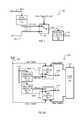
- FIG. 1is a block schematic diagram of a body bias circuit 100 according to a first embodiment. It is assumed that a body bias circuit 100 is included in an integrated circuit device having a first high power supply voltage (VDD), as well as a second high power supply voltage (VDDIO).
- a second power supply voltagecan be greater than the first high power supply voltage (i.e., VDDIO>VDD).
- VDDIOcan be greater than 1.5 volts, such as 1.8 volts as but one example, or greater than 2.0 volts, around 2.5 volts, or even higher, such as around 3.3. volts.
- VDDcan be less than 2.5 volts, or less than 2.0 volts, or less than 1.5 volts.
- VDDIOcan be about 2.5 volts and VDD can be about 1.2 volts.
- the VDDIO supplyramps up first.
- a body bias voltagecan be initially generated based on the VDDIO supply. Once a body bias voltage is at a desirable level, the other power supply voltage VDD can ramp up.
- VDDIOcan be an input/output power supply voltage that provides power to input/output drivers of the IC device.
- control signal CTRLcan then change to a second value that results in first switch input 112 - 0 being isolated from switch output 112 - 2 , and second switch input 112 - 1 being connected to switch output 112 - 2 .
- control signal CTRLcan be based on VDD power-on reset (POR) type circuit, or the like.
- VDDIOramps up before VDD.
- signal CTRLswitches from the first to second value after VDD has reached a stable level. Accordingly, in a power up operation, VDDIO ramps first, resulting in voltage regulator 106 providing VDD_Reg to switch circuit 104 .
- CTRLhas the first value, so VDD_Reg is provided as VDDIn to the body bias generator circuit 102 .
- the body bias generator circuit 102generates body bias voltage VBx, thus establishing a desired body bias for transistors.
- an IC devicecan include multiple body bias circuits like that shown in FIG. 1 , to generate various body bias voltages, including both positive and negative body bias voltages.
- a generated body bias voltagecan be a reverse body bias (i.e., greater than VDD for p-channel devices, or less than VSS for n-channel devices), or a forward body bias (i.e., less than VDD for p-channel devices, or greater than VSS for n-channel devices, but short of a voltage that forward biases the body p-n junction).
- a reverse body bias voltage for p-channel devicescan range from about one volt greater than VDD to about 0.1 volt greater than VDD.
- a reverse body bias voltage for n-channel transistorscan range from about one volt less than VSS to about 0.1 volt less than VSS.
- a forward VBP limitcan depend on doping conditions, but in particular embodiments can be no more than 0.6 less than VDD.
- a forward VBN limitcan depend on doping conditions, but in particular embodiments can be no more than 0.6 greater than VSS.
- embodimentscan include arrangements that switch a power supply voltage to body bias generator circuits
- other embodimentscan maintain (e.g., clamp) transistor bodies at a “safe” voltage upon power up. Subsequently, once body bias voltages are established, the transistor bodies can be switched from the clamped voltage to a desired body bias voltage. Examples of such embodiments will now be described.
- FIG. 2Ais a block schematic diagram of a body bias circuit 200 according to another embodiment. As in the case of FIG. 1 , in FIG. 2A it is assumed that body bias circuit 200 is included in an IC device having a higher second power supply voltage (VDDIO) that ramps up prior to a first power supply voltage VDD.
- VDDIOsecond power supply voltage
- the particular values and relationships between VDD and VDDIOcan include those described above, and equivalents.
- a body bias circuit 200can utilize the first ramping power supply voltage (e.g., VDDIO) to enable clamping circuits to clamp body bias nodes to the other power supply voltages (e.g., VDD, VSS).
- VDDIOfirst ramping power supply voltage
- body bias generator circuitscan generate body bias voltages. The body bias nodes can then be “unclamped” from the power supply voltages and connected to the body bias voltages.
- a body bias circuit 200can include a p-channel transistor body bias (PBB) generator circuit 202 - 0 , an n-channel transistor body bias (NBB) generator circuit 202 - 1 , a first clamp circuit 204 - 0 , a second clamp circuit 204 - 1 , and a clamp control circuit 214 .
- PBB generator circuit 202 - 0can generate a body bias voltage VBP_Gen for p-channel transistors.
- NBB generator circuit 202 - 1can generate a body bias voltage VBN_Gen for n-channel transistors.
- Both PBB and NBB generator circuits ( 202 - 0 / 1 )can be powered with a first power supply voltage (VDD), which is understood to ramp up after a second power supply voltage (VDDIO).
- VDDfirst power supply voltage
- VDDIOsecond power supply voltage
- PBB and NBB generator circuits ( 202 - 0 / 1 )are not active, and thus are not generating their respective body bias voltages VBP_Gen, VBN_Gen.
- Power supply voltage VDDcan be provided from high power supply input 208 - 0 as a first input to first clamp circuit 204 - 0 .
- First clamp circuit 204 - 0can receive VBP_Gen from PBB generator circuit 202 - 0 as a second input.
- Output 210 - 0 of first clamp circuit 204 - 0can set the body bias voltage VBP for some p-channel transistors at p-channel body bias node 210 - 0 .
- First clamp circuit 204 - 0can be controlled by a clamp enable signal (Clamp_EnableP) and a clamp disable signal (Clamp_DisableP).
- the clamp enable signal (Clamp_EnableP)can be activated from, or correspond to, VDDIO.
- clamp_EnablePan initial ramping of VDDIO can activate Clamp_EnableP.
- clamp circuit 204 - 0can clamp p-channel body bias node 210 - 0 to VDD.
- clamp disable signal(Clamp_DisableP) can be activated by clamp control circuit 214 .
- signal Clamp_DisablePwill override signal Clamp_EnableP, resulting in p-channel body bias node 210 - 0 being connected to VBP_Gen.
- second clamp circuit 204 - 1can receive VSS from a low power supply input 208 - 2 , receive VBN_Gen from NBB generator circuit 202 - 1 , and can set the body bias voltage VBN for some n-channel transistors at n-channel body bias node 210 - 1 .
- Second clamp circuit 204 - 1can operate in the same fashion as first clamp circuit 204 - 0 .
- N-channel body bias node 210 - 1can be clamped to VSS by operation of a VDDIO-based clamp enable signal (Clamp_EnableN). Such clamping can be disabled in response to a clamp disable signal (Clamp_DisableN), provided from clamp control circuit 214 , resulting in n-channel body bias node 210 - 1 being connected to receive VBN_Gen.
- Clamp_EnableNVDDIO-based clamp enable signal
- Clamp control circuit 214can operate according to VDD. That is, once VDD has reached a desired level, or some time afterward, clamp control circuit can activate the clamp disable signals (Clamp_DisableP, Clamp_DisableN).
- FIG. 2Bis a timing diagram showing VDDIO, VDD, VBP, VBN and VSS, described above.
- VDDIOcan ramp up. Due to resistive/capacitive coupling, there may be some variation in VBN/VBP.
- VDDIOreaches a level that enables clamp circuits 204 - 0 / 1 .
- VBPis clamped to VDD and VBN is clamped to VSS (which is zero volts in the embodiment shown).
- VDDcan ramp up. Due to clamping circuits 204 - 0 / 1 being enabled, VBP can remain clamped to VDD. Thus, VBP rises with VDD, preventing any forward biasing of p-channel body p-n junctions and/or potential latch-up conditions. Similarly, VBN remains clamped to VSS, also preventing the forward biasing of n-channel body junctions and/or reducing latch-up conditions.
- body bias circuitse.g., 202 - 0 / 1
- VBPcan be activated, generating VBP and VBN voltages.
- clamp control circuit 214can activate clamp disable signals, resulting in clamp circuits 204 - 0 / 1 connecting, or passively enabling the connection of, VBP to VBP_Gen and connecting, or passively enabling the connection of, VBN to VBN_Gen.
- the ICcan now operate with transistors having the desired body bias voltage.
- FIG. 2Bshows transistors operating with reverse body bias voltages (with respect to VDD_opt and VSS levels), it is understood that body bias voltages have any suitable value for a given application. Further, once established, body bias voltages can be varied in dynamic fashion. Body bias voltages (VBP, VBN) can have the relationships and/or ranges as described for particular embodiments herein, and equivalents.
- Generating body bias voltages(e.g., VBP, VBN) with VDD as opposed to VDDIO, as shown in embodiments herein, can be more efficient that conventional approaches.
- VBPbody bias voltage
- VBNbody bias voltages
- generating a VBN of ⁇ 0.6 V with a VDDIO of 2.5 Vwould have a maximum efficiency of 24%.
- VDDis 0.9 V
- generating the same VBNcan be performed with a maximum efficiency of 67%, a significant improvement in efficiency.
- FIG. 3Ais a block schematic diagram of a body bias circuit 300 according to another embodiment.
- a body bias circuit 300can include clamping circuits that operate in the absence of applied power, or otherwise without the need for a stable power supply. Using such “zero bias” clamping circuits, upon power up, transistor bodies can be clamped to power supply voltages (e.g., VDD, VSS). Once the power supply voltages are stable, body bias generator circuits can generate body bias voltages. The body bias nodes can then be “unclamped” from the power supply voltages and connected to the body bias voltages.
- power supply voltagese.g., VDD, VSS
- a body bias circuit 300can include items like those of FIG. 2A , including a PBB generator circuit 302 - 0 , an NBB generator circuit 302 - 1 , a first clamp circuit 304 - 0 , a second clamp circuit 304 - 1 , and a clamp control circuit 314 .
- PBB and NBB generator circuits( 302 - 0 / 1 ) can operate like those of FIG. 2A , generating body bias voltages VBP_Gen for p-channel transistors and VBN_Gen for n-channel transistors once a first power supply voltage VDD is stable.
- clamp control circuit 314can activate the clamp disable signals (Clamp_DisableP, Clamp_DisableN) once VDD has reached a desired level, or some time afterward.
- clamp circuits 304 - 0 / 1do not operate in response to a second power supply VDDIO. Rather, as noted above, in the absence of a VDD, or a stable VDD level, first clamp circuit 304 - 0 can clamp p-channel body bias node 310 - 0 to VDD, while second clamp circuit 304 - 1 can clamp n-channel body bias node 310 - 1 to VSS. In response to clamp disable signal Clamp_DisableP, first clamp circuit 304 - 0 can enable p-channel body bias node 310 - 0 to be connected to the body bias voltage VBP_Gen, generated by PBB generator circuit 302 - 0 .
- second clamp circuit 304 - 1can enable n-channel body bias node 310 - 1 to be connected to the body bias voltage VBN_Gen, generated by NBB generator circuit 302 - 1 .
- clamp circuits 304 - 0 / 1can utilize depletion mode MOS type transistors.
- depletion mode MOS type transistorscan provide a clamping connection (i.e., the source-drain path connects VBN to VSS and/or VBP to VDD).
- a gate voltagecan turn such depletion mode transistors off, enabling the VBN to be connected to VBN_Gen and VBP to be connected to VBP_Gen.
- FIG. 3Bis a timing diagram showing VDD, VBP, VBN and VSS, described above.
- VDDcan start to ramp up.
- body bias levelsVBP and VBN
- VBPbody bias of p-channel transistors
- VBNbody bias of n-channel transistors
- clamp control circuit 314can activate clamp disable signals, resulting in clamp circuits 304 - 0 / 1 connecting VBP to VBP_Gen and VBN to VBN_Gen.
- the ICcan now operate with transistors having the desired body bias voltage.
- body bias voltagescan be reverse body bias voltage, forward body bias voltages, as well as dynamically switching body bias voltages.
- a power supply voltage (VDD) and body bias voltages (VBP, VBN)can have the relationships and/or ranges as described for particular embodiments herein, and equivalents.
- Current source circuit 418can be connected between a gate of transistor N 40 and a lower power supply connection 408 - 2 .
- Current source circuit 418can operate in response to a VDD level. That is, initially, when VDD is ramping up, current source circuit 418 may not draw current. However, once VDD reaches a predetermined level, or is stable for a predetermined amount of time, current source circuit 418 can draw current.
- VDDcan start to ramp to a desired level.
- current source circuit 418can be disabled.
- capacitance C 40By operation of capacitance C 40 , a voltage at the gate of N 40 can track its source (i.e., track VDD). Because N 40 is a depletion mode device, it is conductive in this state, and p-channel body bias node 410 - 0 (i.e., VBP) can be clamped to VDD.
- VDDis at a suitable level, or stable for a suitable amount of time
- current source circuit 418can be enabled.
- the gate of N 40can be pulled toward VSS, turning off N 40 .
- p-channel body bias node 410 - 0can be released from being clamped to VDD, and driven to body bias voltage, such as that generated by a body bias generator circuit (e.g., VBP_Gen).
- VBP_Genbody bias generator circuit
- FIG. 4Bis a side cross sectional representation of a clamping transistor 420 , such as that shown as N 40 in FIG. 4A .
- Clamping transistor 420can be formed in a p-type well (p-well) 422 that is formed in a deep n-type well (n-well) 424 , which is formed in a p-type substrate 426 .
- a first power supply (VDD) input 408 - 0can be connected to a deep n-well tap 428 - 0 , a p-well tap 428 - 1 , and a source 430 of clamping transistor 420 .
- Capacitance C 40can be connected between source 430 and gate 432 .
- a drain 434can be connected to a p-channel body bias node 410 - 0 .
- a channel region 436can be doped with n-type dopants to provide the desired response in a depletion mode.
- a power supply voltage (VDD) and body bias voltage (VBP)can have the relationship and/or ranges as described for particular embodiments herein, and equivalents.
- FIG. 5Ais a schematic diagram of a clamp device 516 according to another embodiment.
- a clamp device 516can include a depletion mode p-channel MOS type transistor P 50 , a capacitance C 50 , and current source circuit 518 .
- Transistor P 50can have a source connected to a low power supply (VSS) input 508 - 2 , a drain connected to an n-channel body bias node 510 - 1 , a gate connected to current source circuit 518 , and a body connected to its source (VSS) (or alternatively to VDD).
- VSSlow power supply
- Capacitance C 50can be connected between the source and gate of transistor P 50 .
- Current source circuit 518can be connected between a gate of transistor P 50 and a high power supply (VDD) connection 508 - 0 .
- Current source circuit 518can operate in the same fashion as 418 shown in FIG. 4A .
- Clamping device 516can operate in a manner like that shown in FIG. 4A .
- VBNcan be clamped to VSS by depletion mode transistor P 50 .
- current source circuit 518can be enabled, driving the gate of P 50 to VDD, thus turning off transistor P 50 .
- FIG. 5Bis a side cross sectional representation of a clamping transistor 520 , such as that shown as P 50 in FIG. 5A .
- Clamping transistor 520can be formed in n-well 524 , which is formed in a p-type substrate 526 .
- a low power supply (VSS) input 508 - 2can be connected to an n-well tap 528 - 0 and a source 530 of clamping transistor 520 .
- Capacitance C 50can be connected between a source 530 and gate 532 of P 50 .
- a drain 534can be connected to an n-channel body bias node 510 - 1 .
- a channel region 536can be doped with p-type dopants to provide the desired response in a depletion mode.
- a power supply voltage (VSS) and body bias voltage (VBN)can have the relationship and/or ranges as described for particular embodiments herein, and equivalents.
- FIG. 6Ais a schematic diagram of a clamp device 616 according to a further embodiment.
- a clamp device 616can include an n-channel junction field effect transistor (JFET) N 60 , a capacitance C 60 , and current source circuit 618 .
- JFET N 60can have a source connected to a first power supply (VDD) input 608 - 0 , a drain connected to a p-channel body bias node 610 - 0 , and a gate connected to current source circuit 618 .
- VDDfirst power supply
- Capacitance C 60can be connected between the source and gate of transistor N 60 .
- Current source circuit 618can be connected between a gate of transistor N 60 and a low power supply (VSS) connection 608 - 2 .
- Current source circuit 618can operate in the same fashion as 418 shown in FIG. 4A .
- Clamping device 616can operate in a manner like that shown in FIG. 4A . As VDD ramps, VBP can be clamped to VDD by JFET P 60 . Once VDD reaches a certain level or is stable for a predetermined amount of time, current source circuit 618 can be enabled, driving the gate of N 60 to VSS, turning off transistor N 60 .
- FIG. 6Bis a side cross sectional representation of a clamping transistor 620 , such as that shown as P 60 in FIG. 6A .
- Clamping transistor 620can be formed in a p-well 622 that is formed in a deep n-well 624 , which is formed in a p-type substrate 626 .
- a first power supply (VDD) input 608 - 0can be connected to a deep n-well tap 628 - 0 and a source 630 of clamping transistor 620 .
- a gate 632can include a p-well tap 628 - 1 that drives p-well 622 .
- Capacitance C 60can be connected between source 630 and gate 632 .
- a drain 634can be connected to a p-channel body bias node 610 - 0 .
- a channel region 636can be doped with n-type dopants to provide the desired response.
- a power supply voltage (VDD) and body bias voltage (VBP)can have the relationship and/or ranges as described for particular embodiments herein, and equivalents.
- FIG. 7Ais a schematic diagram of a clamp device 716 according to a further embodiment.
- a clamp device 716can include a p-channel JFET P 70 , a capacitance C 70 , and current source circuit 718 .
- JFET P 70can have a source connected to a low power supply (VSS) input 708 - 2 , a drain connected to an n-channel body bias node 710 - 1 , and a gate connected to current source circuit 718 .
- VSSlow power supply
- Capacitance C 70can be connected between the source and gate of JFET P 70 .
- Current source circuit 718can be connected between a gate of JFET P 70 and a high power supply (VDD) connection 708 - 0 .
- Current source circuit 718can operate in the same fashion as 418 shown in FIG. 4A .
- Clamping device 716can operate in a manner like that shown in FIG. 4A . As VDD ramps, VBN can be clamped to VSS by JFET P 70 . Once VDD reaches a certain level, or is stable for a predetermined amount of time, current source circuit 718 can be enabled, driving the gate of P 70 to VDD, turning off JFET P 70 .
- FIG. 7Bis a side cross sectional representation of a clamping transistor 720 , such as that shown as P 70 in FIG. 7A .
- Clamping transistor 720can be formed in an n-well 724 , which is formed in a p-type substrate 726 .
- a low power supply (VSS) input 708 - 2can be connected to a source 730 of clamping transistor 720 .
- a gate 732can include an n-well tap 728 - 0 that drives n-well 724 .
- Capacitance C 70can be connected between source 730 and gate 732 .
- a drain 734can be connected to an n-channel body bias node 710 - 1 .
- a channel region 736can be doped with p-type dopants to provide the desired response.
- a power supply voltage (VSS) and body bias voltage (VBN)can have the relationship and/or ranges as described for particular embodiments herein, and equivalents.
- clamp devices and transistors shown in FIGS. 4A to 7Bpresent but a few possible examples of circuits and devices that can be included in embodiments.
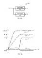
- FIG. 8is a graph showing simulation results of a typical power up operation.
- FIG. 8includes waveforms for a power supply voltage VDD that ramps up upon power up, a p-channel body bias voltage VBP, an n-channel body bias voltage VBN, and a signal VPumpEN, which indicates the activation of body bias voltage generating circuits (e.g., charge pumps).
- VDDpower supply voltage
- VBPp-channel body bias voltage
- VBNn-channel body bias voltage
- VPumpENwhich indicates the activation of body bias voltage generating circuits (e.g., charge pumps).
- VDDstarts to ramp from 0 volts to 1.2 volts. Due to capacitive and resistive coupling VBP and VBN rise with VDD. Such a response can result in the forward biasing of p-n junctions and/or latch-up conditions.
- VDDreaches a desired level of 1.2 V.
- VPB and VBNremain at elevated levels.
- VPumpENgoes to an active level (high in this example).
- VBN and VBPcan then be driven to desired body bias levels (various examples of possible body bias voltages are shown in FIG. 8 ).
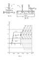
- FIG. 9is a graph showing simulation results of a power up operation according to an embodiment.
- FIG. 9includes waveforms like those of FIG. 8 , including VDD, VBP, VBN and VPumpEN.
- FIG. 9includes waveforms for a second power supply voltage VDDIO and a clamp enable signal VClampEN.
- VDDIOis greater than VDD and ramps up prior to VDD.
- VClampENIn response to an active (high in this example) VClampEN signal, VBP can be clamped to VDD and VBN can be clamped to VSS, as described herein, or equivalents.
- VDDIOstarts to ramp from 0 volts to 2.5 volts.
- VPumpENcan be active, resulting in VBP and VBN being driven to desired body bias voltages.
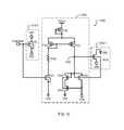
- FIG. 10is a schematic diagram of a clamping circuit 1000 according to one particular embodiment.
- clamping circuit 1000in response to a clamp enable signal (VClampEN) being active, clamping circuit 1000 can clamp a p-channel body bias node (VBP) to a high power supply voltage (VDD) and an n-channel body bias node (VBN) to a low power supply voltage (VSS).
- VBPp-channel body bias node
- VBNhigh power supply voltage
- VSSlow power supply voltage
- a clamping circuit 1000can isolate VBP from VDD and isolate VBN from VSS.
- a clamping circuit 1000includes a first clamping device 1016 - 0 , a second clamping device 1016 - 1 , and a control section 1040 .
- a first clamping device 1016 - 0can include an n-channel MOS type transistor N 100 having a source and body connected to VDD, a drain connected to VBP, and a gate connected to receive VClampEN.
- a control section 1040can also include a disable circuit formed by n-channel MOS type transistors N 102 /N 103 /N 104 .
- Transistors N 102 and N 103can have drains and gates commonly connected to control node 1042 .
- Transistor N 102can have a source connected to the drain of transistor N 104 .
- Transistor N 103can have a source connected to n-channel body bias node VBN.
- the bodies of transistors N 102 /N 104can be commonly connected to each other.
- Transistor N 104can have a source connected to VSS.
- VDDIOcan ramp to a high level, enabling control section 1040 .
- VClampENcan be activated (e.g., driven to VDDIO).
- first clamping device 1016 - 0can clamp VBP to VDD.
- VClampENcan turn on transistor N 101 , pulling one leg of the current mirror low. This results in control node 1042 being driven high.
- second clamping device 1016 - 1can be turned on, clamping VBN to VSS.
- VDDcan then be ramped up, with VBP and VBN now clamped to VDD and VSS, respectively.
- first clamping device 1016 - 0When VClampEN returns to an inactive level (e.g., VSS), first clamping device 1016 - 0 can turn off, isolating VBP from VDD. This can allow VBP to be driven to a desired body bias voltage. In addition, transistor N 101 within the current mirror circuit turns off. As a result, control node 1042 can fall, turning off second clamping device 1016 - 1 to isolate VBN from VSS. This can allow VBN to be driven to a desired body bias level. Disable circuit N 102 /N 103 /N 104 can ensure second clamping device 1016 - 1 remains turned off, even when VBN is driven below VSS.
- VSSinactive level
- DDCdeeply depleted channel
- transistors with driven body bias voltagescan be DDC transistors. That is, bodies of DDC transistors can be clamped upon power-up as described herein, or equivalents.
- the transistors making up body bias circuitscan be DDC transistors.
- any of the MOS type transistors described in the embodiments hereincan be DDC transistors.
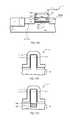
- FIG. 11Ashows a DDC type transistor 1171 that can be included in embodiments herein.
- a DDC transistor 1171can be configured to have an enhanced body coefficient, along with the ability to set a threshold voltage (Vt) with enhanced precision.
- a DDC transistor 1171can include a gate electrode 1173 , source 1175 , drain 1177 , and a gate dielectric 1179 positioned over a substantially undoped channel 1181 .
- Optional lightly doped source and drain extensions (SDE) 1183can be positioned respectively adjacent to source 1175 and drain 1177 . Such extensions 1183 can extend toward each other, reducing effective length of the substantially undoped channel 1181 .
- insulating sidewalls 1193can be formed on sides of gate electrode 1173 .
- DDC transistor 1171is shown as an n-channel transistor having a source 1175 and drain 1177 made of n-type dopant material, formed upon a substrate such as a p-type doped silicon substrate, which can be a p-well 1185 .
- a body bias voltage VBNcan be applied via a tap 1191 to the p-well 1185 .
- a p-channel DDC transistorswould be understood from FIG. 11A (i.e., would have reverse doping types).
- a DDC transistor 1171 , a highly doped screening region 1187 and optional threshold voltage set region 1189can be made with dopants of the same conductivity type as the body (i.e., p-type dopant material in FIG. 11A ).
- a screening region 1187can have a dopant concentration between about 5 ⁇ 10 18 to 1 ⁇ 10 20 dopant atoms/cm 3 , with the selected dopant concentration dependent on the desired threshold voltage as well as other desired transistor characteristics.
- a substantially undoped channel region 1181can have a depth that ranges from approximately 5-25 nm, with the selected thickness based upon the desired threshold voltage for the transistor.
- FIG. 11Bshows a FinFET type transistor 1171 -B that can receive a body bias voltage according to embodiments.
- FinFET transistor 1171 -Bcan include a gate electrode 1173 -B and gate dielectric 1179 -B that surrounds a substantially undoped channel 1181 -B on opposing sides.
- the view of FIG. 11Bis taken along a channel length. Thus, it is understood that source and drain regions can extend into and out of the view shown.
- a body bias VBBcan be applied via a connection to a substrate 1197 .
- FIG. 11Cshows a FinFET type transistor 1171 -C having a screening region 1187 -C, that can receive a body bias voltage according to embodiments.
- the FinFET transistor 1171 -Chas a highly doped region that can be configured to have an enhanced body coefficient, along with the ability to set a Vt with enhanced precision.
- the transistor 1171 -Cincludes a gate electrode 1173 -C and gate dielectric 1179 -C formed over a substantially undoped channel 1181 -C on opposing sides.
- a highly doped screening region 1187 -Ccan be formed in a substrate 1197 below substantially undoped channel 1181 -C rising upward three-dimensionally.
- a Vt set region 1189 -Ccan be formed between the screening region 1187 -C and substantially undoped channel 1181 -C.
- FIG. 11Cthe view of FIG. 11C is taken along a channel length, and source and drain regions can extend into and out of the view, separated from screening region 1187 -C by portions of substantially undoped channel region 1181 -C.
- a body bias VBBcan be applied via a connection to a substrate 1197 .
Landscapes
- Engineering & Computer Science (AREA)
- Physics & Mathematics (AREA)
- Radar, Positioning & Navigation (AREA)
- Nonlinear Science (AREA)
- Electromagnetism (AREA)
- General Physics & Mathematics (AREA)
- Microelectronics & Electronic Packaging (AREA)
- Automation & Control Theory (AREA)
- Semiconductor Integrated Circuits (AREA)
- Logic Circuits (AREA)
- Metal-Oxide And Bipolar Metal-Oxide Semiconductor Integrated Circuits (AREA)
- Electronic Switches (AREA)
- Control Of Electrical Variables (AREA)
Abstract
Description
The present invention relates generally to transistor body biasing circuits for integrated circuit devices, and more particularly to body biasing circuits for establishing body bias voltages upon power-up of such devices.
Integrated circuit (IC) devices can include transistors, such as insulated gate field effect transistors (hereinafter referred to as MOS type transistors, but not implying any particular gate or gate insulator material). MOS type transistors can include gates, drains, sources and bodies. In some IC devices, or some circuits within an IC device, the bodies of transistors have a permanent connection to a power supply voltage. For example, bodies of p-channel MOS transistors are connected to a high power supply voltage (e.g., VDD), while bodies of n-channel transistors are connected to a low power supply voltage (e.g., VSS).
However, in other IC devices or circuits within an IC device, the bodies of transistors can be biased to potential different from a power supply voltage. Such body biasing can advantageously alter the performance of the transistors. For example, a greater reverse body bias (i.e., p-channels body biased to a voltage above VDD or n-channel body biased to a voltage less than VSS) can decrease a transistor current leakage. Greater forward body bias (i.e., p-channels body biased to a voltage below VDD or n-channel body biased to a voltage above VSS) can increase transistor switching speed. In some cases, an IC device can include one or more body bias voltage generating circuits to generate desired body bias voltages, which are then applied to the bodies of target transistors.
A drawback to implementing body biasing circuits can be the need to strictly control body voltages during the transient state of powering up the IC device. If body voltages levels are not strictly controlled, a p-n junction formed by a transistor body can forward bias, drawing a large amount of current, and possibly damaging the IC device. Further, the initial floating states of transistor bodies can give rise to latch-up conditions (activation of a parasitic bipolar junction transistor).
Various embodiments of the present invention will now be described with reference to a number of drawings. The embodiments show circuits, integrated circuit (IC) devices, and methods for controlling body bias voltages during a power-up operation that can reduce current spikes and/or latch-up. Power-up operations can include those operations when a power supply voltage initially ramps up, including when a device is initially powered on, reset, subject to a power interruption event, or dynamically powered on and off for power conservation purposes, as but a few examples.
In the embodiments below, like items are referred to by the same reference character but with the leading digit(s) corresponding to the figure number.
Referring still toFIG. 12B , once VDD reaches stable level, body bias circuits can be activated. This is shown at time ta, where VBP is driven to VBP_opt and VBN is driven to VBN_opt.
As shown inFIG. 13B ,body bias circuits 1301/1302 can establish body bias voltages VBP/VBN prior to VDD ramping-up. This can substantially reduce current draw on power-up, and prevent and/or greatly reduce the chance of latch-up.
It is noted that the efficiency of such a body bias approach can be limited to:
where Vout is VBP or VBN. For example, assuming VBN=−0.6V and VDDIO=2.5 V, efficiency would be no greater than 24%.
In the embodiment shown, abody bias circuit 100 can receive a first power supply voltage (VDD) at a first power supply input108-0, a second power supply voltage (VDDIO) at a second power supply input108-1, and can generate a body bias voltage (VBx) at abody bias node 110. Abody bias circuit 100 can include a bodybias generator circuit 102, aswitch circuit 104, and avoltage regulator 106. Avoltage regulator 106 can receive VDDIO, and regulate it to achieve a predetermined level VDD_Reg (which can be the desired final level for VDD).
Bodybias generator circuit 102 can receive a power supply voltage VDDIn from the switch output112-2. In response to VDDIn, bodybias generator circuit 102 can generate a body bias voltage VBx. It is understood that VBx can be an n-channel body bias voltage or a p-channel body bias voltage.
Referring still toFIG. 1 , in operation, it is assumed the VDDIO ramps up before VDD. Further, signal CTRL switches from the first to second value after VDD has reached a stable level. Accordingly, in a power up operation, VDDIO ramps first, resulting involtage regulator 106 providing VDD_Reg to switchcircuit 104. CTRL has the first value, so VDD_Reg is provided as VDDIn to the bodybias generator circuit 102. The bodybias generator circuit 102 generates body bias voltage VBx, thus establishing a desired body bias for transistors. Subsequently, with transistor body bias(es) established, VDD can ramp up, avoiding conditions that could forward bias p-n junctions and/or lead to latch-up, as bodybias generator circuit 102 is driving such bodies to desired voltages. Once VDD has reached a desired level and/or stability, signal CTRL can switch to the second value, applying VDD as VDDIn to the bodybias generator circuit 102. Because VDD<VDDIO, the generation of the body bias voltage can be more efficient.
It is understood that an IC device can include multiple body bias circuits like that shown inFIG. 1 , to generate various body bias voltages, including both positive and negative body bias voltages. Further, a generated body bias voltage can be a reverse body bias (i.e., greater than VDD for p-channel devices, or less than VSS for n-channel devices), or a forward body bias (i.e., less than VDD for p-channel devices, or greater than VSS for n-channel devices, but short of a voltage that forward biases the body p-n junction). In very particular embodiments, a reverse body bias voltage for p-channel devices (VBP) can range from about one volt greater than VDD to about 0.1 volt greater than VDD. Similarly, a reverse body bias voltage for n-channel transistors (VBN) can range from about one volt less than VSS to about 0.1 volt less than VSS. A forward VBP limit can depend on doping conditions, but in particular embodiments can be no more than 0.6 less than VDD. Likewise, a forward VBN limit can depend on doping conditions, but in particular embodiments can be no more than 0.6 greater than VSS.
While embodiments can include arrangements that switch a power supply voltage to body bias generator circuits, other embodiments can maintain (e.g., clamp) transistor bodies at a “safe” voltage upon power up. Subsequently, once body bias voltages are established, the transistor bodies can be switched from the clamped voltage to a desired body bias voltage. Examples of such embodiments will now be described.
In the embodiment shown, abody bias circuit 200 can utilize the first ramping power supply voltage (e.g., VDDIO) to enable clamping circuits to clamp body bias nodes to the other power supply voltages (e.g., VDD, VSS). Thus, as the device powers up, transistors bodies are clamped to such power supply voltages (e.g., VDD, VSS). Once the lower power supply voltage (VDD) is stable, body bias generator circuits can generate body bias voltages. The body bias nodes can then be “unclamped” from the power supply voltages and connected to the body bias voltages.
In the particular embodiment shown, abody bias circuit 200 can include a p-channel transistor body bias (PBB) generator circuit202-0, an n-channel transistor body bias (NBB) generator circuit202-1, a first clamp circuit204-0, a second clamp circuit204-1, and aclamp control circuit 214. PBB generator circuit202-0 can generate a body bias voltage VBP_Gen for p-channel transistors. Similarly, NBB generator circuit202-1 can generate a body bias voltage VBN_Gen for n-channel transistors. Both PBB and NBB generator circuits (202-0/1) can be powered with a first power supply voltage (VDD), which is understood to ramp up after a second power supply voltage (VDDIO). Thus, in an initial part of a power up operation, prior to VDD ramping up, PBB and NBB generator circuits (202-0/1) are not active, and thus are not generating their respective body bias voltages VBP_Gen, VBN_Gen.
Power supply voltage VDD can be provided from high power supply input208-0 as a first input to first clamp circuit204-0. First clamp circuit204-0 can receive VBP_Gen from PBB generator circuit202-0 as a second input. Output210-0 of first clamp circuit204-0 can set the body bias voltage VBP for some p-channel transistors at p-channel body bias node210-0. First clamp circuit204-0 can be controlled by a clamp enable signal (Clamp_EnableP) and a clamp disable signal (Clamp_DisableP). The clamp enable signal (Clamp_EnableP) can be activated from, or correspond to, VDDIO. Thus, an initial ramping of VDDIO can activate Clamp_EnableP. When Clamp_EnableP is active, clamp circuit204-0 can clamp p-channel body bias node210-0 to VDD. In contrast, the clamp disable signal (Clamp_DisableP) can be activated byclamp control circuit 214. When activated, signal Clamp_DisableP will override signal Clamp_EnableP, resulting in p-channel body bias node210-0 being connected to VBP_Gen.
In a similar fashion to first clamp circuit204-0, second clamp circuit204-1 can receive VSS from a low power supply input208-2, receive VBN_Gen from NBB generator circuit202-1, and can set the body bias voltage VBN for some n-channel transistors at n-channel body bias node210-1. Second clamp circuit204-1 can operate in the same fashion as first clamp circuit204-0. N-channel body bias node210-1 can be clamped to VSS by operation of a VDDIO-based clamp enable signal (Clamp_EnableN). Such clamping can be disabled in response to a clamp disable signal (Clamp_DisableN), provided fromclamp control circuit 214, resulting in n-channel body bias node210-1 being connected to receive VBN_Gen.
One particular power up operation for the body bias circuit ofFIG. 2A will be described with reference toFIG. 2B .FIG. 2B is a timing diagram showing VDDIO, VDD, VBP, VBN and VSS, described above.
Referring toFIGS. 2A and 2B , at time t0, VDDIO can ramp up. Due to resistive/capacitive coupling, there may be some variation in VBN/VBP.
At about time t1, VDDIO reaches a level that enables clamp circuits204-0/1. As a result, VBP is clamped to VDD and VBN is clamped to VSS (which is zero volts in the embodiment shown).
At about time t2, VDD can ramp up. Due to clamping circuits204-0/1 being enabled, VBP can remain clamped to VDD. Thus, VBP rises with VDD, preventing any forward biasing of p-channel body p-n junctions and/or potential latch-up conditions. Similarly, VBN remains clamped to VSS, also preventing the forward biasing of n-channel body junctions and/or reducing latch-up conditions. Once VDD reaches a sufficient level, body bias circuits (e.g.,202-0/1) can be activated, generating VBP and VBN voltages.
At about time t3, VDD reaches a desired level for a predetermined amount of time. As a result,clamp control circuit 214 can activate clamp disable signals, resulting in clamp circuits204-0/1 connecting, or passively enabling the connection of, VBP to VBP_Gen and connecting, or passively enabling the connection of, VBN to VBN_Gen. The IC can now operate with transistors having the desired body bias voltage.
WhileFIG. 2B shows transistors operating with reverse body bias voltages (with respect to VDD_opt and VSS levels), it is understood that body bias voltages have any suitable value for a given application. Further, once established, body bias voltages can be varied in dynamic fashion. Body bias voltages (VBP, VBN) can have the relationships and/or ranges as described for particular embodiments herein, and equivalents.
Generating body bias voltages (e.g., VBP, VBN) with VDD as opposed to VDDIO, as shown in embodiments herein, can be more efficient that conventional approaches. As noted above in connection withFIGS. 13A and 13B , generating a VBN of −0.6 V with a VDDIO of 2.5 V would have a maximum efficiency of 24%. However, if VDD is 0.9 V, generating the same VBN can be performed with a maximum efficiency of 67%, a significant improvement in efficiency.
Abody bias circuit 300 can include items like those ofFIG. 2A , including a PBB generator circuit302-0, an NBB generator circuit302-1, a first clamp circuit304-0, a second clamp circuit304-1, and aclamp control circuit 314. PBB and NBB generator circuits (302-0/1) can operate like those ofFIG. 2A , generating body bias voltages VBP_Gen for p-channel transistors and VBN_Gen for n-channel transistors once a first power supply voltage VDD is stable. Similarly,clamp control circuit 314 can activate the clamp disable signals (Clamp_DisableP, Clamp_DisableN) once VDD has reached a desired level, or some time afterward.
However, unlike the embodiment ofFIG. 2A , clamp circuits304-0/1 do not operate in response to a second power supply VDDIO. Rather, as noted above, in the absence of a VDD, or a stable VDD level, first clamp circuit304-0 can clamp p-channel body bias node310-0 to VDD, while second clamp circuit304-1 can clamp n-channel body bias node310-1 to VSS. In response to clamp disable signal Clamp_DisableP, first clamp circuit304-0 can enable p-channel body bias node310-0 to be connected to the body bias voltage VBP_Gen, generated by PBB generator circuit302-0. Similarly, in response to clamp disable signal Clamp_DisableN, second clamp circuit304-1 can enable n-channel body bias node310-1 to be connected to the body bias voltage VBN_Gen, generated by NBB generator circuit302-1.
In very particular embodiments, clamp circuits304-0/1 can utilize depletion mode MOS type transistors. Thus, in the absence of a gate voltage, such transistors can provide a clamping connection (i.e., the source-drain path connects VBN to VSS and/or VBP to VDD). Subsequently, a gate voltage can turn such depletion mode transistors off, enabling the VBN to be connected to VBN_Gen and VBP to be connected to VBP_Gen.
One particular power up operation for the body bias circuit ofFIG. 3A will be described with reference toFIG. 3B .FIG. 3B is a timing diagram showing VDD, VBP, VBN and VSS, described above.
Referring toFIGS. 3A and 3B , at time t0, VDD can start to ramp up. In a conventional device, such an operation can result in body bias levels (VBP and VBN) varying due to capacitive/resistive coupling. However, by operation of “zero bias” first and second clamp circuits (304-0/1), VBP (a body bias of p-channel transistors) remains clamped to VDD and VBN (a body bias of n-channel transistors) remains clamped to VSS. Consequently the forward biasing of body based p-n junctions and/or latch-up inducing conditions can be prevented.
At about time t1, VDD reaches a desired level for a predetermined amount of time. As a result,clamp control circuit 314 can activate clamp disable signals, resulting in clamp circuits304-0/1 connecting VBP to VBP_Gen and VBN to VBN_Gen. The IC can now operate with transistors having the desired body bias voltage.
As in other embodiments herein, body bias voltages (VBN_Gen, VBP_Gen) can be reverse body bias voltage, forward body bias voltages, as well as dynamically switching body bias voltages. In particular embodiments, a power supply voltage (VDD) and body bias voltages (VBP, VBN) can have the relationships and/or ranges as described for particular embodiments herein, and equivalents.
In operation, upon power up, VDD can start to ramp to a desired level. At this time,current source circuit 418 can be disabled. By operation of capacitance C40, a voltage at the gate of N40 can track its source (i.e., track VDD). Because N40 is a depletion mode device, it is conductive in this state, and p-channel body bias node410-0 (i.e., VBP) can be clamped to VDD.
Subsequently, once VDD is at a suitable level, or stable for a suitable amount of time,current source circuit 418 can be enabled. As a result, the gate of N40 can be pulled toward VSS, turning off N40. In this way, p-channel body bias node410-0 can be released from being clamped to VDD, and driven to body bias voltage, such as that generated by a body bias generator circuit (e.g., VBP_Gen).
In particular embodiments, a power supply voltage (VDD) and body bias voltage (VBP) can have the relationship and/or ranges as described for particular embodiments herein, and equivalents.
Capacitance C50 can be connected between the source and gate of transistor P50.Current source circuit 518 can be connected between a gate of transistor P50 and a high power supply (VDD) connection508-0.Current source circuit 518 can operate in the same fashion as418 shown inFIG. 4A .
Clampingdevice 516 can operate in a manner like that shown inFIG. 4A . In short, as VDD ramps, VBN can be clamped to VSS by depletion mode transistor P50. Once VDD reaches a certain level or is stable for a predetermined amount of time,current source circuit 518 can be enabled, driving the gate of P50 to VDD, thus turning off transistor P50.
In particular embodiments, a power supply voltage (VSS) and body bias voltage (VBN) can have the relationship and/or ranges as described for particular embodiments herein, and equivalents.
Capacitance C60 can be connected between the source and gate of transistor N60.Current source circuit 618 can be connected between a gate of transistor N60 and a low power supply (VSS) connection608-2.Current source circuit 618 can operate in the same fashion as418 shown inFIG. 4A .
Clampingdevice 616 can operate in a manner like that shown inFIG. 4A . As VDD ramps, VBP can be clamped to VDD by JFET P60. Once VDD reaches a certain level or is stable for a predetermined amount of time,current source circuit 618 can be enabled, driving the gate of N60 to VSS, turning off transistor N60.
In particular embodiments, a power supply voltage (VDD) and body bias voltage (VBP) can have the relationship and/or ranges as described for particular embodiments herein, and equivalents.
Capacitance C70 can be connected between the source and gate of JFET P70.Current source circuit 718 can be connected between a gate of JFET P70 and a high power supply (VDD) connection708-0.Current source circuit 718 can operate in the same fashion as418 shown inFIG. 4A .
Clampingdevice 716 can operate in a manner like that shown inFIG. 4A . As VDD ramps, VBN can be clamped to VSS by JFET P70. Once VDD reaches a certain level, or is stable for a predetermined amount of time,current source circuit 718 can be enabled, driving the gate of P70 to VDD, turning off JFET P70.
In particular embodiments, a power supply voltage (VSS) and body bias voltage (VBN) can have the relationship and/or ranges as described for particular embodiments herein, and equivalents.
It is understood that the clamp devices and transistors shown inFIGS. 4A to 7B present but a few possible examples of circuits and devices that can be included in embodiments.
At time t0, VDD starts to ramp from 0 volts to 1.2 volts. Due to capacitive and resistive coupling VBP and VBN rise with VDD. Such a response can result in the forward biasing of p-n junctions and/or latch-up conditions.
At about time t1, VDD reaches a desired level of 1.2 V. VPB and VBN remain at elevated levels.
At about time t2, VPumpEN goes to an active level (high in this example). VBN and VBP can then be driven to desired body bias levels (various examples of possible body bias voltages are shown inFIG. 8 ).
At time t0, VDDIO starts to ramp from 0 volts to 2.5 volts.
At time t1, after VDDIO reached 2.5 volts, VClampEN can be activated. As a result, VBP is clamped to VDD and VBN is clamped to VSS. After time t1, VDD can start to ramp from 0 volts to 1.2 volts. However, unlikeFIG. 8 , due to the clamping operations, VBP tracks VDD and VBN closely tracks VSS. Accordingly, the forward body biasing of body based p-n junctions and latch-up conditions can be prevented.
At time t2, VDD reaches its target value of 1.2 volts.
At time t3, after VDD has reached a stable value, VClampEN can return to an inactive level. Thus, VBP and VBN are released from being clamped to VDD and VSS, respectively.
At time t4, VPumpEN can be active, resulting in VBP and VBN being driven to desired body bias voltages.
In the particular embodiment shown, aclamping circuit 1000 includes a first clamping device1016-0, a second clamping device1016-1, and acontrol section 1040. A first clamping device1016-0 can include an n-channel MOS type transistor N100 having a source and body connected to VDD, a drain connected to VBP, and a gate connected to receive VClampEN.
Acontrol section 1040 can include a current mirror circuit formed by p-channel transistors P100/P101/P102, a resistor R100, and an n-channel MOS type transistor N101. Transistor P100 can have a source connected to a second power supply voltage VDDIO and a gate and drain connected to one another. VDDIO can ramp up before, and be greater than, VDD. Transistors P101/P102 can form a current mirror, having sources commonly connected to the gate-drain of P100. Transistor P101 can have its gate connected to its drain. Transistor P102 can have a gate connected to the gate of P101 and a drain connected to acontrol node 1042. Resistor R100 can be connected between the gate-drain of transistor P101 and the drain of transistor N101. Transistor N101 can have a gate that receives VClampEN and a body and source connected to VSS.
Acontrol section 1040 can also include a disable circuit formed by n-channel MOS type transistors N102/N103/N104. Transistors N102 and N103 can have drains and gates commonly connected to controlnode 1042. Transistor N102 can have a source connected to the drain of transistor N104. Transistor N103 can have a source connected to n-channel body bias node VBN. The bodies of transistors N102/N104 can be commonly connected to each other. Transistor N104 can have a source connected to VSS.
A second clamping device1016-1 can include an n-channel MOS type transistor N105 having a drain connected to VSS, a source connected to VBN, and a body connected to the body of N103.
In operation, VDDIO can ramp to a high level, enablingcontrol section 1040.
Subsequently, VClampEN can be activated (e.g., driven to VDDIO). As a result, first clamping device1016-0 can clamp VBP to VDD. In addition, VClampEN can turn on transistor N101, pulling one leg of the current mirror low. This results incontrol node 1042 being driven high. As a result, second clamping device1016-1 can be turned on, clamping VBN to VSS.
VDD can then be ramped up, with VBP and VBN now clamped to VDD and VSS, respectively.
When VClampEN returns to an inactive level (e.g., VSS), first clamping device1016-0 can turn off, isolating VBP from VDD. This can allow VBP to be driven to a desired body bias voltage. In addition, transistor N101 within the current mirror circuit turns off. As a result,control node 1042 can fall, turning off second clamping device1016-1 to isolate VBN from VSS. This can allow VBN to be driven to a desired body bias level. Disable circuit N102/N103/N104 can ensure second clamping device1016-1 remains turned off, even when VBN is driven below VSS.
While embodiments can be included in IC devices having conventional MOS type transistors, in some embodiments, all or a portion of the transistors within the integrated circuit device can be “deeply depleted channel” (DDC) transistors having an enhanced body effect as compared to conventional transistors. Accordingly, body bias voltages applied to DDC transistors can be used to modulate transistor responses more effectively than conventional MOS type transistors.
In some embodiments, transistors with driven body bias voltages can be DDC transistors. That is, bodies of DDC transistors can be clamped upon power-up as described herein, or equivalents. In addition or alternatively, the transistors making up body bias circuits can be DDC transistors. Thus, it is understood that any of the MOS type transistors described in the embodiments herein can be DDC transistors.
InFIG. 11A ,DDC transistor 1171 is shown as an n-channel transistor having asource 1175 and drain1177 made of n-type dopant material, formed upon a substrate such as a p-type doped silicon substrate, which can be a p-well 1185. A body bias voltage VBN can be applied via atap 1191 to the p-well 1185. However, a p-channel DDC transistors would be understood fromFIG. 11A (i.e., would have reverse doping types).
In some embodiments, aDDC transistor 1171, a highly dopedscreening region 1187 and optional thresholdvoltage set region 1189 can be made with dopants of the same conductivity type as the body (i.e., p-type dopant material inFIG. 11A ). In certain embodiments, ascreening region 1187 can have a dopant concentration between about 5×10¹⁸to 1×10²⁰dopant atoms/cm3, with the selected dopant concentration dependent on the desired threshold voltage as well as other desired transistor characteristics. In some embodiments, a substantiallyundoped channel region 1181 can have a depth that ranges from approximately 5-25 nm, with the selected thickness based upon the desired threshold voltage for the transistor.
Further descriptions of a DDC transistor as well as an exemplary fabrication process and other aspects of a DDC transistor can be found in U.S. Pat. No. 8,273,617, titled “Electronic Devices and Systems, and Methods for Making and Using the Same.”
As in the case ofFIG. 11B , the view ofFIG. 11C is taken along a channel length, and source and drain regions can extend into and out of the view, separated from screening region1187-C by portions of substantially undoped channel region1181-C. A body bias VBB can be applied via a connection to asubstrate 1197. Further descriptions of a FinFET transistor having a highly doped region can be found in patent application International Application No. PCT/US12/49531 titled “Semiconductor Devices Having Fin Structures and Fabrication Methods Thereof”.
It should be appreciated that in the foregoing descriptions of exemplary embodiments, various features are sometimes grouped together in a single embodiment, figure, or description thereof for the purpose of streamlining the disclosure aiding in the understanding of one or more of the various inventive aspects. This method of disclosure, however, is not to be interpreted as reflecting an intention that the claimed invention requires more features than are expressly recited in each claim. Rather, as the following claims reflect, inventive aspects lie in less than all features of a single foregoing disclosed embodiment. Thus, the claims following the detailed description are hereby expressly incorporated into this detailed description, with each claim standing on its own as a separate embodiment of the invention.
It is also understood that the embodiments may be practiced in the absence of an element and/or step not specifically disclosed. That is, an inventive feature of the invention may be elimination of an element.
Accordingly, while the various aspects of the particular embodiments set forth herein have been described in detail, the present invention could be subject to various changes, substitutions, and alterations without departing from the spirit and scope of the invention.
Claims (19)
1. An integrated circuit (IC) device, comprising:
at least a first body bias circuit that receives a first power supply voltage, the first body bias circuit configured to generate a first body bias voltage different from the first power supply voltages of the IC device;
at least a clamp control circuit that receives the first power supply voltage and generates a clamp signal when the clamp control circuit detects a saturation of the first power supply voltage;
at least a first bias control circuit that receives the first power supply voltage, the first body bias voltage and the clamp signal, the first bias control circuit configured to set a first body bias node to the first power supply voltage while the first power supply voltage is developing and until the first power supply voltage has completed developing, and to subsequently enable the first body bias node to be set to the first body bias voltage according to the clamp signal after the first power supply voltage reaches stable level and is saturated; and
a plurality of first transistors having bodies connected to the first body bias node.
2. The IC device ofclaim 1 , wherein:
the first bias control circuit includes a depletion mode transistor having a source-drain path coupled between the first power supply voltage and the first body bias node.
3. The IC device ofclaim 1 , further including:
a second body bias circuit that receives the first power supply voltage, the second body bias circuit configured to generate a second body bias voltage different from the first power supply voltages of the IC device and the first body bias voltage;
a second bias control circuit that receives a second power supply voltage, the second body bias voltage and the clamp signal, the second bias control circuit configured to set a second body bias node to the second power supply voltage while the first power supply voltage is developing, and subsequently set the second body bias node to the second body bias voltage according to the clamp signal after the first power supply voltage reaches stable level and is saturated; and
a plurality of second transistors having bodies connected to the second body bias node.
4. The IC device ofclaim 3 , wherein:
the first transistors are n-channel transistors and the second transistors are p-channel transistors.
5. The IC device ofclaim 1 , wherein:
the IC device receives a first high power supply voltage, a second high power supply voltage greater than the first high power supply voltage, and a low power supply voltage;
the first bias control circuit is powered from the second high power supply voltage, and configured to set the first body bias node to the first power supply voltage in response to the second high power supply voltage, and set the first body bias node to the first body bias voltage in response to the first high power supply voltage reaching a predetermined level.
6. The IC device ofclaim 5 , wherein:
the first high power supply voltage is less than 1.5 volts and the second power supply voltage is greater than 1.5 volts.
7. The IC device ofclaim 1 , wherein:
the first bias control circuit includes a clamping transistor having a source-drain path coupled between the first power supply voltage and the first body bias node, and a gate control circuit configured to enable the clamping transistor while the first body bias circuit is developing the first body bias voltage, and disable the clamping transistor when the first body bias voltage is established; wherein
the clamping transistor is selected from the group of an insulated gate field effect transistor and a junction field effect transistor.
8. The IC device ofclaim 1 , further including:
at least a portion of the first transistors comprise deeply depleted channel (DDC) transistors, each DDC transistor having a screening region formed below a substantially undoped channel, the screening region including
a dopant concentration of no less than 1×10¹⁸dopant atoms/cm3with dopants of a conductivity type opposite to that of a source and drain of the DDC transistor.
9. A method, comprising:
applying a first power supply voltage to an integrated circuit device;
initially clamping at least a first body bias node to the first power supply voltage while the first power supply voltage is developing and until the first power supply voltage has completed developing;
generating at least a first body bias voltage with the first power supply voltage; and
subsequently allowing the first body bias node to be driven by the first body bias voltage after detecting a saturation of the first power supply voltage; wherein
the first body bias node provides the first body bias voltage to bodies of a plurality of first transistors.
10. The method ofclaim 9 , wherein:
prior to generating the first body bias voltage with the first power supply voltage,
generating a clamp enable signal with a third power supply voltage greater than the first power supply voltage; wherein
the first body bias node is clamped to the first power supply voltage in response to the clamp enable signal.
11. The method ofclaim 9 , further including:
initially clamping a second body bias node to a second power supply voltage while the first power supply voltage is developing;
generating a second body bias voltage with the first power supply voltage; and
subsequently allowing the second body bias node to be driven with the second body bias voltage after detecting a saturation of the first power supply voltage; wherein
the second body bias node provides the second body bias voltage to bodies of a plurality of second transistors.
12. The method ofclaim 11 , wherein:
the first body bias voltage is a reverse body bias voltage selected from the group of: a reverse p-channel body bias voltage (VBP) that is greater than the first power supply voltage, and a reverse n-channel body bias voltage (VBN) that is less than the second power supply voltage.
13. The method ofclaim 12 , wherein:
the reverse VBP ranges from 0.1 volts to 1.0 volts more than the first power supply voltage, and the reverse VBP ranges from 0.1 volts to 1.0 volts less than the second power supply voltage.
14. The method ofclaim 9 , wherein:
at least a portion of the first transistors comprise deeply depleted channel (DDC) transistors, each DDC transistor having a screening region formed below a substantially undoped channel, the screening region including
a dopant concentration of no less than 1×10¹⁸dopant atoms/cm3and with dopants of conductivity type opposite to that of a source and drain of the DDC transistor.
15. An integrated circuit (IC) device, comprising:
a first power supply connection configured to receive a first power supply voltage;
a second power supply connection configured to receive a body bias voltage based on a second power supply voltage greater than the first power supply voltage;
at least a first body bias generator circuit coupled to receive power at a generator power supply node and configured to generate a first body bias voltage;
a switch circuit configured to couple the second power supply connection to the generator power supply node while the first power supply voltage is developing and until the first power supply voltage has completed developing, and to subsequently couple the first power supply connection to the generator power supply node after detecting a saturation of the first power supply voltage; and
a plurality of first transistors having bodies coupled to receive the first body bias voltage.
16. The IC device of15, further including:
a voltage regulator configured to receive the second power supply voltage and regulate the second power supply voltage to achieve the body bias voltage.
17. The IC device ofclaim 15 , wherein:
at least a portion of the first transistors comprise deeply depleted channel (DDC) transistors, each DDC transistor having a screening region formed below a substantially undoped channel, the screening region including
a dopant concentration of no less than 1×10¹⁸dopant atoms/cm3with dopants of a conductivity type opposite to that of a source and drain of the DDC transistor.
18. The IC device ofclaim 1 , wherein:
the first bias control circuit is configured to receive a third power supply voltage and to set the first body bias node to the first power supply voltage or the first body bias voltage according to the third power supply voltage, the third power supply voltage ramps up and is established prior to ramping-up of the first power supply voltage.
19. The IC device ofclaim 15 , wherein:
the second power supply voltage rumps up and is established prior to ramping-up of the first power supply voltage.
Priority Applications (4)
| Application Number | Priority Date | Filing Date | Title |
|---|---|---|---|
| US14/341,733US9710006B2 (en) | 2014-07-25 | 2014-07-25 | Power up body bias circuits and methods |
| JP2015140054AJP6746881B2 (en) | 2014-07-25 | 2015-07-13 | Integrated circuit device and method for establishing body bias voltage at power up |
| CN201510446073.8ACN105429618B (en) | 2014-07-25 | 2015-07-27 | Power on body bias circuit and method |
| JP2020073929AJP6943314B2 (en) | 2014-07-25 | 2020-04-17 | Integrated circuit devices and methods |
Applications Claiming Priority (1)
| Application Number | Priority Date | Filing Date | Title |
|---|---|---|---|
| US14/341,733US9710006B2 (en) | 2014-07-25 | 2014-07-25 | Power up body bias circuits and methods |
Publications (2)
| Publication Number | Publication Date |
|---|---|
| US20160026207A1 US20160026207A1 (en) | 2016-01-28 |
| US9710006B2true US9710006B2 (en) | 2017-07-18 |
Family
ID=55166728
Family Applications (1)
| Application Number | Title | Priority Date | Filing Date |
|---|---|---|---|
| US14/341,733Active2034-08-25US9710006B2 (en) | 2014-07-25 | 2014-07-25 | Power up body bias circuits and methods |
Country Status (3)
| Country | Link |
|---|---|
| US (1) | US9710006B2 (en) |
| JP (2) | JP6746881B2 (en) |
| CN (1) | CN105429618B (en) |
Cited By (5)
| Publication number | Priority date | Publication date | Assignee | Title |
|---|---|---|---|---|
| EP3321282A1 (en) | 2002-09-27 | 2018-05-16 | Xencor, Inc. | Optimized fc variants and methods for their generation |
| US10739807B2 (en) | 2018-09-11 | 2020-08-11 | Stmicroelectronics (Crolles 2) Sas | Body biasing for ultra-low voltage digital circuits |
| US10892757B1 (en) | 2019-11-25 | 2021-01-12 | Stmicroelectronics (Research & Development) Limited | Reverse body biasing of a transistor using a photovoltaic source |
| US10924093B1 (en)* | 2019-10-31 | 2021-02-16 | Nxp Usa, Inc. | Integrated circuit with finFETs having dummy structures |
| US20220345031A1 (en)* | 2019-09-25 | 2022-10-27 | Sg Micro Corp | Switching converter and low-voltage startup circuit thereof |
Families Citing this family (8)
| Publication number | Priority date | Publication date | Assignee | Title |
|---|---|---|---|---|
| US20160071849A1 (en)* | 2014-09-08 | 2016-03-10 | Texas Instruments Incorporated | Mode-Variant Adaptive Body Bias Scheme For Low-Power Semiconductors |
| US9811625B2 (en)* | 2015-04-28 | 2017-11-07 | Arm Limited | Computer-implemented method and computer program for generating a layout of a circuit block of an integrated circuit |
| US9627529B1 (en)* | 2015-05-21 | 2017-04-18 | Altera Corporation | Well-tap structures for analog matching transistor arrays |
| US10387690B2 (en)* | 2016-04-21 | 2019-08-20 | Texas Instruments Incorporated | Integrated power supply scheme for powering memory card host interface |
| US10003325B2 (en) | 2016-08-01 | 2018-06-19 | Samsung Electronics Co., Ltd. | System and method for providing an area efficient and design rule check (DRC) friendly power sequencer for digital circuits |
| KR102044629B1 (en)* | 2018-05-09 | 2019-11-13 | 광운대학교 산학협력단 | CMOS Switch with Low On-Resistance |
| JP6970644B2 (en)* | 2018-06-11 | 2021-11-24 | 日立Astemo株式会社 | Semiconductor devices and sensor systems |
| CN113341212B (en)* | 2021-06-05 | 2022-08-02 | 晶通微电子(南京)有限公司 | Differential voltage detection circuit with wide voltage input range |
Citations (476)
| Publication number | Priority date | Publication date | Assignee | Title |
|---|---|---|---|---|
| US3958266A (en) | 1974-04-19 | 1976-05-18 | Rca Corporation | Deep depletion insulated gate field effect transistors |
| US4000504A (en) | 1975-05-12 | 1976-12-28 | Hewlett-Packard Company | Deep channel MOS transistor |
| US4021835A (en) | 1974-01-25 | 1977-05-03 | Hitachi, Ltd. | Semiconductor device and a method for fabricating the same |
| US4242691A (en) | 1978-09-18 | 1980-12-30 | Mitsubishi Denki Kabushiki Kaisha | MOS Semiconductor device |
| US4276095A (en) | 1977-08-31 | 1981-06-30 | International Business Machines Corporation | Method of making a MOSFET device with reduced sensitivity of threshold voltage to source to substrate voltage variations |
| US4315781A (en) | 1980-04-23 | 1982-02-16 | Hughes Aircraft Company | Method of controlling MOSFET threshold voltage with self-aligned channel stop |
| JPS59193066A (en) | 1983-04-15 | 1984-11-01 | Matsushita Electric Ind Co Ltd | MOS type semiconductor device |
| US4518926A (en) | 1982-12-20 | 1985-05-21 | At&T Bell Laboratories | Gate-coupled field-effect transistor pair amplifier |
| US4559091A (en) | 1984-06-15 | 1985-12-17 | Regents Of The University Of California | Method for producing hyperabrupt doping profiles in semiconductors |
| US4578128A (en) | 1984-12-03 | 1986-03-25 | Ncr Corporation | Process for forming retrograde dopant distributions utilizing simultaneous outdiffusion of dopants |
| US4617066A (en) | 1984-11-26 | 1986-10-14 | Hughes Aircraft Company | Process of making semiconductors having shallow, hyperabrupt doped regions by implantation and two step annealing |
| US4662061A (en) | 1985-02-27 | 1987-05-05 | Texas Instruments Incorporated | Method for fabricating a CMOS well structure |
| EP0274278A1 (en) | 1987-01-05 | 1988-07-13 | Seiko Instruments Inc. | MOS field effect transistor and method of manufacturing the same |
| US4761384A (en) | 1986-06-10 | 1988-08-02 | Siemens Aktiengesellschaft | Forming retrograde twin wells by outdiffusion of impurity ions in epitaxial layer followed by CMOS device processing |
| US4780748A (en) | 1986-06-06 | 1988-10-25 | American Telephone & Telegraph Company, At&T Bell Laboratories | Field-effect transistor having a delta-doped ohmic contact |
| US4819043A (en) | 1985-11-29 | 1989-04-04 | Hitachi, Ltd. | MOSFET with reduced short channel effect |
| EP0312237A2 (en) | 1987-10-13 | 1989-04-19 | AT&T Corp. | Interface charge enhancement in delta-doped heterostructure |
| US4885477A (en) | 1987-06-08 | 1989-12-05 | U.S. Philips Corporation | Differential amplifier and current sensing circuit including such an amplifier |
| US4908681A (en) | 1980-04-30 | 1990-03-13 | Sanyo Electric Co., Ltd. | Insulated gate field effect transistor with buried layer |
| US4945254A (en) | 1986-03-19 | 1990-07-31 | The Secretary of State for Defence in Her Britannic Majesty's Government for the United Kingdom of Great Britain and Northern Ireland | Method and apparatus for monitoring surface layer growth |
| US4956311A (en) | 1989-06-27 | 1990-09-11 | National Semiconductor Corporation | Double-diffused drain CMOS process using a counterdoping technique |
| US4982113A (en)* | 1988-12-16 | 1991-01-01 | Nec Corporation | Signal distributing unit for various input signals different in voltage level |
| US5034337A (en) | 1989-02-10 | 1991-07-23 | Texas Instruments Incorporated | Method of making an integrated circuit that combines multi-epitaxial power transistors with logic/analog devices |
| US5144378A (en) | 1990-03-06 | 1992-09-01 | Fujitsu Limited | High electron mobility transistor |
| US5156990A (en) | 1986-07-23 | 1992-10-20 | Texas Instruments Incorporated | Floating-gate memory cell with tailored doping profile |
| US5156989A (en) | 1988-11-08 | 1992-10-20 | Siliconix, Incorporated | Complementary, isolated DMOS IC technology |
| US5166765A (en) | 1991-08-26 | 1992-11-24 | At&T Bell Laboratories | Insulated gate field-effect transistor with pulse-shaped doping |
| EP0531621A2 (en) | 1991-09-12 | 1993-03-17 | Pohang Iron & Steel Co., Ltd. | Process for formation of delta-doped quantum well field effect transistor |
| US5208473A (en) | 1989-11-29 | 1993-05-04 | Mitsubishi Denki Kabushiki Kaisha | Lightly doped MISFET with reduced latchup and punchthrough |
| US5294821A (en) | 1990-10-09 | 1994-03-15 | Seiko Epson Corporation | Thin-film SOI semiconductor device having heavily doped diffusion regions beneath the channels of transistors |
| US5298763A (en) | 1992-11-02 | 1994-03-29 | Motorola, Inc. | Intrinsically doped semiconductor structure and method for making |
| US5369288A (en) | 1992-05-08 | 1994-11-29 | Fujitsu Limited | Semiconductor device for switching a ballistic flow of carriers |
| US5371419A (en)* | 1992-11-23 | 1994-12-06 | Mitsubishi Denki Kabushiki Kaisha | CMOS well switching circuit |
| US5373186A (en) | 1984-11-19 | 1994-12-13 | Max-Planck Gesellschaft Zur Foerderung Der Wissenschaften E.V. | Bipolar transistor with monoatomic base layer between emitter and collector layers |
| US5384476A (en) | 1979-08-25 | 1995-01-24 | Zaidan Hojin Handotai Kenkyu Shinkokai | Short channel MOSFET with buried anti-punch through region |
| US5426328A (en) | 1992-09-21 | 1995-06-20 | Siliconix Incorporated | BICDMOS structures |
| US5444008A (en) | 1993-09-24 | 1995-08-22 | Vlsi Technology, Inc. | High-performance punchthrough implant method for MOS/VLSI |
| EP0683515A1 (en) | 1994-05-17 | 1995-11-22 | Samsung Electronics Co., Ltd. | CMOS and method for manufacturing the same |
| JPH08153873A (en) | 1994-11-28 | 1996-06-11 | Nec Corp | Semiconductor device and fabrication thereof |
| US5552332A (en) | 1995-06-02 | 1996-09-03 | Motorola, Inc. | Process for fabricating a MOSFET device having reduced reverse short channel effects |
| US5559368A (en) | 1994-08-30 | 1996-09-24 | The Regents Of The University Of California | Dynamic threshold voltage mosfet having gate to body connection for ultra-low voltage operation |
| JPH08288508A (en) | 1995-04-14 | 1996-11-01 | Nec Corp | Epitaxial channel mos transistor and manufacturing method thereof |
| US5608253A (en) | 1995-03-22 | 1997-03-04 | Advanced Micro Devices Inc. | Advanced transistor structures with optimum short channel controls for high density/high performance integrated circuits |
| US5622880A (en) | 1994-08-18 | 1997-04-22 | Sun Microsystems, Inc. | Method of making a low power, high performance junction transistor |
| US5624863A (en) | 1995-07-17 | 1997-04-29 | Micron Technology, Inc. | Semiconductor processing method of forming complementary N-type doped and P-type doped active regions within a semiconductor substrate |
| US5625568A (en) | 1993-12-22 | 1997-04-29 | Vlsi Technology, Inc. | Method and apparatus for compacting integrated circuits with standard cell architectures |
| US5641980A (en) | 1995-06-16 | 1997-06-24 | Mitsubishi Denki Kabushiki Kaisha | Device having a high concentration region under the channel |
| US5663583A (en) | 1995-06-06 | 1997-09-02 | Hughes Aircraft Company | Low-noise and power ALGaPSb/GaInAs HEMTs and pseudomorpohic HEMTs on GaAs substrate |
| US5712501A (en) | 1995-10-10 | 1998-01-27 | Motorola, Inc. | Graded-channel semiconductor device |
| US5726488A (en) | 1985-11-29 | 1998-03-10 | Hitachi, Ltd. | Semiconductor device having semiconductor elements formed in a retrograde well structure |
| US5726562A (en) | 1995-09-07 | 1998-03-10 | Nec Corporation | Semiconductor device and power supply controller for same |
| US5731626A (en) | 1994-12-01 | 1998-03-24 | Lucent Technologies Inc. | Process for controlling dopant diffusion in a semiconductor layer and semiconductor layer formed thereby |
| US5736419A (en) | 1996-11-12 | 1998-04-07 | National Semiconductor Corporation | Method of fabricating a raised source/drain MOSFET using self-aligned POCl3 for doping gate/source/drain regions |
| US5753555A (en) | 1995-11-22 | 1998-05-19 | Nec Corporation | Method for forming semiconductor device |
| US5754826A (en) | 1995-08-04 | 1998-05-19 | Synopsys, Inc. | CAD and simulation system for targeting IC designs to multiple fabrication processes |
| US5756365A (en) | 1992-10-30 | 1998-05-26 | Kabushiki Kaisha Toshiba | Method of manufacturing MOS-type semiconductor device having electrode structure capable of coping with short-channel effects |
| US5763921A (en) | 1991-10-22 | 1998-06-09 | Mitsubishi Denki Kabushiki Kaisha | Semiconductor device including retrograde well structure with suppressed substrate bias effects |
| US5847419A (en) | 1996-09-17 | 1998-12-08 | Kabushiki Kaisha Toshiba | Si-SiGe semiconductor device and method of fabricating the same |
| US5854561A (en)* | 1993-11-29 | 1998-12-29 | Mitsubishi Denki Kabushiki Kaisha | Switched substrate bias for MOS DRAM circuits |
| US5856003A (en) | 1997-11-17 | 1999-01-05 | Taiwan Semiconductor Manufacturing Company, Ltd. | Method for forming pseudo buried layer for sub-micron bipolar or BiCMOS device |
| EP0889502A2 (en) | 1997-06-30 | 1999-01-07 | International Business Machines Corporation | Semiconductor structure with abrupt doping profile |
| US5861334A (en) | 1995-08-07 | 1999-01-19 | Hyundai Electronics Industries Co., | Method for fabricating semiconductor device having a buried channel |
| US5885876A (en) | 1996-02-07 | 1999-03-23 | Thunderbird Technologies, Inc. | Methods of fabricating short channel fermi-threshold field effect transistors including drain field termination region |
| US5889315A (en) | 1994-08-18 | 1999-03-30 | National Semiconductor Corporation | Semiconductor structure having two levels of buried regions |
| US5895954A (en) | 1997-03-27 | 1999-04-20 | Mitsubishi Denki Kabushiki Kaisha | Field effect transistor with impurity concentration peak under gate electrode |
| US5918129A (en) | 1997-02-25 | 1999-06-29 | Advanced Micro Devices, Inc. | Method of channel doping using diffusion from implanted polysilicon |
| US5923987A (en) | 1997-06-30 | 1999-07-13 | Sun Microsystems, Inc. | Method for forming MOS devices with retrograde pocket regions and counter dopant regions at the substrate surface |
| US5923067A (en) | 1997-04-04 | 1999-07-13 | International Business Machines Corporation | 3-D CMOS-on-SOI ESD structure and method |
| US5933047A (en)* | 1997-04-30 | 1999-08-03 | Mosaid Technologies Incorporated | High voltage generating circuit for volatile semiconductor memories |
| US5936868A (en) | 1997-03-06 | 1999-08-10 | Harris Corporation | Method for converting an integrated circuit design for an upgraded process |
| US5942932A (en)* | 1997-08-26 | 1999-08-24 | Nanoamp Solutions, Inc. | Circuit and method for preventing latch-up in a CMOS semiconductor device |
| US5946214A (en) | 1997-07-11 | 1999-08-31 | Advanced Micro Devices | Computer implemented method for estimating fabrication yield for semiconductor integrated circuit including memory blocks with redundant rows and/or columns |
| US5985705A (en) | 1998-06-30 | 1999-11-16 | Lsi Logic Corporation | Low threshold voltage MOS transistor and method of manufacture |
| US5989963A (en) | 1997-07-21 | 1999-11-23 | Advanced Micro Devices, Inc. | Method for obtaining a steep retrograde channel profile |
| US5991221A (en)* | 1998-01-30 | 1999-11-23 | Hitachi, Ltd. | Microcomputer and microprocessor having flash memory operable from single external power supply |
| US6001695A (en) | 1998-03-02 | 1999-12-14 | Texas Instruments - Acer Incorporated | Method to form ultra-short channel MOSFET with a gate-side airgap structure |
| US6020227A (en) | 1995-09-12 | 2000-02-01 | National Semiconductor Corporation | Fabrication of multiple field-effect transistor structure having local threshold-adjust doping |
| US6060345A (en) | 1997-04-21 | 2000-05-09 | Advanced Micro Devices, Inc. | Method of making NMOS and PMOS devices with reduced masking steps |
| US6060364A (en) | 1999-03-02 | 2000-05-09 | Advanced Micro Devices, Inc. | Fast Mosfet with low-doped source/drain |
| US6066533A (en) | 1998-09-29 | 2000-05-23 | Advanced Micro Devices, Inc. | MOS transistor with dual metal gate structure |
| US6072217A (en) | 1998-06-11 | 2000-06-06 | Sun Microsystems, Inc. | Tunable threshold SOI device using isolated well structure for back gate |
| US6087210A (en) | 1998-06-05 | 2000-07-11 | Hyundai Electronics Industries | Method of manufacturing a CMOS Transistor |
| US6087691A (en) | 1997-02-04 | 2000-07-11 | Mitsubishi Denki Kabushiki Kaisha | Semiconductor device having lower minority carrier noise |
| US6088518A (en) | 1998-01-30 | 2000-07-11 | Aspec Technology, Inc. | Method and system for porting an integrated circuit layout from a reference process to a target process |
| US6091286A (en) | 1994-02-14 | 2000-07-18 | Philips Electronics North America Corporation | Fully integrated reference circuit having controlled temperature dependence |
| US6096611A (en) | 1998-03-13 | 2000-08-01 | Texas Instruments - Acer Incorporated | Method to fabricate dual threshold CMOS circuits |
| US6103562A (en) | 1998-01-14 | 2000-08-15 | Lg Semicon Co., Ltd. | Method of making semiconductor device with decreased channel width and constant threshold voltage |
| US6121153A (en) | 1994-08-29 | 2000-09-19 | Fujitsu Limited | Semiconductor device having a regrowth crystal region |
| US6147383A (en) | 1995-03-10 | 2000-11-14 | Sony Corporation | LDD buried channel field effect semiconductor device and manufacturing method |
| US6153920A (en) | 1994-12-01 | 2000-11-28 | Lucent Technologies Inc. | Process for controlling dopant diffusion in a semiconductor layer and semiconductor device formed thereby |
| US6157073A (en) | 1997-09-29 | 2000-12-05 | Stmicroelectronics S.A. | Isolation between power supplies of an analog-digital circuit |
| US6175582B1 (en) | 1997-11-26 | 2001-01-16 | Mitsui Chemicals Inc. | Semiconductor laser device |
| US6184112B1 (en) | 1998-12-02 | 2001-02-06 | Advanced Micro Devices, Inc. | Method of forming a MOSFET transistor with a shallow abrupt retrograde dopant profile |
| US6190979B1 (en) | 1999-07-12 | 2001-02-20 | International Business Machines Corporation | Method for fabricating dual workfunction devices on a semiconductor substrate using counter-doping and gapfill |
| US6194259B1 (en) | 1997-06-27 | 2001-02-27 | Advanced Micro Devices, Inc. | Forming retrograde channel profile and shallow LLDD/S-D extensions using nitrogen implants |
| US6198157B1 (en) | 1997-02-26 | 2001-03-06 | Hitachi, Ltd. | Semiconductor device having buried boron and carbon regions |
| US6218892B1 (en) | 1997-06-20 | 2001-04-17 | Intel Corporation | Differential circuits employing forward body bias |
| US6218895B1 (en) | 1997-06-20 | 2001-04-17 | Intel Corporation | Multiple well transistor circuits having forward body bias |
| US6221724B1 (en) | 1998-11-06 | 2001-04-24 | Advanced Micro Devices, Inc. | Method of fabricating an integrated circuit having punch-through suppression |
| US6232164B1 (en) | 1999-05-24 | 2001-05-15 | Taiwan Semiconductor Manufacturing Company | Process of making CMOS device structure having an anti-SCE block implant |
| US6235597B1 (en) | 1999-08-06 | 2001-05-22 | International Business Machines Corporation | Semiconductor structure having reduced silicide resistance between closely spaced gates and method of fabrication |
| US6245618B1 (en) | 1999-02-03 | 2001-06-12 | Advanced Micro Devices, Inc. | Mosfet with localized amorphous region with retrograde implantation |
| US6252452B1 (en)* | 1998-08-25 | 2001-06-26 | Kabushiki Kaisha Toshiba | Semiconductor device |
| US6268640B1 (en) | 1999-08-12 | 2001-07-31 | International Business Machines Corporation | Forming steep lateral doping distribution at source/drain junctions |
| US6271070B2 (en) | 1997-12-25 | 2001-08-07 | Matsushita Electronics Corporation | Method of manufacturing semiconductor device |
| US6271551B1 (en) | 1995-12-15 | 2001-08-07 | U.S. Philips Corporation | Si-Ge CMOS semiconductor device |
| US20010014495A1 (en) | 1999-01-27 | 2001-08-16 | Bin Yu | Method for forming super-steep retrograded channel (SSRC) for cmos transistor using rapid laser annealing to reduce thermal budget |
| US6288429B1 (en) | 1996-12-04 | 2001-09-11 | Sharp Kabushiki Kaisha | Semiconductor device |
| US6297132B1 (en) | 2000-02-07 | 2001-10-02 | Chartered Semiconductor Manufacturing Ltd. | Process to control the lateral doping profile of an implanted channel region |
| US6300177B1 (en) | 2001-01-25 | 2001-10-09 | Chartered Semiconductor Manufacturing Inc. | Method to form transistors with multiple threshold voltages (VT) using a combination of different work function gate materials |
| US6313489B1 (en) | 1999-11-16 | 2001-11-06 | Philips Electronics North America Corporation | Lateral thin-film silicon-on-insulator (SOI) device having a lateral drift region with a retrograde doping profile, and method of making such a device |
| US6320222B1 (en) | 1998-09-01 | 2001-11-20 | Micron Technology, Inc. | Structure and method for reducing threshold voltage variations due to dopant fluctuations |
| US6319799B1 (en) | 2000-05-09 | 2001-11-20 | Board Of Regents, The University Of Texas System | High mobility heterojunction transistor and method |
| US6323525B1 (en) | 1997-09-18 | 2001-11-27 | Kabushiki Kaisha Toshiba | MISFET semiconductor device having relative impurity concentration levels between layers |
| US6326666B1 (en) | 2000-03-23 | 2001-12-04 | International Business Machines Corporation | DTCMOS circuit having improved speed |
| US6335233B1 (en) | 1998-07-02 | 2002-01-01 | Samsung Electronics Co., Ltd. | Method for fabricating MOS transistor |
| US6358806B1 (en) | 2001-06-29 | 2002-03-19 | Lsi Logic Corporation | Silicon carbide CMOS channel |
| US20020033511A1 (en) | 2000-09-15 | 2002-03-21 | Babcock Jeffrey A. | Advanced CMOS using super steep retrograde wells |
| US20020042184A1 (en) | 2000-10-10 | 2002-04-11 | Mahalingam Nandakumar | Reduction in well implant channeling and resulting latchup characteristics in shallow trench ilolation by implanting wells through nitride |
| US6380019B1 (en) | 1998-11-06 | 2002-04-30 | Advanced Micro Devices, Inc. | Method of manufacturing a transistor with local insulator structure |
| US6391752B1 (en) | 2000-09-12 | 2002-05-21 | Taiwan Semiconductor Manufacturing, Co., Ltd. | Method of fabricating a silicon-on-insulator semiconductor device with an implanted ground plane |
| US20020089370A1 (en)* | 2000-12-19 | 2002-07-11 | Shin Yoon Cherl | Internal voltage generator for semiconductor memory device |
| US6426279B1 (en) | 1999-08-18 | 2002-07-30 | Advanced Micro Devices, Inc. | Epitaxial delta doping for retrograde channel profile |
| US6426260B1 (en) | 1997-12-02 | 2002-07-30 | Magepower Semiconductor Corp. | Switching speed improvement in DMO by implanting lightly doped region under gate |
| US6432754B1 (en) | 2001-02-20 | 2002-08-13 | International Business Machines Corporation | Double SOI device with recess etch and epitaxy |
| US6444551B1 (en) | 2001-07-23 | 2002-09-03 | Taiwan Semiconductor Manufacturing Company | N-type buried layer drive-in recipe to reduce pits over buried antimony layer |
| US6444550B1 (en) | 1999-08-18 | 2002-09-03 | Advanced Micro Devices, Inc. | Laser tailoring retrograde channel profile in surfaces |
| US6449749B1 (en) | 1999-11-18 | 2002-09-10 | Pdf Solutions, Inc. | System and method for product yield prediction |
| US6461920B1 (en) | 1996-04-01 | 2002-10-08 | Mitsubishi Denki Kabushiki Kaisha | Semiconductor device and method of manufacturing the same |
| US6461928B2 (en) | 2000-05-23 | 2002-10-08 | Texas Instruments Incorporated | Methodology for high-performance, high reliability input/output devices and analog-compatible input/output and core devices using core device implants |
| US6473282B1 (en)* | 1999-10-16 | 2002-10-29 | Winbond Electronics Corporation | Latch-up protection circuit for integrated circuits biased with multiple power supplies and its method |
| US6472278B1 (en) | 1998-06-22 | 2002-10-29 | Motorola, Inc. | Method and apparatus for creating a voltage threshold in a FET |
| US6482714B1 (en) | 1999-02-24 | 2002-11-19 | Kabushiki Kaisha Toshiba | Semiconductor device and method of manufacturing the same |
| US6489224B1 (en) | 2001-05-31 | 2002-12-03 | Sun Microsystems, Inc. | Method for engineering the threshold voltage of a device using buried wells |
| US6492232B1 (en) | 1998-06-15 | 2002-12-10 | Motorola, Inc. | Method of manufacturing vertical semiconductor device |
| US6500739B1 (en) | 2001-06-14 | 2002-12-31 | Taiwan Semiconductor Manufacturing Company | Formation of an indium retrograde profile via antimony ion implantation to improve NMOS short channel effect |
| US6503801B1 (en) | 1999-08-18 | 2003-01-07 | Advanced Micro Devices, Inc. | Non-uniform channel profile via enhanced diffusion |
| US6503805B2 (en) | 1999-09-02 | 2003-01-07 | Micron Technology, Inc. | Channel implant through gate polysilicon |
| US20030006415A1 (en) | 2000-06-27 | 2003-01-09 | Toshiya Yokogawa | Semiconductor device |
| US6506640B1 (en) | 1999-09-24 | 2003-01-14 | Advanced Micro Devices, Inc. | Multiple channel implantation to form retrograde channel profile and to engineer threshold voltage and sub-surface punch-through |
| US6518623B1 (en) | 2000-06-09 | 2003-02-11 | Mitsubishi Denki Kabushiki Kaisha | Semiconductor device having a buried-channel MOS structure |
| US6521470B1 (en) | 2001-10-31 | 2003-02-18 | United Microelectronics Corp. | Method of measuring thickness of epitaxial layer |
| US6534373B1 (en) | 2001-03-26 | 2003-03-18 | Advanced Micro Devices, Inc. | MOS transistor with reduced floating body effect |
| US6541328B2 (en) | 2001-02-19 | 2003-04-01 | Samsung Electronics Co., Ltd. | Method of fabricating metal oxide semiconductor transistor with lightly doped impurity regions formed after removing spacers used for defining higher density impurity regions |
| US6541829B2 (en) | 1999-12-03 | 2003-04-01 | Kabushiki Kaisha Toshiba | Semiconductor device and method of manufacturing the same |
| US6548842B1 (en) | 2000-03-31 | 2003-04-15 | National Semiconductor Corporation | Field-effect transistor for alleviating short-channel effects |
| US6551885B1 (en) | 2001-02-09 | 2003-04-22 | Advanced Micro Devices, Inc. | Low temperature process for a thin film transistor |
| US6573129B2 (en) | 1999-08-06 | 2003-06-03 | Raytheon Company | Gate electrode formation in double-recessed transistor by two-step etching |
| US6576535B2 (en) | 2001-04-11 | 2003-06-10 | Texas Instruments Incorporated | Carbon doped epitaxial layer for high speed CB-CMOS |
| US6600200B1 (en) | 1999-08-25 | 2003-07-29 | Infineon Technologies Ag | MOS transistor, method for fabricating a MOS transistor and method for fabricating two complementary MOS transistors |
| US6620671B1 (en) | 2001-05-01 | 2003-09-16 | Advanced Micro Devices, Inc. | Method of fabricating transistor having a single crystalline gate conductor |
| US20030173626A1 (en) | 2001-05-18 | 2003-09-18 | Burr James B. | Device including a resistive path to introduce an equivalent RC circuit |
| US6624488B1 (en) | 2000-08-07 | 2003-09-23 | Advanced Micro Devices, Inc. | Epitaxial silicon growth and usage of epitaxial gate insulator for low power, high performance devices |
| US6627473B1 (en) | 1999-11-16 | 2003-09-30 | Nec Compound Semiconductor Devices, Ltd. | Compound semiconductor device with delta doped layer under etching stopper layer for decreasing resistance between active layer and ohmic electrode and process of fabrication thereof |
| US20030183856A1 (en) | 2002-03-28 | 2003-10-02 | Karsten Wieczorek | Semiconductor device having a retrograde dopant profile in a channel region and method for fabricating the same |
| US6630710B1 (en) | 1998-09-29 | 2003-10-07 | Newport Fab, Llc | Elevated channel MOSFET |
| US20030215992A1 (en) | 2002-05-20 | 2003-11-20 | Sohn Yong Sun | Method for forming transistor of semiconductor device |
| US6662350B2 (en) | 2002-01-28 | 2003-12-09 | International Business Machines Corporation | FinFET layout generation |
| US6660605B1 (en) | 2002-11-12 | 2003-12-09 | Texas Instruments Incorporated | Method to fabricate optimal HDD with dual diffusion process to optimize transistor drive current junction capacitance, tunneling current and channel dopant loss |
| US6670260B1 (en) | 1998-11-06 | 2003-12-30 | Advanced Micro Devices, Inc. | Transistor with local insulator structure |
| US6693333B1 (en) | 2001-05-01 | 2004-02-17 | Advanced Micro Devices, Inc. | Semiconductor-on-insulator circuit with multiple work functions |
| US20040053457A1 (en) | 2002-09-17 | 2004-03-18 | Yong-Sun Sohn | Method for fabricating semiconductor device with ultra-shallow super-steep-retrograde epi-channel by boron-fluoride compound doping |
| JP2004087671A (en) | 2002-08-26 | 2004-03-18 | Sharp Corp | Semiconductor device and method of manufacturing the same |
| US20040075118A1 (en) | 2000-12-08 | 2004-04-22 | Bernd Heinemann | Layers in substrate wafers |
| US20040075143A1 (en) | 2000-01-07 | 2004-04-22 | Geum-Jong Bae | CMOS integrated circuit devices and substrates having buried silicon germanium layers therein and methods of forming same |
| US20040084731A1 (en) | 2001-03-29 | 2004-05-06 | Kabushiki Kaisha Toshiba | Semiconductor device comprising buried channel region and method for manufacturing the same |
| US20040087090A1 (en) | 2002-10-31 | 2004-05-06 | Grudowski Paul A. | Semiconductor fabrication process using transistor spacers of differing widths |
| US6743291B2 (en) | 2002-07-09 | 2004-06-01 | Chartered Semiconductor Manufacturing Ltd. | Method of fabricating a CMOS device with integrated super-steep retrograde twin wells using double selective epitaxial growth |
| US6743684B2 (en) | 2002-10-11 | 2004-06-01 | Texas Instruments Incorporated | Method to produce localized halo for MOS transistor |
| US6751519B1 (en) | 2001-10-25 | 2004-06-15 | Kla-Tencor Technologies Corporation | Methods and systems for predicting IC chip yield |
| US6753230B2 (en) | 2002-05-18 | 2004-06-22 | Hynix Semiconductor Inc. | Method for fabricating semiconductor device with ultra-shallow super-steep-retrograde epi-channel by decaborane doping |
| US20040126947A1 (en) | 2002-12-30 | 2004-07-01 | Hynix Semiconductor Inc. | pMOS device having ultra shallow super-steep-retrograde epi-channel with dual channel doping and method for fabricating the same |
| US6760900B2 (en) | 2001-12-03 | 2004-07-06 | Anadigics Inc. | Integrated circuits with scalable design |
| EP1450394A1 (en) | 2002-07-11 | 2004-08-25 | Matsushita Electric Industrial Co., Ltd. | Semiconductor device and method for manufacturing same |
| US6787424B1 (en) | 2001-02-09 | 2004-09-07 | Advanced Micro Devices, Inc. | Fully depleted SOI transistor with elevated source and drain |
| US20040175893A1 (en) | 2003-03-07 | 2004-09-09 | Applied Materials, Inc. | Apparatuses and methods for forming a substantially facet-free epitaxial film |
| US20040180488A1 (en) | 2003-03-13 | 2004-09-16 | Won-Ho Lee | Method for fabricating complementary metal oxide semiconductor image sensor |
| US6797602B1 (en) | 2001-02-09 | 2004-09-28 | Advanced Micro Devices, Inc. | Method of manufacturing a semiconductor device with supersaturated source/drain extensions and metal silicide contacts |
| US6797994B1 (en) | 2000-02-14 | 2004-09-28 | Raytheon Company | Double recessed transistor |
| US6797553B2 (en) | 2000-10-24 | 2004-09-28 | International Business Machines Corporation | Method for making multiple threshold voltage FET using multiple work-function gate materials |
| US6808004B2 (en) | 2002-01-31 | 2004-10-26 | Tht Presses Inc. | Semi-solid molding method |
| US6808994B1 (en) | 2003-06-17 | 2004-10-26 | Micron Technology, Inc. | Transistor structures and processes for forming same |
| US6813750B2 (en) | 2001-04-02 | 2004-11-02 | Kabushiki Kaisha Toshiba | Logic circuit design equipment and method for designing logic circuit for reducing leakage current |
| US6821825B2 (en) | 2001-02-12 | 2004-11-23 | Asm America, Inc. | Process for deposition of semiconductor films |
| US6821852B2 (en) | 2001-02-13 | 2004-11-23 | Micron Technology, Inc. | Dual doped gates |
| US6822297B2 (en) | 2001-06-07 | 2004-11-23 | Texas Instruments Incorporated | Additional n-type LDD/pocket implant for improving short-channel NMOS ESD robustness |
| US6831292B2 (en) | 2001-09-21 | 2004-12-14 | Amberwave Systems Corporation | Semiconductor structures employing strained material layers with defined impurity gradients and methods for fabricating same |
| US6835639B2 (en) | 2001-11-30 | 2004-12-28 | Texas Instruments Incorporated | Multiple work function gates |
| US6852602B2 (en) | 2001-01-31 | 2005-02-08 | Matsushita Electric Industrial Co., Ltd. | Semiconductor crystal film and method for preparation thereof |
| US6852603B2 (en) | 2001-12-12 | 2005-02-08 | Texas Instruments Incorporated | Fabrication of abrupt ultra-shallow junctions |
| US20050056877A1 (en) | 2003-03-28 | 2005-03-17 | Nantero, Inc. | Nanotube-on-gate fet structures and applications |
| US6891439B2 (en) | 2002-11-04 | 2005-05-10 | Advanced Micro Devices, Inc. | Circuit and a method for controlling the bias current in a switched capacitor circuit |
| US6893947B2 (en) | 2002-06-25 | 2005-05-17 | Freescale Semiconductor, Inc. | Advanced RF enhancement-mode FETs with improved gate properties |
| US20050106824A1 (en) | 2001-12-04 | 2005-05-19 | Carnera Alberto | Method for suppressing transient enhanced diffusion of dopants in silicon |
| US6900519B2 (en) | 2002-07-18 | 2005-05-31 | International Business Machines Corporation | Diffused extrinsic base and method for fabrication |
| US20050116282A1 (en) | 2003-12-02 | 2005-06-02 | Vishay-Siliconix | Closed cell trench metal-oxide-semiconductor field effect transistor |
| US6917237B1 (en) | 2004-03-02 | 2005-07-12 | Intel Corporation | Temperature dependent regulation of threshold voltage |
| US6916698B2 (en) | 2002-04-19 | 2005-07-12 | International Business Machines Corporation | High performance CMOS device structure with mid-gap metal gate |
| US6928128B1 (en) | 1999-05-03 | 2005-08-09 | Rambus Inc. | Clock alignment circuit having a self regulating voltage supply |
| US6927463B2 (en) | 1996-06-28 | 2005-08-09 | Sharp Kabushiki Kaisha | Semiconductor device and method for fabricating the same |
| US6930360B2 (en) | 2002-09-24 | 2005-08-16 | Kabushiki Kaisha Toshiba | Semiconductor device and manufacturing method of the same |
| US6930007B2 (en) | 2003-09-15 | 2005-08-16 | Texas Instruments Incorporated | Integration of pre-S/D anneal selective nitride/oxide composite cap for improving transistor performance |
| KR20050099328A (en) | 2004-04-09 | 2005-10-13 | 삼성전자주식회사 | Semiconductor devices having a field effect transistor and methods of fabricating the same |
| US6957163B2 (en) | 2002-04-24 | 2005-10-18 | Yoshiyuki Ando | Integrated circuits having post-silicon adjustment control |
| US6963090B2 (en) | 2003-01-09 | 2005-11-08 | Freescale Semiconductor, Inc. | Enhancement mode metal-oxide-semiconductor field effect transistor |
| US20050250289A1 (en) | 2002-10-30 | 2005-11-10 | Babcock Jeffrey A | Control of dopant diffusion from buried layers in bipolar integrated circuits |
| US20050280075A1 (en) | 2003-06-10 | 2005-12-22 | Fujitsu Limited | Semiconductor integrated circuit device having improved punch-through resistance and production method thereof, semiconductor integrated circuit device including a low-voltage transistor and a high-voltage transistor |
| US20060017100A1 (en) | 2004-07-14 | 2006-01-26 | International Rectifier Corporation | Dynamic deep depletion field effect transistor |
| US20060022270A1 (en) | 2004-07-30 | 2006-02-02 | International Business Machines Corporation | Ultra-thin body super-steep retrograde well (ssrw) fet devices |
| US6995397B2 (en) | 2001-09-14 | 2006-02-07 | Matsushita Electric Industrial Co., Ltd. | Semiconductor device |
| US7008836B2 (en) | 2003-03-28 | 2006-03-07 | Infineon Technologies Wireless Solutions Sweden Ab | Method to provide a triple well in an epitaxially based CMOS or BiCMOS process |
| US20060049464A1 (en) | 2004-09-03 | 2006-03-09 | Rao G R Mohan | Semiconductor devices with graded dopant regions |
| US7013359B1 (en) | 2001-12-21 | 2006-03-14 | Cypress Semiconductor Corporation | High speed memory interface system and method |
| US7015741B2 (en) | 2003-12-23 | 2006-03-21 | Intel Corporation | Adaptive body bias for clock skew compensation |
| US7015546B2 (en) | 2000-02-23 | 2006-03-21 | Semiconductor Research Corporation | Deterministically doped field-effect devices and methods of making same |
| US20060068555A1 (en) | 2004-09-30 | 2006-03-30 | International Business Machines Corporation | Structure and method for manufacturing MOSFET with super-steep retrograded island |
| US20060068586A1 (en) | 2004-09-17 | 2006-03-30 | Bedabrata Pain | Method for implementation of back-illuminated CMOS or CCD imagers |
| US7022559B2 (en) | 1998-09-30 | 2006-04-04 | Intel Corporation | MOSFET gate electrodes having performance tuned work functions and methods of making same |
| US20060071278A1 (en) | 2004-09-27 | 2006-04-06 | Fujitsu Limited | Semiconductor device and method for fabricating the same |
| US7036098B2 (en) | 2003-06-30 | 2006-04-25 | Sun Microsystems, Inc. | On-chip signal state duration measurement and adjustment |
| US7038258B2 (en) | 2003-06-05 | 2006-05-02 | Texas Instruments Incorporated | Semiconductor device having a localized halo implant therein and method of manufacture therefor |
| US7039881B2 (en) | 1999-12-08 | 2006-05-02 | Timothy James Regan | Modification of integrated circuits |
| US20060091481A1 (en) | 2004-10-28 | 2006-05-04 | Ming Li | Multi bridge channel field effect transistors with nano-wire channels and methods of manufacturing the same |
| US7045456B2 (en) | 2003-12-22 | 2006-05-16 | Texas Instruments Incorporated | MOS transistor gates with thin lower metal silicide and methods for making the same |
| US7057216B2 (en) | 2003-10-31 | 2006-06-06 | International Business Machines Corporation | High mobility heterojunction complementary field effect transistors and methods thereof |
| US7061058B2 (en) | 2003-12-01 | 2006-06-13 | Texas Instruments Incorporated | Forming a retrograde well in a transistor to enhance performance of the transistor |
| US7071103B2 (en) | 2004-07-30 | 2006-07-04 | International Business Machines Corporation | Chemical treatment to retard diffusion in a semiconductor overlayer |
| US20060154428A1 (en) | 2005-01-12 | 2006-07-13 | International Business Machines Corporation | Increasing doping of well compensating dopant region according to increasing gate length |
| US7078325B2 (en) | 2000-07-12 | 2006-07-18 | Infineon Technologies Ag | Process for producing a doped semiconductor substrate |
| US20060157794A1 (en) | 2005-01-18 | 2006-07-20 | Doyle Brian S | Non-planar MOS structure with a strained channel region |
| US7089515B2 (en) | 2004-03-09 | 2006-08-08 | International Business Machines Corporation | Threshold voltage roll-off compensation using back-gated MOSFET devices for system high-performance and low standby power |
| US7089513B2 (en) | 2004-03-19 | 2006-08-08 | International Business Machines Corporation | Integrated circuit design for signal integrity, avoiding well proximity effects |
| US7091093B1 (en) | 1999-09-17 | 2006-08-15 | Matsushita Electric Industrial Co., Ltd. | Method for fabricating a semiconductor device having a pocket dopant diffused layer |
| US7105399B1 (en) | 2004-12-07 | 2006-09-12 | Advanced Micro Devices, Inc. | Selective epitaxial growth for tunable channel thickness |
| US20060203581A1 (en) | 2005-03-10 | 2006-09-14 | Joshi Rajiv V | Efficient method and computer program for modeling and improving static memory performance across process variations and environmental conditions |
| US7109099B2 (en) | 2003-10-17 | 2006-09-19 | Chartered Semiconductor Manufacturing Ltd. | End of range (EOR) secondary defect engineering using substitutional carbon doping |
| US20060223248A1 (en) | 2005-03-29 | 2006-10-05 | Texas Instruments Incorporated | N+ poly on high-k dielectric for semiconductor devices |
| US20060220114A1 (en) | 2005-03-30 | 2006-10-05 | Fujitsu Limited | Semiconductor device and manufacturing method thereof |
| US7119381B2 (en) | 2004-07-30 | 2006-10-10 | Freescale Semiconductor, Inc. | Complementary metal-oxide-semiconductor field effect transistor structure having ion implant in only one of the complementary devices |
| US7122411B2 (en) | 2000-08-31 | 2006-10-17 | Micron Technology, Inc | SOI device with reduced drain induced barrier lowering |
| US7127687B1 (en) | 2003-10-14 | 2006-10-24 | Sun Microsystems, Inc. | Method and apparatus for determining transistor sizes |
| US7132323B2 (en) | 2003-11-14 | 2006-11-07 | International Business Machines Corporation | CMOS well structure and method of forming the same |
| US20070004107A1 (en) | 2003-06-20 | 2007-01-04 | Samsung Electroncis Co., Ltd. | Methods for fabricating integrated circuit field effect transistors including channel-containing fin having regions of high and low doping concentrations |
| US7170120B2 (en) | 2005-03-31 | 2007-01-30 | Intel Corporation | Carbon nanotube energy well (CNEW) field effect transistor |
| US7169675B2 (en) | 2004-07-07 | 2007-01-30 | Chartered Semiconductor Manufacturing, Ltd | Material architecture for the fabrication of low temperature transistor |
| US7176137B2 (en) | 2003-05-09 | 2007-02-13 | Taiwan Semiconductor Manufacturing Co., Ltd. | Method for multiple spacer width control |
| US20070040222A1 (en) | 2005-06-15 | 2007-02-22 | Benjamin Van Camp | Method and apparatus for improved ESD performance |
| US7189627B2 (en) | 2004-08-19 | 2007-03-13 | Texas Instruments Incorporated | Method to improve SRAM performance and stability |
| US7202517B2 (en) | 2003-07-18 | 2007-04-10 | Interuniversitair Microelektronica Centrum (Imec Vzw) | Multiple gate semiconductor device and method for forming same |
| US7208354B2 (en) | 2003-07-23 | 2007-04-24 | Asm America, Inc. | Deposition of silicon germanium on silicon-on-insulator structures and bulk substrates |
| US7211871B2 (en) | 2003-12-31 | 2007-05-01 | Dongbu Electronics, Co., Ltd. | Transistors of semiconductor devices and methods of fabricating the same |
| US7221021B2 (en) | 2004-06-25 | 2007-05-22 | Taiwan Semiconductor Manufacturing Co., Ltd. | Method of forming high voltage devices with retrograde well |
| US7226843B2 (en) | 2002-09-30 | 2007-06-05 | Intel Corporation | Indium-boron dual halo MOSFET |
| US7226833B2 (en) | 2004-10-29 | 2007-06-05 | Freescale Semiconductor, Inc. | Semiconductor device structure and method therefor |
| US7230680B2 (en) | 2002-12-20 | 2007-06-12 | Kabushiki Kaisha Toshiba | Wafer flatness evaluation method, wafer flatness evaluation apparatus carrying out the evaluation method, wafer manufacturing method using the evaluation method, wafer quality assurance method using the evaluation method, semiconductor device manufacturing method using the evaluation method and semiconductor device manufacturing method using a wafer evaluated by the evaluation method |
| US7235822B2 (en) | 2003-12-30 | 2007-06-26 | Infineon Technologies Ag | Transistor with silicon and carbon layer in the channel region |
| US7256639B1 (en) | 2004-02-02 | 2007-08-14 | Transmeta Corporation | Systems and methods for integrated circuits comprising multiple body bias domains |
| US7259428B2 (en) | 2004-08-05 | 2007-08-21 | Kabushiki Kaisha Toshiba | Semiconductor device using SOI structure having a triple-well region |
| US7260562B2 (en) | 2003-06-30 | 2007-08-21 | Intel Corporation | Solutions for constraint satisfaction problems requiring multiple constraints |
| US20070212861A1 (en) | 2006-03-07 | 2007-09-13 | International Business Machines Corporation | Laser surface annealing of antimony doped amorphized semiconductor region |
| US20070238253A1 (en) | 2006-04-10 | 2007-10-11 | Tucker Jesse B | Semiconductor transistors having reduced channel widths and methods of fabricating same |
| US7297994B2 (en) | 2002-03-28 | 2007-11-20 | Advanced Micro Devices, Inc. | Semiconductor device having a retrograde dopant profile in a channel region |
| US7301208B2 (en) | 2004-08-04 | 2007-11-27 | Matsushita Electric Industrial Co., Ltd. | Semiconductor device and method for fabricating the same |
| US7304350B2 (en) | 2005-09-05 | 2007-12-04 | Matsushita Electric Industrial Co., Ltd. | Threshold voltage control layer in a semiconductor device |
| US7307471B2 (en) | 2005-08-26 | 2007-12-11 | Texas Instruments Incorporated | Adaptive voltage control and body bias for performance and energy optimization |
| US20080001171A1 (en) | 2006-06-30 | 2008-01-03 | Tsutomu Tezuka | Field effect transistor, integrated circuit element, and method for manufacturing the same |
| KR100794094B1 (en) | 2001-12-28 | 2008-01-10 | 주식회사 하이닉스반도체 | Method of manufacturing transistor of semiconductor device |
| US7323754B2 (en) | 2003-04-10 | 2008-01-29 | Fujitsu Limited | Semiconductor device and its manufacture method |
| US7332439B2 (en) | 2004-09-29 | 2008-02-19 | Intel Corporation | Metal gate transistors with epitaxial source and drain regions |
| US20080067589A1 (en) | 2006-09-20 | 2008-03-20 | Akira Ito | Transistor having reduced channel dopant fluctuation |
| US7348629B2 (en) | 2006-04-20 | 2008-03-25 | International Business Machines Corporation | Metal gated ultra short MOSFET devices |
| US7354833B2 (en) | 2005-06-10 | 2008-04-08 | Taiwan Semiconductor Manufacturing Co., Ltd. | Method for improving threshold voltage stability of a MOS device |
| US20080108208A1 (en) | 2006-11-08 | 2008-05-08 | Varian Semiconductor Equipment Associates, Inc. | Techniques for forming shallow junctions |
| US7380225B2 (en) | 2006-03-14 | 2008-05-27 | International Business Machines Corporation | Method and computer program for efficient cell failure rate estimation in cell arrays |
| US20080138953A1 (en) | 2003-05-20 | 2008-06-12 | Ashok Challa | Methods of Making Power Semiconductor Devices with Thick Bottom Oxide Layer |
| US20080143423A1 (en)* | 2006-12-18 | 2008-06-19 | Shigenobu Komatsu | Semiconductor integrated circuit and manufacturing method therefor |
| US7398497B2 (en) | 2001-07-11 | 2008-07-08 | Fujitsu Limited | Electronic circuit designing method apparatus for designing an electronic circuit, and storage medium for storing an electronic circuit designing method |
| US20080169493A1 (en) | 2007-01-15 | 2008-07-17 | Lee Jin-Woo | Semiconductor devices and dynamic random access memories having a retrograde region and methods of forming the same |
| US20080169516A1 (en) | 2007-01-17 | 2008-07-17 | Taiwan Semiconductor Manufacturing Co., Ltd. | Semiconductor devices for alleviating well proximity effects |
| US7402872B2 (en) | 2004-11-18 | 2008-07-22 | Intel Corporation | Method for forming an integrated circuit |
| US7402207B1 (en) | 2004-05-05 | 2008-07-22 | Advanced Micro Devices, Inc. | Method and apparatus for controlling the thickness of a selective epitaxial growth layer |
| US20080197439A1 (en) | 2004-11-08 | 2008-08-21 | Alfred Goerlach | Semiconductor Device And Method For Manufacturing Same |
| US7416605B2 (en) | 2007-01-08 | 2008-08-26 | Freescale Semiconductor, Inc. | Anneal of epitaxial layer in a semiconductor device |
| US20080227250A1 (en) | 2007-03-15 | 2008-09-18 | Pushkar Ranade | CMOS device with dual-EPI channels and self-aligned contacts |
| US20080237661A1 (en) | 2007-03-30 | 2008-10-02 | Pushkar Ranade | Ultra-abrupt semiconductor junction profile |
| US20080258198A1 (en) | 2005-04-29 | 2008-10-23 | International Business Machines Corporation | Stabilization of flatband voltages and threshold voltages in hafnium oxide based silicon transistors for cmos |
| US7442971B2 (en) | 2004-07-30 | 2008-10-28 | Advanced Micro Devices, Inc. | Self-biasing transistor structure and an SRAM cell having less than six transistors |
| US20080272409A1 (en) | 2007-05-03 | 2008-11-06 | Dsm Solutions, Inc.; | JFET Having a Step Channel Doping Profile and Method of Fabrication |
| US7449733B2 (en) | 2005-11-09 | 2008-11-11 | Kabushiki Kaisha Toshiba | Semiconductor device and method of fabricating the same |
| JP4186774B2 (en) | 2003-09-25 | 2008-11-26 | 沖電気工業株式会社 | Information extraction apparatus, information extraction method, and program |
| US7469164B2 (en) | 2006-06-26 | 2008-12-23 | Nanometrics Incorporated | Method and apparatus for process control with in-die metrology |
| US7470593B2 (en) | 2004-12-29 | 2008-12-30 | Hynix Semiconductor Inc. | Method for manufacturing a cell transistor of a semiconductor memory device |
| US20090003105A1 (en) | 2007-06-26 | 2009-01-01 | Kiyoo Itoh | Semiconductor device |
| US7485536B2 (en) | 2005-12-30 | 2009-02-03 | Intel Corporation | Abrupt junction formation by atomic layer epitaxy of in situ delta doped dopant diffusion barriers |
| US7487474B2 (en) | 2003-01-02 | 2009-02-03 | Pdf Solutions, Inc. | Designing an integrated circuit to improve yield using a variant design element |
| US7491988B2 (en) | 2004-06-28 | 2009-02-17 | Intel Corporation | Transistors with increased mobility in the channel zone and method of fabrication |
| US7496862B2 (en) | 2006-08-29 | 2009-02-24 | Taiwan Semiconductor Manufacturing Co., Ltd. | Method for automatically modifying integrated circuit layout |
| US7496867B2 (en) | 2007-04-02 | 2009-02-24 | Lsi Corporation | Cell library management for power optimization |
| US7498637B2 (en) | 2004-06-15 | 2009-03-03 | Renesas Technology Corp. | Semiconductor memory |
| US20090057762A1 (en) | 2007-09-05 | 2009-03-05 | International Business Machines Corporation | Nanowire Field-Effect Transistors |
| US20090057746A1 (en) | 2007-09-05 | 2009-03-05 | Renesas Technology Corp. | Semiconductor device |
| US7503020B2 (en) | 2006-06-19 | 2009-03-10 | International Business Machines Corporation | IC layout optimization to improve yield |
| US7514766B2 (en) | 2005-10-07 | 2009-04-07 | Nec Electronics Corporation | Semiconductor device |
| US7521323B2 (en) | 2003-09-03 | 2009-04-21 | Nxp B.V. | Method of fabricating a double gate field effect transistor device, and such a double gate field effect transistor device |
| US7521988B2 (en)* | 2006-07-18 | 2009-04-21 | Samsung Electronics Co., Ltd. | Voltage booster for semiconductor device and semiconductor memory device using same |
| US20090108350A1 (en) | 2007-10-26 | 2009-04-30 | Jin Cai | Method For Fabricating Super-Steep Retrograde Well Mosfet On SOI or Bulk Silicon Substrate, And Device Fabricated In Accordance With The Method |
| US7531836B2 (en) | 2005-03-31 | 2009-05-12 | Intel Corporation | Body bias compensation for aged transistors |
| US20090121298A1 (en) | 2005-04-06 | 2009-05-14 | Toshiharu Furukawa | Field effect transistor |
| US7538364B2 (en) | 2003-04-28 | 2009-05-26 | Sharp Kabushiki Kaisha | Compound semiconductor FET |
| US7538412B2 (en) | 2006-06-30 | 2009-05-26 | Infineon Technologies Austria Ag | Semiconductor device with a field stop zone |
| US20090134468A1 (en) | 2007-11-28 | 2009-05-28 | Renesas Technology Corp. | Semiconductor device and method for controlling semiconductor device |
| US7562233B1 (en) | 2004-06-22 | 2009-07-14 | Transmeta Corporation | Adaptive control of operating and body bias voltages |
| US7564105B2 (en) | 2004-04-24 | 2009-07-21 | Taiwan Semiconductor Manufacturing Co., Ltd. | Quasi-plannar and FinFET-like transistors on bulk silicon |
| US7569456B2 (en) | 2003-02-28 | 2009-08-04 | Samsung Electronics Co., Ltd. | MOS transistor with elevated source and drain structures and method of fabrication thereof |
| US7586322B1 (en) | 2007-05-02 | 2009-09-08 | Altera Corporation | Test structure and method for measuring mismatch and well proximity effects |
| US20090224319A1 (en) | 2005-02-14 | 2009-09-10 | Texas Instruments Incorporated | Highly Conductive Shallow Junction Formation |
| US7595243B1 (en) | 2004-03-17 | 2009-09-29 | National Semiconductor Corporation | Fabrication of semiconductor structure having N-channel channel-junction field-effect transistor |
| US7605429B2 (en) | 2005-04-15 | 2009-10-20 | International Business Machines Corporation | Hybrid crystal orientation CMOS structure for adaptive well biasing and for power and performance enhancement |
| US7605060B2 (en) | 2003-03-28 | 2009-10-20 | Nxp B.V. | Method of epitaxial deoposition of an n-doped silicon layer |
| US7608496B2 (en) | 1999-03-12 | 2009-10-27 | International Business Machines Corporation | High speed GE channel heterostructures for field effect devices |
| US7615802B2 (en) | 2003-03-19 | 2009-11-10 | Siced Electronics Development Gmbh & Co. Kg | Semiconductor structure comprising a highly doped conductive channel region and method for producing a semiconductor structure |
| US7622341B2 (en) | 2008-01-16 | 2009-11-24 | International Business Machines Corporation | Sige channel epitaxial development for high-k PFET manufacturability |
| US20090309140A1 (en) | 2008-06-13 | 2009-12-17 | Texas Instruments Incorporated | IN-SITU CARBON DOPED e-SiGeCB STACK FOR MOS TRANSISTOR |
| US20090311837A1 (en) | 2005-10-28 | 2009-12-17 | Dsm Solutions, Inc. | Integrated Circuit Using Complementary Junction Field Effect Transistor and MOS Transistor in Silicon and Silicon Alloys |
| US7638380B2 (en) | 2000-01-05 | 2009-12-29 | Agere Systems Inc. | Method for manufacturing a laterally diffused metal oxide semiconductor device |
| US7639041B1 (en)* | 2008-07-28 | 2009-12-29 | Altera Corporation | Hotsocket-compatible body bias circuitry with power-up current reduction capabilities |
| US20090321849A1 (en) | 2006-05-23 | 2009-12-31 | Nec Corporation | Semiconductor device, integrated circuit, and semiconductor manufacturing method |
| US7644377B1 (en) | 2007-01-31 | 2010-01-05 | Hewlett-Packard Development Company, L.P. | Generating a configuration of a system that satisfies constraints contained in models |
| US7645665B2 (en) | 2006-03-30 | 2010-01-12 | Fujitsu Microelectronics Limited | Semiconductor device having shallow b-doped region and its manufacture |
| US20100012988A1 (en) | 2008-07-21 | 2010-01-21 | Advanced Micro Devices, Inc. | Metal oxide semiconductor devices having implanted carbon diffusion retardation layers and methods for fabricating the same |
| US7651920B2 (en) | 2007-06-29 | 2010-01-26 | Infineon Technologies Ag | Noise reduction in semiconductor device using counter-doping |
| US20100038724A1 (en) | 2008-08-12 | 2010-02-18 | Anderson Brent A | Metal-Gate High-K Reference Structure |
| US7673273B2 (en) | 2002-07-08 | 2010-03-02 | Tier Logic, Inc. | MPGA products based on a prototype FPGA |
| US20100055886A1 (en) | 2005-04-27 | 2010-03-04 | Kabushiki Kaisha Toshiba | Semiconductor manufacturing method and semiconductor device |
| US7675126B2 (en) | 2004-12-30 | 2010-03-09 | Dongbu Electronics Co., Ltd. | Metal oxide semiconductor field effect transistor and method of fabricating the same |
| US7675317B2 (en) | 2007-09-14 | 2010-03-09 | Altera Corporation | Integrated circuits with adjustable body bias and power supply circuitry |
| US7682887B2 (en) | 2005-01-27 | 2010-03-23 | International Business Machines Corporation | Transistor having high mobility channel and methods |
| US7681628B2 (en) | 2006-04-12 | 2010-03-23 | International Business Machines Corporation | Dynamic control of back gate bias in a FinFET SRAM cell |
| US7683442B1 (en) | 2006-09-29 | 2010-03-23 | Burr James B | Raised source/drain with super steep retrograde channel |
| US7696000B2 (en) | 2006-12-01 | 2010-04-13 | International Business Machines Corporation | Low defect Si:C layer with retrograde carbon profile |
| US20100100856A1 (en) | 2008-10-17 | 2010-04-22 | Anurag Mittal | Automated optimization of an integrated circuit layout using cost functions associated with circuit performance characteristics |
| US7704822B2 (en) | 2005-12-27 | 2010-04-27 | Dongbu Hitek Co., Ltd. | Semiconductor device |
| US7704844B2 (en) | 2007-10-04 | 2010-04-27 | International Business Machines Corporation | High performance MOSFET |
| US7709828B2 (en) | 2001-09-24 | 2010-05-04 | Taiwan Semiconductor Manufacturing Company, Ltd. | RF circuits including transistors having strained material layers |
| US7737472B2 (en) | 2007-04-05 | 2010-06-15 | Panasonic Corporation | Semiconductor integrated circuit device |
| US20100149854A1 (en) | 2007-05-01 | 2010-06-17 | Suvolta, Inc. | Semiconductor device storage cell structure, method of operation, and method of manufacture |
| US20100148153A1 (en) | 2008-12-16 | 2010-06-17 | Hudait Mantu K | Group III-V devices with delta-doped layer under channel region |
| US7741138B2 (en) | 2007-08-29 | 2010-06-22 | Dongbu Hitek Co., Ltd. | Semiconductor device and fabricating method thereof |
| US7741200B2 (en) | 2006-12-01 | 2010-06-22 | Applied Materials, Inc. | Formation and treatment of epitaxial layer containing silicon and carbon |
| US7745270B2 (en) | 2007-12-28 | 2010-06-29 | Intel Corporation | Tri-gate patterning using dual layer gate stack |
| US7750682B2 (en) | 2008-03-10 | 2010-07-06 | International Business Machines Corporation | CMOS back-gated keeper technique |
| US7750374B2 (en) | 2006-11-14 | 2010-07-06 | Freescale Semiconductor, Inc | Process for forming an electronic device including a transistor having a metal gate electrode |
| US7750381B2 (en) | 2007-03-20 | 2010-07-06 | Kabushiki Kaisha Toshiba | Semiconductor device and method of manufacturing semiconductor device |
| US7750405B2 (en) | 2005-08-08 | 2010-07-06 | International Business Machines Corporation | Low-cost high-performance planar back-gate CMOS |
| US7755144B2 (en) | 2005-11-15 | 2010-07-13 | Infineon Technologies Ag | Multiple-gate MOS transistors |
| US7755146B2 (en) | 2002-07-08 | 2010-07-13 | Round Rock Research, Llc | Formation of standard voltage threshold and low voltage threshold MOSFET devices |
| US7759206B2 (en) | 2005-11-29 | 2010-07-20 | International Business Machines Corporation | Methods of forming semiconductor devices using embedded L-shape spacers |
| US7761820B2 (en) | 2005-08-05 | 2010-07-20 | International Business Machines Corporation | Automated migration of analog and mixed-signal VLSI design |
| US20100207182A1 (en) | 2009-02-13 | 2010-08-19 | International Business Machines Corporation | Implementing Variable Threshold Voltage Transistors |
| US7808410B2 (en) | 2008-04-11 | 2010-10-05 | Samsung Electronic Co., Ltd. | Current control circuit |
| US7808045B2 (en) | 2005-08-01 | 2010-10-05 | Renesas Electronics Corporation | Semiconductor device and semiconductor integrated circuit using the same |
| US7811873B2 (en) | 2006-09-29 | 2010-10-12 | Oki Semiconductor Co., Ltd. | Method for fabricating MOS-FET |
| US7811881B2 (en) | 2005-10-28 | 2010-10-12 | International Business Machines Corporation | Methods for forming semiconductor structures with buried isolation collars and semiconductor structures formed by these methods |
| US7818702B2 (en) | 2007-02-28 | 2010-10-19 | International Business Machines Corporation | Structure incorporating latch-up resistant semiconductor device structures on hybrid substrates |
| US7821066B2 (en) | 2006-12-08 | 2010-10-26 | Michael Lebby | Multilayered BOX in FDSOI MOSFETS |
| US20100270600A1 (en) | 2009-04-27 | 2010-10-28 | Kabushiki Kaisha Toshiba | Semiconductor integrated circuit device and method of designing the same |
| US7831873B1 (en) | 2007-03-07 | 2010-11-09 | Xilinx, Inc. | Method and apparatus for detecting sudden temperature/voltage changes in integrated circuits |
| US7829402B2 (en) | 2009-02-10 | 2010-11-09 | General Electric Company | MOSFET devices and methods of making |
| US7846822B2 (en) | 2004-07-30 | 2010-12-07 | The Board Of Trustees Of The University Of Illinois | Methods for controlling dopant concentration and activation in semiconductor structures |
| US7855118B2 (en) | 2008-05-30 | 2010-12-21 | Advanced Micro Devices, Inc. | Drive current increase in transistors by asymmetric amorphization implantation |
| US7859013B2 (en) | 2006-05-25 | 2010-12-28 | International Business Machines Corporation | Metal oxide field effect transistor with a sharp halo |
| US7863163B2 (en) | 2005-12-22 | 2011-01-04 | Asm America, Inc. | Epitaxial deposition of doped semiconductor materials |
| US7867835B2 (en) | 2008-02-29 | 2011-01-11 | Chartered Semiconductor Manufacturing Ltd. | Integrated circuit system for suppressing short channel effects |
| US7888205B2 (en) | 2007-06-19 | 2011-02-15 | Sandisk 3D Llc | Highly scalable thin film transistor |
| US7888747B2 (en) | 2008-05-19 | 2011-02-15 | Kabushiki Kaisha Toshiba | Semiconductor device and method of fabricating the same |
| US7895546B2 (en) | 2007-09-04 | 2011-02-22 | Lsi Corporation | Statistical design closure |
| US7897495B2 (en) | 2006-12-12 | 2011-03-01 | Applied Materials, Inc. | Formation of epitaxial layer containing silicon and carbon |
| US20110059588A1 (en) | 2007-04-06 | 2011-03-10 | Shanghai Ic R&D Center | Mos transistor for reducing short-channel effects and its production |
| US7906813B2 (en) | 2006-02-23 | 2011-03-15 | Seiko Epson Corporation | Semiconductor device having a first circuit block isolating a plurality of circuit blocks |
| US7910419B2 (en) | 2008-06-11 | 2011-03-22 | Commissariat A L'energie Atomique | SOI transistor with self-aligned ground plane and gate and buried oxide of variable thickness |
| US20110074498A1 (en)* | 2009-09-30 | 2011-03-31 | Suvolta, Inc. | Electronic Devices and Systems, and Methods for Making and Using the Same |
| US20110073961A1 (en) | 2009-09-28 | 2011-03-31 | International Business Machines Corporation | Self-aligned well implant for improving short channel effects control, parasitic capacitance, and junction leakage |
| US7919791B2 (en) | 2002-03-25 | 2011-04-05 | Cree, Inc. | Doped group III-V nitride materials, and microelectronic devices and device precursor structures comprising same |
| US20110079860A1 (en) | 2009-10-06 | 2011-04-07 | Imec | Tunnel field effect transistor with improved subthreshold swing |
| US20110079861A1 (en) | 2009-09-30 | 2011-04-07 | Lucian Shifren | Advanced Transistors with Threshold Voltage Set Dopant Structures |
| US7926018B2 (en) | 2007-09-25 | 2011-04-12 | Synopsys, Inc. | Method and apparatus for generating a layout for a transistor |
| US20110095811A1 (en) | 2009-10-22 | 2011-04-28 | Taiwan Semiconductor Manufacturing Company, Ltd. | Substrate bias control circuit for system on chip |
| US7935984B2 (en) | 2006-05-31 | 2011-05-03 | Sumitomo Chemical Company, Limited | Compound semiconductor epitaxial substrate and method for producing the same |
| US7941776B2 (en) | 2006-05-26 | 2011-05-10 | Open-Silicon Inc. | Method of IC design optimization via creation of design-specific cells from post-layout patterns |
| US7945800B2 (en) | 2003-12-23 | 2011-05-17 | Round Rock Research, Llc | Synchronization devices having input/output delay model tuning elements in signal paths to provide tuning capabilities to offset signal mismatch |
| US7948008B2 (en) | 2007-10-26 | 2011-05-24 | Micron Technology, Inc. | Floating body field-effect transistors, and methods of forming floating body field-effect transistors |
| WO2011062788A1 (en) | 2009-11-17 | 2011-05-26 | Suvolta, Inc. | Electronic devices and systems, and methods for making and using the same |
| US7952147B2 (en) | 2006-05-22 | 2011-05-31 | Samsung Electronics Co., Ltd. | Semiconductor device having analog transistor with improved operating and flicker noise characteristics and method of making same |
| US7960238B2 (en) | 2008-12-29 | 2011-06-14 | Texas Instruments Incorporated | Multiple indium implant methods and devices and integrated circuits therefrom |
| US7960232B2 (en) | 2005-07-01 | 2011-06-14 | Synopsys, Inc. | Methods of designing an integrated circuit on corrugated substrate |
| US20110147828A1 (en) | 2009-12-21 | 2011-06-23 | Murthy Anand S | Semiconductor device having doped epitaxial region and its methods of fabrication |
| US20110148945A1 (en)* | 2009-12-22 | 2011-06-23 | Renesas Electronics Corporation | D/a converter circuit and its voltage supply control method |
| US7968459B2 (en) | 2006-05-04 | 2011-06-28 | International Business Machines Corporation | Ion implantation combined with in situ or ex situ heat treatment for improved field effect transistors |
| US7968400B2 (en) | 2007-03-13 | 2011-06-28 | Fairchild Semiconductor Corporation | Short channel LV, MV, and HV CMOS devices |
| US7968440B2 (en) | 2008-03-19 | 2011-06-28 | The Board Of Trustees Of The University Of Illinois | Preparation of ultra-shallow semiconductor junctions using intermediate temperature ramp rates and solid interfaces for defect engineering |
| US7968411B2 (en) | 2003-10-20 | 2011-06-28 | Micron Technology, Inc. | Threshold voltage adjustment for long-channel transistors |
| US20110169082A1 (en) | 2010-01-14 | 2011-07-14 | International Business Machines Corporation | Method for forming retrograded well for mosfet |
| US20110175170A1 (en) | 2010-01-21 | 2011-07-21 | International Business Machines Corporation | Structure and method for making low leakage and low mismatch nmosfet |
| US20110180880A1 (en) | 2009-04-14 | 2011-07-28 | International Business Machines Corporation | Dual metal and dual dielectric integration for metal high-k fets |
| US7989900B2 (en) | 2007-02-21 | 2011-08-02 | International Business Machines Corporation | Semiconductor structure including gate electrode having laterally variable work function |
| US7994573B2 (en) | 2007-12-14 | 2011-08-09 | Fairchild Semiconductor Corporation | Structure and method for forming power devices with carbon-containing region |
| US20110193164A1 (en) | 2009-09-30 | 2011-08-11 | Huilong Zhu | Semiconductor device and method for manufacturing the same |
| US20110212590A1 (en) | 2010-02-26 | 2011-09-01 | Taiwan Semiconductor Manufacturing Company, Ltd. | High temperature implantation method for stressor formation |
| US8012827B2 (en) | 2008-04-22 | 2011-09-06 | Imec | Method for fabricating a dual workfunction semiconductor device and the device made thereof |
| US20110230039A1 (en) | 2007-10-31 | 2011-09-22 | Anthony Mowry | Dopant profile tuning for mos devices by adapting a spacer width prior to implantation |
| US8029620B2 (en) | 2006-07-31 | 2011-10-04 | Applied Materials, Inc. | Methods of forming carbon-containing silicon epitaxial layers |
| US20110242921A1 (en) | 2010-03-30 | 2011-10-06 | Hieu Van Tran | Systems And Methods Of Non-Volatile Memory Sensing Including Selective/Differential Threshold Voltage Features |
| US20110248352A1 (en) | 2010-04-12 | 2011-10-13 | Lucian Shifren | Low power semiconductor transistor structure and method of fabrication thereof |
| US8039332B2 (en) | 2008-02-27 | 2011-10-18 | Stmicroelectronics (Crolles 2) Sas | Method of manufacturing a buried-gate semiconductor device and corresponding integrated circuit |
| US8046598B2 (en) | 2007-01-22 | 2011-10-25 | Samsung Electronics Co., Ltd. | Device and method for controlling supply voltage/frequency using information of process variation |
| US8048791B2 (en) | 2009-02-23 | 2011-11-01 | Globalfoundries Inc. | Method of forming a semiconductor device |
| US8048810B2 (en) | 2010-01-29 | 2011-11-01 | Taiwan Semiconductor Manufacturing Company, Ltd. | Method for metal gate N/P patterning |
| US8051340B2 (en) | 2005-02-15 | 2011-11-01 | International Business Machines Corporation | System and method for balancing delay of signal communication paths through well voltage adjustment |
| US8053340B2 (en) | 2007-09-27 | 2011-11-08 | National University Of Singapore | Method for fabricating semiconductor devices with reduced junction diffusion |
| US8063466B2 (en) | 2006-09-07 | 2011-11-22 | Sumco Corporation | Semiconductor substrate for solid-state image sensing device as well as solid-state image sensing device and method for producing the same |
| US8067279B2 (en) | 2003-10-27 | 2011-11-29 | Texas Instruments Incorporated | Application of different isolation schemes for logic and embedded memory |
| US8067280B2 (en) | 2004-11-30 | 2011-11-29 | Taiwan Semiconductor Manufacturing Co., Ltd. | High performance CMOS devices and methods for making same |
| US8067302B2 (en) | 2008-09-25 | 2011-11-29 | Applied Materials, Inc. | Defect-free junction formation using laser melt annealing of octadecaborane self-amorphizing implants |
| US20110294278A1 (en) | 2010-05-28 | 2011-12-01 | Renesas Electronics Corporation | Method for manufacturing semiconductor device |
| US8076719B2 (en) | 2008-02-14 | 2011-12-13 | Maxpower Semiconductor, Inc. | Semiconductor device structures and related processes |
| US20110309447A1 (en)* | 2010-06-22 | 2011-12-22 | Reza Arghavani | Transistor with threshold voltage set notch and method of fabrication thereof |
| US8097529B2 (en) | 2005-12-09 | 2012-01-17 | Semequip, Inc. | System and method for the manufacture of semiconductor devices by the implantation of carbon clusters |
| US8103983B2 (en) | 2008-11-12 | 2012-01-24 | International Business Machines Corporation | Electrically-driven optical proximity correction to compensate for non-optical effects |
| US20120021594A1 (en) | 2008-11-05 | 2012-01-26 | Micron Technology, Inc. | Methods of Forming a Plurality of Transistor Gates, and Methods of Forming a Plurality of Transistor Gates Having at Least Two Different Work Functions |
| US8106424B2 (en) | 2003-12-23 | 2012-01-31 | Infineon Technologies Ag | Field effect transistor with a heterostructure |
| US8105891B2 (en) | 2008-09-12 | 2012-01-31 | Taiwan Semiconductor Manufacturing Company, Ltd. | Method for tuning a work function of high-K metal gate devices |
| US8106481B2 (en) | 2004-09-03 | 2012-01-31 | Rao G R Mohan | Semiconductor devices with graded dopant regions |
| US8110487B2 (en) | 2008-01-31 | 2012-02-07 | Advanced Micro Devices, Inc. | Method of creating a strained channel region in a transistor by deep implantation of strain-inducing species below the channel region |
| US8114761B2 (en) | 2009-11-30 | 2012-02-14 | Applied Materials, Inc. | Method for doping non-planar transistors |
| US8119482B2 (en) | 2005-06-06 | 2012-02-21 | Alpha And Omega Semiconductor Incorporated | MOSFET using gate work function engineering for switching applications |
| US8120069B2 (en) | 2005-12-29 | 2012-02-21 | Intellectual Ventures Ii Llc | Stratified photodiode for high resolution CMOS image sensor implemented with STI technology |
| US8129797B2 (en) | 2008-06-18 | 2012-03-06 | International Business Machines Corporation | Work function engineering for eDRAM MOSFETs |
| US20120056275A1 (en) | 2010-09-07 | 2012-03-08 | International Business Machines Corporation | High performance low power bulk fet device and method of manufacture |
| US8134159B2 (en) | 2009-01-22 | 2012-03-13 | Kabushiki Kaisha Toshiba | Semiconductor device including a p-type transistor having extension regions in sours and drain regions and method of fabricating the same |
| US20120065920A1 (en) | 2010-09-10 | 2012-03-15 | Renesas Electronics Corporation | Evaluation method, evaluation apparatus, and simulation method of semiconductor device |
| US8143120B2 (en) | 2004-09-29 | 2012-03-27 | Agere Systems Inc. | Multiple doping level bipolar junctions transistors and method for forming |
| US8143678B2 (en) | 2007-02-09 | 2012-03-27 | Samsung Electronics Co., Ltd | Thin film transistors having multi-layer channel |
| US8148774B2 (en) | 2008-10-28 | 2012-04-03 | Renesas Electronics Corporation | Method of fabricating semiconductor device with a high breakdown voltage between neighboring wells |
| US8164378B2 (en)* | 2008-05-06 | 2012-04-24 | Freescale Semiconductor, Inc. | Device and technique for transistor well biasing |
| US8163619B2 (en) | 2009-03-27 | 2012-04-24 | National Semiconductor Corporation | Fabrication of semiconductor structure having asymmetric field-effect transistor with tailored pocket portion along source/drain zone |
| US8170857B2 (en) | 2008-11-26 | 2012-05-01 | International Business Machines Corporation | In-situ design method and system for improved memory yield |
| US8169002B2 (en) | 2009-12-31 | 2012-05-01 | National Chiao Tung University | High electron mobility transistor and method for fabricating the same |
| US8176461B1 (en) | 2010-05-10 | 2012-05-08 | Xilinx, Inc. | Design-specific performance specification based on a yield for programmable integrated circuits |
| US8173499B2 (en) | 2009-06-12 | 2012-05-08 | Taiwan Semiconductor Manufacturing Co., Ltd. | Method of fabricating a gate stack integration of complementary MOS device |
| US8173502B2 (en) | 2004-07-15 | 2012-05-08 | Infineon Technologies Ag | Formation of active area using semiconductor growth process without STI integration |
| US8179530B2 (en) | 2000-09-20 | 2012-05-15 | Kla-Tencor Technologies Corp. | Methods and systems for determining a critical dimension and overlay of a specimen |
| US8178430B2 (en) | 2009-04-08 | 2012-05-15 | International Business Machines Corporation | N-type carrier enhancement in semiconductors |
| US8183096B2 (en) | 2008-08-29 | 2012-05-22 | Advanced Micro Devices, Inc. | Static RAM cell design and multi-contact regime for connecting double channel transistors |
| US8185865B2 (en) | 2005-05-06 | 2012-05-22 | Tela Innovations, Inc. | Methods for gate-length biasing using annotation data |
| US8183107B2 (en) | 2009-05-27 | 2012-05-22 | Globalfoundries Inc. | Semiconductor devices with improved local matching and end resistance of RX based resistors |
| US8187959B2 (en) | 2003-12-18 | 2012-05-29 | Imec | Semiconductor substrate with solid phase epitaxial regrowth with reduced junction leakage and method of producing same |
| US8188542B2 (en) | 2007-02-05 | 2012-05-29 | Samsung Electronics Co., Ltd. | Field effect transistors including variable width channels and methods of forming the same |
| US20120132998A1 (en) | 2010-11-29 | 2012-05-31 | International Business Machines Corporation | Replacement Metal Gate Structures Providing Independent Control On Work Function and Gate Leakage Current |
| US20120138953A1 (en) | 2010-12-06 | 2012-06-07 | International Business Machines Corporation | STRUCTURE AND METHOD FOR Vt TUNING AND SHORT CHANNEL CONTROL WITH HIGH K/METAL GATE MOSFETs |
| US8196545B2 (en) | 2008-04-25 | 2012-06-12 | Sumco Techxiv Corporation | Device and method for manufacturing a semiconductor wafer |
| US8201122B2 (en) | 2010-05-25 | 2012-06-12 | International Business Machines Corporation | Computing resistance sensitivities with respect to geometric parameters of conductors with arbitrary shapes |
| US20120146155A1 (en) | 2008-11-28 | 2012-06-14 | Advanced Micro Devices, Inc. | Technique for enhancing dopant profile and channel conductivity by millisecond anneal processes |
| US20120167025A1 (en) | 2010-12-22 | 2012-06-28 | Advanced Micro Devices, Inc. | Method for analyzing sensitivity and failure probability of a circuit |
| US8214190B2 (en) | 2009-04-13 | 2012-07-03 | International Business Machines Corporation | Methodology for correlated memory fail estimations |
| US8217423B2 (en) | 2007-01-04 | 2012-07-10 | International Business Machines Corporation | Structure and method for mobility enhanced MOSFETs with unalloyed silicide |
| US8225255B2 (en) | 2008-05-21 | 2012-07-17 | International Business Machines Corporation | Placement and optimization of process dummy cells |
| US8227307B2 (en) | 2009-06-24 | 2012-07-24 | International Business Machines Corporation | Method for removing threshold voltage adjusting layer with external acid diffusion process |
| US8239803B2 (en) | 2007-09-07 | 2012-08-07 | Renesas Electronics Corporation | Layout method and layout apparatus for semiconductor integrated circuit |
| US8255843B2 (en) | 2005-11-14 | 2012-08-28 | Taiwan Semiconductor Manufacturing Company, Ltd. | Method of manufacturing strained-silicon semiconductor device |
| US8258026B2 (en) | 2005-08-29 | 2012-09-04 | National Semiconductor Corporation | Fabrication of semiconductor architecture having field-effect transistors especially suitable for analog applications |
| US20120223363A1 (en) | 2008-12-31 | 2012-09-06 | Advanced Micro Devices, Inc. | Transistor with an embedded strain-inducing material having a gradually shaped configuration |
| US8266567B2 (en) | 2007-06-28 | 2012-09-11 | Sagantec Israel Ltd. | Semiconductor layout modification method based on design rule and user constraints |
| US8286180B2 (en) | 2006-07-04 | 2012-10-09 | Imagination Technologies Limited | Synchronisation of execution threads on a multi-threaded processor |
| US8288798B2 (en) | 2010-02-10 | 2012-10-16 | Taiwan Semiconductor Manufacturing Company, Ltd. | Step doping in extensions of III-V family semiconductor devices |
| US8299562B2 (en) | 2011-03-28 | 2012-10-30 | Nanya Technology Corporation | Isolation structure and device structure including the same |
| US8324059B2 (en) | 2011-04-25 | 2012-12-04 | United Microelectronics Corp. | Method of fabricating a semiconductor structure |
Family Cites Families (12)
| Publication number | Priority date | Publication date | Assignee | Title |
|---|---|---|---|---|
| JP2772530B2 (en)* | 1988-12-05 | 1998-07-02 | 三菱電機株式会社 | Semiconductor integrated circuit device |
| JPH07254685A (en)* | 1994-03-16 | 1995-10-03 | Toshiba Corp | Semiconductor memory device |
| JP3627423B2 (en)* | 1996-03-28 | 2005-03-09 | 富士通株式会社 | Low voltage type PLL semiconductor device |
| JP3732914B2 (en)* | 1997-02-28 | 2006-01-11 | 株式会社ルネサステクノロジ | Semiconductor device |
| JP3549186B2 (en)* | 1998-08-25 | 2004-08-04 | 株式会社東芝 | Semiconductor device |
| JP2000124787A (en)* | 1998-10-16 | 2000-04-28 | Sanyo Electric Co Ltd | Semiconductor device |
| JP3506638B2 (en)* | 1999-07-26 | 2004-03-15 | Necエレクトロニクス株式会社 | Logic circuit |
| US7355437B2 (en)* | 2006-03-06 | 2008-04-08 | Altera Corporation | Latch-up prevention circuitry for integrated circuits with transistor body biasing |
| JP2009302126A (en)* | 2008-06-10 | 2009-12-24 | Renesas Technology Corp | Semiconductor device |
| CN102640269B (en)* | 2009-09-30 | 2015-08-12 | 苏沃塔公司 | Electronic installation and system and production and preparation method thereof |
| US8404551B2 (en)* | 2010-12-03 | 2013-03-26 | Suvolta, Inc. | Source/drain extension control for advanced transistors |
| JP2012169810A (en)* | 2011-02-14 | 2012-09-06 | Renesas Electronics Corp | Level shift circuit |
- 2014
- 2014-07-25USUS14/341,733patent/US9710006B2/enactiveActive
- 2015
- 2015-07-13JPJP2015140054Apatent/JP6746881B2/enactiveActive
- 2015-07-27CNCN201510446073.8Apatent/CN105429618B/enactiveActive
- 2020
- 2020-04-17JPJP2020073929Apatent/JP6943314B2/enactiveActive
Patent Citations (535)
| Publication number | Priority date | Publication date | Assignee | Title |
|---|---|---|---|---|
| US4021835A (en) | 1974-01-25 | 1977-05-03 | Hitachi, Ltd. | Semiconductor device and a method for fabricating the same |
| US3958266A (en) | 1974-04-19 | 1976-05-18 | Rca Corporation | Deep depletion insulated gate field effect transistors |
| US4000504A (en) | 1975-05-12 | 1976-12-28 | Hewlett-Packard Company | Deep channel MOS transistor |
| US4276095A (en) | 1977-08-31 | 1981-06-30 | International Business Machines Corporation | Method of making a MOSFET device with reduced sensitivity of threshold voltage to source to substrate voltage variations |
| US4242691A (en) | 1978-09-18 | 1980-12-30 | Mitsubishi Denki Kabushiki Kaisha | MOS Semiconductor device |
| US5384476A (en) | 1979-08-25 | 1995-01-24 | Zaidan Hojin Handotai Kenkyu Shinkokai | Short channel MOSFET with buried anti-punch through region |
| US4315781A (en) | 1980-04-23 | 1982-02-16 | Hughes Aircraft Company | Method of controlling MOSFET threshold voltage with self-aligned channel stop |
| US4908681A (en) | 1980-04-30 | 1990-03-13 | Sanyo Electric Co., Ltd. | Insulated gate field effect transistor with buried layer |
| US4518926A (en) | 1982-12-20 | 1985-05-21 | At&T Bell Laboratories | Gate-coupled field-effect transistor pair amplifier |
| JPS59193066A (en) | 1983-04-15 | 1984-11-01 | Matsushita Electric Ind Co Ltd | MOS type semiconductor device |
| US4559091A (en) | 1984-06-15 | 1985-12-17 | Regents Of The University Of California | Method for producing hyperabrupt doping profiles in semiconductors |
| US5373186A (en) | 1984-11-19 | 1994-12-13 | Max-Planck Gesellschaft Zur Foerderung Der Wissenschaften E.V. | Bipolar transistor with monoatomic base layer between emitter and collector layers |
| US4617066A (en) | 1984-11-26 | 1986-10-14 | Hughes Aircraft Company | Process of making semiconductors having shallow, hyperabrupt doped regions by implantation and two step annealing |
| US4578128A (en) | 1984-12-03 | 1986-03-25 | Ncr Corporation | Process for forming retrograde dopant distributions utilizing simultaneous outdiffusion of dopants |
| US4662061A (en) | 1985-02-27 | 1987-05-05 | Texas Instruments Incorporated | Method for fabricating a CMOS well structure |
| US4819043A (en) | 1985-11-29 | 1989-04-04 | Hitachi, Ltd. | MOSFET with reduced short channel effect |
| US5726488A (en) | 1985-11-29 | 1998-03-10 | Hitachi, Ltd. | Semiconductor device having semiconductor elements formed in a retrograde well structure |
| US4945254A (en) | 1986-03-19 | 1990-07-31 | The Secretary of State for Defence in Her Britannic Majesty's Government for the United Kingdom of Great Britain and Northern Ireland | Method and apparatus for monitoring surface layer growth |
| US4780748A (en) | 1986-06-06 | 1988-10-25 | American Telephone & Telegraph Company, At&T Bell Laboratories | Field-effect transistor having a delta-doped ohmic contact |
| US4761384A (en) | 1986-06-10 | 1988-08-02 | Siemens Aktiengesellschaft | Forming retrograde twin wells by outdiffusion of impurity ions in epitaxial layer followed by CMOS device processing |
| US5156990A (en) | 1986-07-23 | 1992-10-20 | Texas Instruments Incorporated | Floating-gate memory cell with tailored doping profile |
| US6229188B1 (en) | 1987-01-05 | 2001-05-08 | Seiko Instruments Inc. | MOS field effect transistor and its manufacturing method |
| EP0274278A1 (en) | 1987-01-05 | 1988-07-13 | Seiko Instruments Inc. | MOS field effect transistor and method of manufacturing the same |
| US4885477A (en) | 1987-06-08 | 1989-12-05 | U.S. Philips Corporation | Differential amplifier and current sensing circuit including such an amplifier |
| EP0312237A2 (en) | 1987-10-13 | 1989-04-19 | AT&T Corp. | Interface charge enhancement in delta-doped heterostructure |
| US5156989A (en) | 1988-11-08 | 1992-10-20 | Siliconix, Incorporated | Complementary, isolated DMOS IC technology |
| US4982113A (en)* | 1988-12-16 | 1991-01-01 | Nec Corporation | Signal distributing unit for various input signals different in voltage level |
| US5034337A (en) | 1989-02-10 | 1991-07-23 | Texas Instruments Incorporated | Method of making an integrated circuit that combines multi-epitaxial power transistors with logic/analog devices |
| US4956311A (en) | 1989-06-27 | 1990-09-11 | National Semiconductor Corporation | Double-diffused drain CMOS process using a counterdoping technique |
| US5208473A (en) | 1989-11-29 | 1993-05-04 | Mitsubishi Denki Kabushiki Kaisha | Lightly doped MISFET with reduced latchup and punchthrough |
| US5144378A (en) | 1990-03-06 | 1992-09-01 | Fujitsu Limited | High electron mobility transistor |
| US5294821A (en) | 1990-10-09 | 1994-03-15 | Seiko Epson Corporation | Thin-film SOI semiconductor device having heavily doped diffusion regions beneath the channels of transistors |
| US5166765A (en) | 1991-08-26 | 1992-11-24 | At&T Bell Laboratories | Insulated gate field-effect transistor with pulse-shaped doping |
| EP0531621A2 (en) | 1991-09-12 | 1993-03-17 | Pohang Iron & Steel Co., Ltd. | Process for formation of delta-doped quantum well field effect transistor |
| US5763921A (en) | 1991-10-22 | 1998-06-09 | Mitsubishi Denki Kabushiki Kaisha | Semiconductor device including retrograde well structure with suppressed substrate bias effects |
| US5369288A (en) | 1992-05-08 | 1994-11-29 | Fujitsu Limited | Semiconductor device for switching a ballistic flow of carriers |
| US5426328A (en) | 1992-09-21 | 1995-06-20 | Siliconix Incorporated | BICDMOS structures |
| US5756365A (en) | 1992-10-30 | 1998-05-26 | Kabushiki Kaisha Toshiba | Method of manufacturing MOS-type semiconductor device having electrode structure capable of coping with short-channel effects |
| US5298763A (en) | 1992-11-02 | 1994-03-29 | Motorola, Inc. | Intrinsically doped semiconductor structure and method for making |
| US5371419A (en)* | 1992-11-23 | 1994-12-06 | Mitsubishi Denki Kabushiki Kaisha | CMOS well switching circuit |
| US5444008A (en) | 1993-09-24 | 1995-08-22 | Vlsi Technology, Inc. | High-performance punchthrough implant method for MOS/VLSI |
| US5854561A (en)* | 1993-11-29 | 1998-12-29 | Mitsubishi Denki Kabushiki Kaisha | Switched substrate bias for MOS DRAM circuits |
| US5625568A (en) | 1993-12-22 | 1997-04-29 | Vlsi Technology, Inc. | Method and apparatus for compacting integrated circuits with standard cell architectures |
| US6091286A (en) | 1994-02-14 | 2000-07-18 | Philips Electronics North America Corporation | Fully integrated reference circuit having controlled temperature dependence |
| EP0683515A1 (en) | 1994-05-17 | 1995-11-22 | Samsung Electronics Co., Ltd. | CMOS and method for manufacturing the same |
| US5719422A (en) | 1994-08-18 | 1998-02-17 | Sun Microsystems, Inc. | Low threshold voltage, high performance junction transistor |
| US5889315A (en) | 1994-08-18 | 1999-03-30 | National Semiconductor Corporation | Semiconductor structure having two levels of buried regions |
| US5899714A (en) | 1994-08-18 | 1999-05-04 | National Semiconductor Corporation | Fabrication of semiconductor structure having two levels of buried regions |
| US5622880A (en) | 1994-08-18 | 1997-04-22 | Sun Microsystems, Inc. | Method of making a low power, high performance junction transistor |
| US6121153A (en) | 1994-08-29 | 2000-09-19 | Fujitsu Limited | Semiconductor device having a regrowth crystal region |
| US5780899A (en) | 1994-08-30 | 1998-07-14 | The Regents Of The University Of California | Delta doped and counter doped dynamic threshold voltage MOSFET for ultra-low voltage operation |
| US5559368A (en) | 1994-08-30 | 1996-09-24 | The Regents Of The University Of California | Dynamic threshold voltage mosfet having gate to body connection for ultra-low voltage operation |
| JPH08153873A (en) | 1994-11-28 | 1996-06-11 | Nec Corp | Semiconductor device and fabrication thereof |
| US5731626A (en) | 1994-12-01 | 1998-03-24 | Lucent Technologies Inc. | Process for controlling dopant diffusion in a semiconductor layer and semiconductor layer formed thereby |
| US6153920A (en) | 1994-12-01 | 2000-11-28 | Lucent Technologies Inc. | Process for controlling dopant diffusion in a semiconductor layer and semiconductor device formed thereby |
| US6043139A (en) | 1994-12-01 | 2000-03-28 | Lucent Technologies Inc. | Process for controlling dopant diffusion in a semiconductor layer |
| US6147383A (en) | 1995-03-10 | 2000-11-14 | Sony Corporation | LDD buried channel field effect semiconductor device and manufacturing method |
| US5877049A (en) | 1995-03-22 | 1999-03-02 | Advanced Micro Devices, Inc. | Method for forming advanced transistor structures with optimum short channel controls for high density/high performance integrated circuits |
| US5608253A (en) | 1995-03-22 | 1997-03-04 | Advanced Micro Devices Inc. | Advanced transistor structures with optimum short channel controls for high density/high performance integrated circuits |
| JPH08288508A (en) | 1995-04-14 | 1996-11-01 | Nec Corp | Epitaxial channel mos transistor and manufacturing method thereof |
| US5552332A (en) | 1995-06-02 | 1996-09-03 | Motorola, Inc. | Process for fabricating a MOSFET device having reduced reverse short channel effects |
| US5663583A (en) | 1995-06-06 | 1997-09-02 | Hughes Aircraft Company | Low-noise and power ALGaPSb/GaInAs HEMTs and pseudomorpohic HEMTs on GaAs substrate |
| US5641980A (en) | 1995-06-16 | 1997-06-24 | Mitsubishi Denki Kabushiki Kaisha | Device having a high concentration region under the channel |
| US5624863A (en) | 1995-07-17 | 1997-04-29 | Micron Technology, Inc. | Semiconductor processing method of forming complementary N-type doped and P-type doped active regions within a semiconductor substrate |
| US5754826A (en) | 1995-08-04 | 1998-05-19 | Synopsys, Inc. | CAD and simulation system for targeting IC designs to multiple fabrication processes |
| US5861334A (en) | 1995-08-07 | 1999-01-19 | Hyundai Electronics Industries Co., | Method for fabricating semiconductor device having a buried channel |
| US5726562A (en) | 1995-09-07 | 1998-03-10 | Nec Corporation | Semiconductor device and power supply controller for same |
| US6020227A (en) | 1995-09-12 | 2000-02-01 | National Semiconductor Corporation | Fabrication of multiple field-effect transistor structure having local threshold-adjust doping |
| US5712501A (en) | 1995-10-10 | 1998-01-27 | Motorola, Inc. | Graded-channel semiconductor device |
| US5753555A (en) | 1995-11-22 | 1998-05-19 | Nec Corporation | Method for forming semiconductor device |
| US6271551B1 (en) | 1995-12-15 | 2001-08-07 | U.S. Philips Corporation | Si-Ge CMOS semiconductor device |
| US5885876A (en) | 1996-02-07 | 1999-03-23 | Thunderbird Technologies, Inc. | Methods of fabricating short channel fermi-threshold field effect transistors including drain field termination region |
| US6461920B1 (en) | 1996-04-01 | 2002-10-08 | Mitsubishi Denki Kabushiki Kaisha | Semiconductor device and method of manufacturing the same |
| US6927463B2 (en) | 1996-06-28 | 2005-08-09 | Sharp Kabushiki Kaisha | Semiconductor device and method for fabricating the same |
| US5847419A (en) | 1996-09-17 | 1998-12-08 | Kabushiki Kaisha Toshiba | Si-SiGe semiconductor device and method of fabricating the same |
| US5736419A (en) | 1996-11-12 | 1998-04-07 | National Semiconductor Corporation | Method of fabricating a raised source/drain MOSFET using self-aligned POCl3 for doping gate/source/drain regions |
| US6288429B1 (en) | 1996-12-04 | 2001-09-11 | Sharp Kabushiki Kaisha | Semiconductor device |
| US6087691A (en) | 1997-02-04 | 2000-07-11 | Mitsubishi Denki Kabushiki Kaisha | Semiconductor device having lower minority carrier noise |
| US5918129A (en) | 1997-02-25 | 1999-06-29 | Advanced Micro Devices, Inc. | Method of channel doping using diffusion from implanted polysilicon |
| US6198157B1 (en) | 1997-02-26 | 2001-03-06 | Hitachi, Ltd. | Semiconductor device having buried boron and carbon regions |
| US5936868A (en) | 1997-03-06 | 1999-08-10 | Harris Corporation | Method for converting an integrated circuit design for an upgraded process |
| US5895954A (en) | 1997-03-27 | 1999-04-20 | Mitsubishi Denki Kabushiki Kaisha | Field effect transistor with impurity concentration peak under gate electrode |
| US5923067A (en) | 1997-04-04 | 1999-07-13 | International Business Machines Corporation | 3-D CMOS-on-SOI ESD structure and method |
| US6060345A (en) | 1997-04-21 | 2000-05-09 | Advanced Micro Devices, Inc. | Method of making NMOS and PMOS devices with reduced masking steps |
| US5933047A (en)* | 1997-04-30 | 1999-08-03 | Mosaid Technologies Incorporated | High voltage generating circuit for volatile semiconductor memories |
| US6218895B1 (en) | 1997-06-20 | 2001-04-17 | Intel Corporation | Multiple well transistor circuits having forward body bias |
| US6218892B1 (en) | 1997-06-20 | 2001-04-17 | Intel Corporation | Differential circuits employing forward body bias |
| US6194259B1 (en) | 1997-06-27 | 2001-02-27 | Advanced Micro Devices, Inc. | Forming retrograde channel profile and shallow LLDD/S-D extensions using nitrogen implants |
| US7906413B2 (en) | 1997-06-30 | 2011-03-15 | International Business Machines Corporation | Abrupt “delta-like” doping in Si and SiGe films by UHV-CVD |
| US5923987A (en) | 1997-06-30 | 1999-07-13 | Sun Microsystems, Inc. | Method for forming MOS devices with retrograde pocket regions and counter dopant regions at the substrate surface |
| EP0889502A2 (en) | 1997-06-30 | 1999-01-07 | International Business Machines Corporation | Semiconductor structure with abrupt doping profile |
| US5946214A (en) | 1997-07-11 | 1999-08-31 | Advanced Micro Devices | Computer implemented method for estimating fabrication yield for semiconductor integrated circuit including memory blocks with redundant rows and/or columns |
| US5989963A (en) | 1997-07-21 | 1999-11-23 | Advanced Micro Devices, Inc. | Method for obtaining a steep retrograde channel profile |
| US5942932A (en)* | 1997-08-26 | 1999-08-24 | Nanoamp Solutions, Inc. | Circuit and method for preventing latch-up in a CMOS semiconductor device |
| US6323525B1 (en) | 1997-09-18 | 2001-11-27 | Kabushiki Kaisha Toshiba | MISFET semiconductor device having relative impurity concentration levels between layers |
| US6157073A (en) | 1997-09-29 | 2000-12-05 | Stmicroelectronics S.A. | Isolation between power supplies of an analog-digital circuit |
| US5856003A (en) | 1997-11-17 | 1999-01-05 | Taiwan Semiconductor Manufacturing Company, Ltd. | Method for forming pseudo buried layer for sub-micron bipolar or BiCMOS device |
| US6175582B1 (en) | 1997-11-26 | 2001-01-16 | Mitsui Chemicals Inc. | Semiconductor laser device |
| US6426260B1 (en) | 1997-12-02 | 2002-07-30 | Magepower Semiconductor Corp. | Switching speed improvement in DMO by implanting lightly doped region under gate |
| US6271070B2 (en) | 1997-12-25 | 2001-08-07 | Matsushita Electronics Corporation | Method of manufacturing semiconductor device |
| US6103562A (en) | 1998-01-14 | 2000-08-15 | Lg Semicon Co., Ltd. | Method of making semiconductor device with decreased channel width and constant threshold voltage |
| US5991221A (en)* | 1998-01-30 | 1999-11-23 | Hitachi, Ltd. | Microcomputer and microprocessor having flash memory operable from single external power supply |
| US6088518A (en) | 1998-01-30 | 2000-07-11 | Aspec Technology, Inc. | Method and system for porting an integrated circuit layout from a reference process to a target process |
| US6001695A (en) | 1998-03-02 | 1999-12-14 | Texas Instruments - Acer Incorporated | Method to form ultra-short channel MOSFET with a gate-side airgap structure |
| US6096611A (en) | 1998-03-13 | 2000-08-01 | Texas Instruments - Acer Incorporated | Method to fabricate dual threshold CMOS circuits |
| US6087210A (en) | 1998-06-05 | 2000-07-11 | Hyundai Electronics Industries | Method of manufacturing a CMOS Transistor |
| US6072217A (en) | 1998-06-11 | 2000-06-06 | Sun Microsystems, Inc. | Tunable threshold SOI device using isolated well structure for back gate |
| US6492232B1 (en) | 1998-06-15 | 2002-12-10 | Motorola, Inc. | Method of manufacturing vertical semiconductor device |
| US6472278B1 (en) | 1998-06-22 | 2002-10-29 | Motorola, Inc. | Method and apparatus for creating a voltage threshold in a FET |
| US5985705A (en) | 1998-06-30 | 1999-11-16 | Lsi Logic Corporation | Low threshold voltage MOS transistor and method of manufacture |
| US6335233B1 (en) | 1998-07-02 | 2002-01-01 | Samsung Electronics Co., Ltd. | Method for fabricating MOS transistor |
| US6252452B1 (en)* | 1998-08-25 | 2001-06-26 | Kabushiki Kaisha Toshiba | Semiconductor device |
| US6320222B1 (en) | 1998-09-01 | 2001-11-20 | Micron Technology, Inc. | Structure and method for reducing threshold voltage variations due to dopant fluctuations |
| US6552377B1 (en) | 1998-09-29 | 2003-04-22 | Advanced Micro Devices, Inc. | Mos transistor with dual metal gate structure |
| US6066533A (en) | 1998-09-29 | 2000-05-23 | Advanced Micro Devices, Inc. | MOS transistor with dual metal gate structure |
| US6630710B1 (en) | 1998-09-29 | 2003-10-07 | Newport Fab, Llc | Elevated channel MOSFET |
| US7022559B2 (en) | 1998-09-30 | 2006-04-04 | Intel Corporation | MOSFET gate electrodes having performance tuned work functions and methods of making same |
| US6221724B1 (en) | 1998-11-06 | 2001-04-24 | Advanced Micro Devices, Inc. | Method of fabricating an integrated circuit having punch-through suppression |
| US6380019B1 (en) | 1998-11-06 | 2002-04-30 | Advanced Micro Devices, Inc. | Method of manufacturing a transistor with local insulator structure |
| US6670260B1 (en) | 1998-11-06 | 2003-12-30 | Advanced Micro Devices, Inc. | Transistor with local insulator structure |
| US6184112B1 (en) | 1998-12-02 | 2001-02-06 | Advanced Micro Devices, Inc. | Method of forming a MOSFET transistor with a shallow abrupt retrograde dopant profile |
| US20010014495A1 (en) | 1999-01-27 | 2001-08-16 | Bin Yu | Method for forming super-steep retrograded channel (SSRC) for cmos transistor using rapid laser annealing to reduce thermal budget |
| US6245618B1 (en) | 1999-02-03 | 2001-06-12 | Advanced Micro Devices, Inc. | Mosfet with localized amorphous region with retrograde implantation |
| US6737724B2 (en) | 1999-02-24 | 2004-05-18 | Kabushiki Kaisha Toshiba | Semiconductor device and method of manufacturing the same |
| US6482714B1 (en) | 1999-02-24 | 2002-11-19 | Kabushiki Kaisha Toshiba | Semiconductor device and method of manufacturing the same |
| US20030047763A1 (en) | 1999-02-24 | 2003-03-13 | Kabushiki Kaisha Toshiba | Semiconductor device and method of manufacturing the same |
| US6060364A (en) | 1999-03-02 | 2000-05-09 | Advanced Micro Devices, Inc. | Fast Mosfet with low-doped source/drain |
| US7608496B2 (en) | 1999-03-12 | 2009-10-27 | International Business Machines Corporation | High speed GE channel heterostructures for field effect devices |
| US6928128B1 (en) | 1999-05-03 | 2005-08-09 | Rambus Inc. | Clock alignment circuit having a self regulating voltage supply |
| US6232164B1 (en) | 1999-05-24 | 2001-05-15 | Taiwan Semiconductor Manufacturing Company | Process of making CMOS device structure having an anti-SCE block implant |
| US6190979B1 (en) | 1999-07-12 | 2001-02-20 | International Business Machines Corporation | Method for fabricating dual workfunction devices on a semiconductor substrate using counter-doping and gapfill |
| US6235597B1 (en) | 1999-08-06 | 2001-05-22 | International Business Machines Corporation | Semiconductor structure having reduced silicide resistance between closely spaced gates and method of fabrication |
| US6573129B2 (en) | 1999-08-06 | 2003-06-03 | Raytheon Company | Gate electrode formation in double-recessed transistor by two-step etching |
| US6268640B1 (en) | 1999-08-12 | 2001-07-31 | International Business Machines Corporation | Forming steep lateral doping distribution at source/drain junctions |
| US6426279B1 (en) | 1999-08-18 | 2002-07-30 | Advanced Micro Devices, Inc. | Epitaxial delta doping for retrograde channel profile |
| US6444550B1 (en) | 1999-08-18 | 2002-09-03 | Advanced Micro Devices, Inc. | Laser tailoring retrograde channel profile in surfaces |
| US6503801B1 (en) | 1999-08-18 | 2003-01-07 | Advanced Micro Devices, Inc. | Non-uniform channel profile via enhanced diffusion |
| US6600200B1 (en) | 1999-08-25 | 2003-07-29 | Infineon Technologies Ag | MOS transistor, method for fabricating a MOS transistor and method for fabricating two complementary MOS transistors |
| US6503805B2 (en) | 1999-09-02 | 2003-01-07 | Micron Technology, Inc. | Channel implant through gate polysilicon |
| US7091093B1 (en) | 1999-09-17 | 2006-08-15 | Matsushita Electric Industrial Co., Ltd. | Method for fabricating a semiconductor device having a pocket dopant diffused layer |
| US6506640B1 (en) | 1999-09-24 | 2003-01-14 | Advanced Micro Devices, Inc. | Multiple channel implantation to form retrograde channel profile and to engineer threshold voltage and sub-surface punch-through |
| US6473282B1 (en)* | 1999-10-16 | 2002-10-29 | Winbond Electronics Corporation | Latch-up protection circuit for integrated circuits biased with multiple power supplies and its method |
| US6627473B1 (en) | 1999-11-16 | 2003-09-30 | Nec Compound Semiconductor Devices, Ltd. | Compound semiconductor device with delta doped layer under etching stopper layer for decreasing resistance between active layer and ohmic electrode and process of fabrication thereof |
| US6313489B1 (en) | 1999-11-16 | 2001-11-06 | Philips Electronics North America Corporation | Lateral thin-film silicon-on-insulator (SOI) device having a lateral drift region with a retrograde doping profile, and method of making such a device |
| US6449749B1 (en) | 1999-11-18 | 2002-09-10 | Pdf Solutions, Inc. | System and method for product yield prediction |
| US6901564B2 (en) | 1999-11-18 | 2005-05-31 | Pdf Solutions, Inc. | System and method for product yield prediction |
| US20030122203A1 (en) | 1999-12-03 | 2003-07-03 | Kabushiki Kaisha Toshiba | Semiconductor device and method of manufacturing the same |
| US6770944B2 (en) | 1999-12-03 | 2004-08-03 | Kabushiki Kaisha Toshiba | Semiconductor device having counter and channel impurity regions |
| US6541829B2 (en) | 1999-12-03 | 2003-04-01 | Kabushiki Kaisha Toshiba | Semiconductor device and method of manufacturing the same |
| US7078776B2 (en) | 1999-12-03 | 2006-07-18 | Kabushiki Kaisha Toshiba | Low threshold voltage semiconductor device |
| US7039881B2 (en) | 1999-12-08 | 2006-05-02 | Timothy James Regan | Modification of integrated circuits |
| US7638380B2 (en) | 2000-01-05 | 2009-12-29 | Agere Systems Inc. | Method for manufacturing a laterally diffused metal oxide semiconductor device |
| US7642140B2 (en) | 2000-01-07 | 2010-01-05 | Samsung Electronics Co., Ltd. | CMOS integrated circuit devices and substrates having buried silicon germanium layers therein and method of forming same |
| US20040075143A1 (en) | 2000-01-07 | 2004-04-22 | Geum-Jong Bae | CMOS integrated circuit devices and substrates having buried silicon germanium layers therein and methods of forming same |
| US6297132B1 (en) | 2000-02-07 | 2001-10-02 | Chartered Semiconductor Manufacturing Ltd. | Process to control the lateral doping profile of an implanted channel region |
| US6797994B1 (en) | 2000-02-14 | 2004-09-28 | Raytheon Company | Double recessed transistor |
| US7015546B2 (en) | 2000-02-23 | 2006-03-21 | Semiconductor Research Corporation | Deterministically doped field-effect devices and methods of making same |
| US6326666B1 (en) | 2000-03-23 | 2001-12-04 | International Business Machines Corporation | DTCMOS circuit having improved speed |
| US6548842B1 (en) | 2000-03-31 | 2003-04-15 | National Semiconductor Corporation | Field-effect transistor for alleviating short-channel effects |
| US6319799B1 (en) | 2000-05-09 | 2001-11-20 | Board Of Regents, The University Of Texas System | High mobility heterojunction transistor and method |
| US6461928B2 (en) | 2000-05-23 | 2002-10-08 | Texas Instruments Incorporated | Methodology for high-performance, high reliability input/output devices and analog-compatible input/output and core devices using core device implants |
| US6518623B1 (en) | 2000-06-09 | 2003-02-11 | Mitsubishi Denki Kabushiki Kaisha | Semiconductor device having a buried-channel MOS structure |
| US20030006415A1 (en) | 2000-06-27 | 2003-01-09 | Toshiya Yokogawa | Semiconductor device |
| US7078325B2 (en) | 2000-07-12 | 2006-07-18 | Infineon Technologies Ag | Process for producing a doped semiconductor substrate |
| US6624488B1 (en) | 2000-08-07 | 2003-09-23 | Advanced Micro Devices, Inc. | Epitaxial silicon growth and usage of epitaxial gate insulator for low power, high performance devices |
| US7122411B2 (en) | 2000-08-31 | 2006-10-17 | Micron Technology, Inc | SOI device with reduced drain induced barrier lowering |
| US7566600B2 (en) | 2000-08-31 | 2009-07-28 | Micron Technology, Inc. | SOI device with reduced drain induced barrier lowering |
| US6391752B1 (en) | 2000-09-12 | 2002-05-21 | Taiwan Semiconductor Manufacturing, Co., Ltd. | Method of fabricating a silicon-on-insulator semiconductor device with an implanted ground plane |
| US7501324B2 (en) | 2000-09-15 | 2009-03-10 | Texas Instruments Incorporated | Advanced CMOS using super steep retrograde wells |
| US7199430B2 (en) | 2000-09-15 | 2007-04-03 | Texas Instruments Incorporated | Advanced CMOS using super steep retrograde wells |
| US7883977B2 (en) | 2000-09-15 | 2011-02-08 | Texas Instruments Incorporated | Advanced CMOS using super steep retrograde wells |
| US20060197158A1 (en) | 2000-09-15 | 2006-09-07 | Texas Instruments Incorporated | Advanced CMOS using Super Steep Retrograde Wells |
| US8129246B2 (en) | 2000-09-15 | 2012-03-06 | Texas Instruments Incorporated | Advanced CMOS using super steep retrograde wells |
| US20020033511A1 (en) | 2000-09-15 | 2002-03-21 | Babcock Jeffrey A. | Advanced CMOS using super steep retrograde wells |
| US7064399B2 (en) | 2000-09-15 | 2006-06-20 | Texas Instruments Incorporated | Advanced CMOS using super steep retrograde wells |
| US7655523B2 (en) | 2000-09-15 | 2010-02-02 | Texas Instruments Incorporated | Advanced CMOS using super steep retrograde wells |
| US8179530B2 (en) | 2000-09-20 | 2012-05-15 | Kla-Tencor Technologies Corp. | Methods and systems for determining a critical dimension and overlay of a specimen |
| US20020042184A1 (en) | 2000-10-10 | 2002-04-11 | Mahalingam Nandakumar | Reduction in well implant channeling and resulting latchup characteristics in shallow trench ilolation by implanting wells through nitride |
| US6797553B2 (en) | 2000-10-24 | 2004-09-28 | International Business Machines Corporation | Method for making multiple threshold voltage FET using multiple work-function gate materials |
| US20040075118A1 (en) | 2000-12-08 | 2004-04-22 | Bernd Heinemann | Layers in substrate wafers |
| US20020089370A1 (en)* | 2000-12-19 | 2002-07-11 | Shin Yoon Cherl | Internal voltage generator for semiconductor memory device |
| US6300177B1 (en) | 2001-01-25 | 2001-10-09 | Chartered Semiconductor Manufacturing Inc. | Method to form transistors with multiple threshold voltages (VT) using a combination of different work function gate materials |
| US6852602B2 (en) | 2001-01-31 | 2005-02-08 | Matsushita Electric Industrial Co., Ltd. | Semiconductor crystal film and method for preparation thereof |
| US6551885B1 (en) | 2001-02-09 | 2003-04-22 | Advanced Micro Devices, Inc. | Low temperature process for a thin film transistor |
| US6787424B1 (en) | 2001-02-09 | 2004-09-07 | Advanced Micro Devices, Inc. | Fully depleted SOI transistor with elevated source and drain |
| US6797602B1 (en) | 2001-02-09 | 2004-09-28 | Advanced Micro Devices, Inc. | Method of manufacturing a semiconductor device with supersaturated source/drain extensions and metal silicide contacts |
| US6821825B2 (en) | 2001-02-12 | 2004-11-23 | Asm America, Inc. | Process for deposition of semiconductor films |
| US6821852B2 (en) | 2001-02-13 | 2004-11-23 | Micron Technology, Inc. | Dual doped gates |
| US6541328B2 (en) | 2001-02-19 | 2003-04-01 | Samsung Electronics Co., Ltd. | Method of fabricating metal oxide semiconductor transistor with lightly doped impurity regions formed after removing spacers used for defining higher density impurity regions |
| US6432754B1 (en) | 2001-02-20 | 2002-08-13 | International Business Machines Corporation | Double SOI device with recess etch and epitaxy |
| US6534373B1 (en) | 2001-03-26 | 2003-03-18 | Advanced Micro Devices, Inc. | MOS transistor with reduced floating body effect |
| US20040084731A1 (en) | 2001-03-29 | 2004-05-06 | Kabushiki Kaisha Toshiba | Semiconductor device comprising buried channel region and method for manufacturing the same |
| US6813750B2 (en) | 2001-04-02 | 2004-11-02 | Kabushiki Kaisha Toshiba | Logic circuit design equipment and method for designing logic circuit for reducing leakage current |
| US6576535B2 (en) | 2001-04-11 | 2003-06-10 | Texas Instruments Incorporated | Carbon doped epitaxial layer for high speed CB-CMOS |
| US6620671B1 (en) | 2001-05-01 | 2003-09-16 | Advanced Micro Devices, Inc. | Method of fabricating transistor having a single crystalline gate conductor |
| US6693333B1 (en) | 2001-05-01 | 2004-02-17 | Advanced Micro Devices, Inc. | Semiconductor-on-insulator circuit with multiple work functions |
| US20030173626A1 (en) | 2001-05-18 | 2003-09-18 | Burr James B. | Device including a resistive path to introduce an equivalent RC circuit |
| US6489224B1 (en) | 2001-05-31 | 2002-12-03 | Sun Microsystems, Inc. | Method for engineering the threshold voltage of a device using buried wells |
| US6822297B2 (en) | 2001-06-07 | 2004-11-23 | Texas Instruments Incorporated | Additional n-type LDD/pocket implant for improving short-channel NMOS ESD robustness |
| US6500739B1 (en) | 2001-06-14 | 2002-12-31 | Taiwan Semiconductor Manufacturing Company | Formation of an indium retrograde profile via antimony ion implantation to improve NMOS short channel effect |
| US6358806B1 (en) | 2001-06-29 | 2002-03-19 | Lsi Logic Corporation | Silicon carbide CMOS channel |
| US7398497B2 (en) | 2001-07-11 | 2008-07-08 | Fujitsu Limited | Electronic circuit designing method apparatus for designing an electronic circuit, and storage medium for storing an electronic circuit designing method |
| US6444551B1 (en) | 2001-07-23 | 2002-09-03 | Taiwan Semiconductor Manufacturing Company | N-type buried layer drive-in recipe to reduce pits over buried antimony layer |
| US6995397B2 (en) | 2001-09-14 | 2006-02-07 | Matsushita Electric Industrial Co., Ltd. | Semiconductor device |
| US6831292B2 (en) | 2001-09-21 | 2004-12-14 | Amberwave Systems Corporation | Semiconductor structures employing strained material layers with defined impurity gradients and methods for fabricating same |
| US7709828B2 (en) | 2001-09-24 | 2010-05-04 | Taiwan Semiconductor Manufacturing Company, Ltd. | RF circuits including transistors having strained material layers |
| US6751519B1 (en) | 2001-10-25 | 2004-06-15 | Kla-Tencor Technologies Corporation | Methods and systems for predicting IC chip yield |
| US8247300B2 (en) | 2001-10-31 | 2012-08-21 | Texas Instruments Incorporated | Control of dopant diffusion from buried layers in bipolar integrated circuits |
| US6521470B1 (en) | 2001-10-31 | 2003-02-18 | United Microelectronics Corp. | Method of measuring thickness of epitaxial layer |
| US6835639B2 (en) | 2001-11-30 | 2004-12-28 | Texas Instruments Incorporated | Multiple work function gates |
| US6760900B2 (en) | 2001-12-03 | 2004-07-06 | Anadigics Inc. | Integrated circuits with scalable design |
| US20050106824A1 (en) | 2001-12-04 | 2005-05-19 | Carnera Alberto | Method for suppressing transient enhanced diffusion of dopants in silicon |
| US6852603B2 (en) | 2001-12-12 | 2005-02-08 | Texas Instruments Incorporated | Fabrication of abrupt ultra-shallow junctions |
| US7013359B1 (en) | 2001-12-21 | 2006-03-14 | Cypress Semiconductor Corporation | High speed memory interface system and method |
| KR100794094B1 (en) | 2001-12-28 | 2008-01-10 | 주식회사 하이닉스반도체 | Method of manufacturing transistor of semiconductor device |
| US6662350B2 (en) | 2002-01-28 | 2003-12-09 | International Business Machines Corporation | FinFET layout generation |
| US6808004B2 (en) | 2002-01-31 | 2004-10-26 | Tht Presses Inc. | Semi-solid molding method |
| US7919791B2 (en) | 2002-03-25 | 2011-04-05 | Cree, Inc. | Doped group III-V nitride materials, and microelectronic devices and device precursor structures comprising same |
| US6881641B2 (en) | 2002-03-28 | 2005-04-19 | Advanced Micro Devices, Inc. | Semiconductor device having a retrograde dopant profile in a channel region and method for fabricating the same |
| US7297994B2 (en) | 2002-03-28 | 2007-11-20 | Advanced Micro Devices, Inc. | Semiconductor device having a retrograde dopant profile in a channel region |
| US20030183856A1 (en) | 2002-03-28 | 2003-10-02 | Karsten Wieczorek | Semiconductor device having a retrograde dopant profile in a channel region and method for fabricating the same |
| US6916698B2 (en) | 2002-04-19 | 2005-07-12 | International Business Machines Corporation | High performance CMOS device structure with mid-gap metal gate |
| US6957163B2 (en) | 2002-04-24 | 2005-10-18 | Yoshiyuki Ando | Integrated circuits having post-silicon adjustment control |
| US6753230B2 (en) | 2002-05-18 | 2004-06-22 | Hynix Semiconductor Inc. | Method for fabricating semiconductor device with ultra-shallow super-steep-retrograde epi-channel by decaborane doping |
| US20030215992A1 (en) | 2002-05-20 | 2003-11-20 | Sohn Yong Sun | Method for forming transistor of semiconductor device |
| US6667200B2 (en) | 2002-05-20 | 2003-12-23 | Hynix Semiconductor Inc. | Method for forming transistor of semiconductor device |
| US6893947B2 (en) | 2002-06-25 | 2005-05-17 | Freescale Semiconductor, Inc. | Advanced RF enhancement-mode FETs with improved gate properties |
| US7673273B2 (en) | 2002-07-08 | 2010-03-02 | Tier Logic, Inc. | MPGA products based on a prototype FPGA |
| US7755146B2 (en) | 2002-07-08 | 2010-07-13 | Round Rock Research, Llc | Formation of standard voltage threshold and low voltage threshold MOSFET devices |
| US6743291B2 (en) | 2002-07-09 | 2004-06-01 | Chartered Semiconductor Manufacturing Ltd. | Method of fabricating a CMOS device with integrated super-steep retrograde twin wells using double selective epitaxial growth |
| US7507999B2 (en) | 2002-07-11 | 2009-03-24 | Panasonic Corporation | Semiconductor device and method for manufacturing same |
| EP1450394A1 (en) | 2002-07-11 | 2004-08-25 | Matsushita Electric Industrial Co., Ltd. | Semiconductor device and method for manufacturing same |
| US6900519B2 (en) | 2002-07-18 | 2005-05-31 | International Business Machines Corporation | Diffused extrinsic base and method for fabrication |
| JP2004087671A (en) | 2002-08-26 | 2004-03-18 | Sharp Corp | Semiconductor device and method of manufacturing the same |
| US20040053457A1 (en) | 2002-09-17 | 2004-03-18 | Yong-Sun Sohn | Method for fabricating semiconductor device with ultra-shallow super-steep-retrograde epi-channel by boron-fluoride compound doping |
| US6730568B2 (en) | 2002-09-17 | 2004-05-04 | Hynix Semiconductor Inc. | Method for fabricating semiconductor device with ultra-shallow super-steep-retrograde epi-channel by boron-fluoride compound doping |
| US7186598B2 (en) | 2002-09-24 | 2007-03-06 | Kabushiki Kaisha Toshiba | Semiconductor device and manufacturing method of the same |
| US6930360B2 (en) | 2002-09-24 | 2005-08-16 | Kabushiki Kaisha Toshiba | Semiconductor device and manufacturing method of the same |
| US7226843B2 (en) | 2002-09-30 | 2007-06-05 | Intel Corporation | Indium-boron dual halo MOSFET |
| US6743684B2 (en) | 2002-10-11 | 2004-06-01 | Texas Instruments Incorporated | Method to produce localized halo for MOS transistor |
| US7064039B2 (en) | 2002-10-11 | 2006-06-20 | Texas Instruments Incorporated | Method to produce localized halo for MOS transistor |
| US20050250289A1 (en) | 2002-10-30 | 2005-11-10 | Babcock Jeffrey A | Control of dopant diffusion from buried layers in bipolar integrated circuits |
| US20040087090A1 (en) | 2002-10-31 | 2004-05-06 | Grudowski Paul A. | Semiconductor fabrication process using transistor spacers of differing widths |
| US6891439B2 (en) | 2002-11-04 | 2005-05-10 | Advanced Micro Devices, Inc. | Circuit and a method for controlling the bias current in a switched capacitor circuit |
| US6660605B1 (en) | 2002-11-12 | 2003-12-09 | Texas Instruments Incorporated | Method to fabricate optimal HDD with dual diffusion process to optimize transistor drive current junction capacitance, tunneling current and channel dopant loss |
| US7230680B2 (en) | 2002-12-20 | 2007-06-12 | Kabushiki Kaisha Toshiba | Wafer flatness evaluation method, wafer flatness evaluation apparatus carrying out the evaluation method, wafer manufacturing method using the evaluation method, wafer quality assurance method using the evaluation method, semiconductor device manufacturing method using the evaluation method and semiconductor device manufacturing method using a wafer evaluated by the evaluation method |
| US6881987B2 (en) | 2002-12-30 | 2005-04-19 | Hynix Semiconductor Inc. | pMOS device having ultra shallow super-steep-retrograde epi-channel with dual channel doping and method for fabricating the same |
| US20040126947A1 (en) | 2002-12-30 | 2004-07-01 | Hynix Semiconductor Inc. | pMOS device having ultra shallow super-steep-retrograde epi-channel with dual channel doping and method for fabricating the same |
| US7487474B2 (en) | 2003-01-02 | 2009-02-03 | Pdf Solutions, Inc. | Designing an integrated circuit to improve yield using a variant design element |
| US6963090B2 (en) | 2003-01-09 | 2005-11-08 | Freescale Semiconductor, Inc. | Enhancement mode metal-oxide-semiconductor field effect transistor |
| US7569456B2 (en) | 2003-02-28 | 2009-08-04 | Samsung Electronics Co., Ltd. | MOS transistor with elevated source and drain structures and method of fabrication thereof |
| US20040175893A1 (en) | 2003-03-07 | 2004-09-09 | Applied Materials, Inc. | Apparatuses and methods for forming a substantially facet-free epitaxial film |
| US20040180488A1 (en) | 2003-03-13 | 2004-09-16 | Won-Ho Lee | Method for fabricating complementary metal oxide semiconductor image sensor |
| US7615802B2 (en) | 2003-03-19 | 2009-11-10 | Siced Electronics Development Gmbh & Co. Kg | Semiconductor structure comprising a highly doped conductive channel region and method for producing a semiconductor structure |
| US7294877B2 (en) | 2003-03-28 | 2007-11-13 | Nantero, Inc. | Nanotube-on-gate FET structures and applications |
| US20050056877A1 (en) | 2003-03-28 | 2005-03-17 | Nantero, Inc. | Nanotube-on-gate fet structures and applications |
| US7605060B2 (en) | 2003-03-28 | 2009-10-20 | Nxp B.V. | Method of epitaxial deoposition of an n-doped silicon layer |
| US7008836B2 (en) | 2003-03-28 | 2006-03-07 | Infineon Technologies Wireless Solutions Sweden Ab | Method to provide a triple well in an epitaxially based CMOS or BiCMOS process |
| US7605041B2 (en) | 2003-04-10 | 2009-10-20 | Fujitsu Microelectronics Limited | Semiconductor device and its manufacture method |
| US7323754B2 (en) | 2003-04-10 | 2008-01-29 | Fujitsu Limited | Semiconductor device and its manufacture method |
| US7538364B2 (en) | 2003-04-28 | 2009-05-26 | Sharp Kabushiki Kaisha | Compound semiconductor FET |
| US7176137B2 (en) | 2003-05-09 | 2007-02-13 | Taiwan Semiconductor Manufacturing Co., Ltd. | Method for multiple spacer width control |
| US8143124B2 (en) | 2003-05-20 | 2012-03-27 | Fairchild Semiconductor Corporation | Methods of making power semiconductor devices with thick bottom oxide layer |
| US20080138953A1 (en) | 2003-05-20 | 2008-06-12 | Ashok Challa | Methods of Making Power Semiconductor Devices with Thick Bottom Oxide Layer |
| US7038258B2 (en) | 2003-06-05 | 2006-05-02 | Texas Instruments Incorporated | Semiconductor device having a localized halo implant therein and method of manufacture therefor |
| US20050280075A1 (en) | 2003-06-10 | 2005-12-22 | Fujitsu Limited | Semiconductor integrated circuit device having improved punch-through resistance and production method thereof, semiconductor integrated circuit device including a low-voltage transistor and a high-voltage transistor |
| US6808994B1 (en) | 2003-06-17 | 2004-10-26 | Micron Technology, Inc. | Transistor structures and processes for forming same |
| US20070004107A1 (en) | 2003-06-20 | 2007-01-04 | Samsung Electroncis Co., Ltd. | Methods for fabricating integrated circuit field effect transistors including channel-containing fin having regions of high and low doping concentrations |
| US7036098B2 (en) | 2003-06-30 | 2006-04-25 | Sun Microsystems, Inc. | On-chip signal state duration measurement and adjustment |
| US7260562B2 (en) | 2003-06-30 | 2007-08-21 | Intel Corporation | Solutions for constraint satisfaction problems requiring multiple constraints |
| US7202517B2 (en) | 2003-07-18 | 2007-04-10 | Interuniversitair Microelektronica Centrum (Imec Vzw) | Multiple gate semiconductor device and method for forming same |
| US7208354B2 (en) | 2003-07-23 | 2007-04-24 | Asm America, Inc. | Deposition of silicon germanium on silicon-on-insulator structures and bulk substrates |
| US7521323B2 (en) | 2003-09-03 | 2009-04-21 | Nxp B.V. | Method of fabricating a double gate field effect transistor device, and such a double gate field effect transistor device |
| US6930007B2 (en) | 2003-09-15 | 2005-08-16 | Texas Instruments Incorporated | Integration of pre-S/D anneal selective nitride/oxide composite cap for improving transistor performance |
| JP4186774B2 (en) | 2003-09-25 | 2008-11-26 | 沖電気工業株式会社 | Information extraction apparatus, information extraction method, and program |
| US7127687B1 (en) | 2003-10-14 | 2006-10-24 | Sun Microsystems, Inc. | Method and apparatus for determining transistor sizes |
| US7109099B2 (en) | 2003-10-17 | 2006-09-19 | Chartered Semiconductor Manufacturing Ltd. | End of range (EOR) secondary defect engineering using substitutional carbon doping |
| US7968411B2 (en) | 2003-10-20 | 2011-06-28 | Micron Technology, Inc. | Threshold voltage adjustment for long-channel transistors |
| US8067279B2 (en) | 2003-10-27 | 2011-11-29 | Texas Instruments Incorporated | Application of different isolation schemes for logic and embedded memory |
| US7057216B2 (en) | 2003-10-31 | 2006-06-06 | International Business Machines Corporation | High mobility heterojunction complementary field effect transistors and methods thereof |
| US7132323B2 (en) | 2003-11-14 | 2006-11-07 | International Business Machines Corporation | CMOS well structure and method of forming the same |
| US7061058B2 (en) | 2003-12-01 | 2006-06-13 | Texas Instruments Incorporated | Forming a retrograde well in a transistor to enhance performance of the transistor |
| US20050116282A1 (en) | 2003-12-02 | 2005-06-02 | Vishay-Siliconix | Closed cell trench metal-oxide-semiconductor field effect transistor |
| US8187959B2 (en) | 2003-12-18 | 2012-05-29 | Imec | Semiconductor substrate with solid phase epitaxial regrowth with reduced junction leakage and method of producing same |
| US7045456B2 (en) | 2003-12-22 | 2006-05-16 | Texas Instruments Incorporated | MOS transistor gates with thin lower metal silicide and methods for making the same |
| US8106424B2 (en) | 2003-12-23 | 2012-01-31 | Infineon Technologies Ag | Field effect transistor with a heterostructure |
| US7945800B2 (en) | 2003-12-23 | 2011-05-17 | Round Rock Research, Llc | Synchronization devices having input/output delay model tuning elements in signal paths to provide tuning capabilities to offset signal mismatch |
| US7015741B2 (en) | 2003-12-23 | 2006-03-21 | Intel Corporation | Adaptive body bias for clock skew compensation |
| US7235822B2 (en) | 2003-12-30 | 2007-06-26 | Infineon Technologies Ag | Transistor with silicon and carbon layer in the channel region |
| US7211871B2 (en) | 2003-12-31 | 2007-05-01 | Dongbu Electronics, Co., Ltd. | Transistors of semiconductor devices and methods of fabricating the same |
| US7256639B1 (en) | 2004-02-02 | 2007-08-14 | Transmeta Corporation | Systems and methods for integrated circuits comprising multiple body bias domains |
| US6917237B1 (en) | 2004-03-02 | 2005-07-12 | Intel Corporation | Temperature dependent regulation of threshold voltage |
| US7089515B2 (en) | 2004-03-09 | 2006-08-08 | International Business Machines Corporation | Threshold voltage roll-off compensation using back-gated MOSFET devices for system high-performance and low standby power |
| US7595243B1 (en) | 2004-03-17 | 2009-09-29 | National Semiconductor Corporation | Fabrication of semiconductor structure having N-channel channel-junction field-effect transistor |
| US7089513B2 (en) | 2004-03-19 | 2006-08-08 | International Business Machines Corporation | Integrated circuit design for signal integrity, avoiding well proximity effects |
| US7510932B2 (en) | 2004-04-09 | 2009-03-31 | Sams Samsung Electronics Co., Ltd. | Semiconductor devices having a field effect transistor and methods of fabricating the same |
| KR20050099328A (en) | 2004-04-09 | 2005-10-13 | 삼성전자주식회사 | Semiconductor devices having a field effect transistor and methods of fabricating the same |
| US7247896B2 (en) | 2004-04-09 | 2007-07-24 | Samsung Electronics Co., Ltd. | Semiconductor devices having a field effect transistor and methods of fabricating the same |
| US7564105B2 (en) | 2004-04-24 | 2009-07-21 | Taiwan Semiconductor Manufacturing Co., Ltd. | Quasi-plannar and FinFET-like transistors on bulk silicon |
| US7402207B1 (en) | 2004-05-05 | 2008-07-22 | Advanced Micro Devices, Inc. | Method and apparatus for controlling the thickness of a selective epitaxial growth layer |
| US7498637B2 (en) | 2004-06-15 | 2009-03-03 | Renesas Technology Corp. | Semiconductor memory |
| US7562233B1 (en) | 2004-06-22 | 2009-07-14 | Transmeta Corporation | Adaptive control of operating and body bias voltages |
| US7221021B2 (en) | 2004-06-25 | 2007-05-22 | Taiwan Semiconductor Manufacturing Co., Ltd. | Method of forming high voltage devices with retrograde well |
| US7491988B2 (en) | 2004-06-28 | 2009-02-17 | Intel Corporation | Transistors with increased mobility in the channel zone and method of fabrication |
| US7169675B2 (en) | 2004-07-07 | 2007-01-30 | Chartered Semiconductor Manufacturing, Ltd | Material architecture for the fabrication of low temperature transistor |
| US20070117326A1 (en) | 2004-07-07 | 2007-05-24 | Tan Chung F | Material architecture for the fabrication of low temperature transistor |
| US7462908B2 (en) | 2004-07-14 | 2008-12-09 | International Rectifier Corporation | Dynamic deep depletion field effect transistor |
| US20060017100A1 (en) | 2004-07-14 | 2006-01-26 | International Rectifier Corporation | Dynamic deep depletion field effect transistor |
| US8173502B2 (en) | 2004-07-15 | 2012-05-08 | Infineon Technologies Ag | Formation of active area using semiconductor growth process without STI integration |
| US7442971B2 (en) | 2004-07-30 | 2008-10-28 | Advanced Micro Devices, Inc. | Self-biasing transistor structure and an SRAM cell having less than six transistors |
| US7002214B1 (en) | 2004-07-30 | 2006-02-21 | International Business Machines Corporation | Ultra-thin body super-steep retrograde well (SSRW) FET devices |
| US7119381B2 (en) | 2004-07-30 | 2006-10-10 | Freescale Semiconductor, Inc. | Complementary metal-oxide-semiconductor field effect transistor structure having ion implant in only one of the complementary devices |
| US7846822B2 (en) | 2004-07-30 | 2010-12-07 | The Board Of Trustees Of The University Of Illinois | Methods for controlling dopant concentration and activation in semiconductor structures |
| US7071103B2 (en) | 2004-07-30 | 2006-07-04 | International Business Machines Corporation | Chemical treatment to retard diffusion in a semiconductor overlayer |
| US20060022270A1 (en) | 2004-07-30 | 2006-02-02 | International Business Machines Corporation | Ultra-thin body super-steep retrograde well (ssrw) fet devices |
| US7301208B2 (en) | 2004-08-04 | 2007-11-27 | Matsushita Electric Industrial Co., Ltd. | Semiconductor device and method for fabricating the same |
| US7259428B2 (en) | 2004-08-05 | 2007-08-21 | Kabushiki Kaisha Toshiba | Semiconductor device using SOI structure having a triple-well region |
| US7189627B2 (en) | 2004-08-19 | 2007-03-13 | Texas Instruments Incorporated | Method to improve SRAM performance and stability |
| US20070158790A1 (en) | 2004-09-03 | 2007-07-12 | Rao G R M | Semiconductor devices with graded dopant regions |
| US20060049464A1 (en) | 2004-09-03 | 2006-03-09 | Rao G R Mohan | Semiconductor devices with graded dopant regions |
| US8106481B2 (en) | 2004-09-03 | 2012-01-31 | Rao G R Mohan | Semiconductor devices with graded dopant regions |
| US20060068586A1 (en) | 2004-09-17 | 2006-03-30 | Bedabrata Pain | Method for implementation of back-illuminated CMOS or CCD imagers |
| US7592241B2 (en) | 2004-09-27 | 2009-09-22 | Fujitsu Microelectronics Limited | Semiconductor device having well with peak impurity concentrations and method for fabricating the same |
| US20060071278A1 (en) | 2004-09-27 | 2006-04-06 | Fujitsu Limited | Semiconductor device and method for fabricating the same |
| US7332439B2 (en) | 2004-09-29 | 2008-02-19 | Intel Corporation | Metal gate transistors with epitaxial source and drain regions |
| US8143120B2 (en) | 2004-09-29 | 2012-03-27 | Agere Systems Inc. | Multiple doping level bipolar junctions transistors and method for forming |
| US20060068555A1 (en) | 2004-09-30 | 2006-03-30 | International Business Machines Corporation | Structure and method for manufacturing MOSFET with super-steep retrograded island |
| US7723750B2 (en) | 2004-09-30 | 2010-05-25 | International Business Machines Corporation | MOSFET with super-steep retrograded island |
| US20060091481A1 (en) | 2004-10-28 | 2006-05-04 | Ming Li | Multi bridge channel field effect transistors with nano-wire channels and methods of manufacturing the same |
| US7427788B2 (en) | 2004-10-28 | 2008-09-23 | Samsung Electronics Co., Ltd. | Multi bridge channel field effect transistors with nano-wire channels and methods of manufacturing the same |
| US7226833B2 (en) | 2004-10-29 | 2007-06-05 | Freescale Semiconductor, Inc. | Semiconductor device structure and method therefor |
| US20080197439A1 (en) | 2004-11-08 | 2008-08-21 | Alfred Goerlach | Semiconductor Device And Method For Manufacturing Same |
| US7402872B2 (en) | 2004-11-18 | 2008-07-22 | Intel Corporation | Method for forming an integrated circuit |
| US8067280B2 (en) | 2004-11-30 | 2011-11-29 | Taiwan Semiconductor Manufacturing Co., Ltd. | High performance CMOS devices and methods for making same |
| US7105399B1 (en) | 2004-12-07 | 2006-09-12 | Advanced Micro Devices, Inc. | Selective epitaxial growth for tunable channel thickness |
| US7470593B2 (en) | 2004-12-29 | 2008-12-30 | Hynix Semiconductor Inc. | Method for manufacturing a cell transistor of a semiconductor memory device |
| US7675126B2 (en) | 2004-12-30 | 2010-03-09 | Dongbu Electronics Co., Ltd. | Metal oxide semiconductor field effect transistor and method of fabricating the same |
| US20060154428A1 (en) | 2005-01-12 | 2006-07-13 | International Business Machines Corporation | Increasing doping of well compensating dopant region according to increasing gate length |
| US7531393B2 (en) | 2005-01-18 | 2009-05-12 | Intel Corporation | Non-planar MOS structure with a strained channel region |
| US20060157794A1 (en) | 2005-01-18 | 2006-07-20 | Doyle Brian S | Non-planar MOS structure with a strained channel region |
| US7682887B2 (en) | 2005-01-27 | 2010-03-23 | International Business Machines Corporation | Transistor having high mobility channel and methods |
| US20090224319A1 (en) | 2005-02-14 | 2009-09-10 | Texas Instruments Incorporated | Highly Conductive Shallow Junction Formation |
| US8051340B2 (en) | 2005-02-15 | 2011-11-01 | International Business Machines Corporation | System and method for balancing delay of signal communication paths through well voltage adjustment |
| US20060203581A1 (en) | 2005-03-10 | 2006-09-14 | Joshi Rajiv V | Efficient method and computer program for modeling and improving static memory performance across process variations and environmental conditions |
| US20060223248A1 (en) | 2005-03-29 | 2006-10-05 | Texas Instruments Incorporated | N+ poly on high-k dielectric for semiconductor devices |
| US20060220114A1 (en) | 2005-03-30 | 2006-10-05 | Fujitsu Limited | Semiconductor device and manufacturing method thereof |
| US7312500B2 (en) | 2005-03-30 | 2007-12-25 | Fujitsu Limited | Manufacturing method of semiconductor device suppressing short-channel effect |
| US7223646B2 (en) | 2005-03-30 | 2007-05-29 | Fujitsu Limited | Manufacturing method of semiconductor device suppressing short-channel effect |
| US7531836B2 (en) | 2005-03-31 | 2009-05-12 | Intel Corporation | Body bias compensation for aged transistors |
| US7170120B2 (en) | 2005-03-31 | 2007-01-30 | Intel Corporation | Carbon nanotube energy well (CNEW) field effect transistor |
| US20090121298A1 (en) | 2005-04-06 | 2009-05-14 | Toshiharu Furukawa | Field effect transistor |
| US8004024B2 (en) | 2005-04-06 | 2011-08-23 | International Business Machines Corporation | Field effect transistor |
| US7605429B2 (en) | 2005-04-15 | 2009-10-20 | International Business Machines Corporation | Hybrid crystal orientation CMOS structure for adaptive well biasing and for power and performance enhancement |
| US20100055886A1 (en) | 2005-04-27 | 2010-03-04 | Kabushiki Kaisha Toshiba | Semiconductor manufacturing method and semiconductor device |
| US20080258198A1 (en) | 2005-04-29 | 2008-10-23 | International Business Machines Corporation | Stabilization of flatband voltages and threshold voltages in hafnium oxide based silicon transistors for cmos |
| US8185865B2 (en) | 2005-05-06 | 2012-05-22 | Tela Innovations, Inc. | Methods for gate-length biasing using annotation data |
| US8119482B2 (en) | 2005-06-06 | 2012-02-21 | Alpha And Omega Semiconductor Incorporated | MOSFET using gate work function engineering for switching applications |
| US7354833B2 (en) | 2005-06-10 | 2008-04-08 | Taiwan Semiconductor Manufacturing Co., Ltd. | Method for improving threshold voltage stability of a MOS device |
| US20070040222A1 (en) | 2005-06-15 | 2007-02-22 | Benjamin Van Camp | Method and apparatus for improved ESD performance |
| US7960232B2 (en) | 2005-07-01 | 2011-06-14 | Synopsys, Inc. | Methods of designing an integrated circuit on corrugated substrate |
| US7808045B2 (en) | 2005-08-01 | 2010-10-05 | Renesas Electronics Corporation | Semiconductor device and semiconductor integrated circuit using the same |
| US7761820B2 (en) | 2005-08-05 | 2010-07-20 | International Business Machines Corporation | Automated migration of analog and mixed-signal VLSI design |
| US7750405B2 (en) | 2005-08-08 | 2010-07-06 | International Business Machines Corporation | Low-cost high-performance planar back-gate CMOS |
| US7307471B2 (en) | 2005-08-26 | 2007-12-11 | Texas Instruments Incorporated | Adaptive voltage control and body bias for performance and energy optimization |
| US8258026B2 (en) | 2005-08-29 | 2012-09-04 | National Semiconductor Corporation | Fabrication of semiconductor architecture having field-effect transistors especially suitable for analog applications |
| US7304350B2 (en) | 2005-09-05 | 2007-12-04 | Matsushita Electric Industrial Co., Ltd. | Threshold voltage control layer in a semiconductor device |
| US7514766B2 (en) | 2005-10-07 | 2009-04-07 | Nec Electronics Corporation | Semiconductor device |
| US20090311837A1 (en) | 2005-10-28 | 2009-12-17 | Dsm Solutions, Inc. | Integrated Circuit Using Complementary Junction Field Effect Transistor and MOS Transistor in Silicon and Silicon Alloys |
| US7811881B2 (en) | 2005-10-28 | 2010-10-12 | International Business Machines Corporation | Methods for forming semiconductor structures with buried isolation collars and semiconductor structures formed by these methods |
| US7449733B2 (en) | 2005-11-09 | 2008-11-11 | Kabushiki Kaisha Toshiba | Semiconductor device and method of fabricating the same |
| US8255843B2 (en) | 2005-11-14 | 2012-08-28 | Taiwan Semiconductor Manufacturing Company, Ltd. | Method of manufacturing strained-silicon semiconductor device |
| US7755144B2 (en) | 2005-11-15 | 2010-07-13 | Infineon Technologies Ag | Multiple-gate MOS transistors |
| US7759206B2 (en) | 2005-11-29 | 2010-07-20 | International Business Machines Corporation | Methods of forming semiconductor devices using embedded L-shape spacers |
| US8097529B2 (en) | 2005-12-09 | 2012-01-17 | Semequip, Inc. | System and method for the manufacture of semiconductor devices by the implantation of carbon clusters |
| US7863163B2 (en) | 2005-12-22 | 2011-01-04 | Asm America, Inc. | Epitaxial deposition of doped semiconductor materials |
| US7704822B2 (en) | 2005-12-27 | 2010-04-27 | Dongbu Hitek Co., Ltd. | Semiconductor device |
| US8120069B2 (en) | 2005-12-29 | 2012-02-21 | Intellectual Ventures Ii Llc | Stratified photodiode for high resolution CMOS image sensor implemented with STI technology |
| US7485536B2 (en) | 2005-12-30 | 2009-02-03 | Intel Corporation | Abrupt junction formation by atomic layer epitaxy of in situ delta doped dopant diffusion barriers |
| US7906813B2 (en) | 2006-02-23 | 2011-03-15 | Seiko Epson Corporation | Semiconductor device having a first circuit block isolating a plurality of circuit blocks |
| US20070212861A1 (en) | 2006-03-07 | 2007-09-13 | International Business Machines Corporation | Laser surface annealing of antimony doped amorphized semiconductor region |
| US7380225B2 (en) | 2006-03-14 | 2008-05-27 | International Business Machines Corporation | Method and computer program for efficient cell failure rate estimation in cell arrays |
| US7645665B2 (en) | 2006-03-30 | 2010-01-12 | Fujitsu Microelectronics Limited | Semiconductor device having shallow b-doped region and its manufacture |
| US20070238253A1 (en) | 2006-04-10 | 2007-10-11 | Tucker Jesse B | Semiconductor transistors having reduced channel widths and methods of fabricating same |
| US7681628B2 (en) | 2006-04-12 | 2010-03-23 | International Business Machines Corporation | Dynamic control of back gate bias in a FinFET SRAM cell |
| US7348629B2 (en) | 2006-04-20 | 2008-03-25 | International Business Machines Corporation | Metal gated ultra short MOSFET devices |
| US7678638B2 (en) | 2006-04-20 | 2010-03-16 | International Business Machines Corporation | Metal gated ultra short MOSFET devices |
| US7494861B2 (en) | 2006-04-20 | 2009-02-24 | International Business Machines Corporation | Method for metal gated ultra short MOSFET devices |
| US7968459B2 (en) | 2006-05-04 | 2011-06-28 | International Business Machines Corporation | Ion implantation combined with in situ or ex situ heat treatment for improved field effect transistors |
| US7952147B2 (en) | 2006-05-22 | 2011-05-31 | Samsung Electronics Co., Ltd. | Semiconductor device having analog transistor with improved operating and flicker noise characteristics and method of making same |
| US20090321849A1 (en) | 2006-05-23 | 2009-12-31 | Nec Corporation | Semiconductor device, integrated circuit, and semiconductor manufacturing method |
| US7859013B2 (en) | 2006-05-25 | 2010-12-28 | International Business Machines Corporation | Metal oxide field effect transistor with a sharp halo |
| US7941776B2 (en) | 2006-05-26 | 2011-05-10 | Open-Silicon Inc. | Method of IC design optimization via creation of design-specific cells from post-layout patterns |
| US7935984B2 (en) | 2006-05-31 | 2011-05-03 | Sumitomo Chemical Company, Limited | Compound semiconductor epitaxial substrate and method for producing the same |
| US7503020B2 (en) | 2006-06-19 | 2009-03-10 | International Business Machines Corporation | IC layout optimization to improve yield |
| US7469164B2 (en) | 2006-06-26 | 2008-12-23 | Nanometrics Incorporated | Method and apparatus for process control with in-die metrology |
| US7538412B2 (en) | 2006-06-30 | 2009-05-26 | Infineon Technologies Austria Ag | Semiconductor device with a field stop zone |
| US20080001171A1 (en) | 2006-06-30 | 2008-01-03 | Tsutomu Tezuka | Field effect transistor, integrated circuit element, and method for manufacturing the same |
| US8286180B2 (en) | 2006-07-04 | 2012-10-09 | Imagination Technologies Limited | Synchronisation of execution threads on a multi-threaded processor |
| US7521988B2 (en)* | 2006-07-18 | 2009-04-21 | Samsung Electronics Co., Ltd. | Voltage booster for semiconductor device and semiconductor memory device using same |
| US8029620B2 (en) | 2006-07-31 | 2011-10-04 | Applied Materials, Inc. | Methods of forming carbon-containing silicon epitaxial layers |
| US7496862B2 (en) | 2006-08-29 | 2009-02-24 | Taiwan Semiconductor Manufacturing Co., Ltd. | Method for automatically modifying integrated circuit layout |
| US8063466B2 (en) | 2006-09-07 | 2011-11-22 | Sumco Corporation | Semiconductor substrate for solid-state image sensing device as well as solid-state image sensing device and method for producing the same |
| US20080067589A1 (en) | 2006-09-20 | 2008-03-20 | Akira Ito | Transistor having reduced channel dopant fluctuation |
| US7683442B1 (en) | 2006-09-29 | 2010-03-23 | Burr James B | Raised source/drain with super steep retrograde channel |
| US7811873B2 (en) | 2006-09-29 | 2010-10-12 | Oki Semiconductor Co., Ltd. | Method for fabricating MOS-FET |
| US20080108208A1 (en) | 2006-11-08 | 2008-05-08 | Varian Semiconductor Equipment Associates, Inc. | Techniques for forming shallow junctions |
| US7750374B2 (en) | 2006-11-14 | 2010-07-06 | Freescale Semiconductor, Inc | Process for forming an electronic device including a transistor having a metal gate electrode |
| US7741200B2 (en) | 2006-12-01 | 2010-06-22 | Applied Materials, Inc. | Formation and treatment of epitaxial layer containing silicon and carbon |
| US7696000B2 (en) | 2006-12-01 | 2010-04-13 | International Business Machines Corporation | Low defect Si:C layer with retrograde carbon profile |
| US7821066B2 (en) | 2006-12-08 | 2010-10-26 | Michael Lebby | Multilayered BOX in FDSOI MOSFETS |
| US7897495B2 (en) | 2006-12-12 | 2011-03-01 | Applied Materials, Inc. | Formation of epitaxial layer containing silicon and carbon |
| US20080143423A1 (en)* | 2006-12-18 | 2008-06-19 | Shigenobu Komatsu | Semiconductor integrated circuit and manufacturing method therefor |
| US8217423B2 (en) | 2007-01-04 | 2012-07-10 | International Business Machines Corporation | Structure and method for mobility enhanced MOSFETs with unalloyed silicide |
| US7416605B2 (en) | 2007-01-08 | 2008-08-26 | Freescale Semiconductor, Inc. | Anneal of epitaxial layer in a semiconductor device |
| US20080169493A1 (en) | 2007-01-15 | 2008-07-17 | Lee Jin-Woo | Semiconductor devices and dynamic random access memories having a retrograde region and methods of forming the same |
| US20080169516A1 (en) | 2007-01-17 | 2008-07-17 | Taiwan Semiconductor Manufacturing Co., Ltd. | Semiconductor devices for alleviating well proximity effects |
| US8046598B2 (en) | 2007-01-22 | 2011-10-25 | Samsung Electronics Co., Ltd. | Device and method for controlling supply voltage/frequency using information of process variation |
| US7644377B1 (en) | 2007-01-31 | 2010-01-05 | Hewlett-Packard Development Company, L.P. | Generating a configuration of a system that satisfies constraints contained in models |
| US8188542B2 (en) | 2007-02-05 | 2012-05-29 | Samsung Electronics Co., Ltd. | Field effect transistors including variable width channels and methods of forming the same |
| US8143678B2 (en) | 2007-02-09 | 2012-03-27 | Samsung Electronics Co., Ltd | Thin film transistors having multi-layer channel |
| US7989900B2 (en) | 2007-02-21 | 2011-08-02 | International Business Machines Corporation | Semiconductor structure including gate electrode having laterally variable work function |
| US7818702B2 (en) | 2007-02-28 | 2010-10-19 | International Business Machines Corporation | Structure incorporating latch-up resistant semiconductor device structures on hybrid substrates |
| US7831873B1 (en) | 2007-03-07 | 2010-11-09 | Xilinx, Inc. | Method and apparatus for detecting sudden temperature/voltage changes in integrated circuits |
| US7968400B2 (en) | 2007-03-13 | 2011-06-28 | Fairchild Semiconductor Corporation | Short channel LV, MV, and HV CMOS devices |
| US7598142B2 (en) | 2007-03-15 | 2009-10-06 | Pushkar Ranade | CMOS device with dual-epi channels and self-aligned contacts |
| US20080227250A1 (en) | 2007-03-15 | 2008-09-18 | Pushkar Ranade | CMOS device with dual-EPI channels and self-aligned contacts |
| US7750381B2 (en) | 2007-03-20 | 2010-07-06 | Kabushiki Kaisha Toshiba | Semiconductor device and method of manufacturing semiconductor device |
| US20080237661A1 (en) | 2007-03-30 | 2008-10-02 | Pushkar Ranade | Ultra-abrupt semiconductor junction profile |
| US7496867B2 (en) | 2007-04-02 | 2009-02-24 | Lsi Corporation | Cell library management for power optimization |
| US7737472B2 (en) | 2007-04-05 | 2010-06-15 | Panasonic Corporation | Semiconductor integrated circuit device |
| US20110059588A1 (en) | 2007-04-06 | 2011-03-10 | Shanghai Ic R&D Center | Mos transistor for reducing short-channel effects and its production |
| US20100149854A1 (en) | 2007-05-01 | 2010-06-17 | Suvolta, Inc. | Semiconductor device storage cell structure, method of operation, and method of manufacture |
| US7586322B1 (en) | 2007-05-02 | 2009-09-08 | Altera Corporation | Test structure and method for measuring mismatch and well proximity effects |
| US20080272409A1 (en) | 2007-05-03 | 2008-11-06 | Dsm Solutions, Inc.; | JFET Having a Step Channel Doping Profile and Method of Fabrication |
| US7888205B2 (en) | 2007-06-19 | 2011-02-15 | Sandisk 3D Llc | Highly scalable thin film transistor |
| US20090003105A1 (en) | 2007-06-26 | 2009-01-01 | Kiyoo Itoh | Semiconductor device |
| US7759714B2 (en) | 2007-06-26 | 2010-07-20 | Hitachi, Ltd. | Semiconductor device |
| US8266567B2 (en) | 2007-06-28 | 2012-09-11 | Sagantec Israel Ltd. | Semiconductor layout modification method based on design rule and user constraints |
| US7651920B2 (en) | 2007-06-29 | 2010-01-26 | Infineon Technologies Ag | Noise reduction in semiconductor device using counter-doping |
| US7741138B2 (en) | 2007-08-29 | 2010-06-22 | Dongbu Hitek Co., Ltd. | Semiconductor device and fabricating method thereof |
| US7895546B2 (en) | 2007-09-04 | 2011-02-22 | Lsi Corporation | Statistical design closure |
| US20090057762A1 (en) | 2007-09-05 | 2009-03-05 | International Business Machines Corporation | Nanowire Field-Effect Transistors |
| US7795677B2 (en) | 2007-09-05 | 2010-09-14 | International Business Machines Corporation | Nanowire field-effect transistors |
| US20090057746A1 (en) | 2007-09-05 | 2009-03-05 | Renesas Technology Corp. | Semiconductor device |
| US8239803B2 (en) | 2007-09-07 | 2012-08-07 | Renesas Electronics Corporation | Layout method and layout apparatus for semiconductor integrated circuit |
| US7675317B2 (en) | 2007-09-14 | 2010-03-09 | Altera Corporation | Integrated circuits with adjustable body bias and power supply circuitry |
| US7926018B2 (en) | 2007-09-25 | 2011-04-12 | Synopsys, Inc. | Method and apparatus for generating a layout for a transistor |
| US20120034745A1 (en) | 2007-09-27 | 2012-02-09 | Globalfoundries Singapore Pte. Ltd. | Method for fabricating semiconductor devices with reduced junction diffusion |
| US8053340B2 (en) | 2007-09-27 | 2011-11-08 | National University Of Singapore | Method for fabricating semiconductor devices with reduced junction diffusion |
| US20100187641A1 (en) | 2007-10-04 | 2010-07-29 | International Business Machines Corporation | High performance mosfet |
| US7704844B2 (en) | 2007-10-04 | 2010-04-27 | International Business Machines Corporation | High performance MOSFET |
| US20090302388A1 (en) | 2007-10-26 | 2009-12-10 | International Business Machines Corporation | Method for Fabricating Super-Steep Retrograde Well Mosfet on SOI or Bulk Silicon Substrate, and Device Fabricated in Accordance with the Method |
| US20090108350A1 (en) | 2007-10-26 | 2009-04-30 | Jin Cai | Method For Fabricating Super-Steep Retrograde Well Mosfet On SOI or Bulk Silicon Substrate, And Device Fabricated In Accordance With The Method |
| US7948008B2 (en) | 2007-10-26 | 2011-05-24 | Micron Technology, Inc. | Floating body field-effect transistors, and methods of forming floating body field-effect transistors |
| US20110230039A1 (en) | 2007-10-31 | 2011-09-22 | Anthony Mowry | Dopant profile tuning for mos devices by adapting a spacer width prior to implantation |
| US20090134468A1 (en) | 2007-11-28 | 2009-05-28 | Renesas Technology Corp. | Semiconductor device and method for controlling semiconductor device |
| US7994573B2 (en) | 2007-12-14 | 2011-08-09 | Fairchild Semiconductor Corporation | Structure and method for forming power devices with carbon-containing region |
| US7745270B2 (en) | 2007-12-28 | 2010-06-29 | Intel Corporation | Tri-gate patterning using dual layer gate stack |
| US7622341B2 (en) | 2008-01-16 | 2009-11-24 | International Business Machines Corporation | Sige channel epitaxial development for high-k PFET manufacturability |
| US8110487B2 (en) | 2008-01-31 | 2012-02-07 | Advanced Micro Devices, Inc. | Method of creating a strained channel region in a transistor by deep implantation of strain-inducing species below the channel region |
| US8076719B2 (en) | 2008-02-14 | 2011-12-13 | Maxpower Semiconductor, Inc. | Semiconductor device structures and related processes |
| US8039332B2 (en) | 2008-02-27 | 2011-10-18 | Stmicroelectronics (Crolles 2) Sas | Method of manufacturing a buried-gate semiconductor device and corresponding integrated circuit |
| US7867835B2 (en) | 2008-02-29 | 2011-01-11 | Chartered Semiconductor Manufacturing Ltd. | Integrated circuit system for suppressing short channel effects |
| US7750682B2 (en) | 2008-03-10 | 2010-07-06 | International Business Machines Corporation | CMOS back-gated keeper technique |
| US7968440B2 (en) | 2008-03-19 | 2011-06-28 | The Board Of Trustees Of The University Of Illinois | Preparation of ultra-shallow semiconductor junctions using intermediate temperature ramp rates and solid interfaces for defect engineering |
| US7808410B2 (en) | 2008-04-11 | 2010-10-05 | Samsung Electronic Co., Ltd. | Current control circuit |
| US8012827B2 (en) | 2008-04-22 | 2011-09-06 | Imec | Method for fabricating a dual workfunction semiconductor device and the device made thereof |
| US8196545B2 (en) | 2008-04-25 | 2012-06-12 | Sumco Techxiv Corporation | Device and method for manufacturing a semiconductor wafer |
| US8164378B2 (en)* | 2008-05-06 | 2012-04-24 | Freescale Semiconductor, Inc. | Device and technique for transistor well biasing |
| US7888747B2 (en) | 2008-05-19 | 2011-02-15 | Kabushiki Kaisha Toshiba | Semiconductor device and method of fabricating the same |
| US8225255B2 (en) | 2008-05-21 | 2012-07-17 | International Business Machines Corporation | Placement and optimization of process dummy cells |
| US7855118B2 (en) | 2008-05-30 | 2010-12-21 | Advanced Micro Devices, Inc. | Drive current increase in transistors by asymmetric amorphization implantation |
| US7910419B2 (en) | 2008-06-11 | 2011-03-22 | Commissariat A L'energie Atomique | SOI transistor with self-aligned ground plane and gate and buried oxide of variable thickness |
| US20090309140A1 (en) | 2008-06-13 | 2009-12-17 | Texas Instruments Incorporated | IN-SITU CARBON DOPED e-SiGeCB STACK FOR MOS TRANSISTOR |
| US20120108050A1 (en) | 2008-06-18 | 2012-05-03 | International Business Machines Corporation | Work function engineering for edram mosfets |
| US8129797B2 (en) | 2008-06-18 | 2012-03-06 | International Business Machines Corporation | Work function engineering for eDRAM MOSFETs |
| US20100012988A1 (en) | 2008-07-21 | 2010-01-21 | Advanced Micro Devices, Inc. | Metal oxide semiconductor devices having implanted carbon diffusion retardation layers and methods for fabricating the same |
| US7639041B1 (en)* | 2008-07-28 | 2009-12-29 | Altera Corporation | Hotsocket-compatible body bias circuitry with power-up current reduction capabilities |
| US20100038724A1 (en) | 2008-08-12 | 2010-02-18 | Anderson Brent A | Metal-Gate High-K Reference Structure |
| US8183096B2 (en) | 2008-08-29 | 2012-05-22 | Advanced Micro Devices, Inc. | Static RAM cell design and multi-contact regime for connecting double channel transistors |
| US8105891B2 (en) | 2008-09-12 | 2012-01-31 | Taiwan Semiconductor Manufacturing Company, Ltd. | Method for tuning a work function of high-K metal gate devices |
| US8067302B2 (en) | 2008-09-25 | 2011-11-29 | Applied Materials, Inc. | Defect-free junction formation using laser melt annealing of octadecaborane self-amorphizing implants |
| US20100100856A1 (en) | 2008-10-17 | 2010-04-22 | Anurag Mittal | Automated optimization of an integrated circuit layout using cost functions associated with circuit performance characteristics |
| US8148774B2 (en) | 2008-10-28 | 2012-04-03 | Renesas Electronics Corporation | Method of fabricating semiconductor device with a high breakdown voltage between neighboring wells |
| US20120021594A1 (en) | 2008-11-05 | 2012-01-26 | Micron Technology, Inc. | Methods of Forming a Plurality of Transistor Gates, and Methods of Forming a Plurality of Transistor Gates Having at Least Two Different Work Functions |
| US8103983B2 (en) | 2008-11-12 | 2012-01-24 | International Business Machines Corporation | Electrically-driven optical proximity correction to compensate for non-optical effects |
| US8170857B2 (en) | 2008-11-26 | 2012-05-01 | International Business Machines Corporation | In-situ design method and system for improved memory yield |
| US20120146155A1 (en) | 2008-11-28 | 2012-06-14 | Advanced Micro Devices, Inc. | Technique for enhancing dopant profile and channel conductivity by millisecond anneal processes |
| US20100148153A1 (en) | 2008-12-16 | 2010-06-17 | Hudait Mantu K | Group III-V devices with delta-doped layer under channel region |
| US7960238B2 (en) | 2008-12-29 | 2011-06-14 | Texas Instruments Incorporated | Multiple indium implant methods and devices and integrated circuits therefrom |
| US20120223363A1 (en) | 2008-12-31 | 2012-09-06 | Advanced Micro Devices, Inc. | Transistor with an embedded strain-inducing material having a gradually shaped configuration |
| US8134159B2 (en) | 2009-01-22 | 2012-03-13 | Kabushiki Kaisha Toshiba | Semiconductor device including a p-type transistor having extension regions in sours and drain regions and method of fabricating the same |
| US7829402B2 (en) | 2009-02-10 | 2010-11-09 | General Electric Company | MOSFET devices and methods of making |
| US20100207182A1 (en) | 2009-02-13 | 2010-08-19 | International Business Machines Corporation | Implementing Variable Threshold Voltage Transistors |
| US8048791B2 (en) | 2009-02-23 | 2011-11-01 | Globalfoundries Inc. | Method of forming a semiconductor device |
| US8163619B2 (en) | 2009-03-27 | 2012-04-24 | National Semiconductor Corporation | Fabrication of semiconductor structure having asymmetric field-effect transistor with tailored pocket portion along source/drain zone |
| US8178430B2 (en) | 2009-04-08 | 2012-05-15 | International Business Machines Corporation | N-type carrier enhancement in semiconductors |
| US20120190177A1 (en) | 2009-04-08 | 2012-07-26 | International Business Machines Corporation | N-type carrier enhancement in semiconductors |
| US8214190B2 (en) | 2009-04-13 | 2012-07-03 | International Business Machines Corporation | Methodology for correlated memory fail estimations |
| US20110180880A1 (en) | 2009-04-14 | 2011-07-28 | International Business Machines Corporation | Dual metal and dual dielectric integration for metal high-k fets |
| US20100270600A1 (en) | 2009-04-27 | 2010-10-28 | Kabushiki Kaisha Toshiba | Semiconductor integrated circuit device and method of designing the same |
| US8183107B2 (en) | 2009-05-27 | 2012-05-22 | Globalfoundries Inc. | Semiconductor devices with improved local matching and end resistance of RX based resistors |
| US8173499B2 (en) | 2009-06-12 | 2012-05-08 | Taiwan Semiconductor Manufacturing Co., Ltd. | Method of fabricating a gate stack integration of complementary MOS device |
| US8227307B2 (en) | 2009-06-24 | 2012-07-24 | International Business Machines Corporation | Method for removing threshold voltage adjusting layer with external acid diffusion process |
| US20110073961A1 (en) | 2009-09-28 | 2011-03-31 | International Business Machines Corporation | Self-aligned well implant for improving short channel effects control, parasitic capacitance, and junction leakage |
| US8236661B2 (en) | 2009-09-28 | 2012-08-07 | International Business Machines Corporation | Self-aligned well implant for improving short channel effects control, parasitic capacitance, and junction leakage |
| US20110079861A1 (en) | 2009-09-30 | 2011-04-07 | Lucian Shifren | Advanced Transistors with Threshold Voltage Set Dopant Structures |
| US20110193164A1 (en) | 2009-09-30 | 2011-08-11 | Huilong Zhu | Semiconductor device and method for manufacturing the same |
| US20110074498A1 (en)* | 2009-09-30 | 2011-03-31 | Suvolta, Inc. | Electronic Devices and Systems, and Methods for Making and Using the Same |
| US20110079860A1 (en) | 2009-10-06 | 2011-04-07 | Imec | Tunnel field effect transistor with improved subthreshold swing |
| US20110095811A1 (en) | 2009-10-22 | 2011-04-28 | Taiwan Semiconductor Manufacturing Company, Ltd. | Substrate bias control circuit for system on chip |
| WO2011062788A1 (en) | 2009-11-17 | 2011-05-26 | Suvolta, Inc. | Electronic devices and systems, and methods for making and using the same |
| US8114761B2 (en) | 2009-11-30 | 2012-02-14 | Applied Materials, Inc. | Method for doping non-planar transistors |
| US20110147828A1 (en) | 2009-12-21 | 2011-06-23 | Murthy Anand S | Semiconductor device having doped epitaxial region and its methods of fabrication |
| US20110148945A1 (en)* | 2009-12-22 | 2011-06-23 | Renesas Electronics Corporation | D/a converter circuit and its voltage supply control method |
| US8169002B2 (en) | 2009-12-31 | 2012-05-01 | National Chiao Tung University | High electron mobility transistor and method for fabricating the same |
| US20110169082A1 (en) | 2010-01-14 | 2011-07-14 | International Business Machines Corporation | Method for forming retrograded well for mosfet |
| US20120187491A1 (en) | 2010-01-14 | 2012-07-26 | International Business Machines Corporation | Method for forming retrograded well for mosfet |
| US20110175170A1 (en) | 2010-01-21 | 2011-07-21 | International Business Machines Corporation | Structure and method for making low leakage and low mismatch nmosfet |
| US8048810B2 (en) | 2010-01-29 | 2011-11-01 | Taiwan Semiconductor Manufacturing Company, Ltd. | Method for metal gate N/P patterning |
| US8288798B2 (en) | 2010-02-10 | 2012-10-16 | Taiwan Semiconductor Manufacturing Company, Ltd. | Step doping in extensions of III-V family semiconductor devices |
| US20110212590A1 (en) | 2010-02-26 | 2011-09-01 | Taiwan Semiconductor Manufacturing Company, Ltd. | High temperature implantation method for stressor formation |
| US20110242921A1 (en) | 2010-03-30 | 2011-10-06 | Hieu Van Tran | Systems And Methods Of Non-Volatile Memory Sensing Including Selective/Differential Threshold Voltage Features |
| US20110248352A1 (en) | 2010-04-12 | 2011-10-13 | Lucian Shifren | Low power semiconductor transistor structure and method of fabrication thereof |
| US8176461B1 (en) | 2010-05-10 | 2012-05-08 | Xilinx, Inc. | Design-specific performance specification based on a yield for programmable integrated circuits |
| US8201122B2 (en) | 2010-05-25 | 2012-06-12 | International Business Machines Corporation | Computing resistance sensitivities with respect to geometric parameters of conductors with arbitrary shapes |
| US20110294278A1 (en) | 2010-05-28 | 2011-12-01 | Renesas Electronics Corporation | Method for manufacturing semiconductor device |
| US20110309447A1 (en)* | 2010-06-22 | 2011-12-22 | Reza Arghavani | Transistor with threshold voltage set notch and method of fabrication thereof |
| US20120056275A1 (en) | 2010-09-07 | 2012-03-08 | International Business Machines Corporation | High performance low power bulk fet device and method of manufacture |
| US20120065920A1 (en) | 2010-09-10 | 2012-03-15 | Renesas Electronics Corporation | Evaluation method, evaluation apparatus, and simulation method of semiconductor device |
| US20120132998A1 (en) | 2010-11-29 | 2012-05-31 | International Business Machines Corporation | Replacement Metal Gate Structures Providing Independent Control On Work Function and Gate Leakage Current |
| US20120138953A1 (en) | 2010-12-06 | 2012-06-07 | International Business Machines Corporation | STRUCTURE AND METHOD FOR Vt TUNING AND SHORT CHANNEL CONTROL WITH HIGH K/METAL GATE MOSFETs |
| US20120167025A1 (en) | 2010-12-22 | 2012-06-28 | Advanced Micro Devices, Inc. | Method for analyzing sensitivity and failure probability of a circuit |
| US8299562B2 (en) | 2011-03-28 | 2012-10-30 | Nanya Technology Corporation | Isolation structure and device structure including the same |
| US8324059B2 (en) | 2011-04-25 | 2012-12-04 | United Microelectronics Corp. | Method of fabricating a semiconductor structure |
Non-Patent Citations (37)
| Title |
|---|
| Abiko, H et al., "A Channel Engineering Combined with Channel Epitaxy Optimization and TED Suppression for 0.15 μm n-n Gate CMOS Technology", 1995 Symposium on VLSI Technology Digest of Technical Papers, 1995, pp. 23-24. |
| Banerjee et al., "Compensating Non-Optical Effects using Electrically-Driven Optical Proximity Correction", Proc. of SPIE, vol. 7275, 2009. |
| Bibliographic information and English Translation of Abstract for KR1020050099328 submitted herewith. |
| Chau, R et al., "A 50nm Depleted-Substrate CMOS Transistor (DST)", Electron Device Meeting 2001, IEDM Technical Digest, IEEE International, 2001, pp. 29.1.1-29.1.4. |
| Cheng et al., "Extremely Thin SOI (ETSOI) CMOS with Record Low Variability for Low Power System-on-Chip Applications", IEDM 2009, Dec. 2009. |
| Cheng et al., "Fully Depleted Extremely Thin SOI Technology Fabricated by a Novel Integration Scheme Featuring Implant-Free, Zero-Silicon-Loss, and Faceted Raised Source/Drain", 2009 Symposium on VLSI Technology Digest of Technical Papers, 2009. |
| Drennan et al., "Implications of Proximity Effects for Analog Design", Custom Integrated Circuits Conference, 2006, CICC '06, IEEE, Sep. 10-13, 2006, pp. 169-176. |
| Dreslinkski, Ronald G. et al., "Near-Threshold Computing: Reclaiming Moore's Law Through Energy Efficient Integrated Circuits", Feb. 2010, Proceedings of the IEEE, vol. 98, Issue 2, IEEE. |
| Ducroquet, F et al. "Fully Depleted Silicon-On-Insulator nMOSFETs with Tensile Strained High Carbon Content Si1-yCy Channel", 2006, ECS 210th Meeting, Abstract 1033. |
| English Translation of JP 8153873 Submitted herewith. |
| Ernst, T et al., "Nanoscaled MOSFET Transistors on Strained Si, SiGe, Ge Layers: Some Integration and Electrical Properties Features", 2006, ECS Trans. 2006, vol. 3, Issue 7, pp. 947-961. |
| Goesele, U et al., Diffusion Engineering by Carbon in Silicon, 2000, Mat. Res. Soc. Symp. vol. 610. |
| Hokazono, A et al., "Steep Channel & Halo Profiles Utilizing Boron-Diffusion-Barrier Layers (Si:C) for 32 nm Node and Beyond", 2008, 2008 Symposium on VLSI Technology Digest of Technical Papers, pp. 112-113. |
| Hokazono, A et al., "Steep Channel Profiles in n/pMOS Controlled by Boron-Doped Si:C Layers for Continual Bulk-CMOS Scaling", 2009, IEDM09-676 Symposium, pp. 29.1.1-29.1.4. |
| Holland, OW and Thomas, DK "A Method to Improve Activation of Implanted Dopants in SiC", 2001, Oak Ridge National Laboratory, Oak Ridge, TN. |
| Hook et al., "Lateral Ion Implant Straggle and Mask Proximity Effect", IEEE Transactions on Electron Devices, vol. 50, No. 9, Sep. 2003. |
| Hori et al., "A 0.1 um CMOS with a Step Channel Profile Formed by Ultra High Vacuum CVD and In-Situ Doped Ions", IEDM 1993, May 12, 1993. |
| Komaragiri, R. et al., "Depletion-Free Poly Gate Electrode Architecture for Sub 100 Nanometer CMOS Devices with High-K Gate Dielectrics", IEEE IEDM Tech Dig., San Francisco CA, 833-836, Dec. 13-15, 2004. |
| Kotaki, H., et al., "Novel Bulk Dynamic Threshold Voltage MOSFET (B-DTMOS) with Advanced Isolation (SITOS) and Gate to Shallow-Well Contact (SSS-C) Processes for Ultra Low Power Dual Gate CMOS", 1996, IEDM 96, pp. 459-462. |
| Lavéant, P. "Incorporation, Diffusion and Agglomeration of Carbon in Silicon", 2002, Solid State Phenomena, vols. 82-84, pp. 189-194. |
| Machine Translation of KR 10-0794094 Submitted herewith. |
| Matsuhashi et al., "High-Performance Double-Layer Epitaxial-Channel PMOSFET Compatible with a Single Gate CMOSFET", 1996 Symposium on VLSI Technology Digest of Technical Papers, 1996. |
| Noda, K et al., "A 0.1- μm Delta-Doped MOSFET Fabricated with Post-Low-Energy Implanting Selective Epitaxy", Apr. 1998, IEEE Transactions on Electron Devices, vol. 45, No. 4, pp. 809-814. |
| Ohguro, T et al., "An 0.18- μm CMOS for Mixed Digital and Analog Aplications with Zero-Volt-Vth Epitaxial-Channel MOSFET's", Jul. 1999, IEEE Transactions on Electron Devices, vol. 46, No. 7, pp. 1378-1383. |
| Pinacho, R et al., "Carbon in Silicon: Modeling of Diffusion and Clustering Mechanisms", Aug. 2002, Journal of Applied Physics, vol. 92, No. 3, pp. 1582-1588. |
| Robertson, LS et al., "The Effect of Impurities on Diffusion and Activation of Ion Implanted Boron in Silicon", 2000, Mat. Res. Soc. Symp. vol. 610. |
| Samsudin, K et al., Integrating Intrinsic Parameter Fluctuation Description into BSIMSOI to Forecast sub-15 nm UTB SOI based 6T SRAM Operation, Solid-State Electronics (50), pp. 86-93. |
| Scholz, R et al., "Carbon-Induced Undersaturation of Silicon Self-Interstitials", Jan. 1998, Appl. Phys. Lett. 72(2), pp. 200-202. |
| Scholz, RF et al., "The Contribution of Vacancies to Carbon Out-Diffusion in Silicon", Jan. 1999,Appl. Phys. Lett., vol. 74, No. 3, pp. 392-394. |
| Shao et al., "Boron diffusion in silicon: the anomalies and control by point defect engineering", Materials Science and Engineering R 42 (2003), Nov. 2003, pp. 65-114. |
| Sheu et al., "Modeling the Well-Edge Proximity Effect in Highly Scaled MOSFETs", IEEE Transactions on Electron Devices, vol. 53, No. 11, Nov. 2006, pp. 2792-2798. |
| Stolk, PA et al., "Physical Mechanisms of Transient Enhanced Dopant Diffusion in Ion-Implanted Silicon", May 1997, J. Appl. Phys. 81(9), pp. 6031-6050. |
| Thompson, S et al., "MOS Scaling: Transistor Challenges for the 21st Century", 1998, Intel Technology Journal Q3' 1998, pp. 1-19. |
| Wann, C. et al., "Channel Profile Optimization and Device Design for Low-Power High-Performance Dynamic-Threshold MOSFET", 1996, IEDM 96, pp. 113-116. |
| Werner, P et al., "Carbon Diffusion in Silicon", Oct. 1998, Applied Physics Letters, vol. 73, No. 17, pp. 2465-2467. |
| Wong, H et al., "Nanoscale CMOS", Proceedings of the IEEE, Vo. 87, No. 4, pp. 537-570. |
| Yan, Ran-Hong et al., "Scaling the Si MOSFET: From Bulk to SOI to Bulk", Jul. 1992, IEEE Transactions on Electron Devices, vol. 39, No. 7. |
Cited By (7)
| Publication number | Priority date | Publication date | Assignee | Title |
|---|---|---|---|---|
| EP3321282A1 (en) | 2002-09-27 | 2018-05-16 | Xencor, Inc. | Optimized fc variants and methods for their generation |
| EP3502133A1 (en) | 2002-09-27 | 2019-06-26 | Xencor, Inc. | Optimized fc variants and methods for their generation |
| US10739807B2 (en) | 2018-09-11 | 2020-08-11 | Stmicroelectronics (Crolles 2) Sas | Body biasing for ultra-low voltage digital circuits |
| US20220345031A1 (en)* | 2019-09-25 | 2022-10-27 | Sg Micro Corp | Switching converter and low-voltage startup circuit thereof |
| US11929667B2 (en)* | 2019-09-25 | 2024-03-12 | Sg Micro Corp | Switching converter and low-voltage startup circuit thereof |
| US10924093B1 (en)* | 2019-10-31 | 2021-02-16 | Nxp Usa, Inc. | Integrated circuit with finFETs having dummy structures |
| US10892757B1 (en) | 2019-11-25 | 2021-01-12 | Stmicroelectronics (Research & Development) Limited | Reverse body biasing of a transistor using a photovoltaic source |
Also Published As
| Publication number | Publication date |
|---|---|
| JP2016032295A (en) | 2016-03-07 |
| CN105429618B (en) | 2018-12-11 |
| JP6746881B2 (en) | 2020-08-26 |
| US20160026207A1 (en) | 2016-01-28 |
| CN105429618A (en) | 2016-03-23 |
| JP6943314B2 (en) | 2021-09-29 |
| JP2020120402A (en) | 2020-08-06 |
Similar Documents
| Publication | Publication Date | Title |
|---|---|---|
| US9710006B2 (en) | Power up body bias circuits and methods | |
| US6303444B1 (en) | Method for introducing an equivalent RC circuit in a MOS device using resistive wells | |
| US9853019B2 (en) | Integrated circuit device body bias circuits and methods | |
| CN110419015B (en) | Method and apparatus for negative output voltage active clamping using floating bandgap reference and temperature compensation | |
| US11189613B2 (en) | Semiconductor device | |
| US20100102872A1 (en) | Dynamic Substrate Bias for PMOS Transistors to Alleviate NBTI Degradation | |
| KR20140029060A (en) | Power selector circuit | |
| US9608615B2 (en) | Negative high voltage hot switching circuit | |
| GB1595143A (en) | Fet inverter circuits | |
| US6784726B2 (en) | Method and structure for supply gated electronic components | |
| US6157070A (en) | Protection circuit against latch-up in a multiple-supply integrated circuit | |
| KR100207886B1 (en) | Level conversion circuit for converting level of input signal, internal potential generation circuit for generating internal potential, internal potential generation unit for generating internal potential, highly reliable semiconductor device and high voltage resistance transistor manufacturing method | |
| US6552601B1 (en) | Method for supply gating low power electronic devices | |
| US7622983B2 (en) | Method and device for adapting the voltage of a MOS transistor bulk | |
| US7319357B2 (en) | System for controlling switch transistor performance | |
| KR100327064B1 (en) | A substrate biasing circuit and a method for biasing a semiconductor material | |
| KR930009810B1 (en) | Semiconductor device with substrate bias circuit | |
| KR100551143B1 (en) | Circuits, Devices, and Methods for Reducing Leakage Current | |
| KR20240093373A (en) | One-time programmable memory circuit, one-time programmable memory and operation method thereof | |
| US10115452B2 (en) | Semiconductor device | |
| US20070267702A1 (en) | Dynamic threshold P-channel MOSFET for ultra-low voltage ultra-low power applications | |
| EP2372716A1 (en) | Pseudo-inverter circuit on SeOI | |
| JPH1168548A (en) | Semiconductor integrated circuit | |
| JP2007165618A (en) | Semiconductor device | |
| WO2002033748A2 (en) | Method and apparatus for introducing an equivalent rc circuit in a mos device using resistive wells |
Legal Events
| Date | Code | Title | Description |
|---|---|---|---|
| AS | Assignment | Owner name:SUVOLTA, INC., CALIFORNIA Free format text:ASSIGNMENT OF ASSIGNORS INTEREST;ASSIGNOR:BOLING, EDWARD J;REEL/FRAME:033397/0293 Effective date:20140717 | |
| AS | Assignment | Owner name:MIE FUJITSU SEMICONDUCTOR LIMITED, JAPAN Free format text:ASSIGNMENT OF ASSIGNORS INTEREST;ASSIGNOR:SU VOLTA, INC.;REEL/FRAME:035508/0113 Effective date:20150303 | |
| STCF | Information on status: patent grant | Free format text:PATENTED CASE | |
| MAFP | Maintenance fee payment | Free format text:PAYMENT OF MAINTENANCE FEE, 4TH YEAR, LARGE ENTITY (ORIGINAL EVENT CODE: M1551); ENTITY STATUS OF PATENT OWNER: LARGE ENTITY Year of fee payment:4 | |
| MAFP | Maintenance fee payment | Free format text:PAYMENT OF MAINTENANCE FEE, 8TH YEAR, LARGE ENTITY (ORIGINAL EVENT CODE: M1552); ENTITY STATUS OF PATENT OWNER: LARGE ENTITY Year of fee payment:8 |