US9702839B2 - Integrated devices to facilitate quantitative assays and diagnostics - Google Patents
Integrated devices to facilitate quantitative assays and diagnosticsDownload PDFInfo
- Publication number
- US9702839B2 US9702839B2US14/004,408US201214004408AUS9702839B2US 9702839 B2US9702839 B2US 9702839B2US 201214004408 AUS201214004408 AUS 201214004408AUS 9702839 B2US9702839 B2US 9702839B2
- Authority
- US
- United States
- Prior art keywords
- sample
- paper
- substrate
- derivative
- reagent
- Prior art date
- Legal status (The legal status is an assumption and is not a legal conclusion. Google has not performed a legal analysis and makes no representation as to the accuracy of the status listed.)
- Active, expires
Links
Images


Classifications
- G—PHYSICS
- G01—MEASURING; TESTING
- G01N—INVESTIGATING OR ANALYSING MATERIALS BY DETERMINING THEIR CHEMICAL OR PHYSICAL PROPERTIES
- G01N27/00—Investigating or analysing materials by the use of electric, electrochemical, or magnetic means
- G01N27/02—Investigating or analysing materials by the use of electric, electrochemical, or magnetic means by investigating impedance
- B—PERFORMING OPERATIONS; TRANSPORTING
- B01—PHYSICAL OR CHEMICAL PROCESSES OR APPARATUS IN GENERAL
- B01L—CHEMICAL OR PHYSICAL LABORATORY APPARATUS FOR GENERAL USE
- B01L3/00—Containers or dishes for laboratory use, e.g. laboratory glassware; Droppers
- B01L3/50—Containers for the purpose of retaining a material to be analysed, e.g. test tubes
- B01L3/502—Containers for the purpose of retaining a material to be analysed, e.g. test tubes with fluid transport, e.g. in multi-compartment structures
- B01L3/5027—Containers for the purpose of retaining a material to be analysed, e.g. test tubes with fluid transport, e.g. in multi-compartment structures by integrated microfluidic structures, i.e. dimensions of channels and chambers are such that surface tension forces are important, e.g. lab-on-a-chip
- B01L3/502707—Containers for the purpose of retaining a material to be analysed, e.g. test tubes with fluid transport, e.g. in multi-compartment structures by integrated microfluidic structures, i.e. dimensions of channels and chambers are such that surface tension forces are important, e.g. lab-on-a-chip characterised by the manufacture of the container or its components
- G—PHYSICS
- G01—MEASURING; TESTING
- G01N—INVESTIGATING OR ANALYSING MATERIALS BY DETERMINING THEIR CHEMICAL OR PHYSICAL PROPERTIES
- G01N21/00—Investigating or analysing materials by the use of optical means, i.e. using sub-millimetre waves, infrared, visible or ultraviolet light
- G01N21/75—Systems in which material is subjected to a chemical reaction, the progress or the result of the reaction being investigated
- G01N21/77—Systems in which material is subjected to a chemical reaction, the progress or the result of the reaction being investigated by observing the effect on a chemical indicator
- G01N21/78—Systems in which material is subjected to a chemical reaction, the progress or the result of the reaction being investigated by observing the effect on a chemical indicator producing a change of colour
- G—PHYSICS
- G01—MEASURING; TESTING
- G01N—INVESTIGATING OR ANALYSING MATERIALS BY DETERMINING THEIR CHEMICAL OR PHYSICAL PROPERTIES
- G01N21/00—Investigating or analysing materials by the use of optical means, i.e. using sub-millimetre waves, infrared, visible or ultraviolet light
- G01N21/84—Systems specially adapted for particular applications
- G01N21/8483—Investigating reagent band
- G—PHYSICS
- G01—MEASURING; TESTING
- G01N—INVESTIGATING OR ANALYSING MATERIALS BY DETERMINING THEIR CHEMICAL OR PHYSICAL PROPERTIES
- G01N27/00—Investigating or analysing materials by the use of electric, electrochemical, or magnetic means
- G01N27/26—Investigating or analysing materials by the use of electric, electrochemical, or magnetic means by investigating electrochemical variables; by using electrolysis or electrophoresis
- G01N27/28—Electrolytic cell components
- G01N27/30—Electrodes, e.g. test electrodes; Half-cells
- G01N27/327—Biochemical electrodes, e.g. electrical or mechanical details for in vitro measurements
- B—PERFORMING OPERATIONS; TRANSPORTING
- B01—PHYSICAL OR CHEMICAL PROCESSES OR APPARATUS IN GENERAL
- B01L—CHEMICAL OR PHYSICAL LABORATORY APPARATUS FOR GENERAL USE
- B01L2200/00—Solutions for specific problems relating to chemical or physical laboratory apparatus
- B01L2200/12—Specific details about manufacturing devices
- B—PERFORMING OPERATIONS; TRANSPORTING
- B01—PHYSICAL OR CHEMICAL PROCESSES OR APPARATUS IN GENERAL
- B01L—CHEMICAL OR PHYSICAL LABORATORY APPARATUS FOR GENERAL USE
- B01L2300/00—Additional constructional details
- B01L2300/06—Auxiliary integrated devices, integrated components
- B01L2300/0627—Sensor or part of a sensor is integrated
- B01L2300/0645—Electrodes
- B—PERFORMING OPERATIONS; TRANSPORTING
- B01—PHYSICAL OR CHEMICAL PROCESSES OR APPARATUS IN GENERAL
- B01L—CHEMICAL OR PHYSICAL LABORATORY APPARATUS FOR GENERAL USE
- B01L2300/00—Additional constructional details
- B01L2300/08—Geometry, shape and general structure
- B01L2300/0809—Geometry, shape and general structure rectangular shaped
- B01L2300/0816—Cards, e.g. flat sample carriers usually with flow in two horizontal directions
- B—PERFORMING OPERATIONS; TRANSPORTING
- B01—PHYSICAL OR CHEMICAL PROCESSES OR APPARATUS IN GENERAL
- B01L—CHEMICAL OR PHYSICAL LABORATORY APPARATUS FOR GENERAL USE
- B01L2300/00—Additional constructional details
- B01L2300/08—Geometry, shape and general structure
- B01L2300/0861—Configuration of multiple channels and/or chambers in a single devices
- B01L2300/0864—Configuration of multiple channels and/or chambers in a single devices comprising only one inlet and multiple receiving wells, e.g. for separation, splitting
- B—PERFORMING OPERATIONS; TRANSPORTING
- B01—PHYSICAL OR CHEMICAL PROCESSES OR APPARATUS IN GENERAL
- B01L—CHEMICAL OR PHYSICAL LABORATORY APPARATUS FOR GENERAL USE
- B01L2300/00—Additional constructional details
- B01L2300/08—Geometry, shape and general structure
- B01L2300/0861—Configuration of multiple channels and/or chambers in a single devices
- B01L2300/0874—Three dimensional network
- B—PERFORMING OPERATIONS; TRANSPORTING
- B01—PHYSICAL OR CHEMICAL PROCESSES OR APPARATUS IN GENERAL
- B01L—CHEMICAL OR PHYSICAL LABORATORY APPARATUS FOR GENERAL USE
- B01L2300/00—Additional constructional details
- B01L2300/08—Geometry, shape and general structure
- B01L2300/0887—Laminated structure
- B—PERFORMING OPERATIONS; TRANSPORTING
- B01—PHYSICAL OR CHEMICAL PROCESSES OR APPARATUS IN GENERAL
- B01L—CHEMICAL OR PHYSICAL LABORATORY APPARATUS FOR GENERAL USE
- B01L2300/00—Additional constructional details
- B01L2300/12—Specific details about materials
- B01L2300/123—Flexible; Elastomeric
- B—PERFORMING OPERATIONS; TRANSPORTING
- B01—PHYSICAL OR CHEMICAL PROCESSES OR APPARATUS IN GENERAL
- B01L—CHEMICAL OR PHYSICAL LABORATORY APPARATUS FOR GENERAL USE
- B01L2300/00—Additional constructional details
- B01L2300/12—Specific details about materials
- B01L2300/126—Paper
- B—PERFORMING OPERATIONS; TRANSPORTING
- B01—PHYSICAL OR CHEMICAL PROCESSES OR APPARATUS IN GENERAL
- B01L—CHEMICAL OR PHYSICAL LABORATORY APPARATUS FOR GENERAL USE
- B01L2400/00—Moving or stopping fluids
- B01L2400/04—Moving fluids with specific forces or mechanical means
- B01L2400/0403—Moving fluids with specific forces or mechanical means specific forces
- B01L2400/0406—Moving fluids with specific forces or mechanical means specific forces capillary forces
- G—PHYSICS
- G01—MEASURING; TESTING
- G01N—INVESTIGATING OR ANALYSING MATERIALS BY DETERMINING THEIR CHEMICAL OR PHYSICAL PROPERTIES
- G01N21/00—Investigating or analysing materials by the use of optical means, i.e. using sub-millimetre waves, infrared, visible or ultraviolet light
- G01N21/62—Systems in which the material investigated is excited whereby it emits light or causes a change in wavelength of the incident light
- G01N21/66—Systems in which the material investigated is excited whereby it emits light or causes a change in wavelength of the incident light electrically excited, e.g. electroluminescence
Definitions
- POC testingIn the field of health care, and particularly human diagnostics, point-of-care (POC) testing generally refers to laboratory tests outside of a central laboratory. POC has improved patient care efficiency as it allows diagnostic testing to be performed wherever a patient may be, including in some instance by the patent themselves. POC not only provides the patients with convenience of self health monitoring, but also allows remote medical record keeping and diagnoses, for example, by uploading the POC test results to a health professional's site through the Internet.
- Impedance-based glucose sensors/test trips together with their dedicated reader apparatusessuch as ONETOUCH® produced by LifeScan Inc., are useful for quantitative assessment of blood glucose levels.
- the reader apparatusescan provide clear and understandable readouts to users, but usually are expensive and are designed for specific tests.
- Test stripsthat can be used with a general-purpose mobile terminal, such as a cellular phones (referred to as “glucophones”), eliminate the need for dedicated reader devices. Instead, the cellular phones can be used as general-purpose reader apparatuses for a variety of data readout, analysis, display, and transmission.
- a glucose meter(“glucopack”), which replaces the battery cover of a cellular phone. Test strips are inserted into the glucopack to analyze glucose level results.
- An existing diagnostic systemuses test strips that exhibit color changes when brought in contact with a test sample, such as blood.
- the color changes of the test stripsare read by a dedicated apparatus, or a general-purpose reader apparatus such as a mobile phone.
- the mobile phonemay have the functionality of obtaining the color information of the test strips.
- the processmay involve taking an image of the test strips using a camera of the mobile phone, and then transmitting the image to an external analysis system for data analysis and display to users.
- the test stripscan be illuminated by the ambient light, or with an external light source.
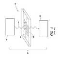
- FIG. 1depicts a schematic diagram of another example of an existing diagnostic system that uses test strips 10 with an application-specific dedicated reader apparatus 20 .
- a light source 22 of the reader apparatussends a light beam 24 to illuminate the detection region of the assay 26 of test strip 10 .
- the assay 26can include the test sample, a mixture of the sample and a reagent, or a reaction derivative from the sample.
- the reaction between the sample and the reagent, or a chemical reaction within the sample itself,can be stimulated using an electronic circuit 28 .
- the transmitted lightcarries the information of the assay 26 , such as color or opacity information, and is received by a photodetector 30 and analyzed by the reader apparatus 20 .
- glucophonescan aid in diabetes management, they exhibit certain limitations, including added cost of the glucopack compartments, limited compatibility of the glucopack compartments with cellular phone models, and a lack of wireless and signal processing functionality on the paper strips.
- Quantitative information relating to a samplealso can be used for diagnoses of, for example, HIV, Malaria, etc.
- a samplesuch as blood is placed onto a test strip
- a pre-deposited assaychanges color and informs the user whether a patient tests positive for an affliction (such as HIV or Malaria).
- the reader apparatusmight not be widely affordable in developing countries where mobile diagnostics are needed the most.
- the usersmight not be able to afford the time to insert the test strip into the reader apparatus, or to carry the reader apparatus around.
- POC testing devicesare becoming popular, particularly with the introduction of mobile-phone-based reader apparatuses.
- Existing devicescan present certain disadvantages, including high cost and the requirement of a separate reader with built-in electronics that runs on batteries.
- inaccurate readingscan result. For example, where the color change occurs along a gradient, it may not be clear to what degree the assay has changed color.
- a diagnostic deviceis read through on a user's visualization of a color change of a test strip, the assessment may be highly subjective leading to some uncertainty in the diagnostic results.
- Quantificationmay require a dedicated external reader apparatus that can be bulky and/or expensive.
- existing POC testingmay require more than one step. For example, after the user disposes a sample, such as a drop of blood, to a test strip, the user may then need to insert the test strip into the reader apparatus, which analyzes the sample or a derivative of the sample, and displays the test results to the user.
- a samplesuch as a drop of blood
- the reader apparatuswhich analyzes the sample or a derivative of the sample, and displays the test results to the user.
- various examples hereindescribe devices for providing quantitative information relating to a sample.
- the devices hereinincorporate sensory electronics on a flexible substrate that for providing the quantitative information relating to the sample.
- the devicesmay be disposable.
- the devicesneed not rely on an external reader apparatus, such as but not limited to a phone or other hand-held mobile device, for performing the sample analysis or quantification, or for providing the quantitative information relating to the sample.
- an external reader apparatussuch as but not limited to a phone or other hand-held mobile device, for performing the sample analysis or quantification, or for providing the quantitative information relating to the sample.
- an external reader apparatusIn order to use an external reader apparatus for sample analysis, certain regulatory requirements may need to be met beforehand for the reader to be classified as a medical diagnostics device.
- an external reader apparatusneed not be used for this purpose.
- the external reader apparatusmay be used to display the quantitative information relating to the sample (which may be used, e.g., to provide a diagnostics outcome).
- Example devices hereininclude a flexible substrate, electronic circuitry and at least one indicator electrically coupled to the electronic circuitry.
- the flexible substrateincludes at least one paper-based portion, at least one elastomeric portion, or at least one plastic portion.
- the electronic circuitrymay be at least partially formed in or disposed on the flexible substrate.
- the at least one indicatoralso may be at least partially formed in or disposed on the flexible substrate.
- the devicesalso include a sample receiver at least partially formed in or disposed on the flexible substrate. In various examples, the sample receiver may be formed in or disposed on at least one paper-based portion, at least one elastomeric portion, or at least one plastic portion of the substrate, where applicable.
- the samplemay be a biological sample.
- the electronic circuitrygenerates an analysis result based on an output signal from the sample or a derivative of the sample.
- the at least one indicatorprovides an indication of the quantitative information relating to the sample based at least in part on the analysis result.
- the at least one indicatormay be part of a display.
- the sample or derivative of the samplemay be contacted with a chemical reagent to provide the output signal.
- the devicemay also include a container to retain the sample formed in or disposed on the flexible substrate.
- a reagentmay be disposed in the container to react with the sample, where an output optical signal that includes at least a color change or electrochemical change is generated representing a degree to which the reagent reacts with the sample, when the sample is present.
- the electronic circuitryis coupled to the substrate to analyze the output signal and generate at least one analysis result.
- the electronic circuitryincludes at least one light source to illuminate the reagent and the biological sample, when present, to measure the color change or electrochemical change and provide an output optical signal representing the color change or electrochemical change.
- the electronic circuitrymay also include at least one photodetector to detect the output optical signal and generate an output electrical signal representing the color change or electrochemical change, where the at least one analysis result is based on the output electrical signal.
- the at least one indicatoris coupled to the flexible substrate, and electrically coupled to the electronic circuitry, to provide an indication of the quantitative information relating to the sample based at least in part on the at least one analysis result
- the devicemay also includes a channel disposed between the sample receiver and the container to transfer the sample or a derivative of the sample from the sample receiver to the container.
- the transfermay be through wicking or other capillary action.
- the quantitative informationincludes at least one of: a glucose level, a T-cell concentration, a microorganism concentration, a water-based pathogen concentration, a bovine serum albumin (BVA) concentration, a bacterial concentration, a viral load, an antigen level, an antibody level, a diagnosis of tuberculosis, a diagnosis of dengue fever, a cardiac enzyme concentration, and a diagnosis of malaria.
- BVAbovine serum albumin
- An example of a deviceemploys flexible or deformable electronics with integrated micro-fluidic channel systems for analyzing analytes, such as biochemical samples of fluids.
- Integrated with such electronicsare one or more indicators, constituting an “onboard human interface,” which can accurately and objectively indicate quantitative information of the test results to the user.
- the microfluidics substratescan be made of a piece of paper or an elastomeric material, and the entire device including the integrated electronics circuitry and the indicator can be made disposable.
- the indicatormay be part of a display.
- Such disposable devicescan be used as POC diagnostic devices.
- flexible substratessuch as foldable, deformable, or stretchable substrates, including paper-based substrates, elastomeric substrates, or plastic substrates
- reagents for samples to be measured, electronic circuitry for analysis of samples, and one or more indicators to convey analysis resultsmay be monolithically formed on a substrate, thereby significantly mitigating possibly adverse effects due to temperature variations across a device during a measurement of the sample.
- a devicethat is entirely disposable, including the electronic circuitry and the indicator(s). This is made possible by using a flexible substrate, such as a foldable, deformable, or stretchable substrate, including a substrate that includes paper-based portions, elastomeric portions, or plastic portions. Printing-based technologies may be used to pattern, e.g., the electronic circuitry and/or the container with the reagents. The resulting device can be relatively inexpensive and disposable yet sufficiently accurate and effective devices.
- a deviceincluding a substrate, and electronic circuitry coupled to the substrate to analyze the analyte.
- the devicefurther includes at least one indicator coupled to the substrate, and electrically coupled to the electronic circuitry, to provide the quantitative information relating to the analyte based at least in part on the analysis.
- a disposable paper-based diagnostic deviceis embedded with ultrathin, photosensitive electronics for on-chip quantification of via light transmittance detection.
- This examplecombines ELISA-based detection for antibodies or antigens as a measure of viral load, using patterned paper diagnostics (e.g., microfluidics inexpensively patterned into paper) and flexible electronics (e.g., photodetectors, amplifiers, LEDs, and antenna).
- patterned paper diagnosticse.g., microfluidics inexpensively patterned into paper
- flexible electronicse.g., photodetectors, amplifiers, LEDs, and antenna.
- Processescan be employed for creating and manipulating ultrathin (such as ⁇ 200 ⁇ m, for example ⁇ 100 ⁇ m or even thinner) electronics, which has a thickness of 1%-10% of existing devices. These devices are also lower in cost, and more rugged/flexible than alternatives. Printing such sensory electronics along with a battery onto thin paper substrates can create low-cost, disposable devices capable of quantification without the need
- an integrally formed diagnostic device and sensorwhich includes a user interface, e.g., in the form of one or more indicators.
- multiple reference points or wellsare disposed on or formed in the substrate and used as different concentration references.
- paperis used as the substrate. Paper provides for adhesion of the sample and wicking a fluid in a predetermined direction.
- the devicescan be based on measurements of optical signals (such as a color change), electrochemical signals, electrical signals (such as impedance signals), or acoustic signals (such as a pressure change).
- a deviceallows for a one-step glucose measurement using a single device that is entirely disposable.
- the entire device including the onboard data analysis circuitry and indicatorcan have a low cost, such as about USD $1.
- a costis comparable to existing test strips which requires an external reader apparatus.
- Existing reader apparatusesare generally not disposable due to their high cost.
- measurements made using existing glucose metersmay require at least two steps.
- the thermal compensation of the circuitryis possible as all components can be printed in the integral process on the single substrate. Thus, measurement accuracy is improved as compared with existing devices using discrete electronic components.
- a deformable paper-based microfluidic devicecan have patterned permeable and impermeable channels. Fluid filters or analyte-binding membranes can be built within the channels. Strategically positioned detection zones can be arranged at given locations in the permeable channels. Arrayed on the surface and/or physically integrated therewith, a plurality of flexible, stretchable and/or foldable electronic devices can be interconnected into a circuitry that remains operative notwithstanding flexing and stretching of the devices.
- Stretchable and foldable electronic devicesmay be fabricated on a paper substrate and can include, for example, an integrated circuit, a semiconductor, transistor, a diode, a logic gate, arrays of electronic components, an optical system, a temperature sensors, a pressure sensor, electrical-conductivity sensors, electrodes for pH sensors, chemical sensors, sensors for enzymatic activity, resistors, capacitors, passive devices, light emitting diodes (LEDs), photodiodes (PDs), or photodetectors.
- an integrated circuita semiconductor, transistor, a diode, a logic gate, arrays of electronic components, an optical system, a temperature sensors, a pressure sensor, electrical-conductivity sensors, electrodes for pH sensors, chemical sensors, sensors for enzymatic activity, resistors, capacitors, passive devices, light emitting diodes (LEDs), photodiodes (PDs), or photodetectors.
- LEDslight emitting diodes
- PDsphotodiodes
- An example hereinis directed a device for providing quantitative information relating to a sample.
- the deviceincludes a substrate, a container at least partially formed in the substrate to retain the sample, electronic circuitry integrated with or coupled to the substrate to analyze an output signal from the sample or a derivative of the sample, and at least one indicator integrated with or coupled to the substrate, and electrically coupled to the electronic circuitry, to provide the quantitative information relating to the sample based at least in part on the analysis.
- a method for obtaining quantitative information relating to a sampleincludes disposing the sample on a device in a substantially automated, one-step process.
- the resulting deviceis disposable.
- a method of making the deviceincluding monolithically forming electronic circuitry and at least one indicator over a flexible substrate.
- the deviceincludes a paper-based substrate, an elastomeric substrate, or a plastic substrate, a container at least partially formed in or disposed on the substrate to retain the biological sample, and a reagent disposed in the container to react with the biological sample.
- An output signal including at least a color changeis generated representing a degree to which the reagent reacts with the biological sample, when the biological sample is present.
- the devicefurther includes electronic circuitry coupled to the substrate to analyze the output signal and generate at least one analysis result.
- the electronic circuitryincludes at least one light source to illuminate the reagent and the sample, when present, to measure the color change and provide an optical signal representing the color change, and at least one photodetector to detect the optical signal and generate an output electrical signal representing the color change, the output electrical signal constituting the at least one analysis result.
- the devicefurther includes at least one indicator coupled to the substrate, and electrically coupled to the electronic circuitry, to provide the quantitative information relating to the sample based at least in part on the at least one analysis result.
- Another exampleis directed to a method for conducting an assay of an analyte in a biological sample so as to provide quantitative information relating to the biological sample, the method performed via a device including a paper-based substrate, at least one light source coupled to the paper-based substrate, at least one photodetector coupled to the paper-based substrate, and at least one indicator coupled to the paper-based substrate.
- the methodincludes applying the biological sample to the paper-based substrate, the paper-based substrate having a reagent disposed thereon to react with the biological sample, wherein an output signal including at least a color change is generated representing a degree to which the reagent reacts with the biological sample; illuminating the reagent and the sample using the at least one light source to measure the color change and provide an optical signal representing the color change; detecting the optical signal using the at least one photodetector and generating an output electrical signal representing the color change; and providing the quantitative information relating to the sample, via the at least one indicator, based at least in part on the output electrical signal.
- FIG. 1is a schematic diagram of an example reader apparatus of an example diagnostic system.
- FIG. 2is a schematic diagram of a device, according to one example, for providing information relating to a sample.
- FIG. 3is a perspective view of a device according to one example.
- FIG. 4is a perspective view of a device according to another example.
- FIG. 5illustrates the principle of light attenuation through a medium.
- FIG. 6is an exploded view of a device according to another example.
- FIG. 7illustrates a fabrication process of a paper-based diagnostic device according to one example.
- FIG. 8illustrates an example electronic circuit diagram of a photodiode circuit for use in a device according to one example.
- FIG. 9illustrates experimental data measured using a red LED and a red photodiode, for a red sample and a blue sample, respectively.
- FIG. 10illustrates photodetector output voltages measured as functions of biases applied to the illumination LED, for various BSA concentrations in the samples.
- FIGS. 11A and 11Billustrate electronic circuit diagrams of example comparators that may be included in a device according to one example.
- FIG. 12illustrates light transmission, filtering, detection, and comparison processes performed on a device according to one example.
- FIGS. 13A and 13Bare schematic diagrams of an indicator having a plurality of indicator LEDs arranged in a substantially circular configuration, according to one example.
- FIG. 14illustrates a circular indicator having a non-linear scale, according to one example.
- FIG. 15illustrates an operation of a circular indicator in conjunction with a diagnostic device according to one example.
- FIG. 16illustrates another example of operation of a circular indicator in conjunction with a diagnostic device according to one example.
- FIG. 17Ais a schematic diagram of an indicator having a plurality of indicator LEDs arranged in a substantially linear configuration, according to one example.
- FIG. 17Bis a schematic diagram of an indicator based on a band of thermochromic ink, according to one example.
- FIG. 18is a schematic diagram of an indicator having a plurality of indicator LEDs arranged in a bar-shaped configuration, according to one example.
- FIG. 19is a schematic diagram of an indicator having a plurality of indicator LEDs arranged in a bubble display configuration, according to one example.
- FIGS. 20A and 20Billustrate an electronic circuit diagram of an array of comparators for analyzing photoelectric signals from a device according to one example.
- FIG. 21illustrates a diagnostic system having an RF coupling with an external reader apparatus, according to one example.
- FIG. 22illustrates a circuit diagram of an array of comparators for analyzing impedance signals from a device according to one example.
- FIGS. 23A, 23B and 23Cillustrate a diagram of a circuit having a synchronous demodulation for analyzing impedance signals from a device according to one example.
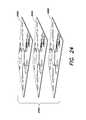
- FIG. 24is a perspective view of a 3-D device including a stack of substrates to perform a plurality of measurements thereon, according to one example.
- FIG. 25is a schematic diagram of a foldable device having a 3-D structure formed by folding 2-D substrate, according to one example.
- the term “includes”means includes but not limited to, the term “including” means including but not limited to.
- the term “based on”means based at least in part on.
- any of the substrates described herein, including a substrate that incorporates at least one paper-based portion, at least one elastomeric portion, or at least one plastic portionmay be configured to make conformal contact with and adhere to the epidermis (e.g., the epidermis of a human or a non-human animal).
- Intricate hydrophilic patternsmay be fabricated in paper substrates to exploit the natural affinity of paper to absorb and wick small volumes of fluid via capillary action. Such devices provide the benefits of their small sizes (e.g., smaller than a credit card) and their ability to perform multiple laboratory functions.
- Paper-based microfluidicscan be different from microfluidics based on other substrates such as a plastic mold or an elastomer, such as (poly)dimethylsiloxane (PDMS). The latter may need external pumping or gravity to transport fluid.
- PDMSpolydimethylsiloxane
- paper-based devicescan be formed to include arrays of channels that allow the fluid to wick through and be transported to one or more reservoirs pre-treated with reagents. Chemical reactions can occur at these reservoirs and initiate color changes, whose reflectance and transmittance intensities depend on the concentration of analytes (e.g., glucose and proteins) in the biological fluid samples (e.g., blood, urine, saliva).
- analytese.g., glucose and proteins
- Blood glucose concentration testsare identified as a POC diagnostic procedure that can take advantage of the examples described herein.
- Other diagnostics valuesthat may be measured include, but are not limited to, T-cell (CD4) concentrations in blood, for determining the health of the immune system and the onset of AIDS.
- CD4T-cell
- a high accuracy, disposable paper-based microfluidic devicecan be used to measure CD4+ T-cell count via impedance spectroscopy.
- the CD4 diagnostic devicecontains ultrathin, flexible sensor electrodes, antennae coils, and high performance integrated circuits that enable impedance analysis and short range, wireless power and data transfer with a cellular phone via inductive coupling or RFID.
- Existing cellular phones/PDAs equipped with RFID functionalitycan be sufficient for displaying results and serve as a telemetric portal for the data.
- CD4+ T-cell countcan be estimated by impedance spectroscopy of lysed CD4+ T-cells in hypotonic fluid media. This technology has been demonstrated in microfluidic devices designed with PDMS; however, existing devices may require additional external tubing, syringe pumps or have gravitational flow requirements, and be coupled with amperometric readers to analyze and display the results.
- Example devicescan perform functions such as (1) capturing CD4 T-cells in a paper-based microfluidics channel, (2) lysing T-cells, causing a measurable change in impedance induced by the release of intracellular ions, and (3) measuring and wirelessly transferring impedance data to a cellular phone via onboard integrated circuits patterned on paper.
- the microfluidic channelsare designed such that test dyes are delivered to the test well site at different times. This can be accomplished simply by varying the distance from dye input zone to test well. This technique can be used to amplify the response due to analyte concentration and is a step in the ubiquitous enzyme-linked immunosorbent assay, such as ELISA tests today.
- the substratemay be formed from other materials and include at least one paper-based portion.
- paperis a useful substrate based on its wicking properties, examples disclosed herein are not limited to paper substrates.
- Other substrate materialssuch as polymer, elastomer, and glass may also be used.
- POC diagnostic devicesare specified to measure analyte concentrations with only microliter volumes of biological fluid, and should enable accurate diagnosis immediately following the contact with the biological fluid.
- an existing systemexploits movement of fluids across paper strips (i.e., dip stick and lateral flow). Dipsticks use colorimetric tests to detect various biological molecules and function by immersing a paper strip (several centimeters long) into a biological fluid. Lateral flow assays accommodate smaller volumes than dipsticks, and use reagents for specific immunochromatographic assays.
- lateral flow and dipstick diagnosticscan be useful, they can be limited in sensitivity, speed, capability of multiplexing a variety of tests simultaneously, capability of using small volumes of fluid, long-term stability, cost, and ease of disposal.
- Plastic- and glass-based microfluidic devicespresent viable alternative methods for more quantitative tests, but they may require fluid pumps and expensive external equipment for external control of flow.
- the paper-based microfluidic devices described hereincan exploit the full sophistication of inorganic single crystalline semiconductor electronics.
- the fabrication of these devicesbegins with the formation of ultrathin circuits in planar serpentine geometries. Previously published procedures can be adopted for fabricating the devices described herein.
- circuitsmay be obtained in packaged or unpackaged form and bonded to polymer encapsulated interconnect arrays as previously described in various patent application publications incorporated herein by reference.
- the electronicscan be integrated directly into/onto the substrate, including on the paper-based portion of the substrate, where they are put into contact with detection zones of the microfuidic devices for recording of electrical impedance, absorption of light, acoustic signals, or other signals.
- Fabrication of microfluidic paper-based devicescan be accomplished using photolithographic processes, wax-based printing techniques, or other methods.
- Paper-based microfluidic devicescan operate without the use of pumps. They can be made of low-cost materials and allow for multiple diagnostic tests to be performed on the same sheet. Incorporating flexible electronics in paper-based microfluidic devices reduces volume of the POC diagnostic systems while maintaining functionality. It also preserves the physical characteristics of paper, which is the accepted medium for POC diagnostics, which may require blood/biological samples.
- the deviceincludes a substrate that has at least one paper-based portion, a sample receiver at least partially formed in or disposed on a paper-based portion of the substrate, electronic circuitry and at least one indicator electrically coupled to the electronic circuitry.
- the electronic circuitry and the at least one indicatorare at least partially formed in or disposed on the substrate.
- the electronic circuitrygenerates an analysis result based on an output signal from the sample or a derivative of the sample.
- the at least one indicatorprovides an indication of the quantitative information relating to the sample based at least in part on the analysis result.
- FIG. 2is a schematic diagram of an example device 100 , according to one example, for providing quantitative information relating to a sample 102 .
- the deviceincludes a substrate 104 , and a container 106 at least partially formed in or disposed on the substrate 104 to retain the sample 102 .
- the container 106can be, for example, a well or an indentation formed in the substrate 104 .
- the container 106can be substantially enclosing a space containing the sample 102 , or can have an open top.
- Electronic circuitry 108 integrated with or coupled to the substrate 104can be used to analyze an output signal from the sample 102 , or from a derivative 109 of the sample 102 to provide an analysis result.
- the derivativecan be an output from a reaction between the sample and a reagent, or results from a reaction within the sample 102 itself (e.g., when the sample 102 is subject to stimulation such as an electrical stimulation or an optical stimulation).
- the devicealso includes at least one indicator 110 integrated with or coupled to the substrate 104 , and electrically coupled to the electronic circuitry 108 , to provide the quantitative information relating to the sample 102 based at least in part on the analysis result.
- the indicator 110is readable by a user, and thus serves as a human interface.
- the device 100can further include a receiver 112 formed at least partially in or on the substrate 104 to receive the sample 102 .
- the receiver 112can be, for example, an indentation or an orifice in the substrate 104 .
- a channel 116is formed at least partially in or on the substrate 104 to transfer the sample 102 from the receiver 112 to the container 106 .
- a drop of the sample 102such as a drop of blood, once received by the receiver, can be drawn to the container 106 via the channel 116 , by capillary action for example.
- the substrate 104includes a piece of paper, and the piece of paper is configured to wick the sample from the receiver 112 to the container 106 via a capillary action within the paper.
- the channel 116need not necessarily be carved out from the paper; rather, the paper can be engineered, for example, by printing wax on the desired location of the channel, or imprinted or pressed to allow the capillary action to occur in preferred directions.
- the substrate 104can further include PDMS disposed over the paper-based portion.
- the PDMSis uncured.
- the substrate 104further includes a urethane disposed over the piece of paper.
- the urethanecan be UV curable.
- the substrate 104can be very thin, for example, having a thickness on the order of approximately 200 microns or less. This ultrathin structure allows the entire device to be foldable, as described in detail below.
- any references to “top” surface and “bottom” surfaceare used primarily to indicate relative position, alignment and/or orientation of various elements/components with respect to the substrate and each other, and these terms do not necessarily indicate any particular frame of reference (e.g., a gravitational frame of reference).
- reference to a “bottom surface of a substrate”does not necessarily require that the indicated surface be facing a ground surface.
- the device 100includes a reagent retained in the container 106 to react with the sample 102 .
- the output signal being analyzedindicates a reaction output of the reagent and the sample.
- the fluidic channel 116transfers the sample 102 to the container 106 to react with the reagent, forming the derivative 109 being analyzed.
- the fluidic channel 116is formed between the piece of paper and a water resistant material.
- the substrate 104is formed by bonding the piece of paper and the water resistant material.
- the water resistant materialincludes PDMS.
- the substrate 104may be fabricated upon a variety of materials, such as paper, glass, elastomer, parylene, plastic, polymer, or PDMS.
- the device 100can be used to measure a variety of properties of the sample 102 .
- the quantitative information provided by the indicator 110can be one of a glucose level, a T-cell concentration, a microorganism concentration, a bovine serum albumin (BVA) concentration, a bacterial concentration, a water-based pathogen concentration, a viral load, antibody level, antigen level, a diagnosis of malaria, tuberculosis or dengue fever, or cardiac enzyme concentration.
- BVAbovine serum albumin
- the device 100can be configured as a chemical sensor, where a chemical reaction can be made through electrical or optical stimulation to a sample onboard the device, or to have a reagent to react with the sample.
- the chemical reactioncan cause a change in conductivity, generate an electrical current, or cause a color or opacity change. These changes can be measured as output signals from the sample.
- a change in electrical current generated by a sample or its derivativemay be measured via a transconductance circuit that converts the current into a voltage.
- the electronic circuitry 108further is configured to facilitate generation of the output signal from the sample or the derivative, such as to cause a chemical reaction in the sample or between the sample and a reagent to form the derivative 109 .
- the output signalcan be direct optical or electrical measurement of the sample 102 .
- the output signalcan be conveyed to the electronic circuitry, or represented, as one of an optical signal, an electrical signal, or an acoustic signal.
- the output signalcan represent a degree to which the reagent reacts with the sample.
- the output signalcan be a color or opacity change representing the degree to which the reagent reacts with the sample, an impedance change representing the degree to which the reagent reacts with the sample, or a pressure change representing the degree to which the reagent reacts with the sample.
- the pressure changecan be measured by a piezo-electric pressure sensor. If a modulated stimulus signal is applied to the sample, and the reaction between the sample and the reagent changes a pressure in the sample or derivative, an acoustic wave can be detected using a pressure sensor. If the sample is stimulated with a DC stimulus signal, then a step change in the pressure may be detected.
- the electronic circuitryfurther includes an analog-to-digital (A/D) converter to convert the reaction output (e.g., the analysis result) to the information in digital form.
- A/D convertercan be a existing A/D converter functioning in conjunction with a digital-watch type of indicator/display 110 .
- Other methods for communicating the quantitative informationcan be adopted. These include visible indications such as different types of display modalities, audible, tactile, or vibrational signals.
- a comparator and a plurality of referencesare employed to realize the function of an A/D converter.
- the output signalrepresents a value indicative of the quantitative information.
- the plurality of referencesare coupled to the substrate, and each have respective different reference values.
- the comparatorcompares the value with the plurality of reference values so as to generate the quantitative information.
- the indicatorincludes a plurality of indicator light emitting diodes (LEDs), coupled to the at least one comparator, to display the quantitative information.
- the plurality of referencescorrespond to progressively higher reference values.
- the comparatorcompares the value progressively with at least some of the plurality of reference values, and each of the plurality of indicator LEDs lights up if the reference value of a corresponding reference is below the value represented by the output signal.
- the indicatorsmay include a visual display.
- the indicatorsmay include other sensory modes or interfaces for displaying quantized values to a user. For example, a vibration or an acoustic signal can indicate that threshold is passed.
- the output signalrepresents a degree to which the reagent reacts with the sample
- the output signalincludes a color change representing the degree to which the reagent reacts with the sample.
- the color changecan be, for example, a change in saturation, hue, brightness, or opacity.
- the electronic circuitryincludes at least one light source to illuminate the reagent and the sample, when present, to generate the output signal based on the color change, wherein the output signal is an optical signal, and at least one photodetector to detect the optical signal and generate an output electrical signal representing the color change.
- the light sourcescan all solid-state emitting devices including an illumination LED, such as an organic light emitting (OLED).
- OLEDorganic light emitting
- the OLEDcan be integrally formed with other organic electronic devices on a flexible substrate 104 , for example though a direct printing process on a paper substrate.
- the plurality of referenceseach include a reference color
- the electronic circuitryfurther includes a plurality of reference light sources each to generate a reference optical signal based on the reference color, and a plurality of reference photodetectors each to convert the reference optical signal into a reference electrical signal.
- the comparatorcompares the output electrical signal with the plurality of reference electrical signals.
- the plurality of referencesare integrated with or coupled to the substrate.
- the comparatorcompares the output electrical signal with the plurality of reference electrical signals substantially simultaneously.
- the device 100can further include a first filter disposed between the sample and the photodetector to obtain a substantially monochromatic transmission light.
- the device 100further includes a second filter disposed between the light source and the sample. The second filter is not needed if a monochromatic illumination LED is used as the light source.
- a plurality of second filtersare disposed between a broad-band illumination LED and the sample to obtain a multi-channel spectrum of light to illuminate the sample. Spectral information from the sample can thus be obtained.
- a plurality of narrow-band illumination LEDscan be adopted without the use of the plurality of second filters.
- the first and second filterscan be made of thin-film polymers having specific dyes disposed thereon.
- the thin-film polymerscan have a thickness of less than 200 microns, such as 50-200 microns.
- the substrateis foldable, and the illumination LED and the photodetector are configured to be substantially aligned with the container by folding the substrate.
- the devicecan further include a plurality of alignment marks to aid the folding.
- the output signalincludes an impedance of the sample
- the electronic circuitryincludes at least one pair of electrodes to measure the impedance of the sample or the derivative.
- the devicecan be configured as a glucose meter, for example.
- Example devices hereinmay provide quantitative information relating to a sample or a derivative of the sample based at least in part on analysis of an optical signal from the sample or the derivative.
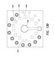
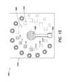
- an example device 300is fabricated over a substrate 304 that includes a piece of chromatography paper 305 and a laminant layer 307 .
- a plurality of containers (e.g., sample wells) 306 a , 306 b , . . .are formed in the substrate 304 to retain a plurality of different, or same, samples to be tested.
- a plurality of reference wells 309 a , 309 b , . . .respectively correspond to one of the plurality of containers.
- a single receiverin the form of an entrance well 312 , receives the sample and feeds the sample to the plurality of sample wells 306 a , 306 b , . . .
- Each of the sample wells or reference wellshas a conformal, micro-scale LED built therein, to illuminate the sample and the reference, respectively, to obtain the quantitative information about the sample.
- Each wellis also equipped with a photodetector such as a photodiode to detect the light transmitted, reflected, or scattered from the sample or the reference.
- the device 300 as shownincludes an array of 6 pairs of sample/reference wells, but can be scaled to include any number of sample and/or reference wells, such as hundreds to thousands.
- the sample wellshave different reagents disposed therein, and are configured to perform different tests for the same sample.
- one wellcan be used to test a viral load, and another well can be used to test a bacterial level.
- the testscan provide binary response, e.g., an indicator LED turns on if a concentration is higher than a specific level.
- a number of indicatorscan be included onboard the device to provide quantitative information for each test. Such indicators are described in detail below with respect to FIGS. 13A-19 .
- sample wellstest different samples, such a blood sample, a saliva sample, and a urine sample from the same individual, or blood samples from different individuals.
- PDMSis used as the laminant layer 307 .
- Uncured PDMScan be used to increase the bond strength between devices (e.g., electrodes), and the receiving substrates (e.g., paper).
- devicese.g., electrodes
- receiving substratese.g., paper
- alternatives to PDMS that cure faster and have better adhesion to polyimide encapsulated devices in the absence of an oxide adhesion layere.g., Dymax UV curable urethanes are employed.
- the architecture of the device 300results in improved thermal stability when measuring a sample at the plurality of sample wells and the results are compared with their respective references in the reference wells at close proximity. Thus, relative measurements, rather than absolute ones, are performed. Change in temperature may increase current and may raise the output offset in, e.g., sample well 306 a , but it would do so locally for the reference well 309 a , by an equivalent or a proportional amount. This is the same for all sample wells 306 a , 306 b , . . . , and their respective references 309 a , 309 b , . . . . Potentially adverse affects on measurement due to temperature changes/variations are thus mitigated.
- the reference dyesare printed and are stable over temperature.
- the measurementsare less affected by temperature or internal heating through circuit elements, because any temperature effects are calibrated out by the references at the locations proximate to the respective sample wells. This results in consistent and accurate measurements.
- the monolithic fabrication process of the components on the substratealso contributes to the thermal stability.
- all the componentscan be printed in a single process on the single paper substrate.
- interdigitated layoutalso reduces the variations in the measurements caused by temperature changes.
- comparator circuitto compare a measurement locally with a reference, instead of using microprocessor, not only reduces complexity and power consumption but also reduces the thermal footprint and thermal instability of the system. For example, several amplifiers can be fabricated monolithically together and generate heat evenly. Thus, changes are shared by all circuits and cancelled out.
- discrete circuitsdo not track temperature changes well due to their size and their non-monolithic nature.
- a discrete circuithas several operational amplifiers in separate packages. They can heat up differently, and errors or temperature-induced variations from one component can ripple through the whole device.
- FIG. 4is a perspective view of a device 400 according to another example.
- the device 400is fabricated over a substrate 404 , which includes a piece of chromatography paper 405 , a laminant layer 407 , and a PDMS layer 411 .
- a receiver 412is formed on a side of the device 400 , in the form of an entrance well.
- a channel 416is formed in the piece of paper 405 to transfer a sample disposed at the receiver 412 to a sample well 406 .
- the sample well 406is sandwiched between a conformal LED 422 and a conformal photodetector 430 .
- the deviceis covered with a top PDMS layer 432 , which encloses the channel 416 and the sample well 406 .
- the output signal during the measurementcan be a change in opacity of the detection region.
- detection and analysis of light transmission through a translucent paper impregnated with a fluid samplecan be performed.
- the LED 422can generate a calibrated intensity of light that passes through the detection region of the sample well 406 , and the photodetector 430 records the intensity of light received on the other side of the detection region.
- the amount of light captureddepends on the opacity of the sample, or a combination of the sample, the reagent, and the test strip.
- FIG. 5illustrates the light attenuation through a medium 500 (such as the sample well 406 containing the sample therein).
- the light intensity I 0 from the LED 422after being attenuated by the medium 500 having a thickness of l and an attenuation coefficient ⁇ , becomes I 1 .
- the transmissivity T of the medium 500is determined by Beer's law:
- the opacityin turn is directly related to the concentration of analyte in the assay.
- the measurementsdo not depend on ambient light.
- This analog signal of the detected light intensityis converted to a digital read out signal by electronics incorporated into the substrate.
- the detected analog signalmay be transmitted (wirelessly or with a wire) to an off-substrate processor for processing.
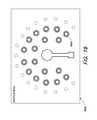
- FIG. 6is an exploded view of a device 600 according to another example.
- the deviceis built upon a substrate 604 in which a sample well and one or more reference wells are formed, as described above in connection with FIGS. 2, 3, and 4 and other figures described below (for ease of illustrating other salient features of the device 600 , such wells are not shown in FIG. 6 ).
- the substrate 604can be a piece of paper having fluidics channels formed therein, PDMS, a glass slide, or composed of other materials as described elsewhere herein.
- a top interface layer 632Disposed over the substrate 604 is a top interface layer 632 composed of, for example, an elastomer or a polymer.
- a photodiode 630is formed in the top interface layer 632 and overlays the sample well in the diagnostic substrate 604 .
- a plurality of reference photodiodes 628are also formed in the top interface layer 632 and overlay their corresponding reference wells in the diagnostic substrate 604 . It is noted that, in this example, the sample is directly measured in the sample well and compared with the six reference wells, unlike the example illustrated in FIG. 3 , where the sample is split and transferred into 6 sample wells and measured therein.
- a plurality of photodiode driver and comparator circuits 608drive the photodiodes 628 , 630 and compare the signals detected by the photodiode 630 and the reference photodiodes 628 .
- a plurality of indicator LEDs 610respectively are disposed adjacent to corresponding reference photodiodes 628 to provide an indication of analysis results (e.g., based on the functionality of comparator circuits 608 , described in greater detail below).
- a bottom interface layer 607 and the top interface layer 632sandwich and interface with the substrate 604 .
- the bottom interface layer 607can be made of polyimide, polyurethane, PDMS, or other elastomeric or polymeric materials.
- the bottom interface 607has a plurality of illumination LEDs 620 built therein or disposed thereon, to illuminate the sample and reference wells in the substrate 604 .
- Flexible or stretchable interconnects 609(not specifically visible in the view of FIG.
- the illumination LEDs 620disposed on or integrated with the bottom interface layer 607 and electrical contacts 611 formed in the bottom interface layer 607 make electrical connections among a thin-film battery 613 , the illumination LEDs 620 , the circuits 608 , the photodiodes 628 , 630 , and the indicator LEDs 610 .
- Such a power sourcemay include, for example, a primary battery, a solar cell such as a organic photovoltaic (OPV) cell, an energy-harvesting device such as an inductive coupling coil, etc.
- a primary batterysuch as a solar cell such as a organic photovoltaic (OPV) cell
- OPNorganic photovoltaic
- an energy-harvesting devicesuch as an inductive coupling coil
- the power source 613can drive the electronic circuits including the LEDs and the photodetectors with a variety of drive configurations, such as a constant current source, pulse-width modulation (PWM) for control and energy savings, or a buck-boost power configuration.
- PWMpulse-width modulation
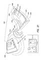
- FIG. 7illustrates a non-limiting example fabrication process of a paper-based diagnostic device, according to one example, in which the electronic circuitry and at least one indicator can be monolithically formed over a flexible substrate.
- the electronic circuitry and at least one indicatorare first formed over a carrier wafer.
- the carrier wafercan be, for example, silicon, silicon-on-insulator (SOI), or glass substrate.
- SOIsilicon-on-insulator
- the integrated circuits including the metal interconnects, and ultrathin silicon circuitryare removed from the carrier substrate using a PDMS stamp.
- step Ba film of Cr/SiO2 is deposited on the backside of the electronic circuitry and then transferred to a receiving substrate that is coated in PDMS.
- This Cr/SiO2 filmenables the formation of strong covalent bonds as illustrated in panel C of FIG. 7 .
- panel Dit is illustrated that the integrated circuits transferred to the thin PDMS coating, which is laminated over the paper substrate. Photodiodes and LEDs can also be transferred this way.
- the monolithically formingincludes forming the electronic circuitry and the at least one indicator over the paper in a single printing process.
- Microfluidic devicesmay be constructed, for example, using techniques developed by Martinez et al: Proc. Natl. Acad. Sci. USA 105, 19606-11 (2008); Lab. Chip. 8, 2146-50 (2008); and Angew. Chem. Int. Ed. Engl. 46, 1318-20 (2007), each of the references being herein incorporated by reference in its entirety.
- an appropriate patterned-paper platform for the devicecan be designed and developed.
- the paper-based substratecan be selected based on wicking speeds, sample retention, consistency and compatibility with the required assay (e.g., glucose oxidase).
- Biocompatible excipientssuch as sucrose or trehalose may be used to stabilize enzymes used in the assay.
- Plasma separation membranesare also selected for the desired diagnostic.
- Device layersmay be composed of a variety of semi-permeable materials such as porous polymers and elastomers, rigid or flexible nanofiber composites, biologically selective membranes (e.g., fluid mosaic model). Other materials that may facilitate a wicking effect similar to paper can also be used. These materials may include gels with wicking properties, and electromagnetic materials that may be designed to create peristaltic motions to pulse analytes and other fluids to test wells.
- semi-permeable materialssuch as porous polymers and elastomers, rigid or flexible nanofiber composites, biologically selective membranes (e.g., fluid mosaic model).
- Other materials that may facilitate a wicking effect similar to papercan also be used. These materials may include gels with wicking properties, and electromagnetic materials that may be designed to create peristaltic motions to pulse analytes and other fluids to test wells.
- Assembly of ultrathin ICs on paper-based microfluidic devicemay be accomplished with a pick-and-place transfer printing tool, with which electronic circuits are transferred from a carrier wafer to paper substrates or other types of substrates employed for the diagnostic devices.
- the metal conductive interconnectstypically include metal encapsulated in polyimide.
- ICs, electrodes, and associated interconnectsmay be moved from dense arrays on an SOI wafer to sparse arrays on paper. Integration of electrodes and circuits with a paper-based microfluidic platform can be achieved with thin layers ( ⁇ 100 ⁇ m) of low modulus PDMS, which encapsulate the electronics and serve as an adhesion layer to the paper microfluidic substrate.
- Thin film passiveswill also be integrated into the circuits by bonding to conductive arrays on the PDMS (ACF bonding, cold welding etc.).
- Electronic devicese.g., LEDs, photodetectors, electrodes
- the active elements of the electronic systemsuse electronic materials such as silicon and gallium arsenide in the form of filamentary serpentine nanoribbons and micro- and nano-membranes (see Kim, p. 838).
- the electronic systemsmay be laminated onto the epidermis with conformal contact and adhesion based on van der Waals interactions in a manner that is mechanically invisible to a user.
- an electronic system of Kim et al.may be configured to include temperature sensors, strain sensors, as well as transistors, light-emitting diodes, photodetectors, radio frequency inductors, capacitors, oscillators, and rectifying diodes.
- the electronic systems of Kim et al.may be configured to provide solar cells and/or wireless coils to provide options for power supply to any of the example devices described herein.
- the epidermal electronic systems described in Kim et al.are fabricated to match the elastic moduli and bending stiffness of the epidermis, it is recognized herein that these electronic systems would need to be configured to match the properties of the substrates described herein.
- the elastic moduli, bending stiffness, and areal mass densities of these electronic systemswould need to be configured to match the substrate herein that includes at least one paper-based portion.
- An example device according to a principle hereinmay be fabricated by disposing an electronic circuitry described herein, formed using the technology of Kim et al. as described above, on a substrate that includes the one or more paper-based portions. It is recognized herein that the electronic circuitry formed using the technology of Kim et al.
- the electronic circuitry formed using the technology of Kim et al.also would need to be disposed on the substrate such that it does not interfere with the actions of the sample receiver to receive the sample or with the at least one indicator to provide an indication of the quantitative information relating to the sample.
- the electronic circuitrywould also need to allow for any wicking of the sample or sample derivative from the sample receiver to a container and any reaction of the sample or sample derivative with reagents.
- the devicemay be fabricated such that the substrate that includes the at least one paper-based portion makes conformal contact with and adhere to an epidermis, e.g., the epidermis of a human or a non-human animal.
- an epidermise.g., the epidermis of a human or a non-human animal.
- FIG. 8illustrates a non-limiting example of a circuit diagram of the photodetector circuit 800 , which can be part of the circuitry 608 illustrated in FIG. 6 .
- a HAMAMATSU® S6430 photodiode 802(Hamamatsu Photonics, Shizuoka Japan), which is sensitive to red light, is used to receive red light emitted by a red LED 804 (e.g., representative of one of the LEDs 620 shown in FIG. 6 ), such as a LUMEX® SSL-LXA 228 SIC LED (Lumex, Inc., Palantine, Ill.).
- An operational amplifier 806such as an AD® 8605 op amp (Analog Devices, Norwood, Mass.), is used to amplify the output electrical signal from the photodiode 802 .
- the LED, photodiode, and supporting circuitry illustrated in FIG. 8are configured an optical detection channel, in which the LED and photodiode may form a substantially matched pair of an optical generator and detector.
- the photodetectorcan be selected to be substantially sensitive to the color band/wavelength(s) of radiation generated by the light source.
- a photodiode sensitive to the same color as the illumination LEDmay be used to detect the as much light from the illumination LED as possible.
- a red-sensitive detector and a red illumination LEDare adopted, but is should be readily appreciated that substantially matched pairs of LEDs-photodetectors for optical detection of other colors/wavelength regions may be employed in devices according to various examples described herein.
- Particular colors/wavelengths of interest for an optical detection channelmay be based, at least in part, on one or more of the nature of the sample (e.g., analyte) to be measured/analyzed, the reagent employed, expected concentrations of analyte, and expected degree of reaction based on the particular reagent employed.
- integrated devices for quantitative assays and diagnosticsmay include LED-photodector pairs and supporting circuitry to provide optical detection channels sensitive to particular colors/wavelength bands based on a particular type of sample for which the device is configured to provide quantitative information.
- FIG. 9illustrates experimental data measured using a red LED and a red photodiode, for a red sample (i.e., an output signal constituting a red color from a sample or sample/reagent combination) and a blue sample (i.e., an output signal constituting a blue color from a sample or sample/reagent combination), respectively.
- a red samplei.e., an output signal constituting a red color from a sample or sample/reagent combination
- a blue samplei.e., an output signal constituting a blue color from a sample or sample/reagent combination
- the derivative 109 from the sample, or from the sample and the reagentcan be configured to have a color that is substantially different from the color of the illumination LED, such that the derivative 109 absorbs as much light as possible from the light source, to improve detection sensitivity.
- a blue assayis adopted for use with a red illumination LED.
- a blue illumination LEDis employed by the device 100 for use with a predominantly red derivative or sample (e.g., blood).
- the measurementscan be made within seconds of the sample being applied to or disposed over a device (e.g., in the case of a substrate with paper-based portions, while the paper is still wet) to provide more consistent results.
- making measurements from the same side of the paper as the sample is droppedmay also improve the measurement accuracy.
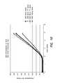
- FIG. 10illustrates photodetector output voltages measured as functions of biases applied to the illumination LED (V LED ), for various BSA concentrations in the samples.
- V LEDillumination LED
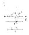
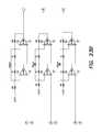
- FIG. 11Aillustrates a circuit diagram representing multiple optical detection channels based on LED-photodetector pairs, as described above, together with a comparator that compares output signals between two such detection channels, according to one example.
- one of the detection channels illustrated in FIG. 11Awould be dedicated to a sample including an analyte that is the subject of the assay, and the other detection channel would be associated with a reference well/sample dye.
- a constant current source circuit 1102drives a sample illumination LED 1104 and a reference illumination LED 1106 , which illuminate the sample and a reference dye, respectively.
- a blue LUMEX® SSL-LX A228 USBC-TR11 LEDs(Lumex, Inc., Palantine, Ill.) may be used for illumination LED 1104 or reference illumination LED 1106 .
- the transmitted, reflected, or scattered light from the sample and the reference dyesare received by the sample photodiode 1108 and the reference photodiode 1110 , respectively.
- a blue HAMAMATSU® S6428 photodiode(Hamamatsu Photonics, Shizuoka Japan) may be used for sample photodiode 1108 or the reference photodiode 1110 .
- Operational amplifiers 1116such as an AD® 8694 op amp (Analog Devices, Norwood, Mass.), may be used.
- Operational amplifier 1118may be a MAX® 9031 op amp (Maxim Integrated Products, Sunnyvale, Calif.). The photocurrents from these photodiodes, after being amplified by their respective amplifiers, are compared by comparator 1112 .
- the insetshows various pins 1114 of an example 14-Lead TSSOP (Fairchild Semiconductor, San Jose, Calif.) for the electrical connections with components of the electronic circuit.
- FIG. 11Billustrates a circuit diagram representing multiple optical detection channels based on LED-photodetector pairs, as described above, together with a comparator that compares output signals between two such detection channels, according to another example. Similar to the electronic circuit of FIG. 11A , one of the detection channels illustrated in FIG. 11B may be dedicated to a sample including an analyte that is the subject of the assay, and the other detection channel would be associated with a reference well/sample dye. As shown in FIG. 11B , a constant current source circuit 1152 drives a sample illumination LED 1154 and a reference illumination LED 1156 , which illuminate the sample and a reference dye, respectively.
- a blue LUMEX® SSL-LX A228 USBC-TR11 LEDsmay be used for illumination LED 1154 or reference illumination LED 1156 .
- the electronic circuitry of FIG. 11Bis modified over the electronic circuitry of FIG. 11A to include operational amplifier 1153 , to reduce the possibility of saturating LEDs 1154 and 1156 .
- Operational amplifier 1153may be an AD® 8694 op amp (Analog Devices, Norwood, Mass.).
- the forward voltage on LEDs 1154 and 1156can be 3.5V to 4V in operation.
- the transmitted, reflected, or scattered light from the sample and the reference dyesare received by the sample photodiode 1158 and the reference photodiode 1160 , respectively.
- a blue HAMAMATSU® S6428 photodiode(Hamamatsu Photonics, Shizuoka Japan) may be used for sample photodiode 1158 or the reference photodiode 1160 .
- Operational amplifiers 1166such as an AD® 8694 op amp (Analog Devices, Norwood, Mass.), may be used.
- Operational amplifier 1168may be a MAX® 9031 op amp (Maxim Integrated Products, Sunnyvale, Calif.).
- the insetshows various pins 1164 of an example 14-Lead TSSOP (Fairchild Semiconductor, San Jose, Calif.) for the electrical connections with components of the electronic circuit.
- FIG. 12illustrates light transmission, filtering, detection, and comparison processes performed on a device according to one example.
- the most relevant spectrum bandmay be analyzed.
- one or more color filtersmay be employed in an optical detection channel, together with an illumination LED and corresponding photodetector.
- the color references and the color of the reagent or assaycan be designed taking into account the available filters to provide appropriate SNR in the optical detection channel to ensure effective measurements.
- a substantially blue sample 1206preferably red light is used for the measurement.
- light from an array of broadband illumination LEDs 1202is filtered with a substantially red filter 1204 .
- narrow-band illumination LEDs emitting substantially in the red spectrumcan be used without the need of the filter 1204 .
- a plurality of filters, or an array of filterscan be used in conjunction of the broadband illumination LEDs to generate light with a spectral distribution to illuminate the sample 1206 . Spectral analysis of the sample 1206 can thus be obtained.
- Another filter 1208can be used to reject light of colors different from that of the light illuminating the sample 1206 .
- the filter 1208can be substantially red, to reject light of colors, so as to improve the SNR at the photodetector 1210 .
- the photodetector 1210can be selected to be sensitive only to red light, and the second filter 1208 may not be needed.
- Each reference wellis also equipped with a reference LED 1203 , a first reference filter 1205 , a reference dye 1207 , a second reference filter 1209 , and a reference photodetector 1211 .
- the photodetectormeasures the light intensity by converting the light into an electrical current, which can be amplified by a transconductance amplifier.
- a quantizerperforms an A/D conversion, for example, by making several comparisons simultaneously. That is, the signals output from the photodetector 1210 for the sample and from the reference photodetector 1211 for the reference dye are compared by a comparator 1212 , and an indicator LED 1214 lights up if the sample 1206 is darker than the reference dye 1207 .
- the ultrathin array of photodetectors 1210 and 1211 in planar serpentine geometriescan be fabricated using any method in the art, including the method illustrated in FIG. 7 , or described in Kim et al., or any of the publications incorporated by reference herein.
- Metal interconnections between the photodetector array and filters/amplifiers, battery, and LEDscan be achieved during the fabrication process.
- the reference dyesare calibrated such that their light transmission property is substantially the same as the sample at a certain concentration.
- three reference dyescan be made to have light transmission properties each mimicking the sample at 10%, 20%, or 30% concentrations. Comparisons can be made against each of the dyes. By using different reference dye values, the concentration of the sample can be derived or interpolated.
- Each reference dyewill be “interrogated,” i.e., compared with the sample to determine whether a reference concentration corresponding to the reference dye is higher or lower than the concentration of the sample, until the concentration of the sample is comparable to that represented by the reference dye. Since the reference dye represents a known concentration, the concentration of the sample can be quickly determined using this comparison method, and the indicator corresponding to the reference dye can light up.
- FIG. 13Ais a schematic diagram of an indicator 1310 having a plurality of indicator LEDs 1310 j , 1310 k , . . . arranged in a substantially circular configuration, e.g., mimicking meter dials.
- the concentration of an analyte in the sampleis measured, and at least some of the LED indicators light up indicating the measured concentration. For example, if the indicator LED 1310 j corresponding to a concentration of 65% lights up while its neighboring indicator LED 1310 k , which corresponds to a concentration of 70% does not, the user can readily visualize that the concentration as measured is between 65% and 70%.
- the reference labels 1317can be printed on the substrate of the device.
- the scalescan be changed by reprinting, while the electronic circuit design can remain the same, thereby significantly reducing cost when a production line switches to manufacture a new batch of devices for different measurements.
- FIG. 13Bfurther illustrates the relationship between the indicator LEDs and the reference dyes.
- the reference dyescan also be printed on the substrate. Different reference dyes 1320 and/or reference labels 1317 may be printed to allow for analysis of other analytes, or for analysis of other concentrations of analytes.
- Each indicator LEDdisplays the result of a comparison between the transmitted light through the respective reference dye 1320 and the transmitted light through the analyte in the sample well 1306 .
- the reference dyes 1320are calibrated for various analyte concentrations, such as at 10%, 20% . . . 100% concentrations. Comparisons can be made against each of the dyes, for the opacity and/or color.
- the simple comparator and indicator design described hereinis effective yet having a lower power consumption and lower cost.
- antigen concentration levels in the samplecan be detected via ELISA that causes a colorimetric change.
- Quantificationcan be determined using color intensity and/or opacity of the sample by measuring the photoelectric signals using the photodetectors.
- illumination of the samplecan be provided by ambient light.
- onboard illumination LEDsprovide lighting, and the measurements can be performed in a light or dark environment.
- the light intensity versus concentration curves relating concentration to transmittancecan be determined in a laboratory setting, and the calibrated reference dyes can then be printed on the devices.
- the number of reference dyesis selected based on the desired resolution. In one example, a 10 bit conversion is desired, and 10 reference colors are included onboard the device.
- Several different diagnostic devicescan be made using the same electronics mask design.
- the analyte or reagentcan be changed. For example, instead of testing for HIV, the device can be used to test for Malaria with a different set of reagents and reference scale.
- the corresponding color referencescan be updated, and the numerical scale and the marking can be changed through printing, since the colors, analyte and the numerical scale are printed on paper.
- the electronic layoutremains the same.
- FIG. 14illustrates a circular indicator 1410 having a non-linear scale.
- Each of the gradated reference wells 1420 , 1422 , . . .serves as a comparison point. There may be any number of wells and comparators. More comparisons enable a higher resolution.
- the scaledoes not have to be uniform. In other words, the gradation does not necessarily have to increase linearly. The gradation may show a higher resolution in the range where the diagnosis requires more sensitivity, such as where the sample concentration more likely will fall in. In one example, in the middle of the range the resolution is higher.
- the resolutionis initially at 5%, and is at 10% at the higher end of the range. From the concentration of 32% to 40%, the resolution is set to be 2%.
- a reference wellhas a concentration that is calibrated to ⁇ 38%, and a reference label 1420 of 38% is printed adjacent to it.
- the next reference well 1422is calibrated to indicate a concentration of ⁇ 40%, and a reference label 1424 of 40% is printed adjacent to it.
- FIG. 15illustrates an operation of a circular indicator 1510 in conjunction with a diagnostic device 1500 according to one example.
- the sample 1502such as blood
- the sample 1502is disposed in the entrance well, and is transferred through the channel, filtered, and/or reacted with a reagent in the sample well to become a derivative 1509 to be analyzed for its concentration of a certain analyte, such as glucose.
- the color and/or opacity of the derivativecan be derived from a photocurrent generated by a photodetector from light transmitted, reflected, or scattered from the sample well.
- the color and/or opacitycan then be compared with those of the reference wells 1520 , which have calibrated scales 0.25, 0.5, 0.75, . . . .
- FIG. 16illustrates another example of operation of a circular indicator in conjunction with a diagnostic device according to one example.
- the derivative 1609 from the samplehas a color or opacity matching one of the reference dyes 1620 that is calibrated for a concentration of 1.25.
- LED indicator 1610 jwhich corresponds to the concentration of 1.25, and those LED indicators below, lights up, while its neighboring LED indicator 1610 k and higher remain unlit. This provides an easy to read indication of the concentration to the user.
- FIG. 17Ais a schematic diagram of an indicator 1710 having a plurality of indicator LEDs arranged in a substantially linear configuration.
- the indicator 1710forms a broken line.
- the number of LEDs 1720 that light upis proportional to the length of the line that indicates a concentration of the analyte.
- FIG. 17Bis a schematic diagram of an indicator 1720 having a band of thermochromic ink 1722 printed on the substrate.
- a heater(not shown) can be used to heat up a portion of the thermochromic ink 1724 , the length of which indicates a concentration of the analyte.
- the color change of the thermochromic ink 1722can be continuous as shown in FIG. 17B , or can be non-continuous, such as forming a broken band or line similar to the LED indicator 1710 illustrated in FIG. 17A .
- FIG. 18is a schematic diagram of an indicator 1810 having a plurality of indicator LEDs arranged in a bar-shaped configuration, where the height of the highest bar 1812 that lights up indicates a concentration of the analyte.
- FIG. 19is a schematic diagram of an indicator 1910 having a plurality of indicator LEDs arranged in a bubble display configuration, where the radius of the outer most ring 1912 that lights up indicates a concentration of the analyte.
- FIGS. 20A and 20Billustrate a circuit diagram of an array of comparators for analyzing photocurrent signals from a device according to one example.
- the illumination LED 2002illuminates the sample, the light from which is detected by the sample photodetector 2004 .
- the photocurrent from the photodetector 2004after being amplified by its associated operational amplifier 2006 , is compared with the photocurrent from a first reference photodetector 2008 by a first comparator 2010 .
- the photocurrent from the photodetector 2004after being amplified by its associated amplifier 2006 , is also simultaneously compared with the photocurrent from a second reference photodetector 2012 by a second comparator 2014 .
- Many more references and comparatorscan be included an electronic circuit based on FIGS. 20A AND 20B .
- Example devices hereinmay provide quantitative information relating to a sample or a derivative of the sample based at least in part on analysis of an electrical signal from the sample or the derivative.
- FIG. 21illustrates an example diagnostic system 2100 including a paper-based microfluidic device 2102 having an RF coupling with a reader apparatus 2103 .
- the reader apparatus 2103can be, for example, a cellular phone or a personal digital assistant (PDA) having a built-in RF inductive coupling function.
- PDApersonal digital assistant
- the device 2102is fabricated on a paper substrate 2104 , which can be hydrophobic.
- a portion 2106 of the paper substratemay be hydrophilic, and helps localize a sample (e.g., a drop of whole blood) 2108 to the test region and absorbs the sample 2108 for contact with at least a pair of electrodes.
- the electrodessend a DC current excitation through the sample.
- a modulated currentis used to excite the sample.
- An electrode paircan measure impedance of the sample using two or four point measurement method.
- three electrodes 2110are employed to realize an electrochemical sensing to quantify glucose concentrations in a small amount of plasma (1-10 ⁇ L).
- the plasmacan be filtered from whole blood, for example, during the wicking process through the hydrophilic paper substrate 2106 , which can serve as a filter paper.
- the plasmacan be filtered from the blood 2108 and drawn through microfluidic channels (not shown) to the three electrodes where a series of chemical reactions take place.
- the three electrodesinclude a working electrode, a counter electrode, and a reference electrode, similar to those used in existing impedance-based glucose readers.
- the working electrodeis where the electrons are produced.
- the reference electrodeapplies a constant voltage (e.g., ⁇ 400 mV, with reference to the working electrode) to drive the chemical reactions and induce a measurable current.
- the counter electrodecompletes the circuit. That is, the electrochemical signal from the reaction can be detected as the measurable current.
- Glucose present in the plasmais converted to gluconic acid by glucose oxidase, precoated in hydrophilic paper substrate 2106 as the reagent.
- Two electronsare released via an intermediary molecule, K 3 Fe(CN) 6 and generate electrical current that is proportional to the concentration of glucose in the plasma.
- Interconnects 2112electrically couple the electrodes 2110 with a potentiostatic circuit 2114 , which generates an output signal indicating the glucose level in the plasma.
- the output signalcan be displayed onboard the device 2102 , for example using the indicator as described above with respect to other examples according to the principles herein.
- the output signalcan be transmitted by a magnetically-coupled transceiver 2116 , through magnetic induction coils or RF antennae 2118 , to the reader apparatus 2103 .
- the reader apparatus 2103can have more processing power than the onboard electronics of the device 2102 .
- the reader apparatus 2103can power the device 2102 through magnetic induction.
- Inductive coupling onboard diagnostic device 2102may provide the benefits of much lower cost than other wireless alternatives (e.g., Bluetooth). Also, since it can scavenge power, the device 2102 does not require the integration of more expensive, inflexible batteries onboard. In addition, the possibility of using cellular phones having inductive coupling and other near field communication modules (i.e., RFID chips) integrated therein open up opportunities for using inductive coupling transceivers, microprocessors, and display drivers onboard the cellular phones to readily communicate with the diagnostic devices wirelessly and display results.
- RFID chipsnear field communication modules
- Adequate power levelscan be transmitted via the magnetic field when an inductive transmitter coil on the reader apparatus (e.g., the cellular phone) is within 1-3 cm of the device's receiver coil.
- This powercan drive the diagnostic device's circuitry once a drop of blood is captured by the device.
- about 94% of the power at 6 volts, 22 mAcan be transferred over a relatively short distance of about 1-3 cm at kilohertz and megahertz transmission frequencies.
- the diagnostic device circuitrycan be designed to draw significantly less power (e.g., ⁇ 50 ⁇ A at 6 Volts DC) for a given measurement.
- data transfer through the transmitter coil of the diagnostic device 2102can be switched on once blood plasma contacts the electrodes.
- the reader apparatus 2103captures data streaming from the device 2102 when they are within a communication range, e.g., ⁇ 3 cm.
- the diagnostic devicehas the built-in inductor coils and passive components, while active components such as the microprocessor, the display driver, and memory are part of the reader apparatus 2103 .
- these active componentscan be integrated in the diagnostic device 2102 , for example using the silicon printing techniques described in the present application.
- rigid microprocessing unitscan be included onboard the paper substrate and coupled to flexible electrodes and antenna.
- the inset of FIG. 21shows that the flexible device 2102 can be fabricated to have a size comparable to a postage stamp, i.e., about 2.2 cm ⁇ 2 cm.
- the entire measurement cyclemay take approximately 10 seconds for the diagnostic device to complete a diagnosis, starting from once a drop of blood contacts the electrodes.
- the onboard circuitrycan then be used to record the electrical current continuously and output a single current value as a diagnostic criterion. Since the current undergoes an initial transient peak and then approaches a steady state, the current value can vary depending on the specific time selected for outputting the single current value.
- all of the diagnostic deviceswill be configured to capture the electrical current value at the same time (typically following the transient peak at about 3 seconds).
- the current measured at this timerepresents the output measurement of the integrated microfluidic diagnostic device, which can be compared to a current vs. glucose calibration curve to determine the glucose concentration.
- the raw current datacan be transferred wirelessly as an analog signal, or digitized onboard the diagnostic device.
- the electronic circuitsalong with passive components (resistors, capacitors) on the diagnostic device filter out high frequency noise, e.g., through a synchronous demodulation, and optimizes the signal prior to wirelessly transferring the data to a remote unit.
- FIG. 22illustrates a diagram of an example circuit of an array of comparators for analyzing impedance signals from a device according to one example.
- the impedanceis measured by a pair of electrodes 2202 .
- a plurality of reference impedances 2204 , 2206are included onboard the device.
- the output signal from the pair of electrodes 2202is compared with the reference signals from the reference impedances 2204 , 2206 , respectively, with first and second comparators 2208 , 2210 .
- Many more reference channels and comparatorscan be included in the device to achieve the desired measurement resolution.
- FIGS. 23A, 23B and 23Cillustrate a diagram of an example circuit having a synchronous demodulation for analyzing impedance signals from a device according to one example.
- a modulation circuit 2302modulates an electrical input signal to the sample 2304 at a given frequency.
- the output impedance signal from the sample 2304after being amplified, is demodulated with a demodulator 2306 at the same frequency of the modulation circuit 2302 .
- the demodulated signalis compared with reference signals from reference impedances 2308 , 2310 , respectively, using comparators 2312 , 2314 .
- the synchronous demodulation processrejects noise current, and is equivalent to the color filter used in the diagnostic device based on optical signals as illustrated in FIG. 12 .
- Additional analysis techniquescan be adopted in the device based on impedance measurements. For example, a spectrum of impedance can be captured by sweeping the frequency during excitation of the sample. Impedance is measured at gradated frequencies. Information is obtained for various frequencies much like an fast Fourier transform (FFT).
- FFTfast Fourier transform
- three dimensional (3-D) devicesare provided. These devices may have electronic components/electrodes embedded within its layers. They may be formed from patterned paper and double-sided adhesive tapes. Three dimensional devices can distribute fluid in a single layer of paper and between adjacent stacks. Three dimensional paper devices can be assembled in large manufacturing scales affordably by stacking large sheets of patterned paper and tape and by cutting the stacks into many individual devices. Multi-layered microfluidic designs provide the devices with the ability to filter blood (e.g., separating plasma) and cause multiplex movements of small amounts of plasma into different test zones.
- bloode.g., separating plasma
- three-dimensional paper-based microfluidicsmay improve accuracy through redundant testing of the glucose level in a particular fluid sample.
- holes patterned in paper and tapefilled with cellulose powder suggests that multiple independent blood samples (denoted by different colored dyes) can be tested independently.
- hydrophobic regionsof wax and/or photoresist
- multiple tests on a single devicecan be achieved by integrating multiple electrode pairs with the holes.
- Potentiostatic circuitrycan be designed to support distinct sets of electrodes associated with a number of different test zones.
- FIG. 24is a perspective view of a 3-D device 2400 including a stack of substrates 2402 , 2404 , 2406 to perform a plurality of measurements thereon, according to one example.
- Each layer of the stackcan include a substantially complete device similar to the device 300 illustrated in FIG. 3 , or the device 400 illustrated in FIG. 4 .
- at least two substrates of the plurality of substrates 2402 , 2404 , 2406 , . . .are configured to perform a redundant measurement to reduce erroneous diagnosis.
- different layers in the stackperform different measurements, on a same sample or different samples, in parallel.
- FIG. 25is a schematic diagram of a foldable device 2500 , which can be similar to the device 300 illustrated in FIG. 3 , or the device 400 illustrated in FIG. 4 .
- the ability of folding the lab-on-the-paperallows the making of a 3-D device 2500 from a 2-D substrate.
- the 2-D substratecan be folded multiple times to form a complex 3-D structure.
- At least two components 2502 , 2504 of the deviceare configured to be aligned by folding the substrate.
- the two componentscan be two electrical contacts for example, and the two electrical contacts are configured to form an electrical connection by folding the substrate.
- the electrical connectionwhen formed, is configured to power up the device by closing the loop on a circuit. This can be useful, for example, in applications such as meat packing, where when meat is packed, a diagnostic device is folded and powered on, and continues to monitor and indicate the bacterial level in the meat pack.
- a plurality of alignment marks or notches 2506 , 2508can be formed in the substrate to aid the alignment process.
- the components to be aligned through the foldinginclude the sample wells having the samples to be measured, and reagents.
- a plurality of samplescan be disposed in an array at one end of the paper, while an array of reagents integrally formed with the substrate are disposed at the other end of the paper, and reactions can occur when the paper is folded to align the two arrays and contacts are made between the samples and the reagents.
- the foldingaligns the sample well with the photodetector, both components printed on the same 2-D lateral surface of the substrate.
- One or more microfluidic channelscan be created by placing a water resistant material, such as an elastomer, on either side of the paper.
- the electronic circuitscan be printed on the elastomer on a single side.
- the photodetectorcan be disposed on one end of the substrate.
- the sample wellcan be disposed on the other end of the substrate on the same side, and can have the sample and an illumination LED disposed therein. When the elastomer is folded, it forms a mechanical structure where light from the LED shines into the photodetector.
- the substratecan be easily folded in areas where stretchable/flexible interconnects are disposed.
- the device 2500can also be folded across active devices (e.g., LEDs) if they are monolithically fabricated, or have a thickness similar to that of a paper. This folding can be performed manually or automatically with a machine, and alignment may be aided by the/alignment marks printed on the paper.
- the devices according to examples of the disclosurecan be standalone devices independent of any external equipment, can have a high accuracy resulting from the quantification/calibration, yet are of low cost and can be easily disposable.
- plastic-based microfluidic devicesrequire external pumps, and often require dedicated reader apparatuses.
- Existing lab-based ELISA testsalso need external readers for quantification. These external reader apparatuses are often complex and expensive.
- Using flexible electronics on paper substratesalso provides the devices with a rugged form factor.
- the microfluidic patterned-paper platformalso makes the devices small and highly portable. These characteristics are beneficial for extending health monitoring and POC services to remote areas.
- the performance of these circuitscan approach that of existing silicon-based electronics, but without degradation upon bending, folding, or twisting.
- inventive embodimentsare presented by way of example only and that, within the scope of the appended claims and equivalents thereto, inventive embodiments may be practiced otherwise than as specifically described and claimed.
- inventive embodiments of the present disclosureare directed to each individual feature, system, article, material, kit, and/or method described herein.
- various aspects of the inventionmay be embodied at least in part as a computer readable storage medium (or multiple computer readable storage media) (e.g., a computer memory, one or more floppy disks, compact disks, optical disks, magnetic tapes, flash memories, circuit configurations in Field Programmable Gate Arrays or other semiconductor devices, or other tangible computer storage medium or non-transitory medium) encoded with one or more programs that, when executed on one or more computers or other processors, perform methods that implement the various embodiments of the technology described above.
- the computer readable medium or mediacan be transportable, such that the program or programs stored thereon can be loaded onto one or more different computers or other processors to implement various aspects of the present technology as described above.
- programor “software” are used herein in a generic sense to refer to any type of computer code or set of computer-executable instructions that can be employed to program a computer or other processor to implement various aspects of the present technology as described above. Additionally, it should be appreciated that according to one aspect of this embodiment, one or more computer programs that when executed perform methods of the present technology need not reside on a single computer or processor, but may be distributed in a modular fashion amongst a number of different computers or processors to implement various aspects of the present technology.
- Computer-executable instructionsmay be in many forms, such as program modules, executed by one or more computers or other devices.
- program modulesinclude routines, programs, objects, components, data structures, etc. that perform particular tasks or implement particular abstract data types.
- functionality of the program modulesmay be combined or distributed as desired in various embodiments.
- the technology described hereinmay be embodied as a method, of which at least one example has been provided.
- the acts performed as part of the methodmay be ordered in any suitable way. Accordingly, embodiments may be constructed in which acts are performed in an order different than illustrated, which may include performing some acts simultaneously, even though shown as sequential acts in illustrative embodiments.
- a reference to “A and/or B”, when used in conjunction with open-ended language such as “comprising”can refer, in one embodiment, to A only (optionally including elements other than B); in another embodiment, to B only (optionally including elements other than A); in yet another embodiment, to both A and B (optionally including other elements); etc.
- the phrase “at least one,” in reference to a list of one or more elements,should be understood to mean at least one element selected from any one or more of the elements in the list of elements, but not necessarily including at least one of each and every element specifically listed within the list of elements and not excluding any combinations of elements in the list of elements.
- This definitionalso allows that elements may optionally be present other than the elements specifically identified within the list of elements to which the phrase “at least one” refers, whether related or unrelated to those elements specifically identified.
- “at least one of A and B”can refer, in one embodiment, to at least one, optionally including more than one, A, with no B present (and optionally including elements other than B); in another embodiment, to at least one, optionally including more than one, B, with no A present (and optionally including elements other than A); in yet another embodiment, to at least one, optionally including more than one, A, and at least one, optionally including more than one, B (and optionally including other elements); etc.
Landscapes
- Chemical & Material Sciences (AREA)
- Health & Medical Sciences (AREA)
- Life Sciences & Earth Sciences (AREA)
- Physics & Mathematics (AREA)
- Analytical Chemistry (AREA)
- General Health & Medical Sciences (AREA)
- Pathology (AREA)
- Chemical Kinetics & Catalysis (AREA)
- Biochemistry (AREA)
- General Physics & Mathematics (AREA)
- Immunology (AREA)
- Molecular Biology (AREA)
- Electrochemistry (AREA)
- Engineering & Computer Science (AREA)
- Plasma & Fusion (AREA)
- Dispersion Chemistry (AREA)
- Hematology (AREA)
- Clinical Laboratory Science (AREA)
- Investigating Or Analysing Materials By The Use Of Chemical Reactions (AREA)
- Investigating Or Analyzing Non-Biological Materials By The Use Of Chemical Means (AREA)
Abstract
Description
wherein ε is a molar absorptivity of the absorber in the medium500, and c is the concentration of the absorber.
- U.S. publication no. 2006 0038182-A1, published Feb. 23, 2006, filed Jun. 2, 2005, and entitled “STRETCHABLE SEMICONDUCTOR ELEMENTS AND STRETCHABLE ELECTRICAL CIRCUITS;”
- U.S. publication no. 2008 0157234-A1, published Jul. 3, 2008, filed Sep. 6, 2006, and entitled “CONTROLLED BUCKLING STRUCTURES IN SEMICONDUCTOR INTERCONNECTS AND NANOMEMBRANES FOR STRETCHABLE ELECTRONICS;”
- U.S. publication no. 2010 0002402-A1, published Jan. 7, 2010, filed Mar. 5, 2009, and entitled “STRETCHABLE AND FOLDABLE ELECTRONIC DEVICES;”
- U.S. publication no. 2010 0087782-A1, published Apr. 8, 2010, filed Oct. 7, 2009, and entitled “CATHETER BALLOON HAVING STRETCHABLE INTEGRATED CIRCUITRY AND SENSOR ARRAY;”
- U.S. publication no. 2010 0116526-A1, published May 13, 2010, filed Nov. 12, 2009, and entitled “EXTREMELY STRETCHABLE ELECTRONICS;”
- U.S. publication no. 2010 0178722-A1, published Jul. 15, 2010, filed Jan. 12, 2010, and entitled “METHODS AND APPLICATIONS OF NON-PLANAR IMAGING ARRAYS;”
- U.S. publication no. 2010 027119-A1, published Oct. 28, 2010, filed Nov. 24, 2009, and entitled “SYSTEMS, DEVICES, AND METHODS UTILIZING STRETCHABLE ELECTRONICS TO MEASURE TIRE OR ROAD SURFACE CONDITIONS;”
- U.S. publication no. 2010-0298895, published Nov. 25, 2010, filed Dec. 11, 2009, and entitled “SYSTEMS, METHODS AND DEVICES USING STRETCHABLE OR FLEXIBLE ELECTRONICS FOR MEDICAL APPLICATIONS;” and
- PCT publication no. WO 2010/102310, published Sep. 10, 2010, filed Mar. 12, 2010, and entitled “SYSTEMS, METHODS, AND DEVICES HAVING STRETCHABLE INTEGRATED CIRCUITRY FOR SENSING AND DELIVERING THERAPY.”
Claims (12)
Priority Applications (1)
| Application Number | Priority Date | Filing Date | Title |
|---|---|---|---|
| US14/004,408US9702839B2 (en) | 2011-03-11 | 2012-03-09 | Integrated devices to facilitate quantitative assays and diagnostics |
Applications Claiming Priority (3)
| Application Number | Priority Date | Filing Date | Title |
|---|---|---|---|
| US201161451943P | 2011-03-11 | 2011-03-11 | |
| US14/004,408US9702839B2 (en) | 2011-03-11 | 2012-03-09 | Integrated devices to facilitate quantitative assays and diagnostics |
| PCT/US2012/028590WO2012125494A2 (en) | 2011-03-11 | 2012-03-09 | Integrated devices to facilitate quantitative assays and diagnostics |
Publications (2)
| Publication Number | Publication Date |
|---|---|
| US20140001058A1 US20140001058A1 (en) | 2014-01-02 |
| US9702839B2true US9702839B2 (en) | 2017-07-11 |
Family
ID=46831273
Family Applications (1)
| Application Number | Title | Priority Date | Filing Date |
|---|---|---|---|
| US14/004,408Active2034-05-08US9702839B2 (en) | 2011-03-11 | 2012-03-09 | Integrated devices to facilitate quantitative assays and diagnostics |
Country Status (3)
| Country | Link |
|---|---|
| US (1) | US9702839B2 (en) |
| EP (1) | EP2681538B1 (en) |
| WO (1) | WO2012125494A2 (en) |
Cited By (19)
| Publication number | Priority date | Publication date | Assignee | Title |
|---|---|---|---|---|
| USD825537S1 (en) | 2014-10-15 | 2018-08-14 | Mc10, Inc. | Electronic device having antenna |
| US10186546B2 (en) | 2008-10-07 | 2019-01-22 | Mc10, Inc. | Systems, methods, and devices having stretchable integrated circuitry for sensing and delivering therapy |
| US10258282B2 (en) | 2013-11-22 | 2019-04-16 | Mc10, Inc. | Conformal sensor systems for sensing and analysis of cardiac activity |
| US10277386B2 (en) | 2016-02-22 | 2019-04-30 | Mc10, Inc. | System, devices, and method for on-body data and power transmission |
| US10296819B2 (en) | 2012-10-09 | 2019-05-21 | Mc10, Inc. | Conformal electronics integrated with apparel |
| US10325951B2 (en) | 2008-10-07 | 2019-06-18 | Mc10, Inc. | Methods and applications of non-planar imaging arrays |
| US10334724B2 (en) | 2013-05-14 | 2019-06-25 | Mc10, Inc. | Conformal electronics including nested serpentine interconnects |
| US10383219B2 (en) | 2008-10-07 | 2019-08-13 | Mc10, Inc. | Extremely stretchable electronics |
| US10447347B2 (en) | 2016-08-12 | 2019-10-15 | Mc10, Inc. | Wireless charger and high speed data off-loader |
| US10673280B2 (en) | 2016-02-22 | 2020-06-02 | Mc10, Inc. | System, device, and method for coupled hub and sensor node on-body acquisition of sensor information |
| US10986465B2 (en) | 2015-02-20 | 2021-04-20 | Medidata Solutions, Inc. | Automated detection and configuration of wearable devices based on on-body status, location, and/or orientation |
| US11154235B2 (en) | 2016-04-19 | 2021-10-26 | Medidata Solutions, Inc. | Method and system for measuring perspiration |
| EP3962649A4 (en)* | 2019-04-28 | 2023-01-25 | Visby Medical, Inc. | Molecular diagnostic devices with digital detection capability and wireless connectivity |
| US11660005B1 (en) | 2021-06-04 | 2023-05-30 | Huxley Medical, Inc. | Processing and analyzing biometric data |
| US11717221B1 (en) | 2020-03-11 | 2023-08-08 | Huxley Medical, Inc. | Patch for improved biometric data capture and related processes |
| US20230314224A1 (en)* | 2014-08-15 | 2023-10-05 | Healthy.Io Ltd. | Precision luxmeter methods for digital cameras to quantify colors in uncontrolled lighting environments |
| US12109010B1 (en) | 2021-08-24 | 2024-10-08 | Huxley Medical, Inc. | Photoplethysmography sensors and processes |
| US12114980B1 (en) | 2021-08-24 | 2024-10-15 | Huxley Medical, Inc. | Photoplethysmography sensors and processes |
| US12178552B1 (en) | 2021-06-04 | 2024-12-31 | Huxley Medical, Inc. | Systems and processes for detecting oxygen saturation and compensating for skin tone variation |
Families Citing this family (77)
| Publication number | Priority date | Publication date | Assignee | Title |
|---|---|---|---|---|
| US8886334B2 (en) | 2008-10-07 | 2014-11-11 | Mc10, Inc. | Systems, methods, and devices using stretchable or flexible electronics for medical applications |
| US9545216B2 (en) | 2011-08-05 | 2017-01-17 | Mc10, Inc. | Catheter balloon methods and apparatus employing sensing elements |
| JP5646492B2 (en) | 2008-10-07 | 2014-12-24 | エムシー10 インコーポレイテッドMc10,Inc. | Stretchable integrated circuit and device with sensor array |
| US9119533B2 (en) | 2008-10-07 | 2015-09-01 | Mc10, Inc. | Systems, methods, and devices having stretchable integrated circuitry for sensing and delivering therapy |
| WO2011041727A1 (en) | 2009-10-01 | 2011-04-07 | Mc10, Inc. | Protective cases with integrated electronics |
| US9702839B2 (en) | 2011-03-11 | 2017-07-11 | Mc10, Inc. | Integrated devices to facilitate quantitative assays and diagnostics |
| US20120280284A1 (en)* | 2011-04-08 | 2012-11-08 | Agency For Science, Technology And Research | Micro-fluidic electronic devices and method for producing such devices |
| JP2014523633A (en) | 2011-05-27 | 2014-09-11 | エムシー10 インコーポレイテッド | Electronic, optical and / or mechanical devices and systems and methods of manufacturing these devices and systems |
| US9222931B2 (en)* | 2011-06-15 | 2015-12-29 | Tim Pfaff | Plasma or serum separator |
| US9757050B2 (en) | 2011-08-05 | 2017-09-12 | Mc10, Inc. | Catheter balloon employing force sensing elements |
| JP6129838B2 (en) | 2011-09-01 | 2017-05-17 | エムシー10 インコーポレイテッドMc10,Inc. | Electronic device that detects the condition of the tissue |
| JP6277130B2 (en) | 2011-10-05 | 2018-02-14 | エムシーテン、インコーポレイテッド | Medical device and method of manufacturing the same |
| US9226402B2 (en) | 2012-06-11 | 2015-12-29 | Mc10, Inc. | Strain isolation structures for stretchable electronics |
| US9247637B2 (en) | 2012-06-11 | 2016-01-26 | Mc10, Inc. | Strain relief structures for stretchable interconnects |
| US9295842B2 (en) | 2012-07-05 | 2016-03-29 | Mc10, Inc. | Catheter or guidewire device including flow sensing and use thereof |
| US9168094B2 (en) | 2012-07-05 | 2015-10-27 | Mc10, Inc. | Catheter device including flow sensing |
| US9285323B2 (en)* | 2012-08-08 | 2016-03-15 | Scanadu Incorporated | Quantifying color changes of chemical test pads induced concentrations of biological analytes under different lighting conditions |
| EP2883037B1 (en) | 2012-08-08 | 2023-06-07 | Healthy.io Ltd. | Method and apparatus for performing and quantifying color changes induced by specific concentrations of biological analytes in an automatically calibrated environment |
| US9528941B2 (en) | 2012-08-08 | 2016-12-27 | Scanadu Incorporated | Method and apparatus for determining analyte concentration by quantifying and interpreting color information captured in a continuous or periodic manner |
| US9171794B2 (en) | 2012-10-09 | 2015-10-27 | Mc10, Inc. | Embedding thin chips in polymer |
| GB201219029D0 (en)* | 2012-10-23 | 2012-12-05 | Liverpool John Moores University | Electromagnetic wave sensing |
| WO2014093639A1 (en)* | 2012-12-12 | 2014-06-19 | Brigham And Women's Hospital, Inc. | System and method for detecting pathogens |
| CA2920485A1 (en) | 2013-08-05 | 2015-02-12 | Mc10, Inc. | Flexible temperature sensor including conformable electronics |
| EP3042195A4 (en)* | 2013-09-04 | 2017-10-25 | Credo Biomedical Pte Ltd. | Assay test device, kit and method of using |
| US9383332B2 (en) | 2013-09-24 | 2016-07-05 | Lifescan Scotland Limited | Analytical test strip with integrated battery |
| KR20160065948A (en) | 2013-10-07 | 2016-06-09 | 엠씨10, 인크 | Conformal sensor systems for sensing and analysis |
| US9442089B2 (en) | 2013-12-23 | 2016-09-13 | Lifescan Scotland Limited | Analyte meter test strip detection |
| CN105874606B (en) | 2014-01-06 | 2021-01-12 | Mc10股份有限公司 | Encapsulated conformal electronic systems and devices and methods of making and using the same |
| CN105980849B (en)* | 2014-02-24 | 2019-09-20 | 英诺斯森提亚公司 | Digital due date device systems |
| US10485118B2 (en) | 2014-03-04 | 2019-11-19 | Mc10, Inc. | Multi-part flexible encapsulation housing for electronic devices and methods of making the same |
| EP3117206A4 (en)* | 2014-03-12 | 2017-11-15 | Mc10, Inc. | Quantification of a change in assay |
| US9586204B2 (en)* | 2014-06-23 | 2017-03-07 | Xerox Corporation | Paper sensor |
| US9933359B2 (en)* | 2014-06-23 | 2018-04-03 | Xerox Corporation | Vendor exclusivity security feature for paper-based diagnostic solution |
| US9899330B2 (en) | 2014-10-03 | 2018-02-20 | Mc10, Inc. | Flexible electronic circuits with embedded integrated circuit die |
| US10297572B2 (en) | 2014-10-06 | 2019-05-21 | Mc10, Inc. | Discrete flexible interconnects for modules of integrated circuits |
| CN104483310B (en)* | 2014-12-03 | 2017-08-11 | 济南大学 | A kind of construction method for visualizing self energizing glucose biological sensor |
| US9658167B2 (en)* | 2014-12-12 | 2017-05-23 | Avery Dennison Retail Information Services, Llc | Sensor labels that log events against time |
| WO2016140961A1 (en) | 2015-03-02 | 2016-09-09 | Mc10, Inc. | Perspiration sensor |
| US9443409B1 (en)* | 2015-03-23 | 2016-09-13 | Elwha Llc | Systems to monitor proximity of body portions relative to an environment |
| US10107790B1 (en)* | 2015-05-05 | 2018-10-23 | Maxim Integrated Products, Inc. | Electric-field imager for assays |
| US10605816B1 (en) | 2015-08-11 | 2020-03-31 | Maxim Integrated Products, Inc. | H-field imager for assays |
| US9753028B2 (en)* | 2015-05-05 | 2017-09-05 | Maxim Integrated Products, Inc. | Electric-field imager for assays |
| US10551336B2 (en) | 2015-05-28 | 2020-02-04 | Agency For Science, Technology And Research | Sensing device for measuring a level of an analyte, method of fabrication thereof |
| WO2016195595A1 (en)* | 2015-05-29 | 2016-12-08 | Agency For Science, Technology And Research | Sensor for and method of sensing an analyte, and method of fabricating a sensor |
| US10182284B2 (en)* | 2015-06-11 | 2019-01-15 | Facebook Technologies, Llc | Connector assembly for detachable audio system |
| US20180292325A1 (en)* | 2015-06-23 | 2018-10-11 | Case Western Reserve University | Systems and methods for optochemical imaging of a chemically active surface |
| WO2017015000A1 (en)* | 2015-07-17 | 2017-01-26 | Mc10, Inc. | Conductive stiffener, method of making a conductive stiffener, and conductive adhesive and encapsulation layers |
| DE102015111712B4 (en)* | 2015-07-20 | 2017-06-01 | Infineon Technologies Ag | Test strip and system for determining measurement data of a test fluid |
| US10709384B2 (en) | 2015-08-19 | 2020-07-14 | Mc10, Inc. | Wearable heat flux devices and methods of use |
| US9791434B2 (en)* | 2015-09-04 | 2017-10-17 | The Florida International University Board Of Trustees | Paper microfluidic devices for forensic serology |
| EP4079383A3 (en) | 2015-10-01 | 2023-02-22 | Medidata Solutions, Inc. | Method and system for interacting with a virtual environment |
| US10532211B2 (en) | 2015-10-05 | 2020-01-14 | Mc10, Inc. | Method and system for neuromodulation and stimulation |
| WO2017070030A1 (en) | 2015-10-21 | 2017-04-27 | Massachusetts Institute Of Technology | Nanowire fet imaging system and related techniques |
| CN105954331B (en)* | 2016-05-04 | 2019-05-17 | 中国科学院大学 | A kind of paper base electrode detection platform and preparation method thereof for biochemical analysis |
| CN105910993A (en)* | 2016-05-24 | 2016-08-31 | 苏州露水生物技术有限公司 | Household pocket-sized blood multi-parameter tester |
| US10900909B2 (en)* | 2016-05-31 | 2021-01-26 | Indian Institute Of Technology, Guwahati | Transmittance based system/kit for point-of-care quantification of biomarkers sample and use thereof |
| CN106018522B (en)* | 2016-07-25 | 2018-09-21 | 济南大学 | Detect the preparation method of the photic electrochemistry paper chip of cancer cell surfaces polysaccharide expression |
| EP4129485A1 (en)* | 2016-08-11 | 2023-02-08 | SRI International | Biological sample-analyzing system, components, and methods thereof |
| US10852242B2 (en)* | 2016-11-30 | 2020-12-01 | Idexx Laboratories, Inc. | Lateral flow assay reader based on human perception and method relating thereto |
| US10656118B2 (en)* | 2017-02-02 | 2020-05-19 | Ika-Werke Gmbh & Co. Kg | Closure for an electrochemical vessel, electrochemical vessel and laboratory device |
| CN206945930U (en)* | 2017-05-23 | 2018-01-30 | 京东方科技集团股份有限公司 | A kind of magnetic induction intensity detection means and terminal device |
| CN109580489A (en)* | 2017-09-29 | 2019-04-05 | 深圳先进技术研究院 | The chip and method of blood glucose and blood lipid are detected simultaneously |
| CN109709158A (en)* | 2017-10-25 | 2019-05-03 | 天津蓝蛇伟业医疗器械有限公司 | A kind of high-efficiency multi-function blood testing strips detector |
| CN107796816A (en)* | 2017-11-22 | 2018-03-13 | 中国农业大学 | A kind of device for detecting safety of foods and method based on image recognition principle |
| CN109142329B (en)* | 2018-07-24 | 2020-11-27 | 中山大学 | An electrochemiluminescence detection device |
| US20210341360A1 (en)* | 2018-10-17 | 2021-11-04 | Hemex Health, Inc. | Diagnostic systems and methods |
| JP7236856B2 (en)* | 2018-12-14 | 2023-03-10 | スリーエム イノベイティブ プロパティズ カンパニー | Judgment system, terminal device, and judgment method |
| US20200209162A1 (en)* | 2018-12-31 | 2020-07-02 | Marco De Angeli | Smart label architecture with organic leds |
| US11768262B2 (en) | 2019-03-14 | 2023-09-26 | Massachusetts Institute Of Technology | Interface responsive to two or more sensor modalities |
| CN114008451B (en) | 2019-06-25 | 2024-11-01 | 希米斯保健股份有限公司 | External ultrasound treatment |
| DE102019117045B4 (en)* | 2019-06-25 | 2021-01-07 | Sentronic GmbH - Gesellschaft für optische Meßsysteme | Sensor module for multiparametric analysis of a medium |
| CN110898866B (en)* | 2019-11-27 | 2024-06-25 | 陕西煤业化工技术研究院有限责任公司 | Paper-based micro-fluidic chip for detecting chromium and mercury ions in water body, preparation method and detection method thereof |
| US11123011B1 (en) | 2020-03-23 | 2021-09-21 | Nix, Inc. | Wearable systems, devices, and methods for measurement and analysis of body fluids |
| CN113295686A (en)* | 2021-05-24 | 2021-08-24 | 上海市口腔病防治院 | Saliva sample pH detection method and special detection device thereof |
| CN113358619B (en)* | 2021-06-05 | 2023-05-19 | 中国科学院新疆理化技术研究所 | Preparation method and application of a fluorescent sensor analysis card for semi-quantitative detection of potassium permanganate solution |
| CN115586227A (en)* | 2022-09-30 | 2023-01-10 | 北京大学 | Chemotherapy drug quantitative screening method based on remote cloud diagnosis integrated sensing device |
| CN116413323A (en)* | 2023-02-28 | 2023-07-11 | 中山大学 | Arrayed Chemical Molecular Detection System Based on Organic Electrochemical Transistors |
Citations (112)
| Publication number | Priority date | Publication date | Assignee | Title |
|---|---|---|---|---|
| US3716861A (en) | 1971-03-22 | 1973-02-13 | J Root | Serpentine antenna mounted on a rotatable capacitive coupler |
| US3805427A (en) | 1972-12-18 | 1974-04-23 | H Epstein | Medical alarm bracelet |
| US5580794A (en) | 1993-08-24 | 1996-12-03 | Metrika Laboratories, Inc. | Disposable electronic assay device |
| US5817008A (en) | 1996-10-31 | 1998-10-06 | Spacelabs Medical, Inc. | Conformal pulse oximetry sensor and monitor |
| US5837546A (en) | 1993-08-24 | 1998-11-17 | Metrika, Inc. | Electronic assay device and method |
| US5907477A (en) | 1995-09-19 | 1999-05-25 | Micron Communications, Inc. | Substrate assembly including a compartmental dam for use in the manufacturing of an enclosed electrical circuit using an encapsulant |
| US5968839A (en) | 1996-05-13 | 1999-10-19 | Metrika, Inc. | Method and device producing a predetermined distribution of detectable change in assays |
| US6009632A (en) | 1997-12-12 | 2000-01-04 | Mercury Diagnostics, Inc. | Alignment system for optical analyte testing meter components |
| US6063046A (en) | 1997-04-11 | 2000-05-16 | Allum; John H. | Method and apparatus for the diagnosis and rehabilitation of balance disorders |
| US6309351B1 (en) | 1995-12-28 | 2001-10-30 | Cygnus, Inc. | Methods for monitoring a physiological analyte |
| US6322963B1 (en) | 1998-06-15 | 2001-11-27 | Biosensor Systems Design., Inc. | Sensor for analyte detection |
| US6403944B1 (en) | 1997-03-07 | 2002-06-11 | Abbott Laboratories | System for measuring a biological parameter by means of photoacoustic interaction |
| US20020094701A1 (en) | 2000-11-29 | 2002-07-18 | Biegelsen David Kalman | Stretchable interconnects using stress gradient films |
| US20020113739A1 (en) | 2000-12-14 | 2002-08-22 | Howard David Amundson | Arrayed-segment loop antenna |
| US20030214408A1 (en) | 2002-05-14 | 2003-11-20 | Motorola, Inc. | Apparel having multiple alternative sensors and corresponding method |
| US6784844B1 (en) | 1999-10-08 | 2004-08-31 | Nokia Mobile Phone Limited | Antenna assembly and method of construction |
| US20040243204A1 (en) | 2003-04-30 | 2004-12-02 | The Regents Of The University Of California | Stretchable polymer-based electronic device |
| US20050037511A1 (en) | 2003-06-04 | 2005-02-17 | Sharrock Stephen P. | Flow sensing for determination of assay results |
| US20050072670A1 (en)* | 2002-03-01 | 2005-04-07 | Miwa Hasegawa | Biosensor |
| US20050096513A1 (en) | 1997-11-11 | 2005-05-05 | Irvine Sensors Corporation | Wearable biomonitor with flexible thinned integrated circuit |
| US20050136501A1 (en) | 2003-05-29 | 2005-06-23 | Kuriger Rex J. | Diagnostic test strip for collecting and detecting an analyte a fluid sample and method for using same |
| WO2005122285A2 (en) | 2004-06-04 | 2005-12-22 | The Board Of Trustees Of The University Of Illinois | Methods and devices for fabricating and assembling printable semiconductor elements |
| US20060264767A1 (en) | 2005-05-17 | 2006-11-23 | Cardiovu, Inc. | Programmable ECG sensor patch |
| US20060286785A1 (en) | 2004-06-04 | 2006-12-21 | The Board Of Trustees Of The University Of Illinois | A Stretchable Form of Single Crystal Silicon for High Performance Electronics on Rubber Substrates |
| US20070123756A1 (en) | 2005-10-14 | 2007-05-31 | Konica Minolta Sensing, Inc. | Vital information measuring device |
| US20070122819A1 (en) | 2005-11-25 | 2007-05-31 | Industrial Technology Research Institute | Analyte assay structure in microfluidic chip for quantitative analysis and method for using the same |
| US7265298B2 (en) | 2003-05-30 | 2007-09-04 | The Regents Of The University Of California | Serpentine and corduroy circuits to enhance the stretchability of a stretchable electronic device |
| US7302751B2 (en) | 2004-04-30 | 2007-12-04 | Hewlett-Packard Development Company, L.P. | Method of fabricating a rat's nest RFID antenna |
| US20080046080A1 (en) | 2006-07-07 | 2008-02-21 | Interuniversitair Microelektronica Centrum (Imec) | Method for forming packaged microelectronic devices and devices thus obtained |
| WO2008030960A2 (en) | 2006-09-06 | 2008-03-13 | The Board Of Trustees Of The University Of Illinois | Controlled buckling structures in semiconductor interconnects and nanomembranes for stretchable electronics |
| US20080139894A1 (en) | 2006-12-08 | 2008-06-12 | Joanna Szydlo-Moore | Devices and systems for remote physiological monitoring |
| US20080157235A1 (en) | 2004-06-04 | 2008-07-03 | Rogers John A | Controlled buckling structures in semiconductor interconnects and nanomembranes for stretchable electronics |
| US7407570B2 (en)* | 2002-03-13 | 2008-08-05 | The Charles Stark Draper Laboratory, Inc. | Disposable, self-administered electrolyte test |
| US20080204021A1 (en) | 2004-06-17 | 2008-08-28 | Koninklijke Philips Electronics N.V. | Flexible and Wearable Radio Frequency Coil Garments for Magnetic Resonance Imaging |
| US20080259576A1 (en) | 2005-10-13 | 2008-10-23 | Nxp B.V. | Electronic Device or Circuit and Method for Fabricating the Same |
| US20090000377A1 (en) | 2007-06-29 | 2009-01-01 | Shipps J Clay | Brain impact measurement system |
| US7487587B2 (en) | 2005-03-22 | 2009-02-10 | Interuniversitair Microelektronica Centrum Vzw (Imec) | Methods of producing a composite substrate |
| US7491892B2 (en) | 2003-03-28 | 2009-02-17 | Princeton University | Stretchable and elastic interconnects |
| US20090048556A1 (en) | 2007-08-17 | 2009-02-19 | Isis Biopolymer Llc | Iontophoretic drug delivery system |
| WO2009111641A1 (en) | 2008-03-05 | 2009-09-11 | The Board Of Trustees Of The University Of Illinois | Stretchable and foldable electronic devices |
| WO2009114689A1 (en) | 2008-03-12 | 2009-09-17 | The Trustees Of The University Of Pennsylvania | Flexible and scalable sensor arrays for recording and modulating physiologic activity |
| US20090261828A1 (en) | 2008-04-17 | 2009-10-22 | Universitat Zurich | Coil assembly and multiple coil arrangement for magnetic resonance imaging |
| US7618260B2 (en) | 2004-02-27 | 2009-11-17 | Daniel Simon R | Wearable modular interface strap |
| US20090322480A1 (en) | 2008-06-30 | 2009-12-31 | Robert Leon Benedict | Rfid tag and method of vehicle attachment thereof |
| WO2010036807A1 (en) | 2008-09-24 | 2010-04-01 | The Board Of Trustees Of The University Of Illinois | Arrays of ultrathin silicon solar microcells |
| US20100087782A1 (en) | 2008-10-07 | 2010-04-08 | Roozbeh Ghaffari | Catheter balloon having stretchable integrated circuitry and sensor array |
| WO2010042957A2 (en) | 2008-10-07 | 2010-04-15 | Mc10, Inc. | Systems, devices, and methods utilizing stretchable electronics to measure tire or road surface conditions |
| US20100090824A1 (en) | 2008-10-14 | 2010-04-15 | Hong Kong Applied Science And Technology Research Institute Co., Ltd. | Miniature and Multi-Band RF Coil Design |
| US20100116526A1 (en) | 2008-10-07 | 2010-05-13 | Arora William J | Extremely stretchable electronics |
| WO2010056857A2 (en) | 2008-11-12 | 2010-05-20 | Mc10, Inc. | Extremely stretchable electronics |
| WO2010081137A2 (en) | 2009-01-12 | 2010-07-15 | Mc10, Inc. | Methods and applications of non-planar imaging arrays |
| US20100178722A1 (en) | 2008-10-07 | 2010-07-15 | De Graff Bassel | Methods and applications of non-planar imaging arrays |
| US7759167B2 (en) | 2005-11-23 | 2010-07-20 | Imec | Method for embedding dies |
| WO2010082993A2 (en) | 2008-12-11 | 2010-07-22 | Mc10, Inc. | Systems, methods, and devices using stretchable or flexible electronics for medical applications |
| WO2010102310A2 (en) | 2009-03-03 | 2010-09-10 | Mc10, Inc. | Systems, methods, and devices having stretchable integrated circuitry for sensing and delivering therapy |
| US7796266B2 (en)* | 2004-04-30 | 2010-09-14 | Kimberly-Clark Worldwide, Inc. | Optical detection system using electromagnetic radiation to detect presence or quantity of analyte |
| US20100245011A1 (en) | 2009-01-16 | 2010-09-30 | Alkiviades Chatzopoulos | Integrated or printed margarita shaped inductor |
| US20100271191A1 (en) | 2008-10-07 | 2010-10-28 | De Graff Bassel | Systems, devices, and methods utilizing stretchable electronics to measure tire or road surface conditions |
| WO2010132552A1 (en) | 2009-05-12 | 2010-11-18 | The Board Of Trustees Of The University Of Illinois | Printed assemblies of ultrathin, microscale inorganic light emitting diodes for deformable and semitransparent displays |
| US20100298895A1 (en) | 2008-10-07 | 2010-11-25 | Roozbeh Ghaffari | Systems, methods, and devices using stretchable or flexible electronics for medical applications |
| US20100321161A1 (en) | 2009-06-23 | 2010-12-23 | Avery Dennison Corporation | Washable rfid device for apparel tracking |
| WO2011003181A1 (en) | 2009-07-06 | 2011-01-13 | Autonomous Identity Management Systems Inc. - Aims | Gait-based authentication system |
| US20110034912A1 (en) | 2008-10-07 | 2011-02-10 | Mc10, Inc. | Systems,methods, and devices having stretchable integrated circuitry for sensing and delivering therapy |
| WO2011041727A1 (en) | 2009-10-01 | 2011-04-07 | Mc10, Inc. | Protective cases with integrated electronics |
| US20110101789A1 (en) | 2008-12-01 | 2011-05-05 | Salter Jr Thomas Steven | Rf power harvesting circuit |
| US20110121822A1 (en) | 2009-11-23 | 2011-05-26 | Harris Corporation | Planar communications antenna having an epicyclic structure and isotropic radiation, and associated methods |
| US7960246B2 (en) | 2004-06-04 | 2011-06-14 | Imec | Method for the manufacture of electronic devices on substrates and devices related thereto |
| US20110140897A1 (en) | 2011-02-16 | 2011-06-16 | Connor Kent Purks | Circuits, systems, and methods for monitoring and reporting foot impact, foot placement, shoe life, and other running/walking characteristics |
| WO2011084450A1 (en) | 2009-12-16 | 2011-07-14 | The Board Of Trustees Of The University Of Illinois | Electrophysiology in-vivo using conformal electronics |
| WO2011084709A2 (en) | 2009-12-17 | 2011-07-14 | Mc10, Inc. | Methods and apparatus for conformal sensing of force and/or change in motion |
| US20110184320A1 (en) | 2010-01-26 | 2011-07-28 | Shipps J Clay | Measurement system using body mounted physically decoupled sensor |
| US20110218757A1 (en) | 2009-10-01 | 2011-09-08 | Mc10, Inc. | Methods and apparatus having power control features for conformal sensing of change in motion of a body part |
| WO2011127331A2 (en) | 2010-04-07 | 2011-10-13 | Mc10, Inc. | Methods and apparatus for measuring technical parameters of equipment, tools and components via conformal electronics |
| US20120016258A1 (en) | 2010-07-14 | 2012-01-19 | Prima-Temp, Inc. | Wireless vaginal sensor probe |
| US20120052268A1 (en) | 2009-01-30 | 2012-03-01 | Universiteit Gent | Stretchable electronic device |
| US20120051005A1 (en) | 2009-01-30 | 2012-03-01 | Universiteit Gent | Stretchable electronic device |
| US20120065937A1 (en) | 2009-10-01 | 2012-03-15 | Mc10, Inc. | Methods and apparatus for measuring technical parameters of equipment, tools and components via conformal electronics |
| US20120087216A1 (en) | 2010-10-12 | 2012-04-12 | P.S.L. Limited | Watch |
| US20120092222A1 (en) | 2009-07-03 | 2012-04-19 | Murata Manufacturing Co., Ltd. | Antenna and antenna module |
| US8207473B2 (en) | 2008-06-24 | 2012-06-26 | Imec | Method for manufacturing a stretchable electronic device |
| US20120172697A1 (en) | 2010-12-30 | 2012-07-05 | Roy Urman | Catheter with sheet array of electrodes |
| WO2012125494A2 (en) | 2011-03-11 | 2012-09-20 | Mc10, Inc. | Integrated devices to facilitate quantitative assays and diagnostics |
| US20120256308A1 (en) | 2011-04-11 | 2012-10-11 | Imec | Method for Sealing a Micro-Cavity |
| WO2012166686A2 (en) | 2011-05-27 | 2012-12-06 | Mc10, Inc. | Electronic, optical and/or mechanical apparatus and systems and methods for fabricating same |
| US20120316455A1 (en) | 2011-06-10 | 2012-12-13 | Aliphcom | Wearable device and platform for sensory input |
| WO2013010171A1 (en) | 2011-07-14 | 2013-01-17 | Mc10, Inc. | Detection of a force on a foot or footwear |
| WO2013022853A1 (en) | 2011-08-05 | 2013-02-14 | Mc10, Inc. | Catheter balloon methods and apparatus employing sensing elements |
| US20130041235A1 (en) | 2009-12-16 | 2013-02-14 | John A. Rogers | Flexible and Stretchable Electronic Systems for Epidermal Electronics |
| WO2013033724A1 (en) | 2011-09-01 | 2013-03-07 | Mc10, Inc. | Electronics for detection of a condition of tissue |
| WO2013034987A2 (en) | 2011-09-08 | 2013-03-14 | Offshore Incorporations (Cayman) Limited, | Sensor device and system for fitness equipment |
| WO2013049716A1 (en) | 2011-09-28 | 2013-04-04 | Mc10, Inc. | Electronics for detection of a property of a surface |
| WO2013052919A2 (en) | 2011-10-05 | 2013-04-11 | Mc10, Inc. | Cardiac catheter employing conformal electronics for mapping |
| US20130192356A1 (en) | 2009-10-01 | 2013-08-01 | Mc10, Inc. | Methods and apparatus for measuring technical parameters of equipment, tools, and components via conformal electronics |
| US20130211761A1 (en) | 2012-02-10 | 2013-08-15 | Nxp B.V. | Calibration method, calibration device and measurement device |
| WO2013170032A2 (en) | 2012-05-09 | 2013-11-14 | Aliphcom | System and method for monitoring the health of a user |
| US20130316442A1 (en) | 2011-02-07 | 2013-11-28 | Ecole Polytechnique Federale De Lausanne (Epfl) | Monitoring system for cell culture |
| US20130316487A1 (en) | 2008-10-07 | 2013-11-28 | Bassel de Graff | Methods and applications of non-planar imaging arrays |
| US20140012242A1 (en) | 2012-07-05 | 2014-01-09 | Mc10, Inc. | Catheter device including flow sensing |
| US20140012160A1 (en) | 2011-08-05 | 2014-01-09 | Mc10, Inc. | Catheter balloon employing force sensing elements |
| US20140022746A1 (en) | 2012-06-11 | 2014-01-23 | MC10 ,Inc. | Strain relief structures for stretachble interconnects |
| US20140097944A1 (en) | 2012-10-09 | 2014-04-10 | Mc10, Inc. | Conformal electronics integrated with apparel |
| WO2014059032A1 (en) | 2012-10-09 | 2014-04-17 | Mc10, Inc. | Embedding thin chips in polymer |
| WO2014106041A1 (en) | 2012-12-27 | 2014-07-03 | Fastert Steven | Monitoring hit count from impact events |
| WO2014110176A1 (en) | 2013-01-08 | 2014-07-17 | Fastert Steven | Application for monitoring a property of a surface |
| US20140240932A1 (en) | 2012-06-11 | 2014-08-28 | Mc10, Inc. | Strain isolation structures for stretchable electronics |
| US20140249520A1 (en) | 2012-07-05 | 2014-09-04 | Mc10, Inc. | Catheter or guidewire device including flow sensing and use thereof |
| US20140303452A1 (en) | 2008-10-07 | 2014-10-09 | Roozbeh Ghaffari | Systems, Methods, and Devices Having Stretchable Integrated Circuitry for Sensing and Delivering Therapy |
| US20140340857A1 (en) | 2013-05-14 | 2014-11-20 | Mc10, Inc. | Conformal electronics including nested serpentine interconnects |
| WO2014197443A1 (en) | 2013-06-03 | 2014-12-11 | Kacyvenski Isaiah | Motion sensor and analysis |
| WO2014205434A2 (en) | 2013-06-21 | 2014-12-24 | Mc10, Inc. | Band with conformable electronics |
| US20150035680A1 (en) | 2013-08-05 | 2015-02-05 | Mc10, Inc. | Flexible temperature sensor including conformable electronics |
| US20150100135A1 (en) | 2013-10-09 | 2015-04-09 | Mc10, Inc. | Utility gear including conformal sensors |
Family Cites Families (1)
| Publication number | Priority date | Publication date | Assignee | Title |
|---|---|---|---|---|
| CN102472745B (en)* | 2009-06-30 | 2015-08-05 | 莫纳什大学 | Use the quantitative of paper-based microfluidic systems and self calibration chemical analysis |
- 2012
- 2012-03-09USUS14/004,408patent/US9702839B2/enactiveActive
- 2012-03-09WOPCT/US2012/028590patent/WO2012125494A2/enactiveApplication Filing
- 2012-03-09EPEP12758368.0Apatent/EP2681538B1/enactiveActive
Patent Citations (184)
| Publication number | Priority date | Publication date | Assignee | Title |
|---|---|---|---|---|
| US3716861A (en) | 1971-03-22 | 1973-02-13 | J Root | Serpentine antenna mounted on a rotatable capacitive coupler |
| US3805427A (en) | 1972-12-18 | 1974-04-23 | H Epstein | Medical alarm bracelet |
| US5580794A (en) | 1993-08-24 | 1996-12-03 | Metrika Laboratories, Inc. | Disposable electronic assay device |
| US5837546A (en) | 1993-08-24 | 1998-11-17 | Metrika, Inc. | Electronic assay device and method |
| US5907477A (en) | 1995-09-19 | 1999-05-25 | Micron Communications, Inc. | Substrate assembly including a compartmental dam for use in the manufacturing of an enclosed electrical circuit using an encapsulant |
| US6309351B1 (en) | 1995-12-28 | 2001-10-30 | Cygnus, Inc. | Methods for monitoring a physiological analyte |
| US5968839A (en) | 1996-05-13 | 1999-10-19 | Metrika, Inc. | Method and device producing a predetermined distribution of detectable change in assays |
| US5817008A (en) | 1996-10-31 | 1998-10-06 | Spacelabs Medical, Inc. | Conformal pulse oximetry sensor and monitor |
| US6403944B1 (en) | 1997-03-07 | 2002-06-11 | Abbott Laboratories | System for measuring a biological parameter by means of photoacoustic interaction |
| US6063046A (en) | 1997-04-11 | 2000-05-16 | Allum; John H. | Method and apparatus for the diagnosis and rehabilitation of balance disorders |
| US20050096513A1 (en) | 1997-11-11 | 2005-05-05 | Irvine Sensors Corporation | Wearable biomonitor with flexible thinned integrated circuit |
| US6009632A (en) | 1997-12-12 | 2000-01-04 | Mercury Diagnostics, Inc. | Alignment system for optical analyte testing meter components |
| US6322963B1 (en) | 1998-06-15 | 2001-11-27 | Biosensor Systems Design., Inc. | Sensor for analyte detection |
| US6784844B1 (en) | 1999-10-08 | 2004-08-31 | Nokia Mobile Phone Limited | Antenna assembly and method of construction |
| US20020094701A1 (en) | 2000-11-29 | 2002-07-18 | Biegelsen David Kalman | Stretchable interconnects using stress gradient films |
| US20020113739A1 (en) | 2000-12-14 | 2002-08-22 | Howard David Amundson | Arrayed-segment loop antenna |
| US20050072670A1 (en)* | 2002-03-01 | 2005-04-07 | Miwa Hasegawa | Biosensor |
| US7407570B2 (en)* | 2002-03-13 | 2008-08-05 | The Charles Stark Draper Laboratory, Inc. | Disposable, self-administered electrolyte test |
| US20030214408A1 (en) | 2002-05-14 | 2003-11-20 | Motorola, Inc. | Apparel having multiple alternative sensors and corresponding method |
| US7491892B2 (en) | 2003-03-28 | 2009-02-17 | Princeton University | Stretchable and elastic interconnects |
| US20040243204A1 (en) | 2003-04-30 | 2004-12-02 | The Regents Of The University Of California | Stretchable polymer-based electronic device |
| US7337012B2 (en) | 2003-04-30 | 2008-02-26 | Lawrence Livermore National Security, Llc | Stretchable polymer-based electronic device |
| US20050136501A1 (en) | 2003-05-29 | 2005-06-23 | Kuriger Rex J. | Diagnostic test strip for collecting and detecting an analyte a fluid sample and method for using same |
| US7265298B2 (en) | 2003-05-30 | 2007-09-04 | The Regents Of The University Of California | Serpentine and corduroy circuits to enhance the stretchability of a stretchable electronic device |
| US20050037511A1 (en) | 2003-06-04 | 2005-02-17 | Sharrock Stephen P. | Flow sensing for determination of assay results |
| US7618260B2 (en) | 2004-02-27 | 2009-11-17 | Daniel Simon R | Wearable modular interface strap |
| US7302751B2 (en) | 2004-04-30 | 2007-12-04 | Hewlett-Packard Development Company, L.P. | Method of fabricating a rat's nest RFID antenna |
| US7796266B2 (en)* | 2004-04-30 | 2010-09-14 | Kimberly-Clark Worldwide, Inc. | Optical detection system using electromagnetic radiation to detect presence or quantity of analyte |
| US7521292B2 (en) | 2004-06-04 | 2009-04-21 | The Board Of Trustees Of The University Of Illinois | Stretchable form of single crystal silicon for high performance electronics on rubber substrates |
| US20140374872A1 (en) | 2004-06-04 | 2014-12-25 | The Board Of Trustees Of The University Of Illinois | Controlled Buckling Structures in Semiconductor Interconnects and Nanomembranes for Stretchable Electronics |
| US20110220890A1 (en) | 2004-06-04 | 2011-09-15 | The Board Of Trustees Of The University Of Illinois | Methods and Devices for Fabricating and Assembling Printable Semiconductor Elements |
| US7960246B2 (en) | 2004-06-04 | 2011-06-14 | Imec | Method for the manufacture of electronic devices on substrates and devices related thereto |
| US8198621B2 (en) | 2004-06-04 | 2012-06-12 | The Board Of Trustees Of The University Of Illinois | Stretchable form of single crystal silicon for high performance electronics on rubber substrates |
| US20080157235A1 (en) | 2004-06-04 | 2008-07-03 | Rogers John A | Controlled buckling structures in semiconductor interconnects and nanomembranes for stretchable electronics |
| US8217381B2 (en) | 2004-06-04 | 2012-07-10 | The Board Of Trustees Of The University Of Illinois | Controlled buckling structures in semiconductor interconnects and nanomembranes for stretchable electronics |
| US20120327608A1 (en) | 2004-06-04 | 2012-12-27 | Rogers John A | Controlled Buckling Structures in Semiconductor Interconnects and Nanomembranes for Stretchable Electronics |
| US20130100618A1 (en) | 2004-06-04 | 2013-04-25 | The Board Of Trustees Of The University Of Illinoi | Stretchable Form of Single Crystal Silicon for High Performance Electronics on Rubber Substrates |
| US8440546B2 (en) | 2004-06-04 | 2013-05-14 | The Board Of Trustees Of The University Of Illinois | Methods and devices for fabricating and assembling printable semiconductor elements |
| WO2005122285A2 (en) | 2004-06-04 | 2005-12-22 | The Board Of Trustees Of The University Of Illinois | Methods and devices for fabricating and assembling printable semiconductor elements |
| US20060286785A1 (en) | 2004-06-04 | 2006-12-21 | The Board Of Trustees Of The University Of Illinois | A Stretchable Form of Single Crystal Silicon for High Performance Electronics on Rubber Substrates |
| US20130320503A1 (en) | 2004-06-04 | 2013-12-05 | The Board Of Trustees Of The University Of Illinois | Methods and devices for fabricating and assembling printable semiconductor elements |
| US7982296B2 (en) | 2004-06-04 | 2011-07-19 | The Board Of Trustees Of The University Of Illinois | Methods and devices for fabricating and assembling printable semiconductor elements |
| US20060038182A1 (en) | 2004-06-04 | 2006-02-23 | The Board Of Trustees Of The University | Stretchable semiconductor elements and stretchable electrical circuits |
| US7557367B2 (en) | 2004-06-04 | 2009-07-07 | The Board Of Trustees Of The University Of Illinois | Stretchable semiconductor elements and stretchable electrical circuits |
| US8664699B2 (en) | 2004-06-04 | 2014-03-04 | The Board Of Trustees Of The University Of Illinois | Methods and devices for fabricating and assembling printable semiconductor elements |
| US8729524B2 (en) | 2004-06-04 | 2014-05-20 | The Board Of Trustees Of The University Of Illinois | Controlled buckling structures in semiconductor interconnects and nanomembranes for stretchable electronics |
| US8754396B2 (en) | 2004-06-04 | 2014-06-17 | The Board Of Trustees Of The University Of Illinois | Stretchable form of single crystal silicon for high performance electronics on rubber substrates |
| US20140191236A1 (en) | 2004-06-04 | 2014-07-10 | The Board Of Trustees Of The University Of Iiiinois | Methods and Devices for Fabricating and Assembling Printable Semiconductor Elements |
| US7622367B1 (en) | 2004-06-04 | 2009-11-24 | The Board Of Trustees Of The University Of Illinois | Methods and devices for fabricating and assembling printable semiconductor elements |
| US20090294803A1 (en) | 2004-06-04 | 2009-12-03 | The Board Of Trustees Of The University Of Illinois | Methods and devices for fabricating and assembling printable semiconductor elements |
| US20150001462A1 (en) | 2004-06-04 | 2015-01-01 | The Board Of Trustees Of The University Of Illinois | Stretchable Form of Single Crystal Silicon for High Performance Electronics on Rubber Substrates |
| US20100072577A1 (en) | 2004-06-04 | 2010-03-25 | The Board Of Trustees Of The University Of Illinois | Methods and Devices for Fabricating and Assembling Printable Semiconductor Elements |
| US20100059863A1 (en) | 2004-06-04 | 2010-03-11 | The Board Of Trustees Of The University Of Illinois | Stretchable Form of Single Crystal Silicon for High Performance Electronics on Rubber Substrates |
| US20080204021A1 (en) | 2004-06-17 | 2008-08-28 | Koninklijke Philips Electronics N.V. | Flexible and Wearable Radio Frequency Coil Garments for Magnetic Resonance Imaging |
| US20090107704A1 (en) | 2005-03-22 | 2009-04-30 | Interuniversitair Microelektronica Centrum Vzw (Imec) | Composite substrate |
| US7487587B2 (en) | 2005-03-22 | 2009-02-10 | Interuniversitair Microelektronica Centrum Vzw (Imec) | Methods of producing a composite substrate |
| US8431828B2 (en) | 2005-03-22 | 2013-04-30 | Imec | Composite substrate |
| US20060264767A1 (en) | 2005-05-17 | 2006-11-23 | Cardiovu, Inc. | Programmable ECG sensor patch |
| US20080259576A1 (en) | 2005-10-13 | 2008-10-23 | Nxp B.V. | Electronic Device or Circuit and Method for Fabricating the Same |
| US20070123756A1 (en) | 2005-10-14 | 2007-05-31 | Konica Minolta Sensing, Inc. | Vital information measuring device |
| US7759167B2 (en) | 2005-11-23 | 2010-07-20 | Imec | Method for embedding dies |
| US20070122819A1 (en) | 2005-11-25 | 2007-05-31 | Industrial Technology Research Institute | Analyte assay structure in microfluidic chip for quantitative analysis and method for using the same |
| US20080046080A1 (en) | 2006-07-07 | 2008-02-21 | Interuniversitair Microelektronica Centrum (Imec) | Method for forming packaged microelectronic devices and devices thus obtained |
| WO2008030960A2 (en) | 2006-09-06 | 2008-03-13 | The Board Of Trustees Of The University Of Illinois | Controlled buckling structures in semiconductor interconnects and nanomembranes for stretchable electronics |
| US20080139894A1 (en) | 2006-12-08 | 2008-06-12 | Joanna Szydlo-Moore | Devices and systems for remote physiological monitoring |
| US20090000377A1 (en) | 2007-06-29 | 2009-01-01 | Shipps J Clay | Brain impact measurement system |
| US20090048556A1 (en) | 2007-08-17 | 2009-02-19 | Isis Biopolymer Llc | Iontophoretic drug delivery system |
| WO2009111641A1 (en) | 2008-03-05 | 2009-09-11 | The Board Of Trustees Of The University Of Illinois | Stretchable and foldable electronic devices |
| US8552299B2 (en) | 2008-03-05 | 2013-10-08 | The Board Of Trustees Of The University Of Illinois | Stretchable and foldable electronic devices |
| US8905772B2 (en) | 2008-03-05 | 2014-12-09 | The Board Of Trustees Of The University Of Illinois | Stretchable and foldable electronic devices |
| US20140140020A1 (en) | 2008-03-05 | 2014-05-22 | John A. Rogers | Stretchable and Foldable Electronic Devices |
| US20100002402A1 (en) | 2008-03-05 | 2010-01-07 | Rogers John A | Stretchable and Foldable Electronic Devices |
| US20110054583A1 (en) | 2008-03-12 | 2011-03-03 | Brian Litt | Flexible and Scalable Sensor Arrays for Recording and Modulating Physiologic Activity |
| WO2009114689A1 (en) | 2008-03-12 | 2009-09-17 | The Trustees Of The University Of Pennsylvania | Flexible and scalable sensor arrays for recording and modulating physiologic activity |
| US20090261828A1 (en) | 2008-04-17 | 2009-10-22 | Universitat Zurich | Coil assembly and multiple coil arrangement for magnetic resonance imaging |
| US8207473B2 (en) | 2008-06-24 | 2012-06-26 | Imec | Method for manufacturing a stretchable electronic device |
| US20090322480A1 (en) | 2008-06-30 | 2009-12-31 | Robert Leon Benedict | Rfid tag and method of vehicle attachment thereof |
| US20140216524A1 (en) | 2008-09-24 | 2014-08-07 | John A. Rogers | Arrays of ultrathin silicon solar microcells |
| US8679888B2 (en) | 2008-09-24 | 2014-03-25 | The Board Of Trustees Of The University Of Illinois | Arrays of ultrathin silicon solar microcells |
| US20110277813A1 (en) | 2008-09-24 | 2011-11-17 | Rogers John A | Arrays of Ultrathin Silicon Solar Microcells |
| WO2010036807A1 (en) | 2008-09-24 | 2010-04-01 | The Board Of Trustees Of The University Of Illinois | Arrays of ultrathin silicon solar microcells |
| US20130316487A1 (en) | 2008-10-07 | 2013-11-28 | Bassel de Graff | Methods and applications of non-planar imaging arrays |
| US20110034912A1 (en) | 2008-10-07 | 2011-02-10 | Mc10, Inc. | Systems,methods, and devices having stretchable integrated circuitry for sensing and delivering therapy |
| US20100271191A1 (en) | 2008-10-07 | 2010-10-28 | De Graff Bassel | Systems, devices, and methods utilizing stretchable electronics to measure tire or road surface conditions |
| US20130313713A1 (en) | 2008-10-07 | 2013-11-28 | Mc10, Inc. | Extremely stretchable electronics |
| US20140039290A1 (en) | 2008-10-07 | 2014-02-06 | Bassel de Graff | Systems, Methods and Devices Having Stretchable Integrated Circuitry for Sensing and Delivering Therapy |
| US8536667B2 (en) | 2008-10-07 | 2013-09-17 | Mc10, Inc. | Systems, methods, and devices having stretchable integrated circuitry for sensing and delivering therapy |
| US20130225965A1 (en) | 2008-10-07 | 2013-08-29 | MC10, Inc | Catheter balloon having stretchable integrated circuitry and sensor array |
| US20100178722A1 (en) | 2008-10-07 | 2010-07-15 | De Graff Bassel | Methods and applications of non-planar imaging arrays |
| US20100116526A1 (en) | 2008-10-07 | 2010-05-13 | Arora William J | Extremely stretchable electronics |
| US20100298895A1 (en) | 2008-10-07 | 2010-11-25 | Roozbeh Ghaffari | Systems, methods, and devices using stretchable or flexible electronics for medical applications |
| US8097926B2 (en) | 2008-10-07 | 2012-01-17 | Mc10, Inc. | Systems, methods, and devices having stretchable integrated circuitry for sensing and delivering therapy |
| US20140303452A1 (en) | 2008-10-07 | 2014-10-09 | Roozbeh Ghaffari | Systems, Methods, and Devices Having Stretchable Integrated Circuitry for Sensing and Delivering Therapy |
| US8886334B2 (en) | 2008-10-07 | 2014-11-11 | Mc10, Inc. | Systems, methods, and devices using stretchable or flexible electronics for medical applications |
| WO2010042957A2 (en) | 2008-10-07 | 2010-04-15 | Mc10, Inc. | Systems, devices, and methods utilizing stretchable electronics to measure tire or road surface conditions |
| WO2010042653A1 (en) | 2008-10-07 | 2010-04-15 | Mc10, Inc. | Catheter balloon having stretchable integrated circuitry and sensor array |
| US8389862B2 (en) | 2008-10-07 | 2013-03-05 | Mc10, Inc. | Extremely stretchable electronics |
| US20100087782A1 (en) | 2008-10-07 | 2010-04-08 | Roozbeh Ghaffari | Catheter balloon having stretchable integrated circuitry and sensor array |
| US8372726B2 (en) | 2008-10-07 | 2013-02-12 | Mc10, Inc. | Methods and applications of non-planar imaging arrays |
| US20150069617A1 (en) | 2008-10-07 | 2015-03-12 | Mc10, Inc. | Extremely stretchable electronics |
| US20150099976A1 (en) | 2008-10-07 | 2015-04-09 | Mc10 Inc. | Systems, methods, and devices using stretchable or flexible electronics for medical applications |
| US9012784B2 (en) | 2008-10-07 | 2015-04-21 | Mc10, Inc. | Extremely stretchable electronics |
| US20120226130A1 (en) | 2008-10-07 | 2012-09-06 | Mc10, Inc. | Systems, methods, and devices having stretchable integrated circuitry for sensing and delivering therapy |
| US20100090824A1 (en) | 2008-10-14 | 2010-04-15 | Hong Kong Applied Science And Technology Research Institute Co., Ltd. | Miniature and Multi-Band RF Coil Design |
| WO2010056857A2 (en) | 2008-11-12 | 2010-05-20 | Mc10, Inc. | Extremely stretchable electronics |
| US20110101789A1 (en) | 2008-12-01 | 2011-05-05 | Salter Jr Thomas Steven | Rf power harvesting circuit |
| WO2010082993A2 (en) | 2008-12-11 | 2010-07-22 | Mc10, Inc. | Systems, methods, and devices using stretchable or flexible electronics for medical applications |
| WO2010081137A2 (en) | 2009-01-12 | 2010-07-15 | Mc10, Inc. | Methods and applications of non-planar imaging arrays |
| US20100245011A1 (en) | 2009-01-16 | 2010-09-30 | Alkiviades Chatzopoulos | Integrated or printed margarita shaped inductor |
| US20120052268A1 (en) | 2009-01-30 | 2012-03-01 | Universiteit Gent | Stretchable electronic device |
| US20120051005A1 (en) | 2009-01-30 | 2012-03-01 | Universiteit Gent | Stretchable electronic device |
| WO2010102310A2 (en) | 2009-03-03 | 2010-09-10 | Mc10, Inc. | Systems, methods, and devices having stretchable integrated circuitry for sensing and delivering therapy |
| WO2010132552A1 (en) | 2009-05-12 | 2010-11-18 | The Board Of Trustees Of The University Of Illinois | Printed assemblies of ultrathin, microscale inorganic light emitting diodes for deformable and semitransparent displays |
| US20100317132A1 (en) | 2009-05-12 | 2010-12-16 | Rogers John A | Printed Assemblies of Ultrathin, Microscale Inorganic Light Emitting Diodes for Deformable and Semitransparent Displays |
| US8865489B2 (en) | 2009-05-12 | 2014-10-21 | The Board Of Trustees Of The University Of Illinois | Printed assemblies of ultrathin, microscale inorganic light emitting diodes for deformable and semitransparent displays |
| US20100321161A1 (en) | 2009-06-23 | 2010-12-23 | Avery Dennison Corporation | Washable rfid device for apparel tracking |
| US20120092222A1 (en) | 2009-07-03 | 2012-04-19 | Murata Manufacturing Co., Ltd. | Antenna and antenna module |
| WO2011003181A1 (en) | 2009-07-06 | 2011-01-13 | Autonomous Identity Management Systems Inc. - Aims | Gait-based authentication system |
| US20120092178A1 (en) | 2009-10-01 | 2012-04-19 | Mc10, Inc. | Methods and apparatus for conformal sensing of change in motion at an arbitrarily-shaped surface |
| US20110218756A1 (en) | 2009-10-01 | 2011-09-08 | Mc10, Inc. | Methods and apparatus for conformal sensing of force and/or acceleration at a person's head |
| US20110218757A1 (en) | 2009-10-01 | 2011-09-08 | Mc10, Inc. | Methods and apparatus having power control features for conformal sensing of change in motion of a body part |
| US20120065937A1 (en) | 2009-10-01 | 2012-03-15 | Mc10, Inc. | Methods and apparatus for measuring technical parameters of equipment, tools and components via conformal electronics |
| US20120244848A1 (en) | 2009-10-01 | 2012-09-27 | Mc10, Inc. | Protective cases with integrated electronics |
| WO2011041727A1 (en) | 2009-10-01 | 2011-04-07 | Mc10, Inc. | Protective cases with integrated electronics |
| US20130192356A1 (en) | 2009-10-01 | 2013-08-01 | Mc10, Inc. | Methods and apparatus for measuring technical parameters of equipment, tools, and components via conformal electronics |
| US20110215931A1 (en) | 2009-10-01 | 2011-09-08 | Mc10, Inc. | Methods and apparatus for assessing head trauma based on conformal sensing of force and/or change in motion of a person's head |
| US20110121822A1 (en) | 2009-11-23 | 2011-05-26 | Harris Corporation | Planar communications antenna having an epicyclic structure and isotropic radiation, and associated methods |
| WO2011084450A1 (en) | 2009-12-16 | 2011-07-14 | The Board Of Trustees Of The University Of Illinois | Electrophysiology in-vivo using conformal electronics |
| US20130041235A1 (en) | 2009-12-16 | 2013-02-14 | John A. Rogers | Flexible and Stretchable Electronic Systems for Epidermal Electronics |
| US20120157804A1 (en) | 2009-12-16 | 2012-06-21 | Rogers John A | High-Speed, High-Resolution Electrophysiology In-Vivo Using Conformal Electronics |
| US20130118255A1 (en) | 2009-12-17 | 2013-05-16 | Gilman Callsen | Methods and apparatus for conformal sensing of force and/or change in motion |
| WO2011084709A2 (en) | 2009-12-17 | 2011-07-14 | Mc10, Inc. | Methods and apparatus for conformal sensing of force and/or change in motion |
| US20110184320A1 (en) | 2010-01-26 | 2011-07-28 | Shipps J Clay | Measurement system using body mounted physically decoupled sensor |
| WO2011127331A2 (en) | 2010-04-07 | 2011-10-13 | Mc10, Inc. | Methods and apparatus for measuring technical parameters of equipment, tools and components via conformal electronics |
| US20120016258A1 (en) | 2010-07-14 | 2012-01-19 | Prima-Temp, Inc. | Wireless vaginal sensor probe |
| US20120087216A1 (en) | 2010-10-12 | 2012-04-12 | P.S.L. Limited | Watch |
| US20120172697A1 (en) | 2010-12-30 | 2012-07-05 | Roy Urman | Catheter with sheet array of electrodes |
| US20130316442A1 (en) | 2011-02-07 | 2013-11-28 | Ecole Polytechnique Federale De Lausanne (Epfl) | Monitoring system for cell culture |
| US20110140897A1 (en) | 2011-02-16 | 2011-06-16 | Connor Kent Purks | Circuits, systems, and methods for monitoring and reporting foot impact, foot placement, shoe life, and other running/walking characteristics |
| US20140001058A1 (en) | 2011-03-11 | 2014-01-02 | Mc10, Inc. | Integrated devices to facilitate quantitative assays and diagnostics |
| WO2012125494A2 (en) | 2011-03-11 | 2012-09-20 | Mc10, Inc. | Integrated devices to facilitate quantitative assays and diagnostics |
| US20120256308A1 (en) | 2011-04-11 | 2012-10-11 | Imec | Method for Sealing a Micro-Cavity |
| WO2012166686A2 (en) | 2011-05-27 | 2012-12-06 | Mc10, Inc. | Electronic, optical and/or mechanical apparatus and systems and methods for fabricating same |
| US20130099358A1 (en) | 2011-05-27 | 2013-04-25 | Mc10, Inc. | Electronic, optical and/or mechanical apparatus and systems and methods for fabricating same |
| US20120316455A1 (en) | 2011-06-10 | 2012-12-13 | Aliphcom | Wearable device and platform for sensory input |
| US20130185003A1 (en) | 2011-07-14 | 2013-07-18 | Mc10, Inc. | Detection of a force on a foot or footwear |
| WO2013010171A1 (en) | 2011-07-14 | 2013-01-17 | Mc10, Inc. | Detection of a force on a foot or footwear |
| US20140012160A1 (en) | 2011-08-05 | 2014-01-09 | Mc10, Inc. | Catheter balloon employing force sensing elements |
| US20130150693A1 (en) | 2011-08-05 | 2013-06-13 | Robert D'Angelo | Catheter balloon methods and apparatus employing sensing elements |
| WO2013022853A1 (en) | 2011-08-05 | 2013-02-14 | Mc10, Inc. | Catheter balloon methods and apparatus employing sensing elements |
| US20130245388A1 (en) | 2011-09-01 | 2013-09-19 | Mc10, Inc. | Electronics for detection of a condition of tissue |
| WO2013033724A1 (en) | 2011-09-01 | 2013-03-07 | Mc10, Inc. | Electronics for detection of a condition of tissue |
| WO2013034987A2 (en) | 2011-09-08 | 2013-03-14 | Offshore Incorporations (Cayman) Limited, | Sensor device and system for fitness equipment |
| WO2013034987A3 (en) | 2011-09-08 | 2013-08-22 | Offshore Incorporations (Cayman) Limited, | Sensor device and system for fitness equipment |
| WO2013049716A1 (en) | 2011-09-28 | 2013-04-04 | Mc10, Inc. | Electronics for detection of a property of a surface |
| US20130200268A1 (en) | 2011-09-28 | 2013-08-08 | Mc10, Inc. | Electronics for detection of a property of a surface |
| US20130274562A1 (en) | 2011-10-05 | 2013-10-17 | Mc10, Inc. | Cardiac catheter employing conformal electronics for mapping |
| WO2013052919A2 (en) | 2011-10-05 | 2013-04-11 | Mc10, Inc. | Cardiac catheter employing conformal electronics for mapping |
| US20130211761A1 (en) | 2012-02-10 | 2013-08-15 | Nxp B.V. | Calibration method, calibration device and measurement device |
| WO2013170032A2 (en) | 2012-05-09 | 2013-11-14 | Aliphcom | System and method for monitoring the health of a user |
| US20140022746A1 (en) | 2012-06-11 | 2014-01-23 | MC10 ,Inc. | Strain relief structures for stretachble interconnects |
| US20140240932A1 (en) | 2012-06-11 | 2014-08-28 | Mc10, Inc. | Strain isolation structures for stretchable electronics |
| US20140012242A1 (en) | 2012-07-05 | 2014-01-09 | Mc10, Inc. | Catheter device including flow sensing |
| WO2014007871A1 (en) | 2012-07-05 | 2014-01-09 | Mc10, Inc. | Catheter device including flow sensing |
| US20140249520A1 (en) | 2012-07-05 | 2014-09-04 | Mc10, Inc. | Catheter or guidewire device including flow sensing and use thereof |
| US20140097944A1 (en) | 2012-10-09 | 2014-04-10 | Mc10, Inc. | Conformal electronics integrated with apparel |
| US20140110859A1 (en) | 2012-10-09 | 2014-04-24 | Mc10, Inc. | Embedding thin chips in polymer |
| WO2014058473A1 (en) | 2012-10-09 | 2014-04-17 | Mc10, Inc. | Conformal electronics integrated with apparel |
| WO2014059032A1 (en) | 2012-10-09 | 2014-04-17 | Mc10, Inc. | Embedding thin chips in polymer |
| US20140188426A1 (en) | 2012-12-27 | 2014-07-03 | Steven FASTERT | Monitoring hit count for impact events |
| WO2014106041A1 (en) | 2012-12-27 | 2014-07-03 | Fastert Steven | Monitoring hit count from impact events |
| WO2014110176A1 (en) | 2013-01-08 | 2014-07-17 | Fastert Steven | Application for monitoring a property of a surface |
| WO2014130931A1 (en) | 2013-02-25 | 2014-08-28 | Yung-Yu Hsu | Strain relief structures for stretchable interconnects |
| WO2014130928A2 (en) | 2013-02-25 | 2014-08-28 | Yung-Yu Hsu | Strain isolation structures for stretchable electronics |
| WO2014186467A2 (en) | 2013-05-14 | 2014-11-20 | Yung-Yu Hsu | Conformal electronics including nested serpentine interconnects |
| US20140340857A1 (en) | 2013-05-14 | 2014-11-20 | Mc10, Inc. | Conformal electronics including nested serpentine interconnects |
| WO2014197443A1 (en) | 2013-06-03 | 2014-12-11 | Kacyvenski Isaiah | Motion sensor and analysis |
| US20150019135A1 (en) | 2013-06-03 | 2015-01-15 | Mc10, Inc. | Motion sensor and analysis |
| WO2015054312A1 (en) | 2013-06-03 | 2015-04-16 | Mc10, Inc. | Conformal sensor systems for sensing and analysis |
| US20140375465A1 (en) | 2013-06-21 | 2014-12-25 | Mc10, Inc. | Band with conformable electronics |
| WO2014205434A2 (en) | 2013-06-21 | 2014-12-24 | Mc10, Inc. | Band with conformable electronics |
| US20150035680A1 (en) | 2013-08-05 | 2015-02-05 | Mc10, Inc. | Flexible temperature sensor including conformable electronics |
| WO2015021039A1 (en) | 2013-08-05 | 2015-02-12 | Xia Li | Flexible temperature sensor including conformable electronics |
| US20150100135A1 (en) | 2013-10-09 | 2015-04-09 | Mc10, Inc. | Utility gear including conformal sensors |
Non-Patent Citations (72)
| Title |
|---|
| Carvalhal et al., "Electrochemical Detection in a Paper-Based Separation Device," Analytical Chemistry, vol. 82, No. 3, pp. 1162-1165 (Jan. 7, 2010). |
| Delaney et al., "Electrogenerated Chemiluminescence Detection in Paper-Based Microfluidic Sensors," Anal. Chem. 2011, 83, 1300-1306.* |
| Demura et al., "Immobilization of Glucose Oxidase with Bombyx mori Silk Fibroin by Only Stretching Treatment and its Application to Glucose Sensor," Biotechnology and Bioengineering, vol. 33, 598-603 (6 pages) (1989). |
| Ellerbee et al., "Quantifying Colorimetric Assays in Paper-Based Microfluidic Devices by Measuring the Transmission of Light through Paper," Analytical Chemistry, vol. 81, No. 20, pp. 8447-8452 (Oct. 15, 2009). |
| Grieshaber et al. , "Electrochemical Biosensors—Sensor Principles and Architectures," Sensors 2008, 8, 1400-1458.* |
| Halsted, "Ligature and Suture Material," Journal of the American Medical Association, vol. LX, No. 15, 1119-1126, (8 pages) (Apr. 12, 1913). |
| International Search Report, PCT/US2012/028590, date of mailing Jun. 13, 2012, 2 pages. |
| John Kennedy, "Nanotech firm makes paper and ink quality displays," SiliconRepublic, Feb. 15, 2005.* |
| Kim et al., "Complementary Metal Oxide Silicon Integrated Circuits Incorporating Monolithically Integrated Stretchable Wavy Interconnects," Applied Physics Letters, vol. 93, 044102-044102.3 (3 pages) (Jul. 31, 2008). |
| Kim et al., "Dissolvable Films of Silk Fibroin for Ultrathin Conformal Bio-Integrated Electronics," Nature, 1-8 (8 pages) (Apr. 18, 2010). |
| Kim et al., "Electrowetting on Paper for Electronic Paper Display," ACS Applied Materials & Interfaces, vol. 2, No. 11, pp. 3318-3323 (Nov. 24, 2010). |
| Kim et al., "Materials and Noncoplanar Mesh Designs for Integrated Circuits with Linear Elastic Responses to Extreme Mechanical Deformations," PNAS, vol. 105, No. 48, 18675-18680 (6 pages) (Dec. 2, 2008). |
| Kim et al., "Stretchable and Foldable Silicon Integrated Circuits," Science, vol. 320, 507-511 (5 pages) (Apr. 25, 2008). |
| Ko et al., "A Hemispherical Electronic Eye Camera Based on Compressible Silicon Optoelectronics," Nature, vol. 454, 748-753 (6 pages) (Aug. 7, 2008). |
| Lawrence et al., "Bioactive Silk Protein Biomaterial Systems for Optical Devices," Biomacromolecules, vol. 9, 1214-1220 (7 pages) (Nov. 4, 2008). |
| Meitl et al., "Transfer Printing by Kinetic Control of Adhesion to an Elastomeric Stamp," Nature, vol. 5, 33-38 (6 pages) (Jan. 2006). |
| Nie et al., "Electrochemical sensing in paper-based microfluidic devices," Lab Chip, 2010, 10, 477-483.* |
| Omenetto et al., "A New Route for Silk," Nature Photonics, vol. 2, 641-643 (3 pages) (Nov. 2008). |
| Omenetto et al., "New Opportunities for an Ancient Material," Science, vol. 329, 528-531 (5 pages) (Jul. 30, 2010). |
| Siegel et al., "Foldable Printed Circuit Boards on Paper Substrates," Advanced Functional Materials, vol. 20, No. 1, pp. 28-35 (Jan. 8, 2010). |
| Supplementary European Search Report for European Application No. 12758368.0, 15 pages (Sep. 7, 2015). |
| Tsukada et al., "Structural Changes of Silk Fibroin Membranes Induced by Immersion in Methanol Aqueous Solutions," Journal of Polymer Science, vol. 32, 961-968 (8 pages) (1994). |
| U.S. Appl. No. 12/575,008, filed Oct. 7, 2009, R. Ghaffari et al., Catheter Balloon Having Stretchable Circuitry and Sensor Array. |
| U.S. Appl. No. 12/921,808, filed Mar. 12, 2009, B. Litt, Flexible and Scalable Sensor Arrays for Recording and Modulating Physiologic Activity. |
| U.S. Appl. No. 12/968,637, filed Dec. 15, 2010, J. Rodgers, High-Speed, High-Resolution Electrophysiology In-Vivo Using Conformal Electronics. |
| U.S. Appl. No. 12/972,073, filed Dec. 17, 2010, G. Callsen et al., Methods and Apparatus for Conformal Sensing of Force and/or Acceleration at a Person's Head. |
| U.S. Appl. No. 12/976,607, filed Dec. 22, 2010, G. Callsen et al., Methods and Apparatus for Conformal Sensing of Change in Motion at an Arbitrarily-Shaped Surface. |
| U.S. Appl. No. 12/976,814, filed Dec. 22, 2010, G. Callsen et al., Methods and Apparatus Having Power Control Features for Conformal Sensing of Change in Motion of a Body Part. |
| U.S. Appl. No. 12/976,833, filed Dec. 22, 2010, G. Callsen et al., Methods and Apparatus for Assessing Head Trauma Based on Conformal Sensing of Force and/or Change in Motion of a Person's Head. |
| U.S. Appl. No. 13/082,388, filed Apr. 7, 2011, B. De Graff et al., Methods and Apparatus for Measuring Technical Parameters of Equipment, Tools and Components Via Conformal Electronics. |
| U.S. Appl. No. 13/481,843, filed May 27, 2012, Elolampi et al., Electronic, Optical and/or Mechanical Apparatus and Systems and Methods for Fabricating Same. |
| U.S. Appl. No. 13/492,636, filed Jun. 8, 2012, J. Rodgers, Flexible and Stretchable Electronic Systems for Epidermal Electronics. |
| U.S. Appl. No. 13/499,626, filed Jun. 12, 2012, R. Ghaffari et al., Protective Cases With Integrated Electronics. |
| U.S. Appl. No. 13/550,254, filed Jul. 16, 2012, J. Carbeck et al., Detection of a Force on a Foot or Footwear. |
| U.S. Appl. No. 13/568,022, filed Aug. 6, 2012, R. D'angelo et al., Catheter Balloon Methods and Apparatus Employing Sensing Elements. |
| U.S. Appl. No. 13/603,290, filed Sep. 4, 2012, Rafferty et al., Electronics for Detection of a Condition of Tissue. |
| U.S. Appl. No. 13/631,739, filed Sep. 28, 2012, C. Rafferty et al., Electronics for Detection of a Property of a Surface. |
| U.S. Appl. No. 13/640,280, filed Feb. 25, 2013, B. De Graff et al., Methods and Apparatus for Measuring Technical Parameters of Equipment, Tools and Components Via Conformal Electronics. |
| U.S. Appl. No. 13/646,613, filed Oct. 5, 2012, R. Ghaffari et al., Cardiac Catheter Employing Conformal Electronics for Mapping. |
| U.S. Appl. No. 13/747,826, filed Jan. 23, 2013, B. De Graff et al., Methods and Applications of Non-Planar Imaging Arrays. |
| U.S. Appl. No. 13/843,873, filed Mar. 15, 2013, Y. Hsu, Strain Isolation Structures for Stretchable Electronics. |
| U.S. Appl. No. 13/843,880, filed Mar. 15, 2013, Y. Hsu, Strain Relief Structures for Stretchable Interconnects. |
| U.S. Appl. No. 13/844,399, filed Mar. 15, 2013, S. Fastert et al., Conformal Electronics Integrated With Apparel. |
| U.S. Appl. No. 13/844,508, filed Mar. 15, 2013, S. Fastert et al., Monitoring Hit Count for Impact Events. |
| U.S. Appl. No. 13/844,635, filed Mar. 15, 2013, R. Ghaffari et al., Catheter Balloon Having Stretchable Integrated Circuitry and Sensor Array. |
| U.S. Appl. No. 13/844,638, filed Mar. 15, 2013, C. Rafferty et al., Embedding Thin Chips in Polymer. |
| U.S. Appl. No. 13/844,677, filed Mar. 15, 2013, S. Lee et al., Catheter Device Including Flow Sensing. |
| U.S. Appl. No. 13/844,767, filed Mar. 15, 2013, R. Ghaffari et al., Catheter Balloon Employing Force Sensing Elements. |
| U.S. Appl. No. 13/963,778, filed Aug. 9, 2013, B. De Graff et al., Systems, Methods and Devices Having Stretchable Integrated Circuitry for Sensing and Delivering Therapy. |
| U.S. Appl. No. 14/004,408, filed Mar. 9, 2012, R. Ghaffari et al., Integrated Devices to Facilitate Quantitative Assays and Diagnostics. |
| U.S. Appl. No. 14/093,329, filed Nov. 29, 2013, R. Ghaffari, Systems, Methods, and Devices Having Stretchable Integrated Circuitry for Sensing and Delivering Therapy. |
| U.S. Appl. No. 14/147,347, filed Jan. 3, 2014, R. Ghaffari et al., Catheter or Guidewire Device Including Flow Sensing and Use Thereof. |
| U.S. Appl. No. 14/155,010, filed Jan. 14, 2014, R. Nuzzo, Methods and Devices for Fabricating and Assembling Printable Semiconductor Elements. |
| U.S. Appl. No. 14/173,525, filed Feb. 5, 2014, J. Rodgers, Arrays of Ultrathin Silicon Solar Microcells. |
| U.S. Appl. No. 14/220,910, filed Mar. 20, 2014, J. Rodgers, Controlled Buckling Structures in Semiconductor Interconnnects and Nanomembranes for Stretchable Electronics. |
| U.S. Appl. No. 14/220,923, filed Mar. 20, 2014, J. Rogers, Stretchable Form of Single Crystal Silicon for High Performance Electronics on Rubber Substrates. |
| U.S. Appl. No. 14/276,413, filed May 13, 2014, Y. Hsu et al., Conformal Electronics Including Nested Serpentine Interconnects. |
| U.S. Appl. No. 14/294,808, filed Jun. 3, 2014, Kacyvenski et al., Motion Sensor and Analysis. |
| U.S. Appl. No. 14/311,686, filed Jun. 23, 2014, Fenuccio et al., Band With Conformable Electronics. |
| U.S. Appl. No. 14/451,981, filed Aug. 5, 2014, X. Li et al., Flexible Temperature Sensor Including Conformable Electronics. |
| U.S. Appl. No. 14/479,100, filed Sep. 5, 2014, J. Rodgers, Printed Assemblies of Ultrathin, Microscale Inorganic Light Emitting Diodes for Deformable and Semitransparent Displays. |
| U.S. Appl. No. 14/488,544, filed Sep. 17, 2014, W. Arora et al., Extremely Stretchable Electronics. |
| U.S. Appl. No. 14/510,868, filed Oct. 9, 2014, B. Ives, Utility Gear Including Conformal Sensors. |
| U.S. Appl. No. 14/518,856, filed Oct. 20, 2014, R. Ghaffari et al., Systems, Methods, and Devices Using Stretchable or Flexible Electronics for Medical Applications. |
| U.S. Appl. No. 14/521,319, filed Oct. 22, 2014, J. Rodgers, Stretchable and Foldable Electronic Devices. |
| U.S. Appl. No. 14/524,817, filed Oct. 27, 2014, X. Li et al., Conformal Electronic Devices. |
| U.S. Appl. No. 14/588,765, filed Jan. 2, 2015, S. Lee et al., Integrated Devices for Low Power Quantitative Measurements. |
| U.S. Appl. No. 14/630,335, filed Feb. 24, 2015, B. Keen, Conformal Electronics with Deformation Indicators. |
| U.S. Appl. No. 14/656,046, filed Mar. 12, 2015, R. Ghaffari et al., Quantification of a Change in Assay. |
| U.S. Appl. No. 25/506,439, filed Oct. 15, 2014, X. Li et al., Electronic Device Having Antenna. |
| Wang et al., "Controlled Release From Multilayer Silk Biomaterial Coatings to Modulate Vascular Cell Responses" Biomaterials, 29, 894-903 (10 pages) (Nov. 28, 2008). |
| Written Opinion, PCT/US2012/028590, date of mailing Jun. 13, 2012, 10 pages. |
Cited By (27)
| Publication number | Priority date | Publication date | Assignee | Title |
|---|---|---|---|---|
| US10186546B2 (en) | 2008-10-07 | 2019-01-22 | Mc10, Inc. | Systems, methods, and devices having stretchable integrated circuitry for sensing and delivering therapy |
| US10325951B2 (en) | 2008-10-07 | 2019-06-18 | Mc10, Inc. | Methods and applications of non-planar imaging arrays |
| US10383219B2 (en) | 2008-10-07 | 2019-08-13 | Mc10, Inc. | Extremely stretchable electronics |
| US10296819B2 (en) | 2012-10-09 | 2019-05-21 | Mc10, Inc. | Conformal electronics integrated with apparel |
| US10334724B2 (en) | 2013-05-14 | 2019-06-25 | Mc10, Inc. | Conformal electronics including nested serpentine interconnects |
| US10258282B2 (en) | 2013-11-22 | 2019-04-16 | Mc10, Inc. | Conformal sensor systems for sensing and analysis of cardiac activity |
| US20230314224A1 (en)* | 2014-08-15 | 2023-10-05 | Healthy.Io Ltd. | Precision luxmeter methods for digital cameras to quantify colors in uncontrolled lighting environments |
| USD825537S1 (en) | 2014-10-15 | 2018-08-14 | Mc10, Inc. | Electronic device having antenna |
| US10986465B2 (en) | 2015-02-20 | 2021-04-20 | Medidata Solutions, Inc. | Automated detection and configuration of wearable devices based on on-body status, location, and/or orientation |
| US10277386B2 (en) | 2016-02-22 | 2019-04-30 | Mc10, Inc. | System, devices, and method for on-body data and power transmission |
| US10567152B2 (en) | 2016-02-22 | 2020-02-18 | Mc10, Inc. | System, devices, and method for on-body data and power transmission |
| US10673280B2 (en) | 2016-02-22 | 2020-06-02 | Mc10, Inc. | System, device, and method for coupled hub and sensor node on-body acquisition of sensor information |
| US11154235B2 (en) | 2016-04-19 | 2021-10-26 | Medidata Solutions, Inc. | Method and system for measuring perspiration |
| US11992326B2 (en) | 2016-04-19 | 2024-05-28 | Medidata Solutions, Inc. | Method and system for measuring perspiration |
| US10447347B2 (en) | 2016-08-12 | 2019-10-15 | Mc10, Inc. | Wireless charger and high speed data off-loader |
| US12263478B2 (en) | 2019-04-28 | 2025-04-01 | Visby Medical, Inc. | Molecular diagnostic devices with digital detection capability and wireless connectivity |
| EP3962649A4 (en)* | 2019-04-28 | 2023-01-25 | Visby Medical, Inc. | Molecular diagnostic devices with digital detection capability and wireless connectivity |
| US12171576B1 (en) | 2020-03-11 | 2024-12-24 | Huxley Medical, Inc. | Patch for improved biometric data capture and related processes |
| US11717221B1 (en) | 2020-03-11 | 2023-08-08 | Huxley Medical, Inc. | Patch for improved biometric data capture and related processes |
| US12178552B1 (en) | 2021-06-04 | 2024-12-31 | Huxley Medical, Inc. | Systems and processes for detecting oxygen saturation and compensating for skin tone variation |
| US12076117B1 (en) | 2021-06-04 | 2024-09-03 | Huxley Medical, Inc. | Processing and analyzing biometric data |
| US11660005B1 (en) | 2021-06-04 | 2023-05-30 | Huxley Medical, Inc. | Processing and analyzing biometric data |
| US12329497B1 (en) | 2021-06-04 | 2025-06-17 | Huxley Medical, Inc. | Processing and analyzing biometric data |
| US12114980B1 (en) | 2021-08-24 | 2024-10-15 | Huxley Medical, Inc. | Photoplethysmography sensors and processes |
| US12109010B1 (en) | 2021-08-24 | 2024-10-08 | Huxley Medical, Inc. | Photoplethysmography sensors and processes |
| US12279853B1 (en) | 2021-08-24 | 2025-04-22 | Huxley Medical, Inc. | Photoplethysmography sensors and processes |
| US12414699B1 (en) | 2021-08-24 | 2025-09-16 | Huxley Medical, Inc. | Photoplethysmography sensors and processes |
Also Published As
| Publication number | Publication date |
|---|---|
| EP2681538A4 (en) | 2015-10-07 |
| EP2681538B1 (en) | 2019-03-06 |
| WO2012125494A3 (en) | 2014-04-17 |
| US20140001058A1 (en) | 2014-01-02 |
| WO2012125494A2 (en) | 2012-09-20 |
| EP2681538A2 (en) | 2014-01-08 |
Similar Documents
| Publication | Publication Date | Title |
|---|---|---|
| US9702839B2 (en) | Integrated devices to facilitate quantitative assays and diagnostics | |
| US11786168B2 (en) | Epidermal sensing systems for optical readout, visualization and analysis of biofluids | |
| Polat et al. | Transducer technologies for biosensors and their wearable applications | |
| JP6661242B2 (en) | Measuring device and method for quantifying assay changes | |
| Kassal et al. | Wireless and mobile optical chemical sensors and biosensors | |
| US20120261256A1 (en) | Sample holders and analytical instrument for point-of-care qualification of clinical samples | |
| US10478815B2 (en) | Biochip device | |
| CN110892247B (en) | Apparatus, systems, and methods for performing optical and electrochemical assays | |
| CN110869745B (en) | Apparatus, system and method for performing optical assays | |
| CN110869746B (en) | Techniques for Performing Optical and Electrochemical Assays Using Common Circuit Systems | |
| US20250050335A1 (en) | Microfluidic system, device and method | |
| CN117337389A (en) | Diagnostic test | |
| US12128404B2 (en) | Microfluidic system, device and method | |
| WO2022150059A1 (en) | Microfluidic system, device and method | |
| WO2013130995A1 (en) | Lateral flow analysis system, method and article | |
| Zhu | CMOS-enabled Cellular and Bio-molecular Sensing Systems: From In-vitro Diagnostics to Ingestible Electronics | |
| Hsiao et al. | A One-Step-Packaged CMOS/Microfluidics Wireless Bio-Analyzer for Point-of-Care Diagnostics | |
| Martínez Olmos et al. | Wireless wearable wristband for continuous sweat pH monitoring |
Legal Events
| Date | Code | Title | Description |
|---|---|---|---|
| AS | Assignment | Owner name:MC10, INC., MASSACHUSETTS Free format text:ASSIGNMENT OF ASSIGNORS INTEREST;ASSIGNORS:GHAFFARI, ROOZBEH;LEE, STEPHEN P.;DE GRAFF, BASSEL;SIGNING DATES FROM 20140416 TO 20140515;REEL/FRAME:033698/0885 | |
| STCF | Information on status: patent grant | Free format text:PATENTED CASE | |
| AS | Assignment | Owner name:BRAEMAR ENERGY VENTURES III, L.P., NEW YORK Free format text:SECURITY INTEREST;ASSIGNOR:MC10, INC.;REEL/FRAME:052296/0969 Effective date:20191112 Owner name:NORTH BRIDGE VENTURE PARTNERS 7, L.P., MASSACHUSETTS Free format text:SECURITY INTEREST;ASSIGNOR:MC10, INC.;REEL/FRAME:052296/0969 Effective date:20191112 Owner name:ABERDARE PARTNERS IV, LP, CALIFORNIA Free format text:SECURITY INTEREST;ASSIGNOR:MC10, INC.;REEL/FRAME:052296/0969 Effective date:20191112 Owner name:ABERDARE VENTURES IV, LP, CALIFORNIA Free format text:SECURITY INTEREST;ASSIGNOR:MC10, INC.;REEL/FRAME:052296/0969 Effective date:20191112 Owner name:WINDHAM-MC INVESTMENT I, LLC, MARYLAND Free format text:SECURITY INTEREST;ASSIGNOR:MC10, INC.;REEL/FRAME:052296/0969 Effective date:20191112 Owner name:NORTH BRIDGE VENTURE PARTNERS VI, L.P., MASSACHUSETTS Free format text:SECURITY INTEREST;ASSIGNOR:MC10, INC.;REEL/FRAME:052296/0969 Effective date:20191112 Owner name:WINDHAM LIFE SCIENCES PARTNERS, LP, MARYLAND Free format text:SECURITY INTEREST;ASSIGNOR:MC10, INC.;REEL/FRAME:052296/0969 Effective date:20191112 Owner name:LABORATORY CORPORATION OF AMERICA HOLDINGS, NORTH CAROLINA Free format text:SECURITY INTEREST;ASSIGNOR:MC10, INC.;REEL/FRAME:052296/0969 Effective date:20191112 | |
| AS | Assignment | Owner name:MC10, INC., MASSACHUSETTS Free format text:RELEASE BY SECURED PARTY;ASSIGNORS:BRAEMAR ENERGY VENTURES III, L.P.;NORTH BRIDGE VENTURE PARTNERS VI, L.P.;NORTH BRIDGE VENTURE PARTNERS 7, L.P.;AND OTHERS;REEL/FRAME:054456/0903 Effective date:20200930 Owner name:MEDIDATA SOLUTIONS, INC., NEW YORK Free format text:ASSIGNMENT OF ASSIGNORS INTEREST;ASSIGNOR:MC10, INC.;REEL/FRAME:054476/0075 Effective date:20200930 | |
| MAFP | Maintenance fee payment | Free format text:PAYMENT OF MAINTENANCE FEE, 4TH YR, SMALL ENTITY (ORIGINAL EVENT CODE: M2551); ENTITY STATUS OF PATENT OWNER: SMALL ENTITY Year of fee payment:4 | |
| FEPP | Fee payment procedure | Free format text:ENTITY STATUS SET TO UNDISCOUNTED (ORIGINAL EVENT CODE: BIG.); ENTITY STATUS OF PATENT OWNER: LARGE ENTITY | |
| MAFP | Maintenance fee payment | Free format text:PAYMENT OF MAINTENANCE FEE, 8TH YEAR, LARGE ENTITY (ORIGINAL EVENT CODE: M1552); ENTITY STATUS OF PATENT OWNER: LARGE ENTITY Year of fee payment:8 |