US9690314B2 - Inductive load power switching circuits - Google Patents
Inductive load power switching circuitsDownload PDFInfo
- Publication number
- US9690314B2 US9690314B2US14/332,967US201414332967AUS9690314B2US 9690314 B2US9690314 B2US 9690314B2US 201414332967 AUS201414332967 AUS 201414332967AUS 9690314 B2US9690314 B2US 9690314B2
- Authority
- US
- United States
- Prior art keywords
- switching device
- mode
- voltage
- enhancement mode
- transistor
- Prior art date
- Legal status (The legal status is an assumption and is not a legal conclusion. Google has not performed a legal analysis and makes no representation as to the accuracy of the status listed.)
- Active, expires
Links
Images


Classifications
- G—PHYSICS
- G05—CONTROLLING; REGULATING
- G05F—SYSTEMS FOR REGULATING ELECTRIC OR MAGNETIC VARIABLES
- G05F1/00—Automatic systems in which deviations of an electric quantity from one or more predetermined values are detected at the output of the system and fed back to a device within the system to restore the detected quantity to its predetermined value or values, i.e. retroactive systems
- G05F1/70—Regulating power factor; Regulating reactive current or power
- H—ELECTRICITY
- H03—ELECTRONIC CIRCUITRY
- H03K—PULSE TECHNIQUE
- H03K17/00—Electronic switching or gating, i.e. not by contact-making and –breaking
- H03K17/08—Modifications for protecting switching circuit against overcurrent or overvoltage
- H03K17/081—Modifications for protecting switching circuit against overcurrent or overvoltage without feedback from the output circuit to the control circuit
- H03K17/0814—Modifications for protecting switching circuit against overcurrent or overvoltage without feedback from the output circuit to the control circuit by measures taken in the output circuit
- H03K17/08142—Modifications for protecting switching circuit against overcurrent or overvoltage without feedback from the output circuit to the control circuit by measures taken in the output circuit in field-effect transistor switches
- Y10T29/41—
- Y—GENERAL TAGGING OF NEW TECHNOLOGICAL DEVELOPMENTS; GENERAL TAGGING OF CROSS-SECTIONAL TECHNOLOGIES SPANNING OVER SEVERAL SECTIONS OF THE IPC; TECHNICAL SUBJECTS COVERED BY FORMER USPC CROSS-REFERENCE ART COLLECTIONS [XRACs] AND DIGESTS
- Y10—TECHNICAL SUBJECTS COVERED BY FORMER USPC
- Y10T—TECHNICAL SUBJECTS COVERED BY FORMER US CLASSIFICATION
- Y10T29/00—Metal working
- Y10T29/49—Method of mechanical manufacture
- Y10T29/49002—Electrical device making
- Y10T29/49117—Conductor or circuit manufacturing
Definitions
- This inventionrelates to power switching circuits, specifically ones for which an inductive load is used.
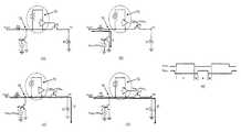
- a single-sided switchis a switching configuration where a switching device is used either to connect the load to a node at a lower potential—a “low-side” switch—or to a node at a higher potential—a “high-side” switch.
- the low-side configurationis shown in FIG. 1 a
- the high-side configurationis shown in FIG. 2 a , where the node at higher potential is represented by a high voltage (HV) source and the node at lower potential is represented by a ground terminal.
- HVhigh voltage
- a freewheeling diode 11(sometimes referred to as a flyback diode) is required to provide a path for the freewheeling load current when the switching device is OFF.
- FIG. 1 bwhen the switching device 12 is biased high by applying a gate-source voltage V gs greater than the device threshold voltage V th , current 13 flows through the load 10 and through switching device 12 , and diode 11 is reverse biased such that no significant current passes through it.
- switching device 12is switched to low by applying a gate-source voltage V gs ⁇ V th , as shown in FIG. 1 c , the current passing through the inductive load 10 cannot terminate abruptly, and so current 13 flows through the load 10 and through diode 11 , while no significant current flows through switching device 12 .
- FIGS. 2 b and 2 cSimilar diagrams detailing current flow through the high-side switching configuration when the switch is biased high and when the switch is turned off (switched low) are shown in FIGS. 2 b and 2 c , respectively.
- the freewheeling diodes 11 used in the circuits of FIGS. 1 and 2have low conduction loss in the ON state as well as good switching characteristics to minimize transient currents during switching, therefore Schottky diodes are commonly used. However, for some applications Schottky diodes cannot support large enough reverse-bias voltages, so high-voltage diodes which exhibit higher conduction and switching losses must be used.
- Switching devices 12which are usually transistors, may be enhancement mode (normally off, V th >0), also known as E-mode, or depletion mode (normally on, V th ⁇ 0), also known as D-mode, devices. In power circuits, enhancement mode devices are typically used to prevent accidental turn on, in order to avoid damage to the devices or other circuit components.
- V th >0also known as E-mode
- depletion modenormally on, V th ⁇ 0
- D-modedepletion mode
- enhancement mode devicesare typically used to prevent accidental turn on, in order to avoid damage to the devices or other circuit components.
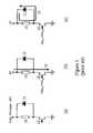
- FIG. 3 ais the same as FIG. 2 a , except that a high-voltage metal-oxide-semiconductor (MOS) transistor 61 is included anti-parallel with diode 11 .
- MOSmetal-oxide-semiconductor
- a standard MOS transistorinherently contains an anti-parallel parasitic diode and can therefore be represented as a transistor 62 anti-parallel to a diode 63 , as illustrated in FIG. 3 a .
- FIG. 3 ais the same as FIG. 2 a , except that a high-voltage metal-oxide-semiconductor (MOS) transistor 61 is included anti-parallel with diode 11 .
- MOSmetal-oxide-semiconductor
- MOS transistor 61 and diode 11both block a voltage equal to that across the load, so that the entire current 13 flows through the load 10 and through switching device 12 .
- diode 11prevents transistor 62 and parasitic diode 63 from turning on by clamping the gate-drain voltage to a value less than V th of the transistor and less than the turn-on voltage of the parasitic diode. Therefore, almost all of the freewheeling current flows through diode 11 , while only a small, insignificant portion flows through the transistor channel and parasitic diode. As shown in FIG.
- MOS device 61may then be biased high, which results in an increase in the channel conductivity of transistor 62 and thereby cause the majority of the freewheeling current to flow through the transistor channel.
- some dead timemust be provided between turn-off of switching device 12 and turn-on of transistor 62 in order to avoid shoot-through currents from the high-voltage supply (HV) to ground. Therefore, diode 11 will be turned on for some time immediately after switching device 12 is switched from high to low and immediately before switching device 12 is switched back from low to high. While this reduces the conduction losses incurred by diode 11 in the absence of MOS transistor 61 , the full switching loss for diode 11 is incurred, regardless of how long the diode remains on.
- the circuit in FIGS. 3 a - dcan in principle operate without diode 11 .
- parasitic diode 63performs the same function that diode 11 performed in the circuit of FIGS. 3 a - d .
- the parasitic diode 63typically has much poorer switching characteristics and suffers from higher switching losses than a standard high-voltage diode, resulting in increased power loss, so the circuit of FIGS. 3 a - d is usually preferred.
- Many power switching circuitscontain one or more high-side or low-side switches.
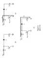
- One exampleis the boost-mode power-factor correction circuit shown in FIG. 4 a , which contains a low-side switch. This circuit is used at the input end in AC-to-DC voltage conversion circuits.
- the configuration for the low-side switch in this circuitis slightly modified from that shown in FIG. 1 a , since in FIG. 1 a the freewheeling diode 11 is connected anti-parallel to the inductive load 10 , whereas in this circuit the freewheeling diode 11 is between the inductive load 30 and the output capacitor 35 .
- the fundamental operating principles of the two circuitsare the same. As seen in FIG.
- diode 11prevents discharge of the output capacitor 35 through switching device 12 during times where the load current is zero or negative, as can occur if the energy stored in the inductor 30 is completely transferred out before the commencement of the next switching cycle.
- a switchin one aspect, includes a first switching device in series with an assembly comprising a load and a second switching device, the first switching device including a first channel, the second switching device including a second channel, wherein in a first mode of operation the second switching device is capable of blocking a voltage applied across the second switching device in a first direction, in a second mode of operation a substantial current flows through the second channel of the second switching device when a voltage is applied across the second switching device in a second direction and a gate of the second switching device is biased below a threshold voltage of the second switching device, and in a third mode of operation a substantial current flows through the second channel of the second switching device when a voltage is applied across the second switching device in the second direction and the gate of the second switching device is biased above the threshold voltage of the second switching device.
- the switch or the assemblycan be free of any diodes.
- a method of operating a switchis described.
- a gate of a first switching device of a switchis biased higher than a threshold voltage of the first switching device and a gate of a second switching device is biased lower than a threshold voltage of the second switching device, allowing current to flow from a high voltage side of the switch to a low voltage or ground side of the switch through the load.
- a bias on the gate of the first switching deviceis changed to be lower than the threshold voltage of the first switching device, causing the second switching device to operate in diode mode and blocking current from flowing to ground.
- a bias on the gate of the second switching deviceis changed to be higher than the threshold voltage of the second switching device, wherein changing the bias at the third time reduces conduction loss in comparison to switch operation between the second time and the third time.
- a boost-mode power-factor correction circuitin another aspect, includes a first switching device comprising a first channel, an inductive load, a capacitor, and a second switching device comprising a second channel, wherein the first switching device is connected to a node between the inductive load and a floating gate drive circuit, the second switching device is configured to be connected to the floating gate drive circuit, and the second switching device is between the inductive load and the capacitor.
- a method of operating the boost-mode power-factor correction circuitincludes causing a load current through the inductive load to be continuous; at a first time, biasing a gate of the first switching device higher than a threshold voltage of the first switching device and biasing a gate of the second switching device lower than a threshold voltage of the second switching device, allowing current to flow through the first switching device; at a second time immediately following the first time, changing a bias on the gate of the first switching device to be lower than the threshold voltage of the first switching device, causing the first switching device to operate in blocking mode and the second switching device to operate in diode mode, allowing current to flow through the second switching device; at a third time immediately following the second time, changing a bias on the gate of the second switching device to be higher than the threshold voltage of the second switching device, wherein changing the bias at the third time reduces conduction loss in comparison to switch operation between the second time and the third time.
- a method of operating the boost-mode power-factor correction circuitincludes causing a load current through the inductive load to be discontinuous, sensing the load current, and when the load current approaches zero, changing a bias on a gate of the second switching device from a voltage higher than a threshold voltage of the second switching device to a voltage lower than the threshold voltage of the second switching.
- a method of operating the boost-mode power-factor correction circuitincludes sensing a load current passing through the inductive load, causing the load current to approach zero and immediately increase after approaching zero, and when the load current approaches zero, switching the second switching device from on to off and switching the first switching device from off to on.
- the first mode of operationcan comprise biasing the gate of the first switching device above a threshold voltage of the first switching device.
- the second mode of operationcan comprise biasing the gate of the first switching device below a threshold voltage of the first switching device.
- the first switching devicecan have a first terminal and a second terminal on opposite sides of the gate, and the first terminal can be adjacent to the assembly and at a higher voltage than the second terminal of the first switching device during operation.
- the first switching devicecan have a first terminal and a second terminal on opposite sides of the gate, and the first terminal can be adjacent to the assembly and at a lower voltage than the second terminal of the first switching device during operation.
- a first nodecan be between the assembly and the first switching device, a second node can be at a high voltage side of the switch, and the second switching device can be capable of blocking a voltage when voltage at the first node is lower than voltage at the second node.
- a first nodecan be between the assembly and the first switching device, a second node can be at a low voltage or ground side of the switch, and the second switching device can be capable of blocking a voltage when voltage at the first node is higher than voltage at the second node.
- the second switching devicecan be capable of blocking a same voltage as the first switching device is capable of blocking.
- the second switching devicecan be capable of blocking voltage in two directions.
- the second switching deviceWhen the gate of the first switching device is biased lower than a threshold voltage of the first switching device, the second switching device can be capable of conducting current. When the gate of the first switching device is biased lower than the threshold voltage of the first switching device, substantially all current can flow through a single primary channel of the second switching device. When the gate of the second switching device is biased higher than the threshold voltage of the second switching device, the voltage drop across the second switching device can be reduced as compared to when the gate of the second switching device is biased lower than the threshold voltage of the second switching device.
- the second switching devicecan have a positive threshold voltage.
- the first switching devicecan have a positive threshold voltage.
- the second switching devicecan be a HEMT.
- the second switching devicecan be a III-Nitride HEMT.
- the first switching devicecan be a HEMT.
- the first switching devicecan be a III-Nitride HEMT.
- the second switching devicecan be structurally the same as the first switching device.
- a voltage drop across the second switching devicecan be smaller in the third mode of operation as compared to in the second mode of operation.
- the loadcan be an inductive load.
- the first switching device or the second switching devicecan comprise a high-voltage depletion mode device and a low-voltage enhancement mode device, the second channel can be a channel of the high-voltage depletion mode device, and the threshold voltage of the second switching device can be a threshold voltage of the low-voltage enhancement mode device.
- the low-voltage enhancement mode devicecan at least block a voltage equal to an absolute value of a threshold voltage of the high-voltage depletion mode device.
- the high-voltage depletion mode devicecan be a III-Nitride HEMT.
- the low-voltage enhancement mode devicecan be a III-Nitride HEMT.
- the low-voltage enhancement mode devicecan be a Si MOS device.
- the devicecan include a diode connected antiparallel to the low-voltage enhancement mode device.
- the first switching devicecan comprise a high-voltage depletion mode device and a low-voltage enhancement mode device, the first channel can be a channel of the high-voltage depletion mode device, and a threshold voltage of the first switching device can be a threshold voltage of the low-voltage enhancement mode device.
- Boost-mode power-factor correction circuitscan include one or more of the following features.
- the first switching devicecan be a III-N HEMT.
- the second switching devicecan be a III-N HEMT.
- Operating a boost-mode power-factor correction circuitcan include causing a load current through the inductive load to be discontinuous, sensing the load current, and when the load current approaches zero, changing a bias on a gate of the second switching device from a voltage higher than a threshold voltage of the second switching device to a voltage lower than the threshold voltage of the second switching device.
- a load current passing through the inductive load, causing the load current to approach zero and immediately increase after approaching zerois sensed.
- the second switching deviceis switched from on to off and the first switching device is switched from off to on.
- Methods described hereinmay include one or more of the following features or steps. Changing the bias at the third time can reduce conduction loss in comparison to switch operation at the second time.
- FIGS. 1 a - cshow schematics of a low-side switch, and current paths for various bias conditions.
- FIGS. 2 a - cshow schematics of a high-side switch, and current paths for various bias conditions.
- FIGS. 3 a - eshow schematics of high-side switches with a MOSFET connected across the inductive load, and current paths for various bias conditions.
- FIGS. 4 a - cshow schematics of a boost-mode power-factor correction circuit and current paths for various bias conditions.
- FIGS. 5 a - dshow schematics of a low-side switch, along with current paths for various bias conditions.
- FIG. 5 eshows a biasing scheme for the switching devices in the circuits of FIGS. 5 a - d.
- FIGS. 6 a - dshow schematics of a high-side switch, along with current paths for various bias conditions.
- FIG. 6 eshows a biasing scheme for the switching devices in the circuits of FIGS. 6 a - d.
- FIG. 7shows a schematic of a low-side switch.
- FIGS. 8 a - dshow schematics of a boost-mode power-factor correction circuit, along with current paths for various bias conditions.
- FIG. 8 eshows a biasing scheme for the switching devices in the circuits of FIGS. 8 a - d.
- FIGS. 9 a - cshow the input current as a function of time for various operating conditions for the circuit in FIG. 8 .
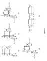
- FIGS. 5 a and 6 aLow-side and high-side switches and the circuits which they comprise, wherein the freewheeling diode shown in FIGS. 1-3 is replaced by a switching device, such as a transistor, are described below.
- a switching devicesuch as a transistor
- FIGS. 5 a and 6 athe freewheeling diode used in the circuits of FIGS. 1 and 2 has been replaced by switching device 41 .
- this devicemay be the same as the switching device 42 used to modulate the current path.
- FIGS. 5 b and 6 billustrate the current path when switching device 42 is biased ON (high) and switching device 41 is biased OFF (low).
- FIGS. 5 c and 6 cillustrate the current path when switching device 42 is switched OFF.
- Switching device 41can be an enhancement mode device, where the threshold voltage V th >0, or a depletion mode device, where the threshold voltage V th ⁇ 0.
- enhancement mode deviceswith threshold voltages as large as possible, such as V th >2V or V th >3V, a high internal barrier from source to drain at 0 bias (such as 0.5-2 eV), a high ON-to-OFF current ratio (such as >10 5 ), along with high breakdown voltage (600/1200 Volts) and low on resistance ( ⁇ 5 or ⁇ 10 mohm-cm 2 for 600/1200 V respectively).
- switching device 41must have the following characteristics. It must be able to block significant voltage when the voltage at terminal 45 / 55 is lower than the voltage at terminal 46 / 56 . This condition occurs when switching device 42 is biased high, as shown in FIGS. 5 b and 6 b .
- blocking a voltagerefers to the ability of a transistor to prevent a current that is greater than 0.0001 times the operating current during regular conduction from flowing through the transistor when a voltage is applied across the transistor. In other words, while a transistor is blocking a voltage which is applied across it, the total current passing through the transistor will not be greater than 0.0001 times the operating current during regular conduction.
- substantially currentincludes any current which is at least ten percent of the operating current during regular conduction.
- the maximum voltage that switching device 41 must be able to blockdepends on the particular circuit application, but in general will be the same or very close to the maximum blocking voltage specified for switching device 42 . In some embodiments, switching device 41 is able to block voltage in both directions. When switching device 42 is switched OFF, switching device 41 must be capable of conducting current 13 in the direction shown in FIGS. 5 c and 6 c . Furthermore, when the circuit is biased such as shown in FIG. 5 c or 6 c , all substantial current through switching device 41 flows through a single, primary channel of the device, wherein the conductivity of this channel may be modulated by the gate electrode.
- switching device 42When switching device 42 is biased ON, such as by setting the gate-source voltage V GS42 greater than the device threshold voltage V th42 , and switching device 41 is biased OFF, such as by setting V GS41 ⁇ V th41 , current 13 flows through inductive load 10 and switching device 42 , as seen in FIG. 5 b .
- switching device 41is said to be in “blocking mode”, as it is supporting a voltage across it while at the same time blocking current from flowing through it, i.e., device 41 is blocking voltage. As shown in FIG.
- a lower power mode of operationmay be achieved by applying a voltage V GS41 >V th41 to the gate of switching device 41 , as shown in FIG. 5 d .
- V GS41 >V th41a voltage
- FIG. 5 eTo prevent shoot-through currents from the high-voltage supply (HV) to ground, gate signals of the form shown in FIG. 5 e are applied.
- the time during which switching device 42 is ON and switching device 41 is OFFis labeled “C” in FIG. 5 e . This corresponds to the mode of operation shown in FIG. 5 b .
- switching device 42When switching device 42 is switched OFF, during the time switching device 41 conducts the freewheeling current, the gate of switching device 41 is driven high, allowing the drain-source voltage of switching device 41 to be simply the on-state resistance (Rd ds-on ) times the load current. To avoid shoot-through currents from the high-voltage supply (HV) to ground, some dead time must be provided between turn-off of switching device 42 and turn-on of switching device 41 . These are the times labeled “A” in FIG. 5 e . During these dead times, switching device 41 operates in the diode mode described above. Since this is a short time in comparison with the entire switching cycle, the relative amount of total power dissipation is low. Time “B” provides the dominant loss factor for switching device 41 , and this corresponds to the low-power mode when switching device 41 is fully enhanced. The mode of operation illustrated in FIG. 5 d allows for a further reduction in conduction loss, although switching losses remain unaffected.
- FIG. 6The detailed operation of the circuit in FIG. 6 is similar to that of FIG. 5 .
- switching device 42When switching device 42 is biased ON, such as by setting V GS42 >V th42 , and switching device 41 is biased OFF, such as by setting V GS41 ⁇ V th41 , current 13 flows through inductive load 10 and switching device 42 , as seen in FIG. 6 b .
- FIG. 6 cwhen switching device 42 is switched OFF, the current through the inductive load 10 cannot change abruptly, so the voltage at terminal 56 is forced sufficiently negative to allow the freewheeling current 13 to be carried through switching device 41 , and switching device 41 now operates in diode mode. Again, in this mode of operation, current is able to flow through switching device 41 even if V GS41 is not changed.
- power dissipation during diode mode operation of switching device 41may be reduced by applying a voltage V GS41 >V th41 to the gate of switching device 41 , as shown in FIG. 6 d .
- V GS41 >V th41a voltage
- some dead timemust be provided between turn-off of switching device 42 and turn-on of switching device 41 in order to avoid shoot-through currents from the high-voltage supply (HV) to ground, and so the bias scheme shown in FIG. 6 e is used.
- Examples of devices that meet the criteria specified above for switching device 41are metal-semiconductor field effect transistors (MESFETs) of any material system, junction field effect transistors (JFETs) of any material system, high electron mobility transistors (HEMTs or HFETs) of any material system, including vertical devices such as current aperture vertical electron transistors (CAVETs), and bidirectional switches comprised of the devices listed above, such as those described U.S. application Ser. No. 12/209,581, filed Sep. 12, 2008, which is hereby incorporated by reference throughout.
- MEFETsmetal-semiconductor field effect transistors
- JFETsjunction field effect transistors
- HEMTs or HFETshigh electron mobility transistors
- CAVETscurrent aperture vertical electron transistors
- Common material systems for HEMTs and MESFETsinclude Ga x Al y In 1-x-y N m As n P 1-m-n or III-V materials, such as III-N materials, III-As materials, and III-P materials.
- Common materials for JFETsinclude III-V materials, SiC, and Si.
- switching device 41is an enhancement mode device to prevent accidental turn on, in order to avoid damage to the device or other circuit components.
- III-Nitride (III-N) devicessuch as III-Nitride HFETs, are especially desirable due to the large blocking voltages that can be achieved with these devices.
- the devicepreferably also exhibits a high access region conductivity (such as sheet resistance ⁇ 750 ohms/square) along with high breakdown voltage (600/1200 Volts) and low on resistance ( ⁇ 5 or ⁇ 10 mohm-cm 2 for 600/1200 V respectively).
- the devicecan also include any of the following: a surface passivation layer, such as SiN, a field plate, such as a slant field plate, and an insulator underneath the gate.
- switching device 41is a SiC JFET.
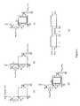
- switching device 41includes a high-voltage depletion mode (D-mode) device 97 connected to a low-voltage enhancement mode (E-mode) device 96 as shown.
- D-modehigh-voltage depletion mode
- E-modelow-voltage enhancement mode
- This configuration for switching device 41operates similarly to the case when a high-voltage E-mode device is used for switching device 41 .
- D-mode device 97blocks the voltage across the switch. This configuration can be advantageous because high-voltage E-mode devices are typically difficult to fabricate.
- the D-mode device 97is capable of blocking the maximum voltage drop across the switch, which for high-voltage applications can be 600V or 1200V or other suitable blocking voltage required by the application.
- the E-mode device 96can block at least
- the D-mode devicecan block about 1200V and has a threshold voltage of about ⁇ 5V, and the E-mode device blocks at least about 5V, such as at least about 10V.
- D-mode device 97can be a high-voltage III-N HEMT device
- E-mode device 96can be a Si MOS device or a III-N HEMT device.
- diode 99which is a low-loss diode such as Schottky diode, can optionally be connected antiparallel to device 96 , as shown, in order to reduce switching losses by preventing turn-on of the parasitic reverse diode inherent in Si MOSFETs.
- a similar configuration to the one shown for switching device 41 in FIG. 7can also be used for switching device 42 , and the configuration may also be used for switching devices 41 and 42 in the high-side switch of FIG. 6 . More details of the operation of this configuration can be found in U.S. application Ser. No. 12/209,581.
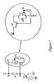
- FIG. 8 aA boost-mode power-factor correction circuit is shown in FIG. 8 a .
- This circuitis similar to that shown in FIG. 4 a , except that diode 11 has been replaced by a switching device 41 connected to a floating gate-drive circuit 72 .
- Switching device 41must meet the same specifications as switching device 41 in FIGS. 5 and 6 .
- the details of operation of this circuitare as follows. When switching device 42 is biased ON and switching device 41 is biased OFF, as seen in FIG. 8 b , current 13 passes through the load 30 and through the switching device 42 .
- the voltage at node 77is kept sufficiently high by the output capacitor 35 so that switching device 41 is in blocking mode, and thereby does not have any substantial current passing through it. As seen in FIG.
- the load currentis negative (flows in the opposite direction through the load) during some portion of the duty cycle. This may occur if there are any inductive or capacitive components leading into the input of this circuit.
- the third, illustrated in FIG. 9 cis the case where the load current approaches zero but then immediately increases again. This mode is known as the “critical mode”.
- switching device 42is switched ON and switching device 41 is switched OFF, as in FIG. 8 b .
- switching device 42is switched OFF, the inductor forces the load current through switching device 41 as shown in FIG. 8 c , and switching device 41 is in diode mode.
- conduction lossescan be reduced by applying a voltage V GS41 >V th41 to the gate of switching device 41 , as shown in FIG. 8 d .
- Some dead timemust be provided between turn-off of switching device 42 and turn-on of switching device 41 in order to prevent the capacitor 35 from discharging through switching devices 42 and 41 , and so the bias scheme shown in FIG. 8 e is used.
- the current in the inductorcan become discontinuous or negative if the energy stored in it is completely transferred, either to the output capacitor or through switching device 42 , before the commencement of the next switching cycle.
- the switching device 41or flyback transistor
- the switching device 41or flyback transistor
- the flyback transistoris between inductor 30 and capacitor 35
- incorrect operationwould result from leaving switching device 41 enhanced after the load current drops to zero, because the current would reverse sign and start discharging the output capacitor.
- the load currentmust be sensed, either directly or indirectly, and if switching device 41 is on, it must be turned off when the current approaches zero.
- switching device 41can be turned off once the current has dropped to 0.1%, 1%, 3%, or 5% of the peak current.
- the third case, the critical modeis essentially the same as the discontinuous mode, with the difference that the switching device 42 turns back on as soon as the load current approaches zero.
- the control circuitis therefore very different from the discontinuous case, but the requirement regarding the switching sequence of the switching devices 42 and 41 is the same.
- the currentmust be sensed to know when it has approached zero, and switching device 41 must be turned off when the current approaches zero.
Landscapes
- Engineering & Computer Science (AREA)
- Physics & Mathematics (AREA)
- Electromagnetism (AREA)
- General Physics & Mathematics (AREA)
- Radar, Positioning & Navigation (AREA)
- Automation & Control Theory (AREA)
- Dc-Dc Converters (AREA)
- Electronic Switches (AREA)
- Power Conversion In General (AREA)
- Inverter Devices (AREA)
Abstract
Description
Claims (22)
Priority Applications (1)
| Application Number | Priority Date | Filing Date | Title |
|---|---|---|---|
| US14/332,967US9690314B2 (en) | 2008-09-23 | 2014-07-16 | Inductive load power switching circuits |
Applications Claiming Priority (5)
| Application Number | Priority Date | Filing Date | Title |
|---|---|---|---|
| US9945108P | 2008-09-23 | 2008-09-23 | |
| US12/556,438US8289065B2 (en) | 2008-09-23 | 2009-09-09 | Inductive load power switching circuits |
| US13/618,726US8531232B2 (en) | 2008-09-23 | 2012-09-14 | Inductive load power switching circuits |
| US13/959,483US8816751B2 (en) | 2008-09-23 | 2013-08-05 | Inductive load power switching circuits |
| US14/332,967US9690314B2 (en) | 2008-09-23 | 2014-07-16 | Inductive load power switching circuits |
Related Parent Applications (1)
| Application Number | Title | Priority Date | Filing Date |
|---|---|---|---|
| US13/959,483DivisionUS8816751B2 (en) | 2008-09-23 | 2013-08-05 | Inductive load power switching circuits |
Publications (2)
| Publication Number | Publication Date |
|---|---|
| US20140327412A1 US20140327412A1 (en) | 2014-11-06 |
| US9690314B2true US9690314B2 (en) | 2017-06-27 |
Family
ID=42037005
Family Applications (5)
| Application Number | Title | Priority Date | Filing Date |
|---|---|---|---|
| US12/556,438Active2030-01-13US8289065B2 (en) | 2008-09-23 | 2009-09-09 | Inductive load power switching circuits |
| US13/618,726ActiveUS8531232B2 (en) | 2008-09-23 | 2012-09-14 | Inductive load power switching circuits |
| US13/618,502ActiveUS8493129B2 (en) | 2008-09-23 | 2012-09-14 | Inductive load power switching circuits |
| US13/959,483ActiveUS8816751B2 (en) | 2008-09-23 | 2013-08-05 | Inductive load power switching circuits |
| US14/332,967Active2030-09-05US9690314B2 (en) | 2008-09-23 | 2014-07-16 | Inductive load power switching circuits |
Family Applications Before (4)
| Application Number | Title | Priority Date | Filing Date |
|---|---|---|---|
| US12/556,438Active2030-01-13US8289065B2 (en) | 2008-09-23 | 2009-09-09 | Inductive load power switching circuits |
| US13/618,726ActiveUS8531232B2 (en) | 2008-09-23 | 2012-09-14 | Inductive load power switching circuits |
| US13/618,502ActiveUS8493129B2 (en) | 2008-09-23 | 2012-09-14 | Inductive load power switching circuits |
| US13/959,483ActiveUS8816751B2 (en) | 2008-09-23 | 2013-08-05 | Inductive load power switching circuits |
Country Status (4)
| Country | Link |
|---|---|
| US (5) | US8289065B2 (en) |
| CN (2) | CN102165694B (en) |
| TW (1) | TWI431936B (en) |
| WO (1) | WO2010039463A2 (en) |
Cited By (5)
| Publication number | Priority date | Publication date | Assignee | Title |
|---|---|---|---|---|
| US10630285B1 (en) | 2017-11-21 | 2020-04-21 | Transphorm Technology, Inc. | Switching circuits having drain connected ferrite beads |
| US10756207B2 (en) | 2018-10-12 | 2020-08-25 | Transphorm Technology, Inc. | Lateral III-nitride devices including a vertical gate module |
| US11749656B2 (en) | 2020-06-16 | 2023-09-05 | Transphorm Technology, Inc. | Module configurations for integrated III-Nitride devices |
| US11810971B2 (en) | 2019-03-21 | 2023-11-07 | Transphorm Technology, Inc. | Integrated design for III-Nitride devices |
| US11973138B2 (en) | 2020-08-05 | 2024-04-30 | Transphorm Technology, Inc. | N-polar devices including a depleting layer with improved conductivity |
Families Citing this family (52)
| Publication number | Priority date | Publication date | Assignee | Title |
|---|---|---|---|---|
| US7915643B2 (en) | 2007-09-17 | 2011-03-29 | Transphorm Inc. | Enhancement mode gallium nitride power devices |
| US7965126B2 (en) | 2008-02-12 | 2011-06-21 | Transphorm Inc. | Bridge circuits and their components |
| US8519438B2 (en) | 2008-04-23 | 2013-08-27 | Transphorm Inc. | Enhancement mode III-N HEMTs |
| US8289065B2 (en) | 2008-09-23 | 2012-10-16 | Transphorm Inc. | Inductive load power switching circuits |
| US7898004B2 (en) | 2008-12-10 | 2011-03-01 | Transphorm Inc. | Semiconductor heterostructure diodes |
| US8742459B2 (en) | 2009-05-14 | 2014-06-03 | Transphorm Inc. | High voltage III-nitride semiconductor devices |
| US8390000B2 (en) | 2009-08-28 | 2013-03-05 | Transphorm Inc. | Semiconductor devices with field plates |
| US8138529B2 (en) | 2009-11-02 | 2012-03-20 | Transphorm Inc. | Package configurations for low EMI circuits |
| US8389977B2 (en) | 2009-12-10 | 2013-03-05 | Transphorm Inc. | Reverse side engineered III-nitride devices |
| US8816497B2 (en)* | 2010-01-08 | 2014-08-26 | Transphorm Inc. | Electronic devices and components for high efficiency power circuits |
| US8624662B2 (en) | 2010-02-05 | 2014-01-07 | Transphorm Inc. | Semiconductor electronic components and circuits |
| US8847563B2 (en)* | 2010-07-15 | 2014-09-30 | Cree, Inc. | Power converter circuits including high electron mobility transistors for switching and rectifcation |
| US8742460B2 (en) | 2010-12-15 | 2014-06-03 | Transphorm Inc. | Transistors with isolation regions |
| US8643062B2 (en) | 2011-02-02 | 2014-02-04 | Transphorm Inc. | III-N device structures and methods |
| US8786327B2 (en) | 2011-02-28 | 2014-07-22 | Transphorm Inc. | Electronic components with reactive filters |
| US8772842B2 (en) | 2011-03-04 | 2014-07-08 | Transphorm, Inc. | Semiconductor diodes with low reverse bias currents |
| US8716141B2 (en) | 2011-03-04 | 2014-05-06 | Transphorm Inc. | Electrode configurations for semiconductor devices |
| US8598937B2 (en) | 2011-10-07 | 2013-12-03 | Transphorm Inc. | High power semiconductor electronic components with increased reliability |
| US9209176B2 (en) | 2011-12-07 | 2015-12-08 | Transphorm Inc. | Semiconductor modules and methods of forming the same |
| EP2608357B1 (en)* | 2011-12-19 | 2014-07-23 | Vetco Gray Controls Limited | Protecting against transients in a communication system |
| US9165766B2 (en) | 2012-02-03 | 2015-10-20 | Transphorm Inc. | Buffer layer structures suited for III-nitride devices with foreign substrates |
| US8648643B2 (en) | 2012-02-24 | 2014-02-11 | Transphorm Inc. | Semiconductor power modules and devices |
| WO2013155108A1 (en) | 2012-04-09 | 2013-10-17 | Transphorm Inc. | N-polar iii-nitride transistors |
| US9184275B2 (en) | 2012-06-27 | 2015-11-10 | Transphorm Inc. | Semiconductor devices with integrated hole collectors |
| US8803246B2 (en) | 2012-07-16 | 2014-08-12 | Transphorm Inc. | Semiconductor electronic components with integrated current limiters |
| US20140021934A1 (en)* | 2012-07-17 | 2014-01-23 | Transphorm, Inc. | Devices and components for power conversion circuits |
| CN103684415A (en)* | 2012-09-06 | 2014-03-26 | 上海航天控制工程研究所 | Highly reliable inductive load driving technology for spacecraft |
| CN103824845B (en) | 2012-11-19 | 2017-08-29 | 台达电子工业股份有限公司 | Semiconductor device with a plurality of semiconductor chips |
| US9065445B2 (en)* | 2012-12-17 | 2015-06-23 | Continental Automotive Systems, Inc. | Voltage clamp assist circuit |
| CN105164811B (en) | 2013-02-15 | 2018-08-31 | 创世舫电子有限公司 | Electrode of semiconductor devices and forming method thereof |
| US9087718B2 (en) | 2013-03-13 | 2015-07-21 | Transphorm Inc. | Enhancement-mode III-nitride devices |
| US9245992B2 (en) | 2013-03-15 | 2016-01-26 | Transphorm Inc. | Carbon doping semiconductor devices |
| US9059076B2 (en) | 2013-04-01 | 2015-06-16 | Transphorm Inc. | Gate drivers for circuits based on semiconductor devices |
| US8917135B2 (en)* | 2013-05-14 | 2014-12-23 | Infineon Technologies Austria Ag | Circuit with a plurality of diodes and method for controlling such a circuit |
| JP6201422B2 (en)* | 2013-05-22 | 2017-09-27 | 富士電機株式会社 | Semiconductor device |
| US9537425B2 (en) | 2013-07-09 | 2017-01-03 | Transphorm Inc. | Multilevel inverters and their components |
| US9443938B2 (en) | 2013-07-19 | 2016-09-13 | Transphorm Inc. | III-nitride transistor including a p-type depleting layer |
| US9443787B2 (en) | 2013-08-09 | 2016-09-13 | Infineon Technologies Austria Ag | Electronic component and method |
| US9543940B2 (en) | 2014-07-03 | 2017-01-10 | Transphorm Inc. | Switching circuits having ferrite beads |
| US9590494B1 (en) | 2014-07-17 | 2017-03-07 | Transphorm Inc. | Bridgeless power factor correction circuits |
| US9318593B2 (en) | 2014-07-21 | 2016-04-19 | Transphorm Inc. | Forming enhancement mode III-nitride devices |
| RU2562778C1 (en)* | 2014-12-02 | 2015-09-10 | Федеральное государственное бюджетное образовательное учреждение высшего профессионального образования "Алтайский государственный технический университет им. И.И. Ползунова" (АлтГТУ) | Reversible semiconductor switching device operating for inductive load |
| US9536966B2 (en) | 2014-12-16 | 2017-01-03 | Transphorm Inc. | Gate structures for III-N devices |
| US9536967B2 (en) | 2014-12-16 | 2017-01-03 | Transphorm Inc. | Recessed ohmic contacts in a III-N device |
| US9627962B2 (en)* | 2015-03-09 | 2017-04-18 | Texas Instruments Incorporated | Fast blocking switch |
| WO2016149146A1 (en) | 2015-03-13 | 2016-09-22 | Transphorm, Inc. | Paralleling of switching devices for high power circuits |
| US11322599B2 (en) | 2016-01-15 | 2022-05-03 | Transphorm Technology, Inc. | Enhancement mode III-nitride devices having an Al1-xSixO gate insulator |
| TWI762486B (en) | 2016-05-31 | 2022-05-01 | 美商創世舫科技有限公司 | Iii-nitride devices including a graded depleting layer |
| US10374591B2 (en)* | 2017-01-03 | 2019-08-06 | General Electric Company | Systems and methods for a gate drive circuit |
| US10319648B2 (en) | 2017-04-17 | 2019-06-11 | Transphorm Inc. | Conditions for burn-in of high power semiconductors |
| KR102412313B1 (en)* | 2018-07-17 | 2022-06-22 | 주식회사 엘지에너지솔루션 | Apparatus and method for diagnosing switch |
| US11664741B2 (en) | 2019-07-25 | 2023-05-30 | Susan Rhodes | System and method for AC power control |
Citations (238)
| Publication number | Priority date | Publication date | Assignee | Title |
|---|---|---|---|---|
| US4384287A (en) | 1979-04-11 | 1983-05-17 | Nippon Electric Co., Ltd. | Inverter circuits using insulated gate field effect transistors |
| US4645562A (en) | 1985-04-29 | 1987-02-24 | Hughes Aircraft Company | Double layer photoresist technique for side-wall profile control in plasma etching processes |
| US4728826A (en) | 1986-03-19 | 1988-03-01 | Siemens Aktiengesellschaft | MOSFET switch with inductive load |
| US4808853A (en) | 1987-11-25 | 1989-02-28 | Triquint Semiconductor, Inc. | Tristate output circuit with selectable output impedance |
| US4821093A (en) | 1986-08-18 | 1989-04-11 | The United States Of America As Represented By The Secretary Of The Army | Dual channel high electron mobility field effect transistor |
| US4914489A (en) | 1986-12-20 | 1990-04-03 | Fujitsu Limited | Constant current semiconductor device |
| JPH0575040A (en) | 1991-09-13 | 1993-03-26 | Fujitsu Ltd | Semiconductor integrated circuit device |
| US5198964A (en) | 1990-09-27 | 1993-03-30 | Hitachi, Ltd. | Packaged semiconductor device and electronic device module including same |
| JPH0667744A (en) | 1992-08-18 | 1994-03-11 | Fujitsu Ltd | Constant-voltage circuit |
| US5329147A (en) | 1993-01-04 | 1994-07-12 | Xerox Corporation | High voltage integrated flyback circuit in 2 μm CMOS |
| US5379209A (en) | 1993-02-09 | 1995-01-03 | Performance Controls, Inc. | Electronic switching circuit |
| US5493487A (en) | 1993-02-09 | 1996-02-20 | Performance Controls, Inc. | Electronic switching circuit |
| US5637922A (en) | 1994-02-07 | 1997-06-10 | General Electric Company | Wireless radio frequency power semiconductor devices using high density interconnect |
| US5646069A (en) | 1995-06-07 | 1997-07-08 | Hughes Aircraft Company | Fabrication process for Alx In1-x As/Gay In1-y As power HFET ohmic contacts |
| US5705847A (en) | 1996-06-10 | 1998-01-06 | Mitsubishi Denki Kabushiki Kaisha | Semiconductor device |
| US5714393A (en) | 1996-12-09 | 1998-02-03 | Motorola, Inc. | Diode-connected semiconductor device and method of manufacture |
| US5789951A (en) | 1997-01-31 | 1998-08-04 | Motorola, Inc. | Monolithic clamping circuit and method of preventing transistor avalanche breakdown |
| US5952856A (en) | 1996-05-02 | 1999-09-14 | Shindengen Electric Manufacturing Co., Ltd. | Inductive load driving method and H-bridge circuit control device |
| US5998810A (en) | 1994-12-19 | 1999-12-07 | Kabushiki Kaisha Toshiba | Semiconductor light-emitting diode having a p-type semiconductor layer formed on a light-emitting layer |
| US6008684A (en) | 1996-10-23 | 1999-12-28 | Industrial Technology Research Institute | CMOS output buffer with CMOS-controlled lateral SCR devices |
| JP2000058871A (en) | 1999-07-02 | 2000-02-25 | Citizen Watch Co Ltd | Integrated circuit of electronic apparatus |
| JP2000101356A (en) | 1998-09-25 | 2000-04-07 | Murata Mfg Co Ltd | High frequency power amplifier circuit |
| JP2000124358A (en) | 1998-10-13 | 2000-04-28 | Matsushita Electric Ind Co Ltd | High frequency integrated circuit |
| US6097046A (en) | 1993-04-30 | 2000-08-01 | Texas Instruments Incorporated | Vertical field effect transistor and diode |
| US6107844A (en) | 1998-09-28 | 2000-08-22 | Tripath Technology, Inc. | Methods and apparatus for reducing MOSFET body diode conduction in a half-bridge configuration |
| US6130831A (en) | 1998-10-21 | 2000-10-10 | Haiden Laboratory Inc. | Positive-negative pulse type high frequency switching power supply unit |
| US6172550B1 (en) | 1996-08-16 | 2001-01-09 | American Superconducting Corporation | Cryogenically-cooled switching circuit |
| US20010032999A1 (en) | 2000-04-25 | 2001-10-25 | Seikoh Yoshida | GaN-based compound semiconductor device |
| US6316793B1 (en) | 1998-06-12 | 2001-11-13 | Cree, Inc. | Nitride based transistors on semi-insulating silicon carbide substrates |
| US20010040247A1 (en) | 2000-03-28 | 2001-11-15 | Yuji Ando | Hetero-junction field effect transistor having an intermediate layer |
| US6333617B1 (en) | 1999-06-10 | 2001-12-25 | Denso Corporation | Inductive load drive control for selectively extinguishing energy through switching devices or diodes |
| US20020036287A1 (en) | 2000-07-28 | 2002-03-28 | The Regents Of The University Of California | Gallium nitride-based HFET and a method for fabricating a gallium nitride-based HFET |
| US6395593B1 (en) | 1999-05-06 | 2002-05-28 | Texas Instruments Incorporated | Method of manufacturing high side and low side guard rings for lowest parasitic performance in an H-bridge configuration |
| US20020121648A1 (en) | 2000-12-30 | 2002-09-05 | Wei-Chou Hsu | An in0.34assb0.15/inp hfet utilizing inp channels |
| US20020125920A1 (en) | 2001-02-06 | 2002-09-12 | Stanley Gerald R. | Half-bridge gate driver circuit |
| US6475889B1 (en) | 2000-04-11 | 2002-11-05 | Cree, Inc. | Method of forming vias in silicon carbide and resulting devices and circuits |
| US20020167023A1 (en) | 2001-05-11 | 2002-11-14 | Cree Lighting Company And Regents Of The University Of California | Group-III nitride based high electron mobility transistor (HEMT) with barrier/spacer layer |
| US20030006437A1 (en) | 1998-09-22 | 2003-01-09 | Nec Corporation | Field effect transistor |
| US20030020092A1 (en) | 2001-07-24 | 2003-01-30 | Primit Parikh | Insulating gate AlGaN/GaN HEMT |
| US6521940B1 (en) | 1990-12-31 | 2003-02-18 | Kopin Corporation | High density electronic circuit modules |
| US6548333B2 (en) | 2000-12-01 | 2003-04-15 | Cree, Inc. | Aluminum gallium nitride/gallium nitride high electron mobility transistors having a gate contact on a gallium nitride based cap segment |
| US6586781B2 (en) | 2000-02-04 | 2003-07-01 | Cree Lighting Company | Group III nitride based FETs and HEMTs with reduced trapping and method for producing the same |
| JP2003229566A (en) | 2001-11-27 | 2003-08-15 | Furukawa Electric Co Ltd:The | Power conversion device and GaN-based semiconductor device used therefor |
| JP2003244943A (en) | 2002-02-13 | 2003-08-29 | Honda Motor Co Ltd | Power supply booster |
| US20030178654A1 (en) | 1999-06-02 | 2003-09-25 | Thornton Trevor J. | Complementary Schottky junction transistors and methods of forming the same |
| US6650169B2 (en) | 2001-10-01 | 2003-11-18 | Koninklijke Philips Electronics N.V. | Gate driver apparatus having an energy recovering circuit |
| JP2003338742A (en) | 2002-05-22 | 2003-11-28 | Nissan Motor Co Ltd | Driver circuit for current control type device |
| US20040041169A1 (en) | 2002-08-26 | 2004-03-04 | Fan Ren | GaN-type enhancement MOSFET using hetero structure |
| US20040061129A1 (en) | 2002-07-16 | 2004-04-01 | Saxler Adam William | Nitride-based transistors and methods of fabrication thereof using non-etched contact recesses |
| US6727531B1 (en) | 2000-08-07 | 2004-04-27 | Advanced Technology Materials, Inc. | Indium gallium nitride channel high electron mobility transistors, and method of making the same |
| JP2004147472A (en) | 2002-10-28 | 2004-05-20 | Matsushita Electric Ind Co Ltd | DC / AC converter for photovoltaic power generation |
| US6781423B1 (en) | 2003-07-04 | 2004-08-24 | Dialog Semiconductor Gmbh | High-voltage interface and driver control circuit |
| US20040164347A1 (en) | 2003-01-15 | 2004-08-26 | Advanced Power Technology, Inc., A Delaware Corporation | Design and fabrication of rugged FRED |
| CN1529408A (en) | 2003-10-17 | 2004-09-15 | 清华大学 | Low Voltage High Linearity RF Amplifier with On-Chip Impedance Matching |
| US20040178831A1 (en) | 2003-03-11 | 2004-09-16 | Ying-Hsin Li | [source follower capable of compensating the threshold voltage] |
| JP2004260114A (en) | 2003-02-27 | 2004-09-16 | Shin Etsu Handotai Co Ltd | Compound semiconductor element |
| JP2004281454A (en) | 2003-03-12 | 2004-10-07 | Sharp Corp | Semiconductor device and manufacturing method thereof |
| JP2005012051A (en) | 2003-06-20 | 2005-01-13 | Toshiba Corp | High breakdown voltage semiconductor device and manufacturing method thereof |
| US20050052221A1 (en) | 2003-09-05 | 2005-03-10 | Sanyo Electric Co., Ltd. | Power supply unit and power supply system having the same |
| US6867078B1 (en) | 2003-11-19 | 2005-03-15 | Freescale Semiconductor, Inc. | Method for forming a microwave field effect transistor with high operating voltage |
| US20050067716A1 (en) | 2003-01-02 | 2005-03-31 | Cree, Inc. | Group III nitride based flip-chip integrated circuit and method for fabricating |
| US20050077541A1 (en) | 2003-10-10 | 2005-04-14 | The Regents Of The University Of California | GaN/AIGaN/GaN dispersion-free high electron mobility transistors |
| US20050077947A1 (en) | 2002-05-02 | 2005-04-14 | Eupec Europaische Gesellschaft Fur Leistungshalbleiter Mbh | Half-bridge circuit |
| US6900657B2 (en) | 2003-09-24 | 2005-05-31 | Saia-Burgess Automotive, Inc. | Stall detection circuit and method |
| US20050133816A1 (en) | 2003-12-19 | 2005-06-23 | Zhaoyang Fan | III-nitride quantum-well field effect transistors |
| US20050146310A1 (en) | 2003-12-24 | 2005-07-07 | Ray Orr | DC converters having buck or boost configurations |
| US20050189562A1 (en) | 2004-02-12 | 2005-09-01 | Kinzer Daniel M. | Integrated III-nitride power devices |
| US20050189561A1 (en) | 2004-02-12 | 2005-09-01 | Kinzer Daniel M. | III-Nitride bidirectional switch |
| US20050194612A1 (en) | 2004-01-23 | 2005-09-08 | International Rectifier Corp. | III-Nitride current control device and method of manufacture |
| US20050218964A1 (en) | 2004-03-31 | 2005-10-06 | Matsushita Electric Industrial Co., Ltd. | Active diode |
| CN1682445A (en) | 2002-09-21 | 2005-10-12 | 皇家飞利浦电子股份有限公司 | Converter circuit and control method for same |
| US20050253168A1 (en) | 2004-05-11 | 2005-11-17 | Cree, Inc. | Wide bandgap transistors with multiple field plates |
| US6979863B2 (en) | 2003-04-24 | 2005-12-27 | Cree, Inc. | Silicon carbide MOSFETs with integrated antiparallel junction barrier Schottky free wheeling diodes and methods of fabricating the same |
| US20060011915A1 (en) | 2004-07-14 | 2006-01-19 | Kabushiki Kaisha Toshiba | Nitride semiconductor device |
| JP2006033723A (en) | 2004-07-21 | 2006-02-02 | Sharp Corp | Optical coupling device for power control and electronic device using the optical coupling device for power control |
| JP2006032749A (en) | 2004-07-20 | 2006-02-02 | Toyota Motor Corp | Semiconductor device and manufacturing method thereof |
| US20060033122A1 (en) | 2004-08-11 | 2006-02-16 | Mark Pavier | Half-bridge package |
| US20060043499A1 (en) | 2002-10-29 | 2006-03-02 | Koninklijke Philips Electronics, N.V. | Bi-directional double nmos switch |
| CN1748320A (en) | 2002-12-16 | 2006-03-15 | 日本电气株式会社 | field effect transistor |
| US20060060871A1 (en) | 2004-01-23 | 2006-03-23 | International Rectifier Corp. | Enhancement mode III-nitride FET |
| US7030428B2 (en) | 2001-12-03 | 2006-04-18 | Cree, Inc. | Strain balanced nitride heterojunction transistors |
| JP2006115557A (en) | 2004-10-12 | 2006-04-27 | Kayaba Ind Co Ltd | Switching element, motor drive circuit and shock absorber |
| US7045404B2 (en) | 2004-01-16 | 2006-05-16 | Cree, Inc. | Nitride-based transistors with a protective layer and a low-damage recess and methods of fabrication thereof |
| US20060108605A1 (en) | 2004-11-22 | 2006-05-25 | Matsushita Electric Industrial Co., Ltd. | Schottky barrier diode and integrated circuit using the same |
| US20060108602A1 (en) | 2004-11-19 | 2006-05-25 | Masashi Tanimoto | Field effect transistor and method of manufacturing the same |
| JP2006158185A (en) | 2004-10-25 | 2006-06-15 | Toshiba Corp | Power semiconductor device |
| US20060124962A1 (en) | 2004-12-09 | 2006-06-15 | Matsushita Electric Industrial Co., Ltd. | Field effect transistor and method for fabricating the same |
| JP2006173754A (en) | 2004-12-13 | 2006-06-29 | Oki Electric Ind Co Ltd | High frequency switch |
| US7071498B2 (en) | 2003-12-17 | 2006-07-04 | Nitronex Corporation | Gallium nitride material devices including an electrode-defining layer and methods of forming the same |
| US20060157729A1 (en) | 2005-01-14 | 2006-07-20 | Matsushita Electric Industrial Co., Ltd. | Semiconductor device |
| US7084475B2 (en) | 2004-02-17 | 2006-08-01 | Velox Semiconductor Corporation | Lateral conduction Schottky diode with plural mesas |
| US20060176007A1 (en) | 2005-01-31 | 2006-08-10 | Best Eric P | Method for stepper motor position referencing |
| US20060181332A1 (en)* | 2005-02-02 | 2006-08-17 | Kinzer Daniel M | Voltage supply circuit including a III-nitride based power semiconductor device |
| US20060186422A1 (en) | 2005-02-22 | 2006-08-24 | Remigijus Gaska | Etching a nitride-based heterostructure |
| US20060189109A1 (en) | 2001-03-02 | 2006-08-24 | Amberwave Systems | Methods of fabricating contact regions for FET incorporating SiGe |
| US20060202272A1 (en) | 2005-03-11 | 2006-09-14 | Cree, Inc. | Wide bandgap transistors with gate-source field plates |
| US7116567B2 (en) | 2005-01-05 | 2006-10-03 | Velox Semiconductor Corporation | GaN semiconductor based voltage conversion device |
| US20060220063A1 (en) | 2005-03-30 | 2006-10-05 | Eudyna Devices Inc. | Semiconductor device having GaN-based semiconductor layer |
| US7125786B2 (en) | 2000-04-11 | 2006-10-24 | Cree, Inc. | Method of forming vias in silicon carbide and resulting devices and circuits |
| US20060238234A1 (en) | 2005-04-25 | 2006-10-26 | Triquint Semiconductor, Inc. | Producing reference voltages using transistors |
| US20060237825A1 (en) | 2005-04-25 | 2006-10-26 | International Rectifier Corporation | Device packages having a III-nitride based power semiconductor device |
| CN1855493A (en) | 2005-03-28 | 2006-11-01 | 三洋电机株式会社 | Active component and switch circuit device |
| US20060255364A1 (en) | 2004-02-05 | 2006-11-16 | Saxler Adam W | Heterojunction transistors including energy barriers and related methods |
| US20060289901A1 (en) | 2003-03-03 | 2006-12-28 | Cree, Inc. | Integrated nitride and silicon carbide-based devices and methods of fabricating integrated nitride-based devices |
| US7161194B2 (en) | 2004-12-06 | 2007-01-09 | Cree, Inc. | High power density and/or linearity transistors |
| US20070007547A1 (en) | 2005-07-06 | 2007-01-11 | Robert Beach | III-Nitride enhancement mode devices |
| US20070018210A1 (en) | 2005-07-21 | 2007-01-25 | Cree, Inc. | Switch mode power amplifier using MIS-HEMT with field plate extension |
| US20070018187A1 (en) | 2005-07-22 | 2007-01-25 | Samsung Electro-Mechanics Co., Ltd. | Vertical GaN-based LED and method of manfacturing the same |
| US20070018199A1 (en) | 2005-07-20 | 2007-01-25 | Cree, Inc. | Nitride-based transistors and fabrication methods with an etch stop layer |
| US7170111B2 (en) | 2004-02-05 | 2007-01-30 | Cree, Inc. | Nitride heterojunction transistors having charge-transfer induced energy barriers and methods of fabricating the same |
| JP2007036218A (en) | 2005-06-27 | 2007-02-08 | Internatl Rectifier Corp | Active drive of normally-on and normally-off cascode connection configuration device through unsymmetrical cmos |
| US20070045670A1 (en) | 2005-08-31 | 2007-03-01 | Kabushiki Kaisha Toshiba | Nitride-based semiconductor device and method of manufacturing the same |
| JP2007096203A (en) | 2005-09-30 | 2007-04-12 | Sanken Electric Co Ltd | Field-effect transistor having 2-dimensional carrier gas layer |
| US20070080672A1 (en) | 2005-10-12 | 2007-04-12 | System General Corp. | High efficiency buck converter for both full load and light load operations |
| US20070090373A1 (en) | 2003-12-05 | 2007-04-26 | International Rectifier Corporation | III-Nitride device with improved layout geometry |
| US20070128743A1 (en) | 2005-12-05 | 2007-06-07 | National Chiao Tung University | Process of producing group III nitride based reflectors |
| JP2007143229A (en) | 2005-11-15 | 2007-06-07 | Toyota Central Res & Dev Lab Inc | Inverter |
| US20070134834A1 (en) | 2005-12-09 | 2007-06-14 | Samsung Electro-Mechanics Co., Ltd. | Method of manufacturing vertical gallium nitride based light emitting diode |
| US20070132037A1 (en) | 2005-12-12 | 2007-06-14 | Oki Electric Industry Co., Ltd. | Semiconductor device having ohmic recessed electrode |
| US20070146045A1 (en) | 2003-03-26 | 2007-06-28 | Semiconductor Energy Laboratory Co., Ltd. | Source follower circuit or bootstrap circuit, driver circuit comprising such circuit, and display device comprising such driver circuit |
| US20070146020A1 (en)* | 2005-11-29 | 2007-06-28 | Advanced Analogic Technologies, Inc | High Frequency Power MESFET Gate Drive Circuits |
| US20070145390A1 (en) | 2005-12-28 | 2007-06-28 | Kabushiki Kaisha Toshiba | Nitride-based semiconductor device |
| US7238560B2 (en) | 2004-07-23 | 2007-07-03 | Cree, Inc. | Methods of fabricating nitride-based transistors with a cap layer and a recessed gate |
| WO2007077666A1 (en) | 2005-12-28 | 2007-07-12 | Nec Corporation | Field effect transistor, and multilayered epitaxial film for use in preparation of field effect transistor |
| US20070158692A1 (en) | 2004-06-24 | 2007-07-12 | Nec Corporation | Semiconductor device |
| US20070164315A1 (en) | 2004-11-23 | 2007-07-19 | Cree, Inc. | Cap Layers Including Aluminum Nitride for Nitride-Based Transistors and Methods of Fabricating Same |
| US20070164322A1 (en) | 2006-01-17 | 2007-07-19 | Cree, Inc. | Methods of fabricating transistors including dielectrically-supported gate electrodes and related devices |
| US7253454B2 (en) | 2005-03-03 | 2007-08-07 | Cree, Inc. | High electron mobility transistor |
| US20070194354A1 (en) | 2006-02-23 | 2007-08-23 | Cree, Inc. | Nitride based transistors for millimeter wave operation |
| JP2007215389A (en) | 2006-01-12 | 2007-08-23 | Hitachi Ltd | Power semiconductor element and semiconductor circuit using the same |
| JP2007215331A (en) | 2006-02-10 | 2007-08-23 | Hitachi Ltd | Booster circuit |
| US7265399B2 (en) | 2004-10-29 | 2007-09-04 | Cree, Inc. | Asymetric layout structures for transistors and methods of fabricating the same |
| US7268375B2 (en) | 2003-10-27 | 2007-09-11 | Sensor Electronic Technology, Inc. | Inverted nitride-based semiconductor structure |
| US20070210329A1 (en) | 2006-03-08 | 2007-09-13 | Sanken Electric Co., Ltd. | Warp-free semiconductor wafer, and devices using the same |
| US20070224710A1 (en) | 2005-11-15 | 2007-09-27 | The Regents Of The University Of California | Methods to shape the electric field in electron devices, passivate dislocations and point defects, and enhance the luminescence efficiency of optical devices |
| WO2007108404A1 (en) | 2006-03-17 | 2007-09-27 | Sumitomo Chemical Company, Limited | Semiconductor field effect transistor and method for fabricating the same |
| JP2007252005A (en) | 2007-06-22 | 2007-09-27 | Kyocera Corp | Wireless communication terminal and communication method |
| US20070228477A1 (en) | 2006-03-31 | 2007-10-04 | Sanken Electric Co., Ltd. | Monolithic integrated circuit of a field-effect semiconductor device and a diode |
| JP2007294769A (en) | 2006-04-26 | 2007-11-08 | Toshiba Corp | Nitride semiconductor device |
| US20070278518A1 (en) | 2005-11-29 | 2007-12-06 | The Hong Kong University Of Science And Technology | Enhancement-Mode III-N Devices, Circuits, and Methods |
| US7321132B2 (en) | 2005-03-15 | 2008-01-22 | Lockheed Martin Corporation | Multi-layer structure for use in the fabrication of integrated circuit devices and methods for fabrication of same |
| US20080017998A1 (en) | 2006-07-19 | 2008-01-24 | Pavio Jeanne S | Semiconductor component and method of manufacture |
| US20080018366A1 (en) | 2006-07-20 | 2008-01-24 | Enpirion, Inc. | Driver for switch and a method of driving the same |
| US7326971B2 (en) | 2005-06-08 | 2008-02-05 | Cree, Inc. | Gallium nitride based high-electron mobility devices |
| US7332795B2 (en) | 2004-05-22 | 2008-02-19 | Cree, Inc. | Dielectric passivation for semiconductor devices |
| US20080073670A1 (en) | 2006-09-22 | 2008-03-27 | Korea Advanced Institute Of Science And Technology | Gallium nitride high electron mobility transistor having inner field-plate for high power applications |
| US20080093626A1 (en) | 2006-10-20 | 2008-04-24 | Kabushiki Kaisha Toshiba | Nitride semiconductor device |
| US7364988B2 (en) | 2005-06-08 | 2008-04-29 | Cree, Inc. | Method of manufacturing gallium nitride based high-electron mobility devices |
| US7378883B1 (en) | 2007-01-03 | 2008-05-27 | Tpo Displays Corp. | Source follower and electronic system utilizing the same |
| US20080122418A1 (en) | 2006-11-28 | 2008-05-29 | Briere Michael A | Synchronous DC/DC converter |
| US20080121876A1 (en) | 2005-07-13 | 2008-05-29 | Sanken Electric Co., Ltd. | Surface-stabilized semiconductor device |
| US20080136390A1 (en) | 2006-12-11 | 2008-06-12 | Briere Michael A | Monolithically integrated III-nitride power converter |
| US7388236B2 (en) | 2006-03-29 | 2008-06-17 | Cree, Inc. | High efficiency and/or high power density wide bandgap transistors |
| US20080158110A1 (en) | 2006-12-27 | 2008-07-03 | Sony Corporation | Pixel circuit, display, and method for driving pixel circuit |
| US20080157121A1 (en) | 2006-12-28 | 2008-07-03 | Fujitsu Limited | High speed high power nitride semiconductor device |
| US20080191342A1 (en) | 2007-02-09 | 2008-08-14 | Infineon Technologies Ag | Multi-chip module |
| US20080203559A1 (en) | 2007-02-28 | 2008-08-28 | Lee Keun-Hyuk | Power device package and semiconductor package mold for fabricating the same |
| JP2008199771A (en) | 2007-02-13 | 2008-08-28 | Fujitsu Ten Ltd | Boosting circuit control device and boosting circuit |
| US20080203430A1 (en) | 2007-02-23 | 2008-08-28 | Grigory Simin | Enhancement mode insulated gate heterostructure field-effect transistor |
| US7419892B2 (en) | 2005-12-13 | 2008-09-02 | Cree, Inc. | Semiconductor devices including implanted regions and protective layers and methods of forming the same |
| US20080230784A1 (en) | 2007-03-20 | 2008-09-25 | Velox Semiconductor | Cascode circuit employing a depletion-mode, GaN-based fet |
| US20080237640A1 (en) | 2007-03-29 | 2008-10-02 | The Regents Of The University Of California | N-face high electron mobility transistors with low buffer leakage and low parasitic resistance |
| US20080237606A1 (en) | 2007-03-30 | 2008-10-02 | Fujitsu Limited | Compound semiconductor device |
| US7432142B2 (en) | 2004-05-20 | 2008-10-07 | Cree, Inc. | Methods of fabricating nitride-based transistors having regrown ohmic contact regions |
| WO2008120094A2 (en) | 2007-03-30 | 2008-10-09 | Picogiga International | Electronic device with improved ohmic contact |
| US7439805B1 (en)* | 2006-06-08 | 2008-10-21 | Rf Micro Devices, Inc. | Enhancement-depletion Darlington device |
| US7443648B2 (en) | 2003-04-15 | 2008-10-28 | Nxp, B.V. | Driver for inductive load |
| US20080272404A1 (en) | 2007-05-04 | 2008-11-06 | Dsm Solutions, Inc. | Method for applying a stress layer to a semiconductor device and device formed therefrom |
| US20080274574A1 (en) | 2007-03-20 | 2008-11-06 | Luminus Devices, Inc. | Laser liftoff structure and related methods |
| US20080283844A1 (en) | 2007-05-16 | 2008-11-20 | Oki Electric Industry Co., Ltd. | Method for manufacturing a field effect transistor having a field plate |
| US7456443B2 (en) | 2004-11-23 | 2008-11-25 | Cree, Inc. | Transistors having buried n-type and p-type regions beneath the source region |
| EP1998376A1 (en) | 2006-03-16 | 2008-12-03 | Fujitsu Ltd. | Compound semiconductor device and process for producing the same |
| US7465967B2 (en) | 2005-03-15 | 2008-12-16 | Cree, Inc. | Group III nitride field effect transistors (FETS) capable of withstanding high temperature reverse bias test conditions |
| US20080308813A1 (en) | 2006-08-18 | 2008-12-18 | Chang Soo Suh | High breakdown enhancement mode gallium nitride based high electron mobility transistors with integrated slant field plate |
| US7477082B2 (en) | 2007-05-15 | 2009-01-13 | Freescale Semiconductor, Inc. | Method and circuit for driving H-bridge that reduces switching noise |
| US20090032820A1 (en) | 2007-08-03 | 2009-02-05 | The Hong Kong University Of Science & Technology | Reliable Normally-Off III-Nitride Active Device Structures, and Related Methods and Systems |
| US20090050936A1 (en) | 2007-08-24 | 2009-02-26 | Tohru Oka | Nitride semiconductor device and power converter including the same |
| US7501669B2 (en) | 2003-09-09 | 2009-03-10 | Cree, Inc. | Wide bandgap transistor devices with field plates |
| US20090065810A1 (en) | 2007-09-12 | 2009-03-12 | James Honea | Iii-nitride bidirectional switches |
| US20090072269A1 (en) | 2007-09-17 | 2009-03-19 | Chang Soo Suh | Gallium nitride diodes and integrated components |
| WO2009036181A2 (en) | 2007-09-14 | 2009-03-19 | Transphorm Inc. | Iii-nitride devices with recessed gates |
| WO2009039041A2 (en) | 2007-09-17 | 2009-03-26 | Transphorm Inc. | Enhancement mode gallium nitride power devices |
| US20090085065A1 (en) | 2007-03-29 | 2009-04-02 | The Regents Of The University Of California | Method to fabricate iii-n semiconductor devices on the n-face of layers which are grown in the iii-face direction using wafer bonding and substrate removal |
| US7544963B2 (en) | 2005-04-29 | 2009-06-09 | Cree, Inc. | Binary group III-nitride based high electron mobility transistors |
| WO2009076076A2 (en) | 2007-12-10 | 2009-06-18 | Transphorm Inc. | Insulated gate e-mode transistors |
| US7550783B2 (en) | 2004-05-11 | 2009-06-23 | Cree, Inc. | Wide bandgap HEMTs with source connected field plates |
| US20090167411A1 (en) | 2007-12-26 | 2009-07-02 | Sanken Electric Co., Ltd. | Normally-off electronic switching device |
| US20090180304A1 (en) | 2008-01-11 | 2009-07-16 | Hamid Tony Bahramian | Integrated III-nitride power converter circuit |
| US20090201072A1 (en) | 2008-02-12 | 2009-08-13 | James Honea | Bridge circuits and their components |
| US20090215230A1 (en) | 2008-02-22 | 2009-08-27 | Renesas Technology Corp. | Manufacturing method of semiconductor device |
| US7592211B2 (en) | 2006-01-17 | 2009-09-22 | Cree, Inc. | Methods of fabricating transistors including supported gate electrodes |
| US20090236728A1 (en) | 2003-06-30 | 2009-09-24 | Renesas Technology Corp. | Semiconductor device |
| WO2009132039A2 (en) | 2008-04-23 | 2009-10-29 | Transphorm Inc. | Enhancement mode iii-n hemts |
| US7612602B2 (en) | 2005-01-31 | 2009-11-03 | Queen's University At Kingston | Resonant gate drive circuits |
| US7615774B2 (en) | 2005-04-29 | 2009-11-10 | Cree.Inc. | Aluminum free group III-nitride based high electron mobility transistors |
| US20090278513A1 (en)* | 2008-05-06 | 2009-11-12 | International Rectifier Corporation (El Segundo, Ca) | Enhancement mode III-nitride switch with increased efficiency and operating frequency |
| US20090315594A1 (en) | 2008-06-23 | 2009-12-24 | Texas Instruments Incorporated | Source/Emitter Follower Buffer Driving a Switching Load and Having Improved Linearity |
| US7638818B2 (en) | 2005-09-07 | 2009-12-29 | Cree, Inc. | Robust transistors with fluorine treatment |
| US7639064B2 (en) | 2008-01-21 | 2009-12-29 | Eutech Microelectronic Inc. | Drive circuit for reducing inductive kickback voltage |
| US20100067275A1 (en) | 2008-09-12 | 2010-03-18 | Chih-Liang Wang | Unidirectional mosfet and applications thereof |
| US20100073067A1 (en) | 2008-09-23 | 2010-03-25 | Transphorm Inc. | Inductive Load Power Switching Circuits |
| US7692263B2 (en) | 2006-11-21 | 2010-04-06 | Cree, Inc. | High voltage GaN transistors |
| US20100097119A1 (en) | 2008-10-22 | 2010-04-22 | The Boeing Company | Gallium nitride switch methodology |
| US20100117095A1 (en) | 2008-11-10 | 2010-05-13 | Ju Jason Zhang | GaN-Based Device Cascoded with an Integrated FET/Schottky Diode Device |
| US7719055B1 (en) | 2007-05-10 | 2010-05-18 | Northrop Grumman Systems Corporation | Cascode power switch topologies |
| WO2010068554A2 (en) | 2008-12-10 | 2010-06-17 | Transphorm Inc. | Semiconductor heterostructure diodes |
| US7746020B2 (en) | 2007-01-22 | 2010-06-29 | Johnson Controls Technology Company | Common mode & differential mode filter for variable speed drive |
| US7745851B2 (en) | 2006-04-13 | 2010-06-29 | Cree, Inc. | Polytype hetero-interface high electron mobility device and method of making |
| WO2010090885A2 (en) | 2009-02-09 | 2010-08-12 | Transphorm Inc. | Iii-nitride devices and circuits |
| US7812369B2 (en) | 2003-09-09 | 2010-10-12 | The Regents Of The University Of California | Fabrication of single or multiple gate field plates |
| WO2010132587A2 (en) | 2009-05-14 | 2010-11-18 | Transphorm Inc. | High voltage iii-nitride semiconductor devices |
| US7855401B2 (en) | 2005-06-29 | 2010-12-21 | Cree, Inc. | Passivation of wide band-gap based semiconductor devices with hydrogen-free sputtered nitrides |
| US20110006346A1 (en) | 2008-03-12 | 2011-01-13 | Yuji Ando | Semiconductor device |
| US7875537B2 (en) | 2007-08-29 | 2011-01-25 | Cree, Inc. | High temperature ion implantation of nitride based HEMTs |
| US20110019450A1 (en) | 2009-07-21 | 2011-01-27 | Robert Callanan | High Speed Rectifier Circuit |
| US20110025397A1 (en) | 2009-01-20 | 2011-02-03 | University Of South Carolina | DRIVER CIRCUIT FOR GALLIUM NITRIDE (GaN) HETEROJUNCTION FIELD EFFECT TRANSISTORS (HFETs) |
| US7884395B2 (en) | 2007-06-26 | 2011-02-08 | Kabushiki Kaisha Toshiba | Semiconductor apparatus |
| US7892974B2 (en) | 2000-04-11 | 2011-02-22 | Cree, Inc. | Method of forming vias in silicon carbide and resulting devices and circuits |
| US7901994B2 (en) | 2004-01-16 | 2011-03-08 | Cree, Inc. | Methods of manufacturing group III nitride semiconductor devices with silicon nitride layers |
| US7906837B2 (en) | 2002-04-16 | 2011-03-15 | Fairchild Semiconductor Corporation | Robust leaded molded packages and methods for forming the same |
| WO2011031431A2 (en) | 2009-08-28 | 2011-03-17 | Transphorm Inc. | Semiconductor devices with field plates |
| US7920013B2 (en) | 2008-04-18 | 2011-04-05 | Linear Technology Corporation | Systems and methods for oscillation suppression in switching circuits |
| US7919791B2 (en) | 2002-03-25 | 2011-04-05 | Cree, Inc. | Doped group III-V nitride materials, and microelectronic devices and device precursor structures comprising same |
| WO2011053981A2 (en) | 2009-11-02 | 2011-05-05 | Transphorm Inc. | Package configurations for low emi circuits |
| WO2011072027A2 (en) | 2009-12-10 | 2011-06-16 | Transphorm Inc. | Reverse side engineered iii-nitride devices |
| US20110169549A1 (en) | 2010-01-08 | 2011-07-14 | Transphorm Inc. | Electronic devices and components for high efficiency power circuits |
| US7985986B2 (en) | 2008-07-31 | 2011-07-26 | Cree, Inc. | Normally-off semiconductor devices |
| WO2011097302A2 (en) | 2010-02-05 | 2011-08-11 | Transphorm Inc. | Semiconductor electronic components and circuits |
| US8013580B2 (en) | 2006-03-06 | 2011-09-06 | Enpirion, Inc. | Controller for a power converter and method of operating the same |
| US20110260781A1 (en)* | 2008-10-20 | 2011-10-27 | The University Of Tokyo | Integrated circuit device |
| US20110298534A1 (en)* | 2010-05-21 | 2011-12-08 | The University Of Tokyo | Integrated circuit device |
| US20120306464A1 (en) | 2011-05-31 | 2012-12-06 | Infineon Technologies Austria Ag | Circuit Arrangement with an Adjustable Transistor Component |
| WO2013085839A2 (en) | 2011-12-07 | 2013-06-13 | Transphorm Inc. | Semiconductor modules and methods of forming the same |
| TW201347143A (en) | 2012-02-24 | 2013-11-16 | Transphorm Inc | Semiconductor power modules and devices |
| CN103477543A (en) | 2011-02-28 | 2013-12-25 | 特兰斯夫公司 | Electronic components with reactive filters |
| US20140015592A1 (en)* | 2012-07-11 | 2014-01-16 | Infineon Technologies Dresden Gmbh | Integrated circuit with at least two switches |
| US20140070627A1 (en)* | 2012-09-07 | 2014-03-13 | International Rectifier Corporation | Integrated Group III-V Power Stage |
| US20160149494A1 (en)* | 2014-11-25 | 2016-05-26 | Chengdu Monolithic Power Systems Co., Ltd. | Multi-mode power converter and associated control method |
Family Cites Families (11)
| Publication number | Priority date | Publication date | Assignee | Title |
|---|---|---|---|---|
| JP2003227578A (en) | 2002-02-04 | 2003-08-15 | Rinnai Corp | Solenoid feed water valve |
| US7454443B2 (en)* | 2003-08-26 | 2008-11-18 | Tamir Ram | Method, system, and program for personal data management using content-based replication |
| JP2005075040A (en) | 2003-08-28 | 2005-03-24 | Re Amemiya:Kk | Alteration mechanism for converting horizontal openable type door to gull wing type door of automobile |
| JP4206374B2 (en) | 2004-08-30 | 2009-01-07 | 株式会社日立産機システム | Synchronous motor control device and initial phase setting method thereof |
| EP1932181A4 (en) | 2005-09-16 | 2009-06-17 | Univ California | ENRICHMENT FIELD EFFECT TRANSISTOR, GALLIUM NITRIDE / ALUMINUM NITRIDE AND N-POLARITY GALLIUM |
| CN101039111A (en)* | 2006-03-14 | 2007-09-19 | 黄敬党 | Inductive load switch circuit capable of switching off quickly |
| JP4772542B2 (en) | 2006-03-15 | 2011-09-14 | 株式会社東芝 | Power converter |
| US20090075455A1 (en) | 2007-09-14 | 2009-03-19 | Umesh Mishra | Growing N-polar III-nitride Structures |
| US7812639B2 (en)* | 2007-12-31 | 2010-10-12 | Sandisk Corporation | Extending drive capability in integrated circuits utilizing programmable-voltage output circuits |
| JP5075040B2 (en) | 2008-07-17 | 2012-11-14 | 日立アロカメディカル株式会社 | Ultrasonic diagnostic equipment |
| TW201035711A (en)* | 2009-03-20 | 2010-10-01 | Well Shin Technology Co Ltd | Assistant circuit of power |
- 2009
- 2009-09-09USUS12/556,438patent/US8289065B2/enactiveActive
- 2009-09-18CNCN200980137436.2Apatent/CN102165694B/enactiveActive
- 2009-09-18WOPCT/US2009/057554patent/WO2010039463A2/enactiveApplication Filing
- 2009-09-18CNCN201410214282.5Apatent/CN104300947B/enactiveActive
- 2009-09-23TWTW098132132Apatent/TWI431936B/enactive
- 2012
- 2012-09-14USUS13/618,726patent/US8531232B2/enactiveActive
- 2012-09-14USUS13/618,502patent/US8493129B2/enactiveActive
- 2013
- 2013-08-05USUS13/959,483patent/US8816751B2/enactiveActive
- 2014
- 2014-07-16USUS14/332,967patent/US9690314B2/enactiveActive
Patent Citations (312)
| Publication number | Priority date | Publication date | Assignee | Title |
|---|---|---|---|---|
| US4384287A (en) | 1979-04-11 | 1983-05-17 | Nippon Electric Co., Ltd. | Inverter circuits using insulated gate field effect transistors |
| US4645562A (en) | 1985-04-29 | 1987-02-24 | Hughes Aircraft Company | Double layer photoresist technique for side-wall profile control in plasma etching processes |
| US4728826A (en) | 1986-03-19 | 1988-03-01 | Siemens Aktiengesellschaft | MOSFET switch with inductive load |
| US4821093A (en) | 1986-08-18 | 1989-04-11 | The United States Of America As Represented By The Secretary Of The Army | Dual channel high electron mobility field effect transistor |
| US4914489A (en) | 1986-12-20 | 1990-04-03 | Fujitsu Limited | Constant current semiconductor device |
| US4808853A (en) | 1987-11-25 | 1989-02-28 | Triquint Semiconductor, Inc. | Tristate output circuit with selectable output impedance |
| US5198964A (en) | 1990-09-27 | 1993-03-30 | Hitachi, Ltd. | Packaged semiconductor device and electronic device module including same |
| US6521940B1 (en) | 1990-12-31 | 2003-02-18 | Kopin Corporation | High density electronic circuit modules |
| JPH0575040A (en) | 1991-09-13 | 1993-03-26 | Fujitsu Ltd | Semiconductor integrated circuit device |
| JPH0667744A (en) | 1992-08-18 | 1994-03-11 | Fujitsu Ltd | Constant-voltage circuit |
| US5329147A (en) | 1993-01-04 | 1994-07-12 | Xerox Corporation | High voltage integrated flyback circuit in 2 μm CMOS |
| US5493487A (en) | 1993-02-09 | 1996-02-20 | Performance Controls, Inc. | Electronic switching circuit |
| US5379209A (en) | 1993-02-09 | 1995-01-03 | Performance Controls, Inc. | Electronic switching circuit |
| US6097046A (en) | 1993-04-30 | 2000-08-01 | Texas Instruments Incorporated | Vertical field effect transistor and diode |
| US5637922A (en) | 1994-02-07 | 1997-06-10 | General Electric Company | Wireless radio frequency power semiconductor devices using high density interconnect |
| US5998810A (en) | 1994-12-19 | 1999-12-07 | Kabushiki Kaisha Toshiba | Semiconductor light-emitting diode having a p-type semiconductor layer formed on a light-emitting layer |
| US5646069A (en) | 1995-06-07 | 1997-07-08 | Hughes Aircraft Company | Fabrication process for Alx In1-x As/Gay In1-y As power HFET ohmic contacts |
| US5952856A (en) | 1996-05-02 | 1999-09-14 | Shindengen Electric Manufacturing Co., Ltd. | Inductive load driving method and H-bridge circuit control device |
| US5705847A (en) | 1996-06-10 | 1998-01-06 | Mitsubishi Denki Kabushiki Kaisha | Semiconductor device |
| US6172550B1 (en) | 1996-08-16 | 2001-01-09 | American Superconducting Corporation | Cryogenically-cooled switching circuit |
| US6008684A (en) | 1996-10-23 | 1999-12-28 | Industrial Technology Research Institute | CMOS output buffer with CMOS-controlled lateral SCR devices |
| US5714393A (en) | 1996-12-09 | 1998-02-03 | Motorola, Inc. | Diode-connected semiconductor device and method of manufacture |
| US5789951A (en) | 1997-01-31 | 1998-08-04 | Motorola, Inc. | Monolithic clamping circuit and method of preventing transistor avalanche breakdown |
| US6486502B1 (en) | 1998-06-12 | 2002-11-26 | Cree, Inc. | Nitride based transistors on semi-insulating silicon carbide substrates |
| US6583454B2 (en) | 1998-06-12 | 2003-06-24 | Cree, Inc. | Nitride based transistors on semi-insulating silicon carbide substrates |
| US6316793B1 (en) | 1998-06-12 | 2001-11-13 | Cree, Inc. | Nitride based transistors on semi-insulating silicon carbide substrates |
| US20030006437A1 (en) | 1998-09-22 | 2003-01-09 | Nec Corporation | Field effect transistor |
| JP2000101356A (en) | 1998-09-25 | 2000-04-07 | Murata Mfg Co Ltd | High frequency power amplifier circuit |
| CN1320298A (en) | 1998-09-28 | 2001-10-31 | 特里帕斯科技公司 | Methods and apparatus for reducing mosfet body diode conduction in a half-bridge configuration |
| US6107844A (en) | 1998-09-28 | 2000-08-22 | Tripath Technology, Inc. | Methods and apparatus for reducing MOSFET body diode conduction in a half-bridge configuration |
| JP2000124358A (en) | 1998-10-13 | 2000-04-28 | Matsushita Electric Ind Co Ltd | High frequency integrated circuit |
| US6130831A (en) | 1998-10-21 | 2000-10-10 | Haiden Laboratory Inc. | Positive-negative pulse type high frequency switching power supply unit |
| US6395593B1 (en) | 1999-05-06 | 2002-05-28 | Texas Instruments Incorporated | Method of manufacturing high side and low side guard rings for lowest parasitic performance in an H-bridge configuration |
| US20030178654A1 (en) | 1999-06-02 | 2003-09-25 | Thornton Trevor J. | Complementary Schottky junction transistors and methods of forming the same |
| US6333617B1 (en) | 1999-06-10 | 2001-12-25 | Denso Corporation | Inductive load drive control for selectively extinguishing energy through switching devices or diodes |
| JP2000058871A (en) | 1999-07-02 | 2000-02-25 | Citizen Watch Co Ltd | Integrated circuit of electronic apparatus |
| US6586781B2 (en) | 2000-02-04 | 2003-07-01 | Cree Lighting Company | Group III nitride based FETs and HEMTs with reduced trapping and method for producing the same |
| US20010040247A1 (en) | 2000-03-28 | 2001-11-15 | Yuji Ando | Hetero-junction field effect transistor having an intermediate layer |
| US6515303B2 (en) | 2000-04-11 | 2003-02-04 | Cree, Inc. | Method of forming vias in silicon carbide and resulting devices and circuits |
| US7125786B2 (en) | 2000-04-11 | 2006-10-24 | Cree, Inc. | Method of forming vias in silicon carbide and resulting devices and circuits |
| US6946739B2 (en) | 2000-04-11 | 2005-09-20 | Cree, Inc. | Layered semiconductor devices with conductive vias |
| US6475889B1 (en) | 2000-04-11 | 2002-11-05 | Cree, Inc. | Method of forming vias in silicon carbide and resulting devices and circuits |
| US6649497B2 (en) | 2000-04-11 | 2003-11-18 | Cree, Inc. | Method of forming vias in silicon carbide and resulting devices and circuits |
| US7892974B2 (en) | 2000-04-11 | 2011-02-22 | Cree, Inc. | Method of forming vias in silicon carbide and resulting devices and circuits |
| US20010032999A1 (en) | 2000-04-25 | 2001-10-25 | Seikoh Yoshida | GaN-based compound semiconductor device |
| US20020036287A1 (en) | 2000-07-28 | 2002-03-28 | The Regents Of The University Of California | Gallium nitride-based HFET and a method for fabricating a gallium nitride-based HFET |
| US6727531B1 (en) | 2000-08-07 | 2004-04-27 | Advanced Technology Materials, Inc. | Indium gallium nitride channel high electron mobility transistors, and method of making the same |
| US6548333B2 (en) | 2000-12-01 | 2003-04-15 | Cree, Inc. | Aluminum gallium nitride/gallium nitride high electron mobility transistors having a gate contact on a gallium nitride based cap segment |
| US6777278B2 (en) | 2000-12-01 | 2004-08-17 | Cree, Inc. | Methods of fabricating aluminum gallium nitride/gallium nitride high electron mobility transistors having a gate contact on a gallium nitride based cap segment |
| US20020121648A1 (en) | 2000-12-30 | 2002-09-05 | Wei-Chou Hsu | An in0.34assb0.15/inp hfet utilizing inp channels |
| US20020125920A1 (en) | 2001-02-06 | 2002-09-12 | Stanley Gerald R. | Half-bridge gate driver circuit |
| US20060189109A1 (en) | 2001-03-02 | 2006-08-24 | Amberwave Systems | Methods of fabricating contact regions for FET incorporating SiGe |
| US6849882B2 (en) | 2001-05-11 | 2005-02-01 | Cree Inc. | Group-III nitride based high electron mobility transistor (HEMT) with barrier/spacer layer |
| US20020167023A1 (en) | 2001-05-11 | 2002-11-14 | Cree Lighting Company And Regents Of The University Of California | Group-III nitride based high electron mobility transistor (HEMT) with barrier/spacer layer |
| US20070205433A1 (en) | 2001-07-24 | 2007-09-06 | Cree, Inc. | Insulating gate AlGaN/GaN HEMTs |
| US20030020092A1 (en) | 2001-07-24 | 2003-01-30 | Primit Parikh | Insulating gate AlGaN/GaN HEMT |
| US7230284B2 (en) | 2001-07-24 | 2007-06-12 | Cree, Inc. | Insulating gate AlGaN/GaN HEMT |
| US6650169B2 (en) | 2001-10-01 | 2003-11-18 | Koninklijke Philips Electronics N.V. | Gate driver apparatus having an energy recovering circuit |
| JP2003229566A (en) | 2001-11-27 | 2003-08-15 | Furukawa Electric Co Ltd:The | Power conversion device and GaN-based semiconductor device used therefor |
| US20060121682A1 (en) | 2001-12-03 | 2006-06-08 | Cree, Inc. | Strain balanced nitride heterojunction transistors and methods of fabricating strain balanced nitride heterojunction transistors |
| US7030428B2 (en) | 2001-12-03 | 2006-04-18 | Cree, Inc. | Strain balanced nitride heterojunction transistors |
| JP2003244943A (en) | 2002-02-13 | 2003-08-29 | Honda Motor Co Ltd | Power supply booster |
| US7919791B2 (en) | 2002-03-25 | 2011-04-05 | Cree, Inc. | Doped group III-V nitride materials, and microelectronic devices and device precursor structures comprising same |
| US7906837B2 (en) | 2002-04-16 | 2011-03-15 | Fairchild Semiconductor Corporation | Robust leaded molded packages and methods for forming the same |
| US20050077947A1 (en) | 2002-05-02 | 2005-04-14 | Eupec Europaische Gesellschaft Fur Leistungshalbleiter Mbh | Half-bridge circuit |
| JP2003338742A (en) | 2002-05-22 | 2003-11-28 | Nissan Motor Co Ltd | Driver circuit for current control type device |
| US6982204B2 (en) | 2002-07-16 | 2006-01-03 | Cree, Inc. | Nitride-based transistors and methods of fabrication thereof using non-etched contact recesses |
| US7550784B2 (en) | 2002-07-16 | 2009-06-23 | Cree, Inc. | Nitride-based transistors and methods of fabrication thereof using non-etched contact recesses |
| US20040061129A1 (en) | 2002-07-16 | 2004-04-01 | Saxler Adam William | Nitride-based transistors and methods of fabrication thereof using non-etched contact recesses |
| US20040041169A1 (en) | 2002-08-26 | 2004-03-04 | Fan Ren | GaN-type enhancement MOSFET using hetero structure |
| CN1682445A (en) | 2002-09-21 | 2005-10-12 | 皇家飞利浦电子股份有限公司 | Converter circuit and control method for same |
| JP2004147472A (en) | 2002-10-28 | 2004-05-20 | Matsushita Electric Ind Co Ltd | DC / AC converter for photovoltaic power generation |
| US20060043499A1 (en) | 2002-10-29 | 2006-03-02 | Koninklijke Philips Electronics, N.V. | Bi-directional double nmos switch |
| US20060102929A1 (en) | 2002-12-16 | 2006-05-18 | Yasuhiro Okamoto | Field-effect transistor |
| CN1748320A (en) | 2002-12-16 | 2006-03-15 | 日本电气株式会社 | field effect transistor |
| US20050067716A1 (en) | 2003-01-02 | 2005-03-31 | Cree, Inc. | Group III nitride based flip-chip integrated circuit and method for fabricating |
| US20040164347A1 (en) | 2003-01-15 | 2004-08-26 | Advanced Power Technology, Inc., A Delaware Corporation | Design and fabrication of rugged FRED |
| JP2004260114A (en) | 2003-02-27 | 2004-09-16 | Shin Etsu Handotai Co Ltd | Compound semiconductor element |
| US20060289901A1 (en) | 2003-03-03 | 2006-12-28 | Cree, Inc. | Integrated nitride and silicon carbide-based devices and methods of fabricating integrated nitride-based devices |
| US20040178831A1 (en) | 2003-03-11 | 2004-09-16 | Ying-Hsin Li | [source follower capable of compensating the threshold voltage] |
| JP2004281454A (en) | 2003-03-12 | 2004-10-07 | Sharp Corp | Semiconductor device and manufacturing method thereof |
| US20070146045A1 (en) | 2003-03-26 | 2007-06-28 | Semiconductor Energy Laboratory Co., Ltd. | Source follower circuit or bootstrap circuit, driver circuit comprising such circuit, and display device comprising such driver circuit |
| US7443648B2 (en) | 2003-04-15 | 2008-10-28 | Nxp, B.V. | Driver for inductive load |
| US6979863B2 (en) | 2003-04-24 | 2005-12-27 | Cree, Inc. | Silicon carbide MOSFETs with integrated antiparallel junction barrier Schottky free wheeling diodes and methods of fabricating the same |
| JP2005012051A (en) | 2003-06-20 | 2005-01-13 | Toshiba Corp | High breakdown voltage semiconductor device and manufacturing method thereof |
| US20090236728A1 (en) | 2003-06-30 | 2009-09-24 | Renesas Technology Corp. | Semiconductor device |
| US6781423B1 (en) | 2003-07-04 | 2004-08-24 | Dialog Semiconductor Gmbh | High-voltage interface and driver control circuit |
| US20050052221A1 (en) | 2003-09-05 | 2005-03-10 | Sanyo Electric Co., Ltd. | Power supply unit and power supply system having the same |
| US7812369B2 (en) | 2003-09-09 | 2010-10-12 | The Regents Of The University Of California | Fabrication of single or multiple gate field plates |
| US7501669B2 (en) | 2003-09-09 | 2009-03-10 | Cree, Inc. | Wide bandgap transistor devices with field plates |
| US7928475B2 (en) | 2003-09-09 | 2011-04-19 | Cree, Inc. | Wide bandgap transistor devices with field plates |
| US6900657B2 (en) | 2003-09-24 | 2005-05-31 | Saia-Burgess Automotive, Inc. | Stall detection circuit and method |
| US20050077541A1 (en) | 2003-10-10 | 2005-04-14 | The Regents Of The University Of California | GaN/AIGaN/GaN dispersion-free high electron mobility transistors |
| CN1529408A (en) | 2003-10-17 | 2004-09-15 | 清华大学 | Low Voltage High Linearity RF Amplifier with On-Chip Impedance Matching |
| US7268375B2 (en) | 2003-10-27 | 2007-09-11 | Sensor Electronic Technology, Inc. | Inverted nitride-based semiconductor structure |
| US6867078B1 (en) | 2003-11-19 | 2005-03-15 | Freescale Semiconductor, Inc. | Method for forming a microwave field effect transistor with high operating voltage |
| US20070090373A1 (en) | 2003-12-05 | 2007-04-26 | International Rectifier Corporation | III-Nitride device with improved layout geometry |
| US7071498B2 (en) | 2003-12-17 | 2006-07-04 | Nitronex Corporation | Gallium nitride material devices including an electrode-defining layer and methods of forming the same |
| US20050133816A1 (en) | 2003-12-19 | 2005-06-23 | Zhaoyang Fan | III-nitride quantum-well field effect transistors |
| US20050146310A1 (en) | 2003-12-24 | 2005-07-07 | Ray Orr | DC converters having buck or boost configurations |
| US7045404B2 (en) | 2004-01-16 | 2006-05-16 | Cree, Inc. | Nitride-based transistors with a protective layer and a low-damage recess and methods of fabrication thereof |
| US7906799B2 (en) | 2004-01-16 | 2011-03-15 | Cree, Inc. | Nitride-based transistors with a protective layer and a low-damage recess |
| US7901994B2 (en) | 2004-01-16 | 2011-03-08 | Cree, Inc. | Methods of manufacturing group III nitride semiconductor devices with silicon nitride layers |
| US20080248634A1 (en) | 2004-01-23 | 2008-10-09 | International Rectifier Corporation | Enhancement mode iii-nitride fet |
| US20060060871A1 (en) | 2004-01-23 | 2006-03-23 | International Rectifier Corp. | Enhancement mode III-nitride FET |
| US20050194612A1 (en) | 2004-01-23 | 2005-09-08 | International Rectifier Corp. | III-Nitride current control device and method of manufacture |
| US7170111B2 (en) | 2004-02-05 | 2007-01-30 | Cree, Inc. | Nitride heterojunction transistors having charge-transfer induced energy barriers and methods of fabricating the same |
| US20060255364A1 (en) | 2004-02-05 | 2006-11-16 | Saxler Adam W | Heterojunction transistors including energy barriers and related methods |
| US7612390B2 (en) | 2004-02-05 | 2009-11-03 | Cree, Inc. | Heterojunction transistors including energy barriers |
| US20050189561A1 (en) | 2004-02-12 | 2005-09-01 | Kinzer Daniel M. | III-Nitride bidirectional switch |
| US20050189562A1 (en) | 2004-02-12 | 2005-09-01 | Kinzer Daniel M. | Integrated III-nitride power devices |
| US7084475B2 (en) | 2004-02-17 | 2006-08-01 | Velox Semiconductor Corporation | Lateral conduction Schottky diode with plural mesas |
| US20050218964A1 (en) | 2004-03-31 | 2005-10-06 | Matsushita Electric Industrial Co., Ltd. | Active diode |
| US20050253168A1 (en) | 2004-05-11 | 2005-11-17 | Cree, Inc. | Wide bandgap transistors with multiple field plates |
| US7915644B2 (en) | 2004-05-11 | 2011-03-29 | Cree, Inc. | Wide bandgap HEMTs with source connected field plates |
| US7573078B2 (en) | 2004-05-11 | 2009-08-11 | Cree, Inc. | Wide bandgap transistors with multiple field plates |
| US7550783B2 (en) | 2004-05-11 | 2009-06-23 | Cree, Inc. | Wide bandgap HEMTs with source connected field plates |
| US7432142B2 (en) | 2004-05-20 | 2008-10-07 | Cree, Inc. | Methods of fabricating nitride-based transistors having regrown ohmic contact regions |
| US7332795B2 (en) | 2004-05-22 | 2008-02-19 | Cree, Inc. | Dielectric passivation for semiconductor devices |
| US20070158692A1 (en) | 2004-06-24 | 2007-07-12 | Nec Corporation | Semiconductor device |
| US7304331B2 (en) | 2004-07-14 | 2007-12-04 | Kabushiki Kaisha Toshiba | Nitride semiconductor device such as transverse power FET for high frequency signal amplification or power control |
| US20060011915A1 (en) | 2004-07-14 | 2006-01-19 | Kabushiki Kaisha Toshiba | Nitride semiconductor device |
| US7777252B2 (en) | 2004-07-20 | 2010-08-17 | Toyota Jidosha Kabushiki Kaisha | III-V hemt devices |
| JP2006032749A (en) | 2004-07-20 | 2006-02-02 | Toyota Motor Corp | Semiconductor device and manufacturing method thereof |
| JP2006033723A (en) | 2004-07-21 | 2006-02-02 | Sharp Corp | Optical coupling device for power control and electronic device using the optical coupling device for power control |
| US7678628B2 (en) | 2004-07-23 | 2010-03-16 | Cree, Inc. | Methods of fabricating nitride-based transistors with a cap layer and a recessed gate |
| US7238560B2 (en) | 2004-07-23 | 2007-07-03 | Cree, Inc. | Methods of fabricating nitride-based transistors with a cap layer and a recessed gate |
| US20060033122A1 (en) | 2004-08-11 | 2006-02-16 | Mark Pavier | Half-bridge package |
| JP2006115557A (en) | 2004-10-12 | 2006-04-27 | Kayaba Ind Co Ltd | Switching element, motor drive circuit and shock absorber |
| JP2006158185A (en) | 2004-10-25 | 2006-06-15 | Toshiba Corp | Power semiconductor device |
| US7265399B2 (en) | 2004-10-29 | 2007-09-04 | Cree, Inc. | Asymetric layout structures for transistors and methods of fabricating the same |
| US20060108602A1 (en) | 2004-11-19 | 2006-05-25 | Masashi Tanimoto | Field effect transistor and method of manufacturing the same |
| US20060108605A1 (en) | 2004-11-22 | 2006-05-25 | Matsushita Electric Industrial Co., Ltd. | Schottky barrier diode and integrated circuit using the same |
| US7456443B2 (en) | 2004-11-23 | 2008-11-25 | Cree, Inc. | Transistors having buried n-type and p-type regions beneath the source region |
| US7709859B2 (en) | 2004-11-23 | 2010-05-04 | Cree, Inc. | Cap layers including aluminum nitride for nitride-based transistors |
| US20070164315A1 (en) | 2004-11-23 | 2007-07-19 | Cree, Inc. | Cap Layers Including Aluminum Nitride for Nitride-Based Transistors and Methods of Fabricating Same |
| US7161194B2 (en) | 2004-12-06 | 2007-01-09 | Cree, Inc. | High power density and/or linearity transistors |
| US20060124962A1 (en) | 2004-12-09 | 2006-06-15 | Matsushita Electric Industrial Co., Ltd. | Field effect transistor and method for fabricating the same |
| JP2006173754A (en) | 2004-12-13 | 2006-06-29 | Oki Electric Ind Co Ltd | High frequency switch |
| US7116567B2 (en) | 2005-01-05 | 2006-10-03 | Velox Semiconductor Corporation | GaN semiconductor based voltage conversion device |
| US20060157729A1 (en) | 2005-01-14 | 2006-07-20 | Matsushita Electric Industrial Co., Ltd. | Semiconductor device |
| US20060176007A1 (en) | 2005-01-31 | 2006-08-10 | Best Eric P | Method for stepper motor position referencing |
| US7612602B2 (en) | 2005-01-31 | 2009-11-03 | Queen's University At Kingston | Resonant gate drive circuits |
| US20060181332A1 (en)* | 2005-02-02 | 2006-08-17 | Kinzer Daniel M | Voltage supply circuit including a III-nitride based power semiconductor device |
| US20060186422A1 (en) | 2005-02-22 | 2006-08-24 | Remigijus Gaska | Etching a nitride-based heterostructure |
| US7253454B2 (en) | 2005-03-03 | 2007-08-07 | Cree, Inc. | High electron mobility transistor |
| US20060202272A1 (en) | 2005-03-11 | 2006-09-14 | Cree, Inc. | Wide bandgap transistors with gate-source field plates |
| US7465967B2 (en) | 2005-03-15 | 2008-12-16 | Cree, Inc. | Group III nitride field effect transistors (FETS) capable of withstanding high temperature reverse bias test conditions |
| US7321132B2 (en) | 2005-03-15 | 2008-01-22 | Lockheed Martin Corporation | Multi-layer structure for use in the fabrication of integrated circuit devices and methods for fabrication of same |
| CN1855493A (en) | 2005-03-28 | 2006-11-01 | 三洋电机株式会社 | Active component and switch circuit device |
| US20060220063A1 (en) | 2005-03-30 | 2006-10-05 | Eudyna Devices Inc. | Semiconductor device having GaN-based semiconductor layer |
| US20060237825A1 (en) | 2005-04-25 | 2006-10-26 | International Rectifier Corporation | Device packages having a III-nitride based power semiconductor device |
| US20060261473A1 (en) | 2005-04-25 | 2006-11-23 | International Rectifier Corporation | Semiconductor device packages with substrates for redistributing semiconductor device electrodes |
| US20060238234A1 (en) | 2005-04-25 | 2006-10-26 | Triquint Semiconductor, Inc. | Producing reference voltages using transistors |
| US7544963B2 (en) | 2005-04-29 | 2009-06-09 | Cree, Inc. | Binary group III-nitride based high electron mobility transistors |
| US7615774B2 (en) | 2005-04-29 | 2009-11-10 | Cree.Inc. | Aluminum free group III-nitride based high electron mobility transistors |
| US7326971B2 (en) | 2005-06-08 | 2008-02-05 | Cree, Inc. | Gallium nitride based high-electron mobility devices |
| US7364988B2 (en) | 2005-06-08 | 2008-04-29 | Cree, Inc. | Method of manufacturing gallium nitride based high-electron mobility devices |
| JP2007036218A (en) | 2005-06-27 | 2007-02-08 | Internatl Rectifier Corp | Active drive of normally-on and normally-off cascode connection configuration device through unsymmetrical cmos |
| US7855401B2 (en) | 2005-06-29 | 2010-12-21 | Cree, Inc. | Passivation of wide band-gap based semiconductor devices with hydrogen-free sputtered nitrides |
| US20070007547A1 (en) | 2005-07-06 | 2007-01-11 | Robert Beach | III-Nitride enhancement mode devices |
| US7714360B2 (en) | 2005-07-13 | 2010-05-11 | Sanken Electric Co., Ltd. | Surface-stabilized semiconductor device |
| US20080121876A1 (en) | 2005-07-13 | 2008-05-29 | Sanken Electric Co., Ltd. | Surface-stabilized semiconductor device |
| US20070018199A1 (en) | 2005-07-20 | 2007-01-25 | Cree, Inc. | Nitride-based transistors and fabrication methods with an etch stop layer |
| US7548112B2 (en) | 2005-07-21 | 2009-06-16 | Cree, Inc. | Switch mode power amplifier using MIS-HEMT with field plate extension |
| US7875914B2 (en) | 2005-07-21 | 2011-01-25 | Cree, Inc. | Switch mode power amplifier using mis-HEMT with field plate extension |
| US20070018210A1 (en) | 2005-07-21 | 2007-01-25 | Cree, Inc. | Switch mode power amplifier using MIS-HEMT with field plate extension |
| US20070018187A1 (en) | 2005-07-22 | 2007-01-25 | Samsung Electro-Mechanics Co., Ltd. | Vertical GaN-based LED and method of manfacturing the same |
| US20070045670A1 (en) | 2005-08-31 | 2007-03-01 | Kabushiki Kaisha Toshiba | Nitride-based semiconductor device and method of manufacturing the same |
| US7955918B2 (en) | 2005-09-07 | 2011-06-07 | Cree, Inc. | Robust transistors with fluorine treatment |
| US7638818B2 (en) | 2005-09-07 | 2009-12-29 | Cree, Inc. | Robust transistors with fluorine treatment |
| JP2007096203A (en) | 2005-09-30 | 2007-04-12 | Sanken Electric Co Ltd | Field-effect transistor having 2-dimensional carrier gas layer |
| US20070080672A1 (en) | 2005-10-12 | 2007-04-12 | System General Corp. | High efficiency buck converter for both full load and light load operations |
| JP2007143229A (en) | 2005-11-15 | 2007-06-07 | Toyota Central Res & Dev Lab Inc | Inverter |
| US20070224710A1 (en) | 2005-11-15 | 2007-09-27 | The Regents Of The University Of California | Methods to shape the electric field in electron devices, passivate dislocations and point defects, and enhance the luminescence efficiency of optical devices |
| US20070146020A1 (en)* | 2005-11-29 | 2007-06-28 | Advanced Analogic Technologies, Inc | High Frequency Power MESFET Gate Drive Circuits |
| US20070278518A1 (en) | 2005-11-29 | 2007-12-06 | The Hong Kong University Of Science And Technology | Enhancement-Mode III-N Devices, Circuits, and Methods |
| US20070128743A1 (en) | 2005-12-05 | 2007-06-07 | National Chiao Tung University | Process of producing group III nitride based reflectors |
| US20070134834A1 (en) | 2005-12-09 | 2007-06-14 | Samsung Electro-Mechanics Co., Ltd. | Method of manufacturing vertical gallium nitride based light emitting diode |
| US20070132037A1 (en) | 2005-12-12 | 2007-06-14 | Oki Electric Industry Co., Ltd. | Semiconductor device having ohmic recessed electrode |
| US7419892B2 (en) | 2005-12-13 | 2008-09-02 | Cree, Inc. | Semiconductor devices including implanted regions and protective layers and methods of forming the same |
| US20090045438A1 (en) | 2005-12-28 | 2009-02-19 | Takashi Inoue | Field effect transistor, and multilayered epitaxial film for use in preparation of field effect transistor |
| WO2007077666A1 (en) | 2005-12-28 | 2007-07-12 | Nec Corporation | Field effect transistor, and multilayered epitaxial film for use in preparation of field effect transistor |
| US7755108B2 (en) | 2005-12-28 | 2010-07-13 | Kabushiki Kaisha Toshiba | Nitride-based semiconductor device |
| US7449730B2 (en) | 2005-12-28 | 2008-11-11 | Kabushiki Kaisha Toshiba | Nitride-based semiconductor device |
| US20090032879A1 (en) | 2005-12-28 | 2009-02-05 | Kabushiki Kaisha Toshiba | Nitride-based semiconductor device |
| US20070145390A1 (en) | 2005-12-28 | 2007-06-28 | Kabushiki Kaisha Toshiba | Nitride-based semiconductor device |
| JP2007215389A (en) | 2006-01-12 | 2007-08-23 | Hitachi Ltd | Power semiconductor element and semiconductor circuit using the same |
| US7960756B2 (en) | 2006-01-17 | 2011-06-14 | Cree, Inc. | Transistors including supported gate electrodes |
| US8049252B2 (en) | 2006-01-17 | 2011-11-01 | Cree, Inc. | Methods of fabricating transistors including dielectrically-supported gate electrodes and related devices |
| US7592211B2 (en) | 2006-01-17 | 2009-09-22 | Cree, Inc. | Methods of fabricating transistors including supported gate electrodes |
| US20070164322A1 (en) | 2006-01-17 | 2007-07-19 | Cree, Inc. | Methods of fabricating transistors including dielectrically-supported gate electrodes and related devices |
| US7709269B2 (en) | 2006-01-17 | 2010-05-04 | Cree, Inc. | Methods of fabricating transistors including dielectrically-supported gate electrodes |
| JP2007215331A (en) | 2006-02-10 | 2007-08-23 | Hitachi Ltd | Booster circuit |
| US7566918B2 (en) | 2006-02-23 | 2009-07-28 | Cree, Inc. | Nitride based transistors for millimeter wave operation |
| US20070194354A1 (en) | 2006-02-23 | 2007-08-23 | Cree, Inc. | Nitride based transistors for millimeter wave operation |
| US8013580B2 (en) | 2006-03-06 | 2011-09-06 | Enpirion, Inc. | Controller for a power converter and method of operating the same |
| US20090218598A1 (en) | 2006-03-08 | 2009-09-03 | Sanken Electric Co., Ltd. | Warp-free semiconductor wafer, and devices using the same |
| US20070210329A1 (en) | 2006-03-08 | 2007-09-13 | Sanken Electric Co., Ltd. | Warp-free semiconductor wafer, and devices using the same |
| EP1998376A1 (en) | 2006-03-16 | 2008-12-03 | Fujitsu Ltd. | Compound semiconductor device and process for producing the same |
| US20110012110A1 (en) | 2006-03-17 | 2011-01-20 | Sumitomo Chemical Company, Limited | Semiconductor field effect transistor and method for fabricating the same |
| WO2007108404A1 (en) | 2006-03-17 | 2007-09-27 | Sumitomo Chemical Company, Limited | Semiconductor field effect transistor and method for fabricating the same |
| US7388236B2 (en) | 2006-03-29 | 2008-06-17 | Cree, Inc. | High efficiency and/or high power density wide bandgap transistors |
| US20070228477A1 (en) | 2006-03-31 | 2007-10-04 | Sanken Electric Co., Ltd. | Monolithic integrated circuit of a field-effect semiconductor device and a diode |
| US7745851B2 (en) | 2006-04-13 | 2010-06-29 | Cree, Inc. | Polytype hetero-interface high electron mobility device and method of making |
| JP2007294769A (en) | 2006-04-26 | 2007-11-08 | Toshiba Corp | Nitride semiconductor device |
| US7439805B1 (en)* | 2006-06-08 | 2008-10-21 | Rf Micro Devices, Inc. | Enhancement-depletion Darlington device |
| US20080017998A1 (en) | 2006-07-19 | 2008-01-24 | Pavio Jeanne S | Semiconductor component and method of manufacture |
| US20080018366A1 (en) | 2006-07-20 | 2008-01-24 | Enpirion, Inc. | Driver for switch and a method of driving the same |
| US20080308813A1 (en) | 2006-08-18 | 2008-12-18 | Chang Soo Suh | High breakdown enhancement mode gallium nitride based high electron mobility transistors with integrated slant field plate |
| US20080073670A1 (en) | 2006-09-22 | 2008-03-27 | Korea Advanced Institute Of Science And Technology | Gallium nitride high electron mobility transistor having inner field-plate for high power applications |
| US20080093626A1 (en) | 2006-10-20 | 2008-04-24 | Kabushiki Kaisha Toshiba | Nitride semiconductor device |
| US7893500B2 (en) | 2006-11-21 | 2011-02-22 | Cree, Inc. | High voltage GaN transistors |
| US7692263B2 (en) | 2006-11-21 | 2010-04-06 | Cree, Inc. | High voltage GaN transistors |
| US20080122418A1 (en) | 2006-11-28 | 2008-05-29 | Briere Michael A | Synchronous DC/DC converter |
| US20080136390A1 (en) | 2006-12-11 | 2008-06-12 | Briere Michael A | Monolithically integrated III-nitride power converter |
| US20080158110A1 (en) | 2006-12-27 | 2008-07-03 | Sony Corporation | Pixel circuit, display, and method for driving pixel circuit |
| US20080157121A1 (en) | 2006-12-28 | 2008-07-03 | Fujitsu Limited | High speed high power nitride semiconductor device |
| US7378883B1 (en) | 2007-01-03 | 2008-05-27 | Tpo Displays Corp. | Source follower and electronic system utilizing the same |
| US7746020B2 (en) | 2007-01-22 | 2010-06-29 | Johnson Controls Technology Company | Common mode & differential mode filter for variable speed drive |
| US20080191342A1 (en) | 2007-02-09 | 2008-08-14 | Infineon Technologies Ag | Multi-chip module |
| JP2008199771A (en) | 2007-02-13 | 2008-08-28 | Fujitsu Ten Ltd | Boosting circuit control device and boosting circuit |
| US20080203430A1 (en) | 2007-02-23 | 2008-08-28 | Grigory Simin | Enhancement mode insulated gate heterostructure field-effect transistor |
| US20080203559A1 (en) | 2007-02-28 | 2008-08-28 | Lee Keun-Hyuk | Power device package and semiconductor package mold for fabricating the same |
| US20080274574A1 (en) | 2007-03-20 | 2008-11-06 | Luminus Devices, Inc. | Laser liftoff structure and related methods |
| US20080230784A1 (en) | 2007-03-20 | 2008-09-25 | Velox Semiconductor | Cascode circuit employing a depletion-mode, GaN-based fet |
| US20090085065A1 (en) | 2007-03-29 | 2009-04-02 | The Regents Of The University Of California | Method to fabricate iii-n semiconductor devices on the n-face of layers which are grown in the iii-face direction using wafer bonding and substrate removal |
| US20080237640A1 (en) | 2007-03-29 | 2008-10-02 | The Regents Of The University Of California | N-face high electron mobility transistors with low buffer leakage and low parasitic resistance |
| US20080237606A1 (en) | 2007-03-30 | 2008-10-02 | Fujitsu Limited | Compound semiconductor device |
| WO2008120094A2 (en) | 2007-03-30 | 2008-10-09 | Picogiga International | Electronic device with improved ohmic contact |
| US20080272404A1 (en) | 2007-05-04 | 2008-11-06 | Dsm Solutions, Inc. | Method for applying a stress layer to a semiconductor device and device formed therefrom |
| US7719055B1 (en) | 2007-05-10 | 2010-05-18 | Northrop Grumman Systems Corporation | Cascode power switch topologies |
| US7477082B2 (en) | 2007-05-15 | 2009-01-13 | Freescale Semiconductor, Inc. | Method and circuit for driving H-bridge that reduces switching noise |
| US20080283844A1 (en) | 2007-05-16 | 2008-11-20 | Oki Electric Industry Co., Ltd. | Method for manufacturing a field effect transistor having a field plate |
| JP2007252005A (en) | 2007-06-22 | 2007-09-27 | Kyocera Corp | Wireless communication terminal and communication method |
| US7884395B2 (en) | 2007-06-26 | 2011-02-08 | Kabushiki Kaisha Toshiba | Semiconductor apparatus |
| US20090032820A1 (en) | 2007-08-03 | 2009-02-05 | The Hong Kong University Of Science & Technology | Reliable Normally-Off III-Nitride Active Device Structures, and Related Methods and Systems |
| US20090050936A1 (en) | 2007-08-24 | 2009-02-26 | Tohru Oka | Nitride semiconductor device and power converter including the same |
| US7875537B2 (en) | 2007-08-29 | 2011-01-25 | Cree, Inc. | High temperature ion implantation of nitride based HEMTs |
| JP2010539712A (en) | 2007-09-12 | 2010-12-16 | トランスフォーム インコーポレイテッド | III-nitride bidirectional switch |
| US20090065810A1 (en) | 2007-09-12 | 2009-03-12 | James Honea | Iii-nitride bidirectional switches |
| WO2009036266A2 (en) | 2007-09-12 | 2009-03-19 | Transphorm Inc. | Iii-nitride bidirectional switches |
| EP2188842A2 (en) | 2007-09-12 | 2010-05-26 | Transphorm, Inc. | Iii-nitride bidirectional switches |
| US7875907B2 (en) | 2007-09-12 | 2011-01-25 | Transphorm Inc. | III-nitride bidirectional switches |
| TW200924068A (en) | 2007-09-14 | 2009-06-01 | Transphorm Inc | III-nitride devices with recessed gates |
| WO2009036181A2 (en) | 2007-09-14 | 2009-03-19 | Transphorm Inc. | Iii-nitride devices with recessed gates |
| WO2009039041A2 (en) | 2007-09-17 | 2009-03-26 | Transphorm Inc. | Enhancement mode gallium nitride power devices |
| US20110121314A1 (en) | 2007-09-17 | 2011-05-26 | Transphorm Inc. | Enhancement mode gallium nitride power devices |
| US20090072269A1 (en) | 2007-09-17 | 2009-03-19 | Chang Soo Suh | Gallium nitride diodes and integrated components |
| US7915643B2 (en) | 2007-09-17 | 2011-03-29 | Transphorm Inc. | Enhancement mode gallium nitride power devices |
| WO2009039028A2 (en) | 2007-09-17 | 2009-03-26 | Transphorm Inc. | Gallium nitride diodes and integrated components |
| TW200924201A (en) | 2007-09-17 | 2009-06-01 | Transphorm Inc | Gallium nitride diodes and integrated components |
| CN101897029A (en) | 2007-12-10 | 2010-11-24 | 特兰斯夫公司 | Insulated Gate E-Mode Transistor |
| TW200947703A (en) | 2007-12-10 | 2009-11-16 | Transphorm Inc | Insulated gate e-mode transistors |
| WO2009076076A2 (en) | 2007-12-10 | 2009-06-18 | Transphorm Inc. | Insulated gate e-mode transistors |
| US7851825B2 (en) | 2007-12-10 | 2010-12-14 | Transphorm Inc. | Insulated gate e-mode transistors |
| US20090167411A1 (en) | 2007-12-26 | 2009-07-02 | Sanken Electric Co., Ltd. | Normally-off electronic switching device |
| US20090180304A1 (en) | 2008-01-11 | 2009-07-16 | Hamid Tony Bahramian | Integrated III-nitride power converter circuit |
| US7639064B2 (en) | 2008-01-21 | 2009-12-29 | Eutech Microelectronic Inc. | Drive circuit for reducing inductive kickback voltage |
| EP2243213A2 (en) | 2008-02-12 | 2010-10-27 | Transphorm, Inc. | Bridge circuits and their components |
| WO2009102732A2 (en) | 2008-02-12 | 2009-08-20 | Transphorm Inc. | Bridge circuits and their components |
| US20090201072A1 (en) | 2008-02-12 | 2009-08-13 | James Honea | Bridge circuits and their components |
| TW200941920A (en) | 2008-02-12 | 2009-10-01 | Transphorm Inc | Bridge circuits and their components |
| JP2011512119A (en) | 2008-02-12 | 2011-04-14 | トランスフォーム インコーポレーテッド | Bridge circuit and its components |
| CN101978589A (en) | 2008-02-12 | 2011-02-16 | 特兰斯夫公司 | Bridge circuit and its components |
| US7965126B2 (en) | 2008-02-12 | 2011-06-21 | Transphorm Inc. | Bridge circuits and their components |
| US20090215230A1 (en) | 2008-02-22 | 2009-08-27 | Renesas Technology Corp. | Manufacturing method of semiconductor device |
| US20110006346A1 (en) | 2008-03-12 | 2011-01-13 | Yuji Ando | Semiconductor device |
| US7920013B2 (en) | 2008-04-18 | 2011-04-05 | Linear Technology Corporation | Systems and methods for oscillation suppression in switching circuits |
| WO2009132039A2 (en) | 2008-04-23 | 2009-10-29 | Transphorm Inc. | Enhancement mode iii-n hemts |
| CN102017160A (en) | 2008-04-23 | 2011-04-13 | 特兰斯夫公司 | Enhancement mode III-N HEMT |
| TW201010076A (en) | 2008-04-23 | 2010-03-01 | Transphorm Inc | Enhancement mode III-N HEMTs |
| US20090278513A1 (en)* | 2008-05-06 | 2009-11-12 | International Rectifier Corporation (El Segundo, Ca) | Enhancement mode III-nitride switch with increased efficiency and operating frequency |
| US7804328B2 (en) | 2008-06-23 | 2010-09-28 | Texas Instruments Incorporated | Source/emitter follower buffer driving a switching load and having improved linearity |
| US20090315594A1 (en) | 2008-06-23 | 2009-12-24 | Texas Instruments Incorporated | Source/Emitter Follower Buffer Driving a Switching Load and Having Improved Linearity |
| US7985986B2 (en) | 2008-07-31 | 2011-07-26 | Cree, Inc. | Normally-off semiconductor devices |
| US20100067275A1 (en) | 2008-09-12 | 2010-03-18 | Chih-Liang Wang | Unidirectional mosfet and applications thereof |
| CN102165694A (en) | 2008-09-23 | 2011-08-24 | 特兰斯夫公司 | Inductive load power switch circuit |
| WO2010039463A2 (en) | 2008-09-23 | 2010-04-08 | Transphorm Inc. | Inductive load power switching circuits |
| US20130320939A1 (en) | 2008-09-23 | 2013-12-05 | Transphorm Inc | Inductive load power switching circuits |
| TW201027912A (en) | 2008-09-23 | 2010-07-16 | Transphorm Inc | Inductive load power switching circuits |
| US20100073067A1 (en) | 2008-09-23 | 2010-03-25 | Transphorm Inc. | Inductive Load Power Switching Circuits |
| US20110260781A1 (en)* | 2008-10-20 | 2011-10-27 | The University Of Tokyo | Integrated circuit device |
| US20100097119A1 (en) | 2008-10-22 | 2010-04-22 | The Boeing Company | Gallium nitride switch methodology |
| US20100117095A1 (en) | 2008-11-10 | 2010-05-13 | Ju Jason Zhang | GaN-Based Device Cascoded with an Integrated FET/Schottky Diode Device |
| WO2010068554A2 (en) | 2008-12-10 | 2010-06-17 | Transphorm Inc. | Semiconductor heterostructure diodes |
| TW201027759A (en) | 2008-12-10 | 2010-07-16 | Transphorm Inc | Semiconductor heterostructure diodes |
| US7898004B2 (en) | 2008-12-10 | 2011-03-01 | Transphorm Inc. | Semiconductor heterostructure diodes |
| US20110025397A1 (en) | 2009-01-20 | 2011-02-03 | University Of South Carolina | DRIVER CIRCUIT FOR GALLIUM NITRIDE (GaN) HETEROJUNCTION FIELD EFFECT TRANSISTORS (HFETs) |
| WO2010090885A2 (en) | 2009-02-09 | 2010-08-12 | Transphorm Inc. | Iii-nitride devices and circuits |
| JP2012517699A (en) | 2009-02-09 | 2012-08-02 | トランスフォーム インコーポレーテッド | III-nitride devices and circuits |
| CN102308387A (en) | 2009-02-09 | 2012-01-04 | 特兰斯夫公司 | III-nitride devices and circuits |
| TW201036155A (en) | 2009-02-09 | 2010-10-01 | Transphorm Inc | III-nitride devices and circuits |
| WO2010132587A2 (en) | 2009-05-14 | 2010-11-18 | Transphorm Inc. | High voltage iii-nitride semiconductor devices |
| US20110019450A1 (en) | 2009-07-21 | 2011-01-27 | Robert Callanan | High Speed Rectifier Circuit |
| WO2011031431A2 (en) | 2009-08-28 | 2011-03-17 | Transphorm Inc. | Semiconductor devices with field plates |
| TW201126686A (en) | 2009-11-02 | 2011-08-01 | Transphorm Inc | Package configurations for low EMI circuits |
| WO2011053981A2 (en) | 2009-11-02 | 2011-05-05 | Transphorm Inc. | Package configurations for low emi circuits |
| WO2011072027A2 (en) | 2009-12-10 | 2011-06-16 | Transphorm Inc. | Reverse side engineered iii-nitride devices |
| TW201143017A (en) | 2010-01-08 | 2011-12-01 | Transphorm Inc | Electronic devices and components for high efficiency power circuits |
| US20110169549A1 (en) | 2010-01-08 | 2011-07-14 | Transphorm Inc. | Electronic devices and components for high efficiency power circuits |
| WO2011085260A2 (en) | 2010-01-08 | 2011-07-14 | Transphorm Inc. | Electronic devices and components for high efficiency power circuits |
| WO2011097302A2 (en) | 2010-02-05 | 2011-08-11 | Transphorm Inc. | Semiconductor electronic components and circuits |
| US20110298534A1 (en)* | 2010-05-21 | 2011-12-08 | The University Of Tokyo | Integrated circuit device |
| CN103477543A (en) | 2011-02-28 | 2013-12-25 | 特兰斯夫公司 | Electronic components with reactive filters |
| US20120306464A1 (en) | 2011-05-31 | 2012-12-06 | Infineon Technologies Austria Ag | Circuit Arrangement with an Adjustable Transistor Component |
| WO2013085839A2 (en) | 2011-12-07 | 2013-06-13 | Transphorm Inc. | Semiconductor modules and methods of forming the same |
| TW201332085A (en) | 2011-12-07 | 2013-08-01 | Transphorm Inc | Semiconductor module and method of forming semiconductor module |
| TW201347143A (en) | 2012-02-24 | 2013-11-16 | Transphorm Inc | Semiconductor power modules and devices |
| US20140015592A1 (en)* | 2012-07-11 | 2014-01-16 | Infineon Technologies Dresden Gmbh | Integrated circuit with at least two switches |
| US20140070627A1 (en)* | 2012-09-07 | 2014-03-13 | International Rectifier Corporation | Integrated Group III-V Power Stage |
| US20160149494A1 (en)* | 2014-11-25 | 2016-05-26 | Chengdu Monolithic Power Systems Co., Ltd. | Multi-mode power converter and associated control method |
Non-Patent Citations (105)
| Title |
|---|
| "Planar, Low Switching Loss, Gallium Nitride Devices for Power Conversion Applications," SBIR N121-090 (Navy), 2012, 3 pages. |
| Ando et al., "10-W/mm AlGaN-GaN HFET with a Field Modulating Plate," IEEE Electron Device Letters, 2003, 24(5):289-291. |
| Ando et al., "10-W/mm AlGaN—GaN HFET with a Field Modulating Plate," IEEE Electron Device Letters, 2003, 24(5):289-291. |
| Arulkumaran et al. "Surface Passivation Effects on AlGaN/GaN High-Electron-Mobility Transistors with SiO2, Si3N4, and Silicon Oxynitride," Applied Physics Letters, 2004, 84(4):613-615. |
| Arulkumaran et al., "Enhancement of Breakdown Voltage by AlN Buffer Layer Thickness in AlGaN/GaN High-electron-mobility Transistors on 4 in. Diameter Silicon," Applied Physics Letters, 2005, 86:123503-1-3. |
| Authorized Lingfei Bai, International Preliminary Report on Patentability in PCT/US2012/026810, mailed Sep. 12, 2013, 6 pages. |
| Authorized officer Athina Nikitas-Etienne, International Preliminary Report on Patentability in PCT/US2009/066647, mailed Jun. 23, 2011, 12 pages. |
| Authorized officer Beate Giffo-Schmitt, International Preliminary Report on Patentability in PCT/US2010/021824, mailed Aug. 18, 2011, 6 pages. |
| Authorized officer Bon Gyoung Goo, International Search Report and Written Opinion in PCT/US2010/055129, mailed Jul. 1, 2011, 11 pages. |
| Authorized officer Cheon Whan Cho, International Search Report and Written Opinion in PCT/US2009/066647, mailed Jul. 1, 2010, 16 pages. |
| Authorized officer Chung Keun Lee, International Search Report and Written Opinion in PCT/US2008/076030, mailed Mar. 23, 2009, 10 pages. |
| Authorized officer Chung Keun Lee, International Search Report and Written Opinion in PCT/US2008/076079, mailed Mar. 20, 2009, 11 pages. |
| Authorized officer Chung Keun Lee, International Search Report and Written Opinion in PCT/US2008/076199, mailed Mar. 24, 2009, 11 pages. |
| Authorized officer Dorothée Mülhausen, International Preliminary Report on Patentability in PCT/US2008/076199, mailed Apr. 1, 2010, 6 pages. |
| Authorized officer Dorothée Mülhausen, International Preliminary Report on Patentability in PCT/US2009/033699, mailed Aug. 26, 2010, 6 pages. |
| Authorized officer Dorothée Mülhausen, International Preliminary Report on Patentability, in PCT/US2009/041304, mailed Nov. 4, 2010, 8 pages. |
| Authorized Officer Gijsbertus Beijer, International Preliminary Report on Patentability in PCT/US2009/057554, mailed Mar. 29, 2011, 7 pages. |
| Authorized officer Jae Woo Wee, International Search Report and Written Opinion in PCT/US2009/033699, mailed Sep. 21, 2009, 11 pages. |
| Authorized officer Jeongmin Choi, International Search Report and Written Opinion in PCT/US2010/046193, mailed Apr. 26, 2011, 13 pages. |
| Authorized officer Kee Young Park, International Search Report and Written Opinion in PCT/US2011/023485, mailed Sep. 23 2011, 10 pages. |
| Authorized officer Keon Hyeong Kim, International Search Report and Written Opinion in PCT/US2008/076160 mailed Mar. 18, 2009, 11 pages. |
| Authorized officer Keon Hyeong Kim, International Search Report and Written Opinion in PCT/US2008/085031, mailed Jun. 24, 2009, 11 pages. |
| Authorized officer Kwak In Gu, International Search Report and Written Opinion in PCT/US2012/026810, mailed Jan. 23, 2013, 10 pages. |
| Authorized officer Nora Lindner, International Preliminary Report on Patentability in PCT/US2008/076079, mailed Apr. 1, 2010, 6 pages. |
| Authorized officer Nora Lindner, International Preliminary Report on Patentability in PCT/US2010/034579, mailed Nov. 24, 2011, 7 pages. |
| Authorized officer Nora Lindner, International Preliminary Report on Patentability in PCT/US2010/059486, mailed Jun. 21, 2012, 6 pages. |
| Authorized officer Nora Lindner, International Preliminary Report on Patentability in PCT/US2011/023485, mailed Aug. 16, 2012, 7 pages. |
| Authorized officer Philippe Bécamel, International Preliminary Report on Patentability in PCT/US2010/046193, mailed Mar. 8, 2012, 10 pages. |
| Authorized officer Philippe Bécamel, International Preliminary Report on Patentability in PCT/US2011/020592, mailed Jul. 19, 2012, 7 pages. |
| Authorized officer Sang Ho Lee, International Search Report and Written Opinion in PCT/US2010/034579, mailed Dec. 24, 2010, 9 pages. |
| Authorized officer Sang Ho Lee, International Search Report and Written Opinion in PCT/US2010/059486, mailed Jul. 26, 2011, 9 pages. |
| Authorized officer Simin Baharlou, International Preliminary Report on Patentability in PCT/US2008/076160, mailed Mar. 25 2010, 6 pages. |
| Authorized officer Sung Chan Chung, International Search Report and Written Opinion for PCT/US2010/021824, mailed Aug. 23, 2010, 9 pages. |
| Authorized officer Sung Hee Kim, International Search Report and the Written Opinion in PCT/US2009/057554, mailed May 10, 2010, 13 pages. |
| Authorized officer Sung Joon Lee, International Search Report and Written Opinion in PCT/US2011/020592, mailed Sep. 19, 2011, 9 pages. |
| Authorized officer Tae Hoon Kim, International Search Report and Written Opinion in PCT/US2009/041304, mailed Dec. 18, 2009, 13 pages. |
| Authorized officer Yolaine Cussac, International Preliminary Report on Patentability in PCT/US2008/076030, Mar. 25, 2010, 5 pages. |
| Authorized officer Yolaine Cussac, International Preliminary Report on Patentability in PCT/US2008/085031, mailed Jun. 24, 2010, 6 pages. |
| Authorized officer Yolaine Cussac, International Preliminary Report on Patentability in PCT/US2010/055129, mailed May 18, 2012, 6 pages. |
| Barnett and Shinn, "Plastic and Elastic Properties of Compositionally Modulated Thin Films," Annu. Rev. Mater. Sci., 1994, 24:481-511. |
| Chen et al., "High-performance AlGaN/GaN Lateral Field-effect Rectifiers Compatible with High Electron Mobility Transistors," Applied Physics Letters, 2008, 92, 253501-1-3. |
| Chen et al., "Single-Chip Boost Converter Using Monolithically Integrated AlGan/GaN Lateral Field-Effect Rectifier and Normally Off HEMT," IEEE Electron Device Letters, May 2009, 30(5):430-432. |
| Cheng et al., "Flat GaN Epitaxial Layers Grown on Si(111) by Metalorganic Vapor Phase Epitaxy Using Step-graded AlGaN Intermediate Layers," Journal of Electronic Materials, 2006, 35(4):592-598. |
| Chinese First Office Action for Application No. 200880120050.6, Aug. 2, 2011, 10 pages. |
| Chinese First Office Action for Application No. 200980110230.0, Dec. 3, 2012, 11 pages. |
| Chinese Second Office Action for Application No. 200980110230.0, Aug. 1, 2013, 6 pages. |
| Chinese Second Office Action for Application No. 200980137436.2, Sep. 10, 2013, 12 pages. |
| Chinese Third Office Action in Application No. 200980110230.0, Jan. 24, 2014, 18 pages. |
| Chu et al., "1200-V Normally Off GaN-on-Si Field-effect Transistors with Low Dynamic On-Resistance," IEEE Electron Device Letters, 2011, 32(5):632-634. |
| Coffie et al., "Unpassivated p-GaN/AlGaN/GaN HEMTs with 7.1 W/mm at 10 GhZ," Electronic Letters, 2003, 39(19):1419-1420. |
| Coffie, "Characterizing and Suppressing DC-to-RF Dispersion in AlGaN/GaN High Electron Mobility Transistors," 2003, PhD Thesis, University of California, Santa Barbara, 169 pages. |
| Dora et al., "High Breakdown Voltage Achieved on AlGaN/GaN HEMTs with Integrated Slant Field Plates," IEEE Electron Device Letters, 2006, 27(9):713-715. |
| Dora et al., "ZrO2 Gate Dielectrics Produced by Ultraviolet Ozone Oxidation for GaN and AlGaN/GaN Transistors," J. Vac. Sci. Technol. B, 2006, 24(2)575-581. |
| Dora, "Understanding Material and Process Limits for High Breakdown Voltage AlGaN/GaN HEMTs," PhD Thesis, University of California, Santa Barbara, Mar. 2006, 157 pages. |
| Fanciulli et al., "Structural and Electrical Properties of HfO2 Films Grown by Atomic Layer Deposition on Si, Ge, GaAs and GaN," Mat. Res. Soc. Symp. Proc., 2004, vol. 786, 6 pages. |
| Green et al., "The Effect of Surface Passivation on the Microwave Characteristics of Undoped AlGaN/GaN HEMT's," IEEE Electron Device Letters, 2000, 21(6):268 270. |
| Gu et al., "AlGaN/GaN MOS Transistors using Crystalline ZrO2 as Gate Dielectric," Proceedings of SPIE, 2007, vol. 6473, 64730S-1-8. |
| Higashiwaki et al. "AlGaN/GaN Heterostructure Field-Effect Transistors on 4H-SiC Substrates with Current-Gain Cutoff Frequency of 190 GHz," Applied Physics Express, 2008, 021103-1-3. |
| Hwang et al., "Effects of a Molecular Beam Epitaxy Grown AlN Passivation Layer on AlGaN/GaN Heterojunction Field Effect Transistors," Solid-State Electronics, 2004, 48:363-366. |
| Im et al., "Normally Off GaN MOSFET Based on AlGaN/GaN Heterostructure with Extremely High 2DEG Density Grown on Silicon Substrate," IEEE Electron Device Letters, 2010, 31(3):192-194. |
| Japanese Office action in Application No. 2010-546867, Sep. 24, 2013, 14 pages. |
| Karmalkar and Mishra, "Enhancement of Breakdown Voltage in AlGaN/GaN High Electron Mobility Transistors Using a Field Plate," IEEE Transactions on Electron Devices, 2001, 48(8):1515-1521. |
| Karmalkar and Mishra, "Very High Voltage AlGaN/GaN High Electron Mobility Transistors Using a Field Plate Deposited on a Stepped Insulator," Solid-State Electronics, 2001, 45:1645-1652. |
| Keller et al., "GaN-GaN Junctions with Ultrathin AlN Interlayers: Expanding Heterojunction Design," Applied Physics Letters, 2002, 80(23):4387-4389. |
| Keller et al., "Method for Heteroepitaxial Growth of High Quality N-Face GaN, InN and AlN and their Alloys by Metal Organic Chemical Vapor Deposition," U.S. Appl. No. 60/866,035, filed Nov. 15, 2006, 31 pages. |
| Keller et al., "GaN—GaN Junctions with Ultrathin AlN Interlayers: Expanding Heterojunction Design," Applied Physics Letters, 2002, 80(23):4387-4389. |
| Khan et al., "AlGaN/GaN Metal Oxide Semiconductor Heterostructure Field Effect Transistor," IEEE Electron Device Letters, 2000, 21(2):63-65. |
| Kim, "Process Development and Device Characteristics of AlGaN/GaN HEMTs for High Frequency Applications," PhD Thesis, University of Illinois at Urbana-Champaign, 2007, 120 pages. |
| Kumar et al., "High Transconductance Enhancement-mode AlGaN/GaN HEMTs on SiC Substrate," Electronics Letters, 2003, 39(24):1758-1760. |
| Kuraguchi et al., "Normally-off GaN-MISFET with Well-controlled Threshold Voltage," Phys. Stats. Sol., 2007, 204(6):2010-2013. |
| Lanford et al., "Recessed-gate Enhancement-mode GaN HEMT with High Threshold Voltage," Electronic Letters, 2005, 41(7):449-450. |
| Lee et al., "Self-aligned Process for Emitter- and Base-regrowth GaN HBTs and BJTs," Solid-State Electronics, 2001, 45:243-247. |
| Marchand et al., "Metalorganic Chemical Vapor Deposition on GaN on Si(111): Stress Control and Application to Filed-effect Transistors," Journal of Applied Physics, 2001, 89(12):7846-7851. |
| Mishra et al., "AlGaN/GaN HEMTs-An Overview of Device Operation and Applications," Proceedings of the IEEE, 2002, 90(6):1022-1031. |
| Mishra et al., "Growing N-polar III-nitride structures," U.S. Appl. No. 60/972,467, filed Sep. 14, 2007, 7 pages. |
| Mishra et al., "N-face High Electron Mobility Transistors with Low Buffer Leakage and Low Parasitic Resistance," U.S. Appl. No. 60/908,914, filed Mar. 29, 2007, 21 pages. |
| Mishra et al., "Polarization-induced Barriers for N-face Nitride-based Electronics," U.S. Appl. No. 60/940,052, filed May 24, 2007, 29 pages. |
| Mishra et al., "AlGaN/GaN HEMTs—An Overview of Device Operation and Applications," Proceedings of the IEEE, 2002, 90(6):1022-1031. |
| Nanjo et al., "Remarkable Breakdown Voltage Enhancement in AlGaN Channel High Electron Mobility Transistors," Applied Physics Letters 92 (2008), 3 pages. |
| Napierala et al., "Selective GaN Epitaxy on Si(111) Substrates Using Porous Aluminum Oxide Buffer Layers," Journal of the Electrochemical Society, 2006. 153(2):G125-G127, 4 pages. |
| Notification of First Office Action in Chinese Application No. 201410214282.5, mailed on Dec. 1, 2016, 17 pages. |
| Ota and Nozawa, "AlGaN/GaN Recessed MIS-gate HFET with High-threshold-voltage Normally-off Operation for Power Electronics Applications," IEEE Electron Device Letters, 2008, 29(7):668-670. |
| Palacios et al., "AlGaN/GaN HEMTs with an InGaN-based Back-barrier," Device Research Conference Digest, 2005, DRC '05 63rd, pp. 181-182. |
| Palacios et al., "AlGaN/GaN High Electron Mobility Transistors with InGaN Back-Barriers," IEEE Electron Device Letters, 2006, 27(1):13-15. |
| Palacios et al., "Fluorine Treatment to Shape the Electric Field in Electron Devices, Passivate Dislocations and Point Defects, and Enhance the Luminescence Efficiency of Optical Devices," U.S. Appl. No. 60/736,628, filed Nov. 15, 2005, 21 pages. |
| Palacios et al., "Nitride-based High Electron Mobility Transistors with a GaN Spacer," Applied Physics Letters, 2006, 89:073508-1-3. |
| Pei et al., "Effect of Dielectric Thickness on Power Performance of AlGaN/GaN HEMTs," IEEE Electron Device Letters, 2009, 30(4):313-315. |
| Rajan et al., "Advanced Transistor Structures Based on N-face GaN," 32M International Symposium on Compound Semiconductors (ISCS), Sep. 18-22, 2005, Europa-Park Rust, Germany, 2 pages. |
| Reiher et al., "Efficient Stress Relief in GaN Heteroepitaxy on Si(111) Using Low-temperature AlN Interlayers," Journal of Crystal Growth, 2003, 248:563-567. |
| Saito et al., "Recessed-gate Structure Approach Toward Normally Off High-voltage AlGaN/GaN HEMT for Power Electronics Applications," IEEE Transactions on Electron Device, 2006, 53(2):356-362. |
| Search Report and Action in TW Application No. 098132132, issued Dec. 6, 2012, 8 pages. |
| Shelton et al., "Selective Area Growth and Characterization of AlGaN/GaN Heterojunction Bipolar Transistors by Metalorganic Chemical Vapor Deposition," IEEE Transactions on Electron Devices, 2001, 48(3):490-494. |
| Shen, "Advanced Polarization-based Design of AlGaN/GaN HEMTs," Jun. 2004, PhD Thesis, University of California, Santa Barbara, 192 pages. |
| Sugiura et al., "Enhancement-mode n-channel GaN MOSFETs Fabricated on p-GaN Using HfO2 as Gate Oxide," Electronics Letters, 2007, vol. 43, No. 17, 2 pages. |
| Suh et al. "High-Breakdown Enhancement-mode AlGaN/GaN HEMTs with Integrated Slant Field-Plate," Electron Devices Meeting, 2006, IEDM '06 International, 3 pages. |
| Suh et al., "High Breakdown Enhancement Mode GaN-based HEMTs with Integrated Slant Field Plate," U.S. Appl. No. 60/822,886, filed Aug. 18, 2006, 16 pages. |
| Suh et al., "III-Nitride Devices with Recessed Gates," U.S. Appl. No. 60/972,481, filed Sep. 14, 2007, 18 pages. |
| Tipirneni et al. "Silicon Dioxide-encapsulated High-Voltage AlGaN/GaN HFETs for Power-Switching Applications," IEEE Electron Device Letters, 2007, 28(9):784-786. |
| Vetury et al., "Direct Measurement of Gate Depletion in High Breakdown (405V) Al/GaN/GaN Heterostructure Field Effect Transistors," IEDM 98, 1998, pp. 55-58. |
| Wang et al., "Comparison of the Effect of Gate Dielectric Layer on 2DEG Carrier Concentration in Strained AlGaN/GaN Heterostructure," Mater. Res. Soc. Symp. Proc., 2007, vol. 831, 6 pages. |
| Wang et al., "Enhancement-mode Si3N4/AlGaN/GaN MISHFETs," IEEE Electron Device Letters, 2006, 27(10):793-795. |
| Wu et al., "A 97.8% Efficient GaN HEMT Boost Converter with 300-W Output Power at 1MHz,"Electronic Device Letters, 2008, IEEE, 29(8):824-826. |
| Wu, "AlGaN/GaN Microwave Power High-Mobility Transistors," PhD Thesis, University of California, Santa Barbara, Jul. 1997, 134 pages. |
| Yoshida, "AlGan/GaN Power FET," Furukawa Review, 2002, 21:7-11. |
| Zhang, "High Voltage GaN HEMTs with Low On-resistance for Switching Applications," PhD Thesis, University of California, Santa Barbara, Sep. 2002, 166 pages. |
Cited By (10)
| Publication number | Priority date | Publication date | Assignee | Title |
|---|---|---|---|---|
| US10630285B1 (en) | 2017-11-21 | 2020-04-21 | Transphorm Technology, Inc. | Switching circuits having drain connected ferrite beads |
| US10897249B1 (en) | 2017-11-21 | 2021-01-19 | Transphorm Technology, Inc. | Switching circuits having drain connected ferrite beads |
| US11309884B1 (en) | 2017-11-21 | 2022-04-19 | Transphorm Technology, Inc. | Switching circuits having drain connected ferrite beads |
| US10756207B2 (en) | 2018-10-12 | 2020-08-25 | Transphorm Technology, Inc. | Lateral III-nitride devices including a vertical gate module |
| US12266725B2 (en) | 2018-10-12 | 2025-04-01 | Transphorm Technology, Inc. | Lateral III-nitride devices including a vertical gate module |
| US11810971B2 (en) | 2019-03-21 | 2023-11-07 | Transphorm Technology, Inc. | Integrated design for III-Nitride devices |
| US12324180B2 (en) | 2019-03-21 | 2025-06-03 | Transphorm Technology, Inc. | Integrated design for III-Nitride devices |
| US11749656B2 (en) | 2020-06-16 | 2023-09-05 | Transphorm Technology, Inc. | Module configurations for integrated III-Nitride devices |
| US12074150B2 (en) | 2020-06-16 | 2024-08-27 | Transphorm Technology, Inc. | Module configurations for integrated III-nitride devices |
| US11973138B2 (en) | 2020-08-05 | 2024-04-30 | Transphorm Technology, Inc. | N-polar devices including a depleting layer with improved conductivity |
Also Published As
| Publication number | Publication date |
|---|---|
| CN104300947A (en) | 2015-01-21 |
| CN102165694A (en) | 2011-08-24 |
| CN102165694B (en) | 2014-05-28 |
| CN104300947B (en) | 2017-07-18 |
| US8493129B2 (en) | 2013-07-23 |
| WO2010039463A2 (en) | 2010-04-08 |
| US20130009692A1 (en) | 2013-01-10 |
| US20140327412A1 (en) | 2014-11-06 |
| WO2010039463A3 (en) | 2010-07-08 |
| TW201027912A (en) | 2010-07-16 |
| US20130009613A1 (en) | 2013-01-10 |
| US20100073067A1 (en) | 2010-03-25 |
| US8289065B2 (en) | 2012-10-16 |
| US20130320939A1 (en) | 2013-12-05 |
| TWI431936B (en) | 2014-03-21 |
| US8531232B2 (en) | 2013-09-10 |
| US8816751B2 (en) | 2014-08-26 |
Similar Documents
| Publication | Publication Date | Title |
|---|---|---|
| US9690314B2 (en) | Inductive load power switching circuits | |
| US9899998B2 (en) | Bridge circuits and their components | |
| US9362903B2 (en) | Gate drivers for circuits based on semiconductor devices | |
| US9935625B2 (en) | Gate drive circuit and power supply capable of reducing surge voltage | |
| US20070170897A1 (en) | High-Frequency Power MESFET Buck Switching Power Supply | |
| EP2390919A2 (en) | III-Nitride switching device with an emulated diode | |
| US20250219624A1 (en) | Slew rate protection circuit |
Legal Events
| Date | Code | Title | Description |
|---|---|---|---|
| AS | Assignment | Owner name:TRANSPHORM INC., CALIFORNIA Free format text:ASSIGNMENT OF ASSIGNORS INTEREST;ASSIGNORS:HONEA, JAMES;WU, YIFENG;SIGNING DATES FROM 20081016 TO 20120803;REEL/FRAME:033529/0830 | |
| STCF | Information on status: patent grant | Free format text:PATENTED CASE | |
| AS | Assignment | Owner name:NEXPERIA B.V., NETHERLANDS Free format text:SECURITY INTEREST;ASSIGNOR:TRANSPHORM, INC.;REEL/FRAME:045853/0159 Effective date:20180404 | |
| AS | Assignment | Owner name:TRANSPHORM TECHNOLOGY, INC., CALIFORNIA Free format text:CHANGE OF NAME;ASSIGNOR:TRANSPHORM, INC.;REEL/FRAME:052091/0697 Effective date:20200212 | |
| MAFP | Maintenance fee payment | Free format text:PAYMENT OF MAINTENANCE FEE, 4TH YR, SMALL ENTITY (ORIGINAL EVENT CODE: M2551); ENTITY STATUS OF PATENT OWNER: SMALL ENTITY Year of fee payment:4 | |
| AS | Assignment | Owner name:RENESAS ELECTRONICS AMERICA INC., JAPAN Free format text:SECURITY INTEREST;ASSIGNORS:TRANSPHORM TECHNOLOGY, INC.;TRANSPHORM, INC.;REEL/FRAME:066713/0531 Effective date:20240301 | |
| FEPP | Fee payment procedure | Free format text:ENTITY STATUS SET TO UNDISCOUNTED (ORIGINAL EVENT CODE: BIG.); ENTITY STATUS OF PATENT OWNER: LARGE ENTITY | |
| MAFP | Maintenance fee payment | Free format text:PAYMENT OF MAINTENANCE FEE, 8TH YEAR, LARGE ENTITY (ORIGINAL EVENT CODE: M1552); ENTITY STATUS OF PATENT OWNER: LARGE ENTITY Year of fee payment:8 |