US9690118B2 - Eye-mountable device to provide automatic accommodation and method of making same - Google Patents
Eye-mountable device to provide automatic accommodation and method of making sameDownload PDFInfo
- Publication number
- US9690118B2 US9690118B2US14/710,332US201514710332AUS9690118B2US 9690118 B2US9690118 B2US 9690118B2US 201514710332 AUS201514710332 AUS 201514710332AUS 9690118 B2US9690118 B2US 9690118B2
- Authority
- US
- United States
- Prior art keywords
- posterior
- layer
- anterior
- region
- electrode
- Prior art date
- Legal status (The legal status is an assumption and is not a legal conclusion. Google has not performed a legal analysis and makes no representation as to the accuracy of the status listed.)
- Active
Links
- 230000004308accommodationEffects0.000titleclaimsabstractdescription90
- 238000004519manufacturing processMethods0.000titleclaimsabstractdescription13
- 239000000463materialSubstances0.000claimsabstractdescription62
- 239000004973liquid crystal related substanceSubstances0.000claimsabstractdescription61
- 238000000034methodMethods0.000claimsabstractdescription41
- 238000007789sealingMethods0.000claimsabstractdescription11
- 239000000758substrateSubstances0.000claimsdescription87
- 239000004020conductorSubstances0.000claimsdescription29
- 230000002093peripheral effectEffects0.000claimsdescription14
- 239000007788liquidSubstances0.000claimsdescription13
- 238000000151depositionMethods0.000claimsdescription12
- 210000004087corneaAnatomy0.000claimsdescription4
- 230000007246mechanismEffects0.000abstractdescription3
- 230000008569processEffects0.000description17
- 238000005538encapsulationMethods0.000description14
- 230000003287optical effectEffects0.000description13
- 238000004891communicationMethods0.000description11
- 210000000744eyelidAnatomy0.000description9
- 229920001296polysiloxanePolymers0.000description8
- 230000015572biosynthetic processEffects0.000description7
- 239000000017hydrogelSubstances0.000description7
- 238000003306harvestingMethods0.000description6
- 238000002955isolationMethods0.000description6
- PCHJSUWPFVWCPO-UHFFFAOYSA-NgoldChemical compound[Au]PCHJSUWPFVWCPO-UHFFFAOYSA-N0.000description5
- 229910052737goldInorganic materials0.000description5
- 239000010931goldSubstances0.000description5
- 230000015654memoryEffects0.000description5
- 229910052751metalInorganic materials0.000description5
- 239000002184metalSubstances0.000description5
- 229920003229poly(methyl methacrylate)Polymers0.000description5
- -1polyethylene terephthalatePolymers0.000description5
- 239000004926polymethyl methacrylateSubstances0.000description5
- 239000007921spraySubstances0.000description5
- 239000004593EpoxySubstances0.000description4
- BQCADISMDOOEFD-UHFFFAOYSA-NSilverChemical compound[Ag]BQCADISMDOOEFD-UHFFFAOYSA-N0.000description4
- 239000000853adhesiveSubstances0.000description4
- 230000001070adhesive effectEffects0.000description4
- 230000008859changeEffects0.000description4
- 230000008021depositionEffects0.000description4
- 230000004438eyesightEffects0.000description4
- 238000012545processingMethods0.000description4
- 239000004642PolyimideSubstances0.000description3
- 229910052782aluminiumInorganic materials0.000description3
- XAGFODPZIPBFFR-UHFFFAOYSA-NaluminiumChemical compound[Al]XAGFODPZIPBFFR-UHFFFAOYSA-N0.000description3
- 239000000560biocompatible materialSubstances0.000description3
- 230000001886ciliary effectEffects0.000description3
- 230000000694effectsEffects0.000description3
- ZXWWAOVKKOVZCZ-UHFFFAOYSA-Kfluorosilicon(3+) prop-2-enoateChemical compoundC(C=C)(=O)[O-].F[Si+3].C(C=C)(=O)[O-].C(C=C)(=O)[O-]ZXWWAOVKKOVZCZ-UHFFFAOYSA-K0.000description3
- 230000006870functionEffects0.000description3
- AMGQUBHHOARCQH-UHFFFAOYSA-Nindium;oxotinChemical compound[In].[Sn]=OAMGQUBHHOARCQH-UHFFFAOYSA-N0.000description3
- 210000003205muscleAnatomy0.000description3
- 229920001721polyimidePolymers0.000description3
- 229920000642polymerPolymers0.000description3
- 201000010041presbyopiaDiseases0.000description3
- 229910052709silverInorganic materials0.000description3
- 239000004332silverSubstances0.000description3
- 238000005507sprayingMethods0.000description3
- 239000012780transparent materialSubstances0.000description3
- KDLHZDBZIXYQEI-UHFFFAOYSA-NPalladiumChemical compound[Pd]KDLHZDBZIXYQEI-UHFFFAOYSA-N0.000description2
- 230000002350accommodative effectEffects0.000description2
- 230000005540biological transmissionEffects0.000description2
- 239000011248coating agentSubstances0.000description2
- 238000000576coating methodMethods0.000description2
- 238000004590computer programMethods0.000description2
- 238000012937correctionMethods0.000description2
- 238000010586diagramMethods0.000description2
- 230000005684electric fieldEffects0.000description2
- 238000004146energy storageMethods0.000description2
- 230000001939inductive effectEffects0.000description2
- 230000000873masking effectEffects0.000description2
- 238000012544monitoring processMethods0.000description2
- 239000002070nanowireSubstances0.000description2
- 239000000382optic materialSubstances0.000description2
- 238000000059patterningMethods0.000description2
- BASFCYQUMIYNBI-UHFFFAOYSA-NplatinumChemical compound[Pt]BASFCYQUMIYNBI-UHFFFAOYSA-N0.000description2
- 229920000139polyethylene terephthalatePolymers0.000description2
- 239000005020polyethylene terephthalateSubstances0.000description2
- 230000004044responseEffects0.000description2
- 239000010703siliconSubstances0.000description2
- 229910052710siliconInorganic materials0.000description2
- 239000000243solutionSubstances0.000description2
- 238000003860storageMethods0.000description2
- 239000010409thin filmSubstances0.000description2
- 238000012546transferMethods0.000description2
- NIXOWILDQLNWCW-UHFFFAOYSA-MAcrylateChemical compound[O-]C(=O)C=CNIXOWILDQLNWCW-UHFFFAOYSA-M0.000description1
- RYGMFSIKBFXOCR-UHFFFAOYSA-NCopperChemical compound[Cu]RYGMFSIKBFXOCR-UHFFFAOYSA-N0.000description1
- LFQSCWFLJHTTHZ-UHFFFAOYSA-NEthanolChemical compoundCCOLFQSCWFLJHTTHZ-UHFFFAOYSA-N0.000description1
- 229920000144PEDOT:PSSPolymers0.000description1
- 229920001609Poly(3,4-ethylenedioxythiophene)Polymers0.000description1
- 239000002042Silver nanowireSubstances0.000description1
- RTAQQCXQSZGOHL-UHFFFAOYSA-NTitaniumChemical compound[Ti]RTAQQCXQSZGOHL-UHFFFAOYSA-N0.000description1
- 230000001133accelerationEffects0.000description1
- 230000009471actionEffects0.000description1
- 230000002411adverseEffects0.000description1
- 238000005452bendingMethods0.000description1
- 230000008901benefitEffects0.000description1
- 239000013590bulk materialSubstances0.000description1
- 239000003990capacitorSubstances0.000description1
- 229920001940conductive polymerPolymers0.000description1
- 239000000470constituentSubstances0.000description1
- 230000008602contractionEffects0.000description1
- 229910052802copperInorganic materials0.000description1
- 239000010949copperSubstances0.000description1
- 239000002537cosmeticSubstances0.000description1
- 230000008878couplingEffects0.000description1
- 238000010168coupling processMethods0.000description1
- 238000005859coupling reactionMethods0.000description1
- 238000009826distributionMethods0.000description1
- 239000011263electroactive materialSubstances0.000description1
- 230000005672electromagnetic fieldEffects0.000description1
- 125000003700epoxy groupChemical group0.000description1
- 238000001704evaporationMethods0.000description1
- 239000007888film coatingSubstances0.000description1
- 238000009501film coatingMethods0.000description1
- 238000001746injection mouldingMethods0.000description1
- 150000002739metalsChemical class0.000description1
- 238000012986modificationMethods0.000description1
- 230000004048modificationEffects0.000description1
- 238000000465mouldingMethods0.000description1
- 230000004118muscle contractionEffects0.000description1
- 239000002071nanotubeSubstances0.000description1
- 230000005693optoelectronicsEffects0.000description1
- 229910052763palladiumInorganic materials0.000description1
- 239000002245particleSubstances0.000description1
- 239000004033plasticSubstances0.000description1
- 229920003023plasticPolymers0.000description1
- 229910052697platinumInorganic materials0.000description1
- 229920001467poly(styrenesulfonates)Polymers0.000description1
- 239000004417polycarbonateSubstances0.000description1
- 229920000515polycarbonatePolymers0.000description1
- 229920000647polyepoxidePolymers0.000description1
- 229920002635polyurethanePolymers0.000description1
- 239000004814polyurethaneSubstances0.000description1
- 238000002360preparation methodMethods0.000description1
- 238000003825pressingMethods0.000description1
- 230000000750progressive effectEffects0.000description1
- 230000011514reflexEffects0.000description1
- 238000000926separation methodMethods0.000description1
- 238000007493shaping processMethods0.000description1
- 229920002379silicone rubberPolymers0.000description1
- 239000002904solventSubstances0.000description1
- 238000004528spin coatingMethods0.000description1
- 238000009987spinningMethods0.000description1
- 239000000126substanceSubstances0.000description1
- 239000004094surface-active agentSubstances0.000description1
- 229910052719titaniumInorganic materials0.000description1
- 239000010936titaniumSubstances0.000description1
- 230000016776visual perceptionEffects0.000description1
- 238000009736wettingMethods0.000description1
Images


Classifications
- G—PHYSICS
- G02—OPTICS
- G02C—SPECTACLES; SUNGLASSES OR GOGGLES INSOFAR AS THEY HAVE THE SAME FEATURES AS SPECTACLES; CONTACT LENSES
- G02C7/00—Optical parts
- G02C7/02—Lenses; Lens systems ; Methods of designing lenses
- G02C7/08—Auxiliary lenses; Arrangements for varying focal length
- G02C7/081—Ophthalmic lenses with variable focal length
- G02C7/083—Electrooptic lenses
- B—PERFORMING OPERATIONS; TRANSPORTING
- B29—WORKING OF PLASTICS; WORKING OF SUBSTANCES IN A PLASTIC STATE IN GENERAL
- B29D—PRODUCING PARTICULAR ARTICLES FROM PLASTICS OR FROM SUBSTANCES IN A PLASTIC STATE
- B29D11/00—Producing optical elements, e.g. lenses or prisms
- B29D11/00009—Production of simple or compound lenses
- B29D11/00038—Production of contact lenses
- B—PERFORMING OPERATIONS; TRANSPORTING
- B29—WORKING OF PLASTICS; WORKING OF SUBSTANCES IN A PLASTIC STATE IN GENERAL
- B29D—PRODUCING PARTICULAR ARTICLES FROM PLASTICS OR FROM SUBSTANCES IN A PLASTIC STATE
- B29D11/00—Producing optical elements, e.g. lenses or prisms
- B29D11/0074—Production of other optical elements not provided for in B29D11/00009- B29D11/0073
- B29D11/00807—Producing lenses combined with electronics, e.g. chips
- B29D11/00817—Producing electro-active lenses or lenses with energy receptors, e.g. batteries or antennas
- G—PHYSICS
- G02—OPTICS
- G02C—SPECTACLES; SUNGLASSES OR GOGGLES INSOFAR AS THEY HAVE THE SAME FEATURES AS SPECTACLES; CONTACT LENSES
- G02C7/00—Optical parts
- G02C7/02—Lenses; Lens systems ; Methods of designing lenses
- G02C7/022—Ophthalmic lenses having special refractive features achieved by special materials or material structures
- G—PHYSICS
- G02—OPTICS
- G02C—SPECTACLES; SUNGLASSES OR GOGGLES INSOFAR AS THEY HAVE THE SAME FEATURES AS SPECTACLES; CONTACT LENSES
- G02C7/00—Optical parts
- G02C7/02—Lenses; Lens systems ; Methods of designing lenses
- G02C7/024—Methods of designing ophthalmic lenses
- G—PHYSICS
- G02—OPTICS
- G02C—SPECTACLES; SUNGLASSES OR GOGGLES INSOFAR AS THEY HAVE THE SAME FEATURES AS SPECTACLES; CONTACT LENSES
- G02C7/00—Optical parts
- G02C7/02—Lenses; Lens systems ; Methods of designing lenses
- G02C7/04—Contact lenses for the eyes
- G—PHYSICS
- G02—OPTICS
- G02C—SPECTACLES; SUNGLASSES OR GOGGLES INSOFAR AS THEY HAVE THE SAME FEATURES AS SPECTACLES; CONTACT LENSES
- G02C7/00—Optical parts
- G02C7/02—Lenses; Lens systems ; Methods of designing lenses
- G02C7/04—Contact lenses for the eyes
- G02C7/049—Contact lenses having special fitting or structural features achieved by special materials or material structures
- B—PERFORMING OPERATIONS; TRANSPORTING
- B29—WORKING OF PLASTICS; WORKING OF SUBSTANCES IN A PLASTIC STATE IN GENERAL
- B29L—INDEXING SCHEME ASSOCIATED WITH SUBCLASS B29C, RELATING TO PARTICULAR ARTICLES
- B29L2011/00—Optical elements, e.g. lenses, prisms
- B29L2011/0016—Lenses
- B29L2011/0041—Contact lenses
- G—PHYSICS
- G02—OPTICS
- G02C—SPECTACLES; SUNGLASSES OR GOGGLES INSOFAR AS THEY HAVE THE SAME FEATURES AS SPECTACLES; CONTACT LENSES
- G02C2202/00—Generic optical aspects applicable to one or more of the subgroups of G02C7/00
- G02C2202/16—Laminated or compound lenses
- G—PHYSICS
- G02—OPTICS
- G02C—SPECTACLES; SUNGLASSES OR GOGGLES INSOFAR AS THEY HAVE THE SAME FEATURES AS SPECTACLES; CONTACT LENSES
- G02C2202/00—Generic optical aspects applicable to one or more of the subgroups of G02C7/00
- G02C2202/18—Cellular lens surfaces
Definitions
- This disclosurerelates generally to the field of optics, and in particular but not exclusively, relates to contact lenses.
- Accommodationis a process by which the eye adjusts its focal distance to maintain focus on objects of varying distance.
- Accommodationis a reflex action, but can be consciously manipulated.
- Accommodationis controlled by contractions of the ciliary muscle.
- the ciliary muscleencircles the eye's elastic lens and applies a force on the elastic lens during muscle contractions that change the focal point of the elastic lens.
- Presbyopiais a progressive age-related loss of accommodative or focusing strength of the eye, which results in increased blur at near distances. This loss of accommodative strength with age has been well studied and is relatively consistent and predictable. Presbyopia affects nearly 1.7 billion people worldwide today (110 million in the United States alone) and that number is expected to substantially rise as the world's population ages. Techniques and devices that can help individuals offset the effects of Presbyopia are increasingly in demand.
- FIG. 1is a functional block diagram of an eye-mountable device that provides auto-accommodation and an external reader for interacting with the eye-mountable device, in accordance with an embodiment.
- FIG. 2Ais a top view illustration of an eye-mountable device, in accordance with an embodiment.
- FIG. 2Bis a perspective view illustration of an eye-mountable device, in accordance with an embodiment.
- FIG. 3is an exploded perspective view that illustrates the various components and layers of an eye-mountable device, in accordance with an embodiment.
- FIG. 4is a flow chart illustrating a process for fabricating an eye-mountable device with a liquid crystal accommodation actuator, in accordance with an embodiment.
- FIG. 5shows cross-sectional views of a process to fabricate an eye-mountable device according to an embodiment.
- FIG. 6shows cross-sectional views of respective eye-mountable devices each according to a corresponding embodiment.
- FIGS. 7A-7Cillustrate configurations of conductive electrodes relative to a liquid crystal layer within the eye-mountable device, in accordance with an embodiment.
- FIG. 8is a profile view that illustrates connections between a ring substrate and conductive electrodes within an eye-mountable device, in accordance with an embodiment.
- Embodiments of a system, apparatus, and method of fabrication for an eye-mountable device (or “EMD”) including an accommodation actuatorare described herein.
- EMDeye-mountable device
- numerous specific detailsare set forth to provide a thorough understanding of the embodiments.
- One skilled in the relevant artwill recognize, however, that the techniques described herein may be practiced without one or more of the specific details, or with other methods, components, materials, etc.
- well-known structures, materials, or operationsare not shown or described in detail to avoid obscuring certain aspects.
- a smart contact lens or other eye-mountable devicethat comprises an electrically activated lens including an accommodation actuator for adjusting the focal distance of the contact lens.
- the accommodationis automatically adjusted in real-time based upon a user's gazing direction.
- the accommodation actuatoris disposed in a center region of the smart contact lens (e.g., covering at least the foveal vision).
- structures and/or fabrication processesaid in the positioning of an accommodation actuator—e.g., relative to electrodes and/or other circuitry that is to support operation of the accommodation actuator.
- the accommodation actuatormay be implemented with a layer of liquid crystal (LC) material, and may require electrodes to electronically control the accommodation actuator. Accordingly, electrical, structural and/or other isolation may need to be provided—e.g., between the electrodes or between the liquid crystal and control circuitry of the EMD.
- Embodiments of the instant disclosuremitigate drawbacks that, for example, are associated with fabrication of an accommodation actuator separately from other lens structures.
- Certain embodimentsvariously allow for an accommodation actuator (e.g., including a LC material and adjoining layers or polyimide or other alignment material) to be built up, by successive processing steps, on an enclosure layer that, for example, is to form at least part of an exterior of a lens enclosure. Such an enclosure layer may be subsequently sealed to another enclosure layer to form the lens enclosure, where the accommodation actuator is surrounded by, and sealed with, a pinch-off region of the lens enclosure.
- an accommodation actuatore.g., including a LC material and adjoining layers or polyimide or other alignment material
- Embodiments of the eye-mountable devicemay include a power supply, control electronics, an accommodation actuator, a gaze direction sensor system, and an antenna all embedded within a lens enclosure formed to be contact mounted to an eye (e.g., shaped to be removeably mounted to a cornea and allow eyelid motion to open and close).
- the control electronicsare coupled to monitor the sensor system to identify gaze direction/focal distance, manipulate the accommodation actuator to control the optical power of the eye-mountable device, and provide wireless communications with an external reader.
- the power supplymay include charging circuitry for controlling inductive wireless charging of an embedded battery.
- the lens enclosuremay be fabricated of a variety of materials compatible for direct contact with a human eye, such as a polymeric material, a hydrogel, PMMA, silicone based polymers (e.g., fluoro-silicon acrylate), or otherwise.
- the electronicsmay be disposed upon a substrate—e.g., having a ring shape—embedded within the lens enclosure near its periphery to avoid interference with incident light received closer to the central region of the cornea.
- the sensor systemmay be arranged on the substrate to face outward towards the eyelids to detect the gaze direction/focal distance based upon the amount and position of eyelid coverage over the sensor system. As the eyelids cover different portions of the sensor system, this changes a characteristic (e.g., its capacitance), which may be measured to determine gaze direction and/or focal distance.
- the gaze direction/focal distance informationmay then be used to determine the amount of accommodation to be applied via a see-through accommodation actuator positioned in a central portion of the lens enclosure.
- the accommodation actuatoris coupled to the controller to be electrically manipulated thereby via the application of a voltage across a pair of electrodes.
- the accommodation actuatormaybe implemented with a LC cell that changes its index of refraction in response to an applied electrical bias signal across the electrodes.
- the accommodation actuatormay be implemented using other types of electro-active materials such as electro-optic materials that vary refractive index in the presence of an applied electric field or electro-mechanical structures that change the shape of a deformable lens.
- Other example structures that may be used to implement the accommodation actuatorinclude electro-wetting optics, micro-electro-mechanical systems, or otherwise.
- an optical strengthe.g., corresponding to a particular focal length
- an optical strengthe.g., corresponding to a particular focal length
- capacitive gaze tracking mechanismsany of a variety of other accommodating optical devices that may operate in or on an eye of a user.
- certain embodimentsare not limited with respect to a particular flexibility/rigidity of the eye-mountable device and/or a particular mechanism (e.g., LC element or other) by which an accommodation actuator changes an optical strength of the device.
- some embodimentsare not limited with respect to a capacitive gaze tracking, photodetector gaze tracking of other technique that may be used to determine whether a change in optical strength is to take place.
- FIG. 1is a functional block diagram of an eye-mountable device (EMD) 100 with gaze tracking for auto-accommodation along with an external reader 105 , in accordance with an embodiment of the disclosure.
- the exposed portion of EMD 100is a flexible lens enclosure 110 formed to be contact-mounted to a corneal surface of an eye.
- a substrate 115is embedded within or surrounded by flexible lens enclosure 110 to provide a mounting surface for a power supply 120 , a controller 125 , a sensor system 135 , an antenna 140 , and various interconnects 145 and 150 .
- An accommodation actuator 130is embedded within flexible lens enclosure 110 and coupled to controller 125 to provide auto-accommodation to the wearer of EMD 100 .
- the illustrated embodiment of power supply 120includes an energy harvesting antenna 155 , charging circuitry 160 , and a battery 165 .
- the illustrated embodiment of controller 125includes control logic 170 , accommodation logic 175 , and communication logic 180 .
- the illustrated embodiment of reader 105includes a processor 182 , an antenna 184 , and memory 186 .
- Controller 125is coupled to receive feedback control signals from sensor system 135 and further coupled to operate accommodation actuator 130 .
- Power supply 120supplies operating voltages to the controller 125 and/or the accommodation actuator 130 .
- Antenna 140is operated by the controller 125 to communicate information to and/or from EMD 100 .
- antenna 140 , controller 125 , power supply 120 , and sensor system 135are all situated on the embedded substrate 115 .
- accommodation actuator 130is embedded within a center region of flexible lens enclosure 110 , but is not disposed on substrate 115 . Because EMD 100 includes electronics and is configured to be contact-mounted to an eye, it is also referred to herein as an ophthalmic electronics platform, a contact lens, or a smart contact lens.
- the flexible lens enclosure 110may have a concave surface configured to adhere (“mount”) to a moistened corneal surface (e.g., by capillary forces with a tear film coating the corneal surface). Additionally or alternatively, the EMD 100 may be adhered by a vacuum force between the corneal surface and flexible lens enclosure 110 due to the concave curvature. While mounted with the concave surface against the eye, the outward-facing surface of flexible lens enclosure 110 may have a convex curvature that is formed to not interfere with eye-lid motion while the EMD 100 is mounted to the eye.
- flexible lens enclosure 110may be a substantially transparent curved disk shaped similarly to a contact lens.
- Flexible lens enclosure 110may include one or more biocompatible materials, such as those employed for use in contact lenses or other ophthalmic applications involving direct contact with the corneal surface. Flexible lens enclosure 110 may optionally be formed in part from such biocompatible materials or may include an outer coating with such biocompatible materials. Flexible lens enclosure 110 may include materials configured to moisturize the corneal surface, such as hydrogels and the like. Flexible lens enclosure 110 is a deformable (“non-rigid”) material to enhance wearer comfort. In some instances, flexible lens enclosure 110 may be shaped to provide a predetermined, vision-correcting optical power, such as can be provided by a contact lens. Flexible lens enclosure 110 may be fabricated of various materials including a polymeric material, a hydrogel, PMMA, silicone based polymers (e.g., fluoro-silicon acrylate), or otherwise.
- Substrate 115includes one or more surfaces suitable for mounting sensor system 135 , controller 125 , power supply 120 , and antenna 140 .
- Substrate 115may be employed both as a mounting platform for chip-based circuitry (e.g., by flip-chip mounting) and/or as a platform for patterning conductive materials (e.g., gold, platinum, palladium, titanium, copper, aluminum, silver, metals, other conductive materials, combinations of these, etc.) to create electrodes, interconnects, antennae, etc.
- substantially transparent conductive materialse.g., indium tin oxide or the flexible conductive materials discussed below
- substrate 115may be patterned on substrate 115 to form circuitry, electrodes, etc.
- antenna 140may be formed by depositing a pattern of gold or another conductive material on substrate 115 .
- interconnects 145 and 150may be formed by depositing suitable patterns of conductive materials on substrate 115 .
- a combination of resists, masks, and deposition techniquesmay be employed to pattern materials on substrate 115 .
- Substrate 115may be a relatively rigid material, such as polyethylene terephthalate (“PET”) or another material sufficient to structurally support the circuitry and/or electronics within enclosure material 110 .
- EMD 100may alternatively be arranged with a group of unconnected substrates rather than a single substrate.
- controller 125 and power supply 120may be mounted to one substrate, while antenna 140 and sensor system 135 are mounted to another substrate and the two may be electrically connected via interconnects.
- substrate 115may be shaped as a flattened ring with a radial width dimension sufficient to provide a mounting platform for the embedded electronics components.
- Substrate 115may have a thickness sufficiently small to allow the substrate to be embedded in flexible lens enclosure 110 without adversely influencing the profile of EMD 100 .
- Substrate 115may have a thickness sufficiently large to provide structural stability suitable for supporting the electronics mounted thereon.
- substrate 115may be shaped as a ring with a diameter of about 10 millimeters, a radial width of about 1 millimeter (e.g., an outer radius 1 millimeter larger than an inner radius), and a thickness of about 50 micrometers.
- Substrate 115may optionally be aligned with the curvature of the eye-mounting surface of EMD 100 (e.g., convex surface).
- substrate 115may be shaped along the surface of an imaginary cone between two circular segments that define an inner radius and an outer radius.
- the surface of substrate 115 along the surface of the imaginary conedefines an inclined surface that is approximately aligned with the curvature of the eye mounting surface at that radius.
- power supply 120 and controller 125may be positioned away from the center of EMD 100 and thereby avoid interference with light transmission to the eye through the center of EMD 110 .
- accommodation actuator 130may be centrally positioned to apply optical accommodation to the light transmitted to the eye through the center of enclosure material 110 .
- substrate 115may be embedded around the periphery (e.g., near the outer circumference) of the disk.
- sensor system 135includes one or more discrete capacitance sensors that are peripherally distributed to sense the eyelid overlap.
- power supply 120includes a battery 165 to power the various embedded electronics, including controller 125 .
- Battery 165may be inductively charged by charging circuitry 160 and energy harvesting antenna 155 .
- antenna 140 and energy harvesting antenna 155are independent antennae, which serve their respective functions of energy harvesting and communications.
- energy harvesting antenna 155 and antenna 140are the same physical antenna that are time shared for their respective functions of inductive charging and wireless communications with reader 105 .
- Charging circuitry 160may include a rectifier/regulator to condition the captured energy for charging battery 165 or directly power controller 125 without battery 165 .
- Charging circuitry 160may also include one or more energy storage devices to mitigate high frequency variations in energy harvesting antenna 155 .
- one or more energy storage devicese.g., a capacitor, an inductor, etc.
- Controller 125contains logic to choreograph the operation of the other embedded components.
- Control logic 170controls the general operation of EMD 100 , including providing a logical user interface, power control functionality, etc.
- Accommodation logic 175includes logic for monitoring feedback signals from sensor system 135 , determining the current gaze direction or focal distance of the user, and manipulating accommodation actuator 130 in response to provide the appropriate accommodation. The auto-accommodation may be implemented in real-time based upon feedback from the gaze tracking, or permit user control to select specific accommodation regimes (e.g., near-field accommodation for reading, far-field accommodation for regular activities, etc.).
- Communication logic 180provides communication protocols for wireless communication with reader 105 via antenna 140 .
- communication logic 180provides backscatter communication via antenna 140 when in the presence of an electromagnetic field 171 output from reader 105 .
- communication logic 180operates as a smart wireless radio-frequency identification (“RFID”) tag that modulates the impedance of antenna 140 for backscatter wireless communications.
- RFIDradio-frequency identification
- the various logic modules of controller 125may be implemented in software/firmware executed on a general purpose microprocessor, in hardware (e.g., application specific integrated circuit), or a combination of both.
- EMD 100may include various other embedded electronics and logic modules.
- a light source or pixel arraymay be included to provide visible feedback to the user.
- An accelerometer or gyroscopemay be included to provide positional, rotational, directional or acceleration feedback information to controller 125 .
- FIGS. 2A and 2Billustrate two views of an EMD 200 , in accordance with an embodiment of the disclosure.
- FIG. 2Ais a top view of EMD 200 while FIG. 2B is a perspective view of the same.
- EMD 200is one possible implementation of EMD 100 illustrated in FIG. 1 .
- the illustrated embodiment of EMD 200includes a flexible lens enclosure 210 , a ring substrate 215 , a power supply 220 , a controller 225 , an accommodation actuator 230 , a capacitive sensor system 235 , and an antenna 240 .
- FIGS. 2A and 2Bare not necessarily drawn to scale, but have been illustrated for purposes of explanation only in describing the arrangement of the example EMD 200 .
- Flexible lens enclosure 210 of EMD 200is shaped as a curved disk.
- Flexible lens enclosure 210is formed with one side having a concave surface 211 suitable to fit over a corneal surface of an eye.
- the opposite side of the diskhas a convex surface 212 that does not interfere with eyelid motion while EMD 200 is mounted to the eye.
- a circular or oval outer side edge 213connects the concave surface 211 and convex surface 212 .
- EMD 200may have dimensions similar to a vision correction and/or cosmetic contact lenses, such as a diameter of approximately 1 centimeter, and a thickness of about 0.1 to about 0.5 millimeters. However, the diameter and thickness values are provided for explanatory purposes only. In some embodiments, the dimensions of EMD 200 are selected according to the size and/or shape of the corneal surface of the wearer's eye.
- Flexible lens enclosure 210may be formed with a curved shape in a variety of ways. For example, techniques similar to those employed to form vision-correction contact lenses, such as heat molding, injection molding, spin casting, etc. may be employed to form flexible lens enclosure 210 .
- Ring substrate 215is embedded within flexible lens enclosure 210 .
- Ring substrate 215may be embedded to be situated along the outer periphery of flexible lens enclosure 210 , away from the central region where accommodation actuator 230 is positioned. In the illustrated embodiment, ring substrate 215 encircles accommodation actuator 230 . Ring substrate 215 does not interfere with vision because it is too close to the eye to be in focus and is positioned away from the central region where incident light is transmitted to the light-sensing portions of the eye.
- ring substrate 215may optionally be formed of a transparent material to further mitigate effects on visual perception.
- Ring substrate 215may be shaped as a flat, circular ring (e.g., a disk with a centered hole). The flat surface of ring substrate 215 (e.g., along the radial width) is a platform for mounting electronics and for patterning conductive materials to form electrodes, antenna(e), and/or interconnections.
- Accommodation actuator 230is centrally positioned within flexible lens enclosure 210 to affect the optical power of EMD 200 in the user's center of vision.
- a pinch-off region 232may be disposed between accommodation actuator 230 and ring substrate 215 to provide electrical isolation from at least some circuitry of ring substrate 215 .
- accommodation actuator 230includes an element that changes its index of refraction under the influence of flexible conductive electrodes manipulated by controller 225 . By changing its refractive index, the net optical power of the curved surfaces of EMD 200 is altered, thereby applying controllable accommodation.
- Accommodation actuator 230may be implemented using a variety of different optoelectronic elements.
- accommodation actuator 230may be implemented using a layer of liquid crystal (e.g., a LC cell) disposed in the center of flexible lens enclosure 210 .
- accommodation actuator 230may be implemented using other types of electro-active optical materials such as electro-optic materials that vary refractive index in the presence of an applied electric field.
- Accommodation actuator 230may be a distinct device embedded within enclosure material 210 (e.g., LC cell), or a bulk material having a controllable refractive index.
- accommodation actuator 230may be implemented using a deformable lens structure that changes shape under the influence of an electrical signal. Accordingly, the optical power of EMD 200 is controlled by controller 225 with the application of electric signals via one or more electrodes extending from controller 225 to accommodation actuator 230 .
- FIG. 3is an explode perspective view illustrating an EMD 300 , in accordance with an embodiment of the disclosure.
- EMD 300is one possible implementation of EMDs 100 or 200 , but the exploded perspective illustration shows additional details of various components.
- the illustrated embodiment of EMD 300includes a flexible lens enclosure including an anterior layer 305 and a posterior layer 310 , an anterior flexible conductive electrode (ANT) 315 , a posterior flexible conductive electrode (POST) 320 , a liquid crystal layer 325 , a ring substrate 330 , a power supply 335 , a controller circuit 340 , an anterior contact pad 345 , and a posterior contact pad 350 (hidden in FIG. 3 ).
- ANTanterior flexible conductive electrode
- POSTposterior flexible conductive electrode
- ANT 315Collectively, the ANT 315 , LC layer 325 , and POST 320 form an accommodation actuator that is manipulated under the influence of controller circuit 340 .
- the illustrated embodiment of ANT 315includes a connection tab 360 and the illustrated embodiment of POST 320 includes a connection tab 365 .
- ANT 315 and POST 320are transparent electrodes that electrically manipulate LC layer 325 via the application of a voltage across the electrodes.
- ANT 315 and POST 320are flexible conductors that substantially maintain their conductivity even in the presence of cyclical mechanical stressing including folding and bending.
- ANT 315 and POST 320are formed from a liquid conductor material that is cured onto, and therefore conform to, the curved surfaces of anterior layer 305 and posterior layer 310 , respectively.
- ANT 315 and POST 320may be applied to anterior layer 305 and posterior layer 310 , respectively, using a variety of techniques.
- a liquid conductor materialincluding conductive epoxy, conductive polymer, conductive silicon, evaporated metal or other conductive material may be spray coated, stamped, shadow masked or otherwise disposed to form electrode structures to operate an accommodation actuator.
- the liquid conductor materialis spray coated on the inside concave surface of anterior layer 305 using a conforming concave stencil and is also spray coated on the inside convex surface of posterior layer 310 using a conforming convex stencil.
- the spray coatingmay be actively controlled without use of stencils, or applied after application of a temporary mask.
- the liquid conductor materialis coated onto a stamp with a conforming shaped surface that is then pressed to anterior layer 305 or posterior layer 310 to transfer the liquid conductor material.
- ANT 315 and POST 320are formed to achieve a desired total sheet resistance.
- Target sheet resistancesmay range between 100 ohms/square to 2000 ohms/square (e.g., 190 ohms/square). Of course, other target sheet resistances outside this range may also be used.
- LC layer 325may be disposed between anterior layer 305 and posterior layer 310 in a central region of the EMD 300 . Formation of LC layer 325 may include spraying, spinning, masking, stamping, stenciling, and/or other operations adapted from conventional fabrication techniques. LC layer 325 may comprise, for example, poly(3,4-ethylenedioxythiophene):poly(styrenesulfonate) (or PEDOT:PSS) or any of various other liquid crystals that provide for variable refractive index characteristics. In an embodiment, LC layer 325 is isolated electrically from at least some circuitry of ring substrate 325 . Additionally or alternatively, LC layer 325 may be disposed between ANT 315 and POST 320 in the central region of EMD 300 .
- FIG. 4is a flow chart illustrating a process 400 for fabricating an EMD—e.g., one of eye-mountable devices 100 , 200 , or 300 —in accordance with an embodiment of the disclosure.
- the order in which some or all of the process blocks appear in process 400should not be deemed limiting. Rather, one of ordinary skill in the art having the benefit of the present disclosure will understand that some of the process blocks may be executed in a variety of orders not illustrated, or even in parallel.
- Features of process 400are described herein with reference to fabrication of EMD 300 . However, such description may be extended to additionally or alternatively apply to fabrication of any of various other EMDs having features set forth herein.
- anterior layer 305 and posterior layer 310are formed as separate layers of a lens enclosure.
- Anterior layer 305 and posterior layer 310may be formed using molds that are spray coated or injected with a flexible, transparent material.
- the flexible, transparent materialmay include any of a polymeric material, a hydrogel, PMMA, silicone based polymers (e.g., fluoro-silicon acrylate), or otherwise.
- anterior layer 305 and/or posterior layer 310may be treated to form reactive surfaces for improved bonding to the ANT 315 and POST 320 .
- anterior layer 305 and posterior layer 310may be plasma treated in a highly ionizing environment that causes the inside surfaces of anterior layer 305 and posterior layer 310 to be chemically reactive.
- conductor material that forms ANT 315 and POST 320is deposited onto the concave surface of anterior layer 305 and deposited onto the convex surface of posterior layer 310 .
- the deposition of the liquid conductor materialmay be spray coated over stencils that conform to the concave and convex surfaces.
- the liquid conductive materialis applied to stamps with curved surfaces that conform to the concave and convex surfaces of anterior layer 305 and posterior layer 310 , respectively. The coated stamps are then pressed against the inside surfaces of anterior layer 305 and posterior layer 310 to transfer the ink pattern thereto. After application of the liquid conductor material, it may be cured and/or annealed—e.g., with heat.
- the conductor materialmay include a conductive epoxy (e.g., any of various conductive silicones), evaporated metal (gold, aluminum), a colloidal solution of conductive particles (e.g., nanotubes or nanowires) and/or the like.
- Deposition of the conductor materialmay include forming any of a variety of conductive structures including, but not limited to, one or more gold wires, silver nanowires, an indium tin oxide thin film, etc.
- various solventse.g., alcohol
- surfactants, or dilutantsmay be added to the liquid conductor material to improve the uniform coating and adhesion of ANT 315 and POST 320 to anterior layer 305 and posterior layer 310 , respectively.
- ring substrate 330including power supply 335 and controller circuit 340 , are positioned between the anterior layer 305 and the posterior layer 310 —e.g., including positioning the substrate over the convex surface of posterior layer 310 (process block 420 ).
- a conductive adhesivemay be applied to contact pads on ring substrate 330 in preparation for electrical coupling of ring substrate 330 to one or both of ANT 315 and POST 320 .
- the positioning at 420may include aligning connection tabs 360 , 365 each with a respective contact pad of ring substrate 330 —e.g., where connection tabs 360 , 365 are radially offset from one another.
- an accommodation actuator structureis disposed between the anterior layer and the posterior layer.
- a liquid crystal materialmay be dispensed around (e.g., including dispensing on) the center region of the concave surface of anterior layer 305 and covers over ANT 315 .
- the LC materialis dispensed over a larger area such that LC layer 325 covers a greater area than either ANT 315 or POST 320 .
- a process block 430the two halves (anterior layer 305 and posterior layer 310 ) of the lens enclosure are pressed together and sealed.
- an amount of enclosure materialmay be added between anterior layer 305 and posterior layer 310 in a region around a circumference of the LC material. Curing of this material between the anterior and posterior layers may result in a pinch-off region being formed around the LC material.
- more enclosure materialis also added to the bottom edge or rim of the mated anterior layer 305 and posterior layer 310 to form the seal. Curing of this additional enclosure material may seal the substrate in a peripheral region between anterior layer 305 and posterior layer 310 .
- the eye-mountable device or smart contact lensis packaged into a sealed container of lens solution for distribution (process block 435 ).
- an accommodation actuator, electrode structures and/or a ring substratemay be variously fabricated and combined with one another, according to different embodiments, as a separate component prior to assembly of such a component with one or both lens enclosure layers.
- FIG. 5illustrates cross-sectional detail views of processing to fabricate an eye-mountable device according to an embodiment. Fabrication processes represented in FIG. 5 may include some or all of the features of operation 400 , for example.
- Detail view 500illustrates formation of a posterior layer 504 (e.g., layer 310 ) on a mold 502
- detail view 510illustrates formation of an anterior layer 514 (e.g., layer 305 ) on a mold 512 .
- One or each of layers 504 , 510may be comprised of one of a silicone, silicone hydrogel, hydrogel, rigid gas permeable (RGP) material, rigid plastic (e.g., polycarbonate), polymethyl methacrylate (PMMA), polymerized acrylate.
- layers 504 , 510may be flexible, in some embodiments.
- one or each of layers 504 , 510have a diameter between 11 and 14 mm in size.
- one or each of layers 504 , 510is between 20 microns and 150 microns (e.g., between 20 microns and 100 microns) thick. However, such dimensions may vary in different embodiments according to implementation specific details.
- Formation of layers 504 , 514may include some or all of the features of the forming at 405 , 410 , for example.
- a recess(not shown)—e.g., 0.1 to 50 um deep—is shaped in a concave side 534 of anterior layer 514 , or in a recess in a convex side 524 of posterior layer 504 , to aid in the formation of a LC layer of an accommodation actuator element.
- the shaping of such a recessmay include pressing and curing between two molds the enclosure material of one of layers 504 , 514 .
- Detail view 520illustrates a flexible electrode 522 (e.g., electrode 320 ) deposited on convex surface 524 of posterior layer 504
- detail view 530illustrates a flexible electrode 532 (e.g., electrode 315 ) deposited on concave surface 534 of posterior layer 514 .
- Formation of one or each of electrodes 522 , 532may including spraying, stamping, shadow masking, evaporating or otherwise depositing a conductive epoxy (e.g., a conductive silicone), a metal (e.g., gold, aluminum, silver, etc.) or other conductive material.
- a conductive epoxye.g., a conductive silicone
- metale.g., gold, aluminum, silver, etc.
- the resulting electrodes 522 , 532may include metal wires, nanowires, indium tin oxide thin films or other such conductive structures to operate an accommodation actuator.
- one or each of flexible electrodes 522 , 532has a thickness between 10 nm and 10 microns and a diameter between 2 mm and 3 mm. However, such thicknesses may vary according to implementation specific details.
- a flexible electrodehas a main body portion and a tab portion (not shown), extending from the main body portion, where the main body portion is to be aligned with a LC layer of an accommodation actuator, and the tab portion is to extend through a pinch-off region that separates the LC layer from a substrate having integrated circuitry disposed therein and/or thereon.
- Detail view 540illustrates placement of such a substrate (e.g., ring substrate 330 )—e.g., including the illustrative control circuitry 542 and antenna 544 —on posterior layer 504 .
- the substratemay instead be initially placed on surface 534 .
- Detail view 550shows deposition of a LC layer 554 on a concave side of anterior layer 514 . Deposition of the LC layer 554 may be including operations adapted from conventional shadow mask, stamping or other fabrication techniques.
- an accommodation actuator structuree.g., a LC layer
- At least partially dielectric alignment layers (not shown) of the accommodation actuatormay be disposed on opposite sides of LC layer 554 .
- the LC layer 554may have a thickness of between 0.1 um and 50 um and/or a diameter of between 4 mm and 10 mm. However, such dimensions are merely illustrative and not limiting on certain embodiments.
- Detail view 560shows respective structures represented in detail views 540 , 550 having been aligned and brought into contact with each other.
- one or both of surfaces 524 , 534may be pretreated—e.g., with a plasma—to improve adhesion between the two.
- Layers 504 , 514may then be sealed to form a flexible enclosure, where an accommodation actuator 562 is located within a central region of the flexible enclosure.
- a perimeter of the central regionmay be defined at least in part by a pinch-off region 564 where layers 504 , 514 are adjacent to (e.g., physically contact) one another.
- an additional amount of contact lens materialmay be disposed around LC layer 554 to aid in adhering layers 504 , 514 . Curing of such additional material (e.g., by heat or ultraviolet light) may result in a sealing of the accommodation actuator within the central region around which pinch-off region 564 is disposed.
- contact lens materialmay also be applied at an edge region around one of layers 504 , 514 , where this additional material is also cured to seal the ring substrate in a region of the lens enclosure between pinch-off region 564 and the respective edges of layers 504 , 514 .
- the electrodes 522 , 532may be separated from one another in pinch-off region 564 .
- conductive layers 522 , 532have a 6 mm diameter, and the pinch-off region has a 7 mm diameter, where the LC layer 554 provides for separation of the conductive layers 522 , 532 in the central region around which pinch-off region 564 is formed.
- FIG. 6show cross-sectional detail views 600 , 650 of eye-mountable devices each according to a respective embodiment.
- detail view 600shows a posterior encapsulation layer 610 sealed with an anterior encapsulation layer 620 to form a flexible lens enclosure.
- a central region of the flexible lens enclosureis defined at least in part by a pinch-off region 625 that extends around a perimeter of the central region.
- the pinch-off region 625may serve as a seal to hold an accommodation actuator 615 within the central region.
- a peripheral region 630is located around a periphery of pinch-off region 625 —e.g., where peripheral region 630 extends from pinch-off region 625 to the respective circumferential edges of encapsulation layers 610 , 620 .
- Peripheral region 630may include a contact lens material that is disposed and cured to aid in sealing of encapsulation layers 610 , 620 with one another.
- a substrate 635having integrated circuitry disposed thereon, may be disposed between encapsulation layers 610 , 620 within peripheral region 630
- a recessis formed in a concave surface of anterior encapsulation layer 620 to aid in the positioning of accommodation actuator 615 during fabrication processing (e.g., according to method 400 ).
- an encapsulation layermay additionally or alternatively be deformed to aid in the formation of a pinch-off region.
- detail view 650shows a posterior encapsulation layer 660 sealed with an anterior encapsulation layer 670 to form a flexible lens enclosure, wherein an accommodation actuator is disposed between encapsulation layers 660 , 670 within a central region of the eye-mountable device.
- Respective portions of the encapsulation layers 660 , 670may adjoin one another to form a pinch-off region 680 that defines at least in part a perimeter of the central region.
- a pinch-off region such as region 680may be formed at least in part by a layer of a lens material, the thickness of which extends from a flexible conductor to an exterior surface of the EMD.
- a pinch-off regionmay be formed by anterior and posterior layers of lens material that each extend from a respective flexible conductor to a different respective exterior side of the EMD. The exterior surface of one such layer of lens material may be deformed in an area over the pinch-off region.
- a pinch-off region 680may be formed at least in part by a flat or convex portion of an otherwise concave surface (e.g., the posterior surface) of an anterior encapsulation layer such as layer 670 .
- the pinch-off region 680may separate a LC layer 665 from circuitry 685 (e.g., of ring substrate 330 ) that is disposed between encapsulation layers 660 , 670 in a peripheral region of the flexible lens enclosure. As shown in detail view 650 , the central region formed by encapsulation layers 660 , 670 may taper in a direction extending toward pinch-off region 680 . Alternatively or in addition, the peripheral region including integrated circuitry 685 may taper in a direction extending toward pinch-off region 680 .
- the accommodation actuatormay comprise, or adjoin, isolation layers disposed between respective portions of an accommodation actuator structure (e.g., a liquid crystal layer) and a flexible conductor.
- the accommodation actuatormay include alignment layers 674 a , 674 b and LC layer 665 .
- alignment layers 674 a , 674 bmay have a thickness of 10 nm to 10 microns, although certain embodiments are not limited in this regard.
- Flexible, transparent electrodes 672 a , 672 bmay be disposed on opposite sides of the accommodation actuator—e.g., where alignment layers 674 a , 674 b provide at least some isolation to prevent one or more conductive paths between pinch-off region 680 and transparent electrodes 672 a , 672 b . Under control of circuitry 685 , electrodes 672 a , 672 b may apply a voltage differential across the accommodation actuator. Alignment layers 672 a , 672 b may comprise polyimide or other suitable material to provide for changing an alignment of liquid crystal molecules to change a refractive index of LC layer 665 .
- an unpowered state of the LC layer 665allows for distance viewing—e.g., where any non-zero voltage applied across the liquid crystal layer shortens a focal distance of the eye-mountable device (as compared to a focal distance of the eye-mountable device without any such voltage applied).
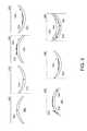
- FIGS. 7A-7Cillustrate example orientations of an anterior flexible conductive electrode (ANT) 705 and a posterior flexible conductive electrode (POST) 732 within an eye-mountable device 700 , in accordance with an embodiment.
- FIG. 7Aillustrates ANT 705 formed onto the concave surface of an anterior layer 705
- FIG. 7Billustrates POST 732 formed onto the convex surface of a posterior layer 710
- FIG. 7Cis a plan view illustration of a fully assembled eye-mountable device 700 .
- FIG. 8is a profile illustration of a portion of ring substrate 730 that forms electrical connections to a connection tab 760 of ANT 715 and a connection tab 765 of POST 732 , in accordance with an embodiment.
- ANT 715includes connection tab 760 for electrically connecting to anterior contact pad 745 disposed on the front side of ring substrate 730 .
- POST 732includes connection tab 765 for electrically connecting to posterior contact pad 750 disposed on the backside of ring substrate 730 .
- FIG. 8illustrates the use of conductive adhesive 785 to improve the electrically connections between connection tabs 760 and 765 and contact pads 745 and 750 , respectively.
- Conductive adhesive 785may be implemented using a variety of different materials, such as, silver loaded epoxies, silicon, or polyurethane, or otherwise.
- Conductive adhesive 785provides flexible, conductive adhesion that maintains electrical connection when the smart contact lens is bent or folded despite the different flexibility characteristics of the various constituent parts of eye-mountable device 700 .
- connection tabs 760 and 765are rotationally offset relative to each other to make room for a through-substrate via for one or both of contact pads 745 , 765 .
- power supply 735 and controller circuit 740are disposed on the front side of ring substrate 730 , thus posterior contact pad 750 is connected to controller circuit 740 using a through substrate via.
- FIG. 7Cfurther illustrates the contour 712 of a LC layer between ANT 715 and POST 732 .
- the LC layermay separate ANT 715 and POST 732 from one another, and may be actuated by voltages applied across these electrodes by controller circuit 740 .
- the LC layerextends across a larger portion of the center region to ensure that ANT 715 and POST 732 do not short circuit to each other.
- transparent insulating layerse.g., polyimide
- ANT 715 and POST 732may form direct contact with the LC layer.
- Both LC layer 720 and respective portions of ANT 715 and POST 732may be contained within the inner radius of ring substrate 730 and may not contact the inner edge of ring substrate 730 .
- ANT 715 and POST 732have a diameter of approximately 6 mm
- LC layer 725has a diameter of approximately 7 mm
- the inner edge of ring substrate 730which defines the center region, has a diameter of 9 mm.
- Anterior layer 705 and posterior layer 710may come in contact with one another to form a pinch-off region 720 between diameter of contour 712 and a larger diameter of the inner edge of ring substrate 730 .
- Pinch-off region 720may variously prevent shorting of the liquid crystal layer, ANT 715 and/or POST 732 to at least some circuitry of ring substrate 730 .
- This apparatusmay be specially constructed for the required purposes, or it may comprise a general purpose computer selectively activated or reconfigured by a computer program stored in the computer.
- a computer programmay be stored in a computer readable storage medium, such as, but is not limited to, any type of disk including floppy disks, optical disks, CD-ROMs, and magnetic-optical disks, read-only memories (ROMs), random access memories (RAMs) such as dynamic RAM (DRAM), EPROMs, EEPROMs, magnetic or optical cards, or any type of media suitable for storing electronic instructions, and coupled to a computer system bus.
Landscapes
- Health & Medical Sciences (AREA)
- Ophthalmology & Optometry (AREA)
- Physics & Mathematics (AREA)
- Engineering & Computer Science (AREA)
- General Physics & Mathematics (AREA)
- Optics & Photonics (AREA)
- General Health & Medical Sciences (AREA)
- Mechanical Engineering (AREA)
- Manufacturing & Machinery (AREA)
- Microelectronics & Electronic Packaging (AREA)
- Liquid Crystal (AREA)
- Prostheses (AREA)
- Eyeglasses (AREA)
Abstract
Description
Claims (26)
Priority Applications (10)
| Application Number | Priority Date | Filing Date | Title |
|---|---|---|---|
| US14/710,332US9690118B2 (en) | 2014-06-13 | 2015-05-12 | Eye-mountable device to provide automatic accommodation and method of making same |
| AU2015275156AAU2015275156B2 (en) | 2014-06-13 | 2015-05-18 | Eye-mountable device to provide automatic accommodation and method of making same |
| CA2950560ACA2950560C (en) | 2014-06-13 | 2015-05-18 | Eye-mountable device to provide automatic accommodation and method of making same |
| JP2016567497AJP6395861B2 (en) | 2014-06-13 | 2015-05-18 | Eye-mountable device for automatic perspective adjustment and method for manufacturing the same |
| PCT/US2015/031415WO2015191247A1 (en) | 2014-06-13 | 2015-05-18 | Eye-mountable device to provide automatic accommodation and method of making same |
| CN201580031769.2ACN106461973B (en) | 2014-06-13 | 2015-05-18 | Eye-mountable device providing self-adjustment and method of making the same |
| EP15807226.4AEP3155477B1 (en) | 2014-06-13 | 2015-05-18 | Eye-mountable device to provide automatic accommodation and method of making same |
| US15/631,815US10268051B2 (en) | 2014-06-13 | 2017-06-23 | Eye-mountable device to provide automatic accommodation and method of making same |
| AU2018202379AAU2018202379B2 (en) | 2014-06-13 | 2018-04-04 | Eye-mountable device to provide automatic accommodation and method of making same |
| US16/375,539US11199727B2 (en) | 2014-06-13 | 2019-04-04 | Eye-mountable device to provide automatic accommodation and method of making same |
Applications Claiming Priority (4)
| Application Number | Priority Date | Filing Date | Title |
|---|---|---|---|
| US201462012033P | 2014-06-13 | 2014-06-13 | |
| US201462012017P | 2014-06-13 | 2014-06-13 | |
| US201462012005P | 2014-06-13 | 2014-06-13 | |
| US14/710,332US9690118B2 (en) | 2014-06-13 | 2015-05-12 | Eye-mountable device to provide automatic accommodation and method of making same |
Related Child Applications (1)
| Application Number | Title | Priority Date | Filing Date |
|---|---|---|---|
| US15/631,815ContinuationUS10268051B2 (en) | 2014-06-13 | 2017-06-23 | Eye-mountable device to provide automatic accommodation and method of making same |
Publications (2)
| Publication Number | Publication Date |
|---|---|
| US20150362754A1 US20150362754A1 (en) | 2015-12-17 |
| US9690118B2true US9690118B2 (en) | 2017-06-27 |
Family
ID=54834093
Family Applications (3)
| Application Number | Title | Priority Date | Filing Date |
|---|---|---|---|
| US14/710,332ActiveUS9690118B2 (en) | 2014-06-13 | 2015-05-12 | Eye-mountable device to provide automatic accommodation and method of making same |
| US15/631,815ActiveUS10268051B2 (en) | 2014-06-13 | 2017-06-23 | Eye-mountable device to provide automatic accommodation and method of making same |
| US16/375,539Active2036-03-12US11199727B2 (en) | 2014-06-13 | 2019-04-04 | Eye-mountable device to provide automatic accommodation and method of making same |
Family Applications After (2)
| Application Number | Title | Priority Date | Filing Date |
|---|---|---|---|
| US15/631,815ActiveUS10268051B2 (en) | 2014-06-13 | 2017-06-23 | Eye-mountable device to provide automatic accommodation and method of making same |
| US16/375,539Active2036-03-12US11199727B2 (en) | 2014-06-13 | 2019-04-04 | Eye-mountable device to provide automatic accommodation and method of making same |
Country Status (7)
| Country | Link |
|---|---|
| US (3) | US9690118B2 (en) |
| EP (1) | EP3155477B1 (en) |
| JP (1) | JP6395861B2 (en) |
| CN (1) | CN106461973B (en) |
| AU (2) | AU2015275156B2 (en) |
| CA (1) | CA2950560C (en) |
| WO (1) | WO2015191247A1 (en) |
Cited By (6)
| Publication number | Priority date | Publication date | Assignee | Title |
|---|---|---|---|---|
| US20170293161A1 (en)* | 2014-06-13 | 2017-10-12 | Verily Life Sciences Llc | Eye-mountable device to provide automatic accommodation and method of making same |
| WO2019055081A1 (en)* | 2017-09-18 | 2019-03-21 | E-Vision Smart Optics, Inc. | Electro-active lens with resistive arcs |
| US10416477B2 (en) | 2014-06-13 | 2019-09-17 | Verily Life Sciences Llc | Ophthalmic system having adjustable accommodation based on photodetection |
| US10670887B2 (en) | 2014-06-13 | 2020-06-02 | Verily Life Sciences Llc | Flexible conductor for use within a contact lens |
| US11061254B2 (en) | 2019-01-24 | 2021-07-13 | International Business Machines Corporation | Adjusting contact lens prescription while wearing lens |
| US11099406B2 (en) | 2019-01-24 | 2021-08-24 | International Business Machines Corporation | Delivering augmented reality via embedded contact lens |
Families Citing this family (38)
| Publication number | Priority date | Publication date | Assignee | Title |
|---|---|---|---|---|
| US9696564B1 (en) | 2012-08-21 | 2017-07-04 | Verily Life Sciences Llc | Contact lens with metal portion and polymer layer having indentations |
| US9459469B2 (en)* | 2014-03-25 | 2016-10-04 | David T. Markus | System for contact lens wireless communication |
| USD754861S1 (en)* | 2014-10-07 | 2016-04-26 | Verily Life Sciences Llc | Contact lens antenna |
| US10216008B2 (en) | 2015-12-31 | 2019-02-26 | International Business Machines Corporation | Saccade and vergence tracking for distance auto focus adjustment |
| US10162194B2 (en) | 2016-03-01 | 2018-12-25 | Verily Life Sciences Llc | Eye mountable device and flexible assembly for fabrication thereof |
| US10488677B2 (en) | 2016-03-03 | 2019-11-26 | Verily Life Sciences Llc | Electronics embedded in rigid gas permeable contact lenses |
| US9939658B1 (en)* | 2016-05-02 | 2018-04-10 | Verily Life Sciences Llc | Autonomous eye tracking contact lens |
| JP2019518546A (en) | 2016-05-31 | 2019-07-04 | キュラ, インク.Qura, Inc. | Implantable intraocular pressure sensor and method of use |
| US10365504B2 (en) | 2016-09-23 | 2019-07-30 | Verily Life Sciences Llc | Rigid, gas-permeable polymer as over-mold and sealant for adaptive ophthalmic lens |
| US11035983B2 (en)* | 2016-09-26 | 2021-06-15 | Verily Life Sciences Llc | Cast-moldable, high refractive index, rigid, gas permeable polymer formulations for an accommodating contact lens |
| WO2018075229A1 (en) | 2016-10-03 | 2018-04-26 | California Institute Of Technology | Radioluminescent phototherapy eye device |
| US10509238B2 (en)* | 2017-04-14 | 2019-12-17 | Verily Life Sciences Llc | Electrowetting opthalmic optics including gas-permeable components |
| US12205231B2 (en) | 2017-07-03 | 2025-01-21 | Holovisions | Holovisions™—adjustable and/or modular augmented reality (AR) eyewear with a movable transflective mirror and different viewing modes |
| US12013538B2 (en) | 2017-07-03 | 2024-06-18 | Holovisions LLC | Augmented reality (AR) eyewear with a section of a fresnel reflector comprising individually-adjustable transmissive-reflective optical elements |
| US11307420B2 (en) | 2017-07-03 | 2022-04-19 | Holovisions LLC | Augmented reality eyewear with “ghost buster” technology |
| US12436394B2 (en) | 2017-07-03 | 2025-10-07 | Holovisions | Augmented reality (or mixed reality) eyewear with see-through optical elements having individually-adjustable opacity/reflectivity levels |
| US11754843B2 (en) | 2017-07-03 | 2023-09-12 | Holovisions LLC | Augmented reality eyewear with “ghost buster” technology |
| US11163163B2 (en) | 2017-07-03 | 2021-11-02 | Holovisions | Augmented reality (AR) eyewear with at least one quasi Fresnel reflector (QFR) |
| US10859868B2 (en) | 2017-08-11 | 2020-12-08 | Coopervision International Limited | Flexible liquid crystal cells and lenses |
| US10827924B2 (en)* | 2017-08-14 | 2020-11-10 | Verily Life Sciences Llc | Dynamic illumination during retinal burst imaging |
| US11857260B2 (en) | 2017-09-21 | 2024-01-02 | Verily Life Sciences Llc | Retinal cameras having movable optical stops |
| US11143885B2 (en)* | 2017-09-25 | 2021-10-12 | Verily Life Sciences Llc | Smart contact lens with antenna and sensor |
| US20190094417A1 (en)* | 2017-09-26 | 2019-03-28 | Verily Life Sciences Llc | Ophthalmic devices including polydopamine layers and methods of depositing a metal layer on ophthalmic devices including a polydopamine layer |
| US11520168B2 (en)* | 2017-12-22 | 2022-12-06 | Sony Corporation | Contact lens and communication system |
| WO2019152526A1 (en) | 2018-01-31 | 2019-08-08 | California Institute Of Technology | Controllable ocular phototherapy |
| US10892643B2 (en) | 2018-03-14 | 2021-01-12 | International Business Machines Corporation | Facilitation of charge of and communication with an electronic device |
| US20190350699A1 (en)* | 2018-05-16 | 2019-11-21 | Quantum Medical Innovations, LLC | Thermoelectrically-powered device for therapeutic presbyopia vision correction |
| KR102564435B1 (en)* | 2018-07-31 | 2023-08-08 | 엘지이노텍 주식회사 | Contact lenses module for presbyopia |
| US11003016B2 (en)* | 2018-09-21 | 2021-05-11 | Coopervision International Limited | Flexible, adjustable lens power liquid crystal cells and lenses |
| US11703697B2 (en)* | 2018-12-21 | 2023-07-18 | Verily Life Sciences Llc | Fluid-containing contact lens with soft posterior element |
| CN109633910B (en)* | 2019-01-14 | 2021-11-05 | 京东方科技集团股份有限公司 | AR/VR contact lens, method for making the same, and electronic device |
| CN109856815A (en)* | 2019-04-12 | 2019-06-07 | 京东方科技集团股份有限公司 | Contact lenses, its manufacturing method and monitoring device |
| WO2021079093A1 (en)* | 2019-10-25 | 2021-04-29 | Coopervision International Limited | Tuneable ophthalmic lens |
| EP4217186A1 (en)* | 2020-10-13 | 2023-08-02 | CooperVision International Limited | Contact lens membrane and related methods |
| IL286933B2 (en)* | 2021-10-03 | 2023-08-01 | Tadbik Advanced Tech Ltd | A multi-functional tag for throughout the plant life cycle |
| CN114545634A (en)* | 2022-02-24 | 2022-05-27 | 北京京东方技术开发有限公司 | Intelligent glasses |
| CN117215087A (en)* | 2022-06-12 | 2023-12-12 | 晶硕光学股份有限公司 | Contact lens |
| WO2025069148A1 (en)* | 2023-09-25 | 2025-04-03 | 株式会社メニコン | Ophthalmic device |
Citations (35)
| Publication number | Priority date | Publication date | Assignee | Title |
|---|---|---|---|---|
| US20050073739A1 (en) | 2001-10-05 | 2005-04-07 | Gerald Meredith | Hybrid electro-active lens |
| US7018040B2 (en) | 1999-07-02 | 2006-03-28 | E-Vision, Llc | Stabilized electro-active contact lens |
| US20070153405A1 (en)* | 2004-03-05 | 2007-07-05 | Koninklijke Philips Electronics, N.V. | Variable focus lens |
| US20070242173A1 (en) | 2004-11-02 | 2007-10-18 | Blum Ronald D | Electro-active spectacles and method of fabricating same |
| US20080208335A1 (en) | 2007-01-22 | 2008-08-28 | Blum Ronald D | Flexible electro-active lens |
| WO2009048647A1 (en) | 2007-10-11 | 2009-04-16 | Pixeloptics Inc. | Alignment of liquid crystalline materials to surface relief diffractive structures |
| US20090256977A1 (en) | 2008-04-11 | 2009-10-15 | Pixeloptics Inc. | Electro-active diffractive lens and method for making the same |
| US20120075712A1 (en) | 2010-05-14 | 2012-03-29 | Pugh Randall B | Liquid meniscus lens including variable voltage zones |
| US8154804B2 (en) | 2008-03-25 | 2012-04-10 | E-Vision Smart Optics, Inc. | Electro-optic lenses for correction of higher order aberrations |
| US20120140167A1 (en) | 2010-11-01 | 2012-06-07 | Pixeloptics, Inc. | Dynamic Changeable Focus Contact And Intraocular Lens |
| US20120236417A1 (en)* | 2011-03-18 | 2012-09-20 | Pugh Randall B | Lens with multi-concave meniscus wall |
| US20120245444A1 (en) | 2007-11-07 | 2012-09-27 | University Of Washington | Wireless powered contact lens with glucose sensor |
| US20120268712A1 (en) | 2010-10-11 | 2012-10-25 | William Egan | Fluid Filled Adjustable Contact Lenses |
| EP2518555A1 (en) | 2003-12-19 | 2012-10-31 | Michel Guillon | Variable focus contact lenses manufactured from a responsive polymer gel |
| WO2013086078A1 (en) | 2011-12-06 | 2013-06-13 | E-Vision Smart Optics, Inc. | Systems, devices, and/or methods for providing images |
| US20130218270A1 (en) | 2010-07-12 | 2013-08-22 | Katholieke Universiteit Leuven | Bionic eye lens |
| US20130245754A1 (en) | 2010-11-15 | 2013-09-19 | Elenza Inc. | Adaptive intraocular lens |
| US20130258277A1 (en) | 2012-03-30 | 2013-10-03 | Johnson & Johnson Vision Care, Inc. | Method and apparatus for a variable power ophthalmic lens |
| US20130258275A1 (en) | 2012-04-03 | 2013-10-03 | Johnson & Johnson | Lens driver for variable-optic electronic ophthalmic lens |
| US20130338767A1 (en) | 2010-12-29 | 2013-12-19 | Elenza Inc. | Devices and methods for dynamic focusing movement |
| US8634145B2 (en) | 2010-07-29 | 2014-01-21 | Johnson & Johnson Vision Care, Inc. | Liquid meniscus lens with concave torus-segment meniscus wall |
| US8636358B2 (en) | 2009-05-17 | 2014-01-28 | Helmut Binder | Lens with variable refraction power for the human eye |
| US20140098226A1 (en) | 2012-10-08 | 2014-04-10 | Google Inc. | Image capture component on active contact lens |
| US20140107447A1 (en) | 2012-10-12 | 2014-04-17 | Google Inc. | In-vitro Calibration Of An Ophthalmic Analyte Sensor |
| US20140192312A1 (en) | 2012-07-26 | 2014-07-10 | Google Inc. | Facilitation of contact lenses with capacitive sensors |
| US20140192311A1 (en) | 2012-07-26 | 2014-07-10 | Google Inc. | Contact lenses with hybrid power sources |
| US20140192318A1 (en) | 2013-01-10 | 2014-07-10 | Karlsruher Institut Fuer Technologie | Sensor system for determining the control signals activating ciliary muscles |
| US20140192313A1 (en) | 2013-01-09 | 2014-07-10 | Johnson & Johnson Vision Care, Inc. | Multi-piece insert device with glue seal for ophthalmic devices |
| US20140213867A1 (en) | 2013-01-25 | 2014-07-31 | Google Inc. | Standby Biasing Of Electrochemical Sensor To Reduce Sensor Stabilization Time During Measurement |
| US20140243971A1 (en) | 2013-02-28 | 2014-08-28 | Johnson & Johnson Vision Care, Inc. | Electronic ophthalmic lens with eye gaze sensor |
| US20140240655A1 (en) | 2013-02-28 | 2014-08-28 | Johnson & Johnson Vision Care, Inc. | Electronic ophthalmic lens with lid position sensor |
| US8827446B2 (en) | 2011-03-10 | 2014-09-09 | Hpo Assets Llc | Electronic lens comprised of hybrid materials |
| US20140276481A1 (en)* | 2013-03-15 | 2014-09-18 | Johnson & Johnson Vision Care, Inc. | Sealing and encapsulation in energized ophthalmic devices with annular inserts |
| US20140327875A1 (en) | 2011-03-08 | 2014-11-06 | Ronald Blum | Advanced electro-active optic device |
| WO2015015205A1 (en) | 2013-08-01 | 2015-02-05 | The University Of Manchester | Liquid crystal device and method of manufacture |
Family Cites Families (29)
| Publication number | Priority date | Publication date | Assignee | Title |
|---|---|---|---|---|
| EP0693188B1 (en)* | 1993-04-07 | 1999-10-27 | Ttp Group Plc | Switchable lens |
| JPH11352445A (en) | 1998-06-09 | 1999-12-24 | Olympus Optical Co Ltd | Variable focus spectacles |
| BR0213012A (en)* | 2001-10-05 | 2004-12-28 | E Vision Llc | Hybrid Electroactive Lenses |
| FR2833477B1 (en) | 2002-07-02 | 2004-02-13 | Francois Michel | IMPLANT PSEUDO-ACCOMODATIVE OPTICAL EQUIPMENT FOR PRESBYTIA CORRECTION |
| AU2003263881A1 (en) | 2002-08-09 | 2004-02-25 | E-Vision, Llc | Electro-active contact lens system |
| US7334894B2 (en) | 2004-12-03 | 2008-02-26 | Searete, Llc | Temporal vision modification |
| TW200815817A (en) | 2006-09-11 | 2008-04-01 | Alphamicron Inc | Interconnection tab used with optical devices |
| AR064986A1 (en) | 2007-01-22 | 2009-05-06 | Pixeloptics Inc | CHOLESTERIC LIQUID CRYSTAL MATERIAL IN ELECTROACTIVE LENS |
| EP2115519A4 (en)* | 2007-02-23 | 2012-12-05 | Pixeloptics Inc | DYNAMIC OPHTHALMIC OPENING |
| WO2009037832A1 (en) | 2007-09-19 | 2009-03-26 | National University Corporation Tohoku University | Flexible transparent electroconductive film |
| WO2009094587A1 (en) | 2008-01-23 | 2009-07-30 | Deering Michael F | Eye mounted displays |
| JP2011515157A (en)* | 2008-03-18 | 2011-05-19 | ピクセルオプティクス, インコーポレイテッド | Advanced electroactive optical component devices |
| US20100076553A1 (en)* | 2008-09-22 | 2010-03-25 | Pugh Randall B | Energized ophthalmic lens |
| WO2010151244A1 (en) | 2009-06-22 | 2010-12-29 | Hewlett-Packard Development Company, L.P. | Transparent conductive material |
| JP5490918B2 (en)* | 2009-12-04 | 2014-05-14 | パロット | Electronically controlled focusing ophthalmic device |
| US9977293B2 (en) | 2010-01-29 | 2018-05-22 | Citizen Watch Co., Ltd. | Electronic eyeglass and liquid crystal lens production methods |
| US8638502B2 (en)* | 2010-09-29 | 2014-01-28 | Johnson & Johnson Vision Care, Inc. | Liquid meniscus lens with non-spherical meniscus wall |
| US8466366B2 (en) | 2011-06-28 | 2013-06-18 | Innova Dynamics, Inc. | Transparent conductors incorporating additives and related manufacturing methods |
| RU2629550C2 (en)* | 2011-12-23 | 2017-08-29 | Джонсон Энд Джонсон Вижн Кэа, Инк. | Changed optical ophthalmological device containing liquid crystalline elements |
| US9004683B2 (en) | 2011-12-29 | 2015-04-14 | Elwha Llc | Optical device with active user-based aberration correction |
| US8857983B2 (en)* | 2012-01-26 | 2014-10-14 | Johnson & Johnson Vision Care, Inc. | Ophthalmic lens assembly having an integrated antenna structure |
| US9241669B2 (en) | 2012-07-18 | 2016-01-26 | Johnson & Johnson Vision Care, Inc. | Neuromuscular sensing for variable-optic electronic ophthalmic lens |
| WO2014084958A1 (en) | 2012-11-30 | 2014-06-05 | Novartis Ag | Sensors for triggering electro-active ophthalmic lenses |
| US8874182B2 (en)* | 2013-01-15 | 2014-10-28 | Google Inc. | Encapsulated electronics |
| US20140232982A1 (en)* | 2013-02-20 | 2014-08-21 | Benjamin T. Iwai | Dynamic multifocal contact lens dual layer with core |
| US9541772B2 (en)* | 2013-09-17 | 2017-01-10 | Johnson & Johnson Vision Care, Inc. | Methods and apparatus for ophthalmic devices including cycloidally oriented liquid crystal layers |
| US9617578B2 (en)* | 2013-12-06 | 2017-04-11 | Verily Life Sciences Llc | Sensor membrane with low temperature coefficient |
| US9690118B2 (en)* | 2014-06-13 | 2017-06-27 | Verily Life Sciences Llc | Eye-mountable device to provide automatic accommodation and method of making same |
| US9907498B2 (en)* | 2014-09-04 | 2018-03-06 | Verily Life Sciences Llc | Channel formation |
- 2015
- 2015-05-12USUS14/710,332patent/US9690118B2/enactiveActive
- 2015-05-18CNCN201580031769.2Apatent/CN106461973B/enactiveActive
- 2015-05-18CACA2950560Apatent/CA2950560C/enactiveActive
- 2015-05-18WOPCT/US2015/031415patent/WO2015191247A1/enactiveApplication Filing
- 2015-05-18AUAU2015275156Apatent/AU2015275156B2/enactiveActive
- 2015-05-18EPEP15807226.4Apatent/EP3155477B1/enactiveActive
- 2015-05-18JPJP2016567497Apatent/JP6395861B2/enactiveActive
- 2017
- 2017-06-23USUS15/631,815patent/US10268051B2/enactiveActive
- 2018
- 2018-04-04AUAU2018202379Apatent/AU2018202379B2/enactiveActive
- 2019
- 2019-04-04USUS16/375,539patent/US11199727B2/enactiveActive
Patent Citations (39)
| Publication number | Priority date | Publication date | Assignee | Title |
|---|---|---|---|---|
| US7018040B2 (en) | 1999-07-02 | 2006-03-28 | E-Vision, Llc | Stabilized electro-active contact lens |
| US20050073739A1 (en) | 2001-10-05 | 2005-04-07 | Gerald Meredith | Hybrid electro-active lens |
| EP2518555A1 (en) | 2003-12-19 | 2012-10-31 | Michel Guillon | Variable focus contact lenses manufactured from a responsive polymer gel |
| US20070153405A1 (en)* | 2004-03-05 | 2007-07-05 | Koninklijke Philips Electronics, N.V. | Variable focus lens |
| US7311398B2 (en) | 2004-03-05 | 2007-12-25 | Koninklijke Philips Electronics N.V. | Variable focus lens |
| US20070242173A1 (en) | 2004-11-02 | 2007-10-18 | Blum Ronald D | Electro-active spectacles and method of fabricating same |
| US20080208335A1 (en) | 2007-01-22 | 2008-08-28 | Blum Ronald D | Flexible electro-active lens |
| WO2009048647A1 (en) | 2007-10-11 | 2009-04-16 | Pixeloptics Inc. | Alignment of liquid crystalline materials to surface relief diffractive structures |
| US20120245444A1 (en) | 2007-11-07 | 2012-09-27 | University Of Washington | Wireless powered contact lens with glucose sensor |
| US8154804B2 (en) | 2008-03-25 | 2012-04-10 | E-Vision Smart Optics, Inc. | Electro-optic lenses for correction of higher order aberrations |
| US20090256977A1 (en) | 2008-04-11 | 2009-10-15 | Pixeloptics Inc. | Electro-active diffractive lens and method for making the same |
| US8636358B2 (en) | 2009-05-17 | 2014-01-28 | Helmut Binder | Lens with variable refraction power for the human eye |
| US20120075712A1 (en) | 2010-05-14 | 2012-03-29 | Pugh Randall B | Liquid meniscus lens including variable voltage zones |
| US20130218270A1 (en) | 2010-07-12 | 2013-08-22 | Katholieke Universiteit Leuven | Bionic eye lens |
| US8634145B2 (en) | 2010-07-29 | 2014-01-21 | Johnson & Johnson Vision Care, Inc. | Liquid meniscus lens with concave torus-segment meniscus wall |
| US20120268712A1 (en) | 2010-10-11 | 2012-10-25 | William Egan | Fluid Filled Adjustable Contact Lenses |
| US20120140167A1 (en) | 2010-11-01 | 2012-06-07 | Pixeloptics, Inc. | Dynamic Changeable Focus Contact And Intraocular Lens |
| US20130245754A1 (en) | 2010-11-15 | 2013-09-19 | Elenza Inc. | Adaptive intraocular lens |
| US20130338767A1 (en) | 2010-12-29 | 2013-12-19 | Elenza Inc. | Devices and methods for dynamic focusing movement |
| US20140327875A1 (en) | 2011-03-08 | 2014-11-06 | Ronald Blum | Advanced electro-active optic device |
| US8827446B2 (en) | 2011-03-10 | 2014-09-09 | Hpo Assets Llc | Electronic lens comprised of hybrid materials |
| US20120236417A1 (en)* | 2011-03-18 | 2012-09-20 | Pugh Randall B | Lens with multi-concave meniscus wall |
| WO2013086078A1 (en) | 2011-12-06 | 2013-06-13 | E-Vision Smart Optics, Inc. | Systems, devices, and/or methods for providing images |
| US20130258277A1 (en) | 2012-03-30 | 2013-10-03 | Johnson & Johnson Vision Care, Inc. | Method and apparatus for a variable power ophthalmic lens |
| US20130258275A1 (en) | 2012-04-03 | 2013-10-03 | Johnson & Johnson | Lens driver for variable-optic electronic ophthalmic lens |
| US20140192312A1 (en) | 2012-07-26 | 2014-07-10 | Google Inc. | Facilitation of contact lenses with capacitive sensors |
| US20140194773A1 (en) | 2012-07-26 | 2014-07-10 | Google Inc. | Facilitation of contact lenses with capacitive sensors |
| US20140192311A1 (en) | 2012-07-26 | 2014-07-10 | Google Inc. | Contact lenses with hybrid power sources |
| US20140098226A1 (en) | 2012-10-08 | 2014-04-10 | Google Inc. | Image capture component on active contact lens |
| US20140107448A1 (en) | 2012-10-12 | 2014-04-17 | Google Inc. | In-vitro Calibration Of An Ophthalmic Analyte Sensor |
| US20140107447A1 (en) | 2012-10-12 | 2014-04-17 | Google Inc. | In-vitro Calibration Of An Ophthalmic Analyte Sensor |
| US20140192313A1 (en) | 2013-01-09 | 2014-07-10 | Johnson & Johnson Vision Care, Inc. | Multi-piece insert device with glue seal for ophthalmic devices |
| US20140192318A1 (en) | 2013-01-10 | 2014-07-10 | Karlsruher Institut Fuer Technologie | Sensor system for determining the control signals activating ciliary muscles |
| US20140209481A1 (en) | 2013-01-25 | 2014-07-31 | Google Inc. | Standby Biasing Of Electrochemical Sensor To Reduce Sensor Stabilization Time During Measurement |
| US20140213867A1 (en) | 2013-01-25 | 2014-07-31 | Google Inc. | Standby Biasing Of Electrochemical Sensor To Reduce Sensor Stabilization Time During Measurement |
| US20140243971A1 (en) | 2013-02-28 | 2014-08-28 | Johnson & Johnson Vision Care, Inc. | Electronic ophthalmic lens with eye gaze sensor |
| US20140240655A1 (en) | 2013-02-28 | 2014-08-28 | Johnson & Johnson Vision Care, Inc. | Electronic ophthalmic lens with lid position sensor |
| US20140276481A1 (en)* | 2013-03-15 | 2014-09-18 | Johnson & Johnson Vision Care, Inc. | Sealing and encapsulation in energized ophthalmic devices with annular inserts |
| WO2015015205A1 (en) | 2013-08-01 | 2015-02-05 | The University Of Manchester | Liquid crystal device and method of manufacture |
Non-Patent Citations (9)
| Title |
|---|
| De Smet, J. et al., "A Liquid Crystal Based Contact Lens Display Using PEDOT: PSS and Obliquely Evaporated SiO2", Late-News Poster, SID 2012 Digest, pp. 1375-1378. |
| De Smet, J. et al., "Progress toward a liquid crystal contact lens display", Journal of the SID 21/9, DOI: 10.1002/jsid.188, 2014 pp. 399-406. |
| Milton, H. et al., "Electronic liquid crystal contact lenses for the correction of presbyopia", Apr. 2014, vol. 22, No. 7, DOI:10.1364/OE.22.008035, Optics Express, pp. 8035-8040. |
| Milton, H. et al., "Optimization of refractive liquid crystal lenses using an efficient multigrid simulation", May 2012, vol. 20, No. 10, Optics Express, pp. 11159-11165. |
| Milton, H. et al., "Switchable liquid crystal contact lenses: dynamic vision for the ageing eye", Proc. of SPIE vol. 9004 90040H, 6 pages. Downloaded From: http://spiedigitallibrary.org/ on Mar. 28, 2014. |
| PCT/US2015/031415-International Search Report and Written Opinion, mailed Aug. 28, 2015, 24 pages. |
| PCT/US2015/031415—International Search Report and Written Opinion, mailed Aug. 28, 2015, 24 pages. |
| Tremblay, E. et al. "Switchable telescopic contact lens", Jul. 2013, vol. 21, No. 13, DOI:10.1364/OE.21.015980, Optics Express, pp. 15980-15986. |
| Yeager, Daniel J. et al., "A Contact Lens With Capacitive Gaze Tracking", U.S. Appl. No. 14/587,664, filed Dec. 31, 2014, 41 pages. |
Cited By (10)
| Publication number | Priority date | Publication date | Assignee | Title |
|---|---|---|---|---|
| US20170293161A1 (en)* | 2014-06-13 | 2017-10-12 | Verily Life Sciences Llc | Eye-mountable device to provide automatic accommodation and method of making same |
| US10268051B2 (en)* | 2014-06-13 | 2019-04-23 | Verily Life Sciences Llc | Eye-mountable device to provide automatic accommodation and method of making same |
| US10416477B2 (en) | 2014-06-13 | 2019-09-17 | Verily Life Sciences Llc | Ophthalmic system having adjustable accommodation based on photodetection |
| US10670887B2 (en) | 2014-06-13 | 2020-06-02 | Verily Life Sciences Llc | Flexible conductor for use within a contact lens |
| US11199727B2 (en)* | 2014-06-13 | 2021-12-14 | Verily Life Sciences Llc | Eye-mountable device to provide automatic accommodation and method of making same |
| WO2019055081A1 (en)* | 2017-09-18 | 2019-03-21 | E-Vision Smart Optics, Inc. | Electro-active lens with resistive arcs |
| US10551690B2 (en) | 2017-09-18 | 2020-02-04 | E-Vision Smart Optics, Inc. | Electro-active lens with resistive arcs |
| EP3496659A4 (en)* | 2017-09-18 | 2020-07-15 | E-Vision Smart Optics, Inc. | ELECTROACTIVE LENSES WITH RESISTIVE ARCHES |
| US11061254B2 (en) | 2019-01-24 | 2021-07-13 | International Business Machines Corporation | Adjusting contact lens prescription while wearing lens |
| US11099406B2 (en) | 2019-01-24 | 2021-08-24 | International Business Machines Corporation | Delivering augmented reality via embedded contact lens |
Also Published As
| Publication number | Publication date |
|---|---|
| CN106461973B (en) | 2021-08-17 |
| US20150362754A1 (en) | 2015-12-17 |
| AU2015275156A1 (en) | 2017-01-12 |
| WO2015191247A1 (en) | 2015-12-17 |
| CA2950560C (en) | 2021-07-20 |
| AU2015275156B2 (en) | 2018-02-01 |
| EP3155477B1 (en) | 2021-07-07 |
| US11199727B2 (en) | 2021-12-14 |
| AU2018202379A1 (en) | 2018-04-26 |
| US10268051B2 (en) | 2019-04-23 |
| AU2018202379B2 (en) | 2019-03-14 |
| US20170293161A1 (en) | 2017-10-12 |
| JP2017520783A (en) | 2017-07-27 |
| EP3155477A1 (en) | 2017-04-19 |
| US20190235281A1 (en) | 2019-08-01 |
| CA2950560A1 (en) | 2015-12-17 |
| EP3155477A4 (en) | 2018-01-03 |
| JP6395861B2 (en) | 2018-09-26 |
| CN106461973A (en) | 2017-02-22 |
Similar Documents
| Publication | Publication Date | Title |
|---|---|---|
| US11199727B2 (en) | Eye-mountable device to provide automatic accommodation and method of making same | |
| US10670887B2 (en) | Flexible conductor for use within a contact lens | |
| US10678068B2 (en) | Electrochromic contact lens | |
| US11703697B2 (en) | Fluid-containing contact lens with soft posterior element | |
| EP3423890B1 (en) | Eye mountable device and flexible assembly for fabrication thereof |
Legal Events
| Date | Code | Title | Description |
|---|---|---|---|
| AS | Assignment | Owner name:GOOGLE INC., CALIFORNIA Free format text:ASSIGNMENT OF ASSIGNORS INTEREST;ASSIGNORS:ETZKORN, JAMES;LINHARDT, JEFFREY G.;OTIS, BRIAN;REEL/FRAME:035621/0607 Effective date:20150506 | |
| AS | Assignment | Owner name:GOOGLE LIFE SCIENCES LLC, CALIFORNIA Free format text:ASSIGNMENT OF ASSIGNORS INTEREST;ASSIGNOR:GOOGLE INC.;REEL/FRAME:037300/0151 Effective date:20150805 Owner name:VERILY LIFE SCIENCES LLC, CALIFORNIA Free format text:CHANGE OF NAME;ASSIGNOR:GOOGLE LIFE SCIENCES LLC;REEL/FRAME:037302/0027 Effective date:20151207 | |
| STCF | Information on status: patent grant | Free format text:PATENTED CASE | |
| AS | Assignment | Owner name:GOOGLE LLC, CALIFORNIA Free format text:CHANGE OF NAME;ASSIGNOR:GOOGLE INC.;REEL/FRAME:044144/0001 Effective date:20170929 | |
| AS | Assignment | Owner name:GOOGLE LLC, CALIFORNIA Free format text:CORRECTIVE ASSIGNMENT TO CORRECT THE CORRECTIVE BY NULLIFICATION TO CORRECT INCORRECTLY RECORDED APPLICATION NUMBERS PREVIOUSLY RECORDED ON REEL 044144 FRAME 0001. ASSIGNOR(S) HEREBY CONFIRMS THE CHANGE OF NAME;ASSIGNOR:GOOGLE INC.;REEL/FRAME:047894/0508 Effective date:20170929 | |
| MAFP | Maintenance fee payment | Free format text:PAYMENT OF MAINTENANCE FEE, 4TH YEAR, LARGE ENTITY (ORIGINAL EVENT CODE: M1551); ENTITY STATUS OF PATENT OWNER: LARGE ENTITY Year of fee payment:4 | |
| AS | Assignment | Owner name:TWENTY TWENTY THERAPEUTICS LLC, CALIFORNIA Free format text:ASSIGNMENT OF ASSIGNORS INTEREST;ASSIGNOR:VERILY LIFE SCIENCES LLC;REEL/FRAME:064163/0186 Effective date:20230606 | |
| AS | Assignment | Owner name:GOOGLE LLC, CALIFORNIA Free format text:CORRECTIVE ASSIGNMENT TO CORRECT THE THE REMOVAL OF THE INCORRECTLY RECORDED APPLICATION NUMBERS 14/149802 AND 15/419313 PREVIOUSLY RECORDED AT REEL: 44144 FRAME: 1. ASSIGNOR(S) HEREBY CONFIRMS THE CHANGE OF NAME;ASSIGNOR:GOOGLE INC.;REEL/FRAME:068092/0502 Effective date:20170929 | |
| AS | Assignment | Owner name:VERILY LIFE SCIENCES LLC, TEXAS Free format text:ASSIGNMENT OF ASSIGNORS INTEREST;ASSIGNOR:TWENTY TWENTY THERAPEUTICS LLC;REEL/FRAME:068846/0001 Effective date:20240807 | |
| MAFP | Maintenance fee payment | Free format text:PAYMENT OF MAINTENANCE FEE, 8TH YEAR, LARGE ENTITY (ORIGINAL EVENT CODE: M1552); ENTITY STATUS OF PATENT OWNER: LARGE ENTITY Year of fee payment:8 |