US9684234B2 - Sequential infiltration synthesis for enhancing multiple-patterning lithography - Google Patents
Sequential infiltration synthesis for enhancing multiple-patterning lithographyDownload PDFInfo
- Publication number
- US9684234B2 US9684234B2US13/902,169US201313902169AUS9684234B2US 9684234 B2US9684234 B2US 9684234B2US 201313902169 AUS201313902169 AUS 201313902169AUS 9684234 B2US9684234 B2US 9684234B2
- Authority
- US
- United States
- Prior art keywords
- resist layer
- sis
- pattern
- substrate
- resist
- Prior art date
- Legal status (The legal status is an assumption and is not a legal conclusion. Google has not performed a legal analysis and makes no representation as to the accuracy of the status listed.)
- Active
Links
Images


Classifications
- G—PHYSICS
- G03—PHOTOGRAPHY; CINEMATOGRAPHY; ANALOGOUS TECHNIQUES USING WAVES OTHER THAN OPTICAL WAVES; ELECTROGRAPHY; HOLOGRAPHY
- G03F—PHOTOMECHANICAL PRODUCTION OF TEXTURED OR PATTERNED SURFACES, e.g. FOR PRINTING, FOR PROCESSING OF SEMICONDUCTOR DEVICES; MATERIALS THEREFOR; ORIGINALS THEREFOR; APPARATUS SPECIALLY ADAPTED THEREFOR
- G03F7/00—Photomechanical, e.g. photolithographic, production of textured or patterned surfaces, e.g. printing surfaces; Materials therefor, e.g. comprising photoresists; Apparatus specially adapted therefor
- G03F7/0002—Lithographic processes using patterning methods other than those involving the exposure to radiation, e.g. by stamping
- G—PHYSICS
- G03—PHOTOGRAPHY; CINEMATOGRAPHY; ANALOGOUS TECHNIQUES USING WAVES OTHER THAN OPTICAL WAVES; ELECTROGRAPHY; HOLOGRAPHY
- G03F—PHOTOMECHANICAL PRODUCTION OF TEXTURED OR PATTERNED SURFACES, e.g. FOR PRINTING, FOR PROCESSING OF SEMICONDUCTOR DEVICES; MATERIALS THEREFOR; ORIGINALS THEREFOR; APPARATUS SPECIALLY ADAPTED THEREFOR
- G03F7/00—Photomechanical, e.g. photolithographic, production of textured or patterned surfaces, e.g. printing surfaces; Materials therefor, e.g. comprising photoresists; Apparatus specially adapted therefor
- G03F7/26—Processing photosensitive materials; Apparatus therefor
- G03F7/40—Treatment after imagewise removal, e.g. baking
- G03F7/405—Treatment with inorganic or organometallic reagents after imagewise removal
- H—ELECTRICITY
- H01—ELECTRIC ELEMENTS
- H01L—SEMICONDUCTOR DEVICES NOT COVERED BY CLASS H10
- H01L21/00—Processes or apparatus adapted for the manufacture or treatment of semiconductor or solid state devices or of parts thereof
- H01L21/02—Manufacture or treatment of semiconductor devices or of parts thereof
- H01L21/027—Making masks on semiconductor bodies for further photolithographic processing not provided for in group H01L21/18 or H01L21/34
- H01L21/0271—Making masks on semiconductor bodies for further photolithographic processing not provided for in group H01L21/18 or H01L21/34 comprising organic layers
- H01L21/0273—Making masks on semiconductor bodies for further photolithographic processing not provided for in group H01L21/18 or H01L21/34 comprising organic layers characterised by the treatment of photoresist layers
- H—ELECTRICITY
- H01—ELECTRIC ELEMENTS
- H01L—SEMICONDUCTOR DEVICES NOT COVERED BY CLASS H10
- H01L21/00—Processes or apparatus adapted for the manufacture or treatment of semiconductor or solid state devices or of parts thereof
- H01L21/02—Manufacture or treatment of semiconductor devices or of parts thereof
- H01L21/04—Manufacture or treatment of semiconductor devices or of parts thereof the devices having potential barriers, e.g. a PN junction, depletion layer or carrier concentration layer
- H01L21/18—Manufacture or treatment of semiconductor devices or of parts thereof the devices having potential barriers, e.g. a PN junction, depletion layer or carrier concentration layer the devices having semiconductor bodies comprising elements of Group IV of the Periodic Table or AIIIBV compounds with or without impurities, e.g. doping materials
- H01L21/30—Treatment of semiconductor bodies using processes or apparatus not provided for in groups H01L21/20 - H01L21/26
- H01L21/302—Treatment of semiconductor bodies using processes or apparatus not provided for in groups H01L21/20 - H01L21/26 to change their surface-physical characteristics or shape, e.g. etching, polishing, cutting
- H01L21/306—Chemical or electrical treatment, e.g. electrolytic etching
- H01L21/3065—Plasma etching; Reactive-ion etching
- H—ELECTRICITY
- H01—ELECTRIC ELEMENTS
- H01L—SEMICONDUCTOR DEVICES NOT COVERED BY CLASS H10
- H01L21/00—Processes or apparatus adapted for the manufacture or treatment of semiconductor or solid state devices or of parts thereof
- H01L21/02—Manufacture or treatment of semiconductor devices or of parts thereof
- H01L21/04—Manufacture or treatment of semiconductor devices or of parts thereof the devices having potential barriers, e.g. a PN junction, depletion layer or carrier concentration layer
- H01L21/18—Manufacture or treatment of semiconductor devices or of parts thereof the devices having potential barriers, e.g. a PN junction, depletion layer or carrier concentration layer the devices having semiconductor bodies comprising elements of Group IV of the Periodic Table or AIIIBV compounds with or without impurities, e.g. doping materials
- H01L21/30—Treatment of semiconductor bodies using processes or apparatus not provided for in groups H01L21/20 - H01L21/26
- H01L21/302—Treatment of semiconductor bodies using processes or apparatus not provided for in groups H01L21/20 - H01L21/26 to change their surface-physical characteristics or shape, e.g. etching, polishing, cutting
- H01L21/306—Chemical or electrical treatment, e.g. electrolytic etching
- H01L21/308—Chemical or electrical treatment, e.g. electrolytic etching using masks
- H01L21/3081—Chemical or electrical treatment, e.g. electrolytic etching using masks characterised by their composition, e.g. multilayer masks, materials
- H—ELECTRICITY
- H01—ELECTRIC ELEMENTS
- H01L—SEMICONDUCTOR DEVICES NOT COVERED BY CLASS H10
- H01L21/00—Processes or apparatus adapted for the manufacture or treatment of semiconductor or solid state devices or of parts thereof
- H01L21/02—Manufacture or treatment of semiconductor devices or of parts thereof
- H01L21/04—Manufacture or treatment of semiconductor devices or of parts thereof the devices having potential barriers, e.g. a PN junction, depletion layer or carrier concentration layer
- H01L21/18—Manufacture or treatment of semiconductor devices or of parts thereof the devices having potential barriers, e.g. a PN junction, depletion layer or carrier concentration layer the devices having semiconductor bodies comprising elements of Group IV of the Periodic Table or AIIIBV compounds with or without impurities, e.g. doping materials
- H01L21/30—Treatment of semiconductor bodies using processes or apparatus not provided for in groups H01L21/20 - H01L21/26
- H01L21/302—Treatment of semiconductor bodies using processes or apparatus not provided for in groups H01L21/20 - H01L21/26 to change their surface-physical characteristics or shape, e.g. etching, polishing, cutting
- H01L21/306—Chemical or electrical treatment, e.g. electrolytic etching
- H01L21/308—Chemical or electrical treatment, e.g. electrolytic etching using masks
- H01L21/3083—Chemical or electrical treatment, e.g. electrolytic etching using masks characterised by their size, orientation, disposition, behaviour, shape, in horizontal or vertical plane
- H01L21/3086—Chemical or electrical treatment, e.g. electrolytic etching using masks characterised by their size, orientation, disposition, behaviour, shape, in horizontal or vertical plane characterised by the process involved to create the mask, e.g. lift-off masks, sidewalls, or to modify the mask, e.g. pre-treatment, post-treatment
Definitions
- This inventionrelates to a method of photolithography. More specifically, this invention relates to novel multiple-patterning lithography methods in which one or more steps are replaced by sequential infiltration synthesis (SIS).
- SISsequential infiltration synthesis
- Photolithographyis a process used in the fabrication of integrated circuits, which entails using light to transfer a pattern from a “mask” to a “photoresist” on a substrate. A series of chemical treatments are then applied in order to etch a desired pattern into the substrate. Improvements in photolithography have advanced integrated circuit manufacturing over the last several decades. The most important advance is the gradual reduction of the wavelength of the illumination source of the photolithography tool: from the 436 nm line of a mercury lamp to the 193 nm light of an ArF laser. By incrementally improving the photolithography process, features as small as 45 nm can be manufactured in high volume using 193 nm photolithography.
- Immersion 193 nm photolithographyis presently deployed for the manufacturing of even more advanced technology nodes.
- several technologieshave been considered, such as extreme ultraviolet lithography (EUVL).
- EUVLextreme ultraviolet lithography
- multiple-patterningachieves a fine feature size at a significant cost. In its simplest form, double-patterning, two separate masks and two exposure steps are required to achieve what a single mask and one exposure step used to accomplish, leading to a much lower throughput and significantly higher cost.
- SISsequential infiltration synthesis
- ALDatomic layer deposition
- the SIS processutilizes alternating exposures to gas phase precursors that infiltrate the organic or partially organic resist material to form a protective component within the resist layer.
- a method for preparing inorganic features with multiply-patterned nanostructurescomprising: modifying a resist material using SIS; etching the first pattern onto the substrate; preparing a second iteration of inorganic features onto the substrate to double the pattern density; and engraving the double-density pattern onto the substrate, wherein no hard mask is deposited between the substrate and the features.
- the resistis selected from the group consisting of polyacrylate(s), poly(vinyl pyridine)(s), poly(vinyl alcohol)(s), polysulfone(s), polyimide(s), and polyphosphate(s).
- the methodmay be performed using litho-etch-litho-etch (LELE) multiple-patterning lithography modified such that hard mask deposition, transfer, and removal steps are replaced with SIS treatment steps.
- the step of modifying the resist using SIScomprises the steps of exposing the resist to a plurality of SIS cycles comprising alternating exposures of a first precursor reactive with the organic resist and a second precursor reactive with the moieties created by the first precursor within the organic resist to form an inorganic protective etch component within the bulk organic resist mask layer.
- first precursor and the second precursormay comprise gas phase precursors.
- the first precursormay comprise a metal or metal-containing compound, and the inorganic protective etch component may comprise a metal oxide or a metal.
- the metal oxideis selected from the group consisting of Al 2 O 3 , ZnO, SiO 2 , HfO 2 , ZrO 2 , Nb 2 O 5 , and TiO 2 .
- the resist mask layercomprises at least one of poly(methyl methacrylate) (PMMA), ZEP520A, poly(methyl glutarimide) (PMGI), phenol formaldehyde resin (DNQ/Novolac), polyhydroxystyrene-based polymers, polyimides and SU-8.
- PMMApoly(methyl methacrylate)
- ZEP520Apoly(methyl glutarimide)
- PMGIpoly(methyl glutarimide)
- DNQ/Novolacphenol formaldehyde resin
- polyhydroxystyrene-based polymerspolyimides and SU-8.
- the step of SIScomprises the following steps: providing a substrate material and applying the resist mask layer over a surface of the substrate material, forming the patterned feature in the resist mask layer by lithography, and performing a plurality of SIS cycles.
- Each SIS cyclemay comprise exposing the resist mask layer to a first precursor reactive with the first organic or partially organic material and exposing the resist mask layer to a second precursor to form a protective etch component within at least a portion of the first resist material.
- a method for preparing inorganic features with multiply-patterned nanostructurescomprising: exposing a pattern onto a substrate, preparing a second iteration of the pattern on the substrate using SIS to effectively double the density of the pattern features; and wherein no hard mask is deposited between the substrate and the pattern.
- the methodmay be litho-freeze-litho-etch (LFLE) multiple-patterning lithography modified such that the resist freeze step is accomplished through SIS treatment.
- the methodmay be LFLE multiple-patterning lithography modified such that the hard mask deposition, transfer, and removal steps are accomplished through SIS treatment.
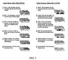
- FIG. 1is a schematic showing LELE and LFLE and the steps that may be replaced using SIS.
- FIG. 2shows a scanning electron micrograph and correlative energy dispersive X-ray (EDX) data of a SIS modified PMMA resist material layer according to an embodiment of the present invention after a two-minute silicon main etching step, the overlay curve plots the aluminum (Al) signal as a function of position;
- EDXenergy dispersive X-ray
- FIG. 3is a backscattered scanning electron microscope (SEM) image of the resist material of FIG. 2 over a silicon substrate after two minutes of silicon main etch;
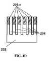
- FIGS. 4A-4Dare a schematic representation of an embodiment of a process according to the present invention, an organic resist layer 201 overlays a substrate layer 202 ( FIG. 4A ), a predetermined pattern 203 is prepared in the organic resist layer 201 ( FIG. 4B ), the patterned resist layer is SIS-modified 201 m ( FIG. 4C ), and an etching process is performed to transfer the pattern 204 to the substrate layer 202 ( FIG. 4D );
- FIG. 5depicts an embodiment of the process according to the present invention
- FIG. 6is a plot of mask thickness and trench depth etched into a Si substrate as a function of the time of the silicon etching step for conventional PMMA resist layers and SIS-modified PMMA having an SIS-Al 2 O 3 protective component;
- FIG. 7is a plot of trench depth etched into a Si substrate as a function of the time of the silicon etching step for conventional ZEP520A resist layers and SIS modified ZEP520A with an SIS-Al 2 O 3 protective component;
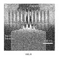
- FIG. 8SEM image of etched trenches (depth ⁇ 200 nm, width ⁇ 90 nm) in a Si substrate prepared using a 33 nm thick SIS-modified PMMA resist layer without additional hard mask;
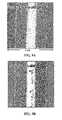
- FIGS. 9A and 9Bare atomic force microscope (AFM) topographic images of a PMMA layer before ( FIG. 9A ) and after the SIS process ( FIG. 9B ) prior to etching;
- AFMatomic force microscope
- FIG. 10Ais a plot of line-edge roughness (peak-to-trough) obtained from the AFM measurements depicted of FIGS. 9A and 9B ;
- FIG. 10Bis a plot of line-edge roughness (1-sigma) obtained from AFM measurements for a ZEP resist layer before and after the SIS process;
- FIG. 11is an SEM image of patterned nanoscale cylinders in a Si substrate prepared by etching a self-assembled PS-b-PMMA block copolymer resist layer with the PMMA component SIS-modified with SIS-Al 2 O 3 ;
- FIGS. 12A-12Care AFM images (upper portion) and AFM line scan data for an ITO substrate with a PS-b-PMMA copolymer resist layer prior to etching ( FIG. 12A ); after a two-minute plasma etch ( FIG. 12B ); and after a two-minute plasma etch of a SIS-modified (with SIS-Al 2 O 3 ) PS-b-PMMA copolymer resist layer ( FIG. 12C );
- FIGS. 13A-Dare SEM images showing how reducing the PMMA thickness can prevent pattern collapse.
- the test patternis a series of 30 nm-wide lines in a 60 nm pitch.
- the resist aspect-ratio (AR)is determined for a 30 nm line.
- Thickness of PMMA filma) 120 nm. b) 75 nm. c) 53 nm. d) 30 nm. Scale bar in all images: 100 nm;
- FIG. 14is an SEM image showing the high aspect-ratio (greater than 6:1), sub-20 nm dense lines etched into silicon using SIS-modified PMMA (5 cycles SIS-Al 2 O 3 ), without using an intermediate hard mask;
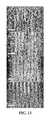
- FIG. 15Aenergy dispersive X-ray (EDX) line scan of a cross section of SIS-modified photoresist on a bottom antireflection coating (BARC) on silicon.
- the dark line in FIG. 15Ais the Al K-line signal along the arrow.
- the trenches etched using SIS-modified photoresist as mask without use of an additional hard maskare shown in FIG. 15B ;
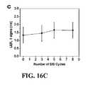
- FIGS. 16A-Care graphs showing line characteristics as a function of SIS cycles.
- FIG. 16Ashows change in line width vs. SIS cycles;
- FIG. 16Bshows the percent change in PMMA volume vs. SIS cycles.
- FIG. 16Cshows line-edge roughness (LER) (1-sigma) prior to plasma etching of lithographically defined lines in the SIS-modified resist layer, as a function of SIS cycles;
- LERline-edge roughness
- FIGS. 17A and 17Bshows the effect of plasma etching on line width.
- the top dashed lineshows the ideal case where plasma etching has no effect on line width.
- the lower dotted lineshows the best linear fit to data points, revealing a ⁇ 5 nm reduction in line width after plasma etching under these conditions.
- FIG. 17Bshows a comparison of LER before and after plasma etching. LER is found to be unchanged within the error in metrology;
- FIGS. 18A and 18Bshow an example test pattern that can be used.
- FIG. 18Ashow an array of test patterns from 30 nm wide lies to 110 nm-wide lines.
- FIG. 18Bshows the details of the test pattern inside the box corresponding to FIG. 18A . The dark lines remain after development while the white areas are removed;
- FIG. 19A-Bshows the methodology for extracting line width from SEM images.
- FIG. 19Ashows the secondary-electron SEM image of the lines and
- FIG. 19Bis a grey-scale average across the y-direction of the box as a function of position x in the same sample.
- the line widthis taken as the distance Was shown in FIG. 19B ;
- FIG. 20A-Cshow the methodology for extracting 1-sigma LER from SEM images.
- FIG. 20Ais a secondary-electron image of five (5) lines.
- FIG. 20Bis a binary outline of the lines in the same sample.
- FIG. 20Cis the grey-scale average across the y-direction as a function of position x (black line and symbols), along with a fit to the grey-scale average data using a Gaussian function with a standard deviation of 1.81 nm; and
- FIG. 21A-Cshow methodology used to determine line width and line edge roughness using AFM.
- FIG. 21Ais a SEM image of the high aspect ration AFM tip used for measurements.
- FIG. 21Bis an image for the image analysis software for measuring line width.
- FIG. 21Cis in image from the image analysis software for determining line edge roughness (LER).
- the present inventionprovides improved methods for preparing low-cost, high-throughput patterned nanostructures of a broad variety of materials with smaller feature sizes by utilizing SIS to modify a resist material prior to performing MPL.
- the resulting nanostructureshave a number of potential uses, including photovoltaic devices, structural supports for a separation membrane in a battery, a fluid filtration membrane, filtering and/or guiding selected wavelengths of light, as active channel material in a transistor, as an array emitter or a field emitter, a three-dimensional electrical contact, and a catalyst.
- nanostructurescomprised of light absorbers, charge separation materials, and/or charge transport materials can outperform analogous devices without nanostructures—this is especially true in systems where bound excitons are formed such as in organic and hybrid organic/inorganic photovoltaics.
- the uniformity and tenability of spacing between nanostructureslends itself to separation and nanofiltration applications. Photonic crystals with uniformly spaced nanostructures are effective at manipulating and modulating light.
- the SIS processinvolves exposing the patterned organic or partially organic resist material layer to various gas phase precursors to synthesize protective components in situ.
- SIScoats the surface of the resist material but also infiltrates into the bulk resist material as well.
- the gas phase precursorsare selected for reaction with the resist material.
- a wide range of precursorsare available for selection for SIS modification which are capable of forming inorganic protective components within a variety of organic resist materials.
- inorganic protective components prepared by SISinclude Al 2 O 3 , TiO 2 , ZnO, SiO 2 , HfO 2 , ZrO 2 and W.
- other metal oxides, metals, and other inorganic materialsmay also be prepared using SIS.
- various known precursorsutilized with atomic layer deposition (ALD) in preparation of layers of metal, metal oxide, metal nitride, metal silicide, and metal halide, ternary, and various multi-component metal-containing systems.
- ALDatomic layer deposition
- the SIS processuses a pair of precursors to form the inorganic protective component where one precursor comprises a metal or metal-containing compound selected to infiltrate into and react with the resist material.
- the second precursorcomprises a compound selected to react with the first precursor (or a portion thereof) bound to the surface and within the bulk of the resist material.
- the protective componentis accordingly synthesized on the surface and within the bulk of the resist material by reaction of the first precursor and the second precursor.
- precursorsinclude, but are not limited to: trimethyl aluminum (TMA), titanium tetrachloride (TiCl 4 ), diethyl zinc (DEZ), and tungsten hexafluoride (WF 6 ).
- TMAtrimethyl aluminum
- TiCl 4titanium tetrachloride
- DEZdiethyl zinc
- WF 6tungsten hexafluoride
- the scope of available precursors and protective components for particular resist materialsmay be further broadened by performing an initial SIS seed layer to form a metal or metal oxide layer reactive with other precursors.
- an Al 2 O 3 seed layermay be utilized to seed the growth of other inorganic materials which do not have direct selective chemistry with pure PS-b-PMMA polymer, e.g., ZnO, MgO, SiO 2 , etc.
- the second precursoris selected in view of the first precursor to carry out the SIS reaction within the resist material to form the protective component.
- the second precursormay be an oxygen source (e.g., H 2 O, O 2 , O 3 , H 2 O 2 ), a reducing agent (H 2 , Si 2 H 6 , HCOH, etc.), a sulphur source (e.g., H 2 S), or other compound reactive with the first precursor.
- an oxygen sourcee.g., H 2 O, O 2 , O 3 , H 2 O 2
- a reducing agentH 2 , Si 2 H 6 , HCOH, etc.
- a sulphur sourcee.g., H 2 S
- the second precursore.g., H 2 O, H 2 S
- the metal-containing precursorcan be utilized next in the SIS sequence so as to react with the adsorbed or bound second precursor.
- various systemsmay comprise more than two precursors. The wide variety of resist material/SIS precursor combinations makes the process applicable to a virtually limitless number of resist materials to which a broad range of protective components may be formed by SIS.
- FIG. 2is energy dispersive X-ray (EDX) imaging of a PMMA resist material modified by Al 2 O 3 .
- the resist materialincludes an unmasked area 50 and a masked area 51 .
- the SIS approachmay be utilized with a patterned PMMA resist layer.
- the PMMA resist layer 201is applied (step 101 ) to a substrate 202 such as a silicon substrate.
- spin coatingmay be used to apply the resist layer 201 to the substrate 202 ; however, other techniques may also be used.
- a pattern 203(shown in FIG. 4B ) may be applied to the resist layer (step 102 ). Patterning of the resist layer 201 may be accomplished by a variety of processes known in the art including electron beam exposure, photolithography and polymer self-assembly processes such as block copolymer lithography.
- selected areas of the PMMA resist layerare exposed to an electron beam or photons to form the pattern 203 .
- the resist layer 201is then developed (step 103 ) using chemical developers such as methyl isobutyl ketone and isopropyl alcohol (MIBK:IPA).
- MIBKisopropyl alcohol
- lithography techniquessuch as electron beam lithography and photolithography may be used to form the patterned feature of the organic resist.
- selection of block copolymersmay be used to prepare the patterned feature of the organic resist.
- a self-assembled pattern of spheres, cylinders, lamellae, or other nanoscale morphologycomprised of two or more polymer blocks such as polystyrene and poly (methyl methacrylate) constitutes the patterned resist layer.
- the patterned resist layer 201is then modified through the SIS process which comprises a plurality of alternating exposures of the patterned resist layer to a metal precursor compound, e.g., trimethyl aluminum (TMA) (step 104 ) which may be the first precursor, and a reactant precursor, e.g., H 2 O (step 105 ) which may be the second precursor.
- a metal precursor compounde.g., trimethyl aluminum (TMA)
- TMAtrimethyl aluminum
- H 2 Ostep 105
- Each precursor exposureresults in a self-limited half-reaction with the resist layer.
- a purge stepe.g., N 2
- Exposures of each reactantcan be performed in one step or in a series of two or more steps to control the amount of material that infiltrates the resist.
- the exposureswere carried out at a temperature of about 85° C. and using precursor partial pressures of about 5 Torr.
- Five SIS cycleswere performed with a 60-second TMA exposure and a 300-second H 2 O exposure in each cycle.
- PMMA domainsare first modified chemically by reaction with TMA, with the Al of the TMA bonding to the PMMA in a highly controllable fashion, owing to the stepwise molecule assembly process.
- the TMA precursorinfiltrates into the bulk of the PMMA.
- the second precursorin this case water, completes the reaction with the Al bonded to the surface and within the PMMA bulk, forming the protective Al 2 O 3 component.
- the resulting modified resist layer 201 mis then etched (step 106 ) to form the desired features 204 in the substrate.
- the features 204 or a portion of the featuresmay be high-aspect ratio features.
- the term high-aspect ratiorefers to features having a depth to length and/or width of at least about 1:1.
- high-aspect ratiois between about 1:1 to about 3:1 and may be between about 1:1 and about 100:1 in still further embodiments.
- the high-aspect ratio featuresmay be formed without an intermediate hard mask.
- the interface between the SIS-synthesized materials and soft mattercan be precisely adjusted, as well as the final structure of the composites and templated inorganic materials.
- poly(4-vinyl pyridine)presents strong coordination reaction with TiCl 4 and Al(CH 3 ) 3 , which prevents further material diffusion into the polymer and results in hollow tubes and spheres.
- the precursormay be selected from, SnCl 4 , AlCl 3 , ZnCl 2 , CdCl 2 , or any other suitable precursor.
- the reaction between metal precursors and soft matteris not strong enough to block the diffusion of materials into the matrix of PMMA nanodomains, therefore, solid nanorods, nanowires, or nanoposts with precisely-controlled size can be generated.
- SISmay be used, as described above, to improve multiple-patterning techniques to decrease the time and cost of LELE and LFLE.
- Double-patterningis the simplest form of multiple-patterning and exists in three main variants (two of which are shown in FIG. 1 ): litho-etch-litho-etch (LELE), litho-freeze-litho-etch (LFLE), and self-aligned double patterning (SADP).
- LELElitho-etch-litho-etch
- LFLElitho-freeze-litho-etch
- SADPself-aligned double patterning
- LELEa dense pattern with pitch P is decomposed into two sub-patterns each with pitch 2P. The first sub-pattern is exposed, developed and etched into the first hard mask. The second sub-pattern is then exposed and developed.
- the assembled patternsare then transferred into a second hard mask, which is used for pattern transfer into the target material.
- the first sub-patternis exposed and developed.
- a “freezing” processis then used to render the photoresist insoluble.
- a second layer of photoresistis then applied again, exposed and developed with the second sub-pattern.
- the assembled patternis then etched into the underlying hard mask or target material.
- a base pattern B1 with pitch 2Pis formed.
- a thin filmis then conformally deposited on the substrate and etched back to reveal the base pattern. B1 is then selectively removed and a denser pattern with pitch P is achieved.
- SADPis best suited for one-dimensional patterns and does not provide as much flexibility in layout as the two previous approaches.
- the present inventiondiscloses novel methods of decreasing the feature size while maintaining low cost and high-throughput multiple patterning methods.
- double patterningis contemplated, which is the simplest form of multiple patterning and exists in three main variants (see FIG. 1 ): litho-etch-litho-etch (LELE), litho-freeze-litho-etch (LFLE), and self-aligned double patterning (SADP).
- LELElitho-etch-litho-etch
- LFLElitho-freeze-litho-etch
- SADPself-aligned double patterning
- a resist or substrateundergoes SIS as described above prior to being subjected to a multiple patterning technique such as, in preferred embodiments, LELE or LFLE.
- the SISacts to modify the resist such that it withstands plasma etching an order of magnitude better than unmodified resist and facilitates production of high-quality, high-aspect-ratio features.
- the present inventionentails use of SIS to simplify the MPL techniques by replacing one or more of the “hard masks” required for their implementation.
- An additional advantageis that SIS can replace or supplement the freeze step in a LFLE process.
- the PMMA resist layer 201is applied (step 101 ) to a substrate 202 such as a silicon substrate.
- a substrate 202such as a silicon substrate.
- spin coatingmay be used to apply the resist layer 201 to the substrate 202 ; however, other techniques may also be used.
- a pattern 203(shown in FIG. 4B ) may be applied to the resist layer (step 102 ). Patterning of the resist layer 201 may be accomplished by a variety of processes known in the art including electron beam exposure, photolithography and polymer self-assembly processes such as block copolymer.
- selected areas of the PMMA resist layerare exposed to an electron beam or photons to form the pattern 203 .
- the resist layer 201is then developed (step 103 ) using chemical developers such as methyl isobutyl ketone and isopropyl alcohol (MIBK:IPA). It is understood that lithography techniques such as electron beam lithography and photolithography may be used to form the patterned feature of the organic resist.
- chemical developerssuch as methyl isobutyl ketone and isopropyl alcohol (MIBK:IPA).
- MIBKisopropyl alcohol
- the patterned resist layer 201is then modified through the SIS process which comprises a plurality of alternating exposures of the patterned resist layer to a metal precursor compound, e.g., trimethyl aluminum (TMA) (step 104 ) which may be the first precursor, and a reactant precursor, e.g., H 2 O (step 105 ) which may be the second precursor.
- a metal precursor compounde.g., trimethyl aluminum (TMA)
- TMAtrimethyl aluminum
- H 2 Ostep 105
- Each precursor exposureresults in a self-limited half-reaction with the resist layer.
- a purge stepe.g., N 2
- Exposures of each reactantcan be performed in one step or in a series of two or more steps to control the amount of material that infiltrates the resist.
- the exposureswere carried out at a temperature of about 85° C. and a pressure of about 5 Torr.
- Five SIS cycleswere performed with a 60-second TMA exposure and a 300-second H 2 O exposure in each cycle.
- PMMA domainsare first modified chemically by reaction with TMA, with the Al of the TMA bonding to the PMMA in a highly controllable fashion, owing to the stepwise molecule assembly process.
- the TMA precursorinfiltrates into the bulk of the PMMA.
- the second precursorin this case water, completes the reaction with the Al bonded to the surface and within the PMMA bulk, forming the protective Al 2 O 3 component.
- the resulting modified resist layer 201 mis then etched (step 106 ) to form the desired features 204 in the substrate.
- the features 204 or a portion of the featuresmay be high-aspect ratio features.
- the term high-aspect ratiorefers to features having a depth to length and/or width of at least about 1:1.
- high-aspect ratiois between about 1:1 to about 3:1 and may be between about 1:1 and about 100:1 in still further embodiments.
- the high-aspect ratio featuresmay be formed without an intermediate hard mask.
- the remaining SIS-modified resist layer 201 mmay be removed (step 107 ) using solvent systems or other techniques known in the art.
- PMMA SIS-modified with Al 2 O 3PMMA/Al 2 O 3
- TMAHtetramethylammoniumhydroxide
- the SIS-modified PMMAmay also be stripped using a solution comprised of ammonium hydroxide and hydrogen peroxide.
- the etching step ( 106 )may be adapted in various embodiments to facilitate substrate etching.
- a brief breakthrough etch stepis used before commencing etching of the substrate to remove the thin layer of Al 2 O 3 over the substrate in the exposed and unmasked areas.
- the first etching stepis configured to break through the protective etch component, which may be a thin inorganic material directly covering exposed regions of the substrate as a result of SIS processing. This protective component layer may form from the reaction on the exposed surface of the silicon substrate or the reaction of residual PMMA with the precursors.
- the initial breakthrough etch stepalso removes a small amount of SIS-modified resist layer.
- the etch parameters for the breakthrough etch stepare listed in Table 1 for PMMA/Al 2 O 3 but may be altered in view of different protective components formed by SIS. Design of the breakthrough step plays a significant role in initiating etching into the silicon substrate. For example, using a breakthrough etch step designed to remove SiO 2 (Table 1) will not initiate etching into the silicon substrate where the Al 2 O 3 comprises the protective component.
- Features prepared in substrate materials by photolithographymay be characterized by the minimum feature size and maximum feature depth (depth of focus). For various devices prepared by photolithography, there is a desire to minimize feature size formed in the substrate while maximizing feature depth of focus. Minimum feature size and depth of focus are driven by the photolithography process and can be defined by the relationships of Equation 1 and Equation 2, respectively.
- Minimum_feature ⁇ _sizek 1 ⁇ ⁇ NA ( 1 )
- Depth_Of ⁇ _Focusk 2 ⁇ ⁇ NA 2 ( 2 )
- ⁇represents the wavelength of the photolithography light source and NA is the numerical aperture which is defined by sin( ⁇ ) and is about 1 for advanced photolithography tools.
- current conventional photolithography processesare capable of a minimum feature size of about 50 nm and a depth of focus of about 80 to about 120 nm.
- the resist layermust be thin, ideally much less than the depth of focus.
- electron beam lithographyalso requires a thin resist layer to obtain a small minimum feature size, i.e., improved resolution.
- SIS-modified resist material layersshow significant etch resistance to various etch processes, including an HBr-based Si etch recipe.
- SIS-modified PMMAcan withstand plasma etching during fabrication of deep trenches in the silicon substrate demonstrating an etch rate of one-tenth that of single-crystal silicon.
- FIG. 6shows that the improvement in etch resistance enables the fabrication of trenches deeper than 150 nm in silicon, with a starting resist layer of PMMA film only 33 nm thick.
- Thinner SIS-modified resist layersmay also be used. For example, a modified resist layer of about 10 nm could replace a conventional 100 nm resist layer. In comparison, unreacted PMMA alone provides little etch resistance.
- the maskis etched at ⁇ 8 nm/min, about one-tenth of the Si etch rate.
- the etch resistance of the SIS-modified resist layercan be modulated by controlling the number of SIS cycles performed. In general, few SIS cycles are needed to significantly increase etch resistance of the resist layer. In various embodiments, from 1 to about 10 SIS cycles are used for extended SIS exposure times, whereas a larger number may be used with shorter SIS exposure times. In particular embodiments, between 2 and 5 SIS cycles are performed.
- the resist layermay be fully infiltrated by the modifying material, modulating the timing, temperature, SIS precursors, and partial pressure of the exposures of the resist material to the SIS precursors controls the depth of infiltration of the SIS treatment. Controlling the SIS infiltration depth permits the resist layer to still be readily removed from the substrate after etching.
- the deeper portions of the resist proximate the substratewill be preserved as substantially pure polymer film. This will facilitate removal of the resist material (e.g., by dissolving in acetone) after completing the etching process.
- FIG. 6shows a plot of feature depth for a plurality of etched trenches in a silicon substrate fabricated using an e-beam method.
- Features more than 200 nm deep into the silicon substratewere fabricated after 120 seconds of plasma etching SIS-modified PMMA/Al 2 O 3 resist layer less than 30 nm in thickness.
- SIS-modified PMMA/Al 2 O 3is estimated to have an etch resistance of about 10:1 compared to silicon (SIS-PMMA:Si).
- FIG. 7shows a plot of feature depth in a silicon substrate after plasma etching using a SIS-modified ZEP520A/Al 2 O 3 resist layer 50 nm thick.
- Feature depths achieved with the SIS-modified resist layerare significantly greater than trenches formed using an unmodified ZEP520A resist layer of the same thickness. While feature depth remained substantially constant (about 25 nm) for etch times between 60 and 120 seconds, the trenches were between about 75 and over 150 nm deep over the same time period using SIS-modified ZEP520A.
- Improving the etch resistance of the resist layer by SIS-modificationenables fabrication of features, including high-aspect ratio features, in silicon without the need for an intermediate hard mask layer or other procedure that can decrease process efficiency, etch performance and/or etch quality.
- a range of high-aspect ratio devices and portions of such devicessuch as DRAM (Dynamic Random Access Memory), interconnect vias, and three-dimensional transistors (e.g., FinFETs) may be made using the SIS-modification process.
- Potential problems that may arise during hard mask deposition, such as the stress and adhesion of the film,can be avoided as well.
- the low thermal budget of the SIS processalso makes it compatible with most microelectronic fabrication processes. By way of example, FIG.
- FIG. 8shows a SEM image of a plurality of high-aspect ratio (e.g., greater than 2:1) trenches (200 nm deep by 90 nm wide) formed in a silicon substrate.
- a 33-nm-thick SIS-modified PMMA/Al 2 O 3 resist layerwas used without the aid of an additional hard mask.
- FIG. 9Ashows an atomic force microscope topographic image of a conventional PMMA resist layer and FIG. 9B shows the PMMA resist layer after SIS treatment.
- FIG. 10Ashows that there is little change in the LER when using SIS-modified PMMA/Al 2 O 3 .
- FIG. 10Bdepicts a similar result for SIS-modified ZEP/Al 2 O 3 .
- SISpermits realization of both high-resolution properties of PMMA and the etch-resistance properties of Al 2 O 3 and hard masks without degrading the initial printed image in the PMMA resist.
- electron-beam (e-beam) lithographywas used to pattern thin PMMA films (thickness: 30-120 nm) on silicon.
- PMMAwas spun on silicon and dried on a hot plate at 180° C. for 90 s.
- Exposurewas performed in a JEOL JBX-9300FS e-beam lithography tool at 100 keV, with doses appropriate for the resist thickness.
- the PMMA resistwas developed in MIBK:IPA (methyl isobutyl ketone:isopropanol) (1:3) for 45 s at ⁇ 5° C., rinsed for 30 s in IPA, and blow-dried using nitrogen.
- MIBK:IPAmethyl isobutyl ketone:isopropanol
- the patterned PMMA filmswere treated by the SIS process to enhance plasma etch resistance.
- the SIS processwas adapted for a commercial reactor capable of large scale batch processing (Beneq TFS500). While the temperature (85° C.) and pressure (5 Torr) were identical to the established process, the reaction time of each half-cycle was lengthened to 600 s, to account for consumption of the precursors by the PMMA film.
- the SIS-treated PMMAwas used directly as etch mask, and patterns were transferred directly into the silicon substrate using HBr-based plasma chemistry. Following plasma etching, the samples were cleaned in an aqueous solution of hydrogen peroxide and ammonium hydroxide (RCA clean), to remove deposits generated during plasma etching and remaining etch mask material.
- RCA cleanaqueous solution of hydrogen peroxide and ammonium hydroxide
- FIGS. 13A-Dshow that the reduction of resist aspect-ratio is effective in preventing pattern collapse.
- a resist aspect-ratio of 1FIG. 13D
- the structures in FIG. 14can be fabricated easily: dense lines, narrower than 20 nm, and deeply etched into the silicon substrate were made using SIS-modification of a mere 30 nm-thick PMMA resist film.
- the etch depth of 130 nm shown in FIG. 14would have required a minimum SiO 2 thickness of ⁇ 5 nm, using a typical Si:SiO 2 selectivity of 25:1 for HBr-based etch chemistry.
- a PMMA thickness of at least 52 nmwould be required (the etch rate of PMMA is about 300 nm/min in this hard mask etching step), if no SIS modification were made.
- FIG. 13Cshows clearly that a 53 nm PMMA film is not sufficiently thin to prevent pattern collapse. While much greater etch selectivity between PMMA and SiO 2 (or between Si and SiO 2 ) exists in industrial manufacturing tools, the improvement due to SIS-modification would make the entire fabrication process significantly more robust.
- FIGS. 15A and 15Bshow clearly the infiltration of Al 2 O 3 and the corresponding increase in resistance to HBr-based plasma etching.
- the photoresistwas patterned using established photolithographic and development processes, similar to that in use by industrial facilities.
- the SIS treatmentenhanced the etch resistance of the photoresist by about 60-fold, decreasing the etch rate of the photoresist from ⁇ 230 nm/min to ⁇ 4 nm/min, thus significantly improving its suitability as an etch mask.
- PMMApoly(methyl methacrylate)
- SISsequential infiltration synthesis
- the SIS processpreserves the original pattern quality, as defined by line-edge roughness (LER), and provides a controllable degree of size-tunability. Furthermore, contrary to current industrial processes where LER is degraded by plasma etching, SIS allows the initial LER in the imaging layer to be preserved throughout plasma etching, with negligible change in the dimensions of the patterns. Importantly, the enhancement is sufficiently strong to allow a very thin PMMA film to be used, circumventing pattern collapse. The combination of reduced resist thickness and enhanced etch resistance allows dense and high aspect-ratio nanostructures to be created with simplicity and reliability unavailable in current manufacturing processes. Here PMMA is used as an example, but a vast array of other polymer chemistries are also compatible with SIS processing.
- LERline-edge roughness
- FIG. 16Ashows evidence of a change in lateral dimensions that is also highly controllable by the number of reaction cycles. Taking into account the change in film thickness, the volume expansion quickly reaches a constant level ( FIG. 16B ) within the error in metrology, and the changes in lateral dimensions become slower for a larger number of cycles.
- LERline-edge roughness
- silicon-based VLSI circuitsLER reduces carrier mobility, introduces significant device-to-device variations, and increases stand-by power consumption.
- the LER of resist patterns immediately following developmentis nearly optimal during the fabrication process, since plasma etching frequently causes severe degradation.
- the SIS modificationpreserves this optimal LER of as-patterned PMMA.
- FIG. 15Cdemonstrates that the line-edge roughness (LER) is unchanged by the SIS process for as many as eight reaction cycles. The LER of the initial PMMA lines has been reduced using cold development, and is comparable to or better than results reported in literature.
- the LER and dimensions of the SIS-modified resist patternsare preserved throughout the plasma etching process.
- the line dimensions and roughnessare measured from SEM images following the procedure described in the paragraphs 86 to 88.
- FIG. 17Ashows that the line widths only reduce slightly, mainly due to the breakthrough step.
- the LERit remains unchanged after the main etching step ( FIG. 17B ), for all line widths down to 30 nm.
- FIG. 13A-Dshow that the reduction of resist aspect-ratio is effective in preventing pattern collapse.
- FIG. 14can be fabricated easily: dense lines, narrower than 20 nm, and deeply etched into the silicon substrate were made using SIS-modification of a mere 30 nm-thick PMMA resist film. For comparison, if a SiO 2 intermediate hard mask were used, the etch depth of 130 nm shown in FIG. 14 would have required a minimum SiO 2 thickness of ⁇ 5 nm, using a typical Si:SiO 2 selectivity of 25:1 for HBr-based etch chemistry. To fully etch through the SiO 2 hard mask, a PMMA thickness of at least 52 nm would be required (the etch rate of PMMA is about 300 nm/min in this hard mask etching step), if no SIS modification were made.
- 13Cshows clearly that a 53 nm PMMA film is not sufficiently thin to prevent pattern collapse. While much greater etch selectivity between PMMA and SiO 2 (or between Si and SiO 2 ) exists in industrial manufacturing tools, the improvement due to SIS-modification would make the entire fabrication process significantly more robust.
- FIGS. 15A and 15Bshow clearly the infiltration of Al 2 O 3 and the corresponding increase in resistance to HBr-based plasma etching.
- the photoresistwas patterned using established photolithographic and development processes, similar to that in use by industrial facilities.
- the SIS treatmentenhanced the etch resistance of the photoresist by about 60-fold, decreasing the etch rate of the photoresist from ⁇ 230 nm/min to ⁇ 4 nm/min, thus significantly improving its suitability as an etch mask.
- SIS-enhanced imaging layersmay be used in high resolution patterning and plasma etching techniques for various applications.
- the SIS processis understood to not cause uncontrolled size change, nor does it introduce additional degradation to lithographically defined patterns.
- the SIS processis also understood to prevent pattern degradation during plasma etching.
- the improved etch resistanceallows pattern collapse to be circumvented during wet development, allowing arbitrary nanostructures with high aspect-ratio to be generated with great simplicity. Taken together, these properties may meet the requirements for resist thickness on the International Technology Roadmap for Semiconductors for a decade in the future.
- FIG. 11depicts a plurality of patterned nanoscale cylindrical features prepared by etching a Si substrate with a SIS modified self-assembled PS-b-PMMA resist layer.
- the PS-b-PMMA resist layercomprises a plurality of orientated PMMA microdomains.
- the PS-b-PMMA resist layer(without intermediate hard mask) was SIS-modified with Al 2 O 3 to improve etch resistance of the PMMA component.
- the SEM imageshows the Si substrate patterned with a plurality of tall cylinders with diameters of about 30 nm formed in response to the ordered microdomains of the SIS-modified PMMA.
- FIGS. 12A-12Cshow AFM images (upper portion) and corresponding atomic force microscopy (AFM) line scan data (lower portion) for an indium tin oxide (ITO) substrate patterned with a PS-b-PMMA resist layer.
- FIG. 12Ashows an ITO substrate and unmodified resist layer prior to etching.
- the AFM data taken along the path 51 illustrated in the AFM imageshow a substantially smooth surface with little change in elevation.
- FIG. 12Bshows an ITO substrate after a two-minute plasma etch using an unmodified PS-b-PMMA resist layer.
- the AFM datashow surface roughness has marginally increased but with little change in surface elevation.
- the AFM dataalso show very little change in the surface morphology relative to unprocessed ITO film.
- FIG. 12Ashows an ITO substrate and unmodified resist layer prior to etching.
- the AFM data taken along the path 51 illustrated in the AFM imageshow a substantially smooth surface with little change in elevation.
- FIG. 12Cshows an ITO substrate after a two-minute plasma etch using a PS-b-PMMA resist layer SIS-modified with Al 2 O 3 .
- the SEM image and corresponding AFM datashow the patterned ITO substrate and significant surface elevation changes with troughs exceeding 30 nm.
- lithography and plasma etchingwere initially developed for the microelectronics industry, they have become essential to other technologies, such as micro-electro-mechanical and microfluidic systems. Indeed, the physical realization of any system with nanoscale components requires a certain degree of top-down patterning.
- an imaging layerresist
- Plasma etchingis then used to transfer the pattern in the imaging layer to a material of interest. These procedures are then repeated many times to complete a functional system.
- the line widths and line-edge roughness (LER)were measured using atomic force microscopy (AFM) or scanning electron microscopy (SEM) where appropriate.
- the lines measuredwere patterned in 30 nm-thick PMMA and were widely spaced (line/space ratio: 0.25) to allow the AFM tip to reach the substrate as shown in FIG. 18 .
- the AFM tip that was used in the experimentsmay be approximately 5 nm.
- FIGS. 21 A, B and Cshow the methodology for determining line width and line edge roughness using AFM.
- line widths and LERwere measured from as-patterned and SIS-treated PMMA patterns using high-aspect ratio AFM tips.
- AFMwas used for metrology in this case because untreated PMMA can be considerably damaged during SEM examination.
- the line widthsare taken as the average width at 50% of the vertical distance from the top of the resist surface using the image analysis software (Veeco, Nanoscope version 7.3).
- the line widthwas W as shown in FIG. 19B .
- the “Width” function and the “Highest Peak”is used a reference, and the line edge is defined as the position where the topography height is 50% of the full resist thickness.
- Line widths and LERwere measured by SEM on SIS-treated samples before and after plasma etching.
- SEMwas chosen in this case since SIS-treated PMMA did not become damaged during SEM examination and because it provided high spatial resolution.
- Line widths and LERwere extracted from SEM images using ImageJ (available from National Institute of Health, NIH) as shown in FIGS. 20A-C .
- the standard deviation (sigma) of the Gaussian fitgives the LER (as shown in FIG. 20C ).
- a white pixelis assigned a value of ‘1’, whereas a black pixel is ‘0.’
- the grey-scale averagegives the probability that a pixel is white at a given position x, matching the definition of LER.
Landscapes
- Engineering & Computer Science (AREA)
- Physics & Mathematics (AREA)
- General Physics & Mathematics (AREA)
- Microelectronics & Electronic Packaging (AREA)
- Manufacturing & Machinery (AREA)
- Computer Hardware Design (AREA)
- Condensed Matter Physics & Semiconductors (AREA)
- Power Engineering (AREA)
- Plasma & Fusion (AREA)
- Chemical & Material Sciences (AREA)
- Inorganic Chemistry (AREA)
- Organic Chemistry (AREA)
- Drying Of Semiconductors (AREA)
Abstract
Description
The present application is a continuation-in-part of U.S. patent application Ser. No. 13/427,619, which was filed on Mar. 2, 2012, and published as US 2012/0241411, and which claims priority to U.S. Provisional Patent Application No. 61/467,166, now U.S. Pat. No. 8,980,418 filed Mar. 24, 2011, each of which is hereby incorporated herein by reference in its entirety.
The United States Government has rights in this invention pursuant to Contract No. DE-ACO2-06CH11357 between the United States Government and the UChicago Argonne, LLC, representing Argonne National Laboratory.
This invention relates to a method of photolithography. More specifically, this invention relates to novel multiple-patterning lithography methods in which one or more steps are replaced by sequential infiltration synthesis (SIS).
This section is intended to provide a background or context to the invention that is, inter alia, recited in the claims. The description herein may include concepts that could be pursued, but are not necessarily ones that have been previously conceived or pursued. Therefore, unless otherwise indicated herein, what is described in this section is not prior art to the description and claims in this application and is not admitted to be prior art by inclusion in this section.
Photolithography is a process used in the fabrication of integrated circuits, which entails using light to transfer a pattern from a “mask” to a “photoresist” on a substrate. A series of chemical treatments are then applied in order to etch a desired pattern into the substrate. Improvements in photolithography have advanced integrated circuit manufacturing over the last several decades. The most important advance is the gradual reduction of the wavelength of the illumination source of the photolithography tool: from the 436 nm line of a mercury lamp to the 193 nm light of an ArF laser. By incrementally improving the photolithography process, features as small as 45 nm can be manufactured in high volume using 193 nm photolithography. Immersion 193 nm photolithography is presently deployed for the manufacturing of even more advanced technology nodes. To print even smaller features, several technologies have been considered, such as extreme ultraviolet lithography (EUVL). The development, however, has been delayed due to several difficulties, in particular the difficulty in designing a light source with sufficient brightness. Consequently, multiple-patterning techniques have emerged as an alternative. However, multiple-patterning achieves a fine feature size at a significant cost. In its simplest form, double-patterning, two separate masks and two exposure steps are required to achieve what a single mask and one exposure step used to accomplish, leading to a much lower throughput and significantly higher cost.
The present invention addresses these problems and provides processes for preparing lower-cost, high-throughput multiple patterning photolithography. In some embodiments, sequential infiltration synthesis (SIS), a method related to atomic layer deposition (ALD), is used to increase the plasma etch resistance and/or render a photoresist layer insoluble in photoresist solvents, thus obviating the need for one or more steps of present techniques of multiple-patterning lithography. The SIS process utilizes alternating exposures to gas phase precursors that infiltrate the organic or partially organic resist material to form a protective component within the resist layer. These techniques modify the standard multiple-patterning lithography techniques to reduce the number of steps and/or decrease the cost and time that these techniques presently require. Potential applications of these methods and system extend to virtually all technologies in which periodic nanomaterial structures are desirable, including optoelectronics, sensors, membranes, photonic crystals, dielectric materials, and electronics.
In one aspect, a method is provided for preparing inorganic features with multiply-patterned nanostructures, comprising: modifying a resist material using SIS; etching the first pattern onto the substrate; preparing a second iteration of inorganic features onto the substrate to double the pattern density; and engraving the double-density pattern onto the substrate, wherein no hard mask is deposited between the substrate and the features.
In some embodiments, the resist is selected from the group consisting of polyacrylate(s), poly(vinyl pyridine)(s), poly(vinyl alcohol)(s), polysulfone(s), polyimide(s), and polyphosphate(s). In further embodiments, the method may be performed using litho-etch-litho-etch (LELE) multiple-patterning lithography modified such that hard mask deposition, transfer, and removal steps are replaced with SIS treatment steps.
In some embodiments the step of modifying the resist using SIS comprises the steps of exposing the resist to a plurality of SIS cycles comprising alternating exposures of a first precursor reactive with the organic resist and a second precursor reactive with the moieties created by the first precursor within the organic resist to form an inorganic protective etch component within the bulk organic resist mask layer.
In further embodiments, first precursor and the second precursor may comprise gas phase precursors. In still further embodiments, the first precursor may comprise a metal or metal-containing compound, and the inorganic protective etch component may comprise a metal oxide or a metal. In some embodiments, the metal oxide is selected from the group consisting of Al2O3, ZnO, SiO2, HfO2, ZrO2, Nb2O5, and TiO2. In further embodiments, the resist mask layer comprises at least one of poly(methyl methacrylate) (PMMA), ZEP520A, poly(methyl glutarimide) (PMGI), phenol formaldehyde resin (DNQ/Novolac), polyhydroxystyrene-based polymers, polyimides and SU-8.
In yet another embodiment, the step of SIS comprises the following steps: providing a substrate material and applying the resist mask layer over a surface of the substrate material, forming the patterned feature in the resist mask layer by lithography, and performing a plurality of SIS cycles. Each SIS cycle may comprise exposing the resist mask layer to a first precursor reactive with the first organic or partially organic material and exposing the resist mask layer to a second precursor to form a protective etch component within at least a portion of the first resist material.
In another aspect, a method is provided for preparing inorganic features with multiply-patterned nanostructures, comprising: exposing a pattern onto a substrate, preparing a second iteration of the pattern on the substrate using SIS to effectively double the density of the pattern features; and wherein no hard mask is deposited between the substrate and the pattern. In some embodiments, the method may be litho-freeze-litho-etch (LFLE) multiple-patterning lithography modified such that the resist freeze step is accomplished through SIS treatment. In further embodiments, the method may be LFLE multiple-patterning lithography modified such that the hard mask deposition, transfer, and removal steps are accomplished through SIS treatment.
These and other advantages and features of the invention, together with the organization and manner of operation thereof, will become apparent from the following detailed description when taken in conjunction with the accompanying drawings, wherein like elements have like numerals throughout the several drawings described below.
The present invention provides improved methods for preparing low-cost, high-throughput patterned nanostructures of a broad variety of materials with smaller feature sizes by utilizing SIS to modify a resist material prior to performing MPL. The resulting nanostructures have a number of potential uses, including photovoltaic devices, structural supports for a separation membrane in a battery, a fluid filtration membrane, filtering and/or guiding selected wavelengths of light, as active channel material in a transistor, as an array emitter or a field emitter, a three-dimensional electrical contact, and a catalyst. In photovoltaic devices, nanostructures comprised of light absorbers, charge separation materials, and/or charge transport materials can outperform analogous devices without nanostructures—this is especially true in systems where bound excitons are formed such as in organic and hybrid organic/inorganic photovoltaics. The uniformity and tenability of spacing between nanostructures lends itself to separation and nanofiltration applications. Photonic crystals with uniformly spaced nanostructures are effective at manipulating and modulating light.
Sequential Infiltration Synthesis
In general, the SIS process involves exposing the patterned organic or partially organic resist material layer to various gas phase precursors to synthesize protective components in situ. SIS coats the surface of the resist material but also infiltrates into the bulk resist material as well. The gas phase precursors are selected for reaction with the resist material. A wide range of precursors are available for selection for SIS modification which are capable of forming inorganic protective components within a variety of organic resist materials. Examples of inorganic protective components prepared by SIS include Al2O3, TiO2, ZnO, SiO2, HfO2, ZrO2and W. However, other metal oxides, metals, and other inorganic materials may also be prepared using SIS. For example, various known precursors utilized with atomic layer deposition (ALD) in preparation of layers of metal, metal oxide, metal nitride, metal silicide, and metal halide, ternary, and various multi-component metal-containing systems.
In various embodiments of the present methods, the SIS process uses a pair of precursors to form the inorganic protective component where one precursor comprises a metal or metal-containing compound selected to infiltrate into and react with the resist material. The second precursor comprises a compound selected to react with the first precursor (or a portion thereof) bound to the surface and within the bulk of the resist material. The protective component is accordingly synthesized on the surface and within the bulk of the resist material by reaction of the first precursor and the second precursor. Although a wide range of precursors are suitable for SIS-modification, examples of various precursors include, but are not limited to: trimethyl aluminum (TMA), titanium tetrachloride (TiCl4), diethyl zinc (DEZ), and tungsten hexafluoride (WF6). The scope of available precursors and protective components for particular resist materials may be further broadened by performing an initial SIS seed layer to form a metal or metal oxide layer reactive with other precursors. For example, an Al2O3seed layer may be utilized to seed the growth of other inorganic materials which do not have direct selective chemistry with pure PS-b-PMMA polymer, e.g., ZnO, MgO, SiO2, etc.
The second precursor is selected in view of the first precursor to carry out the SIS reaction within the resist material to form the protective component. In various embodiments the second precursor may be an oxygen source (e.g., H2O, O2, O3, H2O2), a reducing agent (H2, Si2H6, HCOH, etc.), a sulphur source (e.g., H2S), or other compound reactive with the first precursor. One of skill in the art will appreciate that the order of the precursors may be altered in various embodiments and that the nomenclature ‘first precursor’ and ‘second precursor’ is used herein for ease of reference. For instance, in some embodiments the second precursor (e.g., H2O, H2S) can be selected to react with or bind to a specific functional group in the resist material and utilized first in the SIS sequence, and the metal-containing precursor can be utilized next in the SIS sequence so as to react with the adsorbed or bound second precursor. One of skill in the art will further appreciate that various systems may comprise more than two precursors. The wide variety of resist material/SIS precursor combinations makes the process applicable to a virtually limitless number of resist materials to which a broad range of protective components may be formed by SIS.
The SIS process results in the protective component infiltrating into the bulk of the resist material layer, not merely coating exposed surfaces of the resist layer. By varying the pressure, temperature, and reaction timing of the SIS process precursors, the depth of penetration of the protective component into the resist layer is controllable. The depth of penetration of the protective component can also be controlled by selecting SIS process precursors with specific diffusivities in the resist material layer.FIG. 2 is energy dispersive X-ray (EDX) imaging of a PMMA resist material modified by Al2O3. The resist material includes an unmaskedarea 50 and amasked area 51. The presence of aluminum after 16 seconds of an Al2O3breakthrough etching step and two minutes of HBr/O2silicon etching is represented by theoverlay curve 53. Although a portion of the resist layer opposite the substrate has been removed by etching, resulting in a thinning of the resist layer, significant aluminum is still present within the PMMA at this depth. The remaining resist layer is seen in a backscattered SEM image inFIG. 3 , illustrating that the reaction between resist layer and the precursors has occurred within—rather than simply on top of—the PMMA layer.
The SIS approach may be utilized with a patterned PMMA resist layer. With reference toFIGS. 4 and 5 , the PMMA resistlayer 201 is applied (step101) to asubstrate 202 such as a silicon substrate. In various embodiments, spin coating may be used to apply the resistlayer 201 to thesubstrate 202; however, other techniques may also be used. Next, a pattern203 (shown inFIG. 4B ) may be applied to the resist layer (step102). Patterning of the resistlayer 201 may be accomplished by a variety of processes known in the art including electron beam exposure, photolithography and polymer self-assembly processes such as block copolymer lithography. In various embodiments, selected areas of the PMMA resist layer are exposed to an electron beam or photons to form thepattern 203. The resistlayer 201 is then developed (step103) using chemical developers such as methyl isobutyl ketone and isopropyl alcohol (MIBK:IPA). It is understood that lithography techniques such as electron beam lithography and photolithography may be used to form the patterned feature of the organic resist. In addition, selection of block copolymers may be used to prepare the patterned feature of the organic resist. In the case of block copolymers, a self-assembled pattern of spheres, cylinders, lamellae, or other nanoscale morphology comprised of two or more polymer blocks such as polystyrene and poly (methyl methacrylate) constitutes the patterned resist layer.
The patterned resistlayer 201 is then modified through the SIS process which comprises a plurality of alternating exposures of the patterned resist layer to a metal precursor compound, e.g., trimethyl aluminum (TMA) (step104) which may be the first precursor, and a reactant precursor, e.g., H2O (step105) which may be the second precursor. Each precursor exposure results in a self-limited half-reaction with the resist layer. A purge step (e.g., N2) may be performed following each precursor exposure to remove residual reactant. Exposures of each reactant can be performed in one step or in a series of two or more steps to control the amount of material that infiltrates the resist. In this example, the exposures were carried out at a temperature of about 85° C. and using precursor partial pressures of about 5 Torr. Five SIS cycles were performed with a 60-second TMA exposure and a 300-second H2O exposure in each cycle. PMMA domains are first modified chemically by reaction with TMA, with the Al of the TMA bonding to the PMMA in a highly controllable fashion, owing to the stepwise molecule assembly process. The TMA precursor infiltrates into the bulk of the PMMA. The second precursor, in this case water, completes the reaction with the Al bonded to the surface and within the PMMA bulk, forming the protective Al2O3component. The resulting modified resistlayer 201mis then etched (step106) to form the desired features204 in the substrate. In various embodiments, thefeatures 204 or a portion of the features may be high-aspect ratio features. As used herein, the term high-aspect ratio refers to features having a depth to length and/or width of at least about 1:1. In particular embodiments, high-aspect ratio is between about 1:1 to about 3:1 and may be between about 1:1 and about 100:1 in still further embodiments. The high-aspect ratio features may be formed without an intermediate hard mask.
Multiple Patterning
In one embodiment, by tuning the strength of the reaction between metal precursors and soft matter (e.g. polymers), the interface between the SIS-synthesized materials and soft matter can be precisely adjusted, as well as the final structure of the composites and templated inorganic materials. For example, poly(4-vinyl pyridine) presents strong coordination reaction with TiCl4and Al(CH3)3, which prevents further material diffusion into the polymer and results in hollow tubes and spheres. In further embodiments, the precursor may be selected from, SnCl4, AlCl3, ZnCl2, CdCl2, or any other suitable precursor. For PMMA scaffolds, the reaction between metal precursors and soft matter is not strong enough to block the diffusion of materials into the matrix of PMMA nanodomains, therefore, solid nanorods, nanowires, or nanoposts with precisely-controlled size can be generated.
In further aspects, SIS may be used, as described above, to improve multiple-patterning techniques to decrease the time and cost of LELE and LFLE. Double-patterning is the simplest form of multiple-patterning and exists in three main variants (two of which are shown inFIG. 1 ): litho-etch-litho-etch (LELE), litho-freeze-litho-etch (LFLE), and self-aligned double patterning (SADP). In the case of LELE, a dense pattern with pitch P is decomposed into two sub-patterns each with pitch 2P. The first sub-pattern is exposed, developed and etched into the first hard mask. The second sub-pattern is then exposed and developed. The assembled patterns are then transferred into a second hard mask, which is used for pattern transfer into the target material. In the case of LFLE, the first sub-pattern is exposed and developed. A “freezing” process is then used to render the photoresist insoluble. A second layer of photoresist is then applied again, exposed and developed with the second sub-pattern. The assembled pattern is then etched into the underlying hard mask or target material. In the case of SADP, a base pattern B1 with pitch 2P is formed. A thin film is then conformally deposited on the substrate and etched back to reveal the base pattern. B1 is then selectively removed and a denser pattern with pitch P is achieved. SADP is best suited for one-dimensional patterns and does not provide as much flexibility in layout as the two previous approaches.
The present invention discloses novel methods of decreasing the feature size while maintaining low cost and high-throughput multiple patterning methods.
In some embodiments, double patterning is contemplated, which is the simplest form of multiple patterning and exists in three main variants (seeFIG. 1 ): litho-etch-litho-etch (LELE), litho-freeze-litho-etch (LFLE), and self-aligned double patterning (SADP).
In the present methods, a resist or substrate undergoes SIS as described above prior to being subjected to a multiple patterning technique such as, in preferred embodiments, LELE or LFLE. The SIS acts to modify the resist such that it withstands plasma etching an order of magnitude better than unmodified resist and facilitates production of high-quality, high-aspect-ratio features. The present invention entails use of SIS to simplify the MPL techniques by replacing one or more of the “hard masks” required for their implementation. An additional advantage is that SIS can replace or supplement the freeze step in a LFLE process.
In order to demonstrate the properties of a substrate modified with SIS prior to lithography, an SIS-patterned PMMA resist layer was created.
With reference toFIGS. 4A-4D andFIG. 5 , the PMMA resistlayer 201 is applied (step101) to asubstrate 202 such as a silicon substrate. In various embodiments, spin coating may be used to apply the resistlayer 201 to thesubstrate 202; however, other techniques may also be used. Next, a pattern203 (shown inFIG. 4B ) may be applied to the resist layer (step102). Patterning of the resistlayer 201 may be accomplished by a variety of processes known in the art including electron beam exposure, photolithography and polymer self-assembly processes such as block copolymer. In various embodiments, selected areas of the PMMA resist layer are exposed to an electron beam or photons to form thepattern 203. The resistlayer 201 is then developed (step103) using chemical developers such as methyl isobutyl ketone and isopropyl alcohol (MIBK:IPA). It is understood that lithography techniques such as electron beam lithography and photolithography may be used to form the patterned feature of the organic resist.
The patterned resistlayer 201 is then modified through the SIS process which comprises a plurality of alternating exposures of the patterned resist layer to a metal precursor compound, e.g., trimethyl aluminum (TMA) (step104) which may be the first precursor, and a reactant precursor, e.g., H2O (step105) which may be the second precursor. Each precursor exposure results in a self-limited half-reaction with the resist layer. A purge step (e.g., N2) may be performed following each precursor exposure to remove residual reactant. Exposures of each reactant can be performed in one step or in a series of two or more steps to control the amount of material that infiltrates the resist. In this example, the exposures were carried out at a temperature of about 85° C. and a pressure of about 5 Torr. Five SIS cycles were performed with a 60-second TMA exposure and a 300-second H2O exposure in each cycle. PMMA domains are first modified chemically by reaction with TMA, with the Al of the TMA bonding to the PMMA in a highly controllable fashion, owing to the stepwise molecule assembly process. The TMA precursor infiltrates into the bulk of the PMMA. The second precursor, in this case water, completes the reaction with the Al bonded to the surface and within the PMMA bulk, forming the protective Al2O3component. The resulting modified resistlayer 201mis then etched (step106) to form the desired features204 in the substrate. In various embodiments, thefeatures 204 or a portion of the features may be high-aspect ratio features. As used herein, the term high-aspect ratio refers to features having a depth to length and/or width of at least about 1:1. In particular embodiments, high-aspect ratio is between about 1:1 to about 3:1 and may be between about 1:1 and about 100:1 in still further embodiments. The high-aspect ratio features may be formed without an intermediate hard mask.
After etching, the remaining SIS-modified resistlayer 201mmay be removed (step107) using solvent systems or other techniques known in the art. For example, PMMA SIS-modified with Al2O3(PMMA/Al2O3) can be stripped in a bath of tetramethylammoniumhydroxide (TMAH), which is known to attack aluminum and is found in many photoresist developers. It is also possible to remove the SIS-modified PMMA using a commercially available wet aluminum etchant, comprising a mixture of, for example, H3PO4, CH3COOH, HNO3, and H2O. The SIS-modified PMMA may also be stripped using a solution comprised of ammonium hydroxide and hydrogen peroxide.
The etching step (106) may be adapted in various embodiments to facilitate substrate etching. For example, to initiate etching into the silicon substrate having a SIS-modified PMMA/Al2O3resist layer, a brief breakthrough etch step is used before commencing etching of the substrate to remove the thin layer of Al2O3over the substrate in the exposed and unmasked areas. In some embodiment, the first etching step is configured to break through the protective etch component, which may be a thin inorganic material directly covering exposed regions of the substrate as a result of SIS processing. This protective component layer may form from the reaction on the exposed surface of the silicon substrate or the reaction of residual PMMA with the precursors. The initial breakthrough etch step also removes a small amount of SIS-modified resist layer. The etch parameters for the breakthrough etch step are listed in Table 1 for PMMA/Al2O3but may be altered in view of different protective components formed by SIS. Design of the breakthrough step plays a significant role in initiating etching into the silicon substrate. For example, using a breakthrough etch step designed to remove SiO2(Table 1) will not initiate etching into the silicon substrate where the Al2O3comprises the protective component.
| TABLE 1 |
| Etch parameters for the Al2O3breakthrough and Si etching steps. |
| HBr | Cl2 | O2 | ICP power | ||
| (sccm) | (sccm) | (sccm) | (W) | ||
| Al2O3Breakthrough | 5 | 20 | 0 | 600 |
| SiO2Breakthrough | 0 | 20 | 0 | 600 |
| Si | 25 | 0 | 1 | 250 |
| ICP: inductive-coupled plasma | ||||
Features prepared in substrate materials by photolithography may be characterized by the minimum feature size and maximum feature depth (depth of focus). For various devices prepared by photolithography, there is a desire to minimize feature size formed in the substrate while maximizing feature depth of focus. Minimum feature size and depth of focus are driven by the photolithography process and can be defined by the relationships ofEquation 1 andEquation 2, respectively.
Empirical constants: k1is about 0.25 and k2is about 0.4 to about 0.6. λ represents the wavelength of the photolithography light source and NA is the numerical aperture which is defined by sin(θ) and is about 1 for advanced photolithography tools. Accordingly, current conventional photolithography processes are capable of a minimum feature size of about 50 nm and a depth of focus of about 80 to about 120 nm. To optimize photolithography performance the resist layer must be thin, ideally much less than the depth of focus. Similarly, electron beam lithography also requires a thin resist layer to obtain a small minimum feature size, i.e., improved resolution.
SIS-modified resist material layers show significant etch resistance to various etch processes, including an HBr-based Si etch recipe. SIS-modified PMMA can withstand plasma etching during fabrication of deep trenches in the silicon substrate demonstrating an etch rate of one-tenth that of single-crystal silicon.FIG. 6 shows that the improvement in etch resistance enables the fabrication of trenches deeper than 150 nm in silicon, with a starting resist layer of PMMA film only 33 nm thick. Thinner SIS-modified resist layers may also be used. For example, a modified resist layer of about 10 nm could replace a conventional 100 nm resist layer. In comparison, unreacted PMMA alone provides little etch resistance. During the silicon etch step, the mask is etched at ˜8 nm/min, about one-tenth of the Si etch rate.
The etch resistance of the SIS-modified resist layer can be modulated by controlling the number of SIS cycles performed. In general, few SIS cycles are needed to significantly increase etch resistance of the resist layer. In various embodiments, from 1 to about 10 SIS cycles are used for extended SIS exposure times, whereas a larger number may be used with shorter SIS exposure times. In particular embodiments, between 2 and 5 SIS cycles are performed. Although the resist layer may be fully infiltrated by the modifying material, modulating the timing, temperature, SIS precursors, and partial pressure of the exposures of the resist material to the SIS precursors controls the depth of infiltration of the SIS treatment. Controlling the SIS infiltration depth permits the resist layer to still be readily removed from the substrate after etching. Thus, by only partially infiltrating the polymer resist material, the deeper portions of the resist proximate the substrate will be preserved as substantially pure polymer film. This will facilitate removal of the resist material (e.g., by dissolving in acetone) after completing the etching process.
Improving the etch resistance of the resist layer by SIS-modification enables fabrication of features, including high-aspect ratio features, in silicon without the need for an intermediate hard mask layer or other procedure that can decrease process efficiency, etch performance and/or etch quality. A range of high-aspect ratio devices and portions of such devices such as DRAM (Dynamic Random Access Memory), interconnect vias, and three-dimensional transistors (e.g., FinFETs) may be made using the SIS-modification process. Potential problems that may arise during hard mask deposition, such as the stress and adhesion of the film, can be avoided as well. The low thermal budget of the SIS process also makes it compatible with most microelectronic fabrication processes. By way of example,FIG. 8 shows a SEM image of a plurality of high-aspect ratio (e.g., greater than 2:1) trenches (200 nm deep by 90 nm wide) formed in a silicon substrate. A 33-nm-thick SIS-modified PMMA/Al2O3resist layer was used without the aid of an additional hard mask.
SIS modification of the resist layer does not negatively affect quality of the etched features formed in the substrate. In contrast to conventional etch resistance improvement strategies, e.g., silylated resists, that can increase the line-edge roughness (LER) or change the dimensions of the printed pattern, SIS resist layer modification does not suffer from these problems.FIG. 9A shows an atomic force microscope topographic image of a conventional PMMA resist layer andFIG. 9B shows the PMMA resist layer after SIS treatment.FIG. 10A shows that there is little change in the LER when using SIS-modified PMMA/Al2O3.FIG. 10B depicts a similar result for SIS-modified ZEP/Al2O3. Thus, SIS permits realization of both high-resolution properties of PMMA and the etch-resistance properties of Al2O3and hard masks without degrading the initial printed image in the PMMA resist.
In one embodiment, electron-beam (e-beam) lithography was used to pattern thin PMMA films (thickness: 30-120 nm) on silicon. PMMA was spun on silicon and dried on a hot plate at 180° C. for 90 s. Exposure was performed in a JEOL JBX-9300FS e-beam lithography tool at 100 keV, with doses appropriate for the resist thickness. Following the e-beam exposure, the PMMA resist was developed in MIBK:IPA (methyl isobutyl ketone:isopropanol) (1:3) for 45 s at −5° C., rinsed for 30 s in IPA, and blow-dried using nitrogen.
The patterned PMMA films were treated by the SIS process to enhance plasma etch resistance. In this experiment, the SIS process was adapted for a commercial reactor capable of large scale batch processing (Beneq TFS500). While the temperature (85° C.) and pressure (5 Torr) were identical to the established process, the reaction time of each half-cycle was lengthened to 600 s, to account for consumption of the precursors by the PMMA film.
The SIS-treated PMMA was used directly as etch mask, and patterns were transferred directly into the silicon substrate using HBr-based plasma chemistry. Following plasma etching, the samples were cleaned in an aqueous solution of hydrogen peroxide and ammonium hydroxide (RCA clean), to remove deposits generated during plasma etching and remaining etch mask material.
The results obtained above for PMMA are readily applicable to industrial 193 nm photoresists based on a similar polymer.FIGS. 15A and 15B show clearly the infiltration of Al2O3and the corresponding increase in resistance to HBr-based plasma etching. The photoresist was patterned using established photolithographic and development processes, similar to that in use by industrial facilities. The SIS treatment enhanced the etch resistance of the photoresist by about 60-fold, decreasing the etch rate of the photoresist from ˜230 nm/min to <4 nm/min, thus significantly improving its suitability as an etch mask.
The enhancement of a polymeric resist, namely poly(methyl methacrylate) (PMMA), via sequential infiltration synthesis (SIS), is a simple process for manufacturing dense and high-aspect ratio nanostructures. While PMMA is common for laboratory-scale experiments, it is also a major structural component of photoresists used in industrial 193 nm photolithography processes. They share similar chemical and mechanical properties. The results presented herein on PMMA are generally applicable to the broadly used 193 nm industrial photoresist, in regards to reactivity towards SIS precursors and pattern collapse. The etch resistance of thin PMMA films was enhanced to allow dense sub-20 nm features to be defined and transferred deeply into silicon substrates without the use of intermediate hard masks. The SIS process preserves the original pattern quality, as defined by line-edge roughness (LER), and provides a controllable degree of size-tunability. Furthermore, contrary to current industrial processes where LER is degraded by plasma etching, SIS allows the initial LER in the imaging layer to be preserved throughout plasma etching, with negligible change in the dimensions of the patterns. Importantly, the enhancement is sufficiently strong to allow a very thin PMMA film to be used, circumventing pattern collapse. The combination of reduced resist thickness and enhanced etch resistance allows dense and high aspect-ratio nanostructures to be created with simplicity and reliability unavailable in current manufacturing processes. Here PMMA is used as an example, but a vast array of other polymer chemistries are also compatible with SIS processing.
The process of infiltrating polymers with gaseous matter often leads to swelling. SIS modification of PMMA domains in PS-b-PMMA block copolymer may show evidence of such an effect, but the self-limiting property of SIS leads to dimension changes that are highly controllable by varying only the number of SIS cycles. For lithographically patterned PMMA features,FIG. 16A shows evidence of a change in lateral dimensions that is also highly controllable by the number of reaction cycles. Taking into account the change in film thickness, the volume expansion quickly reaches a constant level (FIG. 16B ) within the error in metrology, and the changes in lateral dimensions become slower for a larger number of cycles. Most carbonyl reaction sites are saturated within the first few cycles, and it is likely that subsequent SIS reactions result instead in more thin film deposition on the resist pattern than pure SIS growth as the diffusion pathways become filled with alumina. For lithographic purposes, this dimensional control is highly desirable to ensure reproducible results.
Generally, it is advantageous to minimize line-edge roughness (LER) of lithographic patterns. In silicon-based VLSI circuits, LER reduces carrier mobility, introduces significant device-to-device variations, and increases stand-by power consumption. In general, the LER of resist patterns immediately following development is nearly optimal during the fabrication process, since plasma etching frequently causes severe degradation. The SIS modification preserves this optimal LER of as-patterned PMMA.FIG. 15C demonstrates that the line-edge roughness (LER) is unchanged by the SIS process for as many as eight reaction cycles. The LER of the initial PMMA lines has been reduced using cold development, and is comparable to or better than results reported in literature.
In many cases, the LER and dimensions of the SIS-modified resist patterns are preserved throughout the plasma etching process. Following a short Al2O3breakthrough and plasma etching into silicon, the line dimensions and roughness are measured from SEM images following the procedure described in the paragraphs 86 to 88.FIG. 17A shows that the line widths only reduce slightly, mainly due to the breakthrough step. As to the LER, it remains unchanged after the main etching step (FIG. 17B ), for all line widths down to 30 nm. These results are marked improvements over industrial processes, where the LER degrades significantly due to erosion of the resist during plasma etching. Although the LER of lines etched into the substrate material can improve with continued etching, the roughness of the resist pattern may never be completely removed. The enhanced etch resistance via SIS modification demonstrated herein presents a simple solution to this important technological challenge.
Collapse of high-aspect-ratio resist structures during wet development is an important problem. In a limited number of applications, such as zone plates for x-ray microscopy, pattern collapse is mitigated by using buttresses between adjacent lines. However, this solution is not applicable to arbitrary patterns. A simple way to prevent pattern collapse is to reduce the resist thickness in order to decrease the aspect-ratio of resist structures. The reduction of resist aspect-ratio after the SIS process is effective in preventing pattern collapse.FIG. 13A-D show that the reduction of resist aspect-ratio is effective in preventing pattern collapse. Using a resist aspect-ratio of 1 (FIG. 13D ), followed by SIS enhancement, the structures inFIG. 14 can be fabricated easily: dense lines, narrower than 20 nm, and deeply etched into the silicon substrate were made using SIS-modification of a mere 30 nm-thick PMMA resist film. For comparison, if a SiO2intermediate hard mask were used, the etch depth of 130 nm shown inFIG. 14 would have required a minimum SiO2thickness of ˜5 nm, using a typical Si:SiO2selectivity of 25:1 for HBr-based etch chemistry. To fully etch through the SiO2hard mask, a PMMA thickness of at least 52 nm would be required (the etch rate of PMMA is about 300 nm/min in this hard mask etching step), if no SIS modification were made.FIG. 13C shows clearly that a 53 nm PMMA film is not sufficiently thin to prevent pattern collapse. While much greater etch selectivity between PMMA and SiO2(or between Si and SiO2) exists in industrial manufacturing tools, the improvement due to SIS-modification would make the entire fabrication process significantly more robust.
The results obtained above for PMMA are readily applicable to industrial 193 nm photoresists based on the same polymer.FIGS. 15A and 15B show clearly the infiltration of Al2O3and the corresponding increase in resistance to HBr-based plasma etching. The photoresist was patterned using established photolithographic and development processes, similar to that in use by industrial facilities. The SIS treatment enhanced the etch resistance of the photoresist by about 60-fold, decreasing the etch rate of the photoresist from ˜230 nm/min to <4 nm/min, thus significantly improving its suitability as an etch mask.
Therefore, SIS-enhanced imaging layers may be used in high resolution patterning and plasma etching techniques for various applications. Although not bound by theory, the SIS process is understood to not cause uncontrolled size change, nor does it introduce additional degradation to lithographically defined patterns. The SIS process is also understood to prevent pattern degradation during plasma etching. Furthermore, the improved etch resistance allows pattern collapse to be circumvented during wet development, allowing arbitrary nanostructures with high aspect-ratio to be generated with great simplicity. Taken together, these properties may meet the requirements for resist thickness on the International Technology Roadmap for Semiconductors for a decade in the future.
It is understood that the techniques described in this disclosure may be utilized in various applications. Although lithography and plasma etching were initially developed for the microelectronics industry, they have become essential to other technologies, such as micro-electro-mechanical and microfluidic systems. Indeed, the physical realization of any system with nanoscale components requires a certain degree of top-down patterning. In lithography, an imaging layer (resist) sensitive to light or electrons is exposed to the image of a fine pattern and developed in wet chemicals. Plasma etching is then used to transfer the pattern in the imaging layer to a material of interest. These procedures are then repeated many times to complete a functional system.
Methodology:
In this disclosure, the line widths and line-edge roughness (LER) were measured using atomic force microscopy (AFM) or scanning electron microscopy (SEM) where appropriate. The lines measured were patterned in 30 nm-thick PMMA and were widely spaced (line/space ratio: 0.25) to allow the AFM tip to reach the substrate as shown inFIG. 18 . The AFM tip that was used in the experiments may be approximately 5 nm. FIGS.21A, B and C show the methodology for determining line width and line edge roughness using AFM.
To examine the effects of SIS-treatment, line widths and LER were measured from as-patterned and SIS-treated PMMA patterns using high-aspect ratio AFM tips. AFM was used for metrology in this case because untreated PMMA can be considerably damaged during SEM examination. In the AFM measurements, the line widths are taken as the average width at 50% of the vertical distance from the top of the resist surface using the image analysis software (Veeco, Nanoscope version 7.3). The line width was W as shown inFIG. 19B . The “Width” function and the “Highest Peak” is used a reference, and the line edge is defined as the position where the topography height is 50% of the full resist thickness.
To examine the effects of plasma etching, line widths and LER were measured by SEM on SIS-treated samples before and after plasma etching. SEM was chosen in this case since SIS-treated PMMA did not become damaged during SEM examination and because it provided high spatial resolution. Line widths and LER were extracted from SEM images using ImageJ (available from National Institute of Health, NIH) as shown inFIGS. 20A-C . The standard deviation (sigma) of the Gaussian fit gives the LER (as shown inFIG. 20C ). A white pixel is assigned a value of ‘1’, whereas a black pixel is ‘0.’ The grey-scale average gives the probability that a pixel is white at a given position x, matching the definition of LER.
The foregoing description of embodiments of the present invention has been presented for purposes of illustration and description. It is not intended to be exhaustive or to limit the present invention to the precise form disclosed, and modifications and variations are possible in light of the above teachings or may be acquired from practice of the present invention. The embodiments were chosen and described in order to explain the principles of the present invention and its practical application to enable one skilled in the art to utilize the present invention in various embodiments, and with various modifications, as are suited to the particular use contemplated.
Claims (14)
1. A method of preparing inorganic features for forming multiple-patterned nanostructures, comprising:
applying a first resist layer to a substrate stack having a substrate and a first hard mask disposed thereon;
patterning the first resist layer with a first pattern;
modifying the patterned first resist layer with a first iteration of inorganic features infiltrated within the patterned first resist layer using Sequential Infiltration Synthesis (SIS) treatment;
applying a second resist layer to the substrate stack;
patterning the second resist layer with a second pattern;
modifying the patterned second resist layer with a second iteration of inorganic features infiltrated within the pattered second resist layer using Sequential Infiltration Synthesis (SIS) treatment; and
engraving a multiple-density pattern reflecting the first pattern and the second pattern onto the substrate.
2. The method ofclaim 1 , further comprising the step of modifying at least one further patterned resist layer with at least one further iteration of inorganic features providing at least one further pattern for the substrate.
3. The method ofclaim 1 , wherein no hard mask is deposited between the substrate and the second iteration of inorganic features.
4. The method ofclaim 1 , wherein the first resist layer and second resist layer comprise a polyacrylate material.
5. The method ofclaim 1 , wherein the first iteration of inorganic features are formed in the first resist layer and the second iteration of inorganic features are formed in the second resist layer, wherein the material of the first resist layer and the material of the second resist layer is selected from the group consisting of poly(methyl methacrylate) (PMMA), poly9methyl glytarimide) (PMGI), phenol formaldehyde resin (DNQ/Novolac), polyhydoxystyrene-based polymers, and polyimides.
6. The method ofclaim 1 , wherein the multiple-density pattern is a double-density pattern.
7. The method ofclaim 1 , wherein the SIS treatment comprises alternating exposures of a first precursor reactive with the first resist layer and a second precursor reactive with the first precursor within the first resist layer to form an inorganic protective etch component within the bulk of the first resist layer.
8. The method ofclaim 7 , wherein the first precursor and the second precursor comprise gas phase precursors.
9. The method ofclaim 7 , wherein the first precursor comprises a metal or metal containing compound, and wherein the inorganic protective etch component comprises a metal oxide or a metal.
10. The method ofclaim 9 , wherein the metal oxide is selected from the group consisting of Al2O3, ZnO, SiO2, HfO2, ZrO2, Nb2O5 and TiO2.
11. A method of lithography comprising:
applying a first resist layer on a substrate stack,
patterning the first resist layer to form a first pattern;
developing the patterned first resist layer;
infiltrating the developed first resist layer using Sequential Infiltration Synthesis wherein:
a first precursor is exposed to and infiltrates into the developed first resist layer and reactions with the bulk of the developed first resist layer; and
a second precursor is exposed to and infiltrates into the developed first resist layer and reactions with the first precursor to form an inorganic component within the developed first resist layer;
etching the substrate stack to engrave the first pattern and the second pattern into a substrate; and
removing the developed first resist layer.
12. The method ofclaim 11 , further comprising the steps of applying further resist layers to the substrate stack, and etching the substrate stack to engrave the further pattern into the substrate.
13. The method ofclaim 11 , wherein a hard mask layer is disposed on the substrate and the first pattern is applied to the hard mask and the first pattern is etched into the hard mask layer.
14. The method ofclaim 11 , further comprising a breakthrough etch step before etching the substrate stack to remove an inorganic layer covering exposed regions of the substrate, formed by the Sequential Infiltration Synthesis.
Priority Applications (2)
| Application Number | Priority Date | Filing Date | Title |
|---|---|---|---|
| US13/902,169US9684234B2 (en) | 2011-03-24 | 2013-05-24 | Sequential infiltration synthesis for enhancing multiple-patterning lithography |
| US15/620,318US10571803B2 (en) | 2011-03-24 | 2017-06-12 | Sequential infiltration synthesis for enhancing multiple-patterning lithography |
Applications Claiming Priority (3)
| Application Number | Priority Date | Filing Date | Title |
|---|---|---|---|
| US201161467166P | 2011-03-24 | 2011-03-24 | |
| US13/427,619US8980418B2 (en) | 2011-03-24 | 2012-03-22 | Sequential infiltration synthesis for advanced lithography |
| US13/902,169US9684234B2 (en) | 2011-03-24 | 2013-05-24 | Sequential infiltration synthesis for enhancing multiple-patterning lithography |
Related Parent Applications (1)
| Application Number | Title | Priority Date | Filing Date |
|---|---|---|---|
| US13/427,619Continuation-In-PartUS8980418B2 (en) | 2011-03-24 | 2012-03-22 | Sequential infiltration synthesis for advanced lithography |
Related Child Applications (1)
| Application Number | Title | Priority Date | Filing Date |
|---|---|---|---|
| US15/620,318DivisionUS10571803B2 (en) | 2011-03-24 | 2017-06-12 | Sequential infiltration synthesis for enhancing multiple-patterning lithography |
Publications (2)
| Publication Number | Publication Date |
|---|---|
| US20130256265A1 US20130256265A1 (en) | 2013-10-03 |
| US9684234B2true US9684234B2 (en) | 2017-06-20 |
Family
ID=49233473
Family Applications (2)
| Application Number | Title | Priority Date | Filing Date |
|---|---|---|---|
| US13/902,169ActiveUS9684234B2 (en) | 2011-03-24 | 2013-05-24 | Sequential infiltration synthesis for enhancing multiple-patterning lithography |
| US15/620,318ActiveUS10571803B2 (en) | 2011-03-24 | 2017-06-12 | Sequential infiltration synthesis for enhancing multiple-patterning lithography |
Family Applications After (1)
| Application Number | Title | Priority Date | Filing Date |
|---|---|---|---|
| US15/620,318ActiveUS10571803B2 (en) | 2011-03-24 | 2017-06-12 | Sequential infiltration synthesis for enhancing multiple-patterning lithography |
Country Status (1)
| Country | Link |
|---|---|
| US (2) | US9684234B2 (en) |
Cited By (325)
| Publication number | Priority date | Publication date | Assignee | Title |
|---|---|---|---|---|
| US20170343896A1 (en)* | 2011-03-24 | 2017-11-30 | Uchicago Argonne, Llc | Sequential infiltration synthesis for enhancing multiple-patterning lithography |
| US10559458B1 (en) | 2018-11-26 | 2020-02-11 | Asm Ip Holding B.V. | Method of forming oxynitride film |
| US10561975B2 (en) | 2014-10-07 | 2020-02-18 | Asm Ip Holdings B.V. | Variable conductance gas distribution apparatus and method |
| USD876504S1 (en) | 2017-04-03 | 2020-02-25 | Asm Ip Holding B.V. | Exhaust flow control ring for semiconductor deposition apparatus |
| US10590535B2 (en) | 2017-07-26 | 2020-03-17 | Asm Ip Holdings B.V. | Chemical treatment, deposition and/or infiltration apparatus and method for using the same |
| US10600673B2 (en) | 2015-07-07 | 2020-03-24 | Asm Ip Holding B.V. | Magnetic susceptor to baseplate seal |
| US10604847B2 (en) | 2014-03-18 | 2020-03-31 | Asm Ip Holding B.V. | Gas distribution system, reactor including the system, and methods of using the same |
| US10612136B2 (en) | 2018-06-29 | 2020-04-07 | ASM IP Holding, B.V. | Temperature-controlled flange and reactor system including same |
| US10622375B2 (en) | 2016-11-07 | 2020-04-14 | Asm Ip Holding B.V. | Method of processing a substrate and a device manufactured by using the method |
| US10643826B2 (en) | 2016-10-26 | 2020-05-05 | Asm Ip Holdings B.V. | Methods for thermally calibrating reaction chambers |
| US10643904B2 (en) | 2016-11-01 | 2020-05-05 | Asm Ip Holdings B.V. | Methods for forming a semiconductor device and related semiconductor device structures |
| US10658181B2 (en) | 2018-02-20 | 2020-05-19 | Asm Ip Holding B.V. | Method of spacer-defined direct patterning in semiconductor fabrication |
| US10655221B2 (en) | 2017-02-09 | 2020-05-19 | Asm Ip Holding B.V. | Method for depositing oxide film by thermal ALD and PEALD |
| US10658205B2 (en) | 2017-09-28 | 2020-05-19 | Asm Ip Holdings B.V. | Chemical dispensing apparatus and methods for dispensing a chemical to a reaction chamber |
| US10665452B2 (en) | 2016-05-02 | 2020-05-26 | Asm Ip Holdings B.V. | Source/drain performance through conformal solid state doping |
| US10672636B2 (en) | 2017-08-09 | 2020-06-02 | Asm Ip Holding B.V. | Cassette holder assembly for a substrate cassette and holding member for use in such assembly |
| US10685834B2 (en) | 2017-07-05 | 2020-06-16 | Asm Ip Holdings B.V. | Methods for forming a silicon germanium tin layer and related semiconductor device structures |
| US10683571B2 (en) | 2014-02-25 | 2020-06-16 | Asm Ip Holding B.V. | Gas supply manifold and method of supplying gases to chamber using same |
| US10692741B2 (en) | 2017-08-08 | 2020-06-23 | Asm Ip Holdings B.V. | Radiation shield |
| US10707106B2 (en) | 2011-06-06 | 2020-07-07 | Asm Ip Holding B.V. | High-throughput semiconductor-processing apparatus equipped with multiple dual-chamber modules |
| US10714385B2 (en) | 2016-07-19 | 2020-07-14 | Asm Ip Holding B.V. | Selective deposition of tungsten |
| US10714315B2 (en) | 2012-10-12 | 2020-07-14 | Asm Ip Holdings B.V. | Semiconductor reaction chamber showerhead |
| US10714350B2 (en) | 2016-11-01 | 2020-07-14 | ASM IP Holdings, B.V. | Methods for forming a transition metal niobium nitride film on a substrate by atomic layer deposition and related semiconductor device structures |
| US10714335B2 (en) | 2017-04-25 | 2020-07-14 | Asm Ip Holding B.V. | Method of depositing thin film and method of manufacturing semiconductor device |
| US10720322B2 (en) | 2016-02-19 | 2020-07-21 | Asm Ip Holding B.V. | Method for forming silicon nitride film selectively on top surface |
| US10720331B2 (en) | 2016-11-01 | 2020-07-21 | ASM IP Holdings, B.V. | Methods for forming a transition metal nitride film on a substrate by atomic layer deposition and related semiconductor device structures |
| US10734223B2 (en) | 2017-10-10 | 2020-08-04 | Asm Ip Holding B.V. | Method for depositing a metal chalcogenide on a substrate by cyclical deposition |
| US10734497B2 (en) | 2017-07-18 | 2020-08-04 | Asm Ip Holding B.V. | Methods for forming a semiconductor device structure and related semiconductor device structures |
| US10734244B2 (en) | 2017-11-16 | 2020-08-04 | Asm Ip Holding B.V. | Method of processing a substrate and a device manufactured by the same |
| US10731249B2 (en) | 2018-02-15 | 2020-08-04 | Asm Ip Holding B.V. | Method of forming a transition metal containing film on a substrate by a cyclical deposition process, a method for supplying a transition metal halide compound to a reaction chamber, and related vapor deposition apparatus |
| US10741385B2 (en) | 2016-07-28 | 2020-08-11 | Asm Ip Holding B.V. | Method and apparatus for filling a gap |
| US10755922B2 (en) | 2018-07-03 | 2020-08-25 | Asm Ip Holding B.V. | Method for depositing silicon-free carbon-containing film as gap-fill layer by pulse plasma-assisted deposition |
| US10755923B2 (en) | 2018-07-03 | 2020-08-25 | Asm Ip Holding B.V. | Method for depositing silicon-free carbon-containing film as gap-fill layer by pulse plasma-assisted deposition |
| US10767789B2 (en) | 2018-07-16 | 2020-09-08 | Asm Ip Holding B.V. | Diaphragm valves, valve components, and methods for forming valve components |
| US10770336B2 (en) | 2017-08-08 | 2020-09-08 | Asm Ip Holding B.V. | Substrate lift mechanism and reactor including same |
| US10770286B2 (en) | 2017-05-08 | 2020-09-08 | Asm Ip Holdings B.V. | Methods for selectively forming a silicon nitride film on a substrate and related semiconductor device structures |
| US10784102B2 (en) | 2016-12-22 | 2020-09-22 | Asm Ip Holding B.V. | Method of forming a structure on a substrate |
| US10787741B2 (en) | 2014-08-21 | 2020-09-29 | Asm Ip Holding B.V. | Method and system for in situ formation of gas-phase compounds |
| US10797133B2 (en) | 2018-06-21 | 2020-10-06 | Asm Ip Holding B.V. | Method for depositing a phosphorus doped silicon arsenide film and related semiconductor device structures |
| US10804098B2 (en) | 2009-08-14 | 2020-10-13 | Asm Ip Holding B.V. | Systems and methods for thin-film deposition of metal oxides using excited nitrogen-oxygen species |
| US10811268B2 (en) | 2018-03-16 | 2020-10-20 | Toshiba Memory Corporation | Substrate processing apparatus, substrate processing method, and semiconductor device fabrication method |
| US10811256B2 (en) | 2018-10-16 | 2020-10-20 | Asm Ip Holding B.V. | Method for etching a carbon-containing feature |
| USD900036S1 (en) | 2017-08-24 | 2020-10-27 | Asm Ip Holding B.V. | Heater electrical connector and adapter |
| US10818758B2 (en) | 2018-11-16 | 2020-10-27 | Asm Ip Holding B.V. | Methods for forming a metal silicate film on a substrate in a reaction chamber and related semiconductor device structures |
| US10829852B2 (en) | 2018-08-16 | 2020-11-10 | Asm Ip Holding B.V. | Gas distribution device for a wafer processing apparatus |
| US10832903B2 (en) | 2011-10-28 | 2020-11-10 | Asm Ip Holding B.V. | Process feed management for semiconductor substrate processing |
| US10847365B2 (en) | 2018-10-11 | 2020-11-24 | Asm Ip Holding B.V. | Method of forming conformal silicon carbide film by cyclic CVD |
| US10844486B2 (en) | 2009-04-06 | 2020-11-24 | Asm Ip Holding B.V. | Semiconductor processing reactor and components thereof |
| US10844484B2 (en) | 2017-09-22 | 2020-11-24 | Asm Ip Holding B.V. | Apparatus for dispensing a vapor phase reactant to a reaction chamber and related methods |
| US10847366B2 (en) | 2018-11-16 | 2020-11-24 | Asm Ip Holding B.V. | Methods for depositing a transition metal chalcogenide film on a substrate by a cyclical deposition process |
| US10847371B2 (en) | 2018-03-27 | 2020-11-24 | Asm Ip Holding B.V. | Method of forming an electrode on a substrate and a semiconductor device structure including an electrode |
| US10851456B2 (en) | 2016-04-21 | 2020-12-01 | Asm Ip Holding B.V. | Deposition of metal borides |
| USD903477S1 (en) | 2018-01-24 | 2020-12-01 | Asm Ip Holdings B.V. | Metal clamp |
| US10854498B2 (en) | 2011-07-15 | 2020-12-01 | Asm Ip Holding B.V. | Wafer-supporting device and method for producing same |
| US10858737B2 (en) | 2014-07-28 | 2020-12-08 | Asm Ip Holding B.V. | Showerhead assembly and components thereof |
| US10867786B2 (en) | 2018-03-30 | 2020-12-15 | Asm Ip Holding B.V. | Substrate processing method |
| US10865475B2 (en) | 2016-04-21 | 2020-12-15 | Asm Ip Holding B.V. | Deposition of metal borides and silicides |
| US10867788B2 (en) | 2016-12-28 | 2020-12-15 | Asm Ip Holding B.V. | Method of forming a structure on a substrate |
| US10872771B2 (en) | 2018-01-16 | 2020-12-22 | Asm Ip Holding B. V. | Method for depositing a material film on a substrate within a reaction chamber by a cyclical deposition process and related device structures |
| US10883175B2 (en) | 2018-08-09 | 2021-01-05 | Asm Ip Holding B.V. | Vertical furnace for processing substrates and a liner for use therein |
| US10892156B2 (en) | 2017-05-08 | 2021-01-12 | Asm Ip Holding B.V. | Methods for forming a silicon nitride film on a substrate and related semiconductor device structures |
| US10896820B2 (en) | 2018-02-14 | 2021-01-19 | Asm Ip Holding B.V. | Method for depositing a ruthenium-containing film on a substrate by a cyclical deposition process |
| US10910262B2 (en) | 2017-11-16 | 2021-02-02 | Asm Ip Holding B.V. | Method of selectively depositing a capping layer structure on a semiconductor device structure |
| US10914004B2 (en) | 2018-06-29 | 2021-02-09 | Asm Ip Holding B.V. | Thin-film deposition method and manufacturing method of semiconductor device |
| US10923344B2 (en) | 2017-10-30 | 2021-02-16 | Asm Ip Holding B.V. | Methods for forming a semiconductor structure and related semiconductor structures |
| US10928731B2 (en) | 2017-09-21 | 2021-02-23 | Asm Ip Holding B.V. | Method of sequential infiltration synthesis treatment of infiltrateable material and structures and devices formed using same |
| US10934619B2 (en) | 2016-11-15 | 2021-03-02 | Asm Ip Holding B.V. | Gas supply unit and substrate processing apparatus including the gas supply unit |
| US10941490B2 (en) | 2014-10-07 | 2021-03-09 | Asm Ip Holding B.V. | Multiple temperature range susceptor, assembly, reactor and system including the susceptor, and methods of using the same |
| USD913980S1 (en) | 2018-02-01 | 2021-03-23 | Asm Ip Holding B.V. | Gas supply plate for semiconductor manufacturing apparatus |
| US10975470B2 (en) | 2018-02-23 | 2021-04-13 | Asm Ip Holding B.V. | Apparatus for detecting or monitoring for a chemical precursor in a high temperature environment |
| US10998192B2 (en)* | 2019-09-13 | 2021-05-04 | International Business Machines Corporation | Sequential infiltration synthesis extreme ultraviolet single expose patterning |
| US11001925B2 (en) | 2016-12-19 | 2021-05-11 | Asm Ip Holding B.V. | Substrate processing apparatus |
| US11004977B2 (en) | 2017-07-19 | 2021-05-11 | Asm Ip Holding B.V. | Method for depositing a group IV semiconductor and related semiconductor device structures |
| US11015245B2 (en) | 2014-03-19 | 2021-05-25 | Asm Ip Holding B.V. | Gas-phase reactor and system having exhaust plenum and components thereof |
| US11018002B2 (en) | 2017-07-19 | 2021-05-25 | Asm Ip Holding B.V. | Method for selectively depositing a Group IV semiconductor and related semiconductor device structures |
| US11018047B2 (en) | 2018-01-25 | 2021-05-25 | Asm Ip Holding B.V. | Hybrid lift pin |
| US11022879B2 (en) | 2017-11-24 | 2021-06-01 | Asm Ip Holding B.V. | Method of forming an enhanced unexposed photoresist layer |
| US11024523B2 (en) | 2018-09-11 | 2021-06-01 | Asm Ip Holding B.V. | Substrate processing apparatus and method |
| US11031242B2 (en) | 2018-11-07 | 2021-06-08 | Asm Ip Holding B.V. | Methods for depositing a boron doped silicon germanium film |
| USD922229S1 (en) | 2019-06-05 | 2021-06-15 | Asm Ip Holding B.V. | Device for controlling a temperature of a gas supply unit |
| US11049751B2 (en) | 2018-09-14 | 2021-06-29 | Asm Ip Holding B.V. | Cassette supply system to store and handle cassettes and processing apparatus equipped therewith |
| US11056567B2 (en) | 2018-05-11 | 2021-07-06 | Asm Ip Holding B.V. | Method of forming a doped metal carbide film on a substrate and related semiconductor device structures |
| US11053591B2 (en) | 2018-08-06 | 2021-07-06 | Asm Ip Holding B.V. | Multi-port gas injection system and reactor system including same |
| US11056344B2 (en) | 2017-08-30 | 2021-07-06 | Asm Ip Holding B.V. | Layer forming method |
| US11069510B2 (en) | 2017-08-30 | 2021-07-20 | Asm Ip Holding B.V. | Substrate processing apparatus |
| US11081345B2 (en) | 2018-02-06 | 2021-08-03 | Asm Ip Holding B.V. | Method of post-deposition treatment for silicon oxide film |
| US11088002B2 (en) | 2018-03-29 | 2021-08-10 | Asm Ip Holding B.V. | Substrate rack and a substrate processing system and method |
| US11087997B2 (en) | 2018-10-31 | 2021-08-10 | Asm Ip Holding B.V. | Substrate processing apparatus for processing substrates |
| US11094546B2 (en) | 2017-10-05 | 2021-08-17 | Asm Ip Holding B.V. | Method for selectively depositing a metallic film on a substrate |
| US11094582B2 (en) | 2016-07-08 | 2021-08-17 | Asm Ip Holding B.V. | Selective deposition method to form air gaps |
| US11101370B2 (en) | 2016-05-02 | 2021-08-24 | Asm Ip Holding B.V. | Method of forming a germanium oxynitride film |
| US11114294B2 (en) | 2019-03-08 | 2021-09-07 | Asm Ip Holding B.V. | Structure including SiOC layer and method of forming same |
| US11114283B2 (en) | 2018-03-16 | 2021-09-07 | Asm Ip Holding B.V. | Reactor, system including the reactor, and methods of manufacturing and using same |
| USD930782S1 (en) | 2019-08-22 | 2021-09-14 | Asm Ip Holding B.V. | Gas distributor |
| US11127589B2 (en) | 2019-02-01 | 2021-09-21 | Asm Ip Holding B.V. | Method of topology-selective film formation of silicon oxide |
| US11127617B2 (en) | 2017-11-27 | 2021-09-21 | Asm Ip Holding B.V. | Storage device for storing wafer cassettes for use with a batch furnace |
| USD931978S1 (en) | 2019-06-27 | 2021-09-28 | Asm Ip Holding B.V. | Showerhead vacuum transport |
| US11139191B2 (en) | 2017-08-09 | 2021-10-05 | Asm Ip Holding B.V. | Storage apparatus for storing cassettes for substrates and processing apparatus equipped therewith |
| US11139308B2 (en) | 2015-12-29 | 2021-10-05 | Asm Ip Holding B.V. | Atomic layer deposition of III-V compounds to form V-NAND devices |
| US11158513B2 (en) | 2018-12-13 | 2021-10-26 | Asm Ip Holding B.V. | Methods for forming a rhenium-containing film on a substrate by a cyclical deposition process and related semiconductor device structures |
| US11171025B2 (en) | 2019-01-22 | 2021-11-09 | Asm Ip Holding B.V. | Substrate processing device |
| USD935572S1 (en) | 2019-05-24 | 2021-11-09 | Asm Ip Holding B.V. | Gas channel plate |
| US11205585B2 (en) | 2016-07-28 | 2021-12-21 | Asm Ip Holding B.V. | Substrate processing apparatus and method of operating the same |
| US11217444B2 (en) | 2018-11-30 | 2022-01-04 | Asm Ip Holding B.V. | Method for forming an ultraviolet radiation responsive metal oxide-containing film |
| USD940837S1 (en) | 2019-08-22 | 2022-01-11 | Asm Ip Holding B.V. | Electrode |
| US11222772B2 (en) | 2016-12-14 | 2022-01-11 | Asm Ip Holding B.V. | Substrate processing apparatus |
| US11227789B2 (en) | 2019-02-20 | 2022-01-18 | Asm Ip Holding B.V. | Method and apparatus for filling a recess formed within a substrate surface |
| US11227782B2 (en) | 2019-07-31 | 2022-01-18 | Asm Ip Holding B.V. | Vertical batch furnace assembly |
| US11232963B2 (en) | 2018-10-03 | 2022-01-25 | Asm Ip Holding B.V. | Substrate processing apparatus and method |
| US11230766B2 (en) | 2018-03-29 | 2022-01-25 | Asm Ip Holding B.V. | Substrate processing apparatus and method |
| US11233133B2 (en) | 2015-10-21 | 2022-01-25 | Asm Ip Holding B.V. | NbMC layers |
| US11242598B2 (en) | 2015-06-26 | 2022-02-08 | Asm Ip Holding B.V. | Structures including metal carbide material, devices including the structures, and methods of forming same |
| US11251068B2 (en) | 2018-10-19 | 2022-02-15 | Asm Ip Holding B.V. | Substrate processing apparatus and substrate processing method |
| US11251040B2 (en) | 2019-02-20 | 2022-02-15 | Asm Ip Holding B.V. | Cyclical deposition method including treatment step and apparatus for same |
| USD944946S1 (en) | 2019-06-14 | 2022-03-01 | Asm Ip Holding B.V. | Shower plate |
| US11270899B2 (en) | 2018-06-04 | 2022-03-08 | Asm Ip Holding B.V. | Wafer handling chamber with moisture reduction |
| US11274369B2 (en) | 2018-09-11 | 2022-03-15 | Asm Ip Holding B.V. | Thin film deposition method |
| US11282698B2 (en) | 2019-07-19 | 2022-03-22 | Asm Ip Holding B.V. | Method of forming topology-controlled amorphous carbon polymer film |
| US11286562B2 (en) | 2018-06-08 | 2022-03-29 | Asm Ip Holding B.V. | Gas-phase chemical reactor and method of using same |
| US11289326B2 (en) | 2019-05-07 | 2022-03-29 | Asm Ip Holding B.V. | Method for reforming amorphous carbon polymer film |
| US11286558B2 (en) | 2019-08-23 | 2022-03-29 | Asm Ip Holding B.V. | Methods for depositing a molybdenum nitride film on a surface of a substrate by a cyclical deposition process and related semiconductor device structures including a molybdenum nitride film |
| USD947913S1 (en) | 2019-05-17 | 2022-04-05 | Asm Ip Holding B.V. | Susceptor shaft |
| US11295980B2 (en) | 2017-08-30 | 2022-04-05 | Asm Ip Holding B.V. | Methods for depositing a molybdenum metal film over a dielectric surface of a substrate by a cyclical deposition process and related semiconductor device structures |
| USD948463S1 (en) | 2018-10-24 | 2022-04-12 | Asm Ip Holding B.V. | Susceptor for semiconductor substrate supporting apparatus |
| USD949319S1 (en) | 2019-08-22 | 2022-04-19 | Asm Ip Holding B.V. | Exhaust duct |
| US11306395B2 (en) | 2017-06-28 | 2022-04-19 | Asm Ip Holding B.V. | Methods for depositing a transition metal nitride film on a substrate by atomic layer deposition and related deposition apparatus |
| US11315794B2 (en) | 2019-10-21 | 2022-04-26 | Asm Ip Holding B.V. | Apparatus and methods for selectively etching films |
| US11342216B2 (en) | 2019-02-20 | 2022-05-24 | Asm Ip Holding B.V. | Cyclical deposition method and apparatus for filling a recess formed within a substrate surface |
| US11339476B2 (en) | 2019-10-08 | 2022-05-24 | Asm Ip Holding B.V. | Substrate processing device having connection plates, substrate processing method |
| US11345999B2 (en) | 2019-06-06 | 2022-05-31 | Asm Ip Holding B.V. | Method of using a gas-phase reactor system including analyzing exhausted gas |
| US11355338B2 (en) | 2019-05-10 | 2022-06-07 | Asm Ip Holding B.V. | Method of depositing material onto a surface and structure formed according to the method |
| US11361990B2 (en) | 2018-05-28 | 2022-06-14 | Asm Ip Holding B.V. | Substrate processing method and device manufactured by using the same |
| US11374112B2 (en) | 2017-07-19 | 2022-06-28 | Asm Ip Holding B.V. | Method for depositing a group IV semiconductor and related semiconductor device structures |
| US11378337B2 (en) | 2019-03-28 | 2022-07-05 | Asm Ip Holding B.V. | Door opener and substrate processing apparatus provided therewith |
| US11390945B2 (en) | 2019-07-03 | 2022-07-19 | Asm Ip Holding B.V. | Temperature control assembly for substrate processing apparatus and method of using same |
| US11390950B2 (en) | 2017-01-10 | 2022-07-19 | Asm Ip Holding B.V. | Reactor system and method to reduce residue buildup during a film deposition process |
| US11393690B2 (en) | 2018-01-19 | 2022-07-19 | Asm Ip Holding B.V. | Deposition method |
| US11390946B2 (en) | 2019-01-17 | 2022-07-19 | Asm Ip Holding B.V. | Methods of forming a transition metal containing film on a substrate by a cyclical deposition process |
| US11401605B2 (en) | 2019-11-26 | 2022-08-02 | Asm Ip Holding B.V. | Substrate processing apparatus |
| US11401385B2 (en) | 2010-08-17 | 2022-08-02 | Uchicago Argonne, Llc | Ordered nanoscale domains by infiltration of block copolymers |
| US11410851B2 (en) | 2017-02-15 | 2022-08-09 | Asm Ip Holding B.V. | Methods for forming a metallic film on a substrate by cyclical deposition and related semiconductor device structures |
| US11414760B2 (en) | 2018-10-08 | 2022-08-16 | Asm Ip Holding B.V. | Substrate support unit, thin film deposition apparatus including the same, and substrate processing apparatus including the same |
| US11424119B2 (en) | 2019-03-08 | 2022-08-23 | Asm Ip Holding B.V. | Method for selective deposition of silicon nitride layer and structure including selectively-deposited silicon nitride layer |
| US11430640B2 (en) | 2019-07-30 | 2022-08-30 | Asm Ip Holding B.V. | Substrate processing apparatus |
| US11430674B2 (en) | 2018-08-22 | 2022-08-30 | Asm Ip Holding B.V. | Sensor array, apparatus for dispensing a vapor phase reactant to a reaction chamber and related methods |
| US11437241B2 (en) | 2020-04-08 | 2022-09-06 | Asm Ip Holding B.V. | Apparatus and methods for selectively etching silicon oxide films |
| US11443947B2 (en)* | 2019-09-13 | 2022-09-13 | Kioxia Corporation | Method for forming etching mask and method for manufacturing semiconductor device |
| US11443926B2 (en) | 2019-07-30 | 2022-09-13 | Asm Ip Holding B.V. | Substrate processing apparatus |
| US11447864B2 (en) | 2019-04-19 | 2022-09-20 | Asm Ip Holding B.V. | Layer forming method and apparatus |
| US11447861B2 (en) | 2016-12-15 | 2022-09-20 | Asm Ip Holding B.V. | Sequential infiltration synthesis apparatus and a method of forming a patterned structure |
| USD965044S1 (en) | 2019-08-19 | 2022-09-27 | Asm Ip Holding B.V. | Susceptor shaft |
| US11453943B2 (en) | 2016-05-25 | 2022-09-27 | Asm Ip Holding B.V. | Method for forming carbon-containing silicon/metal oxide or nitride film by ALD using silicon precursor and hydrocarbon precursor |
| USD965524S1 (en) | 2019-08-19 | 2022-10-04 | Asm Ip Holding B.V. | Susceptor support |
| US11469098B2 (en) | 2018-05-08 | 2022-10-11 | Asm Ip Holding B.V. | Methods for depositing an oxide film on a substrate by a cyclical deposition process and related device structures |
| US11476109B2 (en) | 2019-06-11 | 2022-10-18 | Asm Ip Holding B.V. | Method of forming an electronic structure using reforming gas, system for performing the method, and structure formed using the method |
| US11473195B2 (en) | 2018-03-01 | 2022-10-18 | Asm Ip Holding B.V. | Semiconductor processing apparatus and a method for processing a substrate |
| US11482533B2 (en) | 2019-02-20 | 2022-10-25 | Asm Ip Holding B.V. | Apparatus and methods for plug fill deposition in 3-D NAND applications |
| US11482418B2 (en) | 2018-02-20 | 2022-10-25 | Asm Ip Holding B.V. | Substrate processing method and apparatus |
| US11482412B2 (en) | 2018-01-19 | 2022-10-25 | Asm Ip Holding B.V. | Method for depositing a gap-fill layer by plasma-assisted deposition |
| US11488819B2 (en) | 2018-12-04 | 2022-11-01 | Asm Ip Holding B.V. | Method of cleaning substrate processing apparatus |
| US11488854B2 (en) | 2020-03-11 | 2022-11-01 | Asm Ip Holding B.V. | Substrate handling device with adjustable joints |
| US11495459B2 (en) | 2019-09-04 | 2022-11-08 | Asm Ip Holding B.V. | Methods for selective deposition using a sacrificial capping layer |
| US11492703B2 (en) | 2018-06-27 | 2022-11-08 | Asm Ip Holding B.V. | Cyclic deposition methods for forming metal-containing material and films and structures including the metal-containing material |
| US11499222B2 (en) | 2018-06-27 | 2022-11-15 | Asm Ip Holding B.V. | Cyclic deposition methods for forming metal-containing material and films and structures including the metal-containing material |
| US11499226B2 (en) | 2018-11-02 | 2022-11-15 | Asm Ip Holding B.V. | Substrate supporting unit and a substrate processing device including the same |
| US11501968B2 (en) | 2019-11-15 | 2022-11-15 | Asm Ip Holding B.V. | Method for providing a semiconductor device with silicon filled gaps |
| US11515187B2 (en) | 2020-05-01 | 2022-11-29 | Asm Ip Holding B.V. | Fast FOUP swapping with a FOUP handler |
| US11515188B2 (en) | 2019-05-16 | 2022-11-29 | Asm Ip Holding B.V. | Wafer boat handling device, vertical batch furnace and method |
| US11521851B2 (en) | 2020-02-03 | 2022-12-06 | Asm Ip Holding B.V. | Method of forming structures including a vanadium or indium layer |
| US11527403B2 (en) | 2019-12-19 | 2022-12-13 | Asm Ip Holding B.V. | Methods for filling a gap feature on a substrate surface and related semiconductor structures |
| US11527400B2 (en) | 2019-08-23 | 2022-12-13 | Asm Ip Holding B.V. | Method for depositing silicon oxide film having improved quality by peald using bis(diethylamino)silane |
| US11530483B2 (en) | 2018-06-21 | 2022-12-20 | Asm Ip Holding B.V. | Substrate processing system |
| US11530876B2 (en) | 2020-04-24 | 2022-12-20 | Asm Ip Holding B.V. | Vertical batch furnace assembly comprising a cooling gas supply |
| US11532757B2 (en) | 2016-10-27 | 2022-12-20 | Asm Ip Holding B.V. | Deposition of charge trapping layers |
| US11551912B2 (en) | 2020-01-20 | 2023-01-10 | Asm Ip Holding B.V. | Method of forming thin film and method of modifying surface of thin film |
| US11551925B2 (en) | 2019-04-01 | 2023-01-10 | Asm Ip Holding B.V. | Method for manufacturing a semiconductor device |
| USD975665S1 (en) | 2019-05-17 | 2023-01-17 | Asm Ip Holding B.V. | Susceptor shaft |
| US11557474B2 (en) | 2019-07-29 | 2023-01-17 | Asm Ip Holding B.V. | Methods for selective deposition utilizing n-type dopants and/or alternative dopants to achieve high dopant incorporation |
| US11562901B2 (en) | 2019-09-25 | 2023-01-24 | Asm Ip Holding B.V. | Substrate processing method |
| US11572620B2 (en) | 2018-11-06 | 2023-02-07 | Asm Ip Holding B.V. | Methods for selectively depositing an amorphous silicon film on a substrate |
| US11581186B2 (en) | 2016-12-15 | 2023-02-14 | Asm Ip Holding B.V. | Sequential infiltration synthesis apparatus |
| US11587814B2 (en) | 2019-07-31 | 2023-02-21 | Asm Ip Holding B.V. | Vertical batch furnace assembly |
| US11587815B2 (en) | 2019-07-31 | 2023-02-21 | Asm Ip Holding B.V. | Vertical batch furnace assembly |
| US11594600B2 (en) | 2019-11-05 | 2023-02-28 | Asm Ip Holding B.V. | Structures with doped semiconductor layers and methods and systems for forming same |
| USD979506S1 (en) | 2019-08-22 | 2023-02-28 | Asm Ip Holding B.V. | Insulator |
| US11594450B2 (en) | 2019-08-22 | 2023-02-28 | Asm Ip Holding B.V. | Method for forming a structure with a hole |
| USD980814S1 (en) | 2021-05-11 | 2023-03-14 | Asm Ip Holding B.V. | Gas distributor for substrate processing apparatus |
| US11605528B2 (en) | 2019-07-09 | 2023-03-14 | Asm Ip Holding B.V. | Plasma device using coaxial waveguide, and substrate treatment method |
| USD980813S1 (en) | 2021-05-11 | 2023-03-14 | Asm Ip Holding B.V. | Gas flow control plate for substrate processing apparatus |
| US11610774B2 (en) | 2019-10-02 | 2023-03-21 | Asm Ip Holding B.V. | Methods for forming a topographically selective silicon oxide film by a cyclical plasma-enhanced deposition process |
| US11610775B2 (en) | 2016-07-28 | 2023-03-21 | Asm Ip Holding B.V. | Method and apparatus for filling a gap |
| US11615970B2 (en) | 2019-07-17 | 2023-03-28 | Asm Ip Holding B.V. | Radical assist ignition plasma system and method |
| USD981973S1 (en) | 2021-05-11 | 2023-03-28 | Asm Ip Holding B.V. | Reactor wall for substrate processing apparatus |
| US11626308B2 (en) | 2020-05-13 | 2023-04-11 | Asm Ip Holding B.V. | Laser alignment fixture for a reactor system |
| US11626316B2 (en) | 2019-11-20 | 2023-04-11 | Asm Ip Holding B.V. | Method of depositing carbon-containing material on a surface of a substrate, structure formed using the method, and system for forming the structure |
| US11629406B2 (en) | 2018-03-09 | 2023-04-18 | Asm Ip Holding B.V. | Semiconductor processing apparatus comprising one or more pyrometers for measuring a temperature of a substrate during transfer of the substrate |
| US11629407B2 (en) | 2019-02-22 | 2023-04-18 | Asm Ip Holding B.V. | Substrate processing apparatus and method for processing substrates |
| US11637014B2 (en) | 2019-10-17 | 2023-04-25 | Asm Ip Holding B.V. | Methods for selective deposition of doped semiconductor material |
| US11637011B2 (en) | 2019-10-16 | 2023-04-25 | Asm Ip Holding B.V. | Method of topology-selective film formation of silicon oxide |
| US11639811B2 (en) | 2017-11-27 | 2023-05-02 | Asm Ip Holding B.V. | Apparatus including a clean mini environment |
| US11639548B2 (en) | 2019-08-21 | 2023-05-02 | Asm Ip Holding B.V. | Film-forming material mixed-gas forming device and film forming device |
| US11646184B2 (en) | 2019-11-29 | 2023-05-09 | Asm Ip Holding B.V. | Substrate processing apparatus |
| US11646204B2 (en) | 2020-06-24 | 2023-05-09 | Asm Ip Holding B.V. | Method for forming a layer provided with silicon |
| US11644758B2 (en) | 2020-07-17 | 2023-05-09 | Asm Ip Holding B.V. | Structures and methods for use in photolithography |
| US11643724B2 (en) | 2019-07-18 | 2023-05-09 | Asm Ip Holding B.V. | Method of forming structures using a neutral beam |
| US11646205B2 (en) | 2019-10-29 | 2023-05-09 | Asm Ip Holding B.V. | Methods of selectively forming n-type doped material on a surface, systems for selectively forming n-type doped material, and structures formed using same |
| US11649546B2 (en) | 2016-07-08 | 2023-05-16 | Asm Ip Holding B.V. | Organic reactants for atomic layer deposition |
| US11658035B2 (en) | 2020-06-30 | 2023-05-23 | Asm Ip Holding B.V. | Substrate processing method |
| US11658030B2 (en) | 2017-03-29 | 2023-05-23 | Asm Ip Holding B.V. | Method for forming doped metal oxide films on a substrate by cyclical deposition and related semiconductor device structures |
| US11658029B2 (en) | 2018-12-14 | 2023-05-23 | Asm Ip Holding B.V. | Method of forming a device structure using selective deposition of gallium nitride and system for same |
| US11664245B2 (en) | 2019-07-16 | 2023-05-30 | Asm Ip Holding B.V. | Substrate processing device |
| US11664267B2 (en) | 2019-07-10 | 2023-05-30 | Asm Ip Holding B.V. | Substrate support assembly and substrate processing device including the same |
| US11664199B2 (en) | 2018-10-19 | 2023-05-30 | Asm Ip Holding B.V. | Substrate processing apparatus and substrate processing method |
| US11674220B2 (en) | 2020-07-20 | 2023-06-13 | Asm Ip Holding B.V. | Method for depositing molybdenum layers using an underlayer |
| US11680839B2 (en) | 2019-08-05 | 2023-06-20 | Asm Ip Holding B.V. | Liquid level sensor for a chemical source vessel |
| USD990441S1 (en) | 2021-09-07 | 2023-06-27 | Asm Ip Holding B.V. | Gas flow control plate |
| USD990534S1 (en) | 2020-09-11 | 2023-06-27 | Asm Ip Holding B.V. | Weighted lift pin |
| US11685991B2 (en) | 2018-02-14 | 2023-06-27 | Asm Ip Holding B.V. | Method for depositing a ruthenium-containing film on a substrate by a cyclical deposition process |
| US11688603B2 (en) | 2019-07-17 | 2023-06-27 | Asm Ip Holding B.V. | Methods of forming silicon germanium structures |
| US11705333B2 (en) | 2020-05-21 | 2023-07-18 | Asm Ip Holding B.V. | Structures including multiple carbon layers and methods of forming and using same |
| US11718913B2 (en) | 2018-06-04 | 2023-08-08 | Asm Ip Holding B.V. | Gas distribution system and reactor system including same |
| US11725277B2 (en) | 2011-07-20 | 2023-08-15 | Asm Ip Holding B.V. | Pressure transmitter for a semiconductor processing environment |
| US11725280B2 (en) | 2020-08-26 | 2023-08-15 | Asm Ip Holding B.V. | Method for forming metal silicon oxide and metal silicon oxynitride layers |
| US11735422B2 (en) | 2019-10-10 | 2023-08-22 | Asm Ip Holding B.V. | Method of forming a photoresist underlayer and structure including same |
| US11742198B2 (en) | 2019-03-08 | 2023-08-29 | Asm Ip Holding B.V. | Structure including SiOCN layer and method of forming same |
| US11742189B2 (en) | 2015-03-12 | 2023-08-29 | Asm Ip Holding B.V. | Multi-zone reactor, system including the reactor, and method of using the same |
| US11769682B2 (en) | 2017-08-09 | 2023-09-26 | Asm Ip Holding B.V. | Storage apparatus for storing cassettes for substrates and processing apparatus equipped therewith |
| US11767589B2 (en) | 2020-05-29 | 2023-09-26 | Asm Ip Holding B.V. | Substrate processing device |
| US11776846B2 (en) | 2020-02-07 | 2023-10-03 | Asm Ip Holding B.V. | Methods for depositing gap filling fluids and related systems and devices |
| US11781221B2 (en) | 2019-05-07 | 2023-10-10 | Asm Ip Holding B.V. | Chemical source vessel with dip tube |
| US11781243B2 (en) | 2020-02-17 | 2023-10-10 | Asm Ip Holding B.V. | Method for depositing low temperature phosphorous-doped silicon |
| US11804364B2 (en) | 2020-05-19 | 2023-10-31 | Asm Ip Holding B.V. | Substrate processing apparatus |
| US11814747B2 (en) | 2019-04-24 | 2023-11-14 | Asm Ip Holding B.V. | Gas-phase reactor system-with a reaction chamber, a solid precursor source vessel, a gas distribution system, and a flange assembly |
| US11823876B2 (en) | 2019-09-05 | 2023-11-21 | Asm Ip Holding B.V. | Substrate processing apparatus |
| US11823866B2 (en) | 2020-04-02 | 2023-11-21 | Asm Ip Holding B.V. | Thin film forming method |
| US11821078B2 (en) | 2020-04-15 | 2023-11-21 | Asm Ip Holding B.V. | Method for forming precoat film and method for forming silicon-containing film |
| US11828707B2 (en) | 2020-02-04 | 2023-11-28 | Asm Ip Holding B.V. | Method and apparatus for transmittance measurements of large articles |
| US11827981B2 (en) | 2020-10-14 | 2023-11-28 | Asm Ip Holding B.V. | Method of depositing material on stepped structure |
| US11830738B2 (en) | 2020-04-03 | 2023-11-28 | Asm Ip Holding B.V. | Method for forming barrier layer and method for manufacturing semiconductor device |
| US11830730B2 (en) | 2017-08-29 | 2023-11-28 | Asm Ip Holding B.V. | Layer forming method and apparatus |
| US11840761B2 (en) | 2019-12-04 | 2023-12-12 | Asm Ip Holding B.V. | Substrate processing apparatus |
| US11876356B2 (en) | 2020-03-11 | 2024-01-16 | Asm Ip Holding B.V. | Lockout tagout assembly and system and method of using same |
| US11873557B2 (en) | 2020-10-22 | 2024-01-16 | Asm Ip Holding B.V. | Method of depositing vanadium metal |
| US11885023B2 (en) | 2018-10-01 | 2024-01-30 | Asm Ip Holding B.V. | Substrate retaining apparatus, system including the apparatus, and method of using same |
| US11885013B2 (en) | 2019-12-17 | 2024-01-30 | Asm Ip Holding B.V. | Method of forming vanadium nitride layer and structure including the vanadium nitride layer |
| US11885020B2 (en) | 2020-12-22 | 2024-01-30 | Asm Ip Holding B.V. | Transition metal deposition method |
| US11887857B2 (en) | 2020-04-24 | 2024-01-30 | Asm Ip Holding B.V. | Methods and systems for depositing a layer comprising vanadium, nitrogen, and a further element |
| USD1012873S1 (en) | 2020-09-24 | 2024-01-30 | Asm Ip Holding B.V. | Electrode for semiconductor processing apparatus |
| US11891696B2 (en) | 2020-11-30 | 2024-02-06 | Asm Ip Holding B.V. | Injector configured for arrangement within a reaction chamber of a substrate processing apparatus |
| US11898243B2 (en) | 2020-04-24 | 2024-02-13 | Asm Ip Holding B.V. | Method of forming vanadium nitride-containing layer |
| US11901179B2 (en) | 2020-10-28 | 2024-02-13 | Asm Ip Holding B.V. | Method and device for depositing silicon onto substrates |
| US11915929B2 (en) | 2019-11-26 | 2024-02-27 | Asm Ip Holding B.V. | Methods for selectively forming a target film on a substrate comprising a first dielectric surface and a second metallic surface |
| US11923181B2 (en) | 2019-11-29 | 2024-03-05 | Asm Ip Holding B.V. | Substrate processing apparatus for minimizing the effect of a filling gas during substrate processing |
| US11929251B2 (en) | 2019-12-02 | 2024-03-12 | Asm Ip Holding B.V. | Substrate processing apparatus having electrostatic chuck and substrate processing method |
| US11946137B2 (en) | 2020-12-16 | 2024-04-02 | Asm Ip Holding B.V. | Runout and wobble measurement fixtures |
| US11961741B2 (en) | 2020-03-12 | 2024-04-16 | Asm Ip Holding B.V. | Method for fabricating layer structure having target topological profile |
| US11959168B2 (en) | 2020-04-29 | 2024-04-16 | Asm Ip Holding B.V. | Solid source precursor vessel |
| USD1023959S1 (en) | 2021-05-11 | 2024-04-23 | Asm Ip Holding B.V. | Electrode for substrate processing apparatus |
| US11967488B2 (en) | 2013-02-01 | 2024-04-23 | Asm Ip Holding B.V. | Method for treatment of deposition reactor |
| US11976359B2 (en) | 2020-01-06 | 2024-05-07 | Asm Ip Holding B.V. | Gas supply assembly, components thereof, and reactor system including same |
| US11987881B2 (en) | 2020-05-22 | 2024-05-21 | Asm Ip Holding B.V. | Apparatus for depositing thin films using hydrogen peroxide |
| US11986868B2 (en) | 2020-02-28 | 2024-05-21 | Asm Ip Holding B.V. | System dedicated for parts cleaning |
| US11996289B2 (en) | 2020-04-16 | 2024-05-28 | Asm Ip Holding B.V. | Methods of forming structures including silicon germanium and silicon layers, devices formed using the methods, and systems for performing the methods |
| US11996292B2 (en) | 2019-10-25 | 2024-05-28 | Asm Ip Holding B.V. | Methods for filling a gap feature on a substrate surface and related semiconductor structures |
| US11993847B2 (en) | 2020-01-08 | 2024-05-28 | Asm Ip Holding B.V. | Injector |
| US11996309B2 (en) | 2019-05-16 | 2024-05-28 | Asm Ip Holding B.V. | Wafer boat handling device, vertical batch furnace and method |
| US11993843B2 (en) | 2017-08-31 | 2024-05-28 | Asm Ip Holding B.V. | Substrate processing apparatus |
| US12009224B2 (en) | 2020-09-29 | 2024-06-11 | Asm Ip Holding B.V. | Apparatus and method for etching metal nitrides |
| US12006572B2 (en) | 2019-10-08 | 2024-06-11 | Asm Ip Holding B.V. | Reactor system including a gas distribution assembly for use with activated species and method of using same |
| US12009241B2 (en) | 2019-10-14 | 2024-06-11 | Asm Ip Holding B.V. | Vertical batch furnace assembly with detector to detect cassette |
| US12020934B2 (en) | 2020-07-08 | 2024-06-25 | Asm Ip Holding B.V. | Substrate processing method |
| US12025484B2 (en) | 2018-05-08 | 2024-07-02 | Asm Ip Holding B.V. | Thin film forming method |
| US12027365B2 (en) | 2020-11-24 | 2024-07-02 | Asm Ip Holding B.V. | Methods for filling a gap and related systems and devices |
| US12033885B2 (en) | 2020-01-06 | 2024-07-09 | Asm Ip Holding B.V. | Channeled lift pin |
| US12040177B2 (en) | 2020-08-18 | 2024-07-16 | Asm Ip Holding B.V. | Methods for forming a laminate film by cyclical plasma-enhanced deposition processes |
| US12040199B2 (en) | 2018-11-28 | 2024-07-16 | Asm Ip Holding B.V. | Substrate processing apparatus for processing substrates |
| US12040200B2 (en) | 2017-06-20 | 2024-07-16 | Asm Ip Holding B.V. | Semiconductor processing apparatus and methods for calibrating a semiconductor processing apparatus |
| US12051602B2 (en) | 2020-05-04 | 2024-07-30 | Asm Ip Holding B.V. | Substrate processing system for processing substrates with an electronics module located behind a door in a front wall of the substrate processing system |
| US12051567B2 (en) | 2020-10-07 | 2024-07-30 | Asm Ip Holding B.V. | Gas supply unit and substrate processing apparatus including gas supply unit |
| US12057314B2 (en) | 2020-05-15 | 2024-08-06 | Asm Ip Holding B.V. | Methods for silicon germanium uniformity control using multiple precursors |
| US12074022B2 (en) | 2020-08-27 | 2024-08-27 | Asm Ip Holding B.V. | Method and system for forming patterned structures using multiple patterning process |
| US12087586B2 (en) | 2020-04-15 | 2024-09-10 | Asm Ip Holding B.V. | Method of forming chromium nitride layer and structure including the chromium nitride layer |
| US12104249B2 (en) | 2019-07-18 | 2024-10-01 | Uchicago Argonne, Llc | Sequential infiltration synthesis of group 13 oxide electronic materials |
| US12107005B2 (en) | 2020-10-06 | 2024-10-01 | Asm Ip Holding B.V. | Deposition method and an apparatus for depositing a silicon-containing material |
| US12106944B2 (en) | 2020-06-02 | 2024-10-01 | Asm Ip Holding B.V. | Rotating substrate support |
| US12112940B2 (en) | 2019-07-19 | 2024-10-08 | Asm Ip Holding B.V. | Method of forming topology-controlled amorphous carbon polymer film |
| US12125700B2 (en) | 2020-01-16 | 2024-10-22 | Asm Ip Holding B.V. | Method of forming high aspect ratio features |
| US12129545B2 (en) | 2020-12-22 | 2024-10-29 | Asm Ip Holding B.V. | Precursor capsule, a vessel and a method |
| US12131885B2 (en) | 2020-12-22 | 2024-10-29 | Asm Ip Holding B.V. | Plasma treatment device having matching box |
| US12148609B2 (en) | 2020-09-16 | 2024-11-19 | Asm Ip Holding B.V. | Silicon oxide deposition method |
| US12154824B2 (en) | 2020-08-14 | 2024-11-26 | Asm Ip Holding B.V. | Substrate processing method |
| US12159788B2 (en) | 2020-12-14 | 2024-12-03 | Asm Ip Holding B.V. | Method of forming structures for threshold voltage control |
| US12169361B2 (en) | 2019-07-30 | 2024-12-17 | Asm Ip Holding B.V. | Substrate processing apparatus and method |
| US12173404B2 (en) | 2020-03-17 | 2024-12-24 | Asm Ip Holding B.V. | Method of depositing epitaxial material, structure formed using the method, and system for performing the method |
| US12195852B2 (en) | 2020-11-23 | 2025-01-14 | Asm Ip Holding B.V. | Substrate processing apparatus with an injector |
| US12211742B2 (en) | 2020-09-10 | 2025-01-28 | Asm Ip Holding B.V. | Methods for depositing gap filling fluid |
| US12209308B2 (en) | 2020-11-12 | 2025-01-28 | Asm Ip Holding B.V. | Reactor and related methods |
| US12217954B2 (en) | 2020-08-25 | 2025-02-04 | Asm Ip Holding B.V. | Method of cleaning a surface |
| US12218269B2 (en) | 2020-02-13 | 2025-02-04 | Asm Ip Holding B.V. | Substrate processing apparatus including light receiving device and calibration method of light receiving device |
| US12218000B2 (en) | 2020-09-25 | 2025-02-04 | Asm Ip Holding B.V. | Semiconductor processing method |
| US12217946B2 (en) | 2020-10-15 | 2025-02-04 | Asm Ip Holding B.V. | Method of manufacturing semiconductor device, and substrate treatment apparatus using ether-CAT |
| USD1060598S1 (en) | 2021-12-03 | 2025-02-04 | Asm Ip Holding B.V. | Split showerhead cover |
| US12221357B2 (en) | 2020-04-24 | 2025-02-11 | Asm Ip Holding B.V. | Methods and apparatus for stabilizing vanadium compounds |
| US12230531B2 (en) | 2018-04-09 | 2025-02-18 | Asm Ip Holding B.V. | Substrate supporting apparatus, substrate processing apparatus including the same, and substrate processing method |
| US12241158B2 (en) | 2020-07-20 | 2025-03-04 | Asm Ip Holding B.V. | Method for forming structures including transition metal layers |
| US12243747B2 (en) | 2020-04-24 | 2025-03-04 | Asm Ip Holding B.V. | Methods of forming structures including vanadium boride and vanadium phosphide layers |
| US12243742B2 (en) | 2020-04-21 | 2025-03-04 | Asm Ip Holding B.V. | Method for processing a substrate |
| US12243757B2 (en) | 2020-05-21 | 2025-03-04 | Asm Ip Holding B.V. | Flange and apparatus for processing substrates |
| US12240760B2 (en) | 2016-03-18 | 2025-03-04 | Asm Ip Holding B.V. | Aligned carbon nanotubes |
| US12247286B2 (en) | 2019-08-09 | 2025-03-11 | Asm Ip Holding B.V. | Heater assembly including cooling apparatus and method of using same |
| US12255053B2 (en) | 2020-12-10 | 2025-03-18 | Asm Ip Holding B.V. | Methods and systems for depositing a layer |
| US12252785B2 (en) | 2019-06-10 | 2025-03-18 | Asm Ip Holding B.V. | Method for cleaning quartz epitaxial chambers |
| US12266524B2 (en) | 2020-06-16 | 2025-04-01 | Asm Ip Holding B.V. | Method for depositing boron containing silicon germanium layers |
| US12272527B2 (en) | 2018-05-09 | 2025-04-08 | Asm Ip Holding B.V. | Apparatus for use with hydrogen radicals and method of using same |
| US12278129B2 (en) | 2020-03-04 | 2025-04-15 | Asm Ip Holding B.V. | Alignment fixture for a reactor system |
| US12276023B2 (en) | 2017-08-04 | 2025-04-15 | Asm Ip Holding B.V. | Showerhead assembly for distributing a gas within a reaction chamber |
| US12288710B2 (en) | 2020-12-18 | 2025-04-29 | Asm Ip Holding B.V. | Wafer processing apparatus with a rotatable table |
| US12322591B2 (en) | 2020-07-27 | 2025-06-03 | Asm Ip Holding B.V. | Thin film deposition process |
| US12378665B2 (en) | 2018-10-26 | 2025-08-05 | Asm Ip Holding B.V. | High temperature coatings for a preclean and etch apparatus and related methods |
| US12406846B2 (en) | 2020-05-26 | 2025-09-02 | Asm Ip Holding B.V. | Method for depositing boron and gallium containing silicon germanium layers |
| US12410515B2 (en) | 2020-01-29 | 2025-09-09 | Asm Ip Holding B.V. | Contaminant trap system for a reactor system |
| US12431354B2 (en) | 2020-07-01 | 2025-09-30 | Asm Ip Holding B.V. | Silicon nitride and silicon oxide deposition methods using fluorine inhibitor |
| US12428726B2 (en) | 2019-10-08 | 2025-09-30 | Asm Ip Holding B.V. | Gas injection system and reactor system including same |
| US12431334B2 (en) | 2020-02-13 | 2025-09-30 | Asm Ip Holding B.V. | Gas distribution assembly |
| US12444599B2 (en) | 2021-12-08 | 2025-10-14 | Asm Ip Holding B.V. | Method for forming an ultraviolet radiation responsive metal oxide-containing film |
Families Citing this family (61)
| Publication number | Priority date | Publication date | Assignee | Title |
|---|---|---|---|---|
| US9039401B2 (en) | 2006-02-27 | 2015-05-26 | Microcontinuum, Inc. | Formation of pattern replicating tools |
| US10378106B2 (en) | 2008-11-14 | 2019-08-13 | Asm Ip Holding B.V. | Method of forming insulation film by modified PEALD |
| US9176377B2 (en) | 2010-06-01 | 2015-11-03 | Inpria Corporation | Patterned inorganic layers, radiation based patterning compositions and corresponding methods |
| US10364496B2 (en) | 2011-06-27 | 2019-07-30 | Asm Ip Holding B.V. | Dual section module having shared and unshared mass flow controllers |
| WO2014010592A1 (en) | 2012-07-10 | 2014-01-16 | 株式会社ニコン | Mark formation method and device manufacturing method |
| US9659799B2 (en) | 2012-08-28 | 2017-05-23 | Asm Ip Holding B.V. | Systems and methods for dynamic semiconductor process scheduling |
| US9021985B2 (en) | 2012-09-12 | 2015-05-05 | Asm Ip Holdings B.V. | Process gas management for an inductively-coupled plasma deposition reactor |
| US9484191B2 (en) | 2013-03-08 | 2016-11-01 | Asm Ip Holding B.V. | Pulsed remote plasma method and system |
| US9589770B2 (en) | 2013-03-08 | 2017-03-07 | Asm Ip Holding B.V. | Method and systems for in-situ formation of intermediate reactive species |
| US9589797B2 (en)* | 2013-05-17 | 2017-03-07 | Microcontinuum, Inc. | Tools and methods for producing nanoantenna electronic devices |
| US9240412B2 (en) | 2013-09-27 | 2016-01-19 | Asm Ip Holding B.V. | Semiconductor structure and device and methods of forming same using selective epitaxial process |
| KR20160089515A (en)* | 2013-12-05 | 2016-07-27 | 도쿄엘렉트론가부시키가이샤 | Direct current superposition freeze |
| JP5926753B2 (en)* | 2014-02-26 | 2016-05-25 | 東京エレクトロン株式会社 | Substrate processing method, program, computer storage medium, and substrate processing system |
| KR102263121B1 (en) | 2014-12-22 | 2021-06-09 | 에이에스엠 아이피 홀딩 비.브이. | Semiconductor device and manufacuring method thereof |
| US10529542B2 (en) | 2015-03-11 | 2020-01-07 | Asm Ip Holdings B.V. | Cross-flow reactor and method |
| US10083836B2 (en) | 2015-07-24 | 2018-09-25 | Asm Ip Holding B.V. | Formation of boron-doped titanium metal films with high work function |
| US9960072B2 (en) | 2015-09-29 | 2018-05-01 | Asm Ip Holding B.V. | Variable adjustment for precise matching of multiple chamber cavity housings |
| US10322384B2 (en) | 2015-11-09 | 2019-06-18 | Asm Ip Holding B.V. | Counter flow mixer for process chamber |
| US10468251B2 (en) | 2016-02-19 | 2019-11-05 | Asm Ip Holding B.V. | Method for forming spacers using silicon nitride film for spacer-defined multiple patterning |
| US10501866B2 (en) | 2016-03-09 | 2019-12-10 | Asm Ip Holding B.V. | Gas distribution apparatus for improved film uniformity in an epitaxial system |
| TWI721125B (en) | 2016-03-11 | 2021-03-11 | 美商因普利亞公司 | Pre-patterned lithography templates, processes based on radiation patterning using the templates and processes to form the templates |
| US9892913B2 (en) | 2016-03-24 | 2018-02-13 | Asm Ip Holding B.V. | Radial and thickness control via biased multi-port injection settings |
| KR102592471B1 (en) | 2016-05-17 | 2023-10-20 | 에이에스엠 아이피 홀딩 비.브이. | Method of forming metal interconnection and method of fabricating semiconductor device using the same |
| US9859127B1 (en)* | 2016-06-10 | 2018-01-02 | Lam Research Corporation | Line edge roughness improvement with photon-assisted plasma process |
| US10388509B2 (en) | 2016-06-28 | 2019-08-20 | Asm Ip Holding B.V. | Formation of epitaxial layers via dislocation filtering |
| KR102354490B1 (en) | 2016-07-27 | 2022-01-21 | 에이에스엠 아이피 홀딩 비.브이. | Method of processing a substrate |
| US10395919B2 (en) | 2016-07-28 | 2019-08-27 | Asm Ip Holding B.V. | Method and apparatus for filling a gap |
| KR102613349B1 (en) | 2016-08-25 | 2023-12-14 | 에이에스엠 아이피 홀딩 비.브이. | Exhaust apparatus and substrate processing apparatus and thin film fabricating method using the same |
| US10410943B2 (en) | 2016-10-13 | 2019-09-10 | Asm Ip Holding B.V. | Method for passivating a surface of a semiconductor and related systems |
| US10435790B2 (en) | 2016-11-01 | 2019-10-08 | Asm Ip Holding B.V. | Method of subatmospheric plasma-enhanced ALD using capacitively coupled electrodes with narrow gap |
| US10340135B2 (en) | 2016-11-28 | 2019-07-02 | Asm Ip Holding B.V. | Method of topologically restricted plasma-enhanced cyclic deposition of silicon or metal nitride |
| JP2020502790A (en)* | 2016-12-15 | 2020-01-23 | アーエスエム・イーぺー・ホールディング・ベスローテン・フェンノートシャップ | Semiconductor processing equipment |
| CN108227412A (en)* | 2016-12-15 | 2018-06-29 | Imec 非营利协会 | Photolithographic mask layer |
| US9916980B1 (en)* | 2016-12-15 | 2018-03-13 | Asm Ip Holding B.V. | Method of forming a structure on a substrate |
| US10283353B2 (en) | 2017-03-29 | 2019-05-07 | Asm Ip Holding B.V. | Method of reforming insulating film deposited on substrate with recess pattern |
| US10446393B2 (en) | 2017-05-08 | 2019-10-15 | Asm Ip Holding B.V. | Methods for forming silicon-containing epitaxial layers and related semiconductor device structures |
| US10504742B2 (en) | 2017-05-31 | 2019-12-10 | Asm Ip Holding B.V. | Method of atomic layer etching using hydrogen plasma |
| US10886123B2 (en) | 2017-06-02 | 2021-01-05 | Asm Ip Holding B.V. | Methods for forming low temperature semiconductor layers and related semiconductor device structures |
| JP6827372B2 (en)* | 2017-06-22 | 2021-02-10 | 東京エレクトロン株式会社 | Pattern formation method |
| US10312055B2 (en) | 2017-07-26 | 2019-06-04 | Asm Ip Holding B.V. | Method of depositing film by PEALD using negative bias |
| US10605530B2 (en) | 2017-07-26 | 2020-03-31 | Asm Ip Holding B.V. | Assembly of a liner and a flange for a vertical furnace as well as the liner and the vertical furnace |
| US10236177B1 (en) | 2017-08-22 | 2019-03-19 | ASM IP Holding B.V.. | Methods for depositing a doped germanium tin semiconductor and related semiconductor device structures |
| US10607895B2 (en) | 2017-09-18 | 2020-03-31 | Asm Ip Holdings B.V. | Method for forming a semiconductor device structure comprising a gate fill metal |
| US10290508B1 (en) | 2017-12-05 | 2019-05-14 | Asm Ip Holding B.V. | Method for forming vertical spacers for spacer-defined patterning |
| US10656527B2 (en) | 2017-12-21 | 2020-05-19 | International Business Machines Corporation | Patterning material film stack with hard mask layer configured to support selective deposition on patterned resist layer |
| US11549903B1 (en)* | 2018-01-18 | 2023-01-10 | National Technology & Engineering Solutions Of Sandia, Llc | Enhanced microfabrication using electrochemical techniques |
| US10535516B2 (en) | 2018-02-01 | 2020-01-14 | Asm Ip Holdings B.V. | Method for depositing a semiconductor structure on a surface of a substrate and related semiconductor structures |
| JP2019145714A (en)* | 2018-02-22 | 2019-08-29 | 東芝メモリ株式会社 | Patterning method |
| JP7060840B2 (en)* | 2018-03-06 | 2022-04-27 | 大日本印刷株式会社 | Imprint mold and imprint method |
| US10510536B2 (en) | 2018-03-29 | 2019-12-17 | Asm Ip Holding B.V. | Method of depositing a co-doped polysilicon film on a surface of a substrate within a reaction chamber |
| US10483099B1 (en) | 2018-07-26 | 2019-11-19 | Asm Ip Holding B.V. | Method for forming thermally stable organosilicon polymer film |
| TWI827645B (en)* | 2018-08-23 | 2024-01-01 | 荷蘭商Asm Ip私人控股有限公司 | Substrate processing apparatus and method |
| US10381219B1 (en) | 2018-10-25 | 2019-08-13 | Asm Ip Holding B.V. | Methods for forming a silicon nitride film |
| US10845704B2 (en)* | 2018-10-30 | 2020-11-24 | Taiwan Semiconductor Manufacturing Co., Ltd. | Extreme ultraviolet photolithography method with infiltration for enhanced sensitivity and etch resistance |
| JP2020149037A (en)* | 2019-03-11 | 2020-09-17 | キオクシア株式会社 | Pattern forming material, pattern forming composition, pattern forming method and manufacturing method of semiconductor device |
| JP7163221B2 (en)* | 2019-03-11 | 2022-10-31 | キオクシア株式会社 | Polymer material, composition and method for manufacturing semiconductor device |
| JP2020150175A (en)* | 2019-03-14 | 2020-09-17 | キオクシア株式会社 | Manufacturing method of semiconductor device, manufacturing method of pattern film and metal-containing organic film |
| KR102761236B1 (en)* | 2019-06-10 | 2025-02-05 | 에스케이하이닉스 주식회사 | Method for forming pattern |
| EP4147269A4 (en) | 2020-05-06 | 2024-06-05 | Inpria Corporation | MULTIPLE STRUCTURING WITH ORGANOMETALLIC PHOTOSTRUCTURABLE LAYERS WITH INTERMEDIATE FREEZING STEPS |
| JP7023391B2 (en)* | 2021-01-06 | 2022-02-21 | 大日本印刷株式会社 | Pattern forming method and manufacturing method of uneven structure |
| JPWO2023243410A1 (en)* | 2022-06-14 | 2023-12-21 |
Citations (13)
| Publication number | Priority date | Publication date | Assignee | Title |
|---|---|---|---|---|
| US6162591A (en) | 1998-09-01 | 2000-12-19 | Industrial Technology Research Institute | Photolithography process with gas-phase pretreatment |
| US20050103748A1 (en) | 2002-06-27 | 2005-05-19 | Tokyo Electron Limited | Plasma processing method |
| US20060231525A1 (en) | 1999-06-07 | 2006-10-19 | Koji Asakawa | Method for manufacturing porous structure and method for forming pattern |
| WO2008135749A1 (en) | 2007-05-04 | 2008-11-13 | The University Of Nottingham | Nanoparticles and fabrication thereof |
| US20090101985A1 (en) | 2006-08-18 | 2009-04-23 | International Business Machines Corporation | Trilayer resist scheme for gate etching applications |
| US20100092873A1 (en)* | 2008-10-09 | 2010-04-15 | Scott Sills | Methods Of Utilizing Block Copolymer To Form Patterns |
| US20100248476A1 (en) | 2009-03-24 | 2010-09-30 | Elpida Memory, Inc. | Method of manufacturing semiconductor device |
| US20120046421A1 (en) | 2010-08-17 | 2012-02-23 | Uchicago Argonne, Llc | Ordered Nanoscale Domains by Infiltration of Block Copolymers |
| US20120241411A1 (en) | 2011-03-24 | 2012-09-27 | Uchicago Argonne Llc | Sequential infiltration synthesis for advanced lithography |
| US20130157409A1 (en) | 2011-12-16 | 2013-06-20 | Kaushik Vaidya | Selective atomic layer deposition of passivation layers for silicon-based photovoltaic devices |
| US8900467B1 (en) | 2013-05-25 | 2014-12-02 | HGST Netherlands B.V. | Method for making a chemical contrast pattern using block copolymers and sequential infiltration synthesis |
| US8986562B2 (en) | 2013-08-07 | 2015-03-24 | Ultratech, Inc. | Methods of laser processing photoresist in a gaseous environment |
| US9416447B2 (en) | 2014-02-07 | 2016-08-16 | HGST Netherlands B.V. | Method for line density multiplication using block copolymers and sequential infiltration synthesis |
Family Cites Families (7)
| Publication number | Priority date | Publication date | Assignee | Title |
|---|---|---|---|---|
| US6123862A (en) | 1998-04-24 | 2000-09-26 | Micron Technology, Inc. | Method of forming high aspect ratio apertures |
| US7399709B1 (en) | 2002-09-27 | 2008-07-15 | Taiwan Semiconductor Manufacturing Co., Ltd. | Complementary replacement of material |
| US8993221B2 (en)* | 2012-02-10 | 2015-03-31 | Pixelligent Technologies, Llc | Block co-polymer photoresist |
| US7763319B2 (en) | 2008-01-11 | 2010-07-27 | International Business Machines Corporation | Method of controlling orientation of domains in block copolymer films |
| US20110206905A1 (en) | 2010-02-05 | 2011-08-25 | The Governors Of The University Of Alberta | Method for forming a block copolymer pattern |
| US9684234B2 (en)* | 2011-03-24 | 2017-06-20 | Uchicago Argonne, Llc | Sequential infiltration synthesis for enhancing multiple-patterning lithography |
| US8992792B2 (en)* | 2012-07-20 | 2015-03-31 | Applied Materials, Inc. | Method of fabricating an ultra low-k dielectric self-aligned via |
- 2013
- 2013-05-24USUS13/902,169patent/US9684234B2/enactiveActive
- 2017
- 2017-06-12USUS15/620,318patent/US10571803B2/enactiveActive
Patent Citations (14)
| Publication number | Priority date | Publication date | Assignee | Title |
|---|---|---|---|---|
| US6162591A (en) | 1998-09-01 | 2000-12-19 | Industrial Technology Research Institute | Photolithography process with gas-phase pretreatment |
| US20060231525A1 (en) | 1999-06-07 | 2006-10-19 | Koji Asakawa | Method for manufacturing porous structure and method for forming pattern |
| US20050103748A1 (en) | 2002-06-27 | 2005-05-19 | Tokyo Electron Limited | Plasma processing method |
| US20090101985A1 (en) | 2006-08-18 | 2009-04-23 | International Business Machines Corporation | Trilayer resist scheme for gate etching applications |
| WO2008135749A1 (en) | 2007-05-04 | 2008-11-13 | The University Of Nottingham | Nanoparticles and fabrication thereof |
| US20100092873A1 (en)* | 2008-10-09 | 2010-04-15 | Scott Sills | Methods Of Utilizing Block Copolymer To Form Patterns |
| US20100248476A1 (en) | 2009-03-24 | 2010-09-30 | Elpida Memory, Inc. | Method of manufacturing semiconductor device |
| US20120046421A1 (en) | 2010-08-17 | 2012-02-23 | Uchicago Argonne, Llc | Ordered Nanoscale Domains by Infiltration of Block Copolymers |
| US9487600B2 (en) | 2010-08-17 | 2016-11-08 | Uchicago Argonne, Llc | Ordered nanoscale domains by infiltration of block copolymers |
| US20120241411A1 (en) | 2011-03-24 | 2012-09-27 | Uchicago Argonne Llc | Sequential infiltration synthesis for advanced lithography |
| US20130157409A1 (en) | 2011-12-16 | 2013-06-20 | Kaushik Vaidya | Selective atomic layer deposition of passivation layers for silicon-based photovoltaic devices |
| US8900467B1 (en) | 2013-05-25 | 2014-12-02 | HGST Netherlands B.V. | Method for making a chemical contrast pattern using block copolymers and sequential infiltration synthesis |
| US8986562B2 (en) | 2013-08-07 | 2015-03-24 | Ultratech, Inc. | Methods of laser processing photoresist in a gaseous environment |
| US9416447B2 (en) | 2014-02-07 | 2016-08-16 | HGST Netherlands B.V. | Method for line density multiplication using block copolymers and sequential infiltration synthesis |
Non-Patent Citations (48)
| Title |
|---|
| Amirtharaj et al. "Double Patterning and Hyper-Numerical Aperture Immersion Lithography" via http://www.ece.umd.edu/class/enee416/GroupActivities/Lithography%20Presentation.pdf ; Nov. 17, 2011.* |
| Amirtharaj et al. "Double Patterning and Hyper-Numerical Aperture Immersion Lithography" via http://www.ece.umd.edu/class/enee416/GroupActivities/Lithography%20Presentation.pdf; Nov. 17, 2011. |
| Baravelli, et al., VDD Scalability of FinFet SRAMS: Robustness of Different Design Options Against LER-induced Variations, Solid-State Electronics (2010) pp. 909-918, vol. 54, Elsevier Ltd. |
| Diaz, et al., An Experimentally Validated Analytical Model for Gate Line-Edge Roufhness (LER) Effects on Technoloyg Scaling, IEEE Electron Device Letters (Jun. 2001), pp. 287-289, vol. 22, No. 6. |
| Dreeskornfeld, et al., High Precision Etching of Si/SiO2 on a High-Density Helicon Etcher for Nanoscale Devices, Joyrnal of the Electrochemical Society (2003), pp. G702-G706, vol. 150, The Electrochemical Society. |
| Endo, et al., High Sensitive Negative Silylation Process for 193nm Lithography, Microelectronic Engineering, (2000), pp. 485-488, vol. 53, Elsevier Science B.V. |
| Final Office Action on U.S. Appl. No. 13/427,69 dated Aug. 13, 2014, 22 pages. |
| Frase, et al., CD Characterization of Nanostructures in SEM Metrology, Meas. Sci. Technol. (2007), pp. 510-519, vol. 18, IOP Lublishing Ltd., UK. |
| Goldfarb, et al., Effect of Thin-Film Imaging on Line Edge Roughness Transfer to Underlayers During Etch Processes, J. Vac. Sci. Technol. (Mar./Apr. 2004), pp. 647-653, vol. B22(2), American Vacuum Society. |
| Hartney, et al., Silylation Processes for 193-nm Excimer Laser Lithography, Advances in Resist Technology and Processing VI (1990), pp. 119-130, vol. 1262, SPIE. |
| Hutton, et al, Application of Plasmask® Resist and the Desire Process to Lithography at 248 nm, J. Vac. Sci. Technol. (Nov./Dec. 1990), pp. 1502-1508, vol. 8, No. 6, American Vacuum Society. |
| Kontziampasis, et al., Optimized Surface Silylation of Chemically Amplified Expoxidized Photoresists for Micromachining Applications, Journal of Applied Polymer Science, (2010), pp. 2189-2195, vol. 117, Wiley Periodicals, Inc. |
| Lee, et al., Mobility Analysis of Surface Roughness Scattering in FinFET Devices, Solid-State Electronics, (2011), pp. 195-201, vol. 62, Elsevier Ltd. |
| Lopes, et al., Hierarchical Self-Assembly of Metal Nanostructures on Diblock Copolymer Scaffolds, Nature (Dec. 13, 2001), pp. 735-738, vol. 414, Macmillan Magazine. |
| Lucas et al. "Triple patterning in 10 nm mode metal lithography" http://spie.org/x91233.xml ; Nov. 26, 2012.* |
| Luo, Optical Characterization and Process Control of Top Surface Imaging, Mat. Res. Soc. Symp. Proc., (2000), pp. 183-188, vol. 584, Materials research Society. |
| Ma, et al., Line Edge Roughness of Sub-100 nm Dense and Isolated Features: Experimental Study, J. Vac. Sci. Technol. (Nov./Dec. 2003), pp. 3124-3130, vol. 21, No. 6, American Vacuum Society. |
| Mori, et al., Reduction of Line Edge Roughness in the Top Surface Imaging Process, J. Vac. Sci. Technol., (Nov./Dec. 1998), pp. 3739-3743, vol. 16, No. 6, American Vacuum Society. |
| Non-Final Office Action for U.S. Appl. No. 13/209,190 dated Sep. 21, 2015, 13 pages. |
| Non-Final Office Action on U.S. Appl. No. 13/209,190 dated Oct. 16, 2013, 10 pages. |
| Non-Final Office Action on U.S. Appl. No. 13/427,619 dated Mar. 11, 2014, 21 pages. |
| Notice of Allowance for U.S. Appl. No. 13/209,190, mail date Jun. 17, 2016, 7 pages. |
| Oehrlein, et al., Plasma polymer Interactions: A review of Progress in Understanding Polymer Resist Mask Durability During Plasma Etching for Nanoscale Fabrication, J. Vac. Sci. Technol. (Jan./Feb. 2011), pp. 010801-1-010801-35, vol. 29, No. 1, American Vacuum Society. |
| Office Action dated May 1, 2014 for U.S. Appl. No. 13/209,190, 10 pages. |
| Office Action for U.S. Appl. No. 13/209,190, dated Jun. 10, 2015, 12 pages. |
| Office Action for U.S. Appl. No. 13/209,190, mail date Apr. 6, 2016, 14 pages. |
| Office Action for U.S. Appl. No. 14/645,162, mail date Nov. 18, 2016, 13 pages. |
| Oynick, et al., 25 nm Mechanically Buttressed High Aspect Ration Zone Plates: Fabrication and Performance, J. Vac. Sci. Technol. (2004), pp. 3186-3190, vol. 22, No. 6, American Vacuum Society. |
| Park, et al., "Block Copolymer Lithography: Periodic Arrays of 10-11, Holes in 1 Square Centimeter", Science, (1997) Science vol. 276, pp. 1401-1404. |
| Peng, et al., A Route to nanoscopic Materials via Sequential Infiltration Synthesis on Block Colpolymer Templates, ACS Nano (2011), pp. 4600-4606, vol. 5, No. 6. |
| Peng, et al., Nanoscopic Patterned Materials with Tunable Dimensions via Atomic Layer Deposition on Block Copolymers, Advanced Materials (2010), pp. 5129-5133, vol. 22, Material Views. |
| Pierrat, et al., Prime Process for Deep UV and e-beam Lithography, Microelectronic Engineering (1990), pp. 507-514, vol. 11, MElsevier Science Publishers B.V. |
| Poirier, et al., Two-Dimensional Liquid Phase and the px√3 Phase of Alkanethiol Self-Assembled Monolayers on Au(111), Langmuir (1994), pp. 3383-3386, vol. 10, American Chemical Society. |
| Ras, et al., Hollow Inorganic Nanospheres and Nanotubes with Tunable Wall Thickness by Atomic Layer Deposition on Self-Assembled Polymeric Templates, Advanced Materials (Jan. 2007), pp. 102-106, vol. 19, VCH Verlag GmbH & Co. KGaA, Weinheim. |
| Rio, et al., Study on Line Edge Roughness for Electron Beam Acceleration Voltages from 50 to 5 kV, J. Vac. Sci. Technol. (Nov./Dec. 2009), pp. 2512-2517, vol. 27, No. 6, American Vacuum Society. |
| Satou, et al., Study of Bi-layer Silylation Process for 193 nm Lithography, Part of SPIE Conference on Advances in Resist Technology and Processing XVI, (Mar. 1999), pp. 251-261, vol. 3678, SPIE, Santa Clara, California, USA. |
| Somervell, et al., Study of the Fundamental Contributions to Line Edge Roughness in a 193 nm, Top Surface Imaging Systems, J. Vac. Sci. Technol. (Sep./Oct. 2000), pp. 2551-2559, vol. B 18, No. 5, American Vacuum Society. |
| Tanishiro, et al., UHV Transmission Electron Microscopy on the Reconstructed Surface of (111) Gold, Surface Science 111 (1981) pp. 395-413, North-Holland Publishing Company. |
| Thackeray, et al., Approaches to Deep Ultraviolet Photolithography Utilizing Acid Hardened Resin Photoresist Systems, J. Vac. Sci. Technol. (1989), pp. 1620-1623, vol. 7, No. 6, American Vacuum Society. |
| Tseng, et al., Enhanced Block Copolymer Lithography Using Sequential Infiltration Synthesis, The Journal of Physical Chemistry (2011), pp. 17725-17729, vol. 115, American Chemical Society. |
| Tseng, et al., Enhanced Lithographic Imaging Layer Meets Semiconductor Manufacturing Specification a Decade Early, Advanced Materials (2012), pp. 2608-2613, vol. 24. |
| Tseng, et al., Enhanced Polymeric Lithography Resists via Sequential Infiltration Synthesis, Journal of Materials Chemistry, (2011), pp. 11722-11725, vol. 21. |
| Tseng, et al., Etch Properties of Resists Modified by Sequential Infiltration System, J. Vac. Sci. Technol. (Dec. 2011), pp. 06FG01-1-06FG01-4, vol. B 29(6), American Vacuum Society. |
| Tuda, Profile Evolution During Polysilicon Gate Etching With Low-Pressure High-Density C12/HBr/O2 Plasma Chemistries, J. Vac. Sci. Technol. (May/Jun. 2001) , pp. 711-717, vol. A 19(3), American Vacuum Society. |
| Vertommen, et al., Integrated Silylation and Dry Development of Resist for sub-0.15 μm Top Surface Imaging Applications, Journal of Photopolymer Science and Technology, (1998), pp. 597-612, vol. 11, No. 4. |
| Wang, et al., Nanoscopic Morphologies in Block Copolymer Nanorods as Templates for Atomic-Layer Deposition of Semiconductors, Advanced Materials 2009, 21, 2763-2766, 4 pages. |
| Xiong, et al., Study of Gate Line Edge Roughness Effects in 50 nm Bulk MOSFET Devices, Metrology, Inspection and Process Control for Microlithography XVI, (2002), pp. 733-741, vol. 4689, SPIE. |
| Ye et al., Statistical Modeling and Simulation of Threshold Variation Under Random Dopant Fluctuations and Line-Edge Roughness, IEEE Transactions on Very Large Scale Integration (VLSI) Systems (Jun. 2011), pp. 987-996, vol. 19, No. 6. |
Cited By (407)
| Publication number | Priority date | Publication date | Assignee | Title |
|---|---|---|---|---|
| US10844486B2 (en) | 2009-04-06 | 2020-11-24 | Asm Ip Holding B.V. | Semiconductor processing reactor and components thereof |
| US10804098B2 (en) | 2009-08-14 | 2020-10-13 | Asm Ip Holding B.V. | Systems and methods for thin-film deposition of metal oxides using excited nitrogen-oxygen species |
| US11401385B2 (en) | 2010-08-17 | 2022-08-02 | Uchicago Argonne, Llc | Ordered nanoscale domains by infiltration of block copolymers |
| US20170343896A1 (en)* | 2011-03-24 | 2017-11-30 | Uchicago Argonne, Llc | Sequential infiltration synthesis for enhancing multiple-patterning lithography |
| US10571803B2 (en)* | 2011-03-24 | 2020-02-25 | Uchicago Argonne, Llc | Sequential infiltration synthesis for enhancing multiple-patterning lithography |
| US10707106B2 (en) | 2011-06-06 | 2020-07-07 | Asm Ip Holding B.V. | High-throughput semiconductor-processing apparatus equipped with multiple dual-chamber modules |
| US10854498B2 (en) | 2011-07-15 | 2020-12-01 | Asm Ip Holding B.V. | Wafer-supporting device and method for producing same |
| US11725277B2 (en) | 2011-07-20 | 2023-08-15 | Asm Ip Holding B.V. | Pressure transmitter for a semiconductor processing environment |
| US10832903B2 (en) | 2011-10-28 | 2020-11-10 | Asm Ip Holding B.V. | Process feed management for semiconductor substrate processing |
| US11501956B2 (en) | 2012-10-12 | 2022-11-15 | Asm Ip Holding B.V. | Semiconductor reaction chamber showerhead |
| US10714315B2 (en) | 2012-10-12 | 2020-07-14 | Asm Ip Holdings B.V. | Semiconductor reaction chamber showerhead |
| US11967488B2 (en) | 2013-02-01 | 2024-04-23 | Asm Ip Holding B.V. | Method for treatment of deposition reactor |
| US10683571B2 (en) | 2014-02-25 | 2020-06-16 | Asm Ip Holding B.V. | Gas supply manifold and method of supplying gases to chamber using same |
| US10604847B2 (en) | 2014-03-18 | 2020-03-31 | Asm Ip Holding B.V. | Gas distribution system, reactor including the system, and methods of using the same |
| US11015245B2 (en) | 2014-03-19 | 2021-05-25 | Asm Ip Holding B.V. | Gas-phase reactor and system having exhaust plenum and components thereof |
| US10858737B2 (en) | 2014-07-28 | 2020-12-08 | Asm Ip Holding B.V. | Showerhead assembly and components thereof |
| US10787741B2 (en) | 2014-08-21 | 2020-09-29 | Asm Ip Holding B.V. | Method and system for in situ formation of gas-phase compounds |
| US10941490B2 (en) | 2014-10-07 | 2021-03-09 | Asm Ip Holding B.V. | Multiple temperature range susceptor, assembly, reactor and system including the susceptor, and methods of using the same |
| US11795545B2 (en) | 2014-10-07 | 2023-10-24 | Asm Ip Holding B.V. | Multiple temperature range susceptor, assembly, reactor and system including the susceptor, and methods of using the same |
| US10561975B2 (en) | 2014-10-07 | 2020-02-18 | Asm Ip Holdings B.V. | Variable conductance gas distribution apparatus and method |
| US11742189B2 (en) | 2015-03-12 | 2023-08-29 | Asm Ip Holding B.V. | Multi-zone reactor, system including the reactor, and method of using the same |
| US11242598B2 (en) | 2015-06-26 | 2022-02-08 | Asm Ip Holding B.V. | Structures including metal carbide material, devices including the structures, and methods of forming same |
| US10600673B2 (en) | 2015-07-07 | 2020-03-24 | Asm Ip Holding B.V. | Magnetic susceptor to baseplate seal |
| US11233133B2 (en) | 2015-10-21 | 2022-01-25 | Asm Ip Holding B.V. | NbMC layers |
| US11139308B2 (en) | 2015-12-29 | 2021-10-05 | Asm Ip Holding B.V. | Atomic layer deposition of III-V compounds to form V-NAND devices |
| US11956977B2 (en) | 2015-12-29 | 2024-04-09 | Asm Ip Holding B.V. | Atomic layer deposition of III-V compounds to form V-NAND devices |
| US10720322B2 (en) | 2016-02-19 | 2020-07-21 | Asm Ip Holding B.V. | Method for forming silicon nitride film selectively on top surface |
| US11676812B2 (en) | 2016-02-19 | 2023-06-13 | Asm Ip Holding B.V. | Method for forming silicon nitride film selectively on top/bottom portions |
| US12240760B2 (en) | 2016-03-18 | 2025-03-04 | Asm Ip Holding B.V. | Aligned carbon nanotubes |
| US10865475B2 (en) | 2016-04-21 | 2020-12-15 | Asm Ip Holding B.V. | Deposition of metal borides and silicides |
| US10851456B2 (en) | 2016-04-21 | 2020-12-01 | Asm Ip Holding B.V. | Deposition of metal borides |
| US11101370B2 (en) | 2016-05-02 | 2021-08-24 | Asm Ip Holding B.V. | Method of forming a germanium oxynitride film |
| US10665452B2 (en) | 2016-05-02 | 2020-05-26 | Asm Ip Holdings B.V. | Source/drain performance through conformal solid state doping |
| US11453943B2 (en) | 2016-05-25 | 2022-09-27 | Asm Ip Holding B.V. | Method for forming carbon-containing silicon/metal oxide or nitride film by ALD using silicon precursor and hydrocarbon precursor |
| US11649546B2 (en) | 2016-07-08 | 2023-05-16 | Asm Ip Holding B.V. | Organic reactants for atomic layer deposition |
| US11749562B2 (en) | 2016-07-08 | 2023-09-05 | Asm Ip Holding B.V. | Selective deposition method to form air gaps |
| US11094582B2 (en) | 2016-07-08 | 2021-08-17 | Asm Ip Holding B.V. | Selective deposition method to form air gaps |
| US10714385B2 (en) | 2016-07-19 | 2020-07-14 | Asm Ip Holding B.V. | Selective deposition of tungsten |
| US10741385B2 (en) | 2016-07-28 | 2020-08-11 | Asm Ip Holding B.V. | Method and apparatus for filling a gap |
| US11610775B2 (en) | 2016-07-28 | 2023-03-21 | Asm Ip Holding B.V. | Method and apparatus for filling a gap |
| US11694892B2 (en) | 2016-07-28 | 2023-07-04 | Asm Ip Holding B.V. | Method and apparatus for filling a gap |
| US11107676B2 (en) | 2016-07-28 | 2021-08-31 | Asm Ip Holding B.V. | Method and apparatus for filling a gap |
| US11205585B2 (en) | 2016-07-28 | 2021-12-21 | Asm Ip Holding B.V. | Substrate processing apparatus and method of operating the same |
| US10943771B2 (en) | 2016-10-26 | 2021-03-09 | Asm Ip Holding B.V. | Methods for thermally calibrating reaction chambers |
| US10643826B2 (en) | 2016-10-26 | 2020-05-05 | Asm Ip Holdings B.V. | Methods for thermally calibrating reaction chambers |
| US11532757B2 (en) | 2016-10-27 | 2022-12-20 | Asm Ip Holding B.V. | Deposition of charge trapping layers |
| US10720331B2 (en) | 2016-11-01 | 2020-07-21 | ASM IP Holdings, B.V. | Methods for forming a transition metal nitride film on a substrate by atomic layer deposition and related semiconductor device structures |
| US10643904B2 (en) | 2016-11-01 | 2020-05-05 | Asm Ip Holdings B.V. | Methods for forming a semiconductor device and related semiconductor device structures |
| US11810788B2 (en) | 2016-11-01 | 2023-11-07 | Asm Ip Holding B.V. | Methods for forming a transition metal niobium nitride film on a substrate by atomic layer deposition and related semiconductor device structures |
| US10714350B2 (en) | 2016-11-01 | 2020-07-14 | ASM IP Holdings, B.V. | Methods for forming a transition metal niobium nitride film on a substrate by atomic layer deposition and related semiconductor device structures |
| US10622375B2 (en) | 2016-11-07 | 2020-04-14 | Asm Ip Holding B.V. | Method of processing a substrate and a device manufactured by using the method |
| US10644025B2 (en) | 2016-11-07 | 2020-05-05 | Asm Ip Holding B.V. | Method of processing a substrate and a device manufactured by using the method |
| US10934619B2 (en) | 2016-11-15 | 2021-03-02 | Asm Ip Holding B.V. | Gas supply unit and substrate processing apparatus including the gas supply unit |
| US11396702B2 (en) | 2016-11-15 | 2022-07-26 | Asm Ip Holding B.V. | Gas supply unit and substrate processing apparatus including the gas supply unit |
| US11222772B2 (en) | 2016-12-14 | 2022-01-11 | Asm Ip Holding B.V. | Substrate processing apparatus |
| US11447861B2 (en) | 2016-12-15 | 2022-09-20 | Asm Ip Holding B.V. | Sequential infiltration synthesis apparatus and a method of forming a patterned structure |
| US11970766B2 (en) | 2016-12-15 | 2024-04-30 | Asm Ip Holding B.V. | Sequential infiltration synthesis apparatus |
| US11581186B2 (en) | 2016-12-15 | 2023-02-14 | Asm Ip Holding B.V. | Sequential infiltration synthesis apparatus |
| US12000042B2 (en) | 2016-12-15 | 2024-06-04 | Asm Ip Holding B.V. | Sequential infiltration synthesis apparatus and a method of forming a patterned structure |
| US11851755B2 (en) | 2016-12-15 | 2023-12-26 | Asm Ip Holding B.V. | Sequential infiltration synthesis apparatus and a method of forming a patterned structure |
| US11001925B2 (en) | 2016-12-19 | 2021-05-11 | Asm Ip Holding B.V. | Substrate processing apparatus |
| US10784102B2 (en) | 2016-12-22 | 2020-09-22 | Asm Ip Holding B.V. | Method of forming a structure on a substrate |
| US11251035B2 (en) | 2016-12-22 | 2022-02-15 | Asm Ip Holding B.V. | Method of forming a structure on a substrate |
| US10867788B2 (en) | 2016-12-28 | 2020-12-15 | Asm Ip Holding B.V. | Method of forming a structure on a substrate |
| US11390950B2 (en) | 2017-01-10 | 2022-07-19 | Asm Ip Holding B.V. | Reactor system and method to reduce residue buildup during a film deposition process |
| US12043899B2 (en) | 2017-01-10 | 2024-07-23 | Asm Ip Holding B.V. | Reactor system and method to reduce residue buildup during a film deposition process |
| US10655221B2 (en) | 2017-02-09 | 2020-05-19 | Asm Ip Holding B.V. | Method for depositing oxide film by thermal ALD and PEALD |
| US11410851B2 (en) | 2017-02-15 | 2022-08-09 | Asm Ip Holding B.V. | Methods for forming a metallic film on a substrate by cyclical deposition and related semiconductor device structures |
| US12106965B2 (en) | 2017-02-15 | 2024-10-01 | Asm Ip Holding B.V. | Methods for forming a metallic film on a substrate by cyclical deposition and related semiconductor device structures |
| US11658030B2 (en) | 2017-03-29 | 2023-05-23 | Asm Ip Holding B.V. | Method for forming doped metal oxide films on a substrate by cyclical deposition and related semiconductor device structures |
| USD876504S1 (en) | 2017-04-03 | 2020-02-25 | Asm Ip Holding B.V. | Exhaust flow control ring for semiconductor deposition apparatus |
| US10714335B2 (en) | 2017-04-25 | 2020-07-14 | Asm Ip Holding B.V. | Method of depositing thin film and method of manufacturing semiconductor device |
| US10950432B2 (en) | 2017-04-25 | 2021-03-16 | Asm Ip Holding B.V. | Method of depositing thin film and method of manufacturing semiconductor device |
| US10892156B2 (en) | 2017-05-08 | 2021-01-12 | Asm Ip Holding B.V. | Methods for forming a silicon nitride film on a substrate and related semiconductor device structures |
| US11848200B2 (en) | 2017-05-08 | 2023-12-19 | Asm Ip Holding B.V. | Methods for selectively forming a silicon nitride film on a substrate and related semiconductor device structures |
| US10770286B2 (en) | 2017-05-08 | 2020-09-08 | Asm Ip Holdings B.V. | Methods for selectively forming a silicon nitride film on a substrate and related semiconductor device structures |
| US12040200B2 (en) | 2017-06-20 | 2024-07-16 | Asm Ip Holding B.V. | Semiconductor processing apparatus and methods for calibrating a semiconductor processing apparatus |
| US11976361B2 (en) | 2017-06-28 | 2024-05-07 | Asm Ip Holding B.V. | Methods for depositing a transition metal nitride film on a substrate by atomic layer deposition and related deposition apparatus |
| US11306395B2 (en) | 2017-06-28 | 2022-04-19 | Asm Ip Holding B.V. | Methods for depositing a transition metal nitride film on a substrate by atomic layer deposition and related deposition apparatus |
| US10685834B2 (en) | 2017-07-05 | 2020-06-16 | Asm Ip Holdings B.V. | Methods for forming a silicon germanium tin layer and related semiconductor device structures |
| US10734497B2 (en) | 2017-07-18 | 2020-08-04 | Asm Ip Holding B.V. | Methods for forming a semiconductor device structure and related semiconductor device structures |
| US11695054B2 (en) | 2017-07-18 | 2023-07-04 | Asm Ip Holding B.V. | Methods for forming a semiconductor device structure and related semiconductor device structures |
| US11164955B2 (en) | 2017-07-18 | 2021-11-02 | Asm Ip Holding B.V. | Methods for forming a semiconductor device structure and related semiconductor device structures |
| US11018002B2 (en) | 2017-07-19 | 2021-05-25 | Asm Ip Holding B.V. | Method for selectively depositing a Group IV semiconductor and related semiconductor device structures |
| US12363960B2 (en) | 2017-07-19 | 2025-07-15 | Asm Ip Holding B.V. | Method for depositing a Group IV semiconductor and related semiconductor device structures |
| US11004977B2 (en) | 2017-07-19 | 2021-05-11 | Asm Ip Holding B.V. | Method for depositing a group IV semiconductor and related semiconductor device structures |
| US11374112B2 (en) | 2017-07-19 | 2022-06-28 | Asm Ip Holding B.V. | Method for depositing a group IV semiconductor and related semiconductor device structures |
| US10590535B2 (en) | 2017-07-26 | 2020-03-17 | Asm Ip Holdings B.V. | Chemical treatment, deposition and/or infiltration apparatus and method for using the same |
| US11802338B2 (en) | 2017-07-26 | 2023-10-31 | Asm Ip Holding B.V. | Chemical treatment, deposition and/or infiltration apparatus and method for using the same |
| US12276023B2 (en) | 2017-08-04 | 2025-04-15 | Asm Ip Holding B.V. | Showerhead assembly for distributing a gas within a reaction chamber |
| US11417545B2 (en) | 2017-08-08 | 2022-08-16 | Asm Ip Holding B.V. | Radiation shield |
| US11587821B2 (en) | 2017-08-08 | 2023-02-21 | Asm Ip Holding B.V. | Substrate lift mechanism and reactor including same |
| US10770336B2 (en) | 2017-08-08 | 2020-09-08 | Asm Ip Holding B.V. | Substrate lift mechanism and reactor including same |
| US10692741B2 (en) | 2017-08-08 | 2020-06-23 | Asm Ip Holdings B.V. | Radiation shield |
| US10672636B2 (en) | 2017-08-09 | 2020-06-02 | Asm Ip Holding B.V. | Cassette holder assembly for a substrate cassette and holding member for use in such assembly |
| US11139191B2 (en) | 2017-08-09 | 2021-10-05 | Asm Ip Holding B.V. | Storage apparatus for storing cassettes for substrates and processing apparatus equipped therewith |
| US11769682B2 (en) | 2017-08-09 | 2023-09-26 | Asm Ip Holding B.V. | Storage apparatus for storing cassettes for substrates and processing apparatus equipped therewith |
| USD900036S1 (en) | 2017-08-24 | 2020-10-27 | Asm Ip Holding B.V. | Heater electrical connector and adapter |
| US11830730B2 (en) | 2017-08-29 | 2023-11-28 | Asm Ip Holding B.V. | Layer forming method and apparatus |
| US11295980B2 (en) | 2017-08-30 | 2022-04-05 | Asm Ip Holding B.V. | Methods for depositing a molybdenum metal film over a dielectric surface of a substrate by a cyclical deposition process and related semiconductor device structures |
| US11069510B2 (en) | 2017-08-30 | 2021-07-20 | Asm Ip Holding B.V. | Substrate processing apparatus |
| US11056344B2 (en) | 2017-08-30 | 2021-07-06 | Asm Ip Holding B.V. | Layer forming method |
| US11581220B2 (en) | 2017-08-30 | 2023-02-14 | Asm Ip Holding B.V. | Methods for depositing a molybdenum metal film over a dielectric surface of a substrate by a cyclical deposition process and related semiconductor device structures |
| US11993843B2 (en) | 2017-08-31 | 2024-05-28 | Asm Ip Holding B.V. | Substrate processing apparatus |
| US10928731B2 (en) | 2017-09-21 | 2021-02-23 | Asm Ip Holding B.V. | Method of sequential infiltration synthesis treatment of infiltrateable material and structures and devices formed using same |
| US10844484B2 (en) | 2017-09-22 | 2020-11-24 | Asm Ip Holding B.V. | Apparatus for dispensing a vapor phase reactant to a reaction chamber and related methods |
| US11387120B2 (en) | 2017-09-28 | 2022-07-12 | Asm Ip Holding B.V. | Chemical dispensing apparatus and methods for dispensing a chemical to a reaction chamber |
| US10658205B2 (en) | 2017-09-28 | 2020-05-19 | Asm Ip Holdings B.V. | Chemical dispensing apparatus and methods for dispensing a chemical to a reaction chamber |
| US12033861B2 (en) | 2017-10-05 | 2024-07-09 | Asm Ip Holding B.V. | Method for selectively depositing a metallic film on a substrate |
| US11094546B2 (en) | 2017-10-05 | 2021-08-17 | Asm Ip Holding B.V. | Method for selectively depositing a metallic film on a substrate |
| US10734223B2 (en) | 2017-10-10 | 2020-08-04 | Asm Ip Holding B.V. | Method for depositing a metal chalcogenide on a substrate by cyclical deposition |
| US10923344B2 (en) | 2017-10-30 | 2021-02-16 | Asm Ip Holding B.V. | Methods for forming a semiconductor structure and related semiconductor structures |
| US12040184B2 (en) | 2017-10-30 | 2024-07-16 | Asm Ip Holding B.V. | Methods for forming a semiconductor structure and related semiconductor structures |
| US10734244B2 (en) | 2017-11-16 | 2020-08-04 | Asm Ip Holding B.V. | Method of processing a substrate and a device manufactured by the same |
| US10910262B2 (en) | 2017-11-16 | 2021-02-02 | Asm Ip Holding B.V. | Method of selectively depositing a capping layer structure on a semiconductor device structure |
| US11022879B2 (en) | 2017-11-24 | 2021-06-01 | Asm Ip Holding B.V. | Method of forming an enhanced unexposed photoresist layer |
| US11682572B2 (en) | 2017-11-27 | 2023-06-20 | Asm Ip Holdings B.V. | Storage device for storing wafer cassettes for use with a batch furnace |
| US11127617B2 (en) | 2017-11-27 | 2021-09-21 | Asm Ip Holding B.V. | Storage device for storing wafer cassettes for use with a batch furnace |
| US11639811B2 (en) | 2017-11-27 | 2023-05-02 | Asm Ip Holding B.V. | Apparatus including a clean mini environment |
| US11501973B2 (en) | 2018-01-16 | 2022-11-15 | Asm Ip Holding B.V. | Method for depositing a material film on a substrate within a reaction chamber by a cyclical deposition process and related device structures |
| US10872771B2 (en) | 2018-01-16 | 2020-12-22 | Asm Ip Holding B. V. | Method for depositing a material film on a substrate within a reaction chamber by a cyclical deposition process and related device structures |
| US11393690B2 (en) | 2018-01-19 | 2022-07-19 | Asm Ip Holding B.V. | Deposition method |
| US11972944B2 (en) | 2018-01-19 | 2024-04-30 | Asm Ip Holding B.V. | Method for depositing a gap-fill layer by plasma-assisted deposition |
| US11482412B2 (en) | 2018-01-19 | 2022-10-25 | Asm Ip Holding B.V. | Method for depositing a gap-fill layer by plasma-assisted deposition |
| US12119228B2 (en) | 2018-01-19 | 2024-10-15 | Asm Ip Holding B.V. | Deposition method |
| USD903477S1 (en) | 2018-01-24 | 2020-12-01 | Asm Ip Holdings B.V. | Metal clamp |
| US11018047B2 (en) | 2018-01-25 | 2021-05-25 | Asm Ip Holding B.V. | Hybrid lift pin |
| USD913980S1 (en) | 2018-02-01 | 2021-03-23 | Asm Ip Holding B.V. | Gas supply plate for semiconductor manufacturing apparatus |
| US11735414B2 (en) | 2018-02-06 | 2023-08-22 | Asm Ip Holding B.V. | Method of post-deposition treatment for silicon oxide film |
| US11081345B2 (en) | 2018-02-06 | 2021-08-03 | Asm Ip Holding B.V. | Method of post-deposition treatment for silicon oxide film |
| US10896820B2 (en) | 2018-02-14 | 2021-01-19 | Asm Ip Holding B.V. | Method for depositing a ruthenium-containing film on a substrate by a cyclical deposition process |
| US11387106B2 (en) | 2018-02-14 | 2022-07-12 | Asm Ip Holding B.V. | Method for depositing a ruthenium-containing film on a substrate by a cyclical deposition process |
| US11685991B2 (en) | 2018-02-14 | 2023-06-27 | Asm Ip Holding B.V. | Method for depositing a ruthenium-containing film on a substrate by a cyclical deposition process |
| US12173402B2 (en) | 2018-02-15 | 2024-12-24 | Asm Ip Holding B.V. | Method of forming a transition metal containing film on a substrate by a cyclical deposition process, a method for supplying a transition metal halide compound to a reaction chamber, and related vapor deposition apparatus |
| US10731249B2 (en) | 2018-02-15 | 2020-08-04 | Asm Ip Holding B.V. | Method of forming a transition metal containing film on a substrate by a cyclical deposition process, a method for supplying a transition metal halide compound to a reaction chamber, and related vapor deposition apparatus |
| US10658181B2 (en) | 2018-02-20 | 2020-05-19 | Asm Ip Holding B.V. | Method of spacer-defined direct patterning in semiconductor fabrication |
| US11482418B2 (en) | 2018-02-20 | 2022-10-25 | Asm Ip Holding B.V. | Substrate processing method and apparatus |
| US10975470B2 (en) | 2018-02-23 | 2021-04-13 | Asm Ip Holding B.V. | Apparatus for detecting or monitoring for a chemical precursor in a high temperature environment |
| US11939673B2 (en) | 2018-02-23 | 2024-03-26 | Asm Ip Holding B.V. | Apparatus for detecting or monitoring for a chemical precursor in a high temperature environment |
| US11473195B2 (en) | 2018-03-01 | 2022-10-18 | Asm Ip Holding B.V. | Semiconductor processing apparatus and a method for processing a substrate |
| US11629406B2 (en) | 2018-03-09 | 2023-04-18 | Asm Ip Holding B.V. | Semiconductor processing apparatus comprising one or more pyrometers for measuring a temperature of a substrate during transfer of the substrate |
| US10811268B2 (en) | 2018-03-16 | 2020-10-20 | Toshiba Memory Corporation | Substrate processing apparatus, substrate processing method, and semiconductor device fabrication method |
| US11114283B2 (en) | 2018-03-16 | 2021-09-07 | Asm Ip Holding B.V. | Reactor, system including the reactor, and methods of manufacturing and using same |
| US10847371B2 (en) | 2018-03-27 | 2020-11-24 | Asm Ip Holding B.V. | Method of forming an electrode on a substrate and a semiconductor device structure including an electrode |
| US12020938B2 (en) | 2018-03-27 | 2024-06-25 | Asm Ip Holding B.V. | Method of forming an electrode on a substrate and a semiconductor device structure including an electrode |
| US11398382B2 (en) | 2018-03-27 | 2022-07-26 | Asm Ip Holding B.V. | Method of forming an electrode on a substrate and a semiconductor device structure including an electrode |
| US11230766B2 (en) | 2018-03-29 | 2022-01-25 | Asm Ip Holding B.V. | Substrate processing apparatus and method |
| US11088002B2 (en) | 2018-03-29 | 2021-08-10 | Asm Ip Holding B.V. | Substrate rack and a substrate processing system and method |
| US10867786B2 (en) | 2018-03-30 | 2020-12-15 | Asm Ip Holding B.V. | Substrate processing method |
| US12230531B2 (en) | 2018-04-09 | 2025-02-18 | Asm Ip Holding B.V. | Substrate supporting apparatus, substrate processing apparatus including the same, and substrate processing method |
| US11469098B2 (en) | 2018-05-08 | 2022-10-11 | Asm Ip Holding B.V. | Methods for depositing an oxide film on a substrate by a cyclical deposition process and related device structures |
| US12025484B2 (en) | 2018-05-08 | 2024-07-02 | Asm Ip Holding B.V. | Thin film forming method |
| US12272527B2 (en) | 2018-05-09 | 2025-04-08 | Asm Ip Holding B.V. | Apparatus for use with hydrogen radicals and method of using same |
| US11056567B2 (en) | 2018-05-11 | 2021-07-06 | Asm Ip Holding B.V. | Method of forming a doped metal carbide film on a substrate and related semiconductor device structures |
| US11908733B2 (en) | 2018-05-28 | 2024-02-20 | Asm Ip Holding B.V. | Substrate processing method and device manufactured by using the same |
| US11361990B2 (en) | 2018-05-28 | 2022-06-14 | Asm Ip Holding B.V. | Substrate processing method and device manufactured by using the same |
| US11718913B2 (en) | 2018-06-04 | 2023-08-08 | Asm Ip Holding B.V. | Gas distribution system and reactor system including same |
| US11270899B2 (en) | 2018-06-04 | 2022-03-08 | Asm Ip Holding B.V. | Wafer handling chamber with moisture reduction |
| US11837483B2 (en) | 2018-06-04 | 2023-12-05 | Asm Ip Holding B.V. | Wafer handling chamber with moisture reduction |
| US11286562B2 (en) | 2018-06-08 | 2022-03-29 | Asm Ip Holding B.V. | Gas-phase chemical reactor and method of using same |
| US11530483B2 (en) | 2018-06-21 | 2022-12-20 | Asm Ip Holding B.V. | Substrate processing system |
| US10797133B2 (en) | 2018-06-21 | 2020-10-06 | Asm Ip Holding B.V. | Method for depositing a phosphorus doped silicon arsenide film and related semiconductor device structures |
| US11296189B2 (en) | 2018-06-21 | 2022-04-05 | Asm Ip Holding B.V. | Method for depositing a phosphorus doped silicon arsenide film and related semiconductor device structures |
| US11492703B2 (en) | 2018-06-27 | 2022-11-08 | Asm Ip Holding B.V. | Cyclic deposition methods for forming metal-containing material and films and structures including the metal-containing material |
| US11814715B2 (en) | 2018-06-27 | 2023-11-14 | Asm Ip Holding B.V. | Cyclic deposition methods for forming metal-containing material and films and structures including the metal-containing material |
| US11952658B2 (en) | 2018-06-27 | 2024-04-09 | Asm Ip Holding B.V. | Cyclic deposition methods for forming metal-containing material and films and structures including the metal-containing material |
| US11499222B2 (en) | 2018-06-27 | 2022-11-15 | Asm Ip Holding B.V. | Cyclic deposition methods for forming metal-containing material and films and structures including the metal-containing material |
| US11168395B2 (en) | 2018-06-29 | 2021-11-09 | Asm Ip Holding B.V. | Temperature-controlled flange and reactor system including same |
| US10612136B2 (en) | 2018-06-29 | 2020-04-07 | ASM IP Holding, B.V. | Temperature-controlled flange and reactor system including same |
| US10914004B2 (en) | 2018-06-29 | 2021-02-09 | Asm Ip Holding B.V. | Thin-film deposition method and manufacturing method of semiconductor device |
| US10755923B2 (en) | 2018-07-03 | 2020-08-25 | Asm Ip Holding B.V. | Method for depositing silicon-free carbon-containing film as gap-fill layer by pulse plasma-assisted deposition |
| US11923190B2 (en) | 2018-07-03 | 2024-03-05 | Asm Ip Holding B.V. | Method for depositing silicon-free carbon-containing film as gap-fill layer by pulse plasma-assisted deposition |
| US11646197B2 (en) | 2018-07-03 | 2023-05-09 | Asm Ip Holding B.V. | Method for depositing silicon-free carbon-containing film as gap-fill layer by pulse plasma-assisted deposition |
| US10755922B2 (en) | 2018-07-03 | 2020-08-25 | Asm Ip Holding B.V. | Method for depositing silicon-free carbon-containing film as gap-fill layer by pulse plasma-assisted deposition |
| US10767789B2 (en) | 2018-07-16 | 2020-09-08 | Asm Ip Holding B.V. | Diaphragm valves, valve components, and methods for forming valve components |
| US11053591B2 (en) | 2018-08-06 | 2021-07-06 | Asm Ip Holding B.V. | Multi-port gas injection system and reactor system including same |
| US10883175B2 (en) | 2018-08-09 | 2021-01-05 | Asm Ip Holding B.V. | Vertical furnace for processing substrates and a liner for use therein |
| US10829852B2 (en) | 2018-08-16 | 2020-11-10 | Asm Ip Holding B.V. | Gas distribution device for a wafer processing apparatus |
| US11430674B2 (en) | 2018-08-22 | 2022-08-30 | Asm Ip Holding B.V. | Sensor array, apparatus for dispensing a vapor phase reactant to a reaction chamber and related methods |
| US11024523B2 (en) | 2018-09-11 | 2021-06-01 | Asm Ip Holding B.V. | Substrate processing apparatus and method |
| US11274369B2 (en) | 2018-09-11 | 2022-03-15 | Asm Ip Holding B.V. | Thin film deposition method |
| US11804388B2 (en) | 2018-09-11 | 2023-10-31 | Asm Ip Holding B.V. | Substrate processing apparatus and method |
| US11049751B2 (en) | 2018-09-14 | 2021-06-29 | Asm Ip Holding B.V. | Cassette supply system to store and handle cassettes and processing apparatus equipped therewith |
| US11885023B2 (en) | 2018-10-01 | 2024-01-30 | Asm Ip Holding B.V. | Substrate retaining apparatus, system including the apparatus, and method of using same |
| US11232963B2 (en) | 2018-10-03 | 2022-01-25 | Asm Ip Holding B.V. | Substrate processing apparatus and method |
| US11414760B2 (en) | 2018-10-08 | 2022-08-16 | Asm Ip Holding B.V. | Substrate support unit, thin film deposition apparatus including the same, and substrate processing apparatus including the same |
| US10847365B2 (en) | 2018-10-11 | 2020-11-24 | Asm Ip Holding B.V. | Method of forming conformal silicon carbide film by cyclic CVD |
| US10811256B2 (en) | 2018-10-16 | 2020-10-20 | Asm Ip Holding B.V. | Method for etching a carbon-containing feature |
| US11664199B2 (en) | 2018-10-19 | 2023-05-30 | Asm Ip Holding B.V. | Substrate processing apparatus and substrate processing method |
| US11251068B2 (en) | 2018-10-19 | 2022-02-15 | Asm Ip Holding B.V. | Substrate processing apparatus and substrate processing method |
| USD948463S1 (en) | 2018-10-24 | 2022-04-12 | Asm Ip Holding B.V. | Susceptor for semiconductor substrate supporting apparatus |
| US12378665B2 (en) | 2018-10-26 | 2025-08-05 | Asm Ip Holding B.V. | High temperature coatings for a preclean and etch apparatus and related methods |
| US11735445B2 (en) | 2018-10-31 | 2023-08-22 | Asm Ip Holding B.V. | Substrate processing apparatus for processing substrates |
| US11087997B2 (en) | 2018-10-31 | 2021-08-10 | Asm Ip Holding B.V. | Substrate processing apparatus for processing substrates |
| US11866823B2 (en) | 2018-11-02 | 2024-01-09 | Asm Ip Holding B.V. | Substrate supporting unit and a substrate processing device including the same |
| US11499226B2 (en) | 2018-11-02 | 2022-11-15 | Asm Ip Holding B.V. | Substrate supporting unit and a substrate processing device including the same |
| US11572620B2 (en) | 2018-11-06 | 2023-02-07 | Asm Ip Holding B.V. | Methods for selectively depositing an amorphous silicon film on a substrate |
| US11031242B2 (en) | 2018-11-07 | 2021-06-08 | Asm Ip Holding B.V. | Methods for depositing a boron doped silicon germanium film |
| US11244825B2 (en) | 2018-11-16 | 2022-02-08 | Asm Ip Holding B.V. | Methods for depositing a transition metal chalcogenide film on a substrate by a cyclical deposition process |
| US10847366B2 (en) | 2018-11-16 | 2020-11-24 | Asm Ip Holding B.V. | Methods for depositing a transition metal chalcogenide film on a substrate by a cyclical deposition process |
| US10818758B2 (en) | 2018-11-16 | 2020-10-27 | Asm Ip Holding B.V. | Methods for forming a metal silicate film on a substrate in a reaction chamber and related semiconductor device structures |
| US11411088B2 (en) | 2018-11-16 | 2022-08-09 | Asm Ip Holding B.V. | Methods for forming a metal silicate film on a substrate in a reaction chamber and related semiconductor device structures |
| US11798999B2 (en) | 2018-11-16 | 2023-10-24 | Asm Ip Holding B.V. | Methods for forming a metal silicate film on a substrate in a reaction chamber and related semiconductor device structures |
| US10559458B1 (en) | 2018-11-26 | 2020-02-11 | Asm Ip Holding B.V. | Method of forming oxynitride film |
| US12040199B2 (en) | 2018-11-28 | 2024-07-16 | Asm Ip Holding B.V. | Substrate processing apparatus for processing substrates |
| US11217444B2 (en) | 2018-11-30 | 2022-01-04 | Asm Ip Holding B.V. | Method for forming an ultraviolet radiation responsive metal oxide-containing film |
| US11488819B2 (en) | 2018-12-04 | 2022-11-01 | Asm Ip Holding B.V. | Method of cleaning substrate processing apparatus |
| US11158513B2 (en) | 2018-12-13 | 2021-10-26 | Asm Ip Holding B.V. | Methods for forming a rhenium-containing film on a substrate by a cyclical deposition process and related semiconductor device structures |
| US11769670B2 (en) | 2018-12-13 | 2023-09-26 | Asm Ip Holding B.V. | Methods for forming a rhenium-containing film on a substrate by a cyclical deposition process and related semiconductor device structures |
| US11658029B2 (en) | 2018-12-14 | 2023-05-23 | Asm Ip Holding B.V. | Method of forming a device structure using selective deposition of gallium nitride and system for same |
| US11390946B2 (en) | 2019-01-17 | 2022-07-19 | Asm Ip Holding B.V. | Methods of forming a transition metal containing film on a substrate by a cyclical deposition process |
| US11959171B2 (en) | 2019-01-17 | 2024-04-16 | Asm Ip Holding B.V. | Methods of forming a transition metal containing film on a substrate by a cyclical deposition process |
| US11171025B2 (en) | 2019-01-22 | 2021-11-09 | Asm Ip Holding B.V. | Substrate processing device |
| US11127589B2 (en) | 2019-02-01 | 2021-09-21 | Asm Ip Holding B.V. | Method of topology-selective film formation of silicon oxide |
| US11482533B2 (en) | 2019-02-20 | 2022-10-25 | Asm Ip Holding B.V. | Apparatus and methods for plug fill deposition in 3-D NAND applications |
| US11227789B2 (en) | 2019-02-20 | 2022-01-18 | Asm Ip Holding B.V. | Method and apparatus for filling a recess formed within a substrate surface |
| US11251040B2 (en) | 2019-02-20 | 2022-02-15 | Asm Ip Holding B.V. | Cyclical deposition method including treatment step and apparatus for same |
| US12176243B2 (en) | 2019-02-20 | 2024-12-24 | Asm Ip Holding B.V. | Method and apparatus for filling a recess formed within a substrate surface |
| US11615980B2 (en) | 2019-02-20 | 2023-03-28 | Asm Ip Holding B.V. | Method and apparatus for filling a recess formed within a substrate surface |
| US11798834B2 (en) | 2019-02-20 | 2023-10-24 | Asm Ip Holding B.V. | Cyclical deposition method and apparatus for filling a recess formed within a substrate surface |
| US11342216B2 (en) | 2019-02-20 | 2022-05-24 | Asm Ip Holding B.V. | Cyclical deposition method and apparatus for filling a recess formed within a substrate surface |
| US11629407B2 (en) | 2019-02-22 | 2023-04-18 | Asm Ip Holding B.V. | Substrate processing apparatus and method for processing substrates |
| US12410522B2 (en) | 2019-02-22 | 2025-09-09 | Asm Ip Holding B.V. | Substrate processing apparatus and method for processing substrates |
| US11114294B2 (en) | 2019-03-08 | 2021-09-07 | Asm Ip Holding B.V. | Structure including SiOC layer and method of forming same |
| US11742198B2 (en) | 2019-03-08 | 2023-08-29 | Asm Ip Holding B.V. | Structure including SiOCN layer and method of forming same |
| US11424119B2 (en) | 2019-03-08 | 2022-08-23 | Asm Ip Holding B.V. | Method for selective deposition of silicon nitride layer and structure including selectively-deposited silicon nitride layer |
| US11901175B2 (en) | 2019-03-08 | 2024-02-13 | Asm Ip Holding B.V. | Method for selective deposition of silicon nitride layer and structure including selectively-deposited silicon nitride layer |
| US11378337B2 (en) | 2019-03-28 | 2022-07-05 | Asm Ip Holding B.V. | Door opener and substrate processing apparatus provided therewith |
| US11551925B2 (en) | 2019-04-01 | 2023-01-10 | Asm Ip Holding B.V. | Method for manufacturing a semiconductor device |
| US11447864B2 (en) | 2019-04-19 | 2022-09-20 | Asm Ip Holding B.V. | Layer forming method and apparatus |
| US11814747B2 (en) | 2019-04-24 | 2023-11-14 | Asm Ip Holding B.V. | Gas-phase reactor system-with a reaction chamber, a solid precursor source vessel, a gas distribution system, and a flange assembly |
| US11781221B2 (en) | 2019-05-07 | 2023-10-10 | Asm Ip Holding B.V. | Chemical source vessel with dip tube |
| US11289326B2 (en) | 2019-05-07 | 2022-03-29 | Asm Ip Holding B.V. | Method for reforming amorphous carbon polymer film |
| US11355338B2 (en) | 2019-05-10 | 2022-06-07 | Asm Ip Holding B.V. | Method of depositing material onto a surface and structure formed according to the method |
| US11515188B2 (en) | 2019-05-16 | 2022-11-29 | Asm Ip Holding B.V. | Wafer boat handling device, vertical batch furnace and method |
| US11996309B2 (en) | 2019-05-16 | 2024-05-28 | Asm Ip Holding B.V. | Wafer boat handling device, vertical batch furnace and method |
| USD975665S1 (en) | 2019-05-17 | 2023-01-17 | Asm Ip Holding B.V. | Susceptor shaft |
| USD947913S1 (en) | 2019-05-17 | 2022-04-05 | Asm Ip Holding B.V. | Susceptor shaft |
| USD935572S1 (en) | 2019-05-24 | 2021-11-09 | Asm Ip Holding B.V. | Gas channel plate |
| USD922229S1 (en) | 2019-06-05 | 2021-06-15 | Asm Ip Holding B.V. | Device for controlling a temperature of a gas supply unit |
| US12195855B2 (en) | 2019-06-06 | 2025-01-14 | Asm Ip Holding B.V. | Gas-phase reactor system including a gas detector |
| US11453946B2 (en) | 2019-06-06 | 2022-09-27 | Asm Ip Holding B.V. | Gas-phase reactor system including a gas detector |
| US11345999B2 (en) | 2019-06-06 | 2022-05-31 | Asm Ip Holding B.V. | Method of using a gas-phase reactor system including analyzing exhausted gas |
| US12252785B2 (en) | 2019-06-10 | 2025-03-18 | Asm Ip Holding B.V. | Method for cleaning quartz epitaxial chambers |
| US11476109B2 (en) | 2019-06-11 | 2022-10-18 | Asm Ip Holding B.V. | Method of forming an electronic structure using reforming gas, system for performing the method, and structure formed using the method |
| US11908684B2 (en) | 2019-06-11 | 2024-02-20 | Asm Ip Holding B.V. | Method of forming an electronic structure using reforming gas, system for performing the method, and structure formed using the method |
| USD944946S1 (en) | 2019-06-14 | 2022-03-01 | Asm Ip Holding B.V. | Shower plate |
| USD931978S1 (en) | 2019-06-27 | 2021-09-28 | Asm Ip Holding B.V. | Showerhead vacuum transport |
| US11746414B2 (en) | 2019-07-03 | 2023-09-05 | Asm Ip Holding B.V. | Temperature control assembly for substrate processing apparatus and method of using same |
| US11390945B2 (en) | 2019-07-03 | 2022-07-19 | Asm Ip Holding B.V. | Temperature control assembly for substrate processing apparatus and method of using same |
| US11605528B2 (en) | 2019-07-09 | 2023-03-14 | Asm Ip Holding B.V. | Plasma device using coaxial waveguide, and substrate treatment method |
| US11664267B2 (en) | 2019-07-10 | 2023-05-30 | Asm Ip Holding B.V. | Substrate support assembly and substrate processing device including the same |
| US12107000B2 (en) | 2019-07-10 | 2024-10-01 | Asm Ip Holding B.V. | Substrate support assembly and substrate processing device including the same |
| US11996304B2 (en) | 2019-07-16 | 2024-05-28 | Asm Ip Holding B.V. | Substrate processing device |
| US11664245B2 (en) | 2019-07-16 | 2023-05-30 | Asm Ip Holding B.V. | Substrate processing device |
| US11615970B2 (en) | 2019-07-17 | 2023-03-28 | Asm Ip Holding B.V. | Radical assist ignition plasma system and method |
| US11688603B2 (en) | 2019-07-17 | 2023-06-27 | Asm Ip Holding B.V. | Methods of forming silicon germanium structures |
| US12129548B2 (en) | 2019-07-18 | 2024-10-29 | Asm Ip Holding B.V. | Method of forming structures using a neutral beam |
| US12104249B2 (en) | 2019-07-18 | 2024-10-01 | Uchicago Argonne, Llc | Sequential infiltration synthesis of group 13 oxide electronic materials |
| US11643724B2 (en) | 2019-07-18 | 2023-05-09 | Asm Ip Holding B.V. | Method of forming structures using a neutral beam |
| US11282698B2 (en) | 2019-07-19 | 2022-03-22 | Asm Ip Holding B.V. | Method of forming topology-controlled amorphous carbon polymer film |
| US12112940B2 (en) | 2019-07-19 | 2024-10-08 | Asm Ip Holding B.V. | Method of forming topology-controlled amorphous carbon polymer film |
| US11557474B2 (en) | 2019-07-29 | 2023-01-17 | Asm Ip Holding B.V. | Methods for selective deposition utilizing n-type dopants and/or alternative dopants to achieve high dopant incorporation |
| US12169361B2 (en) | 2019-07-30 | 2024-12-17 | Asm Ip Holding B.V. | Substrate processing apparatus and method |
| US11443926B2 (en) | 2019-07-30 | 2022-09-13 | Asm Ip Holding B.V. | Substrate processing apparatus |
| US11430640B2 (en) | 2019-07-30 | 2022-08-30 | Asm Ip Holding B.V. | Substrate processing apparatus |
| US11587814B2 (en) | 2019-07-31 | 2023-02-21 | Asm Ip Holding B.V. | Vertical batch furnace assembly |
| US11587815B2 (en) | 2019-07-31 | 2023-02-21 | Asm Ip Holding B.V. | Vertical batch furnace assembly |
| US11876008B2 (en) | 2019-07-31 | 2024-01-16 | Asm Ip Holding B.V. | Vertical batch furnace assembly |
| US11227782B2 (en) | 2019-07-31 | 2022-01-18 | Asm Ip Holding B.V. | Vertical batch furnace assembly |
| US11680839B2 (en) | 2019-08-05 | 2023-06-20 | Asm Ip Holding B.V. | Liquid level sensor for a chemical source vessel |
| US12247286B2 (en) | 2019-08-09 | 2025-03-11 | Asm Ip Holding B.V. | Heater assembly including cooling apparatus and method of using same |
| USD965524S1 (en) | 2019-08-19 | 2022-10-04 | Asm Ip Holding B.V. | Susceptor support |
| USD965044S1 (en) | 2019-08-19 | 2022-09-27 | Asm Ip Holding B.V. | Susceptor shaft |
| US11639548B2 (en) | 2019-08-21 | 2023-05-02 | Asm Ip Holding B.V. | Film-forming material mixed-gas forming device and film forming device |
| USD930782S1 (en) | 2019-08-22 | 2021-09-14 | Asm Ip Holding B.V. | Gas distributor |
| US11594450B2 (en) | 2019-08-22 | 2023-02-28 | Asm Ip Holding B.V. | Method for forming a structure with a hole |
| USD979506S1 (en) | 2019-08-22 | 2023-02-28 | Asm Ip Holding B.V. | Insulator |
| USD949319S1 (en) | 2019-08-22 | 2022-04-19 | Asm Ip Holding B.V. | Exhaust duct |
| US12040229B2 (en) | 2019-08-22 | 2024-07-16 | Asm Ip Holding B.V. | Method for forming a structure with a hole |
| USD940837S1 (en) | 2019-08-22 | 2022-01-11 | Asm Ip Holding B.V. | Electrode |
| US11898242B2 (en) | 2019-08-23 | 2024-02-13 | Asm Ip Holding B.V. | Methods for forming a polycrystalline molybdenum film over a surface of a substrate and related structures including a polycrystalline molybdenum film |
| US11286558B2 (en) | 2019-08-23 | 2022-03-29 | Asm Ip Holding B.V. | Methods for depositing a molybdenum nitride film on a surface of a substrate by a cyclical deposition process and related semiconductor device structures including a molybdenum nitride film |
| US11527400B2 (en) | 2019-08-23 | 2022-12-13 | Asm Ip Holding B.V. | Method for depositing silicon oxide film having improved quality by peald using bis(diethylamino)silane |
| US12033849B2 (en) | 2019-08-23 | 2024-07-09 | Asm Ip Holding B.V. | Method for depositing silicon oxide film having improved quality by PEALD using bis(diethylamino)silane |
| US11827978B2 (en) | 2019-08-23 | 2023-11-28 | Asm Ip Holding B.V. | Methods for depositing a molybdenum nitride film on a surface of a substrate by a cyclical deposition process and related semiconductor device structures including a molybdenum nitride film |
| US11495459B2 (en) | 2019-09-04 | 2022-11-08 | Asm Ip Holding B.V. | Methods for selective deposition using a sacrificial capping layer |
| US11823876B2 (en) | 2019-09-05 | 2023-11-21 | Asm Ip Holding B.V. | Substrate processing apparatus |
| US10998192B2 (en)* | 2019-09-13 | 2021-05-04 | International Business Machines Corporation | Sequential infiltration synthesis extreme ultraviolet single expose patterning |
| US11443947B2 (en)* | 2019-09-13 | 2022-09-13 | Kioxia Corporation | Method for forming etching mask and method for manufacturing semiconductor device |
| US11562901B2 (en) | 2019-09-25 | 2023-01-24 | Asm Ip Holding B.V. | Substrate processing method |
| US12230497B2 (en) | 2019-10-02 | 2025-02-18 | Asm Ip Holding B.V. | Methods for forming a topographically selective silicon oxide film by a cyclical plasma-enhanced deposition process |
| US11610774B2 (en) | 2019-10-02 | 2023-03-21 | Asm Ip Holding B.V. | Methods for forming a topographically selective silicon oxide film by a cyclical plasma-enhanced deposition process |
| US12006572B2 (en) | 2019-10-08 | 2024-06-11 | Asm Ip Holding B.V. | Reactor system including a gas distribution assembly for use with activated species and method of using same |
| US11339476B2 (en) | 2019-10-08 | 2022-05-24 | Asm Ip Holding B.V. | Substrate processing device having connection plates, substrate processing method |
| US12428726B2 (en) | 2019-10-08 | 2025-09-30 | Asm Ip Holding B.V. | Gas injection system and reactor system including same |
| US11735422B2 (en) | 2019-10-10 | 2023-08-22 | Asm Ip Holding B.V. | Method of forming a photoresist underlayer and structure including same |
| US12009241B2 (en) | 2019-10-14 | 2024-06-11 | Asm Ip Holding B.V. | Vertical batch furnace assembly with detector to detect cassette |
| US11637011B2 (en) | 2019-10-16 | 2023-04-25 | Asm Ip Holding B.V. | Method of topology-selective film formation of silicon oxide |
| US11637014B2 (en) | 2019-10-17 | 2023-04-25 | Asm Ip Holding B.V. | Methods for selective deposition of doped semiconductor material |
| US11315794B2 (en) | 2019-10-21 | 2022-04-26 | Asm Ip Holding B.V. | Apparatus and methods for selectively etching films |
| US11996292B2 (en) | 2019-10-25 | 2024-05-28 | Asm Ip Holding B.V. | Methods for filling a gap feature on a substrate surface and related semiconductor structures |
| US11646205B2 (en) | 2019-10-29 | 2023-05-09 | Asm Ip Holding B.V. | Methods of selectively forming n-type doped material on a surface, systems for selectively forming n-type doped material, and structures formed using same |
| US11594600B2 (en) | 2019-11-05 | 2023-02-28 | Asm Ip Holding B.V. | Structures with doped semiconductor layers and methods and systems for forming same |
| US12266695B2 (en) | 2019-11-05 | 2025-04-01 | Asm Ip Holding B.V. | Structures with doped semiconductor layers and methods and systems for forming same |
| US11501968B2 (en) | 2019-11-15 | 2022-11-15 | Asm Ip Holding B.V. | Method for providing a semiconductor device with silicon filled gaps |
| US11626316B2 (en) | 2019-11-20 | 2023-04-11 | Asm Ip Holding B.V. | Method of depositing carbon-containing material on a surface of a substrate, structure formed using the method, and system for forming the structure |
| US11915929B2 (en) | 2019-11-26 | 2024-02-27 | Asm Ip Holding B.V. | Methods for selectively forming a target film on a substrate comprising a first dielectric surface and a second metallic surface |
| US11401605B2 (en) | 2019-11-26 | 2022-08-02 | Asm Ip Holding B.V. | Substrate processing apparatus |
| US11923181B2 (en) | 2019-11-29 | 2024-03-05 | Asm Ip Holding B.V. | Substrate processing apparatus for minimizing the effect of a filling gas during substrate processing |
| US11646184B2 (en) | 2019-11-29 | 2023-05-09 | Asm Ip Holding B.V. | Substrate processing apparatus |
| US11929251B2 (en) | 2019-12-02 | 2024-03-12 | Asm Ip Holding B.V. | Substrate processing apparatus having electrostatic chuck and substrate processing method |
| US11840761B2 (en) | 2019-12-04 | 2023-12-12 | Asm Ip Holding B.V. | Substrate processing apparatus |
| US11885013B2 (en) | 2019-12-17 | 2024-01-30 | Asm Ip Holding B.V. | Method of forming vanadium nitride layer and structure including the vanadium nitride layer |
| US11527403B2 (en) | 2019-12-19 | 2022-12-13 | Asm Ip Holding B.V. | Methods for filling a gap feature on a substrate surface and related semiconductor structures |
| US12119220B2 (en) | 2019-12-19 | 2024-10-15 | Asm Ip Holding B.V. | Methods for filling a gap feature on a substrate surface and related semiconductor structures |
| US12033885B2 (en) | 2020-01-06 | 2024-07-09 | Asm Ip Holding B.V. | Channeled lift pin |
| US11976359B2 (en) | 2020-01-06 | 2024-05-07 | Asm Ip Holding B.V. | Gas supply assembly, components thereof, and reactor system including same |
| US11993847B2 (en) | 2020-01-08 | 2024-05-28 | Asm Ip Holding B.V. | Injector |
| US12125700B2 (en) | 2020-01-16 | 2024-10-22 | Asm Ip Holding B.V. | Method of forming high aspect ratio features |
| US11551912B2 (en) | 2020-01-20 | 2023-01-10 | Asm Ip Holding B.V. | Method of forming thin film and method of modifying surface of thin film |
| US12410515B2 (en) | 2020-01-29 | 2025-09-09 | Asm Ip Holding B.V. | Contaminant trap system for a reactor system |
| US11521851B2 (en) | 2020-02-03 | 2022-12-06 | Asm Ip Holding B.V. | Method of forming structures including a vanadium or indium layer |
| US11828707B2 (en) | 2020-02-04 | 2023-11-28 | Asm Ip Holding B.V. | Method and apparatus for transmittance measurements of large articles |
| US11776846B2 (en) | 2020-02-07 | 2023-10-03 | Asm Ip Holding B.V. | Methods for depositing gap filling fluids and related systems and devices |
| US12218269B2 (en) | 2020-02-13 | 2025-02-04 | Asm Ip Holding B.V. | Substrate processing apparatus including light receiving device and calibration method of light receiving device |
| US12431334B2 (en) | 2020-02-13 | 2025-09-30 | Asm Ip Holding B.V. | Gas distribution assembly |
| US11781243B2 (en) | 2020-02-17 | 2023-10-10 | Asm Ip Holding B.V. | Method for depositing low temperature phosphorous-doped silicon |
| US11986868B2 (en) | 2020-02-28 | 2024-05-21 | Asm Ip Holding B.V. | System dedicated for parts cleaning |
| US12278129B2 (en) | 2020-03-04 | 2025-04-15 | Asm Ip Holding B.V. | Alignment fixture for a reactor system |
| US11876356B2 (en) | 2020-03-11 | 2024-01-16 | Asm Ip Holding B.V. | Lockout tagout assembly and system and method of using same |
| US11837494B2 (en) | 2020-03-11 | 2023-12-05 | Asm Ip Holding B.V. | Substrate handling device with adjustable joints |
| US11488854B2 (en) | 2020-03-11 | 2022-11-01 | Asm Ip Holding B.V. | Substrate handling device with adjustable joints |
| US11961741B2 (en) | 2020-03-12 | 2024-04-16 | Asm Ip Holding B.V. | Method for fabricating layer structure having target topological profile |
| US12173404B2 (en) | 2020-03-17 | 2024-12-24 | Asm Ip Holding B.V. | Method of depositing epitaxial material, structure formed using the method, and system for performing the method |
| US11823866B2 (en) | 2020-04-02 | 2023-11-21 | Asm Ip Holding B.V. | Thin film forming method |
| US11830738B2 (en) | 2020-04-03 | 2023-11-28 | Asm Ip Holding B.V. | Method for forming barrier layer and method for manufacturing semiconductor device |
| US11437241B2 (en) | 2020-04-08 | 2022-09-06 | Asm Ip Holding B.V. | Apparatus and methods for selectively etching silicon oxide films |
| US11821078B2 (en) | 2020-04-15 | 2023-11-21 | Asm Ip Holding B.V. | Method for forming precoat film and method for forming silicon-containing film |
| US12087586B2 (en) | 2020-04-15 | 2024-09-10 | Asm Ip Holding B.V. | Method of forming chromium nitride layer and structure including the chromium nitride layer |
| US11996289B2 (en) | 2020-04-16 | 2024-05-28 | Asm Ip Holding B.V. | Methods of forming structures including silicon germanium and silicon layers, devices formed using the methods, and systems for performing the methods |
| US12243742B2 (en) | 2020-04-21 | 2025-03-04 | Asm Ip Holding B.V. | Method for processing a substrate |
| US11530876B2 (en) | 2020-04-24 | 2022-12-20 | Asm Ip Holding B.V. | Vertical batch furnace assembly comprising a cooling gas supply |
| US12130084B2 (en) | 2020-04-24 | 2024-10-29 | Asm Ip Holding B.V. | Vertical batch furnace assembly comprising a cooling gas supply |
| US11887857B2 (en) | 2020-04-24 | 2024-01-30 | Asm Ip Holding B.V. | Methods and systems for depositing a layer comprising vanadium, nitrogen, and a further element |
| US12243747B2 (en) | 2020-04-24 | 2025-03-04 | Asm Ip Holding B.V. | Methods of forming structures including vanadium boride and vanadium phosphide layers |
| US11898243B2 (en) | 2020-04-24 | 2024-02-13 | Asm Ip Holding B.V. | Method of forming vanadium nitride-containing layer |
| US12221357B2 (en) | 2020-04-24 | 2025-02-11 | Asm Ip Holding B.V. | Methods and apparatus for stabilizing vanadium compounds |
| US11959168B2 (en) | 2020-04-29 | 2024-04-16 | Asm Ip Holding B.V. | Solid source precursor vessel |
| US11798830B2 (en) | 2020-05-01 | 2023-10-24 | Asm Ip Holding B.V. | Fast FOUP swapping with a FOUP handler |
| US11515187B2 (en) | 2020-05-01 | 2022-11-29 | Asm Ip Holding B.V. | Fast FOUP swapping with a FOUP handler |
| US12051602B2 (en) | 2020-05-04 | 2024-07-30 | Asm Ip Holding B.V. | Substrate processing system for processing substrates with an electronics module located behind a door in a front wall of the substrate processing system |
| US11626308B2 (en) | 2020-05-13 | 2023-04-11 | Asm Ip Holding B.V. | Laser alignment fixture for a reactor system |
| US12057314B2 (en) | 2020-05-15 | 2024-08-06 | Asm Ip Holding B.V. | Methods for silicon germanium uniformity control using multiple precursors |
| US11804364B2 (en) | 2020-05-19 | 2023-10-31 | Asm Ip Holding B.V. | Substrate processing apparatus |
| US11705333B2 (en) | 2020-05-21 | 2023-07-18 | Asm Ip Holding B.V. | Structures including multiple carbon layers and methods of forming and using same |
| US12243757B2 (en) | 2020-05-21 | 2025-03-04 | Asm Ip Holding B.V. | Flange and apparatus for processing substrates |
| US11987881B2 (en) | 2020-05-22 | 2024-05-21 | Asm Ip Holding B.V. | Apparatus for depositing thin films using hydrogen peroxide |
| US12406846B2 (en) | 2020-05-26 | 2025-09-02 | Asm Ip Holding B.V. | Method for depositing boron and gallium containing silicon germanium layers |
| US11767589B2 (en) | 2020-05-29 | 2023-09-26 | Asm Ip Holding B.V. | Substrate processing device |
| US12106944B2 (en) | 2020-06-02 | 2024-10-01 | Asm Ip Holding B.V. | Rotating substrate support |
| US12266524B2 (en) | 2020-06-16 | 2025-04-01 | Asm Ip Holding B.V. | Method for depositing boron containing silicon germanium layers |
| US11646204B2 (en) | 2020-06-24 | 2023-05-09 | Asm Ip Holding B.V. | Method for forming a layer provided with silicon |
| US11658035B2 (en) | 2020-06-30 | 2023-05-23 | Asm Ip Holding B.V. | Substrate processing method |
| US12431354B2 (en) | 2020-07-01 | 2025-09-30 | Asm Ip Holding B.V. | Silicon nitride and silicon oxide deposition methods using fluorine inhibitor |
| US12020934B2 (en) | 2020-07-08 | 2024-06-25 | Asm Ip Holding B.V. | Substrate processing method |
| US11644758B2 (en) | 2020-07-17 | 2023-05-09 | Asm Ip Holding B.V. | Structures and methods for use in photolithography |
| US12055863B2 (en) | 2020-07-17 | 2024-08-06 | Asm Ip Holding B.V. | Structures and methods for use in photolithography |
| US11674220B2 (en) | 2020-07-20 | 2023-06-13 | Asm Ip Holding B.V. | Method for depositing molybdenum layers using an underlayer |
| US12241158B2 (en) | 2020-07-20 | 2025-03-04 | Asm Ip Holding B.V. | Method for forming structures including transition metal layers |
| US12322591B2 (en) | 2020-07-27 | 2025-06-03 | Asm Ip Holding B.V. | Thin film deposition process |
| US12154824B2 (en) | 2020-08-14 | 2024-11-26 | Asm Ip Holding B.V. | Substrate processing method |
| US12040177B2 (en) | 2020-08-18 | 2024-07-16 | Asm Ip Holding B.V. | Methods for forming a laminate film by cyclical plasma-enhanced deposition processes |
| US12217954B2 (en) | 2020-08-25 | 2025-02-04 | Asm Ip Holding B.V. | Method of cleaning a surface |
| US11725280B2 (en) | 2020-08-26 | 2023-08-15 | Asm Ip Holding B.V. | Method for forming metal silicon oxide and metal silicon oxynitride layers |
| US12074022B2 (en) | 2020-08-27 | 2024-08-27 | Asm Ip Holding B.V. | Method and system for forming patterned structures using multiple patterning process |
| US12211742B2 (en) | 2020-09-10 | 2025-01-28 | Asm Ip Holding B.V. | Methods for depositing gap filling fluid |
| USD990534S1 (en) | 2020-09-11 | 2023-06-27 | Asm Ip Holding B.V. | Weighted lift pin |
| US12148609B2 (en) | 2020-09-16 | 2024-11-19 | Asm Ip Holding B.V. | Silicon oxide deposition method |
| USD1012873S1 (en) | 2020-09-24 | 2024-01-30 | Asm Ip Holding B.V. | Electrode for semiconductor processing apparatus |
| US12218000B2 (en) | 2020-09-25 | 2025-02-04 | Asm Ip Holding B.V. | Semiconductor processing method |
| US12009224B2 (en) | 2020-09-29 | 2024-06-11 | Asm Ip Holding B.V. | Apparatus and method for etching metal nitrides |
| US12107005B2 (en) | 2020-10-06 | 2024-10-01 | Asm Ip Holding B.V. | Deposition method and an apparatus for depositing a silicon-containing material |
| US12051567B2 (en) | 2020-10-07 | 2024-07-30 | Asm Ip Holding B.V. | Gas supply unit and substrate processing apparatus including gas supply unit |
| US11827981B2 (en) | 2020-10-14 | 2023-11-28 | Asm Ip Holding B.V. | Method of depositing material on stepped structure |
| US12217946B2 (en) | 2020-10-15 | 2025-02-04 | Asm Ip Holding B.V. | Method of manufacturing semiconductor device, and substrate treatment apparatus using ether-CAT |
| US11873557B2 (en) | 2020-10-22 | 2024-01-16 | Asm Ip Holding B.V. | Method of depositing vanadium metal |
| US11901179B2 (en) | 2020-10-28 | 2024-02-13 | Asm Ip Holding B.V. | Method and device for depositing silicon onto substrates |
| US12209308B2 (en) | 2020-11-12 | 2025-01-28 | Asm Ip Holding B.V. | Reactor and related methods |
| US12195852B2 (en) | 2020-11-23 | 2025-01-14 | Asm Ip Holding B.V. | Substrate processing apparatus with an injector |
| US12027365B2 (en) | 2020-11-24 | 2024-07-02 | Asm Ip Holding B.V. | Methods for filling a gap and related systems and devices |
| US11891696B2 (en) | 2020-11-30 | 2024-02-06 | Asm Ip Holding B.V. | Injector configured for arrangement within a reaction chamber of a substrate processing apparatus |
| US12255053B2 (en) | 2020-12-10 | 2025-03-18 | Asm Ip Holding B.V. | Methods and systems for depositing a layer |
| US12159788B2 (en) | 2020-12-14 | 2024-12-03 | Asm Ip Holding B.V. | Method of forming structures for threshold voltage control |
| US11946137B2 (en) | 2020-12-16 | 2024-04-02 | Asm Ip Holding B.V. | Runout and wobble measurement fixtures |
| US12288710B2 (en) | 2020-12-18 | 2025-04-29 | Asm Ip Holding B.V. | Wafer processing apparatus with a rotatable table |
| US12129545B2 (en) | 2020-12-22 | 2024-10-29 | Asm Ip Holding B.V. | Precursor capsule, a vessel and a method |
| US11885020B2 (en) | 2020-12-22 | 2024-01-30 | Asm Ip Holding B.V. | Transition metal deposition method |
| US12131885B2 (en) | 2020-12-22 | 2024-10-29 | Asm Ip Holding B.V. | Plasma treatment device having matching box |
| US12442082B2 (en) | 2021-05-04 | 2025-10-14 | Asm Ip Holding B.V. | Reactor system comprising a tuning circuit |
| USD1023959S1 (en) | 2021-05-11 | 2024-04-23 | Asm Ip Holding B.V. | Electrode for substrate processing apparatus |
| USD980814S1 (en) | 2021-05-11 | 2023-03-14 | Asm Ip Holding B.V. | Gas distributor for substrate processing apparatus |
| USD980813S1 (en) | 2021-05-11 | 2023-03-14 | Asm Ip Holding B.V. | Gas flow control plate for substrate processing apparatus |
| USD981973S1 (en) | 2021-05-11 | 2023-03-28 | Asm Ip Holding B.V. | Reactor wall for substrate processing apparatus |
| USD990441S1 (en) | 2021-09-07 | 2023-06-27 | Asm Ip Holding B.V. | Gas flow control plate |
| USD1060598S1 (en) | 2021-12-03 | 2025-02-04 | Asm Ip Holding B.V. | Split showerhead cover |
| US12444599B2 (en) | 2021-12-08 | 2025-10-14 | Asm Ip Holding B.V. | Method for forming an ultraviolet radiation responsive metal oxide-containing film |
Also Published As
| Publication number | Publication date |
|---|---|
| US20170343896A1 (en) | 2017-11-30 |
| US20130256265A1 (en) | 2013-10-03 |
| US10571803B2 (en) | 2020-02-25 |
Similar Documents
| Publication | Publication Date | Title |
|---|---|---|
| US10571803B2 (en) | Sequential infiltration synthesis for enhancing multiple-patterning lithography | |
| US9786511B2 (en) | Sequential infiltration synthesis for advanced lithography | |
| CN113039486B (en) | Method for making hard mask that can be used in next generation photolithography | |
| JP5726693B2 (en) | Manufacturing method of semiconductor device | |
| JP2024045257A (en) | Method for forming EUV patternable hard masks | |
| Tseng et al. | Enhanced polymeric lithography resists via sequential infiltration synthesis | |
| TWI567488B (en) | Self-aligned patterning using directed self-assembly of block copolymers | |
| TWI380350B (en) | Double patterning strategy for contact hole and trench in photolithography | |
| US8119533B2 (en) | Pattern formation in semiconductor fabrication | |
| US7704680B2 (en) | Double exposure technology using high etching selectivity | |
| US20200075319A1 (en) | Morphology of Resist Mask Prior to Etching | |
| HK1040298A1 (en) | Fabrication of sub-micron etch-resistant metal/semiconductor structures using resistless electron beam lithography | |
| US20150031207A1 (en) | Forming multiple gate length transistor gates using sidewall spacers | |
| CN113948367B (en) | Structure and method for photolithography | |
| Meng et al. | A novel nanofabrication technique of silicon-based nanostructures | |
| TW202417972A (en) | Patterning method using secondary resist surface functionalization for mask formation | |
| KR101094953B1 (en) | Method of forming fine pattern of semiconductor device | |
| EP2985798B1 (en) | Method for manufacturing an organic electronic device | |
| US8435875B1 (en) | Method for forming T-shaped gate structure | |
| US20100167536A1 (en) | Method for removing hardened polymer residue | |
| CN110783263B (en) | Method for forming semiconductor structure | |
| JP2023025686A (en) | Method of forming patterned structures | |
| JP2005109035A (en) | Manufacturing method of semiconductor device | |
| JP3802900B2 (en) | Resist pattern forming method and semiconductor device manufacturing method | |
| KR101791052B1 (en) | The Production Method Of Chromium Nano Gap And The Chromium Nano Gap, Photomask Using The Same Production |
Legal Events
| Date | Code | Title | Description |
|---|---|---|---|
| AS | Assignment | Owner name:ENERGY, UNITED STATES DEPARTMENT OF, DISTRICT OF C Free format text:CONFIRMATORY LICENSE;ASSIGNOR:UCHICAGO ARGONNE, LLC;REEL/FRAME:031200/0987 Effective date:20130711 | |
| AS | Assignment | Owner name:UCHICAGO ARGONNE, LLC, ILLINOIS Free format text:ASSIGNMENT OF ASSIGNORS INTEREST;ASSIGNORS:DARLING, SETH B.;ELAM, JEFFREY W.;TSENG, YU-CHIH;SIGNING DATES FROM 20130726 TO 20130823;REEL/FRAME:031238/0973 | |
| STCF | Information on status: patent grant | Free format text:PATENTED CASE | |
| MAFP | Maintenance fee payment | Free format text:PAYMENT OF MAINTENANCE FEE, 4TH YR, SMALL ENTITY (ORIGINAL EVENT CODE: M2551); ENTITY STATUS OF PATENT OWNER: SMALL ENTITY Year of fee payment:4 | |
| MAFP | Maintenance fee payment | Free format text:PAYMENT OF MAINTENANCE FEE, 8TH YR, SMALL ENTITY (ORIGINAL EVENT CODE: M2552); ENTITY STATUS OF PATENT OWNER: SMALL ENTITY Year of fee payment:8 |