US9680020B2 - Increased contact area for FinFETs - Google Patents
Increased contact area for FinFETsDownload PDFInfo
- Publication number
- US9680020B2 US9680020B2US14/794,997US201514794997AUS9680020B2US 9680020 B2US9680020 B2US 9680020B2US 201514794997 AUS201514794997 AUS 201514794997AUS 9680020 B2US9680020 B2US 9680020B2
- Authority
- US
- United States
- Prior art keywords
- diamond
- regions
- section
- shaped cross
- fins
- Prior art date
- Legal status (The legal status is an assumption and is not a legal conclusion. Google has not performed a legal analysis and makes no representation as to the accuracy of the status listed.)
- Expired - Fee Related
Links
- 238000000034methodMethods0.000claimsabstractdescription50
- 230000005669field effectEffects0.000claimsabstractdescription10
- 239000002184metalSubstances0.000claimsdescription16
- 229910052751metalInorganic materials0.000claimsdescription16
- 238000005530etchingMethods0.000claimsdescription11
- 239000000758substrateSubstances0.000claimsdescription9
- 239000012212insulatorSubstances0.000claimsdescription5
- XUIMIQQOPSSXEZ-UHFFFAOYSA-NSiliconChemical compound[Si]XUIMIQQOPSSXEZ-UHFFFAOYSA-N0.000claimsdescription3
- 229910052710siliconInorganic materials0.000claimsdescription3
- 239000010703siliconSubstances0.000claimsdescription3
- 238000000151depositionMethods0.000claimsdescription2
- 230000008569processEffects0.000description25
- 239000010432diamondSubstances0.000description24
- 229910003460diamondInorganic materials0.000description16
- 239000000463materialSubstances0.000description15
- 150000001875compoundsChemical class0.000description5
- 239000004020conductorSubstances0.000description5
- 230000006870functionEffects0.000description5
- 229910000577Silicon-germaniumInorganic materials0.000description4
- 238000010586diagramMethods0.000description3
- 239000004065semiconductorSubstances0.000description3
- 238000003860storageMethods0.000description3
- 229910052581Si3N4Inorganic materials0.000description2
- 239000007795chemical reaction productSubstances0.000description2
- 229910052802copperInorganic materials0.000description2
- 239000003989dielectric materialSubstances0.000description2
- 150000002500ionsChemical class0.000description2
- 238000004519manufacturing processMethods0.000description2
- 150000004767nitridesChemical class0.000description2
- 239000000047productSubstances0.000description2
- HQVNEWCFYHHQES-UHFFFAOYSA-Nsilicon nitrideChemical compoundN12[Si]34N5[Si]62N3[Si]51N64HQVNEWCFYHHQES-UHFFFAOYSA-N0.000description2
- 125000006850spacer groupChemical group0.000description2
- 229910020751SixGe1-xInorganic materials0.000description1
- ATJFFYVFTNAWJD-UHFFFAOYSA-NTinChemical compound[Sn]ATJFFYVFTNAWJD-UHFFFAOYSA-N0.000description1
- 229910045601alloyInorganic materials0.000description1
- 239000000956alloySubstances0.000description1
- 229910052782aluminiumInorganic materials0.000description1
- 229910021417amorphous siliconInorganic materials0.000description1
- 230000015572biosynthetic processEffects0.000description1
- 239000000919ceramicSubstances0.000description1
- 230000000694effectsEffects0.000description1
- 229910052737goldInorganic materials0.000description1
- CJNBYAVZURUTKZ-UHFFFAOYSA-Nhafnium(IV) oxideInorganic materialsO=[Hf]=OCJNBYAVZURUTKZ-UHFFFAOYSA-N0.000description1
- 238000011065in-situ storageMethods0.000description1
- 239000013067intermediate productSubstances0.000description1
- 239000000203mixtureSubstances0.000description1
- 238000012986modificationMethods0.000description1
- 230000004048modificationEffects0.000description1
- 229910021421monocrystalline siliconInorganic materials0.000description1
- 229910052697platinumInorganic materials0.000description1
- 229920003209poly(hydridosilsesquioxane)Polymers0.000description1
- 229910021420polycrystalline siliconInorganic materials0.000description1
- 229920005591polysiliconPolymers0.000description1
- 230000009467reductionEffects0.000description1
- 229910021332silicideInorganic materials0.000description1
- FVBUAEGBCNSCDD-UHFFFAOYSA-Nsilicide(4-)Chemical compound[Si-4]FVBUAEGBCNSCDD-UHFFFAOYSA-N0.000description1
- 229910052709silverInorganic materials0.000description1
- 239000000126substanceSubstances0.000description1
- 229910052721tungstenInorganic materials0.000description1
Images


Classifications
- H—ELECTRICITY
- H10—SEMICONDUCTOR DEVICES; ELECTRIC SOLID-STATE DEVICES NOT OTHERWISE PROVIDED FOR
- H10D—INORGANIC ELECTRIC SEMICONDUCTOR DEVICES
- H10D30/00—Field-effect transistors [FET]
- H10D30/60—Insulated-gate field-effect transistors [IGFET]
- H10D30/62—Fin field-effect transistors [FinFET]
- H10D30/6211—Fin field-effect transistors [FinFET] having fin-shaped semiconductor bodies integral with the bulk semiconductor substrates
- H01L29/7851—
- H—ELECTRICITY
- H01—ELECTRIC ELEMENTS
- H01L—SEMICONDUCTOR DEVICES NOT COVERED BY CLASS H10
- H01L21/00—Processes or apparatus adapted for the manufacture or treatment of semiconductor or solid state devices or of parts thereof
- H01L21/02—Manufacture or treatment of semiconductor devices or of parts thereof
- H01L21/04—Manufacture or treatment of semiconductor devices or of parts thereof the devices having potential barriers, e.g. a PN junction, depletion layer or carrier concentration layer
- H01L21/18—Manufacture or treatment of semiconductor devices or of parts thereof the devices having potential barriers, e.g. a PN junction, depletion layer or carrier concentration layer the devices having semiconductor bodies comprising elements of Group IV of the Periodic Table or AIIIBV compounds with or without impurities, e.g. doping materials
- H01L21/30—Treatment of semiconductor bodies using processes or apparatus not provided for in groups H01L21/20 - H01L21/26
- H01L21/302—Treatment of semiconductor bodies using processes or apparatus not provided for in groups H01L21/20 - H01L21/26 to change their surface-physical characteristics or shape, e.g. etching, polishing, cutting
- H01L21/306—Chemical or electrical treatment, e.g. electrolytic etching
- H01L21/3065—Plasma etching; Reactive-ion etching
- H—ELECTRICITY
- H01—ELECTRIC ELEMENTS
- H01L—SEMICONDUCTOR DEVICES NOT COVERED BY CLASS H10
- H01L21/00—Processes or apparatus adapted for the manufacture or treatment of semiconductor or solid state devices or of parts thereof
- H01L21/02—Manufacture or treatment of semiconductor devices or of parts thereof
- H01L21/04—Manufacture or treatment of semiconductor devices or of parts thereof the devices having potential barriers, e.g. a PN junction, depletion layer or carrier concentration layer
- H01L21/18—Manufacture or treatment of semiconductor devices or of parts thereof the devices having potential barriers, e.g. a PN junction, depletion layer or carrier concentration layer the devices having semiconductor bodies comprising elements of Group IV of the Periodic Table or AIIIBV compounds with or without impurities, e.g. doping materials
- H01L21/30—Treatment of semiconductor bodies using processes or apparatus not provided for in groups H01L21/20 - H01L21/26
- H01L21/31—Treatment of semiconductor bodies using processes or apparatus not provided for in groups H01L21/20 - H01L21/26 to form insulating layers thereon, e.g. for masking or by using photolithographic techniques; After treatment of these layers; Selection of materials for these layers
- H01L21/3105—After-treatment
- H01L21/311—Etching the insulating layers by chemical or physical means
- H01L21/31105—Etching inorganic layers
- H01L21/31111—Etching inorganic layers by chemical means
- H01L21/823418—
- H01L21/823431—
- H01L29/0847—
- H01L29/41791—
- H01L29/66545—
- H—ELECTRICITY
- H10—SEMICONDUCTOR DEVICES; ELECTRIC SOLID-STATE DEVICES NOT OTHERWISE PROVIDED FOR
- H10D—INORGANIC ELECTRIC SEMICONDUCTOR DEVICES
- H10D30/00—Field-effect transistors [FET]
- H10D30/01—Manufacture or treatment
- H10D30/021—Manufacture or treatment of FETs having insulated gates [IGFET]
- H10D30/024—Manufacture or treatment of FETs having insulated gates [IGFET] of fin field-effect transistors [FinFET]
- H—ELECTRICITY
- H10—SEMICONDUCTOR DEVICES; ELECTRIC SOLID-STATE DEVICES NOT OTHERWISE PROVIDED FOR
- H10D—INORGANIC ELECTRIC SEMICONDUCTOR DEVICES
- H10D30/00—Field-effect transistors [FET]
- H10D30/60—Insulated-gate field-effect transistors [IGFET]
- H10D30/62—Fin field-effect transistors [FinFET]
- H10D30/6219—Fin field-effect transistors [FinFET] characterised by the source or drain electrodes
- H—ELECTRICITY
- H10—SEMICONDUCTOR DEVICES; ELECTRIC SOLID-STATE DEVICES NOT OTHERWISE PROVIDED FOR
- H10D—INORGANIC ELECTRIC SEMICONDUCTOR DEVICES
- H10D62/00—Semiconductor bodies, or regions thereof, of devices having potential barriers
- H10D62/10—Shapes, relative sizes or dispositions of the regions of the semiconductor bodies; Shapes of the semiconductor bodies
- H10D62/13—Semiconductor regions connected to electrodes carrying current to be rectified, amplified or switched, e.g. source or drain regions
- H10D62/149—Source or drain regions of field-effect devices
- H10D62/151—Source or drain regions of field-effect devices of IGFETs
- H—ELECTRICITY
- H10—SEMICONDUCTOR DEVICES; ELECTRIC SOLID-STATE DEVICES NOT OTHERWISE PROVIDED FOR
- H10D—INORGANIC ELECTRIC SEMICONDUCTOR DEVICES
- H10D64/00—Electrodes of devices having potential barriers
- H10D64/01—Manufacture or treatment
- H10D64/017—Manufacture or treatment using dummy gates in processes wherein at least parts of the final gates are self-aligned to the dummy gates, i.e. replacement gate processes
- H—ELECTRICITY
- H10—SEMICONDUCTOR DEVICES; ELECTRIC SOLID-STATE DEVICES NOT OTHERWISE PROVIDED FOR
- H10D—INORGANIC ELECTRIC SEMICONDUCTOR DEVICES
- H10D84/00—Integrated devices formed in or on semiconductor substrates that comprise only semiconducting layers, e.g. on Si wafers or on GaAs-on-Si wafers
- H10D84/01—Manufacture or treatment
- H10D84/0123—Integrating together multiple components covered by H10D12/00 or H10D30/00, e.g. integrating multiple IGBTs
- H10D84/0126—Integrating together multiple components covered by H10D12/00 or H10D30/00, e.g. integrating multiple IGBTs the components including insulated gates, e.g. IGFETs
- H10D84/013—Manufacturing their source or drain regions, e.g. silicided source or drain regions
- H—ELECTRICITY
- H10—SEMICONDUCTOR DEVICES; ELECTRIC SOLID-STATE DEVICES NOT OTHERWISE PROVIDED FOR
- H10D—INORGANIC ELECTRIC SEMICONDUCTOR DEVICES
- H10D84/00—Integrated devices formed in or on semiconductor substrates that comprise only semiconducting layers, e.g. on Si wafers or on GaAs-on-Si wafers
- H10D84/01—Manufacture or treatment
- H10D84/0123—Integrating together multiple components covered by H10D12/00 or H10D30/00, e.g. integrating multiple IGBTs
- H10D84/0126—Integrating together multiple components covered by H10D12/00 or H10D30/00, e.g. integrating multiple IGBTs the components including insulated gates, e.g. IGFETs
- H10D84/0149—Manufacturing their interconnections or electrodes, e.g. source or drain electrodes
- H—ELECTRICITY
- H10—SEMICONDUCTOR DEVICES; ELECTRIC SOLID-STATE DEVICES NOT OTHERWISE PROVIDED FOR
- H10D—INORGANIC ELECTRIC SEMICONDUCTOR DEVICES
- H10D84/00—Integrated devices formed in or on semiconductor substrates that comprise only semiconducting layers, e.g. on Si wafers or on GaAs-on-Si wafers
- H10D84/01—Manufacture or treatment
- H10D84/0123—Integrating together multiple components covered by H10D12/00 or H10D30/00, e.g. integrating multiple IGBTs
- H10D84/0126—Integrating together multiple components covered by H10D12/00 or H10D30/00, e.g. integrating multiple IGBTs the components including insulated gates, e.g. IGFETs
- H10D84/0158—Integrating together multiple components covered by H10D12/00 or H10D30/00, e.g. integrating multiple IGBTs the components including insulated gates, e.g. IGFETs the components including FinFETs
- H—ELECTRICITY
- H10—SEMICONDUCTOR DEVICES; ELECTRIC SOLID-STATE DEVICES NOT OTHERWISE PROVIDED FOR
- H10D—INORGANIC ELECTRIC SEMICONDUCTOR DEVICES
- H10D84/00—Integrated devices formed in or on semiconductor substrates that comprise only semiconducting layers, e.g. on Si wafers or on GaAs-on-Si wafers
- H10D84/01—Manufacture or treatment
- H10D84/02—Manufacture or treatment characterised by using material-based technologies
- H10D84/03—Manufacture or treatment characterised by using material-based technologies using Group IV technology, e.g. silicon technology or silicon-carbide [SiC] technology
- H10D84/038—Manufacture or treatment characterised by using material-based technologies using Group IV technology, e.g. silicon technology or silicon-carbide [SiC] technology using silicon technology, e.g. SiGe
- H—ELECTRICITY
- H10—SEMICONDUCTOR DEVICES; ELECTRIC SOLID-STATE DEVICES NOT OTHERWISE PROVIDED FOR
- H10D—INORGANIC ELECTRIC SEMICONDUCTOR DEVICES
- H10D30/00—Field-effect transistors [FET]
- H10D30/60—Insulated-gate field-effect transistors [IGFET]
- H10D30/791—Arrangements for exerting mechanical stress on the crystal lattice of the channel regions
- H10D30/797—Arrangements for exerting mechanical stress on the crystal lattice of the channel regions being in source or drain regions, e.g. SiGe source or drain
Definitions
- the present inventionrelates to semiconductor processing, and more particularly to methods and structures that provide increased areas for contact between source and drain regions and their respective contacts.
- Silicon-on-insulator (SOI) fin field effect transistors (FinFETs) with unmerged epitaxially grown source and drain regionsare usually associated with high contact resistance due to non-selective etch issues.
- the etching process for forming contact holes that penetrate into the source and drain (S/D) regionsoften etch away a portion of the highly conductive S/D regions and loss of contact area occurs. Even with a selective etch, the contact area is usually determined based upon how far the contact etch etches over the S/D regions.
- the S/D regions that are epitaxially grown on the finsoften have a diamond-shaped cross-section and may be referred to as epi-diamonds.
- a method for forming fin field effect transistorsincludes epitaxially growing source and drain (S/D) regions on fins, the S/D regions including a diamond-shaped cross section, and forming a dielectric liner over the S/D regions.
- a dielectric fillis etched over the S/D regions to expose a top portion of the diamond-shaped cross section.
- the finsare recessed into the diamond-shaped cross section.
- a top portion of the diamond-shaped cross section of the S/D regionsis exposed.
- a contact lineris formed on the top portion of the diamond-shaped cross section of the S/D regions and in a recess where the fins were recessed. Contacts are formed over surfaces of the top portion and in the recess.
- Another method for forming fin field effect transistorsincludes forming fins from a silicon layer of a silicon-on-insulator substrate; forming a dummy gate structure on the fins; epitaxially growing source and drain (S/D) regions on the fins, the S/D regions including a diamond-shaped cross section; forming a dielectric liner over the S/D regions; depositing a dielectric fill over the dummy gate structure and the S/D regions; replacing the dummy gate with a replacement metal gate structure and recessing the replacement metal gate structure; etching the dielectric fill over the S/D regions to expose a top portion of the diamond-shaped cross section; recessing the fins into the diamond-shaped cross section; exposing a top portion of the diamond-shaped cross section of the S/D regions; forming a contact liner on the top portion of the diamond-shaped cross section of the S/D regions and in a recess where the fins were recessed; and forming contacts over surfaces of the top portion and in the reces
- a fin field effect transistorincludes a gate structure formed on a fin and epitaxially grown source and drain (S/D) regions formed on the fin adjacent to the gate structure.
- the S/D regionsinclude a diamond-shaped cross section wherein the diamond-shaped cross section includes internal sidewalls where the fin was recessed to a reduced height, and an external top portion of the diamond-shaped cross section of the S/D regions.
- a contact lineris formed over the internal sidewalls and the top portion of the diamond-shaped cross section of the S/D regions, and contacts are formed over the contact liner and over the internal sidewalls and the top portion of the diamond-shaped cross section of the S/D regions.
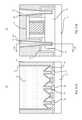
- FIG. 1Ais a cross-sectional view of fins taken at section line 1 A- 1 A in FIG. 1B ;
- FIG. 1Bis a cross-sectional view of a fin field effect transistor (finFET) showing a dummy gate structure in accordance with the present principles;
- FIG. 2Ais a cross-sectional view of the fins taken at section line 2 A- 2 A in FIG. 2B showing diamond shaped cross sections of source and drain (S/D) regions in accordance with the present principles;
- FIG. 2Bis a cross-sectional view of the finFET of FIG. 1B showing S/D regions formed in accordance with the present principles
- FIG. 3Ais a cross-sectional view of the fins taken at section line 3 A- 3 A in FIG. 3B showing a liner formed on the diamond shaped cross sections of the S/D regions in accordance with the present principles;
- FIG. 3Bis a cross-sectional view of the finFET of FIG. 2B showing the liner over the S/D regions formed in accordance with the present principles;
- FIG. 4Ais a cross-sectional view of the fins taken at section line 4 A- 4 A in FIG. 4B showing a dielectric fill formed over the liner in accordance with the present principles;
- FIG. 4Bis a cross-sectional view of the finFET of FIG. 3B showing the dielectric fill formed over the liner and a replacement metal gate structure installed in accordance with the present principles;
- FIG. 5Ais a cross-sectional view of the fins taken at section line 5 A- 5 A in FIG. 5B showing the dielectric fill formed over the liner in accordance with the present principles;
- FIG. 5Bis a cross-sectional view of the finFET of FIG. 4B showing the replacement metal gate structure recessed in accordance with the present principles
- FIG. 6Ais a cross-sectional view of the fins taken at section line 6 A- 6 A in FIG. 6B showing the dielectric fill opened to form contact openings and to expose a top portion of the diamond shaped cross sections of the S/D regions in accordance with the present principles;
- FIG. 6Bis a cross-sectional view of the finFET of FIG. 5B showing the dielectric fill opened to form contact openings in accordance with the present principles;
- FIG. 7Ais a cross-sectional view of the fins taken at section line 7 A- 7 A in FIG. 7B showing fins recessed through the contact openings and into the diamond shaped cross sections of the S/D regions in accordance with the present principles;
- FIG. 7Bis a cross-sectional view of the finFET of FIG. 6B showing the contact openings extended in accordance with the present principles
- FIG. 8Ais a cross-sectional view of the fins taken at section line 8 A- 8 A in FIG. 8B showing the dielectric fill further recessed to expose more of the diamond shaped cross sections of the S/D regions in accordance with the present principles;
- FIG. 8Bis a cross-sectional view of the finFET of FIG. 7B showing the extended contact openings in accordance with the present principles
- FIG. 9Ais a cross-sectional view of the fins taken at section line 9 A- 9 A in FIG. 9B showing the liner removed from a top portion of the diamond shaped cross sections of the S/D regions in accordance with the present principles;
- FIG. 9Bis a cross-sectional view of the finFET of FIG. 8B showing the extended contact openings in accordance with the present principles
- FIG. 10Ais a cross-sectional view of the fins taken at section line 10 A- 10 A in FIG. 10B showing a liner formed over the top portion and in the recesses of the diamond shaped cross sections of the S/D regions in accordance with the present principles;
- FIG. 10Bis a cross-sectional view of the finFET of FIG. 9B showing the liner formed in the extended contact openings in accordance with the present principles
- FIG. 11Ais a cross-sectional view of the fins taken at section line 11 A- 11 A in FIG. 11B showing contact metal formed over the top portion and in the recesses of the diamond shaped cross sections of the S/D regions in accordance with the present principles;
- FIG. 11Bis a cross-sectional view of the finFET of FIG. 10B showing the contact metal formed in the extended contact openings in accordance with the present principles.
- FIG. 12is a block/flow diagram showing methods for forming a finFET in accordance illustrative embodiments.
- the etching process for exposing source and drain (S/D) regionincludes two separate process steps.
- a first stepincludes a timed etch designed to stop on top of epitaxially grown S/D regions.
- the S/D regionsinclude diamond cross-sections so that a continued etch exposes a larger portion of a top of the diamonds.
- a selective etchis performed to remove Si of the fins from a central portion of the diamonds.
- a contact open etchis performed to open up the epitaxial material of the diamonds to maximize surface area or contact area once contacts are formed.
- a design for an integrated circuit chipmay be created in a graphical computer programming language, and stored in a computer storage medium (such as a disk, tape, physical hard drive, or virtual hard drive such as in a storage access network). If the designer does not fabricate chips or the photolithographic masks used to fabricate chips, the designer may transmit the resulting design by physical means (e.g., by providing a copy of the storage medium storing the design) or electronically (e.g., through the Internet) to such entities, directly or indirectly.
- the stored designis then converted into the appropriate format (e.g., GDSII) for the fabrication of photolithographic masks, which typically include multiple copies of the chip design in question that are to be formed on a wafer.
- the photolithographic masksare utilized to define areas of the wafer (and/or the layers thereon) to be etched or otherwise processed.
- the resulting integrated circuit chipscan be distributed by the fabricator in raw wafer form (that is, as a single wafer that has multiple unpackaged chips), as a bare die, or in a packaged form.
- the chipis mounted in a single chip package (such as a plastic carrier, with leads that are affixed to a motherboard or other higher level carrier) or in a multichip package (such as a ceramic carrier that has either or both surface interconnections or buried interconnections).
- the chipis then integrated with other chips, discrete circuit elements, and/or other signal processing devices as part of either (a) an intermediate product, such as a motherboard, or (b) an end product.
- the end productcan be any product that includes integrated circuit chips, ranging from toys and other low-end applications to advanced computer products having a display, a keyboard or other input device, and a central processor.
- material compoundswill be described in terms of listed elements, e.g., SiGe. These compounds include different proportions of the elements within the compound, e.g., SiGe includes Si x Ge 1-x where x is less than or equal to 1, etc. In addition, other elements may be included in the compound, and still function in accordance with the present principles. The compounds with additional elements will be referred to herein as alloys.
- any of the following “/”, “and/or”, and “at least one of”, for example, in the cases of “A/B”, “A and/or B” and “at least one of A and B”,is intended to encompass the selection of the first listed option (A) only, or the selection of the second listed option (B) only, or the selection of both options (A and B).
- such phrasingis intended to encompass the selection of the first listed option (A) only, or the selection of the second listed option (B) only, or the selection of the third listed option (C) only, or the selection of the first and the second listed options (A and B) only, or the selection of the first and third listed options (A and C) only, or the selection of the second and third listed options (B and C) only, or the selection of all three options (A and B and C).
- Thismay be extended, as readily apparent by one of ordinary skill in this and related arts, for as many items listed.
- FIG. 1Ais a cross-section taken at section line 1 A- 1 A of FIG. 1B .
- Device 10includes a dielectric layer 12 that may include a buried oxide (BOX) of a silicon-on-insulator substrate. Fins 14 may be formed from a semiconductor layer of the SOI substrate.
- a dummy gate structure 22(although a gate-first structure may also be employed) includes a dummy gate 20 , spacers 16 and a cap layer 18 .
- the dummy gate structures 20may include amorphous Si or polysilicon (although other materials may be employed), the spacers 16 and the cap layer 18 may include silicon nitride (although other materials may be employed).
- the fins 14may include monocrystalline Si, although other materials, such as SiGe, Ge, SiC, etc. may be employed.
- FIG. 2Ais a cross-section taken at section line 2 A- 2 A of FIG. 2B .
- the S/D regions 24may include Si, SiGe, Ge, etc.
- the S/D regions 24may be unmerged epitaxial S/D regions which have a different composition than the fin that they were grown on.
- the S/D regions 24may be doped during formation using an in-situ doping process, although other doping processes may be employed.
- the epitaxial growth processresults in a cross-section that is diamond-shaped for the S/D regions 24 .
- the diamond-shaped epitaxial layermay be referred to herein as a diamond or a S/D diamond 28 for ease of reference.
- a dielectric liner 26is formed over surfaces of the device 10 .
- the liner 26may include SiN, although other materials may be employed.
- FIG. 3Ais a cross-section taken at section line 3 A- 3 A of FIG. 3B .
- FIG. 4Ais a cross-section taken at section line 4 A- 4 A of FIG. 4B .
- a replacement metal gate (RMG) processis performed.
- a dielectric fill 30is employed to fill up spaces and gaps, followed by a planarizing step, e.g., a chemical mechanical polish (CMP).
- CMPchemical mechanical polish
- the dielectric fill 30may include a flowable oxide.
- the cap layer 18 and the dummy gate 20are removed and replaced with a gate dielectric 32 , a work function metal 34 and a gate conductor 36 .
- the gate dielectric 32may include high-k dielectric materials, such as e.g., HfO 2 .
- the work function metal 34may include Pt, Au, Ag, Cu, etc.
- the gate conductor 36may include W, etc.
- a top surface of the deviceis planarized, by performing, e.g., CMP. Note that gate replacement is not necessary in a gate-first process where the gate structure is formed without the use of a dummy gate.
- the replacement gate metalis recessed and capped with a capping layer (gate cap) 40 .
- a dielectric materiale.g., an oxide
- a CMP processis performed to planarize a top surface of the device 10 .
- FIG. 5Ais a cross-section taken at section line 5 A- 5 A of FIG. 5B .
- FIG. 6Ais a cross-section taken at section line 6 A- 6 A of FIG. 6B .
- Contact holes or openings 42are formed in the dielectric fill material 30 on sides of a gate structure 44 .
- the contact openings 42are formed by a first etch process that removes a large portion of the fill material 30 and exposes the diamonds 28 of the S/D regions 24 .
- the etch processmay include a patterned reactive ion etch (RIE) process that employs an etch chemistry that removes all materials, e.g., oxide, nitrides and Si.
- This etch processmay include a timed etch that removes material sufficient to open up the liner 26 and expose the material of the S/D regions 24 .
- RIEreactive ion etch
- FIG. 7Ais a cross-section taken at section line 7 A- 7 A of FIG. 7B .
- the recesses 46are formed by a second etch process that removes a portion of the fins 14 to open up a central portion (fins) in the diamonds 28 of the S/D regions 24 .
- the etch processmay be a continuation of the first etch process (e.g., timed etch) by switching the etch chemistry.
- the second etch processmay be performed separately from the first etch process.
- the second etch processmay include a selective etch to remove a portion of the fins 14 with minimal etching of oxides and nitrides, which act as mask materials to protect the diamonds 28 of the S/D regions 24 .
- the selective etch processincludes an HBr chemistry for a RIE.
- the recesses 46 formedpreferably leave behind a sufficient portion of the fins 14 to provide adequate reduction for current-crowding effects.
- the sufficient portionis less than about one half the height of the fin 14 .
- the recessed fin heightis less than about 30% of its original height. In still other embodiments, the recessed fin height is less than about 20% of its original height.
- FIG. 8Ais a cross-section taken at section line 8 A- 8 A of FIG. 8B . If the dielectric fill 30 includes oxide, the etch process is configured to remove oxide to expose the liner 26 .
- FIG. 9Ais a cross-section taken at section line 9 A- 9 A of FIG. 9B .
- the liner 26includes silicon nitride and may be removed with a selective etch with respect to, e.g., Si and oxide. This etch leaves a multiple surface exposure of the epitaxially formed S/D regions 24 .
- the exposed surfaceincludes external diamond surfaces, and internal surfaces where the fins 14 were recessed.
- FIG. 10Ais a cross-section taken at section line 10 A- 10 A of FIG. 10B .
- a contact liner 50is conformally formed in the contact holes 42 , recesses 46 and over exposed portions of the S/D regions 24 .
- the liner 50may include Ti, TiN, TaN, or other materials.
- the liner 50may be annealed to form a silicide with the S/D regions 24 .
- FIG. 11Ais a cross-section taken at section line 11 A- 11 A of FIG. 11B .
- a conductoris formed over the liner 50 .
- the conductor and the liner 50are planarized, e.g., by CMP, to form contacts 52 .
- the conductormay include a metal such as W, Cu, Al, etc. to form contacts 52 .
- the contacts 52follow multiple surfaces in contact with the liner 50 on the epitaxially formed S/D regions 24 .
- the liner 50 surfacesinclude external diamond surfaces, and internal surfaces where the fins 14 were recessed.
- each block of the block diagrams and/or flowchart illustration, and combinations of blocks in the block diagrams and/or flowchart illustrationcan be implemented by special purpose hardware-based systems that perform the specified functions or acts or carry out combinations of special purpose hardware and computer instructions.
- finsare formed on a substrate.
- the finsmay be formed in a silicon layer of a silicon-on-insulator (SOI) substrate, although other substrate configurations may be employed.
- SOIsilicon-on-insulator
- an optional dummy gate structuremay be formed on the fins. Alternately, a gate-first process may be employed.
- source and drain (S/D) regionsare epitaxially grown on the fins. The S/D regions include a diamond-shaped cross section.
- a dielectric lineris formed over the S/D regions.
- a dielectric fillis deposited over the dummy gate structure and the S/D regions.
- an optional dummy gate replacementmay be performed by replacing the dummy gate with a replacement metal gate structure and recessing the replacement metal gate structure.
- the dielectric fill over the S/D regionsis etched to expose a top portion of the diamond-shaped cross section.
- the dielectric fill etchmay include performing a timed etch in accordance with a pattern to reach the top portion of the diamond-shaped cross section in block 115 .
- the finsare recessed into the diamond-shaped cross section.
- the fin recess into the diamond-shaped cross sectionmay include performing a selective etch to etch a portion of the fins within the diamond-shaped cross section in block 117 .
- the selective etchmay include a reactive ion etch with an HBr chemistry.
- Blocks 114 and 116may include a same etch process with different chemistries at different times or may include two separate etch processes.
- a top portion of the diamond-shaped cross section of the S/D regionsis exposed. In block 120 , this may include etching away the dielectric liner from the top portion (e.g., exposing more of the top diamond facet surfaces).
- a contact lineris formed on the top portion of the diamond-shaped cross section of the S/D regions and in a recess where the fins were recessed.
- contactsare formed over surfaces of the top portion and in the recess. The contacts may be formed over at least portions of top diamond surfaces (facets) and on exposed sidewalls in the recess where the fins were recessed.
- the recess where the fins were recessedmay include at least one half an original fin height, although other amounts are contemplated, e.g., between 10% and 90% of the fin height.
- processingcontinues to complete the device.
Landscapes
- Engineering & Computer Science (AREA)
- Physics & Mathematics (AREA)
- Chemical & Material Sciences (AREA)
- Computer Hardware Design (AREA)
- Condensed Matter Physics & Semiconductors (AREA)
- General Physics & Mathematics (AREA)
- Manufacturing & Machinery (AREA)
- Microelectronics & Electronic Packaging (AREA)
- Power Engineering (AREA)
- Inorganic Chemistry (AREA)
- General Chemical & Material Sciences (AREA)
- Chemical Kinetics & Catalysis (AREA)
- Plasma & Fusion (AREA)
- Insulated Gate Type Field-Effect Transistor (AREA)
- Thin Film Transistor (AREA)
Abstract
Description
Claims (16)
Priority Applications (2)
| Application Number | Priority Date | Filing Date | Title |
|---|---|---|---|
| US14/794,997US9680020B2 (en) | 2015-07-09 | 2015-07-09 | Increased contact area for FinFETs |
| US15/592,597US9899525B2 (en) | 2015-07-09 | 2017-05-11 | Increased contact area for finFETs |
Applications Claiming Priority (1)
| Application Number | Priority Date | Filing Date | Title |
|---|---|---|---|
| US14/794,997US9680020B2 (en) | 2015-07-09 | 2015-07-09 | Increased contact area for FinFETs |
Related Child Applications (1)
| Application Number | Title | Priority Date | Filing Date |
|---|---|---|---|
| US15/592,597DivisionUS9899525B2 (en) | 2015-07-09 | 2017-05-11 | Increased contact area for finFETs |
Publications (2)
| Publication Number | Publication Date |
|---|---|
| US20170012129A1 US20170012129A1 (en) | 2017-01-12 |
| US9680020B2true US9680020B2 (en) | 2017-06-13 |
Family
ID=57730443
Family Applications (2)
| Application Number | Title | Priority Date | Filing Date |
|---|---|---|---|
| US14/794,997Expired - Fee RelatedUS9680020B2 (en) | 2015-07-09 | 2015-07-09 | Increased contact area for FinFETs |
| US15/592,597ActiveUS9899525B2 (en) | 2015-07-09 | 2017-05-11 | Increased contact area for finFETs |
Family Applications After (1)
| Application Number | Title | Priority Date | Filing Date |
|---|---|---|---|
| US15/592,597ActiveUS9899525B2 (en) | 2015-07-09 | 2017-05-11 | Increased contact area for finFETs |
Country Status (1)
| Country | Link |
|---|---|
| US (2) | US9680020B2 (en) |
Cited By (6)
| Publication number | Priority date | Publication date | Assignee | Title |
|---|---|---|---|---|
| US20150318351A1 (en)* | 2014-05-01 | 2015-11-05 | Globalfoundries Inc. | Multiple epitaxial head raised semiconductor structure and method of making same |
| US10297690B2 (en)* | 2016-12-30 | 2019-05-21 | Taiwan Semiconductor Manufacturing Co., Ltd. | Method of forming a contact structure for a FinFET semiconductor device |
| US11011422B2 (en) | 2018-10-11 | 2021-05-18 | International Business Machines Corporation | Self-aligned wrap-around trench contacts |
| US11309418B2 (en) | 2016-12-30 | 2022-04-19 | Taiwan Semiconductor Manufacturing Co., Ltd. | Contact structure for FinFET semiconductor device |
| US11443982B2 (en) | 2018-11-08 | 2022-09-13 | International Business Machines Corporation | Formation of trench silicide source or drain contacts without gate damage |
| US20230395715A1 (en)* | 2022-06-02 | 2023-12-07 | Globalfoundries U.S. Inc. | Multi-channel replacement metal gate device |
Families Citing this family (6)
| Publication number | Priority date | Publication date | Assignee | Title |
|---|---|---|---|---|
| WO2018009161A1 (en)* | 2016-07-02 | 2018-01-11 | Intel Corporation | Iii-v finfet transistor with v-groove s/d profile for improved access resistance |
| US9831254B1 (en)* | 2016-09-22 | 2017-11-28 | International Business Machines Corporation | Multiple breakdown point low resistance anti-fuse structure |
| US11495672B2 (en) | 2018-06-29 | 2022-11-08 | Intel Corporation | Increased transistor source/drain contact area using sacrificial source/drain layer |
| US10483375B1 (en)* | 2018-07-17 | 2019-11-19 | International Business Machines Coporation | Fin cut etch process for vertical transistor devices |
| US10755964B1 (en)* | 2019-05-31 | 2020-08-25 | Taiwan Semiconductor Manufacturing Co., Ltd. | Source/drain isolation structure and methods thereof |
| US11728223B2 (en) | 2019-12-20 | 2023-08-15 | Taiwan Semiconductor Manufacturing Company, Ltd. | Semiconductor device and methods of manufacture |
Citations (15)
| Publication number | Priority date | Publication date | Assignee | Title |
|---|---|---|---|---|
| US7456476B2 (en) | 2003-06-27 | 2008-11-25 | Intel Corporation | Nonplanar semiconductor device with partially or fully wrapped around gate electrode and methods of fabrication |
| US7915693B2 (en) | 2007-07-27 | 2011-03-29 | Kabushiki Kaisha Toshiba | Semiconductor device with fin and silicide structure |
| US20110147840A1 (en) | 2009-12-23 | 2011-06-23 | Cea Stephen M | Wrap-around contacts for finfet and tri-gate devices |
| US8258577B2 (en) | 2009-06-04 | 2012-09-04 | International Business Machines Corporation | CMOS inverter device with fin structures |
| US8362574B2 (en)* | 2010-06-04 | 2013-01-29 | Kabushiki Kaisha Toshiba | Faceted EPI shape and half-wrap around silicide in S/D merged FinFET |
| US20130187228A1 (en)* | 2012-01-19 | 2013-07-25 | Globalfoundries Inc. | FinFET Semiconductor Devices with Improved Source/Drain Resistance and Methods of Making Same |
| US20140001520A1 (en)* | 2012-06-29 | 2014-01-02 | Glenn A. Glass | Contact resistance reduced p-mos transistors employing ge-rich contact layer |
| US8841189B1 (en) | 2013-06-14 | 2014-09-23 | International Business Machines Corporation | Transistor having all-around source/drain metal contact channel stressor and method to fabricate same |
| US8859379B2 (en) | 2013-03-15 | 2014-10-14 | International Business Machines Corporation | Stress enhanced finFET devices |
| US8921191B2 (en) | 2013-02-05 | 2014-12-30 | GlobalFoundries, Inc. | Integrated circuits including FINFET devices with lower contact resistance and reduced parasitic capacitance and methods for fabricating the same |
| US20150137181A1 (en)* | 2013-11-19 | 2015-05-21 | International Business Machines Corporation | Stress inducing contact metal in finfet cmos |
| US9123826B1 (en)* | 2014-03-24 | 2015-09-01 | International Business Machines Corporation | Single crystal source-drain merged by polycrystalline material |
| US20150279840A1 (en)* | 2014-03-28 | 2015-10-01 | Taiwan Semiconductor Manufacturing Company, Ltd. | Finfets with low source/drain contact resistance |
| US20150295089A1 (en)* | 2014-04-11 | 2015-10-15 | Taiwan Semiconductor Manufacturing Company, Ltd. | Finfets with contact-all-around |
| US9379025B1 (en)* | 2015-06-19 | 2016-06-28 | International Business Machines Corporation | Method of forming source/drain contacts in unmerged FinFETs |
Family Cites Families (2)
| Publication number | Priority date | Publication date | Assignee | Title |
|---|---|---|---|---|
| US8263451B2 (en)* | 2010-02-26 | 2012-09-11 | Taiwan Semiconductor Manufacturing Company, Ltd. | Epitaxy profile engineering for FinFETs |
| US20140131777A1 (en)* | 2012-11-15 | 2014-05-15 | GlobalFoundries, Inc. | Integrated circuits and methods for fabricating integrated circuits with salicide contacts on non-planar source/drain regions |
- 2015
- 2015-07-09USUS14/794,997patent/US9680020B2/ennot_activeExpired - Fee Related
- 2017
- 2017-05-11USUS15/592,597patent/US9899525B2/enactiveActive
Patent Citations (15)
| Publication number | Priority date | Publication date | Assignee | Title |
|---|---|---|---|---|
| US7456476B2 (en) | 2003-06-27 | 2008-11-25 | Intel Corporation | Nonplanar semiconductor device with partially or fully wrapped around gate electrode and methods of fabrication |
| US7915693B2 (en) | 2007-07-27 | 2011-03-29 | Kabushiki Kaisha Toshiba | Semiconductor device with fin and silicide structure |
| US8258577B2 (en) | 2009-06-04 | 2012-09-04 | International Business Machines Corporation | CMOS inverter device with fin structures |
| US20110147840A1 (en) | 2009-12-23 | 2011-06-23 | Cea Stephen M | Wrap-around contacts for finfet and tri-gate devices |
| US8362574B2 (en)* | 2010-06-04 | 2013-01-29 | Kabushiki Kaisha Toshiba | Faceted EPI shape and half-wrap around silicide in S/D merged FinFET |
| US20130187228A1 (en)* | 2012-01-19 | 2013-07-25 | Globalfoundries Inc. | FinFET Semiconductor Devices with Improved Source/Drain Resistance and Methods of Making Same |
| US20140001520A1 (en)* | 2012-06-29 | 2014-01-02 | Glenn A. Glass | Contact resistance reduced p-mos transistors employing ge-rich contact layer |
| US8921191B2 (en) | 2013-02-05 | 2014-12-30 | GlobalFoundries, Inc. | Integrated circuits including FINFET devices with lower contact resistance and reduced parasitic capacitance and methods for fabricating the same |
| US8859379B2 (en) | 2013-03-15 | 2014-10-14 | International Business Machines Corporation | Stress enhanced finFET devices |
| US8841189B1 (en) | 2013-06-14 | 2014-09-23 | International Business Machines Corporation | Transistor having all-around source/drain metal contact channel stressor and method to fabricate same |
| US20150137181A1 (en)* | 2013-11-19 | 2015-05-21 | International Business Machines Corporation | Stress inducing contact metal in finfet cmos |
| US9123826B1 (en)* | 2014-03-24 | 2015-09-01 | International Business Machines Corporation | Single crystal source-drain merged by polycrystalline material |
| US20150279840A1 (en)* | 2014-03-28 | 2015-10-01 | Taiwan Semiconductor Manufacturing Company, Ltd. | Finfets with low source/drain contact resistance |
| US20150295089A1 (en)* | 2014-04-11 | 2015-10-15 | Taiwan Semiconductor Manufacturing Company, Ltd. | Finfets with contact-all-around |
| US9379025B1 (en)* | 2015-06-19 | 2016-06-28 | International Business Machines Corporation | Method of forming source/drain contacts in unmerged FinFETs |
Non-Patent Citations (2)
| Title |
|---|
| Nainani, A., et al., "Is strain engineering scalable in FinFET era? : teaching the old dog some new tricks," IEEE International Electron Devices Meeting (IEDM), Dec. 2012. (pp. 1-4). |
| Rooyackers, R., et al., "Doubling or quadrupling MuGFET fin integration scheme with higher pattern fidelity, lower CD variation and higher layout efficiency," International Electron Devices Meeting, Dec. 2006. (pp. 1-4). |
Cited By (9)
| Publication number | Priority date | Publication date | Assignee | Title |
|---|---|---|---|---|
| US20150318351A1 (en)* | 2014-05-01 | 2015-11-05 | Globalfoundries Inc. | Multiple epitaxial head raised semiconductor structure and method of making same |
| US9793358B2 (en)* | 2014-05-01 | 2017-10-17 | Globalfoundries Inc. | Non-planar semiconductor device with multiple-head epitaxial structure on fin |
| US10297690B2 (en)* | 2016-12-30 | 2019-05-21 | Taiwan Semiconductor Manufacturing Co., Ltd. | Method of forming a contact structure for a FinFET semiconductor device |
| US11309418B2 (en) | 2016-12-30 | 2022-04-19 | Taiwan Semiconductor Manufacturing Co., Ltd. | Contact structure for FinFET semiconductor device |
| US12349392B2 (en) | 2016-12-30 | 2025-07-01 | Taiwan Semiconductor Manufacturing Company, Ltd. | Semiconductor device and manufacturing method thereof |
| US11011422B2 (en) | 2018-10-11 | 2021-05-18 | International Business Machines Corporation | Self-aligned wrap-around trench contacts |
| US11443982B2 (en) | 2018-11-08 | 2022-09-13 | International Business Machines Corporation | Formation of trench silicide source or drain contacts without gate damage |
| US12417944B2 (en) | 2018-11-08 | 2025-09-16 | International Business Machines Corporation | Formation of trench silicide source or drain contacts without gate damage |
| US20230395715A1 (en)* | 2022-06-02 | 2023-12-07 | Globalfoundries U.S. Inc. | Multi-channel replacement metal gate device |
Also Published As
| Publication number | Publication date |
|---|---|
| US20170012129A1 (en) | 2017-01-12 |
| US9899525B2 (en) | 2018-02-20 |
| US20170250285A1 (en) | 2017-08-31 |
Similar Documents
| Publication | Publication Date | Title |
|---|---|---|
| US9899525B2 (en) | Increased contact area for finFETs | |
| US10395995B2 (en) | Dual liner silicide | |
| US10297506B2 (en) | HDP fill with reduced void formation and spacer damage | |
| US9508597B1 (en) | 3D fin tunneling field effect transistor | |
| US10319816B2 (en) | Silicon germanium fin channel formation | |
| KR20220115841A (en) | Semiconductor device and method | |
| US10854753B2 (en) | Uniform fin dimensions using fin cut hardmask | |
| US10403740B2 (en) | Gate planarity for FinFET using dummy polish stop |
Legal Events
| Date | Code | Title | Description |
|---|---|---|---|
| AS | Assignment | Owner name:INTERNATIONAL BUSINESS MACHINES CORPORATION, NEW Y Free format text:ASSIGNMENT OF ASSIGNORS INTEREST;ASSIGNORS:BASKER, VEERARAGHAVAN S.;LIN, CHUNG-HSUN;LIU, ZUOGUANG;AND OTHERS;REEL/FRAME:036043/0220 Effective date:20150630 | |
| AS | Assignment | Owner name:GLOBALFOUNDRIES U.S. 2 LLC, NEW YORK Free format text:ASSIGNMENT OF ASSIGNORS INTEREST;ASSIGNOR:INTERNATIONAL BUSINESS MACHINES CORPORATION;REEL/FRAME:037941/0646 Effective date:20160307 | |
| AS | Assignment | Owner name:GLOBALFOUNDRIES INC., CAYMAN ISLANDS Free format text:ASSIGNMENT OF ASSIGNORS INTEREST;ASSIGNOR:GLOBALFOUNDRIES U.S. 2 LLC;REEL/FRAME:038224/0720 Effective date:20160407 | |
| FEPP | Fee payment procedure | Free format text:PAYOR NUMBER ASSIGNED (ORIGINAL EVENT CODE: ASPN); ENTITY STATUS OF PATENT OWNER: LARGE ENTITY | |
| STCF | Information on status: patent grant | Free format text:PATENTED CASE | |
| AS | Assignment | Owner name:WILMINGTON TRUST, NATIONAL ASSOCIATION, DELAWARE Free format text:SECURITY AGREEMENT;ASSIGNOR:GLOBALFOUNDRIES INC.;REEL/FRAME:049490/0001 Effective date:20181127 | |
| AS | Assignment | Owner name:GLOBALFOUNDRIES U.S. INC., CALIFORNIA Free format text:ASSIGNMENT OF ASSIGNORS INTEREST;ASSIGNOR:GLOBALFOUNDRIES INC.;REEL/FRAME:054633/0001 Effective date:20201022 | |
| AS | Assignment | Owner name:GLOBALFOUNDRIES INC., CAYMAN ISLANDS Free format text:RELEASE BY SECURED PARTY;ASSIGNOR:WILMINGTON TRUST, NATIONAL ASSOCIATION;REEL/FRAME:054636/0001 Effective date:20201117 | |
| FEPP | Fee payment procedure | Free format text:MAINTENANCE FEE REMINDER MAILED (ORIGINAL EVENT CODE: REM.); ENTITY STATUS OF PATENT OWNER: LARGE ENTITY | |
| AS | Assignment | Owner name:GLOBALFOUNDRIES U.S. INC., NEW YORK Free format text:RELEASE BY SECURED PARTY;ASSIGNOR:WILMINGTON TRUST, NATIONAL ASSOCIATION;REEL/FRAME:056987/0001 Effective date:20201117 | |
| LAPS | Lapse for failure to pay maintenance fees | Free format text:PATENT EXPIRED FOR FAILURE TO PAY MAINTENANCE FEES (ORIGINAL EVENT CODE: EXP.); ENTITY STATUS OF PATENT OWNER: LARGE ENTITY | |
| STCH | Information on status: patent discontinuation | Free format text:PATENT EXPIRED DUE TO NONPAYMENT OF MAINTENANCE FEES UNDER 37 CFR 1.362 | |
| FP | Lapsed due to failure to pay maintenance fee | Effective date:20210613 |