US9674118B2 - System and method for low-latency network data switching - Google Patents
System and method for low-latency network data switchingDownload PDFInfo
- Publication number
- US9674118B2 US9674118B2US14/219,908US201414219908AUS9674118B2US 9674118 B2US9674118 B2US 9674118B2US 201414219908 AUS201414219908 AUS 201414219908AUS 9674118 B2US9674118 B2US 9674118B2
- Authority
- US
- United States
- Prior art keywords
- data
- data processing
- crosspoint
- port
- digital
- Prior art date
- Legal status (The legal status is an assumption and is not a legal conclusion. Google has not performed a legal analysis and makes no representation as to the accuracy of the status listed.)
- Active, expires
Links
Images


Classifications
- H—ELECTRICITY
- H04—ELECTRIC COMMUNICATION TECHNIQUE
- H04L—TRANSMISSION OF DIGITAL INFORMATION, e.g. TELEGRAPHIC COMMUNICATION
- H04L49/00—Packet switching elements
- H04L49/30—Peripheral units, e.g. input or output ports
- H—ELECTRICITY
- H04—ELECTRIC COMMUNICATION TECHNIQUE
- H04L—TRANSMISSION OF DIGITAL INFORMATION, e.g. TELEGRAPHIC COMMUNICATION
- H04L45/00—Routing or path finding of packets in data switching networks
- H04L45/28—Routing or path finding of packets in data switching networks using route fault recovery
- H—ELECTRICITY
- H04—ELECTRIC COMMUNICATION TECHNIQUE
- H04L—TRANSMISSION OF DIGITAL INFORMATION, e.g. TELEGRAPHIC COMMUNICATION
- H04L47/00—Traffic control in data switching networks
- H04L47/10—Flow control; Congestion control
- H—ELECTRICITY
- H04—ELECTRIC COMMUNICATION TECHNIQUE
- H04L—TRANSMISSION OF DIGITAL INFORMATION, e.g. TELEGRAPHIC COMMUNICATION
- H04L49/00—Packet switching elements
- H04L49/55—Prevention, detection or correction of errors
- H04L49/557—Error correction, e.g. fault recovery or fault tolerance
- H04L12/24—
- H—ELECTRICITY
- H04—ELECTRIC COMMUNICATION TECHNIQUE
- H04L—TRANSMISSION OF DIGITAL INFORMATION, e.g. TELEGRAPHIC COMMUNICATION
- H04L41/00—Arrangements for maintenance, administration or management of data switching networks, e.g. of packet switching networks
- H—ELECTRICITY
- H04—ELECTRIC COMMUNICATION TECHNIQUE
- H04L—TRANSMISSION OF DIGITAL INFORMATION, e.g. TELEGRAPHIC COMMUNICATION
- H04L47/00—Traffic control in data switching networks
- H04L47/10—Flow control; Congestion control
- H04L47/24—Traffic characterised by specific attributes, e.g. priority or QoS
Definitions
- This disclosurerelates to digital networking, specifically to the replication and switching of digital data signals over a network.
- a great number of business transactionsare conducted over digital networks, including transactions involving the purchase and sale of securities.
- Such transactionsgenerate a large and ever increasing amount of raw real-time data.
- digital market data information from the NASDAQ securities marketcan reach data rates on the order of 2 Gb/s at peak trading hours.
- the handling of such large streams of dataintroduces competing challenges.
- Most computing systemsdo not have sufficient power to process the entirety of the data generated in the electronic marketplace. Consequently, it is desirable for individual clients to receive processed data that includes only the information important to their own needs. However, the time needed to process this data can introduce significant and often unpredictable non-deterministic delays in the client's receipt of the data.
- a networking apparatusincludes a digital crosspoint switch (which may be a solid state crosspoint chip), a data processing card, and a host controller.
- the digital crosspoint switchincludes a plurality of crosspoint ports, including a set of internal crosspoint ports and a set of external crosspoint ports.
- the digital crosspoint switchalso includes a crosspoint control interface through which the digital crosspoint switch can be configured.
- the data processing cardhas at least one data processing input port and at least one data processing output port. These data processing ports are connected to respective internal crosspoint ports.
- the data processing cardincludes a programmable logic device, such as a field programmable gate array (FPGA).
- the programmable logic deviceis operable to process data received on the data processing input port and to output processed data on the data processing output port.
- the data processing cardincludes a logic control interface through which the programmable logic device is configurable.
- the host controlleris connected to both the crosspoint control interface and the logic control interface.
- the host controllerincludes a processor and a non-transitory computer-readable medium that stores executable management instructions. These executable management instructions, when executed on the processor, are operative to configure the digital crosspoint switch over the crosspoint control interface and to configure the data processing card over the logic control interface.
- the programmable logic deviceis configured by sending FPGA instructions over the logic control interface.
- FIG. 1is a schematic functional block diagram of the architecture of a network switching system according to some embodiments.
- FIG. 2is a schematic functional block diagram of the architecture of a network switching system according to some embodiments.
- FIG. 3is a flow diagram of a feed filtering process performed in some embodiments.
- FIG. 4is a schematic illustration of a command-line user interface implemented in some embodiments.
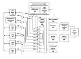
- a network switching apparatusincludes a digital crosspoint switch 100 , a data processing card 102 , and a host controller 104 .
- the digital crosspoint switchincludes a plurality of crosspoint ports 106 , 108 , 110 , 112 , 114 , 116 , 118 , 120 , and 122 .
- three of the crosspoint ports, 106 , 108 , and 110are connected to the data processing card 102 and are referred to herein as internal crosspoint ports.
- crosspoint ports 112 , 114 , 116 , 118 , 120 , and 122are connected to respective transceivers 124 , 126 , 128 , 130 , 132 , 134 that allow connection with a data network such as a local area network (LAN) or a wide area network (WAN).
- Crosspoint ports 112 , 114 , 116 , 118 , 120 , and 122are referred to herein as external crosspoint ports.
- internal crosspoint portsand “external crosspoint ports” are used herein as a matter of labeling, and those different terms do not necessarily imply that that “internal crosspoint ports” and “external crosspoint ports” are functionally different from one another from the perspective of the digital crosspoint switch 100 .
- transceivers 124 , 126 , 128 , 130 , 132 , 134 and their respective crosspoint ports 112 , 114 , 116 , 118 , 120 , and 122may be made using interfaces such as SFI and XFI, among other alternatives.
- the digital crosspoint switch 100is operative to replicate data received at one crosspoint port onto one or more other selected crosspoint ports.
- the digital crosspoint switch 100is in communication with a crosspoint control interface 136 through which the configuration of the digital crosspoint switch 100 is controlled by selective mapping of ports.
- data received at crosspoint port 106is replicated to ports 120 and 122 ; data received at port 108 is replicated both to port 116 and to port 118 ; data received at port 112 is replicated to port 114 ; and data received at port 114 is replicated to ports 110 and 112 .
- the mapping of portsis not necessarily symmetrical.
- data received at port 108is replicated to port 116 , but data received at port 116 is not necessarily replicated to port 108 .
- Some ports, such as port 114may be configured to accommodate the bidirectional flow of data, while other ports, such as ports 116 and 112 , may be configured to accommodate only a unidirectional flow of data. While the foregoing describes one exemplary configuration of the digital crosspoint switch 100 , the configuration of the digital crosspoint switch 100 may be changed by sending configuration instructions to the crosspoint control interface 136 .
- data received on one or more of the external crosspoint portsmay be directed to the data processing card 102 for processing.
- the results of the data processingmay then be fed back into the digital crosspoint switch 100 to be replicated at one or more external crosspoint ports.
- the data processing card 102includes a programmable logic device 146 , such as a field-programmable gate array (FPGA).
- the data processing card 102is configurable through a logic control interface 148 , through which the data processing card 102 receives program instructions and/or parameters for the programmable logic device 142 .
- the data processing cardincludes a plurality of data processing ports 140 , 142 , and 144 . It should be noted that embodiments may include additional ports, but for simplicity, only ports 140 , 142 , and 144 are illustrated here. Data processing ports 140 , 142 , and 144 are connected to respective internal crosspoint ports 106 , 108 , 110 .
- transceiver 126is connected over a data network to a digital market data source 138 , which provides a digital market data feed to the transceiver 126 .
- the digital market data feedmay be, for example, a feed from the NASDAQ exchange in the ITCH format, or a feed from the New York Stock Exchange in the XDP format.
- a digital market data feedis sent as a series of UDP (User Datagram Protocol) packets. These UDP packets may themselves be encapsulated with an Ethernet frame.
- UDPUser Datagram Protocol
- the data processing card 102may perform a variety of different data processing operations.
- the data processing card 102may receive the market data feed on data processing port 144 , which is being used as a data processing input port.
- data processing ports 140 and 142After processing by the programmable logic device 146 , one or more processed market data feeds may then be output to data processing ports 140 and 142 , which are being used as data processing output ports.
- data processing input portand “data processing output port” are label used for ease of understanding and do not necessarily reflect differences in hardware.
- data processing port 144may act as an input data processing port in some configurations of the system (such as the configuration illustrated in FIG. 1 ), but the same port could act as a data processing output port in other configurations.
- One example of a processing operation that can be performed by the data processing card 102is feed filtering.
- the data processing card 102receives on data processing port 144 a digital market data feed consisting of a series of UDP packets.
- the programmable logic device 146identifies the packets that satisfy a first predetermined filtering criterion, and the packets that satisfy that first criterion are output on a first data processing output port 140 .
- the programmable logic device 146also identifies the packets that satisfy a second predetermined filtering criterion, and the packets that satisfy that second criterion are output on a second data processing output port 142 .
- the programmable logic device 146may determine whether the packet includes one or more preselected symbols representing particular securities that are traded on the market, such as stock symbols (e.g. MSFT, GOOG) or symbols for exchange-traded funds (e.g. SPY, VOO).
- stock symbolse.g. MSFT, GOOG
- symbols for exchange-traded fundse.g. SPY, VOO
- a digital market data feedis received from the digital market data source 138 at transceiver 126 , which in turn is connected to external crosspoint port 114 .
- external crosspoint port 114is referred to as a master port.
- the digital crosspoint switch 100is configured to replicate the market data feed at internal crosspoint port 110 .
- the internal crosspoint port 110is connected to a data processing input port 144 of the data processing card 102 .
- the programmable logic device 146processes the digital market data feed (e.g., by filtering) to generate two processed market data feeds.
- the first processed market data feedis output on a first data processing output port 140
- the second processed market data feedis output on a second data processing output port 142 .
- the digital crosspoint switch 100As for the first processed market data feed (from data processing output port 140 ), it is received by the digital crosspoint switch 100 at internal crosspoint port 106 .
- the digital crosspoint switch 100is configured to replicate the first processed market data feed at two of the external crosspoint ports, port 120 and port 122 , which are connected to respective transceivers 132 and 134 . These transceivers send the first processed market data feed over a data network to respective clients 150 , 152 .
- the digital crosspoint switch 100As for the second processed market data feed (from data processing output port 142 ), it is received by the digital crosspoint switch 100 at internal crosspoint port 108 .
- the digital crosspoint switch 100is configured to replicate the first processed market data feed at two of the external crosspoint ports, port 116 and port 118 , which are connected to respective transceivers 128 and 130 . These transceivers send the first processed market data feed over a data network to respective clients 154 , 156 .
- a digital market data feedis processed to generate different processed market data feeds that are disseminated to different clients according to the needs of those clients.
- the systemcan be reconfigured to process additional digital market data feeds to generate still more processed market data feeds for additional clients.
- market datamakes two passes through the digital crosspoint switch 100 .
- the datapasses through the crosspoint switch both on its way to the data processing card 102 and on its way from the data processing card 102 .
- this architecturea greater number of crosspoint ports are required to serve as internal crosspoint ports, leaving fewer ports available to serve as external crosspoint ports (or requiring use of a larger crosspoint switch).
- this architectureleads to much greater flexibility in the configuration of the system, particularly as the market data can be replicated both before and after processing by the data processing card 102 .
- the digital crosspoint switch 100may also be configured to replicate the unprocessed digital market data feed.
- the digital market data feedis replicated at external crosspoint port 112 without being processed by the data processing card 102 .
- a LAN switch 158such as a layer 2/3 switch, provides a data path back to the digital market data source 138 from the clients 150 , 152 , 154 , and 156 .
- Packet data originating from a clientpasses through the LAN switch 158 to transceiver 124 , which in turn is connected to external crosspoint port 112 .
- Data received at port 112is then replicated by the digital crosspoint switch 100 to crosspoint port 114 , from which it passes through transceiver 126 to the digital market data source 138 .
- port 112is referred to as a crossover port.
- the configuration of the digital crosspoint switchis performed by the host controller 104 in accordance with instructions received by a user.
- the host controller 104includes a processor 160 and a non-transitory computer-readable storage medium 162 .
- the storage medium 162stores executable management instructions that, when executed on the processor, are operative to configure the digital crosspoint switch 100 over the crosspoint control interface 136 and to configure the programmable logic device 146 over the logic control interface 148 .
- the host controller 104can receive user instructions through a variety of access points.
- the host controller of FIG. 1is provided with a management network interface 164 through which a user can log on over a computer network.
- the host controller 104may further include a console interface 166 , through which a user can connect a keyboard and a computer monitor.
- the host controller 104may be provided with a serial port (not illustrated), which a user can access using a null modem cable.
- the host controller 104provides a user interface 168 , such as a command-line interface, through which the user provides instructions regarding the configuration of the system.
- the host controller 104configures the data processing card 102 through the logic control interface 148 and configures the digital crosspoint switch 100 through the crosspoint control interface 136 .
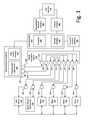
- a digital crosspoint switch 200is connected to several external network interfaces, including Small Form-Factor Pluggable (SFP) transceivers 202 , 204 , 206 , and 208 , and Quad Small Form-Factor Pluggable (QSFP) transceivers 210 , 212 .
- SFPSmall Form-Factor Pluggable
- QSFPQuad Small Form-Factor Pluggable
- the systemincludes thirty-two SFP transceivers and four QSFP transceivers.
- these SFP and QSFP transceiversare accessible on the front panel of a rack mount unit.
- the systemfurther includes a data processing card 214 connected to the digital crosspoint switch 200 through internal QSFP-like interfaces 216 and 218 , each of which preferably conveys four 10 Gb Ethernet signals.
- Internal interfaces 216 and 218may make use of Samtec connectors.
- each of the SFP interfacessupports Ethernet connections with a range of speeds, including 10 Mb, 100 Mb, 1 Gb, and 10 Gb Ethernet. While the use of SFP and QSFP transceivers is described herein by way of example, it should be noted that the use of SFP+ and QSFP+ transceivers is also contemplated in some embodiments.
- Each of the SFP interfaces 202 , 204 , 206 , 208is connected to a respective external port of the digital crosspoint switch 200 .
- Each of the QSFP interfaces 210 , 212 , 216 , 218is connected to a respective set of four external ports of digital crosspoint switch 200 .
- each of the internal QSFP interfaces 216 and 218is connected to a respective set of four internal ports of the digital crosspoint switch 200 . Consequently, in a system with 32 external SFP interfaces, four external QSFP interfaces, and two internal QSFP interfaces, a total of fifty-six crosspoint ports are employed.
- the digital crosspoint switchis a 72-port asynchronous crosspoint switch that supports random-access programming of each input and output port, such that each data output can be programmed to connect to any one of the inputs. Unused ports can be powered down for energy efficiency.
- An appropriate crosspoint switchis available from Vitesse Semiconductor.
- the data processing card 214is provided with a high-performance FPGA 220 .
- Appropriate FPGAs for use in the data processing card 214include those in the Stratix V line from Altera Corporation.
- the data processing card 214further includes a memory 222 and preferably includes a Pulse-Per-Second (PPS) input 224 for use in time stamping applications.
- PPSPulse-Per-Second
- the data processing card 214may include additional QSFP interfaces 226 , 228 .
- the system of FIG. 2further includes crosspoint control circuitry 230 .
- Crosspoint control circuitry 230may be implemented by a FPGA, although the FPGA of the crosspoint control circuitry 230 need not have as high performance as that of FPGA 220 .
- Appropriate FPGAs for use in the crosspoint control circuitry 230include those available from Lattice Semiconductor.
- the crosspoint control circuitry 230communicates with the digital crosspoint switch 200 through a serial bus 232 , which may be an Inter-Integrated Circuit (I 2 C) bus.
- the crosspoint controller circuitry 230may also communicate with and/or control additional hardware in the system over the serial bus 232 , such as temperature gauges 234 and cooling fans 236 to monitor and maintain the operating environment of the system.
- the host controller 238is implemented as main board including a processor 240 .
- the processor 240is an Intel Atom processor.
- the processor 240may be an Intel Xeon or other processor.
- the host controller 238further includes memory 242 .
- the host controller 238is configured to run a Linux Ubuntu kernel.
- the host controllerfurther includes a network interface 246 , which may be on the main board or may be a separate Network Interface Controller (NIC), through which the host controller 238 receives user instructions.
- the NIC 246may be a 1 Gb Ethernet connection.
- serial bus 248which may be a Peripheral Component Interconnect Express (PCI Express) bus.
- PCI ExpressPeripheral Component Interconnect Express
- the host controller 238communicates with the crosspoint control circuitry 230 through a serial bus 250 .
- serial bus 250is a Universal Serial Bus (USB) connection.
- the data processing card( FIG. 1, 102 ; FIG. 2, 214 ) can be configured to perform a variety of operations.
- One such operationis feed filtering.
- a complete digital market data feedcan reach data rates on the order of 2 Gb/s, particularly near the opening and closing of a securities market. Such data rates cannot readily be processed by many computing systems, at least not without introducing significant processing latency. Consequently, it is useful for a client (or group of clients) to receive only the portion of the data feed that is relevant to that client (or group).
- the data processing cardcan be configured to perform feed filtering.
- the data processing cardreceives, on a data processing input port, a network data packet that includes a market data message.
- the data processing carddetermines whether the packet satisfies a first filtering criterion. If the packet satisfies the first filtering criterion, then in step 304 , the packet is output on a first one of the data processing output ports.
- the data processing carddetermines whether the packet satisfies a second filtering criterion. If so, then in step 308 , the packet is output on a second one of the data processing output ports.
- the data processing cardcontinues to process additional data packets as they arrive.
- the packets output on the different output portsconstitute different processed market data feeds.
- the different processed market data feedsare then fed back through the digital crosspoint switch (steps 310 , 312 ) to be replicated and sent to one or more clients.
- the network data packetsmay include market data messages that include a security symbol, such as a symbol for a stock (e.g. MSFT, GOOG) or a symbol for an exchange-traded fund (e.g. SPY, VOO).
- the data processing cardmay store in its memory 222 a group of one or more symbols associated with each of the data processing output ports, and the data processing card may then output to each output port only those network data packets that include a symbol from the respective group.
- Another criterion that may be used when performing feed filteringis to filter by metadata in the network data packet. For example, different clients may subscribe to different levels of service from a digital market data source, and they may not be entitled to receive all data from that data source. In such a case, packets many include information identifying different multicast groups, and the digital market data feed may be filtered such that clients receive only those packets pertaining to multicast groups to which they are entitled.
- a different operation that can be performed by a data processing cardis to perform time stamping.
- the data processing cardcombines time data from the PPS input 224 with network data packets received over a data processing input port to generate time-stamp data. This allows precise recording of the time at which a network data packet has been received and thus permits detection of any undue delay in the receipt of the digital market data feed.
- Digital market data feedsare typically supplied in different protocols for different markets.
- the data processing cardcan be configured to convert the protocol of the digital market data feed; perhaps into a common, market-neutral format.
- a further operation that can be performed by the data processing cardis multiplexing of upstream data.
- a data path from the clients 150 , 152 , 154 , and 156 back to the market data source 138was provided through a separate LAN switch 158
- an upstream data pathmay instead be provided through the data processing card 102 .
- data from the clients 150 , 152 , 154 , and 156is directed by the crosspoint switch 100 to the data processing card 102 .
- the data processing card 102is configured to multiplex data from the clients onto a single upstream data path to the market data source 138 .
- the data processing card 102can make use of, for example, a round-robin scheduling algorithm.
- the upstream data pathcan be directed through the digital crosspoint switch 100 or through another route, such as through QSFP connectors 226 or 228 ( FIG. 2 ).
- the configuration of the data processing cardis performed by operation of the host controller sending FPGA program instructions to the FPGA 220 of the data processing card and/or by the host controller storing data in the memory 222 of the data processing card.
- the FPGAmay be configured through the use of FPGA program instructions to perform feed filtering, while information regarding the criteria used for feed filtering (e.g., groups of symbols associated with different data processing output ports) is stored in the memory 222 . This allows the data processing card to be reconfigured by the host controller without requiring the FPGA 220 to be reprogrammed for every change in filtering criteria. For more significant changes in programming of the FPGA, e.g.
- the host controller 238configures the data processing card 214 by sending FPGA program instructions over the serial bus 248 .
- the host controller 238retrieves FPGA program instructions over a computer network through its network interface controller 246 and reprograms the FPGA 220 by sending the FPGA program instructions over the serial bus 248 .
- the memory 242 ( FIG. 2 ) of the host controller 238stores executable management instructions that, when executed on the processor 240 , are operative to provide a user interface for receiving user commands and to configure the digital crosspoint switch and the data processing card in response to the user commands.
- the user interfaceis a command line interface that can be accessed through a management network interface 164 (FIG. 1 ), through a console interface 166 , through a serial port, or by other means.
- the user interfacemay be an application program running in a Linux environment.
- step 400at the “$” prompt of a Linux shell, the user evokes the command line user interface with the “xpmcli” command. The user interface then presents its own command-line interface with the prompt “+XPM #”.
- step 402the user creates a port group labeled “Saturn” by using the “group [groupname]” command. This invokes a shell interface for the Saturn group using the prompt “Saturn:”.
- step 404using the “add” command, the user adds Ethernet ports labeled eth 20 , eth 21 , eth 22 , and eth 27 to the Saturn group.
- step 406using the “master” command, the user identifies the port labeled eth 27 as the master port through which data for the Saturn group is received, such as port 114 of FIG. 1 .
- the host controllerconfigures the crossover switch to replicate data received at port eth 27 on the remaining ports in the Saturn group, namely ports eth 20 , eth 21 , and eth 22 .
- step 408using the “crossover” command, the user identifies the port labeled eth 21 as the crossover port that provides a return data path to the master port, such as port 112 of FIG. 1 .
- the host controllerconfigures the crossover switch to replicate data received at port eth 21 onto the master port eth 27 .
- the userexits the Saturn shell and returns to the “+XPM #” prompt.
- the userin step 412 , creates a symbol group labeled “ETF” for electronically-traded funds.
- the useradds the symbols SPY, VOO, and EEM to the ETF symbol group.
- the usercreates a symbol group labeled “stocks.”
- the useradds the symbols MSFT, GOOG, and APPL to the stocks group.
- the useradds new ports eth 28 and eth 29 to the Saturn group and indicates that those ports are members of symbol group ETF.
- the useradds new port eth 30 to the Saturn group and indicates that it is a member of the “stocks” symbol group.
- the host controllerconfigures the crossover switch to send data from the master port eth 27 to the data processing card, and it configures the data processing card to provide two filtered outputs: one filtered output containing data that relates to the “stocks” group, and another filtered output that contains data relating to the ETF group.
- the host controllerfurther configures the crosspoint switch to direct the filtered output for the “stocks” group to port eth 30 and to direct the filtered output for the ETF group to ports eth 28 and eth 29 .
- the commandsmay have different names or syntaxes.
- the user interfacemay be altered according to other known principles.
- the user interfacecould be implemented as a web page or a graphical user interface.
Landscapes
- Engineering & Computer Science (AREA)
- Computer Networks & Wireless Communication (AREA)
- Signal Processing (AREA)
- Data Exchanges In Wide-Area Networks (AREA)
- General Engineering & Computer Science (AREA)
- Theoretical Computer Science (AREA)
- Human Computer Interaction (AREA)
- Physics & Mathematics (AREA)
- General Physics & Mathematics (AREA)
Abstract
Description
Claims (20)
Priority Applications (6)
| Application Number | Priority Date | Filing Date | Title |
|---|---|---|---|
| US14/219,908US9674118B2 (en) | 2014-03-19 | 2014-03-19 | System and method for low-latency network data switching |
| AU2015231197AAU2015231197B2 (en) | 2014-03-19 | 2015-03-19 | System and method for low-latency network data switching |
| PCT/US2015/021581WO2015143226A1 (en) | 2014-03-19 | 2015-03-19 | System and method for low-latency network data switching |
| US15/614,553US10484268B2 (en) | 2014-03-19 | 2017-06-05 | System and method for low-latency network data switching |
| US16/377,143US10917335B2 (en) | 2014-03-19 | 2019-04-05 | System and method for low-latency network data switching |
| US17/143,201US11575595B2 (en) | 2014-03-19 | 2021-01-07 | System and method for low-latency network data switching |
Applications Claiming Priority (1)
| Application Number | Priority Date | Filing Date | Title |
|---|---|---|---|
| US14/219,908US9674118B2 (en) | 2014-03-19 | 2014-03-19 | System and method for low-latency network data switching |
Related Child Applications (1)
| Application Number | Title | Priority Date | Filing Date |
|---|---|---|---|
| US15/614,553ContinuationUS10484268B2 (en) | 2014-03-19 | 2017-06-05 | System and method for low-latency network data switching |
Publications (2)
| Publication Number | Publication Date |
|---|---|
| US20150271106A1 US20150271106A1 (en) | 2015-09-24 |
| US9674118B2true US9674118B2 (en) | 2017-06-06 |
Family
ID=54143148
Family Applications (4)
| Application Number | Title | Priority Date | Filing Date |
|---|---|---|---|
| US14/219,908Active2035-07-15US9674118B2 (en) | 2014-03-19 | 2014-03-19 | System and method for low-latency network data switching |
| US15/614,553ActiveUS10484268B2 (en) | 2014-03-19 | 2017-06-05 | System and method for low-latency network data switching |
| US16/377,143ActiveUS10917335B2 (en) | 2014-03-19 | 2019-04-05 | System and method for low-latency network data switching |
| US17/143,201Active2034-10-23US11575595B2 (en) | 2014-03-19 | 2021-01-07 | System and method for low-latency network data switching |
Family Applications After (3)
| Application Number | Title | Priority Date | Filing Date |
|---|---|---|---|
| US15/614,553ActiveUS10484268B2 (en) | 2014-03-19 | 2017-06-05 | System and method for low-latency network data switching |
| US16/377,143ActiveUS10917335B2 (en) | 2014-03-19 | 2019-04-05 | System and method for low-latency network data switching |
| US17/143,201Active2034-10-23US11575595B2 (en) | 2014-03-19 | 2021-01-07 | System and method for low-latency network data switching |
Country Status (3)
| Country | Link |
|---|---|
| US (4) | US9674118B2 (en) |
| AU (1) | AU2015231197B2 (en) |
| WO (1) | WO2015143226A1 (en) |
Cited By (4)
| Publication number | Priority date | Publication date | Assignee | Title |
|---|---|---|---|---|
| US20190238452A1 (en)* | 2014-03-19 | 2019-08-01 | Metamako General Pty Ltd Acn 163 573 331 In Its Capacity As General Partner Of Metamako Technology | System and method for low-latency network data switching |
| US10929405B2 (en) | 2017-11-21 | 2021-02-23 | Gto Llc | Systems and methods for distributed architecture of market-data processing device |
| US11734757B2 (en) | 2020-04-14 | 2023-08-22 | Banque Nationale Du Canada | Computer implemented method and system for automating analysis of profit and loss (PnL) variations based on market events |
| US12387266B2 (en) | 2019-10-08 | 2025-08-12 | Banque Nationale Du Canada | System and method for prioritizing transmission of trading data over a bandwitdh-constrained communication link |
Families Citing this family (15)
| Publication number | Priority date | Publication date | Assignee | Title |
|---|---|---|---|---|
| KR101748546B1 (en)* | 2014-08-13 | 2017-06-16 | 메타마코 테크놀로지 엘피 | Apparatus and method for low latency switching |
| US9912532B2 (en)* | 2015-02-04 | 2018-03-06 | International Business Machines Corporation | Port group configuration for interconnected communication devices |
| US12276420B2 (en) | 2016-02-03 | 2025-04-15 | Strong Force Iot Portfolio 2016, Llc | Industrial internet of things smart heating systems and methods that produce and use hydrogen fuel |
| US11327475B2 (en) | 2016-05-09 | 2022-05-10 | Strong Force Iot Portfolio 2016, Llc | Methods and systems for intelligent collection and analysis of vehicle data |
| US11507064B2 (en) | 2016-05-09 | 2022-11-22 | Strong Force Iot Portfolio 2016, Llc | Methods and systems for industrial internet of things data collection in downstream oil and gas environment |
| KR20230157525A (en) | 2016-05-09 | 2023-11-16 | 스트롱 포스 아이오티 포트폴리오 2016, 엘엘씨 | Methods and systems for the industrial internet of things |
| US10983507B2 (en) | 2016-05-09 | 2021-04-20 | Strong Force Iot Portfolio 2016, Llc | Method for data collection and frequency analysis with self-organization functionality |
| US11774944B2 (en) | 2016-05-09 | 2023-10-03 | Strong Force Iot Portfolio 2016, Llc | Methods and systems for the industrial internet of things |
| US11237546B2 (en) | 2016-06-15 | 2022-02-01 | Strong Force loT Portfolio 2016, LLC | Method and system of modifying a data collection trajectory for vehicles |
| US11442445B2 (en) | 2017-08-02 | 2022-09-13 | Strong Force Iot Portfolio 2016, Llc | Data collection systems and methods with alternate routing of input channels |
| JP7595319B2 (en) | 2017-08-02 | 2024-12-06 | ストロング フォース アイオーティ ポートフォリオ 2016,エルエルシー | Method and system for detection in an industrial internet of things data collection environment using large data sets |
| US10708127B1 (en) | 2017-12-29 | 2020-07-07 | Arista Networks, Inc. | Low-latency network switching device with latency identification and diagnostics |
| US20200133254A1 (en) | 2018-05-07 | 2020-04-30 | Strong Force Iot Portfolio 2016, Llc | Methods and systems for data collection, learning, and streaming of machine signals for part identification and operating characteristics determination using the industrial internet of things |
| CA3126601A1 (en) | 2019-01-13 | 2020-07-16 | Strong Force Iot Portfolio 2016, Llc | Methods, systems, kits and apparatuses for monitoring and managing industrial settings |
| US20220012206A1 (en)* | 2021-09-24 | 2022-01-13 | Intel Corporation | Versatile adaptor for high communication link packing density |
Citations (9)
| Publication number | Priority date | Publication date | Assignee | Title |
|---|---|---|---|---|
| US5796623A (en)* | 1988-10-05 | 1998-08-18 | Quickturn Design Systems, Inc. | Apparatus and method for performing computations with electrically reconfigurable logic devices |
| US20010036181A1 (en)* | 1999-12-23 | 2001-11-01 | Rogers Steven A. | Network switch with packet scheduling |
| US20060112188A1 (en) | 2001-04-26 | 2006-05-25 | Albanese Michael J | Data communication with remote network node |
| US20060146808A1 (en)* | 2004-12-30 | 2006-07-06 | Edoardo Campini | Reconfigurable interconnect/switch for selectably coupling network devices, media, and switch fabric |
| US20070255886A1 (en)* | 2001-05-18 | 2007-11-01 | Xilinx, Inc. | Programmable logic device including programmable interface core and central processing unit |
| US20120130919A1 (en) | 2010-11-19 | 2012-05-24 | Konstantin Gaber | Wire speed monitoring and control of electronic financial transactions |
| WO2013155566A1 (en) | 2012-04-18 | 2013-10-24 | Zomojo Pty Ltd | A networking apparatus and a method for networking |
| US20150016243A1 (en)* | 2013-07-09 | 2015-01-15 | Svein Havard Haugen | Compact router with redundancy |
| US20150271106A1 (en)* | 2014-03-19 | 2015-09-24 | xCelor LLC | System and Method for Low-Latency Network Data Switching |
Family Cites Families (8)
| Publication number | Priority date | Publication date | Assignee | Title |
|---|---|---|---|---|
| US5255264A (en)* | 1991-09-26 | 1993-10-19 | Ipc Information Systems, Inc. | Distributed control switching network for multi-line telephone communications |
| US5721842A (en)* | 1995-08-25 | 1998-02-24 | Apex Pc Solutions, Inc. | Interconnection system for viewing and controlling remotely connected computers with on-screen video overlay for controlling of the interconnection switch |
| US6507581B1 (en)* | 1998-06-12 | 2003-01-14 | Fairchild Semiconductor Corporation | Dynamic port mode selection for crosspoint switch |
| US6813274B1 (en)* | 2000-03-21 | 2004-11-02 | Cisco Technology, Inc. | Network switch and method for data switching using a crossbar switch fabric with output port groups operating concurrently and independently |
| US7984180B2 (en)* | 2005-10-20 | 2011-07-19 | Solarflare Communications, Inc. | Hashing algorithm for network receive filtering |
| CN101098238B (en)* | 2007-06-29 | 2010-12-22 | 华为技术有限公司 | Data communication system, switch network plate and method |
| TWI539843B (en)* | 2011-12-05 | 2016-06-21 | 合勤科技股份有限公司 | Method of switching data network for network appararus, network apparatus, and network system |
| WO2013142742A1 (en)* | 2012-03-21 | 2013-09-26 | Lightfleet Corporation | A packet-flow interconnect fabric |
- 2014
- 2014-03-19USUS14/219,908patent/US9674118B2/enactiveActive
- 2015
- 2015-03-19AUAU2015231197Apatent/AU2015231197B2/ennot_activeCeased
- 2015-03-19WOPCT/US2015/021581patent/WO2015143226A1/enactiveApplication Filing
- 2017
- 2017-06-05USUS15/614,553patent/US10484268B2/enactiveActive
- 2019
- 2019-04-05USUS16/377,143patent/US10917335B2/enactiveActive
- 2021
- 2021-01-07USUS17/143,201patent/US11575595B2/enactiveActive
Patent Citations (9)
| Publication number | Priority date | Publication date | Assignee | Title |
|---|---|---|---|---|
| US5796623A (en)* | 1988-10-05 | 1998-08-18 | Quickturn Design Systems, Inc. | Apparatus and method for performing computations with electrically reconfigurable logic devices |
| US20010036181A1 (en)* | 1999-12-23 | 2001-11-01 | Rogers Steven A. | Network switch with packet scheduling |
| US20060112188A1 (en) | 2001-04-26 | 2006-05-25 | Albanese Michael J | Data communication with remote network node |
| US20070255886A1 (en)* | 2001-05-18 | 2007-11-01 | Xilinx, Inc. | Programmable logic device including programmable interface core and central processing unit |
| US20060146808A1 (en)* | 2004-12-30 | 2006-07-06 | Edoardo Campini | Reconfigurable interconnect/switch for selectably coupling network devices, media, and switch fabric |
| US20120130919A1 (en) | 2010-11-19 | 2012-05-24 | Konstantin Gaber | Wire speed monitoring and control of electronic financial transactions |
| WO2013155566A1 (en) | 2012-04-18 | 2013-10-24 | Zomojo Pty Ltd | A networking apparatus and a method for networking |
| US20150016243A1 (en)* | 2013-07-09 | 2015-01-15 | Svein Havard Haugen | Compact router with redundancy |
| US20150271106A1 (en)* | 2014-03-19 | 2015-09-24 | xCelor LLC | System and Method for Low-Latency Network Data Switching |
Non-Patent Citations (2)
| Title |
|---|
| Vitesse, VSC3172, "6.5 Gbps 72 x 72 Asynchronous Crosspoint Switch", www.vitese.com, dated 2006, 2 pages. |
| XCelor xPort, "Faster than a meter of fiber", dated Nov. 4, 2013, 15 pages. |
Cited By (12)
| Publication number | Priority date | Publication date | Assignee | Title |
|---|---|---|---|---|
| US20190238452A1 (en)* | 2014-03-19 | 2019-08-01 | Metamako General Pty Ltd Acn 163 573 331 In Its Capacity As General Partner Of Metamako Technology | System and method for low-latency network data switching |
| US10484268B2 (en)* | 2014-03-19 | 2019-11-19 | Metamako General Pty Ltd Acn 163 573 331 In Its Capacity As General Partner Of Metamako Technology Lp Abn 11 872 058 101 | System and method for low-latency network data switching |
| US10917335B2 (en)* | 2014-03-19 | 2021-02-09 | Arista Networks, Inc. | System and method for low-latency network data switching |
| US20210126857A1 (en)* | 2014-03-19 | 2021-04-29 | Arista Networks, Inc. | System and method for low-latency network data switching |
| US11575595B2 (en)* | 2014-03-19 | 2023-02-07 | Arista Networks, Inc. | System and method for low-latency network data switching |
| US10929405B2 (en) | 2017-11-21 | 2021-02-23 | Gto Llc | Systems and methods for distributed architecture of market-data processing device |
| US10936598B2 (en) | 2017-11-21 | 2021-03-02 | Gto Llc | Systems and methods for targeted exchange emulation |
| US10936597B2 (en) | 2017-11-21 | 2021-03-02 | Gto Llc | Systems and methods for generating customized filtered-and-partitioned market-data feeds |
| US11055292B2 (en) | 2017-11-21 | 2021-07-06 | Gto Llc | Systems and methods for generating and arbitrating among multiple market-data feeds |
| US11561984B2 (en) | 2017-11-21 | 2023-01-24 | Gto Llc | Systems and methods for generating customized filtered-and-partitioned market-data feeds |
| US12387266B2 (en) | 2019-10-08 | 2025-08-12 | Banque Nationale Du Canada | System and method for prioritizing transmission of trading data over a bandwitdh-constrained communication link |
| US11734757B2 (en) | 2020-04-14 | 2023-08-22 | Banque Nationale Du Canada | Computer implemented method and system for automating analysis of profit and loss (PnL) variations based on market events |
Also Published As
| Publication number | Publication date |
|---|---|
| US20190238452A1 (en) | 2019-08-01 |
| US10917335B2 (en) | 2021-02-09 |
| WO2015143226A1 (en) | 2015-09-24 |
| US20210126857A1 (en) | 2021-04-29 |
| US11575595B2 (en) | 2023-02-07 |
| US20170272386A1 (en) | 2017-09-21 |
| AU2015231197A1 (en) | 2016-11-03 |
| US10484268B2 (en) | 2019-11-19 |
| US20150271106A1 (en) | 2015-09-24 |
| AU2015231197B2 (en) | 2019-06-13 |
Similar Documents
| Publication | Publication Date | Title |
|---|---|---|
| US11575595B2 (en) | System and method for low-latency network data switching | |
| US9904931B2 (en) | FPGA matrix architecture | |
| US8996720B2 (en) | Method and apparatus for mirroring frames to a remote diagnostic system | |
| DE60313780T2 (en) | MULTIPORT SERIAL HIGH-SPEED TRANSMISSION CONNECTOR SCHIP IN A MASTER CONFIGURATION | |
| US10521283B2 (en) | In-node aggregation and disaggregation of MPI alltoall and alltoallv collectives | |
| EP4086836B1 (en) | Financial network | |
| US20190044879A1 (en) | Technologies for reordering network packets on egress | |
| US10091073B2 (en) | Large-scale passive network monitoring using multiple tiers of ordinary network switches | |
| US20120287782A1 (en) | Programmable and high performance switch for data center networks | |
| US20110258290A1 (en) | Bandwidth-Proportioned Datacenters | |
| US20100287294A1 (en) | Very low latency processing device for data packets particular to a specific application | |
| GB2455347A (en) | Control path I/O virtualisation | |
| US10708127B1 (en) | Low-latency network switching device with latency identification and diagnostics | |
| US10560527B2 (en) | Network service chains using hardware logic devices in an information handling system | |
| US9258273B2 (en) | Duplicating packets efficiently within a network security appliance | |
| US12126541B2 (en) | Early and efficient packet truncation | |
| TW202046691A (en) | Server switch system and operation method thereof | |
| US20200386812A1 (en) | Server switch system including field-programmable gate array unit for processing data and operation method thereof | |
| CN113014516A (en) | Method and device for transmitting data stream | |
| DE102023210872A1 (en) | PROGRAMMABLE CUSTOM IMPLEMENTATION OF PERIPHERAL BUS DEVICES USING A DATA PLANE ACCELERATOR (DPA) | |
| JP2010187243A (en) | Input/output data transfer system |
Legal Events
| Date | Code | Title | Description |
|---|---|---|---|
| AS | Assignment | Owner name:XCELOR LLC, ILLINOIS Free format text:ASSIGNMENT OF ASSIGNORS INTEREST;ASSIGNORS:WALKER, ROBERT JAMES;SARDARYAN, SERGEY;SARDARYAN, VAHAN;AND OTHERS;SIGNING DATES FROM 20140318 TO 20140320;REEL/FRAME:032508/0238 | |
| STCF | Information on status: patent grant | Free format text:PATENTED CASE | |
| AS | Assignment | Owner name:METAMAKO GENERAL PTY LTD IN ITS CAPACITY AS GENERA Free format text:ASSIGNMENT OF ASSIGNORS INTEREST;ASSIGNOR:XCELOR, LLC;REEL/FRAME:045304/0937 Effective date:20180315 | |
| AS | Assignment | Owner name:METAMAKO GENERAL PTY LTD ACN 163 573 331 IN ITS CA Free format text:ASSIGNMENT OF ASSIGNORS INTEREST;ASSIGNOR:METAMAKO GENERAL PTY LTD IN ITS CAPACITY AS GENERAL PARTNER OF METAMAKO LIMITED PARTNERSHIP;REEL/FRAME:045626/0320 Effective date:20180418 | |
| AS | Assignment | Owner name:ARISTA NETWORKS, INC., CALIFORNIA Free format text:ASSIGNMENT OF ASSIGNORS INTEREST;ASSIGNOR:METAMAKO GENERAL PTY LTD ACN 163 573 331 IN ITS CAPACITY AS GENERAL PARTNER OF METAMAKO TECHNOLOGY LP ABN 11 872 058 101;REEL/FRAME:052504/0755 Effective date:20200320 | |
| FEPP | Fee payment procedure | Free format text:ENTITY STATUS SET TO UNDISCOUNTED (ORIGINAL EVENT CODE: BIG.); ENTITY STATUS OF PATENT OWNER: LARGE ENTITY | |
| MAFP | Maintenance fee payment | Free format text:PAYMENT OF MAINTENANCE FEE, 4TH YEAR, LARGE ENTITY (ORIGINAL EVENT CODE: M1551); ENTITY STATUS OF PATENT OWNER: LARGE ENTITY Year of fee payment:4 | |
| MAFP | Maintenance fee payment | Free format text:PAYMENT OF MAINTENANCE FEE, 8TH YEAR, LARGE ENTITY (ORIGINAL EVENT CODE: M1552); ENTITY STATUS OF PATENT OWNER: LARGE ENTITY Year of fee payment:8 |