US9673090B2 - Seed layers for metallic interconnects - Google Patents
Seed layers for metallic interconnectsDownload PDFInfo
- Publication number
- US9673090B2 US9673090B2US12/471,571US47157109AUS9673090B2US 9673090 B2US9673090 B2US 9673090B2US 47157109 AUS47157109 AUS 47157109AUS 9673090 B2US9673090 B2US 9673090B2
- Authority
- US
- United States
- Prior art keywords
- pvd
- opening
- deposition
- seed layer
- depositing
- Prior art date
- Legal status (The legal status is an assumption and is not a legal conclusion. Google has not performed a legal analysis and makes no representation as to the accuracy of the status listed.)
- Expired - Fee Related, expires
Links
Images


Classifications
- H—ELECTRICITY
- H01—ELECTRIC ELEMENTS
- H01L—SEMICONDUCTOR DEVICES NOT COVERED BY CLASS H10
- H01L21/00—Processes or apparatus adapted for the manufacture or treatment of semiconductor or solid state devices or of parts thereof
- H01L21/70—Manufacture or treatment of devices consisting of a plurality of solid state components formed in or on a common substrate or of parts thereof; Manufacture of integrated circuit devices or of parts thereof
- H01L21/71—Manufacture of specific parts of devices defined in group H01L21/70
- H01L21/768—Applying interconnections to be used for carrying current between separate components within a device comprising conductors and dielectrics
- H01L21/76838—Applying interconnections to be used for carrying current between separate components within a device comprising conductors and dielectrics characterised by the formation and the after-treatment of the conductors
- H01L21/76841—Barrier, adhesion or liner layers
- H01L21/76843—Barrier, adhesion or liner layers formed in openings in a dielectric
- H—ELECTRICITY
- H01—ELECTRIC ELEMENTS
- H01L—SEMICONDUCTOR DEVICES NOT COVERED BY CLASS H10
- H01L21/00—Processes or apparatus adapted for the manufacture or treatment of semiconductor or solid state devices or of parts thereof
- H01L21/70—Manufacture or treatment of devices consisting of a plurality of solid state components formed in or on a common substrate or of parts thereof; Manufacture of integrated circuit devices or of parts thereof
- H01L21/71—Manufacture of specific parts of devices defined in group H01L21/70
- H01L21/768—Applying interconnections to be used for carrying current between separate components within a device comprising conductors and dielectrics
- H01L21/76838—Applying interconnections to be used for carrying current between separate components within a device comprising conductors and dielectrics characterised by the formation and the after-treatment of the conductors
- H01L21/76841—Barrier, adhesion or liner layers
- H01L21/76871—Layers specifically deposited to enhance or enable the nucleation of further layers, i.e. seed layers
- H01L21/76873—Layers specifically deposited to enhance or enable the nucleation of further layers, i.e. seed layers for electroplating
- H—ELECTRICITY
- H01—ELECTRIC ELEMENTS
- H01L—SEMICONDUCTOR DEVICES NOT COVERED BY CLASS H10
- H01L2221/00—Processes or apparatus adapted for the manufacture or treatment of semiconductor or solid state devices or of parts thereof covered by H01L21/00
- H01L2221/10—Applying interconnections to be used for carrying current between separate components within a device
- H01L2221/1068—Formation and after-treatment of conductors
- H01L2221/1073—Barrier, adhesion or liner layers
- H01L2221/1084—Layers specifically deposited to enhance or enable the nucleation of further layers, i.e. seed layers
- H01L2221/1089—Stacks of seed layers
Definitions
- the present inventionpertains to the field of electroplating metals or alloys for filling high aspect ratio openings, such as trenches and vias, for semiconductor metallization interconnects, thin film heads, or micromachined Microelectromechanical Systems (MEMS) devices.
- embodiments of the present inventionprovide improved seed layers for electroplating copper or silver interconnects in semiconductor devices, and methods and apparatus for fabricating such improved seed layers.
- the improved seed layersfacilitate reliable, void-free filling of small openings with high aspect ratios for so called “Damascene” and “Dual Damascene” copper and/or silver interconnects.
- filling trenches and/or vias formed on a wafer by electroplating copper metal to form semiconductor device interconnectsrequires that a metallization layer (often referred to in the art as a seed layer or a base layer) be formed over the wafer surface.
- the seed layeris required: (a) to provide a low-resistance electrical path (to enables uniform electroplating over the wafer surface); (b) to adhere well to the wafer surface (usually to an oxide-containing a dielectric film such as SiO 2 , SiO X , or SiO X N Y ); and (c) to be compatible with subsequent electroplating copper thereon.
- the requirement of providing a low-resistance electrical pathis fulfilled by choosing the seed layer to be comprised of an adequately thick, low-resistivity material.
- the requirement of adhering well to the wafer surfaceis typically fulfilled by disposing an intermediary barrier (or adhesion) metallic layer having a strong affinity for oxygen atoms under the seed layer.
- the barrier metallic layeris formed prior to the seed layer to provide good adhesion: (a) to the oxide surface underneath it (the barrier layer provides good adhesion to the oxide surface by sharing oxygen atoms) and (b) to the seed layer above it (the harrier metallic layer provides good adhesion to the seed layer by metal to metal bonds).
- the barrier layeris often also referred to as an “adhesion layer” or a “liner”.
- the barrier layeralso serves to mitigate copper out-diffusion directly into the device, or indirectly (through an insulating or a dielectric layer) into the device.
- the barrier layeris usually chosen from the refractory metals or their alloys, such as for example, Ta, TaN X , Cr, CrN X , Ti, TiN X , W, WN X , and other alloys containing one or more of these materials.
- the requirement of being compatible with electroplating copperis fulfilled by choosing a seed layer that does not react spontaneously (i.e., by displacement) with copper electrolyte used during the electroplating. This is satisfied by requiring that the seed layer does not comprise a metal or alloy that is less noble than copper.
- a seed layercomprises a copper layer that is deposited by a “dry” technique, such as by physical vapor deposition (“PVD”), including but not limited to sputtering, ion plating, or evaporation, or by chemical vapor deposition (“CVD”).
- PVDphysical vapor deposition
- CVDchemical vapor deposition
- the seed layermay also be deposited by a “wet” electroless plating process.
- the copper seed layer thicknessis typically in a range of about 300 ⁇ to about 2,000 ⁇ on the field (i.e., the top surface of the wafer outside trenches and via openings).
- the barrier layeris typically deposited to a thickness of about 50 ⁇ to about 500 ⁇ (on the field) by either a PVD or a CVD technique.
- the PVD techniquesinclude, for example and without limitation, techniques such as evaporation, ion plating, and various sputtering techniques, such as DC and/or RF plasma sputtering, bias sputtering, magnetron sputtering, or Ionized Metal Plasma (IMP) sputtering.
- sputtering techniquessuch as DC and/or RF plasma sputtering, bias sputtering, magnetron sputtering, or Ionized Metal Plasma (IMP) sputtering.
- IMPIonized Metal Plasma
- PVDMetal Organic CVD
- PECVDPlasma Enhanced CVD
- LPCVDLow Pressure CVD
- HPCVDHigh Pressure CVD
- MOCVDMetallo Organic CVD
- ARAspect ratio
- Ddepth
- Wwidth
- ARD/W
- commercial copper electrolytescontain additives that adsorb and locally inhibit (or suppress) growth outside the openings (i.e., on the field). Further, growth inhibition inside the openings is decreased from that achieved outside the openings due to slow replenishment of the additives inside the openings as compared with replenishment of the additives on the field. As a result, the deposition rate inside the openings is faster than outside, thereby facilitating void-free copper fill.
- Other well known reasons for voids in copper electrofillinclude discontinuous (or incomplete coverage of) seed layers inside the openings, and pinching-off of opening walls (for example, by overhangs of the top corners) prior to plating.
- the openingsmay consist of vias, trenches, or patterned photoresist.
- an insulating or a dielectric layeris pattern-etched to form openings therein.
- a barrier (or an adhesion) metallic layer and a seed layerare deposited over the insulating layer to metallize its field (the surface surrounding openings), as well as the sidewalls and bottom surfaces of the openings.
- copper electroplatingis performed over the entire metallized surface, including the top surface (the field) surrounding the openings, and inside the patterned openings.
- the seed layer inside the openingsmust completely cover the bottom and the sidewall surfaces inside the openings without discontinuities, or else there will be voids in the copper electrofill.
- the seed layermust not be so thick on the sidewalls that it pinches-off the very narrow openings and should not overhang the top corners of the openings so that it pinches-off the very small openings.
- the barrier layermust also be continuous inside the openings.
- the seed layerIn contrast to these requirements with respect to the openings, the seed layer must be sufficiently thick on the top surface (the field) to provide a low-resistive electrical path that facilitates uniform plating across the surface of the wafer. That is, the seed layer must be sufficiently thick (for example, a Cu seed layer should preferably be at least about 1,000 ⁇ ) on the field to avoid radial non-uniformity across the wafer caused by a voltage (or IR) drop between a contact at the edge of the wafer to the center of the wafer. Any voltage drop (and resulting non-uniformity therefrom) becomes more severe as the resistance of the seed layer increases due to high resistivity and/or insufficient thickness.
- a copper seed layerto a thickness of about 1,000 ⁇ to about 2,000 ⁇ on the top surface (field) by a PVD technique.
- the typical thickness of about 300 ⁇ to about 1,000 ⁇ (on the field), deposited by the CVD techniques,may not be sufficient.
- the non-conformal PVD techniqueswhile providing adequate thickness on the field, fail to provide continuous and complete step coverage inside very narrow openings with large AR. They also result in substantial overhangs at the top corners of the openings.
- the conformal CVD or electroless techniqueswhile providing continuous and complete step coverage of the seed layer inside very narrow openings, pinch-off the small openings when used at thicknesses required on the field for a low-resistance electrical path. As a result, typical conformal CVD or electroless seed layers are too thin on the field and too thick inside the very narrow openings.
- Embodiments of the present inventionadvantageously satisfy the above-identified need in the art and provide a method and apparatus to produce seed layers used to produce void-free copper or silver electrochemical filling of small openings having high aspect ratios.
- One embodiment of the present inventionis a method for depositing two or more PVD seed layers for electroplating metallic interconnects over a substrate, the substrate including a patterned insulating layer which comprises at least one opening surrounded by a field, the at least one opening having top corners, sidewalls, and bottom, the field and the at least one opening being ready for depositing one or more seed layers, and the method includes: (a) depositing by a PVD technique, in a PVD chamber, a continuous PVD seed layer over the sidewalls and bottom of the at least one opening, using a first set of deposition parameters; and (b) depositing by a PVD technique, in a PVD chamber, another PVD seed layer over the substrate, using a second set of deposition parameters, wherein (i) the second set of deposition parameters includes at least one deposition parameter which is different from any of the parameters in the first set of deposition parameters, or the second set of deposition parameters includes at least one deposition parameter whose value is different in the two sets of deposition parameters, (ii
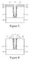
- FIG. 1shows a cross-sectional view of an inventive structure formed in accordance with a preferred embodiment of the present invention wherein a first, conformal seed layer is deposited over a barrier layer, followed by a second, non-conformal seed layer deposited over the first, conformal seed layer;
- FIG. 2shows a cross-sectional view of the inventive structure of FIG. 1 after removing excess plated copper or silver overlying an opening and the field, as well as removing the seed layers and barrier layer overlying the field surrounding the opening;
- FIG. 3shows a cross-sectional view of an inventive structure formed in accordance with an alternative embodiment of the present invention wherein a first, non-conformal seed layer is deposited over a barrier layer, followed by a second, conformal seed layer deposited over the first, non-conformal seed layer;
- FIG. 4shows a cross-sectional view of the inventive structure of FIG. 3 after removing excess plated copper or silver overlying an opening and the field, as well as removing the seed layers and barrier layer overlying the field surrounding the opening;
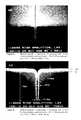
- FIG. 5shows a scanning electron microscope (“SEM”) photograph of a cleaved cross-section (with a tilt angle of 30°) of a trench (the trench is ⁇ 0.10 ⁇ m wide, ⁇ 1.4 ⁇ m deep, and has an aspect ratio of ⁇ 14:1) having seed layers formed in accordance with one embodiment of the present invention
- FIG. 6shows an SEM photograph of the trench shown in FIG. 5 without a tilt, and with a larger enlargement
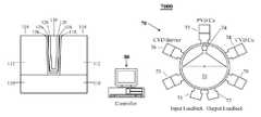
- FIG. 7shows a schematic (not to scale) top view of a cluster tool apparatus, and a frontal view of its controller (e.g. computer), in accordance with a preferred embodiment of the invention.
- controllere.g. computer
- FIG. 1shows a cross-sectional view of an inventive structure formed in accordance with a preferred embodiment of the present invention wherein a first, conformal seed layer is deposited over a barrier layer, followed by a second, non-conformal seed layer deposited over the first, conformal seed layer.
- the conformal seed layerprovides continuous and complete step coverage inside the openings, while the non-conformal seed layer provides a low resistance electrical path over the top surface (field) surrounding the openings to enable uniform plating across the substrate (or wafer).
- the thickness of the combined seed layersbe at least about 1,000 ⁇ on the field.
- barrier layer 18is deposited over the entire surface of wafer 10 , including over patterned insulating layer 12 (having had opening 16 patterned therein in accordance with any one of a number of methods that are well known to those of ordinary skill in the art), using a conformal Chemical Vapor Deposition (“CVD”) technique.
- CVDChemical Vapor Deposition
- barrier layerincludes examples wherein: (a) the barrier layer acts both as an adhesion layer and as a barrier layer; (b) a barrier layer separate from an adhesion layer is used; and (c) a multiplicity of layers is used, some acting as adhesion layers, some acting as barrier layers, or some acting as both.
- waferis used, this also includes the term substrate as it is used in the art.
- present inventionis described in the context of opening 16 , in practice, a multiplicity of openings are patterned and filled in accordance with the present invention.
- barrier layer 18ensures substantially complete and continuous coverage of the bottom and sidewall surfaces inside opening 16 .
- barrier layer 18may also be deposited using a Physical Vapor Deposition (“PVD”) technique that provides continuous bottom and sidewall coverage.
- PVDPhysical Vapor Deposition
- barrier layer 18may comprise, for example and without limitation, a material selected from Ta, TaN X , Cr, CrN X , Ti, TiN X , W, WN X , and other alloys containing one or more of these materials.
- the thickness of barrier layer 18can be in a range of about 30 ⁇ to about 500 ⁇ , and more preferably in a range of about 50 ⁇ to about 300 ⁇ . Since barrier layer 18 occupies a certain fraction of interconnects formed in accordance with the present invention, and since barrier layer 18 has a relatively large resistivity, its thickness should be minimized. However, the thickness of barrier layer 18 should be sufficiently large to mitigate copper out-diffusion and to provide complete bottom and sidewall coverage inside opening 16 . Many CVD techniques and PVD techniques are well known to those of ordinary skill in the art for forming barrier layer 18 .
- conformal seed layer 20is deposited over barrier layer 18 .
- Conformal seed layer 20can be preferably deposited by using a CVD technique, but it can also be deposited by using an electroless technique or any other substantially conformal deposition technique. Many CVD techniques and electroless techniques are well known to those of ordinary skill in the art for forming conformal seed layer 20 .
- the thickness of conformal seed layer 20can be in a range of about 50 ⁇ to about 500 ⁇ , and more preferably in a range of about 100 ⁇ to about 300 ⁇ .
- non-conformal seed layer 22is deposited over conformal seed layer 20 .
- Non-conformal seed layer 22can be preferably obtained using a PVD technique.
- non-conformal seed layer 22can be in a range of about 100 ⁇ to about 3,000 ⁇ , and more preferably in a range of about 500 ⁇ to about 1,800 ⁇ (in the field).
- the conformal and non-conformal seed layersmay comprise the same material, or they may comprise different materials.
- copperis commonly used as a seed layer, a highly conductive silver (Ag) layer can also be used.
- Aghas lower resistivity than that of Cu and, therefore, can be formed with a smaller thickness than that required when using Cu.
- conformal seed layer 20 and non-conformal seed layer 22may comprise, for example, a material selected from Cu, Ag, or alloys comprising one or more of these metals.
- the thickness of the CVD layersis substantially uniform over the entire surface (i.e., conformal), including over field 14 , and over bottom and sidewall surfaces inside opening 16 .
- conformal CVD layersare thicker over the field than inside the openings.
- CVD Cu seed layers inside openingsit is quite common for CVD Cu seed layers inside openings to have a thickness of about 80% of that over the field.
- the thickness of a CVD harrier layer inside the openingsis typically only about 50% of that over the field. Thus, even the best CVD layers exhibit some overhang at the top corners of the openings.
- onedeposits, by a CVD technique, a barrier layer comprised of about 200 ⁇ of TaN X or WN X , then one deposits, by a CVD technique, a conformal seed layer comprised of about 300 ⁇ of Cu, finally one deposits, by a PVD technique, a non-conformal seed layer comprised of about 900 ⁇ of Cu (as measured on the field).
- the inventive “two-step” seed layer depositionensures a continuous seed layer having excellent step coverage, and a low-resistance electrical path on the field to ensure uniform copper plating across the wafer.
- the thickness of the “two-step” seed layer inside the openingsis adequate for copper plating therein.
- the thickness of the “two-step” seed layer inside the openingscan be further decreased (to a range from about 100 ⁇ to about 200 ⁇ ) to enable void-free copper filling of even smaller openings (for example, below 0.10-0.13 ⁇ m).
- the combined thicknesses or the barrier and seed layers at the sidewalls of the openingsis about 400 ⁇ on each side, thus occupying about 800 ⁇ of the 1,800 ⁇ opening. This leaves enough room ( ⁇ 1,000 ⁇ ) to facilitate electroplating inside the opening without sealing or pinching-off of the top corners.
- substrate 10is placed in a copper electroplating bath, and electroplating is carried out in accordance with any one of a number of methods that are well known to those of ordinary skill in the art to deposit a thickness of copper sufficient to fill patterned opening 16 , with some excess, and to cover field 14 surrounding opening 16 .
- excess plated copper overlying opening 16 and overlying field 14are removed using any one of a number of techniques that are well known to those of ordinary skill in the art, for example, using a mechanical polishing or a chemical mechanical polishing (CMP) technique.
- CMPchemical mechanical polishing
- removal techniquessuch as wet or dry etching techniques may also be used to remove excess plated copper overlying opening 16 and field 14 , and to remove seed layers 20 and 22 and barrier metallic layer 18 overlying field 14 . It should be clear to those of ordinary skill in the art that removal may also be accomplished using a combination of techniques, including those identified above.
- electrofill opening 16with any low resistivity material, such as a material selected from Cu, Ag, or an alloy comprising one or more of these metals.
- silver (Ag)has lower resistivity than that of Cu, and may be attractive for further reducing the dimensions of the interconnects.
- FIG. 2shows a cross-sectional view of the inventive structure of FIG. 1 after removing excess plated copper (or silver) 24 overlying opening 16 and field 14 , and removing seed layers 20 and 22 and barrier layer 18 overlying field 14 surrounding opening 16 .
- FIG. 2illustrates the filling of openings (trenches and vias) with electroplated copper (or silver) 24 , as well as the lining of the bottom and sidewall surfaces of opening 16 by barrier layer 18 and seed layers 20 and 22 .
- all metallic layerswere removed from field 14 of insulating layer 12 which surrounds embedded electroplated copper (or silver) interconnect 24 .
- FIG. 3shows a cross-sectional view of an inventive structure formed in accordance with an alternative embodiment of the present invention wherein a first, non-conformal seed layer is deposited over a barrier layer, followed by a second, conformal seed layer deposited over the first, non-conformal seed layer.
- the non-conformal seed layerprovides a low resistance electrical path over the top surface (field) surrounding the openings to enable uniform plating across the substrate (or wafer), while the conformal seed layer provides continuous and complete step coverage inside the openings.
- barrier layer 118is deposited over the entire surface of wafer 110 , including over patterned insulating layer 112 (having had opening 116 patterned therein in accordance with any one of a number of methods that are well known to those of ordinary skill in the art), using a conformal Chemical Vapor Deposition (“CVD”) technique.
- CVDChemical Vapor Deposition
- barrier layerincludes examples wherein: (a) the barrier layer acts both as an adhesion layer and as a barrier layer; (b) a barrier layer separate from an adhesion layer is used; and (c) a multiplicity of layers is used, some acting as adhesion layers, some acting as barrier layers, or some acting as both.
- waferis used, this also includes the term substrate as it is used in the art.
- present inventionis described in the context of opening 116 , in practice, a multiplicity of openings are patterned and filled in accordance with the present invention.
- barrier layer 118ensures complete and continuous coverage of the bottom and sidewall surfaces inside opening 116 .
- barrier layer 118may also be deposited using a Physical Vapor Deposition (“PVD”) technique that provides continuous bottom and sidewall coverage.
- PVDPhysical Vapor Deposition
- barrier layer 118may comprise, for example and without limitation, a material selected from Ta, TaN X , Cr, CrN X , Ti, TiN X , W, WN X , and other alloys containing one or more of these materials.
- the thickness of barrier layer 118can be in a range of about 30 ⁇ to about 500 ⁇ , and more preferably in a range of about 50 ⁇ to about 300 ⁇ . Since barrier layer 118 occupies a certain fraction of interconnects formed in accordance with the present invention, and since barrier layer 118 has a relatively large resistivity, its thickness should be minimized. However, the thickness of barrier layer 118 should be sufficiently large to mitigate copper out-diffusion and to provide complete bottom and sidewall coverage inside opening 116 . Many CVD techniques and PVD techniques are well known to those of ordinary skill in the art for forming barrier layer 118 .
- non-conformal seed layer 126is deposited over barrier layer 118 .
- Non-conformal seed layer 126can be preferably obtained using a PVD technique. Many PVD techniques are well known to those of ordinary skill in the art for forming non-conformal seed layer 126 .
- the thickness of non-conformal seed layer 126can be in a range of about 100 ⁇ to about 3,000 ⁇ , and more preferably in a range of about 500 ⁇ to about 1,800 ⁇ (on the field).
- conformal seed layer 128is deposited over non-conformal seed layer 126 .
- Conformal seed layer 128can be preferably obtained using a CVD or electroless technique or any other substantially conformal deposition technique.
- conformal seed layer 128can be in a range of about 50 ⁇ to about 500 ⁇ , and more preferably in a range of about 100 ⁇ to about 300 ⁇ .
- the conformal and non-conformal seed layersmay comprise the same material, or they may comprise different materials.
- copperis commonly used as a seed layer, a highly conductive silver (Ag) layer can also be used.
- Non-conformal seed layer 126 and conformal seed layer 128may comprise, for example, a material selected from Cu, Ag, or alloys comprising one or more of these metals.
- substrate 110is placed in a copper electroplating bath, and electroplating is carried out in accordance with any one of a number of methods that are well known to those of ordinary skill in the art to deposit a thickness of copper sufficient to fill patterned opening 116 , with some excess, and to cover field 114 surrounding opening 116 .
- excess plated copper overlying opening 116 and field 114 of insulating layer 112 , as well as seed layers 126 and 128 and barrier layer 118 overlying field 114are removed using any one of a number of techniques that are well known to those of ordinary skill in the art, for example, using a mechanical polishing or a chemical mechanical polishing (CMP) technique.
- CMPchemical mechanical polishing
- removal techniquessuch as wet or dry etching techniques may also be used to remove excess plated copper overlying opening 116 and field 114 , and to remove seed layers 126 and 128 and barrier layer 118 overlying field 114 . It should be clear to those of ordinary skill in the art that removal may also be accomplished using a combination of techniques, including those identified above.
- electrofill opening 116with any low resistivity material, such as a material selected from Cu, Ag, or alloys comprising one or more of these metals.
- silver (Ag)has lower resistivity than that of Cu, and may be attractive for further reducing the dimensions of the interconnects.
- FIG. 4shows a cross-sectional view of the inventive structure of FIG. 3 after removing excess electroplated copper (or silver) 130 overlying opening 116 and field 114 , and removing seed layers 126 and 128 and barrier layer 118 overlying field 114 surrounding opening 116 .
- FIG. 4illustrates the filling of openings (trenches and vias) with electroplated copper (or silver) 130 , as well as the lining of the bottom and sidewall surfaces of opening 116 by barrier layer 118 and seed layers 126 and 128 .
- all metallic layerswere removed from field 114 of insulating layer 112 which surrounds embedded electroplated copper (or silver) interconnect 130 .
- FIGS. 5 and 6show scanning electron microscope (“SEM”) photographs of a cross-section of a 0.10 ⁇ m wide trench having a Cu seed layer prepared in accordance with a preferred embodiment of the invention.
- a pattern of trencheswas formed in a SiO 2 insulating layer.
- the trencheswere about 0.10 ⁇ m wide and about 1.4 ⁇ m deep (thereby having an aspect ratio of about 14:1).
- a barrier layer (WN X )was deposited using a CVD technique.
- a relatively thin, conformal Cu seed layerwas deposited using a CVD technique.
- the barrier layer and thin, conformal Cu seed layeris seen at 501 in FIG. 6 .
- the combined thickness of the barrier and the CVD Cu seed layerwas about 500 ⁇ on the field, and about 400-500 ⁇ on the sidewalls and bottom of the trenches.
- a non-conformal PVD Cu seed layer having a thickness of about 1,400 ⁇ (on the field)was deposited by sputtering.
- the non conformal PVD Cu seed layerwas applied in two steps and is seen at 510 in FIG. 6 . The end result, as shown in FIGS.
- FIG. 5shows the cross-section with a tilt of about 30° and an enlargement of 20,000 ⁇ (thus providing also a partial view of the top surface)
- FIG. 6shows the same cross-section with an enlargement of 40,000 ⁇ and without a tilt.
- trenches ⁇ 0.10 ⁇ m wide and ⁇ 1.4 ⁇ m deepwere formed in a SiO 2 insulating layer.
- a barrier layer (WN X )was deposited using a CVD technique.
- a relatively thin, conformal Cu seed layerwas deposited using a CVD technique.
- the combined thickness of the barrier layer and the CVD Cu layerwas ⁇ 500 ⁇ on the field, and ⁇ 400-500 ⁇ on the sidewalls and bottom of the trenches.
- a non-conformal PVD Cu seed layer having a thickness of ⁇ 500 ⁇ (on the field)was deposited by sputtering.
- the end resultwas a combined thickness (including the barrier layer and the Cu seed layers) of only about 400-500 ⁇ on the sidewalls and bottom of the trenches (with excellent continuity and uniformity), and about 1,000 ⁇ on the field, without pinching-off the trenches.
- a relatively thin (“Flash”) PVD seed layercan be deposited first, followed by a conformal CVD or electroless seed layer, and finally followed by a (relatively thick) PVD seed layer to produce three separately deposited seed layers.
- Adhesion of a metallo-organic CVD (MOCVD) deposited Cu seed layer to underlying barrier layeris rather poor, and may not be adequate for use in devices when chemical mechanical polishing (CMP) processing follows Cu plating.
- CMPchemical mechanical polishing
- MOCVD Cu layeris deposited directly over a barrier layer containing a refractory metal, further problems arise. In particular, the morphology, uniformity, and electrical resistivity of the MOCVD Cu layer may not be adequate for use in devices. It is believed that these problems are due to the high affinity of the refractory metal in the barrier layer to oxygen and/or carbon atoms.
- the refractory metal of the barrier layerspontaneously reacts with carbon or oxygen containing species (from the organic part of the metallo-organic compound) to form an oxide, carbide, or a mixed oxide-carbide interfacial layer between itself and the depositing Cu.
- Such an intermediate layeradversely impairs the adhesion of the MOCVD Cu layer.
- Cu(as well as other noble metals) does not adhere well to oxide or carbide layers, and requires a clean metal-to-metal bond in order to adhere well to another metal.
- the oxide, carbide, and/or oxide-carbide interfacial layerimpairs proper nucleation of the MOCVD Cu on the refractory metal barrier layer. This adversely affects the morphology, uniformity, and resistivity of the deposited MOCVD Cu seed layer.
- At least an initial stage of CVD Cu depositionis carried out utilizing high purity, inorganic Cu compounds (precursors), such as, for example and without limitation, chlorides or fluorides, which do not contain oxygen or carbon atoms.
- precursorssuch as, for example and without limitation, chlorides or fluorides, which do not contain oxygen or carbon atoms.
- the resulting clean metal-to-metal interface between a barrier layer containing a refractory metal and the depositing copperensures good adhesion, morphology, uniformity, and low electrical resistivity of the CVD Cu layer.
- the entire CVD Cu layercan be deposited using the inorganic precursors.
- only the initial stage of the CVD Cuis carried out using inorganic precursors, switching later to an MOCVD Cu deposition process, to form the rest of the CVD Cu layer.
- a first, relatively thin, “Flash” PVD seed layeris deposited to enhance adhesion to the barrier layer and/or to improve grain morphology and uniformity of a subsequently deposited CVD seed layer.
- Exposure of wafers to the atmosphere during transport from one deposition chamber to anothermay cause deleterious oxidation and/or contamination of the surface of barrier and/or seed layers. Such exposure should, therefore, be avoided or minimized.
- conformal and non-conformal seed layersare deposited in an apparatus where the conformal and non-conformal seed layer deposition steps can be carried out without breaking vacuum, or without exposing the wafer to the atmosphere between the deposition steps.
- the apparatusmay comprise two or more chambers, at least one chamber for deposition of the conformal seed layer, and at least another chamber for deposition of the non-conformal seed layer.
- the apparatusfurther comprises a chamber for deposition of the barrier layer, preferably by a CVD technique.
- the barrier layermay be deposited in a separate chamber or it may be deposited in one of the chambers used to deposit either the conformal, or the non-conformal, seed layers.
- FIG. 7shows apparatus 7000 that is fabricated in accordance with a preferred embodiment of the invention.
- apparatus 7000comprises cluster tool 70 which operates in accordance with input from controller 80 in a manner that is well known to those of ordinary skill in the art.
- cluster tool 70includes input loadlock 71 and output loadlock 72 .
- loadlocks 71 and 72enable wafers to be inserted into and removed from cluster tool 70 , respectively.
- FIG. 7shows separate input and output loadlocks, it is also within the spirit and scope of the present invention to use a single loadlock for both input and output of wafers.
- cluster tool 70comprises CVD harrier layer deposition chamber 76 , PVD Cu seed layer deposition chamber 77 , and CVD Cu seed layer deposition chamber 78 .
- FIG. 7shows several other processing, for example, processing chambers 75 and 79 , which can be used for other processing steps that are well known to those of ordinary skill in the art, such as pre-cleaning, cooling, or as extra deposition chambers.
- FIG. 7shows separate CVD chambers for depositing a barrier layer and Cu seed layers, it is also within the scope of the invention to deposit both types of layers in the same CVD chamber.
- Controller 80is apparatus which is well known to those of ordinary skill in the art that is used to control the operation of cluster tool 70 . As such, controller 80 determines the sequence and duration of movements and stays of wafer 74 : (a) to and from loadlocks 71 and 72 ; and (b) to and from the various processing chambers 75 - 79 .
- controller 80controls the specific process sequence and process parameters for operation of the various ones of processing chambers 75 - 79 , sometimes referred to in the art as “recipes.” For example, in PVD Cu seed layer deposition chamber 77 , among other things, controller 80 controls the duration of the sputter deposition, the background pressure, the sputtering gas (such as Argon) pressure and flow rate, the cathodic voltage and power, and/or bias voltage applied to the wafer. Lastly, as is also well known to those of ordinary skill in the art, controller 80 performs these functions in accordance with specific recipes which are data structures that dictate the operation of controller 80 software.
- specific recipeswhich are data structures that dictate the operation of controller 80 software.
- the data structuresare typically stored on computer readable media that are input to controller 80 under the control of operation software, which operation software itself is typically stored on a computer readable medium.
- recipesare input to controller 80 to cause it to control cluster tool 70 to process wafers in the manner described above to deposit a Cu barrier layer and Cu seed layers without breaking vacuum or exposing a wafer to the atmosphere.
- the apparatuscomprises a chamber in which both conformal and non-conformal seed layers are deposited utilizing: (a) two or more distinct steps, wherein the deposition variables (or conditions or parameters) during the first step are suitable for the deposition of a substantially conformal (or a non-conformal) seed layer, and the deposition conditions during the second step are suitable for the deposition of a substantially non-conformal (or a conformal) seed layer; (b) wherein at least one of the deposition variables is varied (or ramped) continuously or gradually, thereby changing the nature of the seed layer from substantially conformal to substantially non-conformal, or vice versa; or (c) a combination of at least one distinct step of depositing a substantially conformal (or a non-conformal) seed layer and at least one gradual variation (or ramping) of at least one deposition variable towards a substantially non-conformal (or a conformal) seed layer, and vice versa.
- the nature of certain deposition techniquescan be made more conformal, or less conformal, by varying the deposition parameters (or variables, or conditions). For example, increasing the (partial) pressure during ion plating and other PVD techniques, tends to increase scattering of the depositing atoms (or ions), thereby making the deposition more isotropic and conformal.
- biasing the substratehas a effect on the nature of the deposit. For example, in ionized metal plasma (IMP) and ion plating, increasing the (negative) bias voltage further accelerates positive ions (of the depositing metal) towards the substrate, thereby improving the filling of small openings.
- IMPionized metal plasma
- bias voltagefurther accelerates positive ions (of the depositing metal) towards the substrate, thereby improving the filling of small openings.
- the higher (negative) biasalso increases the removal rate (or back-sputtering) from the top corners of the openings and the field, thereby rendering the deposition to be more conformal.
- decreasing the negative bias, or even using positive biascan render the deposition to be less conformal.
- Deposition rate(or power density) can also affect the nature of the deposition.
- the nature of certain CVD techniquescan be made less conformal, or more conformal, by changing the deposition variables. For example, increasing the substrate temperature tends to shift the deposition from a surface-reaction, rate-controlled deposition at low temperature, to a transport, rate-controlled deposition at higher temperature. As a result, increasing the substrate temperature tends to render the deposition to be less conformal. Conversely, decreasing the temperature, tends to render the deposition to be more conformal. Similarly, increasing the precursor and/or the reacting gas partial pressure (or flow rate) tends to shift the deposition to be a more surface-reaction, rate-controlled deposition, thereby tending to render the deposition to be more conformal.
- PECVDplasma variables in PECVD, such as the power density, may also have significant effects on the nature of the deposition.
- cluster tool 70comprises the following chambers: a CVD deposition chamber for depositing a barrier layer (for example, Ta, TaN X , W, or WN X ); a PVD deposition chamber for depositing a PVD Cu seed layer; and a CVD deposition chamber for depositing a CVD Cu seed layer.
- a barrier layerfor example, Ta, TaN X , W, or WN X
- PVD deposition chamberfor depositing a PVD Cu seed layer
- CVD deposition chamberfor depositing a CVD Cu seed layer.
- Single wafersare transferred in-situ in cluster tool 70 , from one chamber to another, without exposing the wafers to the atmosphere prior to the deposition of the top Cu seed layer.
- the CVD barrier and the CVD Cu seed layerscan be deposited in the same CVD chamber by using different gases and chemistries for the respective layers.
- cluster tool controller 80would cause a deposition process such as the following to be carried out in accordance with a recipe specified, for example in the form of a data structure or software or program code: (a) (in accordance with a first portion of the data structure or a first portion of the software or computer code) introducing wafer 74 into CVD barrier layer deposition chamber 76 and depositing on wafer 74 a CVD barrier layer (about 200-400 ⁇ thick) comprising TaN X or WN X ; (b) (in accordance with a second portion of the data structure or a first portion of software or computer code) transferring wafer 74 through transfer chamber 73 , without exposing wafer 74 to the atmosphere, to PVD Cu seed layer deposition chamber 77 and depositing on wafer 74 a relatively thin (about 100-500 ⁇ ) “Flash” PV
- a three-step combinationmay include a first deposited CVD seed layer, followed by a relatively thick PVD seed layer, and finally followed by a second deposited CVD seed layer.
- Other combinationsmay comprise even more steps in the deposition of the seed layer.
- the three (or more) separately deposited seed layersmay comprise the same metal or alloy or they may comprise, for example and without limitation, different materials chosen from Cu, Ag, or alloys comprising one or more of these metals.
Landscapes
- Engineering & Computer Science (AREA)
- Physics & Mathematics (AREA)
- Condensed Matter Physics & Semiconductors (AREA)
- General Physics & Mathematics (AREA)
- Manufacturing & Machinery (AREA)
- Computer Hardware Design (AREA)
- Microelectronics & Electronic Packaging (AREA)
- Power Engineering (AREA)
- Internal Circuitry In Semiconductor Integrated Circuit Devices (AREA)
- Electrodes Of Semiconductors (AREA)
- Electroplating Methods And Accessories (AREA)
- Magnetic Heads (AREA)
Abstract
Description
Claims (4)
Priority Applications (1)
| Application Number | Priority Date | Filing Date | Title |
|---|---|---|---|
| US12/471,571US9673090B2 (en) | 1999-10-02 | 2009-05-26 | Seed layers for metallic interconnects |
Applications Claiming Priority (7)
| Application Number | Priority Date | Filing Date | Title |
|---|---|---|---|
| US09/410,898US6136707A (en) | 1999-10-02 | 1999-10-02 | Seed layers for interconnects and methods for fabricating such seed layers |
| US09/563,733US6610151B1 (en) | 1999-10-02 | 2000-05-03 | Seed layers for interconnects and methods and apparatus for their fabrication |
| US10/640,846US6903016B2 (en) | 1999-10-02 | 2003-08-14 | Combined conformal/non-conformal seed layers for metallic interconnects |
| US11/057,485US7199052B2 (en) | 1999-10-02 | 2005-02-14 | Seed layers for metallic interconnects |
| US11/654,478US7282445B2 (en) | 1999-10-02 | 2007-01-17 | Multiple seed layers for interconnects |
| US11/868,435US7550386B2 (en) | 1999-10-02 | 2007-10-05 | Advanced seed layers for interconnects |
| US12/471,571US9673090B2 (en) | 1999-10-02 | 2009-05-26 | Seed layers for metallic interconnects |
Related Parent Applications (1)
| Application Number | Title | Priority Date | Filing Date |
|---|---|---|---|
| US11/868,435DivisionUS7550386B2 (en) | 1999-10-02 | 2007-10-05 | Advanced seed layers for interconnects |
Publications (2)
| Publication Number | Publication Date |
|---|---|
| US20090233440A1 US20090233440A1 (en) | 2009-09-17 |
| US9673090B2true US9673090B2 (en) | 2017-06-06 |
Family
ID=27021179
Family Applications (8)
| Application Number | Title | Priority Date | Filing Date |
|---|---|---|---|
| US09/563,733Expired - LifetimeUS6610151B1 (en) | 1999-10-02 | 2000-05-03 | Seed layers for interconnects and methods and apparatus for their fabrication |
| US09/730,220Expired - LifetimeUS6518668B2 (en) | 1999-10-02 | 2000-12-04 | Multiple seed layers for metallic interconnects |
| US10/640,846Expired - LifetimeUS6903016B2 (en) | 1999-10-02 | 2003-08-14 | Combined conformal/non-conformal seed layers for metallic interconnects |
| US11/057,485Expired - LifetimeUS7199052B2 (en) | 1999-10-02 | 2005-02-14 | Seed layers for metallic interconnects |
| US11/654,478Expired - LifetimeUS7282445B2 (en) | 1999-10-02 | 2007-01-17 | Multiple seed layers for interconnects |
| US11/868,435Expired - LifetimeUS7550386B2 (en) | 1999-10-02 | 2007-10-05 | Advanced seed layers for interconnects |
| US12/471,557PendingUS20090239372A1 (en) | 1999-10-02 | 2009-05-26 | Seed Layers for Electroplated Interconnects |
| US12/471,571Expired - Fee RelatedUS9673090B2 (en) | 1999-10-02 | 2009-05-26 | Seed layers for metallic interconnects |
Family Applications Before (7)
| Application Number | Title | Priority Date | Filing Date |
|---|---|---|---|
| US09/563,733Expired - LifetimeUS6610151B1 (en) | 1999-10-02 | 2000-05-03 | Seed layers for interconnects and methods and apparatus for their fabrication |
| US09/730,220Expired - LifetimeUS6518668B2 (en) | 1999-10-02 | 2000-12-04 | Multiple seed layers for metallic interconnects |
| US10/640,846Expired - LifetimeUS6903016B2 (en) | 1999-10-02 | 2003-08-14 | Combined conformal/non-conformal seed layers for metallic interconnects |
| US11/057,485Expired - LifetimeUS7199052B2 (en) | 1999-10-02 | 2005-02-14 | Seed layers for metallic interconnects |
| US11/654,478Expired - LifetimeUS7282445B2 (en) | 1999-10-02 | 2007-01-17 | Multiple seed layers for interconnects |
| US11/868,435Expired - LifetimeUS7550386B2 (en) | 1999-10-02 | 2007-10-05 | Advanced seed layers for interconnects |
| US12/471,557PendingUS20090239372A1 (en) | 1999-10-02 | 2009-05-26 | Seed Layers for Electroplated Interconnects |
Country Status (5)
| Country | Link |
|---|---|
| US (8) | US6610151B1 (en) |
| JP (1) | JP2003511858A (en) |
| KR (1) | KR20020043604A (en) |
| TW (1) | TW504795B (en) |
| WO (1) | WO2001026145A1 (en) |
Families Citing this family (118)
| Publication number | Priority date | Publication date | Assignee | Title |
|---|---|---|---|---|
| US6482734B1 (en)* | 1998-01-20 | 2002-11-19 | Lg Semicon Co., Ltd. | Diffusion barrier layer for semiconductor device and fabrication method thereof |
| JP2000138201A (en)* | 1998-10-29 | 2000-05-16 | Ulvac Seimaku Kk | Half-tone phase shift film dry etching method and apparatus, half-tone phase shift photomask and its manufacturing method, and semiconductor circuit and its manufacturing method |
| US7105434B2 (en)* | 1999-10-02 | 2006-09-12 | Uri Cohen | Advanced seed layery for metallic interconnects |
| US6610151B1 (en)* | 1999-10-02 | 2003-08-26 | Uri Cohen | Seed layers for interconnects and methods and apparatus for their fabrication |
| KR100338112B1 (en)* | 1999-12-22 | 2002-05-24 | 박종섭 | Method of forming a copper wiring in a semiconductor device |
| KR100773165B1 (en)* | 1999-12-24 | 2007-11-02 | 가부시키가이샤 에바라 세이사꾸쇼 | Semiconductor Substrate Processing Equipment and Processing Method |
| KR100407680B1 (en)* | 2000-06-20 | 2003-12-01 | 주식회사 하이닉스반도체 | Method of forming a metal wiring in a semiconductor device |
| US6368954B1 (en)* | 2000-07-28 | 2002-04-09 | Advanced Micro Devices, Inc. | Method of copper interconnect formation using atomic layer copper deposition |
| US6800554B2 (en)* | 2000-12-18 | 2004-10-05 | Intel Corporation | Copper alloys for interconnections having improved electromigration characteristics and methods of making same |
| US6737740B2 (en)* | 2001-02-08 | 2004-05-18 | Micron Technology, Inc. | High performance silicon contact for flip chip |
| US6764940B1 (en) | 2001-03-13 | 2004-07-20 | Novellus Systems, Inc. | Method for depositing a diffusion barrier for copper interconnect applications |
| US6869515B2 (en)* | 2001-03-30 | 2005-03-22 | Uri Cohen | Enhanced electrochemical deposition (ECD) filling of high aspect ratio openings |
| US9076843B2 (en) | 2001-05-22 | 2015-07-07 | Novellus Systems, Inc. | Method for producing ultra-thin tungsten layers with improved step coverage |
| US6842659B2 (en)* | 2001-08-24 | 2005-01-11 | Applied Materials Inc. | Method and apparatus for providing intra-tool monitoring and control |
| US6936906B2 (en)* | 2001-09-26 | 2005-08-30 | Applied Materials, Inc. | Integration of barrier layer and seed layer |
| US6503824B1 (en)* | 2001-10-12 | 2003-01-07 | Mosel Vitelic, Inc. | Forming conductive layers on insulators by physical vapor deposition |
| US6916398B2 (en) | 2001-10-26 | 2005-07-12 | Applied Materials, Inc. | Gas delivery apparatus and method for atomic layer deposition |
| JP3727277B2 (en)* | 2002-02-26 | 2005-12-14 | Necエレクトロニクス株式会社 | Manufacturing method of semiconductor device |
| US6620724B1 (en)* | 2002-05-09 | 2003-09-16 | Infineon Technologies Ag | Low resistivity deep trench fill for DRAM and EDRAM applications |
| US6724087B1 (en)* | 2002-07-31 | 2004-04-20 | Advanced Micro Devices, Inc. | Laminated conductive lines and methods of forming the same |
| US6790773B1 (en)* | 2002-08-28 | 2004-09-14 | Novellus Systems, Inc. | Process for forming barrier/seed structures for integrated circuits |
| US20040096586A1 (en)* | 2002-11-15 | 2004-05-20 | Schulberg Michelle T. | System for deposition of mesoporous materials |
| KR20040060562A (en)* | 2002-12-30 | 2004-07-06 | 동부전자 주식회사 | Oxidation prevention method of barrier metal for manufacturing a semiconductor element |
| US6806192B2 (en)* | 2003-01-24 | 2004-10-19 | Taiwan Semiconductor Manufacturing Company, Ltd. | Method of barrier-less integration with copper alloy |
| US6943111B2 (en)* | 2003-02-10 | 2005-09-13 | Taiwan Semiconductor Manufacturing Company, Ltd. | Barrier free copper interconnect by multi-layer copper seed |
| JP4188125B2 (en)* | 2003-03-05 | 2008-11-26 | Tdk株式会社 | Magnetic recording medium manufacturing method and manufacturing apparatus |
| US8298933B2 (en) | 2003-04-11 | 2012-10-30 | Novellus Systems, Inc. | Conformal films on semiconductor substrates |
| US7842605B1 (en) | 2003-04-11 | 2010-11-30 | Novellus Systems, Inc. | Atomic layer profiling of diffusion barrier and metal seed layers |
| EP1482069A1 (en)* | 2003-05-28 | 2004-12-01 | Interuniversitair Microelektronica Centrum Vzw | Method for producing polycrystalline silicon germanium suitable for micromachining |
| KR100560666B1 (en)* | 2003-07-07 | 2006-03-16 | 삼성전자주식회사 | Metal film deposition system for semiconductor device manufacturing and its operation method |
| US6900127B2 (en)* | 2003-08-27 | 2005-05-31 | Texas Instruments Incorporated | Multilayer integrated circuit copper plateable barriers |
| US7081647B2 (en)* | 2003-09-29 | 2006-07-25 | Matsushita Electric Industrial Co., Ltd. | Microelectromechanical system and method for fabricating the same |
| US20050082606A1 (en)* | 2003-10-20 | 2005-04-21 | Stephan Grunow | Low K dielectric integrated circuit interconnect structure |
| US7265038B2 (en)* | 2003-11-25 | 2007-09-04 | Taiwan Semiconductor Manufacturing Co., Ltd. | Method for forming a multi-layer seed layer for improved Cu ECP |
| KR100587658B1 (en)* | 2003-12-31 | 2006-06-08 | 동부일렉트로닉스 주식회사 | How to minimize terminal effect in the CPC process |
| US7732326B2 (en) | 2004-02-25 | 2010-06-08 | Taiwan Semiconductor Manufacturing Company, Ltd. | Semiconductor device having a second level of metallization formed over a first level with minimal damage to the first level and method |
| US20050184288A1 (en)* | 2004-02-25 | 2005-08-25 | Tien-I Bao | Semiconductor device having a second level of metallization formed over a first level with minimal damage to the first level and method |
| US7067409B2 (en)* | 2004-05-10 | 2006-06-27 | Taiwan Semiconductor Manufacturing Company, Ltd. | Plasma treatment at film layer to reduce sheet resistance and to improve via contact resistance |
| US7378744B2 (en)* | 2004-05-10 | 2008-05-27 | Taiwan Semiconductor Manufacturing Company, Ltd. | Plasma treatment at film layer to reduce sheet resistance and to improve via contact resistance |
| US7306962B2 (en)* | 2004-06-17 | 2007-12-11 | Sharp Laboratories Of America, Inc. | Electroformed metallization |
| US7112470B2 (en)* | 2004-09-15 | 2006-09-26 | International Business Machines Corporation | Chip dicing |
| US7704368B2 (en) | 2005-01-25 | 2010-04-27 | Taiwan Semiconductor Manufacturing Co. Ltd. | Method and apparatus for electrochemical plating semiconductor wafers |
| JP4929156B2 (en)* | 2005-03-09 | 2012-05-09 | 株式会社Ihi | jig |
| EP1909320A1 (en)* | 2006-10-05 | 2008-04-09 | ST Microelectronics Crolles 2 SAS | Copper diffusion barrier |
| US20070080455A1 (en)* | 2005-10-11 | 2007-04-12 | International Business Machines Corporation | Semiconductors and methods of making |
| US7863183B2 (en)* | 2006-01-18 | 2011-01-04 | International Business Machines Corporation | Method for fabricating last level copper-to-C4 connection with interfacial cap structure |
| US7645696B1 (en)* | 2006-06-22 | 2010-01-12 | Novellus Systems, Inc. | Deposition of thin continuous PVD seed layers having improved adhesion to the barrier layer |
| JP2008028058A (en)* | 2006-07-20 | 2008-02-07 | Tokyo Electron Ltd | Method of manufacturing semiconductor device, apparatus for manufacturing semiconductor device, semiconductor device and storage medium |
| US7605078B2 (en)* | 2006-09-29 | 2009-10-20 | Tokyo Electron Limited | Integration of a variable thickness copper seed layer in copper metallization |
| US7510634B1 (en) | 2006-11-10 | 2009-03-31 | Novellus Systems, Inc. | Apparatus and methods for deposition and/or etch selectivity |
| KR100763136B1 (en) | 2006-12-11 | 2007-10-02 | 동부일렉트로닉스 주식회사 | Wafer Bonding Method in System-in-Package |
| DE102007004884A1 (en)* | 2007-01-31 | 2008-08-14 | Advanced Micro Devices, Inc., Sunnyvale | A method of forming a metal layer over a patterned dielectric by electroless deposition using a selectively provided activation layer |
| US8058164B2 (en)* | 2007-06-04 | 2011-11-15 | Lam Research Corporation | Methods of fabricating electronic devices using direct copper plating |
| JP2009016520A (en)* | 2007-07-04 | 2009-01-22 | Tokyo Electron Ltd | Method and apparatus for manufacturing semiconductor apparatus |
| US8084862B2 (en) | 2007-09-20 | 2011-12-27 | International Business Machines Corporation | Interconnect structures with patternable low-k dielectrics and method of fabricating same |
| US8618663B2 (en)* | 2007-09-20 | 2013-12-31 | International Business Machines Corporation | Patternable dielectric film structure with improved lithography and method of fabricating same |
| US7709370B2 (en) | 2007-09-20 | 2010-05-04 | International Business Machines Corporation | Spin-on antireflective coating for integration of patternable dielectric materials and interconnect structures |
| US20090127097A1 (en)* | 2007-11-16 | 2009-05-21 | Kei-Wei Chen | Forming Seed Layer in Nano-Trench Structure Using Net Deposition and Net Etch |
| US7727890B2 (en)* | 2007-12-10 | 2010-06-01 | International Business Machines Corporation | High aspect ratio electroplated metal feature and method |
| KR100924556B1 (en) | 2008-01-04 | 2009-11-02 | 주식회사 하이닉스반도체 | Metal wiring of semiconductor device and method of forming the same |
| US7704886B2 (en)* | 2008-02-14 | 2010-04-27 | Taiwan Semiconductor Manufacturing Company, Ltd. | Multi-step Cu seed layer formation for improving sidewall coverage |
| US8252690B2 (en)* | 2008-02-14 | 2012-08-28 | Taiwan Semiconductor Manufacturing Company, Ltd. | In situ Cu seed layer formation for improving sidewall coverage |
| US7879720B2 (en)* | 2008-09-30 | 2011-02-01 | Samsung Electronics Co., Ltd. | Methods of forming electrical interconnects using electroless plating techniques that inhibit void formation |
| US9159571B2 (en) | 2009-04-16 | 2015-10-13 | Lam Research Corporation | Tungsten deposition process using germanium-containing reducing agent |
| US20100267230A1 (en)* | 2009-04-16 | 2010-10-21 | Anand Chandrashekar | Method for forming tungsten contacts and interconnects with small critical dimensions |
| KR20100133834A (en)* | 2009-06-12 | 2010-12-22 | 웅진케미칼 주식회사 | Fabrics containing low melting point yarn |
| US10256142B2 (en) | 2009-08-04 | 2019-04-09 | Novellus Systems, Inc. | Tungsten feature fill with nucleation inhibition |
| US7956463B2 (en)* | 2009-09-16 | 2011-06-07 | International Business Machines Corporation | Large grain size conductive structure for narrow interconnect openings |
| JP5498751B2 (en)* | 2009-10-05 | 2014-05-21 | ルネサスエレクトロニクス株式会社 | Manufacturing method of semiconductor device |
| WO2011090717A1 (en)* | 2009-12-28 | 2011-07-28 | Gvd Corporation | Coating methods, systems, and related articles |
| US9714474B2 (en)* | 2010-04-06 | 2017-07-25 | Tel Nexx, Inc. | Seed layer deposition in microscale features |
| US8993434B2 (en)* | 2010-09-21 | 2015-03-31 | Applied Materials, Inc. | Methods for forming layers on a substrate |
| TWI413468B (en)* | 2010-12-29 | 2013-10-21 | Unimicron Technology Corp | Method for forming embedded circuit |
| US8399353B2 (en)* | 2011-01-27 | 2013-03-19 | Tokyo Electron Limited | Methods of forming copper wiring and copper film, and film forming system |
| US8524599B2 (en) | 2011-03-17 | 2013-09-03 | Micron Technology, Inc. | Methods of forming at least one conductive element and methods of forming a semiconductor structure |
| JP2012231096A (en)* | 2011-04-27 | 2012-11-22 | Elpida Memory Inc | Semiconductor device and manufacturing method of the same |
| US8525339B2 (en) | 2011-07-27 | 2013-09-03 | International Business Machines Corporation | Hybrid copper interconnect structure and method of fabricating same |
| US8946082B2 (en)* | 2011-09-16 | 2015-02-03 | GlobalFoundries, Inc. | Methods for forming semiconductor devices |
| US20130140688A1 (en)* | 2011-12-02 | 2013-06-06 | Chun-Hung Chen | Through Silicon Via and Method of Manufacturing the Same |
| US10381266B2 (en) | 2012-03-27 | 2019-08-13 | Novellus Systems, Inc. | Tungsten feature fill with nucleation inhibition |
| US11437269B2 (en) | 2012-03-27 | 2022-09-06 | Novellus Systems, Inc. | Tungsten feature fill with nucleation inhibition |
| TWI602283B (en) | 2012-03-27 | 2017-10-11 | 諾發系統有限公司 | Tungsten feature fill |
| US20140046475A1 (en)* | 2012-08-09 | 2014-02-13 | Applied Materials, Inc. | Method and apparatus deposition process synchronization |
| US8853080B2 (en) | 2012-09-09 | 2014-10-07 | Novellus Systems, Inc. | Method for depositing tungsten film with low roughness and low resistivity |
| US8729702B1 (en) | 2012-11-20 | 2014-05-20 | Stmicroelectronics, Inc. | Copper seed layer for an interconnect structure having a doping concentration level gradient |
| US9153486B2 (en) | 2013-04-12 | 2015-10-06 | Lam Research Corporation | CVD based metal/semiconductor OHMIC contact for high volume manufacturing applications |
| US9589808B2 (en) | 2013-12-19 | 2017-03-07 | Lam Research Corporation | Method for depositing extremely low resistivity tungsten |
| US9748137B2 (en) | 2014-08-21 | 2017-08-29 | Lam Research Corporation | Method for void-free cobalt gap fill |
| US9349637B2 (en) | 2014-08-21 | 2016-05-24 | Lam Research Corporation | Method for void-free cobalt gap fill |
| US9997405B2 (en) | 2014-09-30 | 2018-06-12 | Lam Research Corporation | Feature fill with nucleation inhibition |
| US9768060B2 (en)* | 2014-10-29 | 2017-09-19 | Applied Materials, Inc. | Systems and methods for electrochemical deposition on a workpiece including removing contamination from seed layer surface prior to ECD |
| US9953984B2 (en) | 2015-02-11 | 2018-04-24 | Lam Research Corporation | Tungsten for wordline applications |
| US10170320B2 (en) | 2015-05-18 | 2019-01-01 | Lam Research Corporation | Feature fill with multi-stage nucleation inhibition |
| US9978605B2 (en) | 2015-05-27 | 2018-05-22 | Lam Research Corporation | Method of forming low resistivity fluorine free tungsten film without nucleation |
| US9754824B2 (en) | 2015-05-27 | 2017-09-05 | Lam Research Corporation | Tungsten films having low fluorine content |
| US9613818B2 (en) | 2015-05-27 | 2017-04-04 | Lam Research Corporation | Deposition of low fluorine tungsten by sequential CVD process |
| US10276397B2 (en)* | 2015-06-30 | 2019-04-30 | Taiwan Semiconductor Manufacturing Co., Ltd. | CVD metal seed layer |
| US9754891B2 (en) | 2015-09-23 | 2017-09-05 | International Business Machines Corporation | Low-temperature diffusion doping of copper interconnects independent of seed layer composition |
| US9735051B2 (en) | 2015-12-14 | 2017-08-15 | International Business Machines Corporation | Semiconductor device interconnect structures formed by metal reflow process |
| KR102708262B1 (en) | 2016-02-05 | 2024-09-20 | 보드 오브 리전츠, 더 유니버시티 오브 텍사스 시스템 | The manipulatable intraruminal medical device |
| BR112018009251A2 (en) | 2016-02-05 | 2019-04-09 | Board Of Regents Of The University Of Texas System | surgical apparatus and customized main controller for a surgical apparatus |
| US10573522B2 (en) | 2016-08-16 | 2020-02-25 | Lam Research Corporation | Method for preventing line bending during metal fill process |
| US10115670B2 (en) | 2016-08-17 | 2018-10-30 | International Business Machines Corporation | Formation of advanced interconnects including set of metal conductor structures in patterned dielectric layer |
| US9852990B1 (en) | 2016-08-17 | 2017-12-26 | International Business Machines Corporation | Cobalt first layer advanced metallization for interconnects |
| US9941212B2 (en) | 2016-08-17 | 2018-04-10 | International Business Machines Corporation | Nitridized ruthenium layer for formation of cobalt interconnects |
| US9716063B1 (en) | 2016-08-17 | 2017-07-25 | International Business Machines Corporation | Cobalt top layer advanced metallization for interconnects |
| US9859215B1 (en) | 2016-08-17 | 2018-01-02 | International Business Machines Corporation | Formation of advanced interconnects |
| US10211099B2 (en) | 2016-12-19 | 2019-02-19 | Lam Research Corporation | Chamber conditioning for remote plasma process |
| WO2019036292A1 (en) | 2017-08-14 | 2019-02-21 | Lam Research Corporation | Metal fill process for three-dimensional vertical nand wordline |
| US11195748B2 (en) | 2017-09-27 | 2021-12-07 | Invensas Corporation | Interconnect structures and methods for forming same |
| KR102806630B1 (en) | 2018-05-03 | 2025-05-12 | 램 리써치 코포레이션 | Method for depositing tungsten and other metals on 3D NAND structures |
| US10937960B2 (en)* | 2018-08-14 | 2021-03-02 | Newport Fab, Llc | Concurrent fabrication of and structure for capacitive terminals and ohmic terminals in a phase-change material (PCM) radio frequency (RF) switch |
| JP7705347B2 (en) | 2018-12-05 | 2025-07-09 | ラム リサーチ コーポレーション | Void-free, low stress filling |
| US11972952B2 (en) | 2018-12-14 | 2024-04-30 | Lam Research Corporation | Atomic layer deposition on 3D NAND structures |
| WO2020210260A1 (en) | 2019-04-11 | 2020-10-15 | Lam Research Corporation | High step coverage tungsten deposition |
| US12237221B2 (en) | 2019-05-22 | 2025-02-25 | Lam Research Corporation | Nucleation-free tungsten deposition |
| CN112103242B (en)* | 2019-06-18 | 2024-12-20 | 中芯国际集成电路制造(上海)有限公司 | Semiconductor structure and method for forming the same |
| KR20220047333A (en) | 2019-08-12 | 2022-04-15 | 램 리써치 코포레이션 | Tungsten Deposition |
Citations (84)
| Publication number | Priority date | Publication date | Assignee | Title |
|---|---|---|---|---|
| JPH02296324A (en) | 1989-05-11 | 1990-12-06 | Nec Corp | Manufacture of semiconductor device |
| US5091209A (en) | 1989-10-12 | 1992-02-25 | L'air Liquide, Societe Anonyme Pour L'etude Et L'exploitation Des Procedes Georges Claude | Method of forming a thin copper film by low temperture CVD |
| US5151168A (en) | 1990-09-24 | 1992-09-29 | Micron Technology, Inc. | Process for metallizing integrated circuits with electrolytically-deposited copper |
| US5173442A (en) | 1990-07-23 | 1992-12-22 | Microelectronics And Computer Technology Corporation | Methods of forming channels and vias in insulating layers |
| US5219787A (en) | 1990-07-23 | 1993-06-15 | Microelectronics And Computer Technology Corporation | Trenching techniques for forming channels, vias and components in substrates |
| US5354712A (en) | 1992-11-12 | 1994-10-11 | Northern Telecom Limited | Method for forming interconnect structures for integrated circuits |
| JPH06349952A (en) | 1993-06-14 | 1994-12-22 | Oki Electric Ind Co Ltd | Wiring forming method |
| US5403620A (en) | 1992-10-13 | 1995-04-04 | Regents Of The University Of California | Catalysis in organometallic CVD of thin metal films |
| JPH07115073A (en) | 1993-10-18 | 1995-05-02 | Nec Corp | Manufacture of semiconductor device |
| US5549808A (en) | 1995-05-12 | 1996-08-27 | International Business Machines Corporation | Method for forming capped copper electrical interconnects |
| US5612254A (en) | 1992-06-29 | 1997-03-18 | Intel Corporation | Methods of forming an interconnect on a semiconductor substrate |
| US5693563A (en) | 1996-07-15 | 1997-12-02 | Chartered Semiconductor Manufacturing Pte Ltd. | Etch stop for copper damascene process |
| JPH10275783A (en) | 1997-01-31 | 1998-10-13 | Applied Materials Inc | Method and apparatus for low temperature integrated metallization |
| JPH1154512A (en) | 1997-04-11 | 1999-02-26 | Applied Materials Inc | Planarization of integrated CVD / PVD-AL using ultra-thin nucleation layer |
| US5882498A (en) | 1997-10-16 | 1999-03-16 | Advanced Micro Devices, Inc. | Method for reducing oxidation of electroplating chamber contacts and improving uniform electroplating of a substrate |
| US5897752A (en) | 1997-05-20 | 1999-04-27 | Applied Materials, Inc. | Wafer bias ring in a sustained self-sputtering reactor |
| US5913145A (en) | 1997-08-28 | 1999-06-15 | Texas Instruments Incorporated | Method for fabricating thermally stable contacts with a diffusion barrier formed at high temperatures |
| US5913147A (en) | 1997-01-21 | 1999-06-15 | Advanced Micro Devices, Inc. | Method for fabricating copper-aluminum metallization |
| JPH11220021A (en) | 1998-01-30 | 1999-08-10 | Fujitsu Ltd | Method for manufacturing semiconductor device |
| JPH11233631A (en) | 1997-11-25 | 1999-08-27 | Samsung Electronics Co Ltd | Semiconductor device contact forming method |
| US5969422A (en) | 1997-05-15 | 1999-10-19 | Advanced Micro Devices, Inc. | Plated copper interconnect structure |
| US6037258A (en)* | 1999-05-07 | 2000-03-14 | Taiwan Semiconductor Manufacturing Company | Method of forming a smooth copper seed layer for a copper damascene structure |
| US6042700A (en) | 1997-09-15 | 2000-03-28 | Applied Materials, Inc. | Adjustment of deposition uniformity in an inductively coupled plasma source |
| US6065424A (en) | 1995-12-19 | 2000-05-23 | Cornell Research Foundation, Inc. | Electroless deposition of metal films with spray processor |
| US6066892A (en) | 1997-05-08 | 2000-05-23 | Applied Materials, Inc. | Copper alloy seed layer for copper metallization in an integrated circuit |
| US6069068A (en) | 1997-05-30 | 2000-05-30 | International Business Machines Corporation | Sub-quarter-micron copper interconnections with improved electromigration resistance and reduced defect sensitivity |
| US6080285A (en)* | 1998-09-14 | 2000-06-27 | Applied Materials, Inc. | Multiple step ionized metal plasma deposition process for conformal step coverage |
| US6087711A (en) | 1997-02-14 | 2000-07-11 | Micron Technology Inc. | Integrated circuit metallization with superconductor BEOL wiring |
| WO2000048226A1 (en) | 1999-02-12 | 2000-08-17 | Applied Materials, Inc. | High-density plasma source for ionized metal deposition |
| US6110828A (en) | 1996-12-30 | 2000-08-29 | Applied Materials, Inc. | In-situ capped aluminum plug (CAP) process using selective CVD AL for integrated plug/interconnect metallization |
| US6130156A (en) | 1998-04-01 | 2000-10-10 | Texas Instruments Incorporated | Variable doping of metal plugs for enhanced reliability |
| US6136707A (en) | 1999-10-02 | 2000-10-24 | Cohen; Uri | Seed layers for interconnects and methods for fabricating such seed layers |
| US6146517A (en)* | 1999-05-19 | 2000-11-14 | Infineon Technologies North America Corp. | Integrated circuits with copper metallization for interconnections |
| US6169030B1 (en) | 1998-01-14 | 2001-01-02 | Applied Materials, Inc. | Metallization process and method |
| US6174811B1 (en) | 1998-12-02 | 2001-01-16 | Applied Materials, Inc. | Integrated deposition process for copper metallization |
| US6181012B1 (en) | 1998-04-27 | 2001-01-30 | International Business Machines Corporation | Copper interconnection structure incorporating a metal seed layer |
| US6184138B1 (en) | 1999-09-07 | 2001-02-06 | Chartered Semiconductor Manufacturing Ltd. | Method to create a controllable and reproducible dual copper damascene structure |
| US6187670B1 (en)* | 1998-12-02 | 2001-02-13 | Advanced Micro Devices, Inc. | Multi-stage method for forming optimized semiconductor seed layers |
| US6197181B1 (en) | 1998-03-20 | 2001-03-06 | Semitool, Inc. | Apparatus and method for electrolytically depositing a metal on a microelectronic workpiece |
| US6221765B1 (en) | 1998-08-31 | 2001-04-24 | Nec Corporation | Method for manufacturing a semiconductor device |
| US6225221B1 (en) | 2000-02-10 | 2001-05-01 | Chartered Semiconductor Manufacturing Ltd. | Method to deposit a copper seed layer for dual damascene interconnects |
| US6228759B1 (en) | 2000-05-02 | 2001-05-08 | Advanced Micro Devices, Inc. | Method of forming an alloy precipitate to surround interconnect to minimize electromigration |
| US6239021B1 (en) | 1999-05-24 | 2001-05-29 | Advanced Micro Devices, Inc. | Dual barrier and conductor deposition in a dual damascene process for semiconductors |
| US6242349B1 (en) | 1998-12-09 | 2001-06-05 | Advanced Micro Devices, Inc. | Method of forming copper/copper alloy interconnection with reduced electromigration |
| US6249055B1 (en) | 1998-02-03 | 2001-06-19 | Advanced Micro Devices, Inc. | Self-encapsulated copper metallization |
| US6251528B1 (en) | 1998-01-09 | 2001-06-26 | International Business Machines Corporation | Method to plate C4 to copper stud |
| US6252304B1 (en) | 1997-11-10 | 2001-06-26 | General Electric Company | Metallized vias with and method of fabrication |
| US6251242B1 (en) | 2000-01-21 | 2001-06-26 | Applied Materials, Inc. | Magnetron and target producing an extended plasma region in a sputter reactor |
| US6251759B1 (en) | 1998-10-03 | 2001-06-26 | Applied Materials, Inc. | Method and apparatus for depositing material upon a semiconductor wafer using a transition chamber of a multiple chamber semiconductor wafer processing system |
| US6258707B1 (en) | 1999-01-07 | 2001-07-10 | International Business Machines Corporation | Triple damascence tungsten-copper interconnect structure |
| US6258223B1 (en) | 1999-07-09 | 2001-07-10 | Applied Materials, Inc. | In-situ electroless copper seed layer enhancement in an electroplating system |
| US6261946B1 (en) | 1999-01-05 | 2001-07-17 | Advanced Micro Devices, Inc. | Method for forming semiconductor seed layers by high bias deposition |
| US6274008B1 (en) | 2000-01-21 | 2001-08-14 | Applied Materials, Inc. | Integrated process for copper via filling |
| US6281121B1 (en) | 1998-03-06 | 2001-08-28 | Advanced Micro Devices, Inc. | Damascene metal interconnects using highly directional deposition of barrier and/or seed layers including (III) filling metal |
| US6368954B1 (en) | 2000-07-28 | 2002-04-09 | Advanced Micro Devices, Inc. | Method of copper interconnect formation using atomic layer copper deposition |
| US6372633B1 (en) | 1998-07-08 | 2002-04-16 | Applied Materials, Inc. | Method and apparatus for forming metal interconnects |
| US6374770B1 (en) | 1995-10-26 | 2002-04-23 | Applied Materials, Inc. | Apparatus for improving film stability of halogen-doped silicon oxide films |
| US6387800B1 (en) | 1999-12-20 | 2002-05-14 | Taiwan Semiconductor Manufacturing Company | Method of forming barrier and seed layers for electrochemical deposition of copper |
| US6391776B1 (en) | 1999-01-08 | 2002-05-21 | Applied Materials, Inc. | Method of depositing a copper seed layer which promotes improved feature surface coverage |
| US6395642B1 (en) | 1999-12-28 | 2002-05-28 | Taiwan Semiconductor Manufacturing Company | Method to improve copper process integration |
| US6395164B1 (en) | 1999-10-07 | 2002-05-28 | International Business Machines Corporation | Copper seed layer repair technique using electroless touch-up |
| US6398929B1 (en) | 1999-10-08 | 2002-06-04 | Applied Materials, Inc. | Plasma reactor and shields generating self-ionized plasma for sputtering |
| US6403465B1 (en) | 1999-12-28 | 2002-06-11 | Taiwan Semiconductor Manufacturing Company | Method to improve copper barrier properties |
| US6410418B1 (en)* | 1999-08-18 | 2002-06-25 | Advanced Micro Devices, Inc. | Recess metallization via selective insulator formation on nucleation/seed layer |
| US6433429B1 (en) | 1999-09-01 | 2002-08-13 | International Business Machines Corporation | Copper conductive line with redundant liner and method of making |
| US6440289B1 (en) | 1999-04-02 | 2002-08-27 | Advanced Micro Devices, Inc. | Method for improving seed layer electroplating for semiconductor |
| US6458251B1 (en) | 1999-11-16 | 2002-10-01 | Applied Materials, Inc. | Pressure modulation method to obtain improved step coverage of seed layer |
| US6506668B1 (en) | 2001-06-22 | 2003-01-14 | Advanced Micro Devices, Inc. | Utilization of annealing enhanced or repaired seed layer to improve copper interconnect reliability |
| US6515368B1 (en) | 2001-12-07 | 2003-02-04 | Advanced Micro Devices, Inc. | Semiconductor device with copper-filled via includes a copper-zinc/alloy film for reduced electromigration of copper |
| US20030057527A1 (en) | 2001-09-26 | 2003-03-27 | Applied Materials, Inc. | Integration of barrier layer and seed layer |
| US20030116427A1 (en) | 2001-08-30 | 2003-06-26 | Applied Materials, Inc. | Self-ionized and inductively-coupled plasma for sputtering and resputtering |
| US20030129828A1 (en) | 1999-10-02 | 2003-07-10 | Uri Cohen | Methods for making multiple seed layers for metallic interconnects |
| US6605197B1 (en) | 1997-05-13 | 2003-08-12 | Applied Materials, Inc. | Method of sputtering copper to fill trenches and vias |
| US6627542B1 (en)* | 1999-07-12 | 2003-09-30 | Applied Materials, Inc. | Continuous, non-agglomerated adhesion of a seed layer to a barrier layer |
| US6686280B1 (en) | 1999-07-22 | 2004-02-03 | Taiwan Semiconductor Manufacturing Company | Sidewall coverage for copper damascene filling |
| US6758947B2 (en) | 1997-11-26 | 2004-07-06 | Applied Materials, Inc. | Damage-free sculptured coating deposition |
| US20040140196A1 (en) | 2003-01-17 | 2004-07-22 | Applied Materials, Inc. | Shaping features in sputter deposition |
| US20040147104A1 (en) | 2003-01-24 | 2004-07-29 | Taiwan Semiconductor Manufacturing Company | Method of barrier-less integration with copper alloy |
| US20040157431A1 (en) | 2003-02-10 | 2004-08-12 | Taiwan Semiconductor Manufacturing Company | Barrier free copper interconnect by multi-layer copper seed |
| US20040188850A1 (en) | 2003-03-28 | 2004-09-30 | Taiwan Semiconductor Manufacturing Co., Ltd. | Method of forming a robust copper interconnect by dilute metal doping |
| US20040241321A1 (en) | 2002-06-04 | 2004-12-02 | Applied Materials, Inc. | Ruthenium layer formation for copper film deposition |
| US20050045485A1 (en) | 2003-09-03 | 2005-03-03 | Taiwan Semiconductor Manufacturing Co. Ltd. | Method to improve copper electrochemical deposition |
| US20050110147A1 (en) | 2003-11-25 | 2005-05-26 | Taiwan Semiconductor Manufacturing Co., Ltd. | Method for forming a multi-layer seed layer for improved Cu ECP |
| US9929006B2 (en) | 2016-07-20 | 2018-03-27 | Micron Technology, Inc. | Silicon chalcogenate precursors, methods of forming the silicon chalcogenate precursors, and related methods of forming silicon nitride and semiconductor structures |
Family Cites Families (19)
| Publication number | Priority date | Publication date | Assignee | Title |
|---|---|---|---|---|
| US121608A (en)* | 1871-12-05 | Improvement in animal-traps | ||
| US157431A (en)* | 1874-12-01 | Improvement in bottle-stoppers | ||
| US140196A (en)* | 1873-06-24 | Abbaham t | ||
| US116427A (en)* | 1871-06-27 | Improvement in dentists and barbers chairs | ||
| US129828A (en)* | 1872-07-23 | Improvement in lamps | ||
| US110147A (en)* | 1870-12-13 | Improvement in side-saddle trees | ||
| US45485A (en)* | 1864-12-20 | Improved car-replacer | ||
| US147104A (en)* | 1874-02-03 | Improvement in machines for making cotton-laps | ||
| US241321A (en)* | 1881-05-10 | Charles h | ||
| US57527A (en)* | 1866-08-28 | Bronzing-machine | ||
| US188850A (en)* | 1877-03-27 | Improvement in clothes-pounders | ||
| US6188136B1 (en)* | 1996-06-26 | 2001-02-13 | Kabushiki Kaisha Toshiba | Semiconductor device including a wiring layer having a non-doped or high resistivity polycrystal silicon portion |
| JPH11256318A (en)* | 1998-03-10 | 1999-09-21 | Sony Corp | Conductive thin film and its formation as well as semiconductor device and its production |
| US6015749A (en)* | 1998-05-04 | 2000-01-18 | Taiwan Semiconductor Manufacturing Company | Method to improve adhesion between copper and titanium nitride, for copper interconnect structures, via the use of an ion implantation procedure |
| US6461675B2 (en)* | 1998-07-10 | 2002-10-08 | Cvc Products, Inc. | Method for forming a copper film on a substrate |
| US6515343B1 (en)* | 1998-11-19 | 2003-02-04 | Quicklogic Corporation | Metal-to-metal antifuse with non-conductive diffusion barrier |
| US6610151B1 (en)* | 1999-10-02 | 2003-08-26 | Uri Cohen | Seed layers for interconnects and methods and apparatus for their fabrication |
| US7390329B2 (en)* | 2004-05-07 | 2008-06-24 | Usgi Medical, Inc. | Methods for grasping and cinching tissue anchors |
| US8828054B2 (en)* | 2008-04-02 | 2014-09-09 | Liavatec Corporation | Method and apparatus for meniscal repair |
- 2000
- 2000-05-03USUS09/563,733patent/US6610151B1/ennot_activeExpired - Lifetime
- 2000-09-14TWTW089118841Apatent/TW504795B/ennot_activeIP Right Cessation
- 2000-09-25WOPCT/US2000/040983patent/WO2001026145A1/ennot_activeApplication Discontinuation
- 2000-09-25KRKR1020027004251Apatent/KR20020043604A/ennot_activeWithdrawn
- 2000-09-25JPJP2001529014Apatent/JP2003511858A/enactivePending
- 2000-12-04USUS09/730,220patent/US6518668B2/ennot_activeExpired - Lifetime
- 2003
- 2003-08-14USUS10/640,846patent/US6903016B2/ennot_activeExpired - Lifetime
- 2005
- 2005-02-14USUS11/057,485patent/US7199052B2/ennot_activeExpired - Lifetime
- 2007
- 2007-01-17USUS11/654,478patent/US7282445B2/ennot_activeExpired - Lifetime
- 2007-10-05USUS11/868,435patent/US7550386B2/ennot_activeExpired - Lifetime
- 2009
- 2009-05-26USUS12/471,557patent/US20090239372A1/enactivePending
- 2009-05-26USUS12/471,571patent/US9673090B2/ennot_activeExpired - Fee Related
Patent Citations (90)
| Publication number | Priority date | Publication date | Assignee | Title |
|---|---|---|---|---|
| JPH02296324A (en) | 1989-05-11 | 1990-12-06 | Nec Corp | Manufacture of semiconductor device |
| US5091209A (en) | 1989-10-12 | 1992-02-25 | L'air Liquide, Societe Anonyme Pour L'etude Et L'exploitation Des Procedes Georges Claude | Method of forming a thin copper film by low temperture CVD |
| US5173442A (en) | 1990-07-23 | 1992-12-22 | Microelectronics And Computer Technology Corporation | Methods of forming channels and vias in insulating layers |
| US5219787A (en) | 1990-07-23 | 1993-06-15 | Microelectronics And Computer Technology Corporation | Trenching techniques for forming channels, vias and components in substrates |
| US5151168A (en) | 1990-09-24 | 1992-09-29 | Micron Technology, Inc. | Process for metallizing integrated circuits with electrolytically-deposited copper |
| US5612254A (en) | 1992-06-29 | 1997-03-18 | Intel Corporation | Methods of forming an interconnect on a semiconductor substrate |
| US5403620A (en) | 1992-10-13 | 1995-04-04 | Regents Of The University Of California | Catalysis in organometallic CVD of thin metal films |
| US5354712A (en) | 1992-11-12 | 1994-10-11 | Northern Telecom Limited | Method for forming interconnect structures for integrated circuits |
| JPH06349952A (en) | 1993-06-14 | 1994-12-22 | Oki Electric Ind Co Ltd | Wiring forming method |
| JPH07115073A (en) | 1993-10-18 | 1995-05-02 | Nec Corp | Manufacture of semiconductor device |
| US5549808A (en) | 1995-05-12 | 1996-08-27 | International Business Machines Corporation | Method for forming capped copper electrical interconnects |
| US6374770B1 (en) | 1995-10-26 | 2002-04-23 | Applied Materials, Inc. | Apparatus for improving film stability of halogen-doped silicon oxide films |
| US6065424A (en) | 1995-12-19 | 2000-05-23 | Cornell Research Foundation, Inc. | Electroless deposition of metal films with spray processor |
| US5693563A (en) | 1996-07-15 | 1997-12-02 | Chartered Semiconductor Manufacturing Pte Ltd. | Etch stop for copper damascene process |
| US6110828A (en) | 1996-12-30 | 2000-08-29 | Applied Materials, Inc. | In-situ capped aluminum plug (CAP) process using selective CVD AL for integrated plug/interconnect metallization |
| US5913147A (en) | 1997-01-21 | 1999-06-15 | Advanced Micro Devices, Inc. | Method for fabricating copper-aluminum metallization |
| JPH10275783A (en) | 1997-01-31 | 1998-10-13 | Applied Materials Inc | Method and apparatus for low temperature integrated metallization |
| US6139697A (en) | 1997-01-31 | 2000-10-31 | Applied Materials, Inc. | Low temperature integrated via and trench fill process and apparatus |
| US6087711A (en) | 1997-02-14 | 2000-07-11 | Micron Technology Inc. | Integrated circuit metallization with superconductor BEOL wiring |
| JPH1154512A (en) | 1997-04-11 | 1999-02-26 | Applied Materials Inc | Planarization of integrated CVD / PVD-AL using ultra-thin nucleation layer |
| US6066892A (en) | 1997-05-08 | 2000-05-23 | Applied Materials, Inc. | Copper alloy seed layer for copper metallization in an integrated circuit |
| US6605197B1 (en) | 1997-05-13 | 2003-08-12 | Applied Materials, Inc. | Method of sputtering copper to fill trenches and vias |
| US5969422A (en) | 1997-05-15 | 1999-10-19 | Advanced Micro Devices, Inc. | Plated copper interconnect structure |
| US5897752A (en) | 1997-05-20 | 1999-04-27 | Applied Materials, Inc. | Wafer bias ring in a sustained self-sputtering reactor |
| US6069068A (en) | 1997-05-30 | 2000-05-30 | International Business Machines Corporation | Sub-quarter-micron copper interconnections with improved electromigration resistance and reduced defect sensitivity |
| US5913145A (en) | 1997-08-28 | 1999-06-15 | Texas Instruments Incorporated | Method for fabricating thermally stable contacts with a diffusion barrier formed at high temperatures |
| US6042700A (en) | 1997-09-15 | 2000-03-28 | Applied Materials, Inc. | Adjustment of deposition uniformity in an inductively coupled plasma source |
| US5882498A (en) | 1997-10-16 | 1999-03-16 | Advanced Micro Devices, Inc. | Method for reducing oxidation of electroplating chamber contacts and improving uniform electroplating of a substrate |
| US6252304B1 (en) | 1997-11-10 | 2001-06-26 | General Electric Company | Metallized vias with and method of fabrication |
| JPH11233631A (en) | 1997-11-25 | 1999-08-27 | Samsung Electronics Co Ltd | Semiconductor device contact forming method |
| US6758947B2 (en) | 1997-11-26 | 2004-07-06 | Applied Materials, Inc. | Damage-free sculptured coating deposition |
| US6566259B1 (en) | 1997-12-02 | 2003-05-20 | Applied Materials, Inc. | Integrated deposition process for copper metallization |
| US6251528B1 (en) | 1998-01-09 | 2001-06-26 | International Business Machines Corporation | Method to plate C4 to copper stud |
| US6169030B1 (en) | 1998-01-14 | 2001-01-02 | Applied Materials, Inc. | Metallization process and method |
| JPH11220021A (en) | 1998-01-30 | 1999-08-10 | Fujitsu Ltd | Method for manufacturing semiconductor device |
| US6249055B1 (en) | 1998-02-03 | 2001-06-19 | Advanced Micro Devices, Inc. | Self-encapsulated copper metallization |
| US6281121B1 (en) | 1998-03-06 | 2001-08-28 | Advanced Micro Devices, Inc. | Damascene metal interconnects using highly directional deposition of barrier and/or seed layers including (III) filling metal |
| US6197181B1 (en) | 1998-03-20 | 2001-03-06 | Semitool, Inc. | Apparatus and method for electrolytically depositing a metal on a microelectronic workpiece |
| US6130156A (en) | 1998-04-01 | 2000-10-10 | Texas Instruments Incorporated | Variable doping of metal plugs for enhanced reliability |
| US6181012B1 (en) | 1998-04-27 | 2001-01-30 | International Business Machines Corporation | Copper interconnection structure incorporating a metal seed layer |
| US6372633B1 (en) | 1998-07-08 | 2002-04-16 | Applied Materials, Inc. | Method and apparatus for forming metal interconnects |
| US6221765B1 (en) | 1998-08-31 | 2001-04-24 | Nec Corporation | Method for manufacturing a semiconductor device |
| US6080285A (en)* | 1998-09-14 | 2000-06-27 | Applied Materials, Inc. | Multiple step ionized metal plasma deposition process for conformal step coverage |
| US6251759B1 (en) | 1998-10-03 | 2001-06-26 | Applied Materials, Inc. | Method and apparatus for depositing material upon a semiconductor wafer using a transition chamber of a multiple chamber semiconductor wafer processing system |
| US6187670B1 (en)* | 1998-12-02 | 2001-02-13 | Advanced Micro Devices, Inc. | Multi-stage method for forming optimized semiconductor seed layers |
| US6174811B1 (en) | 1998-12-02 | 2001-01-16 | Applied Materials, Inc. | Integrated deposition process for copper metallization |
| US6242349B1 (en) | 1998-12-09 | 2001-06-05 | Advanced Micro Devices, Inc. | Method of forming copper/copper alloy interconnection with reduced electromigration |
| US6261946B1 (en) | 1999-01-05 | 2001-07-17 | Advanced Micro Devices, Inc. | Method for forming semiconductor seed layers by high bias deposition |
| US6258707B1 (en) | 1999-01-07 | 2001-07-10 | International Business Machines Corporation | Triple damascence tungsten-copper interconnect structure |
| US6500762B2 (en) | 1999-01-08 | 2002-12-31 | Applied Materials, Inc. | Method of depositing a copper seed layer which promotes improved feature surface coverage |
| US6391776B1 (en) | 1999-01-08 | 2002-05-21 | Applied Materials, Inc. | Method of depositing a copper seed layer which promotes improved feature surface coverage |
| WO2000048226A1 (en) | 1999-02-12 | 2000-08-17 | Applied Materials, Inc. | High-density plasma source for ionized metal deposition |
| US6440289B1 (en) | 1999-04-02 | 2002-08-27 | Advanced Micro Devices, Inc. | Method for improving seed layer electroplating for semiconductor |
| US6037258A (en)* | 1999-05-07 | 2000-03-14 | Taiwan Semiconductor Manufacturing Company | Method of forming a smooth copper seed layer for a copper damascene structure |
| US6146517A (en)* | 1999-05-19 | 2000-11-14 | Infineon Technologies North America Corp. | Integrated circuits with copper metallization for interconnections |
| US6239021B1 (en) | 1999-05-24 | 2001-05-29 | Advanced Micro Devices, Inc. | Dual barrier and conductor deposition in a dual damascene process for semiconductors |
| US6258223B1 (en) | 1999-07-09 | 2001-07-10 | Applied Materials, Inc. | In-situ electroless copper seed layer enhancement in an electroplating system |
| US6627542B1 (en)* | 1999-07-12 | 2003-09-30 | Applied Materials, Inc. | Continuous, non-agglomerated adhesion of a seed layer to a barrier layer |
| US20040121608A1 (en) | 1999-07-22 | 2004-06-24 | Taiwan Semiconductor Manufacturing Company | Sidewall coverage for copper damascene filling |
| US6686280B1 (en) | 1999-07-22 | 2004-02-03 | Taiwan Semiconductor Manufacturing Company | Sidewall coverage for copper damascene filling |
| US6410418B1 (en)* | 1999-08-18 | 2002-06-25 | Advanced Micro Devices, Inc. | Recess metallization via selective insulator formation on nucleation/seed layer |
| US6433429B1 (en) | 1999-09-01 | 2002-08-13 | International Business Machines Corporation | Copper conductive line with redundant liner and method of making |
| US6184138B1 (en) | 1999-09-07 | 2001-02-06 | Chartered Semiconductor Manufacturing Ltd. | Method to create a controllable and reproducible dual copper damascene structure |
| US20030129828A1 (en) | 1999-10-02 | 2003-07-10 | Uri Cohen | Methods for making multiple seed layers for metallic interconnects |
| US6136707A (en) | 1999-10-02 | 2000-10-24 | Cohen; Uri | Seed layers for interconnects and methods for fabricating such seed layers |
| US6395164B1 (en) | 1999-10-07 | 2002-05-28 | International Business Machines Corporation | Copper seed layer repair technique using electroless touch-up |
| US6398929B1 (en) | 1999-10-08 | 2002-06-04 | Applied Materials, Inc. | Plasma reactor and shields generating self-ionized plasma for sputtering |
| US6582569B1 (en) | 1999-10-08 | 2003-06-24 | Applied Materials, Inc. | Process for sputtering copper in a self ionized plasma |
| US6458251B1 (en) | 1999-11-16 | 2002-10-01 | Applied Materials, Inc. | Pressure modulation method to obtain improved step coverage of seed layer |
| US6387800B1 (en) | 1999-12-20 | 2002-05-14 | Taiwan Semiconductor Manufacturing Company | Method of forming barrier and seed layers for electrochemical deposition of copper |
| US6395642B1 (en) | 1999-12-28 | 2002-05-28 | Taiwan Semiconductor Manufacturing Company | Method to improve copper process integration |
| US6403465B1 (en) | 1999-12-28 | 2002-06-11 | Taiwan Semiconductor Manufacturing Company | Method to improve copper barrier properties |
| US6277249B1 (en) | 2000-01-21 | 2001-08-21 | Applied Materials Inc. | Integrated process for copper via filling using a magnetron and target producing highly energetic ions |
| US6274008B1 (en) | 2000-01-21 | 2001-08-14 | Applied Materials, Inc. | Integrated process for copper via filling |
| US6251242B1 (en) | 2000-01-21 | 2001-06-26 | Applied Materials, Inc. | Magnetron and target producing an extended plasma region in a sputter reactor |
| US6225221B1 (en) | 2000-02-10 | 2001-05-01 | Chartered Semiconductor Manufacturing Ltd. | Method to deposit a copper seed layer for dual damascene interconnects |
| US6228759B1 (en) | 2000-05-02 | 2001-05-08 | Advanced Micro Devices, Inc. | Method of forming an alloy precipitate to surround interconnect to minimize electromigration |
| US6368954B1 (en) | 2000-07-28 | 2002-04-09 | Advanced Micro Devices, Inc. | Method of copper interconnect formation using atomic layer copper deposition |
| US6506668B1 (en) | 2001-06-22 | 2003-01-14 | Advanced Micro Devices, Inc. | Utilization of annealing enhanced or repaired seed layer to improve copper interconnect reliability |
| US20030116427A1 (en) | 2001-08-30 | 2003-06-26 | Applied Materials, Inc. | Self-ionized and inductively-coupled plasma for sputtering and resputtering |
| US20030057527A1 (en) | 2001-09-26 | 2003-03-27 | Applied Materials, Inc. | Integration of barrier layer and seed layer |
| US6515368B1 (en) | 2001-12-07 | 2003-02-04 | Advanced Micro Devices, Inc. | Semiconductor device with copper-filled via includes a copper-zinc/alloy film for reduced electromigration of copper |
| US20040241321A1 (en) | 2002-06-04 | 2004-12-02 | Applied Materials, Inc. | Ruthenium layer formation for copper film deposition |
| US20040140196A1 (en) | 2003-01-17 | 2004-07-22 | Applied Materials, Inc. | Shaping features in sputter deposition |
| US20040147104A1 (en) | 2003-01-24 | 2004-07-29 | Taiwan Semiconductor Manufacturing Company | Method of barrier-less integration with copper alloy |
| US20040157431A1 (en) | 2003-02-10 | 2004-08-12 | Taiwan Semiconductor Manufacturing Company | Barrier free copper interconnect by multi-layer copper seed |
| US20040188850A1 (en) | 2003-03-28 | 2004-09-30 | Taiwan Semiconductor Manufacturing Co., Ltd. | Method of forming a robust copper interconnect by dilute metal doping |
| US20050045485A1 (en) | 2003-09-03 | 2005-03-03 | Taiwan Semiconductor Manufacturing Co. Ltd. | Method to improve copper electrochemical deposition |
| US20050110147A1 (en) | 2003-11-25 | 2005-05-26 | Taiwan Semiconductor Manufacturing Co., Ltd. | Method for forming a multi-layer seed layer for improved Cu ECP |
| US9929006B2 (en) | 2016-07-20 | 2018-03-27 | Micron Technology, Inc. | Silicon chalcogenate precursors, methods of forming the silicon chalcogenate precursors, and related methods of forming silicon nitride and semiconductor structures |
Non-Patent Citations (87)
| Title |
|---|
| "Aluminum Persists as Copper Age Dawns" by A. E. Brown, Semi. Intl., Aug. 1999, pp. 58-66. |
| "Atomic Layer Deposition Targets Thin Films" by P. Singer, Semiconductor International, Sep. 1999, p. 40. |
| "Barrier Capabilities of Selective Chemical Vapor Deposited W Films and WSiN/WSix/W Stacked Layers Against Cu Diffusion" by M. T. Wang et al., J. Electrochemical Soc., vol. 146(2), Feb. 1999, pp. 728-731. |
| "Barriers for copper interconnections" by C. Ryu et al., Solid State Tech., Apr. 1999, pp. 53-56. |
| "Biased Directional Sputtering for Barrier and Seed Layers" by S. Mizuno et al., 1999 Proc. 16th Intl VLSI Multilevel Interconn. Conf. (VMIC), Sep. 7-9, 1999, pp. 591-596. |
| "Characterization of Electroless Copper as a Seed Layer for sub-0.1μm Interconnects" by S. Gandikota et al., IEEE 2001 International Interconnect Technology Conference (IITC), Jun. 4-6, 2001, pp. 30-32. |
| "Copper Barrier Bias-Temperature Stress Tests on Low-k CVD Silicon-Oxide-Based Black Diamond Films" by R. P. Mandal et al., 1999 Proc. 16th Intl VLSI Multilevel Interconn. Conf. (VMIC), Sep. 7-9, 1999, pp. 585-590. |
| "Copper Electroplating Enters Mainstream Processing" by A. E. Brown, Semi. Intl., Apr. 1999, pp. 58-66. |
| "Copper has enormous benefits when compared to aluminum, but its implementation requires some fundamental changes in process technologies" by P. Singer, Semi. Intl., Jun. 1998, pp. 91-98. |
| "Copper On-Chip Interconnections" by P. C. Andricacos, The Electrochemical Society Interface, Spring 1999, pp. 31-37. |
| "Cu Dual Damascene Integration Issues" by S. Kordic et al., 1999 Proc. 16th Intl VLSI Multilevel Interconn. Conf. (VMIC), Sep. 7-9, 1999, pp. 53-62. |
| "CVD Cu technology development for advanced Cu interconnect applications" by Cheng-Hong Lee, et al., IEEE 2000 International Interconnect Technology Conference (HTC), Jun. 5-7, 2000, pp. 242-244. |
| "Damascene copper electroplating for chip interconnections" by P. C. Andricacos et al., IBM Journal of Research & Development, vol. 42, No. 5, 1998, pp. 567-574. |
| "Electroless and Electrolytic Seed Repair Effects on Damascene Feature Fill" by T. Andryuschenko et al., IEEE 2001 International Interconnect Technology Conference (IITC), Jun. 4-6, 2001, pp. 33-35. |
| "Electromigration Characteristics of Damascene CVD, PVD, and Electroplated Copper Metallization" by H. S. Rathore et al., 1999 Proc. 16th Intl VLSI Multi. Inter. Conf. (VMIC), Sep. 7-9, 1999, pp. 89-92. |
| "Electroplating bath control for copper interconnects" T. Taylor et al., Sol. St. Tec., Nov. 1998, pp. 47-57. |
| "Factors Influencing Damascene Feature Fill Using Copper PVD and Electroplating" by J. Reid et al., J. Solid State Technology, pp. 86-103, Jul. 2000. |
| "Gap Filling Electro-Chemical Deposition Technology for Copper Damascene Process" by M. Zhu et al. 1999 Proc. 16th Intl VLSI Multilevel Interconn. Conf. (VMIC), Sep. 7-9, 1999, pp. 541-546. |
| "Implications of damascene topography for electroplated copper interconnects" by M. E. Gross et al., Solid State Tech., Aug. 1999, pp. 47-52. |
| "Integration of Electroless Copper for Seed Repair" by C. Witt et al., IEEE 2002 International Interconnect. Technology Conference (IITC), Jun. 3-5, 2002, pp. 259-261. |
| "Options for CVD of Dielectrics Include low-k Materials" by J. Baliga, Semi. Intl., Jun. 1998, pp. 139-144. |
| "Sputter deposition for semiconductor manufacturing" by S. M. Rossnagel, IBM J. Res. Develop. vol. 43, No. 1/2, Jan./Mar. 1999, pp. 163-179. |
| "Sputter Deposition Processes" by R. Parsons, pp. 177-208 in Thin Film Processes II, Edited by J. L. Vosen and W. Kern, Academic Press (1991). |
| "Sputtered Cr and Reactively Sputtered CrNx Serving as Barrier Layers Against Copper Diffusion" by J. C. Chuang et al., J. Electrochemical Soc., vol. 145(12), Dec. 1998, pp. 4290-4296. |
| "Study of Diffusion Barrier Properties of Ionized Metal Plasma (IMP) Deposited TaN Between Cu and SiO2" by Y. K. Lee et al., 1999 Proc. 16th Intl VLSI Multi. Inter. Conf. (VMIC), Sep. 7-9, 1999, pp. 322-324. |
| "Tantalum Nitride Films Grown by Inorganic Low Temperature Thermal Chemical Vapor Deposition" by A. E. Kaloyeros et al., J. Electrochemical Soc., vol. 146(1), Jan. 1999, pp. 170-176. |
| "The Cathodic Arc Plasma Deposition of Thin Films" by P. C. Johnson, pp. 209-280 in Thin Film Processes II, edited by J. L. Vosen and W. Kern, Academic Press (1991). |
| "The Challenges of the Copper CMP Clean" by D. Hymes et al., Semi. Intl, Jun. 1998, pp. 117-122. |
| "The Environment, Health and Safety Side of Copper Metallization" by L. Mendicino and P. T. Brown, Semi. Intl., Jun. 1998, pp. 105-110. |
| "The Evolution of Interconnection Technology at IBM" by J. G. Ryan et al., IBM Journal of Research & Development, vol. 39, No. 4, 1995. |
| "The Influence of the Underlayer on the CVD Cu Nucleation" by Y. Qian et al., 1999 Proc. 16th Intl VLSI Multilevel Interconn. Conf. (VMIC), Sep. 7-9, 1999, pp. 558-562. |
| "Thermal Chemical Vapor Deposition" by K. F. Jensen and W. Kern, pp. 283-368 in Thin Film Processes II, edited by J. L. Vosen and W. Kern, Academic Press (1991). |
| "Ultrathin CVD Barrier/Seed for 0.1μm Dual Damascene Cu Interconnects" by C. Block et al., IEEE 2001 International Interconnect Technology Conference (IITC), Jun. 4-6, 2001, pp. 210-212. |
| A.E. Brown; Aluminum Persists as Copper Age Dawns; Semi. Intl., Aug. 1999, pp. 58-66. |
| A.E. Brown; Copper Electroplating Enters Mainstream Processing; Semi Intl; Apr. 1999, pp. 58-66. |
| A.E. Kaloyeros et al.; Tantalum Nitride Films Grown by Inorganic Low Temperature Thermal Chemical Vapor Deposition; J. Elect. Society; vol. 146(1), Jan. 1999, pp. 170-176. |
| B. Chin et al., "Barrier and seed layers for damascene copper metallization", Solid State Technology, Jul. 1998, pp. 141-147. |
| B. Chin et al., "Barrier and Seed Technologies for Sub-0.10μm Copper Chips", Semiconductor International, May 2001, pp. 107-114. |
| B. Chin et al.; Barrier and seed layers for damascene copper metallization; Solid State Technology; Jul. 1998, pp. 141-147. |
| B. Chin et al.; Barrier and Seed Technologies for Sub-0.10um Copper Chips; Semiconductor International; May 201, pp. 107-114. |
| Bakli et al., "Materials and processing for 0.25μm multilevel Interconnect", Microelectronic Engineering, 33 (1997) 175-188. |
| Bakli et al.; Materials and processing for 0.25 um multilevel Interconnect; Microelectronic engineering 33 (1997); pp. 175-188. |
| C. Block et al.; Ultrathin CVD Barrier/Seed for 0.1 um Dual Damascene Cu Interconnects; IEEE 2001 Intl Inter Tech Conf (IITC); Jun. 4-6, 2001, pp. 210-212. |
| C. Ryu et al.; Barriers for copper interconnections; Solid State Tech.; Apr. 1999, pp. 53-56. |
| C. Witt et al.; Integration of Electroless Copper for Seed Repair; IEEE 202 Intl Inter Tech Conf (IITC); Jun. 3-5, 2002, pp. 259-261. |
| Cheng-Hong Lee et al.; CVD Cu technology development for advanced Cu interconnect applications; IEEE 2000 Intl. Inter Tech Conf (IITC); Jun. 5-7, 2000; pp. 242-244. |
| Cohen et al., "Sub-0.10μm Cu Interconnects", Solid State Technology, p. 61-68, May 2001. |
| Cohen et al.; Sub-0.1 um Cu Interconnects; Solid State Technology; May 2001, pp. 61-68. |
| D. Hymes et al.; The Challenges of the Copper CMP Clean; Semi Intl; Jun. 1998, pp. 117-122. |
| H. S. Rathmore et al.; Electromigration Characteristics of Damascene CVD, PVD, and Electroplated Copper Metallization; 1999 Proc 16th Intl VLSI Multi Inter Conf (VMIC); Sep. 7-9, 1999, pp. 89-92. |
| International Technology Roadmap for Semiconductors 2000 update Lithography.* |
| J. Baliga; Options for CVD of Dielectrics Include low-k Materials; Semi. Intl.; Jun. 1998, pp. 139-144. |
| J. G. Ryan et al.; The Evolution of Interconnection technology at IBM; IBM Journal of Res. and Devel.; vol. 39, No. 4, 1995. |
| J. Huo and R. Solanki, "Characterization of copper films produced via atomic layer deposition", Journal Materials Research, vol. 17(9), pp. 2394-2398 (Sep. 2002). |
| J. Huo and R. Solanki; Characterization of copper films produced via atomic layer deposition; Journal Materials Research (Sep. 2002); vol. 17(9), pp. 2394-2398. |
| J. Reid et al.; Factors Influencing Damascene Feature Fill Using Copper PVD and Electroplating; J. Solid State Technology; Jul. 2000; pp. 86-103. |
| J.C. Chuang et al.; Sputtered Cr and Reactively Sputtered CrNx Serving as Barrier Layers Against Copper Diffusion; J. Elect. Society; vol. 145(12), Dec. 1998, pp. 4290-4296. |
| K.F.Jensen and W.Kern; Thermal Chemical Vapor Deposition; Thin Film Processes II; Edited by J.L.Vosen and W.Kern; Academic Press (1991); pp. 283-368. |
| L. Chen and T. Ritzdorf, "ECD Seed Layer for Inlaid Copper Metallisation", Semiconductor Fabtech, pp. 267-271, 12th Edition, Jul. 2000. |
| L. Chen and T. Ritzdorf; ECD Seed Layer for Inlaid Copper Metallisation; Semiconductor Fabtech; 12th Edition, Jul. 2000, pp. 267-271. |
| L. Mendicino and P.T. Brown; The Environment, Health and Safety Side of Copper Metallization; Semi Intl; Jun. 1998, pp. 105-110. |
| M. Zhu et al., Gap Filling Electro-Chemical Deposition Technology for Copper Damascene Process; 1999 Proc 16th Intl VLSI Mult Inter Conf (VMIC); Sep. 7-9, 1999, pp. 541-546. |
| M.E. Gross et al.; Implications of damascene topography for electroplated copper interconnects; Solid State Tech; Aug. 1999, pp. 47-52. |
| M.T. Wang et al.; Barrier Capabilities of Selective Cyemical Vapor Deposited W Films and WSiN/WSix/W Stacked Layers Against Cu Diffusion; J. Electrochemical Society; vol. 146(2), Feb. 1999, pp. 728-731. |
| P. Martensson and J. O. Carlsson, "Atomic Layer Epitaxy of Copper on Tantalum", Chemical Vapor Deposition (Advanced Materials), vol. 3(1), pp. 45-50 (1997). |
| P. Martensson and J.O. Carlsson; Atomic Layer Epitaxy of Copper on Tantalum; Chemical Vapor Deposition (Advanced Materials) 1997; vol. 3(1), pp. 45-50. |
| P. Singer; Atomic Layer Deposition Targets Thin Films; Semiconductor International; Sep. 1999, p. 40. |
| P. Singer; Copper has enormous benefits when compared to aluminum, but its implementation requires some fundamental changes in process technologies; Semi International; Jun. 1998; pp. 91-98. |
| P.C. Andricacos et al.; Damascene copper electroplating for chip interconnections; IBM Journal of Res. and Devel.; vol. 42, No. 5, 1998, pp. 567-574. |
| P.C. Andricacos; Copper On-Chip Interconnections; The Electrochemical Society Interface; Spring 1999, pp. 31-37. |
| P.C. Johnson; The Cathodic Arc Plasma Deposition of Thin Films; Thin Film Processes II; Edited by J.L. Vosen and W. Kern; Academic Press (1991); pp. 209-280. |
| R. Kroger et al., "Nucleation and Growth of CVD Cu Films", Materials Research Society Symposium Proceedings, vol. 564, pp. 237-241 (1999). |
| R. Kroger et al., "Properties of Copper Films Prepared by Chemical Vapor Deposition for Advanced Metallization of Microelectronic Devices", J. Electrochemical Society, 146(9), 3248-3254 (1999). |
| R. Kroger et al.; Nucleation and Growth of CVD Cu Films; Materials Research Society Symposium Proceedings; (1999) vol. 564, pp. 237-241. |
| R. Kroger et al.; Properties of Copper Films Prepared by Chemical Vapor Deposition for Advanced Metallization of Microelectronic Devices; J. Electrochemical Society (1999) 146(9), 3248-3254. |
| R. Parsons; Sputter Deposition Processes; Thin Film Processes II, Edited by J.L. Vosen and W. Kern, Academic Press (1991); pp. 177-208. |
| R.P. Mandal et al.; Copper Barrier Bias-Temperature Stress Tests on Low-k CVD Silicon-Oxide Based Black Diamond Films; 1999 Proc 16th Intl VLSI Mult Inter Conf (VMIC), Sep. 7-9, 1999, pp. 585-590. |
| S. Gandikota et al.; Characterization of Electroless Copper as a Seed Layer for sub-0.1 um Interconnects; IEEE 2001 Intl Inter Tech Conf (IITC); Jun. 4-6, 2001, pp. 30-32. |
| S. Kordic et al.; Cu Dual Damascene Integration Issues; 1999 Proc 16th Intl VLSI Multilevel Interconn. Conf. (VMIC); Sep. 7-9, 1999, pp. 53-62. |
| S. Mizuno et al.; Biased Directional Sputtering for Barrier and Seed Layers; 1999 Proc 16th Intl VLSI Mult Inter Conf (VMIC); Sep. 7-9, 1999, pp. 591-596. |
| S.M. Rossnagel; Sputter deposition for semiconductor manufacturing; IBM J. Res. Devel.; vol. 43, No. 1/2, Jan./Mar. 1999, pp. 163-179. |
| T. Andryuschenko et al.; Electroless and Electrolytic Seed Repair Effects on Damascene Feature Fill; IEEE 2001 Intl Inter Tech Conf (IITC); Jun. 4-6, 2001, pp. 33-35. |
| T. Taylor et al.; Electroplating bath control for copper interconnects; Sol. St. Tec.; Nov. 1998, pp. 47-57. |
| V. M. Dubin et al., "Selective and Blanket Electroless Copper Deposition for Ultralarge Scale Integration", J. Electrochem. Soc., vol. 144(3), pp. 898-908, Mar. 1977. |
| V.M. Dubin et al.; Selective and Blanket Electroless Copper Deposition of Ultralarge Scale Integration; J. Electrochem Soc., Mar. 1997, vol. 144(3), pp. 898-908. |
| Y. Qian et al.; The Influence of the Underlayer on the CVD Cu Nucleation; 1999 Proc 16th Intl VLSI Mult Inter Conf (VMIC); Sep. 7-9, 1999, pp. 558-562. |
| Y.K. Lee et al.; Study of Diffusion Barrier Properties of ionized Metal Plasma (IMP) Deposited TaN Between Cu and Si02; 1999 Proc. 16th Intl VLSI Multi Inter Conf (VMIC), Sep. 7-9, 1999, pp. 322-324. |
Also Published As
| Publication number | Publication date |
|---|---|
| KR20020043604A (en) | 2002-06-10 |
| US7550386B2 (en) | 2009-06-23 |
| US20080026569A1 (en) | 2008-01-31 |
| WO2001026145A1 (en) | 2001-04-12 |
| US6518668B2 (en) | 2003-02-11 |
| US7282445B2 (en) | 2007-10-16 |
| US20070117379A1 (en) | 2007-05-24 |
| US6610151B1 (en) | 2003-08-26 |
| US20090233440A1 (en) | 2009-09-17 |
| US6903016B2 (en) | 2005-06-07 |
| US20040087171A1 (en) | 2004-05-06 |
| US7199052B2 (en) | 2007-04-03 |
| US20010005056A1 (en) | 2001-06-28 |
| US20050148172A1 (en) | 2005-07-07 |
| TW504795B (en) | 2002-10-01 |
| JP2003511858A (en) | 2003-03-25 |
| WO2001026145A9 (en) | 2002-08-15 |
| US20090239372A1 (en) | 2009-09-24 |
Similar Documents
| Publication | Publication Date | Title |
|---|---|---|
| US9673090B2 (en) | Seed layers for metallic interconnects | |
| US10096547B2 (en) | Metallic interconnects products | |
| US6924226B2 (en) | Methods for making multiple seed layers for metallic interconnects | |
| US6136707A (en) | Seed layers for interconnects and methods for fabricating such seed layers | |
| US6207222B1 (en) | Dual damascene metallization | |
| US7470612B2 (en) | Method of forming metal wiring layer of semiconductor device | |
| US20060076244A1 (en) | Barrier enhancement process for copper interconnects | |
| US20020068427A1 (en) | Single step process for blanket-selective cvd aluminum deposition | |
| EP0818817A2 (en) | Aluminium hole filling using ionized metal adhesion layer | |
| KR100364260B1 (en) | A method for preparing of integrated circuit of semiconductor | |
| JP2002110783A (en) | Semiconductor substrate, method of manufacturing semiconductor device, and semiconductor device |
Legal Events
| Date | Code | Title | Description |
|---|---|---|---|
| AS | Assignment | Owner name:SEED LAYERS TECHNOLOGY LLC, NEW YORK Free format text:ASSIGNMENT OF ASSIGNORS INTEREST;ASSIGNOR:COHEN, URI;REEL/FRAME:023832/0471 Effective date:20100121 Owner name:SEED LAYERS TECHNOLOGY LLC,NEW YORK Free format text:ASSIGNMENT OF ASSIGNORS INTEREST;ASSIGNOR:COHEN, URI;REEL/FRAME:023832/0471 Effective date:20100121 | |
| AS | Assignment | Owner name:COHEN, URI, DR., CALIFORNIA Free format text:ASSIGNMENT OF ASSIGNORS INTEREST;ASSIGNOR:SEED LAYER TECHNOLOGY, LLC;REEL/FRAME:029420/0866 Effective date:20121205 | |
| STCF | Information on status: patent grant | Free format text:PATENTED CASE | |
| MAFP | Maintenance fee payment | Free format text:PAYMENT OF MAINTENANCE FEE, 4TH YR, SMALL ENTITY (ORIGINAL EVENT CODE: M2551); ENTITY STATUS OF PATENT OWNER: SMALL ENTITY Year of fee payment:4 | |
| FEPP | Fee payment procedure | Free format text:MAINTENANCE FEE REMINDER MAILED (ORIGINAL EVENT CODE: REM.); ENTITY STATUS OF PATENT OWNER: SMALL ENTITY | |
| LAPS | Lapse for failure to pay maintenance fees | Free format text:PATENT EXPIRED FOR FAILURE TO PAY MAINTENANCE FEES (ORIGINAL EVENT CODE: EXP.); ENTITY STATUS OF PATENT OWNER: SMALL ENTITY | |
| STCH | Information on status: patent discontinuation | Free format text:PATENT EXPIRED DUE TO NONPAYMENT OF MAINTENANCE FEES UNDER 37 CFR 1.362 | |
| FP | Lapsed due to failure to pay maintenance fee | Effective date:20250606 |