US9652381B2 - Sub-block garbage collection - Google Patents
Sub-block garbage collectionDownload PDFInfo
- Publication number
- US9652381B2 US9652381B2US14/311,152US201414311152AUS9652381B2US 9652381 B2US9652381 B2US 9652381B2US 201414311152 AUS201414311152 AUS 201414311152AUS 9652381 B2US9652381 B2US 9652381B2
- Authority
- US
- United States
- Prior art keywords
- block
- sub
- erase
- garbage collection
- storage medium
- Prior art date
- Legal status (The legal status is an assumption and is not a legal conclusion. Google has not performed a legal analysis and makes no representation as to the accuracy of the status listed.)
- Active
Links
Images


Classifications
- G—PHYSICS
- G06—COMPUTING OR CALCULATING; COUNTING
- G06F—ELECTRIC DIGITAL DATA PROCESSING
- G06F12/00—Accessing, addressing or allocating within memory systems or architectures
- G06F12/02—Addressing or allocation; Relocation
- G06F12/0223—User address space allocation, e.g. contiguous or non contiguous base addressing
- G06F12/023—Free address space management
- G06F12/0253—Garbage collection, i.e. reclamation of unreferenced memory
- G—PHYSICS
- G06—COMPUTING OR CALCULATING; COUNTING
- G06F—ELECTRIC DIGITAL DATA PROCESSING
- G06F12/00—Accessing, addressing or allocating within memory systems or architectures
- G06F12/02—Addressing or allocation; Relocation
- G06F12/0223—User address space allocation, e.g. contiguous or non contiguous base addressing
- G06F12/023—Free address space management
- G06F12/0238—Memory management in non-volatile memory, e.g. resistive RAM or ferroelectric memory
- G06F12/0246—Memory management in non-volatile memory, e.g. resistive RAM or ferroelectric memory in block erasable memory, e.g. flash memory
- G—PHYSICS
- G06—COMPUTING OR CALCULATING; COUNTING
- G06F—ELECTRIC DIGITAL DATA PROCESSING
- G06F2212/00—Indexing scheme relating to accessing, addressing or allocation within memory systems or architectures
- G06F2212/72—Details relating to flash memory management
- G06F2212/7205—Cleaning, compaction, garbage collection, erase control
Definitions
- the disclosed embodimentsrelate generally to non-volatile data storage systems, and in particular, to enabling garbage collection of a sub-block of an erase block in a non-volatile data storage device.
- Flash memorytypically utilize memory cells to store data as an electrical value, such as an electrical charge or voltage.
- a flash memory cellfor example, includes a single transistor with a floating gate that is used to store a charge representative of a data value.
- Flash memoryis a non-volatile data storage device that can be electrically erased and reprogrammed. Non-volatile memory retains stored information even when not powered, as opposed to volatile memory, which requires power to maintain the stored information. Increases in storage density have been facilitated in various ways, including increasing the density of memory cells on a chip enabled by manufacturing developments, and transitioning from single-level flash memory cells to multi-level flash memory cells, so that two or more bits can be stored by each flash memory cell.
- Garbage collectionis a process of memory management that reclaims portions of memory that no longer contain valid data.
- datais written to flash memory in units called pages, which are made up of multiple memory cells.
- flash memoryis erased in larger units called blocks, which are made up of multiple pages. If some pages of a first block contain invalid data, those pages cannot be overwritten until the whole block containing those pages is erased.
- the process of garbage collectionreads and re-writes the pages with valid data from the first block into a second block and then erases the first block. After garbage collection, the second block contains pages with valid data and free pages that are available for new data to be written.
- garbage collectioninvolves re-writing valid data from one block to another, it results in “write amplification,” which is the ratio of total bytes (or any other unit of data) written to flash memory in a flash-based storage system to total bytes written by host system(s) to the flash-based storage system. Reducing write amplification, through improved garbage collection, improves the life and performance of a flash-based storage system.
- a trigger parametere.g., read-disturb count
- a vulnerability criterione.g., read-disturb threshold
- FIG. 1is a block diagram illustrating an implementation of a data storage system, in accordance with some embodiments.
- FIG. 2is a block diagram illustrating an exemplary management module, in accordance with some embodiments.
- FIG. 3is a visual representation of garbage collection for a sub-block, in accordance with some embodiments.
- FIG. 4Ais a schematic diagram of a column of a three-dimensional (3D) memory device in accordance with some embodiments.
- FIG. 4Bis a schematic diagram of a portion of the column in FIG. 4A in accordance with some embodiments.
- FIG. 5is a schematic diagram of a block of a 3D memory device in accordance with some embodiments.
- FIG. 6is a schematic diagram of a 3D memory device in accordance with some embodiments.
- FIG. 7is a schematic diagram of a 3D memory device in a NAND flash configuration in accordance with some embodiments.
- FIGS. 8A-8Cillustrate a flowchart representation of a method of garbage collection for a storage medium in a storage system, in accordance with some embodiments.
- FIG. 9illustrates a flowchart representation of a method of garbage collection for a storage medium in a storage system, in accordance with some embodiments.
- the various implementations described hereininclude systems, methods and/or devices used to enable garbage collection of a sub-block of a storage medium in a storage device. Some implementations include systems, methods and/or devices for utilizing trigger parameters and vulnerability criteria in a garbage collection scheme.
- some implementationsinclude a method of garbage collection for a storage medium in a storage system.
- the methodincludes determining a first trigger parameter in accordance with one or more operating conditions of a first sub-block of an erase block in the storage medium and determining a second trigger parameter in accordance with one or more operating conditions of a second sub-block of the erase block in the storage medium.
- garbage collection of the first sub-blockis enabled, and in accordance with a determination that the second trigger parameter meets a second vulnerability criterion, garbage collection of the second sub-block is enabled.
- a trigger parameterdetermined in accordance with one or more operating conditions of a sub-block of an erase block, is a read disturb count or read operation count, for the sub-block. More specifically, the one or more operating conditions are read operations being perform on data in the sub-block, and possibly in one or more neighboring sub-blocks or in one or more word lines neighboring the sub-block, and the trigger parameter is a count of those operations. Optionally, the count is a “straight,” un-weighted count of read operations in a region of the storage medium corresponding to the sub-block.
- the countis a weighted count, with read operations in some locations (e.g., in word lines spaced apart from the sub-block by a predefined number of intervening word lines) having a lower count weight than read operations in other locations (e.g., in the sub-block).
- the storage deviceincludes one or more flash memory devices.
- the storage deviceincludes one or more three-dimensional (3D) memory devices and circuitry associated with operation of memory elements in the one or more 3D memory devices.
- the circuitry and one or more memory elements in a respective 3D memory device, of the one or more 3D memory devicesare on the same substrate (e.g., a silicon substrate).
- the first sub-blockis a portion of the erase block and the second sub-block is another portion of the erase block.
- the first vulnerability criterionis determined in accordance with one or more characteristics of the first sub-block.
- the storage deviceenables garbage collection of the first sub-block in accordance with a determination that the erase block or a memory portion that includes the erase block meets predefined age criteria and a determination that the first trigger parameter meets a first vulnerability criterion.
- garbage collectionincludes writing from the first sub-block to a second erase block in the storage medium, wherein the second erase block is distinct from the erase block, and invalidating the first sub-block in the erase block (i.e., invalidating any valid data remaining in the first sub-block when the first sub-block is garbage collected).
- the storage deviceenables garbage collection for a parity stripe that includes the first sub-block, wherein the parity stripe includes a plurality of sub-blocks across a plurality of erase blocks in the storage medium.
- the second vulnerability criterionis determined in accordance with one or more characteristics of the second sub-block. In some implementations, the first vulnerability criterion is distinct from the second vulnerability criterion.
- garbage collection of the first sub-blockis performed prior to garbage collection of the second sub-block.
- the methodincludes determining a first trigger parameter in accordance with one or more operating conditions of a first sub-block of an erase block in the storage medium. In accordance with a determination that the first trigger parameter meets a first vulnerability criterion, garbage collection of the first sub-block is enabled. Furthermore, the method includes determining whether the erase block meets predefined garbage collection scheduling criteria. In accordance with a determination that the erase block meets said garbage collection scheduling criteria, garbage collection of the erase block is enabled.
- the storage deviceincludes one or more flash memory devices.
- the storage deviceincludes one or more three-dimensional (3D) memory devices and circuitry associated with operation of memory elements in the one or more 3D memory devices.
- the circuitry and one or more memory elements in a respective 3D memory device, of the one or more 3D memory devicesare on the same substrate (e.g., a silicon substrate).
- garbage collectionincludes writing from the first sub-block to a second erase block in the storage medium, wherein the second erase block is distinct from the erase block, and invalidating the first sub-block in the erase block.
- a storage deviceincludes one or more processors and memory storing one or more programs to be executed by the one or more processors.
- the one or more programsinclude instructions for determining a first trigger parameter in accordance with one or more operating conditions of a first sub-block of an erase block in the storage medium, and determining a second trigger parameter in accordance with one or more operating conditions of a second sub-block of the erase block in the storage medium.
- the one or more programsinclude instructions for enabling garbage collection of the first sub-block in accordance with a determination that the first trigger parameter meets a first vulnerability criterion, and enabling garbage collection of the second sub-block in accordance with a determination that the second trigger parameter meets a second vulnerability criterion.
- the storage deviceis further configured to operate in accordance with any of the methods described herein.
- a storage devicein yet another aspect, includes a means for determining a first trigger parameter in accordance with one or more operating conditions of a first sub-block of an erase block in the storage medium, and a means for determining a second trigger parameter in accordance with one or more operating conditions of a second sub-block of the erase block in the storage medium. Furthermore, the storage device includes a means for enabling, in accordance with a determination that the first trigger parameter meets a first vulnerability criterion, garbage collection of the first sub-block, and a means for enabling, in accordance with a determination that the second trigger parameter meets a second vulnerability criterion, garbage collection of the second sub-block.
- the storage deviceis further configured to operate in accordance with any of the methods described herein.
- a storage systemincludes a storage medium, one or more processors, and memory storing one or more programs, which when executed by the one or more processors cause the storage system to perform or control performance of any of the methods described herein.
- a non-transitory computer readable storage mediumstores one or more programs configured for execution by one or more processors of a storage device, the one or more programs including instructions for performing any of the methods described herein.
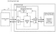
- FIG. 1is a block diagram illustrating an implementation of data storage system 100 , in accordance with some embodiments. While some example features are illustrated, various other features have not been illustrated for the sake of brevity and so as not to obscure more pertinent aspects of the example implementations disclosed herein. To that end, as a non-limiting example, data storage system 100 includes a storage device 120 , which includes a storage controller 124 and a storage medium 130 , and is used in conjunction with a computer system 110 .
- storage medium 130is a single flash memory device while in other implementations storage medium 130 includes a plurality of flash memory devices.
- storage medium 130is NAND-type flash memory or NOR-type flash memory.
- storage medium 130includes one or more three-dimensional (3D) memory devices, as further defined herein.
- storage controller 124is a solid-state drive (SSD) controller.
- SSDsolid-state drive
- other types of storage mediamay be included in accordance with aspects of a wide variety of implementations.
- Computer system 110is coupled to storage controller 124 through data connections 101 .
- computer system 110includes storage controller 124 as a component and/or a sub-system.
- Computer system 110may be any suitable computer device, such as a computer, a laptop computer, a tablet device, a netbook, an internet kiosk, a personal digital assistant, a mobile phone, a smart phone, a gaming device, a computer server, or any other computing device.
- Computer system 110is sometimes called a host or host system.
- computer system 110includes one or more processors, one or more types of memory, a display and/or other user interface components such as a keyboard, a touch screen display, a mouse, a track-pad, a digital camera and/or any number of supplemental devices to add functionality.
- processorsone or more types of memory
- display and/or other user interface componentssuch as a keyboard, a touch screen display, a mouse, a track-pad, a digital camera and/or any number of supplemental devices to add functionality.
- Storage medium 130is coupled to storage controller 124 through connections 103 .
- Connections 103are sometimes called data connections, but typically convey commands in addition to data, and optionally convey metadata, error correction information and/or other information in addition to data values to be stored in storage medium 130 and data values read from storage medium 130 .
- storage controller 124 and storage medium 130are included in the same device as components thereof.
- storage controller 124 and storage medium 130are embedded in a host device, such as a mobile device, tablet, other computer or computer controlled device, and the methods described herein are performed by the embedded memory controller.
- Storage medium 130may include any number (i.e., one or more) of memory devices including, without limitation, non-volatile semiconductor memory devices, such as flash memory.
- flash memory devicescan be configured for enterprise storage suitable for applications such as cloud computing, or for caching data stored (or to be stored) in secondary storage, such as hard disk drives. Additionally and/or alternatively, flash memory can also be configured for relatively smaller-scale applications such as personal flash drives or hard-disk replacements for personal, laptop and tablet computers.
- storage medium 130includes one or more three-dimensional (3D) memory devices, as further defined herein.
- Storage medium 130is divided into a number of addressable and individually selectable blocks, such as selectable portion 131 .
- the individually selectable blocks(sometimes referred to as “erase blocks”) are the minimum size erasable units in a flash memory device. In other words, each block contains the minimum number of memory cells that can be erased simultaneously.
- Each blockis usually further divided into a plurality of pages and/or word lines, where each page or word line is typically an instance of the smallest individually accessible (readable) portion in a block.
- the smallest individually accessible unit of a data setis a sector, which is a subunit of a page.
- a blockincludes a plurality of pages, each page contains a plurality of sectors, and each sector is the minimum unit of data for reading data from the flash memory device.
- the number of pages included in each blockvaries from one implementation to another; examples are 64, 128 and 256 pages, but other numbers of pages per block are suitable in some implementations.
- a sub-blockis smaller than an individually selectable block and is a subset of an individually selectable block.
- a sub-blockis a page.
- a sub-blockis a word line (or all the pages in a word line).
- a sub-blockis any sub-portion of an erase block, such as a contiguous group of word lines, sometimes herein called a zone.
- a zoneis a grouping of two or more pages of an erase block, where a respective erase block includes multiple zones. For example, as described with respect to FIG. 3 , pages 304 - 1 to 304 - 4 form one zone of N total zones of erase block 300 - 1 .
- a sub-block of a block in a three-dimensional memory devicecontains a plurality of word lines in the same layer of a three-dimensional array of non-volatile memory cells.
- each erase blockin a three-dimensional memory device having N (e.g., 48) layers of memory cells, each erase block includes a plurality of word lines at each layer of the three-dimensional memory device, and thus includes A ⁇ N word lines, where A is the number of word lines in each layer that are included in the erase block.
- a particular sub-block of the erase blockincludes all the word lines of the erase block that are located in a single layer of memory cells (e.g., the layer closest to the substrate of the three-dimensional memory device) or, alternatively, includes all the word lines in the erase block in a contiguous set of layers of the three-dimensional memory device.
- storage controller 124includes a management module 121 , a host interface 129 , a storage medium interface (I/O) 128 , and additional module(s) 125 .
- Storage controller 124may include various additional features that have not been illustrated for the sake of brevity and so as not to obscure more pertinent features of the example implementations disclosed herein, and a different arrangement of features may be possible.
- Host interface 129provides an interface to computer system 110 through data connections 101 .
- storage medium I/O 128provides an interface to storage medium 130 though connections 103 .
- storage medium I/O 128includes read and write circuitry, including circuitry capable of providing reading signals to storage medium 130 (e.g., reading threshold voltages for NAND-type flash memory).
- management module 121includes one or more processing units (CPUs, also sometimes called processors) 122 configured to execute instructions in one or more programs (e.g., in management module 121 ).
- the one or more CPUs 122are shared by one or more components within, and in some cases, beyond the function of storage controller 124 .
- Management module 121is coupled to host interface 129 , additional module(s) 125 and storage medium I/O 128 in order to coordinate the operation of these components.
- Additional module(s) 125are coupled to storage medium I/O 128 , host interface 129 , and management module 121 .
- additional module(s) 125may include an error control module to limit the number of uncorrectable errors inadvertently introduced into data during writes to memory or reads from memory.
- additional module(s) 125are executed in software by the one or more CPUs 122 of management module 121 , and, in other embodiments, additional module(s) 125 are implemented in whole or in part using special purpose circuitry (e.g., to perform encoding and decoding functions).
- host interface 129receives data to be stored in storage medium 130 from computer system 110 .
- the data held in host interface 129is made available to an encoder (e.g., in additional module(s) 125 ), which encodes the data to produce one or more codewords.
- the one or more codewordsare made available to storage medium I/O 128 , which transfers the one or more codewords to storage medium 130 in a manner dependent on the type of storage medium being utilized.
- a read operationis initiated when computer system (host) 110 sends one or more host read commands on control line 111 to storage controller 124 requesting data from storage medium 130 .
- Storage controller 124sends one or more read access commands to storage medium 130 , via storage medium I/O 128 , to obtain raw read data in accordance with memory locations (addresses) specified by the one or more host read commands.
- Storage medium I/O 128provides the raw read data (e.g., comprising one or more codewords) to a decoder (e.g., in additional module(s) 125 ). If the decoding is successful, the decoded data is provided to host interface 129 , where the decoded data is made available to computer system 110 . In some implementations, if the decoding is not successful, storage controller 124 may resort to a number of remedial actions or provide an indication of an irresolvable error condition.
- Flash memory devicesutilize memory cells to store data as electrical values, such as electrical charges or voltages.
- Each flash memory celltypically includes a single transistor with a floating gate that is used to store a charge, which modifies the threshold voltage of the transistor (i.e., the voltage needed to turn the transistor on).
- the magnitude of the charge, and the corresponding threshold voltage the charge creates,is used to represent one or more data values.
- a reading threshold voltageis applied to the control gate of the transistor and the resulting sensed current or voltage is mapped to a data value.
- cell voltageand “memory cell voltage,” in the context of flash memory cells, means the threshold voltage of the memory cell, which is the minimum voltage that needs to be applied to the gate of the memory cell's transistor in order for the transistor to conduct current.
- reading threshold voltagessometimes also called reading signals, reading voltages, and/or read thresholds
- gate voltagesapplied to the gates of the flash memory cells to determine whether the memory cells conduct current at that gate voltage.
- the raw data value for that read operationis a “1,” and otherwise the raw data value is a “0.”
- a storage mediume.g., storage medium 130
- each blockis optionally (but typically) further divided into a plurality of pages and/or word lines and/or sectors. While erasure of a storage medium is performed on a block basis, in many embodiments, reading and programming of the storage medium is performed on a smaller subunit of a block (e.g., on a page basis, word line basis, or sector basis). In some embodiments, the smaller subunit of a block consists of multiple memory cells (e.g., single-level cells or multi-level cells). In some embodiments, programming is performed on an entire page.
- a multi-level cell (MLC) NAND flashtypically has four possible states per cell, yielding two bits of information per cell. Further, in some embodiments, a MLC NAND has two page types: (1) a lower page (sometimes called fast page), and (2) an upper page (sometimes called slow page).
- pages in the storage mediummay contain invalid (e.g., stale) data, but those pages cannot be overwritten until the whole block containing those pages is erased.
- the pages with valid data in that blockare read and re-written to a new block and the old block is erased (or put on a queue for erasing). This process is called garbage collection.
- garbage collectionthe new block contains pages with valid data and free pages that are available for new data to be written, and the old block that was erased is also available for new data to be written. Since flash memory can only be programmed and erased a limited number of times, the efficiency of the algorithm used to pick the next block(s) to re-write and erase has a significant impact on the lifetime and reliability of flash-based storage systems.
- Write amplificationis a phenomenon where the actual amount of physical data written to a storage medium (e.g., storage medium 130 ) is a multiple of the logical amount of data intended to be written by a host (e.g., computer system 110 , sometimes called a host).
- a hoste.g., computer system 110 , sometimes called a host.
- the garbage collection process to perform these operationsresults in re-writing data one or more times. This multiplying effect increases the number of writes required over the life of a storage medium, which shortens the time it can reliably operate.
- the formula to calculate the write amplification of a storage systemis given by equation (1):
- operating at higher temperaturesmay cause retention charge loss on blocks that are cold (e.g., idle for an extended period of time from the last program command).
- Read patrollingis utilized to manage this operation retention issue.
- a storage systemcan be configured to use background read patrol mechanisms and read disturb counts to determine when the data in a block should be relocated before it becomes ECC uncorrectable.
- FIG. 2is a block diagram illustrating an exemplary management module 121 , in accordance with some embodiments.
- Management module 121typically includes one or more processing units (CPUs) 122 for executing modules, programs and/or instructions stored in memory 206 and thereby performing processing operations, memory 206 , and one or more communication buses 208 for interconnecting these components.
- Communication buses 208optionally include circuitry (sometimes called a chipset) that interconnects and controls communications between system components.
- Management module 121is coupled to host interface 129 , additional module(s) 125 , and storage medium I/O 128 by communication buses 208 .
- Memory 206includes high-speed random access memory, such as DRAM, SRAM, DDR RAM or other random access solid state memory devices, and may include non-volatile memory, such as one or more magnetic disk storage devices, optical disk storage devices, flash memory devices, or other non-volatile solid state storage devices. Memory 206 optionally includes one or more storage devices remotely located from the CPU(s) 122 . Memory 206 , or alternately the non-volatile memory device(s) within memory 206 , comprises a non-transitory computer readable storage medium. In some embodiments, memory 206 , or the computer readable storage medium of memory 206 stores the following programs, modules, and data structures, or a subset thereof:
- Each of the above identified elementsmay be stored in one or more of the previously mentioned memory devices, and corresponds to a set of instructions for performing a function described above.
- the above identified modules or programsi.e., sets of instructions
- memory 206may store a subset of the modules and data structures identified above.
- memory 206may store additional modules and data structures not described above.
- the programs, modules, and data structures stored in memory 206 , or the computer readable storage medium of memory 206provide instructions for implementing any of the methods described below with reference to FIGS. 8A-8C and 9 .
- FIG. 2shows management module 121 in accordance with some embodiments
- FIG. 2is intended more as a functional description of the various features which may be present in management module 121 than as a structural schematic of the embodiments described herein.
- items shown separatelycould be combined and some items could be separated.
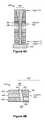
- FIG. 3is a visual representation of garbage collection for a sub-block, in accordance with some embodiments. While some example features are illustrated, various other features have not been illustrated for the sake of brevity and so as not to obscure more pertinent aspects of the example implementations disclosed herein. To that end, as a non-limiting example, storage medium 130 includes erase blocks 300 , each having a plurality of pages 304 , 306 . Furthermore, in some implementations, each erase block 300 includes a plurality of zones 302 (e.g., 302 - 1 through 302 -N), each of which includes a plurality of pages (e.g., zone 302 - 1 includes pages 304 - 1 through 304 - 4 ).
- zones 302e.g., 302 - 1 through 302 -N
- each of pages 304 , 306is further designated as valid (e.g., 304 - 3 ), invalid (e.g., 304 - 2 ), available (e.g., 304 - 7 ), or vulnerable (e.g., 304 - 5 ).
- Pages designated valid and pages designated vulnerableboth contain valid data, while pages designed invalid pages designated available do not contain valid data. Stated another way, vulnerable pages are a subclass of valid pages. In some embodiments, the above designations apply to sub-blocks. Pages are just one example of sub-blocks.
- a “Valid” designationindicates that the data of the corresponding page is accurate and valid
- an “Invalid” designationindicates that the data of the corresponding page has been modified and/or updated, and there the data in the corresponding page is invalid.
- an “Available” designationindicates that the corresponding page does not contain stored data, and is available for writing.
- a pageis designated as “Vulnerable” if a trigger parameter of the page (i.e., sub-block) meets a corresponding vulnerability criterion (as described in greater detail with respect to FIG. 8B ).
- garbage collection of a first sub-block of a first erase blockis performed in accordance with a determination that a first trigger parameter (e.g., a read-disturb count) meets a first vulnerability criterion (e.g., a read-disturb threshold).
- a first trigger parametere.g., a read-disturb count
- a first vulnerability criterione.g., a read-disturb threshold
- performing garbage collection of the first sub-blockincludes writing ( 310 ) a copy of the data of the first sub-block into an available page of a second erase block (e.g., writing the data of page 304 - 5 into page 306 - n of erase block 300 - 2 ).
- the first sub-blocke.g., page 304 - 5
- the new sub-blocke.g., page 306 - n
- the second erase block which includes the copied datais designated as valid.
- garbage collection of a second sub-block of a first erase blockis performed ( 311 ) in accordance with a determination that a second trigger parameter (e.g., a read-disturb count) meets a second vulnerability criterion (e.g., a read-disturb threshold).
- a second trigger parametere.g., a read-disturb count
- a second vulnerability criterione.g., a read-disturb threshold
- the zones 302are the sub-blocks, of erase block 300 , and each zone 302 includes multiple pages. Further, individual pages 304 are designated valid, invalid or available, while sub-blocks are designed as vulnerable or not vulnerable. Thus, in this variation, pages are not designated as vulnerable. Furthermore, when a sub-block (i.e., zone) that has been designated as vulnerable is garbage collected, all valid pages in the sub-block are copied to a different erase block than the erase block that contains the sub-block. After the copying (i.e., garbage collection of the sub-block), the copied pages in the vulnerable sub-block are designated invalid, and the new copies of those pages are used if a read command to read data in any of those page is received.
- a sub-blocki.e., zone
- each zone 302includes a plurality of sub-blocks, and each sub-block includes a plurality of pages. This is similar to the scheme shown in FIG. 3 , except that the sub-blocks are bigger than individual pages.
- each sub-blockcontains all the pages in one or more word lines, and each zone includes at least one sub-block, while at least one zone in the block includes a plurality of sub-blocks.
- a blockcontains four or more zones, with top and bottom zones, farthest and closest to the substrate, that each contain a single sub-block, and two or more middle zones, each of which contains a plurality of sub-blocks.
- a blockcontains at least three zones, each having a distinct contiguous set of word lines in the block.
- each zonehas its own vulnerability criterion (e.g., a different read count threshold, applied on a per-sub-block basis).
- a different read count thresholde.g., applied on a per-sub-block basis.
- one or more sub-blocks in a blockare of different size than other sub-blocks in the same block.
- a particularly vulnerable page or word linecan be its own sub-block, while other sub-blocks of the same block contain multiple pages or word lines and thus are multiple times as large as the sub-block that is particularly vulnerable.
- one sub-blockcan be a subset of another, larger sub-block, with the smaller sub-block having a distinct vulnerability criterion than the larger sub-block.
- the smaller sub-blockcan be configured to protect data in a particularly vulnerable portion of a block by assigning it a different vulnerability criterion (e.g., a smaller read count threshold) than the larger sub-block.
- garbage collecting only a sub-block of an erase blockreduces the impact of garbage collection on the endurance of a storage medium.
- the data integrity of vulnerable sub-blocksis maintained without further wearing the storage medium.
- FIG. 4Ais a schematic diagram of a column 400 of a memory device (e.g., storage medium 130 , FIG. 1 ) in accordance with some embodiments.
- Column 400is integrated within a memory device having a three-dimensional (3D) memory configuration.
- column 400is integrated within the storage medium 130 of FIG. 1 .
- column 400includes storage elements (e.g., SLC or MLC flash memory cells) formed within multiple layers of materials that are formed on a substrate 408 (e.g., a silicon substrate).
- FIG. 4Ashows representative layers 410 , 412 , and 414 .
- layer 410is formed adjacent to substrate 408 (i.e., layer 410 is a “bottom” layer).
- layer 412is adjacent to layer 410
- layer 414is farther from the substrate than other layers of column 400 (i.e., layer 414 is a “top” layer).
- layers 410 , 412 , and 414include a conductive (or semiconductive) material (e.g., doped polysilicon).
- column 400includes other layers, such as an oxide layer interposed between layers 410 and 412 .
- column 400further includes a structure 402 .
- an etch processis performed to etch through layers of column 400 to form an etched region (e.g., a cavity, such as a “memory hole”). After etching through layers of column 400 to form the etched region, the etched region is filled with one or more materials to form structure 402 .
- structure 402has a circular or substantially circular shape. In this example, a cross section of structure 402 that is perpendicular to a surface of substrate 408 is circular.
- column 400includes multiple storage elements, such as representative storage elements 404 and 406 (e.g., SLC or MLC flash memory cells).
- storage element 404is included in a first physical page of a first word line of storage medium 130 in FIG. 1
- the storage element 406is included in a second physical page of a second word line of storage medium 130 in FIG. 1 .
- Storage elements 404 and 406are connected to structure 402 .
- structure 402has a variation.
- structure 402has a “conical” or “tapered” profile.
- Location 420indicates a region of structure 402 associated with tapering of structure 402 .
- structure 402is not tapered below location 420 (i.e., nearer to substrate 408 than location 420 ), and structure 402 is tapered above location 420 (i.e., farther from substrate 408 than location 420 ).
- location 420is between storage elements 404 and 406 because structure 402 begins “tapering” approximately between storage elements 404 and 406 .
- storage elements 404 and 406may be associated with different ECC parameters and/or different memory access parameters to compensate for differences in physical characteristics of storage elements 404 and 406 due to tapering of structure 402 . Differences in physical characteristics of storage elements are described further with reference to FIG. 4B .
- FIG. 4Bis a schematic diagram of a portion 450 of column 400 in accordance with some embodiments.
- portion 450illustrates a charge trap structure 454 and a conductive channel 456 formed within structure 402 .
- control gate 452 and a control gate 460are connected to charge trap structure 454 .
- control gate 452is included in storage element 404 of FIG. 4A
- control gate 460is included in storage element 406 of FIG. 4A .
- control gates 452 and 460are separated by a material, such as an oxide region 458 .
- control gates 452 and 460 and oxide region 458are formed within multiple layers of storage medium 130 .
- control gate 452is formed within a polysilicon layer
- oxide region 458is formed within an oxide layer
- control gate 460is formed within another polysilicon layer.
- control gates 452 and 460 and oxide region 458are formed within one or more “physical layers” of storage medium 130 .
- a physical layerincludes control gate 452 and oxide region 458 .
- charge trap structure 454is separated from control gate 452 and conductive channel 456 by a gate dielectric, such as a silicon oxide.
- charge trap structure 454includes an insulating material, such as silicon nitride.
- conductive channel 456includes a conductive material, such as a metal (e.g., copper).
- portion 450is biased to write a value to storage element 404 and to sense a value stored at storage element 404 . In some embodiments, portion 450 is biased to write a value to storage element 406 and to sense a value stored at storage element 406 .
- chargeis injected into or drained from charge trap structure 454 by biasing control gate 452 relative to conductive channel 456 .
- the amount of charge in charge trap structure 454affects the amount of current through conductive channel 456 during a read operation of storage element 404 and indicates one or more bit values stored in storage element 404 .
- chargeis injected into or drained from charge trap structure 454 by biasing control gate 460 relative to conductive channel 456 .
- the amount of charge in charge trap structure 454affects the amount of current through conductive channel 456 during a read operation of storage element 406 and indicates a state of storage element 406 .
- the state of storage element 406corresponds to one or more bit values stored by storage element 406 .
- FIG. 4Billustrates a variation (or “tapering”) associated with structure 402 .
- the variationcorresponds to a difference between a first width of structure 402 at a first distance from substrate 408 and a second width of structure 402 at a second distance from substrate 408 , where the second distance is greater than the first distance.
- FIG. 4Billustrates that a variation associated with structure 402 affects channel width 462 (e.g., a radius of the channel) that is associated with control gate 452 .
- channel width 464e.g., a radius of the channel
- control gate 460may be less than channel width 462 due to tapering of structure 402 .
- channel width 464is greater than channel width 462 , operation of storage element 404 ( FIG. 4A ) may differ from operation of the storage element 406 ( FIG. 4A ).
- the width of conductive channel 456affects the amount of current conducted by structure 402
- the difference between channel widths 462 and 464affects operation of a memory device that includes portion 450 . Accordingly, biasing control gate 452 with a voltage causes conductive channel 456 to conduct less current as compared to applying voltage to control gate 460 .
- a variation of structure 402causes gate-to-channel distance 466 associated with storage element 404 to be greater than gate-to-channel distance 468 associated with storage element 406 .
- charge trap structure 454has a greater taper effect than conductive channel 456 .
- a greater voltageis applied to control gate 452 to accumulate charge within charge trap structure 454 (e.g., by drawing electrons from conductive channel 456 to within charge trap structure 454 ).
- tapering of structure 402causes programming operations of storage element 404 to differ relative to storage element 406 , which can result in an “incorrect” state being programmed to and/or sensed from storage element 404 .
- the tapering of structure 402also makes storage element 406 more vulnerable to read disturbs than storage element 404 .
- a vulnerability criterion of sub-blocks for enabling garbage collection(as described in greater detail below with respect to FIGS. 8A-8C ) will vary in relation to the distance of the sub-block from the substrate.
- FIG. 4Billustrates that a variation (e.g., tapering) of a structure (e.g., the structure 402 ) extending through multiple layers of a memory device (e.g., storage medium 130 , FIG. 1 ) affects read and write operations associated with the memory device.
- performance of a memory device that includes portion 450is improved by using different ECC strengths (or techniques) and/or memory access techniques (e.g., programming parameters) for storage elements 404 and 406 .
- a first ECC technique and/or a first memory access techniqueis associated with storage element 406
- a second ECC technique and/or a second memory access techniqueis associated with storage element 404 to improve operation of the memory device (e.g., storage medium 130 , FIG. 1 ).
- the second ECC techniquecompensates for a greater number of errors occurring at storage element 404 as compared to storage element 406 due to “tapering” of structure 402 .
- the second ECC techniquehas a higher error correction capability than the first ECC technique, which may improve error correction.
- the second memory access techniquecompensates for a greater number of write errors and/or read errors that may occur at storage element 404 as compared to storage element 406 due to “tapering” of structure 402 .
- second memory access techniqueprograms storage element 404 using a different programming voltage (as compared to first memory access technique) in order to program storage element 404 to the “correct” state.
- second memory access techniquesenses storage element 404 using a different read voltage (as compared to the first memory access technique) in order to read storage element 404 at the “correct” threshold voltage (e.g., to compensate for reduced effectiveness of programming operations at storage element 404 caused by tapering of structure 402 ).
- ECC techniques and/or memory access techniquescan be selectively applied to physical pages of a block based on a location of a variation of structure 402 .
- FIG. 5is a schematic diagram of a block 500 (e.g., an erase block of storage elements) in accordance with some embodiments.
- block 500is included in the storage medium 130 in FIG. 1 .
- block 500includes at least includes physical pages 508 and 510 and further includes column 400 from FIG. 4A .
- block 500includes columns 504 and 506 in addition to column 400 .
- columns 400 , 504 , and 506are formed upon substrate 408 .
- Columns 400 , 504 , and 506include a plurality of physical pages (e.g., word lines of storage elements) formed within the plurality of layers of storage medium 130 ( FIG. 1 ).
- physical pages 508 and 510are formed within the layers of block 500 .
- Each physical page of the block 500includes multiple storage elements.
- storage element 404 of FIG. 4Ais formed within physical page 508
- storage element 406 of FIG. 4Ais formed within physical page 510 .
- a sub-blockincludes one or more selectable portions 131 (e.g., pages or word lines) of a storage medium.
- a group of word linese.g., two or more contiguous word lines in column 506 of block 500 ) comprise a zone.
- a variationoccurs in the structure of each of columns 400 , 504 , and 506 .
- a blockmay include one or more columns with structures that do not include (or that do not substantially include) a variation.
- the variation within each of columns 400 , 504 , and 506occurs at (or approximately at) location 420 .
- variations within each of columns 400 , 504 , and 506occur at different locations (e.g., at different heights above the substrate 408 ).
- FIG. 5illustrates that a location (e.g., location 420 ) of a variation of a structure may occur between (or approximately between) physical pages of a block (e.g., block 500 ).
- storage controller 124applies techniques for encoding, writing, reading, and decoding data from a physical page of block 500 based on a location of the physical page relative to location 420 .
- location 420defines multiple levels (or groups of layers) of a three-dimensional (3D) memory.
- FIG. 6is a schematic diagram of a three-dimensional (3D) memory device 600 in accordance with some embodiments.
- 3D memory device 600is included in storage medium 130 ( FIG. 1 ).
- 3D memory device 600includes block 500 of FIG. 5 and further includes blocks 604 and 606 .
- each of the blocks 500 , 604 , and 606are formed upon substrate 408 .
- location 420defines a level 610 .
- level 610“partitions” 3D memory device 600 into multiple levels (e.g., a “bottom” level that is adjacent to substrate 408 and a “top” level that is non-adjacent to substrate 408 ).
- level 610defines a plane that intersects each of blocks 500 , 604 , and 606 at a level k, where k is a positive integer indicating a distance between substrate 408 and location 420 .
- level kindicates a number of physical pages or a number of word lines of 3D memory device 600 between substrate 408 and location 420 .
- level 610intersects each of blocks 500 , 604 , and 606 at a common level k.
- level 610intersects two or more of blocks 500 , 604 , and 606 at different locations.
- level 610intersects block 500 at a first distance from substrate 408 , intersects block 604 at a second distance from substrate 408 , and intersects block 606 at a third distance from substrate 408 .
- level 610corresponds to a “non-uniform” plane, such as an inclined plane.
- storage controller 124 or a component thereofdetermines a variation location (e.g., the end of a taper region such as location 420 in FIGS. 4A-4B and 5-6 ) for each column or block of storage medium 130 and stores the resulting locations in location table 220 .
- location determination module 218determines location 420 for column 400 by comparing programming parameters required to program a same state to memory elements (or memory cells) in different word lines with different vertical positions relative to the substrate of storage medium 130 (e.g., memory elements 404 and 406 ) during a setup or testing process.
- a first page included in a first word linethat require more intense programming parameters (e.g., programming voltage, number of programming pulses, and/or duration of programming pulses) to program memory cells in the first page with a respective state as compared to the programming parameters required to program memory cells of a second page in a second word line with the same respective state.
- location determination module 218may determine that the variation location is located between the first and second word lines due to the tapering effect of the memory device causing the difference in programming parameters required to program the same respective state.
- location determination module 218determines the variation location for each column or block of storage medium 130 upon the first power-on of storage medium 130 .
- storage controller 124 or a component thereofe.g., location update module 219 , FIG. 2 ) determines an updated variation location for each column or block of storage medium 130 and overwrites the previous locations in location table 220 with the resulting updated locations.
- location update module 219determines updated variation locations for each column or block of storage medium 130 in accordance with a predefined schedule such as every X power cycles of storage medium 130 .
- location table 220stores a determined location 420 for each block of storage medium 130 indicating the end of a taper region for columns within a respective block. For example, for the respective block, determined location 420 indicates a page or word line at which the taper region ends relative to the substrate. In some embodiments, location table 220 stores a determined location 420 for each column of storage medium 130 indicating the end of a taper region for a respective column. For example, for the respective column, determined location 420 indicates a page or word line at which the taper region ends relative to the substrate. As such, in some embodiments, storage controller 124 is able to selectively encode, write, read, and/or decode data from pages or word lines above and below determined location 420 for the respective column. For example, for the respective column, data written to pages or word lines above determined location 420 are encoded with a first ECC technique, and data written to pages or word lines below determined location 420 are encoded with a second ECC technique.
- FIG. 7is a schematic diagram of a 3D memory device 700 in a NAND flash configuration in accordance with some embodiments.
- 3D memory device 700corresponds to storage medium 130 ( FIG. 1 ).
- 3D memory device 700includes a plurality of physical layers 702 , each with a plurality of storage elements (e.g., memory cells), such as a representative memory cell 710 .
- the storage elementsare arranged in arrays within physical layers 702 .
- representative memory cell 710includes a charge trap structure 714 between word line/control gate (WL 4 ) 728 and conductive channel 712 .
- Chargeis injected into or drained from charge trap structure 714 by biasing conductive channel 712 relative to word line 728 .
- charge trap structure 714includes silicon nitride and is separated from word line 728 and conductive channel 712 by a gate dielectric (e.g., silicon oxide).
- the amount of charge in charge trap structure 714affects the amount of current through conductive channel 712 during a read operation of memory cell 710 and indicates one or more bit values that are stored in memory cell 710 .
- 3D memory device 700includes multiple erase blocks, including a first block (block 0 ) 750 , a second block (block 1 ) 752 , and a third block (block 2 ) 754 .
- block 750 - 754each include a “vertical slice” of physical layers 702 that includes a stack of word lines, illustrated as a first word line (WL 0 ) 720 , a second word line (WL 1 ) 722 , a third word line (WL 2 ) 724 , a fourth word line (WL 3 ) 726 , and fifth word line (WL 4 ) 728 .
- Multiple conductive channelshaving a substantially vertical orientation with respect to FIG.
- FIG. 7illustrates three blocks 750 - 754 , five word lines 720 - 728 in each block, and three conductive channels in each block for clarity of illustration.
- 3D memory device 700includes more than three blocks, more than five word lines per block, and more than three conductive channels per block.
- a single blockincludes all the word lines in multiple vertical slices (e.g., two or four vertical slices) of physical layers 702 .
- read/write circuitry 760i.e., read/write circuitry 135 or alternatively read/write circuitry within storage medium I/O 128 ) is coupled with conductive channels via multiple conductive lines, illustrated as a first bit line (BL 0 ) 730 , a second bit line (BL 1 ) 732 , and a third bit line (BL 2 ) 734 at a “top” end of the conducive channels (e.g., relative to substrate 704 ) and a first source line (SL 0 ) 740 , a second source line (SL 1 ) 742 , and a third source line (SL 2 ) 744 ) at a “bottom” end of the conductive channels (e.g., relative to substrate 704 ).
- read/write circuitry 760is coupled with bit lines 730 - 734 via “P” control lines, coupled with source lines 740 - 744 via “M” control lines, and coupled with word lines 720 - 728 via “N” control lines.
- Pbit lines 730 - 734 via “P” control lines
- source lines 740 - 744via “M” control lines
- Nword lines 720 - 728 via “N” control lines.
- each of bit lines 730 - 734 and each of source lines 740 - 744are coupled with the same end (e.g., the top end or the bottom end) of different conductive channels.
- a respective bit lineis coupled with the top of conductive channel 792 and a respective source line is coupled with the top of conductive channel 712 .
- the bottom of conductive channel 792is coupled (e.g., electrically coupled) to the bottom of conductive channel 712 .
- conductive channel 792 and conductive channel 712are coupled in series and are coupled with the respective bit line and the respective source line.
- each of the conductive channelsin FIG. 7 is illustrated as a single conductive channel, in some embodiments, each of the conductive channels include multiple conductive channels that are in a stacked configuration.
- the multiple conductive channels in a stacked configurationmay be coupled by one or more connectors.
- read/write circuitry 760receives memory operation commands from storage controller 124 (e.g., a read command from data read module 212 , a write command from data write module 214 , or an erase command from data erase module 216 ). For example, data is stored in storage elements coupled with word line 728 and read/write circuitry 760 reads bit values from these storage elements.
- the read/write circuitry 760applies selection signals to control lines coupled with word lines 720 - 728 , bit lines 730 - 734 , and source lines 740 - 742 to cause a programming voltage (e.g., a voltage pulse or series of voltage pulses associated with a threshold voltage) to be applied across selected storage element(s) of the selected word line (e.g., fourth word line 728 ) so as to write/program data to the selected storage element(s).
- a programming voltagee.g., a voltage pulse or series of voltage pulses associated with a threshold voltage
- storage controller 124receives a request from the host (e.g., computer system 110 , FIG. 1 ) and, in response, causes read/write circuitry 760 to read bits from particular storage elements of 3D memory device 700 by applying appropriate signals to control lines to cause storage elements of a selected word line to be sensed.
- hoste.g., computer system 110 , FIG. 1
- read/write circuitry 760to read bits from particular storage elements of 3D memory device 700 by applying appropriate signals to control lines to cause storage elements of a selected word line to be sensed.
- FIGS. 8A-8Cillustrate a flowchart representation of a method 800 of garbage collection for a storage medium in a storage system, in accordance with some embodiments.
- the storage devicee.g., storage device 120 , FIG. 1
- garbage collectionuses garbage collection to reclaim portions of memory (e.g., storage medium 130 , FIG. 1 ) that no longer contain valid data.
- the storage devicee.g., storage device 120 , FIG. 1
- first garbage collects only vulnerable sub-blocks of a blocki.e., writes copies of the vulnerable sub-blocks to a different block, and invalidates the data in the vulnerable sub-blocks
- garbage collection of the remainder of the blocki.e., writes copies of the vulnerable sub-blocks to a different block, and invalidates the data in the vulnerable sub-blocks
- the remainder of the blockis not garbage collected if it never meets the criteria for garbage collection.
- method 800is performed by a storage device (e.g., storage device 120 , FIG. 1 ) or one or more components of the storage device (e.g., storage controller 124 and/or storage medium 130 , FIG. 1 ), wherein the storage device is operatively coupled with a host system (e.g., computer system 110 , FIG. 1 ).
- a host systeme.g., computer system 110 , FIG. 1
- method 800is governed by instructions that are stored in a non-transitory computer readable storage medium and that are executed by one or more processors of a device, such as the one or more processing units (CPUs) 122 of management module 121 , shown in FIGS. 1 and 2 .
- CPUsprocessing units
- method 800is performed by a storage system (e.g., data storage system 100 , FIG. 1 ) or one or more components of the storage system (e.g., computer system 110 and/or storage device 120 , FIG. 1 ). In some embodiments, some of the operations of method 800 are performed at a host (e.g., computer system 110 , FIG. 1 ) and information is transmitted to a storage device (e.g., storage device 120 , FIG. 1 ). In some embodiments, method 800 is governed, at least in part, by instructions that are stored in a non-transitory computer readable storage medium and that are executed by one or more processors of a host (not shown in FIG. 1 ).
- method 800is performed by a storage device (e.g., storage device 120 , FIG. 1 ).
- a hoste.g., computer system 110 , FIG. 1 .
- a storage devicedetermines ( 802 ) a first trigger parameter in accordance with one or more operating conditions of a first sub-block of an erase block in a storage medium in the storage device.
- operating conditionsare read operations, or the number of read operations performed in a particular portion of the storage medium.
- Read operationsdegrade data retention by the storage device by disturbing adjacent or nearby memory cells.
- Write operations and erase operationscan also degrade data retention.
- Data retentionsometimes referred to as charge retention on floating gates, is reflected in the ability of a memory cell to produce accurate data values when a read operation is performed.
- Examples of data retention metricsinclude metrics related to the detection or measurement of drifting cell threshold voltages and metrics related to the detection or measurement of data errors during read operations (e.g., bit error rate).
- Trigger parameters determined in accordance with one or more operating conditionsat least partially serve to identify “weak” sub-blocks, which are more likely than other sub-blocks to suffer reduced or impaired data retention, and which are candidates for garbage collection, as described herein.
- sub-blockscan include one or more selectable portions of a storage medium, and are smaller than blocks, which are the smallest unit of storage in the storage medium that can be erased in a single erase operation.
- the first trigger parameteris a read-disturb count of the first sub-block. For example, as previously described, performing a read operation of a respective page disturbs adjacent pages, and therefore increases a read-disturb count of the sub-block(s) containing those adjacent pages. In some implementations, a read-disturb count is maintained by the storage device for each sub-block. For example, in some implementations, performing a read operation of a page of a respective sub-block (e.g., zone 302 - 1 , FIG. 3 ) increments a read-disturb count of the respective sub-block.
- a read-disturb countis maintained by the storage device for each sub-block. For example, in some implementations, performing a read operation of a page of a respective sub-block (e.g., zone 302 - 1 , FIG. 3 ) increments a read-disturb count of the respective sub-block.
- performing a read operation of a page of a respective sub-blockincrements a read-disturb count of both the respective sub-block and any adjacent sub-blocks (e.g., adjacent zone 302 - 2 , FIG. 3 ), while in alternative implementations, only a read-disturb count of any adjacent sub-blocks is incremented.
- the amount by which a read-disturb count is incremented for a respective sub-blockdepends on a physical distance between the respective sub-block and the sub-block in which a disturbing memory operation is being performed. For example, based on FIG. 3 , a read operation performed on page 304 - 4 increments a read-disturb count for page 304 - 5 by 5 , whereas a read-disturb count for page 304 - 1 is incremented by 1.
- the first trigger parameteris a data retention parameter of the first sub-block, a set of data retention parameters, or a combination of data retention parameters.
- Data retention parametersinclude, for example, an error metric corresponding to a number of detected data errors in a sub-block (e.g., a bit error rate), and a stability metric corresponding to one or more threshold voltages (e.g., shifting read, write, and/or erase threshold voltages for the first sub-block).
- data retention parametersinclude a program-erase (PE) cycle count (e.g., of an erase block) and/or other information relating to the accumulated wear of a storage medium 130 , or a portion thereof (e.g., selectable portion 131 , FIG. 1 ).
- PEprogram-erase
- the aforementioned read-disturb countis another example of a data retention parameter.
- the storage deviceregularly performs background monitoring activities (e.g., with state information module 230 , FIG. 2 ) to determine trigger parameters of a respective sub-block (e.g., read-disturb counts and optionally other data retention parameters, sometimes collectively referred to as “state information”), which are stored in a data table in memory (e.g., state information table 232 ).
- background monitoring activitiese.g., with state information module 230 , FIG. 2
- trigger parameters of a respective sub-blocke.g., read-disturb counts and optionally other data retention parameters, sometimes collectively referred to as “state information”
- state informatione.g., read-disturb counts and optionally other data retention parameters, sometimes collectively referred to as “state information”
- state information module 230executes instructions for tracking a read-disturb count for a sub-block of an erase block by identifying (e.g., using translation table 216 ) the physical pages to which data is being written, and incrementing a read-disturb count for the sub-block when a read operation is performed on data in the sub-block and/or when a read operation is performed on data in a region adjacent or neighboring (e.g., within a predefined range) the sub-block.
- state information module 230executes instructions for performing a read patrol operation on a sub-block (e.g., page 304 - 4 , FIG. 3 ) to determine how much erroneous data (e.g., an error rate) the sub-block is storing, if any.
- background monitoring activitiesare performed continuously or according to a pre-defined schedule, for example, performing a read patrol operation after every 20 read operations, or performing a read patrol operation on every page containing valid data a predefined number of times (e.g., once) per predefined unit of time (e.g., N hours, where N is a predefined positive integer between 1 and 24).
- background monitoring activitiesare performed according to a pre-defined schedule that is set based on information from state information table 230 and/or characterization table 234 (storing characteristics of a sub-block, which are described in greater detail below). For example, a read patrol operation is performed more frequently on a sub-block that has been identified as vulnerable, based on a read-disturb count of the sub-block (e.g., a read-disturb count of the sub-block exceeds a threshold, vulnerability criteria being described in greater detail below), and optionally in combination with the location of the sub-block relative to the substrate of the storage medium (e.g., WL 0 720 , FIG. 7 ).
- a read-disturb count of the sub-blocke.g., a read-disturb count of the sub-block exceeds a threshold, vulnerability criteria being described in greater detail below
- the location of the sub-block relative to the substrate of the storage mediume.g., WL 0 720 , FIG. 7
- the storage deviceincludes ( 804 ) one or more flash memory devices.
- the storage deviceincludes a storage medium (e.g., storage medium 130 , FIG. 1 ), and the storage medium includes one or more non-volatile storage devices, such as flash memory devices.
- the storage mediume.g., storage medium 130 , FIG. 1
- the storage mediumis a single flash memory device, while in other embodiments the storage medium includes a plurality of flash memory devices.
- the storage mediumincludes dozens or hundreds of flash memory devices, organized in parallel memory channels, such as 16, 32 or 64 flash memory devices per memory channel, and 8, 16 or 32 parallel memory channels.
- the non-volatile storage medium(e.g., storage medium 130 , FIG. 1 ) includes NAND-type flash memory or NOR-type flash memory. In other embodiments, the storage medium includes one or more other types of non-volatile storage devices.
- the storage deviceincludes ( 806 ) one or more three-dimensional (3D) memory devices and circuitry associated with operation of memory elements in the one or more 3D memory devices.
- the storage deviceincludes a storage medium (e.g., storage medium 130 , FIG. 1 ), and the storage medium includes one or more 3D memory devices and circuitry associated with operation of memory elements in the one or more 3D memory devices.
- the storage mediume.g., storage medium 130 , FIG. 1
- the storage mediumis a single 3D memory device, while in other embodiments the storage medium includes a plurality of 3D memory devices.
- the circuitry and one or more memory elements in a respective 3D memory device, of the one or more 3D memory devicesare ( 808 ) on the same substrate (e.g., a silicon substrate).
- the substrateis a wafer on which the material layers of the one or more memory elements are deposited and/or in which the one or more memory elements are formed.
- the substrateis a carrier substrate which is attached to the one or more memory elements after they are formed.
- the substrateincludes a semiconductor such as silicon.
- the storage devicedetermines ( 810 ) a second trigger parameter in accordance with one or more operating conditions of a second sub-block of the erase block in the storage medium (a detailed discussion of which can be found above with respect to the first trigger parameter).
- the first sub-blockis a portion of the erase block and the second sub-block is ( 812 ) another portion of the erase block.
- the first sub-block and the second sub-blockare distinct portions of the same erase block (e.g., in FIG. 3 , the first sub-block is page 304 - 4 , and the second sub-block is page 304 - 5 ).
- the first sub-blockis a page of a zone of the erase block (e.g., page 304 - 1 of zone 1 ), and the second sub-block is the remainder of pages of the zone of the erase block (e.g., pages 304 - 2 through 304 - 4 of zone 1 ).
- the first sub-blockis a page of the erase block (e.g., page 304 - 1 ) and the second sub-block is the remainder of pages of the erase block (e.g., pages 304 - 2 through 304 - n ).
- the storage deviceenables ( 820 ) garbage collection of the first sub-block.
- vulnerability criteriaare one or more pre-defined threshold limits for the trigger parameters described above. In some implementations, if a trigger parameter of a sub-block meets a corresponding vulnerability criterion, the sub-block is designated as vulnerable.
- the first vulnerability criterionis a threshold on a read-disturb count of the first sub-block (e.g., read-disturb count limit of 100), while in some other implementations, the first vulnerability criterion is a threshold number of data errors detected in the first sub-block by performing a read patrol operation (e.g., eighty erroneous bits in page of size 4K bytes, FIG. 3 ; noting, however, that the threshold number of data errors will be a function of the ECC strength, and optionally the reliability requirements for the device as well).
- a read patrol operatione.g., eighty erroneous bits in page of size 4K bytes, FIG. 3 ; noting, however, that the threshold number of data errors will be a function of the ECC strength, and optionally the reliability requirements for the device as well.
- the first trigger parameterincludes both a read-disturb count and another data retention parameter of the first sub-block
- the first vulnerability criterionincludes thresholds for both the read-disturb count and the data retention parameter. For example, once the read-disturb threshold is met, a read patrol operation is performed, and the number of data errors detected is compared with the error threshold. If the number of data errors exceeds the error threshold, the first sub-block is designated as vulnerable and is scheduled for garbage collection.
- a weighted combination of trigger parametersis compared with a threshold to determine if garbage collection should be enabled for the first sub-block.
- An example of weighted combination of trigger parametersis:
- ⁇ i1 N ⁇ ⁇ ⁇ i ⁇ ( trigger_parameter i - threshold i )
- trigger_parameter iis the i th trigger parameter
- ⁇ iis a weight for the i th trigger parameter
- threshold iis a threshold or subtractive factor for the i th trigger parameter.
- the weighted combinationis computed and then compared with a predefined threshold to determine if garbage collection should be enabled for the first sub-block.
- the first vulnerability criterionis determined ( 816 ) in accordance with one or more characteristics of the first sub-block.
- the one or more characteristicsare intrinsic qualities of a flash memory device that impact data retention.
- the first vulnerability criterionis determined in accordance with a physical location of a sub-block (e.g., a distance of between the first sub-block and the substrate of the storage medium). For example, for the reasons explained above with respect to FIG.
- a sub-block comprising word line 0e.g., WL 0 , 720
- word line 4e.g., WL 4 , 728
- word line 0e.g., a read-disturb threshold of 15,000 for WL 0 , compared to a read-disturb threshold of 25,000 for WL 4 .
- the first vulnerability criterionis determined in accordance with the zone (of a plurality of zones in an erase block) to which the first sub-block corresponds.
- a sub-blocke.g., 302 - 1
- zone 2e.g., a read-disturb threshold of 15,000 for zone 1 , compared to a read-disturb threshold of 25,000 for zone 2 .
- the first vulnerability criterionis determined in accordance with a page to which the first sub-block corresponds. For example, in zone 1 of erase block 300 - 1 ( FIG. 3 ), page 304 - 1 has a stricter vulnerability criterion compared to page 304 - 2 .
- “enabling garbage collection” of a sub-blockis different from the actual garbage collection of the sub-block, which occurs after garbage collection of the sub-block is enabled.
- enabling garbage collection of a sub-blockis implemented by adding the sub-block to a queue or list of sub-blocks scheduled for garbage collection.
- a garbage collection process executed by the storage device's controller or management module or memory channel controllerperforms the actual garbage collection of sub-blocks for which garbage collection has been enabled. Such garbage collection can be deferred in order to execute other memory operations, for example, in accordance with memory operation scheduling criteria implemented by the storage device.
- garbage collectionincludes writing ( 822 ) a copy of valid data from the first sub-block to a second erase block in the storage medium, wherein the second erase block is distinct from the erase block, and invalidating ( 824 ) the first sub-block in the erase block (i.e., invalidating any valid data remaining in the first sub-block when the first sub-block is garbage collected).
- An example of garbage collectionis illustrated and described in greater detail with respect to FIG. 3 .
- the storage deviceenables garbage collection of the first sub-block in accordance with a determination that the erase block or a memory portion that includes the erase block meets predefined age criteria ( 818 ) and a determination that the first trigger parameter meets the first vulnerability criterion (see 814 ).
- age criteriainclude one or more threshold limits on a program-erase (PE) cycle count, an age (e.g., determined with reference to a date of manufacture for the storage device), and/or other age-related metrics for an erase block, or a memory portion that includes the erase block.
- PEprogram-erase
- garbage collection of page 304 - 4FIG.
- erase block 300 - 1(which includes page 304 - 4 ) has a PE cycle count that exceeds 2500, where a “PE cycle count that exceeds 2500” is an example of the aforementioned “predefined age criteria.”
- the storage deviceenables ( 826 ) garbage collection for a parity stripe that includes the first sub-block, wherein the parity stripe includes a plurality of sub-blocks across a plurality of erase blocks in the storage medium.
- a parity stripespans multiple erase blocks (e.g., a super block), and in order to maintain parity protection, when garbage collection is enabled for the first sub-block (e.g., a page in a first erase block), garbage collection is also enabled for the entire parity stripe that includes the first sub-block (e.g., other pages in one or more other erase blocks).
- the storage deviceenables ( 834 ) garbage collection of the second sub-block.
- the second sub-blockhas a read-disturb count that which exceeds a read-disturb threshold of 225,000, and thus garbage collection of both the second sub-block is enabled.
- enabling garbage of the second sub-blockoccurs without enabling garbage collection of the first sub-block, because the second trigger parameter meets the second vulnerability criterion while the first trigger parameter does not (or does not yet) meet the first vulnerability criterion.
- the second vulnerability criterionis determined ( 830 ) in accordance with one or more characteristics of the second sub-block. See the above discussion of sub-block characteristics and vulnerability criteria.
- the first vulnerability criterionis distinct ( 832 ) from the second vulnerability criterion.
- garbage collection of the first sub-blockis performed ( 836 ) prior to (or without) garbage collection of the second sub-block.
- the second trigger parametermeets the second vulnerability criterion after the first trigger parameter meets the first vulnerability criterion, and thus garbage collection of the second sub-block (e.g., erase block 304 - 1 ) is performed at a later time than garbage collection for a first sub-block (e.g., page 304 - 5 ).
- Method 800reduces the impact of garbage collection on the endurance of the storage medium, because data stored in vulnerable sub-blocks of an erase block is preserved without erasing the entire erase block (at least until a separate decision is made to garbage collect the remaining valid data in the erase block).
- FIG. 9illustrates a flowchart representation of a method 900 of garbage collection for a storage medium in a storage system, in accordance with some embodiments.
- the storage devicee.g., storage device 120 , FIG. 1
- garbage collectionuses garbage collection to reclaim portions of memory (e.g., storage medium 130 , FIG. 1 ) that no longer contain valid data.
- the storage devicee.g., storage device 120 , FIG. 1
- the storage devicefirst writes copies of valid data in vulnerable sub-blocks to another erase block, while temporarily withholding copying of other valid data in the erase block and erasing the erase block until a separate decision is made to garbage collect the erase block itself (and thus garbage collecting the remaining valid data, if any, in the erase block).
- method 900is performed by a storage device (e.g., storage device 120 , FIG. 1 ) or one or more components of the storage device (e.g., storage controller 124 and/or storage medium 130 , FIG. 1 ), wherein the storage device is operatively coupled with a host system (e.g., computer system 110 , FIG. 1 ).
- a host systeme.g., computer system 110 , FIG. 1
- method 900is governed by instructions that are stored in a non-transitory computer readable storage medium and that are executed by one or more processors of a device, such as the one or more processing units (CPUs) 122 of management module 121 , shown in FIGS. 1 and 2 .
- CPUsprocessing units
- method 900is performed by a storage system (e.g., data storage system 100 , FIG. 1 ) or one or more components of the storage system (e.g., computer system 110 and/or storage device 120 , FIG. 1 ). In some embodiments, some of the operations of method 900 are performed at a host (e.g., computer system 110 , FIG. 1 ) and information is transmitted to a storage device (e.g., storage device 120 , FIG. 1 ). In some embodiments, method 900 is governed, at least in part, by instructions that are stored in a non-transitory computer readable storage medium and that are executed by one or more processors of a host (not shown in FIG. 1 ).
- method 900describes method 900 as performed by a storage device (e.g., storage device 120 , FIG. 1 ). However, those skilled in the art will appreciate that in other embodiments, one or more of the operations described in method 900 are performed by a host (e.g., computer system 110 , FIG. 1 ).
- a hoste.g., computer system 110 , FIG. 1 .
- a storage devicedetermines ( 902 ) a first trigger parameter in accordance with one or more operating conditions of a first sub-block of an erase block in a storage medium in the storage device. Trigger parameters and operating conditions are discussed in greater detail above with respect to FIG. 8A .
- the storage deviceincludes ( 904 ) one or more flash memory devices.
- the storage deviceincludes a storage medium (e.g., storage medium 130 , FIG. 1 ), and the storage medium includes one or more non-volatile storage devices, such as flash memory devices.
- the storage mediume.g., storage medium 130 , FIG. 1
- the storage mediumis a single flash memory device, while in other embodiments the storage medium includes a plurality of flash memory devices.
- the storage mediumincludes dozens or hundreds of flash memory devices, organized in parallel memory channels, such as 16, 32 or 64 flash memory devices per memory channel, and 8, 16 or 32 parallel memory channels.
- the non-volatile storage medium(e.g., storage medium 130 , FIG. 1 ) includes NAND-type flash memory or NOR-type flash memory. In other embodiments, the storage medium includes one or more other types of non-volatile storage devices.
- the storage deviceincludes ( 906 ) one or more three-dimensional (3D) memory devices and circuitry associated with operation of memory elements in the one or more 3D memory devices.
- the storage deviceincludes a storage medium (e.g., storage medium 130 , FIG. 1 ), and the storage medium includes one or more 3D memory devices and circuitry associated with operation of memory elements in the one or more 3D memory devices.
- the storage mediume.g., storage medium 130 , FIG. 1
- the storage mediumis a single 3D memory device, while in other embodiments the storage medium includes a plurality of 3D memory devices.
- the circuitry and one or more memory elements in a respective 3D memory device, of the one or more 3D memory devicesare ( 908 ) on the same substrate (e.g., a silicon substrate).
- the substrateis a wafer, or a portion (e.g., a die) of a wafer, on which the material layers of the one or more memory elements are deposited and/or in which the one or more memory elements are formed.
- the substrateis a carrier substrate which is attached to the one or more memory elements after they are formed.
- the substrateincludes a semiconductor such as silicon.
- garbage collecting the first sub-blockincludes writing ( 914 ) a copy of valid data from the first sub-block to a second erase block in the storage medium, wherein the second erase block is distinct from the erase block, and invalidating ( 916 ) the first sub-block in the erase block (i.e., invalidating any valid data remaining in the first sub-block when the first sub-block is garbage collected).
- An example of garbage collectionis illustrated and described in greater detail with respect to FIG. 3 .
- the storage devicedetermines ( 918 ) whether the erase block meets predefined garbage collection scheduling criteria. In accordance with a determination that the erase block meets said garbage collection scheduling criteria, the storage device enables ( 920 ) garbage collection of the erase block.
- the garbage collection scheduling criteriainclude a determination that the amount of valid data remaining in the erase block falls below a threshold. In some implementations, the garbage collection scheduling criteria include a determination that the erase block is one of N erase blocks in the storage device having the least amount of valid data, where N (a positive integer) is the number of erase blocks needed by the storage device to be available for storing data.
- Semiconductor memory devicesinclude volatile memory devices, such as dynamic random access memory (“DRAM”) or static random access memory (“SRAM”) devices, non-volatile memory devices, such as resistive random access memory (“ReRAM”), electrically erasable programmable read only memory (“EEPROM”), flash memory (which can also be considered a subset of EEPROM), ferroelectric random access memory (“FRAM”), and magnetoresistive random access memory (“MRAM”), and other semiconductor elements capable of storing information.
- volatile memory devicessuch as dynamic random access memory (“DRAM”) or static random access memory (“SRAM”) devices
- non-volatile memory devicessuch as resistive random access memory (“ReRAM”), electrically erasable programmable read only memory (“EEPROM”), flash memory (which can also be considered a subset of EEPROM), ferroelectric random access memory (“FRAM”), and magnetoresistive random access memory (“MRAM”), and other semiconductor elements capable of storing information.
- ReRAMresistive random access memory
- EEPROMelectrically erasable
- the memory devicescan be formed from passive and/or active elements, in any combinations.
- passive semiconductor memory elementsinclude ReRAM device elements, which in some embodiments include a resistivity switching storage element, such as an anti-fuse, phase change material, etc., and optionally a steering element, such as a diode, etc.
- active semiconductor memory elementsinclude EEPROM and flash memory device elements, which in some embodiments include elements containing a charge storage region, such as a floating gate, conductive nanoparticles, or a charge storage dielectric material.
- Multiple memory elementsmay be configured so that they are connected in series or so that each element is individually accessible.
- flash memory devices in a NAND configurationtypically contain memory elements connected in series.
- a NAND memory arraymay be configured so that the array is composed of multiple strings of memory in which a string is composed of multiple memory elements sharing a single bit line and accessed as a group.
- memory elementsmay be configured so that each element is individually accessible (e.g., a NOR memory array).
- NAND and NOR memory configurationsare exemplary, and memory elements may be otherwise configured.
- the semiconductor memory elements located within and/or over a substratemay be arranged in two or three dimensions, such as a two dimensional memory structure or a three dimensional memory structure.
- the semiconductor memory elementsare arranged in a single plane or a single memory device level.
- memory elementsare arranged in a plane (e.g., in an x-z direction plane) which extends substantially parallel to a major surface of a substrate that supports the memory elements.
- the substratemay be a wafer over or in which the layer of the memory elements are formed or it may be a carrier substrate which is attached to the memory elements after they are formed.
- the substratemay include a semiconductor such as silicon.
- the memory elementsmay be arranged in the single memory device level in an ordered array, such as in a plurality of rows and/or columns. However, the memory elements may be arrayed in non-regular or non-orthogonal configurations.
- the memory elementsmay each have two or more electrodes or contact lines, such as bit lines and word lines.
- a three dimensional memory arrayis arranged so that memory elements occupy multiple planes or multiple memory device levels, thereby forming a structure in three dimensions (i.e., in the x, y and z directions, where the y direction is substantially perpendicular and the x and z directions are substantially parallel to the major surface of the substrate).
- a three dimensional memory structuremay be vertically arranged as a stack of multiple two dimensional memory device levels.
- a three dimensional memory arraymay be arranged as multiple vertical columns (e.g., columns extending substantially perpendicular to the major surface of the substrate, i.e., in the y direction) with each column having multiple memory elements in each column.
- the columnsmay be arranged in a two dimensional configuration (e.g., in an x-z plane), resulting in a three dimensional arrangement of memory elements with elements on multiple vertically stacked memory planes.
- Other configurations of memory elements in three dimensionscan also constitute a three dimensional memory array.
- the memory elementsmay be coupled together to form a NAND string within a single horizontal (e.g., x-z) memory device level.
- the memory elementsmay be coupled together to form a vertical NAND string that traverses across multiple horizontal memory device levels.
- Other three dimensional configurationscan be envisioned wherein some NAND strings contain memory elements in a single memory level while other strings contain memory elements which span through multiple memory levels.
- Three dimensional memory arraysmay also be designed in a NOR configuration and in a ReRAM configuration.
- a monolithic three dimensional memory arraytypically, one or more memory device levels are formed above a single substrate.
- the monolithic three dimensional memory arraymay also have one or more memory layers at least partially within the single substrate.
- the substratemay include a semiconductor such as silicon.
- the layers constituting each memory device level of the arrayare typically formed on the layers of the underlying memory device levels of the array.
- layers of adjacent memory device levels of a monolithic three dimensional memory arraymay be shared or have intervening layers between memory device levels.
- non-monolithic stacked memoriescan be constructed by forming memory levels on separate substrates and then stacking the memory levels atop each other. The substrates may be thinned or removed from the memory device levels before stacking, but as the memory device levels are initially formed over separate substrates, the resulting memory arrays are not monolithic three dimensional memory arrays. Further, multiple two dimensional memory arrays or three dimensional memory arrays (monolithic or non-monolithic) may be formed on separate chips and then packaged together to form a stacked-chip memory device.
- Associated circuitryis typically required for operation of the memory elements and for communication with the memory elements.
- memory devicesmay have circuitry used for controlling and driving memory elements to accomplish functions such as programming and reading.
- This associated circuitrymay be on the same substrate as the memory elements and/or on a separate substrate.
- a controller for memory read-write operationsmay be located on a separate controller chip and/or on the same substrate as the memory elements.
- three-dimensional memory device(or 3D memory device) is herein defined to mean a memory device having multiple memory layers or multiple levels (e.g., sometimes called multiple memory device levels) of memory elements, including any of the following: a memory device having a monolithic or non-monolithic 3D memory array, some non-limiting examples of which are described above; or two or more 2D and/or 3D memory devices, packaged together to form a stacked-chip memory device, some non-limiting examples of which are described above.
- the storage medium(e.g., storage medium 130 , FIG. 1 ) is a single flash memory device, while in other implementations, the storage medium (e.g., storage medium 130 , FIG. 1 ) includes a plurality of flash memory devices.
- a storage systemincludes a storage medium (e.g., storage medium 130 , FIG. 1 ), one or more processors (e.g., CPUs 122 , FIGS. 1 and 2 ) and memory (e.g., memory 206 , FIG. 2 ) storing one or more programs configured for execution by the one or more processors and configured to perform or control performance of any of the methods described above.
- a storage mediume.g., storage medium 130 , FIG. 1
- processorse.g., CPUs 122 , FIGS. 1 and 2
- memorye.g., memory 206 , FIG. 2
- a device operable to perform garbage collectionincludes a storage medium interface (e.g., storage medium I/O 128 , FIG. 1 ) for coupling the device to the storage medium (e.g., storage medium 130 , FIG. 1 ) and one or more modules, including a memory management module (e.g., management module 121 , FIGS. 1 and 2 ) that includes one or more processors (e.g., CPUs 122 , FIGS. 1 and 2 ) and memory (e.g., memory 206 , FIG.
- a storage medium interfacee.g., storage medium I/O 128 , FIG. 1
- modulesincluding a memory management module (e.g., management module 121 , FIGS. 1 and 2 ) that includes one or more processors (e.g., CPUs 122 , FIGS. 1 and 2 ) and memory (e.g., memory 206 , FIG.
- the storage medium interfacee.g., storage medium I/O 128 , FIG. 1
- the storage medium interfacee.g., storage medium I/O 128 , FIG. 1
- firstfirst
- secondsecond
- first contactfirst contact
- first contactsecond contact
- first contactsecond contact
- the term “if”may be construed to mean “when” or “upon” or “in response to determining” or “in accordance with a determination” or “in response to detecting,” that a stated condition precedent is true, depending on the context.
- the phrase “if it is determined [that a stated condition precedent is true]” or “if [a stated condition precedent is true]” or “when [a stated condition precedent is true]”may be construed to mean “upon determining” or “in response to determining” or “in accordance with a determination” or “upon detecting” or “in response to detecting” that the stated condition precedent is true, depending on the context.
Landscapes
- Engineering & Computer Science (AREA)
- Theoretical Computer Science (AREA)
- Physics & Mathematics (AREA)
- General Engineering & Computer Science (AREA)
- General Physics & Mathematics (AREA)
- Read Only Memory (AREA)
- Techniques For Improving Reliability Of Storages (AREA)
- Memory System (AREA)
Abstract
Description
- a data read
module 210 that is used for reading data from one or more blocks in a storage medium; - a
data write module 212 that is used for writing data to one or more blocks in a storage medium; - a data erase
module 214 that is used for erasing data from one or more blocks in a storage medium; - a translation table216 that is used for mapping logical addresses to physical addresses;
- (optionally) a
location determination module 218 that is used for determining a variation location (e.g., the end of a taper region) for each column or block ofstorage medium 130; - (optionally) a
location update module 219 for determining an updated variation location for each column or block ofstorage medium 130; - (optionally) a location table220 storing the variation location determined by
location determination module 218 and/or the updated variation location determined bylocation update module 219 for each column or block ofstorage medium 130; - a
garbage collection module 222 that is used for garbage collection for one or more sub-blocks and/or blocks in astorage medium 130, which optionally includes the following modules or sub-modules, or a subset thereof:- a
trigger module 224 that is used for selecting and/or determining one or more trigger parameters (e.g., read-disturb count) in accordance with one or more operating conditions of a sub-block; - a
vulnerability criteria module 226 that is used for configuring one or more pre-defined threshold limits for one or more trigger parameters selected and/or determined bytrigger module 224; - a garbage collection enable
module 228 that is used for determining whether a trigger parameter meets a vulnerability criterion, and for enabling garbage collection of one or more sub-blocks in accordance with the determination; - a
state information module 230 that is used for determining and/or retrieving state information (described in greater detail with respect toFIG. 8A ) of one or more sub-blocks and/or blocks, including a read-disturb count, data retention parameters (e.g., bit error rate), and/or an age of thestorage medium 130; - a state information table232 that is used for storing state information determined and/or retrieved by
state information module 230; - a characterization table234 that is used for storing one or more characteristics of a sub-block (described in greater detail with respect to
FIG. 8B ); - a garbage
collection sub-block module 236 that is used to garbage collect sub-blocks ofstorage medium 130 that have been enabled for garbage collection; - a garbage
collection block module 238 that is used to garbage collect individually erasable blocks (erase blocks) ofstorage medium 130 that have been enabled for garbage collection; and
- a
- an
update module 240 that is used for updating translation table216 after garbage collection of one or more sub-blocks and/or blocks has been performed.
- a data read
where N is the number of trigger parameters (e.g., N=2, 3 or 4), “trigger_parameteri” is the ithtrigger parameter, αiis a weight for the ithtrigger parameter, and thresholdiis a threshold or subtractive factor for the ithtrigger parameter. In this example, the weighted combination is computed and then compared with a predefined threshold to determine if garbage collection should be enabled for the first sub-block.
Claims (24)
Priority Applications (5)
| Application Number | Priority Date | Filing Date | Title |
|---|---|---|---|
| US14/311,152US9652381B2 (en) | 2014-06-19 | 2014-06-20 | Sub-block garbage collection |
| KR1020177001577AKR101903574B1 (en) | 2014-06-19 | 2015-06-19 | Sub-block garbage collection |
| CN201580025094.0ACN106575256B (en) | 2014-06-19 | 2015-06-19 | Subblock Garbage Collection |
| PCT/US2015/036807WO2015196153A1 (en) | 2014-06-19 | 2015-06-19 | Sub-block garbage collection |
| EP15735796.3AEP3158454B1 (en) | 2014-06-19 | 2015-06-19 | Sub-block garbage collection |
Applications Claiming Priority (2)
| Application Number | Priority Date | Filing Date | Title |
|---|---|---|---|
| US201462014461P | 2014-06-19 | 2014-06-19 | |
| US14/311,152US9652381B2 (en) | 2014-06-19 | 2014-06-20 | Sub-block garbage collection |
Publications (2)
| Publication Number | Publication Date |
|---|---|
| US20150370701A1 US20150370701A1 (en) | 2015-12-24 |
| US9652381B2true US9652381B2 (en) | 2017-05-16 |
Family
ID=54869762
Family Applications (1)
| Application Number | Title | Priority Date | Filing Date |
|---|---|---|---|
| US14/311,152ActiveUS9652381B2 (en) | 2014-06-19 | 2014-06-20 | Sub-block garbage collection |
Country Status (5)
| Country | Link |
|---|---|
| US (1) | US9652381B2 (en) |
| EP (1) | EP3158454B1 (en) |
| KR (1) | KR101903574B1 (en) |
| CN (1) | CN106575256B (en) |
| WO (1) | WO2015196153A1 (en) |
Cited By (12)
| Publication number | Priority date | Publication date | Assignee | Title |
|---|---|---|---|---|
| US10140042B1 (en) | 2017-09-13 | 2018-11-27 | Toshiba Memory Corporation | Deterministic read disturb counter-based data checking for NAND flash |
| US10445022B1 (en) | 2018-04-26 | 2019-10-15 | Alibaba Group Holding Limited | Optimization of log-structured merge (LSM) tree-based databases using object solid state drive (SSD) devices |
| US10613975B2 (en) | 2017-10-25 | 2020-04-07 | Samsung Electronics Co., Ltd. | Method of dynamic garbage collection for a memory device based on valid page count (VPC), garbage collection speed, and maximum and minimum operating speeds |
| US10691572B2 (en) | 2017-08-30 | 2020-06-23 | Nvidia Corporation | Liveness as a factor to evaluate memory vulnerability to soft errors |
| US10725668B1 (en)* | 2014-08-29 | 2020-07-28 | SK Hynix Inc. | Data separation during garbage collection and wear leveling |
| US10929069B2 (en) | 2018-09-12 | 2021-02-23 | International Business Machines Corporation | Addressing page-correlated read issues using intra-block parity |
| US10956317B2 (en) | 2019-02-11 | 2021-03-23 | International Business Machines Corporation | Garbage collection in non-volatile memory that fully programs dependent layers in a target block |
| US11016880B1 (en)* | 2020-04-28 | 2021-05-25 | Seagate Technology Llc | Data storage system with read disturb control strategy whereby disturb condition can be predicted |
| CN114138682A (en)* | 2020-09-04 | 2022-03-04 | 西部数据技术公司 | Partition namespace restriction mitigation using subblock mode |
| US11287989B2 (en) | 2020-03-24 | 2022-03-29 | Western Digital Technologies, Inc. | Dynamic allocation of sub blocks |
| US12007886B2 (en) | 2018-09-12 | 2024-06-11 | International Business Machines Corporation | Addressing page-correlated read issues using intra-block parity |
| US12119065B2 (en) | 2022-03-31 | 2024-10-15 | SanDisk Technoloiges LLC | Non-volatile memory with zoned control for limiting programming for different groups of non-volatile memory cells |
Families Citing this family (38)
| Publication number | Priority date | Publication date | Assignee | Title |
|---|---|---|---|---|
| US10956050B2 (en) | 2014-03-31 | 2021-03-23 | Sandisk Enterprise Ip Llc | Methods and systems for efficient non-isolated transactions |
| US9916356B2 (en) | 2014-03-31 | 2018-03-13 | Sandisk Technologies Llc | Methods and systems for insert optimization of tiered data structures |
| US9798657B2 (en)* | 2014-10-15 | 2017-10-24 | Samsung Electronics Co., Ltd. | Data storage device including nonvolatile memory device and operating method thereof |
| US20160179399A1 (en)* | 2014-12-23 | 2016-06-23 | Sandisk Technologies Inc. | System and Method for Selecting Blocks for Garbage Collection Based on Block Health |
| US9653176B2 (en)* | 2015-06-16 | 2017-05-16 | Sk Hynix Memory Solutions Inc. | Read disturb reclaim policy |
| US10665305B2 (en)* | 2015-09-09 | 2020-05-26 | Toshiba Memory Corporation | Host device connectable to memory device performing patrol read and memory device performing patrol read |
| US10133764B2 (en) | 2015-09-30 | 2018-11-20 | Sandisk Technologies Llc | Reduction of write amplification in object store |
| US10303536B2 (en)* | 2015-10-28 | 2019-05-28 | Via Technologies, Inc. | Non-volatile memory device and control method thereof |
| US10002073B2 (en)* | 2015-11-06 | 2018-06-19 | SK Hynix Inc. | Selective data recycling in non-volatile memory |
| TWI551991B (en)* | 2015-11-20 | 2016-10-01 | 群聯電子股份有限公司 | Method and system for memory management and memory storage device thereof |
| KR20170099018A (en)* | 2016-02-22 | 2017-08-31 | 에스케이하이닉스 주식회사 | Memory system and operation method for the same |
| US10185658B2 (en)* | 2016-02-23 | 2019-01-22 | Sandisk Technologies Llc | Efficient implementation of optimized host-based garbage collection strategies using xcopy and multiple logical stripes |
| US10289340B2 (en) | 2016-02-23 | 2019-05-14 | Sandisk Technologies Llc | Coalescing metadata and data writes via write serialization with device-level address remapping |
| US10747676B2 (en) | 2016-02-23 | 2020-08-18 | Sandisk Technologies Llc | Memory-efficient object address mapping in a tiered data structure |
| TWI587304B (en) | 2016-03-09 | 2017-06-11 | 群聯電子股份有限公司 | Memory managing method, memory control circuit unit and mempry storage apparatus |
| US10540274B2 (en)* | 2016-03-29 | 2020-01-21 | Micron Technology, Inc. | Memory devices including dynamic superblocks, and related methods and electronic systems |
| US10481798B2 (en)* | 2016-10-28 | 2019-11-19 | Pure Storage, Inc. | Efficient flash management for multiple controllers |
| US10628306B2 (en)* | 2017-02-01 | 2020-04-21 | Microsoft Technology Licensing, Llc | Garbage collector |
| US10340016B2 (en)* | 2017-06-26 | 2019-07-02 | Micron Technology, Inc. | Methods of error-based read disturb mitigation and memory devices utilizing the same |
| US10802911B2 (en)* | 2017-08-16 | 2020-10-13 | Western Digital Technologies, Inc. | Non-volatile storage with wear-adjusted failure prediction |
| US10346232B2 (en)* | 2017-08-16 | 2019-07-09 | Western Digital Technologies, Inc. | Non-volatile storage with failure prediction |
| US10908832B2 (en)* | 2017-10-31 | 2021-02-02 | Micron Technology, Inc. | Common pool management |
| KR102369391B1 (en)* | 2017-12-27 | 2022-03-02 | 삼성전자주식회사 | Method of erasing data in nonvolatile memory device and nonvolatile memory device performing the same |
| US10949113B2 (en)* | 2018-01-10 | 2021-03-16 | SK Hynix Inc. | Retention aware block mapping in flash-based solid state drives |
| KR102596407B1 (en)* | 2018-03-13 | 2023-11-01 | 에스케이하이닉스 주식회사 | Storage device and operating method thereof |
| US11593262B1 (en)* | 2018-04-25 | 2023-02-28 | Seagate Technology Llc | Garbage collection command scheduling |
| KR102599046B1 (en)* | 2018-11-16 | 2023-11-06 | 삼성전자주식회사 | Memory Controller Performing Recovery Operation, Operating Method Of The Same And Memory System Including The Same |
| KR102795556B1 (en)* | 2018-12-14 | 2025-04-15 | 에스케이하이닉스 주식회사 | Controller and operating method thereof |
| US11775189B2 (en)* | 2019-04-03 | 2023-10-03 | Pure Storage, Inc. | Segment level heterogeneity |
| US12373340B2 (en) | 2019-04-03 | 2025-07-29 | Pure Storage, Inc. | Intelligent subsegment formation in a heterogeneous storage system |
| US11210027B2 (en)* | 2020-04-13 | 2021-12-28 | Western Digital Technologies, Inc. | Weighting of read commands to zones in storage devices |
| CN112486415B (en)* | 2020-11-30 | 2024-05-24 | 北京泽石科技有限公司 | Garbage collection method and device for storage device |
| US11342033B1 (en)* | 2020-12-28 | 2022-05-24 | Sandisk Technologies Llc | Look neighbor ahead for data recovery |
| TWI856268B (en)* | 2021-09-08 | 2024-09-21 | 群聯電子股份有限公司 | Memory management method, memory storage device and memory control circuit unit |
| CN113724773B (en)* | 2021-09-14 | 2024-03-26 | 群联电子股份有限公司 | Memory management method, memory storage device and memory control circuit unit |
| US12353749B2 (en)* | 2023-01-24 | 2025-07-08 | SanDisk Technologies, Inc. | Firmware scheme for 3 tier memories |
| KR20250071588A (en)* | 2023-11-15 | 2025-05-22 | 에스케이하이닉스 주식회사 | Storage device and operating method thereof |
| US12360673B1 (en)* | 2024-05-29 | 2025-07-15 | SanDisk Technologies, Inc. | Data storage device and method for garbage collection in a multi-tier memory |
Citations (514)
| Publication number | Priority date | Publication date | Assignee | Title |
|---|---|---|---|---|
| US4173737A (en) | 1978-05-04 | 1979-11-06 | Zenith Radio Corporation | Limited position, non-volatile memory tuning system |
| US4888750A (en) | 1986-03-07 | 1989-12-19 | Kryder Mark H | Method and system for erase before write magneto-optic recording |
| US4916652A (en) | 1987-09-30 | 1990-04-10 | International Business Machines Corporation | Dynamic multiple instruction stream multiple data multiple pipeline apparatus for floating-point single instruction stream single data architectures |
| US5129089A (en) | 1987-12-18 | 1992-07-07 | Digital Equipment Corporation | Distributed interlock apparatus and distributed interlock management method |
| US5270979A (en) | 1991-03-15 | 1993-12-14 | Sundisk Corporation | Method for optimum erasing of EEPROM |
| US5329491A (en) | 1993-06-30 | 1994-07-12 | Intel Corporation | Nonvolatile memory card with automatic power supply configuration |
| US5381528A (en) | 1992-10-15 | 1995-01-10 | Maxtor Corporation | Demand allocation of read/write buffer partitions favoring sequential read cache |
| US5404485A (en) | 1993-03-08 | 1995-04-04 | M-Systems Flash Disk Pioneers Ltd. | Flash file system |
| US5488702A (en) | 1994-04-26 | 1996-01-30 | Unisys Corporation | Data block check sequence generation and validation in a file cache system |
| US5519847A (en) | 1993-06-30 | 1996-05-21 | Intel Corporation | Method of pipelining sequential writes in a flash memory |
| US5530705A (en) | 1995-02-08 | 1996-06-25 | International Business Machines Corporation | Soft error recovery system and method |
| US5537555A (en) | 1993-03-22 | 1996-07-16 | Compaq Computer Corporation | Fully pipelined and highly concurrent memory controller |
| US5551003A (en) | 1992-12-11 | 1996-08-27 | International Business Machines Corporation | System for managing log structured array (LSA) of DASDS by managing segment space availability and reclaiming regions of segments using garbage collection procedure |
| US5636342A (en) | 1995-02-17 | 1997-06-03 | Dell Usa, L.P. | Systems and method for assigning unique addresses to agents on a system management bus |
| US5657332A (en) | 1992-05-20 | 1997-08-12 | Sandisk Corporation | Soft errors handling in EEPROM devices |
| US5666114A (en) | 1994-11-22 | 1997-09-09 | International Business Machines Corporation | Method and means for managing linear mapped address spaces storing compressed data at the storage subsystem control unit or device level |
| US5708849A (en) | 1994-01-26 | 1998-01-13 | Intel Corporation | Implementing scatter/gather operations in a direct memory access device on a personal computer |
| US5765185A (en) | 1995-03-17 | 1998-06-09 | Atmel Corporation | EEPROM array with flash-like core having ECC or a write cache or interruptible load cycles |
| US5890193A (en) | 1995-07-28 | 1999-03-30 | Micron Technology, Inc. | Architecture for state machine for controlling internal operations of flash memory |
| US5930188A (en) | 1995-08-04 | 1999-07-27 | Micron Technology, Inc. | Memory circuit for performing threshold voltage tests on cells of a memory array |
| US5936884A (en) | 1995-09-29 | 1999-08-10 | Intel Corporation | Multiple writes per a single erase for a nonvolatile memory |
| US5943692A (en) | 1997-04-30 | 1999-08-24 | International Business Machines Corporation | Mobile client computer system with flash memory management utilizing a virtual address map and variable length data |
| US5946714A (en) | 1996-10-21 | 1999-08-31 | Mitsubishi Denki Kabushiki Kaisha | Semiconductor storage device utilizing address management tables and table state maps for managing data storage and retrieval |
| US5982664A (en) | 1997-10-22 | 1999-11-09 | Oki Electric Industry Co., Ltd. | Semiconductor memory capable of writing and reading data |
| US6000006A (en) | 1997-08-25 | 1999-12-07 | Bit Microsystems, Inc. | Unified re-map and cache-index table with dual write-counters for wear-leveling of non-volatile flash RAM mass storage |
| US6006345A (en) | 1997-05-09 | 1999-12-21 | International Business Machines Corporation | Pattern generator for memory burn-in and test |
| US6016560A (en) | 1995-06-14 | 2000-01-18 | Hitachi, Ltd. | Semiconductor memory, memory device, and memory card |
| US6018304A (en) | 1997-12-18 | 2000-01-25 | Texas Instruments Incorporated | Method and apparatus for high-rate n/n+1 low-complexity modulation codes with adjustable codeword length and error control capability |
| US6044472A (en) | 1996-06-21 | 2000-03-28 | Archos | Device and method for supplying power to an external data medium reader unit connected to a computer, and external reader unit including this device |
| US6070074A (en) | 1998-04-24 | 2000-05-30 | Trw Inc. | Method for enhancing the performance of a regenerative satellite communications system |
| US6104304A (en) | 1999-07-06 | 2000-08-15 | Conexant Systems, Inc. | Self-test and status reporting system for microcontroller-controlled devices |
| US6119250A (en) | 1996-05-07 | 2000-09-12 | Matsushita Electric Industrial Co., Ltd. | Semiconductor integrated circuit |
| US6138261A (en) | 1998-04-29 | 2000-10-24 | Trw Inc. | Concatenated coding system for satellite communications |
| US6182264B1 (en) | 1998-05-22 | 2001-01-30 | Vlsi Technology, Inc. | Smart dynamic selection of error correction methods for DECT based data services |
| US6192092B1 (en) | 1998-06-15 | 2001-02-20 | Intel Corp. | Method and apparatus for clock skew compensation |
| US6260120B1 (en) | 1998-06-29 | 2001-07-10 | Emc Corporation | Storage mapping and partitioning among multiple host processors in the presence of login state changes and host controller replacement |
| US6295592B1 (en) | 1998-07-31 | 2001-09-25 | Micron Technology, Inc. | Method of processing memory requests in a pipelined memory controller |
| US20010026949A1 (en) | 2000-03-27 | 2001-10-04 | Sumio Ogawa | Semiconductor device manufacturing system and method of manufacturing semiconductor devices |
| US6311263B1 (en) | 1994-09-23 | 2001-10-30 | Cambridge Silicon Radio Limited | Data processing circuits and interfaces |
| US20010050824A1 (en) | 1999-01-04 | 2001-12-13 | Maxtor Corporation | Servo area numbering strategy for computer disk drives |
| US20020024846A1 (en) | 1996-09-30 | 2002-02-28 | Takayuki Kawahara | Semiconductor integrated circuit and data processing system |
| US20020032891A1 (en) | 2000-09-12 | 2002-03-14 | Hitachi, Ltd. | Data processing system and data processing method |
| US20020036515A1 (en) | 2000-01-18 | 2002-03-28 | Formfactor, Inc. | Apparatus for reducing power supply noise in an integrated circuit |
| US6408394B1 (en) | 1998-11-18 | 2002-06-18 | Compaq Computer Corp. | System and method for applying initialization power to SCSI devices |
| US6412042B1 (en) | 1999-11-17 | 2002-06-25 | Maxtor Corporation | System and method for improved disk drive performance and reliability |
| US20020083299A1 (en) | 2000-12-22 | 2002-06-27 | International Business Machines Corporation | High speed remote storage controller |
| US20020099904A1 (en) | 2001-01-19 | 2002-07-25 | Conley Kevin M. | Partial block data programming and reading operations in a non-volatile memory |
| US20020116651A1 (en) | 2000-12-20 | 2002-08-22 | Beckert Richard Dennis | Automotive computing devices with emergency power shut down capabilities |
| US6442076B1 (en) | 2000-06-30 | 2002-08-27 | Micron Technology, Inc. | Flash memory with multiple status reading capability |
| US20020122334A1 (en) | 2001-01-03 | 2002-09-05 | Samsung Electronics Co., Ltd. | Flash memory device with cell current measuring scheme using write driver |
| US6449625B1 (en) | 1999-04-20 | 2002-09-10 | Lucent Technologies Inc. | Use of a two-way stack approach to optimize flash memory management for embedded database systems |
| JP2002532806A (en) | 1998-12-18 | 2002-10-02 | ユニシス コーポレーション | Computer system and method for operating multiple operating systems in different partitions of a computer system so that different partitions can communicate with each other via shared memory |
| US20020152305A1 (en) | 2000-03-03 | 2002-10-17 | Jackson Gregory J. | Systems and methods for resource utilization analysis in information management environments |
| US20020162075A1 (en) | 2001-04-30 | 2002-10-31 | Talagala Nisha D. | Storage array employing scrubbing operations at the disk-controller level |
| US20020165896A1 (en) | 2001-05-02 | 2002-11-07 | Kim Jason Seung-Min | Multiprocessor communication system and method |
| US6484224B1 (en) | 1999-11-29 | 2002-11-19 | Cisco Technology Inc. | Multi-interface symmetric multiprocessor |
| US6516437B1 (en) | 2000-03-07 | 2003-02-04 | General Electric Company | Turbo decoder control for use with a programmable interleaver, variable block length, and multiple code rates |
| US20030041299A1 (en) | 2001-08-23 | 2003-02-27 | Fujitsu Limited | Memory controller for multilevel cell memory |
| US20030043829A1 (en) | 2001-07-06 | 2003-03-06 | Abbas Rashid | Cross-bar switch employing a multiple entry point FIFO |
| EP1299800A2 (en) | 2000-06-02 | 2003-04-09 | Sun Microsystems, Inc. | System and method for migrating processes on a network |
| US20030079172A1 (en) | 2001-07-18 | 2003-04-24 | Hiroyuki Yamagishi | Encoding method and encoder |
| US20030088805A1 (en) | 2001-09-28 | 2003-05-08 | Tim Majni | Error indication in a raid memory system |
| US6564285B1 (en) | 1994-06-03 | 2003-05-13 | Intel Corporation | Synchronous interface for a nonvolatile memory |
| US20030093628A1 (en) | 2001-11-14 | 2003-05-15 | Matter Eugene P. | Memory adaptedt to provide dedicated and or shared memory to multiple processors and method therefor |
| US20030163594A1 (en) | 2002-02-27 | 2003-08-28 | Aasheim Jered Donald | Open-architecture file system |
| US20030163629A1 (en) | 2002-02-22 | 2003-08-28 | Conley Kevin M. | Pipelined parallel programming operation in a non-volatile memory system |
| US20030188045A1 (en) | 2000-04-13 | 2003-10-02 | Jacobson Michael B. | System and method for distributing storage controller tasks |
| US20030189856A1 (en) | 2002-04-04 | 2003-10-09 | Samsung Electronics Co., Ltd. | Multi-level flash memory with temperature compensation |
| US20030198100A1 (en) | 2001-12-04 | 2003-10-23 | Hitachi, Ltd. | Method of controlling the operation of non-volatile semiconductor memory chips |
| US20030204341A1 (en) | 2000-03-30 | 2003-10-30 | Guliani Sandeep K. | Method and apparatus for flash voltage detection and lockout |
| US6647387B1 (en) | 2000-04-27 | 2003-11-11 | International Business Machine Corporation | System, apparatus, and method for enhancing storage management in a storage area network |
| US20030212719A1 (en) | 2002-05-08 | 2003-11-13 | Hitachi, Ltd. | Method for heap memory management and computer system using the same method |
| US20030225961A1 (en) | 2002-06-03 | 2003-12-04 | James Chow | Flash memory management system and method |
| US6678788B1 (en) | 2000-05-26 | 2004-01-13 | Emc Corporation | Data type and topological data categorization and ordering for a mass storage system |
| US20040024963A1 (en) | 2002-08-05 | 2004-02-05 | Nisha Talagala | Method and system for striping data to accommodate integrity metadata |
| US20040024957A1 (en) | 2001-08-07 | 2004-02-05 | Chun-Hung Lin | Window-based flash memory storage system and management and access methods thereof |
| US20040057575A1 (en) | 2002-09-25 | 2004-03-25 | Tong Zhang | LDPC code and encoder/decoder regarding same |
| US20040062157A1 (en) | 2001-03-30 | 2004-04-01 | Fujitsu Limited | Storage apparatus and its focus control method |
| US20040073829A1 (en) | 1998-07-16 | 2004-04-15 | Olarig Sompong P. | Fail-over of multiple memory blocks in multiple memory modules in computer system |
| US6728879B1 (en) | 1999-06-02 | 2004-04-27 | Microsoft Corporation | Transactional log with multi-sector log block validation |
| US20040085849A1 (en) | 2002-04-11 | 2004-05-06 | Samsung Electronics Co., Ltd. | Flash memory, and flash memory access method and apparatus |
| US20040114265A1 (en) | 2002-12-16 | 2004-06-17 | Xerox Corporation | User-selectable automatic secure data file erasure of job after job completion |
| US6757768B1 (en) | 2001-05-17 | 2004-06-29 | Cisco Technology, Inc. | Apparatus and technique for maintaining order among requests issued over an external bus of an intermediate network node |
| US20040143710A1 (en) | 2002-12-02 | 2004-07-22 | Walmsley Simon Robert | Cache updating method and apparatus |
| US20040148561A1 (en) | 2003-01-23 | 2004-07-29 | Ba-Zhong Shen | Stopping and/or reducing oscillations in low density parity check (LDPC) decoding |
| US20040153902A1 (en) | 2003-01-21 | 2004-08-05 | Nexflash Technologies, Inc. | Serial flash integrated circuit having error detection and correction |
| US6775792B2 (en) | 2001-01-29 | 2004-08-10 | Snap Appliance, Inc. | Discrete mapping of parity blocks |
| US20040158775A1 (en) | 2003-01-28 | 2004-08-12 | Renesas Technology Corp. | Nonvolatile memory |
| US20040167898A1 (en) | 2003-02-26 | 2004-08-26 | Margolus Norman H. | History preservation in a computer storage system |
| US20040181734A1 (en) | 2003-03-14 | 2004-09-16 | Saliba George A. | Extended error correction codes |
| EP1465203A1 (en) | 2003-04-03 | 2004-10-06 | Samsung Electronics Co., Ltd. | Nonvolatile memory with page copy capability and method thereof |
| US20040199714A1 (en) | 1995-07-31 | 2004-10-07 | Petro Estakhri | Increasing the memory performance of flash memory devices by writing sectors simultaneously to multiple flash memory devices |
| US20040210706A1 (en) | 2002-07-26 | 2004-10-21 | Samsung Electronics Co., Ltd. | Method for managing flash memory |
| US6810440B2 (en) | 1999-06-09 | 2004-10-26 | Qlogic Corporation | Method and apparatus for automatically transferring I/O blocks between a host system and a host adapter |
| US20040237018A1 (en) | 2003-05-23 | 2004-11-25 | Riley Dwight D. | Dual decode scheme |
| US6836808B2 (en) | 2002-02-25 | 2004-12-28 | International Business Machines Corporation | Pipelined packet processing |
| US6836815B1 (en) | 2001-07-11 | 2004-12-28 | Pasternak Solutions Llc | Layered crossbar for interconnection of multiple processors and shared memories |
| US6842436B2 (en) | 1999-12-17 | 2005-01-11 | Siemens Aktiengesellschaft | Multiport-RAM memory device |
| US6865650B1 (en) | 2000-09-29 | 2005-03-08 | Emc Corporation | System and method for hierarchical data storage |
| US20050060456A1 (en) | 2003-09-16 | 2005-03-17 | Denali Software, Inc. | Method and apparatus for multi-port memory controller |
| US20050060501A1 (en) | 2003-09-16 | 2005-03-17 | Denali Software, Inc. | Port independent data transaction interface for multi-port devices |
| US20050073884A1 (en) | 2003-10-03 | 2005-04-07 | Gonzalez Carlos J. | Flash memory data correction and scrub techniques |
| US20050108588A1 (en) | 2003-11-14 | 2005-05-19 | Ming-Huan Yuan | System and method for starting up plural electronic devices in an orderly manner |
| US20050114587A1 (en) | 2003-11-22 | 2005-05-26 | Super Talent Electronics Inc. | ExpressCard with On-Card Flash Memory with Shared Flash-Control Bus but Separate Ready Lines |
| US20050138442A1 (en) | 2003-12-22 | 2005-06-23 | International Business Machines Corporation | Method and system for energy management in a simultaneous multi-threaded (SMT) processing system including per-thread device usage monitoring |
| US20050144361A1 (en) | 2003-12-30 | 2005-06-30 | Gonzalez Carlos J. | Adaptive mode switching of flash memory address mapping based on host usage characteristics |
| US20050144367A1 (en) | 2003-12-30 | 2005-06-30 | Sinclair Alan W. | Data run programming |
| US20050144516A1 (en) | 2003-12-30 | 2005-06-30 | Gonzalez Carlos J. | Adaptive deterministic grouping of blocks into multi-block units |
| US20050144358A1 (en) | 2003-12-30 | 2005-06-30 | Conley Kevin M. | Management of non-volatile memory systems having large erase blocks |
| US20050154825A1 (en) | 2004-01-08 | 2005-07-14 | Fair Robert L. | Adaptive file readahead based on multiple factors |
| US20050172207A1 (en) | 2004-01-30 | 2005-08-04 | Radke William H. | Error detection and correction scheme for a memory device |
| US20050172065A1 (en) | 2004-01-30 | 2005-08-04 | Micron Technology, Inc. | Data move method and apparatus |
| US20050193161A1 (en) | 2004-02-26 | 2005-09-01 | Lee Charles C. | System and method for controlling flash memory |
| US20050201148A1 (en) | 2004-03-12 | 2005-09-15 | Super Talent Electronics, Inc. | Flash memory device and architecture with multi level cells |
| US20050210348A1 (en) | 2004-03-16 | 2005-09-22 | Nec Electronics Corporation | Microcomputer and method of testing same |
| US20050231765A1 (en) | 2003-12-16 | 2005-10-20 | Matsushita Electric Industrial Co., Ltd. | Information recording medium, data processing apparatus and data processing method |
| US20050249013A1 (en) | 2004-04-01 | 2005-11-10 | Janzen Jeffery W | Techniques for storing accurate operating current values |
| US20050251617A1 (en) | 2004-05-07 | 2005-11-10 | Sinclair Alan W | Hybrid non-volatile memory system |
| US6966006B2 (en) | 2002-05-09 | 2005-11-15 | International Business Machines Corporation | Adaptive startup policy for accelerating multi-disk array spin-up |
| US20050257120A1 (en) | 2004-05-13 | 2005-11-17 | Gorobets Sergey A | Pipelined data relocation and improved chip architectures |
| US20050273560A1 (en) | 2004-06-03 | 2005-12-08 | Hulbert Jared E | Method and apparatus to avoid incoherency between a cache memory and flash memory |
| US6978343B1 (en) | 2002-08-05 | 2005-12-20 | Netlogic Microsystems, Inc. | Error-correcting content addressable memory |
| US20050281088A1 (en) | 2004-01-09 | 2005-12-22 | Buffalo Inc. | External storage device |
| US6980985B1 (en) | 2000-08-30 | 2005-12-27 | At&T Corp. | Distributed evalulation of directory queries using a topology cache |
| US6981205B2 (en) | 2001-10-23 | 2005-12-27 | Lenovo (Singapore) Pte Ltd | Data storage apparatus, read data processor, and read data processing method |
| US20050289314A1 (en) | 2004-06-23 | 2005-12-29 | Adusumilli Vijaya P | Simultaneous external read operation during internal programming in a flash memory device |
| US20060010174A1 (en) | 2004-07-09 | 2006-01-12 | Lu Nguyen | Method and system for backing up and restoring data |
| US6988171B2 (en) | 1999-03-03 | 2006-01-17 | International Business Machines Corporation | Method and system for recovery of meta data in a storage controller |
| US20060039227A1 (en) | 2004-08-17 | 2006-02-23 | Lawrence Lai | Memory device having staggered memory operations |
| US20060039196A1 (en) | 2003-10-03 | 2006-02-23 | Gorobets Sergey A | Corrected data storage and handling methods |
| US20060053246A1 (en) | 2004-08-30 | 2006-03-09 | Lee Schweiray J | Systems and methods for providing nonvolatile memory management in wireless phones |
| US20060062054A1 (en) | 2004-09-22 | 2006-03-23 | Darlene Hamilton | Read approach for multi-level virtual ground memory |
| US7020017B2 (en) | 2004-04-06 | 2006-03-28 | Sandisk Corporation | Variable programming of non-volatile memory |
| US20060069932A1 (en) | 2004-09-30 | 2006-03-30 | Hitachi Global Storage Technologies Netherlands B.V. | Data storage device and control method for power-saving modes of serial interface thereof |
| US7024514B2 (en) | 2001-06-19 | 2006-04-04 | Tdk Corporation | Memory controller, flash memory system employing memory controller and method for controlling flash memory device |
| US7028165B2 (en) | 2000-12-06 | 2006-04-11 | Intel Corporation | Processor stalling |
| US7032123B2 (en) | 2001-10-19 | 2006-04-18 | Sun Microsystems, Inc. | Error recovery |
| US20060087893A1 (en) | 2004-10-27 | 2006-04-27 | Sony Corporation | Storage device and information processing system |
| US7043505B1 (en) | 2003-01-28 | 2006-05-09 | Unisys Corporation | Method variation for collecting stability data from proprietary systems |
| US20060107181A1 (en) | 2004-10-13 | 2006-05-18 | Sameep Dave | Decoder architecture system and method |
| US20060103480A1 (en) | 2004-11-17 | 2006-05-18 | Seung-Hyun Moon | Method and apparatus for selectively performing lock-out function in integrated circuit device |
| US20060136570A1 (en) | 2003-06-10 | 2006-06-22 | Pandya Ashish A | Runtime adaptable search processor |
| US20060136681A1 (en) | 2004-12-21 | 2006-06-22 | Sanjeev Jain | Method and apparatus to support multiple memory banks with a memory block |
| US20060136655A1 (en) | 2004-12-16 | 2006-06-22 | Gorobets Sergey A | Cluster auto-alignment |
| US7076598B2 (en) | 2003-09-09 | 2006-07-11 | Solid State System Co., Ltd. | Pipeline accessing method to a large block memory |
| US20060156177A1 (en) | 2004-12-29 | 2006-07-13 | Sailesh Kottapalli | Method and apparatus for recovering from soft errors in register files |
| US20060184738A1 (en) | 2005-02-17 | 2006-08-17 | Bridges Jeffrey T | Unaligned memory access prediction |
| US20060195650A1 (en) | 2005-02-25 | 2006-08-31 | Su Zhiqiang J | Method to detect NAND-flash parameters by hardware automatically |
| US7102860B2 (en) | 2002-06-11 | 2006-09-05 | Stmicroelectronics, Inc. | Power limiting time delay circuit |
| US7111293B1 (en) | 1998-06-03 | 2006-09-19 | Ants Software, Inc. | Method for increased concurrency in a computer system |
| US20060209592A1 (en) | 2005-03-16 | 2006-09-21 | Yan Li | Non-volatile memory and method with power-saving read and program-verify operations |
| US20060224841A1 (en) | 2005-03-29 | 2006-10-05 | Junichi Terai | Information processing device and information processing method |
| US7126873B2 (en) | 2004-06-29 | 2006-10-24 | Super Talent Electronics, Inc. | Method and system for expanding flash storage device capacity |
| US20060244049A1 (en) | 2002-10-04 | 2006-11-02 | Sharp Kabushiki Kaisha | Semiconductor memory device, method for controlling the same, and mobile electronic device |
| US7133282B2 (en) | 2004-05-19 | 2006-11-07 | Hitachi, Ltd. | Disk array device |
| US20060259528A1 (en) | 2005-05-13 | 2006-11-16 | Microsoft Corporation | Implementation for collecting unmanaged memory |
| US20060265568A1 (en) | 2003-05-16 | 2006-11-23 | Burton David A | Methods and systems of cache memory management and snapshot operations |
| US7155579B1 (en) | 2002-12-27 | 2006-12-26 | Unisys Corporation | Memory controller having programmable initialization sequence |
| US20060291301A1 (en) | 2005-06-24 | 2006-12-28 | Marco Ziegelmayer | Memory device and method for operating the memory device |
| US20070011413A1 (en) | 2004-01-29 | 2007-01-11 | Yusuke Nonaka | Storage system having a plurality of interfaces |
| US20070033376A1 (en) | 2005-08-03 | 2007-02-08 | Sinclair Alan W | Data Consolidation and Garbage Collection in Direct Data File Storage Memories |
| US20070058446A1 (en) | 2005-09-15 | 2007-03-15 | Hynix Semiconductor Inc. | Erase and Program Method of Flash Memory Device for Increasing Program Speed of Flash Memory Device |
| US20070061597A1 (en) | 2005-09-14 | 2007-03-15 | Micky Holtzman | Secure yet flexible system architecture for secure devices with flash mass storage memory |
| US20070076479A1 (en) | 2005-09-30 | 2007-04-05 | Mosaid Technologies Incorporated | Multiple independent serial link memory |
| WO2007036834A2 (en) | 2005-09-27 | 2007-04-05 | Nxp B.V. | Error detection / correction circuit and corresponding method |
| US20070081408A1 (en) | 2005-10-06 | 2007-04-12 | Oh Suk Kwon | Multi-chip semiconductor memory device having internal power supply voltage generation circuit for decreasing current consumption |
| US20070083697A1 (en) | 2005-10-07 | 2007-04-12 | Microsoft Corporation | Flash memory management |
| US20070088716A1 (en) | 2005-10-13 | 2007-04-19 | Microsoft Corporation | Extensible meta-data |
| US20070091677A1 (en) | 2005-10-25 | 2007-04-26 | M-Systems Flash Disk Pioneers Ltd. | Method for recovering from errors in flash memory |
| US7212440B2 (en) | 2004-12-30 | 2007-05-01 | Sandisk Corporation | On-chip data grouping and alignment |
| US20070101096A1 (en) | 2005-10-27 | 2007-05-03 | Sandisk Corporation | Non-volatile memory with adaptive handling of data writes |
| US20070106679A1 (en) | 2005-11-04 | 2007-05-10 | Sun Microsystems, Inc. | Dynamic intent log |
| US20070113019A1 (en) | 2005-11-17 | 2007-05-17 | International Business Machines Corporation | Fast path memory read request processing in a multi-level memory architecture |
| US20070133312A1 (en) | 2000-05-10 | 2007-06-14 | Micron Technology, Inc. | Flash with consistent latency for read operations |
| US20070150790A1 (en) | 2005-12-27 | 2007-06-28 | Gross Stephen J | Method of storing downloadable firmware on bulk media |
| US20070147113A1 (en) | 2005-12-28 | 2007-06-28 | Nima Mokhlesi | Alternate sensing techniques for non-volatile memories |
| US20070157064A1 (en) | 2005-12-27 | 2007-07-05 | D.S.P. Group Ltd. | Systems and methods for error corrections |
| US20070156842A1 (en) | 2005-12-29 | 2007-07-05 | Vermeulen Allan H | Distributed storage system with web services client interface |
| WO2007080586A2 (en) | 2006-01-10 | 2007-07-19 | Saifun Semiconductors Ltd. | Rd algorithm improvement for nrom technology |
| US20070174579A1 (en) | 2006-01-20 | 2007-07-26 | Samsung Electronics Co., Ltd. | Apparatus for collecting garbage block of nonvolatile memory according to power state and method of collecting the same |
| US20070180188A1 (en) | 2006-02-02 | 2007-08-02 | Akira Fujibayashi | Virtual path storage system and control method for the same |
| US20070180346A1 (en) | 2006-01-18 | 2007-08-02 | Sandisk Il Ltd. | Method Of Arranging Data In A Multi-Level Cell Memory Device |
| US20070191993A1 (en) | 2006-02-16 | 2007-08-16 | Intel Corporation | Thermal management using an on-die thermal sensor |
| US20070201274A1 (en) | 2000-01-06 | 2007-08-30 | Super Talent Electronics Inc. | Cell-Downgrading and Reference-Voltage Adjustment for a Multi-Bit-Cell Flash Memory |
| US20070204128A1 (en) | 2003-09-10 | 2007-08-30 | Super Talent Electronics Inc. | Two-Level RAM Lookup Table for Block and Page Allocation and Wear-Leveling in Limited-Write Flash-Memories |
| US7269755B2 (en) | 2000-12-22 | 2007-09-11 | Stec, Inc. | Solid-state memory device with protection against power failure |
| US7275170B2 (en) | 2003-02-04 | 2007-09-25 | Fujitsu Limited | Performance controller of electronic device, performance controlling method and computer program product |
| US20070234143A1 (en) | 2006-01-25 | 2007-10-04 | Samsung Electronics Co., Ltd. | Semiconductor memory devices and methods of testing for failed bits of semiconductor memory devices |
| US20070245061A1 (en) | 2006-04-13 | 2007-10-18 | Intel Corporation | Multiplexing a parallel bus interface and a flash memory interface |
| US20070245099A1 (en) | 2005-12-07 | 2007-10-18 | Microsoft Corporation | Cache metadata for implementing bounded transactional memory |
| US7295479B2 (en) | 2003-04-04 | 2007-11-13 | Samsung Electronics Co., Ltd. | Apparatus and method for managing bad blocks in a flash memory |
| US20070263442A1 (en) | 2006-05-15 | 2007-11-15 | Apple Inc. | Off-Die Charge Pump that Supplies Multiple Flash Devices |
| US20070268754A1 (en) | 2000-01-06 | 2007-11-22 | Super Talent Electronics Inc. | Recycling Partially-Stale Flash Blocks Using a Sliding Window for Multi-Level-Cell (MLC) Flash Memory |
| US20070277036A1 (en) | 2003-05-23 | 2007-11-29 | Washington University, A Corporation Of The State Of Missouri | Intelligent data storage and processing using fpga devices |
| US20070279988A1 (en) | 2006-05-17 | 2007-12-06 | Micron Technology, Inc. | Apparatus and method for reduced peak power consumption during common operation of multi-NAND flash memory devices |
| US20070291556A1 (en) | 2006-06-19 | 2007-12-20 | Teruhiko Kamei | Programming Differently Sized Margins and Sensing with Compensations at Select States for Improved Read Operations in Non-Volatile Memory |
| US20070294496A1 (en) | 2006-06-19 | 2007-12-20 | Texas Instruments Incorporated | Methods, apparatus, and systems for secure demand paging and other paging operations for processor devices |
| US20070300130A1 (en) | 2006-05-17 | 2007-12-27 | Sandisk Corporation | Method of Error Correction Coding for Multiple-Sector Pages in Flash Memory Devices |
| US20080013390A1 (en) | 2006-07-12 | 2008-01-17 | Volker Zipprich-Rasch | Memory array architecture and method for high-speed distribution measurements |
| US20080019182A1 (en) | 2006-07-20 | 2008-01-24 | Kosuke Yanagidaira | Semiconductor memory device and control method of the same |
| US20080022163A1 (en) | 2006-06-28 | 2008-01-24 | Hitachi, Ltd. | Storage system and data protection method therefor |
| US20080028275A1 (en) | 2006-06-29 | 2008-01-31 | Digital Fountain, Inc. | Efficient Encoding and Decoding Methods for Representing Schedules and Processing Forward Error Correction Codes |
| US7328377B1 (en) | 2004-01-27 | 2008-02-05 | Altera Corporation | Error correction for programmable logic integrated circuits |
| US20080043871A1 (en) | 2004-09-15 | 2008-02-21 | Eads Secure Networks | Insertion of a Secondary Binary Information Stream into a Main Symbol Stream of a Digital Modulation |
| US20080052451A1 (en) | 2005-03-14 | 2008-02-28 | Phison Electronics Corp. | Flash storage chip and flash array storage system |
| US20080052446A1 (en) | 2006-08-28 | 2008-02-28 | Sandisk Il Ltd. | Logical super block mapping for NAND flash memory |
| US20080056005A1 (en) | 2006-08-30 | 2008-03-06 | Micron Technology, Inc. | Non-volatile memory cell read failure reduction |
| US20080059602A1 (en) | 2006-08-31 | 2008-03-06 | Mari Matsuda | Load balancing method for data I/O paths between groups in which multi-path management is employed |
| US20080071971A1 (en) | 2006-09-20 | 2008-03-20 | Samsung Electronics Co., Ltd. | Apparatus and method for reorganization of mapping information in flash memory |
| US20080077937A1 (en) | 2006-07-28 | 2008-03-27 | Samsung Electronics Co., Ltd. | Multipath accessible semiconductor memory device with host interface between processors |
| US20080077841A1 (en) | 2006-09-27 | 2008-03-27 | Gonzalez Carlos J | Methods of Cell Population Distribution Assisted Read Margining |
| US20080086677A1 (en) | 2006-10-10 | 2008-04-10 | Xueshi Yang | Adaptive systems and methods for storing and retrieving data to and from memory cells |
| US20080112226A1 (en) | 2006-11-13 | 2008-05-15 | Nima Mokhlesi | Non-volatile memory with boost structures |
| US20080141043A1 (en) | 2006-12-06 | 2008-06-12 | David Flynn | Apparatus, system, and method for managing data using a data pipeline |
| US20080147964A1 (en) | 2004-02-26 | 2008-06-19 | Chow David Q | Using various flash memory cells to build usb data flash cards with multiple partitions and autorun function |
| US20080147998A1 (en) | 2006-12-18 | 2008-06-19 | Samsung Electronics Co., Ltd. | Method and apparatus for detecting static data area, wear-leveling, and merging data units in nonvolatile data storage device |
| US20080144371A1 (en) | 2005-10-12 | 2008-06-19 | Macronix International Co., Ltd. | Systems and methods for programming a memory device |
| US20080147714A1 (en) | 2006-12-19 | 2008-06-19 | Mauricio Breternitz | Efficient bloom filter |
| US20080148124A1 (en) | 2004-06-04 | 2008-06-19 | Yan Zhang | Method and system for detecting and correcting errors while accessing memory devices in microprocessor systems |
| WO2008075292A2 (en) | 2006-12-18 | 2008-06-26 | Nxp B.V. | Power-on temperature sensor/spd detect |
| US20080168319A1 (en) | 2007-01-08 | 2008-07-10 | Samsung Electronics Co., Ltd. | Flash memory Device Error Correction Code Controllers and Related Methods and Memory Systems |
| US20080168191A1 (en) | 2007-01-10 | 2008-07-10 | Giora Biran | Barrier and Interrupt Mechanism for High Latency and Out of Order DMA Device |
| US20080170460A1 (en) | 2007-01-17 | 2008-07-17 | Samsung Electronics Co., Ltd | Multi-path accessible semiconductor memory device having mailbox areas and mailbox access control method thereof |
| US20080180084A1 (en) | 2007-01-31 | 2008-07-31 | Dougherty Michael J | Digital media drive failure prediction system and method |
| US20080209282A1 (en) | 2003-11-11 | 2008-08-28 | Samsung Electronics Co., Ltd. | Method of managing a flash memory and the flash memory |
| US7426633B2 (en) | 2005-05-12 | 2008-09-16 | Hewlett-Packard Development Company, L.P. | System and method for reflashing disk drive firmware |
| US20080229000A1 (en) | 2007-03-12 | 2008-09-18 | Samsung Electronics Co., Ltd. | Flash memory device and memory system |
| US20080229003A1 (en) | 2007-03-15 | 2008-09-18 | Nagamasa Mizushima | Storage system and method of preventing deterioration of write performance in storage system |
| US20080229176A1 (en) | 2003-12-22 | 2008-09-18 | International Business Machines Corporation | Method for fast ecc memory testing by software including ecc check byte |
| WO2008121553A1 (en) | 2007-03-29 | 2008-10-09 | Sandisk Corporation | Non-volatile storage with decoding of data using reliability metrics based on multiple reads |
| WO2008121577A1 (en) | 2007-03-31 | 2008-10-09 | Sandisk Corporation | Soft bit data transmission for error correction control in non-volatile memory |
| US20080270680A1 (en) | 2005-11-17 | 2008-10-30 | Chee Keng Chang | Controller for Non-Volatile Memories and Methods of Operating the Memory Controller |
| EP1990921A2 (en) | 2007-05-07 | 2008-11-12 | Broadcom Corporation | Operational parameter adaptable LDPC (low density parity check) decoder |
| US20080282128A1 (en) | 1999-08-04 | 2008-11-13 | Super Talent Electronics, Inc. | Method of Error Correction Code on Solid State Disk to Gain Data Security and Higher Performance |
| US20080285351A1 (en) | 2007-05-14 | 2008-11-20 | Mark Shlick | Measuring threshold voltage distribution in memory using an aggregate characteristic |
| US20080313132A1 (en) | 2007-06-15 | 2008-12-18 | Fang Hao | High accuracy bloom filter using partitioned hashing |
| US20080320110A1 (en) | 2007-06-25 | 2008-12-25 | Sharp Laboratories Of America, Inc. | Firmware rollback and configuration restoration for electronic devices |
| US20090003058A1 (en) | 2007-06-28 | 2009-01-01 | Samsung Electronics Co., Ltd. | Flash memory device and method for adjusting read voltage of flash memory device |
| US20090003046A1 (en) | 2007-06-29 | 2009-01-01 | Thomas Nirschl | Memory with dynamic redundancy configuration |
| US20090019216A1 (en) | 2007-07-15 | 2009-01-15 | Shuhji Yamada | Disk drive device and method for saving a table for managing data in non-volatile semiconductor memory in disk drive device |
| US20090031083A1 (en) | 2007-07-25 | 2009-01-29 | Kenneth Lewis Willis | Storage control unit with memory cash protection via recorded log |
| US7486561B2 (en) | 2006-06-22 | 2009-02-03 | Sandisk Corporation | Method for non-real time reprogramming of non-volatile memory to achieve tighter distribution of threshold voltages |
| US20090037652A1 (en) | 2003-12-02 | 2009-02-05 | Super Talent Electronics Inc. | Command Queuing Smart Storage Transfer Manager for Striping Data to Raw-NAND Flash Modules |
| WO2009028281A1 (en) | 2007-08-31 | 2009-03-05 | Kabushiki Kaisha Toshiba | Semiconductor memory device and method of controlling the same |
| WO2009032945A1 (en) | 2007-09-06 | 2009-03-12 | Siliconsystems, Inc. | Storage subsystem capable of adjusting ecc settings based on monitored conditions |
| US20090070608A1 (en) | 2007-09-12 | 2009-03-12 | Denso Corporation | Electronic control unit and signal monitoring circuit |
| US7516292B2 (en) | 2003-05-09 | 2009-04-07 | Fujitsu Limited | Method for predicting and avoiding danger in execution environment |
| US7523157B2 (en) | 2003-09-25 | 2009-04-21 | International Business Machines Corporation | Managing a plurality of processors as devices |
| US7527466B2 (en) | 2003-04-03 | 2009-05-05 | Simmons Robert J | Building-erection structural member transporter |
| US7529466B2 (en) | 2001-08-06 | 2009-05-05 | Sony Corporation | Signal processing method and signal processing apparatus |
| WO2009058140A1 (en) | 2007-10-31 | 2009-05-07 | Agere Systems Inc. | Systematic error correction for multi-level flash memory |
| US20090116283A1 (en) | 2007-11-07 | 2009-05-07 | Micron Technology, Inc. | Controlling a memory device responsive to degradation |
| US20090125671A1 (en) | 2006-12-06 | 2009-05-14 | David Flynn | Apparatus, system, and method for storage space recovery after reaching a read count limit |
| US20090144598A1 (en) | 2007-11-30 | 2009-06-04 | Tony Yoon | Error correcting code predication system and method |
| US7546478B2 (en) | 2006-02-10 | 2009-06-09 | International Business Machines Corporation | Apparatus and method to provide power to a plurality of data storage devices disposed in a data storage system |
| US20090158288A1 (en) | 2007-12-13 | 2009-06-18 | Mike Stephen Fulton | Method and apparatus for managing system resources |
| US20090172262A1 (en) | 2007-12-27 | 2009-07-02 | Pliant Technology, Inc. | Metadata rebuild in a flash memory controller following a loss of power |
| US20090172335A1 (en) | 2007-12-31 | 2009-07-02 | Anand Krishnamurthi Kulkarni | Flash devices with raid |
| WO2009084724A1 (en) | 2007-12-28 | 2009-07-09 | Kabushiki Kaisha Toshiba | Semiconductor storage device |
| US7566987B2 (en) | 2006-09-14 | 2009-07-28 | Lutron Electronics Co., Inc. | Method of powering up a plurality of loads in sequence |
| US20090193058A1 (en) | 2008-01-29 | 2009-07-30 | Denali Software, Inc. | System and method for providing copyback data integrity in a non-volatile memory system |
| US7571277B2 (en) | 2006-11-06 | 2009-08-04 | Hitachi, Ltd. | Semiconductor memory system for flash memory |
| US20090204823A1 (en) | 2008-02-07 | 2009-08-13 | Analog Devices, Inc. | Method and apparatus for controlling system access during protected modes of operation |
| US20090213649A1 (en) | 2002-08-29 | 2009-08-27 | Renesas Technology Corp. | Semiconductor processing device and IC card |
| US20090222708A1 (en) | 2008-03-01 | 2009-09-03 | Kabushiki Kaisha Toshiba | Error correcting device and error correcting method |
| US20090228761A1 (en) | 2008-03-07 | 2009-09-10 | Anobit Technologies Ltd | Efficient readout from analog memory cells using data compression |
| US20090235128A1 (en) | 2008-03-12 | 2009-09-17 | Samsung Electronics Co., Ltd. | Data detecting apparatus based on channel information and method thereof |
| US7596643B2 (en) | 2007-02-07 | 2009-09-29 | Siliconsystems, Inc. | Storage subsystem with configurable buffer |
| US20090249160A1 (en) | 2005-06-27 | 2009-10-01 | Wen Gao | Methods and apparatus for power reduction in iterative decoders |
| US20090251962A1 (en) | 2008-04-07 | 2009-10-08 | Jong-In Yun | Three-Dimensional Memory Device and Driving Method Thereof |
| US20090268521A1 (en) | 2008-04-28 | 2009-10-29 | Koki Ueno | Non-volatile semiconductor memory device |
| WO2009134576A1 (en) | 2008-04-30 | 2009-11-05 | Apple Inc. | Copyback optimization for memory system |
| US20090292972A1 (en) | 2008-05-23 | 2009-11-26 | Samsung Electronics Co., Ltd. | Error correction apparatus, method thereof and memory device comprising the apparatus |
| US20090296466A1 (en) | 2008-05-28 | 2009-12-03 | Samsung Electronics Co., Ltd. | Memory device and memory programming method |
| US20090296486A1 (en) | 2008-05-28 | 2009-12-03 | Samsung Electronics Co., Ltd. | Memory device and memory programming method |
| US20090310422A1 (en) | 2008-06-11 | 2009-12-17 | Kabushiki Kaisha Toshiba | Non-volatile semiconductor storage device |
| US20090319864A1 (en) | 2008-06-20 | 2009-12-24 | Denali Software, Inc. | Method and apparatus for dynamically configurable multi level error correction |
| US20100002506A1 (en) | 2008-07-04 | 2010-01-07 | Samsung Electronics Co., Ltd. | Memory device and memory programming method |
| US20100011261A1 (en) | 2008-07-08 | 2010-01-14 | International Business Machines Corporation | Verifying Data Integrity of a Non-Volatile Memory System during Data Caching Process |
| US20100008175A1 (en) | 2008-07-10 | 2010-01-14 | Sanmina-Sci Corporation | Battery-less cache memory module with integrated backup |
| US20100020620A1 (en) | 2008-07-23 | 2010-01-28 | Samsung Electronics Co., Ltd | Memory device and method of programming thereof |
| US7669003B2 (en) | 2005-08-03 | 2010-02-23 | Sandisk Corporation | Reprogrammable non-volatile memory systems with indexing of directly stored data files |
| US20100054034A1 (en) | 2008-08-28 | 2010-03-04 | Kabushiki Kaisha Toshiba | Read circuit and read method |
| US20100061151A1 (en) | 2008-09-11 | 2010-03-11 | Toru Miwa | Multi-pass programming for memory with reduced data storage requirement |
| US7681106B2 (en) | 2006-03-29 | 2010-03-16 | Freescale Semiconductor, Inc. | Error correction device and methods thereof |
| US7685494B1 (en) | 2006-05-08 | 2010-03-23 | Marvell International, Ltd. | Error correction coding for varying signal-to-noise ratio channels |
| US20100091535A1 (en) | 2007-03-12 | 2010-04-15 | Anobit Technologies Ltd | Adaptive estimation of memory cell read thresholds |
| US7707481B2 (en) | 2006-05-16 | 2010-04-27 | Pitney Bowes Inc. | System and method for efficient uncorrectable error detection in flash memory |
| US20100103737A1 (en) | 2008-10-28 | 2010-04-29 | Ki Tae Park | Read Compensation Circuits and Apparatus Using Same |
| US20100110798A1 (en) | 2008-10-31 | 2010-05-06 | Jung-Sheng Hoei | Program window adjust for memory cell signal line delay |
| US20100115206A1 (en) | 2008-11-04 | 2010-05-06 | Gridlron Systems, Inc. | Storage device prefetch system using directed graph clusters |
| US20100118608A1 (en) | 2008-11-10 | 2010-05-13 | Samsung Electronics Co., Ltd. | Non-volatile memory device, memory card and system, and method determining read voltage in same |
| US20100138592A1 (en) | 2008-12-02 | 2010-06-03 | Samsung Electronics Co. Ltd. | Memory device, memory system and mapping information recovering method |
| US20100153616A1 (en) | 2008-12-16 | 2010-06-17 | Intel Corporation | Methods and systems to allocate addresses in a high-endurance/low-endurance hybrid flash memory |
| US20100161936A1 (en) | 2008-12-22 | 2010-06-24 | Robert Royer | Method and system for queuing transfers of multiple non-contiguous address ranges with a single command |
| US20100174959A1 (en) | 2009-01-06 | 2010-07-08 | Samsung Electronics Co., Ltd. | Decoding method and memory system device using the same |
| US20100185807A1 (en) | 2009-01-19 | 2010-07-22 | Xiaofeng Meng | Data storage processing method, data searching method and devices thereof |
| US7765454B2 (en) | 2005-05-24 | 2010-07-27 | Sgi International, Inc. | Fault tolerant memory system |
| US20100199125A1 (en) | 2009-02-04 | 2010-08-05 | Micron Technology, Inc. | Systems and Methods for Storing and Recovering Controller Data in Non-Volatile Memory Devices |
| US20100199027A1 (en) | 2007-05-04 | 2010-08-05 | Gemalto S.A. | System and method of managing indexation of flash memory |
| US20100199138A1 (en) | 2009-02-02 | 2010-08-05 | Jun Rye Rho | Nonvolatile memory device and method of operating the same |
| US20100202196A1 (en) | 2009-02-06 | 2010-08-12 | Sang Kyu Lee | Method of reading nonvolatile memory device and nonvolatile memory device for implementing the method |
| US20100202239A1 (en) | 2009-02-11 | 2010-08-12 | Stec, Inc. | Staged-backup flash backed dram module |
| US20100208521A1 (en) | 2009-02-17 | 2010-08-19 | Samsung Electronics Co., Ltd. | Nonvolatile memory device, method of operating nonvolatile memory device and memory system including nonvolatile memory device |
| US7809836B2 (en) | 2004-04-07 | 2010-10-05 | Intel Corporation | System and method for automating bios firmware image recovery using a non-host processor and platform policy to select a donor system |
| US20100257379A1 (en) | 2009-04-02 | 2010-10-07 | Qualcomm Incorporated | Multiple Power Mode System and Method for Memory |
| US20100262889A1 (en) | 2006-06-30 | 2010-10-14 | Bains Kuljit S | Reliability, availability, and serviceability in a memory device |
| US20100281207A1 (en) | 2009-04-30 | 2010-11-04 | Miller Steven C | Flash-based data archive storage system |
| US20100281342A1 (en) | 2009-04-30 | 2010-11-04 | Samsung Electronics Co., Ltd. | Memory controller and memory system |
| US20100306222A1 (en) | 2009-05-29 | 2010-12-02 | Microsoft Corporation | Cache-friendly b-tree accelerator |
| US20100332863A1 (en) | 2009-06-26 | 2010-12-30 | Darren Edward Johnston | Systems, methods and devices for power control in mass storage devices |
| US20100332858A1 (en) | 2009-06-26 | 2010-12-30 | Jon David Trantham | Systems, methods and devices for regulation or isolation of backup power in memory devices |
| US7870326B2 (en) | 2006-07-28 | 2011-01-11 | Samsung Electronics Co., Ltd. | Multiprocessor system and method thereof |
| US20110010514A1 (en) | 2009-07-07 | 2011-01-13 | International Business Machines Corporation | Adjusting Location of Tiered Storage Residence Based on Usage Patterns |
| US20110022779A1 (en) | 2009-07-24 | 2011-01-27 | Lsi Corporation | Skip Operations for Solid State Disks |
| US20110022819A1 (en) | 2009-07-24 | 2011-01-27 | Daniel Jeffrey Post | Index cache tree |
| US7890818B2 (en) | 2007-03-28 | 2011-02-15 | Samsung Electronics Co., Ltd. | Read level control apparatuses and methods |
| US20110051513A1 (en) | 2009-08-25 | 2011-03-03 | Micron Technology, Inc. | Methods, devices, and systems for dealing with threshold voltage change in memory devices |
| WO2011024015A1 (en) | 2009-08-25 | 2011-03-03 | Sandisk Il Ltd. | Restoring data into a flash storage device |
| US20110066806A1 (en) | 2009-05-26 | 2011-03-17 | Jatin Chhugani | System and method for memory bandwidth friendly sorting on multi-core architectures |
| US20110066597A1 (en) | 2009-09-14 | 2011-03-17 | Vmware, Inc. | Method and System for Performing Live Migration of Persistent Data of a Virtual Machine |
| US7913022B1 (en) | 2007-02-14 | 2011-03-22 | Xilinx, Inc. | Port interface modules (PIMs) in a multi-port memory controller (MPMC) |
| US20110072207A1 (en) | 2009-09-22 | 2011-03-24 | Samsung Electronics Co., Ltd | Apparatus and method for logging optimization using non-volatile memory |
| US20110072302A1 (en) | 2009-09-24 | 2011-03-24 | Agiga Tech Inc. | Solid state memory cartridge with wear indication |
| US20110078496A1 (en)* | 2009-09-29 | 2011-03-31 | Micron Technology, Inc. | Stripe based memory operation |
| US20110078407A1 (en) | 2009-09-25 | 2011-03-31 | Russell Lee Lewis | Determining an end of valid log in a log of write records |
| US20110083060A1 (en) | 2009-10-05 | 2011-04-07 | Kabushiki Kaisha Toshiba | Memory system and control method for the same |
| US7925960B2 (en) | 2006-11-07 | 2011-04-12 | Macronix International Co., Ltd. | Memory and method for checking reading errors thereof |
| US20110099460A1 (en) | 2009-10-28 | 2011-04-28 | Gautam Ashok Dusija | Non-Volatile Memory And Method With Post-Write Read And Adaptive Re-Write To Manage Errors |
| US20110113281A1 (en) | 2009-11-12 | 2011-05-12 | Via Technologies, Inc. | Data storage system and method |
| US7945825B2 (en) | 2007-11-25 | 2011-05-17 | Spansion Isreal, Ltd | Recovery while programming non-volatile memory (NVM) |
| US20110122691A1 (en) | 2009-11-20 | 2011-05-26 | Sandisk Corporation | Power management of memory systems |
| US7954041B2 (en) | 2005-10-31 | 2011-05-31 | Samsung Electronics Co., Ltd | Apparatus and method for transmitting/receiving a signal in a communication system using a low density parity check code |
| US20110131444A1 (en) | 2009-12-02 | 2011-06-02 | Seagate Technology Llc | Systems and methods for low wear operation of solid state memory |
| US20110138260A1 (en) | 2009-12-09 | 2011-06-09 | Commissariat A L'energie Atomique Et Aux Ene Alt | LDPC coding process with incremental redundancy |
| US7971112B2 (en) | 2008-02-05 | 2011-06-28 | Fujitsu Limited | Memory diagnosis method |
| US7974368B2 (en) | 2006-09-25 | 2011-07-05 | Sunplus Technology Co., Ltd. | Decoding method and system for real-time wireless channel estimation |
| US20110173378A1 (en) | 2009-08-24 | 2011-07-14 | Ocz Technology Group, Inc. | Computer system with backup function and method therefor |
| US20110179249A1 (en) | 2010-01-15 | 2011-07-21 | Silicon Motion, Inc. | Data Storage Device and Method for Handling Data Read Out from Memory |
| US7996642B1 (en) | 2007-04-25 | 2011-08-09 | Marvell International Ltd. | Digital locked loop on channel tagged memory requests for memory optimization |
| US20110199825A1 (en)* | 2010-02-17 | 2011-08-18 | Samsung Electronics Co., Ltd. | Nonvolatile memory device, operating method thereof, and memory system including the same |
| US8006161B2 (en) | 2005-10-26 | 2011-08-23 | Samsung Electronics Co., Ltd | Apparatus and method for receiving signal in a communication system using a low density parity check code |
| US20110205823A1 (en) | 2010-02-19 | 2011-08-25 | Gerrit Jan Hemink | Non-Volatile Storage With Temperature Compensation Based On Neighbor State Information |
| US20110213920A1 (en) | 2009-08-11 | 2011-09-01 | Texas Memory Systems, Inc. | FLASH-based Memory System with Static or Variable Length Page Stripes Including Data Protection Information and Auxiliary Protection Stripes |
| US20110225347A1 (en) | 2010-03-10 | 2011-09-15 | Seagate Technology Llc | Logical block storage in a storage device |
| US20110222342A1 (en) | 2010-03-09 | 2011-09-15 | Samsung Electronics Co., Ltd. | Data storage system having multi-bit memory device and operating method thereof |
| US20110225346A1 (en)* | 2010-03-10 | 2011-09-15 | Seagate Technology Llc | Garbage collection in a storage device |
| US20110231600A1 (en) | 2006-03-29 | 2011-09-22 | Hitachi, Ltd. | Storage System Comprising Flash Memory Modules Subject to Two Wear - Leveling Process |
| US20110228601A1 (en) | 2010-03-17 | 2011-09-22 | Olbrich Aaron K | Mlc self-raid flash data protection scheme |
| US20110239077A1 (en) | 2006-10-20 | 2011-09-29 | Dong Bai | Method for constructing checking matrix of ldpc code and coding and decoding apparatus utilizing the method |
| US8032724B1 (en) | 2007-04-04 | 2011-10-04 | Marvell International Ltd. | Demand-driven opportunistic garbage collection in memory components |
| US8042011B2 (en) | 2009-04-28 | 2011-10-18 | Synopsys, Inc. | Runtime programmable BIST for testing a multi-port memory device |
| US20110264843A1 (en)* | 2010-04-22 | 2011-10-27 | Seagate Technology Llc | Data segregation in a storage device |
| US20110271040A1 (en) | 2010-04-30 | 2011-11-03 | Kabushiki Kaisha Toshiba | Memory system having nonvolatile semiconductor storage devices |
| EP2386958A1 (en) | 2010-05-13 | 2011-11-16 | Assa Abloy AB | Method for incremental anti-tear garbage collection |
| US20110283119A1 (en) | 2010-05-13 | 2011-11-17 | GCCA Inc. | System and Method for Providing Energy Efficient Cloud Computing |
| US8069390B2 (en) | 2006-07-25 | 2011-11-29 | Commuications Coding Corporation | Universal error control coding scheme for digital communication and data storage systems |
| US20110320733A1 (en) | 2010-06-04 | 2011-12-29 | Steven Ted Sanford | Cache management and acceleration of storage media |
| US20120011393A1 (en) | 2010-07-06 | 2012-01-12 | Roberts Richard B | Bios recovery |
| US20120017053A1 (en) | 2010-07-15 | 2012-01-19 | Hynix Semiconductor Inc. | Nonvolatile memory apparatus for performing wear-leveling and method for controlling the same |
| US20120023144A1 (en)* | 2010-07-21 | 2012-01-26 | Seagate Technology Llc | Managing Wear in Flash Memory |
| US20120026799A1 (en) | 2010-07-29 | 2012-02-02 | Samsung Electronics Co., Ltd. | Non-volatile memory device having reference cells, and related method of setting reference current |
| US20120054414A1 (en) | 2010-09-01 | 2012-03-01 | Lite-On It Corp. | Solid state drive and data control method thereof |
| US20120063234A1 (en) | 2010-09-06 | 2012-03-15 | Hitoshi Shiga | Memory system having nonvolatile semiconductor memories |
| US20120072639A1 (en) | 2010-09-20 | 2012-03-22 | Seagate Technology Llc | Selection of Units for Garbage Collection in Flash Memory |
| US20120096217A1 (en) | 2010-10-15 | 2012-04-19 | Kyquang Son | File system-aware solid-state storage management system |
| US20120110250A1 (en) | 2010-11-03 | 2012-05-03 | Densbits Technologies Ltd. | Meethod, system and computer readable medium for copy back |
| US20120117397A1 (en) | 2010-11-04 | 2012-05-10 | International Business Machines Corporation | Dynamic voltage adjustment to computer system memory |
| US20120117317A1 (en) | 2009-08-20 | 2012-05-10 | Rambus Inc. | Atomic memory device |
| US20120124273A1 (en) | 2010-11-12 | 2012-05-17 | Seagate Technology Llc | Estimating Wear of Non-Volatile, Solid State Memory |
| US20120131286A1 (en) | 2010-11-19 | 2012-05-24 | Faith Rickard E | Dynamic detection and reduction of unaligned i/o operations |
| US8190967B2 (en) | 2006-12-08 | 2012-05-29 | Samsung Electronics Co., Ltd. | Parity check matrix storing method, block LDPC coding method, and apparatus using parity check matrix storing method |
| US20120151124A1 (en)* | 2010-12-08 | 2012-06-14 | Sung Hoon Baek | Non-Volatile Memory Device, Devices Having the Same, and Method of Operating the Same |
| US20120151253A1 (en) | 2010-12-14 | 2012-06-14 | Western Digital Technologies, Inc. | System and method for maintaining a data redundancy scheme in a solid state memory in the event of a power loss |
| US20120151294A1 (en) | 2010-12-09 | 2012-06-14 | Samsung Electronics Co., Ltd. | Method and apparatus for correcting errors in memory device |
| US20120173797A1 (en) | 2010-12-31 | 2012-07-05 | Yang-Chih Shen | Method for performing block management/flash memory management, and associated memory device and controller thereof |
| US20120173826A1 (en) | 2009-09-25 | 2012-07-05 | Fujitsu Limited | Memory system and method for controlling memory system |
| US20120185750A1 (en) | 2011-01-19 | 2012-07-19 | JVC Kenwood Corporation | Decoding device and decoding method for decoding data encoded by ldpc |
| US20120195126A1 (en) | 2008-01-22 | 2012-08-02 | Micron Technology, Inc. | Cell operation monitoring |
| US20120203951A1 (en) | 2010-01-27 | 2012-08-09 | Fusion-Io, Inc. | Apparatus, system, and method for determining a configuration parameter for solid-state storage media |
| US20120203804A1 (en) | 2011-02-08 | 2012-08-09 | International Business Machines Corporation | Incremental class unloading in a region-based garbage collector |
| US20120210095A1 (en) | 2011-02-11 | 2012-08-16 | Fusion-Io, Inc. | Apparatus, system, and method for application direct virtual memory management |
| US8250380B2 (en) | 2009-12-17 | 2012-08-21 | Hitachi Global Storage Technologies Netherlands B.V. | Implementing secure erase for solid state drives |
| US20120216079A1 (en) | 2011-02-22 | 2012-08-23 | Apple Inc. | Obtaining Debug Information from a Flash Memory Device |
| US8254181B2 (en) | 2008-11-24 | 2012-08-28 | Samsung Electronics Co., Ltd. | Nonvolatile memory device and programming method |
| US8259506B1 (en) | 2009-03-25 | 2012-09-04 | Apple Inc. | Database of memory read thresholds |
| US8261020B2 (en) | 2009-05-13 | 2012-09-04 | Microsoft Corporation | Cache enumeration and indexing |
| US20120233391A1 (en) | 2009-08-12 | 2012-09-13 | Texas Memory Systems, Inc. | Efficient Reduction of Read Disturb Errors in NAND FLASH Memory |
| US20120239976A1 (en) | 2010-07-09 | 2012-09-20 | Stec, Inc. | Apparatus and method for determining a read level of a flash memory after an inactive period of time |
| US20120239858A1 (en) | 2010-07-07 | 2012-09-20 | Stec, Inc. | Apparatus and method for determining an operating condition of a memory cell based on cycle information |
| US20120239868A1 (en) | 2009-09-23 | 2012-09-20 | National Digital Research Centre Limited | Flash Memory Device and Control Method |
| US20120236658A1 (en) | 2010-03-24 | 2012-09-20 | Apple Inc. | Systems and methods for refreshing non-volatile memory |
| US20120246204A1 (en) | 2011-03-23 | 2012-09-27 | International Business Machines Corporation | Handling Persistent/Long-Lived Objects To Reduce Garbage Collection Pause Times |
| US20120259863A1 (en) | 2011-04-11 | 2012-10-11 | Bodwin James M | Low Level Object Version Tracking Using Non-Volatile Memory Write Generations |
| US20120278564A1 (en) | 2011-04-29 | 2012-11-01 | Seagate Technology Llc | Secure erasure of data from a non-volatile memory |
| US20120275466A1 (en) | 2010-10-21 | 2012-11-01 | Texas Instruments Incorporated | System and method for classifying packets |
| US20120284574A1 (en) | 2011-05-03 | 2012-11-08 | Chris Nga Yee Avila | Non-Volatile Memory and Method Having Efficient On-Chip Block-Copying with Controlled Error Rate |
| US20120284587A1 (en) | 2008-06-18 | 2012-11-08 | Super Talent Electronics, Inc. | Super-Endurance Solid-State Drive with Endurance Translation Layer (ETL) and Diversion of Temp Files for Reduced Flash Wear |
| US8312349B2 (en) | 2009-10-27 | 2012-11-13 | Micron Technology, Inc. | Error detection/correction based memory management |
| US20120297122A1 (en) | 2011-05-17 | 2012-11-22 | Sergey Anatolievich Gorobets | Non-Volatile Memory and Method Having Block Management with Hot/Cold Data Sorting |
| US20130007543A1 (en) | 2011-06-30 | 2013-01-03 | Seagate Technology Llc | Estimating temporal degradation of non-volatile solid-state memory |
| US20130007073A1 (en) | 2011-06-29 | 2013-01-03 | International Business Machines Corporation | Conservative garbage collection and access protection |
| US20130007343A1 (en) | 2011-06-28 | 2013-01-03 | Seagate Technology Llc | Parameter Tracking for Memory Devices |
| US20130007381A1 (en) | 2011-07-01 | 2013-01-03 | Micron Technology, Inc. | Unaligned data coalescing |
| US20130024735A1 (en) | 2011-07-19 | 2013-01-24 | Ocz Technology Group Inc. | Solid-state memory-based storage method and device with low error rate |
| US20130031438A1 (en) | 2011-07-29 | 2013-01-31 | Stec, Inc. | Multi-rate ldpc decoding |
| US20130036418A1 (en) | 2010-12-22 | 2013-02-07 | Vmware, Inc. | In-Place Snapshots of a Virtual Disk Configured with Sparse Extent |
| US20130038380A1 (en) | 2011-08-11 | 2013-02-14 | International Business Machines Corporation | Iimplementing chip to chip calibration within a tsv stack |
| US20130047045A1 (en) | 2011-08-19 | 2013-02-21 | Stec, Inc. | Error indicator from ecc decoder |
| US8385117B2 (en) | 2011-03-02 | 2013-02-26 | Kabushiki Kaisha Toshiba | Semiconductor memory device and decoding method |
| US20130058145A1 (en) | 2011-09-06 | 2013-03-07 | Samsung Electronics Co., Ltd. | Memory system |
| US20130073924A1 (en) | 2011-09-15 | 2013-03-21 | Sandisk Technologies Inc. | Data storage device and method to correct bit values using multiple read voltages |
| US20130070527A1 (en) | 2011-09-21 | 2013-03-21 | Erez Sabbag | System and method for managing erase operations in a non-volatile memory |
| US20130073798A1 (en) | 2011-09-20 | 2013-03-21 | Samsung Electronics Co., Ltd. | Flash memory device and data management method |
| US20130073784A1 (en) | 2011-09-15 | 2013-03-21 | King Ying Ng | Method and system for random write unalignment handling |
| US20130079942A1 (en) | 2010-06-01 | 2013-03-28 | Koninklijke Philips Electronics N.V. | System and method for sequential application of power to electrical loads |
| US8412985B1 (en) | 2009-06-30 | 2013-04-02 | Micron Technology, Inc. | Hardwired remapped memory |
| US20130086131A1 (en) | 2011-10-03 | 2013-04-04 | Oracle International Corporation | Time-based object aging for generational garbage collectors |
| US20130086132A1 (en) | 2011-10-03 | 2013-04-04 | Oracle International Corporation | Time-based object aging for generational garbage collectors |
| US20130094288A1 (en) | 2011-10-18 | 2013-04-18 | Seagate Technology Llc | Categorizing bit errors of solid-state, non-volatile memory |
| US8429436B2 (en) | 2009-09-09 | 2013-04-23 | Fusion-Io, Inc. | Apparatus, system, and method for power reduction in a storage device |
| US20130103978A1 (en) | 2011-10-19 | 2013-04-25 | Hitachi, Ltd. | Storage system |
| US20130111298A1 (en) | 2011-10-31 | 2013-05-02 | Apple Inc. | Systems and methods for obtaining and using nonvolatile memory health information |
| US20130110891A1 (en) | 2011-10-28 | 2013-05-02 | Hitachi, Ltd. | Storage system and object management method |
| US20130111279A1 (en) | 2011-11-02 | 2013-05-02 | Sandisk Technologies Inc. | Systems and methods of generating a replacement default read threshold |
| US8438459B2 (en) | 2004-12-22 | 2013-05-07 | Lg Electronics Inc. | Apparatus and method for decoding using channel code |
| US20130117606A1 (en) | 2011-11-09 | 2013-05-09 | Micha Anholt | Data protection from write failures in nonvolatile memory |
| US20130121084A1 (en) | 2011-11-10 | 2013-05-16 | Sandisk Technologies Inc. | Method and apparatus to provide data including hard bit data and soft bit data to a rank modulation decoder |
| US20130124888A1 (en) | 2010-06-29 | 2013-05-16 | Panasonic Corporation | Nonvolatile storage system, power supply circuit for memory system, flash memory, flash memory controller, and nonvolatile semiconductor storage device |
| US20130124792A1 (en) | 2011-02-03 | 2013-05-16 | Stec, Inc. | Erase-suspend system and method |
| US20130128666A1 (en) | 2011-11-21 | 2013-05-23 | Chris Avila | Scrub Techniques for Use with Dynamic Read |
| US20130132652A1 (en) | 2010-01-27 | 2013-05-23 | Fusion-Io, Inc. | Managing non-volatile media |
| US20130132647A1 (en) | 2011-11-18 | 2013-05-23 | Stec, Inc. | Optimized garbage collection algorithm to improve solid state drive reliability |
| US8453022B2 (en) | 2007-12-05 | 2013-05-28 | Densbits Technologies Ltd. | Apparatus and methods for generating row-specific reading thresholds in flash memory |
| US20130159609A1 (en) | 2011-12-15 | 2013-06-20 | International Business Machines Corporation | Processing unit reclaiming requests in a solid state memory device |
| US8473680B1 (en) | 2009-09-18 | 2013-06-25 | Marvell International Ltd. | Hotspot detection and caching for storage devices |
| US20130176784A1 (en) | 2011-03-30 | 2013-07-11 | Stec, Inc. | Adjusting operating parameters for memory cells based on wordline address and cycle information |
| US20130179646A1 (en) | 2012-01-10 | 2013-07-11 | Sony Corporation | Storage control device, storage device, and control method for controlling storage control device |
| US20130191601A1 (en) | 2012-01-24 | 2013-07-25 | Fusion-Io, Inc. | Apparatus, system, and method for managing a cache |
| EP2620946A2 (en) | 2012-01-24 | 2013-07-31 | Apple Inc. | Adaptive programming and erasure methods for analog memory cells |
| US20130194874A1 (en) | 2012-01-30 | 2013-08-01 | Fuchen Mu | Dynamic Healing Of Non-Volatile Memory Cells |
| US20130194865A1 (en) | 2012-01-30 | 2013-08-01 | Hitachi Global Storage Technologies Netherlands B.V. | Implementing enhanced data read for multi-level cell (mlc) memory using threshold voltage-drift or resistance drift tolerant moving baseline memory data encoding |
| US8510499B1 (en) | 2010-08-30 | 2013-08-13 | Symantec Corporation | Solid state drive caching using memory structures to determine a storage space replacement candidate |
| US20130232289A1 (en) | 2008-11-10 | 2013-09-05 | Fusion-Io, Inc. | Apparatus, system, and method for wear management |
| US8531888B2 (en) | 2010-07-07 | 2013-09-10 | Marvell World Trade Ltd. | Determining optimal reference voltages for progressive reads in flash memory systems |
| US20130238576A1 (en) | 2012-03-09 | 2013-09-12 | Nathan L. Binkert | Validation of distributed balanced trees |
| US20130254498A1 (en) | 2012-03-23 | 2013-09-26 | Sony Corporation | Storage control apparatus, storage apparatus, information processing system and processing method therefor |
| US20130254507A1 (en) | 2012-03-26 | 2013-09-26 | International Business Machines Corporation | Using different secure erase algorithms to erase chunks from a file associated with different security levels |
| US20130258738A1 (en) | 2011-12-28 | 2013-10-03 | Apple Inc. | Optimized threshold search in analog memory cells using separator pages of the same type as read pages |
| US8554984B2 (en) | 2008-03-01 | 2013-10-08 | Kabushiki Kaisha Toshiba | Memory system |
| US20130265838A1 (en) | 2012-03-19 | 2013-10-10 | Sandisk Technologies Inc. | Immunity Against Temporary and Short Power Drops in Non-Volatile Memory: Pausing Techninques |
| US20130282955A1 (en) | 2012-04-19 | 2013-10-24 | Liam M. Parker | System and method for limiting fragmentation |
| US20130290611A1 (en) | 2012-03-23 | 2013-10-31 | Violin Memory Inc. | Power management in a flash memory |
| US20130297613A1 (en) | 2012-05-04 | 2013-11-07 | Monmouth University | Indexing based on key ranges |
| US20130301373A1 (en) | 2012-05-14 | 2013-11-14 | Eugene Jinglun Tam | Memory Chip Power Management |
| US20130304980A1 (en) | 2011-09-30 | 2013-11-14 | Intel Corporation | Autonomous initialization of non-volatile random access memory in a computer system |
| US20130314988A1 (en) | 2012-05-22 | 2013-11-28 | Sandisk Technologies Inc. | Systems and methods of updating read voltages |
| US20130343131A1 (en) | 2012-06-26 | 2013-12-26 | Lsi Corporation | Fast tracking for flash channels |
| US20130346672A1 (en) | 2012-06-22 | 2013-12-26 | Microsoft Corporation | Multi-Tiered Cache with Storage Medium Awareness |
| US20140013027A1 (en) | 2012-07-06 | 2014-01-09 | Seagate Technology Llc | Layered architecture for hybrid controller |
| US20140013188A1 (en) | 2010-07-21 | 2014-01-09 | Sk Hynix Memory Solutions Inc. | Error recovery for flash memory |
| US8634248B1 (en) | 2012-11-09 | 2014-01-21 | Sandisk Technologies Inc. | On-device data analytics using NAND flash based intelligent memory |
| US20140025864A1 (en) | 2012-07-17 | 2014-01-23 | Via Technologies, Inc. | Data storage device and operating method thereof |
| US20140032890A1 (en) | 2012-07-26 | 2014-01-30 | Wonseok Lee | Storage device comprising variable resistance memory and related method of operation |
| US20140067761A1 (en) | 2012-08-28 | 2014-03-06 | Dhruva Chakrabarti | Logging modifications to a variable in persistent memory |
| US20140063905A1 (en) | 2012-08-29 | 2014-03-06 | SK Hynix Inc. | Semiconductor memory device capable of measuring write current and method for measuring write current |
| US20140071761A1 (en) | 2012-09-10 | 2014-03-13 | Sandisk Technologies Inc. | Non-volatile storage with joint hard bit and soft bit reading |
| US20140075133A1 (en) | 2012-09-10 | 2014-03-13 | Sandisk Technologies Inc. | Peak Current Management in Multi-Die Non-Volatile Memory Devices |
| US20140082261A1 (en) | 2011-10-05 | 2014-03-20 | Lsi Corporation | Self-journaling and hierarchical consistency for non-volatile storage |
| US20140082459A1 (en) | 2012-09-15 | 2014-03-20 | Lsi Corporation | Measuring cell damage for wear leveling in a non-volatile memory |
| US20140082310A1 (en) | 2012-09-14 | 2014-03-20 | Hitachi, Ltd. | Method and apparatus of storage tier and cache management |
| US20140082456A1 (en) | 2012-09-14 | 2014-03-20 | Sandisk Technologies Inc. | Data storage device with intermediate ecc stage |
| US20140095775A1 (en)* | 2012-01-12 | 2014-04-03 | Fusion-io-Inc. | Systems and methods for cache endurance |
| US8694854B1 (en) | 2010-08-17 | 2014-04-08 | Apple Inc. | Read threshold setting based on soft readout statistics |
| US20140101389A1 (en) | 2012-10-08 | 2014-04-10 | Fusion-Io | Cache management |
| US20140115238A1 (en) | 2012-10-18 | 2014-04-24 | Agency For Science, Technology And Research | Storage controllers and storage control methods |
| US20140122818A1 (en) | 2012-10-31 | 2014-05-01 | Hitachi Computer Peripherals Co., Ltd. | Storage apparatus and method for controlling storage apparatus |
| US8724789B2 (en) | 2007-08-06 | 2014-05-13 | Yellow Pages | Systems and methods to connect people for real time communications via directory assistance |
| US20140136927A1 (en) | 2010-10-27 | 2014-05-15 | Lsi Corporation | Adaptive ecc techniques for flash memory based data storage |
| US20140136883A1 (en)* | 2012-11-15 | 2014-05-15 | Lsi Corporation | Read disturb effect determination |
| US20140136762A1 (en) | 2012-11-09 | 2014-05-15 | Sandisk Technologies Inc. | Data search using bloom filters and nand based content addressable memory |
| US20140143505A1 (en) | 2012-11-19 | 2014-05-22 | Advanced Micro Devices, Inc. | Dynamically Configuring Regions of a Main Memory in a Write-Back Mode or a Write-Through Mode |
| US20140153333A1 (en) | 2012-11-30 | 2014-06-05 | Sandisk Technologies Inc. | Systems and Methods to Avoid False Verify and False Read |
| US20140157065A1 (en) | 2012-02-11 | 2014-06-05 | Adrian E. Ong | Method and system for providing a smart memory architecture |
| US20140173224A1 (en) | 2012-12-14 | 2014-06-19 | International Business Machines Corporation | Sequential location accesses in an active memory device |
| US20140181458A1 (en) | 2012-12-23 | 2014-06-26 | Advanced Micro Devices, Inc. | Die-stacked memory device providing data translation |
| US8775741B1 (en) | 2009-01-13 | 2014-07-08 | Violin Memory Inc. | Using temporal access patterns for determining prefetch suitability |
| US20140201596A1 (en) | 2013-01-17 | 2014-07-17 | Apple Inc. | Adaptation of Analog Memory Cell Read Thresholds Using Partial ECC Syndromes |
| US8788778B1 (en) | 2012-06-04 | 2014-07-22 | Western Digital Technologies, Inc. | Garbage collection based on the inactivity level of stored data |
| US20140223084A1 (en) | 2013-02-06 | 2014-08-07 | Samsung Electronics Co., Ltd. | Memory system and related method of operation |
| US20140244578A1 (en) | 2013-02-26 | 2014-08-28 | Fujitsu Technology Solutions Intellectual Property Gmbh | Highly available main memory database system, operating method and uses thereof |
| US8832384B1 (en) | 2010-07-29 | 2014-09-09 | Violin Memory, Inc. | Reassembling abstracted memory accesses for prefetching |
| US20140258755A1 (en) | 2013-03-10 | 2014-09-11 | Lsi Corporation | Storage device power failure infrastructure |
| US20140269090A1 (en)* | 2013-03-15 | 2014-09-18 | Fusion-Io, Inc. | Periodic Erase Operation for a Non-Volatile Medium |
| US20140310494A1 (en) | 2013-04-12 | 2014-10-16 | SMART Storage Systems, Inc. | Storage control system with data management mechanism and method of operation thereof |
| US8874992B2 (en) | 2012-08-31 | 2014-10-28 | Sandisk Technologies Inc. | Systems and methods to initiate updating of reference voltages |
| US8885434B2 (en) | 2009-06-17 | 2014-11-11 | Stmicroelectronics International N.V. | Retention of data during stand-by mode |
| US8898373B1 (en)* | 2011-06-29 | 2014-11-25 | Western Digital Technologies, Inc. | System and method for improving wear-leveling performance in solid-state memory |
| US20140359044A1 (en) | 2009-10-30 | 2014-12-04 | Iii Holdings 2, Llc | Remote memory access functionality in a cluster of data processing nodes |
| US20140359381A1 (en) | 2011-11-02 | 2014-12-04 | The University Of Tokyo | Memory controller and data storage device |
| US8909894B1 (en) | 2011-03-16 | 2014-12-09 | Tintri Inc. | Automatically aligning virtual blocks to physical blocks |
| US8910030B2 (en) | 2008-09-24 | 2014-12-09 | Netapp, Inc. | Redistributing parity in a storage system |
| US8923066B1 (en) | 2012-04-09 | 2014-12-30 | Sk Hynix Memory Solutions Inc. | Storage of read thresholds for NAND flash storage using linear approximation |
| US20150023097A1 (en) | 2013-07-16 | 2015-01-22 | Seagate Technology Llc | Partial reprogramming of solid-state non-volatile memory cells |
| US20150032967A1 (en) | 2013-07-26 | 2015-01-29 | Netapp, Inc. | Systems and methods for adaptive prefetching |
| US20150037624A1 (en) | 2013-07-31 | 2015-02-05 | Dell Products, Lp | System and Method of Cell Block Voltage Analytics to Improve Balancing Effectiveness and Identify Self-discharge Rate |
| US9043517B1 (en) | 2013-07-25 | 2015-05-26 | Sandisk Enterprise Ip Llc | Multipass programming in buffers implemented in non-volatile data storage systems |
| US20150153802A1 (en) | 2013-11-29 | 2015-06-04 | Sandisk Enterprise Ip Llc | Power Failure Architecture and Verification |
| US20150153799A1 (en) | 2013-12-04 | 2015-06-04 | Sandisk Enterprise Ip Llc | Startup Performance and Power Isolation |
| US20150212943A1 (en) | 2014-01-24 | 2015-07-30 | Netapp, Inc. | Methods for combining access history and sequentiality for intelligent prefetching and devices thereof |
| US9128690B2 (en) | 2012-09-24 | 2015-09-08 | Texas Instruments Incorporated | Bus pin reduction and power management |
| US20150268879A1 (en) | 2014-03-21 | 2015-09-24 | Phison Electronics Corp. | Memory management method, memory storage device and memory control circuit unit |
| US20150286438A1 (en) | 2014-04-03 | 2015-10-08 | Lsi Corporation | System, Method and Computer-Readable Medium for Dynamically Configuring an Operational Mode in a Storage Controller |
| US9329789B1 (en) | 2013-10-14 | 2016-05-03 | Marvell International Ltd. | Methods and apparatus for efficiently operating on a storage device |
Family Cites Families (5)
| Publication number | Priority date | Publication date | Assignee | Title |
|---|---|---|---|---|
| JP4762305B2 (en)* | 2005-03-31 | 2011-08-31 | サンディスク コーポレイション | A method for erasing a non-volatile memory using a word line change condition to correct a memory cell having a low erasing speed |
| US7804718B2 (en)* | 2007-03-07 | 2010-09-28 | Mosaid Technologies Incorporated | Partial block erase architecture for flash memory |
| US8463826B2 (en)* | 2009-09-03 | 2013-06-11 | Apple Inc. | Incremental garbage collection for non-volatile memories |
| US8484542B2 (en)* | 2011-02-08 | 2013-07-09 | Sandisk Technologies Inc. | Data recovery using additional error correction coding data |
| CN103559911A (en)* | 2013-10-13 | 2014-02-05 | 广东博观科技有限公司 | Method for improving cycle durability of chip |
- 2014
- 2014-06-20USUS14/311,152patent/US9652381B2/enactiveActive
- 2015
- 2015-06-19CNCN201580025094.0Apatent/CN106575256B/enactiveActive
- 2015-06-19EPEP15735796.3Apatent/EP3158454B1/ennot_activeNot-in-force
- 2015-06-19WOPCT/US2015/036807patent/WO2015196153A1/enactiveApplication Filing
- 2015-06-19KRKR1020177001577Apatent/KR101903574B1/ennot_activeExpired - Fee Related
Patent Citations (544)
| Publication number | Priority date | Publication date | Assignee | Title |
|---|---|---|---|---|
| US4173737A (en) | 1978-05-04 | 1979-11-06 | Zenith Radio Corporation | Limited position, non-volatile memory tuning system |
| US4888750A (en) | 1986-03-07 | 1989-12-19 | Kryder Mark H | Method and system for erase before write magneto-optic recording |
| US4916652A (en) | 1987-09-30 | 1990-04-10 | International Business Machines Corporation | Dynamic multiple instruction stream multiple data multiple pipeline apparatus for floating-point single instruction stream single data architectures |
| US5129089A (en) | 1987-12-18 | 1992-07-07 | Digital Equipment Corporation | Distributed interlock apparatus and distributed interlock management method |
| US5270979A (en) | 1991-03-15 | 1993-12-14 | Sundisk Corporation | Method for optimum erasing of EEPROM |
| US5657332A (en) | 1992-05-20 | 1997-08-12 | Sandisk Corporation | Soft errors handling in EEPROM devices |
| US5381528A (en) | 1992-10-15 | 1995-01-10 | Maxtor Corporation | Demand allocation of read/write buffer partitions favoring sequential read cache |
| US5551003A (en) | 1992-12-11 | 1996-08-27 | International Business Machines Corporation | System for managing log structured array (LSA) of DASDS by managing segment space availability and reclaiming regions of segments using garbage collection procedure |
| US5404485A (en) | 1993-03-08 | 1995-04-04 | M-Systems Flash Disk Pioneers Ltd. | Flash file system |
| US5537555A (en) | 1993-03-22 | 1996-07-16 | Compaq Computer Corporation | Fully pipelined and highly concurrent memory controller |
| US5519847A (en) | 1993-06-30 | 1996-05-21 | Intel Corporation | Method of pipelining sequential writes in a flash memory |
| US5329491A (en) | 1993-06-30 | 1994-07-12 | Intel Corporation | Nonvolatile memory card with automatic power supply configuration |
| US5708849A (en) | 1994-01-26 | 1998-01-13 | Intel Corporation | Implementing scatter/gather operations in a direct memory access device on a personal computer |
| US5488702A (en) | 1994-04-26 | 1996-01-30 | Unisys Corporation | Data block check sequence generation and validation in a file cache system |
| US6564285B1 (en) | 1994-06-03 | 2003-05-13 | Intel Corporation | Synchronous interface for a nonvolatile memory |
| US6311263B1 (en) | 1994-09-23 | 2001-10-30 | Cambridge Silicon Radio Limited | Data processing circuits and interfaces |
| US5666114A (en) | 1994-11-22 | 1997-09-09 | International Business Machines Corporation | Method and means for managing linear mapped address spaces storing compressed data at the storage subsystem control unit or device level |
| US5530705A (en) | 1995-02-08 | 1996-06-25 | International Business Machines Corporation | Soft error recovery system and method |
| US5636342A (en) | 1995-02-17 | 1997-06-03 | Dell Usa, L.P. | Systems and method for assigning unique addresses to agents on a system management bus |
| US5765185A (en) | 1995-03-17 | 1998-06-09 | Atmel Corporation | EEPROM array with flash-like core having ECC or a write cache or interruptible load cycles |
| US6016560A (en) | 1995-06-14 | 2000-01-18 | Hitachi, Ltd. | Semiconductor memory, memory device, and memory card |
| US5890193A (en) | 1995-07-28 | 1999-03-30 | Micron Technology, Inc. | Architecture for state machine for controlling internal operations of flash memory |
| US20040199714A1 (en) | 1995-07-31 | 2004-10-07 | Petro Estakhri | Increasing the memory performance of flash memory devices by writing sectors simultaneously to multiple flash memory devices |
| US5930188A (en) | 1995-08-04 | 1999-07-27 | Micron Technology, Inc. | Memory circuit for performing threshold voltage tests on cells of a memory array |
| US5936884A (en) | 1995-09-29 | 1999-08-10 | Intel Corporation | Multiple writes per a single erase for a nonvolatile memory |
| US6119250A (en) | 1996-05-07 | 2000-09-12 | Matsushita Electric Industrial Co., Ltd. | Semiconductor integrated circuit |
| US6044472A (en) | 1996-06-21 | 2000-03-28 | Archos | Device and method for supplying power to an external data medium reader unit connected to a computer, and external reader unit including this device |
| US20020024846A1 (en) | 1996-09-30 | 2002-02-28 | Takayuki Kawahara | Semiconductor integrated circuit and data processing system |
| US5946714A (en) | 1996-10-21 | 1999-08-31 | Mitsubishi Denki Kabushiki Kaisha | Semiconductor storage device utilizing address management tables and table state maps for managing data storage and retrieval |
| US5943692A (en) | 1997-04-30 | 1999-08-24 | International Business Machines Corporation | Mobile client computer system with flash memory management utilizing a virtual address map and variable length data |
| US6006345A (en) | 1997-05-09 | 1999-12-21 | International Business Machines Corporation | Pattern generator for memory burn-in and test |
| US6000006A (en) | 1997-08-25 | 1999-12-07 | Bit Microsystems, Inc. | Unified re-map and cache-index table with dual write-counters for wear-leveling of non-volatile flash RAM mass storage |
| US5982664A (en) | 1997-10-22 | 1999-11-09 | Oki Electric Industry Co., Ltd. | Semiconductor memory capable of writing and reading data |
| US6018304A (en) | 1997-12-18 | 2000-01-25 | Texas Instruments Incorporated | Method and apparatus for high-rate n/n+1 low-complexity modulation codes with adjustable codeword length and error control capability |
| US6070074A (en) | 1998-04-24 | 2000-05-30 | Trw Inc. | Method for enhancing the performance of a regenerative satellite communications system |
| US6138261A (en) | 1998-04-29 | 2000-10-24 | Trw Inc. | Concatenated coding system for satellite communications |
| US6182264B1 (en) | 1998-05-22 | 2001-01-30 | Vlsi Technology, Inc. | Smart dynamic selection of error correction methods for DECT based data services |
| US7111293B1 (en) | 1998-06-03 | 2006-09-19 | Ants Software, Inc. | Method for increased concurrency in a computer system |
| US6192092B1 (en) | 1998-06-15 | 2001-02-20 | Intel Corp. | Method and apparatus for clock skew compensation |
| US6260120B1 (en) | 1998-06-29 | 2001-07-10 | Emc Corporation | Storage mapping and partitioning among multiple host processors in the presence of login state changes and host controller replacement |
| US20040073829A1 (en) | 1998-07-16 | 2004-04-15 | Olarig Sompong P. | Fail-over of multiple memory blocks in multiple memory modules in computer system |
| US6295592B1 (en) | 1998-07-31 | 2001-09-25 | Micron Technology, Inc. | Method of processing memory requests in a pipelined memory controller |
| US6408394B1 (en) | 1998-11-18 | 2002-06-18 | Compaq Computer Corp. | System and method for applying initialization power to SCSI devices |
| JP2002532806A (en) | 1998-12-18 | 2002-10-02 | ユニシス コーポレーション | Computer system and method for operating multiple operating systems in different partitions of a computer system so that different partitions can communicate with each other via shared memory |
| US20010050824A1 (en) | 1999-01-04 | 2001-12-13 | Maxtor Corporation | Servo area numbering strategy for computer disk drives |
| US6988171B2 (en) | 1999-03-03 | 2006-01-17 | International Business Machines Corporation | Method and system for recovery of meta data in a storage controller |
| US6449625B1 (en) | 1999-04-20 | 2002-09-10 | Lucent Technologies Inc. | Use of a two-way stack approach to optimize flash memory management for embedded database systems |
| US6728879B1 (en) | 1999-06-02 | 2004-04-27 | Microsoft Corporation | Transactional log with multi-sector log block validation |
| US6810440B2 (en) | 1999-06-09 | 2004-10-26 | Qlogic Corporation | Method and apparatus for automatically transferring I/O blocks between a host system and a host adapter |
| US6104304A (en) | 1999-07-06 | 2000-08-15 | Conexant Systems, Inc. | Self-test and status reporting system for microcontroller-controlled devices |
| US20080282128A1 (en) | 1999-08-04 | 2008-11-13 | Super Talent Electronics, Inc. | Method of Error Correction Code on Solid State Disk to Gain Data Security and Higher Performance |
| US6412042B1 (en) | 1999-11-17 | 2002-06-25 | Maxtor Corporation | System and method for improved disk drive performance and reliability |
| US6484224B1 (en) | 1999-11-29 | 2002-11-19 | Cisco Technology Inc. | Multi-interface symmetric multiprocessor |
| US6842436B2 (en) | 1999-12-17 | 2005-01-11 | Siemens Aktiengesellschaft | Multiport-RAM memory device |
| US20070268754A1 (en) | 2000-01-06 | 2007-11-22 | Super Talent Electronics Inc. | Recycling Partially-Stale Flash Blocks Using a Sliding Window for Multi-Level-Cell (MLC) Flash Memory |
| US20070201274A1 (en) | 2000-01-06 | 2007-08-30 | Super Talent Electronics Inc. | Cell-Downgrading and Reference-Voltage Adjustment for a Multi-Bit-Cell Flash Memory |
| US20020036515A1 (en) | 2000-01-18 | 2002-03-28 | Formfactor, Inc. | Apparatus for reducing power supply noise in an integrated circuit |
| US20020152305A1 (en) | 2000-03-03 | 2002-10-17 | Jackson Gregory J. | Systems and methods for resource utilization analysis in information management environments |
| US6516437B1 (en) | 2000-03-07 | 2003-02-04 | General Electric Company | Turbo decoder control for use with a programmable interleaver, variable block length, and multiple code rates |
| US20010026949A1 (en) | 2000-03-27 | 2001-10-04 | Sumio Ogawa | Semiconductor device manufacturing system and method of manufacturing semiconductor devices |
| US20030204341A1 (en) | 2000-03-30 | 2003-10-30 | Guliani Sandeep K. | Method and apparatus for flash voltage detection and lockout |
| US20030188045A1 (en) | 2000-04-13 | 2003-10-02 | Jacobson Michael B. | System and method for distributing storage controller tasks |
| US6647387B1 (en) | 2000-04-27 | 2003-11-11 | International Business Machine Corporation | System, apparatus, and method for enhancing storage management in a storage area network |
| US20070133312A1 (en) | 2000-05-10 | 2007-06-14 | Micron Technology, Inc. | Flash with consistent latency for read operations |
| US6678788B1 (en) | 2000-05-26 | 2004-01-13 | Emc Corporation | Data type and topological data categorization and ordering for a mass storage system |
| EP1299800A2 (en) | 2000-06-02 | 2003-04-09 | Sun Microsystems, Inc. | System and method for migrating processes on a network |
| US6934755B1 (en) | 2000-06-02 | 2005-08-23 | Sun Microsystems, Inc. | System and method for migrating processes on a network |
| US6442076B1 (en) | 2000-06-30 | 2002-08-27 | Micron Technology, Inc. | Flash memory with multiple status reading capability |
| US6980985B1 (en) | 2000-08-30 | 2005-12-27 | At&T Corp. | Distributed evalulation of directory queries using a topology cache |
| US20020032891A1 (en) | 2000-09-12 | 2002-03-14 | Hitachi, Ltd. | Data processing system and data processing method |
| US6865650B1 (en) | 2000-09-29 | 2005-03-08 | Emc Corporation | System and method for hierarchical data storage |
| US7028165B2 (en) | 2000-12-06 | 2006-04-11 | Intel Corporation | Processor stalling |
| US20020116651A1 (en) | 2000-12-20 | 2002-08-22 | Beckert Richard Dennis | Automotive computing devices with emergency power shut down capabilities |
| US20020083299A1 (en) | 2000-12-22 | 2002-06-27 | International Business Machines Corporation | High speed remote storage controller |
| US7269755B2 (en) | 2000-12-22 | 2007-09-11 | Stec, Inc. | Solid-state memory device with protection against power failure |
| US20020122334A1 (en) | 2001-01-03 | 2002-09-05 | Samsung Electronics Co., Ltd. | Flash memory device with cell current measuring scheme using write driver |
| US20020099904A1 (en) | 2001-01-19 | 2002-07-25 | Conley Kevin M. | Partial block data programming and reading operations in a non-volatile memory |
| US6775792B2 (en) | 2001-01-29 | 2004-08-10 | Snap Appliance, Inc. | Discrete mapping of parity blocks |
| US20040062157A1 (en) | 2001-03-30 | 2004-04-01 | Fujitsu Limited | Storage apparatus and its focus control method |
| US20020162075A1 (en) | 2001-04-30 | 2002-10-31 | Talagala Nisha D. | Storage array employing scrubbing operations at the disk-controller level |
| US20020165896A1 (en) | 2001-05-02 | 2002-11-07 | Kim Jason Seung-Min | Multiprocessor communication system and method |
| US6757768B1 (en) | 2001-05-17 | 2004-06-29 | Cisco Technology, Inc. | Apparatus and technique for maintaining order among requests issued over an external bus of an intermediate network node |
| US7024514B2 (en) | 2001-06-19 | 2006-04-04 | Tdk Corporation | Memory controller, flash memory system employing memory controller and method for controlling flash memory device |
| US20030043829A1 (en) | 2001-07-06 | 2003-03-06 | Abbas Rashid | Cross-bar switch employing a multiple entry point FIFO |
| US7184446B2 (en) | 2001-07-06 | 2007-02-27 | Juniper Networks, Inc. | Cross-bar switch employing a multiple entry point FIFO |
| US6836815B1 (en) | 2001-07-11 | 2004-12-28 | Pasternak Solutions Llc | Layered crossbar for interconnection of multiple processors and shared memories |
| US20070208901A1 (en) | 2001-07-11 | 2007-09-06 | Purcell Stephen C | Layered crossbar for interconnection of multiple processors and shared memories |
| US20030079172A1 (en) | 2001-07-18 | 2003-04-24 | Hiroyuki Yamagishi | Encoding method and encoder |
| US7529466B2 (en) | 2001-08-06 | 2009-05-05 | Sony Corporation | Signal processing method and signal processing apparatus |
| US20040024957A1 (en) | 2001-08-07 | 2004-02-05 | Chun-Hung Lin | Window-based flash memory storage system and management and access methods thereof |
| US20030041299A1 (en) | 2001-08-23 | 2003-02-27 | Fujitsu Limited | Memory controller for multilevel cell memory |
| US20030088805A1 (en) | 2001-09-28 | 2003-05-08 | Tim Majni | Error indication in a raid memory system |
| US20060085671A1 (en) | 2001-09-28 | 2006-04-20 | Tim Majni | Error indication in a raid memory system |
| US7032123B2 (en) | 2001-10-19 | 2006-04-18 | Sun Microsystems, Inc. | Error recovery |
| US6981205B2 (en) | 2001-10-23 | 2005-12-27 | Lenovo (Singapore) Pte Ltd | Data storage apparatus, read data processor, and read data processing method |
| US20030093628A1 (en) | 2001-11-14 | 2003-05-15 | Matter Eugene P. | Memory adaptedt to provide dedicated and or shared memory to multiple processors and method therefor |
| US20030198100A1 (en) | 2001-12-04 | 2003-10-23 | Hitachi, Ltd. | Method of controlling the operation of non-volatile semiconductor memory chips |
| US20030163629A1 (en) | 2002-02-22 | 2003-08-28 | Conley Kevin M. | Pipelined parallel programming operation in a non-volatile memory system |
| US6871257B2 (en) | 2002-02-22 | 2005-03-22 | Sandisk Corporation | Pipelined parallel programming operation in a non-volatile memory system |
| US6836808B2 (en) | 2002-02-25 | 2004-12-28 | International Business Machines Corporation | Pipelined packet processing |
| US7533214B2 (en) | 2002-02-27 | 2009-05-12 | Microsoft Corporation | Open architecture flash driver |
| US20030163594A1 (en) | 2002-02-27 | 2003-08-28 | Aasheim Jered Donald | Open-architecture file system |
| US20030189856A1 (en) | 2002-04-04 | 2003-10-09 | Samsung Electronics Co., Ltd. | Multi-level flash memory with temperature compensation |
| US20040085849A1 (en) | 2002-04-11 | 2004-05-06 | Samsung Electronics Co., Ltd. | Flash memory, and flash memory access method and apparatus |
| US20030212719A1 (en) | 2002-05-08 | 2003-11-13 | Hitachi, Ltd. | Method for heap memory management and computer system using the same method |
| US6966006B2 (en) | 2002-05-09 | 2005-11-15 | International Business Machines Corporation | Adaptive startup policy for accelerating multi-disk array spin-up |
| US6895464B2 (en) | 2002-06-03 | 2005-05-17 | Honeywell International Inc. | Flash memory management system and method utilizing multiple block list windows |
| US20030225961A1 (en) | 2002-06-03 | 2003-12-04 | James Chow | Flash memory management system and method |
| US7102860B2 (en) | 2002-06-11 | 2006-09-05 | Stmicroelectronics, Inc. | Power limiting time delay circuit |
| US20040210706A1 (en) | 2002-07-26 | 2004-10-21 | Samsung Electronics Co., Ltd. | Method for managing flash memory |
| US20040024963A1 (en) | 2002-08-05 | 2004-02-05 | Nisha Talagala | Method and system for striping data to accommodate integrity metadata |
| US6978343B1 (en) | 2002-08-05 | 2005-12-20 | Netlogic Microsystems, Inc. | Error-correcting content addressable memory |
| US20090213649A1 (en) | 2002-08-29 | 2009-08-27 | Renesas Technology Corp. | Semiconductor processing device and IC card |
| US20040057575A1 (en) | 2002-09-25 | 2004-03-25 | Tong Zhang | LDPC code and encoder/decoder regarding same |
| US20060244049A1 (en) | 2002-10-04 | 2006-11-02 | Sharp Kabushiki Kaisha | Semiconductor memory device, method for controlling the same, and mobile electronic device |
| US20040143710A1 (en) | 2002-12-02 | 2004-07-22 | Walmsley Simon Robert | Cache updating method and apparatus |
| US20040114265A1 (en) | 2002-12-16 | 2004-06-17 | Xerox Corporation | User-selectable automatic secure data file erasure of job after job completion |
| US7155579B1 (en) | 2002-12-27 | 2006-12-26 | Unisys Corporation | Memory controller having programmable initialization sequence |
| US20040153902A1 (en) | 2003-01-21 | 2004-08-05 | Nexflash Technologies, Inc. | Serial flash integrated circuit having error detection and correction |
| US20040148561A1 (en) | 2003-01-23 | 2004-07-29 | Ba-Zhong Shen | Stopping and/or reducing oscillations in low density parity check (LDPC) decoding |
| US7043505B1 (en) | 2003-01-28 | 2006-05-09 | Unisys Corporation | Method variation for collecting stability data from proprietary systems |
| US20040158775A1 (en) | 2003-01-28 | 2004-08-12 | Renesas Technology Corp. | Nonvolatile memory |
| US7275170B2 (en) | 2003-02-04 | 2007-09-25 | Fujitsu Limited | Performance controller of electronic device, performance controlling method and computer program product |
| US20040167898A1 (en) | 2003-02-26 | 2004-08-26 | Margolus Norman H. | History preservation in a computer storage system |
| US7162678B2 (en) | 2003-03-14 | 2007-01-09 | Quantum Corporation | Extended error correction codes |
| US20040181734A1 (en) | 2003-03-14 | 2004-09-16 | Saliba George A. | Extended error correction codes |
| EP1465203A1 (en) | 2003-04-03 | 2004-10-06 | Samsung Electronics Co., Ltd. | Nonvolatile memory with page copy capability and method thereof |
| US7527466B2 (en) | 2003-04-03 | 2009-05-05 | Simmons Robert J | Building-erection structural member transporter |
| US20080163030A1 (en) | 2003-04-03 | 2008-07-03 | Samsung Electronics Co., Ltd. | Nonvolatile memory with error correction for page copy operation and method thereof |
| US7295479B2 (en) | 2003-04-04 | 2007-11-13 | Samsung Electronics Co., Ltd. | Apparatus and method for managing bad blocks in a flash memory |
| US7516292B2 (en) | 2003-05-09 | 2009-04-07 | Fujitsu Limited | Method for predicting and avoiding danger in execution environment |
| US20060265568A1 (en) | 2003-05-16 | 2006-11-23 | Burton David A | Methods and systems of cache memory management and snapshot operations |
| US20070277036A1 (en) | 2003-05-23 | 2007-11-29 | Washington University, A Corporation Of The State Of Missouri | Intelligent data storage and processing using fpga devices |
| US20040237018A1 (en) | 2003-05-23 | 2004-11-25 | Riley Dwight D. | Dual decode scheme |
| US20060136570A1 (en) | 2003-06-10 | 2006-06-22 | Pandya Ashish A | Runtime adaptable search processor |
| US7076598B2 (en) | 2003-09-09 | 2006-07-11 | Solid State System Co., Ltd. | Pipeline accessing method to a large block memory |
| US20070204128A1 (en) | 2003-09-10 | 2007-08-30 | Super Talent Electronics Inc. | Two-Level RAM Lookup Table for Block and Page Allocation and Wear-Leveling in Limited-Write Flash-Memories |
| US7100002B2 (en) | 2003-09-16 | 2006-08-29 | Denali Software, Inc. | Port independent data transaction interface for multi-port devices |
| US20050060501A1 (en) | 2003-09-16 | 2005-03-17 | Denali Software, Inc. | Port independent data transaction interface for multi-port devices |
| US20050060456A1 (en) | 2003-09-16 | 2005-03-17 | Denali Software, Inc. | Method and apparatus for multi-port memory controller |
| US7523157B2 (en) | 2003-09-25 | 2009-04-21 | International Business Machines Corporation | Managing a plurality of processors as devices |
| US20060039196A1 (en) | 2003-10-03 | 2006-02-23 | Gorobets Sergey A | Corrected data storage and handling methods |
| US7173852B2 (en) | 2003-10-03 | 2007-02-06 | Sandisk Corporation | Corrected data storage and handling methods |
| US20050073884A1 (en) | 2003-10-03 | 2005-04-07 | Gonzalez Carlos J. | Flash memory data correction and scrub techniques |
| US20080209282A1 (en) | 2003-11-11 | 2008-08-28 | Samsung Electronics Co., Ltd. | Method of managing a flash memory and the flash memory |
| US20050108588A1 (en) | 2003-11-14 | 2005-05-19 | Ming-Huan Yuan | System and method for starting up plural electronic devices in an orderly manner |
| US20050114587A1 (en) | 2003-11-22 | 2005-05-26 | Super Talent Electronics Inc. | ExpressCard with On-Card Flash Memory with Shared Flash-Control Bus but Separate Ready Lines |
| US20090037652A1 (en) | 2003-12-02 | 2009-02-05 | Super Talent Electronics Inc. | Command Queuing Smart Storage Transfer Manager for Striping Data to Raw-NAND Flash Modules |
| US20050231765A1 (en) | 2003-12-16 | 2005-10-20 | Matsushita Electric Industrial Co., Ltd. | Information recording medium, data processing apparatus and data processing method |
| US20080229176A1 (en) | 2003-12-22 | 2008-09-18 | International Business Machines Corporation | Method for fast ecc memory testing by software including ecc check byte |
| US20050138442A1 (en) | 2003-12-22 | 2005-06-23 | International Business Machines Corporation | Method and system for energy management in a simultaneous multi-threaded (SMT) processing system including per-thread device usage monitoring |
| US20050144367A1 (en) | 2003-12-30 | 2005-06-30 | Sinclair Alan W. | Data run programming |
| US20050144516A1 (en) | 2003-12-30 | 2005-06-30 | Gonzalez Carlos J. | Adaptive deterministic grouping of blocks into multi-block units |
| US20050144361A1 (en) | 2003-12-30 | 2005-06-30 | Gonzalez Carlos J. | Adaptive mode switching of flash memory address mapping based on host usage characteristics |
| US20050144358A1 (en) | 2003-12-30 | 2005-06-30 | Conley Kevin M. | Management of non-volatile memory systems having large erase blocks |
| US20050154825A1 (en) | 2004-01-08 | 2005-07-14 | Fair Robert L. | Adaptive file readahead based on multiple factors |
| US20050281088A1 (en) | 2004-01-09 | 2005-12-22 | Buffalo Inc. | External storage device |
| US7328377B1 (en) | 2004-01-27 | 2008-02-05 | Altera Corporation | Error correction for programmable logic integrated circuits |
| US20070011413A1 (en) | 2004-01-29 | 2007-01-11 | Yusuke Nonaka | Storage system having a plurality of interfaces |
| US20050172065A1 (en) | 2004-01-30 | 2005-08-04 | Micron Technology, Inc. | Data move method and apparatus |
| US20050172207A1 (en) | 2004-01-30 | 2005-08-04 | Radke William H. | Error detection and correction scheme for a memory device |
| US20050193161A1 (en) | 2004-02-26 | 2005-09-01 | Lee Charles C. | System and method for controlling flash memory |
| US20080147964A1 (en) | 2004-02-26 | 2008-06-19 | Chow David Q | Using various flash memory cells to build usb data flash cards with multiple partitions and autorun function |
| US20050201148A1 (en) | 2004-03-12 | 2005-09-15 | Super Talent Electronics, Inc. | Flash memory device and architecture with multi level cells |
| US20050210348A1 (en) | 2004-03-16 | 2005-09-22 | Nec Electronics Corporation | Microcomputer and method of testing same |
| US20050249013A1 (en) | 2004-04-01 | 2005-11-10 | Janzen Jeffery W | Techniques for storing accurate operating current values |
| US7020017B2 (en) | 2004-04-06 | 2006-03-28 | Sandisk Corporation | Variable programming of non-volatile memory |
| US7809836B2 (en) | 2004-04-07 | 2010-10-05 | Intel Corporation | System and method for automating bios firmware image recovery using a non-host processor and platform policy to select a donor system |
| US20050251617A1 (en) | 2004-05-07 | 2005-11-10 | Sinclair Alan W | Hybrid non-volatile memory system |
| US20050257120A1 (en) | 2004-05-13 | 2005-11-17 | Gorobets Sergey A | Pipelined data relocation and improved chip architectures |
| US7133282B2 (en) | 2004-05-19 | 2006-11-07 | Hitachi, Ltd. | Disk array device |
| US20050273560A1 (en) | 2004-06-03 | 2005-12-08 | Hulbert Jared E | Method and apparatus to avoid incoherency between a cache memory and flash memory |
| US20080148124A1 (en) | 2004-06-04 | 2008-06-19 | Yan Zhang | Method and system for detecting and correcting errors while accessing memory devices in microprocessor systems |
| US20050289314A1 (en) | 2004-06-23 | 2005-12-29 | Adusumilli Vijaya P | Simultaneous external read operation during internal programming in a flash memory device |
| US7126873B2 (en) | 2004-06-29 | 2006-10-24 | Super Talent Electronics, Inc. | Method and system for expanding flash storage device capacity |
| US20060010174A1 (en) | 2004-07-09 | 2006-01-12 | Lu Nguyen | Method and system for backing up and restoring data |
| US20060039227A1 (en) | 2004-08-17 | 2006-02-23 | Lawrence Lai | Memory device having staggered memory operations |
| US20060053246A1 (en) | 2004-08-30 | 2006-03-09 | Lee Schweiray J | Systems and methods for providing nonvolatile memory management in wireless phones |
| US20080043871A1 (en) | 2004-09-15 | 2008-02-21 | Eads Secure Networks | Insertion of a Secondary Binary Information Stream into a Main Symbol Stream of a Digital Modulation |
| US20060062054A1 (en) | 2004-09-22 | 2006-03-23 | Darlene Hamilton | Read approach for multi-level virtual ground memory |
| US20060069932A1 (en) | 2004-09-30 | 2006-03-30 | Hitachi Global Storage Technologies Netherlands B.V. | Data storage device and control method for power-saving modes of serial interface thereof |
| US20060107181A1 (en) | 2004-10-13 | 2006-05-18 | Sameep Dave | Decoder architecture system and method |
| US20060087893A1 (en) | 2004-10-27 | 2006-04-27 | Sony Corporation | Storage device and information processing system |
| US20060103480A1 (en) | 2004-11-17 | 2006-05-18 | Seung-Hyun Moon | Method and apparatus for selectively performing lock-out function in integrated circuit device |
| US20060136655A1 (en) | 2004-12-16 | 2006-06-22 | Gorobets Sergey A | Cluster auto-alignment |
| US20060136681A1 (en) | 2004-12-21 | 2006-06-22 | Sanjeev Jain | Method and apparatus to support multiple memory banks with a memory block |
| US8438459B2 (en) | 2004-12-22 | 2013-05-07 | Lg Electronics Inc. | Apparatus and method for decoding using channel code |
| US20060156177A1 (en) | 2004-12-29 | 2006-07-13 | Sailesh Kottapalli | Method and apparatus for recovering from soft errors in register files |
| US7212440B2 (en) | 2004-12-30 | 2007-05-01 | Sandisk Corporation | On-chip data grouping and alignment |
| US20060184738A1 (en) | 2005-02-17 | 2006-08-17 | Bridges Jeffrey T | Unaligned memory access prediction |
| US20060195650A1 (en) | 2005-02-25 | 2006-08-31 | Su Zhiqiang J | Method to detect NAND-flash parameters by hardware automatically |
| US20080052451A1 (en) | 2005-03-14 | 2008-02-28 | Phison Electronics Corp. | Flash storage chip and flash array storage system |
| US20060209592A1 (en) | 2005-03-16 | 2006-09-21 | Yan Li | Non-volatile memory and method with power-saving read and program-verify operations |
| US20060224841A1 (en) | 2005-03-29 | 2006-10-05 | Junichi Terai | Information processing device and information processing method |
| US7426633B2 (en) | 2005-05-12 | 2008-09-16 | Hewlett-Packard Development Company, L.P. | System and method for reflashing disk drive firmware |
| US20060259528A1 (en) | 2005-05-13 | 2006-11-16 | Microsoft Corporation | Implementation for collecting unmanaged memory |
| US7765454B2 (en) | 2005-05-24 | 2010-07-27 | Sgi International, Inc. | Fault tolerant memory system |
| US20060291301A1 (en) | 2005-06-24 | 2006-12-28 | Marco Ziegelmayer | Memory device and method for operating the memory device |
| US20090249160A1 (en) | 2005-06-27 | 2009-10-01 | Wen Gao | Methods and apparatus for power reduction in iterative decoders |
| US20070033376A1 (en) | 2005-08-03 | 2007-02-08 | Sinclair Alan W | Data Consolidation and Garbage Collection in Direct Data File Storage Memories |
| US7669003B2 (en) | 2005-08-03 | 2010-02-23 | Sandisk Corporation | Reprogrammable non-volatile memory systems with indexing of directly stored data files |
| US20070061597A1 (en) | 2005-09-14 | 2007-03-15 | Micky Holtzman | Secure yet flexible system architecture for secure devices with flash mass storage memory |
| US20070058446A1 (en) | 2005-09-15 | 2007-03-15 | Hynix Semiconductor Inc. | Erase and Program Method of Flash Memory Device for Increasing Program Speed of Flash Memory Device |
| US20090207660A1 (en) | 2005-09-15 | 2009-08-20 | Hynix Semiconductor Inc. | Program method of flash memory device |
| WO2007036834A2 (en) | 2005-09-27 | 2007-04-05 | Nxp B.V. | Error detection / correction circuit and corresponding method |
| US20070076479A1 (en) | 2005-09-30 | 2007-04-05 | Mosaid Technologies Incorporated | Multiple independent serial link memory |
| US20070081408A1 (en) | 2005-10-06 | 2007-04-12 | Oh Suk Kwon | Multi-chip semiconductor memory device having internal power supply voltage generation circuit for decreasing current consumption |
| US20070083697A1 (en) | 2005-10-07 | 2007-04-12 | Microsoft Corporation | Flash memory management |
| US20080144371A1 (en) | 2005-10-12 | 2008-06-19 | Macronix International Co., Ltd. | Systems and methods for programming a memory device |
| US20070088716A1 (en) | 2005-10-13 | 2007-04-19 | Microsoft Corporation | Extensible meta-data |
| US20070091677A1 (en) | 2005-10-25 | 2007-04-26 | M-Systems Flash Disk Pioneers Ltd. | Method for recovering from errors in flash memory |
| US8006161B2 (en) | 2005-10-26 | 2011-08-23 | Samsung Electronics Co., Ltd | Apparatus and method for receiving signal in a communication system using a low density parity check code |
| US20070101096A1 (en) | 2005-10-27 | 2007-05-03 | Sandisk Corporation | Non-volatile memory with adaptive handling of data writes |
| US7954041B2 (en) | 2005-10-31 | 2011-05-31 | Samsung Electronics Co., Ltd | Apparatus and method for transmitting/receiving a signal in a communication system using a low density parity check code |
| US20070106679A1 (en) | 2005-11-04 | 2007-05-10 | Sun Microsystems, Inc. | Dynamic intent log |
| US20080270680A1 (en) | 2005-11-17 | 2008-10-30 | Chee Keng Chang | Controller for Non-Volatile Memories and Methods of Operating the Memory Controller |
| US8041884B2 (en) | 2005-11-17 | 2011-10-18 | Chee Keng Chang | Controller for non-volatile memories and methods of operating the memory controller |
| US20070113019A1 (en) | 2005-11-17 | 2007-05-17 | International Business Machines Corporation | Fast path memory read request processing in a multi-level memory architecture |
| US20070245099A1 (en) | 2005-12-07 | 2007-10-18 | Microsoft Corporation | Cache metadata for implementing bounded transactional memory |
| US20070150790A1 (en) | 2005-12-27 | 2007-06-28 | Gross Stephen J | Method of storing downloadable firmware on bulk media |
| US20070157064A1 (en) | 2005-12-27 | 2007-07-05 | D.S.P. Group Ltd. | Systems and methods for error corrections |
| US20070147113A1 (en) | 2005-12-28 | 2007-06-28 | Nima Mokhlesi | Alternate sensing techniques for non-volatile memories |
| US20070156842A1 (en) | 2005-12-29 | 2007-07-05 | Vermeulen Allan H | Distributed storage system with web services client interface |
| WO2007080586A2 (en) | 2006-01-10 | 2007-07-19 | Saifun Semiconductors Ltd. | Rd algorithm improvement for nrom technology |
| US20070180346A1 (en) | 2006-01-18 | 2007-08-02 | Sandisk Il Ltd. | Method Of Arranging Data In A Multi-Level Cell Memory Device |
| US7774390B2 (en) | 2006-01-20 | 2010-08-10 | Samsung Electronics Co., Ltd. | Apparatus for collecting garbage block of nonvolatile memory according to power state and method of collecting the same |
| US20070174579A1 (en) | 2006-01-20 | 2007-07-26 | Samsung Electronics Co., Ltd. | Apparatus for collecting garbage block of nonvolatile memory according to power state and method of collecting the same |
| US20070234143A1 (en) | 2006-01-25 | 2007-10-04 | Samsung Electronics Co., Ltd. | Semiconductor memory devices and methods of testing for failed bits of semiconductor memory devices |
| US20070180188A1 (en) | 2006-02-02 | 2007-08-02 | Akira Fujibayashi | Virtual path storage system and control method for the same |
| US7546478B2 (en) | 2006-02-10 | 2009-06-09 | International Business Machines Corporation | Apparatus and method to provide power to a plurality of data storage devices disposed in a data storage system |
| US20070191993A1 (en) | 2006-02-16 | 2007-08-16 | Intel Corporation | Thermal management using an on-die thermal sensor |
| US7681106B2 (en) | 2006-03-29 | 2010-03-16 | Freescale Semiconductor, Inc. | Error correction device and methods thereof |
| US20110231600A1 (en) | 2006-03-29 | 2011-09-22 | Hitachi, Ltd. | Storage System Comprising Flash Memory Modules Subject to Two Wear - Leveling Process |
| US20070245061A1 (en) | 2006-04-13 | 2007-10-18 | Intel Corporation | Multiplexing a parallel bus interface and a flash memory interface |
| US7685494B1 (en) | 2006-05-08 | 2010-03-23 | Marvell International, Ltd. | Error correction coding for varying signal-to-noise ratio channels |
| US20070263442A1 (en) | 2006-05-15 | 2007-11-15 | Apple Inc. | Off-Die Charge Pump that Supplies Multiple Flash Devices |
| US7707481B2 (en) | 2006-05-16 | 2010-04-27 | Pitney Bowes Inc. | System and method for efficient uncorrectable error detection in flash memory |
| US20070279988A1 (en) | 2006-05-17 | 2007-12-06 | Micron Technology, Inc. | Apparatus and method for reduced peak power consumption during common operation of multi-NAND flash memory devices |
| US20070300130A1 (en) | 2006-05-17 | 2007-12-27 | Sandisk Corporation | Method of Error Correction Coding for Multiple-Sector Pages in Flash Memory Devices |
| US20070294496A1 (en) | 2006-06-19 | 2007-12-20 | Texas Instruments Incorporated | Methods, apparatus, and systems for secure demand paging and other paging operations for processor devices |
| US20070291556A1 (en) | 2006-06-19 | 2007-12-20 | Teruhiko Kamei | Programming Differently Sized Margins and Sensing with Compensations at Select States for Improved Read Operations in Non-Volatile Memory |
| US7486561B2 (en) | 2006-06-22 | 2009-02-03 | Sandisk Corporation | Method for non-real time reprogramming of non-volatile memory to achieve tighter distribution of threshold voltages |
| US7574554B2 (en) | 2006-06-28 | 2009-08-11 | Hitachi, Ltd. | Storage system and data protection method therefor |
| US20080022163A1 (en) | 2006-06-28 | 2008-01-24 | Hitachi, Ltd. | Storage system and data protection method therefor |
| US20080028275A1 (en) | 2006-06-29 | 2008-01-31 | Digital Fountain, Inc. | Efficient Encoding and Decoding Methods for Representing Schedules and Processing Forward Error Correction Codes |
| US20100262889A1 (en) | 2006-06-30 | 2010-10-14 | Bains Kuljit S | Reliability, availability, and serviceability in a memory device |
| US20080013390A1 (en) | 2006-07-12 | 2008-01-17 | Volker Zipprich-Rasch | Memory array architecture and method for high-speed distribution measurements |
| US20080019182A1 (en) | 2006-07-20 | 2008-01-24 | Kosuke Yanagidaira | Semiconductor memory device and control method of the same |
| US8069390B2 (en) | 2006-07-25 | 2011-11-29 | Commuications Coding Corporation | Universal error control coding scheme for digital communication and data storage systems |
| US20080077937A1 (en) | 2006-07-28 | 2008-03-27 | Samsung Electronics Co., Ltd. | Multipath accessible semiconductor memory device with host interface between processors |
| US7870326B2 (en) | 2006-07-28 | 2011-01-11 | Samsung Electronics Co., Ltd. | Multiprocessor system and method thereof |
| US20080052446A1 (en) | 2006-08-28 | 2008-02-28 | Sandisk Il Ltd. | Logical super block mapping for NAND flash memory |
| US20080056005A1 (en) | 2006-08-30 | 2008-03-06 | Micron Technology, Inc. | Non-volatile memory cell read failure reduction |
| US20080059602A1 (en) | 2006-08-31 | 2008-03-06 | Mari Matsuda | Load balancing method for data I/O paths between groups in which multi-path management is employed |
| US7566987B2 (en) | 2006-09-14 | 2009-07-28 | Lutron Electronics Co., Inc. | Method of powering up a plurality of loads in sequence |
| US20080071971A1 (en) | 2006-09-20 | 2008-03-20 | Samsung Electronics Co., Ltd. | Apparatus and method for reorganization of mapping information in flash memory |
| US7974368B2 (en) | 2006-09-25 | 2011-07-05 | Sunplus Technology Co., Ltd. | Decoding method and system for real-time wireless channel estimation |
| US20080077841A1 (en) | 2006-09-27 | 2008-03-27 | Gonzalez Carlos J | Methods of Cell Population Distribution Assisted Read Margining |
| US20080086677A1 (en) | 2006-10-10 | 2008-04-10 | Xueshi Yang | Adaptive systems and methods for storing and retrieving data to and from memory cells |
| US20110239077A1 (en) | 2006-10-20 | 2011-09-29 | Dong Bai | Method for constructing checking matrix of ldpc code and coding and decoding apparatus utilizing the method |
| US7571277B2 (en) | 2006-11-06 | 2009-08-04 | Hitachi, Ltd. | Semiconductor memory system for flash memory |
| US7925960B2 (en) | 2006-11-07 | 2011-04-12 | Macronix International Co., Ltd. | Memory and method for checking reading errors thereof |
| US20080112226A1 (en) | 2006-11-13 | 2008-05-15 | Nima Mokhlesi | Non-volatile memory with boost structures |
| US20080141043A1 (en) | 2006-12-06 | 2008-06-12 | David Flynn | Apparatus, system, and method for managing data using a data pipeline |
| US20090125671A1 (en) | 2006-12-06 | 2009-05-14 | David Flynn | Apparatus, system, and method for storage space recovery after reaching a read count limit |
| US8190967B2 (en) | 2006-12-08 | 2012-05-29 | Samsung Electronics Co., Ltd. | Parity check matrix storing method, block LDPC coding method, and apparatus using parity check matrix storing method |
| US20080147998A1 (en) | 2006-12-18 | 2008-06-19 | Samsung Electronics Co., Ltd. | Method and apparatus for detecting static data area, wear-leveling, and merging data units in nonvolatile data storage device |
| WO2008075292A2 (en) | 2006-12-18 | 2008-06-26 | Nxp B.V. | Power-on temperature sensor/spd detect |
| US20080147714A1 (en) | 2006-12-19 | 2008-06-19 | Mauricio Breternitz | Efficient bloom filter |
| US20080168319A1 (en) | 2007-01-08 | 2008-07-10 | Samsung Electronics Co., Ltd. | Flash memory Device Error Correction Code Controllers and Related Methods and Memory Systems |
| US20080168191A1 (en) | 2007-01-10 | 2008-07-10 | Giora Biran | Barrier and Interrupt Mechanism for High Latency and Out of Order DMA Device |
| US20080170460A1 (en) | 2007-01-17 | 2008-07-17 | Samsung Electronics Co., Ltd | Multi-path accessible semiconductor memory device having mailbox areas and mailbox access control method thereof |
| US7840762B2 (en) | 2007-01-17 | 2010-11-23 | Samsung Electronics Co., Ltd | Multi-path accessible semiconductor memory device having mailbox areas and mailbox access control method thereof |
| US20080180084A1 (en) | 2007-01-31 | 2008-07-31 | Dougherty Michael J | Digital media drive failure prediction system and method |
| US7596643B2 (en) | 2007-02-07 | 2009-09-29 | Siliconsystems, Inc. | Storage subsystem with configurable buffer |
| US7913022B1 (en) | 2007-02-14 | 2011-03-22 | Xilinx, Inc. | Port interface modules (PIMs) in a multi-port memory controller (MPMC) |
| US20100091535A1 (en) | 2007-03-12 | 2010-04-15 | Anobit Technologies Ltd | Adaptive estimation of memory cell read thresholds |
| US20080229000A1 (en) | 2007-03-12 | 2008-09-18 | Samsung Electronics Co., Ltd. | Flash memory device and memory system |
| US7761655B2 (en) | 2007-03-15 | 2010-07-20 | Hitachi, Ltd. | Storage system and method of preventing deterioration of write performance in storage system |
| US20080229003A1 (en) | 2007-03-15 | 2008-09-18 | Nagamasa Mizushima | Storage system and method of preventing deterioration of write performance in storage system |
| US7890818B2 (en) | 2007-03-28 | 2011-02-15 | Samsung Electronics Co., Ltd. | Read level control apparatuses and methods |
| WO2008121553A1 (en) | 2007-03-29 | 2008-10-09 | Sandisk Corporation | Non-volatile storage with decoding of data using reliability metrics based on multiple reads |
| WO2008121577A1 (en) | 2007-03-31 | 2008-10-09 | Sandisk Corporation | Soft bit data transmission for error correction control in non-volatile memory |
| US8032724B1 (en) | 2007-04-04 | 2011-10-04 | Marvell International Ltd. | Demand-driven opportunistic garbage collection in memory components |
| US7996642B1 (en) | 2007-04-25 | 2011-08-09 | Marvell International Ltd. | Digital locked loop on channel tagged memory requests for memory optimization |
| US20100199027A1 (en) | 2007-05-04 | 2010-08-05 | Gemalto S.A. | System and method of managing indexation of flash memory |
| EP1990921A2 (en) | 2007-05-07 | 2008-11-12 | Broadcom Corporation | Operational parameter adaptable LDPC (low density parity check) decoder |
| US20080285351A1 (en) | 2007-05-14 | 2008-11-20 | Mark Shlick | Measuring threshold voltage distribution in memory using an aggregate characteristic |
| US20080313132A1 (en) | 2007-06-15 | 2008-12-18 | Fang Hao | High accuracy bloom filter using partitioned hashing |
| US20080320110A1 (en) | 2007-06-25 | 2008-12-25 | Sharp Laboratories Of America, Inc. | Firmware rollback and configuration restoration for electronic devices |
| US20090003058A1 (en) | 2007-06-28 | 2009-01-01 | Samsung Electronics Co., Ltd. | Flash memory device and method for adjusting read voltage of flash memory device |
| US20090003046A1 (en) | 2007-06-29 | 2009-01-01 | Thomas Nirschl | Memory with dynamic redundancy configuration |
| US20090019216A1 (en) | 2007-07-15 | 2009-01-15 | Shuhji Yamada | Disk drive device and method for saving a table for managing data in non-volatile semiconductor memory in disk drive device |
| US20090031083A1 (en) | 2007-07-25 | 2009-01-29 | Kenneth Lewis Willis | Storage control unit with memory cash protection via recorded log |
| US8724789B2 (en) | 2007-08-06 | 2014-05-13 | Yellow Pages | Systems and methods to connect people for real time communications via directory assistance |
| WO2009028281A1 (en) | 2007-08-31 | 2009-03-05 | Kabushiki Kaisha Toshiba | Semiconductor memory device and method of controlling the same |
| WO2009032945A1 (en) | 2007-09-06 | 2009-03-12 | Siliconsystems, Inc. | Storage subsystem capable of adjusting ecc settings based on monitored conditions |
| US20090070608A1 (en) | 2007-09-12 | 2009-03-12 | Denso Corporation | Electronic control unit and signal monitoring circuit |
| WO2009058140A1 (en) | 2007-10-31 | 2009-05-07 | Agere Systems Inc. | Systematic error correction for multi-level flash memory |
| US20090116283A1 (en) | 2007-11-07 | 2009-05-07 | Micron Technology, Inc. | Controlling a memory device responsive to degradation |
| US7945825B2 (en) | 2007-11-25 | 2011-05-17 | Spansion Isreal, Ltd | Recovery while programming non-volatile memory (NVM) |
| US20090144598A1 (en) | 2007-11-30 | 2009-06-04 | Tony Yoon | Error correcting code predication system and method |
| US8453022B2 (en) | 2007-12-05 | 2013-05-28 | Densbits Technologies Ltd. | Apparatus and methods for generating row-specific reading thresholds in flash memory |
| US20090158288A1 (en) | 2007-12-13 | 2009-06-18 | Mike Stephen Fulton | Method and apparatus for managing system resources |
| US20090172499A1 (en) | 2007-12-27 | 2009-07-02 | Pliant Technology, Inc. | Patrol function used in flash storage controller to detect data errors |
| US20090172308A1 (en) | 2007-12-27 | 2009-07-02 | Pliant Technology, Inc. | Storage controller for flash memory including a crossbar switch connecting a plurality of processors with a plurality of internal memories |
| US7934052B2 (en) | 2007-12-27 | 2011-04-26 | Pliant Technology, Inc. | System and method for performing host initiated mass storage commands using a hierarchy of data structures |
| US20090172262A1 (en) | 2007-12-27 | 2009-07-02 | Pliant Technology, Inc. | Metadata rebuild in a flash memory controller following a loss of power |
| US20090172259A1 (en) | 2007-12-27 | 2009-07-02 | Pliant Technology, Inc. | Mass storage controller volatile memory containing metadata related to flash memory storage |
| US20090168525A1 (en) | 2007-12-27 | 2009-07-02 | Pliant Technology, Inc. | Flash memory controller having reduced pinout |
| US20090172261A1 (en) | 2007-12-27 | 2009-07-02 | Pliant Technology, Inc. | Multiprocessor storage controller |
| US20090172260A1 (en) | 2007-12-27 | 2009-07-02 | Pliant Technology, Inc. | Flash memory controller and system including data pipelines incorporating multiple buffers |
| US7978516B2 (en) | 2007-12-27 | 2011-07-12 | Pliant Technology, Inc. | Flash memory controller having reduced pinout |
| US20090172258A1 (en) | 2007-12-27 | 2009-07-02 | Pliant Technology, Inc | Flash memory controller garbage collection operations performed independently in multiple flash memory groups |
| WO2009084724A1 (en) | 2007-12-28 | 2009-07-09 | Kabushiki Kaisha Toshiba | Semiconductor storage device |
| US20100037012A1 (en) | 2007-12-28 | 2010-02-11 | Hirokuni Yano | Semiconductor Storage Device, Method of Controlling the Same, Controller and Information Processing Apparatus |
| US20090172335A1 (en) | 2007-12-31 | 2009-07-02 | Anand Krishnamurthi Kulkarni | Flash devices with raid |
| US20120195126A1 (en) | 2008-01-22 | 2012-08-02 | Micron Technology, Inc. | Cell operation monitoring |
| US20090193058A1 (en) | 2008-01-29 | 2009-07-30 | Denali Software, Inc. | System and method for providing copyback data integrity in a non-volatile memory system |
| US7971112B2 (en) | 2008-02-05 | 2011-06-28 | Fujitsu Limited | Memory diagnosis method |
| US20090204823A1 (en) | 2008-02-07 | 2009-08-13 | Analog Devices, Inc. | Method and apparatus for controlling system access during protected modes of operation |
| US8554984B2 (en) | 2008-03-01 | 2013-10-08 | Kabushiki Kaisha Toshiba | Memory system |
| US20090222708A1 (en) | 2008-03-01 | 2009-09-03 | Kabushiki Kaisha Toshiba | Error correcting device and error correcting method |
| US20090228761A1 (en) | 2008-03-07 | 2009-09-10 | Anobit Technologies Ltd | Efficient readout from analog memory cells using data compression |
| US20090235128A1 (en) | 2008-03-12 | 2009-09-17 | Samsung Electronics Co., Ltd. | Data detecting apparatus based on channel information and method thereof |
| US20090251962A1 (en) | 2008-04-07 | 2009-10-08 | Jong-In Yun | Three-Dimensional Memory Device and Driving Method Thereof |
| US20090268521A1 (en) | 2008-04-28 | 2009-10-29 | Koki Ueno | Non-volatile semiconductor memory device |
| WO2009134576A1 (en) | 2008-04-30 | 2009-11-05 | Apple Inc. | Copyback optimization for memory system |
| US20090292972A1 (en) | 2008-05-23 | 2009-11-26 | Samsung Electronics Co., Ltd. | Error correction apparatus, method thereof and memory device comprising the apparatus |
| US20090296466A1 (en) | 2008-05-28 | 2009-12-03 | Samsung Electronics Co., Ltd. | Memory device and memory programming method |
| US20090296486A1 (en) | 2008-05-28 | 2009-12-03 | Samsung Electronics Co., Ltd. | Memory device and memory programming method |
| US20090310422A1 (en) | 2008-06-11 | 2009-12-17 | Kabushiki Kaisha Toshiba | Non-volatile semiconductor storage device |
| US20120284587A1 (en) | 2008-06-18 | 2012-11-08 | Super Talent Electronics, Inc. | Super-Endurance Solid-State Drive with Endurance Translation Layer (ETL) and Diversion of Temp Files for Reduced Flash Wear |
| US20090319864A1 (en) | 2008-06-20 | 2009-12-24 | Denali Software, Inc. | Method and apparatus for dynamically configurable multi level error correction |
| US20100002506A1 (en) | 2008-07-04 | 2010-01-07 | Samsung Electronics Co., Ltd. | Memory device and memory programming method |
| US20100011261A1 (en) | 2008-07-08 | 2010-01-14 | International Business Machines Corporation | Verifying Data Integrity of a Non-Volatile Memory System during Data Caching Process |
| US20100008175A1 (en) | 2008-07-10 | 2010-01-14 | Sanmina-Sci Corporation | Battery-less cache memory module with integrated backup |
| US20100020620A1 (en) | 2008-07-23 | 2010-01-28 | Samsung Electronics Co., Ltd | Memory device and method of programming thereof |
| US20100054034A1 (en) | 2008-08-28 | 2010-03-04 | Kabushiki Kaisha Toshiba | Read circuit and read method |
| US20100061151A1 (en) | 2008-09-11 | 2010-03-11 | Toru Miwa | Multi-pass programming for memory with reduced data storage requirement |
| US8910030B2 (en) | 2008-09-24 | 2014-12-09 | Netapp, Inc. | Redistributing parity in a storage system |
| US20100103737A1 (en) | 2008-10-28 | 2010-04-29 | Ki Tae Park | Read Compensation Circuits and Apparatus Using Same |
| US20100110798A1 (en) | 2008-10-31 | 2010-05-06 | Jung-Sheng Hoei | Program window adjust for memory cell signal line delay |
| US20100115206A1 (en) | 2008-11-04 | 2010-05-06 | Gridlron Systems, Inc. | Storage device prefetch system using directed graph clusters |
| US20100118608A1 (en) | 2008-11-10 | 2010-05-13 | Samsung Electronics Co., Ltd. | Non-volatile memory device, memory card and system, and method determining read voltage in same |
| US20130232289A1 (en) | 2008-11-10 | 2013-09-05 | Fusion-Io, Inc. | Apparatus, system, and method for wear management |
| US8254181B2 (en) | 2008-11-24 | 2012-08-28 | Samsung Electronics Co., Ltd. | Nonvolatile memory device and programming method |
| US20100138592A1 (en) | 2008-12-02 | 2010-06-03 | Samsung Electronics Co. Ltd. | Memory device, memory system and mapping information recovering method |
| US20100153616A1 (en) | 2008-12-16 | 2010-06-17 | Intel Corporation | Methods and systems to allocate addresses in a high-endurance/low-endurance hybrid flash memory |
| US20100161936A1 (en) | 2008-12-22 | 2010-06-24 | Robert Royer | Method and system for queuing transfers of multiple non-contiguous address ranges with a single command |
| US20100174959A1 (en) | 2009-01-06 | 2010-07-08 | Samsung Electronics Co., Ltd. | Decoding method and memory system device using the same |
| US8775741B1 (en) | 2009-01-13 | 2014-07-08 | Violin Memory Inc. | Using temporal access patterns for determining prefetch suitability |
| US20100185807A1 (en) | 2009-01-19 | 2010-07-22 | Xiaofeng Meng | Data storage processing method, data searching method and devices thereof |
| US20100199138A1 (en) | 2009-02-02 | 2010-08-05 | Jun Rye Rho | Nonvolatile memory device and method of operating the same |
| US20100199125A1 (en) | 2009-02-04 | 2010-08-05 | Micron Technology, Inc. | Systems and Methods for Storing and Recovering Controller Data in Non-Volatile Memory Devices |
| US20100202196A1 (en) | 2009-02-06 | 2010-08-12 | Sang Kyu Lee | Method of reading nonvolatile memory device and nonvolatile memory device for implementing the method |
| US20100202239A1 (en) | 2009-02-11 | 2010-08-12 | Stec, Inc. | Staged-backup flash backed dram module |
| US20100208521A1 (en) | 2009-02-17 | 2010-08-19 | Samsung Electronics Co., Ltd. | Nonvolatile memory device, method of operating nonvolatile memory device and memory system including nonvolatile memory device |
| US8259506B1 (en) | 2009-03-25 | 2012-09-04 | Apple Inc. | Database of memory read thresholds |
| US20100257379A1 (en) | 2009-04-02 | 2010-10-07 | Qualcomm Incorporated | Multiple Power Mode System and Method for Memory |
| US8042011B2 (en) | 2009-04-28 | 2011-10-18 | Synopsys, Inc. | Runtime programmable BIST for testing a multi-port memory device |
| US20100281207A1 (en) | 2009-04-30 | 2010-11-04 | Miller Steven C | Flash-based data archive storage system |
| US20100281342A1 (en) | 2009-04-30 | 2010-11-04 | Samsung Electronics Co., Ltd. | Memory controller and memory system |
| US8261020B2 (en) | 2009-05-13 | 2012-09-04 | Microsoft Corporation | Cache enumeration and indexing |
| US20110066806A1 (en) | 2009-05-26 | 2011-03-17 | Jatin Chhugani | System and method for memory bandwidth friendly sorting on multi-core architectures |
| US20100306222A1 (en) | 2009-05-29 | 2010-12-02 | Microsoft Corporation | Cache-friendly b-tree accelerator |
| US8885434B2 (en) | 2009-06-17 | 2014-11-11 | Stmicroelectronics International N.V. | Retention of data during stand-by mode |
| US20100332858A1 (en) | 2009-06-26 | 2010-12-30 | Jon David Trantham | Systems, methods and devices for regulation or isolation of backup power in memory devices |
| US20140122907A1 (en) | 2009-06-26 | 2014-05-01 | Seagate Technology Llc | Device with power control feature involving backup power reservoir circuit |
| US20100332863A1 (en) | 2009-06-26 | 2010-12-30 | Darren Edward Johnston | Systems, methods and devices for power control in mass storage devices |
| US8627117B2 (en) | 2009-06-26 | 2014-01-07 | Seagate Technology Llc | Device with power control feature involving backup power reservoir circuit |
| US8412985B1 (en) | 2009-06-30 | 2013-04-02 | Micron Technology, Inc. | Hardwired remapped memory |
| US20110010514A1 (en) | 2009-07-07 | 2011-01-13 | International Business Machines Corporation | Adjusting Location of Tiered Storage Residence Based on Usage Patterns |
| US20110022779A1 (en) | 2009-07-24 | 2011-01-27 | Lsi Corporation | Skip Operations for Solid State Disks |
| US20110022819A1 (en) | 2009-07-24 | 2011-01-27 | Daniel Jeffrey Post | Index cache tree |
| US20110213920A1 (en) | 2009-08-11 | 2011-09-01 | Texas Memory Systems, Inc. | FLASH-based Memory System with Static or Variable Length Page Stripes Including Data Protection Information and Auxiliary Protection Stripes |
| US20120233391A1 (en) | 2009-08-12 | 2012-09-13 | Texas Memory Systems, Inc. | Efficient Reduction of Read Disturb Errors in NAND FLASH Memory |
| US20120117317A1 (en) | 2009-08-20 | 2012-05-10 | Rambus Inc. | Atomic memory device |
| US20110173378A1 (en) | 2009-08-24 | 2011-07-14 | Ocz Technology Group, Inc. | Computer system with backup function and method therefor |
| US20110051513A1 (en) | 2009-08-25 | 2011-03-03 | Micron Technology, Inc. | Methods, devices, and systems for dealing with threshold voltage change in memory devices |
| WO2011024015A1 (en) | 2009-08-25 | 2011-03-03 | Sandisk Il Ltd. | Restoring data into a flash storage device |
| US8429436B2 (en) | 2009-09-09 | 2013-04-23 | Fusion-Io, Inc. | Apparatus, system, and method for power reduction in a storage device |
| US20110066597A1 (en) | 2009-09-14 | 2011-03-17 | Vmware, Inc. | Method and System for Performing Live Migration of Persistent Data of a Virtual Machine |
| US8473680B1 (en) | 2009-09-18 | 2013-06-25 | Marvell International Ltd. | Hotspot detection and caching for storage devices |
| US20110072207A1 (en) | 2009-09-22 | 2011-03-24 | Samsung Electronics Co., Ltd | Apparatus and method for logging optimization using non-volatile memory |
| US20120239868A1 (en) | 2009-09-23 | 2012-09-20 | National Digital Research Centre Limited | Flash Memory Device and Control Method |
| US20110072302A1 (en) | 2009-09-24 | 2011-03-24 | Agiga Tech Inc. | Solid state memory cartridge with wear indication |
| US20110078407A1 (en) | 2009-09-25 | 2011-03-31 | Russell Lee Lewis | Determining an end of valid log in a log of write records |
| US20120173826A1 (en) | 2009-09-25 | 2012-07-05 | Fujitsu Limited | Memory system and method for controlling memory system |
| US20110078496A1 (en)* | 2009-09-29 | 2011-03-31 | Micron Technology, Inc. | Stripe based memory operation |
| US20110083060A1 (en) | 2009-10-05 | 2011-04-07 | Kabushiki Kaisha Toshiba | Memory system and control method for the same |
| US8312349B2 (en) | 2009-10-27 | 2012-11-13 | Micron Technology, Inc. | Error detection/correction based memory management |
| US20110099460A1 (en) | 2009-10-28 | 2011-04-28 | Gautam Ashok Dusija | Non-Volatile Memory And Method With Post-Write Read And Adaptive Re-Write To Manage Errors |
| US20140359044A1 (en) | 2009-10-30 | 2014-12-04 | Iii Holdings 2, Llc | Remote memory access functionality in a cluster of data processing nodes |
| US20110113281A1 (en) | 2009-11-12 | 2011-05-12 | Via Technologies, Inc. | Data storage system and method |
| US20110122691A1 (en) | 2009-11-20 | 2011-05-26 | Sandisk Corporation | Power management of memory systems |
| US20110131444A1 (en) | 2009-12-02 | 2011-06-02 | Seagate Technology Llc | Systems and methods for low wear operation of solid state memory |
| US20110138260A1 (en) | 2009-12-09 | 2011-06-09 | Commissariat A L'energie Atomique Et Aux Ene Alt | LDPC coding process with incremental redundancy |
| US8250380B2 (en) | 2009-12-17 | 2012-08-21 | Hitachi Global Storage Technologies Netherlands B.V. | Implementing secure erase for solid state drives |
| US20110179249A1 (en) | 2010-01-15 | 2011-07-21 | Silicon Motion, Inc. | Data Storage Device and Method for Handling Data Read Out from Memory |
| US20120203951A1 (en) | 2010-01-27 | 2012-08-09 | Fusion-Io, Inc. | Apparatus, system, and method for determining a configuration parameter for solid-state storage media |
| US20130132652A1 (en) | 2010-01-27 | 2013-05-23 | Fusion-Io, Inc. | Managing non-volatile media |
| US20110199825A1 (en)* | 2010-02-17 | 2011-08-18 | Samsung Electronics Co., Ltd. | Nonvolatile memory device, operating method thereof, and memory system including the same |
| US20110205823A1 (en) | 2010-02-19 | 2011-08-25 | Gerrit Jan Hemink | Non-Volatile Storage With Temperature Compensation Based On Neighbor State Information |
| US20110222342A1 (en) | 2010-03-09 | 2011-09-15 | Samsung Electronics Co., Ltd. | Data storage system having multi-bit memory device and operating method thereof |
| US20110225347A1 (en) | 2010-03-10 | 2011-09-15 | Seagate Technology Llc | Logical block storage in a storage device |
| US20110225346A1 (en)* | 2010-03-10 | 2011-09-15 | Seagate Technology Llc | Garbage collection in a storage device |
| US20110228601A1 (en) | 2010-03-17 | 2011-09-22 | Olbrich Aaron K | Mlc self-raid flash data protection scheme |
| US20120236658A1 (en) | 2010-03-24 | 2012-09-20 | Apple Inc. | Systems and methods for refreshing non-volatile memory |
| US20110264843A1 (en)* | 2010-04-22 | 2011-10-27 | Seagate Technology Llc | Data segregation in a storage device |
| US20110271040A1 (en) | 2010-04-30 | 2011-11-03 | Kabushiki Kaisha Toshiba | Memory system having nonvolatile semiconductor storage devices |
| US20110283119A1 (en) | 2010-05-13 | 2011-11-17 | GCCA Inc. | System and Method for Providing Energy Efficient Cloud Computing |
| US20110289125A1 (en) | 2010-05-13 | 2011-11-24 | Assa Abloy Ab | Method for incremental anti-tear garbage collection |
| EP2386958A1 (en) | 2010-05-13 | 2011-11-16 | Assa Abloy AB | Method for incremental anti-tear garbage collection |
| US20130079942A1 (en) | 2010-06-01 | 2013-03-28 | Koninklijke Philips Electronics N.V. | System and method for sequential application of power to electrical loads |
| US20110320733A1 (en) | 2010-06-04 | 2011-12-29 | Steven Ted Sanford | Cache management and acceleration of storage media |
| US20130124888A1 (en) | 2010-06-29 | 2013-05-16 | Panasonic Corporation | Nonvolatile storage system, power supply circuit for memory system, flash memory, flash memory controller, and nonvolatile semiconductor storage device |
| US20120011393A1 (en) | 2010-07-06 | 2012-01-12 | Roberts Richard B | Bios recovery |
| US20120239858A1 (en) | 2010-07-07 | 2012-09-20 | Stec, Inc. | Apparatus and method for determining an operating condition of a memory cell based on cycle information |
| US8531888B2 (en) | 2010-07-07 | 2013-09-10 | Marvell World Trade Ltd. | Determining optimal reference voltages for progressive reads in flash memory systems |
| US20120239976A1 (en) | 2010-07-09 | 2012-09-20 | Stec, Inc. | Apparatus and method for determining a read level of a flash memory after an inactive period of time |
| US20120017053A1 (en) | 2010-07-15 | 2012-01-19 | Hynix Semiconductor Inc. | Nonvolatile memory apparatus for performing wear-leveling and method for controlling the same |
| US20140013188A1 (en) | 2010-07-21 | 2014-01-09 | Sk Hynix Memory Solutions Inc. | Error recovery for flash memory |
| US20120023144A1 (en)* | 2010-07-21 | 2012-01-26 | Seagate Technology Llc | Managing Wear in Flash Memory |
| US8832384B1 (en) | 2010-07-29 | 2014-09-09 | Violin Memory, Inc. | Reassembling abstracted memory accesses for prefetching |
| US20120026799A1 (en) | 2010-07-29 | 2012-02-02 | Samsung Electronics Co., Ltd. | Non-volatile memory device having reference cells, and related method of setting reference current |
| US8694854B1 (en) | 2010-08-17 | 2014-04-08 | Apple Inc. | Read threshold setting based on soft readout statistics |
| US8510499B1 (en) | 2010-08-30 | 2013-08-13 | Symantec Corporation | Solid state drive caching using memory structures to determine a storage space replacement candidate |
| US20120054414A1 (en) | 2010-09-01 | 2012-03-01 | Lite-On It Corp. | Solid state drive and data control method thereof |
| US20120063234A1 (en) | 2010-09-06 | 2012-03-15 | Hitoshi Shiga | Memory system having nonvolatile semiconductor memories |
| US20120072639A1 (en) | 2010-09-20 | 2012-03-22 | Seagate Technology Llc | Selection of Units for Garbage Collection in Flash Memory |
| US20120096217A1 (en) | 2010-10-15 | 2012-04-19 | Kyquang Son | File system-aware solid-state storage management system |
| US20120275466A1 (en) | 2010-10-21 | 2012-11-01 | Texas Instruments Incorporated | System and method for classifying packets |
| US20140136927A1 (en) | 2010-10-27 | 2014-05-15 | Lsi Corporation | Adaptive ecc techniques for flash memory based data storage |
| US20120110250A1 (en) | 2010-11-03 | 2012-05-03 | Densbits Technologies Ltd. | Meethod, system and computer readable medium for copy back |
| US20120117397A1 (en) | 2010-11-04 | 2012-05-10 | International Business Machines Corporation | Dynamic voltage adjustment to computer system memory |
| US20120124273A1 (en) | 2010-11-12 | 2012-05-17 | Seagate Technology Llc | Estimating Wear of Non-Volatile, Solid State Memory |
| US20120131286A1 (en) | 2010-11-19 | 2012-05-24 | Faith Rickard E | Dynamic detection and reduction of unaligned i/o operations |
| US20120151124A1 (en)* | 2010-12-08 | 2012-06-14 | Sung Hoon Baek | Non-Volatile Memory Device, Devices Having the Same, and Method of Operating the Same |
| US20120151294A1 (en) | 2010-12-09 | 2012-06-14 | Samsung Electronics Co., Ltd. | Method and apparatus for correcting errors in memory device |
| US20120151253A1 (en) | 2010-12-14 | 2012-06-14 | Western Digital Technologies, Inc. | System and method for maintaining a data redundancy scheme in a solid state memory in the event of a power loss |
| US20130036418A1 (en) | 2010-12-22 | 2013-02-07 | Vmware, Inc. | In-Place Snapshots of a Virtual Disk Configured with Sparse Extent |
| US20120173797A1 (en) | 2010-12-31 | 2012-07-05 | Yang-Chih Shen | Method for performing block management/flash memory management, and associated memory device and controller thereof |
| US20120185750A1 (en) | 2011-01-19 | 2012-07-19 | JVC Kenwood Corporation | Decoding device and decoding method for decoding data encoded by ldpc |
| US20130124792A1 (en) | 2011-02-03 | 2013-05-16 | Stec, Inc. | Erase-suspend system and method |
| US20120203804A1 (en) | 2011-02-08 | 2012-08-09 | International Business Machines Corporation | Incremental class unloading in a region-based garbage collector |
| US20120210095A1 (en) | 2011-02-11 | 2012-08-16 | Fusion-Io, Inc. | Apparatus, system, and method for application direct virtual memory management |
| US20120216079A1 (en) | 2011-02-22 | 2012-08-23 | Apple Inc. | Obtaining Debug Information from a Flash Memory Device |
| US8385117B2 (en) | 2011-03-02 | 2013-02-26 | Kabushiki Kaisha Toshiba | Semiconductor memory device and decoding method |
| US8909894B1 (en) | 2011-03-16 | 2014-12-09 | Tintri Inc. | Automatically aligning virtual blocks to physical blocks |
| US20120246204A1 (en) | 2011-03-23 | 2012-09-27 | International Business Machines Corporation | Handling Persistent/Long-Lived Objects To Reduce Garbage Collection Pause Times |
| US20130176784A1 (en) | 2011-03-30 | 2013-07-11 | Stec, Inc. | Adjusting operating parameters for memory cells based on wordline address and cycle information |
| US20120259863A1 (en) | 2011-04-11 | 2012-10-11 | Bodwin James M | Low Level Object Version Tracking Using Non-Volatile Memory Write Generations |
| US20120278564A1 (en) | 2011-04-29 | 2012-11-01 | Seagate Technology Llc | Secure erasure of data from a non-volatile memory |
| US20120284574A1 (en) | 2011-05-03 | 2012-11-08 | Chris Nga Yee Avila | Non-Volatile Memory and Method Having Efficient On-Chip Block-Copying with Controlled Error Rate |
| US20120297122A1 (en) | 2011-05-17 | 2012-11-22 | Sergey Anatolievich Gorobets | Non-Volatile Memory and Method Having Block Management with Hot/Cold Data Sorting |
| US20130007343A1 (en) | 2011-06-28 | 2013-01-03 | Seagate Technology Llc | Parameter Tracking for Memory Devices |
| US8898373B1 (en)* | 2011-06-29 | 2014-11-25 | Western Digital Technologies, Inc. | System and method for improving wear-leveling performance in solid-state memory |
| US20130007073A1 (en) | 2011-06-29 | 2013-01-03 | International Business Machines Corporation | Conservative garbage collection and access protection |
| US20130007543A1 (en) | 2011-06-30 | 2013-01-03 | Seagate Technology Llc | Estimating temporal degradation of non-volatile solid-state memory |
| US20130007381A1 (en) | 2011-07-01 | 2013-01-03 | Micron Technology, Inc. | Unaligned data coalescing |
| US20130024735A1 (en) | 2011-07-19 | 2013-01-24 | Ocz Technology Group Inc. | Solid-state memory-based storage method and device with low error rate |
| US20130031438A1 (en) | 2011-07-29 | 2013-01-31 | Stec, Inc. | Multi-rate ldpc decoding |
| US20130038380A1 (en) | 2011-08-11 | 2013-02-14 | International Business Machines Corporation | Iimplementing chip to chip calibration within a tsv stack |
| US20130047045A1 (en) | 2011-08-19 | 2013-02-21 | Stec, Inc. | Error indicator from ecc decoder |
| US20130058145A1 (en) | 2011-09-06 | 2013-03-07 | Samsung Electronics Co., Ltd. | Memory system |
| US20130073924A1 (en) | 2011-09-15 | 2013-03-21 | Sandisk Technologies Inc. | Data storage device and method to correct bit values using multiple read voltages |
| US20130073784A1 (en) | 2011-09-15 | 2013-03-21 | King Ying Ng | Method and system for random write unalignment handling |
| US20130073798A1 (en) | 2011-09-20 | 2013-03-21 | Samsung Electronics Co., Ltd. | Flash memory device and data management method |
| US20130070527A1 (en) | 2011-09-21 | 2013-03-21 | Erez Sabbag | System and method for managing erase operations in a non-volatile memory |
| US20130304980A1 (en) | 2011-09-30 | 2013-11-14 | Intel Corporation | Autonomous initialization of non-volatile random access memory in a computer system |
| US20130086131A1 (en) | 2011-10-03 | 2013-04-04 | Oracle International Corporation | Time-based object aging for generational garbage collectors |
| US20130086132A1 (en) | 2011-10-03 | 2013-04-04 | Oracle International Corporation | Time-based object aging for generational garbage collectors |
| US20140082261A1 (en) | 2011-10-05 | 2014-03-20 | Lsi Corporation | Self-journaling and hierarchical consistency for non-volatile storage |
| US20130094288A1 (en) | 2011-10-18 | 2013-04-18 | Seagate Technology Llc | Categorizing bit errors of solid-state, non-volatile memory |
| US20130103978A1 (en) | 2011-10-19 | 2013-04-25 | Hitachi, Ltd. | Storage system |
| US20130110891A1 (en) | 2011-10-28 | 2013-05-02 | Hitachi, Ltd. | Storage system and object management method |
| US20130111298A1 (en) | 2011-10-31 | 2013-05-02 | Apple Inc. | Systems and methods for obtaining and using nonvolatile memory health information |
| US20130111279A1 (en) | 2011-11-02 | 2013-05-02 | Sandisk Technologies Inc. | Systems and methods of generating a replacement default read threshold |
| US20140359381A1 (en) | 2011-11-02 | 2014-12-04 | The University Of Tokyo | Memory controller and data storage device |
| US20130117606A1 (en) | 2011-11-09 | 2013-05-09 | Micha Anholt | Data protection from write failures in nonvolatile memory |
| US20130121084A1 (en) | 2011-11-10 | 2013-05-16 | Sandisk Technologies Inc. | Method and apparatus to provide data including hard bit data and soft bit data to a rank modulation decoder |
| US20130132647A1 (en) | 2011-11-18 | 2013-05-23 | Stec, Inc. | Optimized garbage collection algorithm to improve solid state drive reliability |
| US20130128666A1 (en) | 2011-11-21 | 2013-05-23 | Chris Avila | Scrub Techniques for Use with Dynamic Read |
| US20130159609A1 (en) | 2011-12-15 | 2013-06-20 | International Business Machines Corporation | Processing unit reclaiming requests in a solid state memory device |
| US20130258738A1 (en) | 2011-12-28 | 2013-10-03 | Apple Inc. | Optimized threshold search in analog memory cells using separator pages of the same type as read pages |
| US20130179646A1 (en) | 2012-01-10 | 2013-07-11 | Sony Corporation | Storage control device, storage device, and control method for controlling storage control device |
| US20140095775A1 (en)* | 2012-01-12 | 2014-04-03 | Fusion-io-Inc. | Systems and methods for cache endurance |
| EP2620946A2 (en) | 2012-01-24 | 2013-07-31 | Apple Inc. | Adaptive programming and erasure methods for analog memory cells |
| US20130191601A1 (en) | 2012-01-24 | 2013-07-25 | Fusion-Io, Inc. | Apparatus, system, and method for managing a cache |
| US20130194874A1 (en) | 2012-01-30 | 2013-08-01 | Fuchen Mu | Dynamic Healing Of Non-Volatile Memory Cells |
| US20130194865A1 (en) | 2012-01-30 | 2013-08-01 | Hitachi Global Storage Technologies Netherlands B.V. | Implementing enhanced data read for multi-level cell (mlc) memory using threshold voltage-drift or resistance drift tolerant moving baseline memory data encoding |
| US20140157065A1 (en) | 2012-02-11 | 2014-06-05 | Adrian E. Ong | Method and system for providing a smart memory architecture |
| US20130238576A1 (en) | 2012-03-09 | 2013-09-12 | Nathan L. Binkert | Validation of distributed balanced trees |
| US20130265838A1 (en) | 2012-03-19 | 2013-10-10 | Sandisk Technologies Inc. | Immunity Against Temporary and Short Power Drops in Non-Volatile Memory: Pausing Techninques |
| US20130254498A1 (en) | 2012-03-23 | 2013-09-26 | Sony Corporation | Storage control apparatus, storage apparatus, information processing system and processing method therefor |
| US20130290611A1 (en) | 2012-03-23 | 2013-10-31 | Violin Memory Inc. | Power management in a flash memory |
| US20130254507A1 (en) | 2012-03-26 | 2013-09-26 | International Business Machines Corporation | Using different secure erase algorithms to erase chunks from a file associated with different security levels |
| US8923066B1 (en) | 2012-04-09 | 2014-12-30 | Sk Hynix Memory Solutions Inc. | Storage of read thresholds for NAND flash storage using linear approximation |
| US20130282955A1 (en) | 2012-04-19 | 2013-10-24 | Liam M. Parker | System and method for limiting fragmentation |
| US20130297613A1 (en) | 2012-05-04 | 2013-11-07 | Monmouth University | Indexing based on key ranges |
| US20130301373A1 (en) | 2012-05-14 | 2013-11-14 | Eugene Jinglun Tam | Memory Chip Power Management |
| US20130314988A1 (en) | 2012-05-22 | 2013-11-28 | Sandisk Technologies Inc. | Systems and methods of updating read voltages |
| US8788778B1 (en) | 2012-06-04 | 2014-07-22 | Western Digital Technologies, Inc. | Garbage collection based on the inactivity level of stored data |
| US20130346672A1 (en) | 2012-06-22 | 2013-12-26 | Microsoft Corporation | Multi-Tiered Cache with Storage Medium Awareness |
| US20130343131A1 (en) | 2012-06-26 | 2013-12-26 | Lsi Corporation | Fast tracking for flash channels |
| US20140013027A1 (en) | 2012-07-06 | 2014-01-09 | Seagate Technology Llc | Layered architecture for hybrid controller |
| US20140025864A1 (en) | 2012-07-17 | 2014-01-23 | Via Technologies, Inc. | Data storage device and operating method thereof |
| US20140032890A1 (en) | 2012-07-26 | 2014-01-30 | Wonseok Lee | Storage device comprising variable resistance memory and related method of operation |
| US20140067761A1 (en) | 2012-08-28 | 2014-03-06 | Dhruva Chakrabarti | Logging modifications to a variable in persistent memory |
| US20140063905A1 (en) | 2012-08-29 | 2014-03-06 | SK Hynix Inc. | Semiconductor memory device capable of measuring write current and method for measuring write current |
| US8874992B2 (en) | 2012-08-31 | 2014-10-28 | Sandisk Technologies Inc. | Systems and methods to initiate updating of reference voltages |
| US20140075133A1 (en) | 2012-09-10 | 2014-03-13 | Sandisk Technologies Inc. | Peak Current Management in Multi-Die Non-Volatile Memory Devices |
| US20140071761A1 (en) | 2012-09-10 | 2014-03-13 | Sandisk Technologies Inc. | Non-volatile storage with joint hard bit and soft bit reading |
| US20140082310A1 (en) | 2012-09-14 | 2014-03-20 | Hitachi, Ltd. | Method and apparatus of storage tier and cache management |
| US20140082456A1 (en) | 2012-09-14 | 2014-03-20 | Sandisk Technologies Inc. | Data storage device with intermediate ecc stage |
| US20140082459A1 (en) | 2012-09-15 | 2014-03-20 | Lsi Corporation | Measuring cell damage for wear leveling in a non-volatile memory |
| US9128690B2 (en) | 2012-09-24 | 2015-09-08 | Texas Instruments Incorporated | Bus pin reduction and power management |
| US20140101389A1 (en) | 2012-10-08 | 2014-04-10 | Fusion-Io | Cache management |
| US20140115238A1 (en) | 2012-10-18 | 2014-04-24 | Agency For Science, Technology And Research | Storage controllers and storage control methods |
| US20140122818A1 (en) | 2012-10-31 | 2014-05-01 | Hitachi Computer Peripherals Co., Ltd. | Storage apparatus and method for controlling storage apparatus |
| US8634248B1 (en) | 2012-11-09 | 2014-01-21 | Sandisk Technologies Inc. | On-device data analytics using NAND flash based intelligent memory |
| US20140136762A1 (en) | 2012-11-09 | 2014-05-15 | Sandisk Technologies Inc. | Data search using bloom filters and nand based content addressable memory |
| US20140136883A1 (en)* | 2012-11-15 | 2014-05-15 | Lsi Corporation | Read disturb effect determination |
| US20140143505A1 (en) | 2012-11-19 | 2014-05-22 | Advanced Micro Devices, Inc. | Dynamically Configuring Regions of a Main Memory in a Write-Back Mode or a Write-Through Mode |
| US20140153333A1 (en) | 2012-11-30 | 2014-06-05 | Sandisk Technologies Inc. | Systems and Methods to Avoid False Verify and False Read |
| US20140173224A1 (en) | 2012-12-14 | 2014-06-19 | International Business Machines Corporation | Sequential location accesses in an active memory device |
| US20140181458A1 (en) | 2012-12-23 | 2014-06-26 | Advanced Micro Devices, Inc. | Die-stacked memory device providing data translation |
| US20140201596A1 (en) | 2013-01-17 | 2014-07-17 | Apple Inc. | Adaptation of Analog Memory Cell Read Thresholds Using Partial ECC Syndromes |
| US20140223084A1 (en) | 2013-02-06 | 2014-08-07 | Samsung Electronics Co., Ltd. | Memory system and related method of operation |
| US20140244578A1 (en) | 2013-02-26 | 2014-08-28 | Fujitsu Technology Solutions Intellectual Property Gmbh | Highly available main memory database system, operating method and uses thereof |
| US20140258755A1 (en) | 2013-03-10 | 2014-09-11 | Lsi Corporation | Storage device power failure infrastructure |
| US20140269090A1 (en)* | 2013-03-15 | 2014-09-18 | Fusion-Io, Inc. | Periodic Erase Operation for a Non-Volatile Medium |
| US20140310494A1 (en) | 2013-04-12 | 2014-10-16 | SMART Storage Systems, Inc. | Storage control system with data management mechanism and method of operation thereof |
| US20150023097A1 (en) | 2013-07-16 | 2015-01-22 | Seagate Technology Llc | Partial reprogramming of solid-state non-volatile memory cells |
| US9043517B1 (en) | 2013-07-25 | 2015-05-26 | Sandisk Enterprise Ip Llc | Multipass programming in buffers implemented in non-volatile data storage systems |
| US20150032967A1 (en) | 2013-07-26 | 2015-01-29 | Netapp, Inc. | Systems and methods for adaptive prefetching |
| US20150037624A1 (en) | 2013-07-31 | 2015-02-05 | Dell Products, Lp | System and Method of Cell Block Voltage Analytics to Improve Balancing Effectiveness and Identify Self-discharge Rate |
| US9329789B1 (en) | 2013-10-14 | 2016-05-03 | Marvell International Ltd. | Methods and apparatus for efficiently operating on a storage device |
| US20150153802A1 (en) | 2013-11-29 | 2015-06-04 | Sandisk Enterprise Ip Llc | Power Failure Architecture and Verification |
| US20150153799A1 (en) | 2013-12-04 | 2015-06-04 | Sandisk Enterprise Ip Llc | Startup Performance and Power Isolation |
| US20150212943A1 (en) | 2014-01-24 | 2015-07-30 | Netapp, Inc. | Methods for combining access history and sequentiality for intelligent prefetching and devices thereof |
| US20150268879A1 (en) | 2014-03-21 | 2015-09-24 | Phison Electronics Corp. | Memory management method, memory storage device and memory control circuit unit |
| US20150286438A1 (en) | 2014-04-03 | 2015-10-08 | Lsi Corporation | System, Method and Computer-Readable Medium for Dynamically Configuring an Operational Mode in a Storage Controller |
Non-Patent Citations (67)
| Title |
|---|
| Ashkenazi et al., "Platform independent overall security architecture in multi-processor system-on-chip integrated circuits for use in mobile phones and handheld devices," ScienceDirect, Computers and Electrical Engineering 33 (2007), 18 pages. |
| Barr. "Introduction to Watchdog Timers," Oct. 2001 3 pgs. |
| Bayer, "Prefix B-Trees", IP.com Journal, IP.com Inc., West Henrietta, NY, Mar. 30, 2007, 29 pages. |
| Bhattacharjee et al., "Efficient Index Compression in DB2 LUW", IBM Research Report, Jun. 23, 2009, http://domino.research.ibm.com/library/cyberdig.nsf/papers/40B2C45876D0D747852575E100620CE7/$File/rc24815.pdf, 13 pages. |
| Canim, "Buffered Bloom Filters on Solid State Storage," ADMS*10, Singapore, Sep. 13-17, 2010, 8 pgs. |
| European Search Report dated Feb. 23, 2012, received in European Patent Application No. 08866997.3, which corresponds to U.S. Appl. No. 12/082,207, 6 pgs (Prins). |
| Gasior, "Gigabyte's i-Ram storage device, Ram disk without the fuss," The Tech Report, p. 1, Jan. 25, 2006, 5 pages. |
| IBM Research-Zurich, "The Fundamental Limit of Flash Random Write Performance: Understanding, Analysis and Performance Modeling," Mar. 31, 2010, pp. 1-15. |
| Internationai Search Report and Written Opinion dated Feb. 27, 2009, received in International Patent Application No. PCT/US2008/088154, which corresponds to U.S. Appl. No. 12/082,207, 8 pgs (Prins). |
| International Preliminary Report on Patentability dated Dec. 20, 2016, received in International Patent Application No. PCT/US2015/036807, which corresponds to U.S. Appl. No. 14/311,152, 6 pages (Higgins). |
| International Preliminary Report on Patentability dated Dec. 6, 2016, received in International Patent Application No. PCT/US2015/030850, which corresponds to U.S. Appl. No. 14/298,843, 8 pages (Ellis). |
| International Preliminary Report on Patentability dated May 24, 2016, received in International Patent Application No. PCT/US2014/065987, which corresponds to U.S. Appl. No. 14/135,400, 9 pages (George). |
| International Search Report and Written Opinion dated Apr. 20, 2015, received in International Patent Application No. PCT/US2014/063949, which corresponds to U.S. Appl. No. 14/135,433, 21 pages (Delpapa). |
| International Search Report and Written Opinion dated Apr. 5, 2013 received in International Patent Application No. PCT/US2012/065916, which corresponds to U.S. Appl. No. 13/679,969, 7 pgs (Frayer). |
| International Search Report and Written Opinion dated Aug. 31, 2012, received in International Patent Application PCT/US2012/042784, which corresponds to U.S. Appl. No. 13/285,873,12 pgs (Frayer). |
| International Search Report and Written Opinion dated Feb. 13, 2009 received in International Patent Application No. PCT/US08/88229, which corresponds to U.S. Appl. No. 12/082,223, 7 pgs (Olbrich). |
| International Search Report and Written Opinion dated Feb. 13,. 2009, received in International Patent Application No. PCT/US08/88164, which corresponds to U.S. Appl. No. 12/082,220, 6 pgs (Olbrich). |
| International Search Report and Written Opinion dated Feb. 14, 2013, received in International Patent Application No. PCT/US2012/059459, which corresponds to U.S. Appl. No. 13/602,047, 9 pgs (Tai). |
| International Search Report and Written Opinion dated Feb. 18, 2009, received in International Patent Application No. PCT/US08/88206, which corresponds to U.S. Appl. No. 12/082,206, 8 pgs (Prins). |
| International Search Report and Written Opinion dated Feb. 18, 2015, received in International Application No. PCT/US2014/066921, which corresponds to U.S. Appl. No. 14/135,260, 13 pages (Fitzpatrick). |
| International Search Report and Written Opinion dated Feb. 19, 2009, received in International Patent Application No. PCT/US08/88217, which corresponds to U.S. Appl. No. 12/082,204, 7 pgs (Olbrich). |
| International Search Report and Written Opinion dated Feb. 19, 2009, received in International Patent Application No. PCT/US08/88232, which corresponds to U.S. Appl. No. 12/082,222, 8 pgs (Olbrich). |
| International Search Report and Written Opinion dated Feb. 19, 2009, received in International Patent Application No. PCT/US08/88236, which corresponds to U.S. Appl. No. 12/082,203, 7 pgs (Olbrich). |
| International Search Report and Written Opinion dated Feb. 26, 2009, received in International Patent Application No. PCT/US08/88146, which corresponds to U.S. Appl. No. 12/082,221, 10 pgs (Prins). |
| International Search Report and Written Opinion dated Jan. 21, 2015, received in International Application No. PCT/US2014/059748, which corresponds to U.S. Appl. No. 14/137,511, 13 pages (Dancho). |
| International Search Report and Written Opinion dated Jul. 23, 2015, received in International Patent Application No. PCT/US2015/030850, which corresponds to U.S. Appl. No. 14/298,843, 12 pages (Ellis). |
| International Search Report and Written Opinion dated Jul. 25, 2014, received in International Patent Application No. PCT/US2014/029453, which corresponds to U.S. Appl. No. 13/963,444, 9 pages (Frayer). |
| International Search Report and Written Opinion dated Jun. 17, 2013, received in International Patent Application No. PCT/US2012/065919, which corresponds to U.S. Appl. No. 13/679,970, 8 pgs (Frayer). |
| International Search Report and Written Opinion dated Jun. 2, 2015, received in International Patent Application No. PCT/US2015/018255, which corresponds to U.S. Appl. No. 14/336,967, 14 pages (Chander). |
| International Search Report and Written Opinion dated Jun. 30, 2015, received in International Patent Application No. PCT/US2015/023927, which corresponds to U.S. Appl. No. 14/454,687, 11 pages (Kadayam). |
| International Search Report and Written Opinion dated Jun. 6, 2013, received in International Patent Application No. PCT/US2012/059447, which corresponds to U.S. Appl. No. 13/602,031, 12 pgs (Tai). |
| International Search Report and Written Opinion dated Jun. 6, 2013, received in International Patent Application No. PCT/US2012/059453, which corresponds to U.S. Appl. No. 13/602,039,12 pgs (Frayer). |
| International Search Report and Written Opinion dated Jun. 8, 2015, received in International Patent Application No. PCT/US2015/018252, which corresponds to U.S. Appl. No. 14/339,072, 9 pages (Busch). |
| International Search Report and Written Opinion dated Mar. 17, 2015, received in International Patent Application No. PCT/US2014/067467, which corresponds to U.S. Appl. No. 14/135,420, 13 pages (Lucas). |
| International Search Report and Written Opinion dated Mar. 24, 2014, received in International Patent Application No. PCT/US2013/074777, which corresponds to U.S. Appl. No. 13/831,308, 10 pages. (George). |
| International Search Report and Written Opinion dated Mar. 4, 2013, received in PCT/US2012/042771, which corresponds to U.S. Appl. No. 13/286,012, 14 pgs (Stonelake). |
| International Search Report and Written Opinion dated Mar. 7, 2014, received in International Patent Application No. PCT/US2013/074772, which corresponds to U.S. Appl. No. 13/831,218, 10 pages (George). |
| International Search Report and Written Opinion dated Mar. 7, 2014, received in International Patent Application No. PCT/US2013/074779, which corresponds to U.S. Appl. No. 13/831,374, 8 pages (George). |
| International Search Report and Written Opinion dated Mar. 9, 2015, received in International Patent Application No. PCT/US2014/059747, which corresponds to U.S. Appl. No. 14/137,440, 9 pages (Fitzpatrick). |
| International Search Report and Written Opinion dated May 23, 2013, received in International Patent Application No. PCT/US2012/065914, which corresponds to U.S. Appl. No. 13/679,963, 7 pgs (Frayer). |
| International Search Report and Written Opinion dated May 4, 2015, received in International Patent Application No. PCT/US2014/065987, which corresponds to U.S. Appl. No. 14/135,400, 12 pages (George). |
| International Search Report and Written Opinion dated Oct. 27, 2011, received in International Patent Application No. PCT/US2011/028637, which corresponds to U.S. Appl. No. 12/728,200, 11 pgs (Olbrich). |
| International Search Report and Written Opinion dated Sep. 14, 2015, received in International Patent Application No. PCT/US2015/036807, which corresponds to U.S. Appl. No. 14/311,152, 9 pages (Higgins). |
| International Search Report and Written Opinion dated Sep. 26, 2012, received in International Patent Application No. PCT/US2012/042775, which corresponds to U.S. Appl. No. 13/285,892, 8 pgs (Weston-Lewis et al.). |
| International Search Report and Written Opinion, dated Mar. 19, 2009 received in International Patent Application No. PCT/US08/88133, which corresponds to U.S. Appl. No. 12/082,202, 7 pgs (Prins). |
| International Search Report and Written Opinion, dated Mar. 19, 2009, received in International Patent Application No. PCT/US08/88136, which corresponds to U.S. Appl. No. 12/082,205, 7 pgs (Olbrich). |
| Invitation to Pay Additional Fees dated Feb. 13, 2015, received in International Patent Application No. PCT/US2014/063949, which corresponds to U.S. Appl. No. 14/135,433, 6 pages (Delpapa). |
| Kang, "A Multi-Channel Architecture for High-Performance NAND Flash-Based Storage System," J. Syst. Archit., vol. 53, Issue 9, Sep. 2007, 15 pgs. |
| Kim, "A Space-Efficient Flash Translation Layer for CompactFlash Systems," May 2002, lEEE vol. 48, No. 2, 10 pgs. |
| Lee et al., "A Semi-Preemptive Garbage Collector for Solid State Drives," Apr. 2011, IEEE, pp. 12-21. |
| Lu, "A Forest-structured Bloom Filter with Flash Memory," MSST 2011, Denver, CO, May 23-27, 2011, article, 6 pgs. |
| Lu, "A Forest-structured Bloom Filter with Flash Memory," MSST 2011, Denver, CO, May 27, 2011, presentation slides, 25 pgs. |
| McLean, "information Technology-AT Attachment with Packet Interface Extension," Aug. 19, 1998, 339 pgs. |
| Microchip Technology, "Section 10. Watchdog Timer and Power-Saving Modes," 2005, 14 pages. |
| Oestreicher et al., "Object Lifetimes in Java Card," 1999, USENIX, 10 pages. |
| Office Action dated Apr. 25, 2016, received in Chinese Patent Application No. 201280066282.4, which corresponds to U.S. Appl. No. 13/602,047, 8 pages (Tai). |
| Office Action dated Dec. 8, 2014, received in Chinese Patent Application No. 201180021660.2, which corresponds to U.S. Appl. No. 12/726,200, 7 pages (Olbrich). |
| Office Action dated Feb. 17, 2015, received in Chinese Patent Application No. 201210334987.1, which corresponds to U.S. Appl. No. 12/082,207, 9 pages (Prins). |
| Office Action dated Jul. 31, 2015, received in Chinese Patent Application No. 201180021660.2, which corresponds to U.S. Appl. No. 12/726,200, 9 pages (Olbrich). |
| Oracle, "Oracle9i: Database Concepts", Jul. 2001, http://docs.oracle.com/cd/A91202-01/901-doc/server.901/a88856.pdf, 49 pages. |
| Oracle, "Oracle9i: Database Concepts", Jul. 2001, http://docs.oracle.com/cd/A91202—01/901—doc/server.901/a88856.pdf, 49 pages. |
| Park et al., "A High Performance Controller for NAND Flash-Based Solid State Disk (NSSD)," Proceedings of Non-Volatile Semiconductor Memory Workshop, Feb. 2006. 4 pgs. |
| SanDisk Enterprise IP LLC, Notification of the Decision to Grant a Patent Right for Patent for Invention, CN 200880127623.8, Jul. 4, 2013, 1 pg. |
| SanDisk Enterprise IP LLC, Office Action, CN 200880127623.8, Apr. 18, 2012, 12 pgs. |
| SanDisk Enterprise IP LLC, Office Action, CN 200880127623.8, Dec. 31, 2012, 9 pgs. |
| SanDisk Enterprise IP LLC, Office Action, JP 2010-540863, Jul, 24, 2012, 3 pgs. |
| Zeidman, 1999 Verilog Designer's Library, 9 pgs. |
Cited By (15)
| Publication number | Priority date | Publication date | Assignee | Title |
|---|---|---|---|---|
| US10725668B1 (en)* | 2014-08-29 | 2020-07-28 | SK Hynix Inc. | Data separation during garbage collection and wear leveling |
| US10691572B2 (en) | 2017-08-30 | 2020-06-23 | Nvidia Corporation | Liveness as a factor to evaluate memory vulnerability to soft errors |
| US10996870B2 (en) | 2017-09-13 | 2021-05-04 | Toshiba Memory Corporation | Deterministic read disturb counter-based data checking for NAND flash |
| US10599346B2 (en) | 2017-09-13 | 2020-03-24 | Toshiba Memory Corporation | Deterministic read disturb counter-based data checking for NAND flash |
| US10140042B1 (en) | 2017-09-13 | 2018-11-27 | Toshiba Memory Corporation | Deterministic read disturb counter-based data checking for NAND flash |
| US10613975B2 (en) | 2017-10-25 | 2020-04-07 | Samsung Electronics Co., Ltd. | Method of dynamic garbage collection for a memory device based on valid page count (VPC), garbage collection speed, and maximum and minimum operating speeds |
| US10445022B1 (en) | 2018-04-26 | 2019-10-15 | Alibaba Group Holding Limited | Optimization of log-structured merge (LSM) tree-based databases using object solid state drive (SSD) devices |
| US10929069B2 (en) | 2018-09-12 | 2021-02-23 | International Business Machines Corporation | Addressing page-correlated read issues using intra-block parity |
| US12007886B2 (en) | 2018-09-12 | 2024-06-11 | International Business Machines Corporation | Addressing page-correlated read issues using intra-block parity |
| US10956317B2 (en) | 2019-02-11 | 2021-03-23 | International Business Machines Corporation | Garbage collection in non-volatile memory that fully programs dependent layers in a target block |
| US11287989B2 (en) | 2020-03-24 | 2022-03-29 | Western Digital Technologies, Inc. | Dynamic allocation of sub blocks |
| US11016880B1 (en)* | 2020-04-28 | 2021-05-25 | Seagate Technology Llc | Data storage system with read disturb control strategy whereby disturb condition can be predicted |
| CN114138682A (en)* | 2020-09-04 | 2022-03-04 | 西部数据技术公司 | Partition namespace restriction mitigation using subblock mode |
| US11455244B2 (en) | 2020-09-04 | 2022-09-27 | Western Digital Technologies, Inc. | Zoned namespace limitation mitigation using sub block mode |
| US12119065B2 (en) | 2022-03-31 | 2024-10-15 | SanDisk Technoloiges LLC | Non-volatile memory with zoned control for limiting programming for different groups of non-volatile memory cells |
Also Published As
| Publication number | Publication date |
|---|---|
| EP3158454A1 (en) | 2017-04-26 |
| KR101903574B1 (en) | 2018-10-04 |
| KR20170020884A (en) | 2017-02-24 |
| EP3158454B1 (en) | 2019-04-17 |
| CN106575256A (en) | 2017-04-19 |
| CN106575256B (en) | 2019-10-25 |
| US20150370701A1 (en) | 2015-12-24 |
| WO2015196153A1 (en) | 2015-12-23 |
Similar Documents
| Publication | Publication Date | Title |
|---|---|---|
| US9652381B2 (en) | Sub-block garbage collection | |
| US10162748B2 (en) | Prioritizing garbage collection and block allocation based on I/O history for logical address regions | |
| US10114557B2 (en) | Identification of hot regions to enhance performance and endurance of a non-volatile storage device | |
| US10146448B2 (en) | Using history of I/O sequences to trigger cached read ahead in a non-volatile storage device | |
| US10656842B2 (en) | Using history of I/O sizes and I/O sequences to trigger coalesced writes in a non-volatile storage device | |
| US10656840B2 (en) | Real-time I/O pattern recognition to enhance performance and endurance of a storage device | |
| EP3149744B1 (en) | Method and system for dynamic word line based configuration of a three-dimensional memory device | |
| US8964481B2 (en) | Nonvolatile memory device and sub-block managing method thereof | |
| US20170371559A1 (en) | Systems and Methods for Optimizing Media Read Times | |
| US9740425B2 (en) | Tag-based wear leveling for a data storage device | |
| US9070481B1 (en) | Internal current measurement for age measurements | |
| US9588714B2 (en) | Method of operating memory controller and data storage device including memory controller | |
| US9703491B2 (en) | Using history of unaligned writes to cache data and avoid read-modify-writes in a non-volatile storage device | |
| CN104584135B (en) | Flash with Targeted Read Scrub Algorithm | |
| US10956083B2 (en) | Method and system for input-output throttling to improve quality of service in a solid state drive | |
| US9904621B2 (en) | Methods and systems for flash buffer sizing | |
| US20160232088A1 (en) | Garbage Collection in Storage System with Distributed Processors | |
| US10372613B2 (en) | Using sub-region I/O history to cache repeatedly accessed sub-regions in a non-volatile storage device | |
| US9639463B1 (en) | Heuristic aware garbage collection scheme in storage systems | |
| CN107924701B (en) | Dynamic Retuning of Charge-Trapped-Based Memories | |
| US9361221B1 (en) | Write amplification reduction through reliable writes during garbage collection | |
| US11508451B2 (en) | Storage device that determines write area of read reclaim operation based on estimated read count of reclaim area and operating method of the storage device |
Legal Events
| Date | Code | Title | Description |
|---|---|---|---|
| AS | Assignment | Owner name:SANDISK ENTERPRISE IP LLC, CALIFORNIA Free format text:ASSIGNMENT OF ASSIGNORS INTEREST;ASSIGNORS:HIGGINS, JAMES M.;FITZPATRICK, JAMES;DANCHO, MARK;SIGNING DATES FROM 20140619 TO 20140620;REEL/FRAME:033184/0745 | |
| AS | Assignment | Owner name:SANDISK TECHNOLOGIES INC., TEXAS Free format text:ASSIGNMENT OF ASSIGNORS INTEREST;ASSIGNOR:SANDISK ENTERPRISE IP LLC;REEL/FRAME:038295/0225 Effective date:20160324 | |
| AS | Assignment | Owner name:SANDISK TECHNOLOGIES LLC, TEXAS Free format text:CHANGE OF NAME;ASSIGNOR:SANDISK TECHNOLOGIES INC;REEL/FRAME:038807/0807 Effective date:20160516 | |
| STCF | Information on status: patent grant | Free format text:PATENTED CASE | |
| MAFP | Maintenance fee payment | Free format text:PAYMENT OF MAINTENANCE FEE, 4TH YEAR, LARGE ENTITY (ORIGINAL EVENT CODE: M1551); ENTITY STATUS OF PATENT OWNER: LARGE ENTITY Year of fee payment:4 | |
| MAFP | Maintenance fee payment | Free format text:PAYMENT OF MAINTENANCE FEE, 8TH YEAR, LARGE ENTITY (ORIGINAL EVENT CODE: M1552); ENTITY STATUS OF PATENT OWNER: LARGE ENTITY Year of fee payment:8 | |
| AS | Assignment | Owner name:SANDISK TECHNOLOGIES, INC., CALIFORNIA Free format text:ASSIGNMENT OF ASSIGNORS INTEREST;ASSIGNOR:SANDISK TECHNOLOGIES LLC;REEL/FRAME:069796/0423 Effective date:20241227 | |
| AS | Assignment | Owner name:SANDISK TECHNOLOGIES, INC., CALIFORNIA Free format text:PARTIAL RELEASE OF SECURITY INTERESTS;ASSIGNOR:JPMORGAN CHASE BANK, N.A., AS AGENT;REEL/FRAME:071382/0001 Effective date:20250424 Owner name:JPMORGAN CHASE BANK, N.A., AS COLLATERAL AGENT, ILLINOIS Free format text:SECURITY AGREEMENT;ASSIGNOR:SANDISK TECHNOLOGIES, INC.;REEL/FRAME:071050/0001 Effective date:20250424 |