US9646798B2 - Electronic device graphene grid - Google Patents
Electronic device graphene gridDownload PDFInfo
- Publication number
- US9646798B2 US9646798B2US13/612,129US201213612129AUS9646798B2US 9646798 B2US9646798 B2US 9646798B2US 201213612129 AUS201213612129 AUS 201213612129AUS 9646798 B2US9646798 B2US 9646798B2
- Authority
- US
- United States
- Prior art keywords
- grid
- electrode
- anode
- cathode
- graphene
- Prior art date
- Legal status (The legal status is an assumption and is not a legal conclusion. Google has not performed a legal analysis and makes no representation as to the accuracy of the status listed.)
- Active, expires
Links
Images


Classifications
- H—ELECTRICITY
- H01—ELECTRIC ELEMENTS
- H01J—ELECTRIC DISCHARGE TUBES OR DISCHARGE LAMPS
- H01J3/00—Details of electron-optical or ion-optical arrangements or of ion traps common to two or more basic types of discharge tubes or lamps
- H01J3/02—Electron guns
- H01J3/021—Electron guns using a field emission, photo emission, or secondary emission electron source
- H—ELECTRICITY
- H01—ELECTRIC ELEMENTS
- H01J—ELECTRIC DISCHARGE TUBES OR DISCHARGE LAMPS
- H01J2203/00—Electron or ion optical arrangements common to discharge tubes or lamps
- H01J2203/02—Electron guns
- H01J2203/0204—Electron guns using cold cathodes, e.g. field emission cathodes
- H01J2203/0208—Control electrodes
- H01J2203/0212—Gate electrodes
- H01J2203/0232—Gate electrodes characterised by the material
- Y—GENERAL TAGGING OF NEW TECHNOLOGICAL DEVELOPMENTS; GENERAL TAGGING OF CROSS-SECTIONAL TECHNOLOGIES SPANNING OVER SEVERAL SECTIONS OF THE IPC; TECHNICAL SUBJECTS COVERED BY FORMER USPC CROSS-REFERENCE ART COLLECTIONS [XRACs] AND DIGESTS
- Y10—TECHNICAL SUBJECTS COVERED BY FORMER USPC
- Y10T—TECHNICAL SUBJECTS COVERED BY FORMER US CLASSIFICATION
- Y10T29/00—Metal working
- Y10T29/49—Method of mechanical manufacture
- Y10T29/49002—Electrical device making
- Y10T29/49117—Conductor or circuit manufacturing
- Y10T29/49204—Contact or terminal manufacturing
Definitions
- Electronic devicesvary in structure and design, but invariably involve control of a flow of charged carriers (e.g., electrons or ions) between electrodes (i.e., an anode and a cathode).
- the flow of charged carriersmay be a result of thermionic emission, which is the heat-induced flow of charge carriers from a surface or over a potential-energy barrier, from one of the electrodes. This emission occurs because the thermal energy given to the carrier overcomes the binding potential, also known as work function of the electrode.
- a classical example of thermionic emissionis the emission of electrons from a hot cathode, into a vacuum (also known as the Edison effect) in a vacuum tube.
- the hot cathodecan be a metal filament, a coated metal filament, or a separate structure of metal or carbides or borides of transition metals.
- the electronic devicesmay also exploit other physics phenomena (e.g., field electron emission or photoelectric emission) to produce the flow of charged carriers between the anode and the cathode.
- a vacuum tube devicein addition to the anode and cathode electrodes, can include one or more active electrodes (or grids) that influence the flow electrons in the device.
- Vacuum tube devicesthat include three, four, five and six electrodes, etc. are suggestively called triodes, tetrodes, pentodes, hexodes, etc.
- the grids in these devicescan have different functions. For example, a voltage applied to a control grid that is ordinarily placed between the cathode and the anode of an electron tube serves to vary the flow of current.
- a screen grid that is ordinarily placed between the control grid and the anodeacts as an electrostatic shield to protect the control grid from the influence of the anode when its potential changes.
- a suppressor grid that is ordinarily interposed between the screen grid and the anodeacts as an electrostatic shield to suppress secondary emission from the anode.
- a devicein one general aspect, includes an anode, a cathode, and a grid made of graphene material.
- the devicemay be micro or nano-electronic device.
- the gridmay be configured to modulate a flow of electrons from the cathode to anode.
- a method for configuring a multi-electrode electronic deviceincludes providing an anode, providing a cathode and providing a grid that is made of graphene material to modulate a flow of electrons from the cathode to anode.
- the methodmay include disposing the anode, the cathode and the grid in a vacuum-holding container to form the electronic device.
- FIG. 1is a schematic illustration of an exemplary multi-electrode electronic device, in accordance with the principles of the disclosure herein.
- FIG. 2is a schematic illustration of an example device in which a grid electrode made of graphene materials is disposed proximate to an anode or cathode electrode, in accordance with the principles of the disclosure herein.
- FIG. 3is a schematic illustration of an example graphene sheet in which carbon atoms have been removed to form holes or apertures through which charge carriers may flow uninterrupted, in accordance with the principles of the disclosure herein.
- FIG. 4is a schematic illustration of an example graphene electrode disposed above an electrode having field emitter tip array such that holes in the graphene electrode are aligned with field emitter tip array, in accordance with the principles of the disclosure herein.
- FIG. 5is a schematic illustration of an example configuration of a grid electrode made of graphene material that is supported over an underlying electrode by an intervening dielectric spacer layer, in accordance with the principles of the disclosure herein.
- FIG. 6is a flowchart illustrating an example method for configuring a multi-electrode electronic device (e.g., microelectronic or nanoelectronic device), in accordance with the principles of the disclosure herein.
- a multi-electrode electronic devicee.g., microelectronic or nanoelectronic device
- FIG. 7is a schematic illustration of an example arrangement of a pair of electrodes, which may be used in an electronic device, in accordance with the principles of the disclosure herein.
- FIG. 8is a flowchart illustrating an example method for configuring a multi-electrode electronic device, in accordance with the principles of the disclosure herein.
- one or more grid electrodes of a multi-electrode electronic deviceare made from graphene materials.
- FIG. 1shows an example multi-electrode electronic device 100 , in accordance with the principles of the disclosure herein.
- Multi-electrode electronic device 100may, for example, be a microelectronic or a nanoelectronic device.
- Multi-electrode device 100may include an anode 110 , a cathode 120 and one or more grid electrodes (e.g., grids 112 - 116 ).
- Multi-electrode device 100may be configured, for example, depending on the number and configuration of the grid electrodes therein, to operate as a triode, a tetrode, a pentode or other type of electronic device.
- multi-electrode device 100may be configured to operate as a field emission device that is shown and described in U.S. patent application Ser. No. 13/374,545.
- cathoderefers to an electron emitter and the term anode refers to an electron receiver.
- the cathode and the anodemay each act as an electron emitter or an electron receiver and therefore the terms anode and cathode may be understood by context herein.
- a charged carrier flowmay be established in multi-electrode device 100 between anode 110 and cathode 120 .
- Anode 110 and/or cathode 120 surfacesmay include field enhancement structures (e.g., field emitter tips, ridges, carbon nanotubes, etc.)
- the charged carrier flow between anode 110 and cathode 120may be controlled or otherwise influenced by the grid electrodes (e.g., grids 112 - 116 ).
- grids 112 - 116may act, for example, as a control grid, a screening grid and a suppressor grid.
- the grid electrodesmay control (i.e. modulate) the amount of the charged carrier flow between anode 110 and cathode 120 in the same manner as homonym grids control the charged carrier flow in traditional vacuum tubes by modifying the electrical potential profile or electrical field in the direction of the charged carrier flow between anode and cathode under appropriate biasing voltages.
- a positive bias voltage applied to a gridmay, for example, accelerate electrons across the gap between anode 110 and cathode 120 .
- a negative positive bias voltage applied to a gridmay decelerate electrons and reduce or stop the charged carrier flow between anode 110 and cathode 120 .
- the vacuum-tube-like grid electrodes hereinmay be distinguished from ion or electron beam extraction electrodes (e.g., used in ion or electron beam sources) and electrodes of electrostatic lens structures that are used for collimating or focusing ion or electron beams (e.g., in electron beam microscopes and ion implanters).
- Multi-electrode device 100may be encased in container 130 , which may isolate anode 110 , cathode 120 and the one or more grid electrodes in a controlled environment (e.g., a vacuum or gas-filled region).
- the gas used to fill container 130may include one or more atomic or molecular species, partially ionized plasmas, fully ionized plasmas, or mixtures thereof.
- a gas composition and pressure in container 130may be chosen to be conducive to the passage of charged carrier flow between anode 110 and cathode 120 .
- the gas composition, pressure, and ionization state in container 130may be chosen to be conducive to the neutralization of space charges for charged carrier flow between anode 110 and cathode 120 .
- the gas pressure in container 110may, as in conventional vacuum tube devices, be substantially below atmospheric pressure.
- the gas pressuremay be sufficiently low, so that the combination of low gas density and small inter-component separations reduces the likelihood of gas interactions with transiting electrons to low enough levels such that a gas-filled device offers vacuum-like performance
- one or more of the electrodesin multi-electrode device 100 may be made of graphene materials.
- the graphene materials used as electrode materialmay be substantially transparent to the flow of charged carriers between anode 110 and cathode 120 in device operation.
- Multi-electrode device 100may include at least one control grid configured to modulate a flow of electrons from the cathode to anode. Additionally or alternatively, multi-electrode device 100 may include at least one screen grid configured to reduce parasitic capacitance and oscillations.
- the control grid and/or the screen gridmay be made of graphene material.
- FIG. 2shows an example device 200 (which may be a version of multi-electrode device 100 ) having two electrodes 210 and 240 (e.g., cathode and anode) and a grid electrode 250 disposed proximate to one of the electrodes (e.g., electrode 210 ).
- Grid electrode 250may incorporate graphene materials which are substantially transparent to a flow of electrons between electrodes 210 and 240 .
- the electrons flow between electrodes 210 and 240may include electrons having energies, for example, of up to about 100 eV.
- Grid electrode 250may, for example, be a control grid configured to modulate a flow of electrons from the cathode to anode.
- the control gridmay be disposed sufficiently close to electrode 210 to induce or suppress electron emission from electrode 210 when a suitable electric potential is applied to the grid in device operation.
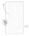
- Grapheneis an allotrope of carbon having a structure of one-atom-thick planar sheets of sp 2 -bonded carbon atoms that are densely packed in a honeycomb crystal lattice, as shown, for example, in the inset in FIG. 2 .
- the graphene materialsmay be in the form of sheets or ribbons and may include unilayer, bilayer or other forms of graphene.
- the graphene material of the control grid(e.g., grid electrode 250 ) may include a graphene sheet having an area of more than 0.1 ⁇ m 2 .
- a version of device 200may have at least one relatively smooth planar anode or cathode surface over which graphene grid electrode 250 may be supported by a sparse array of conducting posts or walls.
- the conducting posts or wallsmay terminate on but are electrically isolated from the underlying anode or cathode.
- Grid electrode 250may be formed, for example, by suspending free-standing graphene materials supported by scaffolding 220 over electrode 210 .
- the smooth planar anode or cathode surface over which graphene grid electrode 250 may be supportedmay be a surface that is substantially planar on a micro- or nanometer scale. Further, a separation distance between the graphene material and the planar surface may be less than about 1 ⁇ m.
- a separation distance between the graphene material and the planar surfaceis about 0.3 ⁇ m. In some device applications, the separation distance between the graphene material and the planar surface may be less than about 0.1 ⁇ m.
- Scaffolding 220may be configured to physically support the graphene material of grid electrode 250 over the planar surface of electrode 210 .
- Scaffolding 220may, for example, include an array of spacers or support posts.
- the spacers or support postswhich may include one or more of dielectrics, oxides, polymers, insulators and glassy material, may be electrically isolated from the planar surface of electrode 210 .
- Graphenewhich has a local hexagonal carbon ring structure, may have a high transmission probability for electrons through the hexagonal openings in its structure.
- electronic bandgaps in the graphene materials used for grid 250may be suitably modified (e.g., by doping or functionalizing) to reduce or avoid inelastic electron scattering of incident electrons that may pass close to a carbon atom in the graphene structure.
- the doping and functionalizing techniques that are used to create or modify electronic bandgaps in the graphene materialsmay be the same or similar to techniques that are described, for example, in Beidou Guo et al. Graphene Doping: A Review , J. Insciences. 2011, 1 (2), 80-89, and in D. W. Boukhvalov et al. Chemical functionalization of graphene, J. Phys.: Condens. Matter 21 344205.
- both of the foregoing referencesare incorporated by reference in their entireties herein.
- the transmission probability of incident electrons from vacuum through graphenemay be approximated as a quantum tunneling process through a model finite square potential well.
- the model potential well widthmay be set equal to the single-atom thickness of a graphene sheet ⁇ 0.3 nm, while the potential well depth may be approximated by the ⁇ 5 eV binding energy of vacuum electrons on the graphene lattice.
- T0.996
- any effects of electron-electron scattering on the transparency of the graphene materialsmay be avoided or mitigated by bandgap engineering of the graphene materials used to make grid 250 .
- Typical electric transition energies in raw or undoped graphene materialsmay be about 100 meV around the Dirac point. However, the electric transition energies may be expected to increase up to about 10 eV under very strong electric fields that may be applied in operation of device 200 .
- a concentration of induced charge carriers in graphenemay be dependent on the external electric field with the proportionality between the induced charge carriers and the applied electric field of about 0.055 electrons/nm 2 per 1 V/nm electric field in vacuum.
- the graphene materials used for grid electrode 250may be provided with electronic bandgaps at suitable energies to permit through transmission of electron flow between electrodes 210 and 240 in device operation.
- the graphene materials with electronic bandgapsmay be functionalized and/or doped graphene materials.
- the graphene materials used for an electrodemay have holes or apertures formed therein to permit through passage of a flow of charged carriers between anode 110 and cathode 120 in device operation.
- the holeswhich may be larger than a basic hexagon carbon ring or unit of graphene's atomic structure, may be formed by removing carbon atoms from a graphene sheet or ribbon.
- FIG. 3shows schematically a graphene sheet 300 in which carbon atoms have been removed to form holes or apertures 310 through which charge carriers may flow uninterrupted.
- Holes or apertures 310may be physically formed by processing graphene using any suitable technique including, for example, electron beam exposure, ion beam drilling, copolymer block lithography, diblock copolymer templating, and/or surface-assisted polymer synthesis.
- Any suitable techniqueincluding, for example, electron beam exposure, ion beam drilling, copolymer block lithography, diblock copolymer templating, and/or surface-assisted polymer synthesis.
- the named techniquesare variously described, for example, in S. Garaj et al. Graphene as a subnanometre trans - electrode membrane , Nature 467, 190-193, (9 Sep. 2010); Kim et al. Fabrication and Characterization of Large - Area, Semiconducting Nanoperforated Graphene Materials , Nano Lett., 2010, 10 (4), pp. 1125-1131; D. C.
- nano-photolithographic and etching techniquesmay be used to create a pattern of holes in the graphene materials used as an electrode.
- graphene deposited on a substratemay be patterned by nanoimprint lithography to create rows of highly curved regions, which are then etched away to create an array of very small holes in the graphene material.
- the processmay exploit the enhanced reactivity of carbon atoms along a fold or curve in the graphene material to preferentially create holes at the curved regions.
- a graphene sheet used for a proximate grid electrodemay be mechanically placed on the array of field tips. Such placement may be expected to locally curve or mechanically stress the graphene sheet, which after etching may result in apertures or holes that are automatically aligned with the field emitter tips.
- FIG. 4shows an example graphene electrode 420 disposed above an electrode 410 having a field emitter tip array 412 .
- Holes 422 formed in graphene electrode 420are shown as being aligned with field emitter tip array 412 . Holes 422 may be created by a self-aligning process of placing a graphene sheet over electrode 410 in mechanical contact with field emitter tip array 412 and etching the graphene regions stressed by mechanical contact with the field emitter tips.
- the graphene material used for making a grid electrodeincludes a graphene sheet with physical pores formed by carbon atoms removed therein.
- a size distribution of the physical poresmay be selected upon consideration of device design parameters.
- the poresmay have cross-sectional areas, for example, in a range of about 1 nm 2 -100 nm 2 or 100 nm 2 -1000 nm 2 .
- the foregoing example grid electrodes made of graphene materialsmay be separated from the underlying electrode (e.g., electrodes 210 and 410 ) by a vacuum or gas-filled gap.
- a grid electrode made of graphene materialsmay be separated from the underlying electrode by a dielectric spacer layer.
- FIG. 5shows an example configuration 500 of a grid electrode 520 made of graphene material that is separated from an underlying electrode 510 by a dielectric spacer layer 530 .
- Materials and dimensions of dielectric spacer layer 530may be selected so that in device operation substantially all of the electron flow to or from electrode 510 can tunnel or transmit through both dielectric spacer layer 530 and grid electrode 520 without being absorbed or scattered.
- Dielectric spacer layer 530may, for example, be of the order of a few nanometers thick.
- dielectric spacer layer 530may be a continuous layer or may be a porous layer with holes or apertures (e.g., hole 532 ) formed in it.
- the holes of apertures 532 in dielectric spacer layer 530may be formed, for example, by etching the dielectric material through holes or apertures (e.g., holes 310 ) in grid electrode 520 . In such case, holes of apertures 532 in dielectric spacer layer 530 may form vacuum or gas-filled gaps between electrode s 510 and 520 .
- graphene material of a control gridmay be supported by an intervening dielectric material layer disposed on the planar surface of the underlying electrode.
- the intervening dielectric material layermay be configured to allow tunneling or transmission of the electron flow therethrough. Further, the intervening dielectric material layer may be partially etched to form a porous structure to support the graphene grid over the underlying electrode.
- providing a control grid that is made of graphene material to modulate a flow of electrons from the cathode to anode 630may include disposing the control grid sufficiently close to the cathode (or anode) to induce or suppress electron emission from the cathode (or anode) when an electric potential is applied to the grid in device operation.
- the graphene materialmay include unilayer and/or bilayer graphene.
- the graphene material of the control gridmay include a graphene sheet having an area of more than 0.1 ⁇ m 2 .
- the graphene material of the control gridmay be substantially transparent to the flow electrons from the cathode to the anode.
- the graphene material of the control gridmay, for example, include a graphene sheet with physical holes or pores formed therein.
- the poresmay have cross-sectional areas in a range of about 1 nm 2 -100 nm 2 , 100 nm 2 -1000 nm 2 , etc.
- the pores in the graphene sheetmay be formed lithographically, formed by copolymer block lithography, and/or by electron-beam or ion-beam drilling.
- the pores in the graphene sheetmay be aligned with field emitter tips on the anode.
- At least one of the anode and the cathodemay have a substantially planar surface on a micro- or nanometer scale.
- Providing a control grid that is made of graphene material to modulate a flow of electrons from the cathode to anode 630may include disposing the graphene material of the control grid over the planar surface.
- a separation distance between the graphene material and the planar surfacemay be less than about 1 ⁇ m. In some experimental investigations of suspended graphene sheets, a separation distance between the graphene material and the planar surface is about 0.3 ⁇ m. In some device applications, the separation distance between the graphene material and the planar surface may be less than about 0.1 ⁇ m.
- Method 600may further include providing a scaffolding configured to physically support the graphene material of the control grid over the planar surface ( 650 ).
- the scaffoldingmay include an array of spacers or support posts, which are electrically isolated from the planar surface.
- the spacers or support postsmay be made from one or more of dielectrics, oxides, polymers, insulators and glassy material.
- Method 600may further include providing an intervening dielectric material layer disposed on the planar surface to support the graphene material of the control grid ( 660 ).
- the intervening dielectric material layermay be configured to allow tunneling or transmission of the electron flow therethrough.
- the intervening dielectric material layermay be partially etched to form a porous structure to support the graphene grid.
- FIG. 7shows an example arrangement 700 of a pair of electrodes (e.g., first electrode 710 and second electrode 720 ), which may be used in an electronic device.
- the pair of electrodes 710 and 720may be disposed in a vacuum-holding container (e.g., container 130 , FIG. 1 ).
- Second electrode 720may be disposed in close proximity to first electrode 710 and configured to modulate or change an energy barrier to a flow of electrons through the surface of first electrode 710 .
- second electrode 720may be disposed in the vacuum-holing container and configured to modulate a flow of electrons through the second electrode itself (e.g., by controlling space charge in the vacuum-holding container).
- Second electrode 720may be made of a 2-d layered material including one or more of graphene, graphyne, graphdiyne, a two-dimensional carbon allotrope, and a two-dimensional semimetal material.
- the 2-d layered materialmay have an electron transmission probability for 1 eV electrons that exceeds 0.25 and/or an electron transmission probability for 10 eV electrons that exceeds 0.5.
- the 2-d layered material of which the second electrode is mademay have an electronic bandgap therein, for example, to permit transmission of the electron flow therethrough in operation of device.
- the 2-d layered materialmay, for example, be doped graphene material or functionalized graphene material.
- Second electrode 720may be disposed next to a surface of first electrode 710 so that it is separated by a vacuum gap from at least a portion of the surface of first electrode 710 .
- second electrode 720may be disposed next to the surface of first electrode 710 supported by a dielectric material layer 730 disposed over the surface of first electrode 710 .
- Dielectric material layer 730 disposed over the surface of first electrode 710may be about 0.3 nm-10 nm thick in some applications. In other applications, dielectric material layer 730 may be greater than 10 nm thick.
- Dielectric material layer 730 disposed over the surface of first electrode 710may be a continuous dielectric material layer which is configured to allow tunneling or transmission therethrough of substantially all electron flow to and from the first electrode in device operation.
- Dielectric material layer 730may, for example, be a porous dielectric material layer configured to permit formation of vacuum gaps between first electrode 710 and second electrode 720 .
- the 2d-layer material of second electrode 720may have pores therein permitting chemical etching therethrough to remove portions of dielectric material layer 730 to form, for example, the vacuum gaps.
- FIG. 8shows an example method 800 for configuring a multi-electrode electronic device (e.g., a microelectronic or nanoelectronic device).
- Method 800includes providing a first electrode in a vacuum-holding container of the electronic device ( 810 ), and providing a second electrode next to a surface of the first electrode ( 820 ).
- the second electrodemay be made of a 2-d layered material including one or more of graphene, graphyne, graphdiyne, a two-dimensional carbon allotrope, and a two-dimensional semimetal material, and configured to change an energy potential profile to modulate a flow of electrons through the surface of the first electrode. wherein the second electrode is configured to change an energy potential profile to modulate a flow of electrons through a surface of the first electrode and/or the second electrode itself.
- providing a second electrode made of a 2-d layered material 820may include using a 2-d layered material having an electron transmission probability that for 1 eV electrons exceeds 0.25 and/or an electron transmission probability that for 10 eV electrons exceeds 0.5. Further, providing a second electrode made of a 2-d layered material 820 may include using a 2-d layered material that has an electronic bandgap therein. Method 800 may include selecting the electronic bandgap of the 2-d layered material so as to permit transmission of or forbid the electron flow therethrough based on the electron energy in operation of the electronic device.
- the 2-d layered material having an electronic band gapmay be doped graphene material and/or functionalized graphene material.
- disposing a second electrode made of a 2-d layered material next to a surface of the first electrodemay include forming a vacuum gap between the 2-d layered material and the surface of the first electrode.
- Disposing a second electrode made of a 2-d layered material next to a surface of the first electrode 820may include disposing a dielectric material layer to support the 2-d layered material over the surface of the first electrode.
- the dielectric material layermay be about 0.3 nm-10 nm thick. In other applications, the dielectric material layer may, for example, be greater than about 10 nm thick.
- disposing a dielectric material layer to support the 2-d layered material over the surface of the first electrodemay include disposing a continuous dielectric material layer, which is configured to allow transmission of substantially all of the electron flow therethrough to and from the first electrode in operation of the electronic device.
- Method 800may include removing portions of the dielectric material layer away to permit formation of vacuum gaps between the first electrode and the 2-d layered material of the second electrode.
- the 2-d layered materialmay have pores therein, and removing portions of the dielectric material layer involve chemically etching the portions of the dielectric material through the pores in the 2-d layered material.
- the dimensions and materials of the devices described hereinmay be selected for device operation with grid and anode voltages relative to the cathode in suitable ranges.
- the dimensions and materials of a devicemay be selected for device operation with grid and anode voltages relative to the cathode, for example, in the range of 0 to 20 volts.
- the dimensions and materials of a devicemay be selected for device operation with grid and anode voltages relative to the cathode, for example, in the range of 0 to 40 volts.
- the dimensions and materials of a devicemay be selected for device operation with grid and anode voltages relative to the cathode, for example, in the range of 0 to 100 volts.
Landscapes
- Carbon And Carbon Compounds (AREA)
Abstract
Description
Claims (42)
Priority Applications (22)
| Application Number | Priority Date | Filing Date | Title |
|---|---|---|---|
| US13/612,129US9646798B2 (en) | 2011-12-29 | 2012-09-12 | Electronic device graphene grid |
| CN201280070924.8ACN104160467B (en) | 2011-12-29 | 2012-12-27 | The material of field emission apparatus and configuration |
| EP12863524.0AEP2801102B1 (en) | 2011-12-29 | 2012-12-27 | Anode with suppressor grid |
| KR1020147021047AKR101988068B1 (en) | 2011-12-29 | 2012-12-27 | Field emission device |
| KR1020147021314AKR20140128975A (en) | 2011-12-29 | 2012-12-27 | Electronic device graphene grid |
| PCT/US2012/071845WO2013101948A1 (en) | 2011-12-29 | 2012-12-27 | Materials and configurations of a field emission device |
| JP2014550467AJP6278897B2 (en) | 2011-12-29 | 2012-12-27 | Apparatus and method for field emission devices |
| PCT/US2012/071833WO2013101937A1 (en) | 2011-12-29 | 2012-12-27 | Electronic device graphene grid |
| CN201280070857.XACN104137254B (en) | 2011-12-29 | 2012-12-27 | field emission device |
| CN201280065581.6ACN104024147A (en) | 2011-12-29 | 2012-12-27 | Electronic device graphene grid |
| KR1020147021370AKR101988069B1 (en) | 2011-12-29 | 2012-12-27 | Anode with Suppressor Grid |
| PCT/US2012/071841WO2013101944A2 (en) | 2011-12-29 | 2012-12-27 | Performance optimization of a field emission device |
| PCT/US2012/071837WO2013101941A1 (en) | 2011-12-29 | 2012-12-27 | Field emission device |
| CN201280070914.4ACN104769698B (en) | 2011-12-29 | 2012-12-27 | The performance optimization of field emission apparatus |
| EP12863100.9AEP2798673B1 (en) | 2011-12-29 | 2012-12-27 | Field emission device |
| EP12861564.8AEP2797837A4 (en) | 2011-12-29 | 2012-12-27 | Electronic device graphene grid |
| IN5630DEN2014IN2014DN05630A (en) | 2011-12-29 | 2012-12-27 | |
| CN201280070838.7ACN104137218B (en) | 2011-12-29 | 2012-12-27 | Anode with suppressor grid |
| PCT/US2012/071849WO2013101951A1 (en) | 2011-12-29 | 2012-12-27 | Anode with suppressor grid |
| US14/613,459US9659734B2 (en) | 2012-09-12 | 2015-02-04 | Electronic device multi-layer graphene grid |
| US14/706,485US9659735B2 (en) | 2012-09-12 | 2015-05-07 | Applications of graphene grids in vacuum electronics |
| US15/603,340US10056219B2 (en) | 2012-09-12 | 2017-05-23 | Applications of graphene grids in vacuum electronics |
Applications Claiming Priority (6)
| Application Number | Priority Date | Filing Date | Title |
|---|---|---|---|
| US201161631270P | 2011-12-29 | 2011-12-29 | |
| US13/374,545US8575842B2 (en) | 2011-12-29 | 2011-12-30 | Field emission device |
| US201261637986P | 2012-04-25 | 2012-04-25 | |
| US13/545,504US9018861B2 (en) | 2011-12-29 | 2012-07-10 | Performance optimization of a field emission device |
| US13/587,762US8692226B2 (en) | 2011-12-29 | 2012-08-16 | Materials and configurations of a field emission device |
| US13/612,129US9646798B2 (en) | 2011-12-29 | 2012-09-12 | Electronic device graphene grid |
Related Parent Applications (2)
| Application Number | Title | Priority Date | Filing Date |
|---|---|---|---|
| US13/374,545Continuation-In-PartUS8575842B2 (en) | 2011-12-29 | 2011-12-30 | Field emission device |
| US14/613,459Continuation-In-PartUS9659734B2 (en) | 2012-09-12 | 2015-02-04 | Electronic device multi-layer graphene grid |
Related Child Applications (2)
| Application Number | Title | Priority Date | Filing Date |
|---|---|---|---|
| US14/613,459Continuation-In-PartUS9659734B2 (en) | 2012-09-12 | 2015-02-04 | Electronic device multi-layer graphene grid |
| US14/706,485Continuation-In-PartUS9659735B2 (en) | 2012-09-12 | 2015-05-07 | Applications of graphene grids in vacuum electronics |
Publications (2)
| Publication Number | Publication Date |
|---|---|
| US20130169142A1 US20130169142A1 (en) | 2013-07-04 |
| US9646798B2true US9646798B2 (en) | 2017-05-09 |
Family
ID=48694284
Family Applications (1)
| Application Number | Title | Priority Date | Filing Date |
|---|---|---|---|
| US13/612,129Active2032-03-10US9646798B2 (en) | 2011-12-29 | 2012-09-12 | Electronic device graphene grid |
Country Status (1)
| Country | Link |
|---|---|
| US (1) | US9646798B2 (en) |
Cited By (1)
| Publication number | Priority date | Publication date | Assignee | Title |
|---|---|---|---|---|
| US12191357B2 (en) | 2019-03-08 | 2025-01-07 | Infinite Potential Laboratories Lp | Quantum control devices and methods |
Families Citing this family (17)
| Publication number | Priority date | Publication date | Assignee | Title |
|---|---|---|---|---|
| US9627168B2 (en) | 2011-12-30 | 2017-04-18 | Elwha Llc | Field emission device with nanotube or nanowire grid |
| US20140205796A1 (en)* | 2013-01-18 | 2014-07-24 | International Business Machines Corporation | Method of forming graphene nanomesh |
| TWI493549B (en)* | 2013-03-05 | 2015-07-21 | Nat Univ Tsing Hua | Resistive random-access memory |
| US9997703B2 (en)* | 2013-07-25 | 2018-06-12 | Hewlett Packard Enterprise Development Lp | Resistive memory device having field enhanced features |
| KR101519333B1 (en) | 2013-10-17 | 2015-05-13 | 건국대학교 산학협력단 | LITHIUM ION BATTERY ANODE MATERIAL WITH α-GRAPHDIYNE |
| CN104667953B (en)* | 2013-11-29 | 2017-06-09 | 中国科学院过程工程研究所 | A kind of N doping graphite alkene, preparation method and its usage |
| CN106489186B (en) | 2014-05-13 | 2018-08-24 | 三星电子株式会社 | Use the electron-emitting device and its manufacturing method of graphene |
| EP3007199A1 (en)* | 2014-10-10 | 2016-04-13 | Max-Planck-Gesellschaft zur Förderung der Wissenschaften e.V. | Electron tube device |
| KR102312202B1 (en)* | 2014-11-21 | 2021-10-14 | 한국전자통신연구원 | Field-emission device |
| US9666401B2 (en)* | 2014-11-21 | 2017-05-30 | Electronics And Telecommunications Research Institute | Field-emission device with improved beams-convergence |
| KR102341688B1 (en)* | 2016-01-26 | 2021-12-21 | 한국전자통신연구원 | Field emission device and x-ray emission source having the same |
| US9805900B1 (en) | 2016-05-04 | 2017-10-31 | Lockheed Martin Corporation | Two-dimensional graphene cold cathode, anode, and grid |
| CN106117521B (en)* | 2016-06-24 | 2018-02-13 | 中国科学院化学研究所 | A kind of carbyne film and preparation method and application |
| US10438764B2 (en)* | 2016-12-07 | 2019-10-08 | Electronics And Telecommunications Research Institute | Field emission apparatus |
| KR102238574B1 (en)* | 2016-12-07 | 2021-04-12 | 한국전자통신연구원 | Field emission apparatus |
| CN111384249B (en)* | 2018-12-27 | 2021-06-11 | Tcl科技集团股份有限公司 | Composite material, preparation method thereof and quantum dot light-emitting diode |
| CN109841295B (en)* | 2019-03-29 | 2021-07-30 | 广州国显科技有限公司 | Display device, touch panel, conductive composite material and manufacturing method thereof |
Citations (120)
| Publication number | Priority date | Publication date | Assignee | Title |
|---|---|---|---|---|
| US2404919A (en) | 1940-05-01 | 1946-07-30 | Research Corp | Electronic switching device and circuit therefor |
| US2489850A (en) | 1948-03-09 | 1949-11-29 | George W Baker | Support for the electrodes of electron discharge devices |
| US2744960A (en) | 1950-05-17 | 1956-05-08 | Hartford Nat Bank & Trust Co | Time-multiplex pulse-code modulation signal transmission system |
| US2798963A (en) | 1951-11-19 | 1957-07-09 | Gen Electric | Self-regulating X-ray tube |
| US3254244A (en) | 1961-06-27 | 1966-05-31 | Westinghouse Electric Corp | Thermionic power conversion triode |
| US4274035A (en) | 1978-07-21 | 1981-06-16 | Hitachi, Ltd. | Field emission electron gun |
| US4427886A (en) | 1982-08-02 | 1984-01-24 | Wisconsin Alumni Research Foundation | Low voltage field emission electron gun |
| US4721885A (en)* | 1987-02-11 | 1988-01-26 | Sri International | Very high speed integrated microelectronic tubes |
| US5177402A (en) | 1992-01-03 | 1993-01-05 | Etec Systems, Inc. | Arc suppressor for electron gun |
| CN1069828A (en) | 1991-05-13 | 1993-03-10 | 精工爱普生株式会社 | Multipole field-causing electron ballistic device and manufacture method thereof |
| US5272411A (en) | 1992-01-28 | 1993-12-21 | Itt Corporation | Coaxial triode apparatus |
| US5371371A (en) | 1992-08-27 | 1994-12-06 | Kabushiki Kaisha Toshiba | Magnetic immersion field emission electron gun systems capable of reducing aberration of electrostatic lens |
| US5376184A (en) | 1992-06-17 | 1994-12-27 | Aspden; Harold | Thermoelectric heat transfer apparatus |
| US5548138A (en) | 1992-09-18 | 1996-08-20 | Hitachi, Ltd. | Semiconductor device with reduced tunnel resistance and circuitry using the same |
| US5578901A (en) | 1994-02-14 | 1996-11-26 | E. I. Du Pont De Nemours And Company | Diamond fiber field emitters |
| US5606215A (en) | 1994-08-01 | 1997-02-25 | Motorola, Inc. | Field emission device arc-suppressor |
| US5631524A (en) | 1993-07-28 | 1997-05-20 | Fuji Electric Co. Ltd. | Switching apparatus |
| US5717279A (en) | 1995-02-28 | 1998-02-10 | Nec Corporation | Field emission cathode with resistive gate areas and electron gun using same |
| US5834781A (en) | 1996-02-14 | 1998-11-10 | Hitachi, Ltd. | Electron source and electron beam-emitting apparatus equipped with same |
| US5838096A (en) | 1995-07-17 | 1998-11-17 | Hitachi, Ltd. | Cathode having a reservoir and method of manufacturing the same |
| US5850120A (en) | 1995-07-07 | 1998-12-15 | Nec Corporation | Electron gun with a gamma correct field emission cathode |
| US5908699A (en) | 1996-10-11 | 1999-06-01 | Skion Corporation | Cold cathode electron emitter and display structure |
| US5936348A (en) | 1996-04-24 | 1999-08-10 | Hamamatsu Photonics K.K. | Photomultiplier tube with focusing electrode plate |
| US5936354A (en) | 1998-11-02 | 1999-08-10 | Motorola, Inc. | Field emission display with temperature sensing element and method for the operation thereof |
| US5942834A (en) | 1997-01-22 | 1999-08-24 | Thermocon, Inc. | Thermionic electric converters |
| US5982095A (en) | 1995-09-19 | 1999-11-09 | Lucent Technologies Inc. | Plasma displays having electrodes of low-electron affinity materials |
| US6031336A (en) | 1998-06-17 | 2000-02-29 | Motorola, Inc. | Field emission display and method for the operation thereof |
| US6104143A (en) | 1999-10-01 | 2000-08-15 | Peabody Engneering Corporation | Exciter circuit with solid switch device separated from discharge path |
| EP1063197A2 (en) | 1999-06-25 | 2000-12-27 | Sony Corporation | Charge separation type heterojunction structure and manufacturing method therefor |
| US6205790B1 (en) | 1999-05-28 | 2001-03-27 | Lucent Technologies Inc. | Efficient thermoelectric controller |
| US6249080B1 (en) | 1997-10-29 | 2001-06-19 | Matsushita Electric Works, Ltd. | Field emission electron source, method of producing the same, and use of the same |
| TW451256B (en) | 1999-02-19 | 2001-08-21 | Motorola Inc | Method and circuit for controlling field emission current |
| US6313587B1 (en) | 1998-01-13 | 2001-11-06 | Fusion Lighting, Inc. | High frequency inductive lamp and power oscillator |
| US6346931B1 (en) | 1996-11-12 | 2002-02-12 | Micron Technology, Inc. | Method and apparatus for adjustment of fed image |
| US20020036452A1 (en) | 1999-12-21 | 2002-03-28 | Masakazu Muroyama | Electron emission device, cold cathode field emission device and method for the production thereof, and cold cathode field emission display and method for the production thereof |
| US6373175B1 (en) | 1990-07-13 | 2002-04-16 | Gec-Marconi Limited | Electronic switching devices |
| US6404089B1 (en) | 2000-07-21 | 2002-06-11 | Mark R. Tomion | Electrodynamic field generator |
| US20030001490A1 (en) | 1999-03-15 | 2003-01-02 | Kabushiki Kaisha Toshiba | Electron emission element, method of manufacturing the same, display device and method of manufacturing the same |
| US20030006684A1 (en)* | 2001-03-27 | 2003-01-09 | Shinichi Kawate | Catalyst used to form carbon fiber, method of making the same and electron emitting device, electron source, image forming apparatus, secondary battery and body for storing hydrogen |
| US6538367B1 (en) | 1999-07-15 | 2003-03-25 | Agere Systems Inc. | Field emitting device comprising field-concentrating nanoconductor assembly and method for making the same |
| US20030124944A1 (en) | 2001-12-25 | 2003-07-03 | Masafumi Kyogaku | Electron emitting device, electron source and image display device and methods of manufacturing these devices |
| US6590320B1 (en) | 2000-02-23 | 2003-07-08 | Copytale, Inc. | Thin-film planar edge-emitter field emission flat panel display |
| US20030132393A1 (en) | 2000-02-16 | 2003-07-17 | Steven Dimitrijevic | Diamond/carbon nanotube structures for efficient electron field emission |
| US6621096B2 (en) | 2001-05-21 | 2003-09-16 | Hewlett-Packard Develpoment Company, L.P. | Device isolation process flow for ARS system |
| US6632113B1 (en) | 1998-09-09 | 2003-10-14 | Canon Kabushiki Kaisha | Image display apparatus, disassembly processing method therefor, and component recovery method |
| US20040004588A1 (en) | 2000-10-19 | 2004-01-08 | Toru Kawase | Driving method and driving apparatus for a field emission device |
| US20040036402A1 (en) | 1994-02-23 | 2004-02-26 | Till Keesmann | Field emission cathode using carbon fibers |
| US20040050415A1 (en) | 2002-09-13 | 2004-03-18 | Eneco Inc. | Tunneling-effect energy converters |
| US20040118347A1 (en) | 2000-05-23 | 2004-06-24 | Groves James F. | Process and apparatus for plasma activated depositions in a vacuum |
| US20040131858A1 (en) | 2001-03-13 | 2004-07-08 | Burden Adrian Paul | Field electron emission materials and devices |
| US20040226914A1 (en) | 2003-04-28 | 2004-11-18 | Dong Chun Christine | Apparatus and method for removal of surface oxides via fluxless technique involving electron attachment and remote ion generation |
| US20040238809A1 (en) | 2001-07-06 | 2004-12-02 | Pavel Adamec | Electron emission device |
| US20050001598A1 (en) | 2003-07-02 | 2005-01-06 | Mes International, Inc. | Electrical power generation system and method |
| US20050016575A1 (en) | 2003-06-13 | 2005-01-27 | Nalin Kumar | Field emission based thermoelectric device |
| US20050057168A1 (en) | 2003-08-27 | 2005-03-17 | Song Yoon Ho | Field emission device |
| US20050151461A1 (en) | 1997-10-22 | 2005-07-14 | Tuck Richard A. | Field emission devices |
| US20050248256A1 (en) | 2004-05-04 | 2005-11-10 | Yoon Ho Song | Field emission display |
| US7061188B1 (en) | 2002-03-29 | 2006-06-13 | Technical Consumer Products, Inc. | Instant start electronic ballast with universal AC input voltage |
| US20060139207A1 (en) | 2004-12-29 | 2006-06-29 | Nikonov Dmitri E | Non-blocking switch having carbon nanostructures and Mach-Zehnder interferometer |
| US7122967B2 (en) | 2003-01-17 | 2006-10-17 | Samsung Sdi Co., Ltd. | Field emission display and driving device thereof |
| US20060261724A1 (en) | 2005-05-19 | 2006-11-23 | Texas Instruments Incorporated | Display using a movable electron field emitter and method of manufacture thereof |
| US20060273301A1 (en) | 2001-05-21 | 2006-12-07 | Garret Moddel | High speed electron tunneling devices |
| US20060284539A1 (en) | 2005-06-20 | 2006-12-21 | Chien-Min Sung | Diamond-like carbon devices and methods for the use and manufacture thereof |
| US7157849B2 (en) | 2003-01-21 | 2007-01-02 | Samsung Sdi Co., Ltd. | Field emission display including mesh grid and focusing electrode and its method of manufacture |
| US20070023621A1 (en) | 2005-07-27 | 2007-02-01 | Blick Robert H | Nanoelectromechanical and Microelectromechanical Sensors and Analyzers |
| US7173366B2 (en) | 2003-08-12 | 2007-02-06 | Samsung Sdi Co., Ltd. | Field emission display having carbon nanotube emitter and method of manufacturing the same |
| US20070046163A1 (en) | 2005-08-31 | 2007-03-01 | Hiroshi Sata | Flat-panel display |
| US20070158588A1 (en) | 2005-09-05 | 2007-07-12 | Fang Zhou | Charged particle beam emitting device and method for operating a charged particle beam emitting device |
| US7268480B2 (en) | 2003-12-12 | 2007-09-11 | Samsung Sdi Co., Ltd. | Field emission device, display adopting the same and method of manufacturing the same |
| US20080001513A1 (en) | 2006-06-30 | 2008-01-03 | Tsinghua University | Field emission microelectronic device |
| US20080017237A1 (en) | 2006-07-19 | 2008-01-24 | James William Bray | Heat transfer and power generation device |
| US20080100235A1 (en) | 2006-10-26 | 2008-05-01 | Industrial Technology Research Institute | Field emission backlight unit and scanning driving method |
| US7462979B2 (en)* | 2002-05-24 | 2008-12-09 | Sony Corporation | Cold cathode field emission display |
| US20090011706A1 (en) | 2006-05-23 | 2009-01-08 | Innovision Research & Technology Plc | Near field RF communicators and near field communications-enabled devices |
| US20090115305A1 (en) | 2007-05-22 | 2009-05-07 | Nantero, Inc. | Triodes using nanofabric articles and methods of making the same |
| US20090146583A1 (en) | 2007-02-28 | 2009-06-11 | Doheny Eye Institute | Portable handheld illumination system |
| US20090194870A1 (en) | 2008-01-31 | 2009-08-06 | Nathanson Harvey C | Method and Apparatus for Solid State Cooling System |
| US20090303654A1 (en) | 2008-06-04 | 2009-12-10 | Xerox Corporation | Tailored emitter bias as a means to optimize the indirect-charging performance of a nano-structured emitting electrode |
| CN101635245A (en) | 2003-04-25 | 2010-01-27 | Cxr有限公司 | X-ray tube electron sources |
| US20100019648A1 (en) | 2007-03-29 | 2010-01-28 | Hiroshi Yasuda | Electron gun and electron beam exposure apparatus |
| US20100026160A1 (en) | 2006-09-27 | 2010-02-04 | Denki Kagaku Kogyo Kabushiki Kaisha | Electron source |
| US20100066245A1 (en) | 2008-09-15 | 2010-03-18 | Jan Van Spijker | Ion barrier membrane for use in a vacuum tube using electron multiplying, an electron multiplying structure for use in a vacuum tube using electron multiplying as well as a vacuum tube using electron multiplying provided with such an electron multiplying structure |
| US20100090579A1 (en) | 2007-03-01 | 2010-04-15 | Josef Sellmair | Device for the field emission of particles and production method |
| US20100090601A1 (en) | 2008-01-07 | 2010-04-15 | Communications And Power Industries, Inc. | Grid for vacuum electron device and method for manufacture of same |
| US20100102325A1 (en) | 2008-10-29 | 2010-04-29 | Electronics And Telecommunications Research Institute | Vacuum channel transistor and diode emitting thermal cathode electrons, and method of manufacturing the vacuum channel transistor |
| US7710013B2 (en) | 2003-09-30 | 2010-05-04 | Sumitomo Electric Industries, Ltd. | Electron emitting device with projection comprising base portion and electron emission portion |
| US20100108882A1 (en) | 2008-10-09 | 2010-05-06 | California Institute Of Technology | 4d imaging in an ultrafast electron microscope |
| US7741764B1 (en) | 2007-01-09 | 2010-06-22 | Chien-Min Sung | DLC emitter devices and associated methods |
| US7750462B1 (en) | 1999-10-12 | 2010-07-06 | Microassembly Technologies, Inc. | Microelectromechanical systems using thermocompression bonding |
| US20100271003A1 (en) | 2007-10-11 | 2010-10-28 | The Regents Of The University Of California | Nanotube Resonator Devices |
| US7825591B2 (en) | 2006-02-15 | 2010-11-02 | Panasonic Corporation | Mesh structure and field-emission electron source apparatus using the same |
| US20100283436A1 (en)* | 2009-05-05 | 2010-11-11 | City University Of Hong Kong | Method and apparatus for suppressing noise caused by parasitic capacitance and/or resistance in an electronic circuit or system |
| US20100295486A1 (en) | 2006-09-08 | 2010-11-25 | Tamio Ikehashi | Actuator |
| US20100329964A1 (en) | 2007-10-30 | 2010-12-30 | Canatu Oy | Deposit and electrical devices comprising the same |
| US20110037400A1 (en) | 2007-10-31 | 2011-02-17 | Kumho Electric, Inc. | Constant Current Driving Circuit for Field Emission Device |
| US20110088954A1 (en) | 2009-10-15 | 2011-04-21 | Baker Hughes Incorporated | Polycrystalline compacts including nanoparticulate inclusions, cutting elements and earth-boring tools including such compacts, and methods of forming such compacts |
| US20110139203A1 (en) | 2009-12-16 | 2011-06-16 | Gm Global Technology Operations, Inc. | Heterostructure thermoelectric generator |
| US20110147761A1 (en) | 2006-11-07 | 2011-06-23 | Cbrite Inc. | Two-terminal switching devices and their methods of fabrication |
| US20110186805A1 (en) | 2010-02-02 | 2011-08-04 | Searete Llc | Doped graphene electronic materials |
| US20110192976A1 (en) | 2010-02-10 | 2011-08-11 | Halcyon Molecular, Inc. | Aberration-correcting dark-field electron microscopy |
| US20110201201A1 (en) | 2010-01-26 | 2011-08-18 | Wisconsin Alumni Research Foundation | Methods of fabricating large-area, semiconducting nanoperforated graphene materials |
| US8018169B2 (en) | 2006-03-31 | 2011-09-13 | Electronics And Telecommunications Research Institute | Field emission device |
| US20110226960A1 (en) | 2010-03-17 | 2011-09-22 | Tsinghua University | Carbon nanotube film composite structure, transmission electron microscope grid using the same, and method for making the same |
| US8089579B1 (en) | 2009-08-27 | 2012-01-03 | Rockwell Collins, Inc. | System and method for providing a light control mechanism for a display |
| US8089206B2 (en) | 2008-07-09 | 2012-01-03 | Tsinghua University | Field emission cathode and field emission display employing with same |
| US20120006784A1 (en) | 2010-07-07 | 2012-01-12 | Hon Hai Precision Industry Co., Ltd. | Transmission electron microscope grid and method for making same |
| CN102339699A (en) | 2011-09-30 | 2012-02-01 | 东南大学 | Graphene-based field emission triode structure |
| US20120041370A1 (en) | 1998-10-29 | 2012-02-16 | Medtronic Minimed, Inc. | Method and apparatus for detecting occlusions in an ambulatory infusion pump |
| US20130168635A1 (en) | 2011-12-29 | 2013-07-04 | Elwha LLC, a limited liability company of the State of Delaware | Materials and configurations of a field emission device |
| WO2013101937A1 (en) | 2011-12-29 | 2013-07-04 | Elwha Llc | Electronic device graphene grid |
| US20130169193A1 (en) | 2011-12-29 | 2013-07-04 | Elwha LLC, a limited liability company of the State of Delaware | Performance optimization of a field emission device |
| US20130169156A1 (en) | 2011-12-29 | 2013-07-04 | Elwha LLC, a limited liability company of the State of Delaware | Field emission device |
| US20130169108A1 (en) | 2011-12-29 | 2013-07-04 | Elwha Llc | Anode with suppressor grid |
| US20130221843A1 (en) | 2011-12-29 | 2013-08-29 | Elwha Llc | Field emission device with ac output |
| US20130229105A1 (en) | 2011-12-29 | 2013-09-05 | Elwha Llc | Variable field emission device |
| US20130229133A1 (en) | 2011-12-29 | 2013-09-05 | Elwha LLC,a limited liability company of the State of Delaware | Addressable array of field emission devices |
| US20130313980A1 (en) | 2011-12-29 | 2013-11-28 | Elwha Llc | Embodiments of a field emission device |
| US20140070696A1 (en) | 2011-12-29 | 2014-03-13 | Elwha Llc | Time-varying field emission device |
| US8674300B2 (en) | 2010-03-10 | 2014-03-18 | ICT Integrated Circuit Testing Gesellschaft fur Halbleiterprüftechnik mbH | Feedback loop for emitter flashing |
| US20140333213A1 (en) | 2011-12-29 | 2014-11-13 | Elwha Llc | Field emission device with ac output |
- 2012
- 2012-09-12USUS13/612,129patent/US9646798B2/enactiveActive
Patent Citations (126)
| Publication number | Priority date | Publication date | Assignee | Title |
|---|---|---|---|---|
| US2404919A (en) | 1940-05-01 | 1946-07-30 | Research Corp | Electronic switching device and circuit therefor |
| US2489850A (en) | 1948-03-09 | 1949-11-29 | George W Baker | Support for the electrodes of electron discharge devices |
| US2744960A (en) | 1950-05-17 | 1956-05-08 | Hartford Nat Bank & Trust Co | Time-multiplex pulse-code modulation signal transmission system |
| US2798963A (en) | 1951-11-19 | 1957-07-09 | Gen Electric | Self-regulating X-ray tube |
| US3254244A (en) | 1961-06-27 | 1966-05-31 | Westinghouse Electric Corp | Thermionic power conversion triode |
| US4274035A (en) | 1978-07-21 | 1981-06-16 | Hitachi, Ltd. | Field emission electron gun |
| US4427886A (en) | 1982-08-02 | 1984-01-24 | Wisconsin Alumni Research Foundation | Low voltage field emission electron gun |
| US4721885A (en)* | 1987-02-11 | 1988-01-26 | Sri International | Very high speed integrated microelectronic tubes |
| US6373175B1 (en) | 1990-07-13 | 2002-04-16 | Gec-Marconi Limited | Electronic switching devices |
| CN1069828A (en) | 1991-05-13 | 1993-03-10 | 精工爱普生株式会社 | Multipole field-causing electron ballistic device and manufacture method thereof |
| US5386172A (en) | 1991-05-13 | 1995-01-31 | Seiko Epson Corporation | Multiple electrode field electron emission device and method of manufacture |
| US5177402A (en) | 1992-01-03 | 1993-01-05 | Etec Systems, Inc. | Arc suppressor for electron gun |
| US5272411A (en) | 1992-01-28 | 1993-12-21 | Itt Corporation | Coaxial triode apparatus |
| US5376184A (en) | 1992-06-17 | 1994-12-27 | Aspden; Harold | Thermoelectric heat transfer apparatus |
| US5371371A (en) | 1992-08-27 | 1994-12-06 | Kabushiki Kaisha Toshiba | Magnetic immersion field emission electron gun systems capable of reducing aberration of electrostatic lens |
| US5548138A (en) | 1992-09-18 | 1996-08-20 | Hitachi, Ltd. | Semiconductor device with reduced tunnel resistance and circuitry using the same |
| US5631524A (en) | 1993-07-28 | 1997-05-20 | Fuji Electric Co. Ltd. | Switching apparatus |
| US5578901A (en) | 1994-02-14 | 1996-11-26 | E. I. Du Pont De Nemours And Company | Diamond fiber field emitters |
| US20040036402A1 (en) | 1994-02-23 | 2004-02-26 | Till Keesmann | Field emission cathode using carbon fibers |
| US5606215A (en) | 1994-08-01 | 1997-02-25 | Motorola, Inc. | Field emission device arc-suppressor |
| US5717279A (en) | 1995-02-28 | 1998-02-10 | Nec Corporation | Field emission cathode with resistive gate areas and electron gun using same |
| US5850120A (en) | 1995-07-07 | 1998-12-15 | Nec Corporation | Electron gun with a gamma correct field emission cathode |
| US5838096A (en) | 1995-07-17 | 1998-11-17 | Hitachi, Ltd. | Cathode having a reservoir and method of manufacturing the same |
| US5982095A (en) | 1995-09-19 | 1999-11-09 | Lucent Technologies Inc. | Plasma displays having electrodes of low-electron affinity materials |
| US5834781A (en) | 1996-02-14 | 1998-11-10 | Hitachi, Ltd. | Electron source and electron beam-emitting apparatus equipped with same |
| US5936348A (en) | 1996-04-24 | 1999-08-10 | Hamamatsu Photonics K.K. | Photomultiplier tube with focusing electrode plate |
| US5908699A (en) | 1996-10-11 | 1999-06-01 | Skion Corporation | Cold cathode electron emitter and display structure |
| US6346931B1 (en) | 1996-11-12 | 2002-02-12 | Micron Technology, Inc. | Method and apparatus for adjustment of fed image |
| US5942834A (en) | 1997-01-22 | 1999-08-24 | Thermocon, Inc. | Thermionic electric converters |
| US20050151461A1 (en) | 1997-10-22 | 2005-07-14 | Tuck Richard A. | Field emission devices |
| US6249080B1 (en) | 1997-10-29 | 2001-06-19 | Matsushita Electric Works, Ltd. | Field emission electron source, method of producing the same, and use of the same |
| US6313587B1 (en) | 1998-01-13 | 2001-11-06 | Fusion Lighting, Inc. | High frequency inductive lamp and power oscillator |
| US6949887B2 (en) | 1998-01-13 | 2005-09-27 | Intel Corporation | High frequency inductive lamp and power oscillator |
| US6031336A (en) | 1998-06-17 | 2000-02-29 | Motorola, Inc. | Field emission display and method for the operation thereof |
| US6632113B1 (en) | 1998-09-09 | 2003-10-14 | Canon Kabushiki Kaisha | Image display apparatus, disassembly processing method therefor, and component recovery method |
| US20120041370A1 (en) | 1998-10-29 | 2012-02-16 | Medtronic Minimed, Inc. | Method and apparatus for detecting occlusions in an ambulatory infusion pump |
| US5936354A (en) | 1998-11-02 | 1999-08-10 | Motorola, Inc. | Field emission display with temperature sensing element and method for the operation thereof |
| TW451256B (en) | 1999-02-19 | 2001-08-21 | Motorola Inc | Method and circuit for controlling field emission current |
| US20030001490A1 (en) | 1999-03-15 | 2003-01-02 | Kabushiki Kaisha Toshiba | Electron emission element, method of manufacturing the same, display device and method of manufacturing the same |
| US6205790B1 (en) | 1999-05-28 | 2001-03-27 | Lucent Technologies Inc. | Efficient thermoelectric controller |
| EP1063197A2 (en) | 1999-06-25 | 2000-12-27 | Sony Corporation | Charge separation type heterojunction structure and manufacturing method therefor |
| US6538367B1 (en) | 1999-07-15 | 2003-03-25 | Agere Systems Inc. | Field emitting device comprising field-concentrating nanoconductor assembly and method for making the same |
| US6104143A (en) | 1999-10-01 | 2000-08-15 | Peabody Engneering Corporation | Exciter circuit with solid switch device separated from discharge path |
| US7750462B1 (en) | 1999-10-12 | 2010-07-06 | Microassembly Technologies, Inc. | Microelectromechanical systems using thermocompression bonding |
| US20020036452A1 (en) | 1999-12-21 | 2002-03-28 | Masakazu Muroyama | Electron emission device, cold cathode field emission device and method for the production thereof, and cold cathode field emission display and method for the production thereof |
| US20030132393A1 (en) | 2000-02-16 | 2003-07-17 | Steven Dimitrijevic | Diamond/carbon nanotube structures for efficient electron field emission |
| US6590320B1 (en) | 2000-02-23 | 2003-07-08 | Copytale, Inc. | Thin-film planar edge-emitter field emission flat panel display |
| US20040118347A1 (en) | 2000-05-23 | 2004-06-24 | Groves James F. | Process and apparatus for plasma activated depositions in a vacuum |
| US6404089B1 (en) | 2000-07-21 | 2002-06-11 | Mark R. Tomion | Electrodynamic field generator |
| CN1481542A (en) | 2000-10-19 | 2004-03-10 | ���µ�����ҵ��ʽ���� | Driving method and driving device of field emission device |
| US20040004588A1 (en) | 2000-10-19 | 2004-01-08 | Toru Kawase | Driving method and driving apparatus for a field emission device |
| US20040131858A1 (en) | 2001-03-13 | 2004-07-08 | Burden Adrian Paul | Field electron emission materials and devices |
| US20030006684A1 (en)* | 2001-03-27 | 2003-01-09 | Shinichi Kawate | Catalyst used to form carbon fiber, method of making the same and electron emitting device, electron source, image forming apparatus, secondary battery and body for storing hydrogen |
| US6621096B2 (en) | 2001-05-21 | 2003-09-16 | Hewlett-Packard Develpoment Company, L.P. | Device isolation process flow for ARS system |
| US20060273301A1 (en) | 2001-05-21 | 2006-12-07 | Garret Moddel | High speed electron tunneling devices |
| US20040238809A1 (en) | 2001-07-06 | 2004-12-02 | Pavel Adamec | Electron emission device |
| US20030124944A1 (en) | 2001-12-25 | 2003-07-03 | Masafumi Kyogaku | Electron emitting device, electron source and image display device and methods of manufacturing these devices |
| US7061188B1 (en) | 2002-03-29 | 2006-06-13 | Technical Consumer Products, Inc. | Instant start electronic ballast with universal AC input voltage |
| US7462979B2 (en)* | 2002-05-24 | 2008-12-09 | Sony Corporation | Cold cathode field emission display |
| US20040050415A1 (en) | 2002-09-13 | 2004-03-18 | Eneco Inc. | Tunneling-effect energy converters |
| JP2005539401A (en) | 2002-09-13 | 2005-12-22 | エネコ インコーポレイテッド | Tunneling effect energy converter |
| US7122967B2 (en) | 2003-01-17 | 2006-10-17 | Samsung Sdi Co., Ltd. | Field emission display and driving device thereof |
| US7157849B2 (en) | 2003-01-21 | 2007-01-02 | Samsung Sdi Co., Ltd. | Field emission display including mesh grid and focusing electrode and its method of manufacture |
| US7903789B2 (en) | 2003-04-25 | 2011-03-08 | Rapiscan Systems, Inc. | X-ray tube electron sources |
| CN101635245A (en) | 2003-04-25 | 2010-01-27 | Cxr有限公司 | X-ray tube electron sources |
| US20040226914A1 (en) | 2003-04-28 | 2004-11-18 | Dong Chun Christine | Apparatus and method for removal of surface oxides via fluxless technique involving electron attachment and remote ion generation |
| US20050016575A1 (en) | 2003-06-13 | 2005-01-27 | Nalin Kumar | Field emission based thermoelectric device |
| CN1816684A (en) | 2003-07-02 | 2006-08-09 | 麦斯国际有限公司 | Electrical power generation system and method |
| US20050001598A1 (en) | 2003-07-02 | 2005-01-06 | Mes International, Inc. | Electrical power generation system and method |
| US7173366B2 (en) | 2003-08-12 | 2007-02-06 | Samsung Sdi Co., Ltd. | Field emission display having carbon nanotube emitter and method of manufacturing the same |
| US20050057168A1 (en) | 2003-08-27 | 2005-03-17 | Song Yoon Ho | Field emission device |
| US7710013B2 (en) | 2003-09-30 | 2010-05-04 | Sumitomo Electric Industries, Ltd. | Electron emitting device with projection comprising base portion and electron emission portion |
| US7268480B2 (en) | 2003-12-12 | 2007-09-11 | Samsung Sdi Co., Ltd. | Field emission device, display adopting the same and method of manufacturing the same |
| US20050248256A1 (en) | 2004-05-04 | 2005-11-10 | Yoon Ho Song | Field emission display |
| US20060139207A1 (en) | 2004-12-29 | 2006-06-29 | Nikonov Dmitri E | Non-blocking switch having carbon nanostructures and Mach-Zehnder interferometer |
| US20060261724A1 (en) | 2005-05-19 | 2006-11-23 | Texas Instruments Incorporated | Display using a movable electron field emitter and method of manufacture thereof |
| US20060284539A1 (en) | 2005-06-20 | 2006-12-21 | Chien-Min Sung | Diamond-like carbon devices and methods for the use and manufacture thereof |
| US20070023621A1 (en) | 2005-07-27 | 2007-02-01 | Blick Robert H | Nanoelectromechanical and Microelectromechanical Sensors and Analyzers |
| US20070046163A1 (en) | 2005-08-31 | 2007-03-01 | Hiroshi Sata | Flat-panel display |
| US20070158588A1 (en) | 2005-09-05 | 2007-07-12 | Fang Zhou | Charged particle beam emitting device and method for operating a charged particle beam emitting device |
| US7825591B2 (en) | 2006-02-15 | 2010-11-02 | Panasonic Corporation | Mesh structure and field-emission electron source apparatus using the same |
| US8018169B2 (en) | 2006-03-31 | 2011-09-13 | Electronics And Telecommunications Research Institute | Field emission device |
| US20090011706A1 (en) | 2006-05-23 | 2009-01-08 | Innovision Research & Technology Plc | Near field RF communicators and near field communications-enabled devices |
| US20080001513A1 (en) | 2006-06-30 | 2008-01-03 | Tsinghua University | Field emission microelectronic device |
| US20080017237A1 (en) | 2006-07-19 | 2008-01-24 | James William Bray | Heat transfer and power generation device |
| US20100295486A1 (en) | 2006-09-08 | 2010-11-25 | Tamio Ikehashi | Actuator |
| US20100026160A1 (en) | 2006-09-27 | 2010-02-04 | Denki Kagaku Kogyo Kabushiki Kaisha | Electron source |
| US20080100235A1 (en) | 2006-10-26 | 2008-05-01 | Industrial Technology Research Institute | Field emission backlight unit and scanning driving method |
| US20110147761A1 (en) | 2006-11-07 | 2011-06-23 | Cbrite Inc. | Two-terminal switching devices and their methods of fabrication |
| US7741764B1 (en) | 2007-01-09 | 2010-06-22 | Chien-Min Sung | DLC emitter devices and associated methods |
| US20090146583A1 (en) | 2007-02-28 | 2009-06-11 | Doheny Eye Institute | Portable handheld illumination system |
| US20100090579A1 (en) | 2007-03-01 | 2010-04-15 | Josef Sellmair | Device for the field emission of particles and production method |
| US20100019648A1 (en) | 2007-03-29 | 2010-01-28 | Hiroshi Yasuda | Electron gun and electron beam exposure apparatus |
| US20090115305A1 (en) | 2007-05-22 | 2009-05-07 | Nantero, Inc. | Triodes using nanofabric articles and methods of making the same |
| US20100271003A1 (en) | 2007-10-11 | 2010-10-28 | The Regents Of The University Of California | Nanotube Resonator Devices |
| US20100329964A1 (en) | 2007-10-30 | 2010-12-30 | Canatu Oy | Deposit and electrical devices comprising the same |
| US20110037400A1 (en) | 2007-10-31 | 2011-02-17 | Kumho Electric, Inc. | Constant Current Driving Circuit for Field Emission Device |
| US20100090601A1 (en) | 2008-01-07 | 2010-04-15 | Communications And Power Industries, Inc. | Grid for vacuum electron device and method for manufacture of same |
| US20090194870A1 (en) | 2008-01-31 | 2009-08-06 | Nathanson Harvey C | Method and Apparatus for Solid State Cooling System |
| US20090303654A1 (en) | 2008-06-04 | 2009-12-10 | Xerox Corporation | Tailored emitter bias as a means to optimize the indirect-charging performance of a nano-structured emitting electrode |
| US8089206B2 (en) | 2008-07-09 | 2012-01-03 | Tsinghua University | Field emission cathode and field emission display employing with same |
| US20100066245A1 (en) | 2008-09-15 | 2010-03-18 | Jan Van Spijker | Ion barrier membrane for use in a vacuum tube using electron multiplying, an electron multiplying structure for use in a vacuum tube using electron multiplying as well as a vacuum tube using electron multiplying provided with such an electron multiplying structure |
| US20100108882A1 (en) | 2008-10-09 | 2010-05-06 | California Institute Of Technology | 4d imaging in an ultrafast electron microscope |
| US20100102325A1 (en) | 2008-10-29 | 2010-04-29 | Electronics And Telecommunications Research Institute | Vacuum channel transistor and diode emitting thermal cathode electrons, and method of manufacturing the vacuum channel transistor |
| US20100283436A1 (en)* | 2009-05-05 | 2010-11-11 | City University Of Hong Kong | Method and apparatus for suppressing noise caused by parasitic capacitance and/or resistance in an electronic circuit or system |
| US8089579B1 (en) | 2009-08-27 | 2012-01-03 | Rockwell Collins, Inc. | System and method for providing a light control mechanism for a display |
| US20110088954A1 (en) | 2009-10-15 | 2011-04-21 | Baker Hughes Incorporated | Polycrystalline compacts including nanoparticulate inclusions, cutting elements and earth-boring tools including such compacts, and methods of forming such compacts |
| US20110139203A1 (en) | 2009-12-16 | 2011-06-16 | Gm Global Technology Operations, Inc. | Heterostructure thermoelectric generator |
| US20110201201A1 (en) | 2010-01-26 | 2011-08-18 | Wisconsin Alumni Research Foundation | Methods of fabricating large-area, semiconducting nanoperforated graphene materials |
| US20110186805A1 (en) | 2010-02-02 | 2011-08-04 | Searete Llc | Doped graphene electronic materials |
| US20110192976A1 (en) | 2010-02-10 | 2011-08-11 | Halcyon Molecular, Inc. | Aberration-correcting dark-field electron microscopy |
| US8674300B2 (en) | 2010-03-10 | 2014-03-18 | ICT Integrated Circuit Testing Gesellschaft fur Halbleiterprüftechnik mbH | Feedback loop for emitter flashing |
| US20110226960A1 (en) | 2010-03-17 | 2011-09-22 | Tsinghua University | Carbon nanotube film composite structure, transmission electron microscope grid using the same, and method for making the same |
| US20120006784A1 (en) | 2010-07-07 | 2012-01-12 | Hon Hai Precision Industry Co., Ltd. | Transmission electron microscope grid and method for making same |
| CN102339699A (en) | 2011-09-30 | 2012-02-01 | 东南大学 | Graphene-based field emission triode structure |
| US20130168635A1 (en) | 2011-12-29 | 2013-07-04 | Elwha LLC, a limited liability company of the State of Delaware | Materials and configurations of a field emission device |
| WO2013101937A1 (en) | 2011-12-29 | 2013-07-04 | Elwha Llc | Electronic device graphene grid |
| US20130169193A1 (en) | 2011-12-29 | 2013-07-04 | Elwha LLC, a limited liability company of the State of Delaware | Performance optimization of a field emission device |
| US20130169156A1 (en) | 2011-12-29 | 2013-07-04 | Elwha LLC, a limited liability company of the State of Delaware | Field emission device |
| US20130169108A1 (en) | 2011-12-29 | 2013-07-04 | Elwha Llc | Anode with suppressor grid |
| US20130221843A1 (en) | 2011-12-29 | 2013-08-29 | Elwha Llc | Field emission device with ac output |
| US20130229105A1 (en) | 2011-12-29 | 2013-09-05 | Elwha Llc | Variable field emission device |
| US20130229133A1 (en) | 2011-12-29 | 2013-09-05 | Elwha LLC,a limited liability company of the State of Delaware | Addressable array of field emission devices |
| US20130313980A1 (en) | 2011-12-29 | 2013-11-28 | Elwha Llc | Embodiments of a field emission device |
| US20140070696A1 (en) | 2011-12-29 | 2014-03-13 | Elwha Llc | Time-varying field emission device |
| US20140333213A1 (en) | 2011-12-29 | 2014-11-13 | Elwha Llc | Field emission device with ac output |
Non-Patent Citations (87)
| Title |
|---|
| Bell et al.; "Precision Cutting and Patterning of Graphene with Helium Ions"; uploaded on Jul. 27, 2015; pp. 1-16. |
| Bieri et al.; "Porous graphenes: two-dimensional polymer synthesis with atomic precision"; Chemical Communications; Dec. 7, 2009; pp. 6919-6921; No. 45; The Royal Society of Chemistry. |
| Boukhvalov et al.; "Chemical functionalization of graphene"; Journal of Physics: Condensed Matter; Jul. 27, 2009; pp. 1-12; vol. 21; IOP Publishing Ltd. |
| Britnell et al.; "Electron Tunneling Through Ultrathin Boron Nitride Crystalline Barriers"; NANO Letters; bearing dates of Jan. 18, 2012, Feb. 14, 2012 and Mar. 1, 2012; pp. 1707-1710; vol. 12; American Chemical Society. |
| Brodie et al. "Vacuum Microelectronic Devices"; Proceedings of the IEEE; Jul. 1994; pp. 1006-1034; vol. 82, No. 7; IEEE. |
| Chinese State Intellectual Property Office, Decision of Final Rejection, App. No. 2012/80065581.6 (Based on PCT Patent Application No. PCT/US2012/071833); Dec. 21, 2015 (received by our Agent on Jan. 5, 2016); pp. 1-6 (machine translation provided, 6 pages total). |
| Chinese State Intellectual Property Office, Notification of the First Office Action, App. No. 2012/80070914.4; Apr. 20, 2016 (received by our Agent on Apr. 27, 2016) pp. 1-13 (machine translation provided). |
| Choi et al.; "A Simple Structure and Fabrication of Carbon-Nanotube Field Emission Display"; Applied Surface Science; bearing dates of Mar. 24, 2003 and Jul. 20, 2003; pp. 370-374; vol. 221; Elsevier B.V. |
| Chou et al.; "Sub-10 nm Imprint Lithography and Applications"; J. Vac. Sci. Technol. B; Nov./Dec. 1997; pp. 2897-2904; vol. 15, No. 6; American Vacuum Society. |
| Chung et al.; "Energy Exchange Processes in Electron Emission at High Fields and Temperatures"; J. Vac. Sci. Technol. B; Mar./Apr. 1994; pp. 727-736; vol. 12, No. 2; American Vacuum Society. |
| Dean et al.; "Current Saturation Mechanisms in Carbon Nanotube Field Emitters"; Applied Physics Letters; Jan. 17, 2000; pp. 375-377; vol. 76; No. 3; American Institute of Physics. |
| Desplat et al.; "Interaction of Cesium and Oxygen on W(110)"; Surface Science; 1980 (and bearing dates of Jun. 18, 1979 and Sep. 14, 1979); pp. 97-118; vol. 92; North-Holland Publishing Company. |
| Ding, Meng; "Field Emission from Silicon"; Paper submitted to the Department of Physics at Massachusetts Institute of Technology; Jun. 2001; 277 pp. total; Massachusetts Institute of Technology. |
| European Patent Office, Supplementary European Search Report, Pursuant to Rule 62 EPC; App. No. EP 12863100; Oct. 7, 2015 (received by our Agent on Oct. 14, 2015); pp. 1-6. |
| European Patent Office, Supplementary European Search Report, Pursuant to Rule 62 EPC; App. No. EP12861564; Jul. 23, 2015 (received by our Agent on Jul. 20, 2015); pp. 1-6. |
| European Search Report; European App. No. EP 12 86 3524; Jul. 9, 2015 (received by our agent on Jul. 6, 2015); pp. 1-10. |
| Feenstra et al.; "Low-energy Electron Reflectivity from Graphene"; uploaded on Jul. 27, 2015; pp. 1-16. |
| Fisher et al.; "Thermal and Electrical Energy Transport and Conversion in Nanoscale Electron Field Emission Processes"; Transactions of the ASME; Oct. 2002; pp. 954-962; vol. 124; ASME. |
| Fursey, George N.; Field Emission in Vacuum Microelectronics (1st Edition); Jan. 21, 2005; 205 pages; ISBN-10: 0306474506 and ISBN-13: 978-0306474507; Springer (entire book cited, but not provided). |
| Garaj et al.; "Graphene as a sub-nanometer trans-electrode membrane"; Nature; Sep. 9, 2010; pp. 1-13; vol. 467, No. 7312; National Institutes of Health. |
| Guo et al.; "Graphene Doping: A Review"; Insciences Journal, Nanotechnology; Apr. 27, 2011; pp. 80-89; vol. 1, No. 2; Insciences Journal. |
| Han et al.; "Vacuum Nanoelectronics: Back to the Future?-Gate Insulated Nanoscale Vacuum Channel Transistor"; Applied Physics Letters; bearing dates of Feb. 24, 2012, Apr. 22, 2012 and May 23, 2012; pp. 213505-1-213505-4; vol. 100; American Institute of Physics. |
| Han et al.; "Vacuum Nanoelectronics: Back to the Future?—Gate Insulated Nanoscale Vacuum Channel Transistor"; Applied Physics Letters; bearing dates of Feb. 24, 2012, Apr. 22, 2012 and May 23, 2012; pp. 213505-1-213505-4; vol. 100; American Institute of Physics. |
| Himpsel et al.; "Quantum Photoyield of Diamond(111)-A Stable Negative-Affinity Emitter"; Physical Review B; Jul. 15, 1979; pp. 624-627; vol. 20; No. 2; The American Physical Society. |
| Himpsel et al.; "Quantum Photoyield of Diamond(111)—A Stable Negative-Affinity Emitter"; Physical Review B; Jul. 15, 1979; pp. 624-627; vol. 20; No. 2; The American Physical Society. |
| Hishinuma et al.; "Refrigeration by Combined Tunneling and Thermionic Emission in Vacuum: Use of Nanometer Scale Design"; Applied Physics Letters; Apr. 23, 2001; cover page and pp. 2572-2574; vol. 78; No. 17; American Institute of Physics. |
| Hu, Chenming; "Gate Oxide Scaling Limits and Projection"; International Electron Devices Meeting 1996, IEEE, pp. 319-322. |
| Humphrey et al.; "Power Optimization in Thermionic Devices"; J. Phys. D: Appl. Phys.; bearing dates of Nov. 11, 2004, Jun. 3, 2005 and 2005; pp. 2051-2054; vol. 38; IOP Publishing Ltd. |
| Humphrey et al.; "Reversible Quantum Brownian Heat Engines for Electrons"; Physical Review Letters; Sep. 9, 2002; pp. 116801-1-116801-4; vol. 89, No. 11; The American Physical Society. |
| Japanese Patent Office; Notice of Rejection; App. No. 2009-500523; Mar. 21, 2013 (received by our agent on Mar. 26, 2013); 6 total pages (3 pages with English Machine Translation). |
| Kim et al.; "Fabrication and Characterization of Large-Area, Semiconducting Nanoperforated Graphene Materials"; NANO Letters; Mar. 1, 2010; pp. 1125-1131; vol. 10; American Chemical Society. |
| Kusunoki et al.; "Highly Efficient and Long Life Metal-Insulator-Metal Cathodes"; J. Vac. Sci. Technol. B-Microelectronics and Nanometer Structures; Jul./Aug. 2012; pp. 041202-1-041202-8; vol. 30; No. 4; American Vacuum Society. |
| Kusunoki et al.; "Highly Efficient and Long Life Metal-Insulator-Metal Cathodes"; J. Vac. Sci. Technol. B—Microelectronics and Nanometer Structures; Jul./Aug. 2012; pp. 041202-1-041202-8; vol. 30; No. 4; American Vacuum Society. |
| Lovicott, Dominick; "Electron Emission Thermal Energy Conversion"; Thesis presented to the Graduate School Faculty at the University of Missouri at Columbia; Jul. 2010; pp. 1-141 and 22 addit. pages which incl. title page, signature page, acknowledgements, abstract, table of contents, list of figures, list of tables, and nomenclature; University of Missouri-Columbia. |
| Lovicott, Dominick; "Electron Emission Thermal Energy Conversion"; Thesis presented to the Graduate School Faculty at the University of Missouri at Columbia; Jul. 2010; pp. 1-141 and 22 addit. pages which incl. title page, signature page, acknowledgements, abstract, table of contents, list of figures, list of tables, and nomenclature; University of Missouri—Columbia. |
| Mammana et al.; "Field Emission Device With Back Gated Structure"; J.Vac. Sci. Technol. A-Vacuum, Surfaces, and Films; Jul./Aug. 2004; pp. 1455-1460; vol. 22; No. 4; American Vacuum Society. |
| Mammana et al.; "Field Emission Device With Back Gated Structure"; J.Vac. Sci. Technol. A—Vacuum, Surfaces, and Films; Jul./Aug. 2004; pp. 1455-1460; vol. 22; No. 4; American Vacuum Society. |
| Marcus et al.; "Formation of Silicon Tips with <1 nm Radius"; Applied Physics Letters; Jan. 15, 1990; pp. 236-238; vol. 56; No. 3; American Institute of Physics. |
| McClain et al.; "First-principles theory of low-energy electron diffraction and quantum interference in few-layer graphene"; Materials Science Condensed Matter; Nov. 12, 2013; pp. 1-5; arXiv.org. |
| Medvedev et al.; "Generation of Magnetic Fields in the Relativistic Shock of Gamma-Ray-Burst Sources"; The Astrophysical Journal; Dec. 1, 1999; pp. 697-706;vol. 526; The American Astronomical Society. |
| Milanovic et al.; "Micromachining Technology for Lateral Field Emission Devices"; IEEE Transactions on Electron Devices; Jan. 2001; pp. 166-173; vol. 48; No. 1; IEEE. |
| Mimura et al.; "Improvement of the Emission Current from a Cesiated Metal-Oxide-Semiconductor Cathode"; Applied Physics Letters; bearing dates of Oct. 6, 2005, Feb. 6, 2006 and Mar. 24, 2006; pp. 123514-1-123514-3; vol. 88; American Institute of Physics. |
| Mishra et al.; "Model of Work Function of Tungsten Cathodes with Barium Oxide Coating"; Journal of Applied Physics; Mar. 15, 2004; pp. 3069-3074; vol. 95, No. 6; American Institute of Physics. |
| Mutus et al.; "Low Energy Electron Point Projection Microscopy of Suspended Graphene, the Ultimate 'Microscope Slide'"; Mesoscale and Nanoscale Physics Condensed Matter; Feb. 17, 2011; pp. 1-16, arXiv.org. |
| Mutus et al.; "Low Energy Electron Point Projection Microscopy of Suspended Graphene, the Ultimate ‘Microscope Slide’"; Mesoscale and Nanoscale Physics Condensed Matter; Feb. 17, 2011; pp. 1-16, arXiv.org. |
| Nakpathomkum et al.; "Thermoelectric Efficiency at Maximum Power in Low-Dimensional Systems"; Oct. 7, 2010; pp. 1-13. |
| Nasibulin et al.; "A Novel Hybrid Carbon Material;" Nature Nanotechnology; Mar. 2007; pp. 156-161; vol. 2; Nature Publishing Group. |
| O'Dwyer et al.; "Electronic Efficiency in Nanostructured Thermionic and Thermoelectric Devices"; Physical Review B; bearing dates of 2005, Jun. 15, 2005, Sep. 6, 2005 and Nov. 21, 2005; pp. 205330-1-205330-10; vol. 72; Issue 205330; The American Physical Society. |
| Ottens et al.; "Near-Field Radiative Heat Transfer Between Macroscopic Planar Surfaces"; Physical Review Letters; Jul. 1, 2011; pp. 014301-1-014301-4; vol. 107, Issue 014301; American Physical Society. |
| Pan et al.; "Field Emission Heat Engines II"; Intellectual Ventures internal white paper; created on May 15, 2012 and printed on Aug. 2, 2012; pp. 1-43. |
| Pan et al.; "Field Emission Heat Engines"; printed on Dec. 28, 2011; 92 pp. total (incl. cover sheet, table of contents). |
| PCT International Search Report; Application No. PCT/US2012/071833; Mar. 8, 2013; pp. 1-3 (Plus 5 pages search history information). |
| PCT International Search Report; International App. No. PCT/US13/38249; Nov. 5, 2013; pp. 1-4. |
| PCT International Search Report; International App. No. PCT/US13/38476; Aug. 26, 2013; pp. 1-2. |
| PCT International Search Report; International App. No. PCT/US2012/071837; Mar. 11, 2013; pp. 1-3 (plus 4 pages of search history information). |
| PCT International Search Report; International App. No. PCT/US2012/071841; Mar. 1, 2013; pp. 1-2 (additional 4 pages of Search History). |
| PCT International Search Report; International App. No. PCT/US2012/071845; Mar. 4, 2013; pp. 1-3. |
| PCT International Search Report; International App. No. PCT/US2012/071849; Feb. 27, 2013; pp. 1-3 (additional 3 pages of Search History). |
| PCT International Search Report; International App. No. PCT/US2013/038233; Oct. 4, 2013; pp. 1-5. |
| PCT International Search Report; International App. No. PCT/US2013/038254; Aug. 26, 2013; pp. 1-2. |
| PCT International Search Report; International App. No. PCT/US2015/030749; Aug. 27, 2015; pp. 1-4. |
| Rasor, Ned S.; "Thermionic Energy Conversion Plasmas"; IEEE Transactions on Plasma Science; Dec. 1991; pp. 1191-1208; vol. 19, No. 6; IEEE. |
| Schwede et al.; "Photon-Enhanced Thermionic Emission for Solar Concentrator Systems"; Nature Materials; Sep. 2010; pp. 762-767; vol. 9. |
| Shakouri, Ali; "Nanoscale Devices for Solid State Refrigeration and Power Generation"; 20th IEEE SEMI-THERM Symposium; bearing a date of 2004 and printed on Dec. 28, 2011; pp. 1-10; IEEE. |
| Shaw et al.; "Method and Structure for Local Emission Regulation and Arc Prevention in Field Emitter Arrays"; J.Vac. Sci. Technol. B; Mar./Apr. 2005; pp. 836- 839; vol. 23; No. 2. |
| Spindt et al.; "Physical Properties of Thin-Film Field Emission Cathodes with Molybdenum Cones"; Journal of Applied Physics; Dec. 1976; pp. 5248-5263; vol. 47; No. 12; American Institute of Physics. |
| State Intellectual Property Office of P.R.C., Notification of the First Office Action; Chinese Patent App. No. 201280070924.8; Nov. 25, 2015, (received by our agent on Dec. 2, 2015); 8 pages (machine translation provided). |
| Stephanos, Cyril; "Thermoelectronic Power Generation from Solar Radiation and Heat"; Dec. 17, 2012; pp. 1-151; located at: http://opus.bibliothek.uni-augsburg.de/opus4/files/2253/Dissertation-Stephanos.pdf. |
| Stephanos, Cyril; "Thermoelectronic Power Generation from Solar Radiation and Heat"; Dec. 17, 2012; pp. 1-151; located at: http://opus.bibliothek.uni-augsburg.de/opus4/files/2253/Dissertation—Stephanos.pdf. |
| The State Intellectual Property Office of P.R.C., First Office Action, App. No. 2012/80070857.X (Based on PCT Patent Application No. PCT/US2012/071837); Jun. 29, 2016 (received by our Agent on Jun. 24, 2016); pp. 1-13 (machine translation, as provided). |
| The State Intellectual Property Office of P.R.C., First Office Action, App. No. 2013/80015575.4 (Based on PCT Patent Application No. PCT/US2013/038254); Feb. 3, 2016 (received by our Agent on Feb. 13, 2016); pp. 1-11 (machine translation, as provided). |
| The State Intellectual Property Office of P.R.C., Notification of the First Office Action; App. No. 201280070838.7; Nov. 25, 2015, (received by our agent on Dec. 2, 2015); pp. 1-6 (machine translation provided). |
| The State Intellectual Property Office of P.R.C., Second Office Action, App. No. 2012/80065581.6 (Based on PCT Patent Application No. PCT/US2012/071833); Jul. 22, 2016 (received by our Agent on Jul. 27, 2016); pp. 1-9 (machine translation, as provided). |
| The State Intellectual Property Office of P.R.C., Third Office Action, App. No. 2012/80065581.6 (Based on PCT Patent Application No. PCT/US2012/071833); Dec. 7, 2016 (received by our Agent on Dec. 12. 2016); pp. 1-10 (machine translation, as provided). |
| The State Intellectual Property Office of P.R.C.; Notification of the Second Office Action; App. No. 2012/80070838.7; Jul. 6, 2016 (received by our Agent on Jul. 11, 2016); pp. 1-7 (machine translation provided). |
| The State Intellectual Property Office of P.R.C.; Notification of the Second Office Action; App. No. 2012/80070924.8; Jul. 6, 2016 (received by our Agent on Jul. 11, 2016); pp. 1-3 (machine translation provided). |
| The State Intellectual Property Office of P.R.C.; Notification of the Second Office Action; App. No. 2013/80015575.4; Aug. 19, 2016 (received by our Agent on Aug. 23, 2016); pp. 1-4 (machine translation provided). |
| Tsu et al.; "Tunneling in a Finite Superlattice"; Appl. Phys. Lett.; Jun. 1, 1973; pp. 562-564; vol. 22, No. 11; American Institute of Physics. |
| Tuckerman et al.; "Microchannel Heat Transfer: Early History, Commercial Applications, and Emerging Opportunities"; Proceedings of the ASME 2011 9th International Conference on Nanochannels, Microchannels and Minichannels in Edmonton, Alberta, Canada; Jun. 19-22, 2011; pp. 1-18; ASME. |
| Tuckerman et al.; High-Performance Heat Sinking for VLSI; IEEE Electron Device Letters; May 1981; pp. 126-129; vol. EDL-2, No. 5; IEEE. |
| Vining, Cronin B.; "An Inconvenient Truth About Thermoelectrics"; Nature Materials; Feb. 2009; pp. 83-85; vol. 8; Macmillan Publishers Limited. |
| Westover, Tyler L.; "Energy Transport and Conversion in Electron Emission Processes"; A Dissertation submitted to the Faculty of Purdue University in West Lafayette, Indiana; Aug. 2008; pp. 1-236 plus addit. 20 pages incl. Dissertation Acceptance form, Research Integrity and Copyright Disclaimer form; title page, acknowledgements, table of contents, list of tables, list of figures, and abstract; ProQuest LLC, Ann Arbor, MI. |
| Yan et al.; "Time-Domain Simulation of Electron Diffraction in Crystals"; Dec. 8, 2011; pp. 1-25. |
| Yang et al.; "Monochromatic Electron Photoemission from Diamondoid Monolayers"; created on Aug. 2, 2012; 26 pages total (incl. Figs. & Supporting Online Material addendum of 8 pgs.). |
| Zhu et al.; "Large Current Density from Carbon Nanotube Field Emitters"; Applied Physics Letters; Aug. 9, 1999; pp. 873-875; vol. 75; No. 6; American Institute of Physics. |
| Zhu, Wei; Vacuum Microelectronics (1st Edition); Sep. 21, 2001; 396 pages; ISBN-10: 047132244X and ISBN-13: 978-04713224443; Wiley-Interscience (entire book cited, but not provided). |
| Zhu, Wei; Vacuum Microelectronics (1st Edition); Sep. 21, 2001; 396 pages; ISBN-10: 047132244X and ISBN-13: 978-04713224443; Wiley—Interscience (entire book cited, but not provided). |
Cited By (1)
| Publication number | Priority date | Publication date | Assignee | Title |
|---|---|---|---|---|
| US12191357B2 (en) | 2019-03-08 | 2025-01-07 | Infinite Potential Laboratories Lp | Quantum control devices and methods |
Also Published As
| Publication number | Publication date |
|---|---|
| US20130169142A1 (en) | 2013-07-04 |
Similar Documents
| Publication | Publication Date | Title |
|---|---|---|
| US9646798B2 (en) | Electronic device graphene grid | |
| EP2797837A1 (en) | Electronic device graphene grid | |
| Yamaguchi et al. | Field emission from atomically thin edges of reduced graphene oxide | |
| Giubileo et al. | Effect of electron irradiation on the transport and field emission properties of few-layer MoS2 field-effect transistors | |
| Sattler | Carbon Nanomaterials Sourcebook: Graphene, Fullerenes, Nanotubes, and Nanodiamonds, Volume I | |
| US9659734B2 (en) | Electronic device multi-layer graphene grid | |
| US10056219B2 (en) | Applications of graphene grids in vacuum electronics | |
| Ramaneti et al. | Vertically aligned diamond-graphite hybrid nanorod arrays with superior field electron emission properties | |
| Davidovich et al. | Pulsed and static field emission VAC of carbon nanocluster structures: Experiment and its interpretation | |
| Hsu et al. | Nanodiamond vacuum field emission device with gate modulated triode characteristics | |
| Sohi et al. | Advances in gas ionization sensors based on nanostructured materials: a review | |
| Shao et al. | A few-layer graphene ring-cathode field emitter for focused electron/ion beam applications | |
| Lei et al. | Very high field emission from a carbon nanotube array with isolated subregions and balanced resistances | |
| WO2015175765A1 (en) | Applications of graphene grids in vacuum electronics | |
| Wu et al. | Investigation on gallium ions impacting monolayer graphene | |
| JP4988369B2 (en) | Method for manufacturing carbon nanotube transistor | |
| Sarker et al. | Enhancement in field emission current density of Ni nanoparticles embedded in thin silica matrix by swift heavy ion irradiation | |
| Taak et al. | High sensitive/wide dynamic range, field emission pressure sensor based on fully embedded CNTs | |
| Kleshch et al. | A comparative study of field emission from NanoBuds, nanographite and pure or N‐doped single‐wall carbon nanotubes | |
| Sanborn et al. | Oxygen plasma resurrection of triode type carbon nanotube field emission cathodes | |
| Cheng et al. | Paradox of low field enhancement factor for field emission nanodiodes in relation to quantum screening effects | |
| Koohsorkhi et al. | Investigation of carbon nanotube-based field-emission triode devices on silicon substrates | |
| Svetlichnyi et al. | Modelling of the influence of a pointed field emission cathode design from the silicon carbide with graphene film on the electric field strength | |
| Bocharov et al. | Operational characteristics of a graphene-based electron field emitter | |
| Lawrowski et al. | Improvement of Homogeneity and Aspect Ratio of Silicon Tips for Field Emission by Reactive‐Ion Etching |
Legal Events
| Date | Code | Title | Description |
|---|---|---|---|
| AS | Assignment | Owner name:ELWHA LLC, WASHINGTON Free format text:ASSIGNMENT OF ASSIGNORS INTEREST;ASSIGNORS:HYDE, RODERICK A.;KARE, JORDIN T.;MYHRVOLD, NATHAN P.;AND OTHERS;SIGNING DATES FROM 20121013 TO 20121109;REEL/FRAME:035300/0116 | |
| AS | Assignment | Owner name:ELWHA LLC, WASHINGTON Free format text:ASSIGNMENT OF ASSIGNORS INTEREST;ASSIGNORS:HYDE, RODERICK A;KARE, JORDIN T;MYHRVOLD, NATHAN P;AND OTHERS;SIGNING DATES FROM 20121013 TO 20121109;REEL/FRAME:035354/0173 | |
| FEPP | Fee payment procedure | Free format text:PAYOR NUMBER ASSIGNED (ORIGINAL EVENT CODE: ASPN); ENTITY STATUS OF PATENT OWNER: LARGE ENTITY | |
| STCF | Information on status: patent grant | Free format text:PATENTED CASE | |
| CC | Certificate of correction | ||
| MAFP | Maintenance fee payment | Free format text:PAYMENT OF MAINTENANCE FEE, 4TH YEAR, LARGE ENTITY (ORIGINAL EVENT CODE: M1551); ENTITY STATUS OF PATENT OWNER: LARGE ENTITY Year of fee payment:4 | |
| AS | Assignment | Owner name:THE INVENTION SCIENCE FUND II, LLC, WASHINGTON Free format text:ASSIGNMENT OF ASSIGNORS INTEREST;ASSIGNOR:ELWHA LLC;REEL/FRAME:060803/0866 Effective date:20220415 | |
| AS | Assignment | Owner name:MODERN ELECTRON, INC., WASHINGTON Free format text:NUNC PRO TUNC ASSIGNMENT;ASSIGNOR:THE INVENTION SCIENCE FUND II, LLC;REEL/FRAME:062880/0348 Effective date:20220420 | |
| MAFP | Maintenance fee payment | Free format text:PAYMENT OF MAINTENANCE FEE, 8TH YEAR, LARGE ENTITY (ORIGINAL EVENT CODE: M1552); ENTITY STATUS OF PATENT OWNER: LARGE ENTITY Year of fee payment:8 | |
| AS | Assignment | Owner name:MODERN HYDROGEN, INC., WASHINGTON Free format text:CHANGE OF NAME;ASSIGNOR:MODERN ELECTRON, INC.;REEL/FRAME:071351/0865 Effective date:20230512 |