US9640396B2 - Spin-on spacer materials for double- and triple-patterning lithography - Google Patents
Spin-on spacer materials for double- and triple-patterning lithographyDownload PDFInfo
- Publication number
- US9640396B2 US9640396B2US12/652,464US65246410AUS9640396B2US 9640396 B2US9640396 B2US 9640396B2US 65246410 AUS65246410 AUS 65246410AUS 9640396 B2US9640396 B2US 9640396B2
- Authority
- US
- United States
- Prior art keywords
- layer
- raised feature
- composition
- patterned surface
- raised
- Prior art date
- Legal status (The legal status is an assumption and is not a legal conclusion. Google has not performed a legal analysis and makes no representation as to the accuracy of the status listed.)
- Active, expires
Links
- 0*OCN(CC)C1=NC(N(CO*)CO*)=NC(N(CO*)CO*)=N1.*OCN(CC)C1=NC(N(CO*)CO*)=NC(N(CO*)COC)=N1.*OCN1C(=O)N(CO*)C(OC)C1OC.*OCN1C(=O)N(CO*)C2(*)N(CO*)C(=O)N(CO*)C12*.*OCNC(=O)NCO*Chemical compound*OCN(CC)C1=NC(N(CO*)CO*)=NC(N(CO*)CO*)=N1.*OCN(CC)C1=NC(N(CO*)CO*)=NC(N(CO*)COC)=N1.*OCN1C(=O)N(CO*)C(OC)C1OC.*OCN1C(=O)N(CO*)C2(*)N(CO*)C(=O)N(CO*)C12*.*OCNC(=O)NCO*0.000description4
- OPJKMCIQDMXFGX-UHFFFAOYSA-NC=CC1=CC=C(OC(=O)OC(C)(C)C)C=C1.C=CC1=CC=C(OC2CCCO2)C=C1Chemical compoundC=CC1=CC=C(OC(=O)OC(C)(C)C)C=C1.C=CC1=CC=C(OC2CCCO2)C=C1OPJKMCIQDMXFGX-UHFFFAOYSA-N0.000description1
- SMZXWBJGUVTPDN-UHFFFAOYSA-OCC.CC.CC(C)C(C)C(C)C.CC(C)C(C)C(C)C.[H+]Chemical compoundCC.CC.CC(C)C(C)C(C)C.CC(C)C(C)C(C)C.[H+]SMZXWBJGUVTPDN-UHFFFAOYSA-O0.000description1
- SIMKNRMRJAZXFT-MDJGYBJXSA-LCCCCO[Ti]12(OCCCC)(OC(C)=CC(OCC)=O1)OC(C)=CC(OCC)=O2.O=[Ti]=O.[2HH]Chemical compoundCCCCO[Ti]12(OCCCC)(OC(C)=CC(OCC)=O1)OC(C)=CC(OCC)=O2.O=[Ti]=O.[2HH]SIMKNRMRJAZXFT-MDJGYBJXSA-L0.000description1
Images


Classifications
- H—ELECTRICITY
- H01—ELECTRIC ELEMENTS
- H01L—SEMICONDUCTOR DEVICES NOT COVERED BY CLASS H10
- H01L21/00—Processes or apparatus adapted for the manufacture or treatment of semiconductor or solid state devices or of parts thereof
- H01L21/02—Manufacture or treatment of semiconductor devices or of parts thereof
- H01L21/027—Making masks on semiconductor bodies for further photolithographic processing not provided for in group H01L21/18 or H01L21/34
- H01L21/0271—Making masks on semiconductor bodies for further photolithographic processing not provided for in group H01L21/18 or H01L21/34 comprising organic layers
- H01L21/0273—Making masks on semiconductor bodies for further photolithographic processing not provided for in group H01L21/18 or H01L21/34 comprising organic layers characterised by the treatment of photoresist layers
- H01L21/0274—Photolithographic processes
- H—ELECTRICITY
- H01—ELECTRIC ELEMENTS
- H01L—SEMICONDUCTOR DEVICES NOT COVERED BY CLASS H10
- H01L21/00—Processes or apparatus adapted for the manufacture or treatment of semiconductor or solid state devices or of parts thereof
- H01L21/02—Manufacture or treatment of semiconductor devices or of parts thereof
- H01L21/027—Making masks on semiconductor bodies for further photolithographic processing not provided for in group H01L21/18 or H01L21/34
- H01L21/033—Making masks on semiconductor bodies for further photolithographic processing not provided for in group H01L21/18 or H01L21/34 comprising inorganic layers
- H01L21/0334—Making masks on semiconductor bodies for further photolithographic processing not provided for in group H01L21/18 or H01L21/34 comprising inorganic layers characterised by their size, orientation, disposition, behaviour, shape, in horizontal or vertical plane
- H01L21/0337—Making masks on semiconductor bodies for further photolithographic processing not provided for in group H01L21/18 or H01L21/34 comprising inorganic layers characterised by their size, orientation, disposition, behaviour, shape, in horizontal or vertical plane characterised by the process involved to create the mask, e.g. lift-off masks, sidewalls, or to modify the mask, e.g. pre-treatment, post-treatment
- C—CHEMISTRY; METALLURGY
- C08—ORGANIC MACROMOLECULAR COMPOUNDS; THEIR PREPARATION OR CHEMICAL WORKING-UP; COMPOSITIONS BASED THEREON
- C08G—MACROMOLECULAR COMPOUNDS OBTAINED OTHERWISE THAN BY REACTIONS ONLY INVOLVING UNSATURATED CARBON-TO-CARBON BONDS
- C08G77/00—Macromolecular compounds obtained by reactions forming a linkage containing silicon with or without sulfur, nitrogen, oxygen or carbon in the main chain of the macromolecule
- C08G77/04—Polysiloxanes
- C08G77/20—Polysiloxanes containing silicon bound to unsaturated aliphatic groups
- G—PHYSICS
- G03—PHOTOGRAPHY; CINEMATOGRAPHY; ANALOGOUS TECHNIQUES USING WAVES OTHER THAN OPTICAL WAVES; ELECTROGRAPHY; HOLOGRAPHY
- G03F—PHOTOMECHANICAL PRODUCTION OF TEXTURED OR PATTERNED SURFACES, e.g. FOR PRINTING, FOR PROCESSING OF SEMICONDUCTOR DEVICES; MATERIALS THEREFOR; ORIGINALS THEREFOR; APPARATUS SPECIALLY ADAPTED THEREFOR
- G03F7/00—Photomechanical, e.g. photolithographic, production of textured or patterned surfaces, e.g. printing surfaces; Materials therefor, e.g. comprising photoresists; Apparatus specially adapted therefor
- G03F7/26—Processing photosensitive materials; Apparatus therefor
- G03F7/40—Treatment after imagewise removal, e.g. baking
- H—ELECTRICITY
- H01—ELECTRIC ELEMENTS
- H01L—SEMICONDUCTOR DEVICES NOT COVERED BY CLASS H10
- H01L21/00—Processes or apparatus adapted for the manufacture or treatment of semiconductor or solid state devices or of parts thereof
- H01L21/02—Manufacture or treatment of semiconductor devices or of parts thereof
- H01L21/02104—Forming layers
- H01L21/02107—Forming insulating materials on a substrate
- H01L21/02109—Forming insulating materials on a substrate characterised by the type of layer, e.g. type of material, porous/non-porous, pre-cursors, mixtures or laminates
- H01L21/02205—Forming insulating materials on a substrate characterised by the type of layer, e.g. type of material, porous/non-porous, pre-cursors, mixtures or laminates the layer being characterised by the precursor material for deposition
- H01L21/02208—Forming insulating materials on a substrate characterised by the type of layer, e.g. type of material, porous/non-porous, pre-cursors, mixtures or laminates the layer being characterised by the precursor material for deposition the precursor containing a compound comprising Si
- H—ELECTRICITY
- H01—ELECTRIC ELEMENTS
- H01L—SEMICONDUCTOR DEVICES NOT COVERED BY CLASS H10
- H01L21/00—Processes or apparatus adapted for the manufacture or treatment of semiconductor or solid state devices or of parts thereof
- H01L21/02—Manufacture or treatment of semiconductor devices or of parts thereof
- H01L21/027—Making masks on semiconductor bodies for further photolithographic processing not provided for in group H01L21/18 or H01L21/34
- H01L21/033—Making masks on semiconductor bodies for further photolithographic processing not provided for in group H01L21/18 or H01L21/34 comprising inorganic layers
- H01L21/0334—Making masks on semiconductor bodies for further photolithographic processing not provided for in group H01L21/18 or H01L21/34 comprising inorganic layers characterised by their size, orientation, disposition, behaviour, shape, in horizontal or vertical plane
- H01L21/0338—Process specially adapted to improve the resolution of the mask
- H—ELECTRICITY
- H01—ELECTRIC ELEMENTS
- H01L—SEMICONDUCTOR DEVICES NOT COVERED BY CLASS H10
- H01L21/00—Processes or apparatus adapted for the manufacture or treatment of semiconductor or solid state devices or of parts thereof
- H01L21/02—Manufacture or treatment of semiconductor devices or of parts thereof
- H01L21/04—Manufacture or treatment of semiconductor devices or of parts thereof the devices having potential barriers, e.g. a PN junction, depletion layer or carrier concentration layer
- H01L21/18—Manufacture or treatment of semiconductor devices or of parts thereof the devices having potential barriers, e.g. a PN junction, depletion layer or carrier concentration layer the devices having semiconductor bodies comprising elements of Group IV of the Periodic Table or AIIIBV compounds with or without impurities, e.g. doping materials
- H01L21/30—Treatment of semiconductor bodies using processes or apparatus not provided for in groups H01L21/20 - H01L21/26
- H01L21/31—Treatment of semiconductor bodies using processes or apparatus not provided for in groups H01L21/20 - H01L21/26 to form insulating layers thereon, e.g. for masking or by using photolithographic techniques; After treatment of these layers; Selection of materials for these layers
- H01L21/312—Organic layers, e.g. photoresist
- H01L21/3121—Layers comprising organo-silicon compounds
- H—ELECTRICITY
- H01—ELECTRIC ELEMENTS
- H01L—SEMICONDUCTOR DEVICES NOT COVERED BY CLASS H10
- H01L21/00—Processes or apparatus adapted for the manufacture or treatment of semiconductor or solid state devices or of parts thereof
- H01L21/02—Manufacture or treatment of semiconductor devices or of parts thereof
- H01L21/02104—Forming layers
- H01L21/02107—Forming insulating materials on a substrate
- H01L21/02225—Forming insulating materials on a substrate characterised by the process for the formation of the insulating layer
- H01L21/0226—Forming insulating materials on a substrate characterised by the process for the formation of the insulating layer formation by a deposition process
- H01L21/02282—Forming insulating materials on a substrate characterised by the process for the formation of the insulating layer formation by a deposition process liquid deposition, e.g. spin-coating, sol-gel techniques, spray coating
Definitions
- the present inventionis broadly concerned with novel, multiple patterning methods that utilize a shrinkable composition to form spacer structures.
- Double patterning using currently available toolsis the only lithographic technique planned for use from 2008 to 2012 for the 32- and 22-nm half-pitch nodes.
- Self-aligned spacer technologyis one double-patterning technology under extensive investigation.
- the spacer approachhas the advantage of requiring only one lithographic exposure, which avoids the serious issue of overlay between successive exposures.
- Spacersare created by depositing a coating on prepatterned features and then etching to remove those portions of the film present on the horizontal surfaces, which leaves the spacer film layer lining only the sidewalls. The original patterned feature is then removed to leave only the spacers. Because two spacers are created for every line, the line density doubles. As a result, 32-nm or smaller dense lines can be fabricated.
- RELACSresolution enhancement lithography assisted by chemical shrink
- the RELACS processis based on a crosslinking reaction induced by acid that is diffused out from the resist and involves four steps: spin-coating; blanket exposure; baking; and developing.
- the primary application of the technologyhas been to shrink contact holes, which depends upon a chemical interaction induced by the resist. This approach is not useful for forming small lines, but rather only has applicability to double the frequency of large (>100-nm) lines fabricated by KrF (248-nm) technology because the KrF RELACS process is performed under relatively mild conditions ( ⁇ 120° C.).
- the present inventionaddresses the problems of the prior art by providing a method of forming a microelectronic structure.
- the methodcomprises providing a precursor structure having a patterned surface.
- the patterned surfaceincludes at least one raised feature having sidewalls and an upper surface:
- a shrinkable compositionis applied to the patterned surface, so that it covers the feature sidewalls and upper surface.
- the shrinkable compositionis healed so as to form a conformal layer of the composition on the patterned surface and over the raised feature. At least some of the conformal layer is removed to yield a pre-spacer structure comprising the raised feature and remnants of the conformal layer against the raised feature sidewalls.
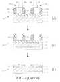
- FIG. 1is a schematic depiction of a double-patterning process according to the invention
- FIG. 2is a schematic illustration depicting a triple-patterning process according to the invention.
- FIG. 3is a scanning electron microscope (SEM) photograph of the conformal coating prepared in Example 1;
- FIG. 4is an SEM photograph showing the conformal coating prepared in Example 2.
- FIG. 5is an SEM photograph of the conformal coating prepared in Example 3.
- FIG. 6is an SEM photograph showing the conformal coating prepared in Example 4.
- FIG. 7( a )is a schematic illustration of the template stack used in Example 5.
- FIG. 7( b )is an SEM photograph of the conformal coating prepared in Example 5.
- FIG. 7( c )is an SEM photograph of the sidewalls that were formed after etching the structure in Example 5;
- FIG. 7( d )is an SEM photograph showing the collapsing that occurred after further etching to remove the photoresist of the structure of Example 5;
- FIG. 8( a )is a schematic illustration of an alternative template stack used in Example 5 in order to prevent pattern collapse
- FIG. 8( b )is an SEM photograph of the coating prepared in Example 5.
- FIG. 8( c )is an SEM photograph of the sidewalls that were formed after etching the alternative structure in Example 5;
- FIG. 8( d )is an SEM photograph showing the alternative structure of Example 5 after further etching to remove the photoresist.
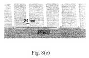
- FIG. 8( e )is an SEM photograph showing the alternative structure of Example 5 after further etching to transfer the pattern to the hard mask layer.
- the present inventionprovides a novel two-step approach that is based upon coating shrinkage.
- FIG. 1illustrates one embodiment of the invention, where FIG. 1( a ) depicts a patterned precursor structure 10 .
- Structure 10includes first layer 12 , having an upper surface 12 a and a backside 12 b .
- FIG. 1is a “snapshot” of the particular microelectronic process. That is, the steps described in FIG. 1 could be at the beginning of the process so that the snapshot depicts the first layers in the “stack” that is being fabricated. Or, the steps could be in the middle of the stack being fabricated, or the last steps in the process so that the snapshot shows some of the last stages involved in building the stack.
- backside 12 bcould have any number of layers or substrates 13 adjacent it, including conventional microelectronic substrates such as those selected from the group consisting of silicon, SiGe, SiO 2 , Si 3 N 4 , aluminum, tungsten, tungsten silicide, gallium arsenide, germanium, tantalum, tantalum nitride, coral, black diamond, phosphorous or boron doped glass, and mixtures of the foregoing.
- conventional microelectronic substratessuch as those selected from the group consisting of silicon, SiGe, SiO 2 , Si 3 N 4 , aluminum, tungsten, tungsten silicide, gallium arsenide, germanium, tantalum, tantalum nitride, coral, black diamond, phosphorous or boron doped glass, and mixtures of the foregoing.
- First layer 12is preferably a spin-on carbon layer (“SOC”) or amorphous carbon layer, and it can be applied and formed according to any prior art processes, which typically involve spin-coating.
- a spin-on carbon layerwill preferably comprise at least about 80% carbon atoms, and even more preferably from about 80% to about 95% carbon atoms, based upon the total number of atoms in all the solids in the composition taken as 100%. One having ordinary skill in the art can readily calculate this percentage based upon the chemical structure of the solids included in the composition.
- the thickness of the first layer 12will typically be from about 50 nm to about 1,000 nm, and preferably from about 100 nm to about 300 nm.
- Structure 10further includes a second layer 14 adjacent upper surface 12 a .
- Second layer 14includes an upper surface 14 a and can be applied by any known application method and processed according to known conditions.
- Second layer 14is preferably a hard mask layer, although it could also be an organic bottom anti-reflective coating.
- the composition that forms second layer 14can be applied by any known application method, with one preferred method being spin-coating the composition at speeds of from about 1,000 rpm to about 4,000 rpm (preferably from about 1,500 rpm to about 2,500 rpm) for a time period of from about 10 seconds to about 60 seconds (preferably from about 20 seconds to about 60 seconds).
- the compositionis then baked so as to induce thermal crosslinking.
- Preferred baking conditionsinvolve temperatures of at least about 100° C., preferably from about 120° C.
- the thickness of the crosslinked second layer 14will typically be from about 20 nm to about 150 nm, and preferably from about 30 nm to about 100 nm.
- the second layer 14has an n-value of from about 1.4 to about 2, and more preferably from about 1.6 to about 2, and a k-value of from about 0 to about 0.6 at the wavelength of use (e.g., 365 nm, 248 nm, 193 nm, 157 nm, or 13.5 nm).
- the wavelength of usee.g., 365 nm, 248 nm, 193 nm, 157 nm, or 13.5 nm.
- the cured second layer 14will be sufficiently crosslinked that it will be substantially insoluble in typical organic solvents such as ethyl lactate, propylene glycol methyl ether acetate (PGMEA), propylene glycol methyl ether (PGME), propylene glycol n-propyl ether (PnP), cyclohexanone, acetone, Gamma butyrolactone (GBL), and mixtures thereof.
- typical organic solventssuch as ethyl lactate, propylene glycol methyl ether acetate (PGMEA), propylene glycol methyl ether (PGME), propylene glycol n-propyl ether (PnP), cyclohexanone, acetone, Gamma butyrolactone (GBL), and mixtures thereof.
- PELpropylene glycol methyl ether acetate
- PnPpropylene glycol methyl ether
- PnPpropylene glycol n-propyl ether
- a solvente.g., ethyl lactate
- spin dryingat about 2,000-3,500 rpm for about 20-30 seconds to remove the solvent.
- the thicknessis measured again at five different points on the wafer using ellipsometry, and the average of these measurements is determined. This is the average final film thickness.
- the amount of strippingis the difference between the initial and final average film thicknesses.
- the percent strippingis:
- % ⁇ ⁇ stripping( amount ⁇ ⁇ of ⁇ ⁇ stripping initial ⁇ ⁇ average ⁇ ⁇ film ⁇ ⁇ thickness ) ⁇ 100.
- a photosensitive compositioncan then be applied to the cured second layer 14 to form an imaging layer (not shown), followed by imaging, light exposure, and developing to form pattern 16 .
- the photosensitive compositionis preferably spin-applied and then post-application baked (“PAB”) at a temperature of at least about 80° C., preferably from about 80° C. to about 130° C., and more preferably from about 100° C. to about 120° C., and for time periods of from about 60 seconds to about 120 seconds.
- Suitable photosensitive compositionsinclude commercially-available photoresists, or any other photosensitive compositions.
- the thickness of the imaging layer after bakingwill typically be from about 50 nm to about 1,000 nm, and more preferably from about 60 nm to about 400 nm.
- the imaging layeris then exposed to radiation with a photomask (not shown) positioned above the surface of the imaging layer.
- the maskhas open areas designed to permit radiation to pass through the mask and contact surface of the imaging layer.
- the remaining solid portions of the maskare designed to prevent radiation from contacting the surface of the imaging layer in certain areas.
- the present inventive processcan be used with radiation of most wavelengths under 500 nm, but preferred wavelengths are selected from the group consisting of 365 nm, 248 nm, 193 nm, 157 nm, and 13.5 nm.
- the portions of the imaging layer that are exposed to radiationare rendered soluble in photoresist developer.
- the imaging layeris preferably subjected to a post-exposure bake (PEB) at a temperature of from about 80° C. to about 180° C., more preferably from about 100° C. to about 180° C., for a time period of from about 60 seconds to about 120 seconds.
- PEBpost-exposure bake
- the exposed portions of the imaging layer, which were made soluble by the above process,are then contacted with a photoresist developer to remove the exposed portions, forming the patterned layer 16 shown in FIG. 1 .
- Patterned layer 16includes raised features 18 (e.g., lines). Although FIG. 1 only shows two raised features 18 , it will be appreciated that any number of raised features could be formed according to the current knowledge in the art.
- Each raised feature 18includes respective first and second sidewalls 20 a , 20 b , which are substantially perpendicular to upper surface 14 a , as well as respective upper surfaces 22 , which are substantially parallel to upper surface 14 a .
- the width W of feature 18is from about 20 nm to about 100 nm, more preferably from about 22 nm to about 80 nm, and even more preferably about 32 nm.
- features 18could also be formed from a number of other compositions.
- features 18could also be formed in layers selected from the group consisting of anti-reflective, hard mask, amorphous carbon, silicon, oxide (e.g., metal oxide) layers.
- the particular layercould be formed on second layer 14 , after which an imaging layer is formed on that layer.
- the imaging layerwould then be patterned as described above, and that pattern would be transferred (e.g., via etching) to the alternative layer to form features 18 .
- the keyis to provide the patterned structure 10 with those features 18 .
- the features 18have a pitch (W:D) of from about 1:2 to about 1:4, and more preferably about 1:3 (see FIG. 1( b ) ).
- Wis 32 nm while D is 96 nm.
- a shrinkable composition 24is applied to the upper surface 14 a of second layer 14 , as well as to the sidewalls 20 a , 20 b and upper surfaces 22 of the features 18 .
- the shrinkable composition 24can be applied by any known methods, but it is preferably spin-applied or spin-coated.
- the shrinkable composition 24is then heated, causing it to shrink dramatically by releasing many small molecules, thus forming the conformal coating 26 illustrated in FIG. 1( c ) .
- the temperatures to which shrinkable composition is heatedwill depend upon the material from which features 18 are formed. For example, when features 18 are formed from a photoresist composition, shrinkable composition 24 is heated to temperatures of less than about 120° C., preferably less than about 110° C. and more preferably from about 80° C. to about 100° C. When features 18 are formed from a material other than a photoresist composition, shrinkable composition 24 is heated to temperatures of less than about 300° C., preferably less than about 250° C., and more preferably from about 100° C. to about 210° C.
- conformal coating 26there are no chemical interactions between conformal coating 26 and the sidewalls 20 a , 20 b or upper surfaces 22 of features 18 .
- Thisallows the process to be used with any type of feature 18 .
- the above baking temperaturesallow the process to be used under mild conditions that avoid distortion of features 18 .
- Arepresents the thickness of conformal coating 26 on top of a feature 18 at its thickest point
- Brepresents the thickness of conformal coating 26 at its thinnest point between features 18 (i.e., at the lowest point of the “valley” between features).
- shrinkable composition 24will shrink by at least about 25%, preferably at least about 35%, more preferably at least about 50%, and even more preferably from about 55% to about 90% during this heating step.
- pre-spacers 28are subjected to an etching process to form pre-spacers 28 .
- Suitable etchantsinclude those selected from the group consisting of Cl 2 , CF 4 , CH 3 F, and CHF 3 , and typical etch rates are from about 1 ⁇ /second to about 10 ⁇ /second, and preferably from about 3 ⁇ /second to about 8 ⁇ /second. Additional, etching could be accomplished via conventional wet etching processes.
- Each pre-spacer 28comprises the raised feature 18 and shrinkable composition remnants 30 . As depicted in FIG. 1( d ) , there is a remnant 30 against each sidewall 20 a , 20 b .
- the raised features 18are then removed (e.g., by O 2 etching) from each pre-spacer 28 , leaving behind the remnants 30 ( FIG. 1( e ) ).
- the remnants 30act as “spacers,” for forming very small features (e.g., lines that are less than about 70 nm, preferably less than about 50 nm, and more preferably less than about 32 nm). That is, the structure 10 is subjected to an etching process that transfers the pattern created by the remnants 30 to the second layer 14 , thus forming lines 34 in second layer 14 .
- the etching processremoves the remnants 30 as well as the second layer 14 in the areas not protected by remnants 30 .
- Suitable etchantsinclude those selected from the group consisting of Cl 2 , CF 4 , CH 3 F, and CHF 3 , and typical etch rates are from about 1 ⁇ /second to about 10 ⁇ /second, and preferably from about 3 ⁇ /second to about 8 ⁇ /second.
- the patterncan be further transferred to the first layer 12 and to substrate 13 , using conventional techniques, if desired.
- the above processdescribes a double-patterning process according to the invention.
- the double-patterning processcan be modified by adding an extra etch step to yield a triple-patterning process.
- This processis shown in FIG. 2 , where like numbering is used to designate similar materials.
- the same processing conditionse.g., spin speeds, temperatures, etching, time periods, etc.
- spin speeds, temperatures, etching, time periods, etc.would be used as described with respect to FIG. 1 , unless stated otherwise.
- Raised features 18will typically have a width W as described previously. Those features 18 are then “trimmed” so that their respective widths are at least cut in half ( FIG. 2( b ) ). That is, the trimmed features 18 ′ will preferably have a width W′ that is from about 50 nm to about 90 nm, more preferably from about 60 nm to about 80 nm, and even more preferably about 70 nm. This trimming can be accomplished by any known process, with one suitable process involving plasma etching.
- the features 18 ′ and second layer 14are then subjected to a partial etch process to yield arched features 18 ′′ and partially etched second layer 14 ′, which includes lower raised features or “nubs” 36 .
- Suitable etchants for this partial etching stepinclude those selected from the group consisting of Cl 2 , CF 4 , CH 3 F, and CHF 3 , and typical etch rates are from about 1 ⁇ /second to about 10 ⁇ /second, and preferably from about 3 ⁇ /second to about 7 ⁇ /second.
- the arched features 18 ′′are then removed (e.g., by etching) to leave the patterned structure 38 shown in FIG. 2( d ) .
- a photosensitive layer 40( FIG. 2( e ) ) is applied to the upper surface 14 a ′ and to nubs 36 , using known processes, such as that described previously. Photosensitive layer 40 is then patterned (exposed and developed) to yield raised features 42 , as depicted in FIG. 2( f ) .
- Each raised feature 42includes respective first and second sidewalls 44 a , 44 b , which are substantially perpendicular to upper surface 14 a ′, as well as respective upper surfaces 46 , which are substantially parallel to upper surface 14 a′.
- the shrinkable composition 24is applied to the upper surface 14 a ′ of second layer 14 ′, as well as to the sidewalls 44 a , 44 b and upper surfaces 46 of the features 42 as described previously and as shown in FIG. 2( g ) .
- Composition 24is then subjected to the shrinking process previously described ( FIG. 2( h ) ) to form conformal coating 26 .
- the remaining steps of FIG. 2( i )-( k )are similar to those described above with respect to FIG. 1( d )-( f ) .
- the embodiment of FIG. 2triples the pattern rather than doubles it (i.e., the embodiment of FIG. 2 results in 50% more lines 34 than that of FIG. 1 ).
- lines 34will also be quite small, having widths of less than about 70 nm, preferably less than about 50 nm, and more preferably from about 16 nm to about 32 nm.
- FIG. 2( l )illustrates the additional step of transferring the pattern to the first layer 12 .
- this patterncan be further transferred to the substrate 13 , if desired.
- compositions for Use as Shrinkable Composition 24are Compositions for Use as Shrinkable Composition 24
- the composition for use as shrinkable composition 24is preferably an organic or organometallic composition and will exhibit certain properties making it suitable for this application.
- the compositionmust exhibit high shrinkage during the heating steps described above. This means that, if the features 18 are formed from a photoresist composition, the shrinkable composition 24 must decompose at temperatures of less than about 120° C., preferably less than about 110° C., and more preferably from about 80° C. to about 100° C., so that the composition shrinks without destroying features 18 . If the features 18 are formed from a material other than a photoresist composition, the shrinkable composition 24 must decompose at temperatures of less than about 300° C., preferably less than about 250° C., and more preferably from about 100° C. to about 210° C., so that the composition shrinks without destroying features 18 .
- the shrinkable composition 24preferably comprises an organic solvent that can be used to dissolve or disperse the solids within the composition 24 .
- the solvent systemis selected so that it will not distort the photoresist pattern, with preferred solvents being selected from the group consisting of mesitylene, methyl isobutyl carbinol, d-limonene, and mixtures thereof. This is particularly beneficial for embodiments where features 18 are formed from a photoresist composition, which is typically more fragile than other substrates.
- the solvent systemcould include the above solvents and/or solvents selected from the group consisting of ethyl lactate, propylene glycol methyl ether, propylene glycol methyl ether acetate, and propylene glycol n-propyl ether.
- the shrinkable compositionetch more slowly than the features 18 .
- the etch selectivity of the shrinkable composition as compared to that of the features 18is preferably less than about 0.30, more preferably less than about 0.25, and more preferably from about 0.001 to about 0.10.
- these numbersare achieved using O 2 as the etchant.
- these numbersare achieved using Cl 2 , CF 4 , CH 3 F, or CHF 3 as the etchant.
- One suitable shrinkable compositioncomprises a crosslinker or crosslinking agent dispersed or dissolved in a solvent system.
- Crosslinking agentsare suitable because they can self-condense into a network with significant shrinkage.
- a typical crosslinking agent suitable for use in the present inventionis an aminoplast such as poly(melamine-co-formaldehyde) methylated (sold under the name Cymel® 303, by Cytec industries).
- crosslinking agentsinclude those selected from the group consisting of poly(melamine-co-formaldehyde) butylate/isobutylate, hexamethylmelamine glycoluril (such as that sold under the name: Powderlink®, by Cytec Industries), 1,3-bis(methoxymethyl)-4,5-bis(methoxy)-ethylenurea (“BMNU”), 1,3-bis(methoxymethyl)urea (“BMU”), and the following derivatives:
- the degree of shrinkagedepends upon the molecular weight of released alcohol and the baking temperature. Greater shrinkage can be achieved by combining a large released molar mass of alcohol, such as butanol, and a higher-temperature baking.
- An etch-resistant polymer, such as polysiloxane,can be blended with the crosslinker to improve the etch selectivity, if desired.
- the solvent systempreferably comprises one or more solvents selected from the group consisting of propylene glycol monomethyl ether (“PGME”), mesitylene, methyl isobutyl carbinol, d-limonene, and mixtures thereof.
- PGMEpropylene glycol monomethyl ether
- the solids content of the composition of this embodimentis preferably from about 1% to about 15% by weight, and more preferably from about 3% to about 10% by weight, based upon the total weight of the composition taken as 100% by weight.
- the crosslinking agentwill preferably be present at a level of from about 80% to about 99% by weight, and more preferably from about 90% to about 95% by weight, based upon the total weight of solids in the composition taken as 100% by weight.
- the compositionwill also comprise an acid, such as those selected from the group consisting of p-toluene sulfonic acid, dinonyl naphthalene sulfonic acid, trifluoromethane sulfuric acid, and heptadecafluoro octanesulfonic acid.
- the acidwill preferably be present at a level of from about 1% to about 70% by weight and more preferably from about 5% to about 10% by weight, based upon the total weight of crosslinking agent in the composition taken as 100% by weight.
- This crosslinker-containing family of compositionsis more suitable for embodiments where features 18 are not formed from a photoresist composition because this family of compositions achieves better shrinkage at higher bake temperatures.
- compositionscomprise a polymer having acid-labile side chains from chain polymerization dispersed or dissolved in a solvent system.
- a thick filmis prepared via spin-coating as described previously, and when the film is baked, acid cleaves the acid-labile side chain, resulting in the release of volatile products. As the side chain is released, the film shrinks significantly. The degree of shrinkage is determined by the composition and size of the side chain.
- the side chaincan be selected so that it can be cleaved by an acid at low temperatures (e.g., less than about 120° C.), thus making this family of compositions also suitable for use in situations where features 18 are formed from a photoresist composition as well as for features 18 that are formed from a material other than a photoresist composition.
- Monomers for use in these polymersinclude those selected from the group consisting of styrene, methyl acrylate, and acrylate derivatives.
- styrene-based monomersinclude:
- Suitable acrylate or methacrylate monomers with acid labile side chainsinclude:
- Sources of the acid-labile side chainscan include those selected from the group consisting of t-butyl, the acetyl family, the adamantyl family, and the lactone family.
- An etch-resistant componentcan also be used to prepare a copolymer with suitable etch-resistant properties, if desired.
- the solvent systempreferably comprises one or more solvents selected from the group consisting of mesitylene, methyl isobutyl carbinol, d-limonene, and mixtures thereof.
- the solids content of the composition of this embodimentis preferably from about 2% to about 15% by weight, and more preferably from about 3% to about 10% by weight, based upon the total weight of the composition taken as 100% by weight.
- the polymerwill preferably be present at a level of from about 85% to about 99% by weight, and more preferably from about 90% to about 95% by weight, based upon the total weight of solids in the composition taken as 100% by weight.
- composition of this embodimentwill also comprise an acid, such as those selected from the group consisting of p-toluene sulfonic acid, dinonyl naphthalene sulfonic acid, trifluoromethane sulfuric acid, and heptadecafluoro octanesulfonic acid.
- the acidwill preferably be present at a level of from about 1% to about 10% by weight, and more preferably from about to about 7% by weight, based upon the total weight of polymer in the composition taken as 100% by weight.
- Blends of a heavy solvent and an etch-resistant polymerare yet another example of suitable shrinkage compositions 24 .
- the etch-resistant polymercan be any polymer with the etch selectivity compared to feature 18 that was described above. Preferred such etch-resistant polymers are silicon-containing polymers.
- the heavy solventremains with the etch-resistant polymer after spin-coating to form a uniform film.
- the heavy solventthen vaporizes completely during baking (preferably at less than about 120° C., making it suitable for photoresist features 18 as well as non-photoresist features 18 ), and only the etch-resistant polymer is left to form the conformal coating.
- “Heavy solvent”refers to those compatible with the etch-resistant polymer and having a boiling point that will allow it to remain after spin-coating but vaporize during the shrinking temperatures described previously.
- Typical examples of a heavy solventinclude those selected from the group consisting of 2-ethyl-2-adamantyl acrylate, 2-methyl-2-adamantyl methacrylate, 2-methyl-adamantyl acrylate, 1-dodecene, and mixtures thereof.
- the solids content of the compositionis preferably from about 2% to about 15% by weight, and more preferably from about 3% to about 10% by weight, based upon the total weight of the composition taken as 100% by weight.
- the polymerwill preferably be present at a level of from about 20% to about 80% by weight, and more preferably from about 40% to about 60% by weight, based upon the total weight of solids in the composition taken as 100% by weight.
- a further family of materials suitable for the shrinkable composition 24includes organometallic compounds dispersed or dissolved in a solvent system.
- the preferred organometallic compoundsare those that will release ligands at the previously described shrinkage temperatures to form a metal oxide. This elimination of volatile ligands results in the conformal coating 26 .
- the ligandscan be released at low temperatures (e.g., less than about 120° C.), thus making this family of compositions also suitable for use in situations where features 18 are formed from a photoresist composition as well as for features 18 that are formed from a material other than a photoresist composition.
- Typical examplesinclude those selected from the group consisting of titanium (IV) bis(ethyl acetoacetato) diisopropoxide, titanium (IV) bis(ammonium lactato) dihydroxide, titanium (IV) diisopropoxide (bis-2,3-pentanedionate), aluminum diisopropoxide ethylacetoacetate, vanadium (IV) oxide bis(2,4-pentane-dionate), zirconium dibutoxide bis(2,4-pentanedionate), aluminum pentanedionate bis(ethylaceto-acetate), hafnium dibutoxide bis(2,4-pentanedionate), vanadium III 2,4-pentanedionate, and poly(dibutyl titanate).
- the solvent systempreferably comprises one or more solvents selected from the group consisting of methyl carbinol isobutyl, mesitylene, 1-dodecene, and mixtures thereof.
- the solids content of the compositionis preferably from about 2% to about 15% by weight, and more preferably from about 3% to about 10% by weight, based upon the total weight of the composition taken as 100% by weight.
- the organometallic compoundwill preferably be present at a level of from about 40% to about 90% by weight, and more preferably from about 40% to about 80% by weight, based upon the total weight of solids in the composition taken as 100% by weight.
- a solutionwas made by dissolving 10 grams of Cymel® 303 (a crosslinking agent obtained from Cytec Industries, West Paterson, N.J.) in 90 grams of PGME (obtained from General Chemical West LLC, Hollister, Calif.), a polar solvent. The resulting solution comprised 0.25 wt % of crosslinking agent.
- PGMEobtained from General Chemical West LLC, Hollister, Calif.
- p-TSAp-toluene sulfonic acid
- the mixturewas stirred for 10 minutes and then filtered through a 0.1- ⁇ m filter.
- the formulationwas spin-coated onto a flat silicon wafer at 1,500 rpm for 60 seconds, and the film or coating thickness was measured. The wafer was then baked at 205° C. for 60 seconds, with Scheme A depicting the reaction. The coating thickness was measured again in order to obtain the shrinkage. The thickness was reduced by 35% during baking.
- the formulationwas also spin-coated onto a wafer with silicon lines at 1,500 rpm for 60 seconds and baked at 205° C. for 60 seconds.
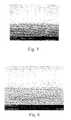
- FIG. 3shows the resulting conformal coating on the silicon lines.
- a solutionwas made by dissolving 10 grams of Cymel® 303 in 90 grams of mesitylene (obtained from Sigma-Aldrich, St. Louis, Mo.), a nonpolar solvent. Next, 0.05 gram of dinonyl naphthalene sulfonic acid solution (“DNNSA,” obtained from Sigma-Aldrich, St. Louis, Mo.) was added to obtain a solution that included 0.5 wt % of crosslinking agent. The mixture was stirred for 10 minutes and then filtered through a 0.1- ⁇ m filter.
- DNNSAdinonyl naphthalene sulfonic acid solution
- the formulationwas spin-coated onto a flat silicon wafer at 1,500 rpm for 60 seconds, and the coating thickness was measured.
- the waferwas then baked at 205° C. for 60 seconds, and the coating thickness was measured to determine coating shrinkage.
- the coating thicknesswas reduced by 35% during baking.
- the mixturewas stirred for 10 minutes and filtered through a 0.1- ⁇ m filter.
- the formulationwas spin-coated onto a flat silicon wafer at 1,500 rpm for 60 seconds and the coating thickness was measured.
- the waferwas then baked at 110° C. for 60 seconds, and the thickness of the coating was measured again to obtain shrinkage data.
- the coating thicknesswas reduced by 70% during baking.
- Scheme Bprovides a depiction of the volatile release during baking.
- the formulationwas also spin-coated onto a photoresist-patterned wafer at 1,500 rpm for 60 seconds and baked at 90° C. for 60 seconds.
- FIG. 5shows the resulting conformal coating on top of the photoresist lines.
- a solutionwas made by dissolving 8 grams (32 wt %) of Adamantate EA and 2 grams (8 wt %) of a silicone methacrylate monomer (3-(methacryloyloxy)propyl-tris(trimethylsilyloxy)-silane, obtained from TCI America, Portland, Oreg.) in 15 grams of mesitylene. Polymerization was performed at 100° C. for 24 hours. The solution was diluted to 7.5 wt % using 108.3 grams of mesitylene, and 0.05 gram of DNNSA (which was 0.5 wt % of polymer) was then added to the solution. The mixture was stirred for 10 minutes and filtered through a 0.1- ⁇ m filter.
- a flat silicon waferwas spin-coated at 1,500 rpm for 60 seconds, and the coating thickness was measured.
- the waferwas then baked at 110° C. for 60 seconds, and the thickness of the coating was measured again in order to obtain shrinkage data.
- the coating thicknesswas reduced by 55% during baking.
- the formulationwas also spin-coated onto a photoresist-patterned wafer at 1,500 rpm for 60 seconds and baked at 90° C. for 60 seconds.
- FIG. 6shows the resulting conformal coating on top of photoresist lines.
- the etch rates of the coating in different gaseswere measured using Oxford Plasmalab RIE under the following conditions: power—100 W; pressure—50 mTorr; backside Helium—3 mTorr; and gas—50 sccm.
- the etch selectivities of the coating compared to a commercially available photoresist (AR1682J, obtained from JSR Micro, Sunnyvale, Calif.) and to a thermal oxide layer after 30 seconds of etchingare listed in Table 1.
- a solutionwas made by dissolving 8 grams (32 wt %) of Adamantate EA and 2 grams (8 wt %) of a silicone methacrylate monomer (MCR-M07, monomethacrylate-terminated polydimethylsiloxane; molecular weight: 600-800 g/mol; obtained from Gelest Inc, Morrisville, Pa.) in 15 grams of mesitylene. Polymerization was performed at 80° C. for 24 hours. The solution was diluted to 7.5 wt % using 108.3 grams of methyl isobutyl carbinol (obtained from Sigma-Aldrich, St. Louis, Mo.), and 0.05 gram of DNNSA (0.5 wt % of polymer) was then added to the solution.
- MCR-M07monomethacrylate-terminated polydimethylsiloxane; molecular weight: 600-800 g/mol; obtained from Gelest Inc, Morrisville, Pa.
- the mixturewas stirred for 10 minutes and was then filtered through a 0.1- ⁇ m filter.
- a flat silicon waferwas spin-coated at 1,500 rpm for 60 seconds, and the thickness of the coating was measured.
- the coatingwas then baked at 110° C. for 60 seconds, and the thickness of the coating was measured again in order to obtain shrinkage data. The coating thickness was reduced by 55% during baking.
- etch rates in different gaseswere measured using an Oxford Plasmalab RIE under the following conditions: power—100 W; pressure—50 mTorr; backside Helium—3 mTorr; gas—50 sccm.
- the etch selectivities of the coating compared to a commercially available photoresist (AR1682J) and to a the thermal oxide layer after 30 seconds of etchingare listed in Table 2.
- a resist-patterned waferwas used as a template, as schematically depicted in FIG. 7( a ) .
- An organic bottom antireflective coating(ARC® 29A, obtained from Brewer Science Inc, Rolla, Mo.) was used as the layer between the patterned photoresist and the substrate.
- the above formulationwas spin-coated onto the photoresist-patterned wafer at 1,000 rpm for 60 seconds and then baked at 90° C. for 60 seconds.
- FIG. 7( b )shows the resulting conformal coating on the top of the photoresist lines.
- the coated waferwas then etched using chlorine gas (Cl 2 —50 sccm; Argon—20 sccm; power—200 W; and pressure: 50 mTorr), and FIG. 7( c ) shows the sidewall formation.
- the waferwas further etched using oxygen (O 2 —50 sccm; power—100 W; pressure—100 mTorr) to remove the resist.
- oxygenO 2 —50 sccm; power—100 W; pressure—100 mTorr
- a new templatewas prepared with the stacking of layers as shown in FIG. 8( a ) .
- a bottom layer of OptiStack SOC 110(a spin-on carbon or “SOC,” obtained from Brewer Science Brewer Science Inc, Rolla, Mo.) was applied to a silicon wafer.
- a silicon-containing bottom anti-reflective coating OPTISTACK® HM710(a hard mask or “HM,” obtained from Brewer Science Inc, Rolla, Mo.), was applied on the top of spin-on carbon.
- a photoresist layer(Pi6001, obtained from TOK, Japan) was formed on top of the hard mask layer, followed by patterning to form lines.
- the above formulationwas spin-coated onto the photoresist-patterned wafer at 2,000 rpm for 60 seconds, followed by baking at 90° C. for 60 seconds (see FIG. 8( b ) ).
- the coated waferwas etched using chlorine gas (Cl 2 —50 sccm; Argon—20 sccm; power—200 W; pressure—50 mTorr).
- FIG. 8( c )shows sidewall formation.
- FIG. 8( d )shows the standing spacer after resist removal.
- CF 4 etching(CF 4 —35 sccm; power—100 W; pressure—50 mTorr) was used to transfer the pattern to the bottom hardmask layer FIG. 8( e ) .
- a solutionwas made by dissolving 9 grams (36 wt %) of a silicone methacrylate monomer (3-(methacryloyloxy) propyltris (trimethylsilyloxy) silane, obtained from TCI America, Portland, Oreg.), 1 gram (4 wt % of the solution) of glycidyl methacrylate, and 0.1 grain (1 wt % of monomers) of AIBN in 15 grams of mesitylene. Polymerization was performed at 100° C. for 24 hours, and the solution was used without further purification.
- a silicone methacrylate monomer(3-(methacryloyloxy) propyltris (trimethylsilyloxy) silane, obtained from TCI America, Portland, Oreg.
- AIBN0.1 grain (1 wt % of monomers
- Titanium (IV) bis(ethyl acetoacetato) diisopropoxide(0.5 g, obtained from Sigma-Aldrich, St. Louis, Mo.) was dissolved in 9.5 g methyl isobutyl carbinol. The mixture was stirred for 10 minutes and filtered through a 0.1- ⁇ m filter. The mixture was spin-coated onto a flat silicon wafer at 1,500 rpm for 60 seconds, the coating thickness was measured. The coating was then baked at 110° C. for 60 seconds, and the thickness of the coating was measured again in order to obtain shrinkage data. The coating thickness was reduced by 80% during baking.
Landscapes
- Engineering & Computer Science (AREA)
- Physics & Mathematics (AREA)
- Chemical & Material Sciences (AREA)
- General Physics & Mathematics (AREA)
- Manufacturing & Machinery (AREA)
- Computer Hardware Design (AREA)
- Microelectronics & Electronic Packaging (AREA)
- Power Engineering (AREA)
- Condensed Matter Physics & Semiconductors (AREA)
- Inorganic Chemistry (AREA)
- Chemical Kinetics & Catalysis (AREA)
- Health & Medical Sciences (AREA)
- Medicinal Chemistry (AREA)
- Polymers & Plastics (AREA)
- Organic Chemistry (AREA)
- Photosensitive Polymer And Photoresist Processing (AREA)
- Materials For Photolithography (AREA)
- Exposure Of Semiconductors, Excluding Electron Or Ion Beam Exposure (AREA)
Abstract
Description
This application claims the priority benefit of a provisional application entitled SPIN-ON SPACER MATERIALS FOR DOUBLE-PATTERNING LITHOGRAPHY, Ser. No. 61/143,013, filed Jan. 7, 2009, incorporated by reference herein.
Field of the Invention
The present invention is broadly concerned with novel, multiple patterning methods that utilize a shrinkable composition to form spacer structures.
Description of the Prior Art
Due to delays in developing the next generation of 193-nm immersion technology and extreme ultraviolet lithography (EUVL), double patterning using currently available tools is the only lithographic technique planned for use from 2008 to 2012 for the 32- and 22-nm half-pitch nodes. Self-aligned spacer technology is one double-patterning technology under extensive investigation. The spacer approach has the advantage of requiring only one lithographic exposure, which avoids the serious issue of overlay between successive exposures. Spacers are created by depositing a coating on prepatterned features and then etching to remove those portions of the film present on the horizontal surfaces, which leaves the spacer film layer lining only the sidewalls. The original patterned feature is then removed to leave only the spacers. Because two spacers are created for every line, the line density doubles. As a result, 32-nm or smaller dense lines can be fabricated.
There have been prior attempts using spacer technology based on films applied using CVD (chemical vapor deposition) processes. The process involves several CVD steps to prepare the layers under the photoresist before photolithography. After photolithography, several steps of etching are used to open the underlayers to prepare the template. After the template is prepared, CVD is used to apply a conformal coating, which can be further etched to form spacers. The need for so many steps makes the process costly and inefficient. Furthermore, the accumulation of layers leads to the inability to control CD (critical dimension).
Other attempts have been made to double the frequency or pitch of small features using materials and a process called resolution enhancement lithography assisted by chemical shrink (RELACS). The RELACS process is based on a crosslinking reaction induced by acid that is diffused out from the resist and involves four steps: spin-coating; blanket exposure; baking; and developing. The primary application of the technology has been to shrink contact holes, which depends upon a chemical interaction induced by the resist. This approach is not useful for forming small lines, but rather only has applicability to double the frequency of large (>100-nm) lines fabricated by KrF (248-nm) technology because the KrF RELACS process is performed under relatively mild conditions (<120° C.). However, the fabrication of 32-nm lines is based on ArF (193-nm) technology. The mobility of acid in an ArF resist is extremely low, and the ArF RELACS process requires a high baking temperature (>120° C.), which will distort the original resist lines. Thus, this process lacks potential for any practical applications.
The present invention addresses the problems of the prior art by providing a method of forming a microelectronic structure. The method comprises providing a precursor structure having a patterned surface. The patterned surface includes at least one raised feature having sidewalls and an upper surface: A shrinkable composition is applied to the patterned surface, so that it covers the feature sidewalls and upper surface. The shrinkable composition is healed so as to form a conformal layer of the composition on the patterned surface and over the raised feature. At least some of the conformal layer is removed to yield a pre-spacer structure comprising the raised feature and remnants of the conformal layer against the raised feature sidewalls.
The present invention provides a novel two-step approach that is based upon coating shrinkage.
Preferably, thesecond layer 14 has an n-value of from about 1.4 to about 2, and more preferably from about 1.6 to about 2, and a k-value of from about 0 to about 0.6 at the wavelength of use (e.g., 365 nm, 248 nm, 193 nm, 157 nm, or 13.5 nm). Advantageously, the curedsecond layer 14 will be sufficiently crosslinked that it will be substantially insoluble in typical organic solvents such as ethyl lactate, propylene glycol methyl ether acetate (PGMEA), propylene glycol methyl ether (PGME), propylene glycol n-propyl ether (PnP), cyclohexanone, acetone, Gamma butyrolactone (GBL), and mixtures thereof. Thus, when subjected to a stripping test, the curedsecond layer 14 will have a percent stripping of less than about 5%, preferably less than about 1%, and even more preferably about 0%. The stripping test involves first determining the thickness by taking the average of measurements at five different locations of the curedsecond layer 14. This is the initial average film thickness. Next, a solvent (e.g., ethyl lactate) is puddled onto the cured film for about 20 seconds, followed by spin drying at about 2,000-3,500 rpm for about 20-30 seconds to remove the solvent. The thickness is measured again at five different points on the wafer using ellipsometry, and the average of these measurements is determined. This is the average final film thickness.
The amount of stripping is the difference between the initial and final average film thicknesses. The percent stripping is:
In a preferred embodiment, a photosensitive composition can then be applied to the curedsecond layer 14 to form an imaging layer (not shown), followed by imaging, light exposure, and developing to formpattern 16. Although this can be accomplished by known methods, one possible process is described herein. In this process, the photosensitive composition is preferably spin-applied and then post-application baked (“PAB”) at a temperature of at least about 80° C., preferably from about 80° C. to about 130° C., and more preferably from about 100° C. to about 120° C., and for time periods of from about 60 seconds to about 120 seconds. Suitable photosensitive compositions include commercially-available photoresists, or any other photosensitive compositions. The thickness of the imaging layer after baking will typically be from about 50 nm to about 1,000 nm, and more preferably from about 60 nm to about 400 nm.
The imaging layer is then exposed to radiation with a photomask (not shown) positioned above the surface of the imaging layer. The mask has open areas designed to permit radiation to pass through the mask and contact surface of the imaging layer. The remaining solid portions of the mask are designed to prevent radiation from contacting the surface of the imaging layer in certain areas. Those skilled in the art will readily understand that the arrangement of open areas and solid portions is designed based upon the desired pattern to be formed in the imaging layer and ultimately in the layers below the imaging layer. The present inventive process can be used with radiation of most wavelengths under 500 nm, but preferred wavelengths are selected from the group consisting of 365 nm, 248 nm, 193 nm, 157 nm, and 13.5 nm.
Upon exposure, the portions of the imaging layer that are exposed to radiation are rendered soluble in photoresist developer. After exposure, the imaging layer is preferably subjected to a post-exposure bake (PEB) at a temperature of from about 80° C. to about 180° C., more preferably from about 100° C. to about 180° C., for a time period of from about 60 seconds to about 120 seconds. The exposed portions of the imaging layer, which were made soluble by the above process, are then contacted with a photoresist developer to remove the exposed portions, forming the patternedlayer 16 shown inFIG. 1 .
The above process describes the process for forming raisedfeatures 18 from photosensitive composition. However, it will be appreciated that thefeatures 18 could also be formed from a number of other compositions. For example, features18 could also be formed in layers selected from the group consisting of anti-reflective, hard mask, amorphous carbon, silicon, oxide (e.g., metal oxide) layers. With any of these layer types, features18 would be formed according to known processes. For example, the particular layer could be formed onsecond layer 14, after which an imaging layer is formed on that layer. The imaging layer would then be patterned as described above, and that pattern would be transferred (e.g., via etching) to the alternative layer to form features18. Regardless of the material from which thefeatures 18 are formed, the key is to provide the patternedstructure 10 with thosefeatures 18. Furthermore, it is preferred that thefeatures 18 have a pitch (W:D) of from about 1:2 to about 1:4, and more preferably about 1:3 (seeFIG. 1(b) ). In a particularly preferred embodiment, W is 32 nm while D is 96 nm.
Once the patternedstructure 10 has been formed, either by the above-described process or by other processes known in the art, ashrinkable composition 24 is applied to theupper surface 14aofsecond layer 14, as well as to thesidewalls upper surfaces 22 of thefeatures 18. Theshrinkable composition 24 can be applied by any known methods, but it is preferably spin-applied or spin-coated.
Theshrinkable composition 24 is then heated, causing it to shrink dramatically by releasing many small molecules, thus forming theconformal coating 26 illustrated inFIG. 1(c) . The temperatures to which shrinkable composition is heated will depend upon the material from which features18 are formed. For example, when features18 are formed from a photoresist composition,shrinkable composition 24 is heated to temperatures of less than about 120° C., preferably less than about 110° C. and more preferably from about 80° C. to about 100° C. When features18 are formed from a material other than a photoresist composition,shrinkable composition 24 is heated to temperatures of less than about 300° C., preferably less than about 250° C., and more preferably from about 100° C. to about 210° C.
Advantageously, there are no chemical interactions betweenconformal coating 26 and thesidewalls upper surfaces 22 offeatures 18. This allows the process to be used with any type offeature 18. Furthermore, the above baking temperatures allow the process to be used under mild conditions that avoid distortion offeatures 18.
It is preferable that A equals B (still referring toFIG. 1(c) ), and even more preferably B is less than A, thus allowing the pre-spacer formation to be accomplished with very little etching. “A” represents the thickness ofconformal coating 26 on top of afeature 18 at its thickest point, while “B” represents the thickness ofconformal coating 26 at its thinnest point between features18 (i.e., at the lowest point of the “valley” between features). Using locations A and B as a reference,shrinkable composition 24 will shrink by at least about 25%, preferably at least about 35%, more preferably at least about 50%, and even more preferably from about 55% to about 90% during this heating step.
Next, and referring toFIG. 1(d) ,conformal coating 26 is subjected to an etching process to form pre-spacers28. Suitable etchants include those selected from the group consisting of Cl2, CF4, CH3F, and CHF3, and typical etch rates are from about 1 Å/second to about 10 Å/second, and preferably from about 3 Å/second to about 8 Å/second. Additional, etching could be accomplished via conventional wet etching processes. Each pre-spacer28 comprises the raisedfeature 18 andshrinkable composition remnants 30. As depicted inFIG. 1(d) , there is a remnant30 against eachsidewall FIG. 1(e) ). Theremnants 30 act as “spacers,” for forming very small features (e.g., lines that are less than about 70 nm, preferably less than about 50 nm, and more preferably less than about 32 nm). That is, thestructure 10 is subjected to an etching process that transfers the pattern created by theremnants 30 to thesecond layer 14, thus forminglines 34 insecond layer 14. The etching process removes theremnants 30 as well as thesecond layer 14 in the areas not protected byremnants 30. Suitable etchants include those selected from the group consisting of Cl2, CF4, CH3F, and CHF3, and typical etch rates are from about 1 Å/second to about 10 Å/second, and preferably from about 3 Å/second to about 8 Å/second. The pattern can be further transferred to thefirst layer 12 and tosubstrate 13, using conventional techniques, if desired.
The above process describes a double-patterning process according to the invention. Advantageously, the double-patterning process can be modified by adding an extra etch step to yield a triple-patterning process. This process is shown inFIG. 2 , where like numbering is used to designate similar materials. Also, the same processing conditions (e.g., spin speeds, temperatures, etching, time periods, etc.) would be used as described with respect toFIG. 1 , unless stated otherwise.
Referring toFIG. 2(a) , it will be seen that the patternedstructure 10 is again provided as described above. Raised features18 will typically have a width W as described previously. Those features18 are then “trimmed” so that their respective widths are at least cut in half (FIG. 2(b) ). That is, the trimmed features18′ will preferably have a width W′ that is from about 50 nm to about 90 nm, more preferably from about 60 nm to about 80 nm, and even more preferably about 70 nm. This trimming can be accomplished by any known process, with one suitable process involving plasma etching.
As shown inFIG. 2(c) , thefeatures 18′ andsecond layer 14 are then subjected to a partial etch process to yieldarched features 18″ and partially etchedsecond layer 14′, which includes lower raised features or “nubs”36. Suitable etchants for this partial etching step include those selected from the group consisting of Cl2, CF4, CH3F, and CHF3, and typical etch rates are from about 1 Å/second to about 10 Å/second, and preferably from about 3 Å/second to about 7 Å/second.
The arched features18″ are then removed (e.g., by etching) to leave the patternedstructure 38 shown inFIG. 2(d) . A photosensitive layer40 (FIG. 2(e) ) is applied to theupper surface 14a′ and tonubs 36, using known processes, such as that described previously.Photosensitive layer 40 is then patterned (exposed and developed) to yield raised features42, as depicted inFIG. 2(f) . Each raisedfeature 42 includes respective first andsecond sidewalls upper surface 14a′, as well as respectiveupper surfaces 46, which are substantially parallel toupper surface 14a′.
Next, theshrinkable composition 24 is applied to theupper surface 14a′ ofsecond layer 14′, as well as to thesidewalls upper surfaces 46 of thefeatures 42 as described previously and as shown inFIG. 2(g) .Composition 24 is then subjected to the shrinking process previously described (FIG. 2(h) ) to formconformal coating 26. The remaining steps ofFIG. 2(i)-(k) are similar to those described above with respect toFIG. 1(d)-(f) . It will be noted, however, that the embodiment ofFIG. 2 triples the pattern rather than doubles it (i.e., the embodiment ofFIG. 2 results in 50%more lines 34 than that ofFIG. 1 ). Advantageously, lines34 will also be quite small, having widths of less than about 70 nm, preferably less than about 50 nm, and more preferably from about 16 nm to about 32 nm.
Finally,FIG. 2(l) illustrates the additional step of transferring the pattern to thefirst layer 12. As was the case with the previous embodiment, this pattern can be further transferred to thesubstrate 13, if desired.
It will be appreciated that the above-described process is photoresist independent, and no interaction occurs between the coating and the substrate as described above. As a result, this process can be extended to any substrate and can be applied under mild conditions (<120° C.), which avoids distortion of the original lines. Thus, this new approach is based on different mechanisms than, and provides significant advantages over, the prior art approaches. The process can be used to double, and even triple, the frequency of dense lines. As used herein, “dense” refers to a region having at least about 50% of its surface area filled withfeatures 18.
The composition for use asshrinkable composition 24 is preferably an organic or organometallic composition and will exhibit certain properties making it suitable for this application. For example, the composition must exhibit high shrinkage during the heating steps described above. This means that, if thefeatures 18 are formed from a photoresist composition, theshrinkable composition 24 must decompose at temperatures of less than about 120° C., preferably less than about 110° C., and more preferably from about 80° C. to about 100° C., so that the composition shrinks without destroying features18. If thefeatures 18 are formed from a material other than a photoresist composition, theshrinkable composition 24 must decompose at temperatures of less than about 300° C., preferably less than about 250° C., and more preferably from about 100° C. to about 210° C., so that the composition shrinks without destroying features18.
Theshrinkable composition 24 preferably comprises an organic solvent that can be used to dissolve or disperse the solids within thecomposition 24. Preferably, the solvent system is selected so that it will not distort the photoresist pattern, with preferred solvents being selected from the group consisting of mesitylene, methyl isobutyl carbinol, d-limonene, and mixtures thereof. This is particularly beneficial for embodiments where features18 are formed from a photoresist composition, which is typically more fragile than other substrates. In embodiments where features18 are not formed from a photoresist composition, the solvent system could include the above solvents and/or solvents selected from the group consisting of ethyl lactate, propylene glycol methyl ether, propylene glycol methyl ether acetate, and propylene glycol n-propyl ether.
It is also highly desirable that the shrinkable composition etch more slowly than thefeatures 18. Thus, the etch selectivity of the shrinkable composition as compared to that of thefeatures 18 is preferably less than about 0.30, more preferably less than about 0.25, and more preferably from about 0.001 to about 0.10. When features18 are formed from a photoresist composition, these numbers are achieved using O2as the etchant. When features18 are formed from a material other than a photoresist composition, these numbers are achieved using Cl2, CF4, CH3F, or CHF3as the etchant.
One suitable shrinkable composition comprises a crosslinker or crosslinking agent dispersed or dissolved in a solvent system. Crosslinking agents are suitable because they can self-condense into a network with significant shrinkage. A typical crosslinking agent suitable for use in the present invention is an aminoplast such as poly(melamine-co-formaldehyde) methylated (sold under the name Cymel® 303, by Cytec industries). Other suitable crosslinking agents include those selected from the group consisting of poly(melamine-co-formaldehyde) butylate/isobutylate, hexamethylmelamine glycoluril (such as that sold under the name: Powderlink®, by Cytec Industries), 1,3-bis(methoxymethyl)-4,5-bis(methoxy)-ethylenurea (“BMNU”), 1,3-bis(methoxymethyl)urea (“BMU”), and the following derivatives:

The degree of shrinkage depends upon the molecular weight of released alcohol and the baking temperature. Greater shrinkage can be achieved by combining a large released molar mass of alcohol, such as butanol, and a higher-temperature baking. An etch-resistant polymer, such as polysiloxane, can be blended with the crosslinker to improve the etch selectivity, if desired.
For this type of composition, the solvent system preferably comprises one or more solvents selected from the group consisting of propylene glycol monomethyl ether (“PGME”), mesitylene, methyl isobutyl carbinol, d-limonene, and mixtures thereof. Furthermore, the solids content of the composition of this embodiment is preferably from about 1% to about 15% by weight, and more preferably from about 3% to about 10% by weight, based upon the total weight of the composition taken as 100% by weight. The crosslinking agent will preferably be present at a level of from about 80% to about 99% by weight, and more preferably from about 90% to about 95% by weight, based upon the total weight of solids in the composition taken as 100% by weight.
The composition will also comprise an acid, such as those selected from the group consisting of p-toluene sulfonic acid, dinonyl naphthalene sulfonic acid, trifluoromethane sulfuric acid, and heptadecafluoro octanesulfonic acid. The acid will preferably be present at a level of from about 1% to about 70% by weight and more preferably from about 5% to about 10% by weight, based upon the total weight of crosslinking agent in the composition taken as 100% by weight.
This crosslinker-containing family of compositions is more suitable for embodiments where features18 are not formed from a photoresist composition because this family of compositions achieves better shrinkage at higher bake temperatures.
Other suitable compositions comprise a polymer having acid-labile side chains from chain polymerization dispersed or dissolved in a solvent system. A thick film is prepared via spin-coating as described previously, and when the film is baked, acid cleaves the acid-labile side chain, resulting in the release of volatile products. As the side chain is released, the film shrinks significantly. The degree of shrinkage is determined by the composition and size of the side chain. The side chain can be selected so that it can be cleaved by an acid at low temperatures (e.g., less than about 120° C.), thus making this family of compositions also suitable for use in situations where features18 are formed from a photoresist composition as well as forfeatures 18 that are formed from a material other than a photoresist composition.
Monomers for use in these polymers include those selected from the group consisting of styrene, methyl acrylate, and acrylate derivatives. Some suitable styrene-based monomers include:


Sources of the acid-labile side chains can include those selected from the group consisting of t-butyl, the acetyl family, the adamantyl family, and the lactone family. An etch-resistant component can also be used to prepare a copolymer with suitable etch-resistant properties, if desired.
For this type of composition, the solvent system preferably comprises one or more solvents selected from the group consisting of mesitylene, methyl isobutyl carbinol, d-limonene, and mixtures thereof. Furthermore, the solids content of the composition of this embodiment is preferably from about 2% to about 15% by weight, and more preferably from about 3% to about 10% by weight, based upon the total weight of the composition taken as 100% by weight. The polymer will preferably be present at a level of from about 85% to about 99% by weight, and more preferably from about 90% to about 95% by weight, based upon the total weight of solids in the composition taken as 100% by weight.
The composition of this embodiment will also comprise an acid, such as those selected from the group consisting of p-toluene sulfonic acid, dinonyl naphthalene sulfonic acid, trifluoromethane sulfuric acid, and heptadecafluoro octanesulfonic acid. The acid will preferably be present at a level of from about 1% to about 10% by weight, and more preferably from about to about 7% by weight, based upon the total weight of polymer in the composition taken as 100% by weight.
Blends of a heavy solvent and an etch-resistant polymer are yet another example ofsuitable shrinkage compositions 24. The etch-resistant polymer can be any polymer with the etch selectivity compared to feature18 that was described above. Preferred such etch-resistant polymers are silicon-containing polymers.
The heavy solvent remains with the etch-resistant polymer after spin-coating to form a uniform film. The heavy solvent then vaporizes completely during baking (preferably at less than about 120° C., making it suitable for photoresist features18 as well as non-photoresist features18), and only the etch-resistant polymer is left to form the conformal coating. “Heavy solvent” refers to those compatible with the etch-resistant polymer and having a boiling point that will allow it to remain after spin-coating but vaporize during the shrinking temperatures described previously. Typical examples of a heavy solvent include those selected from the group consisting of 2-ethyl-2-adamantyl acrylate, 2-methyl-2-adamantyl methacrylate, 2-methyl-adamantyl acrylate, 1-dodecene, and mixtures thereof.
For this type of composition, the solids content of the composition is preferably from about 2% to about 15% by weight, and more preferably from about 3% to about 10% by weight, based upon the total weight of the composition taken as 100% by weight. The polymer will preferably be present at a level of from about 20% to about 80% by weight, and more preferably from about 40% to about 60% by weight, based upon the total weight of solids in the composition taken as 100% by weight.
A further family of materials suitable for theshrinkable composition 24 includes organometallic compounds dispersed or dissolved in a solvent system. The preferred organometallic compounds are those that will release ligands at the previously described shrinkage temperatures to form a metal oxide. This elimination of volatile ligands results in theconformal coating 26. The ligands can be released at low temperatures (e.g., less than about 120° C.), thus making this family of compositions also suitable for use in situations where features18 are formed from a photoresist composition as well as forfeatures 18 that are formed from a material other than a photoresist composition.
Typical examples include those selected from the group consisting of titanium (IV) bis(ethyl acetoacetato) diisopropoxide, titanium (IV) bis(ammonium lactato) dihydroxide, titanium (IV) diisopropoxide (bis-2,3-pentanedionate), aluminum diisopropoxide ethylacetoacetate, vanadium (IV) oxide bis(2,4-pentane-dionate), zirconium dibutoxide bis(2,4-pentanedionate), aluminum pentanedionate bis(ethylaceto-acetate), hafnium dibutoxide bis(2,4-pentanedionate), vanadium III 2,4-pentanedionate, and poly(dibutyl titanate).
The following shows the ligand release that would occur when using titanium (IV) bis(ethyl acetoacetato) diisopropoxid as the organometallic compound:

For this type of composition, the solvent system preferably comprises one or more solvents selected from the group consisting of methyl carbinol isobutyl, mesitylene, 1-dodecene, and mixtures thereof. Furthermore, the solids content of the composition is preferably from about 2% to about 15% by weight, and more preferably from about 3% to about 10% by weight, based upon the total weight of the composition taken as 100% by weight. The organometallic compound will preferably be present at a level of from about 40% to about 90% by weight, and more preferably from about 40% to about 80% by weight, based upon the total weight of solids in the composition taken as 100% by weight.
The following examples set forth preferred methods in accordance with the invention. It is to be understood, however, that these examples are provided by way of illustration and nothing therein should be taken as a limitation upon the overall scope of the invention.
A solution was made by dissolving 10 grams of Cymel® 303 (a crosslinking agent obtained from Cytec Industries, West Paterson, N.J.) in 90 grams of PGME (obtained from General Chemical West LLC, Hollister, Calif.), a polar solvent. The resulting solution comprised 0.25 wt % of crosslinking agent. Next, 0.025 gram of p-toluene sulfonic acid (“p-TSA,” obtained from Sigma-Aldrich, St. Louis, Mo.) was added as a catalyst. The mixture was stirred for 10 minutes and then filtered through a 0.1-μm filter. The formulation was spin-coated onto a flat silicon wafer at 1,500 rpm for 60 seconds, and the film or coating thickness was measured. The wafer was then baked at 205° C. for 60 seconds, with Scheme A depicting the reaction. The coating thickness was measured again in order to obtain the shrinkage. The thickness was reduced by 35% during baking.
The formulation was also spin-coated onto a wafer with silicon lines at 1,500 rpm for 60 seconds and baked at 205° C. for 60 seconds.FIG. 3 shows the resulting conformal coating on the silicon lines.

A solution was made by dissolving 10 grams of Cymel®303 in 90 grams of mesitylene (obtained from Sigma-Aldrich, St. Louis, Mo.), a nonpolar solvent. Next, 0.05 gram of dinonyl naphthalene sulfonic acid solution (“DNNSA,” obtained from Sigma-Aldrich, St. Louis, Mo.) was added to obtain a solution that included 0.5 wt % of crosslinking agent. The mixture was stirred for 10 minutes and then filtered through a 0.1-μm filter.
The formulation was spin-coated onto a flat silicon wafer at 1,500 rpm for 60 seconds, and the coating thickness was measured. The wafer was then baked at 205° C. for 60 seconds, and the coating thickness was measured to determine coating shrinkage. The coating thickness was reduced by 35% during baking.
The formulation was also spin-coated onto a wafer with silicon lines at 1,500 rpm for 60 seconds and was then baked at 205° C. for 60 seconds.FIG. 4 shows the resulting conformal coating made from this formulation on the silicon lines wafer.
In this procedure, 10 grams (40 wt %) Adamantate EA (2-ethyl-2-adamantyl acrylate; obtained from Idemitsu Kosan Co., Ltd., Chiba, Japan) and 0.1 gram (1 wt % of Adamantate EA) of azobisisobutyronitrile (“AIBN,” an initiator obtained from Sigma-Aldrich, St. Louis, Mo.) were dissolved in 15 grams of mesitylene. Polymerization was performed at 100° C. for 24 hours, after which the solution was diluted to 7.5 wt % using mesitylene. Next, 0.05 gram of DNNSA (0.5 wt % of polymer) was added to the polymer solution. The mixture was stirred for 10 minutes and filtered through a 0.1-μm filter. The formulation was spin-coated onto a flat silicon wafer at 1,500 rpm for 60 seconds and the coating thickness was measured. The wafer was then baked at 110° C. for 60 seconds, and the thickness of the coating was measured again to obtain shrinkage data. The coating thickness was reduced by 70% during baking. Scheme B provides a depiction of the volatile release during baking.
The formulation was also spin-coated onto a photoresist-patterned wafer at 1,500 rpm for 60 seconds and baked at 90° C. for 60 seconds.FIG. 5 shows the resulting conformal coating on top of the photoresist lines.

A solution was made by dissolving 8 grams (32 wt %) of Adamantate EA and 2 grams (8 wt %) of a silicone methacrylate monomer (3-(methacryloyloxy)propyl-tris(trimethylsilyloxy)-silane, obtained from TCI America, Portland, Oreg.) in 15 grams of mesitylene. Polymerization was performed at 100° C. for 24 hours. The solution was diluted to 7.5 wt % using 108.3 grams of mesitylene, and 0.05 gram of DNNSA (which was 0.5 wt % of polymer) was then added to the solution. The mixture was stirred for 10 minutes and filtered through a 0.1-μm filter. A flat silicon wafer was spin-coated at 1,500 rpm for 60 seconds, and the coating thickness was measured. The wafer was then baked at 110° C. for 60 seconds, and the thickness of the coating was measured again in order to obtain shrinkage data. The coating thickness was reduced by 55% during baking.
The formulation was also spin-coated onto a photoresist-patterned wafer at 1,500 rpm for 60 seconds and baked at 90° C. for 60 seconds.FIG. 6 shows the resulting conformal coating on top of photoresist lines.
The etch rates of the coating in different gases were measured using Oxford Plasmalab RIE under the following conditions: power—100 W; pressure—50 mTorr; backside Helium—3 mTorr; and gas—50 sccm. The etch selectivities of the coating compared to a commercially available photoresist (AR1682J, obtained from JSR Micro, Sunnyvale, Calif.) and to a thermal oxide layer after 30 seconds of etching are listed in Table 1.
| TABLE 1 | ||
| GAS | ||
| O2 | CF4 | Cl2 | ||
| AR1682J | 0.25 | 1.2 | 1.4 | ||
| Thermal Oxide | — | 2.4 | — | ||
A solution was made by dissolving 8 grams (32 wt %) of Adamantate EA and 2 grams (8 wt %) of a silicone methacrylate monomer (MCR-M07, monomethacrylate-terminated polydimethylsiloxane; molecular weight: 600-800 g/mol; obtained from Gelest Inc, Morrisville, Pa.) in 15 grams of mesitylene. Polymerization was performed at 80° C. for 24 hours. The solution was diluted to 7.5 wt % using 108.3 grams of methyl isobutyl carbinol (obtained from Sigma-Aldrich, St. Louis, Mo.), and 0.05 gram of DNNSA (0.5 wt % of polymer) was then added to the solution. The mixture was stirred for 10 minutes and was then filtered through a 0.1-μm filter. A flat silicon wafer was spin-coated at 1,500 rpm for 60 seconds, and the thickness of the coating was measured. The coating was then baked at 110° C. for 60 seconds, and the thickness of the coating was measured again in order to obtain shrinkage data. The coating thickness was reduced by 55% during baking.
The etch rates in different gases were measured using an Oxford Plasmalab RIE under the following conditions: power—100 W; pressure—50 mTorr; backside Helium—3 mTorr; gas—50 sccm. The etch selectivities of the coating compared to a commercially available photoresist (AR1682J) and to a the thermal oxide layer after 30 seconds of etching are listed in Table 2.
| TABLE 2 | ||
| GAS | ||
| O2 | CF4 | Cl2 | ||
| AR1682J | 0.10 | 1.2 | 1.4 | ||
| Thermal Oxide | — | 2.4 | — | ||
A resist-patterned wafer was used as a template, as schematically depicted inFIG. 7(a) . An organic bottom antireflective coating (ARC® 29A, obtained from Brewer Science Inc, Rolla, Mo.) was used as the layer between the patterned photoresist and the substrate. The above formulation was spin-coated onto the photoresist-patterned wafer at 1,000 rpm for 60 seconds and then baked at 90° C. for 60 seconds.FIG. 7(b) shows the resulting conformal coating on the top of the photoresist lines.
The coated wafer was then etched using chlorine gas (Cl2—50 sccm; Argon—20 sccm; power—200 W; and pressure: 50 mTorr), andFIG. 7(c) shows the sidewall formation. The wafer was further etched using oxygen (O2—50 sccm; power—100 W; pressure—100 mTorr) to remove the resist. However, the spacers collapsed due to the use of an organic bottom anti-reflective coating as the bottom layer, which etched in oxygen much faster than the spacers (FIG. 7(d) .
To address the collapse problem, a new template was prepared with the stacking of layers as shown inFIG. 8(a) . Specifically, a bottom layer of OptiStack SOC110 (a spin-on carbon or “SOC,” obtained from Brewer Science Brewer Science Inc, Rolla, Mo.) was applied to a silicon wafer. Next, a silicon-containing bottom anti-reflective coating OPTISTACK® HM710 (a hard mask or “HM,” obtained from Brewer Science Inc, Rolla, Mo.), was applied on the top of spin-on carbon. A photoresist layer (Pi6001, obtained from TOK, Japan) was formed on top of the hard mask layer, followed by patterning to form lines.
The above formulation was spin-coated onto the photoresist-patterned wafer at 2,000 rpm for 60 seconds, followed by baking at 90° C. for 60 seconds (seeFIG. 8(b) ). The coated wafer was etched using chlorine gas (Cl2—50 sccm; Argon—20 sccm; power—200 W; pressure—50 mTorr).FIG. 8(c) shows sidewall formation.
The wafer was further etched by oxygen to remove the photoresist (O2—50 sccm; power—100 W; pressure—100 mTorr).FIG. 8(d) shows the standing spacer after resist removal. CF4etching (CF4—35 sccm; power—100 W; pressure—50 mTorr) was used to transfer the pattern to the bottom hardmask layerFIG. 8(e) .
A solution was made by dissolving 9 grams (36 wt %) of a silicone methacrylate monomer (3-(methacryloyloxy) propyltris (trimethylsilyloxy) silane, obtained from TCI America, Portland, Oreg.), 1 gram (4 wt % of the solution) of glycidyl methacrylate, and 0.1 grain (1 wt % of monomers) of AIBN in 15 grams of mesitylene. Polymerization was performed at 100° C. for 24 hours, and the solution was used without further purification.
A solution of mesitylene and the above polymer (6 wt %) and 23.3 grams (14 wt %) of 2-ethyl-2-adamantyl methacrylate (sold under the name Adamantate EM by Idemitsu Kosan Co., Ltd., Chiba, Japan) was prepared. The mixture was stirred for 10 minutes and filtered through a 0.1-μm filter. The mixture was spin-coated on a flat silicon wafer at 1,500 rpm for 60 seconds, and the coating thickness was measured. The coating was then baked at 110° C. for 60 seconds, and the thickness of the coating was measured again in order to obtain shrinkage data. The coating thickness was reduced by 70% during baking.
Titanium (IV) bis(ethyl acetoacetato) diisopropoxide (0.5 g, obtained from Sigma-Aldrich, St. Louis, Mo.) was dissolved in 9.5 g methyl isobutyl carbinol. The mixture was stirred for 10 minutes and filtered through a 0.1-μm filter. The mixture was spin-coated onto a flat silicon wafer at 1,500 rpm for 60 seconds, the coating thickness was measured. The coating was then baked at 110° C. for 60 seconds, and the thickness of the coating was measured again in order to obtain shrinkage data. The coating thickness was reduced by 80% during baking.
Claims (19)
1. A method of forming a microelectronic structure, said method comprising:
providing a precursor structure having a patterned surface, said patterned surface including at least one raised feature having first and second sidewalls and an upper surface, wherein said precursor structure further comprises a second raised feature that is below said at least one raised feature, said second raised feature having first and second sidewalls and an upper surface and said at least one raised feature being in contact with said second raised feature sidewalls and upper surface, said second raised feature and said at least one raised feature being formed of different materials;
spin-applying a shrinkable composition to said patterned surface, said composition having an initial thickness and covering said at least one raised feature having said first and second sidewalls and said upper surface;
heating said shrinkable composition, wherein said composition shrinks by at least about 25% so as to form a conformal layer of said composition on said patterned surface and over said at least one raised feature, said conformal layer having a final thickness that is at least about 25% less than said initial thickness; and
removing at least some of said conformal layer to yield a pre-spacer structure comprising said at least one raised feature and remnants of said conformal layer against said at least one raised feature first and second sidewalls.
2. The method ofclaim 1 , further comprising removing said at least one raised feature from said pre-spacer structure so as to leave said remnants on said patterned surface.
3. The method ofclaim 2 , wherein said patterned surface has a first pattern comprising said at least one raised feature prior to said applying and a second pattern after removing said at least one raised feature, said second pattern comprising said remnants and being double that of the first pattern.
4. The method ofclaim 2 , there being one or more layers below said patterned surface and further comprising transferring the pattern created by said remnants down to one or more of said layers below said patterned surface.
5. The method ofclaim 1 , said patterned surface including at least two of said raised features immediately adjacent one another, wherein after said heating there is a maximum thickness A of said conformal layer on the upper surface of each feature and a minimum thickness B on said patterned surface at a point between said two raised features, and B is less than or equal to A.
6. The method ofclaim 1 , wherein said precursor structure comprises:
a first layer having an upper surface;
a second layer having an upper surface, said second layer being adjacent said first layer upper surface; and
said patterned surface being adjacent said second layer upper surface.
7. The method ofclaim 6 , said first layer comprising a spin-on carbon layer, said second layer comprising a hard mask layer, and said patterned surface comprising a photosensitive layer.
8. The method ofclaim 1 , said patterned surface having a plurality of said raised features at a pitch of from about 1:2 to about 1:4.
9. The method ofclaim 1 , further comprising removing said at least one raised feature from said pre-spacer structure so as to leave said remnants and said second raised feature on said patterned surface.
10. The method ofclaim 9 , wherein said patterned surface has a first pattern comprising said at least one raised feature prior to said applying and a second pattern after removing said at least one raised feature, said second pattern comprising said remnants and said second raised feature and being triple that of the first pattern.
11. The method ofclaim 1 , wherein said shrinkable composition is selected from the group consisting of:
(a) a composition comprising a crosslinking agent dispersed or dissolved in a solvent system;
(b) a composition comprising a polymer dispersed or dissolved in a solvent system, said polymer comprising acid-labile side chains;
(c) a composition comprising a polymer resistant to O2, Cl2, CF4, CH3F, or CHF3etchants, said polymer being dispersed or dissolved in a solvent system comprising a heavy solvent; and
(d) a composition comprising an organometallic compound dissolved or dispersed in a solvent system.
12. The method ofclaim 11 , wherein said shrinkable composition is (a), and said crosslinking agent is selected from the group consisting of poly(melamine-co-formaldehyde) methylated, poly(melamine-co-formaldehyde) butylate, poly(melamine-co-formaldehyde) isobutylate, hexamethylmelamine, glycolurils, 1,3-bis(methoxymethyl)-4,5-bis(methoxy)-ethylenurea, 1,3-bis(methoxymethyl) urea, and the following derivatives:

13. The method ofclaim 11 , wherein said shrinkable composition is (b), and said polymer comprises monomers selected from the group consisting of styrenes, methyl acrylates, and acrylates, and said acid-labile side chain is selected from the group consisting of t-butyl, acetyls, adamantyls, and lactones.
14. The method ofclaim 11 , wherein:
said shrinkable composition is (c);
said polymer has an etch selectivity compared to that of said at least one raised feature of less than about 0.30 when O2is used as an etchant; and
said heavy solvent is selected from the group consisting of 2-ethyl-2-adamantyl acrylate, 2-methyl-2-adamantyl methacrylate, 2-methyl-adamantyl acrylate, 1-dodecene, and mixtures thereof.
15. The method ofclaim 11 , wherein said shrinkable composition is (d), and said organometallic compound is selected from the group consisting of titanium (IV) bis(ethyl acetoacetato) diisopropoxide, titanium (IV) bis(ammonium lactato) dihydroxide, titanium (IV) diisopropoxide (bis-2,3-pentanedionate), aluminum diisopropoxide ethylacetoacetate, vanadium (IV) oxide bis(2,4-pentane-dionate), zirconium dibutoxide bis(2,4-pentane-dionate), aluminum pentanedionate bis(ethylacetoacetate), hafnium dibutoxide bis(2,4-pentanedionate), vanadium III 2,4-pentanedionate, and poly(dibutyl titanate).
16. The method ofclaim 1 , wherein said heating comprises heating at a temperature of less than about 300° C.
17. The method ofclaim 16 , wherein said heating comprises heating at a temperature of less than about 120° C.
18. The method ofclaim 17 , wherein said patterned surface comprises a photosensitive layer, and said shrinkable composition comprises a solvent selected from the group consisting of mesitylene, methyl isobutyl carbinol, d-limonene, and mixtures thereof.
19. A method of forming a microelectronic structure, said method comprising:
providing a precursor structure comprising:
a first layer comprising a spin-on carbon layer and having an upper surface;
a second layer comprising a hard mask layer and having an upper surface, said second layer being adjacent said first layer upper surface;
a patterned surface adjacent said second layer upper surface, said patterned surface comprising a photosensitive layer and including at least one raised feature having first and second sidewalls and an upper surface; and
a second raised feature that is below said at least one raised feature, said second raised feature having first and second sidewalls and an upper surface and said at least one raised feature being in contact with said second raised feature sidewalls and upper surface, said second raised feature and said at least one raised feature being formed of different materials;
applying a shrinkable composition to said patterned surface, said composition having an initial thickness and covering said at least one raised feature having said first and second sidewalls and said upper surface;
heating said shrinkable composition, wherein said composition shrinks by at least about 25% so as to form a conformal layer of said composition on said patterned surface and over said at least one raised feature, said conformal layer having a final thickness that is at least about 25% less than said initial thickness; and
removing at least some of said conformal layer to yield a pre-spacer structure comprising said at least one raised feature and remnants of said conformal layer against said at least one raised feature first and second sidewalls.
Priority Applications (2)
| Application Number | Priority Date | Filing Date | Title |
|---|---|---|---|
| US12/652,464US9640396B2 (en) | 2009-01-07 | 2010-01-05 | Spin-on spacer materials for double- and triple-patterning lithography |
| TW099100242ATW201033739A (en) | 2009-01-07 | 2010-01-07 | Spin-on spacer materials for double-and triple-patterning lithography |
Applications Claiming Priority (2)
| Application Number | Priority Date | Filing Date | Title |
|---|---|---|---|
| US14301309P | 2009-01-07 | 2009-01-07 | |
| US12/652,464US9640396B2 (en) | 2009-01-07 | 2010-01-05 | Spin-on spacer materials for double- and triple-patterning lithography |
Publications (2)
| Publication Number | Publication Date |
|---|---|
| US20100170868A1 US20100170868A1 (en) | 2010-07-08 |
| US9640396B2true US9640396B2 (en) | 2017-05-02 |
Family
ID=42311036
Family Applications (1)
| Application Number | Title | Priority Date | Filing Date |
|---|---|---|---|
| US12/652,464Active2034-05-14US9640396B2 (en) | 2009-01-07 | 2010-01-05 | Spin-on spacer materials for double- and triple-patterning lithography |
Country Status (6)
| Country | Link |
|---|---|
| US (1) | US9640396B2 (en) |
| EP (1) | EP2374145A4 (en) |
| JP (1) | JP2012514762A (en) |
| KR (1) | KR20110111473A (en) |
| TW (1) | TW201033739A (en) |
| WO (1) | WO2010080789A2 (en) |
Cited By (8)
| Publication number | Priority date | Publication date | Assignee | Title |
|---|---|---|---|---|
| WO2022020507A1 (en)* | 2020-07-23 | 2022-01-27 | Lam Research Corporation | Advanced self aligned multiple patterning using tin oxide |
| US11768435B2 (en) | 2018-11-02 | 2023-09-26 | Brewer Science, Inc. | Bottom-up conformal coating and photopatterning on PAG-immobilized surfaces |
| US11848212B2 (en) | 2019-06-27 | 2023-12-19 | Lam Research Corporation | Alternating etch and passivation process |
| US11987876B2 (en) | 2018-03-19 | 2024-05-21 | Lam Research Corporation | Chamfer-less via integration scheme |
| US12051589B2 (en) | 2016-06-28 | 2024-07-30 | Lam Research Corporation | Tin oxide thin film spacers in semiconductor device manufacturing |
| US12094711B2 (en) | 2017-02-17 | 2024-09-17 | Lam Research Corporation | Tin oxide films in semiconductor device manufacturing |
| US12112980B2 (en) | 2017-02-13 | 2024-10-08 | Lam Research Corporation | Method to create air gaps |
| US12183589B2 (en) | 2018-01-30 | 2024-12-31 | Lam Research Corporation | Tin oxide mandrels in patterning |
Families Citing this family (378)
| Publication number | Priority date | Publication date | Assignee | Title |
|---|---|---|---|---|
| JP5357186B2 (en) | 2008-01-29 | 2013-12-04 | ブルーワー サイエンス アイ エヌ シー. | On-track process for hard mask pattern formation by multiple dark field exposure |
| US10378106B2 (en) | 2008-11-14 | 2019-08-13 | Asm Ip Holding B.V. | Method of forming insulation film by modified PEALD |
| US9394608B2 (en) | 2009-04-06 | 2016-07-19 | Asm America, Inc. | Semiconductor processing reactor and components thereof |
| US8802201B2 (en) | 2009-08-14 | 2014-08-12 | Asm America, Inc. | Systems and methods for thin-film deposition of metal oxides using excited nitrogen-oxygen species |
| WO2012092139A2 (en) | 2010-12-27 | 2012-07-05 | Brewer Science Inc. | Processes to pattern small features for advanced patterning needs |
| US8901016B2 (en)* | 2010-12-28 | 2014-12-02 | Asm Japan K.K. | Method of forming metal oxide hardmask |
| US9312155B2 (en) | 2011-06-06 | 2016-04-12 | Asm Japan K.K. | High-throughput semiconductor-processing apparatus equipped with multiple dual-chamber modules |
| US10364496B2 (en) | 2011-06-27 | 2019-07-30 | Asm Ip Holding B.V. | Dual section module having shared and unshared mass flow controllers |
| US10854498B2 (en) | 2011-07-15 | 2020-12-01 | Asm Ip Holding B.V. | Wafer-supporting device and method for producing same |
| US20130023129A1 (en) | 2011-07-20 | 2013-01-24 | Asm America, Inc. | Pressure transmitter for a semiconductor processing environment |
| US9017481B1 (en) | 2011-10-28 | 2015-04-28 | Asm America, Inc. | Process feed management for semiconductor substrate processing |
| JP6592243B2 (en)* | 2011-11-21 | 2019-10-16 | ブルーワー サイエンス アイ エヌ シー. | Assist layer for EUV lithography |
| US8551690B2 (en) | 2012-01-20 | 2013-10-08 | Micron Technology, Inc. | Methods of forming patterns |
| US9659799B2 (en) | 2012-08-28 | 2017-05-23 | Asm Ip Holding B.V. | Systems and methods for dynamic semiconductor process scheduling |
| US9275960B2 (en)* | 2012-09-27 | 2016-03-01 | Taiwan Semiconductor Manufacturing Company, Ltd. | Integrated circuit formed using spacer-like copper deposition |
| US10714315B2 (en) | 2012-10-12 | 2020-07-14 | Asm Ip Holdings B.V. | Semiconductor reaction chamber showerhead |
| US8999852B2 (en) | 2012-12-12 | 2015-04-07 | Micron Technology, Inc. | Substrate mask patterns, methods of forming a structure on a substrate, methods of forming a square lattice pattern from an oblique lattice pattern, and methods of forming a pattern on a substrate |
| US8889558B2 (en) | 2012-12-12 | 2014-11-18 | Micron Technology, Inc. | Methods of forming a pattern on a substrate |
| US8889559B2 (en) | 2012-12-12 | 2014-11-18 | Micron Technology, Inc. | Methods of forming a pattern on a substrate |
| US20160376700A1 (en) | 2013-02-01 | 2016-12-29 | Asm Ip Holding B.V. | System for treatment of deposition reactor |
| US8937018B2 (en) | 2013-03-06 | 2015-01-20 | Micron Technology, Inc. | Methods of forming a pattern on a substrate |
| US9589770B2 (en) | 2013-03-08 | 2017-03-07 | Asm Ip Holding B.V. | Method and systems for in-situ formation of intermediate reactive species |
| US9484191B2 (en) | 2013-03-08 | 2016-11-01 | Asm Ip Holding B.V. | Pulsed remote plasma method and system |
| US8961807B2 (en) | 2013-03-15 | 2015-02-24 | Cabot Microelectronics Corporation | CMP compositions with low solids content and methods related thereto |
| CN104078329B (en)* | 2013-03-28 | 2019-05-28 | 中芯国际集成电路制造(上海)有限公司 | The forming method of autoregistration multiple graphics |
| US9318412B2 (en) | 2013-07-26 | 2016-04-19 | Nanya Technology Corporation | Method for semiconductor self-aligned patterning |
| US9240412B2 (en) | 2013-09-27 | 2016-01-19 | Asm Ip Holding B.V. | Semiconductor structure and device and methods of forming same using selective epitaxial process |
| US9129814B2 (en)* | 2013-11-25 | 2015-09-08 | Taiwan Semiconductor Manufacturing Company, Ltd. | Method for integrated circuit patterning |
| US10683571B2 (en) | 2014-02-25 | 2020-06-16 | Asm Ip Holding B.V. | Gas supply manifold and method of supplying gases to chamber using same |
| US10167557B2 (en) | 2014-03-18 | 2019-01-01 | Asm Ip Holding B.V. | Gas distribution system, reactor including the system, and methods of using the same |
| US11015245B2 (en) | 2014-03-19 | 2021-05-25 | Asm Ip Holding B.V. | Gas-phase reactor and system having exhaust plenum and components thereof |
| KR20150136387A (en) | 2014-05-27 | 2015-12-07 | 삼성전자주식회사 | Method of manufacturing semiconductor device |
| US10858737B2 (en) | 2014-07-28 | 2020-12-08 | Asm Ip Holding B.V. | Showerhead assembly and components thereof |
| KR102193680B1 (en) | 2014-08-14 | 2020-12-21 | 삼성전자주식회사 | Method of manufacturing semiconductor device |
| US9890456B2 (en) | 2014-08-21 | 2018-02-13 | Asm Ip Holding B.V. | Method and system for in situ formation of gas-phase compounds |
| US9657845B2 (en) | 2014-10-07 | 2017-05-23 | Asm Ip Holding B.V. | Variable conductance gas distribution apparatus and method |
| US10941490B2 (en) | 2014-10-07 | 2021-03-09 | Asm Ip Holding B.V. | Multiple temperature range susceptor, assembly, reactor and system including the susceptor, and methods of using the same |
| US9564312B2 (en) | 2014-11-24 | 2017-02-07 | Lam Research Corporation | Selective inhibition in atomic layer deposition of silicon-containing films |
| KR102263121B1 (en) | 2014-12-22 | 2021-06-09 | 에이에스엠 아이피 홀딩 비.브이. | Semiconductor device and manufacuring method thereof |
| US10529542B2 (en) | 2015-03-11 | 2020-01-07 | Asm Ip Holdings B.V. | Cross-flow reactor and method |
| US10276355B2 (en) | 2015-03-12 | 2019-04-30 | Asm Ip Holding B.V. | Multi-zone reactor, system including the reactor, and method of using the same |
| US10458018B2 (en) | 2015-06-26 | 2019-10-29 | Asm Ip Holding B.V. | Structures including metal carbide material, devices including the structures, and methods of forming same |
| US10600673B2 (en) | 2015-07-07 | 2020-03-24 | Asm Ip Holding B.V. | Magnetic susceptor to baseplate seal |
| US9960072B2 (en) | 2015-09-29 | 2018-05-01 | Asm Ip Holding B.V. | Variable adjustment for precise matching of multiple chamber cavity housings |
| US10211308B2 (en) | 2015-10-21 | 2019-02-19 | Asm Ip Holding B.V. | NbMC layers |
| US10322384B2 (en) | 2015-11-09 | 2019-06-18 | Asm Ip Holding B.V. | Counter flow mixer for process chamber |
| US11139308B2 (en) | 2015-12-29 | 2021-10-05 | Asm Ip Holding B.V. | Atomic layer deposition of III-V compounds to form V-NAND devices |
| US10529554B2 (en) | 2016-02-19 | 2020-01-07 | Asm Ip Holding B.V. | Method for forming silicon nitride film selectively on sidewalls or flat surfaces of trenches |
| US10468251B2 (en) | 2016-02-19 | 2019-11-05 | Asm Ip Holding B.V. | Method for forming spacers using silicon nitride film for spacer-defined multiple patterning |
| US10501866B2 (en) | 2016-03-09 | 2019-12-10 | Asm Ip Holding B.V. | Gas distribution apparatus for improved film uniformity in an epitaxial system |
| US10343920B2 (en) | 2016-03-18 | 2019-07-09 | Asm Ip Holding B.V. | Aligned carbon nanotubes |
| US9892913B2 (en) | 2016-03-24 | 2018-02-13 | Asm Ip Holding B.V. | Radial and thickness control via biased multi-port injection settings |
| US10190213B2 (en) | 2016-04-21 | 2019-01-29 | Asm Ip Holding B.V. | Deposition of metal borides |
| WO2017184701A1 (en)* | 2016-04-21 | 2017-10-26 | Applied Materials, Inc. | Doped and undoped vanadium oxides for low-k spacer applications |
| US10865475B2 (en) | 2016-04-21 | 2020-12-15 | Asm Ip Holding B.V. | Deposition of metal borides and silicides |
| US10032628B2 (en) | 2016-05-02 | 2018-07-24 | Asm Ip Holding B.V. | Source/drain performance through conformal solid state doping |
| US10367080B2 (en) | 2016-05-02 | 2019-07-30 | Asm Ip Holding B.V. | Method of forming a germanium oxynitride film |
| KR102592471B1 (en) | 2016-05-17 | 2023-10-20 | 에이에스엠 아이피 홀딩 비.브이. | Method of forming metal interconnection and method of fabricating semiconductor device using the same |
| US11453943B2 (en) | 2016-05-25 | 2022-09-27 | Asm Ip Holding B.V. | Method for forming carbon-containing silicon/metal oxide or nitride film by ALD using silicon precursor and hydrocarbon precursor |
| US10388509B2 (en) | 2016-06-28 | 2019-08-20 | Asm Ip Holding B.V. | Formation of epitaxial layers via dislocation filtering |
| US9859151B1 (en) | 2016-07-08 | 2018-01-02 | Asm Ip Holding B.V. | Selective film deposition method to form air gaps |
| US10612137B2 (en) | 2016-07-08 | 2020-04-07 | Asm Ip Holdings B.V. | Organic reactants for atomic layer deposition |
| US10714385B2 (en) | 2016-07-19 | 2020-07-14 | Asm Ip Holding B.V. | Selective deposition of tungsten |
| KR102354490B1 (en) | 2016-07-27 | 2022-01-21 | 에이에스엠 아이피 홀딩 비.브이. | Method of processing a substrate |
| KR102532607B1 (en) | 2016-07-28 | 2023-05-15 | 에이에스엠 아이피 홀딩 비.브이. | Substrate processing apparatus and method of operating the same |
| US9887082B1 (en) | 2016-07-28 | 2018-02-06 | Asm Ip Holding B.V. | Method and apparatus for filling a gap |
| US10395919B2 (en) | 2016-07-28 | 2019-08-27 | Asm Ip Holding B.V. | Method and apparatus for filling a gap |
| US9812320B1 (en) | 2016-07-28 | 2017-11-07 | Asm Ip Holding B.V. | Method and apparatus for filling a gap |
| US10629435B2 (en)* | 2016-07-29 | 2020-04-21 | Lam Research Corporation | Doped ALD films for semiconductor patterning applications |
| KR102613349B1 (en) | 2016-08-25 | 2023-12-14 | 에이에스엠 아이피 홀딩 비.브이. | Exhaust apparatus and substrate processing apparatus and thin film fabricating method using the same |
| US10410943B2 (en) | 2016-10-13 | 2019-09-10 | Asm Ip Holding B.V. | Method for passivating a surface of a semiconductor and related systems |
| US10643826B2 (en) | 2016-10-26 | 2020-05-05 | Asm Ip Holdings B.V. | Methods for thermally calibrating reaction chambers |
| US11532757B2 (en) | 2016-10-27 | 2022-12-20 | Asm Ip Holding B.V. | Deposition of charge trapping layers |
| US10714350B2 (en) | 2016-11-01 | 2020-07-14 | ASM IP Holdings, B.V. | Methods for forming a transition metal niobium nitride film on a substrate by atomic layer deposition and related semiconductor device structures |
| US10229833B2 (en) | 2016-11-01 | 2019-03-12 | Asm Ip Holding B.V. | Methods for forming a transition metal nitride film on a substrate by atomic layer deposition and related semiconductor device structures |
| US10435790B2 (en) | 2016-11-01 | 2019-10-08 | Asm Ip Holding B.V. | Method of subatmospheric plasma-enhanced ALD using capacitively coupled electrodes with narrow gap |
| US10643904B2 (en) | 2016-11-01 | 2020-05-05 | Asm Ip Holdings B.V. | Methods for forming a semiconductor device and related semiconductor device structures |
| US10134757B2 (en) | 2016-11-07 | 2018-11-20 | Asm Ip Holding B.V. | Method of processing a substrate and a device manufactured by using the method |
| US10832908B2 (en) | 2016-11-11 | 2020-11-10 | Lam Research Corporation | Self-aligned multi-patterning process flow with ALD gapfill spacer mask |
| US10454029B2 (en) | 2016-11-11 | 2019-10-22 | Lam Research Corporation | Method for reducing the wet etch rate of a sin film without damaging the underlying substrate |
| KR102546317B1 (en) | 2016-11-15 | 2023-06-21 | 에이에스엠 아이피 홀딩 비.브이. | Gas supply unit and substrate processing apparatus including the same |
| US10340135B2 (en) | 2016-11-28 | 2019-07-02 | Asm Ip Holding B.V. | Method of topologically restricted plasma-enhanced cyclic deposition of silicon or metal nitride |
| KR102762543B1 (en) | 2016-12-14 | 2025-02-05 | 에이에스엠 아이피 홀딩 비.브이. | Substrate processing apparatus |
| US11581186B2 (en) | 2016-12-15 | 2023-02-14 | Asm Ip Holding B.V. | Sequential infiltration synthesis apparatus |
| US11447861B2 (en) | 2016-12-15 | 2022-09-20 | Asm Ip Holding B.V. | Sequential infiltration synthesis apparatus and a method of forming a patterned structure |
| KR102700194B1 (en) | 2016-12-19 | 2024-08-28 | 에이에스엠 아이피 홀딩 비.브이. | Substrate processing apparatus |
| US10269558B2 (en) | 2016-12-22 | 2019-04-23 | Asm Ip Holding B.V. | Method of forming a structure on a substrate |
| US10867788B2 (en) | 2016-12-28 | 2020-12-15 | Asm Ip Holding B.V. | Method of forming a structure on a substrate |
| US11390950B2 (en) | 2017-01-10 | 2022-07-19 | Asm Ip Holding B.V. | Reactor system and method to reduce residue buildup during a film deposition process |
| US10655221B2 (en) | 2017-02-09 | 2020-05-19 | Asm Ip Holding B.V. | Method for depositing oxide film by thermal ALD and PEALD |
| US10468261B2 (en) | 2017-02-15 | 2019-11-05 | Asm Ip Holding B.V. | Methods for forming a metallic film on a substrate by cyclical deposition and related semiconductor device structures |
| US10283353B2 (en) | 2017-03-29 | 2019-05-07 | Asm Ip Holding B.V. | Method of reforming insulating film deposited on substrate with recess pattern |
| US10529563B2 (en) | 2017-03-29 | 2020-01-07 | Asm Ip Holdings B.V. | Method for forming doped metal oxide films on a substrate by cyclical deposition and related semiconductor device structures |
| KR102457289B1 (en) | 2017-04-25 | 2022-10-21 | 에이에스엠 아이피 홀딩 비.브이. | Method for depositing a thin film and manufacturing a semiconductor device |
| US10770286B2 (en) | 2017-05-08 | 2020-09-08 | Asm Ip Holdings B.V. | Methods for selectively forming a silicon nitride film on a substrate and related semiconductor device structures |
| US10446393B2 (en) | 2017-05-08 | 2019-10-15 | Asm Ip Holding B.V. | Methods for forming silicon-containing epitaxial layers and related semiconductor device structures |
| US10892156B2 (en) | 2017-05-08 | 2021-01-12 | Asm Ip Holding B.V. | Methods for forming a silicon nitride film on a substrate and related semiconductor device structures |
| US10504742B2 (en) | 2017-05-31 | 2019-12-10 | Asm Ip Holding B.V. | Method of atomic layer etching using hydrogen plasma |
| US10886123B2 (en) | 2017-06-02 | 2021-01-05 | Asm Ip Holding B.V. | Methods for forming low temperature semiconductor layers and related semiconductor device structures |
| US12040200B2 (en) | 2017-06-20 | 2024-07-16 | Asm Ip Holding B.V. | Semiconductor processing apparatus and methods for calibrating a semiconductor processing apparatus |
| US11306395B2 (en) | 2017-06-28 | 2022-04-19 | Asm Ip Holding B.V. | Methods for depositing a transition metal nitride film on a substrate by atomic layer deposition and related deposition apparatus |
| US10685834B2 (en) | 2017-07-05 | 2020-06-16 | Asm Ip Holdings B.V. | Methods for forming a silicon germanium tin layer and related semiconductor device structures |
| KR20190009245A (en) | 2017-07-18 | 2019-01-28 | 에이에스엠 아이피 홀딩 비.브이. | Methods for forming a semiconductor device structure and related semiconductor device structures |
| US11018002B2 (en) | 2017-07-19 | 2021-05-25 | Asm Ip Holding B.V. | Method for selectively depositing a Group IV semiconductor and related semiconductor device structures |
| US10541333B2 (en) | 2017-07-19 | 2020-01-21 | Asm Ip Holding B.V. | Method for depositing a group IV semiconductor and related semiconductor device structures |
| US11374112B2 (en) | 2017-07-19 | 2022-06-28 | Asm Ip Holding B.V. | Method for depositing a group IV semiconductor and related semiconductor device structures |
| US10312055B2 (en) | 2017-07-26 | 2019-06-04 | Asm Ip Holding B.V. | Method of depositing film by PEALD using negative bias |
| US10605530B2 (en) | 2017-07-26 | 2020-03-31 | Asm Ip Holding B.V. | Assembly of a liner and a flange for a vertical furnace as well as the liner and the vertical furnace |
| US10590535B2 (en) | 2017-07-26 | 2020-03-17 | Asm Ip Holdings B.V. | Chemical treatment, deposition and/or infiltration apparatus and method for using the same |
| TWI815813B (en) | 2017-08-04 | 2023-09-21 | 荷蘭商Asm智慧財產控股公司 | Showerhead assembly for distributing a gas within a reaction chamber |
| US10770336B2 (en) | 2017-08-08 | 2020-09-08 | Asm Ip Holding B.V. | Substrate lift mechanism and reactor including same |
| US10692741B2 (en) | 2017-08-08 | 2020-06-23 | Asm Ip Holdings B.V. | Radiation shield |
| US10249524B2 (en) | 2017-08-09 | 2019-04-02 | Asm Ip Holding B.V. | Cassette holder assembly for a substrate cassette and holding member for use in such assembly |
| US11139191B2 (en) | 2017-08-09 | 2021-10-05 | Asm Ip Holding B.V. | Storage apparatus for storing cassettes for substrates and processing apparatus equipped therewith |
| US11769682B2 (en) | 2017-08-09 | 2023-09-26 | Asm Ip Holding B.V. | Storage apparatus for storing cassettes for substrates and processing apparatus equipped therewith |
| USD900036S1 (en) | 2017-08-24 | 2020-10-27 | Asm Ip Holding B.V. | Heater electrical connector and adapter |
| US11830730B2 (en) | 2017-08-29 | 2023-11-28 | Asm Ip Holding B.V. | Layer forming method and apparatus |
| KR102491945B1 (en) | 2017-08-30 | 2023-01-26 | 에이에스엠 아이피 홀딩 비.브이. | Substrate processing apparatus |
| US11295980B2 (en) | 2017-08-30 | 2022-04-05 | Asm Ip Holding B.V. | Methods for depositing a molybdenum metal film over a dielectric surface of a substrate by a cyclical deposition process and related semiconductor device structures |
| US11056344B2 (en) | 2017-08-30 | 2021-07-06 | Asm Ip Holding B.V. | Layer forming method |
| KR102401446B1 (en) | 2017-08-31 | 2022-05-24 | 에이에스엠 아이피 홀딩 비.브이. | Substrate processing apparatus |
| US10269559B2 (en) | 2017-09-13 | 2019-04-23 | Lam Research Corporation | Dielectric gapfill of high aspect ratio features utilizing a sacrificial etch cap layer |
| US10607895B2 (en) | 2017-09-18 | 2020-03-31 | Asm Ip Holdings B.V. | Method for forming a semiconductor device structure comprising a gate fill metal |
| KR102630301B1 (en) | 2017-09-21 | 2024-01-29 | 에이에스엠 아이피 홀딩 비.브이. | Method of sequential infiltration synthesis treatment of infiltrateable material and structures and devices formed using same |
| US10844484B2 (en) | 2017-09-22 | 2020-11-24 | Asm Ip Holding B.V. | Apparatus for dispensing a vapor phase reactant to a reaction chamber and related methods |
| US10658205B2 (en) | 2017-09-28 | 2020-05-19 | Asm Ip Holdings B.V. | Chemical dispensing apparatus and methods for dispensing a chemical to a reaction chamber |
| US10403504B2 (en) | 2017-10-05 | 2019-09-03 | Asm Ip Holding B.V. | Method for selectively depositing a metallic film on a substrate |
| US10319588B2 (en) | 2017-10-10 | 2019-06-11 | Asm Ip Holding B.V. | Method for depositing a metal chalcogenide on a substrate by cyclical deposition |
| US10923344B2 (en) | 2017-10-30 | 2021-02-16 | Asm Ip Holding B.V. | Methods for forming a semiconductor structure and related semiconductor structures |
| KR102443047B1 (en) | 2017-11-16 | 2022-09-14 | 에이에스엠 아이피 홀딩 비.브이. | Method of processing a substrate and a device manufactured by the same |
| US10910262B2 (en) | 2017-11-16 | 2021-02-02 | Asm Ip Holding B.V. | Method of selectively depositing a capping layer structure on a semiconductor device structure |
| US11022879B2 (en) | 2017-11-24 | 2021-06-01 | Asm Ip Holding B.V. | Method of forming an enhanced unexposed photoresist layer |
| WO2019103613A1 (en) | 2017-11-27 | 2019-05-31 | Asm Ip Holding B.V. | A storage device for storing wafer cassettes for use with a batch furnace |
| CN111344522B (en) | 2017-11-27 | 2022-04-12 | 阿斯莫Ip控股公司 | Including clean mini-environment device |
| US10290508B1 (en) | 2017-12-05 | 2019-05-14 | Asm Ip Holding B.V. | Method for forming vertical spacers for spacer-defined patterning |
| US10872771B2 (en) | 2018-01-16 | 2020-12-22 | Asm Ip Holding B. V. | Method for depositing a material film on a substrate within a reaction chamber by a cyclical deposition process and related device structures |
| KR102695659B1 (en) | 2018-01-19 | 2024-08-14 | 에이에스엠 아이피 홀딩 비.브이. | Method for depositing a gap filling layer by plasma assisted deposition |
| TWI799494B (en) | 2018-01-19 | 2023-04-21 | 荷蘭商Asm 智慧財產控股公司 | Deposition method |
| USD903477S1 (en) | 2018-01-24 | 2020-12-01 | Asm Ip Holdings B.V. | Metal clamp |
| US11018047B2 (en) | 2018-01-25 | 2021-05-25 | Asm Ip Holding B.V. | Hybrid lift pin |
| US10535516B2 (en) | 2018-02-01 | 2020-01-14 | Asm Ip Holdings B.V. | Method for depositing a semiconductor structure on a surface of a substrate and related semiconductor structures |
| USD880437S1 (en) | 2018-02-01 | 2020-04-07 | Asm Ip Holding B.V. | Gas supply plate for semiconductor manufacturing apparatus |
| US11081345B2 (en) | 2018-02-06 | 2021-08-03 | Asm Ip Holding B.V. | Method of post-deposition treatment for silicon oxide film |
| US10896820B2 (en) | 2018-02-14 | 2021-01-19 | Asm Ip Holding B.V. | Method for depositing a ruthenium-containing film on a substrate by a cyclical deposition process |
| WO2019158960A1 (en) | 2018-02-14 | 2019-08-22 | Asm Ip Holding B.V. | A method for depositing a ruthenium-containing film on a substrate by a cyclical deposition process |
| US10731249B2 (en) | 2018-02-15 | 2020-08-04 | Asm Ip Holding B.V. | Method of forming a transition metal containing film on a substrate by a cyclical deposition process, a method for supplying a transition metal halide compound to a reaction chamber, and related vapor deposition apparatus |
| KR102636427B1 (en) | 2018-02-20 | 2024-02-13 | 에이에스엠 아이피 홀딩 비.브이. | Substrate processing method and apparatus |
| US10658181B2 (en) | 2018-02-20 | 2020-05-19 | Asm Ip Holding B.V. | Method of spacer-defined direct patterning in semiconductor fabrication |
| US10975470B2 (en) | 2018-02-23 | 2021-04-13 | Asm Ip Holding B.V. | Apparatus for detecting or monitoring for a chemical precursor in a high temperature environment |
| US11473195B2 (en) | 2018-03-01 | 2022-10-18 | Asm Ip Holding B.V. | Semiconductor processing apparatus and a method for processing a substrate |
| CN112005343B (en) | 2018-03-02 | 2025-05-06 | 朗姆研究公司 | Selective deposition using hydrolysis |
| US11629406B2 (en) | 2018-03-09 | 2023-04-18 | Asm Ip Holding B.V. | Semiconductor processing apparatus comprising one or more pyrometers for measuring a temperature of a substrate during transfer of the substrate |
| US11114283B2 (en) | 2018-03-16 | 2021-09-07 | Asm Ip Holding B.V. | Reactor, system including the reactor, and methods of manufacturing and using same |
| KR102646467B1 (en) | 2018-03-27 | 2024-03-11 | 에이에스엠 아이피 홀딩 비.브이. | Method of forming an electrode on a substrate and a semiconductor device structure including an electrode |
| US10510536B2 (en) | 2018-03-29 | 2019-12-17 | Asm Ip Holding B.V. | Method of depositing a co-doped polysilicon film on a surface of a substrate within a reaction chamber |
| US11230766B2 (en) | 2018-03-29 | 2022-01-25 | Asm Ip Holding B.V. | Substrate processing apparatus and method |
| US11088002B2 (en) | 2018-03-29 | 2021-08-10 | Asm Ip Holding B.V. | Substrate rack and a substrate processing system and method |
| KR102501472B1 (en) | 2018-03-30 | 2023-02-20 | 에이에스엠 아이피 홀딩 비.브이. | Substrate processing method |
| KR102600229B1 (en) | 2018-04-09 | 2023-11-10 | 에이에스엠 아이피 홀딩 비.브이. | Substrate supporting device, substrate processing apparatus including the same and substrate processing method |
| TWI811348B (en) | 2018-05-08 | 2023-08-11 | 荷蘭商Asm 智慧財產控股公司 | Methods for depositing an oxide film on a substrate by a cyclical deposition process and related device structures |
| US12025484B2 (en) | 2018-05-08 | 2024-07-02 | Asm Ip Holding B.V. | Thin film forming method |
| US12272527B2 (en) | 2018-05-09 | 2025-04-08 | Asm Ip Holding B.V. | Apparatus for use with hydrogen radicals and method of using same |
| KR20190129718A (en) | 2018-05-11 | 2019-11-20 | 에이에스엠 아이피 홀딩 비.브이. | Methods for forming a doped metal carbide film on a substrate and related semiconductor device structures |
| KR102596988B1 (en) | 2018-05-28 | 2023-10-31 | 에이에스엠 아이피 홀딩 비.브이. | Method of processing a substrate and a device manufactured by the same |
| US11718913B2 (en) | 2018-06-04 | 2023-08-08 | Asm Ip Holding B.V. | Gas distribution system and reactor system including same |
| TWI840362B (en) | 2018-06-04 | 2024-05-01 | 荷蘭商Asm Ip私人控股有限公司 | Wafer handling chamber with moisture reduction |
| US11286562B2 (en) | 2018-06-08 | 2022-03-29 | Asm Ip Holding B.V. | Gas-phase chemical reactor and method of using same |
| KR102568797B1 (en) | 2018-06-21 | 2023-08-21 | 에이에스엠 아이피 홀딩 비.브이. | Substrate processing system |
| US10797133B2 (en) | 2018-06-21 | 2020-10-06 | Asm Ip Holding B.V. | Method for depositing a phosphorus doped silicon arsenide film and related semiconductor device structures |
| TWI873894B (en) | 2018-06-27 | 2025-02-21 | 荷蘭商Asm Ip私人控股有限公司 | Cyclic deposition methods for forming metal-containing material and films and structures including the metal-containing material |
| KR102854019B1 (en) | 2018-06-27 | 2025-09-02 | 에이에스엠 아이피 홀딩 비.브이. | Periodic deposition method for forming a metal-containing material and films and structures comprising the metal-containing material |
| US10612136B2 (en) | 2018-06-29 | 2020-04-07 | ASM IP Holding, B.V. | Temperature-controlled flange and reactor system including same |
| KR102686758B1 (en) | 2018-06-29 | 2024-07-18 | 에이에스엠 아이피 홀딩 비.브이. | Method for depositing a thin film and manufacturing a semiconductor device |
| US10388513B1 (en) | 2018-07-03 | 2019-08-20 | Asm Ip Holding B.V. | Method for depositing silicon-free carbon-containing film as gap-fill layer by pulse plasma-assisted deposition |
| US10755922B2 (en) | 2018-07-03 | 2020-08-25 | Asm Ip Holding B.V. | Method for depositing silicon-free carbon-containing film as gap-fill layer by pulse plasma-assisted deposition |
| US10767789B2 (en) | 2018-07-16 | 2020-09-08 | Asm Ip Holding B.V. | Diaphragm valves, valve components, and methods for forming valve components |
| US10483099B1 (en) | 2018-07-26 | 2019-11-19 | Asm Ip Holding B.V. | Method for forming thermally stable organosilicon polymer film |
| US11053591B2 (en) | 2018-08-06 | 2021-07-06 | Asm Ip Holding B.V. | Multi-port gas injection system and reactor system including same |
| US10883175B2 (en) | 2018-08-09 | 2021-01-05 | Asm Ip Holding B.V. | Vertical furnace for processing substrates and a liner for use therein |
| US10829852B2 (en) | 2018-08-16 | 2020-11-10 | Asm Ip Holding B.V. | Gas distribution device for a wafer processing apparatus |
| US11430674B2 (en) | 2018-08-22 | 2022-08-30 | Asm Ip Holding B.V. | Sensor array, apparatus for dispensing a vapor phase reactant to a reaction chamber and related methods |
| KR102707956B1 (en) | 2018-09-11 | 2024-09-19 | 에이에스엠 아이피 홀딩 비.브이. | Method for deposition of a thin film |
| US11024523B2 (en) | 2018-09-11 | 2021-06-01 | Asm Ip Holding B.V. | Substrate processing apparatus and method |
| US11049751B2 (en) | 2018-09-14 | 2021-06-29 | Asm Ip Holding B.V. | Cassette supply system to store and handle cassettes and processing apparatus equipped therewith |
| CN110970344B (en) | 2018-10-01 | 2024-10-25 | Asmip控股有限公司 | Substrate holding apparatus, system comprising the same and method of using the same |
| US11232963B2 (en) | 2018-10-03 | 2022-01-25 | Asm Ip Holding B.V. | Substrate processing apparatus and method |
| KR102592699B1 (en) | 2018-10-08 | 2023-10-23 | 에이에스엠 아이피 홀딩 비.브이. | Substrate support unit and apparatuses for depositing thin film and processing the substrate including the same |
| US10847365B2 (en) | 2018-10-11 | 2020-11-24 | Asm Ip Holding B.V. | Method of forming conformal silicon carbide film by cyclic CVD |
| US10811256B2 (en) | 2018-10-16 | 2020-10-20 | Asm Ip Holding B.V. | Method for etching a carbon-containing feature |
| KR102605121B1 (en) | 2018-10-19 | 2023-11-23 | 에이에스엠 아이피 홀딩 비.브이. | Substrate processing apparatus and substrate processing method |
| KR102546322B1 (en) | 2018-10-19 | 2023-06-21 | 에이에스엠 아이피 홀딩 비.브이. | Substrate processing apparatus and substrate processing method |
| USD948463S1 (en) | 2018-10-24 | 2022-04-12 | Asm Ip Holding B.V. | Susceptor for semiconductor substrate supporting apparatus |
| US10381219B1 (en) | 2018-10-25 | 2019-08-13 | Asm Ip Holding B.V. | Methods for forming a silicon nitride film |
| US12378665B2 (en) | 2018-10-26 | 2025-08-05 | Asm Ip Holding B.V. | High temperature coatings for a preclean and etch apparatus and related methods |
| US11087997B2 (en) | 2018-10-31 | 2021-08-10 | Asm Ip Holding B.V. | Substrate processing apparatus for processing substrates |
| KR102748291B1 (en) | 2018-11-02 | 2024-12-31 | 에이에스엠 아이피 홀딩 비.브이. | Substrate support unit and substrate processing apparatus including the same |
| US11572620B2 (en) | 2018-11-06 | 2023-02-07 | Asm Ip Holding B.V. | Methods for selectively depositing an amorphous silicon film on a substrate |
| US11031242B2 (en) | 2018-11-07 | 2021-06-08 | Asm Ip Holding B.V. | Methods for depositing a boron doped silicon germanium film |
| US11393694B2 (en)* | 2018-11-13 | 2022-07-19 | Tokyo Electron Limited | Method for planarization of organic films |
| US10818758B2 (en) | 2018-11-16 | 2020-10-27 | Asm Ip Holding B.V. | Methods for forming a metal silicate film on a substrate in a reaction chamber and related semiconductor device structures |
| US10847366B2 (en) | 2018-11-16 | 2020-11-24 | Asm Ip Holding B.V. | Methods for depositing a transition metal chalcogenide film on a substrate by a cyclical deposition process |
| US10559458B1 (en) | 2018-11-26 | 2020-02-11 | Asm Ip Holding B.V. | Method of forming oxynitride film |
| US12040199B2 (en) | 2018-11-28 | 2024-07-16 | Asm Ip Holding B.V. | Substrate processing apparatus for processing substrates |
| US11217444B2 (en) | 2018-11-30 | 2022-01-04 | Asm Ip Holding B.V. | Method for forming an ultraviolet radiation responsive metal oxide-containing film |
| KR102636428B1 (en) | 2018-12-04 | 2024-02-13 | 에이에스엠 아이피 홀딩 비.브이. | A method for cleaning a substrate processing apparatus |
| US11158513B2 (en) | 2018-12-13 | 2021-10-26 | Asm Ip Holding B.V. | Methods for forming a rhenium-containing film on a substrate by a cyclical deposition process and related semiconductor device structures |
| TWI874340B (en) | 2018-12-14 | 2025-03-01 | 荷蘭商Asm Ip私人控股有限公司 | Method of forming device structure, structure formed by the method and system for performing the method |
| TWI866480B (en) | 2019-01-17 | 2024-12-11 | 荷蘭商Asm Ip 私人控股有限公司 | Methods of forming a transition metal containing film on a substrate by a cyclical deposition process |
| KR102727227B1 (en) | 2019-01-22 | 2024-11-07 | 에이에스엠 아이피 홀딩 비.브이. | Semiconductor processing device |
| CN111524788B (en) | 2019-02-01 | 2023-11-24 | Asm Ip私人控股有限公司 | Method for forming topologically selective films of silicon oxide |
| KR102626263B1 (en) | 2019-02-20 | 2024-01-16 | 에이에스엠 아이피 홀딩 비.브이. | Cyclical deposition method including treatment step and apparatus for same |
| TWI873122B (en) | 2019-02-20 | 2025-02-21 | 荷蘭商Asm Ip私人控股有限公司 | Method of filling a recess formed within a surface of a substrate, semiconductor structure formed according to the method, and semiconductor processing apparatus |
| TWI838458B (en) | 2019-02-20 | 2024-04-11 | 荷蘭商Asm Ip私人控股有限公司 | Apparatus and methods for plug fill deposition in 3-d nand applications |
| TWI845607B (en) | 2019-02-20 | 2024-06-21 | 荷蘭商Asm Ip私人控股有限公司 | Cyclical deposition method and apparatus for filling a recess formed within a substrate surface |
| TWI842826B (en) | 2019-02-22 | 2024-05-21 | 荷蘭商Asm Ip私人控股有限公司 | Substrate processing apparatus and method for processing substrate |
| KR102782593B1 (en) | 2019-03-08 | 2025-03-14 | 에이에스엠 아이피 홀딩 비.브이. | Structure Including SiOC Layer and Method of Forming Same |
| KR102858005B1 (en) | 2019-03-08 | 2025-09-09 | 에이에스엠 아이피 홀딩 비.브이. | Method for Selective Deposition of Silicon Nitride Layer and Structure Including Selectively-Deposited Silicon Nitride Layer |
| US11742198B2 (en) | 2019-03-08 | 2023-08-29 | Asm Ip Holding B.V. | Structure including SiOCN layer and method of forming same |
| JP2020167398A (en) | 2019-03-28 | 2020-10-08 | エーエスエム・アイピー・ホールディング・ベー・フェー | Door openers and substrate processing equipment provided with door openers |
| KR102809999B1 (en) | 2019-04-01 | 2025-05-19 | 에이에스엠 아이피 홀딩 비.브이. | Method of manufacturing semiconductor device |
| KR20200123380A (en) | 2019-04-19 | 2020-10-29 | 에이에스엠 아이피 홀딩 비.브이. | Layer forming method and apparatus |
| KR20200125453A (en) | 2019-04-24 | 2020-11-04 | 에이에스엠 아이피 홀딩 비.브이. | Gas-phase reactor system and method of using same |
| KR20200130121A (en) | 2019-05-07 | 2020-11-18 | 에이에스엠 아이피 홀딩 비.브이. | Chemical source vessel with dip tube |
| US11289326B2 (en) | 2019-05-07 | 2022-03-29 | Asm Ip Holding B.V. | Method for reforming amorphous carbon polymer film |
| KR20200130652A (en) | 2019-05-10 | 2020-11-19 | 에이에스엠 아이피 홀딩 비.브이. | Method of depositing material onto a surface and structure formed according to the method |
| JP7598201B2 (en) | 2019-05-16 | 2024-12-11 | エーエスエム・アイピー・ホールディング・ベー・フェー | Wafer boat handling apparatus, vertical batch furnace and method |
| JP7612342B2 (en) | 2019-05-16 | 2025-01-14 | エーエスエム・アイピー・ホールディング・ベー・フェー | Wafer boat handling apparatus, vertical batch furnace and method |
| USD975665S1 (en) | 2019-05-17 | 2023-01-17 | Asm Ip Holding B.V. | Susceptor shaft |
| USD947913S1 (en) | 2019-05-17 | 2022-04-05 | Asm Ip Holding B.V. | Susceptor shaft |
| USD935572S1 (en) | 2019-05-24 | 2021-11-09 | Asm Ip Holding B.V. | Gas channel plate |
| KR102837863B1 (en) | 2019-06-04 | 2025-07-23 | 램 리써치 코포레이션 | Polymeric protective liner for reactive ion etching during patterning |
| USD922229S1 (en) | 2019-06-05 | 2021-06-15 | Asm Ip Holding B.V. | Device for controlling a temperature of a gas supply unit |
| KR20200141002A (en) | 2019-06-06 | 2020-12-17 | 에이에스엠 아이피 홀딩 비.브이. | Method of using a gas-phase reactor system including analyzing exhausted gas |
| KR20200141931A (en) | 2019-06-10 | 2020-12-21 | 에이에스엠 아이피 홀딩 비.브이. | Method for cleaning quartz epitaxial chambers |
| KR20200143254A (en) | 2019-06-11 | 2020-12-23 | 에이에스엠 아이피 홀딩 비.브이. | Method of forming an electronic structure using an reforming gas, system for performing the method, and structure formed using the method |
| USD944946S1 (en) | 2019-06-14 | 2022-03-01 | Asm Ip Holding B.V. | Shower plate |
| USD931978S1 (en) | 2019-06-27 | 2021-09-28 | Asm Ip Holding B.V. | Showerhead vacuum transport |
| KR20210005515A (en) | 2019-07-03 | 2021-01-14 | 에이에스엠 아이피 홀딩 비.브이. | Temperature control assembly for substrate processing apparatus and method of using same |
| JP7499079B2 (en) | 2019-07-09 | 2024-06-13 | エーエスエム・アイピー・ホールディング・ベー・フェー | Plasma device using coaxial waveguide and substrate processing method |
| CN112216646A (en) | 2019-07-10 | 2021-01-12 | Asm Ip私人控股有限公司 | Substrate supporting assembly and substrate processing device comprising same |
| KR20210010307A (en) | 2019-07-16 | 2021-01-27 | 에이에스엠 아이피 홀딩 비.브이. | Substrate processing apparatus |
| KR20210010816A (en) | 2019-07-17 | 2021-01-28 | 에이에스엠 아이피 홀딩 비.브이. | Radical assist ignition plasma system and method |
| KR102860110B1 (en) | 2019-07-17 | 2025-09-16 | 에이에스엠 아이피 홀딩 비.브이. | Methods of forming silicon germanium structures |
| US11643724B2 (en) | 2019-07-18 | 2023-05-09 | Asm Ip Holding B.V. | Method of forming structures using a neutral beam |
| KR20210010817A (en) | 2019-07-19 | 2021-01-28 | 에이에스엠 아이피 홀딩 비.브이. | Method of Forming Topology-Controlled Amorphous Carbon Polymer Film |
| TWI839544B (en) | 2019-07-19 | 2024-04-21 | 荷蘭商Asm Ip私人控股有限公司 | Method of forming topology-controlled amorphous carbon polymer film |
| TWI851767B (en) | 2019-07-29 | 2024-08-11 | 荷蘭商Asm Ip私人控股有限公司 | Methods for selective deposition utilizing n-type dopants and/or alternative dopants to achieve high dopant incorporation |
| US12169361B2 (en) | 2019-07-30 | 2024-12-17 | Asm Ip Holding B.V. | Substrate processing apparatus and method |
| CN112309899A (en) | 2019-07-30 | 2021-02-02 | Asm Ip私人控股有限公司 | Substrate processing apparatus |
| CN112309900A (en) | 2019-07-30 | 2021-02-02 | Asm Ip私人控股有限公司 | Substrate processing apparatus |
| US11227782B2 (en) | 2019-07-31 | 2022-01-18 | Asm Ip Holding B.V. | Vertical batch furnace assembly |
| US11587815B2 (en) | 2019-07-31 | 2023-02-21 | Asm Ip Holding B.V. | Vertical batch furnace assembly |
| US11587814B2 (en) | 2019-07-31 | 2023-02-21 | Asm Ip Holding B.V. | Vertical batch furnace assembly |
| CN112323048B (en) | 2019-08-05 | 2024-02-09 | Asm Ip私人控股有限公司 | Liquid level sensor for chemical source container |
| CN114207184A (en) | 2019-08-06 | 2022-03-18 | 朗姆研究公司 | Thermal Atomic Layer Deposition of Silicon-Containing Films |
| CN112342526A (en) | 2019-08-09 | 2021-02-09 | Asm Ip私人控股有限公司 | Heater assembly including cooling device and method of using same |
| USD965044S1 (en) | 2019-08-19 | 2022-09-27 | Asm Ip Holding B.V. | Susceptor shaft |
| USD965524S1 (en) | 2019-08-19 | 2022-10-04 | Asm Ip Holding B.V. | Susceptor support |
| JP2021031769A (en) | 2019-08-21 | 2021-03-01 | エーエスエム アイピー ホールディング ビー.ブイ. | Production apparatus of mixed gas of film deposition raw material and film deposition apparatus |
| USD979506S1 (en) | 2019-08-22 | 2023-02-28 | Asm Ip Holding B.V. | Insulator |
| USD949319S1 (en) | 2019-08-22 | 2022-04-19 | Asm Ip Holding B.V. | Exhaust duct |
| USD940837S1 (en) | 2019-08-22 | 2022-01-11 | Asm Ip Holding B.V. | Electrode |
| KR20210024423A (en) | 2019-08-22 | 2021-03-05 | 에이에스엠 아이피 홀딩 비.브이. | Method for forming a structure with a hole |
| USD930782S1 (en) | 2019-08-22 | 2021-09-14 | Asm Ip Holding B.V. | Gas distributor |
| KR20210024420A (en) | 2019-08-23 | 2021-03-05 | 에이에스엠 아이피 홀딩 비.브이. | Method for depositing silicon oxide film having improved quality by peald using bis(diethylamino)silane |
| US11286558B2 (en) | 2019-08-23 | 2022-03-29 | Asm Ip Holding B.V. | Methods for depositing a molybdenum nitride film on a surface of a substrate by a cyclical deposition process and related semiconductor device structures including a molybdenum nitride film |
| KR102806450B1 (en) | 2019-09-04 | 2025-05-12 | 에이에스엠 아이피 홀딩 비.브이. | Methods for selective deposition using a sacrificial capping layer |
| KR102733104B1 (en) | 2019-09-05 | 2024-11-22 | 에이에스엠 아이피 홀딩 비.브이. | Substrate processing apparatus |
| US11562901B2 (en) | 2019-09-25 | 2023-01-24 | Asm Ip Holding B.V. | Substrate processing method |
| CN112593212B (en) | 2019-10-02 | 2023-12-22 | Asm Ip私人控股有限公司 | Method for forming topologically selective silicon oxide film by cyclic plasma enhanced deposition process |
| TWI846953B (en) | 2019-10-08 | 2024-07-01 | 荷蘭商Asm Ip私人控股有限公司 | Substrate processing device |
| KR20210042810A (en) | 2019-10-08 | 2021-04-20 | 에이에스엠 아이피 홀딩 비.브이. | Reactor system including a gas distribution assembly for use with activated species and method of using same |
| TW202128273A (en) | 2019-10-08 | 2021-08-01 | 荷蘭商Asm Ip私人控股有限公司 | Gas injection system, reactor system, and method of depositing material on surface of substratewithin reaction chamber |
| TWI846966B (en) | 2019-10-10 | 2024-07-01 | 荷蘭商Asm Ip私人控股有限公司 | Method of forming a photoresist underlayer and structure including same |
| US12009241B2 (en) | 2019-10-14 | 2024-06-11 | Asm Ip Holding B.V. | Vertical batch furnace assembly with detector to detect cassette |
| TWI834919B (en) | 2019-10-16 | 2024-03-11 | 荷蘭商Asm Ip私人控股有限公司 | Method of topology-selective film formation of silicon oxide |
| US11637014B2 (en) | 2019-10-17 | 2023-04-25 | Asm Ip Holding B.V. | Methods for selective deposition of doped semiconductor material |
| KR102845724B1 (en) | 2019-10-21 | 2025-08-13 | 에이에스엠 아이피 홀딩 비.브이. | Apparatus and methods for selectively etching films |
| KR20210050453A (en) | 2019-10-25 | 2021-05-07 | 에이에스엠 아이피 홀딩 비.브이. | Methods for filling a gap feature on a substrate surface and related semiconductor structures |
| US11646205B2 (en) | 2019-10-29 | 2023-05-09 | Asm Ip Holding B.V. | Methods of selectively forming n-type doped material on a surface, systems for selectively forming n-type doped material, and structures formed using same |
| KR20210054983A (en) | 2019-11-05 | 2021-05-14 | 에이에스엠 아이피 홀딩 비.브이. | Structures with doped semiconductor layers and methods and systems for forming same |
| US11501968B2 (en) | 2019-11-15 | 2022-11-15 | Asm Ip Holding B.V. | Method for providing a semiconductor device with silicon filled gaps |
| KR102861314B1 (en) | 2019-11-20 | 2025-09-17 | 에이에스엠 아이피 홀딩 비.브이. | Method of depositing carbon-containing material on a surface of a substrate, structure formed using the method, and system for forming the structure |
| US11450529B2 (en) | 2019-11-26 | 2022-09-20 | Asm Ip Holding B.V. | Methods for selectively forming a target film on a substrate comprising a first dielectric surface and a second metallic surface |
| CN112951697B (en) | 2019-11-26 | 2025-07-29 | Asmip私人控股有限公司 | Substrate processing apparatus |
| CN120432376A (en) | 2019-11-29 | 2025-08-05 | Asm Ip私人控股有限公司 | Substrate processing apparatus |
| CN112885692B (en) | 2019-11-29 | 2025-08-15 | Asmip私人控股有限公司 | Substrate processing apparatus |
| JP7527928B2 (en) | 2019-12-02 | 2024-08-05 | エーエスエム・アイピー・ホールディング・ベー・フェー | Substrate processing apparatus and substrate processing method |
| KR20210070898A (en) | 2019-12-04 | 2021-06-15 | 에이에스엠 아이피 홀딩 비.브이. | Substrate processing apparatus |
| KR20210078405A (en) | 2019-12-17 | 2021-06-28 | 에이에스엠 아이피 홀딩 비.브이. | Method of forming vanadium nitride layer and structure including the vanadium nitride layer |
| KR20210080214A (en) | 2019-12-19 | 2021-06-30 | 에이에스엠 아이피 홀딩 비.브이. | Methods for filling a gap feature on a substrate and related semiconductor structures |
| JP7636892B2 (en) | 2020-01-06 | 2025-02-27 | エーエスエム・アイピー・ホールディング・ベー・フェー | Channeled Lift Pins |
| JP7730637B2 (en) | 2020-01-06 | 2025-08-28 | エーエスエム・アイピー・ホールディング・ベー・フェー | Gas delivery assembly, components thereof, and reactor system including same |
| US11993847B2 (en) | 2020-01-08 | 2024-05-28 | Asm Ip Holding B.V. | Injector |
| KR20210093163A (en) | 2020-01-16 | 2021-07-27 | 에이에스엠 아이피 홀딩 비.브이. | Method of forming high aspect ratio features |
| KR102675856B1 (en) | 2020-01-20 | 2024-06-17 | 에이에스엠 아이피 홀딩 비.브이. | Method of forming thin film and method of modifying surface of thin film |
| TWI889744B (en) | 2020-01-29 | 2025-07-11 | 荷蘭商Asm Ip私人控股有限公司 | Contaminant trap system, and baffle plate stack |
| TW202513845A (en) | 2020-02-03 | 2025-04-01 | 荷蘭商Asm Ip私人控股有限公司 | Semiconductor structures and methods for forming the same |
| KR20210100010A (en) | 2020-02-04 | 2021-08-13 | 에이에스엠 아이피 홀딩 비.브이. | Method and apparatus for transmittance measurements of large articles |
| US11776846B2 (en) | 2020-02-07 | 2023-10-03 | Asm Ip Holding B.V. | Methods for depositing gap filling fluids and related systems and devices |
| KR20210103956A (en) | 2020-02-13 | 2021-08-24 | 에이에스엠 아이피 홀딩 비.브이. | Substrate processing apparatus including light receiving device and calibration method of light receiving device |
| TW202146691A (en) | 2020-02-13 | 2021-12-16 | 荷蘭商Asm Ip私人控股有限公司 | Gas distribution assembly, shower plate assembly, and method of adjusting conductance of gas to reaction chamber |
| TWI855223B (en) | 2020-02-17 | 2024-09-11 | 荷蘭商Asm Ip私人控股有限公司 | Method for growing phosphorous-doped silicon layer |
| CN113410160A (en) | 2020-02-28 | 2021-09-17 | Asm Ip私人控股有限公司 | System specially used for cleaning parts |
| KR20210113043A (en) | 2020-03-04 | 2021-09-15 | 에이에스엠 아이피 홀딩 비.브이. | Alignment fixture for a reactor system |
| KR20210116240A (en) | 2020-03-11 | 2021-09-27 | 에이에스엠 아이피 홀딩 비.브이. | Substrate handling device with adjustable joints |
| US11876356B2 (en) | 2020-03-11 | 2024-01-16 | Asm Ip Holding B.V. | Lockout tagout assembly and system and method of using same |
| KR102775390B1 (en) | 2020-03-12 | 2025-02-28 | 에이에스엠 아이피 홀딩 비.브이. | Method for Fabricating Layer Structure Having Target Topological Profile |
| US12173404B2 (en) | 2020-03-17 | 2024-12-24 | Asm Ip Holding B.V. | Method of depositing epitaxial material, structure formed using the method, and system for performing the method |
| KR102755229B1 (en) | 2020-04-02 | 2025-01-14 | 에이에스엠 아이피 홀딩 비.브이. | Thin film forming method |
| TWI887376B (en) | 2020-04-03 | 2025-06-21 | 荷蘭商Asm Ip私人控股有限公司 | Method for manufacturing semiconductor device |
| TWI888525B (en) | 2020-04-08 | 2025-07-01 | 荷蘭商Asm Ip私人控股有限公司 | Apparatus and methods for selectively etching silcon oxide films |
| KR20210128343A (en) | 2020-04-15 | 2021-10-26 | 에이에스엠 아이피 홀딩 비.브이. | Method of forming chromium nitride layer and structure including the chromium nitride layer |
| US11821078B2 (en) | 2020-04-15 | 2023-11-21 | Asm Ip Holding B.V. | Method for forming precoat film and method for forming silicon-containing film |
| US11996289B2 (en) | 2020-04-16 | 2024-05-28 | Asm Ip Holding B.V. | Methods of forming structures including silicon germanium and silicon layers, devices formed using the methods, and systems for performing the methods |
| KR20210130646A (en) | 2020-04-21 | 2021-11-01 | 에이에스엠 아이피 홀딩 비.브이. | Method for processing a substrate |
| KR20210132600A (en) | 2020-04-24 | 2021-11-04 | 에이에스엠 아이피 홀딩 비.브이. | Methods and systems for depositing a layer comprising vanadium, nitrogen, and a further element |
| CN113555279A (en) | 2020-04-24 | 2021-10-26 | Asm Ip私人控股有限公司 | Methods of forming vanadium nitride-containing layers and structures comprising the same |
| TW202208671A (en) | 2020-04-24 | 2022-03-01 | 荷蘭商Asm Ip私人控股有限公司 | Methods of forming structures including vanadium boride and vanadium phosphide layers |
| KR20210132612A (en) | 2020-04-24 | 2021-11-04 | 에이에스엠 아이피 홀딩 비.브이. | Methods and apparatus for stabilizing vanadium compounds |
| KR102866804B1 (en) | 2020-04-24 | 2025-09-30 | 에이에스엠 아이피 홀딩 비.브이. | Vertical batch furnace assembly comprising a cooling gas supply |
| KR102783898B1 (en) | 2020-04-29 | 2025-03-18 | 에이에스엠 아이피 홀딩 비.브이. | Solid source precursor vessel |
| KR20210134869A (en) | 2020-05-01 | 2021-11-11 | 에이에스엠 아이피 홀딩 비.브이. | Fast FOUP swapping with a FOUP handler |
| JP7726664B2 (en) | 2020-05-04 | 2025-08-20 | エーエスエム・アイピー・ホールディング・ベー・フェー | Substrate processing system for processing a substrate |
| KR102788543B1 (en) | 2020-05-13 | 2025-03-27 | 에이에스엠 아이피 홀딩 비.브이. | Laser alignment fixture for a reactor system |
| TW202146699A (en) | 2020-05-15 | 2021-12-16 | 荷蘭商Asm Ip私人控股有限公司 | Method of forming a silicon germanium layer, semiconductor structure, semiconductor device, method of forming a deposition layer, and deposition system |
| KR20210143653A (en) | 2020-05-19 | 2021-11-29 | 에이에스엠 아이피 홀딩 비.브이. | Substrate processing apparatus |
| KR20210145079A (en) | 2020-05-21 | 2021-12-01 | 에이에스엠 아이피 홀딩 비.브이. | Flange and apparatus for processing substrates |
| KR102795476B1 (en) | 2020-05-21 | 2025-04-11 | 에이에스엠 아이피 홀딩 비.브이. | Structures including multiple carbon layers and methods of forming and using same |
| TWI873343B (en) | 2020-05-22 | 2025-02-21 | 荷蘭商Asm Ip私人控股有限公司 | Reaction system for forming thin film on substrate |
| KR20210146802A (en) | 2020-05-26 | 2021-12-06 | 에이에스엠 아이피 홀딩 비.브이. | Method for depositing boron and gallium containing silicon germanium layers |
| TWI876048B (en) | 2020-05-29 | 2025-03-11 | 荷蘭商Asm Ip私人控股有限公司 | Substrate processing device |
| TW202212620A (en) | 2020-06-02 | 2022-04-01 | 荷蘭商Asm Ip私人控股有限公司 | Apparatus for processing substrate, method of forming film, and method of controlling apparatus for processing substrate |
| TW202208659A (en) | 2020-06-16 | 2022-03-01 | 荷蘭商Asm Ip私人控股有限公司 | Method for depositing boron containing silicon germanium layers |
| TW202218133A (en) | 2020-06-24 | 2022-05-01 | 荷蘭商Asm Ip私人控股有限公司 | Method for forming a layer provided with silicon |
| TWI873359B (en) | 2020-06-30 | 2025-02-21 | 荷蘭商Asm Ip私人控股有限公司 | Substrate processing method |
| US12431354B2 (en) | 2020-07-01 | 2025-09-30 | Asm Ip Holding B.V. | Silicon nitride and silicon oxide deposition methods using fluorine inhibitor |
| TW202202649A (en) | 2020-07-08 | 2022-01-16 | 荷蘭商Asm Ip私人控股有限公司 | Substrate processing method |
| KR20220010438A (en) | 2020-07-17 | 2022-01-25 | 에이에스엠 아이피 홀딩 비.브이. | Structures and methods for use in photolithography |
| TWI878570B (en) | 2020-07-20 | 2025-04-01 | 荷蘭商Asm Ip私人控股有限公司 | Method and system for depositing molybdenum layers |
| KR20220011092A (en) | 2020-07-20 | 2022-01-27 | 에이에스엠 아이피 홀딩 비.브이. | Method and system for forming structures including transition metal layers |
| US12322591B2 (en) | 2020-07-27 | 2025-06-03 | Asm Ip Holding B.V. | Thin film deposition process |
| CN115735261A (en) | 2020-07-28 | 2023-03-03 | 朗姆研究公司 | Impurity reduction in silicon-containing films |
| KR20220021863A (en) | 2020-08-14 | 2022-02-22 | 에이에스엠 아이피 홀딩 비.브이. | Method for processing a substrate |
| US12040177B2 (en) | 2020-08-18 | 2024-07-16 | Asm Ip Holding B.V. | Methods for forming a laminate film by cyclical plasma-enhanced deposition processes |
| TW202228863A (en) | 2020-08-25 | 2022-08-01 | 荷蘭商Asm Ip私人控股有限公司 | Method for cleaning a substrate, method for selectively depositing, and reaction system |
| US11725280B2 (en) | 2020-08-26 | 2023-08-15 | Asm Ip Holding B.V. | Method for forming metal silicon oxide and metal silicon oxynitride layers |
| TW202229601A (en) | 2020-08-27 | 2022-08-01 | 荷蘭商Asm Ip私人控股有限公司 | Method of forming patterned structures, method of manipulating mechanical property, device structure, and substrate processing system |
| TW202217045A (en) | 2020-09-10 | 2022-05-01 | 荷蘭商Asm Ip私人控股有限公司 | Methods for depositing gap filing fluids and related systems and devices |
| USD990534S1 (en) | 2020-09-11 | 2023-06-27 | Asm Ip Holding B.V. | Weighted lift pin |
| KR20220036866A (en) | 2020-09-16 | 2022-03-23 | 에이에스엠 아이피 홀딩 비.브이. | Silicon oxide deposition method |
| USD1012873S1 (en) | 2020-09-24 | 2024-01-30 | Asm Ip Holding B.V. | Electrode for semiconductor processing apparatus |
| TWI889903B (en) | 2020-09-25 | 2025-07-11 | 荷蘭商Asm Ip私人控股有限公司 | Semiconductor processing method |
| US12009224B2 (en) | 2020-09-29 | 2024-06-11 | Asm Ip Holding B.V. | Apparatus and method for etching metal nitrides |
| KR20220045900A (en) | 2020-10-06 | 2022-04-13 | 에이에스엠 아이피 홀딩 비.브이. | Deposition method and an apparatus for depositing a silicon-containing material |
| CN114293174A (en) | 2020-10-07 | 2022-04-08 | Asm Ip私人控股有限公司 | Gas supply unit and substrate processing apparatus including the same |
| TW202229613A (en) | 2020-10-14 | 2022-08-01 | 荷蘭商Asm Ip私人控股有限公司 | Method of depositing material on stepped structure |
| TW202232565A (en) | 2020-10-15 | 2022-08-16 | 荷蘭商Asm Ip私人控股有限公司 | Method of manufacturing semiconductor device, and substrate treatment apparatus using ether-cat |
| TW202217037A (en) | 2020-10-22 | 2022-05-01 | 荷蘭商Asm Ip私人控股有限公司 | Method of depositing vanadium metal, structure, device and a deposition assembly |
| TW202223136A (en) | 2020-10-28 | 2022-06-16 | 荷蘭商Asm Ip私人控股有限公司 | Method for forming layer on substrate, and semiconductor processing system |
| TW202229620A (en) | 2020-11-12 | 2022-08-01 | 特文特大學 | Deposition system, method for controlling reaction condition, method for depositing |
| TW202229795A (en) | 2020-11-23 | 2022-08-01 | 荷蘭商Asm Ip私人控股有限公司 | A substrate processing apparatus with an injector |
| TW202235649A (en) | 2020-11-24 | 2022-09-16 | 荷蘭商Asm Ip私人控股有限公司 | Methods for filling a gap and related systems and devices |
| TW202235675A (en) | 2020-11-30 | 2022-09-16 | 荷蘭商Asm Ip私人控股有限公司 | Injector, and substrate processing apparatus |
| US12255053B2 (en) | 2020-12-10 | 2025-03-18 | Asm Ip Holding B.V. | Methods and systems for depositing a layer |
| TW202233884A (en) | 2020-12-14 | 2022-09-01 | 荷蘭商Asm Ip私人控股有限公司 | Method of forming structures for threshold voltage control |
| US11946137B2 (en) | 2020-12-16 | 2024-04-02 | Asm Ip Holding B.V. | Runout and wobble measurement fixtures |
| TW202232639A (en) | 2020-12-18 | 2022-08-16 | 荷蘭商Asm Ip私人控股有限公司 | Wafer processing apparatus with a rotatable table |
| TW202226899A (en) | 2020-12-22 | 2022-07-01 | 荷蘭商Asm Ip私人控股有限公司 | Plasma treatment device having matching box |
| TW202231903A (en) | 2020-12-22 | 2022-08-16 | 荷蘭商Asm Ip私人控股有限公司 | Transition metal deposition method, transition metal layer, and deposition assembly for depositing transition metal on substrate |
| TW202242184A (en) | 2020-12-22 | 2022-11-01 | 荷蘭商Asm Ip私人控股有限公司 | Precursor capsule, precursor vessel, vapor deposition assembly, and method of loading solid precursor into precursor vessel |
| USD981973S1 (en) | 2021-05-11 | 2023-03-28 | Asm Ip Holding B.V. | Reactor wall for substrate processing apparatus |
| USD980814S1 (en) | 2021-05-11 | 2023-03-14 | Asm Ip Holding B.V. | Gas distributor for substrate processing apparatus |
| USD1023959S1 (en) | 2021-05-11 | 2024-04-23 | Asm Ip Holding B.V. | Electrode for substrate processing apparatus |
| USD980813S1 (en) | 2021-05-11 | 2023-03-14 | Asm Ip Holding B.V. | Gas flow control plate for substrate processing apparatus |
| USD990441S1 (en) | 2021-09-07 | 2023-06-27 | Asm Ip Holding B.V. | Gas flow control plate |
| USD1060598S1 (en) | 2021-12-03 | 2025-02-04 | Asm Ip Holding B.V. | Split showerhead cover |
| KR102850787B1 (en)* | 2022-11-14 | 2025-08-26 | (재)한국나노기술원 | Manufacturing method of optoelectronic device using template structure and optoelectronic device using template structure thereby |
Citations (221)
| Publication number | Priority date | Publication date | Assignee | Title |
|---|---|---|---|---|
| US3345210A (en) | 1964-08-26 | 1967-10-03 | Motorola Inc | Method of applying an ohmic contact to thin film passivated resistors |
| US3561962A (en) | 1966-09-01 | 1971-02-09 | Xerox Corp | Method of image reproduction by photo-polymerization and blushing |
| US3615615A (en) | 1970-04-13 | 1971-10-26 | Eastman Kodak Co | Photographic emulsions including reactive quaternary salts |
| US3629036A (en) | 1969-02-14 | 1971-12-21 | Shipley Co | The method coating of photoresist on circuit boards |
| US3682641A (en) | 1970-03-23 | 1972-08-08 | Du Pont | Photoresist developer extender baths containing polyoxyalkylene ethers and esters and process of use |
| US3833374A (en) | 1970-07-14 | 1974-09-03 | Metalphoto Corp | Coloring of anodized aluminum |
| US3856751A (en) | 1972-06-14 | 1974-12-24 | Eastman Kodak Co | Diacid-xanthylium ion polyester and photographic element comprised thereof |
| US3873361A (en) | 1973-11-29 | 1975-03-25 | Ibm | Method of depositing thin film utilizing a lift-off mask |
| US3894163A (en) | 1971-03-08 | 1975-07-08 | Western Electric Co | Additives to negative photoresists which increase the sensitivity thereof |
| US3976524A (en) | 1974-06-17 | 1976-08-24 | Ibm Corporation | Planarization of integrated circuit surfaces through selective photoresist masking |
| US4137365A (en) | 1975-11-21 | 1979-01-30 | Nasa | Oxygen post-treatment of plastic surfaces coated with plasma polymerized silicon-containing monomers |
| US4175175A (en) | 1963-07-16 | 1979-11-20 | Union Carbide Corporation | Polyarylene polyethers |
| US4244799A (en) | 1978-09-11 | 1981-01-13 | Bell Telephone Laboratories, Incorporated | Fabrication of integrated circuits utilizing thick high-resolution patterns |
| US4320224A (en) | 1977-09-07 | 1982-03-16 | Imperial Chemical Industries Limited | Thermoplastic aromatic polyetherketones |
| US4346163A (en) | 1977-11-17 | 1982-08-24 | Matsushita Electric Industrial Co. Ltd. | Resist for use in forming a positive pattern with a radiation and process for forming a positive pattern with radiation |
| US4369090A (en) | 1980-11-06 | 1983-01-18 | Texas Instruments Incorporated | Process for etching sloped vias in polyimide insulators |
| US4397722A (en) | 1981-12-31 | 1983-08-09 | International Business Machines Corporation | Polymers from aromatic silanes and process for their preparation |
| US4430419A (en) | 1981-01-22 | 1984-02-07 | Nippon Telegraph & Telephone Public Corporation | Positive resist and method for manufacturing a pattern thereof |
| US4526856A (en) | 1983-05-23 | 1985-07-02 | Allied Corporation | Low striation positive diazoketone resist composition with cyclic ketone(s) and aliphatic alcohol as solvents |
| EP0160248A2 (en) | 1984-04-30 | 1985-11-06 | International Business Machines Corporation | Method of forming narrow photoresist lines on the surface of a substrate |
| US4578328A (en) | 1984-07-09 | 1986-03-25 | General Electric Company | Photopatternable polyimide compositions and method for making |
| US4647517A (en) | 1984-07-07 | 1987-03-03 | Licentia Patent-Verwaltungs-Gmbh | Mask for X-ray lithography |
| US4683024A (en) | 1985-02-04 | 1987-07-28 | American Telephone And Telegraph Company, At&T Bell Laboratories | Device fabrication method using spin-on glass resins |
| US4732841A (en) | 1986-03-24 | 1988-03-22 | Fairchild Semiconductor Corporation | Tri-level resist process for fine resolution photolithography |
| US4738916A (en) | 1984-06-11 | 1988-04-19 | Nippon Telegraph And Telephone Corp. | Intermediate layer material of three-layer resist system |
| US4742152A (en) | 1986-05-27 | 1988-05-03 | United Technologies Corporation | High temperature fluorinated polyimides |
| US4803147A (en) | 1987-11-24 | 1989-02-07 | Hoechst Celanese Corporation | Photosensitive polyimide polymer compositions |
| US4808513A (en) | 1987-04-06 | 1989-02-28 | Morton Thiokol, Inc. | Method of developing a high contrast, positive photoresist using a developer containing alkanolamine |
| US4845265A (en) | 1988-02-29 | 1989-07-04 | Allied-Signal Inc. | Polyfunctional vinyl ether terminated ester oligomers |
| US4891303A (en) | 1988-05-26 | 1990-01-02 | Texas Instruments Incorporated | Trilayer microlithographic process using a silicon-based resist as the middle layer |
| US4910122A (en) | 1982-09-30 | 1990-03-20 | Brewer Science, Inc. | Anti-reflective coating |
| US4927736A (en) | 1987-07-21 | 1990-05-22 | Hoechst Celanese Corporation | Hydroxy polyimides and high temperature positive photoresists therefrom |
| US4996247A (en) | 1984-02-10 | 1991-02-26 | General Electric Company | Enhancing color stability to sterilizing radiation of polymer compositions |
| US5057399A (en) | 1989-03-31 | 1991-10-15 | Tony Flaim | Method for making polyimide microlithographic compositions soluble in alkaline media |
| US5066566A (en) | 1990-07-31 | 1991-11-19 | At&T Bell Laboratories | Resist materials |
| US5089593A (en) | 1988-06-28 | 1992-02-18 | Amoco Corporation | Polyimide containing 4,4'-bis(4-amino-2-trifluoromethylphenoxy)-biphenyl moieties |
| US5091047A (en) | 1986-09-11 | 1992-02-25 | National Semiconductor Corp. | Plasma etching using a bilayer mask |
| US5106718A (en) | 1988-10-20 | 1992-04-21 | Ciba-Geigy Corporation | Positive photoresist composition containing alkali-soluble phenolic resin, photosensitive quinonediazide compound and sulfonyl containing compound |
| JPH04151155A (en) | 1990-10-15 | 1992-05-25 | Seiko Epson Corp | Manufacture of semiconductor device |
| US5126231A (en) | 1990-02-26 | 1992-06-30 | Applied Materials, Inc. | Process for multi-layer photoresist etching with minimal feature undercut and unchanging photoresist load during etch |
| US5132774A (en)* | 1990-02-05 | 1992-07-21 | Mitsubishi Denki Kabushiki Kaisha | Semiconductor device including interlayer insulating film |
| US5137780A (en) | 1987-10-16 | 1992-08-11 | The Curators Of The University Of Missouri | Article having a composite insulative coating |
| US5169494A (en) | 1989-03-27 | 1992-12-08 | Matsushita Electric Industrial Co., Ltd. | Fine pattern forming method |
| US5198153A (en) | 1989-05-26 | 1993-03-30 | International Business Machines Corporation | Electrically conductive polymeric |
| US5246782A (en) | 1990-12-10 | 1993-09-21 | The Dow Chemical Company | Laminates of polymers having perfluorocyclobutane rings and polymers containing perfluorocyclobutane rings |
| JPH05326358A (en) | 1992-05-18 | 1993-12-10 | Sony Corp | Method for forming fine pattern |
| US5302548A (en) | 1987-07-31 | 1994-04-12 | Kabushiki Kaisha Toshiba | Semiconductor device manufacturing method |
| US5304626A (en) | 1988-06-28 | 1994-04-19 | Amoco Corporation | Polyimide copolymers containing 3,3',4,4'-tetracarboxybiphenyl dianhydride (BPDA) moieties |
| US5336925A (en) | 1988-11-07 | 1994-08-09 | Brewer Science, Inc. | Positive working polyamic acid/imide photoresist compositions and their use as dielectrics |
| US5340684A (en) | 1989-12-07 | 1994-08-23 | Kabushiki Kaisha Toshiba | Photosensitive composition and resin-encapsulated semiconductor device |
| JPH06295064A (en) | 1993-04-09 | 1994-10-21 | Kansai Paint Co Ltd | Photosensitive composition and pattern producing method |
| US5370969A (en) | 1992-07-28 | 1994-12-06 | Sharp Kabushiki Kaisha | Trilayer lithographic process |
| US5397684A (en) | 1993-04-27 | 1995-03-14 | International Business Machines Corporation | Antireflective polyimide dielectric for photolithography |
| US5403438A (en) | 1991-01-10 | 1995-04-04 | Fujitsu Limited | Process for forming pattern |
| US5443941A (en) | 1993-03-01 | 1995-08-22 | National Semiconductor Corporation | Plasma polymer antireflective coating |
| GB2288184A (en) | 1994-03-31 | 1995-10-11 | Catalysts & Chem Ind Co | Coating composition |
| JPH07335884A (en) | 1994-06-14 | 1995-12-22 | Sony Corp | Forming method of side wall spacer |
| JPH0862401A (en) | 1994-08-24 | 1996-03-08 | Hoya Corp | Manufacture of optical member having antireflective property |
| US5542971A (en) | 1994-12-01 | 1996-08-06 | Pitney Bowes | Bar codes using luminescent invisible inks |
| US5545588A (en) | 1995-05-05 | 1996-08-13 | Taiwan Semiconductor Manufacturing Company | Method of using disposable hard mask for gate critical dimension control |
| US5554473A (en) | 1994-11-23 | 1996-09-10 | Mitsubishi Chemical America, Inc. | Photoreceptor having charge transport layers containing a copolycarbonate and layer containing same |
| US5607824A (en) | 1994-07-27 | 1997-03-04 | International Business Machines Corporation | Antireflective coating for microlithography |
| US5633210A (en) | 1996-04-29 | 1997-05-27 | Taiwan Semiconductor Manufacturing Company, Ltd. | Method for forming damage free patterned layers adjoining the edges of high step height apertures |
| US5632910A (en) | 1993-12-24 | 1997-05-27 | Sony Corporation | Multilayer resist pattern forming method |
| US5667940A (en) | 1994-05-11 | 1997-09-16 | United Microelectronics Corporation | Process for creating high density integrated circuits utilizing double coating photoresist mask |
| KR970071126A (en) | 1996-04-01 | 1997-11-07 | 김광호 | Pattern formation method using dual photoresist |
| US5688987A (en) | 1994-11-09 | 1997-11-18 | Brewer Science, Inc. | Non-subliming Mid-UV dyes and ultra-thin organic arcs having differential solubility |
| US5691101A (en) | 1994-03-15 | 1997-11-25 | Kabushiki Kaisha Toshiba | Photosensitive composition |
| US5739254A (en) | 1996-08-29 | 1998-04-14 | Xerox Corporation | Process for haloalkylation of high performance polymers |
| JPH10149531A (en) | 1996-11-15 | 1998-06-02 | Sony Corp | Magnetic recording medium and its production |
| US5772925A (en) | 1994-06-29 | 1998-06-30 | Shin-Etsu Chemical Co., Ltd. | Anti-reflective coating composition |
| US5807790A (en) | 1996-05-07 | 1998-09-15 | Advanced Micro Devices, Inc. | Selective i-line BARL etch process |
| JPH10307394A (en) | 1997-05-09 | 1998-11-17 | Hitachi Ltd | Positive photosensitive resin composition, pattern forming method using the same, and method of manufacturing electronic device |
| US5922503A (en) | 1996-03-06 | 1999-07-13 | Clariant Finance (Bvi) Limited | Process for obtaining a lift-off imaging profile |
| US5925578A (en) | 1995-12-29 | 1999-07-20 | Hyundai Electronics Industries Co., Ltd. | Method for forming fine patterns of a semiconductor device |
| US5939235A (en) | 1993-02-05 | 1999-08-17 | Fuji Photo Film Co., Ltd. | Positive-working light-sensitive composition |
| US5952448A (en) | 1996-12-31 | 1999-09-14 | Korea Research Institute Of Chemical Technology | Stable precursor of polyimide and a process for preparing the same |
| US5968324A (en) | 1995-12-05 | 1999-10-19 | Applied Materials, Inc. | Method and apparatus for depositing antireflective coating |
| US5972560A (en) | 1997-01-31 | 1999-10-26 | Shin-Etsu Chemical Co., Ltd. | High molecular weight silicone compound, chemically amplified positive resist composition and patterning method |
| US5998569A (en) | 1998-03-17 | 1999-12-07 | International Business Machines Corporation | Environmentally stable optical filter materials |
| US6015650A (en) | 1995-12-29 | 2000-01-18 | Hyundai Electronics Industries Co., Ltd. | Method for forming micro patterns of semiconductor devices |
| US6020269A (en) | 1998-12-02 | 2000-02-01 | Advanced Micro Devices, Inc. | Ultra-thin resist and nitride/oxide hard mask for metal etch |
| US6042997A (en) | 1996-06-11 | 2000-03-28 | Ibm Corporation | Copolymers and photoresist compositions comprising copolymer resin binder component |
| US6046112A (en) | 1998-12-14 | 2000-04-04 | Taiwan Semiconductor Manufacturing Company | Chemical mechanical polishing slurry |
| US6054254A (en) | 1997-07-03 | 2000-04-25 | Kabushiki Kaisha Toshiba | Composition for underlying film and method of forming a pattern using the film |
| US6063547A (en) | 1998-06-11 | 2000-05-16 | Chartered Semiconductor Manufacturing, Ltd. | Physical vapor deposition poly-p-phenylene sulfide film as a bottom anti-reflective coating on polysilicon |
| US6071662A (en) | 1998-07-23 | 2000-06-06 | Xerox Corporation | Imaging member with improved anti-curl backing layer |
| US6103456A (en) | 1998-07-22 | 2000-08-15 | Siemens Aktiengesellschaft | Prevention of photoresist poisoning from dielectric antireflective coating in semiconductor fabrication |
| US6110653A (en) | 1999-07-26 | 2000-08-29 | International Business Machines Corporation | Acid sensitive ARC and method of use |
| EP1033624A1 (en) | 1998-08-07 | 2000-09-06 | Clariant International Ltd. | Radiation-sensitive composition of chemical amplification type |
| US6121098A (en) | 1998-06-30 | 2000-09-19 | Infineon Technologies North America Corporation | Semiconductor manufacturing method |
| US6124077A (en) | 1997-09-05 | 2000-09-26 | Kansai Paint Co., Ltd. | Visible light-sensitive compositions and pattern formation process |
| US6127070A (en) | 1998-12-01 | 2000-10-03 | Advanced Micro Devices, Inc. | Thin resist with nitride hard mask for via etch application |
| US6136511A (en) | 1999-01-20 | 2000-10-24 | Micron Technology, Inc. | Method of patterning substrates using multilayer resist processing |
| US6136679A (en) | 1999-03-05 | 2000-10-24 | Taiwan Semiconductor Manufacturing Company | Gate micro-patterning process |
| US6156665A (en) | 1998-04-13 | 2000-12-05 | Lucent Technologies Inc. | Trilayer lift-off process for semiconductor device metallization |
| US6156658A (en) | 1998-12-02 | 2000-12-05 | Advanced Micro Devices, Inc. | Ultra-thin resist and silicon/oxide hard mask for metal etch |
| US6162580A (en) | 1992-07-22 | 2000-12-19 | Asahi Kasei Kogyo Kabushiki Kaisha | Photosensitive polyimide precursor compositions processable by exposure to short wavelength light |
| EP1061560A2 (en) | 1999-06-11 | 2000-12-20 | Shipley Company LLC | Antireflective hard mask compositions |
| US6165695A (en) | 1998-12-01 | 2000-12-26 | Advanced Micro Devices, Inc. | Thin resist with amorphous silicon hard mask for via etch application |
| US6171763B1 (en) | 1998-12-02 | 2001-01-09 | Advanced Micro Devices, Inc. | Ultra-thin resist and oxide/nitride hard mask for metal etch |
| US6187509B1 (en) | 1997-10-07 | 2001-02-13 | Kansai Paint Co., Ltd. | Positive type electrodeposition photoresist compositions and pattern formation process |
| US6200907B1 (en) | 1998-12-02 | 2001-03-13 | Advanced Micro Devices, Inc. | Ultra-thin resist and barrier metal/oxide hard mask for metal etch |
| US6207238B1 (en) | 1998-12-16 | 2001-03-27 | Battelle Memorial Institute | Plasma enhanced chemical deposition for high and/or low index of refraction polymers |
| US6218292B1 (en) | 1997-12-18 | 2001-04-17 | Advanced Micro Devices, Inc. | Dual layer bottom anti-reflective coating |
| US6232386B1 (en) | 1997-02-26 | 2001-05-15 | Integument Technologies, Inc. | Polymer composites having an oxyhalo surface and methods for making same |
| US6251562B1 (en) | 1998-12-23 | 2001-06-26 | International Business Machines Corporation | Antireflective polymer and method of use |
| US6268108B1 (en) | 1997-07-16 | 2001-07-31 | Tokyo Ohka Kogyo Co., Ltd. | Composition for forming antireflective coating film and method for forming resist pattern using same |
| US6268282B1 (en) | 1998-09-03 | 2001-07-31 | Micron Technology, Inc. | Semiconductor processing methods of forming and utilizing antireflective material layers, and methods of forming transistor gate stacks |
| US6291145B1 (en) | 1997-03-07 | 2001-09-18 | Nikon Corporation | Image formation method with photosensitive material |
| US6306560B1 (en) | 1998-12-02 | 2001-10-23 | Advanced Micro Devices, Inc. | Ultra-thin resist and SiON/oxide hard mask for metal etch |
| US6309955B1 (en) | 2001-02-16 | 2001-10-30 | Advanced Micro Devices, Inc. | Method for using a CVD organic barc as a hard mask during via etch |
| US6309789B1 (en) | 1998-06-03 | 2001-10-30 | Clariant Finance (Bvi) Limited | Composition for reflection reducing coating |
| US6309926B1 (en) | 1998-12-04 | 2001-10-30 | Advanced Micro Devices | Thin resist with nitride hard mask for gate etch application |
| US6316165B1 (en) | 1999-03-08 | 2001-11-13 | Shipley Company, L.L.C. | Planarizing antireflective coating compositions |
| US6319649B1 (en) | 1994-10-13 | 2001-11-20 | Hitachi, Ltd. | Photosensitive resin composition and method of forming resist images |
| US6338936B1 (en) | 1998-02-02 | 2002-01-15 | Taiyo Ink Manufacturing Co., Ltd. | Photosensitive resin composition and method for formation of resist pattern by use thereof |
| US20020009599A1 (en) | 2000-01-26 | 2002-01-24 | Welch Cletus N. | Photochromic polyurethane coating and articles having such a coating |
| US20020031729A1 (en) | 2000-07-31 | 2002-03-14 | Shipley Company, L.L.C. | Antireflective coating compositions |
| US6359028B1 (en) | 1995-07-12 | 2002-03-19 | Mitsubishi Engineering-Plastics Corporation | Polycarbonate resin composition |
| US6361833B1 (en) | 1998-10-28 | 2002-03-26 | Henkel Corporation | Composition and process for treating metal surfaces |
| US6380611B1 (en) | 1998-09-03 | 2002-04-30 | Micron Technology, Inc. | Treatment for film surface to reduce photo footing |
| US6383952B1 (en) | 2001-02-28 | 2002-05-07 | Advanced Micro Devices, Inc. | RELACS process to double the frequency or pitch of small feature formation |
| US6391472B1 (en) | 1999-08-26 | 2002-05-21 | Brewer Science, Inc. | Fill material for dual damascene processes |
| US20020076642A1 (en) | 2000-09-19 | 2002-06-20 | Shipley Company, L.L.C. | Antireflective composition |
| US6410209B1 (en) | 1998-09-15 | 2002-06-25 | Shipley Company, L.L.C. | Methods utilizing antireflective coating compositions with exposure under 200 nm |
| US6426125B1 (en) | 1999-03-17 | 2002-07-30 | General Electric Company | Multilayer article and method of making by ARC plasma deposition |
| US6428894B1 (en) | 1997-06-04 | 2002-08-06 | International Business Machines Corporation | Tunable and removable plasma deposited antireflective coatings |
| US20020106898A1 (en) | 2001-02-05 | 2002-08-08 | Ming-Sheng Tsai | Methods for removing silicon-oxy-nitride layer and wafer surface cleaning |
| US20020110665A1 (en) | 2000-04-24 | 2002-08-15 | Shipley Company, L.L.C. | Aperture fill |
| US6440640B1 (en) | 1998-12-01 | 2002-08-27 | Advanced Micro Devices, Inc. | Thin resist with transition metal hard mask for via etch application |
| US20020120070A1 (en) | 1998-12-31 | 2002-08-29 | Hyundai Electronics Industries Co., Ltd. | Anti reflective coating polymers and the preparation method thereof |
| US20020120091A1 (en) | 2001-02-16 | 2002-08-29 | Lisa Scott | Poly amic acid system for polyimides |
| US6451498B1 (en) | 1998-05-28 | 2002-09-17 | Atotech Deutschland Gmbh | Photosensitive composition |
| US6455416B1 (en) | 2000-10-24 | 2002-09-24 | Advanced Micro Devices, Inc. | Developer soluble dyed BARC for dual damascene process |
| US6458509B1 (en) | 1999-04-30 | 2002-10-01 | Toagosei Co., Ltd. | Resist compositions |
| US6458705B1 (en) | 2001-06-06 | 2002-10-01 | United Microelectronics Corp. | Method for forming via-first dual damascene interconnect structure |
| US20020160211A1 (en) | 2000-08-04 | 2002-10-31 | Tomoharu Kurita | Flexible metal-clad laminate and process for preparing the same |
| US6488509B1 (en) | 2002-01-23 | 2002-12-03 | Taiwan Semiconductor Manufacturing Company | Plug filling for dual-damascene process |
| US6487879B1 (en) | 1997-03-07 | 2002-12-03 | Corning Incorporated | Method of making titania-doped fused silica |
| US20020182874A1 (en) | 2001-06-01 | 2002-12-05 | Chih-Jung Wang | Method for forming hybrid low-k film stack to avoid thermal stress effect |
| US6509137B1 (en) | 2000-02-10 | 2003-01-21 | Winbond Electronics Corp. | Multilayer photoresist process in photolithography |
| US20030017688A1 (en) | 2001-07-20 | 2003-01-23 | United Microelectronics Corporation | Method for reducing hole defects in the polysilicon layer |
| US20030040179A1 (en) | 2001-08-24 | 2003-02-27 | Thakar Gautam V. | Polysilicon processing using an anti-reflective dual layer hardmask for 193 nm lithography |
| US20030049566A1 (en) | 2000-02-22 | 2003-03-13 | Sabnis Ram W. | Organic polymeric antireflective coatings deposited by chemical vapor deposition |
| US20030064608A1 (en) | 2001-02-02 | 2003-04-03 | Sabnis Ram W. | Polymeric antireflective coatings deposited by plasma enhanced chemical vapor deposition |
| US6558819B1 (en) | 1999-08-20 | 2003-05-06 | Fuji Photo Film Co., Ltd. | Arylsilane compound, light emitting device material and light emitting device by using the same |
| US6566280B1 (en) | 2002-08-26 | 2003-05-20 | Intel Corporation | Forming polymer features on a substrate |
| JP2003162065A (en) | 2001-11-26 | 2003-06-06 | Mitsubishi Electric Corp | Exposure device, exposure mask, exposure method, display device, and electronic component |
| US6586560B1 (en) | 2001-09-18 | 2003-07-01 | Microchem Corp. | Alkaline soluble maleimide-containing polymers |
| US20030122269A1 (en) | 2001-05-29 | 2003-07-03 | Essilor International Compagnie Generale D'optique | Method for forming on-site a coated optical article |
| JP2003183387A (en) | 2001-12-19 | 2003-07-03 | Central Glass Co Ltd | Fluorine-containing alicylic diamine and polymer using the same |
| US20030129531A1 (en) | 2002-01-09 | 2003-07-10 | Oberlander Joseph E. | Positive-working photoimageable bottom antireflective coating |
| US20030129547A1 (en) | 2002-01-09 | 2003-07-10 | Neisser Mark O. | Process for producing an image using a first minimum bottom antireflective coating composition |
| US20030143404A1 (en) | 2001-11-01 | 2003-07-31 | Welch Cletus N. | Articles having a photochromic polymeric coating |
| US20030162120A1 (en) | 2002-02-16 | 2003-08-28 | Sang-Woong Yoon | Compositions for anti-reflective light absorbing layer and method for forming patterns in semiconductor device using the same |
| US6616692B1 (en) | 1999-04-30 | 2003-09-09 | Advanced Medical Optics, Inc. | Intraocular lens combinations |
| US20030194636A1 (en) | 2002-04-11 | 2003-10-16 | Wanat Stanley F. | Photoresist compositions comprising acetals and ketals as solvents |
| US6638853B1 (en) | 2002-07-03 | 2003-10-28 | Taiwan Semiconductor Manufacturing Co. Ltd. | Method for avoiding photoresist resist residue on semioconductor feature sidewalls |
| US20030215736A1 (en) | 2002-01-09 | 2003-11-20 | Oberlander Joseph E. | Negative-working photoimageable bottom antireflective coating |
| US20040010062A1 (en) | 2001-09-27 | 2004-01-15 | Byeong-In Ahn | Polyimide copolymer and methods for preparing the same |
| US6680252B2 (en) | 2001-05-15 | 2004-01-20 | United Microelectronics Corp. | Method for planarizing barc layer in dual damascene process |
| US20040018451A1 (en) | 2002-07-23 | 2004-01-29 | Samsung Electronics Co., Ltd. | Photoresist developer-soluble organic bottom antireflective composition and photolithography and etching process using the same |
| US20040053141A1 (en) | 2002-09-16 | 2004-03-18 | Numerical Technologies, Inc. | Using second exposure to assist a PSM exposure in printing a tight space adjacent to large feature |
| US6709979B2 (en) | 2000-05-29 | 2004-03-23 | Sony Corporation | Method of manufacturing a semiconductor device |
| US20040058275A1 (en) | 2002-06-25 | 2004-03-25 | Brewer Science, Inc. | Wet-developable anti-reflective compositions |
| US20040077173A1 (en) | 2002-10-17 | 2004-04-22 | Swaminathan Sivakumar | Using water soluble bottom anti-reflective coating |
| US6740469B2 (en) | 2002-06-25 | 2004-05-25 | Brewer Science Inc. | Developer-soluble metal alkoxide coatings for microelectronic applications |
| US6767689B2 (en) | 2001-05-11 | 2004-07-27 | Shipley Company, L.L.C. | Antireflective coating compositions |
| WO2004076465A2 (en) | 2003-02-24 | 2004-09-10 | Brewer Science Inc. | Silyl acrylate and poss compositions used in microlithographic processes |
| US6803168B1 (en) | 1997-05-27 | 2004-10-12 | Clariant Finance (Bvi) Limited | Composition for anti-reflective coating or radiation absorbing coating and compounds used in the composition |
| US6803172B2 (en) | 2001-10-26 | 2004-10-12 | Hynix Semiconductor Inc. | Organic anti-reflective coating material and preparation thereof |
| US20040210034A1 (en) | 2002-01-17 | 2004-10-21 | Cox Robert Christian | Spin bowl compatible polyamic acids/imides as wet developable polymer binders for anti-reflective coatings |
| US20040220379A1 (en) | 2003-05-02 | 2004-11-04 | Park Seung Koo | Polyamic ester having moieties of electro optic and nonlinear optical compound in side chains as an electro optic and nonlinear optical polymer, manufacturing method therefor and film manufactured therefrom |
| EP1480081A2 (en) | 2003-05-22 | 2004-11-24 | Clariant International Ltd. | Use of water soluble negative tone photoresist for producing closely spaced contact holes |
| WO2004113417A1 (en) | 2003-05-23 | 2004-12-29 | Dow Corning Corporation | Siloxane resin-based anti-reflective coating composition having high wet etch rate |
| WO2005001901A2 (en) | 2003-06-11 | 2005-01-06 | Brewer Science, Inc. | Wet developable hard mask in conjunction with thin photoresist for micro photolithography |
| US6849293B2 (en) | 2002-05-02 | 2005-02-01 | Institute Of Microelectronics | Method to minimize iso-dense contact or via gap filling variation of polymeric materials in the spin coat process |
| US6852473B2 (en) | 2000-01-12 | 2005-02-08 | Infineon Technologies Richmond, Lp | Anti-reflective coating conformality control |
| US6852474B2 (en) | 2002-04-30 | 2005-02-08 | Brewer Science Inc. | Polymeric antireflective coatings deposited by plasma enhanced chemical vapor deposition |
| JP2005070154A (en) | 2003-08-28 | 2005-03-17 | Tokyo Ohka Kogyo Co Ltd | Antireflection film forming composition and resist pattern forming method |
| US6893702B2 (en) | 2000-05-29 | 2005-05-17 | Fujitsu Limited | Magnetic recording medium substrate, method of producing the same, and method of evaluating magnetic recording medium |
| US20050148170A1 (en) | 2003-10-15 | 2005-07-07 | Mandar Bhave | Developer-soluble materials and methods of using the same in via-first dual damascene applications |
| US6924228B2 (en) | 2003-03-06 | 2005-08-02 | Samsung Electronics Co., Ltd. | Method of forming a via contact structure using a dual damascene technique |
| US20050167394A1 (en) | 2004-01-30 | 2005-08-04 | Wei Liu | Techniques for the use of amorphous carbon (APF) for various etch and litho integration scheme |
| US20050214674A1 (en) | 2004-03-25 | 2005-09-29 | Yu Sui | Positive-working photoimageable bottom antireflective coating |
| US20050255410A1 (en) | 2004-04-29 | 2005-11-17 | Guerrero Douglas J | Anti-reflective coatings using vinyl ether crosslinkers |
| US6976904B2 (en) | 1998-07-09 | 2005-12-20 | Li Family Holdings, Ltd. | Chemical mechanical polishing slurry |
| US20060003601A1 (en)* | 2002-10-25 | 2006-01-05 | Yoshiki Sugeta | Method of forming fine patterns |
| US20060019455A1 (en) | 2004-07-26 | 2006-01-26 | Haowen Bu | Transistor fabrication methods using reduced width sidewall spacers |
| US20060088788A1 (en)* | 2004-10-26 | 2006-04-27 | Takanori Kudo | Composition for coating over a photoresist pattern |
| US7074527B2 (en) | 2003-09-23 | 2006-07-11 | Freescale Semiconductor, Inc. | Method for fabricating a mask using a hardmask and method for making a semiconductor device using the same |
| US20060160028A1 (en) | 2005-01-17 | 2006-07-20 | Hyung-Rae Lee | Method of forming fine patterns of a semiconductor device |
| US7108958B2 (en) | 2002-07-31 | 2006-09-19 | Brewer Science Inc. | Photosensitive bottom anti-reflective coatings |
| US20070018286A1 (en) | 2005-07-14 | 2007-01-25 | Asml Netherlands B.V. | Substrate, lithographic multiple exposure method, machine readable medium |
| US20070049155A1 (en)* | 2005-08-25 | 2007-03-01 | Vitex Systems, Inc. | Encapsulated devices and method of making |
| US20070049030A1 (en)* | 2005-09-01 | 2007-03-01 | Sandhu Gurtej S | Pitch multiplication spacers and methods of forming the same |
| US20070059639A1 (en) | 2005-09-13 | 2007-03-15 | Fuji Photo Film Co., Ltd. | Positive resist composition and pattern-forming method using the same |
| EP1772776A1 (en) | 2005-10-05 | 2007-04-11 | ASML Netherlands BV | Method of patterning a positive tone resist layer overlaying a lithographic substrate and a computer program |
| US20070117310A1 (en)* | 2005-03-15 | 2007-05-24 | Micron Technology, Inc. | Multiple deposition for integration of spacers in pitch multiplication process |
| US20070196772A1 (en) | 2006-02-23 | 2007-08-23 | Hynix Semiconductor Inc. | Method for forming fine pattern of semiconductor device |
| US7265431B2 (en) | 2002-05-17 | 2007-09-04 | Intel Corporation | Imageable bottom anti-reflective coating for high resolution lithography |
| US20070207406A1 (en) | 2004-04-29 | 2007-09-06 | Guerrero Douglas J | Anti-reflective coatings using vinyl ether crosslinkers |
| US20070212654A1 (en) | 2006-03-09 | 2007-09-13 | International Business Machines Corporation | Method for lithography for optimizing process conditions |
| US20070212649A1 (en) | 2006-03-07 | 2007-09-13 | Asml Netherlands B.V. | Method and system for enhanced lithographic patterning |
| EP1845416A2 (en) | 2006-04-11 | 2007-10-17 | Rohm and Haas Electronic Materials, L.L.C. | Coating compositions for photolithography |
| US20070264830A1 (en) | 2006-05-10 | 2007-11-15 | Lam Research Corporation | Pitch reduction |
| US20080044772A1 (en) | 2006-08-18 | 2008-02-21 | Guerrero Douglas J | Anti-reflective imaging layer for multiple patterning process |
| WO2008036496A1 (en) | 2006-09-22 | 2008-03-27 | Tokyo Electron Limited | Method for double patterning a developable anti-reflective coating |
| WO2008039705A1 (en) | 2006-09-25 | 2008-04-03 | Brewer Science Inc. | Method of creating photolithographic structures with developer-trimmed hard mask |
| JP2008083668A (en) | 2006-08-30 | 2008-04-10 | Shin Etsu Chem Co Ltd | Photoresist underlayer film material, photoresist underlayer film substrate, and pattern forming method |
| EP1959479A2 (en) | 2007-02-13 | 2008-08-20 | Rohm and Haas Electronic Materials LLC | Electronic device manufacture |
| US20080319152A1 (en)* | 2004-05-07 | 2008-12-25 | Toshihiko Okamoto | Curable Composition |
| US20090111281A1 (en) | 2007-10-26 | 2009-04-30 | Christopher Dennis Bencher | Frequency doubling using a photo-resist template mask |
| US20090191474A1 (en) | 2008-01-29 | 2009-07-30 | Brewer Science Inc. | On-track process for patterning hardmask by multiple dark field exposures |
| US20090258501A1 (en)* | 2008-04-11 | 2009-10-15 | Sandisk 3D Llc | Double patterning method |
| US20090291397A1 (en)* | 2008-05-22 | 2009-11-26 | Devilliers Anton | Methods Of Forming Structures Supported By Semiconductor Substrates |
| US20090317739A1 (en)* | 2008-06-18 | 2009-12-24 | Muthiah Thiyagarajan | Composition for Coating over a Photoresist Pattern |
| US20100009292A1 (en)* | 2007-02-26 | 2010-01-14 | Jsr Corporation | Resin composition for micropattern formation and method of micropattern formation |
| US20100130016A1 (en)* | 2008-11-24 | 2010-05-27 | Micron Technology, Inc. | Methods of forming a masking pattern for integrated circuits |
| US20110104616A1 (en)* | 2008-03-11 | 2011-05-05 | Lam Research Corporation | Line width roughness improvement with noble gas plasma |
Family Cites Families (4)
| Publication number | Priority date | Publication date | Assignee | Title |
|---|---|---|---|---|
| US4244798A (en)* | 1979-10-29 | 1981-01-13 | General Motors Corporation | Exhaust electrode process for exhaust gas oxygen sensor |
| US4847517A (en)* | 1988-02-16 | 1989-07-11 | Ltv Aerospace & Defense Co. | Microwave tube modulator |
| US7636130B2 (en) | 2003-10-22 | 2009-12-22 | Darwin Chang | Television with automatic input switching |
| US20090102971A1 (en) | 2006-03-08 | 2009-04-23 | Westinghouse Digital Electronics, Llc | Method and apparatus for automatic startup and shutdown including automatic source switching |
- 2010
- 2010-01-05USUS12/652,464patent/US9640396B2/enactiveActive
- 2010-01-06EPEP10729436Apatent/EP2374145A4/ennot_activeWithdrawn
- 2010-01-06WOPCT/US2010/020199patent/WO2010080789A2/enactiveApplication Filing
- 2010-01-06JPJP2011544671Apatent/JP2012514762A/ennot_activeWithdrawn
- 2010-01-06KRKR1020117018434Apatent/KR20110111473A/ennot_activeWithdrawn
- 2010-01-07TWTW099100242Apatent/TW201033739A/enunknown
Patent Citations (237)
| Publication number | Priority date | Publication date | Assignee | Title |
|---|---|---|---|---|
| US4175175A (en) | 1963-07-16 | 1979-11-20 | Union Carbide Corporation | Polyarylene polyethers |
| US3345210A (en) | 1964-08-26 | 1967-10-03 | Motorola Inc | Method of applying an ohmic contact to thin film passivated resistors |
| US3561962A (en) | 1966-09-01 | 1971-02-09 | Xerox Corp | Method of image reproduction by photo-polymerization and blushing |
| US3629036A (en) | 1969-02-14 | 1971-12-21 | Shipley Co | The method coating of photoresist on circuit boards |
| US3682641A (en) | 1970-03-23 | 1972-08-08 | Du Pont | Photoresist developer extender baths containing polyoxyalkylene ethers and esters and process of use |
| US3615615A (en) | 1970-04-13 | 1971-10-26 | Eastman Kodak Co | Photographic emulsions including reactive quaternary salts |
| US3833374A (en) | 1970-07-14 | 1974-09-03 | Metalphoto Corp | Coloring of anodized aluminum |
| US3894163A (en) | 1971-03-08 | 1975-07-08 | Western Electric Co | Additives to negative photoresists which increase the sensitivity thereof |
| US3856751A (en) | 1972-06-14 | 1974-12-24 | Eastman Kodak Co | Diacid-xanthylium ion polyester and photographic element comprised thereof |
| US3873361A (en) | 1973-11-29 | 1975-03-25 | Ibm | Method of depositing thin film utilizing a lift-off mask |
| US3976524A (en) | 1974-06-17 | 1976-08-24 | Ibm Corporation | Planarization of integrated circuit surfaces through selective photoresist masking |
| US4137365A (en) | 1975-11-21 | 1979-01-30 | Nasa | Oxygen post-treatment of plastic surfaces coated with plasma polymerized silicon-containing monomers |
| US4320224A (en) | 1977-09-07 | 1982-03-16 | Imperial Chemical Industries Limited | Thermoplastic aromatic polyetherketones |
| US4346163A (en) | 1977-11-17 | 1982-08-24 | Matsushita Electric Industrial Co. Ltd. | Resist for use in forming a positive pattern with a radiation and process for forming a positive pattern with radiation |
| US4244799A (en) | 1978-09-11 | 1981-01-13 | Bell Telephone Laboratories, Incorporated | Fabrication of integrated circuits utilizing thick high-resolution patterns |
| US4369090A (en) | 1980-11-06 | 1983-01-18 | Texas Instruments Incorporated | Process for etching sloped vias in polyimide insulators |
| US4430419A (en) | 1981-01-22 | 1984-02-07 | Nippon Telegraph & Telephone Public Corporation | Positive resist and method for manufacturing a pattern thereof |
| US4397722A (en) | 1981-12-31 | 1983-08-09 | International Business Machines Corporation | Polymers from aromatic silanes and process for their preparation |
| US4910122A (en) | 1982-09-30 | 1990-03-20 | Brewer Science, Inc. | Anti-reflective coating |
| US4526856A (en) | 1983-05-23 | 1985-07-02 | Allied Corporation | Low striation positive diazoketone resist composition with cyclic ketone(s) and aliphatic alcohol as solvents |
| US4996247A (en) | 1984-02-10 | 1991-02-26 | General Electric Company | Enhancing color stability to sterilizing radiation of polymer compositions |
| EP0160248A2 (en) | 1984-04-30 | 1985-11-06 | International Business Machines Corporation | Method of forming narrow photoresist lines on the surface of a substrate |
| US4568631A (en) | 1984-04-30 | 1986-02-04 | International Business Machines Corporation | Process for delineating photoresist lines at pattern edges only using image reversal composition with diazoquinone |
| US4738916A (en) | 1984-06-11 | 1988-04-19 | Nippon Telegraph And Telephone Corp. | Intermediate layer material of three-layer resist system |
| US4647517A (en) | 1984-07-07 | 1987-03-03 | Licentia Patent-Verwaltungs-Gmbh | Mask for X-ray lithography |
| US4578328A (en) | 1984-07-09 | 1986-03-25 | General Electric Company | Photopatternable polyimide compositions and method for making |
| US4683024A (en) | 1985-02-04 | 1987-07-28 | American Telephone And Telegraph Company, At&T Bell Laboratories | Device fabrication method using spin-on glass resins |
| US4732841A (en) | 1986-03-24 | 1988-03-22 | Fairchild Semiconductor Corporation | Tri-level resist process for fine resolution photolithography |
| US4742152A (en) | 1986-05-27 | 1988-05-03 | United Technologies Corporation | High temperature fluorinated polyimides |
| US5091047A (en) | 1986-09-11 | 1992-02-25 | National Semiconductor Corp. | Plasma etching using a bilayer mask |
| US4808513A (en) | 1987-04-06 | 1989-02-28 | Morton Thiokol, Inc. | Method of developing a high contrast, positive photoresist using a developer containing alkanolamine |
| US4927736A (en) | 1987-07-21 | 1990-05-22 | Hoechst Celanese Corporation | Hydroxy polyimides and high temperature positive photoresists therefrom |
| US5302548A (en) | 1987-07-31 | 1994-04-12 | Kabushiki Kaisha Toshiba | Semiconductor device manufacturing method |
| US5137780A (en) | 1987-10-16 | 1992-08-11 | The Curators Of The University Of Missouri | Article having a composite insulative coating |
| US4803147A (en) | 1987-11-24 | 1989-02-07 | Hoechst Celanese Corporation | Photosensitive polyimide polymer compositions |
| US4845265A (en) | 1988-02-29 | 1989-07-04 | Allied-Signal Inc. | Polyfunctional vinyl ether terminated ester oligomers |
| US4891303A (en) | 1988-05-26 | 1990-01-02 | Texas Instruments Incorporated | Trilayer microlithographic process using a silicon-based resist as the middle layer |
| US5089593A (en) | 1988-06-28 | 1992-02-18 | Amoco Corporation | Polyimide containing 4,4'-bis(4-amino-2-trifluoromethylphenoxy)-biphenyl moieties |
| US5304626A (en) | 1988-06-28 | 1994-04-19 | Amoco Corporation | Polyimide copolymers containing 3,3',4,4'-tetracarboxybiphenyl dianhydride (BPDA) moieties |
| US5106718A (en) | 1988-10-20 | 1992-04-21 | Ciba-Geigy Corporation | Positive photoresist composition containing alkali-soluble phenolic resin, photosensitive quinonediazide compound and sulfonyl containing compound |
| US5336925A (en) | 1988-11-07 | 1994-08-09 | Brewer Science, Inc. | Positive working polyamic acid/imide photoresist compositions and their use as dielectrics |
| US5169494A (en) | 1989-03-27 | 1992-12-08 | Matsushita Electric Industrial Co., Ltd. | Fine pattern forming method |
| US5057399A (en) | 1989-03-31 | 1991-10-15 | Tony Flaim | Method for making polyimide microlithographic compositions soluble in alkaline media |
| US5198153A (en) | 1989-05-26 | 1993-03-30 | International Business Machines Corporation | Electrically conductive polymeric |
| US5340684A (en) | 1989-12-07 | 1994-08-23 | Kabushiki Kaisha Toshiba | Photosensitive composition and resin-encapsulated semiconductor device |
| US5132774A (en)* | 1990-02-05 | 1992-07-21 | Mitsubishi Denki Kabushiki Kaisha | Semiconductor device including interlayer insulating film |
| US5126231A (en) | 1990-02-26 | 1992-06-30 | Applied Materials, Inc. | Process for multi-layer photoresist etching with minimal feature undercut and unchanging photoresist load during etch |
| US5066566A (en) | 1990-07-31 | 1991-11-19 | At&T Bell Laboratories | Resist materials |
| JPH04151155A (en) | 1990-10-15 | 1992-05-25 | Seiko Epson Corp | Manufacture of semiconductor device |
| US5246782A (en) | 1990-12-10 | 1993-09-21 | The Dow Chemical Company | Laminates of polymers having perfluorocyclobutane rings and polymers containing perfluorocyclobutane rings |
| US5403438A (en) | 1991-01-10 | 1995-04-04 | Fujitsu Limited | Process for forming pattern |
| JPH05326358A (en) | 1992-05-18 | 1993-12-10 | Sony Corp | Method for forming fine pattern |
| US6162580A (en) | 1992-07-22 | 2000-12-19 | Asahi Kasei Kogyo Kabushiki Kaisha | Photosensitive polyimide precursor compositions processable by exposure to short wavelength light |
| US5370969A (en) | 1992-07-28 | 1994-12-06 | Sharp Kabushiki Kaisha | Trilayer lithographic process |
| US5939235A (en) | 1993-02-05 | 1999-08-17 | Fuji Photo Film Co., Ltd. | Positive-working light-sensitive composition |
| US5443941A (en) | 1993-03-01 | 1995-08-22 | National Semiconductor Corporation | Plasma polymer antireflective coating |
| JPH06295064A (en) | 1993-04-09 | 1994-10-21 | Kansai Paint Co Ltd | Photosensitive composition and pattern producing method |
| US5397684A (en) | 1993-04-27 | 1995-03-14 | International Business Machines Corporation | Antireflective polyimide dielectric for photolithography |
| US5632910A (en) | 1993-12-24 | 1997-05-27 | Sony Corporation | Multilayer resist pattern forming method |
| US5691101A (en) | 1994-03-15 | 1997-11-25 | Kabushiki Kaisha Toshiba | Photosensitive composition |
| GB2288184A (en) | 1994-03-31 | 1995-10-11 | Catalysts & Chem Ind Co | Coating composition |
| US5667940A (en) | 1994-05-11 | 1997-09-16 | United Microelectronics Corporation | Process for creating high density integrated circuits utilizing double coating photoresist mask |
| JPH07335884A (en) | 1994-06-14 | 1995-12-22 | Sony Corp | Forming method of side wall spacer |
| US5772925A (en) | 1994-06-29 | 1998-06-30 | Shin-Etsu Chemical Co., Ltd. | Anti-reflective coating composition |
| US5607824A (en) | 1994-07-27 | 1997-03-04 | International Business Machines Corporation | Antireflective coating for microlithography |
| JPH0862401A (en) | 1994-08-24 | 1996-03-08 | Hoya Corp | Manufacture of optical member having antireflective property |
| US6319649B1 (en) | 1994-10-13 | 2001-11-20 | Hitachi, Ltd. | Photosensitive resin composition and method of forming resist images |
| US5688987A (en) | 1994-11-09 | 1997-11-18 | Brewer Science, Inc. | Non-subliming Mid-UV dyes and ultra-thin organic arcs having differential solubility |
| US5892096A (en) | 1994-11-09 | 1999-04-06 | Brewer Science, Inc. | Non-subliming mid-UV dyes and ultra-thin organic arcs having differential solubility |
| US5554473A (en) | 1994-11-23 | 1996-09-10 | Mitsubishi Chemical America, Inc. | Photoreceptor having charge transport layers containing a copolycarbonate and layer containing same |
| US5542971A (en) | 1994-12-01 | 1996-08-06 | Pitney Bowes | Bar codes using luminescent invisible inks |
| US5545588A (en) | 1995-05-05 | 1996-08-13 | Taiwan Semiconductor Manufacturing Company | Method of using disposable hard mask for gate critical dimension control |
| US6359028B1 (en) | 1995-07-12 | 2002-03-19 | Mitsubishi Engineering-Plastics Corporation | Polycarbonate resin composition |
| US5968324A (en) | 1995-12-05 | 1999-10-19 | Applied Materials, Inc. | Method and apparatus for depositing antireflective coating |
| US6015650A (en) | 1995-12-29 | 2000-01-18 | Hyundai Electronics Industries Co., Ltd. | Method for forming micro patterns of semiconductor devices |
| US5925578A (en) | 1995-12-29 | 1999-07-20 | Hyundai Electronics Industries Co., Ltd. | Method for forming fine patterns of a semiconductor device |
| US5922503A (en) | 1996-03-06 | 1999-07-13 | Clariant Finance (Bvi) Limited | Process for obtaining a lift-off imaging profile |
| KR970071126A (en) | 1996-04-01 | 1997-11-07 | 김광호 | Pattern formation method using dual photoresist |
| US5633210A (en) | 1996-04-29 | 1997-05-27 | Taiwan Semiconductor Manufacturing Company, Ltd. | Method for forming damage free patterned layers adjoining the edges of high step height apertures |
| US5807790A (en) | 1996-05-07 | 1998-09-15 | Advanced Micro Devices, Inc. | Selective i-line BARL etch process |
| US6042997A (en) | 1996-06-11 | 2000-03-28 | Ibm Corporation | Copolymers and photoresist compositions comprising copolymer resin binder component |
| US5739254A (en) | 1996-08-29 | 1998-04-14 | Xerox Corporation | Process for haloalkylation of high performance polymers |
| JPH10149531A (en) | 1996-11-15 | 1998-06-02 | Sony Corp | Magnetic recording medium and its production |
| US5952448A (en) | 1996-12-31 | 1999-09-14 | Korea Research Institute Of Chemical Technology | Stable precursor of polyimide and a process for preparing the same |
| US5972560A (en) | 1997-01-31 | 1999-10-26 | Shin-Etsu Chemical Co., Ltd. | High molecular weight silicone compound, chemically amplified positive resist composition and patterning method |
| US6232386B1 (en) | 1997-02-26 | 2001-05-15 | Integument Technologies, Inc. | Polymer composites having an oxyhalo surface and methods for making same |
| US6487879B1 (en) | 1997-03-07 | 2002-12-03 | Corning Incorporated | Method of making titania-doped fused silica |
| US6291145B1 (en) | 1997-03-07 | 2001-09-18 | Nikon Corporation | Image formation method with photosensitive material |
| JPH10307394A (en) | 1997-05-09 | 1998-11-17 | Hitachi Ltd | Positive photosensitive resin composition, pattern forming method using the same, and method of manufacturing electronic device |
| US6803168B1 (en) | 1997-05-27 | 2004-10-12 | Clariant Finance (Bvi) Limited | Composition for anti-reflective coating or radiation absorbing coating and compounds used in the composition |
| US6428894B1 (en) | 1997-06-04 | 2002-08-06 | International Business Machines Corporation | Tunable and removable plasma deposited antireflective coatings |
| US6054254A (en) | 1997-07-03 | 2000-04-25 | Kabushiki Kaisha Toshiba | Composition for underlying film and method of forming a pattern using the film |
| US6268108B1 (en) | 1997-07-16 | 2001-07-31 | Tokyo Ohka Kogyo Co., Ltd. | Composition for forming antireflective coating film and method for forming resist pattern using same |
| US6124077A (en) | 1997-09-05 | 2000-09-26 | Kansai Paint Co., Ltd. | Visible light-sensitive compositions and pattern formation process |
| US6187509B1 (en) | 1997-10-07 | 2001-02-13 | Kansai Paint Co., Ltd. | Positive type electrodeposition photoresist compositions and pattern formation process |
| US6218292B1 (en) | 1997-12-18 | 2001-04-17 | Advanced Micro Devices, Inc. | Dual layer bottom anti-reflective coating |
| US6338936B1 (en) | 1998-02-02 | 2002-01-15 | Taiyo Ink Manufacturing Co., Ltd. | Photosensitive resin composition and method for formation of resist pattern by use thereof |
| US6576409B2 (en) | 1998-02-02 | 2003-06-10 | Taiyo Ink Manufacturing Co., Ltd. | Photosensitive resin composition and method for formation of resist pattern by use thereof |
| US5998569A (en) | 1998-03-17 | 1999-12-07 | International Business Machines Corporation | Environmentally stable optical filter materials |
| US6156665A (en) | 1998-04-13 | 2000-12-05 | Lucent Technologies Inc. | Trilayer lift-off process for semiconductor device metallization |
| US6451498B1 (en) | 1998-05-28 | 2002-09-17 | Atotech Deutschland Gmbh | Photosensitive composition |
| US6309789B1 (en) | 1998-06-03 | 2001-10-30 | Clariant Finance (Bvi) Limited | Composition for reflection reducing coating |
| US6063547A (en) | 1998-06-11 | 2000-05-16 | Chartered Semiconductor Manufacturing, Ltd. | Physical vapor deposition poly-p-phenylene sulfide film as a bottom anti-reflective coating on polysilicon |
| US6121098A (en) | 1998-06-30 | 2000-09-19 | Infineon Technologies North America Corporation | Semiconductor manufacturing method |
| US6976904B2 (en) | 1998-07-09 | 2005-12-20 | Li Family Holdings, Ltd. | Chemical mechanical polishing slurry |
| US6103456A (en) | 1998-07-22 | 2000-08-15 | Siemens Aktiengesellschaft | Prevention of photoresist poisoning from dielectric antireflective coating in semiconductor fabrication |
| US6071662A (en) | 1998-07-23 | 2000-06-06 | Xerox Corporation | Imaging member with improved anti-curl backing layer |
| EP1033624A1 (en) | 1998-08-07 | 2000-09-06 | Clariant International Ltd. | Radiation-sensitive composition of chemical amplification type |
| US6268282B1 (en) | 1998-09-03 | 2001-07-31 | Micron Technology, Inc. | Semiconductor processing methods of forming and utilizing antireflective material layers, and methods of forming transistor gate stacks |
| US6380611B1 (en) | 1998-09-03 | 2002-04-30 | Micron Technology, Inc. | Treatment for film surface to reduce photo footing |
| US6410209B1 (en) | 1998-09-15 | 2002-06-25 | Shipley Company, L.L.C. | Methods utilizing antireflective coating compositions with exposure under 200 nm |
| US6602652B2 (en) | 1998-09-15 | 2003-08-05 | Shipley Company, L.L.C. | Antireflective coating compositions and exposure methods under 200 nm |
| US6361833B1 (en) | 1998-10-28 | 2002-03-26 | Henkel Corporation | Composition and process for treating metal surfaces |
| US6127070A (en) | 1998-12-01 | 2000-10-03 | Advanced Micro Devices, Inc. | Thin resist with nitride hard mask for via etch application |
| US6440640B1 (en) | 1998-12-01 | 2002-08-27 | Advanced Micro Devices, Inc. | Thin resist with transition metal hard mask for via etch application |
| US6165695A (en) | 1998-12-01 | 2000-12-26 | Advanced Micro Devices, Inc. | Thin resist with amorphous silicon hard mask for via etch application |
| US6156658A (en) | 1998-12-02 | 2000-12-05 | Advanced Micro Devices, Inc. | Ultra-thin resist and silicon/oxide hard mask for metal etch |
| US6020269A (en) | 1998-12-02 | 2000-02-01 | Advanced Micro Devices, Inc. | Ultra-thin resist and nitride/oxide hard mask for metal etch |
| US6171763B1 (en) | 1998-12-02 | 2001-01-09 | Advanced Micro Devices, Inc. | Ultra-thin resist and oxide/nitride hard mask for metal etch |
| US6306560B1 (en) | 1998-12-02 | 2001-10-23 | Advanced Micro Devices, Inc. | Ultra-thin resist and SiON/oxide hard mask for metal etch |
| US6200907B1 (en) | 1998-12-02 | 2001-03-13 | Advanced Micro Devices, Inc. | Ultra-thin resist and barrier metal/oxide hard mask for metal etch |
| US6309926B1 (en) | 1998-12-04 | 2001-10-30 | Advanced Micro Devices | Thin resist with nitride hard mask for gate etch application |
| US6046112A (en) | 1998-12-14 | 2000-04-04 | Taiwan Semiconductor Manufacturing Company | Chemical mechanical polishing slurry |
| US6207238B1 (en) | 1998-12-16 | 2001-03-27 | Battelle Memorial Institute | Plasma enhanced chemical deposition for high and/or low index of refraction polymers |
| US6251562B1 (en) | 1998-12-23 | 2001-06-26 | International Business Machines Corporation | Antireflective polymer and method of use |
| US20020120070A1 (en) | 1998-12-31 | 2002-08-29 | Hyundai Electronics Industries Co., Ltd. | Anti reflective coating polymers and the preparation method thereof |
| US6136511A (en) | 1999-01-20 | 2000-10-24 | Micron Technology, Inc. | Method of patterning substrates using multilayer resist processing |
| US6136679A (en) | 1999-03-05 | 2000-10-24 | Taiwan Semiconductor Manufacturing Company | Gate micro-patterning process |
| US6316165B1 (en) | 1999-03-08 | 2001-11-13 | Shipley Company, L.L.C. | Planarizing antireflective coating compositions |
| US6426125B1 (en) | 1999-03-17 | 2002-07-30 | General Electric Company | Multilayer article and method of making by ARC plasma deposition |
| US6616692B1 (en) | 1999-04-30 | 2003-09-09 | Advanced Medical Optics, Inc. | Intraocular lens combinations |
| US6458509B1 (en) | 1999-04-30 | 2002-10-01 | Toagosei Co., Ltd. | Resist compositions |
| KR20010007323A (en) | 1999-06-11 | 2001-01-26 | 마티네즈 길러모 | Antireflective hard mask compositions |
| EP1061560A2 (en) | 1999-06-11 | 2000-12-20 | Shipley Company LLC | Antireflective hard mask compositions |
| US6319651B1 (en) | 1999-07-26 | 2001-11-20 | International Business Machines Corporation | Acid sensitive ARC and method of use |
| US6110653A (en) | 1999-07-26 | 2000-08-29 | International Business Machines Corporation | Acid sensitive ARC and method of use |
| US6558819B1 (en) | 1999-08-20 | 2003-05-06 | Fuji Photo Film Co., Ltd. | Arylsilane compound, light emitting device material and light emitting device by using the same |
| US6391472B1 (en) | 1999-08-26 | 2002-05-21 | Brewer Science, Inc. | Fill material for dual damascene processes |
| US20020183426A1 (en) | 1999-08-26 | 2002-12-05 | Lamb James E. | Crosslinkable fill compositions for uniformly protecting via and contact holes |
| US6852473B2 (en) | 2000-01-12 | 2005-02-08 | Infineon Technologies Richmond, Lp | Anti-reflective coating conformality control |
| US20020009599A1 (en) | 2000-01-26 | 2002-01-24 | Welch Cletus N. | Photochromic polyurethane coating and articles having such a coating |
| US6509137B1 (en) | 2000-02-10 | 2003-01-21 | Winbond Electronics Corp. | Multilayer photoresist process in photolithography |
| US20030049566A1 (en) | 2000-02-22 | 2003-03-13 | Sabnis Ram W. | Organic polymeric antireflective coatings deposited by chemical vapor deposition |
| US20020110665A1 (en) | 2000-04-24 | 2002-08-15 | Shipley Company, L.L.C. | Aperture fill |
| US6709979B2 (en) | 2000-05-29 | 2004-03-23 | Sony Corporation | Method of manufacturing a semiconductor device |
| US6893702B2 (en) | 2000-05-29 | 2005-05-17 | Fujitsu Limited | Magnetic recording medium substrate, method of producing the same, and method of evaluating magnetic recording medium |
| US20020031729A1 (en) | 2000-07-31 | 2002-03-14 | Shipley Company, L.L.C. | Antireflective coating compositions |
| US20020160211A1 (en) | 2000-08-04 | 2002-10-31 | Tomoharu Kurita | Flexible metal-clad laminate and process for preparing the same |
| US20020076642A1 (en) | 2000-09-19 | 2002-06-20 | Shipley Company, L.L.C. | Antireflective composition |
| US6455416B1 (en) | 2000-10-24 | 2002-09-24 | Advanced Micro Devices, Inc. | Developer soluble dyed BARC for dual damascene process |
| US20030064608A1 (en) | 2001-02-02 | 2003-04-03 | Sabnis Ram W. | Polymeric antireflective coatings deposited by plasma enhanced chemical vapor deposition |
| US20020106898A1 (en) | 2001-02-05 | 2002-08-08 | Ming-Sheng Tsai | Methods for removing silicon-oxy-nitride layer and wafer surface cleaning |
| US20020120091A1 (en) | 2001-02-16 | 2002-08-29 | Lisa Scott | Poly amic acid system for polyimides |
| US6309955B1 (en) | 2001-02-16 | 2001-10-30 | Advanced Micro Devices, Inc. | Method for using a CVD organic barc as a hard mask during via etch |
| US6383952B1 (en) | 2001-02-28 | 2002-05-07 | Advanced Micro Devices, Inc. | RELACS process to double the frequency or pitch of small feature formation |
| US6767689B2 (en) | 2001-05-11 | 2004-07-27 | Shipley Company, L.L.C. | Antireflective coating compositions |
| US6680252B2 (en) | 2001-05-15 | 2004-01-20 | United Microelectronics Corp. | Method for planarizing barc layer in dual damascene process |
| US20030122269A1 (en) | 2001-05-29 | 2003-07-03 | Essilor International Compagnie Generale D'optique | Method for forming on-site a coated optical article |
| US20020182874A1 (en) | 2001-06-01 | 2002-12-05 | Chih-Jung Wang | Method for forming hybrid low-k film stack to avoid thermal stress effect |
| US6458705B1 (en) | 2001-06-06 | 2002-10-01 | United Microelectronics Corp. | Method for forming via-first dual damascene interconnect structure |
| US20030017688A1 (en) | 2001-07-20 | 2003-01-23 | United Microelectronics Corporation | Method for reducing hole defects in the polysilicon layer |
| US20030040179A1 (en) | 2001-08-24 | 2003-02-27 | Thakar Gautam V. | Polysilicon processing using an anti-reflective dual layer hardmask for 193 nm lithography |
| US6586560B1 (en) | 2001-09-18 | 2003-07-01 | Microchem Corp. | Alkaline soluble maleimide-containing polymers |
| US20040010062A1 (en) | 2001-09-27 | 2004-01-15 | Byeong-In Ahn | Polyimide copolymer and methods for preparing the same |
| US6803172B2 (en) | 2001-10-26 | 2004-10-12 | Hynix Semiconductor Inc. | Organic anti-reflective coating material and preparation thereof |
| US20030143404A1 (en) | 2001-11-01 | 2003-07-31 | Welch Cletus N. | Articles having a photochromic polymeric coating |
| JP2003162065A (en) | 2001-11-26 | 2003-06-06 | Mitsubishi Electric Corp | Exposure device, exposure mask, exposure method, display device, and electronic component |
| JP2003183387A (en) | 2001-12-19 | 2003-07-03 | Central Glass Co Ltd | Fluorine-containing alicylic diamine and polymer using the same |
| US6844131B2 (en) | 2002-01-09 | 2005-01-18 | Clariant Finance (Bvi) Limited | Positive-working photoimageable bottom antireflective coating |
| US20030129547A1 (en) | 2002-01-09 | 2003-07-10 | Neisser Mark O. | Process for producing an image using a first minimum bottom antireflective coating composition |
| US20030129531A1 (en) | 2002-01-09 | 2003-07-10 | Oberlander Joseph E. | Positive-working photoimageable bottom antireflective coating |
| US20030215736A1 (en) | 2002-01-09 | 2003-11-20 | Oberlander Joseph E. | Negative-working photoimageable bottom antireflective coating |
| US20060063106A1 (en) | 2002-01-17 | 2006-03-23 | Cox Robert C | Spin bowl compatible polyamic acids/imides as wet developable polymer binders for anti-reflective coatings |
| US7261997B2 (en) | 2002-01-17 | 2007-08-28 | Brewer Science Inc. | Spin bowl compatible polyamic acids/imides as wet developable polymer binders for anti-reflective coatings |
| US20040210034A1 (en) | 2002-01-17 | 2004-10-21 | Cox Robert Christian | Spin bowl compatible polyamic acids/imides as wet developable polymer binders for anti-reflective coatings |
| US6488509B1 (en) | 2002-01-23 | 2002-12-03 | Taiwan Semiconductor Manufacturing Company | Plug filling for dual-damascene process |
| US20030162120A1 (en) | 2002-02-16 | 2003-08-28 | Sang-Woong Yoon | Compositions for anti-reflective light absorbing layer and method for forming patterns in semiconductor device using the same |
| US6838223B2 (en) | 2002-02-16 | 2005-01-04 | Samsung Electronics Co., Ltd. | Compositions for anti-reflective light absorbing layer and method for forming patterns in semiconductor device using the same |
| US20030194636A1 (en) | 2002-04-11 | 2003-10-16 | Wanat Stanley F. | Photoresist compositions comprising acetals and ketals as solvents |
| US6852474B2 (en) | 2002-04-30 | 2005-02-08 | Brewer Science Inc. | Polymeric antireflective coatings deposited by plasma enhanced chemical vapor deposition |
| US6849293B2 (en) | 2002-05-02 | 2005-02-01 | Institute Of Microelectronics | Method to minimize iso-dense contact or via gap filling variation of polymeric materials in the spin coat process |
| US7265431B2 (en) | 2002-05-17 | 2007-09-04 | Intel Corporation | Imageable bottom anti-reflective coating for high resolution lithography |
| US6872506B2 (en) | 2002-06-25 | 2005-03-29 | Brewer Science Inc. | Wet-developable anti-reflective compositions |
| US6740469B2 (en) | 2002-06-25 | 2004-05-25 | Brewer Science Inc. | Developer-soluble metal alkoxide coatings for microelectronic applications |
| US20040058275A1 (en) | 2002-06-25 | 2004-03-25 | Brewer Science, Inc. | Wet-developable anti-reflective compositions |
| US6638853B1 (en) | 2002-07-03 | 2003-10-28 | Taiwan Semiconductor Manufacturing Co. Ltd. | Method for avoiding photoresist resist residue on semioconductor feature sidewalls |
| US20040018451A1 (en) | 2002-07-23 | 2004-01-29 | Samsung Electronics Co., Ltd. | Photoresist developer-soluble organic bottom antireflective composition and photolithography and etching process using the same |
| US7108958B2 (en) | 2002-07-31 | 2006-09-19 | Brewer Science Inc. | Photosensitive bottom anti-reflective coatings |
| US6566280B1 (en) | 2002-08-26 | 2003-05-20 | Intel Corporation | Forming polymer features on a substrate |
| US20040053141A1 (en) | 2002-09-16 | 2004-03-18 | Numerical Technologies, Inc. | Using second exposure to assist a PSM exposure in printing a tight space adjacent to large feature |
| US20040077173A1 (en) | 2002-10-17 | 2004-04-22 | Swaminathan Sivakumar | Using water soluble bottom anti-reflective coating |
| US20060003601A1 (en)* | 2002-10-25 | 2006-01-05 | Yoshiki Sugeta | Method of forming fine patterns |
| WO2004076465A2 (en) | 2003-02-24 | 2004-09-10 | Brewer Science Inc. | Silyl acrylate and poss compositions used in microlithographic processes |
| US6924228B2 (en) | 2003-03-06 | 2005-08-02 | Samsung Electronics Co., Ltd. | Method of forming a via contact structure using a dual damascene technique |
| US20040220379A1 (en) | 2003-05-02 | 2004-11-04 | Park Seung Koo | Polyamic ester having moieties of electro optic and nonlinear optical compound in side chains as an electro optic and nonlinear optical polymer, manufacturing method therefor and film manufactured therefrom |
| EP1480081A2 (en) | 2003-05-22 | 2004-11-24 | Clariant International Ltd. | Use of water soluble negative tone photoresist for producing closely spaced contact holes |
| WO2004113417A1 (en) | 2003-05-23 | 2004-12-29 | Dow Corning Corporation | Siloxane resin-based anti-reflective coating composition having high wet etch rate |
| WO2005001901A2 (en) | 2003-06-11 | 2005-01-06 | Brewer Science, Inc. | Wet developable hard mask in conjunction with thin photoresist for micro photolithography |
| US20050074699A1 (en) | 2003-06-11 | 2005-04-07 | Sun Sam X. | Wet developable hard mask in conjunction with thin photoresist for micro photolithography |
| JP2005070154A (en) | 2003-08-28 | 2005-03-17 | Tokyo Ohka Kogyo Co Ltd | Antireflection film forming composition and resist pattern forming method |
| US7074527B2 (en) | 2003-09-23 | 2006-07-11 | Freescale Semiconductor, Inc. | Method for fabricating a mask using a hardmask and method for making a semiconductor device using the same |
| US20050148170A1 (en) | 2003-10-15 | 2005-07-07 | Mandar Bhave | Developer-soluble materials and methods of using the same in via-first dual damascene applications |
| US20050167394A1 (en) | 2004-01-30 | 2005-08-04 | Wei Liu | Techniques for the use of amorphous carbon (APF) for various etch and litho integration scheme |
| US20050214674A1 (en) | 2004-03-25 | 2005-09-29 | Yu Sui | Positive-working photoimageable bottom antireflective coating |
| WO2005093513A2 (en) | 2004-03-25 | 2005-10-06 | Az Electronic Materials Usa Corp. | Positive-working photoimageable bottom antireflective coating |
| US20070207406A1 (en) | 2004-04-29 | 2007-09-06 | Guerrero Douglas J | Anti-reflective coatings using vinyl ether crosslinkers |
| US20050255410A1 (en) | 2004-04-29 | 2005-11-17 | Guerrero Douglas J | Anti-reflective coatings using vinyl ether crosslinkers |
| US20070117049A1 (en) | 2004-04-29 | 2007-05-24 | Guerrero Douglas J | Anti-reflective coatings using vinyl ether crosslinkers |
| WO2005111719A2 (en) | 2004-04-29 | 2005-11-24 | Brewer Science Inc. | Anti-reflective coatings using vinyl ether crosslinkers |
| US20080319152A1 (en)* | 2004-05-07 | 2008-12-25 | Toshihiko Okamoto | Curable Composition |
| US20060019455A1 (en) | 2004-07-26 | 2006-01-26 | Haowen Bu | Transistor fabrication methods using reduced width sidewall spacers |
| US20060088788A1 (en)* | 2004-10-26 | 2006-04-27 | Takanori Kudo | Composition for coating over a photoresist pattern |
| US20060160028A1 (en) | 2005-01-17 | 2006-07-20 | Hyung-Rae Lee | Method of forming fine patterns of a semiconductor device |
| US20070117310A1 (en)* | 2005-03-15 | 2007-05-24 | Micron Technology, Inc. | Multiple deposition for integration of spacers in pitch multiplication process |
| US20070018286A1 (en) | 2005-07-14 | 2007-01-25 | Asml Netherlands B.V. | Substrate, lithographic multiple exposure method, machine readable medium |
| US20070049155A1 (en)* | 2005-08-25 | 2007-03-01 | Vitex Systems, Inc. | Encapsulated devices and method of making |
| US20070049030A1 (en)* | 2005-09-01 | 2007-03-01 | Sandhu Gurtej S | Pitch multiplication spacers and methods of forming the same |
| US20070059639A1 (en) | 2005-09-13 | 2007-03-15 | Fuji Photo Film Co., Ltd. | Positive resist composition and pattern-forming method using the same |
| EP1772776A1 (en) | 2005-10-05 | 2007-04-11 | ASML Netherlands BV | Method of patterning a positive tone resist layer overlaying a lithographic substrate and a computer program |
| US20070196772A1 (en) | 2006-02-23 | 2007-08-23 | Hynix Semiconductor Inc. | Method for forming fine pattern of semiconductor device |
| US20070212649A1 (en) | 2006-03-07 | 2007-09-13 | Asml Netherlands B.V. | Method and system for enhanced lithographic patterning |
| US20070212654A1 (en) | 2006-03-09 | 2007-09-13 | International Business Machines Corporation | Method for lithography for optimizing process conditions |
| EP1845416A2 (en) | 2006-04-11 | 2007-10-17 | Rohm and Haas Electronic Materials, L.L.C. | Coating compositions for photolithography |
| US20070264830A1 (en) | 2006-05-10 | 2007-11-15 | Lam Research Corporation | Pitch reduction |
| US20080044772A1 (en) | 2006-08-18 | 2008-02-21 | Guerrero Douglas J | Anti-reflective imaging layer for multiple patterning process |
| JP2008083668A (en) | 2006-08-30 | 2008-04-10 | Shin Etsu Chem Co Ltd | Photoresist underlayer film material, photoresist underlayer film substrate, and pattern forming method |
| WO2008036496A1 (en) | 2006-09-22 | 2008-03-27 | Tokyo Electron Limited | Method for double patterning a developable anti-reflective coating |
| WO2008039705A1 (en) | 2006-09-25 | 2008-04-03 | Brewer Science Inc. | Method of creating photolithographic structures with developer-trimmed hard mask |
| EP1959479A2 (en) | 2007-02-13 | 2008-08-20 | Rohm and Haas Electronic Materials LLC | Electronic device manufacture |
| US20100009292A1 (en)* | 2007-02-26 | 2010-01-14 | Jsr Corporation | Resin composition for micropattern formation and method of micropattern formation |
| US20090111281A1 (en) | 2007-10-26 | 2009-04-30 | Christopher Dennis Bencher | Frequency doubling using a photo-resist template mask |
| US20090191474A1 (en) | 2008-01-29 | 2009-07-30 | Brewer Science Inc. | On-track process for patterning hardmask by multiple dark field exposures |
| US20110104616A1 (en)* | 2008-03-11 | 2011-05-05 | Lam Research Corporation | Line width roughness improvement with noble gas plasma |
| US20090258501A1 (en)* | 2008-04-11 | 2009-10-15 | Sandisk 3D Llc | Double patterning method |
| US20090291397A1 (en)* | 2008-05-22 | 2009-11-26 | Devilliers Anton | Methods Of Forming Structures Supported By Semiconductor Substrates |
| US20090317739A1 (en)* | 2008-06-18 | 2009-12-24 | Muthiah Thiyagarajan | Composition for Coating over a Photoresist Pattern |
| US20100130016A1 (en)* | 2008-11-24 | 2010-05-27 | Micron Technology, Inc. | Methods of forming a masking pattern for integrated circuits |
Non-Patent Citations (45)
| Title |
|---|
| "Aqueous Processable Positive and Negative Tone Photoresists," Willson Research Group, University of Texas at Austin, Apr. 18, 2001, http://willson.cm.utexas.edu/Research/Sub-Files/Water-Soluble, 7 pages. |
| "Aqueous Processable Positive and Negative Tone Photoresists," Willson Research Group, University of Texas at Austin, Apr. 18, 2001, http://willson.cm.utexas.edu/Research/Sub—Files/Water—Soluble, 7 pages. |
| 2.2 Ion Implantation Process Parameters, www.iue.tuwien.ac.at/phd/hoessinger/node20.html, 1 page. |
| 2.2.1 Dopant Species, www.iue.tuwien.ac.at/phd/hoessinger/node21.html, 2 pages. |
| 2.2.2 Ion Beam Energy, www.iue.tuwien.ac.at/phd/hoessinger/node22.html, 5 pages. |
| 2.2.3 Implantation Dose, www.iue.tuwien.ac.at/phd/hoessinger/node23.html, 1 page. |
| 2.2.4 Tilt and Twist Angle, www.iue.tuwien.ac.at/phd/hoessinger/node24.html, 2 pages. |
| Bencher, "SADP: The best option for <32nm NAND flash," Nanochip Technology Journal, vol. 5, No. 2, 2007, pp. 8-13. |
| Case Technology Inc., Ion Implantation, www.casetechnology.com/links.html, pp. 1-24. |
| Guerrero et al., "Material Development for DP Processes," Sep. 25, 2008, retrieved from Internet: URL:http:/www.sematech.org/meetings/archives/litho/8376/pres/0-DM-02-Guerrero-BSI. |
| Guerrero et al., "Photochemical Studies on Bottom Anti-Reflective Coatings," Journal of Photopolymer Science and Technology, vol. 19, No. 3, 2006, pp. 343-347. |
| Guerrero et al., "Material Development for DP Processes," Sep. 25, 2008, retrieved from Internet: URL:http:/www.sematech.org/meetings/archives/litho/8376/pres/0-DM-02—Guerrero—BSI. |
| Huang et al., "A new method to characterize conformality of BARC coatings," Proceedings of SPIE, vol. 5753, 2005, pp. 627-635. |
| International Preliminary Report on Patentability dated Aug. 12, 2010 in related case PCT/US2009/032446 filed on Jan. 29, 2009. |
| International Preliminary Report on Patentability dated Dec. 3, 2008 in related case PCT/US2007/076078 filed on Aug. 16, 2007. |
| International Preliminary Report on Patentability dated Jul. 21, 2011 in corresponding PCT/US2010/020199 filed on Jan. 6, 2010. |
| International Search Report and Written Opinion dated Aug. 20, 2009 in related case PCT/US2009/032446 filed on Jan. 29, 2009. |
| International Search Report and Written Opinion dated Aug. 20, 2010 in corresponding case PCT/US2010/020199 filed on Jan. 6, 2010. |
| International Search Report and Written Opinion dated Jan. 9, 2008 in related case PCT/US2007/076078 filed on Aug. 16, 2007. |
| Ion Implantation Process, p2library.nfesc.navy.mil/P2-Opportunity-Handbook/1-12.html, 6 pages. |
| Ion Implantation Process, p2library.nfesc.navy.mil/P2—Opportunity—Handbook/1—12.html, 6 pages. |
| Lee et al., "Performance of Vinyl Ether Cross-Linkers on Resist for 193 nm Lithography," SPIE vol. 4690, pp. 541-548 (2002). |
| Mack, "Antireflective Coatings," Microlithography World, Summer 1997, pp. 29-30. |
| Moon et al, "Three-Component Photopolymers Based on Thermal Cross-Linking and Acidolytic De-Cross-Linking of Vinyl Ether Groups. Effects of Binder Polymers on Photopolymer Characteristics," Chemistry of Materials, vol. 6, No. 10, Oct. 1994, pp. 1854-1860. |
| Office action dated Jul. 27, 2010 in related case 11839317 filed Aug. 15, 2007. |
| Office Action dated Jun. 9, 2011 in related U.S. Appl. No. 12/362,268, filed Jan. 29, 2009. |
| Office Action dated Mar. 2, 2011 in related U.S. Appl. No. 12/362,268, filed Jan. 29, 2009. |
| Office action dated Mar. 3, 2010 in related case 11839317 filed Aug. 15, 2007. |
| Office Action dated May 24, 2012 in related U.S. Appl. No. 13/114,612, filed May 24, 2011. |
| Okazaki et al., "Positive-Working Photosensitive Alakline-Developable Polyimide Precursor Based on Semi-Alicyclic Poly (amide acid), Vinyl Ether Crosslinker, and a Photoacid Generator," J. Photopolym Sci Technol, vol. 19, No. 2, p. 277-280. |
| Okoroanyanwu, "Limits of Ultrathin Resist Processes," Future Fab Intl., Sep. 2003, pp. 1-15, http://www.future-fab.com/login.asp?s-id=0&d-ID=1158&login=true&mode=print. |
| Okoroanyanwu, "Limits of Ultrathin Resist Processes," Future Fab Intl., Sep. 2003, pp. 1-15, http://www.future-fab.com/login.asp?s—id=0&d—ID=1158&login=true&mode=print. |
| Rubin et al, "Ion Implantation in Silicon Technology," American Institute of Physics, Jun./Jul. 2003, pp. 12-15. |
| Sturtevant et al., "Removable Organic Antireflection Coating", Advances in Resist Technology and Processing XIII, Roderick R. Kunz, Chair/Editor, SPIE, vol. 2724, pp. 738-746 (Mar. 1996). |
| Translated Abstract of JP No. 200570154, Mar. 17, 2005, 1 page. |
| Translation of JP Pub No. 2003162065; Jun. 6, 2003, 19 pages. |
| Translation of JP Pub No. JP 06295064, Oct. 21, 1994, 16 pages. |
| Translation of JP Pub No. JP 08062401A, Mar. 8, 1996, 7 pages. |
| Translation of JP Pub No. JP 10149531, Jun. 2, 1998, 17 pages. |
| Translation of JP Pub No. JP 10307394, Nov. 11, 1998, 33 pages. |
| Tseng et al., "A comprehensive comparison between double patterning and double patterning with spacer on sub-50nm product implementation," Proceedings of SPIE, vol. 6924, 2008, paper 69241Y. |
| White et al, "Synthesis and Characterizations of Photodefinable Polycarbonates for Use as Sacrificial Materials in the Fabrication of Microfluidic Devices," School of Chemical Engineering, Georgia Institute of Technology, Atlanta, GA 30332-0100, Advances in Resist Technology and Processing XIX, Theodore H. Fedynyshyn, Editor, Proceedings of SPIE, vol. 4690 (2002), pp. 242-253. |
| Yamada et al., "Positive and Negative Tone Water Processable Photoresist: A Progress Report," SPIE vol. 3333, pp. 245-253 (1998). |
| Yamada et al., "The Design and Study of Aqueous-Processable Positive Tone Photoresists," SPIE vol. 3999. pp. 569-578 (2000). |
| Yoshino et al., "Compatibility of Chemically Amplified Photoresists with Bottom Anti-Reflective Coatings," Advances in Resist Technology and Processing XV, Will Conley, Chair/Editor, SPIE, vol. 3333, pp. 655-661 (Feb. 1998). |
Cited By (11)
| Publication number | Priority date | Publication date | Assignee | Title |
|---|---|---|---|---|
| US12051589B2 (en) | 2016-06-28 | 2024-07-30 | Lam Research Corporation | Tin oxide thin film spacers in semiconductor device manufacturing |
| US12112980B2 (en) | 2017-02-13 | 2024-10-08 | Lam Research Corporation | Method to create air gaps |
| US12094711B2 (en) | 2017-02-17 | 2024-09-17 | Lam Research Corporation | Tin oxide films in semiconductor device manufacturing |
| US12417916B2 (en) | 2017-02-17 | 2025-09-16 | Lam Research Corporation | Tin oxide films in semiconductor device manufacturing |
| US12437995B2 (en) | 2017-02-17 | 2025-10-07 | Lam Research Corporation | Tin oxide films in semiconductor device manufacturing |
| US12183589B2 (en) | 2018-01-30 | 2024-12-31 | Lam Research Corporation | Tin oxide mandrels in patterning |
| US11987876B2 (en) | 2018-03-19 | 2024-05-21 | Lam Research Corporation | Chamfer-less via integration scheme |
| US11768435B2 (en) | 2018-11-02 | 2023-09-26 | Brewer Science, Inc. | Bottom-up conformal coating and photopatterning on PAG-immobilized surfaces |
| US11848212B2 (en) | 2019-06-27 | 2023-12-19 | Lam Research Corporation | Alternating etch and passivation process |
| US12293919B2 (en) | 2019-06-27 | 2025-05-06 | Lam Research Corporation | Alternating etch and passivation process |
| WO2022020507A1 (en)* | 2020-07-23 | 2022-01-27 | Lam Research Corporation | Advanced self aligned multiple patterning using tin oxide |
Also Published As
| Publication number | Publication date |
|---|---|
| US20100170868A1 (en) | 2010-07-08 |
| TW201033739A (en) | 2010-09-16 |
| KR20110111473A (en) | 2011-10-11 |
| WO2010080789A3 (en) | 2010-11-04 |
| EP2374145A2 (en) | 2011-10-12 |
| WO2010080789A2 (en) | 2010-07-15 |
| EP2374145A4 (en) | 2012-11-07 |
| JP2012514762A (en) | 2012-06-28 |
Similar Documents
| Publication | Publication Date | Title |
|---|---|---|
| US9640396B2 (en) | Spin-on spacer materials for double- and triple-patterning lithography | |
| US12437993B2 (en) | Adhesion layers for EUV lithography | |
| US9996008B2 (en) | Photoresist pattern trimming methods | |
| US9583344B2 (en) | Photoresist pattern trimming methods | |
| EP2245512B1 (en) | On-track process for patterning hardmask by multiple dark field exposures | |
| US7759253B2 (en) | Method and material for forming a double exposure lithography pattern | |
| US8258056B2 (en) | Method and material for forming a double exposure lithography pattern | |
| US10162266B2 (en) | Photoresist pattern trimming methods | |
| TWI617890B (en) | A composition comprising a polymeric thermal acid generator and processes thereof | |
| KR100876892B1 (en) | Manufacturing method of semiconductor device | |
| KR20160016648A (en) | Pattern shrink methods | |
| CN115427890A (en) | Spin-on composition comprising carbon material, metal organic compound and solvent and method for producing metal oxide film over substrate | |
| US8334090B2 (en) | Mixed lithography with dual resist and a single pattern transfer | |
| JP2002198283A (en) | Method of forming resist pattern | |
| US20080107971A1 (en) | Silylphenylene Polymer Composition For The Formation Of Interlayers And Process For The Formation Of Patterns By Using The Same | |
| EP4418305A1 (en) | Patterning process | |
| JPH06242610A (en) | Organic material film having bleaching effect of discoloring effect to light |
Legal Events
| Date | Code | Title | Description |
|---|---|---|---|
| AS | Assignment | Owner name:BREWER SCIENCE INC., MISSOURI Free format text:ASSIGNMENT OF ASSIGNORS INTEREST;ASSIGNORS:LIN, QIN;PULIGADDA, RAMA;CLAYPOOL, JAMES;AND OTHERS;SIGNING DATES FROM 20100211 TO 20100224;REEL/FRAME:024106/0636 | |
| STCF | Information on status: patent grant | Free format text:PATENTED CASE | |
| MAFP | Maintenance fee payment | Free format text:PAYMENT OF MAINTENANCE FEE, 4TH YR, SMALL ENTITY (ORIGINAL EVENT CODE: M2551); ENTITY STATUS OF PATENT OWNER: SMALL ENTITY Year of fee payment:4 | |
| MAFP | Maintenance fee payment | Free format text:PAYMENT OF MAINTENANCE FEE, 8TH YR, SMALL ENTITY (ORIGINAL EVENT CODE: M2552); ENTITY STATUS OF PATENT OWNER: SMALL ENTITY Year of fee payment:8 |