US9634191B2 - Wire bond free wafer level LED - Google Patents
Wire bond free wafer level LEDDownload PDFInfo
- Publication number
- US9634191B2 US9634191B2US11/985,410US98541007AUS9634191B2US 9634191 B2US9634191 B2US 9634191B2US 98541007 AUS98541007 AUS 98541007AUS 9634191 B2US9634191 B2US 9634191B2
- Authority
- US
- United States
- Prior art keywords
- electrode
- layer
- type layer
- semiconductor device
- type
- Prior art date
- Legal status (The legal status is an assumption and is not a legal conclusion. Google has not performed a legal analysis and makes no representation as to the accuracy of the status listed.)
- Active
Links
Images


Classifications
- H—ELECTRICITY
- H01—ELECTRIC ELEMENTS
- H01L—SEMICONDUCTOR DEVICES NOT COVERED BY CLASS H10
- H01L25/00—Assemblies consisting of a plurality of semiconductor or other solid state devices
- H01L25/03—Assemblies consisting of a plurality of semiconductor or other solid state devices all the devices being of a type provided for in a single subclass of subclasses H10B, H10D, H10F, H10H, H10K or H10N, e.g. assemblies of rectifier diodes
- H01L25/04—Assemblies consisting of a plurality of semiconductor or other solid state devices all the devices being of a type provided for in a single subclass of subclasses H10B, H10D, H10F, H10H, H10K or H10N, e.g. assemblies of rectifier diodes the devices not having separate containers
- H01L25/075—Assemblies consisting of a plurality of semiconductor or other solid state devices all the devices being of a type provided for in a single subclass of subclasses H10B, H10D, H10F, H10H, H10K or H10N, e.g. assemblies of rectifier diodes the devices not having separate containers the devices being of a type provided for in group H10H20/00
- H01L25/0756—Stacked arrangements of devices
- H01L33/385—
- H01L33/50—
- H01L33/58—
- H—ELECTRICITY
- H10—SEMICONDUCTOR DEVICES; ELECTRIC SOLID-STATE DEVICES NOT OTHERWISE PROVIDED FOR
- H10H—INORGANIC LIGHT-EMITTING SEMICONDUCTOR DEVICES HAVING POTENTIAL BARRIERS
- H10H20/00—Individual inorganic light-emitting semiconductor devices having potential barriers, e.g. light-emitting diodes [LED]
- H10H20/80—Constructional details
- H10H20/81—Bodies
- H10H20/813—Bodies having a plurality of light-emitting regions, e.g. multi-junction LEDs or light-emitting devices having photoluminescent regions within the bodies
- H—ELECTRICITY
- H10—SEMICONDUCTOR DEVICES; ELECTRIC SOLID-STATE DEVICES NOT OTHERWISE PROVIDED FOR
- H10H—INORGANIC LIGHT-EMITTING SEMICONDUCTOR DEVICES HAVING POTENTIAL BARRIERS
- H10H20/00—Individual inorganic light-emitting semiconductor devices having potential barriers, e.g. light-emitting diodes [LED]
- H10H20/80—Constructional details
- H10H20/83—Electrodes
- H10H20/831—Electrodes characterised by their shape
- H10H20/8314—Electrodes characterised by their shape extending at least partially onto an outer side surface of the bodies
- H—ELECTRICITY
- H10—SEMICONDUCTOR DEVICES; ELECTRIC SOLID-STATE DEVICES NOT OTHERWISE PROVIDED FOR
- H10H—INORGANIC LIGHT-EMITTING SEMICONDUCTOR DEVICES HAVING POTENTIAL BARRIERS
- H10H20/00—Individual inorganic light-emitting semiconductor devices having potential barriers, e.g. light-emitting diodes [LED]
- H10H20/80—Constructional details
- H10H20/85—Packages
- H10H20/851—Wavelength conversion means
- H10H20/8514—Wavelength conversion means characterised by their shape, e.g. plate or foil
- H—ELECTRICITY
- H10—SEMICONDUCTOR DEVICES; ELECTRIC SOLID-STATE DEVICES NOT OTHERWISE PROVIDED FOR
- H10H—INORGANIC LIGHT-EMITTING SEMICONDUCTOR DEVICES HAVING POTENTIAL BARRIERS
- H10H20/00—Individual inorganic light-emitting semiconductor devices having potential barriers, e.g. light-emitting diodes [LED]
- H10H20/80—Constructional details
- H10H20/85—Packages
- H10H20/855—Optical field-shaping means, e.g. lenses
- H—ELECTRICITY
- H10—SEMICONDUCTOR DEVICES; ELECTRIC SOLID-STATE DEVICES NOT OTHERWISE PROVIDED FOR
- H10H—INORGANIC LIGHT-EMITTING SEMICONDUCTOR DEVICES HAVING POTENTIAL BARRIERS
- H10H20/00—Individual inorganic light-emitting semiconductor devices having potential barriers, e.g. light-emitting diodes [LED]
- H10H20/80—Constructional details
- H10H20/85—Packages
- H10H20/857—Interconnections, e.g. lead-frames, bond wires or solder balls
- H—ELECTRICITY
- H01—ELECTRIC ELEMENTS
- H01L—SEMICONDUCTOR DEVICES NOT COVERED BY CLASS H10
- H01L2224/00—Indexing scheme for arrangements for connecting or disconnecting semiconductor or solid-state bodies and methods related thereto as covered by H01L24/00
- H01L2224/01—Means for bonding being attached to, or being formed on, the surface to be connected, e.g. chip-to-package, die-attach, "first-level" interconnects; Manufacturing methods related thereto
- H01L2224/42—Wire connectors; Manufacturing methods related thereto
- H01L2224/44—Structure, shape, material or disposition of the wire connectors prior to the connecting process
- H01L2224/45—Structure, shape, material or disposition of the wire connectors prior to the connecting process of an individual wire connector
- H01L2224/45001—Core members of the connector
- H01L2224/45099—Material
- H01L2224/451—Material with a principal constituent of the material being a metal or a metalloid, e.g. boron (B), silicon (Si), germanium (Ge), arsenic (As), antimony (Sb), tellurium (Te) and polonium (Po), and alloys thereof
- H01L2224/45138—Material with a principal constituent of the material being a metal or a metalloid, e.g. boron (B), silicon (Si), germanium (Ge), arsenic (As), antimony (Sb), tellurium (Te) and polonium (Po), and alloys thereof the principal constituent melting at a temperature of greater than or equal to 950°C and less than 1550°C
- H01L2224/45139—Silver (Ag) as principal constituent
- H—ELECTRICITY
- H01—ELECTRIC ELEMENTS
- H01L—SEMICONDUCTOR DEVICES NOT COVERED BY CLASS H10
- H01L2224/00—Indexing scheme for arrangements for connecting or disconnecting semiconductor or solid-state bodies and methods related thereto as covered by H01L24/00
- H01L2224/01—Means for bonding being attached to, or being formed on, the surface to be connected, e.g. chip-to-package, die-attach, "first-level" interconnects; Manufacturing methods related thereto
- H01L2224/42—Wire connectors; Manufacturing methods related thereto
- H01L2224/47—Structure, shape, material or disposition of the wire connectors after the connecting process
- H01L2224/48—Structure, shape, material or disposition of the wire connectors after the connecting process of an individual wire connector
- H01L2224/4805—Shape
- H01L2224/4809—Loop shape
- H01L2224/48091—Arched
- H—ELECTRICITY
- H01—ELECTRIC ELEMENTS
- H01L—SEMICONDUCTOR DEVICES NOT COVERED BY CLASS H10
- H01L2224/00—Indexing scheme for arrangements for connecting or disconnecting semiconductor or solid-state bodies and methods related thereto as covered by H01L24/00
- H01L2224/01—Means for bonding being attached to, or being formed on, the surface to be connected, e.g. chip-to-package, die-attach, "first-level" interconnects; Manufacturing methods related thereto
- H01L2224/42—Wire connectors; Manufacturing methods related thereto
- H01L2224/47—Structure, shape, material or disposition of the wire connectors after the connecting process
- H01L2224/49—Structure, shape, material or disposition of the wire connectors after the connecting process of a plurality of wire connectors
- H01L2224/491—Disposition
- H01L2224/49105—Connecting at different heights
- H01L2224/49107—Connecting at different heights on the semiconductor or solid-state body
- H—ELECTRICITY
- H01—ELECTRIC ELEMENTS
- H01L—SEMICONDUCTOR DEVICES NOT COVERED BY CLASS H10
- H01L2924/00—Indexing scheme for arrangements or methods for connecting or disconnecting semiconductor or solid-state bodies as covered by H01L24/00
- H—ELECTRICITY
- H01—ELECTRIC ELEMENTS
- H01L—SEMICONDUCTOR DEVICES NOT COVERED BY CLASS H10
- H01L2924/00—Indexing scheme for arrangements or methods for connecting or disconnecting semiconductor or solid-state bodies as covered by H01L24/00
- H01L2924/0001—Technical content checked by a classifier
- H01L2924/00014—Technical content checked by a classifier the subject-matter covered by the group, the symbol of which is combined with the symbol of this group, being disclosed without further technical details
- H01L33/22—
- H01L33/46—
- H01L33/486—
- H01L33/62—
- H—ELECTRICITY
- H10—SEMICONDUCTOR DEVICES; ELECTRIC SOLID-STATE DEVICES NOT OTHERWISE PROVIDED FOR
- H10H—INORGANIC LIGHT-EMITTING SEMICONDUCTOR DEVICES HAVING POTENTIAL BARRIERS
- H10H20/00—Individual inorganic light-emitting semiconductor devices having potential barriers, e.g. light-emitting diodes [LED]
- H10H20/80—Constructional details
- H10H20/81—Bodies
- H10H20/819—Bodies characterised by their shape, e.g. curved or truncated substrates
- H10H20/82—Roughened surfaces, e.g. at the interface between epitaxial layers
- H—ELECTRICITY
- H10—SEMICONDUCTOR DEVICES; ELECTRIC SOLID-STATE DEVICES NOT OTHERWISE PROVIDED FOR
- H10H—INORGANIC LIGHT-EMITTING SEMICONDUCTOR DEVICES HAVING POTENTIAL BARRIERS
- H10H20/00—Individual inorganic light-emitting semiconductor devices having potential barriers, e.g. light-emitting diodes [LED]
- H10H20/80—Constructional details
- H10H20/84—Coatings, e.g. passivation layers or antireflective coatings
- H10H20/841—Reflective coatings, e.g. dielectric Bragg reflectors
- H—ELECTRICITY
- H10—SEMICONDUCTOR DEVICES; ELECTRIC SOLID-STATE DEVICES NOT OTHERWISE PROVIDED FOR
- H10H—INORGANIC LIGHT-EMITTING SEMICONDUCTOR DEVICES HAVING POTENTIAL BARRIERS
- H10H20/00—Individual inorganic light-emitting semiconductor devices having potential barriers, e.g. light-emitting diodes [LED]
- H10H20/80—Constructional details
- H10H20/85—Packages
- H10H20/8506—Containers
Definitions
- This inventionrelates to semiconductor devices, and in particular to light emitting devices capable of wire bond free fabrication and operation.
- LEDLight emitting diodes
- LEDLight emitting diodes
- LEDsare solid state devices that convert electric energy to light, and generally comprise one or more active layers of semiconductor material sandwiched between oppositely doped layers. When a bias is applied across the doped layers, holes and electrons are injected into the active layer where they recombine to generate light. Light from the active layer is emitted from all surfaces of the LED.
- TIRtotal internal reflection
- U.S. Pat. No. 6,657,236, assigned to Cree Inc.discloses structures for enhancing light extraction in LEDs through the use of internal and external optical elements formed in an array.
- the optical elementshave many different shapes, such as hemispheres and pyramids, and may be located on the surface of, or within, various layers of the LED.
- the elementsprovide surfaces from which light refracts or scatters.
- a reflective materialmay be used to coat one or more of the layers of the device to enhance light extraction by reflecting light emitted from the active layers away from the substrate or other photon absorbing materials.
- LED devicesare often described as having a vertical geometry or a lateral geometry as shown in FIGS. 1 and 2 , respectively. Both configurations are known in the art.
- Vertical geometry devicestypically feature p-contact and n-contact electrodes on opposite surfaces of the device. Charge carriers move vertically through the semiconductor layers in response to a bias.
- Lateral geometry devicesare usually arranged with a split-level electrode configuration with both electrodes on the top surface of layers on different levels of the device. Thus, the electrodes do not share a common surface but rather a common top-side orientation with respect to the layers on which they are disposed. Charge carriers move laterally through the semiconductor layers for at least a portion of the current path in response to a bias.
- Several variations of these common geometriesare known and used in the art.
- FIG. 1illustrates a vertical geometry nitride LED 100 that is known and used in the art.
- An active region 102is interposed between p-type layer 104 and n-type layer 106 .
- the semiconductor layersare grown on a conductive substrate 108 .
- a thin semi-transparent current spreading contact 110covers most or all of the p-type layer.
- a biasis applied to the device 100 using electrode 112 and substrate 108 .
- Electrode 112is connected to an outside voltage source (not shown) via wire 114 .
- the substrate 108may be connected to the voltage source with solder bumps, pads or wires on the bottom side of the wafer 108 .
- Phosphor layer 118covers all the surfaces of the device with wire 114 protruding through the phosphor layer 118 .
- FIG. 2 aillustrates an LED device 200 having a split-level lateral geometry that is known and used in the art.
- An active region 202is interposed between p-type layer 204 and n-type layer 206 .
- the semiconductor layersare grown on a substrate 208 .
- a thin semi-transparent current spreading contact 210covers most or all of the p-type layer.
- a biasis applied to the device 200 using p-contact electrode 212 and n-contact electrode 214 .
- Wires 216 , 218provide connections to an outside voltage source (not shown).
- a phosphor layer 220covers all the surfaces of the device with wires 216 , 218 protruding through the phosphor layer 220 .
- the biasis applied to the device 200 through electrodes 212 , 214 .
- Current and charge carriersmove laterally through the device between the electrodes 212 , 214 .
- a percentage of the carriersrecombine in the active region 202 , causing light to be emitted.
- Some of the emitted lighthas its wavelength downconverted in the phosphor layer 220 , enabling the device to emit light with desired wavelength spectrum.
- FIG. 2 billustrates a known LED device 250 similar to the device 200 shown in FIG. 2 a .
- the device 250features the flip-chip configuration with the growth substrate 252 disposed above the n-type layer 254 , the active region 256 , and the p-type layer 258 . After the semiconductor layers 254 , 256 , 258 are grown on the growth substrate 252 , the device 250 is flipped and mounted to a surface. Thus, the device emits light through the growth substrate. This configuration requires a transparent substrate so that the light may escape the device primarily through the top surface.
- a phosphor layer 260coats the entire device and downconverts a portion of the light emitted from the active region 258 .
- n-contact electrode 262 and a reflective p-contact electrode 264are disposed on the bottom side of the device 250 to provide the necessary bias for radiative recombination.
- the device 250emits light from the active region 256 , most of which is emitted out the top surface of the device 250 . A portion of the light is absorbed and/or back-scattered by the growth substrate 252 before it is emitted.
- FIG. 3depicts a typical flip-chip LED device 300 having a vertical geometry configuration that is known in the art. Oppositely doped n-type layer 302 and p-type layer 304 sandwich the active region 306 .
- a reflective element 308such as a mirror, is shown bonded to a carrier wafer 310 with a metal bond 312 .
- the LED device 300has been flip-chip mounted, and the reflective element 308 is adjacent to p-type layer 304 .
- the n-type layer 302 , the p-type layer 304 and active region 306are grown on a growth substrate (not shown) that is subsequently removed. The exposed surface of the n-type layer 302 is textured or roughened to improve light extraction.
- a layer of conversion material 314such as phosphor for example, can be disposed over an n-pad 316 that provides a surface to which a wire 318 can be bonded.
- the wire 318connects the device to an external voltage/current source (not shown).
- the phosphor layeronly needs to coat the top surface.
- One disadvantage inherent to all of these exemplary configurationsis that their design prevents package level components such as, for example, a phosphor layer or an encapsulation structure from being applied until after the device is singulated and mounted in a conventional LED package.
- package level componentssuch as, for example, a phosphor layer or an encapsulation structure
- the constraintis caused by the need to connect the device to an outside voltage source using a wire bond or other similar means of connection.
- the constraintis caused by the need to coat the sides of the substrate with phosphor to prevent too much blue light from escaping without being downconverted.
- a semiconductor devicesuch as an LED chip, that has two bottom-side electrical contacts, allowing for wire bond free fabrication.
- One embodiment of a semiconductor device according to the present inventioncomprises an active region interposed between an n-type semiconductor layer and a p-type semiconductor layer.
- a p-electrodeis disposed such that a lead is accessible from a point on the surface of the device opposite the primary emission surface.
- the p-electrodeis electrically connected to the p-type layer.
- An n-electrodeis also disposed such that a lead is accessible from a point on the surface of the device opposite the primary emission surface.
- the n-electrodeis electrically connected to the n-type layer.
- the p-electrode and the n-electrodeare thick enough to provide primary mechanical support for the semiconductor device.
- a method for fabricating semiconductor devices according to the present inventionis also disclosed.
- First and second semiconductor layers and an active regionare grown on a growth substrate. A portion of the surface of the first semiconductor layer opposite the growth substrate is exposed.
- a spacer layeris formed on the second semiconductor layer and the exposed portion of the first semiconductor layer. A portion of the spacer layer is removed such that a portion of the first and second semiconductor layers is exposed.
- An electrode layeris formed on the remaining portions of the spacer layer and the exposed portions of the first and second semiconductor layers.
- the growth substrateis removed.
- a portion of the electrode layeris removed to form first and second electrodes such that the first electrode is electrically contacting the first semiconductor layer and the second electrode is electrically contacting the second semiconductor layer.
- the first and second electrodesare disposed to be electrically isolated from one another.
- FIG. 2 ais a cross-sectional view of another embodiment of an LED device according to a known embodiment disclosed in the prior art.
- FIG. 2 bis a cross-sectional view of another embodiment of a flip-chip LED device according to a known embodiment disclosed in the prior art.
- FIGS. 4 a -4 gare cross-sectional views of one embodiment of a semiconductor device according to the claims of the present invention shown at various stages of the fabrication process.
- FIG. 5is a cross-sectional view of another embodiment of a semiconductor device according to the claims of the present invention.
- FIG. 6is a cross-sectional view of another embodiment of a semiconductor device according to the claims of the present invention.
- FIG. 7is a cross-sectional view of another embodiment of a semiconductor device according to the claims of the present invention.
- FIG. 8is a cross-sectional view of another embodiment of a semiconductor device according to the claims of the present invention.
- FIG. 9is a cross-sectional view of another embodiment of a semiconductor device according to the claims of the present invention.
- FIG. 10is a cross-sectional view of another embodiment of a semiconductor device according to the claims of the present invention.
- FIG. 11is a cross-sectional view of another embodiment of a semiconductor device according to the claims of the present invention.
- FIGS. 12 a -12 care cross-sectional views of one embodiment of a semiconductor device according to the claims of the present invention shown at various stages of production.
- FIG. 13is a cross-sectional view of another embodiment of a semiconductor device according to the claims of the present invention.
- the present inventionas embodied in the claims enables wafer-level packaging of semiconductor devices, such as high efficiency light emitting diode (LED) devices, for example.
- the claimsalso teach a method for fabricating these devices.
- a bias voltageis applied across the device and light is emitted as a result of radiative recombination in the active region of the device.
- Various elements and procedurescan be used to increase the light output of the device. For example, layers of materials functioning as mirrors or refractors can be formed at certain locations within the device to redirect emitted light away from photon absorbing materials such as the substrate.
- Another method often employed in the artis to roughen or texture one or more of the layers to prevent total internal reflection. Such features are typically added at the wafer level of fabrication.
- an encapsulantmay be added over the device. These encapsulants typically have characteristics that affect the emitted light in some intended fashion. For example, an encapsulant may function as a lens, focusing or collimating the emitted light to achieve a particular beam profile.
- Features such as conversion layers and encapsulants, often referred to as packaging elements,are typically added to the device after a device has been mounted and wire bonded in a conventional LED package.
- Wire bondsare lead wires that provide electrical paths from an outside voltage/current source to the internal semiconductor layers, allowing a voltage bias to be applied to the device. Because the structures and methods disclosed in the claims obviate the need for wire bonds, packaging elements may be added to the device at the wafer level, i.e., prior to being mounted and wired bonded in a conventional LED package. The new design provides additional flexibility, permitting customers to specify additional features that may be realized at the wafer level. Also, because the features may be added to the chip at the wafer level rather than at a later packaging level, the cost to produce the chip is significantly reduced.
- first, second, etc.may be used herein to describe various elements, components, regions, layers and/or sections, these elements, components, regions, layers and/or sections should not be limited by these terms. These terms are only used to distinguish one element, component, region, layer or section from another region, layer or section. Thus, a first element, component, region, layer or section discussed below could be termed a second element, component, region, layer or section without departing from the teachings of the present invention.
- ⁇and “layers” are used interchangeably throughout the application.
- a person of ordinary skill in the artwill understand that a single “layer” of semiconductor material may actually comprise several individual layers of material. Likewise, several “layers” of material may be considered functionally as a single layer. In other words, the term “layer” does not denote an homogenous layer of semiconductor material.
- a single “layer”may contain various dopant concentrations and alloy compositions that are localized in sub-layers. Such sub-layers may function as buffer layers, contact layers or etch-stop layers, for example. These sub-layers may be formed in a single formation step or in multiple steps. Unless specifically stated otherwise, the Applicant does not intend to limit the scope of the invention as embodied in the claims by describing an element as comprising a “layer” or “layers” of material.
- Embodiments of the inventionare described herein with reference to cross-sectional view illustrations that are schematic illustrations of idealized embodiments of the invention. As such, variations from the shapes of the illustrations as a result, for example, of manufacturing techniques and/or tolerances are expected. Embodiments of the invention should not be construed as limited to the particular shapes of the regions illustrated herein but are to include deviations in shapes that result, for example, from manufacturing. A region illustrated or described as square or rectangular will typically have rounded or curved features due to normal manufacturing tolerances. Thus, the regions illustrated in the figures are schematic in nature and their shapes are not intended to illustrate the precise shape of a region of a device and are not intended to limit the scope of the invention.
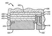
- FIGS. 4 a -4 gillustrate one embodiment of a semiconductor device 400 according to the present invention at various stages during a fabrication process.
- the device 400is shown as an individual device during a fabrication process. It is understood, however, that semiconductor devices are typically fabricated at the wafer level with the individual devices singulated from the wafer in a subsequent processing step. Nonetheless, the process described herein can also be used for fabricating individual devices. It is also understood that although the fabrication steps are shown in a particular order below, the device 400 can be fabricated by steps in a different order and can include additional or fewer steps.
- FIG. 4 ashows epitaxial layers grown on a substrate 402 .
- the oppositely doped n-type and p-type layers 404 , 406 and active region 408 interposed between themare typically formed on a substrate 402 using known fabrication methods and devices, such as epitaxial growth in a metalorganic chemical vapor deposition (MOCVD) reactor.
- MOCVDmetalorganic chemical vapor deposition
- the semiconductor layers 404 , 406 , 408can be from several different material systems with a preferred system being the Group-III nitride system.
- Group-III nitridesrefer to those semiconductor compounds formed between nitrogen and the elements in the Group III of the periodic table, usually aluminum (Al), gallium (Ga), and indium (In).
- the termalso refers to ternary and quaternary compounds such as aluminum gallium nitride (AlGaN) and aluminum indium gallium nitride (AlInGaN).
- the active region 408can comprise single quantum well (SQW), multiple quantum well (MQW), double heterostructure or super lattice structures.
- the n- and p-type layers 404 , 406are gallium nitride (GaN) and the active region 408 is a multiquantum well (MQW) structure having alternating layers of GaN and InGaN.
- the n- and p-type layers 404 , 406can be or may include Group III-nitride materials such as AlGaN or AlInGaN.
- the substrate 402can be made of many materials such as sapphire, silicon carbide, aluminum nitride (AlN), GaN, with a suitable substrate being a 4H polytype of silicon carbide, although other silicon carbide polytypes can also be used including 3C, 6H and 15R polytypes.
- Silicon carbide (SiC)has certain advantages, such as a closer crystal lattice match to Group III nitrides than sapphire and results in Group III nitride films of higher quality.
- SiC substratesare available from Cree Research, Inc., of Durham, N.C. and methods for producing them are set forth in the scientific literature as well as in U.S. Pat. Nos. Re. 34,861; 4,946,547; and 5,200,022.
- n-type or p-type layersmay be preferable to grow the n-type layers first. This is the case for several reasons that are known in the art.
- One reason for growing the n-type layers firstis that they are grown at higher temperatures than the p-type layers; n-type layers are grown at temperatures around 1100° C., and p-type layers are grown around 900° C.
- the dopant material(often magnesium) can diffuse into adjacent layers, reducing the quality of the layer.
- n-type layershave been grown on the substrate, subsequent p-type layers can be grown at lower temperatures that do not substantially affect the n-type layers that have already been formed.
- Another reason for growing n-type layers firstis that layers grown on the substrate must be grown for longer periods of time to overcome the lattice mismatch at the substrate interface. Layers grown longer are grown thicker. Because p-type layers are more light-absorbent than n-type layers, it is desirable to have a thicker n-type layer so that less emitted light is absorbed.
- n-type layer 404is shown grown first on substrate 402 . Then, the active region 408 is formed on the n-type layer 404 , and the p-type layer 406 is formed on the active region 408 . The device is shown flipped upside down with the latter grown layers on bottom in FIG. 4 a .
- the active region 408can comprise single quantum well (SQW), multiple quantum well (MQW), double heterostructure or superlattice structures. It is understood that additional layers and elements can also be included in the device 400 , including but not limited to buffer, nucleation, contact and current spreading layers and superlattice structures on one or both sides of the active region 408 as well as light extraction layers and elements.
- a portion of the n-type layer 404is exposed using a known etching process, chlorine reactive ion etching for example, or another process that is known in the art.
- a conductive n-pad 410is formed on an exposed portion of the n-type layer 404 which is shown extending laterally beyond the edges of the active region 408 and the p-type layer 406 .
- a p-pad 412is formed on the exposed surface of the p-type layer 406 .
- the n-pad 410 and p-pad 412function as contacts that will facilitate an electrical connection between the semiconductor layers 404 , 406 and leads that will be added at a later stage in the fabrication process as discussed below.
- the pads 410 , 412may comprise a conductive metal material such as gold, silver or copper, for example.
- p-pad 412may be formed from a reflective material, such as aluminum, silver, gold, rhodium, platinum, palladium, gold tin or combinations thereof. These reflective materials can be deposited on the surface of p-type layer 406 using conventional methods, such as sputtering. Using a reflective material to form the p-pad 412 may increase the light extraction efficiency of the device 400 by redirecting light emitted from the active region 408 that might otherwise be absorbed by layers and elements below the p-pad, such as spacer elements or electrodes, both of which are discussed in detail below.
- a reflective materialsuch as aluminum, silver, gold, rhodium, platinum, palladium, gold tin or combinations thereof.
- a layer of spacing material 414is deposited on the device, coating the n-pad 410 , the p-pad 412 , and any exposed portion of bottom surface of the n-type layer 404 .
- the spacing materialshould comprise an insulating material.
- a selectively patterned dielectrice.g., SiN or SiO 2
- polymere.g., BCB or silicone
- the spacing materialis then patterned using a known process to expose a portion of both the n-pad 410 and the p-pad 412 , leaving some of the spacing material 414 to remain, as shown in FIG. 4 c .
- the remaining structuresfunction as spacing elements 416 .
- the spacing elements 416are arranged to electrically isolate the n- and p-electrodes from each other. These electrodes are not formed until a later stage of fabrication (shown in FIG. 4 g ).
- the spacing elementscan take various shapes and vary in dimension so long as at least a portion of both the n-pad 410 and the p-pad 412 are exposed for electrical connection.
- a conductive metal layer 418is deposited on the bottom side of the device 400 , covering the spacing elements 416 and the exposed portions of both the n-pad 410 and the p-pad 412 .
- the thick conductive metal layer 418may be applied to the device 400 by different known methods such as electroplating, for example.
- the conductive metal layer 418should be thick enough to provide mechanical support to the finished device.
- a layershould be at least 20 ⁇ m thick, with a preferred thickness in the range of 50-400 ⁇ m. Planarization and polishing steps may be employed to insure the final surface of the thick conductive metal layer is smooth and planar. Although several different metals and metal alloys can be used, copper (Cu) is a preferred material.
- the substrate 402may be removed and the top surface of the n-type layer 404 may be modified as shown in FIG. 4 e .
- the substrate 402can be removed by several known methods, including wet and dry etching processes, laser ablation, mechanical grinding, or a grinding/etching combination process. It is understood, however, that in other embodiments according to the present invention, part of the substrate 402 can remain on the n-type layer 404 , and that the substrate 402 can be shaped or textured to enhance light extraction.
- the n-type layer 404may be processed in several different ways. It may be desirable to modify (e.g., texture or roughen) various surfaces on or within the device to provide a multitude of angled surfaces and increase light extraction.
- a modified surfaceimproves light extraction by providing a varying surface that allows light that would otherwise be trapped in the LED, by total internal reflection (TIR), to escape as emitted light.
- TIRtotal internal reflection
- the variations in the modified surfaceincrease the chances that the light will reach an emission surface within the critical angle (as defined by Snell's law) and will be emitted. For light that does not escape through the modified surface, the variations of the modified surface reflect the light at different angles, increasing the chances that the light will escape on the next pass after reflecting off the p-pad.
- a semiconductor surfacemay be modified.
- the surfacemay have portions removed by processes such as etching, grinding or ablation. It is also possible to add material, such as nanoparticles or light extraction elements for example, to the surface in order to give it a non-uniform texture. Adding light extraction structures to a surface within the device is discussed at length in U.S. Pat. No. 6,657,236 assigned to Cree, Inc. A combination of any of these processes may also achieve the desired surface modifications.
- modified surface 420is shown as a surface of the n-type layer 404 opposite the active region 408 in FIG. 4 e , it is understood that many different surfaces within the device 400 may be modified to achieve the same extraction enhancing effect. Also, device 400 might not have any modified surfaces.
- a portion of the thick metal layer 418is then etched away using a known method such that two separate metal electrodes are defined as shown in FIG. 4 f .
- An n-electrode 422is formed, contacting the n-pad and providing an electrical path to the n-type layer 404 .
- a p-electrode 424contacts the p-pad and provides an electrical path to the p-type layer 406 .
- the electrodes 422 , 424should be electrically isolated from one another and from the active region 408 . In this particular embodiment isolation is achieved with the spacer elements 416 as discussed above.
- the bottom surfaces of the electrodes 422 , 424function as leads and are easily accessible from the bottom of the device 400 .
- noncontiguous p-electrode and n-electrodesmay be formed in a single deposition step by using known methods such as thick patterned photoresist.
- Different embodiments of the devicescan have electrodes arranged in different ways according to the present invention.
- the electrodes 422 , 424are shown extending to the same level at the bottom of the device, which facilitates mounting the device to structure, such as a submount or printed circuit board (PCB), where the mounting points are at the same level.
- the electrodescan extend to different levels so that the device can be mounted to a structure having mounting points at different levels.
- the p-type electrode 424can extend further from the device 400 than the n-type electrode such that their leads are at different levels.
- a phosphor layer 426can be formed on the top surface of the n-type layer 404 .
- the phosphor layer 426may also cover other surfaces such as the sides of the device.
- Phosphor layersare known in the art as a wavelength conversion mechanism and may be deposited using known methods.
- the phosphor layer 426may comprise more than one phosphor as well as light scattering particles. By down-converting a portion of the light emitted from the active region 408 , the device emission spectrum can be shifted to yield a color of light that is different from that which is emitted internally from the active region 408 .
- a binder(not shown), for example silicone, may be used to bind the phosphor layer 426 to the n-type layer 404 .
- the phosphor layer 426may be provided in a number of known binders such as, for example, epoxy, silicone or low-temperature glass.
- the phosphor layer 426may be formed by, for example, dispensing, screen printing, jet printing, molding, spin coating or by mounting a previously made component.
- the new arrangementprovides a semiconductor device that has two bottom-side contacts for biasing the light-emitting semiconductor layers. Thus, the device does not require a wire bond or other such connection means.
- the new arrangementallows for a phosphor layer, an encapsulant, and other elements or features that are typically added at the packaging level to be added at the wafer level of fabrication.
- FIG. 5depicts another embodiment of a semiconductor device 500 according to the claims of the present invention.
- the device 500 and the device 400 shown in FIG. 4 gfunction similarly and contain several common elements that are denoted by using the same reference numbers.
- the n-type layer 502 of device 500is disposed over the active region 408 such that the edges of all the semiconductor layers 502 , 406 , 408 are substantially flush with each other.
- the n-type layer 502has been removed from the area above the n-electrode 422 using a known process such as etching.
- a lateral connectionis established using a stairstep-shaped n-pad 504 that is deposited using a known method. Because all of the semiconductor layers 502 , 406 , 408 are located entirely above the p-electrode 424 , the configuration may exhibit increased structural stability.
- the n-electrode 422 and the spacer elements 416 that are shown on the right side of FIG. 5may extend up to a point such that their top surfaces are flush with the top surface of the n-type layer 502 .
- the n-padwould be flat and extend across the flush top surfaces forming a connection between the n-electrode 422 and the n-type layer 502 .
- the embodiment shown in FIG. 5features an n-type layer 502 which is disposed on the top side of the active region 408 , it may be desirable to switch the orientation of the layers.
- the p-type layer 602is on the top side of the active region 606 with the n-type layer 604 disposed on the bottom side of the active region 606 .
- the device 600contains many common elements and functions similarly as the embodiment shown in FIG. 4 g . In this configuration, a thin semi-transparent stairstep-shaped p-pad might be particularly advantageous. Current does not spread as well throughout p-type layers as it does throughout n-type layers.
- the stairstep-shaped p-pad 608forms a good ohmic contact with substantially the entire top surface of the p-type layer 606 .
- the stairstep-shaped p-pad 608provides a connection between the p-electrode 610 and p-type layer 602 while effectively spreading current across the length of the p-type layer 602 and while allowing light to be emitted out of the top surface of the device 600 .
- the n-pad 612is a reflective element and provides a connection between the n-electrode 614 and the n-type layer 604 . Both electrodes 610 , 614 have leads with access points on the bottom surface of the device 600 .
- FIG. 7shows another embodiment of a semiconductor device 700 according to the claims of the present invention.
- An active region 702is interposed between a p-type layer 704 and an n-type layer 706 .
- the semiconductor layers 702 , 704 , 706are formed on a substrate 707 made from a material such as SiC. In this embodiment at least part of the growth substrate 707 remains as part of the device 700 , adding structural stability.
- a p-electrode 708is disposed along at least one of the outside edges of the device 700 .
- a current spreading layer 710is formed on top of the p-type layer 704 .
- the current spreading layer 710should be in good ohmic contact with the p-type layer 704 to ensure that current is distributed over substantially the entire surface of the p-type layer 704 so that light is emitted out of the top surface of the device 700 .
- the current spreading layer 710may comprise transparent conductive oxides, such as indium tin oxide (ITO), for example.
- ITOindium tin oxide
- the p-electrode 708makes contact with the current spreading layer 710 along its top lateral surface.
- An n-electrode 712is arranged along one of the outside edges of the device 700 opposite the p-electrode 708 .
- the n-electrode 712contacts the n-type layer 706 on its bottom surface.
- Both electrodes 708 , 712have leads that are accessible from the bottom side of the device 700 .
- Spacer element 714isolates p-electrode 708 from the n-type layer 706 and the substrate 707 .
- Spacer element 716isolates n-electrode 712 from the substrate 707 .
- the spacer elements 714 , 716may comprise a high resistance or insulating dielectric material such as SiO 2 or silicon nitride, for example.
- a phosphor layer 718can be formed on the top surface of the current spreading layer 710 .
- the phosphor layermay cover other surfaces as well, such as the side surfaces of the device 700 .
- the phosphor layer 718performs a wavelength conversion function and may be provided in a number of known binders such as, for example, epoxy, silicone or low-temperature glass.
- the phosphor layer 718may be formed by, for example, dispensing, screen printing, jet printing, molding, spin coating, or by mounting a previously made component.
- a reflective layer 720may be added to the device 700 to improve the external quantum efficiency.
- the reflective layer 720is disposed on the bottom side of the substrate 707 .
- Light emitted from the active region 702is redirected by the reflective layer 720 towards the primary emission surface at the top of the device 700 .
- the reflective layer 720should comprise a material with high reflectivity such as aluminum, for example.
- the reflective layer 720may also be disposed internally within the device 700 .
- the substrate 707may comprise a conductive material such as n-type SiC, allowing for an electrical connection to the bottom semiconductor layer and obviating the need for the n-electrode.
- n-electrode 712 and spacer element 716would be unnecessary and reflective layer 720 and substrate 707 would extend such that their right edge would be flush with or even beyond the right edges of the semiconductor layers 702 , 704 , 706 .
- the electrical connection to the n-type layer 706would run from the bottom surface of the device 700 up through the conductive substrate and reflective layer up to the layer 706 .
- FIG. 8illustrates another embodiment of a semiconductor device 800 according to the claims in the present invention.
- the device 800shares several common elements with and functions similarly as device 700 shown in FIG. 7 .
- a portion of the substrate 707has been removed using a known process, exposing some of the surface of the n-type layer 706 .
- Part of the substrate 707may remain for structural support as shown; however, in other embodiments all of the substrate 707 may be removed.
- the exposed n-type layer 706may be modified as discussed in detail above.
- the modified surface 802combats TIR by scattering the light, improving the light extraction.
- a reflective layer 804is formed on the bottom surface of the n-type layer 706 .
- a preferred material for the reflective layer 804is aluminum, but other materials may be used.
- the opening created by the removal of the substrate 707can be filled to create a base element 806 comprising a material such as polyimide, for example.
- Base element 806adds structural support to the device 800 .
- the base elementmay comprise a conductive material such as aluminum or copper, for example, allowing for an electrical connection to the bottom semiconductor layer and obviating the need for the n-electrode.
- n-electrode 712 and spacer element 716would be unnecessary and reflective layer 804 and base element 806 would extend such that their right edge would be flush with or even beyond the right edges of the semiconductor layers 702 , 704 , 706 .
- the electrical connection to the n-type layer 706would run from the bottom surface of the device 700 up through the conductive base element and reflective layer up to the layer 706 .
- FIG. 9Another embodiment of a semiconductor device 900 according to the claims of the present invention is shown in FIG. 9 .
- the device 900shares common elements with and functions similarly as the device 700 .
- the device 900can be fabricated using a flip-chip process that is known in the art.
- the active region 902is interposed between n-type layer 904 and p-type layer 906 , where the n-type layer is arranged on the top side of the active region with respect to the orientation shown in FIG. 9 .
- the n-electrode 908is disposed using a known process vertically along the outer edge of the device 900 , providing an electrical connection from a lead accessible from the bottom surface of the device 900 to the n-type layer 904 .
- a current spreading layer 910is shown on the top surface of the n-type layer 904 .
- the current spreading layer 910may be disposed on only a portion of the n-type layer or even omitted as current typically spreads very well through n-type materials.
- a thin semi-transparent current spreading layer 912is disposed on the p-type layer 906 .
- a p-electrode 914extends vertically down from the current spreading layer 912 along the outside of the device 900 such that a lead is accessible from the bottom side of the device 900 . As discussed above, because the leads of the electrodes 908 , 914 are accessible from the bottom side of the device 900 , there is no need for a wire bond to connect the device 900 to an external voltage source.
- a reflective layer 916is disposed on the bottom surface of the current spreading layer 912 .
- the reflective layer 916may comprise a material that is both reflective and conductive such as mixture of platinum and silver, for example.
- the reflective layermay comprise a multilayer stack of dielectric materials such as SiO 2 /Ta 2 O 5 , for example, that comprise a distributed Bragg reflector.
- a base element 918 that provides structural supportis formed below the reflective layer 916 .
- the base element 918may comprise a thermally conductive material such as copper, for example, and is disposed on the bottom of the reflective layer 916 between the spacer elements 714 , 716 .
- the modified surface 920 of the n-type layer 904enhances the light extraction of the device 900 as discussed above.
- a phosphor layer 718is disposed over the current spreading layer 910 .
- the phosphor layer 718covers all or part of the spreading layer 910 .
- the phosphor layer 718may also cover the entire top side of the device as well as the sides of the device as shown in FIG. 7 .
- FIG. 10illustrates another embodiment of a semiconductor device 1000 .
- the device 1000shares several common elements with device 900 and functions in a similar fashion.
- the conductive base element 1002functions as a p-electrode.
- a reflective layer 1004is disposed on the bottom surface of the p-type layer to make an ohmic contact to the p-type layer and to redirect light emitted from the active region 902 towards the primary emission surface of the device 1000 . If both the base element 1002 and the reflective layer 1004 are conductive materials, there is no need for a current spreading layer or a separate electrode to contact the p-type layer 906 .
- the electrical connectionmay be made from the bottom side of the device anywhere along the exposed surface of the conductive base element 1002 .
- the conductive base element 1002may comprise a metal such as copper, nickel or gold, for example, or a doped semiconductor such as SiC or Si, for example.
- FIG. 11shows an embodiment of a semiconductor device 1100 .
- the device 1100functions similarly as the device 400 as shown in FIG. 4 g and shares many common elements.
- the device 1100has the added advantage of scalability in two dimensions.
- An active region 1102is interposed between an n-type layer 1104 and a p-type layer 1106 .
- the n-type layer 1104is contacted in several locations by multiple n-pads 1108 .
- the p-type layer 1106is contacted in several locations by multiple p-pads 1110 .
- Multiple n-electrodes 1112 having leads accessible from a surface of the device 1100 opposite the primary emission surface 1114provide multiple electrical paths to the n-type layer 1104 through the n-pads 1108 .
- Electrodes 1116also opposite the primary emission surface 1114 , provide electrical paths to the p-type layer 1106 . Because the growth substrate has been removed, the electrodes 1112 , 1116 must be thick enough to provide primary mechanical support for the device.
- the n-pads 1108can be much smaller than the p-pads 1110 as shown in FIG. 11 .
- viascan be used to expose the n-type layer.
- the viascan be formed by etching or other means through the p-type layer 1106 and the active region 1102 to expose the n-type layer 1104 .
- the n-pads 1108 and p-pads 1110can then be deposited, followed by the n-electrodes 1112 and p-electrodes 1116 using processes similar to those discussed above relating to FIGS. 4 a -4 g .
- a surface of the n-type layer 1104may be modified as shown to improve light extraction.
- a phosphor layer(not shown) may be deposited over all the surfaces of the device 1100 or only the top primary emission surface of the device 1100 .
- FIG. 11allows for scalability by providing for good current spreading across substantially all of the n-type and p-type layers 1104 , 1106 regardless of the size of the device.
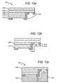
- FIGS. 12 a - cillustrate an embodiment of a semiconductor device 1200 in various steps of production.
- the device 1200is similar to device 400 shown in FIG. 4 g and shares many common elements.
- An n-type layer 1204 and p-type layer 1206are grown on a substrate 1202 .
- the p-pad 1212is deposited.
- a spacer layer 1216is then deposited and patterned by etching or other means to expose portions of the p-pad 1212 and the n-type layer 1204 .
- an n-pad 1210is deposited over the spacer layer 1216 .
- the n-pad 1210partially overlaps the p-pad 1212 , although they are electrically isolated from one another by the spacer layer 1216 as shown.
- the overlapping n-pad 1210provides a larger surface area for connection, allowing for a larger n-electrode 1210 .
- the large n-electrode 1210provides for an easier connection when packaging the device 1200 without sacrificing the size of the active layer 1208 .
- the n- and p-electrodes 1222 , 1224are formed similarly as discussed above.
- the growth substrate 1202is removed, and the surface of the n-type layer 1204 can be modified as shown. Additionally, a phosphor layer (not shown) can be deposited over all the surfaces of the device 1200 or only over the top primary emission surface.
- FIG. 13shows an embodiment of a semiconductor device 1300 .
- the device 1300combines some of the features from the embodiments shown in FIG. 11 and FIG. 12 .
- the device 1300is scalable similar to the device 1100 shown in FIG. 11 .
- An n-type layer 1304 , an active region 1306 , and a p-type layer 1306are all grown on a growth substrate that is subsequently removed. Portions of the p-type layer 1306 and the active region 1308 are removed by etching or another process to reveal portions of the n-type layer 1304 .
- the removed portionsdefine multiple vias through which a connection to the n-type layer 1304 can be made.
- the p-pad 1312is then deposited with holes that correspond to the vias, allowing access to the n-type layer 1304 .
- a spacer layer 1316is then deposited and patterned to expose the p-pad 1312 in some regions and the n-type layer 1304 inside the vias.
- An n-pad 1310is then deposited, contacting the n-type layer 1304 in the vias.
- the n-pad 1310contacts the n-type layer 1304 in multiple locations and is interconnected throughout the device 1300 . In order to provide the interconnectivity, part of the n-pad 1310 overlaps the p-pad 1312 .
- the spacer layer 1316keeps the n- and p-pads 1310 , 1312 electrically isolated.
- the n- and p-electrodes 1318 , 1320are then formed and the growth substrate removed as discussed above. In another embodiment, the growth substrate may be removed earlier in the fabrication process.
- the device 1300allows for the size and geometry of the electrodes 1318 , 1320 to be tailored independently of the n-pad 1310 and the vias through the active layer 1308 . This can potentially make packaging the device 1300 simpler and more cost effective. Furthermore, because of the interconnected n-pad 1310 and the large p-pad 1312 , current spreading in the semiconductor layers is improved which leads to increased light extraction over the entire active region 1308 .
Landscapes
- Engineering & Computer Science (AREA)
- Power Engineering (AREA)
- Microelectronics & Electronic Packaging (AREA)
- Physics & Mathematics (AREA)
- Condensed Matter Physics & Semiconductors (AREA)
- General Physics & Mathematics (AREA)
- Computer Hardware Design (AREA)
- Led Devices (AREA)
- Led Device Packages (AREA)
Abstract
Description
Claims (30)
Priority Applications (14)
| Application Number | Priority Date | Filing Date | Title |
|---|---|---|---|
| US11/985,410US9634191B2 (en) | 2007-11-14 | 2007-11-14 | Wire bond free wafer level LED |
| EP08848823AEP2220692A2 (en) | 2007-11-14 | 2008-09-11 | Wire bond free wafer level led |
| PCT/US2008/010703WO2009064330A2 (en) | 2007-11-14 | 2008-09-11 | Wire bond free wafer level led |
| JP2010534010AJP5433583B2 (en) | 2007-11-14 | 2008-09-11 | Wafer stage LED without wire bonding |
| KR1020107013082AKR101503558B1 (en) | 2007-11-14 | 2008-09-11 | Wire bond free wafer level led |
| CN2008801245954ACN101933166B (en) | 2007-11-14 | 2008-09-11 | Wafer-Level Light-Emitting Diodes Without Wire Bonding |
| US12/463,709US8368100B2 (en) | 2007-11-14 | 2009-05-11 | Semiconductor light emitting diodes having reflective structures and methods of fabricating same |
| US12/905,995US8536584B2 (en) | 2007-11-14 | 2010-10-15 | High voltage wire bond free LEDS |
| US13/023,788US8643039B2 (en) | 2007-11-14 | 2011-02-09 | Lateral semiconductor Light Emitting Diodes having large area contacts |
| US13/112,502US9660153B2 (en) | 2007-11-14 | 2011-05-20 | Gap engineering for flip-chip mounted horizontal LEDs |
| JP2012212830AJP5767184B2 (en) | 2007-11-14 | 2012-09-26 | Wafer stage LED without wire bonding |
| US13/909,927US9461201B2 (en) | 2007-11-14 | 2013-06-04 | Light emitting diode dielectric mirror |
| US14/159,209US9397266B2 (en) | 2007-11-14 | 2014-01-20 | Lateral semiconductor light emitting diodes having large area contacts |
| US15/449,510US10199360B2 (en) | 2007-11-14 | 2017-03-03 | Wire bond free wafer level LED |
Applications Claiming Priority (1)
| Application Number | Priority Date | Filing Date | Title |
|---|---|---|---|
| US11/985,410US9634191B2 (en) | 2007-11-14 | 2007-11-14 | Wire bond free wafer level LED |
Related Parent Applications (1)
| Application Number | Title | Priority Date | Filing Date |
|---|---|---|---|
| US12/329,713Continuation-In-PartUS8575633B2 (en) | 2007-11-14 | 2008-12-08 | Light emitting diode with improved light extraction |
Related Child Applications (3)
| Application Number | Title | Priority Date | Filing Date |
|---|---|---|---|
| US12/418,816Continuation-In-PartUS7985970B2 (en) | 2007-11-14 | 2009-04-06 | High voltage low current surface-emitting LED |
| US12/463,709Continuation-In-PartUS8368100B2 (en) | 2007-11-14 | 2009-05-11 | Semiconductor light emitting diodes having reflective structures and methods of fabricating same |
| US15/449,510ContinuationUS10199360B2 (en) | 2007-11-14 | 2017-03-03 | Wire bond free wafer level LED |
Publications (2)
| Publication Number | Publication Date |
|---|---|
| US20090121241A1 US20090121241A1 (en) | 2009-05-14 |
| US9634191B2true US9634191B2 (en) | 2017-04-25 |
Family
ID=40622883
Family Applications (2)
| Application Number | Title | Priority Date | Filing Date |
|---|---|---|---|
| US11/985,410ActiveUS9634191B2 (en) | 2007-11-14 | 2007-11-14 | Wire bond free wafer level LED |
| US15/449,510ActiveUS10199360B2 (en) | 2007-11-14 | 2017-03-03 | Wire bond free wafer level LED |
Family Applications After (1)
| Application Number | Title | Priority Date | Filing Date |
|---|---|---|---|
| US15/449,510ActiveUS10199360B2 (en) | 2007-11-14 | 2017-03-03 | Wire bond free wafer level LED |
Country Status (6)
| Country | Link |
|---|---|
| US (2) | US9634191B2 (en) |
| EP (1) | EP2220692A2 (en) |
| JP (2) | JP5433583B2 (en) |
| KR (1) | KR101503558B1 (en) |
| CN (1) | CN101933166B (en) |
| WO (1) | WO2009064330A2 (en) |
Cited By (9)
| Publication number | Priority date | Publication date | Assignee | Title |
|---|---|---|---|---|
| US20150371974A1 (en)* | 2014-06-18 | 2015-12-24 | X-Celeprint Limited | Micro assembled led displays and lighting elements |
| US20160005930A1 (en)* | 2013-03-26 | 2016-01-07 | Osram Opto Semiconductors Gmbh | Optoelectronic semiconductor chip encapsulated with an ald layer and corresponding method of production |
| US20160172545A1 (en)* | 2013-07-16 | 2016-06-16 | Osram Opto Semiconductors Gmbh | Optoelectronic Semiconductor Chip |
| US20170082873A1 (en)* | 2014-03-25 | 2017-03-23 | Brown University | High frequency light emission device |
| US20180013042A1 (en)* | 2015-08-26 | 2018-01-11 | Samsung Electronics Co., Ltd. | Light-emitting diode (led), led package and apparatus including the same |
| US10692844B2 (en) | 2016-04-05 | 2020-06-23 | X Display Company Technology Limited | Micro-transfer printed LED and color filter structures |
| US10782002B2 (en) | 2016-10-28 | 2020-09-22 | X Display Company Technology Limited | LED optical components |
| US11316077B2 (en)* | 2017-01-30 | 2022-04-26 | Osram Oled Gmbh | Radiation-emitting device |
| US20220336712A1 (en)* | 2019-06-21 | 2022-10-20 | Lg Electronics Inc. | Display device using micro led, and method for manufacturing same |
Families Citing this family (111)
| Publication number | Priority date | Publication date | Assignee | Title |
|---|---|---|---|---|
| JP2536797Y2 (en) | 1992-12-25 | 1997-05-28 | 武蔵精密工業株式会社 | Closed forging die equipment |
| US7067849B2 (en) | 2001-07-17 | 2006-06-27 | Lg Electronics Inc. | Diode having high brightness and method thereof |
| US6949395B2 (en) | 2001-10-22 | 2005-09-27 | Oriol, Inc. | Method of making diode having reflective layer |
| US7148520B2 (en) | 2001-10-26 | 2006-12-12 | Lg Electronics Inc. | Diode having vertical structure and method of manufacturing the same |
| JP5346443B2 (en)* | 2007-04-16 | 2013-11-20 | ローム株式会社 | Semiconductor light emitting device and manufacturing method thereof |
| US9484499B2 (en) | 2007-04-20 | 2016-11-01 | Cree, Inc. | Transparent ohmic contacts on light emitting diodes with carrier substrates |
| US8368114B2 (en)* | 2007-05-18 | 2013-02-05 | Chiuchung Yang | Flip chip LED die and array thereof |
| US9634191B2 (en) | 2007-11-14 | 2017-04-25 | Cree, Inc. | Wire bond free wafer level LED |
| US7915629B2 (en) | 2008-12-08 | 2011-03-29 | Cree, Inc. | Composite high reflectivity layer |
| US8536584B2 (en)* | 2007-11-14 | 2013-09-17 | Cree, Inc. | High voltage wire bond free LEDS |
| US8368100B2 (en)* | 2007-11-14 | 2013-02-05 | Cree, Inc. | Semiconductor light emitting diodes having reflective structures and methods of fabricating same |
| US9461201B2 (en) | 2007-11-14 | 2016-10-04 | Cree, Inc. | Light emitting diode dielectric mirror |
| US8575633B2 (en)* | 2008-12-08 | 2013-11-05 | Cree, Inc. | Light emitting diode with improved light extraction |
| US8637883B2 (en)* | 2008-03-19 | 2014-01-28 | Cree, Inc. | Low index spacer layer in LED devices |
| US10147843B2 (en)* | 2008-07-24 | 2018-12-04 | Lumileds Llc | Semiconductor light emitting device including a window layer and a light-directing structure |
| US8384115B2 (en)* | 2008-08-01 | 2013-02-26 | Cree, Inc. | Bond pad design for enhancing light extraction from LED chips |
| US9293656B2 (en)* | 2012-11-02 | 2016-03-22 | Epistar Corporation | Light emitting device |
| US8716723B2 (en)* | 2008-08-18 | 2014-05-06 | Tsmc Solid State Lighting Ltd. | Reflective layer between light-emitting diodes |
| US8008683B2 (en)* | 2008-10-22 | 2011-08-30 | Samsung Led Co., Ltd. | Semiconductor light emitting device |
| US8017963B2 (en)* | 2008-12-08 | 2011-09-13 | Cree, Inc. | Light emitting diode with a dielectric mirror having a lateral configuration |
| JP4724222B2 (en)* | 2008-12-12 | 2011-07-13 | 株式会社東芝 | Method for manufacturing light emitting device |
| US8323996B2 (en)* | 2009-03-02 | 2012-12-04 | Infineon Technologies Ag | Semiconductor device |
| US8529102B2 (en) | 2009-04-06 | 2013-09-10 | Cree, Inc. | Reflector system for lighting device |
| US8476668B2 (en)* | 2009-04-06 | 2013-07-02 | Cree, Inc. | High voltage low current surface emitting LED |
| US9093293B2 (en) | 2009-04-06 | 2015-07-28 | Cree, Inc. | High voltage low current surface emitting light emitting diode |
| US8741715B2 (en)* | 2009-04-29 | 2014-06-03 | Cree, Inc. | Gate electrodes for millimeter-wave operation and methods of fabrication |
| KR101070974B1 (en) | 2009-07-28 | 2011-10-06 | 한국광기술원 | Wafer level light emitting diode package |
| JP2011071272A (en) | 2009-09-25 | 2011-04-07 | Toshiba Corp | Semiconductor light-emitting device and method for manufacturing the same |
| US9435493B2 (en) | 2009-10-27 | 2016-09-06 | Cree, Inc. | Hybrid reflector system for lighting device |
| JP5414579B2 (en)* | 2009-11-19 | 2014-02-12 | 株式会社東芝 | Semiconductor light emitting device |
| JP5349260B2 (en) | 2009-11-19 | 2013-11-20 | 株式会社東芝 | Semiconductor light emitting device and manufacturing method thereof |
| JP5101645B2 (en)* | 2010-02-24 | 2012-12-19 | 株式会社東芝 | Semiconductor light emitting device |
| JP5202559B2 (en) | 2010-03-09 | 2013-06-05 | 株式会社東芝 | Semiconductor light emitting device and manufacturing method thereof |
| JP5197654B2 (en)* | 2010-03-09 | 2013-05-15 | 株式会社東芝 | Semiconductor light emitting device and manufacturing method thereof |
| US9105824B2 (en) | 2010-04-09 | 2015-08-11 | Cree, Inc. | High reflective board or substrate for LEDs |
| JP5356312B2 (en) | 2010-05-24 | 2013-12-04 | 株式会社東芝 | Semiconductor light emitting device |
| JP5426481B2 (en)* | 2010-05-26 | 2014-02-26 | 株式会社東芝 | Light emitting device |
| JP5390472B2 (en) | 2010-06-03 | 2014-01-15 | 株式会社東芝 | Semiconductor light emitting device and manufacturing method thereof |
| JP5414627B2 (en)* | 2010-06-07 | 2014-02-12 | 株式会社東芝 | Semiconductor light emitting device and manufacturing method thereof |
| JP5449039B2 (en)* | 2010-06-07 | 2014-03-19 | 株式会社東芝 | Semiconductor light emitting device and manufacturing method thereof |
| JP4875185B2 (en) | 2010-06-07 | 2012-02-15 | 株式会社東芝 | Optical semiconductor device |
| JP2011258673A (en)* | 2010-06-07 | 2011-12-22 | Toshiba Corp | Semiconductor light-emitting device and method of manufacturing the same |
| CN102280553A (en)* | 2010-06-10 | 2011-12-14 | 杨秋忠 | Flip-chip Light Emitting Diode (LED) crystal grain and crystal grain array thereof |
| DE102010025320B4 (en)* | 2010-06-28 | 2021-11-11 | OSRAM Opto Semiconductors Gesellschaft mit beschränkter Haftung | Optoelectronic component and method for its production |
| US8764224B2 (en) | 2010-08-12 | 2014-07-01 | Cree, Inc. | Luminaire with distributed LED sources |
| US8455882B2 (en) | 2010-10-15 | 2013-06-04 | Cree, Inc. | High efficiency LEDs |
| KR101739573B1 (en)* | 2010-10-28 | 2017-06-08 | 엘지이노텍 주식회사 | Light-emitting element |
| US8556469B2 (en) | 2010-12-06 | 2013-10-15 | Cree, Inc. | High efficiency total internal reflection optic for solid state lighting luminaires |
| TWI441361B (en)* | 2010-12-31 | 2014-06-11 | Interlight Optotech Corp | Light-emitting diode package structure and manufacturing method thereof |
| US9166126B2 (en)* | 2011-01-31 | 2015-10-20 | Cree, Inc. | Conformally coated light emitting devices and methods for providing the same |
| DE102011011139B4 (en)* | 2011-02-14 | 2023-01-19 | Osram Opto Semiconductors Gmbh | Method for producing at least one optoelectronic semiconductor component and optoelectronic semiconductor component |
| CN102683514B (en)* | 2011-03-06 | 2017-07-14 | 维亚甘有限公司 | LED package and manufacture method |
| DE102011014845B4 (en)* | 2011-03-23 | 2023-05-17 | OSRAM Opto Semiconductors Gesellschaft mit beschränkter Haftung | Semiconductor light-emitting device and method of manufacturing a semiconductor light-emitting device |
| US8680556B2 (en) | 2011-03-24 | 2014-03-25 | Cree, Inc. | Composite high reflectivity layer |
| TWI557953B (en)* | 2011-03-25 | 2016-11-11 | 鴻海精密工業股份有限公司 | Light-emitting diode flip-chip packaging structure and manufacturing method thereof |
| DE102011016302A1 (en) | 2011-04-07 | 2012-10-11 | Osram Opto Semiconductors Gmbh | Optoelectronic semiconductor chip |
| JP4989773B1 (en) | 2011-05-16 | 2012-08-01 | 株式会社東芝 | Semiconductor light emitting device |
| CN103548162B (en) | 2011-05-24 | 2016-11-09 | 皇家飞利浦有限公司 | P-N Separation Metal Filler for Flip Chip LED |
| US8686429B2 (en) | 2011-06-24 | 2014-04-01 | Cree, Inc. | LED structure with enhanced mirror reflectivity |
| US9728676B2 (en) | 2011-06-24 | 2017-08-08 | Cree, Inc. | High voltage monolithic LED chip |
| US10243121B2 (en) | 2011-06-24 | 2019-03-26 | Cree, Inc. | High voltage monolithic LED chip with improved reliability |
| CN102231421B (en)* | 2011-07-15 | 2013-01-23 | 中国科学院半导体研究所 | Light-emitting diode package structure manufacturing method |
| TWI515923B (en) | 2011-08-30 | 2016-01-01 | 晶元光電股份有限公司 | Light-emitting element |
| CN102339913B (en)* | 2011-09-30 | 2013-06-19 | 映瑞光电科技(上海)有限公司 | High-voltage LED (Light Emitting Diode) device and manufacturing method thereof |
| JP5364771B2 (en)* | 2011-10-17 | 2013-12-11 | 株式会社東芝 | Optical semiconductor device and manufacturing method thereof |
| KR101960366B1 (en)* | 2011-11-30 | 2019-03-21 | 엘지디스플레이 주식회사 | Semiconductor light emitting device and method for fabricating thereof |
| CN102646769B (en)* | 2012-03-30 | 2015-08-05 | 达亮电子(苏州)有限公司 | Light-emitting diode component, package structure for LED and manufacture method thereof |
| JP5715593B2 (en)* | 2012-04-25 | 2015-05-07 | 株式会社東芝 | Semiconductor light emitting device |
| CN102683534B (en)* | 2012-05-21 | 2015-02-25 | 厦门市三安光电科技有限公司 | Vertical type alternating-current light-emitting diode device and manufacturing method thereof |
| KR20130131852A (en)* | 2012-05-25 | 2013-12-04 | 엘지이노텍 주식회사 | Light-emitting device package and light-emitting module |
| KR101350159B1 (en)* | 2012-08-31 | 2014-02-13 | 한국광기술원 | Method for manufacturing white light emitting diode |
| DE102012218457A1 (en) | 2012-10-10 | 2014-04-10 | Osram Opto Semiconductors Gmbh | OPTOELECTRONIC COMPONENT AND METHOD FOR THE PRODUCTION THEREOF |
| KR20140092127A (en) | 2013-01-15 | 2014-07-23 | 삼성전자주식회사 | Semiconductor light emitting device and the method of the same |
| JP5426788B2 (en)* | 2013-01-31 | 2014-02-26 | 株式会社東芝 | Semiconductor light emitting device |
| JP5422760B2 (en)* | 2013-02-04 | 2014-02-19 | 株式会社東芝 | Semiconductor light emitting device |
| US9577172B2 (en)* | 2013-02-19 | 2017-02-21 | Koninklijke Philips N.V. | Light emitting die component formed by multilayer structures |
| US10295124B2 (en)* | 2013-02-27 | 2019-05-21 | Cree, Inc. | Light emitter packages and methods |
| JP6464147B2 (en)* | 2013-04-23 | 2019-02-06 | コーニンクレッカ フィリップス エヌ ヴェKoninklijke Philips N.V. | Light-emitting device side interconnect |
| WO2014184698A1 (en)* | 2013-05-14 | 2014-11-20 | Koninklijke Philips N.V. | Chip scale light emitting device package in molded leadframe |
| CN103311385B (en)* | 2013-05-21 | 2014-09-03 | 严敏 | Manufacturing method for semiconductor lighting DA (direct attach) eutectic chip |
| CN103531689B (en)* | 2013-05-24 | 2017-02-22 | 安徽三安光电有限公司 | Light emitting device |
| JP5837006B2 (en)* | 2013-07-16 | 2015-12-24 | 株式会社東芝 | Manufacturing method of optical semiconductor device |
| US9655253B2 (en)* | 2013-07-25 | 2017-05-16 | Cyntec Co., Ltd. | Method of fabrication of encapsulated electronics devices mounted on a redistribution layer |
| TWI615997B (en)* | 2013-08-06 | 2018-02-21 | 新世紀光電股份有限公司 | Light emitting diode structure |
| TWI604635B (en)* | 2014-01-07 | 2017-11-01 | 晶元光電股份有限公司 | Photoelectric element and method of manufacturing same |
| WO2015109580A1 (en)* | 2014-01-26 | 2015-07-30 | 上海瑞丰光电子有限公司 | Led encapsulation method |
| CN103811624A (en)* | 2014-02-18 | 2014-05-21 | 江苏新广联科技股份有限公司 | Encapsulation-free type UVLED (Ultraviolet Light-Emitting Diode) chip |
| KR102282141B1 (en)* | 2014-09-02 | 2021-07-28 | 삼성전자주식회사 | Semiconductor light emitting device |
| JP2016081562A (en) | 2014-10-09 | 2016-05-16 | ソニー株式会社 | Display apparatus, manufacturing method of the same, and electronic apparatus |
| US10254217B2 (en)* | 2014-11-19 | 2019-04-09 | Honeywell International, Inc. | Benzene sensors and associated methods |
| CN105679925B (en)* | 2014-11-21 | 2019-01-22 | 环视先进数字显示无锡有限公司 | The preparation method and chip of chip are directly welded in display with red LED |
| US10658546B2 (en) | 2015-01-21 | 2020-05-19 | Cree, Inc. | High efficiency LEDs and methods of manufacturing |
| TW201631808A (en)* | 2015-02-25 | 2016-09-01 | 隆達電子股份有限公司 | Light-emitting diode chip package |
| KR102405588B1 (en)* | 2015-03-11 | 2022-06-08 | 쑤저우 레킨 세미컨덕터 컴퍼니 리미티드 | Light emitting module |
| KR20160149363A (en) | 2015-06-17 | 2016-12-28 | 삼성전자주식회사 | Semiconductor light emitting device |
| JP6072192B2 (en)* | 2015-10-22 | 2017-02-01 | 株式会社東芝 | Semiconductor light emitting device, method for manufacturing semiconductor light emitting device, and method for manufacturing light emitting device |
| KR102481646B1 (en)* | 2015-11-12 | 2022-12-29 | 삼성전자주식회사 | Semiconductor light emitting device package |
| DE102015122641A1 (en) | 2015-12-22 | 2017-06-22 | Osram Opto Semiconductors Gmbh | Method for producing an optoelectronic component and optoelectronic component |
| DE102016106570A1 (en)* | 2016-04-11 | 2017-10-12 | Osram Opto Semiconductors Gmbh | A light-emitting semiconductor chip, light-emitting component and method for producing a light-emitting component |
| US10707277B2 (en) | 2016-10-04 | 2020-07-07 | Vuereal Inc. | Method of integrating functional tuning materials with micro devices and structures thereof |
| CN108574032B (en)* | 2017-03-10 | 2020-09-29 | 英属开曼群岛商錼创科技股份有限公司 | Light-emitting elements and display equipment |
| CN107195734A (en)* | 2017-05-17 | 2017-09-22 | 复旦大学 | A kind of micro LED preparation method |
| KR101873505B1 (en)* | 2017-08-30 | 2018-07-02 | 서울반도체 주식회사 | Wafer-level light emitting diode package |
| KR101930006B1 (en)* | 2017-09-26 | 2018-12-17 | 에피스타 코포레이션 | Light-emitting device |
| KR101895979B1 (en)* | 2018-03-28 | 2018-09-06 | 현영길 | Led luminaire integrated with led chip substrate |
| DE102018123930A1 (en)* | 2018-09-27 | 2020-04-02 | Osram Opto Semiconductors Gmbh | Optoelectronic semiconductor chip with first and second contact element and method for producing the optoelectronic semiconductor chip |
| CN109888076B (en)* | 2019-04-15 | 2023-11-24 | 江西乾照半导体科技有限公司 | Infrared LED chip with reflecting bowl cup and manufacturing method |
| KR20220012258A (en)* | 2019-05-23 | 2022-02-03 | 뷰리얼 인크. | Methods for integrating microdevices and their structures and functional coordination materials |
| EP4138148A1 (en) | 2019-06-06 | 2023-02-22 | Nuvoton Technology Corporation Japan | Semiconductor light-emitting element and semiconductor light-emitting device |
| WO2023033213A1 (en)* | 2021-09-06 | 2023-03-09 | 엘지전자 주식회사 | Semiconductor light-emitting element for display panel and display device comprising same |
| US20250228043A1 (en)* | 2024-01-09 | 2025-07-10 | Lumileds Llc | TRANSFERRABLE POLYCHROMIC microLEDs |
Citations (122)
| Publication number | Priority date | Publication date | Assignee | Title |
|---|---|---|---|---|
| WO1983000408A1 (en) | 1981-07-16 | 1983-02-03 | Joachim Sieg | Optoelectronic component |
| US4824767A (en) | 1986-01-09 | 1989-04-25 | Intel Corporation | Dual glass contact process |
| JPH0329532A (en) | 1989-06-27 | 1991-02-07 | Matsushita Electric Works Ltd | Power supply backup system for bus system |
| JPH04284620A (en) | 1991-03-13 | 1992-10-09 | Mitsubishi Electric Corp | Manufacture of semiconductor device |
| JPH08111544A (en) | 1994-10-07 | 1996-04-30 | Sharp Corp | Semiconductor light emitting device |
| US5563079A (en) | 1992-06-09 | 1996-10-08 | Goldstar Co., Ltd. | Method of making a field effect transistor |
| JPH098403A (en) | 1995-06-15 | 1997-01-10 | Nichia Chem Ind Ltd | Nitride semiconductor device manufacturing method and nitride semiconductor device |
| US5712175A (en) | 1994-09-12 | 1998-01-27 | Murata Manufacturing Co., Ltd. | Method of making semiconductor device having a schottky gate electrode |
| JPH10163535A (en) | 1996-11-27 | 1998-06-19 | Kasei Optonix Co Ltd | White light emitting element |
| US5803579A (en) | 1996-06-13 | 1998-09-08 | Gentex Corporation | Illuminator assembly incorporating light emitting diodes |
| US5959316A (en) | 1998-09-01 | 1999-09-28 | Hewlett-Packard Company | Multiple encapsulation of phosphor-LED devices |
| JP2000311704A (en) | 1999-04-27 | 2000-11-07 | Toshiba Battery Co Ltd | Sealed nickel hydrogen secondary battery |
| US6212213B1 (en) | 1999-01-29 | 2001-04-03 | Agilent Technologies, Inc. | Projector light source utilizing a solid state green light source |
| US6234648B1 (en) | 1998-09-28 | 2001-05-22 | U.S. Philips Corporation | Lighting system |
| JP2001308380A (en) | 2000-04-19 | 2001-11-02 | Seiwa Electric Mfg Co Ltd | Gallium nitride semiconductor light-emitting element |
| US6375340B1 (en) | 1999-07-08 | 2002-04-23 | Patent-Treuhand-Gesellschaft Fuer Elektrische Gluehlampen Mbh | Led component group with heat dissipating support |
| US6395572B1 (en) | 1999-04-15 | 2002-05-28 | Rohm Co, Ltd. | Method of producing semiconductor light-emitting element |
| KR200277135Y1 (en) | 2002-03-04 | 2002-05-30 | 주식회사 토우그린 | Laser fog light |
| US20020125485A1 (en)* | 1999-12-22 | 2002-09-12 | Lumileds Lighting U.S. Llc | Semiconductor light emitting device and method |
| US20020139987A1 (en) | 2001-03-29 | 2002-10-03 | Collins William David | Monolithic series/parallel led arrays formed on highly resistive substrates |
| KR20020077135A (en) | 2001-03-30 | 2002-10-11 | 스미토모덴키고교가부시키가이샤 | Light emission apparatus and method of fabricating the same |
| US6480389B1 (en) | 2002-01-04 | 2002-11-12 | Opto Tech Corporation | Heat dissipation structure for solid-state light emitting device package |
| US6486499B1 (en)* | 1999-12-22 | 2002-11-26 | Lumileds Lighting U.S., Llc | III-nitride light-emitting device with increased light generating capability |
| US6489637B1 (en) | 1999-06-09 | 2002-12-03 | Sanyo Electric Co., Ltd. | Hybrid integrated circuit device |
| US20020180351A1 (en) | 2001-04-30 | 2002-12-05 | Mcnulty Thomas Francis | UV reflectors and UV-based light sources having reduced UV radiation leakage incorporating the same |
| US20020185965A1 (en)* | 2001-06-11 | 2002-12-12 | Lumileds Lighting, U.S., Llc | Phosphor-converted light emitting device |
| US20020190260A1 (en)* | 1999-12-22 | 2002-12-19 | Yu-Chen Shen | Selective placement of quantum wells in flipchip light emitting diodes for improved light extraction |
| US6513949B1 (en) | 1999-12-02 | 2003-02-04 | Koninklijke Philips Electronics N.V. | LED/phosphor-LED hybrid lighting systems |
| US20030030063A1 (en) | 2001-07-27 | 2003-02-13 | Krzysztof Sosniak | Mixed color leds for auto vanity mirrors and other applications where color differentiation is critical |
| US6538371B1 (en) | 2000-03-27 | 2003-03-25 | The General Electric Company | White light illumination system with improved color output |
| WO2003032397A2 (en) | 2001-07-24 | 2003-04-17 | Cree, Inc. | INSULTING GATE AlGaN/GaN HEMT |
| US6550949B1 (en) | 1996-06-13 | 2003-04-22 | Gentex Corporation | Systems and components for enhancing rear vision from a vehicle |
| US6552495B1 (en) | 2001-12-19 | 2003-04-22 | Koninklijke Philips Electronics N.V. | Adaptive control system and method with spatial uniform color metric for RGB LED based white light illumination |
| US6577073B2 (en) | 2000-05-31 | 2003-06-10 | Matsushita Electric Industrial Co., Ltd. | Led lamp |
| JP2003209286A (en) | 2001-11-08 | 2003-07-25 | Nichia Chem Ind Ltd | Light emitting device and manufacturing method thereof |
| US20030146411A1 (en) | 2001-05-21 | 2003-08-07 | Srivastava Alok Mani | Yellow light-emitting halophosphate phosphors and light sources incorporating the same |
| US6614172B2 (en)* | 2000-02-02 | 2003-09-02 | Industrial Technology Research Institute | High efficiency white light emitting diode |
| US6650044B1 (en)* | 2000-10-13 | 2003-11-18 | Lumileds Lighting U.S., Llc | Stenciling phosphor layers on light emitting diodes |
| US6657236B1 (en)* | 1999-12-03 | 2003-12-02 | Cree Lighting Company | Enhanced light extraction in LEDs through the use of internal and external optical elements |
| US20040016936A1 (en) | 2002-07-29 | 2004-01-29 | Matsushita Electric Works, Ltd. | Light emitting device |
| US20040041222A1 (en) | 2002-09-04 | 2004-03-04 | Loh Ban P. | Power surface mount light emitting die package |
| JP2004080046A (en) | 2000-05-31 | 2004-03-11 | Matsushita Electric Ind Co Ltd | LED lamps and lamp units |
| JP2004103443A (en) | 2002-09-11 | 2004-04-02 | Toshiba Lighting & Technology Corp | LED lighting device |
| US20040105261A1 (en) | 1997-12-17 | 2004-06-03 | Color Kinetics, Incorporated | Methods and apparatus for generating and modulating illumination conditions |
| US6784463B2 (en) | 1997-06-03 | 2004-08-31 | Lumileds Lighting U.S., Llc | III-Phospide and III-Arsenide flip chip light-emitting devices |
| US6791259B1 (en) | 1998-11-30 | 2004-09-14 | General Electric Company | Solid state illumination system containing a light emitting diode, a light scattering material and a luminescent material |
| JP2004266240A (en) | 2002-07-08 | 2004-09-24 | Nichia Chem Ind Ltd | Method for manufacturing nitride semiconductor device and nitride semiconductor device |
| US6809347B2 (en) | 2000-12-28 | 2004-10-26 | Leuchtstoffwerk Breitungen Gmbh | Light source comprising a light-emitting element |
| US20040217364A1 (en) | 2003-05-01 | 2004-11-04 | Cree Lighting Company, Inc. | Multiple component solid state white light |
| US6817735B2 (en) | 2001-05-24 | 2004-11-16 | Matsushita Electric Industrial Co., Ltd. | Illumination light source |
| US6828596B2 (en)* | 2002-06-13 | 2004-12-07 | Lumileds Lighting U.S., Llc | Contacting scheme for large and small area semiconductor light emitting flip chip devices |
| JP2004356116A (en) | 2003-05-26 | 2004-12-16 | Citizen Electronics Co Ltd | Light emitting diode |
| US6841804B1 (en) | 2003-10-27 | 2005-01-11 | Formosa Epitaxy Incorporation | Device of white light-emitting diode |
| US6869812B1 (en) | 2003-05-13 | 2005-03-22 | Heng Liu | High power AllnGaN based multi-chip light emitting diode |
| US20050082974A1 (en) | 2003-10-17 | 2005-04-21 | Citizen Electronics Co., Ltd. | White light emitting diode |
| US20050082562A1 (en) | 2003-10-15 | 2005-04-21 | Epistar Corporation | High efficiency nitride based light emitting device |
| WO2005048361A2 (en) | 2003-11-12 | 2005-05-26 | Matsushita Electric Works, Ltd. | A method for producing a light-emitting device |
| JP2005142311A (en) | 2003-11-06 | 2005-06-02 | Tzu-Chi Cheng | Light-emitting device |
| US20050139252A1 (en) | 2003-12-29 | 2005-06-30 | Youngtack Shim | Photovoltaic systems and methods |
| US6914267B2 (en) | 1999-06-23 | 2005-07-05 | Citizen Electronics Co. Ltd. | Light emitting diode |
| US6936857B2 (en) | 2003-02-18 | 2005-08-30 | Gelcore, Llc | White light LED device |
| US20050211989A1 (en) | 2004-03-29 | 2005-09-29 | Stanley Electric Co., Ltd. | Semiconductor light emitting device capable of suppressing silver migration of reflection film made of silver |
| US20050221527A1 (en)* | 2004-03-19 | 2005-10-06 | Industrial Technology Research Institute | Light emitting diode and fabrication method thereof |
| JP2005286291A (en) | 2004-03-30 | 2005-10-13 | Samsung Electro-Mechanics Co Ltd | Nitride semiconductor light emitting device and manufacturing method thereof |
| US20050224821A1 (en) | 2001-01-24 | 2005-10-13 | Nichia Corporation | Light emitting diode, optical semiconductor device, epoxy resin composition suited for optical semiconductor device, and method for manufacturing the same |
| US6972438B2 (en) | 2003-09-30 | 2005-12-06 | Cree, Inc. | Light emitting diode with porous SiC substrate and method for fabricating |
| WO2005124877A2 (en) | 2004-06-18 | 2005-12-29 | Philips Intellectual Property & Standards Gmbh | Led with improve light emittance profile |
| US20060012989A1 (en) | 2004-07-16 | 2006-01-19 | Chi Lin Technology Co., Ltd. | Light emitting diode and backlight module having light emitting diode |
| JP2006032779A (en) | 2004-07-20 | 2006-02-02 | Sanyo Electric Co Ltd | Nitride semiconductor light emitting element |
| US20060038190A1 (en)* | 2004-08-17 | 2006-02-23 | Samsung Electro-Mechanics Co., Ltd. | Fabrication method of light emitting diode incorporating substrate surface treatment by laser and light emitting diode fabricated thereby |
| US20060043402A1 (en)* | 2004-08-31 | 2006-03-02 | Toyoda Gosei Co., Ltd. | Light emitting device and light emitting element |
| US20060054907A1 (en) | 2004-09-16 | 2006-03-16 | Mu-Jen Lai | Light-emitting device of gallium nitride-based III-V group compound semiconductor |
| US20060063289A1 (en) | 2004-09-21 | 2006-03-23 | Negley Gerald H | Methods of coating semiconductor light emitting elements by evaporating solvent from a suspension |
| WO2006035664A1 (en) | 2004-09-27 | 2006-04-06 | Matsushita Electric Industrial Co., Ltd. | Semiconductor light emitting element, manufacturing method and mounting method of the same and light emitting device |
| US20060081869A1 (en)* | 2004-10-20 | 2006-04-20 | Chi-Wei Lu | Flip-chip electrode light-emitting element formed by multilayer coatings |
| US20060105482A1 (en) | 2004-11-12 | 2006-05-18 | Lumileds Lighting U.S., Llc | Array of light emitting devices to produce a white light source |
| US7066623B2 (en) | 2003-12-19 | 2006-06-27 | Soo Ghee Lee | Method and apparatus for producing untainted white light using off-white light emitting diodes |
| US20060169994A1 (en)* | 2005-02-03 | 2006-08-03 | United Epitaxy Company, Ltd. | Light emitting device and manufacture method thereof |
| US7095056B2 (en) | 2003-12-10 | 2006-08-22 | Sensor Electronic Technology, Inc. | White light emitting device and method |
| US20060202105A1 (en)* | 2005-03-14 | 2006-09-14 | Lumileds Lighting U.S., Llc | Wavelength-converted semiconductor light emitting device |
| US20060273335A1 (en) | 2004-07-12 | 2006-12-07 | Hirokazu Asahara | Semiconductor light emitting device |
| US20060273333A1 (en) | 2005-06-03 | 2006-12-07 | Liang-Wen Wu | Light emitting diode and method of fabricating thereof |
| US7154125B2 (en)* | 2002-04-23 | 2006-12-26 | Sharp Kabushiki Kaisha | Nitride-based semiconductor light-emitting device and manufacturing method thereof |
| US20070018184A1 (en) | 2005-07-20 | 2007-01-25 | Goldeneye, Inc. | Light emitting diodes with high light extraction and high reflectivity |
| US20070057271A1 (en) | 2005-09-13 | 2007-03-15 | Stefano Schiaffino | Interconnects for semiconductor light emitting devices |
| JP2007511065A (en) | 2003-11-04 | 2007-04-26 | 松下電器産業株式会社 | Semiconductor light emitting device, lighting module, lighting device, and method of manufacturing semiconductor light emitting device |
| US7213940B1 (en) | 2005-12-21 | 2007-05-08 | Led Lighting Fixtures, Inc. | Lighting device and lighting method |
| US20070102693A1 (en) | 2003-12-24 | 2007-05-10 | Hideo Nagai | Semiconductor light emitting device, lighting module, lighting apparatus, display element, and manufacturing method for semiconductor light emitting device |
| US20070109779A1 (en) | 2005-11-11 | 2007-05-17 | Yoshifumi Sekiguchi | Illuminating device and liquid-crystal display device using the same |
| US20070145392A1 (en) | 2004-06-30 | 2007-06-28 | Cree, Inc. | Light emitting devices having current blocking structures and methods of fabricating light emitting devices having current blocking structures |
| US20070181895A1 (en)* | 2004-03-18 | 2007-08-09 | Hideo Nagai | Nitride based led with a p-type injection region |
| US20070202624A1 (en) | 2006-02-24 | 2007-08-30 | Samsung Electro-Mechanics Co., Ltd. | Nitride-based semiconductor light-emitting device and method of manufacturing the same |
| WO2007141763A1 (en) | 2006-06-09 | 2007-12-13 | Koninklijke Philips Electronics N.V. | Low profile side emitting led |
| US7388232B2 (en)* | 2003-10-31 | 2008-06-17 | Toyoda Gosei Co., Ltd. | Light emitting element and light emitting device |
| US20080157115A1 (en) | 2005-06-21 | 2008-07-03 | Epistar Corporation | High-efficiency light-emitting device and manufacturing method thereof |
| US20080179602A1 (en) | 2007-01-22 | 2008-07-31 | Led Lighting Fixtures, Inc. | Fault tolerant light emitters, systems incorporating fault tolerant light emitters and methods of fabricating fault tolerant light emitters |
| US20080211416A1 (en) | 2007-01-22 | 2008-09-04 | Led Lighting Fixtures, Inc. | Illumination devices using externally interconnected arrays of light emitting devices, and methods of fabricating same |
| US20080217635A1 (en) | 2004-06-30 | 2008-09-11 | David Todd Emerson | Light emitting devices having current reducing structures and methods of forming light emitting devices having current reducing structures |
| US7439166B1 (en) | 2005-06-11 | 2008-10-21 | Hrl Laboratories, Llc | Method for producing tiered gate structure devices |
| US20090008654A1 (en) | 2004-12-22 | 2009-01-08 | Hideo Nagai | Semiconductor Light Emitting Device, Illumination Module, Illumination Apparatus, Method For Manufacturing Semiconductor Light Emitting Device, and Method For Manufacturing Semiconductor Light Emitting Element |
| US20090072251A1 (en) | 2007-09-14 | 2009-03-19 | Cotco Luminant Device Limited | LED surface-mount device and LED display incorporating such device |
| WO2009039805A1 (en) | 2007-09-28 | 2009-04-02 | Osram Opto Semiconductors Gmbh | Opto-electronic component and method for the production thereof |
| US20090096386A1 (en) | 2005-05-13 | 2009-04-16 | Industrial Technology Research Institute | Light-emitting systems |
| US7521862B2 (en)* | 2006-11-20 | 2009-04-21 | Philips Lumileds Lighting Co., Llc | Light emitting device including luminescent ceramic and light-scattering material |
| US20090109151A1 (en) | 2007-10-29 | 2009-04-30 | Seoul Opto Device Co., Ltd. | Light emitting diode package |
| US20090121241A1 (en) | 2007-11-14 | 2009-05-14 | Cree, Inc. | Wire bond free wafer level LED |
| US20090129085A1 (en) | 2007-11-16 | 2009-05-21 | Avago Technologies Ecbu Ip (Singapore) Pte. Ltd. | Optical device |
| JP4284620B2 (en) | 2004-12-27 | 2009-06-24 | ソニー株式会社 | Information processing apparatus and method, and program |
| US20090261356A1 (en) | 2008-04-17 | 2009-10-22 | Samsung Electro-Mechanics Co., Ltd. | Sub-Mount, light emitting diode package and manufacturing method thereof |
| US20090267085A1 (en) | 2005-03-11 | 2009-10-29 | Seoul Semiconductor Co., Ltd. | Led package having an array of light emitting cells coupled in series |
| US20090283781A1 (en) | 2008-05-16 | 2009-11-19 | Cree Hong Kong Limited | Mini V SMD |
| US20090283787A1 (en) | 2007-11-14 | 2009-11-19 | Matthew Donofrio | Semiconductor light emitting diodes having reflective structures and methods of fabricating same |
| US7622742B2 (en) | 2003-07-03 | 2009-11-24 | Epivalley Co., Ltd. | III-nitride compound semiconductor light emitting device |
| US20100059733A1 (en) | 2006-09-13 | 2010-03-11 | Helio Optoelectronics Corporation | LED Structure |
| US7683377B2 (en) | 2003-07-16 | 2010-03-23 | Panasonic Corporation | Semiconductor light emitting device, method of manufacturing the same, and lighting apparatus and display apparatus using the same |
| US7714342B2 (en) | 2006-01-10 | 2010-05-11 | Samsung Electro-Mechanics Co., Ltd. | Chip coated light emitting diode package and manufacturing method thereof |
| US20100155746A1 (en) | 2009-04-06 | 2010-06-24 | Cree, Inc. | High voltage low current surface-emitting led |
| US7781791B2 (en) | 2006-02-28 | 2010-08-24 | Rohm Co., Ltd. | Semiconductor light emitting element |
| US8106417B2 (en) | 2002-04-09 | 2012-01-31 | Lg Electronics Inc. | Vertical topology light emitting device using a conductive support structure |
| US9129977B2 (en) | 2000-08-04 | 2015-09-08 | The Regents Of The University Of California | Method of controlling stress in group-III nitride films deposited on substrates |
| US9178121B2 (en) | 2006-12-15 | 2015-11-03 | Cree, Inc. | Reflective mounting substrates for light emitting diodes |
| US9219200B2 (en) | 2003-04-15 | 2015-12-22 | Luminus Devices, Inc. | Large emission area light-emitting devices |
Family Cites Families (22)
| Publication number | Priority date | Publication date | Assignee | Title |
|---|---|---|---|---|
| JPS57178387A (en)* | 1981-04-28 | 1982-11-02 | Matsushita Electric Ind Co Ltd | Indicator for luminescence and its manufacture |
| JP2827992B2 (en) | 1995-11-02 | 1998-11-25 | 日本電気株式会社 | Method of forming fine pattern |
| US6972436B2 (en) | 1998-08-28 | 2005-12-06 | Cree, Inc. | High voltage, high temperature capacitor and interconnection structures |
| US6465809B1 (en) | 1999-06-09 | 2002-10-15 | Kabushiki Kaisha Toshiba | Bonding type semiconductor substrate, semiconductor light emitting element, and preparation process thereof |
| WO2003050849A2 (en) | 2001-12-06 | 2003-06-19 | Hrl Laboratories, Llc | High power-low noise microwave gan heterojunction field effet transistor |
| US6934677B2 (en) | 2001-12-14 | 2005-08-23 | Microsoft Corporation | Quantization matrices based on critical band pattern information for digital audio wherein quantization bands differ from critical bands |
| TW520616B (en) | 2001-12-31 | 2003-02-11 | Ritdisplay Corp | Manufacturing method of organic surface light emitting device |
| JP2003332633A (en)* | 2002-05-16 | 2003-11-21 | Sony Corp | Display device and method of manufacturing display device |
| US7244965B2 (en)* | 2002-09-04 | 2007-07-17 | Cree Inc, | Power surface mount light emitting die package |
| JP2004356230A (en)* | 2003-05-27 | 2004-12-16 | Matsushita Electric Works Ltd | Light emitting device and its manufacturing method |
| KR20050034936A (en)* | 2003-10-10 | 2005-04-15 | 삼성전기주식회사 | Wavelength - converted light emitting diode package using phosphor and manufacturing method |
| WO2005050748A1 (en)* | 2003-11-19 | 2005-06-02 | Nichia Corporation | Semiconductor device and method for manufacturing same |
| JP2006086469A (en)* | 2004-09-17 | 2006-03-30 | Matsushita Electric Ind Co Ltd | Semiconductor light emitting device, illumination module, illumination device, and method for manufacturing semiconductor light emitting device |
| JP4721691B2 (en)* | 2004-11-26 | 2011-07-13 | 京セラ株式会社 | LIGHT EMITTING ELEMENT AND LIGHTING DEVICE USING THE LIGHT EMITTING ELEMENT |
| JP2007087973A (en) | 2005-09-16 | 2007-04-05 | Rohm Co Ltd | Nitride semiconductor device manufacturing method and nitride semiconductor light emitting device obtained by the method |
| CN100375303C (en) | 2005-10-27 | 2008-03-12 | 晶能光电(江西)有限公司 | Ohmic electrode containing gold germanium and nickel, indium gallium aluminum nitrogen semiconductor light-emitting element and manufacturing method |
| KR100620393B1 (en) | 2005-11-03 | 2006-09-06 | 한국전자통신연구원 | Field effect transistor and its manufacturing method |
| KR100665284B1 (en) | 2005-11-07 | 2007-01-09 | 삼성전기주식회사 | Semiconductor light emitting device |
| KR100853166B1 (en) | 2007-01-30 | 2008-08-20 | 포항공과대학교 산학협력단 | Method for manufacturing field effect compound semiconductor device |
| US7943286B2 (en) | 2007-03-27 | 2011-05-17 | Bae Systems Information And Electronic Systems Integration Inc. | Reproducible, high yield method for fabricating ultra-short T-gates on HFETs |
| US7935985B2 (en) | 2007-03-29 | 2011-05-03 | The Regents Of The University Of Califonia | N-face high electron mobility transistors with low buffer leakage and low parasitic resistance |
| US20090140279A1 (en) | 2007-12-03 | 2009-06-04 | Goldeneye, Inc. | Substrate-free light emitting diode chip |
- 2007
- 2007-11-14USUS11/985,410patent/US9634191B2/enactiveActive
- 2008
- 2008-09-11EPEP08848823Apatent/EP2220692A2/ennot_activeWithdrawn
- 2008-09-11KRKR1020107013082Apatent/KR101503558B1/enactiveActive
- 2008-09-11CNCN2008801245954Apatent/CN101933166B/enactiveActive
- 2008-09-11WOPCT/US2008/010703patent/WO2009064330A2/enactiveApplication Filing
- 2008-09-11JPJP2010534010Apatent/JP5433583B2/enactiveActive
- 2012
- 2012-09-26JPJP2012212830Apatent/JP5767184B2/enactiveActive
- 2017
- 2017-03-03USUS15/449,510patent/US10199360B2/enactiveActive
Patent Citations (151)
| Publication number | Priority date | Publication date | Assignee | Title |
|---|---|---|---|---|
| WO1983000408A1 (en) | 1981-07-16 | 1983-02-03 | Joachim Sieg | Optoelectronic component |
| US4824767A (en) | 1986-01-09 | 1989-04-25 | Intel Corporation | Dual glass contact process |
| JPH0329532A (en) | 1989-06-27 | 1991-02-07 | Matsushita Electric Works Ltd | Power supply backup system for bus system |
| JPH04284620A (en) | 1991-03-13 | 1992-10-09 | Mitsubishi Electric Corp | Manufacture of semiconductor device |
| US5563079A (en) | 1992-06-09 | 1996-10-08 | Goldstar Co., Ltd. | Method of making a field effect transistor |
| US5712175A (en) | 1994-09-12 | 1998-01-27 | Murata Manufacturing Co., Ltd. | Method of making semiconductor device having a schottky gate electrode |
| JPH08111544A (en) | 1994-10-07 | 1996-04-30 | Sharp Corp | Semiconductor light emitting device |
| JPH098403A (en) | 1995-06-15 | 1997-01-10 | Nichia Chem Ind Ltd | Nitride semiconductor device manufacturing method and nitride semiconductor device |
| US6132072A (en) | 1996-06-13 | 2000-10-17 | Gentex Corporation | Led assembly |
| US5803579A (en) | 1996-06-13 | 1998-09-08 | Gentex Corporation | Illuminator assembly incorporating light emitting diodes |
| US6550949B1 (en) | 1996-06-13 | 2003-04-22 | Gentex Corporation | Systems and components for enhancing rear vision from a vehicle |
| JPH10163535A (en) | 1996-11-27 | 1998-06-19 | Kasei Optonix Co Ltd | White light emitting element |
| US6946309B2 (en)* | 1997-06-03 | 2005-09-20 | Lumileds Lighting U.S., Llc | III-Phosphide and III-Arsenide flip chip light-emitting devices |
| US6784463B2 (en) | 1997-06-03 | 2004-08-31 | Lumileds Lighting U.S., Llc | III-Phospide and III-Arsenide flip chip light-emitting devices |
| US20040105261A1 (en) | 1997-12-17 | 2004-06-03 | Color Kinetics, Incorporated | Methods and apparatus for generating and modulating illumination conditions |
| US5959316A (en) | 1998-09-01 | 1999-09-28 | Hewlett-Packard Company | Multiple encapsulation of phosphor-LED devices |
| JP2003529889A (en) | 1998-09-28 | 2003-10-07 | コーニンクレッカ フィリップス エレクトロニクス エヌ ヴィ | Lighting device |
| US6234648B1 (en) | 1998-09-28 | 2001-05-22 | U.S. Philips Corporation | Lighting system |
| US6791259B1 (en) | 1998-11-30 | 2004-09-14 | General Electric Company | Solid state illumination system containing a light emitting diode, a light scattering material and a luminescent material |
| US6212213B1 (en) | 1999-01-29 | 2001-04-03 | Agilent Technologies, Inc. | Projector light source utilizing a solid state green light source |
| US6395572B1 (en) | 1999-04-15 | 2002-05-28 | Rohm Co, Ltd. | Method of producing semiconductor light-emitting element |
| JP2000311704A (en) | 1999-04-27 | 2000-11-07 | Toshiba Battery Co Ltd | Sealed nickel hydrogen secondary battery |
| US6489637B1 (en) | 1999-06-09 | 2002-12-03 | Sanyo Electric Co., Ltd. | Hybrid integrated circuit device |
| US6914267B2 (en) | 1999-06-23 | 2005-07-05 | Citizen Electronics Co. Ltd. | Light emitting diode |
| US6375340B1 (en) | 1999-07-08 | 2002-04-23 | Patent-Treuhand-Gesellschaft Fuer Elektrische Gluehlampen Mbh | Led component group with heat dissipating support |
| US7014336B1 (en) | 1999-11-18 | 2006-03-21 | Color Kinetics Incorporated | Systems and methods for generating and modulating illumination conditions |
| US6513949B1 (en) | 1999-12-02 | 2003-02-04 | Koninklijke Philips Electronics N.V. | LED/phosphor-LED hybrid lighting systems |
| US6692136B2 (en) | 1999-12-02 | 2004-02-17 | Koninklijke Philips Electronics N.V. | LED/phosphor-LED hybrid lighting systems |
| JP2003515956A (en) | 1999-12-02 | 2003-05-07 | コーニンクレッカ フィリップス エレクトロニクス エヌ ヴィ | Hybrid lighting system including white LED and fluorescent LED to generate white light |
| US6657236B1 (en)* | 1999-12-03 | 2003-12-02 | Cree Lighting Company | Enhanced light extraction in LEDs through the use of internal and external optical elements |
| US6486499B1 (en)* | 1999-12-22 | 2002-11-26 | Lumileds Lighting U.S., Llc | III-nitride light-emitting device with increased light generating capability |
| US20020190260A1 (en)* | 1999-12-22 | 2002-12-19 | Yu-Chen Shen | Selective placement of quantum wells in flipchip light emitting diodes for improved light extraction |
| US6646292B2 (en)* | 1999-12-22 | 2003-11-11 | Lumileds Lighting, U.S., Llc | Semiconductor light emitting device and method |
| US20020125485A1 (en)* | 1999-12-22 | 2002-09-12 | Lumileds Lighting U.S. Llc | Semiconductor light emitting device and method |
| US6614172B2 (en)* | 2000-02-02 | 2003-09-02 | Industrial Technology Research Institute | High efficiency white light emitting diode |
| US6538371B1 (en) | 2000-03-27 | 2003-03-25 | The General Electric Company | White light illumination system with improved color output |
| JP2001308380A (en) | 2000-04-19 | 2001-11-02 | Seiwa Electric Mfg Co Ltd | Gallium nitride semiconductor light-emitting element |
| US6577073B2 (en) | 2000-05-31 | 2003-06-10 | Matsushita Electric Industrial Co., Ltd. | Led lamp |
| JP2004080046A (en) | 2000-05-31 | 2004-03-11 | Matsushita Electric Ind Co Ltd | LED lamps and lamp units |
| US9129977B2 (en) | 2000-08-04 | 2015-09-08 | The Regents Of The University Of California | Method of controlling stress in group-III nitride films deposited on substrates |
| US6650044B1 (en)* | 2000-10-13 | 2003-11-18 | Lumileds Lighting U.S., Llc | Stenciling phosphor layers on light emitting diodes |
| US6809347B2 (en) | 2000-12-28 | 2004-10-26 | Leuchtstoffwerk Breitungen Gmbh | Light source comprising a light-emitting element |
| US20050224821A1 (en) | 2001-01-24 | 2005-10-13 | Nichia Corporation | Light emitting diode, optical semiconductor device, epoxy resin composition suited for optical semiconductor device, and method for manufacturing the same |
| US20020139987A1 (en) | 2001-03-29 | 2002-10-03 | Collins William David | Monolithic series/parallel led arrays formed on highly resistive substrates |
| US6547249B2 (en) | 2001-03-29 | 2003-04-15 | Lumileds Lighting U.S., Llc | Monolithic series/parallel led arrays formed on highly resistive substrates |
| KR20020077135A (en) | 2001-03-30 | 2002-10-11 | 스미토모덴키고교가부시키가이샤 | Light emission apparatus and method of fabricating the same |
| US20020180351A1 (en) | 2001-04-30 | 2002-12-05 | Mcnulty Thomas Francis | UV reflectors and UV-based light sources having reduced UV radiation leakage incorporating the same |
| US20030146411A1 (en) | 2001-05-21 | 2003-08-07 | Srivastava Alok Mani | Yellow light-emitting halophosphate phosphors and light sources incorporating the same |
| US7008078B2 (en) | 2001-05-24 | 2006-03-07 | Matsushita Electric Industrial Co., Ltd. | Light source having blue, blue-green, orange and red LED's |
| US6817735B2 (en) | 2001-05-24 | 2004-11-16 | Matsushita Electric Industrial Co., Ltd. | Illumination light source |
| US20020185965A1 (en)* | 2001-06-11 | 2002-12-12 | Lumileds Lighting, U.S., Llc | Phosphor-converted light emitting device |
| US6642652B2 (en)* | 2001-06-11 | 2003-11-04 | Lumileds Lighting U.S., Llc | Phosphor-converted light emitting device |
| JP2005527102A (en) | 2001-07-24 | 2005-09-08 | クリー インコーポレイテッド | High electron mobility transistor and manufacturing method thereof |
| WO2003032397A2 (en) | 2001-07-24 | 2003-04-17 | Cree, Inc. | INSULTING GATE AlGaN/GaN HEMT |
| US20030030063A1 (en) | 2001-07-27 | 2003-02-13 | Krzysztof Sosniak | Mixed color leds for auto vanity mirrors and other applications where color differentiation is critical |
| JP2003209286A (en) | 2001-11-08 | 2003-07-25 | Nichia Chem Ind Ltd | Light emitting device and manufacturing method thereof |
| US6552495B1 (en) | 2001-12-19 | 2003-04-22 | Koninklijke Philips Electronics N.V. | Adaptive control system and method with spatial uniform color metric for RGB LED based white light illumination |
| US6480389B1 (en) | 2002-01-04 | 2002-11-12 | Opto Tech Corporation | Heat dissipation structure for solid-state light emitting device package |
| KR200277135Y1 (en) | 2002-03-04 | 2002-05-30 | 주식회사 토우그린 | Laser fog light |
| US8106417B2 (en) | 2002-04-09 | 2012-01-31 | Lg Electronics Inc. | Vertical topology light emitting device using a conductive support structure |
| US7154125B2 (en)* | 2002-04-23 | 2006-12-26 | Sharp Kabushiki Kaisha | Nitride-based semiconductor light-emitting device and manufacturing method thereof |
| US6828596B2 (en)* | 2002-06-13 | 2004-12-07 | Lumileds Lighting U.S., Llc | Contacting scheme for large and small area semiconductor light emitting flip chip devices |
| JP2004266240A (en) | 2002-07-08 | 2004-09-24 | Nichia Chem Ind Ltd | Method for manufacturing nitride semiconductor device and nitride semiconductor device |
| US20040016936A1 (en) | 2002-07-29 | 2004-01-29 | Matsushita Electric Works, Ltd. | Light emitting device |
| US20040041222A1 (en) | 2002-09-04 | 2004-03-04 | Loh Ban P. | Power surface mount light emitting die package |
| JP2004103443A (en) | 2002-09-11 | 2004-04-02 | Toshiba Lighting & Technology Corp | LED lighting device |
| US6936857B2 (en) | 2003-02-18 | 2005-08-30 | Gelcore, Llc | White light LED device |
| US9219200B2 (en) | 2003-04-15 | 2015-12-22 | Luminus Devices, Inc. | Large emission area light-emitting devices |
| US20040217364A1 (en) | 2003-05-01 | 2004-11-04 | Cree Lighting Company, Inc. | Multiple component solid state white light |
| US7005679B2 (en) | 2003-05-01 | 2006-02-28 | Cree, Inc. | Multiple component solid state white light |
| US6869812B1 (en) | 2003-05-13 | 2005-03-22 | Heng Liu | High power AllnGaN based multi-chip light emitting diode |
| JP2004356116A (en) | 2003-05-26 | 2004-12-16 | Citizen Electronics Co Ltd | Light emitting diode |
| US7622742B2 (en) | 2003-07-03 | 2009-11-24 | Epivalley Co., Ltd. | III-nitride compound semiconductor light emitting device |
| US7683377B2 (en) | 2003-07-16 | 2010-03-23 | Panasonic Corporation | Semiconductor light emitting device, method of manufacturing the same, and lighting apparatus and display apparatus using the same |
| US6972438B2 (en) | 2003-09-30 | 2005-12-06 | Cree, Inc. | Light emitting diode with porous SiC substrate and method for fabricating |
| US20050082562A1 (en) | 2003-10-15 | 2005-04-21 | Epistar Corporation | High efficiency nitride based light emitting device |
| US20050082974A1 (en) | 2003-10-17 | 2005-04-21 | Citizen Electronics Co., Ltd. | White light emitting diode |
| US6841804B1 (en) | 2003-10-27 | 2005-01-11 | Formosa Epitaxy Incorporation | Device of white light-emitting diode |
| US7388232B2 (en)* | 2003-10-31 | 2008-06-17 | Toyoda Gosei Co., Ltd. | Light emitting element and light emitting device |
| JP2007511065A (en) | 2003-11-04 | 2007-04-26 | 松下電器産業株式会社 | Semiconductor light emitting device, lighting module, lighting device, and method of manufacturing semiconductor light emitting device |
| JP2005142311A (en) | 2003-11-06 | 2005-06-02 | Tzu-Chi Cheng | Light-emitting device |
| CN1871713A (en) | 2003-11-12 | 2006-11-29 | 松下电工株式会社 | A method for producing a light-emitting device |
| US7709282B2 (en)* | 2003-11-12 | 2010-05-04 | Panasonic Electric Works Co., Ltd. | Method for producing a light emitting device |
| WO2005048361A2 (en) | 2003-11-12 | 2005-05-26 | Matsushita Electric Works, Ltd. | A method for producing a light-emitting device |
| US7095056B2 (en) | 2003-12-10 | 2006-08-22 | Sensor Electronic Technology, Inc. | White light emitting device and method |
| US7066623B2 (en) | 2003-12-19 | 2006-06-27 | Soo Ghee Lee | Method and apparatus for producing untainted white light using off-white light emitting diodes |
| US20070102693A1 (en) | 2003-12-24 | 2007-05-10 | Hideo Nagai | Semiconductor light emitting device, lighting module, lighting apparatus, display element, and manufacturing method for semiconductor light emitting device |
| US7755095B2 (en) | 2003-12-24 | 2010-07-13 | Panasonic Corporation | Semiconductor light emitting device, lighting module, lighting apparatus, display element, and manufacturing method for semiconductor light emitting device |
| US20050139252A1 (en) | 2003-12-29 | 2005-06-30 | Youngtack Shim | Photovoltaic systems and methods |
| JP2007529879A (en) | 2004-03-18 | 2007-10-25 | 松下電器産業株式会社 | Semiconductor light emitting device, lighting module, lighting device, surface mount component, and display device |
| US20070181895A1 (en)* | 2004-03-18 | 2007-08-09 | Hideo Nagai | Nitride based led with a p-type injection region |
| US7420218B2 (en) | 2004-03-18 | 2008-09-02 | Matsushita Electric Industrial Co., Ltd. | Nitride based LED with a p-type injection region |
| US20050221527A1 (en)* | 2004-03-19 | 2005-10-06 | Industrial Technology Research Institute | Light emitting diode and fabrication method thereof |
| US20050211989A1 (en) | 2004-03-29 | 2005-09-29 | Stanley Electric Co., Ltd. | Semiconductor light emitting device capable of suppressing silver migration of reflection film made of silver |
| US7141825B2 (en) | 2004-03-29 | 2006-11-28 | Stanley Electric Co., Ltd. | Semiconductor light emitting device capable of suppressing silver migration of reflection film made of silver |
| JP2005286291A (en) | 2004-03-30 | 2005-10-13 | Samsung Electro-Mechanics Co Ltd | Nitride semiconductor light emitting device and manufacturing method thereof |
| WO2005124877A2 (en) | 2004-06-18 | 2005-12-29 | Philips Intellectual Property & Standards Gmbh | Led with improve light emittance profile |
| US20070145392A1 (en) | 2004-06-30 | 2007-06-28 | Cree, Inc. | Light emitting devices having current blocking structures and methods of fabricating light emitting devices having current blocking structures |
| US20080217635A1 (en) | 2004-06-30 | 2008-09-11 | David Todd Emerson | Light emitting devices having current reducing structures and methods of forming light emitting devices having current reducing structures |
| US20060273335A1 (en) | 2004-07-12 | 2006-12-07 | Hirokazu Asahara | Semiconductor light emitting device |
| US20060012989A1 (en) | 2004-07-16 | 2006-01-19 | Chi Lin Technology Co., Ltd. | Light emitting diode and backlight module having light emitting diode |
| JP2006032779A (en) | 2004-07-20 | 2006-02-02 | Sanyo Electric Co Ltd | Nitride semiconductor light emitting element |
| US20060038190A1 (en)* | 2004-08-17 | 2006-02-23 | Samsung Electro-Mechanics Co., Ltd. | Fabrication method of light emitting diode incorporating substrate surface treatment by laser and light emitting diode fabricated thereby |
| US7160744B2 (en)* | 2004-08-17 | 2007-01-09 | Samsung Electro-Mechanics Co., Ltd. | Fabrication method of light emitting diode incorporating substrate surface treatment by laser and light emitting diode fabricated thereby |
| US20060043402A1 (en)* | 2004-08-31 | 2006-03-02 | Toyoda Gosei Co., Ltd. | Light emitting device and light emitting element |
| US7453092B2 (en)* | 2004-08-31 | 2008-11-18 | Toyoda Gosei Co., Ltd. | Light emitting device and light emitting element having predetermined optical form |
| JP2006100787A (en) | 2004-08-31 | 2006-04-13 | Toyoda Gosei Co Ltd | Light emitting device and light emitting element |
| US20060054907A1 (en) | 2004-09-16 | 2006-03-16 | Mu-Jen Lai | Light-emitting device of gallium nitride-based III-V group compound semiconductor |
| US20060063289A1 (en) | 2004-09-21 | 2006-03-23 | Negley Gerald H | Methods of coating semiconductor light emitting elements by evaporating solvent from a suspension |
| US20070262338A1 (en)* | 2004-09-27 | 2007-11-15 | Kazushi Higashi | Semiconductor Light-Emitting Element, Manufacturing Method and Mounting Method of the Same and Light-Emitting Device |
| WO2006035664A1 (en) | 2004-09-27 | 2006-04-06 | Matsushita Electric Industrial Co., Ltd. | Semiconductor light emitting element, manufacturing method and mounting method of the same and light emitting device |
| CN101027795A (en) | 2004-09-27 | 2007-08-29 | 松下电器产业株式会社 | Semiconductor light emitting element, manufacturing method and mounting method of the same and light emitting device |
| US20060081869A1 (en)* | 2004-10-20 | 2006-04-20 | Chi-Wei Lu | Flip-chip electrode light-emitting element formed by multilayer coatings |
| US20060105482A1 (en) | 2004-11-12 | 2006-05-18 | Lumileds Lighting U.S., Llc | Array of light emitting devices to produce a white light source |
| US20090008654A1 (en) | 2004-12-22 | 2009-01-08 | Hideo Nagai | Semiconductor Light Emitting Device, Illumination Module, Illumination Apparatus, Method For Manufacturing Semiconductor Light Emitting Device, and Method For Manufacturing Semiconductor Light Emitting Element |
| JP4284620B2 (en) | 2004-12-27 | 2009-06-24 | ソニー株式会社 | Information processing apparatus and method, and program |
| US7192797B2 (en) | 2005-02-03 | 2007-03-20 | Epistar Corporation | Light emitting device and manufacture method thereof |
| JP2006216933A (en) | 2005-02-03 | 2006-08-17 | Epistar Corp | Light emitting device and manufacturing method thereof |
| US20060169994A1 (en)* | 2005-02-03 | 2006-08-03 | United Epitaxy Company, Ltd. | Light emitting device and manufacture method thereof |
| US20090267085A1 (en) | 2005-03-11 | 2009-10-29 | Seoul Semiconductor Co., Ltd. | Led package having an array of light emitting cells coupled in series |
| US7341878B2 (en)* | 2005-03-14 | 2008-03-11 | Philips Lumileds Lighting Company, Llc | Wavelength-converted semiconductor light emitting device |
| JP2006352085A (en) | 2005-03-14 | 2006-12-28 | Philips Lumileds Lightng Co Llc | Wavelength conversion type semiconductor light emitting device |
| US20060202105A1 (en)* | 2005-03-14 | 2006-09-14 | Lumileds Lighting U.S., Llc | Wavelength-converted semiconductor light emitting device |
| US20090096386A1 (en) | 2005-05-13 | 2009-04-16 | Industrial Technology Research Institute | Light-emitting systems |
| US20060273333A1 (en) | 2005-06-03 | 2006-12-07 | Liang-Wen Wu | Light emitting diode and method of fabricating thereof |
| US7439166B1 (en) | 2005-06-11 | 2008-10-21 | Hrl Laboratories, Llc | Method for producing tiered gate structure devices |
| US20080157115A1 (en) | 2005-06-21 | 2008-07-03 | Epistar Corporation | High-efficiency light-emitting device and manufacturing method thereof |
| US20070018184A1 (en) | 2005-07-20 | 2007-01-25 | Goldeneye, Inc. | Light emitting diodes with high light extraction and high reflectivity |
| US20070018182A1 (en) | 2005-07-20 | 2007-01-25 | Goldeneye, Inc. | Light emitting diodes with improved light extraction and reflectivity |
| US20070057271A1 (en) | 2005-09-13 | 2007-03-15 | Stefano Schiaffino | Interconnects for semiconductor light emitting devices |
| US7348212B2 (en)* | 2005-09-13 | 2008-03-25 | Philips Lumileds Lighting Company Llc | Interconnects for semiconductor light emitting devices |
| US20070109779A1 (en) | 2005-11-11 | 2007-05-17 | Yoshifumi Sekiguchi | Illuminating device and liquid-crystal display device using the same |
| US7213940B1 (en) | 2005-12-21 | 2007-05-08 | Led Lighting Fixtures, Inc. | Lighting device and lighting method |
| US7714342B2 (en) | 2006-01-10 | 2010-05-11 | Samsung Electro-Mechanics Co., Ltd. | Chip coated light emitting diode package and manufacturing method thereof |
| US20070202624A1 (en) | 2006-02-24 | 2007-08-30 | Samsung Electro-Mechanics Co., Ltd. | Nitride-based semiconductor light-emitting device and method of manufacturing the same |
| US7781791B2 (en) | 2006-02-28 | 2010-08-24 | Rohm Co., Ltd. | Semiconductor light emitting element |
| WO2007141763A1 (en) | 2006-06-09 | 2007-12-13 | Koninklijke Philips Electronics N.V. | Low profile side emitting led |
| US20100059733A1 (en) | 2006-09-13 | 2010-03-11 | Helio Optoelectronics Corporation | LED Structure |
| US7521862B2 (en)* | 2006-11-20 | 2009-04-21 | Philips Lumileds Lighting Co., Llc | Light emitting device including luminescent ceramic and light-scattering material |
| US9178121B2 (en) | 2006-12-15 | 2015-11-03 | Cree, Inc. | Reflective mounting substrates for light emitting diodes |
| US20080211416A1 (en) | 2007-01-22 | 2008-09-04 | Led Lighting Fixtures, Inc. | Illumination devices using externally interconnected arrays of light emitting devices, and methods of fabricating same |
| US20080179602A1 (en) | 2007-01-22 | 2008-07-31 | Led Lighting Fixtures, Inc. | Fault tolerant light emitters, systems incorporating fault tolerant light emitters and methods of fabricating fault tolerant light emitters |
| US20090072251A1 (en) | 2007-09-14 | 2009-03-19 | Cotco Luminant Device Limited | LED surface-mount device and LED display incorporating such device |
| WO2009039805A1 (en) | 2007-09-28 | 2009-04-02 | Osram Opto Semiconductors Gmbh | Opto-electronic component and method for the production thereof |
| US20090109151A1 (en) | 2007-10-29 | 2009-04-30 | Seoul Opto Device Co., Ltd. | Light emitting diode package |
| US20090283787A1 (en) | 2007-11-14 | 2009-11-19 | Matthew Donofrio | Semiconductor light emitting diodes having reflective structures and methods of fabricating same |
| US20090121241A1 (en) | 2007-11-14 | 2009-05-14 | Cree, Inc. | Wire bond free wafer level LED |
| US20090129085A1 (en) | 2007-11-16 | 2009-05-21 | Avago Technologies Ecbu Ip (Singapore) Pte. Ltd. | Optical device |
| US20090261356A1 (en) | 2008-04-17 | 2009-10-22 | Samsung Electro-Mechanics Co., Ltd. | Sub-Mount, light emitting diode package and manufacturing method thereof |
| US20090283781A1 (en) | 2008-05-16 | 2009-11-19 | Cree Hong Kong Limited | Mini V SMD |
| US20100155746A1 (en) | 2009-04-06 | 2010-06-24 | Cree, Inc. | High voltage low current surface-emitting led |
Non-Patent Citations (127)
| Title |
|---|
| Cree® XLamp® 7090 XR-E Series LED Binning and Labeling. |
| Decision of Dismissal of Amendment from Japanese Appl. No. 2012-212830, dated Nov. 13, 2014. |
| Decision of Patent Grant from Japanese Appl. No. 2012-212830, dated May 19, 2015. |
| Decision of Rejection from Chinese Patent appl No. 2009801491972, dated Mar. 25, 2015. |
| Decision of Rejection from Chinese Patent Appl. No. 200980149197.2, dated Mar. 25, 2015. |
| Decision of Rejection from Japanese Patent Application No. 2009-132243, dated Oct. 2, 2012. |
| Decision of Rejection from Japanese Patent Application No. 2010-534010, dated Apr. 16, 2013. |
| Extended European Search Report for European Patent Application No. 10185708.4 mailed Dec. 2, 2010. |
| Final Office Action from U.S. Appl. No. 12/321,059, mailed Sep. 24, 2010. |
| Final Office Action from U.S. Appl. No. 12/329,713, mailed Feb. 11, 2011. |
| First Office Action from Chinese Patent Appl. No. 2011800608702, dated Jul. 1, 2015. |
| First Office Action from Chinese Patent Application No. 200910137491.3 mailed Apr. 14, 2010. |
| From related application: European Office Action dated Dec. 12, 2009. |
| George Craford, Philips Lumileds Lighting Company, "Light Extraction From LEDs", Session J3: Emerging Science of Solid State Lighting—Current State of the Art in High Brightness LEDs, p. 7, 2007 American Physical Society March Meeting, vol. 52, No. 1 (Mar. 6, 2007). |
| Grundbacher et al., "Utilization of an Electron Beam Resist Process to Examine the Effects of Asymmetric Gate Recess on the Device Characteristics of AlGaAs/InGaAs PHEMT's," IEEE, vol. 44. No. 12. Dec. 1997. |
| International Search Report and Written Opinion for Patent Application No. PCT/US2011/001741, mailed Feb. 14, 2012. |
| International Search Report and Written Opinion for PCT application No. PCT/US2010/024980 mailed Oct. 6, 2010. |
| LEDs Magazine—Lumileds Introduces Thin Film Flip Chips to Boost LED Brightness, Jul. 11, 2007, available at http://ledsmagazine.com/news/4/7/16. |
| Nichia Corp. White LED Part No. NSPW312BS. |
| Nichia Corp. White LED, Part No. NSPW300BS. |
| Notice of Allowance from U.S. Appl. No. 12/012,376, dated: May 13, 2011. |
| Notice of Allowance of Patent from Korean Patent Appl. No. 10-2010-7013082, dated Jan. 30, 2015. |
| Notice of for Rejection from Japanese Patent appl. No. 2012-212830, dated Jan. 21, 2014. |
| Notice of Issuance for Appl. No. 201180060870.2; Mar. 21, 2016. |
| Notice of Reasons for Rejection for Japanese Patent Appl. No. 2009-132243, dated Dec. 16, 2011. |
| Notice of Reasons for Rejection from Japanese Patent Application 2010-534010, dated Jun. 26, 2012. |
| Office Action and Search Report for Chinese Patent Application No. 200980149197.2, dated Nov. 15, 2012. |
| Office Action for German Patent Application No. 10 2008 029 318.0 dated mailed Dec. 13, 2010. |
| Office Action for Korean Patent Application No. 10-2005-7020463 mailed Dec. 21, 2010. |
| Office Action from Korean Patent Appl. No. 52003035292, dated Aug. 22, 2014. |
| Office Action from U.S. Appl. No. 11/904,064, dated: Apr. 22, 2011. |
| Office Action from U.S. Appl. No. 12/002,429, dated: Jan. 28, 2011. |
| Office Action from U.S. Appl. No. 12/012,376, dated: Dec. 3, 2010. |
| Office Action from U.S. Appl. No. 12/012,376, dated: Feb. 22, 2011. |
| Office Action from U.S. Appl. No. 12/012,376, dated: Jul. 8, 2010. |
| Office Action from U.S. Appl. No. 12/321,059, mailed Feb. 11, 2011. |
| Office Action from U.S. Appl. No. 12/329,713, dated Feb. 27, 2013. |
| Office Action from U.S. Appl. No. 12/329,713, dated Oct. 15, 2012. |
| Office Action from U.S. Appl. No. 12/329,713, mailed Aug. 3, 2011. |
| Office Action from U.S. Appl. No. 12/329,713, mailed Feb. 15, 2012. |
| Office Action from U.S. Appl. No. 12/329,713, mailed Sep. 1, 2010. |
| Office Action from U.S. Appl. No. 12/418,816, mailed Aug. 20, 2010. |
| Office Action from U.S. Appl. No. 12/418,816, mailed Oct. 29, 2010. |
| Office Action from U.S. Appl. No. 12/432,478, dated: May 16, 2011. |
| Office Action from U.S. Appl. No. 12/432,478, dated: Nov. 17, 2010. |
| Office Action from U.S. Appl. No. 12/821,069, dated: Dec. 28, 2010. |
| Office Action from U.S. Appl. No. 12/905,995, dated Jan. 11, 2013. |
| Office Action U.S. Appl. No. 12/418,816, mailed Apr. 16, 2010. |
| PCT International Preliminary Report, Date: Mar. 27, 2008, PCT/US05/20603. |
| PCT International Search Report and Written Opinion from related PCT application No. PCT/US2008/010703, date: Aug. 26, 2009. |
| Reasons for Rejection from Japanese Patent Appl. No. 2012-212830, dated Aug. 27, 2013. |
| Response to Final Office Action, U.S. Appl. No. 12/321,059, filed Nov. 23, 2010. |
| Response to Final Office Action, U.S. Appl. No. 12/329,713, filed Jul. 8, 2011. |
| Response to OA from U.S. Appl. No. 12/329,713, filed Apr. 23, 2013. |
| Response to OA from U.S. Appl. No. 12/329,713, filed Jan. 14, 2013. |
| Response to OA from U.S. Appl. No. 12/905,995, filed Apr. 5, 2013. |
| Response to Office Action from U.S. Appl. No. 11/904,064, filed Jul. 22, 2011. |
| Response to Office Action from U.S. Appl. No. 12/012,376, filed Jan. 26, 2011. |
| Response to Office Action from U.S. Appl. No. 12/012,376, filed Mar. 22, 2011. |
| Response to Office Action from U.S. Appl. No. 12/012,376, filed Sep. 28, 2010. |
| Response to Office Action from U.S. Appl. No. 12/432,478, filed Mar. 17, 2011. |
| Response to Office Action U.S. Appl. No. 12/329,713, filed Aug. 15, 2012. |
| Response to Office Action U.S. Appl. No. 12/329,713, filed Dec. 5, 2011. |
| Response to Office Action U.S. Appl. No. 12/418,816, filed Aug. 11, 2010. |
| Response to Office Action U.S. Appl. No. 12/418,816, filed Feb. 28, 2011. |
| Response to Office Action U.S. Appl. No. 12/418,816, filed Oct. 20, 2010. |
| Response to Office Action, U.S. Appl. No. 12/321,059, filed Jun. 13, 2011. |
| Response to Office U.S. Appl. No. 12/329,713, filed Dec. 1, 2010. |
| Schnitzer et al. "30% External Quantum Efficiency Prom Surface Textured, Thin-Film Light-Emitting Diodes", Applied Physics Letters, Oct. 18, 1993, No. 16, vol. 64, Oct. 1993, pp. 2174-2176. |
| Second Office Action from Chinese Patent appl No. 201180060870.2, dated Nov. 11, 2015. |
| Second Office Action from Chinese Patent Appl. No. 200580124595.4, dated Jan. 6, 2013. |
| Second Office Action from Chinese Patent Appl. No. 200980149197.2, dated Dec. 30, 2013 (received Feb. 18, 2014). |
| Streubel, et al. "High Brightness AlGaInP Light-Emitting Diodes", IEEE Journal on Selected Topics in Quantum Electronics, vol. 8, No. 2, Mar./Apr. 2002, pp. 321-332. |
| Third Office Action from Chinese Appl No. 2009801491972, dated Sep. 2, 2014. |
| U.S. Appl. No. 11/613,692, filed Dec. 20, 2006. |
| U.S. Appl. No. 11/613,714, filed Dec. 20, 2006. |
| U.S. Appl. No. 11/614,180, filed Dec. 21, 2006. |
| U.S. Appl. No. 11/624,811, filed Jan. 19, 2007. |
| U.S. Appl. No. 11/626,483, filed Jan. 24, 2007. |
| U.S. Appl. No. 11/736,761, filed Apr. 18, 2007. |
| U.S. Appl. No. 11/736,799, filed Apr. 18, 2007. |
| U.S. Appl. No. 11/743,754, filed May 3, 2007. |
| U.S. Appl. No. 11/751,982, filed May 22, 2007. |
| U.S. Appl. No. 11/751,990, filed May 22, 2007. |
| U.S. Appl. No. 11/753,103, filed May 24, 2007. |
| U.S. Appl. No. 11/755,153, filed May 30, 2007. |
| U.S. Appl. No. 11/835,044, filed Aug. 7, 2007. |
| U.S. Appl. No. 11/843,243, filed Aug. 22, 2007. |
| U.S. Appl. No. 11/856,421, filed Sep. 17, 2007. |
| U.S. Appl. No. 11/859,048, filed Sep. 21, 2007. |
| U.S. Appl. No. 11/870,679, filed Oct. 11, 2007. |
| U.S. Appl. No. 11/895,573, filed Aug. 24, 2007. |
| U.S. Appl. No. 11/936,163, filed Nov. 7, 2007. |
| U.S. Appl. No. 11/939,047, filed Nov. 13, 2007. |
| U.S. Appl. No. 11/947,323, filed Nov. 29, 2007. |
| U.S. Appl. No. 11/948,021, filed Nov. 30, 2007. |
| U.S. Appl. No. 11/951,626, filed Dec. 6, 2007. |
| U.S. Appl. No. 12/035,604, filed Feb. 22, 2008. |
| U.S. Appl. No. 12/117,122, filed May 8, 2008. |
| U.S. Appl. No. 12/117,131, filed May 8, 2008. |
| U.S. Appl. No. 12/117,136, filed May 8, 2008. |
| U.S. Appl. No. 12/117,148, filed May 8, 2008. |
| U.S. Appl. No. 12/117,271, filed May 8, 2008. |
| U.S. Appl. No. 12/248,220, filed Oct. 9, 2008. |
| U.S. Appl. No. 12/277,745, filed Nov. 25, 2008. |
| U.S. Patent Application Publication No. US 2003/012475, Wei et al., Jul. 2003. |
| U.S. Patent Application Publication No. US 2003/0218183 A1. Micovic et al., Nov. 2003. |
| U.S. Patent Application Publication No. US 2005/0147923, Sawada, Ken, Jul. 2005. |
| U.S. Patent Application Publication No. US 2007/0063215, Kohda, Shinichi, Mar. 2007. |
| U.S. Patent Application Publication No. US 2007/0102715, Ko et al., May 2007. |
| U.S. Patent Application Publication No. US 2007/0111473, Furukawa et al., May 2007. |
| U.S. Patent Application Publication No. US 2008/0182369, Jeong et al., Jul. 2008. |
| U.S. Patent Application Publication No. US 2008/0230799, Wang et al., Sep. 2008. |
| U.S. Patent Application Publication No. US 2008/0237640, Mishra et al., Oct. 2008. |
| U.S. Patent Application Publication No. US 2008/0241757, Xu et al., Oct. 2008. |
| U.S. Patent Application Publication No. US 2008/0251858, Ahn et al., Oct. 2008. |
| U.S. Patent Application Publication No. US 2009/0140272, Beeson et al., Jun. 2009. |
| U.S. Patent Application Publication No. US 2009/0283787, Donofrio et al., Nov. 2009. |
| US Publication No. US 2005/0077531 A1, to Kim, dated: Apr. 14, 2005. |
| US Publication No. US 2005/0104080 A1, to Ichihara, dated: May 19, 2005. |
| US Publication No. US 2007/0057271 A1, to Schiaffino, et al. dated: Mar. 15, 2007. |
| US Publication No. US 2007/0200127 A1, to Andrews et al., dated: Aug. 30, 2007. |
| US Publication No. US 2007/0262338 A1, to Higashi et al., dated: Nov. 15, 2007. |
| Van de Ven et al., "Warm White Illumination with High CRI and High Efficacy by Combining 455 nm Excited Yellowish Phosphor LEDs and Red AlInGaP LEDs", First International Conference on White LEDs and Solid State Lighting. |
| Windisch et al. "Impact of Texture-Enhanced Transmission on High-Efficiency Surface-Textured Light-Emitting Diodes", Applied Physics Letters vol. 79, No. 15, Oct. 2001, pp. 2315-2317. |
| Windisch et al. "Light-Extraction Mechanisms in High-Efficiency Surface-Textured Light-Emitting Diodes", IEEE Journal on Selected Topics in Quantum Electronics, vol. 8, No. 2, Mar./Apr. 2002, pp. 248-255. |
| Written Opinion of the International Search Authority for PCT Application No. PCT/US2009/066743 filed Dec. 14, 2009. |
Cited By (14)
| Publication number | Priority date | Publication date | Assignee | Title |
|---|---|---|---|---|
| US20160005930A1 (en)* | 2013-03-26 | 2016-01-07 | Osram Opto Semiconductors Gmbh | Optoelectronic semiconductor chip encapsulated with an ald layer and corresponding method of production |
| US20160172545A1 (en)* | 2013-07-16 | 2016-06-16 | Osram Opto Semiconductors Gmbh | Optoelectronic Semiconductor Chip |
| US10014444B2 (en)* | 2013-07-16 | 2018-07-03 | Osram Opto Semiconductors Gmbh | Optoelectronic semiconductor chip |
| US20170082873A1 (en)* | 2014-03-25 | 2017-03-23 | Brown University | High frequency light emission device |
| US20150371974A1 (en)* | 2014-06-18 | 2015-12-24 | X-Celeprint Limited | Micro assembled led displays and lighting elements |
| US10833225B2 (en)* | 2014-06-18 | 2020-11-10 | X Display Company Technology Limited | Micro assembled LED displays and lighting elements |
| US10243123B2 (en)* | 2015-08-26 | 2019-03-26 | Samsung Electronics Co., Ltd. | Light-emitting diode (LED), LED package and apparatus including the same |
| US10734559B2 (en) | 2015-08-26 | 2020-08-04 | Samsung Electronics Co., Ltd. | Light-emitting diode (LED), LED package and apparatus including the same |
| US20180013042A1 (en)* | 2015-08-26 | 2018-01-11 | Samsung Electronics Co., Ltd. | Light-emitting diode (led), led package and apparatus including the same |
| US10692844B2 (en) | 2016-04-05 | 2020-06-23 | X Display Company Technology Limited | Micro-transfer printed LED and color filter structures |
| US10782002B2 (en) | 2016-10-28 | 2020-09-22 | X Display Company Technology Limited | LED optical components |
| US11316077B2 (en)* | 2017-01-30 | 2022-04-26 | Osram Oled Gmbh | Radiation-emitting device |
| US20220336712A1 (en)* | 2019-06-21 | 2022-10-20 | Lg Electronics Inc. | Display device using micro led, and method for manufacturing same |
| US12289934B2 (en)* | 2019-06-21 | 2025-04-29 | Lg Electronics Inc. | Display device using micro LED, and method for manufacturing same |
Also Published As
| Publication number | Publication date |
|---|---|
| US20170179088A1 (en) | 2017-06-22 |
| CN101933166A (en) | 2010-12-29 |
| US20090121241A1 (en) | 2009-05-14 |
| JP5767184B2 (en) | 2015-08-19 |
| KR20100093565A (en) | 2010-08-25 |
| KR101503558B1 (en) | 2015-03-17 |
| US10199360B2 (en) | 2019-02-05 |
| EP2220692A2 (en) | 2010-08-25 |
| JP5433583B2 (en) | 2014-03-05 |
| CN101933166B (en) | 2013-10-02 |
| JP2013038438A (en) | 2013-02-21 |
| WO2009064330A2 (en) | 2009-05-22 |
| JP2011503898A (en) | 2011-01-27 |
| WO2009064330A3 (en) | 2009-09-24 |
Similar Documents
| Publication | Publication Date | Title |
|---|---|---|
| US10199360B2 (en) | Wire bond free wafer level LED | |
| CN110085715B (en) | Semiconductor light emitting devices | |
| US9461201B2 (en) | Light emitting diode dielectric mirror | |
| US9299884B2 (en) | Light emitting device and light emitting device package including the same | |
| US9397266B2 (en) | Lateral semiconductor light emitting diodes having large area contacts | |
| US8536584B2 (en) | High voltage wire bond free LEDS | |
| KR100969100B1 (en) | Light emitting device, manufacturing method and light emitting device package | |
| KR101978968B1 (en) | Semiconductor light emitting device and light emitting apparatus | |
| KR20110106347A (en) | High Reflectivity Composite Layer | |
| US9391248B2 (en) | Light emitting device, light emitting device package | |
| CN107851688B (en) | Light Emitting Diodes and Light Emitting Diode Packages | |
| US8455882B2 (en) | High efficiency LEDs | |
| KR100646636B1 (en) | Light emitting device and manufacturing method thereof | |
| KR102133904B1 (en) | Light emitting diode dielectric mirror | |
| KR20110135103A (en) | Semiconductor light emitting device and method for manufacturing same | |
| KR101081166B1 (en) | Light emitting device, method for fabricating the same and light emitting device package | |
| KR20160029942A (en) | Semiconductor light emitting device | |
| KR102034710B1 (en) | Light Emitting Device | |
| KR20120015882A (en) | The light- |
Legal Events
| Date | Code | Title | Description |
|---|---|---|---|
| AS | Assignment | Owner name:CREE, INC., CALIFORNIA Free format text:ASSIGNMENT OF ASSIGNORS INTEREST;ASSIGNORS:KELLER, BERND;CHITNIS, ASHAY;MEDENDORP, JR., NICHOLAS W.;AND OTHERS;SIGNING DATES FROM 20071227 TO 20080212;REEL/FRAME:020505/0934 Owner name:CREE, INC., CALIFORNIA Free format text:ASSIGNMENT OF ASSIGNORS INTEREST;ASSIGNORS:KELLER, BERND;CHITNIS, ASHAY;MEDENDORP, JR., NICHOLAS W.;AND OTHERS;REEL/FRAME:020505/0934;SIGNING DATES FROM 20071227 TO 20080212 | |
| STCF | Information on status: patent grant | Free format text:PATENTED CASE | |
| MAFP | Maintenance fee payment | Free format text:PAYMENT OF MAINTENANCE FEE, 4TH YEAR, LARGE ENTITY (ORIGINAL EVENT CODE: M1551); ENTITY STATUS OF PATENT OWNER: LARGE ENTITY Year of fee payment:4 | |
| AS | Assignment | Owner name:CREELED, INC., NORTH CAROLINA Free format text:ASSIGNMENT OF ASSIGNORS INTEREST;ASSIGNOR:CREE, INC.;REEL/FRAME:057017/0311 Effective date:20210301 | |
| AS | Assignment | Owner name:CITIZENS BANK, N.A., MASSACHUSETTS Free format text:SECURITY INTEREST;ASSIGNORS:SMART MODULAR TECHNOLOGIES, INC.;SMART HIGH RELIABILITY SOLUTIONS, LLC;SMART EMBEDDED COMPUTING, INC.;AND OTHERS;REEL/FRAME:058983/0001 Effective date:20220207 | |
| MAFP | Maintenance fee payment | Free format text:PAYMENT OF MAINTENANCE FEE, 8TH YEAR, LARGE ENTITY (ORIGINAL EVENT CODE: M1552); ENTITY STATUS OF PATENT OWNER: LARGE ENTITY Year of fee payment:8 | |
| AS | Assignment | Owner name:SMART MODULAR TECHNOLOGIES, INC., CALIFORNIA Free format text:RELEASE OF PATENT SECURITY INTEREST RECORDED AT R/F 058983/0001;ASSIGNOR:CITIZENS BANK, N.A.;REEL/FRAME:071725/0207 Effective date:20250624 Owner name:SMART EMBEDDED COMPUTING, INC., ARIZONA Free format text:RELEASE OF PATENT SECURITY INTEREST RECORDED AT R/F 058983/0001;ASSIGNOR:CITIZENS BANK, N.A.;REEL/FRAME:071725/0207 Effective date:20250624 Owner name:SMART HIGH RELIABILITY SOLUTIONS LLC, CALIFORNIA Free format text:RELEASE OF PATENT SECURITY INTEREST RECORDED AT R/F 058983/0001;ASSIGNOR:CITIZENS BANK, N.A.;REEL/FRAME:071725/0207 Effective date:20250624 Owner name:CREELED, INC., CALIFORNIA Free format text:RELEASE OF PATENT SECURITY INTEREST RECORDED AT R/F 058983/0001;ASSIGNOR:CITIZENS BANK, N.A.;REEL/FRAME:071725/0207 Effective date:20250624 | |
| AS | Assignment | Owner name:JPMORGAN CHASE BANK, N.A., ILLINOIS Free format text:PATENT SECURITY AGREEMENT;ASSIGNORS:CREELED, INC.;PENGUIN SOLUTIONS CORPORATION (DE);SMART EMBEDDED COMPUTING, INC.;AND OTHERS;REEL/FRAME:071755/0001 Effective date:20250624 |