US9632537B2 - Electronic component embedded in ceramic material - Google Patents
Electronic component embedded in ceramic materialDownload PDFInfo
- Publication number
- US9632537B2 US9632537B2US14/033,981US201314033981AUS9632537B2US 9632537 B2US9632537 B2US 9632537B2US 201314033981 AUS201314033981 AUS 201314033981AUS 9632537 B2US9632537 B2US 9632537B2
- Authority
- US
- United States
- Prior art keywords
- cover glass
- electronic component
- trench
- electronic
- electronic device
- Prior art date
- Legal status (The legal status is an assumption and is not a legal conclusion. Google has not performed a legal analysis and makes no representation as to the accuracy of the status listed.)
- Active, expires
Links
Images


Classifications
- G—PHYSICS
- G06—COMPUTING OR CALCULATING; COUNTING
- G06F—ELECTRIC DIGITAL DATA PROCESSING
- G06F1/00—Details not covered by groups G06F3/00 - G06F13/00 and G06F21/00
- G06F1/16—Constructional details or arrangements
- G06F1/1613—Constructional details or arrangements for portable computers
- G06F1/1633—Constructional details or arrangements of portable computers not specific to the type of enclosures covered by groups G06F1/1615 - G06F1/1626
- G06F1/1637—Details related to the display arrangement, including those related to the mounting of the display in the housing
- B—PERFORMING OPERATIONS; TRANSPORTING
- B32—LAYERED PRODUCTS
- B32B—LAYERED PRODUCTS, i.e. PRODUCTS BUILT-UP OF STRATA OF FLAT OR NON-FLAT, e.g. CELLULAR OR HONEYCOMB, FORM
- B32B17/00—Layered products essentially comprising sheet glass, or glass, slag, or like fibres
- B32B17/06—Layered products essentially comprising sheet glass, or glass, slag, or like fibres comprising glass as the main or only constituent of a layer, next to another layer of a specific material
- G—PHYSICS
- G06—COMPUTING OR CALCULATING; COUNTING
- G06F—ELECTRIC DIGITAL DATA PROCESSING
- G06F1/00—Details not covered by groups G06F3/00 - G06F13/00 and G06F21/00
- G06F1/16—Constructional details or arrangements
- G—PHYSICS
- G06—COMPUTING OR CALCULATING; COUNTING
- G06F—ELECTRIC DIGITAL DATA PROCESSING
- G06F1/00—Details not covered by groups G06F3/00 - G06F13/00 and G06F21/00
- G06F1/16—Constructional details or arrangements
- G06F1/1613—Constructional details or arrangements for portable computers
- G—PHYSICS
- G06—COMPUTING OR CALCULATING; COUNTING
- G06F—ELECTRIC DIGITAL DATA PROCESSING
- G06F1/00—Details not covered by groups G06F3/00 - G06F13/00 and G06F21/00
- G06F1/16—Constructional details or arrangements
- G06F1/1613—Constructional details or arrangements for portable computers
- G06F1/1626—Constructional details or arrangements for portable computers with a single-body enclosure integrating a flat display, e.g. Personal Digital Assistants [PDAs]
- G—PHYSICS
- G06—COMPUTING OR CALCULATING; COUNTING
- G06F—ELECTRIC DIGITAL DATA PROCESSING
- G06F1/00—Details not covered by groups G06F3/00 - G06F13/00 and G06F21/00
- G06F1/16—Constructional details or arrangements
- G06F1/1613—Constructional details or arrangements for portable computers
- G06F1/1633—Constructional details or arrangements of portable computers not specific to the type of enclosures covered by groups G06F1/1615 - G06F1/1626
- G06F1/1684—Constructional details or arrangements related to integrated I/O peripherals not covered by groups G06F1/1635 - G06F1/1675
- G06F1/1698—Constructional details or arrangements related to integrated I/O peripherals not covered by groups G06F1/1635 - G06F1/1675 the I/O peripheral being a sending/receiving arrangement to establish a cordless communication link, e.g. radio or infrared link, integrated cellular phone
- H—ELECTRICITY
- H01—ELECTRIC ELEMENTS
- H01Q—ANTENNAS, i.e. RADIO AERIALS
- H01Q1/00—Details of, or arrangements associated with, antennas
- H01Q1/12—Supports; Mounting means
- H01Q1/22—Supports; Mounting means by structural association with other equipment or articles
- H01Q1/2258—Supports; Mounting means by structural association with other equipment or articles used with computer equipment
- H—ELECTRICITY
- H04—ELECTRIC COMMUNICATION TECHNIQUE
- H04M—TELEPHONIC COMMUNICATION
- H04M1/00—Substation equipment, e.g. for use by subscribers
- H04M1/02—Constructional features of telephone sets
- H04M1/0202—Portable telephone sets, e.g. cordless phones, mobile phones or bar type handsets
- H—ELECTRICITY
- H04—ELECTRIC COMMUNICATION TECHNIQUE
- H04M—TELEPHONIC COMMUNICATION
- H04M1/00—Substation equipment, e.g. for use by subscribers
- H04M1/02—Constructional features of telephone sets
- H04M1/0202—Portable telephone sets, e.g. cordless phones, mobile phones or bar type handsets
- H04M1/026—Details of the structure or mounting of specific components
- H04M1/0266—Details of the structure or mounting of specific components for a display module assembly
- H—ELECTRICITY
- H01—ELECTRIC ELEMENTS
- H01Q—ANTENNAS, i.e. RADIO AERIALS
- H01Q1/00—Details of, or arrangements associated with, antennas
- H01Q1/12—Supports; Mounting means
- H01Q1/1271—Supports; Mounting means for mounting on windscreens
- H—ELECTRICITY
- H04—ELECTRIC COMMUNICATION TECHNIQUE
- H04M—TELEPHONIC COMMUNICATION
- H04M1/00—Substation equipment, e.g. for use by subscribers
- H04M1/02—Constructional features of telephone sets
- H04M1/0202—Portable telephone sets, e.g. cordless phones, mobile phones or bar type handsets
- H04M1/026—Details of the structure or mounting of specific components
Definitions
- Embodiments described hereinrelate generally to ceramic materials having an electronic component embedded therein, and more particularly to electrically active components embedded in a ceramic surface defining a portion of an outer surface of an electronic device.
- Electronic devicesare ubiquitous in modern society. Examples include phones, tablet computing devices, personal computers, watches, glasses, fitness meters, earpieces, and so on. One thing is generally true of all electronic devices: each generation adds more functionality (and thus circuitry) than the last. As circuitry increases, available space decreases.
- Some electronic devicesinclude a cover glass or other relatively hard, transparent element that covers a display.
- the cover glasstypically is not used for anything other than protection of the display and to form part of the housing, or to be affixed to the housing. Thus, the space occupied by the cover glass may be considered wasted space from the point of view of attempting to maximize electronic circuitry within a given volume for an electronic device.
- cover glassesmay be very resistant to scratches and damage, but may be difficult to cut, polish, grind, drill or otherwise shape or process due to their very hardness.
- an improved ceramic material having an electronic component embedded thereinmay be useful.
- One embodiment described hereinmay take the form of an electronic device, including: a housing; a cover glass affixed to the housing; and an electronic component embedded within the cover glass.
- the electronic devicemay also have a trench defined within the cover glass; the electronic component located within the trench; and a retention element occupying a remainder of the trench, thereby embedding the electronic component with the cover glass.
- Another embodimentmay take the form of an electronic device, comprising: a housing; a ceramic element affixed to the housing, the ceramic element defining a void; an electronic component affixed within the void; and at least one electronic circuit within the housing and in electrical communication with the electronic component.
- FIG. 1depicts a perspective view of a sample electronic device having an electronic component embedded in a ceramic material.
- FIG. 2is a cross-sectional view of the sample electronic device of FIG. 1 , taken along line A-A of FIG. 1 .
- FIG. 3Ais an exploded view of the cover glass structure of FIG. 2 , showing the electronic component and other elements.
- FIG. 3Bis a cross-sectional view of a cover glass substrate, taken along line 3 B- 3 B of FIG. 3A .
- FIG. 4is a cross-sectional view of another sample electronic device having an electronic component embedded in a ceramic material, similar to the view of FIG. 2 .
- FIG. 5Ais an exploded view of the cover glass structure of FIG. 4 , showing the electronic component and other elements.
- FIG. 5Bis a cross-sectional view of another sample cover glass substrate, taken along line 5 B- 5 B of FIG. 5A .
- FIG. 6is a cross-sectional view of a third sample electronic device having an electronic component embedded in a ceramic material, similar to the view of FIG. 2 .
- FIG. 7is a cross-sectional view of a fourth sample electronic device having an electronic component embedded in a ceramic material, similar to the view of FIG. 2 .
- FIG. 8is a cross-sectional view of a fifth sample electronic device having an electronic component embedded in a ceramic material, similar to the view of FIG. 2 .
- Embodiments discussed hereinmay take the form of a ceramic material having an electronic component embedded therein, and more particularly to a sapphire surface having an electrically energized component embedded within.
- the sapphire surfacemay take the form of a portion of a housing for an electronic device. Since sapphire may be substantially transparent, it may form a cover glass for a display within or forming part of the electronic device, as one example. The cover glass may be bonded, affixed, or otherwise attached to a remainder of the housing, thereby forming an enclosure for the electronic device.
- the electronic component embedded in the ceramic materialmay be electrically active (e.g., powered).
- the electronic componentmay be active only at intervals or constantly, or at least constantly while the electronic device is on.
- the electronic componentmay be an antenna.
- the electronic componentmay be a sensor, such as a capacitive sensor.
- the electronic componentmay be a display, such as an organic light-emitting diode array.
- a fourth example of an electronic componentmay be a ground or shield element, which is an example of a passive (e.g., not powered) component that may be embedded.
- Moving the electronic component into the ceramic materialmay provide physical separation from these other elements and thus reduce or mitigate the effects of noise. It should be appreciated that the same is true in embodiments where the electronic component generates noise that adversely impacts the other elements in the electronic device.
- Noisegenerally includes any error or fluctuation induced in the operation of an electronic component or element, including parasitic capacitances, parasitic voltages, crosstalk, and the like.
- a shield or groundmay be embedded within the ceramic near the electronic component in order to block noise between the component and other electronics within the electronic device.
- a shield layermay be placed directly under the electronic device within the same space formed in the ceramic.
- a void spacemay be formed within the ceramic in order to accept the electronic component and any optional shield or ground.
- a variety of sample methods for forming such a void spaceare discussed in more detail below.
- the electronic device 100may be, for example, a tablet device (as illustrated), a mobile phone, a portable computer, a wearable device, and so on.
- the ceramic layer 105may abut a housing 115 .
- the ceramic layer 105may be adjacent to, bonded to and/or directly abutting the housing 115 .
- the electronic device 100is shown with the cover glass 105 proud of the housing 115 .
- the cover glassmay be flush with, or recessed within, the housing.
- the cover glassis shown with a flat upper surface and an angled sidewall. In other embodiments, the upper surface may be curved or otherwise arcuate rather than planar, and the arc may continue along the cover glass such that no sharp angle with any sidewall is formed.
- the cover glass 105 overlaying the displaymay be made of a transparent ceramic such as sapphire. It should be appreciated that the cover glass 105 may be fully or at least partially formed from other materials such as alumina, chemically strengthened glass, and the like. For example, a layer of alumina may be used to bond two adjacent sapphire layers to one another. Likewise, an optically clear adhesive may be used to bond adjacent sapphire layers and may form part of the cover glass.
- cover glassmay be used herein, it should be appreciated that this term imposes no requirement that glass be incorporated or used in the element. For example, a cover glass may be formed entirely from sapphire, or may be formed from sapphire and alumina, sapphire and adhesive, and so forth.
- the terms “cover glass” and “ceramic layer”may be used essentially interchangeably, certain embodiments of a “ceramic layer” may be replaced with (or encompass) non-ceramics, such as glass, plastic and so on.
- a sample electronic component 110is shown embedded within the cover glass 105 .
- the electronic elementmay be visible through the ceramic in certain embodiments and as shown.
- the electronic element 110may be placed beneath an ink layer or otherwise concealed so that it is not visible through the cover glass.
- the cover glass 105may be opaque or translucent, at least in part, in order to conceal the electronic element.
- the electronic elementmay be formed from a transparent or translucent material.
- the electronic component 110may include, incorporate, or be one or more antennas.
- a first portion of the electronic componentmay be an antenna and a second portion may be a ground path.
- the multiple electronic antennasmay be physically and/or operationally connected to one another.
- FIG. 2depicts a first sample cross-section taken along line A-A of FIG. 1 .
- a trench 200may be formed in the sapphire or other ceramic material forming the cover glass 105 .
- the trench 200may run about all four sides of the cover glass to form an annular groove, or may be discontinuous, such that multiple trench segments are formed as part of the overall trench.
- the trench 200may be formed through a variety of different operations.
- the trenchmay be formed by computer numerical control (CNC) grinding, ultrasonic machining, laser ablation, plasma etching, laser etching (in addition to or without chemical etching), deep reactive ion etching, and so forth.
- CNCcomputer numerical control
- the lasermay be a femtosecond laser or any other suitable laser.
- the electronic component 110may be deposited in the trench 200 , filling at least a portion of the trench.
- the componentmay be pre-formed prior to deposit, or may be deposited in a liquid form and cool within the trench. Further, the electronic component 110 may extend the length of the trench 200 or may extend only partially along the trench. Likewise, as mentioned above, multiple electronic components may occupy a single trench and may be laid out without touching one another or may be laid out to at least partially overlap.
- the electronic component 110may be a conductive metal strip extending along at least a portion of the trench 200 .
- the metalmay be heated until it is a liquid and poured into the trench; upon cooling, the liquid will generally occupy the deepest part of the trench.
- the ceramic structure 105may be inverted from its orientation shown in FIG. 2 during addition of the electronic component 110 , such that the deepest part during addition of the electronic component is the “top” of the trench with respect to the orientation shown in FIG. 2 .
- the electronic component 110may be deposited within the trench 200 through chemical vapor deposition or any other suitable deposition method. This may permit the bottom or walls of the trench 200 to be coated with the electronic component without requiring the center of the trench to be filled, for example and as shown in FIG. 2 .
- the filler material 205may be sapphire, alumina, glass (which may or may not be chemically strengthened), plastic, epoxy, poly(methyl methacrylate) (PMMA), polycarbonate, or the like, and may depend on the material forming the ceramic substrate.
- the filler 205has an index of refraction and transparency that is close or identical to that of the ceramic.
- aluminamay be employed as a filler 205 in order to match the optical properties of sapphire.
- a solid piece of ceramicmay be used as a filler 205 .
- the ceramic fillermay have a size and shape that approximately matches the dimensions of the trench 200 .
- This ceramic filler 205may be bonded to the ceramic material forming the cover glass 105 , for example along the sides of the trench 200 or at any other region of the trench not filled by the electronic component 110 .
- an optically clear adhesivemay be used to bond the two.
- a fritmay be placed between the ceramic 105 and filler 205 and heated to bond the two.
- amorphous alumina or glassmay be placed between the ceramic substrate and ceramic filler and heated to fuse the two together, for example at a molecular level.
- an adhesive other than an optically clear adhesivemay be employed.
- an epoxymay bond the ceramic filler and the ceramic substrate. Fillers may be used with any or all embodiments discussed herein.
- one or more through-holesmay be formed when filling the trench 200 .
- These viasmay be formed by leaving certain portions of the trench 200 unfilled, or by removing some of the filler 205 .
- the viasmay permit electrical connection from the electronic component embedded within the trench to one or more electrical elements 210 within the housing.
- a viamay electrically connect the embedded electronic component to a power supply, a processor, a sensor, an electrical ground, and the like.
- Electronic circuitry 210may likewise or further include a display stack that is viewable through the cover glass 105 .
- the display stackmay generate graphics, text and/or other images that may be shown to a viewer of the electronic device 100 .
- the display stackmay be an LCD display stack, and LED display stack, an OLED display stack, and so on.
- the display stackmay include a number of discrete elements or layers, including color filters, polarizers, lighting elements (such as back lights and/or edge lights), a pixel layer, TFT circuitry for driving pixels, and the like.
- the display stackmay also include touch-sensitive circuitry configured to recognize a touch on the cover glass 105 or elsewhere on the housing 115 of the device 100 .
- One example of such circuitryis a capacitive touch sensor array.
- a biometric sensorsuch as a capacitive fingerprint sensor
- multiple viasmay extend through the filler in order to permit multiple electrical connections. This may be useful if there are multiple electronic components located within the trench, for example. It may also be useful if an electronic component requires more than one type of electrical connection (for example, some electronic components may require both power and an output connection).
- the resulting structuremay be polished and finished.
- the exact method used to polish the ceramic and fillermay vary with certain properties of the two, end uses of the cover glass (or other surface) formed by the combination of ceramic and filler, visibility of the back side of the ceramic and interface between ceramic and filler, and the like.
- the interface between ceramic and fillermay be smoother and/or more polished than in embodiments where the ceramic is translucent or opaque, and/or embodiments where the ceramic is not an external portion of the electronic device.
- the back surface of the ceramic (e.g., the surface of the ceramic on which the trench is formed) and/or the fillermay be polished through annealing, mechanical polishing, chemical etching, aero lapping, and the like.
- annealingmay serve to at least partially bond the ceramic to the filler through its high heat of operation.
- an adhesive 215may bond the cover glass 105 to the housing 115 . This adhesive may prevent ingress of particles from the environment to the interior of the electronic device 100 .
- the adhesive 215may be replaced with a barrier that may be affixed or adhered to either or both of the housing and cover glass. The barrier may be compressible in certain embodiments in order to provide a tight seal between the cover glass 105 and housing 115 .
- FIG. 3Ais an exploded view of a ceramic substrate 105 (e.g., a cover glass), an electronic element 110 (such as an antenna), and a filler 205 .
- the trench 200is shown on the underside of the ceramic substrate, which may be an optically transparent ceramic such as sapphire.
- the trench 200is generally sized to receive the electronic element 110 .
- the electronic componentdoes not extend past any edge of the trench, but instead is fully contained within the trench.
- FIG. 3Adepicts a single electronic component that is formed as a contiguous, unbroken rectangle, it should be appreciated that differently-shaped or configured electronic components may be employed.
- multiple electronic componentsmay be separated by one or more insulating spacers.
- the size and shape of the electronic component 110may vary somewhat from the size and shape of the trench 200 , even though the electronic component may fit fully within the trench.
- the multiple electronic componentsmay not be physically joined to one another or a single electronic component may be placed within the trench.
- the filler 205is also shown in FIG. 3A .
- the filleris shown as a solid annular construct in FIG. 3A , it should be appreciated that it may be granular, discontinuous, or otherwise formed from multiple pieces or parts.
- the filler 205bonds to the ceramic substrate 105 and retains the electronic component 110 in place in the trench 200 .
- the fillermay also serve to electrically isolate or insulate the electronic component from other electronic elements within the device enclosure.
- the filler 205may be chosen for its electrically insulating properties; for example, a material with a high dielectric constant may be chosen as a filler.
- One or more depressions or recesses 300may be formed in the filler to accommodate one or more protrusions of the antenna, as indicated in phantom in FIG. 3A .
- FIG. 3Bgenerally is a cross-sectional view taken along line 3 B- 3 B of FIG. 3A , showing the cross-sectional structure of the trench 200 in the ceramic substrate 105 .
- the cross-sectional structure of the trenchmay vary between embodiments.
- the trenchmay have a flat or angled bottom rather than a curved bottom.
- FIG. 4depicts a cross-sectional view of another embodiment 400 , again taken along line A-A of FIG. 1 .
- FIG. 4generally depicts a cross-section of a cover glass 105 formed from multiple laminated layers of sapphire 405 , 410 , or another suitable cover glass material.
- a receptacle, such as a trench 200may be formed in one of the sapphire layers and may hold the antenna or antennas.
- the cover glass 105may be formed from first 405 and second 410 cover glass layers that are bonded together.
- the first, outer layer 405may have a depression 420 formed in its inner surface that is sized to accept the second, inner cover glass layer (see, for example, FIG. 5B ).
- the outer layer 405may be somewhat similar to a bucket—it may have a raised ledge or lip 425 running along its periphery, with the raised ledge extending inwardly into the outer layer.
- the raised ledge 425may abut a base 430 of the depression 420 , thus forming a wall or walls around the depression.
- the ledgemay be formed by multiple sidewalls abutting one another.
- the sidewallsmay meet at a sharp angle, such as a right angle, or may curved transitions may be formed between the sidewalls and connect the sidewalls. Likewise, the transition from the sidewall(s) to the base may be curved, sharp, angled, or the like.
- the second, inner cover glass layer 410may be sized to fit within, and substantially fill, the depression 420 in the outer cover glass layer 405 . Accordingly, the shape of the inner cover glass layer may be at least partially dictated by the shape of the depression 420 in the outer cover glass layer. In some embodiments, however, a spacer, filler or the like may be placed between the inner and outer cover glass layers.
- a trough or groove 200may be formed in an upper surface of the inner cover glass layer 410 , as shown in FIG. 4 .
- the antenna or other electronic component 110may be formed in or placed in this groove prior to sealing the outer and inner cover glass layer.
- itmay be relatively simple to place or form the antenna 110 within the embodiment 400 , since the upper surface of the inner cover glass layer 405 is exposed prior to bonding together the inner and outer cover glass layers.
- the antennamay be solid and placed within the trough 200 , may be deposited in vapor or particulate form into the trough, may be poured as a liquid into the trough (after which it may cool to form a solid), and so on.
- the antennawhen placed, may occupy the entirety of the trough in some embodiments, although in other embodiments the antenna may occupy only a portion of the trough.
- the occupied portionmay be only a segment of the length of the trough, or may be a partial depth of the trough, or both.
- the relative thicknesses of the outer and inner cover glass layers 405 , 410may vary from embodiment to embodiment. They need not be the same thickness at any point or along any cross-section.
- the exact location of the trough 200may vary. It may be formed at any point along the inner cover glass layer 405 and may (or may not) extend fully around a perimeter of the cover glass layer 410 . The distance between an edge of the inner cover glass layer and the edge of the trough may vary as necessary or desired and need not be constant. Further, in some embodiments the trough 200 may be formed in the depression 420 of the outer cover glass layer 405 rather than in the inner cover glass layer 410 .
- the inner and outer cover glass layers 405 , 410may be bonded to one another with a chemical or mechanical bond, or any other suitable adhesive bond employing any suitable material including alumina, an adhesive (such as an optically clear adhesive), and the like.
- one or more vias 415may connect the antenna or other electronic component 110 to the electronic circuitry 210 of the electronic device 400 .
- the vias 415may be formed in the cover glass layer 410 in any of a number of fashions and may be filled with any suitable conductive material, including metal, ceramic, composites, and the like.
- the size and/or shape of the vias 415may vary not only from embodiment to embodiment, but also between vias of the same embodiment. Certain vias may be lozenge-shaped while others are round, for example.
- the via-filling materialmay be overmolded or overfill the via in some embodiments.
- an end of the via 415may be larger than a middle portion of the via to provide a larger contact surface to either the antenna or the electronic circuitry 210 .
- the cross-section of the viamay vary along its length in some embodiments.
- the vias 415may be formed by a similar or identical process as used to form the antenna 110 , for example physical vapor deposition.
- the viasmay be formed in a separate deposition process, for example after the antenna is formed and after the inner and outer cover glass layers 405 , 410 are bonded to one another.
- the vias 415may be flooded with a liquid metal, which may then dry to fill the vias and form electrical connections to the antenna(s).
- FIG. 5Agenerally shows an exploded view of the outer cover glass layer 405 , the antenna 110 , and the inner cover glass layer 410 .
- one or more holesmay be formed in the outer cover glass layer to accept one or more protrusions of the antenna.
- the protrusionsif any project downward, such holes may be formed in the inner cover glass layer 410 and may be formed as deeper sections of the trough 200 .
- FIG. 5Bis a cross-sectional view taken along line 6 B- 6 B of FIG. 5A .
- FIG. 5Billustrates the “bucket” shape of the depression 420 as formed by the sidewalls 425 and base 430 .
- FIG. 6shows another embodiment 600 of an electronic device having an electronic component 110 embedded in a cover glass 105 .
- the cover glassmay be formed from a ceramic, one example of which is sapphire.
- FIG. 6is generally similar to FIG. 4 except that the trough 200 containing the antenna 110 is formed in the outer cover glass layer 605 . Although no via is shown in FIG. 6 , vias may extend through the inner cover glass layer 610 from the electronic circuitry 210 to the antenna 110 . Placing the via closer to an exterior surface of the cover glass 105 and further from the electronic circuitry 210 may improve operation of the antenna and may prevent or reduce cross-talk and/or other interference between the antenna and the electronic circuitry.
- FIG. 7depicts a cross-sectional view similar to those of FIGS. 4 and 6 , showing yet another embodiment 700 having an antenna 110 embedded in a ceramic material.
- the antennamay be formed or placed within a slot or groove 705 that runs about an exterior edge 710 of the cover glass 105 .
- the antenna edgemay be exposed to the environment while in other a coating may be applied over the antenna's edge and, optionally, at least part of the edge of the cover glass and/or housing to provide shielding from environmental effects and hazards.
- the groove/slot 705may be formed at any time, such as before or after the inner and outer ceramic layers 715 , 720 are affixed to one another. Some embodiments may use a single sheet of ceramic rather than the inner and outer layers depicted in FIG. 7 .
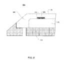
- FIG. 8is another cross-sectional view of an embodiment 800 similar to that of FIG. 7 .
- the cover glass 105is split into upper and lower cover glass layers 805 , 810 .
- the layersare not nested together as is the case in the embodiments shown in FIGS. 4 and 6 . Rather, the layers form the upper and lower portions of the cover glass and sit adjacent to one another with an interface 815 defining the point of contact.
- the interface 815may be planar, such that the opposing sides of the upper and lower cover glass layers are flat.
- the layersmay be bonded to one another, for example with an optically clear adhesive.
- the slot 820 for the antenna 110may be formed in either of the upper and lower cover glass layers 805 , 810 or may be partially in both layers, although the slot is shown in FIG. 7 in the upper cover glass layer. Likewise, the slot 820 need not necessarily be formed in either layer adjacent the interface 815 between the layers. It may be more convenient and/or simpler to create the slot at the interface, however, since the slot may then be formed in an exposed surface of at least one of the cover glass layers prior to bonding the two together. Again, one or more vias may extend through the lower cover glass layer 810 and connect the antenna to the electronic circuitry 210 .
- one or more ink layersmay be deposited beneath at least a portion of the cover glass to provide decoration and/or to mask the presence of the antenna.
- the region of the cover glass beneath the antennamay be colored to obscure the antenna, for example.
- Such ink layersare purely optional.
- the inkmay be selectively deposited so as to not cover the vias, thereby permitting electrical connections between the antenna(s) and the electronic circuitry through the vias.
- Some embodimentsmay have a trench or passage formed entirely within a cover glass.
- a lasermay be used to selectively excite ceramic molecules at a certain depth beneath the surface of the cover glass. These excited molecules may vaporize while the molecules surrounding them may remain relatively stable and unaffected.
- a voidmay be formed in the interior of the cover glass without requiring any through-holes to be formed or any chemicals to be used. Vias may later be formed to connect to the void; these vias may permit the antenna material to be deposited within the void as necessary. The vias may then be filled or sealed with an appropriate material.
- the lasermay be selectively applied to the sapphire lattice at a depth within cover glass to weaken the bonds between molecules.
- These molecules with weakened bondsmay then be more easily etched with a chemical etchant to form a passage or path through the sapphire, into which an antenna or other electronic component may be deposited. Vias may be formed in the same fashion and, optionally, in conjunction with forming the internal trench.
- a shieldmay be placed between the electronic component and the electronic circuitry.
- a shieldmay likewise be placed therebetween.
- the shieldmay insulate the electronic component in the cover glass from noise, parasitic capacitances and other undesirable electrical effects caused by proximity to the electronic circuitry and vice versa.
- the shieldmay be a ground plane.
- the inkif used may be deposited on the shield itself and the shield may additionally provide structural support to the cover glass.
Landscapes
- Engineering & Computer Science (AREA)
- Theoretical Computer Science (AREA)
- Computer Hardware Design (AREA)
- General Engineering & Computer Science (AREA)
- Human Computer Interaction (AREA)
- Physics & Mathematics (AREA)
- General Physics & Mathematics (AREA)
- Signal Processing (AREA)
- Microelectronics & Electronic Packaging (AREA)
- Casings For Electric Apparatus (AREA)
Abstract
Description
Embodiments described herein relate generally to ceramic materials having an electronic component embedded therein, and more particularly to electrically active components embedded in a ceramic surface defining a portion of an outer surface of an electronic device.
Electronic devices are ubiquitous in modern society. Examples include phones, tablet computing devices, personal computers, watches, glasses, fitness meters, earpieces, and so on. One thing is generally true of all electronic devices: each generation adds more functionality (and thus circuitry) than the last. As circuitry increases, available space decreases.
Eventually, even with the ongoing miniaturization in circuitry, a limit on physical space can be reached such that no more space is available to add any more electronic components. Likewise, even if space is available, cross-talk, interference and the like between closely-packed electronic components may cause erratic operation of overall failure.
Some electronic devices include a cover glass or other relatively hard, transparent element that covers a display. The cover glass typically is not used for anything other than protection of the display and to form part of the housing, or to be affixed to the housing. Thus, the space occupied by the cover glass may be considered wasted space from the point of view of attempting to maximize electronic circuitry within a given volume for an electronic device.
Further, some electronic devices use sapphire or other hard but brittle ceramics as a cover glass. Such cover glasses may be very resistant to scratches and damage, but may be difficult to cut, polish, grind, drill or otherwise shape or process due to their very hardness.
Thus, an improved ceramic material having an electronic component embedded therein may be useful.
One embodiment described herein may take the form of an electronic device, including: a housing; a cover glass affixed to the housing; and an electronic component embedded within the cover glass. The electronic device may also have a trench defined within the cover glass; the electronic component located within the trench; and a retention element occupying a remainder of the trench, thereby embedding the electronic component with the cover glass.
Another embodiment may take the form of an electronic device, comprising: a housing; a ceramic element affixed to the housing, the ceramic element defining a void; an electronic component affixed within the void; and at least one electronic circuit within the housing and in electrical communication with the electronic component.
Other embodiments will be apparent to those skilled in the art upon reading the disclosure in its entirety.
Embodiments discussed herein may take the form of a ceramic material having an electronic component embedded therein, and more particularly to a sapphire surface having an electrically energized component embedded within. In some embodiments, the sapphire surface may take the form of a portion of a housing for an electronic device. Since sapphire may be substantially transparent, it may form a cover glass for a display within or forming part of the electronic device, as one example. The cover glass may be bonded, affixed, or otherwise attached to a remainder of the housing, thereby forming an enclosure for the electronic device.
In some embodiments, the electronic component embedded in the ceramic material may be electrically active (e.g., powered). The electronic component may be active only at intervals or constantly, or at least constantly while the electronic device is on. As one example of an electrically active component, the electronic component may be an antenna. As another example of an electrically active component, the electronic component may be a sensor, such as a capacitive sensor. As a third example of an electrically active component, the electronic component may be a display, such as an organic light-emitting diode array. Yet a fourth example of an electronic component may be a ground or shield element, which is an example of a passive (e.g., not powered) component that may be embedded.
In embodiments where the electronic component is affected by, or vulnerable to, noise generated by other elements in the electronic device, moving the electronic component into the ceramic material may provide physical separation from these other elements and thus reduce or mitigate the effects of noise. It should be appreciated that the same is true in embodiments where the electronic component generates noise that adversely impacts the other elements in the electronic device. “Noise,” as used herein, generally includes any error or fluctuation induced in the operation of an electronic component or element, including parasitic capacitances, parasitic voltages, crosstalk, and the like.
In some embodiments, a shield or ground may be embedded within the ceramic near the electronic component in order to block noise between the component and other electronics within the electronic device. For example, a shield layer may be placed directly under the electronic device within the same space formed in the ceramic.
Typically, a void space may be formed within the ceramic in order to accept the electronic component and any optional shield or ground. A variety of sample methods for forming such a void space are discussed in more detail below.
Turning now toFIG. 1 , a sampleelectronic device 100 incorporating aceramic layer 105 and anelectronic component 110 embedded in the ceramic layer is shown. Theelectronic device 100 may be, for example, a tablet device (as illustrated), a mobile phone, a portable computer, a wearable device, and so on. Theceramic layer 105 may abut ahousing 115. Theceramic layer 105 may be adjacent to, bonded to and/or directly abutting thehousing 115. Theelectronic device 100 is shown with thecover glass 105 proud of thehousing 115. In alternative embodiments, the cover glass may be flush with, or recessed within, the housing. Likewise, the cover glass is shown with a flat upper surface and an angled sidewall. In other embodiments, the upper surface may be curved or otherwise arcuate rather than planar, and the arc may continue along the cover glass such that no sharp angle with any sidewall is formed.
In the illustrated embodiment, thecover glass 105 overlaying the display may be made of a transparent ceramic such as sapphire. It should be appreciated that thecover glass 105 may be fully or at least partially formed from other materials such as alumina, chemically strengthened glass, and the like. For example, a layer of alumina may be used to bond two adjacent sapphire layers to one another. Likewise, an optically clear adhesive may be used to bond adjacent sapphire layers and may form part of the cover glass. Although the term “cover glass” may be used herein, it should be appreciated that this term imposes no requirement that glass be incorporated or used in the element. For example, a cover glass may be formed entirely from sapphire, or may be formed from sapphire and alumina, sapphire and adhesive, and so forth. Likewise, although the terms “cover glass” and “ceramic layer” may be used essentially interchangeably, certain embodiments of a “ceramic layer” may be replaced with (or encompass) non-ceramics, such as glass, plastic and so on.
A sampleelectronic component 110 is shown embedded within thecover glass 105. The electronic element may be visible through the ceramic in certain embodiments and as shown. In alternative embodiments, theelectronic element 110 may be placed beneath an ink layer or otherwise concealed so that it is not visible through the cover glass. As yet another option, thecover glass 105 may be opaque or translucent, at least in part, in order to conceal the electronic element. As still another option, the electronic element may be formed from a transparent or translucent material.
As previously mentioned, in one embodiment theelectronic component 110 may include, incorporate, or be one or more antennas. For example, a first portion of the electronic component may be an antenna and a second portion may be a ground path. As yet another example, there may be multipleelectronic components 110 taking the form of multiple, unconnected antennas, each of which may transmit and/or receive at a different frequency or band of frequencies. In still another embodiment, the multiple electronic antennas may be physically and/or operationally connected to one another.
Thetrench 200 may be formed through a variety of different operations. For example, the trench may be formed by computer numerical control (CNC) grinding, ultrasonic machining, laser ablation, plasma etching, laser etching (in addition to or without chemical etching), deep reactive ion etching, and so forth. In embodiments where laser ablation is used to form thetrench 200, the laser may be a femtosecond laser or any other suitable laser.
Theelectronic component 110 may be deposited in thetrench 200, filling at least a portion of the trench. The component may be pre-formed prior to deposit, or may be deposited in a liquid form and cool within the trench. Further, theelectronic component 110 may extend the length of thetrench 200 or may extend only partially along the trench. Likewise, as mentioned above, multiple electronic components may occupy a single trench and may be laid out without touching one another or may be laid out to at least partially overlap.
As one example, theelectronic component 110 may be a conductive metal strip extending along at least a portion of thetrench 200. The metal may be heated until it is a liquid and poured into the trench; upon cooling, the liquid will generally occupy the deepest part of the trench. In many embodiments, theceramic structure 105 may be inverted from its orientation shown inFIG. 2 during addition of theelectronic component 110, such that the deepest part during addition of the electronic component is the “top” of the trench with respect to the orientation shown inFIG. 2 .
In addition to depositing theelectronic component 110 in a solid or liquid form, the electronic component may be deposited within thetrench 200 through chemical vapor deposition or any other suitable deposition method. This may permit the bottom or walls of thetrench 200 to be coated with the electronic component without requiring the center of the trench to be filled, for example and as shown inFIG. 2 .
After theelectronic component 110 is deposited, the remainder of thetrench 200 not occupied by the component may be filled. In some embodiments, less than the total remainder of the trench is filled. Thefiller material 205 may be sapphire, alumina, glass (which may or may not be chemically strengthened), plastic, epoxy, poly(methyl methacrylate) (PMMA), polycarbonate, or the like, and may depend on the material forming the ceramic substrate. Typically, although not necessarily, in embodiments using an optically transparent ceramic105, thefiller 205 has an index of refraction and transparency that is close or identical to that of the ceramic. By employing a filler that matches or comes close to the ceramic substrate with respect to these properties, optical aberrations in a finished enclosure may be reduced or eliminated. For example, alumina may be employed as afiller 205 in order to match the optical properties of sapphire.
As another option, a solid piece of ceramic may be used as afiller 205. The ceramic filler may have a size and shape that approximately matches the dimensions of thetrench 200. Thisceramic filler 205 may be bonded to the ceramic material forming thecover glass 105, for example along the sides of thetrench 200 or at any other region of the trench not filled by theelectronic component 110. In some embodiments, an optically clear adhesive may be used to bond the two. In other embodiments, a frit may be placed between the ceramic105 andfiller 205 and heated to bond the two. In still other embodiments, amorphous alumina or glass may be placed between the ceramic substrate and ceramic filler and heated to fuse the two together, for example at a molecular level. In some embodiments, an adhesive other than an optically clear adhesive may be employed. In yet other embodiments, an epoxy may bond the ceramic filler and the ceramic substrate. Fillers may be used with any or all embodiments discussed herein.
It should be appreciated that one or more through-holes (e.g., vias) may be formed when filling thetrench 200. These vias may be formed by leaving certain portions of thetrench 200 unfilled, or by removing some of thefiller 205. The vias may permit electrical connection from the electronic component embedded within the trench to one or moreelectrical elements 210 within the housing. For example, a via may electrically connect the embedded electronic component to a power supply, a processor, a sensor, an electrical ground, and the like. These are all examples ofelectronic circuitry 210.
In some embodiments, multiple vias may extend through the filler in order to permit multiple electrical connections. This may be useful if there are multiple electronic components located within the trench, for example. It may also be useful if an electronic component requires more than one type of electrical connection (for example, some electronic components may require both power and an output connection).
After sealing the filler to the ceramic substrate, the resulting structure may be polished and finished. The exact method used to polish the ceramic and filler may vary with certain properties of the two, end uses of the cover glass (or other surface) formed by the combination of ceramic and filler, visibility of the back side of the ceramic and interface between ceramic and filler, and the like. For example, in embodiments where the ceramic is transparent and used as a cover glass or other visually transparent element, the interface between ceramic and filler may be smoother and/or more polished than in embodiments where the ceramic is translucent or opaque, and/or embodiments where the ceramic is not an external portion of the electronic device.
Accordingly, in certain embodiments the back surface of the ceramic (e.g., the surface of the ceramic on which the trench is formed) and/or the filler may be polished through annealing, mechanical polishing, chemical etching, aero lapping, and the like. In addition to polishing this surface of the ceramic and/or filler, certain of the foregoing techniques may likewise assist in bonding the filler to the ceramic. Annealing, as one example, may serve to at least partially bond the ceramic to the filler through its high heat of operation.
In some embodiments, an adhesive215 may bond thecover glass 105 to thehousing 115. This adhesive may prevent ingress of particles from the environment to the interior of theelectronic device 100. In alternative embodiments, the adhesive215 may be replaced with a barrier that may be affixed or adhered to either or both of the housing and cover glass. The barrier may be compressible in certain embodiments in order to provide a tight seal between thecover glass 105 andhousing 115.
Thetrench 200 is generally sized to receive theelectronic element 110. Typically, the electronic component does not extend past any edge of the trench, but instead is fully contained within the trench. AlthoughFIG. 3A depicts a single electronic component that is formed as a contiguous, unbroken rectangle, it should be appreciated that differently-shaped or configured electronic components may be employed. For example, multiple electronic components may be separated by one or more insulating spacers. Indeed, the size and shape of theelectronic component 110 may vary somewhat from the size and shape of thetrench 200, even though the electronic component may fit fully within the trench. In some embodiments, as discussed above, the multiple electronic components may not be physically joined to one another or a single electronic component may be placed within the trench.
Thefiller 205 is also shown inFIG. 3A . Although the filler is shown as a solid annular construct inFIG. 3A , it should be appreciated that it may be granular, discontinuous, or otherwise formed from multiple pieces or parts. Typically, thefiller 205 bonds to theceramic substrate 105 and retains theelectronic component 110 in place in thetrench 200. In some embodiments, the filler may also serve to electrically isolate or insulate the electronic component from other electronic elements within the device enclosure. Thus, thefiller 205 may be chosen for its electrically insulating properties; for example, a material with a high dielectric constant may be chosen as a filler. One or more depressions or recesses300 may be formed in the filler to accommodate one or more protrusions of the antenna, as indicated in phantom inFIG. 3A .
In the embodiment shown inFIG. 4 , thecover glass 105 may be formed from first405 and second410 cover glass layers that are bonded together. The first,outer layer 405 may have adepression 420 formed in its inner surface that is sized to accept the second, inner cover glass layer (see, for example,FIG. 5B ). Thus, theouter layer 405 may be somewhat similar to a bucket—it may have a raised ledge orlip 425 running along its periphery, with the raised ledge extending inwardly into the outer layer. The raisedledge 425 may abut abase 430 of thedepression 420, thus forming a wall or walls around the depression. In some embodiments, the ledge may be formed by multiple sidewalls abutting one another. The sidewalls may meet at a sharp angle, such as a right angle, or may curved transitions may be formed between the sidewalls and connect the sidewalls. Likewise, the transition from the sidewall(s) to the base may be curved, sharp, angled, or the like.
The second, innercover glass layer 410 may be sized to fit within, and substantially fill, thedepression 420 in the outercover glass layer 405. Accordingly, the shape of the inner cover glass layer may be at least partially dictated by the shape of thedepression 420 in the outer cover glass layer. In some embodiments, however, a spacer, filler or the like may be placed between the inner and outer cover glass layers.
Generally, a trough or groove200 (e.g., a trench) may be formed in an upper surface of the innercover glass layer 410, as shown inFIG. 4 . The antenna or otherelectronic component 110 may be formed in or placed in this groove prior to sealing the outer and inner cover glass layer. In such an embodiment, it may be relatively simple to place or form theantenna 110 within theembodiment 400, since the upper surface of the innercover glass layer 405 is exposed prior to bonding together the inner and outer cover glass layers. The antenna may be solid and placed within thetrough 200, may be deposited in vapor or particulate form into the trough, may be poured as a liquid into the trough (after which it may cool to form a solid), and so on. The antenna, when placed, may occupy the entirety of the trough in some embodiments, although in other embodiments the antenna may occupy only a portion of the trough. The occupied portion may be only a segment of the length of the trough, or may be a partial depth of the trough, or both.
It should be appreciated that the relative thicknesses of the outer and inner cover glass layers405,410 may vary from embodiment to embodiment. They need not be the same thickness at any point or along any cross-section.
Likewise, the exact location of thetrough 200 may vary. It may be formed at any point along the innercover glass layer 405 and may (or may not) extend fully around a perimeter of thecover glass layer 410. The distance between an edge of the inner cover glass layer and the edge of the trough may vary as necessary or desired and need not be constant. Further, in some embodiments thetrough 200 may be formed in thedepression 420 of the outercover glass layer 405 rather than in the innercover glass layer 410.
As discussed with respect to previous embodiments, the inner and outer cover glass layers405,410 may be bonded to one another with a chemical or mechanical bond, or any other suitable adhesive bond employing any suitable material including alumina, an adhesive (such as an optically clear adhesive), and the like.
As shown inFIG. 4 , one ormore vias 415 may connect the antenna or otherelectronic component 110 to theelectronic circuitry 210 of theelectronic device 400. Thevias 415 may be formed in thecover glass layer 410 in any of a number of fashions and may be filled with any suitable conductive material, including metal, ceramic, composites, and the like.
The size and/or shape of thevias 415 may vary not only from embodiment to embodiment, but also between vias of the same embodiment. Certain vias may be lozenge-shaped while others are round, for example. The via-filling material may be overmolded or overfill the via in some embodiments. Likewise, an end of the via415 may be larger than a middle portion of the via to provide a larger contact surface to either the antenna or theelectronic circuitry 210. Thus, the cross-section of the via may vary along its length in some embodiments.
It should be appreciated that thevias 415 may be formed by a similar or identical process as used to form theantenna 110, for example physical vapor deposition. The vias may be formed in a separate deposition process, for example after the antenna is formed and after the inner and outer cover glass layers405,410 are bonded to one another. As another example, thevias 415 may be flooded with a liquid metal, which may then dry to fill the vias and form electrical connections to the antenna(s).
The cross-sectional shape of the outercover glass layer 405 is shown to best effect inFIG. 5B , which is a cross-sectional view taken alongline 6B-6B ofFIG. 5A .FIG. 5B illustrates the “bucket” shape of thedepression 420 as formed by thesidewalls 425 andbase 430.
In the embodiment ofFIG. 7 , the groove/slot 705 may be formed at any time, such as before or after the inner and outerceramic layers FIG. 7 .
Theslot 820 for theantenna 110 may be formed in either of the upper and lower cover glass layers805,810 or may be partially in both layers, although the slot is shown inFIG. 7 in the upper cover glass layer. Likewise, theslot 820 need not necessarily be formed in either layer adjacent theinterface 815 between the layers. It may be more convenient and/or simpler to create the slot at the interface, however, since the slot may then be formed in an exposed surface of at least one of the cover glass layers prior to bonding the two together. Again, one or more vias may extend through the lowercover glass layer 810 and connect the antenna to theelectronic circuitry 210.
In some embodiments, one or more ink layers may be deposited beneath at least a portion of the cover glass to provide decoration and/or to mask the presence of the antenna. The region of the cover glass beneath the antenna may be colored to obscure the antenna, for example. Such ink layers are purely optional. In embodiments having one or more ink coatings, the ink may be selectively deposited so as to not cover the vias, thereby permitting electrical connections between the antenna(s) and the electronic circuitry through the vias.
Some embodiments may have a trench or passage formed entirely within a cover glass. For example, a laser may be used to selectively excite ceramic molecules at a certain depth beneath the surface of the cover glass. These excited molecules may vaporize while the molecules surrounding them may remain relatively stable and unaffected. Thus, a void may be formed in the interior of the cover glass without requiring any through-holes to be formed or any chemicals to be used. Vias may later be formed to connect to the void; these vias may permit the antenna material to be deposited within the void as necessary. The vias may then be filled or sealed with an appropriate material. Similarly, the laser may be selectively applied to the sapphire lattice at a depth within cover glass to weaken the bonds between molecules. These molecules with weakened bonds may then be more easily etched with a chemical etchant to form a passage or path through the sapphire, into which an antenna or other electronic component may be deposited. Vias may be formed in the same fashion and, optionally, in conjunction with forming the internal trench.
In yet other embodiments, a shield may be placed between the electronic component and the electronic circuitry. For example, just as one or more ink layers may be deposited on the underside of the cover glass or otherwise between the cover glass and electronic circuitry, a shield may likewise be placed therebetween. The shield may insulate the electronic component in the cover glass from noise, parasitic capacitances and other undesirable electrical effects caused by proximity to the electronic circuitry and vice versa. In some embodiments, the shield may be a ground plane. Further, in embodiments employing a shield, the ink (if used) may be deposited on the shield itself and the shield may additionally provide structural support to the cover glass.
Although various embodiments have been described herein, it should be appreciated that variants and changes will be apparent to those of skill in the art upon reading the disclosure. Accordingly, the proper scope of protection is set forth in the following claims.
Claims (9)
1. An electronic device, comprising:
a housing;
a cover glass affixed to the housing;
a trench formed into a surface of the cover glass;
an electronic component disposed within a portion of the trench; and
a retention element that occupies a remainder of the trench, wherein the electronic component is interposed between the retention element and the cover glass and wherein the retention element is formed from sapphire.
2. The electronic device ofclaim 1 , wherein the cover glass is formed from sapphire.
3. The electronic device ofclaim 2 , wherein the retention element is molecularly bonded to the cover glass.
4. An electronic device, comprising:
a housing;
a cover glass affixed to the housing;
a trench formed into a surface of the cover glass;
an electronic component disposed within a portion of the trench; and
a retention element that occupies a remainder of the trench, wherein the electronic component is interposed between the retention element and the cover glass and wherein the retention element is a frit that is fused to the cover glass after deposition in the trench.
5. The electronic device ofclaim 1 , further comprising:
at least one electronic circuit;
at least one via in electrical communication with the electronic circuit and the electronic component, the via defining an electrical connection between the electronic circuit and the electronic component.
6. The electronic device ofclaim 5 , wherein the via extends through a portion of the cover glass.
7. The electronic device ofclaim 1 , further comprising a display stack operative to display at least one image through the cover glass.
8. An electronic device, comprising:
a housing;
a display in the housing;
a transparent element that covers the display and is affixed to the housing, wherein the transparent element has first and second opposing surfaces, wherein the first surface of the transparent element forms an exterior surface of the electronic device, wherein a trench is formed in the second surface of the transparent element;
an electronic component, wherein at least a portion of the electronic component is formed in the trench;
ink that is formed on the second surface of the transparent element in the trench, wherein the ink is interposed between the second surface of the transparent element and the electronic component; and
at least one electronic circuit within the housing, wherein the at last one electronic circuit is in electrical communication with the electronic component.
9. The electronic device defined inclaim 8 , wherein the transparent element is formed from sapphire.
Priority Applications (10)
| Application Number | Priority Date | Filing Date | Title |
|---|---|---|---|
| US14/033,981US9632537B2 (en) | 2013-09-23 | 2013-09-23 | Electronic component embedded in ceramic material |
| KR1020167008567AKR101933285B1 (en) | 2013-09-23 | 2014-09-19 | Electronic component embedded in ceramic material |
| PCT/US2014/056439WO2015042335A1 (en) | 2013-09-23 | 2014-09-19 | Electronic component embedded in ceramic material |
| EP14781994.0AEP3014380B1 (en) | 2013-09-23 | 2014-09-19 | Electronic component embedded in ceramic material |
| JP2016544001AJP6636432B2 (en) | 2013-09-23 | 2014-09-19 | Electronic components embedded in ceramic material |
| AU2014323434AAU2014323434B2 (en) | 2013-09-23 | 2014-09-19 | Electronic component embedded in ceramic material |
| TW103132852ATWI618465B (en) | 2013-09-23 | 2014-09-23 | Electronic component embedded in ceramic material |
| CN201420688579.0UCN204305488U (en) | 2013-09-23 | 2014-09-23 | Electronic equipment |
| CN201410649044.7ACN104582359B (en) | 2013-09-23 | 2014-09-23 | The electronic component of embedded ceramic material |
| US14/512,660US9678540B2 (en) | 2013-09-23 | 2014-10-13 | Electronic component embedded in ceramic material |
Applications Claiming Priority (1)
| Application Number | Priority Date | Filing Date | Title |
|---|---|---|---|
| US14/033,981US9632537B2 (en) | 2013-09-23 | 2013-09-23 | Electronic component embedded in ceramic material |
Related Child Applications (1)
| Application Number | Title | Priority Date | Filing Date |
|---|---|---|---|
| US14/512,660Continuation-In-PartUS9678540B2 (en) | 2013-09-23 | 2014-10-13 | Electronic component embedded in ceramic material |
Publications (2)
| Publication Number | Publication Date |
|---|---|
| US20150085429A1 US20150085429A1 (en) | 2015-03-26 |
| US9632537B2true US9632537B2 (en) | 2017-04-25 |
Family
ID=52690740
Family Applications (1)
| Application Number | Title | Priority Date | Filing Date |
|---|---|---|---|
| US14/033,981Active2034-02-24US9632537B2 (en) | 2013-09-23 | 2013-09-23 | Electronic component embedded in ceramic material |
Country Status (1)
| Country | Link |
|---|---|
| US (1) | US9632537B2 (en) |
Cited By (35)
| Publication number | Priority date | Publication date | Assignee | Title |
|---|---|---|---|---|
| US9792516B2 (en) | 2016-01-26 | 2017-10-17 | Next Biometrics Group Asa | Flexible card with fingerprint sensor |
| US11118338B2 (en) | 2017-05-22 | 2021-09-14 | Kohler Co. | Plumbing fixtures with insert-molded components |
| US11408158B2 (en) | 2016-04-26 | 2022-08-09 | Kohler Co. | Composite faucet body and internal waterway |
| US11419231B1 (en) | 2016-09-22 | 2022-08-16 | Apple Inc. | Forming glass covers for electronic devices |
| US11420900B2 (en) | 2018-09-26 | 2022-08-23 | Apple Inc. | Localized control of bulk material properties |
| US11460892B2 (en)* | 2020-03-28 | 2022-10-04 | Apple Inc. | Glass cover member for an electronic device enclosure |
| US11513613B2 (en) | 2016-07-15 | 2022-11-29 | Apple Inc. | Capacitive gap sensor ring for an input device |
| US11531306B2 (en) | 2013-06-11 | 2022-12-20 | Apple Inc. | Rotary input mechanism for an electronic device |
| US11535551B2 (en) | 2016-09-23 | 2022-12-27 | Apple Inc. | Thermoformed cover glass for an electronic device |
| US11550268B2 (en) | 2020-06-02 | 2023-01-10 | Apple Inc. | Switch module for electronic crown assembly |
| US11561515B2 (en) | 2018-08-02 | 2023-01-24 | Apple Inc. | Crown for an electronic watch |
| US11565506B2 (en) | 2016-09-23 | 2023-01-31 | Apple Inc. | Thermoformed cover glass for an electronic device |
| US11567457B2 (en) | 2014-09-02 | 2023-01-31 | Apple Inc. | Wearable electronic device |
| US11666273B2 (en) | 2020-05-20 | 2023-06-06 | Apple Inc. | Electronic device enclosure including a glass ceramic region |
| US11669205B2 (en) | 2014-02-12 | 2023-06-06 | Apple Inc. | Rejection of false turns of rotary inputs for electronic devices |
| US11680010B2 (en) | 2019-07-09 | 2023-06-20 | Apple Inc. | Evaluation of transparent components for electronic devices |
| US11720064B2 (en) | 2016-07-25 | 2023-08-08 | Apple Inc. | Force-detecting input structure |
| US11754981B2 (en) | 2018-06-25 | 2023-09-12 | Apple Inc. | Crown for an electronic watch |
| US11796961B2 (en) | 2018-08-24 | 2023-10-24 | Apple Inc. | Conductive cap for watch crown |
| US11796968B2 (en) | 2018-08-30 | 2023-10-24 | Apple Inc. | Crown assembly for an electronic watch |
| US11850822B2 (en) | 2016-09-23 | 2023-12-26 | Apple Inc. | Electronic device having a component with crack hindering internal stress regions |
| US11860587B2 (en) | 2019-02-12 | 2024-01-02 | Apple Inc. | Variable frictional feedback device for a digital crown of an electronic watch |
| US11886149B2 (en) | 2013-08-09 | 2024-01-30 | Apple Inc. | Tactile switch for an electronic device |
| US11927988B2 (en) | 2020-03-28 | 2024-03-12 | Apple Inc. | Glass cover member for an electronic device enclosure |
| US11945048B2 (en) | 2020-12-23 | 2024-04-02 | Apple Inc. | Laser-based cutting of transparent components for an electronic device |
| US11988995B2 (en) | 2015-03-08 | 2024-05-21 | Apple Inc. | Compressible seal for rotatable and translatable input mechanisms |
| US20240231440A9 (en)* | 2022-10-24 | 2024-07-11 | Corning Incorporated | Elastic bilinear structure for impact force mitigation |
| US12065372B2 (en) | 2020-12-17 | 2024-08-20 | Apple Inc. | Fluid forming a glass component for a portable electronic device |
| US12066795B2 (en) | 2017-07-18 | 2024-08-20 | Apple Inc. | Tri-axis force sensor |
| US12092996B2 (en) | 2021-07-16 | 2024-09-17 | Apple Inc. | Laser-based rotation sensor for a crown of an electronic watch |
| US12104929B2 (en) | 2016-05-17 | 2024-10-01 | Apple Inc. | Rotatable crown for an electronic device |
| US12189347B2 (en) | 2022-06-14 | 2025-01-07 | Apple Inc. | Rotation sensor for a crown of an electronic watch |
| US12195379B2 (en) | 2020-12-17 | 2025-01-14 | Apple Inc. | Forming and bonding of glass components for portable electronic devices |
| US12259690B2 (en) | 2018-08-24 | 2025-03-25 | Apple Inc. | Watch crown having a conductive surface |
| US12396686B2 (en) | 2021-08-31 | 2025-08-26 | Apple Inc. | Sensing health parameters in wearable devices |
Families Citing this family (9)
| Publication number | Priority date | Publication date | Assignee | Title |
|---|---|---|---|---|
| US9632537B2 (en) | 2013-09-23 | 2017-04-25 | Apple Inc. | Electronic component embedded in ceramic material |
| US9678540B2 (en) | 2013-09-23 | 2017-06-13 | Apple Inc. | Electronic component embedded in ceramic material |
| JPWO2015097936A1 (en)* | 2013-12-25 | 2017-03-23 | パナソニックIpマネジメント株式会社 | Electronics |
| US9225056B2 (en) | 2014-02-12 | 2015-12-29 | Apple Inc. | Antenna on sapphire structure |
| KR102331876B1 (en)* | 2014-07-10 | 2021-11-29 | 코닝 인코포레이티드 | Cold formed glass applique |
| KR200488235Y1 (en)* | 2014-08-27 | 2018-12-31 | 애플 인크. | Sapphire cover for electronic devices |
| US9618973B2 (en)* | 2015-06-26 | 2017-04-11 | Intel Corporation | Mechanically embedded heating element |
| CN109922177A (en)* | 2018-12-28 | 2019-06-21 | 瑞声科技(新加坡)有限公司 | A kind of casing and the mobile terminal using the casing |
| US11272631B2 (en)* | 2019-09-09 | 2022-03-08 | Apple Inc. | Conductive PVD stack-up design to improve reliability of deposited electrodes |
Citations (268)
| Publication number | Priority date | Publication date | Assignee | Title |
|---|---|---|---|---|
| US2248955A (en) | 1939-01-13 | 1941-07-15 | Frank L Capps | Sapphire grinding means |
| US2854794A (en) | 1955-09-22 | 1958-10-07 | Daystrom Inc | Treating sapphire objects of irregular shapes |
| US3208070A (en)* | 1962-08-06 | 1965-09-21 | Libbey Owens Ford Glass Co | Automobile windshield of laminated glass having embedded antenna wires |
| GB1135886A (en) | 1966-09-26 | 1968-12-04 | Ibm | Method and apparatus for vibratory cutting |
| US3753775A (en) | 1971-03-01 | 1973-08-21 | Rca Corp | Chemical polishing of sapphire |
| US3866232A (en)* | 1972-12-09 | 1975-02-11 | Delog Detag Flachglas Ag | Automotive-vehicle windshield with built-in active-antenna system |
| US3964942A (en) | 1970-10-16 | 1976-06-22 | International Business Machines Corporation | Chemical polishing of single crystal dielectrics |
| US4008111A (en) | 1975-12-31 | 1977-02-15 | International Business Machines Corporation | AlN masking for selective etching of sapphire |
| US4054895A (en) | 1976-12-27 | 1977-10-18 | Rca Corporation | Silicon-on-sapphire mesa transistor having doped edges |
| US4070211A (en) | 1977-04-04 | 1978-01-24 | The United States Of America As Represented By The Secretary Of The Navy | Technique for threshold control over edges of devices on silicon-on-sapphire |
| US4085302A (en) | 1976-11-22 | 1978-04-18 | Control Data Corporation | Membrane-type touch panel |
| JPS5432062A (en) | 1977-08-17 | 1979-03-09 | Agency Of Ind Science & Technol | Si single crystal substrate on sapphire |
| US4339300A (en) | 1977-07-25 | 1982-07-13 | Noble Lowell A | Process for smoothing surfaces of crystalline materials |
| US4393578A (en) | 1980-01-02 | 1983-07-19 | General Electric Company | Method of making silicon-on-sapphire FET |
| US4662124A (en) | 1980-11-17 | 1987-05-05 | Tokyo Shibaura Denki Kabushiki Kaisha | Method of grinding a sapphire wafer |
| US4732867A (en) | 1986-11-03 | 1988-03-22 | General Electric Company | Method of forming alignment marks in sapphire |
| US4735917A (en) | 1986-04-28 | 1988-04-05 | General Electric Company | Silicon-on-sapphire integrated circuits |
| US4775641A (en) | 1986-09-25 | 1988-10-04 | General Electric Company | Method of making silicon-on-sapphire semiconductor devices |
| US4811004A (en) | 1987-05-11 | 1989-03-07 | Dale Electronics, Inc. | Touch panel system and method for using same |
| EP0305626A1 (en) | 1987-09-03 | 1989-03-08 | W. Blösch AG | Wrist watch |
| US4826300A (en) | 1987-07-30 | 1989-05-02 | Hughes Aircraft Company | Silicon-on-sapphire liquid crystal light valve and method |
| US4849299A (en) | 1986-06-19 | 1989-07-18 | Montres Rado S.A. | Watch cover glass and process for the manufacture of such a glass |
| JPH0239578A (en) | 1988-07-29 | 1990-02-08 | Kyocera Corp | light emitting element |
| US4908074A (en) | 1986-02-28 | 1990-03-13 | Kyocera Corporation | Gallium arsenide on sapphire heterostructure |
| US4946546A (en) | 1987-12-23 | 1990-08-07 | U.S. Philips Corporation | Method of metallizing a substrate of silica, quartz, glass or sapphire |
| JPH0321048A (en) | 1989-06-19 | 1991-01-29 | Kyocera Corp | Package for storing semiconductor elements |
| US5005020A (en)* | 1987-01-20 | 1991-04-02 | Asahi Glass Company, Ltd. | Transparent glass antenna for an automobile |
| JPH0398948A (en) | 1989-09-11 | 1991-04-24 | Koufu Nippon Denki Kk | Accumulation mechanism for paper sheet and the like |
| JPH03115200A (en) | 1989-09-29 | 1991-05-16 | Kyocera Corp | Method for joining single crystal sapphire |
| JPH03177335A (en) | 1989-12-05 | 1991-08-01 | Seiko Electronic Components Ltd | Engraving of sapphire cover glass |
| JPH03250659A (en) | 1990-02-27 | 1991-11-08 | Kyocera Corp | Package for storing semiconductor elements |
| JPH0413773A (en) | 1990-05-01 | 1992-01-17 | Fuji Photo Film Co Ltd | Cyanine compound and information recording medium produced by using the same |
| JPH0470565A (en) | 1990-07-11 | 1992-03-05 | Daiichi Rajio Isotope Kenkyusho:Kk | Latex agglutination test nd reagent used therein |
| JPH0495895A (en) | 1990-08-10 | 1992-03-27 | Toshiba Corp | fast breeder reactor |
| US5151389A (en) | 1990-09-10 | 1992-09-29 | Rockwell International Corporation | Method for dicing semiconductor substrates using an excimer laser beam |
| US5154023A (en) | 1991-06-11 | 1992-10-13 | Spire Corporation | Polishing process for refractory materials |
| JPH0527257A (en) | 1991-07-19 | 1993-02-05 | Kyocera Corp | Liquid crystal display |
| JPH0585894A (en) | 1991-10-01 | 1993-04-06 | Kyocera Corp | Single crystal sapphire bonded body and method for producing the same |
| JPH05313103A (en) | 1992-05-12 | 1993-11-26 | Miki:Kk | Glasses |
| JPH05333164A (en) | 1992-06-02 | 1993-12-17 | Seiko Epson Corp | Multi-layer cover glass for watches |
| JPH05335435A (en) | 1992-05-29 | 1993-12-17 | Kyocera Corp | Package for accommodating semiconductor element |
| JPH06242260A (en) | 1993-02-12 | 1994-09-02 | Kyocera Corp | Cover glass for watches |
| JPH06314694A (en) | 1993-04-28 | 1994-11-08 | Kyocera Corp | Heating apparatus of semiconductor wafer |
| JPH06337292A (en) | 1993-05-28 | 1994-12-06 | Citizen Watch Co Ltd | Cover glass for watch and production thereof |
| US5377669A (en) | 1992-04-06 | 1995-01-03 | Henke-Sass, Wolf Gmbh | Sapphire protective covering for medical endoscope |
| US5413360A (en) | 1992-12-01 | 1995-05-09 | Kyocera Corporation | Electrostatic chuck |
| JPH07129952A (en) | 1993-10-29 | 1995-05-19 | Kyocera Corp | Magnetic disk substrate and manufacturing method thereof |
| JPH07145000A (en) | 1993-11-18 | 1995-06-06 | Yamatake Honeywell Co Ltd | Sapphire wafer bonding method |
| US5427051A (en) | 1993-05-21 | 1995-06-27 | General Electric Company | Solid state formation of sapphire using a localized energy source |
| US5441591A (en) | 1993-06-07 | 1995-08-15 | The United States Of America As Represented By The Secretary Of The Navy | Silicon to sapphire bond |
| US5451553A (en) | 1993-09-24 | 1995-09-19 | General Electric Company | Solid state thermal conversion of polycrystalline alumina to sapphire |
| JPH0840797A (en) | 1994-07-29 | 1996-02-13 | Kyocera Corp | Sapphire substrate for film composition analysis and film composition analysis method using the same |
| JPH08148594A (en) | 1994-11-25 | 1996-06-07 | Kyocera Corp | Package for storing optical semiconductor elements |
| US5543630A (en) | 1995-01-31 | 1996-08-06 | The United States Of America As Represented By The Secretary Of The Air Force | High Tc superconducting devices on bi-crystal substrates |
| US5549746A (en) | 1993-09-24 | 1996-08-27 | General Electric Company | Solid state thermal conversion of polycrystalline alumina to sapphire using a seed crystal |
| JPH098690A (en) | 1995-06-23 | 1997-01-10 | Kyocera Corp | Portable communication device |
| US5627109A (en) | 1994-09-16 | 1997-05-06 | Sassa; Michinari | Method of manufacturing a semiconductor device that uses a sapphire substrate |
| US5661313A (en) | 1993-09-09 | 1997-08-26 | The United States Of America As Represented By The Secretary Of The Navy | Electroluminescent device in silicon on sapphire |
| US5697998A (en) | 1996-03-05 | 1997-12-16 | The Aerospace Corporation | Sapphire window laser edge annealing |
| US5702654A (en) | 1996-08-30 | 1997-12-30 | Hughes Electronics | Method of making thermal shock resistant sapphire for IR windows and domes |
| US5792298A (en)* | 1993-09-23 | 1998-08-11 | Saint-Gobain Vitrage | Method of making a laminated glass pane with embedded antenna wires |
| US5804522A (en) | 1994-09-10 | 1998-09-08 | Uegami; Kenjiro | Hardened alumina material |
| JPH10239520A (en) | 1997-02-28 | 1998-09-11 | Kyocera Corp | Polarizing beam splitter |
| JPH10269543A (en) | 1997-03-27 | 1998-10-09 | Kyocera Corp | Substrate for magnetic disk |
| JPH10275955A (en) | 1997-03-31 | 1998-10-13 | Kyocera Corp | Semiconductor laser diode and method of manufacturing the same |
| WO1998056575A1 (en) | 1997-06-11 | 1998-12-17 | Saphikon Inc. | Eutectic bonding of single crystal components |
| JPH10335259A (en) | 1997-05-29 | 1998-12-18 | Kyocera Corp | Semiconductor device and manufacturing method thereof |
| US5852622A (en) | 1988-08-30 | 1998-12-22 | Onyx Optics, Inc. | Solid state lasers with composite crystal or glass components |
| US5877094A (en) | 1994-04-07 | 1999-03-02 | International Business Machines Corporation | Method for fabricating a silicon-on-sapphire wafer |
| JPH1173764A (en) | 1997-08-27 | 1999-03-16 | Kyocera Corp | D-RAM type determination method |
| JPH11135889A (en) | 1997-10-30 | 1999-05-21 | Kyocera Corp | Crystal growth substrate and light emitting device using the same |
| US6025060A (en) | 1988-08-30 | 2000-02-15 | Onyx Optics, Inc. | Method and apparatus for composite gemstones |
| US6028762A (en) | 1996-01-31 | 2000-02-22 | Kyocera Corporation | Electrostatic chuck |
| US6028711A (en) | 1997-07-31 | 2000-02-22 | Asahi Kogaku Kogyo Kabushiki Kaisha | Reading lens |
| US6030849A (en) | 1997-06-16 | 2000-02-29 | Matsushita Electric Industrial Co. Ltd. | Methods of manufacturing semiconductor, semiconductor device and semiconductor substrate |
| US6038079A (en) | 1997-10-09 | 2000-03-14 | Imagyn Medical Technologies, Inc. | Sapphire objective system |
| JP3021048B2 (en) | 1993-04-15 | 2000-03-15 | ハス ホールディング エーエス | How to neutralize waste |
| EP1013802A1 (en) | 1998-12-22 | 2000-06-28 | Japan cell Co., Ltd. | Method of joining synthetic corundum, method of manufacturing synthetic corundumcell, and corundum cell |
| JP2000183203A (en) | 1998-12-18 | 2000-06-30 | Kyocera Corp | Optical semiconductor element storage package |
| JP2000196149A (en) | 1998-12-25 | 2000-07-14 | Kyocera Corp | Semiconductor light emitting device and method of manufacturing the same |
| US6121880A (en)* | 1999-05-27 | 2000-09-19 | Intermec Ip Corp. | Sticker transponder for use on glass surface |
| US6123026A (en) | 1996-11-12 | 2000-09-26 | Raytheon Company | System and method for increasing the durability of a sapphire window in high stress environments |
| JP2001134927A (en) | 1999-11-09 | 2001-05-18 | Kyocera Corp | Magnetic recording media |
| JP3177335B2 (en) | 1992-03-12 | 2001-06-18 | 三井化学株式会社 | Crosslinked polyolefin molded article and method for producing the same |
| JP2001176993A (en) | 1999-12-21 | 2001-06-29 | Kyocera Corp | Package for housing semiconductor element and method of manufacturing the same |
| US6265089B1 (en) | 1999-07-15 | 2001-07-24 | The United States Of America As Represented By The Secretary Of The Navy | Electronic devices grown on off-axis sapphire substrate |
| JP2001237335A (en) | 2000-02-24 | 2001-08-31 | Kyocera Corp | Package for housing semiconductor element and method of manufacturing the same |
| JP2001298170A (en) | 2000-04-13 | 2001-10-26 | Kyocera Corp | Sapphire substrate and device substrate using the same |
| JP2002015977A (en) | 2000-06-29 | 2002-01-18 | Kyocera Corp | Board holder |
| JP3250659B2 (en) | 1997-03-24 | 2002-01-28 | タイコエレクトロニクスアンプ株式会社 | Card connector |
| US20020017653A1 (en) | 1999-08-26 | 2002-02-14 | Feng-Ju Chuang | Blue light emitting diode with sapphire substrate and method for making the same |
| US20020021250A1 (en)* | 2000-06-21 | 2002-02-21 | Takeshi Asano | Display device, computer terminal, and antenna |
| JP2002109854A (en) | 2000-09-29 | 2002-04-12 | Kyocera Corp | Tape cleaner |
| US6379985B1 (en) | 2001-08-01 | 2002-04-30 | Xerox Corporation | Methods for cleaving facets in III-V nitrides grown on c-face sapphire substrates |
| US6406769B1 (en) | 1998-04-02 | 2002-06-18 | Comadur S.A. | Watch crystal including a lens and manufacturing method for such a lens |
| JP2002184845A (en) | 2000-12-15 | 2002-06-28 | Kyocera Corp | Wafer support substrate |
| WO2002054718A2 (en) | 2000-12-29 | 2002-07-11 | Vertu Ltd. | A casing |
| JP2002201096A (en) | 2000-10-31 | 2002-07-16 | Kyocera Corp | Single crystal sapphire substrate and heat treatment method thereof |
| US6424017B2 (en) | 1999-01-12 | 2002-07-23 | Kulite Semiconductor Products, Inc. | Silicon-on-sapphire transducer |
| US20020111194A1 (en)* | 2000-12-11 | 2002-08-15 | Farbod Behbahani | Laptop wireless systems integrated with an LCD panel |
| US20020109264A1 (en)* | 2001-02-09 | 2002-08-15 | Ernst Pollmann Uhren- Und Apparatebau Offene Handelsgesellschaft | Method of embedding at least one flexible conductive track foil, a conductive track unit as well as an embedding unit therefor |
| JP2002255694A (en) | 2001-02-26 | 2002-09-11 | Kyocera Corp | Semiconductor substrate and manufacturing method thereof |
| US6457294B1 (en)* | 1999-09-01 | 2002-10-01 | Prc-Desoto International, Inc. | Insulating glass unit with structural primary sealant system |
| JP2002289529A (en) | 2001-03-23 | 2002-10-04 | Yasuhiko Arakawa | Substrate for semiconductor layer growth |
| JP2002293692A (en) | 2001-03-29 | 2002-10-09 | Kyocera Corp | Single crystal sapphire substrate and heat treatment method thereof |
| US20020167068A1 (en) | 2001-05-09 | 2002-11-14 | International Business Machines Corporation | Silicon on sapphire structure (devices) with buffer layer |
| US20020168837A1 (en) | 2001-05-09 | 2002-11-14 | Ibm | Method of fabricating silicon devices on sapphire with wafer bonding |
| US6483237B2 (en) | 1999-02-01 | 2002-11-19 | Gem Lighting Llc | High intensity discharge lamp with single crystal sapphire envelope |
| US6489221B2 (en) | 1999-11-17 | 2002-12-03 | North Carolina State University | High temperature pendeoepitaxial methods of fabricating gallium nitride semiconductor layers on sapphire substrates |
| JP2003015156A (en) | 2001-06-28 | 2003-01-15 | Kyocera Corp | Liquid crystal display device and liquid crystal projector device using the same |
| CN1400859A (en) | 2001-07-27 | 2003-03-05 | 株式会社东芝 | Display device and portable terminal equipment |
| JP2003069176A (en) | 2001-08-28 | 2003-03-07 | Kyocera Corp | Sapphire substrate, manufacturing method thereof, electronic device using the same, and manufacturing method thereof |
| US6547722B1 (en) | 1999-07-13 | 2003-04-15 | Olympus Optical Co., Ltd. | Endoscope having resistance to high-temperature and high-pressure steam |
| JP2003133802A (en) | 2001-10-29 | 2003-05-09 | Kyocera Corp | High frequency window for microwave tube |
| JP2003137690A (en) | 2001-10-24 | 2003-05-14 | Kyocera Corp | Star blue sapphire and manufacturing method thereof |
| US6586819B2 (en) | 2000-08-14 | 2003-07-01 | Nippon Telegraph And Telephone Corporation | Sapphire substrate, semiconductor device, electronic component, and crystal growing method |
| JP2003245847A (en) | 2002-02-22 | 2003-09-02 | Kyocera Corp | Sapphire wafer processing method and electronic device manufacturing method |
| JP2003277194A (en) | 2002-03-22 | 2003-10-02 | Kyocera Corp | Single crystal sapphire substrate and method of manufacturing the same |
| JP2003282551A (en) | 2002-03-26 | 2003-10-03 | Kyocera Corp | Single crystal sapphire substrate and manufacturing method thereof |
| US20030197648A1 (en)* | 2002-04-17 | 2003-10-23 | Dell Products L.P. | Glass antenna for laptop computers |
| US6642989B2 (en) | 1998-12-28 | 2003-11-04 | Kyocera Corporation | Liquid crystal display device having particular constructed sapphire substrate |
| JP2003332234A (en) | 2002-05-15 | 2003-11-21 | Kyocera Corp | Sapphire substrate having nitrided layer and method of manufacturing the same |
| JP2004111848A (en) | 2002-09-20 | 2004-04-08 | Kyocera Corp | Sapphire substrate, epitaxial substrate using the same, and method of manufacturing the same |
| JP2004168622A (en) | 2002-11-22 | 2004-06-17 | Kyocera Corp | Single crystal sapphire substrate and method of manufacturing the same |
| WO2004059731A1 (en) | 2002-12-20 | 2004-07-15 | International Business Machines Corporation | Silicon on sapphire structure (devices) with buffer layer |
| US6775073B2 (en) | 2000-10-19 | 2004-08-10 | Olympus Corporation | Real image type zoom finder |
| JP2004288934A (en) | 2003-03-24 | 2004-10-14 | Kyocera Corp | Sapphire substrate and its manufacturing method, epitaxial substrate, semiconductor device and its manufacturing method |
| JP2004296575A (en) | 2003-03-26 | 2004-10-21 | Kyocera Corp | Light emitting element storage package and light emitting device |
| JP2004296912A (en) | 2003-03-27 | 2004-10-21 | Kyocera Corp | Wafer support substrate |
| JP2004296701A (en) | 2003-03-26 | 2004-10-21 | Kyocera Corp | Epitaxial substrate, semiconductor device, and crystal growth method for nitride semiconductor |
| US6819693B2 (en) | 1996-02-29 | 2004-11-16 | Kyocera Corporation | Sapphire monocrystal, semiconductor laser diode using the same for substrate, and method for manufacturing the same |
| US6818532B2 (en) | 2002-04-09 | 2004-11-16 | Oriol, Inc. | Method of etching substrates |
| US6849524B2 (en) | 1998-10-23 | 2005-02-01 | Emcore Corporation | Semiconductor wafer protection and cleaning for device separation using laser ablation |
| US6852253B2 (en) | 2000-04-27 | 2005-02-08 | Sony Corporation | Method of forming substrate |
| US6858274B2 (en) | 1998-12-22 | 2005-02-22 | Rion Co., Ltd. | Synthetic corundum cell |
| JP2005047718A (en) | 2003-07-28 | 2005-02-24 | Kyocera Corp | Single crystal sapphire substrate for semiconductor device, manufacturing method thereof, and semiconductor light emitting device |
| JP2005064492A (en) | 2003-07-28 | 2005-03-10 | Kyocera Corp | Single crystal sapphire substrate, manufacturing method thereof, and semiconductor light emitting device |
| JP2005079171A (en) | 2003-08-28 | 2005-03-24 | Kyocera Corp | Sapphire substrate for semiconductor device, manufacturing method thereof, GaN-based semiconductor light-emitting device and GaN-based semiconductor white light-emitting device using the same |
| US6872108B2 (en) | 2001-09-18 | 2005-03-29 | Honda Giken Kogyo Kabushiki Kaisha | Drive shaft bearing structure for watercraft |
| JP2005085888A (en) | 2003-09-05 | 2005-03-31 | Kyocera Corp | Single crystal sapphire substrate for semiconductor device, manufacturing method thereof, GaN-based semiconductor light-emitting device and GaN-based semiconductor white light-emitting device using the same |
| US6875099B2 (en) | 2000-10-24 | 2005-04-05 | Kodratenko Vladimir Stepanovich | Polishing tool and a composition for producing said tool |
| JP2005101230A (en) | 2003-09-24 | 2005-04-14 | Kyocera Corp | Single crystal sapphire substrate for semiconductor device, manufacturing method thereof, GaN-based semiconductor light-emitting device and GaN-based semiconductor white light-emitting device using the same |
| JP2005104742A (en) | 2003-09-26 | 2005-04-21 | Kyocera Corp | Single crystal growth substrate and semiconductor device |
| JP2005136106A (en) | 2003-10-29 | 2005-05-26 | Kyocera Corp | Single crystal sapphire substrate, manufacturing method thereof, and semiconductor light emitting device |
| US6911375B2 (en) | 2003-06-02 | 2005-06-28 | International Business Machines Corporation | Method of fabricating silicon devices on sapphire with wafer bonding at low temperature |
| JP2005277334A (en) | 2004-03-26 | 2005-10-06 | Kyocera Corp | Single crystal sapphire substrate and nitride semiconductor light emitting device using the same |
| JP2005285869A (en) | 2004-03-26 | 2005-10-13 | Kyocera Corp | Epitaxial substrate and semiconductor device using the same |
| JP2005314121A (en) | 2004-04-26 | 2005-11-10 | Kyocera Corp | Single crystal sapphire substrate, manufacturing method thereof, and semiconductor light emitting device |
| US20060003587A1 (en) | 2004-07-02 | 2006-01-05 | Chih-Ming Hsu | Grinding method for a sapphire wafer |
| US20060010795A1 (en)* | 2004-07-15 | 2006-01-19 | Nippon Sheet Glass Co., Ltd. | Window material for vehicle |
| JP2006016239A (en) | 2004-06-30 | 2006-01-19 | Kyocera Kinseki Corp | Quartz wave plate and manufacturing method thereof |
| JP2006016230A (en) | 2004-06-30 | 2006-01-19 | Kyocera Kinseki Corp | Crystal thin film |
| US20060043396A1 (en) | 2004-08-30 | 2006-03-02 | Kyocera Corporation | Sapphire substrate, epitaxial substrate and semiconductor device |
| JP2006062931A (en) | 2004-08-30 | 2006-03-09 | Kyocera Corp | Sapphire substrate, heat treatment method thereof, and crystal growth method |
| JP2006066442A (en) | 2004-08-24 | 2006-03-09 | Kyocera Corp | Single crystal sapphire substrate for semiconductor device, manufacturing method thereof, and semiconductor light emitting device |
| US20060055619A1 (en) | 2004-09-13 | 2006-03-16 | Emag Technologies, Inc. | Coupled sectorial loop antenna for ultra-wideband applications |
| US20060061512A1 (en)* | 2004-09-22 | 2006-03-23 | Takeshi Asano | Antennas encapsulated within plastic display covers of computing devices |
| US7018709B2 (en) | 2002-10-22 | 2006-03-28 | Luna Innovations Incorporated | Contamination-resistant coated substrates |
| US7030417B2 (en) | 2002-05-15 | 2006-04-18 | Matsushita Electric Industrial Co., Ltd. | Semiconductor light emitting device and fabrication method thereof |
| WO2006043685A1 (en) | 2004-10-19 | 2006-04-27 | Semiconductor Energy Laboratory Co., Ltd. | Semiconductor device having antenna and method for manufacturing thereof |
| CN1770552A (en) | 2004-11-01 | 2006-05-10 | 旭硝子株式会社 | Laminated glass with embedded antenna and manufacturing method thereof |
| US7074652B2 (en) | 2003-09-23 | 2006-07-11 | Samsung Electro-Mechanics Co., Ltd. | Method for separating sapphire wafer into chips |
| US20060162849A1 (en) | 2003-06-13 | 2006-07-27 | Joo-Hwan Han | Method of joining ceramics: reaction diffusion-bonding |
| JP2006232639A (en) | 2005-02-25 | 2006-09-07 | Kyocera Corp | Nitride-based semiconductor vapor phase growth method, nitride-based semiconductor epitaxial substrate using the same, free-standing substrate, and semiconductor device |
| US20060196849A1 (en) | 2005-03-04 | 2006-09-07 | Kevin Moeggenborg | Composition and method for polishing a sapphire surface |
| JP2006232640A (en) | 2005-02-25 | 2006-09-07 | Kyocera Corp | R-plane sapphire substrate, epitaxial substrate and semiconductor device using the same, and manufacturing method thereof |
| US7128846B2 (en) | 2002-02-28 | 2006-10-31 | Toyoda Gosei Co., Ltd. | Process for producing group III nitride compound semiconductor |
| JP2006339308A (en) | 2005-05-31 | 2006-12-14 | Kyocera Kinseki Corp | Semiconductor light emitting device |
| US7151045B2 (en) | 2003-09-23 | 2006-12-19 | Samsung Electro-Mechanics Co., Ltd. | Method for separating sapphire wafer into chips using dry-etching |
| US7171290B2 (en) | 2001-06-26 | 2007-01-30 | Eads Astrium Sas | Method and device for controlling satellite attitude and steering using a gyrodyne cluster |
| CN1930598A (en) | 2004-02-20 | 2007-03-14 | 日本写真印刷株式会社 | Protection panel for electronic apparatus display window and production method for protection panel |
| US7208096B2 (en) | 2002-06-26 | 2007-04-24 | Agency For Science, Technology And Research | Method of cleaving GaN/sapphire for forming laser mirror facets |
| JP2007150072A (en) | 2005-11-29 | 2007-06-14 | Kyocera Corp | Stamper for imprint and light emitting device using the same |
| US7255740B2 (en) | 2003-02-18 | 2007-08-14 | Schott Ag | Method of growing hexagonal single crystals and use of same as substrates for semiconductor elements |
| EP1829846A1 (en) | 2004-11-29 | 2007-09-05 | Kyocera Corporation | Composite ceramic body, method for producing same, microchemical chip, and reformer |
| US20070204493A1 (en) | 2005-01-06 | 2007-09-06 | Arkwright, Inc. | Labels for electronic devices |
| JP2007237628A (en) | 2006-03-10 | 2007-09-20 | Allied Material Corp | Method and apparatus for cutting single crystal sapphire substrate |
| JP2007237627A (en) | 2006-03-10 | 2007-09-20 | Allied Material Corp | Method and apparatus for cutting single crystal sapphire substrate |
| JP2007269577A (en) | 2006-03-31 | 2007-10-18 | Kyocera Corp | Sapphire single crystal with yellow to sky blue color |
| WO2007143480A2 (en) | 2006-06-01 | 2007-12-13 | Ceralink, Inc. | Method of lamination using radio frequency heating and pressure |
| US20070287503A1 (en)* | 2004-06-02 | 2007-12-13 | Zhinong Ying | Transparent Conductive Antenna for a Portable Communication Device |
| EP1868263A1 (en) | 2005-04-01 | 2007-12-19 | Nissha Printing Co., Ltd. | Transparent antenna for display, light transmissive member for display, having antenna, and part for housing, having antenna |
| WO2008036888A1 (en) | 2006-09-22 | 2008-03-27 | Saint-Gobain Ceramics & Plastics, Inc. | C-plane sapphire method and apparatus |
| DE202008002512U1 (en) | 2007-03-05 | 2008-05-08 | Schurter Gmbh | Electric switch |
| JP2008111984A (en) | 2006-10-30 | 2008-05-15 | Kyocera Corp | Portable electronic devices |
| US20080145632A1 (en) | 2004-11-26 | 2008-06-19 | Mitsui Chemicals, Inc. | Window Material for Display |
| US7390702B2 (en) | 2004-09-30 | 2008-06-24 | Oki Electric Industry Co., Ltd. | Method for manufacturing semiconductor device |
| JP2008211040A (en) | 2007-02-27 | 2008-09-11 | Kyocera Corp | Single crystal sapphire substrate, manufacturing method thereof, and semiconductor light emitting device using the same |
| WO2008122296A1 (en) | 2007-04-04 | 2008-10-16 | Nokia Corporation | Casing assembly |
| US20080264767A1 (en) | 2007-04-26 | 2008-10-30 | Hong Fu Jin Precision Industry (Shenzhen)Co., Ltd. | Push buttons |
| JP2008297150A (en) | 2007-05-30 | 2008-12-11 | Kyocera Corp | Sapphire single crystal and manufacturing method thereof |
| CN101342887A (en) | 2007-07-10 | 2009-01-14 | 船井电机株式会社 | Portable electronic device |
| US7495615B2 (en) | 2003-03-25 | 2009-02-24 | Fujitsu Limited | Antenna coupling module |
| WO2009025842A1 (en) | 2007-08-22 | 2009-02-26 | Apple Inc. | Laminated display window and device incorporating same |
| US7499093B2 (en) | 1998-12-24 | 2009-03-03 | Aptina Imaging Corporation | Contoured surface cover plate for image sensor array |
| US20090098807A1 (en) | 2007-10-05 | 2009-04-16 | Saint-Gobain Ceramics & Plastics, Inc. | Composite slurries of nano silicon carbide and alumina |
| US20090104409A1 (en) | 2005-06-14 | 2009-04-23 | The Swatch Group Research And Development Ltd | Technical or decorative piece associating a transparent material and a silicon based amorphous material and method of manufacturing the same |
| US20090130415A1 (en) | 2007-11-21 | 2009-05-21 | Saint-Gobain Ceramics & Plastics, Inc. | R-Plane Sapphire Method and Apparatus |
| US7561351B2 (en) | 2006-09-01 | 2009-07-14 | Olympus Medical Systems Corp. | Imaging module for endoscopes |
| US20090268019A1 (en) | 2007-01-16 | 2009-10-29 | Olympus Medical Systems Corp. | Image pickup apparatus and endoscope |
| US7616951B2 (en) | 2006-10-16 | 2009-11-10 | Zaracom Technologies Inc. | Wireless coverage testing system based on simulations using radio resource parameters |
| JP2009263534A (en) | 2008-04-25 | 2009-11-12 | Yushiro Chem Ind Co Ltd | Abrasive grain dispersion medium, slurry composition, method of polishing of brittle material, and preparation method of sapphire substrate |
| US7619567B2 (en) | 2003-06-26 | 2009-11-17 | Hrl Laboratories, Llc | Integrated phased array antenna |
| US20090283211A1 (en)* | 2005-11-29 | 2009-11-19 | Tsutomu Matsuhira | Method of Manufacturing a Display Device and Bonding Method |
| WO2009151160A1 (en) | 2008-06-12 | 2009-12-17 | Korea Atomic Energy Research Institute | Method for manufacturing the color controlled sappire |
| US20090321234A1 (en) | 2008-06-27 | 2009-12-31 | Hong Fu Jin Precision Industry (Shenzhen) Co., Ltd | Input key |
| US7663189B2 (en) | 2004-12-20 | 2010-02-16 | Oki Semiconductor Co., Ltd. | Silicon-on-sapphire semiconductor device with shallow lightly-doped drain |
| JP2010056485A (en) | 2008-08-29 | 2010-03-11 | Yamaguchi Univ | Light emitting element, light emitting device, and method of processing sapphire substrate |
| US7683838B2 (en) | 2007-02-09 | 2010-03-23 | Semiconductor Energy Laboratory Co., Ltd | Semiconductor device |
| US20100092728A1 (en) | 2006-10-13 | 2010-04-15 | Masataka Hasegawa | Laminate, and polishing material and grinding material using the same, and method for producing the laminate |
| US7704321B2 (en) | 2002-05-13 | 2010-04-27 | Rutgers, The State University | Polycrystalline material having a plurality of single crystal particles |
| WO2010057842A1 (en) | 2008-11-19 | 2010-05-27 | S.O.I.Tec Silicon On Insulator Technologies | Preparing a surface of a sapphire substrate for fabricating heterostructures |
| WO2010079268A1 (en) | 2009-01-07 | 2010-07-15 | Commissariat A L'energie Atomique Et Aux Energies Alternatives | Flat screen with integrated antenna |
| KR20100090897A (en) | 2009-02-09 | 2010-08-18 | (주)한국니코 | Navigation key structure of mobile |
| US20100231466A1 (en)* | 2004-11-01 | 2010-09-16 | Asahi Glass Company, Limited | Antenna-embedded laminated glass |
| US7803451B2 (en) | 2005-07-29 | 2010-09-28 | Onyx Optics, Inc. | Optical composites between similar and between dissimilar materials |
| US7807549B2 (en) | 2000-02-16 | 2010-10-05 | Ziptronix, Inc. | Method for low temperature bonding and bonded structure |
| GB2471161A (en) | 2009-06-17 | 2010-12-22 | Apple Inc | Touch and display panel antennas |
| US20110019354A1 (en) | 2009-03-02 | 2011-01-27 | Christopher Prest | Techniques for Strengthening Glass Covers for Portable Electronic Devices |
| US20110019123A1 (en) | 2009-03-02 | 2011-01-27 | Christopher Prest | Techniques for Strengthening Glass Covers for Portable Electronic Devices |
| US7883557B2 (en) | 2006-06-06 | 2011-02-08 | Yuling Liu | Slurry for chemical-mechanical planarization of sapphire and method for manufacturing the same |
| US7902474B2 (en) | 2008-05-01 | 2011-03-08 | Apple Inc. | Button assembly with inverted dome switch |
| US20110062394A1 (en) | 2009-08-05 | 2011-03-17 | University Of British Columbia | Rare earth-doped sapphire films and related methods |
| US7943953B2 (en) | 2006-01-31 | 2011-05-17 | Kyocera Corporation | Light emitting device and light emitting module |
| JP2011109407A (en) | 2009-11-17 | 2011-06-02 | Funai Electric Co Ltd | Portable information communication terminal |
| US7956356B2 (en) | 2006-12-28 | 2011-06-07 | Saint-Gobain Ceramics & Plastics, Inc. | Sapphire substrates and methods of making same |
| US7977587B2 (en) | 2008-10-08 | 2011-07-12 | Research In Motion Limited | Two-stage switch assembly |
| US20110177300A1 (en) | 2009-12-17 | 2011-07-21 | Apple Inc. | Dichroic glass for cosmetic appeal in an electronic device |
| US20110195560A1 (en) | 2008-11-24 | 2011-08-11 | S.O.I.Tec Silicon On Insulator Technologies | Method of producing a silicon-on-sapphire type heterostructure |
| US8003189B2 (en) | 2006-02-10 | 2011-08-23 | Saint-Gobain Ceramics & Plastics, Inc. | Optical scanning window |
| US8009441B2 (en) | 2007-06-25 | 2011-08-30 | Novatel Wireless, Inc. | Electronic component cover and arrangement |
| US20110223840A1 (en) | 2010-03-10 | 2011-09-15 | Fujimi Incorporated | Polishing Composition and Polishing Method Using The Same |
| US20120038471A1 (en) | 2010-08-13 | 2012-02-16 | Samsung Electro-Mechanics Co., Ltd. | Haptic feedback actuator, haptic feedback device and electronic device |
| EP2424034A1 (en) | 2010-08-27 | 2012-02-29 | Apple Inc. | Antennas mounted under dielectric plates |
| US20120088099A1 (en) | 2006-12-01 | 2012-04-12 | Susos Ag | Ultra-thin hydrophobic and oleophobic layer, method of manufacture and use in watchmaking as an epilame and in mechanical engineering as a barrier film |
| US8158900B2 (en) | 2009-05-06 | 2012-04-17 | Nokia Corporation | Apparatus and method concerning modular keypad assembly |
| US8157912B2 (en) | 2007-09-11 | 2012-04-17 | Osram Sylvania Inc. | Method of converting PCA to sapphire and converted article |
| US20120118228A1 (en) | 2010-11-15 | 2012-05-17 | Sang Hoon Lee | Sapphire ingot grower |
| US20120135177A1 (en) | 2010-11-30 | 2012-05-31 | Cornejo Ivan A | Methods for forming grooves and separating strengthened glass substrate sheets |
| US8197303B2 (en) | 2006-12-28 | 2012-06-12 | Saint-Gobain Ceramics & Plastics, Inc. | Sapphire substrates and methods of making same |
| US20120212890A1 (en)* | 2011-02-22 | 2012-08-23 | Hironari Hoshino | Cover and electronic device |
| US20120229424A1 (en) | 2009-11-04 | 2012-09-13 | Nokia Corporation | Apparatus |
| US8268656B2 (en) | 2009-04-20 | 2012-09-18 | Disco Corporation | Optical device wafer processing method |
| US8270914B2 (en)* | 2009-12-03 | 2012-09-18 | Apple Inc. | Bezel gap antennas |
| JP5027257B2 (en) | 2007-03-06 | 2012-09-19 | アレヴァ エヌペ | Nuclear power plants using nanoparticles in an emergency and related methods |
| JP5085894B2 (en) | 2006-07-11 | 2012-11-28 | 住友化学株式会社 | Propylene-based resin composition and molded body comprising the same |
| US20120299841A1 (en)* | 2011-05-27 | 2012-11-29 | Auden Techno Corp. | Touch structure and touch panel having an antenna function |
| US8390023B2 (en) | 2006-10-20 | 2013-03-05 | Panasonic Corporation | Sapphire substrate, nitride semiconductor luminescent element using the sapphire substrate, and method for manufacturing the nitride semiconductor luminescent element |
| US20130082895A1 (en) | 2011-09-30 | 2013-04-04 | Boon W. Shiu | Antenna Structures with Molded and Coated Substrates |
| CN103052286A (en) | 2011-10-12 | 2013-04-17 | 宏达国际电子股份有限公司 | Hand-held electronic device |
| US20130102359A1 (en) | 2011-10-20 | 2013-04-25 | Tien-Hwa Ho | Smart phone-combinable otologic inspection device |
| CN103096649A (en) | 2011-10-27 | 2013-05-08 | 深圳富泰宏精密工业有限公司 | Shell body and preparing method thereof |
| JP2013516690A (en) | 2010-01-06 | 2013-05-13 | アップル インコーポレイテッド | Handheld computing devices |
| US8455879B2 (en) | 2006-12-28 | 2013-06-04 | Saint-Gobain Ceramics & Plastics, Inc. | Sapphire substrates and methods of making same |
| US20130237402A1 (en) | 2012-03-06 | 2013-09-12 | Tera Xtal Technology Corporation | Sapphire material and production method thereof |
| US20130260680A1 (en) | 2012-04-02 | 2013-10-03 | Nuvoton Technology Corporation | Electronic device for reducing power consumption |
| JP5313103B2 (en) | 2009-10-13 | 2013-10-09 | 信越ポリマー株式会社 | Electronic equipment and computer program |
| JP5333164B2 (en) | 2009-11-18 | 2013-11-06 | 株式会社島津製作所 | Radiography equipment |
| JP5335435B2 (en) | 2005-12-08 | 2013-11-06 | エルジー・ケム・リミテッド | Assemblyable spacer for battery module production |
| JP2014027558A (en) | 2012-07-27 | 2014-02-06 | Kyocera Corp | Electronic apparatus |
| US8721917B2 (en) | 2007-10-05 | 2014-05-13 | Saint-Gobain Ceramics & Plastics, Inc. | Polishing of sapphire with composite slurries |
| US20140178647A1 (en)* | 2012-12-24 | 2014-06-26 | Samsung Electro-Mechanics Co., Ltd. | Window glass having inlay printing part in bezel area and method for manufacturing the same |
| US8866590B2 (en)* | 2006-05-30 | 2014-10-21 | Dow Corning | Insulating glass unit with an electronic device and process for its production |
| US20150085429A1 (en) | 2013-09-23 | 2015-03-26 | Apple Inc. | Electronic component embedded in ceramic material |
| US20150085432A1 (en) | 2013-09-23 | 2015-03-26 | Apple Inc. | Electronic component embedded in ceramic material |
| US20160064800A1 (en) | 2014-08-27 | 2016-03-03 | Apple Inc. | Signal transmission system for electronic devices |
| US20160062405A1 (en) | 2014-08-27 | 2016-03-03 | Apple Inc. | Sapphire cover for electronic devices |
| US20160087332A1 (en) | 2014-02-12 | 2016-03-24 | Apple Inc. | Antenna on sapphire structure |
- 2013
- 2013-09-23USUS14/033,981patent/US9632537B2/enactiveActive
Patent Citations (283)
| Publication number | Priority date | Publication date | Assignee | Title |
|---|---|---|---|---|
| US2248955A (en) | 1939-01-13 | 1941-07-15 | Frank L Capps | Sapphire grinding means |
| US2854794A (en) | 1955-09-22 | 1958-10-07 | Daystrom Inc | Treating sapphire objects of irregular shapes |
| US3208070A (en)* | 1962-08-06 | 1965-09-21 | Libbey Owens Ford Glass Co | Automobile windshield of laminated glass having embedded antenna wires |
| GB1135886A (en) | 1966-09-26 | 1968-12-04 | Ibm | Method and apparatus for vibratory cutting |
| US3964942A (en) | 1970-10-16 | 1976-06-22 | International Business Machines Corporation | Chemical polishing of single crystal dielectrics |
| US3753775A (en) | 1971-03-01 | 1973-08-21 | Rca Corp | Chemical polishing of sapphire |
| US3866232A (en)* | 1972-12-09 | 1975-02-11 | Delog Detag Flachglas Ag | Automotive-vehicle windshield with built-in active-antenna system |
| US4008111A (en) | 1975-12-31 | 1977-02-15 | International Business Machines Corporation | AlN masking for selective etching of sapphire |
| US4085302A (en) | 1976-11-22 | 1978-04-18 | Control Data Corporation | Membrane-type touch panel |
| US4054895A (en) | 1976-12-27 | 1977-10-18 | Rca Corporation | Silicon-on-sapphire mesa transistor having doped edges |
| US4070211A (en) | 1977-04-04 | 1978-01-24 | The United States Of America As Represented By The Secretary Of The Navy | Technique for threshold control over edges of devices on silicon-on-sapphire |
| US4339300A (en) | 1977-07-25 | 1982-07-13 | Noble Lowell A | Process for smoothing surfaces of crystalline materials |
| JPS5432062A (en) | 1977-08-17 | 1979-03-09 | Agency Of Ind Science & Technol | Si single crystal substrate on sapphire |
| US4393578A (en) | 1980-01-02 | 1983-07-19 | General Electric Company | Method of making silicon-on-sapphire FET |
| US4662124A (en) | 1980-11-17 | 1987-05-05 | Tokyo Shibaura Denki Kabushiki Kaisha | Method of grinding a sapphire wafer |
| US4908074A (en) | 1986-02-28 | 1990-03-13 | Kyocera Corporation | Gallium arsenide on sapphire heterostructure |
| US4735917A (en) | 1986-04-28 | 1988-04-05 | General Electric Company | Silicon-on-sapphire integrated circuits |
| US4849299A (en) | 1986-06-19 | 1989-07-18 | Montres Rado S.A. | Watch cover glass and process for the manufacture of such a glass |
| US4775641A (en) | 1986-09-25 | 1988-10-04 | General Electric Company | Method of making silicon-on-sapphire semiconductor devices |
| US4732867A (en) | 1986-11-03 | 1988-03-22 | General Electric Company | Method of forming alignment marks in sapphire |
| US5005020A (en)* | 1987-01-20 | 1991-04-02 | Asahi Glass Company, Ltd. | Transparent glass antenna for an automobile |
| US4811004A (en) | 1987-05-11 | 1989-03-07 | Dale Electronics, Inc. | Touch panel system and method for using same |
| US4826300A (en) | 1987-07-30 | 1989-05-02 | Hughes Aircraft Company | Silicon-on-sapphire liquid crystal light valve and method |
| EP0305626A1 (en) | 1987-09-03 | 1989-03-08 | W. Blösch AG | Wrist watch |
| US4946546A (en) | 1987-12-23 | 1990-08-07 | U.S. Philips Corporation | Method of metallizing a substrate of silica, quartz, glass or sapphire |
| JPH0239578A (en) | 1988-07-29 | 1990-02-08 | Kyocera Corp | light emitting element |
| US6025060A (en) | 1988-08-30 | 2000-02-15 | Onyx Optics, Inc. | Method and apparatus for composite gemstones |
| US5852622A (en) | 1988-08-30 | 1998-12-22 | Onyx Optics, Inc. | Solid state lasers with composite crystal or glass components |
| JPH0321048A (en) | 1989-06-19 | 1991-01-29 | Kyocera Corp | Package for storing semiconductor elements |
| JPH0398948A (en) | 1989-09-11 | 1991-04-24 | Koufu Nippon Denki Kk | Accumulation mechanism for paper sheet and the like |
| JPH03115200A (en) | 1989-09-29 | 1991-05-16 | Kyocera Corp | Method for joining single crystal sapphire |
| JPH03177335A (en) | 1989-12-05 | 1991-08-01 | Seiko Electronic Components Ltd | Engraving of sapphire cover glass |
| JPH03250659A (en) | 1990-02-27 | 1991-11-08 | Kyocera Corp | Package for storing semiconductor elements |
| JPH0413773A (en) | 1990-05-01 | 1992-01-17 | Fuji Photo Film Co Ltd | Cyanine compound and information recording medium produced by using the same |
| JPH0470565A (en) | 1990-07-11 | 1992-03-05 | Daiichi Rajio Isotope Kenkyusho:Kk | Latex agglutination test nd reagent used therein |
| JPH0495895A (en) | 1990-08-10 | 1992-03-27 | Toshiba Corp | fast breeder reactor |
| US5151389A (en) | 1990-09-10 | 1992-09-29 | Rockwell International Corporation | Method for dicing semiconductor substrates using an excimer laser beam |
| US5154023A (en) | 1991-06-11 | 1992-10-13 | Spire Corporation | Polishing process for refractory materials |
| JPH0527257A (en) | 1991-07-19 | 1993-02-05 | Kyocera Corp | Liquid crystal display |
| JPH0585894A (en) | 1991-10-01 | 1993-04-06 | Kyocera Corp | Single crystal sapphire bonded body and method for producing the same |
| JP3177335B2 (en) | 1992-03-12 | 2001-06-18 | 三井化学株式会社 | Crosslinked polyolefin molded article and method for producing the same |
| US5377669A (en) | 1992-04-06 | 1995-01-03 | Henke-Sass, Wolf Gmbh | Sapphire protective covering for medical endoscope |
| JPH05313103A (en) | 1992-05-12 | 1993-11-26 | Miki:Kk | Glasses |
| JPH05335435A (en) | 1992-05-29 | 1993-12-17 | Kyocera Corp | Package for accommodating semiconductor element |
| JPH05333164A (en) | 1992-06-02 | 1993-12-17 | Seiko Epson Corp | Multi-layer cover glass for watches |
| US5413360A (en) | 1992-12-01 | 1995-05-09 | Kyocera Corporation | Electrostatic chuck |
| JPH06242260A (en) | 1993-02-12 | 1994-09-02 | Kyocera Corp | Cover glass for watches |
| JP3021048B2 (en) | 1993-04-15 | 2000-03-15 | ハス ホールディング エーエス | How to neutralize waste |
| JPH06314694A (en) | 1993-04-28 | 1994-11-08 | Kyocera Corp | Heating apparatus of semiconductor wafer |
| US5427051A (en) | 1993-05-21 | 1995-06-27 | General Electric Company | Solid state formation of sapphire using a localized energy source |
| JPH06337292A (en) | 1993-05-28 | 1994-12-06 | Citizen Watch Co Ltd | Cover glass for watch and production thereof |
| US5441591A (en) | 1993-06-07 | 1995-08-15 | The United States Of America As Represented By The Secretary Of The Navy | Silicon to sapphire bond |
| US5661313A (en) | 1993-09-09 | 1997-08-26 | The United States Of America As Represented By The Secretary Of The Navy | Electroluminescent device in silicon on sapphire |
| US5792298A (en)* | 1993-09-23 | 1998-08-11 | Saint-Gobain Vitrage | Method of making a laminated glass pane with embedded antenna wires |
| US5451553A (en) | 1993-09-24 | 1995-09-19 | General Electric Company | Solid state thermal conversion of polycrystalline alumina to sapphire |
| US5549746A (en) | 1993-09-24 | 1996-08-27 | General Electric Company | Solid state thermal conversion of polycrystalline alumina to sapphire using a seed crystal |
| JPH07129952A (en) | 1993-10-29 | 1995-05-19 | Kyocera Corp | Magnetic disk substrate and manufacturing method thereof |
| JPH07145000A (en) | 1993-11-18 | 1995-06-06 | Yamatake Honeywell Co Ltd | Sapphire wafer bonding method |
| US5877094A (en) | 1994-04-07 | 1999-03-02 | International Business Machines Corporation | Method for fabricating a silicon-on-sapphire wafer |
| JPH0840797A (en) | 1994-07-29 | 1996-02-13 | Kyocera Corp | Sapphire substrate for film composition analysis and film composition analysis method using the same |
| US5804522A (en) | 1994-09-10 | 1998-09-08 | Uegami; Kenjiro | Hardened alumina material |
| US5627109A (en) | 1994-09-16 | 1997-05-06 | Sassa; Michinari | Method of manufacturing a semiconductor device that uses a sapphire substrate |
| JPH08148594A (en) | 1994-11-25 | 1996-06-07 | Kyocera Corp | Package for storing optical semiconductor elements |
| US5543630A (en) | 1995-01-31 | 1996-08-06 | The United States Of America As Represented By The Secretary Of The Air Force | High Tc superconducting devices on bi-crystal substrates |
| JPH098690A (en) | 1995-06-23 | 1997-01-10 | Kyocera Corp | Portable communication device |
| US6028762A (en) | 1996-01-31 | 2000-02-22 | Kyocera Corporation | Electrostatic chuck |
| US6819693B2 (en) | 1996-02-29 | 2004-11-16 | Kyocera Corporation | Sapphire monocrystal, semiconductor laser diode using the same for substrate, and method for manufacturing the same |
| US5697998A (en) | 1996-03-05 | 1997-12-16 | The Aerospace Corporation | Sapphire window laser edge annealing |
| US5702654A (en) | 1996-08-30 | 1997-12-30 | Hughes Electronics | Method of making thermal shock resistant sapphire for IR windows and domes |
| US6123026A (en) | 1996-11-12 | 2000-09-26 | Raytheon Company | System and method for increasing the durability of a sapphire window in high stress environments |
| JPH10239520A (en) | 1997-02-28 | 1998-09-11 | Kyocera Corp | Polarizing beam splitter |
| JP3250659B2 (en) | 1997-03-24 | 2002-01-28 | タイコエレクトロニクスアンプ株式会社 | Card connector |
| JPH10269543A (en) | 1997-03-27 | 1998-10-09 | Kyocera Corp | Substrate for magnetic disk |
| JPH10275955A (en) | 1997-03-31 | 1998-10-13 | Kyocera Corp | Semiconductor laser diode and method of manufacturing the same |
| JPH10335259A (en) | 1997-05-29 | 1998-12-18 | Kyocera Corp | Semiconductor device and manufacturing method thereof |
| WO1998056575A1 (en) | 1997-06-11 | 1998-12-17 | Saphikon Inc. | Eutectic bonding of single crystal components |
| US6030849A (en) | 1997-06-16 | 2000-02-29 | Matsushita Electric Industrial Co. Ltd. | Methods of manufacturing semiconductor, semiconductor device and semiconductor substrate |
| US6028711A (en) | 1997-07-31 | 2000-02-22 | Asahi Kogaku Kogyo Kabushiki Kaisha | Reading lens |
| JPH1173764A (en) | 1997-08-27 | 1999-03-16 | Kyocera Corp | D-RAM type determination method |
| US6038079A (en) | 1997-10-09 | 2000-03-14 | Imagyn Medical Technologies, Inc. | Sapphire objective system |
| JPH11135889A (en) | 1997-10-30 | 1999-05-21 | Kyocera Corp | Crystal growth substrate and light emitting device using the same |
| US6406769B1 (en) | 1998-04-02 | 2002-06-18 | Comadur S.A. | Watch crystal including a lens and manufacturing method for such a lens |
| US6849524B2 (en) | 1998-10-23 | 2005-02-01 | Emcore Corporation | Semiconductor wafer protection and cleaning for device separation using laser ablation |
| JP2000183203A (en) | 1998-12-18 | 2000-06-30 | Kyocera Corp | Optical semiconductor element storage package |
| EP1013802A1 (en) | 1998-12-22 | 2000-06-28 | Japan cell Co., Ltd. | Method of joining synthetic corundum, method of manufacturing synthetic corundumcell, and corundum cell |
| US6858274B2 (en) | 1998-12-22 | 2005-02-22 | Rion Co., Ltd. | Synthetic corundum cell |
| US7499093B2 (en) | 1998-12-24 | 2009-03-03 | Aptina Imaging Corporation | Contoured surface cover plate for image sensor array |
| JP2000196149A (en) | 1998-12-25 | 2000-07-14 | Kyocera Corp | Semiconductor light emitting device and method of manufacturing the same |
| US6642989B2 (en) | 1998-12-28 | 2003-11-04 | Kyocera Corporation | Liquid crystal display device having particular constructed sapphire substrate |
| US6424017B2 (en) | 1999-01-12 | 2002-07-23 | Kulite Semiconductor Products, Inc. | Silicon-on-sapphire transducer |
| US6483237B2 (en) | 1999-02-01 | 2002-11-19 | Gem Lighting Llc | High intensity discharge lamp with single crystal sapphire envelope |
| US6121880A (en)* | 1999-05-27 | 2000-09-19 | Intermec Ip Corp. | Sticker transponder for use on glass surface |
| US6275157B1 (en)* | 1999-05-27 | 2001-08-14 | Intermec Ip Corp. | Embedded RFID transponder in vehicle window glass |
| US6547722B1 (en) | 1999-07-13 | 2003-04-15 | Olympus Optical Co., Ltd. | Endoscope having resistance to high-temperature and high-pressure steam |
| US6265089B1 (en) | 1999-07-15 | 2001-07-24 | The United States Of America As Represented By The Secretary Of The Navy | Electronic devices grown on off-axis sapphire substrate |
| US20020017653A1 (en) | 1999-08-26 | 2002-02-14 | Feng-Ju Chuang | Blue light emitting diode with sapphire substrate and method for making the same |
| US6457294B1 (en)* | 1999-09-01 | 2002-10-01 | Prc-Desoto International, Inc. | Insulating glass unit with structural primary sealant system |
| JP2001134927A (en) | 1999-11-09 | 2001-05-18 | Kyocera Corp | Magnetic recording media |
| US6489221B2 (en) | 1999-11-17 | 2002-12-03 | North Carolina State University | High temperature pendeoepitaxial methods of fabricating gallium nitride semiconductor layers on sapphire substrates |
| JP2001176993A (en) | 1999-12-21 | 2001-06-29 | Kyocera Corp | Package for housing semiconductor element and method of manufacturing the same |
| US7807549B2 (en) | 2000-02-16 | 2010-10-05 | Ziptronix, Inc. | Method for low temperature bonding and bonded structure |
| JP2001237335A (en) | 2000-02-24 | 2001-08-31 | Kyocera Corp | Package for housing semiconductor element and method of manufacturing the same |
| JP2001298170A (en) | 2000-04-13 | 2001-10-26 | Kyocera Corp | Sapphire substrate and device substrate using the same |
| US6852253B2 (en) | 2000-04-27 | 2005-02-08 | Sony Corporation | Method of forming substrate |
| US20020021250A1 (en)* | 2000-06-21 | 2002-02-21 | Takeshi Asano | Display device, computer terminal, and antenna |
| JP2002015977A (en) | 2000-06-29 | 2002-01-18 | Kyocera Corp | Board holder |
| US6586819B2 (en) | 2000-08-14 | 2003-07-01 | Nippon Telegraph And Telephone Corporation | Sapphire substrate, semiconductor device, electronic component, and crystal growing method |
| JP2002109854A (en) | 2000-09-29 | 2002-04-12 | Kyocera Corp | Tape cleaner |
| US6775073B2 (en) | 2000-10-19 | 2004-08-10 | Olympus Corporation | Real image type zoom finder |
| US6875099B2 (en) | 2000-10-24 | 2005-04-05 | Kodratenko Vladimir Stepanovich | Polishing tool and a composition for producing said tool |
| JP2002201096A (en) | 2000-10-31 | 2002-07-16 | Kyocera Corp | Single crystal sapphire substrate and heat treatment method thereof |
| US20020111194A1 (en)* | 2000-12-11 | 2002-08-15 | Farbod Behbahani | Laptop wireless systems integrated with an LCD panel |
| JP2002184845A (en) | 2000-12-15 | 2002-06-28 | Kyocera Corp | Wafer support substrate |
| WO2002054718A2 (en) | 2000-12-29 | 2002-07-11 | Vertu Ltd. | A casing |
| US20020109264A1 (en)* | 2001-02-09 | 2002-08-15 | Ernst Pollmann Uhren- Und Apparatebau Offene Handelsgesellschaft | Method of embedding at least one flexible conductive track foil, a conductive track unit as well as an embedding unit therefor |
| JP2002255694A (en) | 2001-02-26 | 2002-09-11 | Kyocera Corp | Semiconductor substrate and manufacturing method thereof |
| JP2002289529A (en) | 2001-03-23 | 2002-10-04 | Yasuhiko Arakawa | Substrate for semiconductor layer growth |
| JP2002293692A (en) | 2001-03-29 | 2002-10-09 | Kyocera Corp | Single crystal sapphire substrate and heat treatment method thereof |
| US20020167068A1 (en) | 2001-05-09 | 2002-11-14 | International Business Machines Corporation | Silicon on sapphire structure (devices) with buffer layer |
| US20020168837A1 (en) | 2001-05-09 | 2002-11-14 | Ibm | Method of fabricating silicon devices on sapphire with wafer bonding |
| US7171290B2 (en) | 2001-06-26 | 2007-01-30 | Eads Astrium Sas | Method and device for controlling satellite attitude and steering using a gyrodyne cluster |
| JP2003015156A (en) | 2001-06-28 | 2003-01-15 | Kyocera Corp | Liquid crystal display device and liquid crystal projector device using the same |
| CN1400859A (en) | 2001-07-27 | 2003-03-05 | 株式会社东芝 | Display device and portable terminal equipment |
| US6379985B1 (en) | 2001-08-01 | 2002-04-30 | Xerox Corporation | Methods for cleaving facets in III-V nitrides grown on c-face sapphire substrates |
| JP2003069176A (en) | 2001-08-28 | 2003-03-07 | Kyocera Corp | Sapphire substrate, manufacturing method thereof, electronic device using the same, and manufacturing method thereof |
| US6872108B2 (en) | 2001-09-18 | 2005-03-29 | Honda Giken Kogyo Kabushiki Kaisha | Drive shaft bearing structure for watercraft |
| JP2003137690A (en) | 2001-10-24 | 2003-05-14 | Kyocera Corp | Star blue sapphire and manufacturing method thereof |
| JP2003133802A (en) | 2001-10-29 | 2003-05-09 | Kyocera Corp | High frequency window for microwave tube |
| JP2003245847A (en) | 2002-02-22 | 2003-09-02 | Kyocera Corp | Sapphire wafer processing method and electronic device manufacturing method |
| US7128846B2 (en) | 2002-02-28 | 2006-10-31 | Toyoda Gosei Co., Ltd. | Process for producing group III nitride compound semiconductor |
| JP2003277194A (en) | 2002-03-22 | 2003-10-02 | Kyocera Corp | Single crystal sapphire substrate and method of manufacturing the same |
| JP2003282551A (en) | 2002-03-26 | 2003-10-03 | Kyocera Corp | Single crystal sapphire substrate and manufacturing method thereof |
| US6818532B2 (en) | 2002-04-09 | 2004-11-16 | Oriol, Inc. | Method of etching substrates |
| US20030197648A1 (en)* | 2002-04-17 | 2003-10-23 | Dell Products L.P. | Glass antenna for laptop computers |
| US6677906B2 (en) | 2002-04-17 | 2004-01-13 | Dell Products L.P. | Glass antenna for laptop computers |
| US7704321B2 (en) | 2002-05-13 | 2010-04-27 | Rutgers, The State University | Polycrystalline material having a plurality of single crystal particles |
| US7030417B2 (en) | 2002-05-15 | 2006-04-18 | Matsushita Electric Industrial Co., Ltd. | Semiconductor light emitting device and fabrication method thereof |
| JP2003332234A (en) | 2002-05-15 | 2003-11-21 | Kyocera Corp | Sapphire substrate having nitrided layer and method of manufacturing the same |
| US7208096B2 (en) | 2002-06-26 | 2007-04-24 | Agency For Science, Technology And Research | Method of cleaving GaN/sapphire for forming laser mirror facets |
| JP2004111848A (en) | 2002-09-20 | 2004-04-08 | Kyocera Corp | Sapphire substrate, epitaxial substrate using the same, and method of manufacturing the same |
| US7018709B2 (en) | 2002-10-22 | 2006-03-28 | Luna Innovations Incorporated | Contamination-resistant coated substrates |
| JP2004168622A (en) | 2002-11-22 | 2004-06-17 | Kyocera Corp | Single crystal sapphire substrate and method of manufacturing the same |
| WO2004059731A1 (en) | 2002-12-20 | 2004-07-15 | International Business Machines Corporation | Silicon on sapphire structure (devices) with buffer layer |
| US7255740B2 (en) | 2003-02-18 | 2007-08-14 | Schott Ag | Method of growing hexagonal single crystals and use of same as substrates for semiconductor elements |
| JP2004288934A (en) | 2003-03-24 | 2004-10-14 | Kyocera Corp | Sapphire substrate and its manufacturing method, epitaxial substrate, semiconductor device and its manufacturing method |
| US7495615B2 (en) | 2003-03-25 | 2009-02-24 | Fujitsu Limited | Antenna coupling module |
| JP2004296701A (en) | 2003-03-26 | 2004-10-21 | Kyocera Corp | Epitaxial substrate, semiconductor device, and crystal growth method for nitride semiconductor |
| JP2004296575A (en) | 2003-03-26 | 2004-10-21 | Kyocera Corp | Light emitting element storage package and light emitting device |
| JP2004296912A (en) | 2003-03-27 | 2004-10-21 | Kyocera Corp | Wafer support substrate |
| US6911375B2 (en) | 2003-06-02 | 2005-06-28 | International Business Machines Corporation | Method of fabricating silicon devices on sapphire with wafer bonding at low temperature |
| US20060162849A1 (en) | 2003-06-13 | 2006-07-27 | Joo-Hwan Han | Method of joining ceramics: reaction diffusion-bonding |
| US7619567B2 (en) | 2003-06-26 | 2009-11-17 | Hrl Laboratories, Llc | Integrated phased array antenna |
| JP2005064492A (en) | 2003-07-28 | 2005-03-10 | Kyocera Corp | Single crystal sapphire substrate, manufacturing method thereof, and semiconductor light emitting device |
| JP2005047718A (en) | 2003-07-28 | 2005-02-24 | Kyocera Corp | Single crystal sapphire substrate for semiconductor device, manufacturing method thereof, and semiconductor light emitting device |
| JP2005079171A (en) | 2003-08-28 | 2005-03-24 | Kyocera Corp | Sapphire substrate for semiconductor device, manufacturing method thereof, GaN-based semiconductor light-emitting device and GaN-based semiconductor white light-emitting device using the same |
| JP2005085888A (en) | 2003-09-05 | 2005-03-31 | Kyocera Corp | Single crystal sapphire substrate for semiconductor device, manufacturing method thereof, GaN-based semiconductor light-emitting device and GaN-based semiconductor white light-emitting device using the same |
| US7151045B2 (en) | 2003-09-23 | 2006-12-19 | Samsung Electro-Mechanics Co., Ltd. | Method for separating sapphire wafer into chips using dry-etching |
| US7074652B2 (en) | 2003-09-23 | 2006-07-11 | Samsung Electro-Mechanics Co., Ltd. | Method for separating sapphire wafer into chips |
| JP2005101230A (en) | 2003-09-24 | 2005-04-14 | Kyocera Corp | Single crystal sapphire substrate for semiconductor device, manufacturing method thereof, GaN-based semiconductor light-emitting device and GaN-based semiconductor white light-emitting device using the same |
| JP2005104742A (en) | 2003-09-26 | 2005-04-21 | Kyocera Corp | Single crystal growth substrate and semiconductor device |
| JP2005136106A (en) | 2003-10-29 | 2005-05-26 | Kyocera Corp | Single crystal sapphire substrate, manufacturing method thereof, and semiconductor light emitting device |
| CN1930598A (en) | 2004-02-20 | 2007-03-14 | 日本写真印刷株式会社 | Protection panel for electronic apparatus display window and production method for protection panel |
| JP2005277334A (en) | 2004-03-26 | 2005-10-06 | Kyocera Corp | Single crystal sapphire substrate and nitride semiconductor light emitting device using the same |
| JP2005285869A (en) | 2004-03-26 | 2005-10-13 | Kyocera Corp | Epitaxial substrate and semiconductor device using the same |
| JP2005314121A (en) | 2004-04-26 | 2005-11-10 | Kyocera Corp | Single crystal sapphire substrate, manufacturing method thereof, and semiconductor light emitting device |
| US20070287503A1 (en)* | 2004-06-02 | 2007-12-13 | Zhinong Ying | Transparent Conductive Antenna for a Portable Communication Device |
| JP2006016239A (en) | 2004-06-30 | 2006-01-19 | Kyocera Kinseki Corp | Quartz wave plate and manufacturing method thereof |
| JP2006016230A (en) | 2004-06-30 | 2006-01-19 | Kyocera Kinseki Corp | Crystal thin film |
| US20060003587A1 (en) | 2004-07-02 | 2006-01-05 | Chih-Ming Hsu | Grinding method for a sapphire wafer |
| US20060010795A1 (en)* | 2004-07-15 | 2006-01-19 | Nippon Sheet Glass Co., Ltd. | Window material for vehicle |
| JP2006066442A (en) | 2004-08-24 | 2006-03-09 | Kyocera Corp | Single crystal sapphire substrate for semiconductor device, manufacturing method thereof, and semiconductor light emitting device |
| JP2006062931A (en) | 2004-08-30 | 2006-03-09 | Kyocera Corp | Sapphire substrate, heat treatment method thereof, and crystal growth method |
| US20060043396A1 (en) | 2004-08-30 | 2006-03-02 | Kyocera Corporation | Sapphire substrate, epitaxial substrate and semiconductor device |
| US20060055619A1 (en) | 2004-09-13 | 2006-03-16 | Emag Technologies, Inc. | Coupled sectorial loop antenna for ultra-wideband applications |
| US20060061512A1 (en)* | 2004-09-22 | 2006-03-23 | Takeshi Asano | Antennas encapsulated within plastic display covers of computing devices |
| US7390702B2 (en) | 2004-09-30 | 2008-06-24 | Oki Electric Industry Co., Ltd. | Method for manufacturing semiconductor device |
| US20080036680A1 (en) | 2004-10-19 | 2008-02-14 | Semiconductor Energy Laboratory Co., Ltd. | Semiconductor Device Having Antenna and Method for Manufacturing Thereof |
| WO2006043685A1 (en) | 2004-10-19 | 2006-04-27 | Semiconductor Energy Laboratory Co., Ltd. | Semiconductor device having antenna and method for manufacturing thereof |
| US20100231466A1 (en)* | 2004-11-01 | 2010-09-16 | Asahi Glass Company, Limited | Antenna-embedded laminated glass |
| US8350766B2 (en) | 2004-11-01 | 2013-01-08 | Asahi Glass Company, Limited | Antenna-embedded laminated glass |
| CN1770552A (en) | 2004-11-01 | 2006-05-10 | 旭硝子株式会社 | Laminated glass with embedded antenna and manufacturing method thereof |
| US20080145632A1 (en) | 2004-11-26 | 2008-06-19 | Mitsui Chemicals, Inc. | Window Material for Display |
| EP1829846A1 (en) | 2004-11-29 | 2007-09-05 | Kyocera Corporation | Composite ceramic body, method for producing same, microchemical chip, and reformer |
| US7663189B2 (en) | 2004-12-20 | 2010-02-16 | Oki Semiconductor Co., Ltd. | Silicon-on-sapphire semiconductor device with shallow lightly-doped drain |
| US20070204493A1 (en) | 2005-01-06 | 2007-09-06 | Arkwright, Inc. | Labels for electronic devices |
| JP2006232640A (en) | 2005-02-25 | 2006-09-07 | Kyocera Corp | R-plane sapphire substrate, epitaxial substrate and semiconductor device using the same, and manufacturing method thereof |
| JP2006232639A (en) | 2005-02-25 | 2006-09-07 | Kyocera Corp | Nitride-based semiconductor vapor phase growth method, nitride-based semiconductor epitaxial substrate using the same, free-standing substrate, and semiconductor device |
| US20060196849A1 (en) | 2005-03-04 | 2006-09-07 | Kevin Moeggenborg | Composition and method for polishing a sapphire surface |
| CN101180765A (en) | 2005-04-01 | 2008-05-14 | 日本写真印刷株式会社 | Transparent antenna for display, light transmissive member for display, having antenna, and part for housing, having antenna |
| EP1868263A1 (en) | 2005-04-01 | 2007-12-19 | Nissha Printing Co., Ltd. | Transparent antenna for display, light transmissive member for display, having antenna, and part for housing, having antenna |
| JP2006339308A (en) | 2005-05-31 | 2006-12-14 | Kyocera Kinseki Corp | Semiconductor light emitting device |
| US20090104409A1 (en) | 2005-06-14 | 2009-04-23 | The Swatch Group Research And Development Ltd | Technical or decorative piece associating a transparent material and a silicon based amorphous material and method of manufacturing the same |
| US7803451B2 (en) | 2005-07-29 | 2010-09-28 | Onyx Optics, Inc. | Optical composites between similar and between dissimilar materials |
| US20090283211A1 (en)* | 2005-11-29 | 2009-11-19 | Tsutomu Matsuhira | Method of Manufacturing a Display Device and Bonding Method |
| JP2007150072A (en) | 2005-11-29 | 2007-06-14 | Kyocera Corp | Stamper for imprint and light emitting device using the same |
| JP5335435B2 (en) | 2005-12-08 | 2013-11-06 | エルジー・ケム・リミテッド | Assemblyable spacer for battery module production |
| US7943953B2 (en) | 2006-01-31 | 2011-05-17 | Kyocera Corporation | Light emitting device and light emitting module |
| US8003189B2 (en) | 2006-02-10 | 2011-08-23 | Saint-Gobain Ceramics & Plastics, Inc. | Optical scanning window |
| JP2007237627A (en) | 2006-03-10 | 2007-09-20 | Allied Material Corp | Method and apparatus for cutting single crystal sapphire substrate |
| JP2007237628A (en) | 2006-03-10 | 2007-09-20 | Allied Material Corp | Method and apparatus for cutting single crystal sapphire substrate |
| JP2007269577A (en) | 2006-03-31 | 2007-10-18 | Kyocera Corp | Sapphire single crystal with yellow to sky blue color |
| US8866590B2 (en)* | 2006-05-30 | 2014-10-21 | Dow Corning | Insulating glass unit with an electronic device and process for its production |
| WO2007143480A2 (en) | 2006-06-01 | 2007-12-13 | Ceralink, Inc. | Method of lamination using radio frequency heating and pressure |
| US7883557B2 (en) | 2006-06-06 | 2011-02-08 | Yuling Liu | Slurry for chemical-mechanical planarization of sapphire and method for manufacturing the same |
| JP5085894B2 (en) | 2006-07-11 | 2012-11-28 | 住友化学株式会社 | Propylene-based resin composition and molded body comprising the same |
| US7561351B2 (en) | 2006-09-01 | 2009-07-14 | Olympus Medical Systems Corp. | Imaging module for endoscopes |
| US20080075941A1 (en) | 2006-09-22 | 2008-03-27 | Saint-Gobain Ceramics & Plastics, Inc. | C-plane sapphire method and apparatus |
| WO2008036888A1 (en) | 2006-09-22 | 2008-03-27 | Saint-Gobain Ceramics & Plastics, Inc. | C-plane sapphire method and apparatus |
| US20100092728A1 (en) | 2006-10-13 | 2010-04-15 | Masataka Hasegawa | Laminate, and polishing material and grinding material using the same, and method for producing the laminate |
| US7616951B2 (en) | 2006-10-16 | 2009-11-10 | Zaracom Technologies Inc. | Wireless coverage testing system based on simulations using radio resource parameters |
| US8390023B2 (en) | 2006-10-20 | 2013-03-05 | Panasonic Corporation | Sapphire substrate, nitride semiconductor luminescent element using the sapphire substrate, and method for manufacturing the nitride semiconductor luminescent element |
| JP2008111984A (en) | 2006-10-30 | 2008-05-15 | Kyocera Corp | Portable electronic devices |
| US20120088099A1 (en) | 2006-12-01 | 2012-04-12 | Susos Ag | Ultra-thin hydrophobic and oleophobic layer, method of manufacture and use in watchmaking as an epilame and in mechanical engineering as a barrier film |
| US7956356B2 (en) | 2006-12-28 | 2011-06-07 | Saint-Gobain Ceramics & Plastics, Inc. | Sapphire substrates and methods of making same |
| US8455879B2 (en) | 2006-12-28 | 2013-06-04 | Saint-Gobain Ceramics & Plastics, Inc. | Sapphire substrates and methods of making same |
| US8197303B2 (en) | 2006-12-28 | 2012-06-12 | Saint-Gobain Ceramics & Plastics, Inc. | Sapphire substrates and methods of making same |
| US20090268019A1 (en) | 2007-01-16 | 2009-10-29 | Olympus Medical Systems Corp. | Image pickup apparatus and endoscope |
| US7683838B2 (en) | 2007-02-09 | 2010-03-23 | Semiconductor Energy Laboratory Co., Ltd | Semiconductor device |
| JP2008211040A (en) | 2007-02-27 | 2008-09-11 | Kyocera Corp | Single crystal sapphire substrate, manufacturing method thereof, and semiconductor light emitting device using the same |
| DE202008002512U1 (en) | 2007-03-05 | 2008-05-08 | Schurter Gmbh | Electric switch |
| JP5027257B2 (en) | 2007-03-06 | 2012-09-19 | アレヴァ エヌペ | Nuclear power plants using nanoparticles in an emergency and related methods |
| WO2008122296A1 (en) | 2007-04-04 | 2008-10-16 | Nokia Corporation | Casing assembly |
| US20080264767A1 (en) | 2007-04-26 | 2008-10-30 | Hong Fu Jin Precision Industry (Shenzhen)Co., Ltd. | Push buttons |
| JP2008297150A (en) | 2007-05-30 | 2008-12-11 | Kyocera Corp | Sapphire single crystal and manufacturing method thereof |
| US8009441B2 (en) | 2007-06-25 | 2011-08-30 | Novatel Wireless, Inc. | Electronic component cover and arrangement |
| CN101342887A (en) | 2007-07-10 | 2009-01-14 | 船井电机株式会社 | Portable electronic device |
| WO2009025842A1 (en) | 2007-08-22 | 2009-02-26 | Apple Inc. | Laminated display window and device incorporating same |
| US7966785B2 (en) | 2007-08-22 | 2011-06-28 | Apple Inc. | Laminated display window and device incorporating same |
| US8157912B2 (en) | 2007-09-11 | 2012-04-17 | Osram Sylvania Inc. | Method of converting PCA to sapphire and converted article |
| US20090098807A1 (en) | 2007-10-05 | 2009-04-16 | Saint-Gobain Ceramics & Plastics, Inc. | Composite slurries of nano silicon carbide and alumina |
| US8721917B2 (en) | 2007-10-05 | 2014-05-13 | Saint-Gobain Ceramics & Plastics, Inc. | Polishing of sapphire with composite slurries |
| US20090130415A1 (en) | 2007-11-21 | 2009-05-21 | Saint-Gobain Ceramics & Plastics, Inc. | R-Plane Sapphire Method and Apparatus |
| JP2009263534A (en) | 2008-04-25 | 2009-11-12 | Yushiro Chem Ind Co Ltd | Abrasive grain dispersion medium, slurry composition, method of polishing of brittle material, and preparation method of sapphire substrate |
| US7902474B2 (en) | 2008-05-01 | 2011-03-08 | Apple Inc. | Button assembly with inverted dome switch |
| WO2009151160A1 (en) | 2008-06-12 | 2009-12-17 | Korea Atomic Energy Research Institute | Method for manufacturing the color controlled sappire |
| US20090321234A1 (en) | 2008-06-27 | 2009-12-31 | Hong Fu Jin Precision Industry (Shenzhen) Co., Ltd | Input key |
| JP2010056485A (en) | 2008-08-29 | 2010-03-11 | Yamaguchi Univ | Light emitting element, light emitting device, and method of processing sapphire substrate |
| US7977587B2 (en) | 2008-10-08 | 2011-07-12 | Research In Motion Limited | Two-stage switch assembly |
| WO2010057842A1 (en) | 2008-11-19 | 2010-05-27 | S.O.I.Tec Silicon On Insulator Technologies | Preparing a surface of a sapphire substrate for fabricating heterostructures |
| US20110195560A1 (en) | 2008-11-24 | 2011-08-11 | S.O.I.Tec Silicon On Insulator Technologies | Method of producing a silicon-on-sapphire type heterostructure |
| US20120019419A1 (en) | 2009-01-07 | 2012-01-26 | Christophe Prat | Flat Screen With Integrated Antenna |
| US8922434B2 (en) | 2009-01-07 | 2014-12-30 | Commissariat A L'energie Atomique Et Aux Energies Alternatives | Flat screen with integrated antenna |
| WO2010079268A1 (en) | 2009-01-07 | 2010-07-15 | Commissariat A L'energie Atomique Et Aux Energies Alternatives | Flat screen with integrated antenna |
| KR20100090897A (en) | 2009-02-09 | 2010-08-18 | (주)한국니코 | Navigation key structure of mobile |
| US20110019354A1 (en) | 2009-03-02 | 2011-01-27 | Christopher Prest | Techniques for Strengthening Glass Covers for Portable Electronic Devices |
| US20110019123A1 (en) | 2009-03-02 | 2011-01-27 | Christopher Prest | Techniques for Strengthening Glass Covers for Portable Electronic Devices |
| US8268656B2 (en) | 2009-04-20 | 2012-09-18 | Disco Corporation | Optical device wafer processing method |
| US8158900B2 (en) | 2009-05-06 | 2012-04-17 | Nokia Corporation | Apparatus and method concerning modular keypad assembly |
| GB2471161A (en) | 2009-06-17 | 2010-12-22 | Apple Inc | Touch and display panel antennas |
| CN102804106A (en) | 2009-06-17 | 2012-11-28 | 苹果公司 | Touch and display panel antennas |
| US20110062394A1 (en) | 2009-08-05 | 2011-03-17 | University Of British Columbia | Rare earth-doped sapphire films and related methods |
| JP5313103B2 (en) | 2009-10-13 | 2013-10-09 | 信越ポリマー株式会社 | Electronic equipment and computer program |
| US20120229424A1 (en) | 2009-11-04 | 2012-09-13 | Nokia Corporation | Apparatus |
| JP2011109407A (en) | 2009-11-17 | 2011-06-02 | Funai Electric Co Ltd | Portable information communication terminal |
| JP5333164B2 (en) | 2009-11-18 | 2013-11-06 | 株式会社島津製作所 | Radiography equipment |
| US8270914B2 (en)* | 2009-12-03 | 2012-09-18 | Apple Inc. | Bezel gap antennas |
| US20110177300A1 (en) | 2009-12-17 | 2011-07-21 | Apple Inc. | Dichroic glass for cosmetic appeal in an electronic device |
| JP2013516690A (en) | 2010-01-06 | 2013-05-13 | アップル インコーポレイテッド | Handheld computing devices |
| US20110223840A1 (en) | 2010-03-10 | 2011-09-15 | Fujimi Incorporated | Polishing Composition and Polishing Method Using The Same |
| US20120038471A1 (en) | 2010-08-13 | 2012-02-16 | Samsung Electro-Mechanics Co., Ltd. | Haptic feedback actuator, haptic feedback device and electronic device |
| CN102437405A (en) | 2010-08-27 | 2012-05-02 | 苹果公司 | Antennas mounted under dielectric plates |
| EP2424034A1 (en) | 2010-08-27 | 2012-02-29 | Apple Inc. | Antennas mounted under dielectric plates |
| US20120118228A1 (en) | 2010-11-15 | 2012-05-17 | Sang Hoon Lee | Sapphire ingot grower |
| US20120135177A1 (en) | 2010-11-30 | 2012-05-31 | Cornejo Ivan A | Methods for forming grooves and separating strengthened glass substrate sheets |
| JP2012174053A (en) | 2011-02-22 | 2012-09-10 | Sony Corp | Cover material and electronic apparatus |
| US20120212890A1 (en)* | 2011-02-22 | 2012-08-23 | Hironari Hoshino | Cover and electronic device |
| US20120299841A1 (en)* | 2011-05-27 | 2012-11-29 | Auden Techno Corp. | Touch structure and touch panel having an antenna function |
| US8665235B2 (en) | 2011-05-27 | 2014-03-04 | Auden Techno Corp. | Touch structure and touch panel having an antenna function |
| US20130082895A1 (en) | 2011-09-30 | 2013-04-04 | Boon W. Shiu | Antenna Structures with Molded and Coated Substrates |
| CN103052286A (en) | 2011-10-12 | 2013-04-17 | 宏达国际电子股份有限公司 | Hand-held electronic device |
| US20130102359A1 (en) | 2011-10-20 | 2013-04-25 | Tien-Hwa Ho | Smart phone-combinable otologic inspection device |
| CN103096649A (en) | 2011-10-27 | 2013-05-08 | 深圳富泰宏精密工业有限公司 | Shell body and preparing method thereof |
| US20130237402A1 (en) | 2012-03-06 | 2013-09-12 | Tera Xtal Technology Corporation | Sapphire material and production method thereof |
| US20130260680A1 (en) | 2012-04-02 | 2013-10-03 | Nuvoton Technology Corporation | Electronic device for reducing power consumption |
| TW201342246A (en) | 2012-04-02 | 2013-10-16 | Nuvoton Technology Corp | Electronic device |
| US8971963B2 (en)* | 2012-04-02 | 2015-03-03 | Nuvoton Technology Corporation | Electronic device for reducing power consumption |
| JP2014027558A (en) | 2012-07-27 | 2014-02-06 | Kyocera Corp | Electronic apparatus |
| US20140178647A1 (en)* | 2012-12-24 | 2014-06-26 | Samsung Electro-Mechanics Co., Ltd. | Window glass having inlay printing part in bezel area and method for manufacturing the same |
| US20150085429A1 (en) | 2013-09-23 | 2015-03-26 | Apple Inc. | Electronic component embedded in ceramic material |
| US20150085432A1 (en) | 2013-09-23 | 2015-03-26 | Apple Inc. | Electronic component embedded in ceramic material |
| US20160087332A1 (en) | 2014-02-12 | 2016-03-24 | Apple Inc. | Antenna on sapphire structure |
| US20160064800A1 (en) | 2014-08-27 | 2016-03-03 | Apple Inc. | Signal transmission system for electronic devices |
| US20160062405A1 (en) | 2014-08-27 | 2016-03-03 | Apple Inc. | Sapphire cover for electronic devices |
Non-Patent Citations (7)
| Title |
|---|
| Flores, Marc, "Can a Case Scratch the iPhone 4's Glass and Shatter it?," Oct. 8, 2010, pp. 1-10, retrieved from the internet: URL:http://www.intomobile.com/2010/10/08/glassgate-iphone-4. |
| International Search Report and Written Opinion, PCT/US2014/056439, 11 pages, Feb. 6, 2015. |
| Quick, Darren, "Aston Martin teams with Mobiado for transparent touchscreen concept phone," Mar. 28, 2011, pp. 1-5, retrieved from the internet: URL:http://www-gizmag.com/cpt002-aston-martin-concept-phone/18248. |
| Schmid et al., "Effect of Crystal Orientation and Temperature on the Strength of Sapphire," J.Am.Ceram.Soc., 81, 1998, pp. 885-893. |
| Sykes, Neil, "The Use of Lasers in Target Manufacture," 2010, pp. 1-24, retrieved from the internet: URL:heep://www.stfc.ac.uk/CLF/resources/PDF/events-3effw-weds-sykes.pdf. |
| Sykes, Neil, "The Use of Lasers in Target Manufacture," 2010, pp. 1-24, retrieved from the internet: URL:heep://www.stfc.ac.uk/CLF/resources/PDF/events—3effw—weds—sykes.pdf. |
| Zahler, James, "Sapphire and GaN Substrate Materials," DOE SSL Manufacturing R&D Workshop 2012, Presentation, Apr. 14, 2012, pp. 1-19. |
Cited By (53)
| Publication number | Priority date | Publication date | Assignee | Title |
|---|---|---|---|---|
| US11531306B2 (en) | 2013-06-11 | 2022-12-20 | Apple Inc. | Rotary input mechanism for an electronic device |
| US12181840B2 (en) | 2013-08-09 | 2024-12-31 | Apple Inc. | Tactile switch for an electronic device |
| US11886149B2 (en) | 2013-08-09 | 2024-01-30 | Apple Inc. | Tactile switch for an electronic device |
| US11669205B2 (en) | 2014-02-12 | 2023-06-06 | Apple Inc. | Rejection of false turns of rotary inputs for electronic devices |
| US12045416B2 (en) | 2014-02-12 | 2024-07-23 | Apple Inc. | Rejection of false turns of rotary inputs for electronic devices |
| US12307047B2 (en) | 2014-02-12 | 2025-05-20 | Apple Inc. | Rejection of false turns of rotary inputs for electronic devices |
| US11762342B2 (en) | 2014-09-02 | 2023-09-19 | Apple Inc. | Wearable electronic device |
| US11567457B2 (en) | 2014-09-02 | 2023-01-31 | Apple Inc. | Wearable electronic device |
| US11988995B2 (en) | 2015-03-08 | 2024-05-21 | Apple Inc. | Compressible seal for rotatable and translatable input mechanisms |
| US9792516B2 (en) | 2016-01-26 | 2017-10-17 | Next Biometrics Group Asa | Flexible card with fingerprint sensor |
| US10055664B2 (en) | 2016-01-26 | 2018-08-21 | Next Biometrics Group Asa | Flexible card with fingerprint sensor |
| US11408158B2 (en) | 2016-04-26 | 2022-08-09 | Kohler Co. | Composite faucet body and internal waterway |
| US11982073B2 (en) | 2016-04-26 | 2024-05-14 | Kohler Co. | Composite faucet body and internal waterway |
| US12104929B2 (en) | 2016-05-17 | 2024-10-01 | Apple Inc. | Rotatable crown for an electronic device |
| US11513613B2 (en) | 2016-07-15 | 2022-11-29 | Apple Inc. | Capacitive gap sensor ring for an input device |
| US12086331B2 (en) | 2016-07-15 | 2024-09-10 | Apple Inc. | Capacitive gap sensor ring for an input device |
| US11720064B2 (en) | 2016-07-25 | 2023-08-08 | Apple Inc. | Force-detecting input structure |
| US12105479B2 (en) | 2016-07-25 | 2024-10-01 | Apple Inc. | Force-detecting input structure |
| US11419231B1 (en) | 2016-09-22 | 2022-08-16 | Apple Inc. | Forming glass covers for electronic devices |
| US11565506B2 (en) | 2016-09-23 | 2023-01-31 | Apple Inc. | Thermoformed cover glass for an electronic device |
| US11535551B2 (en) | 2016-09-23 | 2022-12-27 | Apple Inc. | Thermoformed cover glass for an electronic device |
| US11850822B2 (en) | 2016-09-23 | 2023-12-26 | Apple Inc. | Electronic device having a component with crack hindering internal stress regions |
| US11603650B2 (en) | 2017-05-22 | 2023-03-14 | Kohler Co. | Plumbing fixtures with insert-molded components |
| US11118338B2 (en) | 2017-05-22 | 2021-09-14 | Kohler Co. | Plumbing fixtures with insert-molded components |
| US11913207B2 (en) | 2017-05-22 | 2024-02-27 | Kohler Co. | Plumbing fixtures with insert-molded components |
| US12066795B2 (en) | 2017-07-18 | 2024-08-20 | Apple Inc. | Tri-axis force sensor |
| US12105480B2 (en) | 2018-06-25 | 2024-10-01 | Apple Inc. | Crown for an electronic watch |
| US11754981B2 (en) | 2018-06-25 | 2023-09-12 | Apple Inc. | Crown for an electronic watch |
| US11561515B2 (en) | 2018-08-02 | 2023-01-24 | Apple Inc. | Crown for an electronic watch |
| US11906937B2 (en) | 2018-08-02 | 2024-02-20 | Apple Inc. | Crown for an electronic watch |
| US12282302B2 (en) | 2018-08-02 | 2025-04-22 | Apple Inc. | Crown for an electronic watch |
| US11796961B2 (en) | 2018-08-24 | 2023-10-24 | Apple Inc. | Conductive cap for watch crown |
| US12276943B2 (en) | 2018-08-24 | 2025-04-15 | Apple Inc. | Conductive cap for watch crown |
| US12259690B2 (en) | 2018-08-24 | 2025-03-25 | Apple Inc. | Watch crown having a conductive surface |
| US12326697B2 (en) | 2018-08-30 | 2025-06-10 | Apple Inc. | Crown assembly for an electronic watch |
| US11796968B2 (en) | 2018-08-30 | 2023-10-24 | Apple Inc. | Crown assembly for an electronic watch |
| US11420900B2 (en) | 2018-09-26 | 2022-08-23 | Apple Inc. | Localized control of bulk material properties |
| US12346070B2 (en) | 2019-02-12 | 2025-07-01 | Apple Inc. | Variable frictional feedback device for a digital crown of an electronic watch |
| US11860587B2 (en) | 2019-02-12 | 2024-01-02 | Apple Inc. | Variable frictional feedback device for a digital crown of an electronic watch |
| US11680010B2 (en) | 2019-07-09 | 2023-06-20 | Apple Inc. | Evaluation of transparent components for electronic devices |
| US11460892B2 (en)* | 2020-03-28 | 2022-10-04 | Apple Inc. | Glass cover member for an electronic device enclosure |
| US11927988B2 (en) | 2020-03-28 | 2024-03-12 | Apple Inc. | Glass cover member for an electronic device enclosure |
| US11666273B2 (en) | 2020-05-20 | 2023-06-06 | Apple Inc. | Electronic device enclosure including a glass ceramic region |
| US11550268B2 (en) | 2020-06-02 | 2023-01-10 | Apple Inc. | Switch module for electronic crown assembly |
| US12189342B2 (en) | 2020-06-02 | 2025-01-07 | Apple Inc. | Switch module for electronic crown assembly |
| US11815860B2 (en) | 2020-06-02 | 2023-11-14 | Apple Inc. | Switch module for electronic crown assembly |
| US12195379B2 (en) | 2020-12-17 | 2025-01-14 | Apple Inc. | Forming and bonding of glass components for portable electronic devices |
| US12065372B2 (en) | 2020-12-17 | 2024-08-20 | Apple Inc. | Fluid forming a glass component for a portable electronic device |
| US11945048B2 (en) | 2020-12-23 | 2024-04-02 | Apple Inc. | Laser-based cutting of transparent components for an electronic device |
| US12092996B2 (en) | 2021-07-16 | 2024-09-17 | Apple Inc. | Laser-based rotation sensor for a crown of an electronic watch |
| US12396686B2 (en) | 2021-08-31 | 2025-08-26 | Apple Inc. | Sensing health parameters in wearable devices |
| US12189347B2 (en) | 2022-06-14 | 2025-01-07 | Apple Inc. | Rotation sensor for a crown of an electronic watch |
| US20240231440A9 (en)* | 2022-10-24 | 2024-07-11 | Corning Incorporated | Elastic bilinear structure for impact force mitigation |
Also Published As
| Publication number | Publication date |
|---|---|
| US20150085429A1 (en) | 2015-03-26 |
Similar Documents
| Publication | Publication Date | Title |
|---|---|---|
| US9632537B2 (en) | Electronic component embedded in ceramic material | |
| US9678540B2 (en) | Electronic component embedded in ceramic material | |
| EP3014380B1 (en) | Electronic component embedded in ceramic material | |
| TWI576734B (en) | Touch control device | |
| US9772730B2 (en) | Touch panel with function of fingerprint identification | |
| TWI574186B (en) | Touch control device | |
| EP3418854A1 (en) | Display device and input-sensing member | |
| CN104933970B (en) | Display components and terminals | |
| CN103529578B (en) | Touch-control sensing structure | |
| CN103576949B (en) | Touch panel and manufacturing method thereof | |
| US9058154B2 (en) | Window substrate and display device having the same | |
| CN104866020A (en) | Display screen component and terminal | |
| KR20120091871A (en) | Display device and method for manufacturing the same | |
| JP2010128648A (en) | Input device and its manufacturing method | |
| JP2015209349A (en) | Film-integrated glass, film material, and method for manufacturing film material | |
| TW201527112A (en) | Display device | |
| CN104978067A (en) | Touch panel | |
| JP6706760B2 (en) | Touch sensor and electronic device | |
| CN119907407A (en) | Display panel and display device | |
| CN103164063A (en) | Touch panel module and touch three-dimensional display device |
Legal Events
| Date | Code | Title | Description |
|---|---|---|---|
| AS | Assignment | Owner name:APPLE INC., CALIFORNIA Free format text:ASSIGNMENT OF ASSIGNORS INTEREST;ASSIGNORS:MEMERING, DALE N.;DE JONG, ERIK G.;ROTHKOPF, FLETCHER R.;AND OTHERS;SIGNING DATES FROM 20130930 TO 20131001;REEL/FRAME:031356/0984 | |
| FEPP | Fee payment procedure | Free format text:PAYOR NUMBER ASSIGNED (ORIGINAL EVENT CODE: ASPN); ENTITY STATUS OF PATENT OWNER: LARGE ENTITY | |
| STCF | Information on status: patent grant | Free format text:PATENTED CASE | |
| MAFP | Maintenance fee payment | Free format text:PAYMENT OF MAINTENANCE FEE, 4TH YEAR, LARGE ENTITY (ORIGINAL EVENT CODE: M1551); ENTITY STATUS OF PATENT OWNER: LARGE ENTITY Year of fee payment:4 | |
| MAFP | Maintenance fee payment | Free format text:PAYMENT OF MAINTENANCE FEE, 8TH YEAR, LARGE ENTITY (ORIGINAL EVENT CODE: M1552); ENTITY STATUS OF PATENT OWNER: LARGE ENTITY Year of fee payment:8 |