US9631782B2 - LED-based rectangular illumination device - Google Patents
LED-based rectangular illumination deviceDownload PDFInfo
- Publication number
- US9631782B2 US9631782B2US13/015,431US201113015431AUS9631782B2US 9631782 B2US9631782 B2US 9631782B2US 201113015431 AUS201113015431 AUS 201113015431AUS 9631782 B2US9631782 B2US 9631782B2
- Authority
- US
- United States
- Prior art keywords
- light
- leds
- reflective
- bottom reflector
- insert
- Prior art date
- Legal status (The legal status is an assumption and is not a legal conclusion. Google has not performed a legal analysis and makes no representation as to the accuracy of the status listed.)
- Active, expires
Links
Images


Classifications
- F—MECHANICAL ENGINEERING; LIGHTING; HEATING; WEAPONS; BLASTING
- F21—LIGHTING
- F21K—NON-ELECTRIC LIGHT SOURCES USING LUMINESCENCE; LIGHT SOURCES USING ELECTROCHEMILUMINESCENCE; LIGHT SOURCES USING CHARGES OF COMBUSTIBLE MATERIAL; LIGHT SOURCES USING SEMICONDUCTOR DEVICES AS LIGHT-GENERATING ELEMENTS; LIGHT SOURCES NOT OTHERWISE PROVIDED FOR
- F21K9/00—Light sources using semiconductor devices as light-generating elements, e.g. using light-emitting diodes [LED] or lasers
- F21K9/20—Light sources comprising attachment means
- F21K9/23—Retrofit light sources for lighting devices with a single fitting for each light source, e.g. for substitution of incandescent lamps with bayonet or threaded fittings
- F21K9/233—Retrofit light sources for lighting devices with a single fitting for each light source, e.g. for substitution of incandescent lamps with bayonet or threaded fittings specially adapted for generating a spot light distribution, e.g. for substitution of reflector lamps
- F—MECHANICAL ENGINEERING; LIGHTING; HEATING; WEAPONS; BLASTING
- F21—LIGHTING
- F21K—NON-ELECTRIC LIGHT SOURCES USING LUMINESCENCE; LIGHT SOURCES USING ELECTROCHEMILUMINESCENCE; LIGHT SOURCES USING CHARGES OF COMBUSTIBLE MATERIAL; LIGHT SOURCES USING SEMICONDUCTOR DEVICES AS LIGHT-GENERATING ELEMENTS; LIGHT SOURCES NOT OTHERWISE PROVIDED FOR
- F21K9/00—Light sources using semiconductor devices as light-generating elements, e.g. using light-emitting diodes [LED] or lasers
- F21K9/60—Optical arrangements integrated in the light source, e.g. for improving the colour rendering index or the light extraction
- F21K9/62—Optical arrangements integrated in the light source, e.g. for improving the colour rendering index or the light extraction using mixing chambers, e.g. housings with reflective walls
- F—MECHANICAL ENGINEERING; LIGHTING; HEATING; WEAPONS; BLASTING
- F21—LIGHTING
- F21K—NON-ELECTRIC LIGHT SOURCES USING LUMINESCENCE; LIGHT SOURCES USING ELECTROCHEMILUMINESCENCE; LIGHT SOURCES USING CHARGES OF COMBUSTIBLE MATERIAL; LIGHT SOURCES USING SEMICONDUCTOR DEVICES AS LIGHT-GENERATING ELEMENTS; LIGHT SOURCES NOT OTHERWISE PROVIDED FOR
- F21K9/00—Light sources using semiconductor devices as light-generating elements, e.g. using light-emitting diodes [LED] or lasers
- F21K9/60—Optical arrangements integrated in the light source, e.g. for improving the colour rendering index or the light extraction
- F21K9/64—Optical arrangements integrated in the light source, e.g. for improving the colour rendering index or the light extraction using wavelength conversion means distinct or spaced from the light-generating element, e.g. a remote phosphor layer
- F—MECHANICAL ENGINEERING; LIGHTING; HEATING; WEAPONS; BLASTING
- F21—LIGHTING
- F21Y—INDEXING SCHEME ASSOCIATED WITH SUBCLASSES F21K, F21L, F21S and F21V, RELATING TO THE FORM OR THE KIND OF THE LIGHT SOURCES OR OF THE COLOUR OF THE LIGHT EMITTED
- F21Y2101/00—Point-like light sources
- F—MECHANICAL ENGINEERING; LIGHTING; HEATING; WEAPONS; BLASTING
- F21—LIGHTING
- F21Y—INDEXING SCHEME ASSOCIATED WITH SUBCLASSES F21K, F21L, F21S and F21V, RELATING TO THE FORM OR THE KIND OF THE LIGHT SOURCES OR OF THE COLOUR OF THE LIGHT EMITTED
- F21Y2105/00—Planar light sources
- F21Y2105/10—Planar light sources comprising a two-dimensional array of point-like light-generating elements
- F—MECHANICAL ENGINEERING; LIGHTING; HEATING; WEAPONS; BLASTING
- F21—LIGHTING
- F21Y—INDEXING SCHEME ASSOCIATED WITH SUBCLASSES F21K, F21L, F21S and F21V, RELATING TO THE FORM OR THE KIND OF THE LIGHT SOURCES OR OF THE COLOUR OF THE LIGHT EMITTED
- F21Y2115/00—Light-generating elements of semiconductor light sources
- F21Y2115/10—Light-emitting diodes [LED]
Definitions
- the described embodimentsrelate to illumination devices that include Light Emitting Diodes (LEDs).
- LEDsLight Emitting Diodes
- the use of light emitting diodes in general lightingis still limited due to limitations in light output level or flux generated by the illumination devices due to the limited maximum temperature of the LED chip, and the life time requirements, which are strongly related to the temperature of the LED chip.
- the temperature of the LED chipis determined by the cooling capacity in the system, and the power efficiency of device (optical power produced by the LEDs and LED system, versus the electrical power going in).
- Illumination devices that use LEDsalso typically suffer from poor color quality characterized by color point instability. The color point instability varies over time as well as from part to part. Poor color quality is also characterized by poor color rendering, which is due to the spectrum produced by the LED light sources having bands with no or little power.
- illumination devices that use LEDstypically have spatial and/or angular variations in the color. Additionally, illumination devices that use LEDs are expensive due to, among other things, the necessity of required color control electronics and/or sensors to maintain the color point of the light source or using only a selection of LEDs produced, which meet the color and/or flux requirements for the application.
- An illumination deviceincludes Light Emitting Diodes (LEDs).
- the illumination deviceincludes a light source sub-assembly having a length dimension extending in a first direction, a width dimension extending in a second direction perpendicular to the first direction, and a plurality of Light Emitting Diodes (LEDs) mounted in a first plane, wherein the width dimension is less than the length dimension.
- a light conversion sub-assemblyis mounted above the first plane and physically separated from the plurality of LEDs and configured to mix and color convert light emitted from the light source sub-assembly.
- a first portion of a first interior surface of the light conversion sub-assemblyis aligned with the first direction and is coated with a first type of wavelength converting material and a first portion of a second interior surface aligned with the second direction reflects incident light without color conversion.
- a portion of an output window of the light conversion sub-assemblyis coated with a second type of wavelength converting material.
- the first portion of the second interior surface aligned with the second direction and/or a bottom reflector insertmay reflect at least 95% of incident light between 380 nanometers and 780 nanometers without color conversion.
- the illumination deviceincludes a mounting board having a length dimension extending in a first direction, a width dimension extending in a second direction perpendicular to the first direction, wherein the length dimension is greater than the width dimension.
- a plurality of LEDsis mounted to the mounting board.
- a light mixing cavityis configured to reflect light emitted from the plurality of LEDs until the light exits through an output window that is disposed above the plurality of LEDs and is physically separated from the plurality of LEDs.
- a first portion of the cavity, which is aligned with the first directionis coated with a first type of wavelength converting material and a second portion of the cavity, which is aligned with the second direction, reflects incident light without color conversion.
- a portion of the output windowis coated with a second type of wavelength converting material.
- the second portion of the second interior surface aligned with the second direction and/or a bottom reflector insertmay reflect at least 95% of incident light between 380 nanometers and 780 nanometers without color conversion.
- the illumination deviceincludes a plurality of LEDs and a light mixing cavity mounted above and physically separated from the plurality of LEDs and configured to mix and color convert light emitted from the LEDs.
- a first interior surface of the light mixing cavityincludes a replaceable, reflective insert that has a non-metallic, diffuse reflective layer backed by a second reflective layer.
- the second reflective layermay be specular reflective.
- the replaceable, reflective insertmay be a bottom reflector insert that forms a bottom surface of the light mixing cavity and/or a sidewall insert that forms sidewall surfaces of the light mixing cavity.
- the illumination deviceincludes a mounting board having a plurality of raised pads and a plurality of LEDs mounted on the raised pads of the mounting board.
- a light mixing cavityis configured to reflect light emitted from the plurality of LEDs until the light exits through an output window.
- the light mixing cavityincludes a bottom reflector having a plurality of holes wherein the raised pads elevate the LEDs above a top surface of the bottom reflector through the holes.
- a first portion of the cavityis coated with a first type of wavelength converting material and a portion of the output window is coated with a second type of wavelength converting material.
- FIG. 1illustrates a perspective view of an embodiment of a light emitting diode (LED) illumination device.
- LEDlight emitting diode
- FIG. 2shows an exploded view illustrating components of the LED illumination device.
- FIGS. 3A and 3Billustrate perspective, cross-sectional views of an embodiment of the LED illumination device.
- FIG. 4illustrates a mounting board that provides electrical connections to the attached LEDs and a heat spreading layer for the LED illumination device.
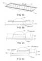
- FIG. 5Aillustrates a bottom reflector insert attached to the top surface of the mounting board.
- FIG. 5Billustrates a cross-sectional view of a portion of the mounting board, a bottom reflector insert and an LED with a submount, where the thickness of the bottom reflector insert is approximately the same thickness as the submount of the LED.
- FIG. 5Cillustrates another cross-sectional view of a portion of the mounting board, a bottom reflector insert and an LED with a submount, where the thickness of bottom reflector insert is significantly greater than the thickness of the submount of the LED.
- FIG. 5Dillustrates another cross-sectional view of a portion of the mounting board, a bottom reflector insert and an LED with a submount, where the bottom reflector insert includes a non-metallic layer and a thin metallic reflective backing layer.
- FIG. 5Eillustrates a perspective view of another embodiment of the mounting board and bottom reflector insert that includes a raised portion between the LEDs.
- FIG. 5Fillustrates another embodiment of a bottom reflector insert where each LED is surrounded by a separate individual optical well.
- FIG. 6Aillustrates an embodiment of sidewall insert used with the illumination device.
- FIGS. 6B and 6Cillustrates a perspective view and side view, respectively, of another embodiment of the sidewall insert with a wavelength converting material patterned along the length of the rectangular cavity and no wavelength converting material patterned along the width.
- FIG. 7Aillustrates a side view of the output window for the illumination device with a layer on the inside surface of the window.
- FIG. 7Billustrates a side view of another embodiment of the output window for the illumination device with two additional layers; one on the inside of the window and one on the outside of the window.
- FIG. 7Cillustrates a side view of another embodiment of the output window for the illumination device with two additional layers; both on the same inside surface of the window.
- FIG. 8shows a perspective view of a reflector mounted to illumination device for collimating the light emitted from the illumination device.
- FIG. 9illustrates illumination device with a bottom heat sink attached.
- FIG. 10illustrates a side view of an illumination device integrated into a retrofit lamp device.
- FIG. 1illustrates a perspective view of an embodiment of a light emitting diode (LED) illumination device 100 .
- FIG. 2shows an exploded view illustrating components of LED illumination device 100 .
- LED illumination device 100includes one or more LED die or packaged LEDs and a mounting board to which LED die or packaged LEDs are attached.
- FIGS. 3A and 3Billustrate perspective, cross-sectional views of an embodiment of the LED illumination device 100 .
- LED illumination device 100includes one or more solid state light emitting elements, such as light emitting diodes (LEDs) 102 , mounted on mounting board 104 .
- Mounting board 104is attached to mounting base 101 and secured in position by mounting board retaining ring 103 .
- mounting board 104 populated by LEDs 102 and mounting board retaining ring 103comprise light source sub-assembly 115 .
- Light source sub-assembly 115is operable to convert electrical energy into light using LEDs 102 .
- the light emitted from light source sub-assembly 115is directed to light conversion sub-assembly 116 for color mixing and color conversion.
- Light conversion sub-assembly 116includes cavity body 105 and output window 108 , and optionally includes either or both bottom reflector insert 106 and sidewall insert 107 .
- Output window 108is fixed to the top of cavity body 105 .
- Cavity body 105includes interior sidewalls, which may be used to reflect light from the LEDS 102 until the light exits through output window 108 when sub-assembly 116 is mounted over light source sub-assembly 115 .
- Bottom reflector insert 106may optionally be placed over mounting board 104 .
- Bottom reflector insert 106includes holes such that the light emitting portion of each LED 102 is not blocked by bottom reflector insert 106 .
- Sidewall insert 107may optionally be placed inside cavity body 105 such that the interior surfaces of sidewall insert 107 reflect the light from the LEDS 102 until the light exits through output window 108 when sub-assembly 116 is mounted over light source sub-assembly 115 .
- the sidewall insert 107 , output window 108 , and bottom reflector insert 106 disposed on mounting board 104define a light mixing cavity 109 in the LED illumination device 100 in which a portion of light from the LEDs 102 is reflected until it exits through output window 108 . Reflecting the light within the cavity 109 prior to exiting the output window 108 has the effect of mixing the light and providing a more uniform distribution of the light that is emitted from the LED illumination device 100 .
- FIGS. 3A and 3Billustrate cut-away perspective views of light mixing cavity 109 .
- Portions of sidewall insert 107may including a coating 111 of wavelength converting material, such as phosphor, as illustrated in FIGS. 3A and 3B .
- portions of output window 108may be coated with a different wavelength converting material (shown in FIG. 7B ).
- the photo converting properties of these materials in combination with the mixing of light within cavity 109results in a color converted light output by output window 108 .
- specific color properties of light output by output window 108may be specified, e.g. color point, color temperature, and color rendering index (CRI).
- CRIcolor rendering index
- Cavity 109may be filled with a non-solid material, such as air or an inert gas, so that the LEDs 102 emit light into the non-solid material as opposed to into a solid encapsulant material.
- a non-solid materialsuch as air or an inert gas
- the cavitymay be hermetically sealed and Argon gas used to fill the cavity.
- Nitrogenmay be used.
- the LEDs 102can emit light having different or the same colors, either by direct emission or by phosphor conversion, e.g., where phosphor layers are applied to the LEDs as part of the LED package.
- the illumination device 100may use any combination of colored LEDs 102 , such as red, green, blue, amber, or cyan, or the LEDs 102 may all produce the same color light or may all produce white light.
- the LEDs 102may all emit either blue or UV light.
- the LEDs 102may emit polarized light or non-polarized light and LED based illumination device 100 may use any combination of polarized or non-polarized LEDs.
- the output light of the illumination device 100When used in combination with phosphors (or other wavelength conversion means such as luminescent dyes), which may be, e.g., in or on the output window 108 , applied to the sidewalls of cavity body 105 , or applied to other components placed inside the cavity (such as sidewall insert 107 and/or bottom reflector insert 106 or other inserted components not shown), the output light of the illumination device 100 has the color as desired.
- phosphorsor other wavelength conversion means such as luminescent dyes
- the phosphorsmay be chosen from the set denoted by the following chemical formulas: Y 3 Al 5 O 12 :Ce, (also known as YAG:Ce, or simply YAG) (Y,Gd) 3 Al 5 O 12 :Ce, CaS:Eu, SrS:Eu, SrGa 2 S4:Eu, Ca 3 (Sc,Mg) 2 Si 3 O 12 :Ce, Ca 3 Sc 2 Si 3 O 12 :Ce, Ca 3 Sc 2 O 4 :Ce, Ba 3 Si 6 O 12 N 2 :Eu, (Sr,Ca)AlSiN 3 :Eu, CaAlSiN 3 :Eu, CaAlSi(ON) 3 :Eu, Ba 2 SiO 4 :Eu, Sr 2 SiO 4 :Eu, Ca 2 SiO 4 :Eu, CaSc 2 O 4 :Ce, CaSi 2 O 2 N 2 :Eu, SrSi 2 O 2 N 2
- the adjustment of color point of the illumination devicemay be accomplished by replacing sidewall insert 107 and/or the output window 108 , which similarly may be coated or impregnated with one or more wavelength converting materials, and are selected based on their performance, such as their color conversion properties.
- a red emitting phosphorsuch as CaAlSiN 3 :Eu, or (Sr,Ca)AlSiN 3 :Eu covers a portion of sidewall insert 107 and bottom reflector insert 106 at the bottom of the cavity 109 , and a YAG phosphor covers a portion of the output window 108 .
- a single type of wavelength converting materialmay be patterned on the sidewall, which may be, e.g., the sidewall insert 107 shown in FIG. 3B .
- a red phosphormay be patterned on different areas of the sidewall insert 107 and a yellow phosphor may cover the output window 108 , shown in FIG. 7A .
- the coverage and/or concentrations of the phosphorsmay be varied to produce different color temperatures. It should be understood that the coverage area of the red and/or the concentrations of the red and yellow phosphors will need to vary to produce the desired color temperatures if the blue light produced by the LEDs 102 varies.
- the color performance of the LEDs 102 , red phosphor on the sidewall insert 107 and the yellow phosphor on the output window 108may be measured before assembly and selected based on performance so that the assembled pieces produce the desired color temperature.
- the thickness of the red phosphormay be, e.g., between 60 ⁇ m to 100 ⁇ m and more specifically between 80 ⁇ m to 90 ⁇ m, while the thickness of the yellow phosphor may be, e.g., between 100 ⁇ m to 140 ⁇ m and more specifically between 110 ⁇ m to 120 ⁇ m.
- the red phosphormay be mixed with a binder at a concentration of 1%-3% by volume.
- the yellow phosphormay be mixed with a binder at a concentration of 12%-17% by volume.
- FIG. 4illustrates mounting board 104 in greater detail.
- the mounting board 104provides electrical connections to the attached LEDs 102 to a power supply (not shown).
- the LEDs 102are packaged LEDs, such as the Luxeon Rebel manufactured by Philips Lumileds Lighting. Other types of packaged LEDs may also be used, such as those manufactured by OSRAM (Ostar package), Luminus Devices (USA), Cree (USA), Nichia (Japan), or Tridonic (Austria).
- a packaged LEDis an assembly of one or more LED die that contains electrical connections, such as wire bond connections or stud bumps, and possibly includes an optical element and thermal, mechanical, and electrical interfaces.
- the LEDs 102may include a lens over the LED chips.
- LEDs without a lensmay be used.
- LEDs without lensesmay include protective layers, which may include phosphors.
- the phosphorscan be applied as a dispersion in a binder, or applied as a separate plate.
- Each LED 102includes at least one LED chip or die, which may be mounted on a submount.
- the LED chiptypically has a size about 1 mm by 1 mm by 0.5 mm, but these dimensions may vary.
- the LEDs 102may include multiple chips.
- the multiple chipscan emit light of similar or different colors, e.g., red, green, and blue.
- different phosphor layersmay be applied on different chips on the same submount.
- the submountmay be ceramic or other appropriate material.
- the submounttypically includes electrical contact pads on a bottom surface that are coupled to contacts on the mounting board 104 .
- electrical bond wiresmay be used to electrically connect the chips to a mounting board.
- the LEDs 102may include thermal contact areas on the bottom surface of the submount through which heat generated by the LED chips can be extracted.
- the thermal contact areas of the LEDsare coupled to heat spreading layers 131 on the mounting board 104 .
- Heat spreading layers 131may be disposed on any of the top, bottom, or intermediate layers of mounting board 104 . Heat spreading layers 131 may be connected by vias that connect any of the top, bottom, and intermediate heat spreading layers.
- the mounting board 104conducts heat generated by the LEDs 102 to the sides of the board 104 and the bottom of the board 104 .
- the bottom of mounting board 104may be thermally coupled to a heat sink 130 (shown in FIG. 9 ) via mounting base 101 .
- mounting board 104may be directly coupled to a heat sink, or a lighting fixture and/or other mechanisms to dissipate the heat, such as a fan.
- the mounting board 104conducts heat to a heat sink thermally coupled to the top of the board 104 .
- mounting board retaining ring 103 and cavity body 105may conduct heat away from the top surface of mounting board 104 .
- Mounting board 104may be an FR4 board, e.g., that is 0.5 mm thick, with relatively thick copper layers, e.g., 30 ⁇ m to 100 ⁇ m, on the top and bottom surfaces that serve as thermal contact areas.
- the board 104may be a metal core printed circuit board (PCB) or a ceramic submount with appropriate electrical connections.
- PCBmetal core printed circuit board
- Other types of boardsmay be used, such as those made of alumina (aluminum oxide in ceramic form), or aluminum nitride (also in ceramic form).
- Mounting board 104includes electrical pads to which the electrical pads on the LEDs 102 are connected.
- the electrical padsare electrically connected by a metal, e.g., copper, trace to a contact, to which a wire, bridge or other external electrical source is connected.
- the electrical padsmay be vias through the board 104 and the electrical connection is made on the opposite side, i.e., the bottom, of the board.
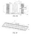
- Mounting board 104as illustrated, is rectangular in dimension. LEDs 102 mounted to mounting board 104 may be arranged in different configurations on rectangular mounting board 104 . In one example LEDs 102 are aligned in rows extending in the length dimension and in columns extending in the width dimension of mounting board 104 .
- LEDs 102have a hexagonal arrangement to produce a closely packed structure. In such an arrangement each LED is equidistant from each of its immediate neighbors. Such an arrangement is desirable to increase the uniformity of light emitted from the light source sub-assembly 115 .
- FIG. 5Aillustrates a bottom reflector insert 106 attached to the top surface of the mounting board 104 .
- the bottom reflector insert 106may be made from a material with high thermal conductivity and may be placed in thermal contact with the board 104 . As illustrated, the bottom reflector insert 106 may be mounted on the top surface of the board 104 , around the LEDs 102 .
- the bottom reflector insert 106may be highly reflective so that light reflecting downward in the cavity 109 is reflected back generally towards the output window 108 .
- the bottom reflector insertby way of example, may reflect at least 95% of incident light between 380 nanometers and 780 nanometers. Additionally, the bottom reflector insert 106 may have a high thermal conductivity, such that it acts as an additional heat spreader.
- the thickness of the bottom reflector insert 106may be approximately the same thickness as the submounts 102 submount of the LEDs 102 or slightly thicker. Holes are punched in the bottom reflector insert 106 for the LEDs 102 and bottom reflector insert 106 is mounted over the LED package submounts 102 submount and the rest of the board 104 . In this manner a highly reflective surface covers the bottom of cavity body 105 except in the areas where light is emitted by LEDs 102 .
- the bottom reflector insert 106may be made with a highly thermally conductive material, such as an aluminum based material that is processed to make the material highly reflective and durable.
- a material referred to as Miro®, manufactured by Alanod, a German companymay be used as the bottom reflector insert 106 .
- the high reflectivity of the bottom reflector insert 106may either be achieved by polishing the aluminum, or by covering the inside surface of the bottom reflector insert 106 with one or more reflective coatings.
- the bottom reflector insert 106might alternatively be made from a highly reflective thin material, such as VikuitiTM ESR, as sold by 3M (USA), which has a thickness of 65 ⁇ m.
- bottom reflector insert 106may be made from a highly reflective non-metallic material such as LumirrorTM E60L manufactured by Toray (Japan) or microcrystalline polyethylene terephthalate (MCPET) such as that manufactured by Furukawa Electric Co. Ltd. (Japan) or a sintered PTFE material such as that manufactured by W.L. Gore (USA).
- the thickness of bottom reflector insert 106particularly when constructed from a non-metallic reflective film, may be significantly greater than the thickness of the submounts 102 submount of LEDs 102 as illustrated in FIG. 5C .
- bottom reflector insert 106may be punched in the bottom reflector insert 106 to reveal the submount 102 submount of the LED package, and bottom reflector insert 106 is mounted directly on top of mounting board 104 .
- the thickness of bottom reflector insert 106may be greater than the thickness of the submount 102 submount without significantly impinging on light emitted by LEDs 102 .
- mounting board 104may include raised pads 104 pad to approximately match the footprint of the LED submount 102 submount such that the light emitting portion of LED 102 is raised above bottom reflector insert 106 .
- the non-metallic layer 106 amay be backed by a thin metallic reflective backing layer 106 b to enhance overall reflectivity as illustrated in FIG. 5D .
- the non-metallic reflective layer 106 amay exhibit diffuse reflective properties and the reflective backing layer 106 b may exhibit specular reflective properties. This approach has been effective in reducing the potential for wave-guiding inside specular reflective layers. It is desirable to minimize wave-guiding within reflective layers because wave-guiding reduces overall cavity efficiency.
- the cavity body 105 and the bottom reflector insert 106may be thermally coupled and may be produced as one piece if desired.
- the bottom reflector insert 106may be mounted to the board 104 , e.g., using a thermal conductive paste or tape.
- the top surface of the mounting board 104is configured to be highly reflective, so as to obviate the need for the bottom reflector insert 106 .
- a reflective coatingmight be applied to board 104 , the coating composed of white particles e.g. made from TiO2, ZnO, or BaSO4 immersed in a transparent binder such as an epoxy, silicone, acrylic, or N-Methylpyrrolidone (NMP) materials.
- the coatingmight be made from a phosphor material such as YAG:Ce.
- the coating of phosphor material and/or the TiO2, ZnO or GaSO4 materialmay be applied directly to the board 104 or to, e.g., the bottom reflector insert 106 , for example, by screen printing.
- FIG. 5Eillustrates a perspective view of another embodiment of illumination device 100 .
- the bottom reflector insert 106may include a raised portion between the LEDs 102 such as that illustrated in FIG. 5D .
- Illumination device 100is illustrated in FIG. 5D with a diverter 117 between the LEDs configured to redirect light emitted at large angles from the LEDs 102 into narrower angles with respect to a normal to the top surface of mounting board 104 .
- the illumination device 100can be used in applications where light under large angles is to be avoided, for example, due to glare issues (office lighting or general lighting), or due to efficiency reasons where it is desirable to send light only where it is needed and most effective, e.g.
- the diverter 117is illustrated as having a tapered shape, but alternative shapes may be used if desired, for example, a half dome shape, or a spherical cap, or aspherical reflector shapes.
- the diverter 117can have a specular reflective coating, a diffuse coating, or can be coated with one or more phosphors.
- the height of the diverter 117may be smaller than the height of the cavity 109 (e.g., approximately half the height of the cavity 109 ) so that there is a small space between the top of the diverter 117 , and the output window 108 .
- FIG. 5Fillustrates another embodiment of a bottom reflector insert 106 where each LED 102 in illumination device 100 is surrounded by a separate individual optical well 118 .
- Optical well 118may have a parabolic, compound parabolic, elliptical shape, or other appropriate shape.
- the light from illumination device 100is collimated from large angles into smaller angles, e.g., from a 2 ⁇ 90 degree angle to a 2 ⁇ 60 degree angle, or a 2 ⁇ 45 degree beam.
- the illumination device 100can be used as a direct light source, for example, as a down light or an under the cabinet light, or it can be used to inject the light into a cavity 109 .
- the optical well 118can have a specular reflective coating, a diffuse coating, or can be coated with one or more phosphors.
- Optical well 118may be constructed as part of bottom reflector insert 106 in one piece of material or may be constructed separately and combined with bottom reflector insert 106 to form a bottom reflector insert 106 with optical well features.
- FIG. 6Aillustrates sidewall insert 107 .
- Sidewall insert 107may be made with highly thermally conductive material, such as an aluminum based material that is processed to make the material highly reflective and durable.
- highly thermally conductive materialsuch as an aluminum based material that is processed to make the material highly reflective and durable.
- a material referred to as Miro®manufactured by Alanod, a German company
- the high reflectivity of sidewall insert 107may be achieved by polishing the aluminum, or by covering the inside surface of the sidewall insert 107 with one or more reflective coatings.
- the bottom reflector insert 106might alternatively be made from a highly reflective thin material, such as VikuitiTM ESR, as sold by 3M (USA), which has a thickness of 65 ⁇ m.
- bottom reflector insert 106may be made from a highly reflective non-metallic material such as LumirrorTM E60L manufactured by Toray (Japan) or microcrystalline polyethylene terephthalate (MCPET) such as that manufactured by Furukawa Electric Co. Ltd. (Japan) or a sintered PTFE material such as that manufactured by W.L. Gore (USA).
- the interior surfaces of sidewall insert 107can either be specular reflective or diffuse reflective.
- An example of a highly specular reflective coatingis a silver mirror, with a transparent layer protecting the silver layer from oxidation.
- highly diffuse reflective materialsinclude MCPET, PTFE, and Toray E60L materials.
- highly diffuse reflective coatingscan be applied. Such coatings may include titanium dioxide (TiO2), zinc oxide (ZnO), and barium sulfate (BaSO4) particles, or a combination of these materials.
- a non-metallic reflective layermay be backed by a reflective backing layer to enhance overall reflectivity.
- the non-metallic reflective layermay exhibit diffuse reflective properties and the reflective backing layer may exhibit specular reflective properties. This approach has been effective in reducing the potential for wave-guiding inside specular reflective layers; resulting in increased cavity efficiency.
- sidewall insert 107may be made of a highly diffuse, reflective MCPET material.
- a portion of the interior surfacesmay be coated with an overcoat layer or impregnated with a wavelength converting material, such as phosphor or luminescent dyes.
- a wavelength converting materialsuch as phosphor or luminescent dyes.
- a phosphor that may be usedmay include Y 3 Al 5 O 12 :Ce, (Y,Gd) 3 Al 5 O 12 :Ce, CaS:Eu, SrS:Eu, SrGa 2 S4:Eu, Ca 3 (Sc,Mg) 2 Si 3 O 12 :Ce, Ca 3 Sc 2 Si 3 O 12 :Ce, Ca 3 Sc 2 O 4 :Ce, Ba 3 Si 6 O 12 N 2 :Eu, (Sr,Ca)AlSiN 3 :Eu, CaAlSiN 3 :Eu, CaAlSi(ON) 3 :Eu, Ba 2 SiO 4 :Eu, Sr 2 SiO 4 :Eu, Ca 2 SiO 4 :Eu, CaSc 2 O 4 :Ce, CaSi 2 O 2 N 2 :Eu, SrSi 2 O 2 N 2 :Eu, BaSi 2 O 2 N 2 :Eu, Ca 5 (PO 4
- the interior sidewall surfaces of cavity 109may be realized using a separate sidewall insert 107 that is placed inside cavity body 105 , or may be achieved by treatment of the interior surfaces of cavity body 105 .
- Sidewall insert 107may be positioned within cavity body 105 and used to define the sidewalls of cavity 109 .
- sidewall insert 107can be inserted into cavity body 105 from the top or the bottom depending on which side has a larger opening.
- FIGS. 6B-6Cillustrate treatment of selected interior sidewall surfaces of cavity 109 .
- the described treatmentsare applied to sidewall insert 107 , but as discussed above, sidewall insert 107 may not be used and the described treatments may be applied to the interior surfaces of cavity body 105 directly.
- FIG. 6 billustrates a rectangular cavity having a length extending along the longer dimension pictured and a width extending along the shorter dimension pictured.
- a reflective coating 113is applied to the two shorter sidewall surfaces 107 s and a coating 111 of wavelength converting material is applied along the sidewall surfaces 107 l corresponding with the length dimension.
- the material used to form the sidewall insert 107itself may be reflective, thereby obviating the need for reflective coating 113 .
- the shorter sidewall surfaces 107 sreflect at least 95% of incident light between 380 nanometers and 780 nanometers without color conversion.
- This combination of treatments to sidewall insert 107i.e., reflective short sidewall surfaces 107 s and wavelength converting long sidewalls surfaces 107 l , has been found to be particularly advantageous.
- the implementation of a reflective surface on the sidewall surfaces 107 s corresponding to the width dimensionhas proven to improve the color uniformity of the output beam emitted from output window 108 .
- FIG. 6B and 6Cillustrate a sawtooth shaped patterned coating 111 where the peak of each sawtooth is aligned with the placement of each LED 102 as illustrated in FIG. 6C .
- Any portion of the sidewall surfaces 107 l without coating 111are reflective and, e.g., may reflect at least 95% of incident light between 380 nanometers and 780 nanometers without color conversion.
- the implementation of phosphor patterns on the sidewall surfaces 107 l corresponding to the length dimension where the phosphor pattern is concentrated around the LEDshas also improved color uniformity and enables more efficient use of phosphor materials.
- a sawtooth patternis illustrated, other patterns such as semicircular, parabolic, flattened sawtooth patterns, and others may be employed to similar effect.
- the coating 111may have no pattern, i.e., the entirety of the sidewall surfaces 107 l may be coated with phosphor.
- FIGS. 7A-7Cillustrate various configurations of output window 108 in cross sectional views.
- the window 108is shown mounted on top of the cavity body 105 . It can be beneficial to seal the gap between the window 108 and the cavity body 105 to form a hermetically sealed cavity 109 , such that no dust or humidity can enter the cavity 109 .
- a sealing materialmay be used to fill the gap between the window 108 and the cavity body 105 , as for example an epoxy or a silicone material. It may be beneficial to use a material that remains flexible over time due to the differences in thermal expansion coefficients of the materials of the window 108 and cavity body 105 .
- the window 108might be made of glass or a transparent ceramic material, and soldered onto the cavity body 105 .
- the window 108may be plated at the edges with a metallic material, such as aluminum, or silver, or copper, or gold, and solder paste is applied in between the cavity body 105 and window 108 .
- solder pasteis applied in between the cavity body 105 and window 108 .
- the window 108has an additional layer 124 on the inside surface of the window, i.e., the surface facing the cavity 109 .
- the additional layer 124may contain either or both diffusing particles and particles with wavelength converting properties such as phosphors.
- the layer 124can be applied to the window 108 by screen printing, spray painting, or powder coating.
- screen printing and spray paintingtypically the particles are immersed in a binder, which can by a polyurethane based lacquer, or a silicone material.
- a binding materialis mixed into the powder mix in the form of small pellets which have a low melting point, and which make a uniform layer when the window 108 is heated, or a base coat is applied to the window 108 to which the particles stick during the coating process.
- the powder coatingmay be applied using an electric field, and the window and phosphor particles baked in an oven so that the phosphor permanently adheres to the window.
- the thickness and optical properties of the layer 124 applied to the window 108may be monitored during the powder coat process for example by using a laser and a spectrometer, and/or detector, or and/or camera, both in forward scatter and back scattered modes, to obtain the right color and/or optical properties.
- the window 108has two additional layers 124 and 126 ; one on the inside of the window and one on the outside of the window 108 , respectively.
- the outside layer 126may be light scattering particles, such as TiO2, ZnO, and/or BaSO4 particles. Phosphor particles may be added to the layer 126 to do a final adjustment of the color of the light coming out of the illumination device 100 .
- the inside layer 124may contain wavelength converting particles, such as a phosphor.
- the window 108also has two additional layers 124 and 128 , but both are on the same inside surface of the window 108 . While two layers are shown, it should be understood that additional layers may be used.
- layer 124which is closest to the window 108 , includes white scattering particles, such that the window 108 appears white if viewed from the outside, and has a uniform light output over angle
- layer 128includes a yellow emitting phosphor.
- the window 108 and the phosphor, e.g., in layer 124 , on the window 108should be configured so that they do not get too hot.
- the window 108may have a high thermal conductivity, e.g., not less than 1 W/(m K), and the window 108 may be thermally coupled to the cavity body 105 , which serves as a heat-sink, using a material with low thermal resistance, such as solder, thermal paste or thermal tape.
- a good material for the windowis aluminum oxide, which can be used in its crystalline form, called Sapphire, as well in its poly-crystalline or ceramic form, called Alumina. Other patterns may be used if desired as for example small dots with varying size, thickness and density.
- FIG. 8shows a perspective view of a reflector 140 mounted to illumination device 100 for collimating the light emitted from the cavity 109 .
- the reflector 140may be made out of a thermal conductive material, such as a material that includes aluminum or copper and may be thermally coupled to a heat spreader on the board 104 , as discussed in reference to FIG. 4A , along with or through cavity body 105 . Heat flows by conduction through heat spreading layers 131 attached to board 104 , the thermally conductive cavity body 105 , and the thermally conductive reflector 140 . Heat also flows via thermal convection over the reflector 140 .
- Reflector 140may be a compound parabolic concentrator, where the concentrator is made out of a highly reflecting material.
- Optical elementssuch as a diffuser or reflector 140 may be removably coupled to the cavity body 105 , e.g., by means of threads, a clamp, a twist-lock mechanism, or other appropriate arrangement. In other examples, diffuser or reflector 140 may be coupled to mounting base 101 directly.
- FIG. 9illustrates illumination device 100 with a bottom heat sink 130 attached.
- the board 104may be bonded to the heat sink 130 by way of thermal epoxy.
- the heat sink 130may be screwed to the illumination device 100 , via screw threads to clamp the illumination device 100 to the heat sink 130 , as illustrated in FIG. 9 .
- the board 104may include heat spreading layers 131 that act as thermal contact areas that are thermally coupled to heat sink 130 , e.g., using thermal grease, thermal tape or thermal epoxy.
- a thermal contact area of at least 50 square millimeters, but preferably 100 square millimetersshould be used per one watt of electrical energy flow into the LEDs on the board.
- a 1000 to 2000 square millimeter heatsink contact areashould be used.
- Using a larger heat sink 130permits the LEDs 102 to be driven at higher power, and also allows for different heat sink designs, so that the cooling capacity is less dependent on the orientation of the heat sink.
- fans or other solutions for forced coolingmay be used to remove the heat from the device.
- the bottom heat sinkmay include an aperture so that electrical connections can be made to the board 104 .
- Heat spreading layer 131 on the board 104may be attached to either the reflector, or to a heat sink, such as heat sink 130 .
- heat spreading layer 131may be attached directly to an external structure such as a light fixture.
- reflector 140may be made of a metal such as aluminum, copper or alloys thereof, and is thermally coupled to the heat sink 130 to assist in heat dissipation.
- multiple LEDs 102may be used in the illumination device 100 .
- the LEDs 102are positioned linearly along the length and width dimension shown.
- the illumination device 100may have more or fewer LEDs, but twenty LEDs has been found to be a useful quantity of LEDs 102 . In one embodiment, twenty LEDs are used.
- any of sidewall insert 107 , bottom reflector insert 106 , and output window 108may be patterned with phosphor. Both the pattern itself and the phosphor composition may vary.
- the illumination devicemay include different types of phosphors that are located at different areas of the light mixing cavity 109 . For example, a red phosphor may be located on either or both of the sidewall insert 107 and the bottom reflector insert 106 and yellow and green phosphors may be located on the top or bottom surfaces of the window 108 or embedded within the window 108 .
- a central reflectore.g., such as diverter 117 shown in FIG.
- 5Emay have patterns of different types of phosphor, e.g., a red phosphor on a first area and a green phosphor on a separate second area.
- different types of phosphorse.g., red and green
- one type of phosphormay be patterned on the sidewall insert 107 at a first area, e.g., in stripes, spots, or other patterns, while another type of phosphor is located on a different second area of the sidewall insert 107 .
- additional phosphorsmay be used and located in different areas in the cavity 109 .
- only a single type of wavelength converting materialmay be used and patterned in the cavity 109 , e.g., on the sidewalls.
- the luminaire illustrated in FIG. 10includes an illumination device 100 integrated into a retrofit lamp device 150 .
- the retrofit lamp device 150includes a reflector 140 with an internal surface 142 that is polished to be reflective or optionally includes a reflective coating and/or a wavelength converting layer.
- the reflector 140may further include a window 144 that may optionally include a coating of a wavelength converting layer or other optical coating such as a dichroic filter.
- an LED based illumination deviceis not an LED, but is an LED light source or fixture or component part of an LED light source or fixture.
- LED based illumination device 100may be a replacement lamp or retrofit lamp or a part of a replacement lamp or retrofit lamp. As illustrated in FIG. 10 , an LED based illumination device 100 may be a part of an LED based retrofit lamp device 150 .
- FIGS. 3A and 3Billustrate the side walls as having a linear configuration, but it should understood that the sidewalls may have any desired configuration, e.g., curved, non-vertical, beveled etc.
- a higher transfer efficiencyis achieved through the light mixing cavity 109 by pre-collimation of the light using tapered side walls.
- cavity body 105is used to clamp mounting board 104 directly to mounting base 101 without the use of mounting board retaining ring 103 .
- mounting base 101 and heat sink 130may be a single component. The examples illustrated in FIGS.
Landscapes
- Engineering & Computer Science (AREA)
- Physics & Mathematics (AREA)
- Microelectronics & Electronic Packaging (AREA)
- Optics & Photonics (AREA)
- General Engineering & Computer Science (AREA)
- Led Device Packages (AREA)
- Non-Portable Lighting Devices Or Systems Thereof (AREA)
Abstract
Description
Claims (14)
Priority Applications (12)
| Application Number | Priority Date | Filing Date | Title |
|---|---|---|---|
| US13/015,431US9631782B2 (en) | 2010-02-04 | 2011-01-27 | LED-based rectangular illumination device |
| PCT/US2011/022986WO2011097135A1 (en) | 2010-02-04 | 2011-01-28 | Led-based rectangular illumination device |
| EP20130197032EP2708796A2 (en) | 2010-02-04 | 2011-01-28 | LED-based rectangular illumination device |
| ES11705728.1TES2453982T3 (en) | 2010-02-04 | 2011-01-28 | Rectangular LED-based lighting device |
| MX2012009081AMX2012009081A (en) | 2010-02-04 | 2011-01-28 | Led-based rectangular illumination device. |
| JP2012552011AJP2013519208A (en) | 2010-02-04 | 2011-01-28 | LED-based rectangular illumination device |
| BR112012019621ABR112012019621A2 (en) | 2010-02-04 | 2011-01-28 | lighting device |
| CA2788107ACA2788107A1 (en) | 2010-02-04 | 2011-01-28 | Led-based rectangular illumination device |
| KR1020127020717AKR20120123674A (en) | 2010-02-04 | 2011-01-28 | Led-based rectangular illumination device |
| CN2011800084162ACN102792085A (en) | 2010-02-04 | 2011-01-28 | LED-based rectangular illumination device |
| EP11705728.1AEP2531770B1 (en) | 2010-02-04 | 2011-01-28 | Led-based rectangular illumination device |
| TW100103996ATWI428543B (en) | 2010-02-04 | 2011-02-01 | Led-based rectangular illumination device |
Applications Claiming Priority (2)
| Application Number | Priority Date | Filing Date | Title |
|---|---|---|---|
| US30154610P | 2010-02-04 | 2010-02-04 | |
| US13/015,431US9631782B2 (en) | 2010-02-04 | 2011-01-27 | LED-based rectangular illumination device |
Publications (2)
| Publication Number | Publication Date |
|---|---|
| US20110182068A1 US20110182068A1 (en) | 2011-07-28 |
| US9631782B2true US9631782B2 (en) | 2017-04-25 |
Family
ID=44308825
Family Applications (1)
| Application Number | Title | Priority Date | Filing Date |
|---|---|---|---|
| US13/015,431Active2032-11-23US9631782B2 (en) | 2010-02-04 | 2011-01-27 | LED-based rectangular illumination device |
Country Status (11)
| Country | Link |
|---|---|
| US (1) | US9631782B2 (en) |
| EP (2) | EP2708796A2 (en) |
| JP (1) | JP2013519208A (en) |
| KR (1) | KR20120123674A (en) |
| CN (1) | CN102792085A (en) |
| BR (1) | BR112012019621A2 (en) |
| CA (1) | CA2788107A1 (en) |
| ES (1) | ES2453982T3 (en) |
| MX (1) | MX2012009081A (en) |
| TW (1) | TWI428543B (en) |
| WO (1) | WO2011097135A1 (en) |
Cited By (2)
| Publication number | Priority date | Publication date | Assignee | Title |
|---|---|---|---|---|
| US20160252219A1 (en)* | 2011-10-26 | 2016-09-01 | Koninklijke Philips N.V. | Light-emitting arrangement with adapted wavelength converter |
| US10760745B2 (en)* | 2016-11-10 | 2020-09-01 | Lumileds Llc | LED lighting unit |
Families Citing this family (11)
| Publication number | Priority date | Publication date | Assignee | Title |
|---|---|---|---|---|
| US9228785B2 (en) | 2010-05-04 | 2016-01-05 | Alexander Poltorak | Fractal heat transfer device |
| US10852069B2 (en) | 2010-05-04 | 2020-12-01 | Fractal Heatsink Technologies, LLC | System and method for maintaining efficiency of a fractal heat sink |
| US8820951B2 (en) | 2012-02-06 | 2014-09-02 | Xicato, Inc. | LED-based light source with hybrid spot and general lighting characteristics |
| EP2820351B1 (en)* | 2012-03-01 | 2017-02-01 | Philips Lighting Holding B.V. | Led lighting arrangement |
| EP2639491A1 (en)* | 2012-03-12 | 2013-09-18 | Panasonic Corporation | Light Emitting Device, And Illumination Apparatus And Luminaire Using Same |
| US20130272027A1 (en)* | 2012-04-11 | 2013-10-17 | Shenzhen China Star Optoelectronics Technology Co., Ltd. | Method for Manufacturing LED Light Bar and LED Light Bar and Backlight Module |
| ITFI20120246A1 (en)* | 2012-11-15 | 2014-05-16 | Consorzio Terranuova | "LIGHTING SYSTEM AND ITS COMPONENTS" |
| US10308856B1 (en) | 2013-03-15 | 2019-06-04 | The Research Foundation For The State University Of New York | Pastes for thermal, electrical and mechanical bonding |
| EP3407101B1 (en)* | 2016-01-22 | 2024-05-29 | Niterra Co., Ltd. | Wavelength conversion member and light-emitting device |
| CA3123580C (en)* | 2018-12-17 | 2024-04-30 | Lutron Technology Company Llc | Light source having multiple differently-colored emitters |
| CN115823530A (en)* | 2022-12-12 | 2023-03-21 | 苏州欧普照明有限公司 | Reflectors and lighting fixtures |
Citations (75)
| Publication number | Priority date | Publication date | Assignee | Title |
|---|---|---|---|---|
| US3851164A (en)* | 1973-12-04 | 1974-11-26 | C Intrator | Umbrella light |
| US4277820A (en)* | 1979-04-04 | 1981-07-07 | Bostonian Edward T | Method and apparatus for converting a ceiling light fixture having a plurality of fluorescent lamps into a single lamp, or two lamp, fixture |
| US5962971A (en) | 1997-08-29 | 1999-10-05 | Chen; Hsing | LED structure with ultraviolet-light emission chip and multilayered resins to generate various colored lights |
| US5966393A (en) | 1996-12-13 | 1999-10-12 | The Regents Of The University Of California | Hybrid light-emitting sources for efficient and cost effective white lighting and for full-color applications |
| US5998925A (en) | 1996-07-29 | 1999-12-07 | Nichia Kagaku Kogyo Kabushiki Kaisha | Light emitting device having a nitride compound semiconductor and a phosphor containing a garnet fluorescent material |
| US6066861A (en) | 1996-09-20 | 2000-05-23 | Siemens Aktiengesellschaft | Wavelength-converting casting composition and its use |
| US6068383A (en) | 1998-03-02 | 2000-05-30 | Robertson; Roger | Phosphorous fluorescent light assembly excited by light emitting diodes |
| US6220725B1 (en) | 1998-03-30 | 2001-04-24 | Eastman Kodak Company | Integrating cavity light source |
| US6234648B1 (en) | 1998-09-28 | 2001-05-22 | U.S. Philips Corporation | Lighting system |
| US6340824B1 (en) | 1997-09-01 | 2002-01-22 | Kabushiki Kaisha Toshiba | Semiconductor light emitting device including a fluorescent material |
| US6351069B1 (en) | 1999-02-18 | 2002-02-26 | Lumileds Lighting, U.S., Llc | Red-deficiency-compensating phosphor LED |
| US6357889B1 (en) | 1999-12-01 | 2002-03-19 | General Electric Company | Color tunable light source |
| US20020043926A1 (en) | 2000-08-28 | 2002-04-18 | Toyoda Gosei Co., Ltd. | Light-emitting unit |
| US6469322B1 (en) | 1998-02-06 | 2002-10-22 | General Electric Company | Green emitting phosphor for use in UV light emitting diodes |
| US6504301B1 (en) | 1999-09-03 | 2003-01-07 | Lumileds Lighting, U.S., Llc | Non-incandescent lightbulb package using light emitting diodes |
| US6547416B2 (en)* | 2000-12-21 | 2003-04-15 | Koninklijke Philips Electronics N.V. | Faceted multi-chip package to provide a beam of uniform white light from multiple monochrome LEDs |
| US6577073B2 (en) | 2000-05-31 | 2003-06-10 | Matsushita Electric Industrial Co., Ltd. | Led lamp |
| US6576930B2 (en) | 1996-06-26 | 2003-06-10 | Osram Opto Semiconductors Gmbh | Light-radiating semiconductor component with a luminescence conversion element |
| US6586882B1 (en) | 1999-04-20 | 2003-07-01 | Koninklijke Philips Electronics N.V. | Lighting system |
| US6600175B1 (en) | 1996-03-26 | 2003-07-29 | Advanced Technology Materials, Inc. | Solid state white light emitter and display using same |
| US6621211B1 (en) | 2000-05-15 | 2003-09-16 | General Electric Company | White light emitting phosphor blends for LED devices |
| US6649946B2 (en) | 1999-11-30 | 2003-11-18 | Osram Opto Semiconductors Gmbh | Light source using a yellow-to-red-emitting phosphor |
| US6674233B2 (en) | 2001-09-20 | 2004-01-06 | Patent-Treuhand-Gesellschaft für elektrische Glühlampen mbH | Illumination unit having at least one LED as light source |
| US6674223B2 (en) | 1999-11-30 | 2004-01-06 | Lg Electronics Inc. | Mask in color cathode ray tube |
| US6680569B2 (en) | 1999-02-18 | 2004-01-20 | Lumileds Lighting U.S. Llc | Red-deficiency compensating phosphor light emitting device |
| US6724142B2 (en) | 2001-02-07 | 2004-04-20 | Patent-Treuhand-Gesellschaft für elektrische Glühlampen mbH | Highly efficient fluorescent material |
| US6765237B1 (en) | 2003-01-15 | 2004-07-20 | Gelcore, Llc | White light emitting device based on UV LED and phosphor blend |
| US6791259B1 (en) | 1998-11-30 | 2004-09-14 | General Electric Company | Solid state illumination system containing a light emitting diode, a light scattering material and a luminescent material |
| US6850002B2 (en) | 2000-07-28 | 2005-02-01 | Osram Opto Semiconductors Gmbh | Light emitting device for generating specific colored light, including white light |
| US20050057145A1 (en) | 2003-09-17 | 2005-03-17 | Nan Ya Plastics Corporation | Method for producing white light emission by means of secondary light excitation and its product |
| EP1548851A2 (en) | 2003-12-26 | 2005-06-29 | Stanley Electric Co., Ltd. | Semiconductor light-emitting apparatus having wavelength conversion portion and method of fabricating the same |
| US7004679B2 (en) | 2001-12-13 | 2006-02-28 | Nippon Steel Corporation | Easily-cuttable tunnel segment structure |
| US20060087487A1 (en) | 2004-10-26 | 2006-04-27 | Tsutomu Ota | Lighting apparatus and liquid crystal display apparatus |
| US20060097245A1 (en) | 2002-08-30 | 2006-05-11 | Aanegola Srinath K | Light emitting diode component |
| US20060152140A1 (en) | 2005-01-10 | 2006-07-13 | Brandes George R | Light emission device |
| US7083302B2 (en) | 2004-03-24 | 2006-08-01 | J. S. Technology Co., Ltd. | White light LED assembly |
| TWM300351U (en) | 2006-05-10 | 2006-11-01 | Bacol Optoelectronic Co Ltd | Full-color light-emitting unit and the full-color LED panel |
| WO2007002234A1 (en) | 2005-06-23 | 2007-01-04 | Rensselaer Polytechnic Institute | Package design for producing white light with short-wavelength leds and down-conversion materials |
| US20070081336A1 (en) | 2005-10-11 | 2007-04-12 | Bierhuizen Serge J | Illumination system with optical concentrator and wavelength converting element |
| EP1780592A1 (en) | 2004-06-30 | 2007-05-02 | Mitsubishi Chemical Corporation | Light emitting device, backlight unit for lighting, display unit and display unit |
| KR100729910B1 (en)* | 2006-11-23 | 2007-06-18 | 성일물산 주식회사 | Integral Solar Delineator |
| US7250715B2 (en) | 2004-02-23 | 2007-07-31 | Philips Lumileds Lighting Company, Llc | Wavelength converted semiconductor light emitting devices |
| WO2007102098A1 (en) | 2006-03-06 | 2007-09-13 | Koninklijke Philips Electronics N.V. | Light-emitting diode module |
| US20070223219A1 (en) | 2005-01-10 | 2007-09-27 | Cree, Inc. | Multi-chip light emitting device lamps for providing high-cri warm white light and light fixtures including the same |
| US20070236933A1 (en) | 2006-04-06 | 2007-10-11 | Philips Lumileds Lighting Company Llc | Angular dependent element positioned for color tuning |
| WO2007130536A2 (en) | 2006-05-05 | 2007-11-15 | Cree Led Lighting Solutions, Inc. | Lighting device |
| JP2008045942A (en)* | 2006-08-11 | 2008-02-28 | Nsk Ltd | Magnetic encoder and rolling bearing unit including the magnetic encoder |
| US7344952B2 (en) | 2005-10-28 | 2008-03-18 | Philips Lumileds Lighting Company, Llc | Laminating encapsulant film containing phosphor over LEDs |
| US7350933B2 (en)* | 2005-05-23 | 2008-04-01 | Avago Technologies Ecbu Ip Pte Ltd | Phosphor converted light source |
| US20080128735A1 (en) | 2006-12-05 | 2008-06-05 | Samsung Electro-Mechanics Co., Ltd. | White light emitting device and white light source module using the same |
| US20080142816A1 (en) | 2006-12-15 | 2008-06-19 | Philips Lumileds Lighting Company Llc | Tunable White Point Light Source Using a Wavelength Converting Element |
| US7431479B2 (en) | 2004-07-15 | 2008-10-07 | Lumination Llc | LED lighting system with reflective board |
| WO2008142638A1 (en) | 2007-05-24 | 2008-11-27 | Koninklijke Philips Electronics N.V. | Color-tunable illumination system |
| WO2008149250A1 (en) | 2007-06-04 | 2008-12-11 | Koninklijke Philips Electronics N.V. | Color-tunable illumination system, lamp and luminaire |
| WO2008157080A2 (en) | 2007-06-18 | 2008-12-24 | Xicato, Inc. | Solid state illumination device |
| US7479662B2 (en) | 2002-08-30 | 2009-01-20 | Lumination Llc | Coated LED with improved efficiency |
| WO2009013695A2 (en) | 2007-07-25 | 2009-01-29 | Koninklijke Philips Electronics N.V. | Color conversion device and color controllable light-output device |
| WO2009016585A2 (en) | 2007-08-02 | 2009-02-05 | Koninklijke Philips Electronics N.V. | Color conversion device |
| WO2009021859A1 (en) | 2007-08-10 | 2009-02-19 | Osram Gesellschaft mit beschränkter Haftung | Radiation-emitting device |
| US7494246B2 (en) | 2007-06-06 | 2009-02-24 | Philips Lumileds Lighting Company, Llc | Thin luminaire for general lighting applications |
| US7503676B2 (en)* | 2006-07-26 | 2009-03-17 | Kyocera Corporation | Light-emitting device and illuminating apparatus |
| US20090103296A1 (en) | 2007-10-17 | 2009-04-23 | Xicato, Inc. | Illumination Device with Light Emitting Diodes |
| WO2009052099A1 (en) | 2007-10-17 | 2009-04-23 | Xicato, Inc. | Illumination device with light emitting diodes and movable light adjustment member |
| US20090116251A1 (en) | 2007-11-05 | 2009-05-07 | Xicato, Inc. | Modular Solid State Lighting Device |
| US7534002B2 (en) | 2005-09-15 | 2009-05-19 | Toyoda Gosei Co., Ltd. | Lighting device |
| US7555194B2 (en)* | 2004-12-08 | 2009-06-30 | Nippon Sheet Glass Co., Ltd. | Illumination device and image scanning device |
| US7614759B2 (en) | 2005-12-22 | 2009-11-10 | Cree Led Lighting Solutions, Inc. | Lighting device |
| TW200947694A (en) | 2008-01-31 | 2009-11-16 | Koninkl Philips Electronics Nv | A light emitting device |
| TW200949157A (en) | 2008-02-08 | 2009-12-01 | 3M Innovative Properties Co | Perforated backlight |
| US7646030B2 (en)* | 2004-05-11 | 2010-01-12 | Neobulb Technologies, Inc. | Flip chip type LED lighting device manufacturing method |
| WO2010017523A1 (en) | 2008-08-08 | 2010-02-11 | Xicato, Inc. | Color tunable light source |
| US7717591B2 (en) | 2007-12-27 | 2010-05-18 | Lumination Llc | Incorporating reflective layers into LED systems and/or components |
| US7726856B2 (en)* | 2006-07-14 | 2010-06-01 | Koito Manufacturing Co., Ltd. | Vehicular marker lamp |
| US7845825B2 (en)* | 2009-12-02 | 2010-12-07 | Abl Ip Holding Llc | Light fixture using near UV solid state device and remote semiconductor nanophosphors to produce white light |
| US8097894B2 (en)* | 2009-07-23 | 2012-01-17 | Koninklijke Philips Electronics N.V. | LED with molded reflective sidewall coating |
Family Cites Families (2)
| Publication number | Priority date | Publication date | Assignee | Title |
|---|---|---|---|---|
| WO2004100226A2 (en)* | 2003-05-05 | 2004-11-18 | Gelcore Llc | Method and apparatus for led panel lamp systems |
| JP4771800B2 (en)* | 2005-12-02 | 2011-09-14 | スタンレー電気株式会社 | Semiconductor light emitting device and manufacturing method thereof |
- 2011
- 2011-01-27USUS13/015,431patent/US9631782B2/enactiveActive
- 2011-01-28EPEP20130197032patent/EP2708796A2/ennot_activeWithdrawn
- 2011-01-28EPEP11705728.1Apatent/EP2531770B1/ennot_activeNot-in-force
- 2011-01-28MXMX2012009081Apatent/MX2012009081A/enactiveIP Right Grant
- 2011-01-28CNCN2011800084162Apatent/CN102792085A/enactivePending
- 2011-01-28WOPCT/US2011/022986patent/WO2011097135A1/enactiveApplication Filing
- 2011-01-28CACA2788107Apatent/CA2788107A1/ennot_activeAbandoned
- 2011-01-28KRKR1020127020717Apatent/KR20120123674A/ennot_activeWithdrawn
- 2011-01-28BRBR112012019621Apatent/BR112012019621A2/ennot_activeIP Right Cessation
- 2011-01-28JPJP2012552011Apatent/JP2013519208A/enactivePending
- 2011-01-28ESES11705728.1Tpatent/ES2453982T3/enactiveActive
- 2011-02-01TWTW100103996Apatent/TWI428543B/ennot_activeIP Right Cessation
Patent Citations (84)
| Publication number | Priority date | Publication date | Assignee | Title |
|---|---|---|---|---|
| US3851164A (en)* | 1973-12-04 | 1974-11-26 | C Intrator | Umbrella light |
| US4277820A (en)* | 1979-04-04 | 1981-07-07 | Bostonian Edward T | Method and apparatus for converting a ceiling light fixture having a plurality of fluorescent lamps into a single lamp, or two lamp, fixture |
| US6600175B1 (en) | 1996-03-26 | 2003-07-29 | Advanced Technology Materials, Inc. | Solid state white light emitter and display using same |
| US6812500B2 (en) | 1996-06-26 | 2004-11-02 | Osram Opto Semiconductors Gmbh & Co. Ohg. | Light-radiating semiconductor component with a luminescence conversion element |
| US7126162B2 (en) | 1996-06-26 | 2006-10-24 | Osram Gmbh | Light-radiating semiconductor component with a luminescence conversion element |
| US7629621B2 (en) | 1996-06-26 | 2009-12-08 | Osram Gmbh | Light-radiating semiconductor component with a luminescence conversion element |
| US6576930B2 (en) | 1996-06-26 | 2003-06-10 | Osram Opto Semiconductors Gmbh | Light-radiating semiconductor component with a luminescence conversion element |
| US5998925A (en) | 1996-07-29 | 1999-12-07 | Nichia Kagaku Kogyo Kabushiki Kaisha | Light emitting device having a nitride compound semiconductor and a phosphor containing a garnet fluorescent material |
| US6066861A (en) | 1996-09-20 | 2000-05-23 | Siemens Aktiengesellschaft | Wavelength-converting casting composition and its use |
| US5966393A (en) | 1996-12-13 | 1999-10-12 | The Regents Of The University Of California | Hybrid light-emitting sources for efficient and cost effective white lighting and for full-color applications |
| US5962971A (en) | 1997-08-29 | 1999-10-05 | Chen; Hsing | LED structure with ultraviolet-light emission chip and multilayered resins to generate various colored lights |
| US6340824B1 (en) | 1997-09-01 | 2002-01-22 | Kabushiki Kaisha Toshiba | Semiconductor light emitting device including a fluorescent material |
| US6469322B1 (en) | 1998-02-06 | 2002-10-22 | General Electric Company | Green emitting phosphor for use in UV light emitting diodes |
| US6068383A (en) | 1998-03-02 | 2000-05-30 | Robertson; Roger | Phosphorous fluorescent light assembly excited by light emitting diodes |
| US6220725B1 (en) | 1998-03-30 | 2001-04-24 | Eastman Kodak Company | Integrating cavity light source |
| US6234648B1 (en) | 1998-09-28 | 2001-05-22 | U.S. Philips Corporation | Lighting system |
| US6791259B1 (en) | 1998-11-30 | 2004-09-14 | General Electric Company | Solid state illumination system containing a light emitting diode, a light scattering material and a luminescent material |
| US6351069B1 (en) | 1999-02-18 | 2002-02-26 | Lumileds Lighting, U.S., Llc | Red-deficiency-compensating phosphor LED |
| US6680569B2 (en) | 1999-02-18 | 2004-01-20 | Lumileds Lighting U.S. Llc | Red-deficiency compensating phosphor light emitting device |
| US6586882B1 (en) | 1999-04-20 | 2003-07-01 | Koninklijke Philips Electronics N.V. | Lighting system |
| US6504301B1 (en) | 1999-09-03 | 2003-01-07 | Lumileds Lighting, U.S., Llc | Non-incandescent lightbulb package using light emitting diodes |
| US6649946B2 (en) | 1999-11-30 | 2003-11-18 | Osram Opto Semiconductors Gmbh | Light source using a yellow-to-red-emitting phosphor |
| US6674223B2 (en) | 1999-11-30 | 2004-01-06 | Lg Electronics Inc. | Mask in color cathode ray tube |
| US6357889B1 (en) | 1999-12-01 | 2002-03-19 | General Electric Company | Color tunable light source |
| US6621211B1 (en) | 2000-05-15 | 2003-09-16 | General Electric Company | White light emitting phosphor blends for LED devices |
| US6577073B2 (en) | 2000-05-31 | 2003-06-10 | Matsushita Electric Industrial Co., Ltd. | Led lamp |
| US6850002B2 (en) | 2000-07-28 | 2005-02-01 | Osram Opto Semiconductors Gmbh | Light emitting device for generating specific colored light, including white light |
| US20020043926A1 (en) | 2000-08-28 | 2002-04-18 | Toyoda Gosei Co., Ltd. | Light-emitting unit |
| US6547416B2 (en)* | 2000-12-21 | 2003-04-15 | Koninklijke Philips Electronics N.V. | Faceted multi-chip package to provide a beam of uniform white light from multiple monochrome LEDs |
| US6724142B2 (en) | 2001-02-07 | 2004-04-20 | Patent-Treuhand-Gesellschaft für elektrische Glühlampen mbH | Highly efficient fluorescent material |
| US6674233B2 (en) | 2001-09-20 | 2004-01-06 | Patent-Treuhand-Gesellschaft für elektrische Glühlampen mbH | Illumination unit having at least one LED as light source |
| US7004679B2 (en) | 2001-12-13 | 2006-02-28 | Nippon Steel Corporation | Easily-cuttable tunnel segment structure |
| US20060097245A1 (en) | 2002-08-30 | 2006-05-11 | Aanegola Srinath K | Light emitting diode component |
| US7479662B2 (en) | 2002-08-30 | 2009-01-20 | Lumination Llc | Coated LED with improved efficiency |
| US6765237B1 (en) | 2003-01-15 | 2004-07-20 | Gelcore, Llc | White light emitting device based on UV LED and phosphor blend |
| US20050057145A1 (en) | 2003-09-17 | 2005-03-17 | Nan Ya Plastics Corporation | Method for producing white light emission by means of secondary light excitation and its product |
| EP1548851A2 (en) | 2003-12-26 | 2005-06-29 | Stanley Electric Co., Ltd. | Semiconductor light-emitting apparatus having wavelength conversion portion and method of fabricating the same |
| US7250715B2 (en) | 2004-02-23 | 2007-07-31 | Philips Lumileds Lighting Company, Llc | Wavelength converted semiconductor light emitting devices |
| US7083302B2 (en) | 2004-03-24 | 2006-08-01 | J. S. Technology Co., Ltd. | White light LED assembly |
| US7646030B2 (en)* | 2004-05-11 | 2010-01-12 | Neobulb Technologies, Inc. | Flip chip type LED lighting device manufacturing method |
| EP1780592A1 (en) | 2004-06-30 | 2007-05-02 | Mitsubishi Chemical Corporation | Light emitting device, backlight unit for lighting, display unit and display unit |
| US7431479B2 (en) | 2004-07-15 | 2008-10-07 | Lumination Llc | LED lighting system with reflective board |
| US20060087487A1 (en) | 2004-10-26 | 2006-04-27 | Tsutomu Ota | Lighting apparatus and liquid crystal display apparatus |
| US7555194B2 (en)* | 2004-12-08 | 2009-06-30 | Nippon Sheet Glass Co., Ltd. | Illumination device and image scanning device |
| US20060152140A1 (en) | 2005-01-10 | 2006-07-13 | Brandes George R | Light emission device |
| US7564180B2 (en) | 2005-01-10 | 2009-07-21 | Cree, Inc. | Light emission device and method utilizing multiple emitters and multiple phosphors |
| US20070223219A1 (en) | 2005-01-10 | 2007-09-27 | Cree, Inc. | Multi-chip light emitting device lamps for providing high-cri warm white light and light fixtures including the same |
| US7350933B2 (en)* | 2005-05-23 | 2008-04-01 | Avago Technologies Ecbu Ip Pte Ltd | Phosphor converted light source |
| WO2007002234A1 (en) | 2005-06-23 | 2007-01-04 | Rensselaer Polytechnic Institute | Package design for producing white light with short-wavelength leds and down-conversion materials |
| US7534002B2 (en) | 2005-09-15 | 2009-05-19 | Toyoda Gosei Co., Ltd. | Lighting device |
| US20070081336A1 (en) | 2005-10-11 | 2007-04-12 | Bierhuizen Serge J | Illumination system with optical concentrator and wavelength converting element |
| US7344952B2 (en) | 2005-10-28 | 2008-03-18 | Philips Lumileds Lighting Company, Llc | Laminating encapsulant film containing phosphor over LEDs |
| US7614759B2 (en) | 2005-12-22 | 2009-11-10 | Cree Led Lighting Solutions, Inc. | Lighting device |
| WO2007102098A1 (en) | 2006-03-06 | 2007-09-13 | Koninklijke Philips Electronics N.V. | Light-emitting diode module |
| US20070236933A1 (en) | 2006-04-06 | 2007-10-11 | Philips Lumileds Lighting Company Llc | Angular dependent element positioned for color tuning |
| WO2007130536A2 (en) | 2006-05-05 | 2007-11-15 | Cree Led Lighting Solutions, Inc. | Lighting device |
| US20070262334A1 (en) | 2006-05-10 | 2007-11-15 | Wei-Pang Chiang | Full color led display |
| TWM300351U (en) | 2006-05-10 | 2006-11-01 | Bacol Optoelectronic Co Ltd | Full-color light-emitting unit and the full-color LED panel |
| US7726856B2 (en)* | 2006-07-14 | 2010-06-01 | Koito Manufacturing Co., Ltd. | Vehicular marker lamp |
| US7503676B2 (en)* | 2006-07-26 | 2009-03-17 | Kyocera Corporation | Light-emitting device and illuminating apparatus |
| JP2008045942A (en)* | 2006-08-11 | 2008-02-28 | Nsk Ltd | Magnetic encoder and rolling bearing unit including the magnetic encoder |
| KR100729910B1 (en)* | 2006-11-23 | 2007-06-18 | 성일물산 주식회사 | Integral Solar Delineator |
| US20080128735A1 (en) | 2006-12-05 | 2008-06-05 | Samsung Electro-Mechanics Co., Ltd. | White light emitting device and white light source module using the same |
| US20080142816A1 (en) | 2006-12-15 | 2008-06-19 | Philips Lumileds Lighting Company Llc | Tunable White Point Light Source Using a Wavelength Converting Element |
| WO2008142638A1 (en) | 2007-05-24 | 2008-11-27 | Koninklijke Philips Electronics N.V. | Color-tunable illumination system |
| WO2008149250A1 (en) | 2007-06-04 | 2008-12-11 | Koninklijke Philips Electronics N.V. | Color-tunable illumination system, lamp and luminaire |
| US7494246B2 (en) | 2007-06-06 | 2009-02-24 | Philips Lumileds Lighting Company, Llc | Thin luminaire for general lighting applications |
| WO2008157080A2 (en) | 2007-06-18 | 2008-12-24 | Xicato, Inc. | Solid state illumination device |
| WO2009013695A2 (en) | 2007-07-25 | 2009-01-29 | Koninklijke Philips Electronics N.V. | Color conversion device and color controllable light-output device |
| WO2009016585A2 (en) | 2007-08-02 | 2009-02-05 | Koninklijke Philips Electronics N.V. | Color conversion device |
| WO2009016585A3 (en) | 2007-08-02 | 2009-04-09 | Koninkl Philips Electronics Nv | Color conversion device |
| TW200926453A (en) | 2007-08-02 | 2009-06-16 | Koninkl Philips Electronics Nv | Color conversion device |
| WO2009021859A1 (en) | 2007-08-10 | 2009-02-19 | Osram Gesellschaft mit beschränkter Haftung | Radiation-emitting device |
| WO2009052099A1 (en) | 2007-10-17 | 2009-04-23 | Xicato, Inc. | Illumination device with light emitting diodes and movable light adjustment member |
| US20090103296A1 (en) | 2007-10-17 | 2009-04-23 | Xicato, Inc. | Illumination Device with Light Emitting Diodes |
| US20090116251A1 (en) | 2007-11-05 | 2009-05-07 | Xicato, Inc. | Modular Solid State Lighting Device |
| US7717591B2 (en) | 2007-12-27 | 2010-05-18 | Lumination Llc | Incorporating reflective layers into LED systems and/or components |
| TW200947694A (en) | 2008-01-31 | 2009-11-16 | Koninkl Philips Electronics Nv | A light emitting device |
| US20100309648A1 (en) | 2008-01-31 | 2010-12-09 | Koninklijke Philips Electronics N.V. | Light emitting device |
| TW200949157A (en) | 2008-02-08 | 2009-12-01 | 3M Innovative Properties Co | Perforated backlight |
| US20110032449A1 (en) | 2008-02-08 | 2011-02-10 | Freier David G | Perforated backlight |
| WO2010017523A1 (en) | 2008-08-08 | 2010-02-11 | Xicato, Inc. | Color tunable light source |
| US8097894B2 (en)* | 2009-07-23 | 2012-01-17 | Koninklijke Philips Electronics N.V. | LED with molded reflective sidewall coating |
| US7845825B2 (en)* | 2009-12-02 | 2010-12-07 | Abl Ip Holding Llc | Light fixture using near UV solid state device and remote semiconductor nanophosphors to produce white light |
Non-Patent Citations (6)
| Title |
|---|
| English Abstract of TW 200926453 visited at www.espacenet.com on Jun. 7, 2013, 2 pages. |
| English Abstract of TW 200947694 visited at www.espacenet.com on Jun. 7, 2013, 2 pages. |
| English Abstract of TW 200949157 visited at www.espacenet.com on Jun. 7, 2013, 2 pages. |
| English Abstract of TW M300351 visited at www.espacenet.com on Jun. 7, 2013, 1 page. |
| International Search Report and Written Opinion mailed on Jul. 14, 2011 for International Application No. PCT/US2011/022986 , 12 pages. |
| International Search Report and Written Opinion mailed on Jul. 14, 2011 for International Application No. PCT/US2011/022986, 12 pages. |
Cited By (2)
| Publication number | Priority date | Publication date | Assignee | Title |
|---|---|---|---|---|
| US20160252219A1 (en)* | 2011-10-26 | 2016-09-01 | Koninklijke Philips N.V. | Light-emitting arrangement with adapted wavelength converter |
| US10760745B2 (en)* | 2016-11-10 | 2020-09-01 | Lumileds Llc | LED lighting unit |
Also Published As
| Publication number | Publication date |
|---|---|
| ES2453982T3 (en) | 2014-04-09 |
| KR20120123674A (en) | 2012-11-09 |
| EP2708796A2 (en) | 2014-03-19 |
| CA2788107A1 (en) | 2011-08-11 |
| BR112012019621A2 (en) | 2019-09-24 |
| JP2013519208A (en) | 2013-05-23 |
| EP2531770B1 (en) | 2013-12-25 |
| TWI428543B (en) | 2014-03-01 |
| TW201142216A (en) | 2011-12-01 |
| US20110182068A1 (en) | 2011-07-28 |
| EP2531770A1 (en) | 2012-12-12 |
| WO2011097135A1 (en) | 2011-08-11 |
| CN102792085A (en) | 2012-11-21 |
| MX2012009081A (en) | 2012-12-17 |
Similar Documents
| Publication | Publication Date | Title |
|---|---|---|
| US9631782B2 (en) | LED-based rectangular illumination device | |
| US8297767B2 (en) | LED-based illumination modules with PTFE color converting surfaces | |
| US9086213B2 (en) | Illumination device with light emitting diodes | |
| US9528666B2 (en) | Integrated LED based illumination device | |
| US8899767B2 (en) | Grid structure on a transmissive layer of an LED-based illumination module |
Legal Events
| Date | Code | Title | Description |
|---|---|---|---|
| AS | Assignment | Owner name:XICATO, INC., CALIFORNIA Free format text:ASSIGNMENT OF ASSIGNORS INTEREST;ASSIGNORS:HARBERS, GERARD;MCGRODDY, KELLY C.;REED, CHRISTOPHER R.;REEL/FRAME:025708/0964 Effective date:20110125 | |
| AS | Assignment | Owner name:WHITE OAK GLOBAL ADVISORS, LLC, CALIFORNIA Free format text:SECURITY INTEREST;ASSIGNOR:XICATO, INC.;REEL/FRAME:034151/0054 Effective date:20141028 | |
| STCF | Information on status: patent grant | Free format text:PATENTED CASE | |
| FEPP | Fee payment procedure | Free format text:MAINTENANCE FEE REMINDER MAILED (ORIGINAL EVENT CODE: REM.); ENTITY STATUS OF PATENT OWNER: SMALL ENTITY | |
| FEPP | Fee payment procedure | Free format text:SURCHARGE FOR LATE PAYMENT, SMALL ENTITY (ORIGINAL EVENT CODE: M2554); ENTITY STATUS OF PATENT OWNER: SMALL ENTITY | |
| MAFP | Maintenance fee payment | Free format text:PAYMENT OF MAINTENANCE FEE, 4TH YR, SMALL ENTITY (ORIGINAL EVENT CODE: M2551); ENTITY STATUS OF PATENT OWNER: SMALL ENTITY Year of fee payment:4 | |
| AS | Assignment | Owner name:SBC XICATO CORPORATION, CALIFORNIA Free format text:ASSIGNMENT OF ASSIGNORS INTEREST;ASSIGNOR:XICATO, INC.;REEL/FRAME:062459/0458 Effective date:20220720 | |
| MAFP | Maintenance fee payment | Free format text:PAYMENT OF MAINTENANCE FEE, 8TH YR, SMALL ENTITY (ORIGINAL EVENT CODE: M2552); ENTITY STATUS OF PATENT OWNER: SMALL ENTITY Year of fee payment:8 |