US9627442B2 - Horizontally oriented and vertically stacked memory cells - Google Patents
Horizontally oriented and vertically stacked memory cellsDownload PDFInfo
- Publication number
- US9627442B2 US9627442B2US15/138,381US201615138381AUS9627442B2US 9627442 B2US9627442 B2US 9627442B2US 201615138381 AUS201615138381 AUS 201615138381AUS 9627442 B2US9627442 B2US 9627442B2
- Authority
- US
- United States
- Prior art keywords
- memory cell
- memory
- electrode
- cell material
- materials
- Prior art date
- Legal status (The legal status is an assumption and is not a legal conclusion. Google has not performed a legal analysis and makes no representation as to the accuracy of the status listed.)
- Expired - Fee Related
Links
Images


Classifications
- H—ELECTRICITY
- H10—SEMICONDUCTOR DEVICES; ELECTRIC SOLID-STATE DEVICES NOT OTHERWISE PROVIDED FOR
- H10B—ELECTRONIC MEMORY DEVICES
- H10B63/00—Resistance change memory devices, e.g. resistive RAM [ReRAM] devices
- H10B63/80—Arrangements comprising multiple bistable or multi-stable switching components of the same type on a plane parallel to the substrate, e.g. cross-point arrays
- H10B63/84—Arrangements comprising multiple bistable or multi-stable switching components of the same type on a plane parallel to the substrate, e.g. cross-point arrays arranged in a direction perpendicular to the substrate, e.g. 3D cell arrays
- H01L27/2481—
- H01L27/2463—
- H01L27/249—
- H01L45/122—
- H01L45/1226—
- H01L45/1233—
- H01L45/1253—
- H01L45/1625—
- H—ELECTRICITY
- H10—SEMICONDUCTOR DEVICES; ELECTRIC SOLID-STATE DEVICES NOT OTHERWISE PROVIDED FOR
- H10B—ELECTRONIC MEMORY DEVICES
- H10B63/00—Resistance change memory devices, e.g. resistive RAM [ReRAM] devices
- H10B63/80—Arrangements comprising multiple bistable or multi-stable switching components of the same type on a plane parallel to the substrate, e.g. cross-point arrays
- H10B63/84—Arrangements comprising multiple bistable or multi-stable switching components of the same type on a plane parallel to the substrate, e.g. cross-point arrays arranged in a direction perpendicular to the substrate, e.g. 3D cell arrays
- H10B63/845—Arrangements comprising multiple bistable or multi-stable switching components of the same type on a plane parallel to the substrate, e.g. cross-point arrays arranged in a direction perpendicular to the substrate, e.g. 3D cell arrays the switching components being connected to a common vertical conductor
- H—ELECTRICITY
- H10—SEMICONDUCTOR DEVICES; ELECTRIC SOLID-STATE DEVICES NOT OTHERWISE PROVIDED FOR
- H10N—ELECTRIC SOLID-STATE DEVICES NOT OTHERWISE PROVIDED FOR
- H10N70/00—Solid-state devices having no potential barriers, and specially adapted for rectifying, amplifying, oscillating or switching
- H10N70/011—Manufacture or treatment of multistable switching devices
- H10N70/021—Formation of switching materials, e.g. deposition of layers
- H10N70/026—Formation of switching materials, e.g. deposition of layers by physical vapor deposition, e.g. sputtering
- H—ELECTRICITY
- H10—SEMICONDUCTOR DEVICES; ELECTRIC SOLID-STATE DEVICES NOT OTHERWISE PROVIDED FOR
- H10N—ELECTRIC SOLID-STATE DEVICES NOT OTHERWISE PROVIDED FOR
- H10N70/00—Solid-state devices having no potential barriers, and specially adapted for rectifying, amplifying, oscillating or switching
- H10N70/801—Constructional details of multistable switching devices
- H10N70/821—Device geometry
- H10N70/826—Device geometry adapted for essentially vertical current flow, e.g. sandwich or pillar type devices
- H—ELECTRICITY
- H10—SEMICONDUCTOR DEVICES; ELECTRIC SOLID-STATE DEVICES NOT OTHERWISE PROVIDED FOR
- H10N—ELECTRIC SOLID-STATE DEVICES NOT OTHERWISE PROVIDED FOR
- H10N70/00—Solid-state devices having no potential barriers, and specially adapted for rectifying, amplifying, oscillating or switching
- H10N70/801—Constructional details of multistable switching devices
- H10N70/841—Electrodes
- H01L45/04—
- H01L45/06—
- H01L45/14—
- H01L45/144—
- H01L45/146—
- H01L45/147—
- H01L45/1675—
- H—ELECTRICITY
- H10—SEMICONDUCTOR DEVICES; ELECTRIC SOLID-STATE DEVICES NOT OTHERWISE PROVIDED FOR
- H10N—ELECTRIC SOLID-STATE DEVICES NOT OTHERWISE PROVIDED FOR
- H10N70/00—Solid-state devices having no potential barriers, and specially adapted for rectifying, amplifying, oscillating or switching
- H10N70/011—Manufacture or treatment of multistable switching devices
- H10N70/061—Shaping switching materials
- H10N70/063—Shaping switching materials by etching of pre-deposited switching material layers, e.g. lithography
- H—ELECTRICITY
- H10—SEMICONDUCTOR DEVICES; ELECTRIC SOLID-STATE DEVICES NOT OTHERWISE PROVIDED FOR
- H10N—ELECTRIC SOLID-STATE DEVICES NOT OTHERWISE PROVIDED FOR
- H10N70/00—Solid-state devices having no potential barriers, and specially adapted for rectifying, amplifying, oscillating or switching
- H10N70/20—Multistable switching devices, e.g. memristors
- H10N70/231—Multistable switching devices, e.g. memristors based on solid-state phase change, e.g. between amorphous and crystalline phases, Ovshinsky effect
- H—ELECTRICITY
- H10—SEMICONDUCTOR DEVICES; ELECTRIC SOLID-STATE DEVICES NOT OTHERWISE PROVIDED FOR
- H10N—ELECTRIC SOLID-STATE DEVICES NOT OTHERWISE PROVIDED FOR
- H10N70/00—Solid-state devices having no potential barriers, and specially adapted for rectifying, amplifying, oscillating or switching
- H10N70/801—Constructional details of multistable switching devices
- H10N70/821—Device geometry
- H10N70/823—Device geometry adapted for essentially horizontal current flow, e.g. bridge type devices
- H—ELECTRICITY
- H10—SEMICONDUCTOR DEVICES; ELECTRIC SOLID-STATE DEVICES NOT OTHERWISE PROVIDED FOR
- H10N—ELECTRIC SOLID-STATE DEVICES NOT OTHERWISE PROVIDED FOR
- H10N70/00—Solid-state devices having no potential barriers, and specially adapted for rectifying, amplifying, oscillating or switching
- H10N70/801—Constructional details of multistable switching devices
- H10N70/881—Switching materials
- H10N70/882—Compounds of sulfur, selenium or tellurium, e.g. chalcogenides
- H10N70/8828—Tellurides, e.g. GeSbTe
- H—ELECTRICITY
- H10—SEMICONDUCTOR DEVICES; ELECTRIC SOLID-STATE DEVICES NOT OTHERWISE PROVIDED FOR
- H10N—ELECTRIC SOLID-STATE DEVICES NOT OTHERWISE PROVIDED FOR
- H10N70/00—Solid-state devices having no potential barriers, and specially adapted for rectifying, amplifying, oscillating or switching
- H10N70/801—Constructional details of multistable switching devices
- H10N70/881—Switching materials
- H10N70/883—Oxides or nitrides
- H10N70/8833—Binary metal oxides, e.g. TaOx
- H—ELECTRICITY
- H10—SEMICONDUCTOR DEVICES; ELECTRIC SOLID-STATE DEVICES NOT OTHERWISE PROVIDED FOR
- H10N—ELECTRIC SOLID-STATE DEVICES NOT OTHERWISE PROVIDED FOR
- H10N70/00—Solid-state devices having no potential barriers, and specially adapted for rectifying, amplifying, oscillating or switching
- H10N70/801—Constructional details of multistable switching devices
- H10N70/881—Switching materials
- H10N70/883—Oxides or nitrides
- H10N70/8836—Complex metal oxides, e.g. perovskites, spinels
Definitions
- the present disclosurerelates generally to semiconductor memory devices, methods, and systems, and more particularly, to horizontally oriented and vertically stacked memory cells.
- RAMrandom-access memory
- ROMread only memory
- DRAMdynamic random access memory
- SDRAMsynchronous dynamic random access memory
- resistivee.g., resistance variable, memory, among others.
- resistive memoryinclude programmable conductor memory, resistive random access memory (RRAM), and phase change random access memory (PCRAM), among others.
- Non-volatile memorymay be utilized as non-volatile memory for a wide range of electronic applications in need of high memory densities, high reliability, and low power consumption.
- Non-volatile memorymay be used in, for example, personal computers, portable memory sticks, solid state drives (SSDs), digital cameras, cellular telephones, portable music players such as MP3 players, movie players, and other electronic devices.
- Memory devicessuch as resistive memory devices may include a number of memory cells, e.g., resistive memory cells, arranged in an array.
- an access devicesuch as a diode, a field effect transistor (FET), or bipolar junction transistor (BJT)
- FETfield effect transistor
- BJTbipolar junction transistor
- the memory cell material, e.g., memory element, of each memory cellmay be coupled to a data line, e.g., bit line, in a “column” of the array.
- the access device of a memory cellmay be accessed through a row decoder activating a row of memory cells by selecting the word line coupled to their gates.
- the programmed state of a particular memory cell in a row of selected memory cellsmay be determined, e.g., sensed, by causing different currents to flow in the memory elements depending on the resistance associated with a programmed state for the particular memory cell.
- Memory cellssuch as resistive memory cells may be programmed, e.g., written, to a desired state. That is, one of a number of programmed states, e.g., resistance levels, can be set for a memory cell.
- a single level cellSLC
- Memory cellscan also be programmed to one of more than two programmed states, such as to represent more than two binary digits, e.g., 1111, 0111, 0011, 1011, 1001, 0001, 0101, 1101, 1100, 0100, 0000, 1000, 1010, 0010, 0110, or 1110.
- Such cellsmay be referred to as multi state memory cells, multi-digit cells, or multilevel cells (MLCs).
- Resistive memory cellssuch as RRAM cells and PCRAM cells may store data by varying the resistance level of a resistive memory cell material, e.g., resistive memory element.
- datamay be programmed to a selected RRAM cell by applying sources of energy, such as positive or negative electrical pulses, e.g., positive or negative voltage or current pulses, to a particular RRAM cell material for a predetermined duration.
- sources of energysuch as positive or negative electrical pulses, e.g., positive or negative voltage or current pulses
- RRAM cellsmay be programmed to a number of resistance levels by application of voltages or currents of various magnitudes, polarities, and durations.
- the resistive memory cell material of a PCRAM cellmay be a phase change material, such as Germanium-Antimony-Telluride (GST).
- GSTGermanium-Antimony-Telluride
- the phase change materialmay exist in an amorphous, higher resistance state, or a crystalline, lower resistance state.
- the resistance state of the PCRAM cellmay be altered by applying sources of energy to the cell, such as current pulses or pulses of light, among other sources of energy.
- the resistance state of the PCRAM cellmay be altered by heating the cell with a programming current. This may result in the PCRAM cell being programmed to a particular resistance state, which may correspond to a data state.
- the amorphous, higher resistance statemay correspond to a data state of 1
- the crystalline, lower resistance statemay correspond to a data state of 0.
- the choice of these corresponding data statesmay be reversed, that is, in other binary systems, the amorphous, higher resistance state may correspond to a data state of 0, and the crystalline, lower resistance state may correspond to a data state of 1.
- resistive memory cellssuch as RRAM cells and PCRAM cells
- a resistive memory devicemay be horizontally oriented, e.g., the electrodes of the cells may be located adjacent the sides of the cells.
- resistive memory cells in resistive memory devicesmay be vertically stacked, e.g., a first cell may be stacked on top of a second cell.
- horizontally oriented resistive memory cellsmay not be also be vertically stacked, and vice versa. That is, a memory device processed in accordance with previous approaches may have only horizontally oriented memory cells or only vertically stacked memory cells, but may not have memory cells that are both horizontally oriented and vertically stacked.
- Memory devices having only horizontally oriented memory cells or only vertically stacked memory cellsmay have a large size, e.g., area, and/or a low density.
- FIGS. 1A-1Lillustrate process steps associated with forming a memory device in accordance with one or more embodiments of the present disclosure.
- One or more method embodimentsinclude forming a vertical stack having a first insulator material, a first memory cell material on the first insulator material, a second insulator material on the first memory cell material, a second memory cell material on the second insulator material, and a third insulator material on the second memory cell material, forming an electrode adjacent a first side of the first memory cell material and a first side of the second memory cell material, and forming an electrode adjacent a second side of the first memory cell material and a second side of the second memory cell material.
- One or more embodiments of the present disclosurecan include memory devices, e.g., resistive memory devices, having memory cells that are both horizontally oriented and vertically stacked. Additionally, one or more embodiments of the present disclosure can be used to process memory devices, e.g., resistive memory devices, having memory cells that are both horizontally oriented and vertically stacked. Memory devices having memory cells that are both horizontally oriented and vertically stacked can have a decreased size, e.g., area, and/or an increased density.
- 105may reference element “05” in FIG. 1
- a similar elementmay be referenced as 205 in FIG. 2 .
- a number of somethingcan refer to one or more such things.
- a number of memory devicescan refer to one or more memory devices.
- FIGS. 1A-1Lillustrate process steps associated with forming a memory device in accordance with embodiments of the present disclosure.
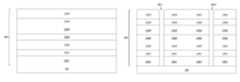
- FIG. 1Aillustrates a schematic cross-sectional view of a vertical stack 105 formed, e.g., deposited, on an access device 110 .
- vertical stack 105includes a first insulator material 112 - 1 formed, e.g., deposited, on access device 110 , a first memory cell material 114 - 1 formed on first insulator material 112 - 1 , a second insulator material 112 - 2 formed on first memory cell material 114 - 1 , a second memory cell material 114 - 2 formed on second insulator material 112 - 2 , a third insulator material 112 - 3 formed on second memory cell material 114 - 2 , a third memory cell material 114 - 3 formed on third insulator material 114 - 2 , and a fourth insulator material 112 - 4 formed on third memory cell material 114 - 2 .
- each insulator material 112 - 1 , 112 - 2 , 112 - 3 , and 112 - 4can be, for example, 50 nanometers, and the thickness of each memory cell material 114 - 1 , 114 - 2 , and 114 - 3 can be, for example, 2 nanometers.
- embodiments of the present disclosureare not limited to a particular thickness. Additionally, embodiments of the present disclosure are not limited to a particular number of insulator materials and memory cell materials, e.g., vertical stack 105 can include more or fewer insulator materials and memory cell materials than shown in FIG. 1A .
- Vertical stack 105can be formed on access device 110 in situ or ex situ using physical vapor deposition (PVD), for example.
- PVDphysical vapor deposition
- insulator materials 112 - 1 through 112 - 4 and memory cell materials 114 - 1 through 114 - 3can be formed in a sealed environment, e.g., chamber, using PVD.
- insulator material 112 - 1can be deposited on access device 110 in a sealed environment using PVD.
- Memory cell material 114 - 1can then be deposited on insulator material 112 - 1 in the same sealed environment without breaking the seal, e.g., vacuum, of the environment using PVD.
- Insulator material 112 - 2can then be deposited on memory cell material 114 - 1 , memory cell material 114 - 2 can then be deposited on insulator material 112 - 2 , insulator material 112 - 3 can then be deposited on memory cell material 114 - 2 , memory cell material 114 - 3 can then be deposited on insulator material 112 - 3 , and insulator material 112 - 4 can then be deposited on memory cell material 114 - 3 , all in the same sealed environment without breaking the seal of the environment using PVD.
- insulator materials 112 - 1 through 112 - 4 and memory cell materials 114 - 1 through 114 - 3can be formed in an unsealed environment using PVD.
- Embodiments of the present disclosureare not limited to a particular type of deposition process for forming vertical stack 105 .
- using PVD to form vertical stack 105can form memory cell materials, e.g., memory cell materials 114 - 1 through 114 - 3 , having the thickness previously described herein more efficiently, e.g., more cheaply, in less time, and/or using fewer materials, than other deposition processes, such as chemical vapor deposition (CVD), atomic layer deposition (ALD), and/or conformal deposition processes.
- CVDchemical vapor deposition
- ALDatomic layer deposition
- Access device 110can be, for example, a transistor, such as a field effect transistor (FET) or bipolar junction transistor (BJT), or a diode, among other types of access devices.
- FETfield effect transistor
- BJTbipolar junction transistor
- An example of an FET as an access devicewill be further described herein in connection with FIG. 2 .
- embodiments of the present disclosureare not limited to a particular type of access device.
- Insulator materials 112 - 1 through 112 - 4can be, for example, a dielectric material.
- Dielectric materialscan include, for example, nitride dielectric materials, such as silicon nitride (Si 3 N 4 ) dielectric materials, and oxide dielectric materials, such as silicon dioxide (SiO 2 ) dielectric materials.
- nitride dielectric materialssuch as silicon nitride (Si 3 N 4 ) dielectric materials
- oxide dielectric materialssuch as silicon dioxide (SiO 2 ) dielectric materials.
- embodiments of the present disclosureare not limited to a particular type of insulator material.
- Memory cell materials 114 - 1 through 114 - 3can be, for example, a two-terminal resistive memory cell material, such as a phase change (PC) material or resistive random access memory (RRAM) cell material.
- PC materialscan include, for example, phase change chalcogenide alloys such as Germanium-Antimony-Tellurium (GST) materials, e.g., Ge—Sb—Te materials such as Ge 2 Sb 2 Te 5 , Ge 1 Sb 2 Te 4 , Ge 1 Sb 4 Te 7 , etc.
- GSTGermanium-Antimony-Tellurium
- Ge—Sb—Te materialssuch as Ge 2 Sb 2 Te 5 , Ge 1 Sb 2 Te 4 , Ge 1 Sb 4 Te 7 , etc.
- the hyphenated chemical composition notationindicates the elements included in a particular mixture or compound, and is intended to represent all stoichiometries involving the indicated elements.
- PC materialscan include, for example, Ge—Te, In—Se, Sb—Te, Ga—Sb, In—Sb, As—Te, Al—Te, Ge—Sb—Te, Te—Ge—As, In—Sb—Te, Te—Sn—Se, Ge—Se—Ga, Bi—Se—Sb, Ga—Se—Te, Sn—Sb—Te, In—Sb—Ge, Te—Ge—Sb—S, Te—Ge—Sn—O, Te—Ge—Sn—Au, Pd—Te—Ge—Sn, In—Se—Ti—Co, Ge—Sb—Te—Pd, Ge—Sb—Te—Co, Sb—Te—Bi—Se, Ag—In—Sb—Te, Ge—Sb—Se—Te, Ge—Sn—Sb—Te, Ge—Te—Sn—Ni, Ge—Te—Sn—
- RRAM cell materialscan include, for example, Ge x Se y , a binary metal oxide such as Cu x O y , Wo x , Nb 2 O 5 , Al 2 O 3 , Ta 2 O 5 , TiO x , ZrO x , Ni x O, and Fe x O, and/or other materials that can support solid phase electrolyte behavior.
- a binary metal oxidesuch as Cu x O y , Wo x , Nb 2 O 5 , Al 2 O 3 , Ta 2 O 5 , TiO x , ZrO x , Ni x O, and Fe x O, and/or other materials that can support solid phase electrolyte behavior.
- RRAM cell materialscan include perovskite oxides such as doped or undoped SrTiO 3 , SrZrO 3 , and BaTiO 3 , colossal magnetoresistive materials such as Pr (1-x) Ca x MnO 3 (PCMO), La (1-x) Ca x MnO 3 (LCMO), and Ba (1-x) Sr x TiO 3 , and polymer materials such as Bengala Rose, AlQ 3 Ag, Cu-TCNQ, DDQ, TAPA, and Fluorescine-based polymers, among other types of RRAM cell materials.
- Embodiments of the present disclosureare not limited to a particular type of RRAM cell material.
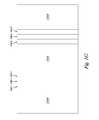
- FIG. 1Billustrates a schematic cross-sectional view of the structure shown in FIG. 1A after a subsequent processing step. Portions of vertical stack 105 are removed, e.g., etched and/or patterned, to form openings 120 - 1 and 120 - 2 in vertical stack 105 shown in FIG. 1B . As shown in FIG. 1B , one or more sides of insulator materials 112 - 1 through 112 - 4 and memory cell materials 114 - 1 through 114 - 3 can be adjacent openings 120 - 1 and 120 - 2 .
- Openings 120 - 1 and 120 - 2can be formed in vertical stack 105 in a number of ways.
- openings 120 - 1 and 120 - 2can be formed by etching through vertical stack 105 , e.g., through insulator material 112 - 4 , memory cell material 114 - 3 , insulator material 112 - 3 , memory cell material 114 - 2 , insulator material 112 - 2 , memory cell material 114 - 1 , and insulator material 112 - 1 , to access device 110 such that the bottom of openings 120 - 1 and 120 - 2 are adjacent access device 110 , as shown in FIG. 1B .
- openings 120 - 1 and 120 - 2can be formed in a single etch through vertical stack 105 .
- openings 120 - 1 and 120 - 2can be formed in a series of etches through vertical stack 105 , e.g., a first etch that removes a portion of insulator material 112 - 4 , a second, subsequent etch that removes a portion of memory cell material 114 - 3 , a third, subsequent etch that removes a portion of insulator material 112 - 3 , etc.
- FIG. 1Cillustrates a schematic cross-sectional view of the structure shown in FIG. 1B after a subsequent processing step.
- Portions of memory cell material 114 - 1are removed, e.g., etched and/or patterned, to form recesses 122 - 1 , 122 - 2 , 122 - 3 , and 122 - 4 in memory cell material 112 - 1 shown in FIG. 1C .
- portions of memory cell material 114 - 2are removed to form recesses 122 - 5 , 122 - 6 , 122 - 7 , and 122 - 8 in memory cell material 114 - 2 shown in FIG. 1C .
- portions of memory cell material 114 - 3are removed to form recesses 122 - 9 , 122 - 10 , 122 - 11 , and 122 - 12 in memory cell material 114 - 3 shown in FIG. 1C .
- Recesses 122 - 1 , 122 - 2 , 122 - 5 , 122 - 6 , 122 - 9 , and 122 - 10can be adjacent opening 120 - 1
- recesses 122 - 3 , 122 - 4 , 122 - 7 , 122 - 8 , 122 - 11 , and 122 - 12can be adjacent opening 120 - 2 , as shown in FIG. 1C .
- Recesses 122 - 1 through 122 - 4can be formed by selectively removing portions of memory cell material 114 - 1 , e.g., by removing portions of memory cell material 114 - 1 without removing any portion of insulator materials 112 - 1 through 112 - 4 .
- Recesses 122 - 5 through 122 - 8can be formed by selectively removing portions of memory cell material 114 - 2 , e.g., by removing portions of memory cell material 114 - 2 without removing any portion of insulator materials 112 - 1 through 112 - 4 .
- Recesses 122 - 9 through 122 - 12can be formed by selectively removing portions of memory cell material 114 - 3 , e.g., by removing portions of memory cell material 114 - 3 without removing any portion of insulator materials 112 - 1 through 112 - 4 .
- the portions of memory cell material 114 - 1 through 114 - 3 that are selectively removed to form recesses 122 - 1 through 122 - 12can be selectively removed with, for example, a selective wet etch that etches back the memory cell materials without etching the insulator materials.
- FIG. 1Dillustrates a schematic cross-sectional view of the structure shown in FIG. 1C after a subsequent processing step.
- electrode material 124 - 1is formed in opening 120 - 1 and recesses 122 - 1 , 122 - 2 , 122 - 5 , 122 - 6 , 122 - 9 , and 122 - 10 .
- electrode material 124 - 2is formed in opening 120 - 2 and recesses 122 - 3 , 122 - 4 , 122 - 7 , 122 - 8 , 122 - 11 , and 122 - 12 .
- Electrode materials 124 - 1 and 124 - 2can be, for example, a metal material, such as a tungsten or platinum material, among other metal materials.
- electrode material 124 - 1can be conformally formed, e.g., conformally deposited, in opening 120 - 1 and recesses 122 - 1 , 122 - 2 , 122 - 5 , 122 - 6 , 122 - 9 , and 122 - 10 such that electrode material 124 - 1 completely fills recesses 122 - 1 , 122 - 2 , 122 - 5 , 122 - 6 , 122 - 9 , and 122 - 10 , and partially fills opening 120 - 1 , as shown in FIG. 1D .
- electrode material 124 - 2can be conformally formed, e.g., conformally deposited, in opening 120 - 2 and recesses 122 - 3 , 122 - 4 , 122 - 7 , 122 - 8 , 122 - 11 , and 122 - 12 such that electrode material 124 - 2 completely fills recesses 122 - 3 , 122 - 4 , 122 - 7 , 122 - 8 , 122 - 11 , and 122 - 12 , and partially fills opening 120 - 2 , as shown in FIG. 1D .
- recesses 122 - 1 through 122 - 12may not be formed in memory cell materials 114 - 1 through 114 - 3 . That is, one or more embodiments may not include the process step previously described in connection with FIG. 1C .
- electrode material 124 - 1can be selectively formed, e.g., selectively deposited, in opening 120 - 1 adjacent the sides of memory cell materials 114 - 1 through 114 - 3 that are adjacent opening 120 - 1 .
- electrode material 124 - 1can be formed, e.g., deposited, in opening 120 - 1 adjacent the sides of memory cell materials 114 - 1 through 114 - 3 that are adjacent opening 120 - 1 without forming any electrode material 124 - 1 adjacent the sides of insulator materials 112 - 1 through 112 - 4 that are adjacent opening 120 - 1 .
- electrode material 124 - 2can be selectively formed in opening 120 - 2 adjacent the sides of memory cell materials 114 - 1 through 114 - 3 that are adjacent opening 120 - 2 .
- electrode material 124 - 2can be formed in opening 120 - 2 adjacent the sides of memory cell materials 114 - 1 through 114 - 3 that are adjacent opening 120 - 2 without forming any electrode material 124 - 2 adjacent the sides of insulator materials 112 - 1 through 112 - 4 that are adjacent opening 120 - 2 .
- FIG. 1Eillustrates a schematic cross-sectional view of the structure shown in FIG. 1D after a subsequent processing step.
- Portions of electrode materials 124 - 1 and 124 - 2are removed, e.g., etched and/or patterned, from openings 120 - 1 and 120 - 2 , respectively, as shown in FIG. 1E .
- the removed portions of electrode materials 124 - 1 and 124 - 2can be removed, for example, by an anisotropic dry etch.
- portions of electrode materials 124 - 1 and 124 - 2can be removed such that no electrode material 124 - 1 or 124 - 2 remains in openings 120 - 1 or 120 - 2 , respectively.
- electrode material 124 - 1can remain in recesses 122 - 1 , 122 - 2 , 122 - 5 , 122 - 6 , 122 - 9 , and 122 - 10
- electrode material 124 - 2can remain in recesses 122 - 3 , 122 - 4 , 122 - 7 , 122 - 8 , 122 - 11 , and 122 - 12 .
- recesses 122 - 1 , 122 - 2 , 122 - 5 , 122 - 6 , 122 - 9 , and 122 - 10can remain completely filled with electrode material 124 - 1
- recesses 122 - 3 , 122 - 4 , 122 - 7 , 122 - 8 , 122 - 11 , and 122 - 12can remain completely filled with electrode material 124 - 2 , as shown in FIG. 1E .
- a side of electrode material 124 - 1 in recesses 122 - 1 , 122 - 2 , 122 - 5 , 122 - 6 , 122 - 9 , and 122 - 10can be adjacent opening 120 - 1
- a side of electrode material 124 - 2 in recesses 122 - 3 , 122 - 4 , 122 - 7 , 122 - 8 , 122 - 11 , and 122 - 12can be adjacent opening 120 - 2 , as shown in FIG. 1E .
- the portions of electrode materials 124 - 1 and 124 - 2 that remain in recesses 122 - 1 through 122 - 12can form lines, e.g., metal lines, that run parallel to the surface of vertical stack 105 , e.g., into and out of the page, as shown in FIG. 1E .
- These linescan be, for example, data lines, e.g., bit lines.
- the electrode materials 124 - 1 and 124 - 2 that are selectively formed in openings 120 - 1 and 120 - 2 , respectively, adjacent the sides of memory cell materials 114 - 1 through 114 - 3 that are adjacent openings 120 - 1 and 120 - 2 , respectively,can form the lines.
- FIG. 1Fillustrates a schematic cross-sectional view of the structure shown in FIG. 1E after a subsequent processing step.
- insulator material 126 - 1is formed in opening 120 - 1
- insulator material 126 - 2is formed in opening 120 - 2 .
- Insulator materials 126 - 1 and 126 - 2can be formed, e.g., deposited, in openings 120 - 1 and 120 - 2 , respectively, in a number of ways, including physical vapor deposition (PVD), chemical vapor deposition (CVD), and/or atomic layer deposition (ALD).
- PVDphysical vapor deposition
- CVDchemical vapor deposition
- ALDatomic layer deposition
- insulator material 126 - 1can be formed in opening 120 - 1 such that insulator material 126 - 1 is adjacent electrode material 124 - 1 and access device 110 .
- insulator material 126 - 2can be formed in opening 120 - 2 such that insulator material 126 - 2 is adjacent electrode material 124 - 2 and access device 110 .
- insulator materials 126 - 1 and 126 - 2can be formed in openings 120 - 1 and 120 - 2 , respectively, such that insulator materials 126 - 1 and 126 - 2 completely fill openings 120 - 1 and 120 - 2 , respectively, as shown in FIG. 1F .
- Insulator materials 126 - 1 and 126 - 2can be, for example, a dielectric material.
- Dielectric materialscan include, for example, nitride dielectric materials, such as silicon nitride (Si 3 N 4 ) dielectric materials, and oxide dielectric materials, such as silicon dioxide (SiO 2 ) dielectric materials.
- nitride dielectric materialssuch as silicon nitride (Si 3 N 4 ) dielectric materials
- oxide dielectric materialssuch as silicon dioxide (SiO 2 ) dielectric materials.
- embodiments of the present disclosureare not limited to a particular type of insulator material.
- insulator materials 126 - 1 and 126 - 2can be the same material, e.g., the same dielectric material, as insulator materials 112 - 1 through 112 - 4 .
- insulator materials 126 - 1 and 126 - 2can be a different material than insulator materials 112 - 1 through 112 - 4 .
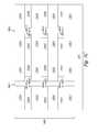
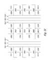
- FIG. 1Gillustrates a schematic top view of the embodiment shown in FIG. 1F .
- electrode materialse.g., data lines, 124 - 1 and 124 - 2 are shown for ease of illustration. However, electrode materials 124 - 1 and 124 - 2 can run through vertical stack 105 , e.g., underneath fourth insulator material 112 - 4 , as previously described herein. As shown in FIG. 1G , electrode materials, e.g., data lines, 124 - 1 and 124 - 2 can run parallel to the surface of vertical stack 105 .
- FIG. 1Hillustrates a schematic top view of the structure shown in FIG. 1G after a subsequent processing step.
- Portions of vertical stack 105are removed, e.g., etched and/or patterned, to form openings 140 - 1 , 140 - 2 , 140 - 3 , 140 - 4 , 140 - 5 , 140 - 6 , 140 - 7 , 140 - 8 , and 140 - 9 in vertical stack 105 shown in FIG. 1H .
- One or more sides of electrode materials 124 - 1 and 124 - 2can be adjacent openings 140 - 1 through 140 - 9 , as shown in FIG. 1H .
- one or more sides of insulator materials 112 - 1 through 112 - 4 and memory cell materials 114 - 1 through 114 - 3can be adjacent openings 144 - 1 through 144 - 12 .
- Openings 140 - 1 through 140 - 9can be formed in vertical stack 105 in a number of ways.
- openings 140 - 1 through 140 - 9can be formed by etching through vertical stack 105 to access device 110 (not shown in FIG. 1H ) such that the bottom of openings 140 - 1 through 140 - 9 are adjacent access device 110 .
- openings 140 - 1 through 140 - 9can be formed in a single etch through vertical stack 105 , or in a series of etches through vertical stack 105 .
- FIG. 1Iillustrates a schematic top view of the structure shown in FIG. 1H after a subsequent processing step.
- insulator material 142 - 1is formed in opening 140 - 1
- insulator material 142 - 2is formed in opening 140 - 2
- insulator material 142 - 3is formed in opening 140 - 3
- insulator material 142 - 4is formed in opening 140 - 4
- insulator material 142 - 5is formed in opening 140 - 5
- insulator material 142 - 6is formed in opening 140 - 6
- insulator material 142 - 7is formed in opening 140 - 7
- insulator material 142 - 8is formed in opening 140 - 8
- insulator material 142 - 9is formed in opening 140 - 9 .
- Insulator materials 142 - 1 through 142 - 9can be formed, e.g., deposited, in openings 140 - 1 through 140 - 9 in a number of ways, including physical vapor deposition (PVD), chemical vapor deposition (CVD), and/or atomic layer deposition (ALD).
- PVDphysical vapor deposition
- CVDchemical vapor deposition
- ALDatomic layer deposition
- insulator materials 142 - 1 through 142 - 9can be formed in openings 140 - 1 through 140 - 9 such that insulator materials 142 - 1 through 142 - 9 are adjacent one or more sides of electrode materials 124 - 1 and 124 - 2 . Further, although not shown in FIG. 1I , insulator materials 142 - 1 through 142 - 9 can be formed in openings 140 - 1 through 140 - 9 such that insulator materials 142 - 1 through 142 - 9 are adjacent one or more sides of insulator materials 112 - 1 through 112 - 4 and memory cell materials 114 - 1 through 114 - 3 .
- insulator materials 142 - 1 through 142 - 9can be formed in openings 140 - 1 through 140 - 9 such that insulator materials 142 - 1 through 142 - 9 completely fill openings 140 - 1 through 140 - 9 .
- Insulator materials 142 - 1 through 142 - 9can be, for example, a dielectric material.
- Dielectric materialscan include, for example, nitride dielectric materials, such as silicon nitride (Si 3 N 4 ) dielectric materials, and oxide dielectric materials, such as silicon dioxide (SiO 2 ) dielectric materials.
- insulator materials 142 - 1 through 142 - 9can be the same material, e.g., the same dielectric material, as insulator materials 112 - 1 through 112 - 4 and/or insulator materials 126 - 1 and 126 - 2 .
- insulator materials 142 - 1 through 142 - 9can be a different material than insulator materials 112 - 1 through 112 - 4 and/or insulator materials 126 - 1 and 126 - 2 .
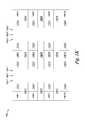
- FIG. 1Jillustrates a schematic top view of the structure shown in FIG. 1I after a subsequent processing step.
- Portions of vertical stack 105are removed, e.g., etched and/or patterned, to form openings 144 - 1 , 144 - 2 , 144 - 3 , 144 - 4 , 144 - 5 , 144 - 6 , 144 - 7 , 144 - 8 , 144 - 9 , 144 - 10 , 144 - 11 , and 144 - 12 in vertical stack 105 shown in FIG. 1J .
- one or more sides of insulator materials 112 - 1 through 112 - 4 and memory cell materials 114 - 1 through 114 - 3can be adjacent openings 144 - 1 through 144 - 12 .
- Openings 144 - 1 through 144 - 12can be formed in vertical stack 105 in a number of ways.
- openings 144 - 1 through 144 - 12can be formed by etching through vertical stack 105 to access device 110 (not shown in FIG. 1J ) such that the bottom of openings 144 - 1 through 144 - 12 are adjacent access device 110 .
- openings 144 - 1 through 144 - 12can be formed in a single etch through vertical stack 105 , or in a series of etches through vertical stack 105 .
- FIG. 1Killustrates a schematic tip view of the structure shown in FIG. 1J after a subsequent processing step.
- electrode material 146 - 1is formed in opening 144 - 1
- electrode material 146 - 2is formed in opening 144 - 2
- electrode material 146 - 3is formed in opening 144 - 3
- electrode material 146 - 4is formed in opening 144 - 4
- electrode material 146 - 5is formed in opening 144 - 5
- electrode material 146 - 6is formed in opening 144 - 6
- electrode material 146 - 7is formed in opening 144 - 7
- electrode material 146 - 8is formed in opening 144 - 8
- electrode material 146 - 9is formed in opening 144 - 9
- electrode material 146 - 10is formed in opening 144 - 10
- electrode material 146 - 11is formed in opening 144 - 11
- electrode material 146 - 12is formed in opening 144 - 12 .
- Electrode materials 146 - 1 through 146 - 12can be formed, e.g., deposited, in openings 144 - 1 through 144 - 12 in a number of ways, including physical vapor deposition (PVD), chemical vapor deposition (CVD), and/or atomic layer deposition (ALD).
- PVDphysical vapor deposition
- CVDchemical vapor deposition
- ALDatomic layer deposition
- Electrode materials 146 - 1 through 146 - 12can be, for example, a metal material, such as a tungsten or platinum material, among other metal materials. Electrode materials 146 - 1 through 146 - 12 can be the same material, e.g., the same metal material, as electrode materials 124 - 1 and 124 - 2 . Alternatively, electrode materials 146 - 1 through 146 - 12 can be a different material than electrode materials 124 - 1 and 124 - 2 .
- Electrode materials 146 - 1 through 146 - 12can also be, for example, access device contacts. That is, electrode materials 146 - 1 through 146 - 12 can be formed in openings 144 - 1 through 144 - 12 such that electrode materials 146 - 1 through 146 - 12 are in contact with access device 110 (not shown in FIG. 1J ). Additionally, electrode materials 146 - 1 through 146 - 12 can be formed in openings 144 - 1 through 144 - 12 such that electrode materials 146 - 1 through 146 - 12 are adjacent one or more sides of insulator materials 112 - 1 through 112 - 4 and memory cell materials 114 - 1 through 114 - 3 (not shown in FIG. 1J ).
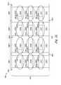
- the structure illustrated in FIG. 1Kcan be a portion of a memory device 100 , such as a resistive memory device, for example.
- a memory device 100such as a resistive memory device, for example.
- embodiments of the present disclosureare not limited to a particular type of memory device.
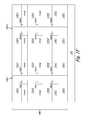
- FIG. 1Lillustrates a schematic cross-sectional view of the embodiment shown in FIG. 1K .
- electrode materials 146 - 1 through 146 - 3are in contact with access device 110 .
- electrode materials 146 - 1 and 146 - 2are adjacent a side of memory cell materials 114 - 1 through 114 - 3 that is opposite a side of memory cell materials 114 - 1 through 114 - 3 that is adjacent electrode material 124 - 1 .
- electrode materials 146 - 2 and 146 - 3are adjacent a side of memory cell materials 114 - 1 through 114 - 3 that is opposite a side of memory cell materials 114 - 1 through 114 - 3 that is adjacent electrode material 124 - 2 , as illustrated in FIG. 1L .
- the structure illustrated in FIG. 1Lincludes vertical stacks 128 - 1 , 128 - 2 , 128 - 3 , and 128 - 4 of self-aligned memory cells.
- vertical stack 128 - 1includes self-aligned memory cells 130 - 1 , 130 - 2 , and 130 - 3
- vertical stack 128 - 2includes self-aligned memory cells 130 - 4 , 130 - 5 , and 130 - 6
- vertical stack 128 - 3includes self-aligned memory cells 130 - 7 , 130 - 8 , and 130 - 9
- vertical stack 128 - 4includes self-aligned memory cells 130 - 10 , 130 - 11 , and 130 - 12 .
- embodiments of the present disclosureare not limited to a particular number of vertical stacks, or to a particular number of memory cells in a vertical stack.
- each memory cell in vertical stacks 128 - 1 through 128 - 4is horizontally oriented. That is, each memory cell can include a memory cell material, a first electrode, e.g., a portion of a first electrode material, adjacent a first side of the memory cell material, and a second electrode, e.g., a portion of a second electrode material, adjacent a second side of the memory cell material that is opposite the first side, as shown in FIG. 1L .
- a “side” of a memory cell material, as used herein,can be a surface of the memory cell material that is perpendicular to the top surface of access device 110 .
- Each memory cellcan also include an insulator material, e.g., a portion of an insulator material, adjacent the top and bottom of the memory cell material, as illustrated in FIG. 1H .
- a “top” and “bottom” of a memory cell material, as used herein,can be surfaces of the memory cell material that are parallel to the top surface of access device 110 .
- memory cell 130 - 1 in vertical stack 128 - 1 , memory cell 130 - 4 in vertical stack 128 - 2 , memory cell 130 - 7 in vertical stack 128 - 3 , and memory cell 130 - 10 in vertical stack 128 - 4each include memory cell material 114 - 3 , a portion of insulator material 112 - 4 adjacent the top of memory cell material 114 - 3 , and a portion of insulator material 112 - 3 adjacent the bottom of memory cell material 114 - 3 .
- Memory cell 130 - 1further includes a portion of electrode material 146 - 1 adjacent a first side of memory cell material 114 - 3 , and a portion of electrode material 124 - 1 adjacent a second, opposite side of memory cell material 114 - 3 .
- Memory cell 130 - 4further includes a portion of electrode material 146 - 2 adjacent a first side of memory cell material 114 - 3 , and a portion of electrode material 124 - 1 adjacent a second, opposite side of memory cell material 114 - 3 .
- Memory cell 130 - 7further includes a portion of electrode material 146 - 2 adjacent a first side of memory cell material 114 - 3 , and a portion of electrode material 124 - 2 adjacent a second, opposite side of memory cell material 114 - 3 .
- Memory cell 130 - 10further includes a portion of electrode material 146 - 3 adjacent a first side of memory cell material 114 - 3 , and a portion of electrode material 124 - 2 adjacent a second, opposite side of memory cell material 114 - 3 .
- a particular electrodee.g., a portion of a particular electrode material
- a portion of electrode material 146 - 1is adjacent a first side of the memory cell material in each memory cell 130 - 1 through 130 - 3 in vertical stack 128 - 1
- a portion of electrode material 146 - 3is adjacent a first side of the memory cell material in each memory cell 130 - 10 through 130 - 12 in vertical stack 128 - 4 .
- different electrodescan be adjacent a second side of the memory cell material in each memory cell in a vertical stack.
- a portion of different electrode materials 124 - 1are adjacent a second side of the memory cell material in each memory cell 130 - 1 through 130 - 3 in vertical stack 128 - 1
- a portion of different electrode materials 124 - 2are adjacent a second side of the memory cell material in each memory cell 130 - 10 through 130 - 12 in vertical stack 128 - 4 .
- a particular electrodee.g., a portion of a particular electrode material
- a portion of electrode material 146 - 2is adjacent a first side of the memory cell material in each memory cell 130 - 4 through 130 - 6 in vertical stack 128 - 2 , and a portion of the same electrode material 146 - 2 is also adjacent a first side of the memory cell material in each memory cell 130 - 7 through 130 - 9 in vertical stack 128 - 3 .
- different electrodescan be adjacent a first side of the memory cell material in each memory cell in adjacent vertical stacks.
- a portion of electrode material 146 - 2is adjacent a first side of the memory cell material in each memory cell 130 - 7 through 130 - 9 in vertical stack 128 - 3
- a portion of different electrode material 146 - 3is adjacent a first side of the memory cell material in each memory cell 130 - 10 through 130 - 12 in vertical stack 128 - 4 .
- adjacent vertical stackse.g., the memory cells in adjacent vertical stacks
- vertical stacks 128 - 1 and 128 - 2e.g., the memory cells in vertical stacks 128 - 1 and 128 - 2
- insulator material 126 - 1e.g., the memory cells in vertical stacks 128 - 1 and 128 - 2
- vertical stacks 128 - 3 and 128 - 4e.g., the memory cells in vertical stacks 128 - 3 and 128 - 4
- Memory device 100may include additional elements not shown in FIG. 1K or 1L so as not to obscure embodiments of the present disclosure.
- memory device 100may include an access line, e.g., word line, coupled to access device 110 and/or electrode materials 146 - 1 through 146 - 3 .
- memory device 100may include sense circuitry coupled to electrode materials 124 - 1 and 124 - 2 .
- One or more method embodimentsinclude forming a vertical stack having a first insulator material, a first memory cell material on the first insulator material, a second insulator material on the first memory cell material, a second memory cell material on the second insulator material, and a third insulator material on the second memory cell material, forming an electrode adjacent a first side of the first memory cell material and a first side of the second memory cell material, and forming an electrode adjacent a second side of the first memory cell material and a second side of the second memory cell material.
Landscapes
- Engineering & Computer Science (AREA)
- Manufacturing & Machinery (AREA)
- Semiconductor Memories (AREA)
Abstract
Description
Claims (18)
Priority Applications (1)
| Application Number | Priority Date | Filing Date | Title |
|---|---|---|---|
| US15/138,381US9627442B2 (en) | 2010-06-22 | 2016-04-26 | Horizontally oriented and vertically stacked memory cells |
Applications Claiming Priority (4)
| Application Number | Priority Date | Filing Date | Title |
|---|---|---|---|
| US12/820,923US8367460B2 (en) | 2010-06-22 | 2010-06-22 | Horizontally oriented and vertically stacked memory cells |
| US13/759,576US9024283B2 (en) | 2010-06-22 | 2013-02-05 | Horizontally oriented and vertically stacked memory cells |
| US14/688,502US9349949B2 (en) | 2010-06-22 | 2015-04-16 | Horizontally oriented and vertically stacked memory cells |
| US15/138,381US9627442B2 (en) | 2010-06-22 | 2016-04-26 | Horizontally oriented and vertically stacked memory cells |
Related Parent Applications (1)
| Application Number | Title | Priority Date | Filing Date |
|---|---|---|---|
| US14/688,502ContinuationUS9349949B2 (en) | 2010-06-22 | 2015-04-16 | Horizontally oriented and vertically stacked memory cells |
Publications (2)
| Publication Number | Publication Date |
|---|---|
| US20160240587A1 US20160240587A1 (en) | 2016-08-18 |
| US9627442B2true US9627442B2 (en) | 2017-04-18 |
Family
ID=45327843
Family Applications (4)
| Application Number | Title | Priority Date | Filing Date |
|---|---|---|---|
| US12/820,923Expired - Fee RelatedUS8367460B2 (en) | 2010-06-22 | 2010-06-22 | Horizontally oriented and vertically stacked memory cells |
| US13/759,576Active2030-09-05US9024283B2 (en) | 2010-06-22 | 2013-02-05 | Horizontally oriented and vertically stacked memory cells |
| US14/688,502Expired - Fee RelatedUS9349949B2 (en) | 2010-06-22 | 2015-04-16 | Horizontally oriented and vertically stacked memory cells |
| US15/138,381Expired - Fee RelatedUS9627442B2 (en) | 2010-06-22 | 2016-04-26 | Horizontally oriented and vertically stacked memory cells |
Family Applications Before (3)
| Application Number | Title | Priority Date | Filing Date |
|---|---|---|---|
| US12/820,923Expired - Fee RelatedUS8367460B2 (en) | 2010-06-22 | 2010-06-22 | Horizontally oriented and vertically stacked memory cells |
| US13/759,576Active2030-09-05US9024283B2 (en) | 2010-06-22 | 2013-02-05 | Horizontally oriented and vertically stacked memory cells |
| US14/688,502Expired - Fee RelatedUS9349949B2 (en) | 2010-06-22 | 2015-04-16 | Horizontally oriented and vertically stacked memory cells |
Country Status (1)
| Country | Link |
|---|---|
| US (4) | US8367460B2 (en) |
Families Citing this family (5)
| Publication number | Priority date | Publication date | Assignee | Title |
|---|---|---|---|---|
| JP2013197396A (en)* | 2012-03-21 | 2013-09-30 | Toshiba Corp | Semiconductor memory device and method of manufacturing the same |
| US8803122B2 (en)* | 2012-07-31 | 2014-08-12 | Globalfoundries Singapore Pte. Ltd. | Method for forming a PCRAM with low reset current |
| US9691475B2 (en)* | 2015-03-19 | 2017-06-27 | Micron Technology, Inc. | Constructions comprising stacked memory arrays |
| US9595669B2 (en) | 2015-06-30 | 2017-03-14 | Western Digital Technologies, Inc. | Electroplated phase change switch |
| US12156486B2 (en) | 2020-12-02 | 2024-11-26 | International Business Machines Corporation | Horizontal RRAM device and architecture for variability reduction |
Citations (115)
| Publication number | Priority date | Publication date | Assignee | Title |
|---|---|---|---|---|
| US4242954A (en) | 1978-05-23 | 1981-01-06 | Graham Magnetics Incorporated | Calendar roll system |
| US4247893A (en) | 1977-01-03 | 1981-01-27 | Motorola, Inc. | Memory interface device with processing capability |
| US4252328A (en) | 1980-05-01 | 1981-02-24 | Ferrofluidics Corporation | Self-activating ferrofluid seal and method |
| US4264917A (en) | 1978-10-19 | 1981-04-28 | Compagnie Internationale Pour L'informatique Cii-Honeywell Bull | Flat package for integrated circuit devices |
| US4277836A (en) | 1975-12-23 | 1981-07-07 | Nippon Electric Co., Ltd. | Composite random access memory providing direct and auxiliary memory access |
| USRE30671E (en) | 1979-07-09 | 1981-07-07 | Texas Instruments Incorporated | Microprocessor system having high order capability |
| US4290843A (en) | 1980-02-19 | 1981-09-22 | Texas Instruments Incorporated | Epitaxial growth of magnetic memory film on implanted substrate |
| US4301040A (en) | 1978-06-23 | 1981-11-17 | Charleswater Products, Inc. | Electrically conductive foam and method of preparation and use |
| US4301503A (en) | 1977-07-05 | 1981-11-17 | Bally Manufacturing Corporation | Home computer and game apparatus |
| US4302939A (en) | 1980-01-21 | 1981-12-01 | The United States Of America As Represented By The United States Department Of Energy | Solid state engine using nitinol memory alloy |
| US4312898A (en) | 1978-05-23 | 1982-01-26 | Graham Magnetics, Inc. | Process for making magnetic tape |
| US4321693A (en) | 1980-07-31 | 1982-03-23 | Texas Instruments Incorporated | Magnetic bubble memory chip with dedicated redundancy data section provided thereon |
| US4325217A (en) | 1980-01-21 | 1982-04-20 | The United States Of America As Represented By The United States Department Of Energy | Solid state engine with alternating motion |
| US4331089A (en) | 1979-06-06 | 1982-05-25 | Fritz Gegauf Ag Bernina-Naehmaschinenfabrik | Device for simplification of sewing machine adjustments and set-up |
| US4332257A (en) | 1980-02-11 | 1982-06-01 | Bunker Ramo Corporation | Medical clip and electrode constructions |
| US4335809A (en) | 1979-02-13 | 1982-06-22 | Barcrest Limited | Entertainment machines |
| US4344153A (en) | 1978-04-14 | 1982-08-10 | Hitachi, Ltd. | Magnetic bubble memory device and method of fabricating the same |
| US4352334A (en) | 1981-08-03 | 1982-10-05 | Childs William R | Method and apparatus for stitching material along a curve |
| US4352957A (en) | 1980-03-17 | 1982-10-05 | Storage Technology Corporation | Speech detector circuit with associated gain control for a tasi system |
| US4360823A (en) | 1977-03-16 | 1982-11-23 | U.S. Philips Corporation | Semiconductor device having an improved multilayer wiring system |
| US4365112A (en) | 1980-03-17 | 1982-12-21 | Storage Technology Corporation | Speech detector circuit for a TASI system |
| USRE31208E (en) | 1974-12-26 | 1983-04-12 | Unimation, Inc. | Signal modification device for memory controlled manipulator apparatus |
| US4384349A (en) | 1979-10-01 | 1983-05-17 | Texas Instruments Incorporated | High density electrically erasable floating gate dual-injection programmable memory device |
| US4394741A (en) | 1980-06-28 | 1983-07-19 | Lucas Industries Limited | Battery monitoring system |
| US4420767A (en) | 1978-11-09 | 1983-12-13 | Zilog, Inc. | Thermally balanced leadless microelectronic circuit chip carrier |
| US4423596A (en) | 1981-12-28 | 1984-01-03 | Karnes Thomas E | Thermal engine |
| US4433389A (en) | 1978-12-26 | 1984-02-21 | Burroughs Corporation | Memory address translation system for accessing memory locations via job names |
| US4434618A (en) | 1982-07-19 | 1984-03-06 | Dillon Corbett L | Engine construction |
| US4444702A (en) | 1981-04-09 | 1984-04-24 | Krupp Kautex Maschinenbau Gmbh. | Method and apparatus for producing extruded sections of thermoplastic material |
| US4455742A (en) | 1982-06-07 | 1984-06-26 | Westinghouse Electric Corp. | Method of making self-aligned memory MNOS-transistor |
| US4464425A (en) | 1980-01-15 | 1984-08-07 | Kabel-Und Metallwerke Gutehoffnungshutte Aktiengesellschaft | Foamed polymeric shrink-fit objects and their process of manufacture |
| US4472939A (en) | 1983-05-20 | 1984-09-25 | Wang Frederick E | Energy conversion system |
| US4485948A (en) | 1983-06-30 | 1984-12-04 | Michaels Of Oregon Co. | Hand gun holster with abrasion-resistant longitudinal spine |
| US4501124A (en) | 1980-09-18 | 1985-02-26 | Shell Oil Company | Apparatus for leakage detection of cryogenic materials |
| US4517492A (en) | 1974-06-25 | 1985-05-14 | Owens-Illinois, Inc. | Selective control of discharge position in gas discharge display/memory device |
| US4542960A (en) | 1982-06-30 | 1985-09-24 | International Business Machines Corporation | Fringe-field switched storage-effect liquid crystal display devices |
| US4544443A (en) | 1983-05-13 | 1985-10-01 | Shap Kabushiki Kaisha | Method for manufacturing an optical memory element |
| US4554027A (en) | 1983-05-28 | 1985-11-19 | G. Rau Gmbh & Co. | Shaped part made of a composite material and a process for its production |
| US4586980A (en) | 1984-02-20 | 1986-05-06 | Canon Kabushiki Kaisha | Pattern forming method |
| US4605926A (en) | 1982-09-13 | 1986-08-12 | Duplo Seiko Corp. | Illegal-sheet-material detection apparatus in sheet material manufacturing machine |
| US4615849A (en) | 1982-11-25 | 1986-10-07 | Sodemape Holding Ag | Method and device for sintering differing molded parts in particular from various types of foaming plastic in particular |
| US4619034A (en) | 1983-05-02 | 1986-10-28 | Ncr Corporation | Method of making laser recrystallized silicon-on-insulator nonvolatile memory device |
| US4621261A (en) | 1982-12-21 | 1986-11-04 | Thomson-Csf | System for making a thermo-active device temperature dependent |
| US4675715A (en) | 1982-12-09 | 1987-06-23 | American Telephone And Telegraph Company, At&T Bell Laboratories | Semiconductor integrated circuit vertical geometry impedance element |
| US4901230A (en) | 1983-04-25 | 1990-02-13 | Cray Research, Inc. | Computer vector multiprocessing control with multiple access memory and priority conflict resolution method |
| US4924427A (en) | 1985-11-15 | 1990-05-08 | Unisys Corporation | Direct memory access controller with direct memory to memory transfers |
| US4953102A (en) | 1985-03-30 | 1990-08-28 | Mita Industrial Co., Ltd. | Method for producing character patterns |
| US5016165A (en) | 1987-01-12 | 1991-05-14 | Fujitsu Limited | Direct memory access controlled system |
| US5020003A (en) | 1988-09-29 | 1991-05-28 | At&T Bell Laboratories | Graphics controller image creation |
| US5232876A (en) | 1990-10-25 | 1993-08-03 | Hyundai Electronics Industries, Co., Ltd. | Method for manufacturing a silicon layer having increased surface area |
| US5300808A (en) | 1992-05-04 | 1994-04-05 | Motorola, Inc. | EPROM package and method of optically erasing |
| US5334862A (en) | 1993-08-10 | 1994-08-02 | Micron Semiconductor, Inc. | Thin film transistor (TFT) loads formed in recessed plugs |
| US5383413A (en) | 1992-09-07 | 1995-01-24 | Brother Kogyo Kabushiki Kaisha | Embroidery pattern processing apparatus |
| US5416916A (en) | 1990-07-06 | 1995-05-16 | Nec Electronics Incorporated | Structure for enabling direct memory-to-memory transfer with a fly-by DMA unit |
| US5506993A (en) | 1993-03-02 | 1996-04-09 | International Business Machines Corporation | Message packet transmitter |
| US5506953A (en) | 1993-05-14 | 1996-04-09 | Compaq Computer Corporation | Memory mapped video control registers |
| US5543678A (en) | 1993-05-11 | 1996-08-06 | Hoiberg; Dane A. | Flat motors |
| US5559969A (en) | 1994-08-09 | 1996-09-24 | Unisys Corporation | Method and apparatus for efficiently interfacing variable width data streams to a fixed width memory |
| US5563945A (en) | 1993-03-20 | 1996-10-08 | Motorola Inc. | Data storage device |
| US5566106A (en) | 1994-02-17 | 1996-10-15 | National Semiconductor Corporation | Method for reducing the spacing between the horizontally-adjacent floating gates of a flash EPROM array |
| US5592546A (en) | 1993-09-20 | 1997-01-07 | Fujitsu Limited | Memory dialing control system having improved telephone number retrieval function by using history information |
| US5608892A (en) | 1995-06-09 | 1997-03-04 | Alantec Corporation | Active cache for a microprocessor |
| US5764918A (en) | 1995-01-23 | 1998-06-09 | Poulter; Vernon C. | Communications node for transmitting data files over telephone networks |
| US5765740A (en) | 1993-12-30 | 1998-06-16 | Ferguson; Patrick J. | Suture-material-dispenser system for suture material |
| US5768445A (en) | 1996-09-13 | 1998-06-16 | Silicon Graphics, Inc. | Compression and decompression scheme performed on shared workstation memory by media coprocessor |
| US5810053A (en) | 1996-09-17 | 1998-09-22 | Mandich; Ivan C. | Pipe liner, a coiled liner product and methods for forming, installing and coiling the liner |
| US5815727A (en) | 1994-12-20 | 1998-09-29 | Nec Corporation | Parallel processor for executing plural thread program in parallel using virtual thread numbers |
| US5827322A (en) | 1994-11-16 | 1998-10-27 | Advanced Cardiovascular Systems, Inc. | Shape memory locking mechanism for intravascular stents |
| US5860112A (en) | 1995-12-27 | 1999-01-12 | Intel Corporation | Method and apparatus for blending bus writes and cache write-backs to memory |
| US5861116A (en) | 1994-08-31 | 1999-01-19 | Plastic Innovations, Inc. | Process for installing a pipe liner |
| US5912453A (en) | 1995-09-29 | 1999-06-15 | International Business Machines Corporation | Multiple application chip card with decoupled programs |
| US5929634A (en) | 1995-06-10 | 1999-07-27 | Firma Mesutronic Geratebau Gmbh | Device for sensing metallically conductive parts in an at least substantially non-conductive conveyor stream |
| US5940860A (en) | 1996-07-01 | 1999-08-17 | Sun Microsystems, Inc. | Methods and apparatus for substantially memory-less coherence transformer for connecting computer node coherence domains |
| US5943517A (en) | 1996-02-15 | 1999-08-24 | Asahi Kogaku Kogyo Kabushiki Kaisha | Electro-developing type still video camera using electro-developing recording medium and having memory-medium for storing image data read therefrom |
| US5956344A (en) | 1997-02-03 | 1999-09-21 | Siemens Information And Communication Networks, Inc. | Interprocessor communications in an ATM environment |
| US5968192A (en) | 1997-05-09 | 1999-10-19 | Artisan Components, Inc. | Programmable universal test interface and method for making the same |
| US5978307A (en) | 1998-05-21 | 1999-11-02 | Integrated Device Technology, Inc. | Integrated circuit memory devices having partitioned multi-port memory arrays therein for increasing data bandwidth and methods of operating same |
| US5982700A (en) | 1998-05-21 | 1999-11-09 | Integrated Device Technology, Inc. | Buffer memory arrays having nonlinear columns for providing parallel data access capability and methods of operating same |
| US5986922A (en) | 1997-09-30 | 1999-11-16 | Alliance Semiconductor | Method of and apparatus for increasing load resistance within an SRAM array |
| US5997465A (en) | 1994-03-17 | 1999-12-07 | Ffv Aerotech Ab | Device for exerting an external pressure on a human body |
| US5999478A (en) | 1998-05-21 | 1999-12-07 | Integrated Device Technology, Inc. | Highly integrated tri-port memory buffers having fast fall-through capability and methods of operating same |
| US6003112A (en) | 1997-06-30 | 1999-12-14 | Intel Corporation | Memory controller and method for clearing or copying memory utilizing register files to store address information |
| US6033412A (en) | 1997-04-03 | 2000-03-07 | Losken; H. Wolfgang | Automated implantable bone distractor for incremental bone adjustment |
| US6044481A (en) | 1997-05-09 | 2000-03-28 | Artisan Components, Inc. | Programmable universal test interface for testing memories with different test methodologies |
| US6078971A (en) | 1995-12-07 | 2000-06-20 | Nec Corporation | Input/output buffer and method for invalidating transferred data in direct memory access transfer |
| US6085296A (en) | 1997-11-12 | 2000-07-04 | Digital Equipment Corporation | Sharing memory pages and page tables among computer processes |
| US6095323A (en) | 1998-06-12 | 2000-08-01 | Ferguson; Patrick J. | Suture-material-dispenser system for suture material |
| US6173425B1 (en) | 1998-04-15 | 2001-01-09 | Integrated Device Technology, Inc. | Methods of testing integrated circuits to include data traversal path identification information and related status information in test data streams |
| US6177315B1 (en) | 1999-05-28 | 2001-01-23 | National Semiconductor Corporation | Method of fabricating a high density EEPROM array |
| US6218227B1 (en) | 1999-10-25 | 2001-04-17 | Advanced Micro Devices, Inc. | Method to generate a MONOS type flash cell using polycrystalline silicon as an ONO top layer |
| US6222562B1 (en) | 1998-06-23 | 2001-04-24 | Phoenix Technologies Ltd. | Fast processed screen image |
| US6248635B1 (en) | 1999-10-25 | 2001-06-19 | Advanced Micro Devices, Inc. | Process for fabricating a bit-line in a monos device using a dual layer hard mask |
| US20040114413A1 (en)* | 2002-12-13 | 2004-06-17 | Parkinson Ward D. | Memory and access devices |
| US20040151024A1 (en)* | 2003-02-05 | 2004-08-05 | Peter Fricke | Memory array |
| US20050145984A1 (en) | 2004-01-06 | 2005-07-07 | Yi-Chou Chen | Horizontal chalcogenide element defined by a pad for use in solid-state memories |
| US7006370B1 (en) | 2003-11-18 | 2006-02-28 | Lsi Logic Corporation | Memory cell architecture |
| US20060054991A1 (en) | 2004-09-10 | 2006-03-16 | Kuo Charles C | Forming phase change memory arrays |
| US7075131B2 (en) | 2002-07-19 | 2006-07-11 | Macronix International Co., Ltd. | Phase change memory device |
| US20060284237A1 (en) | 2005-06-20 | 2006-12-21 | Jae-Hyun Park | Phase change memory cells having a cell diode and a bottom electrode self-aligned with each other and methods of fabricating the same |
| US7199008B2 (en) | 2004-05-25 | 2007-04-03 | Taiwan Semiconductor Manufacturing Company, Ltd. | Microelectronic device having floating gate protective layer and method of manufacture therefor |
| US20070161186A1 (en) | 2006-01-09 | 2007-07-12 | Macronix International Co., Ltd. | Programmable Resistive RAM and Manufacturing Method |
| US20070278529A1 (en) | 2006-05-30 | 2007-12-06 | Macronix International Co., Ltd. | Resistor random access memory cell with l-shaped electrode |
| US20070285962A1 (en) | 2006-05-23 | 2007-12-13 | Industrial Technology Research Institute | Phase change memory device and fabrication method thereof |
| US20080035905A1 (en) | 2006-08-08 | 2008-02-14 | Ward Parkinson | Chalcogenide switch with laser recrystallized diode isolation device and use thereof in three dimensional memory arrays |
| US20080042118A1 (en) | 2006-02-25 | 2008-02-21 | Elpida Memory, Inc. | Phase-change memory device with minimized reduction in thermal efficiency and method of manufacturing the same |
| US20080048213A1 (en) | 2006-08-25 | 2008-02-28 | Jun Liu | Self-aligned, planar phase change memory elements and devices, systems employing the same and methods of forming the same |
| US20080116441A1 (en) | 2006-11-16 | 2008-05-22 | Usha Raghuram | Nonvolatile phase change memory cell having a reduced contact area |
| US20080119007A1 (en) | 2006-11-16 | 2008-05-22 | Usha Raghuram | Method of making a nonvolatile phase change memory cell having a reduced contact area |
| US20090027955A1 (en)* | 2007-07-26 | 2009-01-29 | Samsung Electronics Co., Ltd. | Non-volatile memory devices including stacked nand-type resistive memory cell strings and methods of fabricating the same |
| US20090108470A1 (en)* | 2007-10-29 | 2009-04-30 | Kabushiki Kaisha Toshiba | Semiconductor device |
| US20090140229A1 (en)* | 2007-12-04 | 2009-06-04 | Ovonyx, Inc. | Active material devices with containment layer |
| US20090267044A1 (en) | 2008-04-28 | 2009-10-29 | Heon Yong Chang | Phase change memory device having a bent heater and method for manufacturing the same |
| US7646664B2 (en) | 2006-10-09 | 2010-01-12 | Samsung Electronics Co., Ltd. | Semiconductor device with three-dimensional array structure |
| US20100006814A1 (en) | 2008-07-11 | 2010-01-14 | Industrial Technology Research Institute | Phase-change memory element |
| US20110241077A1 (en)* | 2010-04-06 | 2011-10-06 | Macronix International Co., Ltd. | Integrated circuit 3d memory array and manufacturing method |
- 2010
- 2010-06-22USUS12/820,923patent/US8367460B2/ennot_activeExpired - Fee Related
- 2013
- 2013-02-05USUS13/759,576patent/US9024283B2/enactiveActive
- 2015
- 2015-04-16USUS14/688,502patent/US9349949B2/ennot_activeExpired - Fee Related
- 2016
- 2016-04-26USUS15/138,381patent/US9627442B2/ennot_activeExpired - Fee Related
Patent Citations (130)
| Publication number | Priority date | Publication date | Assignee | Title |
|---|---|---|---|---|
| US4517492A (en) | 1974-06-25 | 1985-05-14 | Owens-Illinois, Inc. | Selective control of discharge position in gas discharge display/memory device |
| USRE31208E (en) | 1974-12-26 | 1983-04-12 | Unimation, Inc. | Signal modification device for memory controlled manipulator apparatus |
| US4277836A (en) | 1975-12-23 | 1981-07-07 | Nippon Electric Co., Ltd. | Composite random access memory providing direct and auxiliary memory access |
| US4247893A (en) | 1977-01-03 | 1981-01-27 | Motorola, Inc. | Memory interface device with processing capability |
| US4360823A (en) | 1977-03-16 | 1982-11-23 | U.S. Philips Corporation | Semiconductor device having an improved multilayer wiring system |
| US4301503A (en) | 1977-07-05 | 1981-11-17 | Bally Manufacturing Corporation | Home computer and game apparatus |
| US4344153A (en) | 1978-04-14 | 1982-08-10 | Hitachi, Ltd. | Magnetic bubble memory device and method of fabricating the same |
| US4312898A (en) | 1978-05-23 | 1982-01-26 | Graham Magnetics, Inc. | Process for making magnetic tape |
| US4242954A (en) | 1978-05-23 | 1981-01-06 | Graham Magnetics Incorporated | Calendar roll system |
| US4301040A (en) | 1978-06-23 | 1981-11-17 | Charleswater Products, Inc. | Electrically conductive foam and method of preparation and use |
| US4264917A (en) | 1978-10-19 | 1981-04-28 | Compagnie Internationale Pour L'informatique Cii-Honeywell Bull | Flat package for integrated circuit devices |
| US4420767A (en) | 1978-11-09 | 1983-12-13 | Zilog, Inc. | Thermally balanced leadless microelectronic circuit chip carrier |
| US4433389A (en) | 1978-12-26 | 1984-02-21 | Burroughs Corporation | Memory address translation system for accessing memory locations via job names |
| US4335809A (en) | 1979-02-13 | 1982-06-22 | Barcrest Limited | Entertainment machines |
| US4331089A (en) | 1979-06-06 | 1982-05-25 | Fritz Gegauf Ag Bernina-Naehmaschinenfabrik | Device for simplification of sewing machine adjustments and set-up |
| USRE30671E (en) | 1979-07-09 | 1981-07-07 | Texas Instruments Incorporated | Microprocessor system having high order capability |
| US4384349A (en) | 1979-10-01 | 1983-05-17 | Texas Instruments Incorporated | High density electrically erasable floating gate dual-injection programmable memory device |
| US4464425A (en) | 1980-01-15 | 1984-08-07 | Kabel-Und Metallwerke Gutehoffnungshutte Aktiengesellschaft | Foamed polymeric shrink-fit objects and their process of manufacture |
| US4325217A (en) | 1980-01-21 | 1982-04-20 | The United States Of America As Represented By The United States Department Of Energy | Solid state engine with alternating motion |
| US4302939A (en) | 1980-01-21 | 1981-12-01 | The United States Of America As Represented By The United States Department Of Energy | Solid state engine using nitinol memory alloy |
| US4332257A (en) | 1980-02-11 | 1982-06-01 | Bunker Ramo Corporation | Medical clip and electrode constructions |
| US4290843A (en) | 1980-02-19 | 1981-09-22 | Texas Instruments Incorporated | Epitaxial growth of magnetic memory film on implanted substrate |
| US4365112A (en) | 1980-03-17 | 1982-12-21 | Storage Technology Corporation | Speech detector circuit for a TASI system |
| US4352957A (en) | 1980-03-17 | 1982-10-05 | Storage Technology Corporation | Speech detector circuit with associated gain control for a tasi system |
| US4252328A (en) | 1980-05-01 | 1981-02-24 | Ferrofluidics Corporation | Self-activating ferrofluid seal and method |
| US4394741A (en) | 1980-06-28 | 1983-07-19 | Lucas Industries Limited | Battery monitoring system |
| US4433278A (en) | 1980-06-28 | 1984-02-21 | Lucas Industries Limited | Battery state of charge evaluator system |
| US4321693A (en) | 1980-07-31 | 1982-03-23 | Texas Instruments Incorporated | Magnetic bubble memory chip with dedicated redundancy data section provided thereon |
| US4501124A (en) | 1980-09-18 | 1985-02-26 | Shell Oil Company | Apparatus for leakage detection of cryogenic materials |
| US4444702A (en) | 1981-04-09 | 1984-04-24 | Krupp Kautex Maschinenbau Gmbh. | Method and apparatus for producing extruded sections of thermoplastic material |
| US4352334A (en) | 1981-08-03 | 1982-10-05 | Childs William R | Method and apparatus for stitching material along a curve |
| US4423596A (en) | 1981-12-28 | 1984-01-03 | Karnes Thomas E | Thermal engine |
| US4455742A (en) | 1982-06-07 | 1984-06-26 | Westinghouse Electric Corp. | Method of making self-aligned memory MNOS-transistor |
| US4542960A (en) | 1982-06-30 | 1985-09-24 | International Business Machines Corporation | Fringe-field switched storage-effect liquid crystal display devices |
| US4434618A (en) | 1982-07-19 | 1984-03-06 | Dillon Corbett L | Engine construction |
| US4605926A (en) | 1982-09-13 | 1986-08-12 | Duplo Seiko Corp. | Illegal-sheet-material detection apparatus in sheet material manufacturing machine |
| US4615849A (en) | 1982-11-25 | 1986-10-07 | Sodemape Holding Ag | Method and device for sintering differing molded parts in particular from various types of foaming plastic in particular |
| US4675715A (en) | 1982-12-09 | 1987-06-23 | American Telephone And Telegraph Company, At&T Bell Laboratories | Semiconductor integrated circuit vertical geometry impedance element |
| US4621261A (en) | 1982-12-21 | 1986-11-04 | Thomson-Csf | System for making a thermo-active device temperature dependent |
| US4901230A (en) | 1983-04-25 | 1990-02-13 | Cray Research, Inc. | Computer vector multiprocessing control with multiple access memory and priority conflict resolution method |
| US4619034A (en) | 1983-05-02 | 1986-10-28 | Ncr Corporation | Method of making laser recrystallized silicon-on-insulator nonvolatile memory device |
| US4544443A (en) | 1983-05-13 | 1985-10-01 | Shap Kabushiki Kaisha | Method for manufacturing an optical memory element |
| US4472939A (en) | 1983-05-20 | 1984-09-25 | Wang Frederick E | Energy conversion system |
| US4554027A (en) | 1983-05-28 | 1985-11-19 | G. Rau Gmbh & Co. | Shaped part made of a composite material and a process for its production |
| US4485948A (en) | 1983-06-30 | 1984-12-04 | Michaels Of Oregon Co. | Hand gun holster with abrasion-resistant longitudinal spine |
| US4586980A (en) | 1984-02-20 | 1986-05-06 | Canon Kabushiki Kaisha | Pattern forming method |
| US4953102A (en) | 1985-03-30 | 1990-08-28 | Mita Industrial Co., Ltd. | Method for producing character patterns |
| US4924427A (en) | 1985-11-15 | 1990-05-08 | Unisys Corporation | Direct memory access controller with direct memory to memory transfers |
| US5016165A (en) | 1987-01-12 | 1991-05-14 | Fujitsu Limited | Direct memory access controlled system |
| US5020003A (en) | 1988-09-29 | 1991-05-28 | At&T Bell Laboratories | Graphics controller image creation |
| US5416916A (en) | 1990-07-06 | 1995-05-16 | Nec Electronics Incorporated | Structure for enabling direct memory-to-memory transfer with a fly-by DMA unit |
| US5232876A (en) | 1990-10-25 | 1993-08-03 | Hyundai Electronics Industries, Co., Ltd. | Method for manufacturing a silicon layer having increased surface area |
| US5332696A (en) | 1990-10-25 | 1994-07-26 | Hyundai Electronics Industries Co., Ltd. | Method for manufacturing a silicon layer having increased surface area |
| US5300808A (en) | 1992-05-04 | 1994-04-05 | Motorola, Inc. | EPROM package and method of optically erasing |
| US5383413A (en) | 1992-09-07 | 1995-01-24 | Brother Kogyo Kabushiki Kaisha | Embroidery pattern processing apparatus |
| US5506993A (en) | 1993-03-02 | 1996-04-09 | International Business Machines Corporation | Message packet transmitter |
| US5563945A (en) | 1993-03-20 | 1996-10-08 | Motorola Inc. | Data storage device |
| US5543678A (en) | 1993-05-11 | 1996-08-06 | Hoiberg; Dane A. | Flat motors |
| US5506953A (en) | 1993-05-14 | 1996-04-09 | Compaq Computer Corporation | Memory mapped video control registers |
| US5617529A (en) | 1993-05-14 | 1997-04-01 | Compaq Computer Corporation | Memory-mapped video control registers |
| US5334862A (en) | 1993-08-10 | 1994-08-02 | Micron Semiconductor, Inc. | Thin film transistor (TFT) loads formed in recessed plugs |
| US5592546A (en) | 1993-09-20 | 1997-01-07 | Fujitsu Limited | Memory dialing control system having improved telephone number retrieval function by using history information |
| US5765740A (en) | 1993-12-30 | 1998-06-16 | Ferguson; Patrick J. | Suture-material-dispenser system for suture material |
| US5566106A (en) | 1994-02-17 | 1996-10-15 | National Semiconductor Corporation | Method for reducing the spacing between the horizontally-adjacent floating gates of a flash EPROM array |
| US5997465A (en) | 1994-03-17 | 1999-12-07 | Ffv Aerotech Ab | Device for exerting an external pressure on a human body |
| US5559969A (en) | 1994-08-09 | 1996-09-24 | Unisys Corporation | Method and apparatus for efficiently interfacing variable width data streams to a fixed width memory |
| US5861116A (en) | 1994-08-31 | 1999-01-19 | Plastic Innovations, Inc. | Process for installing a pipe liner |
| US5827322A (en) | 1994-11-16 | 1998-10-27 | Advanced Cardiovascular Systems, Inc. | Shape memory locking mechanism for intravascular stents |
| US5815727A (en) | 1994-12-20 | 1998-09-29 | Nec Corporation | Parallel processor for executing plural thread program in parallel using virtual thread numbers |
| US5764918A (en) | 1995-01-23 | 1998-06-09 | Poulter; Vernon C. | Communications node for transmitting data files over telephone networks |
| US6072795A (en) | 1995-01-23 | 2000-06-06 | Poulter; Vernon C. | Communications node for transmitting data files over telephone networks |
| US5608892A (en) | 1995-06-09 | 1997-03-04 | Alantec Corporation | Active cache for a microprocessor |
| US5875466A (en) | 1995-06-09 | 1999-02-23 | Alantec Corporation | Active cache for a microprocessor |
| US5929634A (en) | 1995-06-10 | 1999-07-27 | Firma Mesutronic Geratebau Gmbh | Device for sensing metallically conductive parts in an at least substantially non-conductive conveyor stream |
| US5912453A (en) | 1995-09-29 | 1999-06-15 | International Business Machines Corporation | Multiple application chip card with decoupled programs |
| US6078971A (en) | 1995-12-07 | 2000-06-20 | Nec Corporation | Input/output buffer and method for invalidating transferred data in direct memory access transfer |
| US5860112A (en) | 1995-12-27 | 1999-01-12 | Intel Corporation | Method and apparatus for blending bus writes and cache write-backs to memory |
| US5943517A (en) | 1996-02-15 | 1999-08-24 | Asahi Kogaku Kogyo Kabushiki Kaisha | Electro-developing type still video camera using electro-developing recording medium and having memory-medium for storing image data read therefrom |
| US5940860A (en) | 1996-07-01 | 1999-08-17 | Sun Microsystems, Inc. | Methods and apparatus for substantially memory-less coherence transformer for connecting computer node coherence domains |
| US5768445A (en) | 1996-09-13 | 1998-06-16 | Silicon Graphics, Inc. | Compression and decompression scheme performed on shared workstation memory by media coprocessor |
| US5810053A (en) | 1996-09-17 | 1998-09-22 | Mandich; Ivan C. | Pipe liner, a coiled liner product and methods for forming, installing and coiling the liner |
| US5956344A (en) | 1997-02-03 | 1999-09-21 | Siemens Information And Communication Networks, Inc. | Interprocessor communications in an ATM environment |
| US6033412A (en) | 1997-04-03 | 2000-03-07 | Losken; H. Wolfgang | Automated implantable bone distractor for incremental bone adjustment |
| US6044481A (en) | 1997-05-09 | 2000-03-28 | Artisan Components, Inc. | Programmable universal test interface for testing memories with different test methodologies |
| US5968192A (en) | 1997-05-09 | 1999-10-19 | Artisan Components, Inc. | Programmable universal test interface and method for making the same |
| US6003112A (en) | 1997-06-30 | 1999-12-14 | Intel Corporation | Memory controller and method for clearing or copying memory utilizing register files to store address information |
| US5986922A (en) | 1997-09-30 | 1999-11-16 | Alliance Semiconductor | Method of and apparatus for increasing load resistance within an SRAM array |
| US6085296A (en) | 1997-11-12 | 2000-07-04 | Digital Equipment Corporation | Sharing memory pages and page tables among computer processes |
| US6173425B1 (en) | 1998-04-15 | 2001-01-09 | Integrated Device Technology, Inc. | Methods of testing integrated circuits to include data traversal path identification information and related status information in test data streams |
| US5999478A (en) | 1998-05-21 | 1999-12-07 | Integrated Device Technology, Inc. | Highly integrated tri-port memory buffers having fast fall-through capability and methods of operating same |
| US5982700A (en) | 1998-05-21 | 1999-11-09 | Integrated Device Technology, Inc. | Buffer memory arrays having nonlinear columns for providing parallel data access capability and methods of operating same |
| US5978307A (en) | 1998-05-21 | 1999-11-02 | Integrated Device Technology, Inc. | Integrated circuit memory devices having partitioned multi-port memory arrays therein for increasing data bandwidth and methods of operating same |
| US6095323A (en) | 1998-06-12 | 2000-08-01 | Ferguson; Patrick J. | Suture-material-dispenser system for suture material |
| US6222562B1 (en) | 1998-06-23 | 2001-04-24 | Phoenix Technologies Ltd. | Fast processed screen image |
| US6177315B1 (en) | 1999-05-28 | 2001-01-23 | National Semiconductor Corporation | Method of fabricating a high density EEPROM array |
| US6218227B1 (en) | 1999-10-25 | 2001-04-17 | Advanced Micro Devices, Inc. | Method to generate a MONOS type flash cell using polycrystalline silicon as an ONO top layer |
| US6248635B1 (en) | 1999-10-25 | 2001-06-19 | Advanced Micro Devices, Inc. | Process for fabricating a bit-line in a monos device using a dual layer hard mask |
| US7075131B2 (en) | 2002-07-19 | 2006-07-11 | Macronix International Co., Ltd. | Phase change memory device |
| US20040114413A1 (en)* | 2002-12-13 | 2004-06-17 | Parkinson Ward D. | Memory and access devices |
| US20040151024A1 (en)* | 2003-02-05 | 2004-08-05 | Peter Fricke | Memory array |
| US6839263B2 (en) | 2003-02-05 | 2005-01-04 | Hewlett-Packard Development Company, L.P. | Memory array with continuous current path through multiple lines |
| US7006370B1 (en) | 2003-11-18 | 2006-02-28 | Lsi Logic Corporation | Memory cell architecture |
| US7038230B2 (en) | 2004-01-06 | 2006-05-02 | Macronix Internation Co., Ltd. | Horizontal chalcogenide element defined by a pad for use in solid-state memories |
| US20050145984A1 (en) | 2004-01-06 | 2005-07-07 | Yi-Chou Chen | Horizontal chalcogenide element defined by a pad for use in solid-state memories |
| US20060157681A1 (en) | 2004-01-06 | 2006-07-20 | Yi-Chou Chen | Horizontal chalcogenide element defined by a pad for use in solid-state memories |
| US7199008B2 (en) | 2004-05-25 | 2007-04-03 | Taiwan Semiconductor Manufacturing Company, Ltd. | Microelectronic device having floating gate protective layer and method of manufacture therefor |
| US7259023B2 (en) | 2004-09-10 | 2007-08-21 | Intel Corporation | Forming phase change memory arrays |
| US20060054991A1 (en) | 2004-09-10 | 2006-03-16 | Kuo Charles C | Forming phase change memory arrays |
| US20070259479A1 (en) | 2004-09-10 | 2007-11-08 | Kuo Charles C | Forming phase change memory arrays |
| US7671395B2 (en) | 2005-06-20 | 2010-03-02 | Samsung Electronics Co., Ltd. | Phase change memory cells having a cell diode and a bottom electrode self-aligned with each other |
| US20060284237A1 (en) | 2005-06-20 | 2006-12-21 | Jae-Hyun Park | Phase change memory cells having a cell diode and a bottom electrode self-aligned with each other and methods of fabricating the same |
| US7442602B2 (en) | 2005-06-20 | 2008-10-28 | Samsung Electronics Co., Ltd. | Methods of fabricating phase change memory cells having a cell diode and a bottom electrode self-aligned with each other |
| US20090026439A1 (en) | 2005-06-20 | 2009-01-29 | Jae-Hyun Park | Phase Change Memory Cells Having a Cell Diode and a Bottom Electrode Self-Aligned with Each Other |
| US20070161186A1 (en) | 2006-01-09 | 2007-07-12 | Macronix International Co., Ltd. | Programmable Resistive RAM and Manufacturing Method |
| US20080042118A1 (en) | 2006-02-25 | 2008-02-21 | Elpida Memory, Inc. | Phase-change memory device with minimized reduction in thermal efficiency and method of manufacturing the same |
| US20070285962A1 (en) | 2006-05-23 | 2007-12-13 | Industrial Technology Research Institute | Phase change memory device and fabrication method thereof |
| US20070278529A1 (en) | 2006-05-30 | 2007-12-06 | Macronix International Co., Ltd. | Resistor random access memory cell with l-shaped electrode |
| US20080035905A1 (en) | 2006-08-08 | 2008-02-14 | Ward Parkinson | Chalcogenide switch with laser recrystallized diode isolation device and use thereof in three dimensional memory arrays |
| US20100012918A1 (en) | 2006-08-08 | 2010-01-21 | Ward Parkinson | Write-Once Memory Array including Phase-Change Elements and Threshold Switch Isolation |
| US20100009522A1 (en) | 2006-08-08 | 2010-01-14 | Ward Parkinson | Method for Forming Chalcogenide Switch with Crystallized Thin Film Diode Isolation |
| US20080048213A1 (en) | 2006-08-25 | 2008-02-28 | Jun Liu | Self-aligned, planar phase change memory elements and devices, systems employing the same and methods of forming the same |
| US7646664B2 (en) | 2006-10-09 | 2010-01-12 | Samsung Electronics Co., Ltd. | Semiconductor device with three-dimensional array structure |
| US20080116441A1 (en) | 2006-11-16 | 2008-05-22 | Usha Raghuram | Nonvolatile phase change memory cell having a reduced contact area |
| US20080119007A1 (en) | 2006-11-16 | 2008-05-22 | Usha Raghuram | Method of making a nonvolatile phase change memory cell having a reduced contact area |
| US20090027955A1 (en)* | 2007-07-26 | 2009-01-29 | Samsung Electronics Co., Ltd. | Non-volatile memory devices including stacked nand-type resistive memory cell strings and methods of fabricating the same |
| US20090108470A1 (en)* | 2007-10-29 | 2009-04-30 | Kabushiki Kaisha Toshiba | Semiconductor device |
| US20090140229A1 (en)* | 2007-12-04 | 2009-06-04 | Ovonyx, Inc. | Active material devices with containment layer |
| US20090267044A1 (en) | 2008-04-28 | 2009-10-29 | Heon Yong Chang | Phase change memory device having a bent heater and method for manufacturing the same |
| US20100006814A1 (en) | 2008-07-11 | 2010-01-14 | Industrial Technology Research Institute | Phase-change memory element |
| US20110241077A1 (en)* | 2010-04-06 | 2011-10-06 | Macronix International Co., Ltd. | Integrated circuit 3d memory array and manufacturing method |
Also Published As
| Publication number | Publication date |
|---|---|
| US9024283B2 (en) | 2015-05-05 |
| US9349949B2 (en) | 2016-05-24 |
| US8367460B2 (en) | 2013-02-05 |
| US20150221866A1 (en) | 2015-08-06 |
| US20130153853A1 (en) | 2013-06-20 |
| US20160240587A1 (en) | 2016-08-18 |
| US20110309319A1 (en) | 2011-12-22 |
Similar Documents
| Publication | Publication Date | Title |
|---|---|---|
| US8324065B2 (en) | Resistive memory and methods of processing resistive memory | |
| US9812505B2 (en) | Non-volatile memory device containing oxygen-scavenging material portions and method of making thereof | |
| US7935953B2 (en) | Nonvolatile memory device, array of nonvolatile memory devices, and methods of making the same | |
| US10460798B2 (en) | Memory cells having a plurality of resistance variable materials | |
| US7821809B2 (en) | Nonvolatile memory device and method including resistor and transistor | |
| US8283198B2 (en) | Resistive memory and methods of processing resistive memory | |
| US9627442B2 (en) | Horizontally oriented and vertically stacked memory cells | |
| US8716059B2 (en) | Combined conductive plug/conductive line memory arrays and methods of forming the same | |
| US20120181498A1 (en) | Vertical nonvolatile memory device and method for fabricating the same | |
| US9123640B2 (en) | Three dimensional resistive memory | |
| US9406881B1 (en) | Memory cells having a heater electrode formed between a first storage material and a second storage material and methods of forming the same | |
| US20160005965A1 (en) | Memory cells having a first selecting chalcogenide material and a second selecting chalcogenide material and methods therof | |
| WO2016153515A1 (en) | Resistance memory devices including cation metal doped volatile selectors | |
| WO2016153516A1 (en) | Resistance memory devices including cation metal doped volatile selectors and cation metal electrodes | |
| KR102778953B1 (en) | Resistance variable memory device and method for fabricating the same | |
| KR20240115515A (en) | Resistance variable memory device and method for fabricating the same |
Legal Events
| Date | Code | Title | Description |
|---|---|---|---|
| AS | Assignment | Owner name:MICRON TECHNOLOGY, INC., IDAHO Free format text:ASSIGNMENT OF ASSIGNORS INTEREST;ASSIGNORS:QUICK, TIMOTHY A.;MARSH, EUGENE P.;REEL/FRAME:038381/0180 Effective date:20100615 | |
| FEPP | Fee payment procedure | Free format text:PAYOR NUMBER ASSIGNED (ORIGINAL EVENT CODE: ASPN); ENTITY STATUS OF PATENT OWNER: LARGE ENTITY | |
| STCF | Information on status: patent grant | Free format text:PATENTED CASE | |
| FEPP | Fee payment procedure | Free format text:MAINTENANCE FEE REMINDER MAILED (ORIGINAL EVENT CODE: REM.); ENTITY STATUS OF PATENT OWNER: LARGE ENTITY | |
| FEPP | Fee payment procedure | Free format text:SURCHARGE FOR LATE PAYMENT, LARGE ENTITY (ORIGINAL EVENT CODE: M1554); ENTITY STATUS OF PATENT OWNER: LARGE ENTITY | |
| MAFP | Maintenance fee payment | Free format text:PAYMENT OF MAINTENANCE FEE, 4TH YEAR, LARGE ENTITY (ORIGINAL EVENT CODE: M1551); ENTITY STATUS OF PATENT OWNER: LARGE ENTITY Year of fee payment:4 | |
| FEPP | Fee payment procedure | Free format text:MAINTENANCE FEE REMINDER MAILED (ORIGINAL EVENT CODE: REM.); ENTITY STATUS OF PATENT OWNER: LARGE ENTITY | |
| LAPS | Lapse for failure to pay maintenance fees | Free format text:PATENT EXPIRED FOR FAILURE TO PAY MAINTENANCE FEES (ORIGINAL EVENT CODE: EXP.); ENTITY STATUS OF PATENT OWNER: LARGE ENTITY | |
| STCH | Information on status: patent discontinuation | Free format text:PATENT EXPIRED DUE TO NONPAYMENT OF MAINTENANCE FEES UNDER 37 CFR 1.362 | |
| FP | Lapsed due to failure to pay maintenance fee | Effective date:20250418 |