US9626399B2 - Conditional updates for reducing frequency of data modification operations - Google Patents
Conditional updates for reducing frequency of data modification operationsDownload PDFInfo
- Publication number
- US9626399B2 US9626399B2US14/336,949US201414336949AUS9626399B2US 9626399 B2US9626399 B2US 9626399B2US 201414336949 AUS201414336949 AUS 201414336949AUS 9626399 B2US9626399 B2US 9626399B2
- Authority
- US
- United States
- Prior art keywords
- data object
- conditional
- data
- update
- leaf node
- Prior art date
- Legal status (The legal status is an assumption and is not a legal conclusion. Google has not performed a legal analysis and makes no representation as to the accuracy of the status listed.)
- Expired - Fee Related, expires
Links
Images


Classifications
- G06F17/30327—
- G—PHYSICS
- G06—COMPUTING OR CALCULATING; COUNTING
- G06F—ELECTRIC DIGITAL DATA PROCESSING
- G06F16/00—Information retrieval; Database structures therefor; File system structures therefor
- G06F16/20—Information retrieval; Database structures therefor; File system structures therefor of structured data, e.g. relational data
- G06F16/22—Indexing; Data structures therefor; Storage structures
- G06F16/2228—Indexing structures
- G06F16/2246—Trees, e.g. B+trees
Definitions
- the disclosed embodimentsrelate generally to memory systems, and in particular, to improving the performance and efficiency of tiered data structures.
- tiered data structurescan be used to dramatically improve the speed and efficiency of data storage. Some tiered data structures enable data searches, data insertions, data deletions and sequential data access to be performed in logarithmic time. However, further improvements to tiered data structures can further increase the speed and efficiency with which data can be stored and retrieved, thereby improving the performance of computers relying on such tiered data structures.
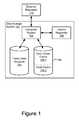
- FIG. 1is a block diagram illustrating an implementation of a data storage system, in accordance with some embodiments.
- FIG. 2is a block diagram illustrating an implementation of a computer system, in accordance with some embodiments.
- FIGS. 3A-3Fillustrate an example of a tiered data structure and example operations performed with the example tiered data structure, in accordance with some embodiments.
- FIGS. 4A-4Eillustrate a method of efficient cache utilization in a tiered data structure, in accordance with some embodiments.
- FIGS. 5A-5Cillustrate a method of performing conditional updates for reducing frequency of data modification operations (e.g., in a tiered data structure), in accordance with some embodiments.
- FIGS. 6A-6Dillustrate a method of compaction of information in a tiered data structure, in accordance with some embodiments.
- the various implementations described hereininclude systems, methods and/or devices used to improve the performance and efficiency of tiered data structures.
- One or more of the various implementations described hereininclude systems, methods and/or devices for efficient cache utilization in a tiered data structure.
- One or more of the various implementations described hereininclude systems, methods and/or devices for performing conditional updates for reducing frequency of data modification operations (e.g., in a tiered data structure).
- One or more of the various implementations described hereininclude systems, methods and/or devices for compaction of information in a tiered data structure.
- a computer systemdetects a request, from a requestor, to access a first data object stored in a tiered data structure that includes internal nodes and leaf nodes.
- the computer systemretrieves a leaf node that includes the first data object and locks the leaf node that includes the first data object. While the leaf node that includes the first data object is locked, the computer system transmits, to the requestor, a first conditional-update communication and detecting a first conditional-update response in response to the first conditional-update communication.
- the computer systemperforms one or more operations based on the first conditional-update response corresponding to the first data object before unlocking the leaf node that includes the first data object.
- two or more of the leaf nodeseach include multiple data objects, each of the data objects including unique key information and a corresponding value.
- the request to access a first data objectincludes a conditional request to modify the first data object.
- the leaf node that includes the first data objectis write-locked while the first conditional-update communication is transmitted and the response is received.
- retrieving the leaf nodeincludes traversing the tiered data structure by navigating through one or more internal nodes to the leaf node that includes the first data object, and after traversing through the one or more internal nodes, the computer system read-locks the one or more internal nodes that were traversed to reach the leaf node that includes the first data object.
- the first conditional-update communicationprovides information that enables the requestor to determine whether or not to update the value of the first data object based on a current value of the first data object.
- performing the one or more operations based on the first conditional-update responseincludes, in accordance with a determination that the first conditional-update response includes a request to update the value of the first data object, updating the value of the first data object in accordance with the first conditional-update response; and in accordance with a determination that the first conditional-update response does not include a request to update the value of the first data object, forgoing updating the value of the first data object.
- the request to access the first data objectidentifies a plurality of data objects including the first data object.
- the computer systemtransmits to the requestor a second conditional-update communication that includes an indication of the current value of a second data object in the plurality of data objects; detects a second conditional-update response corresponding to the second data object received from the requestor in response to the second conditional-update communication; and in response to detecting the second conditional-update response corresponding to the second data object, performs one or more operations based on the second conditional-update response corresponding to the second data object.
- the leaf node that includes the first data objectis unlocked after the computer system performs the one or more operations based on the second conditional-update response corresponding to the second data object.
- conditional-update communicationincludes an executable callback object
- conditional-update responsecorresponds to a result generated based on execution of the callback object
- the one or more memory devicesinclude one or more three-dimensional (3D) memory devices and circuitry associated with operation of memory elements in the one or more 3D memory devices.
- the circuitry and one or more memory elements in a respective 3D memory device, of the one or more 3D memory devicesare on the same substrate (e.g., a silicon substrate).
- FIG. 1is a block diagram illustrating an implementation of a data storage system 101 , in accordance with some embodiments. While some example features are illustrated, various other features have not been illustrated for the sake of brevity and so as not to obscure more pertinent aspects of the example implementations disclosed herein. To that end, as a non-limiting example, data storage system 101 includes computer system 102 , tiered data structure 104 , cache 106 , and one or more internal requestors 108 (e.g., processes or applications that are internal to data storage system 101 ). While internal requestor 108 is shown as separate from computer system 102 in FIG. 1 , in some circumstances internal requestor 108 is a processor application that is co-resident with data access processes on the computer system 102 .
- internal requestor 108is shown as separate from computer system 102 in FIG. 1 , in some circumstances internal requestor 108 is a processor application that is co-resident with data access processes on the computer system 102 .
- cache 106is divided into a data object cache portion 106 - 1 for storing data objects retrieved from tiered data structure 104 and node cache portion 106 - 2 for storing nodes retrieved from tiered data structure 104 .
- tiered data structure 104is stored in non-volatile memory such as NAND-type flash memory or NOR-type flash memory, magnetic hard disk drives or other persistent storage medium that maintains its state when power is removed.
- cache 106is stored in RAM or other random access memory that is not persistent and does not maintain its state when power is removed.
- tiered data structure 104is divided across a plurality of storage devices.
- Computer system 102responds to requests from internal requestors 108 (e.g., other computer systems or components of data storage system 101 that need access to data stored in tiered data structure 104 ) and/or external requestors 110 by storing, retrieving, and modifying data in tiered data structure 104 and cache 106 , as described in greater detail below with reference to FIGS. 4A-4E, 5A-5C, and 6A-6D
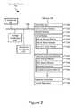
- FIG. 2is a block diagram illustrating an implementation of a computer system 102 , in accordance with some embodiments.
- Computer system 102typically includes one or more processors (also sometimes called CPUs or processing units or microprocessors or microcontrollers) 202 for executing modules, programs and/or instructions stored in memory 206 and thereby performing processing operations, memory 206 , and one or more communication buses 208 for interconnecting these components.
- processorsalso sometimes called CPUs or processing units or microprocessors or microcontrollers
- Communication buses 208optionally include circuitry (sometimes called a chipset) that interconnects and controls communications between system components.
- computer system 102is coupled to tiered data structure 104 , and cache 106 (optionally including data object cache portion 106 - 1 and node cache portion 106 - 2 ) by communication buses 208 and storage interface(s) 210 (e.g., an input output, I/O, interface such as a PCI bus or PCIe bus).
- computer system 102is coupled to internal requestor(s) 108 and/or external requestors 110 by communication buses 208 and requestor interface(s) 212 .
- Memory 206includes high-speed random access memory, such as DRAM, SRAM, DDR RAM or other random access solid state memory devices, and may include non-volatile memory, such as one or more magnetic disk storage devices, optical disk storage devices, flash memory devices, or other non-volatile solid state storage devices. Memory 206 optionally includes one or more storage devices remotely located from processor(s) 202 . Memory 206 , or alternately the non-volatile memory device(s) within memory 206 , comprises a non-transitory computer readable storage medium. In some embodiments, memory 206 , or the computer readable storage medium of memory 206 stores the following programs, modules, and data structures, or a subset thereof:
- Each of the above identified elementsmay be stored in one or more of the previously mentioned memory devices, and corresponds to a set of instructions for performing a function described above.
- the above identified modules or programsi.e., sets of instructions
- memory 206may store a subset of the modules and data structures identified above.
- memory 206may store additional modules and data structures not described above.
- the programs, modules, and data structures stored in memory 206 , or the computer readable storage medium of memory 206provide instructions for implementing respective operations in the methods described below with reference to FIGS. 4A-4E, 5A-5C , and/or 6 A- 6 D.
- FIG. 2shows a computer system 102
- FIG. 2is intended more as a functional description of the various features which may be present in a non-volatile computer system than as a structural schematic of the embodiments described herein.
- items shown separatelycould be combined and some items could be separated.
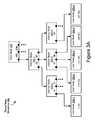
- FIG. 3Aillustrates an example of a tiered data structure, in accordance with some embodiments.
- Tiered data structure 104includes a plurality of nodes. The plurality of nodes are organized in a tiered structure in which each respective node is connected to one or more other nodes in levels (tiers) above and/or below the respective node.
- a parent node for a respective node in tiered data structure 104is a node that is a level (tier) above the respective node in tiered data structure 104 and refers to the respective node.
- a child node for a respective node in tiered data structure 104is a node that is a level (tier) below the respective node in tiered data structure 104 and refers to the respective node.
- Root node 302is an external node that has no parent node, typically there is only one root node for tiered data structure 104 .
- Internal nodes 304are nodes that have both a parent node and one or more child nodes and are thus internal to the tiered data structure.
- Leaf nodes 306are nodes that do not have child nodes and are thus “external” nodes.
- Root node 302 and internal nodes 304include references that indicate which child nodes are associated with a particular range of data. For example, root node 302 in FIG. 3A indicates that internal node 304 - 1 is associated with data with keys between 1 and 136.
- Internal node 304 - 1indicates that: internal node 304 - 2 is associated with data objects having keys between 1 and 24; internal node 304 - 3 is associated with data objects having keys between 25 and 66; and internal node 304 - 4 is associated with data objects having keys between 67 and 136.
- internal node 304 - 3indicates that: leaf node 306 - 2 includes data with keys between 25 and 30; leaf node 306 - 3 includes data with keys between 31 and 58; and leaf node 306 - 4 includes data with keys between 59 and 66, and so on.
- each leaf nodehas a maximum size and when the leaf node exceeds the maximum size, the leaf node is split into two leaf nodes. In some embodiments, each leaf node has a minimum size and when a leaf node is below the minimum size, the leaf node is combined with one or more other leaf nodes.
- each non-leaf node(e.g., root node or internal node) has a maximum number of child nodes, and when a splitting a leaf node results in a non-leaf node having more than the maximum number of child nodes, the non-leaf node is split to accommodate the extra child nodes.
- each non-leaf node(e.g., root node or internal node) has a minimum number of child nodes, and when a combining two or more leaf nodes results in a non-leaf node having less than the minimum number of child nodes, the non-leaf node is combined with one or more other non-leaf nodes to accommodate the reduced number of child nodes.
- the tiered data structuremay additionally conform to some or all of the rules associated with B ⁇ Trees, B+ Trees, B*Trees or other tiered data structures.
- FIG. 3Billustrates an example of efficient cache utilization in a tiered data structure, in accordance with some embodiments.
- populated cache 310 - ais an example of cache 106 from FIGS. 1 and 2 that is populated with one or more data objects and one or more nodes that were retrieved to respond to prior requests for data objects by one or more internal or external requestors.
- one of the prior requestswas a request for data object 58
- computer system 102traversed through tiered data structure 104 in FIG. 3A by traversing, in sequence, root node 302 , internal node 304 - 1 , internal node 304 - 3 to identify and retrieve leaf node 306 - 3 , which includes data object 58 .
- data object 58is cached in data object cache portion 106 - 1 and the traversed nodes are cached in node cache portion 106 - 2 .
- the data objects in the populated cache 310are shown in order of “staleness” where more stale data objects are near the bottom of data object cache portion 106 - 1 and less stale (e.g., fresher) data objects are near the top of data object cache portion 106 - 1 , as data objects are refreshed, they are reordered in the cache to represent their staleness, even though the data objects are, in many circumstances, not actually moved within the cache.
- stalenesse.g., fresher
- the nodes in the populated cache 310are shown in order of “staleness” where more stale nodes are near the bottom of node cache portion 106 - 2 and less stale (e.g., fresher) data objects are near the top of node cache portion 106 - 2 , as nodes are refreshed, they are reordered in the cache to represent their staleness, even though nodes are, in many circumstances, not actually moved within the cache.
- computer system 102determines that data object 61 is not in data object cache portion 106 - 1 in populated cache 310 - a . Subsequently, computer system 102 traverses through tiered data structure 104 in FIG. 3A by traversing, in sequence, root node 302 , internal node 304 - 1 , internal node 304 - 3 to identify and retrieve leaf node 306 - 4 , which includes data object 61 .
- computer system 102When traversing tiered data structure 104 , computer system 102 is able to use a number of cached nodes to improve response time (e.g., by using root node 302 , internal node 304 - 1 and internal node 304 - 3 to determine that leaf node 306 - 4 has be retrieved from tiered data structure 104 ).
- Computer system 102caches the traversed nodes in node cache portion 106 - 2 and caches data object 61 in data object cache portion 106 - 1 as shown in updated cache 310 - b in FIG. 3B .
- data object 2 and leaf node 306 - 1are evicted from cache 106 in accordance with a cache eviction policy, as shown in updated cache 310 - b in FIG. 3B .
- computer system 102determines that data object 25 is in data object cache portion 106 - 1 in populated cache 310 - b .
- computer system 102does not traverse tiered data structure 104 to retrieve data object 25 , because data object 25 is retrieved from cache 106 .
- data object 25is refreshed in data object cache portion 106 - 1 so that it is less stale than object 61 rather than being more stale than data object 61 , as shown in updated cache 310 - c in FIG. 3B .
- data object 25is identified in data object cache portion 106 - 1 using a hash table to locate a portion of data object cache portion 106 - 1 that includes data object 25 . As no new data objects or nodes were added to cache 106 , no data objects or nodes are evicted from cache 106 .
- computer system 102determines that data object 70 is not in data object cache portion 106 - 1 in populated cache 310 - c . Subsequently, computer system 102 traverses through tiered data structure 104 in FIG. 3A by traversing, in sequence, root node 302 , internal node 304 - 1 , internal node 304 - 4 to identify and retrieve leaf node 306 - 5 , which includes data object 70 .
- computer system 102When traversing tiered data structure 104 , computer system 102 is able to use a number of cached nodes to improve response time (e.g., by using root node 302 and internal node 304 - 1 to determine that internal node 304 - 4 and leaf node 306 - 5 have to be retrieved from tiered data structure 104 ).
- Computer system 102caches the traversed nodes in node cache portion 106 - 2 and caches data object 70 in data object cache portion 106 - 1 as shown in updated cache 310 - d in FIG. 3B .
- data object 33 , internal node 304 - 3 , and leaf node 306 - 3are evicted from cache 106 in accordance with a cache eviction policy, as shown in updated cache 310 - d in FIG. 3B .
- root node 302 and leaf nodes 306are cached in node cache portion 106 - 2 , but most leaf nodes are quickly evicted from node cache portion 106 - 2 , while internal nodes 304 are frequently used and are thus frequently refreshed in cache 106 , so that the node cache portion 106 - 2 includes primarily internal nodes 304 during normal operation (e.g., 50% or more of the capacity of node cache portion 106 - 2 is occupied by internal nodes).
- Using a data object cache in addition to a node cache instead of solely using a node cacheimproves the performance of the cache by increasing the likelihood that a requested data object will be available from the cache.
- FIG. 3Cillustrates an example of performing conditional updates for reducing frequency of traversals (e.g., in a tiered data structure), in accordance with some embodiments.
- computer system 102FIGS. 1 and 2 detects ( 320 ) a request, received from an internal requestor or an external requestor, to access one or more data objects (e.g., data object 59 , which is in leaf node 306 - 4 ).
- data objectse.g., data object 59 , which is in leaf node 306 - 4
- tiered data structure 104does not have any nodes locked (e.g., read locked or read/write locked) by computer system 102 .
- one or more other computer systems using the same tiered data structureoptionally lock one or more of the nodes of tiered data structure 104 when they are using those nodes.
- computer system 102traverses ( 322 ) tiered data structure 104 , as shown in FIG. 3C , to reach the node (e.g., leaf node 306 - 4 ) that includes the requested data object(s) (e.g., data object 59 ).
- computer system 102After identifying the leaf node that includes the requested data object, computer system 102 locks ( 323 ) the leaf node that includes the requested data object, as shown in FIG. 5C , where leaf node 306 - 4 is locked, and performs one or more additional operation (e.g., operations 324 - 326 ), while the leaf node is locked (e.g., read or read/write locked).
- computer system 102transmits ( 324 ) a conditional-update communication to a requestor, detects ( 325 ) a constitutional update response, and performs ( 326 ) one or more operations based on the conditional update response.
- computer system 102performs a conditional write operation where the requestor decides whether or not to perform the write operation based on the current value of the data object.
- computer system 102performs a read-modify-write operation by returning a current value of the data object to the requestor in the conditional-update communication.
- conditional update operationsinclude “fetch and op” operations and “compare and swap” operations. In circumstances where the condition for the conditional update operation is not met, then the operation performed based on the conditional-update response optionally includes deciding not to perform any update on the requested data object.
- the detected request(e.g., detected in operation 320 ) includes a request to access multiple data objects that are in a single leaf node, in which case operations 324 - 326 are, optionally, repeated for two or more of the multiple data objects, so as to reduce the number of traversals of tiered data structure 104 .
- computer system 102unlocks ( 328 ) the leaf node (e.g., leaf node 306 - 4 ) that was locked in response to the request to access the requested data object. Additional details regarding performing conditional updates for reducing frequency of data modification operations (e.g., in a tiered data structure) are described below with reference to method 500 and FIGS. 5A-5C .
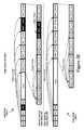
- FIGS. 3D-3Fillustrate examples of compaction of information in a tiered data structure, in accordance with some embodiments.
- FIG. 3Cshows an example leaf node 306 - 4 from tiered data structure 104 in FIG. 3A .
- Leaf node 306 - 4includes data for data objects 59 , 60 , 61 , 63 and 66 .
- leaf node 306 - 4For each of these data objects (e.g., DO 59 , DO 60 , DO 61 , DO 63 , DO 66 ), leaf node 306 - 4 includes a corresponding fixed length header (H 59 , H 60 , H 61 , H 63 , and H 66 , respectively) and corresponding metadata (e.g., M 59 , M 60 , M 61 , M 63 , and M 66 , respectively).
- H 59 , H 60 , H 61 , H 63 , and H 66corresponding fixed length header
- metadatae.g., M 59 , M 60 , M 61 , M 63 , and M 66 , respectively.
- the fixed length headersinclude a metadata type in embodiments where there are a plurality of different metadata types for metadata of the data objects, and an offset (e.g., a number of bytes) from a particular portion of the leaf node (e.g., a beginning or an end of the leaf node) to the location of the data object in the leaf node.
- the fixed length headerseach have the same length, and can, thus, be used to perform a binary search through data objects in the leaf node.
- the fixed length headersare packed to the left in the leaf node and the data objects and metadata are packed to the right in the leaf node, so that there is a growing area in the middle of the leaf node that increases or decreases in size as additional data objects are added to, or removed from, the leaf node.
- Packing the headers and data objects in different directionsenables both the headers and the data objects to have fixed points to refer to when the data objects and nodes are identified by offsets (e.g., the headers can be identified based on an offset from a left edge of the leaf node, and the data objects and metadata can be identified based on an offset from a right edge of the leaf node).
- the data objects (e.g., DO 59 , DO 60 , DO 61 , DO 63 , DO 66 ) in leaf node 306 - 4each include unique key information (e.g., K 59 , K 60 , K 61 , K 63 , K 66 , respectively) and a corresponding value (e.g., V 59 , V 60 , V 61 , V 63 , V 66 , respectively).
- the unique key information for some of the data objectsis a full unique key for the data objects, while the unique key information for other data objects is a portion of a unique key for the data objects, and the metadata for these data objects indicates a location of a key prefix that is shared with one or more other data objects that can be used to recreate the unique key for the data object in combination with the unique key information stored with the data object.
- data object 59includes a full unique key in unique key information K 59
- data object 60includes a partial key in unique key information K 60
- metadata M 60 associated with data object 60is used to identify a location of a key prefix (e.g., a portion of K 59 that serves as a key prefix for data object 60 and, in combination with unique key information K 60 can be used to determine a unique key for data object 60 ).
- data object 61includes a partial key in unique key information K 61 and metadata M 61 associated with data object 61 is used to identify a location of a key prefix (e.g., a portion of K 59 that serves as a key prefix for data object 61 and, in combination with unique key information K 61 can be used to determine a unique key for data object 61 ).
- a key prefixe.g., a portion of K 59 that serves as a key prefix for data object 61 and, in combination with unique key information K 61 can be used to determine a unique key for data object 61 ).
- Metadatafor a corresponding data object optionally includes one or more of the following: key length information 334 indicating a length of unique key information associated with the corresponding data object; data length information 336 indicating a length of the corresponding data object or the value of the corresponding data object; prefix offset information 338 that indicates a location of a start of a key prefix for the corresponding data object; prefix length information 340 that indicates a length of the key prefix for the corresponding data object; data overflow pointer 342 that indicates a location of data for the corresponding data object that is too large to fit in the leaf node; and global version information 344 that indicates a version of the corresponding data object.
- key length information 334indicating a length of unique key information associated with the corresponding data object
- data length information 336indicating a length of the corresponding data object or the value of the corresponding data object
- prefix offset information 338indicates a location of a start of a key prefix for the corresponding data object
- prefix length information 340
- the global version information 344includes information identifying the order of each change to data objects in tiered data structure 104 ( FIGS. 1 and 2 ) or data objects in data storage system 101 ( FIGS. 1 and 2 ), which can be used to determine whether a change to a first data object occurred before or after a change to a second, different, data object.
- different data objectshave different types of metadata with different lengths, sometimes called variable-length metadata.
- variable length metadataenables shorter metadata to be used in many situations, and using shorter metadata increases the number of data objects that can be stored in a leaf node.
- there are four types of metadatatype-0 metadata, type-1 metadata, type-2 metadata and type-3 metadata.
- Type-0 metadatais used when the data object has the same key prefix, key length, and data length as the preceding data object, in which case the metadata includes only global version information 344 (e.g., represented as a 64-bit unsigned integer), and other information such as key prefix location, data length and key length are determined by looking at the metadata corresponding to the preceding data object.
- Type-1 metadatais used when the data object has a key length and data length that can each fit in a single byte and data that fits in the leaf node, in which case the metadata includes key length information 334 (e.g., represented as an 8-bit unsigned integer), data length information 336 (e.g., represented as an 8-bit unsigned integer), prefix offset information 338 (e.g., represented as an 16-bit unsigned integer), prefix length information 340 (e.g., represented as an 8-bit unsigned integer), and global version information 344 (e.g., represented as a 64-bit unsigned integer).
- key length information 334e.g., represented as an 8-bit unsigned integer
- data length information 336e.g., represented as an 8-bit unsigned integer
- prefix offset information 338e.g., represented as an 16-bit unsigned integer
- prefix length information 340e.g., represented as an 8-bit unsigned integer
- global version information 344e.g.
- Type-2 metadatais used when the data object has a key length and data length that can each fit in two bytes, in which case the metadata includes key length information 334 (e.g., represented as an 16-bit unsigned integer), data length information 336 (e.g., represented as an 16-bit unsigned integer), prefix offset information 338 (e.g., represented as an 16-bit unsigned integer), prefix length information 340 (e.g., represented as an 16-bit unsigned integer), data overflow pointer 342 (e.g., represented as a 64-bit unsigned integer), and global version information 344 (e.g., represented as a 64-bit unsigned integer).
- key length information 334e.g., represented as an 16-bit unsigned integer
- data length information 336e.g., represented as an 16-bit unsigned integer
- prefix offset information 338e.g., represented as an 16-bit unsigned integer
- prefix length information 340e.g., represented as an 16-bit unsigned
- Type-3 metadatais used for data objects that do not fit in the other categories, in which case the metadata includes key length information 334 (e.g., represented as an 32-bit unsigned integer), data length information 336 (e.g., represented as an 32-bit unsigned integer), prefix offset information 338 (e.g., represented as an 16-bit unsigned integer), prefix length information 340 (e.g., represented as an 32-bit unsigned integer), data overflow pointer 342 (e.g., represented as a 64-bit unsigned integer), and global version information 344 (e.g., represented as a 64-bit unsigned integer).
- key length information 334e.g., represented as an 32-bit unsigned integer
- data length information 336e.g., represented as an 32-bit unsigned integer
- prefix offset information 338e.g., represented as an 16-bit unsigned integer
- prefix length information 340e.g., represented as an 32-bit unsigned integer
- Enabling the use of other types of metadatasaves space in the leaf node when type-3 metadata is not needed to store all of the relevant metadata for a data object.
- type-0, type-1, and type-2e.g., type-0, type-1, and type-2
- Enabling the use of other types of metadatasaves space in the leaf node when type-3 metadata is not needed to store all of the relevant metadata for a data object.
- type-0, type-1, and type-2saves space in the leaf node when type-3 metadata is not needed to store all of the relevant metadata for a data object.
- FIG. 3Eshows an example, of deleting a data object from leaf node 306 - 4 .
- leaf node 306 - 4is shown with highlighting in black to indicate the information in leaf node 306 - 4 that will be deleted when the deletion operation is performed.
- header H 63is deleted from leaf node 306 - 4 , as shown in the lower part of FIG. 3E , and the remaining headers (e.g., H 59 , H 60 , H 61 , and H 66 ) are repacked against the left edge of leaf node 306 - 4 .
- data object D 063 and corresponding metadata M 63are deleted as shown in the lower part of FIG. 3E , and the remaining data objects (e.g., DO 59 , DO 60 , DO 61 , and D 066 ) and metadata (e.g., M 59 , M 60 , M 61 , and M 66 ) are repacked against the right edge of leaf node 306 - 4 .
- data object 66relied on a portion of the key of data object 63 as a key prefix for data object 66 .
- unique key information K 66 for data object 66is updated to include a full unique key for data object 66
- metadata M 66is updated to include a null value for the prefix offset information to indicate that there is no key prefix for data object 66 and that the unique key information K 66 for data object 66 includes a full unique key.
- computer system 102determines that there is another data object (e.g., data object 59 ) in leaf node 306 - 4 that is associated with unique key information that could be used as a new key prefix for data object 66 , and unique key information K 66 is updated to include a portion of the unique key for data object 66 that, when combined with the new key prefix can be used to generate the full unique key for data object 66 , and metadata M 66 is updated to point to unique key information (e.g., K 59 ) for the other data object so that a portion of unique key information (e.g., K 59 ) for the other data object can be used as a key prefix for data object 66 .
- another data objecte.g., data object 59
- unique key information K 66is updated to include a portion of the unique key for data object 66 that, when combined with the new key prefix can be used to generate the full unique key for data object 66
- metadata M 66is updated to point to unique key information
- repacking the data objects and headers as described above after deleting data object 63will change locations of data objects, metadata and headers relative to the locations from which offsets identifying locations of these elements are measured, and thus after a data object, header, and metadata have been deleted, computer system 102 updates the offset information in the header and metadata corresponding to one or more of the other data objects (e.g., data objects that remain in leaf node 306 - 4 after to deleting data object 63 ).
- FIG. 3Fshows an example, of adding a data object from leaf node 306 - 4 .
- leaf node 306 - 4is shown with data object DO 65 that is to be added to leaf node 306 - 4 .
- new header H 65is added in between header H 63 and header H 66 , as shown in the lower part of FIG. 3F , and the headers (e.g., H 59 , H 60 , H 61 , H 63 , H 65 , and H 66 ) are repacked against the left edge of leaf node 306 - 4 .
- data object DO 65 and corresponding metadata M 65are added to leaf node 306 - 4 as shown in the lower part of FIG. 3F , and the data objects (e.g., DO 59 , DO 60 , DO 61 , DO 63 , DO 65 , and DO 66 ) and metadata (e.g., M 59 , M 60 , M 61 , M 63 , M 65 , and M 66 ) are repacked against the right edge of leaf node 306 - 4 .
- data objectse.g., DO 60 , DO 61 , DO 63 , DO 65 , and DO 66
- metadatae.g., M 59 , M 60 , M 61 , M 63 , M 65 , and M 66
- data object 66relied on a portion of the key of data object 63 as a key prefix for data object 66 and data object 63 was adjacent to metadata M 66 for data object 66 .
- metadata M 66 of data object 66is updated to indicate a different offset for the key prefix for data object 66 , because the relative position between metadata M 66 and unique key information K 63 has changed.
- newly added data object 65is also able to use a portion of unique key information K 63 as a key prefix, and thus metadata M 65 of data object 65 is updated to identify a portion of K 63 as a key prefix that can be combined with unique key information K 65 to generate a full unique key for data object 65 .
- repacking the data objects and headers as described above after adding data object 65will change locations of data objects, metadata and headers relative to the locations from which offsets identifying locations of these elements are measured, and thus after a new data object, new header and new metadata have been inserted, computer system 102 updates the offset information in the header and metadata corresponding to one or more of the other data objects (e.g., data objects that were in leaf node 306 - 4 prior to adding data object 65 ).
- one or more data objectsare updated without adding or deleting a data object from leaf node 306 - 4 .
- updating a data objectwill, in some circumstances change a size of the data object (e.g., by changing a type of metadata used by the data object to a smaller or larger size of metadata or by changing a length of the data to a smaller or larger length).
- the change in the data object or associated metadatawill, in many circumstances, change locations of data objects, metadata and headers relative to the locations from which offsets identifying locations of these elements are measured, and thus after a data object or metadata has been updated, computer system 102 updates the offset information in the header and metadata corresponding to one or more of the other data objects. Additional details regarding compaction of information in a tiered data structure are described below with reference to method 600 and FIGS. 6A-6D .
- FIGS. 4A-4Eillustrate a method 400 for efficient cache utilization in a tiered data structure, in accordance with some embodiments.
- Method 400is, optionally, governed by instructions that are stored in a non-transitory computer readable storage medium and that are executed by one or more processors of one or more computer systems (e.g., computer system 102 , FIG. 2 ).
- Each of the operations shown in FIGS. 4A-4Etypically corresponds to instructions stored in a computer memory or non-transitory computer readable storage medium (e.g., memory 206 of computer system 102 in FIG. 2 ).
- the computer readable storage mediumoptionally (and typically) includes a magnetic or optical disk storage device, solid state storage devices such as Flash memory, or other non-volatile memory device or devices.
- the computer readable instructions stored on the computer readable storage mediumtypically include one or more of: source code, assembly language code, object code, or other instruction format that is interpreted or executed by one or more processors. In various embodiments, some operations in method 400 are combined and/or the order of some operations is changed from the order shown in FIGS. 4A-4E .
- a computer systemdetects ( 402 ) a request, received from a requestor (e.g., an internal requestor 108 or an external requestor 110 in FIG. 1 ), to access a first data object stored in a tiered data structure (e.g., tiered data structure 104 in FIGS. 1 and 3A ), the tiered data structure stored in one or more memory devices, wherein the tiered data structure includes a plurality of internal (non-leaf) nodes (e.g., nodes between a root node and the leaf nodes in the tiered data structure) and a plurality of leaf nodes.
- a requestore.g., an internal requestor 108 or an external requestor 110 in FIG. 1
- a tiered data structuree.g., tiered data structure 104 in FIGS. 1 and 3A
- the tiered data structurestored in one or more memory devices, wherein the tiered data structure includes a plurality of internal (non-leaf) nodes (e.g.
- the tiered data structureis a B ⁇ Tree or B ⁇ Tree like structure (e.g., a B+ tree or a B* tree, or the like) that includes a root node, two or more internal (parent) nodes, and two or more leaf (external child) nodes.
- the topmost nodeis sometimes called the root node.
- an internal nodealso known as an inner node, or inode for short, parent node or branch node
- a leaf nodealso known as an outer node, external node, or terminal node
- two or more of the leaf nodeseach include ( 404 ) multiple data objects, each of the data objects including unique key information (e.g., a unique key or information from which a unique key can be identified such as a shortened key and a location/length of a key prefix) and a corresponding value.
- the corresponding valueis data.
- the corresponding valueis a pointer identifying a location where the data is stored.
- the data objectsare contiguous data objects where the unique key information for a respective contiguous data object is adjacent or substantially adjacent to the corresponding value for the respective contiguous data object or other data for the respective contiguous data object that is adjacent to the corresponding value.
- the data objectsare split data objects where the unique key information for a respective split data object is separated from the corresponding value for the respective split data object by other data for other data objects and the unique key information for the respective split data object is stored with a pointer that identifies a location of the corresponding value for the respective split data object.
- the computer systemdetermines ( 406 ) whether the first data object is stored in a cache (e.g., data object cache portion 106 - 1 in FIGS. 1 and 3B ) that includes a plurality of data objects from the tiered data structure.
- the data objects stored in the cacheare stored separately from the leaf node to which they correspond in the tiered data structure (e.g., such that a first data object can be retrieved from the cache without retrieving a leaf node that includes data objects that are adjacent to the first data object and without traversing through one or more internal nodes of the tiered data structure).
- some or all of the cacheis in memory of the computer system.
- some or all of the cacheis remote from the computer system and the cache is (operatively) in communication with the computer system via one or more communication systems.
- the cacheis stored ( 410 ) in high-speed memory (e.g., RAM or other non-persistent memory with a high read/write rate that loses stored information when power is shut off to the memory, or even high-speed persistent memory).
- high-speed persistent memoryis more expensive than slower persistent memory and thus the amount of high-speed persistent memory is smaller than the amount of slower persistent memory, so as to reduce device cost.
- the tiered data structureis stored in persistent memory that has a slower average read and/or write speed than the high-speed memory (e.g., wherein the persistent memory is flash memory, any suitable three-dimensional non-volatile memory such as vertical NAND, RRAM (also called ReRAM), etc., hard drive disks, or other persistent memory that maintains its state even when power is shut off to the memory).
- the cacheis populated ( 412 ) with data objects retrieved by traversing the tiered data structure in response to prior requests to access data objects from the tiered data structure.
- the computer systemAfter determining whether the first data object is stored in the cache, in accordance with a determination that the first data object is stored in the cache, the computer system returns ( 414 ) the first data object from the cache to the requestor. For example, data object 25 is retrieved from data object cache portion 106 - 1 in response to request 2 in FIG. 3B , as described in greater detail above.
- data object 25is retrieved from data object cache portion 106 - 1 in response to request 2 in FIG. 3B , as described in greater detail above.
- one or more other data objects included in the leaf node for the first data objectare not included in the cache (e.g., because those data objects are not frequently used data objects). For example in FIG.
- leaf node 306 - 2 and data objects 26 - 30are not stored in data object cache portion 106 - 1 , even though data object 25 is stored in data object cache portion 106 - 1 .
- Forgoing storing some data objects from one or more leaf nodes instead of storing the whole leaf nodeimproves the utility of the cache because more of the frequently used data objects can be stored in the cache than if full leaf nodes were stored in the cache, because less frequently used data objects that happen to reside in the same leaf node as more frequently used objects do not need to be stored in the cache.
- storing frequently used data objects in the cache separately from their corresponding leaf nodeseffectively increases the size of the cache, as less unnecessary information is stored in the cache.
- returning the first data object from the cache to the requestorincludes locating ( 416 ) the first data object in the cache using a hash table to map a unique key of the first data object that is included with the request to a portion of the cache (sometimes referred to as a “bucket”) that includes the first data object (and, optionally, one or more other data objects which have unique keys that are mapped to the portion of the cache by the hash table).
- returning the first data object from the cache to the requestorincludes locating ( 418 ) the first data object in the cache without reference to the tiered data structure (e.g., without traversing the tiered data structure and without retrieving the leaf node that includes the first data object).
- the cachehas a predefined size, at a respective point in time, the cache is populated with recently accessed data objects for a plurality of leaf nodes (e.g., in response to prior requests to access the data objects) and the predefined size of the cache is smaller ( 420 ) than the aggregate size of the plurality of leaf nodes. For example, more data objects are stored in the cache than could be stored in the cache if each of the data objects was stored with its corresponding leaf node. Thus, in some embodiments, separately caching data objects enables a larger number of recently used data objects to be stored in the cache than would be able to be stored if full leaf nodes were cached, as described above with reference to FIG. 3B .
- the respective point in timeis a point in time after ( 422 ) one or more data objects have been evicted from the cache (e.g., the cache has reached a maximum capacity and one or more least recently used objects, including the one or more evicted data objects, have been being evicted from the cache to make room for more recently used objects).
- the computer systemtraverses ( 426 ) the tiered data structure to a leaf node that includes the first data object.
- the computer systemin conjunction with traversing the tiered data structure to the leaf node for the first data object, the computer system caches ( 428 ) internal nodes that are traversed between a root node and the leaf node for the first data object. For example in FIG. 3B , internal node 304 - 4 is cached after being used to retrieve data object 70 in response to request 3 .
- the nodesare cached in the same cache as the data objects (e.g., cache 106 in FIGS. 1 and 3B ). In some embodiments, the nodes are cached in a node cache (e.g., node cache portion 106 - 2 in FIGS. 1 and 3B ) that is separate from the data object cache (e.g., data object cache portion 106 - 1 in FIGS. 1 and 3B ) used for the data objects. In some embodiments, the leaf node for the first data object is also cached. In some embodiments, the node cache is smaller than the data object cache. In some embodiments, the node cache can store a smaller number of nodes than the data object cache can store data objects.
- the node cacheis, optionally, governed by a least recently used (LRU) cache eviction policy so that when new nodes are stored in the node cache, the least recently used nodes in the node cache are evicted to make room for the new nodes.
- traversing the tiered data structure to the leaf node for the first data objectincludes retrieving ( 430 ) one or more nodes that were previously cached (e.g., stored in a node portion of the cache or in a separate node cache) during previous traversals of the tiered data structure (e.g., in response to prior requests to access data objects). For example, in FIG. 3B , internal nodes 304 - 1 and 304 - 3 are used to respond to request 1 .
- the computer systemAfter traversing the tiered data structure, the computer system returns ( 432 ) the first data object from the leaf node for the first data object in the tiered data structure to the requestor. In some embodiments, in accordance with a determination that the first data object is not stored in the cache, after returning the first data object from the leaf node for the first data object, the computer system stores ( 434 ) the first data object in the cache.
- the computer systemin conjunction with storing the first data object in the cache, in accordance with a determination that cache eviction criteria have been met, the computer system evicts ( 435 ) one or more other data objects from the cache (e.g., evicting the least recently used data objects in accordance with a least recently used (LRU) cache eviction policy or evicting the oldest data objects in accordance with a first in first out (FIFO) cache eviction policy).
- the computer systemalso caches ( 436 ) the leaf node for the first data object in the cache. For example, in FIG. 3B , leaf node 306 - 4 that includes data object 61 is cached in node cache portion 106 - 2 when data object 61 is retrieved and cached in data object cache portion 106 - 1 .
- the cachehas a data object portion (e.g., data object cache portion 106 - 1 in FIGS. 1 and 3B ) for storing data objects separately from their corresponding leaf nodes and a node portion (e.g., node cache portion 106 - 2 in FIGS. 1 and 3B ) for storing leaf nodes and internal nodes of the tiered data structure.
- a data object portione.g., data object cache portion 106 - 1 in FIGS. 1 and 3B
- node portione.g., node cache portion 106 - 2 in FIGS. 1 and 3B
- the computer systemin conjunction with returning the first data object from the leaf node for the first data object in the tiered data structure to the requestor (e.g., when the first data object is not stored in the cache), the computer system caches ( 438 ) the first data object in the data object portion of the cache and caches the leaf node for the first data object in the node portion of the cache. After caching the first data object and the leaf node for the first data object, the computer system accesses ( 440 ) a different data object in a different leaf node of the tiered data structure (e.g., in response to detecting a request to access the different data object received from the requestor or another, different, requestor).
- the computer systemcaches ( 442 ) the different data object in the data object portion of the cache while maintaining the first data object in the data object portion of the cache and caches ( 444 ) the different leaf node in the node portion of the cache and evicts the leaf node for the first data object from the node portion of the cache.
- the leaf node for the first data objectis evicted before caching the different leaf node to make room for the different leaf node. For example in FIG.
- leaf node 306 - 3in response to request 3 , leaf node 306 - 3 is evicted from node cache portion 106 - 2 , while data object 58 (which is from leaf node 306 - 3 ) remains in data object cache portion 106 - 1 .
- the computer systemdetects ( 446 ) an insert request to insert a second data object into the tiered data structure.
- the computer systemtraverses ( 450 ) the tiered data structure to a leaf node for the second data object and inserting the second data object into the leaf node for the second data object (e.g., the leaf node for the first data object or another leaf node that is different from the leaf node for the first data object).
- inserting the second data object in the tiered data structurecauses a leaf node and optionally one or more internal nodes to be split.
- the computer systemin accordance with a determination that the second data object was successfully inserted into the tiered data structure, stores ( 452 ) the second data object in the cache separately from the leaf node for the second data object. In some embodiments, if the second data object is not successfully inserted into the tiered data structure, the computer system forgoes storing the second data object in the cache (e.g., the second data object is not stored in the cache) and an error message is optionally sent to the requestor indicating that the second data object was not inserted.
- the computer systemdetects ( 454 ) an update request to update a third data object in the tiered data structure.
- the computer systemtraverses ( 458 ) the tiered data structure to a leaf node for the third data object and updating the third data object in the leaf node for the third data object (e.g., the leaf node for the first data object or another leaf node that is different from the leaf node for the first data object).
- the computer systemstores ( 460 ) the updated third object in the cache separately from the leaf node for the third data object.
- the computer systemforgoes updating the third data object in the cache (e.g., the third data object is not updated in the cache) and an error message is optionally sent to the requestor indicating that the third data object was not updated.
- storing the updated third object in the cacheincludes updating/replacing the prior version of the third data object in the cache with the updated third object, whereas if a prior version of the third object is not stored in the cache, the updated third object is stored in the cache without needing to delete or overwrite a prior version of the third object.
- the computer systemdetects ( 462 ) a delete request to delete a fourth data object in the tiered data structure.
- the computer systemtraverses ( 466 ) the tiered data structure to a leaf node for the fourth data object and deleting the fourth data object from the leaf node for the fourth data object (e.g., the leaf node for the first data object or another leaf node that is different from the leaf node for the first data object).
- deleting the fourth data object in the tiered data structurecauses two or more leaf nodes and, optionally, two or more internal nodes to be combined.
- the computer systemin accordance with a determination that the fourth data object was successfully deleted in the tiered data structure and is stored in the cache, deletes ( 468 ) the fourth object from the cache. In some embodiments, if the fourth data object is not successfully deleted from the tiered data structure, the computer system forgoes deleting the fourth data object from the cache (e.g., the fourth data object is not deleted from the cache) and an error message is optionally sent to the requestor indicating that the fourth data object was not deleted. In situations where the fourth object is not stored in the cache (e.g., in accordance with a determination that the fourth object is not in the cache), the fourth object does not need to be deleted from the object cache.
- tiered data structures, data objects, nodes, and unique key informationdescribed above with reference to method 400 optionally have one or more of the characteristics of the tiered data structures, data objects, nodes, and unique key information described herein with reference to other methods described herein (e.g., method 500 and 600 ). For brevity, these details are not repeated here.
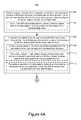
- FIGS. 5A-5Cillustrate a method 500 for performing conditional updates for reducing frequency of data modification operations (e.g., in a tiered data structure), in accordance with some embodiments.
- Method 500is, optionally, governed by instructions that are stored in a non-transitory computer readable storage medium and that are executed by one or more processors of one or more computer systems (e.g., computer system 102 , FIG. 2 ).
- Each of the operations shown in FIGS. 5A-5Ctypically corresponds to instructions stored in a computer memory or non-transitory computer readable storage medium (e.g., memory 206 of computer system 102 in FIG. 2 ).
- the computer readable storage mediumoptionally (and typically) includes a magnetic or optical disk storage device, solid state storage devices such as Flash memory, or other non-volatile memory device or devices.
- the computer readable instructions stored on the computer readable storage mediumtypically include one or more of: source code, assembly language code, object code, or other instruction format that is interpreted or executed by one or more processors. In various embodiments, some operations in method 500 are combined and/or the order of some operations is changed from the order shown in FIGS. 5A-5C .
- a computer systemdetects ( 502 ) a request, received from a requestor (e.g., an internal requestor 108 or an external requestor 110 in FIG. 1 ), to access a first data object stored in a tiered data structure (e.g., tiered data structure 104 in FIGS. 1 and 3A ), the tiered data structure stored in one or more memory devices, wherein the tiered data structure includes a plurality of internal (non-leaf) nodes (e.g., nodes between a root node and the leaf nodes in the tiered data structure) and a plurality of leaf nodes.
- a requestore.g., an internal requestor 108 or an external requestor 110 in FIG. 1
- a tiered data structuree.g., tiered data structure 104 in FIGS. 1 and 3A
- the tiered data structurestored in one or more memory devices, wherein the tiered data structure includes a plurality of internal (non-leaf) nodes (e.g.
- the tiered data structureis a B ⁇ Tree or B ⁇ Tree like structure (e.g., a B+ tree or a B* tree, or the like) that includes a root node, two or more internal (parent) nodes, and two or more leaf (external child) nodes.
- the topmost nodeis sometimes called the root node.
- an internal nodealso known as an inner node, inode for short, parent node or branch node
- a leaf nodealso known as an outer node, external node, or terminal node
- two or more of the leaf nodeseach include ( 504 ) multiple data objects, each of the data objects including unique key information (e.g., a unique key or information from which a unique key can be identified such as a shortened key and a location/length of a key prefix) and a corresponding value.
- the corresponding valueis data.
- the corresponding valueis a pointer identifying a location where the data is stored.
- the data objectsare contiguous data objects where the unique key information for a respective contiguous data object is adjacent or substantially adjacent to the corresponding value for the respective contiguous data object or other data for the respective contiguous data object that is adjacent to the corresponding value.
- the data objectsare split data objects where the unique key information for a respective split data object is separated from the corresponding value for the respective split data object by other data for other data objects and the unique key information for the respective split data object is stored with a pointer that identifies a location of the corresponding value for the respective split data object.
- the request to access a first data objectincludes ( 506 ) a conditional request to modify the first data object (e.g., a request that may or may not result in modifying the first data object depending on one or more conditions such as the current value of the first data object).
- the computer systemperforms ( 508 ) one or more operations in response to detecting the request to access the first data object.
- the computer systemretrieves ( 510 ) a leaf node that includes the first data object.
- retrieving the leaf nodeincludes traversing ( 512 ) the tiered data structure by navigating through one or more internal nodes to the leaf node that includes the first data object, and after traversing through the one or more internal nodes, the computer system read-locks ( 514 ) the one or more internal nodes that were traversed to reach the leaf node that includes the first data object.
- the computer systemalso locks ( 516 ) the leaf node that includes the first data object.
- the leaf node that includes the first data objectis write-locked ( 518 ) while the first conditional-update communication is transmitted and the response is received.
- leaf node 306 - 4is write locked while the conditional-update communication is transmitted and the response is received
- the computer systemperforms a plurality of operations while the leaf node that includes the first data object is locked.
- the computer systemtransmits ( 522 ), to the requestor, a first conditional-update communication that includes an indication of the current value of the first data object.
- the conditional-update communicationincludes ( 524 ) an executable callback object.
- the computer systemAfter transmitting the first conditional-update communication, the computer system detects ( 526 ) a first conditional-update response corresponding to the first data object received from the requestor in response to the first conditional-update communication (e.g., based on the indication of the current value of the first data object).
- the conditional-update responsecorresponds ( 528 ) to a result generated based on execution of the callback object.
- the computer systemIn response to detecting the first conditional-update response corresponding to the first data object, the computer system performs ( 530 ) one or more operations based on the first conditional-update response corresponding to the first data object.
- the first conditional-update communicationprovides ( 532 ) information that enables the requestor to determine whether or not to update the value of the first data object based on a current value of the first data object and performing the one or more operations based on the first conditional-update response includes determining whether or not the conditional-update response includes a request to update the value of the first data object.
- the computer systemupdates ( 534 ) the value of the first data object in accordance with the first conditional-update response.
- the computer systemforgoes ( 536 ) updating the value of the first data object (e.g., the first conditional-update response corresponding to the first data object enables performance of an update operation that is not a blind update).
- the request to access the first data objectidentifies ( 538 ) a plurality of data objects including the first data object.
- the computer systemtransmits ( 540 ), to the requestor, a second conditional-update communication that includes an indication of the current value of a second data object in the plurality of data objects.
- the computer systemsubsequently detects ( 542 ) a second conditional-update response corresponding to the second data object received from the requestor in response to the second conditional-update communication (e.g., based on the indication of the current value of the second data object) and, in response to detecting the second conditional-update response corresponding to the second data object, the computer system performs ( 544 ) one or more operations based on the second conditional-update response corresponding to the second data object. In some embodiments, this process is repeated for a number of different data objects in a predefined (key) order until an object is reached that is not in the leaf node that includes the first data object (e.g., as shown above in FIG. 3C with reference to operations 324 - 326 ).
- the computer systemAfter performing the one or more operations based on the first conditional-update response corresponding to the first data object, the computer system unlocks ( 546 ) the leaf node that includes the first data object (e.g., so that other read and/or write operations can be performed on the leaf node and/or data objects contained therein). For example, in FIG. 3C , leaf node 306 - 4 is unlocked in tiered data structure 104 after performing the operations based on the conditional-update response.
- the leaf node that includes the first data objectis unlocked after performing ( 548 ) the one or more operations based on the second conditional-update response corresponding to the second data object. For example, the leaf node that includes the first data object is unlocked in response to a determination that the request to access the first data object does not identify any additional data objects in the leaf node that includes the first data object.
- tiered data structures, data objects, nodes, and unique key information described above with reference to method 500optionally have one or more of the characteristics of the tiered data structures, data objects, nodes, and unique key information described herein with reference to other methods described herein (e.g., method 400 and 600 ). For brevity, these details are not repeated here.
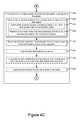
- FIGS. 6A-6Dillustrate a method 600 for compaction of information in a tiered data structure, in accordance with some embodiments.
- Method 600is, optionally, governed by instructions that are stored in a non-transitory computer readable storage medium and that are executed by one or more processors of one or more computer systems (e.g., computer system 102 , FIG. 2 ).
- Each of the operations shown in FIGS. 6A-6Dtypically corresponds to instructions stored in a computer memory or non-transitory computer readable storage medium (e.g., memory 206 of computer system 102 in FIG. 2 ).
- the computer readable storage mediumoptionally (and typically) includes a magnetic or optical disk storage device, solid state storage devices such as Flash memory, or other non-volatile memory device or devices.
- the computer readable instructions stored on the computer readable storage mediumtypically include one or more of: source code, assembly language code, object code, or other instruction format that is interpreted or executed by one or more processors. In various embodiments, some operations in method 600 are combined and/or the order of some operations is changed from the order shown in FIGS. 6A-6D .
- a computer systemdetects ( 602 ) a request, received from a requestor (e.g., an internal requestor 108 or an external requestor 110 in FIG. 1 ), to access a first data object stored in a tiered data structure (e.g., tiered data structure 104 in FIGS. 1 and 3A ), the tiered data structure stored in one or more memory devices.
- the tiered data structureincludes ( 604 ) a plurality of internal (non-leaf) nodes (e.g., nodes between a root node and the leaf nodes in the tiered data structure) and a plurality of leaf nodes.
- the tiered data structureis a B ⁇ Tree or B ⁇ Tree like structure (e.g., a B+ tree or a B* tree, or the like) that includes a root node, two or more internal (parent) nodes, and two or more leaf (external child) nodes.
- the topmost nodeis sometimes called the root node.
- an internal nodealso known as an inner node, inode for short, parent node or branch node
- a leaf nodealso known as an outer node, external node, or terminal node
- two or more of the leaf nodeseach include ( 606 ) multiple data objects, each of the data objects including unique key information (e.g., a unique key or information from which a unique key can be identified such as a shortened key and a location/length of a key prefix) and a corresponding value.
- the corresponding valueis data.
- the corresponding valueis a pointer identifying a location where the data is stored.
- the data objectsare contiguous data objects where the unique key information for a respective contiguous data object is adjacent or substantially adjacent to the corresponding value for the respective contiguous data object or other data for the respective contiguous data object that is adjacent to the corresponding value.
- the data objectsare split data objects where the unique key information for a respective split data object is separated from the corresponding value for the respective split data object by other data for other data objects and the unique key information for the respective split data object is stored with a pointer that identifies a location of the corresponding value for the respective split data object.
- the first data objectis ( 608 ) uniquely identified by a first key. For example, in FIG. 3D , data object 60 relies on a portion of the key K 59 of data object 59 is used, in combination with the unique key information K 60 for data object 60 to generate a full unique key that uniquely identifies data object 60 .
- the computer systemretrieves ( 610 ) a leaf node that includes the first data object.
- the data objects in the leaf nodeare sorted ( 612 ) by key in a predefined key order (e.g., the keys of the data objects in the leaf node are either monotonically increasing or monotonically decreasing from a beginning to an end of the leaf node).
- each respective data object of a plurality of the data objects in the leaf node, including the first data objectincludes metadata ( 614 ) that identifies a location of a key prefix for the key corresponding to the respective data object.
- the metadataspecifies a location (e.g., an offset to the start of the key prefix) and a length of the key prefix in the leaf node (e.g., metadata M 60 for data object 60 includes prefix offset information 338 and prefix length information 340 in FIG. 3D ).
- a locatione.g., an offset to the start of the key prefix
- a length of the key prefix in the leaf nodee.g., metadata M 60 for data object 60 includes prefix offset information 338 and prefix length information 340 in FIG. 3D .
- one or more of the data objects in the leaf nodehave a null prefix and the entire key is included in the metadata for these data objects with null prefixes.
- one or more data objects in the leaf nodeinclude a full key and thus do not have metadata that identifies a location of a corresponding key prefix.
- first metadata for the first data objecthas ( 616 ) a first length (e.g., metadata M 61 for data object 61 is type-0 metadata in FIG. 3D ) and second metadata for a second data object in the plurality of data objects has a second length (e.g., metadata M 60 for data object 60 is type-1 metadata in FIG. 3D ) that is different from the first length.
- the first metadatahas a first metadata format that is different from a second metadata format of the second data object.
- the first metadatais part of a contiguous first data object where the first metadata, first unique key information and first value are stored as a contiguous sequence of data (e.g., for data object 61 , M 61 , K 61 and V 61 are stored contiguously in leaf node 306 - 4 as shown in FIG. 3D ) and the second metadata is part of a contiguous second data object where the second metadata, second unique key information and second value are stored as a contiguous sequence of data (e.g., for data object 60 , M 60 , K 60 and V 60 are stored contiguously in leaf node 306 - 4 as shown in FIG. 3D ).
- the leaf nodeincludes ( 618 ) a fixed length header for each of the plurality of data objects (e.g., headers H 59 , H 60 , H 61 , H 63 , and H 66 in FIG. 3D ).
- the fixed length headersenable binary searching within the plurality of data objects.
- the fixed length headerincludes information identifying a format of metadata included in the data object.
- the fixed length headeralso includes a pointer identifying a location of the data object in the leaf node.
- different data objects in the plurality of data objectshave different formats of metadata.
- the different formats of metadatahave different fields and/or different lengths (e.g., so as to increase an amount of data that can be stored in the leaf nodes by using metadata with a reduced size when possible).
- the leaf nodeas stored, is compressed.
- the computer systemdecompresses ( 620 ) the leaf node.
- the leaf nodeis recompressed after being modified and the compressed, modified, leaf node is stored.
- the computer systemAfter retrieving the leaf node that includes the first data object and, optionally, decompressing the leaf node, the computer system identifies ( 622 ) the first data object in the leaf node. In the process of identifying the first data object in the leaf node, the computer system combines ( 624 ) unique key information (e.g., a “shortened” or “truncated” key) of the first data object with a key prefix that is stored separately in the leaf node to generate a combined key.
- unique key informatione.g., a “shortened” or “truncated” key
- the key prefix for the first data objectis stored ( 626 ) as part of a second data object (e.g., as part of the unique key information of the second data information) that is stored before the first data object in predefined order (e.g., a key order) in the leaf node.
- the key prefixincludes ( 628 ) a predefined portion of a key (or unique key information) of a distinct second data object in the leaf node.
- metadata M 60 for data object 60is retrieved and used to identify a key prefix that is a portion of key K 59 for data object 59 and the key prefix (e.g., a specified portion of K 59 ) is combined with unique key information K 60 for data object 60 to generate a full unique key (or combined key) for data object 60 , which is then available for comparison with the first key for the requested data object.
- key prefixe.g., a specified portion of K 59
- the computer systemdetermines ( 630 ) that the combined key matches the first key that uniquely identifies the first data object.
- identifying the first data objectincludes ( 632 ) searching through the leaf node for the first data object by comparing the first key with a plurality of candidate keys for candidate data objects in the leaf node.
- the computer systemuses a binary search pattern where a middle key in a range of key values is compared to the first key and then if the first key is greater than the middle key a first subrange above the middle key is searched starting with a key in the middle of the first subrange, but if the first key is less than the middle key, a second subrange that is below the middle key is searched starting with a key in the middle of the second subrange.
- a respective candidate key for a respective candidate data objectis generated by combining unique key information for the respective candidate data object with a corresponding key prefix for the respective candidate data object to generate the respective candidate key.
- the computer systemdetects ( 636 ) a request to update the first data object in the leaf node.
- the computer systemin response ( 638 ) to detecting the request to update the first data object, the computer system updates ( 640 ) the value of the first data object, wherein updating the value of the first data object changes a location of the key prefix for the first data object in the leaf node.
- updating the value of the first data objectcauses a change in an offset distance from a predefined point in the leaf node (e.g., an offset from a beginning or ending of the leaf node) to the data object that includes the key prefix for the first data object.
- the computer systemin response ( 638 ) to detecting the request to update the first data object, updates ( 642 ) the unique key information corresponding to the first data object to reflect the change in the location of the key prefix for the first data object. While changing the value of the respective data object does not change the key of the first data object, a change in size of the first data object will, in some circumstances, cause one or more data objects to be moved around in the leaf node in accordance with the change in size of the first data object.
- pointers in one or more headerse.g., offsets specified by one or more fixed length headers
- metadata for data objectse.g., offsets to one or more the key prefixes
- the computer systemdetects ( 644 ) a request to insert a new data object in the tiered data structure.
- the computer systemin response ( 646 ) to detecting the request to insert the new data object in the tiered data structure, identifies ( 648 ) a respective leaf node, of the plurality of leaf nodes in the tiered data structure, into which the new data object is to be inserted and identifies ( 650 ) a position in the respective leaf node that is after a prior data object in the respective leaf node in a predefined order.
- the computer systemdetermines ( 652 ) a prefix for the key of the respective data object based on a comparison between the key of the respective data object with the key of the prior data object and inserts ( 654 ) the data object into the respective leaf node along with an indication of a location in the leaf node of the prefix for the key of the respective data object.
- the computer systemalso updates metadata (e.g., prefix information) that identifies a location of a prefix for one or more data objects that are after the new data object in the predefined order (e.g., data objects that point to a key prefix in a data object that is before the new data object in the predefined order).
- metadatae.g., prefix information
- the computer systemdetects ( 656 ) a request to delete a respective data object in the leaf node that is before a subsequent data object in the leaf node, the respective data object having a key.
- the computer systemin response to detecting the request to delete the respective data object, and in accordance with a determination that the subsequent data object relies on a portion of the key of the respective data object as a key prefix for the subsequent data object, the computer system updates ( 658 ) the subsequent data object so that metadata of the subsequent data object does not rely on the portion of the key of the respective data object as the key prefix for the subsequent data object (e.g., by including the whole key in the subsequent data object or by relying on a portion of a key of a different data object in the leaf node).
- An example of deleting a data object from a leaf nodeis described above in greater detail with reference to FIG. 3E .
- tiered data structures, data objects, nodes, and unique key information described above with reference to method 600optionally have one or more of the characteristics of the tiered data structures, data objects, nodes, and unique key information described herein with reference to other methods described herein (e.g., method 400 and 500 ). For brevity, these details are not repeated here.
- Semiconductor memory devicesinclude volatile memory devices, such as dynamic random access memory (“DRAM”) or static random access memory (“SRAM”) devices, non-volatile memory devices, such as resistive random access memory (“ReRAM”), electrically erasable programmable read only memory (“EEPROM”), flash memory (which can also be considered a subset of EEPROM), ferroelectric random access memory (“FRAM”), and magnetoresistive random access memory (“MRAM”), and other semiconductor elements capable of storing information.
- volatile memory devicessuch as dynamic random access memory (“DRAM”) or static random access memory (“SRAM”) devices
- non-volatile memory devicessuch as resistive random access memory (“ReRAM”), electrically erasable programmable read only memory (“EEPROM”), flash memory (which can also be considered a subset of EEPROM), ferroelectric random access memory (“FRAM”), and magnetoresistive random access memory (“MRAM”), and other semiconductor elements capable of storing information.
- ReRAMresistive random access memory
- EEPROMelectrically erasable
- the memory devicescan be formed from passive and/or active elements, in any combinations.
- passive semiconductor memory elementsinclude ReRAM device elements, which in some embodiments include a resistivity switching storage element, such as an anti-fuse, phase change material, etc., and optionally a steering element, such as a diode, etc.
- active semiconductor memory elementsinclude EEPROM and flash memory device elements, which in some embodiments include elements containing a charge storage region, such as a floating gate, conductive nanoparticles, or a charge storage dielectric material.
- Multiple memory elementsmay be configured so that they are connected in series or so that each element is individually accessible.
- flash memory devices in a NAND configurationtypically contain memory elements connected in series.
- a NAND memory arraymay be configured so that the array is composed of multiple strings of memory in which a string is composed of multiple memory elements sharing a single bit line and accessed as a group.
- memory elementsmay be configured so that each element is individually accessible (e.g., a NOR memory array).
- NAND and NOR memory configurationsare exemplary, and memory elements may be otherwise configured.
- the semiconductor memory elements located within and/or over a substratemay be arranged in two or three dimensions, such as a two dimensional memory structure or a three dimensional memory structure.
- the semiconductor memory elementsare arranged in a single plane or a single memory device level.
- memory elementsare arranged in a plane (e.g., in an x-z direction plane) which extends substantially parallel to a major surface of a substrate that supports the memory elements.
- the substratemay be a wafer over or in which the layer of the memory elements are formed or it may be a carrier substrate which is attached to the memory elements after they are formed.
- the substratemay include a semiconductor such as silicon.
- the memory elementsmay be arranged in the single memory device level in an ordered array, such as in a plurality of rows and/or columns. However, the memory elements may be arrayed in non-regular or non-orthogonal configurations.
- the memory elementsmay each have two or more electrodes or contact lines, such as bit lines and word lines.
- a three dimensional memory arrayis arranged so that memory elements occupy multiple planes or multiple memory device levels, thereby forming a structure in three dimensions (i.e., in the x, y and z directions, where the y direction is substantially perpendicular and the x and z directions are substantially parallel to the major surface of the substrate).
- a three dimensional memory structuremay be vertically arranged as a stack of multiple two dimensional memory device levels.
- a three dimensional memory arraymay be arranged as multiple vertical columns (e.g., columns extending substantially perpendicular to the major surface of the substrate, i.e., in the y direction) with each column having multiple memory elements in each column.
- the columnsmay be arranged in a two dimensional configuration (e.g., in an x-z plane), resulting in a three dimensional arrangement of memory elements with elements on multiple vertically stacked memory planes.
- Other configurations of memory elements in three dimensionscan also constitute a three dimensional memory array.
- the memory elementsmay be coupled together to form a NAND string within a single horizontal (e.g., x-z) memory device level.
- the memory elementsmay be coupled together to form a vertical NAND string that traverses across multiple horizontal memory device levels.
- Other three dimensional configurationscan be envisioned wherein some NAND strings contain memory elements in a single memory level while other strings contain memory elements which span through multiple memory levels.
- Three dimensional memory arraysmay also be designed in a NOR configuration and in a ReRAM configuration.
- a monolithic three dimensional memory arraytypically, one or more memory device levels are formed above a single substrate.
- the monolithic three dimensional memory arraymay also have one or more memory layers at least partially within the single substrate.
- the substratemay include a semiconductor such as silicon.
- the layers constituting each memory device level of the arrayare typically formed on the layers of the underlying memory device levels of the array.
- layers of adjacent memory device levels of a monolithic three dimensional memory arraymay be shared or have intervening layers between memory device levels.
- non-monolithic stacked memoriescan be constructed by forming memory levels on separate substrates and then stacking the memory levels atop each other. The substrates may be thinned or removed from the memory device levels before stacking, but as the memory device levels are initially formed over separate substrates, the resulting memory arrays are not monolithic three dimensional memory arrays. Further, multiple two dimensional memory arrays or three dimensional memory arrays (monolithic or non-monolithic) may be formed on separate chips and then packaged together to form a stacked-chip memory device.
- Associated circuitryis typically required for operation of the memory elements and for communication with the memory elements.
- memory devicesmay have circuitry used for controlling and driving memory elements to accomplish functions such as programming and reading.
- This associated circuitrymay be on the same substrate as the memory elements and/or on a separate substrate.
- a controller for memory read-write operationsmay be located on a separate controller chip and/or on the same substrate as the memory elements.
- three-dimensional memory device(or 3D memory device) is herein defined to mean a memory device having multiple memory layers or multiple levels (e.g., sometimes called multiple memory device levels) of memory elements, including any of the following: a memory device having a monolithic or non-monolithic 3D memory array, some non-limiting examples of which are described above; or two or more 2D and/or 3D memory devices, packaged together to form a stacked-chip memory device, some non-limiting examples of which are described above.
- firstfirst
- secondsecond
- first contactfirst contact
- first contactsecond contact
- first contactsecond contact
- the phrase “at least one of A, B and C”is to be construed to require one or more of the listed items, and this phase reads on a single instance of A alone, a single instance of B alone, or a single instance of C alone, while also encompassing combinations of the listed items such as “one or more of A and one or more of B without any of C,” and the like.
- the term “if”may be construed to mean “when” or “upon” or “in response to determining” or “in accordance with a determination” or “in response to detecting,” that a stated condition precedent is true, depending on the context.
- the phrase “if it is determined [that a stated condition precedent is true]” or “if [a stated condition precedent is true]” or “when [a stated condition precedent is true]”may be construed to mean “upon determining” or “in response to determining” or “in accordance with a determination” or “upon detecting” or “in response to detecting” that the stated condition precedent is true, depending on the context.
Landscapes
- Engineering & Computer Science (AREA)
- Theoretical Computer Science (AREA)
- Software Systems (AREA)
- Data Mining & Analysis (AREA)
- Databases & Information Systems (AREA)
- Physics & Mathematics (AREA)
- General Engineering & Computer Science (AREA)
- General Physics & Mathematics (AREA)
- Information Retrieval, Db Structures And Fs Structures Therefor (AREA)
Abstract
Description
- operating
logic 220 includes procedures for handling various basic system services and for performing hardware dependent tasks; communications module 222 that is used for communicating with other computer systems or computer components (e.g., via storage interface(s)210 and requestor interface(s)212);request module 224 for detecting and processing request received from internal requestors108 (FIG. 1 ) and external requestors110 (FIG. 1 );cache module 226 for storing and retrieving information (e.g., data objects and nodes) fromcache 106, optionally including:cache storage module 228 for storing information (e.g., data objects and nodes) incache 106;cache search module 230 for performing searches based on requested information (e.g., a search for a requested data object or retrieving a node for use in searching for a requested data object) incache 106; andcache eviction policies 232 for determining which information (e.g., data objects and/or nodes) to evict fromcache 106;
- tiered
data structure module 234 for storing and retrieving information (e.g., data objects and nodes) withintiered data structure 104, optionally including:- tiered data
structure storage module 236 for storing information (e.g., new data objects or updated data objects) in leaf nodes oftiered data structure 104 and/or deleting information fromtiered data structure 104; - tiered data
structure search module 238 for searching throughtiered data structure 104 for requested data (e.g., one or more data objects requested by a requestor); metadata generator 240 for generating metadata for data objects that is stored in leaf nodes oftiered data structure 104 with the data objects and enables the data objects to be located with tiered datastructure search module 238 in response to requests from requestors; andconditional update module 242 for locking portions oftiered data structure 104 while a conditional update operation is being performed so as to improve the efficiency of the conditional update operation;
- tiered data
response generator 224 for generating responses to requests from internal and external requestors based on data retrieved in response to the requests; and- optionally, one or more
internal requestors 108 for requesting data objects fromtiered data structure 104 and/orcache 106.
- operating
Claims (21)
Priority Applications (1)
| Application Number | Priority Date | Filing Date | Title |
|---|---|---|---|
| US14/336,949US9626399B2 (en) | 2014-03-31 | 2014-07-21 | Conditional updates for reducing frequency of data modification operations |
Applications Claiming Priority (2)
| Application Number | Priority Date | Filing Date | Title |
|---|---|---|---|
| US201461973174P | 2014-03-31 | 2014-03-31 | |
| US14/336,949US9626399B2 (en) | 2014-03-31 | 2014-07-21 | Conditional updates for reducing frequency of data modification operations |
Publications (2)
| Publication Number | Publication Date |
|---|---|
| US20150278283A1 US20150278283A1 (en) | 2015-10-01 |
| US9626399B2true US9626399B2 (en) | 2017-04-18 |
Family
ID=54190677
Family Applications (1)
| Application Number | Title | Priority Date | Filing Date |
|---|---|---|---|
| US14/336,949Expired - Fee RelatedUS9626399B2 (en) | 2014-03-31 | 2014-07-21 | Conditional updates for reducing frequency of data modification operations |
Country Status (1)
| Country | Link |
|---|---|
| US (1) | US9626399B2 (en) |
Families Citing this family (10)
| Publication number | Priority date | Publication date | Assignee | Title |
|---|---|---|---|---|
| US10630686B2 (en) | 2015-03-12 | 2020-04-21 | Fornetix Llc | Systems and methods for organizing devices in a policy hierarchy |
| US10560440B2 (en) | 2015-03-12 | 2020-02-11 | Fornetix Llc | Server-client PKI for applied key management system and process |
| US10965459B2 (en) | 2015-03-13 | 2021-03-30 | Fornetix Llc | Server-client key escrow for applied key management system and process |
| US10346424B2 (en)* | 2015-12-01 | 2019-07-09 | International Business Machines Corporation | Object processing |
| US10931653B2 (en)* | 2016-02-26 | 2021-02-23 | Fornetix Llc | System and method for hierarchy manipulation in an encryption key management system |
| US10880281B2 (en) | 2016-02-26 | 2020-12-29 | Fornetix Llc | Structure of policies for evaluating key attributes of encryption keys |
| US10275480B1 (en)* | 2016-06-16 | 2019-04-30 | Amazon Technologies, Inc. | Immediately-consistent lock-free indexing for distributed applications |
| US20200175074A1 (en)* | 2018-12-04 | 2020-06-04 | Vmware, Inc. | Tree structure aware cache eviction policy |
| JP2020201656A (en)* | 2019-06-07 | 2020-12-17 | ルネサスエレクトロニクス株式会社 | Search circuit |
| US12164770B2 (en)* | 2023-03-23 | 2024-12-10 | Dell Products L.P. | Caching techniques using a unified cache of metadata leaf objects with mixed pointer types and lazy content resolution |
Citations (514)
| Publication number | Priority date | Publication date | Assignee | Title |
|---|---|---|---|---|
| US4173737A (en) | 1978-05-04 | 1979-11-06 | Zenith Radio Corporation | Limited position, non-volatile memory tuning system |
| US4888750A (en) | 1986-03-07 | 1989-12-19 | Kryder Mark H | Method and system for erase before write magneto-optic recording |
| US4916652A (en) | 1987-09-30 | 1990-04-10 | International Business Machines Corporation | Dynamic multiple instruction stream multiple data multiple pipeline apparatus for floating-point single instruction stream single data architectures |
| US5129089A (en) | 1987-12-18 | 1992-07-07 | Digital Equipment Corporation | Distributed interlock apparatus and distributed interlock management method |
| US5270979A (en) | 1991-03-15 | 1993-12-14 | Sundisk Corporation | Method for optimum erasing of EEPROM |
| US5329491A (en) | 1993-06-30 | 1994-07-12 | Intel Corporation | Nonvolatile memory card with automatic power supply configuration |
| US5381528A (en) | 1992-10-15 | 1995-01-10 | Maxtor Corporation | Demand allocation of read/write buffer partitions favoring sequential read cache |
| US5404485A (en) | 1993-03-08 | 1995-04-04 | M-Systems Flash Disk Pioneers Ltd. | Flash file system |
| US5488702A (en) | 1994-04-26 | 1996-01-30 | Unisys Corporation | Data block check sequence generation and validation in a file cache system |
| US5519847A (en) | 1993-06-30 | 1996-05-21 | Intel Corporation | Method of pipelining sequential writes in a flash memory |
| US5530705A (en) | 1995-02-08 | 1996-06-25 | International Business Machines Corporation | Soft error recovery system and method |
| US5537555A (en) | 1993-03-22 | 1996-07-16 | Compaq Computer Corporation | Fully pipelined and highly concurrent memory controller |
| US5551003A (en) | 1992-12-11 | 1996-08-27 | International Business Machines Corporation | System for managing log structured array (LSA) of DASDS by managing segment space availability and reclaiming regions of segments using garbage collection procedure |
| US5636342A (en) | 1995-02-17 | 1997-06-03 | Dell Usa, L.P. | Systems and method for assigning unique addresses to agents on a system management bus |
| US5657332A (en) | 1992-05-20 | 1997-08-12 | Sandisk Corporation | Soft errors handling in EEPROM devices |
| US5666114A (en) | 1994-11-22 | 1997-09-09 | International Business Machines Corporation | Method and means for managing linear mapped address spaces storing compressed data at the storage subsystem control unit or device level |
| US5708849A (en) | 1994-01-26 | 1998-01-13 | Intel Corporation | Implementing scatter/gather operations in a direct memory access device on a personal computer |
| US5765185A (en) | 1995-03-17 | 1998-06-09 | Atmel Corporation | EEPROM array with flash-like core having ECC or a write cache or interruptible load cycles |
| US5890193A (en) | 1995-07-28 | 1999-03-30 | Micron Technology, Inc. | Architecture for state machine for controlling internal operations of flash memory |
| US5930188A (en) | 1995-08-04 | 1999-07-27 | Micron Technology, Inc. | Memory circuit for performing threshold voltage tests on cells of a memory array |
| US5936884A (en) | 1995-09-29 | 1999-08-10 | Intel Corporation | Multiple writes per a single erase for a nonvolatile memory |
| US5943692A (en) | 1997-04-30 | 1999-08-24 | International Business Machines Corporation | Mobile client computer system with flash memory management utilizing a virtual address map and variable length data |
| US5946714A (en) | 1996-10-21 | 1999-08-31 | Mitsubishi Denki Kabushiki Kaisha | Semiconductor storage device utilizing address management tables and table state maps for managing data storage and retrieval |
| US5982664A (en) | 1997-10-22 | 1999-11-09 | Oki Electric Industry Co., Ltd. | Semiconductor memory capable of writing and reading data |
| US6000006A (en) | 1997-08-25 | 1999-12-07 | Bit Microsystems, Inc. | Unified re-map and cache-index table with dual write-counters for wear-leveling of non-volatile flash RAM mass storage |
| US6006345A (en) | 1997-05-09 | 1999-12-21 | International Business Machines Corporation | Pattern generator for memory burn-in and test |
| US6016560A (en) | 1995-06-14 | 2000-01-18 | Hitachi, Ltd. | Semiconductor memory, memory device, and memory card |
| US6018304A (en) | 1997-12-18 | 2000-01-25 | Texas Instruments Incorporated | Method and apparatus for high-rate n/n+1 low-complexity modulation codes with adjustable codeword length and error control capability |
| US6044472A (en) | 1996-06-21 | 2000-03-28 | Archos | Device and method for supplying power to an external data medium reader unit connected to a computer, and external reader unit including this device |
| US6070074A (en) | 1998-04-24 | 2000-05-30 | Trw Inc. | Method for enhancing the performance of a regenerative satellite communications system |
| US6104304A (en) | 1999-07-06 | 2000-08-15 | Conexant Systems, Inc. | Self-test and status reporting system for microcontroller-controlled devices |
| US6119250A (en) | 1996-05-07 | 2000-09-12 | Matsushita Electric Industrial Co., Ltd. | Semiconductor integrated circuit |
| US6138261A (en) | 1998-04-29 | 2000-10-24 | Trw Inc. | Concatenated coding system for satellite communications |
| US6182264B1 (en) | 1998-05-22 | 2001-01-30 | Vlsi Technology, Inc. | Smart dynamic selection of error correction methods for DECT based data services |
| US6192092B1 (en) | 1998-06-15 | 2001-02-20 | Intel Corp. | Method and apparatus for clock skew compensation |
| US6260120B1 (en) | 1998-06-29 | 2001-07-10 | Emc Corporation | Storage mapping and partitioning among multiple host processors in the presence of login state changes and host controller replacement |
| US6295592B1 (en) | 1998-07-31 | 2001-09-25 | Micron Technology, Inc. | Method of processing memory requests in a pipelined memory controller |
| US20010026949A1 (en) | 2000-03-27 | 2001-10-04 | Sumio Ogawa | Semiconductor device manufacturing system and method of manufacturing semiconductor devices |
| US6311263B1 (en) | 1994-09-23 | 2001-10-30 | Cambridge Silicon Radio Limited | Data processing circuits and interfaces |
| US20010050824A1 (en) | 1999-01-04 | 2001-12-13 | Maxtor Corporation | Servo area numbering strategy for computer disk drives |
| US20020024846A1 (en) | 1996-09-30 | 2002-02-28 | Takayuki Kawahara | Semiconductor integrated circuit and data processing system |
| US20020032891A1 (en) | 2000-09-12 | 2002-03-14 | Hitachi, Ltd. | Data processing system and data processing method |
| US20020036515A1 (en) | 2000-01-18 | 2002-03-28 | Formfactor, Inc. | Apparatus for reducing power supply noise in an integrated circuit |
| US6408394B1 (en) | 1998-11-18 | 2002-06-18 | Compaq Computer Corp. | System and method for applying initialization power to SCSI devices |
| US6412042B1 (en) | 1999-11-17 | 2002-06-25 | Maxtor Corporation | System and method for improved disk drive performance and reliability |
| US20020083299A1 (en) | 2000-12-22 | 2002-06-27 | International Business Machines Corporation | High speed remote storage controller |
| US20020099904A1 (en) | 2001-01-19 | 2002-07-25 | Conley Kevin M. | Partial block data programming and reading operations in a non-volatile memory |
| US20020116651A1 (en) | 2000-12-20 | 2002-08-22 | Beckert Richard Dennis | Automotive computing devices with emergency power shut down capabilities |
| US6442076B1 (en) | 2000-06-30 | 2002-08-27 | Micron Technology, Inc. | Flash memory with multiple status reading capability |
| US20020122334A1 (en) | 2001-01-03 | 2002-09-05 | Samsung Electronics Co., Ltd. | Flash memory device with cell current measuring scheme using write driver |
| US6449625B1 (en) | 1999-04-20 | 2002-09-10 | Lucent Technologies Inc. | Use of a two-way stack approach to optimize flash memory management for embedded database systems |
| JP2002532806A (en) | 1998-12-18 | 2002-10-02 | ユニシス コーポレーション | Computer system and method for operating multiple operating systems in different partitions of a computer system so that different partitions can communicate with each other via shared memory |
| US20020152305A1 (en) | 2000-03-03 | 2002-10-17 | Jackson Gregory J. | Systems and methods for resource utilization analysis in information management environments |
| US20020162075A1 (en) | 2001-04-30 | 2002-10-31 | Talagala Nisha D. | Storage array employing scrubbing operations at the disk-controller level |
| US20020165896A1 (en) | 2001-05-02 | 2002-11-07 | Kim Jason Seung-Min | Multiprocessor communication system and method |
| US6484224B1 (en) | 1999-11-29 | 2002-11-19 | Cisco Technology Inc. | Multi-interface symmetric multiprocessor |
| US6516437B1 (en) | 2000-03-07 | 2003-02-04 | General Electric Company | Turbo decoder control for use with a programmable interleaver, variable block length, and multiple code rates |
| US20030041299A1 (en) | 2001-08-23 | 2003-02-27 | Fujitsu Limited | Memory controller for multilevel cell memory |
| US20030043829A1 (en) | 2001-07-06 | 2003-03-06 | Abbas Rashid | Cross-bar switch employing a multiple entry point FIFO |
| EP1299800A2 (en) | 2000-06-02 | 2003-04-09 | Sun Microsystems, Inc. | System and method for migrating processes on a network |
| US20030079172A1 (en) | 2001-07-18 | 2003-04-24 | Hiroyuki Yamagishi | Encoding method and encoder |
| US20030088805A1 (en) | 2001-09-28 | 2003-05-08 | Tim Majni | Error indication in a raid memory system |
| US6564285B1 (en) | 1994-06-03 | 2003-05-13 | Intel Corporation | Synchronous interface for a nonvolatile memory |
| US20030093628A1 (en) | 2001-11-14 | 2003-05-15 | Matter Eugene P. | Memory adaptedt to provide dedicated and or shared memory to multiple processors and method therefor |
| US20030163594A1 (en) | 2002-02-27 | 2003-08-28 | Aasheim Jered Donald | Open-architecture file system |
| US20030163629A1 (en) | 2002-02-22 | 2003-08-28 | Conley Kevin M. | Pipelined parallel programming operation in a non-volatile memory system |
| US20030188045A1 (en) | 2000-04-13 | 2003-10-02 | Jacobson Michael B. | System and method for distributing storage controller tasks |
| US20030189856A1 (en) | 2002-04-04 | 2003-10-09 | Samsung Electronics Co., Ltd. | Multi-level flash memory with temperature compensation |
| US20030198100A1 (en) | 2001-12-04 | 2003-10-23 | Hitachi, Ltd. | Method of controlling the operation of non-volatile semiconductor memory chips |
| US20030204341A1 (en) | 2000-03-30 | 2003-10-30 | Guliani Sandeep K. | Method and apparatus for flash voltage detection and lockout |
| US6647387B1 (en) | 2000-04-27 | 2003-11-11 | International Business Machine Corporation | System, apparatus, and method for enhancing storage management in a storage area network |
| US20030212719A1 (en) | 2002-05-08 | 2003-11-13 | Hitachi, Ltd. | Method for heap memory management and computer system using the same method |
| US20030225961A1 (en) | 2002-06-03 | 2003-12-04 | James Chow | Flash memory management system and method |
| US6678788B1 (en) | 2000-05-26 | 2004-01-13 | Emc Corporation | Data type and topological data categorization and ordering for a mass storage system |
| US20040024963A1 (en) | 2002-08-05 | 2004-02-05 | Nisha Talagala | Method and system for striping data to accommodate integrity metadata |
| US20040024957A1 (en) | 2001-08-07 | 2004-02-05 | Chun-Hung Lin | Window-based flash memory storage system and management and access methods thereof |
| US20040057575A1 (en) | 2002-09-25 | 2004-03-25 | Tong Zhang | LDPC code and encoder/decoder regarding same |
| US20040062157A1 (en) | 2001-03-30 | 2004-04-01 | Fujitsu Limited | Storage apparatus and its focus control method |
| US20040073829A1 (en) | 1998-07-16 | 2004-04-15 | Olarig Sompong P. | Fail-over of multiple memory blocks in multiple memory modules in computer system |
| US6728879B1 (en) | 1999-06-02 | 2004-04-27 | Microsoft Corporation | Transactional log with multi-sector log block validation |
| US20040085849A1 (en) | 2002-04-11 | 2004-05-06 | Samsung Electronics Co., Ltd. | Flash memory, and flash memory access method and apparatus |
| US20040114265A1 (en) | 2002-12-16 | 2004-06-17 | Xerox Corporation | User-selectable automatic secure data file erasure of job after job completion |
| US6757768B1 (en) | 2001-05-17 | 2004-06-29 | Cisco Technology, Inc. | Apparatus and technique for maintaining order among requests issued over an external bus of an intermediate network node |
| US20040143710A1 (en) | 2002-12-02 | 2004-07-22 | Walmsley Simon Robert | Cache updating method and apparatus |
| US20040148561A1 (en) | 2003-01-23 | 2004-07-29 | Ba-Zhong Shen | Stopping and/or reducing oscillations in low density parity check (LDPC) decoding |
| US20040153902A1 (en) | 2003-01-21 | 2004-08-05 | Nexflash Technologies, Inc. | Serial flash integrated circuit having error detection and correction |
| US6775792B2 (en) | 2001-01-29 | 2004-08-10 | Snap Appliance, Inc. | Discrete mapping of parity blocks |
| US20040158775A1 (en) | 2003-01-28 | 2004-08-12 | Renesas Technology Corp. | Nonvolatile memory |
| US20040167898A1 (en) | 2003-02-26 | 2004-08-26 | Margolus Norman H. | History preservation in a computer storage system |
| US20040181734A1 (en) | 2003-03-14 | 2004-09-16 | Saliba George A. | Extended error correction codes |
| EP1465203A1 (en) | 2003-04-03 | 2004-10-06 | Samsung Electronics Co., Ltd. | Nonvolatile memory with page copy capability and method thereof |
| US20040199714A1 (en) | 1995-07-31 | 2004-10-07 | Petro Estakhri | Increasing the memory performance of flash memory devices by writing sectors simultaneously to multiple flash memory devices |
| US20040210706A1 (en) | 2002-07-26 | 2004-10-21 | Samsung Electronics Co., Ltd. | Method for managing flash memory |
| US6810440B2 (en) | 1999-06-09 | 2004-10-26 | Qlogic Corporation | Method and apparatus for automatically transferring I/O blocks between a host system and a host adapter |
| US20040237018A1 (en) | 2003-05-23 | 2004-11-25 | Riley Dwight D. | Dual decode scheme |
| US6836808B2 (en) | 2002-02-25 | 2004-12-28 | International Business Machines Corporation | Pipelined packet processing |
| US6836815B1 (en) | 2001-07-11 | 2004-12-28 | Pasternak Solutions Llc | Layered crossbar for interconnection of multiple processors and shared memories |
| US6842436B2 (en) | 1999-12-17 | 2005-01-11 | Siemens Aktiengesellschaft | Multiport-RAM memory device |
| US6865650B1 (en) | 2000-09-29 | 2005-03-08 | Emc Corporation | System and method for hierarchical data storage |
| US20050060456A1 (en) | 2003-09-16 | 2005-03-17 | Denali Software, Inc. | Method and apparatus for multi-port memory controller |
| US20050060501A1 (en) | 2003-09-16 | 2005-03-17 | Denali Software, Inc. | Port independent data transaction interface for multi-port devices |
| US20050073884A1 (en) | 2003-10-03 | 2005-04-07 | Gonzalez Carlos J. | Flash memory data correction and scrub techniques |
| US20050108588A1 (en) | 2003-11-14 | 2005-05-19 | Ming-Huan Yuan | System and method for starting up plural electronic devices in an orderly manner |
| US20050114587A1 (en) | 2003-11-22 | 2005-05-26 | Super Talent Electronics Inc. | ExpressCard with On-Card Flash Memory with Shared Flash-Control Bus but Separate Ready Lines |
| US20050138442A1 (en) | 2003-12-22 | 2005-06-23 | International Business Machines Corporation | Method and system for energy management in a simultaneous multi-threaded (SMT) processing system including per-thread device usage monitoring |
| US20050144361A1 (en) | 2003-12-30 | 2005-06-30 | Gonzalez Carlos J. | Adaptive mode switching of flash memory address mapping based on host usage characteristics |
| US20050144367A1 (en) | 2003-12-30 | 2005-06-30 | Sinclair Alan W. | Data run programming |
| US20050144516A1 (en) | 2003-12-30 | 2005-06-30 | Gonzalez Carlos J. | Adaptive deterministic grouping of blocks into multi-block units |
| US20050144358A1 (en) | 2003-12-30 | 2005-06-30 | Conley Kevin M. | Management of non-volatile memory systems having large erase blocks |
| US20050154825A1 (en) | 2004-01-08 | 2005-07-14 | Fair Robert L. | Adaptive file readahead based on multiple factors |
| US20050172207A1 (en) | 2004-01-30 | 2005-08-04 | Radke William H. | Error detection and correction scheme for a memory device |
| US20050172065A1 (en) | 2004-01-30 | 2005-08-04 | Micron Technology, Inc. | Data move method and apparatus |
| US20050193161A1 (en) | 2004-02-26 | 2005-09-01 | Lee Charles C. | System and method for controlling flash memory |
| US20050201148A1 (en) | 2004-03-12 | 2005-09-15 | Super Talent Electronics, Inc. | Flash memory device and architecture with multi level cells |
| US20050210348A1 (en) | 2004-03-16 | 2005-09-22 | Nec Electronics Corporation | Microcomputer and method of testing same |
| US20050231765A1 (en) | 2003-12-16 | 2005-10-20 | Matsushita Electric Industrial Co., Ltd. | Information recording medium, data processing apparatus and data processing method |
| US20050249013A1 (en) | 2004-04-01 | 2005-11-10 | Janzen Jeffery W | Techniques for storing accurate operating current values |
| US20050251617A1 (en) | 2004-05-07 | 2005-11-10 | Sinclair Alan W | Hybrid non-volatile memory system |
| US6966006B2 (en) | 2002-05-09 | 2005-11-15 | International Business Machines Corporation | Adaptive startup policy for accelerating multi-disk array spin-up |
| US20050257120A1 (en) | 2004-05-13 | 2005-11-17 | Gorobets Sergey A | Pipelined data relocation and improved chip architectures |
| US20050273560A1 (en) | 2004-06-03 | 2005-12-08 | Hulbert Jared E | Method and apparatus to avoid incoherency between a cache memory and flash memory |
| US6978343B1 (en) | 2002-08-05 | 2005-12-20 | Netlogic Microsystems, Inc. | Error-correcting content addressable memory |
| US20050281088A1 (en) | 2004-01-09 | 2005-12-22 | Buffalo Inc. | External storage device |
| US6980985B1 (en) | 2000-08-30 | 2005-12-27 | At&T Corp. | Distributed evalulation of directory queries using a topology cache |
| US6981205B2 (en) | 2001-10-23 | 2005-12-27 | Lenovo (Singapore) Pte Ltd | Data storage apparatus, read data processor, and read data processing method |
| US20050289314A1 (en) | 2004-06-23 | 2005-12-29 | Adusumilli Vijaya P | Simultaneous external read operation during internal programming in a flash memory device |
| US20060010174A1 (en) | 2004-07-09 | 2006-01-12 | Lu Nguyen | Method and system for backing up and restoring data |
| US6988171B2 (en) | 1999-03-03 | 2006-01-17 | International Business Machines Corporation | Method and system for recovery of meta data in a storage controller |
| US20060039227A1 (en) | 2004-08-17 | 2006-02-23 | Lawrence Lai | Memory device having staggered memory operations |
| US20060039196A1 (en) | 2003-10-03 | 2006-02-23 | Gorobets Sergey A | Corrected data storage and handling methods |
| US20060053246A1 (en) | 2004-08-30 | 2006-03-09 | Lee Schweiray J | Systems and methods for providing nonvolatile memory management in wireless phones |
| US20060062054A1 (en) | 2004-09-22 | 2006-03-23 | Darlene Hamilton | Read approach for multi-level virtual ground memory |
| US7020017B2 (en) | 2004-04-06 | 2006-03-28 | Sandisk Corporation | Variable programming of non-volatile memory |
| US20060069932A1 (en) | 2004-09-30 | 2006-03-30 | Hitachi Global Storage Technologies Netherlands B.V. | Data storage device and control method for power-saving modes of serial interface thereof |
| US7024514B2 (en) | 2001-06-19 | 2006-04-04 | Tdk Corporation | Memory controller, flash memory system employing memory controller and method for controlling flash memory device |
| US7028165B2 (en) | 2000-12-06 | 2006-04-11 | Intel Corporation | Processor stalling |
| US7032123B2 (en) | 2001-10-19 | 2006-04-18 | Sun Microsystems, Inc. | Error recovery |
| US20060087893A1 (en) | 2004-10-27 | 2006-04-27 | Sony Corporation | Storage device and information processing system |
| US7043505B1 (en) | 2003-01-28 | 2006-05-09 | Unisys Corporation | Method variation for collecting stability data from proprietary systems |
| US20060107181A1 (en) | 2004-10-13 | 2006-05-18 | Sameep Dave | Decoder architecture system and method |
| US20060103480A1 (en) | 2004-11-17 | 2006-05-18 | Seung-Hyun Moon | Method and apparatus for selectively performing lock-out function in integrated circuit device |
| US20060136570A1 (en) | 2003-06-10 | 2006-06-22 | Pandya Ashish A | Runtime adaptable search processor |
| US20060136681A1 (en) | 2004-12-21 | 2006-06-22 | Sanjeev Jain | Method and apparatus to support multiple memory banks with a memory block |
| US20060136655A1 (en) | 2004-12-16 | 2006-06-22 | Gorobets Sergey A | Cluster auto-alignment |
| US7076598B2 (en) | 2003-09-09 | 2006-07-11 | Solid State System Co., Ltd. | Pipeline accessing method to a large block memory |
| US20060156177A1 (en) | 2004-12-29 | 2006-07-13 | Sailesh Kottapalli | Method and apparatus for recovering from soft errors in register files |
| US20060184738A1 (en) | 2005-02-17 | 2006-08-17 | Bridges Jeffrey T | Unaligned memory access prediction |
| US20060195650A1 (en) | 2005-02-25 | 2006-08-31 | Su Zhiqiang J | Method to detect NAND-flash parameters by hardware automatically |
| US7102860B2 (en) | 2002-06-11 | 2006-09-05 | Stmicroelectronics, Inc. | Power limiting time delay circuit |
| US7111293B1 (en) | 1998-06-03 | 2006-09-19 | Ants Software, Inc. | Method for increased concurrency in a computer system |
| US20060209592A1 (en) | 2005-03-16 | 2006-09-21 | Yan Li | Non-volatile memory and method with power-saving read and program-verify operations |
| US20060224841A1 (en) | 2005-03-29 | 2006-10-05 | Junichi Terai | Information processing device and information processing method |
| US7126873B2 (en) | 2004-06-29 | 2006-10-24 | Super Talent Electronics, Inc. | Method and system for expanding flash storage device capacity |
| US20060244049A1 (en) | 2002-10-04 | 2006-11-02 | Sharp Kabushiki Kaisha | Semiconductor memory device, method for controlling the same, and mobile electronic device |
| US7133282B2 (en) | 2004-05-19 | 2006-11-07 | Hitachi, Ltd. | Disk array device |
| US20060259528A1 (en) | 2005-05-13 | 2006-11-16 | Microsoft Corporation | Implementation for collecting unmanaged memory |
| US20060265568A1 (en) | 2003-05-16 | 2006-11-23 | Burton David A | Methods and systems of cache memory management and snapshot operations |
| US7155579B1 (en) | 2002-12-27 | 2006-12-26 | Unisys Corporation | Memory controller having programmable initialization sequence |
| US20060291301A1 (en) | 2005-06-24 | 2006-12-28 | Marco Ziegelmayer | Memory device and method for operating the memory device |
| US20070011413A1 (en) | 2004-01-29 | 2007-01-11 | Yusuke Nonaka | Storage system having a plurality of interfaces |
| US20070033376A1 (en) | 2005-08-03 | 2007-02-08 | Sinclair Alan W | Data Consolidation and Garbage Collection in Direct Data File Storage Memories |
| US20070058446A1 (en) | 2005-09-15 | 2007-03-15 | Hynix Semiconductor Inc. | Erase and Program Method of Flash Memory Device for Increasing Program Speed of Flash Memory Device |
| US20070061597A1 (en) | 2005-09-14 | 2007-03-15 | Micky Holtzman | Secure yet flexible system architecture for secure devices with flash mass storage memory |
| US20070076479A1 (en) | 2005-09-30 | 2007-04-05 | Mosaid Technologies Incorporated | Multiple independent serial link memory |
| WO2007036834A2 (en) | 2005-09-27 | 2007-04-05 | Nxp B.V. | Error detection / correction circuit and corresponding method |
| US20070081408A1 (en) | 2005-10-06 | 2007-04-12 | Oh Suk Kwon | Multi-chip semiconductor memory device having internal power supply voltage generation circuit for decreasing current consumption |
| US20070083697A1 (en) | 2005-10-07 | 2007-04-12 | Microsoft Corporation | Flash memory management |
| US20070088716A1 (en) | 2005-10-13 | 2007-04-19 | Microsoft Corporation | Extensible meta-data |
| US20070091677A1 (en) | 2005-10-25 | 2007-04-26 | M-Systems Flash Disk Pioneers Ltd. | Method for recovering from errors in flash memory |
| US7212440B2 (en) | 2004-12-30 | 2007-05-01 | Sandisk Corporation | On-chip data grouping and alignment |
| US20070101096A1 (en) | 2005-10-27 | 2007-05-03 | Sandisk Corporation | Non-volatile memory with adaptive handling of data writes |
| US20070106679A1 (en) | 2005-11-04 | 2007-05-10 | Sun Microsystems, Inc. | Dynamic intent log |
| US20070113019A1 (en) | 2005-11-17 | 2007-05-17 | International Business Machines Corporation | Fast path memory read request processing in a multi-level memory architecture |
| US20070133312A1 (en) | 2000-05-10 | 2007-06-14 | Micron Technology, Inc. | Flash with consistent latency for read operations |
| US20070150790A1 (en) | 2005-12-27 | 2007-06-28 | Gross Stephen J | Method of storing downloadable firmware on bulk media |
| US20070147113A1 (en) | 2005-12-28 | 2007-06-28 | Nima Mokhlesi | Alternate sensing techniques for non-volatile memories |
| US20070157064A1 (en) | 2005-12-27 | 2007-07-05 | D.S.P. Group Ltd. | Systems and methods for error corrections |
| US20070156842A1 (en) | 2005-12-29 | 2007-07-05 | Vermeulen Allan H | Distributed storage system with web services client interface |
| WO2007080586A2 (en) | 2006-01-10 | 2007-07-19 | Saifun Semiconductors Ltd. | Rd algorithm improvement for nrom technology |
| US20070174579A1 (en) | 2006-01-20 | 2007-07-26 | Samsung Electronics Co., Ltd. | Apparatus for collecting garbage block of nonvolatile memory according to power state and method of collecting the same |
| US20070180188A1 (en) | 2006-02-02 | 2007-08-02 | Akira Fujibayashi | Virtual path storage system and control method for the same |
| US20070180346A1 (en) | 2006-01-18 | 2007-08-02 | Sandisk Il Ltd. | Method Of Arranging Data In A Multi-Level Cell Memory Device |
| US20070191993A1 (en) | 2006-02-16 | 2007-08-16 | Intel Corporation | Thermal management using an on-die thermal sensor |
| US20070201274A1 (en) | 2000-01-06 | 2007-08-30 | Super Talent Electronics Inc. | Cell-Downgrading and Reference-Voltage Adjustment for a Multi-Bit-Cell Flash Memory |
| US20070204128A1 (en) | 2003-09-10 | 2007-08-30 | Super Talent Electronics Inc. | Two-Level RAM Lookup Table for Block and Page Allocation and Wear-Leveling in Limited-Write Flash-Memories |
| US7269755B2 (en) | 2000-12-22 | 2007-09-11 | Stec, Inc. | Solid-state memory device with protection against power failure |
| US7275170B2 (en) | 2003-02-04 | 2007-09-25 | Fujitsu Limited | Performance controller of electronic device, performance controlling method and computer program product |
| US20070234143A1 (en) | 2006-01-25 | 2007-10-04 | Samsung Electronics Co., Ltd. | Semiconductor memory devices and methods of testing for failed bits of semiconductor memory devices |
| US20070245061A1 (en) | 2006-04-13 | 2007-10-18 | Intel Corporation | Multiplexing a parallel bus interface and a flash memory interface |
| US20070245099A1 (en) | 2005-12-07 | 2007-10-18 | Microsoft Corporation | Cache metadata for implementing bounded transactional memory |
| US7295479B2 (en) | 2003-04-04 | 2007-11-13 | Samsung Electronics Co., Ltd. | Apparatus and method for managing bad blocks in a flash memory |
| US20070263442A1 (en) | 2006-05-15 | 2007-11-15 | Apple Inc. | Off-Die Charge Pump that Supplies Multiple Flash Devices |
| US20070268754A1 (en) | 2000-01-06 | 2007-11-22 | Super Talent Electronics Inc. | Recycling Partially-Stale Flash Blocks Using a Sliding Window for Multi-Level-Cell (MLC) Flash Memory |
| US20070277036A1 (en) | 2003-05-23 | 2007-11-29 | Washington University, A Corporation Of The State Of Missouri | Intelligent data storage and processing using fpga devices |
| US20070279988A1 (en) | 2006-05-17 | 2007-12-06 | Micron Technology, Inc. | Apparatus and method for reduced peak power consumption during common operation of multi-NAND flash memory devices |
| US20070291556A1 (en) | 2006-06-19 | 2007-12-20 | Teruhiko Kamei | Programming Differently Sized Margins and Sensing with Compensations at Select States for Improved Read Operations in Non-Volatile Memory |
| US20070294496A1 (en) | 2006-06-19 | 2007-12-20 | Texas Instruments Incorporated | Methods, apparatus, and systems for secure demand paging and other paging operations for processor devices |
| US20070300130A1 (en) | 2006-05-17 | 2007-12-27 | Sandisk Corporation | Method of Error Correction Coding for Multiple-Sector Pages in Flash Memory Devices |
| US20080013390A1 (en) | 2006-07-12 | 2008-01-17 | Volker Zipprich-Rasch | Memory array architecture and method for high-speed distribution measurements |
| US20080019182A1 (en) | 2006-07-20 | 2008-01-24 | Kosuke Yanagidaira | Semiconductor memory device and control method of the same |
| US20080022163A1 (en) | 2006-06-28 | 2008-01-24 | Hitachi, Ltd. | Storage system and data protection method therefor |
| US20080028275A1 (en) | 2006-06-29 | 2008-01-31 | Digital Fountain, Inc. | Efficient Encoding and Decoding Methods for Representing Schedules and Processing Forward Error Correction Codes |
| US7328377B1 (en) | 2004-01-27 | 2008-02-05 | Altera Corporation | Error correction for programmable logic integrated circuits |
| US20080043871A1 (en) | 2004-09-15 | 2008-02-21 | Eads Secure Networks | Insertion of a Secondary Binary Information Stream into a Main Symbol Stream of a Digital Modulation |
| US20080052451A1 (en) | 2005-03-14 | 2008-02-28 | Phison Electronics Corp. | Flash storage chip and flash array storage system |
| US20080052446A1 (en) | 2006-08-28 | 2008-02-28 | Sandisk Il Ltd. | Logical super block mapping for NAND flash memory |
| US20080056005A1 (en) | 2006-08-30 | 2008-03-06 | Micron Technology, Inc. | Non-volatile memory cell read failure reduction |
| US20080059602A1 (en) | 2006-08-31 | 2008-03-06 | Mari Matsuda | Load balancing method for data I/O paths between groups in which multi-path management is employed |
| US20080071971A1 (en) | 2006-09-20 | 2008-03-20 | Samsung Electronics Co., Ltd. | Apparatus and method for reorganization of mapping information in flash memory |
| US20080077937A1 (en) | 2006-07-28 | 2008-03-27 | Samsung Electronics Co., Ltd. | Multipath accessible semiconductor memory device with host interface between processors |
| US20080077841A1 (en) | 2006-09-27 | 2008-03-27 | Gonzalez Carlos J | Methods of Cell Population Distribution Assisted Read Margining |
| US20080086677A1 (en) | 2006-10-10 | 2008-04-10 | Xueshi Yang | Adaptive systems and methods for storing and retrieving data to and from memory cells |
| US20080112226A1 (en) | 2006-11-13 | 2008-05-15 | Nima Mokhlesi | Non-volatile memory with boost structures |
| US20080141043A1 (en) | 2006-12-06 | 2008-06-12 | David Flynn | Apparatus, system, and method for managing data using a data pipeline |
| US20080147964A1 (en) | 2004-02-26 | 2008-06-19 | Chow David Q | Using various flash memory cells to build usb data flash cards with multiple partitions and autorun function |
| US20080147998A1 (en) | 2006-12-18 | 2008-06-19 | Samsung Electronics Co., Ltd. | Method and apparatus for detecting static data area, wear-leveling, and merging data units in nonvolatile data storage device |
| US20080144371A1 (en) | 2005-10-12 | 2008-06-19 | Macronix International Co., Ltd. | Systems and methods for programming a memory device |
| US20080147714A1 (en) | 2006-12-19 | 2008-06-19 | Mauricio Breternitz | Efficient bloom filter |
| US20080148124A1 (en) | 2004-06-04 | 2008-06-19 | Yan Zhang | Method and system for detecting and correcting errors while accessing memory devices in microprocessor systems |
| WO2008075292A2 (en) | 2006-12-18 | 2008-06-26 | Nxp B.V. | Power-on temperature sensor/spd detect |
| US20080168319A1 (en) | 2007-01-08 | 2008-07-10 | Samsung Electronics Co., Ltd. | Flash memory Device Error Correction Code Controllers and Related Methods and Memory Systems |
| US20080168191A1 (en) | 2007-01-10 | 2008-07-10 | Giora Biran | Barrier and Interrupt Mechanism for High Latency and Out of Order DMA Device |
| US20080170460A1 (en) | 2007-01-17 | 2008-07-17 | Samsung Electronics Co., Ltd | Multi-path accessible semiconductor memory device having mailbox areas and mailbox access control method thereof |
| US20080180084A1 (en) | 2007-01-31 | 2008-07-31 | Dougherty Michael J | Digital media drive failure prediction system and method |
| US20080209282A1 (en) | 2003-11-11 | 2008-08-28 | Samsung Electronics Co., Ltd. | Method of managing a flash memory and the flash memory |
| US7426633B2 (en) | 2005-05-12 | 2008-09-16 | Hewlett-Packard Development Company, L.P. | System and method for reflashing disk drive firmware |
| US20080229000A1 (en) | 2007-03-12 | 2008-09-18 | Samsung Electronics Co., Ltd. | Flash memory device and memory system |
| US20080229003A1 (en) | 2007-03-15 | 2008-09-18 | Nagamasa Mizushima | Storage system and method of preventing deterioration of write performance in storage system |
| US20080229176A1 (en) | 2003-12-22 | 2008-09-18 | International Business Machines Corporation | Method for fast ecc memory testing by software including ecc check byte |
| WO2008121553A1 (en) | 2007-03-29 | 2008-10-09 | Sandisk Corporation | Non-volatile storage with decoding of data using reliability metrics based on multiple reads |
| WO2008121577A1 (en) | 2007-03-31 | 2008-10-09 | Sandisk Corporation | Soft bit data transmission for error correction control in non-volatile memory |
| US20080270680A1 (en) | 2005-11-17 | 2008-10-30 | Chee Keng Chang | Controller for Non-Volatile Memories and Methods of Operating the Memory Controller |
| EP1990921A2 (en) | 2007-05-07 | 2008-11-12 | Broadcom Corporation | Operational parameter adaptable LDPC (low density parity check) decoder |
| US20080282128A1 (en) | 1999-08-04 | 2008-11-13 | Super Talent Electronics, Inc. | Method of Error Correction Code on Solid State Disk to Gain Data Security and Higher Performance |
| US20080285351A1 (en) | 2007-05-14 | 2008-11-20 | Mark Shlick | Measuring threshold voltage distribution in memory using an aggregate characteristic |
| US20080313132A1 (en) | 2007-06-15 | 2008-12-18 | Fang Hao | High accuracy bloom filter using partitioned hashing |
| US20080320110A1 (en) | 2007-06-25 | 2008-12-25 | Sharp Laboratories Of America, Inc. | Firmware rollback and configuration restoration for electronic devices |
| US20090003058A1 (en) | 2007-06-28 | 2009-01-01 | Samsung Electronics Co., Ltd. | Flash memory device and method for adjusting read voltage of flash memory device |
| US20090003046A1 (en) | 2007-06-29 | 2009-01-01 | Thomas Nirschl | Memory with dynamic redundancy configuration |
| US20090019216A1 (en) | 2007-07-15 | 2009-01-15 | Shuhji Yamada | Disk drive device and method for saving a table for managing data in non-volatile semiconductor memory in disk drive device |
| US20090031083A1 (en) | 2007-07-25 | 2009-01-29 | Kenneth Lewis Willis | Storage control unit with memory cash protection via recorded log |
| US7486561B2 (en) | 2006-06-22 | 2009-02-03 | Sandisk Corporation | Method for non-real time reprogramming of non-volatile memory to achieve tighter distribution of threshold voltages |
| US20090037652A1 (en) | 2003-12-02 | 2009-02-05 | Super Talent Electronics Inc. | Command Queuing Smart Storage Transfer Manager for Striping Data to Raw-NAND Flash Modules |
| WO2009028281A1 (en) | 2007-08-31 | 2009-03-05 | Kabushiki Kaisha Toshiba | Semiconductor memory device and method of controlling the same |
| WO2009032945A1 (en) | 2007-09-06 | 2009-03-12 | Siliconsystems, Inc. | Storage subsystem capable of adjusting ecc settings based on monitored conditions |
| US20090070608A1 (en) | 2007-09-12 | 2009-03-12 | Denso Corporation | Electronic control unit and signal monitoring circuit |
| US7516292B2 (en) | 2003-05-09 | 2009-04-07 | Fujitsu Limited | Method for predicting and avoiding danger in execution environment |
| US7523157B2 (en) | 2003-09-25 | 2009-04-21 | International Business Machines Corporation | Managing a plurality of processors as devices |
| US7527466B2 (en) | 2003-04-03 | 2009-05-05 | Simmons Robert J | Building-erection structural member transporter |
| US7529466B2 (en) | 2001-08-06 | 2009-05-05 | Sony Corporation | Signal processing method and signal processing apparatus |
| WO2009058140A1 (en) | 2007-10-31 | 2009-05-07 | Agere Systems Inc. | Systematic error correction for multi-level flash memory |
| US20090116283A1 (en) | 2007-11-07 | 2009-05-07 | Micron Technology, Inc. | Controlling a memory device responsive to degradation |
| US20090125671A1 (en) | 2006-12-06 | 2009-05-14 | David Flynn | Apparatus, system, and method for storage space recovery after reaching a read count limit |
| US20090144598A1 (en) | 2007-11-30 | 2009-06-04 | Tony Yoon | Error correcting code predication system and method |
| US7546478B2 (en) | 2006-02-10 | 2009-06-09 | International Business Machines Corporation | Apparatus and method to provide power to a plurality of data storage devices disposed in a data storage system |
| US20090158288A1 (en) | 2007-12-13 | 2009-06-18 | Mike Stephen Fulton | Method and apparatus for managing system resources |
| US20090172262A1 (en) | 2007-12-27 | 2009-07-02 | Pliant Technology, Inc. | Metadata rebuild in a flash memory controller following a loss of power |
| US20090172335A1 (en) | 2007-12-31 | 2009-07-02 | Anand Krishnamurthi Kulkarni | Flash devices with raid |
| WO2009084724A1 (en) | 2007-12-28 | 2009-07-09 | Kabushiki Kaisha Toshiba | Semiconductor storage device |
| US7566987B2 (en) | 2006-09-14 | 2009-07-28 | Lutron Electronics Co., Inc. | Method of powering up a plurality of loads in sequence |
| US20090193058A1 (en) | 2008-01-29 | 2009-07-30 | Denali Software, Inc. | System and method for providing copyback data integrity in a non-volatile memory system |
| US7571277B2 (en) | 2006-11-06 | 2009-08-04 | Hitachi, Ltd. | Semiconductor memory system for flash memory |
| US20090204823A1 (en) | 2008-02-07 | 2009-08-13 | Analog Devices, Inc. | Method and apparatus for controlling system access during protected modes of operation |
| US20090213649A1 (en) | 2002-08-29 | 2009-08-27 | Renesas Technology Corp. | Semiconductor processing device and IC card |
| US20090222708A1 (en) | 2008-03-01 | 2009-09-03 | Kabushiki Kaisha Toshiba | Error correcting device and error correcting method |
| US20090228761A1 (en) | 2008-03-07 | 2009-09-10 | Anobit Technologies Ltd | Efficient readout from analog memory cells using data compression |
| US20090235128A1 (en) | 2008-03-12 | 2009-09-17 | Samsung Electronics Co., Ltd. | Data detecting apparatus based on channel information and method thereof |
| US7596643B2 (en) | 2007-02-07 | 2009-09-29 | Siliconsystems, Inc. | Storage subsystem with configurable buffer |
| US20090249160A1 (en) | 2005-06-27 | 2009-10-01 | Wen Gao | Methods and apparatus for power reduction in iterative decoders |
| US20090251962A1 (en) | 2008-04-07 | 2009-10-08 | Jong-In Yun | Three-Dimensional Memory Device and Driving Method Thereof |
| US20090268521A1 (en) | 2008-04-28 | 2009-10-29 | Koki Ueno | Non-volatile semiconductor memory device |
| WO2009134576A1 (en) | 2008-04-30 | 2009-11-05 | Apple Inc. | Copyback optimization for memory system |
| US20090292972A1 (en) | 2008-05-23 | 2009-11-26 | Samsung Electronics Co., Ltd. | Error correction apparatus, method thereof and memory device comprising the apparatus |
| US20090296466A1 (en) | 2008-05-28 | 2009-12-03 | Samsung Electronics Co., Ltd. | Memory device and memory programming method |
| US20090296486A1 (en) | 2008-05-28 | 2009-12-03 | Samsung Electronics Co., Ltd. | Memory device and memory programming method |
| US20090310422A1 (en) | 2008-06-11 | 2009-12-17 | Kabushiki Kaisha Toshiba | Non-volatile semiconductor storage device |
| US20090319864A1 (en) | 2008-06-20 | 2009-12-24 | Denali Software, Inc. | Method and apparatus for dynamically configurable multi level error correction |
| US20100002506A1 (en) | 2008-07-04 | 2010-01-07 | Samsung Electronics Co., Ltd. | Memory device and memory programming method |
| US20100011261A1 (en) | 2008-07-08 | 2010-01-14 | International Business Machines Corporation | Verifying Data Integrity of a Non-Volatile Memory System during Data Caching Process |
| US20100008175A1 (en) | 2008-07-10 | 2010-01-14 | Sanmina-Sci Corporation | Battery-less cache memory module with integrated backup |
| US20100020620A1 (en) | 2008-07-23 | 2010-01-28 | Samsung Electronics Co., Ltd | Memory device and method of programming thereof |
| US7669003B2 (en) | 2005-08-03 | 2010-02-23 | Sandisk Corporation | Reprogrammable non-volatile memory systems with indexing of directly stored data files |
| US20100054034A1 (en) | 2008-08-28 | 2010-03-04 | Kabushiki Kaisha Toshiba | Read circuit and read method |
| US20100061151A1 (en) | 2008-09-11 | 2010-03-11 | Toru Miwa | Multi-pass programming for memory with reduced data storage requirement |
| US7681106B2 (en) | 2006-03-29 | 2010-03-16 | Freescale Semiconductor, Inc. | Error correction device and methods thereof |
| US7685494B1 (en) | 2006-05-08 | 2010-03-23 | Marvell International, Ltd. | Error correction coding for varying signal-to-noise ratio channels |
| US20100091535A1 (en) | 2007-03-12 | 2010-04-15 | Anobit Technologies Ltd | Adaptive estimation of memory cell read thresholds |
| US7707481B2 (en) | 2006-05-16 | 2010-04-27 | Pitney Bowes Inc. | System and method for efficient uncorrectable error detection in flash memory |
| US20100103737A1 (en) | 2008-10-28 | 2010-04-29 | Ki Tae Park | Read Compensation Circuits and Apparatus Using Same |
| US20100110798A1 (en) | 2008-10-31 | 2010-05-06 | Jung-Sheng Hoei | Program window adjust for memory cell signal line delay |
| US20100115206A1 (en) | 2008-11-04 | 2010-05-06 | Gridlron Systems, Inc. | Storage device prefetch system using directed graph clusters |
| US20100118608A1 (en) | 2008-11-10 | 2010-05-13 | Samsung Electronics Co., Ltd. | Non-volatile memory device, memory card and system, and method determining read voltage in same |
| US20100138592A1 (en) | 2008-12-02 | 2010-06-03 | Samsung Electronics Co. Ltd. | Memory device, memory system and mapping information recovering method |
| US20100153616A1 (en) | 2008-12-16 | 2010-06-17 | Intel Corporation | Methods and systems to allocate addresses in a high-endurance/low-endurance hybrid flash memory |
| US20100161936A1 (en) | 2008-12-22 | 2010-06-24 | Robert Royer | Method and system for queuing transfers of multiple non-contiguous address ranges with a single command |
| US20100174959A1 (en) | 2009-01-06 | 2010-07-08 | Samsung Electronics Co., Ltd. | Decoding method and memory system device using the same |
| US20100185807A1 (en) | 2009-01-19 | 2010-07-22 | Xiaofeng Meng | Data storage processing method, data searching method and devices thereof |
| US7765454B2 (en) | 2005-05-24 | 2010-07-27 | Sgi International, Inc. | Fault tolerant memory system |
| US20100199125A1 (en) | 2009-02-04 | 2010-08-05 | Micron Technology, Inc. | Systems and Methods for Storing and Recovering Controller Data in Non-Volatile Memory Devices |
| US20100199027A1 (en) | 2007-05-04 | 2010-08-05 | Gemalto S.A. | System and method of managing indexation of flash memory |
| US20100199138A1 (en) | 2009-02-02 | 2010-08-05 | Jun Rye Rho | Nonvolatile memory device and method of operating the same |
| US20100202196A1 (en) | 2009-02-06 | 2010-08-12 | Sang Kyu Lee | Method of reading nonvolatile memory device and nonvolatile memory device for implementing the method |
| US20100202239A1 (en) | 2009-02-11 | 2010-08-12 | Stec, Inc. | Staged-backup flash backed dram module |
| US20100208521A1 (en) | 2009-02-17 | 2010-08-19 | Samsung Electronics Co., Ltd. | Nonvolatile memory device, method of operating nonvolatile memory device and memory system including nonvolatile memory device |
| US7809836B2 (en) | 2004-04-07 | 2010-10-05 | Intel Corporation | System and method for automating bios firmware image recovery using a non-host processor and platform policy to select a donor system |
| US20100257379A1 (en) | 2009-04-02 | 2010-10-07 | Qualcomm Incorporated | Multiple Power Mode System and Method for Memory |
| US20100262889A1 (en) | 2006-06-30 | 2010-10-14 | Bains Kuljit S | Reliability, availability, and serviceability in a memory device |
| US20100281207A1 (en) | 2009-04-30 | 2010-11-04 | Miller Steven C | Flash-based data archive storage system |
| US20100281342A1 (en) | 2009-04-30 | 2010-11-04 | Samsung Electronics Co., Ltd. | Memory controller and memory system |
| US20100306222A1 (en) | 2009-05-29 | 2010-12-02 | Microsoft Corporation | Cache-friendly b-tree accelerator |
| US20100332863A1 (en) | 2009-06-26 | 2010-12-30 | Darren Edward Johnston | Systems, methods and devices for power control in mass storage devices |
| US20100332858A1 (en) | 2009-06-26 | 2010-12-30 | Jon David Trantham | Systems, methods and devices for regulation or isolation of backup power in memory devices |
| US7870326B2 (en) | 2006-07-28 | 2011-01-11 | Samsung Electronics Co., Ltd. | Multiprocessor system and method thereof |
| US20110010514A1 (en) | 2009-07-07 | 2011-01-13 | International Business Machines Corporation | Adjusting Location of Tiered Storage Residence Based on Usage Patterns |
| US20110022779A1 (en) | 2009-07-24 | 2011-01-27 | Lsi Corporation | Skip Operations for Solid State Disks |
| US20110022819A1 (en) | 2009-07-24 | 2011-01-27 | Daniel Jeffrey Post | Index cache tree |
| US7890818B2 (en) | 2007-03-28 | 2011-02-15 | Samsung Electronics Co., Ltd. | Read level control apparatuses and methods |
| US20110051513A1 (en) | 2009-08-25 | 2011-03-03 | Micron Technology, Inc. | Methods, devices, and systems for dealing with threshold voltage change in memory devices |
| WO2011024015A1 (en) | 2009-08-25 | 2011-03-03 | Sandisk Il Ltd. | Restoring data into a flash storage device |
| US20110066806A1 (en) | 2009-05-26 | 2011-03-17 | Jatin Chhugani | System and method for memory bandwidth friendly sorting on multi-core architectures |
| US20110066597A1 (en) | 2009-09-14 | 2011-03-17 | Vmware, Inc. | Method and System for Performing Live Migration of Persistent Data of a Virtual Machine |
| US7913022B1 (en) | 2007-02-14 | 2011-03-22 | Xilinx, Inc. | Port interface modules (PIMs) in a multi-port memory controller (MPMC) |
| US20110072207A1 (en) | 2009-09-22 | 2011-03-24 | Samsung Electronics Co., Ltd | Apparatus and method for logging optimization using non-volatile memory |
| US20110072302A1 (en) | 2009-09-24 | 2011-03-24 | Agiga Tech Inc. | Solid state memory cartridge with wear indication |
| US20110078496A1 (en) | 2009-09-29 | 2011-03-31 | Micron Technology, Inc. | Stripe based memory operation |
| US20110078407A1 (en) | 2009-09-25 | 2011-03-31 | Russell Lee Lewis | Determining an end of valid log in a log of write records |
| US20110083060A1 (en) | 2009-10-05 | 2011-04-07 | Kabushiki Kaisha Toshiba | Memory system and control method for the same |
| US7925960B2 (en) | 2006-11-07 | 2011-04-12 | Macronix International Co., Ltd. | Memory and method for checking reading errors thereof |
| US20110099460A1 (en) | 2009-10-28 | 2011-04-28 | Gautam Ashok Dusija | Non-Volatile Memory And Method With Post-Write Read And Adaptive Re-Write To Manage Errors |
| US20110113281A1 (en) | 2009-11-12 | 2011-05-12 | Via Technologies, Inc. | Data storage system and method |
| US7945825B2 (en) | 2007-11-25 | 2011-05-17 | Spansion Isreal, Ltd | Recovery while programming non-volatile memory (NVM) |
| US20110122691A1 (en) | 2009-11-20 | 2011-05-26 | Sandisk Corporation | Power management of memory systems |
| US7954041B2 (en) | 2005-10-31 | 2011-05-31 | Samsung Electronics Co., Ltd | Apparatus and method for transmitting/receiving a signal in a communication system using a low density parity check code |
| US20110131444A1 (en) | 2009-12-02 | 2011-06-02 | Seagate Technology Llc | Systems and methods for low wear operation of solid state memory |
| US20110138260A1 (en) | 2009-12-09 | 2011-06-09 | Commissariat A L'energie Atomique Et Aux Ene Alt | LDPC coding process with incremental redundancy |
| US7971112B2 (en) | 2008-02-05 | 2011-06-28 | Fujitsu Limited | Memory diagnosis method |
| US7974368B2 (en) | 2006-09-25 | 2011-07-05 | Sunplus Technology Co., Ltd. | Decoding method and system for real-time wireless channel estimation |
| US20110173378A1 (en) | 2009-08-24 | 2011-07-14 | Ocz Technology Group, Inc. | Computer system with backup function and method therefor |
| US20110179249A1 (en) | 2010-01-15 | 2011-07-21 | Silicon Motion, Inc. | Data Storage Device and Method for Handling Data Read Out from Memory |
| US7996642B1 (en) | 2007-04-25 | 2011-08-09 | Marvell International Ltd. | Digital locked loop on channel tagged memory requests for memory optimization |
| US20110199825A1 (en) | 2010-02-17 | 2011-08-18 | Samsung Electronics Co., Ltd. | Nonvolatile memory device, operating method thereof, and memory system including the same |
| US8006161B2 (en) | 2005-10-26 | 2011-08-23 | Samsung Electronics Co., Ltd | Apparatus and method for receiving signal in a communication system using a low density parity check code |
| US20110205823A1 (en) | 2010-02-19 | 2011-08-25 | Gerrit Jan Hemink | Non-Volatile Storage With Temperature Compensation Based On Neighbor State Information |
| US20110213920A1 (en) | 2009-08-11 | 2011-09-01 | Texas Memory Systems, Inc. | FLASH-based Memory System with Static or Variable Length Page Stripes Including Data Protection Information and Auxiliary Protection Stripes |
| US20110225347A1 (en) | 2010-03-10 | 2011-09-15 | Seagate Technology Llc | Logical block storage in a storage device |
| US20110222342A1 (en) | 2010-03-09 | 2011-09-15 | Samsung Electronics Co., Ltd. | Data storage system having multi-bit memory device and operating method thereof |
| US20110225346A1 (en) | 2010-03-10 | 2011-09-15 | Seagate Technology Llc | Garbage collection in a storage device |
| US20110231600A1 (en) | 2006-03-29 | 2011-09-22 | Hitachi, Ltd. | Storage System Comprising Flash Memory Modules Subject to Two Wear - Leveling Process |
| US20110228601A1 (en) | 2010-03-17 | 2011-09-22 | Olbrich Aaron K | Mlc self-raid flash data protection scheme |
| US20110239077A1 (en) | 2006-10-20 | 2011-09-29 | Dong Bai | Method for constructing checking matrix of ldpc code and coding and decoding apparatus utilizing the method |
| US8032724B1 (en) | 2007-04-04 | 2011-10-04 | Marvell International Ltd. | Demand-driven opportunistic garbage collection in memory components |
| US8042011B2 (en) | 2009-04-28 | 2011-10-18 | Synopsys, Inc. | Runtime programmable BIST for testing a multi-port memory device |
| US20110264843A1 (en) | 2010-04-22 | 2011-10-27 | Seagate Technology Llc | Data segregation in a storage device |
| US20110271040A1 (en) | 2010-04-30 | 2011-11-03 | Kabushiki Kaisha Toshiba | Memory system having nonvolatile semiconductor storage devices |
| EP2386958A1 (en) | 2010-05-13 | 2011-11-16 | Assa Abloy AB | Method for incremental anti-tear garbage collection |
| US20110283119A1 (en) | 2010-05-13 | 2011-11-17 | GCCA Inc. | System and Method for Providing Energy Efficient Cloud Computing |
| US8069390B2 (en) | 2006-07-25 | 2011-11-29 | Commuications Coding Corporation | Universal error control coding scheme for digital communication and data storage systems |
| US20110320733A1 (en) | 2010-06-04 | 2011-12-29 | Steven Ted Sanford | Cache management and acceleration of storage media |
| US20120011393A1 (en) | 2010-07-06 | 2012-01-12 | Roberts Richard B | Bios recovery |
| US20120017053A1 (en) | 2010-07-15 | 2012-01-19 | Hynix Semiconductor Inc. | Nonvolatile memory apparatus for performing wear-leveling and method for controlling the same |
| US20120023144A1 (en) | 2010-07-21 | 2012-01-26 | Seagate Technology Llc | Managing Wear in Flash Memory |
| US20120026799A1 (en) | 2010-07-29 | 2012-02-02 | Samsung Electronics Co., Ltd. | Non-volatile memory device having reference cells, and related method of setting reference current |
| US20120054414A1 (en) | 2010-09-01 | 2012-03-01 | Lite-On It Corp. | Solid state drive and data control method thereof |
| US20120063234A1 (en) | 2010-09-06 | 2012-03-15 | Hitoshi Shiga | Memory system having nonvolatile semiconductor memories |
| US20120072639A1 (en) | 2010-09-20 | 2012-03-22 | Seagate Technology Llc | Selection of Units for Garbage Collection in Flash Memory |
| US20120096217A1 (en) | 2010-10-15 | 2012-04-19 | Kyquang Son | File system-aware solid-state storage management system |
| US20120110250A1 (en) | 2010-11-03 | 2012-05-03 | Densbits Technologies Ltd. | Meethod, system and computer readable medium for copy back |
| US20120117397A1 (en) | 2010-11-04 | 2012-05-10 | International Business Machines Corporation | Dynamic voltage adjustment to computer system memory |
| US20120117317A1 (en) | 2009-08-20 | 2012-05-10 | Rambus Inc. | Atomic memory device |
| US20120124273A1 (en) | 2010-11-12 | 2012-05-17 | Seagate Technology Llc | Estimating Wear of Non-Volatile, Solid State Memory |
| US20120131286A1 (en) | 2010-11-19 | 2012-05-24 | Faith Rickard E | Dynamic detection and reduction of unaligned i/o operations |
| US8190967B2 (en) | 2006-12-08 | 2012-05-29 | Samsung Electronics Co., Ltd. | Parity check matrix storing method, block LDPC coding method, and apparatus using parity check matrix storing method |
| US20120151124A1 (en) | 2010-12-08 | 2012-06-14 | Sung Hoon Baek | Non-Volatile Memory Device, Devices Having the Same, and Method of Operating the Same |
| US20120151253A1 (en) | 2010-12-14 | 2012-06-14 | Western Digital Technologies, Inc. | System and method for maintaining a data redundancy scheme in a solid state memory in the event of a power loss |
| US20120151294A1 (en) | 2010-12-09 | 2012-06-14 | Samsung Electronics Co., Ltd. | Method and apparatus for correcting errors in memory device |
| US20120173797A1 (en) | 2010-12-31 | 2012-07-05 | Yang-Chih Shen | Method for performing block management/flash memory management, and associated memory device and controller thereof |
| US20120173826A1 (en) | 2009-09-25 | 2012-07-05 | Fujitsu Limited | Memory system and method for controlling memory system |
| US20120185750A1 (en) | 2011-01-19 | 2012-07-19 | JVC Kenwood Corporation | Decoding device and decoding method for decoding data encoded by ldpc |
| US20120195126A1 (en) | 2008-01-22 | 2012-08-02 | Micron Technology, Inc. | Cell operation monitoring |
| US20120203951A1 (en) | 2010-01-27 | 2012-08-09 | Fusion-Io, Inc. | Apparatus, system, and method for determining a configuration parameter for solid-state storage media |
| US20120203804A1 (en) | 2011-02-08 | 2012-08-09 | International Business Machines Corporation | Incremental class unloading in a region-based garbage collector |
| US20120210095A1 (en) | 2011-02-11 | 2012-08-16 | Fusion-Io, Inc. | Apparatus, system, and method for application direct virtual memory management |
| US8250380B2 (en) | 2009-12-17 | 2012-08-21 | Hitachi Global Storage Technologies Netherlands B.V. | Implementing secure erase for solid state drives |
| US20120216079A1 (en) | 2011-02-22 | 2012-08-23 | Apple Inc. | Obtaining Debug Information from a Flash Memory Device |
| US8254181B2 (en) | 2008-11-24 | 2012-08-28 | Samsung Electronics Co., Ltd. | Nonvolatile memory device and programming method |
| US8259506B1 (en) | 2009-03-25 | 2012-09-04 | Apple Inc. | Database of memory read thresholds |
| US8261020B2 (en)* | 2009-05-13 | 2012-09-04 | Microsoft Corporation | Cache enumeration and indexing |
| US20120233391A1 (en) | 2009-08-12 | 2012-09-13 | Texas Memory Systems, Inc. | Efficient Reduction of Read Disturb Errors in NAND FLASH Memory |
| US20120239976A1 (en) | 2010-07-09 | 2012-09-20 | Stec, Inc. | Apparatus and method for determining a read level of a flash memory after an inactive period of time |
| US20120239858A1 (en) | 2010-07-07 | 2012-09-20 | Stec, Inc. | Apparatus and method for determining an operating condition of a memory cell based on cycle information |
| US20120239868A1 (en) | 2009-09-23 | 2012-09-20 | National Digital Research Centre Limited | Flash Memory Device and Control Method |
| US20120236658A1 (en) | 2010-03-24 | 2012-09-20 | Apple Inc. | Systems and methods for refreshing non-volatile memory |
| US20120246204A1 (en) | 2011-03-23 | 2012-09-27 | International Business Machines Corporation | Handling Persistent/Long-Lived Objects To Reduce Garbage Collection Pause Times |
| US20120259863A1 (en) | 2011-04-11 | 2012-10-11 | Bodwin James M | Low Level Object Version Tracking Using Non-Volatile Memory Write Generations |
| US20120278564A1 (en) | 2011-04-29 | 2012-11-01 | Seagate Technology Llc | Secure erasure of data from a non-volatile memory |
| US20120275466A1 (en) | 2010-10-21 | 2012-11-01 | Texas Instruments Incorporated | System and method for classifying packets |
| US20120284574A1 (en) | 2011-05-03 | 2012-11-08 | Chris Nga Yee Avila | Non-Volatile Memory and Method Having Efficient On-Chip Block-Copying with Controlled Error Rate |
| US20120284587A1 (en) | 2008-06-18 | 2012-11-08 | Super Talent Electronics, Inc. | Super-Endurance Solid-State Drive with Endurance Translation Layer (ETL) and Diversion of Temp Files for Reduced Flash Wear |
| US8312349B2 (en) | 2009-10-27 | 2012-11-13 | Micron Technology, Inc. | Error detection/correction based memory management |
| US20120297122A1 (en) | 2011-05-17 | 2012-11-22 | Sergey Anatolievich Gorobets | Non-Volatile Memory and Method Having Block Management with Hot/Cold Data Sorting |
| US20130007543A1 (en) | 2011-06-30 | 2013-01-03 | Seagate Technology Llc | Estimating temporal degradation of non-volatile solid-state memory |
| US20130007073A1 (en) | 2011-06-29 | 2013-01-03 | International Business Machines Corporation | Conservative garbage collection and access protection |
| US20130007343A1 (en) | 2011-06-28 | 2013-01-03 | Seagate Technology Llc | Parameter Tracking for Memory Devices |
| US20130007381A1 (en) | 2011-07-01 | 2013-01-03 | Micron Technology, Inc. | Unaligned data coalescing |
| US20130024735A1 (en) | 2011-07-19 | 2013-01-24 | Ocz Technology Group Inc. | Solid-state memory-based storage method and device with low error rate |
| US20130031438A1 (en) | 2011-07-29 | 2013-01-31 | Stec, Inc. | Multi-rate ldpc decoding |
| US20130036418A1 (en) | 2010-12-22 | 2013-02-07 | Vmware, Inc. | In-Place Snapshots of a Virtual Disk Configured with Sparse Extent |
| US20130038380A1 (en) | 2011-08-11 | 2013-02-14 | International Business Machines Corporation | Iimplementing chip to chip calibration within a tsv stack |
| US20130047045A1 (en) | 2011-08-19 | 2013-02-21 | Stec, Inc. | Error indicator from ecc decoder |
| US8385117B2 (en) | 2011-03-02 | 2013-02-26 | Kabushiki Kaisha Toshiba | Semiconductor memory device and decoding method |
| US20130058145A1 (en) | 2011-09-06 | 2013-03-07 | Samsung Electronics Co., Ltd. | Memory system |
| US20130073924A1 (en) | 2011-09-15 | 2013-03-21 | Sandisk Technologies Inc. | Data storage device and method to correct bit values using multiple read voltages |
| US20130070527A1 (en) | 2011-09-21 | 2013-03-21 | Erez Sabbag | System and method for managing erase operations in a non-volatile memory |
| US20130073798A1 (en) | 2011-09-20 | 2013-03-21 | Samsung Electronics Co., Ltd. | Flash memory device and data management method |
| US20130073784A1 (en) | 2011-09-15 | 2013-03-21 | King Ying Ng | Method and system for random write unalignment handling |
| US20130079942A1 (en) | 2010-06-01 | 2013-03-28 | Koninklijke Philips Electronics N.V. | System and method for sequential application of power to electrical loads |
| US8412985B1 (en) | 2009-06-30 | 2013-04-02 | Micron Technology, Inc. | Hardwired remapped memory |
| US20130086131A1 (en) | 2011-10-03 | 2013-04-04 | Oracle International Corporation | Time-based object aging for generational garbage collectors |
| US20130086132A1 (en) | 2011-10-03 | 2013-04-04 | Oracle International Corporation | Time-based object aging for generational garbage collectors |
| US20130094288A1 (en) | 2011-10-18 | 2013-04-18 | Seagate Technology Llc | Categorizing bit errors of solid-state, non-volatile memory |
| US8429436B2 (en) | 2009-09-09 | 2013-04-23 | Fusion-Io, Inc. | Apparatus, system, and method for power reduction in a storage device |
| US20130103978A1 (en) | 2011-10-19 | 2013-04-25 | Hitachi, Ltd. | Storage system |
| US20130111298A1 (en) | 2011-10-31 | 2013-05-02 | Apple Inc. | Systems and methods for obtaining and using nonvolatile memory health information |
| US20130110891A1 (en) | 2011-10-28 | 2013-05-02 | Hitachi, Ltd. | Storage system and object management method |
| US20130111279A1 (en) | 2011-11-02 | 2013-05-02 | Sandisk Technologies Inc. | Systems and methods of generating a replacement default read threshold |
| US8438459B2 (en) | 2004-12-22 | 2013-05-07 | Lg Electronics Inc. | Apparatus and method for decoding using channel code |
| US20130117606A1 (en) | 2011-11-09 | 2013-05-09 | Micha Anholt | Data protection from write failures in nonvolatile memory |
| US20130121084A1 (en) | 2011-11-10 | 2013-05-16 | Sandisk Technologies Inc. | Method and apparatus to provide data including hard bit data and soft bit data to a rank modulation decoder |
| US20130124888A1 (en) | 2010-06-29 | 2013-05-16 | Panasonic Corporation | Nonvolatile storage system, power supply circuit for memory system, flash memory, flash memory controller, and nonvolatile semiconductor storage device |
| US20130124792A1 (en) | 2011-02-03 | 2013-05-16 | Stec, Inc. | Erase-suspend system and method |
| US20130128666A1 (en) | 2011-11-21 | 2013-05-23 | Chris Avila | Scrub Techniques for Use with Dynamic Read |
| US20130132652A1 (en) | 2010-01-27 | 2013-05-23 | Fusion-Io, Inc. | Managing non-volatile media |
| US20130132647A1 (en) | 2011-11-18 | 2013-05-23 | Stec, Inc. | Optimized garbage collection algorithm to improve solid state drive reliability |
| US8453022B2 (en) | 2007-12-05 | 2013-05-28 | Densbits Technologies Ltd. | Apparatus and methods for generating row-specific reading thresholds in flash memory |
| US20130159609A1 (en) | 2011-12-15 | 2013-06-20 | International Business Machines Corporation | Processing unit reclaiming requests in a solid state memory device |
| US8473680B1 (en) | 2009-09-18 | 2013-06-25 | Marvell International Ltd. | Hotspot detection and caching for storage devices |
| US20130176784A1 (en) | 2011-03-30 | 2013-07-11 | Stec, Inc. | Adjusting operating parameters for memory cells based on wordline address and cycle information |
| US20130179646A1 (en) | 2012-01-10 | 2013-07-11 | Sony Corporation | Storage control device, storage device, and control method for controlling storage control device |
| US20130191601A1 (en) | 2012-01-24 | 2013-07-25 | Fusion-Io, Inc. | Apparatus, system, and method for managing a cache |
| EP2620946A2 (en) | 2012-01-24 | 2013-07-31 | Apple Inc. | Adaptive programming and erasure methods for analog memory cells |
| US20130194874A1 (en) | 2012-01-30 | 2013-08-01 | Fuchen Mu | Dynamic Healing Of Non-Volatile Memory Cells |
| US20130194865A1 (en) | 2012-01-30 | 2013-08-01 | Hitachi Global Storage Technologies Netherlands B.V. | Implementing enhanced data read for multi-level cell (mlc) memory using threshold voltage-drift or resistance drift tolerant moving baseline memory data encoding |
| US8510499B1 (en)* | 2010-08-30 | 2013-08-13 | Symantec Corporation | Solid state drive caching using memory structures to determine a storage space replacement candidate |
| US20130232289A1 (en) | 2008-11-10 | 2013-09-05 | Fusion-Io, Inc. | Apparatus, system, and method for wear management |
| US8531888B2 (en) | 2010-07-07 | 2013-09-10 | Marvell World Trade Ltd. | Determining optimal reference voltages for progressive reads in flash memory systems |
| US20130238576A1 (en) | 2012-03-09 | 2013-09-12 | Nathan L. Binkert | Validation of distributed balanced trees |
| US20130254498A1 (en) | 2012-03-23 | 2013-09-26 | Sony Corporation | Storage control apparatus, storage apparatus, information processing system and processing method therefor |
| US20130254507A1 (en) | 2012-03-26 | 2013-09-26 | International Business Machines Corporation | Using different secure erase algorithms to erase chunks from a file associated with different security levels |
| US20130258738A1 (en) | 2011-12-28 | 2013-10-03 | Apple Inc. | Optimized threshold search in analog memory cells using separator pages of the same type as read pages |
| US8554984B2 (en) | 2008-03-01 | 2013-10-08 | Kabushiki Kaisha Toshiba | Memory system |
| US20130265838A1 (en) | 2012-03-19 | 2013-10-10 | Sandisk Technologies Inc. | Immunity Against Temporary and Short Power Drops in Non-Volatile Memory: Pausing Techninques |
| US20130282955A1 (en) | 2012-04-19 | 2013-10-24 | Liam M. Parker | System and method for limiting fragmentation |
| US20130290611A1 (en) | 2012-03-23 | 2013-10-31 | Violin Memory Inc. | Power management in a flash memory |
| US20130297613A1 (en) | 2012-05-04 | 2013-11-07 | Monmouth University | Indexing based on key ranges |
| US20130301373A1 (en) | 2012-05-14 | 2013-11-14 | Eugene Jinglun Tam | Memory Chip Power Management |
| US20130304980A1 (en) | 2011-09-30 | 2013-11-14 | Intel Corporation | Autonomous initialization of non-volatile random access memory in a computer system |
| US20130314988A1 (en) | 2012-05-22 | 2013-11-28 | Sandisk Technologies Inc. | Systems and methods of updating read voltages |
| US20130343131A1 (en) | 2012-06-26 | 2013-12-26 | Lsi Corporation | Fast tracking for flash channels |
| US20130346672A1 (en) | 2012-06-22 | 2013-12-26 | Microsoft Corporation | Multi-Tiered Cache with Storage Medium Awareness |
| US20140013027A1 (en) | 2012-07-06 | 2014-01-09 | Seagate Technology Llc | Layered architecture for hybrid controller |
| US20140013188A1 (en) | 2010-07-21 | 2014-01-09 | Sk Hynix Memory Solutions Inc. | Error recovery for flash memory |
| US8634248B1 (en) | 2012-11-09 | 2014-01-21 | Sandisk Technologies Inc. | On-device data analytics using NAND flash based intelligent memory |
| US20140025864A1 (en) | 2012-07-17 | 2014-01-23 | Via Technologies, Inc. | Data storage device and operating method thereof |
| US20140032890A1 (en) | 2012-07-26 | 2014-01-30 | Wonseok Lee | Storage device comprising variable resistance memory and related method of operation |
| US20140067761A1 (en) | 2012-08-28 | 2014-03-06 | Dhruva Chakrabarti | Logging modifications to a variable in persistent memory |
| US20140063905A1 (en) | 2012-08-29 | 2014-03-06 | SK Hynix Inc. | Semiconductor memory device capable of measuring write current and method for measuring write current |
| US20140071761A1 (en) | 2012-09-10 | 2014-03-13 | Sandisk Technologies Inc. | Non-volatile storage with joint hard bit and soft bit reading |
| US20140075133A1 (en) | 2012-09-10 | 2014-03-13 | Sandisk Technologies Inc. | Peak Current Management in Multi-Die Non-Volatile Memory Devices |
| US20140082261A1 (en) | 2011-10-05 | 2014-03-20 | Lsi Corporation | Self-journaling and hierarchical consistency for non-volatile storage |
| US20140082459A1 (en) | 2012-09-15 | 2014-03-20 | Lsi Corporation | Measuring cell damage for wear leveling in a non-volatile memory |
| US20140082310A1 (en) | 2012-09-14 | 2014-03-20 | Hitachi, Ltd. | Method and apparatus of storage tier and cache management |
| US20140082456A1 (en) | 2012-09-14 | 2014-03-20 | Sandisk Technologies Inc. | Data storage device with intermediate ecc stage |
| US20140095775A1 (en) | 2012-01-12 | 2014-04-03 | Fusion-io-Inc. | Systems and methods for cache endurance |
| US8694854B1 (en) | 2010-08-17 | 2014-04-08 | Apple Inc. | Read threshold setting based on soft readout statistics |
| US20140101389A1 (en) | 2012-10-08 | 2014-04-10 | Fusion-Io | Cache management |
| US20140115238A1 (en) | 2012-10-18 | 2014-04-24 | Agency For Science, Technology And Research | Storage controllers and storage control methods |
| US20140122818A1 (en) | 2012-10-31 | 2014-05-01 | Hitachi Computer Peripherals Co., Ltd. | Storage apparatus and method for controlling storage apparatus |
| US8724789B2 (en) | 2007-08-06 | 2014-05-13 | Yellow Pages | Systems and methods to connect people for real time communications via directory assistance |
| US20140136927A1 (en) | 2010-10-27 | 2014-05-15 | Lsi Corporation | Adaptive ecc techniques for flash memory based data storage |
| US20140136883A1 (en) | 2012-11-15 | 2014-05-15 | Lsi Corporation | Read disturb effect determination |
| US20140136762A1 (en) | 2012-11-09 | 2014-05-15 | Sandisk Technologies Inc. | Data search using bloom filters and nand based content addressable memory |
| US20140143505A1 (en) | 2012-11-19 | 2014-05-22 | Advanced Micro Devices, Inc. | Dynamically Configuring Regions of a Main Memory in a Write-Back Mode or a Write-Through Mode |
| US20140153333A1 (en) | 2012-11-30 | 2014-06-05 | Sandisk Technologies Inc. | Systems and Methods to Avoid False Verify and False Read |
| US20140157065A1 (en) | 2012-02-11 | 2014-06-05 | Adrian E. Ong | Method and system for providing a smart memory architecture |
| US20140173224A1 (en) | 2012-12-14 | 2014-06-19 | International Business Machines Corporation | Sequential location accesses in an active memory device |
| US20140181458A1 (en) | 2012-12-23 | 2014-06-26 | Advanced Micro Devices, Inc. | Die-stacked memory device providing data translation |
| US8775741B1 (en) | 2009-01-13 | 2014-07-08 | Violin Memory Inc. | Using temporal access patterns for determining prefetch suitability |
| US20140201596A1 (en) | 2013-01-17 | 2014-07-17 | Apple Inc. | Adaptation of Analog Memory Cell Read Thresholds Using Partial ECC Syndromes |
| US8788778B1 (en) | 2012-06-04 | 2014-07-22 | Western Digital Technologies, Inc. | Garbage collection based on the inactivity level of stored data |
| US20140223084A1 (en) | 2013-02-06 | 2014-08-07 | Samsung Electronics Co., Ltd. | Memory system and related method of operation |
| US20140244578A1 (en) | 2013-02-26 | 2014-08-28 | Fujitsu Technology Solutions Intellectual Property Gmbh | Highly available main memory database system, operating method and uses thereof |
| US8832384B1 (en) | 2010-07-29 | 2014-09-09 | Violin Memory, Inc. | Reassembling abstracted memory accesses for prefetching |
| US20140258755A1 (en) | 2013-03-10 | 2014-09-11 | Lsi Corporation | Storage device power failure infrastructure |
| US20140269090A1 (en) | 2013-03-15 | 2014-09-18 | Fusion-Io, Inc. | Periodic Erase Operation for a Non-Volatile Medium |
| US20140310494A1 (en) | 2013-04-12 | 2014-10-16 | SMART Storage Systems, Inc. | Storage control system with data management mechanism and method of operation thereof |
| US8874992B2 (en) | 2012-08-31 | 2014-10-28 | Sandisk Technologies Inc. | Systems and methods to initiate updating of reference voltages |
| US8885434B2 (en) | 2009-06-17 | 2014-11-11 | Stmicroelectronics International N.V. | Retention of data during stand-by mode |
| US8898373B1 (en) | 2011-06-29 | 2014-11-25 | Western Digital Technologies, Inc. | System and method for improving wear-leveling performance in solid-state memory |
| US20140359044A1 (en) | 2009-10-30 | 2014-12-04 | Iii Holdings 2, Llc | Remote memory access functionality in a cluster of data processing nodes |
| US20140359381A1 (en) | 2011-11-02 | 2014-12-04 | The University Of Tokyo | Memory controller and data storage device |
| US8909894B1 (en) | 2011-03-16 | 2014-12-09 | Tintri Inc. | Automatically aligning virtual blocks to physical blocks |
| US8910030B2 (en) | 2008-09-24 | 2014-12-09 | Netapp, Inc. | Redistributing parity in a storage system |
| US8923066B1 (en) | 2012-04-09 | 2014-12-30 | Sk Hynix Memory Solutions Inc. | Storage of read thresholds for NAND flash storage using linear approximation |
| US20150023097A1 (en) | 2013-07-16 | 2015-01-22 | Seagate Technology Llc | Partial reprogramming of solid-state non-volatile memory cells |
| US20150032967A1 (en) | 2013-07-26 | 2015-01-29 | Netapp, Inc. | Systems and methods for adaptive prefetching |
| US20150037624A1 (en) | 2013-07-31 | 2015-02-05 | Dell Products, Lp | System and Method of Cell Block Voltage Analytics to Improve Balancing Effectiveness and Identify Self-discharge Rate |
| US9043517B1 (en) | 2013-07-25 | 2015-05-26 | Sandisk Enterprise Ip Llc | Multipass programming in buffers implemented in non-volatile data storage systems |
| US20150153802A1 (en) | 2013-11-29 | 2015-06-04 | Sandisk Enterprise Ip Llc | Power Failure Architecture and Verification |
| US20150153799A1 (en) | 2013-12-04 | 2015-06-04 | Sandisk Enterprise Ip Llc | Startup Performance and Power Isolation |
| US20150212943A1 (en) | 2014-01-24 | 2015-07-30 | Netapp, Inc. | Methods for combining access history and sequentiality for intelligent prefetching and devices thereof |
| US9128690B2 (en) | 2012-09-24 | 2015-09-08 | Texas Instruments Incorporated | Bus pin reduction and power management |
| US20150268879A1 (en) | 2014-03-21 | 2015-09-24 | Phison Electronics Corp. | Memory management method, memory storage device and memory control circuit unit |
| US20150286438A1 (en) | 2014-04-03 | 2015-10-08 | Lsi Corporation | System, Method and Computer-Readable Medium for Dynamically Configuring an Operational Mode in a Storage Controller |
| US9329789B1 (en) | 2013-10-14 | 2016-05-03 | Marvell International Ltd. | Methods and apparatus for efficiently operating on a storage device |
- 2014
- 2014-07-21USUS14/336,949patent/US9626399B2/ennot_activeExpired - Fee Related
Patent Citations (544)
| Publication number | Priority date | Publication date | Assignee | Title |
|---|---|---|---|---|
| US4173737A (en) | 1978-05-04 | 1979-11-06 | Zenith Radio Corporation | Limited position, non-volatile memory tuning system |
| US4888750A (en) | 1986-03-07 | 1989-12-19 | Kryder Mark H | Method and system for erase before write magneto-optic recording |
| US4916652A (en) | 1987-09-30 | 1990-04-10 | International Business Machines Corporation | Dynamic multiple instruction stream multiple data multiple pipeline apparatus for floating-point single instruction stream single data architectures |
| US5129089A (en) | 1987-12-18 | 1992-07-07 | Digital Equipment Corporation | Distributed interlock apparatus and distributed interlock management method |
| US5270979A (en) | 1991-03-15 | 1993-12-14 | Sundisk Corporation | Method for optimum erasing of EEPROM |
| US5657332A (en) | 1992-05-20 | 1997-08-12 | Sandisk Corporation | Soft errors handling in EEPROM devices |
| US5381528A (en) | 1992-10-15 | 1995-01-10 | Maxtor Corporation | Demand allocation of read/write buffer partitions favoring sequential read cache |
| US5551003A (en) | 1992-12-11 | 1996-08-27 | International Business Machines Corporation | System for managing log structured array (LSA) of DASDS by managing segment space availability and reclaiming regions of segments using garbage collection procedure |
| US5404485A (en) | 1993-03-08 | 1995-04-04 | M-Systems Flash Disk Pioneers Ltd. | Flash file system |
| US5537555A (en) | 1993-03-22 | 1996-07-16 | Compaq Computer Corporation | Fully pipelined and highly concurrent memory controller |
| US5519847A (en) | 1993-06-30 | 1996-05-21 | Intel Corporation | Method of pipelining sequential writes in a flash memory |
| US5329491A (en) | 1993-06-30 | 1994-07-12 | Intel Corporation | Nonvolatile memory card with automatic power supply configuration |
| US5708849A (en) | 1994-01-26 | 1998-01-13 | Intel Corporation | Implementing scatter/gather operations in a direct memory access device on a personal computer |
| US5488702A (en) | 1994-04-26 | 1996-01-30 | Unisys Corporation | Data block check sequence generation and validation in a file cache system |
| US6564285B1 (en) | 1994-06-03 | 2003-05-13 | Intel Corporation | Synchronous interface for a nonvolatile memory |
| US6311263B1 (en) | 1994-09-23 | 2001-10-30 | Cambridge Silicon Radio Limited | Data processing circuits and interfaces |
| US5666114A (en) | 1994-11-22 | 1997-09-09 | International Business Machines Corporation | Method and means for managing linear mapped address spaces storing compressed data at the storage subsystem control unit or device level |
| US5530705A (en) | 1995-02-08 | 1996-06-25 | International Business Machines Corporation | Soft error recovery system and method |
| US5636342A (en) | 1995-02-17 | 1997-06-03 | Dell Usa, L.P. | Systems and method for assigning unique addresses to agents on a system management bus |
| US5765185A (en) | 1995-03-17 | 1998-06-09 | Atmel Corporation | EEPROM array with flash-like core having ECC or a write cache or interruptible load cycles |
| US6016560A (en) | 1995-06-14 | 2000-01-18 | Hitachi, Ltd. | Semiconductor memory, memory device, and memory card |
| US5890193A (en) | 1995-07-28 | 1999-03-30 | Micron Technology, Inc. | Architecture for state machine for controlling internal operations of flash memory |
| US20040199714A1 (en) | 1995-07-31 | 2004-10-07 | Petro Estakhri | Increasing the memory performance of flash memory devices by writing sectors simultaneously to multiple flash memory devices |
| US5930188A (en) | 1995-08-04 | 1999-07-27 | Micron Technology, Inc. | Memory circuit for performing threshold voltage tests on cells of a memory array |
| US5936884A (en) | 1995-09-29 | 1999-08-10 | Intel Corporation | Multiple writes per a single erase for a nonvolatile memory |
| US6119250A (en) | 1996-05-07 | 2000-09-12 | Matsushita Electric Industrial Co., Ltd. | Semiconductor integrated circuit |
| US6044472A (en) | 1996-06-21 | 2000-03-28 | Archos | Device and method for supplying power to an external data medium reader unit connected to a computer, and external reader unit including this device |
| US20020024846A1 (en) | 1996-09-30 | 2002-02-28 | Takayuki Kawahara | Semiconductor integrated circuit and data processing system |
| US5946714A (en) | 1996-10-21 | 1999-08-31 | Mitsubishi Denki Kabushiki Kaisha | Semiconductor storage device utilizing address management tables and table state maps for managing data storage and retrieval |
| US5943692A (en) | 1997-04-30 | 1999-08-24 | International Business Machines Corporation | Mobile client computer system with flash memory management utilizing a virtual address map and variable length data |
| US6006345A (en) | 1997-05-09 | 1999-12-21 | International Business Machines Corporation | Pattern generator for memory burn-in and test |
| US6000006A (en) | 1997-08-25 | 1999-12-07 | Bit Microsystems, Inc. | Unified re-map and cache-index table with dual write-counters for wear-leveling of non-volatile flash RAM mass storage |
| US5982664A (en) | 1997-10-22 | 1999-11-09 | Oki Electric Industry Co., Ltd. | Semiconductor memory capable of writing and reading data |
| US6018304A (en) | 1997-12-18 | 2000-01-25 | Texas Instruments Incorporated | Method and apparatus for high-rate n/n+1 low-complexity modulation codes with adjustable codeword length and error control capability |
| US6070074A (en) | 1998-04-24 | 2000-05-30 | Trw Inc. | Method for enhancing the performance of a regenerative satellite communications system |
| US6138261A (en) | 1998-04-29 | 2000-10-24 | Trw Inc. | Concatenated coding system for satellite communications |
| US6182264B1 (en) | 1998-05-22 | 2001-01-30 | Vlsi Technology, Inc. | Smart dynamic selection of error correction methods for DECT based data services |
| US7111293B1 (en) | 1998-06-03 | 2006-09-19 | Ants Software, Inc. | Method for increased concurrency in a computer system |
| US6192092B1 (en) | 1998-06-15 | 2001-02-20 | Intel Corp. | Method and apparatus for clock skew compensation |
| US6260120B1 (en) | 1998-06-29 | 2001-07-10 | Emc Corporation | Storage mapping and partitioning among multiple host processors in the presence of login state changes and host controller replacement |
| US20040073829A1 (en) | 1998-07-16 | 2004-04-15 | Olarig Sompong P. | Fail-over of multiple memory blocks in multiple memory modules in computer system |
| US6295592B1 (en) | 1998-07-31 | 2001-09-25 | Micron Technology, Inc. | Method of processing memory requests in a pipelined memory controller |
| US6408394B1 (en) | 1998-11-18 | 2002-06-18 | Compaq Computer Corp. | System and method for applying initialization power to SCSI devices |
| JP2002532806A (en) | 1998-12-18 | 2002-10-02 | ユニシス コーポレーション | Computer system and method for operating multiple operating systems in different partitions of a computer system so that different partitions can communicate with each other via shared memory |
| US20010050824A1 (en) | 1999-01-04 | 2001-12-13 | Maxtor Corporation | Servo area numbering strategy for computer disk drives |
| US6988171B2 (en) | 1999-03-03 | 2006-01-17 | International Business Machines Corporation | Method and system for recovery of meta data in a storage controller |
| US6449625B1 (en) | 1999-04-20 | 2002-09-10 | Lucent Technologies Inc. | Use of a two-way stack approach to optimize flash memory management for embedded database systems |
| US6728879B1 (en) | 1999-06-02 | 2004-04-27 | Microsoft Corporation | Transactional log with multi-sector log block validation |
| US6810440B2 (en) | 1999-06-09 | 2004-10-26 | Qlogic Corporation | Method and apparatus for automatically transferring I/O blocks between a host system and a host adapter |
| US6104304A (en) | 1999-07-06 | 2000-08-15 | Conexant Systems, Inc. | Self-test and status reporting system for microcontroller-controlled devices |
| US20080282128A1 (en) | 1999-08-04 | 2008-11-13 | Super Talent Electronics, Inc. | Method of Error Correction Code on Solid State Disk to Gain Data Security and Higher Performance |
| US6412042B1 (en) | 1999-11-17 | 2002-06-25 | Maxtor Corporation | System and method for improved disk drive performance and reliability |
| US6484224B1 (en) | 1999-11-29 | 2002-11-19 | Cisco Technology Inc. | Multi-interface symmetric multiprocessor |
| US6842436B2 (en) | 1999-12-17 | 2005-01-11 | Siemens Aktiengesellschaft | Multiport-RAM memory device |
| US20070268754A1 (en) | 2000-01-06 | 2007-11-22 | Super Talent Electronics Inc. | Recycling Partially-Stale Flash Blocks Using a Sliding Window for Multi-Level-Cell (MLC) Flash Memory |
| US20070201274A1 (en) | 2000-01-06 | 2007-08-30 | Super Talent Electronics Inc. | Cell-Downgrading and Reference-Voltage Adjustment for a Multi-Bit-Cell Flash Memory |
| US20020036515A1 (en) | 2000-01-18 | 2002-03-28 | Formfactor, Inc. | Apparatus for reducing power supply noise in an integrated circuit |
| US20020152305A1 (en) | 2000-03-03 | 2002-10-17 | Jackson Gregory J. | Systems and methods for resource utilization analysis in information management environments |
| US6516437B1 (en) | 2000-03-07 | 2003-02-04 | General Electric Company | Turbo decoder control for use with a programmable interleaver, variable block length, and multiple code rates |
| US20010026949A1 (en) | 2000-03-27 | 2001-10-04 | Sumio Ogawa | Semiconductor device manufacturing system and method of manufacturing semiconductor devices |
| US20030204341A1 (en) | 2000-03-30 | 2003-10-30 | Guliani Sandeep K. | Method and apparatus for flash voltage detection and lockout |
| US20030188045A1 (en) | 2000-04-13 | 2003-10-02 | Jacobson Michael B. | System and method for distributing storage controller tasks |
| US6647387B1 (en) | 2000-04-27 | 2003-11-11 | International Business Machine Corporation | System, apparatus, and method for enhancing storage management in a storage area network |
| US20070133312A1 (en) | 2000-05-10 | 2007-06-14 | Micron Technology, Inc. | Flash with consistent latency for read operations |
| US6678788B1 (en) | 2000-05-26 | 2004-01-13 | Emc Corporation | Data type and topological data categorization and ordering for a mass storage system |
| EP1299800A2 (en) | 2000-06-02 | 2003-04-09 | Sun Microsystems, Inc. | System and method for migrating processes on a network |
| US6934755B1 (en) | 2000-06-02 | 2005-08-23 | Sun Microsystems, Inc. | System and method for migrating processes on a network |
| US6442076B1 (en) | 2000-06-30 | 2002-08-27 | Micron Technology, Inc. | Flash memory with multiple status reading capability |
| US6980985B1 (en) | 2000-08-30 | 2005-12-27 | At&T Corp. | Distributed evalulation of directory queries using a topology cache |
| US20020032891A1 (en) | 2000-09-12 | 2002-03-14 | Hitachi, Ltd. | Data processing system and data processing method |
| US6865650B1 (en) | 2000-09-29 | 2005-03-08 | Emc Corporation | System and method for hierarchical data storage |
| US7028165B2 (en) | 2000-12-06 | 2006-04-11 | Intel Corporation | Processor stalling |
| US20020116651A1 (en) | 2000-12-20 | 2002-08-22 | Beckert Richard Dennis | Automotive computing devices with emergency power shut down capabilities |
| US20020083299A1 (en) | 2000-12-22 | 2002-06-27 | International Business Machines Corporation | High speed remote storage controller |
| US7269755B2 (en) | 2000-12-22 | 2007-09-11 | Stec, Inc. | Solid-state memory device with protection against power failure |
| US20020122334A1 (en) | 2001-01-03 | 2002-09-05 | Samsung Electronics Co., Ltd. | Flash memory device with cell current measuring scheme using write driver |
| US20020099904A1 (en) | 2001-01-19 | 2002-07-25 | Conley Kevin M. | Partial block data programming and reading operations in a non-volatile memory |
| US6775792B2 (en) | 2001-01-29 | 2004-08-10 | Snap Appliance, Inc. | Discrete mapping of parity blocks |
| US20040062157A1 (en) | 2001-03-30 | 2004-04-01 | Fujitsu Limited | Storage apparatus and its focus control method |
| US20020162075A1 (en) | 2001-04-30 | 2002-10-31 | Talagala Nisha D. | Storage array employing scrubbing operations at the disk-controller level |
| US20020165896A1 (en) | 2001-05-02 | 2002-11-07 | Kim Jason Seung-Min | Multiprocessor communication system and method |
| US6757768B1 (en) | 2001-05-17 | 2004-06-29 | Cisco Technology, Inc. | Apparatus and technique for maintaining order among requests issued over an external bus of an intermediate network node |
| US7024514B2 (en) | 2001-06-19 | 2006-04-04 | Tdk Corporation | Memory controller, flash memory system employing memory controller and method for controlling flash memory device |
| US20030043829A1 (en) | 2001-07-06 | 2003-03-06 | Abbas Rashid | Cross-bar switch employing a multiple entry point FIFO |
| US7184446B2 (en) | 2001-07-06 | 2007-02-27 | Juniper Networks, Inc. | Cross-bar switch employing a multiple entry point FIFO |
| US6836815B1 (en) | 2001-07-11 | 2004-12-28 | Pasternak Solutions Llc | Layered crossbar for interconnection of multiple processors and shared memories |
| US20070208901A1 (en) | 2001-07-11 | 2007-09-06 | Purcell Stephen C | Layered crossbar for interconnection of multiple processors and shared memories |
| US20030079172A1 (en) | 2001-07-18 | 2003-04-24 | Hiroyuki Yamagishi | Encoding method and encoder |
| US7529466B2 (en) | 2001-08-06 | 2009-05-05 | Sony Corporation | Signal processing method and signal processing apparatus |
| US20040024957A1 (en) | 2001-08-07 | 2004-02-05 | Chun-Hung Lin | Window-based flash memory storage system and management and access methods thereof |
| US20030041299A1 (en) | 2001-08-23 | 2003-02-27 | Fujitsu Limited | Memory controller for multilevel cell memory |
| US20030088805A1 (en) | 2001-09-28 | 2003-05-08 | Tim Majni | Error indication in a raid memory system |
| US20060085671A1 (en) | 2001-09-28 | 2006-04-20 | Tim Majni | Error indication in a raid memory system |
| US7032123B2 (en) | 2001-10-19 | 2006-04-18 | Sun Microsystems, Inc. | Error recovery |
| US6981205B2 (en) | 2001-10-23 | 2005-12-27 | Lenovo (Singapore) Pte Ltd | Data storage apparatus, read data processor, and read data processing method |
| US20030093628A1 (en) | 2001-11-14 | 2003-05-15 | Matter Eugene P. | Memory adaptedt to provide dedicated and or shared memory to multiple processors and method therefor |
| US20030198100A1 (en) | 2001-12-04 | 2003-10-23 | Hitachi, Ltd. | Method of controlling the operation of non-volatile semiconductor memory chips |
| US20030163629A1 (en) | 2002-02-22 | 2003-08-28 | Conley Kevin M. | Pipelined parallel programming operation in a non-volatile memory system |
| US6871257B2 (en) | 2002-02-22 | 2005-03-22 | Sandisk Corporation | Pipelined parallel programming operation in a non-volatile memory system |
| US6836808B2 (en) | 2002-02-25 | 2004-12-28 | International Business Machines Corporation | Pipelined packet processing |
| US7533214B2 (en) | 2002-02-27 | 2009-05-12 | Microsoft Corporation | Open architecture flash driver |
| US20030163594A1 (en) | 2002-02-27 | 2003-08-28 | Aasheim Jered Donald | Open-architecture file system |
| US20030189856A1 (en) | 2002-04-04 | 2003-10-09 | Samsung Electronics Co., Ltd. | Multi-level flash memory with temperature compensation |
| US20040085849A1 (en) | 2002-04-11 | 2004-05-06 | Samsung Electronics Co., Ltd. | Flash memory, and flash memory access method and apparatus |
| US20030212719A1 (en) | 2002-05-08 | 2003-11-13 | Hitachi, Ltd. | Method for heap memory management and computer system using the same method |
| US6966006B2 (en) | 2002-05-09 | 2005-11-15 | International Business Machines Corporation | Adaptive startup policy for accelerating multi-disk array spin-up |
| US6895464B2 (en) | 2002-06-03 | 2005-05-17 | Honeywell International Inc. | Flash memory management system and method utilizing multiple block list windows |
| US20030225961A1 (en) | 2002-06-03 | 2003-12-04 | James Chow | Flash memory management system and method |
| US7102860B2 (en) | 2002-06-11 | 2006-09-05 | Stmicroelectronics, Inc. | Power limiting time delay circuit |
| US20040210706A1 (en) | 2002-07-26 | 2004-10-21 | Samsung Electronics Co., Ltd. | Method for managing flash memory |
| US20040024963A1 (en) | 2002-08-05 | 2004-02-05 | Nisha Talagala | Method and system for striping data to accommodate integrity metadata |
| US6978343B1 (en) | 2002-08-05 | 2005-12-20 | Netlogic Microsystems, Inc. | Error-correcting content addressable memory |
| US20090213649A1 (en) | 2002-08-29 | 2009-08-27 | Renesas Technology Corp. | Semiconductor processing device and IC card |
| US20040057575A1 (en) | 2002-09-25 | 2004-03-25 | Tong Zhang | LDPC code and encoder/decoder regarding same |
| US20060244049A1 (en) | 2002-10-04 | 2006-11-02 | Sharp Kabushiki Kaisha | Semiconductor memory device, method for controlling the same, and mobile electronic device |
| US20040143710A1 (en) | 2002-12-02 | 2004-07-22 | Walmsley Simon Robert | Cache updating method and apparatus |
| US20040114265A1 (en) | 2002-12-16 | 2004-06-17 | Xerox Corporation | User-selectable automatic secure data file erasure of job after job completion |
| US7155579B1 (en) | 2002-12-27 | 2006-12-26 | Unisys Corporation | Memory controller having programmable initialization sequence |
| US20040153902A1 (en) | 2003-01-21 | 2004-08-05 | Nexflash Technologies, Inc. | Serial flash integrated circuit having error detection and correction |
| US20040148561A1 (en) | 2003-01-23 | 2004-07-29 | Ba-Zhong Shen | Stopping and/or reducing oscillations in low density parity check (LDPC) decoding |
| US7043505B1 (en) | 2003-01-28 | 2006-05-09 | Unisys Corporation | Method variation for collecting stability data from proprietary systems |
| US20040158775A1 (en) | 2003-01-28 | 2004-08-12 | Renesas Technology Corp. | Nonvolatile memory |
| US7275170B2 (en) | 2003-02-04 | 2007-09-25 | Fujitsu Limited | Performance controller of electronic device, performance controlling method and computer program product |
| US20040167898A1 (en) | 2003-02-26 | 2004-08-26 | Margolus Norman H. | History preservation in a computer storage system |
| US7162678B2 (en) | 2003-03-14 | 2007-01-09 | Quantum Corporation | Extended error correction codes |
| US20040181734A1 (en) | 2003-03-14 | 2004-09-16 | Saliba George A. | Extended error correction codes |
| EP1465203A1 (en) | 2003-04-03 | 2004-10-06 | Samsung Electronics Co., Ltd. | Nonvolatile memory with page copy capability and method thereof |
| US7527466B2 (en) | 2003-04-03 | 2009-05-05 | Simmons Robert J | Building-erection structural member transporter |
| US20080163030A1 (en) | 2003-04-03 | 2008-07-03 | Samsung Electronics Co., Ltd. | Nonvolatile memory with error correction for page copy operation and method thereof |
| US7295479B2 (en) | 2003-04-04 | 2007-11-13 | Samsung Electronics Co., Ltd. | Apparatus and method for managing bad blocks in a flash memory |
| US7516292B2 (en) | 2003-05-09 | 2009-04-07 | Fujitsu Limited | Method for predicting and avoiding danger in execution environment |
| US20060265568A1 (en) | 2003-05-16 | 2006-11-23 | Burton David A | Methods and systems of cache memory management and snapshot operations |
| US20070277036A1 (en) | 2003-05-23 | 2007-11-29 | Washington University, A Corporation Of The State Of Missouri | Intelligent data storage and processing using fpga devices |
| US20040237018A1 (en) | 2003-05-23 | 2004-11-25 | Riley Dwight D. | Dual decode scheme |
| US20060136570A1 (en) | 2003-06-10 | 2006-06-22 | Pandya Ashish A | Runtime adaptable search processor |
| US7076598B2 (en) | 2003-09-09 | 2006-07-11 | Solid State System Co., Ltd. | Pipeline accessing method to a large block memory |
| US20070204128A1 (en) | 2003-09-10 | 2007-08-30 | Super Talent Electronics Inc. | Two-Level RAM Lookup Table for Block and Page Allocation and Wear-Leveling in Limited-Write Flash-Memories |
| US7100002B2 (en) | 2003-09-16 | 2006-08-29 | Denali Software, Inc. | Port independent data transaction interface for multi-port devices |
| US20050060501A1 (en) | 2003-09-16 | 2005-03-17 | Denali Software, Inc. | Port independent data transaction interface for multi-port devices |
| US20050060456A1 (en) | 2003-09-16 | 2005-03-17 | Denali Software, Inc. | Method and apparatus for multi-port memory controller |
| US7523157B2 (en) | 2003-09-25 | 2009-04-21 | International Business Machines Corporation | Managing a plurality of processors as devices |
| US20060039196A1 (en) | 2003-10-03 | 2006-02-23 | Gorobets Sergey A | Corrected data storage and handling methods |
| US7173852B2 (en) | 2003-10-03 | 2007-02-06 | Sandisk Corporation | Corrected data storage and handling methods |
| US20050073884A1 (en) | 2003-10-03 | 2005-04-07 | Gonzalez Carlos J. | Flash memory data correction and scrub techniques |
| US20080209282A1 (en) | 2003-11-11 | 2008-08-28 | Samsung Electronics Co., Ltd. | Method of managing a flash memory and the flash memory |
| US20050108588A1 (en) | 2003-11-14 | 2005-05-19 | Ming-Huan Yuan | System and method for starting up plural electronic devices in an orderly manner |
| US20050114587A1 (en) | 2003-11-22 | 2005-05-26 | Super Talent Electronics Inc. | ExpressCard with On-Card Flash Memory with Shared Flash-Control Bus but Separate Ready Lines |
| US20090037652A1 (en) | 2003-12-02 | 2009-02-05 | Super Talent Electronics Inc. | Command Queuing Smart Storage Transfer Manager for Striping Data to Raw-NAND Flash Modules |
| US20050231765A1 (en) | 2003-12-16 | 2005-10-20 | Matsushita Electric Industrial Co., Ltd. | Information recording medium, data processing apparatus and data processing method |
| US20080229176A1 (en) | 2003-12-22 | 2008-09-18 | International Business Machines Corporation | Method for fast ecc memory testing by software including ecc check byte |
| US20050138442A1 (en) | 2003-12-22 | 2005-06-23 | International Business Machines Corporation | Method and system for energy management in a simultaneous multi-threaded (SMT) processing system including per-thread device usage monitoring |
| US20050144367A1 (en) | 2003-12-30 | 2005-06-30 | Sinclair Alan W. | Data run programming |
| US20050144516A1 (en) | 2003-12-30 | 2005-06-30 | Gonzalez Carlos J. | Adaptive deterministic grouping of blocks into multi-block units |
| US20050144361A1 (en) | 2003-12-30 | 2005-06-30 | Gonzalez Carlos J. | Adaptive mode switching of flash memory address mapping based on host usage characteristics |
| US20050144358A1 (en) | 2003-12-30 | 2005-06-30 | Conley Kevin M. | Management of non-volatile memory systems having large erase blocks |
| US20050154825A1 (en) | 2004-01-08 | 2005-07-14 | Fair Robert L. | Adaptive file readahead based on multiple factors |
| US20050281088A1 (en) | 2004-01-09 | 2005-12-22 | Buffalo Inc. | External storage device |
| US7328377B1 (en) | 2004-01-27 | 2008-02-05 | Altera Corporation | Error correction for programmable logic integrated circuits |
| US20070011413A1 (en) | 2004-01-29 | 2007-01-11 | Yusuke Nonaka | Storage system having a plurality of interfaces |
| US20050172065A1 (en) | 2004-01-30 | 2005-08-04 | Micron Technology, Inc. | Data move method and apparatus |
| US20050172207A1 (en) | 2004-01-30 | 2005-08-04 | Radke William H. | Error detection and correction scheme for a memory device |
| US20050193161A1 (en) | 2004-02-26 | 2005-09-01 | Lee Charles C. | System and method for controlling flash memory |
| US20080147964A1 (en) | 2004-02-26 | 2008-06-19 | Chow David Q | Using various flash memory cells to build usb data flash cards with multiple partitions and autorun function |
| US20050201148A1 (en) | 2004-03-12 | 2005-09-15 | Super Talent Electronics, Inc. | Flash memory device and architecture with multi level cells |
| US20050210348A1 (en) | 2004-03-16 | 2005-09-22 | Nec Electronics Corporation | Microcomputer and method of testing same |
| US20050249013A1 (en) | 2004-04-01 | 2005-11-10 | Janzen Jeffery W | Techniques for storing accurate operating current values |
| US7020017B2 (en) | 2004-04-06 | 2006-03-28 | Sandisk Corporation | Variable programming of non-volatile memory |
| US7809836B2 (en) | 2004-04-07 | 2010-10-05 | Intel Corporation | System and method for automating bios firmware image recovery using a non-host processor and platform policy to select a donor system |
| US20050251617A1 (en) | 2004-05-07 | 2005-11-10 | Sinclair Alan W | Hybrid non-volatile memory system |
| US20050257120A1 (en) | 2004-05-13 | 2005-11-17 | Gorobets Sergey A | Pipelined data relocation and improved chip architectures |
| US7133282B2 (en) | 2004-05-19 | 2006-11-07 | Hitachi, Ltd. | Disk array device |
| US20050273560A1 (en) | 2004-06-03 | 2005-12-08 | Hulbert Jared E | Method and apparatus to avoid incoherency between a cache memory and flash memory |
| US20080148124A1 (en) | 2004-06-04 | 2008-06-19 | Yan Zhang | Method and system for detecting and correcting errors while accessing memory devices in microprocessor systems |
| US20050289314A1 (en) | 2004-06-23 | 2005-12-29 | Adusumilli Vijaya P | Simultaneous external read operation during internal programming in a flash memory device |
| US7126873B2 (en) | 2004-06-29 | 2006-10-24 | Super Talent Electronics, Inc. | Method and system for expanding flash storage device capacity |
| US20060010174A1 (en) | 2004-07-09 | 2006-01-12 | Lu Nguyen | Method and system for backing up and restoring data |
| US20060039227A1 (en) | 2004-08-17 | 2006-02-23 | Lawrence Lai | Memory device having staggered memory operations |
| US20060053246A1 (en) | 2004-08-30 | 2006-03-09 | Lee Schweiray J | Systems and methods for providing nonvolatile memory management in wireless phones |
| US20080043871A1 (en) | 2004-09-15 | 2008-02-21 | Eads Secure Networks | Insertion of a Secondary Binary Information Stream into a Main Symbol Stream of a Digital Modulation |
| US20060062054A1 (en) | 2004-09-22 | 2006-03-23 | Darlene Hamilton | Read approach for multi-level virtual ground memory |
| US20060069932A1 (en) | 2004-09-30 | 2006-03-30 | Hitachi Global Storage Technologies Netherlands B.V. | Data storage device and control method for power-saving modes of serial interface thereof |
| US20060107181A1 (en) | 2004-10-13 | 2006-05-18 | Sameep Dave | Decoder architecture system and method |
| US20060087893A1 (en) | 2004-10-27 | 2006-04-27 | Sony Corporation | Storage device and information processing system |
| US20060103480A1 (en) | 2004-11-17 | 2006-05-18 | Seung-Hyun Moon | Method and apparatus for selectively performing lock-out function in integrated circuit device |
| US20060136655A1 (en) | 2004-12-16 | 2006-06-22 | Gorobets Sergey A | Cluster auto-alignment |
| US20060136681A1 (en) | 2004-12-21 | 2006-06-22 | Sanjeev Jain | Method and apparatus to support multiple memory banks with a memory block |
| US8438459B2 (en) | 2004-12-22 | 2013-05-07 | Lg Electronics Inc. | Apparatus and method for decoding using channel code |
| US20060156177A1 (en) | 2004-12-29 | 2006-07-13 | Sailesh Kottapalli | Method and apparatus for recovering from soft errors in register files |
| US7212440B2 (en) | 2004-12-30 | 2007-05-01 | Sandisk Corporation | On-chip data grouping and alignment |
| US20060184738A1 (en) | 2005-02-17 | 2006-08-17 | Bridges Jeffrey T | Unaligned memory access prediction |
| US20060195650A1 (en) | 2005-02-25 | 2006-08-31 | Su Zhiqiang J | Method to detect NAND-flash parameters by hardware automatically |
| US20080052451A1 (en) | 2005-03-14 | 2008-02-28 | Phison Electronics Corp. | Flash storage chip and flash array storage system |
| US20060209592A1 (en) | 2005-03-16 | 2006-09-21 | Yan Li | Non-volatile memory and method with power-saving read and program-verify operations |
| US20060224841A1 (en) | 2005-03-29 | 2006-10-05 | Junichi Terai | Information processing device and information processing method |
| US7426633B2 (en) | 2005-05-12 | 2008-09-16 | Hewlett-Packard Development Company, L.P. | System and method for reflashing disk drive firmware |
| US20060259528A1 (en) | 2005-05-13 | 2006-11-16 | Microsoft Corporation | Implementation for collecting unmanaged memory |
| US7765454B2 (en) | 2005-05-24 | 2010-07-27 | Sgi International, Inc. | Fault tolerant memory system |
| US20060291301A1 (en) | 2005-06-24 | 2006-12-28 | Marco Ziegelmayer | Memory device and method for operating the memory device |
| US20090249160A1 (en) | 2005-06-27 | 2009-10-01 | Wen Gao | Methods and apparatus for power reduction in iterative decoders |
| US20070033376A1 (en) | 2005-08-03 | 2007-02-08 | Sinclair Alan W | Data Consolidation and Garbage Collection in Direct Data File Storage Memories |
| US7669003B2 (en) | 2005-08-03 | 2010-02-23 | Sandisk Corporation | Reprogrammable non-volatile memory systems with indexing of directly stored data files |
| US20070061597A1 (en) | 2005-09-14 | 2007-03-15 | Micky Holtzman | Secure yet flexible system architecture for secure devices with flash mass storage memory |
| US20070058446A1 (en) | 2005-09-15 | 2007-03-15 | Hynix Semiconductor Inc. | Erase and Program Method of Flash Memory Device for Increasing Program Speed of Flash Memory Device |
| US20090207660A1 (en) | 2005-09-15 | 2009-08-20 | Hynix Semiconductor Inc. | Program method of flash memory device |
| WO2007036834A2 (en) | 2005-09-27 | 2007-04-05 | Nxp B.V. | Error detection / correction circuit and corresponding method |
| US20070076479A1 (en) | 2005-09-30 | 2007-04-05 | Mosaid Technologies Incorporated | Multiple independent serial link memory |
| US20070081408A1 (en) | 2005-10-06 | 2007-04-12 | Oh Suk Kwon | Multi-chip semiconductor memory device having internal power supply voltage generation circuit for decreasing current consumption |
| US20070083697A1 (en) | 2005-10-07 | 2007-04-12 | Microsoft Corporation | Flash memory management |
| US20080144371A1 (en) | 2005-10-12 | 2008-06-19 | Macronix International Co., Ltd. | Systems and methods for programming a memory device |
| US20070088716A1 (en) | 2005-10-13 | 2007-04-19 | Microsoft Corporation | Extensible meta-data |
| US20070091677A1 (en) | 2005-10-25 | 2007-04-26 | M-Systems Flash Disk Pioneers Ltd. | Method for recovering from errors in flash memory |
| US8006161B2 (en) | 2005-10-26 | 2011-08-23 | Samsung Electronics Co., Ltd | Apparatus and method for receiving signal in a communication system using a low density parity check code |
| US20070101096A1 (en) | 2005-10-27 | 2007-05-03 | Sandisk Corporation | Non-volatile memory with adaptive handling of data writes |
| US7954041B2 (en) | 2005-10-31 | 2011-05-31 | Samsung Electronics Co., Ltd | Apparatus and method for transmitting/receiving a signal in a communication system using a low density parity check code |
| US20070106679A1 (en) | 2005-11-04 | 2007-05-10 | Sun Microsystems, Inc. | Dynamic intent log |
| US20080270680A1 (en) | 2005-11-17 | 2008-10-30 | Chee Keng Chang | Controller for Non-Volatile Memories and Methods of Operating the Memory Controller |
| US8041884B2 (en) | 2005-11-17 | 2011-10-18 | Chee Keng Chang | Controller for non-volatile memories and methods of operating the memory controller |
| US20070113019A1 (en) | 2005-11-17 | 2007-05-17 | International Business Machines Corporation | Fast path memory read request processing in a multi-level memory architecture |
| US20070245099A1 (en) | 2005-12-07 | 2007-10-18 | Microsoft Corporation | Cache metadata for implementing bounded transactional memory |
| US20070150790A1 (en) | 2005-12-27 | 2007-06-28 | Gross Stephen J | Method of storing downloadable firmware on bulk media |
| US20070157064A1 (en) | 2005-12-27 | 2007-07-05 | D.S.P. Group Ltd. | Systems and methods for error corrections |
| US20070147113A1 (en) | 2005-12-28 | 2007-06-28 | Nima Mokhlesi | Alternate sensing techniques for non-volatile memories |
| US20070156842A1 (en) | 2005-12-29 | 2007-07-05 | Vermeulen Allan H | Distributed storage system with web services client interface |
| WO2007080586A2 (en) | 2006-01-10 | 2007-07-19 | Saifun Semiconductors Ltd. | Rd algorithm improvement for nrom technology |
| US20070180346A1 (en) | 2006-01-18 | 2007-08-02 | Sandisk Il Ltd. | Method Of Arranging Data In A Multi-Level Cell Memory Device |
| US7774390B2 (en) | 2006-01-20 | 2010-08-10 | Samsung Electronics Co., Ltd. | Apparatus for collecting garbage block of nonvolatile memory according to power state and method of collecting the same |
| US20070174579A1 (en) | 2006-01-20 | 2007-07-26 | Samsung Electronics Co., Ltd. | Apparatus for collecting garbage block of nonvolatile memory according to power state and method of collecting the same |
| US20070234143A1 (en) | 2006-01-25 | 2007-10-04 | Samsung Electronics Co., Ltd. | Semiconductor memory devices and methods of testing for failed bits of semiconductor memory devices |
| US20070180188A1 (en) | 2006-02-02 | 2007-08-02 | Akira Fujibayashi | Virtual path storage system and control method for the same |
| US7546478B2 (en) | 2006-02-10 | 2009-06-09 | International Business Machines Corporation | Apparatus and method to provide power to a plurality of data storage devices disposed in a data storage system |
| US20070191993A1 (en) | 2006-02-16 | 2007-08-16 | Intel Corporation | Thermal management using an on-die thermal sensor |
| US7681106B2 (en) | 2006-03-29 | 2010-03-16 | Freescale Semiconductor, Inc. | Error correction device and methods thereof |
| US20110231600A1 (en) | 2006-03-29 | 2011-09-22 | Hitachi, Ltd. | Storage System Comprising Flash Memory Modules Subject to Two Wear - Leveling Process |
| US20070245061A1 (en) | 2006-04-13 | 2007-10-18 | Intel Corporation | Multiplexing a parallel bus interface and a flash memory interface |
| US7685494B1 (en) | 2006-05-08 | 2010-03-23 | Marvell International, Ltd. | Error correction coding for varying signal-to-noise ratio channels |
| US20070263442A1 (en) | 2006-05-15 | 2007-11-15 | Apple Inc. | Off-Die Charge Pump that Supplies Multiple Flash Devices |
| US7707481B2 (en) | 2006-05-16 | 2010-04-27 | Pitney Bowes Inc. | System and method for efficient uncorrectable error detection in flash memory |
| US20070279988A1 (en) | 2006-05-17 | 2007-12-06 | Micron Technology, Inc. | Apparatus and method for reduced peak power consumption during common operation of multi-NAND flash memory devices |
| US20070300130A1 (en) | 2006-05-17 | 2007-12-27 | Sandisk Corporation | Method of Error Correction Coding for Multiple-Sector Pages in Flash Memory Devices |
| US20070294496A1 (en) | 2006-06-19 | 2007-12-20 | Texas Instruments Incorporated | Methods, apparatus, and systems for secure demand paging and other paging operations for processor devices |
| US20070291556A1 (en) | 2006-06-19 | 2007-12-20 | Teruhiko Kamei | Programming Differently Sized Margins and Sensing with Compensations at Select States for Improved Read Operations in Non-Volatile Memory |
| US7486561B2 (en) | 2006-06-22 | 2009-02-03 | Sandisk Corporation | Method for non-real time reprogramming of non-volatile memory to achieve tighter distribution of threshold voltages |
| US7574554B2 (en) | 2006-06-28 | 2009-08-11 | Hitachi, Ltd. | Storage system and data protection method therefor |
| US20080022163A1 (en) | 2006-06-28 | 2008-01-24 | Hitachi, Ltd. | Storage system and data protection method therefor |
| US20080028275A1 (en) | 2006-06-29 | 2008-01-31 | Digital Fountain, Inc. | Efficient Encoding and Decoding Methods for Representing Schedules and Processing Forward Error Correction Codes |
| US20100262889A1 (en) | 2006-06-30 | 2010-10-14 | Bains Kuljit S | Reliability, availability, and serviceability in a memory device |
| US20080013390A1 (en) | 2006-07-12 | 2008-01-17 | Volker Zipprich-Rasch | Memory array architecture and method for high-speed distribution measurements |
| US20080019182A1 (en) | 2006-07-20 | 2008-01-24 | Kosuke Yanagidaira | Semiconductor memory device and control method of the same |
| US8069390B2 (en) | 2006-07-25 | 2011-11-29 | Commuications Coding Corporation | Universal error control coding scheme for digital communication and data storage systems |
| US20080077937A1 (en) | 2006-07-28 | 2008-03-27 | Samsung Electronics Co., Ltd. | Multipath accessible semiconductor memory device with host interface between processors |
| US7870326B2 (en) | 2006-07-28 | 2011-01-11 | Samsung Electronics Co., Ltd. | Multiprocessor system and method thereof |
| US20080052446A1 (en) | 2006-08-28 | 2008-02-28 | Sandisk Il Ltd. | Logical super block mapping for NAND flash memory |
| US20080056005A1 (en) | 2006-08-30 | 2008-03-06 | Micron Technology, Inc. | Non-volatile memory cell read failure reduction |
| US20080059602A1 (en) | 2006-08-31 | 2008-03-06 | Mari Matsuda | Load balancing method for data I/O paths between groups in which multi-path management is employed |
| US7566987B2 (en) | 2006-09-14 | 2009-07-28 | Lutron Electronics Co., Inc. | Method of powering up a plurality of loads in sequence |
| US20080071971A1 (en) | 2006-09-20 | 2008-03-20 | Samsung Electronics Co., Ltd. | Apparatus and method for reorganization of mapping information in flash memory |
| US7974368B2 (en) | 2006-09-25 | 2011-07-05 | Sunplus Technology Co., Ltd. | Decoding method and system for real-time wireless channel estimation |
| US20080077841A1 (en) | 2006-09-27 | 2008-03-27 | Gonzalez Carlos J | Methods of Cell Population Distribution Assisted Read Margining |
| US20080086677A1 (en) | 2006-10-10 | 2008-04-10 | Xueshi Yang | Adaptive systems and methods for storing and retrieving data to and from memory cells |
| US20110239077A1 (en) | 2006-10-20 | 2011-09-29 | Dong Bai | Method for constructing checking matrix of ldpc code and coding and decoding apparatus utilizing the method |
| US7571277B2 (en) | 2006-11-06 | 2009-08-04 | Hitachi, Ltd. | Semiconductor memory system for flash memory |
| US7925960B2 (en) | 2006-11-07 | 2011-04-12 | Macronix International Co., Ltd. | Memory and method for checking reading errors thereof |
| US20080112226A1 (en) | 2006-11-13 | 2008-05-15 | Nima Mokhlesi | Non-volatile memory with boost structures |
| US20080141043A1 (en) | 2006-12-06 | 2008-06-12 | David Flynn | Apparatus, system, and method for managing data using a data pipeline |
| US20090125671A1 (en) | 2006-12-06 | 2009-05-14 | David Flynn | Apparatus, system, and method for storage space recovery after reaching a read count limit |
| US8190967B2 (en) | 2006-12-08 | 2012-05-29 | Samsung Electronics Co., Ltd. | Parity check matrix storing method, block LDPC coding method, and apparatus using parity check matrix storing method |
| US20080147998A1 (en) | 2006-12-18 | 2008-06-19 | Samsung Electronics Co., Ltd. | Method and apparatus for detecting static data area, wear-leveling, and merging data units in nonvolatile data storage device |
| WO2008075292A2 (en) | 2006-12-18 | 2008-06-26 | Nxp B.V. | Power-on temperature sensor/spd detect |
| US20080147714A1 (en) | 2006-12-19 | 2008-06-19 | Mauricio Breternitz | Efficient bloom filter |
| US20080168319A1 (en) | 2007-01-08 | 2008-07-10 | Samsung Electronics Co., Ltd. | Flash memory Device Error Correction Code Controllers and Related Methods and Memory Systems |
| US20080168191A1 (en) | 2007-01-10 | 2008-07-10 | Giora Biran | Barrier and Interrupt Mechanism for High Latency and Out of Order DMA Device |
| US20080170460A1 (en) | 2007-01-17 | 2008-07-17 | Samsung Electronics Co., Ltd | Multi-path accessible semiconductor memory device having mailbox areas and mailbox access control method thereof |
| US7840762B2 (en) | 2007-01-17 | 2010-11-23 | Samsung Electronics Co., Ltd | Multi-path accessible semiconductor memory device having mailbox areas and mailbox access control method thereof |
| US20080180084A1 (en) | 2007-01-31 | 2008-07-31 | Dougherty Michael J | Digital media drive failure prediction system and method |
| US7596643B2 (en) | 2007-02-07 | 2009-09-29 | Siliconsystems, Inc. | Storage subsystem with configurable buffer |
| US7913022B1 (en) | 2007-02-14 | 2011-03-22 | Xilinx, Inc. | Port interface modules (PIMs) in a multi-port memory controller (MPMC) |
| US20100091535A1 (en) | 2007-03-12 | 2010-04-15 | Anobit Technologies Ltd | Adaptive estimation of memory cell read thresholds |
| US20080229000A1 (en) | 2007-03-12 | 2008-09-18 | Samsung Electronics Co., Ltd. | Flash memory device and memory system |
| US7761655B2 (en) | 2007-03-15 | 2010-07-20 | Hitachi, Ltd. | Storage system and method of preventing deterioration of write performance in storage system |
| US20080229003A1 (en) | 2007-03-15 | 2008-09-18 | Nagamasa Mizushima | Storage system and method of preventing deterioration of write performance in storage system |
| US7890818B2 (en) | 2007-03-28 | 2011-02-15 | Samsung Electronics Co., Ltd. | Read level control apparatuses and methods |
| WO2008121553A1 (en) | 2007-03-29 | 2008-10-09 | Sandisk Corporation | Non-volatile storage with decoding of data using reliability metrics based on multiple reads |
| WO2008121577A1 (en) | 2007-03-31 | 2008-10-09 | Sandisk Corporation | Soft bit data transmission for error correction control in non-volatile memory |
| US8032724B1 (en) | 2007-04-04 | 2011-10-04 | Marvell International Ltd. | Demand-driven opportunistic garbage collection in memory components |
| US7996642B1 (en) | 2007-04-25 | 2011-08-09 | Marvell International Ltd. | Digital locked loop on channel tagged memory requests for memory optimization |
| US20100199027A1 (en) | 2007-05-04 | 2010-08-05 | Gemalto S.A. | System and method of managing indexation of flash memory |
| EP1990921A2 (en) | 2007-05-07 | 2008-11-12 | Broadcom Corporation | Operational parameter adaptable LDPC (low density parity check) decoder |
| US20080285351A1 (en) | 2007-05-14 | 2008-11-20 | Mark Shlick | Measuring threshold voltage distribution in memory using an aggregate characteristic |
| US20080313132A1 (en) | 2007-06-15 | 2008-12-18 | Fang Hao | High accuracy bloom filter using partitioned hashing |
| US20080320110A1 (en) | 2007-06-25 | 2008-12-25 | Sharp Laboratories Of America, Inc. | Firmware rollback and configuration restoration for electronic devices |
| US20090003058A1 (en) | 2007-06-28 | 2009-01-01 | Samsung Electronics Co., Ltd. | Flash memory device and method for adjusting read voltage of flash memory device |
| US20090003046A1 (en) | 2007-06-29 | 2009-01-01 | Thomas Nirschl | Memory with dynamic redundancy configuration |
| US20090019216A1 (en) | 2007-07-15 | 2009-01-15 | Shuhji Yamada | Disk drive device and method for saving a table for managing data in non-volatile semiconductor memory in disk drive device |
| US20090031083A1 (en) | 2007-07-25 | 2009-01-29 | Kenneth Lewis Willis | Storage control unit with memory cash protection via recorded log |
| US8724789B2 (en) | 2007-08-06 | 2014-05-13 | Yellow Pages | Systems and methods to connect people for real time communications via directory assistance |
| WO2009028281A1 (en) | 2007-08-31 | 2009-03-05 | Kabushiki Kaisha Toshiba | Semiconductor memory device and method of controlling the same |
| WO2009032945A1 (en) | 2007-09-06 | 2009-03-12 | Siliconsystems, Inc. | Storage subsystem capable of adjusting ecc settings based on monitored conditions |
| US20090070608A1 (en) | 2007-09-12 | 2009-03-12 | Denso Corporation | Electronic control unit and signal monitoring circuit |
| WO2009058140A1 (en) | 2007-10-31 | 2009-05-07 | Agere Systems Inc. | Systematic error correction for multi-level flash memory |
| US20090116283A1 (en) | 2007-11-07 | 2009-05-07 | Micron Technology, Inc. | Controlling a memory device responsive to degradation |
| US7945825B2 (en) | 2007-11-25 | 2011-05-17 | Spansion Isreal, Ltd | Recovery while programming non-volatile memory (NVM) |
| US20090144598A1 (en) | 2007-11-30 | 2009-06-04 | Tony Yoon | Error correcting code predication system and method |
| US8453022B2 (en) | 2007-12-05 | 2013-05-28 | Densbits Technologies Ltd. | Apparatus and methods for generating row-specific reading thresholds in flash memory |
| US20090158288A1 (en) | 2007-12-13 | 2009-06-18 | Mike Stephen Fulton | Method and apparatus for managing system resources |
| US20090172499A1 (en) | 2007-12-27 | 2009-07-02 | Pliant Technology, Inc. | Patrol function used in flash storage controller to detect data errors |
| US20090172308A1 (en) | 2007-12-27 | 2009-07-02 | Pliant Technology, Inc. | Storage controller for flash memory including a crossbar switch connecting a plurality of processors with a plurality of internal memories |
| US7934052B2 (en) | 2007-12-27 | 2011-04-26 | Pliant Technology, Inc. | System and method for performing host initiated mass storage commands using a hierarchy of data structures |
| US20090172262A1 (en) | 2007-12-27 | 2009-07-02 | Pliant Technology, Inc. | Metadata rebuild in a flash memory controller following a loss of power |
| US20090172259A1 (en) | 2007-12-27 | 2009-07-02 | Pliant Technology, Inc. | Mass storage controller volatile memory containing metadata related to flash memory storage |
| US20090168525A1 (en) | 2007-12-27 | 2009-07-02 | Pliant Technology, Inc. | Flash memory controller having reduced pinout |
| US20090172261A1 (en) | 2007-12-27 | 2009-07-02 | Pliant Technology, Inc. | Multiprocessor storage controller |
| US20090172260A1 (en) | 2007-12-27 | 2009-07-02 | Pliant Technology, Inc. | Flash memory controller and system including data pipelines incorporating multiple buffers |
| US7978516B2 (en) | 2007-12-27 | 2011-07-12 | Pliant Technology, Inc. | Flash memory controller having reduced pinout |
| US20090172258A1 (en) | 2007-12-27 | 2009-07-02 | Pliant Technology, Inc | Flash memory controller garbage collection operations performed independently in multiple flash memory groups |
| WO2009084724A1 (en) | 2007-12-28 | 2009-07-09 | Kabushiki Kaisha Toshiba | Semiconductor storage device |
| US20100037012A1 (en) | 2007-12-28 | 2010-02-11 | Hirokuni Yano | Semiconductor Storage Device, Method of Controlling the Same, Controller and Information Processing Apparatus |
| US20090172335A1 (en) | 2007-12-31 | 2009-07-02 | Anand Krishnamurthi Kulkarni | Flash devices with raid |
| US20120195126A1 (en) | 2008-01-22 | 2012-08-02 | Micron Technology, Inc. | Cell operation monitoring |
| US20090193058A1 (en) | 2008-01-29 | 2009-07-30 | Denali Software, Inc. | System and method for providing copyback data integrity in a non-volatile memory system |
| US7971112B2 (en) | 2008-02-05 | 2011-06-28 | Fujitsu Limited | Memory diagnosis method |
| US20090204823A1 (en) | 2008-02-07 | 2009-08-13 | Analog Devices, Inc. | Method and apparatus for controlling system access during protected modes of operation |
| US8554984B2 (en) | 2008-03-01 | 2013-10-08 | Kabushiki Kaisha Toshiba | Memory system |
| US20090222708A1 (en) | 2008-03-01 | 2009-09-03 | Kabushiki Kaisha Toshiba | Error correcting device and error correcting method |
| US20090228761A1 (en) | 2008-03-07 | 2009-09-10 | Anobit Technologies Ltd | Efficient readout from analog memory cells using data compression |
| US20090235128A1 (en) | 2008-03-12 | 2009-09-17 | Samsung Electronics Co., Ltd. | Data detecting apparatus based on channel information and method thereof |
| US20090251962A1 (en) | 2008-04-07 | 2009-10-08 | Jong-In Yun | Three-Dimensional Memory Device and Driving Method Thereof |
| US20090268521A1 (en) | 2008-04-28 | 2009-10-29 | Koki Ueno | Non-volatile semiconductor memory device |
| WO2009134576A1 (en) | 2008-04-30 | 2009-11-05 | Apple Inc. | Copyback optimization for memory system |
| US20090292972A1 (en) | 2008-05-23 | 2009-11-26 | Samsung Electronics Co., Ltd. | Error correction apparatus, method thereof and memory device comprising the apparatus |
| US20090296466A1 (en) | 2008-05-28 | 2009-12-03 | Samsung Electronics Co., Ltd. | Memory device and memory programming method |
| US20090296486A1 (en) | 2008-05-28 | 2009-12-03 | Samsung Electronics Co., Ltd. | Memory device and memory programming method |
| US20090310422A1 (en) | 2008-06-11 | 2009-12-17 | Kabushiki Kaisha Toshiba | Non-volatile semiconductor storage device |
| US20120284587A1 (en) | 2008-06-18 | 2012-11-08 | Super Talent Electronics, Inc. | Super-Endurance Solid-State Drive with Endurance Translation Layer (ETL) and Diversion of Temp Files for Reduced Flash Wear |
| US20090319864A1 (en) | 2008-06-20 | 2009-12-24 | Denali Software, Inc. | Method and apparatus for dynamically configurable multi level error correction |
| US20100002506A1 (en) | 2008-07-04 | 2010-01-07 | Samsung Electronics Co., Ltd. | Memory device and memory programming method |
| US20100011261A1 (en) | 2008-07-08 | 2010-01-14 | International Business Machines Corporation | Verifying Data Integrity of a Non-Volatile Memory System during Data Caching Process |
| US20100008175A1 (en) | 2008-07-10 | 2010-01-14 | Sanmina-Sci Corporation | Battery-less cache memory module with integrated backup |
| US20100020620A1 (en) | 2008-07-23 | 2010-01-28 | Samsung Electronics Co., Ltd | Memory device and method of programming thereof |
| US20100054034A1 (en) | 2008-08-28 | 2010-03-04 | Kabushiki Kaisha Toshiba | Read circuit and read method |
| US20100061151A1 (en) | 2008-09-11 | 2010-03-11 | Toru Miwa | Multi-pass programming for memory with reduced data storage requirement |
| US8910030B2 (en) | 2008-09-24 | 2014-12-09 | Netapp, Inc. | Redistributing parity in a storage system |
| US20100103737A1 (en) | 2008-10-28 | 2010-04-29 | Ki Tae Park | Read Compensation Circuits and Apparatus Using Same |
| US20100110798A1 (en) | 2008-10-31 | 2010-05-06 | Jung-Sheng Hoei | Program window adjust for memory cell signal line delay |
| US20100115206A1 (en) | 2008-11-04 | 2010-05-06 | Gridlron Systems, Inc. | Storage device prefetch system using directed graph clusters |
| US20100118608A1 (en) | 2008-11-10 | 2010-05-13 | Samsung Electronics Co., Ltd. | Non-volatile memory device, memory card and system, and method determining read voltage in same |
| US20130232289A1 (en) | 2008-11-10 | 2013-09-05 | Fusion-Io, Inc. | Apparatus, system, and method for wear management |
| US8254181B2 (en) | 2008-11-24 | 2012-08-28 | Samsung Electronics Co., Ltd. | Nonvolatile memory device and programming method |
| US20100138592A1 (en) | 2008-12-02 | 2010-06-03 | Samsung Electronics Co. Ltd. | Memory device, memory system and mapping information recovering method |
| US20100153616A1 (en) | 2008-12-16 | 2010-06-17 | Intel Corporation | Methods and systems to allocate addresses in a high-endurance/low-endurance hybrid flash memory |
| US20100161936A1 (en) | 2008-12-22 | 2010-06-24 | Robert Royer | Method and system for queuing transfers of multiple non-contiguous address ranges with a single command |
| US20100174959A1 (en) | 2009-01-06 | 2010-07-08 | Samsung Electronics Co., Ltd. | Decoding method and memory system device using the same |
| US8775741B1 (en) | 2009-01-13 | 2014-07-08 | Violin Memory Inc. | Using temporal access patterns for determining prefetch suitability |
| US20100185807A1 (en) | 2009-01-19 | 2010-07-22 | Xiaofeng Meng | Data storage processing method, data searching method and devices thereof |
| US20100199138A1 (en) | 2009-02-02 | 2010-08-05 | Jun Rye Rho | Nonvolatile memory device and method of operating the same |
| US20100199125A1 (en) | 2009-02-04 | 2010-08-05 | Micron Technology, Inc. | Systems and Methods for Storing and Recovering Controller Data in Non-Volatile Memory Devices |
| US20100202196A1 (en) | 2009-02-06 | 2010-08-12 | Sang Kyu Lee | Method of reading nonvolatile memory device and nonvolatile memory device for implementing the method |
| US20100202239A1 (en) | 2009-02-11 | 2010-08-12 | Stec, Inc. | Staged-backup flash backed dram module |
| US20100208521A1 (en) | 2009-02-17 | 2010-08-19 | Samsung Electronics Co., Ltd. | Nonvolatile memory device, method of operating nonvolatile memory device and memory system including nonvolatile memory device |
| US8259506B1 (en) | 2009-03-25 | 2012-09-04 | Apple Inc. | Database of memory read thresholds |
| US20100257379A1 (en) | 2009-04-02 | 2010-10-07 | Qualcomm Incorporated | Multiple Power Mode System and Method for Memory |
| US8042011B2 (en) | 2009-04-28 | 2011-10-18 | Synopsys, Inc. | Runtime programmable BIST for testing a multi-port memory device |
| US20100281207A1 (en) | 2009-04-30 | 2010-11-04 | Miller Steven C | Flash-based data archive storage system |
| US20100281342A1 (en) | 2009-04-30 | 2010-11-04 | Samsung Electronics Co., Ltd. | Memory controller and memory system |
| US8261020B2 (en)* | 2009-05-13 | 2012-09-04 | Microsoft Corporation | Cache enumeration and indexing |
| US20110066806A1 (en) | 2009-05-26 | 2011-03-17 | Jatin Chhugani | System and method for memory bandwidth friendly sorting on multi-core architectures |
| US20100306222A1 (en) | 2009-05-29 | 2010-12-02 | Microsoft Corporation | Cache-friendly b-tree accelerator |
| US8885434B2 (en) | 2009-06-17 | 2014-11-11 | Stmicroelectronics International N.V. | Retention of data during stand-by mode |
| US20100332858A1 (en) | 2009-06-26 | 2010-12-30 | Jon David Trantham | Systems, methods and devices for regulation or isolation of backup power in memory devices |
| US20140122907A1 (en) | 2009-06-26 | 2014-05-01 | Seagate Technology Llc | Device with power control feature involving backup power reservoir circuit |
| US20100332863A1 (en) | 2009-06-26 | 2010-12-30 | Darren Edward Johnston | Systems, methods and devices for power control in mass storage devices |
| US8627117B2 (en) | 2009-06-26 | 2014-01-07 | Seagate Technology Llc | Device with power control feature involving backup power reservoir circuit |
| US8412985B1 (en) | 2009-06-30 | 2013-04-02 | Micron Technology, Inc. | Hardwired remapped memory |
| US20110010514A1 (en) | 2009-07-07 | 2011-01-13 | International Business Machines Corporation | Adjusting Location of Tiered Storage Residence Based on Usage Patterns |
| US20110022779A1 (en) | 2009-07-24 | 2011-01-27 | Lsi Corporation | Skip Operations for Solid State Disks |
| US20110022819A1 (en) | 2009-07-24 | 2011-01-27 | Daniel Jeffrey Post | Index cache tree |
| US20110213920A1 (en) | 2009-08-11 | 2011-09-01 | Texas Memory Systems, Inc. | FLASH-based Memory System with Static or Variable Length Page Stripes Including Data Protection Information and Auxiliary Protection Stripes |
| US20120233391A1 (en) | 2009-08-12 | 2012-09-13 | Texas Memory Systems, Inc. | Efficient Reduction of Read Disturb Errors in NAND FLASH Memory |
| US20120117317A1 (en) | 2009-08-20 | 2012-05-10 | Rambus Inc. | Atomic memory device |
| US20110173378A1 (en) | 2009-08-24 | 2011-07-14 | Ocz Technology Group, Inc. | Computer system with backup function and method therefor |
| US20110051513A1 (en) | 2009-08-25 | 2011-03-03 | Micron Technology, Inc. | Methods, devices, and systems for dealing with threshold voltage change in memory devices |
| WO2011024015A1 (en) | 2009-08-25 | 2011-03-03 | Sandisk Il Ltd. | Restoring data into a flash storage device |
| US8429436B2 (en) | 2009-09-09 | 2013-04-23 | Fusion-Io, Inc. | Apparatus, system, and method for power reduction in a storage device |
| US20110066597A1 (en) | 2009-09-14 | 2011-03-17 | Vmware, Inc. | Method and System for Performing Live Migration of Persistent Data of a Virtual Machine |
| US8473680B1 (en) | 2009-09-18 | 2013-06-25 | Marvell International Ltd. | Hotspot detection and caching for storage devices |
| US20110072207A1 (en) | 2009-09-22 | 2011-03-24 | Samsung Electronics Co., Ltd | Apparatus and method for logging optimization using non-volatile memory |
| US20120239868A1 (en) | 2009-09-23 | 2012-09-20 | National Digital Research Centre Limited | Flash Memory Device and Control Method |
| US20110072302A1 (en) | 2009-09-24 | 2011-03-24 | Agiga Tech Inc. | Solid state memory cartridge with wear indication |
| US20110078407A1 (en) | 2009-09-25 | 2011-03-31 | Russell Lee Lewis | Determining an end of valid log in a log of write records |
| US20120173826A1 (en) | 2009-09-25 | 2012-07-05 | Fujitsu Limited | Memory system and method for controlling memory system |
| US20110078496A1 (en) | 2009-09-29 | 2011-03-31 | Micron Technology, Inc. | Stripe based memory operation |
| US20110083060A1 (en) | 2009-10-05 | 2011-04-07 | Kabushiki Kaisha Toshiba | Memory system and control method for the same |
| US8312349B2 (en) | 2009-10-27 | 2012-11-13 | Micron Technology, Inc. | Error detection/correction based memory management |
| US20110099460A1 (en) | 2009-10-28 | 2011-04-28 | Gautam Ashok Dusija | Non-Volatile Memory And Method With Post-Write Read And Adaptive Re-Write To Manage Errors |
| US20140359044A1 (en) | 2009-10-30 | 2014-12-04 | Iii Holdings 2, Llc | Remote memory access functionality in a cluster of data processing nodes |
| US20110113281A1 (en) | 2009-11-12 | 2011-05-12 | Via Technologies, Inc. | Data storage system and method |
| US20110122691A1 (en) | 2009-11-20 | 2011-05-26 | Sandisk Corporation | Power management of memory systems |
| US20110131444A1 (en) | 2009-12-02 | 2011-06-02 | Seagate Technology Llc | Systems and methods for low wear operation of solid state memory |
| US20110138260A1 (en) | 2009-12-09 | 2011-06-09 | Commissariat A L'energie Atomique Et Aux Ene Alt | LDPC coding process with incremental redundancy |
| US8250380B2 (en) | 2009-12-17 | 2012-08-21 | Hitachi Global Storage Technologies Netherlands B.V. | Implementing secure erase for solid state drives |
| US20110179249A1 (en) | 2010-01-15 | 2011-07-21 | Silicon Motion, Inc. | Data Storage Device and Method for Handling Data Read Out from Memory |
| US20120203951A1 (en) | 2010-01-27 | 2012-08-09 | Fusion-Io, Inc. | Apparatus, system, and method for determining a configuration parameter for solid-state storage media |
| US20130132652A1 (en) | 2010-01-27 | 2013-05-23 | Fusion-Io, Inc. | Managing non-volatile media |
| US20110199825A1 (en) | 2010-02-17 | 2011-08-18 | Samsung Electronics Co., Ltd. | Nonvolatile memory device, operating method thereof, and memory system including the same |
| US20110205823A1 (en) | 2010-02-19 | 2011-08-25 | Gerrit Jan Hemink | Non-Volatile Storage With Temperature Compensation Based On Neighbor State Information |
| US20110222342A1 (en) | 2010-03-09 | 2011-09-15 | Samsung Electronics Co., Ltd. | Data storage system having multi-bit memory device and operating method thereof |
| US20110225347A1 (en) | 2010-03-10 | 2011-09-15 | Seagate Technology Llc | Logical block storage in a storage device |
| US20110225346A1 (en) | 2010-03-10 | 2011-09-15 | Seagate Technology Llc | Garbage collection in a storage device |
| US20110228601A1 (en) | 2010-03-17 | 2011-09-22 | Olbrich Aaron K | Mlc self-raid flash data protection scheme |
| US20120236658A1 (en) | 2010-03-24 | 2012-09-20 | Apple Inc. | Systems and methods for refreshing non-volatile memory |
| US20110264843A1 (en) | 2010-04-22 | 2011-10-27 | Seagate Technology Llc | Data segregation in a storage device |
| US20110271040A1 (en) | 2010-04-30 | 2011-11-03 | Kabushiki Kaisha Toshiba | Memory system having nonvolatile semiconductor storage devices |
| US20110283119A1 (en) | 2010-05-13 | 2011-11-17 | GCCA Inc. | System and Method for Providing Energy Efficient Cloud Computing |
| US20110289125A1 (en) | 2010-05-13 | 2011-11-24 | Assa Abloy Ab | Method for incremental anti-tear garbage collection |
| EP2386958A1 (en) | 2010-05-13 | 2011-11-16 | Assa Abloy AB | Method for incremental anti-tear garbage collection |
| US20130079942A1 (en) | 2010-06-01 | 2013-03-28 | Koninklijke Philips Electronics N.V. | System and method for sequential application of power to electrical loads |
| US20110320733A1 (en) | 2010-06-04 | 2011-12-29 | Steven Ted Sanford | Cache management and acceleration of storage media |
| US20130124888A1 (en) | 2010-06-29 | 2013-05-16 | Panasonic Corporation | Nonvolatile storage system, power supply circuit for memory system, flash memory, flash memory controller, and nonvolatile semiconductor storage device |
| US20120011393A1 (en) | 2010-07-06 | 2012-01-12 | Roberts Richard B | Bios recovery |
| US20120239858A1 (en) | 2010-07-07 | 2012-09-20 | Stec, Inc. | Apparatus and method for determining an operating condition of a memory cell based on cycle information |
| US8531888B2 (en) | 2010-07-07 | 2013-09-10 | Marvell World Trade Ltd. | Determining optimal reference voltages for progressive reads in flash memory systems |
| US20120239976A1 (en) | 2010-07-09 | 2012-09-20 | Stec, Inc. | Apparatus and method for determining a read level of a flash memory after an inactive period of time |
| US20120017053A1 (en) | 2010-07-15 | 2012-01-19 | Hynix Semiconductor Inc. | Nonvolatile memory apparatus for performing wear-leveling and method for controlling the same |
| US20140013188A1 (en) | 2010-07-21 | 2014-01-09 | Sk Hynix Memory Solutions Inc. | Error recovery for flash memory |
| US20120023144A1 (en) | 2010-07-21 | 2012-01-26 | Seagate Technology Llc | Managing Wear in Flash Memory |
| US8832384B1 (en) | 2010-07-29 | 2014-09-09 | Violin Memory, Inc. | Reassembling abstracted memory accesses for prefetching |
| US20120026799A1 (en) | 2010-07-29 | 2012-02-02 | Samsung Electronics Co., Ltd. | Non-volatile memory device having reference cells, and related method of setting reference current |
| US8694854B1 (en) | 2010-08-17 | 2014-04-08 | Apple Inc. | Read threshold setting based on soft readout statistics |
| US8510499B1 (en)* | 2010-08-30 | 2013-08-13 | Symantec Corporation | Solid state drive caching using memory structures to determine a storage space replacement candidate |
| US20120054414A1 (en) | 2010-09-01 | 2012-03-01 | Lite-On It Corp. | Solid state drive and data control method thereof |
| US20120063234A1 (en) | 2010-09-06 | 2012-03-15 | Hitoshi Shiga | Memory system having nonvolatile semiconductor memories |
| US20120072639A1 (en) | 2010-09-20 | 2012-03-22 | Seagate Technology Llc | Selection of Units for Garbage Collection in Flash Memory |
| US20120096217A1 (en) | 2010-10-15 | 2012-04-19 | Kyquang Son | File system-aware solid-state storage management system |
| US20120275466A1 (en) | 2010-10-21 | 2012-11-01 | Texas Instruments Incorporated | System and method for classifying packets |
| US20140136927A1 (en) | 2010-10-27 | 2014-05-15 | Lsi Corporation | Adaptive ecc techniques for flash memory based data storage |
| US20120110250A1 (en) | 2010-11-03 | 2012-05-03 | Densbits Technologies Ltd. | Meethod, system and computer readable medium for copy back |
| US20120117397A1 (en) | 2010-11-04 | 2012-05-10 | International Business Machines Corporation | Dynamic voltage adjustment to computer system memory |
| US20120124273A1 (en) | 2010-11-12 | 2012-05-17 | Seagate Technology Llc | Estimating Wear of Non-Volatile, Solid State Memory |
| US20120131286A1 (en) | 2010-11-19 | 2012-05-24 | Faith Rickard E | Dynamic detection and reduction of unaligned i/o operations |
| US20120151124A1 (en) | 2010-12-08 | 2012-06-14 | Sung Hoon Baek | Non-Volatile Memory Device, Devices Having the Same, and Method of Operating the Same |
| US20120151294A1 (en) | 2010-12-09 | 2012-06-14 | Samsung Electronics Co., Ltd. | Method and apparatus for correcting errors in memory device |
| US20120151253A1 (en) | 2010-12-14 | 2012-06-14 | Western Digital Technologies, Inc. | System and method for maintaining a data redundancy scheme in a solid state memory in the event of a power loss |
| US20130036418A1 (en) | 2010-12-22 | 2013-02-07 | Vmware, Inc. | In-Place Snapshots of a Virtual Disk Configured with Sparse Extent |
| US20120173797A1 (en) | 2010-12-31 | 2012-07-05 | Yang-Chih Shen | Method for performing block management/flash memory management, and associated memory device and controller thereof |
| US20120185750A1 (en) | 2011-01-19 | 2012-07-19 | JVC Kenwood Corporation | Decoding device and decoding method for decoding data encoded by ldpc |
| US20130124792A1 (en) | 2011-02-03 | 2013-05-16 | Stec, Inc. | Erase-suspend system and method |
| US20120203804A1 (en) | 2011-02-08 | 2012-08-09 | International Business Machines Corporation | Incremental class unloading in a region-based garbage collector |
| US20120210095A1 (en) | 2011-02-11 | 2012-08-16 | Fusion-Io, Inc. | Apparatus, system, and method for application direct virtual memory management |
| US20120216079A1 (en) | 2011-02-22 | 2012-08-23 | Apple Inc. | Obtaining Debug Information from a Flash Memory Device |
| US8385117B2 (en) | 2011-03-02 | 2013-02-26 | Kabushiki Kaisha Toshiba | Semiconductor memory device and decoding method |
| US8909894B1 (en) | 2011-03-16 | 2014-12-09 | Tintri Inc. | Automatically aligning virtual blocks to physical blocks |
| US20120246204A1 (en) | 2011-03-23 | 2012-09-27 | International Business Machines Corporation | Handling Persistent/Long-Lived Objects To Reduce Garbage Collection Pause Times |
| US20130176784A1 (en) | 2011-03-30 | 2013-07-11 | Stec, Inc. | Adjusting operating parameters for memory cells based on wordline address and cycle information |
| US20120259863A1 (en) | 2011-04-11 | 2012-10-11 | Bodwin James M | Low Level Object Version Tracking Using Non-Volatile Memory Write Generations |
| US20120278564A1 (en) | 2011-04-29 | 2012-11-01 | Seagate Technology Llc | Secure erasure of data from a non-volatile memory |
| US20120284574A1 (en) | 2011-05-03 | 2012-11-08 | Chris Nga Yee Avila | Non-Volatile Memory and Method Having Efficient On-Chip Block-Copying with Controlled Error Rate |
| US20120297122A1 (en) | 2011-05-17 | 2012-11-22 | Sergey Anatolievich Gorobets | Non-Volatile Memory and Method Having Block Management with Hot/Cold Data Sorting |
| US20130007343A1 (en) | 2011-06-28 | 2013-01-03 | Seagate Technology Llc | Parameter Tracking for Memory Devices |
| US8898373B1 (en) | 2011-06-29 | 2014-11-25 | Western Digital Technologies, Inc. | System and method for improving wear-leveling performance in solid-state memory |
| US20130007073A1 (en) | 2011-06-29 | 2013-01-03 | International Business Machines Corporation | Conservative garbage collection and access protection |
| US20130007543A1 (en) | 2011-06-30 | 2013-01-03 | Seagate Technology Llc | Estimating temporal degradation of non-volatile solid-state memory |
| US20130007381A1 (en) | 2011-07-01 | 2013-01-03 | Micron Technology, Inc. | Unaligned data coalescing |
| US20130024735A1 (en) | 2011-07-19 | 2013-01-24 | Ocz Technology Group Inc. | Solid-state memory-based storage method and device with low error rate |
| US20130031438A1 (en) | 2011-07-29 | 2013-01-31 | Stec, Inc. | Multi-rate ldpc decoding |
| US20130038380A1 (en) | 2011-08-11 | 2013-02-14 | International Business Machines Corporation | Iimplementing chip to chip calibration within a tsv stack |
| US20130047045A1 (en) | 2011-08-19 | 2013-02-21 | Stec, Inc. | Error indicator from ecc decoder |
| US20130058145A1 (en) | 2011-09-06 | 2013-03-07 | Samsung Electronics Co., Ltd. | Memory system |
| US20130073924A1 (en) | 2011-09-15 | 2013-03-21 | Sandisk Technologies Inc. | Data storage device and method to correct bit values using multiple read voltages |
| US20130073784A1 (en) | 2011-09-15 | 2013-03-21 | King Ying Ng | Method and system for random write unalignment handling |
| US20130073798A1 (en) | 2011-09-20 | 2013-03-21 | Samsung Electronics Co., Ltd. | Flash memory device and data management method |
| US20130070527A1 (en) | 2011-09-21 | 2013-03-21 | Erez Sabbag | System and method for managing erase operations in a non-volatile memory |
| US20130304980A1 (en) | 2011-09-30 | 2013-11-14 | Intel Corporation | Autonomous initialization of non-volatile random access memory in a computer system |
| US20130086131A1 (en) | 2011-10-03 | 2013-04-04 | Oracle International Corporation | Time-based object aging for generational garbage collectors |
| US20130086132A1 (en) | 2011-10-03 | 2013-04-04 | Oracle International Corporation | Time-based object aging for generational garbage collectors |
| US20140082261A1 (en) | 2011-10-05 | 2014-03-20 | Lsi Corporation | Self-journaling and hierarchical consistency for non-volatile storage |
| US20130094288A1 (en) | 2011-10-18 | 2013-04-18 | Seagate Technology Llc | Categorizing bit errors of solid-state, non-volatile memory |
| US20130103978A1 (en) | 2011-10-19 | 2013-04-25 | Hitachi, Ltd. | Storage system |
| US20130110891A1 (en) | 2011-10-28 | 2013-05-02 | Hitachi, Ltd. | Storage system and object management method |
| US20130111298A1 (en) | 2011-10-31 | 2013-05-02 | Apple Inc. | Systems and methods for obtaining and using nonvolatile memory health information |
| US20130111279A1 (en) | 2011-11-02 | 2013-05-02 | Sandisk Technologies Inc. | Systems and methods of generating a replacement default read threshold |
| US20140359381A1 (en) | 2011-11-02 | 2014-12-04 | The University Of Tokyo | Memory controller and data storage device |
| US20130117606A1 (en) | 2011-11-09 | 2013-05-09 | Micha Anholt | Data protection from write failures in nonvolatile memory |
| US20130121084A1 (en) | 2011-11-10 | 2013-05-16 | Sandisk Technologies Inc. | Method and apparatus to provide data including hard bit data and soft bit data to a rank modulation decoder |
| US20130132647A1 (en) | 2011-11-18 | 2013-05-23 | Stec, Inc. | Optimized garbage collection algorithm to improve solid state drive reliability |
| US20130128666A1 (en) | 2011-11-21 | 2013-05-23 | Chris Avila | Scrub Techniques for Use with Dynamic Read |
| US20130159609A1 (en) | 2011-12-15 | 2013-06-20 | International Business Machines Corporation | Processing unit reclaiming requests in a solid state memory device |
| US20130258738A1 (en) | 2011-12-28 | 2013-10-03 | Apple Inc. | Optimized threshold search in analog memory cells using separator pages of the same type as read pages |
| US20130179646A1 (en) | 2012-01-10 | 2013-07-11 | Sony Corporation | Storage control device, storage device, and control method for controlling storage control device |
| US20140095775A1 (en) | 2012-01-12 | 2014-04-03 | Fusion-io-Inc. | Systems and methods for cache endurance |
| EP2620946A2 (en) | 2012-01-24 | 2013-07-31 | Apple Inc. | Adaptive programming and erasure methods for analog memory cells |
| US20130191601A1 (en) | 2012-01-24 | 2013-07-25 | Fusion-Io, Inc. | Apparatus, system, and method for managing a cache |
| US20130194874A1 (en) | 2012-01-30 | 2013-08-01 | Fuchen Mu | Dynamic Healing Of Non-Volatile Memory Cells |
| US20130194865A1 (en) | 2012-01-30 | 2013-08-01 | Hitachi Global Storage Technologies Netherlands B.V. | Implementing enhanced data read for multi-level cell (mlc) memory using threshold voltage-drift or resistance drift tolerant moving baseline memory data encoding |
| US20140157065A1 (en) | 2012-02-11 | 2014-06-05 | Adrian E. Ong | Method and system for providing a smart memory architecture |
| US20130238576A1 (en) | 2012-03-09 | 2013-09-12 | Nathan L. Binkert | Validation of distributed balanced trees |
| US20130265838A1 (en) | 2012-03-19 | 2013-10-10 | Sandisk Technologies Inc. | Immunity Against Temporary and Short Power Drops in Non-Volatile Memory: Pausing Techninques |
| US20130254498A1 (en) | 2012-03-23 | 2013-09-26 | Sony Corporation | Storage control apparatus, storage apparatus, information processing system and processing method therefor |
| US20130290611A1 (en) | 2012-03-23 | 2013-10-31 | Violin Memory Inc. | Power management in a flash memory |
| US20130254507A1 (en) | 2012-03-26 | 2013-09-26 | International Business Machines Corporation | Using different secure erase algorithms to erase chunks from a file associated with different security levels |
| US8923066B1 (en) | 2012-04-09 | 2014-12-30 | Sk Hynix Memory Solutions Inc. | Storage of read thresholds for NAND flash storage using linear approximation |
| US20130282955A1 (en) | 2012-04-19 | 2013-10-24 | Liam M. Parker | System and method for limiting fragmentation |
| US20130297613A1 (en) | 2012-05-04 | 2013-11-07 | Monmouth University | Indexing based on key ranges |
| US20130301373A1 (en) | 2012-05-14 | 2013-11-14 | Eugene Jinglun Tam | Memory Chip Power Management |
| US20130314988A1 (en) | 2012-05-22 | 2013-11-28 | Sandisk Technologies Inc. | Systems and methods of updating read voltages |
| US8788778B1 (en) | 2012-06-04 | 2014-07-22 | Western Digital Technologies, Inc. | Garbage collection based on the inactivity level of stored data |
| US20130346672A1 (en) | 2012-06-22 | 2013-12-26 | Microsoft Corporation | Multi-Tiered Cache with Storage Medium Awareness |
| US20130343131A1 (en) | 2012-06-26 | 2013-12-26 | Lsi Corporation | Fast tracking for flash channels |
| US20140013027A1 (en) | 2012-07-06 | 2014-01-09 | Seagate Technology Llc | Layered architecture for hybrid controller |
| US20140025864A1 (en) | 2012-07-17 | 2014-01-23 | Via Technologies, Inc. | Data storage device and operating method thereof |
| US20140032890A1 (en) | 2012-07-26 | 2014-01-30 | Wonseok Lee | Storage device comprising variable resistance memory and related method of operation |
| US20140067761A1 (en) | 2012-08-28 | 2014-03-06 | Dhruva Chakrabarti | Logging modifications to a variable in persistent memory |
| US20140063905A1 (en) | 2012-08-29 | 2014-03-06 | SK Hynix Inc. | Semiconductor memory device capable of measuring write current and method for measuring write current |
| US8874992B2 (en) | 2012-08-31 | 2014-10-28 | Sandisk Technologies Inc. | Systems and methods to initiate updating of reference voltages |
| US20140075133A1 (en) | 2012-09-10 | 2014-03-13 | Sandisk Technologies Inc. | Peak Current Management in Multi-Die Non-Volatile Memory Devices |
| US20140071761A1 (en) | 2012-09-10 | 2014-03-13 | Sandisk Technologies Inc. | Non-volatile storage with joint hard bit and soft bit reading |
| US20140082310A1 (en) | 2012-09-14 | 2014-03-20 | Hitachi, Ltd. | Method and apparatus of storage tier and cache management |
| US20140082456A1 (en) | 2012-09-14 | 2014-03-20 | Sandisk Technologies Inc. | Data storage device with intermediate ecc stage |
| US20140082459A1 (en) | 2012-09-15 | 2014-03-20 | Lsi Corporation | Measuring cell damage for wear leveling in a non-volatile memory |
| US9128690B2 (en) | 2012-09-24 | 2015-09-08 | Texas Instruments Incorporated | Bus pin reduction and power management |
| US20140101389A1 (en) | 2012-10-08 | 2014-04-10 | Fusion-Io | Cache management |
| US20140115238A1 (en) | 2012-10-18 | 2014-04-24 | Agency For Science, Technology And Research | Storage controllers and storage control methods |
| US20140122818A1 (en) | 2012-10-31 | 2014-05-01 | Hitachi Computer Peripherals Co., Ltd. | Storage apparatus and method for controlling storage apparatus |
| US8634248B1 (en) | 2012-11-09 | 2014-01-21 | Sandisk Technologies Inc. | On-device data analytics using NAND flash based intelligent memory |
| US20140136762A1 (en) | 2012-11-09 | 2014-05-15 | Sandisk Technologies Inc. | Data search using bloom filters and nand based content addressable memory |
| US20140136883A1 (en) | 2012-11-15 | 2014-05-15 | Lsi Corporation | Read disturb effect determination |
| US20140143505A1 (en) | 2012-11-19 | 2014-05-22 | Advanced Micro Devices, Inc. | Dynamically Configuring Regions of a Main Memory in a Write-Back Mode or a Write-Through Mode |
| US20140153333A1 (en) | 2012-11-30 | 2014-06-05 | Sandisk Technologies Inc. | Systems and Methods to Avoid False Verify and False Read |
| US20140173224A1 (en) | 2012-12-14 | 2014-06-19 | International Business Machines Corporation | Sequential location accesses in an active memory device |
| US20140181458A1 (en) | 2012-12-23 | 2014-06-26 | Advanced Micro Devices, Inc. | Die-stacked memory device providing data translation |
| US20140201596A1 (en) | 2013-01-17 | 2014-07-17 | Apple Inc. | Adaptation of Analog Memory Cell Read Thresholds Using Partial ECC Syndromes |
| US20140223084A1 (en) | 2013-02-06 | 2014-08-07 | Samsung Electronics Co., Ltd. | Memory system and related method of operation |
| US20140244578A1 (en) | 2013-02-26 | 2014-08-28 | Fujitsu Technology Solutions Intellectual Property Gmbh | Highly available main memory database system, operating method and uses thereof |
| US20140258755A1 (en) | 2013-03-10 | 2014-09-11 | Lsi Corporation | Storage device power failure infrastructure |
| US20140269090A1 (en) | 2013-03-15 | 2014-09-18 | Fusion-Io, Inc. | Periodic Erase Operation for a Non-Volatile Medium |
| US20140310494A1 (en) | 2013-04-12 | 2014-10-16 | SMART Storage Systems, Inc. | Storage control system with data management mechanism and method of operation thereof |
| US20150023097A1 (en) | 2013-07-16 | 2015-01-22 | Seagate Technology Llc | Partial reprogramming of solid-state non-volatile memory cells |
| US9043517B1 (en) | 2013-07-25 | 2015-05-26 | Sandisk Enterprise Ip Llc | Multipass programming in buffers implemented in non-volatile data storage systems |
| US20150032967A1 (en) | 2013-07-26 | 2015-01-29 | Netapp, Inc. | Systems and methods for adaptive prefetching |
| US20150037624A1 (en) | 2013-07-31 | 2015-02-05 | Dell Products, Lp | System and Method of Cell Block Voltage Analytics to Improve Balancing Effectiveness and Identify Self-discharge Rate |
| US9329789B1 (en) | 2013-10-14 | 2016-05-03 | Marvell International Ltd. | Methods and apparatus for efficiently operating on a storage device |
| US20150153802A1 (en) | 2013-11-29 | 2015-06-04 | Sandisk Enterprise Ip Llc | Power Failure Architecture and Verification |
| US20150153799A1 (en) | 2013-12-04 | 2015-06-04 | Sandisk Enterprise Ip Llc | Startup Performance and Power Isolation |
| US20150212943A1 (en) | 2014-01-24 | 2015-07-30 | Netapp, Inc. | Methods for combining access history and sequentiality for intelligent prefetching and devices thereof |
| US20150268879A1 (en) | 2014-03-21 | 2015-09-24 | Phison Electronics Corp. | Memory management method, memory storage device and memory control circuit unit |
| US20150286438A1 (en) | 2014-04-03 | 2015-10-08 | Lsi Corporation | System, Method and Computer-Readable Medium for Dynamically Configuring an Operational Mode in a Storage Controller |
Non-Patent Citations (69)
| Title |
|---|
| Ashkenazi et al., "Platform independent overall security architecture in multi-processor system-on-chip integrated circuits for use in mobile phones and handheld devices." ScienceDirect, Computers and Electrical Engineering 33 (2007), 18 pages. |
| Barr, "Introduction to Watchdog Timers," Oct. 2001, 3 pgs. |
| Bayer, "Prefix B-Trees", ip.com Journal ip.com Inc., West Henrietta, NY, Mar. 30, 2007, 29 pages. |
| Bhattacharjee et al., "Efficient Index Compression in DB2 LUW", IBM Research Report, Jun. 23, 2009, http://domino.research.ibm.com/library/cyberdig.nsf/papers/40B2C45876D0D747852575E100620CE7/$File/rc24815.pdf, 13 pages. |
| Canim, "Buffered Bloom Filters on Solid State Storage," ADMS*10, Singapore, Sep. 13-17, 2010, 8 pgs. |
| David E. Ferguson, "Bit-Tree: A Data Structure for Fast File Processing", May 1992, Communications of the ACM: vol. 35 Issue 6, Jun. 1992, pp. 114-120.* |
| European Search Report dated Feb. 23, 2012, received in European Patent Application No. 08866997.3, which corresponds to U.S. Appl. No. 12/082,207, 6 pgs (Prins). |
| Gasior, "Gigabyte's i-Ram storage device, Ram disk without the fuss," The Tech Report, p. 1, Jan. 25, 2006, 5 pages. |
| IBM Research-Zurich, "The Fundamental Limit of Flash Random Write Performance: Understanding, Analysis and Performance Modeling," Mar. 31, 2010, pp. 1-15. |
| International Preliminary Report on Patentability dated Dec. 20, 2016, received in International Patent Application No. PCT/US2015/036807, which corresponds to U.S. Appl. No. 14/311,152, 6 pages (Higgins). |
| International Preliminary Report on Patentability dated Dec. 6, 2016, received in International Patent Application No. PCT/US2015/030850, which corresponds to U.S. Appl. No. 14/298,843, 8 pages (Ellis). |
| International Preliminary Report on Patentability dated May 24, 2016, received in International Patent Application No. PCT/US2014/065987, which corresponds to U.S. Appl. No. 14/135,400, 9 pages (George). |
| International Search Report and Written Opinion dated Apr. 20, 2015, received in International Patent Application No. PCT/US2014/063949, which corresponds to U.S. Appl. No. 14/135,433, 21 pages (Delpapa). |
| International Search Report and Written Opinion dated Apr. 5, 2013, received in International Patent Application No. PCT/US2012/065916, which corresponds to U.S. Appl. No. 13/679,969, 7 pgs (Frayer). |
| International Search Report and Written Opinion dated Aug. 31, 2012, received in International Patent Application No. PCT/US2012/042764, which corresponds to U.S. Appl. No. 13/285,873, 12 pgs (Frayer). |
| International Search Report and Written Opinion dated Feb. 13, 2009, received in International Patent Application No. PCT/US08/88164, which corresponds to U.S. Appl. No. 12/082,220, 6 pgs (Olbrich). |
| International Search Report and Written Opinion dated Feb. 13, 2009, received in International Patent Application No. PCT/US08/88229, which corresponds to U.S. Appl. No. 12/082,223, 7 pgs (Olbrich). |
| International Search Report and Written Opinion dated Feb. 14, 2013, received in International Patent Application No. PCT/US2012/059459, which corresponds to U.S. Appl. No. 13/602,047, 9 pgs (Tai). |
| International Search Report and Written Opinion dated Feb. 18, 2009, received in International Patent Application No. PCT/US08/88206, which corresponds to U.S. Appl. No. 12/082,206, 7 pgs (Prins). |
| International Search Report and Written Opinion dated Feb. 18, 2015, received in International Application No. PCT/US2014/066921, which corresponds to U.S. Appl. No. 14/135,260, 13 pages (Fitzpatrick). |
| International Search Report and Written Opinion dated Feb. 19, 2009, received in International Patent Application No. PCT/US08/88217, which corresponds to U.S. Appl. No. 12/082,204, 7 pgs (Olbrich). |
| International Search Report and Written Opinion dated Feb. 19, 2009, received in International Patent Application No. PCT/US08/88232, which corresponds to U.S. Appl. No. 12/082,222, 8 pgs (Olbrich). |
| International Search Report and Written Opinion dated Feb. 19, 2009, received in International Patent Application No. PCT/US08/88236, which corresponds to U.S. Appl. No. 12/082,203, 7 pgs (Olbrich). |
| International Search Report and Written Opinion dated Feb. 26, 2009, received in International Patent Application No. PCT/US08/88146, which corresponds to U.S. Appl. No. 12/082,221, 10 pgs (Olbrich). |
| International Search Report and Written Opinion dated Feb. 27, 2009, received in International Patent Application No. PCT/US2008/088154, which corresponds to U.S. Appl. No. 12/082,207, 8 pgs (Prins). |
| International Search Report and Written Opinion dated Jan. 21, 2015, received in International Application No. PCT/US2014/059748, which corresponds to U.S. Appl. No. 14/137,511, 13 pages (Dancho). |
| International Search Report and Written Opinion dated Jul. 23, 2015, received in International Patent Application No. PCT/US2015/030850, which corresponds to U.S. Appl. No. 14/298/843, 12 pages (Ellis). |
| International Search Report and Written Opinion dated Jul. 25, 2014, received in International Patent Application No. PCT/US2014/029453, which corresponds to U.S. Appl. No. 13/963,444, 9 pages (Frayer). |
| International Search Report and Written Opinion dated Jun. 17, 2013, received in International Patent Application No. PCT/US2012/065919, which corresponds to U.S. Appl. No. 13/679,970, 8 pgs (Frayer). |
| International Search Report and Written Opinion dated Jun. 2, 2015, received in International Patent Application No. PCT/US2015/018255, which corresponds to U.S. Appl. No. 14/336,967, 14 pages (Chander). |
| International Search Report and Written Opinion dated Jun. 30, 2015, received in International Patent Application No. PCT/US2015/023927, which corresponds to U.S. Appl. No. 14/454,687, 11 pages (Kadayam). |
| International Search Report and Written Opinion dated Jun. 6, 2013, received in International Patent Application No. PCT/US2012/059447, which corresponds to U.S. Appl. No. 13/602,031, 12 pgs (Tai). |
| International Search Report and Written Opinion dated Jun. 6, 2013, received in International Patent Application No. PCT/US2012/059453, which corresponds to U.S. Appl. No. 13/602,039, 12 pgs (Frayer). |
| International Search Report and Written Opinion dated Jun. 8, 2015, received in International Patent Application No. PCT/US2015/018252, which corresponds to U.S. Appl. No. 14/339,072, 9 pages (Busch). |
| International Search Report and Written Opinion dated Mar. 17, 2015, received in International Patent Application No. PCT/US2014/067467, which corresponds to U.S. Appl. No. 14/135,420, 13 pages (Lucas). |
| International Search Report and Written Opinion dated Mar. 19, 2009, received in International Patent Application No. PCT/US08/88136, which corresponds to U.S. Appl. No. 12/082,205, 7 pgs (Olbrich). |
| International Search Report and Written Opinion dated Mar. 24, 2014, received in International Patent Application No. PCT/US2013/074777, which corresponds to U.S. Appl. No. 13/831,308, 10 pgs (George). |
| International Search Report and Written Opinion dated Mar. 4, 2013, received in PCT/US2012/042771, which corresponds to U.S. Appl. No. 13/286,012, 14 pgs (Stonelake). |
| International Search Report and Written Opinion dated Mar. 7, 2014, received in International Patent Application No. PCT/US2013/074772, which corresponds to U.S. Appl. No. 13/831,218, 10 pgs (George). |
| International Search Report and Written Opinion dated Mar. 7, 2014, received in International Patent Application No. PCT/US2013/074779, which corresponds to U.S. Appl. No. 13/831,374, 8 pgs (George). |
| International Search Report and Written Opinion dated Mar. 9, 2015, received in International Patent Application No. PCT/US2014/059747, which corresponds to U.S. Appl. No. 14/137,440, 9 pages (Fitzpatrick). |
| International Search Report and Written Opinion dated May 23, 2013, received in International Patent Application No. PCT/US2012/065914, which corresponds to U.S. Appl. No. 13/679,963, 7 pgs (Frayer). |
| International Search Report and Written Opinion dated May 4, 2015, received in International Patent Application No. PCT/US2014/065987, which corresponds to U.S. Appl. No. 14/135,400, 12 pages (George). |
| International Search Report and Written Opinion dated Oct. 27, 2009, received in International Patent Application No. PCT/US2011/028637, which corresponds to U.S. Appl. No. 12/726,200, 13 pgs (Olbrich). |
| International Search Report and Written Opinion dated Sep. 14, 2015, received in International Patent Application No. PCT/US2015/036807, which corresponds to U.S. Appl. No. 14/311,152, 9 pages (Higgins). |
| International Search Report and Written Opinion dated Sep. 26, 2012, received in International Patent Application No. PCT/US2012/042775, which corresponds to U.S. Appl. No. 13/285,892, 8 pgs (Weston-Lewis et al.). |
| International Search Report and Written Opinion, dated Mar. 19, 2009 received in International Patent Application No. PCT/US08/88133, which corresponds to U.S. Appl. No. 12/082,202, 7 pgs (Prins). |
| Invitation to Pay Additional Fees dated Feb. 13, 2015, received in International Patent Application No. PCT/US2014/063949, which corresponds to U.S. Appl. No. 14/135,433, 6 pages (Delpapa). |
| Kang, "A Multi-Channel Architecture for High-Performance NAND Flash-Based Storage System," J. Syst. Archit., vol. 53, Issue 9, Sep. 2007, 15 pgs. |
| Kim, "A Space-Efficient Flash Translation Layer for CompactFlash Systems," May 2002, IEEE vol. 48, No. 2, 10 pgs. |
| Lee et al., "A Semi-Preemptive Garbage Collector for Solid State Drives," Apr. 2011, IEEE, pp. 12-21. |
| Lu, "A Forest-structured Bloom Filter with Flash Memory," MSST 2011, Denver, CO, May 23-27, 2011, article, 6 pgs. |
| Lu, "A Forest-structured Bloom Filter with Flash Memory," MSST 2011, Denver, CO, May 23-27, 2011, presentation slides, 25 pgs. |
| McLean, "Information Technology-AT Attachment with Packet Interface Extension," Aug. 19, 1998, 339 pgs. |
| McLean, "Information Technology—AT Attachment with Packet Interface Extension," Aug. 19, 1998, 339 pgs. |
| Microchip Technology, "Section 10. Watchdog Timer and Power-Saving Modes," 2005, 14 pages. |
| Notification of the Decision to Grant a Patent Right for Patent for Invention dated Jul. 4, 2013, received in Chinese Patent Application No. 200880127623.8, which corresponds to U.S. Appl. No. 12/082,207,1 pg (Prins). |
| Oestreicher et al., "Object Lifetimes in Java Card," 1999, USENIX, 10 pages. |
| Office Action dated Apr. 18, 2012, received in Chinese Patent Application No. 200880127623.8, which corresponds to U.S. Appl. No. 12/082,207,12 pgs (Prins). |
| Office Action dated Apr. 25, 2016, received in Chinese Patent Application No. 201280066282.4, which corresponds to U.S. Appl. No. 13/602,047, 8 pages (Tai). |
| Office Action dated Dec. 31, 2012, received in Chinese Patent Application No. 200880127623.8, which corresponds to U.S. Appl. No. 12/082,207, 9 pgs (Prins). |
| Office Action dated Dec. 8, 2014, received in Chinese Patent Application No. 201180021660.2, which corresponds to U.S. Appl. No. 12/726,200, 7 pages (Olbrich). |
| Office Action dated Feb. 17, 2015, received in Chinese Patent Application No. 201210334987.1, which corresponds to U.S. Appl. No. 12/082,207, 9 pages (Prins). |
| Office Action dated Jul. 24, 2012, received in Japanese Patent Application No. JP 2010-540863, 3 pgs (Prins). |
| Office Action dated Jul. 31, 2015, received in Chinese Patent Application No. 201180021660.2, which corresponds to U.S. Appl. No. 12/726,200, 9 pages (Olbrich). |
| Oracle, "Oracle9i: Database Concepts", Jul. 2001, http://docs.oracle.com/cd/A91202-01/901-doc/server.901/a88856.pdf, 49 pages. |
| Oracle, "Oracle9i: Database Concepts", Jul. 2001, http://docs.oracle.com/cd/A91202—01/901—doc/server.901/a88856.pdf, 49 pages. |
| Park et al., "A High Perfomance Controller for NAND Flash-Based Solid State Disk (NSSD)," Proceedings of Non-Volatile Semiconductor Memory Workshop, Feb. 2006, 4 pgs. |
| Zeidman, 1999 Verilog Designer's Library, 9 pgs. |
Also Published As
| Publication number | Publication date |
|---|---|
| US20150278283A1 (en) | 2015-10-01 |
Similar Documents
| Publication | Publication Date | Title |
|---|---|---|
| US9626400B2 (en) | Compaction of information in tiered data structure | |
| US9626399B2 (en) | Conditional updates for reducing frequency of data modification operations | |
| US9390021B2 (en) | Efficient cache utilization in a tiered data structure | |
| US9697267B2 (en) | Methods and systems for performing efficient snapshots in tiered data structures | |
| US9916356B2 (en) | Methods and systems for insert optimization of tiered data structures | |
| US10956050B2 (en) | Methods and systems for efficient non-isolated transactions | |
| KR102806137B1 (en) | Dedupe dram system algorithm architecture | |
| US10318434B2 (en) | Optimized hopscotch multiple hash tables for efficient memory in-line deduplication application | |
| US8868926B2 (en) | Cryptographic hash database | |
| KR102597630B1 (en) | Virtual bucket multiple hash tables for efficient memory in-line deduplication application | |
| US20200341905A1 (en) | Memory-Efficient Block/Object Address Mapping | |
| CN111858404A (en) | Cache data positioning system | |
| US9619165B1 (en) | Convertible leaf memory mapping | |
| KR102321346B1 (en) | Data journaling method for large solid state drive device | |
| US10445372B2 (en) | Method and device to access auxiliary mapping data for a data structure | |
| US11481143B2 (en) | Metadata management for extent-based storage system | |
| KR102360879B1 (en) | Methods and apparatuses for cacheline conscious extendible hashing | |
| KR20240172737A (en) | Memory system and its operation method, storage medium and memory controller |
Legal Events
| Date | Code | Title | Description |
|---|---|---|---|
| AS | Assignment | Owner name:SANDISK ENTERPRISE IP LLC, CALIFORNIA Free format text:ASSIGNMENT OF ASSIGNORS INTEREST;ASSIGNORS:O'KRAFKA, BRIAN W.;CHIU, PATRICK;CHANDER, RAMESH;AND OTHERS;SIGNING DATES FROM 20140718 TO 20140719;REEL/FRAME:033470/0146 | |
| AS | Assignment | Owner name:SANDISK TECHNOLOGIES INC., TEXAS Free format text:ASSIGNMENT OF ASSIGNORS INTEREST;ASSIGNOR:SANDISK ENTERPRISE IP LLC;REEL/FRAME:038295/0225 Effective date:20160324 | |
| AS | Assignment | Owner name:SANDISK TECHNOLOGIES LLC, TEXAS Free format text:CHANGE OF NAME;ASSIGNOR:SANDISK TECHNOLOGIES INC;REEL/FRAME:038807/0807 Effective date:20160516 | |
| STCF | Information on status: patent grant | Free format text:PATENTED CASE | |
| MAFP | Maintenance fee payment | Free format text:PAYMENT OF MAINTENANCE FEE, 4TH YEAR, LARGE ENTITY (ORIGINAL EVENT CODE: M1551); ENTITY STATUS OF PATENT OWNER: LARGE ENTITY Year of fee payment:4 | |
| FEPP | Fee payment procedure | Free format text:MAINTENANCE FEE REMINDER MAILED (ORIGINAL EVENT CODE: REM.); ENTITY STATUS OF PATENT OWNER: LARGE ENTITY | |
| LAPS | Lapse for failure to pay maintenance fees | Free format text:PATENT EXPIRED FOR FAILURE TO PAY MAINTENANCE FEES (ORIGINAL EVENT CODE: EXP.); ENTITY STATUS OF PATENT OWNER: LARGE ENTITY | |
| STCH | Information on status: patent discontinuation | Free format text:PATENT EXPIRED DUE TO NONPAYMENT OF MAINTENANCE FEES UNDER 37 CFR 1.362 | |
| FP | Lapsed due to failure to pay maintenance fee | Effective date:20250418 |