US9626045B1 - Position-sensing panel and related methods - Google Patents
Position-sensing panel and related methodsDownload PDFInfo
- Publication number
- US9626045B1 US9626045B1US12/891,329US89132910AUS9626045B1US 9626045 B1US9626045 B1US 9626045B1US 89132910 AUS89132910 AUS 89132910AUS 9626045 B1US9626045 B1US 9626045B1
- Authority
- US
- United States
- Prior art keywords
- electrode
- electrodes
- cut
- touch panel
- out portion
- Prior art date
- Legal status (The legal status is an assumption and is not a legal conclusion. Google has not performed a legal analysis and makes no representation as to the accuracy of the status listed.)
- Expired - Fee Related, expires
Links
Images


Classifications
- G—PHYSICS
- G06—COMPUTING OR CALCULATING; COUNTING
- G06F—ELECTRIC DIGITAL DATA PROCESSING
- G06F3/00—Input arrangements for transferring data to be processed into a form capable of being handled by the computer; Output arrangements for transferring data from processing unit to output unit, e.g. interface arrangements
- G06F3/01—Input arrangements or combined input and output arrangements for interaction between user and computer
- G06F3/03—Arrangements for converting the position or the displacement of a member into a coded form
- G06F3/041—Digitisers, e.g. for touch screens or touch pads, characterised by the transducing means
- G06F3/044—Digitisers, e.g. for touch screens or touch pads, characterised by the transducing means by capacitive means
- G06F3/0445—Digitisers, e.g. for touch screens or touch pads, characterised by the transducing means by capacitive means using two or more layers of sensing electrodes, e.g. using two layers of electrodes separated by a dielectric layer
- G—PHYSICS
- G06—COMPUTING OR CALCULATING; COUNTING
- G06F—ELECTRIC DIGITAL DATA PROCESSING
- G06F3/00—Input arrangements for transferring data to be processed into a form capable of being handled by the computer; Output arrangements for transferring data from processing unit to output unit, e.g. interface arrangements
- G06F3/01—Input arrangements or combined input and output arrangements for interaction between user and computer
- G06F3/03—Arrangements for converting the position or the displacement of a member into a coded form
- G06F3/041—Digitisers, e.g. for touch screens or touch pads, characterised by the transducing means
- G06F3/044—Digitisers, e.g. for touch screens or touch pads, characterised by the transducing means by capacitive means
- G06F3/0446—Digitisers, e.g. for touch screens or touch pads, characterised by the transducing means by capacitive means using a grid-like structure of electrodes in at least two directions, e.g. using row and column electrodes
- G—PHYSICS
- G06—COMPUTING OR CALCULATING; COUNTING
- G06F—ELECTRIC DIGITAL DATA PROCESSING
- G06F3/00—Input arrangements for transferring data to be processed into a form capable of being handled by the computer; Output arrangements for transferring data from processing unit to output unit, e.g. interface arrangements
- G06F3/01—Input arrangements or combined input and output arrangements for interaction between user and computer
- G06F3/03—Arrangements for converting the position or the displacement of a member into a coded form
- G06F3/041—Digitisers, e.g. for touch screens or touch pads, characterised by the transducing means
- G06F3/044—Digitisers, e.g. for touch screens or touch pads, characterised by the transducing means by capacitive means
- G06F3/0448—Details of the electrode shape, e.g. for enhancing the detection of touches, for generating specific electric field shapes, for enhancing display quality
- G—PHYSICS
- G06—COMPUTING OR CALCULATING; COUNTING
- G06F—ELECTRIC DIGITAL DATA PROCESSING
- G06F3/00—Input arrangements for transferring data to be processed into a form capable of being handled by the computer; Output arrangements for transferring data from processing unit to output unit, e.g. interface arrangements
- G06F3/01—Input arrangements or combined input and output arrangements for interaction between user and computer
- G06F3/03—Arrangements for converting the position or the displacement of a member into a coded form
- G06F3/041—Digitisers, e.g. for touch screens or touch pads, characterised by the transducing means
- G06F3/0412—Digitisers structurally integrated in a display
- G—PHYSICS
- G06—COMPUTING OR CALCULATING; COUNTING
- G06F—ELECTRIC DIGITAL DATA PROCESSING
- G06F3/00—Input arrangements for transferring data to be processed into a form capable of being handled by the computer; Output arrangements for transferring data from processing unit to output unit, e.g. interface arrangements
- G06F3/01—Input arrangements or combined input and output arrangements for interaction between user and computer
- G06F3/03—Arrangements for converting the position or the displacement of a member into a coded form
- G06F3/041—Digitisers, e.g. for touch screens or touch pads, characterised by the transducing means
- G06F3/0416—Control or interface arrangements specially adapted for digitisers
- G—PHYSICS
- G06—COMPUTING OR CALCULATING; COUNTING
- G06F—ELECTRIC DIGITAL DATA PROCESSING
- G06F3/00—Input arrangements for transferring data to be processed into a form capable of being handled by the computer; Output arrangements for transferring data from processing unit to output unit, e.g. interface arrangements
- G06F3/01—Input arrangements or combined input and output arrangements for interaction between user and computer
- G06F3/03—Arrangements for converting the position or the displacement of a member into a coded form
- G06F3/041—Digitisers, e.g. for touch screens or touch pads, characterised by the transducing means
- G06F3/045—Digitisers, e.g. for touch screens or touch pads, characterised by the transducing means using resistive elements, e.g. a single continuous surface or two parallel surfaces put in contact
Definitions
- a position sensorcan detect the presence and location of a touch by a finger or by an object, such as a stylus, within an area of an external interface of the position sensor.
- the position sensorenables direct interaction with information displayed on the screen, rather than indirectly via a mouse or touchpad.
- Position sensorscan be attached to or provided as part of devices with a display, including but not limited to computers, personal digital assistants (PDAs), satellite navigation devices, mobile telephones, portable media players, portable game consoles, public information kiosks, and point of sale systems. Position sensors have also been used as control panels on various appliances.
- a capacitive touch screenmay include an insulator, coated with a transparent conductor in a particular pattern.
- an array of conductive drive electrodes or lines and conductive sense electrodes or lines arranged in two separate spaced apart layerscan be used to form a touch screen having capacitive nodes.
- a nodeis formed at each intersection of drive and sense electrodes. The electrodes cross at the intersections but are separated by an insulator so as to not make electrical contact.
- the sense electrodesare capacitively coupled with the drive electrodes at the intersection nodes.
- a pulsed or alternating voltage applied on a drive electrodewill therefore induce a charge on the sense electrodes that intersect with the drive electrode.
- the amount of induced chargeis susceptible to external influence, such as from the proximity of a nearby finger.
- a touch position-sensing panelhaving first and second electrodes which cross over each other to form touch sensing nodes at their intersection. Cut-outs are formed in the first electrodes at touch sensing nodes. The cut-outs extend at least partially across the region where second electrodes cross over the first electrode.
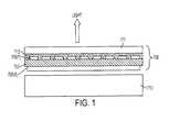
- FIG. 1illustrates schematically a cross-section of an exemplary position sensing panel
- FIG. 2illustrates schematically a set of sense electrodes
- FIG. 3Aillustrates schematically a set of drive electrodes for an exemplary position sensing panel
- FIG. 3Billustrates schematically another set of drive electrodes for an exemplary position sensing panel
- FIG. 3Cillustrates schematically another set of drive electrodes for an exemplary position sensing panel
- FIG. 3Dillustrates schematically another set of drive electrodes for an exemplary position sensing panel
- FIG. 4illustrates schematically an arrangement of drive and sense electrodes of an exemplary position sensing panel
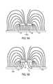
- FIG. 5Aillustrates schematically the electric fields at a node of an exemplary position sensing panel
- FIG. 5Billustrates schematically the electric fields at a node of an exemplary position sensing panel that includes one or more cut-out sections
- FIG. 6illustrates schematically a portion of an arrangement of a sense electrode of another exemplary position sensing panel
- FIG. 7illustrates schematically a portion of an arrangement of drive and sense electrodes of another exemplary position sensing panel.
- a displaymay be overlaid with a position-sensing panel.
- the displaymay take various forms. Examples include, but are not limited to liquid crystal displays such as an active matrix liquid crystal display, an electroluminescent display, an electrophoretic display, a plasma display, cathode-ray display, an OLED display, or the like. It will be appreciated that light emitted from the display should be able to pass through the position-sensing panel.
- FIG. 1illustrates an exemplary touch position-sensing panel 700 which overlies a display 710 .
- the panel 700includes a substrate 703 .
- the panel 700can also include a first 705 (X) electrode and second 706 (Y) electrode.
- the substrate 703has a surface on each side.
- the electrodes 705 (X) and 706 (Y)may be formed on opposing surfaces of the substrate 703 .
- the substrate 703may be provided adjacent to the display 710 such that one electrode 705 (X) is between the display 710 and the substrate 703 .
- An air gapis formed between the display 710 and the first electrode 705 (X) and an adhesive layer 712 can be disposed between the second electrode 706 (Y) and the transparent cover layer 711 .
- the touch position-sensing panelmay have a second substrate (not shown).
- a touch position-sensing panelmay have a transparent panel, a first adhesive layer on the panel, a first electrode layer forming first electrodes, a first substrate, a second adhesive layer, a second electrode layer forming second electrodes, and the second substrate.
- the first conductive electrode layeris attached to the first substrate and the second conductive electrode layer is attached to the second substrate.
- Substrate 703which forms a core of the exemplary position-sensing panel 700 , can be formed from a transparent, non-conductive material such as glass or a plastic.
- suitable plastic substrate materialsinclude, but are not limited to, Polyethylene terephthalate (PET), Polyethylene Naphthalate (PEN), or polycarbonate (PC).
- the panel structure and production methodologymay be utilized in other types of touch position-sensing panels.
- drive electrodes 705 (X)are provided on one surface of the substrate 703
- sense electrodes 706 (Y)are provided on the opposing surface of the substrate 703 .
- Capacitive sensing channels or nodesare formed by capacitive coupling in the localized regions where the drive electrodes 705 (X) and the sense electrodes 706 (Y) cross over each other on opposites sides of the non-conductive substrate 703 .
- Transparent cover layer 711is provided over the substrate 703 , and may be joined thereto by any methods and materials.
- One exemplary materialis a pressure-sensitive adhesive.
- the cover layer 711may be glass, polycarbonate, or Poly(methyl methacrylate).
- ITOIndium-tin-oxide
- any other clear conductive materialmay be used, such as other inorganic and organic conductive materials, such as Antimony-tin-oxide (ATO), tin oxide, PEDOT or other conductive polymers, carbon nanotube or metal nanowire impregnated materials, and the like.
- opaque metal conductorsmay be used such as a conductive mesh, which may be of copper, silver or other conductive materials.
- each sense electrode 706 (Y)has a solid area of ITO.
- the sense electrodescan be formed and shaped into a rectangular area. Other shapes can be used. For example, the sense electrodes can be tapered.
- each drive electrode 705 (X)has solid areas of ITO that together cover substantially an active area of the position-sensing panel, except in regions between the drive electrodes and the cut-out regions 740 .
- the drive electrodes 705 (X)have a width of from about 3 mm to about 12 mm depending on design.
- the cut-out regions 740can have various shapes. Although shown as rectangular notches in FIG. 3A , other shapes can also be used. For example and with reference to FIGS. 3B and 3C , triangular notches, semi-circular notches, and other shapes may be used. Also, with reference to FIG. 3D , multiple shapes can be used within a drive electrode 705 (X).
- the spacing between the cut-outs 740can also be varied. For example, the distance (D) from a first edge 710 to a second edge 712 of the cut-outs can vary. For example, the first edge 710 to second edge 712 distance (D) can be uniform within one drive electrode 705 (X) but vary between different drive electrodes 705 (X). As another example, the edge-to-edge distance (D) may vary along the length of any one of the different drive electrodes 705 (X).
- size of the cut-outs 740can vary, either within one electrode or among the various drive electrodes 705 (X).
- the first edge 710 to second edge 712 distance (D) of the cut-out sections 740 in the drive electrodes 705 (X)can be made narrow to maintain the shielding ability of the drive electrodes 705 (X) against noise arising from the underlying display.
- the first edge 710 to second edge 712 distance (D) of the cut-out section 740may not be not greater than substantially 200 microns. Other sizes can also be used, depending on the application.
- the first edge 710 to second edge 712 distance (D) of the at least some of the cut-out sections 740may exceed 200 microns.
- the shape of the cut-outs 740is designed to be substantially complimentary to the shape of the sense electrode 706 (Y) in the region of cross over. For example, if the sense electrode 706 (Y) tapers in width, then the cut-out sections 740 are shaped and sized to substantially match the tapered sense electrode 706 (Y).
- Connecting lines 707which connect the drive electrodes 705 (X) to a control unit, may be formed as part of the process of forming the auxiliary conductors, as described in more detail below.
- a position-sensing panel 790 having both drive electrodes 705 (X) and sense electrodes 706 (Y)is shown and described.
- the drive electrodes 705 (X) and the sense electrodes 706 (Y)are formed by solid areas of ITO.
- Sensing area 720 of the position-sensing paneldenoted by the dotted line, encompasses each or substantially each of the intersections 730 formed by the X and Y electrodes.
- the gaps between adjacent electrodes 705 (X)are made narrow to enhance their shielding ability against noise arising from the underlying display. In some examples, about 90% of the sensing area 720 is covered by ITO. In such a configuration, the gap between adjacent ITO drive electrodes 705 (X) may not be greater than substantially 200 microns.
- Other drive electrode 705 (X)can be used depending on the width of the sense electrodes 706 (Y).
- the drive electrodes 705 (X)are formed of ITO and shaped to form bars. Each bar forms channels with sense electrodes 706 (Y) on the other side of the substrate 703 . As mentioned above, there are intersections 730 where the drive electrodes 705 (X) cross over the sense electrodes 706 (Y) to form capacitive sensing nodes. At each intersection 730 , the drive electrodes 705 (X) have cut-out sections 740 substantially aligned with the centerlines of the intersecting sense electrodes 706 (Y). The cut-out sections 740 extend partially across the width of the drive electrodes 705 (X).
- the cut-out sections 740 in the drive electrodes 705 (X)extend inwardly from both sides of the drive electrodes 705 (X), and the cut-out sections 740 at each intersection 730 are symmetrically arranged about the centerlines of the drive electrodes 705 (X) so that the drive electrodes 705 (X) are unbroken along their centerlines.
- the cut-out sections 740can be arranged across the centerlines of the drive electrodes 705 (X) so that the drive electrodes 705 (X) are unbroken along their edges.
- the cut-out sections 740can be arranged asymmetrically with respect to the centerlines of the drive electrodes 705 (X).
- the cut-out sections 740could each extend from one side of a drive electrode 705 (X), leaving the drive electrode 705 (X) unbroken on the other side.
- different cut-out sections 740could extend from the same, or different, sides of a drive electrode 705 (X).
- a capacitive sensing nodeis formed at each intersection where a sensing electrode 705 (Y) overlies a drive electrode 705 (X).
- Each nodehas a node capacitance.
- this node capacitancecan be regarded as being made up of two different components.
- the first componentis the plate capacitance, which is the capacitance between the opposed parallel spaced apart surfaces of the sensing electrode 705 (Y) and the drive electrode 705 (X).
- the second componentis the fringe capacitance, which is the capacitance between the other parts of the sensing electrode 705 (Y) and the drive electrode 705 (X) outside of the overlapping sections of the drive and sensing electrodes.
- the fringe capacitancecan be produced by the electric fields acting between the sensing electrode 705 (Y) and the drive electrode 705 (X) in fringe areas near to the edges of the overlapping sections of the drive and sensing electrodes.
- FIG. 5Ashows a section taken along a drive electrode 705 (X) through the center of the region where a sensing electrode 705 (Y) and a drive electrode 705 (X) overlap to define a node with some electric field lines.
- the drive electrode 705 (X)is continuous and does not include any cut-out sections 740 .
- the first component of the capacitance of the nodeis determined by the electric fields between the opposed parallel surfaces of the sensing electrode 705 (Y) and the drive electrode 705 (X) in the region 300 .
- the second component of the capacitance of the nodeis determined by the electric fields between other parts of the sensing electrode 705 (Y) and the drive electrode 705 (X) near to the edges of the overlapping sections of the sensing electrode 705 (Y) and the drive electrode 705 (X), for example in fringe regions 501 .
- the resulting change in the node capacitanceis predominantly due to changes in the fringe capacitance.
- the touching or close proximity of an objectcauses a relatively larger change in the fringe capacitance, while there is a relatively smaller change in the plate capacitance.
- the plate electric fields in the region 300 of the node between the directly opposed parallel spaced apart surfaces of the overlapping sections of the drive and sensing electrodes and away from the edges of the overlapping sections of the drive and sensing electrodesare less subject to change when an object touches the surface of the screen than the fringe electric fields between the drive and sensing electrodes outside of, and near to the edges of, the overlapping sections of the drive and sensing electrodes, for example in regions 301 .
- thisis because the electric fields between the directly opposed parallel spaced apart surfaces of the overlapping sections of the drive and sensing electrodes are shielded by the drive and sensing electrodes themselves.
- FIG. 5Bshows a section taken along a drive electrode 705 (X) having a cut-out section 740 through the center of the region where a sensing electrode 705 (Y) and a drive electrode 705 (X) overlap to define a node, and showing some electric field lines.
- the cut-out section 740 in the drive electrode 705 (X)reduce the area of the opposed parallel spaced apart surfaces of the overlapping sections of the drive and sensing electrodes in the region 300 , and so reduce the plate capacitance component of the node capacitance.
- the cut-out sections 740have minimal effect on the fringe capacitance component of the node capacitance.
- the cut-out sections 740reduce the proportion of the total node capacitance which is contributed by the plate capacitance component and increase the proportion of the total node capacitance which is contributed by the fringe capacitance component.
- the touching or close proximity of an objectcauses a relatively larger change in the fringe capacitance than in the plate capacitance. Accordingly, the cut-out sections 740 reducing the proportion of the total node capacitance which is contributed by the plate capacitance and increasing the proportion which is contributed by the fringe capacitance has the effect of increasing the amount of change in the total node capacitance which is caused by the touching or close proximity of an object.
- the cut-outs 740may reduce the total mutual capacitance of the drive and sense electrodes.
- the cut-outs 740may also reduce the currents and electrical power used to operate the touch position-sensing panel.
- the cut-outs 740may reduce the total mutual capacitance of the drive electrodes 705 (X) and sense electrodes 706 (Y) without reducing the mutual capacitance in the fringe region of the intersections.
- the increase in the proportion of the total capacitance at the intersectionwhich is provided by the fringe electric field in the fringe regions of the node, can increase the sensitivity of the touch position-sensing panel, allow the resolution or sensing area of the touch position-sensing panel to be increased, and/or allow the thickness of the touch position-sensing panel to be reduced.
- the width of the cut-out sections 740 in the drive electrodes 705 (X)is made substantially equal to the width of the intersecting sense electrodes 706 (Y). This increases the reduction in the proportion of the total capacitance at the intersection which is provided by the non-fringe electric field in the non-fringe regions of the node. This increases the proportion of the total capacitance at the node which is provided by the fringe electric field in the fringe regions of the intersection.
- the width of the cut-out sections 740 in the drive electrodes 705 (X)is smaller than the width of the intersecting sense electrodes 706 (Y) so that each edge of the cut-out section 740 is a predetermined distance inside the respective edge of the intersecting sense electrode 706 (Y). This distance can be selected to allow for possible alignment errors between the drive electrodes 705 (X) and the intersecting sense electrodes 706 (Y). The predetermined distances is selected so that possible alignment errors do not result in the edge of the cut-out section 740 being located outside the edge of the intersecting sense electrode 706 (Y). Locating the edge of the cut-out section 740 outside the edge of the intersecting sense electrode 706 (Y) may reduce the capacitance at the intersection which is provided by the fringe electric field in the fringe regions of the intersection.
- Drive electrode connecting lines 707are shown leading out from the drive electrodes 705 (X) for connection to a control unit 760 .
- Sense electrode connecting lines 708are provided to connect sense electrodes 706 (Y) to the same or a different control unit.
- the patterns of the connecting linesare shown by way of an example only.
- FIG. 6illustrates a part of another exemplary touch position-sensing panel 800 .
- the panel 800includes drive electrodes 805 (X) and the sensing electrodes 805 (Y) formed by solid areas of ITO.
- the sensing electrode 805 (Y)comprises a primary section 806 extending in the Y direction and a plurality of secondary crossbar sections 807 extending outwardly from the primary section 806 to both sides in the X direction.
- the primary section 806 and secondary crossbar sections 807are arranged to overlay drive electrodes 805 (X) to form intersections, where each intersection runs along a drive electrode 805 (X).
- FIG. 6illustrates a part of another exemplary touch position-sensing panel 800 .
- the panel 800includes drive electrodes 805 (X) and the sensing electrodes 805 (Y) formed by solid areas of ITO.
- the sensing electrode 805 (Y)comprises a primary section 806 extending in the Y direction and a plurality of secondary crossbar sections 807
- the drive electrodes 805 (X)have cut-out sections 840 aligned with the centerlines of both the primary section 806 and the secondary sections 807 of the sensing electrode 805 (Y).
- the cut-out sections 840are arranged across and along the centerlines of the drive electrodes 805 (X) so that the drive electrodes 805 (X) are unbroken along their edges.
- a single sense electrode 805(Y) is shown. There may be a number of sense electrodes 805 (Y) arranged side by side in a complete touch position-sensing panel. Adjacent sense electrodes may have a similar pattern or may have a somewhat complimentary patter so that crossbar sections are interpolated.
- the drive electrodes 705 (X) and 805 (X)are rectangular strips with cut-out sections.
- the shape of the drive electrodes and the interconnection between the channels of any given electrodemay be modified according to the type of touch with which the position-sensing panel is intended to be used.
- the electrodesmay have saw-tooth or diamond shape edges with attendant inter-stripe gaps to facilitate field interpolation to aid in smoothing positional response.
- the transparency of the position-sensing paneloptionally transmits at least 85% of light having a wavelength in the visible part of the electromagnetic spectrum that is incident on the panel, in particular from a display underlying the panel.
- the process of manufacturing a position-sensing panel of any of the types discussed above relative to FIGS. 1-7includes the steps of patterning drive electrodes, such as ITO drive electrodes, on one substrate surface and patterning sense electrodes on the opposite surface of the same substrate.
- the process of patterning the electrodesmay include steps of: depositing a positive or negative resist over unpatterned ITO on a substrate; exposing the photoresist to UV light through a mask of the appropriate pattern; developing the resist by washing away unexposed resist with a solvent; etching away the exposed ITO areas using a suitable etchant; and finally removing the exposed photoresist using a suitable solvent.
- etching liquid for use in removing exposed ITOis, for example, an etching acid.
- suitable removal liquids for the photoresistinclude organic solvents.
- suitable positive and negative photoresists, etching liquids and photoresist removal liquidsmay also be used.
- ITOmay be deposited on the substrate by sputtering ITO onto the substrate using a shadow mask having a pattern suitable for formation of electrodes in any of the various shapes as described above.
- Lead-outs 707 , 708 for connection of the sense electrodes to a control unit of the position-sensing panelmay be formed by a printing process, such as inkjet printing, in which a conductive material or conductive material precursor is printed to form the Y electrode pattern and, in the case where a catalytic precursor ink is used, treating the precursor ink to convert the precursor ink to the final conductive material, for example by electroless plating.
- a printing processsuch as inkjet printing, in which a conductive material or conductive material precursor is printed to form the Y electrode pattern and, in the case where a catalytic precursor ink is used, treating the precursor ink to convert the precursor ink to the final conductive material, for example by electroless plating.
- the substratemay be uniformly coated with a catalytic photosensitive ink which is exposed to UV light through a photomask or vector-exposed to UV light from a laser or other suitable light source, rinsed with solvent to wash away the unexposed ink, then immersing the remaining ink in a metal plating bath to form the fine conductive traces.
- a catalytic photosensitive inkwhich is exposed to UV light through a photomask or vector-exposed to UV light from a laser or other suitable light source, rinsed with solvent to wash away the unexposed ink, then immersing the remaining ink in a metal plating bath to form the fine conductive traces.
- Suitable catalytic inksare commercially available.
- Lead-outs 707 , 708 for connection of the sense and drive electrodes to a control unit of the position-sensing panelmay be formed in the same process steps as formation of the sense and drive electrodes.
- Auxiliary conductorsmay be formed in the same way as the sense electrodes.
- a similar methode.g. evaporation or printing
- auxiliary conductorsin order to simplify manufacture of the position-sensing panel.
- the touch position sensors described abovecan be attached to numerous electronic devices, such as computers, personal digital assistants (PDA), satellite navigation devices, mobile phones, portable media players, portable game consoles, public information kiosks, point of sale systems, and the like.
- electronic devicesmay include a central processor or other processing device for executing program instructions, an internal communication bus, various types of memory or storage media (RAM, ROM, EEPROM, cache memory, disk drives etc.) for code and data storage, and one or more network interface cards or ports for communication purposes.
Landscapes
- Engineering & Computer Science (AREA)
- General Engineering & Computer Science (AREA)
- Theoretical Computer Science (AREA)
- Human Computer Interaction (AREA)
- Physics & Mathematics (AREA)
- General Physics & Mathematics (AREA)
- Quality & Reliability (AREA)
- Position Input By Displaying (AREA)
Abstract
Description
Claims (21)
Priority Applications (1)
| Application Number | Priority Date | Filing Date | Title |
|---|---|---|---|
| US12/891,329US9626045B1 (en) | 2010-09-27 | 2010-09-27 | Position-sensing panel and related methods |
Applications Claiming Priority (1)
| Application Number | Priority Date | Filing Date | Title |
|---|---|---|---|
| US12/891,329US9626045B1 (en) | 2010-09-27 | 2010-09-27 | Position-sensing panel and related methods |
Publications (1)
| Publication Number | Publication Date |
|---|---|
| US9626045B1true US9626045B1 (en) | 2017-04-18 |
Family
ID=58765557
Family Applications (1)
| Application Number | Title | Priority Date | Filing Date |
|---|---|---|---|
| US12/891,329Expired - Fee RelatedUS9626045B1 (en) | 2010-09-27 | 2010-09-27 | Position-sensing panel and related methods |
Country Status (1)
| Country | Link |
|---|---|
| US (1) | US9626045B1 (en) |
Cited By (7)
| Publication number | Priority date | Publication date | Assignee | Title |
|---|---|---|---|---|
| US20170102820A1 (en)* | 2016-08-11 | 2017-04-13 | Xiamen Tianma Micro-Electronics Co., Ltd. | Touch control display panel and display device |
| US20180224967A1 (en)* | 2017-02-09 | 2018-08-09 | Solomon Systech Limited | Touch Sensor |
| US10228808B2 (en)* | 2009-10-26 | 2019-03-12 | Atmel Corporation | Sense electrode design |
| US10275085B2 (en)* | 2009-04-20 | 2019-04-30 | Japan Display Inc. | Display device with capacitive touch sensor with slit formed in a surface of a detecting electrode opposed to a scanning electrode to realize detection with high accuracy |
| WO2022111285A1 (en)* | 2020-11-24 | 2022-06-02 | 深圳麦克韦尔科技有限公司 | Battery rod for electronic atomization, and electronic atomization device |
| US20220334680A1 (en)* | 2011-04-22 | 2022-10-20 | Japan Display Inc. | Display panel with touch detector, touch panel, and electronic unit |
| US20250130668A1 (en)* | 2012-07-24 | 2025-04-24 | Japan Display Inc. | Touch sensor device and display device with a touch sensor |
Citations (38)
| Publication number | Priority date | Publication date | Assignee | Title |
|---|---|---|---|---|
| US5194852A (en)* | 1986-12-01 | 1993-03-16 | More Edward S | Electro-optic slate for direct entry and display and/or storage of hand-entered textual and graphic information |
| US20020097231A1 (en)* | 2000-12-01 | 2002-07-25 | Fujitsu Limited | Touch panel device |
| US6657616B2 (en)* | 2001-03-16 | 2003-12-02 | Invensys Appliance Controls Company | Capacitive touch keyboard |
| US20040239650A1 (en)* | 2003-06-02 | 2004-12-02 | Mackey Bob Lee | Sensor patterns for a capacitive sensing apparatus |
| US20050207273A1 (en)* | 2004-03-19 | 2005-09-22 | Hamilton Beach/Proctor-Silex, Inc. | Storage food processor |
| US20070074914A1 (en)* | 2005-10-05 | 2007-04-05 | Geaghan Bernard O | Interleaved electrodes for touch sensing |
| US7202895B2 (en)* | 2002-04-10 | 2007-04-10 | Canon Kabushiki Kaisha | Image pickup apparatus provided with image pickup element including photoelectric conversion portions in depth direction of semiconductor |
| US20070229470A1 (en)* | 2006-03-31 | 2007-10-04 | Warren Snyder | Capacitive touch sense device having polygonal shaped sensor elements |
| US20070279395A1 (en)* | 2006-05-31 | 2007-12-06 | Harald Philipp | Two Dimensional Position Sensor |
| US20080309633A1 (en)* | 2007-06-13 | 2008-12-18 | Apple Inc. | Touch-sensitive display |
| US20080309635A1 (en) | 2007-06-14 | 2008-12-18 | Epson Imaging Devices Corporation | Capacitive input device |
| US20090159344A1 (en)* | 2007-12-21 | 2009-06-25 | Apple Inc. | Touch pad electrode design |
| US20090194344A1 (en)* | 2008-01-31 | 2009-08-06 | Avago Technologies Ecbu Ip (Singapore) Pte. Ltd. | Single Layer Mutual Capacitance Sensing Systems, Device, Components and Methods |
| US20090315854A1 (en) | 2008-06-18 | 2009-12-24 | Epson Imaging Devices Corporation | Capacitance type input device and display device with input function |
| US7663607B2 (en) | 2004-05-06 | 2010-02-16 | Apple Inc. | Multipoint touchscreen |
| US20100045632A1 (en) | 2008-04-10 | 2010-02-25 | Atmel Corporation | Capacitive Position Sensor |
| US20100110038A1 (en)* | 2008-10-31 | 2010-05-06 | Michael Mo | Mutual capacitance touch screen and combined mutual capacitance touch screen |
| US20100265187A1 (en) | 2009-04-20 | 2010-10-21 | Shih Chang Chang | Signal routing in an oled structure that includes a touch actuated sensor configuration |
| US20100302201A1 (en)* | 2009-06-02 | 2010-12-02 | Avago Technologies Ecbu (Singapore) Pte. Ltd. | Sensor Patterns for Mutual Capacitance Touchscreens |
| US7864503B2 (en) | 2007-05-11 | 2011-01-04 | Sense Pad Tech Co., Ltd | Capacitive type touch panel |
| US7875814B2 (en) | 2005-07-21 | 2011-01-25 | Tpo Displays Corp. | Electromagnetic digitizer sensor array structure |
| US7920129B2 (en) | 2007-01-03 | 2011-04-05 | Apple Inc. | Double-sided touch-sensitive panel with shield and drive combined layer |
| US20110095990A1 (en)* | 2009-10-23 | 2011-04-28 | Harald Philipp | Interdigitated touchscreen electrodes |
| US20110109583A1 (en)* | 2009-02-23 | 2011-05-12 | Yong Hoon Lee | Capacitive Touch Screen Panel |
| US8031094B2 (en) | 2009-09-11 | 2011-10-04 | Apple Inc. | Touch controller with improved analog front end |
| US8031174B2 (en) | 2007-01-03 | 2011-10-04 | Apple Inc. | Multi-touch surface stackup arrangement |
| US8040326B2 (en) | 2007-06-13 | 2011-10-18 | Apple Inc. | Integrated in-plane switching display and touch sensor |
| US8049732B2 (en) | 2007-01-03 | 2011-11-01 | Apple Inc. | Front-end signal compensation |
| US20120113014A1 (en) | 2010-11-04 | 2012-05-10 | Qrg Limited | Touch position-sensing panel and method |
| US8179381B2 (en) | 2008-02-28 | 2012-05-15 | 3M Innovative Properties Company | Touch screen sensor |
| US8217902B2 (en) | 2007-04-27 | 2012-07-10 | Tpk Touch Solutions Inc. | Conductor pattern structure of capacitive touch panel |
| US8243027B2 (en) | 2006-06-09 | 2012-08-14 | Apple Inc. | Touch screen liquid crystal display |
| US20120242592A1 (en) | 2011-03-21 | 2012-09-27 | Rothkopf Fletcher R | Electronic devices with flexible displays |
| US20120242588A1 (en) | 2011-03-21 | 2012-09-27 | Myers Scott A | Electronic devices with concave displays |
| WO2012129247A2 (en) | 2011-03-21 | 2012-09-27 | Apple Inc. | Electronic devices with flexible displays |
| US20120243719A1 (en) | 2011-03-21 | 2012-09-27 | Franklin Jeremy C | Display-Based Speaker Structures for Electronic Devices |
| US20120243151A1 (en) | 2011-03-21 | 2012-09-27 | Stephen Brian Lynch | Electronic Devices With Convex Displays |
| US20130076612A1 (en) | 2011-09-26 | 2013-03-28 | Apple Inc. | Electronic device with wrap around display |
- 2010
- 2010-09-27USUS12/891,329patent/US9626045B1/ennot_activeExpired - Fee Related
Patent Citations (38)
| Publication number | Priority date | Publication date | Assignee | Title |
|---|---|---|---|---|
| US5194852A (en)* | 1986-12-01 | 1993-03-16 | More Edward S | Electro-optic slate for direct entry and display and/or storage of hand-entered textual and graphic information |
| US20020097231A1 (en)* | 2000-12-01 | 2002-07-25 | Fujitsu Limited | Touch panel device |
| US6657616B2 (en)* | 2001-03-16 | 2003-12-02 | Invensys Appliance Controls Company | Capacitive touch keyboard |
| US7202895B2 (en)* | 2002-04-10 | 2007-04-10 | Canon Kabushiki Kaisha | Image pickup apparatus provided with image pickup element including photoelectric conversion portions in depth direction of semiconductor |
| US20040239650A1 (en)* | 2003-06-02 | 2004-12-02 | Mackey Bob Lee | Sensor patterns for a capacitive sensing apparatus |
| US20050207273A1 (en)* | 2004-03-19 | 2005-09-22 | Hamilton Beach/Proctor-Silex, Inc. | Storage food processor |
| US7663607B2 (en) | 2004-05-06 | 2010-02-16 | Apple Inc. | Multipoint touchscreen |
| US7875814B2 (en) | 2005-07-21 | 2011-01-25 | Tpo Displays Corp. | Electromagnetic digitizer sensor array structure |
| US20070074914A1 (en)* | 2005-10-05 | 2007-04-05 | Geaghan Bernard O | Interleaved electrodes for touch sensing |
| US20070229470A1 (en)* | 2006-03-31 | 2007-10-04 | Warren Snyder | Capacitive touch sense device having polygonal shaped sensor elements |
| US20070279395A1 (en)* | 2006-05-31 | 2007-12-06 | Harald Philipp | Two Dimensional Position Sensor |
| US8243027B2 (en) | 2006-06-09 | 2012-08-14 | Apple Inc. | Touch screen liquid crystal display |
| US8049732B2 (en) | 2007-01-03 | 2011-11-01 | Apple Inc. | Front-end signal compensation |
| US8031174B2 (en) | 2007-01-03 | 2011-10-04 | Apple Inc. | Multi-touch surface stackup arrangement |
| US7920129B2 (en) | 2007-01-03 | 2011-04-05 | Apple Inc. | Double-sided touch-sensitive panel with shield and drive combined layer |
| US8217902B2 (en) | 2007-04-27 | 2012-07-10 | Tpk Touch Solutions Inc. | Conductor pattern structure of capacitive touch panel |
| US7864503B2 (en) | 2007-05-11 | 2011-01-04 | Sense Pad Tech Co., Ltd | Capacitive type touch panel |
| US20080309633A1 (en)* | 2007-06-13 | 2008-12-18 | Apple Inc. | Touch-sensitive display |
| US8040326B2 (en) | 2007-06-13 | 2011-10-18 | Apple Inc. | Integrated in-plane switching display and touch sensor |
| US20080309635A1 (en) | 2007-06-14 | 2008-12-18 | Epson Imaging Devices Corporation | Capacitive input device |
| US20090159344A1 (en)* | 2007-12-21 | 2009-06-25 | Apple Inc. | Touch pad electrode design |
| US20090194344A1 (en)* | 2008-01-31 | 2009-08-06 | Avago Technologies Ecbu Ip (Singapore) Pte. Ltd. | Single Layer Mutual Capacitance Sensing Systems, Device, Components and Methods |
| US8179381B2 (en) | 2008-02-28 | 2012-05-15 | 3M Innovative Properties Company | Touch screen sensor |
| US20100045632A1 (en) | 2008-04-10 | 2010-02-25 | Atmel Corporation | Capacitive Position Sensor |
| US20090315854A1 (en) | 2008-06-18 | 2009-12-24 | Epson Imaging Devices Corporation | Capacitance type input device and display device with input function |
| US20100110038A1 (en)* | 2008-10-31 | 2010-05-06 | Michael Mo | Mutual capacitance touch screen and combined mutual capacitance touch screen |
| US20110109583A1 (en)* | 2009-02-23 | 2011-05-12 | Yong Hoon Lee | Capacitive Touch Screen Panel |
| US20100265187A1 (en) | 2009-04-20 | 2010-10-21 | Shih Chang Chang | Signal routing in an oled structure that includes a touch actuated sensor configuration |
| US20100302201A1 (en)* | 2009-06-02 | 2010-12-02 | Avago Technologies Ecbu (Singapore) Pte. Ltd. | Sensor Patterns for Mutual Capacitance Touchscreens |
| US8031094B2 (en) | 2009-09-11 | 2011-10-04 | Apple Inc. | Touch controller with improved analog front end |
| US20110095990A1 (en)* | 2009-10-23 | 2011-04-28 | Harald Philipp | Interdigitated touchscreen electrodes |
| US20120113014A1 (en) | 2010-11-04 | 2012-05-10 | Qrg Limited | Touch position-sensing panel and method |
| US20120242592A1 (en) | 2011-03-21 | 2012-09-27 | Rothkopf Fletcher R | Electronic devices with flexible displays |
| US20120242588A1 (en) | 2011-03-21 | 2012-09-27 | Myers Scott A | Electronic devices with concave displays |
| WO2012129247A2 (en) | 2011-03-21 | 2012-09-27 | Apple Inc. | Electronic devices with flexible displays |
| US20120243719A1 (en) | 2011-03-21 | 2012-09-27 | Franklin Jeremy C | Display-Based Speaker Structures for Electronic Devices |
| US20120243151A1 (en) | 2011-03-21 | 2012-09-27 | Stephen Brian Lynch | Electronic Devices With Convex Displays |
| US20130076612A1 (en) | 2011-09-26 | 2013-03-28 | Apple Inc. | Electronic device with wrap around display |
Non-Patent Citations (7)
| Title |
|---|
| U.S. Appl. No. 61/454,894, filed Mar. 21, 2011, Rothkopf. |
| U.S. Appl. No. 61/454,936, filed Mar. 21, 2011, Myers. |
| U.S. Appl. No. 61/454,950, filed Mar. 21, 2011, Lynch. |
| Yilmaz U.S. Appl. No. 12/939,794, Final Rejection from U.S. Patent and Trademark Office, May 9, 2013. |
| Yilmaz, U.S. Appl. No. 12/939,794, Non-final Rejection from U.S. Patent and Trademark Office, Oct. 4, 2012. |
| Yilmaz, U.S. Appl. No. 12/939,794, Request for Continued Examination and Response, Sep. 9, 2013. |
| Yilmaz, U.S. Appl. No. 12/939,794, Response to Non-final Rejection from U.S. Patent and Trademark Office, Feb. 4, 2013. |
Cited By (12)
| Publication number | Priority date | Publication date | Assignee | Title |
|---|---|---|---|---|
| US10275085B2 (en)* | 2009-04-20 | 2019-04-30 | Japan Display Inc. | Display device with capacitive touch sensor with slit formed in a surface of a detecting electrode opposed to a scanning electrode to realize detection with high accuracy |
| US10817108B2 (en) | 2009-04-20 | 2020-10-27 | Japan Display Inc. | Display device with capacitive touch sensor with slit formed in a surface of a detecting electrode opposed to a scanning electrode to realize detection with high accuracy |
| US10228808B2 (en)* | 2009-10-26 | 2019-03-12 | Atmel Corporation | Sense electrode design |
| US10338759B1 (en) | 2009-10-26 | 2019-07-02 | Neodrón Limited | Sense electrode design |
| US10795523B2 (en) | 2009-10-26 | 2020-10-06 | Neodrón Limited | Sense electrode design |
| US20220334680A1 (en)* | 2011-04-22 | 2022-10-20 | Japan Display Inc. | Display panel with touch detector, touch panel, and electronic unit |
| US11893193B2 (en)* | 2011-04-22 | 2024-02-06 | Japan Display Inc. | Display panel with touch detector, touch panel, and electronic unit |
| US20250130668A1 (en)* | 2012-07-24 | 2025-04-24 | Japan Display Inc. | Touch sensor device and display device with a touch sensor |
| US20170102820A1 (en)* | 2016-08-11 | 2017-04-13 | Xiamen Tianma Micro-Electronics Co., Ltd. | Touch control display panel and display device |
| US10126865B2 (en)* | 2016-08-11 | 2018-11-13 | Xiamen Tianma Micro-Electronics Co., Ltd. | Touch control display panel and display device |
| US20180224967A1 (en)* | 2017-02-09 | 2018-08-09 | Solomon Systech Limited | Touch Sensor |
| WO2022111285A1 (en)* | 2020-11-24 | 2022-06-02 | 深圳麦克韦尔科技有限公司 | Battery rod for electronic atomization, and electronic atomization device |
Similar Documents
| Publication | Publication Date | Title |
|---|---|---|
| US8786572B2 (en) | Touch position-sensing panel and method | |
| US9081427B2 (en) | Position-sensing panel and method | |
| US9252768B2 (en) | Position-sensing panel | |
| US9465491B2 (en) | Method for forming a capacitive touch sensor for identifying a fingerprint | |
| US9218561B2 (en) | Touch sensor with RFID | |
| US9442535B2 (en) | Touch sensor with integrated antenna | |
| US9626045B1 (en) | Position-sensing panel and related methods | |
| US9137882B2 (en) | Electrostatic capacity type touch screen panel for display device and method of manufacturing the same | |
| US10900766B2 (en) | Integrated passive circuit elements for sensing devices | |
| KR101314779B1 (en) | Electrostatic capacity type touch screen panel and method of manufacturing the same | |
| EP2737390B1 (en) | Capacitive touch panel and a method of manufacturing the same | |
| US9007332B2 (en) | Position sensing panel | |
| KR101475106B1 (en) | Electrostatic capacity type touch screen panel and method of manufacturing the same | |
| KR20130069938A (en) | Conductive pattern of touch panel | |
| US11099703B1 (en) | Touch sensor panels with silver nanowire-based touch electrodes | |
| JP6138059B2 (en) | Touch panel | |
| CN106020562A (en) | Touch screen, production method thereof and outer-hanging type touch screen | |
| US9753572B2 (en) | Touch panel, method of fabricating the same and touch display device | |
| CN202433856U (en) | Touch position sensing panel and touch sensing device | |
| KR101886279B1 (en) | Fabrication method of electrode-pattern of touch panel | |
| KR101370443B1 (en) | Conductive pattern of touch panel | |
| US10306758B2 (en) | Enhanced conductors | |
| KR101370402B1 (en) | Fabrication method of electrode-pattern of touch panel and structure of electrode-pattern using the same |
Legal Events
| Date | Code | Title | Description |
|---|---|---|---|
| AS | Assignment | Owner name:QRG LIMITED, UNITED KINGDOM Free format text:ASSIGNMENT OF ASSIGNORS INTEREST;ASSIGNOR:YILMAZ, ESAT;REEL/FRAME:025047/0045 Effective date:20100927 | |
| AS | Assignment | Owner name:ATMEL CORPORATION, CALIFORNIA Free format text:ASSIGNMENT OF ASSIGNORS INTEREST;ASSIGNOR:QRG LIMITED;REEL/FRAME:025121/0199 Effective date:20101006 | |
| AS | Assignment | Owner name:MORGAN STANLEY SENIOR FUNDING, INC. AS ADMINISTRAT Free format text:PATENT SECURITY AGREEMENT;ASSIGNOR:ATMEL CORPORATION;REEL/FRAME:031912/0173 Effective date:20131206 Owner name:MORGAN STANLEY SENIOR FUNDING, INC. AS ADMINISTRATIVE AGENT, NEW YORK Free format text:PATENT SECURITY AGREEMENT;ASSIGNOR:ATMEL CORPORATION;REEL/FRAME:031912/0173 Effective date:20131206 | |
| AS | Assignment | Owner name:JPMORGAN CHASE BANK, N.A., AS ADMINISTRATIVE AGENT Free format text:SECURITY INTEREST;ASSIGNOR:ATMEL CORPORATION;REEL/FRAME:041715/0747 Effective date:20170208 Owner name:JPMORGAN CHASE BANK, N.A., AS ADMINISTRATIVE AGENT, ILLINOIS Free format text:SECURITY INTEREST;ASSIGNOR:ATMEL CORPORATION;REEL/FRAME:041715/0747 Effective date:20170208 | |
| STCF | Information on status: patent grant | Free format text:PATENTED CASE | |
| AS | Assignment | Owner name:JPMORGAN CHASE BANK, N.A., AS ADMINISTRATIVE AGENT, ILLINOIS Free format text:SECURITY INTEREST;ASSIGNORS:MICROCHIP TECHNOLOGY INCORPORATED;SILICON STORAGE TECHNOLOGY, INC.;ATMEL CORPORATION;AND OTHERS;REEL/FRAME:046426/0001 Effective date:20180529 Owner name:JPMORGAN CHASE BANK, N.A., AS ADMINISTRATIVE AGENT Free format text:SECURITY INTEREST;ASSIGNORS:MICROCHIP TECHNOLOGY INCORPORATED;SILICON STORAGE TECHNOLOGY, INC.;ATMEL CORPORATION;AND OTHERS;REEL/FRAME:046426/0001 Effective date:20180529 | |
| AS | Assignment | Owner name:WELLS FARGO BANK, NATIONAL ASSOCIATION, AS NOTES COLLATERAL AGENT, CALIFORNIA Free format text:SECURITY INTEREST;ASSIGNORS:MICROCHIP TECHNOLOGY INCORPORATED;SILICON STORAGE TECHNOLOGY, INC.;ATMEL CORPORATION;AND OTHERS;REEL/FRAME:047103/0206 Effective date:20180914 Owner name:WELLS FARGO BANK, NATIONAL ASSOCIATION, AS NOTES C Free format text:SECURITY INTEREST;ASSIGNORS:MICROCHIP TECHNOLOGY INCORPORATED;SILICON STORAGE TECHNOLOGY, INC.;ATMEL CORPORATION;AND OTHERS;REEL/FRAME:047103/0206 Effective date:20180914 | |
| AS | Assignment | Owner name:MICROCHIP TECHNOLOGY INCORPORATED, ARIZONA Free format text:RELEASE OF SECURITY INTEREST IN CERTAIN PATENT RIGHTS;ASSIGNOR:WELLS FARGO BANK, NATIONAL ASSOCIATION, AS NOTES COLLATERAL AGENT;REEL/FRAME:047976/0937 Effective date:20181221 Owner name:MICROCHIP TECHNOLOGY INCORPORATED, ARIZONA Free format text:RELEASE OF SECURITY INTEREST IN CERTAIN PATENT RIGHTS;ASSIGNOR:JPMORGAN CHASE BANK, N.A., AS ADMINISTRATIVE AGENT;REEL/FRAME:047976/0884 Effective date:20181221 Owner name:ATMEL CORPORATION, ARIZONA Free format text:RELEASE OF SECURITY INTEREST IN CERTAIN PATENT RIGHTS;ASSIGNOR:JPMORGAN CHASE BANK, N.A., AS ADMINISTRATIVE AGENT;REEL/FRAME:047976/0884 Effective date:20181221 Owner name:ATMEL CORPORATION, ARIZONA Free format text:RELEASE OF SECURITY INTEREST IN CERTAIN PATENT RIGHTS;ASSIGNOR:WELLS FARGO BANK, NATIONAL ASSOCIATION, AS NOTES COLLATERAL AGENT;REEL/FRAME:047976/0937 Effective date:20181221 | |
| AS | Assignment | Owner name:NEODRON LIMITED, IRELAND Free format text:ASSIGNMENT OF ASSIGNORS INTEREST;ASSIGNORS:MICROCHIP TECHNOLOGY INC.;ATMEL CORPORATION;MICROCHIP TECHNOLOGY GERMANY GMBH;REEL/FRAME:048259/0840 Effective date:20181221 | |
| MAFP | Maintenance fee payment | Free format text:PAYMENT OF MAINTENANCE FEE, 4TH YEAR, LARGE ENTITY (ORIGINAL EVENT CODE: M1551); ENTITY STATUS OF PATENT OWNER: LARGE ENTITY Year of fee payment:4 | |
| AS | Assignment | Owner name:MICROSEMI STORAGE SOLUTIONS, INC., ARIZONA Free format text:RELEASE BY SECURED PARTY;ASSIGNOR:JPMORGAN CHASE BANK, N.A., AS ADMINISTRATIVE AGENT;REEL/FRAME:059333/0222 Effective date:20220218 Owner name:MICROSEMI CORPORATION, ARIZONA Free format text:RELEASE BY SECURED PARTY;ASSIGNOR:JPMORGAN CHASE BANK, N.A., AS ADMINISTRATIVE AGENT;REEL/FRAME:059333/0222 Effective date:20220218 Owner name:ATMEL CORPORATION, ARIZONA Free format text:RELEASE BY SECURED PARTY;ASSIGNOR:JPMORGAN CHASE BANK, N.A., AS ADMINISTRATIVE AGENT;REEL/FRAME:059333/0222 Effective date:20220218 Owner name:SILICON STORAGE TECHNOLOGY, INC., ARIZONA Free format text:RELEASE BY SECURED PARTY;ASSIGNOR:JPMORGAN CHASE BANK, N.A., AS ADMINISTRATIVE AGENT;REEL/FRAME:059333/0222 Effective date:20220218 Owner name:MICROCHIP TECHNOLOGY INCORPORATED, ARIZONA Free format text:RELEASE BY SECURED PARTY;ASSIGNOR:JPMORGAN CHASE BANK, N.A., AS ADMINISTRATIVE AGENT;REEL/FRAME:059333/0222 Effective date:20220218 | |
| AS | Assignment | Owner name:ATMEL CORPORATION, ARIZONA Free format text:RELEASE BY SECURED PARTY;ASSIGNOR:JPMORGAN CHASE BANK, N.A., AS ADMINISTRATIVE AGENT;REEL/FRAME:059262/0105 Effective date:20220218 | |
| AS | Assignment | Owner name:MICROSEMI STORAGE SOLUTIONS, INC., ARIZONA Free format text:RELEASE BY SECURED PARTY;ASSIGNOR:WELLS FARGO BANK, NATIONAL ASSOCIATION, AS NOTES COLLATERAL AGENT;REEL/FRAME:059358/0001 Effective date:20220228 Owner name:MICROSEMI CORPORATION, ARIZONA Free format text:RELEASE BY SECURED PARTY;ASSIGNOR:WELLS FARGO BANK, NATIONAL ASSOCIATION, AS NOTES COLLATERAL AGENT;REEL/FRAME:059358/0001 Effective date:20220228 Owner name:ATMEL CORPORATION, ARIZONA Free format text:RELEASE BY SECURED PARTY;ASSIGNOR:WELLS FARGO BANK, NATIONAL ASSOCIATION, AS NOTES COLLATERAL AGENT;REEL/FRAME:059358/0001 Effective date:20220228 Owner name:SILICON STORAGE TECHNOLOGY, INC., ARIZONA Free format text:RELEASE BY SECURED PARTY;ASSIGNOR:WELLS FARGO BANK, NATIONAL ASSOCIATION, AS NOTES COLLATERAL AGENT;REEL/FRAME:059358/0001 Effective date:20220228 Owner name:MICROCHIP TECHNOLOGY INCORPORATED, ARIZONA Free format text:RELEASE BY SECURED PARTY;ASSIGNOR:WELLS FARGO BANK, NATIONAL ASSOCIATION, AS NOTES COLLATERAL AGENT;REEL/FRAME:059358/0001 Effective date:20220228 | |
| FEPP | Fee payment procedure | Free format text:MAINTENANCE FEE REMINDER MAILED (ORIGINAL EVENT CODE: REM.); ENTITY STATUS OF PATENT OWNER: LARGE ENTITY | |
| LAPS | Lapse for failure to pay maintenance fees | Free format text:PATENT EXPIRED FOR FAILURE TO PAY MAINTENANCE FEES (ORIGINAL EVENT CODE: EXP.); ENTITY STATUS OF PATENT OWNER: LARGE ENTITY | |
| STCH | Information on status: patent discontinuation | Free format text:PATENT EXPIRED DUE TO NONPAYMENT OF MAINTENANCE FEES UNDER 37 CFR 1.362 | |
| FP | Lapsed due to failure to pay maintenance fee | Effective date:20250418 |