US9623527B2 - Component carrier assembly having a trench structure which separates component carrier regions, and method for producing a plurality of component carrier regions - Google Patents
Component carrier assembly having a trench structure which separates component carrier regions, and method for producing a plurality of component carrier regionsDownload PDFInfo
- Publication number
- US9623527B2 US9623527B2US14/115,854US201114115854AUS9623527B2US 9623527 B2US9623527 B2US 9623527B2US 201114115854 AUS201114115854 AUS 201114115854AUS 9623527 B2US9623527 B2US 9623527B2
- Authority
- US
- United States
- Prior art keywords
- component carrier
- carrier body
- major face
- carrier
- trenches
- Prior art date
- Legal status (The legal status is an assumption and is not a legal conclusion. Google has not performed a legal analysis and makes no representation as to the accuracy of the status listed.)
- Active, expires
Links
- 238000004519manufacturing processMethods0.000titleclaimsdescription10
- 239000011248coating agentSubstances0.000claimsabstractdescription57
- 238000000576coating methodMethods0.000claimsabstractdescription57
- 239000004065semiconductorSubstances0.000claimsabstractdescription27
- 238000000034methodMethods0.000claimsdescription26
- 239000000463materialSubstances0.000claimsdescription12
- 238000010276constructionMethods0.000claimsdescription5
- 239000000126substanceSubstances0.000claimsdescription4
- 230000003628erosive effectEffects0.000claimsdescription3
- 238000000227grindingMethods0.000claimsdescription2
- 238000005498polishingMethods0.000claimsdescription2
- 239000000969carrierSubstances0.000description17
- 230000015572biosynthetic processEffects0.000description6
- 230000005693optoelectronicsEffects0.000description5
- 238000002120advanced silicon etchingMethods0.000description3
- 238000000708deep reactive-ion etchingMethods0.000description3
- 238000011161developmentMethods0.000description3
- 230000018109developmental processEffects0.000description3
- JBRZTFJDHDCESZ-UHFFFAOYSA-NAsGaChemical compound[As]#[Ga]JBRZTFJDHDCESZ-UHFFFAOYSA-N0.000description2
- 229910001218Gallium arsenideInorganic materials0.000description2
- XUIMIQQOPSSXEZ-UHFFFAOYSA-NSiliconChemical compound[Si]XUIMIQQOPSSXEZ-UHFFFAOYSA-N0.000description2
- BQCADISMDOOEFD-UHFFFAOYSA-NSilverChemical compound[Ag]BQCADISMDOOEFD-UHFFFAOYSA-N0.000description2
- 239000002313adhesive filmSubstances0.000description2
- 229910052732germaniumInorganic materials0.000description2
- GNPVGFCGXDBREM-UHFFFAOYSA-Ngermanium atomChemical compound[Ge]GNPVGFCGXDBREM-UHFFFAOYSA-N0.000description2
- PCHJSUWPFVWCPO-UHFFFAOYSA-NgoldChemical compound[Au]PCHJSUWPFVWCPO-UHFFFAOYSA-N0.000description2
- 229910052737goldInorganic materials0.000description2
- 239000010931goldSubstances0.000description2
- 239000011159matrix materialSubstances0.000description2
- 229910001092metal group alloyInorganic materials0.000description2
- BASFCYQUMIYNBI-UHFFFAOYSA-NplatinumChemical compound[Pt]BASFCYQUMIYNBI-UHFFFAOYSA-N0.000description2
- 238000000926separation methodMethods0.000description2
- 229910052710siliconInorganic materials0.000description2
- 239000010703siliconSubstances0.000description2
- 229910052709silverInorganic materials0.000description2
- 239000004332silverSubstances0.000description2
- 229910000679solderInorganic materials0.000description2
- RYGMFSIKBFXOCR-UHFFFAOYSA-NCopperChemical compound[Cu]RYGMFSIKBFXOCR-UHFFFAOYSA-N0.000description1
- 229910001128Sn alloyInorganic materials0.000description1
- ATJFFYVFTNAWJD-UHFFFAOYSA-NTinChemical compound[Sn]ATJFFYVFTNAWJD-UHFFFAOYSA-N0.000description1
- RTAQQCXQSZGOHL-UHFFFAOYSA-NTitaniumChemical compound[Ti]RTAQQCXQSZGOHL-UHFFFAOYSA-N0.000description1
- 239000004411aluminiumSubstances0.000description1
- 229910052782aluminiumInorganic materials0.000description1
- XAGFODPZIPBFFR-UHFFFAOYSA-NaluminiumChemical compound[Al]XAGFODPZIPBFFR-UHFFFAOYSA-N0.000description1
- 239000000919ceramicSubstances0.000description1
- 229910052802copperInorganic materials0.000description1
- 239000010949copperSubstances0.000description1
- 230000001419dependent effectEffects0.000description1
- 238000000151depositionMethods0.000description1
- 230000008021depositionEffects0.000description1
- JVPLOXQKFGYFMN-UHFFFAOYSA-Ngold tinChemical compound[Sn].[Au]JVPLOXQKFGYFMN-UHFFFAOYSA-N0.000description1
- 229910052738indiumInorganic materials0.000description1
- APFVFJFRJDLVQX-UHFFFAOYSA-Nindium atomChemical compound[In]APFVFJFRJDLVQX-UHFFFAOYSA-N0.000description1
- 229910052751metalInorganic materials0.000description1
- 239000002184metalSubstances0.000description1
- 229910052697platinumInorganic materials0.000description1
- 238000007650screen-printingMethods0.000description1
- 238000004544sputter depositionMethods0.000description1
- 229910052718tinInorganic materials0.000description1
- 239000010936titaniumSubstances0.000description1
- 229910052719titaniumInorganic materials0.000description1
- WFKWXMTUELFFGS-UHFFFAOYSA-NtungstenChemical compound[W]WFKWXMTUELFFGS-UHFFFAOYSA-N0.000description1
- 229910052721tungstenInorganic materials0.000description1
- 239000010937tungstenSubstances0.000description1
Images


Classifications
- B—PERFORMING OPERATIONS; TRANSPORTING
- B23—MACHINE TOOLS; METAL-WORKING NOT OTHERWISE PROVIDED FOR
- B23Q—DETAILS, COMPONENTS, OR ACCESSORIES FOR MACHINE TOOLS, e.g. ARRANGEMENTS FOR COPYING OR CONTROLLING; MACHINE TOOLS IN GENERAL CHARACTERISED BY THE CONSTRUCTION OF PARTICULAR DETAILS OR COMPONENTS; COMBINATIONS OR ASSOCIATIONS OF METAL-WORKING MACHINES, NOT DIRECTED TO A PARTICULAR RESULT
- B23Q3/00—Devices holding, supporting, or positioning work or tools, of a kind normally removable from the machine
- H—ELECTRICITY
- H01—ELECTRIC ELEMENTS
- H01L—SEMICONDUCTOR DEVICES NOT COVERED BY CLASS H10
- H01L21/00—Processes or apparatus adapted for the manufacture or treatment of semiconductor or solid state devices or of parts thereof
- H01L21/67—Apparatus specially adapted for handling semiconductor or electric solid state devices during manufacture or treatment thereof; Apparatus specially adapted for handling wafers during manufacture or treatment of semiconductor or electric solid state devices or components ; Apparatus not specifically provided for elsewhere
- H01L21/683—Apparatus specially adapted for handling semiconductor or electric solid state devices during manufacture or treatment thereof; Apparatus specially adapted for handling wafers during manufacture or treatment of semiconductor or electric solid state devices or components ; Apparatus not specifically provided for elsewhere for supporting or gripping
- H01L21/6835—Apparatus specially adapted for handling semiconductor or electric solid state devices during manufacture or treatment thereof; Apparatus specially adapted for handling wafers during manufacture or treatment of semiconductor or electric solid state devices or components ; Apparatus not specifically provided for elsewhere for supporting or gripping using temporarily an auxiliary support
- H—ELECTRICITY
- H01—ELECTRIC ELEMENTS
- H01L—SEMICONDUCTOR DEVICES NOT COVERED BY CLASS H10
- H01L21/00—Processes or apparatus adapted for the manufacture or treatment of semiconductor or solid state devices or of parts thereof
- H01L21/02—Manufacture or treatment of semiconductor devices or of parts thereof
- H01L21/04—Manufacture or treatment of semiconductor devices or of parts thereof the devices having potential barriers, e.g. a PN junction, depletion layer or carrier concentration layer
- H01L21/18—Manufacture or treatment of semiconductor devices or of parts thereof the devices having potential barriers, e.g. a PN junction, depletion layer or carrier concentration layer the devices having semiconductor bodies comprising elements of Group IV of the Periodic Table or AIIIBV compounds with or without impurities, e.g. doping materials
- H01L21/30—Treatment of semiconductor bodies using processes or apparatus not provided for in groups H01L21/20 - H01L21/26
- H01L21/302—Treatment of semiconductor bodies using processes or apparatus not provided for in groups H01L21/20 - H01L21/26 to change their surface-physical characteristics or shape, e.g. etching, polishing, cutting
- H01L21/306—Chemical or electrical treatment, e.g. electrolytic etching
- H01L21/30604—Chemical etching
- H—ELECTRICITY
- H01—ELECTRIC ELEMENTS
- H01L—SEMICONDUCTOR DEVICES NOT COVERED BY CLASS H10
- H01L21/00—Processes or apparatus adapted for the manufacture or treatment of semiconductor or solid state devices or of parts thereof
- H01L21/67—Apparatus specially adapted for handling semiconductor or electric solid state devices during manufacture or treatment thereof; Apparatus specially adapted for handling wafers during manufacture or treatment of semiconductor or electric solid state devices or components ; Apparatus not specifically provided for elsewhere
- H01L21/683—Apparatus specially adapted for handling semiconductor or electric solid state devices during manufacture or treatment thereof; Apparatus specially adapted for handling wafers during manufacture or treatment of semiconductor or electric solid state devices or components ; Apparatus not specifically provided for elsewhere for supporting or gripping
- H01L21/6835—Apparatus specially adapted for handling semiconductor or electric solid state devices during manufacture or treatment thereof; Apparatus specially adapted for handling wafers during manufacture or treatment of semiconductor or electric solid state devices or components ; Apparatus not specifically provided for elsewhere for supporting or gripping using temporarily an auxiliary support
- H01L21/6836—Wafer tapes, e.g. grinding or dicing support tapes
- H—ELECTRICITY
- H01—ELECTRIC ELEMENTS
- H01L—SEMICONDUCTOR DEVICES NOT COVERED BY CLASS H10
- H01L24/00—Arrangements for connecting or disconnecting semiconductor or solid-state bodies; Methods or apparatus related thereto
- H01L24/93—Batch processes
- H01L24/95—Batch processes at chip-level, i.e. with connecting carried out on a plurality of singulated devices, i.e. on diced chips
- H01L24/97—Batch processes at chip-level, i.e. with connecting carried out on a plurality of singulated devices, i.e. on diced chips the devices being connected to a common substrate, e.g. interposer, said common substrate being separable into individual assemblies after connecting
- H—ELECTRICITY
- H01—ELECTRIC ELEMENTS
- H01L—SEMICONDUCTOR DEVICES NOT COVERED BY CLASS H10
- H01L21/00—Processes or apparatus adapted for the manufacture or treatment of semiconductor or solid state devices or of parts thereof
- H01L21/70—Manufacture or treatment of devices consisting of a plurality of solid state components formed in or on a common substrate or of parts thereof; Manufacture of integrated circuit devices or of parts thereof
- H01L21/77—Manufacture or treatment of devices consisting of a plurality of solid state components or integrated circuits formed in, or on, a common substrate
- H01L21/78—Manufacture or treatment of devices consisting of a plurality of solid state components or integrated circuits formed in, or on, a common substrate with subsequent division of the substrate into plural individual devices
- H—ELECTRICITY
- H01—ELECTRIC ELEMENTS
- H01L—SEMICONDUCTOR DEVICES NOT COVERED BY CLASS H10
- H01L22/00—Testing or measuring during manufacture or treatment; Reliability measurements, i.e. testing of parts without further processing to modify the parts as such; Structural arrangements therefor
- H01L22/10—Measuring as part of the manufacturing process
- H—ELECTRICITY
- H01—ELECTRIC ELEMENTS
- H01L—SEMICONDUCTOR DEVICES NOT COVERED BY CLASS H10
- H01L2221/00—Processes or apparatus adapted for the manufacture or treatment of semiconductor or solid state devices or of parts thereof covered by H01L21/00
- H01L2221/67—Apparatus for handling semiconductor or electric solid state devices during manufacture or treatment thereof; Apparatus for handling wafers during manufacture or treatment of semiconductor or electric solid state devices or components; Apparatus not specifically provided for elsewhere
- H01L2221/683—Apparatus for handling semiconductor or electric solid state devices during manufacture or treatment thereof; Apparatus for handling wafers during manufacture or treatment of semiconductor or electric solid state devices or components; Apparatus not specifically provided for elsewhere for supporting or gripping
- H01L2221/68304—Apparatus for handling semiconductor or electric solid state devices during manufacture or treatment thereof; Apparatus for handling wafers during manufacture or treatment of semiconductor or electric solid state devices or components; Apparatus not specifically provided for elsewhere for supporting or gripping using temporarily an auxiliary support
- H01L2221/68327—Apparatus for handling semiconductor or electric solid state devices during manufacture or treatment thereof; Apparatus for handling wafers during manufacture or treatment of semiconductor or electric solid state devices or components; Apparatus not specifically provided for elsewhere for supporting or gripping using temporarily an auxiliary support used during dicing or grinding
- H01L2221/68331—Apparatus for handling semiconductor or electric solid state devices during manufacture or treatment thereof; Apparatus for handling wafers during manufacture or treatment of semiconductor or electric solid state devices or components; Apparatus not specifically provided for elsewhere for supporting or gripping using temporarily an auxiliary support used during dicing or grinding of passive members, e.g. die mounting substrate
- H—ELECTRICITY
- H01—ELECTRIC ELEMENTS
- H01L—SEMICONDUCTOR DEVICES NOT COVERED BY CLASS H10
- H01L2224/00—Indexing scheme for arrangements for connecting or disconnecting semiconductor or solid-state bodies and methods related thereto as covered by H01L24/00
- H01L2224/80—Methods for connecting semiconductor or other solid state bodies using means for bonding being attached to, or being formed on, the surface to be connected
- H01L2224/83—Methods for connecting semiconductor or other solid state bodies using means for bonding being attached to, or being formed on, the surface to be connected using a layer connector
- H01L2224/8319—Arrangement of the layer connectors prior to mounting
- H01L2224/83192—Arrangement of the layer connectors prior to mounting wherein the layer connectors are disposed only on another item or body to be connected to the semiconductor or solid-state body
- H—ELECTRICITY
- H01—ELECTRIC ELEMENTS
- H01L—SEMICONDUCTOR DEVICES NOT COVERED BY CLASS H10
- H01L2924/00—Indexing scheme for arrangements or methods for connecting or disconnecting semiconductor or solid-state bodies as covered by H01L24/00
- H—ELECTRICITY
- H01—ELECTRIC ELEMENTS
- H01L—SEMICONDUCTOR DEVICES NOT COVERED BY CLASS H10
- H01L2924/00—Indexing scheme for arrangements or methods for connecting or disconnecting semiconductor or solid-state bodies as covered by H01L24/00
- H01L2924/0001—Technical content checked by a classifier
- H01L2924/00014—Technical content checked by a classifier the subject-matter covered by the group, the symbol of which is combined with the symbol of this group, being disclosed without further technical details
- H—ELECTRICITY
- H01—ELECTRIC ELEMENTS
- H01L—SEMICONDUCTOR DEVICES NOT COVERED BY CLASS H10
- H01L2924/00—Indexing scheme for arrangements or methods for connecting or disconnecting semiconductor or solid-state bodies as covered by H01L24/00
- H01L2924/01—Chemical elements
- H01L2924/01005—Boron [B]
- H—ELECTRICITY
- H01—ELECTRIC ELEMENTS
- H01L—SEMICONDUCTOR DEVICES NOT COVERED BY CLASS H10
- H01L2924/00—Indexing scheme for arrangements or methods for connecting or disconnecting semiconductor or solid-state bodies as covered by H01L24/00
- H01L2924/01—Chemical elements
- H01L2924/01013—Aluminum [Al]
- H—ELECTRICITY
- H01—ELECTRIC ELEMENTS
- H01L—SEMICONDUCTOR DEVICES NOT COVERED BY CLASS H10
- H01L2924/00—Indexing scheme for arrangements or methods for connecting or disconnecting semiconductor or solid-state bodies as covered by H01L24/00
- H01L2924/01—Chemical elements
- H01L2924/01029—Copper [Cu]
- H—ELECTRICITY
- H01—ELECTRIC ELEMENTS
- H01L—SEMICONDUCTOR DEVICES NOT COVERED BY CLASS H10
- H01L2924/00—Indexing scheme for arrangements or methods for connecting or disconnecting semiconductor or solid-state bodies as covered by H01L24/00
- H01L2924/01—Chemical elements
- H01L2924/01032—Germanium [Ge]
- H—ELECTRICITY
- H01—ELECTRIC ELEMENTS
- H01L—SEMICONDUCTOR DEVICES NOT COVERED BY CLASS H10
- H01L2924/00—Indexing scheme for arrangements or methods for connecting or disconnecting semiconductor or solid-state bodies as covered by H01L24/00
- H01L2924/01—Chemical elements
- H01L2924/01047—Silver [Ag]
- H—ELECTRICITY
- H01—ELECTRIC ELEMENTS
- H01L—SEMICONDUCTOR DEVICES NOT COVERED BY CLASS H10
- H01L2924/00—Indexing scheme for arrangements or methods for connecting or disconnecting semiconductor or solid-state bodies as covered by H01L24/00
- H01L2924/01—Chemical elements
- H01L2924/01049—Indium [In]
- H—ELECTRICITY
- H01—ELECTRIC ELEMENTS
- H01L—SEMICONDUCTOR DEVICES NOT COVERED BY CLASS H10
- H01L2924/00—Indexing scheme for arrangements or methods for connecting or disconnecting semiconductor or solid-state bodies as covered by H01L24/00
- H01L2924/01—Chemical elements
- H01L2924/01074—Tungsten [W]
- H—ELECTRICITY
- H01—ELECTRIC ELEMENTS
- H01L—SEMICONDUCTOR DEVICES NOT COVERED BY CLASS H10
- H01L2924/00—Indexing scheme for arrangements or methods for connecting or disconnecting semiconductor or solid-state bodies as covered by H01L24/00
- H01L2924/01—Chemical elements
- H01L2924/01078—Platinum [Pt]
- H—ELECTRICITY
- H01—ELECTRIC ELEMENTS
- H01L—SEMICONDUCTOR DEVICES NOT COVERED BY CLASS H10
- H01L2924/00—Indexing scheme for arrangements or methods for connecting or disconnecting semiconductor or solid-state bodies as covered by H01L24/00
- H01L2924/01—Chemical elements
- H01L2924/01079—Gold [Au]
- H—ELECTRICITY
- H01—ELECTRIC ELEMENTS
- H01L—SEMICONDUCTOR DEVICES NOT COVERED BY CLASS H10
- H01L2924/00—Indexing scheme for arrangements or methods for connecting or disconnecting semiconductor or solid-state bodies as covered by H01L24/00
- H01L2924/10—Details of semiconductor or other solid state devices to be connected
- H01L2924/11—Device type
- H01L2924/12—Passive devices, e.g. 2 terminal devices
- H01L2924/1204—Optical Diode
- H01L2924/12041—LED
- H—ELECTRICITY
- H01—ELECTRIC ELEMENTS
- H01L—SEMICONDUCTOR DEVICES NOT COVERED BY CLASS H10
- H01L2924/00—Indexing scheme for arrangements or methods for connecting or disconnecting semiconductor or solid-state bodies as covered by H01L24/00
- H01L2924/10—Details of semiconductor or other solid state devices to be connected
- H01L2924/11—Device type
- H01L2924/12—Passive devices, e.g. 2 terminal devices
- H01L2924/1204—Optical Diode
- H01L2924/12042—LASER
- H—ELECTRICITY
- H01—ELECTRIC ELEMENTS
- H01L—SEMICONDUCTOR DEVICES NOT COVERED BY CLASS H10
- H01L2924/00—Indexing scheme for arrangements or methods for connecting or disconnecting semiconductor or solid-state bodies as covered by H01L24/00
- H01L2924/10—Details of semiconductor or other solid state devices to be connected
- H01L2924/11—Device type
- H01L2924/14—Integrated circuits
- H—ELECTRICITY
- H01—ELECTRIC ELEMENTS
- H01L—SEMICONDUCTOR DEVICES NOT COVERED BY CLASS H10
- H01L2924/00—Indexing scheme for arrangements or methods for connecting or disconnecting semiconductor or solid-state bodies as covered by H01L24/00
- H01L2924/15—Details of package parts other than the semiconductor or other solid state devices to be connected
- H01L2924/151—Die mounting substrate
- H01L2924/156—Material
- H01L2924/15786—Material with a principal constituent of the material being a non metallic, non metalloid inorganic material
- H01L33/486—
- H—ELECTRICITY
- H10—SEMICONDUCTOR DEVICES; ELECTRIC SOLID-STATE DEVICES NOT OTHERWISE PROVIDED FOR
- H10H—INORGANIC LIGHT-EMITTING SEMICONDUCTOR DEVICES HAVING POTENTIAL BARRIERS
- H10H20/00—Individual inorganic light-emitting semiconductor devices having potential barriers, e.g. light-emitting diodes [LED]
- H10H20/80—Constructional details
- H10H20/85—Packages
- H10H20/8506—Containers
Definitions
- the present applicationrelates to a component carrier assembly with a plurality of component carrier regions and to a method for producing a plurality of component carrier regions.
- Optoelectronic componentssuch as for example optoelectronic semiconductor chips are often mounted on component carriers for further processing.
- Such component carriersmay for example take the form of ceramic carriers.
- Such component carriersit is difficult to meet stringent precision requirements, for instance with regard to the perpendicularity of the side faces.
- One objectis to simplify the formation of component carriers which meet stringent precision requirements. Furthermore, it is intended to provide a method which simplifies the production of component carriers.
- a component carrier assemblycomprises a plurality of component carrier regions, which are provided for the mounting of preferably optoelectronic semiconductor components.
- the component carrier assemblycomprises a carrier body with a first major face.
- a trench patternis formed in the carrier body, with first trenches extending preferably parallel to one another in a first direction, the first trenches delimiting the component carrier regions in a second direction extending transversely of the trenches.
- a coatingis formed on the carrier body, such that the component carrier regions each have a first major face of the carrier body which is coated at least in places and a side face of the trench pattern which is coated at least in places.
- a carrier bodywhich has a first major face and a second major face opposite the first major face.
- a trench patternis formed in the carrier body in the first major face, wherein the trench pattern comprises first trenches extending in a first direction, which trenches separate from one another at least in places component carrier regions arranged adjacent one another in a second direction extending transversely of the first direction.
- a coatingis formed, which covers the first major face at least in places and a side face of the trench pattern at least in places.
- the carrier bodyis thinned at the second major face in such a way that the trench pattern extends completely through the carrier body at least in places in a direction extending obliquely or perpendicularly to the first major face.
- the methodis particularly suitable for the production of the above-described component carrier assembly.
- Features described below in connection with the component carrier assemblymay therefore also be used for the method and vice versa.
- the trench patternis formed by means of a chemical, in particular dry chemical, method or by means of erosion.
- a particularly suitable dry chemical methodis deep reactive ion etching (DRIE) or a method based thereon, such as for example advanced silicon etching (ASE).
- DRIEdeep reactive ion etching
- ASEadvanced silicon etching
- At least one side face of each component carrier regionis thus already formed on formation of the trench pattern.
- An angle of the side facemay be adjusted very precisely when forming the trench pattern, such that for example trenches with a side face perpendicular to the first major face may be produced very accurately.
- the carrier bodyis preferably based on a semiconductor material.
- siliconis particularly suitable because of its inexpensive and large-area availability.
- Another semiconductor materialfor example gallium arsenide or germanium, may however also be used.
- a semiconductor component mounted on the first major facemay be electrically contacted in a simple manner by means of the coating extending over the side face.
- At least two side faces of the component carrier regionare coated at least in places.
- the coatingmay also at least in places or completely cover the side faces of the component carrier region on all sides.
- the carrier bodyis thus provided with the coating along the entire circumference.
- the coatingis formed by means of a coating source, wherein a main coating direction of the coating source is oblique to a normal to the first major face. Formation of the coating on at least one side face of the component carrier regions is thus simplified.
- the carrier bodymay be rotated relative to the normal to the first major face. Coating of a plurality or all of the side faces of the component carrier regions is thus simplified.
- the first trenchesextend over the carrier body only in places in the first direction.
- the extent of the carrier bodyis greater in the first direction than the extent of the first trench in this direction. It is also preferable for the carrier body to be of continuous construction. All the component carrier regions may thus be provided in a common, mechanically stable component carrier assembly.
- component carrier regions arranged adjacent one another in the second directionare separated from one another in the continuous carrier body by one of the first trenches.
- the trench patterncomprises second trenches extending in the second direction, in particular parallel to one another, which delimit the component carrier regions in the first direction.
- the component carrier regionsare arranged on a common auxiliary carrier, for example an adhesive film, and separated from one another by means of the trench pattern.
- the component carrier regionsare thus present on the auxiliary carrier in singulated form, for example in a matrix.
- Population of the component carrier regions with semiconductor components, for example by means of a pick-and-place method,is thus simplified in comparison with component carriers provided as bulk good.
- the trench patternis configured as a grid, such that the carrier body is singulated into mutually separated component carrier regions on thinning.
- the component carrier regionsthus constitute singulated component carriers, for the production of which no further singulation step is necessary in addition to formation of the trench pattern and thinning.
- the trench patternis in strip-form and the carrier body is divided on thinning into a plurality of component carrier strips each with a plurality of component carrier regions.
- the component carrier regions of a component carrier stripmay subsequently be singulated into component carriers in a further singulation step. Singulation may proceed before or after mounting of semiconductor components on the component carriers.
- a mechanical singulation methodis suitable, for example, for instance sawing, cleaving or breaking, or a laser separation method.
- the trench patternis only configured in strip form in places.
- the component carriercomprises a continuous carrier body, with which a plurality of component carrier regions is formed.
- componentsare mounted on component carrier regions before the component carrier regions are singulated from the component carrier assembly into component carriers.
- Population with componentsmay thus proceed while the component carrier assembly is still intact.
- the componentsare operated prior to singulation. By starting them up, it is for example possible to determine and dispose of components which are not functional or which fail after only very brief operation.
- the componentsare preferably connected together electrically in the component carrier assembly in such a way that a plurality of components can be electrically operated simultaneously.
- FIGS. 1A and 1Bshow a first exemplary embodiment of a component carrier assembly in schematic plan view ( FIG. 1A ) and associated sectional view ( FIG. 1B );
- FIGS. 2A and 2Bshow a second exemplary embodiment of a component carrier assembly in schematic plan view ( FIG. 2A ) and associated sectional view ( FIG. 2B );
- FIGS. 3A and 3Bshow a third exemplary embodiment of a component carrier assembly in schematic plan view ( FIG. 3A ) and associated sectional view ( FIG. 3B );
- FIGS. 4A to 4Fshow an exemplary embodiment of a method for producing component carrier regions using intermediate steps each shown schematically in sectional view.
- FIGS. 5A to 5Bshow a second exemplary embodiment of a method for producing component carrier regions using intermediate steps shown schematically in sectional view.
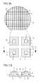
- a first exemplary embodiment of a component carrier assembly 1is shown in schematic plan view in FIG. 1A , with an enlarged portion, and in associated schematic sectional view along line AA′ in FIG. 1B .
- the component carrier assemblycomprises a carrier body 2 , which may for example take the form of a semiconductor wafer.
- the carrier body 2is preferably based on a semiconductor material, in particular silicon. In contrast thereto, it is also possible to use another semiconductor material, for instance gallium arsenide or germanium.
- the carrier bodyIn a vertical direction extending perpendicularly to a main plane of extension of the carrier body 2 , the carrier body extends between a first major face 21 and a second major face 22 . At the side of the first major face 21 a trench pattern 3 is formed with first trenches 31 extending parallel to one another. The first trenches 31 extend in a first direction. In the vertical direction the first trenches extend right through the carrier body 2 . In the first direction the first trenches 31 extend over the carrier body 2 only in places, such that the carrier body 2 is of continuous construction despite the first trenches 31 . In other words, the carrier body 2 is of one-piece configuration.
- the enlarged representationshows four component carrier regions 10 .
- two adjacent component carrier regions 10are separated from one another by a first trench 31 .
- a singulation line 8is shown.
- Component carrier regions 10 adjacent in the first directionmay be singulated along this line. Singulation may proceed for example mechanically, for instance by means of cleaving, breaking or sawing. A laser separation method may also be used.
- each component carrier regionthus has two side faces 5 formed by the trench pattern 3 and two side faces in each case perpendicular or at least transverse thereto, which arise only on singulation of the component carrier assembly 1 into component carriers.
- the first trenches 31form side faces 5 which delimit the carrier bodies 2 of the component carrier regions 10 in the second direction.
- a coating 4is formed on the carrier bodies 2 .
- the coating 4extends in places on the first major face 21 and on the second side face 5 .
- the second major face 22 of the carrier body 2is free of material of the coating 4 .
- the component carrier regions 10are each intended for mounting at least one semiconductor component, for example an optoelectronic semiconductor chip, for instance an LED or a laser diode, on the first major face 21 .
- the coating 4is preferably patterned in such a way that semiconductor components mounted on the component carrier assembly 1 may be jointly electrically contacted.
- the coating 4extends in strip form in the first direction over a plurality of component carrier regions 10 .
- Semiconductor components mounted on the component carrier assemblymay be started up, in particular jointly. It is thus simply possible to determine and dispose of semiconductor components which are not functional, which fail after a comparatively short operating time or which do not display specified electronic or optoelectronic characteristics.
- the component carrier regions 10may be singulated along the singulation line 8 .
- the electrical connection between adjacent component carrier regionsis thus broken.
- the singulation stepproduces component carriers from the component carrier assembly on which semiconductor components have already been mounted.
- a further coating(not shown explicitly in FIGS. 1A and 1B ), for example a solder layer, on the coating 4 .
- Configuration of the coating 4is freely variable within broad limits.
- the coatingmay also be unpatterned and extend over the entire first major face 21 of the carrier body 2 .
- the coating 4may also be configured such that just one side face 5 is covered by the coating 4 at least in places.
- the coatingmay furthermore also be of multilayer construction.
- At least one layer of the coating 4preferably contains a metal, for example copper, gold, silver, aluminium, platinum, titanium or tungsten, or a metal alloy with at least one of the stated materials.
- the second exemplary embodiment of a component carrier assemblycorresponds substantially to the first exemplary embodiment described in connection with FIGS. 1A and 1B .
- the component carrier assemblycomprises strip-form regions 15 , which are formed by means of the first trenches 31 of the trench pattern 3 .
- the first trenches 31extend in the first direction over the complete carrier body 2 , such that the strip-form regions, each with a plurality of component carrier regions 10 , are separated from one another.
- the strip-form regions 15are arranged on a common auxiliary carrier 6 .
- An example of a suitable material for the auxiliary carrier 6is a film, in particular a self-adhesive film.
- the component carrier regions 10 on the strip-form regions 15may be singulated along singulation lines 8 before or after mounting semiconductor components.
- the third exemplary embodiment of a component carrier assemblycorresponds substantially to the second exemplary embodiment described in connection with FIGS. 2A and 2B .
- the trench pattern 3comprises second trenches 32 extending in the second direction.
- the carrier bodies 2 of the individual component carrier regions 10are thus completely separated from one another by the trench pattern 3 and are available on the auxiliary carrier 6 for further processing, for example population with semiconductor components.
- the component carrier regions 10are arranged next to one another in a regular pattern, for example in a matrix. In comparison to component carriers which are provided as goods in bulk, population with semiconductor components, for example using a pick-and-place method, is simplified.
- the side faces 5 of the individual carrier bodies 2 of the component carrier regions 10are provided with a coating 4 on all sides.
- the coating 4may however also be formed on just one side face or on two side faces.
- a further coating 7is formed on the side of the coating 4 remote from the carrier body 2 .
- the further coating 7may take the form, for example, of a solder layer.
- the further coating 7may contain gold, indium, tin or silver, for example.
- a metal alloy with at least one of the stated materials, for example a gold-tin alloy,may also be used.
- FIGS. 4A to 4FOne exemplary embodiment of a method for producing a plurality of component carrier regions is shown in FIGS. 4A to 4F using intermediate steps each illustrated schematically in sectional view.
- the component carrier assemblymay be embodied as described in connection with FIGS. 1A to 3B .
- a carrier body 2is provided which extends in a vertical direction between a first major face 21 and a second major face 22 ( FIG. 4A ).
- a trench pattern 3comprising a plurality of first trenches 31 is formed on the first major face 21 .
- the first trenches 31extend in a vertical direction incompletely through the carrier body 2 .
- the trench patternis preferably formed chemically, in particular dry chemically, for instance by means of deep reactive ion etching or by means of ASE. In contrast thereto, an erosion method may also be used.
- a coating 4is formed by means of a coating source.
- the arrows 9show a main coating direction of the coating source.
- the main coating directionis oblique to a normal to the first major face 21 .
- Coating of side faces 5 of the trench pattern 3is thus simplified.
- a sputtering method or vapour deposition, for example,may be used for coating.
- the coating 4may be patterned, for example by means of a photolithographic method.
- a further coating 7may be applied to the coating 4 .
- the further coating 7may be applied using a method described in connection with the coating 4 .
- the further coatingmay also be applied by means of a screen printing process. Patterned application of the further coating may thus be achieved simply and inexpensively.
- the carrier body 2is mounted on a temporary carrier 65 on the first major face 21 side ( FIG. 4D ).
- a filmfor example, is suitable for the temporary carrier 65 .
- a rigid carriermay also be used.
- the carrier body 2is thinned at least until the trench pattern 3 extends completely through the carrier body in the vertical direction ( FIG. 4E ) Thinning may for example proceed mechanically, for instance by means of grinding, lapping or polishing. Then an auxiliary carrier 6 may be applied on the second major face 22 side. The temporary carrier 65 may then be detached.
- the carrier body 2is continuous even after thinning, such that the auxiliary carrier 6 may be dispensed with.
- the second exemplary embodiment, shown in FIGS. 5A and 5B , of a methodcorresponds substantially to the first exemplary embodiment described in connection with FIGS. 4A to 4F .
- the carrier body 2is rotated relative to its normal line during coating, such that the coating 4 may cover all the side faces 5 of the trench pattern 3 .
- the finished component carrier regions 10are shown in FIG. 5B .
- the described methodalso provides a simple, reliable way of producing component carriers in which at least one side face arises as early as during formation of the trench pattern.
- Component carriers produced in this waymay be distinguished by particularly high side face precision relative to the first major face.
- an angle of inclination of the side facemay be established as early as during formation of the trench pattern.
- the angle of inclination to the first major face 21is preferably 90° with a deviation of at most +/ ⁇ 5°.
- an angle other than 90°in particular an angle between 10° and 85° inclusive, for example 45°, may also be convenient, however.
- component carrier regions 10may be simply provided in a component carrier assembly, such that population with semiconductor components and additionally also start-up of the semiconductor components in the assembly may be performed simply.
Landscapes
- Engineering & Computer Science (AREA)
- Computer Hardware Design (AREA)
- Power Engineering (AREA)
- Microelectronics & Electronic Packaging (AREA)
- General Physics & Mathematics (AREA)
- Manufacturing & Machinery (AREA)
- Physics & Mathematics (AREA)
- Condensed Matter Physics & Semiconductors (AREA)
- Chemical & Material Sciences (AREA)
- Chemical Kinetics & Catalysis (AREA)
- General Chemical & Material Sciences (AREA)
- Mechanical Engineering (AREA)
- Dicing (AREA)
- Led Device Packages (AREA)
- Container, Conveyance, Adherence, Positioning, Of Wafer (AREA)
Abstract
Description
The present application relates to a component carrier assembly with a plurality of component carrier regions and to a method for producing a plurality of component carrier regions.
Optoelectronic components such as for example optoelectronic semiconductor chips are often mounted on component carriers for further processing.
Such component carriers may for example take the form of ceramic carriers. However, with such component carriers it is difficult to meet stringent precision requirements, for instance with regard to the perpendicularity of the side faces.
One object is to simplify the formation of component carriers which meet stringent precision requirements. Furthermore, it is intended to provide a method which simplifies the production of component carriers.
This object is achieved by the subject matter of the independent claims. Configurations and further developments constitute the subject matter of the dependent claims.
According to one embodiment, a component carrier assembly comprises a plurality of component carrier regions, which are provided for the mounting of preferably optoelectronic semiconductor components. The component carrier assembly comprises a carrier body with a first major face. On the first major face a trench pattern is formed in the carrier body, with first trenches extending preferably parallel to one another in a first direction, the first trenches delimiting the component carrier regions in a second direction extending transversely of the trenches. A coating is formed on the carrier body, such that the component carrier regions each have a first major face of the carrier body which is coated at least in places and a side face of the trench pattern which is coated at least in places.
In a method for producing a plurality of component carrier regions, according to one embodiment a carrier body is provided which has a first major face and a second major face opposite the first major face. A trench pattern is formed in the carrier body in the first major face, wherein the trench pattern comprises first trenches extending in a first direction, which trenches separate from one another at least in places component carrier regions arranged adjacent one another in a second direction extending transversely of the first direction. A coating is formed, which covers the first major face at least in places and a side face of the trench pattern at least in places. The carrier body is thinned at the second major face in such a way that the trench pattern extends completely through the carrier body at least in places in a direction extending obliquely or perpendicularly to the first major face.
The method is particularly suitable for the production of the above-described component carrier assembly. Features described below in connection with the component carrier assembly may therefore also be used for the method and vice versa.
According to one embodiment the trench pattern is formed by means of a chemical, in particular dry chemical, method or by means of erosion. A particularly suitable dry chemical method is deep reactive ion etching (DRIE) or a method based thereon, such as for example advanced silicon etching (ASE). Such methods allow trenches with a large aspect ratio, i.e. trenches which may be very deep compared with their width, to be formed with great accuracy.
At least one side face of each component carrier region is thus already formed on formation of the trench pattern. An angle of the side face may be adjusted very precisely when forming the trench pattern, such that for example trenches with a side face perpendicular to the first major face may be produced very accurately.
The carrier body is preferably based on a semiconductor material. For example, silicon is particularly suitable because of its inexpensive and large-area availability. Another semiconductor material, for example gallium arsenide or germanium, may however also be used.
A semiconductor component mounted on the first major face may be electrically contacted in a simple manner by means of the coating extending over the side face.
In one variant configuration, at least two side faces of the component carrier region are coated at least in places. The coating may also at least in places or completely cover the side faces of the component carrier region on all sides. The carrier body is thus provided with the coating along the entire circumference.
In one preferred configuration, the coating is formed by means of a coating source, wherein a main coating direction of the coating source is oblique to a normal to the first major face. Formation of the coating on at least one side face of the component carrier regions is thus simplified.
During coating the carrier body may be rotated relative to the normal to the first major face. Coating of a plurality or all of the side faces of the component carrier regions is thus simplified.
In a variant embodiment of the component carrier assembly, the first trenches extend over the carrier body only in places in the first direction. In other words, the extent of the carrier body is greater in the first direction than the extent of the first trench in this direction. It is also preferable for the carrier body to be of continuous construction. All the component carrier regions may thus be provided in a common, mechanically stable component carrier assembly.
In one further development, component carrier regions arranged adjacent one another in the second direction are separated from one another in the continuous carrier body by one of the first trenches.
In a further variant configuration, the trench pattern comprises second trenches extending in the second direction, in particular parallel to one another, which delimit the component carrier regions in the first direction. With such a trench pattern it is possible to form two or more, in particular all of the side faces of the carrier body when forming the trench pattern. An additional singulation step for singulating the component carrier assembly into component carrier regions may be dispensed with.
In a preferred further development, the component carrier regions are arranged on a common auxiliary carrier, for example an adhesive film, and separated from one another by means of the trench pattern. The component carrier regions are thus present on the auxiliary carrier in singulated form, for example in a matrix. Population of the component carrier regions with semiconductor components, for example by means of a pick-and-place method, is thus simplified in comparison with component carriers provided as bulk good.
In one configuration of the method, the trench pattern is configured as a grid, such that the carrier body is singulated into mutually separated component carrier regions on thinning. In this case, the component carrier regions thus constitute singulated component carriers, for the production of which no further singulation step is necessary in addition to formation of the trench pattern and thinning.
In a further variant configuration of the method the trench pattern is in strip-form and the carrier body is divided on thinning into a plurality of component carrier strips each with a plurality of component carrier regions. The component carrier regions of a component carrier strip may subsequently be singulated into component carriers in a further singulation step. Singulation may proceed before or after mounting of semiconductor components on the component carriers. A mechanical singulation method is suitable, for example, for instance sawing, cleaving or breaking, or a laser separation method.
In a further variant configuration of the method, the trench pattern is only configured in strip form in places. After complete severing, the component carrier comprises a continuous carrier body, with which a plurality of component carrier regions is formed.
In one preferred configuration, components are mounted on component carrier regions before the component carrier regions are singulated from the component carrier assembly into component carriers.
Population with components may thus proceed while the component carrier assembly is still intact.
In a further preferred configuration, the components are operated prior to singulation. By starting them up, it is for example possible to determine and dispose of components which are not functional or which fail after only very brief operation. The components are preferably connected together electrically in the component carrier assembly in such a way that a plurality of components can be electrically operated simultaneously.
Further features, configurations and convenient aspects are revealed by the following description of the exemplary embodiments in conjunction with the figures, in which:
Identical, similar or identically acting elements are provided with the same reference numerals in the figures.
The figures and the size ratios of the elements illustrated in the figures relative to one another are not to be regarded as being to scale. Rather, individual elements may be illustrated on an exaggeratedly large scale for greater ease of depiction and/or better comprehension.
A first exemplary embodiment of a component carrier assembly1 is shown in schematic plan view inFIG. 1A , with an enlarged portion, and in associated schematic sectional view along line AA′ inFIG. 1B . The component carrier assembly comprises acarrier body 2, which may for example take the form of a semiconductor wafer. Thecarrier body 2 is preferably based on a semiconductor material, in particular silicon. In contrast thereto, it is also possible to use another semiconductor material, for instance gallium arsenide or germanium.
In a vertical direction extending perpendicularly to a main plane of extension of thecarrier body 2, the carrier body extends between a firstmajor face 21 and a secondmajor face 22. At the side of the first major face21 atrench pattern 3 is formed withfirst trenches 31 extending parallel to one another. Thefirst trenches 31 extend in a first direction. In the vertical direction the first trenches extend right through thecarrier body 2. In the first direction thefirst trenches 31 extend over thecarrier body 2 only in places, such that thecarrier body 2 is of continuous construction despite thefirst trenches 31. In other words, thecarrier body 2 is of one-piece configuration.
The enlarged representation shows fourcomponent carrier regions 10. In a second direction extending perpendicularly to the first direction, two adjacentcomponent carrier regions 10 are separated from one another by afirst trench 31. In the second direction asingulation line 8 is shown.Component carrier regions 10 adjacent in the first direction may be singulated along this line. Singulation may proceed for example mechanically, for instance by means of cleaving, breaking or sawing. A laser separation method may also be used. After singulation, each component carrier region thus has two side faces5 formed by thetrench pattern 3 and two side faces in each case perpendicular or at least transverse thereto, which arise only on singulation of the component carrier assembly1 into component carriers.
Thefirst trenches 31 form side faces5 which delimit thecarrier bodies 2 of thecomponent carrier regions 10 in the second direction. Acoating 4 is formed on thecarrier bodies 2. Thecoating 4 extends in places on the firstmajor face 21 and on thesecond side face 5. The secondmajor face 22 of thecarrier body 2 is free of material of thecoating 4.
Thecomponent carrier regions 10 are each intended for mounting at least one semiconductor component, for example an optoelectronic semiconductor chip, for instance an LED or a laser diode, on the firstmajor face 21. Thecoating 4 is preferably patterned in such a way that semiconductor components mounted on the component carrier assembly1 may be jointly electrically contacted.
In the exemplary embodiment shown, thecoating 4 extends in strip form in the first direction over a plurality ofcomponent carrier regions 10. Semiconductor components mounted on the component carrier assembly may be started up, in particular jointly. It is thus simply possible to determine and dispose of semiconductor components which are not functional, which fail after a comparatively short operating time or which do not display specified electronic or optoelectronic characteristics.
After temporary start-up thecomponent carrier regions 10 may be singulated along thesingulation line 8. On singulation, the electrical connection between adjacent component carrier regions is thus broken.
The singulation step produces component carriers from the component carrier assembly on which semiconductor components have already been mounted.
In particular to simplify mounting of the semiconductor components, it is possible to form a further coating (not shown explicitly inFIGS. 1A and 1B ), for example a solder layer, on thecoating 4.
Configuration of thecoating 4 is freely variable within broad limits. In particular, the coating may also be unpatterned and extend over the entire firstmajor face 21 of thecarrier body 2. Moreover, thecoating 4 may also be configured such that just oneside face 5 is covered by thecoating 4 at least in places.
The coating may furthermore also be of multilayer construction. At least one layer of thecoating 4 preferably contains a metal, for example copper, gold, silver, aluminium, platinum, titanium or tungsten, or a metal alloy with at least one of the stated materials.
The second exemplary embodiment of a component carrier assembly, shown inFIGS. 2A and 2B , corresponds substantially to the first exemplary embodiment described in connection withFIGS. 1A and 1B . Unlike in the first embodiment, the component carrier assembly comprises strip-form regions 15, which are formed by means of thefirst trenches 31 of thetrench pattern 3. Thefirst trenches 31 extend in the first direction over thecomplete carrier body 2, such that the strip-form regions, each with a plurality ofcomponent carrier regions 10, are separated from one another.
The strip-form regions 15 are arranged on a commonauxiliary carrier 6. An example of a suitable material for theauxiliary carrier 6 is a film, in particular a self-adhesive film. As described in connection with the first exemplary embodiment, thecomponent carrier regions 10 on the strip-form regions 15 may be singulated alongsingulation lines 8 before or after mounting semiconductor components.
The third exemplary embodiment of a component carrier assembly, shown inFIGS. 3A and 3B , corresponds substantially to the second exemplary embodiment described in connection withFIGS. 2A and 2B . Unlike in the second embodiment, thetrench pattern 3 comprisessecond trenches 32 extending in the second direction.
Thecarrier bodies 2 of the individualcomponent carrier regions 10 are thus completely separated from one another by thetrench pattern 3 and are available on theauxiliary carrier 6 for further processing, for example population with semiconductor components. By means of theauxiliary carrier 6, thecomponent carrier regions 10 are arranged next to one another in a regular pattern, for example in a matrix. In comparison to component carriers which are provided as goods in bulk, population with semiconductor components, for example using a pick-and-place method, is simplified.
In this exemplary embodiment, the side faces5 of theindividual carrier bodies 2 of thecomponent carrier regions 10 are provided with acoating 4 on all sides. As described in connection with the previous Figures, thecoating 4 may however also be formed on just one side face or on two side faces.
Afurther coating 7 is formed on the side of thecoating 4 remote from thecarrier body 2. Thefurther coating 7 may take the form, for example, of a solder layer. Thefurther coating 7 may contain gold, indium, tin or silver, for example. A metal alloy with at least one of the stated materials, for example a gold-tin alloy, may also be used.
One exemplary embodiment of a method for producing a plurality of component carrier regions is shown inFIGS. 4A to 4F using intermediate steps each illustrated schematically in sectional view. In plan view the component carrier assembly may be embodied as described in connection withFIGS. 1A to 3B .
Acarrier body 2 is provided which extends in a vertical direction between a firstmajor face 21 and a second major face22 (FIG. 4A ). Atrench pattern 3 comprising a plurality offirst trenches 31 is formed on the firstmajor face 21. Thefirst trenches 31 extend in a vertical direction incompletely through thecarrier body 2.
The trench pattern is preferably formed chemically, in particular dry chemically, for instance by means of deep reactive ion etching or by means of ASE. In contrast thereto, an erosion method may also be used.
As shown inFIG. 4B , acoating 4 is formed by means of a coating source. The arrows9 show a main coating direction of the coating source. The main coating direction is oblique to a normal to the firstmajor face 21. Coating of side faces5 of thetrench pattern 3 is thus simplified. A sputtering method or vapour deposition, for example, may be used for coating.
Unlike in the described exemplary embodiment, thecoating 4 may be patterned, for example by means of a photolithographic method.
As shown inFIG. 4C , afurther coating 7 may be applied to thecoating 4. Thefurther coating 7 may be applied using a method described in connection with thecoating 4. Alternatively, the further coating may also be applied by means of a screen printing process. Patterned application of the further coating may thus be achieved simply and inexpensively.
Thecarrier body 2 is mounted on atemporary carrier 65 on the firstmajor face 21 side (FIG. 4D ). A film, for example, is suitable for thetemporary carrier 65. Alternatively, a rigid carrier may also be used.
From the secondmajor face 22, thecarrier body 2 is thinned at least until thetrench pattern 3 extends completely through the carrier body in the vertical direction (FIG. 4E ) Thinning may for example proceed mechanically, for instance by means of grinding, lapping or polishing. Then anauxiliary carrier 6 may be applied on the secondmajor face 22 side. Thetemporary carrier 65 may then be detached.
In a configuration of the trench pattern as described in connection withFIGS. 1A and 1B , thecarrier body 2 is continuous even after thinning, such that theauxiliary carrier 6 may be dispensed with.
The second exemplary embodiment, shown inFIGS. 5A and 5B , of a method corresponds substantially to the first exemplary embodiment described in connection withFIGS. 4A to 4F . Unlike in said first embodiment, thecarrier body 2 is rotated relative to its normal line during coating, such that thecoating 4 may cover all the side faces5 of thetrench pattern 3.
The finishedcomponent carrier regions 10 are shown inFIG. 5B .
The described method also provides a simple, reliable way of producing component carriers in which at least one side face arises as early as during formation of the trench pattern. Component carriers produced in this way may be distinguished by particularly high side face precision relative to the first major face. In particular, an angle of inclination of the side face may be established as early as during formation of the trench pattern. The angle of inclination to the firstmajor face 21 is preferably 90° with a deviation of at most +/−5°. Depending on the requirements made of the component carriers to be produced, an angle other than 90°, in particular an angle between 10° and 85° inclusive, for example 45°, may also be convenient, however.
In addition, thecomponent carrier regions 10 may be simply provided in a component carrier assembly, such that population with semiconductor components and additionally also start-up of the semiconductor components in the assembly may be performed simply.
The invention is not restricted by the description given with reference to the exemplary embodiments. Rather, the invention encompasses any novel feature and any combination of features, including in particular any combination of features in the claims, even if this feature or this combination is not itself explicitly indicated in the claims or the exemplary embodiments.
Claims (12)
1. A component carrier assembly comprising:
a plurality of component carrier regions, which are intended for mounting semiconductor components,
wherein:
the component carrier assembly comprises a carrier body with a first major face and a second major face opposite the first major face,
on the first major face a trench pattern is formed in the carrier body, with first trenches extending in a first direction, the first trenches delimiting the component carrier regions in a second direction extended transversely of the trenches,
a coating is formed on the carrier body, such that the component carrier regions each have a first major face of the carrier body which is coated at least in places and a side face of the trench pattern which is coated at least in places,
the carrier body is based on a semiconductor material,
the first trenches do not extend to an edge of the carrier body, the carrier body being of continuous construction,
the second major face of the carrier body is free of material of the coating, and
the carrier body is formed as a single and contiguous piece.
2. The component carrier assembly according toclaim 1 , wherein at least two side faces of a component carrier region are coated.
3. The component carrier assembly according toclaim 1 , wherein component carrier regions arranged adjacent one another in the second direction are separated from one another in the continuous carrier body by one of the first trenches.
4. The component carrier assembly according toclaim 1 , wherein the trench pattern comprises second trenches extending parallel to one another in the second direction, the second trenches delimiting the component carrier regions in the first direction.
5. A method for producing a plurality of component carrier regions, comprising the steps of:
a) providing a component carrier comprising a carrier body having a first major face and a second major face opposite the first major face;
b) forming a trench pattern in the carrier body in the first major face, wherein the trench pattern comprises first trenches extending in a first direction, which first trenches separate from one another at least in places the component carrier regions arranged adjacent one another in a second direction extending transversely of the first direction;
c) forming a coating, which covers the first major face at least in places and a side face of the trench pattern at least in places; and
d) thinning the carrier body at the second major face in such a way that the trench pattern extends completely through the carrier body at least in places in a direction extending obliquely or perpendicularly to the first major face,
wherein:
the first trenches do not extend to an edge of the carrier body,
the component carrier comprises a continuous carrier body forming a plurality of component carrier regions,
the thinning of the carrier body in step d) is performed after step b), and is performed over the entire area of the second major face of the carrier body.
6. The method according toclaim 5 , wherein the coating in step c) is formed by means of a coating source and a main coating direction of the coating source is oblique to a normal to the first major face.
7. The method according toclaim 6 , wherein the carrier body is thinned in step d) over its entire area.
8. The method according toclaim 5 , wherein the trench pattern is formed using a dry chemical method or using erosion.
9. The method according toclaim 5 , wherein components are mounted on the component carrier, the components being operated prior to singulation.
10. The method according toclaim 5 , wherein the carrier body is thinned in step d) mechanically.
11. The method according toclaim 5 , wherein the carrier body is thinned by grinding, lapping or polishing.
12. A component carrier assembly comprising a plurality of component carrier regions, which are intended for mounting semiconductor components,
wherein:
the component carrier assembly comprises a carrier body with a first major face and a second major face opposite the first major face,
on the first major face a trench pattern is formed in the carrier body, with first trenches extending in a first direction, the first trenches delimiting the component carrier regions in a second direction extended transversely of the trenches,
a coating is formed on the carrier body, such that the component carrier regions each have a first major face of the carrier body which is coated at least in places and a side face of the trench pattern which is coated at least in places,
the carrier body is based on a semiconductor material,
the first trenches do not extend to an edge of the carrier body, the carrier body being of continuous construction, and
the second major face of the carrier body is free of material of the coating,
the carrier body is formed as a single and contiguous piece, and
the first trenches extend completely through the carrier body in a direction that extends vertically to the first major face.
Applications Claiming Priority (1)
| Application Number | Priority Date | Filing Date | Title |
|---|---|---|---|
| PCT/EP2011/057334WO2012152307A1 (en) | 2011-05-06 | 2011-05-06 | Component carrier assembly having a trench structure which separates component carrier regions, and method for producing a plurality of component carrier regions |
Publications (2)
| Publication Number | Publication Date |
|---|---|
| US20140145391A1 US20140145391A1 (en) | 2014-05-29 |
| US9623527B2true US9623527B2 (en) | 2017-04-18 |
Family
ID=44119005
Family Applications (1)
| Application Number | Title | Priority Date | Filing Date |
|---|---|---|---|
| US14/115,854Active2031-09-29US9623527B2 (en) | 2011-05-06 | 2011-05-06 | Component carrier assembly having a trench structure which separates component carrier regions, and method for producing a plurality of component carrier regions |
Country Status (6)
| Country | Link |
|---|---|
| US (1) | US9623527B2 (en) |
| JP (1) | JP5805306B2 (en) |
| CN (1) | CN103503175B (en) |
| DE (1) | DE112011105215B4 (en) |
| TW (1) | TWI597820B (en) |
| WO (1) | WO2012152307A1 (en) |
Families Citing this family (3)
| Publication number | Priority date | Publication date | Assignee | Title |
|---|---|---|---|---|
| DE102014101492A1 (en) | 2014-02-06 | 2015-08-06 | Osram Opto Semiconductors Gmbh | Optoelectronic semiconductor component |
| DE102017117135A1 (en) | 2017-07-28 | 2019-01-31 | Osram Opto Semiconductors Gmbh | Method for producing a plurality of laser diodes and laser diode |
| GB2609636B (en)* | 2021-08-11 | 2024-10-30 | Ligentec Sa | Stress-relief structure for photonic integrated circuits |
Citations (33)
| Publication number | Priority date | Publication date | Assignee | Title |
|---|---|---|---|---|
| JPH02163955A (en) | 1988-12-17 | 1990-06-25 | Tekunisuko:Kk | Coating-type heat sink and its manufacture |
| JPH02244689A (en) | 1989-03-16 | 1990-09-28 | Fuji Electric Co Ltd | Method for manufacturing a submount for a semiconductor laser element heat sink |
| US4990462A (en)* | 1989-04-12 | 1991-02-05 | Advanced Micro Devices, Inc. | Method for coplanar integration of semiconductor ic devices |
| JPH04150086A (en) | 1990-10-12 | 1992-05-22 | Nec Corp | Heat sink for laser diode |
| JPH06188525A (en) | 1992-09-07 | 1994-07-08 | Philips Electron Nv | Block-shaped support manufacturing method |
| JPH08330672A (en) | 1995-05-31 | 1996-12-13 | Nec Corp | Semiconductor device |
| US6048434A (en)* | 1993-09-16 | 2000-04-11 | Hitachi, Ltd. | Substrate holding system including an electrostatic chuck |
| US6234440B1 (en)* | 1999-10-28 | 2001-05-22 | Eugene N. Boney | Cornice installation support system |
| US20020011655A1 (en)* | 2000-04-24 | 2002-01-31 | Kazuo Nishiyama | Chip-like electronic components, a method of manufacturing the same, a pseudo wafer therefor and a method of manufacturing thereof |
| JP2002094123A (en) | 2000-09-14 | 2002-03-29 | Citizen Electronics Co Ltd | Surface-mounted light emitting diode and its manufacturing method |
| US6379999B1 (en)* | 1999-09-10 | 2002-04-30 | Oki Electric Industry Co., Ltd. | Semiconductor device and method of manufacturing the same |
| US20020069820A1 (en)* | 2000-12-08 | 2002-06-13 | Applied Materials, Inc. | Heater with detachable ceramic top plate |
| US6491757B2 (en)* | 1995-09-01 | 2002-12-10 | Asm America, Inc. | Wafer support system |
| US20030107866A1 (en)* | 2001-12-10 | 2003-06-12 | Tae-Won Lee | Electrostatic chuck of an ion implanter |
| US20030132319A1 (en)* | 2002-01-15 | 2003-07-17 | Hytros Mark M. | Showerhead assembly for a processing chamber |
| US20030141570A1 (en)* | 2002-01-28 | 2003-07-31 | Chen Shiuh-Hui Steven | Semiconductor wafer having a thin die and tethers and methods of making the same |
| US6894386B2 (en)* | 2001-10-08 | 2005-05-17 | Micron Technology, Inc. | Apparatus and method for packaging circuits |
| US20050199489A1 (en)* | 2002-01-28 | 2005-09-15 | Applied Materials, Inc. | Electroless deposition apparatus |
| US7049672B2 (en)* | 2003-01-02 | 2006-05-23 | Intel Corporation | Method and apparatus for preparing a plurality of dice in wafers |
| JP2006261482A (en) | 2005-03-18 | 2006-09-28 | Mitsui Chemicals Inc | Semiconductor wafer surface protection film and protection method for semiconductor wafer using the same |
| EP1749794A2 (en) | 2005-08-01 | 2007-02-07 | Shinko Electric Industries Co., Ltd. | Electronic parts packaging structure and method of manufacturing the same |
| JP2008034585A (en) | 2006-07-28 | 2008-02-14 | Kyocera Corp | Submount, semiconductor laser device, and manufacturing method of submount |
| US20090042320A1 (en)* | 2006-10-09 | 2009-02-12 | Solexel, Inc. | Methods for liquid transfer coating of three-dimensional substrates |
| US7514291B2 (en)* | 2004-03-10 | 2009-04-07 | Micron Technology, Inc. | Methods relating to singulating semiconductor wafers and wafer scale assemblies |
| US7665201B2 (en)* | 2005-09-15 | 2010-02-23 | Infineon Technologies Ag | Method for manufacturing electronic modules |
| US7712211B2 (en)* | 2003-05-06 | 2010-05-11 | Micron Technology, Inc. | Method for packaging circuits and packaged circuits |
| US20110021031A1 (en)* | 2007-10-31 | 2011-01-27 | Taylor Travis R | High lifetime consumable silicon nitride-silicon dioxide plasma processing components |
| CN101994925A (en) | 2009-08-13 | 2011-03-30 | 台湾伊必艾科技有限公司 | Structure and manufacturing method of surface-mounted light-emitting element |
| US7972444B2 (en)* | 2007-11-07 | 2011-07-05 | Mattson Technology, Inc. | Workpiece support with fluid zones for temperature control |
| US20120104445A1 (en)* | 2010-11-03 | 2012-05-03 | Yang ming-kun | Chip package and method for forming the same |
| US20120181738A1 (en)* | 2011-01-17 | 2012-07-19 | Ibiden Co., Ltd. | Electronic part positioning jig |
| US8541262B2 (en)* | 2010-09-02 | 2013-09-24 | Taiwan Semiconductor Manufacturing Company, Ltd. | Die edge contacts for semiconductor devices |
| US20160042996A1 (en)* | 2014-08-05 | 2016-02-11 | Disco Corporation | Wafer processing method |
- 2011
- 2011-05-06USUS14/115,854patent/US9623527B2/enactiveActive
- 2011-05-06CNCN201180070672.4Apatent/CN103503175B/enactiveActive
- 2011-05-06JPJP2014509608Apatent/JP5805306B2/enactiveActive
- 2011-05-06WOPCT/EP2011/057334patent/WO2012152307A1/enactiveApplication Filing
- 2011-05-06DEDE112011105215.4Tpatent/DE112011105215B4/enactiveActive
- 2012
- 2012-05-03TWTW101115749Apatent/TWI597820B/ennot_activeIP Right Cessation
Patent Citations (35)
| Publication number | Priority date | Publication date | Assignee | Title |
|---|---|---|---|---|
| JPH02163955A (en) | 1988-12-17 | 1990-06-25 | Tekunisuko:Kk | Coating-type heat sink and its manufacture |
| JPH02244689A (en) | 1989-03-16 | 1990-09-28 | Fuji Electric Co Ltd | Method for manufacturing a submount for a semiconductor laser element heat sink |
| US4990462A (en)* | 1989-04-12 | 1991-02-05 | Advanced Micro Devices, Inc. | Method for coplanar integration of semiconductor ic devices |
| JPH04150086A (en) | 1990-10-12 | 1992-05-22 | Nec Corp | Heat sink for laser diode |
| JPH06188525A (en) | 1992-09-07 | 1994-07-08 | Philips Electron Nv | Block-shaped support manufacturing method |
| US5578866A (en) | 1992-09-07 | 1996-11-26 | U.S. Philips Corporation | Method of manufacturing a block-shaped support body for a semiconductor component |
| US6048434A (en)* | 1993-09-16 | 2000-04-11 | Hitachi, Ltd. | Substrate holding system including an electrostatic chuck |
| JPH08330672A (en) | 1995-05-31 | 1996-12-13 | Nec Corp | Semiconductor device |
| US6491757B2 (en)* | 1995-09-01 | 2002-12-10 | Asm America, Inc. | Wafer support system |
| US6379999B1 (en)* | 1999-09-10 | 2002-04-30 | Oki Electric Industry Co., Ltd. | Semiconductor device and method of manufacturing the same |
| US6234440B1 (en)* | 1999-10-28 | 2001-05-22 | Eugene N. Boney | Cornice installation support system |
| US20020011655A1 (en)* | 2000-04-24 | 2002-01-31 | Kazuo Nishiyama | Chip-like electronic components, a method of manufacturing the same, a pseudo wafer therefor and a method of manufacturing thereof |
| JP2002094123A (en) | 2000-09-14 | 2002-03-29 | Citizen Electronics Co Ltd | Surface-mounted light emitting diode and its manufacturing method |
| US20020069820A1 (en)* | 2000-12-08 | 2002-06-13 | Applied Materials, Inc. | Heater with detachable ceramic top plate |
| US7358154B2 (en)* | 2001-10-08 | 2008-04-15 | Micron Technology, Inc. | Method for fabricating packaged die |
| US6894386B2 (en)* | 2001-10-08 | 2005-05-17 | Micron Technology, Inc. | Apparatus and method for packaging circuits |
| US20030107866A1 (en)* | 2001-12-10 | 2003-06-12 | Tae-Won Lee | Electrostatic chuck of an ion implanter |
| US20030132319A1 (en)* | 2002-01-15 | 2003-07-17 | Hytros Mark M. | Showerhead assembly for a processing chamber |
| US20030141570A1 (en)* | 2002-01-28 | 2003-07-31 | Chen Shiuh-Hui Steven | Semiconductor wafer having a thin die and tethers and methods of making the same |
| US20050199489A1 (en)* | 2002-01-28 | 2005-09-15 | Applied Materials, Inc. | Electroless deposition apparatus |
| US7049672B2 (en)* | 2003-01-02 | 2006-05-23 | Intel Corporation | Method and apparatus for preparing a plurality of dice in wafers |
| US7712211B2 (en)* | 2003-05-06 | 2010-05-11 | Micron Technology, Inc. | Method for packaging circuits and packaged circuits |
| US7514291B2 (en)* | 2004-03-10 | 2009-04-07 | Micron Technology, Inc. | Methods relating to singulating semiconductor wafers and wafer scale assemblies |
| JP2006261482A (en) | 2005-03-18 | 2006-09-28 | Mitsui Chemicals Inc | Semiconductor wafer surface protection film and protection method for semiconductor wafer using the same |
| EP1749794A2 (en) | 2005-08-01 | 2007-02-07 | Shinko Electric Industries Co., Ltd. | Electronic parts packaging structure and method of manufacturing the same |
| US7665201B2 (en)* | 2005-09-15 | 2010-02-23 | Infineon Technologies Ag | Method for manufacturing electronic modules |
| JP2008034585A (en) | 2006-07-28 | 2008-02-14 | Kyocera Corp | Submount, semiconductor laser device, and manufacturing method of submount |
| US20090042320A1 (en)* | 2006-10-09 | 2009-02-12 | Solexel, Inc. | Methods for liquid transfer coating of three-dimensional substrates |
| US20110021031A1 (en)* | 2007-10-31 | 2011-01-27 | Taylor Travis R | High lifetime consumable silicon nitride-silicon dioxide plasma processing components |
| US7972444B2 (en)* | 2007-11-07 | 2011-07-05 | Mattson Technology, Inc. | Workpiece support with fluid zones for temperature control |
| CN101994925A (en) | 2009-08-13 | 2011-03-30 | 台湾伊必艾科技有限公司 | Structure and manufacturing method of surface-mounted light-emitting element |
| US8541262B2 (en)* | 2010-09-02 | 2013-09-24 | Taiwan Semiconductor Manufacturing Company, Ltd. | Die edge contacts for semiconductor devices |
| US20120104445A1 (en)* | 2010-11-03 | 2012-05-03 | Yang ming-kun | Chip package and method for forming the same |
| US20120181738A1 (en)* | 2011-01-17 | 2012-07-19 | Ibiden Co., Ltd. | Electronic part positioning jig |
| US20160042996A1 (en)* | 2014-08-05 | 2016-02-11 | Disco Corporation | Wafer processing method |
Non-Patent Citations (2)
| Title |
|---|
| Williams, M.E. Baldwin, D.G.. (1995). Semiconductor Industrial Hygiene Handbook-Monitoring, Ventilation, Equipment and Ergonomics-A.4.6 Wafer Etching. William Andrew Publishing/Noyes. Online version available at: http://app.knovel.com/hotlink/pdf/id:kt0064ELF5/semiconductor-industrial/wafer-etching.* |
| Williams, M.E. Baldwin, D.G.. (1995). Semiconductor Industrial Hygiene Handbook—Monitoring, Ventilation, Equipment and Ergonomics—A.4.6 Wafer Etching. William Andrew Publishing/Noyes. Online version available at: http://app.knovel.com/hotlink/pdf/id:kt0064ELF5/semiconductor-industrial/wafer-etching.* |
Also Published As
| Publication number | Publication date |
|---|---|
| TWI597820B (en) | 2017-09-01 |
| CN103503175A (en) | 2014-01-08 |
| TW201304120A (en) | 2013-01-16 |
| JP5805306B2 (en) | 2015-11-04 |
| JP2014519699A (en) | 2014-08-14 |
| CN103503175B (en) | 2016-05-25 |
| US20140145391A1 (en) | 2014-05-29 |
| DE112011105215B4 (en) | 2024-09-26 |
| DE112011105215A5 (en) | 2014-05-15 |
| WO2012152307A1 (en) | 2012-11-15 |
Similar Documents
| Publication | Publication Date | Title |
|---|---|---|
| US9082926B2 (en) | Semiconductor optical emitting device with metallized sidewalls | |
| US7901989B2 (en) | Reconstituted wafer level stacking | |
| US9165816B2 (en) | Method for singulating a component composite assembly | |
| US20180047628A1 (en) | Method for singulating an assemblage into semiconductor chips, and semiconductor chip | |
| US20090079038A1 (en) | Method Of Making An Integrated Circuit Including Singulating A Semiconductor Wafer | |
| US9653422B2 (en) | Chip package and method for forming the same | |
| CN104040738B (en) | Method for producing a plurality of optoelectronic semiconductor chips and optoelectronic semiconductor chip | |
| JP2007184426A (en) | Manufacturing method of semiconductor device | |
| US10854793B2 (en) | Method for producing an optoelectronic component and optoelectronic component | |
| US20130292825A1 (en) | Chip package and method for forming the same | |
| US20160218097A1 (en) | Radiation-emitting semiconductor chip and method of producing radiation-emitting semiconductor chips | |
| US7655539B2 (en) | Dice by grind for back surface metallized dies | |
| US9623527B2 (en) | Component carrier assembly having a trench structure which separates component carrier regions, and method for producing a plurality of component carrier regions | |
| US20120319297A1 (en) | Chip package and method for forming the same | |
| JP4939452B2 (en) | Manufacturing method of semiconductor device | |
| Lishan et al. | Wafer dicing using dry etching on standard tapes and frames | |
| US9177862B2 (en) | Semiconductor stack structure and fabrication method thereof | |
| US20160190404A1 (en) | Manufacturing method of light-emitting device | |
| JP2004349550A (en) | Semiconductor device and manufacturing method thereof | |
| US10121690B2 (en) | Method of manufacturing a semiconductor component and semiconductor component | |
| US20200168505A1 (en) | Semiconductor Chip, Method of Producing a Semiconductor Chip and Apparatus Having a Plurality of Semiconductor Chips |
Legal Events
| Date | Code | Title | Description |
|---|---|---|---|
| AS | Assignment | Owner name:OSRAM OPTO SEMICONDUCTORS GMBH, GERMANY Free format text:ASSIGNMENT OF ASSIGNORS INTEREST;ASSIGNOR:DACHS, JUERGEN;REEL/FRAME:032150/0698 Effective date:20131204 | |
| STCF | Information on status: patent grant | Free format text:PATENTED CASE | |
| AS | Assignment | Owner name:OSRAM OLED GMBH, GERMANY Free format text:ASSIGNMENT OF ASSIGNORS INTEREST;ASSIGNOR:OSRAM OPTO SEMICONDUCTORS GMBH;REEL/FRAME:051467/0906 Effective date:20191218 | |
| MAFP | Maintenance fee payment | Free format text:PAYMENT OF MAINTENANCE FEE, 4TH YEAR, LARGE ENTITY (ORIGINAL EVENT CODE: M1551); ENTITY STATUS OF PATENT OWNER: LARGE ENTITY Year of fee payment:4 | |
| MAFP | Maintenance fee payment | Free format text:PAYMENT OF MAINTENANCE FEE, 8TH YEAR, LARGE ENTITY (ORIGINAL EVENT CODE: M1552); ENTITY STATUS OF PATENT OWNER: LARGE ENTITY Year of fee payment:8 |