US9618846B2 - PECVD films for EUV lithography - Google Patents
PECVD films for EUV lithographyDownload PDFInfo
- Publication number
- US9618846B2 US9618846B2US15/053,987US201615053987AUS9618846B2US 9618846 B2US9618846 B2US 9618846B2US 201615053987 AUS201615053987 AUS 201615053987AUS 9618846 B2US9618846 B2US 9618846B2
- Authority
- US
- United States
- Prior art keywords
- layer
- photoresist
- underlayers
- atomically smooth
- layer stack
- Prior art date
- Legal status (The legal status is an assumption and is not a legal conclusion. Google has not performed a legal analysis and makes no representation as to the accuracy of the status listed.)
- Active
Links
Images


Classifications
- H—ELECTRICITY
- H01—ELECTRIC ELEMENTS
- H01L—SEMICONDUCTOR DEVICES NOT COVERED BY CLASS H10
- H01L22/00—Testing or measuring during manufacture or treatment; Reliability measurements, i.e. testing of parts without further processing to modify the parts as such; Structural arrangements therefor
- H01L22/10—Measuring as part of the manufacturing process
- H01L22/12—Measuring as part of the manufacturing process for structural parameters, e.g. thickness, line width, refractive index, temperature, warp, bond strength, defects, optical inspection, electrical measurement of structural dimensions, metallurgic measurement of diffusions
- G—PHYSICS
- G03—PHOTOGRAPHY; CINEMATOGRAPHY; ANALOGOUS TECHNIQUES USING WAVES OTHER THAN OPTICAL WAVES; ELECTROGRAPHY; HOLOGRAPHY
- G03F—PHOTOMECHANICAL PRODUCTION OF TEXTURED OR PATTERNED SURFACES, e.g. FOR PRINTING, FOR PROCESSING OF SEMICONDUCTOR DEVICES; MATERIALS THEREFOR; ORIGINALS THEREFOR; APPARATUS SPECIALLY ADAPTED THEREFOR
- G03F7/00—Photomechanical, e.g. photolithographic, production of textured or patterned surfaces, e.g. printing surfaces; Materials therefor, e.g. comprising photoresists; Apparatus specially adapted therefor
- G03F7/004—Photosensitive materials
- G03F7/09—Photosensitive materials characterised by structural details, e.g. supports, auxiliary layers
- G03F7/11—Photosensitive materials characterised by structural details, e.g. supports, auxiliary layers having cover layers or intermediate layers, e.g. subbing layers
- G—PHYSICS
- G01—MEASURING; TESTING
- G01B—MEASURING LENGTH, THICKNESS OR SIMILAR LINEAR DIMENSIONS; MEASURING ANGLES; MEASURING AREAS; MEASURING IRREGULARITIES OF SURFACES OR CONTOURS
- G01B11/00—Measuring arrangements characterised by the use of optical techniques
- G01B11/26—Measuring arrangements characterised by the use of optical techniques for measuring angles or tapers; for testing the alignment of axes
- G—PHYSICS
- G03—PHOTOGRAPHY; CINEMATOGRAPHY; ANALOGOUS TECHNIQUES USING WAVES OTHER THAN OPTICAL WAVES; ELECTROGRAPHY; HOLOGRAPHY
- G03F—PHOTOMECHANICAL PRODUCTION OF TEXTURED OR PATTERNED SURFACES, e.g. FOR PRINTING, FOR PROCESSING OF SEMICONDUCTOR DEVICES; MATERIALS THEREFOR; ORIGINALS THEREFOR; APPARATUS SPECIALLY ADAPTED THEREFOR
- G03F7/00—Photomechanical, e.g. photolithographic, production of textured or patterned surfaces, e.g. printing surfaces; Materials therefor, e.g. comprising photoresists; Apparatus specially adapted therefor
- G03F7/004—Photosensitive materials
- G03F7/09—Photosensitive materials characterised by structural details, e.g. supports, auxiliary layers
- G03F7/092—Photosensitive materials characterised by structural details, e.g. supports, auxiliary layers characterised by backside coating or layers, by lubricating-slip layers or means, by oxygen barrier layers or by stripping-release layers or means
- G—PHYSICS
- G03—PHOTOGRAPHY; CINEMATOGRAPHY; ANALOGOUS TECHNIQUES USING WAVES OTHER THAN OPTICAL WAVES; ELECTROGRAPHY; HOLOGRAPHY
- G03F—PHOTOMECHANICAL PRODUCTION OF TEXTURED OR PATTERNED SURFACES, e.g. FOR PRINTING, FOR PROCESSING OF SEMICONDUCTOR DEVICES; MATERIALS THEREFOR; ORIGINALS THEREFOR; APPARATUS SPECIALLY ADAPTED THEREFOR
- G03F7/00—Photomechanical, e.g. photolithographic, production of textured or patterned surfaces, e.g. printing surfaces; Materials therefor, e.g. comprising photoresists; Apparatus specially adapted therefor
- G03F7/004—Photosensitive materials
- G03F7/09—Photosensitive materials characterised by structural details, e.g. supports, auxiliary layers
- G03F7/094—Multilayer resist systems, e.g. planarising layers
- G—PHYSICS
- G03—PHOTOGRAPHY; CINEMATOGRAPHY; ANALOGOUS TECHNIQUES USING WAVES OTHER THAN OPTICAL WAVES; ELECTROGRAPHY; HOLOGRAPHY
- G03F—PHOTOMECHANICAL PRODUCTION OF TEXTURED OR PATTERNED SURFACES, e.g. FOR PRINTING, FOR PROCESSING OF SEMICONDUCTOR DEVICES; MATERIALS THEREFOR; ORIGINALS THEREFOR; APPARATUS SPECIALLY ADAPTED THEREFOR
- G03F7/00—Photomechanical, e.g. photolithographic, production of textured or patterned surfaces, e.g. printing surfaces; Materials therefor, e.g. comprising photoresists; Apparatus specially adapted therefor
- G03F7/16—Coating processes; Apparatus therefor
- G—PHYSICS
- G03—PHOTOGRAPHY; CINEMATOGRAPHY; ANALOGOUS TECHNIQUES USING WAVES OTHER THAN OPTICAL WAVES; ELECTROGRAPHY; HOLOGRAPHY
- G03F—PHOTOMECHANICAL PRODUCTION OF TEXTURED OR PATTERNED SURFACES, e.g. FOR PRINTING, FOR PROCESSING OF SEMICONDUCTOR DEVICES; MATERIALS THEREFOR; ORIGINALS THEREFOR; APPARATUS SPECIALLY ADAPTED THEREFOR
- G03F7/00—Photomechanical, e.g. photolithographic, production of textured or patterned surfaces, e.g. printing surfaces; Materials therefor, e.g. comprising photoresists; Apparatus specially adapted therefor
- G03F7/70—Microphotolithographic exposure; Apparatus therefor
- G03F7/70483—Information management; Active and passive control; Testing; Wafer monitoring, e.g. pattern monitoring
- G03F7/70605—Workpiece metrology
- G03F7/70608—Monitoring the unpatterned workpiece, e.g. measuring thickness, reflectivity or effects of immersion liquid on resist
- H—ELECTRICITY
- H01—ELECTRIC ELEMENTS
- H01L—SEMICONDUCTOR DEVICES NOT COVERED BY CLASS H10
- H01L21/00—Processes or apparatus adapted for the manufacture or treatment of semiconductor or solid state devices or of parts thereof
- H01L21/02—Manufacture or treatment of semiconductor devices or of parts thereof
- H01L21/027—Making masks on semiconductor bodies for further photolithographic processing not provided for in group H01L21/18 or H01L21/34
- H01L21/0271—Making masks on semiconductor bodies for further photolithographic processing not provided for in group H01L21/18 or H01L21/34 comprising organic layers
- H01L21/0273—Making masks on semiconductor bodies for further photolithographic processing not provided for in group H01L21/18 or H01L21/34 comprising organic layers characterised by the treatment of photoresist layers
- H01L21/0274—Photolithographic processes
- H01L21/0276—Photolithographic processes using an anti-reflective coating
- H—ELECTRICITY
- H01—ELECTRIC ELEMENTS
- H01L—SEMICONDUCTOR DEVICES NOT COVERED BY CLASS H10
- H01L21/00—Processes or apparatus adapted for the manufacture or treatment of semiconductor or solid state devices or of parts thereof
- H01L21/02—Manufacture or treatment of semiconductor devices or of parts thereof
- H01L21/027—Making masks on semiconductor bodies for further photolithographic processing not provided for in group H01L21/18 or H01L21/34
- H01L21/033—Making masks on semiconductor bodies for further photolithographic processing not provided for in group H01L21/18 or H01L21/34 comprising inorganic layers
- H01L21/0332—Making masks on semiconductor bodies for further photolithographic processing not provided for in group H01L21/18 or H01L21/34 comprising inorganic layers characterised by their composition, e.g. multilayer masks, materials
- H—ELECTRICITY
- H01—ELECTRIC ELEMENTS
- H01L—SEMICONDUCTOR DEVICES NOT COVERED BY CLASS H10
- H01L21/00—Processes or apparatus adapted for the manufacture or treatment of semiconductor or solid state devices or of parts thereof
- H01L21/02—Manufacture or treatment of semiconductor devices or of parts thereof
- H01L21/04—Manufacture or treatment of semiconductor devices or of parts thereof the devices having potential barriers, e.g. a PN junction, depletion layer or carrier concentration layer
- H01L21/18—Manufacture or treatment of semiconductor devices or of parts thereof the devices having potential barriers, e.g. a PN junction, depletion layer or carrier concentration layer the devices having semiconductor bodies comprising elements of Group IV of the Periodic Table or AIIIBV compounds with or without impurities, e.g. doping materials
- H01L21/30—Treatment of semiconductor bodies using processes or apparatus not provided for in groups H01L21/20 - H01L21/26
- H01L21/31—Treatment of semiconductor bodies using processes or apparatus not provided for in groups H01L21/20 - H01L21/26 to form insulating layers thereon, e.g. for masking or by using photolithographic techniques; After treatment of these layers; Selection of materials for these layers
- H01L21/3105—After-treatment
- H01L21/311—Etching the insulating layers by chemical or physical means
- H01L21/31144—Etching the insulating layers by chemical or physical means using masks
- H—ELECTRICITY
- H01—ELECTRIC ELEMENTS
- H01L—SEMICONDUCTOR DEVICES NOT COVERED BY CLASS H10
- H01L21/00—Processes or apparatus adapted for the manufacture or treatment of semiconductor or solid state devices or of parts thereof
- H01L21/02—Manufacture or treatment of semiconductor devices or of parts thereof
- H01L21/04—Manufacture or treatment of semiconductor devices or of parts thereof the devices having potential barriers, e.g. a PN junction, depletion layer or carrier concentration layer
- H01L21/18—Manufacture or treatment of semiconductor devices or of parts thereof the devices having potential barriers, e.g. a PN junction, depletion layer or carrier concentration layer the devices having semiconductor bodies comprising elements of Group IV of the Periodic Table or AIIIBV compounds with or without impurities, e.g. doping materials
- H01L21/30—Treatment of semiconductor bodies using processes or apparatus not provided for in groups H01L21/20 - H01L21/26
- H01L21/31—Treatment of semiconductor bodies using processes or apparatus not provided for in groups H01L21/20 - H01L21/26 to form insulating layers thereon, e.g. for masking or by using photolithographic techniques; After treatment of these layers; Selection of materials for these layers
- H01L21/314—Inorganic layers
- H01L21/3146—Carbon layers, e.g. diamond-like layers
- H—ELECTRICITY
- H01—ELECTRIC ELEMENTS
- H01L—SEMICONDUCTOR DEVICES NOT COVERED BY CLASS H10
- H01L21/00—Processes or apparatus adapted for the manufacture or treatment of semiconductor or solid state devices or of parts thereof
- H01L21/02—Manufacture or treatment of semiconductor devices or of parts thereof
- H01L21/02104—Forming layers
- H01L21/02107—Forming insulating materials on a substrate
- H01L21/02225—Forming insulating materials on a substrate characterised by the process for the formation of the insulating layer
- H01L21/0226—Forming insulating materials on a substrate characterised by the process for the formation of the insulating layer formation by a deposition process
- H01L21/02263—Forming insulating materials on a substrate characterised by the process for the formation of the insulating layer formation by a deposition process deposition from the gas or vapour phase
- H01L21/02271—Forming insulating materials on a substrate characterised by the process for the formation of the insulating layer formation by a deposition process deposition from the gas or vapour phase deposition by decomposition or reaction of gaseous or vapour phase compounds, i.e. chemical vapour deposition
- H01L21/02274—Forming insulating materials on a substrate characterised by the process for the formation of the insulating layer formation by a deposition process deposition from the gas or vapour phase deposition by decomposition or reaction of gaseous or vapour phase compounds, i.e. chemical vapour deposition in the presence of a plasma [PECVD]
- H—ELECTRICITY
- H01—ELECTRIC ELEMENTS
- H01L—SEMICONDUCTOR DEVICES NOT COVERED BY CLASS H10
- H01L21/00—Processes or apparatus adapted for the manufacture or treatment of semiconductor or solid state devices or of parts thereof
- H01L21/02—Manufacture or treatment of semiconductor devices or of parts thereof
- H01L21/027—Making masks on semiconductor bodies for further photolithographic processing not provided for in group H01L21/18 or H01L21/34
- H01L21/033—Making masks on semiconductor bodies for further photolithographic processing not provided for in group H01L21/18 or H01L21/34 comprising inorganic layers
- H01L21/0334—Making masks on semiconductor bodies for further photolithographic processing not provided for in group H01L21/18 or H01L21/34 comprising inorganic layers characterised by their size, orientation, disposition, behaviour, shape, in horizontal or vertical plane
- H01L21/0337—Making masks on semiconductor bodies for further photolithographic processing not provided for in group H01L21/18 or H01L21/34 comprising inorganic layers characterised by their size, orientation, disposition, behaviour, shape, in horizontal or vertical plane characterised by the process involved to create the mask, e.g. lift-off masks, sidewalls, or to modify the mask, e.g. pre-treatment, post-treatment
- H—ELECTRICITY
- H01—ELECTRIC ELEMENTS
- H01L—SEMICONDUCTOR DEVICES NOT COVERED BY CLASS H10
- H01L21/00—Processes or apparatus adapted for the manufacture or treatment of semiconductor or solid state devices or of parts thereof
- H01L21/02—Manufacture or treatment of semiconductor devices or of parts thereof
- H01L21/027—Making masks on semiconductor bodies for further photolithographic processing not provided for in group H01L21/18 or H01L21/34
- H01L21/033—Making masks on semiconductor bodies for further photolithographic processing not provided for in group H01L21/18 or H01L21/34 comprising inorganic layers
- H01L21/0334—Making masks on semiconductor bodies for further photolithographic processing not provided for in group H01L21/18 or H01L21/34 comprising inorganic layers characterised by their size, orientation, disposition, behaviour, shape, in horizontal or vertical plane
- H01L21/0338—Process specially adapted to improve the resolution of the mask
Definitions
- EUVextreme ultraviolet
- a multi-layer stacksuitable for extreme ultraviolet lithography and methods for depositing a multi-layer stack in semiconductor processing.
- One aspectinvolves a multi-layer stack on a semiconductor substrate for extreme ultraviolet lithography including an atomically smooth layer with an average local roughness of less than a monolayer, and one or more underlayers, such that the one or more underlayers have high etch contrast to layers adjacent to them.
- the multi-layer stackalso includes a photoresist, and a target layer, such that the atomically smooth layer and the one or more underlayers are between the photoresist and the target layer, and the atomically smooth layer is adjacent to the photoresist.
- the photoresistis between about 100 ⁇ and 600 ⁇ thick.
- the thickness of the atomically smooth layeris between about 30 ⁇ and about 60 ⁇ .
- one of the one or more underlayersis a hardmask adjacent to a target layer.
- the hardmaskincludes amorphous carbon having a hydrogen content less than about 20%.
- the underlayer of amorphous carbonis between about 400 ⁇ and about 900 ⁇ .
- the underlayer of amorphous carbonhas a modulus to stress ratio of about 1:1.
- one of the one or more underlayersincludes amorphous silicon having a hydrogen content less than about 5%.
- the atomically smooth layerincludes an oxide. In some embodiments, at least one of the one or more underlayers reflects or absorbs a leveling beam struck on the substrate to measure wafer leveling. In some embodiments, the average local roughness of the atomically smooth layer is less than about 2 ⁇ .
- Another aspectinvolves a method of processing a semiconductor substrate for extreme ultraviolet lithography by depositing one or more underlayers on a target layer; depositing an atomically smooth layer having a roughness of less than a monolayer; and depositing a photoresist layer on top of the atomically smooth layer.
- each layeris deposited by plasma-enhanced chemical vapor deposition.
- depositing the one or more underlayersfurther includes depositing an amorphous carbon layer on the target layer by exposing the substrate to a hydrocarbon precursor.
- the atomically smooth layeris deposited to a thickness between about 30 ⁇ and about 60 ⁇ .
- the methodalso includes patterning the photoresist layer using extreme ultraviolet lithography.
- Another aspectinvolves an apparatus for processing semiconductor substrates including one or more process chambers; one or more gas inlets into the one or more process chambers and associated flow-control hardware; a low frequency radio frequency (LFRF) generator; a high frequency radio frequency (HFRF) generator; and a controller having at least one processor and a memory.
- LFRFlow frequency radio frequency
- HFRFhigh frequency radio frequency
- the at least one processor and the memoryare communicatively connected with one another, the at least one processor is at least operatively connected with the flow-control hardware, the LFRF generator, and the HFRF generator, and the memory stores computer-executable instructions for: depositing one or more underlayers on a substrate; depositing an atomically smooth layer having a roughness of less than a monolayer; and depositing a photoresist layer on top of the atomically smooth layer.
- the atomically smooth underlayeris deposited to a thickness between about 30 ⁇ and about 60 ⁇ .
- at least one of the one or more underlayers deposited on the substrateincludes amorphous carbon.
- FIG. 1is a schematic depiction of a multi-layer stack on a semiconductor substrate in accordance with disclosed embodiments.
- FIG. 2is a schematic depiction of an optical leveling sensor for use in accordance with disclosed embodiments.
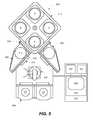
- FIG. 3is a process flow diagram of a method in accordance with disclosed embodiments.
- FIG. 4is a schematic illustration of a deposition chamber for use in accordance with disclosed embodiments.
- FIG. 5is a schematic illustration of a deposition tool for use in accordance with disclosed embodiments.
- FIGS. 6A-6D and 7A-7Dare images of patterns formed in experimental results using disclosed embodiments.
- Patterning of thin films in semiconductor processingis often a critical step in the manufacture and fabrication of semiconductors.
- Conventional stacks for lithographyoften include a photoresist layer on top of an underlayer, which is typically deposited on a hardmask by spin-on methods.
- the hardmaskis often made of one composition, and the hardmask itself is deposited on a target layer.
- Conventional patterninginvolves photolithography, such as 193 nm lithography. In photolithography, patterns are printed by emitting photons from a photon source onto a mask and printing the pattern onto a photosensitive photoresist, thereby causing a chemical reaction in the photoresist that removes certain portions of the photoresist to form the pattern.
- the number of photons that may hit the photoresistmay vary. In many practices, a large number of photons hit the photoresist, with each photon carrying less energy. Since a large number of photons may be used, the error due to some stray photons does not substantially affect the resulting defined pattern.
- EUVExtreme ultraviolet
- lithographyhas been developed to print smaller patterns on a photoresist using EUV light sources at approximately 13.5 nm wavelength in leading-edge lithography tools, which are also referred to as scanners.
- the EUV radiationis strongly absorbed in a wide range of materials, including quartz and water, and so operates in a vacuum.
- EUV lithographyIn EUV lithography, fewer photons are emitted from the source and the photons hit the photoresist to form the pattern. Each of the photons carries higher energy than the photons used in conventional lithography. Moreover, in EUV lithography fewer higher energy photons hit the photoresist so a few stray photons that miss the photosensitive sites may cause a larger error in the defined pattern. Compared to conventional lithography where more lower-energy photons are used and a few stray photons may not affect the pattern substantially, the stochastic effect due to this photon and sensitizer shot noise in EUV lithography is of particular concern.
- the multi-layer stackmay be used to form lines or spaces or contacts and holes in integrated circuits and may form features for advanced technology nodes, as defined by the International Technology Roadmap for Semiconductors. Examples of these advanced technology nodes include 22 nm nodes, 16 nm nodes, and beyond. In the 16 nm node, the width of a typical via or line in a Damascene structure is no greater than about 30 nm.
- FIG. 1is a schematic illustration of an example of a multi-layer stack on a semiconductor substrate.
- the wafer 100includes a target layer 110 , a multi-layer stack 120 , an optional underlayer 130 , and a photoresist 140 .
- the target layer 110may be any target layer or substrate, such as a metal, an oxide, a dielectric material, or an ultra-low-k (ULK) substrate.
- the target layer 110is a silicon substrate.
- the multi-layer stack 120includes an atomically smooth layer 120 a , and underlayers 120 b and 120 c .
- the multi-layer stack 120includes 2 underlayers (as shown in multi-layer stack 120 ), or more than 2 underlayers, or more than 3 underlayers, or more than 4 underlayers, or more than 5 underlayers.
- underlayer 130is included as part of the multi-layer stack 120 .
- Optional underlayer 130may be a spin-on layer or a layer deposited by plasma-enhanced chemical vapor deposition (PECVD).
- PECVDplasma-enhanced chemical vapor deposition
- FIG. 1depicts two underlayers 120 b and 120 c , as well as an atomically smooth layer 120 a.
- the underlayer adjacent to target layer 110is a robust hardmask layer, which may be measured by the modulus and stress.
- robust hardmask layersmay have a modulus of at least 100 MPa and a stress less than about 500 MPa.
- underlayer 120 cor the underlayer adjacent to the target layer 110 , is an amorphous carbon layer.
- the modulus to stress ratio of an underlayer 120 c of amorphous carbonis at least about 1:1.
- robust hardmask layers used for underlayer 110may also include diamond-like carbon (DLC), doped amorphous carbon, and spin-on carbon (SoC).
- DLCdiamond-like carbon
- SoCspin-on carbon
- underlayers 120 b and 120 cmay be removable after transferring a pattern to a subsequent layer.
- underlayer 120 bmay be removed after a pattern is transferred to underlayer 120 c .
- underlayers 120 b and 120 cmay reflect, or refract, or absorb a leveling beam emitted on the substrate to measure wafer levelness.
- the composition of underlayers 120 b and 120 cmay be selected from one of many classes of compositions, such as oxides, metals (e.g., hafnium, cobalt, tungsten, titanium) or conductive films (e.g., titanium nitride, titanium silicide, cobalt silicide), dielectric materials (e.g., silicon oxide, silicon nitride), hardmask materials (e.g., amorphous carbon, amorphous silicon), or others such as silicon oxynitride (SiON), nitrogen-free anti-reflective layer (NFARL), or silicon anti-reflective coating (SiARC).
- oxidessuch as oxides, metals (e.g., hafnium, cobalt, tungsten, titanium) or conductive films (e.g., titanium nitride, titanium silicide, cobalt silicide), dielectric materials (e.g., silicon oxide, silicon nitride), hardmask materials (e.g
- underlayer 120 bis an amorphous silicon layer and underlayer 120 c is an amorphous carbon layer. In most embodiments, underlayer 120 b and underlayer 120 c may each be between about 100 ⁇ and about 900 ⁇ thick.
- Underlayers 120 b and 120 care selected based on their etch contrast relative to adjacent layers.
- underlayer 120 bhas a high etch contrast relative to underlayer 120 c and also has a high etch contrast relative to 120 a .
- underlayer 120 chas a high etch contrast relative to both underlayer 120 b and target layer 110 .
- underlayer 120 cis an amorphous carbon layer
- underlayer 120 bmay have high etch contrast to both the atomically smooth layer 120 a and the amorphous carbon underlayer 120 c.
- Underlayers 120 b and 120 cmay also be selected based on other optimizable properties, such as physical properties, chemical properties, and optical properties. Examples of such properties may include surface energy, bonding structure, hydrophobicity, refractive index, and extinction coefficient.
- the atomically smooth layer 120 ais a thin layer typically deposited in a layer near the top of the multi-layer stack, such as the first or second layer below the photoresist 140 .
- the atomically smooth layer 120 ais characterized by its very low roughness. “Atomically smooth” is defined as having a roughness of less than 1 monolayer, or about half a monolayer of deviation from the mean line. “Local” roughness is defined as the roughness in 1 square micron of surface area of a wafer. Roughness of a layer may be evaluated by observation and by atomic force microscopy (AFM). The roughness may be measured by the average of the vertical deviations of the roughness profile from the mean line. In one example, an “atomically smooth” layer 120 a may have an average roughness of less than about 2 ⁇ . Roughness may also be measured by the root mean square (RMS) of vertical deviations of the roughness profile from the mean line.
- RMSroot mean square
- the atomically smooth layer 120 ais a thin layer.
- the thickness of the atomically smooth layer 120 amay be between about 30 ⁇ and about 60 ⁇ .
- the atomically smooth layer 120 amay have high etch contrast to adjacent layers and may also be removable after transferring the pattern to a subsequent layer.
- the atomically smooth layer 120 ais an oxide layer.
- the atomically smooth layer 120 ais a thin layer of silicon oxide.
- the multi-layer stackmay be used in EUV lithography by using a shrinking effect.
- a larger featureis printed on the photoresist using EUV lithography, and the feature is shrunk as each layer is etched down the multi-layer stack, thereby reducing roughness caused by photon and sensitizer shot noise described above.
- the feature printed on the photoresistshrinks such that the patterned features in the target layer have a critical dimension less than or equal to about 70% of the size or width of the critical dimension of the pattern in the photoresist.
- the percentage of the shrinkagemay be optimized by various etch processes.
- the percentage of shrinkagemay also be limited by pitch.
- Line edge roughnessmay be defined as the deviation of a feature edge (as viewed top-down) from a smooth, ideal shape—that is, the edge deviations of a feature that occur on a dimensional scale smaller than the resolution limit of the imaging tool that was used to print the feature.
- the magnitude of LERmay be affected by a multitude of factors, such as the photon shot noise in the exposing radiation, the stochastic nature of the dissolution of the photoresist in the developer, the metrology noise introduced by a scanning electron microscope, and chemical interactions between the photoresist and underlying film.
- Sidewall roughness on the patterned photoresistmay be highly anisotropic and the roughness may propagate from the photoresist-substrate interface up the photoresist pattern sidewall.
- roughnessmay be correlated from the photoresist-substrate interface to the photoresist-air interface for a number of different photoresist material platforms.
- photoresist LERis desired to be less than about 1 nm (3 ⁇ ). As each layer is etched down in a multi-layer stack, the walls of the feature are smoothed and LER may be optimized to be closer to less than 1 nm.
- multi-layer stacksmay enable or substantially enable high volume manufacturing by using EUV lithography.
- Thinner photoresist filmsmay be used, thereby reducing the exposure dose used to pattern the photoresist. For example, reducing the photoresist thickness from approximately 1000 ⁇ to approximately 300 ⁇ may significantly reduce the dose needed to expose the photoresist, which thereby improves the scanner throughput.
- the photoresistmay also serve as a mask during reactive ion etching (RIE) of the underlying films to transfer the mask pattern onto the target layer. Where the photoresist serves as a mask for this purpose, the lower limit on the photoresist thickness may be determined by the minimum thickness of the photoresist to enable use as a mask.
- RIEreactive ion etching
- low LCDUmay be obtained by using EUV lithography to define a larger feature and narrowing or shrinking the feature each time the pattern is transferred down to each layer, such as an atomically smooth layer, then one or more underlayers, and finally to the target layer.
- Another optimized effect of using multi-layer stacks in EUV lithographyis the effective use of an optical leveling sensor to determine levelness of the wafer.
- leveling methodsare used to ensure that the photons hit a level photoresist and accurately print the pattern onto the photoresist.
- Formation of suitable images in the photoresistoften involves precise alignment of the focal plane of the exposure radiation projected onto the photoresist film. This is important because the defined pattern of the photoresist is used as a starting point to etch the semiconductor substrate and to define subsequent layers of the semiconductor stack.
- the levelness of a substratemay be measured by an optical leveling sensor.
- FIG. 2provides an example of a schematic illustration of an optical leveling sensor detecting the levelness of the wafer.
- the substrate or waferincludes a metal 201 , which may be patterned; an oxide layer 203 ; a hardmask layer 205 which may be an amorphous carbon ( ⁇ -C) or amorphous silicon ( ⁇ -Si) layer; a cap layer 207 , which may be a silicon oxynitride (SiON) layer; an underlayer 209 ; and a photoresist 211 .
- Optical leveling sensorsoften involve a leveling beam 213 , which may emit a beam onto the photoresist 211 .
- Optical sensorsmay operate in approximately the 500 nm to 1800 nm wavelength range, which is also called the broadband leveling beam.
- the photoresist 211reflects the beam, and the reflected beam is detected by a sensor 215 .
- the sensorwill be able to accurately detect whether the substrate is level. Because many different types of wafers may be processed in a tool or apparatus, the optical leveling sensor should be able to determine the levelness of various types of wafers.
- the photoresist 211may refract the beam to underlayers which may have other reflective or refractive properties, such as the metal 201 as shown in FIG.
- a subsequent layermay reflect and/or refract the leveling beam, which is also then detected by the sensor 215 .
- a source of errors in detection of the surface of the photoresistis the reflection of the incident broadband beams from existing wafer topography.
- the sensormay not be able to determine the levelness of the wafer accurately.
- the optical leveling sensormay be able to determine levelness quickly, the optical leveling sensor has a higher level of error due to the various types of wafers used in conventional lithography.
- an air gaugemay be used to evaluate levelness of wafers in lithography.
- the air gaugemeasures the back pressure under the wafer and can detect whether a wafer is imbalanced.
- the measurementis more accurate, a measurement for whether the wafer is level takes longer, thereby reducing wafer throughput.
- EUV lithographyIn contrast to conventional lithography, EUV lithography is most typically performed in a vacuum.
- the air gaugemay not be used to detect whether the wafer is level for lithography because the air gauge measures pressure.
- an optical leveling sensor used to measure the levelness of the wafer and standard wafers used in EUV lithographymay cause reflection or refraction that reflects or refracts the beam, and the sensor may detect the wrong reflected or refracted beam in error.
- the multi-layer stack described hereinis useful because one or more underlayer may have absorbing properties that prevent or block the leveling beam from reflecting and refracting subsequent layers, thereby decreasing the error of the measurements detected by the sensor.
- multi-layer stacksenable accurate optical focusing and leveling systems in EUV lithography tools by replacing the currently used films with optimized multi-layer stacks as described herein.
- the target layermay be a silicon oxide-based layer, such as a TEOS layer about 1500 ⁇ thick.
- a first underlayer of amorphous carbonwhich may be an ashable hardmask.
- the amorphous carbon layermay be robust and have a high modulus, particularly to maintain the fine pattern when it is patterned in subsequent steps.
- Example thicknesses of the amorphous carbon layermay be about 400 ⁇ or about 900 ⁇ .
- On top of the amorphous layermay be a second underlayer of amorphous silicon, which has high etch contrast with amorphous carbon.
- the amorphous siliconis doped. In some embodiments, the amorphous silicon is undoped. This layer may be about 100 ⁇ thick.
- On top of the amorphous silicon layermay be an atomically smooth layer.
- the amorphous silicon layermay have high etch contrast with the atomically smooth layer.
- the atomically smooth layermay be a silicon oxide layer about 30 ⁇ to about 60 ⁇ thick, and may be deposited such that the roughness of the film is less than a monolayer. For example, the average roughness of the atomically smooth layer may be about 2 ⁇ .
- On top of the atomically smooth layermay be a photoresist layer.
- This example of a multi-layer stackmay be used in EUV lithography by patterning larger features than desired in the photoresist layer, then patterning and etching the pattern down and removing each layer such that as the pattern is etched down each layer, the feature shrinks by size.
- FIG. 3is a process flow diagram depicting a method 300 of depositing a multi-layer stack.
- a target layermay be deposited on a substrate, or a substrate including a target layer may be provided.
- the target layeris deposited on a substrate or wafer, such as a silicon wafer.
- the target layeris a metal layer, oxide layer, dielectric layer, or an ultra-low-k layer.
- the target layeris tetraethyl orthosilicate (TEOS).
- the thickness of the target layermay vary from about 200 ⁇ to about 2000 ⁇ , or about 1500 ⁇ .
- one or more underlayersare deposited on the substrate.
- the underlayersare deposited directly on top of the target layer.
- one underlayeris deposited.
- two underlayersare deposited. The number of underlayers that may be deposited may range from 1 to at least 4 or at least 5 or more.
- Each underlayermay have a composition different than or the same as an adjacent layer and is removable after transferring a pattern to a subsequent layer.
- at least one of the underlayersis a hardmask layer.
- Underlayersmay be oxides, metals, conductive films, dielectric material, or other material.
- Example metalsinclude hafnium, cobalt, tungsten, and titanium and example conductive films include titanium nitride, titanium silicide, and cobalt silicide.
- Example dielectric materialsinclude silicon oxide and silicon nitride.
- underlayer compositionsinclude amorphous carbon, amorphous silicon, silicon oxynitride (SiON), nitrogen-free anti-reflective layer (NFARL), and silicon anti-reflective coating (SiARC).
- the underlayer deposited directly on top of the target layerhas a high modulus or is highly robust, which may be measured by modulus or stress.
- robust underlayersinclude amorphous carbon, or diamond-like carbon.
- an amorphous carbon layermay be deposited as at least one of the one or more underlayers by exposing the substrate to a hydrocarbon precursor.
- the underlayer deposited directly on top of the target layerhas high etch contrast to the target layer.
- Each underlayerhas high etch contrast to the adjacent underlayer.
- a target layer of TEOShas high etch contrast to a layer of amorphous carbon.
- an underlayer of amorphous carbonmay deposited on top of a target layer of TEOS.
- each underlayermay range from about 100 ⁇ to about 900 ⁇ or from about 400 ⁇ to about 900 ⁇ . In some embodiments, the thickness of each underlayer is the same. In some embodiments, the thickness of each underlayer is different. In various embodiments, the thickness of an underlayer on top of the target layer is thicker than other underlayers.
- a 400 ⁇ underlayer of amorphous carbonis deposited on the target layer, and a 100 ⁇ layer of amorphous silicon with low hydrogen content is deposited on top of the amorphous carbon layer.
- the hydrogen content in a low-hydrogen amorphous silicon layermay be less than about 5%, or less than about 10%, or less than about 20%.
- the low-hydrogen contentmay depend on the adhesion of a layer on top of the amorphous silicon layer.
- an amorphous carbon layermay also have low hydrogen content, or less than about 10% hydrogen, or less than about 20% hydrogen.
- an atomically smooth layeris deposited on the substrate.
- “Atomically smooth”may be defined as having a local roughness less than 1 monolayer, or about half a monolayer.
- “Local” roughnessmay be defined as the roughness measured in 1 square micron of wafer surface area. Roughness of the layer may be evaluated by observation or atomic force spectroscopy and may be measured by evaluating the average of vertical deviations of the roughness profile from the mean line, or the root mean square (RMS) of vertical deviations of the roughness profile from the mean line. In some embodiments, the average local roughness of the atomically smooth layer is less than about 2 ⁇ .
- the atomically smooth layeris deposited on the one or more underlayers. In a specific embodiment, the atomically smooth layer is deposited on top of a low-hydrogen amorphous silicon layer. In various embodiments, the atomically smooth layer is removable after transferring a pattern to a subsequent layer.
- the atomically smooth layermay be a thin layer and have a thickness between about 30 ⁇ and about 60 ⁇ . Compared to the underlayer below the atomically smooth layer and to any layer deposited on top of the atomically smooth layer, the atomically smooth layer may have a high etch contrast. In a specific example, the atomically smooth layer is a thin layer of silicon oxide (SiO 2 ). In many embodiments, the atomically smooth layer is an oxide layer.
- a photoresistmay be deposited on the atomically smooth layer.
- the photoresistmay be directly adjacent to the atomically smooth layer such that the photoresist is deposited directly on top of the atomically smooth layer.
- the atomically smooth layer and one or more underlayersare deposited such that the layers are between the photoresist and the target layer.
- one or more underlayeris deposited on top of the atomically smooth layer.
- the photoresistmay be poly(methyl methacrylate) poly(methyl glutarimide) (PMGI) or phenol formaldehyde resin.
- the thickness of the photoresistmay be between about 100 ⁇ and about 600 ⁇ , for example about 300 ⁇ . In some embodiments, the thickness of the deposited photoresist is 600 ⁇ .
- the photoresistmay be patterned using extreme ultraviolet (EUV) lithography.
- EUV lithographyinvolves depositing photosensitive sites of a defined pattern onto the photoresist and printing the pattern onto the photoresist.
- the patternis transferred to subsequent layers by a shrinking method such that the size of the features defined shrinks as each layer is patterned and removed.
- Each layer described in method 300may be deposited by various methods. Examples of deposition processes include atomic layer deposition (ALD), plasma-enhanced ALD (PEALD), conformal film deposition (CFD), chemical vapor deposition (CVD), plasma-enhanced CVD (PECVD), physical vapor deposition (PVD), and spin-on methods.
- ALDatomic layer deposition
- PEALDplasma-enhanced ALD
- CCDconformal film deposition
- CVDchemical vapor deposition
- PECVDplasma-enhanced CVD
- PVDphysical vapor deposition
- spin-on methodsspin-on methods.
- an underlayer in operation 303may be deposited by a deposition technique, such as plasma-enhanced chemical vapor deposition (PECVD), and may involve generating a plasma in the deposition chamber from deposition gases including a hydrocarbon precursor.
- PECVDplasma-enhanced chemical vapor deposition
- the hydrocarbon precursormay be defined by the formula C x H y , where x is an integer between 2 and 10, and y is an integer between 2 and 24. Examples include methane (CH 4 ), acetylene (C 2 H 2 ), ethylene (C 2 H 4 ), propylene (C 3 H 6 ), butane (C 4 H 10 ), cyclohexane (C 6 H 12 ), benzene (C 6 H 6 ), and toluene (C 7 H 8 ).
- RFradio frequency
- a dual radio frequency (RF) plasma sourceincluding a high frequency (HF) power and a low frequency (LF) power may be used.
- Deposition and use of multi-layer stacks described hereinmay be performed on any apparatus suitable for semiconductor processing.
- the apparatusmay be integrated and may have one or more chambers or stations for processing semiconductor substrates.
- An apparatus suitable for practicing methods described hereinmay also include lithography tools, deposition tools, etching tools, and others.
- deposition techniques provided hereinmay be implemented in a plasma-enhanced chemical vapor deposition (PECVD) reactor or a conformal film deposition (CFD) reactor.
- PECVDplasma-enhanced chemical vapor deposition
- CCDconformal film deposition
- Such a reactormay take many forms and may be part of an apparatus that includes one or more chambers or reactors—sometimes including multiple stations—that may each house one or more wafers and may be configured to perform various wafer operations.
- the one or more chambersmay maintain the wafer in a defined position or positions (with or without motion within that position, e.g., rotation, vibration, or other agitation).
- a wafer undergoing film depositionmay be transferred from one station to another within a reactor or chamber during the process.
- the wafermay be transferred from chamber to chamber within the apparatus to perform different operations. Full deposition or any fraction of the total film thickness for any deposition step may occur entirely at a single station. While in process, each wafer may be held in place by a pedestal, wafer chuck, and/or other wafer-holding apparatus. For certain operations in which the wafer is to be heated, the apparatus may include a heater, such as a heating plate.
- a VectorTM (e.g., C3 Vector) or SequelTM (e.g., C2 Sequel) reactorproduced by Lam Research Corp. of Fremont, Calif., are both examples of suitable reactors that may be used to implement the techniques described herein.
- FIG. 4provides a simple block diagram depicting various reactor components arranged for implementing methods described herein.
- a reactor 400includes a process chamber 424 that encloses other components of the reactor 400 and serves to contain plasma generated by a capacitive-discharge type system including a showerhead 414 working in conjunction with a grounded heater block 420 .
- a high frequency (HF) radio frequency (RF) generator 404 and a low frequency (LF) RF generator 402may be connected to a matching network 406 and to the showerhead 414 .
- the power and frequency supplied by matching network 406may be sufficient to generate a plasma from process gases supplied to the process chamber 424 .
- the HFRF componentmay generally be between 5 MHz to 60 MHz, e.g., 13.56 MHz.
- the LF componentmay be from about 100 kHz to 2 MHz, e.g., 430 kHz.
- a wafer pedestal 418may support a substrate 416 .
- the wafer pedestal 418may include a chuck, a fork, or lift pins (not shown) to hold and transfer the substrate into and out of the chamber 424 between operations.
- the chuckmay be an electrostatic chuck, a mechanical chuck, or various other types of chuck as are available for use in the industry and/or for research.
- Various process gasesmay be introduced via inlet 412 .
- Multiple source gas lines 410are connected to manifold 408 .
- the gasesmay be premixed or not.
- Appropriate valving and mass flow control mechanismsmay be employed to ensure that the correct process gases are delivered during the deposition and plasma treatment phases of each operation in the process.
- liquid flow control mechanismsmay be employed. Such liquids may then be vaporized and mixed with process gases during transportation in a manifold heated above the vaporization point of the chemical precursor supplied in liquid form before reaching the deposition chamber 424 .
- Process gasesmay exit chamber 424 via an outlet 422 .
- a vacuum pumpe.g., a one or two stage mechanical dry pump and/or turbomolecular pump 440 , may be used to draw process gases out of the process chamber 424 and to maintain a suitably low pressure within the process chamber 424 by using a closed-loop-controlled flow restriction device, such as a throttle valve or a pendulum valve.
- the techniques for deposition discussed hereinmay be implemented on a multi-station or single station tool.
- a 300 mm Lam VectorTM tool having a 4-station deposition scheme or a 200 mm Sequel tool having a 6-station deposition schememay be used.
- tools for processing 450 mm wafersmay be used.
- the wafersmay be indexed after every deposition process, or may be indexed after etching steps if the etching chambers or stations are also part of the same tool, or multiple depositions and treatments may be conducted at a single station before indexing the wafer.
- the wafersmay be indexed after each layer is deposited, such as after an underlayer is deposited, or after an atomically smooth layer is deposited.
- an apparatusmay be provided that is configured to perform the techniques described herein.
- a suitable apparatusmay include hardware for performing various process operations as well as a system controller 430 having instructions for controlling process operations in accordance with the disclosed embodiments.
- the system controller 430will typically include one or more memory devices and one or more processors communicatively connected with various process control equipment, e.g., valves, RF generators, wafer handling systems, etc., and configured to execute the instructions so that the apparatus will perform a technique in accordance with the disclosed embodiments, e.g., a technique such as that provided in the operations of FIG. 3 .
- Machine-readable media containing instructions for controlling process operations in accordance with the present disclosuremay be coupled to the system controller 430 .
- the controller 430may be communicatively connected with various hardware devices, e.g., mass flow controllers, valves, RF generators, vacuum pumps, etc. to facilitate control of the various process parameters that are associated with the deposition operations as described herein.
- a system controller 430may control all of the activities of the reactor 400 .
- the system controller 430may execute system control software stored in a mass storage device, loaded into a memory device, and executed on a processor.
- the control logicmay be hard coded in the controller 430 .
- Applications Specific Integrated Circuits, Programmable Logic Devicese.g., field-programmable gate arrays, or FPGAs
- FPGAsfield-programmable gate arrays
- the system control softwaremay include instructions for controlling the timing of gas flows, wafer movement, RF generator activation, etc., as well as instructions for controlling the mixture of gases, the chamber and/or station pressure, the chamber and/or station temperature, the wafer temperature, the target power levels, the RF power levels, the substrate pedestal, chuck, and/or susceptor position, and other parameters of a particular process performed by the reactor apparatus 400 .
- the system control softwaremay be configured in any suitable way. For example, various process tool component subroutines or control objects may be written to control operation of the process tool components necessary to carry out various process tool processes.
- the system control softwaremay be coded in any suitable computer readable programming language.
- the system controller 430may typically include one or more memory devices and one or more processors configured to execute the instructions so that the apparatus will perform a technique in accordance with the present disclosure.
- Machine-readable media containing instructions for controlling process operations in accordance with disclosed embodimentsmay be coupled to the system controller 430 .
- the method and apparatus described hereinmay be used in conjunction with lithographic patterning tools or processes such as those described below for fabrication or manufacture of semiconductor devices, displays, LEDs, photovoltaic panels, and the like. Typically, though not necessarily, such tools/processes will be used or conducted together in a common fabrication facility.
- Lithographic patterning of a filmtypically includes some or all of the following steps, each step performed with a number of possible tools: (1) application of photoresist on a workpiece, i.e., substrate or multi-layer stack as provided in disclosed embodiments, using a spin-on or spray-on tool; (2) curing a photoresist using a hot plate or furnace or UV curing tool; (3) exposing the photoresist to visible or UV or x-ray light with a tool such as a wafer stepper; (4) developing the resist so as to selectively remove resist and thereby pattern it using a tool such as a wet bench; (5) transferred the resist pattern into an underlying film or workpiece, such as an amorphous carbon underlayer, by using a dry or plasma-assisted etching tool; and (6) removing the resist using a tool such as an RF or microwave plasma resist stripper.
- a toolsuch as an RF or microwave plasma resist stripper.
- FIG. 5shows a schematic view of an embodiment of a multi-station processing tool 500 with an inbound load lock 502 and an outbound load lock 504 , either or both of which may include a remote plasma source.
- a robot 506at atmospheric pressure, is configured to move wafers from a cassette loaded through a pod 508 into inbound load lock 502 via an atmospheric port 510 .
- a waferis placed by the robot 506 on a pedestal 512 in the inbound load lock 502 , the atmospheric port 510 is closed, and the load lock is pumped down.
- the wafermay be exposed to a remote plasma treatment in the load lock prior to being introduced into a processing chamber 514 . Further, the wafer also may be heated in the inbound load lock 502 as well, for example, to remove moisture and adsorbed gases. Next, a chamber transport port 516 to processing chamber 514 is opened, and another robot (not shown) places the wafer into the reactor on a pedestal of a first station shown in the reactor for processing. While the embodiment depicted includes load locks, it will be appreciated that, in some embodiments, direct entry of a wafer into a process station may be provided.
- the depicted processing chamber 514includes four process stations, numbered from 1 to 4 in the embodiment shown in FIG. 5 .
- Each stationhas a heated pedestal (shown at 518 for station 1), and gas line inlets.
- each process stationmay have different or multiple purposes.
- a process stationmay be switchable between a CFD and PECVD process mode.
- processing chamber 514may include one or more matched pairs of CFD and PECVD process stations.
- a processing chamber according to the present disclosuremay have any suitable number of stations.
- a processing chambermay have five or more stations, while in other embodiments a processing chamber may have three or fewer stations.
- FIG. 5also depicts an embodiment of a wafer handling system 590 for transferring wafers within processing chamber 514 .
- wafer handling system 590may transfer wafers between various process stations and/or between a process station and a load lock. It will be appreciated that any suitable wafer handling system may be employed. Non-limiting examples include wafer carousels and wafer handling robots.
- FIG. 5also depicts an embodiment of a system controller 550 employed to control process conditions and hardware states of process tool 500 .
- System controller 550may include one or more memory devices 556 , one or more mass storage devices 554 , and one or more processors 552 .
- Processor 552may include a CPU or computer, analog and/or digital input/output connections, stepper motor controller boards, etc.
- system controller 550controls all of the activities of process tool 500 .
- System controller 550executes system control software 558 stored in mass storage device 554 , loaded into memory device 556 , and executed on processor 552 .
- the control logicmay be hard coded in the controller 550 .
- Applications Specific Integrated Circuits, Programmable Logic Devicese.g., field-programmable gate arrays, or FPGAs
- FPGAsfield-programmable gate arrays
- System control software 558may include instructions for controlling the timing, mixture of gases, chamber and/or station pressure, chamber and/or station temperature, wafer temperature, target power levels, RF power levels, RF exposure time, substrate pedestal, chuck and/or susceptor position, and other parameters of a particular process performed by process tool 500 .
- System control software 558may be configured in any suitable way. For example, various process tool component subroutines or control objects may be written to control operation of the process tool components necessary to carry out various process tool processes.
- System control software 558may be coded in any suitable computer readable programming language.
- system control software 558may include input/output control (IOC) sequencing instructions for controlling the various parameters described above.
- IOCinput/output control
- each operation of a deposition processmay include one or more instructions for execution by system controller 550 .
- the instructions for setting process conditions for a PECVD process operationmay be included in a corresponding PECVD recipe process operation.
- the PECVD process operationsmay be sequentially arranged, so that all instructions for a PECVD process are executed concurrently with that process phase.
- mass storage device 554 and/or memory device 556 associated with system controller 550may be employed in some embodiments.
- programs or sections of programs for this purposeinclude a substrate positioning program, a process gas control program, a pressure control program, a heater control program, and a plasma control program.
- a substrate positioning programmay include program code for process tool components that are used to load the substrate onto pedestal 518 and to control the spacing between the substrate and other parts of process tool 500 .
- a process gas control programmay include code for controlling gas composition and flow rates and optionally for flowing gas into one or more process stations prior to deposition of a multi-layer stack in order to stabilize the pressure in the process station.
- the controller 550includes instructions for depositing one or more underlayers, then depositing an atomically smooth layer.
- a pressure control programmay include code for controlling the pressure in the process station by regulating, for example, a throttle valve in the exhaust system of the process station, a gas flow into the process station, etc.
- the controller 550includes instructions for depositing one or more underlayers and depositing an atomically smooth layer.
- a heater control programmay include code for controlling the current to a heating unit that is used to heat the substrate.
- the heater control programmay control delivery of a heat transfer gas (such as helium) to the substrate.
- the controller 550includes instructions for depositing one or more underlayers, and depositing an atomically smooth layer.
- a plasma control programmay include code for setting RF power levels and exposure times in one or more process stations in accordance with the embodiments herein.
- the controller 550includes instructions for depositing one or more underlayers, and depositing an atomically smooth layer.
- the user interfacemay include a display screen, graphical software displays of the apparatus and/or process conditions, and user input devices such as pointing devices, keyboards, touch screens, microphones, etc.
- parameters adjusted by system controller 550may relate to process conditions.
- process conditionsinclude process gas composition and flow rates, temperature, pressure, plasma conditions (such as RF bias power levels and exposure times), etc. These parameters may be provided to the user in the form of a recipe, which may be entered utilizing the user interface.
- Signals for monitoring the processmay be provided by analog and/or digital input connections of system controller 550 from various process tool sensors.
- the signals for controlling the processmay be output on the analog and digital output connections of process tool 500 .
- process tool sensorsthat may be monitored include mass flow controllers, pressure sensors (such as manometers), thermocouples, etc. Appropriately programmed feedback and control algorithms may be used with data from these sensors to maintain process conditions.
- System controller 550may provide program instructions for implementing the above-described deposition processes.
- the program instructionsmay control a variety of process parameters, such as DC power level, RF bias power level, pressure, temperature, etc.
- the instructionsmay control the parameters to operate in-situ deposition of multi-layer film stacks according to various embodiments described herein.
- the system controller 550will typically include one or more memory devices and one or more processors configured to execute the instructions so that the apparatus will perform a method in accordance with the disclosed embodiments.
- Machine-readable, non-transitory media containing instructions for controlling process operations in accordance with the disclosed embodimentsmay be coupled to the system controller 550 .
- a 1500 ⁇ layer of tetraethyl orthosilicate (TEOS)was deposited on a silicon substrate as the target layer.
- a 900 ⁇ underlayer of amorphous carbonwas deposited on the target layer, followed by a 200 ⁇ layer of amorphous silicon with low hydrogen content.
- a 60 ⁇ atomically smooth layerwas deposited on the amorphous silicon layer.
- a 100 ⁇ underlayerwas deposited on the atomically smooth layer, followed by deposition of a standard 600 ⁇ photoresist.
- the wafer with the multi-layer stackwas patterned using EUV lithography to pattern larger holes in the photoresist.
- the improvement in local critical dimension uniformity (LCDU) for 30 nm vias in 52 nm pitchwas evaluated.
- LCDUlocal critical dimension uniformity
- the goal LCDUwas 2.5 nm (3 ⁇ ).
- the average critical dimension (CD) of the photoresist after EUV lithographywas 28.9 nm and the LCDU was 4.92 nm (3 ⁇ ).
- a top-down image of the patterned photoresist on the multi-layer stackis shown in FIG. 6A .
- the subsequent layerswere patterned and etched while shrinking the feature to a target size.
- HMOhardmask open etch
- the average CDwas 27.9 nm and the LCDU was 2.56 (3 ⁇ ).
- a top-down image of the patterned substrate after HMOis provided in FIG. 6B .
- the target layerwas patterned and the local CD average was 23.1 nm with an LCDU of 2.38 (3 ⁇ ).
- a top-down image of the patterned target layeris provided in FIG. 6C and a side profile view of the patterned target layer is provided in FIG. 6D .
- the resulting CD shranksuch that the target layer CD was approximately 70% of the size of the CD in the photoresist.
- the target layer etchwas close to the goal LCDU of 2.5.
- the patterned target layerhas smooth edges and low line edge roughness.
- a 1000 ⁇ layer of tetraethyl orthosilicate (TEOS)was deposited on a silicon substrate as the target layer.
- a 400 ⁇ underlayer of amorphous carbonwas deposited on the target layer, followed by a 100 ⁇ layer of amorphous silicon with low hydrogen content.
- a 30 ⁇ atomically smooth layerwas deposited on the amorphous silicon layer.
- a 100 ⁇ underlayerwas deposited on the atomically smooth layer, followed by deposition of a 300 ⁇ standard photoresist.
- the wafer with the multi-layer stackwas patterned using EUV lithography to pattern larger holes in the photoresist.
- the improvement in local critical dimension uniformity (LCDU) for 30 nm vias in 52 nm pitchwas evaluated.
- LCDUlocal critical dimension uniformity
- the goal LCDUwas 2.5 nm (3 ⁇ ).
- the average CD of the photoresist after EUV lithographywas 28.6 nm and the LCDU was 4.29 nm (3 ⁇ ).
- a top-down image of the patterned photoresistis provided in FIG. 7A .
- the subsequent layerswere patterned and etched while shrinking the feature to a target size.
- the average CDwas 20.9 nm and the LCDU was 3.39 (3 ⁇ ).
- a top-down image of the substrate after HMOis provided in FIG. 7B .
- the target layerwas patterned and the local CD average was 22.8 nm with an LCDU of 2.77 (3 ⁇ ).
- a top-down image of the patterned target layeris provided in FIG. 7C and a side profile view of the patterned target layer is provided in FIG. 7D .
- the resulting critical dimension (CD) shranksuch that the target layer CD was approximately 70% of the size of the CD in the photoresist.
- the target layer etchwas close to the goal LCDU of 2.5.
- 7C and 7Dis comparable to that of the target layer in FIGS. 6C and 6D .
- thinner filmssuch as thinner underlayers or thinner photoresists, may be used in EUV lithography. This may thereby increase throughput of wafers in semiconductor processing.
Landscapes
- Engineering & Computer Science (AREA)
- Physics & Mathematics (AREA)
- General Physics & Mathematics (AREA)
- Manufacturing & Machinery (AREA)
- Power Engineering (AREA)
- Computer Hardware Design (AREA)
- Microelectronics & Electronic Packaging (AREA)
- Condensed Matter Physics & Semiconductors (AREA)
- Chemical & Material Sciences (AREA)
- Architecture (AREA)
- Structural Engineering (AREA)
- Inorganic Chemistry (AREA)
- Chemical Kinetics & Catalysis (AREA)
- Plasma & Fusion (AREA)
- Exposure And Positioning Against Photoresist Photosensitive Materials (AREA)
- Drying Of Semiconductors (AREA)
- General Chemical & Material Sciences (AREA)
- Materials Engineering (AREA)
- Mechanical Engineering (AREA)
- Metallurgy (AREA)
- Organic Chemistry (AREA)
Abstract
Description
This application is a divisional application claiming benefit of U.S. patent application Ser. No. 14/185,757, filed on Feb. 20, 2014, and titled “PECVD FILMS FOR EUV LITHOGRAPHY,” which claims benefit of U.S. Provisional Patent Application No. 61/769,126, filed Feb. 25, 2013, and titled “PECVD FILMS FOR EUV LITHOGRAPHY,” both of which are incorporated by reference herein in their entireties and for all purposes.
Patterning methods are critical to semiconductor processing. In particular, extreme ultraviolet (EUV) lithography has been explored to extend lithographic technology beyond its optical limits and replace current photolithography methods to pattern small critical dimension features. Current EUV lithography methods result in poor edge roughness and weak patterns that may ultimately render the substrate useless.
Provided herein is a multi-layer stack suitable for extreme ultraviolet lithography and methods for depositing a multi-layer stack in semiconductor processing. One aspect involves a multi-layer stack on a semiconductor substrate for extreme ultraviolet lithography including an atomically smooth layer with an average local roughness of less than a monolayer, and one or more underlayers, such that the one or more underlayers have high etch contrast to layers adjacent to them.
In various embodiments, the multi-layer stack also includes a photoresist, and a target layer, such that the atomically smooth layer and the one or more underlayers are between the photoresist and the target layer, and the atomically smooth layer is adjacent to the photoresist. In some embodiments, the photoresist is between about 100 Å and 600 Å thick. In some embodiments, the thickness of the atomically smooth layer is between about 30 Å and about 60 Å.
In many embodiments, one of the one or more underlayers is a hardmask adjacent to a target layer. In some embodiments, the hardmask includes amorphous carbon having a hydrogen content less than about 20%. In some embodiments, the underlayer of amorphous carbon is between about 400 Å and about 900 Å. In some embodiments, the underlayer of amorphous carbon has a modulus to stress ratio of about 1:1. In various embodiments, one of the one or more underlayers includes amorphous silicon having a hydrogen content less than about 5%.
In various embodiments, the atomically smooth layer includes an oxide. In some embodiments, at least one of the one or more underlayers reflects or absorbs a leveling beam struck on the substrate to measure wafer leveling. In some embodiments, the average local roughness of the atomically smooth layer is less than about 2 Å.
Another aspect involves a method of processing a semiconductor substrate for extreme ultraviolet lithography by depositing one or more underlayers on a target layer; depositing an atomically smooth layer having a roughness of less than a monolayer; and depositing a photoresist layer on top of the atomically smooth layer.
In various embodiments, each layer is deposited by plasma-enhanced chemical vapor deposition. In many embodiments, depositing the one or more underlayers further includes depositing an amorphous carbon layer on the target layer by exposing the substrate to a hydrocarbon precursor.
In some embodiments, the atomically smooth layer is deposited to a thickness between about 30 Å and about 60 Å. In various embodiments, the method also includes patterning the photoresist layer using extreme ultraviolet lithography.
Another aspect involves an apparatus for processing semiconductor substrates including one or more process chambers; one or more gas inlets into the one or more process chambers and associated flow-control hardware; a low frequency radio frequency (LFRF) generator; a high frequency radio frequency (HFRF) generator; and a controller having at least one processor and a memory. The at least one processor and the memory are communicatively connected with one another, the at least one processor is at least operatively connected with the flow-control hardware, the LFRF generator, and the HFRF generator, and the memory stores computer-executable instructions for: depositing one or more underlayers on a substrate; depositing an atomically smooth layer having a roughness of less than a monolayer; and depositing a photoresist layer on top of the atomically smooth layer.
In various embodiments, the atomically smooth underlayer is deposited to a thickness between about 30 Å and about 60 Å. In some embodiments, at least one of the one or more underlayers deposited on the substrate includes amorphous carbon.
These and other aspects are described further below with reference to the drawings.
In the following description, numerous specific details are set forth to provide a thorough understanding of the presented embodiments. The disclosed embodiments may be practiced without some or all of these specific details. In other instances, well-known process operations have not been described in detail to not unnecessarily obscure the disclosed embodiments. While the disclosed embodiments will be described in conjunction with the specific embodiments, it will be understood that it is not intended to limit the disclosed embodiments.
Patterning of thin films in semiconductor processing is often a critical step in the manufacture and fabrication of semiconductors. Conventional stacks for lithography often include a photoresist layer on top of an underlayer, which is typically deposited on a hardmask by spin-on methods. The hardmask is often made of one composition, and the hardmask itself is deposited on a target layer. Conventional patterning involves photolithography, such as 193 nm lithography. In photolithography, patterns are printed by emitting photons from a photon source onto a mask and printing the pattern onto a photosensitive photoresist, thereby causing a chemical reaction in the photoresist that removes certain portions of the photoresist to form the pattern. In conventional lithography, the number of photons that may hit the photoresist may vary. In many practices, a large number of photons hit the photoresist, with each photon carrying less energy. Since a large number of photons may be used, the error due to some stray photons does not substantially affect the resulting defined pattern.
As devices shrink, the need for printing smaller features increases. Although multiple patterning techniques have been developed for use with conventional photolithography, multiple patterning uses multiple layers of deposition and etching processes. Scaling of features on advanced semiconductor integrated circuits (ICs) and other devices has driven lithography to improve resolution by moving to ever smaller imaging source wavelengths.
Extreme ultraviolet (EUV) lithography has been developed to print smaller patterns on a photoresist using EUV light sources at approximately 13.5 nm wavelength in leading-edge lithography tools, which are also referred to as scanners. The EUV radiation is strongly absorbed in a wide range of materials, including quartz and water, and so operates in a vacuum.
In EUV lithography, fewer photons are emitted from the source and the photons hit the photoresist to form the pattern. Each of the photons carries higher energy than the photons used in conventional lithography. Moreover, in EUV lithography fewer higher energy photons hit the photoresist so a few stray photons that miss the photosensitive sites may cause a larger error in the defined pattern. Compared to conventional lithography where more lower-energy photons are used and a few stray photons may not affect the pattern substantially, the stochastic effect due to this photon and sensitizer shot noise in EUV lithography is of particular concern.
Provided herein is a multi-layer stack tailored to achieve optimum etch contrast to shrink features and smooth the edges of features while enabling use of the optical leveling sensor with little or reduced error. The multi-layer stack may be used to form lines or spaces or contacts and holes in integrated circuits and may form features for advanced technology nodes, as defined by the International Technology Roadmap for Semiconductors. Examples of these advanced technology nodes include 22 nm nodes, 16 nm nodes, and beyond. In the 16 nm node, the width of a typical via or line in a Damascene structure is no greater than about 30 nm.
Themulti-layer stack 120 includes an atomicallysmooth layer 120a, andunderlayers multi-layer stack 120 includes 2 underlayers (as shown in multi-layer stack120), or more than 2 underlayers, or more than 3 underlayers, or more than 4 underlayers, or more than 5 underlayers. In some embodiments,underlayer 130 is included as part of themulti-layer stack 120.Optional underlayer 130 may be a spin-on layer or a layer deposited by plasma-enhanced chemical vapor deposition (PECVD). As an example,FIG. 1 depicts twounderlayers smooth layer 120a.
In various embodiments, the underlayer adjacent to targetlayer 110 is a robust hardmask layer, which may be measured by the modulus and stress. For example, robust hardmask layers may have a modulus of at least 100 MPa and a stress less than about 500 MPa. In many embodiments,underlayer 120c, or the underlayer adjacent to thetarget layer 110, is an amorphous carbon layer. In some embodiments, the modulus to stress ratio of anunderlayer 120cof amorphous carbon is at least about 1:1. Examples of robust hardmask layers used forunderlayer 110 may also include diamond-like carbon (DLC), doped amorphous carbon, and spin-on carbon (SoC).
In various embodiments,underlayers underlayer 120bmay be removed after a pattern is transferred to underlayer120c. In some embodiments,underlayers
The composition ofunderlayers underlayer 120bis an amorphous silicon layer andunderlayer 120cis an amorphous carbon layer. In most embodiments,underlayer 120bandunderlayer 120cmay each be between about 100 Å and about 900 Å thick.
The atomicallysmooth layer 120ais a thin layer typically deposited in a layer near the top of the multi-layer stack, such as the first or second layer below thephotoresist 140. The atomicallysmooth layer 120ais characterized by its very low roughness. “Atomically smooth” is defined as having a roughness of less than 1 monolayer, or about half a monolayer of deviation from the mean line. “Local” roughness is defined as the roughness in 1 square micron of surface area of a wafer. Roughness of a layer may be evaluated by observation and by atomic force microscopy (AFM). The roughness may be measured by the average of the vertical deviations of the roughness profile from the mean line. In one example, an “atomically smooth”layer 120amay have an average roughness of less than about 2 Å. Roughness may also be measured by the root mean square (RMS) of vertical deviations of the roughness profile from the mean line.
In many embodiments, the atomicallysmooth layer 120ais a thin layer. The thickness of the atomicallysmooth layer 120amay be between about 30 Å and about 60 Å. The atomicallysmooth layer 120amay have high etch contrast to adjacent layers and may also be removable after transferring the pattern to a subsequent layer. In various embodiments, the atomicallysmooth layer 120ais an oxide layer. In some examples, the atomicallysmooth layer 120ais a thin layer of silicon oxide.
The multi-layer stack may be used in EUV lithography by using a shrinking effect. A larger feature is printed on the photoresist using EUV lithography, and the feature is shrunk as each layer is etched down the multi-layer stack, thereby reducing roughness caused by photon and sensitizer shot noise described above. In many embodiments, the feature printed on the photoresist shrinks such that the patterned features in the target layer have a critical dimension less than or equal to about 70% of the size or width of the critical dimension of the pattern in the photoresist. The percentage of the shrinkage may be optimized by various etch processes. The percentage of shrinkage may also be limited by pitch.
Use of the multi-layer stack in EUV lithography may result in several optimized effects. For example, using a multi-layer stack may result in optimized low line edge roughness (LER). Line edge roughness may be defined as the deviation of a feature edge (as viewed top-down) from a smooth, ideal shape—that is, the edge deviations of a feature that occur on a dimensional scale smaller than the resolution limit of the imaging tool that was used to print the feature. The magnitude of LER may be affected by a multitude of factors, such as the photon shot noise in the exposing radiation, the stochastic nature of the dissolution of the photoresist in the developer, the metrology noise introduced by a scanning electron microscope, and chemical interactions between the photoresist and underlying film. Sidewall roughness on the patterned photoresist may be highly anisotropic and the roughness may propagate from the photoresist-substrate interface up the photoresist pattern sidewall. In ultrathin photoresist films, which may be about 100 nm in thickness or less, roughness may be correlated from the photoresist-substrate interface to the photoresist-air interface for a number of different photoresist material platforms. In EUV lithography, particularly for high volume manufacturing, photoresist LER is desired to be less than about 1 nm (3σ). As each layer is etched down in a multi-layer stack, the walls of the feature are smoothed and LER may be optimized to be closer to less than 1 nm.
Another optimized effect of using multi-layer stacks is improved throughput. Use of multi-layer stacks may enable or substantially enable high volume manufacturing by using EUV lithography. Thinner photoresist films may be used, thereby reducing the exposure dose used to pattern the photoresist. For example, reducing the photoresist thickness from approximately 1000 Å to approximately 300 Å may significantly reduce the dose needed to expose the photoresist, which thereby improves the scanner throughput. The photoresist may also serve as a mask during reactive ion etching (RIE) of the underlying films to transfer the mask pattern onto the target layer. Where the photoresist serves as a mask for this purpose, the lower limit on the photoresist thickness may be determined by the minimum thickness of the photoresist to enable use as a mask.
Another optimized effect of using multi-layer stacks may be obtaining low local critical dimension uniformity (LCDU). In various embodiments, low LCDU may be obtained by using EUV lithography to define a larger feature and narrowing or shrinking the feature each time the pattern is transferred down to each layer, such as an atomically smooth layer, then one or more underlayers, and finally to the target layer.
Another optimized effect of using multi-layer stacks in EUV lithography is the effective use of an optical leveling sensor to determine levelness of the wafer. To accurately print a pattern in conventional lithography, leveling methods are used to ensure that the photons hit a level photoresist and accurately print the pattern onto the photoresist. Formation of suitable images in the photoresist often involves precise alignment of the focal plane of the exposure radiation projected onto the photoresist film. This is important because the defined pattern of the photoresist is used as a starting point to etch the semiconductor substrate and to define subsequent layers of the semiconductor stack.
The levelness of a substrate may be measured by an optical leveling sensor.FIG. 2 provides an example of a schematic illustration of an optical leveling sensor detecting the levelness of the wafer. The substrate or wafer includes ametal 201, which may be patterned; anoxide layer 203; ahardmask layer 205 which may be an amorphous carbon (α-C) or amorphous silicon (α-Si) layer; acap layer 207, which may be a silicon oxynitride (SiON) layer; anunderlayer 209; and aphotoresist 211. Optical leveling sensors often involve aleveling beam 213, which may emit a beam onto thephotoresist 211. Optical sensors may operate in approximately the 500 nm to 1800 nm wavelength range, which is also called the broadband leveling beam. Thephotoresist 211 reflects the beam, and the reflected beam is detected by asensor 215. Depending on the properties of the wafer or the photoresist, the sensor will be able to accurately detect whether the substrate is level. Because many different types of wafers may be processed in a tool or apparatus, the optical leveling sensor should be able to determine the levelness of various types of wafers. However, since thephotoresist 211 may refract the beam to underlayers which may have other reflective or refractive properties, such as themetal 201 as shown inFIG. 2 , a subsequent layer may reflect and/or refract the leveling beam, which is also then detected by thesensor 215. As depicted, the beam reflected off of themetal layer 201 and was also detected by thesensor 215. Thus, a source of errors in detection of the surface of the photoresist is the reflection of the incident broadband beams from existing wafer topography. As a result, the sensor may not be able to determine the levelness of the wafer accurately. Although the optical leveling sensor may be able to determine levelness quickly, the optical leveling sensor has a higher level of error due to the various types of wafers used in conventional lithography.
Alternatively, an air gauge may be used to evaluate levelness of wafers in lithography. The air gauge measures the back pressure under the wafer and can detect whether a wafer is imbalanced. However, although the measurement is more accurate, a measurement for whether the wafer is level takes longer, thereby reducing wafer throughput.
In contrast to conventional lithography, EUV lithography is most typically performed in a vacuum. The air gauge may not be used to detect whether the wafer is level for lithography because the air gauge measures pressure. Thus, an optical leveling sensor used to measure the levelness of the wafer and standard wafers used in EUV lithography may cause reflection or refraction that reflects or refracts the beam, and the sensor may detect the wrong reflected or refracted beam in error.
The multi-layer stack described herein is useful because one or more underlayer may have absorbing properties that prevent or block the leveling beam from reflecting and refracting subsequent layers, thereby decreasing the error of the measurements detected by the sensor. Thus, multi-layer stacks enable accurate optical focusing and leveling systems in EUV lithography tools by replacing the currently used films with optimized multi-layer stacks as described herein.
One example of a multi-layer stack that may exhibit these optimized properties is provided. Each layer may be deposited using PECVD. The target layer may be a silicon oxide-based layer, such as a TEOS layer about 1500 Å thick. On top of the target layer may be a first underlayer of amorphous carbon, which may be an ashable hardmask. The amorphous carbon layer may be robust and have a high modulus, particularly to maintain the fine pattern when it is patterned in subsequent steps. Example thicknesses of the amorphous carbon layer may be about 400 Å or about 900 Å. On top of the amorphous layer may be a second underlayer of amorphous silicon, which has high etch contrast with amorphous carbon. In some embodiments the amorphous silicon is doped. In some embodiments, the amorphous silicon is undoped. This layer may be about 100 Å thick. On top of the amorphous silicon layer may be an atomically smooth layer. The amorphous silicon layer may have high etch contrast with the atomically smooth layer. The atomically smooth layer may be a silicon oxide layer about 30 Å to about 60 Å thick, and may be deposited such that the roughness of the film is less than a monolayer. For example, the average roughness of the atomically smooth layer may be about 2 Å. On top of the atomically smooth layer may be a photoresist layer. This example of a multi-layer stack may be used in EUV lithography by patterning larger features than desired in the photoresist layer, then patterning and etching the pattern down and removing each layer such that as the pattern is etched down each layer, the feature shrinks by size.
Method
Provided herein are methods of depositing multi-layer stacks in accordance with disclosed embodiments.FIG. 3 is a process flow diagram depicting amethod 300 of depositing a multi-layer stack. Prior tooperation 303, a target layer may be deposited on a substrate, or a substrate including a target layer may be provided. In many embodiments, the target layer is deposited on a substrate or wafer, such as a silicon wafer. In some embodiments, the target layer is a metal layer, oxide layer, dielectric layer, or an ultra-low-k layer. In a specific embodiment, the target layer is tetraethyl orthosilicate (TEOS). The thickness of the target layer may vary from about 200 Å to about 2000 Å, or about 1500 Å.
Inoperation 303, one or more underlayers are deposited on the substrate. In many embodiments, the underlayers are deposited directly on top of the target layer. In some embodiments, one underlayer is deposited. In various embodiments, two underlayers are deposited. The number of underlayers that may be deposited may range from 1 to at least 4 or at least 5 or more.
Each underlayer may have a composition different than or the same as an adjacent layer and is removable after transferring a pattern to a subsequent layer. In various embodiments, at least one of the underlayers is a hardmask layer. Underlayers may be oxides, metals, conductive films, dielectric material, or other material. Example metals include hafnium, cobalt, tungsten, and titanium and example conductive films include titanium nitride, titanium silicide, and cobalt silicide. Example dielectric materials include silicon oxide and silicon nitride. Other example underlayer compositions include amorphous carbon, amorphous silicon, silicon oxynitride (SiON), nitrogen-free anti-reflective layer (NFARL), and silicon anti-reflective coating (SiARC). In some embodiments, the underlayer deposited directly on top of the target layer has a high modulus or is highly robust, which may be measured by modulus or stress. Examples of robust underlayers include amorphous carbon, or diamond-like carbon. In some embodiments, an amorphous carbon layer may be deposited as at least one of the one or more underlayers by exposing the substrate to a hydrocarbon precursor.
In various embodiments, the underlayer deposited directly on top of the target layer has high etch contrast to the target layer. Each underlayer has high etch contrast to the adjacent underlayer. For example, a target layer of TEOS has high etch contrast to a layer of amorphous carbon. Thus, in some embodiments, an underlayer of amorphous carbon may deposited on top of a target layer of TEOS.
The thickness of each underlayer may range from about 100 Å to about 900 Å or from about 400 Å to about 900 Å. In some embodiments, the thickness of each underlayer is the same. In some embodiments, the thickness of each underlayer is different. In various embodiments, the thickness of an underlayer on top of the target layer is thicker than other underlayers. In a specific example, a 400 Å underlayer of amorphous carbon is deposited on the target layer, and a 100 Å layer of amorphous silicon with low hydrogen content is deposited on top of the amorphous carbon layer. The hydrogen content in a low-hydrogen amorphous silicon layer may be less than about 5%, or less than about 10%, or less than about 20%. The low-hydrogen content may depend on the adhesion of a layer on top of the amorphous silicon layer. In many embodiments, an amorphous carbon layer may also have low hydrogen content, or less than about 10% hydrogen, or less than about 20% hydrogen.
Returning toFIG. 3 , inoperation 305, an atomically smooth layer is deposited on the substrate. “Atomically smooth” may be defined as having a local roughness less than 1 monolayer, or about half a monolayer. “Local” roughness may be defined as the roughness measured in 1 square micron of wafer surface area. Roughness of the layer may be evaluated by observation or atomic force spectroscopy and may be measured by evaluating the average of vertical deviations of the roughness profile from the mean line, or the root mean square (RMS) of vertical deviations of the roughness profile from the mean line. In some embodiments, the average local roughness of the atomically smooth layer is less than about 2 Å.
In many embodiments, the atomically smooth layer is deposited on the one or more underlayers. In a specific embodiment, the atomically smooth layer is deposited on top of a low-hydrogen amorphous silicon layer. In various embodiments, the atomically smooth layer is removable after transferring a pattern to a subsequent layer. The atomically smooth layer may be a thin layer and have a thickness between about 30 Å and about 60 Å. Compared to the underlayer below the atomically smooth layer and to any layer deposited on top of the atomically smooth layer, the atomically smooth layer may have a high etch contrast. In a specific example, the atomically smooth layer is a thin layer of silicon oxide (SiO2). In many embodiments, the atomically smooth layer is an oxide layer.
Inoperation 307, a photoresist may be deposited on the atomically smooth layer. In various embodiments, the photoresist may be directly adjacent to the atomically smooth layer such that the photoresist is deposited directly on top of the atomically smooth layer. In many embodiments, the atomically smooth layer and one or more underlayers are deposited such that the layers are between the photoresist and the target layer. In some embodiments, before the photoresist is deposited, one or more underlayer is deposited on top of the atomically smooth layer. In many embodiments, the photoresist may be poly(methyl methacrylate) poly(methyl glutarimide) (PMGI) or phenol formaldehyde resin. The thickness of the photoresist may be between about 100 Å and about 600 Å, for example about 300 Å. In some embodiments, the thickness of the deposited photoresist is 600 Å.
In some embodiments, the photoresist may be patterned using extreme ultraviolet (EUV) lithography. In many embodiments, EUV lithography involves depositing photosensitive sites of a defined pattern onto the photoresist and printing the pattern onto the photoresist. In many embodiments, after the pattern is defined on the photoresist, the pattern is transferred to subsequent layers by a shrinking method such that the size of the features defined shrinks as each layer is patterned and removed.
Each layer described inmethod 300 may be deposited by various methods. Examples of deposition processes include atomic layer deposition (ALD), plasma-enhanced ALD (PEALD), conformal film deposition (CFD), chemical vapor deposition (CVD), plasma-enhanced CVD (PECVD), physical vapor deposition (PVD), and spin-on methods. In some embodiments, an underlayer inoperation 303 may be deposited by a deposition technique, such as plasma-enhanced chemical vapor deposition (PECVD), and may involve generating a plasma in the deposition chamber from deposition gases including a hydrocarbon precursor. The hydrocarbon precursor may be defined by the formula CxHy, where x is an integer between 2 and 10, and y is an integer between 2 and 24. Examples include methane (CH4), acetylene (C2H2), ethylene (C2H4), propylene (C3H6), butane (C4H10), cyclohexane (C6H12), benzene (C6H6), and toluene (C7H8). A dual radio frequency (RF) plasma source including a high frequency (HF) power and a low frequency (LF) power may be used.
Apparatus
Deposition and use of multi-layer stacks described herein may be performed on any apparatus suitable for semiconductor processing. In some embodiments, the apparatus may be integrated and may have one or more chambers or stations for processing semiconductor substrates. An apparatus suitable for practicing methods described herein may also include lithography tools, deposition tools, etching tools, and others.
As an example, deposition techniques provided herein may be implemented in a plasma-enhanced chemical vapor deposition (PECVD) reactor or a conformal film deposition (CFD) reactor. Such a reactor may take many forms and may be part of an apparatus that includes one or more chambers or reactors—sometimes including multiple stations—that may each house one or more wafers and may be configured to perform various wafer operations. The one or more chambers may maintain the wafer in a defined position or positions (with or without motion within that position, e.g., rotation, vibration, or other agitation). In one implementation, prior to operations performed in disclosed embodiments, a wafer undergoing film deposition may be transferred from one station to another within a reactor or chamber during the process. In other implementations, the wafer may be transferred from chamber to chamber within the apparatus to perform different operations. Full deposition or any fraction of the total film thickness for any deposition step may occur entirely at a single station. While in process, each wafer may be held in place by a pedestal, wafer chuck, and/or other wafer-holding apparatus. For certain operations in which the wafer is to be heated, the apparatus may include a heater, such as a heating plate. A Vector™ (e.g., C3 Vector) or Sequel™ (e.g., C2 Sequel) reactor, produced by Lam Research Corp. of Fremont, Calif., are both examples of suitable reactors that may be used to implement the techniques described herein.
Within the reactor, awafer pedestal 418 may support asubstrate 416. Thewafer pedestal 418 may include a chuck, a fork, or lift pins (not shown) to hold and transfer the substrate into and out of thechamber 424 between operations. The chuck may be an electrostatic chuck, a mechanical chuck, or various other types of chuck as are available for use in the industry and/or for research.
Various process gases may be introduced viainlet 412. Multiplesource gas lines 410 are connected tomanifold 408. The gases may be premixed or not. Appropriate valving and mass flow control mechanisms may be employed to ensure that the correct process gases are delivered during the deposition and plasma treatment phases of each operation in the process. In the case where a chemical precursor(s) is delivered in liquid form, liquid flow control mechanisms may be employed. Such liquids may then be vaporized and mixed with process gases during transportation in a manifold heated above the vaporization point of the chemical precursor supplied in liquid form before reaching thedeposition chamber 424.
Process gases may exitchamber 424 via anoutlet 422. A vacuum pump, e.g., a one or two stage mechanical dry pump and/orturbomolecular pump 440, may be used to draw process gases out of theprocess chamber 424 and to maintain a suitably low pressure within theprocess chamber 424 by using a closed-loop-controlled flow restriction device, such as a throttle valve or a pendulum valve.
As discussed above, the techniques for deposition discussed herein may be implemented on a multi-station or single station tool. In specific implementations, a 300 mm Lam Vector™ tool having a 4-station deposition scheme or a 200 mm Sequel tool having a 6-station deposition scheme may be used. In some implementations, tools for processing 450 mm wafers may be used. In various implementations, the wafers may be indexed after every deposition process, or may be indexed after etching steps if the etching chambers or stations are also part of the same tool, or multiple depositions and treatments may be conducted at a single station before indexing the wafer. In some implementations, the wafers may be indexed after each layer is deposited, such as after an underlayer is deposited, or after an atomically smooth layer is deposited.
In some embodiments, an apparatus may be provided that is configured to perform the techniques described herein. A suitable apparatus may include hardware for performing various process operations as well as asystem controller 430 having instructions for controlling process operations in accordance with the disclosed embodiments. Thesystem controller 430 will typically include one or more memory devices and one or more processors communicatively connected with various process control equipment, e.g., valves, RF generators, wafer handling systems, etc., and configured to execute the instructions so that the apparatus will perform a technique in accordance with the disclosed embodiments, e.g., a technique such as that provided in the operations ofFIG. 3 . Machine-readable media containing instructions for controlling process operations in accordance with the present disclosure may be coupled to thesystem controller 430. Thecontroller 430 may be communicatively connected with various hardware devices, e.g., mass flow controllers, valves, RF generators, vacuum pumps, etc. to facilitate control of the various process parameters that are associated with the deposition operations as described herein.
In some embodiments, asystem controller 430 may control all of the activities of thereactor 400. Thesystem controller 430 may execute system control software stored in a mass storage device, loaded into a memory device, and executed on a processor. Alternatively, the control logic may be hard coded in thecontroller 430. Applications Specific Integrated Circuits, Programmable Logic Devices (e.g., field-programmable gate arrays, or FPGAs) and the like may be used for these purposes. In the following discussion, wherever “software” or “code” is used, functionally comparable hard coded logic may be used in its place. The system control software may include instructions for controlling the timing of gas flows, wafer movement, RF generator activation, etc., as well as instructions for controlling the mixture of gases, the chamber and/or station pressure, the chamber and/or station temperature, the wafer temperature, the target power levels, the RF power levels, the substrate pedestal, chuck, and/or susceptor position, and other parameters of a particular process performed by thereactor apparatus 400. The system control software may be configured in any suitable way. For example, various process tool component subroutines or control objects may be written to control operation of the process tool components necessary to carry out various process tool processes. The system control software may be coded in any suitable computer readable programming language.
Thesystem controller 430 may typically include one or more memory devices and one or more processors configured to execute the instructions so that the apparatus will perform a technique in accordance with the present disclosure. Machine-readable media containing instructions for controlling process operations in accordance with disclosed embodiments may be coupled to thesystem controller 430.
The method and apparatus described herein may be used in conjunction with lithographic patterning tools or processes such as those described below for fabrication or manufacture of semiconductor devices, displays, LEDs, photovoltaic panels, and the like. Typically, though not necessarily, such tools/processes will be used or conducted together in a common fabrication facility. Lithographic patterning of a film typically includes some or all of the following steps, each step performed with a number of possible tools: (1) application of photoresist on a workpiece, i.e., substrate or multi-layer stack as provided in disclosed embodiments, using a spin-on or spray-on tool; (2) curing a photoresist using a hot plate or furnace or UV curing tool; (3) exposing the photoresist to visible or UV or x-ray light with a tool such as a wafer stepper; (4) developing the resist so as to selectively remove resist and thereby pattern it using a tool such as a wet bench; (5) transferred the resist pattern into an underlying film or workpiece, such as an amorphous carbon underlayer, by using a dry or plasma-assisted etching tool; and (6) removing the resist using a tool such as an RF or microwave plasma resist stripper.
One or more process stations may be included in a multi-station processing tool.FIG. 5 shows a schematic view of an embodiment of amulti-station processing tool 500 with aninbound load lock 502 and anoutbound load lock 504, either or both of which may include a remote plasma source. Arobot 506, at atmospheric pressure, is configured to move wafers from a cassette loaded through apod 508 intoinbound load lock 502 via anatmospheric port 510. A wafer is placed by therobot 506 on apedestal 512 in theinbound load lock 502, theatmospheric port 510 is closed, and the load lock is pumped down. Where theinbound load lock 502 includes a remote plasma source, the wafer may be exposed to a remote plasma treatment in the load lock prior to being introduced into aprocessing chamber 514. Further, the wafer also may be heated in theinbound load lock 502 as well, for example, to remove moisture and adsorbed gases. Next, achamber transport port 516 toprocessing chamber 514 is opened, and another robot (not shown) places the wafer into the reactor on a pedestal of a first station shown in the reactor for processing. While the embodiment depicted includes load locks, it will be appreciated that, in some embodiments, direct entry of a wafer into a process station may be provided.
The depictedprocessing chamber 514 includes four process stations, numbered from 1 to 4 in the embodiment shown inFIG. 5 . Each station has a heated pedestal (shown at518 for station 1), and gas line inlets. It will be appreciated that in some embodiments, each process station may have different or multiple purposes. For example, in some embodiments, a process station may be switchable between a CFD and PECVD process mode. Additionally or alternatively, in some embodiments, processingchamber 514 may include one or more matched pairs of CFD and PECVD process stations. While the depictedprocessing chamber 514 includes four stations, it will be understood that a processing chamber according to the present disclosure may have any suitable number of stations. For example, in some embodiments, a processing chamber may have five or more stations, while in other embodiments a processing chamber may have three or fewer stations.
In some embodiments,system controller 550 controls all of the activities ofprocess tool 500.System controller 550 executessystem control software 558 stored inmass storage device 554, loaded intomemory device 556, and executed onprocessor 552. Alternatively, the control logic may be hard coded in thecontroller 550. Applications Specific Integrated Circuits, Programmable Logic Devices (e.g., field-programmable gate arrays, or FPGAs) and the like may be used for these purposes. In the following discussion, wherever “software” or “code” is used, functionally comparable hard coded logic may be used in its place.System control software 558 may include instructions for controlling the timing, mixture of gases, chamber and/or station pressure, chamber and/or station temperature, wafer temperature, target power levels, RF power levels, RF exposure time, substrate pedestal, chuck and/or susceptor position, and other parameters of a particular process performed byprocess tool 500.System control software 558 may be configured in any suitable way. For example, various process tool component subroutines or control objects may be written to control operation of the process tool components necessary to carry out various process tool processes.System control software 558 may be coded in any suitable computer readable programming language.
In some embodiments,system control software 558 may include input/output control (IOC) sequencing instructions for controlling the various parameters described above. For example, each operation of a deposition process may include one or more instructions for execution bysystem controller 550. The instructions for setting process conditions for a PECVD process operation may be included in a corresponding PECVD recipe process operation. In some embodiments, the PECVD process operations may be sequentially arranged, so that all instructions for a PECVD process are executed concurrently with that process phase.
Other computer software and/or programs stored onmass storage device 554 and/ormemory device 556 associated withsystem controller 550 may be employed in some embodiments. Examples of programs or sections of programs for this purpose include a substrate positioning program, a process gas control program, a pressure control program, a heater control program, and a plasma control program.
A substrate positioning program may include program code for process tool components that are used to load the substrate ontopedestal 518 and to control the spacing between the substrate and other parts ofprocess tool 500.
A process gas control program may include code for controlling gas composition and flow rates and optionally for flowing gas into one or more process stations prior to deposition of a multi-layer stack in order to stabilize the pressure in the process station. In some embodiments, thecontroller 550 includes instructions for depositing one or more underlayers, then depositing an atomically smooth layer.
A pressure control program may include code for controlling the pressure in the process station by regulating, for example, a throttle valve in the exhaust system of the process station, a gas flow into the process station, etc. In some embodiments, thecontroller 550 includes instructions for depositing one or more underlayers and depositing an atomically smooth layer.
A heater control program may include code for controlling the current to a heating unit that is used to heat the substrate. Alternatively, the heater control program may control delivery of a heat transfer gas (such as helium) to the substrate. In certain implementations, thecontroller 550 includes instructions for depositing one or more underlayers, and depositing an atomically smooth layer.
A plasma control program may include code for setting RF power levels and exposure times in one or more process stations in accordance with the embodiments herein. In some embodiments, thecontroller 550 includes instructions for depositing one or more underlayers, and depositing an atomically smooth layer.
In some embodiments, there may be a user interface associated withsystem controller 550. The user interface may include a display screen, graphical software displays of the apparatus and/or process conditions, and user input devices such as pointing devices, keyboards, touch screens, microphones, etc.
In some embodiments, parameters adjusted bysystem controller 550 may relate to process conditions. Non-limiting examples include process gas composition and flow rates, temperature, pressure, plasma conditions (such as RF bias power levels and exposure times), etc. These parameters may be provided to the user in the form of a recipe, which may be entered utilizing the user interface.
Signals for monitoring the process may be provided by analog and/or digital input connections ofsystem controller 550 from various process tool sensors. The signals for controlling the process may be output on the analog and digital output connections ofprocess tool 500. Non-limiting examples of process tool sensors that may be monitored include mass flow controllers, pressure sensors (such as manometers), thermocouples, etc. Appropriately programmed feedback and control algorithms may be used with data from these sensors to maintain process conditions.
Thesystem controller 550 will typically include one or more memory devices and one or more processors configured to execute the instructions so that the apparatus will perform a method in accordance with the disclosed embodiments. Machine-readable, non-transitory media containing instructions for controlling process operations in accordance with the disclosed embodiments may be coupled to thesystem controller 550.
Experiments were conducted to evaluate the effect of using a multi-layer stack in extreme ultraviolet (EUV) lithography. Two types of multi-layer stacks were used to pattern generic via holes.
In the first experiment, a 1500 Å layer of tetraethyl orthosilicate (TEOS) was deposited on a silicon substrate as the target layer. A 900 Å underlayer of amorphous carbon was deposited on the target layer, followed by a 200 Å layer of amorphous silicon with low hydrogen content. A 60 Å atomically smooth layer was deposited on the amorphous silicon layer. A 100 Å underlayer was deposited on the atomically smooth layer, followed by deposition of a standard 600 Å photoresist. The wafer with the multi-layer stack was patterned using EUV lithography to pattern larger holes in the photoresist. The improvement in local critical dimension uniformity (LCDU) for 30 nm vias in 52 nm pitch was evaluated. The goal LCDU was 2.5 nm (3σ). The average critical dimension (CD) of the photoresist after EUV lithography was 28.9 nm and the LCDU was 4.92 nm (3σ). A top-down image of the patterned photoresist on the multi-layer stack is shown inFIG. 6A .
The subsequent layers were patterned and etched while shrinking the feature to a target size. After the photoresist was pretreated and the pattern was transferred to the amorphous carbon in a hardmask open etch (hereinafter “HMO”), the average CD was 27.9 nm and the LCDU was 2.56 (3σ). A top-down image of the patterned substrate after HMO is provided inFIG. 6B . Lastly, the target layer was patterned and the local CD average was 23.1 nm with an LCDU of 2.38 (3σ). A top-down image of the patterned target layer is provided inFIG. 6C and a side profile view of the patterned target layer is provided inFIG. 6D . The resulting CD shrank such that the target layer CD was approximately 70% of the size of the CD in the photoresist. The target layer etch was close to the goal LCDU of 2.5. As shown inFIGS. 6C and 6D , the patterned target layer has smooth edges and low line edge roughness.
In the second experiment, a 1000 Å layer of tetraethyl orthosilicate (TEOS) was deposited on a silicon substrate as the target layer. A 400 Å underlayer of amorphous carbon was deposited on the target layer, followed by a 100 Å layer of amorphous silicon with low hydrogen content. A 30 Å atomically smooth layer was deposited on the amorphous silicon layer. A 100 Å underlayer was deposited on the atomically smooth layer, followed by deposition of a 300 Å standard photoresist. The wafer with the multi-layer stack was patterned using EUV lithography to pattern larger holes in the photoresist. The improvement in local critical dimension uniformity (LCDU) for 30 nm vias in 52 nm pitch was evaluated. The goal LCDU was 2.5 nm (3σ). The average CD of the photoresist after EUV lithography was 28.6 nm and the LCDU was 4.29 nm (3σ). A top-down image of the patterned photoresist is provided inFIG. 7A .
The subsequent layers were patterned and etched while shrinking the feature to a target size. After HMO, the average CD was 20.9 nm and the LCDU was 3.39 (3σ). A top-down image of the substrate after HMO is provided inFIG. 7B . Lastly, the target layer was patterned and the local CD average was 22.8 nm with an LCDU of 2.77 (3σ). A top-down image of the patterned target layer is provided inFIG. 7C and a side profile view of the patterned target layer is provided inFIG. 7D . The resulting critical dimension (CD) shrank such that the target layer CD was approximately 70% of the size of the CD in the photoresist. The target layer etch was close to the goal LCDU of 2.5. The quality of the patterned target layer inFIGS. 7C and 7D is comparable to that of the target layer inFIGS. 6C and 6D . This suggests that thinner films, such as thinner underlayers or thinner photoresists, may be used in EUV lithography. This may thereby increase throughput of wafers in semiconductor processing.
Although the foregoing embodiments have been described in some detail for purposes of clarity of understanding, it will be apparent that certain changes and modifications may be practiced within the scope of the appended claims. It should be noted that there are many alternative ways of implementing the processes, systems and apparatus of the present embodiments. Accordingly, the present embodiments are to be considered as illustrative and not restrictive, and the embodiments are not to be limited to the details given herein.
Claims (11)
1. A multi-layer stack on a semiconductor substrate for extreme ultraviolet lithography comprising:
an atomically smooth layer with an average local roughness of less than a monolayer, and one or more underlayers,
wherein the one or more underlayers have high etch contrast to layers adjacent to them, and
wherein one of the one or more underlayers comprises amorphous silicon having a hydrogen content less than about 5%.
2. The multi-layer stack ofclaim 1 , further comprising:
a photoresist, and
a target layer,
wherein the atomically smooth layer and the one or more underlayers are between the photoresist and the target layer, and
wherein the atomically smooth layer is adjacent to the photoresist.
3. The multi-layer stack ofclaim 2 , wherein the photoresist is between about 100 Å and 600 Å thick.
4. The multi-layer stack ofclaim 1 , wherein the thickness of the atomically smooth layer is between about 30 Å and about 60 Å.
5. The multi-layer stack ofclaim 1 , wherein the atomically smooth layer comprises an oxide.
6. The multi-layer stack ofclaim 1 , wherein the average local roughness of the atomically smooth layer is less than about 2 Å.
7. The multi-layer stack ofclaim 1 , wherein another one of the one or more underlayers is a hardmask adjacent to a target layer.
8. The multi-layer stack ofclaim 7 , wherein the hardmask comprises amorphous carbon having a hydrogen content less than about 20%.
9. The multi-layer stack ofclaim 8 , wherein the amorphous carbon hardmask has a thickness between about 400 Å and about 900 Å.
10. The multi-layer stack ofclaim 8 , wherein the amorphous carbon hardmask has a modulus to stress ratio of about 1:1.
11. The multi-layer stack ofclaim 1 , wherein at least one of the one or more underlayers absorbs a leveling beam struck on the substrate to measure wafer levelness.
Priority Applications (1)
| Application Number | Priority Date | Filing Date | Title |
|---|---|---|---|
| US15/053,987US9618846B2 (en) | 2013-02-25 | 2016-02-25 | PECVD films for EUV lithography |
Applications Claiming Priority (3)
| Application Number | Priority Date | Filing Date | Title |
|---|---|---|---|
| US201361769126P | 2013-02-25 | 2013-02-25 | |
| US14/185,757US9304396B2 (en) | 2013-02-25 | 2014-02-20 | PECVD films for EUV lithography |
| US15/053,987US9618846B2 (en) | 2013-02-25 | 2016-02-25 | PECVD films for EUV lithography |
Related Parent Applications (1)
| Application Number | Title | Priority Date | Filing Date |
|---|---|---|---|
| US14/185,757DivisionUS9304396B2 (en) | 2013-02-25 | 2014-02-20 | PECVD films for EUV lithography |
Publications (2)
| Publication Number | Publication Date |
|---|---|
| US20160179005A1 US20160179005A1 (en) | 2016-06-23 |
| US9618846B2true US9618846B2 (en) | 2017-04-11 |
Family
ID=51387302
Family Applications (2)
| Application Number | Title | Priority Date | Filing Date |
|---|---|---|---|
| US14/185,757Active2034-03-31US9304396B2 (en) | 2013-02-25 | 2014-02-20 | PECVD films for EUV lithography |
| US15/053,987ActiveUS9618846B2 (en) | 2013-02-25 | 2016-02-25 | PECVD films for EUV lithography |
Family Applications Before (1)
| Application Number | Title | Priority Date | Filing Date |
|---|---|---|---|
| US14/185,757Active2034-03-31US9304396B2 (en) | 2013-02-25 | 2014-02-20 | PECVD films for EUV lithography |
Country Status (3)
| Country | Link |
|---|---|
| US (2) | US9304396B2 (en) |
| KR (4) | KR102247539B1 (en) |
| TW (1) | TWI595538B (en) |
Cited By (233)
| Publication number | Priority date | Publication date | Assignee | Title |
|---|---|---|---|---|
| US11187983B2 (en) | 2018-06-26 | 2021-11-30 | International Business Machines Corporation | EUV patterning of monolayers for selective atomic layer deposition |
| US11274369B2 (en) | 2018-09-11 | 2022-03-15 | Asm Ip Holding B.V. | Thin film deposition method |
| US11286558B2 (en) | 2019-08-23 | 2022-03-29 | Asm Ip Holding B.V. | Methods for depositing a molybdenum nitride film on a surface of a substrate by a cyclical deposition process and related semiconductor device structures including a molybdenum nitride film |
| US11295980B2 (en) | 2017-08-30 | 2022-04-05 | Asm Ip Holding B.V. | Methods for depositing a molybdenum metal film over a dielectric surface of a substrate by a cyclical deposition process and related semiconductor device structures |
| USD947913S1 (en) | 2019-05-17 | 2022-04-05 | Asm Ip Holding B.V. | Susceptor shaft |
| US11296189B2 (en) | 2018-06-21 | 2022-04-05 | Asm Ip Holding B.V. | Method for depositing a phosphorus doped silicon arsenide film and related semiconductor device structures |
| US11306395B2 (en) | 2017-06-28 | 2022-04-19 | Asm Ip Holding B.V. | Methods for depositing a transition metal nitride film on a substrate by atomic layer deposition and related deposition apparatus |
| US11315794B2 (en) | 2019-10-21 | 2022-04-26 | Asm Ip Holding B.V. | Apparatus and methods for selectively etching films |
| US11342216B2 (en) | 2019-02-20 | 2022-05-24 | Asm Ip Holding B.V. | Cyclical deposition method and apparatus for filling a recess formed within a substrate surface |
| US11339476B2 (en) | 2019-10-08 | 2022-05-24 | Asm Ip Holding B.V. | Substrate processing device having connection plates, substrate processing method |
| US11345999B2 (en) | 2019-06-06 | 2022-05-31 | Asm Ip Holding B.V. | Method of using a gas-phase reactor system including analyzing exhausted gas |
| US11355338B2 (en) | 2019-05-10 | 2022-06-07 | Asm Ip Holding B.V. | Method of depositing material onto a surface and structure formed according to the method |
| US11355257B2 (en)* | 2019-12-20 | 2022-06-07 | Gigaphoton Inc. | Extreme ultraviolet light condensation mirror, extreme ultraviolet light condensation mirror manufacturing method, and electronic device manufacturing method |
| US11361990B2 (en) | 2018-05-28 | 2022-06-14 | Asm Ip Holding B.V. | Substrate processing method and device manufactured by using the same |
| US11378337B2 (en) | 2019-03-28 | 2022-07-05 | Asm Ip Holding B.V. | Door opener and substrate processing apparatus provided therewith |
| US11387106B2 (en) | 2018-02-14 | 2022-07-12 | Asm Ip Holding B.V. | Method for depositing a ruthenium-containing film on a substrate by a cyclical deposition process |
| US11387120B2 (en) | 2017-09-28 | 2022-07-12 | Asm Ip Holding B.V. | Chemical dispensing apparatus and methods for dispensing a chemical to a reaction chamber |
| US11393690B2 (en) | 2018-01-19 | 2022-07-19 | Asm Ip Holding B.V. | Deposition method |
| US11390945B2 (en) | 2019-07-03 | 2022-07-19 | Asm Ip Holding B.V. | Temperature control assembly for substrate processing apparatus and method of using same |
| US11390946B2 (en) | 2019-01-17 | 2022-07-19 | Asm Ip Holding B.V. | Methods of forming a transition metal containing film on a substrate by a cyclical deposition process |
| US11390950B2 (en) | 2017-01-10 | 2022-07-19 | Asm Ip Holding B.V. | Reactor system and method to reduce residue buildup during a film deposition process |
| US11396702B2 (en) | 2016-11-15 | 2022-07-26 | Asm Ip Holding B.V. | Gas supply unit and substrate processing apparatus including the gas supply unit |
| US11398382B2 (en) | 2018-03-27 | 2022-07-26 | Asm Ip Holding B.V. | Method of forming an electrode on a substrate and a semiconductor device structure including an electrode |
| US11401605B2 (en) | 2019-11-26 | 2022-08-02 | Asm Ip Holding B.V. | Substrate processing apparatus |
| US11411088B2 (en) | 2018-11-16 | 2022-08-09 | Asm Ip Holding B.V. | Methods for forming a metal silicate film on a substrate in a reaction chamber and related semiconductor device structures |
| US11410851B2 (en) | 2017-02-15 | 2022-08-09 | Asm Ip Holding B.V. | Methods for forming a metallic film on a substrate by cyclical deposition and related semiconductor device structures |
| US11414760B2 (en) | 2018-10-08 | 2022-08-16 | Asm Ip Holding B.V. | Substrate support unit, thin film deposition apparatus including the same, and substrate processing apparatus including the same |
| US11417545B2 (en) | 2017-08-08 | 2022-08-16 | Asm Ip Holding B.V. | Radiation shield |
| US11424119B2 (en) | 2019-03-08 | 2022-08-23 | Asm Ip Holding B.V. | Method for selective deposition of silicon nitride layer and structure including selectively-deposited silicon nitride layer |
| US11430640B2 (en) | 2019-07-30 | 2022-08-30 | Asm Ip Holding B.V. | Substrate processing apparatus |
| US11430674B2 (en) | 2018-08-22 | 2022-08-30 | Asm Ip Holding B.V. | Sensor array, apparatus for dispensing a vapor phase reactant to a reaction chamber and related methods |
| US11437241B2 (en) | 2020-04-08 | 2022-09-06 | Asm Ip Holding B.V. | Apparatus and methods for selectively etching silicon oxide films |
| US11443926B2 (en) | 2019-07-30 | 2022-09-13 | Asm Ip Holding B.V. | Substrate processing apparatus |
| US11447861B2 (en) | 2016-12-15 | 2022-09-20 | Asm Ip Holding B.V. | Sequential infiltration synthesis apparatus and a method of forming a patterned structure |
| US11450529B2 (en) | 2019-11-26 | 2022-09-20 | Asm Ip Holding B.V. | Methods for selectively forming a target film on a substrate comprising a first dielectric surface and a second metallic surface |
| US11447864B2 (en) | 2019-04-19 | 2022-09-20 | Asm Ip Holding B.V. | Layer forming method and apparatus |
| USD965044S1 (en) | 2019-08-19 | 2022-09-27 | Asm Ip Holding B.V. | Susceptor shaft |
| US11453943B2 (en) | 2016-05-25 | 2022-09-27 | Asm Ip Holding B.V. | Method for forming carbon-containing silicon/metal oxide or nitride film by ALD using silicon precursor and hydrocarbon precursor |
| USD965524S1 (en) | 2019-08-19 | 2022-10-04 | Asm Ip Holding B.V. | Susceptor support |
| US11473195B2 (en) | 2018-03-01 | 2022-10-18 | Asm Ip Holding B.V. | Semiconductor processing apparatus and a method for processing a substrate |
| US11476109B2 (en) | 2019-06-11 | 2022-10-18 | Asm Ip Holding B.V. | Method of forming an electronic structure using reforming gas, system for performing the method, and structure formed using the method |
| US11482533B2 (en) | 2019-02-20 | 2022-10-25 | Asm Ip Holding B.V. | Apparatus and methods for plug fill deposition in 3-D NAND applications |
| US11482412B2 (en) | 2018-01-19 | 2022-10-25 | Asm Ip Holding B.V. | Method for depositing a gap-fill layer by plasma-assisted deposition |
| US11482418B2 (en) | 2018-02-20 | 2022-10-25 | Asm Ip Holding B.V. | Substrate processing method and apparatus |
| US11488819B2 (en) | 2018-12-04 | 2022-11-01 | Asm Ip Holding B.V. | Method of cleaning substrate processing apparatus |
| US11488854B2 (en) | 2020-03-11 | 2022-11-01 | Asm Ip Holding B.V. | Substrate handling device with adjustable joints |
| US11492703B2 (en) | 2018-06-27 | 2022-11-08 | Asm Ip Holding B.V. | Cyclic deposition methods for forming metal-containing material and films and structures including the metal-containing material |
| US11495459B2 (en) | 2019-09-04 | 2022-11-08 | Asm Ip Holding B.V. | Methods for selective deposition using a sacrificial capping layer |
| US11501968B2 (en) | 2019-11-15 | 2022-11-15 | Asm Ip Holding B.V. | Method for providing a semiconductor device with silicon filled gaps |
| US11499222B2 (en) | 2018-06-27 | 2022-11-15 | Asm Ip Holding B.V. | Cyclic deposition methods for forming metal-containing material and films and structures including the metal-containing material |
| US11501973B2 (en) | 2018-01-16 | 2022-11-15 | Asm Ip Holding B.V. | Method for depositing a material film on a substrate within a reaction chamber by a cyclical deposition process and related device structures |
| US11499226B2 (en) | 2018-11-02 | 2022-11-15 | Asm Ip Holding B.V. | Substrate supporting unit and a substrate processing device including the same |
| US11515187B2 (en) | 2020-05-01 | 2022-11-29 | Asm Ip Holding B.V. | Fast FOUP swapping with a FOUP handler |
| US11515188B2 (en) | 2019-05-16 | 2022-11-29 | Asm Ip Holding B.V. | Wafer boat handling device, vertical batch furnace and method |
| US11521851B2 (en) | 2020-02-03 | 2022-12-06 | Asm Ip Holding B.V. | Method of forming structures including a vanadium or indium layer |
| US11527403B2 (en) | 2019-12-19 | 2022-12-13 | Asm Ip Holding B.V. | Methods for filling a gap feature on a substrate surface and related semiconductor structures |
| US11532757B2 (en) | 2016-10-27 | 2022-12-20 | Asm Ip Holding B.V. | Deposition of charge trapping layers |
| US11530876B2 (en) | 2020-04-24 | 2022-12-20 | Asm Ip Holding B.V. | Vertical batch furnace assembly comprising a cooling gas supply |
| US11530483B2 (en) | 2018-06-21 | 2022-12-20 | Asm Ip Holding B.V. | Substrate processing system |
| US11551925B2 (en) | 2019-04-01 | 2023-01-10 | Asm Ip Holding B.V. | Method for manufacturing a semiconductor device |
| US11551912B2 (en) | 2020-01-20 | 2023-01-10 | Asm Ip Holding B.V. | Method of forming thin film and method of modifying surface of thin film |
| US11557474B2 (en) | 2019-07-29 | 2023-01-17 | Asm Ip Holding B.V. | Methods for selective deposition utilizing n-type dopants and/or alternative dopants to achieve high dopant incorporation |
| USD975665S1 (en) | 2019-05-17 | 2023-01-17 | Asm Ip Holding B.V. | Susceptor shaft |
| US11562901B2 (en) | 2019-09-25 | 2023-01-24 | Asm Ip Holding B.V. | Substrate processing method |
| US11572620B2 (en) | 2018-11-06 | 2023-02-07 | Asm Ip Holding B.V. | Methods for selectively depositing an amorphous silicon film on a substrate |
| US11581186B2 (en) | 2016-12-15 | 2023-02-14 | Asm Ip Holding B.V. | Sequential infiltration synthesis apparatus |
| US11587815B2 (en) | 2019-07-31 | 2023-02-21 | Asm Ip Holding B.V. | Vertical batch furnace assembly |
| US11587821B2 (en) | 2017-08-08 | 2023-02-21 | Asm Ip Holding B.V. | Substrate lift mechanism and reactor including same |
| US11587814B2 (en) | 2019-07-31 | 2023-02-21 | Asm Ip Holding B.V. | Vertical batch furnace assembly |
| USD979506S1 (en) | 2019-08-22 | 2023-02-28 | Asm Ip Holding B.V. | Insulator |
| US11594600B2 (en) | 2019-11-05 | 2023-02-28 | Asm Ip Holding B.V. | Structures with doped semiconductor layers and methods and systems for forming same |
| US11594450B2 (en) | 2019-08-22 | 2023-02-28 | Asm Ip Holding B.V. | Method for forming a structure with a hole |
| USD980814S1 (en) | 2021-05-11 | 2023-03-14 | Asm Ip Holding B.V. | Gas distributor for substrate processing apparatus |
| US11605528B2 (en) | 2019-07-09 | 2023-03-14 | Asm Ip Holding B.V. | Plasma device using coaxial waveguide, and substrate treatment method |
| USD980813S1 (en) | 2021-05-11 | 2023-03-14 | Asm Ip Holding B.V. | Gas flow control plate for substrate processing apparatus |
| US11610774B2 (en) | 2019-10-02 | 2023-03-21 | Asm Ip Holding B.V. | Methods for forming a topographically selective silicon oxide film by a cyclical plasma-enhanced deposition process |
| US11610775B2 (en) | 2016-07-28 | 2023-03-21 | Asm Ip Holding B.V. | Method and apparatus for filling a gap |
| US11615980B2 (en) | 2019-02-20 | 2023-03-28 | Asm Ip Holding B.V. | Method and apparatus for filling a recess formed within a substrate surface |
| USD981973S1 (en) | 2021-05-11 | 2023-03-28 | Asm Ip Holding B.V. | Reactor wall for substrate processing apparatus |
| US11615970B2 (en) | 2019-07-17 | 2023-03-28 | Asm Ip Holding B.V. | Radical assist ignition plasma system and method |
| US11626308B2 (en) | 2020-05-13 | 2023-04-11 | Asm Ip Holding B.V. | Laser alignment fixture for a reactor system |
| US11626316B2 (en) | 2019-11-20 | 2023-04-11 | Asm Ip Holding B.V. | Method of depositing carbon-containing material on a surface of a substrate, structure formed using the method, and system for forming the structure |
| US11629407B2 (en) | 2019-02-22 | 2023-04-18 | Asm Ip Holding B.V. | Substrate processing apparatus and method for processing substrates |
| US11637011B2 (en) | 2019-10-16 | 2023-04-25 | Asm Ip Holding B.V. | Method of topology-selective film formation of silicon oxide |
| US11637014B2 (en) | 2019-10-17 | 2023-04-25 | Asm Ip Holding B.V. | Methods for selective deposition of doped semiconductor material |
| US11639548B2 (en) | 2019-08-21 | 2023-05-02 | Asm Ip Holding B.V. | Film-forming material mixed-gas forming device and film forming device |
| US11639811B2 (en) | 2017-11-27 | 2023-05-02 | Asm Ip Holding B.V. | Apparatus including a clean mini environment |
| US11644758B2 (en) | 2020-07-17 | 2023-05-09 | Asm Ip Holding B.V. | Structures and methods for use in photolithography |
| US11646204B2 (en) | 2020-06-24 | 2023-05-09 | Asm Ip Holding B.V. | Method for forming a layer provided with silicon |
| US11643724B2 (en) | 2019-07-18 | 2023-05-09 | Asm Ip Holding B.V. | Method of forming structures using a neutral beam |
| US11646197B2 (en) | 2018-07-03 | 2023-05-09 | Asm Ip Holding B.V. | Method for depositing silicon-free carbon-containing film as gap-fill layer by pulse plasma-assisted deposition |
| US11646184B2 (en) | 2019-11-29 | 2023-05-09 | Asm Ip Holding B.V. | Substrate processing apparatus |
| US11646205B2 (en) | 2019-10-29 | 2023-05-09 | Asm Ip Holding B.V. | Methods of selectively forming n-type doped material on a surface, systems for selectively forming n-type doped material, and structures formed using same |
| US11649546B2 (en) | 2016-07-08 | 2023-05-16 | Asm Ip Holding B.V. | Organic reactants for atomic layer deposition |
| US11658029B2 (en) | 2018-12-14 | 2023-05-23 | Asm Ip Holding B.V. | Method of forming a device structure using selective deposition of gallium nitride and system for same |
| US11658035B2 (en) | 2020-06-30 | 2023-05-23 | Asm Ip Holding B.V. | Substrate processing method |
| US11664267B2 (en) | 2019-07-10 | 2023-05-30 | Asm Ip Holding B.V. | Substrate support assembly and substrate processing device including the same |
| US11664245B2 (en) | 2019-07-16 | 2023-05-30 | Asm Ip Holding B.V. | Substrate processing device |
| US11664199B2 (en) | 2018-10-19 | 2023-05-30 | Asm Ip Holding B.V. | Substrate processing apparatus and substrate processing method |
| US11674220B2 (en) | 2020-07-20 | 2023-06-13 | Asm Ip Holding B.V. | Method for depositing molybdenum layers using an underlayer |
| US11676812B2 (en) | 2016-02-19 | 2023-06-13 | Asm Ip Holding B.V. | Method for forming silicon nitride film selectively on top/bottom portions |
| US11682572B2 (en) | 2017-11-27 | 2023-06-20 | Asm Ip Holdings B.V. | Storage device for storing wafer cassettes for use with a batch furnace |
| US11680839B2 (en) | 2019-08-05 | 2023-06-20 | Asm Ip Holding B.V. | Liquid level sensor for a chemical source vessel |
| US11688603B2 (en) | 2019-07-17 | 2023-06-27 | Asm Ip Holding B.V. | Methods of forming silicon germanium structures |
| USD990441S1 (en) | 2021-09-07 | 2023-06-27 | Asm Ip Holding B.V. | Gas flow control plate |
| US11685991B2 (en) | 2018-02-14 | 2023-06-27 | Asm Ip Holding B.V. | Method for depositing a ruthenium-containing film on a substrate by a cyclical deposition process |
| USD990534S1 (en) | 2020-09-11 | 2023-06-27 | Asm Ip Holding B.V. | Weighted lift pin |
| US11695054B2 (en) | 2017-07-18 | 2023-07-04 | Asm Ip Holding B.V. | Methods for forming a semiconductor device structure and related semiconductor device structures |
| US11694892B2 (en) | 2016-07-28 | 2023-07-04 | Asm Ip Holding B.V. | Method and apparatus for filling a gap |
| US11705333B2 (en) | 2020-05-21 | 2023-07-18 | Asm Ip Holding B.V. | Structures including multiple carbon layers and methods of forming and using same |
| US11718913B2 (en) | 2018-06-04 | 2023-08-08 | Asm Ip Holding B.V. | Gas distribution system and reactor system including same |
| US11725277B2 (en) | 2011-07-20 | 2023-08-15 | Asm Ip Holding B.V. | Pressure transmitter for a semiconductor processing environment |
| US11725280B2 (en) | 2020-08-26 | 2023-08-15 | Asm Ip Holding B.V. | Method for forming metal silicon oxide and metal silicon oxynitride layers |
| US11735422B2 (en) | 2019-10-10 | 2023-08-22 | Asm Ip Holding B.V. | Method of forming a photoresist underlayer and structure including same |
| US11735445B2 (en) | 2018-10-31 | 2023-08-22 | Asm Ip Holding B.V. | Substrate processing apparatus for processing substrates |
| US11735414B2 (en) | 2018-02-06 | 2023-08-22 | Asm Ip Holding B.V. | Method of post-deposition treatment for silicon oxide film |
| US11742189B2 (en) | 2015-03-12 | 2023-08-29 | Asm Ip Holding B.V. | Multi-zone reactor, system including the reactor, and method of using the same |
| US11742198B2 (en) | 2019-03-08 | 2023-08-29 | Asm Ip Holding B.V. | Structure including SiOCN layer and method of forming same |
| US11749562B2 (en) | 2016-07-08 | 2023-09-05 | Asm Ip Holding B.V. | Selective deposition method to form air gaps |
| US11767589B2 (en) | 2020-05-29 | 2023-09-26 | Asm Ip Holding B.V. | Substrate processing device |
| US11769670B2 (en) | 2018-12-13 | 2023-09-26 | Asm Ip Holding B.V. | Methods for forming a rhenium-containing film on a substrate by a cyclical deposition process and related semiconductor device structures |
| US11769682B2 (en) | 2017-08-09 | 2023-09-26 | Asm Ip Holding B.V. | Storage apparatus for storing cassettes for substrates and processing apparatus equipped therewith |
| US11776846B2 (en) | 2020-02-07 | 2023-10-03 | Asm Ip Holding B.V. | Methods for depositing gap filling fluids and related systems and devices |
| US11781221B2 (en) | 2019-05-07 | 2023-10-10 | Asm Ip Holding B.V. | Chemical source vessel with dip tube |
| US11781243B2 (en) | 2020-02-17 | 2023-10-10 | Asm Ip Holding B.V. | Method for depositing low temperature phosphorous-doped silicon |
| US11795545B2 (en) | 2014-10-07 | 2023-10-24 | Asm Ip Holding B.V. | Multiple temperature range susceptor, assembly, reactor and system including the susceptor, and methods of using the same |
| US11802338B2 (en) | 2017-07-26 | 2023-10-31 | Asm Ip Holding B.V. | Chemical treatment, deposition and/or infiltration apparatus and method for using the same |
| US11804364B2 (en) | 2020-05-19 | 2023-10-31 | Asm Ip Holding B.V. | Substrate processing apparatus |
| US11804388B2 (en) | 2018-09-11 | 2023-10-31 | Asm Ip Holding B.V. | Substrate processing apparatus and method |
| US11810788B2 (en) | 2016-11-01 | 2023-11-07 | Asm Ip Holding B.V. | Methods for forming a transition metal niobium nitride film on a substrate by atomic layer deposition and related semiconductor device structures |
| US11814747B2 (en) | 2019-04-24 | 2023-11-14 | Asm Ip Holding B.V. | Gas-phase reactor system-with a reaction chamber, a solid precursor source vessel, a gas distribution system, and a flange assembly |
| US11823876B2 (en) | 2019-09-05 | 2023-11-21 | Asm Ip Holding B.V. | Substrate processing apparatus |
| US11821078B2 (en) | 2020-04-15 | 2023-11-21 | Asm Ip Holding B.V. | Method for forming precoat film and method for forming silicon-containing film |
| US11823866B2 (en) | 2020-04-02 | 2023-11-21 | Asm Ip Holding B.V. | Thin film forming method |
| US11827981B2 (en) | 2020-10-14 | 2023-11-28 | Asm Ip Holding B.V. | Method of depositing material on stepped structure |
| US11828707B2 (en) | 2020-02-04 | 2023-11-28 | Asm Ip Holding B.V. | Method and apparatus for transmittance measurements of large articles |
| US11830730B2 (en) | 2017-08-29 | 2023-11-28 | Asm Ip Holding B.V. | Layer forming method and apparatus |
| US11830738B2 (en) | 2020-04-03 | 2023-11-28 | Asm Ip Holding B.V. | Method for forming barrier layer and method for manufacturing semiconductor device |
| US11837441B2 (en) | 2019-05-29 | 2023-12-05 | Lam Research Corporation | Depositing a carbon hardmask by high power pulsed low frequency RF |
| US11840761B2 (en) | 2019-12-04 | 2023-12-12 | Asm Ip Holding B.V. | Substrate processing apparatus |
| US11848200B2 (en) | 2017-05-08 | 2023-12-19 | Asm Ip Holding B.V. | Methods for selectively forming a silicon nitride film on a substrate and related semiconductor device structures |
| US11876008B2 (en) | 2019-07-31 | 2024-01-16 | Asm Ip Holding B.V. | Vertical batch furnace assembly |
| US11876356B2 (en) | 2020-03-11 | 2024-01-16 | Asm Ip Holding B.V. | Lockout tagout assembly and system and method of using same |
| US11873557B2 (en) | 2020-10-22 | 2024-01-16 | Asm Ip Holding B.V. | Method of depositing vanadium metal |
| US11887857B2 (en) | 2020-04-24 | 2024-01-30 | Asm Ip Holding B.V. | Methods and systems for depositing a layer comprising vanadium, nitrogen, and a further element |
| US11885013B2 (en) | 2019-12-17 | 2024-01-30 | Asm Ip Holding B.V. | Method of forming vanadium nitride layer and structure including the vanadium nitride layer |
| US11885020B2 (en) | 2020-12-22 | 2024-01-30 | Asm Ip Holding B.V. | Transition metal deposition method |
| USD1012873S1 (en) | 2020-09-24 | 2024-01-30 | Asm Ip Holding B.V. | Electrode for semiconductor processing apparatus |
| US11885023B2 (en) | 2018-10-01 | 2024-01-30 | Asm Ip Holding B.V. | Substrate retaining apparatus, system including the apparatus, and method of using same |
| US11891696B2 (en) | 2020-11-30 | 2024-02-06 | Asm Ip Holding B.V. | Injector configured for arrangement within a reaction chamber of a substrate processing apparatus |
| US11898243B2 (en) | 2020-04-24 | 2024-02-13 | Asm Ip Holding B.V. | Method of forming vanadium nitride-containing layer |
| US11901179B2 (en) | 2020-10-28 | 2024-02-13 | Asm Ip Holding B.V. | Method and device for depositing silicon onto substrates |
| US11923181B2 (en) | 2019-11-29 | 2024-03-05 | Asm Ip Holding B.V. | Substrate processing apparatus for minimizing the effect of a filling gas during substrate processing |
| US11923190B2 (en) | 2018-07-03 | 2024-03-05 | Asm Ip Holding B.V. | Method for depositing silicon-free carbon-containing film as gap-fill layer by pulse plasma-assisted deposition |
| US11929251B2 (en) | 2019-12-02 | 2024-03-12 | Asm Ip Holding B.V. | Substrate processing apparatus having electrostatic chuck and substrate processing method |
| US11939673B2 (en) | 2018-02-23 | 2024-03-26 | Asm Ip Holding B.V. | Apparatus for detecting or monitoring for a chemical precursor in a high temperature environment |
| US11946137B2 (en) | 2020-12-16 | 2024-04-02 | Asm Ip Holding B.V. | Runout and wobble measurement fixtures |
| US11956977B2 (en) | 2015-12-29 | 2024-04-09 | Asm Ip Holding B.V. | Atomic layer deposition of III-V compounds to form V-NAND devices |
| US11959168B2 (en) | 2020-04-29 | 2024-04-16 | Asm Ip Holding B.V. | Solid source precursor vessel |
| US11961741B2 (en) | 2020-03-12 | 2024-04-16 | Asm Ip Holding B.V. | Method for fabricating layer structure having target topological profile |
| US11967488B2 (en) | 2013-02-01 | 2024-04-23 | Asm Ip Holding B.V. | Method for treatment of deposition reactor |
| USD1023959S1 (en) | 2021-05-11 | 2024-04-23 | Asm Ip Holding B.V. | Electrode for substrate processing apparatus |
| US11976359B2 (en) | 2020-01-06 | 2024-05-07 | Asm Ip Holding B.V. | Gas supply assembly, components thereof, and reactor system including same |
| US11987881B2 (en) | 2020-05-22 | 2024-05-21 | Asm Ip Holding B.V. | Apparatus for depositing thin films using hydrogen peroxide |
| US11986868B2 (en) | 2020-02-28 | 2024-05-21 | Asm Ip Holding B.V. | System dedicated for parts cleaning |
| US11993847B2 (en) | 2020-01-08 | 2024-05-28 | Asm Ip Holding B.V. | Injector |
| US11996292B2 (en) | 2019-10-25 | 2024-05-28 | Asm Ip Holding B.V. | Methods for filling a gap feature on a substrate surface and related semiconductor structures |
| US11996309B2 (en) | 2019-05-16 | 2024-05-28 | Asm Ip Holding B.V. | Wafer boat handling device, vertical batch furnace and method |
| US11996289B2 (en) | 2020-04-16 | 2024-05-28 | Asm Ip Holding B.V. | Methods of forming structures including silicon germanium and silicon layers, devices formed using the methods, and systems for performing the methods |
| US12009241B2 (en) | 2019-10-14 | 2024-06-11 | Asm Ip Holding B.V. | Vertical batch furnace assembly with detector to detect cassette |
| US12009224B2 (en) | 2020-09-29 | 2024-06-11 | Asm Ip Holding B.V. | Apparatus and method for etching metal nitrides |
| US12006572B2 (en) | 2019-10-08 | 2024-06-11 | Asm Ip Holding B.V. | Reactor system including a gas distribution assembly for use with activated species and method of using same |
| US12020934B2 (en) | 2020-07-08 | 2024-06-25 | Asm Ip Holding B.V. | Substrate processing method |
| US12022647B2 (en) | 2021-05-18 | 2024-06-25 | Micron Technology, Inc. | Microelectronic devices including memory cell structures, and related methods and electronic systems |
| US12027365B2 (en) | 2020-11-24 | 2024-07-02 | Asm Ip Holding B.V. | Methods for filling a gap and related systems and devices |
| US12025484B2 (en) | 2018-05-08 | 2024-07-02 | Asm Ip Holding B.V. | Thin film forming method |
| US12033861B2 (en) | 2017-10-05 | 2024-07-09 | Asm Ip Holding B.V. | Method for selectively depositing a metallic film on a substrate |
| US12033885B2 (en) | 2020-01-06 | 2024-07-09 | Asm Ip Holding B.V. | Channeled lift pin |
| US12033849B2 (en) | 2019-08-23 | 2024-07-09 | Asm Ip Holding B.V. | Method for depositing silicon oxide film having improved quality by PEALD using bis(diethylamino)silane |
| US12040199B2 (en) | 2018-11-28 | 2024-07-16 | Asm Ip Holding B.V. | Substrate processing apparatus for processing substrates |
| US12040184B2 (en) | 2017-10-30 | 2024-07-16 | Asm Ip Holding B.V. | Methods for forming a semiconductor structure and related semiconductor structures |
| US12040200B2 (en) | 2017-06-20 | 2024-07-16 | Asm Ip Holding B.V. | Semiconductor processing apparatus and methods for calibrating a semiconductor processing apparatus |
| US12040177B2 (en) | 2020-08-18 | 2024-07-16 | Asm Ip Holding B.V. | Methods for forming a laminate film by cyclical plasma-enhanced deposition processes |
| US12051567B2 (en) | 2020-10-07 | 2024-07-30 | Asm Ip Holding B.V. | Gas supply unit and substrate processing apparatus including gas supply unit |
| US12051602B2 (en) | 2020-05-04 | 2024-07-30 | Asm Ip Holding B.V. | Substrate processing system for processing substrates with an electronics module located behind a door in a front wall of the substrate processing system |
| US12057314B2 (en) | 2020-05-15 | 2024-08-06 | Asm Ip Holding B.V. | Methods for silicon germanium uniformity control using multiple precursors |
| US12068154B2 (en) | 2020-04-13 | 2024-08-20 | Asm Ip Holding B.V. | Method of forming a nitrogen-containing carbon film and system for performing the method |
| US12074022B2 (en) | 2020-08-27 | 2024-08-27 | Asm Ip Holding B.V. | Method and system for forming patterned structures using multiple patterning process |
| US12087586B2 (en) | 2020-04-15 | 2024-09-10 | Asm Ip Holding B.V. | Method of forming chromium nitride layer and structure including the chromium nitride layer |
| US12106944B2 (en) | 2020-06-02 | 2024-10-01 | Asm Ip Holding B.V. | Rotating substrate support |
| US12107005B2 (en) | 2020-10-06 | 2024-10-01 | Asm Ip Holding B.V. | Deposition method and an apparatus for depositing a silicon-containing material |
| US12112940B2 (en) | 2019-07-19 | 2024-10-08 | Asm Ip Holding B.V. | Method of forming topology-controlled amorphous carbon polymer film |
| US12125700B2 (en) | 2020-01-16 | 2024-10-22 | Asm Ip Holding B.V. | Method of forming high aspect ratio features |
| US12131885B2 (en) | 2020-12-22 | 2024-10-29 | Asm Ip Holding B.V. | Plasma treatment device having matching box |
| US12129545B2 (en) | 2020-12-22 | 2024-10-29 | Asm Ip Holding B.V. | Precursor capsule, a vessel and a method |
| US12148609B2 (en) | 2020-09-16 | 2024-11-19 | Asm Ip Holding B.V. | Silicon oxide deposition method |
| US12154824B2 (en) | 2020-08-14 | 2024-11-26 | Asm Ip Holding B.V. | Substrate processing method |
| US12159788B2 (en) | 2020-12-14 | 2024-12-03 | Asm Ip Holding B.V. | Method of forming structures for threshold voltage control |
| US12169361B2 (en) | 2019-07-30 | 2024-12-17 | Asm Ip Holding B.V. | Substrate processing apparatus and method |
| US12173404B2 (en) | 2020-03-17 | 2024-12-24 | Asm Ip Holding B.V. | Method of depositing epitaxial material, structure formed using the method, and system for performing the method |
| US12173402B2 (en) | 2018-02-15 | 2024-12-24 | Asm Ip Holding B.V. | Method of forming a transition metal containing film on a substrate by a cyclical deposition process, a method for supplying a transition metal halide compound to a reaction chamber, and related vapor deposition apparatus |
| US12195852B2 (en) | 2020-11-23 | 2025-01-14 | Asm Ip Holding B.V. | Substrate processing apparatus with an injector |
| US12203166B2 (en) | 2020-05-07 | 2025-01-21 | Asm Ip Holding B.V. | Apparatus and methods for performing an in-situ etch of reaction chambers with fluorine-based radicals |
| US12209308B2 (en) | 2020-11-12 | 2025-01-28 | Asm Ip Holding B.V. | Reactor and related methods |
| US12218269B2 (en) | 2020-02-13 | 2025-02-04 | Asm Ip Holding B.V. | Substrate processing apparatus including light receiving device and calibration method of light receiving device |
| US12217946B2 (en) | 2020-10-15 | 2025-02-04 | Asm Ip Holding B.V. | Method of manufacturing semiconductor device, and substrate treatment apparatus using ether-CAT |
| USD1060598S1 (en) | 2021-12-03 | 2025-02-04 | Asm Ip Holding B.V. | Split showerhead cover |
| US12218000B2 (en) | 2020-09-25 | 2025-02-04 | Asm Ip Holding B.V. | Semiconductor processing method |
| US12217954B2 (en) | 2020-08-25 | 2025-02-04 | Asm Ip Holding B.V. | Method of cleaning a surface |
| US12221357B2 (en) | 2020-04-24 | 2025-02-11 | Asm Ip Holding B.V. | Methods and apparatus for stabilizing vanadium compounds |
| US12230531B2 (en) | 2018-04-09 | 2025-02-18 | Asm Ip Holding B.V. | Substrate supporting apparatus, substrate processing apparatus including the same, and substrate processing method |
| US12243747B2 (en) | 2020-04-24 | 2025-03-04 | Asm Ip Holding B.V. | Methods of forming structures including vanadium boride and vanadium phosphide layers |
| US12240760B2 (en) | 2016-03-18 | 2025-03-04 | Asm Ip Holding B.V. | Aligned carbon nanotubes |
| US12243742B2 (en) | 2020-04-21 | 2025-03-04 | Asm Ip Holding B.V. | Method for processing a substrate |
| US12241158B2 (en) | 2020-07-20 | 2025-03-04 | Asm Ip Holding B.V. | Method for forming structures including transition metal layers |
| US12243757B2 (en) | 2020-05-21 | 2025-03-04 | Asm Ip Holding B.V. | Flange and apparatus for processing substrates |
| US12247286B2 (en) | 2019-08-09 | 2025-03-11 | Asm Ip Holding B.V. | Heater assembly including cooling apparatus and method of using same |
| US12252785B2 (en) | 2019-06-10 | 2025-03-18 | Asm Ip Holding B.V. | Method for cleaning quartz epitaxial chambers |
| US12255053B2 (en) | 2020-12-10 | 2025-03-18 | Asm Ip Holding B.V. | Methods and systems for depositing a layer |
| US12266524B2 (en) | 2020-06-16 | 2025-04-01 | Asm Ip Holding B.V. | Method for depositing boron containing silicon germanium layers |
| US12272527B2 (en) | 2018-05-09 | 2025-04-08 | Asm Ip Holding B.V. | Apparatus for use with hydrogen radicals and method of using same |
| US12278129B2 (en) | 2020-03-04 | 2025-04-15 | Asm Ip Holding B.V. | Alignment fixture for a reactor system |
| US12276023B2 (en) | 2017-08-04 | 2025-04-15 | Asm Ip Holding B.V. | Showerhead assembly for distributing a gas within a reaction chamber |
| US12288710B2 (en) | 2020-12-18 | 2025-04-29 | Asm Ip Holding B.V. | Wafer processing apparatus with a rotatable table |
| US12322591B2 (en) | 2020-07-27 | 2025-06-03 | Asm Ip Holding B.V. | Thin film deposition process |
| US12363960B2 (en) | 2017-07-19 | 2025-07-15 | Asm Ip Holding B.V. | Method for depositing a Group IV semiconductor and related semiconductor device structures |
| US12378665B2 (en) | 2018-10-26 | 2025-08-05 | Asm Ip Holding B.V. | High temperature coatings for a preclean and etch apparatus and related methods |
| US12406846B2 (en) | 2020-05-26 | 2025-09-02 | Asm Ip Holding B.V. | Method for depositing boron and gallium containing silicon germanium layers |
| US12410515B2 (en) | 2020-01-29 | 2025-09-09 | Asm Ip Holding B.V. | Contaminant trap system for a reactor system |
| US12428726B2 (en) | 2019-10-08 | 2025-09-30 | Asm Ip Holding B.V. | Gas injection system and reactor system including same |
| US12431334B2 (en) | 2020-02-13 | 2025-09-30 | Asm Ip Holding B.V. | Gas distribution assembly |
| US12435412B2 (en) | 2019-08-30 | 2025-10-07 | Lam Research Corporation | High density, modulus, and hardness amorphous carbon films at low pressure |
| US12444599B2 (en) | 2021-12-08 | 2025-10-14 | Asm Ip Holding B.V. | Method for forming an ultraviolet radiation responsive metal oxide-containing film |
Families Citing this family (60)
| Publication number | Priority date | Publication date | Assignee | Title |
|---|---|---|---|---|
| US8435608B1 (en) | 2008-06-27 | 2013-05-07 | Novellus Systems, Inc. | Methods of depositing smooth and conformal ashable hard mask films |
| US9257274B2 (en) | 2010-04-15 | 2016-02-09 | Lam Research Corporation | Gapfill of variable aspect ratio features with a composite PEALD and PECVD method |
| US9892917B2 (en) | 2010-04-15 | 2018-02-13 | Lam Research Corporation | Plasma assisted atomic layer deposition of multi-layer films for patterning applications |
| US9997357B2 (en) | 2010-04-15 | 2018-06-12 | Lam Research Corporation | Capped ALD films for doping fin-shaped channel regions of 3-D IC transistors |
| US8637411B2 (en) | 2010-04-15 | 2014-01-28 | Novellus Systems, Inc. | Plasma activated conformal dielectric film deposition |
| JP2013102081A (en) | 2011-11-09 | 2013-05-23 | Tamura Seisakusho Co Ltd | Schottky barrier diode |
| JP6538300B2 (en) | 2012-11-08 | 2019-07-03 | ノベラス・システムズ・インコーポレーテッドNovellus Systems Incorporated | Method for depositing a film on a sensitive substrate |
| US9304396B2 (en) | 2013-02-25 | 2016-04-05 | Lam Research Corporation | PECVD films for EUV lithography |
| US9589799B2 (en) | 2013-09-30 | 2017-03-07 | Lam Research Corporation | High selectivity and low stress carbon hardmask by pulsed low frequency RF power |
| US9320387B2 (en) | 2013-09-30 | 2016-04-26 | Lam Research Corporation | Sulfur doped carbon hard masks |
| TWI639179B (en) | 2014-01-31 | 2018-10-21 | 美商蘭姆研究公司 | Vacuum integrated hard mask process and equipment |
| US9583358B2 (en) | 2014-05-30 | 2017-02-28 | Samsung Electronics Co., Ltd. | Hardmask composition and method of forming pattern by using the hardmask composition |
| KR102287343B1 (en) | 2014-07-04 | 2021-08-06 | 삼성전자주식회사 | Hardmask composition and method of forming patterning using the hardmask composition |
| KR102287344B1 (en) | 2014-07-25 | 2021-08-06 | 삼성전자주식회사 | Hardmask composition and method of forming patterning using the hardmask composition |
| US9564312B2 (en) | 2014-11-24 | 2017-02-07 | Lam Research Corporation | Selective inhibition in atomic layer deposition of silicon-containing films |
| CN105719981B (en)* | 2014-12-04 | 2018-09-07 | 中芯国际集成电路制造(上海)有限公司 | Semiconductor structure and forming method thereof |
| KR102384226B1 (en) | 2015-03-24 | 2022-04-07 | 삼성전자주식회사 | Hardmask composition and method of forming pattern using the same |
| KR102463893B1 (en) | 2015-04-03 | 2022-11-04 | 삼성전자주식회사 | Hardmask composition and method of forming patterning using the hardmask composition |
| EP3258317B1 (en)* | 2016-06-16 | 2022-01-19 | IMEC vzw | Method for performing extreme ultra violet (euv) lithography |
| US10249495B2 (en)* | 2016-06-28 | 2019-04-02 | Applied Materials, Inc. | Diamond like carbon layer formed by an electron beam plasma process |
| US9773643B1 (en)* | 2016-06-30 | 2017-09-26 | Lam Research Corporation | Apparatus and method for deposition and etch in gap fill |
| US10062563B2 (en) | 2016-07-01 | 2018-08-28 | Lam Research Corporation | Selective atomic layer deposition with post-dose treatment |
| US10784100B2 (en)* | 2016-07-21 | 2020-09-22 | Tokyo Electron Limited | Back-side friction reduction of a substrate |
| KR102667884B1 (en) | 2016-07-27 | 2024-05-23 | 삼성전자주식회사 | Method for manufacturing semiconductor device |
| US10566212B2 (en) | 2016-12-19 | 2020-02-18 | Lam Research Corporation | Designer atomic layer etching |
| US10082736B2 (en) | 2017-01-13 | 2018-09-25 | International Business Machines Corporation | Approach to lowering extreme ultraviolet exposure dose for inorganic hardmasks for extreme ultraviolet patterning |
| US10832909B2 (en) | 2017-04-24 | 2020-11-10 | Lam Research Corporation | Atomic layer etch, reactive precursors and energetic sources for patterning applications |
| US10796912B2 (en)* | 2017-05-16 | 2020-10-06 | Lam Research Corporation | Eliminating yield impact of stochastics in lithography |
| CN117524848A (en) | 2017-06-08 | 2024-02-06 | 应用材料公司 | High density low Wen Tanmo for hard mask and other patterning applications |
| US10745282B2 (en) | 2017-06-08 | 2020-08-18 | Applied Materials, Inc. | Diamond-like carbon film |
| US11034847B2 (en) | 2017-07-14 | 2021-06-15 | Samsung Electronics Co., Ltd. | Hardmask composition, method of forming pattern using hardmask composition, and hardmask formed from hardmask composition |
| KR102433666B1 (en) | 2017-07-27 | 2022-08-18 | 삼성전자주식회사 | Hardmask composition, method of forming patterning using the hardmask composition, and hardmask formed from the hardmask composition |
| KR102486388B1 (en) | 2017-07-28 | 2023-01-09 | 삼성전자주식회사 | Method of preparing graphene quantum dot, hardmask composition including the graphene quantum dot obtained by the method, method of forming patterning using the hardmask composition, and hardmask formed from the hardmask composition |
| US10269559B2 (en) | 2017-09-13 | 2019-04-23 | Lam Research Corporation | Dielectric gapfill of high aspect ratio features utilizing a sacrificial etch cap layer |
| KR20190061872A (en)* | 2017-11-28 | 2019-06-05 | 주식회사 원익아이피에스 | Method of fabricating amorphous silicon layer |
| KR102540963B1 (en) | 2017-12-27 | 2023-06-07 | 삼성전자주식회사 | Method of forming a micropattern and substrate processing apparatus |
| SG11202009406RA (en) | 2018-04-09 | 2020-10-29 | Applied Materials Inc | Carbon hard masks for patterning applications and methods related thereto |
| KR20240104192A (en) | 2018-11-14 | 2024-07-04 | 램 리써치 코포레이션 | Methods for Making hard masks useful in next-generation lithography |
| US12211691B2 (en) | 2018-12-20 | 2025-01-28 | Lam Research Corporation | Dry development of resists |
| US12125711B2 (en) | 2019-03-18 | 2024-10-22 | Lam Research Corporation | Reducing roughness of extreme ultraviolet lithography resists |
| EP3723112B1 (en)* | 2019-04-09 | 2023-12-20 | Imec Vzw | Method for forming a gate mask layer |
| WO2020223011A1 (en)* | 2019-04-30 | 2020-11-05 | Lam Research Corporation | Atomic layer etch and selective deposition process for extreme ultraviolet lithography resist improvement |
| JP2022534793A (en) | 2019-06-07 | 2022-08-03 | ラム リサーチ コーポレーション | In situ control of film properties during atomic layer deposition |
| TW202514284A (en) | 2019-06-26 | 2025-04-01 | 美商蘭姆研究公司 | Photoresist development with halide chemistries |
| CN114008761A (en) | 2019-07-01 | 2022-02-01 | 应用材料公司 | Tuning membrane properties by optimizing plasmonic coupling materials |
| KR102794839B1 (en)* | 2019-07-09 | 2025-04-14 | 에이에스엠 아이피 홀딩 비.브이. | Structure including a photoresist underlayer and method of forming same |
| KR102808552B1 (en)* | 2019-10-01 | 2025-05-16 | 삼성전자주식회사 | Method of manufacturing integrated circuit device |
| JP2022550568A (en)* | 2019-10-02 | 2022-12-02 | ラム リサーチ コーポレーション | Surface modification of substrates with high EUV absorbers for high performance EUV photoresists |
| WO2021146138A1 (en)* | 2020-01-15 | 2021-07-22 | Lam Research Corporation | Underlayer for photoresist adhesion and dose reduction |
| JP7702419B2 (en) | 2020-02-28 | 2025-07-03 | ラム リサーチ コーポレーション | Multilayer hardmasks for defect reduction in EUV patterning - Patents.com |
| US12436464B2 (en) | 2020-04-03 | 2025-10-07 | Lam Research Corporation | Pre-exposure photoresist curing to enhance EUV lithographic performance |
| US11664214B2 (en) | 2020-06-29 | 2023-05-30 | Applied Materials, Inc. | Methods for producing high-density, nitrogen-doped carbon films for hardmasks and other patterning applications |
| US11664226B2 (en) | 2020-06-29 | 2023-05-30 | Applied Materials, Inc. | Methods for producing high-density carbon films for hardmasks and other patterning applications |
| JP7382512B2 (en) | 2020-07-07 | 2023-11-16 | ラム リサーチ コーポレーション | Integrated dry process for irradiated photoresist patterning |
| US20230107357A1 (en)* | 2020-11-13 | 2023-04-06 | Lam Research Corporation | Process tool for dry removal of photoresist |
| US11776810B2 (en) | 2021-08-31 | 2023-10-03 | Taiwan Semiconductor Manufacturing Co., Ltd. | Method of forming a semiconductor device |
| US12230536B1 (en)* | 2021-12-22 | 2025-02-18 | Intel Corporation | Self-assembled guided hole and via patterning over grating |
| WO2023137275A1 (en)* | 2022-01-13 | 2023-07-20 | Lam Research Corporation | High selectivity and uniform dielectric etch |
| EP4470029A1 (en)* | 2022-01-28 | 2024-12-04 | LAM Research Corporation | Enhanced euv underlayer effect with diffusion barrier layer |
| WO2025174785A1 (en)* | 2024-02-12 | 2025-08-21 | Applied Materials, Inc. | Deposition of resist underlayer with reduced sp2 carbon content |
Citations (144)
| Publication number | Priority date | Publication date | Assignee | Title |
|---|---|---|---|---|
| SU382671A1 (en) | 1971-03-25 | 1973-05-25 | Ю. В. Далаго, В. П. Степанюк , В. А. Черненко Московский машиностроительный завод Знам труда | METHOD OF FILLING GAS ACCESSED CAPACITIES WITH SOLVENTS |
| US3816976A (en) | 1971-07-15 | 1974-06-18 | Lummus Co | Process for the purification of acetylene and ethylene |
| US4209357A (en) | 1979-05-18 | 1980-06-24 | Tegal Corporation | Plasma reactor apparatus |
| US4274841A (en) | 1980-03-28 | 1981-06-23 | Union Carbide Corporation | Acetylene recovery process and apparatus |
| JPS6219539A (en) | 1985-07-18 | 1987-01-28 | Nichigou Asechiren Kk | Purification of acetylene and apparatus used therefor |
| US4668261A (en) | 1984-06-16 | 1987-05-26 | Kernforschungsanlage Julich Gmbh | Apparatus for the separation of a gas component from a gas mixture by freezeout |
| US4673589A (en) | 1986-02-18 | 1987-06-16 | Amoco Corporation | Photoconducting amorphous carbon |
| US4863493A (en) | 1987-08-07 | 1989-09-05 | Nichigo Acetylene Kabushiki Kaisha | High purity acetylene gas |
| US4863760A (en) | 1987-12-04 | 1989-09-05 | Hewlett-Packard Company | High speed chemical vapor deposition process utilizing a reactor having a fiber coating liquid seal and a gas sea; |
| US4975144A (en) | 1988-03-22 | 1990-12-04 | Semiconductor Energy Laboratory Co., Ltd. | Method of plasma etching amorphous carbon films |
| US5022959A (en) | 1988-08-23 | 1991-06-11 | Semiconductor Energy Laboratory Co., Ltd. | Method of wet etching by use of plasma etched carbonaceous masks |
| US5222549A (en) | 1988-07-04 | 1993-06-29 | Japan Oxygen Co., Ltd. | Condenser/evaporator |
| US5231057A (en) | 1990-08-20 | 1993-07-27 | Fujitsu Limited | Method of depositing insulating layer on underlying layer using plasma-assisted cvd process using pulse-modulated plasma |
| US5261250A (en) | 1993-03-09 | 1993-11-16 | Polycold Systems International | Method and apparatus for recovering multicomponent vapor mixtures |
| US5378316A (en) | 1991-04-03 | 1995-01-03 | Eastman Kodak Company | High durability mask for dry etch processing of GaAs |
| US5419804A (en) | 1993-02-18 | 1995-05-30 | Northern Telecom Limited | Semiconductor etching process |
| US5470661A (en) | 1993-01-07 | 1995-11-28 | International Business Machines Corporation | Diamond-like carbon films from a hydrocarbon helium plasma |
| JPH08152262A (en) | 1994-11-29 | 1996-06-11 | Kawasaki Steel Corp | Circulating adsorber for noble gas separation process |
| US5562952A (en) | 1993-11-11 | 1996-10-08 | Nissin Electric Co., Ltd. | Plasma-CVD method and apparatus |
| US5670066A (en) | 1995-03-17 | 1997-09-23 | Lam Research Corporation | Vacuum plasma processing wherein workpiece position is detected prior to chuck being activated |
| US5792269A (en) | 1995-10-31 | 1998-08-11 | Applied Materials, Inc. | Gas distribution for CVD systems |
| US5900288A (en) | 1994-01-03 | 1999-05-04 | Xerox Corporation | Method for improving substrate adhesion in fluoropolymer deposition processes |
| US5968379A (en) | 1995-07-14 | 1999-10-19 | Applied Materials, Inc. | High temperature ceramic heater assembly with RF capability and related methods |
| US5985103A (en) | 1995-12-19 | 1999-11-16 | Micron Technology, Inc. | Method for improved bottom and side wall coverage of high aspect ratio features |
| US6006797A (en) | 1995-11-02 | 1999-12-28 | The Boc Group Plc | Method and vessel for the storage of gas |
| US6030591A (en) | 1994-04-06 | 2000-02-29 | Atmi Ecosys Corporation | Process for removing and recovering halocarbons from effluent process streams |
| US6035803A (en) | 1997-09-29 | 2000-03-14 | Applied Materials, Inc. | Method and apparatus for controlling the deposition of a fluorinated carbon film |
| US6041734A (en) | 1997-12-01 | 2000-03-28 | Applied Materials, Inc. | Use of an asymmetric waveform to control ion bombardment during substrate processing |
| US6066209A (en) | 1997-09-11 | 2000-05-23 | Applied Materials, Inc. | Cold trap |
| US6114259A (en) | 1999-07-27 | 2000-09-05 | Lsi Logic Corporation | Process for treating exposed surfaces of a low dielectric constant carbon doped silicon oxide dielectric material to protect the material from damage |
| US6150719A (en) | 1997-07-28 | 2000-11-21 | General Electric Company | Amorphous hydrogenated carbon hermetic structure and fabrication method |
| US6241793B1 (en) | 1999-08-02 | 2001-06-05 | Taiwan Semiconductor Manufacturing Company, Ltd | Cold trap equipped with curvilinear cooling plate |
| US6286321B1 (en) | 2000-01-03 | 2001-09-11 | Thermo Savant, Inc. | Condenser cold trap unit with separate fraction collection feature |
| US20010021491A1 (en) | 1999-11-24 | 2001-09-13 | Nexpress Solutiions Llc | Fusing belt for applying a protective overcoat to a photographic element |
| US6319299B1 (en) | 2000-03-30 | 2001-11-20 | Vanguard International Semiconductor Corporation | Adjustable cold trap with different stages |
| US6331480B1 (en) | 1999-02-18 | 2001-12-18 | Taiwan Semiconductor Manufacturing Company | Method to improve adhesion between an overlying oxide hard mask and an underlying low dielectric constant material |
| US6367413B1 (en) | 1999-06-15 | 2002-04-09 | Tokyo Electron Limited | Apparatus for monitoring substrate biasing during plasma processing of a substrate |
| US6387819B1 (en) | 1998-04-29 | 2002-05-14 | Applied Materials, Inc. | Method for etching low K dielectric layers |
| US6422918B1 (en) | 2000-01-04 | 2002-07-23 | Advanced Micro Devices, Inc. | Chemical-mechanical polishing of photoresist layer |
| US6458516B1 (en) | 1997-12-12 | 2002-10-01 | Applied Materials Inc. | Method of etching dielectric layers using a removable hardmask |
| US6465051B1 (en) | 1994-04-28 | 2002-10-15 | Applied Materials, Inc. | Method of operating high density plasma CVD reactor with combined inductive and capacitive coupling |
| US6478924B1 (en) | 2000-03-07 | 2002-11-12 | Applied Materials, Inc. | Plasma chamber support having dual electrodes |
| US20020182848A1 (en) | 2001-06-01 | 2002-12-05 | Joseph John R. | Method of improving the fabrication of etched semiconductor devices |
| US20020185151A1 (en) | 2001-05-23 | 2002-12-12 | Han Qingyuan | Plasma process for removing polymer and residues from substrates |
| US20030044532A1 (en) | 2001-08-29 | 2003-03-06 | Shyh-Dar Lee | Process for preparing porous low dielectric constant material |
| US6541397B1 (en) | 2002-03-29 | 2003-04-01 | Applied Materials, Inc. | Removable amorphous carbon CMP stop |
| US6573030B1 (en) | 2000-02-17 | 2003-06-03 | Applied Materials, Inc. | Method for depositing an amorphous carbon layer |
| US20030106647A1 (en) | 2000-07-17 | 2003-06-12 | Akira Koshiishi | Apparatus for holding an object to be processed |
| US20030124859A1 (en) | 1998-09-29 | 2003-07-03 | Applied Materials, Inc. | CVD plasma assisted low dielectric constant films |
| US6613434B1 (en) | 1999-03-09 | 2003-09-02 | Centre National De La Recherche Scientifique | Method for treating polymer surface |
| US6617553B2 (en) | 1999-05-19 | 2003-09-09 | Applied Materials, Inc. | Multi-zone resistive heater |
| US6635185B2 (en) | 1997-12-31 | 2003-10-21 | Alliedsignal Inc. | Method of etching and cleaning using fluorinated carbonyl compounds |
| US20040000534A1 (en) | 2002-06-28 | 2004-01-01 | Infineon Technologies North America Corp. | Hardmask of amorphous carbon-hydrogen (a-C:H) layers with tunable etch resistivity |
| US20040018750A1 (en) | 2002-07-02 | 2004-01-29 | Sophie Auguste J.L. | Method for deposition of nitrogen doped silicon carbide films |
| US20040016972A1 (en) | 2002-07-29 | 2004-01-29 | Dinkar Singh | Enhanced t-gate structure for modulation doped field effect transistors |
| US20040023502A1 (en) | 2002-08-02 | 2004-02-05 | Applied Materials Inc. | Undoped and fluorinated amorphous carbon film as pattern mask for metal etch |
| US20040058517A1 (en) | 2002-09-23 | 2004-03-25 | Applied Materials, Inc. | Method of fabricating a gate structure of a field effect transistor using an alpha-carbon mask |
| US6777349B2 (en) | 2002-03-13 | 2004-08-17 | Novellus Systems, Inc. | Hermetic silicon carbide |
| US6787452B2 (en) | 2002-11-08 | 2004-09-07 | Chartered Semiconductor Manufacturing Ltd. | Use of amorphous carbon as a removable ARC material for dual damascene fabrication |
| US6787819B2 (en) | 1999-06-16 | 2004-09-07 | Micron Technology, Inc. | Retrograde well structure for a CMOS imager |
| US20040180551A1 (en) | 2003-03-13 | 2004-09-16 | Biles Peter John | Carbon hard mask for aluminum interconnect fabrication |
| FR2853313A1 (en) | 2003-04-04 | 2004-10-08 | Air Liquide | PROCESS FOR REMOVAL OF A SOLVENT CONTAINED IN ACETYLENE, INSTALLATION FOR IMPLEMENTING THE PROCESS |
| US20040224504A1 (en) | 2000-06-23 | 2004-11-11 | Gadgil Prasad N. | Apparatus and method for plasma enhanced monolayer processing |
| US20040266195A1 (en) | 2003-06-30 | 2004-12-30 | International Business Machines Corporation | Methods of planarization |
| US20050042889A1 (en) | 2001-12-14 | 2005-02-24 | Albert Lee | Bi-layer approach for a hermetic low dielectric constant layer for barrier applications |
| US20050054202A1 (en) | 2003-09-04 | 2005-03-10 | Taiwan Semiconductor Manufacturing Co., Ltd. | Method for simultaneous degas and baking in copper damascene process |
| US6884733B1 (en) | 2002-08-08 | 2005-04-26 | Advanced Micro Devices, Inc. | Use of amorphous carbon hard mask for gate patterning to eliminate requirement of poly re-oxidation |
| US20050098119A1 (en) | 1997-06-16 | 2005-05-12 | Kurt Burger | Method and device for vacuum-coating a substrate |
| WO2005048367A1 (en) | 2003-11-13 | 2005-05-26 | Philips Intellectual Property & Standards Gmbh | Electronic device comprising a protective barrier layer stack |
| US20050112506A1 (en) | 2001-10-29 | 2005-05-26 | Gunter Czech | Photolithographic patterning process using a carbon hard mask layer of diamond-like hardness produced by a plasma-enhanced deposition process |
| US20050129935A1 (en) | 2002-05-09 | 2005-06-16 | Riken | Thin-film material and method for producing same |
| US20050130404A1 (en) | 2002-05-08 | 2005-06-16 | Applied Materials, Inc. | Methods and apparatus for e-beam treatment used to fabricate integrated circuit devices |
| US20050167394A1 (en) | 2004-01-30 | 2005-08-04 | Wei Liu | Techniques for the use of amorphous carbon (APF) for various etch and litho integration scheme |
| US20050202683A1 (en) | 2004-03-12 | 2005-09-15 | Applied Materials, Inc. | Method of depositing an amorphous carbon film for etch hardmask application |
| US6967072B2 (en) | 2000-06-08 | 2005-11-22 | Applied Materials, Inc. | Photolithography scheme using a silicon containing resist |
| US20050260411A1 (en) | 2004-04-28 | 2005-11-24 | Ravi Kramadhati V | Diamond-like carbon films with low dielectric constant and high mechanical strength |
| US20050287771A1 (en) | 2004-03-05 | 2005-12-29 | Applied Materials, Inc. | Liquid precursors for the CVD deposition of amorphous carbon films |
| US20060019486A1 (en) | 2003-09-24 | 2006-01-26 | Novellus Systems, Inc. | Novel film for copper diffusion barrier |
| US20060091559A1 (en) | 2004-11-04 | 2006-05-04 | International Business Machines Corporation | Hardmask for improved reliability of silicon based dielectrics |
| US20060154477A1 (en) | 2005-01-12 | 2006-07-13 | Quain Geng | Polymer spacer formation |
| US20060154086A1 (en) | 2005-01-13 | 2006-07-13 | International Business Machines Corporation | Multilayer hardmask scheme for damage-free dual damascene processing of SiCOH dielectrics |
| US20060197881A1 (en) | 2005-03-03 | 2006-09-07 | Beo-Deul Kang | Organic thin film transistor array panel and manufacturing method thereof |
| US20060205223A1 (en) | 2004-12-30 | 2006-09-14 | Smayling Michael C | Line edge roughness reduction compatible with trimming |
| US20060246373A1 (en) | 2005-05-01 | 2006-11-02 | Rohm And Haas Electronic Materials Llc | Compositions and processes for immersion lithography |
| US20070032054A1 (en) | 2005-08-08 | 2007-02-08 | Applied Materials, Inc. | Semiconductor substrate process using a low temperature deposited carbon-containing hard mask |
| US20070048674A1 (en) | 2005-09-01 | 2007-03-01 | Wells David H | Methods for forming arrays of small, closely spaced features |
| US20070059913A1 (en) | 2005-09-15 | 2007-03-15 | King Sean W | Capping layer to reduce amine poisoning of photoresist layers |
| US20070072112A1 (en) | 2005-05-04 | 2007-03-29 | Rohm And Haas Electronic Materials Llc | Coating compositions |
| US20070077780A1 (en) | 2005-10-05 | 2007-04-05 | Judy Wang | Process to open carbon based hardmask |
| US7202176B1 (en) | 2004-12-13 | 2007-04-10 | Novellus Systems, Inc. | Enhanced stripping of low-k films using downstream gas mixing |
| US7205228B2 (en) | 2003-06-03 | 2007-04-17 | Applied Materials, Inc. | Selective metal encapsulation schemes |
| US20070087520A1 (en) | 2005-10-17 | 2007-04-19 | Nec Electronics Corporation | Method for manufacturing semiconductor device |
| US20070105303A1 (en) | 2004-08-27 | 2007-05-10 | Busch Brett W | Methods of forming a plurality of circuit components and methods of forming a plurality of structures suspended elevationally above a substrate |
| US7220982B2 (en) | 2004-07-27 | 2007-05-22 | Micron Technology, Inc. | Amorphous carbon-based non-volatile memory |
| US20070125762A1 (en) | 2005-12-01 | 2007-06-07 | Applied Materials, Inc. | Multi-zone resistive heater |
| US20070134917A1 (en) | 2005-12-13 | 2007-06-14 | Taiwan Semiconductor Manufacturing Co., Ltd. | Partial-via-first dual-damascene process with tri-layer resist approach |
| US20070140029A1 (en) | 2005-12-15 | 2007-06-21 | Hyun-Jo Kim | Resistive memory devices including selected reference memory cells |
| US20070166546A1 (en) | 2004-04-23 | 2007-07-19 | Shigeru Ichikawa | Carbon composite materials comprising particles of metal carbides dispersed therein and method for producing the same |
| US20070166979A1 (en) | 2006-01-04 | 2007-07-19 | Tza-Hao Wang | Metal etching process and rework method thereof |
| US20070202640A1 (en) | 2006-02-28 | 2007-08-30 | Applied Materials, Inc. | Low-k spacer integration into CMOS transistors |
| US7271106B2 (en)* | 2004-08-31 | 2007-09-18 | Micron Technology, Inc. | Critical dimension control for integrated circuits |
| US20070249172A1 (en) | 2006-04-25 | 2007-10-25 | Applied Materials, Inc. | Method for removing masking materials with reduced low-k dielectric material damage |
| US20070247073A1 (en) | 2006-04-24 | 2007-10-25 | Applied Materials, Inc. | Plasma reactor apparatus with a VHF capacitively coupled plasma source of variable frequency |
| US7288484B1 (en) | 2004-07-13 | 2007-10-30 | Novellus Systems, Inc. | Photoresist strip method for low-k dielectrics |
| US7314506B2 (en) | 2004-10-25 | 2008-01-01 | Matheson Tri-Gas, Inc. | Fluid purification system with low temperature purifier |
| US20080073636A1 (en) | 2006-09-22 | 2008-03-27 | Hynix Semiconductor Inc. | Nonvolatile Memory Device and Fabrication Method Thereof |
| US20080083916A1 (en) | 2006-10-04 | 2008-04-10 | Hynix Semiconductor Inc. | Nonvolatile Memory Device and Fabrication Method Thereof |
| US7381644B1 (en) | 2005-12-23 | 2008-06-03 | Novellus Systems, Inc. | Pulsed PECVD method for modulating hydrogen content in hard mask |
| US20080128907A1 (en) | 2006-12-01 | 2008-06-05 | International Business Machines Corporation | Semiconductor structure with liner |
| US7399712B1 (en) | 2005-10-31 | 2008-07-15 | Novellus Systems, Inc. | Method for etching organic hardmasks |
| US20080200003A1 (en) | 2005-07-04 | 2008-08-21 | Industry-University Cooperation Foundation Hanyang | Method for Forming Multi-Layered Binary Oxide Film for Use in Resistance Random Access Memory |
| US20080242912A1 (en) | 2007-03-29 | 2008-10-02 | Olivier Letessier | Methods and Apparatus for Providing a High Purity Acetylene Product |
| US20080254641A1 (en) | 2004-01-13 | 2008-10-16 | Tokyo Electron Limited | Manufacturing Method Of Semiconductor Device And Film Deposition System |
| US20080264803A1 (en) | 2007-04-20 | 2008-10-30 | Rajat Agrawal | Methods and Apparatus for the Storage of Acetylene in the Absence of Acetone or Dimethylformamide |
| US20090176174A1 (en) | 2008-01-08 | 2009-07-09 | International Business Machines Corporation | Multiple exposure photolithography methods and photoresist compostions |
| US20090182180A1 (en) | 2008-01-10 | 2009-07-16 | Shih-Wen Huang | Low pressure acetylene storage |
| US7576009B2 (en) | 2007-06-05 | 2009-08-18 | Hynix Semiconductor Inc. | Method for forming fine pattern of semiconductor device |
| US20090305516A1 (en) | 2008-06-04 | 2009-12-10 | Novellus Systems, Inc. | Method for purifying acetylene gas for use in semiconductor processes |
| US7637269B1 (en) | 2009-07-29 | 2009-12-29 | Tokyo Electron Limited | Low damage method for ashing a substrate using CO2/CO-based process |
| US20100151691A1 (en) | 2008-12-12 | 2010-06-17 | Novellus Systems Inc. | Method for improved thickness repeatability of pecvd deposited carbon films |
| US7803715B1 (en) | 2008-12-29 | 2010-09-28 | Shai Haimson | Lithographic patterning for sub-90nm with a multi-layered carbon-based hardmask |
| US7915166B1 (en) | 2007-02-22 | 2011-03-29 | Novellus Systems, Inc. | Diffusion barrier and etch stop films |
| CN102001616A (en) | 2009-08-31 | 2011-04-06 | 上海丽恒光微电子科技有限公司 | Method of fabricating and encapsulating mems devices |
| US7981810B1 (en) | 2006-06-08 | 2011-07-19 | Novellus Systems, Inc. | Methods of depositing highly selective transparent ashable hardmask films |
| US7981777B1 (en) | 2007-02-22 | 2011-07-19 | Novellus Systems, Inc. | Methods of depositing stable and hermetic ashable hardmask films |
| US20110236594A1 (en) | 2010-03-25 | 2011-09-29 | Jason Haverkamp | In-Situ Deposition of Film Stacks |
| US20110236600A1 (en) | 2010-03-25 | 2011-09-29 | Keith Fox | Smooth Silicon-Containing Films |
| US20110244142A1 (en) | 2010-03-30 | 2011-10-06 | Applied Materials, Inc. | Nitrogen doped amorphous carbon hardmask |
| US8110493B1 (en) | 2005-12-23 | 2012-02-07 | Novellus Systems, Inc. | Pulsed PECVD method for modulating hydrogen content in hard mask |
| US8129281B1 (en) | 2005-05-12 | 2012-03-06 | Novellus Systems, Inc. | Plasma based photoresist removal system for cleaning post ash residue |
| US8227352B2 (en) | 2010-04-30 | 2012-07-24 | Applied Materials, Inc. | Amorphous carbon deposition method for improved stack defectivity |
| US20120196446A1 (en) | 2005-10-31 | 2012-08-02 | Graff Wesley P | Method for etching organic hardmasks |
| CN102790127A (en) | 2011-05-17 | 2012-11-21 | 因特瓦克公司 | Method for rear point contact fabrication for solar cells |
| US20130109188A1 (en) | 2011-10-27 | 2013-05-02 | Jong Mun Kim | Plasma etch processes for boron-doped carbonaceous mask layers |
| US8435608B1 (en) | 2008-06-27 | 2013-05-07 | Novellus Systems, Inc. | Methods of depositing smooth and conformal ashable hard mask films |
| US20130216956A1 (en)* | 2010-10-14 | 2013-08-22 | Nissan Chemical Industries, Ltd. | Monolayer or multilayer forming composition |
| US8563414B1 (en) | 2010-04-23 | 2013-10-22 | Novellus Systems, Inc. | Methods for forming conductive carbon films by PECVD |
| US20140057454A1 (en) | 2007-08-31 | 2014-02-27 | Novellus Systems, Inc. | Methods and apparatus for plasma-based deposition |
| US20140199628A1 (en) | 2013-01-15 | 2014-07-17 | International Business Machines Corporation | Lithographic material stack including a metal-compound hard mask |
| US20140239462A1 (en) | 2013-02-25 | 2014-08-28 | Lam Research Corporation | Pecvd films for euv lithography |
| US20140273469A1 (en) | 2013-03-15 | 2014-09-18 | Globalfoundries Inc | Methods of forming trench/via features in an underlying structure using a process that includes a masking layer formed by a directed self-assembly process |
| US20140273473A1 (en) | 2013-03-13 | 2014-09-18 | Globalfoundries Inc. | Methods of forming a masking layer for patterning underlying structures |
| US20150093915A1 (en) | 2013-09-30 | 2015-04-02 | Lam Research Corporation | Sulfur doped carbon hard masks |
| US20150093908A1 (en) | 2013-09-30 | 2015-04-02 | Lam Research Corporation | High selectivity and low stress carbon hardmask by pulsed low frequency rf power |
Family Cites Families (8)
| Publication number | Priority date | Publication date | Assignee | Title |
|---|---|---|---|---|
| JPS6018914U (en) | 1983-07-15 | 1985-02-08 | 近畿印刷株式会社 | folding paper box |
| KR100704470B1 (en)* | 2004-07-29 | 2007-04-10 | 주식회사 하이닉스반도체 | Method for manufacturing semiconductor device using amorphous carbon film as sacrificial hard mask |
| KR100832015B1 (en)* | 2005-10-12 | 2008-05-26 | 주식회사 하이닉스반도체 | Contact hole formation method of semiconductor device |
| KR100866735B1 (en)* | 2007-05-01 | 2008-11-03 | 주식회사 하이닉스반도체 | Method of forming fine pattern of semiconductor device |
| US7772122B2 (en)* | 2008-09-18 | 2010-08-10 | Lam Research Corporation | Sidewall forming processes |
| JP5460230B2 (en) | 2008-10-31 | 2014-04-02 | 富士フイルム株式会社 | Positive photosensitive composition |
| JP5675078B2 (en) | 2009-10-13 | 2015-02-25 | 富士フイルム株式会社 | Actinic ray-sensitive or radiation-sensitive resin composition |
| JP5622448B2 (en) | 2010-06-15 | 2014-11-12 | 東京応化工業株式会社 | Resist composition, resist pattern formation method, polymer compound, compound |
- 2014
- 2014-02-20USUS14/185,757patent/US9304396B2/enactiveActive
- 2014-02-25KRKR1020140022022Apatent/KR102247539B1/enactiveActive
- 2014-02-25TWTW103106336Apatent/TWI595538B/enactive
- 2016
- 2016-02-25USUS15/053,987patent/US9618846B2/enactiveActive
- 2021
- 2021-04-27KRKR1020210054382Apatent/KR102390822B1/enactiveActive
- 2022
- 2022-04-21KRKR1020220049352Apatent/KR102592305B1/enactiveActive
- 2023
- 2023-10-17KRKR1020230138917Apatent/KR102841277B1/enactiveActive
Patent Citations (172)
| Publication number | Priority date | Publication date | Assignee | Title |
|---|---|---|---|---|
| SU382671A1 (en) | 1971-03-25 | 1973-05-25 | Ю. В. Далаго, В. П. Степанюк , В. А. Черненко Московский машиностроительный завод Знам труда | METHOD OF FILLING GAS ACCESSED CAPACITIES WITH SOLVENTS |
| US3816976A (en) | 1971-07-15 | 1974-06-18 | Lummus Co | Process for the purification of acetylene and ethylene |
| US4209357A (en) | 1979-05-18 | 1980-06-24 | Tegal Corporation | Plasma reactor apparatus |
| US4274841A (en) | 1980-03-28 | 1981-06-23 | Union Carbide Corporation | Acetylene recovery process and apparatus |
| US4668261A (en) | 1984-06-16 | 1987-05-26 | Kernforschungsanlage Julich Gmbh | Apparatus for the separation of a gas component from a gas mixture by freezeout |
| JPS6219539A (en) | 1985-07-18 | 1987-01-28 | Nichigou Asechiren Kk | Purification of acetylene and apparatus used therefor |
| US4673589A (en) | 1986-02-18 | 1987-06-16 | Amoco Corporation | Photoconducting amorphous carbon |
| US4863493A (en) | 1987-08-07 | 1989-09-05 | Nichigo Acetylene Kabushiki Kaisha | High purity acetylene gas |
| US4863760A (en) | 1987-12-04 | 1989-09-05 | Hewlett-Packard Company | High speed chemical vapor deposition process utilizing a reactor having a fiber coating liquid seal and a gas sea; |
| US4975144A (en) | 1988-03-22 | 1990-12-04 | Semiconductor Energy Laboratory Co., Ltd. | Method of plasma etching amorphous carbon films |
| US5222549A (en) | 1988-07-04 | 1993-06-29 | Japan Oxygen Co., Ltd. | Condenser/evaporator |
| US5022959A (en) | 1988-08-23 | 1991-06-11 | Semiconductor Energy Laboratory Co., Ltd. | Method of wet etching by use of plasma etched carbonaceous masks |
| US5231057A (en) | 1990-08-20 | 1993-07-27 | Fujitsu Limited | Method of depositing insulating layer on underlying layer using plasma-assisted cvd process using pulse-modulated plasma |
| US5378316A (en) | 1991-04-03 | 1995-01-03 | Eastman Kodak Company | High durability mask for dry etch processing of GaAs |
| US5470661A (en) | 1993-01-07 | 1995-11-28 | International Business Machines Corporation | Diamond-like carbon films from a hydrocarbon helium plasma |
| US5419804A (en) | 1993-02-18 | 1995-05-30 | Northern Telecom Limited | Semiconductor etching process |
| US5261250A (en) | 1993-03-09 | 1993-11-16 | Polycold Systems International | Method and apparatus for recovering multicomponent vapor mixtures |
| US5562952A (en) | 1993-11-11 | 1996-10-08 | Nissin Electric Co., Ltd. | Plasma-CVD method and apparatus |
| US5900288A (en) | 1994-01-03 | 1999-05-04 | Xerox Corporation | Method for improving substrate adhesion in fluoropolymer deposition processes |
| US6030591A (en) | 1994-04-06 | 2000-02-29 | Atmi Ecosys Corporation | Process for removing and recovering halocarbons from effluent process streams |
| US6465051B1 (en) | 1994-04-28 | 2002-10-15 | Applied Materials, Inc. | Method of operating high density plasma CVD reactor with combined inductive and capacitive coupling |
| JPH08152262A (en) | 1994-11-29 | 1996-06-11 | Kawasaki Steel Corp | Circulating adsorber for noble gas separation process |
| US5670066A (en) | 1995-03-17 | 1997-09-23 | Lam Research Corporation | Vacuum plasma processing wherein workpiece position is detected prior to chuck being activated |
| US5968379A (en) | 1995-07-14 | 1999-10-19 | Applied Materials, Inc. | High temperature ceramic heater assembly with RF capability and related methods |
| US5792269A (en) | 1995-10-31 | 1998-08-11 | Applied Materials, Inc. | Gas distribution for CVD systems |
| US6006797A (en) | 1995-11-02 | 1999-12-28 | The Boc Group Plc | Method and vessel for the storage of gas |
| US5985103A (en) | 1995-12-19 | 1999-11-16 | Micron Technology, Inc. | Method for improved bottom and side wall coverage of high aspect ratio features |
| US20050098119A1 (en) | 1997-06-16 | 2005-05-12 | Kurt Burger | Method and device for vacuum-coating a substrate |
| US6150719A (en) | 1997-07-28 | 2000-11-21 | General Electric Company | Amorphous hydrogenated carbon hermetic structure and fabrication method |
| US6066209A (en) | 1997-09-11 | 2000-05-23 | Applied Materials, Inc. | Cold trap |
| US6035803A (en) | 1997-09-29 | 2000-03-14 | Applied Materials, Inc. | Method and apparatus for controlling the deposition of a fluorinated carbon film |
| US6041734A (en) | 1997-12-01 | 2000-03-28 | Applied Materials, Inc. | Use of an asymmetric waveform to control ion bombardment during substrate processing |
| US6458516B1 (en) | 1997-12-12 | 2002-10-01 | Applied Materials Inc. | Method of etching dielectric layers using a removable hardmask |
| US6635185B2 (en) | 1997-12-31 | 2003-10-21 | Alliedsignal Inc. | Method of etching and cleaning using fluorinated carbonyl compounds |
| US6387819B1 (en) | 1998-04-29 | 2002-05-14 | Applied Materials, Inc. | Method for etching low K dielectric layers |
| US20030124859A1 (en) | 1998-09-29 | 2003-07-03 | Applied Materials, Inc. | CVD plasma assisted low dielectric constant films |
| US6331480B1 (en) | 1999-02-18 | 2001-12-18 | Taiwan Semiconductor Manufacturing Company | Method to improve adhesion between an overlying oxide hard mask and an underlying low dielectric constant material |
| US6613434B1 (en) | 1999-03-09 | 2003-09-02 | Centre National De La Recherche Scientifique | Method for treating polymer surface |
| US6617553B2 (en) | 1999-05-19 | 2003-09-09 | Applied Materials, Inc. | Multi-zone resistive heater |
| US6367413B1 (en) | 1999-06-15 | 2002-04-09 | Tokyo Electron Limited | Apparatus for monitoring substrate biasing during plasma processing of a substrate |
| US6787819B2 (en) | 1999-06-16 | 2004-09-07 | Micron Technology, Inc. | Retrograde well structure for a CMOS imager |
| US6114259A (en) | 1999-07-27 | 2000-09-05 | Lsi Logic Corporation | Process for treating exposed surfaces of a low dielectric constant carbon doped silicon oxide dielectric material to protect the material from damage |
| US6241793B1 (en) | 1999-08-02 | 2001-06-05 | Taiwan Semiconductor Manufacturing Company, Ltd | Cold trap equipped with curvilinear cooling plate |
| US20010021491A1 (en) | 1999-11-24 | 2001-09-13 | Nexpress Solutiions Llc | Fusing belt for applying a protective overcoat to a photographic element |
| US6286321B1 (en) | 2000-01-03 | 2001-09-11 | Thermo Savant, Inc. | Condenser cold trap unit with separate fraction collection feature |
| US6422918B1 (en) | 2000-01-04 | 2002-07-23 | Advanced Micro Devices, Inc. | Chemical-mechanical polishing of photoresist layer |
| US7223526B2 (en) | 2000-02-17 | 2007-05-29 | Applied Materials, Inc. | Method of depositing an amorphous carbon layer |
| US6573030B1 (en) | 2000-02-17 | 2003-06-03 | Applied Materials, Inc. | Method for depositing an amorphous carbon layer |
| US20070128538A1 (en) | 2000-02-17 | 2007-06-07 | Applied Materials, Inc. | Method of depositing an amorphous carbon layer |
| US6478924B1 (en) | 2000-03-07 | 2002-11-12 | Applied Materials, Inc. | Plasma chamber support having dual electrodes |
| US6319299B1 (en) | 2000-03-30 | 2001-11-20 | Vanguard International Semiconductor Corporation | Adjustable cold trap with different stages |
| US6967072B2 (en) | 2000-06-08 | 2005-11-22 | Applied Materials, Inc. | Photolithography scheme using a silicon containing resist |
| US20040224504A1 (en) | 2000-06-23 | 2004-11-11 | Gadgil Prasad N. | Apparatus and method for plasma enhanced monolayer processing |
| US20030106647A1 (en) | 2000-07-17 | 2003-06-12 | Akira Koshiishi | Apparatus for holding an object to be processed |
| US20020185151A1 (en) | 2001-05-23 | 2002-12-12 | Han Qingyuan | Plasma process for removing polymer and residues from substrates |
| US20020182848A1 (en) | 2001-06-01 | 2002-12-05 | Joseph John R. | Method of improving the fabrication of etched semiconductor devices |
| US20030044532A1 (en) | 2001-08-29 | 2003-03-06 | Shyh-Dar Lee | Process for preparing porous low dielectric constant material |
| US20050112506A1 (en) | 2001-10-29 | 2005-05-26 | Gunter Czech | Photolithographic patterning process using a carbon hard mask layer of diamond-like hardness produced by a plasma-enhanced deposition process |
| US20050042889A1 (en) | 2001-12-14 | 2005-02-24 | Albert Lee | Bi-layer approach for a hermetic low dielectric constant layer for barrier applications |
| US6777349B2 (en) | 2002-03-13 | 2004-08-17 | Novellus Systems, Inc. | Hermetic silicon carbide |
| US20070054500A1 (en) | 2002-03-29 | 2007-03-08 | Applied Materials, Inc. | Removable amorphous carbon cmp stop |
| US6541397B1 (en) | 2002-03-29 | 2003-04-01 | Applied Materials, Inc. | Removable amorphous carbon CMP stop |
| US20050130404A1 (en) | 2002-05-08 | 2005-06-16 | Applied Materials, Inc. | Methods and apparatus for e-beam treatment used to fabricate integrated circuit devices |
| US20050129935A1 (en) | 2002-05-09 | 2005-06-16 | Riken | Thin-film material and method for producing same |
| US20040000534A1 (en) | 2002-06-28 | 2004-01-01 | Infineon Technologies North America Corp. | Hardmask of amorphous carbon-hydrogen (a-C:H) layers with tunable etch resistivity |
| US20040018750A1 (en) | 2002-07-02 | 2004-01-29 | Sophie Auguste J.L. | Method for deposition of nitrogen doped silicon carbide films |
| US20040140506A1 (en) | 2002-07-29 | 2004-07-22 | International Business Machines Corporation | Enhanced T-gate structure for modulation doped field effect transistors |
| US20040016972A1 (en) | 2002-07-29 | 2004-01-29 | Dinkar Singh | Enhanced t-gate structure for modulation doped field effect transistors |
| US20040023502A1 (en) | 2002-08-02 | 2004-02-05 | Applied Materials Inc. | Undoped and fluorinated amorphous carbon film as pattern mask for metal etch |
| US6884733B1 (en) | 2002-08-08 | 2005-04-26 | Advanced Micro Devices, Inc. | Use of amorphous carbon hard mask for gate patterning to eliminate requirement of poly re-oxidation |
| US20040058517A1 (en) | 2002-09-23 | 2004-03-25 | Applied Materials, Inc. | Method of fabricating a gate structure of a field effect transistor using an alpha-carbon mask |
| US6787452B2 (en) | 2002-11-08 | 2004-09-07 | Chartered Semiconductor Manufacturing Ltd. | Use of amorphous carbon as a removable ARC material for dual damascene fabrication |
| US20040180551A1 (en) | 2003-03-13 | 2004-09-16 | Biles Peter John | Carbon hard mask for aluminum interconnect fabrication |
| FR2853313A1 (en) | 2003-04-04 | 2004-10-08 | Air Liquide | PROCESS FOR REMOVAL OF A SOLVENT CONTAINED IN ACETYLENE, INSTALLATION FOR IMPLEMENTING THE PROCESS |
| US7205228B2 (en) | 2003-06-03 | 2007-04-17 | Applied Materials, Inc. | Selective metal encapsulation schemes |
| US20040266195A1 (en) | 2003-06-30 | 2004-12-30 | International Business Machines Corporation | Methods of planarization |
| US20050054202A1 (en) | 2003-09-04 | 2005-03-10 | Taiwan Semiconductor Manufacturing Co., Ltd. | Method for simultaneous degas and baking in copper damascene process |
| US20060019486A1 (en) | 2003-09-24 | 2006-01-26 | Novellus Systems, Inc. | Novel film for copper diffusion barrier |
| WO2005048367A1 (en) | 2003-11-13 | 2005-05-26 | Philips Intellectual Property & Standards Gmbh | Electronic device comprising a protective barrier layer stack |
| US20080254641A1 (en) | 2004-01-13 | 2008-10-16 | Tokyo Electron Limited | Manufacturing Method Of Semiconductor Device And Film Deposition System |
| US7064078B2 (en) | 2004-01-30 | 2006-06-20 | Applied Materials | Techniques for the use of amorphous carbon (APF) for various etch and litho integration scheme |
| US20060231524A1 (en) | 2004-01-30 | 2006-10-19 | Wei Liu | Techniques for the use of amorphous carbon (apf) for various etch and litho integration schemes |
| CN1914715A (en) | 2004-01-30 | 2007-02-14 | 应用材料公司 | Techniques for the use of amorphous carbon(apf) for various etch and litho integration scheme |
| US20050167394A1 (en) | 2004-01-30 | 2005-08-04 | Wei Liu | Techniques for the use of amorphous carbon (APF) for various etch and litho integration scheme |
| US20050287771A1 (en) | 2004-03-05 | 2005-12-29 | Applied Materials, Inc. | Liquid precursors for the CVD deposition of amorphous carbon films |
| US7407893B2 (en) | 2004-03-05 | 2008-08-05 | Applied Materials, Inc. | Liquid precursors for the CVD deposition of amorphous carbon films |
| US20050202683A1 (en) | 2004-03-12 | 2005-09-15 | Applied Materials, Inc. | Method of depositing an amorphous carbon film for etch hardmask application |
| US20070166546A1 (en) | 2004-04-23 | 2007-07-19 | Shigeru Ichikawa | Carbon composite materials comprising particles of metal carbides dispersed therein and method for producing the same |
| US20050260411A1 (en) | 2004-04-28 | 2005-11-24 | Ravi Kramadhati V | Diamond-like carbon films with low dielectric constant and high mechanical strength |
| US7288484B1 (en) | 2004-07-13 | 2007-10-30 | Novellus Systems, Inc. | Photoresist strip method for low-k dielectrics |
| US7220982B2 (en) | 2004-07-27 | 2007-05-22 | Micron Technology, Inc. | Amorphous carbon-based non-volatile memory |
| US20070105303A1 (en) | 2004-08-27 | 2007-05-10 | Busch Brett W | Methods of forming a plurality of circuit components and methods of forming a plurality of structures suspended elevationally above a substrate |
| US7271106B2 (en)* | 2004-08-31 | 2007-09-18 | Micron Technology, Inc. | Critical dimension control for integrated circuits |
| US7314506B2 (en) | 2004-10-25 | 2008-01-01 | Matheson Tri-Gas, Inc. | Fluid purification system with low temperature purifier |
| US20060091559A1 (en) | 2004-11-04 | 2006-05-04 | International Business Machines Corporation | Hardmask for improved reliability of silicon based dielectrics |
| US7202176B1 (en) | 2004-12-13 | 2007-04-10 | Novellus Systems, Inc. | Enhanced stripping of low-k films using downstream gas mixing |
| US20060205223A1 (en) | 2004-12-30 | 2006-09-14 | Smayling Michael C | Line edge roughness reduction compatible with trimming |
| US7235478B2 (en) | 2005-01-12 | 2007-06-26 | Intel Corporation | Polymer spacer formation |
| US20060154477A1 (en) | 2005-01-12 | 2006-07-13 | Quain Geng | Polymer spacer formation |
| US20060154086A1 (en) | 2005-01-13 | 2006-07-13 | International Business Machines Corporation | Multilayer hardmask scheme for damage-free dual damascene processing of SiCOH dielectrics |
| US20060197881A1 (en) | 2005-03-03 | 2006-09-07 | Beo-Deul Kang | Organic thin film transistor array panel and manufacturing method thereof |
| US20060246373A1 (en) | 2005-05-01 | 2006-11-02 | Rohm And Haas Electronic Materials Llc | Compositions and processes for immersion lithography |
| US20070072112A1 (en) | 2005-05-04 | 2007-03-29 | Rohm And Haas Electronic Materials Llc | Coating compositions |
| US8129281B1 (en) | 2005-05-12 | 2012-03-06 | Novellus Systems, Inc. | Plasma based photoresist removal system for cleaning post ash residue |
| US20080200003A1 (en) | 2005-07-04 | 2008-08-21 | Industry-University Cooperation Foundation Hanyang | Method for Forming Multi-Layered Binary Oxide Film for Use in Resistance Random Access Memory |
| US20070032054A1 (en) | 2005-08-08 | 2007-02-08 | Applied Materials, Inc. | Semiconductor substrate process using a low temperature deposited carbon-containing hard mask |
| US7323401B2 (en) | 2005-08-08 | 2008-01-29 | Applied Materials, Inc. | Semiconductor substrate process using a low temperature deposited carbon-containing hard mask |
| US20070048674A1 (en) | 2005-09-01 | 2007-03-01 | Wells David H | Methods for forming arrays of small, closely spaced features |
| US20070059913A1 (en) | 2005-09-15 | 2007-03-15 | King Sean W | Capping layer to reduce amine poisoning of photoresist layers |
| CN1953146A (en) | 2005-10-05 | 2007-04-25 | 应用材料公司 | Process to open carbon based hardmask |
| US20070077780A1 (en) | 2005-10-05 | 2007-04-05 | Judy Wang | Process to open carbon based hardmask |
| US20070087520A1 (en) | 2005-10-17 | 2007-04-19 | Nec Electronics Corporation | Method for manufacturing semiconductor device |
| US7399712B1 (en) | 2005-10-31 | 2008-07-15 | Novellus Systems, Inc. | Method for etching organic hardmasks |
| US8664124B2 (en) | 2005-10-31 | 2014-03-04 | Novellus Systems, Inc. | Method for etching organic hardmasks |
| US8114782B2 (en) | 2005-10-31 | 2012-02-14 | Novellus Systems, Inc. | Method for etching organic hardmasks |
| US20080254639A1 (en) | 2005-10-31 | 2008-10-16 | Novellus Systems, Inc. | Method for etching organic hardmasks |
| US20120149207A1 (en) | 2005-10-31 | 2012-06-14 | Graff Wesley P | Method for etching organic hardmasks |
| US8569179B2 (en) | 2005-10-31 | 2013-10-29 | Novellus Systems, Inc. | Method for etching organic hardmasks |
| US20120196446A1 (en) | 2005-10-31 | 2012-08-02 | Graff Wesley P | Method for etching organic hardmasks |
| US20070125762A1 (en) | 2005-12-01 | 2007-06-07 | Applied Materials, Inc. | Multi-zone resistive heater |
| TW200723447A (en) | 2005-12-13 | 2007-06-16 | Taiwan Semiconductor Mfg Co Ltd | Partial-via-first dual-damascene process with tri-layer resist approach |
| US20070134917A1 (en) | 2005-12-13 | 2007-06-14 | Taiwan Semiconductor Manufacturing Co., Ltd. | Partial-via-first dual-damascene process with tri-layer resist approach |
| US20070140029A1 (en) | 2005-12-15 | 2007-06-21 | Hyun-Jo Kim | Resistive memory devices including selected reference memory cells |
| US7495984B2 (en) | 2005-12-15 | 2009-02-24 | Samsung Electronics Co., Ltd. | Resistive memory devices including selected reference memory cells |
| US8110493B1 (en) | 2005-12-23 | 2012-02-07 | Novellus Systems, Inc. | Pulsed PECVD method for modulating hydrogen content in hard mask |
| US7381644B1 (en) | 2005-12-23 | 2008-06-03 | Novellus Systems, Inc. | Pulsed PECVD method for modulating hydrogen content in hard mask |
| US20070166979A1 (en) | 2006-01-04 | 2007-07-19 | Tza-Hao Wang | Metal etching process and rework method thereof |
| US20070202640A1 (en) | 2006-02-28 | 2007-08-30 | Applied Materials, Inc. | Low-k spacer integration into CMOS transistors |
| US20070247073A1 (en) | 2006-04-24 | 2007-10-25 | Applied Materials, Inc. | Plasma reactor apparatus with a VHF capacitively coupled plasma source of variable frequency |
| US20070249172A1 (en) | 2006-04-25 | 2007-10-25 | Applied Materials, Inc. | Method for removing masking materials with reduced low-k dielectric material damage |
| US7981810B1 (en) | 2006-06-08 | 2011-07-19 | Novellus Systems, Inc. | Methods of depositing highly selective transparent ashable hardmask films |
| US20080073636A1 (en) | 2006-09-22 | 2008-03-27 | Hynix Semiconductor Inc. | Nonvolatile Memory Device and Fabrication Method Thereof |
| US20080083916A1 (en) | 2006-10-04 | 2008-04-10 | Hynix Semiconductor Inc. | Nonvolatile Memory Device and Fabrication Method Thereof |
| US20080128907A1 (en) | 2006-12-01 | 2008-06-05 | International Business Machines Corporation | Semiconductor structure with liner |
| US8669181B1 (en) | 2007-02-22 | 2014-03-11 | Novellus Systems, Inc. | Diffusion barrier and etch stop films |
| US7915166B1 (en) | 2007-02-22 | 2011-03-29 | Novellus Systems, Inc. | Diffusion barrier and etch stop films |
| US7981777B1 (en) | 2007-02-22 | 2011-07-19 | Novellus Systems, Inc. | Methods of depositing stable and hermetic ashable hardmask films |
| US20080242912A1 (en) | 2007-03-29 | 2008-10-02 | Olivier Letessier | Methods and Apparatus for Providing a High Purity Acetylene Product |
| US20080264803A1 (en) | 2007-04-20 | 2008-10-30 | Rajat Agrawal | Methods and Apparatus for the Storage of Acetylene in the Absence of Acetone or Dimethylformamide |
| US7576009B2 (en) | 2007-06-05 | 2009-08-18 | Hynix Semiconductor Inc. | Method for forming fine pattern of semiconductor device |
| US20140057454A1 (en) | 2007-08-31 | 2014-02-27 | Novellus Systems, Inc. | Methods and apparatus for plasma-based deposition |
| US8962101B2 (en) | 2007-08-31 | 2015-02-24 | Novellus Systems, Inc. | Methods and apparatus for plasma-based deposition |
| US20090176174A1 (en) | 2008-01-08 | 2009-07-09 | International Business Machines Corporation | Multiple exposure photolithography methods and photoresist compostions |
| US20090182180A1 (en) | 2008-01-10 | 2009-07-16 | Shih-Wen Huang | Low pressure acetylene storage |
| US7820556B2 (en) | 2008-06-04 | 2010-10-26 | Novellus Systems, Inc. | Method for purifying acetylene gas for use in semiconductor processes |
| US20100297853A1 (en) | 2008-06-04 | 2010-11-25 | Novellus | Method for purifying acetylene gas for use in semiconductor processes |
| US8309473B2 (en) | 2008-06-04 | 2012-11-13 | Novellus Systems, Inc. | Method for purifying acetylene gas for use in semiconductor processes |
| US20090305516A1 (en) | 2008-06-04 | 2009-12-10 | Novellus Systems, Inc. | Method for purifying acetylene gas for use in semiconductor processes |
| US8435608B1 (en) | 2008-06-27 | 2013-05-07 | Novellus Systems, Inc. | Methods of depositing smooth and conformal ashable hard mask films |
| US9240320B1 (en) | 2008-06-27 | 2016-01-19 | Novellus Systems, Inc. | Methods of depositing smooth and conformal ashable hard mask films |
| US20100151691A1 (en) | 2008-12-12 | 2010-06-17 | Novellus Systems Inc. | Method for improved thickness repeatability of pecvd deposited carbon films |
| US7955990B2 (en) | 2008-12-12 | 2011-06-07 | Novellus Systems, Inc. | Method for improved thickness repeatability of PECVD deposited carbon films |
| US7803715B1 (en) | 2008-12-29 | 2010-09-28 | Shai Haimson | Lithographic patterning for sub-90nm with a multi-layered carbon-based hardmask |
| TW201133618A (en) | 2009-07-29 | 2011-10-01 | Tokyo Electron Ltd | Low damage method for ashing a substrate using CO2/CO-based process |
| US7637269B1 (en) | 2009-07-29 | 2009-12-29 | Tokyo Electron Limited | Low damage method for ashing a substrate using CO2/CO-based process |
| CN102001616A (en) | 2009-08-31 | 2011-04-06 | 上海丽恒光微电子科技有限公司 | Method of fabricating and encapsulating mems devices |
| US20110236594A1 (en) | 2010-03-25 | 2011-09-29 | Jason Haverkamp | In-Situ Deposition of Film Stacks |
| US20110236600A1 (en) | 2010-03-25 | 2011-09-29 | Keith Fox | Smooth Silicon-Containing Films |
| US20110244142A1 (en) | 2010-03-30 | 2011-10-06 | Applied Materials, Inc. | Nitrogen doped amorphous carbon hardmask |
| US8563414B1 (en) | 2010-04-23 | 2013-10-22 | Novellus Systems, Inc. | Methods for forming conductive carbon films by PECVD |
| US8227352B2 (en) | 2010-04-30 | 2012-07-24 | Applied Materials, Inc. | Amorphous carbon deposition method for improved stack defectivity |
| US20130216956A1 (en)* | 2010-10-14 | 2013-08-22 | Nissan Chemical Industries, Ltd. | Monolayer or multilayer forming composition |
| CN102790127A (en) | 2011-05-17 | 2012-11-21 | 因特瓦克公司 | Method for rear point contact fabrication for solar cells |
| US20130109188A1 (en) | 2011-10-27 | 2013-05-02 | Jong Mun Kim | Plasma etch processes for boron-doped carbonaceous mask layers |
| US20140199628A1 (en) | 2013-01-15 | 2014-07-17 | International Business Machines Corporation | Lithographic material stack including a metal-compound hard mask |
| US20140239462A1 (en) | 2013-02-25 | 2014-08-28 | Lam Research Corporation | Pecvd films for euv lithography |
| US9304396B2 (en) | 2013-02-25 | 2016-04-05 | Lam Research Corporation | PECVD films for EUV lithography |
| US20140273473A1 (en) | 2013-03-13 | 2014-09-18 | Globalfoundries Inc. | Methods of forming a masking layer for patterning underlying structures |
| US20140273469A1 (en) | 2013-03-15 | 2014-09-18 | Globalfoundries Inc | Methods of forming trench/via features in an underlying structure using a process that includes a masking layer formed by a directed self-assembly process |
| US20150093915A1 (en) | 2013-09-30 | 2015-04-02 | Lam Research Corporation | Sulfur doped carbon hard masks |
| US20150093908A1 (en) | 2013-09-30 | 2015-04-02 | Lam Research Corporation | High selectivity and low stress carbon hardmask by pulsed low frequency rf power |
| US9320387B2 (en) | 2013-09-30 | 2016-04-26 | Lam Research Corporation | Sulfur doped carbon hard masks |
Non-Patent Citations (103)
| Title |
|---|
| Callegari et al. (1993) "Optical properties of hydrogenated amorphous-carbon film for attenuated phase-shift mask applications," J.Vac. Sci. Technol. B 11(6):2697-2699. |
| Chinese First Office Action, dated Aug. 1, 2016, issued in Application No. CN 201410513782.9. |
| Chinese First Office Action, dated Aug. 16, 2016, issued in Application No. CN 201310049856.3. |
| Chinese First Office Action, dated Oct. 9, 2016, issued in Application No. CN 201410513389.X. |
| FABTECH news release: "New Product: Ashable hard mask process from Novellus targets high aspect ratio etch," (Jun. 28, 2007), 2 pages. |
| Grill, A. (1999) "Diamond-like carbon: state of the art," Diamond and Related Materials 8,pp. 428-434. |
| Grill, A. (1999) "Plasma-deposited diamondlike carbon and related materials," IBM Journal of Research and Development, vol. 43, ½, http://research.ibm.com/journal/rd/431/grill.html.,14 pp. |
| Grill, et al. (1990) "Diamondlike carbon films by rf plasma-assisted chemical vapor deposition from acetylene," IBM J. Res. Develop., 34(6):849-857. |
| Holmes et al. (1987) "Trimethylsilylacetylene", Organic Syntheses, Coll. vol. 8, p. 606; vol. 65, p. 61. |
| Ikeda et al. (1992) "Top-PECVD": A New Conformal Plasma Enhanced CVD Technology using TEOS, Ozone and Pulse-modulated RF Plasma, IEEE, pp. 11.2.1-11.2.4. |
| Jacobsohn et al. (1998) "Hydrogenated Carbon-Nitrogen Films Obtained by PECVD Using Acetylyne and Nitrogen as Precursor Gases," Mat. Res. Soc. Symp. Proc., 498: 283-288. |
| Korean Office Action, dated Jun. 1, 2010, issued in KR Application No. 2009/0048358. |
| Korean Office Action, dated Sep. 15, 2015, issued in KR Application No. 10-2009-0123999. |
| Kragler et al. (1995) "Scanning tunneling microscopy based lithography employing amorphous hydrogenated carbon as a high resolution resist mask," Appl. Phys. Lett. 67(8):1163-1165. |
| Kreupl, Franz et al. (2008) "Carbon-Based Resistive Memory," presented at IEDM, submitted Jun. 26, 2008; accepted Aug. 4, 2008, 4 pages. |
| Lemaire, P.J., Walker, K.L., Kranz, K.S., Huff, R.G. and DiMarcello, F.V. "Diffusion of Hydrogen Through Hermetic Carbon Films on Silica Fibers," AT&T Bell Laboratories, 600 Mountain Avenue, Murray Hill, NJ 07974. Mat. Res. Soc. Symp. Proc., 172:85-96 © 1990 Materials Research Society. |
| Matheson brochure: "PICO-TRAP™ AHM: Ultra-Purification System for PECVD of Amorphous Carbon Films," (Apr. 2010), Matheson, 2pp. |
| Muhl et al. (1999) "A Review of the Preparation of Carbon Nitride Films," Diamond and Related Materials, 8:1809-1830. |
| Ong, Soon-Eng et al. (2007) "Temperature effect on bonding structures of amorphous carbon containing more than 30at.% silicon," Diamond & Related Materials, 16:1823-1827. |
| Singapore Examination Report dated Jun. 22, 2016 issued in Application No. SG 201300974-1. |
| Singapore Search Report and Written Opinion dated Dec. 15, 2015 issued in SG 201300974-1. |
| Subramonium et al., "Low Temperature Ashable Hardmask (AHM™) Films for sub-45nm Patterning," citation information unavailable, no date available, 3pp. |
| Taiwan Examination and Search Report, dated Oct. 4, 2016, issued in Application No. TW 102104640. |
| Taiwan Office Action, dated May 8, 2014, issued in TW Application No. 098142631. |
| U.S. Appl. No. 11/612,382, filed Dec. 18, 2006, entitled "Methods of Improving Ashable Hardmask Adhesion to Metal layers". |
| U.S. Appl. No. 11/849,208, filed Aug. 31, 2007, entitled "Methods and Apparatus for Plasma-Based Deposition". |
| U.S. Appl. No. 13/160,399, filed Jun. 14, 2011, entitled "Methods of Depositing Highly Selective Transparent Ashable Hardmask Films". |
| US Final Office Action dated Apr. 15, 2010, issued in U.S. Appl. No. 11/710,652. |
| US Final Office Action dated Oct. 18, 2012, issued in U.S. Appl. No. 12/163,670. |
| US Final Office Action, dated Apr. 12, 2011, issued in U.S. Appl. No. 11/849,208. |
| US Final Office Action, dated Apr. 19, 2012, issued in U.S. Appl. No. 12/786,842. |
| US Final Office Action, dated Apr. 24, 2013, issued in U.S. Appl. No. 11/849,208. |
| US Final Office Action, dated Aug. 4, 2014, issued in U.S. Appl. No. 13/974,808. |
| US Final Office Action, dated Dec. 21, 2009, issued in U.S. Appl. No. 12/133,223. |
| US Final Office Action, dated Dec. 30, 2010, issued in U.S. Appl. No. 11/449,983. |
| US Final Office Action, dated Dec. 9, 2009, issued in U.S. Appl. No. 11/612,382. |
| US Final Office Action, dated Feb. 24, 2009, issued in U.S. Appl. No. 11/612,382. |
| US Final Office Action, dated Jul. 22, 2016, issued in U.S. Appl. No. 14/248,046. |
| US Final Office Action, dated Jul. 9, 2008, issued in U.S. Appl. No. 11/449,983. |
| US Final Office Action, dated Mar. 14, 2013, issued in U.S. Appl. No. 12/766,721. |
| US Final Office Action, dated May 12, 2009, issued in U.S. Appl. No. 11/612,382. |
| US Final Office Action, dated May 13, 2008, issued in U.S. Appl. No. 11/612,382. |
| US Final Office Action, dated Oct. 24, 2007, issued in U.S. Appl. No. 11/263,148. |
| US Final Office Action, dated Oct. 9, 2015, issued in U.S. Appl. No. 14/270,001. |
| US Final Office Action, dated Sep. 14, 2012, issued in U.S. Appl. No. 11/849,208. |
| US Final Office Action, dated Sep. 15, 2009, issued in U.S. Appl. No. 11/449,983. |
| US Notice of Allowance dated Jan. 3, 2013, issued in U.S. Appl. No. 12/163,670. |
| US Notice of Allowance dated Nov. 24, 2010, issued in U.S. Appl. No. 11/710,652. |
| US Notice of Allowance dated Oct. 25, 2013, issued in U.S. Appl. No. 13/032,392. |
| US Notice of Allowance dated Sep. 22, 2015, issued in U.S. Appl. No. 13/856,364. |
| US Notice of Allowance, dated Dec. 27, 2015, issued in U.S. Appl. No. 14/270,001. |
| US Notice of Allowance, dated Dec. 30, 2013, issued in U.S. Appl. No. 13/372,363. |
| US Notice of Allowance, dated Jan. 7, 2008, issued in U.S. Appl. No. 11/318,269. |
| US Notice of Allowance, dated Jul. 1, 2013, issued in U.S. Appl. No. 13/371,184. |
| US Notice of Allowance, dated Jul. 20, 2012, issued in U.S. Appl. No. 12/786,842. |
| US Notice of Allowance, dated Jun. 28, 2013, issued in U.S. Appl. No. 12/766,721. |
| US Notice of Allowance, dated Mar. 16, 2011, issued in U.S. Appl. No. 11/449,983. |
| US Notice of Allowance, dated Mar. 18, 2008, issued in U.S. Appl. No. 11/263,148. |
| US Notice of Allowance, dated Mar. 2, 2010, issued in U.S. Appl. No. 12/133,223. |
| US Notice of Allowance, dated Mar. 22, 2011, issued in U.S. Appl. No. 11/710,377. |
| US Notice of Allowance, dated May 7, 2007, issued in U.S. Appl. No. 11/318,269. |
| US Notice of Allowance, dated Nov. 2, 2010, issued in U.S. Appl. No. 12/334,220. |
| US Notice of Allowance, dated Nov. 25, 2015, issued in U.S. Appl. No. 14/185,757. |
| US Notice of Allowance, dated Oct. 13, 2011, issued in U.S. Appl. No. 11/263,148. |
| US Notice of Allowance, dated Oct. 23, 2014, issued in U.S. Appl. No. 13/974,808. |
| US Notice of Allowance, dated Oct. 31, 2016, issued in U.S. Appl. No. 14/248,046. |
| US Notice of Allowance, dated Oct. 4, 2006, issued in U.S. Appl. No. 11/318,269. |
| US Notice of Allowance, dated Oct. 7, 2011, issued in U.S. Appl. No. 12/048,967. |
| US Office Action dated Aug. 5, 2010, issued in U.S. Appl. No. 11/710,652. |
| US Office Action dated Jul. 9, 2013, issued in U.S. Appl. No. 13/032,392. |
| US Office Action dated Nov. 20, 2009, issued in U.S. Appl. No. 11/710,652. |
| US Office Action dated, Dec. 27, 2007, issued in U.S. Appl. No. 11/449,983. |
| US Office Action, dated Apr. 18, 2011, issued in U.S. Appl. No. 12/048,967. |
| US Office Action, dated Aug. 10, 2012, issued in U.S. Appl. No. 12/766,721. |
| US Office Action, dated Aug. 19, 2008, issued in U.S. Appl. No. 11/612,382. |
| US Office Action, dated Aug. 19, 2009, issued in U.S. Appl. No. 11/710,377. |
| US Office Action, dated Aug. 19, 2009, issued in U.S. Appl. No. 12/133,223. |
| US Office Action, dated Aug. 27, 2007, issued in U.S. Appl. No. 11/318,269. |
| US Office Action, dated Aug. 6, 2015, issued in U.S. Appl. No. 14/185,757. |
| US Office Action, dated Dec. 14, 2006, issued in U.S. Appl. No. 11/318,269. |
| US Office Action, dated Feb. 14, 2012, issued in U.S. Appl. No. 12/163,670. |
| US Office Action, dated Feb. 15, 2013, issued in U.S. Appl. No. 13/371,184. |
| US Office Action, dated Feb. 28, 2014, issued in U.S. Appl. No. 13/974,808. |
| US Office Action, dated Jan. 14, 2016, issued in U.S. Appl. No. 14/248,046. |
| US Office Action, dated Jan. 5, 2009, issued in U.S. Appl. No. 11/449,983. |
| US Office Action, dated Jan. 5, 2009, issued in U.S. Appl. No. 11/710,377. |
| US Office Action, dated Jul. 6, 2012, issued in U.S. Appl. No. 12/163,670. |
| US Office Action, dated Jun. 1, 2007, issued in U.S. Appl. No. 11/263,148. |
| US Office Action, dated Jun. 1, 2007, issued in U.S. Appl. No. 11/612,382. |
| US Office Action, dated Jun. 21, 2010, issued in U.S. Appl. No. 11/449,983. |
| US Office Action, dated Mar. 26, 2010, issued in U.S. Appl. No. 11/612,382. |
| US Office Action, dated Mar. 31, 2010, issued in U.S. Appl. No. 11/710,377. |
| US Office Action, dated May 15, 2015, issued in U.S. Appl. No. 14/270,001. |
| US Office Action, dated May 2, 2011, issued in U.S. Appl. No. 11/263,148. |
| US Office Action, dated Nov. 22, 2010, issued in U.S. Appl. No. 12/048,967. |
| US Office Action, dated Nov. 9, 2011, issued in U.S. Appl. No. 12/786,842. |
| US Office Action, dated Oct. 19, 2011, issued in U.S. Appl. No. 12/163,670. |
| US Office Action, dated Oct. 9, 2007, issued in U.S. Appl. No. 11/612,382. |
| US Office Action, dated Oct. 9, 2013, issued in U.S. Appl. No. 13/372,363. |
| US Office Action, dated Sep. 3, 2010, issued in U.S. Appl. No. 11/849,208. |
| US Supplemental Notice of Allowance, dated Feb. 8, 2011, issued in U.S. Appl. No. 12/334,220. |
| van de Ven et al. (1990) "Advantages of Dual Frequency PECVD for Deposition of ILD and Passivation Films," VLSI Multilevel Interconnection Conference Proceedings, Seventh International IEEE, 194-201. |
| Voronkin et al. (1994) "Structure and mechanical properties of a-C:H films deposited onto polymer substrates: Diamond and Related Materials," 4:5-9. |
Cited By (272)
| Publication number | Priority date | Publication date | Assignee | Title |
|---|---|---|---|---|
| US11725277B2 (en) | 2011-07-20 | 2023-08-15 | Asm Ip Holding B.V. | Pressure transmitter for a semiconductor processing environment |
| US11967488B2 (en) | 2013-02-01 | 2024-04-23 | Asm Ip Holding B.V. | Method for treatment of deposition reactor |
| US11795545B2 (en) | 2014-10-07 | 2023-10-24 | Asm Ip Holding B.V. | Multiple temperature range susceptor, assembly, reactor and system including the susceptor, and methods of using the same |
| US11742189B2 (en) | 2015-03-12 | 2023-08-29 | Asm Ip Holding B.V. | Multi-zone reactor, system including the reactor, and method of using the same |
| US11956977B2 (en) | 2015-12-29 | 2024-04-09 | Asm Ip Holding B.V. | Atomic layer deposition of III-V compounds to form V-NAND devices |
| US11676812B2 (en) | 2016-02-19 | 2023-06-13 | Asm Ip Holding B.V. | Method for forming silicon nitride film selectively on top/bottom portions |
| US12240760B2 (en) | 2016-03-18 | 2025-03-04 | Asm Ip Holding B.V. | Aligned carbon nanotubes |
| US11453943B2 (en) | 2016-05-25 | 2022-09-27 | Asm Ip Holding B.V. | Method for forming carbon-containing silicon/metal oxide or nitride film by ALD using silicon precursor and hydrocarbon precursor |
| US11749562B2 (en) | 2016-07-08 | 2023-09-05 | Asm Ip Holding B.V. | Selective deposition method to form air gaps |
| US11649546B2 (en) | 2016-07-08 | 2023-05-16 | Asm Ip Holding B.V. | Organic reactants for atomic layer deposition |
| US11694892B2 (en) | 2016-07-28 | 2023-07-04 | Asm Ip Holding B.V. | Method and apparatus for filling a gap |
| US11610775B2 (en) | 2016-07-28 | 2023-03-21 | Asm Ip Holding B.V. | Method and apparatus for filling a gap |
| US11532757B2 (en) | 2016-10-27 | 2022-12-20 | Asm Ip Holding B.V. | Deposition of charge trapping layers |
| US11810788B2 (en) | 2016-11-01 | 2023-11-07 | Asm Ip Holding B.V. | Methods for forming a transition metal niobium nitride film on a substrate by atomic layer deposition and related semiconductor device structures |
| US11396702B2 (en) | 2016-11-15 | 2022-07-26 | Asm Ip Holding B.V. | Gas supply unit and substrate processing apparatus including the gas supply unit |
| US11851755B2 (en) | 2016-12-15 | 2023-12-26 | Asm Ip Holding B.V. | Sequential infiltration synthesis apparatus and a method of forming a patterned structure |
| US11581186B2 (en) | 2016-12-15 | 2023-02-14 | Asm Ip Holding B.V. | Sequential infiltration synthesis apparatus |
| US11447861B2 (en) | 2016-12-15 | 2022-09-20 | Asm Ip Holding B.V. | Sequential infiltration synthesis apparatus and a method of forming a patterned structure |
| US11970766B2 (en) | 2016-12-15 | 2024-04-30 | Asm Ip Holding B.V. | Sequential infiltration synthesis apparatus |
| US12000042B2 (en) | 2016-12-15 | 2024-06-04 | Asm Ip Holding B.V. | Sequential infiltration synthesis apparatus and a method of forming a patterned structure |
| US12043899B2 (en) | 2017-01-10 | 2024-07-23 | Asm Ip Holding B.V. | Reactor system and method to reduce residue buildup during a film deposition process |
| US11390950B2 (en) | 2017-01-10 | 2022-07-19 | Asm Ip Holding B.V. | Reactor system and method to reduce residue buildup during a film deposition process |
| US11410851B2 (en) | 2017-02-15 | 2022-08-09 | Asm Ip Holding B.V. | Methods for forming a metallic film on a substrate by cyclical deposition and related semiconductor device structures |
| US12106965B2 (en) | 2017-02-15 | 2024-10-01 | Asm Ip Holding B.V. | Methods for forming a metallic film on a substrate by cyclical deposition and related semiconductor device structures |
| US11848200B2 (en) | 2017-05-08 | 2023-12-19 | Asm Ip Holding B.V. | Methods for selectively forming a silicon nitride film on a substrate and related semiconductor device structures |
| US12040200B2 (en) | 2017-06-20 | 2024-07-16 | Asm Ip Holding B.V. | Semiconductor processing apparatus and methods for calibrating a semiconductor processing apparatus |
| US11976361B2 (en) | 2017-06-28 | 2024-05-07 | Asm Ip Holding B.V. | Methods for depositing a transition metal nitride film on a substrate by atomic layer deposition and related deposition apparatus |
| US11306395B2 (en) | 2017-06-28 | 2022-04-19 | Asm Ip Holding B.V. | Methods for depositing a transition metal nitride film on a substrate by atomic layer deposition and related deposition apparatus |
| US11695054B2 (en) | 2017-07-18 | 2023-07-04 | Asm Ip Holding B.V. | Methods for forming a semiconductor device structure and related semiconductor device structures |
| US12363960B2 (en) | 2017-07-19 | 2025-07-15 | Asm Ip Holding B.V. | Method for depositing a Group IV semiconductor and related semiconductor device structures |
| US11802338B2 (en) | 2017-07-26 | 2023-10-31 | Asm Ip Holding B.V. | Chemical treatment, deposition and/or infiltration apparatus and method for using the same |
| US12276023B2 (en) | 2017-08-04 | 2025-04-15 | Asm Ip Holding B.V. | Showerhead assembly for distributing a gas within a reaction chamber |
| US11417545B2 (en) | 2017-08-08 | 2022-08-16 | Asm Ip Holding B.V. | Radiation shield |
| US11587821B2 (en) | 2017-08-08 | 2023-02-21 | Asm Ip Holding B.V. | Substrate lift mechanism and reactor including same |
| US11769682B2 (en) | 2017-08-09 | 2023-09-26 | Asm Ip Holding B.V. | Storage apparatus for storing cassettes for substrates and processing apparatus equipped therewith |
| US11830730B2 (en) | 2017-08-29 | 2023-11-28 | Asm Ip Holding B.V. | Layer forming method and apparatus |
| US11295980B2 (en) | 2017-08-30 | 2022-04-05 | Asm Ip Holding B.V. | Methods for depositing a molybdenum metal film over a dielectric surface of a substrate by a cyclical deposition process and related semiconductor device structures |
| US11581220B2 (en) | 2017-08-30 | 2023-02-14 | Asm Ip Holding B.V. | Methods for depositing a molybdenum metal film over a dielectric surface of a substrate by a cyclical deposition process and related semiconductor device structures |
| US11387120B2 (en) | 2017-09-28 | 2022-07-12 | Asm Ip Holding B.V. | Chemical dispensing apparatus and methods for dispensing a chemical to a reaction chamber |
| US12033861B2 (en) | 2017-10-05 | 2024-07-09 | Asm Ip Holding B.V. | Method for selectively depositing a metallic film on a substrate |
| US12040184B2 (en) | 2017-10-30 | 2024-07-16 | Asm Ip Holding B.V. | Methods for forming a semiconductor structure and related semiconductor structures |
| US11639811B2 (en) | 2017-11-27 | 2023-05-02 | Asm Ip Holding B.V. | Apparatus including a clean mini environment |
| US11682572B2 (en) | 2017-11-27 | 2023-06-20 | Asm Ip Holdings B.V. | Storage device for storing wafer cassettes for use with a batch furnace |
| US11501973B2 (en) | 2018-01-16 | 2022-11-15 | Asm Ip Holding B.V. | Method for depositing a material film on a substrate within a reaction chamber by a cyclical deposition process and related device structures |
| US11482412B2 (en) | 2018-01-19 | 2022-10-25 | Asm Ip Holding B.V. | Method for depositing a gap-fill layer by plasma-assisted deposition |
| US11393690B2 (en) | 2018-01-19 | 2022-07-19 | Asm Ip Holding B.V. | Deposition method |
| US12119228B2 (en) | 2018-01-19 | 2024-10-15 | Asm Ip Holding B.V. | Deposition method |
| US11972944B2 (en) | 2018-01-19 | 2024-04-30 | Asm Ip Holding B.V. | Method for depositing a gap-fill layer by plasma-assisted deposition |
| US11735414B2 (en) | 2018-02-06 | 2023-08-22 | Asm Ip Holding B.V. | Method of post-deposition treatment for silicon oxide film |
| US11387106B2 (en) | 2018-02-14 | 2022-07-12 | Asm Ip Holding B.V. | Method for depositing a ruthenium-containing film on a substrate by a cyclical deposition process |
| US11685991B2 (en) | 2018-02-14 | 2023-06-27 | Asm Ip Holding B.V. | Method for depositing a ruthenium-containing film on a substrate by a cyclical deposition process |
| US12173402B2 (en) | 2018-02-15 | 2024-12-24 | Asm Ip Holding B.V. | Method of forming a transition metal containing film on a substrate by a cyclical deposition process, a method for supplying a transition metal halide compound to a reaction chamber, and related vapor deposition apparatus |
| US11482418B2 (en) | 2018-02-20 | 2022-10-25 | Asm Ip Holding B.V. | Substrate processing method and apparatus |
| US11939673B2 (en) | 2018-02-23 | 2024-03-26 | Asm Ip Holding B.V. | Apparatus for detecting or monitoring for a chemical precursor in a high temperature environment |
| US11473195B2 (en) | 2018-03-01 | 2022-10-18 | Asm Ip Holding B.V. | Semiconductor processing apparatus and a method for processing a substrate |
| US12020938B2 (en) | 2018-03-27 | 2024-06-25 | Asm Ip Holding B.V. | Method of forming an electrode on a substrate and a semiconductor device structure including an electrode |
| US11398382B2 (en) | 2018-03-27 | 2022-07-26 | Asm Ip Holding B.V. | Method of forming an electrode on a substrate and a semiconductor device structure including an electrode |
| US12230531B2 (en) | 2018-04-09 | 2025-02-18 | Asm Ip Holding B.V. | Substrate supporting apparatus, substrate processing apparatus including the same, and substrate processing method |
| US12025484B2 (en) | 2018-05-08 | 2024-07-02 | Asm Ip Holding B.V. | Thin film forming method |
| US12272527B2 (en) | 2018-05-09 | 2025-04-08 | Asm Ip Holding B.V. | Apparatus for use with hydrogen radicals and method of using same |
| US11908733B2 (en) | 2018-05-28 | 2024-02-20 | Asm Ip Holding B.V. | Substrate processing method and device manufactured by using the same |
| US11361990B2 (en) | 2018-05-28 | 2022-06-14 | Asm Ip Holding B.V. | Substrate processing method and device manufactured by using the same |
| US11718913B2 (en) | 2018-06-04 | 2023-08-08 | Asm Ip Holding B.V. | Gas distribution system and reactor system including same |
| US11296189B2 (en) | 2018-06-21 | 2022-04-05 | Asm Ip Holding B.V. | Method for depositing a phosphorus doped silicon arsenide film and related semiconductor device structures |
| US11530483B2 (en) | 2018-06-21 | 2022-12-20 | Asm Ip Holding B.V. | Substrate processing system |
| US11187983B2 (en) | 2018-06-26 | 2021-11-30 | International Business Machines Corporation | EUV patterning of monolayers for selective atomic layer deposition |
| US11814715B2 (en) | 2018-06-27 | 2023-11-14 | Asm Ip Holding B.V. | Cyclic deposition methods for forming metal-containing material and films and structures including the metal-containing material |
| US11499222B2 (en) | 2018-06-27 | 2022-11-15 | Asm Ip Holding B.V. | Cyclic deposition methods for forming metal-containing material and films and structures including the metal-containing material |
| US11952658B2 (en) | 2018-06-27 | 2024-04-09 | Asm Ip Holding B.V. | Cyclic deposition methods for forming metal-containing material and films and structures including the metal-containing material |
| US11492703B2 (en) | 2018-06-27 | 2022-11-08 | Asm Ip Holding B.V. | Cyclic deposition methods for forming metal-containing material and films and structures including the metal-containing material |
| US11646197B2 (en) | 2018-07-03 | 2023-05-09 | Asm Ip Holding B.V. | Method for depositing silicon-free carbon-containing film as gap-fill layer by pulse plasma-assisted deposition |
| US11923190B2 (en) | 2018-07-03 | 2024-03-05 | Asm Ip Holding B.V. | Method for depositing silicon-free carbon-containing film as gap-fill layer by pulse plasma-assisted deposition |
| US11430674B2 (en) | 2018-08-22 | 2022-08-30 | Asm Ip Holding B.V. | Sensor array, apparatus for dispensing a vapor phase reactant to a reaction chamber and related methods |
| US11274369B2 (en) | 2018-09-11 | 2022-03-15 | Asm Ip Holding B.V. | Thin film deposition method |
| US11804388B2 (en) | 2018-09-11 | 2023-10-31 | Asm Ip Holding B.V. | Substrate processing apparatus and method |
| US11885023B2 (en) | 2018-10-01 | 2024-01-30 | Asm Ip Holding B.V. | Substrate retaining apparatus, system including the apparatus, and method of using same |
| US11414760B2 (en) | 2018-10-08 | 2022-08-16 | Asm Ip Holding B.V. | Substrate support unit, thin film deposition apparatus including the same, and substrate processing apparatus including the same |
| US11664199B2 (en) | 2018-10-19 | 2023-05-30 | Asm Ip Holding B.V. | Substrate processing apparatus and substrate processing method |
| US12378665B2 (en) | 2018-10-26 | 2025-08-05 | Asm Ip Holding B.V. | High temperature coatings for a preclean and etch apparatus and related methods |
| US11735445B2 (en) | 2018-10-31 | 2023-08-22 | Asm Ip Holding B.V. | Substrate processing apparatus for processing substrates |
| US11499226B2 (en) | 2018-11-02 | 2022-11-15 | Asm Ip Holding B.V. | Substrate supporting unit and a substrate processing device including the same |
| US11866823B2 (en) | 2018-11-02 | 2024-01-09 | Asm Ip Holding B.V. | Substrate supporting unit and a substrate processing device including the same |
| US11572620B2 (en) | 2018-11-06 | 2023-02-07 | Asm Ip Holding B.V. | Methods for selectively depositing an amorphous silicon film on a substrate |
| US11798999B2 (en) | 2018-11-16 | 2023-10-24 | Asm Ip Holding B.V. | Methods for forming a metal silicate film on a substrate in a reaction chamber and related semiconductor device structures |
| US11411088B2 (en) | 2018-11-16 | 2022-08-09 | Asm Ip Holding B.V. | Methods for forming a metal silicate film on a substrate in a reaction chamber and related semiconductor device structures |
| US12040199B2 (en) | 2018-11-28 | 2024-07-16 | Asm Ip Holding B.V. | Substrate processing apparatus for processing substrates |
| US11488819B2 (en) | 2018-12-04 | 2022-11-01 | Asm Ip Holding B.V. | Method of cleaning substrate processing apparatus |
| US11769670B2 (en) | 2018-12-13 | 2023-09-26 | Asm Ip Holding B.V. | Methods for forming a rhenium-containing film on a substrate by a cyclical deposition process and related semiconductor device structures |
| US11658029B2 (en) | 2018-12-14 | 2023-05-23 | Asm Ip Holding B.V. | Method of forming a device structure using selective deposition of gallium nitride and system for same |
| US11390946B2 (en) | 2019-01-17 | 2022-07-19 | Asm Ip Holding B.V. | Methods of forming a transition metal containing film on a substrate by a cyclical deposition process |
| US11959171B2 (en) | 2019-01-17 | 2024-04-16 | Asm Ip Holding B.V. | Methods of forming a transition metal containing film on a substrate by a cyclical deposition process |
| US12176243B2 (en) | 2019-02-20 | 2024-12-24 | Asm Ip Holding B.V. | Method and apparatus for filling a recess formed within a substrate surface |
| US11342216B2 (en) | 2019-02-20 | 2022-05-24 | Asm Ip Holding B.V. | Cyclical deposition method and apparatus for filling a recess formed within a substrate surface |
| US11615980B2 (en) | 2019-02-20 | 2023-03-28 | Asm Ip Holding B.V. | Method and apparatus for filling a recess formed within a substrate surface |
| US11798834B2 (en) | 2019-02-20 | 2023-10-24 | Asm Ip Holding B.V. | Cyclical deposition method and apparatus for filling a recess formed within a substrate surface |
| US11482533B2 (en) | 2019-02-20 | 2022-10-25 | Asm Ip Holding B.V. | Apparatus and methods for plug fill deposition in 3-D NAND applications |
| US11629407B2 (en) | 2019-02-22 | 2023-04-18 | Asm Ip Holding B.V. | Substrate processing apparatus and method for processing substrates |
| US12410522B2 (en) | 2019-02-22 | 2025-09-09 | Asm Ip Holding B.V. | Substrate processing apparatus and method for processing substrates |
| US11424119B2 (en) | 2019-03-08 | 2022-08-23 | Asm Ip Holding B.V. | Method for selective deposition of silicon nitride layer and structure including selectively-deposited silicon nitride layer |
| US11742198B2 (en) | 2019-03-08 | 2023-08-29 | Asm Ip Holding B.V. | Structure including SiOCN layer and method of forming same |
| US11901175B2 (en) | 2019-03-08 | 2024-02-13 | Asm Ip Holding B.V. | Method for selective deposition of silicon nitride layer and structure including selectively-deposited silicon nitride layer |
| US11378337B2 (en) | 2019-03-28 | 2022-07-05 | Asm Ip Holding B.V. | Door opener and substrate processing apparatus provided therewith |
| US11551925B2 (en) | 2019-04-01 | 2023-01-10 | Asm Ip Holding B.V. | Method for manufacturing a semiconductor device |
| US11447864B2 (en) | 2019-04-19 | 2022-09-20 | Asm Ip Holding B.V. | Layer forming method and apparatus |
| US11814747B2 (en) | 2019-04-24 | 2023-11-14 | Asm Ip Holding B.V. | Gas-phase reactor system-with a reaction chamber, a solid precursor source vessel, a gas distribution system, and a flange assembly |
| US11781221B2 (en) | 2019-05-07 | 2023-10-10 | Asm Ip Holding B.V. | Chemical source vessel with dip tube |
| US11355338B2 (en) | 2019-05-10 | 2022-06-07 | Asm Ip Holding B.V. | Method of depositing material onto a surface and structure formed according to the method |
| US11996309B2 (en) | 2019-05-16 | 2024-05-28 | Asm Ip Holding B.V. | Wafer boat handling device, vertical batch furnace and method |
| US11515188B2 (en) | 2019-05-16 | 2022-11-29 | Asm Ip Holding B.V. | Wafer boat handling device, vertical batch furnace and method |
| USD975665S1 (en) | 2019-05-17 | 2023-01-17 | Asm Ip Holding B.V. | Susceptor shaft |
| USD947913S1 (en) | 2019-05-17 | 2022-04-05 | Asm Ip Holding B.V. | Susceptor shaft |
| US11837441B2 (en) | 2019-05-29 | 2023-12-05 | Lam Research Corporation | Depositing a carbon hardmask by high power pulsed low frequency RF |
| US12195855B2 (en) | 2019-06-06 | 2025-01-14 | Asm Ip Holding B.V. | Gas-phase reactor system including a gas detector |
| US11453946B2 (en) | 2019-06-06 | 2022-09-27 | Asm Ip Holding B.V. | Gas-phase reactor system including a gas detector |
| US11345999B2 (en) | 2019-06-06 | 2022-05-31 | Asm Ip Holding B.V. | Method of using a gas-phase reactor system including analyzing exhausted gas |
| US12252785B2 (en) | 2019-06-10 | 2025-03-18 | Asm Ip Holding B.V. | Method for cleaning quartz epitaxial chambers |
| US11908684B2 (en) | 2019-06-11 | 2024-02-20 | Asm Ip Holding B.V. | Method of forming an electronic structure using reforming gas, system for performing the method, and structure formed using the method |
| US11476109B2 (en) | 2019-06-11 | 2022-10-18 | Asm Ip Holding B.V. | Method of forming an electronic structure using reforming gas, system for performing the method, and structure formed using the method |
| US11390945B2 (en) | 2019-07-03 | 2022-07-19 | Asm Ip Holding B.V. | Temperature control assembly for substrate processing apparatus and method of using same |
| US11746414B2 (en) | 2019-07-03 | 2023-09-05 | Asm Ip Holding B.V. | Temperature control assembly for substrate processing apparatus and method of using same |
| US11605528B2 (en) | 2019-07-09 | 2023-03-14 | Asm Ip Holding B.V. | Plasma device using coaxial waveguide, and substrate treatment method |
| US12107000B2 (en) | 2019-07-10 | 2024-10-01 | Asm Ip Holding B.V. | Substrate support assembly and substrate processing device including the same |
| US11664267B2 (en) | 2019-07-10 | 2023-05-30 | Asm Ip Holding B.V. | Substrate support assembly and substrate processing device including the same |
| US11664245B2 (en) | 2019-07-16 | 2023-05-30 | Asm Ip Holding B.V. | Substrate processing device |
| US11996304B2 (en) | 2019-07-16 | 2024-05-28 | Asm Ip Holding B.V. | Substrate processing device |
| US11615970B2 (en) | 2019-07-17 | 2023-03-28 | Asm Ip Holding B.V. | Radical assist ignition plasma system and method |
| US11688603B2 (en) | 2019-07-17 | 2023-06-27 | Asm Ip Holding B.V. | Methods of forming silicon germanium structures |
| US12129548B2 (en) | 2019-07-18 | 2024-10-29 | Asm Ip Holding B.V. | Method of forming structures using a neutral beam |
| US11643724B2 (en) | 2019-07-18 | 2023-05-09 | Asm Ip Holding B.V. | Method of forming structures using a neutral beam |
| US12112940B2 (en) | 2019-07-19 | 2024-10-08 | Asm Ip Holding B.V. | Method of forming topology-controlled amorphous carbon polymer film |
| US11557474B2 (en) | 2019-07-29 | 2023-01-17 | Asm Ip Holding B.V. | Methods for selective deposition utilizing n-type dopants and/or alternative dopants to achieve high dopant incorporation |
| US12169361B2 (en) | 2019-07-30 | 2024-12-17 | Asm Ip Holding B.V. | Substrate processing apparatus and method |
| US11443926B2 (en) | 2019-07-30 | 2022-09-13 | Asm Ip Holding B.V. | Substrate processing apparatus |
| US11430640B2 (en) | 2019-07-30 | 2022-08-30 | Asm Ip Holding B.V. | Substrate processing apparatus |
| US11587815B2 (en) | 2019-07-31 | 2023-02-21 | Asm Ip Holding B.V. | Vertical batch furnace assembly |
| US11587814B2 (en) | 2019-07-31 | 2023-02-21 | Asm Ip Holding B.V. | Vertical batch furnace assembly |
| US11876008B2 (en) | 2019-07-31 | 2024-01-16 | Asm Ip Holding B.V. | Vertical batch furnace assembly |
| US11680839B2 (en) | 2019-08-05 | 2023-06-20 | Asm Ip Holding B.V. | Liquid level sensor for a chemical source vessel |
| US12247286B2 (en) | 2019-08-09 | 2025-03-11 | Asm Ip Holding B.V. | Heater assembly including cooling apparatus and method of using same |
| USD965524S1 (en) | 2019-08-19 | 2022-10-04 | Asm Ip Holding B.V. | Susceptor support |
| USD965044S1 (en) | 2019-08-19 | 2022-09-27 | Asm Ip Holding B.V. | Susceptor shaft |
| US11639548B2 (en) | 2019-08-21 | 2023-05-02 | Asm Ip Holding B.V. | Film-forming material mixed-gas forming device and film forming device |
| USD979506S1 (en) | 2019-08-22 | 2023-02-28 | Asm Ip Holding B.V. | Insulator |
| US12040229B2 (en) | 2019-08-22 | 2024-07-16 | Asm Ip Holding B.V. | Method for forming a structure with a hole |
| US11594450B2 (en) | 2019-08-22 | 2023-02-28 | Asm Ip Holding B.V. | Method for forming a structure with a hole |
| US12033849B2 (en) | 2019-08-23 | 2024-07-09 | Asm Ip Holding B.V. | Method for depositing silicon oxide film having improved quality by PEALD using bis(diethylamino)silane |
| US11286558B2 (en) | 2019-08-23 | 2022-03-29 | Asm Ip Holding B.V. | Methods for depositing a molybdenum nitride film on a surface of a substrate by a cyclical deposition process and related semiconductor device structures including a molybdenum nitride film |
| US11827978B2 (en) | 2019-08-23 | 2023-11-28 | Asm Ip Holding B.V. | Methods for depositing a molybdenum nitride film on a surface of a substrate by a cyclical deposition process and related semiconductor device structures including a molybdenum nitride film |
| US11898242B2 (en) | 2019-08-23 | 2024-02-13 | Asm Ip Holding B.V. | Methods for forming a polycrystalline molybdenum film over a surface of a substrate and related structures including a polycrystalline molybdenum film |
| US12435412B2 (en) | 2019-08-30 | 2025-10-07 | Lam Research Corporation | High density, modulus, and hardness amorphous carbon films at low pressure |
| US11495459B2 (en) | 2019-09-04 | 2022-11-08 | Asm Ip Holding B.V. | Methods for selective deposition using a sacrificial capping layer |
| US11823876B2 (en) | 2019-09-05 | 2023-11-21 | Asm Ip Holding B.V. | Substrate processing apparatus |
| US11562901B2 (en) | 2019-09-25 | 2023-01-24 | Asm Ip Holding B.V. | Substrate processing method |
| US12230497B2 (en) | 2019-10-02 | 2025-02-18 | Asm Ip Holding B.V. | Methods for forming a topographically selective silicon oxide film by a cyclical plasma-enhanced deposition process |
| US11610774B2 (en) | 2019-10-02 | 2023-03-21 | Asm Ip Holding B.V. | Methods for forming a topographically selective silicon oxide film by a cyclical plasma-enhanced deposition process |
| US11339476B2 (en) | 2019-10-08 | 2022-05-24 | Asm Ip Holding B.V. | Substrate processing device having connection plates, substrate processing method |
| US12006572B2 (en) | 2019-10-08 | 2024-06-11 | Asm Ip Holding B.V. | Reactor system including a gas distribution assembly for use with activated species and method of using same |
| US12428726B2 (en) | 2019-10-08 | 2025-09-30 | Asm Ip Holding B.V. | Gas injection system and reactor system including same |
| US11735422B2 (en) | 2019-10-10 | 2023-08-22 | Asm Ip Holding B.V. | Method of forming a photoresist underlayer and structure including same |
| US12009241B2 (en) | 2019-10-14 | 2024-06-11 | Asm Ip Holding B.V. | Vertical batch furnace assembly with detector to detect cassette |
| US11637011B2 (en) | 2019-10-16 | 2023-04-25 | Asm Ip Holding B.V. | Method of topology-selective film formation of silicon oxide |
| US11637014B2 (en) | 2019-10-17 | 2023-04-25 | Asm Ip Holding B.V. | Methods for selective deposition of doped semiconductor material |
| US11315794B2 (en) | 2019-10-21 | 2022-04-26 | Asm Ip Holding B.V. | Apparatus and methods for selectively etching films |
| US11996292B2 (en) | 2019-10-25 | 2024-05-28 | Asm Ip Holding B.V. | Methods for filling a gap feature on a substrate surface and related semiconductor structures |
| US11646205B2 (en) | 2019-10-29 | 2023-05-09 | Asm Ip Holding B.V. | Methods of selectively forming n-type doped material on a surface, systems for selectively forming n-type doped material, and structures formed using same |
| US12266695B2 (en) | 2019-11-05 | 2025-04-01 | Asm Ip Holding B.V. | Structures with doped semiconductor layers and methods and systems for forming same |
| US11594600B2 (en) | 2019-11-05 | 2023-02-28 | Asm Ip Holding B.V. | Structures with doped semiconductor layers and methods and systems for forming same |
| US11501968B2 (en) | 2019-11-15 | 2022-11-15 | Asm Ip Holding B.V. | Method for providing a semiconductor device with silicon filled gaps |
| US11626316B2 (en) | 2019-11-20 | 2023-04-11 | Asm Ip Holding B.V. | Method of depositing carbon-containing material on a surface of a substrate, structure formed using the method, and system for forming the structure |
| US11915929B2 (en) | 2019-11-26 | 2024-02-27 | Asm Ip Holding B.V. | Methods for selectively forming a target film on a substrate comprising a first dielectric surface and a second metallic surface |
| US11450529B2 (en) | 2019-11-26 | 2022-09-20 | Asm Ip Holding B.V. | Methods for selectively forming a target film on a substrate comprising a first dielectric surface and a second metallic surface |
| US11401605B2 (en) | 2019-11-26 | 2022-08-02 | Asm Ip Holding B.V. | Substrate processing apparatus |
| US11923181B2 (en) | 2019-11-29 | 2024-03-05 | Asm Ip Holding B.V. | Substrate processing apparatus for minimizing the effect of a filling gas during substrate processing |
| US11646184B2 (en) | 2019-11-29 | 2023-05-09 | Asm Ip Holding B.V. | Substrate processing apparatus |
| US11929251B2 (en) | 2019-12-02 | 2024-03-12 | Asm Ip Holding B.V. | Substrate processing apparatus having electrostatic chuck and substrate processing method |
| US11840761B2 (en) | 2019-12-04 | 2023-12-12 | Asm Ip Holding B.V. | Substrate processing apparatus |
| US11885013B2 (en) | 2019-12-17 | 2024-01-30 | Asm Ip Holding B.V. | Method of forming vanadium nitride layer and structure including the vanadium nitride layer |
| US11527403B2 (en) | 2019-12-19 | 2022-12-13 | Asm Ip Holding B.V. | Methods for filling a gap feature on a substrate surface and related semiconductor structures |
| US12119220B2 (en) | 2019-12-19 | 2024-10-15 | Asm Ip Holding B.V. | Methods for filling a gap feature on a substrate surface and related semiconductor structures |
| US11355257B2 (en)* | 2019-12-20 | 2022-06-07 | Gigaphoton Inc. | Extreme ultraviolet light condensation mirror, extreme ultraviolet light condensation mirror manufacturing method, and electronic device manufacturing method |
| US12033885B2 (en) | 2020-01-06 | 2024-07-09 | Asm Ip Holding B.V. | Channeled lift pin |
| US11976359B2 (en) | 2020-01-06 | 2024-05-07 | Asm Ip Holding B.V. | Gas supply assembly, components thereof, and reactor system including same |
| US11993847B2 (en) | 2020-01-08 | 2024-05-28 | Asm Ip Holding B.V. | Injector |
| US12125700B2 (en) | 2020-01-16 | 2024-10-22 | Asm Ip Holding B.V. | Method of forming high aspect ratio features |
| US11551912B2 (en) | 2020-01-20 | 2023-01-10 | Asm Ip Holding B.V. | Method of forming thin film and method of modifying surface of thin film |
| US12410515B2 (en) | 2020-01-29 | 2025-09-09 | Asm Ip Holding B.V. | Contaminant trap system for a reactor system |
| US11521851B2 (en) | 2020-02-03 | 2022-12-06 | Asm Ip Holding B.V. | Method of forming structures including a vanadium or indium layer |
| US11828707B2 (en) | 2020-02-04 | 2023-11-28 | Asm Ip Holding B.V. | Method and apparatus for transmittance measurements of large articles |
| US11776846B2 (en) | 2020-02-07 | 2023-10-03 | Asm Ip Holding B.V. | Methods for depositing gap filling fluids and related systems and devices |
| US12431334B2 (en) | 2020-02-13 | 2025-09-30 | Asm Ip Holding B.V. | Gas distribution assembly |
| US12218269B2 (en) | 2020-02-13 | 2025-02-04 | Asm Ip Holding B.V. | Substrate processing apparatus including light receiving device and calibration method of light receiving device |
| US11781243B2 (en) | 2020-02-17 | 2023-10-10 | Asm Ip Holding B.V. | Method for depositing low temperature phosphorous-doped silicon |
| US11986868B2 (en) | 2020-02-28 | 2024-05-21 | Asm Ip Holding B.V. | System dedicated for parts cleaning |
| US12278129B2 (en) | 2020-03-04 | 2025-04-15 | Asm Ip Holding B.V. | Alignment fixture for a reactor system |
| US11876356B2 (en) | 2020-03-11 | 2024-01-16 | Asm Ip Holding B.V. | Lockout tagout assembly and system and method of using same |
| US11837494B2 (en) | 2020-03-11 | 2023-12-05 | Asm Ip Holding B.V. | Substrate handling device with adjustable joints |
| US11488854B2 (en) | 2020-03-11 | 2022-11-01 | Asm Ip Holding B.V. | Substrate handling device with adjustable joints |
| US11961741B2 (en) | 2020-03-12 | 2024-04-16 | Asm Ip Holding B.V. | Method for fabricating layer structure having target topological profile |
| US12173404B2 (en) | 2020-03-17 | 2024-12-24 | Asm Ip Holding B.V. | Method of depositing epitaxial material, structure formed using the method, and system for performing the method |
| US11823866B2 (en) | 2020-04-02 | 2023-11-21 | Asm Ip Holding B.V. | Thin film forming method |
| US11830738B2 (en) | 2020-04-03 | 2023-11-28 | Asm Ip Holding B.V. | Method for forming barrier layer and method for manufacturing semiconductor device |
| US11437241B2 (en) | 2020-04-08 | 2022-09-06 | Asm Ip Holding B.V. | Apparatus and methods for selectively etching silicon oxide films |
| US12068154B2 (en) | 2020-04-13 | 2024-08-20 | Asm Ip Holding B.V. | Method of forming a nitrogen-containing carbon film and system for performing the method |
| US12087586B2 (en) | 2020-04-15 | 2024-09-10 | Asm Ip Holding B.V. | Method of forming chromium nitride layer and structure including the chromium nitride layer |
| US11821078B2 (en) | 2020-04-15 | 2023-11-21 | Asm Ip Holding B.V. | Method for forming precoat film and method for forming silicon-containing film |
| US11996289B2 (en) | 2020-04-16 | 2024-05-28 | Asm Ip Holding B.V. | Methods of forming structures including silicon germanium and silicon layers, devices formed using the methods, and systems for performing the methods |
| US12243742B2 (en) | 2020-04-21 | 2025-03-04 | Asm Ip Holding B.V. | Method for processing a substrate |
| US12243747B2 (en) | 2020-04-24 | 2025-03-04 | Asm Ip Holding B.V. | Methods of forming structures including vanadium boride and vanadium phosphide layers |
| US11887857B2 (en) | 2020-04-24 | 2024-01-30 | Asm Ip Holding B.V. | Methods and systems for depositing a layer comprising vanadium, nitrogen, and a further element |
| US12130084B2 (en) | 2020-04-24 | 2024-10-29 | Asm Ip Holding B.V. | Vertical batch furnace assembly comprising a cooling gas supply |
| US11898243B2 (en) | 2020-04-24 | 2024-02-13 | Asm Ip Holding B.V. | Method of forming vanadium nitride-containing layer |
| US11530876B2 (en) | 2020-04-24 | 2022-12-20 | Asm Ip Holding B.V. | Vertical batch furnace assembly comprising a cooling gas supply |
| US12221357B2 (en) | 2020-04-24 | 2025-02-11 | Asm Ip Holding B.V. | Methods and apparatus for stabilizing vanadium compounds |
| US11959168B2 (en) | 2020-04-29 | 2024-04-16 | Asm Ip Holding B.V. | Solid source precursor vessel |
| US11798830B2 (en) | 2020-05-01 | 2023-10-24 | Asm Ip Holding B.V. | Fast FOUP swapping with a FOUP handler |
| US11515187B2 (en) | 2020-05-01 | 2022-11-29 | Asm Ip Holding B.V. | Fast FOUP swapping with a FOUP handler |
| US12051602B2 (en) | 2020-05-04 | 2024-07-30 | Asm Ip Holding B.V. | Substrate processing system for processing substrates with an electronics module located behind a door in a front wall of the substrate processing system |
| US12203166B2 (en) | 2020-05-07 | 2025-01-21 | Asm Ip Holding B.V. | Apparatus and methods for performing an in-situ etch of reaction chambers with fluorine-based radicals |
| US11626308B2 (en) | 2020-05-13 | 2023-04-11 | Asm Ip Holding B.V. | Laser alignment fixture for a reactor system |
| US12057314B2 (en) | 2020-05-15 | 2024-08-06 | Asm Ip Holding B.V. | Methods for silicon germanium uniformity control using multiple precursors |
| US11804364B2 (en) | 2020-05-19 | 2023-10-31 | Asm Ip Holding B.V. | Substrate processing apparatus |
| US11705333B2 (en) | 2020-05-21 | 2023-07-18 | Asm Ip Holding B.V. | Structures including multiple carbon layers and methods of forming and using same |
| US12243757B2 (en) | 2020-05-21 | 2025-03-04 | Asm Ip Holding B.V. | Flange and apparatus for processing substrates |
| US11987881B2 (en) | 2020-05-22 | 2024-05-21 | Asm Ip Holding B.V. | Apparatus for depositing thin films using hydrogen peroxide |
| US12406846B2 (en) | 2020-05-26 | 2025-09-02 | Asm Ip Holding B.V. | Method for depositing boron and gallium containing silicon germanium layers |
| US11767589B2 (en) | 2020-05-29 | 2023-09-26 | Asm Ip Holding B.V. | Substrate processing device |
| US12106944B2 (en) | 2020-06-02 | 2024-10-01 | Asm Ip Holding B.V. | Rotating substrate support |
| US12266524B2 (en) | 2020-06-16 | 2025-04-01 | Asm Ip Holding B.V. | Method for depositing boron containing silicon germanium layers |
| US11646204B2 (en) | 2020-06-24 | 2023-05-09 | Asm Ip Holding B.V. | Method for forming a layer provided with silicon |
| US11658035B2 (en) | 2020-06-30 | 2023-05-23 | Asm Ip Holding B.V. | Substrate processing method |
| US12020934B2 (en) | 2020-07-08 | 2024-06-25 | Asm Ip Holding B.V. | Substrate processing method |
| US12055863B2 (en) | 2020-07-17 | 2024-08-06 | Asm Ip Holding B.V. | Structures and methods for use in photolithography |
| US11644758B2 (en) | 2020-07-17 | 2023-05-09 | Asm Ip Holding B.V. | Structures and methods for use in photolithography |
| US12241158B2 (en) | 2020-07-20 | 2025-03-04 | Asm Ip Holding B.V. | Method for forming structures including transition metal layers |
| US11674220B2 (en) | 2020-07-20 | 2023-06-13 | Asm Ip Holding B.V. | Method for depositing molybdenum layers using an underlayer |
| US12322591B2 (en) | 2020-07-27 | 2025-06-03 | Asm Ip Holding B.V. | Thin film deposition process |
| US12154824B2 (en) | 2020-08-14 | 2024-11-26 | Asm Ip Holding B.V. | Substrate processing method |
| US12040177B2 (en) | 2020-08-18 | 2024-07-16 | Asm Ip Holding B.V. | Methods for forming a laminate film by cyclical plasma-enhanced deposition processes |
| US12217954B2 (en) | 2020-08-25 | 2025-02-04 | Asm Ip Holding B.V. | Method of cleaning a surface |
| US11725280B2 (en) | 2020-08-26 | 2023-08-15 | Asm Ip Holding B.V. | Method for forming metal silicon oxide and metal silicon oxynitride layers |
| US12074022B2 (en) | 2020-08-27 | 2024-08-27 | Asm Ip Holding B.V. | Method and system for forming patterned structures using multiple patterning process |
| USD990534S1 (en) | 2020-09-11 | 2023-06-27 | Asm Ip Holding B.V. | Weighted lift pin |
| US12148609B2 (en) | 2020-09-16 | 2024-11-19 | Asm Ip Holding B.V. | Silicon oxide deposition method |
| USD1012873S1 (en) | 2020-09-24 | 2024-01-30 | Asm Ip Holding B.V. | Electrode for semiconductor processing apparatus |
| US12218000B2 (en) | 2020-09-25 | 2025-02-04 | Asm Ip Holding B.V. | Semiconductor processing method |
| US12009224B2 (en) | 2020-09-29 | 2024-06-11 | Asm Ip Holding B.V. | Apparatus and method for etching metal nitrides |
| US12107005B2 (en) | 2020-10-06 | 2024-10-01 | Asm Ip Holding B.V. | Deposition method and an apparatus for depositing a silicon-containing material |
| US12051567B2 (en) | 2020-10-07 | 2024-07-30 | Asm Ip Holding B.V. | Gas supply unit and substrate processing apparatus including gas supply unit |
| US11827981B2 (en) | 2020-10-14 | 2023-11-28 | Asm Ip Holding B.V. | Method of depositing material on stepped structure |
| US12217946B2 (en) | 2020-10-15 | 2025-02-04 | Asm Ip Holding B.V. | Method of manufacturing semiconductor device, and substrate treatment apparatus using ether-CAT |
| US11873557B2 (en) | 2020-10-22 | 2024-01-16 | Asm Ip Holding B.V. | Method of depositing vanadium metal |
| US11901179B2 (en) | 2020-10-28 | 2024-02-13 | Asm Ip Holding B.V. | Method and device for depositing silicon onto substrates |
| US12209308B2 (en) | 2020-11-12 | 2025-01-28 | Asm Ip Holding B.V. | Reactor and related methods |
| US12195852B2 (en) | 2020-11-23 | 2025-01-14 | Asm Ip Holding B.V. | Substrate processing apparatus with an injector |
| US12027365B2 (en) | 2020-11-24 | 2024-07-02 | Asm Ip Holding B.V. | Methods for filling a gap and related systems and devices |
| US11891696B2 (en) | 2020-11-30 | 2024-02-06 | Asm Ip Holding B.V. | Injector configured for arrangement within a reaction chamber of a substrate processing apparatus |
| US12255053B2 (en) | 2020-12-10 | 2025-03-18 | Asm Ip Holding B.V. | Methods and systems for depositing a layer |
| US12159788B2 (en) | 2020-12-14 | 2024-12-03 | Asm Ip Holding B.V. | Method of forming structures for threshold voltage control |
| US11946137B2 (en) | 2020-12-16 | 2024-04-02 | Asm Ip Holding B.V. | Runout and wobble measurement fixtures |
| US12288710B2 (en) | 2020-12-18 | 2025-04-29 | Asm Ip Holding B.V. | Wafer processing apparatus with a rotatable table |
| US11885020B2 (en) | 2020-12-22 | 2024-01-30 | Asm Ip Holding B.V. | Transition metal deposition method |
| US12131885B2 (en) | 2020-12-22 | 2024-10-29 | Asm Ip Holding B.V. | Plasma treatment device having matching box |
| US12129545B2 (en) | 2020-12-22 | 2024-10-29 | Asm Ip Holding B.V. | Precursor capsule, a vessel and a method |
| US12442082B2 (en) | 2021-05-04 | 2025-10-14 | Asm Ip Holding B.V. | Reactor system comprising a tuning circuit |
| USD980814S1 (en) | 2021-05-11 | 2023-03-14 | Asm Ip Holding B.V. | Gas distributor for substrate processing apparatus |
| USD981973S1 (en) | 2021-05-11 | 2023-03-28 | Asm Ip Holding B.V. | Reactor wall for substrate processing apparatus |
| USD1023959S1 (en) | 2021-05-11 | 2024-04-23 | Asm Ip Holding B.V. | Electrode for substrate processing apparatus |
| USD980813S1 (en) | 2021-05-11 | 2023-03-14 | Asm Ip Holding B.V. | Gas flow control plate for substrate processing apparatus |
| US12022647B2 (en) | 2021-05-18 | 2024-06-25 | Micron Technology, Inc. | Microelectronic devices including memory cell structures, and related methods and electronic systems |
| USD990441S1 (en) | 2021-09-07 | 2023-06-27 | Asm Ip Holding B.V. | Gas flow control plate |
| USD1060598S1 (en) | 2021-12-03 | 2025-02-04 | Asm Ip Holding B.V. | Split showerhead cover |
| US12444599B2 (en) | 2021-12-08 | 2025-10-14 | Asm Ip Holding B.V. | Method for forming an ultraviolet radiation responsive metal oxide-containing film |
Also Published As
| Publication number | Publication date |
|---|---|
| KR102592305B1 (en) | 2023-10-19 |
| KR20220054276A (en) | 2022-05-02 |
| KR102247539B1 (en) | 2021-05-03 |
| US20140239462A1 (en) | 2014-08-28 |
| KR20210050504A (en) | 2021-05-07 |
| US9304396B2 (en) | 2016-04-05 |
| TW201501179A (en) | 2015-01-01 |
| KR20230148803A (en) | 2023-10-25 |
| KR102841277B1 (en) | 2025-08-01 |
| KR20140106442A (en) | 2014-09-03 |
| TWI595538B (en) | 2017-08-11 |
| KR102390822B1 (en) | 2022-04-25 |
| US20160179005A1 (en) | 2016-06-23 |
Similar Documents
| Publication | Publication Date | Title |
|---|---|---|
| KR102841277B1 (en) | Pecvd films for euv lithography | |
| US12105422B2 (en) | Photoresist development with halide chemistries | |
| US12278125B2 (en) | Integrated dry processes for patterning radiation photoresist patterning | |
| TWI711887B (en) | Low roughness euv lithography | |
| US7375038B2 (en) | Method for plasma etching a chromium layer through a carbon hard mask suitable for photomask fabrication | |
| US20230314954A1 (en) | Dry backside and bevel edge clean of photoresist | |
| CN110892509A (en) | Eliminating yield impact of random numbers in photolithography | |
| KR101194192B1 (en) | Method for forming amorphous carbon nitride film, amorphous carbon nitride film, multilayer resist film, method for manufacturing semiconductor device, and storage medium in which control program is stored | |
| CN100490063C (en) | Methods and apparatus for processing semiconductor wafers with plasma processing chambers in a wafer track environment | |
| US20240036474A1 (en) | Control of metallic contamination from metal-containing photoresist | |
| WO2024123632A2 (en) | Endpoint detection and tracking of photoresist processes | |
| WO2024233496A1 (en) | Oxidative surface treatments on underlayers to reduce the dose to size of euv photoresists | |
| TW202417812A (en) | Method to optimize post deposition baking condition of photo resistive materials |
Legal Events
| Date | Code | Title | Description |
|---|---|---|---|
| STCF | Information on status: patent grant | Free format text:PATENTED CASE | |
| MAFP | Maintenance fee payment | Free format text:PAYMENT OF MAINTENANCE FEE, 4TH YEAR, LARGE ENTITY (ORIGINAL EVENT CODE: M1551); ENTITY STATUS OF PATENT OWNER: LARGE ENTITY Year of fee payment:4 | |
| MAFP | Maintenance fee payment | Free format text:PAYMENT OF MAINTENANCE FEE, 8TH YEAR, LARGE ENTITY (ORIGINAL EVENT CODE: M1552); ENTITY STATUS OF PATENT OWNER: LARGE ENTITY Year of fee payment:8 |