US9614026B2 - High mobility transport layer structures for rhombohedral Si/Ge/SiGe devices - Google Patents
High mobility transport layer structures for rhombohedral Si/Ge/SiGe devicesDownload PDFInfo
- Publication number
- US9614026B2 US9614026B2US14/202,699US201414202699AUS9614026B2US 9614026 B2US9614026 B2US 9614026B2US 201414202699 AUS201414202699 AUS 201414202699AUS 9614026 B2US9614026 B2US 9614026B2
- Authority
- US
- United States
- Prior art keywords
- region
- sige
- layer
- doped
- layers
- Prior art date
- Legal status (The legal status is an assumption and is not a legal conclusion. Google has not performed a legal analysis and makes no representation as to the accuracy of the status listed.)
- Active
Links
- 229910000577Silicon-germaniumInorganic materials0.000titleclaimsabstractdescription58
- 239000000758substrateSubstances0.000claimsabstractdescription33
- 239000000463materialSubstances0.000claimsabstractdescription28
- 239000013078crystalSubstances0.000claimsabstractdescription25
- 229910052594sapphireInorganic materials0.000claimsabstractdescription23
- 239000010980sapphireSubstances0.000claimsabstractdescription23
- 239000004065semiconductorSubstances0.000claimsdescription16
- 229910045601alloyInorganic materials0.000claimsdescription9
- 239000000956alloySubstances0.000claimsdescription9
- 229910052732germaniumInorganic materials0.000abstractdescription10
- 229910052710siliconInorganic materials0.000abstractdescription10
- 230000037230mobilityEffects0.000description40
- 238000000034methodMethods0.000description26
- 239000002019doping agentSubstances0.000description10
- 235000012431wafersNutrition0.000description9
- 238000004519manufacturing processMethods0.000description6
- 238000002441X-ray diffractionMethods0.000description5
- 238000010586diagramMethods0.000description5
- 239000002800charge carrierSubstances0.000description4
- 238000005516engineering processMethods0.000description4
- 229940095676wafer productDrugs0.000description4
- 230000008901benefitEffects0.000description3
- 238000004364calculation methodMethods0.000description3
- 229910052799carbonInorganic materials0.000description3
- 230000000694effectsEffects0.000description3
- 238000005530etchingMethods0.000description3
- 230000005525hole transportEffects0.000description3
- 238000002347injectionMethods0.000description3
- 239000007924injectionSubstances0.000description3
- 229910003811SiGeCInorganic materials0.000description2
- 238000000151depositionMethods0.000description2
- 238000000407epitaxyMethods0.000description2
- 238000005468ion implantationMethods0.000description2
- 229910052751metalInorganic materials0.000description2
- 239000002184metalSubstances0.000description2
- 238000005498polishingMethods0.000description2
- 239000010936titaniumSubstances0.000description2
- ZOXJGFHDIHLPTG-UHFFFAOYSA-NBoronChemical compound[B]ZOXJGFHDIHLPTG-UHFFFAOYSA-N0.000description1
- WSNMPAVSZJSIMT-UHFFFAOYSA-NCOc1c(C)c2COC(=O)c2c(O)c1CC(O)C1(C)CCC(=O)O1Chemical compoundCOc1c(C)c2COC(=O)c2c(O)c1CC(O)C1(C)CCC(=O)O1WSNMPAVSZJSIMT-UHFFFAOYSA-N0.000description1
- 229910021532CalciteInorganic materials0.000description1
- OKTJSMMVPCPJKN-UHFFFAOYSA-NCarbonChemical compound[C]OKTJSMMVPCPJKN-UHFFFAOYSA-N0.000description1
- -1GeCInorganic materials0.000description1
- 241000951490Hylocharis chrysuraSpecies0.000description1
- 229910003327LiNbO3Inorganic materials0.000description1
- 229910052581Si3N4Inorganic materials0.000description1
- VYPSYNLAJGMNEJ-UHFFFAOYSA-NSilicium dioxideChemical compoundO=[Si]=OVYPSYNLAJGMNEJ-UHFFFAOYSA-N0.000description1
- RTAQQCXQSZGOHL-UHFFFAOYSA-NTitaniumChemical compound[Ti]RTAQQCXQSZGOHL-UHFFFAOYSA-N0.000description1
- 238000010521absorption reactionMethods0.000description1
- 238000000137annealingMethods0.000description1
- 229910052787antimonyInorganic materials0.000description1
- WATWJIUSRGPENY-UHFFFAOYSA-Nantimony atomChemical compound[Sb]WATWJIUSRGPENY-UHFFFAOYSA-N0.000description1
- 230000015572biosynthetic processEffects0.000description1
- 229910052796boronInorganic materials0.000description1
- 238000012937correctionMethods0.000description1
- 230000007423decreaseEffects0.000description1
- 230000007547defectEffects0.000description1
- 230000008021depositionEffects0.000description1
- 238000001514detection methodMethods0.000description1
- 238000011161developmentMethods0.000description1
- 238000001312dry etchingMethods0.000description1
- 230000007613environmental effectEffects0.000description1
- 239000003574free electronSubstances0.000description1
- 230000006870functionEffects0.000description1
- 238000010438heat treatmentMethods0.000description1
- 238000001534heteroepitaxyMethods0.000description1
- 238000002248hydride vapour-phase epitaxyMethods0.000description1
- BHEPBYXIRTUNPN-UHFFFAOYSA-Nhydridophosphorus(.) (triplet)Chemical compound[PH]BHEPBYXIRTUNPN-UHFFFAOYSA-N0.000description1
- 238000005286illuminationMethods0.000description1
- GQYHUHYESMUTHG-UHFFFAOYSA-Nlithium niobateChemical compound[Li+].[O-][Nb](=O)=OGQYHUHYESMUTHG-UHFFFAOYSA-N0.000description1
- 238000013507mappingMethods0.000description1
- 238000005259measurementMethods0.000description1
- 238000002488metal-organic chemical vapour depositionMethods0.000description1
- 239000003607modifierSubstances0.000description1
- 229910003465moissaniteInorganic materials0.000description1
- 238000000059patterningMethods0.000description1
- 238000001020plasma etchingMethods0.000description1
- 229920001296polysiloxanePolymers0.000description1
- 238000009417prefabricationMethods0.000description1
- 238000003908quality control methodMethods0.000description1
- 238000011160researchMethods0.000description1
- 229910010271silicon carbideInorganic materials0.000description1
- HQVNEWCFYHHQES-UHFFFAOYSA-Nsilicon nitrideChemical compoundN12[Si]34N5[Si]62N3[Si]51N64HQVNEWCFYHHQES-UHFFFAOYSA-N0.000description1
- 229910052814silicon oxideInorganic materials0.000description1
- 238000001228spectrumMethods0.000description1
- 238000004544sputter depositionMethods0.000description1
- 229910052719titaniumInorganic materials0.000description1
- 230000007723transport mechanismEffects0.000description1
- 238000001039wet etchingMethods0.000description1
- 229910052984zinc sulfideInorganic materials0.000description1
Images


Classifications
- H01L29/045—
- H—ELECTRICITY
- H10—SEMICONDUCTOR DEVICES; ELECTRIC SOLID-STATE DEVICES NOT OTHERWISE PROVIDED FOR
- H10D—INORGANIC ELECTRIC SEMICONDUCTOR DEVICES
- H10D62/00—Semiconductor bodies, or regions thereof, of devices having potential barriers
- H10D62/80—Semiconductor bodies, or regions thereof, of devices having potential barriers characterised by the materials
- H10D62/81—Semiconductor bodies, or regions thereof, of devices having potential barriers characterised by the materials of structures exhibiting quantum-confinement effects, e.g. single quantum wells; of structures having periodic or quasi-periodic potential variation
- H10D62/815—Semiconductor bodies, or regions thereof, of devices having potential barriers characterised by the materials of structures exhibiting quantum-confinement effects, e.g. single quantum wells; of structures having periodic or quasi-periodic potential variation of structures having periodic or quasi-periodic potential variation, e.g. superlattices or multiple quantum wells [MQW]
- H10D62/8171—Doping structures, e.g. doping superlattices or nipi superlattices
- H—ELECTRICITY
- H01—ELECTRIC ELEMENTS
- H01L—SEMICONDUCTOR DEVICES NOT COVERED BY CLASS H10
- H01L21/00—Processes or apparatus adapted for the manufacture or treatment of semiconductor or solid state devices or of parts thereof
- H01L21/02—Manufacture or treatment of semiconductor devices or of parts thereof
- H01L21/02104—Forming layers
- H01L21/02365—Forming inorganic semiconducting materials on a substrate
- H01L21/02367—Substrates
- H01L21/0237—Materials
- H01L21/0242—Crystalline insulating materials
- H—ELECTRICITY
- H01—ELECTRIC ELEMENTS
- H01L—SEMICONDUCTOR DEVICES NOT COVERED BY CLASS H10
- H01L21/00—Processes or apparatus adapted for the manufacture or treatment of semiconductor or solid state devices or of parts thereof
- H01L21/02—Manufacture or treatment of semiconductor devices or of parts thereof
- H01L21/02104—Forming layers
- H01L21/02365—Forming inorganic semiconducting materials on a substrate
- H01L21/02367—Substrates
- H01L21/02433—Crystal orientation
- H—ELECTRICITY
- H01—ELECTRIC ELEMENTS
- H01L—SEMICONDUCTOR DEVICES NOT COVERED BY CLASS H10
- H01L21/00—Processes or apparatus adapted for the manufacture or treatment of semiconductor or solid state devices or of parts thereof
- H01L21/02—Manufacture or treatment of semiconductor devices or of parts thereof
- H01L21/02104—Forming layers
- H01L21/02365—Forming inorganic semiconducting materials on a substrate
- H01L21/02436—Intermediate layers between substrates and deposited layers
- H01L21/02439—Materials
- H01L21/02441—Group 14 semiconducting materials
- H01L21/0245—Silicon, silicon germanium, germanium
- H—ELECTRICITY
- H01—ELECTRIC ELEMENTS
- H01L—SEMICONDUCTOR DEVICES NOT COVERED BY CLASS H10
- H01L21/00—Processes or apparatus adapted for the manufacture or treatment of semiconductor or solid state devices or of parts thereof
- H01L21/02—Manufacture or treatment of semiconductor devices or of parts thereof
- H01L21/02104—Forming layers
- H01L21/02365—Forming inorganic semiconducting materials on a substrate
- H01L21/02436—Intermediate layers between substrates and deposited layers
- H01L21/02516—Crystal orientation
- H—ELECTRICITY
- H01—ELECTRIC ELEMENTS
- H01L—SEMICONDUCTOR DEVICES NOT COVERED BY CLASS H10
- H01L21/00—Processes or apparatus adapted for the manufacture or treatment of semiconductor or solid state devices or of parts thereof
- H01L21/02—Manufacture or treatment of semiconductor devices or of parts thereof
- H01L21/02104—Forming layers
- H01L21/02365—Forming inorganic semiconducting materials on a substrate
- H01L21/02518—Deposited layers
- H01L21/02521—Materials
- H01L21/02524—Group 14 semiconducting materials
- H01L21/02532—Silicon, silicon germanium, germanium
- H—ELECTRICITY
- H01—ELECTRIC ELEMENTS
- H01L—SEMICONDUCTOR DEVICES NOT COVERED BY CLASS H10
- H01L21/00—Processes or apparatus adapted for the manufacture or treatment of semiconductor or solid state devices or of parts thereof
- H01L21/02—Manufacture or treatment of semiconductor devices or of parts thereof
- H01L21/02104—Forming layers
- H01L21/02365—Forming inorganic semiconducting materials on a substrate
- H01L21/02518—Deposited layers
- H01L21/0257—Doping during depositing
- H01L21/02584—Delta-doping
- H01L29/155—
- H01L29/165—
- H01L31/035236—
- H01L31/03682—
- H01L35/22—
- H—ELECTRICITY
- H10—SEMICONDUCTOR DEVICES; ELECTRIC SOLID-STATE DEVICES NOT OTHERWISE PROVIDED FOR
- H10D—INORGANIC ELECTRIC SEMICONDUCTOR DEVICES
- H10D62/00—Semiconductor bodies, or regions thereof, of devices having potential barriers
- H10D62/40—Crystalline structures
- H10D62/405—Orientations of crystalline planes
- H—ELECTRICITY
- H10—SEMICONDUCTOR DEVICES; ELECTRIC SOLID-STATE DEVICES NOT OTHERWISE PROVIDED FOR
- H10D—INORGANIC ELECTRIC SEMICONDUCTOR DEVICES
- H10D62/00—Semiconductor bodies, or regions thereof, of devices having potential barriers
- H10D62/80—Semiconductor bodies, or regions thereof, of devices having potential barriers characterised by the materials
- H10D62/81—Semiconductor bodies, or regions thereof, of devices having potential barriers characterised by the materials of structures exhibiting quantum-confinement effects, e.g. single quantum wells; of structures having periodic or quasi-periodic potential variation
- H10D62/815—Semiconductor bodies, or regions thereof, of devices having potential barriers characterised by the materials of structures exhibiting quantum-confinement effects, e.g. single quantum wells; of structures having periodic or quasi-periodic potential variation of structures having periodic or quasi-periodic potential variation, e.g. superlattices or multiple quantum wells [MQW]
- H10D62/8161—Semiconductor bodies, or regions thereof, of devices having potential barriers characterised by the materials of structures exhibiting quantum-confinement effects, e.g. single quantum wells; of structures having periodic or quasi-periodic potential variation of structures having periodic or quasi-periodic potential variation, e.g. superlattices or multiple quantum wells [MQW] potential variation due to variations in composition or crystallinity, e.g. heterojunction superlattices
- H10D62/8162—Semiconductor bodies, or regions thereof, of devices having potential barriers characterised by the materials of structures exhibiting quantum-confinement effects, e.g. single quantum wells; of structures having periodic or quasi-periodic potential variation of structures having periodic or quasi-periodic potential variation, e.g. superlattices or multiple quantum wells [MQW] potential variation due to variations in composition or crystallinity, e.g. heterojunction superlattices having quantum effects only in the vertical direction, i.e. layered structures having quantum effects solely resulting from vertical potential variation
- H10D62/8164—Semiconductor bodies, or regions thereof, of devices having potential barriers characterised by the materials of structures exhibiting quantum-confinement effects, e.g. single quantum wells; of structures having periodic or quasi-periodic potential variation of structures having periodic or quasi-periodic potential variation, e.g. superlattices or multiple quantum wells [MQW] potential variation due to variations in composition or crystallinity, e.g. heterojunction superlattices having quantum effects only in the vertical direction, i.e. layered structures having quantum effects solely resulting from vertical potential variation comprising only semiconductor materials
- H—ELECTRICITY
- H10—SEMICONDUCTOR DEVICES; ELECTRIC SOLID-STATE DEVICES NOT OTHERWISE PROVIDED FOR
- H10D—INORGANIC ELECTRIC SEMICONDUCTOR DEVICES
- H10D62/00—Semiconductor bodies, or regions thereof, of devices having potential barriers
- H10D62/80—Semiconductor bodies, or regions thereof, of devices having potential barriers characterised by the materials
- H10D62/82—Heterojunctions
- H10D62/822—Heterojunctions comprising only Group IV materials heterojunctions, e.g. Si/Ge heterojunctions
- H—ELECTRICITY
- H10—SEMICONDUCTOR DEVICES; ELECTRIC SOLID-STATE DEVICES NOT OTHERWISE PROVIDED FOR
- H10F—INORGANIC SEMICONDUCTOR DEVICES SENSITIVE TO INFRARED RADIATION, LIGHT, ELECTROMAGNETIC RADIATION OF SHORTER WAVELENGTH OR CORPUSCULAR RADIATION
- H10F10/00—Individual photovoltaic cells, e.g. solar cells
- H10F10/10—Individual photovoltaic cells, e.g. solar cells having potential barriers
- H10F10/16—Photovoltaic cells having only PN heterojunction potential barriers
- H—ELECTRICITY
- H10—SEMICONDUCTOR DEVICES; ELECTRIC SOLID-STATE DEVICES NOT OTHERWISE PROVIDED FOR
- H10F—INORGANIC SEMICONDUCTOR DEVICES SENSITIVE TO INFRARED RADIATION, LIGHT, ELECTROMAGNETIC RADIATION OF SHORTER WAVELENGTH OR CORPUSCULAR RADIATION
- H10F77/00—Constructional details of devices covered by this subclass
- H10F77/10—Semiconductor bodies
- H10F77/14—Shape of semiconductor bodies; Shapes, relative sizes or dispositions of semiconductor regions within semiconductor bodies
- H10F77/146—Superlattices; Multiple quantum well structures
- H—ELECTRICITY
- H10—SEMICONDUCTOR DEVICES; ELECTRIC SOLID-STATE DEVICES NOT OTHERWISE PROVIDED FOR
- H10F—INORGANIC SEMICONDUCTOR DEVICES SENSITIVE TO INFRARED RADIATION, LIGHT, ELECTROMAGNETIC RADIATION OF SHORTER WAVELENGTH OR CORPUSCULAR RADIATION
- H10F77/00—Constructional details of devices covered by this subclass
- H10F77/10—Semiconductor bodies
- H10F77/16—Material structures, e.g. crystalline structures, film structures or crystal plane orientations
- H10F77/162—Non-monocrystalline materials, e.g. semiconductor particles embedded in insulating materials
- H10F77/164—Polycrystalline semiconductors
- H10F77/1642—Polycrystalline semiconductors including only Group IV materials
- H—ELECTRICITY
- H10—SEMICONDUCTOR DEVICES; ELECTRIC SOLID-STATE DEVICES NOT OTHERWISE PROVIDED FOR
- H10N—ELECTRIC SOLID-STATE DEVICES NOT OTHERWISE PROVIDED FOR
- H10N10/00—Thermoelectric devices comprising a junction of dissimilar materials, i.e. devices exhibiting Seebeck or Peltier effects
- H10N10/80—Constructional details
- H10N10/85—Thermoelectric active materials
- H10N10/851—Thermoelectric active materials comprising inorganic compositions
- H10N10/8556—Thermoelectric active materials comprising inorganic compositions comprising compounds containing germanium or silicon
- H01L29/7782—
- H—ELECTRICITY
- H10—SEMICONDUCTOR DEVICES; ELECTRIC SOLID-STATE DEVICES NOT OTHERWISE PROVIDED FOR
- H10D—INORGANIC ELECTRIC SEMICONDUCTOR DEVICES
- H10D30/00—Field-effect transistors [FET]
- H10D30/40—FETs having zero-dimensional [0D], one-dimensional [1D] or two-dimensional [2D] charge carrier gas channels
- H10D30/47—FETs having zero-dimensional [0D], one-dimensional [1D] or two-dimensional [2D] charge carrier gas channels having 2D charge carrier gas channels, e.g. nanoribbon FETs or high electron mobility transistors [HEMT]
- H10D30/471—High electron mobility transistors [HEMT] or high hole mobility transistors [HHMT]
- H10D30/473—High electron mobility transistors [HEMT] or high hole mobility transistors [HHMT] having confinement of carriers by multiple heterojunctions, e.g. quantum well HEMT
- Y—GENERAL TAGGING OF NEW TECHNOLOGICAL DEVELOPMENTS; GENERAL TAGGING OF CROSS-SECTIONAL TECHNOLOGIES SPANNING OVER SEVERAL SECTIONS OF THE IPC; TECHNICAL SUBJECTS COVERED BY FORMER USPC CROSS-REFERENCE ART COLLECTIONS [XRACs] AND DIGESTS
- Y02—TECHNOLOGIES OR APPLICATIONS FOR MITIGATION OR ADAPTATION AGAINST CLIMATE CHANGE
- Y02E—REDUCTION OF GREENHOUSE GAS [GHG] EMISSIONS, RELATED TO ENERGY GENERATION, TRANSMISSION OR DISTRIBUTION
- Y02E10/00—Energy generation through renewable energy sources
- Y02E10/50—Photovoltaic [PV] energy
- Y02E10/546—Polycrystalline silicon PV cells
Definitions
- the present inventionrelates to integrated circuits (“IC”) semiconductor electronic devices, and in particular to an electronic device including a high mobility transport layer such as crystalline SiGe on a sapphire chip.
- ICintegrated circuits
- Performance of many electronic devicescan be improved if carrier mobility is increased.
- Prior calculationsshow that Si and Ge have Type-H band gap alignment in cubically strained and relaxed layers. Quantum wells and super lattices with Si, Ge, and SiGe have been good noble structures to build high electron mobility layers and high hole mobility layers.
- the atomic lattice constant of Geis bigger than that of Si, and direct epitaxial growth generates a high density of misfit dislocations which decreases carrier mobility and shortens the life time of devices.
- Known configurationsutilize special buffer layers such as super lattice or gradient indexed layers to grow Ge on Si wafers or Si on Ge wafers. The growth of these buffer layers takes extra time and effort. For example, the layers can be subject to a post-annealing process to remove dislocations by dislocation gliding inside of the buffer layer or layers.
- Prior Silicone-on-Sapphire (SOS) technologytypically utilizes R-plane (1-102) Sapphire which has a rectangular plane. Silicone (100) crystal is grown on the R-plane Sapphire.
- the present inventionutilizes C-plane (0001) Sapphire which has a triangle plane, and a Si (Ge) (C) (111) crystal or an alloy of group TV semiconductor (111) crystal is grown thereon.
- One embodimentis an electronic device including a trigonal crystal (e.g. Sapphire) substrate defining a (0001) C-plane, and plurality of rhombohedrally aligned (111)-oriented crystals disposed on the (0001) C-plane of the Sapphire substrate.
- the (111)-oriented crystalscan comprise a group IV semiconductor or an alloy of group IV semiconductors (e.g. SiGe).
- the devicefurther includes a first region disposed on the rhombohedrally aligned SiGe layer, the first region comprising a layer of intrinsic or doped Si, Ge, SiGe.
- the first regioncan comprise p-doped Ge or intrinsic Ge, wherein the first region has a thickness of less than about 100 nanometers (“nm”).
- the first regioncan be layered between two adjacent secondary regions, the secondary regions can comprise p+ doped SiGe or p+ doped Si, such that the first region collects holes from the two secondary regions.
- the first regioncan have at least two times higher hole mobility than the adjacent secondary regions.
- the first regioncan comprise n-doped Si or intrinsic Si, wherein the first region has a thickness that is less than about 100 nm.
- the first regioncan be layered between two adjacent secondary regions, wherein the secondary regions comprise n+ doped SiGe or Ge, such that the first region collects electrons from the two adjacent secondary regions.
- the first regioncan have at least two times higher electron mobility than the adjacent secondary regions.
- the first regioncan comprise p-doped Ge or intrinsic Ge, wherein the first region has a thickness that is less than about 100 nm.
- the first regionmay be layered between two adjacent secondary regions, the adjacent secondary regions comprising p+ doped SiGe or Si, such that the first region collects holes from the two secondary regions.
- the devicecan include a third region comprising n-doped Si or intrinsic Si with the third region having a thickness of less than about 100 nm.
- the third regioncan be layered between two adjacent fourth regions comprising n+ doped SiGe or Ge such that the third region collects electrons from the two fourth regions.
- the first regioncan have at least two times higher hole mobility than the adjacent secondary regions, and the third region can have at least two times higher electron mobility than the adjacent fourth regions.
- Another embodimentis a method of fabricating an electronic device.
- the methodincludes providing a trigonal crystal substrate defining a (0001) C-plane. Heat is applied to the substrate to raise the temperature of the substrate to a level that facilitates growth of rhombohedrally aligned Si or SiGe material.
- a layer of a buffer material selected from the group consisting of group IV semiconductors and alloys formed of group IV semiconductorsis grown on the substrate.
- the layer of buffer materialcomprises a plurality of rhombohedrally aligned (111)-oriented crystals disposed on the (0001) C-plane of the crystal substrate.
- a first region of materialis grown on the buffer layer.
- the first regioncomprises an intrinsic or doped first semiconductor material selected from the group consisting of Si, Ge, SiGe.
- the first regioncan comprise a first layer of SiGe, and the method can further include growing a layer of Ge material on the first layer, and growing a second layer of SiGe material on the layer of Ge material, such that the layer of Ge material is disposed between adjacent layers of SiGe material.
- the first and second layers of SiGecan comprise p+doped SiGe, and the layer of Ge material can comprise p-doped Ge.
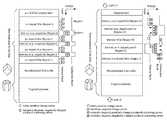
- FIG. 1is a schematic diagram that shows a Type-II bandgap alignment of Si and Ge;
- FIG. 2is a schematic diagram that shows rhombohedral SiGe/Ge high hole mobility layers for p-type TE material, transistor, and solar cell layer;
- FIG. 3is a schematic diagram that shows a rhombohedral SiGe/Si high electron mobility layers for n-type TE material, transistor, and solar cell layer;
- FIG. 4is a graph that shows an approximation of hole mobility vs. hole density of p-type Ge
- FIG. 5is a graph that shows an approximation of electron mobility vs. donor density of n-type Si
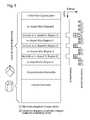
- FIG. 6is a schematic diagram that shows an enhanced solar cell structure-I with two high mobility transport layers made of electron quantum well and hole quantum well;
- FIG. 7is a schematic diagram that shows an enhanced solar cell structure-II with high mobility transport layers made of electron quantum well and hole quantum well;
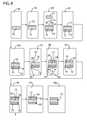
- FIG. 8is a flowchart showing fabrication of a device according to one embodiment of the present invention.
- carrier mobilityaffects performance of many electronic devices such as transistors, solar cells, thermo-electric (TE) devices and the like.
- the performance of such devicescan be improved if carrier mobility is increased.
- Prior calculationsshow that Si and Ge have type-II bandgap alignment in cubically strained and relaxed layers.
- the rhombohedral epitaxy technology described in the above-identified patentsprovides for alignment of (111)-oriented cubic Si/Ge/SiGe crystals on (0001) C-plane of trigonal substrates with hexagonal-triangular three-fold interface.
- This epitaxial technologyenables utilization of thousands of trigonal crystals as a substrate for SiGe alloy structures.
- the present disclosurerelates to fabrication of more complex high mobility layer structures for rhombohedrally aligned SiGe on a trigonal substrate.
- group IV semiconductors and alloysmay be rhombohedrally aligned on a trigonal substrate.
- Si, Ge, C, SiC, GeC, and SiGeCcan also be utilized to form a rhombohedrally aligned buffer layer or a trigonal substrate.
- the trigonal substratecan comprise Sapphire, Lithium Niobate (LiNbO 3 ), Langasite, Langatate, Antimony, Calcite, or other suitable material.
- FIG. 1shows the type-II bandgap alignment of Si and Ge such that Si has a lower conduction band energy and a lower valence band energy than Ge.
- the bandgap of Siis 1.1 eV and that of Ge is 0.67 eV at room temperature.
- Detailed numerical values of band alignments of cubically strained and relaxed Si/Ge/Si/Geare known in the art.
- an additional correction termis required because the strain direction of the rhombohedrally aligned SiGe is not the same as that of cubically strained and relaxed Si/Ge/SiGe. Therefore, a new calculation of band alignment is needed for strain effects on [111] direction which are perpendicular to ⁇ 2-20> in-plane directions.
- a Si layeris disposed between two Ge layers.
- the Si layerhas a slower conduction band that forms a quantum well for electrons. In other words, electrons in the conduction band drift into the Si layer to “find” a lower energy state.
- a Ge layer between two Si layershas a higher valence band top energy level such that it forms a quantum well for holes (i.e. it attracts holes in the valence band). This principle concept is utilized in the high mobility transport layer structures in FIGS. 2 and 3 according to one embodiment.
- SiGe and Ge layersare grown with rhombohedral alignment on trigonal substrate.
- An optional rhombohedral Site buffer layercan be formed on a trigonal substrate.
- the trigonal substratecan comprise Sapphire or other suitable material.
- the circles with vertical lines in themrepresent ionized p-dopants, or negatively charged Coulomb scattering centers.
- Region-Iis a highly doped p-type SiGe (p+doped SiGe) and Region-II is intrinsic or low-density doped p-type pure Ge layer (no Si), Region-II has a higher valence band top energy level so that it forms a quantum well for holes, Region-I has high density of p-type dopants and numerous holes generated from p-type dopants, Once p-type dopants in Region-I are ionized to release holes into the valence band, ionized dopants form a negatively charged Coulomb scattering center. Thus, the hole-mobility of Region-I is very low.
- Region-IIreceives a high density of holes from Region-I, yet it has few scattering centers because Region-II is intrinsic or very low doped p-type layer, Therefore Region-II has very high hole mobility with high density of holes which came from. Region-I.
- Region-IIfunctions as an ultra fast super-highway of holes (i.e. a high mobility transport region).
- Region-ISi or SiGe
- Region-IIpure Ge
- FIG. 4shows the enhancement of mobility from 200 cm2/V ⁇ s at 10 19 /cm 3 doping density to 2000 cm2/V ⁇ s at 10 16 /cm 3 doping density. Therefore 10 times faster mobility is achieved with high mobility hole transport layer in FIG. 2 .
- FIG. 3shows a similar high mobility transport layer for electrons comprising a heavily doped n+SiGe layer (Region-I) and an intrinsic or low n-type doped pure Si (no Ge) layer (Region-II),
- the circles with vertical lines in themrepresent ionized p-dopants, or negatively charged Coulomb scattering centers.
- the open dots/circlesrepresent holes or positive charge carriers.
- Intrinsic or low n-doped Si layer (Region-II)has a lower conduction band than that of SiGe or Ge in Region-I, so that Region-II forms a quantum well for electrons.
- Region-IIintrinsic or low n-doped Si
- Region-Ican be doped with n-type dopants such as Phosphorous of 10 19 /cm 3 concentration, and Region-II (pure Si) may be low density n-type doped at 10 16 /cm 3 concentration.
- FIG. 5shows the enhancement of electron mobility from 120 cm 2 /V ⁇ s at 10 19 /cm 3 doping density to 1200 cm 2 /Vs at 10 16 /cm 3 doping density. Therefore 10 times faster mobility is achieved with the high mobility electron transport layer in FIG. 3 .
- the ultra fast Region IIis pure Ge (no Si) and pure Si (no Ge) in FIGS. 2 and 3 , respectively.
- the fast transport layersdo not have an alloy scattering effect and also maintain high mobility of intrinsic or very low doped semiconductors. Repetition of Region-I and Region-II in a device or structure generates a plurality of high mobility transport layers making high current flow possible.
- An optional Rhombohedral SiGe buffer layercan be utilized to improve the single crystalline quality of Region-I and Region-II.
- An optional capping layercan be utilized to reduce surface charge loss effect.
- the high mobility transport layer structures in FIGS. 2 and 3can be used for many electronic device applications. For example, if the left side is hot (above 500° C.) and right side is cold (300° C.) this structure can be used as a p-type TE material structure ( FIG. 2 structure) and a n-type TE material structure ( FIG. 3 structure). Compared to conventional TE devices, this arrangement provides higher current output and better figure of merit (thermoelectric ZT factor) due to the increased charge-carrier mobilities. Similar structures with one or more multiples of Region-I and Region-II layers under gate voltage can be used for transistors. Also, the structures of FIG. 2 or 3 can be utilized in solar cells. Such solar cells have higher efficiency due to the enhanced charge transport mechanism of the high mobility transport layers.
- enhanced solar cell structurescan be fabricated by integrating electron quantum well of pure Si layer and hole quantum well of pure Ge layer together.
- Region-Iis intrinsic or moderately n-type doped SiGe which generates free electrons upon light injection and Region-II is intrinsic or low n-type doped pure Si layer as an electron quantum well (QW) for high mobility transport layer.
- Region-IIIis an optional intrinsic SiGe layer that separates two high mobility electron-transport layers, electron quantum well and hole quantum well. Region-III also generates and provides electrons and holes into Region-II (electron QW) and Region-IV (hole QW) upon light injection.
- Region IVis made with intrinsic or low p-type doped pure Ge (no Si) layer as hole QW for high mobility hole-transport layer.
- Region-Vis intrinsic or moderately p-type doped SiGe layer that generates and provides mobile holes into Region-IV (hole QW).
- An optional capping layerreduces charge carrier loss into the semiconductor surface and an optional rhombohedral SiGe buffer layer improves single crystalline quality of Region-I to Region-V.
- the light injectioncan be from above the surface “Light(1)” or form backside through transparent trigonal substrate “Light(2).” Many trigonal substrates such as Sapphire are transparent in the solar spectrum. Therefore, backside illumination can be made through transparent trigonal substrate.
- FIG. 7shows another similar structure as that of FIG. 6 .
- the enhanced solar cell structures in FIGS. 6 and 7can be applied to not only rhombohedral Si/Ge/SiGe structures on trigonal substrates, but also conventional cubic Si/Ge/SiGe structures on square (100) planes of cubic substrates.
- the high mobility electron and hole transport layersare separately connected to ( ⁇ ) and (+) metal electrodes by ohmic contact and deliver more photo-voltaic current than conventional solar cells.
- a process of fabricating a multi-layer hybrid structure 30includes providing a C-plane Sapphire wafer 15 at step 50 .
- Processes for fabricating C-plane Sapphire wafersare known, such that step 50 will not be described in detail.
- An optional heat absorption layer 52such as Carbon (C) or Titanium (Ti) can be deposited on one side of the Sapphire wafer 15 at step 55 utilizing a suitable known process.
- a substrate heater 54is utilized to apply IR heat 53 to raise the temperature of the Sapphire layer 15 to the optimum growth temperature for rhombohedrally aligned Si/SiGe on C-plane Sapphire.
- the optional heat absorbing layer 52absorbs more IR heat 53 and assists in maintaining a uniform high substrate temperature. It will be understood that other heating methods and processes can also be utilized.
- Si/SiGe layers 10are grown on the back side of the Sapphire wafer 15 utilizing a known epitaxial growth method. Examples of such processes include sputtering, MBD, MOCVD, PVE, HVPE, e-Beam deposit, LPE, LPCD, etc.
- Optional Si/SiGe device pre-fabrication processessuch as chemical-mechanical polishing (CMP), dopant drive-in, ion-implantation, and other such processes can optionally be performed at step 65 .
- CMPchemical-mechanical polishing
- Deposition or growth of a protection layer 72is performed at step 70 . Layer 72 protects the Si/SiGe layer 10 during formation of the III-Nitride structures.
- step 75the optional heat absorbing layer 52 is removed (if necessary) utilizing a suitable known etching process such as wet etching, dry etching, plasma etching, reactive, on etching, or the like to form an exposed Sapphire surface 76 .
- a suitable known etching processsuch as wet etching, dry etching, plasma etching, reactive, on etching, or the like.
- heat 82is applied and III-Nitride layers 20 such as GaN, AIN, AIGan, and InN are grown on the exposed surface 76 of front side 18 of C-plane Sapphire (opposite side from Si/SiGe layers).
- III-Nitride processesare known in the art, and this step in the process will not therefore be described in detail.
- Known III-Nitride pre-device fabrication processessuch as chemical-mechanical polishing (CMP), dopant ion-implantation, and etc. can be performed in step 85 .
- CMPchemical-mechanical polishing
- a second protection layer 92(such as silicon oxide or silicon nitride) is deposited or grown utilizing known processes. Second protection layer 92 protects the III-Nitride layers 20 .
- the hybrid wafer 30 with Si/SiGe layers 10 and III-Nitride layers 20can be used as a wafer product.
- steps 65 and 85are optional, and may or may not be included in a hybrid wafer product according to the present invention.
- the hybrid wafer productcan be further processed by removing and depositing each protection layer at a time and performing further post-wafer device fabrications as steps 95 and 100 in order make full hybrid circuit with Si/SiGe 10 on one side and III-Nitride 20 on the other side.
- a double sided hybrid wafer product 30can be commercialized after stop 90 and full hybrid devices/products can be commercialized after step 100 . It will be understood that it is possible to exchange the order of growth and device fabrication sequences of Si/SiGe and III-Nitrides such that III-Nitrides are grown first and Si/SiGe layers are grown later.
- the double sided hybrid crystal growth technology described abovealso applies to Si(Ge)/Sapphire/ZnO hybrid structure as well since ZnO has the same Wurtzite crystal structure as III-Nitride on C-plane Sapphire.
- SiGeC alloyin addition to SiGe alloy on C-plane sapphire.
- Si, Ge, and Care group IV semiconductor materials that can readily build the rhombohedral double side structure with GaN in a substantially similar epitaxy.
Landscapes
- Engineering & Computer Science (AREA)
- Microelectronics & Electronic Packaging (AREA)
- Physics & Mathematics (AREA)
- Condensed Matter Physics & Semiconductors (AREA)
- General Physics & Mathematics (AREA)
- Manufacturing & Machinery (AREA)
- Computer Hardware Design (AREA)
- Power Engineering (AREA)
- Chemical & Material Sciences (AREA)
- Crystallography & Structural Chemistry (AREA)
- Inorganic Chemistry (AREA)
- Materials Engineering (AREA)
- Recrystallisation Techniques (AREA)
Abstract
Description
Claims (4)
Priority Applications (2)
| Application Number | Priority Date | Filing Date | Title |
|---|---|---|---|
| US14/202,699US9614026B2 (en) | 2013-03-13 | 2014-03-10 | High mobility transport layer structures for rhombohedral Si/Ge/SiGe devices |
| US15/449,449US10256305B2 (en) | 2013-03-13 | 2017-03-03 | High mobility transport layer structures for rhombohedral Si/Ge/SiGe devices |
Applications Claiming Priority (2)
| Application Number | Priority Date | Filing Date | Title |
|---|---|---|---|
| US201361779317P | 2013-03-13 | 2013-03-13 | |
| US14/202,699US9614026B2 (en) | 2013-03-13 | 2014-03-10 | High mobility transport layer structures for rhombohedral Si/Ge/SiGe devices |
Related Child Applications (1)
| Application Number | Title | Priority Date | Filing Date |
|---|---|---|---|
| US15/449,449DivisionUS10256305B2 (en) | 2013-03-13 | 2017-03-03 | High mobility transport layer structures for rhombohedral Si/Ge/SiGe devices |
Publications (2)
| Publication Number | Publication Date |
|---|---|
| US20140264459A1 US20140264459A1 (en) | 2014-09-18 |
| US9614026B2true US9614026B2 (en) | 2017-04-04 |
Family
ID=51523646
Family Applications (2)
| Application Number | Title | Priority Date | Filing Date |
|---|---|---|---|
| US14/202,699ActiveUS9614026B2 (en) | 2013-03-13 | 2014-03-10 | High mobility transport layer structures for rhombohedral Si/Ge/SiGe devices |
| US15/449,449ActiveUS10256305B2 (en) | 2013-03-13 | 2017-03-03 | High mobility transport layer structures for rhombohedral Si/Ge/SiGe devices |
Family Applications After (1)
| Application Number | Title | Priority Date | Filing Date |
|---|---|---|---|
| US15/449,449ActiveUS10256305B2 (en) | 2013-03-13 | 2017-03-03 | High mobility transport layer structures for rhombohedral Si/Ge/SiGe devices |
Country Status (1)
| Country | Link |
|---|---|
| US (2) | US9614026B2 (en) |
Families Citing this family (12)
| Publication number | Priority date | Publication date | Assignee | Title |
|---|---|---|---|---|
| US8119904B2 (en)* | 2009-07-31 | 2012-02-21 | International Business Machines Corporation | Silicon wafer based structure for heterostructure solar cells |
| CN105336587B (en)* | 2014-06-17 | 2018-05-15 | 中芯国际集成电路制造(北京)有限公司 | Semiconductor devices and its manufacture method |
| KR20170077241A (en)* | 2014-11-13 | 2017-07-05 | 아티룩스 인코포레이티드 | Light absorption apparatus |
| JP6507985B2 (en)* | 2015-10-13 | 2019-05-08 | 富士通株式会社 | Thermoelectric conversion element and method of manufacturing the same |
| US10858754B2 (en)* | 2015-11-25 | 2020-12-08 | United States Of America As Represented By The Administrator Of Nasa | Rhombohedron epitaxial growth with molten target sputtering |
| WO2017100481A1 (en) | 2015-12-08 | 2017-06-15 | University Of Houston System | High mobility silicon on flexible substrates |
| US10651034B2 (en) | 2016-03-30 | 2020-05-12 | U.S.A. As Represented By The Administrator Of The National Aeronautics And Space Administration | Thermal absorption coating on sapphire for epitaxial process |
| US10797193B2 (en)* | 2018-01-23 | 2020-10-06 | Lumentum Operations Llc | Bias control structure for avalanche photodiodes |
| WO2020171699A1 (en)* | 2019-02-18 | 2020-08-27 | Technische Universiteit Eindhoven | Light-emitting or light-absorbing component |
| UA120025C2 (en)* | 2019-03-26 | 2019-09-10 | Андрій Дмитрович Хворостяний | SEMICONDUCTOR THERMOELECTRIC GENERATOR |
| KR20220113458A (en)* | 2019-12-09 | 2022-08-12 | 엔테그리스, 아이엔씨. | Diffusion barriers made of multiple barrier materials, and related articles and methods |
| CN112382657B (en)* | 2020-11-16 | 2022-03-18 | 中国科学院物理研究所 | Patterned silicon substrate-silicon germanium thin film composite structure and its preparation method and application |
Citations (41)
| Publication number | Priority date | Publication date | Assignee | Title |
|---|---|---|---|---|
| US4357183A (en) | 1980-08-13 | 1982-11-02 | Massachusetts Institute Of Technology | Heteroepitaxy of germanium silicon on silicon utilizing alloying control |
| US5205871A (en) | 1990-06-01 | 1993-04-27 | The United States Of America As Represented By The Secretary Of The Navy | Monocrystalline germanium film on sapphire |
| US5347157A (en) | 1992-12-17 | 1994-09-13 | Eastman Kodak Company | Multilayer structure having a (111)-oriented buffer layer |
| US5394826A (en) | 1992-01-31 | 1995-03-07 | Fujitsu Limited | Method of (111) group II-VI epitaxial layer grown on (111) silicon substrate |
| US5667586A (en) | 1995-01-30 | 1997-09-16 | International Business Machines Corporation | Method for forming a single crystal semiconductor on a substrate |
| US5709745A (en) | 1993-01-25 | 1998-01-20 | Ohio Aerospace Institute | Compound semi-conductors and controlled doping thereof |
| US5759898A (en) | 1993-10-29 | 1998-06-02 | International Business Machines Corporation | Production of substrate for tensilely strained semiconductor |
| US5769964A (en) | 1996-08-29 | 1998-06-23 | The United States Of America As Reprresented By The United States Department Of Energy | Bulk single crystal ternary substrates for a thermophotovoltaic energy conversion system |
| US5951757A (en) | 1997-05-06 | 1999-09-14 | The United States Of America As Represented By The Secretary Of The Navy | Method for making silicon germanium alloy and electric device structures |
| US6096389A (en) | 1995-09-14 | 2000-08-01 | Canon Kabushiki Kaisha | Method and apparatus for forming a deposited film using a microwave CVD process |
| US6100546A (en) | 1994-04-07 | 2000-08-08 | Sdl, Inc. | III-V arsenide-nitride semiconductor |
| US6306211B1 (en) | 1999-03-23 | 2001-10-23 | Matsushita Electric Industrial Co., Ltd. | Method for growing semiconductor film and method for fabricating semiconductor device |
| US20020172820A1 (en)* | 2001-03-30 | 2002-11-21 | The Regents Of The University Of California | Methods of fabricating nanostructures and nanowires and devices fabricated therefrom |
| US6488771B1 (en) | 2001-09-25 | 2002-12-03 | The United States Of America As Represented By The Administrator Of The National Aeronautics And Space Administration | Method for growing low-defect single crystal heteroepitaxial films |
| US6524935B1 (en) | 2000-09-29 | 2003-02-25 | International Business Machines Corporation | Preparation of strained Si/SiGe on insulator by hydrogen induced layer transfer technique |
| US6562127B1 (en) | 2002-01-16 | 2003-05-13 | The United States Of America As Represented By The Secretary Of The Navy | Method of making mosaic array of thin semiconductor material of large substrates |
| US6627809B1 (en) | 1999-11-10 | 2003-09-30 | Massachusetts Institute Of Technology | Superlattice structures having selected carrier pockets and related methods |
| US20030209191A1 (en) | 2002-05-13 | 2003-11-13 | Purdy Andrew P. | Ammonothermal process for bulk synthesis and growth of cubic GaN |
| US6653658B2 (en) | 2001-07-05 | 2003-11-25 | Isonics Corporation | Semiconductor wafers with integrated heat spreading layer |
| US20040147079A1 (en) | 2002-06-10 | 2004-07-29 | Leonard Forbes | Output prediction logic circuits with ultra-thin vertical transistors and methods of formation |
| US6784074B2 (en) | 2001-05-09 | 2004-08-31 | Nsc-Nanosemiconductor Gmbh | Defect-free semiconductor templates for epitaxial growth and method of making same |
| US6787793B2 (en) | 2001-12-11 | 2004-09-07 | Sharp Kabushiki Kaisha | Strained Si device with first SiGe layer with higher Ge concentration being relaxed to have substantially same lattice constant as second SiGe layer with lower Ge concentration |
| US20040173790A1 (en) | 2003-03-05 | 2004-09-09 | Yee-Chia Yeo | Method of forming strained silicon on insulator substrate |
| US20040190681A1 (en) | 2003-03-26 | 2004-09-30 | Rigaku Corporaton | X-ray diffraction apparatus |
| US20040201022A1 (en) | 2000-06-19 | 2004-10-14 | Semiconductor Energy Laboratory Co., Ltd. | Semiconductor device |
| US20040214407A1 (en) | 2003-01-27 | 2004-10-28 | Amberwave Systems Corporation | Semiconductor structures with structural homogeneity |
| US20040221792A1 (en) | 2003-05-07 | 2004-11-11 | Micron Technology, Inc. | Strained Si/SiGe structures by ion implantation |
| US20060163612A1 (en) | 2003-06-13 | 2006-07-27 | Arizona Board Of Regents | Sixsnyge1-x-y and related alloy heterostructures based on si, ge and sn |
| US20060211221A1 (en) | 2003-04-22 | 2006-09-21 | Siegfried Mantl | Method for producing a strained layer on a substrate and corresponding layer structure |
| US20060270200A1 (en) | 2003-10-17 | 2006-11-30 | Hitachi Cable, Ltd. | III group nitride semiconductor substrate, substrate for group III nitride semiconductor device, and fabrication methods thereof |
| US20070168130A1 (en) | 2005-03-31 | 2007-07-19 | The Council Of Scientific And Industrial Research | Method for computing crystal shapes from X-ray diffraction data (XRD) of a substance |
| US7247885B2 (en) | 2005-05-26 | 2007-07-24 | Avago Technologies General Ip (Singapore) Ltd. Pte. | Carrier confinement in light-emitting group IV semiconductor devices |
| US20070222034A1 (en)* | 2006-03-21 | 2007-09-27 | U.S.A As Represented By The Administrator Of The National Aeronautics & Space Administration | Graded index silicon geranium on lattice matched silicon geranium semiconductor alloy |
| US7341883B2 (en) | 2005-09-27 | 2008-03-11 | The United States Of America As Represented By The Administrator Of The National Aeronautics And Space Administration | Silicon germanium semiconductive alloy and method of fabricating same |
| US7368335B2 (en) | 2000-08-02 | 2008-05-06 | Semiconductor Energy Laboratory Co., Ltd. | Semiconductor device and method of manufacturing the same |
| US20080113186A1 (en) | 2004-09-14 | 2008-05-15 | John Kouvetakis | Method for Growing Si-Ge Semiconductor Materials and Devices on Substrates |
| US20080257395A1 (en) | 2001-12-12 | 2008-10-23 | Hi-Z Corporation | Miniature quantum well thermoelectric device |
| US20090103680A1 (en)* | 2007-10-18 | 2009-04-23 | U.S.A As Represented By The Administrator Of The National Aeronautics And Space Administration | Method Of Generating X-Ray Diffraction Data For Integral Detection Of Twin Defects In Super-Hetero-Epitaxial Materials |
| US20090206369A1 (en) | 2006-11-14 | 2009-08-20 | Northrop Grumman Space & Mission Systems Corp. | High electron mobility transistor semiconductor device and fabrication method thereof |
| US20140264325A1 (en)* | 2013-03-14 | 2014-09-18 | U.S.A. As Represented By The Administrator Of The National Aeronautics And Space Administration | Double Sided Sl(GE)/Sapphire/lll-Nitride Hybrid Structure |
| US20140339580A1 (en)* | 2013-05-16 | 2014-11-20 | U.S.A. As Represented By The Administrator Of The National Aeronautics And Space Administration | Integrated Multi-Color Light Emitting Device Made With Hybrid Crystal Structure |
Family Cites Families (1)
| Publication number | Priority date | Publication date | Assignee | Title |
|---|---|---|---|---|
| JPH0811718B2 (en)* | 1992-02-27 | 1996-02-07 | 大同ほくさん株式会社 | Gas source molecular beam epitaxy system |
- 2014
- 2014-03-10USUS14/202,699patent/US9614026B2/enactiveActive
- 2017
- 2017-03-03USUS15/449,449patent/US10256305B2/enactiveActive
Patent Citations (50)
| Publication number | Priority date | Publication date | Assignee | Title |
|---|---|---|---|---|
| US4357183A (en) | 1980-08-13 | 1982-11-02 | Massachusetts Institute Of Technology | Heteroepitaxy of germanium silicon on silicon utilizing alloying control |
| US5205871A (en) | 1990-06-01 | 1993-04-27 | The United States Of America As Represented By The Secretary Of The Navy | Monocrystalline germanium film on sapphire |
| US5394826A (en) | 1992-01-31 | 1995-03-07 | Fujitsu Limited | Method of (111) group II-VI epitaxial layer grown on (111) silicon substrate |
| US5347157A (en) | 1992-12-17 | 1994-09-13 | Eastman Kodak Company | Multilayer structure having a (111)-oriented buffer layer |
| US5709745A (en) | 1993-01-25 | 1998-01-20 | Ohio Aerospace Institute | Compound semi-conductors and controlled doping thereof |
| US5759898A (en) | 1993-10-29 | 1998-06-02 | International Business Machines Corporation | Production of substrate for tensilely strained semiconductor |
| US6100546A (en) | 1994-04-07 | 2000-08-08 | Sdl, Inc. | III-V arsenide-nitride semiconductor |
| US5667586A (en) | 1995-01-30 | 1997-09-16 | International Business Machines Corporation | Method for forming a single crystal semiconductor on a substrate |
| US6096389A (en) | 1995-09-14 | 2000-08-01 | Canon Kabushiki Kaisha | Method and apparatus for forming a deposited film using a microwave CVD process |
| US5769964A (en) | 1996-08-29 | 1998-06-23 | The United States Of America As Reprresented By The United States Department Of Energy | Bulk single crystal ternary substrates for a thermophotovoltaic energy conversion system |
| US5951757A (en) | 1997-05-06 | 1999-09-14 | The United States Of America As Represented By The Secretary Of The Navy | Method for making silicon germanium alloy and electric device structures |
| US6306211B1 (en) | 1999-03-23 | 2001-10-23 | Matsushita Electric Industrial Co., Ltd. | Method for growing semiconductor film and method for fabricating semiconductor device |
| US6627809B1 (en) | 1999-11-10 | 2003-09-30 | Massachusetts Institute Of Technology | Superlattice structures having selected carrier pockets and related methods |
| US20040201022A1 (en) | 2000-06-19 | 2004-10-14 | Semiconductor Energy Laboratory Co., Ltd. | Semiconductor device |
| US7368335B2 (en) | 2000-08-02 | 2008-05-06 | Semiconductor Energy Laboratory Co., Ltd. | Semiconductor device and method of manufacturing the same |
| US6524935B1 (en) | 2000-09-29 | 2003-02-25 | International Business Machines Corporation | Preparation of strained Si/SiGe on insulator by hydrogen induced layer transfer technique |
| US20020172820A1 (en)* | 2001-03-30 | 2002-11-21 | The Regents Of The University Of California | Methods of fabricating nanostructures and nanowires and devices fabricated therefrom |
| US6784074B2 (en) | 2001-05-09 | 2004-08-31 | Nsc-Nanosemiconductor Gmbh | Defect-free semiconductor templates for epitaxial growth and method of making same |
| US6653658B2 (en) | 2001-07-05 | 2003-11-25 | Isonics Corporation | Semiconductor wafers with integrated heat spreading layer |
| US6488771B1 (en) | 2001-09-25 | 2002-12-03 | The United States Of America As Represented By The Administrator Of The National Aeronautics And Space Administration | Method for growing low-defect single crystal heteroepitaxial films |
| US6787793B2 (en) | 2001-12-11 | 2004-09-07 | Sharp Kabushiki Kaisha | Strained Si device with first SiGe layer with higher Ge concentration being relaxed to have substantially same lattice constant as second SiGe layer with lower Ge concentration |
| US20080257395A1 (en) | 2001-12-12 | 2008-10-23 | Hi-Z Corporation | Miniature quantum well thermoelectric device |
| US6562127B1 (en) | 2002-01-16 | 2003-05-13 | The United States Of America As Represented By The Secretary Of The Navy | Method of making mosaic array of thin semiconductor material of large substrates |
| US20030209191A1 (en) | 2002-05-13 | 2003-11-13 | Purdy Andrew P. | Ammonothermal process for bulk synthesis and growth of cubic GaN |
| US20040147079A1 (en) | 2002-06-10 | 2004-07-29 | Leonard Forbes | Output prediction logic circuits with ultra-thin vertical transistors and methods of formation |
| US20040214407A1 (en) | 2003-01-27 | 2004-10-28 | Amberwave Systems Corporation | Semiconductor structures with structural homogeneity |
| US20040173790A1 (en) | 2003-03-05 | 2004-09-09 | Yee-Chia Yeo | Method of forming strained silicon on insulator substrate |
| US20040190681A1 (en) | 2003-03-26 | 2004-09-30 | Rigaku Corporaton | X-ray diffraction apparatus |
| US20060211221A1 (en) | 2003-04-22 | 2006-09-21 | Siegfried Mantl | Method for producing a strained layer on a substrate and corresponding layer structure |
| US20040221792A1 (en) | 2003-05-07 | 2004-11-11 | Micron Technology, Inc. | Strained Si/SiGe structures by ion implantation |
| US20060163612A1 (en) | 2003-06-13 | 2006-07-27 | Arizona Board Of Regents | Sixsnyge1-x-y and related alloy heterostructures based on si, ge and sn |
| US20060270200A1 (en) | 2003-10-17 | 2006-11-30 | Hitachi Cable, Ltd. | III group nitride semiconductor substrate, substrate for group III nitride semiconductor device, and fabrication methods thereof |
| US20080113186A1 (en) | 2004-09-14 | 2008-05-15 | John Kouvetakis | Method for Growing Si-Ge Semiconductor Materials and Devices on Substrates |
| US20070168130A1 (en) | 2005-03-31 | 2007-07-19 | The Council Of Scientific And Industrial Research | Method for computing crystal shapes from X-ray diffraction data (XRD) of a substance |
| US7247885B2 (en) | 2005-05-26 | 2007-07-24 | Avago Technologies General Ip (Singapore) Ltd. Pte. | Carrier confinement in light-emitting group IV semiconductor devices |
| US7341883B2 (en) | 2005-09-27 | 2008-03-11 | The United States Of America As Represented By The Administrator Of The National Aeronautics And Space Administration | Silicon germanium semiconductive alloy and method of fabricating same |
| US20070222034A1 (en)* | 2006-03-21 | 2007-09-27 | U.S.A As Represented By The Administrator Of The National Aeronautics & Space Administration | Graded index silicon geranium on lattice matched silicon geranium semiconductor alloy |
| US20090206369A1 (en) | 2006-11-14 | 2009-08-20 | Northrop Grumman Space & Mission Systems Corp. | High electron mobility transistor semiconductor device and fabrication method thereof |
| US20090165837A1 (en) | 2007-10-18 | 2009-07-02 | United States of America as represented by the Administrator of the National Aeronautics and | Thermoelectric Materials and Devices |
| US7558371B2 (en)* | 2007-10-18 | 2009-07-07 | The United States Of America As Represented By The Administrator Of The National Aeronautics And Space Administration | Method of generating X-ray diffraction data for integral detection of twin defects in super-hetero-epitaxial materials |
| US20090103680A1 (en)* | 2007-10-18 | 2009-04-23 | U.S.A As Represented By The Administrator Of The National Aeronautics And Space Administration | Method Of Generating X-Ray Diffraction Data For Integral Detection Of Twin Defects In Super-Hetero-Epitaxial Materials |
| US20090206368A1 (en) | 2007-10-18 | 2009-08-20 | U.S.A As Represented By The Administrator Of The National Aeronautics And Space Administration | Rhombohedral cubic semiconductor materials on trigonal substrate with single crystal properties and devices based on such materials |
| US20090220047A1 (en) | 2007-10-18 | 2009-09-03 | The United States Of America As Represented By The Administrator Of The National Aeronautics | Hybrid Bandgap Engineering For Super-Hetero-Epitaxial Semiconductor Materials, and Products Thereof |
| US7769135B2 (en) | 2007-10-18 | 2010-08-03 | The United States Of America As Represented By The Administrator Of The National Aeronautics And Space Administration | X-ray diffraction wafer mapping method for rhombohedral super-hetero-epitaxy |
| US7906358B2 (en) | 2007-10-18 | 2011-03-15 | The United States Of America As Represented By The Administrator Of The National Aeronautics And Space Administration | Epitaxial growth of cubic crystalline semiconductor alloys on basal plane of trigonal or hexagonal crystal |
| US8044294B2 (en) | 2007-10-18 | 2011-10-25 | The United States Of America As Represented By The Administrator Of The National Aeronautics And Space Administration | Thermoelectric materials and devices |
| US8226767B2 (en) | 2007-10-18 | 2012-07-24 | The United States Of America As Represented By The Administrator Of The National Aeronautics And Space Administration | Hybrid bandgap engineering for super-hetero-epitaxial semiconductor materials, and products thereof |
| US8257491B2 (en) | 2007-10-18 | 2012-09-04 | The United States Of America, As Represented By The Administrator Of The National Aeronautics And Space Administration | Rhombohedral cubic semiconductor materials on trigonal substrate with single crystal properties and devices based on such materials |
| US20140264325A1 (en)* | 2013-03-14 | 2014-09-18 | U.S.A. As Represented By The Administrator Of The National Aeronautics And Space Administration | Double Sided Sl(GE)/Sapphire/lll-Nitride Hybrid Structure |
| US20140339580A1 (en)* | 2013-05-16 | 2014-11-20 | U.S.A. As Represented By The Administrator Of The National Aeronautics And Space Administration | Integrated Multi-Color Light Emitting Device Made With Hybrid Crystal Structure |
Non-Patent Citations (19)
| Title |
|---|
| B. Sanorpim S et al., "Chartcterization of MOVPE-grown GaN layers on GaAs (111)B with a cubic-GaN(111) epitaxial intermediate layer," Physical Status Solidi, Nov. 2003, pp. 305-309, vol. 240, No. 2. |
| C. Jacoboni, et al., "A Review of Some Charge Transport Properties of Silicon," Solid-State Electronics, 1977, vol. 20, pp. 77-89, Pergamon Press. |
| Chris G. Van De Walle et al., "Theoretical calculations of heterojunction discontinuities in the Si/Ge system," Physical Review B, Oct. 1986, pp. 5621-5634, vol. 34, No. 8. |
| H. Wado, et al., "Expitaxial growth of SiGe on A1203 using Si2H6 gas and Ge solid source molecular beam epitaxy," Journal of Crystal Growth, vol. 169, pp. 457-62. (1996). |
| Hiroyuki Wado, et al., "Epitaxal growth of SiGe on A1203 using Si2H6 gas and Ge solid source molecular beam epitaxy," Journal of Crystal Growth, 1996, pp. 457-462, vol. 169. |
| I. Lagnado, et al., "Integration of Si and SiGe with A1203 (sapphire)," Microelectronic Engineering, 2001, pp. 445-459, vol. 59. |
| Martin M. Rieger, et al, "Electronic-band parameters in strained Si1-xGex alloys on Si1-yGey substrates," Phys. Rev. B 1993, pp. 14276-14287, vol. 49, No. 19. |
| Max V. Fischetti, et al,, "Band structure, deformation potentials, and carrier mobility in strained Si, Ge, and SiGe alloys," Journal of Applied Physics, Aug. 1996, pp. 2234-2252, vol. 80, No. 4. |
| Nakamura, T. Mukai T et al., "High-Power GaN P-N. Junction Blue-Light-Emitting Diodes," Japanese Journal of Applied Physics, Dec. 1991, pp. L1998-L2001, vol. 30, No. 12A. |
| O. Ambacher, "Growth and Applications of Group III-nitrides," Journal of Physics, Applied Physics, 1998, pp. 2653-2710, vol. 31. |
| P.M. Mooney et al., "X-ray diffraction analysis of SiGe/Si heterostructures on sapphire substrates,"Applied Physics Letters, Jun. 1998, pp. 924-926, vol. 73, No. 7. |
| Suraj J. Mathew, et al., "Hole Confinement and Low-Frequency Noise in SiGe pFET's on Silicon-on-Sapphire," IEEE Electron Device Letters, Apr. 1999, pp. 173-175, vol. 20, No. 4. |
| Suraj J. Mathew. et al., "Effect of GE Profile on the Frequency Response of a SiGe pFET on Sapphire Technology," Device Research Conference Digest, Jun. 23-25, 1997, pp. 130-131, Fort Collins, Colorado. |
| T.P. Humphreys et al. "Heteroepitaxial growth and characterization of GaAs on silicon-on sapphire and sapphire substrates," Appl. Phys. Lett. Apr. 1989, pp, 1887-1669, vol. 54, No. 17. |
| W.B. Dubbelday, et al., "The growth of SiGe on sapphire using rapid thermal chemical vapor deposition," Journal of Crystal Growth, 2001, pp. 20-28, vol. 222. |
| Y. Park, G.C. King, S. H. Choi, "Rhombohedral Epitaxy of Cubic SiGe on Trigorial c-plane sapphire," Journal of Crystal Growth, 2008, pp. 2724-2731, No. 310. |
| Yan Zhang, et al., "Measurement of Seebeck coefficient perpendicular to SiGe superlattice", Twenty-First International Conference on Thermolelectrics, Aug. 25-29, 2002, pp. 329-332, Long Beach, California. |
| Yeonjoon Park et al., "Analysis of Twin Defects in GaAs(111)B Moelcuiar Beam Epitaxy Growth," Journal of Vacuum Science and Technology B, May-Jun. 2000, pp. 1586-1571, vol. 18, No. 3. |
| Z. Liliental-Weber et al., "Electron Microscopy Characterization of GaN Films Grown by Molecular-beam Epitaxy on Sapphire and SiC," Journal of Vacuum Science and Technology B, Jul.-Aug. 1995, pp. 1578-1581, vol. 13 No. 4. |
Also Published As
| Publication number | Publication date |
|---|---|
| US20170179233A1 (en) | 2017-06-22 |
| US20140264459A1 (en) | 2014-09-18 |
| US10256305B2 (en) | 2019-04-09 |
Similar Documents
| Publication | Publication Date | Title |
|---|---|---|
| US10256305B2 (en) | High mobility transport layer structures for rhombohedral Si/Ge/SiGe devices | |
| CN101981699B (en) | Semiconductor-based large-area flexible electronics | |
| US8987736B2 (en) | [100] or [110] aligned, semiconductor-based, large-area, flexible, electronic devices | |
| US8178221B2 (en) | {100}<100> or 45°-rotated {100}<100>, semiconductor-based, large-area, flexible, electronic devices | |
| US7906229B2 (en) | Semiconductor-based, large-area, flexible, electronic devices | |
| CN101981685B (en) | [100] or [110] arrayed semiconductor-based large-area flexible electronic devices | |
| EP2266135B1 (en) | Semiconductor-based, large-area, flexible, electronic devices on {110}<100>oriented substrates | |
| CN104576807A (en) | Semiconductor device | |
| US9824885B2 (en) | Method of fabricating double sided Si(Ge)/Sapphire/III-nitride hybrid structure | |
| CN101807520A (en) | Method for realizing p-type metal polar large energy gap semiconductor by using polarized induction positive hole | |
| Su et al. | Single-crystal CdTe homojunction structures for solar cell applications | |
| EP3238229A1 (en) | A method of epitaxial growth of a material interface between group iii-v materials and silicon wafers providing counterbalancing of residual strains | |
| Tetyorkin et al. | Infrared photodiodes on II-VI and III-V narrow gap semiconductors | |
| JP4431290B2 (en) | Semiconductor element and semiconductor layer | |
| Besikci | III-V infrared detectors on Si substrates | |
| Lyle | Research and Development of Electrical Contacts to β-Ga2O3 for Power Electronics and UV Photodetectors | |
| JP6004429B2 (en) | Method for producing single-crystal SiGe layer and solar cell using the same | |
| Hossain et al. | Design of high efficient InN quantum dot based solar cell | |
| HK1151387A (en) | Semiconductor-based, large-area, flexible, electronic devices on {110}<100> oriented substrates | |
| HK1150093B (en) | Semiconductor-based large-area flexible electronic devices | |
| HK1148112B (en) | Semiconductor-based, large-area, flexible, electronic devices on {110 }<100>oriented substrates | |
| HK1150095B (en) | [100] or [110] aligned, semiconductor-based, large-area, flexible, electronic devices |
Legal Events
| Date | Code | Title | Description |
|---|---|---|---|
| AS | Assignment | Owner name:UNITED STATES OF AMERICA AS REPRESENTED BY THE ADM Free format text:ASSIGNMENT OF ASSIGNORS INTEREST;ASSIGNORS:CHOI, SANG HYOUK;KING, GLEN C.;REEL/FRAME:035837/0001 Effective date:20140321 | |
| AS | Assignment | Owner name:UNITED STATES DEPARTMENT OF TRANSPORTATION AS REPR Free format text:ASSIGNMENT OF ASSIGNORS INTEREST;ASSIGNOR:LEE, KUNIK;REEL/FRAME:038390/0268 Effective date:20160425 | |
| AS | Assignment | Owner name:UNITED STATES OF AMERICA AS REPRESENTED BY THE ADM Free format text:ASSIGNMENT OF ASSIGNORS INTEREST;ASSIGNOR:NATIONAL INSTITUTE OF AEROSPACE ASSOCIATES;REEL/FRAME:040150/0552 Effective date:20140811 Owner name:UNITED STATES OF AMERICA AS REPRESENTED BY THE ADM Free format text:ASSIGNMENT OF ASSIGNORS INTEREST;ASSIGNOR:THE GEORGE WASHINGTON UNIVERSITY;REEL/FRAME:040150/0885 Effective date:20140915 | |
| STCF | Information on status: patent grant | Free format text:PATENTED CASE | |
| MAFP | Maintenance fee payment | Free format text:PAYMENT OF MAINTENANCE FEE, 4TH YEAR, LARGE ENTITY (ORIGINAL EVENT CODE: M1551); ENTITY STATUS OF PATENT OWNER: LARGE ENTITY Year of fee payment:4 | |
| MAFP | Maintenance fee payment | Free format text:PAYMENT OF MAINTENANCE FEE, 8TH YEAR, LARGE ENTITY (ORIGINAL EVENT CODE: M1552); ENTITY STATUS OF PATENT OWNER: LARGE ENTITY Year of fee payment:8 |