US9613825B2 - Photoresist strip processes for improved device integrity - Google Patents
Photoresist strip processes for improved device integrityDownload PDFInfo
- Publication number
- US9613825B2 US9613825B2US13/590,083US201213590083AUS9613825B2US 9613825 B2US9613825 B2US 9613825B2US 201213590083 AUS201213590083 AUS 201213590083AUS 9613825 B2US9613825 B2US 9613825B2
- Authority
- US
- United States
- Prior art keywords
- substrate
- photoresist
- hydrogen
- strip
- volumetric flow
- Prior art date
- Legal status (The legal status is an assumption and is not a legal conclusion. Google has not performed a legal analysis and makes no representation as to the accuracy of the status listed.)
- Active, expires
Links
- 238000000034methodMethods0.000titleclaimsabstractdescription154
- 230000008569processEffects0.000titleclaimsabstractdescription108
- 229920002120photoresistant polymerPolymers0.000titleclaimsabstractdescription96
- 239000000758substrateSubstances0.000claimsabstractdescription80
- 229910052739hydrogenInorganic materials0.000claimsabstractdescription71
- 239000001257hydrogenSubstances0.000claimsabstractdescription68
- UFHFLCQGNIYNRP-UHFFFAOYSA-NHydrogenChemical compound[H][H]UFHFLCQGNIYNRP-UHFFFAOYSA-N0.000claimsabstractdescription66
- 239000007943implantSubstances0.000claimsabstractdescription35
- XUIMIQQOPSSXEZ-UHFFFAOYSA-NSiliconChemical compound[Si]XUIMIQQOPSSXEZ-UHFFFAOYSA-N0.000claimsabstractdescription20
- 229910052710siliconInorganic materials0.000claimsabstractdescription20
- 239000010703siliconSubstances0.000claimsabstractdescription20
- 238000013022ventingMethods0.000claimsabstractdescription9
- 150000002431hydrogenChemical class0.000claimsabstractdescription7
- 239000007789gasSubstances0.000claimsdescription50
- IJGRMHOSHXDMSA-UHFFFAOYSA-NAtomic nitrogenChemical compoundN#NIJGRMHOSHXDMSA-UHFFFAOYSA-N0.000claimsdescription21
- 239000000203mixtureSubstances0.000claimsdescription10
- 238000006243chemical reactionMethods0.000claimsdescription7
- 229910021419crystalline siliconInorganic materials0.000claimsdescription4
- 230000007246mechanismEffects0.000claimsdescription3
- NJPPVKZQTLUDBO-UHFFFAOYSA-NnovaluronChemical compoundC1=C(Cl)C(OC(F)(F)C(OC(F)(F)F)F)=CC=C1NC(=O)NC(=O)C1=C(F)C=CC=C1FNJPPVKZQTLUDBO-UHFFFAOYSA-N0.000claimsdescription2
- 238000000059patterningMethods0.000claimsdescription2
- 229910001873dinitrogenInorganic materials0.000claims1
- 239000000463materialSubstances0.000abstractdescription19
- 210000002381plasmaAnatomy0.000description61
- 235000012431wafersNutrition0.000description43
- 150000002500ionsChemical class0.000description20
- 238000004519manufacturing processMethods0.000description16
- QVGXLLKOCUKJST-UHFFFAOYSA-Natomic oxygenChemical compound[O]QVGXLLKOCUKJST-UHFFFAOYSA-N0.000description15
- 229910052799carbonInorganic materials0.000description15
- 239000001301oxygenSubstances0.000description15
- 229910052760oxygenInorganic materials0.000description15
- OKTJSMMVPCPJKN-UHFFFAOYSA-NCarbonChemical compound[C]OKTJSMMVPCPJKN-UHFFFAOYSA-N0.000description14
- 239000004065semiconductorSubstances0.000description12
- 241000894007speciesSpecies0.000description12
- 150000001875compoundsChemical class0.000description11
- 238000012545processingMethods0.000description11
- 239000007800oxidant agentSubstances0.000description10
- YCKRFDGAMUMZLT-UHFFFAOYSA-NFluorine atomChemical compound[F]YCKRFDGAMUMZLT-UHFFFAOYSA-N0.000description9
- 239000011737fluorineSubstances0.000description9
- 229910052731fluorineInorganic materials0.000description9
- 238000005468ion implantationMethods0.000description9
- 230000001276controlling effectEffects0.000description8
- 239000002019doping agentSubstances0.000description8
- 229910052757nitrogenInorganic materials0.000description8
- 230000015572biosynthetic processEffects0.000description7
- MWUXSHHQAYIFBG-UHFFFAOYSA-Nnitrogen oxideInorganic materialsO=[N]MWUXSHHQAYIFBG-UHFFFAOYSA-N0.000description7
- 239000013078crystalSubstances0.000description6
- 230000007547defectEffects0.000description6
- CURLTUGMZLYLDI-UHFFFAOYSA-NCarbon dioxideChemical compoundO=C=OCURLTUGMZLYLDI-UHFFFAOYSA-N0.000description5
- 238000001514detection methodMethods0.000description5
- 238000002513implantationMethods0.000description5
- XKRFYHLGVUSROY-UHFFFAOYSA-NArgonChemical compound[Ar]XKRFYHLGVUSROY-UHFFFAOYSA-N0.000description4
- 238000001157Fourier transform infrared spectrumMethods0.000description4
- GQPLMRYTRLFLPF-UHFFFAOYSA-NNitrous OxideChemical compound[O-][N+]#NGQPLMRYTRLFLPF-UHFFFAOYSA-N0.000description4
- RAHZWNYVWXNFOC-UHFFFAOYSA-NSulphur dioxideChemical compoundO=S=ORAHZWNYVWXNFOC-UHFFFAOYSA-N0.000description4
- 125000004429atomChemical group0.000description4
- 238000010586diagramMethods0.000description4
- 230000006698inductionEffects0.000description4
- 239000002245particleSubstances0.000description4
- 238000011112process operationMethods0.000description4
- 239000000047productSubstances0.000description4
- ZOXJGFHDIHLPTG-UHFFFAOYSA-NBoronChemical compound[B]ZOXJGFHDIHLPTG-UHFFFAOYSA-N0.000description3
- UGFAIRIUMAVXCW-UHFFFAOYSA-NCarbon monoxideChemical class[O+]#[C-]UGFAIRIUMAVXCW-UHFFFAOYSA-N0.000description3
- XPDWGBQVDMORPB-UHFFFAOYSA-NFluoroformChemical compoundFC(F)FXPDWGBQVDMORPB-UHFFFAOYSA-N0.000description3
- 229910008314Si—H2Inorganic materials0.000description3
- 229910052786argonInorganic materials0.000description3
- 229910052785arsenicInorganic materials0.000description3
- RQNWIZPPADIBDY-UHFFFAOYSA-Narsenic atomChemical compound[As]RQNWIZPPADIBDY-UHFFFAOYSA-N0.000description3
- 229910052796boronInorganic materials0.000description3
- 229910002092carbon dioxideInorganic materials0.000description3
- 239000001569carbon dioxideSubstances0.000description3
- RWRIWBAIICGTTQ-UHFFFAOYSA-NdifluoromethaneChemical compoundFCFRWRIWBAIICGTTQ-UHFFFAOYSA-N0.000description3
- 238000005530etchingMethods0.000description3
- BHEPBYXIRTUNPN-UHFFFAOYSA-Nhydridophosphorus(.) (triplet)Chemical compound[PH]BHEPBYXIRTUNPN-UHFFFAOYSA-N0.000description3
- 125000004435hydrogen atomChemical group[H]*0.000description3
- 239000011261inert gasSubstances0.000description3
- 238000001459lithographyMethods0.000description3
- 229910052756noble gasInorganic materials0.000description3
- 230000005855radiationEffects0.000description3
- MGWGWNFMUOTEHG-UHFFFAOYSA-N4-(3,5-dimethylphenyl)-1,3-thiazol-2-amineChemical compoundCC1=CC(C)=CC(C=2N=C(N)SC=2)=C1MGWGWNFMUOTEHG-UHFFFAOYSA-N0.000description2
- 229910018503SF6Inorganic materials0.000description2
- 238000010521absorption reactionMethods0.000description2
- 229910052782aluminiumInorganic materials0.000description2
- XAGFODPZIPBFFR-UHFFFAOYSA-NaluminiumChemical compound[Al]XAGFODPZIPBFFR-UHFFFAOYSA-N0.000description2
- 238000004458analytical methodMethods0.000description2
- 230000008901benefitEffects0.000description2
- 239000001273butaneSubstances0.000description2
- 239000006227byproductSubstances0.000description2
- 229910002091carbon monoxideInorganic materials0.000description2
- 239000011248coating agentSubstances0.000description2
- 238000000576coating methodMethods0.000description2
- 238000000151depositionMethods0.000description2
- 230000001627detrimental effectEffects0.000description2
- 238000009792diffusion processMethods0.000description2
- -1e.g.Chemical class0.000description2
- 230000000694effectsEffects0.000description2
- 238000005516engineering processMethods0.000description2
- 230000004907fluxEffects0.000description2
- 229910052732germaniumInorganic materials0.000description2
- GNPVGFCGXDBREM-UHFFFAOYSA-Ngermanium atomChemical compound[Ge]GNPVGFCGXDBREM-UHFFFAOYSA-N0.000description2
- 229910052736halogenInorganic materials0.000description2
- 125000005843halogen groupChemical group0.000description2
- 150000002367halogensChemical class0.000description2
- 229910052734heliumInorganic materials0.000description2
- WMIYKQLTONQJES-UHFFFAOYSA-NhexafluoroethaneChemical compoundFC(F)(F)C(F)(F)FWMIYKQLTONQJES-UHFFFAOYSA-N0.000description2
- 239000012212insulatorSubstances0.000description2
- 238000010884ion-beam techniqueMethods0.000description2
- QKCGXXHCELUCKW-UHFFFAOYSA-Nn-[4-[4-(dinaphthalen-2-ylamino)phenyl]phenyl]-n-naphthalen-2-ylnaphthalen-2-amineChemical compoundC1=CC=CC2=CC(N(C=3C=CC(=CC=3)C=3C=CC(=CC=3)N(C=3C=C4C=CC=CC4=CC=3)C=3C=C4C=CC=CC4=CC=3)C3=CC4=CC=CC=C4C=C3)=CC=C21QKCGXXHCELUCKW-UHFFFAOYSA-N0.000description2
- IJDNQMDRQITEOD-UHFFFAOYSA-Nn-butaneChemical compoundCCCCIJDNQMDRQITEOD-UHFFFAOYSA-N0.000description2
- OFBQJSOFQDEBGM-UHFFFAOYSA-Nn-pentaneNatural productsCCCCCOFBQJSOFQDEBGM-UHFFFAOYSA-N0.000description2
- JCXJVPUVTGWSNB-UHFFFAOYSA-Nnitrogen dioxideInorganic materialsO=[N]=OJCXJVPUVTGWSNB-UHFFFAOYSA-N0.000description2
- 239000001272nitrous oxideSubstances0.000description2
- 238000001004secondary ion mass spectrometryMethods0.000description2
- 238000001228spectrumMethods0.000description2
- XTQHKBHJIVJGKJ-UHFFFAOYSA-Nsulfur monoxideChemical classS=OXTQHKBHJIVJGKJ-UHFFFAOYSA-N0.000description2
- TXEYQDLBPFQVAA-UHFFFAOYSA-NtetrafluoromethaneChemical compoundFC(F)(F)FTXEYQDLBPFQVAA-UHFFFAOYSA-N0.000description2
- 238000012546transferMethods0.000description2
- GYHNNYVSQQEPJS-UHFFFAOYSA-NGalliumChemical compound[Ga]GYHNNYVSQQEPJS-UHFFFAOYSA-N0.000description1
- MHAJPDPJQMAIIY-UHFFFAOYSA-NHydrogen peroxideChemical compoundOOMHAJPDPJQMAIIY-UHFFFAOYSA-N0.000description1
- CBENFWSGALASAD-UHFFFAOYSA-NOzoneChemical compound[O-][O+]=OCBENFWSGALASAD-UHFFFAOYSA-N0.000description1
- 241000183024Populus tremulaSpecies0.000description1
- 229910018540Si CInorganic materials0.000description1
- 229910008045Si-SiInorganic materials0.000description1
- VYPSYNLAJGMNEJ-UHFFFAOYSA-NSilicium dioxideChemical compoundO=[Si]=OVYPSYNLAJGMNEJ-UHFFFAOYSA-N0.000description1
- 229910006411Si—SiInorganic materials0.000description1
- RTAQQCXQSZGOHL-UHFFFAOYSA-NTitaniumChemical compound[Ti]RTAQQCXQSZGOHL-UHFFFAOYSA-N0.000description1
- 238000003848UV Light-CuringMethods0.000description1
- IKWTVSLWAPBBKU-UHFFFAOYSA-Na1010_sialChemical compoundO=[As]O[As]=OIKWTVSLWAPBBKU-UHFFFAOYSA-N0.000description1
- 230000002411adverseEffects0.000description1
- 229910052787antimonyInorganic materials0.000description1
- WATWJIUSRGPENY-UHFFFAOYSA-Nantimony atomChemical compound[Sb]WATWJIUSRGPENY-UHFFFAOYSA-N0.000description1
- 238000013459approachMethods0.000description1
- 229910000413arsenic oxideInorganic materials0.000description1
- 229960002594arsenic trioxideDrugs0.000description1
- 230000009286beneficial effectEffects0.000description1
- 229910052797bismuthInorganic materials0.000description1
- JCXGWMGPZLAOME-UHFFFAOYSA-Nbismuth atomChemical compound[Bi]JCXGWMGPZLAOME-UHFFFAOYSA-N0.000description1
- 229910052810boron oxideInorganic materials0.000description1
- 239000003990capacitorSubstances0.000description1
- 229910002090carbon oxideInorganic materials0.000description1
- 239000012159carrier gasSubstances0.000description1
- 238000005266castingMethods0.000description1
- 239000002800charge carrierSubstances0.000description1
- 229910017052cobaltInorganic materials0.000description1
- 239000010941cobaltSubstances0.000description1
- GUTLYIVDDKVIGB-UHFFFAOYSA-Ncobalt atomChemical compound[Co]GUTLYIVDDKVIGB-UHFFFAOYSA-N0.000description1
- 238000001816coolingMethods0.000description1
- 230000002596correlated effectEffects0.000description1
- 229920006037cross link polymerPolymers0.000description1
- 238000001723curingMethods0.000description1
- 238000013461designMethods0.000description1
- JKWMSGQKBLHBQQ-UHFFFAOYSA-Ndiboron trioxideChemical compoundO=BOB=OJKWMSGQKBLHBQQ-UHFFFAOYSA-N0.000description1
- OKZIUSOJQLYFSE-UHFFFAOYSA-NdifluoroboronChemical compoundF[B]FOKZIUSOJQLYFSE-UHFFFAOYSA-N0.000description1
- 238000007865dilutingMethods0.000description1
- 239000003085diluting agentSubstances0.000description1
- 238000010790dilutionMethods0.000description1
- 239000012895dilutionSubstances0.000description1
- WRQGPGZATPOHHX-UHFFFAOYSA-Nethyl 2-oxohexanoateChemical compoundCCCCC(=O)C(=O)OCCWRQGPGZATPOHHX-UHFFFAOYSA-N0.000description1
- 230000004927fusionEffects0.000description1
- 229910052733galliumInorganic materials0.000description1
- 238000010438heat treatmentMethods0.000description1
- 239000001307heliumSubstances0.000description1
- SWQJXJOGLNCZEY-UHFFFAOYSA-Nhelium atomChemical compound[He]SWQJXJOGLNCZEY-UHFFFAOYSA-N0.000description1
- 229930195733hydrocarbonNatural products0.000description1
- 150000002430hydrocarbonsChemical class0.000description1
- 238000007654immersionMethods0.000description1
- 239000012535impuritySubstances0.000description1
- 238000010348incorporationMethods0.000description1
- 229910052738indiumInorganic materials0.000description1
- APFVFJFRJDLVQX-UHFFFAOYSA-Nindium atomChemical compound[In]APFVFJFRJDLVQX-UHFFFAOYSA-N0.000description1
- 238000009616inductively coupled plasmaMethods0.000description1
- 239000003701inert diluentSubstances0.000description1
- 230000003993interactionEffects0.000description1
- 230000007774longtermEffects0.000description1
- 230000001404mediated effectEffects0.000description1
- 229910052751metalInorganic materials0.000description1
- 239000002184metalSubstances0.000description1
- 230000007935neutral effectEffects0.000description1
- 150000002835noble gasesChemical class0.000description1
- 230000003287optical effectEffects0.000description1
- 230000003647oxidationEffects0.000description1
- 238000007254oxidation reactionMethods0.000description1
- 230000001590oxidative effectEffects0.000description1
- 229910021420polycrystalline siliconInorganic materials0.000description1
- 229920005591polysiliconPolymers0.000description1
- 230000008092positive effectEffects0.000description1
- 229910021332silicideInorganic materials0.000description1
- FVBUAEGBCNSCDD-UHFFFAOYSA-Nsilicide(4-)Chemical compound[Si-4]FVBUAEGBCNSCDD-UHFFFAOYSA-N0.000description1
- 229910010271silicon carbideInorganic materials0.000description1
- 229910052814silicon oxideInorganic materials0.000description1
- 239000002904solventSubstances0.000description1
- 238000004544sputter depositionMethods0.000description1
- 238000003860storageMethods0.000description1
- SFZCNBIFKDRMGX-UHFFFAOYSA-Nsulfur hexafluorideChemical compoundFS(F)(F)(F)(F)FSFZCNBIFKDRMGX-UHFFFAOYSA-N0.000description1
- 229960000909sulfur hexafluorideDrugs0.000description1
- 229910052815sulfur oxideInorganic materials0.000description1
- 229910052716thalliumInorganic materials0.000description1
- BKVIYDNLLOSFOA-UHFFFAOYSA-NthalliumChemical compound[Tl]BKVIYDNLLOSFOA-UHFFFAOYSA-N0.000description1
- 229910052719titaniumInorganic materials0.000description1
- 239000010936titaniumSubstances0.000description1
- 239000003039volatile agentSubstances0.000description1
- XLYOFNOQVPJJNP-UHFFFAOYSA-NwaterSubstancesOXLYOFNOQVPJJNP-UHFFFAOYSA-N0.000description1
- 229910052724xenonInorganic materials0.000description1
- FHNFHKCVQCLJFQ-UHFFFAOYSA-Nxenon atomChemical compound[Xe]FHNFHKCVQCLJFQ-UHFFFAOYSA-N0.000description1
Images


Classifications
- H—ELECTRICITY
- H01—ELECTRIC ELEMENTS
- H01L—SEMICONDUCTOR DEVICES NOT COVERED BY CLASS H10
- H01L21/00—Processes or apparatus adapted for the manufacture or treatment of semiconductor or solid state devices or of parts thereof
- H01L21/02—Manufacture or treatment of semiconductor devices or of parts thereof
- H01L21/04—Manufacture or treatment of semiconductor devices or of parts thereof the devices having potential barriers, e.g. a PN junction, depletion layer or carrier concentration layer
- H01L21/18—Manufacture or treatment of semiconductor devices or of parts thereof the devices having potential barriers, e.g. a PN junction, depletion layer or carrier concentration layer the devices having semiconductor bodies comprising elements of Group IV of the Periodic Table or AIIIBV compounds with or without impurities, e.g. doping materials
- H01L21/30—Treatment of semiconductor bodies using processes or apparatus not provided for in groups H01L21/20 - H01L21/26
- H01L21/302—Treatment of semiconductor bodies using processes or apparatus not provided for in groups H01L21/20 - H01L21/26 to change their surface-physical characteristics or shape, e.g. etching, polishing, cutting
- H01L21/306—Chemical or electrical treatment, e.g. electrolytic etching
- H01L21/3065—Plasma etching; Reactive-ion etching
- H—ELECTRICITY
- H01—ELECTRIC ELEMENTS
- H01L—SEMICONDUCTOR DEVICES NOT COVERED BY CLASS H10
- H01L21/00—Processes or apparatus adapted for the manufacture or treatment of semiconductor or solid state devices or of parts thereof
- H01L21/02—Manufacture or treatment of semiconductor devices or of parts thereof
- H01L21/04—Manufacture or treatment of semiconductor devices or of parts thereof the devices having potential barriers, e.g. a PN junction, depletion layer or carrier concentration layer
- H01L21/18—Manufacture or treatment of semiconductor devices or of parts thereof the devices having potential barriers, e.g. a PN junction, depletion layer or carrier concentration layer the devices having semiconductor bodies comprising elements of Group IV of the Periodic Table or AIIIBV compounds with or without impurities, e.g. doping materials
- H01L21/30—Treatment of semiconductor bodies using processes or apparatus not provided for in groups H01L21/20 - H01L21/26
- H01L21/31—Treatment of semiconductor bodies using processes or apparatus not provided for in groups H01L21/20 - H01L21/26 to form insulating layers thereon, e.g. for masking or by using photolithographic techniques; After treatment of these layers; Selection of materials for these layers
- H01L21/3105—After-treatment
- H01L21/311—Etching the insulating layers by chemical or physical means
- H01L21/31127—Etching organic layers
- H01L21/31133—Etching organic layers by chemical means
- H01L21/31138—Etching organic layers by chemical means by dry-etching
- G—PHYSICS
- G03—PHOTOGRAPHY; CINEMATOGRAPHY; ANALOGOUS TECHNIQUES USING WAVES OTHER THAN OPTICAL WAVES; ELECTROGRAPHY; HOLOGRAPHY
- G03F—PHOTOMECHANICAL PRODUCTION OF TEXTURED OR PATTERNED SURFACES, e.g. FOR PRINTING, FOR PROCESSING OF SEMICONDUCTOR DEVICES; MATERIALS THEREFOR; ORIGINALS THEREFOR; APPARATUS SPECIALLY ADAPTED THEREFOR
- G03F7/00—Photomechanical, e.g. photolithographic, production of textured or patterned surfaces, e.g. printing surfaces; Materials therefor, e.g. comprising photoresists; Apparatus specially adapted therefor
- G03F7/26—Processing photosensitive materials; Apparatus therefor
- G03F7/42—Stripping or agents therefor
- G03F7/427—Stripping or agents therefor using plasma means only
- H—ELECTRICITY
- H01—ELECTRIC ELEMENTS
- H01J—ELECTRIC DISCHARGE TUBES OR DISCHARGE LAMPS
- H01J37/00—Discharge tubes with provision for introducing objects or material to be exposed to the discharge, e.g. for the purpose of examination or processing thereof
- H01J37/32—Gas-filled discharge tubes
- H01J37/32431—Constructional details of the reactor
- H01J37/3244—Gas supply means
- H01J37/32449—Gas control, e.g. control of the gas flow
- H—ELECTRICITY
- H01—ELECTRIC ELEMENTS
- H01J—ELECTRIC DISCHARGE TUBES OR DISCHARGE LAMPS
- H01J37/00—Discharge tubes with provision for introducing objects or material to be exposed to the discharge, e.g. for the purpose of examination or processing thereof
- H01J37/32—Gas-filled discharge tubes
- H01J37/32431—Constructional details of the reactor
- H01J37/32715—Workpiece holder
- H01J37/32724—Temperature
Definitions
- Photoresistis a light sensitive material used in certain fabrication processes to form a patterned coating on a work piece, e.g., a semiconductor wafer, during processing. After exposing the photoresist coated surface to a pattern of high energy radiation, a portion of the photoresist is removed to reveal the surface below, leaving the rest of the surface protected. Semiconductor processes such as etching, depositing, and ion implanting can be performed on the uncovered surface and the remaining photoresist. After performing one or more semiconductor processes, the remaining photoresist is removed in a strip operation.
- the hydrogen-based photoresist strip methodscan employ one or more of the following techniques: 1) minimization of hydrogen budget by using short processes with minimal overstrip duration, 2) providing dilute hydrogen, e.g., 2%-16% hydrogen concentration, 3) minimization of material loss by controlling process conditions and chemistry, 4) using a low temperature resist strip, 5) controlling implant conditions and concentrations, and 6) performing one or more post-strip venting processes. Apparatus suitable to perform the photoresist strip methods are also provided.
- a methodincluding providing a substrate having photoresist disposed thereon to reaction chamber and exposing the substrate to a plasma generated from a process gas comprising nitrogen and hydrogen and having a hydrogen concentration [H] of between about 2% and 16% to thereby remove photoresist from the substrate.
- the process gascomprises molecular nitrogen (N2) and molecular hydrogen (H2).
- the process gascontains substantially no oxygen-containing compounds.
- the hydrogen concentrationis between about 2% and 10% and can be less than 8%. In some embodiments, the hydrogen concentration about 4%.
- process gasses chemistriesinclude H2/N2, H2/N2/Ar, and H2/N2/He.
- the substrateis exposed to the plasma for a time t and the cross-product of [H] and the time t ([H] ⁇ t) is between about 50 and 2000 sccm-seconds, or about between about 50 and 500 sccm-seconds.
- the substrate temperatureis below about 285° C., for example between about 200° C. and 250° C.
- Another aspect of the disclosure provided hereinis a method including providing a substrate having photoresist disposed thereon to reaction chamber; exposing the substrate to a plasma generated from a process gas comprising hydrogen to thereby remove photoresist from the substrate; and after exposing the substrate to the plasma, venting the substrate at a substrate temperature between about 200° C. and 450° C.
- the methodsfurther include, after venting the substrate, performing a high temperature implant drive process at a substrate temperature of at least about 800° C.
- the hydrogen concentration of the process gascan be 16% or greater in certain embodiments.
- the hydrogen concentration [H] of the process gasis less than 16%.
- the hydrogen concentration [H] of the process gasis less than 10%.
- the hydrogen concentration [H] of the process gasis less than 5%.
- an apparatusincluding a plasma source, a gas inlet for introducing a gas mixture into the plasma source, a showerhead positioned downstream of the gas inlet, a substrate support downstream of the showerhead, said substrate support comprising a pedestal and temperature-controlling mechanism to control a temperature of a substrate supported on the substrate support, and, a controller for executing a set of instructions for performing the methods described herein.
- the set of instructionsinclude instructions to introduce a gas mixture to the gas inlet comprising nitrogen and hydrogen and having a hydrogen concentration [H] of between about 2% and 16%.
- the set of instructionsincludes instruction to maintain the temperature of the substrate at about 285° C. or less.
- FIGS. 1A-1Ddepicts various stages of semiconductor fabrication before and after ion implantation and stripping operations.
- FIG. 2shows a flow diagram illustrating certain operations of a photoresist strip process.
- FIG. 3is a graph showing the concentration of atoms up to a depth of 400 ⁇ of silicon wafers after a) exposure to photoresist strip plasma using 16% H 2 , b) exposure to photoresist strip plasma using 4% H 2 , c) bare control Si wafer and d) after rapid thermal process (RTP) anneal at 900° C. for 30s.
- RTPrapid thermal process
- FIG. 4shows FTIR spectra for silicon wafers after a) exposure to photoresist strip using 16% H 2 , b) exposure to photoresist strip using 4% H 2 , and c) bare control Si wafer.
- FIGS. 5A and 5Bschematic illustrations of carbon doped silicon under a gate.
- FIG. 6shows an analysis of carbon content in crystalline Si as a function of exposure to hydrogen plasma.
- FIG. 7shows a flow diagram illustrating certain operations of a photoresist strip process.
- FIG. 8shows FTIR spectra of substrates after a) exposure to photoresist strip plasma using 16% H 2 and a 12 hour 200° C. anneal in air and b) exposure to photoresist strip plasma using 4% H 2 and 12 hour 200° C. anneal in air, compared to control.
- FIG. 9is a schematic illustration showing aspects of a downstream plasma apparatus suitable for practicing the methods described herein.
- FIG. 10is a simplified schematic showing a top view of a multi-station apparatus suitable for practicing the methods described herein.
- the terms “work piece”, “semiconductor wafer”, “wafer” and “partially fabricated integrated circuit”will be used interchangeably.
- the term “partially fabricated integrated circuit”can refer to a silicon wafer during any of many stages of integrated circuit fabrication thereon. The following detailed description assumes the invention is implemented on a wafer. However, the invention is not so limited.
- the work piecemay be of various shapes, sizes, and materials.
- other work pieces that may take advantage of this inventioninclude various articles such as displays, printed circuit boards, and the like.
- Photoresistis a light sensitive material used in certain fabrication processes to form a patterned coating on a work piece, e.g., a semiconductor wafer, during processing. After exposing the photoresist coated surface to a pattern of high energy radiation, a portion of the photoresist is removed to reveal the surface below, leaving the rest of the surface protected. Semiconductor processes such as etching, depositing, and ion implanting are performed on the uncovered surface and the remaining photoresist. After performing one or more semiconductor processes, the remaining photoresist is removed in a strip operation.
- Front-End-of-Line (FEOL) fabrication processesincluding p and n MOSFET and other transistor fabrication processes, DRAM storage capacitor fabrication processes, and flash floating gate fabrication processes can involve multiple lithographic patterning operations, and multiple photoresist strip processes.
- the photoresist strip processesmay be or include high dose implantation strip (HDIS) or other implant strip processes.
- HDIShigh dose implantation strip
- dopant ionse.g., ions of boron, boron difluoride, indium, gallium, thallium, phosphorous, arsenic, antimony, bismuth, carbon, xenon, argon or germanium
- the ionsimplant in exposed regions of the work piece as well as in the remaining photoresist surface.
- the processmay form well regions (source/drain), lightly doped drain (LDD), halo implant regions, and doubled diffused drain (DDD) regions, as well as other implanted regions.
- the ion implantimpregnates the resist with the implant species and depletes the surface of hydrogen.
- the outer layer or crust of the resistforms a carbonized layer that may be much denser than the underlying bulk resist layer. These two layers have different thermal expansion rates and react to stripping processes at different rates.
- the difference between the outer layer and bulk layeris quite pronounced in post high-dose ion implant resist.
- the ion dosemay be greater than 1 ⁇ 10 15 ions/cm2 and the energy may be from 10 KeV to greater than 100 KeV.
- Traditional HDIS processesemploy oxygen chemistries where monatomic oxygen plasma is formed away from the process chamber and then directed at the work piece surface. The reactive oxygen combines with the photoresist to form gaseous by-products which is removed with a vacuum pump. For HDIS, additional gases are needed to remove the implanted dopants with oxygen.
- Residuesare commonly found on the substrate surface after implant and stripping. They may result from sputtering during the high-energy implant, incomplete removal of crust, and/or oxidation of implant atoms in the resist. After stripping, the surface should be residue free or substantially residue free to ensure high yield and eliminate the need for additional residue removal processing. Residues may be removed by overstripping, i.e., a continuation of the strip process past the point nominally required to remove all photoresist. Unfortunately, in conventional implant strip operations, overstripping sometimes removes some of the underlying functional device structure. At the device layer, even very little silicon loss from the transistor source/drain regions may adversely affect device performance and yield, especially for ultra shallow junction devices fabricated at the ⁇ 32 nm design rule or below.
- the methods and apparatusmay be used to efficiently and effectively to remove photoresist materials after high-dose ion implantation.
- the methods and apparatusare not limited to high-dose implant strip (HDIS).
- HDIShigh-dose implant strip
- the methods and apparatusare also not limited to any particular category of dopants implanted.
- described methods and apparatusmay be effectively used with stripping after medium or low dose implant.
- specific dopant ionssuch as boron, arsenic, and phosphorous are discussed
- the described methods and apparatusmay be effectively used to strip resist impregnated with other dopants, such as nitrogen, oxygen, carbon, germanium, and aluminum.
- the methods and apparatusare not limited to post-implant removal of photoresist, but may also be used to remove photoresist that has not undergone an implantation.
- the methods and apparatus described hereinemploy hydrogen-based chemistries to remove photoresist and/or related residues.
- the chemistriesinclude hydrogen with an optional gas such as nitrogen, helium, argon and the like with substantially no oxidant or fluorine-based chemistries.
- the chemistriesmay include an oxygen-containing compound and/or a fluorine containing compound.
- the strip processes described hereingenerally involve generating a plasma from a plasma from a gas including various component gases.
- the strip chemistries described hereinare hydrogen-based.
- Molecular hydrogen (H 2 )is typically a main component of the plasma-generating gas.
- the strip chemistry for one or more of the operations of an overall strip processis generated from a gas consisting essentially of H 2 and N 2 .
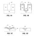
- FIGS. 1A-1Ddepicts various stages of semiconductor fabrication before and after ion implantation and stripping operations. While FIGS. 1A-1D provide an example of a fabrication process that may employ the methods described herein, the methods are not so limited and may be employed with any hydrogen-based photoresist strip process, with particular applications of FEOL processes.
- FIG. 1Ashows a semiconductor substrate 101 coated with photoresist material 103 .
- the substrate 101may include one or more layers of deposited film, e.g., oxide film, silicide contact, and/or polysilicon film, or may be a bare silicon substrate, including for example a silicon-on-insulator type substrate.
- the photoresist materialcoats the entire substrate surface.
- the photoresistis then exposed to patterned radiation generated through a mask and developed to remove a portion of the material, e.g., the opening 104 shown in FIG. 1A between the remaining photoresist materials 103 .
- the substrateis then exposed to an ion implant process.
- ion implantthe surface of the work piece or wafer is implanted with dopant ions.
- the processmay be, for example, a plasma-immersion ion implantation (PIII) or ion beam implantation.
- the ionsbombard the substrate surface, including the exposed silicon layer 101 and the photoresist 103 .
- small amounts of the underlying material 107may be sputtered to the photoresist sidewalls. See FIG. 1B .
- This materialmay include some of the implant species, other material in the plasma or ion beam, and by-products of the implantation. They include silicon, aluminum, carbon, fluorine, titanium, other contact materials such as cobalt, and oxygen in both elemental and compound forms.
- the actual speciesdepend on the composition of the substrate before ion implant, the photoresist, and the implanted species.
- a doped region 109is created.
- the ion energy or intensity of the bombardmentdetermines the depth or thickness of the doped region.
- the density of the ion fluxdetermines the extent of doping.
- the ionsalso impregnate the photoresist surface creating a crust layer 105 .
- the crust layer 105may be carbonized and highly cross-linked polymer chains. The crust is usually depleted of hydrogen and impregnated with the implant species.
- the crust layer 105is denser than the bulk resist layer 103 .
- the relative densitydepends on the ion flux while the thickness of the crust layer depends on the ion energy.
- This crust layer 105is harder to strip than the bulk photoresist 103 below. Removal rates of the crust layer may be 50% or 75% slower than the underlying bulk photoresist.
- the bulk photoresistcontains relatively high levels of chemically bonded nitrogen and some of its original casting solvent. At elevated wafer temperature, e.g., above 150° C. to above 200° C., the bulk resist can outgas and expand relative to the crust layer. The entire photoresist can then “pop” as the underlying bulk photoresist builds up pressure under the crust. Photoresist popping is a source of particles and process defects because the residues are especially hard to clean from the wafer surface and chamber internal parts. With high-dose ion implantation, the density difference between the crust and underlying bulk photoresist layer is even higher. The crust may also be thicker.
- FIG. 1Cshows the substrate after a strip that fails to completely remove the photoresist 103 and the sidewall sputter residue 107 .
- the sidewall sputter residue 107may include particles that do not form a volatile compound under conventional strip chemistries. These particles may remain after a conventional strip operation.
- the residuemay also include oxides of implanted species formed with the reactive oxygen used in the conventional strip chemistry, such as boron oxide and arsenic oxide. Portions of the crust 105 may also remain on the substrate. Crust sidewalls and corners at the bottom of photoresist vias may be hard to strip because of geometries. Stringers, long, narrow photoresist residue segments that may be left by non-exposure between two adjacent exposure areas, may also be present.
- Overstripis a continuation of the strip process past the point nominally required to remove all photoresist. If the photoresist is totally removed in some areas of the wafer but not others, continuation of the strip process would cause additional material, typically silicon and silicon oxide, to be removed from areas that are already stripped.
- FIG. 1Dshows the substrate after all residue has been removed.
- Described hereinare hydrogen-containing plasma strip processes that can be used to strip photoresist after ion implantation or other post-patterning processing.
- the methods and apparatus described hereincan be implemented for post halo implant resist strip.
- the methods and apparatusreduce dislocations in a Si or other substrate that can compromise device integrity.
- the hydrogen-containing plasmasmay or may not contain other reactive species such as oxygen and fluorine species. Without being bound by a particular theory, it is believed that dislocations are more liable to be formed with hydrogen-based plasmas that do not contain oxygen, fluorine, or other species that can react with hydrogen.
- the approaches described hereinmay be advantageously used with hydrogen-based plasmas that include oxygen, fluorine and other reactive species as well as those that do not.
- the hydrogen-based resist strip processesemploy one or more of the following techniques: 1) minimization of hydrogen budget by using short processes with minimal overstrip duration, 2) providing dilute hydrogen, e.g., 2%-16% H 2 , 3) minimization of material loss by controlling process conditions and chemistry, 4) using a low temperature resist strip, 5) controlling implant conditions and concentrations, and 6) performing one or more post-strip venting processes. These are discussed below.
- FIG. 2shows a flow diagram illustrating certain operations of a photoresist strip process.
- the process 200begins at block 201 with providing a substrate having photoresist thereon. Examples of substrates having photoresist are described above with respect to FIGS. 1A-1C .
- the substratecan be a silicon substrate for example, including a silicon-on-insulator substrate.
- the photoresistcan be directly on the surface of the silicon substrate in some embodiments. In some embodiments, one or more layers of deposited film or material may be between a silicon or other substrate and the photoresist. In some embodiments, the photoresist and substrate may have undergone an ion implantation process.
- the process 200continues at block 203 with a bulk photoresist strip.
- block 203may be preceded by or include one or more operations to remove a thin crust layer.
- block 203involves a hydrogen-based strip chemistry.
- strip chemistriesinclude: H 2 /N 2 , H 2 /N 2 /Ar, H 2 /N 2 /He, H 2 /N 2 /other noble gas, H 2 /Ar, H 2 /He, and H 2 /other noble gas.
- Other hydrogen-containing compoundsmay be used instead of or in addition to H 2 . Examples include NH 2 .
- Other inert compoundsmay be used instead of or in addition to the N 2 , Ar or He.
- the strip chemistrydoes not include oxidizing agents or halogen-containing compounds.
- the strip chemistrymay include an oxidizing agent and/or a fluorine or other halogen-containing compound in addition to or instead of the N 2 and noble gases described.
- an oxidizing agentmay be a relatively strong oxidizing agent, such as O 2 , or a weak oxidizing agent.
- weak oxidizing agentsinclude carbon oxides such as carbon dioxide (CO 2 ), carbon monoxide (CO), nitrogen oxides such as nitrous oxide (N 2 O), nitric oxide (NO), nitrogen dioxide (NO 2 ), and sulfur oxides such as sulfur oxide (SO) and sulfur dioxide (SO 2 ).
- weak oxidesinclude any oxygen containing hydrocarbons (CxHyOz) and water (H 2 O).
- fluorine-containing compoundsinclude nitrogen trifluoride (NF 3 ), sulfur hexafluoride (SF 6 ), hexafluoroethane (C 2 F 6 ), tetrafluoromethane (CF 4 ), trifluoromethane (CHF 3 ), difluoromethane (CH 2 F 2 ), octofluoropropane (C 3 F 8 ), octofluorocyclobutane (C 4 F 8 ), octofluoro[1-]butane (C 4 F 8 ), octofluoro[ 2 -]butane (C 4 F 8 ), octofluoroisobutylene (C 4 F 8 ), fluorine (F 2 ), and the like.
- NF 3nitrogen trifluoride
- SF 6sulfur hexafluoride
- C 2 F 6hexafluoroethane
- CF 4tetrafluoromethane
- CHF 3di
- the process 200continues at block 205 with bulk resist strip end point detection.
- Block 205can involve infrared detection, optical detection, emission detection or other appropriate detection method.
- the process 200continues at block 207 with an overstrip operation.
- the overstrip chemistry and process conditionsare the same as used for the bulk photoresist strip in block 203 .
- block 205may involve using a different chemistry, component concentration, or process conditions than used in block 203 . Examples include using a lower temperature, or hydrogen concentration than in block 203 .
- An overstrip operationcan be measured as a percent duration of the bulk strip operation. At least part of a Si wafer or other substrate is covered by resist until the end point. During overstrip, the substrate may be particularly vulnerable to dislocations caused by a hydrogen-based chemistry.
- the duration of the over strip stepis determined experimentally and may be different at different mask levels and implant steps. In some embodiments, overstrip duration ranges from about 0 to 200% of the time to end point, for example, 0 to 50%, or 0 to 20%. Minimizing the overstrip also reduces thermal budget and substrate exposure to plasma.
- hydrogen absorption into the Si or other substrateis reduced by diluting the hydrogen with nitrogen or another inert gas.
- hydrogen concentration [H]may be between about 2% and 16%, as measured in volumetric flow percentage.
- FIG. 3is a graph showing the concentration of atoms (as measured by Secondary Ion Mass Spectrometry (SIMS)) up to a depth of 400 ⁇ of silicon wafers after a) exposure to photoresist strip plasma using 16% H 2 , b) exposure to photoresist strip plasma using 4% H 2 , c) bare control Si wafer and d) after rapid thermal process (RTP) anneal at 900° C. for 30s.
- SIMSSecondary Ion Mass Spectrometry
- FIG. 3demonstrates that the number of H atoms in a wafer after strip is correlated to the [H] in the photoresist strip plasma.
- FIG. 3also demonstrates that these atoms are driven out after RTP anneal, with the post-RTP curve not showing any signal above noise. Without being bound by a particular theory, it is believed that post-strip processing such as an RTP anneal that drives out H atoms may cause a shockwave in Si crystal that can cause dislocations.
- a strip process gas having [H] of 16%produces a clean that is fast and effective at removing stringers and other residue, it may cause dislocations in the substrate. Accordingly, in some embodiments, a strip process gas having an [H] of less than 16% is used, e.g., between 2% and 15% or 2% and 10%, to reduce defects. In some embodiments, the [H] is less than 8% or 5%.
- FIG. 4shows FTIR spectra for silicon wafers after a) exposure to photoresist strip using 16% H 2 , b) exposure to photoresist strip using 4% H 2 , and c) bare control Si wafer.
- an increase in Si—H bondsare shown for the 4% and 16% spectra, while an increase in Si—H2 bonds is shown only for the 16% spectrum. This indicates that bonding in a Si wafer can be modulated by [H] in the strip chemistry.
- hydrogen in the strip process gasis controlled to modulate the incorporation of hydrogen in the system as well as modulating bonding.
- Thiscan be implemented by using a cross product [H] ⁇ time of between about 1 and 2400 sccm-seconds per layer, with [H] measured in volumetric flow and t.
- [H] ⁇ timemay be between about 50 and 2000 sccm-seconds, e.g., between 50 and 1000 sccm-seconds per layer, or between about 50 and 500 sccm-seconds per pass through the strip apparatus.
- a strip operation having a cross product within these rangesmay or may not also have an [H] of less than 16% as described above.
- a strip operationis performed a temperature between 100° C. and 400° C. In some embodiments, the temperature is below about 285° C., e.g., between 200° C. and 285° C., or between about 200° C. and 250° C.
- Both hydrogen absorption into the Si crystal, hydrogen diffusion inside the crystal, the formation of Si—H and Si—H 2 bonds and dislocation formation and propagationmay be affected by temperature.
- Kink pair formation and motionmay be affected by temperature.
- Low temperature and in particular low thermal budget(defined as the product of time and temperature in units of s ⁇ K) may have a strong effect of the kinetics of dislocations formation and propagation.
- a process temperature of between 200° C. and 285° C., or between about 200° C. and 250° C. in some embodimentscan reduce one or more mechanisms that may contribute comprising device integrity.
- the overall thermal budgetmay then be determined by minimizing material loss while leaving the substrate clean of residue.
- FIG. 5Ashows carbon doped silicon under a gate.
- the carbon impurities in a Si crystalcreating strain due the shorter Si—C bond.
- Tensile stressresults in a larger than equilibrium lattice constant and longer Si—Si bonds. From the device perspective this is beneficial, causing higher density of charge carriers and a faster device. Mechanically, this is detrimental and is assisting in the formation of defects.
- a hydrogen-based strip processcan cause carbon depletion, creating a vacancy in the crystal and increasing strain. This is illustrated in FIG. 5B .
- FIG. 6shows SIMS analysis of carbon content in crystalline Si as a function of exposure to hydrogen plasma.
- a C implant dose rangeis 5*10 14 to 5*10 16 at energies of 6 to 10 KeV.
- a processmay use a dose of 6*10 15 at 8 KeV.
- a dopant implant dose calculated for a non-hydrogen based stripmay be reduced by up to 15%.
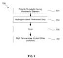
- FIG. 7shows a flow diagram illustrating certain operations of a photoresist strip process.
- the process 700begins at block 701 with providing a substrate having photoresist on it. As indicated above, in some embodiments, the photoresist and substrate have previously undergone an implant process.
- the process 700continues at block 703 with performing a hydrogen-based strip process. Strip chemistries are discussed above and may, for example, include essentially H 2 diluted with N 2 or other inert diluent. Note that according to various embodiments, block 703 can include one or more of a crust removal operation, a bulk photoresist operation and an overstrip operation.
- FIG. 8shows FTIR spectra after a) exposure to photoresist strip plasma using 16% H 2 and a 12 hour 200° C. anneal in air and b) exposure to photoresist strip plasma using 4% H 2 and 12 hour 200° C. anneal in air, compared to control.
- FIG. 8shows that the incorporated hydrogen can be driven out at a relatively low temperature. Without being bound by a particular theory it is believed that these relatively low temperatures can drive out the hydrogen atoms without causing dislocations that occur at higher temperatures used, for example, with RTP processes.
- a low temperature ventcan occur at less than about 450° C., less than 400° C., less than about 300° C. according to various embodiments.
- a high temperature implant drivemay involve a RTP process for example at temperatures of 800° C. or higher.
- blocks 703 and 705are both performed multiple times, e.g., a vent operation can be performed each time a photoresist strip is performed during FEOL processing.
- block 703is performed multiple times for different FEOL devices (e.g., once of NMOS fabrication, once for PMOS fabrication, etc.), with a single vent performed prior to block 707 .
- multiple vent processesmay be performed prior to block 707 . For example, if block 703 is performed ten times, block 705 can be performed from one to ten times.
- a hydrogen-containing gastypically including molecular hydrogen
- the gas introduced to the plasma sourcecontains the chemically active species that will be ionized or otherwise in the plasma source to form a plasma.
- an inlet gasmay consist essentially of molecular hydrogen and one or more inert gases such as nitrogen.
- the inlet gasincludes no oxygen-containing compound.
- the inlet gasincludes only oxygen-containing compounds that are weak oxidants.
- the gas introduced to the plasma sourcemay be premixed, partially mixed or unmixed.
- Example RF plasma power for a 300 mm waferranges between about 300 Watts to about 10 Kilowatts. In some embodiments, the RF plasma power is between about 2000 Watts and 5000 Watts, e.g., 3500 W.
- the plasma gasis distributed to the work surface via a showerhead assembly.
- the showerhead assemblymay be grounded or have an applied voltage to attract some charge species while not affecting the flow of neutral species to the wafer, e.g., 0-1000 watt bias. Many of the electrically charged species in the plasma recombine at the showerhead.
- the assemblyincludes the showerhead itself which may be a metal plate having holes to direct the plasma and inert gas mixture into the reaction chamber.
- the showerheadredistributes the active hydrogen from the plasma source over a larger area, allowing a smaller plasma source to be used.
- the number and arrangement of the showerhead holesmay be set to optimize strip rate and strip rate uniformity.
- the showerhead holesare preferably smaller and fewer in the center of the showerhead in order to push the active gases toward the outer regions.
- the showerheadmay have at least 100 holes.
- Suitable showerheadincludes the Gamma xPR showerhead or the GxT drop-in showerhead available from Novellus Systems, Inc. of San Jose, Calif. In embodiments in which there is no showerhead assembly, the plasma enters the process chamber directly.
- the process chambermay be any suitable reaction chamber for the strip operation being performed. It may be one chamber of a multi-chambered apparatus or it may simply be a single chamber apparatus. The chamber may also include multiple stations where different wafers are processed simultaneously. The process chamber may be the same chamber where the implant, etch, or other resist-mediated process takes place. In other embodiments, a separate chamber is reserved for the strip.
- Process chamber pressuremay range from about 600 mTorr to 2 Torr. In certain embodiments, the pressure ranges from about 0.9 Ton to 1.5 Torr.
- the process chamberincludes one or more processing stations on which strip operations are performed.
- the one or more processing stationsincludes a preheat station, at least one strip station, and an over-ash station.
- the wafer supportis configured to support the wafer during processing.
- the wafer supportmay also transfer heat to and from the wafer during processing to adjust the wafer temperature as necessary.
- the waferis supported on a plurality of minimum contacts and does not physically contact the wafer support surface plane.
- a spindlepicks up the wafer and transfers the wafer from one station to another.
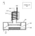
- FIG. 9is a schematic illustration showing aspects of a downstream plasma apparatus 900 suitable for practicing the present invention on wafers.
- Apparatus 900has a plasma producing portion 911 and an exposure chamber 901 separated by a showerhead assembly 917 .
- a wafer 903rests on a platen (or stage) 905 .
- Platen 905is fitted with a heating/cooling element.
- platen 905is also configured for applying a bias to wafer 903 .
- Low pressureis attained in exposure chamber 901 via vacuum pump via conduit 907 .
- Sources of gaseous hydrogen (with or without dilution/carrier gas) and carbon dioxide (or other weak oxidizing agent)provide a flow of gas via inlet 909 into plasma producing portion 911 of the apparatus.
- Plasma producing portion 911is surrounded in part by induction coils 913 , which are in turn connected to a power source 915 .
- gas mixturesare introduced into plasma producing portion 911 , induction coils 913 are energized and a plasma is generated in plasma producing portion 911 .
- showerhead assemblymay have an applied voltage or be grounded directs the flow of species into exposure chamber 901 .
- wafer 903may be temperature controlled and/or a RF bias may be applied.
- induction coils 913may loop around the plasma source 911 in an interlaced pattern.
- the plasma source 911may be shaped as a dome instead of a cylinder.
- a suitable apparatusincludes hardware for accomplishing the process operations and a system controller having instructions for controlling process operations in accordance with the present invention.
- Machine-readable mediamay be coupled to the controller and contain instructions for controlling process conditions for these operations.
- the system controllerwill typically include one or more memory devices and one or more processors configured to execute the instructions so that the apparatus will perform a method in accordance with embodiments of the present invention.
- Machine-readable media containing instructions for controlling process operationsmay be coupled to the system controller.
- a controller 950may be connected to components of the process chamber, and control process gas composition, pressure, temperature and wafer indexing of the stripping operations.
- the system controllerincludes programs, which can include logic of any form. For example, it can include logic hard coded on digital signal processors and similar processers that have specific algorithms implemented as hardware. It can also include software of firmware instructions that may be executed on a general purpose computer.
- Suitable plasma chambers and systemsinclude the Gamma 2100, 2130 I 2 CP (Interlaced Inductively Coupled Plasma), G400, and GxT offered by Novellus Systems, Inc. of San Jose, Calif.
- Other systemsinclude the Fusion line from Axcelis Technologies Inc. of Rockville, Md., TERA21 from PSK Tech Inc. in Korea, and the Aspen from Mattson Technology Inc. in Fremont, Calif.
- various strip chambersmay be configured onto cluster tools. For example, a strip chamber may be added to a Centura cluster tool available from Applied Materials of Santa Clara, Calif.
- FIG. 10is a simplified schematic showing a top view of a multi-station apparatus including stations 1 , 2 , 3 , 4 , 5 and 6 . Wafers enter the apparatus at station 1 via chamber 1001 , are transferred to each station in sequence for a processing operation at that station and exit from station 6 via chamber 1002 after the process is complete.
- the apparatus/process described hereinabovemay be used in conjunction with lithographic patterning tools or processes, for example, for the fabrication or manufacture of semiconductor devices, displays, LEDs, photovoltaic panels and the like. Typically, though not necessarily, such tools/processes will be used or conducted together in a common fabrication facility.
- Lithographic patterning of a filmtypically comprises some or all of the following steps, each step enabled with a number of possible tools: (1) application of photoresist on a workpiece, i.e., substrate, using a spin-on or spray-on tool; (2) curing of photoresist using a hot plate or furnace or UV curing tool; (3) exposing the photoresist to visible or UV or x-ray light with a tool such as a wafer stepper; (4) developing the resist so as to selectively remove resist and thereby pattern it using a tool such as a wet bench; (5) transferring the resist pattern into an underlying film or workpiece by using a dry or plasma-assisted etching tool; and (6) removing the resist using a tool such as an RF or microwave plasma resist stripper.
- a toolsuch as an RF or microwave plasma resist stripper.
Landscapes
- Engineering & Computer Science (AREA)
- Physics & Mathematics (AREA)
- Plasma & Fusion (AREA)
- Chemical & Material Sciences (AREA)
- General Physics & Mathematics (AREA)
- Analytical Chemistry (AREA)
- Condensed Matter Physics & Semiconductors (AREA)
- Manufacturing & Machinery (AREA)
- Computer Hardware Design (AREA)
- Microelectronics & Electronic Packaging (AREA)
- Power Engineering (AREA)
- General Chemical & Material Sciences (AREA)
- Chemical Kinetics & Catalysis (AREA)
- Drying Of Semiconductors (AREA)
- Plasma Technology (AREA)
- Photosensitive Polymer And Photoresist Processing (AREA)
- Formation Of Insulating Films (AREA)
Abstract
Description
This application claims benefit under 35 USC §119(e) of U.S. Provisional Patent Application No. 61/528,029, filed Aug. 26, 2011, which is incorporated by reference herein.
Photoresist is a light sensitive material used in certain fabrication processes to form a patterned coating on a work piece, e.g., a semiconductor wafer, during processing. After exposing the photoresist coated surface to a pattern of high energy radiation, a portion of the photoresist is removed to reveal the surface below, leaving the rest of the surface protected. Semiconductor processes such as etching, depositing, and ion implanting can be performed on the uncovered surface and the remaining photoresist. After performing one or more semiconductor processes, the remaining photoresist is removed in a strip operation.
Provided herein are methods and apparatus of hydrogen-based photoresist strip operations that reduce dislocations in a silicon wafer or other substrate. According to various embodiments, the hydrogen-based photoresist strip methods can employ one or more of the following techniques: 1) minimization of hydrogen budget by using short processes with minimal overstrip duration, 2) providing dilute hydrogen, e.g., 2%-16% hydrogen concentration, 3) minimization of material loss by controlling process conditions and chemistry, 4) using a low temperature resist strip, 5) controlling implant conditions and concentrations, and 6) performing one or more post-strip venting processes. Apparatus suitable to perform the photoresist strip methods are also provided.
A method including providing a substrate having photoresist disposed thereon to reaction chamber and exposing the substrate to a plasma generated from a process gas comprising nitrogen and hydrogen and having a hydrogen concentration [H] of between about 2% and 16% to thereby remove photoresist from the substrate. In certain embodiments, the process gas comprises molecular nitrogen (N2) and molecular hydrogen (H2). In certain embodiments, the process gas contains substantially no oxygen-containing compounds. In embodiments, wherein the hydrogen concentration is between about 2% and 10% and can be less than 8%. In some embodiments, the hydrogen concentration about 4%.
Examples of process gasses chemistries include H2/N2, H2/N2/Ar, and H2/N2/He. In some embodiments, the substrate is exposed to the plasma for a time t and the cross-product of [H] and the time t ([H]×t) is between about 50 and 2000 sccm-seconds, or about between about 50 and 500 sccm-seconds. In certain embodiments, the substrate temperature is below about 285° C., for example between about 200° C. and 250° C.
Another aspect of the disclosure provided herein is a method including providing a substrate having photoresist disposed thereon to reaction chamber; exposing the substrate to a plasma generated from a process gas comprising hydrogen to thereby remove photoresist from the substrate; and after exposing the substrate to the plasma, venting the substrate at a substrate temperature between about 200° C. and 450° C. In some embodiments, the methods further include, after venting the substrate, performing a high temperature implant drive process at a substrate temperature of at least about 800° C. The hydrogen concentration of the process gas can be 16% or greater in certain embodiments. In certain embodiments, the hydrogen concentration [H] of the process gas is less than 16%. In certain embodiments, the hydrogen concentration [H] of the process gas is less than 10%. In certain embodiments, the hydrogen concentration [H] of the process gas is less than 5%.
Another aspect of the subject matter disclosed herein is an apparatus including a plasma source, a gas inlet for introducing a gas mixture into the plasma source, a showerhead positioned downstream of the gas inlet, a substrate support downstream of the showerhead, said substrate support comprising a pedestal and temperature-controlling mechanism to control a temperature of a substrate supported on the substrate support, and, a controller for executing a set of instructions for performing the methods described herein. In some embodiments, the set of instructions include instructions to introduce a gas mixture to the gas inlet comprising nitrogen and hydrogen and having a hydrogen concentration [H] of between about 2% and 16%. In some embodiments, the set of instructions includes instruction to maintain the temperature of the substrate at about 285° C. or less.
In the following detailed description of the present invention, numerous specific embodiments are set forth in order to provide a thorough understanding of the invention. However, as will be apparent to those skilled in the art, the present invention may be practiced without these specific details or by using alternate elements or processes. In other instances well-known processes, procedures and components have not been described in detail so as not to unnecessarily obscure aspects of the present invention.
In this application, the terms “work piece”, “semiconductor wafer”, “wafer” and “partially fabricated integrated circuit” will be used interchangeably. One skilled in the art would understand that the term “partially fabricated integrated circuit” can refer to a silicon wafer during any of many stages of integrated circuit fabrication thereon. The following detailed description assumes the invention is implemented on a wafer. However, the invention is not so limited. The work piece may be of various shapes, sizes, and materials. In addition to semiconductor wafers, other work pieces that may take advantage of this invention include various articles such as displays, printed circuit boards, and the like.
Photoresist is a light sensitive material used in certain fabrication processes to form a patterned coating on a work piece, e.g., a semiconductor wafer, during processing. After exposing the photoresist coated surface to a pattern of high energy radiation, a portion of the photoresist is removed to reveal the surface below, leaving the rest of the surface protected. Semiconductor processes such as etching, depositing, and ion implanting are performed on the uncovered surface and the remaining photoresist. After performing one or more semiconductor processes, the remaining photoresist is removed in a strip operation.
Front-End-of-Line (FEOL) fabrication processes, including p and n MOSFET and other transistor fabrication processes, DRAM storage capacitor fabrication processes, and flash floating gate fabrication processes can involve multiple lithographic patterning operations, and multiple photoresist strip processes. In some embodiments, the photoresist strip processes may be or include high dose implantation strip (HDIS) or other implant strip processes.
During ion implantation, dopant ions, e.g., ions of boron, boron difluoride, indium, gallium, thallium, phosphorous, arsenic, antimony, bismuth, carbon, xenon, argon or germanium, are accelerated toward a work piece target. The ions implant in exposed regions of the work piece as well as in the remaining photoresist surface. The process may form well regions (source/drain), lightly doped drain (LDD), halo implant regions, and doubled diffused drain (DDD) regions, as well as other implanted regions. The ion implant impregnates the resist with the implant species and depletes the surface of hydrogen. The outer layer or crust of the resist forms a carbonized layer that may be much denser than the underlying bulk resist layer. These two layers have different thermal expansion rates and react to stripping processes at different rates.
The difference between the outer layer and bulk layer is quite pronounced in post high-dose ion implant resist. In high-dose implantation, the ion dose may be greater than 1×10¹⁵ions/cm2 and the energy may be from 10 KeV to greater than 100 KeV. Traditional HDIS processes employ oxygen chemistries where monatomic oxygen plasma is formed away from the process chamber and then directed at the work piece surface. The reactive oxygen combines with the photoresist to form gaseous by-products which is removed with a vacuum pump. For HDIS, additional gases are needed to remove the implanted dopants with oxygen.
Primary implant strip considerations include strip rate, amount of residue, and film loss of the exposed and underlying film layer. Residues are commonly found on the substrate surface after implant and stripping. They may result from sputtering during the high-energy implant, incomplete removal of crust, and/or oxidation of implant atoms in the resist. After stripping, the surface should be residue free or substantially residue free to ensure high yield and eliminate the need for additional residue removal processing. Residues may be removed by overstripping, i.e., a continuation of the strip process past the point nominally required to remove all photoresist. Unfortunately, in conventional implant strip operations, overstripping sometimes removes some of the underlying functional device structure. At the device layer, even very little silicon loss from the transistor source/drain regions may adversely affect device performance and yield, especially for ultra shallow junction devices fabricated at the <32 nm design rule or below.
In some embodiments, the methods and apparatus may be used to efficiently and effectively to remove photoresist materials after high-dose ion implantation. The methods and apparatus are not limited to high-dose implant strip (HDIS). The methods and apparatus are also not limited to any particular category of dopants implanted. For instance, described methods and apparatus may be effectively used with stripping after medium or low dose implant. Although specific dopant ions such as boron, arsenic, and phosphorous are discussed, the described methods and apparatus may be effectively used to strip resist impregnated with other dopants, such as nitrogen, oxygen, carbon, germanium, and aluminum. Further, the methods and apparatus are not limited to post-implant removal of photoresist, but may also be used to remove photoresist that has not undergone an implantation.
The methods and apparatus described herein employ hydrogen-based chemistries to remove photoresist and/or related residues. In some embodiments, the chemistries include hydrogen with an optional gas such as nitrogen, helium, argon and the like with substantially no oxidant or fluorine-based chemistries. In some other embodiments, the chemistries may include an oxygen-containing compound and/or a fluorine containing compound.
The strip processes described herein generally involve generating a plasma from a plasma from a gas including various component gases. As indicated, the strip chemistries described herein are hydrogen-based. Molecular hydrogen (H2) is typically a main component of the plasma-generating gas. In some embodiments, the strip chemistry for one or more of the operations of an overall strip process is generated from a gas consisting essentially of H2and N2.
While hydrogen-based strip chemistries such as H2/N2chemistries have resulted in clean, fast and effective removal of photoresist, certain hydrogen-based strip processes have been unexpectedly found to cause dislocations or other defects in silicon substrates during FEOL fabrication. These defects can compromise device integrity. Formation of dislocation in the Si crystal can be detrimental to device performance. In some cases dislocations can negate the positive effects of lattice straining and slow the device. In other cases dislocations can cause yield loss. In yet other cases, dislocations can create a device reliability problem, affecting long term operation. The methods and apparatus described herein provide effective photoresist stripping while reducing or minimizing defects.
The substrate is then exposed to an ion implant process. During ion implant, the surface of the work piece or wafer is implanted with dopant ions. The process may be, for example, a plasma-immersion ion implantation (PIII) or ion beam implantation. The ions bombard the substrate surface, including the exposedsilicon layer 101 and thephotoresist 103. With high energy ion implantation, small amounts of theunderlying material 107 may be sputtered to the photoresist sidewalls. SeeFIG. 1B . This material may include some of the implant species, other material in the plasma or ion beam, and by-products of the implantation. They include silicon, aluminum, carbon, fluorine, titanium, other contact materials such as cobalt, and oxygen in both elemental and compound forms. The actual species depend on the composition of the substrate before ion implant, the photoresist, and the implanted species.
At the exposedsilicon layer 101, a dopedregion 109 is created. The ion energy or intensity of the bombardment determines the depth or thickness of the doped region. The density of the ion flux determines the extent of doping. The ions also impregnate the photoresist surface creating acrust layer 105. Thecrust layer 105 may be carbonized and highly cross-linked polymer chains. The crust is usually depleted of hydrogen and impregnated with the implant species. Thecrust layer 105 is denser than the bulk resistlayer 103. The relative density depends on the ion flux while the thickness of the crust layer depends on the ion energy.
Thiscrust layer 105 is harder to strip than thebulk photoresist 103 below. Removal rates of the crust layer may be 50% or 75% slower than the underlying bulk photoresist. The bulk photoresist contains relatively high levels of chemically bonded nitrogen and some of its original casting solvent. At elevated wafer temperature, e.g., above 150° C. to above 200° C., the bulk resist can outgas and expand relative to the crust layer. The entire photoresist can then “pop” as the underlying bulk photoresist builds up pressure under the crust. Photoresist popping is a source of particles and process defects because the residues are especially hard to clean from the wafer surface and chamber internal parts. With high-dose ion implantation, the density difference between the crust and underlying bulk photoresist layer is even higher. The crust may also be thicker.
Described herein are hydrogen-containing plasma strip processes that can be used to strip photoresist after ion implantation or other post-patterning processing. For example, the methods and apparatus described herein can be implemented for post halo implant resist strip. The methods and apparatus reduce dislocations in a Si or other substrate that can compromise device integrity. As noted above, in certain embodiments, the hydrogen-containing plasmas may or may not contain other reactive species such as oxygen and fluorine species. Without being bound by a particular theory, it is believed that dislocations are more liable to be formed with hydrogen-based plasmas that do not contain oxygen, fluorine, or other species that can react with hydrogen. However, in some embodiments, the approaches described herein may be advantageously used with hydrogen-based plasmas that include oxygen, fluorine and other reactive species as well as those that do not.
According to various embodiments the hydrogen-based resist strip processes employ one or more of the following techniques: 1) minimization of hydrogen budget by using short processes with minimal overstrip duration, 2) providing dilute hydrogen, e.g., 2%-16% H2, 3) minimization of material loss by controlling process conditions and chemistry, 4) using a low temperature resist strip, 5) controlling implant conditions and concentrations, and 6) performing one or more post-strip venting processes. These are discussed below.
Theprocess 200 continues atblock 205 with bulk resist strip end point detection. Block205 can involve infrared detection, optical detection, emission detection or other appropriate detection method. Theprocess 200 continues atblock 207 with an overstrip operation. In some embodiments, the overstrip chemistry and process conditions are the same as used for the bulk photoresist strip inblock 203. In some other embodiments, block205 may involve using a different chemistry, component concentration, or process conditions than used inblock 203. Examples include using a lower temperature, or hydrogen concentration than inblock 203.
An overstrip operation can be measured as a percent duration of the bulk strip operation. At least part of a Si wafer or other substrate is covered by resist until the end point. During overstrip, the substrate may be particularly vulnerable to dislocations caused by a hydrogen-based chemistry. The duration of the over strip step is determined experimentally and may be different at different mask levels and implant steps. In some embodiments, overstrip duration ranges from about 0 to 200% of the time to end point, for example, 0 to 50%, or 0 to 20%. Minimizing the overstrip also reduces thermal budget and substrate exposure to plasma.
In some embodiments, hydrogen absorption into the Si or other substrate is reduced by diluting the hydrogen with nitrogen or another inert gas. For example, hydrogen concentration [H] may be between about 2% and 16%, as measured in volumetric flow percentage.FIG. 3 is a graph showing the concentration of atoms (as measured by Secondary Ion Mass Spectrometry (SIMS)) up to a depth of 400 Å of silicon wafers after a) exposure to photoresist strip plasma using 16% H2, b) exposure to photoresist strip plasma using 4% H2, c) bare control Si wafer and d) after rapid thermal process (RTP) anneal at 900° C. for 30s. Nitrogen was used as the diluent for a) and b).FIG. 3 demonstrates that the number of H atoms in a wafer after strip is correlated to the [H] in the photoresist strip plasma.FIG. 3 also demonstrates that these atoms are driven out after RTP anneal, with the post-RTP curve not showing any signal above noise. Without being bound by a particular theory, it is believed that post-strip processing such as an RTP anneal that drives out H atoms may cause a shockwave in Si crystal that can cause dislocations.
While a strip process gas having [H] of 16% produces a clean that is fast and effective at removing stringers and other residue, it may cause dislocations in the substrate. Accordingly, in some embodiments, a strip process gas having an [H] of less than 16% is used, e.g., between 2% and 15% or 2% and 10%, to reduce defects. In some embodiments, the [H] is less than 8% or 5%.
In certain embodiments, hydrogen in the strip process gas is controlled to modulate the incorporation of hydrogen in the system as well as modulating bonding. This can be implemented by using a cross product [H]×time of between about 1 and 2400 sccm-seconds per layer, with [H] measured in volumetric flow and t. For example, [H]×time may be between about 50 and 2000 sccm-seconds, e.g., between 50 and 1000 sccm-seconds per layer, or between about 50 and 500 sccm-seconds per pass through the strip apparatus. Note that according to various embodiments, a strip operation having a cross product within these ranges may or may not also have an [H] of less than 16% as described above.
In some embodiments, a strip operation is performed a temperature between 100° C. and 400° C. In some embodiments, the temperature is below about 285° C., e.g., between 200° C. and 285° C., or between about 200° C. and 250° C. Both hydrogen absorption into the Si crystal, hydrogen diffusion inside the crystal, the formation of Si—H and Si—H2bonds and dislocation formation and propagation may be affected by temperature. Kink pair formation and motion may be affected by temperature. Low temperature and in particular low thermal budget (defined as the product of time and temperature in units of s·K) may have a strong effect of the kinetics of dislocations formation and propagation. Without being bound to a particular theory, it believed that rates of hydrogen diffusion and/or formation of Si—H and Si—H2bonds may exhibit Arrhenius behavior, exponentially related to temperature, with linear dependence on time and concentration. Accordingly, a process temperature of between 200° C. and 285° C., or between about 200° C. and 250° C. in some embodiments can reduce one or more mechanisms that may contribute comprising device integrity. The overall thermal budget may then be determined by minimizing material loss while leaving the substrate clean of residue.
In some embodiments, implant conditions and concentrations are controlled.FIG. 5A shows carbon doped silicon under a gate. The carbon impurities in a Si crystal, creating strain due the shorter Si—C bond. Tensile stress results in a larger than equilibrium lattice constant and longer Si—Si bonds. From the device perspective this is beneficial, causing higher density of charge carriers and a faster device. Mechanically, this is detrimental and is assisting in the formation of defects. In some embodiments, a hydrogen-based strip process can cause carbon depletion, creating a vacancy in the crystal and increasing strain. This is illustrated inFIG. 5B .FIG. 6 shows SIMS analysis of carbon content in crystalline Si as a function of exposure to hydrogen plasma. Lower levels of carbon are measured as hydrogen concentration in the plasma increases from 4% to 16%. The highest level of carbon is measured for the control, where no plasma was present. The interaction between implanted C and H from resist strip is shown inFIG. 6 . In some embodiments, the effect of hydrogen on substrate straining due to reaction between hydrogen and carbon (or other doping element such as carbon, boron, phosphorous, arsenic etc.) is minimized by reducing dopant implant concentration. For example, a modulation of the carbon implant, by +/−15%, in conjunction with the hydrogen plasma process allows for straining engineering that enhances performance without undesired dislocations. According to various embodiments, a C implant dose range is 5*1014to 5*1016at energies of 6 to 10 KeV. For example, a process may use a dose of 6*1015at 8 KeV. In some embodiments, a dopant implant dose calculated for a non-hydrogen based strip may be reduced by up to 15%.
In the same or other embodiments as described above, a venting process can be performed after one or more hydrogen-based photoresist strip processes.FIG. 7 shows a flow diagram illustrating certain operations of a photoresist strip process. Theprocess 700 begins atblock 701 with providing a substrate having photoresist on it. As indicated above, in some embodiments, the photoresist and substrate have previously undergone an implant process. Theprocess 700 continues atblock 703 with performing a hydrogen-based strip process. Strip chemistries are discussed above and may, for example, include essentially H2diluted with N2or other inert diluent. Note that according to various embodiments, block703 can include one or more of a crust removal operation, a bulk photoresist operation and an overstrip operation. Duringblock 703, hydrogen is incorporated into the substrate. Theprocess 700 continues atblock 705 with venting at a relatively low temperature, e.g., between about 200° C. and 450° C.FIG. 8 shows FTIR spectra after a) exposure to photoresist strip plasma using 16% H2and a 12hour 200° C. anneal in air and b) exposure to photoresist strip plasma using 4% H2and 12hour 200° C. anneal in air, compared to control.FIG. 8 shows that the incorporated hydrogen can be driven out at a relatively low temperature. Without being bound by a particular theory it is believed that these relatively low temperatures can drive out the hydrogen atoms without causing dislocations that occur at higher temperatures used, for example, with RTP processes. A low temperature vent can occur at less than about 450° C., less than 400° C., less than about 300° C. according to various embodiments.
Returning toFIG. 7 , in some embodiments, theprocess 700 continues atblock 707 with a high temperature implant drive. A high temperature implant drive may involve a RTP process for example at temperatures of 800° C. or higher. In some embodiments, prior to block707, blocks703 and705 are both performed multiple times, e.g., a vent operation can be performed each time a photoresist strip is performed during FEOL processing. In some other embodiments, block703 is performed multiple times for different FEOL devices (e.g., once of NMOS fabrication, once for PMOS fabrication, etc.), with a single vent performed prior to block707. In some other embodiments, multiple vent processes may be performed prior to block707. For example, ifblock 703 is performed ten times, block705 can be performed from one to ten times.
Inlet Gas
A hydrogen-containing gas, typically including molecular hydrogen, is introduced to the plasma source. The gas introduced to the plasma source contains the chemically active species that will be ionized or otherwise in the plasma source to form a plasma. As indicated above, in certain embodiments, an inlet gas may consist essentially of molecular hydrogen and one or more inert gases such as nitrogen. In some embodiments, the inlet gas includes no oxygen-containing compound. In some embodiments, the inlet gas includes only oxygen-containing compounds that are weak oxidants. One having ordinary skill in the art will understand that that trace amounts of other species may be present. The gas introduced to the plasma source may be premixed, partially mixed or unmixed.
Plasma Generation
Various types of plasma sources may be used in accordance with the invention, including RF, DC, and microwave based plasma sources. In a preferred embodiment, a downstream RF plasma source is used. Example RF plasma power for a 300 mm wafer ranges between about 300 Watts to about 10 Kilowatts. In some embodiments, the RF plasma power is between about 2000 Watts and 5000 Watts, e.g., 3500 W.
Showerhead Assembly
According to various embodiments, the plasma gas is distributed to the work surface via a showerhead assembly. The showerhead assembly may be grounded or have an applied voltage to attract some charge species while not affecting the flow of neutral species to the wafer, e.g., 0-1000 watt bias. Many of the electrically charged species in the plasma recombine at the showerhead. The assembly includes the showerhead itself which may be a metal plate having holes to direct the plasma and inert gas mixture into the reaction chamber. The showerhead redistributes the active hydrogen from the plasma source over a larger area, allowing a smaller plasma source to be used. The number and arrangement of the showerhead holes may be set to optimize strip rate and strip rate uniformity. If the plasma source is centrally located over the wafer, the showerhead holes are preferably smaller and fewer in the center of the showerhead in order to push the active gases toward the outer regions. The showerhead may have at least 100 holes. Suitable showerhead includes the Gamma xPR showerhead or the GxT drop-in showerhead available from Novellus Systems, Inc. of San Jose, Calif. In embodiments in which there is no showerhead assembly, the plasma enters the process chamber directly.
Process Chamber
The process chamber may be any suitable reaction chamber for the strip operation being performed. It may be one chamber of a multi-chambered apparatus or it may simply be a single chamber apparatus. The chamber may also include multiple stations where different wafers are processed simultaneously. The process chamber may be the same chamber where the implant, etch, or other resist-mediated process takes place. In other embodiments, a separate chamber is reserved for the strip. Process chamber pressure may range from about 600 mTorr to 2 Torr. In certain embodiments, the pressure ranges from about 0.9 Ton to 1.5 Torr.
The process chamber includes one or more processing stations on which strip operations are performed. In certain embodiments, the one or more processing stations includes a preheat station, at least one strip station, and an over-ash station. The wafer support is configured to support the wafer during processing. The wafer support may also transfer heat to and from the wafer during processing to adjust the wafer temperature as necessary. In certain embodiments, the wafer is supported on a plurality of minimum contacts and does not physically contact the wafer support surface plane. A spindle picks up the wafer and transfers the wafer from one station to another.
Another aspect of the disclosure is an apparatus configured to accomplish the methods described herein. A suitable apparatus includes hardware for accomplishing the process operations and a system controller having instructions for controlling process operations in accordance with the present invention. Machine-readable media may be coupled to the controller and contain instructions for controlling process conditions for these operations. The system controller will typically include one or more memory devices and one or more processors configured to execute the instructions so that the apparatus will perform a method in accordance with embodiments of the present invention. Machine-readable media containing instructions for controlling process operations may be coupled to the system controller. InFIGS. 9 and 10 , for example, acontroller 950 may be connected to components of the process chamber, and control process gas composition, pressure, temperature and wafer indexing of the stripping operations.
Instructions for controlling process operations may be hardcoded or software. In some embodiments, the system controller includes programs, which can include logic of any form. For example, it can include logic hard coded on digital signal processors and similar processers that have specific algorithms implemented as hardware. It can also include software of firmware instructions that may be executed on a general purpose computer.
Suitable plasma chambers and systems include the Gamma 2100, 2130 I2CP (Interlaced Inductively Coupled Plasma), G400, and GxT offered by Novellus Systems, Inc. of San Jose, Calif. Other systems include the Fusion line from Axcelis Technologies Inc. of Rockville, Md., TERA21 from PSK Tech Inc. in Korea, and the Aspen from Mattson Technology Inc. in Fremont, Calif. Additionally, various strip chambers may be configured onto cluster tools. For example, a strip chamber may be added to a Centura cluster tool available from Applied Materials of Santa Clara, Calif.
The apparatus/process described hereinabove may be used in conjunction with lithographic patterning tools or processes, for example, for the fabrication or manufacture of semiconductor devices, displays, LEDs, photovoltaic panels and the like. Typically, though not necessarily, such tools/processes will be used or conducted together in a common fabrication facility. Lithographic patterning of a film typically comprises some or all of the following steps, each step enabled with a number of possible tools: (1) application of photoresist on a workpiece, i.e., substrate, using a spin-on or spray-on tool; (2) curing of photoresist using a hot plate or furnace or UV curing tool; (3) exposing the photoresist to visible or UV or x-ray light with a tool such as a wafer stepper; (4) developing the resist so as to selectively remove resist and thereby pattern it using a tool such as a wet bench; (5) transferring the resist pattern into an underlying film or workpiece by using a dry or plasma-assisted etching tool; and (6) removing the resist using a tool such as an RF or microwave plasma resist stripper.
While this invention has been described in terms of a few preferred embodiments, it should not be limited to the specifics presented above. Many variations on the above-described preferred embodiments may be employed.
Claims (18)
1. A method comprising:
providing a substrate having an exposed silicon surface and an ion-implanted photoresist, the ion-implanted photoresist including a bulk photoresist and a carbonized outer layer on the bulk photoresist, disposed thereon to reaction chamber;
exposing the substrate to a plasma generated from a process gas consisting essentially of nitrogen (N2) and hydrogen (H2), wherein the volumetric flow percentage of H2in the process gas is between about 2% and 16% and the balance of the process gas is N2, to thereby remove photoresist from the substrate, wherein the substrate temperature is between about 200° C. and 285° C. and the chamber pressure is between 600 mTorr and 2 Torr.
2. The method ofclaim 1 , wherein the volumetric flow percentage of H2is between about 2% and 10%.
3. The method ofclaim 1 , wherein the volumetric flow percentage of H2is less than about 8%.
4. The method ofclaim 1 , wherein the volumetric flow percentage of H2is about 4%.
5. The method ofclaim 1 , wherein the substrate is exposed to the plasma for a time t and the cross-product of the volumetric flow percentage of H2[H] and the time t ([H]×t) is between about 50 and 2000 sccm-seconds.
6. The method ofclaim 5 , wherein [H]×t is between about 50 and 500 sccm-seconds.
7. The method ofclaim 1 , wherein the substrate temperature is between about 200° C. and 250° C.
8. The method ofclaim 1 , further comprising applying photoresist to the substrate, exposing the photoresist to light, patterning the photoresist and transferring the pattern to the substrate.
9. A method comprising:
providing a substrate having photoresist disposed thereon to reaction chamber;
exposing the substrate to a plasma generated from a process gas consisting essentially of hydrogen gas (H2) and nitrogen gas (N2) wherein H2is present at a first volumetric flowrate and the balance of the process gas is N2and the N2is present in a higher volumetric flow percentage than H2to thereby remove photoresist from the substrate, wherein the substrate temperature is between about 200° C. and 285° C. and the chamber pressure is between 600 mTorr and 2 Torr;
after exposing the substrate to the plasma, venting the substrate by exposing the substrate to a thermal anneal at a substrate temperature between about 200° C. and 450° C. to thereby remove incorporated hydrogen from a crystalline silicon (Si) surface of the substrate.
10. The method ofclaim 9 , further comprising after venting the substrate, performing a high temperature implant drive process at a substrate temperature of at least about 800° C.
11. The method ofclaim 9 , wherein the volumetric flow percentage of H2in the process gas is 16% or greater.
12. The method ofclaim 9 , wherein the volumetric flow percentage of H2in the process gas is less than 16%.
13. The method ofclaim 9 , wherein the volumetric flow percentage of H2in the process gas is less than 10%.
14. The method ofclaim 9 , wherein the volumetric flow percentage of H2in the process gas is less than 5%.
15. The method ofclaim 9 , wherein the substrate is vented at a temperature less than 400° C.
16. The method ofclaim 9 , wherein hydrogen is incorporated into the crystalline silicon surface during the exposing operation.
17. An apparatus comprising:
a plasma source,
a gas inlet for introducing a gas mixture into the plasma source,
a showerhead positioned downstream of the gas inlet, and
a substrate support downstream of the showerhead, said substrate support comprising a pedestal and temperature-controlling mechanism to control a temperature of a substrate supported on the substrate support; and, a controller for executing a set of instructions, said set of instructions comprising instructions to introduce a gas mixture to the gas inlet consisting essentially of nitrogen (N2) and hydrogen (H2) and having a volumetric flow percentage of H2of between about 2% and 16%, wherein the balance of the gas mixture is N2and further wherein said set of instructions comprise instructions to expose the substrate to a plasma generated from the gas mixture for a time t such that the cross-product of the volumetric flow percentage of H2[H] and the time t ([H]×t) is between about 50 and 2000 sccm-seconds, and to maintain the substrate temperature between about 200° C. and 285° C. and the chamber pressure between 600 mTorr and 2 Torr.
18. The apparatus ofclaim 17 , wherein [H]×t is between about 50 and 500 sccm-seconds.
Priority Applications (7)
| Application Number | Priority Date | Filing Date | Title |
|---|---|---|---|
| US13/590,083US9613825B2 (en) | 2011-08-26 | 2012-08-20 | Photoresist strip processes for improved device integrity |
| SG2012062360ASG188065A1 (en) | 2011-08-26 | 2012-08-21 | Photoresist strip processes for improved device integrity |
| KR1020120093279AKR102013959B1 (en) | 2011-08-26 | 2012-08-24 | Photoresist strip processes for improved device integrity |
| EP12181659.9AEP2562796A3 (en) | 2011-08-26 | 2012-08-24 | Photoresist strip processes for improved device integrity |
| TW101130809ATWI598704B (en) | 2011-08-26 | 2012-08-24 | Photoresist strip processes for improved device integrity |
| CN201210308821.2ACN102955381B (en) | 2011-08-26 | 2012-08-27 | The photoresist lift off method integrated for improved device |
| JP2012186425AJP6598420B2 (en) | 2011-08-26 | 2012-08-27 | Photoresist stripping process for improved device integrity |
Applications Claiming Priority (2)
| Application Number | Priority Date | Filing Date | Title |
|---|---|---|---|
| US201161528029P | 2011-08-26 | 2011-08-26 | |
| US13/590,083US9613825B2 (en) | 2011-08-26 | 2012-08-20 | Photoresist strip processes for improved device integrity |
Publications (2)
| Publication Number | Publication Date |
|---|---|
| US20130048014A1 US20130048014A1 (en) | 2013-02-28 |
| US9613825B2true US9613825B2 (en) | 2017-04-04 |
Family
ID=47215348
Family Applications (1)
| Application Number | Title | Priority Date | Filing Date |
|---|---|---|---|
| US13/590,083Active2033-07-30US9613825B2 (en) | 2011-08-26 | 2012-08-20 | Photoresist strip processes for improved device integrity |
Country Status (7)
| Country | Link |
|---|---|
| US (1) | US9613825B2 (en) |
| EP (1) | EP2562796A3 (en) |
| JP (1) | JP6598420B2 (en) |
| KR (1) | KR102013959B1 (en) |
| CN (1) | CN102955381B (en) |
| SG (1) | SG188065A1 (en) |
| TW (1) | TWI598704B (en) |
Cited By (2)
| Publication number | Priority date | Publication date | Assignee | Title |
|---|---|---|---|---|
| US9941108B2 (en) | 2004-12-13 | 2018-04-10 | Novellus Systems, Inc. | High dose implantation strip (HDIS) in H2 base chemistry |
| US12165845B2 (en)* | 2021-11-30 | 2024-12-10 | Panasonic Intellectual Property Management Co., Ltd. | Plasma processing apparatus and method for using plasma processing apparatus |
Families Citing this family (14)
| Publication number | Priority date | Publication date | Assignee | Title |
|---|---|---|---|---|
| US8129281B1 (en) | 2005-05-12 | 2012-03-06 | Novellus Systems, Inc. | Plasma based photoresist removal system for cleaning post ash residue |
| US8435895B2 (en) | 2007-04-04 | 2013-05-07 | Novellus Systems, Inc. | Methods for stripping photoresist and/or cleaning metal regions |
| US8591661B2 (en)* | 2009-12-11 | 2013-11-26 | Novellus Systems, Inc. | Low damage photoresist strip method for low-K dielectrics |
| US8721797B2 (en) | 2009-12-11 | 2014-05-13 | Novellus Systems, Inc. | Enhanced passivation process to protect silicon prior to high dose implant strip |
| US20110143548A1 (en)* | 2009-12-11 | 2011-06-16 | David Cheung | Ultra low silicon loss high dose implant strip |
| JP2014146748A (en)* | 2013-01-30 | 2014-08-14 | Toshiba Corp | Semiconductor device, method of manufacturing the same, and semiconductor substrate |
| US9514954B2 (en) | 2014-06-10 | 2016-12-06 | Lam Research Corporation | Peroxide-vapor treatment for enhancing photoresist-strip performance and modifying organic films |
| US9679749B2 (en)* | 2014-09-26 | 2017-06-13 | Lam Research Corporation | Gas distribution device with actively cooled grid |
| US9543157B2 (en)* | 2014-09-30 | 2017-01-10 | Infineon Technologies Ag | Method for processing a carrier, a method for operating a plasma processing chamber, and a method for processing a semiconductor wafer |
| KR20170106300A (en)* | 2014-11-12 | 2017-09-20 | 온토스 이큅먼트 시스템즈 | Simultaneous Hydrophilization of Photoresist Surface and Metal Surface Preparation: Methods, Systems, and Products |
| KR102148833B1 (en)* | 2016-02-26 | 2020-08-28 | 베이징 이타운 세미컨덕터 테크놀로지 컴퍼니 리미티드 | Injection type photoresist stripping process |
| FR3086101B1 (en)* | 2018-09-17 | 2022-07-08 | Ion Beam Services | DEVICE FOR ENHANCING CARRIER MOBILITY IN A MOSFET CHANNEL ON SILICON CARBIDE |
| US11527412B2 (en)* | 2020-08-09 | 2022-12-13 | Applied Materials, Inc. | Method for increasing photoresist etch selectivity to enable high energy hot implant in SiC devices |
| CN113690178B (en)* | 2021-08-23 | 2024-06-11 | 长江先进存储产业创新中心有限责任公司 | Manufacturing method of metal conductive structure |
Citations (216)
| Publication number | Priority date | Publication date | Assignee | Title |
|---|---|---|---|---|
| US4201579A (en) | 1978-06-05 | 1980-05-06 | Motorola, Inc. | Method for removing photoresist by hydrogen plasma |
| US4357203A (en) | 1981-12-30 | 1982-11-02 | Rca Corporation | Plasma etching of polyimide |
| US4699689A (en) | 1985-05-17 | 1987-10-13 | Emergent Technologies Corporation | Method and apparatus for dry processing of substrates |
| EP0304068A2 (en) | 1987-08-19 | 1989-02-22 | Fujitsu Limited | Removing resist layers |
| JPH01200628A (en) | 1988-02-05 | 1989-08-11 | Toshiba Corp | Dry etching |
| US4961820A (en) | 1988-06-09 | 1990-10-09 | Fujitsu Limited | Ashing method for removing an organic film on a substance of a semiconductor device under fabrication |
| US5122225A (en) | 1990-11-21 | 1992-06-16 | Texas Instruments Incorporated | Selective etch method |
| US5158644A (en) | 1986-12-19 | 1992-10-27 | Applied Materials, Inc. | Reactor chamber self-cleaning process |
| JPH05275326A (en) | 1992-03-30 | 1993-10-22 | Sumitomo Metal Ind Ltd | Resist ashing method |
| US5292393A (en) | 1986-12-19 | 1994-03-08 | Applied Materials, Inc. | Multichamber integrated process system |
| JPH06208972A (en) | 1993-01-12 | 1994-07-26 | Matsushita Electric Ind Co Ltd | Plasma processing method |
| US5354386A (en) | 1989-03-24 | 1994-10-11 | National Semiconductor Corporation | Method for plasma etching tapered and stepped vias |
| GB2300303A (en) | 1995-04-24 | 1996-10-30 | Nec Corp | Etching silicon oxide during semiconductor manufacture |
| US5593541A (en) | 1993-05-14 | 1997-01-14 | Applied Materials, Inc. | Method of manufacturing using corrosion-resistant apparatus comprising rhodium |
| JPH0936099A (en) | 1995-07-19 | 1997-02-07 | Toshiba Corp | Dry etching method |
| US5626678A (en) | 1994-01-25 | 1997-05-06 | Applied Materials, Inc. | Non-conductive alignment member for uniform plasma processing of substrates |
| US5633073A (en) | 1995-07-14 | 1997-05-27 | Applied Materials, Inc. | Ceramic susceptor with embedded metal electrode and eutectic connection |
| US5651860A (en) | 1996-03-06 | 1997-07-29 | Micron Technology, Inc. | Ion-implanted resist removal method |
| US5660682A (en) | 1996-03-14 | 1997-08-26 | Lsi Logic Corporation | Plasma clean with hydrogen gas |
| US5707485A (en) | 1995-12-20 | 1998-01-13 | Micron Technology, Inc. | Method and apparatus for facilitating removal of material from the backside of wafers via a plasma etch |
| US5767021A (en) | 1992-06-22 | 1998-06-16 | Matsushita Electric Industrial Co., Ltd. | Dry etching method, chemical vapor deposition method, and apparatus for processing semiconductor substrate |
| US5773201A (en) | 1987-08-19 | 1998-06-30 | Fujitsu Limited | Method of stripping a resist mask |
| JPH10209118A (en) | 1997-01-28 | 1998-08-07 | Sony Corp | Ashing method |
| US5792269A (en) | 1995-10-31 | 1998-08-11 | Applied Materials, Inc. | Gas distribution for CVD systems |
| US5811358A (en) | 1997-01-03 | 1998-09-22 | Mosel Vitelic Inc. | Low temperature dry process for stripping photoresist after high dose ion implantation |
| US5814155A (en) | 1996-06-26 | 1998-09-29 | Vlsi Technology, Inc. | Plasma ashing enhancement |
| US5817406A (en) | 1995-07-14 | 1998-10-06 | Applied Materials, Inc. | Ceramic susceptor with embedded metal electrode and brazing material connection |
| US5820685A (en) | 1996-01-17 | 1998-10-13 | Applied Materials, Inc. | Wafer support device |
| US5830775A (en) | 1996-11-26 | 1998-11-03 | Sharp Microelectronics Technology, Inc. | Raised silicided source/drain electrode formation with reduced substrate silicon consumption |
| US5844195A (en) | 1996-11-18 | 1998-12-01 | Applied Materials, Inc. | Remote plasma source |
| JPH1187307A (en) | 1997-09-05 | 1999-03-30 | Sony Corp | Method and apparatus for regist removal |
| US5900351A (en) | 1995-01-17 | 1999-05-04 | International Business Machines Corporation | Method for stripping photoresist |
| US5908672A (en) | 1997-10-15 | 1999-06-01 | Applied Materials, Inc. | Method and apparatus for depositing a planarized passivation layer |
| US5911834A (en) | 1996-11-18 | 1999-06-15 | Applied Materials, Inc. | Gas delivery system |
| US5968324A (en) | 1995-12-05 | 1999-10-19 | Applied Materials, Inc. | Method and apparatus for depositing antireflective coating |
| US5980770A (en) | 1998-04-16 | 1999-11-09 | Siemens Aktiengesellschaft | Removal of post-RIE polymer on Al/Cu metal line |
| US6013574A (en) | 1996-01-30 | 2000-01-11 | Advanced Micro Devices, Inc. | Method of forming low resistance contact structures in vias arranged between two levels of interconnect lines |
| US6030901A (en)* | 1999-06-24 | 2000-02-29 | Advanced Micro Devices, Inc. | Photoresist stripping without degrading low dielectric constant materials |
| US6039834A (en) | 1997-03-05 | 2000-03-21 | Applied Materials, Inc. | Apparatus and methods for upgraded substrate processing system with microwave plasma source |
| US6045618A (en) | 1995-09-25 | 2000-04-04 | Applied Materials, Inc. | Microwave apparatus for in-situ vacuum line cleaning for substrate processing equipment |
| TW387097B (en) | 1997-08-12 | 2000-04-11 | Tel Yamanishi Kk | Plasma processing apparatus |
| US6054379A (en) | 1998-02-11 | 2000-04-25 | Applied Materials, Inc. | Method of depositing a low k dielectric with organo silane |
| US6077764A (en) | 1997-04-21 | 2000-06-20 | Applied Materials, Inc. | Process for depositing high deposition rate halogen-doped silicon oxide layer |
| US6083852A (en) | 1997-05-07 | 2000-07-04 | Applied Materials, Inc. | Method for applying films using reduced deposition rates |
| US6086952A (en) | 1998-06-15 | 2000-07-11 | Applied Materials, Inc. | Chemical vapor deposition of a copolymer of p-xylylene and a multivinyl silicon/oxygen comonomer |
| US6098568A (en) | 1997-12-01 | 2000-08-08 | Applied Materials, Inc. | Mixed frequency CVD apparatus |
| US6107184A (en) | 1998-12-09 | 2000-08-22 | Applied Materials, Inc. | Nano-porous copolymer films having low dielectric constants |
| US6121091A (en)* | 1999-01-19 | 2000-09-19 | Taiwan Semiconductor Manufacturing Company | Reduction of a hot carrier effect phenomena via use of transient enhanced diffusion processes |
| US6125788A (en) | 1994-07-18 | 2000-10-03 | Applied Materials, Inc. | Plasma reactor with enhanced plasma uniformity by gas addition, reduced chamber diameter and reduced RF wafer pedestal diameter |
| US6127262A (en) | 1996-06-28 | 2000-10-03 | Applied Materials, Inc. | Method and apparatus for depositing an etch stop layer |
| US6129091A (en) | 1996-10-04 | 2000-10-10 | Taiwan Semiconductor Manfacturing Company | Method for cleaning silicon wafers with deep trenches |
| US6130166A (en) | 1999-02-01 | 2000-10-10 | Vlsi Technology, Inc. | Alternative plasma chemistry for enhanced photoresist removal |
| JP2000286248A (en) | 1999-01-28 | 2000-10-13 | Canon Inc | Method of treating ion-implanted photoresist residue and method of manufacturing semiconductor device |
| US6156149A (en) | 1997-05-07 | 2000-12-05 | Applied Materials, Inc. | In situ deposition of a dielectric oxide layer and anti-reflective coating |
| US6171945B1 (en) | 1998-10-22 | 2001-01-09 | Applied Materials, Inc. | CVD nanoporous silica low dielectric constant films |
| US6177347B1 (en) | 1999-07-02 | 2001-01-23 | Taiwan Semiconductor Manufacturing Company | In-situ cleaning process for Cu metallization |
| US6184134B1 (en) | 2000-02-18 | 2001-02-06 | Infineon Technologies North America Corp. | Dry process for cleaning residues/polymers after metal etch |
| US6187072B1 (en) | 1995-09-25 | 2001-02-13 | Applied Materials, Inc. | Method and apparatus for reducing perfluorocompound gases from substrate processing equipment emissions |
| EP1077476A2 (en) | 1999-08-05 | 2001-02-21 | Axcelis Technologies, Inc. | Oxygen free plasma stripping process |
| US6194628B1 (en) | 1995-09-25 | 2001-02-27 | Applied Materials, Inc. | Method and apparatus for cleaning a vacuum line in a CVD system |
| US6193802B1 (en) | 1995-09-25 | 2001-02-27 | Applied Materials, Inc. | Parallel plate apparatus for in-situ vacuum line cleaning for substrate processing equipment |
| EP1081754A2 (en) | 1999-09-03 | 2001-03-07 | Applied Materials, Inc. | Cleaning contact area with successive fluoride and hydrogen plasmas |
| US6203657B1 (en) | 1998-03-31 | 2001-03-20 | Lam Research Corporation | Inductively coupled plasma downstream strip module |
| US6204192B1 (en) | 1999-03-29 | 2001-03-20 | Lsi Logic Corporation | Plasma cleaning process for openings formed in at least one low dielectric constant insulation layer over copper metallization in integrated circuit structures |
| US6242350B1 (en) | 1999-03-18 | 2001-06-05 | Taiwan Semiconductor Manufacturing Company | Post gate etch cleaning process for self-aligned gate mosfets |
| US6245690B1 (en) | 1998-11-04 | 2001-06-12 | Applied Materials, Inc. | Method of improving moisture resistance of low dielectric constant films |
| JP2001189305A (en) | 1999-11-05 | 2001-07-10 | Axcelis Technologies Inc | Method of determining end point and ashing method in oxygen-free plasma processing |
| US20010014529A1 (en) | 1999-12-09 | 2001-08-16 | Tong-Yu Chen | Method of manufacturing metallic interconnects |
| US6277733B1 (en) | 1998-10-05 | 2001-08-21 | Texas Instruments Incorporated | Oxygen-free, dry plasma process for polymer removal |
| US6287990B1 (en) | 1998-02-11 | 2001-09-11 | Applied Materials, Inc. | CVD plasma assisted low dielectric constant films |
| US20010027023A1 (en) | 2000-02-15 | 2001-10-04 | Shigenori Ishihara | Organic substance removing methods, methods of producing semiconductor device, and organic substance removing apparatuses |
| US6303523B2 (en) | 1998-02-11 | 2001-10-16 | Applied Materials, Inc. | Plasma processes for depositing low dielectric constant films |
| US6306564B1 (en) | 1997-05-27 | 2001-10-23 | Tokyo Electron Limited | Removal of resist or residue from semiconductors using supercritical carbon dioxide |
| JP2001308078A (en) | 2000-02-15 | 2001-11-02 | Canon Inc | Organic matter removing method, semiconductor device manufacturing method, organic matter removing apparatus and system |
| US6319842B1 (en) | 2001-01-02 | 2001-11-20 | Novellus Systems Incorporated | Method of cleansing vias in semiconductor wafer having metal conductive layer |
| US20020000202A1 (en) | 2000-06-29 | 2002-01-03 | Katsuhisa Yuda | Remote plasma apparatus for processing sustrate with two types of gases |
| US20020005392A1 (en) | 1997-11-17 | 2002-01-17 | Leroy Luo | Systems and methods for variable mode plasma enhanced processing of semiconductor wafers |
| US6340435B1 (en) | 1998-02-11 | 2002-01-22 | Applied Materials, Inc. | Integrated low K dielectrics and etch stops |
| US6342446B1 (en) | 1998-10-06 | 2002-01-29 | Texas Instruments Incorporated | Plasma process for organic residue removal from copper |
| US6350701B1 (en) | 1995-07-29 | 2002-02-26 | Semiconductor Energy Laboratory Co., Ltd | Etching system |
| US6352936B1 (en) | 1998-02-27 | 2002-03-05 | Imec Vzw | Method for stripping ion implanted photoresist layer |
| US6365516B1 (en) | 2000-01-14 | 2002-04-02 | Advanced Micro Devices, Inc. | Advanced cobalt silicidation with in-situ hydrogen plasma clean |
| US20020039625A1 (en) | 1999-09-30 | 2002-04-04 | Novellus Systems, Inc. | Apparatus and method for injecting and modifying gas concentration of a meta-stable or atomic species in a downstream plasma reactor |
| US20020045331A1 (en) | 2000-10-17 | 2002-04-18 | Aminpur Massud A. | Method of producing a semiconductor device using feature trimming |
| US20020072016A1 (en) | 2000-12-13 | 2002-06-13 | Applied Materials, Inc. | Substrate cleaning apparatus and method |
| US20020081854A1 (en) | 2000-12-22 | 2002-06-27 | Patrick Morrow | Method for making a dual damascene interconnect using a multilayer hard mask |
| US20020078976A1 (en) | 2000-12-21 | 2002-06-27 | Nguyen Thomas D. | Method and apparatus for reducing he backside faults during wafer processing |
| US6413583B1 (en) | 1998-02-11 | 2002-07-02 | Applied Materials, Inc. | Formation of a liquid-like silica layer by reaction of an organosilicon compound and a hydroxyl forming compound |
| US20020090827A1 (en) | 1999-01-28 | 2002-07-11 | Shigenobu Yokoshima | Method of processing residue of ion implanted photoresist, and method of producing semiconductor device |
| US6426304B1 (en) | 2000-06-30 | 2002-07-30 | Lam Research Corporation | Post etch photoresist strip with hydrogen for organosilicate glass low-κ etch applications |
| US6432830B1 (en) | 1998-05-15 | 2002-08-13 | Applied Materials, Inc. | Semiconductor fabrication process |
| US20020111041A1 (en) | 2001-02-12 | 2002-08-15 | Lam Research Corporation | Post-etch photoresist strip with O2 and NH3 for organosilicate glass low-K dielectric etch applications |
| US20020132486A1 (en) | 2001-01-18 | 2002-09-19 | Applied Materials, Inc. | Nitride open etch process based on trifluoromethane and sulfur hexafluoride |
| US20020139775A1 (en) | 2001-03-30 | 2002-10-03 | Taiwan Semiconductor Manufacturing Co. Ltd. | Method and apparatus for in-situ descum/hot bake/dry etch photoresist/polyimide layer |
| US6465964B1 (en) | 1999-10-25 | 2002-10-15 | Matsushita Electric Works, Ltd. | Plasma treatment apparatus and plasma generation method using the apparatus |
| US20020151156A1 (en) | 2000-12-22 | 2002-10-17 | Hallock John Scott | Process for removal of photoresist after post ion implantation |
| US20020153099A1 (en)* | 2000-04-03 | 2002-10-24 | Albert Wang | Apparatus for increased workpiece throughput |
| US20020185151A1 (en) | 2001-05-23 | 2002-12-12 | Han Qingyuan | Plasma process for removing polymer and residues from substrates |
| US20020185226A1 (en) | 2000-08-10 | 2002-12-12 | Lea Leslie Michael | Plasma processing apparatus |
| US20020187643A1 (en) | 2001-06-11 | 2002-12-12 | Shiqun Gu | Plasma treatment system |
| US20020197870A1 (en) | 1999-09-29 | 2002-12-26 | Johnson Wayne L | High speed stripping for damaged photoresist |
| US20030036284A1 (en) | 2001-08-16 | 2003-02-20 | Yu-Ren Chou | Method for removing the photoresist layer of ion-implanting process |
| US20030045115A1 (en) | 2001-08-28 | 2003-03-06 | Sunfei Fang | Method of cleaning an inter-level dielectric interconnect |
| US20030045131A1 (en) | 2001-08-31 | 2003-03-06 | Applied Materials, Inc. | Method and apparatus for processing a wafer |
| US6537422B2 (en) | 2000-04-26 | 2003-03-25 | Tokyo Electron Limited | Single-substrate-heat-processing apparatus for semiconductor process |
| JP2003100718A (en) | 2001-09-26 | 2003-04-04 | Tokyo Electron Ltd | Etching method |
| US6562544B1 (en) | 1996-11-04 | 2003-05-13 | Applied Materials, Inc. | Method and apparatus for improving accuracy in photolithographic processing of substrates |
| US6569257B1 (en) | 2000-11-09 | 2003-05-27 | Applied Materials Inc. | Method for cleaning a process chamber |
| US6593247B1 (en) | 1998-02-11 | 2003-07-15 | Applied Materials, Inc. | Method of depositing low k films using an oxidizing plasma |
| JP2003264170A (en) | 2002-01-07 | 2003-09-19 | Tokyo Electron Ltd | Plasma treatment method |
| US6632735B2 (en) | 2001-08-07 | 2003-10-14 | Applied Materials, Inc. | Method of depositing low dielectric constant carbon doped silicon oxide |
| US6656832B1 (en) | 2002-07-25 | 2003-12-02 | Taiwan Semiconductor Manufacturing Co., Ltd | Plasma treatment method for fabricating microelectronic fabrication having formed therein conductor layer with enhanced electrical properties |
| US6660656B2 (en) | 1998-02-11 | 2003-12-09 | Applied Materials Inc. | Plasma processes for depositing low dielectric constant films |
| US6663715B1 (en) | 1999-11-10 | 2003-12-16 | Nec Corporation | Plasma CVD apparatus for large area CVD film |
| US6667244B1 (en) | 2000-03-24 | 2003-12-23 | Gerald M. Cox | Method for etching sidewall polymer and other residues from the surface of semiconductor devices |
| US6680164B2 (en) | 2001-11-30 | 2004-01-20 | Applied Materials Inc. | Solvent free photoresist strip and residue removal processing for post etching of low-k films |
| US6693043B1 (en) | 2002-09-20 | 2004-02-17 | Novellus Systems, Inc. | Method for removing photoresist from low-k films in a downstream plasma system |
| US6709715B1 (en) | 1999-06-17 | 2004-03-23 | Applied Materials Inc. | Plasma enhanced chemical vapor deposition of copolymer of parylene N and comonomers with various double bonds |
| US6720132B2 (en) | 2002-01-08 | 2004-04-13 | Taiwan Semiconductor Manufacturing Co., Ltd. | Bi-layer photoresist dry development and reactive ion etch method |
| US20040084412A1 (en) | 2001-05-14 | 2004-05-06 | Carlo Waldfried | Plasma ashing process |
| WO2004051702A2 (en) | 2002-12-02 | 2004-06-17 | Sem Technology Co., Ltd | Apparatus for treating surfaces of a substrate with atmospheric pressure plasma |
| US6764940B1 (en) | 2001-03-13 | 2004-07-20 | Novellus Systems, Inc. | Method for depositing a diffusion barrier for copper interconnect applications |
| US6777173B2 (en) | 2002-08-30 | 2004-08-17 | Lam Research Corporation | H2O vapor as a processing gas for crust, resist, and residue removal for post ion implant resist strip |
| US6787452B2 (en) | 2002-11-08 | 2004-09-07 | Chartered Semiconductor Manufacturing Ltd. | Use of amorphous carbon as a removable ARC material for dual damascene fabrication |
| US6797188B1 (en) | 1997-11-12 | 2004-09-28 | Meihua Shen | Self-cleaning process for etching silicon-containing material |
| US6800571B2 (en) | 1998-09-29 | 2004-10-05 | Applied Materials Inc. | CVD plasma assisted low dielectric constant films |
| WO2004102640A1 (en) | 2003-05-07 | 2004-11-25 | Axcelis Technologies, Inc. | Wide temperature range chuck system |
| US20040237997A1 (en) | 2003-05-27 | 2004-12-02 | Applied Materials, Inc. ; | Method for removal of residue from a substrate |
| KR20040103073A (en) | 2003-05-30 | 2004-12-08 | 피에스케이 주식회사 | Method for removing photo-resist in semiconductor manufacturing process |
| US20040245091A1 (en) | 2003-06-04 | 2004-12-09 | Applied Materials, Inc. | Hdp-cvd multistep gapfill process |
| US20040248414A1 (en) | 2003-02-04 | 2004-12-09 | Taiwan Semiconductor Manufacturing Company, Ltd. | Bi-level resist structure and fabrication method for contact holes on semiconductor substrates |
| US6837967B1 (en) | 2002-11-06 | 2005-01-04 | Lsi Logic Corporation | Method and apparatus for cleaning deposited films from the edge of a wafer |
| US6848455B1 (en) | 2002-04-22 | 2005-02-01 | Novellus Systems, Inc. | Method and apparatus for removing photoresist and post-etch residue from semiconductor substrates by in-situ generation of oxidizing species |
| US20050022839A1 (en)* | 1999-10-20 | 2005-02-03 | Savas Stephen E. | Systems and methods for photoresist strip and residue treatment in integrated circuit manufacturing |
| US20050026430A1 (en) | 2003-08-01 | 2005-02-03 | Applied Materials, Inc. | Selective etching of carbon-doped low-k dielectrics |
| US20050079723A1 (en) | 2003-10-14 | 2005-04-14 | Hiroaki Niimi | Method for removal of hydrocarbon contamination on gate oxide prior to non-thermal nitridation using "spike" radical oxidation |
| US20050106888A1 (en) | 2003-11-14 | 2005-05-19 | Taiwan Semiconductor Manufacturing Co. | Method of in-situ damage removal - post O2 dry process |
| US6900135B2 (en) | 2002-08-27 | 2005-05-31 | Applied Materials, Inc. | Buffer station for wafer backside cleaning and inspection |
| US6902682B2 (en) | 1997-07-11 | 2005-06-07 | Applied Materials, Inc. | Method and apparatus for electrostatically maintaining substrate flatness |
| US20050158667A1 (en) | 2004-01-20 | 2005-07-21 | Applied Materials, Inc. | Solvent free photoresist strip and residue removal processing for post etching of low-k films |
| US20050196967A1 (en) | 2004-01-20 | 2005-09-08 | Savas Stephen E. | System and method for removal of photoresist and residues following contact etch with a stop layer present |
| JP2005268312A (en) | 2004-03-16 | 2005-09-29 | Semiconductor Leading Edge Technologies Inc | Resist removing method and semiconductor device manufactured using same |
| TW200535277A (en) | 2004-03-30 | 2005-11-01 | Tokyo Electron Ltd | Method of improving the wafer to wafer uniformity and defectivity of a deposited dielectric film |
| US20060046482A1 (en) | 2004-08-26 | 2006-03-02 | Applied Materials, Inc. | Semiconductor processing using energized hydrogen gas and in combination with wet cleaning |
| US20060051881A1 (en)* | 2004-09-09 | 2006-03-09 | Tegal Corporation | System and method for processing a wafer including stop-on-aluminum processing |
| JP2006073612A (en) | 2004-08-31 | 2006-03-16 | Rohm Co Ltd | Resist removing method |
| WO2006028858A2 (en) | 2004-09-07 | 2006-03-16 | Lam Research Corporation | Methods of removing photoresist on substrates |
| US20060102197A1 (en) | 2004-11-16 | 2006-05-18 | Kang-Lie Chiang | Post-etch treatment to remove residues |
| US20060138399A1 (en) | 2002-08-22 | 2006-06-29 | Mitsushi Itano | Removing solution |
| US20060141758A1 (en) | 2004-12-28 | 2006-06-29 | Ronald Naumann | Method of forming contact pads |
| US7074298B2 (en) | 2002-05-17 | 2006-07-11 | Applied Materials | High density plasma CVD chamber |
| US20060154471A1 (en) | 2005-01-12 | 2006-07-13 | Masaki Minami | Dual damascene interconnections having low K layer with reduced damage arising from photoresist stripping |
| US20060163202A1 (en) | 2005-01-21 | 2006-07-27 | Tokyo Electron Limited | Plasma etching method |
| CN1815697A (en) | 2005-01-21 | 2006-08-09 | 东京毅力科创株式会社 | Plasma etching method |
| US20060182875A1 (en) | 2005-02-14 | 2006-08-17 | Fuji Photo Film Co., Ltd. | Method for manufacturing a disc-shaped information medium |
| US20060201623A1 (en) | 2005-03-09 | 2006-09-14 | Yoo Woo S | Low temperature wafer backside cleaning |
| US20060289384A1 (en) | 2003-02-15 | 2006-12-28 | Applied Materials, Inc. | Method and apparatus for performing hydrogen optical emission endpoint detection for photoresist strip and residue removal |
| JP2006351594A (en) | 2005-06-13 | 2006-12-28 | Toshiba Ceramics Co Ltd | Measuring method of electrical characteristics of semiconductor wafer |
| JP2007019367A (en) | 2005-07-11 | 2007-01-25 | Ricoh Co Ltd | Manufacturing method of semiconductor device |
| US20070040172A1 (en) | 2005-08-17 | 2007-02-22 | Kabushiki Kaisha Kobe Seiko Sho (Kobe Steel, Ltd.) | Source/drain electrodes, thin-film transistor substrates, manufacture methods thereof, and display devices |
| JP2007053344A (en) | 2005-07-20 | 2007-03-01 | Fujitsu Ltd | Manufacturing method of electronic device |
| US7186648B1 (en) | 2001-03-13 | 2007-03-06 | Novellus Systems, Inc. | Barrier first method for single damascene trench applications |
| US20070068900A1 (en) | 2005-09-27 | 2007-03-29 | Lam Research Corporation | Apparatus and methods to remove films on bevel edge and backside of wafer |
| US7202176B1 (en) | 2004-12-13 | 2007-04-10 | Novellus Systems, Inc. | Enhanced stripping of low-k films using downstream gas mixing |
| JP2007109744A (en) | 2005-10-11 | 2007-04-26 | Tokuyama Corp | Substrate cleaning solution |
| US20070144673A1 (en) | 2005-12-28 | 2007-06-28 | Lg.Philips Lcd Co., Ltd. | Apparatus for fabricating flat panel display and method for preventing substrate damage using the same |
| US20070178698A1 (en) | 2004-03-31 | 2007-08-02 | Fujitsu Limited | Substrate processing apparatus and fabrication process of a semiconductor device |
| US20070224826A1 (en) | 2006-03-22 | 2007-09-27 | Applied Materials, Inc. | Plasma dielectric etch process including in-situ backside polymer removal for low-dielectric constant material |
| US20070235137A1 (en) | 2006-03-28 | 2007-10-11 | Tokyo Electon Limited | Gas distribution system for a post-etch treatment system |
| US7288484B1 (en) | 2004-07-13 | 2007-10-30 | Novellus Systems, Inc. | Photoresist strip method for low-k dielectrics |
| US7297635B2 (en) | 2001-09-26 | 2007-11-20 | Tokyo Electron Limited | Processing method |
| US20070281491A1 (en) | 2006-06-05 | 2007-12-06 | Lam Research Corporation | Residue free hardmask trim |
| US20080026589A1 (en) | 2000-12-29 | 2008-01-31 | Lam Research Corporation | Electrode for plasma processes and method for manufacture and use thereof |
| US20080044995A1 (en) | 2006-08-21 | 2008-02-21 | Lam Research Corporation | Trilayer resist organic layer etch |
| US7344993B2 (en) | 2005-01-11 | 2008-03-18 | Tokyo Electron Limited, Inc. | Low-pressure removal of photoresist and etch residue |
| US20080102646A1 (en) | 2006-10-26 | 2008-05-01 | Mark Naoshi Kawaguchi | Integrated method and apparatus for efficient removal of halogen residues from etched substrates |
| US7390755B1 (en) | 2002-03-26 | 2008-06-24 | Novellus Systems, Inc. | Methods for post etch cleans |
| US20080160729A1 (en) | 2006-12-29 | 2008-07-03 | Christian Krueger | Technique for removing resist material after high dose implantation in a semiconductor device |
| EP1956638A2 (en) | 2007-02-08 | 2008-08-13 | Applied Materials, Inc. | Removal of process residues on the backside of a substrate |
| US20080248656A1 (en) | 2007-04-04 | 2008-10-09 | Novellus Systems, Inc. | Methods for stripping photoresist and/or cleaning metal regions |
| JP2008300704A (en) | 2007-06-01 | 2008-12-11 | Sharp Corp | Resist removing method, semiconductor manufacturing method, and resist removing apparatus |
| US7465680B2 (en) | 2005-09-07 | 2008-12-16 | Applied Materials, Inc. | Post deposition plasma treatment to increase tensile stress of HDP-CVD SIO2 |
| US7468326B2 (en) | 2005-08-24 | 2008-12-23 | United Microelectronics Corp. | Method of cleaning a wafer |
| US20090053901A1 (en)* | 2004-12-13 | 2009-02-26 | Novellus Systems Inc. | High dose implantation strip (hdis) in h2 base chemistry |
| US20090061623A1 (en) | 2007-09-05 | 2009-03-05 | United Microelectronics Corp. | Method of forming electrical connection structure |
| US20090117746A1 (en) | 2007-11-02 | 2009-05-07 | Tokyo Electron Limited | Gas supply device, substrate processing apparatus and substrate processing method |
| US7556712B2 (en) | 2005-12-22 | 2009-07-07 | Samsung Electronics Co., Ltd. | Laser cleaning of backside of wafer for photolithographic processing |
| US20090200268A1 (en) | 2008-02-08 | 2009-08-13 | Lam Research Corporation | Adjustable gap capacitively coupled rf plasma reactor including lateral bellows and non-contact particle seal |
| US20090221148A1 (en) | 2008-02-29 | 2009-09-03 | Tokyo Electron Limited | Plasma etching method, plasma etching apparatus and computer-readable storage medium |
| US7595005B2 (en) | 2006-12-11 | 2009-09-29 | Tokyo Electron Limited | Method and apparatus for ashing a substrate using carbon dioxide |
| US7597816B2 (en) | 2004-09-03 | 2009-10-06 | Lam Research Corporation | Wafer bevel polymer removal |
| US7601272B2 (en) | 2005-01-08 | 2009-10-13 | Applied Materials, Inc. | Method and apparatus for integrating metrology with etch processing |
| US20090277472A1 (en)* | 2008-05-06 | 2009-11-12 | Novellus Systems, Inc. | Photoresist Stripping Method and Apparatus |
| US20090277871A1 (en) | 2008-03-05 | 2009-11-12 | Axcelis Technologies, Inc. | Plasma mediated ashing processes that include formation of a protective layer before and/or during the plasma mediated ashing process |
| US7628864B2 (en) | 2004-04-28 | 2009-12-08 | Tokyo Electron Limited | Substrate cleaning apparatus and method |
| US20100015812A1 (en) | 2001-02-15 | 2010-01-21 | Tokyo Electron Limited | Method and apparatus for processing workpiece |
| US7651949B2 (en) | 2004-12-27 | 2010-01-26 | Dongbu Electronics Co., Ltd. | Method of manufacturing a semiconductor device |
| US20100062591A1 (en) | 2008-09-08 | 2010-03-11 | Taiwan Semiconductor Manufacturing Company, Ltd. | N2 based plasma treatment and ash for hk metal gate protection |
| JP2010098279A (en) | 2008-10-14 | 2010-04-30 | Novellus Systems Inc | High dose implantation strip (hdis) in hydrogen base chemistry |
| US20100130017A1 (en) | 2008-11-21 | 2010-05-27 | Axcelis Technologies, Inc. | Front end of line plasma mediated ashing processes and apparatus |
| US7740768B1 (en) | 2006-10-12 | 2010-06-22 | Novellus Systems, Inc. | Simultaneous front side ash and backside clean |
| US7799685B2 (en)* | 2003-10-13 | 2010-09-21 | Mattson Technology, Inc. | System and method for removal of photoresist in transistor fabrication for integrated circuit manufacturing |
| US20100308463A1 (en) | 2009-06-03 | 2010-12-09 | Jengyi Yu | Interfacial capping layers for interconnects |
| US20110006034A1 (en) | 2009-07-13 | 2011-01-13 | Applied Materials, Inc. | Method for removing implanted photo resist from hard disk drive substrates |
| US20110031493A1 (en)* | 2009-08-07 | 2011-02-10 | Semiconductor Energy Laboratory Co., Ltd. | Semiconductor device and manufacturing method thereof |
| WO2011071980A2 (en) | 2009-12-11 | 2011-06-16 | Novellus Systems, Inc. | Ultra low silicon loss high dose implant strip |
| WO2011072061A2 (en) | 2009-12-11 | 2011-06-16 | Novellus Systems, Inc. | Enhanced passivation process to protect silicon prior to high dose implant strip |
| US20110139176A1 (en) | 2009-12-11 | 2011-06-16 | David Cheung | Low damage photoresist strip method for low-k dielectrics |
| US20110223756A1 (en)* | 2010-03-11 | 2011-09-15 | Schaeffer James K | Method of Enhancing Photoresist Adhesion to Rare Earth Oxides |
| US8097527B2 (en) | 2007-07-11 | 2012-01-17 | Jusung Engineering Co. Ltd. | Method of forming epitaxial layer |
| WO2012018375A2 (en) | 2010-07-27 | 2012-02-09 | Axcelis Technologies Inc. | Plasma mediated ashing processes |
| US8129281B1 (en) | 2005-05-12 | 2012-03-06 | Novellus Systems, Inc. | Plasma based photoresist removal system for cleaning post ash residue |
| US8173547B2 (en) | 2008-10-23 | 2012-05-08 | Lam Research Corporation | Silicon etch with passivation using plasma enhanced oxidation |
| US20120211462A1 (en) | 2011-02-22 | 2012-08-23 | Applied Materials, Inc. | Remotely-excited fluorine and water vapor etch |
| US20140080309A1 (en) | 2012-09-17 | 2014-03-20 | Applied Materials, Inc. | Differential silicon oxide etch |
| US20150357202A1 (en) | 2014-06-10 | 2015-12-10 | Lam Research Corporation | Peroxide-vapor treatment for enhancing photoresist-strip performance and modifying organic films |
Family Cites Families (3)
| Publication number | Priority date | Publication date | Assignee | Title |
|---|---|---|---|---|
| JP3287406B2 (en)* | 1999-06-11 | 2002-06-04 | 日本電気株式会社 | Method for manufacturing semiconductor device |
| JP2009094115A (en)* | 2007-10-04 | 2009-04-30 | Hitachi Kokusai Electric Inc | Manufacturing method of semiconductor device |
| JP7070524B2 (en)* | 2019-10-02 | 2022-05-18 | 株式会社三洋物産 | Pachinko machine |
- 2012
- 2012-08-20USUS13/590,083patent/US9613825B2/enactiveActive
- 2012-08-21SGSG2012062360Apatent/SG188065A1/enunknown
- 2012-08-24TWTW101130809Apatent/TWI598704B/enactive
- 2012-08-24KRKR1020120093279Apatent/KR102013959B1/enactiveActive
- 2012-08-24EPEP12181659.9Apatent/EP2562796A3/ennot_activeWithdrawn
- 2012-08-27JPJP2012186425Apatent/JP6598420B2/enactiveActive
- 2012-08-27CNCN201210308821.2Apatent/CN102955381B/enactiveActive
Patent Citations (300)
| Publication number | Priority date | Publication date | Assignee | Title |
|---|---|---|---|---|
| US4201579A (en) | 1978-06-05 | 1980-05-06 | Motorola, Inc. | Method for removing photoresist by hydrogen plasma |
| US4357203A (en) | 1981-12-30 | 1982-11-02 | Rca Corporation | Plasma etching of polyimide |
| US4699689A (en) | 1985-05-17 | 1987-10-13 | Emergent Technologies Corporation | Method and apparatus for dry processing of substrates |
| US5158644A (en) | 1986-12-19 | 1992-10-27 | Applied Materials, Inc. | Reactor chamber self-cleaning process |
| US5292393A (en) | 1986-12-19 | 1994-03-08 | Applied Materials, Inc. | Multichamber integrated process system |
| EP0304068A2 (en) | 1987-08-19 | 1989-02-22 | Fujitsu Limited | Removing resist layers |
| US4861424A (en) | 1987-08-19 | 1989-08-29 | Fujitsu Limited | Ashing process of a resist layer formed on a substrate under fabrication to a semiconductor device |
| JPS6448418A (en) | 1987-08-19 | 1989-02-22 | Fujitsu Ltd | Ashing method |
| US5773201A (en) | 1987-08-19 | 1998-06-30 | Fujitsu Limited | Method of stripping a resist mask |
| JPH01200628A (en) | 1988-02-05 | 1989-08-11 | Toshiba Corp | Dry etching |
| US4961820A (en) | 1988-06-09 | 1990-10-09 | Fujitsu Limited | Ashing method for removing an organic film on a substance of a semiconductor device under fabrication |
| US5354386A (en) | 1989-03-24 | 1994-10-11 | National Semiconductor Corporation | Method for plasma etching tapered and stepped vias |
| US5122225A (en) | 1990-11-21 | 1992-06-16 | Texas Instruments Incorporated | Selective etch method |
| JPH05275326A (en) | 1992-03-30 | 1993-10-22 | Sumitomo Metal Ind Ltd | Resist ashing method |
| US5767021A (en) | 1992-06-22 | 1998-06-16 | Matsushita Electric Industrial Co., Ltd. | Dry etching method, chemical vapor deposition method, and apparatus for processing semiconductor substrate |
| JPH06208972A (en) | 1993-01-12 | 1994-07-26 | Matsushita Electric Ind Co Ltd | Plasma processing method |
| US5593541A (en) | 1993-05-14 | 1997-01-14 | Applied Materials, Inc. | Method of manufacturing using corrosion-resistant apparatus comprising rhodium |
| US5626678A (en) | 1994-01-25 | 1997-05-06 | Applied Materials, Inc. | Non-conductive alignment member for uniform plasma processing of substrates |
| US6125788A (en) | 1994-07-18 | 2000-10-03 | Applied Materials, Inc. | Plasma reactor with enhanced plasma uniformity by gas addition, reduced chamber diameter and reduced RF wafer pedestal diameter |
| US5900351A (en) | 1995-01-17 | 1999-05-04 | International Business Machines Corporation | Method for stripping photoresist |
| JPH08293487A (en) | 1995-04-24 | 1996-11-05 | Nec Corp | Method of etching |
| GB2300303A (en) | 1995-04-24 | 1996-10-30 | Nec Corp | Etching silicon oxide during semiconductor manufacture |
| US5817406A (en) | 1995-07-14 | 1998-10-06 | Applied Materials, Inc. | Ceramic susceptor with embedded metal electrode and brazing material connection |
| US5633073A (en) | 1995-07-14 | 1997-05-27 | Applied Materials, Inc. | Ceramic susceptor with embedded metal electrode and eutectic connection |
| JPH0936099A (en) | 1995-07-19 | 1997-02-07 | Toshiba Corp | Dry etching method |
| US6350701B1 (en) | 1995-07-29 | 2002-02-26 | Semiconductor Energy Laboratory Co., Ltd | Etching system |
| US6517913B1 (en) | 1995-09-25 | 2003-02-11 | Applied Materials, Inc. | Method and apparatus for reducing perfluorocompound gases from substrate processing equipment emissions |
| US6680420B2 (en) | 1995-09-25 | 2004-01-20 | Applied Materials Inc. | Apparatus for cleaning an exhaust line in a semiconductor processing system |
| US6045618A (en) | 1995-09-25 | 2000-04-04 | Applied Materials, Inc. | Microwave apparatus for in-situ vacuum line cleaning for substrate processing equipment |
| US6193802B1 (en) | 1995-09-25 | 2001-02-27 | Applied Materials, Inc. | Parallel plate apparatus for in-situ vacuum line cleaning for substrate processing equipment |
| US6689930B1 (en) | 1995-09-25 | 2004-02-10 | Applied Materials Inc. | Method and apparatus for cleaning an exhaust line in a semiconductor processing system |
| US6194628B1 (en) | 1995-09-25 | 2001-02-27 | Applied Materials, Inc. | Method and apparatus for cleaning a vacuum line in a CVD system |
| US6187072B1 (en) | 1995-09-25 | 2001-02-13 | Applied Materials, Inc. | Method and apparatus for reducing perfluorocompound gases from substrate processing equipment emissions |
| US5792269A (en) | 1995-10-31 | 1998-08-11 | Applied Materials, Inc. | Gas distribution for CVD systems |
| US5968324A (en) | 1995-12-05 | 1999-10-19 | Applied Materials, Inc. | Method and apparatus for depositing antireflective coating |
| US7070657B1 (en) | 1995-12-05 | 2006-07-04 | Applied Materials Inc. | Method and apparatus for depositing antireflective coating |
| US5707485A (en) | 1995-12-20 | 1998-01-13 | Micron Technology, Inc. | Method and apparatus for facilitating removal of material from the backside of wafers via a plasma etch |
| US5820685A (en) | 1996-01-17 | 1998-10-13 | Applied Materials, Inc. | Wafer support device |
| US6013574A (en) | 1996-01-30 | 2000-01-11 | Advanced Micro Devices, Inc. | Method of forming low resistance contact structures in vias arranged between two levels of interconnect lines |
| US5895272A (en) | 1996-03-06 | 1999-04-20 | Micron Technology, Inc. | Ion-implanted resist removal method |
| US5651860A (en) | 1996-03-06 | 1997-07-29 | Micron Technology, Inc. | Ion-implanted resist removal method |
| US5660682A (en) | 1996-03-14 | 1997-08-26 | Lsi Logic Corporation | Plasma clean with hydrogen gas |
| US5814155A (en) | 1996-06-26 | 1998-09-29 | Vlsi Technology, Inc. | Plasma ashing enhancement |
| US6209484B1 (en) | 1996-06-28 | 2001-04-03 | Applied Materials, Inc. | Method and apparatus for depositing an etch stop layer |
| US6127262A (en) | 1996-06-28 | 2000-10-03 | Applied Materials, Inc. | Method and apparatus for depositing an etch stop layer |
| US6129091A (en) | 1996-10-04 | 2000-10-10 | Taiwan Semiconductor Manfacturing Company | Method for cleaning silicon wafers with deep trenches |
| US6562544B1 (en) | 1996-11-04 | 2003-05-13 | Applied Materials, Inc. | Method and apparatus for improving accuracy in photolithographic processing of substrates |
| US5911834A (en) | 1996-11-18 | 1999-06-15 | Applied Materials, Inc. | Gas delivery system |
| US5844195A (en) | 1996-11-18 | 1998-12-01 | Applied Materials, Inc. | Remote plasma source |
| US5830775A (en) | 1996-11-26 | 1998-11-03 | Sharp Microelectronics Technology, Inc. | Raised silicided source/drain electrode formation with reduced substrate silicon consumption |
| US5811358A (en) | 1997-01-03 | 1998-09-22 | Mosel Vitelic Inc. | Low temperature dry process for stripping photoresist after high dose ion implantation |
| JPH10209118A (en) | 1997-01-28 | 1998-08-07 | Sony Corp | Ashing method |
| US6230652B1 (en) | 1997-03-05 | 2001-05-15 | Applied Materials, Inc. | Apparatus and methods for upgraded substrate processing system with microwave plasma source |
| US6361707B1 (en) | 1997-03-05 | 2002-03-26 | Applied Materials, Inc. | Apparatus and methods for upgraded substrate processing system with microwave plasma source |
| US6039834A (en) | 1997-03-05 | 2000-03-21 | Applied Materials, Inc. | Apparatus and methods for upgraded substrate processing system with microwave plasma source |
| US6395092B1 (en) | 1997-04-21 | 2002-05-28 | Applied Materials, Inc. | Apparatus for depositing high deposition rate halogen-doped silicon oxide layer |
| US6077764A (en) | 1997-04-21 | 2000-06-20 | Applied Materials, Inc. | Process for depositing high deposition rate halogen-doped silicon oxide layer |
| US6324439B1 (en) | 1997-05-07 | 2001-11-27 | Applied Materials, Inc. | Method and apparatus for applying films using reduced deposition rates |
| US6083852A (en) | 1997-05-07 | 2000-07-04 | Applied Materials, Inc. | Method for applying films using reduced deposition rates |
| US6156149A (en) | 1997-05-07 | 2000-12-05 | Applied Materials, Inc. | In situ deposition of a dielectric oxide layer and anti-reflective coating |
| US6306564B1 (en) | 1997-05-27 | 2001-10-23 | Tokyo Electron Limited | Removal of resist or residue from semiconductors using supercritical carbon dioxide |
| US6902682B2 (en) | 1997-07-11 | 2005-06-07 | Applied Materials, Inc. | Method and apparatus for electrostatically maintaining substrate flatness |
| US6162323A (en) | 1997-08-12 | 2000-12-19 | Tokyo Electron Yamanashi Limited | Plasma processing apparatus |
| TW387097B (en) | 1997-08-12 | 2000-04-11 | Tel Yamanishi Kk | Plasma processing apparatus |
| JPH1187307A (en) | 1997-09-05 | 1999-03-30 | Sony Corp | Method and apparatus for regist removal |
| US5908672A (en) | 1997-10-15 | 1999-06-01 | Applied Materials, Inc. | Method and apparatus for depositing a planarized passivation layer |
| US6797188B1 (en) | 1997-11-12 | 2004-09-28 | Meihua Shen | Self-cleaning process for etching silicon-containing material |
| US20020005392A1 (en) | 1997-11-17 | 2002-01-17 | Leroy Luo | Systems and methods for variable mode plasma enhanced processing of semiconductor wafers |
| US6358573B1 (en) | 1997-12-01 | 2002-03-19 | Applied Materials, Inc. | Mixed frequency CVD process |
| US6098568A (en) | 1997-12-01 | 2000-08-08 | Applied Materials, Inc. | Mixed frequency CVD apparatus |
| US6660663B1 (en) | 1998-02-11 | 2003-12-09 | Applied Materials Inc. | Computer readable medium for holding a program for performing plasma-assisted CVD of low dielectric constant films formed from organosilane compounds |
| US7560377B2 (en) | 1998-02-11 | 2009-07-14 | Applied Materials, Inc. | Plasma processes for depositing low dielectric constant films |
| US6413583B1 (en) | 1998-02-11 | 2002-07-02 | Applied Materials, Inc. | Formation of a liquid-like silica layer by reaction of an organosilicon compound and a hydroxyl forming compound |
| US6562690B1 (en) | 1998-02-11 | 2003-05-13 | Applied Materials, Inc. | Plasma processes for depositing low dielectric constant films |
| US6511909B1 (en) | 1998-02-11 | 2003-01-28 | Applied Materials, Inc. | Method of depositing a low K dielectric with organo silane |
| US6511903B1 (en) | 1998-02-11 | 2003-01-28 | Applied Materials, Inc. | Method of depositing a low k dielectric with organo silane |
| US7227244B2 (en) | 1998-02-11 | 2007-06-05 | Applied Materials, Inc. | Integrated low k dielectrics and etch stops |
| US6770556B2 (en) | 1998-02-11 | 2004-08-03 | Applied Materials Inc. | Method of depositing a low dielectric with organo silane |
| US6660656B2 (en) | 1998-02-11 | 2003-12-09 | Applied Materials Inc. | Plasma processes for depositing low dielectric constant films |
| US6287990B1 (en) | 1998-02-11 | 2001-09-11 | Applied Materials, Inc. | CVD plasma assisted low dielectric constant films |
| US6669858B2 (en) | 1998-02-11 | 2003-12-30 | Applied Materials Inc. | Integrated low k dielectrics and etch stops |
| US6303523B2 (en) | 1998-02-11 | 2001-10-16 | Applied Materials, Inc. | Plasma processes for depositing low dielectric constant films |
| US6054379A (en) | 1998-02-11 | 2000-04-25 | Applied Materials, Inc. | Method of depositing a low k dielectric with organo silane |
| US7160821B2 (en) | 1998-02-11 | 2007-01-09 | Applied Materials, Inc. | Method of depositing low k films |
| US6734115B2 (en) | 1998-02-11 | 2004-05-11 | Applied Materials Inc. | Plasma processes for depositing low dielectric constant films |
| US6072227A (en) | 1998-02-11 | 2000-06-06 | Applied Materials, Inc. | Low power method of depositing a low k dielectric with organo silane |
| US7023092B2 (en) | 1998-02-11 | 2006-04-04 | Applied Materials Inc. | Low dielectric constant film produced from silicon compounds comprising silicon-carbon bonds |
| US6593247B1 (en) | 1998-02-11 | 2003-07-15 | Applied Materials, Inc. | Method of depositing low k films using an oxidizing plasma |
| US6340435B1 (en) | 1998-02-11 | 2002-01-22 | Applied Materials, Inc. | Integrated low K dielectrics and etch stops |
| US6858153B2 (en) | 1998-02-11 | 2005-02-22 | Applied Materials Inc. | Integrated low K dielectrics and etch stops |
| US6348725B2 (en) | 1998-02-11 | 2002-02-19 | Applied Materials, Inc. | Plasma processes for depositing low dielectric constant films |
| US6537929B1 (en) | 1998-02-11 | 2003-03-25 | Applied Materials, Inc. | CVD plasma assisted low dielectric constant films |
| US6869896B2 (en) | 1998-02-11 | 2005-03-22 | Applied Materials, Inc. | Plasma processes for depositing low dielectric constant films |
| US6806207B2 (en) | 1998-02-11 | 2004-10-19 | Applied Materials Inc. | Method of depositing low K films |
| US6541282B1 (en) | 1998-02-11 | 2003-04-01 | Applied Materials, Inc. | Plasma processes for depositing low dielectric constant films |
| US6930061B2 (en) | 1998-02-11 | 2005-08-16 | Applied Materials Inc. | Plasma processes for depositing low dielectric constant films |
| US6730593B2 (en) | 1998-02-11 | 2004-05-04 | Applied Materials Inc. | Method of depositing a low K dielectric with organo silane |
| US6596655B1 (en) | 1998-02-11 | 2003-07-22 | Applied Materials Inc. | Plasma processes for depositing low dielectric constant films |
| US6352936B1 (en) | 1998-02-27 | 2002-03-05 | Imec Vzw | Method for stripping ion implanted photoresist layer |
| US6203657B1 (en) | 1998-03-31 | 2001-03-20 | Lam Research Corporation | Inductively coupled plasma downstream strip module |
| US5980770A (en) | 1998-04-16 | 1999-11-09 | Siemens Aktiengesellschaft | Removal of post-RIE polymer on Al/Cu metal line |
| US6432830B1 (en) | 1998-05-15 | 2002-08-13 | Applied Materials, Inc. | Semiconductor fabrication process |
| US6086952A (en) | 1998-06-15 | 2000-07-11 | Applied Materials, Inc. | Chemical vapor deposition of a copolymer of p-xylylene and a multivinyl silicon/oxygen comonomer |
| US7205249B2 (en) | 1998-09-29 | 2007-04-17 | Applied Materials, Inc. | CVD plasma assisted low dielectric constant films |
| US6800571B2 (en) | 1998-09-29 | 2004-10-05 | Applied Materials Inc. | CVD plasma assisted low dielectric constant films |
| US6277733B1 (en) | 1998-10-05 | 2001-08-21 | Texas Instruments Incorporated | Oxygen-free, dry plasma process for polymer removal |
| US6342446B1 (en) | 1998-10-06 | 2002-01-29 | Texas Instruments Incorporated | Plasma process for organic residue removal from copper |
| US6171945B1 (en) | 1998-10-22 | 2001-01-09 | Applied Materials, Inc. | CVD nanoporous silica low dielectric constant films |
| US6743737B2 (en) | 1998-11-04 | 2004-06-01 | Applied Materials, Inc. | Method of improving moisture resistance of low dielectric constant films |
| US6245690B1 (en) | 1998-11-04 | 2001-06-12 | Applied Materials, Inc. | Method of improving moisture resistance of low dielectric constant films |
| US6448187B2 (en) | 1998-11-04 | 2002-09-10 | Applied Materials, Inc. | Method of improving moisture resistance of low dielectric constant films |
| US6107184A (en) | 1998-12-09 | 2000-08-22 | Applied Materials, Inc. | Nano-porous copolymer films having low dielectric constants |
| US6121091A (en)* | 1999-01-19 | 2000-09-19 | Taiwan Semiconductor Manufacturing Company | Reduction of a hot carrier effect phenomena via use of transient enhanced diffusion processes |
| US20020090827A1 (en) | 1999-01-28 | 2002-07-11 | Shigenobu Yokoshima | Method of processing residue of ion implanted photoresist, and method of producing semiconductor device |
| JP2000286248A (en) | 1999-01-28 | 2000-10-13 | Canon Inc | Method of treating ion-implanted photoresist residue and method of manufacturing semiconductor device |
| US6130166A (en) | 1999-02-01 | 2000-10-10 | Vlsi Technology, Inc. | Alternative plasma chemistry for enhanced photoresist removal |
| US6242350B1 (en) | 1999-03-18 | 2001-06-05 | Taiwan Semiconductor Manufacturing Company | Post gate etch cleaning process for self-aligned gate mosfets |
| US6204192B1 (en) | 1999-03-29 | 2001-03-20 | Lsi Logic Corporation | Plasma cleaning process for openings formed in at least one low dielectric constant insulation layer over copper metallization in integrated circuit structures |
| US6709715B1 (en) | 1999-06-17 | 2004-03-23 | Applied Materials Inc. | Plasma enhanced chemical vapor deposition of copolymer of parylene N and comonomers with various double bonds |
| US6030901A (en)* | 1999-06-24 | 2000-02-29 | Advanced Micro Devices, Inc. | Photoresist stripping without degrading low dielectric constant materials |
| US6177347B1 (en) | 1999-07-02 | 2001-01-23 | Taiwan Semiconductor Manufacturing Company | In-situ cleaning process for Cu metallization |
| JP2001110775A (en) | 1999-08-05 | 2001-04-20 | Axcelis Technologies Inc | Plasma stripping method for removing photoresist and residues after etching |
| EP1077476A2 (en) | 1999-08-05 | 2001-02-21 | Axcelis Technologies, Inc. | Oxygen free plasma stripping process |
| US6638875B2 (en) | 1999-08-05 | 2003-10-28 | Axcelis Technologies, Inc. | Oxygen free plasma stripping process |
| US6281135B1 (en) | 1999-08-05 | 2001-08-28 | Axcelis Technologies, Inc. | Oxygen free plasma stripping process |
| EP1081754A2 (en) | 1999-09-03 | 2001-03-07 | Applied Materials, Inc. | Cleaning contact area with successive fluoride and hydrogen plasmas |
| US20020197870A1 (en) | 1999-09-29 | 2002-12-26 | Johnson Wayne L | High speed stripping for damaged photoresist |
| US20020039625A1 (en) | 1999-09-30 | 2002-04-04 | Novellus Systems, Inc. | Apparatus and method for injecting and modifying gas concentration of a meta-stable or atomic species in a downstream plasma reactor |
| US20050022839A1 (en)* | 1999-10-20 | 2005-02-03 | Savas Stephen E. | Systems and methods for photoresist strip and residue treatment in integrated circuit manufacturing |
| US6465964B1 (en) | 1999-10-25 | 2002-10-15 | Matsushita Electric Works, Ltd. | Plasma treatment apparatus and plasma generation method using the apparatus |
| JP2001189305A (en) | 1999-11-05 | 2001-07-10 | Axcelis Technologies Inc | Method of determining end point and ashing method in oxygen-free plasma processing |
| US6663715B1 (en) | 1999-11-10 | 2003-12-16 | Nec Corporation | Plasma CVD apparatus for large area CVD film |
| US20010014529A1 (en) | 1999-12-09 | 2001-08-16 | Tong-Yu Chen | Method of manufacturing metallic interconnects |
| US6365516B1 (en) | 2000-01-14 | 2002-04-02 | Advanced Micro Devices, Inc. | Advanced cobalt silicidation with in-situ hydrogen plasma clean |
| US20010027023A1 (en) | 2000-02-15 | 2001-10-04 | Shigenori Ishihara | Organic substance removing methods, methods of producing semiconductor device, and organic substance removing apparatuses |
| JP2001308078A (en) | 2000-02-15 | 2001-11-02 | Canon Inc | Organic matter removing method, semiconductor device manufacturing method, organic matter removing apparatus and system |
| US6184134B1 (en) | 2000-02-18 | 2001-02-06 | Infineon Technologies North America Corp. | Dry process for cleaning residues/polymers after metal etch |
| US6667244B1 (en) | 2000-03-24 | 2003-12-23 | Gerald M. Cox | Method for etching sidewall polymer and other residues from the surface of semiconductor devices |
| US20020153099A1 (en)* | 2000-04-03 | 2002-10-24 | Albert Wang | Apparatus for increased workpiece throughput |
| US6537422B2 (en) | 2000-04-26 | 2003-03-25 | Tokyo Electron Limited | Single-substrate-heat-processing apparatus for semiconductor process |
| US20020000202A1 (en) | 2000-06-29 | 2002-01-03 | Katsuhisa Yuda | Remote plasma apparatus for processing sustrate with two types of gases |
| US6426304B1 (en) | 2000-06-30 | 2002-07-30 | Lam Research Corporation | Post etch photoresist strip with hydrogen for organosilicate glass low-κ etch applications |
| US20020185226A1 (en) | 2000-08-10 | 2002-12-12 | Lea Leslie Michael | Plasma processing apparatus |
| US6555472B2 (en) | 2000-10-17 | 2003-04-29 | Advanced Micro Devices, Inc. | Method of producing a semiconductor device using feature trimming |
| US20020045331A1 (en) | 2000-10-17 | 2002-04-18 | Aminpur Massud A. | Method of producing a semiconductor device using feature trimming |
| US6569257B1 (en) | 2000-11-09 | 2003-05-27 | Applied Materials Inc. | Method for cleaning a process chamber |
| US20020072016A1 (en) | 2000-12-13 | 2002-06-13 | Applied Materials, Inc. | Substrate cleaning apparatus and method |
| US20020078976A1 (en) | 2000-12-21 | 2002-06-27 | Nguyen Thomas D. | Method and apparatus for reducing he backside faults during wafer processing |
| US20020081854A1 (en) | 2000-12-22 | 2002-06-27 | Patrick Morrow | Method for making a dual damascene interconnect using a multilayer hard mask |
| US20020151156A1 (en) | 2000-12-22 | 2002-10-17 | Hallock John Scott | Process for removal of photoresist after post ion implantation |
| US20080026589A1 (en) | 2000-12-29 | 2008-01-31 | Lam Research Corporation | Electrode for plasma processes and method for manufacture and use thereof |
| US6319842B1 (en) | 2001-01-02 | 2001-11-20 | Novellus Systems Incorporated | Method of cleansing vias in semiconductor wafer having metal conductive layer |
| US20020132486A1 (en) | 2001-01-18 | 2002-09-19 | Applied Materials, Inc. | Nitride open etch process based on trifluoromethane and sulfur hexafluoride |
| US20020111041A1 (en) | 2001-02-12 | 2002-08-15 | Lam Research Corporation | Post-etch photoresist strip with O2 and NH3 for organosilicate glass low-K dielectric etch applications |
| US20100015812A1 (en) | 2001-02-15 | 2010-01-21 | Tokyo Electron Limited | Method and apparatus for processing workpiece |
| US7186648B1 (en) | 2001-03-13 | 2007-03-06 | Novellus Systems, Inc. | Barrier first method for single damascene trench applications |
| US6764940B1 (en) | 2001-03-13 | 2004-07-20 | Novellus Systems, Inc. | Method for depositing a diffusion barrier for copper interconnect applications |
| US20020139775A1 (en) | 2001-03-30 | 2002-10-03 | Taiwan Semiconductor Manufacturing Co. Ltd. | Method and apparatus for in-situ descum/hot bake/dry etch photoresist/polyimide layer |
| US20040084412A1 (en) | 2001-05-14 | 2004-05-06 | Carlo Waldfried | Plasma ashing process |
| US20020185151A1 (en) | 2001-05-23 | 2002-12-12 | Han Qingyuan | Plasma process for removing polymer and residues from substrates |
| US20020187643A1 (en) | 2001-06-11 | 2002-12-12 | Shiqun Gu | Plasma treatment system |
| US6632735B2 (en) | 2001-08-07 | 2003-10-14 | Applied Materials, Inc. | Method of depositing low dielectric constant carbon doped silicon oxide |
| CN1402316A (en) | 2001-08-16 | 2003-03-12 | 联华电子股份有限公司 | Method for removing photoresist layer used in ion implantation process |
| US20030036284A1 (en) | 2001-08-16 | 2003-02-20 | Yu-Ren Chou | Method for removing the photoresist layer of ion-implanting process |
| US20030045115A1 (en) | 2001-08-28 | 2003-03-06 | Sunfei Fang | Method of cleaning an inter-level dielectric interconnect |
| US20080286697A1 (en) | 2001-08-31 | 2008-11-20 | Steven Verhaverbeke | Method and apparatus for processing a wafer |
| US20030045131A1 (en) | 2001-08-31 | 2003-03-06 | Applied Materials, Inc. | Method and apparatus for processing a wafer |
| US7297635B2 (en) | 2001-09-26 | 2007-11-20 | Tokyo Electron Limited | Processing method |
| US20040209469A1 (en) | 2001-09-26 | 2004-10-21 | Akitoshi Harada | Etching method |
| JP2003100718A (en) | 2001-09-26 | 2003-04-04 | Tokyo Electron Ltd | Etching method |
| US6680164B2 (en) | 2001-11-30 | 2004-01-20 | Applied Materials Inc. | Solvent free photoresist strip and residue removal processing for post etching of low-k films |
| JP2003264170A (en) | 2002-01-07 | 2003-09-19 | Tokyo Electron Ltd | Plasma treatment method |
| US6720132B2 (en) | 2002-01-08 | 2004-04-13 | Taiwan Semiconductor Manufacturing Co., Ltd. | Bi-layer photoresist dry development and reactive ion etch method |
| US7390755B1 (en) | 2002-03-26 | 2008-06-24 | Novellus Systems, Inc. | Methods for post etch cleans |
| US8058181B1 (en) | 2002-03-26 | 2011-11-15 | Novellus Systems, Inc. | Method for post-etch cleans |
| US7569492B1 (en) | 2002-03-26 | 2009-08-04 | Novellus Systems, Inc. | Method for post-etch cleans |
| US6848455B1 (en) | 2002-04-22 | 2005-02-01 | Novellus Systems, Inc. | Method and apparatus for removing photoresist and post-etch residue from semiconductor substrates by in-situ generation of oxidizing species |
| US20060191478A1 (en) | 2002-05-17 | 2006-08-31 | Applied Materials, Inc. | High density plasma CVD chamber |
| US7074298B2 (en) | 2002-05-17 | 2006-07-11 | Applied Materials | High density plasma CVD chamber |
| US6656832B1 (en) | 2002-07-25 | 2003-12-02 | Taiwan Semiconductor Manufacturing Co., Ltd | Plasma treatment method for fabricating microelectronic fabrication having formed therein conductor layer with enhanced electrical properties |
| US20060138399A1 (en) | 2002-08-22 | 2006-06-29 | Mitsushi Itano | Removing solution |
| US6900135B2 (en) | 2002-08-27 | 2005-05-31 | Applied Materials, Inc. | Buffer station for wafer backside cleaning and inspection |
| US6777173B2 (en) | 2002-08-30 | 2004-08-17 | Lam Research Corporation | H2O vapor as a processing gas for crust, resist, and residue removal for post ion implant resist strip |
| US6693043B1 (en) | 2002-09-20 | 2004-02-17 | Novellus Systems, Inc. | Method for removing photoresist from low-k films in a downstream plasma system |
| US6837967B1 (en) | 2002-11-06 | 2005-01-04 | Lsi Logic Corporation | Method and apparatus for cleaning deposited films from the edge of a wafer |
| US6787452B2 (en) | 2002-11-08 | 2004-09-07 | Chartered Semiconductor Manufacturing Ltd. | Use of amorphous carbon as a removable ARC material for dual damascene fabrication |
| WO2004051702A2 (en) | 2002-12-02 | 2004-06-17 | Sem Technology Co., Ltd | Apparatus for treating surfaces of a substrate with atmospheric pressure plasma |
| CN1720349A (en) | 2002-12-02 | 2006-01-11 | 希姆科技有限公司 | Apparatus for treating surfaces of a substrate with atmospheric pressure plasma |
| US20040248414A1 (en) | 2003-02-04 | 2004-12-09 | Taiwan Semiconductor Manufacturing Company, Ltd. | Bi-level resist structure and fabrication method for contact holes on semiconductor substrates |
| US20060289384A1 (en) | 2003-02-15 | 2006-12-28 | Applied Materials, Inc. | Method and apparatus for performing hydrogen optical emission endpoint detection for photoresist strip and residue removal |
| WO2004102640A1 (en) | 2003-05-07 | 2004-11-25 | Axcelis Technologies, Inc. | Wide temperature range chuck system |
| JP2007515781A (en) | 2003-05-07 | 2007-06-14 | アクセリス テクノロジーズ, インコーポレイテッド | Wide temperature chuck device |
| US20040237997A1 (en) | 2003-05-27 | 2004-12-02 | Applied Materials, Inc. ; | Method for removal of residue from a substrate |
| KR20040103073A (en) | 2003-05-30 | 2004-12-08 | 피에스케이 주식회사 | Method for removing photo-resist in semiconductor manufacturing process |
| US20040245091A1 (en) | 2003-06-04 | 2004-12-09 | Applied Materials, Inc. | Hdp-cvd multistep gapfill process |
| US20050026430A1 (en) | 2003-08-01 | 2005-02-03 | Applied Materials, Inc. | Selective etching of carbon-doped low-k dielectrics |
| US7256134B2 (en) | 2003-08-01 | 2007-08-14 | Applied Materials, Inc. | Selective etching of carbon-doped low-k dielectrics |
| CN1868043A (en) | 2003-08-11 | 2006-11-22 | 艾克塞利斯技术公司 | Plasma ashing process |
| WO2005017983A2 (en) | 2003-08-11 | 2005-02-24 | Axcelis Technologies Inc. | Plasma ashing process |
| US7799685B2 (en)* | 2003-10-13 | 2010-09-21 | Mattson Technology, Inc. | System and method for removal of photoresist in transistor fabrication for integrated circuit manufacturing |
| US20050079723A1 (en) | 2003-10-14 | 2005-04-14 | Hiroaki Niimi | Method for removal of hydrocarbon contamination on gate oxide prior to non-thermal nitridation using "spike" radical oxidation |
| US20050106888A1 (en) | 2003-11-14 | 2005-05-19 | Taiwan Semiconductor Manufacturing Co. | Method of in-situ damage removal - post O2 dry process |
| US20050158667A1 (en) | 2004-01-20 | 2005-07-21 | Applied Materials, Inc. | Solvent free photoresist strip and residue removal processing for post etching of low-k films |
| US20050196967A1 (en) | 2004-01-20 | 2005-09-08 | Savas Stephen E. | System and method for removal of photoresist and residues following contact etch with a stop layer present |
| JP2005268312A (en) | 2004-03-16 | 2005-09-29 | Semiconductor Leading Edge Technologies Inc | Resist removing method and semiconductor device manufactured using same |
| TW200535277A (en) | 2004-03-30 | 2005-11-01 | Tokyo Electron Ltd | Method of improving the wafer to wafer uniformity and defectivity of a deposited dielectric film |
| US20070178698A1 (en) | 2004-03-31 | 2007-08-02 | Fujitsu Limited | Substrate processing apparatus and fabrication process of a semiconductor device |
| US7628864B2 (en) | 2004-04-28 | 2009-12-08 | Tokyo Electron Limited | Substrate cleaning apparatus and method |
| US8058178B1 (en) | 2004-07-13 | 2011-11-15 | Novellus Systems, Inc. | Photoresist strip method for low-k dielectrics |
| US7585777B1 (en) | 2004-07-13 | 2009-09-08 | Novellus Systems, Inc. | Photoresist strip method for low-k dielectrics |
| US7288484B1 (en) | 2004-07-13 | 2007-10-30 | Novellus Systems, Inc. | Photoresist strip method for low-k dielectrics |
| US20070037396A1 (en) | 2004-08-26 | 2007-02-15 | Steven Verhaverbeke | Semiconductor processing using energized hydrogen gas and in combination with wet cleaning |
| US20060046482A1 (en) | 2004-08-26 | 2006-03-02 | Applied Materials, Inc. | Semiconductor processing using energized hydrogen gas and in combination with wet cleaning |
| JP2006073612A (en) | 2004-08-31 | 2006-03-16 | Rohm Co Ltd | Resist removing method |
| US7597816B2 (en) | 2004-09-03 | 2009-10-06 | Lam Research Corporation | Wafer bevel polymer removal |
| CN101015042A (en) | 2004-09-07 | 2007-08-08 | 兰姆研究公司 | Methods of removing photoresist on substrates |
| WO2006028858A2 (en) | 2004-09-07 | 2006-03-16 | Lam Research Corporation | Methods of removing photoresist on substrates |
| US20060051881A1 (en)* | 2004-09-09 | 2006-03-09 | Tegal Corporation | System and method for processing a wafer including stop-on-aluminum processing |
| US20060102197A1 (en) | 2004-11-16 | 2006-05-18 | Kang-Lie Chiang | Post-etch treatment to remove residues |
| CN101057314A (en) | 2004-11-16 | 2007-10-17 | 应用材料股份有限公司 | Post-etch treatment to remove residues |
| US20140182619A1 (en) | 2004-12-13 | 2014-07-03 | Novellus Systems, Inc. | High dose implantation strip (hdis) in h2 base chemistry |
| US20120211473A1 (en) | 2004-12-13 | 2012-08-23 | Haruhiro Harry Goto | High dose implantation strip (hdis) in h2 base chemistry |
| US8641862B2 (en) | 2004-12-13 | 2014-02-04 | Novellus Systems, Inc. | High dose implantation strip (HDIS) in H2 base chemistry |
| US7202176B1 (en) | 2004-12-13 | 2007-04-10 | Novellus Systems, Inc. | Enhanced stripping of low-k films using downstream gas mixing |
| US8193096B2 (en) | 2004-12-13 | 2012-06-05 | Novellus Systems, Inc. | High dose implantation strip (HDIS) in H2 base chemistry |
| US20090053901A1 (en)* | 2004-12-13 | 2009-02-26 | Novellus Systems Inc. | High dose implantation strip (hdis) in h2 base chemistry |
| US20090056875A1 (en) | 2004-12-13 | 2009-03-05 | Novellus Systems, Inc. | Enhanced stripping of low-K films using downstream gas mixing |
| US7651949B2 (en) | 2004-12-27 | 2010-01-26 | Dongbu Electronics Co., Ltd. | Method of manufacturing a semiconductor device |
| US20060141758A1 (en) | 2004-12-28 | 2006-06-29 | Ronald Naumann | Method of forming contact pads |
| US7601272B2 (en) | 2005-01-08 | 2009-10-13 | Applied Materials, Inc. | Method and apparatus for integrating metrology with etch processing |
| US7344993B2 (en) | 2005-01-11 | 2008-03-18 | Tokyo Electron Limited, Inc. | Low-pressure removal of photoresist and etch residue |
| US20060154471A1 (en) | 2005-01-12 | 2006-07-13 | Masaki Minami | Dual damascene interconnections having low K layer with reduced damage arising from photoresist stripping |
| US20060163202A1 (en) | 2005-01-21 | 2006-07-27 | Tokyo Electron Limited | Plasma etching method |
| CN1815697A (en) | 2005-01-21 | 2006-08-09 | 东京毅力科创株式会社 | Plasma etching method |
| US20060182875A1 (en) | 2005-02-14 | 2006-08-17 | Fuji Photo Film Co., Ltd. | Method for manufacturing a disc-shaped information medium |
| US20060201623A1 (en) | 2005-03-09 | 2006-09-14 | Yoo Woo S | Low temperature wafer backside cleaning |
| US8716143B1 (en) | 2005-05-12 | 2014-05-06 | Novellus Systems, Inc. | Plasma based photoresist removal system for cleaning post ash residue |
| US8129281B1 (en) | 2005-05-12 | 2012-03-06 | Novellus Systems, Inc. | Plasma based photoresist removal system for cleaning post ash residue |
| JP2006351594A (en) | 2005-06-13 | 2006-12-28 | Toshiba Ceramics Co Ltd | Measuring method of electrical characteristics of semiconductor wafer |
| JP2007019367A (en) | 2005-07-11 | 2007-01-25 | Ricoh Co Ltd | Manufacturing method of semiconductor device |
| JP2007053344A (en) | 2005-07-20 | 2007-03-01 | Fujitsu Ltd | Manufacturing method of electronic device |
| US20070173066A1 (en) | 2005-07-20 | 2007-07-26 | Fujitsu Limited | Manufacturing method of electronic device |
| US20070040172A1 (en) | 2005-08-17 | 2007-02-22 | Kabushiki Kaisha Kobe Seiko Sho (Kobe Steel, Ltd.) | Source/drain electrodes, thin-film transistor substrates, manufacture methods thereof, and display devices |
| US7468326B2 (en) | 2005-08-24 | 2008-12-23 | United Microelectronics Corp. | Method of cleaning a wafer |
| US7465680B2 (en) | 2005-09-07 | 2008-12-16 | Applied Materials, Inc. | Post deposition plasma treatment to increase tensile stress of HDP-CVD SIO2 |
| US20070068900A1 (en) | 2005-09-27 | 2007-03-29 | Lam Research Corporation | Apparatus and methods to remove films on bevel edge and backside of wafer |
| JP2007109744A (en) | 2005-10-11 | 2007-04-26 | Tokuyama Corp | Substrate cleaning solution |
| US7556712B2 (en) | 2005-12-22 | 2009-07-07 | Samsung Electronics Co., Ltd. | Laser cleaning of backside of wafer for photolithographic processing |
| US20070144673A1 (en) | 2005-12-28 | 2007-06-28 | Lg.Philips Lcd Co., Ltd. | Apparatus for fabricating flat panel display and method for preventing substrate damage using the same |
| US20070224826A1 (en) | 2006-03-22 | 2007-09-27 | Applied Materials, Inc. | Plasma dielectric etch process including in-situ backside polymer removal for low-dielectric constant material |
| US7432209B2 (en) | 2006-03-22 | 2008-10-07 | Applied Materials, Inc. | Plasma dielectric etch process including in-situ backside polymer removal for low-dielectric constant material |
| US8034176B2 (en) | 2006-03-28 | 2011-10-11 | Tokyo Electron Limited | Gas distribution system for a post-etch treatment system |
| US20070235137A1 (en) | 2006-03-28 | 2007-10-11 | Tokyo Electon Limited | Gas distribution system for a post-etch treatment system |
| JP2007266610A (en) | 2006-03-28 | 2007-10-11 | Tokyo Electron Ltd | Gas distribution system for post-etch treatment system |
| US20070281491A1 (en) | 2006-06-05 | 2007-12-06 | Lam Research Corporation | Residue free hardmask trim |
| US20080044995A1 (en) | 2006-08-21 | 2008-02-21 | Lam Research Corporation | Trilayer resist organic layer etch |
| CN101131928A (en) | 2006-08-21 | 2008-02-27 | 兰姆研究有限公司 | Trilayer resist organic layer etch |
| US7740768B1 (en) | 2006-10-12 | 2010-06-22 | Novellus Systems, Inc. | Simultaneous front side ash and backside clean |
| US8444869B1 (en) | 2006-10-12 | 2013-05-21 | Novellus Systems, Inc. | Simultaneous front side ash and backside clean |
| US20080102646A1 (en) | 2006-10-26 | 2008-05-01 | Mark Naoshi Kawaguchi | Integrated method and apparatus for efficient removal of halogen residues from etched substrates |
| US7595005B2 (en) | 2006-12-11 | 2009-09-29 | Tokyo Electron Limited | Method and apparatus for ashing a substrate using carbon dioxide |
| US20080160729A1 (en) | 2006-12-29 | 2008-07-03 | Christian Krueger | Technique for removing resist material after high dose implantation in a semiconductor device |
| JP2008218997A (en) | 2007-02-08 | 2008-09-18 | Applied Materials Inc | Removal of processing residues on the back of the substrate |
| EP1956638A2 (en) | 2007-02-08 | 2008-08-13 | Applied Materials, Inc. | Removal of process residues on the backside of a substrate |
| US8435895B2 (en) | 2007-04-04 | 2013-05-07 | Novellus Systems, Inc. | Methods for stripping photoresist and/or cleaning metal regions |
| US20130157465A1 (en) | 2007-04-04 | 2013-06-20 | David Chen | Methods for stripping photoresist and/or cleaning metal regions |
| US9373497B2 (en) | 2007-04-04 | 2016-06-21 | Novellus Systems, Inc. | Methods for stripping photoresist and/or cleaning metal regions |
| US20080248656A1 (en) | 2007-04-04 | 2008-10-09 | Novellus Systems, Inc. | Methods for stripping photoresist and/or cleaning metal regions |
| US20100216312A1 (en) | 2007-06-01 | 2010-08-26 | Sharp Kabushiki Kaisha | Resist removing method, semiconductor manufacturing method, and resist removing apparatus |
| JP2008300704A (en) | 2007-06-01 | 2008-12-11 | Sharp Corp | Resist removing method, semiconductor manufacturing method, and resist removing apparatus |
| US8097527B2 (en) | 2007-07-11 | 2012-01-17 | Jusung Engineering Co. Ltd. | Method of forming epitaxial layer |
| US20090061623A1 (en) | 2007-09-05 | 2009-03-05 | United Microelectronics Corp. | Method of forming electrical connection structure |
| US20090117746A1 (en) | 2007-11-02 | 2009-05-07 | Tokyo Electron Limited | Gas supply device, substrate processing apparatus and substrate processing method |
| US20090200268A1 (en) | 2008-02-08 | 2009-08-13 | Lam Research Corporation | Adjustable gap capacitively coupled rf plasma reactor including lateral bellows and non-contact particle seal |
| US20090221148A1 (en) | 2008-02-29 | 2009-09-03 | Tokyo Electron Limited | Plasma etching method, plasma etching apparatus and computer-readable storage medium |
| US20090277871A1 (en) | 2008-03-05 | 2009-11-12 | Axcelis Technologies, Inc. | Plasma mediated ashing processes that include formation of a protective layer before and/or during the plasma mediated ashing process |
| US20090277472A1 (en)* | 2008-05-06 | 2009-11-12 | Novellus Systems, Inc. | Photoresist Stripping Method and Apparatus |
| US20100062591A1 (en) | 2008-09-08 | 2010-03-11 | Taiwan Semiconductor Manufacturing Company, Ltd. | N2 based plasma treatment and ash for hk metal gate protection |
| JP2010098279A (en) | 2008-10-14 | 2010-04-30 | Novellus Systems Inc | High dose implantation strip (hdis) in hydrogen base chemistry |
| US20140120733A1 (en) | 2008-10-14 | 2014-05-01 | Novellus Systems, Inc. | Low damage photoresist strip method for low-k dielectrics |
| US8598037B2 (en) | 2008-10-23 | 2013-12-03 | Lam Research Corporation | Silicon etch with passivation using plasma enhanced oxidation |
| US8173547B2 (en) | 2008-10-23 | 2012-05-08 | Lam Research Corporation | Silicon etch with passivation using plasma enhanced oxidation |
| US20100130017A1 (en) | 2008-11-21 | 2010-05-27 | Axcelis Technologies, Inc. | Front end of line plasma mediated ashing processes and apparatus |
| US20100308463A1 (en) | 2009-06-03 | 2010-12-09 | Jengyi Yu | Interfacial capping layers for interconnects |
| US20110006034A1 (en) | 2009-07-13 | 2011-01-13 | Applied Materials, Inc. | Method for removing implanted photo resist from hard disk drive substrates |
| US20110031493A1 (en)* | 2009-08-07 | 2011-02-10 | Semiconductor Energy Laboratory Co., Ltd. | Semiconductor device and manufacturing method thereof |
| US8721797B2 (en) | 2009-12-11 | 2014-05-13 | Novellus Systems, Inc. | Enhanced passivation process to protect silicon prior to high dose implant strip |
| WO2011072042A2 (en) | 2009-12-11 | 2011-06-16 | Novellus Systems, Inc. | Low damage photoresist strip method for low-k dielectrics |
| WO2011071980A2 (en) | 2009-12-11 | 2011-06-16 | Novellus Systems, Inc. | Ultra low silicon loss high dose implant strip |
| US8591661B2 (en) | 2009-12-11 | 2013-11-26 | Novellus Systems, Inc. | Low damage photoresist strip method for low-K dielectrics |
| WO2011072061A2 (en) | 2009-12-11 | 2011-06-16 | Novellus Systems, Inc. | Enhanced passivation process to protect silicon prior to high dose implant strip |
| US20110143548A1 (en) | 2009-12-11 | 2011-06-16 | David Cheung | Ultra low silicon loss high dose implant strip |
| US20150332933A1 (en) | 2009-12-11 | 2015-11-19 | Novellus Systems, Inc. | Ultra low silicon loss high dose implant strip |
| US20110139176A1 (en) | 2009-12-11 | 2011-06-16 | David Cheung | Low damage photoresist strip method for low-k dielectrics |
| US20110139175A1 (en) | 2009-12-11 | 2011-06-16 | David Cheung | Enhanced passivation process to protect silicon prior to high dose implant strip |
| US20110223756A1 (en)* | 2010-03-11 | 2011-09-15 | Schaeffer James K | Method of Enhancing Photoresist Adhesion to Rare Earth Oxides |
| WO2012018375A2 (en) | 2010-07-27 | 2012-02-09 | Axcelis Technologies Inc. | Plasma mediated ashing processes |
| US20120211462A1 (en) | 2011-02-22 | 2012-08-23 | Applied Materials, Inc. | Remotely-excited fluorine and water vapor etch |
| US20140080309A1 (en) | 2012-09-17 | 2014-03-20 | Applied Materials, Inc. | Differential silicon oxide etch |
| US20150357202A1 (en) | 2014-06-10 | 2015-12-10 | Lam Research Corporation | Peroxide-vapor treatment for enhancing photoresist-strip performance and modifying organic films |
Non-Patent Citations (165)
| Title |
|---|
| A. Kalnitsky and W. K. Chung, "Characterization and Optimization of a Single Wafer Downstream Plasma Stripper," Journal of the Electrochemical Society, vol. 135, No. 9, Sep. 1988, pp. 2338-2341. |
| Abe et al. (Aug. 2003) "Novel photoresist stripping technology using ozone/vaporized water mixture," IEEE Trans. Semicon. Manufact., 16(3):401-408. |
| Chen, et al., "Method for Post-Etch Cleans," U.S. Appl. No. 10/137,096, May 1, 2002. |
| Chen, et al., "Method for Post-Etch Cleans," U.S. Appl. No. 12/111,095, filed Aug. 28, 2008. |
| Chen, et al., "Method for Post-Etch Cleans," U.S. Appl. No. 12/502,130, filed Jul. 31, 2009. |
| Chen, et al., "Methods for Stripping Photoresist and/or Cleaning Metal Regions," U.S. Appl. No. 11/696,633, filed Apr. 7, 2007. |
| Cheung, et al. "Enhanced Passivation Process to Protect Silicon Prior to High Dose Implant Strip," U.S. Appl. No. 12/963,503, filed Dec. 8, 2009. |
| Cheung, et al. "Low Damage Photoresist Strip Method for Low-K Dielectrics," U.S. Appl. No. 12/636,601, filed Dec. 11, 2009. |
| Cheung, et al. "Ultra Low Silicon Loss High Dose Implant Strip," U.S. Appl. No. 12/636,582, filed Dec. 11, 2009. |
| Cheung, et al., "Plasma Based Photoresist Removal System for Cleaning Post Ash Residue," U.S. Appl. No. 11/128,930, filed May 12, 2005. |
| Chinese First Office Action and Search Report dated Aug. 5, 2014 issued in CN 201080056102.5. |
| Chinese First Office Action and Search Report dated Sep. 1, 2014 issued in CN 201080055428.6. |
| Chinese First Office Action dated Sep. 24, 2014 issued in CN Application No. 201080056124.1. |
| Chinese Fourth Office Action dated Apr. 5, 2016 issued in CN 201080055428.6. |
| Chinese Fourth Office Action dated Jun. 14, 2016 issued in CN Application No. 201080056124.1. |
| Chinese Office Action dated Jul. 20, 2012, issued in Application No. 200810187894.4. |
| Chinese Office Action dated Jun. 19, 2013, issued in Application No. 200810187894.4. |
| Chinese Second Office Action and Search Report dated Feb. 13, 2015 issued in CN 201080056102.5. |
| Chinese Second Office Action dated Jun. 23, 2015 issued in CN 201080055428.6. |
| Chinese Second Office Action dated Jun. 3, 2015 issued in CN Application No. 201080056124.1. |
| Chinese Third Office Action dated Dec. 10, 2015 issued in CN Application No. 201080056124.1. |
| Chinese Third Office Action dated Jan. 4, 2016 issued in CN 201080055428.6. |
| Chinese Third Office Action dated Sep. 28, 2015 issued in CN 201080056102.5. |
| De Gendt et al. (1999) "A Novel Resist and Post-Etch Residue Removal Process Using Ozonated Chemistry," Solid State Phenomena vols. 65-66:165-168. |
| European Partial Search Report dated Apr. 17, 2013 issued in Application No. 12 18 1659. |
| European Partial Search Report dated Aug. 19, 2013 issued in Application No. 12 18 1659. |
| Final Office Action mailed May 15, 2012, for U.S. Appl. No. 11/696,633. |
| Final Office Action mailed Sep. 20, 2010, for U.S. Appl. No. 11/696,633. |
| Final Office Action mailed Sep. 28, 2011, for U.S. Appl. No. 11/696,633. |
| Ghandhi, Sorab K., (1983) "VLSI Fabrication Principles," by John wiley & Sons, Inc., pp. 517-520. |
| Goto et al , "Enhanced Stripping of Low-K Films Using Downstream Gas Mixing," Novellus Systems, Inc., U.S. Appl. No. 10/890,653, filed Jul. 13, 2004. |
| Goto et al , "Enhanced Stripping of Low-K Films Using Downstream Gas Mixing," Novellus Systems, Inc., U.S. Appl. No. 11/712,253, filed Feb. 27, 2007, pp. 1-28. |
| Goto et al., "Enhanced Stripping of Low-K Films Using Downstream Gas Mixing," Novellus Systems, Inc., U.S. Appl. No. 11/011,273, filed Dec. 13, 2004. |
| Goto, ct al., "Photoresist Strip Method for Low-K Dielectrics," U.S. Appl. No. 11/859,727, filed Sep. 21, 2007. |
| Goto, et al., "High Dose Implantation Strip (HDIS) in H2 Base Chemistry," Novellus Systems, Inc., U.S. Appl. No. 12/251,305, filed Oct. 14, 2008. |
| Goto, et al., "High Dose Implantation Strip (HDIS) in H2 Base Chemistry," Novellus Systems, Inc., U.S. Appl. No. 13/462,660, filed May 2, 2012. |
| Goto, et al., "Photoresist Strip Method for Low-K Dielectrics," U.S. Appl. No. 12/533,461, filed Jul. 31, 2009. |
| International Search Report and Written Opinion for Application No. PCT/US2010/059388 mailed Jun. 27, 2011. |
| International Search Report and Written Opinion for Application No. PCT/US2010/059517 mailed Jul. 14, 2011. |
| International Search Report and Written Opinion for Application No. PCT/US2010/059547 mailed Jul. 13, 2011. |
| Japanese Description of details of Reasons for Rejection dated Oct. 9, 2012, issued in Application No. 2009-018046. |
| Japanese Office Action (Notice of Reasons for Rejection) dated Sep. 1, 2015 issued in JP 2012-543229. |
| Japanese Office Action [Decision of Rejection] dated Sep. 8, 2015 issued in JP 2012-543254. |
| Japanese Office Action dated Nov. 11, 2014 issued in JP 2012-543229. |
| Japanese Office Action dated Nov. 11, 2014 issued in JP 2012-543254. |
| Japanese Office Action dated Oct. 28, 2014 issued in JP 2012-543261. |
| Japanese Office Action dated Sep. 20, 2016 issued in Application No. JP 2012-186425. |
| Japanese Office Action dated Sep. 25, 2012, issued in Application No. 2009-018046. |
| Japanese Summary of Reasons for Rejection dated Sep. 3, 2013, issued in Application No. 2009-018046. |
| Kikuchi et al., Native Oxide Removal on Si Surfaces by NF3-Added Hydrogen and Water Vapor Plasma Downstream Treatment, Jpn J. Appl. Phys. vol. 33 (1994), pp. 2207-2211, Part 1, No. 4B, Apr. 1994. |
| Korean Notice of Scheduled date of Ruling mailed Oct. 18, 2016, for Application No. KR 2008-0116792. |
| Korean Office Action [Final Rejection] dated Sep. 8, 2015, issued in Application No. KR KR 2008-0116792. |
| Korean Office Action dated Feb. 25, 2015, issued in Application No. 2008-0116792. |
| Korean Office Action dated Nov. 19, 2015, issued in Application No. 2008-0116792. |
| Noda et al. (2003) "Development of a Photoresist Removal Method Using Ozone Gas with Water Vapor for LCD Manufacturing," J. Electrochem. Soc. 150(9):G537-G542. |
| Notice of Allowance for U.S. Appl. No. 10/137,096 mailed Jan. 15, 2008. |
| Notice of Allowance for U.S. Appl. No. 10/890,653 mailed Jun. 15, 2007. |
| Notice of Allowance for U.S. Appl. No. 11/011,273 mailed Nov. 28, 2006. |
| Notice of Allowance for U.S. Appl. No. 11/128,930 mailed Oct. 28, 2011. |
| Notice of Allowance for U.S. Appl. No. 11/548,801 mailed Feb. 17, 2010. |
| Notice of Allowance for U.S. Appl. No. 11/859,727 mailed May 1, 2009. |
| Notice of Allowance for U.S. Appl. No. 12/111,095 mailed Apr. 3, 2009. |
| Notice of Allowance for U.S. Appl. No. 12/251,305 mailed Feb. 17, 2012. |
| Notice of Allowance for U.S. Appl. No. 12/502,130 mailed Aug. 12, 2011. |
| Notice of Allowance for U.S. Appl. No. 12/533,461 mailed Aug. 12, 2011. |
| Office Action mailed Dec. 15, 2009, for U.S. Appl. No. 11/696,633. |
| Office Action mailed Jan. 27, 2012, for U.S. Appl. No. 11/696,633. |
| Office Action mailed Jul. 27, 2012, for U.S. Appl. No. 12/963,503. |
| Office Action mailed Jun. 6, 2011, for U.S. Appl. No. 11/696,633. |
| Office Action mailed Mar. 30, 2012, for U.S. Appl. No. 12/636,601. |
| Office Action mailed May 26, 2010, for U.S. Appl. No. 11/696,633. |
| PCT International Preliminary Report on Patentability and Written Opinion, dated Jun. 21, 2012, issued in Application No. PCT/US2010/059388. |
| PCT International Preliminary Report on Patentability and Written Opinion, dated Jun. 21, 2012, issued in Application No. PCT/US2010/059517. |
| PCT International Preliminary Report on Patentability and Written Opinion, dated Jun. 21, 2012, issued in Application No. PCT/US2010/059547. |
| S. Wolf and R.N. Tauber, (Silicon Processing for the VLSI Era, vol. 1-Process Technology, Lattice Press, 1986), pp. 539-543. |
| S. Wolf and R.N. Tauber, (Silicon Processing for the VLSI Era, vol. 1—Process Technology, Lattice Press, 1986), pp. 539-543. |
| Singapore Examination Report, dated Mar. 21, 2014, issued in Application No. 201204092-9. |
| Singapore Final Examination Report dated Nov. 3, 2014 issued in Application No. 201203361-9. |
| Singapore Office Action dated Aug. 1, 2013 issued in Applivcation No. 201203361-9. |
| Singapore Search and Examination Report dated Jul. 7, 2014, 2014 issued in SG 201206236-0. |
| Singapore Search Report and Written Opinion dated Dec. 13, 2013 issued in SG 201206236-0. |
| Singapore Second Written Opinion dated Apr. 5, 2014 issued in Application No. 201203361-9. |
| Singapore Second Written Opinion, dated Aug. 17, 2012, issued in Application No. 201104086-2. |
| Singapore Written Opinion and Search Report mailed Feb. 2, 2012, for Application No. 201104086-2. |
| Singapore Written Opinion, dated Jul. 15, 2013, issued in Application No. 201204092-9. |
| Supplemental Notice of Allowance for U.S. Appl. No. 10/890,653 mailed Jul. 23, 2007. |
| Taiwan Office Action [Decision] dated Jul. 14, 2015, issued in Application No. 099143368. |
| Taiwan Office Action and Search Report dated Oct. 4, 2016 issued in Application No. TW 101130809. |
| Taiwan Office Action and Search Report, dated Nov. 20, 2015, issued in TW 099143367. |
| Taiwan Office Action dated Jun. 16, 2015 issued in Application No. 099143366. |
| Taiwan Office Action dated Jun. 19, 2014 issued in TW 097146496. |
| Taiwan Office Action dated Mar. 23, 2015, issued in Application No. 099143368. |
| Taiwan Search Report dated Feb. 17, 2014 issued in TW 097146496. |
| U.S. Appl. No. 13/274,638, filed Oct. 17, 2011, entitled "Photoresist Strip Method for Low-K Dielectrics." |
| U.S. Appl. No. 13/370,689, filed Feb. 10, 2012, entitled "Plasma Based Photoresist Removal System for Cleaning Post Ash Residue". |
| U.S. Appl. No. 14/066,587, filed Oct. 29, 2013, entitled "Low Damage Photoresist Strip Method for Low-K Dielectrics." |
| U.S. Appl. No. 14/301,155, filed Jun. 10, 2014, entitled "Peroxide-Vapor Treatment for Enhancing Photoresist-Strip Performance and Modifying Organic Films." |
| U.S. Final Office Action for U.S. Appl. No. 10/137,096 mailed Jul. 27, 2007. |
| U.S. Final Office Action for U.S. Appl. No. 10/890,653 mailed Jan. 10, 2006. |
| U.S. Final Office Action for U.S. Appl. No. 11/128,930 mailed Jul. 21, 2008. |
| U.S. Final Office Action for U.S. Appl. No. 11/128,930 mailed Mar. 8, 2007. |
| U.S. Final Office Action for U.S. Appl. No. 11/128,930 mailed Sep. 9, 2010. |
| U.S. Final Office Action for U.S. Appl. No. 12/533,461 mailed May 26, 2011. |
| U.S. Final Office Action for U.S. Appl. No. 12/786,230 mailed Apr. 26, 2012. |
| U.S. Office Action for U.S. Appl. No. 10/137,096 mailed Jul. 11, 2003. |
| U.S. Office Action for U.S. Appl. No. 10/890,653 mailed Apr. 5, 2007. |
| U.S. Office Action for U.S. Appl. No. 10/890,653 mailed Jul. 27, 2005. |
| U.S. Office Action for U.S. Appl. No. 10/890,653 mailed Jun. 26, 2006. |
| U.S. Office Action for U.S. Appl. No. 10/890,653 mailed Oct. 11, 2006. |
| U.S. Office Action for U.S. Appl. No. 11/128,930 mailed Dec. 10, 2007. |
| U.S. Office Action for U.S. Appl. No. 11/128,930 mailed Feb. 26, 2010. |
| U.S. Office Action for U.S. Appl. No. 11/128,930 mailed Jun. 29, 2007. |
| U.S. Office Action for U.S. Appl. No. 11/128,930 mailed Mar. 19, 2007. |
| U.S. Office Action for U.S. Appl. No. 11/128,930 mailed Mar. 20, 2009. |
| U.S. Office Action for U.S. Appl. No. 11/128,930 mailed May 10, 2011. |
| U.S. Office Action for U.S. Appl. No. 11/128,930 mailed Sep. 13, 2006. |
| U.S. Office Action for U.S. Appl. No. 11/128,930 mailed Sep. 17, 2009. |
| U.S. Office Action for U.S. Appl. No. 11/712,253 mailed Dec. 23, 2008. |
| U.S. Office Action for U.S. Appl. No. 11/712,253 mailed Jan. 29, 2010. |
| U.S. Office Action for U.S. Appl. No. 11/712,253 mailed Jul. 17, 2009. |
| U.S. Office Action for U.S. Appl. No. 11/712,253 mailed Mar. 1, 2011. |
| U.S. Office Action for U.S. Appl. No. 11/859,727 mailed Oct. 6, 2008. |
| U.S. Office Action for U.S. Appl. No. 12/111,095 mailed Aug. 25, 2008. |
| U.S. Office Action for U.S. Appl. No. 12/251,305 mailed Nov. 2, 2011. |
| U.S. Office Action for U.S. Appl. No. 12/502,130 mailed Dec. 8, 2010. |
| U.S. Office Action for U.S. Appl. No. 12/533,461 mailed Nov. 5, 2010. |
| U.S. Office Action for U.S. Appl. No. 12/786,230 mailed Nov. 10, 2011. |
| US Advisory Action Before the Filing of an Appeal Brief, dated Sep. 20, 2013, issued in U.S. Appl. No. 12/636,582. |
| US Final Office Action dated Aug. 20, 2013, issued in U.S. Appl. No. 13/370,689. |
| US Final Office Action, dated Feb. 26, 2015, issued in U.S. Appl. No. 12/636,582. |
| US Final Office Action, dated Jan. 22, 2013, issued in U.S. Appl. No. 12/963,503. |
| US Final Office Action, dated Jul. 10, 2015, issued in U.S. Appl. No. 14/066,587. |
| US Final Office Action, dated Mar. 16, 2016, issued in U.S. Appl. No. 14/301,155. |
| US Final Office Action, dated May 13, 2013, issued in U.S. Appl. No. 12/636,582. |
| US Final Office Action, dated May 13, 2016, issued in U.S. Appl. No. 14/721,977. |
| US Final Office Action, dated Nov. 12, 2013, issued in U.S. Appl. No. 13/759,958. |
| US Final Office Action, dated Oct. 9, 2014, issued in U.S. Appl. No. 14/066,587. |
| US Final Office Action, dated Sep. 5, 2012, issued in U.S. Appl. No. 12/636,601. |
| US Notice of Allowance dated Jan. 17, 2014, issued in U.S. Appl. No. 13/370,689. |
| US Notice of Allowance dated Jan. 24, 2013, issued in U.S. Appl. No. 12/786,230. |
| US Notice of Allowance, dated Apr. 28, 2014, issued in U.S. Appl. No. 13/759,958. |
| US Notice of Allowance, dated Aug. 2, 2016, issued in U.S. Appl. No. 14/301,155. |
| US Notice of Allowance, dated Dec. 31, 2013, issued in U.S. Appl. No. 13/462,660. |
| US Notice of Allowance, dated Feb. 12, 2014, issued in U.S. Appl. No. 12/963,503. |
| US Notice of Allowance, dated Jul. 23, 2013, issued in U.S. Appl. No. 12/636,601. |
| US Notice of Allowance, dated Oct. 29, 2012, issued in U.S. Appl. No. 11/696,633. |
| US Notice of Allowance, dated Sep. 22, 2014, issued in U.S. Appl. No. 13/759,958. |
| US Notice of Allowance, dated Sep. 28, 2016, issued in U.S. Appl. No. 14/721,977. |
| US Notice of Allowance, dated Sep. 30, 2013, issued in U.S. Appl. No. 13/462,660. |
| US Office Action dated Feb. 15, 2013, U.S. Appl. No. 13/274,638. |
| US Office Action dated Feb. 22, 2013, issued in U.S. Appl. No. 13/370,689. |
| US Office Action, dated Apr. 10, 2014, issued in U.S. Appl. No. 14/066,587. |
| US Office Action, dated Apr. 26, 2013, issued in U.S. Appl. No. 13/462,660. |
| US Office Action, dated Aug. 13, 2014, issued in U.S. Appl. No. 12/636,582. |
| US Office Action, dated Aug. 23, 2013, issued in U.S. Appl. No. 12/963,503. |
| US Office Action, dated Dec. 4, 2013, issued in U.S. Appl. No. 12/636,582. |
| US Office Action, dated Feb. 12, 2013, issued in U.S. Appl. No. 12/636,601. |
| US Office Action, dated Jul. 19, 2013, issued in U.S. Appl. No. 13/759,958. |
| US Office Action, dated Mar. 18, 2015, issued in U.S. Appl. No. 14/066,587. |
| US Office Action, dated Oct. 14, 2015, issued in U.S. Appl. No. 14/301,155. |
| US Office Action, dated Sep. 16, 2015, issued in U.S. Appl. No. 14/721,977. |
| US Office Action, dated Sep. 6, 2012, issued in U.S. Appl. No. 12/636,582. |
| US Supplemental Notice of Allowability, dated Nov. 5, 2013, issued in U.S. Appl. No. 12/636,601. |
| Woody K, Chung, "Low Damage, Downstream RF Plasma Ashing of High Energy, Heavily Doped Implanted Resists," Semicon Korea, Dec. 1989. |
| Woody K. Chung, "Downstream Plasma Removal of Mobile Ion Impurity From SIO2", Published Proceedings of the 8th International Plasma Processing Symposium, Fall 1990, 7 pages. |
Cited By (2)
| Publication number | Priority date | Publication date | Assignee | Title |
|---|---|---|---|---|
| US9941108B2 (en) | 2004-12-13 | 2018-04-10 | Novellus Systems, Inc. | High dose implantation strip (HDIS) in H2 base chemistry |
| US12165845B2 (en)* | 2021-11-30 | 2024-12-10 | Panasonic Intellectual Property Management Co., Ltd. | Plasma processing apparatus and method for using plasma processing apparatus |
Also Published As
| Publication number | Publication date |
|---|---|
| SG188065A1 (en) | 2013-03-28 |
| US20130048014A1 (en) | 2013-02-28 |
| CN102955381A (en) | 2013-03-06 |
| EP2562796A3 (en) | 2013-09-18 |
| EP2562796A2 (en) | 2013-02-27 |
| KR20130023167A (en) | 2013-03-07 |
| TWI598704B (en) | 2017-09-11 |
| KR102013959B1 (en) | 2019-08-23 |
| CN102955381B (en) | 2019-07-09 |
| JP2013051416A (en) | 2013-03-14 |
| JP6598420B2 (en) | 2019-10-30 |
| TW201331725A (en) | 2013-08-01 |
Similar Documents
| Publication | Publication Date | Title |
|---|---|---|
| US9613825B2 (en) | Photoresist strip processes for improved device integrity | |
| US8641862B2 (en) | High dose implantation strip (HDIS) in H2 base chemistry | |
| US9564344B2 (en) | Ultra low silicon loss high dose implant strip | |
| US8721797B2 (en) | Enhanced passivation process to protect silicon prior to high dose implant strip | |
| US9514954B2 (en) | Peroxide-vapor treatment for enhancing photoresist-strip performance and modifying organic films | |
| JP5586077B2 (en) | Exfoliation after high dose injection by hydrogen-based chemical reaction (HDIS) |
Legal Events
| Date | Code | Title | Description |
|---|---|---|---|
| AS | Assignment | Owner name:NOVELLUS SYSTEMS, INC., CALIFORNIA Free format text:ASSIGNMENT OF ASSIGNORS INTEREST;ASSIGNORS:SHAVIV, ROEY;OSTROWSKI, KIRK;CHEUNG, DAVID;AND OTHERS;SIGNING DATES FROM 20120913 TO 20120926;REEL/FRAME:029222/0006 | |
| STCF | Information on status: patent grant | Free format text:PATENTED CASE | |
| MAFP | Maintenance fee payment | Free format text:PAYMENT OF MAINTENANCE FEE, 4TH YEAR, LARGE ENTITY (ORIGINAL EVENT CODE: M1551); ENTITY STATUS OF PATENT OWNER: LARGE ENTITY Year of fee payment:4 | |
| MAFP | Maintenance fee payment | Free format text:PAYMENT OF MAINTENANCE FEE, 8TH YEAR, LARGE ENTITY (ORIGINAL EVENT CODE: M1552); ENTITY STATUS OF PATENT OWNER: LARGE ENTITY Year of fee payment:8 |