US9601692B1 - Hetero-switching layer in a RRAM device and method - Google Patents
Hetero-switching layer in a RRAM device and methodDownload PDFInfo
- Publication number
- US9601692B1 US9601692B1US14/611,022US201514611022AUS9601692B1US 9601692 B1US9601692 B1US 9601692B1US 201514611022 AUS201514611022 AUS 201514611022AUS 9601692 B1US9601692 B1US 9601692B1
- Authority
- US
- United States
- Prior art keywords
- switching
- voltage
- resistive switching
- electrode
- electrodes
- Prior art date
- Legal status (The legal status is an assumption and is not a legal conclusion. Google has not performed a legal analysis and makes no representation as to the accuracy of the status listed.)
- Active
Links
- 238000000034methodMethods0.000titleclaimsdescription74
- 239000000463materialSubstances0.000claimsabstractdescription329
- 239000007769metal materialSubstances0.000claimsabstractdescription55
- 229910052751metalInorganic materials0.000claimsabstractdescription26
- 239000002184metalSubstances0.000claimsabstractdescription26
- 239000004065semiconductorSubstances0.000claimsabstractdescription12
- 239000000758substrateSubstances0.000claimsabstractdescription12
- 239000007784solid electrolyteSubstances0.000claimsdescription83
- PXHVJJICTQNCMI-UHFFFAOYSA-NNickelChemical compound[Ni]PXHVJJICTQNCMI-UHFFFAOYSA-N0.000claimsdescription14
- KDLHZDBZIXYQEI-UHFFFAOYSA-NPalladiumChemical compound[Pd]KDLHZDBZIXYQEI-UHFFFAOYSA-N0.000claimsdescription14
- 229910052721tungstenInorganic materials0.000claimsdescription14
- 239000010937tungstenSubstances0.000claimsdescription14
- 229910052782aluminiumInorganic materials0.000claimsdescription13
- XAGFODPZIPBFFR-UHFFFAOYSA-NaluminiumChemical compound[Al]XAGFODPZIPBFFR-UHFFFAOYSA-N0.000claimsdescription13
- RYGMFSIKBFXOCR-UHFFFAOYSA-NCopperChemical compound[Cu]RYGMFSIKBFXOCR-UHFFFAOYSA-N0.000claimsdescription12
- 229910052802copperInorganic materials0.000claimsdescription12
- 239000010949copperSubstances0.000claimsdescription12
- 230000004888barrier functionEffects0.000claimsdescription11
- WFKWXMTUELFFGS-UHFFFAOYSA-NtungstenChemical compound[W]WFKWXMTUELFFGS-UHFFFAOYSA-N0.000claimsdescription11
- VYPSYNLAJGMNEJ-UHFFFAOYSA-NSilicium dioxideChemical compoundO=[Si]=OVYPSYNLAJGMNEJ-UHFFFAOYSA-N0.000claimsdescription9
- 230000008859changeEffects0.000claimsdescription9
- 239000002923metal particleSubstances0.000claimsdescription8
- 229910052814silicon oxideInorganic materials0.000claimsdescription8
- 230000007547defectEffects0.000claimsdescription7
- PCHJSUWPFVWCPO-UHFFFAOYSA-NgoldChemical compound[Au]PCHJSUWPFVWCPO-UHFFFAOYSA-N0.000claimsdescription7
- 229910052737goldInorganic materials0.000claimsdescription7
- 239000010931goldSubstances0.000claimsdescription7
- 229910052759nickelInorganic materials0.000claimsdescription7
- 229910052763palladiumInorganic materials0.000claimsdescription7
- BASFCYQUMIYNBI-UHFFFAOYSA-NplatinumChemical compound[Pt]BASFCYQUMIYNBI-UHFFFAOYSA-N0.000claimsdescription6
- 230000004044responseEffects0.000claimsdescription6
- -1tungsten nitrideChemical class0.000claimsdescription6
- 229910005866GeSeInorganic materials0.000claimsdescription5
- RTAQQCXQSZGOHL-UHFFFAOYSA-NTitaniumChemical compound[Ti]RTAQQCXQSZGOHL-UHFFFAOYSA-N0.000claimsdescription4
- 229910044991metal oxideInorganic materials0.000claimsdescription4
- 150000004706metal oxidesChemical class0.000claimsdescription4
- 239000002245particleSubstances0.000claimsdescription4
- MZLGASXMSKOWSE-UHFFFAOYSA-Ntantalum nitrideChemical compound[Ta]#NMZLGASXMSKOWSE-UHFFFAOYSA-N0.000claimsdescription4
- 239000010936titaniumSubstances0.000claimsdescription4
- 229910052719titaniumInorganic materials0.000claimsdescription4
- 229910017107AlOxInorganic materials0.000claimsdescription3
- 229910005829GeSInorganic materials0.000claimsdescription3
- 229910018321SbTeInorganic materials0.000claimsdescription3
- 229910003087TiOxInorganic materials0.000claimsdescription3
- NRTOMJZYCJJWKI-UHFFFAOYSA-NTitanium nitrideChemical compound[Ti]#NNRTOMJZYCJJWKI-UHFFFAOYSA-N0.000claimsdescription3
- 229910052697platinumInorganic materials0.000claimsdescription3
- 229910052715tantalumInorganic materials0.000claimsdescription3
- GUVRBAGPIYLISA-UHFFFAOYSA-Ntantalum atomChemical compound[Ta]GUVRBAGPIYLISA-UHFFFAOYSA-N0.000claimsdescription3
- HLLICFJUWSZHRJ-UHFFFAOYSA-NtioxidazoleChemical compoundCCCOC1=CC=C2N=C(NC(=O)OC)SC2=C1HLLICFJUWSZHRJ-UHFFFAOYSA-N0.000claimsdescription3
- ZNOKGRXACCSDPY-UHFFFAOYSA-Ntungsten(VI) oxideInorganic materialsO=[W](=O)=OZNOKGRXACCSDPY-UHFFFAOYSA-N0.000claimsdescription3
- 229910016553CuOxInorganic materials0.000claimsdescription2
- 229910016417CuxSyInorganic materials0.000claimsdescription2
- 229910003070TaOxInorganic materials0.000claimsdescription2
- 150000004770chalcogenidesChemical class0.000claimsdescription2
- MAKDTFFYCIMFQP-UHFFFAOYSA-Ntitanium tungstenChemical compound[Ti].[W]MAKDTFFYCIMFQP-UHFFFAOYSA-N0.000claimsdescription2
- 229910021417amorphous siliconInorganic materials0.000description75
- 239000002210silicon-based materialSubstances0.000description68
- 230000008569processEffects0.000description29
- 239000007772electrode materialSubstances0.000description23
- 239000003989dielectric materialSubstances0.000description20
- 238000010586diagramMethods0.000description12
- 238000012545processingMethods0.000description11
- 229910052710siliconInorganic materials0.000description9
- XUIMIQQOPSSXEZ-UHFFFAOYSA-NSiliconChemical compound[Si]XUIMIQQOPSSXEZ-UHFFFAOYSA-N0.000description8
- BQCADISMDOOEFD-UHFFFAOYSA-NSilverChemical compound[Ag]BQCADISMDOOEFD-UHFFFAOYSA-N0.000description8
- 239000010703siliconSubstances0.000description8
- 229910052709silverInorganic materials0.000description8
- 239000004332silverSubstances0.000description8
- 238000009792diffusion processMethods0.000description7
- 230000014759maintenance of locationEffects0.000description5
- 238000004519manufacturing processMethods0.000description5
- 230000015654memoryEffects0.000description5
- 238000012986modificationMethods0.000description5
- 230000004048modificationEffects0.000description5
- 238000007254oxidation reactionMethods0.000description5
- 230000006399behaviorEffects0.000description4
- 230000008901benefitEffects0.000description4
- 238000000151depositionMethods0.000description4
- 230000005684electric fieldEffects0.000description4
- 230000003647oxidationEffects0.000description4
- 239000000956alloySubstances0.000description3
- 230000015572biosynthetic processEffects0.000description3
- 239000004020conductorSubstances0.000description3
- 230000007246mechanismEffects0.000description3
- 229910021420polycrystalline siliconInorganic materials0.000description3
- 229920005591polysiliconPolymers0.000description3
- 238000004544sputter depositionMethods0.000description3
- 229910000577Silicon-germaniumInorganic materials0.000description2
- 229910020750SixGeyInorganic materials0.000description2
- LEVVHYCKPQWKOP-UHFFFAOYSA-N[Si].[Ge]Chemical compound[Si].[Ge]LEVVHYCKPQWKOP-UHFFFAOYSA-N0.000description2
- 238000013459approachMethods0.000description2
- 238000000231atomic layer depositionMethods0.000description2
- 150000002739metalsChemical class0.000description2
- 239000000203mixtureSubstances0.000description2
- 239000012811non-conductive materialSubstances0.000description2
- 230000037361pathwayEffects0.000description2
- 230000009467reductionEffects0.000description2
- 238000006722reduction reactionMethods0.000description2
- 238000003860storageMethods0.000description2
- 229910052581Si3N4Inorganic materials0.000description1
- GWEVSGVZZGPLCZ-UHFFFAOYSA-NTitan oxideChemical compoundO=[Ti]=OGWEVSGVZZGPLCZ-UHFFFAOYSA-N0.000description1
- 229910045601alloyInorganic materials0.000description1
- 238000003491arrayMethods0.000description1
- 238000006243chemical reactionMethods0.000description1
- 238000005229chemical vapour depositionMethods0.000description1
- 229910052681coesiteInorganic materials0.000description1
- 150000001875compoundsChemical class0.000description1
- 239000000356contaminantSubstances0.000description1
- 238000011109contaminationMethods0.000description1
- 229910052906cristobaliteInorganic materials0.000description1
- 230000007423decreaseEffects0.000description1
- 230000003247decreasing effectEffects0.000description1
- 230000008021depositionEffects0.000description1
- 238000005137deposition processMethods0.000description1
- 238000013461designMethods0.000description1
- 230000000694effectsEffects0.000description1
- 239000002001electrolyte materialSubstances0.000description1
- 238000009713electroplatingMethods0.000description1
- 238000005516engineering processMethods0.000description1
- 230000005669field effectEffects0.000description1
- 229910052732germaniumInorganic materials0.000description1
- 239000012212insulatorSubstances0.000description1
- 230000010354integrationEffects0.000description1
- 150000002500ionsChemical class0.000description1
- 229910021421monocrystalline siliconInorganic materials0.000description1
- 230000007935neutral effectEffects0.000description1
- 229910052755nonmetalInorganic materials0.000description1
- 150000002843nonmetalsChemical class0.000description1
- 238000005240physical vapour depositionMethods0.000description1
- 238000011160researchMethods0.000description1
- 239000000377silicon dioxideSubstances0.000description1
- 235000012239silicon dioxideNutrition0.000description1
- HQVNEWCFYHHQES-UHFFFAOYSA-Nsilicon nitrideChemical compoundN12[Si]34N5[Si]62N3[Si]51N64HQVNEWCFYHHQES-UHFFFAOYSA-N0.000description1
- 239000007787solidSubstances0.000description1
- 229910052682stishoviteInorganic materials0.000description1
- 230000001629suppressionEffects0.000description1
- 239000013077target materialSubstances0.000description1
- OGIDPMRJRNCKJF-UHFFFAOYSA-Ntitanium oxideInorganic materials[Ti]=OOGIDPMRJRNCKJF-UHFFFAOYSA-N0.000description1
- 230000001052transient effectEffects0.000description1
- 229910052905tridymiteInorganic materials0.000description1
Images


Classifications
- H01L45/1253—
- H—ELECTRICITY
- H10—SEMICONDUCTOR DEVICES; ELECTRIC SOLID-STATE DEVICES NOT OTHERWISE PROVIDED FOR
- H10N—ELECTRIC SOLID-STATE DEVICES NOT OTHERWISE PROVIDED FOR
- H10N70/00—Solid-state devices having no potential barriers, and specially adapted for rectifying, amplifying, oscillating or switching
- H10N70/801—Constructional details of multistable switching devices
- H10N70/841—Electrodes
- G—PHYSICS
- G11—INFORMATION STORAGE
- G11C—STATIC STORES
- G11C13/00—Digital stores characterised by the use of storage elements not covered by groups G11C11/00, G11C23/00, or G11C25/00
- G11C13/0002—Digital stores characterised by the use of storage elements not covered by groups G11C11/00, G11C23/00, or G11C25/00 using resistive RAM [RRAM] elements
- G11C13/0007—Digital stores characterised by the use of storage elements not covered by groups G11C11/00, G11C23/00, or G11C25/00 using resistive RAM [RRAM] elements comprising metal oxide memory material, e.g. perovskites
- G—PHYSICS
- G11—INFORMATION STORAGE
- G11C—STATIC STORES
- G11C13/00—Digital stores characterised by the use of storage elements not covered by groups G11C11/00, G11C23/00, or G11C25/00
- G11C13/0002—Digital stores characterised by the use of storage elements not covered by groups G11C11/00, G11C23/00, or G11C25/00 using resistive RAM [RRAM] elements
- G11C13/0021—Auxiliary circuits
- G11C13/004—Reading or sensing circuits or methods
- G—PHYSICS
- G11—INFORMATION STORAGE
- G11C—STATIC STORES
- G11C13/00—Digital stores characterised by the use of storage elements not covered by groups G11C11/00, G11C23/00, or G11C25/00
- G11C13/0002—Digital stores characterised by the use of storage elements not covered by groups G11C11/00, G11C23/00, or G11C25/00 using resistive RAM [RRAM] elements
- G11C13/0021—Auxiliary circuits
- G11C13/0069—Writing or programming circuits or methods
- G—PHYSICS
- G11—INFORMATION STORAGE
- G11C—STATIC STORES
- G11C13/00—Digital stores characterised by the use of storage elements not covered by groups G11C11/00, G11C23/00, or G11C25/00
- G11C13/0002—Digital stores characterised by the use of storage elements not covered by groups G11C11/00, G11C23/00, or G11C25/00 using resistive RAM [RRAM] elements
- G11C13/0021—Auxiliary circuits
- G11C13/0097—Erasing, e.g. resetting, circuits or methods
- H01L45/142—
- H01L45/143—
- H01L45/144—
- H01L45/146—
- H—ELECTRICITY
- H10—SEMICONDUCTOR DEVICES; ELECTRIC SOLID-STATE DEVICES NOT OTHERWISE PROVIDED FOR
- H10B—ELECTRONIC MEMORY DEVICES
- H10B63/00—Resistance change memory devices, e.g. resistive RAM [ReRAM] devices
- H10B63/80—Arrangements comprising multiple bistable or multi-stable switching components of the same type on a plane parallel to the substrate, e.g. cross-point arrays
- H10B63/82—Arrangements comprising multiple bistable or multi-stable switching components of the same type on a plane parallel to the substrate, e.g. cross-point arrays the switching components having a common active material layer
- H—ELECTRICITY
- H10—SEMICONDUCTOR DEVICES; ELECTRIC SOLID-STATE DEVICES NOT OTHERWISE PROVIDED FOR
- H10N—ELECTRIC SOLID-STATE DEVICES NOT OTHERWISE PROVIDED FOR
- H10N70/00—Solid-state devices having no potential barriers, and specially adapted for rectifying, amplifying, oscillating or switching
- H10N70/20—Multistable switching devices, e.g. memristors
- H10N70/24—Multistable switching devices, e.g. memristors based on migration or redistribution of ionic species, e.g. anions, vacancies
- H10N70/245—Multistable switching devices, e.g. memristors based on migration or redistribution of ionic species, e.g. anions, vacancies the species being metal cations, e.g. programmable metallization cells
- H—ELECTRICITY
- H10—SEMICONDUCTOR DEVICES; ELECTRIC SOLID-STATE DEVICES NOT OTHERWISE PROVIDED FOR
- H10N—ELECTRIC SOLID-STATE DEVICES NOT OTHERWISE PROVIDED FOR
- H10N70/00—Solid-state devices having no potential barriers, and specially adapted for rectifying, amplifying, oscillating or switching
- H10N70/801—Constructional details of multistable switching devices
- H10N70/821—Device geometry
- H10N70/826—Device geometry adapted for essentially vertical current flow, e.g. sandwich or pillar type devices
- H—ELECTRICITY
- H10—SEMICONDUCTOR DEVICES; ELECTRIC SOLID-STATE DEVICES NOT OTHERWISE PROVIDED FOR
- H10N—ELECTRIC SOLID-STATE DEVICES NOT OTHERWISE PROVIDED FOR
- H10N70/00—Solid-state devices having no potential barriers, and specially adapted for rectifying, amplifying, oscillating or switching
- H10N70/801—Constructional details of multistable switching devices
- H10N70/881—Switching materials
- H10N70/882—Compounds of sulfur, selenium or tellurium, e.g. chalcogenides
- H10N70/8822—Sulfides, e.g. CuS
- H—ELECTRICITY
- H10—SEMICONDUCTOR DEVICES; ELECTRIC SOLID-STATE DEVICES NOT OTHERWISE PROVIDED FOR
- H10N—ELECTRIC SOLID-STATE DEVICES NOT OTHERWISE PROVIDED FOR
- H10N70/00—Solid-state devices having no potential barriers, and specially adapted for rectifying, amplifying, oscillating or switching
- H10N70/801—Constructional details of multistable switching devices
- H10N70/881—Switching materials
- H10N70/882—Compounds of sulfur, selenium or tellurium, e.g. chalcogenides
- H10N70/8825—Selenides, e.g. GeSe
- H—ELECTRICITY
- H10—SEMICONDUCTOR DEVICES; ELECTRIC SOLID-STATE DEVICES NOT OTHERWISE PROVIDED FOR
- H10N—ELECTRIC SOLID-STATE DEVICES NOT OTHERWISE PROVIDED FOR
- H10N70/00—Solid-state devices having no potential barriers, and specially adapted for rectifying, amplifying, oscillating or switching
- H10N70/801—Constructional details of multistable switching devices
- H10N70/881—Switching materials
- H10N70/882—Compounds of sulfur, selenium or tellurium, e.g. chalcogenides
- H10N70/8828—Tellurides, e.g. GeSbTe
- H—ELECTRICITY
- H10—SEMICONDUCTOR DEVICES; ELECTRIC SOLID-STATE DEVICES NOT OTHERWISE PROVIDED FOR
- H10N—ELECTRIC SOLID-STATE DEVICES NOT OTHERWISE PROVIDED FOR
- H10N70/00—Solid-state devices having no potential barriers, and specially adapted for rectifying, amplifying, oscillating or switching
- H10N70/801—Constructional details of multistable switching devices
- H10N70/881—Switching materials
- H10N70/883—Oxides or nitrides
- H10N70/8833—Binary metal oxides, e.g. TaOx
- H—ELECTRICITY
- H10—SEMICONDUCTOR DEVICES; ELECTRIC SOLID-STATE DEVICES NOT OTHERWISE PROVIDED FOR
- H10N—ELECTRIC SOLID-STATE DEVICES NOT OTHERWISE PROVIDED FOR
- H10N70/00—Solid-state devices having no potential barriers, and specially adapted for rectifying, amplifying, oscillating or switching
- H10N70/801—Constructional details of multistable switching devices
- H10N70/881—Switching materials
- H10N70/884—Switching materials based on at least one element of group IIIA, IVA or VA, e.g. elemental or compound semiconductors
- G—PHYSICS
- G11—INFORMATION STORAGE
- G11C—STATIC STORES
- G11C11/00—Digital stores characterised by the use of particular electric or magnetic storage elements; Storage elements therefor
- G11C11/56—Digital stores characterised by the use of particular electric or magnetic storage elements; Storage elements therefor using storage elements with more than two stable states represented by steps, e.g. of voltage, current, phase, frequency
- G11C11/5678—Digital stores characterised by the use of particular electric or magnetic storage elements; Storage elements therefor using storage elements with more than two stable states represented by steps, e.g. of voltage, current, phase, frequency using amorphous/crystalline phase transition storage elements
- G—PHYSICS
- G11—INFORMATION STORAGE
- G11C—STATIC STORES
- G11C13/00—Digital stores characterised by the use of storage elements not covered by groups G11C11/00, G11C23/00, or G11C25/00
- G11C13/0002—Digital stores characterised by the use of storage elements not covered by groups G11C11/00, G11C23/00, or G11C25/00 using resistive RAM [RRAM] elements
- G11C13/0021—Auxiliary circuits
- G11C13/0069—Writing or programming circuits or methods
- G11C2013/0073—Write using bi-directional cell biasing
- G—PHYSICS
- G11—INFORMATION STORAGE
- G11C—STATIC STORES
- G11C2213/00—Indexing scheme relating to G11C13/00 for features not covered by this group
- G11C2213/10—Resistive cells; Technology aspects
- G11C2213/15—Current-voltage curve
- G—PHYSICS
- G11—INFORMATION STORAGE
- G11C—STATIC STORES
- G11C2213/00—Indexing scheme relating to G11C13/00 for features not covered by this group
- G11C2213/30—Resistive cell, memory material aspects
- G11C2213/33—Material including silicon
Definitions
- the present inventionis related to switching devices. More particularly, the present invention provides a resistive switching device characterized by a controllable programming current with faster operation speed. Embodiments of the present invention have been applied to fabrication and operation of a resistive random access memory device. But it should be recognized that the present invention can have a much broader range of applicability.
- FETfield effect transistors
- problemssuch as short channel effect can degrade device performance.
- sub 100 nm device sizecan lead to sub-threshold slope non-scaling and also increases power dissipation.
- transistor-based memoriessuch as those commonly known as Flash may approach an end to scaling within a decade.
- Non-volatile random access memory devicessuch as ferroelectric RAM (Fe RAM), magneto-resistive RAM (MRAM), organic RAM (ORAM), and phase change RAM (PCRAM), among others, have been explored as next generation memory devices. These devices often require new materials and device structures to couple with silicon-based devices to form a memory cell, which lack one or more key attributes. For example, FeRAM and MRAM devices have fast switching characteristics and good programming endurance, but their fabrication is not CMOS compatible and size is usually large. Switching for a PCRAM device requires a high power. Organic RAM is incompatible with large volume silicon-based fabrication and device reliability is usually poor. Desirable attributes of a high density device should include high switching speed, reliable switching, and high endurance, among others.
- Fe RAMferroelectric RAM
- MRAMmagneto-resistive RAM
- ORAMorganic RAM
- PCRAMphase change RAM
- the present inventionis directed to switching device. More particularly, the present invention is directed to a resistive switching device having more than one switching material to enhance performance of the resistive switching device.
- the resistive switching devicecan include a first switching material for switching and a second material for suppressing leakage current when an operating voltage is applied.
- Embodiments according to the present inventioncan be particularly useful for a non-volatile memory device in an interconnected device array. It should be recognized, however, that embodiments according to the present invention can have a much broader range of applicability.
- a non-volatile memory device structureincludes a first electrode, a second electrode, and a resistive switching material stack sandwiched between the first electrode and the second electrode.
- the resistive switching material stackoverlies the first electrode.
- the resistive switching material stackincludes a first resistive switching material and a second resistive switching material.
- the second switching materialoverlying the first electrode and the first switching material overlying the second switching material.
- the first switching materialis characterized by a first switching voltage having a first amplitude.
- the second resistive switching materialis characterized by a second switching voltage having a second amplitude no greater than the first switching voltage.
- the second electrodeincludes at least a metal material overlying the first switching material, and physically and electrically in contact with the first resistive switching material.
- a method for writing to a resistive switching deviceincludes providing a resistive switching device.
- the resistive switching deviceincludes a first electrode, a switching material stack comprising a first switching material and a second switching material, and a second electrode.
- the second switching materialoverlies the first electrode, the first switching material overlies the second switching material, and the second electrode comprising at least a metal material overlies the first switching material.
- the first switching materialis characterized by a first switching voltage having a first amplitude.
- the second switching materialis characterized by a second switching voltage.
- the first amplitudeis greater than the second amplitude.
- the methodincludes applying a first voltage to the second electrode to cause the first switching material to change from a first high resistance state to a first low resistant state.
- a method for erasing of a resistive switching device after writeincludes providing a resistive switching device in a write state.
- the resistive switching deviceincludes a first electrode, a switching material stack comprising a first switching material and a second switching material, and a second electrode.
- the second switching materialoverlies the first electrode, the first switching material overlies the second switching material, and the second electrode comprising at least a metal material overlies the first switching material.
- the first switching materialis characterized by a first switching voltage having a first amplitude.
- the second switching materialis characterized by a second switching voltage.
- the first amplitudeis greater than the second amplitude.
- the write stateis caused at least by a low resistance state of the first switching material.
- the methodincludes applying a first voltage more negative than an erase voltage of the first resistive switching material to cause at least the first switching material to be in a first high resistance state and to cause the resistive switching device to change from the write state to an erased state.
- a method to read a state of a resistive switching deviceincludes providing a resistive switching device.
- the resistive switching deviceincludes a first electrode, a switching material stack comprising a first switching material and a second switching material, and a second electrode.
- the second switching materialoverlies the first electrode, the first switching material overlies the second switching material, and the second electrode comprising at least a metal material overlies the first switching material.
- the first switching materialis characterized by a first switching voltage having a first amplitude.
- the second switching materialis characterized by a second switching voltage.
- the first amplitudeis greater than the second amplitude.
- the methodincludes applying a read voltage to the second electrode, the read voltage is configured to cause the second switching material to change from a first high resistance state to a first low resistance state while maintaining a resistance state of the first switching material.
- the methodincludes determining a read current flowing in the resistive switching device to determine the state of the resistive switching device in a specific embodiment.
- a method for suppressing a leak current in a resistive switching deviceincludes providing a resistive switching device.
- the resistive switching deviceincludes a first electrode, a switching material stack comprising a first switching material and a second switching material, and a second electrode.
- the second switching materialoverlies the first electrode, the first switching material overlies the second switching material, and the second electrode comprising at least a metal material overlies the first switching material.
- the first switching materialis characterized by a first switching voltage having a first amplitude.
- the second switching materialis characterized by a second switching voltage.
- the first amplitudeis greater than the second amplitude.
- the methodincludes applying a first voltage to the second electrode, the first voltage being configured to cause the second switching material to be at a high resistance state and maintaining the first switching material to be at a low resistance state, the high resistance state suppressing a leak current from applying the first voltage.
- a non-volatile memory device structureincludes a first electrode configured to extend in a first direction.
- the non-volatile memory device structureincludes a first structure configured to extend in a first direction.
- the first structureincludes a stack of switching material spatially configured to extend in a second direction at an angle to the first direction.
- the stack of switching materialincludes a first switching material overlying the first electrode.
- the first switching materialincludes a solid electrolyte material in a specific embodiment.
- the stack of switching materialincludes a second switching material overlying the first switching material.
- the second switching materialincludes an amorphous silicon material in a specific embodiment.
- the non-volatile memory device structurefurther includes a second electrode comprising at least a portion comprising a metal material in contact with the amorphous silicon material in a specific embodiment.
- a non-volatile memory device structurein a specific embodiment, includes a first structure spatially configured to extend in a first direction.
- the first structureincludes a first electrode, a solid electrolyte material overlying the first electrode and an amorphous silicon material overlying the solid electrolyte material.
- the non-volatile memory device structureincludes a second electrode spatially configured to extend in a second direction at an angle to the first direction.
- the second electrodeincludes at least a first portion directly in contact with the amorphous silicon material and a second portion for an interconnect structure.
- a non-volatile memory device structurein a specific embodiment, includes a first electrode spatially configured to extend in a first direction, a second electrode spatially configured to extend in a second direction perpendicular to the first direction, and a first structure disposed in an intersection region formed between the first electrode and the second electrode.
- the first structureincludes a solid electrolyte material overlying the first electrode and an amorphous silicon material overlying the solid electrolyte material.
- the second electrodeincludes at least a metal material in direct contact with the amorphous silicon material.
- Additional aspectsinclude a method of reading a resistive switching device in a crossbar array, comprising: providing a first switching device, a second switching device, a third switching device, and a fourth switching device, the first switching device being in a first resistance state, each of the first switching device, the second switching device, the third switching device, and the fourth switching device comprising at least a first switching material and a second switching material, the first switching material being characterized by a first on voltage and a first off voltage and the second switching material being characterized by a second on voltage and a second off voltage, the first on voltage being greater than the second on voltage, the first off voltage being greater than the second off voltage; applying a read voltage to the first switching device, the read voltage being configured to maintain the second switching material of at least one of the second switching device, the third device and the fourth device to be at a high resistance state, the high resistance state suppressing a leakage current from at least one of the second switching device, the third device and the fourth device to flow in the first switching device; and measuring a read current
- Additional aspectsinclude the method of above wherein the first on voltage causes the first switching material to change from a first high resistance state to a first low resistance state and the first off voltage causes the first switching material to change from the first low resistance state to a first high resistance state.
- Additional aspectsinclude the method of above wherein the second on voltage causes the second switching material to change from a second high resistance state to a second low resistance state and the second off voltage causes the second switching material to change from the second low resistance state to a second high resistance state.
- Additional aspectsinclude the method of above wherein the read voltage is configured to be greater than the second on voltage and no greater than three times the second first on voltage to maintain the second switching material of at least one of the second switching device, the third device and the fourth device to be at the high resistance state.
- non-volatile memory device structurecomprising: a first electrode configured to extend in a first direction; and a first structure comprising a stack of material spatially configured to extend in a second direction at an angle to the first direction, the stack of material comprising: a solid electrolyte material overlying the first electrode; an amorphous silicon material overlying the solid electrolyte material; and a second electrode comprising at least a portion comprising a metal material in contact with the amorphous silicon material.
- Non-volatile memory device structurecomprising: a first structure spatially configured to extend in a first direction, the first structure comprising: a first electrode; a solid electrolyte material overlying the first electrode; an amorphous silicon material overlying the solid electrolyte material; and a second electrode spatially configured to extend in a second direction at an angle to the first direction, the second electrode comprising at least a first portion directly in contact with the amorphous silicon material and a second portion for an interconnect structure.
- Non-volatile memory device structurecomprising: a first electrode spatially configured to extend in a first direction; a second electrode spatially configured to extend in a second direction, the second direction being perpendicular to the first direction; and a first structure disposed in an intersection region formed between the first electrode and the second electrode, the first structure comprising: a solid electrolyte material overlying the first electrode; an amorphous silicon material overlying the solid electrolyte material.
- Additional aspectsinclude a method for suppressing a leak current in a resistive switching device, comprising: providing a resistive switching device, the resistive switching device comprising a first electrode, a switching material stack comprising a first switching material and a second switching material, the second switching material overlying the first electrode, the first switching material overlying the second switching material, and a second electrode comprising at least a metal material overlying the first switching material, the first switching material being characterized by a first switching voltage, the second switching material being characterized by a second switching voltage, the first switching voltage being characterized by a first amplitude and the second switching device being characterized by a second amplitude, the first amplitude being greater than the second amplitude; and applying a first voltage to the second electrode, the first voltage being configured to cause the second switching material to be at a high resistance state and maintaining the first switching material to be at a low resistance state, the high resistance state suppressing a leak current from applying the first voltage.
- Additional aspectsincludes a method according to the above wherein the first voltage is no greater than an on voltage for the first switching material and less negative than an off voltage for the second switching material.
- Embodiments according to the present inventionprovide a device structure to form a non-volatile memory device that has leakage current suppressed or eliminated, which is essential for a crossbar array of memory cells.
- the device structurefurther provides desirable characteristics for write, read, and erase and allowing fabrication of a memory device having a high on state current and desirable data retention characteristic.
- the present deviceuses materials and techniques that are compatible with current CMOS processing. Depending on the embodiment, one or more of these benefits may be achieved.
- One skilled in the artwould recognize other variations, modifications, and alternatives.
- FIG. 1is a simplified diagram illustrating a device structure for a resistive switching device according to an embodiment of the present invention.
- FIG. 2is a simplified diagram illustrating mechanism of switching for a first switching device.
- FIG. 2Ais a simplified current versus voltage characteristic of the first switching device.
- FIG. 3is a simplified diagram illustrating mechanism of switching for a second switching device.
- FIG. 3Ais a simplified current versus voltage characteristic of the second switching device.
- FIGS. 4, 4 a 5 , 5 a , 6 , 6 a , 7 , 7 a , 8 , 8 aare simplified diagrams illustrating mechanism of switching for a switching device according to embodiments of the present invention.
- FIG. 9is a simplified diagram illustrating voltage pulse for turning on the switching device according to an embodiment of the present invention.
- FIG. 10illustrates short voltage pulse for read of the switching device and corresponding voltage versus current characteristic according to an embodiment of the present invention.
- FIG. 11is a simplified voltage versus current plot illustrating leakage current suppression in the switching device according to an embodiment of the present invention.
- FIG. 12is a simplified diagram illustrating a crossbar array of switching devices according to an embodiment of the present invention.
- FIG. 13-15are simplified diagrams illustrating various device structures for fabricating a switching device for implementing in a crossbar array according to embodiments of the present invention.
- the present inventionis directed to switching device. More particularly, the present invention is directed to a resistive switching device having more than one switching material to enhance performance of the resistive switching device.
- the resistive switching devicecan include a first switching material for switching and a second material for suppressing leakage current when an operating voltage is applied.
- Embodiments according to the present inventioncan be particularly useful for a non-volatile memory device in an interconnected device array. It should be recognized that embodiments according to the present invention can have a much broader range of applicability.
- High density and low cost storage devicesare in ever increasing demand due to the growth in consumer devices common in the market place.
- Current non-volatile memory devices including Flashare probably at an end to further scaling due to fundamental limitations in the devices. It is predicted that current charge storage in a floating gate or a dielectric material in Flash may not be possible in device size less that about 10 nm.
- a new category of devices using an interconnected crossbar configuration that are vertically integrated in a three dimensional mannercan have a high device density not achievable in current memory devices.
- leakage current from a cell in an interconnected crossbar arraycan form a sneak path in the array.
- a sneak pathis a current path for leakage current from one cell to propagate in an array of cells.
- the leakage currentcan interfere with proper operations (read write, or erase) in all the cells in the sneak path.
- a rectifiercan be used to suppress the leakage current and to isolate a cell from the leakage current.
- the rectifieradds complexity to the device design and could be difficult to integrate in a crossbar array. Certain devices may have rectifying behavior but such devices usually have a symmetrical IV characteristic, which does not work well in a crossbar array. Other cells may have a low on state current and thus have poor data retention properties.
- CMOS devicesare usually first formed on a substrate and the memory arrays are subsequently fabricated above the CMOS devices. Processing temperature of the memory cells should not be greater than 500 Degree Celsius to ensure proper functioning of the CMOS devices.
- Embodiments of the present inventionprovide a device structure and related methods to form a resistive switching device that is rectifying and processing parameters that are compatible with current CMOS device processing technologies.
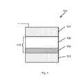
- a resistive switching device structure 100according to an embodiment of the present invention is provided.
- the device structureincludes a first electrode 102 , a second electrode 104 , and a switching material stack 110 disposed in between the first electrode and the second electrode.
- the switching material stackincludes a first resistive switching material 106 overlying a second resistive switching material 108 .
- First electrode materialcan be a suitable metal material including alloy materials, or a semiconductor material having a suitable conductivity characteristic.
- the first electrodecan be a semiconductor material having a suitable electrical conducting property.
- the first electrodemay include a conductive silicon-bearing material, such as doped (e.g. P-type) polysilicon material, a doped silicon-containing layer, a doped silicon germanium material, and the like.
- the first electrodecan also be a first metal material including alloy materials such as those commonly used in CMOS processing, a combination of metal and doped silicon-containing material, or the like. Examples of the first metal material are copper, tungsten, or aluminum, and other suitable metal materials. In various embodiments, these metal materials may be deposited using a physical vapor deposition process, chemical vapor deposition process, electroplating, or electroless deposition process, including any combinations of these, and others.
- one or more adhesion layers or diffusion layersmay be disposed below the first metal material and/or above the first metal material to reduce contamination of metal material into other portions of the device.
- Diffusion barrier material or adhesion materialmay each include titanium, titanium nitride, tungsten, tungsten nitride, tantalum, tantalum nitride, titanium tungsten, or combinations of these materials.
- the semiconductor materialcan be a doped polysilicon material depending on the implementation.
- the second electrode 104has at least a portion that includes a metal material in direct contact with the first switching material.
- the metal materialcan include a material including metal particles of silver, gold, platinum, palladium, nickel, aluminum, and others.
- mixtures of the materialmay include other compounds besides the metal particles, for example, the metal particles may be part of an alloy with other metals or non-metals.
- the metal materialhas a desirable characteristic in the first switching material and the second switching material, for example, diffusion, oxidation and reduction, and others.
- the second electrodecan also be a second metal material such as those commonly used in CMOS processing such as copper, tungsten, or aluminum, and other suitable metal materials.
- One or more adhesion layersmay be disposed below the second metal material and/or above the second metal material.
- an adhesion layer/barrier layermay include tungsten nitride, titanium, titanium nitride, tantalum, tantalum nitride, or combinations of these films.
- the first switching materialis configured to determine a switching characteristic and retention characteristic of the resistive switching device and the second switching material is configured to control leakage current in the resistive switching device.
- the first switching materialis an undoped amorphous silicon material an intrinsic semiconductor, a non-stoichiometric material, such as a silicon sub-oxide, or the like.
- the switching material usedis usually a non-conductive material having defect sites or grain boundaries allowing a plurality of metal particles from the second metal electrode to form a metal region therein when a voltage is applied to the second electrode or the first electrode.
- the switching materialmay include a metal oxide, or the like.
- the polysilicon materialallows for controlling and improving switching properties of the amorphous silicon switching material.
- switching materialssuch as metal oxide, or other non-conductive material having defect sites or grain boundaries or non-stoichiometric sites, such as a silicon sub-oxide
- other contact materialmay be used, or the contact layer may not be needed.
- the first switching materialcan be an amorphous semiconductor and/or sub-oxide material such as Si, Ge, Si x Ge y , SiO x and Si x Ge y O z .
- any such sub-oxiderefers to a non-stoichiometric oxide.
- An example of thisis silicon oxide: stoichiometric silicon oxide is SiO2, and non-stoichiometric oxide may be SiOx where 0 ⁇ x ⁇ 2.
- other forms of non-stoichiometric oxidemay be formed or grown using various fabrication techniques.
- the amorphous material and/or suboxideis characterized by a switching voltage ranging from about 1.0 to about 4 volts, 1.5 volts to about 4 volts, or the like, depending on the process condition.
- the composition of the first switching material layermay be non-uniform. For example, SiOx in an upper region of a resistive switching material layer and SiOy in a lower region, where 0 ⁇ y ⁇ x ⁇ 2, or the like.
- the second switching materialcan be a solid electrolyte material.
- the solid electrolyte materialcan include be chalcogenide based such as Ge x S y , Ge x Se y , SbxTe y , Ag x Se y , and Cu x S y , or can be metal oxide based such as WO x , TiO x , AlO x , HfO x , CuO x , and TaO x , where 0 ⁇ x ⁇ appropriate stoichiometric value (e.g. 2, 3, etc.) (e.g. GeS, GeSe, WO 3 , or SbTe, and the like).
- chalcogenide basedsuch as Ge x S y , Ge x Se y , SbxTe y , Ag x Se y , and Cu x S y
- metal oxide basedsuch as WO x , TiO x , AlO x
- the solid electrolyte materialcan have a first switching voltage ranging from about 0.1 volt to about 1.0, about 0.1 volt to about 0.5 volt, or the like depending on the solid electrolyte material.
- the solid electrolyte materialfurther provides a temperature advantage in processing, as the deposition temperature is generally less than about 400 Degree Celsius.
- Ge x S y , Ge x Se y (e.g. GeS, GeSe) and SbxSe y (e.g. SbSe)can be deposited using a sputtering process performed at about room temperature.
- WO xe.g.
- WO 3can be formed by oxidation of tungsten metal, a common material used in COMS processing, at a temperature of about 400 Degree Celsius or less.
- TiO x , AlO x , and HfO xcan be deposited using a sputtering or an ALD (atomic layer deposition) process at lower than 400 Degree Celsius.
- ALDatomic layer deposition
- metal materialsuch as copper or silver has a high diffusivity in the solid electrolyte material
- the first switching voltageis small and write voltage is generally lower than erase voltage for the solid electrolyte material (for example, Ge x Se y (e.g. GeSe) has a write voltage of about 0.4 volt and an erase voltage of about ⁇ 0.2 volt).
- an additional barrier material layermay be disposed between first switching material 106 and metal material 104 .
- This barrier material layermay provide a barrier against undesired contaminants from affecting first switching material 106 , or the like.
- the barrier materialmay include titanium, titanium oxide, tungsten, or the like.
- FIG. 2illustrates switching characteristic of the first switching device using amorphous silicon material as the switching material.
- the first switching deviceincludes a first electrode 202 , a second electrode 204 , and an amorphous silicon material 206 disposed in between the first electrode and the second electrode.
- the second electrodehas at least a portion that includes a metal material in a specific embodiment.
- the metal materialcan be silver, gold, platinum, palladium, nickel, aluminum, and others.
- a positive voltage 208 greater than a first threshold voltageis applied to the second electrode of an as fabricated device, a metal region 210 is formed in a portion of the amorphous silicon material and causes the first switching device to be in a high resistance state or an off state.
- the formation of the metal region in the amorphous silicon materialis a diffusion process assisted by an electric field upon application of the positive voltage to the second electrode.
- the metal regionis formed from neutral metal particles that are derived from the second electrode and are located in defect sites of the switching material.
- the metal regionincludes a first filament structure 212 , which expands or retracts depending on an amplitude and polarity of voltage applied.
- a write voltage +Vth1.1is applied, causing the first filament structure to extend.
- the amorphous silicon materialis in a low resistance state and the first switching device is at an on state and an on state current flows in the amorphous silicon material.
- the write voltageis a positive voltage applied to the second electrode and can range from about 1 to 6 volts depending on the process conditions of the amorphous silicon material, among others.
- rectificationis possible for a low on state current (for example, less than about 2 u amp).
- filament structureis not stable at low on state current, and data retention is therefore poor.
- Repeatable resistive switchingcan be provided by formation or deformation of the filament structure within the switching material.
- the repeatable resistive switchingcan be in response to application, and subsequent variation, of a voltage to the two terminal resistive switching device.
- the devicecan be switching from a high resistance state, e.g., off, to a low resistance state, e.g., on, when the voltage is increased beyond a certain threshold voltage (e.g., a filament formation voltage).
- the devicecan be switched from the low resistance state to the high resistance state, e.g., off, when the voltage is decreased lower than a second threshold voltage.
- a voltage between the certain threshold voltage and the second threshold voltagecan cause a current resistance state of the device to remain unchanged (and utilized, e.g., to read the current resistance state of the device).
- a positive voltage applied to the top wiring structurecan generate an electric field(s) causing particles of conductive material (ions) to form and diffuse within the switching material.
- the particles of conductive materialcan form a structure (e.g., a filament) extending at least in part across a switching material when the positive voltage is removed.
- the filamentcreates an electrical pathway across switching material, resulting in the low resistance state mentioned above.
- a suitable negative voltage applied to the top wiring structurecan generate a second electric field(s) that at least in part deforms the filament. Deformation of the filament can interrupt the electrical pathway across switching material, resulting in the high resistance state.
- FIG. 2Aillustrates switching behavior of the first switching device using amorphous silicon material as the switching material.
- the first switching devicehas a first forward switching threshold or a first write voltage of Vth1.1 and a first erase voltage of ⁇ Vth1.2 and Vth1.1>>
- the second switching deviceincludes a first electrode 306 and a second electrode 308 .
- a second filament structure 310is formed in the solid electrolyte material.
- the second filament structuremay be formed by a chemical reaction, for example, a reduction/oxidation reaction when the positive voltage is applied.
- the second filament structureforms a conductive path in the solid electrolyte material and causes a second low resistance state in the solid electrode material.
- a negative voltage applied to the second electrodewould break or cause discontinuity in the second filament structure and the solid electrolyte material reverts back to a high resistive state.
- FIG. 3Aillustrates a switching behavior of the second switching device using solid electrolyte material as the switching material.
- the second switching devicehas a second forward switching threshold or a second write voltage of Vth2.1 and a second erase voltage of ⁇ Vth2.2 and Vth2.1>>
- FIG. 4-8illustrate operations of a switching device comprising two switching materials according to an embodiment of the present invention.
- an as fabricated device 400is provided.
- the as fabricated deviceincludes a first electrode 402 , a switching material stack comprises of a first switching material 404 and a second switching material 406 .
- the first switching materialoverlies the second switching material, and a second electrode 408 overlies the first switching material, as shown.
- the first electrodecan include a first metal material.
- the first metal materialcan be tungsten, copper, or aluminum or a conductor material commonly used in CMOS processing depending on the application.
- the first switching materialincludes an amorphous silicon material and the second switching material includes a solid electrolyte in a specific embodiment.
- the second electrodehas at least a portion that includes a metal material in direct contact with the first switching material.
- the metal materialcan be silver, copper, nickel, gold, palladium, aluminum or other suitable metals having a desirable diffusivity characteristic in the first switching material and the second material in a specific embodiment.
- first metal region 410is formed in a portion of the solid electrolyte material and a second metal region 412 is formed in a portion of the amorphous silicon material.
- First metal region 410is characterized by a first filament structure and a first length.
- the first filament structureincludes a series of metal particles to provide a conductive path in the solid electrolyte material.
- second metal region 412further includes a second filament structure characterized by a second length.
- the first length and the second lengthdepend on an operating voltage and respective switching voltage of each of the amorphous silicon material and the solid electrolyte material.
- the switching deviceis now at an initial off state in which the amorphous silicon material is in a first high resistance state and a first off state.
- the solid electrolyte materialis in a second high resistance state or a second off state.
- a second voltage greater than about a write voltage Vth1.1 for the amorphous silicon materialis applied.
- the second filament structure in the amorphous silicon materialextends 502 .
- the second voltagewould turn on both amorphous silicon material and the solid electrolyte and a third filament structure 504 is formed in the solid electrolyte material as shown in FIG. 5 .
- the switching deviceis now being written in which the amorphous silicon material is in a first low resistance state and a first on state and the solid electrolyte material is in a second low resistance state or a second on state. This is only a transient state during writing.
- a corresponding I-V representation 504is also shown in FIG. 5 .
- FIG. 6is a simplified diagram illustrating a first erase cycle after writing when a fourth voltage more negative than a first erase voltage for the solid electrolyte material ⁇ Vth2.2 is applied. Corresponding I-V curve 604 is also shown. The third filament structure in the solid electrolyte material retracts and the solid electrolyte is back to the high resistance state. The fourth voltage is not high enough to cause the amorphous silicon to be in a low resistance state and the second filament structure 608 remains extended in the amorphous silicon material. In this instant, the amorphous silicon is in the on state or written state while the solid electrolyte material is in the off state or erase state and the device remains in a written state or on state.
- FIG. 8illustrate an erase operation of the resistive switching device according to an embodiment of the present invention.
- the devicestarts at a written state as in FIG. 5 .
- both the solid electrolyte material and the amorphous silicon materialare at their respective on states or low resistance states.
- a negative voltage having an amplitude greater than Vth1.2would cause the first metal structure in the solid electrolyte material and the metal filament structure in the amorphous silicon material to retract.
- both the amorphous silicon material and the sold electrolyte materialare in their respective high resistance states and the resistive switching device is at an off state. Therefore, from FIGS. 4-8 , in some embodiments, the amorphous silicon material is written first and can be erased after the solid electrolyte has been erased.
- a device state of the resistive switching deviceis determined by a state of the amorphous silicon material. That is the resistive switching device is at an on state if the amorphous silicon material is at an on state or a low resistance state. The device is in an off state if both the amorphous silicon material and the solid electrolyte material are in their respective high resistance states. During a write process, a voltage greater than +Vth1.1 would cause both the amorphous silicon material and the solid electrolyte to be in a low resistance state.
- a read voltageis applied.
- the read voltagecan be in a range between +Vth2.1 and +Vth1.1, so that the read voltage would not turn on the amorphous silicon material if it is at a high resistance state or the device in at an off state. If the device is at an on state, the read voltage between +Vth2.1 and +Vth1.1 would merely measure the state of the device.
- amorphous silicon materialin an ideal situation, during a write process, only the amorphous silicon material is caused to be at an on state, and during an erase cycle, only the amorphous silicon material is caused to be at an off state.
- the solid electrolytehas a lower on voltage and a lower off voltage than the amorphous silicon material, and would be turned on at the on voltage of the amorphous silicon material and would be turned off at the off voltage of the amorphous silicon material. Therefore, in a write cycle, a voltage greater than Vth1.1 would cause both the amorphous silicon material and the solid electrolyte material to be in their respective on states. A subsequent voltage between ⁇ Vth2.2 and ⁇ Vth1.2 would only turn off the solid electrolyte material and the device is at on state with only the amorphous silicon material being at on state.
- the read voltagewould only turn on the solid electrolyte material.
- the solid electrolyteis turned off after the read process using a voltage between ⁇ Vth2.2 and ⁇ Vth1.2. If the device is at an off state, only the solid electrolyte material would be turned on and the amorphous silicon material would remained at the off state, so that the read voltage would not turn on the amorphous silicon material and only determines the state of the device.
- An illustrationis shown in a voltage pulse diagram in FIG. 9 .
- the state (on or off) of a deviceshould not be altered by a read voltage.
- Voltage overshoot or undershootcan occur as shown in FIG. 10 . If the device is at an off state, voltage overshoot may cause a write process in the amorphous silicon material if the amorphous silicon material is at an off state, a voltage undershoot could cause an erase process in the solid electrolyte material. Therefore, to use a short voltage pulse for read, a voltage greater that the on voltage for the solid electrolyte material (Vth2.1) is first applied.
- the deviceif the device is in an on state, the device would be turned on by the on voltage for the solid electrolyte material. An erase voltage greater than the erase voltage for the solid electrolyte material is then applied.
- the read voltage pulsecan have an amplitude between the write voltage of the solid electrolyte material and the write voltage of the amorphous silicon material followed by an erase voltage between the erase voltage of the amorphous silicon material and the erase voltage of the solid electrolyte material to ensure that the device state would not be altered in the read process.
- leakage current in the devicecan be suppressed during a read process as illustrated in the I-V characteristic in FIG. 11 .
- the amorphous silicon materialis at an on state or low resistance state. Leakage current in the device is suppressed if the solid electrolyte material is at a high resistance state. Therefore, a read voltage between the erase voltage ( ⁇ Vth1.2) of the amorphous silicon material and the write voltage of the solid electrolyte material (Vth2.1) would suppress leakage current.
- the read voltage appliedshould be no greater than +Vth2.1 to prevent turning on the solid electrolyte material to cause leakage current (of the unselected cells), and the read voltage should not be more negative than ⁇ Vth1.2 so that the on state of the amorphous silicon is maintained (of the unselected cells).
- Embodiments according to the present inventionfurther provide a method to suppress leakage current in an array, for example in an interconnected crossbar array, to prevent erroneous reading of a state of a target cell.
- a sneak path for leakage currentcan include at least three cells coupled to the target cell in the crossbar array as shown in FIG. 12 .
- a first cell 1202 , a second cell 1204 , a third cell 1208 , and a fourth cell 1206 in a crossbar arrayare provided.
- Each of the first cell, the second cell, the third cell, and the fourth cellhas a two layer switching material configuration as shown in FIG. 1 .
- the two layer switching materialincludes an amorphous silicon as the first switching material and a solid electrolyte as the second switching material.
- the first cellis the target cell for read.
- the second cell 1204 and the first cell 1202share a common first electrode 1210
- the third cell 1208 and the fourth cell 1206share a common second electrode 1212 .
- the fourth cell 1206is indirectly connected to the first cell 1202 through the second cell 1204 and the third cell 1208 .
- a forward biased voltage 1214 for readis applied on common first electrode 1210 , as shown, to the first cell 1202 and a read current is measured. This would cause the second cell 1204 and the third cell 1208 to be forward biased as they are electrically connected to the first cell, the fourth cell 1206 would remain reverse bias since it is not directly connected to the first cell.
- the second cell 1204 , the third cell 1208 , and the fourth cell 1206are each at on state, that is, the amorphous silicon material in all three cells are at low resistant state, the leakage current (e.g. via 1203 , 1206 and 1208 ) would be most severe if no rectification is provided.
- the solid electrolyte material in each of the three cellscan be at on state or off state.
- the solid electrolyte material in each of the three cells1204 , 1206 , 1208 are at off state or high resistance state
- the read voltageis no greater than three times the write voltage of the solid electrolyte material
- the solid electrolyte material (of cells 1204 , 1206 and 1208 )would not be turned on, no leakage current would be allowed to flow in the target cell.
- a read voltageshould be greater than the write voltage for the solid electrolyte material to determine the state of the target cell.
- the read voltageshould be greater than the write voltage of the solid electrolyte material of the target cell but no greater than three times the write voltage of the solid electrolyte material: Vth 2.1 ⁇ V read ⁇ 3 Vth 2.1
- the reversed biased cellis erased, the voltage drop across the reversed biased cell decreases and the solid electrolyte material in other cells in the sneak path are erased and the erase at a higher speed, in ns usually.
- the sneak pathis blocked, as the cells are in a higher resistance state and the resistance of the target cell ( 1202 ) can be measured.
- the magnitude of the erase voltage (Vth2.2)is usually smaller than the magnitude of write voltage (Vth2.1) for the solid electrolyte material, the forward biased cells (second cell 1204 and the third cell 1208 ) in the sneak path would not be affected.
- the resistive switching materialscan be formed as a part of the first electrode, or as a part of the second electrode, or as a switching element formed in an intersection region of the first electrode and the second electrode.
- FIG. 13is a simplified diagram illustrating a first device structure and a method for fabricating a resistive switching device using more than one switching materials according to an embodiment of the present invention is provided.
- the methodincludes providing a substrate 1302 having a surface region.
- the substratecan be a suitable semiconductor material such as single crystal silicon wafer, a silicon on insulator (commonly called SOI), or a silicon germanium material depending on the application.
- the substratecan include one or more transistor devices (e.g. CMOS transistor devices) formed thereon.
- the one or more transistorsprovide control circuitry for the resistive switching device in a specific embodiment.
- the devicesmay include logic, processing circuitry, or the like.
- a first dielectric material 1304is formed overlying the surface region of the semiconductor substrate.
- the first dielectric materialcan be silicon oxide, silicon nitride, a high K dielectric material, a low K dielectric material, or a combination, depending on the application.
- the methodincludes depositing a first electrode material overlying the first dielectric material.
- the first electrode materialcan be tungsten, copper or aluminum and further includes one or more diffusion barrier or adhesion layer depending on the electrode material used.
- the methodincludes depositing a first switching material overlying the first electrode material.
- the first switching materialis characterized by a first resistance depending on a first switching voltage applied to the device.
- the first switching materialcan be a solid electrolyte material.
- the solid electrolyte materialcan be WO3, GeSe, GeS, SbTe, and the like.
- the first switching materialcan be deposited using a sputtering process from a suitable target material.
- the WO3can be formed by oxidation of a tungsten electrode in a specific embodiment. Oxidation temperature can be at about 300 Degree Celsius or lower, compatible to CMOS processing.
- the solid electrolyte materialhas a switching voltage ranging from about 0.5 volt to about 1.5 volts depending on the material.
- a second switching materialis deposited overlying the first switching material.
- the second switching materialis characterized by a second resistance depending on a second switching voltage.
- the second switching materialis configured to have a second switching voltage of second amplitude higher than that of the first switching material in a specific embodiment.
- the second switching materialcan be an amorphous silicon material in a specific embodiment. Depending on the process conditions, the amorphous silicon material can have a switching voltage ranging from about 1 volt to about 4 volts.
- the methodsubjects the second switching material, the first switching material, and the first electrode material to a first pattern and etch process to form a first structure 1306 .
- the first structureincludes the second switching material 1308 , the first switching material 1310 , and the first electrode material 1312 and configured in an elongated shape and spatially oriented in a first direction in a specific embodiment.
- a second dielectric materialis formed overlying the first structure and spaces between the first structures.
- the second dielectric materialis planarized to isolate each of the first structures in a specific embodiment.
- the first structureincludes an exposed surface region of the second switching material in a specific embodiment.
- the methodincludes forming a second electrode material overlying the first structure.
- the second electrode materialhas a first portion 1314 that includes a metal material in a specific embodiment.
- the metal materialis in direct contact with the second switching material in a specific embodiment.
- the metal materialis characterized by a suitable mobility and diffusivity in the first switching material and the second switching material in a specific embodiment.
- the second electrode materialfurther includes a second portion 1316 that forms a wiring structure for the resistive switching device in a specific embodiment.
- the metal materialcan include silver, gold, palladium, copper, aluminum, nickel and the likes.
- the second electrode materialis subjected to a third pattern and etch process to form a second electrode structure.
- the second electrode structureis elongated in shape and spatially disposed in a second direction at an angle to the first direction.
- the first electrode structure and the second electrode structureare orthogonal to each other to form a crossbar structure.
- the first switching material and the second switching materialare disposed in an intersecting region formed by the first electrode structure and the second electrode structure in a specific embodiment.
- the methodincludes forming a first electrode structure 1412 in a portion of the first dielectric material 304 .
- the first electrode structure 1412is elongated in shape and spatially extended in a first direction in a specific embodiment.
- the first electrode structurecan be formed by first depositing an electrode material overlying the first dielectric material followed by a first pattern and etch process.
- the first electrode materialcan be tungsten, copper or aluminum and further includes one or more diffusion barrier or adhesion layer depending on the electrode material used.
- a second dielectric materialis formed overlying the first electrode structure and filling gaps between the first electrode structures. The second dielectric material is subjected to a planarizing process to expose a surface region of the first electrode structure and to isolate the first electrode structure in a specific embodiment.
- the first electrode structurecan be formed by a damascene process.
- the damascene processincludes formed an opening structure in the first dielectric material by a second pattern and etch process.
- the first electrode material including the one or more diffusion barrier or adhesion layeris formed to fill the opening structure and a thickness overlying the first dielectric material.
- the methodthen performs a planarization process to remove the first thickness of first electrode material overlying the first dielectric material to isolate the first electrode material in the opening structure in a specific embodiment.
- the first electrode structureis configured in an elongated manner and extends in a first direction in a specific embodiment.
- the methodforms a first switching material comprising a solid electrolyte material 1410 overlying the first electrode structure and a second switching material 1408 overlying the first switching material.
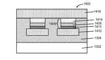
- a metal material 1414is formed overlying the second switching material. Similar to the device structure in FIG. 13 , the first switching material 1410 comprises a solid electrolyte material and the second switching material comprises an amorphous silicon material.
- the metal 1414can include silver, gold, palladium, copper, aluminum, nickel and the like. Silver material in and the respective dielectric material depend on the way the first electrode structure is formed.
- the second switching material 1408comprising an amorphous silicon material is formed overlying the first switching material.
- each of the pillar structuresincludes the first switching material, the second switching material, and the metal material in a specific embodiment.
- Each of the pillar structuresare formed overlying at least a portion of the first electrode structure and maintain an electrical contact with the first electrode structure in a specific embodiment.
- the methodincludes forming a third dielectric material overlying each of the pillar structures.
- the third dielectric materialis planarized to expose a surface region of the metal material and to isolate each of the pillar structures in a specific embodiment.
- a second electrode materialis deposited overlying the metal material and the planarized third dielectric material in a specific embodiment.
- the second electrode materialhas a first portion that include the metal material selected from silver, gold, palladium, copper, aluminum, nickel and the likes for amorphous silicon material as the second switching material.
- the second electrode materialfurther includes a second portion 1416 for a second wiring structure for the switching device in a specific embodiment.
- the second electrode materialis subjected to a fourth pattern and etch process to form a second electrode structure overlying the at least the second switching material and the third dielectric material.
- the second electrode structureis configured to extend in a second direction at an angle to the first angle.
- the second electrodeis configured orthogonal to the first electrode structure.
- Embodiment in FIG. 15forms a first electrode structure 1512 spatially disposed in a first direction.
- a second structure 1506comprising the first switching material 1508 , the second switching material 1510 , the metal material 1514 , and the second electrode material 1516 is formed overlying at least the first electrode structure 1512 .
- the second structureis elongated in shape and spatially configured in a second direction orthogonal to the first direction in a specific embodiment.
- FIGS. 13, 14, and 15illustrate ways to form a crossbar array of switching devices using more than one switching material according to embodiments of the present invention.
- the switching devicehas desirable properties to form a crossbar array of devices, for example rectifying, good retention characteristics, among others.
- rectifyingfor example rectifying
- good retention characteristicsfor example rectifying
- one skilled in the artwould recognized other variations, modifications, and alternatives.
Landscapes
- Chemical & Material Sciences (AREA)
- Engineering & Computer Science (AREA)
- Materials Engineering (AREA)
- Semiconductor Memories (AREA)
Abstract
Description
This application is a continuation-in-part of U.S. application Ser. No. 13/920,021 filed Jun. 17, 2013, now U.S. Pat. No. 8,947,908, to be issued on Feb. 3, 2015, which is a continuation-in-part of U.S. application Ser. No. 13/290,024, filed Nov. 4, 2011, now U.S. Pat. No. 8,467,227 issued Jun. 18, 2013, which is a non-provisional of U.S. Application No. 61/410,035, filed Nov. 4, 2010. U.S. application Ser. No. 13/920,021 filed Jun. 17, 2013 also claims priority to and is a continuation-in-part of U.S. application Ser. No. 13/585,759, filed Aug. 14, 2012, now U.S. Pat. No. 8,569,172 issued Oct. 29, 2013; U.S. Application No. 61/712,171, filed Oct. 10, 2012; and U.S. application No. 61/786,100, filed Mar. 15, 2013. This application also claims priority to and is a continuation-in-part of U.S. application Ser. No. 12/835,704 filed Jul. 13, 2010; U.S. patent application Ser. No. 14/509,967 filed Oct. 8, 2014 that claims priority to and is a continuation of U.S. application Ser. No. 12/861,432 filed Aug. 23, 2010, now U.S. Pat. No. 8,884,261, issued Nov. 11, 2014; and U.S. patent application Ser. No. 14/573,817 filed Dec. 17, 2014 that claims priority to U.S. application Ser. No. 13/462,653 filed May 2, 2012, now U.S. Pat. No. 8,946,046, to be issued on Feb. 3, 2015. The above applications are herein by incorporated by reference, for all purposes.
Not Applicable
The present invention is related to switching devices. More particularly, the present invention provides a resistive switching device characterized by a controllable programming current with faster operation speed. Embodiments of the present invention have been applied to fabrication and operation of a resistive random access memory device. But it should be recognized that the present invention can have a much broader range of applicability.
The success of semiconductor devices has been mainly driven by an intensive transistor down-scaling process. However, as field effect transistors (FET) approach sizes less than 100 nm, problems such as short channel effect can degrade device performance. Moreover,such sub 100 nm device size can lead to sub-threshold slope non-scaling and also increases power dissipation. It is generally believed that transistor-based memories such as those commonly known as Flash may approach an end to scaling within a decade.
Other non-volatile random access memory devices such as ferroelectric RAM (Fe RAM), magneto-resistive RAM (MRAM), organic RAM (ORAM), and phase change RAM (PCRAM), among others, have been explored as next generation memory devices. These devices often require new materials and device structures to couple with silicon-based devices to form a memory cell, which lack one or more key attributes. For example, FeRAM and MRAM devices have fast switching characteristics and good programming endurance, but their fabrication is not CMOS compatible and size is usually large. Switching for a PCRAM device requires a high power. Organic RAM is incompatible with large volume silicon-based fabrication and device reliability is usually poor. Desirable attributes of a high density device should include high switching speed, reliable switching, and high endurance, among others.
From the above, a new semiconductor device structure and integration is desirable.
The present invention is directed to switching device. More particularly, the present invention is directed to a resistive switching device having more than one switching material to enhance performance of the resistive switching device. For example, the resistive switching device can include a first switching material for switching and a second material for suppressing leakage current when an operating voltage is applied. Embodiments according to the present invention can be particularly useful for a non-volatile memory device in an interconnected device array. It should be recognized, however, that embodiments according to the present invention can have a much broader range of applicability.
In a specific embodiment, a non-volatile memory device structure is provided. The non-volatile memory device includes a first electrode, a second electrode, and a resistive switching material stack sandwiched between the first electrode and the second electrode. In a specific embodiment, the resistive switching material stack overlies the first electrode. The resistive switching material stack includes a first resistive switching material and a second resistive switching material. In a specific embodiment, the second switching material overlying the first electrode and the first switching material overlying the second switching material. In a specific embodiment, the first switching material is characterized by a first switching voltage having a first amplitude. The second resistive switching material is characterized by a second switching voltage having a second amplitude no greater than the first switching voltage. In a specific embodiment, the second electrode includes at least a metal material overlying the first switching material, and physically and electrically in contact with the first resistive switching material.
In a specific embodiment, a method for writing to a resistive switching device is provided. The method includes providing a resistive switching device. The resistive switching device includes a first electrode, a switching material stack comprising a first switching material and a second switching material, and a second electrode. In a specific embodiment, the second switching material overlies the first electrode, the first switching material overlies the second switching material, and the second electrode comprising at least a metal material overlies the first switching material. The first switching material is characterized by a first switching voltage having a first amplitude. The second switching material is characterized by a second switching voltage. In a specific embodiment, the first amplitude is greater than the second amplitude. In a specific embodiment, the method includes applying a first voltage to the second electrode to cause the first switching material to change from a first high resistance state to a first low resistant state.
In a specific embodiment, a method for erasing of a resistive switching device after write is provided. The method includes providing a resistive switching device in a write state. The resistive switching device includes a first electrode, a switching material stack comprising a first switching material and a second switching material, and a second electrode. In a specific embodiment, the second switching material overlies the first electrode, the first switching material overlies the second switching material, and the second electrode comprising at least a metal material overlies the first switching material. The first switching material is characterized by a first switching voltage having a first amplitude. The second switching material is characterized by a second switching voltage. In a specific embodiment, the first amplitude is greater than the second amplitude. In a specific embodiment, the write state is caused at least by a low resistance state of the first switching material. The method includes applying a first voltage more negative than an erase voltage of the first resistive switching material to cause at least the first switching material to be in a first high resistance state and to cause the resistive switching device to change from the write state to an erased state.
In a specific embodiment, a method to read a state of a resistive switching device is provided. The method includes providing a resistive switching device. The resistive switching device includes a first electrode, a switching material stack comprising a first switching material and a second switching material, and a second electrode. In a specific embodiment, the second switching material overlies the first electrode, the first switching material overlies the second switching material, and the second electrode comprising at least a metal material overlies the first switching material. The first switching material is characterized by a first switching voltage having a first amplitude. The second switching material is characterized by a second switching voltage. In a specific embodiment, the first amplitude is greater than the second amplitude. The method includes applying a read voltage to the second electrode, the read voltage is configured to cause the second switching material to change from a first high resistance state to a first low resistance state while maintaining a resistance state of the first switching material. The method includes determining a read current flowing in the resistive switching device to determine the state of the resistive switching device in a specific embodiment.
In a specific embodiment, a method for suppressing a leak current in a resistive switching device is provided. The method includes providing a resistive switching device. The resistive switching device includes a first electrode, a switching material stack comprising a first switching material and a second switching material, and a second electrode. In a specific embodiment, the second switching material overlies the first electrode, the first switching material overlies the second switching material, and the second electrode comprising at least a metal material overlies the first switching material. The first switching material is characterized by a first switching voltage having a first amplitude. The second switching material is characterized by a second switching voltage. In a specific embodiment, the first amplitude is greater than the second amplitude. The method includes applying a first voltage to the second electrode, the first voltage being configured to cause the second switching material to be at a high resistance state and maintaining the first switching material to be at a low resistance state, the high resistance state suppressing a leak current from applying the first voltage.
In a specific embodiment, a non-volatile memory device structure is provided. The non-volatile memory device structure includes a first electrode configured to extend in a first direction. The non-volatile memory device structure includes a first structure configured to extend in a first direction. In a specific embodiment, the first structure includes a stack of switching material spatially configured to extend in a second direction at an angle to the first direction. In a specific embodiment, the stack of switching material includes a first switching material overlying the first electrode. The first switching material includes a solid electrolyte material in a specific embodiment. The stack of switching material includes a second switching material overlying the first switching material. In a specific embodiment, the second switching material includes an amorphous silicon material in a specific embodiment. The non-volatile memory device structure further includes a second electrode comprising at least a portion comprising a metal material in contact with the amorphous silicon material in a specific embodiment.
In a specific embodiment, a non-volatile memory device structure is provided. The non-volatile memory device structure includes a first structure spatially configured to extend in a first direction. In a specific embodiment, the first structure includes a first electrode, a solid electrolyte material overlying the first electrode and an amorphous silicon material overlying the solid electrolyte material. The non-volatile memory device structure includes a second electrode spatially configured to extend in a second direction at an angle to the first direction. In a specific embodiment, the second electrode includes at least a first portion directly in contact with the amorphous silicon material and a second portion for an interconnect structure.
In a specific embodiment, a non-volatile memory device structure is provided. The non-volatile memory device structure includes a first electrode spatially configured to extend in a first direction, a second electrode spatially configured to extend in a second direction perpendicular to the first direction, and a first structure disposed in an intersection region formed between the first electrode and the second electrode. In a specific embodiment, the first structure includes a solid electrolyte material overlying the first electrode and an amorphous silicon material overlying the solid electrolyte material. In a specific embodiment, the second electrode includes at least a metal material in direct contact with the amorphous silicon material.
Additional aspects include a method of reading a resistive switching device in a crossbar array, comprising: providing a first switching device, a second switching device, a third switching device, and a fourth switching device, the first switching device being in a first resistance state, each of the first switching device, the second switching device, the third switching device, and the fourth switching device comprising at least a first switching material and a second switching material, the first switching material being characterized by a first on voltage and a first off voltage and the second switching material being characterized by a second on voltage and a second off voltage, the first on voltage being greater than the second on voltage, the first off voltage being greater than the second off voltage; applying a read voltage to the first switching device, the read voltage being configured to maintain the second switching material of at least one of the second switching device, the third device and the fourth device to be at a high resistance state, the high resistance state suppressing a leakage current from at least one of the second switching device, the third device and the fourth device to flow in the first switching device; and measuring a read current in the first switching device caused by the read voltage to determine the first resistance of the first switching device.
Additional aspects include the method of above wherein the first on voltage causes the first switching material to change from a first high resistance state to a first low resistance state and the first off voltage causes the first switching material to change from the first low resistance state to a first high resistance state.
Additional aspects include the method of above wherein the second on voltage causes the second switching material to change from a second high resistance state to a second low resistance state and the second off voltage causes the second switching material to change from the second low resistance state to a second high resistance state.
Additional aspects include the method of above wherein the read voltage is configured to be greater than the second on voltage and no greater than three times the second first on voltage to maintain the second switching material of at least one of the second switching device, the third device and the fourth device to be at the high resistance state.
Additional aspects include a non-volatile memory device structure comprising: a first electrode configured to extend in a first direction; and a first structure comprising a stack of material spatially configured to extend in a second direction at an angle to the first direction, the stack of material comprising: a solid electrolyte material overlying the first electrode; an amorphous silicon material overlying the solid electrolyte material; and a second electrode comprising at least a portion comprising a metal material in contact with the amorphous silicon material.
Additional aspects include a non-volatile memory device structure comprising: a first structure spatially configured to extend in a first direction, the first structure comprising: a first electrode; a solid electrolyte material overlying the first electrode; an amorphous silicon material overlying the solid electrolyte material; and a second electrode spatially configured to extend in a second direction at an angle to the first direction, the second electrode comprising at least a first portion directly in contact with the amorphous silicon material and a second portion for an interconnect structure.
Additional aspects include a non-volatile memory device structure comprising: a first electrode spatially configured to extend in a first direction; a second electrode spatially configured to extend in a second direction, the second direction being perpendicular to the first direction; and a first structure disposed in an intersection region formed between the first electrode and the second electrode, the first structure comprising: a solid electrolyte material overlying the first electrode; an amorphous silicon material overlying the solid electrolyte material.
Additional aspects include a method for suppressing a leak current in a resistive switching device, comprising: providing a resistive switching device, the resistive switching device comprising a first electrode, a switching material stack comprising a first switching material and a second switching material, the second switching material overlying the first electrode, the first switching material overlying the second switching material, and a second electrode comprising at least a metal material overlying the first switching material, the first switching material being characterized by a first switching voltage, the second switching material being characterized by a second switching voltage, the first switching voltage being characterized by a first amplitude and the second switching device being characterized by a second amplitude, the first amplitude being greater than the second amplitude; and applying a first voltage to the second electrode, the first voltage being configured to cause the second switching material to be at a high resistance state and maintaining the first switching material to be at a low resistance state, the high resistance state suppressing a leak current from applying the first voltage.
Additional aspects includes a method according to the above wherein the first voltage is no greater than an on voltage for the first switching material and less negative than an off voltage for the second switching material.
Many benefits can be achieved by ways of the present invention. Embodiments according to the present invention provide a device structure to form a non-volatile memory device that has leakage current suppressed or eliminated, which is essential for a crossbar array of memory cells. The device structure further provides desirable characteristics for write, read, and erase and allowing fabrication of a memory device having a high on state current and desirable data retention characteristic. Additionally, the present device uses materials and techniques that are compatible with current CMOS processing. Depending on the embodiment, one or more of these benefits may be achieved. One skilled in the art would recognize other variations, modifications, and alternatives.
The present invention is directed to switching device. More particularly, the present invention is directed to a resistive switching device having more than one switching material to enhance performance of the resistive switching device. For example, the resistive switching device can include a first switching material for switching and a second material for suppressing leakage current when an operating voltage is applied. Embodiments according to the present invention can be particularly useful for a non-volatile memory device in an interconnected device array. It should be recognized that embodiments according to the present invention can have a much broader range of applicability.
High density and low cost storage devices are in ever increasing demand due to the growth in consumer devices common in the market place. Current non-volatile memory devices including Flash are probably at an end to further scaling due to fundamental limitations in the devices. It is predicted that current charge storage in a floating gate or a dielectric material in Flash may not be possible in device size less that about 10 nm. A new category of devices using an interconnected crossbar configuration that are vertically integrated in a three dimensional manner can have a high device density not achievable in current memory devices.
However, leakage current from a cell in an interconnected crossbar array can form a sneak path in the array. A sneak path is a current path for leakage current from one cell to propagate in an array of cells. The leakage current can interfere with proper operations (read write, or erase) in all the cells in the sneak path. To suppress the leakage current and to isolate a cell from the leakage current, a rectifier can be used. The rectifier adds complexity to the device design and could be difficult to integrate in a crossbar array. Certain devices may have rectifying behavior but such devices usually have a symmetrical IV characteristic, which does not work well in a crossbar array. Other cells may have a low on state current and thus have poor data retention properties.
Additionally, to exploit the advantage for vertically stacking of cells, controlling CMOS devices are usually first formed on a substrate and the memory arrays are subsequently fabricated above the CMOS devices. Processing temperature of the memory cells should not be greater than 500 Degree Celsius to ensure proper functioning of the CMOS devices. Embodiments of the present invention provide a device structure and related methods to form a resistive switching device that is rectifying and processing parameters that are compatible with current CMOS device processing technologies.
Referring toFIG. 1 . A resistiveswitching device structure 100 according to an embodiment of the present invention is provided. The device structure includes afirst electrode 102, asecond electrode 104, and a switchingmaterial stack 110 disposed in between the first electrode and the second electrode. The switching material stack includes a firstresistive switching material 106 overlying a secondresistive switching material 108.
First electrode material can be a suitable metal material including alloy materials, or a semiconductor material having a suitable conductivity characteristic. In one specific embodiment, the first electrode can be a semiconductor material having a suitable electrical conducting property. For example, the first electrode may include a conductive silicon-bearing material, such as doped (e.g. P-type) polysilicon material, a doped silicon-containing layer, a doped silicon germanium material, and the like. The first electrode can also be a first metal material including alloy materials such as those commonly used in CMOS processing, a combination of metal and doped silicon-containing material, or the like. Examples of the first metal material are copper, tungsten, or aluminum, and other suitable metal materials. In various embodiments, these metal materials may be deposited using a physical vapor deposition process, chemical vapor deposition process, electroplating, or electroless deposition process, including any combinations of these, and others.
In certain embodiments, one or more adhesion layers or diffusion layers may be disposed below the first metal material and/or above the first metal material to reduce contamination of metal material into other portions of the device. Diffusion barrier material or adhesion material may each include titanium, titanium nitride, tungsten, tungsten nitride, tantalum, tantalum nitride, titanium tungsten, or combinations of these materials. The semiconductor material can be a doped polysilicon material depending on the implementation.
Depending on the application, thesecond electrode 104 has at least a portion that includes a metal material in direct contact with the first switching material. In a specific embodiment, the metal material can include a material including metal particles of silver, gold, platinum, palladium, nickel, aluminum, and others. In some embodiments, mixtures of the material may include other compounds besides the metal particles, for example, the metal particles may be part of an alloy with other metals or non-metals.
The metal material has a desirable characteristic in the first switching material and the second switching material, for example, diffusion, oxidation and reduction, and others.
In various embodiments, the second electrode can also be a second metal material such as those commonly used in CMOS processing such as copper, tungsten, or aluminum, and other suitable metal materials. One or more adhesion layers may be disposed below the second metal material and/or above the second metal material. For example, an adhesion layer/barrier layer may include tungsten nitride, titanium, titanium nitride, tantalum, tantalum nitride, or combinations of these films.
In a specific embodiment, the first switching material is configured to determine a switching characteristic and retention characteristic of the resistive switching device and the second switching material is configured to control leakage current in the resistive switching device. In some embodiments, the first switching material is an undoped amorphous silicon material an intrinsic semiconductor, a non-stoichiometric material, such as a silicon sub-oxide, or the like. The switching material used is usually a non-conductive material having defect sites or grain boundaries allowing a plurality of metal particles from the second metal electrode to form a metal region therein when a voltage is applied to the second electrode or the first electrode. In some embodiments, the switching material may include a metal oxide, or the like.
In a specific embodiment, the polysilicon material allows for controlling and improving switching properties of the amorphous silicon switching material. For other switching materials, such as metal oxide, or other non-conductive material having defect sites or grain boundaries or non-stoichiometric sites, such as a silicon sub-oxide, other contact material may be used, or the contact layer may not be needed. Of course, one skilled in the art would recognize other variations, modifications, and alternatives.
In a specific embodiment, the first switching material can be an amorphous semiconductor and/or sub-oxide material such as Si, Ge, SixGey, SiOxand SixGeyOz. It should be understood that any such sub-oxide refers to a non-stoichiometric oxide. An example of this is silicon oxide: stoichiometric silicon oxide is SiO2, and non-stoichiometric oxide may be SiOx where 0<x<2. In various embodiments, other forms of non-stoichiometric oxide may be formed or grown using various fabrication techniques. The amorphous material and/or suboxide is characterized by a switching voltage ranging from about 1.0 to about 4 volts, 1.5 volts to about 4 volts, or the like, depending on the process condition. In various embodiments, the composition of the first switching material layer may be non-uniform. For example, SiOx in an upper region of a resistive switching material layer and SiOy in a lower region, where 0<y<x<2, or the like.
As merely an example, the second switching material can be a solid electrolyte material. The solid electrolyte material can include be chalcogenide based such as GexSy, GexSey, SbxTey, AgxSey, and CuxSy, or can be metal oxide based such as WOx, TiOx, AlOx, HfOx, CuOx, and TaOx, where 0<x<appropriate stoichiometric value (e.g. 2, 3, etc.) (e.g. GeS, GeSe, WO3, or SbTe, and the like). The solid electrolyte material can have a first switching voltage ranging from about 0.1 volt to about 1.0, about 0.1 volt to about 0.5 volt, or the like depending on the solid electrolyte material. The solid electrolyte material further provides a temperature advantage in processing, as the deposition temperature is generally less than about 400 Degree Celsius. For example, GexSy, GexSey(e.g. GeS, GeSe) and SbxSey(e.g. SbSe) can be deposited using a sputtering process performed at about room temperature. WOx(e.g. WO3) can be formed by oxidation of tungsten metal, a common material used in COMS processing, at a temperature of about 400 Degree Celsius or less. TiOx, AlOx, and HfOxcan be deposited using a sputtering or an ALD (atomic layer deposition) process at lower than 400 Degree Celsius. As metal material such as copper or silver has a high diffusivity in the solid electrolyte material, the first switching voltage is small and write voltage is generally lower than erase voltage for the solid electrolyte material (for example, GexSey(e.g. GeSe) has a write voltage of about 0.4 volt and an erase voltage of about −0.2 volt). In various embodiments, an additional barrier material layer may be disposed between first switchingmaterial 106 andmetal material 104. This barrier material layer may provide a barrier against undesired contaminants from affecting first switchingmaterial 106, or the like. In some embodiments, the barrier material may include titanium, titanium oxide, tungsten, or the like.
Repeatable resistive switching can be provided by formation or deformation of the filament structure within the switching material. For instance, the repeatable resistive switching can be in response to application, and subsequent variation, of a voltage to the two terminal resistive switching device. As one example, the device can be switching from a high resistance state, e.g., off, to a low resistance state, e.g., on, when the voltage is increased beyond a certain threshold voltage (e.g., a filament formation voltage). The device can be switched from the low resistance state to the high resistance state, e.g., off, when the voltage is decreased lower than a second threshold voltage. In some embodiments, a voltage between the certain threshold voltage and the second threshold voltage can cause a current resistance state of the device to remain unchanged (and utilized, e.g., to read the current resistance state of the device).
In one or more disclosed embodiments, a positive voltage applied to the top wiring structure can generate an electric field(s) causing particles of conductive material (ions) to form and diffuse within the switching material. The particles of conductive material can form a structure (e.g., a filament) extending at least in part across a switching material when the positive voltage is removed. Under suitable circumstances (e.g., application of the positive voltage or the electric field(s)), the filament creates an electrical pathway across switching material, resulting in the low resistance state mentioned above. In additional embodiments, a suitable negative voltage applied to the top wiring structure can generate a second electric field(s) that at least in part deforms the filament. Deformation of the filament can interrupt the electrical pathway across switching material, resulting in the high resistance state.
As shown in a simplified diagram inFIG. 3 , switching behavior of asecond switching device 300 using asolid electrolyte 302 as a switching material is illustrated. The second switching device includes afirst electrode 306 and asecond electrode 308. As shown, when apositive voltage 304 is applied tosecond electrode 308, asecond filament structure 310 is formed in the solid electrolyte material. The second filament structure may be formed by a chemical reaction, for example, a reduction/oxidation reaction when the positive voltage is applied. The second filament structure forms a conductive path in the solid electrolyte material and causes a second low resistance state in the solid electrode material. A negative voltage applied to the second electrode would break or cause discontinuity in the second filament structure and the solid electrolyte material reverts back to a high resistive state.
In addition, |Vth1.x|>>|Vth2.x|, where x=1 or 2, that is operating voltages (write, erase or read) of the first switching device (using amorphous silicon as switching material) is configured to be greater than operating voltages of the second switching device using solid electrolyte material as switching device.
Referring again toFIG. 4 , when a voltage greater than a first threshold voltage Vth1.0 for the amorphous silicon material is applied, afirst metal region 410 is formed in a portion of the solid electrolyte material and asecond metal region 412 is formed in a portion of the amorphous silicon material.First metal region 410 is characterized by a first filament structure and a first length. The first filament structure includes a series of metal particles to provide a conductive path in the solid electrolyte material. In a specific embodiment,second metal region 412 further includes a second filament structure characterized by a second length. In a specific embodiment, the first length and the second length depend on an operating voltage and respective switching voltage of each of the amorphous silicon material and the solid electrolyte material. The switching device is now at an initial off state in which the amorphous silicon material is in a first high resistance state and a first off state. The solid electrolyte material is in a second high resistance state or a second off state.
To write into the switching device, a second voltage greater than about a write voltage Vth1.1 for the amorphous silicon material is applied. The second filament structure in the amorphous silicon material extends502. As the write voltage for the solid electrolyte material is lower, the second voltage would turn on both amorphous silicon material and the solid electrolyte and athird filament structure 504 is formed in the solid electrolyte material as shown inFIG. 5 . The switching device is now being written in which the amorphous silicon material is in a first low resistance state and a first on state and the solid electrolyte material is in a second low resistance state or a second on state. This is only a transient state during writing. A correspondingI-V representation 504 is also shown inFIG. 5 .
To turn on the solid electrolyte material after it is in the off state (for example, as inFIG. 6 ), only a small voltage, greater than about Vth2.1 is needed to turn the solid electrolyte into a low resistance state or an on state. This is illustrated inFIG. 7 . As shown, when a voltage greater than about Vth2.1 is applied, while the amorphous silicon in at a low resistant state, a voltage greater than about Vth2.1 causes the solid electrolyte material to be in a low resistant state. Now both the amorphous silicon material and the solid electrolyte material are in their respective low resistance states, the resistive switching device is now again being written.
In a specific embodiment, a device state of the resistive switching device is determined by a state of the amorphous silicon material. That is the resistive switching device is at an on state if the amorphous silicon material is at an on state or a low resistance state. The device is in an off state if both the amorphous silicon material and the solid electrolyte material are in their respective high resistance states. During a write process, a voltage greater than +Vth1.1 would cause both the amorphous silicon material and the solid electrolyte to be in a low resistance state.
To determine a state of the device during a read process, a read voltage is applied. The read voltage can be in a range between +Vth2.1 and +Vth1.1, so that the read voltage would not turn on the amorphous silicon material if it is at a high resistance state or the device in at an off state. If the device is at an on state, the read voltage between +Vth2.1 and +Vth1.1 would merely measure the state of the device.
In one embodiment, in an ideal situation, during a write process, only the amorphous silicon material is caused to be at an on state, and during an erase cycle, only the amorphous silicon material is caused to be at an off state. However, this is not possible as the solid electrolyte has a lower on voltage and a lower off voltage than the amorphous silicon material, and would be turned on at the on voltage of the amorphous silicon material and would be turned off at the off voltage of the amorphous silicon material. Therefore, in a write cycle, a voltage greater than Vth1.1 would cause both the amorphous silicon material and the solid electrolyte material to be in their respective on states. A subsequent voltage between −Vth2.2 and −Vth1.2 would only turn off the solid electrolyte material and the device is at on state with only the amorphous silicon material being at on state.
In one embodiment, during a read process, if the device is at an on state, the amorphous silicon material is at an on state or at a low resistance state, the read voltage would only turn on the solid electrolyte material. The solid electrolyte is turned off after the read process using a voltage between −Vth2.2 and −Vth1.2. If the device is at an off state, only the solid electrolyte material would be turned on and the amorphous silicon material would remained at the off state, so that the read voltage would not turn on the amorphous silicon material and only determines the state of the device. An illustration is shown in a voltage pulse diagram inFIG. 9 .
The state (on or off) of a device should not be altered by a read voltage. In cases where short voltage pulses are applied for a read process, voltage rises or falls in a short duration to reduce a pulse width. Voltage overshoot or undershoot can occur as shown inFIG. 10 . If the device is at an off state, voltage overshoot may cause a write process in the amorphous silicon material if the amorphous silicon material is at an off state, a voltage undershoot could cause an erase process in the solid electrolyte material. Therefore, to use a short voltage pulse for read, a voltage greater that the on voltage for the solid electrolyte material (Vth2.1) is first applied. In some embodiments, if the device is in an on state, the device would be turned on by the on voltage for the solid electrolyte material. An erase voltage greater than the erase voltage for the solid electrolyte material is then applied. Alternatively, the read voltage pulse can have an amplitude between the write voltage of the solid electrolyte material and the write voltage of the amorphous silicon material followed by an erase voltage between the erase voltage of the amorphous silicon material and the erase voltage of the solid electrolyte material to ensure that the device state would not be altered in the read process.
In a specific embodiment, leakage current in the device can be suppressed during a read process as illustrated in the I-V characteristic inFIG. 11 . For example, for an on state device, the amorphous silicon material is at an on state or low resistance state. Leakage current in the device is suppressed if the solid electrolyte material is at a high resistance state. Therefore, a read voltage between the erase voltage (−Vth1.2) of the amorphous silicon material and the write voltage of the solid electrolyte material (Vth2.1) would suppress leakage current. That is, the read voltage applied should be no greater than +Vth2.1 to prevent turning on the solid electrolyte material to cause leakage current (of the unselected cells), and the read voltage should not be more negative than −Vth1.2 so that the on state of the amorphous silicon is maintained (of the unselected cells).
Embodiments according to the present invention further provide a method to suppress leakage current in an array, for example in an interconnected crossbar array, to prevent erroneous reading of a state of a target cell. A sneak path for leakage current can include at least three cells coupled to the target cell in the crossbar array as shown inFIG. 12 . As merely an example, afirst cell 1202, asecond cell 1204, athird cell 1208, and afourth cell 1206 in a crossbar array are provided. Each of the first cell, the second cell, the third cell, and the fourth cell has a two layer switching material configuration as shown inFIG. 1 . The two layer switching material includes an amorphous silicon as the first switching material and a solid electrolyte as the second switching material. As merely an example, the first cell is the target cell for read. As shown, thesecond cell 1204 and thefirst cell 1202 share a commonfirst electrode 1210, and thethird cell 1208 and thefourth cell 1206 share a commonsecond electrode 1212. Thefourth cell 1206 is indirectly connected to thefirst cell 1202 through thesecond cell 1204 and thethird cell 1208. To determine the state of the first cell, a forward biasedvoltage 1214 for read is applied on commonfirst electrode 1210, as shown, to thefirst cell 1202 and a read current is measured. This would cause thesecond cell 1204 and thethird cell 1208 to be forward biased as they are electrically connected to the first cell, thefourth cell 1206 would remain reverse bias since it is not directly connected to the first cell.
If thesecond cell 1204, thethird cell 1208, and thefourth cell 1206 are each at on state, that is, the amorphous silicon material in all three cells are at low resistant state, the leakage current (e.g. via1203,1206 and1208) would be most severe if no rectification is provided. In various embodiments, there are again two possibilities for each of the on state cells: the solid electrolyte material in each of the three cells (e.g.1204,1206,1208) can be at on state or off state. For a first case where the solid electrolyte material in each of the three cells (1204,1206,1208) are at off state or high resistance state, if the read voltage is no greater than three times the write voltage of the solid electrolyte material, the solid electrolyte material (ofcells
Vth2.1<Vread<3Vth2.1
Vth2.1<Vread<3Vth2.1
As a device state (on or off) depends only on the state of the amorphous silicon material and independent of the state of the solid electrolyte material, a single voltage pulse is used to turn on or turn off the amorphous silicon material and therefore the device. Of course other variations, modifications, and alternatives exist and would be obvious to one skilled in the art.
Consider again the case where all the cells (e.g.1204,1206,1208) in the sneak path (e.g. via1204,1206,1208) are at on state, and both the amorphous silicon material and the solid electrolyte in the cells in the sneak path are at on state or low resistance state. To prevent leakage current to affect the target cell (1202) during read, a forward read voltage (1214) greater than three times Vth2.2, or three times the erase voltage of the solid electrolyte material is first applied, the solid electrolyte material in the reversed biased cell (for example, thefourth cell 1206 inFIG. 4 ) in the sneak path will be erased and resistance in the reversed biased cell increases. Once the reversed biased cell is erased, the voltage drop across the reversed biased cell decreases and the solid electrolyte material in other cells in the sneak path are erased and the erase at a higher speed, in ns usually. Once the solid electrolyte material in the reversed biased cell is erased, the sneak path is blocked, as the cells are in a higher resistance state and the resistance of the target cell (1202) can be measured. As the magnitude of the erase voltage (Vth2.2) is usually smaller than the magnitude of write voltage (Vth2.1) for the solid electrolyte material, the forward biased cells (second cell 1204 and the third cell1208) in the sneak path would not be affected.
Since the amorphous silicon material and the solid electrolyte material both have a high resistance at off state, more than one method and device structure may be used to fabricate a crossbar array of the resistive switching device having desired rectification characteristics, among others. The resistive switching materials can be formed as a part of the first electrode, or as a part of the second electrode, or as a switching element formed in an intersection region of the first electrode and the second electrode.
In a specific embodiment, the method includes depositing a first electrode material overlying the first dielectric material. The first electrode material can be tungsten, copper or aluminum and further includes one or more diffusion barrier or adhesion layer depending on the electrode material used.
In a specific embodiment, the method includes depositing a first switching material overlying the first electrode material. The first switching material is characterized by a first resistance depending on a first switching voltage applied to the device. In a specific embodiment, the first switching material can be a solid electrolyte material. The solid electrolyte material can be WO3, GeSe, GeS, SbTe, and the like. The first switching material can be deposited using a sputtering process from a suitable target material. For WO3 as the first switching material, the WO3 can be formed by oxidation of a tungsten electrode in a specific embodiment. Oxidation temperature can be at about 300 Degree Celsius or lower, compatible to CMOS processing. The solid electrolyte material has a switching voltage ranging from about 0.5 volt to about 1.5 volts depending on the material.
In a specific embodiment, a second switching material is deposited overlying the first switching material. The second switching material is characterized by a second resistance depending on a second switching voltage. The second switching material is configured to have a second switching voltage of second amplitude higher than that of the first switching material in a specific embodiment. The second switching material can be an amorphous silicon material in a specific embodiment. Depending on the process conditions, the amorphous silicon material can have a switching voltage ranging from about 1 volt to about 4 volts.
The method subjects the second switching material, the first switching material, and the first electrode material to a first pattern and etch process to form a first structure1306. The first structure includes thesecond switching material 1308, thefirst switching material 1310, and thefirst electrode material 1312 and configured in an elongated shape and spatially oriented in a first direction in a specific embodiment. In a specific embodiment, a second dielectric material is formed overlying the first structure and spaces between the first structures. The second dielectric material is planarized to isolate each of the first structures in a specific embodiment. The first structure includes an exposed surface region of the second switching material in a specific embodiment.
The method includes forming a second electrode material overlying the first structure. The second electrode material has afirst portion 1314 that includes a metal material in a specific embodiment. The metal material is in direct contact with the second switching material in a specific embodiment. The metal material is characterized by a suitable mobility and diffusivity in the first switching material and the second switching material in a specific embodiment. The second electrode material further includes asecond portion 1316 that forms a wiring structure for the resistive switching device in a specific embodiment. For amorphous silicon material as the second switching material, the metal material can include silver, gold, palladium, copper, aluminum, nickel and the likes.
In a specific embodiment, the second electrode material is subjected to a third pattern and etch process to form a second electrode structure. The second electrode structure is elongated in shape and spatially disposed in a second direction at an angle to the first direction. In a specific embodiment, the first electrode structure and the second electrode structure are orthogonal to each other to form a crossbar structure. The first switching material and the second switching material are disposed in an intersecting region formed by the first electrode structure and the second electrode structure in a specific embodiment.
Depending on the embodiment, there can be variations to the method of forming the resistive switching device as illustrated inFIG. 14 . In a specific embodiment, the method includes forming afirst electrode structure 1412 in a portion of the firstdielectric material 304. Thefirst electrode structure 1412 is elongated in shape and spatially extended in a first direction in a specific embodiment. The first electrode structure can be formed by first depositing an electrode material overlying the first dielectric material followed by a first pattern and etch process. The first electrode material can be tungsten, copper or aluminum and further includes one or more diffusion barrier or adhesion layer depending on the electrode material used. A second dielectric material is formed overlying the first electrode structure and filling gaps between the first electrode structures. The second dielectric material is subjected to a planarizing process to expose a surface region of the first electrode structure and to isolate the first electrode structure in a specific embodiment.
Alternatively, the first electrode structure can be formed by a damascene process. The damascene process includes formed an opening structure in the first dielectric material by a second pattern and etch process. The first electrode material including the one or more diffusion barrier or adhesion layer is formed to fill the opening structure and a thickness overlying the first dielectric material. The method then performs a planarization process to remove the first thickness of first electrode material overlying the first dielectric material to isolate the first electrode material in the opening structure in a specific embodiment. The first electrode structure is configured in an elongated manner and extends in a first direction in a specific embodiment.
In a specific embodiment, the method forms a first switching material comprising asolid electrolyte material 1410 overlying the first electrode structure and asecond switching material 1408 overlying the first switching material. Ametal material 1414 is formed overlying the second switching material. Similar to the device structure inFIG. 13 , thefirst switching material 1410 comprises a solid electrolyte material and the second switching material comprises an amorphous silicon material. Themetal 1414 can include silver, gold, palladium, copper, aluminum, nickel and the like. Silver material in and the respective dielectric material depend on the way the first electrode structure is formed. Thesecond switching material 1408 comprising an amorphous silicon material is formed overlying the first switching material. The method subjects the first switching material, the second switching material, and the metal material to a third pattern and etch process to form a plurality of pillar structures1406. As shown, each of the pillar structures includes the first switching material, the second switching material, and the metal material in a specific embodiment. Each of the pillar structures are formed overlying at least a portion of the first electrode structure and maintain an electrical contact with the first electrode structure in a specific embodiment.
The method includes forming a third dielectric material overlying each of the pillar structures. The third dielectric material is planarized to expose a surface region of the metal material and to isolate each of the pillar structures in a specific embodiment. A second electrode material is deposited overlying the metal material and the planarized third dielectric material in a specific embodiment. The second electrode material has a first portion that include the metal material selected from silver, gold, palladium, copper, aluminum, nickel and the likes for amorphous silicon material as the second switching material. The second electrode material further includes asecond portion 1416 for a second wiring structure for the switching device in a specific embodiment. The second electrode material is subjected to a fourth pattern and etch process to form a second electrode structure overlying the at least the second switching material and the third dielectric material. In a specific embodiment, the second electrode structure is configured to extend in a second direction at an angle to the first angle. In a preferred embodiment, the second electrode is configured orthogonal to the first electrode structure.
Depending on the application there can be other variations as shown in a simplified diagram inFIG. 15 . Embodiment inFIG. 15 forms afirst electrode structure 1512 spatially disposed in a first direction. Asecond structure 1506 comprising thefirst switching material 1508, thesecond switching material 1510, themetal material 1514, and thesecond electrode material 1516 is formed overlying at least thefirst electrode structure 1512. In a specific embodiment, the second structure is elongated in shape and spatially configured in a second direction orthogonal to the first direction in a specific embodiment.
Accordingly, examples inFIGS. 13, 14, and 15 illustrate ways to form a crossbar array of switching devices using more than one switching material according to embodiments of the present invention. The switching device has desirable properties to form a crossbar array of devices, for example rectifying, good retention characteristics, among others. Of course one skilled in the art would recognized other variations, modifications, and alternatives.
Though the present invention has been described using various examples and embodiments, it is also understood that the examples and embodiments described herein are for illustrative purposes only and that various modifications or alternatives in light thereof will be suggested to persons skilled in the art and are to be included within the spirit and purview of this application and scope of the appended claims.
Claims (21)
1. A semiconductor device comprising:
a substrate;
a first plurality of electrodes disposed upon the substrate, wherein each electrode from the first plurality of electrodes comprises a metal containing material;
a plurality of resistive switching devices disposed overlying the plurality of first electrodes, wherein each resistive switching device from the plurality of resistive switching devices comprises a first resistive switching material, a second resistive switching material, and at least an active metal material, wherein the first resistive switching material is disposed overlying the first electrode, wherein the second resistive switching material is disposed overlying and contacting the first resistive switching material, wherein the active metal material is disposed overlying the second resistive switching material, wherein the first resistive switching material is characterized by a first switching voltage having a first amplitude, wherein the second resistive switching material is characterized by a second switching voltage having a second amplitude, and wherein the first amplitude is less than the second amplitude;
a second plurality of electrodes disposed above the plurality of resistive switching devices, wherein each electrode from the second plurality of electrodes comprises the metal material, and wherein each electrode from the second plurality of electrodes is disposed overlying and electrically coupled to the active metal material of the resistive switching devices from the plurality of resistive switching devices.
2. The device ofclaim 1 wherein the metal containing material in each electrode from the first plurality of electrodes comprises particles of metal selected from a group consisting of: copper, tungsten, aluminum;
wherein each electrode from the first plurality of electrodes also comprises a barrier material selected from a group consisting of titanium, titanium nitride, tungsten, tungsten nitride, tantalum, tantalum nitride, and titanium tungsten; and
wherein the first resistive switching material is disposed overlying and contacting the barrier material.
3. The device ofclaim 1 wherein the metal containing material in each electrode from the plurality of electrodes comprises particles of copper metal; and
wherein each electrode from the first plurality of electrodes includes tantalum nitride.
4. The device ofclaim 1 wherein the first resistive switching material is configured to maintain a high resistance state until after the first switching voltage is applied, after which the first resistive switching material is configured to enter a low resistance state.
5. The device ofclaim 1 wherein the first resistive switching material is characterized by the first switching voltage having the first amplitudes within a range of about 0.1 volts to about 1 volt.
6. The device ofclaim 1 wherein the first resistive switching material comprises a solid electrolyte.
7. The device ofclaim 1 wherein the first resistive switching material is selected from a group consisting of: a chalcogenide, a metal oxide, GeS, GeSe, W03, SbTe, GexSy, GexSey, SbxTey, AgxSey, CuxSy, WOx, TiOx, AlOx, HfOx, CuOx, and TaOx, where 0<x<appropriate stoichiometric value, and where 0<y<appropriate stoichiometric value.
8. The device ofclaim 7 wherein the second resistive switching material is characterized by the second switching voltage having the second amplitude within a range of about 1.5 volts to about 4 volts.
9. The device ofclaim 1 wherein the active metal material comprises metal particles selected from a group consisting of: gold, platinum, palladium, aluminum, and nickel.
10. The device ofclaim 9 wherein the resistive switching material comprises a non-stoichiometric material comprising a plurality of defect sites.
11. The device ofclaim 9 wherein the resistive switching material comprises a non-stoichiometric silicon oxide comprising a plurality of defect sites.
12. The device ofclaim 11 wherein at least some of the metal particles from the active metal material are disposed within defect sites from the plurality of defect sites.
13. The device ofclaim 1 further comprising:
a plurality of CMOS devices disposed within the substrate, wherein the plurality of CMOS devices comprise control circuitry for the plurality of resistive switching devices.
14. A method for operating a semiconductor device comprising a substrate, a first plurality of electrodes disposed upon the substrate, wherein each electrode from the first plurality of electrodes comprises a metal containing material, a plurality of resistive switching devices disposed overlying the plurality of first electrodes, wherein each resistive switching device from the plurality of resistive switching devices comprises a first resistive switching material, a second resistive switching material, and at least an active metal material, wherein the first resistive switching material is disposed overlying the first electrode, wherein the second resistive switching material is disposed overlying and contacting the first resistive switching material, wherein the active metal material is disposed overlying the second resistive switching material, wherein the first resistive switching material is characterized by a first switching voltage having a first amplitude, wherein the second resistive switching material is characterized by a second switching voltage having a second amplitude, and wherein the first amplitude is less than the second amplitude, and a second plurality of electrodes disposed above the plurality of resistive switching devices, wherein each electrode from the second plurality of electrodes comprises the metal material, and wherein each electrode from the second plurality of electrodes is disposed overlying and electrically coupled to the active metal material of the resistive switching devices from the plurality of resistive switching devices comprising:
applying a first access voltage across a first electrode from the first plurality of electrodes and a first electrode from the second plurality of electrodes to there by apply the first access voltage across a resistive switching device from the plurality of resistive switching devices, wherein an amplitude of the first access voltage is greater than the first amplitude of the first switching voltage, wherein the amplitude of the first access voltage is less than the second amplitude of the second switching voltage to thereby cause first resistive switching material of the switching material stack to change from a high resistance state to a low resistant state;
determining a read current flowing across the first electrode from the first plurality of electrodes and the first electrode from the second plurality of electrodes; and
determining a state of the resistive switching device in response to the read current.
15. The method ofclaim 14 wherein a first plurality of resistive switching devices are coupled to the first electrode from the first plurality of electrodes; and
wherein a voltage having an amplitude greater than the first amplitude of the first switching voltage is inhibited from being applied to the first plurality of resistive switching devices other than the resistive switching device in response to the applying the first access voltage across the first electrode from the first plurality of electrodes and the first electrode from the second plurality of electrodes.
16. The method ofclaim 14 wherein a first plurality of resistive switching devices are coupled to the first electrode from the second plurality of electrodes; and
wherein a voltage having an amplitude greater than the first amplitude of the first switching voltage is inhibited from being applied to the first plurality of resistive switching devices other than the resistive switching device in response to the applying the first access voltage across the first electrode from the first plurality of electrodes and the first electrode from the second plurality of electrodes.
17. The method ofclaim 14 wherein a second resistive switching device is coupled to a second electrode from the first plurality of electrodes and a second electrode from the second plurality of electrodes;
and wherein a voltage having an amplitude greater than the first amplitude of the first switching voltage is inhibited from being applied to the second resistive switching device in response to the applying the first access voltage across the first electrode from the first plurality of electrodes and the first voltage from the second plurality of electrodes.
18. The method ofclaim 14 wherein the second resistive switching material is characterized by a third switching voltage having a third amplitude and associated with switching from the high resistance state to the low resistance state; and
wherein a voltage having an amplitude greater than the third amplitude of the third switching voltage is inhibited from being applied to the second resistive switching in response to the applying the first access voltage across the first electrode from the first plurality of electrodes and the first voltage from the second plurality of electrodes.
19. The method ofclaim 18 wherein the first switching voltage is positive;
wherein the third switching voltage is negative; and
wherein the first access voltage is positive.
20. The method ofclaim 14 wherein when applying the first access voltage across the resistive switching device, a conductive filament is formed in a first resistive switching material in the resistive switching device from the plurality of resistive switching devices.
21. The method ofclaim 14 wherein applying the first access voltage comprises
applying the first access voltage using a driver circuit disposed within the substrate.
Priority Applications (2)
| Application Number | Priority Date | Filing Date | Title |
|---|---|---|---|
| US14/611,022US9601692B1 (en) | 2010-07-13 | 2015-01-30 | Hetero-switching layer in a RRAM device and method |
| US14/613,299US9570678B1 (en) | 2010-06-08 | 2015-02-03 | Resistive RAM with preferental filament formation region and methods |
Applications Claiming Priority (12)
| Application Number | Priority Date | Filing Date | Title |
|---|---|---|---|
| US12/835,704US9012307B2 (en) | 2010-07-13 | 2010-07-13 | Two terminal resistive switching device structure and method of fabricating |
| US12/861,432US8884261B2 (en) | 2010-08-23 | 2010-08-23 | Device switching using layered device structure |
| US41003510P | 2010-11-04 | 2010-11-04 | |
| US13/290,024US8467227B1 (en) | 2010-11-04 | 2011-11-04 | Hetero resistive switching material layer in RRAM device and method |
| US13/462,653US8946046B1 (en) | 2012-05-02 | 2012-05-02 | Guided path for forming a conductive filament in RRAM |
| US13/585,759US8569172B1 (en) | 2012-08-14 | 2012-08-14 | Noble metal/non-noble metal electrode for RRAM applications |
| US201261712171P | 2012-10-10 | 2012-10-10 | |
| US201361786100P | 2013-03-14 | 2013-03-14 | |
| US13/920,021US8947908B2 (en) | 2010-11-04 | 2013-06-17 | Hetero-switching layer in a RRAM device and method |
| US14/509,967US9590013B2 (en) | 2010-08-23 | 2014-10-08 | Device switching using layered device structure |
| US14/573,817US9972778B2 (en) | 2012-05-02 | 2014-12-17 | Guided path for forming a conductive filament in RRAM |
| US14/611,022US9601692B1 (en) | 2010-07-13 | 2015-01-30 | Hetero-switching layer in a RRAM device and method |
Related Parent Applications (3)
| Application Number | Title | Priority Date | Filing Date |
|---|---|---|---|
| US12/835,704Continuation-In-PartUS9012307B2 (en) | 2010-06-08 | 2010-07-13 | Two terminal resistive switching device structure and method of fabricating |
| US13/920,021Continuation-In-PartUS8947908B2 (en) | 2010-07-13 | 2013-06-17 | Hetero-switching layer in a RRAM device and method |
| US14/573,817Continuation-In-PartUS9972778B2 (en) | 2010-07-13 | 2014-12-17 | Guided path for forming a conductive filament in RRAM |
Related Child Applications (3)
| Application Number | Title | Priority Date | Filing Date |
|---|---|---|---|
| US13/462,653Continuation-In-PartUS8946046B1 (en) | 2010-06-08 | 2012-05-02 | Guided path for forming a conductive filament in RRAM |
| US13/920,021Continuation-In-PartUS8947908B2 (en) | 2010-07-13 | 2013-06-17 | Hetero-switching layer in a RRAM device and method |
| US14/509,967ContinuationUS9590013B2 (en) | 2010-07-13 | 2014-10-08 | Device switching using layered device structure |
Publications (1)
| Publication Number | Publication Date |
|---|---|
| US9601692B1true US9601692B1 (en) | 2017-03-21 |
Family
ID=58358327
Family Applications (1)
| Application Number | Title | Priority Date | Filing Date |
|---|---|---|---|
| US14/611,022ActiveUS9601692B1 (en) | 2010-06-08 | 2015-01-30 | Hetero-switching layer in a RRAM device and method |
Country Status (1)
| Country | Link |
|---|---|
| US (1) | US9601692B1 (en) |
Cited By (6)
| Publication number | Priority date | Publication date | Assignee | Title |
|---|---|---|---|---|
| US10565497B2 (en)* | 2015-12-30 | 2020-02-18 | SK Hynix Inc. | Synapse and neuromorphic device including the same |
| US11171650B2 (en)* | 2019-02-27 | 2021-11-09 | Huazhong University Of Science And Technology | Reversible logic circuit and operation method thereof |
| US11355703B2 (en)* | 2020-06-16 | 2022-06-07 | International Business Machines Corporation | Phase change device with interfacing first and second semiconductor layers |
| US20220319588A1 (en)* | 2021-03-30 | 2022-10-06 | International Business Machines Corporation | Two-terminal non-volatile memory cell for decoupled read and write operations |
| US20230011421A1 (en)* | 2021-07-12 | 2023-01-12 | Iucf-Hyu (Industry-University Cooperation Foundation Hanyang University) | Selector and memory device using the same |
| US11569444B2 (en)* | 2021-03-30 | 2023-01-31 | International Business Machines Corporation | Three-dimensional confined memory cell with decoupled read-write |
Citations (427)
| Publication number | Priority date | Publication date | Assignee | Title |
|---|---|---|---|---|
| US680652A (en) | 1897-11-08 | 1901-08-13 | Leonard L Elden | Circuit-breaker. |
| US4433468A (en) | 1980-03-26 | 1984-02-28 | Nippon Electric Co., Ltd. | Method for making semiconductor device having improved thermal stress characteristics |
| US4684972A (en) | 1981-08-07 | 1987-08-04 | The British Petroleum Company, P.L.C. | Non-volatile amorphous semiconductor memory device utilizing a forming voltage |
| US4741601A (en) | 1984-10-08 | 1988-05-03 | Nec Corporation | Non-linear device for driving liquid crystal display |
| US4994866A (en) | 1988-01-07 | 1991-02-19 | Fujitsu Limited | Complementary semiconductor device |
| US5139911A (en) | 1989-01-04 | 1992-08-18 | Fuji Xerox Co., Ltd. | Electrophotographic photoreceptor with two part surface layer |
| US5242855A (en) | 1991-09-30 | 1993-09-07 | Nec Corporation | Method of fabricating a polycrystalline silicon film having a reduced resistivity |
| US5278085A (en) | 1992-08-11 | 1994-01-11 | Micron Semiconductor, Inc. | Single mask process for forming both n-type and p-type gates in a polycrystalline silicon layer during the formation of a semiconductor device |
| US5315131A (en) | 1990-11-22 | 1994-05-24 | Matsushita Electric Industrial Co., Ltd. | Electrically reprogrammable nonvolatile memory device |
| US5335219A (en) | 1991-01-18 | 1994-08-02 | Ovshinsky Stanford R | Homogeneous composition of microcrystalline semiconductor material, semiconductor devices and directly overwritable memory elements fabricated therefrom, and arrays fabricated from the memory elements |
| US5360981A (en) | 1989-05-11 | 1994-11-01 | British Telecommunications Public Limited Company | Amorphous silicon memory |
| US5457649A (en) | 1994-08-26 | 1995-10-10 | Microchip Technology, Inc. | Semiconductor memory device and write-once, read-only semiconductor memory array using amorphous-silicon and method therefor |
| US5499208A (en) | 1994-09-12 | 1996-03-12 | At&T Corp. | Integrated circuit memory device |
| US5538564A (en) | 1994-03-18 | 1996-07-23 | Regents Of The University Of California | Three dimensional amorphous silicon/microcrystalline silicon solar cells |
| US5541869A (en) | 1991-10-22 | 1996-07-30 | British Telecommunications, Plc | Resistive memory element |
| US5594363A (en) | 1995-04-07 | 1997-01-14 | Zycad Corporation | Logic cell and routing architecture in a field programmable gate array |
| US5596214A (en) | 1994-05-30 | 1997-01-21 | Nec Corporation | Non-volatile semiconductor memory device having a metal-insulator-semiconductor gate structure and method for fabricating the same |
| US5614756A (en) | 1990-04-12 | 1997-03-25 | Actel Corporation | Metal-to-metal antifuse with conductive |
| US5627451A (en) | 1993-04-28 | 1997-05-06 | Fujitsu Limited | Control method and control apparatus for secondary battery charging in constant current charging method |
| US5645628A (en) | 1994-07-14 | 1997-07-08 | Matsushita Electric Industrial Co., Ltd. | Electroless plating bath used for forming a wiring of a semiconductor device, and method of forming a wiring of a semiconductor device |
| US5673223A (en) | 1995-06-09 | 1997-09-30 | Samsung Electronics Co., Ltd. | Nonvolatile semiconductor memory device with multiple word line voltage generators |
| US5707487A (en) | 1991-01-22 | 1998-01-13 | Kabushiki Kaisha Toshiba | Method of manufacturing semiconductor device |
| US5751012A (en) | 1995-06-07 | 1998-05-12 | Micron Technology, Inc. | Polysilicon pillar diode for use in a non-volatile memory cell |
| US5840608A (en) | 1996-11-22 | 1998-11-24 | United Microelectronics Corporation | High density ROM and a method of making the same |
| US5923587A (en) | 1996-09-21 | 1999-07-13 | Samsung Electronics, Co., Ltd. | Multi-bit memory cell array of a non-volatile semiconductor memory device and method for driving the same |
| US5970332A (en) | 1995-03-28 | 1999-10-19 | U.S. Philips Corporation | Method of manufacturing a semiconductor device with a BiCMOS circuit |
| US5973335A (en) | 1994-12-22 | 1999-10-26 | U.S. Philips Corporation | Semiconductor memory devices with amorphous silicon alloy |
| US5998244A (en) | 1996-08-22 | 1999-12-07 | Micron Technology, Inc. | Memory cell incorporating a chalcogenide element and method of making same |
| US6002268A (en) | 1993-01-08 | 1999-12-14 | Dynachip Corporation | FPGA with conductors segmented by active repeaters |
| US6037204A (en) | 1998-08-07 | 2000-03-14 | Taiwan Semiconductor Manufacturing Company | Silicon and arsenic double implanted pre-amorphization process for salicide technology |
| US6122318A (en) | 1996-10-31 | 2000-09-19 | Kabushiki Kaisha Toshiba | Video encoding apparatus and video decoding apparatus |
| US6128214A (en) | 1999-03-29 | 2000-10-03 | Hewlett-Packard | Molecular wire crossbar memory |
| US6143642A (en) | 1997-12-22 | 2000-11-07 | Vlsi Technology, Inc. | Programmable semiconductor structures and methods for making the same |
| US6180998B1 (en) | 1998-03-30 | 2001-01-30 | Lsi Logic Corporation | DRAM with built-in noise protection |
| US6181597B1 (en) | 1999-02-04 | 2001-01-30 | Tower Semiconductor Ltd. | EEPROM array using 2-bit non-volatile memory cells with serial read operations |
| US6181587B1 (en) | 1999-11-24 | 2001-01-30 | Mitsubishi Denki Kabushiki Kaisha | Analog signal detecting circuit, and AC side current detector of semiconductor power conversion device |
| EP1096465A2 (en) | 1999-10-26 | 2001-05-02 | Sel Semiconductor Energy Laboratory Co., Ltd. | Gradation control of an electro-optical display device |
| US6259116B1 (en) | 1997-10-22 | 2001-07-10 | U.S. Philips Corporation | Multiple memory element semiconductor memory devices |
| US6288435B1 (en) | 1999-12-28 | 2001-09-11 | Xerox Corporation | Continuous amorphous silicon layer sensors using doped poly-silicon back contact |
| US6291836B1 (en) | 1996-06-05 | 2001-09-18 | U. S. Philips Corporation | Method of operating a programmable, non-volatile memory device |
| US20020048940A1 (en) | 1998-09-03 | 2002-04-25 | Garo J. Derderian | Chemical vapor deposition for smooth metal films |
| US6436765B1 (en) | 2001-02-09 | 2002-08-20 | United Microelectronics Corp. | Method of fabricating a trenched flash memory cell |
| US6436818B1 (en) | 1997-02-19 | 2002-08-20 | Micron Technology, Inc. | Semiconductor structure having a doped conductive layer |
| US6492694B2 (en) | 1998-02-27 | 2002-12-10 | Micron Technology, Inc. | Highly conductive composite polysilicon gate for CMOS integrated circuits |
| US20030006440A1 (en) | 2001-07-03 | 2003-01-09 | Matsushita Electric Industrial Co., Ltd. | Integrated circuit device including a layered superlattice material with an interface buffer layer |
| US20030036238A1 (en) | 2000-12-22 | 2003-02-20 | The Regents Of The University Of California | Process for direct integration of a thin-film silicon p-n junction diode with a magnetic tunnel junction |
| US20030052330A1 (en) | 2001-09-20 | 2003-03-20 | Klein Rita J. | Electro-and electroless plating of metal in the manufacture of PCRAM devices |
| US6552932B1 (en) | 2001-09-21 | 2003-04-22 | Sandisk Corporation | Segmented metal bitlines |
| WO2003034498A1 (en) | 2001-10-16 | 2003-04-24 | Midwest Research Institute | Stacked switchable element and diode combination |
| US20030141565A1 (en) | 2002-01-28 | 2003-07-31 | Fumihiko Hirose | Diode |
| US20030174574A1 (en) | 2002-03-12 | 2003-09-18 | Perner Frederick A. | Write pulse circuit for a magnetic memory |
| US6627530B2 (en) | 2000-12-22 | 2003-09-30 | Matrix Semiconductor, Inc. | Patterning three dimensional structures |
| US20030194865A1 (en) | 2002-04-10 | 2003-10-16 | Gilton Terry L. | Method of manufacture of programmable conductor memory |
| US20030206659A1 (en) | 1998-09-08 | 2003-11-06 | Canon Kabushiki Kaisha | Image processing apparatus including an image data encoder having at least two scalability modes and method therefor |
| US20040026682A1 (en) | 2002-06-17 | 2004-02-12 | Hai Jiang | Nano-dot memory and fabricating same |
| US20040036124A1 (en) | 2001-09-25 | 2004-02-26 | Matrix Semiconductor, Inc. | Inverted staggered thin film transistor with salicided source/drain structures and method of making same |
| US6724186B2 (en) | 2000-06-27 | 2004-04-20 | Brown & Sharpe Tesa Sa | Measuring device with magneto-resistive electrodes, and measuring method |
| US6731535B1 (en) | 2002-12-10 | 2004-05-04 | Renesas Technology Corp. | Nonvolatile semiconductor memory device |
| US6740921B2 (en) | 2002-02-01 | 2004-05-25 | Hitachi, Ltd. | Semiconductor memory cell and method of forming same |
| US6762474B1 (en) | 1998-06-10 | 2004-07-13 | Agere Systems Inc. | Method and apparatus for temperature compensation of read-only memory |
| US6768157B2 (en) | 2001-08-13 | 2004-07-27 | Advanced Micro Devices, Inc. | Memory device |
| US20040159835A1 (en) | 2001-08-13 | 2004-08-19 | Krieger Juri Heinrich | Memory device |
| US20040170040A1 (en) | 2002-08-02 | 2004-09-02 | Unity Semiconductor Corporation | Rewritable memory with non-linear memory element |
| US20040192006A1 (en) | 2002-02-20 | 2004-09-30 | Campbell Kristy A. | Layered resistance variable memory device and method of fabrication |
| US20040194340A1 (en) | 1998-10-14 | 2004-10-07 | Tokyo Electron Limited | Method and apparatus for surface treatment |
| US20040202041A1 (en) | 2003-04-11 | 2004-10-14 | Sharp Kabushiki Kaisha | Memory cell, memory device and manufacturing method of memory cell |
| US6816405B1 (en) | 2003-06-02 | 2004-11-09 | International Business Machines Corporation | Segmented word line architecture for cross point magnetic random access memory |
| US6821879B2 (en) | 2002-10-30 | 2004-11-23 | Xerox Corporation | Copper interconnect by immersion/electroless plating in dual damascene process |
| US6838720B2 (en) | 2001-08-13 | 2005-01-04 | Advanced Micro Devices, Inc. | Memory device with active passive layers |
| US6848012B2 (en) | 2002-09-27 | 2005-01-25 | Broadcom Corporation | Method and system for an adaptive multimode media queue |
| US20050020510A1 (en) | 2002-08-29 | 2005-01-27 | Benedict Dale L. | D-mannose contraceptives |
| US20050019699A1 (en) | 2001-02-08 | 2005-01-27 | Moore John T. | Non-volatile resistance variable device |
| US6849891B1 (en) | 2003-12-08 | 2005-02-01 | Sharp Laboratories Of America, Inc. | RRAM memory cell electrodes |
| US20050029587A1 (en) | 1995-06-07 | 2005-02-10 | Harshfield Steven T. | Method and apparatus for forming an integrated circuit electrode having a reduced contact area |
| US6858481B2 (en) | 2001-08-13 | 2005-02-22 | Advanced Micro Devices, Inc. | Memory device with active and passive layers |
| US20050041498A1 (en) | 2003-06-16 | 2005-02-24 | Claudio Resta | Writing circuit for a phase change memory device |
| US6864127B2 (en) | 1997-04-25 | 2005-03-08 | Semiconductor Energy Laboratory Co., Ltd. | Semiconductor device and method of fabricating the same |
| US20050052915A1 (en) | 2002-12-19 | 2005-03-10 | Matrix Semiconductor, Inc. | Nonvolatile memory cell without a dielectric antifuse having high- and low-impedance states |
| US6867618B2 (en) | 2001-11-19 | 2005-03-15 | Broadcom Corporation | Voltage mode differential driver and method |
| US20050062045A1 (en) | 2002-10-02 | 2005-03-24 | Arup Bhattacharyya | Processes of forming stacked resistor constructions |
| US20050073881A1 (en) | 2003-10-06 | 2005-04-07 | Tran Lung The | Magnetic memory device including groups of series-connected memory elements |
| US6881994B2 (en) | 2000-08-14 | 2005-04-19 | Matrix Semiconductor, Inc. | Monolithic three dimensional array of charge storage devices containing a planarized surface |
| US20050101081A1 (en) | 2003-09-30 | 2005-05-12 | Kabushiki Kaisha Toshiba | Nonvolatile semiconductor memory and a fabrication method thereof |
| US6897519B1 (en) | 2003-02-26 | 2005-05-24 | Dialog Semiconductor | Tunneling floating gate APS pixel |
| US6927430B2 (en) | 2001-06-28 | 2005-08-09 | Sharp Laboratories Of America, Inc. | Shared bit line cross-point memory array incorporating P/N junctions |
| US20050175099A1 (en) | 2004-02-06 | 2005-08-11 | Nokia Corporation | Transcoder and associated system, method and computer program product for low-complexity reduced resolution transcoding |
| US6939787B2 (en) | 1999-12-28 | 2005-09-06 | Fujitsu Limited | Method for fabricating semiconductor device having gate electrode with polymetal structure of polycrystalline silicon film and metal film |
| US6946719B2 (en) | 2003-12-03 | 2005-09-20 | Matrix Semiconductor, Inc | Semiconductor device including junction diode contacting contact-antifuse unit comprising silicide |
| US20060017488A1 (en) | 2004-07-21 | 2006-01-26 | Sharp Laboratories Of America, Inc. | Mono-polarity switchable PCMO resistor trimmer |
| US20060028895A1 (en) | 2004-08-09 | 2006-02-09 | Carl Taussig | Silver island anti-fuse |
| US20060054950A1 (en) | 2004-09-10 | 2006-03-16 | In-Gyu Baek | Non-volatile memory cells employing a transition metal oxide layer as a data storage material layer and methods of manufacturing the same |
| WO2005124787A3 (en) | 2004-06-16 | 2006-03-16 | Koninkl Philips Electronics Nv | Electrical device having a programmable resistor connected in series to a punch-through diode and method of manufacturing therefor |
| US7020006B2 (en) | 2002-08-02 | 2006-03-28 | Unity Semiconductor Corporation | Discharge of conductive array lines in fast memory |
| US7023093B2 (en) | 2002-10-24 | 2006-04-04 | International Business Machines Corporation | Very low effective dielectric constant interconnect Structures and methods for fabricating the same |
| US20060134837A1 (en) | 1998-11-16 | 2006-06-22 | Vivek Subramanian | Vertically stacked field programmable nonvolatile memory and method of fabrication |
| US20060154417A1 (en) | 2005-01-11 | 2006-07-13 | Sharp Kabushiki Kaisha | Semiconductor memory device |
| US7087454B2 (en) | 2002-08-29 | 2006-08-08 | Micron Technology, Inc. | Fabrication of single polarity programmable resistance structure |
| US7102150B2 (en) | 2001-05-11 | 2006-09-05 | Harshfield Steven T | PCRAM memory cell and method of making same |
| US20060215445A1 (en) | 2005-03-28 | 2006-09-28 | In-Gyu Baek | Magneto-resistive memory cells and devices having asymmetrical contacts and methods of fabrication therefor |
| US7122853B1 (en) | 2004-08-17 | 2006-10-17 | Fasl, Inc. | Method to improve yield and simplify operation of polymer memory cells |
| US20060231910A1 (en) | 2005-04-15 | 2006-10-19 | Taiwan Semiconductor Manufacturing Co., Ltd. | Method for forming silicide and semiconductor device formed thereby |
| US20060246606A1 (en) | 2005-05-02 | 2006-11-02 | Sharp Laboratories Of America, Inc. | Self-aligned cross point resistor memory array |
| US20060268594A1 (en) | 2003-03-18 | 2006-11-30 | Haruki Toda | Programmable resistance memory device |
| US20060279979A1 (en) | 2005-06-13 | 2006-12-14 | Tyler Lowrey | Method of reading phase-change memory elements |
| US20060281244A1 (en) | 2005-06-08 | 2006-12-14 | Masayuki Ichige | Nonvolatile semiconductor memory device and method of manufacturing the same |
| US20060286762A1 (en) | 2005-06-15 | 2006-12-21 | Winbond Electronics Corp. | Method for non-volatile memory fabrication |
| US20070008773A1 (en) | 2005-07-11 | 2007-01-11 | Matrix Semiconductor, Inc. | Nonvolatile memory cell comprising switchable resistor and transistor |
| US20070015348A1 (en) | 2005-07-18 | 2007-01-18 | Sharp Laboratories Of America, Inc. | Crosspoint resistor memory device with back-to-back Schottky diodes |
| US7167387B2 (en) | 2003-10-23 | 2007-01-23 | Matsushita Electric Industrial Co., Ltd. | Variable resistance element, method of manufacturing the element, memory containing the element, and method of driving the memory |
| US20070025144A1 (en) | 2005-07-29 | 2007-02-01 | International Business Machines Corporation | Write operations for phase-change-material memory |
| US20070035990A1 (en) | 2005-08-15 | 2007-02-15 | Micron Technology, Inc. | Method and apparatus providing a cross-point memory array using a variable resistance memory cell and capacitance |
| US20070042612A1 (en) | 2005-08-22 | 2007-02-22 | Hirotaka Nishino | Method for manufacturing semiconductor device |
| US20070045615A1 (en) | 2005-08-31 | 2007-03-01 | Samsung Electronics Co., Ltd. | Non-volatile organic resistance random access memory device and method of manufacturing the same |
| US7187577B1 (en) | 2005-11-23 | 2007-03-06 | Grandis, Inc. | Method and system for providing current balanced writing for memory cells and magnetic devices |
| US20070069119A1 (en) | 2005-09-23 | 2007-03-29 | Massachusetts Institute Of Technology | Optical trapping with a semiconductor |
| US20070087508A1 (en) | 2003-12-03 | 2007-04-19 | Herner S B | Method for making a p-i-n diode crystallized adjacent to a silicide in series with a dielectric antifuse |
| US20070091685A1 (en) | 2004-01-27 | 2007-04-26 | Guterman Daniel C | Efficient verification for coarse/fine programming of non-volatile memory |
| US20070090425A1 (en) | 2005-09-28 | 2007-04-26 | Matrix Semiconductor, Inc. | Memory cell comprising switchable semiconductor memory element with trimmable resistance |
| US20070105390A1 (en) | 2005-11-09 | 2007-05-10 | Oh Travis B | Oxygen depleted etching process |
| US20070105284A1 (en) | 2003-12-03 | 2007-05-10 | Herner S B | Method for forming a memory cell comprising a semiconductor junction diode crystallized adjacent to a silicide |
| US7221599B1 (en) | 2004-11-01 | 2007-05-22 | Spansion, Llc | Polymer memory cell operation |
| US20070133250A1 (en) | 2005-12-08 | 2007-06-14 | Juhan Kim | Phase change memory including diode access device |
| US20070133270A1 (en) | 2005-09-05 | 2007-06-14 | Samsung Electronics Co., Ltd. | Phase-change random access memory device and method of operating the same |
| US7238607B2 (en) | 2002-12-19 | 2007-07-03 | Sandisk 3D Llc | Method to minimize formation of recess at surface planarized by chemical mechanical planarization |
| US7238994B2 (en) | 2005-06-17 | 2007-07-03 | Macronix International Co., Ltd. | Thin film plate phase change ram circuit and manufacturing method |
| US20070159876A1 (en) | 2006-01-06 | 2007-07-12 | Tadahiko Sugibayashi | Magnetic ramdom access memory and operating method of the same |
| US20070159869A1 (en) | 2006-01-09 | 2007-07-12 | Samsung Electronics Co., Ltd. | Multi-state resistive memory element, multi-bit resistive memory cell, operating method thereof, and data processing system using the memory element |
| US20070171698A1 (en) | 2005-12-23 | 2007-07-26 | Heinz Hoenigschmid | Memory circuit including a resistive memory element and method for operating such a memory circuit |
| US7251152B2 (en) | 2004-08-26 | 2007-07-31 | Infineon Technologies Ag | Memory circuit having memory cells which have a resistance memory element |
| US20070205510A1 (en) | 2006-03-03 | 2007-09-06 | Lavoie Adrien R | Noble metal barrier layers |
| US7274587B2 (en) | 2004-11-10 | 2007-09-25 | Kabushiki Kaisha Toshiba | Semiconductor memory element and semiconductor memory device |
| US20070228414A1 (en) | 2006-03-31 | 2007-10-04 | Sandisk 3D, Llc | Heterojunction device comprising a semiconductor and a resistivity-switching oxide or nitride |
| JP2007281208A (en) | 2006-04-07 | 2007-10-25 | Matsushita Electric Ind Co Ltd | Multilayer variable resistance element array, variable resistance device, multilayer nonvolatile memory element array, and nonvolatile memory device |
| US7289353B2 (en) | 2004-08-17 | 2007-10-30 | Spansion, Llc | Systems and methods for adjusting programming thresholds of polymer memory cells |
| US20070284575A1 (en) | 2005-07-18 | 2007-12-13 | Sharp Laboratories Of America, Inc. | Metal/semiconductor/metal current limiter |
| US20070291527A1 (en) | 2006-06-07 | 2007-12-20 | Sony Corporation | Memory apparatus |
| US20070290186A1 (en) | 2006-05-04 | 2007-12-20 | El Mostafa Bourim | Non-volatile variable resistance memory device and method of fabricating the same |
| US20070297501A1 (en) | 2006-06-08 | 2007-12-27 | Via Technologies, Inc. | Decoding Systems and Methods in Computational Core of Programmable Graphics Processing Unit |
| US20070295950A1 (en) | 2006-06-27 | 2007-12-27 | Samsung Electronics Co., Ltd. | Variable resistance random access memory device and a method of fabricating the same |
| US20080002481A1 (en) | 2002-12-20 | 2008-01-03 | Dietmar Gogl | Integrated Circuit, Method of Operating an Integrated Circuit, Method of Manufacturing an Integrated Circuit, Memory Module, Stackable Memory Module |
| US20080007987A1 (en) | 2003-09-22 | 2008-01-10 | Daisaburo Takashima | Semiconductor integrated circuit device |
| US20080006907A1 (en) | 2006-07-06 | 2008-01-10 | Samsung Electronics Co., Ltd | Non-volatile memory device including a variable resistance material |
| US20080019163A1 (en) | 2006-07-21 | 2008-01-24 | Heinz Hoenigschmid | Method and memory circuit for operating a resistive memory cell |
| US7324363B2 (en) | 2005-12-12 | 2008-01-29 | Synopsys, Inc. | SPICE optimized for arrays |
| US20080043521A1 (en) | 2006-08-21 | 2008-02-21 | Corvin Liaw | Method of determining a memory state of a resistive memory cell and device measuring the memory state of a resistive memory cell |
| US20080048164A1 (en) | 2006-07-11 | 2008-02-28 | Matsushita Electric Industrial Co., Ltd. | Electro-resistance element, method of manufacturing the same and electro-resistance memory using the same |
| US7345907B2 (en) | 2005-07-11 | 2008-03-18 | Sandisk 3D Llc | Apparatus and method for reading an array of nonvolatile memory cells including switchable resistor memory elements |
| US20080083918A1 (en) | 2004-07-22 | 2008-04-10 | Sony Corporation | Storage Element |
| US20080089110A1 (en) | 2006-10-16 | 2008-04-17 | Warren Robinett | Crossbar-memory systems and methods for writing to and reading from crossbar memory junctions of crossbar-memory systems |
| US20080090337A1 (en) | 2006-10-03 | 2008-04-17 | Williams R Stanley | Electrically actuated switch |
| US7365411B2 (en) | 2004-08-12 | 2008-04-29 | Micron Technology, Inc. | Resistance variable memory with temperature tolerant materials |
| CN101170132A (en) | 2006-10-27 | 2008-04-30 | 奇梦达股份公司 | modifiable gate stack memory element |
| US20080106925A1 (en) | 2006-11-08 | 2008-05-08 | Symetrix Corporation | Correlated electron memory |
| US20080106926A1 (en) | 2006-11-08 | 2008-05-08 | Symetrix Corporation | Non-volatile resistance switching memories and methods of making same |
| JP2008147343A (en) | 2006-12-08 | 2008-06-26 | Sharp Corp | Nonvolatile semiconductor memory device |
| US20080165571A1 (en) | 2007-01-09 | 2008-07-10 | Macronix International Co., Ltd. | Method, Apparatus and Computer Program Product for Read Before Programming Process on Multiple Programmable Resistive Memory Cell |
| US7405418B2 (en) | 2004-02-17 | 2008-07-29 | Infineon Technologies Ag | Memory device electrode with a surface structure |
| US20080185567A1 (en) | 2007-02-05 | 2008-08-07 | Nitin Kumar | Methods for forming resistive switching memory elements |
| US20080192531A1 (en) | 2005-10-19 | 2008-08-14 | Fujitsu Limited | Method of writing into semiconductor memory device |
| US20080198934A1 (en) | 2007-02-20 | 2008-08-21 | Edward Hong | Motion refinement engine for use in video encoding in accordance with a plurality of sub-pixel resolutions and methods for use therewith |
| US20080206931A1 (en) | 2002-07-26 | 2008-08-28 | Laurent Breuil | Nonvolatile memory element and production method thereof and storage memory arrangement |
| US20080205179A1 (en) | 2007-02-28 | 2008-08-28 | Qimonda Ag | Integrated circuit having a memory array |
| US20080220601A1 (en) | 2007-03-05 | 2008-09-11 | Nitin Kumar | Methods for forming nonvolatile memory elements with resistive-switching metal oxides |
| US20080232160A1 (en) | 2007-02-27 | 2008-09-25 | International Business Machines Corporation | Rectifying element for a crosspoint based memory array architecture |
| US20080278988A1 (en) | 2007-05-09 | 2008-11-13 | Klaus Ufert | Resistive switching element |
| US20080278990A1 (en) | 2007-05-09 | 2008-11-13 | Pragati Kumar | Resistive-switching nonvolatile memory elements |
| US20080301497A1 (en) | 2007-06-04 | 2008-12-04 | Silicon Motion, Inc. | Testing Apparatus, System, and Method for Testing at Least One Device with a Connection Interface |
| US20080304312A1 (en) | 2007-06-11 | 2008-12-11 | Macronix International Co., Ltd. | Resistance memory with tungsten compound and manufacturing |
| US20080311722A1 (en) | 2007-06-15 | 2008-12-18 | Sandisk 3D Llc | Method for forming polycrystalline thin film bipolar transistors |
| US20090001345A1 (en) | 2007-06-29 | 2009-01-01 | April Schricker | Memory cell that employs a selectively deposited reversible resistance-switching element and methods of forming the same |
| US20090003717A1 (en) | 2007-06-28 | 2009-01-01 | Mitsubishi Electric Corporation | Image encoding device, image decoding device, image encoding method and image decoding method |
| US20090001343A1 (en) | 2007-06-29 | 2009-01-01 | April Schricker | Memory cell that employs a selectively deposited reversible resistance-switching element and methods of forming the same |
| US7474000B2 (en) | 2003-12-05 | 2009-01-06 | Sandisk 3D Llc | High density contact to relaxed geometry layers |
| WO2009005699A1 (en) | 2007-06-29 | 2009-01-08 | Sandisk 3D, Llc | Memory cell that employs a selectively grown reversible resistance-switching element and methods of forming the same |
| US20090014703A1 (en) | 2007-02-07 | 2009-01-15 | Tsuneo Inaba | Semiconductor memory device |
| US20090014707A1 (en) | 2006-10-20 | 2009-01-15 | Wei Lu | Non-volatile solid state resistive switching devices |
| JP2009043873A (en) | 2007-08-08 | 2009-02-26 | Sony Corp | Storage element and storage device |
| US20090052226A1 (en) | 2007-08-24 | 2009-02-26 | Samsung Electronics Co., Ltd | Resistive random access memory device |
| US7499355B2 (en) | 2006-07-31 | 2009-03-03 | Sandisk 3D Llc | High bandwidth one time field-programmable memory |
| US7515454B2 (en) | 2006-08-02 | 2009-04-07 | Infineon Technologies Ag | CBRAM cell and CBRAM array, and method of operating thereof |
| US20090091981A1 (en) | 2007-10-08 | 2009-04-09 | Samsung Electronics Co., Ltd. | Nonvolatile memory device with multiple page regions, and methods of reading and precharging the same |
| US20090095951A1 (en) | 2007-10-12 | 2009-04-16 | Ovonyx, Inc. | Memory Device With Low Reset Current |
| US7521705B2 (en) | 2005-08-15 | 2009-04-21 | Micron Technology, Inc. | Reproducible resistance variable insulating memory devices having a shaped bottom electrode |
| US20090109728A1 (en) | 2007-10-17 | 2009-04-30 | Kabushiki Kaisha Toshiba | Resistance change memory device |
| US20090122591A1 (en) | 2007-11-14 | 2009-05-14 | Qimonda North America Corporation | Sense Amplifier Biasing Method and Apparatus |
| US7534625B2 (en) | 2004-09-24 | 2009-05-19 | Karpov Ilya V | Phase change memory with damascene memory element |
| KR20090051206A (en) | 2006-09-29 | 2009-05-21 | 후지쯔 마이크로일렉트로닉스 가부시키가이샤 | Nonvolatile semiconductor storage apparatus, reading method thereof, writing method thereof and erasing method thereof |
| US20090134432A1 (en) | 2007-11-22 | 2009-05-28 | Kabushiki Kaisha Toshiba | Nonvolatile semiconductor memory device and method of manufacturing the same |
| US7541252B2 (en) | 2006-11-09 | 2009-06-02 | Samsung Electronics Co., Ltd. | Methods of fabricating a semiconductor device including a self-aligned cell diode |
| US20090141567A1 (en) | 2007-11-09 | 2009-06-04 | Kwang Jin Lee | Semiconductor device having memory array, method of writing, and systems associated therewith |
| US20090152737A1 (en) | 2000-07-14 | 2009-06-18 | Micron Technology, Inc. | Memory devices having contact features |
| US7550380B2 (en) | 2004-11-03 | 2009-06-23 | Micron Technology, Inc. | Electroless plating of metal caps for chalcogenide-based memory devices |
| US20090168486A1 (en) | 2007-12-27 | 2009-07-02 | Sandisk 3D Llc | Large capacity one-time programmable memory cell using metal oxides |
| US7561461B2 (en) | 2007-02-28 | 2009-07-14 | Panasonic Corporation | Non-volatile semiconductor memory device |
| US7566643B2 (en) | 2007-07-23 | 2009-07-28 | Ovonyx, Inc. | Liquid phase deposition of contacts in programmable resistance and switching devices |
| US20090227067A1 (en) | 2008-03-10 | 2009-09-10 | Pragati Kumar | Methods for Forming Resistive Switching Memory Elements by Heating Deposited Layers |
| US20090231910A1 (en) | 2008-03-11 | 2009-09-17 | Micron Technology, Inc. | Non-volatile memory with resistive access component |
| US20090231905A1 (en) | 2006-11-30 | 2009-09-17 | Fujitsu Limited | Nonvolatile semiconductor memory device, and writing method, reading method and erasing method of nonvolatile semiconductor memory device |
| US20090251941A1 (en) | 2008-04-03 | 2009-10-08 | Semiconductor Energy Labortory Co., Ltd. | Semiconductor Device |
| US20090250787A1 (en) | 2008-04-07 | 2009-10-08 | Toshie Kutsunai | Semiconductor storage device and manufacturing method of the same |
| US20090257265A1 (en) | 2008-04-11 | 2009-10-15 | Sandisk 3D Llc | Multilevel nonvolatile memory device containing a carbon storage material and methods of making and using same |
| US20090256130A1 (en) | 2008-04-11 | 2009-10-15 | Sandisk 3D Llc | Memory cell that employs a selectively fabricated carbon nano-tube reversible resistance-switching element, and methods of forming the same |
| US20090268513A1 (en) | 2008-04-29 | 2009-10-29 | Luca De Ambroggi | Memory device with different types of phase change memory |
| US20090267047A1 (en) | 2008-04-28 | 2009-10-29 | Hitachi, Ltd. | Semiconductor memory device and manufacturing method thereof |
| US20090272962A1 (en) | 2008-05-01 | 2009-11-05 | Pragati Kumar | Reduction of forming voltage in semiconductor devices |
| US7615439B1 (en) | 2008-09-29 | 2009-11-10 | Sandisk Corporation | Damascene process for carbon memory element with MIIM diode |
| US20090283737A1 (en) | 2008-05-19 | 2009-11-19 | Masahiro Kiyotoshi | Nonvolatile storage device and method for manufacturing same |
| US20090298224A1 (en) | 2002-12-13 | 2009-12-03 | Lowrey Tyler A | Memory and Access Device and Method Therefor |
| US20090309087A1 (en) | 2008-06-12 | 2009-12-17 | Macronix International Co., Ltd. | Phase change memory cell having top and bottom sidewall contacts |
| US20090321789A1 (en) | 2008-06-30 | 2009-12-31 | Sandisk 3D Llc | Triangle two dimensional complementary patterning of pillars |
| US20090321706A1 (en) | 2008-06-25 | 2009-12-31 | Qimonda Ag | Resistive Memory Devices with Improved Resistive Changing Elements |
| US20100007937A1 (en) | 2006-11-09 | 2010-01-14 | Sage Electrochromics, Inc. | Method of making an ion-switching device without a separate lithiation step |
| US20100012914A1 (en) | 2008-07-18 | 2010-01-21 | Sandisk 3D Llc | Carbon-based resistivity-switching materials and methods of forming the same |
| CN101636792A (en) | 2007-03-13 | 2010-01-27 | 松下电器产业株式会社 | Resistance-variable storage device |
| US20100019221A1 (en) | 2008-07-22 | 2010-01-28 | Macronix International Co., Ltd. | Fully self-aligned pore-type memory cell having diode access device |
| US20100019310A1 (en) | 2008-07-25 | 2010-01-28 | Kabushiki Kaisha Toshiba | Semiconductor memory device |
| US20100025675A1 (en) | 2008-07-31 | 2010-02-04 | Semiconductor Energy Laboratory Co., Ltd. | Semiconductor device and method for manufacturing the same |
| US20100032638A1 (en) | 2008-08-07 | 2010-02-11 | Sandisk 3D Llc | Memory cell that includes a carbon-based memory element and methods of forming the same |
| US20100032637A1 (en) | 2008-08-06 | 2010-02-11 | Hitachi, Ltd. | Nonvolatile memory device and method of manufacturing the same |
| US20100034518A1 (en) | 2003-11-10 | 2010-02-11 | Panasonic Corporation | Integrated circuit for use in a playback apparatus |
| US20100039136A1 (en) | 2008-08-15 | 2010-02-18 | Qualcomm Incorporated | Gate Level Reconfigurable Magnetic Logic |
| US20100038791A1 (en) | 2008-08-12 | 2010-02-18 | Industrial Technology Research Institute | Resistive random access memory and method for fabricating the same |
| US7667442B2 (en) | 2005-03-16 | 2010-02-23 | Ricoh Company, Ltd. | Constant voltage power supply circuit and method of testing the same |
| US20100044798A1 (en) | 2008-06-09 | 2010-02-25 | Taiwan Semiconductor Manufacturing Company, Ltd. | Transistor device and a method of manufacturing the same |
| US20100044708A1 (en) | 2008-08-19 | 2010-02-25 | Chunghwa Picture Tubes, Ltd. | Thin film transistor, pixel structure and fabrication methods thereof |
| US20100046622A1 (en) | 2006-12-14 | 2010-02-25 | Thomson Licensing | Method and apparatus for encoding and/or decoding bit depth scalable video data using adaptive enhancement layer residual prediction |
| WO2010026654A1 (en) | 2008-09-05 | 2010-03-11 | 株式会社 東芝 | Memory device |
| US20100067279A1 (en) | 2006-09-19 | 2010-03-18 | Byung-Gil Choi | Semiconductor memory device using variable resistor |
| US20100067282A1 (en) | 2008-09-18 | 2010-03-18 | Seagate Technology Llc | Memory array with read reference voltage cells |
| US7692959B2 (en) | 2008-04-22 | 2010-04-06 | International Business Machines Corporation | Multilayer storage class memory using externally heated phase change material |
| US20100085822A1 (en) | 2008-10-06 | 2010-04-08 | Tianhong Yan | Continuous programming of non-volatile memory |
| US20100085798A1 (en) | 2008-10-08 | 2010-04-08 | The Regents Of The University Of Michigan | Silicon-based nanoscale resistive device with adjustable resistance |
| US20100084625A1 (en) | 2008-10-02 | 2010-04-08 | Guy Wicker | Memory Device |
| US20100090192A1 (en) | 2006-08-31 | 2010-04-15 | Nxp, B.V. | Method for controlled formation of the resistive switching material in a resistive switching device and device obtained thereof |
| US7704788B2 (en) | 2007-04-06 | 2010-04-27 | Samsung Electronics Co., Ltd. | Methods of fabricating multi-bit phase-change memory devices and devices formed thereby |
| US20100101290A1 (en) | 2008-10-24 | 2010-04-29 | Antonio Bertolotto | Method for the production of an agent for treatment of agricultural soils |
| US20100102290A1 (en) | 2008-10-20 | 2010-04-29 | The Regents Of The University Of Michigan | Silicon based nanoscale crossbar memory |
| US20100118587A1 (en) | 2008-11-12 | 2010-05-13 | Seagate Technology Llc | Resistive sense memory array with partial block update capability |
| US7719001B2 (en) | 2006-06-28 | 2010-05-18 | Semiconductor Energy Laboratory Co., Ltd | Semiconductor device with metal oxides and an organic compound |
| US7728318B2 (en) | 2006-11-16 | 2010-06-01 | Sandisk Corporation | Nonvolatile phase change memory cell having a reduced contact area |
| US7729158B2 (en) | 2003-04-03 | 2010-06-01 | Kabushiki Kaisha Toshiba | Resistance change memory device |
| US20100140614A1 (en) | 2008-12-09 | 2010-06-10 | Hitachi, Ltd. | Oxide semiconductor device and method of manufacturing the same and active matrix substrate |
| US20100157651A1 (en) | 2008-12-18 | 2010-06-24 | Sandisk 3D Llc | Method of programming a nonvolatile memory device containing a carbon storage material |
| US20100157659A1 (en) | 2008-12-22 | 2010-06-24 | Unity Semiconductor Corporation | Digital potentiometer using third dimensional memory |
| US20100157710A1 (en) | 2008-12-19 | 2010-06-24 | Unity Semiconductor Corporation | Array Operation Using A Schottky Diode As a Non-Ohmic Isolation Device |
| US20100157656A1 (en) | 2008-12-19 | 2010-06-24 | Kabushiki Kaisha Toshiba | Resistance change memory |
| US7746601B2 (en) | 2004-03-03 | 2010-06-29 | Kabushiki Kaisha Toshiba | Magneto-resistance effect element with a surface contacting with a side face of electrode having a magnetization direction |
| US7746696B1 (en) | 2008-03-04 | 2010-06-29 | Xilinx, Inc. | CMOS twin cell non-volatile random access memory |
| US20100163828A1 (en) | 2008-12-30 | 2010-07-01 | Industrial Technology Research Institute | Phase change memory devices and methods for fabricating the same |
| US7749805B2 (en) | 2005-03-10 | 2010-07-06 | Qimonda Ag | Method for manufacturing an integrated circuit including an electrolyte material layer |
| US20100171086A1 (en) | 2009-01-07 | 2010-07-08 | Macronix International Co., Ltd. | Integrated circuit memory with single crystal silicon on silicide driver and manufacturing method |
| US20100176368A1 (en) | 2009-01-14 | 2010-07-15 | Ko Nikka | Method of manufacturing semiconductor memory device, and semiconductor memory device |
| US20100176367A1 (en) | 2009-01-12 | 2010-07-15 | Micron Technology, Inc. | Memory cell having dielectric memory element |
| US20100182821A1 (en) | 2003-12-26 | 2010-07-22 | Panasonic Corporation | Memory device, memory circuit and semiconductor integrated circuit having variable resistance |
| US7764536B2 (en) | 2007-08-07 | 2010-07-27 | Grandis, Inc. | Method and system for providing a sense amplifier and drive circuit for spin transfer torque magnetic random access memory |
| US7772581B2 (en) | 2006-09-11 | 2010-08-10 | Macronix International Co., Ltd. | Memory device having wide area phase change element and small electrode contact area |
| US20100203731A1 (en) | 2009-02-09 | 2010-08-12 | Bob Kong | Formation of a Zinc Passivation Layer on Titanium or Titanium Alloys Used in Semiconductor Processing |
| US7776682B1 (en) | 2005-04-20 | 2010-08-17 | Spansion Llc | Ordered porosity to direct memory element formation |
| US7786589B2 (en) | 2006-12-06 | 2010-08-31 | Kabushiki Kaisha Toshiba | Semiconductor device and method for manufacturing semiconductor device |
| US7786464B2 (en) | 2007-11-20 | 2010-08-31 | Infineon Technologies Ag | Integrated circuit having dielectric layer including nanocrystals |
| US20100219510A1 (en) | 2008-06-30 | 2010-09-02 | Sandisk 3D Llc | Method for fabricating high density pillar structures by double patterning using positive photoresist |
| US20100221868A1 (en) | 2007-12-04 | 2010-09-02 | Regino Sandoval | Active Material Devices with Containment Layer |
| US7791060B2 (en) | 2006-09-27 | 2010-09-07 | Kabushiki Kaisha Toshiba | Semiconductor memory device and method of controlling the same |
| US20100237314A1 (en) | 2009-03-19 | 2010-09-23 | Takayuki Tsukamoto | Resistance change type memory |
| US20100243983A1 (en) | 2009-03-31 | 2010-09-30 | Tony Chiang | Controlled localized defect paths for resistive memories |
| US20100258781A1 (en) | 2009-04-10 | 2010-10-14 | Prashant Phatak | Resistive switching memory element including doped silicon electrode |
| US20100271885A1 (en) | 2009-04-24 | 2010-10-28 | Sandisk 3D Llc | Reduced complexity array line drivers for 3D matrix arrays |
| US7824956B2 (en) | 2007-06-29 | 2010-11-02 | Sandisk 3D Llc | Memory cell that employs a selectively grown reversible resistance-switching element and methods of forming the same |
| US20100277969A1 (en) | 2008-10-31 | 2010-11-04 | Seagate Technology Llc. | Structures for resistive random access memory cells |
| US7829875B2 (en) | 2006-03-31 | 2010-11-09 | Sandisk 3D Llc | Nonvolatile rewritable memory cell comprising a resistivity-switching oxide or nitride and an antifuse |
| US7835170B2 (en) | 2005-05-09 | 2010-11-16 | Nantero, Inc. | Memory elements and cross point switches and arrays of same using nonvolatile nanotube blocks |
| US20100321095A1 (en) | 2008-06-10 | 2010-12-23 | Takumi Mikawa | Semiconductor device, manufacturing method of semiconductor device, semiconductor chip and system |
| US7858468B2 (en) | 2008-10-30 | 2010-12-28 | Micron Technology, Inc. | Memory devices and formation methods |
| US7859884B2 (en) | 2005-01-19 | 2010-12-28 | Sandisk 3D Llc | Structure and method for biasing phase change memory array for reliable writing |
| CN101501850B (en) | 2006-10-16 | 2011-01-05 | 松下电器产业株式会社 | Nonvolatile memory element and method for manufacturing the same |
| US20110007551A1 (en) | 2009-07-13 | 2011-01-13 | Seagate Technology Llc | Non-Volatile Memory Cell with Non-Ohmic Selection Layer |
| WO2011005266A1 (en) | 2009-07-10 | 2011-01-13 | Hewlett-Packard Development Company, L.P. | Memristive junction with intrinsic rectifier |
| US20110006275A1 (en) | 2009-07-13 | 2011-01-13 | Seagate Technology Llc | Non-volatile resistive sense memory |
| US7881097B2 (en) | 2006-12-26 | 2011-02-01 | Sony Corporation | Storage element and memory |
| JP2011023645A (en) | 2009-07-17 | 2011-02-03 | Sharp Corp | Semiconductor storage element using nonvolatile variable-resistance element |
| KR20110014248A (en) | 2010-11-28 | 2011-02-10 | 오세영 | Night light emitting panel device for solar energy supply |
| US20110033967A1 (en) | 2006-06-04 | 2011-02-10 | Markus Lutz | Methods for trapping charge in a microelectromechanical system and microelectromechanical system employing same |
| US7897953B2 (en) | 2008-01-16 | 2011-03-01 | Micron Technology, Inc. | Multi-level programmable PCRAM memory |
| US7898838B2 (en) | 2008-10-31 | 2011-03-01 | Seagate Technology Llc | Resistive sense memory calibration for self-reference read method |
| US20110066878A1 (en) | 2009-09-17 | 2011-03-17 | Kabushiki Kaisha Toshiba | Non-volatile semiconductor storage device |
| US20110063888A1 (en) | 2009-09-11 | 2011-03-17 | Semiconductor Manufacturing International (Shanghai) Corporation | Green Transistor for Resistive Random Access Memory and Method of Operating the Same |
| US20110068373A1 (en) | 2009-09-24 | 2011-03-24 | Kabushiki Kaisha Toshiba | Semiconductor memory device |
| US20110069533A1 (en) | 2009-09-18 | 2011-03-24 | Kurosawa Tomonori | Resistance change memory and control method thereof |
| US7920412B2 (en) | 2006-09-29 | 2011-04-05 | Kabushiki Kaisha Toshiba | Magnetic random access memory and method of manufacturing the same |
| US7924138B2 (en) | 2007-03-01 | 2011-04-12 | Fujitsu Limited | Semiconductor device and manufacturing method of the same |
| US7927472B2 (en) | 2002-03-25 | 2011-04-19 | Ulvac, Inc. | Optical film thickness controlling method, optical film thickness controlling apparatus, dielectric multilayer film manufacturing apparatus, and dielectric multilayer film manufactured using the same controlling apparatus or manufacturing apparatus |
| US20110089391A1 (en) | 2009-10-20 | 2011-04-21 | Andrei Mihnea | Punch-through diode steering element |
| CN102077296A (en) | 2009-06-08 | 2011-05-25 | 松下电器产业株式会社 | Forming method for resistance-change non-volatile memory element, and resistance-change non-volatile memory device |
| US20110128779A1 (en) | 2009-11-30 | 2011-06-02 | Andrea Redaelli | Memory including a selector switch on a variable resistance memory cell |
| US20110136327A1 (en) | 2009-12-03 | 2011-06-09 | Applied Materials, Inc. | High mobility monolithic p-i-n diodes |
| US20110133149A1 (en) | 2009-12-04 | 2011-06-09 | Sonehara Takeshi | Resistance change memory and manufacturing method thereof |
| US20110151277A1 (en) | 2009-02-23 | 2011-06-23 | Panasonic Corporation | Information recording medium |
| US7968419B2 (en) | 2005-07-18 | 2011-06-28 | Sharp Laboratories Of America, Inc. | Back-to-back metal/semiconductor/metal (MSM) Schottky diode |
| US20110155991A1 (en) | 2009-12-29 | 2011-06-30 | Industrial Technology Research Institute | Resistive memory device and fabricating method thereof |
| US7984776B2 (en) | 2007-03-30 | 2011-07-26 | The Regents Of The University Of Michigan | Energy storage and control system for a vehicle electrified drivetrain |
| US20110183525A1 (en) | 2010-01-27 | 2011-07-28 | International Business Machines Corporation | Homogeneous Porous Low Dielectric Constant Materials |
| US20110193051A1 (en) | 2010-02-08 | 2011-08-11 | Samsung Electronics Co., Ltd. | Resistance memory devices and methods of forming the same |
| US20110194329A1 (en) | 2010-02-09 | 2011-08-11 | Sony Corporation | Memory component, memory device, and method of operating memory device |
| US20110198557A1 (en) | 2008-02-07 | 2011-08-18 | International Business Machines Corporation | Method for fabrication of crystalline diodes for resistive memories |
| US8004882B2 (en) | 2004-06-04 | 2011-08-23 | Micron Technology, Inc. | Spintronic devices with integrated transistors |
| US20110204312A1 (en) | 2008-05-10 | 2011-08-25 | Intermolecular, Inc. | Confinement techniques for non-volatile resistive-switching memories |
| US20110205782A1 (en) | 2010-02-23 | 2011-08-25 | Xiying Chen Costa | Step soft program for reversible resistivity-switching elements |
| US20110205780A1 (en) | 2010-02-19 | 2011-08-25 | Shinichi Yasuda | Semiconductor Integrated Circuit |
| US20110212616A1 (en) | 2010-02-26 | 2011-09-01 | Robert Seidel | Metallization system of a semiconductor device comprising rounded interconnects formed by hard mask rounding |
| US8018760B2 (en) | 2006-12-28 | 2011-09-13 | Panasonic Corporation | Resistance variable element and resistance variable memory apparatus |
| US8021897B2 (en) | 2009-02-19 | 2011-09-20 | Micron Technology, Inc. | Methods of fabricating a cross point memory array |
| US20110227028A1 (en) | 2010-03-16 | 2011-09-22 | Deepak Chandra Sekar | Bottom electrodes for use with metal oxide resistivity switching layers |
| US8045364B2 (en) | 2009-12-18 | 2011-10-25 | Unity Semiconductor Corporation | Non-volatile memory device ion barrier |
| WO2011133138A1 (en) | 2010-04-19 | 2011-10-27 | Hewlett-Packard Development Company, L.P. | Nanoscale switching devices with partially oxidized electrodes |
| US8054679B2 (en) | 2007-06-19 | 2011-11-08 | Elpida Memory Inc. | Phase change memory device |
| US8054674B2 (en) | 2007-05-10 | 2011-11-08 | Sharp Kabushiki Kaisha | Variable resistive element, manufacturing method for same, and non-volatile semiconductor memory device |
| US20110284814A1 (en) | 2010-05-24 | 2011-11-24 | Guobiao Zhang | Large Bit-Per-Cell Three-Dimensional Mask-Programmable Read-Only Memory |
| US8067815B2 (en) | 2008-12-11 | 2011-11-29 | Macronix International Co., Lt.d. | Aluminum copper oxide based memory devices and methods for manufacture |
| US20110299324A1 (en) | 2008-10-31 | 2011-12-08 | Seagate Technology Llc | Write current compensation using word line boosting circuitry |
| US20110305064A1 (en) | 2010-06-11 | 2011-12-15 | Crossbar, Inc. | Interface control for improved switching in rram |
| US20110312151A1 (en) | 2010-06-11 | 2011-12-22 | Crossbar Inc. | Pillar structure for memory device and method |
| US20110310656A1 (en) | 2010-06-18 | 2011-12-22 | Franz Kreupl | Memory Cell With Resistance-Switching Layers Including Breakdown Layer |
| US8084830B2 (en) | 2009-02-24 | 2011-12-27 | Kabushiki Kaisha Toshiba | Nonvolatile semiconductor memory device |
| US20110317470A1 (en) | 2010-06-24 | 2011-12-29 | The Regents Of The University Of Michigan | Rectification element and method for resistive switching for non volatile memory device |
| US8088688B1 (en) | 2010-11-05 | 2012-01-03 | Crossbar, Inc. | p+ polysilicon material on aluminum for non-volatile memory device and method |
| US20120001146A1 (en) | 2010-06-24 | 2012-01-05 | The Regents Of The University Of Michigan | Nanoscale metal oxide resistive switching element |
| US20120001145A1 (en) | 2008-12-31 | 2012-01-05 | Michele Magistretti | Avoiding degradation of chalcogenide material during definition of multilayer stack structure |
| EP2405441A1 (en) | 2010-07-09 | 2012-01-11 | Crossbar, Inc. | Resistive memory using SiGe material |
| US20120007035A1 (en) | 2010-07-12 | 2012-01-12 | Crossbar, Inc. | Intrinsic Programming Current Control for a RRAM |
| US8097874B2 (en) | 2008-10-30 | 2012-01-17 | Seagate Technology Llc | Programmable resistive memory cell with sacrificial metal |
| EP2408035A2 (en) | 2010-07-13 | 2012-01-18 | Crossbar, Inc. | Two terminal resistive switching device structure and method of fabricating |
| US20120012806A1 (en) | 2010-07-13 | 2012-01-19 | Crossbar, Inc. | Improved on/off ratio for non-volatile memory device and method |
| US20120012808A1 (en) | 2004-09-29 | 2012-01-19 | Herner S Brad | Deposited semiconductor structure to minimize n-type dopant diffusion and method of making |
| US8102018B2 (en) | 2005-05-09 | 2012-01-24 | Nantero Inc. | Nonvolatile resistive memories having scalable two-terminal nanotube switches |
| US20120025161A1 (en) | 2008-02-27 | 2012-02-02 | Manuj Rathor | Diode and resistive memory device structures |
| US20120033479A1 (en) | 2010-08-06 | 2012-02-09 | Lsi Corporation | Modification of logic by morphological manipulation of a semiconductor resistive element |
| US20120043621A1 (en) | 2010-08-23 | 2012-02-23 | Crossbar, Inc. | Stackable non-volatile resistive switching memory device and method |
| US20120044751A1 (en) | 2009-10-28 | 2012-02-23 | Intermolecular, Inc. | Bipolar resistive-switching memory with a single diode per memory cell |
| US20120043520A1 (en) | 2010-08-23 | 2012-02-23 | Crossbar, Inc. | Disturb-resistant non-volatile memory device and method |
| US20120043654A1 (en) | 2010-08-19 | 2012-02-23 | Taiwan Semiconductor Manufacturing Company, Ltd. | Mechanisms for forming copper pillar bumps using patterned anodes |
| US20120043519A1 (en) | 2010-08-23 | 2012-02-23 | Crossbar, Inc. | Device switching using layered device structure |
| US20120074374A1 (en) | 2010-09-29 | 2012-03-29 | Crossbar, Inc. | Conductive path in switching material in a resistive random access memory device and control |
| US20120074507A1 (en) | 2010-09-29 | 2012-03-29 | Crossbar, Inc. | Integration of an amorphous silicon resistive switching device |
| US20120076203A1 (en) | 2009-05-29 | 2012-03-29 | Mitsubishi Electric Corporation | Video encoding device, video decoding device, video encoding method, and video decoding method |
| US20120087169A1 (en) | 2010-10-07 | 2012-04-12 | Crossbar, Inc. | Circuit for concurrent read operation and method therefor |
| US20120087172A1 (en) | 2010-10-12 | 2012-04-12 | Fujitsu Limited | Semiconductor memory and system |
| US20120091420A1 (en) | 2010-10-15 | 2012-04-19 | Kabushiki Kaisha Toshiba | Nonvolatile resistance change device |
| US20120104351A1 (en) | 2010-07-01 | 2012-05-03 | Zhiqiang Wei | Non-volatile memory cell, non-volatile memory cell array, and method of manufacturing the same |
| US20120108030A1 (en) | 2010-10-27 | 2012-05-03 | Crossbar, Inc. | Method for obtaining smooth, continuous silver film |
| US20120122290A1 (en) | 2006-07-14 | 2012-05-17 | 4D-S Pty Ltd. | Systems and methods for fabricating self-aligned memory cell |
| US20120140816A1 (en) | 2010-12-01 | 2012-06-07 | Jean-Francois Franche | Method and system for parallel encoding of a video |
| US20120147657A1 (en) | 2009-06-19 | 2012-06-14 | Sekar Deepak C | Programming reversible resistance switching elements |
| US20120145984A1 (en) | 2010-12-13 | 2012-06-14 | Peter Rabkin | Punch-through diode |
| US20120155146A1 (en) | 2010-12-20 | 2012-06-21 | Yoshihiro Ueda | Resistance-change memory |
| US8207064B2 (en) | 2009-09-17 | 2012-06-26 | Sandisk 3D Llc | 3D polysilicon diode with low contact resistance and method for forming same |
| US20120176831A1 (en) | 2010-06-18 | 2012-07-12 | Li Xiao | Resistive Random Access Memory With Low Current Operation |
| US8231998B2 (en) | 2007-03-30 | 2012-07-31 | The Regents Of The University Of Michigan | Deposited microarchitectured battery and manufacturing method |
| US8237146B2 (en) | 2010-02-24 | 2012-08-07 | Sandisk 3D Llc | Memory cell with silicon-containing carbon switching layer and methods for forming the same |
| US8243542B2 (en) | 2005-11-30 | 2012-08-14 | Samsung Electronics Co., Ltd. | Resistance variable memory devices and read methods thereof |
| US20120205793A1 (en) | 2011-02-10 | 2012-08-16 | Applied Materials, Inc. | Seed layer passivation |
| US20120205606A1 (en) | 2011-02-14 | 2012-08-16 | Dongguk University Industry-Academic Cooperation Foundation | Nonvolatile Memory Device Using The Resistive Switching of Graphene Oxide And The Fabrication Method Thereof |
| US20120218807A1 (en) | 2011-02-25 | 2012-08-30 | Micron Technology, Inc. | Resistive memory sensing methods and devices |
| US8258020B2 (en) | 2010-11-04 | 2012-09-04 | Crossbar Inc. | Interconnects for stacked non-volatile memory device and method |
| US20120224413A1 (en) | 2011-03-02 | 2012-09-06 | Jingyan Zhang | Non-Volatile Storage System Using Opposite Polarity Programming Signals For MIM Memory Cell |
| US20120235112A1 (en) | 2010-11-30 | 2012-09-20 | Huo Zongliang | Resistive switching memory and method for manufacturing the same |
| US20120236625A1 (en) | 2011-03-18 | 2012-09-20 | Sony Corporation | Memory element and memory device |
| US8274812B2 (en) | 2010-06-14 | 2012-09-25 | Crossbar, Inc. | Write and erase scheme for resistive memory device |
| US20120243292A1 (en) | 2011-03-22 | 2012-09-27 | Akira Takashima | Memory device |
| US20120241710A1 (en) | 2011-03-21 | 2012-09-27 | Nanyang Technological University | Fabrication of RRAM Cell Using CMOS Compatible Processes |
| US20120250183A1 (en) | 2011-03-31 | 2012-10-04 | Nidec Corporation | Motor and storage disk drive |
| US20120269275A1 (en) | 2010-10-20 | 2012-10-25 | Nokia Corporation | Method and device for video coding and decoding |
| US8305793B2 (en)* | 2008-05-16 | 2012-11-06 | Qimonda Ag | Integrated circuit with an array of resistance changing memory cells |
| US8320160B2 (en) | 2011-03-18 | 2012-11-27 | Crossbar, Inc. | NAND architecture having a resistive memory cell connected to a control gate of a field-effect transistor |
| US20120305879A1 (en) | 2011-05-31 | 2012-12-06 | Crossbar, Inc. | Switching device having a non-linear element |
| US20120305874A1 (en) | 2011-05-31 | 2012-12-06 | Crossbar, Inc. | Vertical Diodes for Non-Volatile Memory Device |
| US20120327701A1 (en) | 2011-06-23 | 2012-12-27 | Crossbar, Inc. | Memory array architecture with two-terminal memory cells |
| US20120326265A1 (en) | 2011-06-24 | 2012-12-27 | International Business Machines Corporation | Method of forming memory cell access device |
| US20130020548A1 (en) | 2011-07-22 | 2013-01-24 | Crossbar, Inc. | Seed layer for a p+ silicon germanium material for a non-volatile memory device and method |
| US20130023085A1 (en) | 2011-07-22 | 2013-01-24 | Intermolecular, Inc. | Method for forming metal oxides and silicides in a memory device |
| US8369129B2 (en) | 2009-06-18 | 2013-02-05 | Kabushiki Kaisha Toshiba | Semiconductor memory device with variable resistance element |
| US8385100B2 (en) | 2009-12-08 | 2013-02-26 | Intel Corporation | Energy-efficient set write of phase change memory with switch |
| US8389971B2 (en) | 2010-10-14 | 2013-03-05 | Sandisk 3D Llc | Memory cells having storage elements that share material layers with steering elements and methods of forming the same |
| US20130065066A1 (en) | 2010-05-27 | 2013-03-14 | Applied Thin Films, Inc. | Protective coatings for substrates having an active surface |
| US20130075688A1 (en) | 2011-09-27 | 2013-03-28 | Semiconductor Manufacturing International Corporation | Semiconductor Memory Device and Manufacturing Method Thereof |
| US20130075685A1 (en) | 2011-09-22 | 2013-03-28 | Yubao Li | Methods and apparatus for including an air gap in carbon-based memory devices |
| US20130119341A1 (en) | 2011-01-27 | 2013-05-16 | Institute of Microelectronics, Chinese Academy of Sciences | Resistive random access memory cell and memory |
| US20130128653A1 (en) | 2010-06-03 | 2013-05-23 | Peking University | Resistive radom access memory device, method for manufacturing the same, and method for operating the same |
| US8456892B2 (en) | 2010-09-29 | 2013-06-04 | Kabushiki Kaisha Toshiba | Semiconductor integrated circuit |
| US8467226B2 (en)* | 2011-01-14 | 2013-06-18 | Micron Technology, Inc. | Programming an array of resistance random access memory cells using unipolar pulses |
| US8467227B1 (en)* | 2010-11-04 | 2013-06-18 | Crossbar, Inc. | Hetero resistive switching material layer in RRAM device and method |
| US20130166825A1 (en) | 2011-12-27 | 2013-06-27 | Jin Yeong Kim | Method Of Controlling Non-Volatile Memory, Non-Volatile Memory Controller Therefor, And Memory System Including The Same |
| US20130207065A1 (en) | 2012-02-14 | 2013-08-15 | Intermolecular, Inc. | Bipolar multistate nonvolatile memory |
| US20130214234A1 (en) | 2012-02-22 | 2013-08-22 | Adesto Technologies Corporation | Resistive Switching Devices and Methods of Formation Thereof |
| US20130235648A1 (en) | 2012-03-12 | 2013-09-12 | Samsung Semiconductor Co., Ltd. | Resistive memory device and related method of operation |
| US20130279240A1 (en) | 2010-11-04 | 2013-10-24 | Crossbar, Inc. | Hetero-switching layer in a rram device and method |
| US8569104B2 (en) | 2012-02-07 | 2013-10-29 | Intermolecular, Inc. | Transition metal oxide bilayers |
| US8587989B2 (en) | 2008-06-20 | 2013-11-19 | Nantero Inc. | NRAM arrays with nanotube blocks, nanotube traces, and nanotube planes and methods of making same |
| US20130308369A1 (en) | 2010-11-04 | 2013-11-21 | Crossbar, Inc. | Switching device having a non-linear element |
| US8619459B1 (en) | 2011-06-23 | 2013-12-31 | Crossbar, Inc. | High operating speed resistive random access memory |
| US20140015018A1 (en) | 2012-07-12 | 2014-01-16 | SK Hynix Inc. | Semiconductor device and method of fabricating the same |
| US20140029327A1 (en) | 2012-07-24 | 2014-01-30 | John Paul Strachan | Bipolar resistive switch heat mitigation |
| US8658476B1 (en) | 2012-04-20 | 2014-02-25 | Crossbar, Inc. | Low temperature P+ polycrystalline silicon material for non-volatile memory device |
| US20140070160A1 (en) | 2012-09-07 | 2014-03-13 | Takayuki Ishikawa | Nonvolatile memory device |
| US8693241B2 (en) | 2011-07-13 | 2014-04-08 | SK Hynix Inc. | Semiconductor intergrated circuit device, method of manufacturing the same, and method of driving the same |
| US20140103284A1 (en) | 2012-02-07 | 2014-04-17 | Intermolecular Inc. | ReRAM Cells Including TaXSiYN Embedded Resistors |
| US20140145135A1 (en) | 2011-06-30 | 2014-05-29 | Crossbar, Inc. | Sub-oxide interface layer for two-terminal memory |
| US20140166961A1 (en) | 2012-12-14 | 2014-06-19 | Taiwan Semiconductor Manufacturing Company, Ltd. | Resistive random access memory (rram) and method of making |
| US20140175360A1 (en) | 2012-12-20 | 2014-06-26 | Intermolecular Inc. | Bilayered Oxide Structures for ReRAM Cells |
| US20140177315A1 (en) | 2012-12-20 | 2014-06-26 | Intermolecular Inc. | Multi-Level Memory Array Having Resistive Elements For Multi-Bit Data Storage |
| US20140192589A1 (en) | 2012-04-13 | 2014-07-10 | Crossbar, Inc. | Reduced diffusion in metal electrode for two-terminal memory |
| US20140197369A1 (en) | 2013-01-16 | 2014-07-17 | Hewlett-Packard Development Company, L.P. | Nanoparticle-based memristor structure |
| US20140233294A1 (en) | 2013-02-21 | 2014-08-21 | Taiwan Semiconductor Manufacturing Company, Ltd. | Memory Cell with Decoupled Read/Write Path |
| US20140264250A1 (en) | 2013-03-14 | 2014-09-18 | Crossbar, Inc. | Low temperature in-situ doped silicon-based conductor material for memory cell |
| US20140268997A1 (en) | 2013-03-15 | 2014-09-18 | Crossbar, Inc. | Programming two-terminal memory cells with reduced program current |
| US20140264236A1 (en) | 2013-03-14 | 2014-09-18 | Crossbar, Inc. | Controlling on-state current for two-terminal memory |
| US20140269002A1 (en) | 2013-03-14 | 2014-09-18 | Crossbar, Inc. | Two-terminal memory with intrinsic rectifying characteristic |
| US20140268998A1 (en) | 2013-03-14 | 2014-09-18 | Crossbar, Inc. | Rram with dual mode operation |
| US8853759B2 (en) | 2008-01-23 | 2014-10-07 | Samsung Electronics Co., Ltd. | Resistive memory devices and methods of manufacturing the same |
| US8854859B2 (en) | 2010-08-20 | 2014-10-07 | Shine C. Chung | Programmably reversible resistive device cells using CMOS logic processes |
| US20140312296A1 (en) | 2011-06-30 | 2014-10-23 | Crossbar, Inc. | Three-dimensional oblique two-terminal memory with enhanced electric field |
| US20140335675A1 (en) | 2013-05-08 | 2014-11-13 | Crossbar, Inc. | Regulating interface layer growth with n2o for two-terminal memory |
| US8946673B1 (en) | 2012-08-24 | 2015-02-03 | Crossbar, Inc. | Resistive switching device structure with improved data retention for non-volatile memory device and method |
| US8946667B1 (en) | 2012-04-13 | 2015-02-03 | Crossbar, Inc. | Barrier structure for a silver based RRAM and method |
| US20150070961A1 (en) | 2013-09-06 | 2015-03-12 | Kabushiki Kaisha Toshiba | Semiconductor storage device |
| US8999811B2 (en) | 2010-05-21 | 2015-04-07 | Semiconductor Energy Laboratory Co., Ltd. | Semiconductor device |
| US20150228334A1 (en) | 2011-05-31 | 2015-08-13 | Crossbar, Inc. | Memory array architecture with two-terminal memory cells |
| US20160111640A1 (en) | 2014-10-15 | 2016-04-21 | National Sun Yat-Sen University | Resistive random access memory |
- 2015
- 2015-01-30USUS14/611,022patent/US9601692B1/enactiveActive
Patent Citations (503)
| Publication number | Priority date | Publication date | Assignee | Title |
|---|---|---|---|---|
| US680652A (en) | 1897-11-08 | 1901-08-13 | Leonard L Elden | Circuit-breaker. |
| US4433468A (en) | 1980-03-26 | 1984-02-28 | Nippon Electric Co., Ltd. | Method for making semiconductor device having improved thermal stress characteristics |
| US4684972A (en) | 1981-08-07 | 1987-08-04 | The British Petroleum Company, P.L.C. | Non-volatile amorphous semiconductor memory device utilizing a forming voltage |
| US4741601A (en) | 1984-10-08 | 1988-05-03 | Nec Corporation | Non-linear device for driving liquid crystal display |
| US4994866A (en) | 1988-01-07 | 1991-02-19 | Fujitsu Limited | Complementary semiconductor device |
| US5139911A (en) | 1989-01-04 | 1992-08-18 | Fuji Xerox Co., Ltd. | Electrophotographic photoreceptor with two part surface layer |
| US5360981A (en) | 1989-05-11 | 1994-11-01 | British Telecommunications Public Limited Company | Amorphous silicon memory |
| US5763898A (en) | 1990-04-12 | 1998-06-09 | Actel Corporation | Above via metal-to-metal antifuses incorporating a tungsten via plug |
| US5614756A (en) | 1990-04-12 | 1997-03-25 | Actel Corporation | Metal-to-metal antifuse with conductive |
| US5315131A (en) | 1990-11-22 | 1994-05-24 | Matsushita Electric Industrial Co., Ltd. | Electrically reprogrammable nonvolatile memory device |
| US5335219A (en) | 1991-01-18 | 1994-08-02 | Ovshinsky Stanford R | Homogeneous composition of microcrystalline semiconductor material, semiconductor devices and directly overwritable memory elements fabricated therefrom, and arrays fabricated from the memory elements |
| US5707487A (en) | 1991-01-22 | 1998-01-13 | Kabushiki Kaisha Toshiba | Method of manufacturing semiconductor device |
| US5242855A (en) | 1991-09-30 | 1993-09-07 | Nec Corporation | Method of fabricating a polycrystalline silicon film having a reduced resistivity |
| US5541869A (en) | 1991-10-22 | 1996-07-30 | British Telecommunications, Plc | Resistive memory element |
| US5278085A (en) | 1992-08-11 | 1994-01-11 | Micron Semiconductor, Inc. | Single mask process for forming both n-type and p-type gates in a polycrystalline silicon layer during the formation of a semiconductor device |
| US6002268A (en) | 1993-01-08 | 1999-12-14 | Dynachip Corporation | FPGA with conductors segmented by active repeaters |
| US5627451A (en) | 1993-04-28 | 1997-05-06 | Fujitsu Limited | Control method and control apparatus for secondary battery charging in constant current charging method |
| US5538564A (en) | 1994-03-18 | 1996-07-23 | Regents Of The University Of California | Three dimensional amorphous silicon/microcrystalline silicon solar cells |
| US5596214A (en) | 1994-05-30 | 1997-01-21 | Nec Corporation | Non-volatile semiconductor memory device having a metal-insulator-semiconductor gate structure and method for fabricating the same |
| US5645628A (en) | 1994-07-14 | 1997-07-08 | Matsushita Electric Industrial Co., Ltd. | Electroless plating bath used for forming a wiring of a semiconductor device, and method of forming a wiring of a semiconductor device |
| US5457649A (en) | 1994-08-26 | 1995-10-10 | Microchip Technology, Inc. | Semiconductor memory device and write-once, read-only semiconductor memory array using amorphous-silicon and method therefor |
| US5714416A (en) | 1994-08-26 | 1998-02-03 | Microchip Technology Incorporated | Semiconductor memory device and write-once, read-only semiconductor memory array using amorphous-silicon and method therefor |
| US5499208A (en) | 1994-09-12 | 1996-03-12 | At&T Corp. | Integrated circuit memory device |
| US5973335A (en) | 1994-12-22 | 1999-10-26 | U.S. Philips Corporation | Semiconductor memory devices with amorphous silicon alloy |
| US5970332A (en) | 1995-03-28 | 1999-10-19 | U.S. Philips Corporation | Method of manufacturing a semiconductor device with a BiCMOS circuit |
| US5594363A (en) | 1995-04-07 | 1997-01-14 | Zycad Corporation | Logic cell and routing architecture in a field programmable gate array |
| US5751012A (en) | 1995-06-07 | 1998-05-12 | Micron Technology, Inc. | Polysilicon pillar diode for use in a non-volatile memory cell |
| US20050029587A1 (en) | 1995-06-07 | 2005-02-10 | Harshfield Steven T. | Method and apparatus for forming an integrated circuit electrode having a reduced contact area |
| US5673223A (en) | 1995-06-09 | 1997-09-30 | Samsung Electronics Co., Ltd. | Nonvolatile semiconductor memory device with multiple word line voltage generators |
| US6291836B1 (en) | 1996-06-05 | 2001-09-18 | U. S. Philips Corporation | Method of operating a programmable, non-volatile memory device |
| US5998244A (en) | 1996-08-22 | 1999-12-07 | Micron Technology, Inc. | Memory cell incorporating a chalcogenide element and method of making same |
| US5923587A (en) | 1996-09-21 | 1999-07-13 | Samsung Electronics, Co., Ltd. | Multi-bit memory cell array of a non-volatile semiconductor memory device and method for driving the same |
| US6122318A (en) | 1996-10-31 | 2000-09-19 | Kabushiki Kaisha Toshiba | Video encoding apparatus and video decoding apparatus |
| US5840608A (en) | 1996-11-22 | 1998-11-24 | United Microelectronics Corporation | High density ROM and a method of making the same |
| US6436818B1 (en) | 1997-02-19 | 2002-08-20 | Micron Technology, Inc. | Semiconductor structure having a doped conductive layer |
| US6864127B2 (en) | 1997-04-25 | 2005-03-08 | Semiconductor Energy Laboratory Co., Ltd. | Semiconductor device and method of fabricating the same |
| US6259116B1 (en) | 1997-10-22 | 2001-07-10 | U.S. Philips Corporation | Multiple memory element semiconductor memory devices |
| US6143642A (en) | 1997-12-22 | 2000-11-07 | Vlsi Technology, Inc. | Programmable semiconductor structures and methods for making the same |
| US6492694B2 (en) | 1998-02-27 | 2002-12-10 | Micron Technology, Inc. | Highly conductive composite polysilicon gate for CMOS integrated circuits |
| US6180998B1 (en) | 1998-03-30 | 2001-01-30 | Lsi Logic Corporation | DRAM with built-in noise protection |
| US6762474B1 (en) | 1998-06-10 | 2004-07-13 | Agere Systems Inc. | Method and apparatus for temperature compensation of read-only memory |
| US6037204A (en) | 1998-08-07 | 2000-03-14 | Taiwan Semiconductor Manufacturing Company | Silicon and arsenic double implanted pre-amorphization process for salicide technology |
| US20020048940A1 (en) | 1998-09-03 | 2002-04-25 | Garo J. Derderian | Chemical vapor deposition for smooth metal films |
| US20030206659A1 (en) | 1998-09-08 | 2003-11-06 | Canon Kabushiki Kaisha | Image processing apparatus including an image data encoder having at least two scalability modes and method therefor |
| US20040194340A1 (en) | 1998-10-14 | 2004-10-07 | Tokyo Electron Limited | Method and apparatus for surface treatment |
| US20060134837A1 (en) | 1998-11-16 | 2006-06-22 | Vivek Subramanian | Vertically stacked field programmable nonvolatile memory and method of fabrication |
| US6181597B1 (en) | 1999-02-04 | 2001-01-30 | Tower Semiconductor Ltd. | EEPROM array using 2-bit non-volatile memory cells with serial read operations |
| US6128214A (en) | 1999-03-29 | 2000-10-03 | Hewlett-Packard | Molecular wire crossbar memory |
| EP1096465A2 (en) | 1999-10-26 | 2001-05-02 | Sel Semiconductor Energy Laboratory Co., Ltd. | Gradation control of an electro-optical display device |
| US6181587B1 (en) | 1999-11-24 | 2001-01-30 | Mitsubishi Denki Kabushiki Kaisha | Analog signal detecting circuit, and AC side current detector of semiconductor power conversion device |
| US6939787B2 (en) | 1999-12-28 | 2005-09-06 | Fujitsu Limited | Method for fabricating semiconductor device having gate electrode with polymetal structure of polycrystalline silicon film and metal film |
| US6288435B1 (en) | 1999-12-28 | 2001-09-11 | Xerox Corporation | Continuous amorphous silicon layer sensors using doped poly-silicon back contact |
| US6724186B2 (en) | 2000-06-27 | 2004-04-20 | Brown & Sharpe Tesa Sa | Measuring device with magneto-resistive electrodes, and measuring method |
| US20120080798A1 (en) | 2000-07-14 | 2012-04-05 | Round Rock Research, Llc | Memory devices having contact features |
| US20090152737A1 (en) | 2000-07-14 | 2009-06-18 | Micron Technology, Inc. | Memory devices having contact features |
| US6881994B2 (en) | 2000-08-14 | 2005-04-19 | Matrix Semiconductor, Inc. | Monolithic three dimensional array of charge storage devices containing a planarized surface |
| US6627530B2 (en) | 2000-12-22 | 2003-09-30 | Matrix Semiconductor, Inc. | Patterning three dimensional structures |
| US20030036238A1 (en) | 2000-12-22 | 2003-02-20 | The Regents Of The University Of California | Process for direct integration of a thin-film silicon p-n junction diode with a magnetic tunnel junction |
| US20050019699A1 (en) | 2001-02-08 | 2005-01-27 | Moore John T. | Non-volatile resistance variable device |
| US6436765B1 (en) | 2001-02-09 | 2002-08-20 | United Microelectronics Corp. | Method of fabricating a trenched flash memory cell |
| US7102150B2 (en) | 2001-05-11 | 2006-09-05 | Harshfield Steven T | PCRAM memory cell and method of making same |
| US6927430B2 (en) | 2001-06-28 | 2005-08-09 | Sharp Laboratories Of America, Inc. | Shared bit line cross-point memory array incorporating P/N junctions |
| US20030006440A1 (en) | 2001-07-03 | 2003-01-09 | Matsushita Electric Industrial Co., Ltd. | Integrated circuit device including a layered superlattice material with an interface buffer layer |
| US7254053B2 (en) | 2001-08-13 | 2007-08-07 | Advanced Micro Devices, Inc. | Active programming and operation of a memory device |
| US20040159835A1 (en) | 2001-08-13 | 2004-08-19 | Krieger Juri Heinrich | Memory device |
| US7026702B2 (en) | 2001-08-13 | 2006-04-11 | Advanced Micro Devices, Inc. | Memory device |
| US6858481B2 (en) | 2001-08-13 | 2005-02-22 | Advanced Micro Devices, Inc. | Memory device with active and passive layers |
| US6815286B2 (en) | 2001-08-13 | 2004-11-09 | Advanced Micro Devices, Inc. | Memory device |
| US6768157B2 (en) | 2001-08-13 | 2004-07-27 | Advanced Micro Devices, Inc. | Memory device |
| US6864522B2 (en) | 2001-08-13 | 2005-03-08 | Advanced Micro Devices, Inc. | Memory device |
| US6838720B2 (en) | 2001-08-13 | 2005-01-04 | Advanced Micro Devices, Inc. | Memory device with active passive layers |
| US20030052330A1 (en) | 2001-09-20 | 2003-03-20 | Klein Rita J. | Electro-and electroless plating of metal in the manufacture of PCRAM devices |
| US6552932B1 (en) | 2001-09-21 | 2003-04-22 | Sandisk Corporation | Segmented metal bitlines |
| US20040036124A1 (en) | 2001-09-25 | 2004-02-26 | Matrix Semiconductor, Inc. | Inverted staggered thin film transistor with salicided source/drain structures and method of making same |
| WO2003034498A1 (en) | 2001-10-16 | 2003-04-24 | Midwest Research Institute | Stacked switchable element and diode combination |
| JP2005506703A (en) | 2001-10-16 | 2005-03-03 | ミッドウエスト リサーチ インスティチュート | Stacked switchable elements and diode combinations |
| US6867618B2 (en) | 2001-11-19 | 2005-03-15 | Broadcom Corporation | Voltage mode differential driver and method |
| US20030141565A1 (en) | 2002-01-28 | 2003-07-31 | Fumihiko Hirose | Diode |
| US6740921B2 (en) | 2002-02-01 | 2004-05-25 | Hitachi, Ltd. | Semiconductor memory cell and method of forming same |
| US20040192006A1 (en) | 2002-02-20 | 2004-09-30 | Campbell Kristy A. | Layered resistance variable memory device and method of fabrication |
| US20030174574A1 (en) | 2002-03-12 | 2003-09-18 | Perner Frederick A. | Write pulse circuit for a magnetic memory |
| US7927472B2 (en) | 2002-03-25 | 2011-04-19 | Ulvac, Inc. | Optical film thickness controlling method, optical film thickness controlling apparatus, dielectric multilayer film manufacturing apparatus, and dielectric multilayer film manufactured using the same controlling apparatus or manufacturing apparatus |
| US6858482B2 (en) | 2002-04-10 | 2005-02-22 | Micron Technology, Inc. | Method of manufacture of programmable switching circuits and memory cells employing a glass layer |
| US7479650B2 (en) | 2002-04-10 | 2009-01-20 | Micron Technology, Inc. | Method of manufacture of programmable conductor memory |
| US20030194865A1 (en) | 2002-04-10 | 2003-10-16 | Gilton Terry L. | Method of manufacture of programmable conductor memory |
| US20040026682A1 (en) | 2002-06-17 | 2004-02-12 | Hai Jiang | Nano-dot memory and fabricating same |
| US20080206931A1 (en) | 2002-07-26 | 2008-08-28 | Laurent Breuil | Nonvolatile memory element and production method thereof and storage memory arrangement |
| US7020006B2 (en) | 2002-08-02 | 2006-03-28 | Unity Semiconductor Corporation | Discharge of conductive array lines in fast memory |
| US20040170040A1 (en) | 2002-08-02 | 2004-09-02 | Unity Semiconductor Corporation | Rewritable memory with non-linear memory element |
| US7087454B2 (en) | 2002-08-29 | 2006-08-08 | Micron Technology, Inc. | Fabrication of single polarity programmable resistance structure |
| US20050020510A1 (en) | 2002-08-29 | 2005-01-27 | Benedict Dale L. | D-mannose contraceptives |
| US6848012B2 (en) | 2002-09-27 | 2005-01-25 | Broadcom Corporation | Method and system for an adaptive multimode media queue |
| US20050062045A1 (en) | 2002-10-02 | 2005-03-24 | Arup Bhattacharyya | Processes of forming stacked resistor constructions |
| US7023093B2 (en) | 2002-10-24 | 2006-04-04 | International Business Machines Corporation | Very low effective dielectric constant interconnect Structures and methods for fabricating the same |
| US6821879B2 (en) | 2002-10-30 | 2004-11-23 | Xerox Corporation | Copper interconnect by immersion/electroless plating in dual damascene process |
| US6731535B1 (en) | 2002-12-10 | 2004-05-04 | Renesas Technology Corp. | Nonvolatile semiconductor memory device |
| US20090298224A1 (en) | 2002-12-13 | 2009-12-03 | Lowrey Tyler A | Memory and Access Device and Method Therefor |
| US20050052915A1 (en) | 2002-12-19 | 2005-03-10 | Matrix Semiconductor, Inc. | Nonvolatile memory cell without a dielectric antifuse having high- and low-impedance states |
| US7238607B2 (en) | 2002-12-19 | 2007-07-03 | Sandisk 3D Llc | Method to minimize formation of recess at surface planarized by chemical mechanical planarization |
| US7433253B2 (en) | 2002-12-20 | 2008-10-07 | Qimonda Ag | Integrated circuit, method of operating an integrated circuit, method of manufacturing an integrated circuit, memory module, stackable memory module |
| US20080002481A1 (en) | 2002-12-20 | 2008-01-03 | Dietmar Gogl | Integrated Circuit, Method of Operating an Integrated Circuit, Method of Manufacturing an Integrated Circuit, Memory Module, Stackable Memory Module |
| US6897519B1 (en) | 2003-02-26 | 2005-05-24 | Dialog Semiconductor | Tunneling floating gate APS pixel |
| US7606059B2 (en) | 2003-03-18 | 2009-10-20 | Kabushiki Kaisha Toshiba | Three-dimensional programmable resistance memory device with a read/write circuit stacked under a memory cell array |
| US20060268594A1 (en) | 2003-03-18 | 2006-11-30 | Haruki Toda | Programmable resistance memory device |
| US7729158B2 (en) | 2003-04-03 | 2010-06-01 | Kabushiki Kaisha Toshiba | Resistance change memory device |
| US20040202041A1 (en) | 2003-04-11 | 2004-10-14 | Sharp Kabushiki Kaisha | Memory cell, memory device and manufacturing method of memory cell |
| US6816405B1 (en) | 2003-06-02 | 2004-11-09 | International Business Machines Corporation | Segmented word line architecture for cross point magnetic random access memory |
| US20050041498A1 (en) | 2003-06-16 | 2005-02-24 | Claudio Resta | Writing circuit for a phase change memory device |
| US20080007987A1 (en) | 2003-09-22 | 2008-01-10 | Daisaburo Takashima | Semiconductor integrated circuit device |
| US7883964B2 (en) | 2003-09-30 | 2011-02-08 | Kabushiki Kaisha Toshiba | Nonvolatile semiconductor memory and a fabrication method thereof |
| US20050101081A1 (en) | 2003-09-30 | 2005-05-12 | Kabushiki Kaisha Toshiba | Nonvolatile semiconductor memory and a fabrication method thereof |
| US20050073881A1 (en) | 2003-10-06 | 2005-04-07 | Tran Lung The | Magnetic memory device including groups of series-connected memory elements |
| US7167387B2 (en) | 2003-10-23 | 2007-01-23 | Matsushita Electric Industrial Co., Ltd. | Variable resistance element, method of manufacturing the element, memory containing the element, and method of driving the memory |
| US20100034518A1 (en) | 2003-11-10 | 2010-02-11 | Panasonic Corporation | Integrated circuit for use in a playback apparatus |
| US20070087508A1 (en) | 2003-12-03 | 2007-04-19 | Herner S B | Method for making a p-i-n diode crystallized adjacent to a silicide in series with a dielectric antifuse |
| US20070105284A1 (en) | 2003-12-03 | 2007-05-10 | Herner S B | Method for forming a memory cell comprising a semiconductor junction diode crystallized adjacent to a silicide |
| US6946719B2 (en) | 2003-12-03 | 2005-09-20 | Matrix Semiconductor, Inc | Semiconductor device including junction diode contacting contact-antifuse unit comprising silicide |
| US7474000B2 (en) | 2003-12-05 | 2009-01-06 | Sandisk 3D Llc | High density contact to relaxed geometry layers |
| US6849891B1 (en) | 2003-12-08 | 2005-02-01 | Sharp Laboratories Of America, Inc. | RRAM memory cell electrodes |
| US20100182821A1 (en) | 2003-12-26 | 2010-07-22 | Panasonic Corporation | Memory device, memory circuit and semiconductor integrated circuit having variable resistance |
| US20070091685A1 (en) | 2004-01-27 | 2007-04-26 | Guterman Daniel C | Efficient verification for coarse/fine programming of non-volatile memory |
| US20050175099A1 (en) | 2004-02-06 | 2005-08-11 | Nokia Corporation | Transcoder and associated system, method and computer program product for low-complexity reduced resolution transcoding |
| US7405418B2 (en) | 2004-02-17 | 2008-07-29 | Infineon Technologies Ag | Memory device electrode with a surface structure |
| US7746601B2 (en) | 2004-03-03 | 2010-06-29 | Kabushiki Kaisha Toshiba | Magneto-resistance effect element with a surface contacting with a side face of electrode having a magnetization direction |
| US8004882B2 (en) | 2004-06-04 | 2011-08-23 | Micron Technology, Inc. | Spintronic devices with integrated transistors |
| US8164948B2 (en) | 2004-06-04 | 2012-04-24 | Micron Technology, Inc. | Spintronic devices with integrated transistors |
| WO2005124787A3 (en) | 2004-06-16 | 2006-03-16 | Koninkl Philips Electronics Nv | Electrical device having a programmable resistor connected in series to a punch-through diode and method of manufacturing therefor |
| JP2008503085A (en) | 2004-06-16 | 2008-01-31 | コーニンクレッカ フィリップス エレクトロニクス エヌ ヴィ | Electrical device and manufacturing method thereof |
| JP2006032951A (en) | 2004-07-21 | 2006-02-02 | Sharp Corp | Unipolar resistance variable PCMO register adjustment circuit |
| US20060017488A1 (en) | 2004-07-21 | 2006-01-26 | Sharp Laboratories Of America, Inc. | Mono-polarity switchable PCMO resistor trimmer |
| US20080083918A1 (en) | 2004-07-22 | 2008-04-10 | Sony Corporation | Storage Element |
| US20060028895A1 (en) | 2004-08-09 | 2006-02-09 | Carl Taussig | Silver island anti-fuse |
| US7365411B2 (en) | 2004-08-12 | 2008-04-29 | Micron Technology, Inc. | Resistance variable memory with temperature tolerant materials |
| US7122853B1 (en) | 2004-08-17 | 2006-10-17 | Fasl, Inc. | Method to improve yield and simplify operation of polymer memory cells |
| US7289353B2 (en) | 2004-08-17 | 2007-10-30 | Spansion, Llc | Systems and methods for adjusting programming thresholds of polymer memory cells |
| US7251152B2 (en) | 2004-08-26 | 2007-07-31 | Infineon Technologies Ag | Memory circuit having memory cells which have a resistance memory element |
| US20060054950A1 (en) | 2004-09-10 | 2006-03-16 | In-Gyu Baek | Non-volatile memory cells employing a transition metal oxide layer as a data storage material layer and methods of manufacturing the same |
| US7534625B2 (en) | 2004-09-24 | 2009-05-19 | Karpov Ilya V | Phase change memory with damascene memory element |
| US20120012808A1 (en) | 2004-09-29 | 2012-01-19 | Herner S Brad | Deposited semiconductor structure to minimize n-type dopant diffusion and method of making |
| US7221599B1 (en) | 2004-11-01 | 2007-05-22 | Spansion, Llc | Polymer memory cell operation |
| US7550380B2 (en) | 2004-11-03 | 2009-06-23 | Micron Technology, Inc. | Electroless plating of metal caps for chalcogenide-based memory devices |
| US7274587B2 (en) | 2004-11-10 | 2007-09-25 | Kabushiki Kaisha Toshiba | Semiconductor memory element and semiconductor memory device |
| US20060154417A1 (en) | 2005-01-11 | 2006-07-13 | Sharp Kabushiki Kaisha | Semiconductor memory device |
| US8102698B2 (en) | 2005-01-19 | 2012-01-24 | Sandisk 3D Llc | Structure and method for biasing phase change memory array for reliable writing |
| US7859884B2 (en) | 2005-01-19 | 2010-12-28 | Sandisk 3D Llc | Structure and method for biasing phase change memory array for reliable writing |
| US7749805B2 (en) | 2005-03-10 | 2010-07-06 | Qimonda Ag | Method for manufacturing an integrated circuit including an electrolyte material layer |
| US7667442B2 (en) | 2005-03-16 | 2010-02-23 | Ricoh Company, Ltd. | Constant voltage power supply circuit and method of testing the same |
| US20110204314A1 (en) | 2005-03-28 | 2011-08-25 | Samsung Electronics Co., Ltd. | Resistive memory cells and devices having asymmetrical contacts |
| US20060215445A1 (en) | 2005-03-28 | 2006-09-28 | In-Gyu Baek | Magneto-resistive memory cells and devices having asymmetrical contacts and methods of fabrication therefor |
| US20060231910A1 (en) | 2005-04-15 | 2006-10-19 | Taiwan Semiconductor Manufacturing Co., Ltd. | Method for forming silicide and semiconductor device formed thereby |
| US7776682B1 (en) | 2005-04-20 | 2010-08-17 | Spansion Llc | Ordered porosity to direct memory element formation |
| US20060246606A1 (en) | 2005-05-02 | 2006-11-02 | Sharp Laboratories Of America, Inc. | Self-aligned cross point resistor memory array |
| US8102018B2 (en) | 2005-05-09 | 2012-01-24 | Nantero Inc. | Nonvolatile resistive memories having scalable two-terminal nanotube switches |
| US7835170B2 (en) | 2005-05-09 | 2010-11-16 | Nantero, Inc. | Memory elements and cross point switches and arrays of same using nonvolatile nanotube blocks |
| US20060281244A1 (en) | 2005-06-08 | 2006-12-14 | Masayuki Ichige | Nonvolatile semiconductor memory device and method of manufacturing the same |
| US20060279979A1 (en) | 2005-06-13 | 2006-12-14 | Tyler Lowrey | Method of reading phase-change memory elements |
| US20060286762A1 (en) | 2005-06-15 | 2006-12-21 | Winbond Electronics Corp. | Method for non-volatile memory fabrication |
| US7238994B2 (en) | 2005-06-17 | 2007-07-03 | Macronix International Co., Ltd. | Thin film plate phase change ram circuit and manufacturing method |
| US7426128B2 (en) | 2005-07-11 | 2008-09-16 | Sandisk 3D Llc | Switchable resistive memory with opposite polarity write pulses |
| US20070008773A1 (en) | 2005-07-11 | 2007-01-11 | Matrix Semiconductor, Inc. | Nonvolatile memory cell comprising switchable resistor and transistor |
| US7345907B2 (en) | 2005-07-11 | 2008-03-18 | Sandisk 3D Llc | Apparatus and method for reading an array of nonvolatile memory cells including switchable resistor memory elements |
| US20070015348A1 (en) | 2005-07-18 | 2007-01-18 | Sharp Laboratories Of America, Inc. | Crosspoint resistor memory device with back-to-back Schottky diodes |
| US7968419B2 (en) | 2005-07-18 | 2011-06-28 | Sharp Laboratories Of America, Inc. | Back-to-back metal/semiconductor/metal (MSM) Schottky diode |
| US20070284575A1 (en) | 2005-07-18 | 2007-12-13 | Sharp Laboratories Of America, Inc. | Metal/semiconductor/metal current limiter |
| US20070025144A1 (en) | 2005-07-29 | 2007-02-01 | International Business Machines Corporation | Write operations for phase-change-material memory |
| US20070035990A1 (en) | 2005-08-15 | 2007-02-15 | Micron Technology, Inc. | Method and apparatus providing a cross-point memory array using a variable resistance memory cell and capacitance |
| US7521705B2 (en) | 2005-08-15 | 2009-04-21 | Micron Technology, Inc. | Reproducible resistance variable insulating memory devices having a shaped bottom electrode |
| US20070042612A1 (en) | 2005-08-22 | 2007-02-22 | Hirotaka Nishino | Method for manufacturing semiconductor device |
| US20070045615A1 (en) | 2005-08-31 | 2007-03-01 | Samsung Electronics Co., Ltd. | Non-volatile organic resistance random access memory device and method of manufacturing the same |
| JP2007067408A (en) | 2005-08-31 | 2007-03-15 | Samsung Electronics Co Ltd | Nonvolatile organic resistance memory device and method of manufacturing the same |
| US20070133270A1 (en) | 2005-09-05 | 2007-06-14 | Samsung Electronics Co., Ltd. | Phase-change random access memory device and method of operating the same |
| US20070069119A1 (en) | 2005-09-23 | 2007-03-29 | Massachusetts Institute Of Technology | Optical trapping with a semiconductor |
| US20070090425A1 (en) | 2005-09-28 | 2007-04-26 | Matrix Semiconductor, Inc. | Memory cell comprising switchable semiconductor memory element with trimmable resistance |
| US20080192531A1 (en) | 2005-10-19 | 2008-08-14 | Fujitsu Limited | Method of writing into semiconductor memory device |
| US20070105390A1 (en) | 2005-11-09 | 2007-05-10 | Oh Travis B | Oxygen depleted etching process |
| US7187577B1 (en) | 2005-11-23 | 2007-03-06 | Grandis, Inc. | Method and system for providing current balanced writing for memory cells and magnetic devices |
| US8243542B2 (en) | 2005-11-30 | 2012-08-14 | Samsung Electronics Co., Ltd. | Resistance variable memory devices and read methods thereof |
| US20070133250A1 (en) | 2005-12-08 | 2007-06-14 | Juhan Kim | Phase change memory including diode access device |
| US7324363B2 (en) | 2005-12-12 | 2008-01-29 | Synopsys, Inc. | SPICE optimized for arrays |
| US20070171698A1 (en) | 2005-12-23 | 2007-07-26 | Heinz Hoenigschmid | Memory circuit including a resistive memory element and method for operating such a memory circuit |
| US20070159876A1 (en) | 2006-01-06 | 2007-07-12 | Tadahiko Sugibayashi | Magnetic ramdom access memory and operating method of the same |
| US20070159869A1 (en) | 2006-01-09 | 2007-07-12 | Samsung Electronics Co., Ltd. | Multi-state resistive memory element, multi-bit resistive memory cell, operating method thereof, and data processing system using the memory element |
| US20070205510A1 (en) | 2006-03-03 | 2007-09-06 | Lavoie Adrien R | Noble metal barrier layers |
| US7829875B2 (en) | 2006-03-31 | 2010-11-09 | Sandisk 3D Llc | Nonvolatile rewritable memory cell comprising a resistivity-switching oxide or nitride and an antifuse |
| US7875871B2 (en) | 2006-03-31 | 2011-01-25 | Sandisk 3D Llc | Heterojunction device comprising a semiconductor and a resistivity-switching oxide or nitride |
| US8227787B2 (en) | 2006-03-31 | 2012-07-24 | Sandisk 3D Llc | Heterojunction device comprising a semiconductor and a resistivity-switching oxide or nitride |
| US20070228414A1 (en) | 2006-03-31 | 2007-10-04 | Sandisk 3D, Llc | Heterojunction device comprising a semiconductor and a resistivity-switching oxide or nitride |
| JP2007281208A (en) | 2006-04-07 | 2007-10-25 | Matsushita Electric Ind Co Ltd | Multilayer variable resistance element array, variable resistance device, multilayer nonvolatile memory element array, and nonvolatile memory device |
| US20070290186A1 (en) | 2006-05-04 | 2007-12-20 | El Mostafa Bourim | Non-volatile variable resistance memory device and method of fabricating the same |
| US20110033967A1 (en) | 2006-06-04 | 2011-02-10 | Markus Lutz | Methods for trapping charge in a microelectromechanical system and microelectromechanical system employing same |
| US20070291527A1 (en) | 2006-06-07 | 2007-12-20 | Sony Corporation | Memory apparatus |
| JP2007328857A (en) | 2006-06-07 | 2007-12-20 | Sony Corp | Storage device |
| US20070297501A1 (en) | 2006-06-08 | 2007-12-27 | Via Technologies, Inc. | Decoding Systems and Methods in Computational Core of Programmable Graphics Processing Unit |
| US20070295950A1 (en) | 2006-06-27 | 2007-12-27 | Samsung Electronics Co., Ltd. | Variable resistance random access memory device and a method of fabricating the same |
| US7719001B2 (en) | 2006-06-28 | 2010-05-18 | Semiconductor Energy Laboratory Co., Ltd | Semiconductor device with metal oxides and an organic compound |
| US20080006907A1 (en) | 2006-07-06 | 2008-01-10 | Samsung Electronics Co., Ltd | Non-volatile memory device including a variable resistance material |
| US20080048164A1 (en) | 2006-07-11 | 2008-02-28 | Matsushita Electric Industrial Co., Ltd. | Electro-resistance element, method of manufacturing the same and electro-resistance memory using the same |
| US20120122290A1 (en) | 2006-07-14 | 2012-05-17 | 4D-S Pty Ltd. | Systems and methods for fabricating self-aligned memory cell |
| US20080019163A1 (en) | 2006-07-21 | 2008-01-24 | Heinz Hoenigschmid | Method and memory circuit for operating a resistive memory cell |
| US7499355B2 (en) | 2006-07-31 | 2009-03-03 | Sandisk 3D Llc | High bandwidth one time field-programmable memory |
| US7515454B2 (en) | 2006-08-02 | 2009-04-07 | Infineon Technologies Ag | CBRAM cell and CBRAM array, and method of operating thereof |
| US20080043521A1 (en) | 2006-08-21 | 2008-02-21 | Corvin Liaw | Method of determining a memory state of a resistive memory cell and device measuring the memory state of a resistive memory cell |
| US7869253B2 (en) | 2006-08-21 | 2011-01-11 | Qimonda Ag | Method of determining a memory state of a resistive memory cell and device measuring the memory state of a resistive memory cell |
| CN101131872A (en) | 2006-08-21 | 2008-02-27 | 奇梦达股份公司 | Method of determining a memory state of a resistive memory cell and device measuring the memory state of a resistive memory cell |
| US20100090192A1 (en) | 2006-08-31 | 2010-04-15 | Nxp, B.V. | Method for controlled formation of the resistive switching material in a resistive switching device and device obtained thereof |
| US7772581B2 (en) | 2006-09-11 | 2010-08-10 | Macronix International Co., Ltd. | Memory device having wide area phase change element and small electrode contact area |
| US20100067279A1 (en) | 2006-09-19 | 2010-03-18 | Byung-Gil Choi | Semiconductor memory device using variable resistor |
| US7791060B2 (en) | 2006-09-27 | 2010-09-07 | Kabushiki Kaisha Toshiba | Semiconductor memory device and method of controlling the same |
| KR20090051206A (en) | 2006-09-29 | 2009-05-21 | 후지쯔 마이크로일렉트로닉스 가부시키가이샤 | Nonvolatile semiconductor storage apparatus, reading method thereof, writing method thereof and erasing method thereof |
| US7920412B2 (en) | 2006-09-29 | 2011-04-05 | Kabushiki Kaisha Toshiba | Magnetic random access memory and method of manufacturing the same |
| US20080090337A1 (en) | 2006-10-03 | 2008-04-17 | Williams R Stanley | Electrically actuated switch |
| CN101501850B (en) | 2006-10-16 | 2011-01-05 | 松下电器产业株式会社 | Nonvolatile memory element and method for manufacturing the same |
| US20080089110A1 (en) | 2006-10-16 | 2008-04-17 | Warren Robinett | Crossbar-memory systems and methods for writing to and reading from crossbar memory junctions of crossbar-memory systems |
| US20090014707A1 (en) | 2006-10-20 | 2009-01-15 | Wei Lu | Non-volatile solid state resistive switching devices |
| CN101170132A (en) | 2006-10-27 | 2008-04-30 | 奇梦达股份公司 | modifiable gate stack memory element |
| US20080106925A1 (en) | 2006-11-08 | 2008-05-08 | Symetrix Corporation | Correlated electron memory |
| US20080106926A1 (en) | 2006-11-08 | 2008-05-08 | Symetrix Corporation | Non-volatile resistance switching memories and methods of making same |
| US7778063B2 (en) | 2006-11-08 | 2010-08-17 | Symetrix Corporation | Non-volatile resistance switching memories and methods of making same |
| US7541252B2 (en) | 2006-11-09 | 2009-06-02 | Samsung Electronics Co., Ltd. | Methods of fabricating a semiconductor device including a self-aligned cell diode |
| US20100007937A1 (en) | 2006-11-09 | 2010-01-14 | Sage Electrochromics, Inc. | Method of making an ion-switching device without a separate lithiation step |
| US7728318B2 (en) | 2006-11-16 | 2010-06-01 | Sandisk Corporation | Nonvolatile phase change memory cell having a reduced contact area |
| US20090231905A1 (en) | 2006-11-30 | 2009-09-17 | Fujitsu Limited | Nonvolatile semiconductor memory device, and writing method, reading method and erasing method of nonvolatile semiconductor memory device |
| US7786589B2 (en) | 2006-12-06 | 2010-08-31 | Kabushiki Kaisha Toshiba | Semiconductor device and method for manufacturing semiconductor device |
| JP2008147343A (en) | 2006-12-08 | 2008-06-26 | Sharp Corp | Nonvolatile semiconductor memory device |
| US20100046622A1 (en) | 2006-12-14 | 2010-02-25 | Thomson Licensing | Method and apparatus for encoding and/or decoding bit depth scalable video data using adaptive enhancement layer residual prediction |
| US7881097B2 (en) | 2006-12-26 | 2011-02-01 | Sony Corporation | Storage element and memory |
| US8018760B2 (en) | 2006-12-28 | 2011-09-13 | Panasonic Corporation | Resistance variable element and resistance variable memory apparatus |
| US20080165571A1 (en) | 2007-01-09 | 2008-07-10 | Macronix International Co., Ltd. | Method, Apparatus and Computer Program Product for Read Before Programming Process on Multiple Programmable Resistive Memory Cell |
| US20080185567A1 (en) | 2007-02-05 | 2008-08-07 | Nitin Kumar | Methods for forming resistive switching memory elements |
| US7972897B2 (en) | 2007-02-05 | 2011-07-05 | Intermolecular, Inc. | Methods for forming resistive switching memory elements |
| US20090014703A1 (en) | 2007-02-07 | 2009-01-15 | Tsuneo Inaba | Semiconductor memory device |
| US20080198934A1 (en) | 2007-02-20 | 2008-08-21 | Edward Hong | Motion refinement engine for use in video encoding in accordance with a plurality of sub-pixel resolutions and methods for use therewith |
| US8265136B2 (en) | 2007-02-20 | 2012-09-11 | Vixs Systems, Inc. | Motion refinement engine for use in video encoding in accordance with a plurality of sub-pixel resolutions and methods for use therewith |
| US20080232160A1 (en) | 2007-02-27 | 2008-09-25 | International Business Machines Corporation | Rectifying element for a crosspoint based memory array architecture |
| US7561461B2 (en) | 2007-02-28 | 2009-07-14 | Panasonic Corporation | Non-volatile semiconductor memory device |
| US20080205179A1 (en) | 2007-02-28 | 2008-08-28 | Qimonda Ag | Integrated circuit having a memory array |
| US7924138B2 (en) | 2007-03-01 | 2011-04-12 | Fujitsu Limited | Semiconductor device and manufacturing method of the same |
| US7629198B2 (en) | 2007-03-05 | 2009-12-08 | Intermolecular, Inc. | Methods for forming nonvolatile memory elements with resistive-switching metal oxides |
| US20080220601A1 (en) | 2007-03-05 | 2008-09-11 | Nitin Kumar | Methods for forming nonvolatile memory elements with resistive-switching metal oxides |
| US20100110767A1 (en) | 2007-03-13 | 2010-05-06 | Yoshikazu Katoh | Resistance variable memory apparatus |
| CN101636792A (en) | 2007-03-13 | 2010-01-27 | 松下电器产业株式会社 | Resistance-variable storage device |
| US7984776B2 (en) | 2007-03-30 | 2011-07-26 | The Regents Of The University Of Michigan | Energy storage and control system for a vehicle electrified drivetrain |
| US8231998B2 (en) | 2007-03-30 | 2012-07-31 | The Regents Of The University Of Michigan | Deposited microarchitectured battery and manufacturing method |
| US7704788B2 (en) | 2007-04-06 | 2010-04-27 | Samsung Electronics Co., Ltd. | Methods of fabricating multi-bit phase-change memory devices and devices formed thereby |
| US8144498B2 (en) | 2007-05-09 | 2012-03-27 | Intermolecular, Inc. | Resistive-switching nonvolatile memory elements |
| US20080278990A1 (en) | 2007-05-09 | 2008-11-13 | Pragati Kumar | Resistive-switching nonvolatile memory elements |
| US20080278988A1 (en) | 2007-05-09 | 2008-11-13 | Klaus Ufert | Resistive switching element |
| US8054674B2 (en) | 2007-05-10 | 2011-11-08 | Sharp Kabushiki Kaisha | Variable resistive element, manufacturing method for same, and non-volatile semiconductor memory device |
| US20080301497A1 (en) | 2007-06-04 | 2008-12-04 | Silicon Motion, Inc. | Testing Apparatus, System, and Method for Testing at Least One Device with a Connection Interface |
| US20080304312A1 (en) | 2007-06-11 | 2008-12-11 | Macronix International Co., Ltd. | Resistance memory with tungsten compound and manufacturing |
| US20080311722A1 (en) | 2007-06-15 | 2008-12-18 | Sandisk 3D Llc | Method for forming polycrystalline thin film bipolar transistors |
| US8054679B2 (en) | 2007-06-19 | 2011-11-08 | Elpida Memory Inc. | Phase change memory device |
| US20090003717A1 (en) | 2007-06-28 | 2009-01-01 | Mitsubishi Electric Corporation | Image encoding device, image decoding device, image encoding method and image decoding method |
| US20090001345A1 (en) | 2007-06-29 | 2009-01-01 | April Schricker | Memory cell that employs a selectively deposited reversible resistance-switching element and methods of forming the same |
| US20090001343A1 (en) | 2007-06-29 | 2009-01-01 | April Schricker | Memory cell that employs a selectively deposited reversible resistance-switching element and methods of forming the same |
| US8233308B2 (en) | 2007-06-29 | 2012-07-31 | Sandisk 3D Llc | Memory cell that employs a selectively deposited reversible resistance-switching element and methods of forming the same |
| US7824956B2 (en) | 2007-06-29 | 2010-11-02 | Sandisk 3D Llc | Memory cell that employs a selectively grown reversible resistance-switching element and methods of forming the same |
| WO2009005699A1 (en) | 2007-06-29 | 2009-01-08 | Sandisk 3D, Llc | Memory cell that employs a selectively grown reversible resistance-switching element and methods of forming the same |
| US7566643B2 (en) | 2007-07-23 | 2009-07-28 | Ovonyx, Inc. | Liquid phase deposition of contacts in programmable resistance and switching devices |
| US7764536B2 (en) | 2007-08-07 | 2010-07-27 | Grandis, Inc. | Method and system for providing a sense amplifier and drive circuit for spin transfer torque magnetic random access memory |
| JP2009043873A (en) | 2007-08-08 | 2009-02-26 | Sony Corp | Storage element and storage device |
| US20090052226A1 (en) | 2007-08-24 | 2009-02-26 | Samsung Electronics Co., Ltd | Resistive random access memory device |
| US20090091981A1 (en) | 2007-10-08 | 2009-04-09 | Samsung Electronics Co., Ltd. | Nonvolatile memory device with multiple page regions, and methods of reading and precharging the same |
| US20090095951A1 (en) | 2007-10-12 | 2009-04-16 | Ovonyx, Inc. | Memory Device With Low Reset Current |
| US20090109728A1 (en) | 2007-10-17 | 2009-04-30 | Kabushiki Kaisha Toshiba | Resistance change memory device |
| US20090141567A1 (en) | 2007-11-09 | 2009-06-04 | Kwang Jin Lee | Semiconductor device having memory array, method of writing, and systems associated therewith |
| US20090122591A1 (en) | 2007-11-14 | 2009-05-14 | Qimonda North America Corporation | Sense Amplifier Biasing Method and Apparatus |
| US7786464B2 (en) | 2007-11-20 | 2010-08-31 | Infineon Technologies Ag | Integrated circuit having dielectric layer including nanocrystals |
| US20090134432A1 (en) | 2007-11-22 | 2009-05-28 | Kabushiki Kaisha Toshiba | Nonvolatile semiconductor memory device and method of manufacturing the same |
| US20100221868A1 (en) | 2007-12-04 | 2010-09-02 | Regino Sandoval | Active Material Devices with Containment Layer |
| US20090168486A1 (en) | 2007-12-27 | 2009-07-02 | Sandisk 3D Llc | Large capacity one-time programmable memory cell using metal oxides |
| US7897953B2 (en) | 2008-01-16 | 2011-03-01 | Micron Technology, Inc. | Multi-level programmable PCRAM memory |
| US8853759B2 (en) | 2008-01-23 | 2014-10-07 | Samsung Electronics Co., Ltd. | Resistive memory devices and methods of manufacturing the same |
| US20110198557A1 (en) | 2008-02-07 | 2011-08-18 | International Business Machines Corporation | Method for fabrication of crystalline diodes for resistive memories |
| US20120025161A1 (en) | 2008-02-27 | 2012-02-02 | Manuj Rathor | Diode and resistive memory device structures |
| US7746696B1 (en) | 2008-03-04 | 2010-06-29 | Xilinx, Inc. | CMOS twin cell non-volatile random access memory |
| US8143092B2 (en) | 2008-03-10 | 2012-03-27 | Pragati Kumar | Methods for forming resistive switching memory elements by heating deposited layers |
| US20090227067A1 (en) | 2008-03-10 | 2009-09-10 | Pragati Kumar | Methods for Forming Resistive Switching Memory Elements by Heating Deposited Layers |
| US8369139B2 (en) | 2008-03-11 | 2013-02-05 | Micron Technology, Inc. | Non-volatile memory with resistive access component |
| US20090231910A1 (en) | 2008-03-11 | 2009-09-17 | Micron Technology, Inc. | Non-volatile memory with resistive access component |
| US20090251941A1 (en) | 2008-04-03 | 2009-10-08 | Semiconductor Energy Labortory Co., Ltd. | Semiconductor Device |
| US20090250787A1 (en) | 2008-04-07 | 2009-10-08 | Toshie Kutsunai | Semiconductor storage device and manufacturing method of the same |
| US20090257265A1 (en) | 2008-04-11 | 2009-10-15 | Sandisk 3D Llc | Multilevel nonvolatile memory device containing a carbon storage material and methods of making and using same |
| US7830698B2 (en) | 2008-04-11 | 2010-11-09 | Sandisk 3D Llc | Multilevel nonvolatile memory device containing a carbon storage material and methods of making and using same |
| US20090256130A1 (en) | 2008-04-11 | 2009-10-15 | Sandisk 3D Llc | Memory cell that employs a selectively fabricated carbon nano-tube reversible resistance-switching element, and methods of forming the same |
| US7692959B2 (en) | 2008-04-22 | 2010-04-06 | International Business Machines Corporation | Multilayer storage class memory using externally heated phase change material |
| US20090267047A1 (en) | 2008-04-28 | 2009-10-29 | Hitachi, Ltd. | Semiconductor memory device and manufacturing method thereof |
| US20090268513A1 (en) | 2008-04-29 | 2009-10-29 | Luca De Ambroggi | Memory device with different types of phase change memory |
| US20090272962A1 (en) | 2008-05-01 | 2009-11-05 | Pragati Kumar | Reduction of forming voltage in semiconductor devices |
| US20110204312A1 (en) | 2008-05-10 | 2011-08-25 | Intermolecular, Inc. | Confinement techniques for non-volatile resistive-switching memories |
| US8305793B2 (en)* | 2008-05-16 | 2012-11-06 | Qimonda Ag | Integrated circuit with an array of resistance changing memory cells |
| US20090283737A1 (en) | 2008-05-19 | 2009-11-19 | Masahiro Kiyotoshi | Nonvolatile storage device and method for manufacturing same |
| US20100044798A1 (en) | 2008-06-09 | 2010-02-25 | Taiwan Semiconductor Manufacturing Company, Ltd. | Transistor device and a method of manufacturing the same |
| US20100321095A1 (en) | 2008-06-10 | 2010-12-23 | Takumi Mikawa | Semiconductor device, manufacturing method of semiconductor device, semiconductor chip and system |
| US20090309087A1 (en) | 2008-06-12 | 2009-12-17 | Macronix International Co., Ltd. | Phase change memory cell having top and bottom sidewall contacts |
| US8587989B2 (en) | 2008-06-20 | 2013-11-19 | Nantero Inc. | NRAM arrays with nanotube blocks, nanotube traces, and nanotube planes and methods of making same |
| US20090321706A1 (en) | 2008-06-25 | 2009-12-31 | Qimonda Ag | Resistive Memory Devices with Improved Resistive Changing Elements |
| US20090321789A1 (en) | 2008-06-30 | 2009-12-31 | Sandisk 3D Llc | Triangle two dimensional complementary patterning of pillars |
| US20100219510A1 (en) | 2008-06-30 | 2010-09-02 | Sandisk 3D Llc | Method for fabricating high density pillar structures by double patterning using positive photoresist |
| US20100012914A1 (en) | 2008-07-18 | 2010-01-21 | Sandisk 3D Llc | Carbon-based resistivity-switching materials and methods of forming the same |
| US20100019221A1 (en) | 2008-07-22 | 2010-01-28 | Macronix International Co., Ltd. | Fully self-aligned pore-type memory cell having diode access device |
| US20100019310A1 (en) | 2008-07-25 | 2010-01-28 | Kabushiki Kaisha Toshiba | Semiconductor memory device |
| US20100025675A1 (en) | 2008-07-31 | 2010-02-04 | Semiconductor Energy Laboratory Co., Ltd. | Semiconductor device and method for manufacturing the same |
| US20100032637A1 (en) | 2008-08-06 | 2010-02-11 | Hitachi, Ltd. | Nonvolatile memory device and method of manufacturing the same |
| US20100032638A1 (en) | 2008-08-07 | 2010-02-11 | Sandisk 3D Llc | Memory cell that includes a carbon-based memory element and methods of forming the same |
| US20100032640A1 (en) | 2008-08-07 | 2010-02-11 | Sandisk 3D Llc | Memory cell that includes a carbon-based memory element and methods of forming the same |
| US20100038791A1 (en) | 2008-08-12 | 2010-02-18 | Industrial Technology Research Institute | Resistive random access memory and method for fabricating the same |
| US20100039136A1 (en) | 2008-08-15 | 2010-02-18 | Qualcomm Incorporated | Gate Level Reconfigurable Magnetic Logic |
| US20100044708A1 (en) | 2008-08-19 | 2010-02-25 | Chunghwa Picture Tubes, Ltd. | Thin film transistor, pixel structure and fabrication methods thereof |
| WO2010026654A1 (en) | 2008-09-05 | 2010-03-11 | 株式会社 東芝 | Memory device |
| US20100067282A1 (en) | 2008-09-18 | 2010-03-18 | Seagate Technology Llc | Memory array with read reference voltage cells |
| US7615439B1 (en) | 2008-09-29 | 2009-11-10 | Sandisk Corporation | Damascene process for carbon memory element with MIIM diode |
| US20100084625A1 (en) | 2008-10-02 | 2010-04-08 | Guy Wicker | Memory Device |
| US20100085822A1 (en) | 2008-10-06 | 2010-04-08 | Tianhong Yan | Continuous programming of non-volatile memory |
| JP2012504840A (en) | 2008-10-06 | 2012-02-23 | サンディスク スリーディー,エルエルシー | Continuous programming of non-volatile memory |
| WO2010042354A1 (en) | 2008-10-06 | 2010-04-15 | Sandisk 3D Llc | Continuous programming of resistive memory using staggered precharge |
| US20100085798A1 (en) | 2008-10-08 | 2010-04-08 | The Regents Of The University Of Michigan | Silicon-based nanoscale resistive device with adjustable resistance |
| WO2010042732A2 (en) | 2008-10-08 | 2010-04-15 | The Regents Of The University Of Michigan | Silicon-based nanoscale resistive device with adjustable resistance |
| JP2012505551A (en) | 2008-10-08 | 2012-03-01 | ザ・リージェンツ・オブ・ザ・ユニバーシティ・オブ・ミシガン | Silicon-based nanoscale resistor with adjustable resistance |
| US8071972B2 (en) | 2008-10-20 | 2011-12-06 | The Regents Of The University Of Michigan | Silicon based nanoscale crossbar memory |
| US20100102290A1 (en) | 2008-10-20 | 2010-04-29 | The Regents Of The University Of Michigan | Silicon based nanoscale crossbar memory |
| US20100101290A1 (en) | 2008-10-24 | 2010-04-29 | Antonio Bertolotto | Method for the production of an agent for treatment of agricultural soils |
| US7858468B2 (en) | 2008-10-30 | 2010-12-28 | Micron Technology, Inc. | Memory devices and formation methods |
| US8097874B2 (en) | 2008-10-30 | 2012-01-17 | Seagate Technology Llc | Programmable resistive memory cell with sacrificial metal |
| US20110299324A1 (en) | 2008-10-31 | 2011-12-08 | Seagate Technology Llc | Write current compensation using word line boosting circuitry |
| US20110122679A1 (en) | 2008-10-31 | 2011-05-26 | Seagate Technology Llc | Resistive Sense Memory Calibration for Self-Reference Read Method |
| US7898838B2 (en) | 2008-10-31 | 2011-03-01 | Seagate Technology Llc | Resistive sense memory calibration for self-reference read method |
| US20100277969A1 (en) | 2008-10-31 | 2010-11-04 | Seagate Technology Llc. | Structures for resistive random access memory cells |
| US20100118587A1 (en) | 2008-11-12 | 2010-05-13 | Seagate Technology Llc | Resistive sense memory array with partial block update capability |
| US20100140614A1 (en) | 2008-12-09 | 2010-06-10 | Hitachi, Ltd. | Oxide semiconductor device and method of manufacturing the same and active matrix substrate |
| US8067815B2 (en) | 2008-12-11 | 2011-11-29 | Macronix International Co., Lt.d. | Aluminum copper oxide based memory devices and methods for manufacture |
| US20100157651A1 (en) | 2008-12-18 | 2010-06-24 | Sandisk 3D Llc | Method of programming a nonvolatile memory device containing a carbon storage material |
| US20100157710A1 (en) | 2008-12-19 | 2010-06-24 | Unity Semiconductor Corporation | Array Operation Using A Schottky Diode As a Non-Ohmic Isolation Device |
| US20100157656A1 (en) | 2008-12-19 | 2010-06-24 | Kabushiki Kaisha Toshiba | Resistance change memory |
| US20100157659A1 (en) | 2008-12-22 | 2010-06-24 | Unity Semiconductor Corporation | Digital potentiometer using third dimensional memory |
| US20100163828A1 (en) | 2008-12-30 | 2010-07-01 | Industrial Technology Research Institute | Phase change memory devices and methods for fabricating the same |
| US20120001145A1 (en) | 2008-12-31 | 2012-01-05 | Michele Magistretti | Avoiding degradation of chalcogenide material during definition of multilayer stack structure |
| US20100171086A1 (en) | 2009-01-07 | 2010-07-08 | Macronix International Co., Ltd. | Integrated circuit memory with single crystal silicon on silicide driver and manufacturing method |
| US20100176367A1 (en) | 2009-01-12 | 2010-07-15 | Micron Technology, Inc. | Memory cell having dielectric memory element |
| US20100176368A1 (en) | 2009-01-14 | 2010-07-15 | Ko Nikka | Method of manufacturing semiconductor memory device, and semiconductor memory device |
| US20100203731A1 (en) | 2009-02-09 | 2010-08-12 | Bob Kong | Formation of a Zinc Passivation Layer on Titanium or Titanium Alloys Used in Semiconductor Processing |
| US8021897B2 (en) | 2009-02-19 | 2011-09-20 | Micron Technology, Inc. | Methods of fabricating a cross point memory array |
| US20110151277A1 (en) | 2009-02-23 | 2011-06-23 | Panasonic Corporation | Information recording medium |
| US8084830B2 (en) | 2009-02-24 | 2011-12-27 | Kabushiki Kaisha Toshiba | Nonvolatile semiconductor memory device |
| US20100237314A1 (en) | 2009-03-19 | 2010-09-23 | Takayuki Tsukamoto | Resistance change type memory |
| US20100243983A1 (en) | 2009-03-31 | 2010-09-30 | Tony Chiang | Controlled localized defect paths for resistive memories |
| US20100258781A1 (en) | 2009-04-10 | 2010-10-14 | Prashant Phatak | Resistive switching memory element including doped silicon electrode |
| US8183553B2 (en) | 2009-04-10 | 2012-05-22 | Intermolecular, Inc. | Resistive switching memory element including doped silicon electrode |
| US20100271885A1 (en) | 2009-04-24 | 2010-10-28 | Sandisk 3D Llc | Reduced complexity array line drivers for 3D matrix arrays |
| US20120076203A1 (en) | 2009-05-29 | 2012-03-29 | Mitsubishi Electric Corporation | Video encoding device, video decoding device, video encoding method, and video decoding method |
| US20120120712A1 (en) | 2009-06-08 | 2012-05-17 | Ken Kawai | Forming method for variable resistance nonvolatile memory element, and variable resistance nonvolatile memory device |
| CN102077296A (en) | 2009-06-08 | 2011-05-25 | 松下电器产业株式会社 | Forming method for resistance-change non-volatile memory element, and resistance-change non-volatile memory device |
| US8369129B2 (en) | 2009-06-18 | 2013-02-05 | Kabushiki Kaisha Toshiba | Semiconductor memory device with variable resistance element |
| US20120147657A1 (en) | 2009-06-19 | 2012-06-14 | Sekar Deepak C | Programming reversible resistance switching elements |
| WO2011005266A1 (en) | 2009-07-10 | 2011-01-13 | Hewlett-Packard Development Company, L.P. | Memristive junction with intrinsic rectifier |
| US20110006275A1 (en) | 2009-07-13 | 2011-01-13 | Seagate Technology Llc | Non-volatile resistive sense memory |
| US20110007551A1 (en) | 2009-07-13 | 2011-01-13 | Seagate Technology Llc | Non-Volatile Memory Cell with Non-Ohmic Selection Layer |
| JP2012533195A (en) | 2009-07-13 | 2012-12-20 | シーゲイト テクノロジー エルエルシー | Nonvolatile memory cell having non-ohmic selection layer |
| WO2011008654A1 (en) | 2009-07-13 | 2011-01-20 | Seagate Technology Llc | Non-volatile memory cell with non-ohmic selection layer |
| JP2011023645A (en) | 2009-07-17 | 2011-02-03 | Sharp Corp | Semiconductor storage element using nonvolatile variable-resistance element |
| CN102024494A (en) | 2009-09-11 | 2011-04-20 | 中芯国际集成电路制造(上海)有限公司 | Green transistor, resistive random access memory and its driving method |
| US20110063888A1 (en) | 2009-09-11 | 2011-03-17 | Semiconductor Manufacturing International (Shanghai) Corporation | Green Transistor for Resistive Random Access Memory and Method of Operating the Same |
| US20110066878A1 (en) | 2009-09-17 | 2011-03-17 | Kabushiki Kaisha Toshiba | Non-volatile semiconductor storage device |
| US8207064B2 (en) | 2009-09-17 | 2012-06-26 | Sandisk 3D Llc | 3D polysilicon diode with low contact resistance and method for forming same |
| US20110069533A1 (en) | 2009-09-18 | 2011-03-24 | Kurosawa Tomonori | Resistance change memory and control method thereof |
| JP2011065737A (en) | 2009-09-18 | 2011-03-31 | Toshiba Corp | Resistance change memory |
| US20110068373A1 (en) | 2009-09-24 | 2011-03-24 | Kabushiki Kaisha Toshiba | Semiconductor memory device |
| US20110089391A1 (en) | 2009-10-20 | 2011-04-21 | Andrei Mihnea | Punch-through diode steering element |
| US8274130B2 (en) | 2009-10-20 | 2012-09-25 | Sandisk 3D Llc | Punch-through diode steering element |
| US20120044751A1 (en) | 2009-10-28 | 2012-02-23 | Intermolecular, Inc. | Bipolar resistive-switching memory with a single diode per memory cell |
| US20110128779A1 (en) | 2009-11-30 | 2011-06-02 | Andrea Redaelli | Memory including a selector switch on a variable resistance memory cell |
| US20110136327A1 (en) | 2009-12-03 | 2011-06-09 | Applied Materials, Inc. | High mobility monolithic p-i-n diodes |
| US20130264535A1 (en) | 2009-12-04 | 2013-10-10 | Kabushiki Kaisha Toshiba | Resistance change memory and manufacturing method thereof |
| US20110133149A1 (en) | 2009-12-04 | 2011-06-09 | Sonehara Takeshi | Resistance change memory and manufacturing method thereof |
| US8385100B2 (en) | 2009-12-08 | 2013-02-26 | Intel Corporation | Energy-efficient set write of phase change memory with switch |
| US8045364B2 (en) | 2009-12-18 | 2011-10-25 | Unity Semiconductor Corporation | Non-volatile memory device ion barrier |
| US20110155991A1 (en) | 2009-12-29 | 2011-06-30 | Industrial Technology Research Institute | Resistive memory device and fabricating method thereof |
| US20110183525A1 (en) | 2010-01-27 | 2011-07-28 | International Business Machines Corporation | Homogeneous Porous Low Dielectric Constant Materials |
| US20110193051A1 (en) | 2010-02-08 | 2011-08-11 | Samsung Electronics Co., Ltd. | Resistance memory devices and methods of forming the same |
| US20110194329A1 (en) | 2010-02-09 | 2011-08-11 | Sony Corporation | Memory component, memory device, and method of operating memory device |
| US20110205780A1 (en) | 2010-02-19 | 2011-08-25 | Shinichi Yasuda | Semiconductor Integrated Circuit |
| US20110205782A1 (en) | 2010-02-23 | 2011-08-25 | Xiying Chen Costa | Step soft program for reversible resistivity-switching elements |
| US8237146B2 (en) | 2010-02-24 | 2012-08-07 | Sandisk 3D Llc | Memory cell with silicon-containing carbon switching layer and methods for forming the same |
| US20110212616A1 (en) | 2010-02-26 | 2011-09-01 | Robert Seidel | Metallization system of a semiconductor device comprising rounded interconnects formed by hard mask rounding |
| US20110227028A1 (en) | 2010-03-16 | 2011-09-22 | Deepak Chandra Sekar | Bottom electrodes for use with metal oxide resistivity switching layers |
| US20130026440A1 (en) | 2010-04-19 | 2013-01-31 | Jianhua Yang | Nanoscale switching devices with partially oxidized electrodes |
| WO2011133138A1 (en) | 2010-04-19 | 2011-10-27 | Hewlett-Packard Development Company, L.P. | Nanoscale switching devices with partially oxidized electrodes |
| US8999811B2 (en) | 2010-05-21 | 2015-04-07 | Semiconductor Energy Laboratory Co., Ltd. | Semiconductor device |
| US20110284814A1 (en) | 2010-05-24 | 2011-11-24 | Guobiao Zhang | Large Bit-Per-Cell Three-Dimensional Mask-Programmable Read-Only Memory |
| US20130065066A1 (en) | 2010-05-27 | 2013-03-14 | Applied Thin Films, Inc. | Protective coatings for substrates having an active surface |
| US20130128653A1 (en) | 2010-06-03 | 2013-05-23 | Peking University | Resistive radom access memory device, method for manufacturing the same, and method for operating the same |
| US8441835B2 (en) | 2010-06-11 | 2013-05-14 | Crossbar, Inc. | Interface control for improved switching in RRAM |
| US20110312151A1 (en) | 2010-06-11 | 2011-12-22 | Crossbar Inc. | Pillar structure for memory device and method |
| US20120220100A1 (en) | 2010-06-11 | 2012-08-30 | Crossbar Inc. | Pillar structure for memory device and method |
| US8198144B2 (en) | 2010-06-11 | 2012-06-12 | Crossbar, Inc. | Pillar structure for memory device and method |
| US20110305064A1 (en) | 2010-06-11 | 2011-12-15 | Crossbar, Inc. | Interface control for improved switching in rram |
| US20120320660A1 (en) | 2010-06-14 | 2012-12-20 | Crossbar, Inc. | Write and erase scheme for resistive memory device |
| US8274812B2 (en) | 2010-06-14 | 2012-09-25 | Crossbar, Inc. | Write and erase scheme for resistive memory device |
| US20110310656A1 (en) | 2010-06-18 | 2011-12-22 | Franz Kreupl | Memory Cell With Resistance-Switching Layers Including Breakdown Layer |
| US20120176831A1 (en) | 2010-06-18 | 2012-07-12 | Li Xiao | Resistive Random Access Memory With Low Current Operation |
| US8351241B2 (en)* | 2010-06-24 | 2013-01-08 | The Regents Of The University Of Michigan | Rectification element and method for resistive switching for non volatile memory device |
| US20120001146A1 (en) | 2010-06-24 | 2012-01-05 | The Regents Of The University Of Michigan | Nanoscale metal oxide resistive switching element |
| US20110317470A1 (en) | 2010-06-24 | 2011-12-29 | The Regents Of The University Of Michigan | Rectification element and method for resistive switching for non volatile memory device |
| US20120104351A1 (en) | 2010-07-01 | 2012-05-03 | Zhiqiang Wei | Non-volatile memory cell, non-volatile memory cell array, and method of manufacturing the same |
| EP2405441A1 (en) | 2010-07-09 | 2012-01-11 | Crossbar, Inc. | Resistive memory using SiGe material |
| US8374018B2 (en) | 2010-07-09 | 2013-02-12 | Crossbar, Inc. | Resistive memory using SiGe material |
| US20130134379A1 (en) | 2010-07-09 | 2013-05-30 | Crossbar, Inc. | Resistive memory using sige material |
| US20120008366A1 (en) | 2010-07-09 | 2012-01-12 | Crossbar, Inc. | RESTIVE MEMORY USING SiGe MATERIAL |
| US20120007035A1 (en) | 2010-07-12 | 2012-01-12 | Crossbar, Inc. | Intrinsic Programming Current Control for a RRAM |
| US8168506B2 (en) | 2010-07-13 | 2012-05-01 | Crossbar, Inc. | On/off ratio for non-volatile memory device and method |
| EP2408035A2 (en) | 2010-07-13 | 2012-01-18 | Crossbar, Inc. | Two terminal resistive switching device structure and method of fabricating |
| US20120012806A1 (en) | 2010-07-13 | 2012-01-19 | Crossbar, Inc. | Improved on/off ratio for non-volatile memory device and method |
| US20120015506A1 (en) | 2010-07-13 | 2012-01-19 | Crossbar, Inc. | Two terminal resistive switching device structure and method of fabricating |
| US20120033479A1 (en) | 2010-08-06 | 2012-02-09 | Lsi Corporation | Modification of logic by morphological manipulation of a semiconductor resistive element |
| US20120043654A1 (en) | 2010-08-19 | 2012-02-23 | Taiwan Semiconductor Manufacturing Company, Ltd. | Mechanisms for forming copper pillar bumps using patterned anodes |
| US8854859B2 (en) | 2010-08-20 | 2014-10-07 | Shine C. Chung | Programmably reversible resistive device cells using CMOS logic processes |
| US20120043621A1 (en) | 2010-08-23 | 2012-02-23 | Crossbar, Inc. | Stackable non-volatile resistive switching memory device and method |
| US20120043520A1 (en) | 2010-08-23 | 2012-02-23 | Crossbar, Inc. | Disturb-resistant non-volatile memory device and method |
| US8659003B2 (en) | 2010-08-23 | 2014-02-25 | Crossbar, Inc. | Disturb-resistant non-volatile memory device and method |
| US20120043519A1 (en) | 2010-08-23 | 2012-02-23 | Crossbar, Inc. | Device switching using layered device structure |
| US20120074507A1 (en) | 2010-09-29 | 2012-03-29 | Crossbar, Inc. | Integration of an amorphous silicon resistive switching device |
| US20120074374A1 (en) | 2010-09-29 | 2012-03-29 | Crossbar, Inc. | Conductive path in switching material in a resistive random access memory device and control |
| US8456892B2 (en) | 2010-09-29 | 2013-06-04 | Kabushiki Kaisha Toshiba | Semiconductor integrated circuit |
| US8675384B2 (en) | 2010-10-07 | 2014-03-18 | Crossbar, Inc. | Circuit for concurrent read operation and method therefor |
| US20120087169A1 (en) | 2010-10-07 | 2012-04-12 | Crossbar, Inc. | Circuit for concurrent read operation and method therefor |
| US8315079B2 (en) | 2010-10-07 | 2012-11-20 | Crossbar, Inc. | Circuit for concurrent read operation and method therefor |
| US20120087172A1 (en) | 2010-10-12 | 2012-04-12 | Fujitsu Limited | Semiconductor memory and system |
| US8389971B2 (en) | 2010-10-14 | 2013-03-05 | Sandisk 3D Llc | Memory cells having storage elements that share material layers with steering elements and methods of forming the same |
| JP2012089567A (en) | 2010-10-15 | 2012-05-10 | Toshiba Corp | Non-volatile resistance change element |
| US20120091420A1 (en) | 2010-10-15 | 2012-04-19 | Kabushiki Kaisha Toshiba | Nonvolatile resistance change device |
| US20120269275A1 (en) | 2010-10-20 | 2012-10-25 | Nokia Corporation | Method and device for video coding and decoding |
| US20120252183A1 (en) | 2010-10-27 | 2012-10-04 | Crossbar, Inc. | Method for obtaining smooth, continuous silver film |
| US8187945B2 (en) | 2010-10-27 | 2012-05-29 | Crossbar, Inc. | Method for obtaining smooth, continuous silver film |
| US20120108030A1 (en) | 2010-10-27 | 2012-05-03 | Crossbar, Inc. | Method for obtaining smooth, continuous silver film |
| US20130279240A1 (en) | 2010-11-04 | 2013-10-24 | Crossbar, Inc. | Hetero-switching layer in a rram device and method |
| US20130308369A1 (en) | 2010-11-04 | 2013-11-21 | Crossbar, Inc. | Switching device having a non-linear element |
| US8399307B2 (en) | 2010-11-04 | 2013-03-19 | Crossbar, Inc. | Interconnects for stacked non-volatile memory device and method |
| US8258020B2 (en) | 2010-11-04 | 2012-09-04 | Crossbar Inc. | Interconnects for stacked non-volatile memory device and method |
| US8467227B1 (en)* | 2010-11-04 | 2013-06-18 | Crossbar, Inc. | Hetero resistive switching material layer in RRAM device and method |
| US8947908B2 (en)* | 2010-11-04 | 2015-02-03 | Crossbar, Inc. | Hetero-switching layer in a RRAM device and method |
| US8088688B1 (en) | 2010-11-05 | 2012-01-03 | Crossbar, Inc. | p+ polysilicon material on aluminum for non-volatile memory device and method |
| US20120142163A1 (en) | 2010-11-05 | 2012-06-07 | Crossbar Inc. | P+ polysilicon material on aluminum for non-volatile memory device and method |
| KR20110014248A (en) | 2010-11-28 | 2011-02-10 | 오세영 | Night light emitting panel device for solar energy supply |
| US20120235112A1 (en) | 2010-11-30 | 2012-09-20 | Huo Zongliang | Resistive switching memory and method for manufacturing the same |
| US20120140816A1 (en) | 2010-12-01 | 2012-06-07 | Jean-Francois Franche | Method and system for parallel encoding of a video |
| US20120145984A1 (en) | 2010-12-13 | 2012-06-14 | Peter Rabkin | Punch-through diode |
| US20120155146A1 (en) | 2010-12-20 | 2012-06-21 | Yoshihiro Ueda | Resistance-change memory |
| US8467226B2 (en)* | 2011-01-14 | 2013-06-18 | Micron Technology, Inc. | Programming an array of resistance random access memory cells using unipolar pulses |
| US20130119341A1 (en) | 2011-01-27 | 2013-05-16 | Institute of Microelectronics, Chinese Academy of Sciences | Resistive random access memory cell and memory |
| US20120205793A1 (en) | 2011-02-10 | 2012-08-16 | Applied Materials, Inc. | Seed layer passivation |
| US20120205606A1 (en) | 2011-02-14 | 2012-08-16 | Dongguk University Industry-Academic Cooperation Foundation | Nonvolatile Memory Device Using The Resistive Switching of Graphene Oxide And The Fabrication Method Thereof |
| US20120218807A1 (en) | 2011-02-25 | 2012-08-30 | Micron Technology, Inc. | Resistive memory sensing methods and devices |
| US20120224413A1 (en) | 2011-03-02 | 2012-09-06 | Jingyan Zhang | Non-Volatile Storage System Using Opposite Polarity Programming Signals For MIM Memory Cell |
| US8320160B2 (en) | 2011-03-18 | 2012-11-27 | Crossbar, Inc. | NAND architecture having a resistive memory cell connected to a control gate of a field-effect transistor |
| US20120236625A1 (en) | 2011-03-18 | 2012-09-20 | Sony Corporation | Memory element and memory device |
| US20120241710A1 (en) | 2011-03-21 | 2012-09-27 | Nanyang Technological University | Fabrication of RRAM Cell Using CMOS Compatible Processes |
| US20120243292A1 (en) | 2011-03-22 | 2012-09-27 | Akira Takashima | Memory device |
| US20120250183A1 (en) | 2011-03-31 | 2012-10-04 | Nidec Corporation | Motor and storage disk drive |
| US20150228334A1 (en) | 2011-05-31 | 2015-08-13 | Crossbar, Inc. | Memory array architecture with two-terminal memory cells |
| US8394670B2 (en) | 2011-05-31 | 2013-03-12 | Crossbar, Inc. | Vertical diodes for non-volatile memory device |
| US8502185B2 (en) | 2011-05-31 | 2013-08-06 | Crossbar, Inc. | Switching device having a non-linear element |
| US20120305879A1 (en) | 2011-05-31 | 2012-12-06 | Crossbar, Inc. | Switching device having a non-linear element |
| US20120305874A1 (en) | 2011-05-31 | 2012-12-06 | Crossbar, Inc. | Vertical Diodes for Non-Volatile Memory Device |
| US20120327701A1 (en) | 2011-06-23 | 2012-12-27 | Crossbar, Inc. | Memory array architecture with two-terminal memory cells |
| US8619459B1 (en) | 2011-06-23 | 2013-12-31 | Crossbar, Inc. | High operating speed resistive random access memory |
| US20120326265A1 (en) | 2011-06-24 | 2012-12-27 | International Business Machines Corporation | Method of forming memory cell access device |
| US20140145135A1 (en) | 2011-06-30 | 2014-05-29 | Crossbar, Inc. | Sub-oxide interface layer for two-terminal memory |
| US9166163B2 (en) | 2011-06-30 | 2015-10-20 | Crossbar, Inc. | Sub-oxide interface layer for two-terminal memory |
| US20140312296A1 (en) | 2011-06-30 | 2014-10-23 | Crossbar, Inc. | Three-dimensional oblique two-terminal memory with enhanced electric field |
| US8934294B2 (en) | 2011-07-13 | 2015-01-13 | SK Hynix Inc. | Semiconductor integrated circuit device, method of manufacturing the same, and method of driving the same |
| US8693241B2 (en) | 2011-07-13 | 2014-04-08 | SK Hynix Inc. | Semiconductor intergrated circuit device, method of manufacturing the same, and method of driving the same |
| US20130020548A1 (en) | 2011-07-22 | 2013-01-24 | Crossbar, Inc. | Seed layer for a p+ silicon germanium material for a non-volatile memory device and method |
| US20130023085A1 (en) | 2011-07-22 | 2013-01-24 | Intermolecular, Inc. | Method for forming metal oxides and silicides in a memory device |
| US8466005B2 (en) | 2011-07-22 | 2013-06-18 | Intermolecular, Inc. | Method for forming metal oxides and silicides in a memory device |
| US20130075685A1 (en) | 2011-09-22 | 2013-03-28 | Yubao Li | Methods and apparatus for including an air gap in carbon-based memory devices |
| US20130075688A1 (en) | 2011-09-27 | 2013-03-28 | Semiconductor Manufacturing International Corporation | Semiconductor Memory Device and Manufacturing Method Thereof |
| US20130166825A1 (en) | 2011-12-27 | 2013-06-27 | Jin Yeong Kim | Method Of Controlling Non-Volatile Memory, Non-Volatile Memory Controller Therefor, And Memory System Including The Same |
| US8569104B2 (en) | 2012-02-07 | 2013-10-29 | Intermolecular, Inc. | Transition metal oxide bilayers |
| US20140103284A1 (en) | 2012-02-07 | 2014-04-17 | Intermolecular Inc. | ReRAM Cells Including TaXSiYN Embedded Resistors |
| US20130207065A1 (en) | 2012-02-14 | 2013-08-15 | Intermolecular, Inc. | Bipolar multistate nonvolatile memory |
| US20130214234A1 (en) | 2012-02-22 | 2013-08-22 | Adesto Technologies Corporation | Resistive Switching Devices and Methods of Formation Thereof |
| US20130235648A1 (en) | 2012-03-12 | 2013-09-12 | Samsung Semiconductor Co., Ltd. | Resistive memory device and related method of operation |
| US20140192589A1 (en) | 2012-04-13 | 2014-07-10 | Crossbar, Inc. | Reduced diffusion in metal electrode for two-terminal memory |
| US8946667B1 (en) | 2012-04-13 | 2015-02-03 | Crossbar, Inc. | Barrier structure for a silver based RRAM and method |
| US8658476B1 (en) | 2012-04-20 | 2014-02-25 | Crossbar, Inc. | Low temperature P+ polycrystalline silicon material for non-volatile memory device |
| US20140015018A1 (en) | 2012-07-12 | 2014-01-16 | SK Hynix Inc. | Semiconductor device and method of fabricating the same |
| US20140029327A1 (en) | 2012-07-24 | 2014-01-30 | John Paul Strachan | Bipolar resistive switch heat mitigation |
| US8946673B1 (en) | 2012-08-24 | 2015-02-03 | Crossbar, Inc. | Resistive switching device structure with improved data retention for non-volatile memory device and method |
| US20140070160A1 (en) | 2012-09-07 | 2014-03-13 | Takayuki Ishikawa | Nonvolatile memory device |
| US20140166961A1 (en) | 2012-12-14 | 2014-06-19 | Taiwan Semiconductor Manufacturing Company, Ltd. | Resistive random access memory (rram) and method of making |
| US20140175360A1 (en) | 2012-12-20 | 2014-06-26 | Intermolecular Inc. | Bilayered Oxide Structures for ReRAM Cells |
| US20140177315A1 (en) | 2012-12-20 | 2014-06-26 | Intermolecular Inc. | Multi-Level Memory Array Having Resistive Elements For Multi-Bit Data Storage |
| US20140197369A1 (en) | 2013-01-16 | 2014-07-17 | Hewlett-Packard Development Company, L.P. | Nanoparticle-based memristor structure |
| US20140233294A1 (en) | 2013-02-21 | 2014-08-21 | Taiwan Semiconductor Manufacturing Company, Ltd. | Memory Cell with Decoupled Read/Write Path |
| US20140264236A1 (en) | 2013-03-14 | 2014-09-18 | Crossbar, Inc. | Controlling on-state current for two-terminal memory |
| US20140264250A1 (en) | 2013-03-14 | 2014-09-18 | Crossbar, Inc. | Low temperature in-situ doped silicon-based conductor material for memory cell |
| US20140268998A1 (en) | 2013-03-14 | 2014-09-18 | Crossbar, Inc. | Rram with dual mode operation |
| US9093635B2 (en) | 2013-03-14 | 2015-07-28 | Crossbar, Inc. | Controlling on-state current for two-terminal memory |
| US20140269002A1 (en) | 2013-03-14 | 2014-09-18 | Crossbar, Inc. | Two-terminal memory with intrinsic rectifying characteristic |
| US20140268997A1 (en) | 2013-03-15 | 2014-09-18 | Crossbar, Inc. | Programming two-terminal memory cells with reduced program current |
| US20140335675A1 (en) | 2013-05-08 | 2014-11-13 | Crossbar, Inc. | Regulating interface layer growth with n2o for two-terminal memory |
| US20150070961A1 (en) | 2013-09-06 | 2015-03-12 | Kabushiki Kaisha Toshiba | Semiconductor storage device |
| US20160111640A1 (en) | 2014-10-15 | 2016-04-21 | National Sun Yat-Sen University | Resistive random access memory |
Non-Patent Citations (335)
| Title |
|---|
| A. Avila et al., "Switching in coplanar amorphous hydrogenated silicon devices", Solid-State Electronics, 2000, pp. 17-27, vol. 44, Elsevier Science Ltd. |
| A. E. Owen et al., "Electronic Switching in Amorphous Silicon Devices: Properties of the Conducting Filament", Proceedings of 5th International Conference on Solid-State and Integrated Circuit Technology, IEEE, 1998, pp. 830-833. |
| A. E. Owen et al., "Switching in amorphous devices", Int. J. Electronics, 1992, pp. 897-906, vol. 73, No. 5, Taylor and Francis Ltd. |
| A. J. Holmes et al., "Design of Analogue Synapse Circuits using Non-Volatile a-Si:H Memory Devices", Proceedings of ISCAS, 1994, pp. 351-354. |
| A. Moopenn et al., "Programmable Synaptic Devices for Electronic Neural Nets", Control and Computers, 1990, pp. 37-41, vol. 18 No. 2. |
| A.E. Owen et al., "Memory Switching in Amorphous Silicon Devices", Journal of Non-Crystalline Solids 59 & 60,1983, pp. 1273-1280, North Holland Publishing Company/Physical Society of Japan. |
| A.E. Owen et al., "New amorphous-silicon electrically programmable nonvolatile switching device", Solid-State and Electron Devices, IEEE Proceedings, Apr. 1982, pp. 51-54, vol. 129, Pt. I., No. 2. |
| Advisory Action for U.S. Appl. No. 12/835,704 dated Jun. 8, 2012. |
| Alexandra Stikeman, "Polymer Memory-The plastic path to better data storage", Technology Review, www.technologyreview.com, Sep. 2002, pp. 31. |
| André Dehon, "Array-Based Architecture for FET-Based, Nanoscale Electronics", IEEE Transactions on Nanotechnology, Mar. 2003, pp. 23-32, vol. 2, No. 1, IEEE. |
| C. P. Collier et al., "Electronically Configurable Molecular-Based Logic Gates", Science Jul. 16, 1999, pp. 391-395, vol. 285, No. 5426, American Association for the Advancement of Science. |
| Cagli C., et al., "Evidence for Threshold Switching in the Set Process of Nio-based Rram and Physical Modeling for Set, Reset, Retention and Disturb Prediction", 2008 IEEE International Electron Devices Meeting (IEDM), Dec. 15-17, 2008, pp. 1-4, San Francisco, CA, USA. |
| Chang P.H., et al., "Aluminum Spiking at Contact Windows in Al/Ti--W/Si," Applied Physics Letters, 1988, vol. 52 (4), pp. 272-274. |
| Chinese Office Action (English Translation) for Chinese Application No 201110195933.7 dated May 18, 2015, 4 Pages. |
| Chinese Office Action (English Translation) for Chinese Application No. 201110195933.7 dated Jul. 31, 2014, 4 pages. |
| Chinese Office Action (English Translation) for Chinese Application No. 201180050941.0 dated Apr. 3, 2015, 8 pages. |
| Chinese Office Action (English Translation) for Chinese Application No. 201180050941.0 dated Dec. 9, 2015, 5 pages. |
| Chinese Office Action (English Translation) for Chinese Application No. 201280027066.9 dated Nov. 23, 2015, 5 pages. |
| Chinese Office Action (with English Translation) for Chinese Application No. 201280027066.9 mailed on Jul. 4, 2016, 5 pages. |
| Chinese Office Action (with English Translation) for Chinese Application No. 201290000773.4 dated Jun. 9, 2014, 3 pages. |
| Chinese Office Action mailed on Sep. 1, 2016 for Chinese Application No. 201380027469.8, 8 pages (including translation). |
| Chinese Search Report (English Translation) for Chinese Application No. 201180050941.0 dated Mar. 25, 2015, 1 page |
| Chinese Search Report (English Translation) for Chinese Application No. 201280027066.9 dated Nov. 13, 2015, 2 pages. |
| Chou S.Y., et al., "Imprint Lithography With 25-Nanometer Resolution," Science, 1996, vol. 272, pp. 85-87. |
| Corrected Notice of Allowability dated Dec. 6, 2016 for U.S. Appl. No. 14/383,079, 33 pages. |
| Corrected Notice of Allowability dated Jun. 15, 2016 for U.S. Appl. No. 13/952,467, 10 pages. |
| Corrected Notice of Allowability dated Nov. 20, 2014 for U.S. Appl. No. 13/594,665, 5 pages. |
| Corrected Notice of Allowability mailed Oct. 1, 2013 for U.S. Appl. No. 13/733,828, 5 pages. |
| Corrected Notice of Allowability mailed Sep. 9, 2014 for U.S. Appl. No. 13/620,012, 2 pages. |
| Corrected Notice of Allowance for U.S. Appl. No. 12/861,666 dated Jan. 11, 2013. |
| D. A. Muller et al., "The Electronic structure at the atomic scale of ultrathin gate oxides", Nature, Jun. 24, 1999, pp. 758-761, vol. 399. |
| European Office Action dated Aug. 8, 2012 for European Application No. EP11005207, 4 pages. |
| European Office Action for Application No. 11005649.6 dated Dec. 1, 2014, 2 pages. |
| European Office Action for Application No. 11005649.6 dated Nov. 17, 2015, 5 pages. |
| European Search Report for Application No. EP 09 81 9890.6 of Mar. 27, 2012. |
| European Search Report for Application No. EP 1100 5207.3 of Oct. 12, 2011. |
| European Search Report for Application No. EP11005207.3 mailed on Oct. 12, 2011. |
| European Search Report for Application No. EP14000949, mailed on Jun. 4, 2014, 7 pages. |
| European Search Report for European Application No. EP11005649 mailed Oct. 15, 2014, 2 pages. |
| Ex parte Quayle Action for U.S. Appl. No. 12/826,653 dated May 8, 2012. |
| Final Office Action dated Jun. 29, 2016 for U.S. Appl. No. 14/692,677, 21 pages. |
| Final Office Action for U.S. Appl. No. 14/612,025 dated Jun. 14, 2016, 7 pages. |
| Final Office Action mailed Aug. 13, 2014 for U.S. Appl. No. 13/525,096 filed Jun. 15, 2012. |
| Final Office Action mailed Feb. 1, 2016 for U.S. Appl. No. 14/573,817. |
| Final Office Action mailed May 20, 2016 for U.S. Appl. No. 14/253,796. |
| Gerhard Müller et al., "Status and Outlook of Emerging Nonvolatile Memory Technologies", IEEE, 2004, pp. 567-570. |
| Hajto J., et al., "Electronic Switching in Amorphous-Semiconductor Thin Films", Chapter 14, 1992, pp. 640-701. |
| Hao-Chih Yuan et al., "Silicon Solar Cells with Front Hetero-Contact and Aluminum Alloy Back Junction", NREL Conference Paper CP-520-42566, 33rd IEEE Photovoltaic Specialists Conference, May 11-16, 2008, National Renewable Energy Laboratory, San Diego, California. |
| Herb Goronkin et al., "High-Performance Emerging Solid-State Memory Technologies", MRS Bulletin, www.mrs.org/publications/bulletin, Nov. 2004, pp. 805-813. |
| Herve Marand et al., MESc. 5025 lecture notes: Chapter 7. Diffusion, University of Vermont, http://www.files.chem.vt.edu/chem-dept/marand/MEScchap6-1c.pdf. |
| Hu X.Y., et al., "Write Amplification Analysis in Flash-based Solid State Drives", SYSTOR'09; 20090504 - 20090406, May 4, 2009, pp. 1-9. |
| International Search Report and Written Opinion for Application No. PCT/US2011/040362, mailed on Jan. 19, 2012, 1 pages. |
| International Search Report and Written Opinion for Application No. PCT/US2012/040232, mailed on Feb. 26, 2013, 7 pages. |
| International Search Report and Written Opinion for Application No. PCT/US2012/044077, mailed on Jan. 25, 2013, pages. |
| International Search Report and Written Opinion for Application No. PCT/US2012/045312, mailed on Mar. 29, 2013, 11 pages. |
| International Search Report and Written Opinion for Application No. PCT/US2013/042746, mailed on Sep. 6, 2013, 7 pages. |
| International Search Report and Written Opinion for Application No. PCT/US2013/054976, mailed on Dec. 16, 2013, 9 pages. |
| International Search Report and Written Opinion for PCT/US2011/046035 filed on Jul. 29, 2011. |
| International Search Report and Written Opinion for PCT/US2012/040242, filed May 31, 2012. |
| International Search Report and Written Opinion for PCT/US2013/061244, filed on Sep. 23, 2013. |
| International Search Report and Written Opinion for PCT/US2013/077628, filed on Dec. 23, 2013. |
| International Search Report for Application No. PCT/US2011/046036, mailed on Feb. 23, 2012, 3 pages. |
| International Search Report for PCT/US2009/060023 filed on Oct. 8, 2009. |
| International Search Report for PCT/US2009/061249 filed on Oct. 20, 2009. |
| International Search Report for PCT/US2011/040090 filed on Jun. 10, 2011. |
| International Search Report for PCT/US2011/045124 filed on Jul. 22, 2011. |
| J. Campbell Scott, "Is There an Immortal Memory?", www.sciencemag.org, Apr. 2, 2004, pp. 62-63, vol. 304 No. 5667, American Association for the Advancement of Science. |
| J. Del Alamo et al., "Operating Limits of Al-Alloyed High-Low Junctions for BSF Solar Cells", Solid-State Electronics, 1981, pp. 415-420, vol. 24, Pergamon Press Ltd., Great Britain. |
| J. Hajto et al., "Amorphous & Microcrystalline Semiconductor Devices: vol. 2, Materials and Device Physics", Mar. 1, 2004, pp. 640-700, Artech House Publishers. |
| J. Hajto et al., "Analogue memory and ballistic electron effects in metal-amorphous silicon structures", Philosophical Magazine B, 1991, pp. 349-369, vol. 63 No. 1, Taylor & Francis Ltd. |
| J. Hajto et al., "The Programmability of Amorphous Silicon Analogue Memory Elements", Mat. Res. Soc. Symp. Proc., 1990, pp. 405-410, vol. 192, Materials Research Society. |
| J. Hu, et al., "AC Characteristics of Cr/p+a-Si:H/V Analog Switching Devices", IEEE Transactions on Electron Devices, Sep. 2000, pp. 1751-1757, vol. 47 No. 9, IEEE. |
| J. Suñé et al., "Nondestructive multiple breakdown events in very thin SiO2 films", Applied Physics Letters, 1989, pp. 128-130, vol. 55. |
| Jafar M., et al., "Switching in Amorphous-silicon Devices," Physical Review, 1994, vol. 49 (19), pp. 611-615. |
| Jang Wook Choi, "Bistable [2]Rotaxane Based Molecular Electronics: Fundamentals and Applications", Dissertation, Chapter 3, <http://resolver.caltech.edu/CaltechETD:etd-052412007-194737> 2007, pp. 79-120, California Institute of Technology, Pasadena. |
| Jang Wook Choi, "Bistable [2]Rotaxane Based Molecular Electronics: Fundamentals and Applications", Dissertation, Chapter 3, 2007, pp. 79-120, California Institute of Technology, Pasadena. |
| Japanese Office Action (English Translation) for Japanese Application No. 2011-153349 mailed Feb. 24, 2015, 3 pages. |
| Japanese Office Action (English Translation) for Japanese Application No. 2013-525926 mailed Mar. 3, 2015, 4 pages. |
| Japanese Office Action (English Translation) for Japanese Application No. 2014-513700 mailed Jan. 12, 2016, 4 pages. |
| Japanese Office Action mailed on Aug. 9, 2016 for Japanese Application No. 2014-513700, 8 pages (including translation). |
| Japanese Search Report (English Translation) for Japanese Application No. 2011-153349 dated Februrary 9, 2015, 11 pages. |
| Japanese Search Report (English Translation) for Japanese Application No. 2013-525926 dated Feb. 9, 2015, 15 pages. |
| Japanese Search Report (English Translation) for Japanese Application No. 2014-513700 dated Jan. 14, 2016, 25 pages. |
| Jian Hu et al., "Area-Dependent Switching in Thin Film-Silicon Devices", Materials Research Society, Mal. Res. Soc. Symp Proc., 2003, pp. A18.3.1-A18.3.6, vol. 762. |
| Jian Hu et al., "Switching and filament formation in hot-wire CVD p-type a-Si:H devices", Thin Solid Films, Science Direct, www.sciencedirect.com, 2003, pp. 249-252, vol. 430, Elsevier Science B.V. |
| Jo S H et al "Nanoscale Memristive Devices for Memory and Logic Applications", Ph. D Dissertation, University of Michigan, 2010. |
| K. Terabe et al., "Quantized conductance atomic switch", Nature, www.nature.com/nature, Jan. 6, 2005, pp. 47-50, vol. 433, Nature Publishing Group. |
| Kuk-Hwan Kim et al., "Nanoscale resistive memory with intrinsic diode characteristics and long endurance," Applied Physics Letters, 2010, pp. 053106-1-053106-3, vol. 96, American Institute of Physics. |
| Liu M., et al., "rFGA: CMOS-Nano Hybrid FPGA Using RRAM Components", IEEE CB3 N171ntemational Symposium on Nanoscale Architectures, Anaheim, USA, Jun. 12-13, 2008, pp. 93-98. |
| M. J. Rose et al., "Amorphous Silicon Analogue Memory Devices", Journal of Non-Crystalline Solids, 1989, pp. 168-170, vol. 115, Elsevier Science Publishers B.V., North-Holland. |
| M. Jafar et al., "Switching in amorphous-silicon devices", Physical Review B, May 15, 1994, pp. 611-615, vol. 49, No. 19, The American Physical Society. |
| Michael Kund et al., "Conductive bridging RAM (CBRAM): An emerging non-volatile memory technology scalable to sub 20nm", IEEE, 2005. |
| Newman R.C., "Defects in Silicon," Reports on Progress in Physics, 1982, vol. 45, pp. 1163-1210. |
| Notice of Allowance dated Aug. 28, 2015 for U.S. Appl. No. 14/573,770, 23 pages. |
| Notice of Allowance dated Dec. 16, 2014 for U.S. Appl. No. 12/835,704, 47 pages. |
| Notice of Allowance dated Dec. 19, 2014 for U.S. Appl. No. 13/529,985, 9 pages. |
| Notice of Allowance dated Jul. 1, 2016 for U.S. Appl. No. 14/213,953, 96 pages. |
| Notice of Allowance dated Jul. 17, 2014 for U.S. Appl. No. 12/861,432, 25 pages. |
| Notice of Allowance dated Nov. 26, 2013 for U.S. Appl. No. 13/481,696, 15 pages. |
| Notice of Allowance dated Oct. 17, 2016 for U.S. Appl. No. 14/213,953, 43 pages. |
| Notice of Allowance dated Oct. 5, 2016 for U.S. Appl. No. 14/887,050, 113 pages. |
| Notice of Allowance dated Sep. 14, 2016 for U.S. Appl. No. 14/588,202, 119 pages. |
| Notice of Allowance for U.S. Appl. No. 12/582,086 dated Oct. 21, 2011. |
| Notice of Allowance for U.S. Appl. No. 12/814,410 dated Jan. 8, 2013. |
| Notice of Allowance for U.S. Appl. No. 12/833,898 dated May 30, 2012. |
| Notice of Allowance for U.S. Appl. No. 12/835,699 dated Feb. 6, 2012. |
| Notice of Allowance for U.S. Appl. No. 12/861,650 dated Jun. 19, 2012. |
| Notice of Allowance for U.S. Appl. No. 12/861,666 dated Nov. 14, 2012. |
| Notice of Allowance for U.S. Appl. No. 12/894,087 dated Oct. 25, 2012. |
| Notice of Allowance for U.S. Appl. No. 12/939,824 dated Jul. 24, 2012. |
| Notice of Allowance for U.S. Appl. No. 12/939,824 dated May 11, 2012. |
| Notice of Allowance for U.S. Appl. No. 12/940,920 dated Oct. 5, 2011. |
| Notice of Allowance for U.S. Appl. No. 13/118,258, dated Feb. 6, 2013. |
| Notice of Allowance for U.S. Appl. No. 13/149,807 dated Oct. 29, 2012. |
| Notice of Allowance for U.S. Appl. No. 13/158,231 dated Apr. 17, 2012. |
| Notice of Allowance for U.S. Appl. No. 13/174,264, dated Oct. 16, 2013. |
| Notice of Allowance for U.S. Appl. No. 13/290,024 dated Nov. 28, 2012. |
| Notice of Allowance for U.S. Appl. No. 13/314,513 dated Jan. 24, 2013. |
| Notice of Allowance for U.S. Appl. No. 13/417,135, dated Oct. 23, 2013. |
| Notice of Allowance for U.S. Appl. No. 13/452,657, dated Oct. 10, 2013. |
| Notice of Allowance for U.S. Appl. No. 13/468,201, dated Feb. 20, 2014. |
| Notice of Allowance for U.S. Appl. No. 13/532,019 dated Nov. 14, 2012. |
| Notice of Allowance for U.S. Appl. No. 13/725,331, dated Jan. 17, 2014. |
| Notice of Allowance for U.S. Appl. No. 13/769,152, dated Oct. 8, 2013. |
| Notice of Allowance for U.S. Appl. No. 13/905,074, dated Oct. 8, 2013 |
| Notice of Allowance for U.S. Appl. No. 13/912,136 dated Aug. 3, 2015, 15 pages. |
| Notice of Allowance for U.S. Appl. No. 13/952,467 dated May 20, 2016, 19 pages. |
| Notice of Allowance for U.S. Appl. No. 13/952,467 dated Sep. 28, 2016, 128 pages. |
| Notice of Allowance for U.S. Appl. No. 14/027,045 dated Jun. 9, 2015, 14 pages. |
| Notice of Allowance for U.S. Appl. No. 14/194,499 dated Dec. 12, 2016, 125 pages. |
| Notice of Allowance for U.S. Appl. No. 14/213,953 dated Feb. 16, 2016, 21 pages. |
| Notice of Allowance for U.S. Appl. No. 14/383,079 dated Aug. 17, 2016, 71 pages. |
| Notice of Allowance for U.S. Appl. No. 14/383,079 dated Jan. 4, 2016, 27 pages. |
| Notice of Allowance for U.S. Appl. No. 14/509,967 dated Feb. 17, 2016, 18 pages. |
| Notice of Allowance for U.S. Appl. No. 14/509,967 dated Jun. 6, 2016, 96 pages. |
| Notice of Allowance for U.S. Appl. No. 14/509,967 dated Oct. 24, 2016, 42 pages. |
| Notice of Allowance for U.S. Appl. No. 14/588,202 dated Jan. 20, 2016, 15 pages. |
| Notice of Allowance for U.S. Appl. No. 14/612,025 dated Jul. 22, 2015, 25 pages. |
| Notice of Allowance for U.S. Appl. No. 14/612,025 dated Oct. 19, 2016, 108 pages. |
| Notice of Allowance for U.S. Appl. No. 14/692,677 dated Nov. 21, 2016, 97 pages. |
| Notice of Allowance for U.S. Appl. No. 14/887,050 dated Jun. 22, 2016, 13 pages. |
| Notice of Allowance for U.S. Appl. No. 14/946,367 dated Jul. 13, 2016, 23 pages. |
| Notice of Allowance for U.S. Appl. No. 15/046,172 dated Oct. 4, 2016, 116 pages. |
| Notice of Allowance mailed Apr. 2, 2013 for U.S. Appl. No. 13/149,757 filed May 31, 2011. |
| Notice of Allowance mailed Apr. 20, 2016 for U.S. Appl. No. 14/573,817. |
| Notice of Allowance mailed Apr. 9, 2013 for U.S. Appl. No. 13/748,490, 8 pages. |
| Notice of Allowance mailed Aug. 26, 2015 for U.S. Appl. No. 14/034,390. |
| Notice of Allowance mailed Aug. 27, 2014 for U.S. Appl. No. 13/077,941, 9 pages. |
| Notice of Allowance mailed Aug. 31, 2012 for U.S. Appl. No. 13/051,296, 8 pages. |
| Notice of Allowance mailed Aug. 8, 2013 for U.S. Appl. No. 13/733,828, 9 pages. |
| Notice of Allowance mailed Dec. 23, 2015 for U.S. Appl. No. 14/573,770. |
| Notice of Allowance mailed Feb. 10, 2015 for U.S. Appl. No. 13/525,096 filed Jun. 15, 2012. |
| Notice of Allowance mailed Jan. 11, 2013 for U.S. Appl. No. 12/894,087 filed Sep. 29, 2010. |
| Notice of Allowance mailed Jan. 11, 2016 for U.S. Appl. No. 14/613,299. |
| Notice of Allowance mailed Jan. 16, 2014 for U.S. Appl.No. 13/921,157 filed Jun. 18, 2013. |
| Notice of Allowance mailed Jan. 20, 2016 for U.S. Appl. No. 14/034,390. |
| Notice of Allowance mailed Mar. 12, 2012 for U.S. Appl. No. 12/913,719, 5 pages. |
| Notice of Allowance mailed Mar. 15, 2013 for U.S. Appl. No. 12/894,098, 12 pages. |
| Notice of Allowance mailed Mar. 17, 2014 for U.S. Appl. No. 13/592,224, 8 pages. |
| Notice of Allowance mailed Mar. 20, 2014 for U.S. Appl. No. 13/461,725, filed May 1, 2012. |
| Notice of Allowance mailed Mar. 20, 2014 for U.S. Appl. No. 13/598,550, 8 pages. |
| Notice of Allowance mailed May 17, 2013 for U.S. Appl. No. 13/290,024. |
| Notice of Allowance mailed May 22, 2012 for U.S. Appl. No. 12/815,369, 10 pages. |
| Notice of Allowance mailed Nov. 13, 2013 for U.S. Appl. No. 13/461,725, 10 pages. |
| Notice of Allowance mailed Nov. 29, 2012 for U.S. Appl. No. 12/815,318, 8 pages. |
| Notice of Allowance mailed Oct. 21, 2014 for U.S. Appl. No. 13/426,869, 11 pages. |
| Notice of Allowance mailed Oct. 28, 2013 for U.S. Appl. No. 13/194,500, 13 pages. |
| Notice of Allowance mailed Oct. 28, 2013 for U.S. Appl. No. 13/651,169, 10 pages. |
| Notice of Allowance mailed Oct. 8, 2014 for U.S. Appl. No. 13/077,941, 4 pages. |
| Notice of Allowance mailed Sep. 17, 2013 for U.S. Appl. No. 13/679,976, 8 pages. |
| Notice of Allowance mailed Sep. 17, 2014 for U.S. Appl. No. 13/462,653, 7 pages. |
| Notice of Allowance mailed Sep. 17, 2014 for U.S. Appl. No. 13/960,735, 9 pages. |
| Notice of Allowance mailed Sep. 18, 2012 for U.S. Appl. No. 12/900,232, 8 pages. |
| Notice of Allowance mailed Sep. 18, 2014 for U.S. Appl. No. 13/586,815, 9 pages. |
| Notice of Allowance mailed Sep. 18, 2014 for U.S. Appl. No. 13/920,021, 8 pages. |
| Notice of Allowance mailed Sep. 19, 2013 for U.S. Appl. No. 13/585,759, 8 pages. |
| Notice of Allowance mailed Sep. 25, 2014 for U.S. Appl. No. 13/447,036, 11 pages. |
| Notice of Allowance mailed Sep. 26, 2014 for U.S. Appl. No. 13/594,665, 9 pages. |
| Notice of Allowance mailed Sep. 30, 2013 for U.S. Appl. No. 13/481,696, 9 pages. |
| Notice of Allowance mailed Sep. 4, 2014 for U.S. Appl. No. 13/761,132, 6 pages. |
| Notice of Allowance mailed Sep. 8, 2015 for U.S. Appl. No. 14/613,299. |
| Notice of Allowance mailed Sep. 9, 2014 for U.S. Appl. No. 13/870,919 filed Apr. 25, 2013. |
| Notice of Allowance mailed Sep. 9, 2014 for U.S. Appl. No. 13/870,919, 5 pages. |
| Office Action dated Apr. 11, 2014 for U.S. Appl. No. 13/594,665, 44 pages. |
| Office Action dated Apr. 6, 2015 for U.S. Appl. No. 13/912,136, 23 pages. |
| Office Action dated Aug. 12, 2016 for U.S. Appl. No. 14/613,301, 43 pages. |
| Office Action dated Aug. 12, 2016 for U.S. Appl. No. 14/667,346, 27 pages. |
| Office Action dated Aug. 23, 2016 for U.S. Appl. No. 14/613,585, 9 pages. |
| Office Action dated Dec. 31, 2015 for U.S. Appl. No. 14/692,677, 27 pages. |
| Office Action dated Feb. 5, 2015 for U.S. Appl. No. 14/027,045, 6 pages. |
| Office Action for Application No. EP 1100 5207.3 dated Aug. 8, 2012. |
| Office Action for U.S Appl. No. 14/597,151 dated Oct. 20, 2016, 52 pages. |
| Office Action for U.S. Appl. No. 11/875,541 dated Jul. 22, 2010. |
| Office Action for U.S. Appl. No. 11/875,541 dated Jun. 8, 2012. |
| Office Action for U.S. Appl. No. 11/875,541 dated Mar. 30, 2011. |
| Office Action for U.S. Appl. No. 11/875,541 dated Oct. 5, 2011. |
| Office Action for U.S. Appl. No. 12/582,086 dated Apr. 19, 2011. |
| Office Action for U.S. Appl. No. 12/582,086 dated Sep. 6, 2011. |
| Office Action for U.S. Appl. No. 12/625,817, dated Feb. 28, 2014. |
| Office Action for U.S. Appl. No. 12/814,410 dated Apr. 17, 2012. |
| Office Action for U.S. Appl. No. 12/833,898 dated Apr. 5, 2012. |
| Office Action for U.S. Appl. No. 12/835,699 dated Aug. 24, 2011. |
| Office Action for U.S. Appl. No. 12/835,704 dated Mar. 1, 2012. |
| Office Action for U.S. Appl. No. 12/835,704 dated Sep. 21, 2011. |
| Office Action for U.S. Appl. No. 12/835,704, dated Mar. 14, 2014. |
| Office Action for U.S. Appl. No. 12/861,432, dated Jan. 8, 2014. |
| Office Action for U.S. Appl. No. 12/861,432, dated Mar. 29, 2013. |
| Office Action for U.S. Appl. No. 12/861,650 dated Jan. 25, 2012. |
| Office Action for U.S. Appl. No. 12/861,650 dated Oct. 16, 2012. |
| Office Action for U.S. Appl. No. 12/894,098 dated Aug. 1, 2012. |
| Office Action for U.S. Appl. No. 13/143,047, dated Apr. 11, 2014. |
| Office Action for U.S. Appl. No. 13/149,653 dated Apr. 25, 2012. |
| Office Action for U.S. Appl. No. 13/149,653 dated Nov. 20, 2012. |
| Office Action for U.S. Appl. No. 13/156,232, dated Nov. 26, 2012. |
| Office Action for U.S. Appl. No. 13/167,920, dated Mar. 12, 2014. |
| Office Action for U.S. Appl. No. 13/314,513 dated Mar. 27, 2012. |
| Office Action for U.S. Appl. No. 13/417,135 dated Oct. 9, 2012. |
| Office Action for U.S. Appl. No. 13/434,567, dated Feb. 6, 2014. |
| Office Action for U.S. Appl. No. 13/586,815, dated Jan. 29, 2014. |
| Office Action for U.S. Appl. No. 13/620,012, dated Feb. 11, 2014. |
| Office Action for U.S. Appl. No. 13/739,283, dated Jan. 16, 2014. |
| Office Action for U.S. Appl. No. 13/761,132, dated Apr. 25, 2014. |
| Office Action for U.S. Appl. No. 13/870,919, Dated Apr. 3, 2014. |
| Office Action for U.S. Appl. No. 13/952,467 dated Jan. 15, 2016, 22 pages. |
| Office Action for U.S. Appl. No. 14/194,499 dated May 18, 2016, 10 pages. |
| Office Action for U.S. Appl. No. 14/207,430 dated Jul. 25, 2016, 79 pages. |
| Office Action for U.S. Appl. No. 14/207,430 dated Mar. 10, 2016, 78 pages. |
| Office Action for U.S. Appl. No. 14/207,430 dated Oct. 15, 2015, 57 pages. |
| Office Action for U.S. Appl. No. 14/213,953 dated Nov. 9, 2015, 20 pages. |
| Office Action for U.S. Appl. No. 14/383,079 dated Aug. 4, 2015, 11 pages. |
| Office Action for U.S. Appl. No. 14/383,079 dated May 10, 2016, 7 pages. |
| Office Action for U.S. Appl. No. 14/588,136 dated Nov. 2, 2016, 132 pages. |
| Office Action for U.S. Appl. No. 14/588,202 dated May 10, 2016, 8 pages. |
| Office Action for U.S. Appl. No. 14/588,202 dated Sep. 11, 2015, 9 pages. |
| Office Action for U.S. Appl. No. 14/612,025 dated Feb. 1, 2016, 12 pages. |
| Office Action for U.S. Appl. No. 14/613,301 dated Feb. 4, 2016, 42 pages. |
| Office Action for U.S. Appl. No. 14/613,301 dated Jul. 31, 2015, 26 pages. |
| Office Action for U.S. Appl. No. 14/613,301 dated Mar. 31, 2015, 58 pages. |
| Office Action for U.S. Appl. No. 14/887,050 dated Mar. 11, 2016, 12 pages |
| Office Action for U.S. Appl. No. 15/046,172 dated Apr. 20, 2016, 8 pages |
| Office Action mailed Apr. 1, 2013 for U.S. Appl. No. 13/174,077, 15 pages. |
| Office Action mailed Apr. 15, 2016 for U.S. Appl. No. 14/597,151. |
| Office Action mailed Apr. 16, 2012 for U.S. Appl. No. 12/834,610, 23 pages. |
| Office Action mailed Apr. 6, 2015 for U.S. Appl. No. 14/034,390, 27 pages. |
| Office Action mailed Apr. 8, 2016 for U.S. Appl. No. 14/573,770. |
| Office Action mailed Aug. 12, 2013 for U.S. Appl. No. 13/077,941, 64 pages. |
| Office Action mailed Aug. 19, 2013 for U.S. Appl. No. 13/585,759, 15 pages. |
| Office Action mailed Aug. 2, 2013 for U.S. Appl. No. 13/594,665, 35 pages. |
| Office Action mailed Aug. 27, 2013 for U.S. Appl. No. 13/436,714, 20 pages. |
| Office Action mailed Aug. 9, 2013 for U.S. Appl. No. 13/764,710, 15 pages. |
| Office Action mailed Dec. 27, 2013 for U.S Appl. No. 13/525,096, 23 pages. |
| Office Action mailed Dec. 3, 2015 for U.S. Appl. No. 14/253,796. |
| Office Action mailed Dec. 6, 2013 for U.S. Appl. No. 13/564,639, 28 pages. |
| Office Action mailed Dec. 6, 2013 for U.S. Appl. No. 13/960,735, 19 pages. |
| Office Action mailed Feb. 13, 2014 for U.S. Appl. No. 13/174,077, 21 pages. |
| Office Action mailed Feb. 17, 2011 for U.S. Appl. No. 12/913,719, 17 pages. |
| Office Action mailed Jan. 10, 2014 for U.S. Appl. No. 13/920,021, 34 pages. |
| Office Action mailed Jan. 25, 2012 for U.S. Appl. No. 12/861,650 filed Aug. 23, 2010. |
| Office Action mailed Jul. 11, 2013 for U.S. Appl. No. 13/764,698, 14 pages. |
| Office Action mailed Jul. 22, 2011 for U.S. Appl. No. 121913,719, 13 pages. |
| Office Action mailed Jul. 29, 2013 for U.S. Appl. No. 13/466,008, 27 pages. |
| Office Action mailed Jul. 30, 2012 for U.S. Appl. No. 121900,232, 13 pages. |
| Office Action mailed Jul. 9, 2013 for U.S. Appl. No. 13/447,036, 26 pages. |
| Office Action mailed Jul. 9, 2014 for U.S. Appl. No. 14/166,691, 18 pages. |
| Office Action mailed Jul. 9, 2015 for U.S. Appl. No. 14/573,817. |
| Office Action mailed Jun. 17, 2014 for U.S. Appl. No. 14/072,657 filed Nov. 5, 2013. |
| Office Action mailed Jun. 19, 2012 for U.S. Appl. No. 13/149,757, 11 pages. |
| Office Action mailed Jun. 30, 2014 for U.S. Appl. No. 13/531,449, 19 pages. |
| Office Action mailed Mar. 14, 2012 for U.S. Appl. No. 12/815,369, 18 pages. |
| Office Action mailed Mar. 17, 2015 for U.S. Appl. No. 14/573,770. |
| Office Action mailed Mar. 19, 2013 for U.S. Appl. No. 13/465,188, 13 pages. |
| Office Action mailed Mar. 19, 2013 for U.S. Appl. No. 13/564,639, 25 pages. |
| Office Action mailed Mar. 21, 2014 for U.S. Appl. No. 13/447,036, 27 pages. |
| Office Action mailed Mar. 6, 2013 for U.S. Appl. No. 13/174,264 filed Jun. 30, 2011. |
| Office Action mailed Mar. 6, 2013 for U.S. Appl. No. 13/174,264, 30 pages. |
| Office Action mailed Mar. 6, 2013 for U.S. Appl. No. 13/679,976, 27 pages. |
| Office Action mailed Mar. 7, 2013 for U.S. Appl. No. 13/651,169, 15 pages. |
| Office Action mailed May 16, 2012 for U.S. Appl. No. 12/815,318, 25 pages |
| Office Action mailed May 20, 2013 for U.S. Appl. No. 13/725,331, 28 pages. |
| Office Action mailed May 20, 2016 for U.S. Appl. No. 14/613,299. |
| Office Action mailed May 21, 2014 for U.S. Appl. No. 13/764,698, 31 pages. |
| Office Action mailed May 23, 2013 for U.S. Appl. No. 13/592,224, 21 pages. |
| Office Action mailed May 7, 2013 for U.S. Appl. No. 13/585,759, 22 pages. |
| Office Action mailed Oct. 25, 2012 for U.S. Appl. No. 13/461,725, filed May 1, 2012. |
| Office Action mailed Oct. 3, 2013 for U.S. Appl. No. 13/921,157, 21 pages. |
| Office Action mailed Sep. 11, 2014 for U.S. Appl. No. 13/739,283, 32 pages. |
| Office Action mailed Sep. 12, 2014 for U.S. Appl. No. 13/426,869, 25 pages. |
| Office Action mailed Sep. 12, 2014 for U.S. Appl. No. 13/756,498, 43 pages. |
| Office Action mailed Sep. 2, 2014 for U.S. Appl. No. 13/705,082, 41 pages. |
| Office Action mailed Sep. 20, 2013 for U.S. Appl. No. 13/481,600 filed May 25, 2012. |
| Office Action mailed Sep. 20, 2013 for U.S. Appl. No. 131481,600, 25 pages. |
| Office Action mailed Sep. 21, 2011 for U.S. Appl. No. 12/835,704, 19 pages. |
| Office Action mailed Sep. 22, 2014 for U.S. Appl. No. 13/189,401, 26 pages. |
| Office Action mailed Sep. 25, 2013 for U.S. Appl. No. 13/194,479, 25 pages. |
| Office Action mailed Sep. 30, 2013 for U.S. Appl. No. 13/189,401, 42 pages. |
| Office Action mailed Sep. 30, 2013 for U.S. Appl. No. 13/462,653, 35 pages. |
| Office Action of U.S. Appl. No. 13/436,714 dated Dec. 7, 2012. |
| P.G. Le Comber, "Present and Future Applications of Amorphous Silicon and Its Alloys", Journal of Non-Crystalline Solids, 1989, pp. 1-13, vol. 115, Elsevier Science Publishers B.V., North-Holland. |
| P.G. Lecomber et al., "The Switching Mechanism in Amorphous Silicon Junctions", Journal of Non-Crystalline Solids,1985, pp. 1373-1382, vol. 77 & 78, Elsevier Science Publishers B.V., North Holland Physics Publishing Division, North-Holland, Amsterdam. |
| Peng-Heng Chang et al., "Aluminum spiking at contact windows in Al/Ti-W/Si", Appl. Phys. Lett., Jan. 25, 1988, pp. 272-274, vol. 52 No. 4, American Institute of Physics. |
| Rainer Waser et al., "Nanoionics-based resistive switching memories", Nature Materials, Nov. 2007, pp. 833-835, vol. 6, Nature Publishing Group. |
| Russo U., et al., "Self-Accelerated Thermal Dissolution Model for Reset Programming in Unipolar Resistive-Switching Memory (RRAM) Devices," IEEE Transactions on Electron Devices, 2009, vol. 56 (2), pp. 193-200. |
| S. Hudgens et al., "Overview of Phase-Change Chalcogenide Nonvolatile Memory Technology", MRS Bulletin, www.mrs.org/publications/bulletin, Nov. 2004, pp. 829-832. |
| S. K. Dey, "Electrothermal model of switching in amorphous silicon films", J. Vac. Sci. Technol., Jan./Feb. 1980, pp. 445-448, vol. 17, No. 1, American Vacuum Society. |
| S. Zankovych et al., "Nanoimprint Lithography: challenges and prospects", Nanotechnology, 2001, pp. 91-95, vol. 12, Institute of Physics Publishing. |
| S.H. Lee et al., "Full Integration and Cell Characteristics for 64Mb Nonvolatile PRAM", 2004 Symposium on VLSI Technology Digest of Technical Papers, IEEE, 2004, pp. 20-21. |
| Shin W., et al., "Effect of Native Oxide on Polycrystalline Silicon CMP," Journal of the Korean Physical Society, 2009, vol. 54 (3), pp. 1077-1081. |
| Shong Yin, "Solution Processed Silver Sulfide Thin Films for Filament Memory Applications", Technical Report No. UCB/EECS-2010-166, http://www.eecs.berkeley.edu/Pubs/TechRpts/2010/EECS-2010-166.html, Dec. 17, 2010, Electrical Engineering and Computer Sciences, University of California at Berkeley. |
| Shubhra Gangopadhyay et al., "Memory Switching in Sputtered Hydrogenated Amorphous Silicon (a-Si:H)", Japanese Journal of Applied Physics, Short Notes, 1985, pp. 1363-1364, vol. 24 No. 10. |
| Stephen Y. Chou et al., "Imprint Lithography With 25-Nanometer Resolution", Science, Apr. 5, 1996, pp. 85-87, vol. 272, American Association for the Advancement of Science. |
| Suehle J.S., et al., "Temperature Dependence of Soft Breakdown and Wear-out in Sub-3 Nm Si02 Films", 38th Annual International Reliability Physics Symposium, San Jose, California, 2000, pp. 33-39. |
| Sung Hyun Jo et al., "Ag/a-Si:H/c-Si Resistive Switching Nonvolatile Memory Devices", Nanotechnology Materials and Devices Conference, IEEE, 2006, pp. 116-117, vol. 1. |
| Sung Hyun Jo et al., "CMOS Compatible Nanoscale Nonvolatile Resistance Switching Memory", Nano Letters, 2008, pp. 392-397, vol. 8, No. 2. |
| Sung Hyun Jo et al., "Experimental, Modeling and Simulation Studies of Nanoscale Resistance Switching Devices", 9th Conference on Nanotechnology, IEEE, 2009, pp. 493-495. |
| Sung Hyun Jo et al., "High-Density Crossbar Arrays Based on a Si Memristive System", Nano Letters, 2009, pp. 870-874, vol. 9 No. 2, American Chemical Society Publications. |
| Sung Hyun Jo et al., "High-Density Crossbar Arrays Based on a Si Memristive System", Supporting Information, 2009, pp. 1-4. |
| Sung Hyun Jo et al., "Nanoscale Memristor Device as Synapse in Neuromorphic Systems", Nano Letters, 10, 1297-1301, 2010, pubs.acs.org/NanoLett, A-E, American Chemical Society Publications. |
| Sung Hyun Jo et al., "Nonvolatile Resistive Switching Devices Based on Nanoscale Metal/Amorphous Silicon/Crystalline Silicon Junctions", Mater. Res. Soc. Symp. Proc., 2007, vol. 997, Materials Research Society. |
| Sung Hyun Jo et al., "Programmable Resistance Switching in Nanoscale Two-Terminal Devices", Nano Letters, 2009, pp. 496-500, vol. 9 No. 1, American Chemical Society Publications. |
| Sung Hyun Jo et al., "Programmable Resistance Switching in Nanoscale Two-Terminal Devices," Supporting Information, Dec. 29, 2008, pp. 1-4, vol. 9., No. 1, Department of Electrical Engineering and Computer Science, the University of Michigan, Ann Arbor, Michigan. |
| Sung Hyun Jo et al., "Si Memristive Devices Applied to Memory and Neuromorphic Circuits", Proceedings of 2010 IEEE International Symposium on Circuits and Systems, 2010, pp. 13-16. |
| Sung Hyun Jo et al., "Si-Based Two-Terminal Resistive Switching Nonvolatile Memory", IEEE, 2008. |
| Sung Hyun Jo, "Nanoscale Memristive Devices for Memory and Logic Applications", Ph. D dissertation, University of Michigan, 2010. |
| Sung-Hyun Jo et al., "A Silicon-Based Crossbar Ultra-High-Density Non-Volatile Memory", SSEL Annual Report 2007. |
| Supplemental Notice of Allowance for U.S. Appl. No. 12/894,087 dated Jan. 11, 2013. |
| W. Den Boer, "Threshold switching in hydrogenated amorphous silicon", Appl. Phys. Letter, 1982, pp. 812-813, vol. 40, American Institute of Physics. |
| Wei Lu et al., "Nanoelectronics from the bottom up", Nature Materials, www.nature.com/naturematerials, Nov. 2007, pp. 841-850, vol. 6, Nature Publishing Group. |
| Wei Lu et al., "Supporting Information", 2008. |
| Written Opinion for PCT Application No. PCT/US2011/046036, mailed on Feb. 23, 2012, 4 pages. |
| Written Opinion of the International Searching Authority for PCT/US2009/060023 filed on Oct. 8, 2009. |
| Written Opinion of the International Searching Authority for PCT/US2009/061249 filed on Oct. 20, 2009. |
| Written Opinion of the International Searching Authority for PCT/US2011/040090 filed on Jun. 10, 2011. |
| Written Opinion of the International Searching Authority for PCT/US2011/045124 filed on Jul. 22, 2011. |
| Yajie Dong et al., "Si/a-Si Core/Shell Nanowires as Nonvolatile Crossbar Switches", Nano Letters, Jan. 2008, pp. 386-391, vol. 8 No. 2, American Chemical Society. |
| Yong Chen et al., "Nanoscale molecular-switch crossbar circuits", Nanotechnology, 2003, pp. 462-468, vol. 14, Institute of Physics Publishing Ltd. |
Cited By (8)
| Publication number | Priority date | Publication date | Assignee | Title |
|---|---|---|---|---|
| US10565497B2 (en)* | 2015-12-30 | 2020-02-18 | SK Hynix Inc. | Synapse and neuromorphic device including the same |
| US11171650B2 (en)* | 2019-02-27 | 2021-11-09 | Huazhong University Of Science And Technology | Reversible logic circuit and operation method thereof |
| US11355703B2 (en)* | 2020-06-16 | 2022-06-07 | International Business Machines Corporation | Phase change device with interfacing first and second semiconductor layers |
| US20220319588A1 (en)* | 2021-03-30 | 2022-10-06 | International Business Machines Corporation | Two-terminal non-volatile memory cell for decoupled read and write operations |
| US11569444B2 (en)* | 2021-03-30 | 2023-01-31 | International Business Machines Corporation | Three-dimensional confined memory cell with decoupled read-write |
| US11568927B2 (en)* | 2021-03-30 | 2023-01-31 | International Business Machines Corporation | Two-terminal non-volatile memory cell for decoupled read and write operations |
| US20230011421A1 (en)* | 2021-07-12 | 2023-01-12 | Iucf-Hyu (Industry-University Cooperation Foundation Hanyang University) | Selector and memory device using the same |
| US11968915B2 (en)* | 2021-07-12 | 2024-04-23 | Iucf-Hyu (Industry-University Cooperation Foundation Hanyang University) | Selector and memory device using the same |
Similar Documents
| Publication | Publication Date | Title |
|---|---|---|
| US8947908B2 (en) | Hetero-switching layer in a RRAM device and method | |
| US8659933B2 (en) | Hereto resistive switching material layer in RRAM device and method | |
| CN103000806B (en) | Resistive nonvolatile memory device and its operating method, semiconductor devices | |
| US8767441B2 (en) | Switching device having a non-linear element | |
| US9129887B2 (en) | Resistor structure for a non-volatile memory device and method | |
| US8723154B2 (en) | Integration of an amorphous silicon resistive switching device | |
| CN102013456B (en) | Method for manufacturing memory element | |
| TWI472018B (en) | Memory elements and memory devices | |
| US7772029B2 (en) | Memory element and memory device comprising memory layer positioned between first and second electrodes | |
| US8203873B2 (en) | Rectifying element for a crosspoint based memory array architecture | |
| US9601692B1 (en) | Hetero-switching layer in a RRAM device and method | |
| JP4781431B2 (en) | Nonvolatile semiconductor memory device and writing method thereof | |
| USRE46636E1 (en) | Nonvolatile memory device, nonvolatile memory device group, and manufacturing method thereof | |
| JPWO2007023569A1 (en) | Nonvolatile semiconductor memory device and writing method thereof | |
| US20110233511A1 (en) | Nonvolatile memory element and manufacturing method thereof | |
| WO2017217119A1 (en) | Circuit element, storage device, electronic device, method for writing information to circuit element, and method for reading information from circuit element | |
| TW202217815A (en) | Switching device containing sulfur, memory device and integrated circuit memory device | |
| JP2010278275A (en) | Semiconductor memory device | |
| KR102395814B1 (en) | Selection device and memory device comprising the same | |
| WO2008035432A1 (en) | Semiconductor storage device, method for manufacturing semiconductor storage device, writing method of semiconductor storage device, and reading method of semiconductor storage device | |
| USRE46335E1 (en) | Switching device having a non-linear element | |
| KR20220038919A (en) | Selection device and memory device and memory device comprising the same | |
| KR20080040734A (en) | Nonvolatile Semiconductor Memory and Writing Method Thereof |
Legal Events
| Date | Code | Title | Description |
|---|---|---|---|
| AS | Assignment | Owner name:CROSSBAR, INC., CALIFORNIA Free format text:ASSIGNMENT OF ASSIGNORS INTEREST;ASSIGNOR:JO, SUNG HYUN;REEL/FRAME:036557/0800 Effective date:20141216 | |
| STCF | Information on status: patent grant | Free format text:PATENTED CASE | |
| MAFP | Maintenance fee payment | Free format text:PAYMENT OF MAINTENANCE FEE, 4TH YEAR, LARGE ENTITY (ORIGINAL EVENT CODE: M1551); ENTITY STATUS OF PATENT OWNER: LARGE ENTITY Year of fee payment:4 | |
| MAFP | Maintenance fee payment | Free format text:PAYMENT OF MAINTENANCE FEE, 8TH YEAR, LARGE ENTITY (ORIGINAL EVENT CODE: M1552); ENTITY STATUS OF PATENT OWNER: LARGE ENTITY Year of fee payment:8 |