US9601342B2 - FinFETs with strained well regions - Google Patents
FinFETs with strained well regionsDownload PDFInfo
- Publication number
- US9601342B2 US9601342B2US14/846,020US201514846020AUS9601342B2US 9601342 B2US9601342 B2US 9601342B2US 201514846020 AUS201514846020 AUS 201514846020AUS 9601342 B2US9601342 B2US 9601342B2
- Authority
- US
- United States
- Prior art keywords
- semiconductor
- layer
- semiconductor region
- sub
- region
- Prior art date
- Legal status (The legal status is an assumption and is not a legal conclusion. Google has not performed a legal analysis and makes no representation as to the accuracy of the status listed.)
- Expired - Fee Related
Links
Images


Classifications
- H—ELECTRICITY
- H10—SEMICONDUCTOR DEVICES; ELECTRIC SOLID-STATE DEVICES NOT OTHERWISE PROVIDED FOR
- H10D—INORGANIC ELECTRIC SEMICONDUCTOR DEVICES
- H10D84/00—Integrated devices formed in or on semiconductor substrates that comprise only semiconducting layers, e.g. on Si wafers or on GaAs-on-Si wafers
- H10D84/01—Manufacture or treatment
- H10D84/0123—Integrating together multiple components covered by H10D12/00 or H10D30/00, e.g. integrating multiple IGBTs
- H10D84/0126—Integrating together multiple components covered by H10D12/00 or H10D30/00, e.g. integrating multiple IGBTs the components including insulated gates, e.g. IGFETs
- H10D84/0158—Integrating together multiple components covered by H10D12/00 or H10D30/00, e.g. integrating multiple IGBTs the components including insulated gates, e.g. IGFETs the components including FinFETs
- H—ELECTRICITY
- H10—SEMICONDUCTOR DEVICES; ELECTRIC SOLID-STATE DEVICES NOT OTHERWISE PROVIDED FOR
- H10D—INORGANIC ELECTRIC SEMICONDUCTOR DEVICES
- H10D62/00—Semiconductor bodies, or regions thereof, of devices having potential barriers
- H10D62/80—Semiconductor bodies, or regions thereof, of devices having potential barriers characterised by the materials
- H10D62/83—Semiconductor bodies, or regions thereof, of devices having potential barriers characterised by the materials being Group IV materials, e.g. B-doped Si or undoped Ge
- H10D62/832—Semiconductor bodies, or regions thereof, of devices having potential barriers characterised by the materials being Group IV materials, e.g. B-doped Si or undoped Ge being Group IV materials comprising two or more elements, e.g. SiGe
- H—ELECTRICITY
- H01—ELECTRIC ELEMENTS
- H01L—SEMICONDUCTOR DEVICES NOT COVERED BY CLASS H10
- H01L21/00—Processes or apparatus adapted for the manufacture or treatment of semiconductor or solid state devices or of parts thereof
- H01L21/02—Manufacture or treatment of semiconductor devices or of parts thereof
- H01L21/02104—Forming layers
- H01L21/02365—Forming inorganic semiconducting materials on a substrate
- H01L21/02518—Deposited layers
- H01L21/02521—Materials
- H01L21/02524—Group 14 semiconducting materials
- H01L21/02532—Silicon, silicon germanium, germanium
- H—ELECTRICITY
- H01—ELECTRIC ELEMENTS
- H01L—SEMICONDUCTOR DEVICES NOT COVERED BY CLASS H10
- H01L21/00—Processes or apparatus adapted for the manufacture or treatment of semiconductor or solid state devices or of parts thereof
- H01L21/02—Manufacture or treatment of semiconductor devices or of parts thereof
- H01L21/02104—Forming layers
- H01L21/02365—Forming inorganic semiconducting materials on a substrate
- H01L21/02518—Deposited layers
- H01L21/0257—Doping during depositing
- H—ELECTRICITY
- H01—ELECTRIC ELEMENTS
- H01L—SEMICONDUCTOR DEVICES NOT COVERED BY CLASS H10
- H01L21/00—Processes or apparatus adapted for the manufacture or treatment of semiconductor or solid state devices or of parts thereof
- H01L21/02—Manufacture or treatment of semiconductor devices or of parts thereof
- H01L21/04—Manufacture or treatment of semiconductor devices or of parts thereof the devices having potential barriers, e.g. a PN junction, depletion layer or carrier concentration layer
- H01L21/18—Manufacture or treatment of semiconductor devices or of parts thereof the devices having potential barriers, e.g. a PN junction, depletion layer or carrier concentration layer the devices having semiconductor bodies comprising elements of Group IV of the Periodic Table or AIIIBV compounds with or without impurities, e.g. doping materials
- H01L21/30—Treatment of semiconductor bodies using processes or apparatus not provided for in groups H01L21/20 - H01L21/26
- H01L21/302—Treatment of semiconductor bodies using processes or apparatus not provided for in groups H01L21/20 - H01L21/26 to change their surface-physical characteristics or shape, e.g. etching, polishing, cutting
- H01L21/306—Chemical or electrical treatment, e.g. electrolytic etching
- H01L21/308—Chemical or electrical treatment, e.g. electrolytic etching using masks
- H01L21/3081—Chemical or electrical treatment, e.g. electrolytic etching using masks characterised by their composition, e.g. multilayer masks, materials
- H—ELECTRICITY
- H01—ELECTRIC ELEMENTS
- H01L—SEMICONDUCTOR DEVICES NOT COVERED BY CLASS H10
- H01L21/00—Processes or apparatus adapted for the manufacture or treatment of semiconductor or solid state devices or of parts thereof
- H01L21/02—Manufacture or treatment of semiconductor devices or of parts thereof
- H01L21/04—Manufacture or treatment of semiconductor devices or of parts thereof the devices having potential barriers, e.g. a PN junction, depletion layer or carrier concentration layer
- H01L21/18—Manufacture or treatment of semiconductor devices or of parts thereof the devices having potential barriers, e.g. a PN junction, depletion layer or carrier concentration layer the devices having semiconductor bodies comprising elements of Group IV of the Periodic Table or AIIIBV compounds with or without impurities, e.g. doping materials
- H01L21/30—Treatment of semiconductor bodies using processes or apparatus not provided for in groups H01L21/20 - H01L21/26
- H01L21/31—Treatment of semiconductor bodies using processes or apparatus not provided for in groups H01L21/20 - H01L21/26 to form insulating layers thereon, e.g. for masking or by using photolithographic techniques; After treatment of these layers; Selection of materials for these layers
- H01L21/3105—After-treatment
- H01L21/31051—Planarisation of the insulating layers
- H01L21/31053—Planarisation of the insulating layers involving a dielectric removal step
- H01L21/31055—Planarisation of the insulating layers involving a dielectric removal step the removal being a chemical etching step, e.g. dry etching
- H—ELECTRICITY
- H01—ELECTRIC ELEMENTS
- H01L—SEMICONDUCTOR DEVICES NOT COVERED BY CLASS H10
- H01L21/00—Processes or apparatus adapted for the manufacture or treatment of semiconductor or solid state devices or of parts thereof
- H01L21/70—Manufacture or treatment of devices consisting of a plurality of solid state components formed in or on a common substrate or of parts thereof; Manufacture of integrated circuit devices or of parts thereof
- H01L21/71—Manufacture of specific parts of devices defined in group H01L21/70
- H01L21/76—Making of isolation regions between components
- H01L21/762—Dielectric regions, e.g. EPIC dielectric isolation, LOCOS; Trench refilling techniques, SOI technology, use of channel stoppers
- H01L21/76224—Dielectric regions, e.g. EPIC dielectric isolation, LOCOS; Trench refilling techniques, SOI technology, use of channel stoppers using trench refilling with dielectric materials
- H01L21/823412—
- H01L21/823431—
- H01L27/0886—
- H01L29/0649—
- H01L29/0657—
- H01L29/1054—
- H01L29/161—
- H01L29/165—
- H01L29/41791—
- H01L29/66431—
- H01L29/66712—
- H01L29/66787—
- H01L29/66795—
- H01L29/7787—
- H01L29/7789—
- H01L29/7802—
- H01L29/7842—
- H01L29/7848—
- H01L29/7849—
- H01L29/785—
- H—ELECTRICITY
- H10—SEMICONDUCTOR DEVICES; ELECTRIC SOLID-STATE DEVICES NOT OTHERWISE PROVIDED FOR
- H10D—INORGANIC ELECTRIC SEMICONDUCTOR DEVICES
- H10D30/00—Field-effect transistors [FET]
- H10D30/01—Manufacture or treatment
- H10D30/015—Manufacture or treatment of FETs having heterojunction interface channels or heterojunction gate electrodes, e.g. HEMT
- H—ELECTRICITY
- H10—SEMICONDUCTOR DEVICES; ELECTRIC SOLID-STATE DEVICES NOT OTHERWISE PROVIDED FOR
- H10D—INORGANIC ELECTRIC SEMICONDUCTOR DEVICES
- H10D30/00—Field-effect transistors [FET]
- H10D30/01—Manufacture or treatment
- H10D30/021—Manufacture or treatment of FETs having insulated gates [IGFET]
- H10D30/024—Manufacture or treatment of FETs having insulated gates [IGFET] of fin field-effect transistors [FinFET]
- H—ELECTRICITY
- H10—SEMICONDUCTOR DEVICES; ELECTRIC SOLID-STATE DEVICES NOT OTHERWISE PROVIDED FOR
- H10D—INORGANIC ELECTRIC SEMICONDUCTOR DEVICES
- H10D30/00—Field-effect transistors [FET]
- H10D30/01—Manufacture or treatment
- H10D30/021—Manufacture or treatment of FETs having insulated gates [IGFET]
- H10D30/026—Manufacture or treatment of FETs having insulated gates [IGFET] having laterally-coplanar source and drain regions, a gate at the sides of the bulk channel, and both horizontal and vertical current flow
- H—ELECTRICITY
- H10—SEMICONDUCTOR DEVICES; ELECTRIC SOLID-STATE DEVICES NOT OTHERWISE PROVIDED FOR
- H10D—INORGANIC ELECTRIC SEMICONDUCTOR DEVICES
- H10D30/00—Field-effect transistors [FET]
- H10D30/01—Manufacture or treatment
- H10D30/021—Manufacture or treatment of FETs having insulated gates [IGFET]
- H10D30/028—Manufacture or treatment of FETs having insulated gates [IGFET] of double-diffused metal oxide semiconductor [DMOS] FETs
- H10D30/0291—Manufacture or treatment of FETs having insulated gates [IGFET] of double-diffused metal oxide semiconductor [DMOS] FETs of vertical DMOS [VDMOS] FETs
- H—ELECTRICITY
- H10—SEMICONDUCTOR DEVICES; ELECTRIC SOLID-STATE DEVICES NOT OTHERWISE PROVIDED FOR
- H10D—INORGANIC ELECTRIC SEMICONDUCTOR DEVICES
- H10D30/00—Field-effect transistors [FET]
- H10D30/40—FETs having zero-dimensional [0D], one-dimensional [1D] or two-dimensional [2D] charge carrier gas channels
- H10D30/47—FETs having zero-dimensional [0D], one-dimensional [1D] or two-dimensional [2D] charge carrier gas channels having 2D charge carrier gas channels, e.g. nanoribbon FETs or high electron mobility transistors [HEMT]
- H10D30/471—High electron mobility transistors [HEMT] or high hole mobility transistors [HHMT]
- H10D30/475—High electron mobility transistors [HEMT] or high hole mobility transistors [HHMT] having wider bandgap layer formed on top of lower bandgap active layer, e.g. undoped barrier HEMTs such as i-AlGaN/GaN HEMTs
- H10D30/4755—High electron mobility transistors [HEMT] or high hole mobility transistors [HHMT] having wider bandgap layer formed on top of lower bandgap active layer, e.g. undoped barrier HEMTs such as i-AlGaN/GaN HEMTs having wide bandgap charge-carrier supplying layers, e.g. modulation doped HEMTs such as n-AlGaAs/GaAs HEMTs
- H—ELECTRICITY
- H10—SEMICONDUCTOR DEVICES; ELECTRIC SOLID-STATE DEVICES NOT OTHERWISE PROVIDED FOR
- H10D—INORGANIC ELECTRIC SEMICONDUCTOR DEVICES
- H10D30/00—Field-effect transistors [FET]
- H10D30/40—FETs having zero-dimensional [0D], one-dimensional [1D] or two-dimensional [2D] charge carrier gas channels
- H10D30/47—FETs having zero-dimensional [0D], one-dimensional [1D] or two-dimensional [2D] charge carrier gas channels having 2D charge carrier gas channels, e.g. nanoribbon FETs or high electron mobility transistors [HEMT]
- H10D30/471—High electron mobility transistors [HEMT] or high hole mobility transistors [HHMT]
- H10D30/478—High electron mobility transistors [HEMT] or high hole mobility transistors [HHMT] the 2D charge carrier gas being at least partially not parallel to a main surface of the semiconductor body
- H—ELECTRICITY
- H10—SEMICONDUCTOR DEVICES; ELECTRIC SOLID-STATE DEVICES NOT OTHERWISE PROVIDED FOR
- H10D—INORGANIC ELECTRIC SEMICONDUCTOR DEVICES
- H10D30/00—Field-effect transistors [FET]
- H10D30/60—Insulated-gate field-effect transistors [IGFET]
- H10D30/62—Fin field-effect transistors [FinFET]
- H10D30/6211—Fin field-effect transistors [FinFET] having fin-shaped semiconductor bodies integral with the bulk semiconductor substrates
- H—ELECTRICITY
- H10—SEMICONDUCTOR DEVICES; ELECTRIC SOLID-STATE DEVICES NOT OTHERWISE PROVIDED FOR
- H10D—INORGANIC ELECTRIC SEMICONDUCTOR DEVICES
- H10D30/00—Field-effect transistors [FET]
- H10D30/60—Insulated-gate field-effect transistors [IGFET]
- H10D30/62—Fin field-effect transistors [FinFET]
- H10D30/6219—Fin field-effect transistors [FinFET] characterised by the source or drain electrodes
- H—ELECTRICITY
- H10—SEMICONDUCTOR DEVICES; ELECTRIC SOLID-STATE DEVICES NOT OTHERWISE PROVIDED FOR
- H10D—INORGANIC ELECTRIC SEMICONDUCTOR DEVICES
- H10D30/00—Field-effect transistors [FET]
- H10D30/60—Insulated-gate field-effect transistors [IGFET]
- H10D30/64—Double-diffused metal-oxide semiconductor [DMOS] FETs
- H10D30/66—Vertical DMOS [VDMOS] FETs
- H—ELECTRICITY
- H10—SEMICONDUCTOR DEVICES; ELECTRIC SOLID-STATE DEVICES NOT OTHERWISE PROVIDED FOR
- H10D—INORGANIC ELECTRIC SEMICONDUCTOR DEVICES
- H10D30/00—Field-effect transistors [FET]
- H10D30/60—Insulated-gate field-effect transistors [IGFET]
- H10D30/751—Insulated-gate field-effect transistors [IGFET] having composition variations in the channel regions
- H—ELECTRICITY
- H10—SEMICONDUCTOR DEVICES; ELECTRIC SOLID-STATE DEVICES NOT OTHERWISE PROVIDED FOR
- H10D—INORGANIC ELECTRIC SEMICONDUCTOR DEVICES
- H10D30/00—Field-effect transistors [FET]
- H10D30/60—Insulated-gate field-effect transistors [IGFET]
- H10D30/791—Arrangements for exerting mechanical stress on the crystal lattice of the channel regions
- H10D30/797—Arrangements for exerting mechanical stress on the crystal lattice of the channel regions being in source or drain regions, e.g. SiGe source or drain
- H—ELECTRICITY
- H10—SEMICONDUCTOR DEVICES; ELECTRIC SOLID-STATE DEVICES NOT OTHERWISE PROVIDED FOR
- H10D—INORGANIC ELECTRIC SEMICONDUCTOR DEVICES
- H10D30/00—Field-effect transistors [FET]
- H10D30/60—Insulated-gate field-effect transistors [IGFET]
- H10D30/791—Arrangements for exerting mechanical stress on the crystal lattice of the channel regions
- H10D30/798—Arrangements for exerting mechanical stress on the crystal lattice of the channel regions being provided in or under the channel regions
- H—ELECTRICITY
- H10—SEMICONDUCTOR DEVICES; ELECTRIC SOLID-STATE DEVICES NOT OTHERWISE PROVIDED FOR
- H10D—INORGANIC ELECTRIC SEMICONDUCTOR DEVICES
- H10D62/00—Semiconductor bodies, or regions thereof, of devices having potential barriers
- H10D62/10—Shapes, relative sizes or dispositions of the regions of the semiconductor bodies; Shapes of the semiconductor bodies
- H10D62/113—Isolations within a component, i.e. internal isolations
- H10D62/115—Dielectric isolations, e.g. air gaps
- H10D62/116—Dielectric isolations, e.g. air gaps adjoining the input or output regions of field-effect devices, e.g. adjoining source or drain regions
- H—ELECTRICITY
- H10—SEMICONDUCTOR DEVICES; ELECTRIC SOLID-STATE DEVICES NOT OTHERWISE PROVIDED FOR
- H10D—INORGANIC ELECTRIC SEMICONDUCTOR DEVICES
- H10D62/00—Semiconductor bodies, or regions thereof, of devices having potential barriers
- H10D62/10—Shapes, relative sizes or dispositions of the regions of the semiconductor bodies; Shapes of the semiconductor bodies
- H10D62/117—Shapes of semiconductor bodies
- H—ELECTRICITY
- H10—SEMICONDUCTOR DEVICES; ELECTRIC SOLID-STATE DEVICES NOT OTHERWISE PROVIDED FOR
- H10D—INORGANIC ELECTRIC SEMICONDUCTOR DEVICES
- H10D62/00—Semiconductor bodies, or regions thereof, of devices having potential barriers
- H10D62/10—Shapes, relative sizes or dispositions of the regions of the semiconductor bodies; Shapes of the semiconductor bodies
- H10D62/13—Semiconductor regions connected to electrodes carrying current to be rectified, amplified or switched, e.g. source or drain regions
- H10D62/149—Source or drain regions of field-effect devices
- H10D62/151—Source or drain regions of field-effect devices of IGFETs
- H—ELECTRICITY
- H10—SEMICONDUCTOR DEVICES; ELECTRIC SOLID-STATE DEVICES NOT OTHERWISE PROVIDED FOR
- H10D—INORGANIC ELECTRIC SEMICONDUCTOR DEVICES
- H10D62/00—Semiconductor bodies, or regions thereof, of devices having potential barriers
- H10D62/10—Shapes, relative sizes or dispositions of the regions of the semiconductor bodies; Shapes of the semiconductor bodies
- H10D62/17—Semiconductor regions connected to electrodes not carrying current to be rectified, amplified or switched, e.g. channel regions
- H10D62/393—Body regions of DMOS transistors or IGBTs
- H—ELECTRICITY
- H10—SEMICONDUCTOR DEVICES; ELECTRIC SOLID-STATE DEVICES NOT OTHERWISE PROVIDED FOR
- H10D—INORGANIC ELECTRIC SEMICONDUCTOR DEVICES
- H10D62/00—Semiconductor bodies, or regions thereof, of devices having potential barriers
- H10D62/80—Semiconductor bodies, or regions thereof, of devices having potential barriers characterised by the materials
- H10D62/81—Semiconductor bodies, or regions thereof, of devices having potential barriers characterised by the materials of structures exhibiting quantum-confinement effects, e.g. single quantum wells; of structures having periodic or quasi-periodic potential variation
- H10D62/815—Semiconductor bodies, or regions thereof, of devices having potential barriers characterised by the materials of structures exhibiting quantum-confinement effects, e.g. single quantum wells; of structures having periodic or quasi-periodic potential variation of structures having periodic or quasi-periodic potential variation, e.g. superlattices or multiple quantum wells [MQW]
- H10D62/8171—Doping structures, e.g. doping superlattices or nipi superlattices
- H—ELECTRICITY
- H10—SEMICONDUCTOR DEVICES; ELECTRIC SOLID-STATE DEVICES NOT OTHERWISE PROVIDED FOR
- H10D—INORGANIC ELECTRIC SEMICONDUCTOR DEVICES
- H10D62/00—Semiconductor bodies, or regions thereof, of devices having potential barriers
- H10D62/80—Semiconductor bodies, or regions thereof, of devices having potential barriers characterised by the materials
- H10D62/82—Heterojunctions
- H10D62/822—Heterojunctions comprising only Group IV materials heterojunctions, e.g. Si/Ge heterojunctions
- H—ELECTRICITY
- H10—SEMICONDUCTOR DEVICES; ELECTRIC SOLID-STATE DEVICES NOT OTHERWISE PROVIDED FOR
- H10D—INORGANIC ELECTRIC SEMICONDUCTOR DEVICES
- H10D64/00—Electrodes of devices having potential barriers
- H10D64/60—Electrodes characterised by their materials
- H10D64/602—Heterojunction gate electrodes for FETs
- H—ELECTRICITY
- H10—SEMICONDUCTOR DEVICES; ELECTRIC SOLID-STATE DEVICES NOT OTHERWISE PROVIDED FOR
- H10D—INORGANIC ELECTRIC SEMICONDUCTOR DEVICES
- H10D84/00—Integrated devices formed in or on semiconductor substrates that comprise only semiconducting layers, e.g. on Si wafers or on GaAs-on-Si wafers
- H10D84/01—Manufacture or treatment
- H10D84/0123—Integrating together multiple components covered by H10D12/00 or H10D30/00, e.g. integrating multiple IGBTs
- H10D84/0126—Integrating together multiple components covered by H10D12/00 or H10D30/00, e.g. integrating multiple IGBTs the components including insulated gates, e.g. IGFETs
- H10D84/0128—Manufacturing their channels
- H—ELECTRICITY
- H10—SEMICONDUCTOR DEVICES; ELECTRIC SOLID-STATE DEVICES NOT OTHERWISE PROVIDED FOR
- H10D—INORGANIC ELECTRIC SEMICONDUCTOR DEVICES
- H10D84/00—Integrated devices formed in or on semiconductor substrates that comprise only semiconducting layers, e.g. on Si wafers or on GaAs-on-Si wafers
- H10D84/01—Manufacture or treatment
- H10D84/0123—Integrating together multiple components covered by H10D12/00 or H10D30/00, e.g. integrating multiple IGBTs
- H10D84/0126—Integrating together multiple components covered by H10D12/00 or H10D30/00, e.g. integrating multiple IGBTs the components including insulated gates, e.g. IGFETs
- H10D84/0151—Manufacturing their isolation regions
- H—ELECTRICITY
- H10—SEMICONDUCTOR DEVICES; ELECTRIC SOLID-STATE DEVICES NOT OTHERWISE PROVIDED FOR
- H10D—INORGANIC ELECTRIC SEMICONDUCTOR DEVICES
- H10D84/00—Integrated devices formed in or on semiconductor substrates that comprise only semiconducting layers, e.g. on Si wafers or on GaAs-on-Si wafers
- H10D84/01—Manufacture or treatment
- H10D84/02—Manufacture or treatment characterised by using material-based technologies
- H10D84/03—Manufacture or treatment characterised by using material-based technologies using Group IV technology, e.g. silicon technology or silicon-carbide [SiC] technology
- H10D84/038—Manufacture or treatment characterised by using material-based technologies using Group IV technology, e.g. silicon technology or silicon-carbide [SiC] technology using silicon technology, e.g. SiGe
- H—ELECTRICITY
- H10—SEMICONDUCTOR DEVICES; ELECTRIC SOLID-STATE DEVICES NOT OTHERWISE PROVIDED FOR
- H10D—INORGANIC ELECTRIC SEMICONDUCTOR DEVICES
- H10D84/00—Integrated devices formed in or on semiconductor substrates that comprise only semiconducting layers, e.g. on Si wafers or on GaAs-on-Si wafers
- H10D84/80—Integrated devices formed in or on semiconductor substrates that comprise only semiconducting layers, e.g. on Si wafers or on GaAs-on-Si wafers characterised by the integration of at least one component covered by groups H10D12/00 or H10D30/00, e.g. integration of IGFETs
- H10D84/82—Integrated devices formed in or on semiconductor substrates that comprise only semiconducting layers, e.g. on Si wafers or on GaAs-on-Si wafers characterised by the integration of at least one component covered by groups H10D12/00 or H10D30/00, e.g. integration of IGFETs of only field-effect components
- H10D84/83—Integrated devices formed in or on semiconductor substrates that comprise only semiconducting layers, e.g. on Si wafers or on GaAs-on-Si wafers characterised by the integration of at least one component covered by groups H10D12/00 or H10D30/00, e.g. integration of IGFETs of only field-effect components of only insulated-gate FETs [IGFET]
- H10D84/834—Integrated devices formed in or on semiconductor substrates that comprise only semiconducting layers, e.g. on Si wafers or on GaAs-on-Si wafers characterised by the integration of at least one component covered by groups H10D12/00 or H10D30/00, e.g. integration of IGFETs of only field-effect components of only insulated-gate FETs [IGFET] comprising FinFETs
- H01L29/432—
Definitions
- MOS transistorsare closely related to the drive currents of the MOS transistors, which are further closely related to the mobility of charges in the channels of the MOS transistors.
- MOS transistorshave high drive currents when the electron mobility in their channel regions is high
- PMOS transistorshave high drive currents when the hole mobility in their channel regions is high.
- III-V compound semiconductorsGermanium, silicon germanium, and compound semiconductor materials (referred to as III-V compound semiconductors hereinafter) comprising group III and group V elements are thus good candidates for forming their high electron mobility and/or hole mobility.
- Germanium, silicon germanium, and III-V compound semiconductor regionsare also promising materials for forming the channel regions of Fin Field-Effect transistors (FinFETs). Methods and structures for further improving the drive currents on the FinFETs are currently being studied.
- FIGS. 1 through 10Care cross-sectional views of intermediate stages in the manufacturing of a semiconductor fin and a Fin Field-Effect Transistor (FinFET) in accordance with some exemplary embodiments.
- FinFETFin Field-Effect Transistor
- FIG. 11illustrates a band diagram of a plurality of semiconductor regions in the FinFET.
- Fin Field-Effect TransistorsFin Field-Effect Transistors
- methods of forming the sameare provided in accordance with various exemplary embodiments.
- the intermediate stages of forming the FinFETs in accordance with some embodimentsare illustrated.
- the variations of the embodimentsare discussed.
- like reference numbersare used to designate like elements.
- substrate 20is provided.
- Substrate 20may be a semiconductor substrate such as a crystalline silicon substrate.
- Substrate 20may also include silicon, germanium, carbon, or the like.
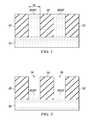
- Insulation regionssuch as Shallow Trench Isolation (STI) regions 22 are formed in substrate 20 .
- STI regions 22may be formed by recessing semiconductor substrate 20 to form trenches, and then filling the trenches with dielectric materials such as silicon oxide.
- a Chemical Mechanical Polish (CMP)is then performed to remove excess portions of the dielectric materials, and the remaining portions are STI regions 22 .
- the top surfaces of STI regions 22are thus level with the top surface of substrate 20 .
- STI regions 22include neighboring regions having their sidewalls facing each other. Portions 20 ′ of substrate 20 extend between the neighboring STI regions. Width W 1 of substrate portions 20 ′ may be between about 10 nm and about 200 nm. It is appreciated that the dimensions recited throughout the description are merely examples, and may be changed to different values.
- the neighboring STI regionsmay be separate regions, or may be portions of a continuous region, which may form a STI ring in some embodiments.
- substrate portions 20 ′are recessed, forming recesses 24 between neighboring STI regions 22 .
- the bottoms of recesses 24are higher than the bottom surfaces of STI regions 22 .
- the bottoms of recesses 24are substantially level with or lower than the bottoms of STI regions 22 .
- semiconductor regions 26are grown in recesses 24 through epitaxy.
- the top surfaces of semiconductor regionsare lower than the top surfaces of STI regions 22 .
- Semiconductor regions 26may have a first lattice constant greater than the lattice constant of substrate 20 .
- semiconductor regions 26comprises silicon germanium, which is expressed as Si 1-x Ge x , wherein value X is the atomic percentage of germanium in semiconductor regions 26 , which atomic percentage may be between about 0.2 (20 percent) and 1 (100 percent) in exemplary embodiments.
- Semiconductor regions 26are a relaxed semiconductor region, which means that at least the top portions of semiconductor regions are relaxed with substantially no stress.
- thickness T 1is greater than about 30 nm, and may be between about 30 nm and about 150 nm.
- the conduction band of semiconductor regions 26is lower than the conduction band of bulk silicon by between about 0.036 eV and about 0.144 eV, wherein the conduction band of silicon is about 1.1 eV.
- FIG. 11schematically illustrates bandgap BG 1 , conduction band Ec 1 , and valence band Ev 1 of semiconductor regions 26 .
- semiconductor regions 28are grown in recesses 24 through epitaxy, wherein semiconductor regions 28 are grown over and contacting semiconductor regions 26 .
- Semiconductor regions 28have a tensile strain, and may be un-doped with n-type and p-type impurities. In some embodiments, the tensile strain is generated by making the lattice constant of semiconductor regions 28 smaller than the lattice constant of semiconductor regions 26 . In some embodiments, the tensile strain is higher than about 1.36 MPa, and may be higher than about 6.8 GPa.
- Semiconductor regions 28include portions in recesses 24 ( FIG. 3 ), which portions have thickness T 2 .
- Thickness T 2is small enough, so that after the subsequent Chemical Mechanical Polish (CMP) in FIG. 5 , semiconductor regions 28 are not relaxed and have the tensile strain.
- thickness T 2is smaller than about 150 nm, and may be between about 30 nm and about 150 nm.
- FIG. 11schematically illustrates bandgap BG 2 , conduction band Ec 2 , and valence band Ev 2 of semiconductor regions 28 .
- Conduction band Ec 2is lower than the conduction band Ec 1 of semiconductor regions 26 , with the difference (Ec 1 ⁇ Ec 2 ) being greater than about 0.036 eV, for example.
- semiconductor regions 28comprise Si 1-y Ge y , wherein value Y is the atomic percentage of germanium in semiconductor regions 28 .
- Value Ymay be smaller than about 0.3 (30 percent), and may be between 0 and about 0.3. Value Y may also be equal to 0, which means that semiconductor regions 28 are silicon regions free from germanium.
- value Yis smaller than value X of semiconductor regions 26 , with the difference (X ⁇ Y) being greater than about 0.1, greater than about 0.3, or greater than about 0.5, for example.
- a greater difference (X ⁇ Y)may advantageously result in a greater tensile strain in semiconductor regions 28 , and a greater conduction band difference (Ec 1 ⁇ Ec 2 ).
- Semiconductor regions 28may be grown to a level higher than the top surfaces of STI regions 22 .
- a CMPis then performed to level the top surface of STI regions 22 and semiconductor regions 28 .
- the resulting structureis shown in FIG. 5 .
- the growth of semiconductor regions 28stops at a time when the top surface of semiconductor regions 28 is level with or lower than the top surfaces of STI regions 22 .
- the CMPmay be performed, or may be skipped.
- STI regions 22are recessed, for example, through an etching step.
- the top surfaces 22 A of the remaining STI regions 22are higher than the interfaces 27 between semiconductor regions 26 and semiconductor regions 28 .
- the portions of semiconductor regions 28 that are higher than top surfaces 22 Aare referred to as semiconductor fins 30 hereinafter.
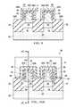
- FIG. 7illustrates the thinning of semiconductor regions 28 .
- the thinningis performed by applying and patterning photo resist 31 , and then using photo resist 31 as a mask to etch semiconductor fins 30 .
- semiconductor regions 28have lower portions and upper portions narrower than the lower portions.
- the lower portionshave width W 2
- the upper portionshave width W 3 , wherein both widths W 2 and W 3 are measured close to the transition region transiting from the narrow portions to the wide portions.
- width W 2is between about 8 nm and about 200 nm
- width W 3is between about 6 nm and about 200 nm.
- the difference (W 2 ⁇ W 3 )may be greater than about 2 nm, or greater than about 5 nm, for example.
- an entirety of semiconductor fins 30is thinned.
- an upper portion of each of semiconductor fins 30is thinned, and the lower portion of each of semiconductor fins 30 remains not thinned.
- the narrow portions of semiconductor regions 28have sidewalls 28 A, and the wide portions of semiconductor regions 28 have sidewalls 28 B, which are vertically misaligned to the respective overlying sidewalls 28 A. Furthermore, sidewalls 28 B are not continuously transitioned to the respective overlying sidewalls 28 A. Rather, top surfaces 28 C of the wide portions connect sidewalls 28 B to the respective overlying sidewalls 28 A. Top surface 28 C may be substantially flat in some embodiments. Sidewalls 28 B and the respective overlying sidewalls 28 A may be misaligned by misalignment r 1 , which may be greater than about 1 nm, or greater than about 5 nm. Top surfaces 28 C may be level with the top surface 22 A of STI regions 22 . Alternatively, although not shown, top surfaces 28 C are higher than the top surface 22 A of STI regions 22 .
- FIG. 8illustrates the formation of semiconductor regions 34 , which are epitaxially grown on the exposed top surfaces and sidewalls of semiconductor fins 30 .
- Semiconductor regions 34are substantially conformal layers, with the portions on the top surfaces of semiconductor fins 30 having substantially the same thickness T 3 as the portions on the sidewalls of semiconductor fins 30 .
- thickness T 3is between about 5 nm and about 150 nm.
- Semiconductor regions 34are in contact with the top surfaces and the sidewalls of the narrow portions of semiconductor regions 28 , and in contact with the top surfaces 28 C of the wide portions of semiconductor regions 28 . In the embodiments that top surfaces 28 C are higher than top surfaces 22 A of STI regions 22 , semiconductor regions 34 are also grown on the sidewalls of the wide portions of semiconductor regions 28 .
- Bandgap BG 3 , conduction band Ec 3 , and valence band Ev 3 of semiconductor regions 34are schematically illustrated in FIG. 11 .
- Conduction band Ec 3is higher than conduction band Ec 2 of semiconductor regions 28 , with the difference (Ec 3 ⁇ Ec 2 ) being greater than about 0.036 eV, for example.
- semiconductor regions 34comprise Si 1-z Ge z , wherein value Z is the atomic percentage of silicon in semiconductor regions 34 .
- Value Zmay be greater than about 0.3, and may be between about 0.3 and 1.
- Value Zmay also be equal to 1, which means that semiconductor regions 34 are pure germanium regions free from silicon.
- value Zis greater than value Y of semiconductor regions 28 , with the difference (Z ⁇ Y) being greater than about 0.1, or greater than about 0.3, for example.
- a greater difference (Z ⁇ Y)may advantageously result in a greater conduction band difference (Ec 3 ⁇ Ec 2 ).
- semiconductor regions 34include layers 34 A and layers 34 B, which are formed over layers 34 A.
- Layers 34 A and layers 34 Bmay have substantially the same atomic percentage of silicon and substantially the same atomic percentage of germanium, although their compositions may also be different from each other.
- layers 34 Aare not doped with n-type impurities, and may also be free from p-type impurities.
- layers 34 Aare n-type doped layers with the n-type impurity concentration lower than about 10 16 /cm 3 , for example. Thickness T 4 of layers 34 A may be greater than 0 nm and smaller than about 50 nm.
- Layers 34 Bare n-type layers, wherein the n-type impurity concentration in layers 34 B may be higher than about 10 18 /cm 3 . In these embodiments, the n-type impurity concentration in layers 34 A is lower than the n-type impurity concentration in layers 34 B. Layers 34 B act as the electron-supply layers for supplying electrons to the underlying carrier channels 46 ( FIG. 10A through 10C ).
- the doped n-type impuritymay include phosphorous, arsenic, antimony, or combinations thereof.
- Layers 34 A and layers 34 Bmay be formed in-situ in a same vacuum chamber, and may be formed using essentially the same process conditions, except that in the formation of layers 34 A, no n-type dopant is added, while the n-type dopant is added in the formation of layers 34 B. Alternatively, in the formation of both layers 34 A and 34 B, n-type dopants are added, and the n-type dopant amount for forming layers 34 A is smaller than that for forming layers 34 B. In some embodiments, thickness T 5 of doped layers 34 B is between about 1 nm and about 20 nm.
- semiconductor regions 34further include layers 34 C over layers 34 B.
- Layers 34 Cmay have atomic percentages of silicon and germanium same as either one, or both, of layers 34 A and 34 B. In alternative embodiments, the silicon and germanium atomic percentages in layers 34 A, 34 B, and 34 C are all different from each other. Layers 34 C may also be un-doped with n-type impurities, or doped with n-type impurities that have a lower impurity concentration than the respective underlying layers 34 B. In alternative embodiments, layers 34 C are not formed, and the respective structure may be found in FIG. 10B .
- FIG. 9illustrates the formation of silicon caps 36 , which may be substantially pure silicon regions with no germanium added. Silicon caps 36 may also be formed through epitaxy, and hence are over the top portions and sidewall portions of semiconductor regions 34 . In some embodiments, no n-type and p-type impurities are added into silicon caps 36 , although n-type and p-type impurities with low concentrations, for example, lower than about 10 16 /cm 3 , may also be added. Thickness T 6 of silicon caps 36 may be between about 1 nm and about 20 nm in some embodiments. In alternative embodiments, silicon caps 36 are not formed.
- gate dielectric 40 and gate electrode 42are formed.
- Gate dielectric 40may be formed of a dielectric material such as silicon oxide, silicon nitride, an oxynitride, multi-layers thereof, and/or combinations thereof.
- Gate dielectric 40may also be formed of high-k dielectric materials. The exemplary high-k materials may have k values greater than about 4.0, or greater than about 7.0.
- Gate electrode 42may be formed of doped polysilicon, metals, metal nitrides, metal silicides, and the like. The bottom ends of gate dielectric 42 may contact the top surfaces of STI regions 22 . After the formation of gate dielectric 40 and gate electrode 42 , source and drain regions 50 ( FIG. 10C ) are formed.
- semiconductor regions 28form interfaces 44 with the adjoin semiconductor regions 34 .
- Carrier channels 46which are alternatively referred to as Two-Dimensional Electron Gas (2DEG) channels, are formed and located in semiconductor regions 28 . 2DEG channels 46 may also be close to interfaces 44 . Although semiconductor regions 28 may not be doped with n-type impurities, carrier channels 46 still have a high density of electrons, which are supplied by the respective overlying electron-supply layers 34 B.
- FIG. 10Billustrates a cross-sectional view of FinFET 38 in accordance with alternative embodiments. These embodiments are essentially the same as the embodiments in FIG. 10A , except that the layer 34 C in FIG. 10A is not formed. Accordingly, silicon caps 36 are in physical contact with the respective underlying layers 34 B.
- FIG. 10Cillustrates a cross-sectional view of FinFET 38 , wherein the cross-sectional view is obtained from the plane crossing line 10 C- 10 C in FIG. 10A .
- Source and drain regions 50are formed on the opposite sides of gate dielectric 40 and gate electrode 42 .
- Source and drain regions 50are doped with an n-type impurity such as phosphorous, arsenic, antimony, or the like, and hence the respective FinFET 38 is an n-type FinFET.
- 2DEG channel 46interconnects the source and drain regions 50 .
- FIG. 11schematically illustrates a band diagram of semiconductor regions 26 , 28 , and 34 .
- the conduction band Ec 2 of semiconductor region 28is lower than conduction band Ec 1 of semiconductor region 26 and conduction band Ec 3 of semiconductor region 34 .
- conduction bands Ec 1 , Ec 2 , and Ec 3form a well, with conduction band Ec 2 forming the bottom of the well.
- Electrons 48which are supplied by electron-supply layers 34 B ( FIGS. 10A and 10B ), are confined in the well to form the 2DEG channels.
- the formation of the wellis attributed to that semiconductor region 28 is tensile strained, and hence conduction band Ec 2 is suppressed to a level lower than conduction bands Ec 1 and Ec 3 .
- semiconductor region 28is not tensile strained, the conduction band of semiconductor region 28 will be higher than the conduction bands of semiconductor regions 26 and 34 , and hence the well region and the 2DEG channel will not be formed.
- semiconductor region 28may not be doped with impurities, electrons can move freely without collision or with substantially reduced collisions with the impurities.
- the overlying semiconductor region 28may have a tensile strain.
- the tensile strainresults in a conduction band well to be formed in semiconductor region 28 .
- electron-supply layer 34 Bis formed overlying semiconductor region 28 to supply electrons, which are confined in the well formed in semiconductor region 28 to form the 2DEG channel. Accordingly, the resulting FinFET has a high saturation current.
- a devicein accordance with some embodiments, includes a substrate and insulation regions over a portion of the substrate.
- a first semiconductor regionis between the insulation regions and having a first conduction band.
- a second semiconductor regionis over and adjoining the first semiconductor region, wherein the second semiconductor region includes an upper portion higher than top surfaces of the insulation regions to form a semiconductor fin.
- the second semiconductor regionalso includes a wide portion and a narrow portion over the wide portion, wherein the narrow portion is narrower than the wide portion.
- the semiconductor finhas a tensile strain and has a second conduction band lower than the first conduction band.
- a third semiconductor regionis over and adjoining a top surface and sidewalls of the semiconductor fin, wherein the third semiconductor region has a third conduction band higher than the second conduction band.
- a devicein accordance with other embodiments, includes a silicon substrate and STI regions over a portion of the silicon substrate.
- a first SiGe regionis located between and in contact with the STI regions, wherein the first SiGe region has a first germanium atomic percentage.
- a silicon-containing regionis over the first SiGe region.
- the silicon-containing regionhas a tensile stress.
- a second SiGe regioncontacts a top surface and sidewalls of the silicon-containing region.
- the silicon-containing regionhas a wide portion having a first sidewall and a top surface, and a narrow portion over the wide portion and having a second sidewall. The first sidewall and the second sidewall are on a same side of the silicon-containing region.
- Edges of the wide portionare vertically aligned to respective edges of the first SiGe region.
- the top surface of the wide portionconnects the first sidewall to the second sidewall.
- the second SiGe regionhas second germanium atomic percentage.
- the first and the second germanium atomic percentagesare higher than a third germanium atomic percentage of the silicon-containing region.
- the devicefurther includes a gate dielectric over the second SiGe region, a gate electrode over the gate dielectric, and a source region and a drain region on opposite sides of the gate dielectric and the gate electrode.
- a methodincludes recessing a portion of a substrate between two insulation regions to form a recess, performing a first epitaxy to grow a first semiconductor region in the recess, and performing a second epitaxy to grow a second semiconductor region in the recess.
- the first semiconductor regionis relaxed.
- the second semiconductor regionis over and contacting the first semiconductor region.
- the second semiconductor regionhas a tensile strain.
- a planarizationis performed to level top surfaces of the second semiconductor region and the insulation regions.
- the insulation regionsare recessed, wherein a top portion of the second semiconductor region over the insulation regions forms a semiconductor fin.
- the semiconductor finis thinned to have a smaller width.
- a third epitaxyis performed to grow a third semiconductor region on a top surface and sidewalls of the semiconductor fin.
- the second semiconductor regionhas a conduction band lower than conduction bands of the first and the third semiconductor regions.
Landscapes
- Engineering & Computer Science (AREA)
- General Physics & Mathematics (AREA)
- Physics & Mathematics (AREA)
- Condensed Matter Physics & Semiconductors (AREA)
- Manufacturing & Machinery (AREA)
- Computer Hardware Design (AREA)
- Microelectronics & Electronic Packaging (AREA)
- Power Engineering (AREA)
- Chemical & Material Sciences (AREA)
- General Chemical & Material Sciences (AREA)
- Chemical Kinetics & Catalysis (AREA)
- Insulated Gate Type Field-Effect Transistor (AREA)
- Crystallography & Structural Chemistry (AREA)
Abstract
Description
This application is a divisional of U.S. patent application Ser. No. 13/789,798, entitled “FinFETs with Strained Well Regions,” filed Mar. 8, 2013, which application relates the following commonly-assigned U.S. patent application Ser. No. 13/779,015, filed Feb. 27, 2013, and entitled “FinFETs with Strained Well Regions,” which applications are hereby incorporated herein by reference.
The speed of metal-oxide-semiconductor (MOS) transistors are closely related to the drive currents of the MOS transistors, which are further closely related to the mobility of charges in the channels of the MOS transistors. For example, NMOS transistors have high drive currents when the electron mobility in their channel regions is high, while PMOS transistors have high drive currents when the hole mobility in their channel regions is high. Germanium, silicon germanium, and compound semiconductor materials (referred to as III-V compound semiconductors hereinafter) comprising group III and group V elements are thus good candidates for forming their high electron mobility and/or hole mobility.
Germanium, silicon germanium, and III-V compound semiconductor regions are also promising materials for forming the channel regions of Fin Field-Effect transistors (FinFETs). Methods and structures for further improving the drive currents on the FinFETs are currently being studied.
For a more complete understanding of the embodiments, and the advantages thereof, reference is now made to the following descriptions taken in conjunction with the accompanying drawings, in which:
The making and using of the embodiments of the disclosure are discussed in detail below. It should be appreciated, however, that the embodiments provide many applicable concepts that can be embodied in a wide variety of specific contexts. The specific embodiments discussed are illustrative, and do not limit the scope of the disclosure.
Fin Field-Effect Transistors (FinFETs) and methods of forming the same are provided in accordance with various exemplary embodiments. The intermediate stages of forming the FinFETs in accordance with some embodiments are illustrated. The variations of the embodiments are discussed. Throughout the various views and illustrative embodiments, like reference numbers are used to designate like elements.
Referring toFIG. 1 ,substrate 20 is provided.Substrate 20 may be a semiconductor substrate such as a crystalline silicon substrate.Substrate 20 may also include silicon, germanium, carbon, or the like. Insulation regions such as Shallow Trench Isolation (STI)regions 22 are formed insubstrate 20.STI regions 22 may be formed by recessingsemiconductor substrate 20 to form trenches, and then filling the trenches with dielectric materials such as silicon oxide. A Chemical Mechanical Polish (CMP) is then performed to remove excess portions of the dielectric materials, and the remaining portions areSTI regions 22. The top surfaces ofSTI regions 22 are thus level with the top surface ofsubstrate 20.
Referring toFIG. 2 ,substrate portions 20′ are recessed, formingrecesses 24 between neighboringSTI regions 22. In some embodiments, the bottoms ofrecesses 24 are higher than the bottom surfaces ofSTI regions 22. In alternative embodiments, the bottoms ofrecesses 24 are substantially level with or lower than the bottoms ofSTI regions 22.
Referring toFIG. 3 ,semiconductor regions 26 are grown inrecesses 24 through epitaxy. The top surfaces of semiconductor regions are lower than the top surfaces ofSTI regions 22.Semiconductor regions 26 may have a first lattice constant greater than the lattice constant ofsubstrate 20. In some embodiments,semiconductor regions 26 comprises silicon germanium, which is expressed as Si1-xGex, wherein value X is the atomic percentage of germanium insemiconductor regions 26, which atomic percentage may be between about 0.2 (20 percent) and 1 (100 percent) in exemplary embodiments.Semiconductor regions 26 are a relaxed semiconductor region, which means that at least the top portions of semiconductor regions are relaxed with substantially no stress. This may be achieved by, for example, making thickness T1 great enough, since the stresses in upper portions ofsemiconductor regions 26 are increasingly smaller than the lower portions. In some exemplary embodiments, thickness T1 is greater than about 30 nm, and may be between about 30 nm and about 150 nm. In some exemplary embodiments, the conduction band ofsemiconductor regions 26 is lower than the conduction band of bulk silicon by between about 0.036 eV and about 0.144 eV, wherein the conduction band of silicon is about 1.1 eV.FIG. 11 schematically illustrates bandgap BG1, conduction band Ec1, and valence band Ev1 ofsemiconductor regions 26.
Next, referring toFIG. 4 ,semiconductor regions 28 are grown inrecesses 24 through epitaxy, whereinsemiconductor regions 28 are grown over and contactingsemiconductor regions 26.Semiconductor regions 28 have a tensile strain, and may be un-doped with n-type and p-type impurities. In some embodiments, the tensile strain is generated by making the lattice constant ofsemiconductor regions 28 smaller than the lattice constant ofsemiconductor regions 26. In some embodiments, the tensile strain is higher than about 1.36 MPa, and may be higher than about 6.8 GPa.Semiconductor regions 28 include portions in recesses24 (FIG. 3 ), which portions have thickness T2. Thickness T2 is small enough, so that after the subsequent Chemical Mechanical Polish (CMP) inFIG. 5 ,semiconductor regions 28 are not relaxed and have the tensile strain. In some exemplary embodiments, thickness T2 is smaller than about 150 nm, and may be between about 30 nm and about 150 nm.
Referring toFIG. 6 ,STI regions 22 are recessed, for example, through an etching step. The top surfaces22A of the remainingSTI regions 22 are higher than theinterfaces 27 betweensemiconductor regions 26 andsemiconductor regions 28. The portions ofsemiconductor regions 28 that are higher thantop surfaces 22A are referred to assemiconductor fins 30 hereinafter.
Due to the thinning, the narrow portions ofsemiconductor regions 28 have sidewalls28A, and the wide portions ofsemiconductor regions 28 have sidewalls28B, which are vertically misaligned to the respective overlying sidewalls28A. Furthermore, sidewalls28B are not continuously transitioned to the respective overlying sidewalls28A. Rather,top surfaces 28C of the wide portions connectsidewalls 28B to the respective overlying sidewalls28A.Top surface 28C may be substantially flat in some embodiments.Sidewalls 28B and the respective overlying sidewalls28A may be misaligned by misalignment r1, which may be greater than about 1 nm, or greater than about 5 nm.Top surfaces 28C may be level with thetop surface 22A ofSTI regions 22. Alternatively, although not shown,top surfaces 28C are higher than thetop surface 22A ofSTI regions 22.
Bandgap BG3, conduction band Ec3, and valence band Ev3 ofsemiconductor regions 34 are schematically illustrated inFIG. 11 . Conduction band Ec3 is higher than conduction band Ec2 ofsemiconductor regions 28, with the difference (Ec3−Ec2) being greater than about 0.036 eV, for example. In some embodiments,semiconductor regions 34 comprise Si1-zGez, wherein value Z is the atomic percentage of silicon insemiconductor regions 34. Value Z may be greater than about 0.3, and may be between about 0.3 and 1. Value Z may also be equal to 1, which means thatsemiconductor regions 34 are pure germanium regions free from silicon. Furthermore, value Z is greater than value Y ofsemiconductor regions 28, with the difference (Z−Y) being greater than about 0.1, or greater than about 0.3, for example. A greater difference (Z−Y) may advantageously result in a greater conduction band difference (Ec3−Ec2).
In some embodiments,semiconductor regions 34 includelayers 34A and layers34B, which are formed overlayers 34A.Layers 34A and layers34B may have substantially the same atomic percentage of silicon and substantially the same atomic percentage of germanium, although their compositions may also be different from each other. In some exemplary embodiments, layers34A are not doped with n-type impurities, and may also be free from p-type impurities. In alternative embodiments, layers34A are n-type doped layers with the n-type impurity concentration lower than about 1016/cm3, for example. Thickness T4 oflayers 34A may be greater than 0 nm and smaller than about 50 nm.Layers 34B are n-type layers, wherein the n-type impurity concentration inlayers 34B may be higher than about 1018/cm3. In these embodiments, the n-type impurity concentration inlayers 34A is lower than the n-type impurity concentration inlayers 34B.Layers 34B act as the electron-supply layers for supplying electrons to the underlying carrier channels46 (FIG. 10A through 10C ).
The doped n-type impurity may include phosphorous, arsenic, antimony, or combinations thereof.Layers 34A and layers34B may be formed in-situ in a same vacuum chamber, and may be formed using essentially the same process conditions, except that in the formation oflayers 34A, no n-type dopant is added, while the n-type dopant is added in the formation oflayers 34B. Alternatively, in the formation of bothlayers layers 34A is smaller than that for forminglayers 34B. In some embodiments, thickness T5 of dopedlayers 34B is between about 1 nm and about 20 nm.
In some embodiments,semiconductor regions 34 further includelayers 34C overlayers 34B.Layers 34C may have atomic percentages of silicon and germanium same as either one, or both, oflayers layers Layers 34C may also be un-doped with n-type impurities, or doped with n-type impurities that have a lower impurity concentration than the respectiveunderlying layers 34B. In alternative embodiments, layers34C are not formed, and the respective structure may be found inFIG. 10B .
The structure shown inFIG. 9 may be used to formFinFET 38, as shown inFIGS. 10A, 10B, and 10C . Referring toFIG. 10A ,gate dielectric 40 andgate electrode 42 are formed.Gate dielectric 40 may be formed of a dielectric material such as silicon oxide, silicon nitride, an oxynitride, multi-layers thereof, and/or combinations thereof.Gate dielectric 40 may also be formed of high-k dielectric materials. The exemplary high-k materials may have k values greater than about 4.0, or greater than about 7.0.Gate electrode 42 may be formed of doped polysilicon, metals, metal nitrides, metal silicides, and the like. The bottom ends ofgate dielectric 42 may contact the top surfaces ofSTI regions 22. After the formation ofgate dielectric 40 andgate electrode 42, source and drain regions50 (FIG. 10C ) are formed.
As shown inFIG. 10A ,semiconductor regions 28 form interfaces44 with theadjoin semiconductor regions 34.Carrier channels 46, which are alternatively referred to as Two-Dimensional Electron Gas (2DEG) channels, are formed and located insemiconductor regions 28.2DEG channels 46 may also be close to interfaces44. Althoughsemiconductor regions 28 may not be doped with n-type impurities,carrier channels 46 still have a high density of electrons, which are supplied by the respective overlying electron-supply layers 34B.
In the embodiments of the present disclosure, by formingrelaxed semiconductor region 26 that has a greater lattice constant than the lattice constant ofsemiconductor region 28, the overlyingsemiconductor region 28 may have a tensile strain. The tensile strain results in a conduction band well to be formed insemiconductor region 28. Furthermore, electron-supply layer 34B is formedoverlying semiconductor region 28 to supply electrons, which are confined in the well formed insemiconductor region 28 to form the 2DEG channel. Accordingly, the resulting FinFET has a high saturation current.
In addition, in the embodiments of the present disclosure, by thinning semiconductor fins, more spaces are provided for forming semiconductor layers on the sidewalls of semiconductor fins. The required chip area occupied by the respective FinFET is hence reduced. The channel width of the respective FinFET, however, is not adversely reduced since the total width of the 2DEG channel is not reduced compared to the scenario that no thinning is performed.
In accordance with some embodiments, a device includes a substrate and insulation regions over a portion of the substrate. A first semiconductor region is between the insulation regions and having a first conduction band. A second semiconductor region is over and adjoining the first semiconductor region, wherein the second semiconductor region includes an upper portion higher than top surfaces of the insulation regions to form a semiconductor fin. The second semiconductor region also includes a wide portion and a narrow portion over the wide portion, wherein the narrow portion is narrower than the wide portion. The semiconductor fin has a tensile strain and has a second conduction band lower than the first conduction band. A third semiconductor region is over and adjoining a top surface and sidewalls of the semiconductor fin, wherein the third semiconductor region has a third conduction band higher than the second conduction band.
In accordance with other embodiments, a device includes a silicon substrate and STI regions over a portion of the silicon substrate. A first SiGe region is located between and in contact with the STI regions, wherein the first SiGe region has a first germanium atomic percentage. A silicon-containing region is over the first SiGe region. The silicon-containing region has a tensile stress. A second SiGe region contacts a top surface and sidewalls of the silicon-containing region. The silicon-containing region has a wide portion having a first sidewall and a top surface, and a narrow portion over the wide portion and having a second sidewall. The first sidewall and the second sidewall are on a same side of the silicon-containing region. Edges of the wide portion are vertically aligned to respective edges of the first SiGe region. The top surface of the wide portion connects the first sidewall to the second sidewall. The second SiGe region has second germanium atomic percentage. The first and the second germanium atomic percentages are higher than a third germanium atomic percentage of the silicon-containing region. The device further includes a gate dielectric over the second SiGe region, a gate electrode over the gate dielectric, and a source region and a drain region on opposite sides of the gate dielectric and the gate electrode.
In accordance with yet other embodiments, a method includes recessing a portion of a substrate between two insulation regions to form a recess, performing a first epitaxy to grow a first semiconductor region in the recess, and performing a second epitaxy to grow a second semiconductor region in the recess. The first semiconductor region is relaxed. The second semiconductor region is over and contacting the first semiconductor region. The second semiconductor region has a tensile strain. A planarization is performed to level top surfaces of the second semiconductor region and the insulation regions. The insulation regions are recessed, wherein a top portion of the second semiconductor region over the insulation regions forms a semiconductor fin. The semiconductor fin is thinned to have a smaller width. A third epitaxy is performed to grow a third semiconductor region on a top surface and sidewalls of the semiconductor fin. The second semiconductor region has a conduction band lower than conduction bands of the first and the third semiconductor regions.
Although the embodiments and their advantages have been described in detail, it should be understood that various changes, substitutions and alterations can be made herein without departing from the spirit and scope of the embodiments as defined by the appended claims. Moreover, the scope of the present application is not intended to be limited to the particular embodiments of the process, machine, manufacture, and composition of matter, means, methods and steps described in the specification. As one of ordinary skill in the art will readily appreciate from the disclosure, processes, machines, manufacture, compositions of matter, means, methods, or steps, presently existing or later to be developed, that perform substantially the same function or achieve substantially the same result as the corresponding embodiments described herein may be utilized according to the disclosure. Accordingly, the appended claims are intended to include within their scope such processes, machines, manufacture, compositions of matter, means, methods, or steps. In addition, each claim constitutes a separate embodiment, and the combination of various claims and embodiments are within the scope of the disclosure.
Claims (20)
1. A method comprising: forming a semiconductor fin protruding higher than top surfaces of insulation regions, wherein the insulation regions are on opposite sides of the semiconductor fin; recessing a first sidewall and a second sidewall of the semiconductor fin, wherein the first sidewall and the second sidewall are opposite sidewalls of the semiconductor fin; performing a first epitaxy to grow a semiconductor layer, wherein the semiconductor layer comprises a first sidewall portion contacting the first recessed sidewall of the semiconductor fin, and a second sidewall portion contacting the second recessed sidewall; forming a gate dielectric over the semiconductor fin; forming a gate electrode over the gate dielectric; and epitaxially growing a silicon cap over the semiconductor layer, wherein the silicon cap is underlying the gate dielectric.
2. The method ofclaim 1 , wherein the recessing the first sidewall and the second sidewall of the semiconductor fin comprises:
forming a photo resist directly over a middle portion of the semiconductor fin; and
etching portions of the semiconductor fin not covered by the photo resist.
3. The method ofclaim 1 , wherein during the recessing the first sidewall and the second sidewall of the semiconductor fin, a top surface of the semiconductor fin remains not recessed.
4. The method ofclaim 1 , wherein the first epitaxy comprises:
epitaxially growing a first semiconductor sub-layer, with no p-type and n-type impurity in-situ doped;
epitaxially growing a second semiconductor sub-layer over the first semiconductor sub-layer, with an n-type impurity in-situ doped; and
epitaxially growing a third semiconductor sub-layer over the second semiconductor sub-layer, with no p-type and n-type impurity in-situ doped.
5. The method ofclaim 1 further comprising forming a source/drain region, wherein the source/drain region contacts both the first sidewall portion and the second sidewall portion of the semiconductor layer, and the source/drain region contacts the recessed semiconductor fin.
6. The method ofclaim 1 further comprising:
recessing top surfaces of the insulation regions, and a portion of a semiconductor region between the recessed insulation regions forms the semiconductor fin.
7. The method ofclaim 6 further comprising, before the recessing:
recessing a portion of a substrate between the insulation regions to form a recess;
performing a second epitaxy to grow a first semiconductor region in the recess, wherein the first semiconductor region is relaxed;
performing a third epitaxy to grow a second semiconductor region in the recess, wherein the second semiconductor region is over and contacting the first semiconductor region, and wherein the second semiconductor region has a tensile strain; and
performing a planarization to level top surfaces of the second semiconductor region and the insulation regions.
8. A method comprising:
forming a semiconductor region having a portion over top surfaces of insulation regions, wherein the semiconductor region comprises:
a wide portion with opposite sidewalls contacting edges of the insulation regions, wherein the wide portion has a top surface substantially level with top surfaces of the insulation regions; and
a narrow portion narrower than the wide portion over the wide portion, wherein the wide portion comprises an extension portion laterally extending beyond a respective sidewall of the narrow portion, and the narrow portion has a first bandgap;
epitaxially growing a semiconductor layer contacting a top surface and sidewalls of the narrow portion, wherein the semiconductor layer has a second bandgap greater than the first bandgap; and
forming a gate stack overlapping both the narrow portion and the extension portion of the wide portion.
9. The method ofclaim 8 , wherein the narrow portion has a tensile stress.
10. The method ofclaim 8 , wherein the semiconductor layer comprises sidewall portions contacting the sidewalls of the narrow portion, and the method further comprises:
forming a source/drain region contacting the sidewall portions.
11. The method ofclaim 8 , wherein the epitaxially growing the semiconductor layer comprises:
growing a first sub-layer, wherein substantially no n-type impurity is added into the first sub-layer; and
growing a second sub-layer over the first sub-layer, wherein an n-type impurity is added into the second sub-layer.
12. The method ofclaim 11 wherein the epitaxially growing the semiconductor layer further comprises:
growing a third sub-layer over the second sub-layer, wherein substantially no n-type impurity is added into the third sub-layer.
13. A method comprising:
recessing a portion of a substrate between two insulation regions to form a recess;
performing a first epitaxy to grow a first semiconductor region in the recess, wherein the first semiconductor region is relaxed;
performing a second epitaxy to grow a second semiconductor region in the recess, wherein the second semiconductor region is over and contacting the first semiconductor region, and wherein the second semiconductor region has a tensile strain;
performing a planarization to level a top surface of the second semiconductor region and the insulation regions;
recessing the insulation regions, wherein a top portion of the second semiconductor region higher than the insulation regions forms a semiconductor fin;
thinning the semiconductor fin; and
performing a third epitaxy to grow a third semiconductor region on a top surface and sidewalls of the semiconductor fin, wherein the second semiconductor region has a conduction band lower than conduction bands of the first and the third semiconductor regions.
14. The method ofclaim 13 further comprising:
forming a gate dielectric over the third semiconductor region;
forming a gate electrode over the gate dielectric; and
forming a source region and a drain region on opposite sides of the semiconductor fin.
15. The method ofclaim 14 , wherein after the thinning, a semiconductor region underlying the thinned semiconductor fin has an extension extending beyond sidewalls of the thinned semiconductor fin, and the gate electrode overlaps the extension.
16. The method ofclaim 13 , wherein the first and the third semiconductor regions comprise silicon germanium, and wherein the second semiconductor region comprises silicon, with a germanium atomic percentage in the second semiconductor region being lower than atomic percentages in the first and the third semiconductor regions.
17. The method ofclaim 13 , wherein the third epitaxy comprises:
growing a first sub-layer of the third semiconductor region, wherein substantially no n-type impurity is added into the first sub-layer of the third semiconductor region; and
growing a second sub-layer of the third semiconductor region over the first sub-layer of the third semiconductor region, wherein an n-type impurity is added into the second sub-layer of the third semiconductor region.
18. The method ofclaim 17 , wherein the third epitaxy further comprises:
growing a third sub-layer of the third semiconductor region over the second sub-layer of the third semiconductor region, wherein substantially no n-type impurity is added into the third sub-layer of the third semiconductor region.
19. The method ofclaim 13 further comprising growing a silicon cap over the third semiconductor region, wherein the silicon cap is substantially free from germanium.
20. The method ofclaim 1 , wherein the semiconductor layer has a conduction band greater than a conduction band of the semiconductor fin.
Priority Applications (3)
| Application Number | Priority Date | Filing Date | Title |
|---|---|---|---|
| US14/846,020US9601342B2 (en) | 2013-02-27 | 2015-09-04 | FinFETs with strained well regions |
| US15/450,201US9859380B2 (en) | 2013-02-27 | 2017-03-06 | FinFETs with strained well regions |
| US15/816,376US10164023B2 (en) | 2013-03-08 | 2017-11-17 | FinFETs with strained well regions |
Applications Claiming Priority (3)
| Application Number | Priority Date | Filing Date | Title |
|---|---|---|---|
| US13/779,015US9087902B2 (en) | 2013-02-27 | 2013-02-27 | FinFETs with strained well regions |
| US13/789,798US9159824B2 (en) | 2013-02-27 | 2013-03-08 | FinFETs with strained well regions |
| US14/846,020US9601342B2 (en) | 2013-02-27 | 2015-09-04 | FinFETs with strained well regions |
Related Parent Applications (1)
| Application Number | Title | Priority Date | Filing Date |
|---|---|---|---|
| US13/789,798DivisionUS9159824B2 (en) | 2013-02-27 | 2013-03-08 | FinFETs with strained well regions |
Related Child Applications (1)
| Application Number | Title | Priority Date | Filing Date |
|---|---|---|---|
| US15/450,201ContinuationUS9859380B2 (en) | 2013-02-27 | 2017-03-06 | FinFETs with strained well regions |
Publications (2)
| Publication Number | Publication Date |
|---|---|
| US20150380528A1 US20150380528A1 (en) | 2015-12-31 |
| US9601342B2true US9601342B2 (en) | 2017-03-21 |
Family
ID=51385439
Family Applications (5)
| Application Number | Title | Priority Date | Filing Date |
|---|---|---|---|
| US13/789,798ActiveUS9159824B2 (en) | 2013-02-27 | 2013-03-08 | FinFETs with strained well regions |
| US14/846,020Expired - Fee RelatedUS9601342B2 (en) | 2013-02-27 | 2015-09-04 | FinFETs with strained well regions |
| US15/450,201ActiveUS9859380B2 (en) | 2013-02-27 | 2017-03-06 | FinFETs with strained well regions |
| US15/688,214ActiveUS10164022B2 (en) | 2013-03-08 | 2017-08-28 | FinFETs with strained well regions |
| US15/816,376ActiveUS10164023B2 (en) | 2013-03-08 | 2017-11-17 | FinFETs with strained well regions |
Family Applications Before (1)
| Application Number | Title | Priority Date | Filing Date |
|---|---|---|---|
| US13/789,798ActiveUS9159824B2 (en) | 2013-02-27 | 2013-03-08 | FinFETs with strained well regions |
Family Applications After (3)
| Application Number | Title | Priority Date | Filing Date |
|---|---|---|---|
| US15/450,201ActiveUS9859380B2 (en) | 2013-02-27 | 2017-03-06 | FinFETs with strained well regions |
| US15/688,214ActiveUS10164022B2 (en) | 2013-03-08 | 2017-08-28 | FinFETs with strained well regions |
| US15/816,376ActiveUS10164023B2 (en) | 2013-03-08 | 2017-11-17 | FinFETs with strained well regions |
Country Status (3)
| Country | Link |
|---|---|
| US (5) | US9159824B2 (en) |
| KR (1) | KR101452122B1 (en) |
| DE (1) | DE102013104481B4 (en) |
Cited By (138)
| Publication number | Priority date | Publication date | Assignee | Title |
|---|---|---|---|---|
| US10269576B1 (en) | 2017-11-15 | 2019-04-23 | Taiwan Semiconductor Manufacturing Co., Ltd. | Etching and structures formed thereby |
| US10325912B2 (en) | 2017-10-30 | 2019-06-18 | Taiwan Semiconductor Manufacturing Co., Ltd. | Semiconductor structure cutting process and structures formed thereby |
| US10355102B2 (en) | 2017-11-15 | 2019-07-16 | Taiwan Semiconductor Manufacturing Co., Ltd. | Semiconductor device and method of manufacturing the same |
| US10483168B2 (en) | 2017-11-15 | 2019-11-19 | Taiwan Semiconductor Manufacturing Co., Ltd. | Low-k gate spacer and formation thereof |
| US10510889B2 (en) | 2017-11-29 | 2019-12-17 | Taiwan Semiconductor Manufacturing Co., Ltd. | P-type strained channel in a fin field effect transistor (FinFET) device |
| US10510883B2 (en) | 2017-11-28 | 2019-12-17 | Taiwan Semiconductor Manufacturing Co., Ltd. | Asymmetric source and drain structures in semiconductor devices |
| US10515948B2 (en) | 2017-11-15 | 2019-12-24 | Taiwan Semiconductor Manufacturing Co., Ltd. | Semiconductor device including vertical routing structure and method for manufacturing the same |
| US10629749B2 (en) | 2017-11-30 | 2020-04-21 | Taiwan Semiconductor Manufacturing Co., Ltd. | Method of treating interfacial layer on silicon germanium |
| US10680106B2 (en) | 2017-11-15 | 2020-06-09 | Taiwan Semiconductor Manufacturing Co., Ltd. | Method of forming source/drain epitaxial stacks |
| US10748774B2 (en) | 2017-11-30 | 2020-08-18 | Taiwan Semiconductor Manufacturing Co., Ltd. | Semiconductor device and manufacturing method thereof |
| US10749007B2 (en) | 2018-03-14 | 2020-08-18 | Taiwan Semiconductor Manufacturing Co., Ltd. | Gate structure with desired profile for semiconductor devices |
| US10763363B2 (en) | 2018-04-10 | 2020-09-01 | Taiwan Semiconductor Manufacturing Co., Ltd. | Gradient doped region of recessed fin forming a FinFET device |
| US10840152B2 (en) | 2018-09-27 | 2020-11-17 | Taiwan Semiconductor Manufacturing Co., Ltd. | Semiconductor device and manufacturing method thereof |
| US10854715B2 (en) | 2018-04-13 | 2020-12-01 | Taiwan Semiconductor Manufacturing Co., Ltd. | Supportive layer in source/drains of FinFET devices |
| US10867809B2 (en) | 2017-11-22 | 2020-12-15 | Taiwan Semiconductor Manufacturing Co., Ltd. | Laser anneal process |
| US10868114B2 (en) | 2018-10-30 | 2020-12-15 | Taiwan Semiconductor Manufacturing Co., Ltd. | Isolation structures of semiconductor devices |
| US10867862B2 (en) | 2018-08-31 | 2020-12-15 | Taiwan Semiconductor Manufacturing Company, Ltd. | Semiconductor method and device |
| US10872906B2 (en) | 2018-10-25 | 2020-12-22 | Taiwan Semiconductor Manufacturing Co., Ltd. | Semiconductor device and manufacturing method thereof |
| US10964792B1 (en) | 2019-11-22 | 2021-03-30 | Taiwan Semiconductor Manufacturing Co., Ltd. | Dual metal capped via contact structures for semiconductor devices |
| US10978344B2 (en) | 2019-08-23 | 2021-04-13 | Taiwan Semiconductor Manufacturing Company, Ltd. | Melting laser anneal of epitaxy regions |
| US11011623B2 (en) | 2018-06-29 | 2021-05-18 | Taiwan Semiconductor Manufacturing Company, Ltd. | Method for increasing germanium concentration of FIN and resulting semiconductor device |
| US11018012B2 (en) | 2018-09-21 | 2021-05-25 | Taiwan Semiconductor Manufacturing Co., Ltd. | Contact structures with deposited silicide layers |
| US11069812B2 (en) | 2018-09-28 | 2021-07-20 | Taiwan Semiconductor Manufacturing Company, Ltd. | Fin field-effect transistor device and method of forming the same |
| US11088034B2 (en) | 2019-05-22 | 2021-08-10 | Taiwan Semiconductor Manufacturing Co., Ltd. | Gate structures for semiconductor devices |
| US11087987B2 (en) | 2018-10-31 | 2021-08-10 | Taiwan Semiconductor Manufacturing Company, Ltd. | Semiconductor device and method |
| US20210249309A1 (en)* | 2020-02-11 | 2021-08-12 | Taiwan Semiconductor Manufacturing Co., Ltd. | Profile control of a gap fill structure |
| US11094826B2 (en) | 2018-09-27 | 2021-08-17 | Taiwan Semiconductor Manufacturing Company, Ltd. | FinFET device and method of forming same |
| US11107923B2 (en) | 2019-06-14 | 2021-08-31 | Taiwan Semiconductor Manufacturing Company, Ltd. | Source/drain regions of FinFET devices and methods of forming same |
| US11107736B1 (en) | 2020-03-31 | 2021-08-31 | Taiwan Semiconductor Manufacturing Co., Ltd. | Gate structures for semiconductor devices |
| US11114303B2 (en) | 2018-07-31 | 2021-09-07 | Taiwan Semiconductor Manufacturing Co., Ltd. | Gate all around device, method for manufacturing FinFET device, and method for manufacturing gate all around device |
| US11114547B2 (en) | 2019-09-17 | 2021-09-07 | Taiwan Semiconductor Manufacturing Co., Ltd. | Field effect transistor with negative capacitance dieletric structures |
| US11114549B2 (en) | 2017-11-29 | 2021-09-07 | Taiwan Semiconductor Manufacturing Co., Ltd. | Semiconductor structure cutting process and structures formed thereby |
| US11139432B1 (en) | 2020-04-01 | 2021-10-05 | Taiwan Semiconductor Manufacturing Company, Ltd. | Methods of forming a FinFET device |
| US11164786B2 (en) | 2017-09-28 | 2021-11-02 | Taiwan Semiconductor Manufacturing Co., Ltd. | Power reduction in finFET structures |
| US11183423B2 (en) | 2017-11-28 | 2021-11-23 | Taiwan Semiconductor Manufacturing Co., Ltd. | Liner structure in interlayer dielectric structure for semiconductor devices |
| US11183574B2 (en) | 2019-05-24 | 2021-11-23 | Taiwan Semiconductor Manufacturing Co., Ltd. | Work function layers for transistor gate electrodes |
| US11189697B2 (en) | 2020-04-01 | 2021-11-30 | Taiwan Semiconductor Manufacturing Co., Ltd. | Ultra-thin fin structure and method of fabricating the same |
| US11211479B2 (en) | 2018-08-14 | 2021-12-28 | Taiwan Semiconductor Manufaciuring Co., Ltd. | Method of fabricating trimmed fin and fin structure |
| US11217526B2 (en) | 2019-02-28 | 2022-01-04 | Taiwan Semiconductor Manufacturing Co., Ltd. | Semiconductor device with source resistor and manufacturing method thereof |
| US11227918B2 (en) | 2018-07-31 | 2022-01-18 | Taiwan Semiconductor Manufacturing Company, Ltd. | Melt anneal source and drain regions |
| US11233119B2 (en) | 2020-03-02 | 2022-01-25 | Taiwan Semiconductor Manufacturing Co., Ltd. | Core-shell nanostructures for semiconductor devices |
| US11233123B2 (en) | 2017-09-28 | 2022-01-25 | Taiwan Semiconductor Manufacturing Co., Ltd. | Fully strained channel |
| US11233149B2 (en) | 2020-03-03 | 2022-01-25 | Taiwan Semiconductor Manufacturing Co., . Ltd. | Spacer structures for semiconductor devices |
| US11245028B2 (en) | 2020-01-30 | 2022-02-08 | Taiwan Semiconductor Manufacturing Co., Ltd. | Isolation structures of semiconductor devices |
| US11245023B1 (en) | 2020-07-31 | 2022-02-08 | Taiwan Semiconductor Manufacturing Co., Ltd. | Semiconductor device and manufacturing method thereof |
| US11257911B2 (en) | 2020-04-01 | 2022-02-22 | Taiwan Semiconductor Manufacturing Company, Ltd. | Sacrificial layer for semiconductor process |
| US11257928B2 (en) | 2018-11-27 | 2022-02-22 | Taiwan Semiconductor Manufacturing Company, Ltd. | Method for epitaxial growth and device |
| US11264237B2 (en) | 2018-09-28 | 2022-03-01 | Taiwan Semiconductor Manufacturing Company, Ltd. | Method of epitaxy and semiconductor device |
| US11264513B2 (en) | 2020-06-30 | 2022-03-01 | Taiwan Semiconductor Manufacturing Co., Ltd. | Isolation structures for transistors |
| US11276604B1 (en) | 2020-10-27 | 2022-03-15 | Taiwan Semiconductor Manufacturing Co., Ltd. | Radical-activated etching of metal oxides |
| US11296095B2 (en) | 2020-06-12 | 2022-04-05 | Taiwan Semiconductor Manufacturing Co., Ltd. | Memory device and method for forming the same |
| US11296227B2 (en) | 2019-10-16 | 2022-04-05 | Taiwan Semiconductor Manufacturing Co., Ltd. | Method of manufacturing semiconductor devices and semiconductor devices |
| US11295989B2 (en) | 2020-05-26 | 2022-04-05 | Taiwan Semiconductor Manufacturing Co., Ltd. | Gate structures for semiconductor devices |
| US11309419B2 (en) | 2020-01-17 | 2022-04-19 | Taiwan Semiconductor Manufacturing Co., Ltd. | Semiconductor device and manufacturing method thereof |
| US11335606B2 (en) | 2020-08-19 | 2022-05-17 | Taiwan Semiconductor Manufacturing Co., Ltd. | Power rails for stacked semiconductor device |
| US11373870B2 (en) | 2019-06-27 | 2022-06-28 | Taiwan Semiconductor Manufacturing Co., Ltd. | Method for manufacturing semiconductor device including performing thermal treatment on germanium layer |
| US11374090B2 (en) | 2019-10-31 | 2022-06-28 | Taiwan Semiconductor Manufacturing Co., Ltd. | Gate structures for semiconductor devices |
| US11387109B1 (en) | 2021-03-05 | 2022-07-12 | Taiwan Semiconductor Manufacturing Co., Ltd. | CMP process and methods thereof |
| US11417571B2 (en) | 2020-06-12 | 2022-08-16 | Taiwan Semiconductor Manufacturing Co., Ltd. | Dopant profile control in gate structures for semiconductor devices |
| US11417764B2 (en) | 2020-01-29 | 2022-08-16 | Taiwan Semiconductor Manufacturing Co., Ltd. | Interface profile control in epitaxial structures for semiconductor devices |
| US11424347B2 (en) | 2020-06-11 | 2022-08-23 | Taiwan Semiconductor Manufacturing Co., Ltd. | Semiconductor device and method |
| US11437371B2 (en) | 2020-07-10 | 2022-09-06 | Taiwan Semiconductor Manufacturing Co., Ltd. | Field effect transistors with negative capacitance layers |
| US11437497B2 (en) | 2018-06-29 | 2022-09-06 | Taiwan Semiconductor Manufacturing Company, Ltd. | Semiconductor device and method |
| US11444198B2 (en) | 2020-05-29 | 2022-09-13 | Taiwan Semiconductor Manufacturing Co., Ltd. | Work function control in gate structures |
| US11450743B2 (en) | 2020-10-21 | 2022-09-20 | Taiwan Semiconductor Manufacturing Co., Ltd. | Method of forming a semiconductor device with implantation of impurities at high temperature |
| US11476342B1 (en) | 2021-05-05 | 2022-10-18 | Taiwan Semiconductor Manufacturing Company, Ltd. | Semiconductor device with improved source and drain contact area and methods of fabrication thereof |
| US11489057B2 (en) | 2020-08-07 | 2022-11-01 | Taiwan Semiconductor Manufacturing Co., Ltd. | Contact structures in semiconductor devices |
| US11495463B2 (en) | 2020-10-27 | 2022-11-08 | Taiwan Semiconductor Manufacturing Co., Ltd. | Semiconductor device and manufacturing method thereof |
| US11521969B2 (en) | 2020-01-29 | 2022-12-06 | Taiwan Semiconductor Manufacturing Co., Ltd. | Isolation structures for semiconductor devices |
| US11569234B2 (en) | 2020-09-21 | 2023-01-31 | Taiwan Semiconductor Manufacturing Co., Ltd. | Semiconductor device structure and methods of forming the same |
| US11575026B2 (en) | 2021-03-19 | 2023-02-07 | Taiwan Semiconductor Manufacturing Co., Ltd. | Source/drain structure for semiconductor device |
| US11600703B2 (en) | 2021-01-29 | 2023-03-07 | Taiwan Semiconductor Manufacturing Co., Ltd. | Germanium tin gate-all-around device |
| US11610979B2 (en) | 2020-08-13 | 2023-03-21 | Taiwan Semiconductor Manufacturing Co., Ltd. | Profile control in forming epitaxy regions for transistors |
| US11677013B2 (en) | 2020-03-30 | 2023-06-13 | Taiwan Semiconductor Manufacturing Co., Ltd. | Source/drain epitaxial layers for transistors |
| US11682665B2 (en) | 2019-06-19 | 2023-06-20 | Taiwan Semiconductor Manufacturing Co., Ltd. | Semiconductor layout with different row heights |
| US11688625B2 (en) | 2021-08-30 | 2023-06-27 | Taiwan Semiconductor Manufacturing Company, Ltd. | Method for manufacturing semiconductor device |
| US11685015B2 (en) | 2019-01-28 | 2023-06-27 | Taiwan Semiconductor Manufacturing Co., Ltd. | Method and system for performing chemical mechanical polishing |
| US11695055B2 (en) | 2020-03-03 | 2023-07-04 | Taiwan Semiconductor Manufacturing Co., Ltd. | Passivation layers for semiconductor devices |
| US11705372B2 (en) | 2020-02-11 | 2023-07-18 | Taiwan Semiconductor Manufacturing Co., Ltd. | Fin loss prevention |
| US11721593B2 (en) | 2020-09-30 | 2023-08-08 | Tiawan Semiconductor Manufacturing Co., Ltd. | Source/drain epitaxial structures for semiconductor devices |
| US11749570B2 (en) | 2021-08-31 | 2023-09-05 | Taiwan Semiconductor Manufacturing Company, Ltd. | Etch monitoring and performing |
| US11777014B2 (en) | 2021-01-04 | 2023-10-03 | Taiwan Semiconductor Manufacturing Co., Ltd. | Controlled doping in a gate dielectric layer |
| US11848238B2 (en) | 2020-06-30 | 2023-12-19 | Taiwan Semiconductor Manufacturing Co., Ltd. | Methods for manufacturing semiconductor devices with tunable low-k inner air spacers |
| US11848209B2 (en) | 2021-02-26 | 2023-12-19 | Taiwan Semiconductor Manufacturing Co., Ltd. | Patterning semiconductor devices and structures resulting therefrom |
| US11854831B2 (en) | 2020-11-24 | 2023-12-26 | Taiwan Semiconductor Manufacturing Co., Ltd. | Cleaning process for source/drain epitaxial structures |
| US11869954B2 (en) | 2021-05-28 | 2024-01-09 | Taiwan Semiconductor Manufacturing Co., Ltd. | Nanostructured channel regions for semiconductor devices |
| US11869892B2 (en) | 2021-04-29 | 2024-01-09 | Taiwan Semiconductor Manufacturing Company, Ltd. | Semiconductor device structure and methods of forming the same |
| US11901412B2 (en) | 2021-08-30 | 2024-02-13 | Taiwan Semiconductor Manufacturing Co., Ltd. | Facet-free epitaxial structures for semiconductor devices |
| US11901415B2 (en) | 2021-05-28 | 2024-02-13 | Taiwan Semiconductor Manufacturing Co., Ltd. | Transistor isolation structures |
| US11908921B2 (en) | 2021-08-26 | 2024-02-20 | Taiwan Semiconductor Manufacturing Co., Ltd. | Transistor isolation structures |
| US11920254B2 (en) | 2021-08-30 | 2024-03-05 | Taiwan Semiconductor Manufacturing Co., Ltd. | Detection of contact formation between a substrate and contact pins in an electroplating system |
| US11929287B2 (en) | 2021-04-23 | 2024-03-12 | Taiwan Semiconductor Manufacturing Co., Ltd. | Dielectric liner for field effect transistors |
| US11942533B2 (en) | 2021-08-31 | 2024-03-26 | Taiwan Semiconductor Manufacturing Co., Ltd. | Channel structures for semiconductor devices |
| US11942358B2 (en) | 2021-03-12 | 2024-03-26 | Taiwan Semiconductor Manufacturing Co., Ltd. | Low thermal budget dielectric for semiconductor devices |
| US11948939B2 (en) | 2021-01-13 | 2024-04-02 | Taiwan Semiconductor Manufacturing Company, Ltd | Profile control of gate structures in semiconductor devices |
| US11948840B2 (en) | 2021-08-31 | 2024-04-02 | Taiwan Semiconductor Manufacturing Co., Ltd. | Protective layer over FinFET and method of forming same |
| US11961884B2 (en) | 2021-03-31 | 2024-04-16 | Taiwan Semiconductor Manufacturing Company, Ltd. | Fill structures with air gaps |
| US11990511B2 (en) | 2021-08-27 | 2024-05-21 | Taiwan Semiconductor Manufacturing Co., Ltd. | Source/drain device and method of forming thereof |
| US11996317B2 (en) | 2021-01-15 | 2024-05-28 | Taiwan Semiconductor Manufacturing Co., Ltd. | Methods for forming isolation regions by depositing and oxidizing a silicon liner |
| US12002867B2 (en) | 2021-08-27 | 2024-06-04 | Taiwan Semiconductor Manufacturing Co., Ltd. | Contact structure for semiconductor device |
| US12021125B2 (en) | 2021-07-16 | 2024-06-25 | Taiwan Semiconductor Manufacturing Co., Ltd. | High selectivity etching with germanium-containing gases |
| US12027583B2 (en) | 2021-05-13 | 2024-07-02 | Taiwan Semiconductor Manufacturing Company, Ltd. | Gate structures for semiconductor devices |
| US12040384B2 (en) | 2021-08-27 | 2024-07-16 | Taiwan Semiconductor Manufacturing Co., Ltd. | Source/drain structure for semiconductor device |
| US12057478B2 (en) | 2019-10-31 | 2024-08-06 | Taiwan Semiconductor Manufacturing Co., Ltd. | Gate structures for semiconductor devices |
| US12057506B2 (en) | 2021-07-08 | 2024-08-06 | Taiwan Semiconductor Manufacturing Company, Ltd. | Semiconductor device and manufacturing method thereof |
| US12057449B2 (en) | 2020-01-29 | 2024-08-06 | Taiwan Semiconductor Manufacturing Co., Ltd. | Isolation structures for semiconductor devices |
| US12062576B2 (en) | 2021-07-16 | 2024-08-13 | Taiwan Semiconductor Manufacturing Company, Ltd. | Semiconductor devices with a rare earth metal oxide layer |
| US12062658B2 (en) | 2021-03-31 | 2024-08-13 | Taiwan Semiconductor Manufacturing Company, Ltd. | Method for forming an integrated circuit having transistor gates over an interconnection structure |
| US12087845B2 (en) | 2021-04-21 | 2024-09-10 | Taiwan Semiconductor Manufacturing Co., Ltd. | System and methods of manufacturing semiconductor devices |
| US12125891B2 (en) | 2020-07-22 | 2024-10-22 | Taiwan Semiconductor Manufacturing Co., Ltd. | Semiconductor device having gate spacers extending below a fin top surface |
| US12136600B2 (en) | 2021-04-08 | 2024-11-05 | Taiwan Semiconductor Manufacturing Company, Ltd. | Grounded metal ring structure for through-silicon via |
| US12154829B2 (en) | 2020-10-14 | 2024-11-26 | Taiwan Semiconductor Manufacturing Company, Ltd. | Method of manufacturing semiconductor devices and semiconductor devices |
| US12166037B2 (en) | 2021-08-27 | 2024-12-10 | Taiwan Semiconductor Manufacturing Company, Ltd. | Isolation layers in stacked semiconductor devices |
| US12183797B2 (en) | 2021-05-12 | 2024-12-31 | Taiwan Semiconductor Manufacturing Company, Ltd. | Profile control of channel structures for semiconductor devices |
| US12191212B2 (en) | 2021-07-09 | 2025-01-07 | Taiwan Semiconductor Manufacturing Co., Ltd. | Semiconductor method and device |
| US12191393B2 (en) | 2021-04-23 | 2025-01-07 | Taiwan Semiconductor Manufacturing Co., Ltd. | Low Ge isolated epitaxial layer growth over nano-sheet architecture design for RP reduction |
| US12191205B2 (en) | 2021-07-09 | 2025-01-07 | Taiwan Semiconductor Manufacturing Company, Ltd. | Semiconductor device and manufacturing method thereof |
| US12211938B2 (en) | 2018-09-27 | 2025-01-28 | Taiwan Semiconductor Manufacturing Company, Ltd. | FinFET device and method of forming same |
| US12218219B2 (en) | 2021-08-27 | 2025-02-04 | Taiwan Semiconductor Manufacturing Co., Ltd. | Spacer structure for semiconductor device |
| US12243931B2 (en) | 2020-03-30 | 2025-03-04 | Taiwan Semiconductor Manufacturing Co., Ltd. | Source/drain epitaxial layers for transistors |
| US12310092B2 (en) | 2021-06-18 | 2025-05-20 | Taiwan Semiconductor Manufacturing Company, Ltd. | Multi-functional transistors in semiconductor devices |
| US12317566B2 (en) | 2021-03-05 | 2025-05-27 | Taiwan Semiconductor Manufacturing Company, Ltd. | Isolated fin structures in semiconductor devices |
| US12317554B2 (en) | 2021-04-09 | 2025-05-27 | Taiwan Semiconductor Manufacturing Company, Ltd. | Contact structures for semiconductor devices |
| US12336249B2 (en) | 2022-03-16 | 2025-06-17 | Taiwan Semiconductor Manufacturing Company, Ltd. | Gate spacer and formation method thereof |
| US12336211B2 (en) | 2021-05-27 | 2025-06-17 | Taiwan Semiconductor Manufacturing Co., Ltd. | Dielectric layer on semiconductor device and method of forming the same |
| US12336272B2 (en) | 2021-07-23 | 2025-06-17 | Taiwan Semiconductor Manufacturing Company, Ltd. | Semiconductor device structure and methods of forming the same |
| US12349383B2 (en) | 2021-06-17 | 2025-07-01 | Taiwan Semiconductor Manufacturing Company, Ltd. | Isolation structures in semiconductor devices |
| US12363933B2 (en) | 2021-07-09 | 2025-07-15 | Taiwan Semiconductor Manufacturing Company, Ltd. | Dielectric structures in semiconductor devices |
| US12362234B2 (en) | 2021-08-27 | 2025-07-15 | Taiwan Semiconductor Manufacturing Company, Ltd. | Contact structure for semiconductor device |
| US12376337B2 (en) | 2021-03-19 | 2025-07-29 | Taiwan Semiconductor Manufacturing Company, Ltd. | Air inner spacers |
| US12382676B2 (en) | 2021-07-09 | 2025-08-05 | Taiwan Semiconductor Manufacturing Company, Ltd. | Semiconductor device structure and methods of forming the same |
| US12396239B2 (en) | 2022-04-17 | 2025-08-19 | Taiwan Semiconductor Manufacturing Company, Ltd. | Semiconductor device structure and methods of forming the same |
| US12402372B2 (en) | 2022-06-03 | 2025-08-26 | Taiwan Semiconductor Manufacturing Company, Ltd. | Insulating structures in semiconductor device |
| US12402343B2 (en) | 2022-03-29 | 2025-08-26 | Taiwan Semiconductor Manufacturing Company, Ltd. | Work function tuning in semiconductor devices |
| US12414320B2 (en) | 2018-09-28 | 2025-09-09 | Taiwan Semiconductor Manufacturing Company, Ltd. | Fin field-effect transistor device with composite liner for the fin |
| US12412775B2 (en) | 2021-07-09 | 2025-09-09 | Taiwan Semiconductor Manufacturing Company, Ltd. | Isolation structures in semiconductor devices |
| US12439642B2 (en) | 2022-06-06 | 2025-10-07 | Taiwan Semiconductor Manufacturing Company, Ltd. | Seam-top seal for dielectrics |
| US12446269B2 (en) | 2022-05-06 | 2025-10-14 | Taiwan Semiconductor Manufacturing Company, Ltd. | Strained nanosheets on silicon-on-insulator substrate |
Families Citing this family (126)
| Publication number | Priority date | Publication date | Assignee | Title |
|---|---|---|---|---|
| US8367498B2 (en) | 2010-10-18 | 2013-02-05 | Taiwan Semiconductor Manufacturing Company, Ltd. | Fin-like field effect transistor (FinFET) device and method of manufacturing same |
| US9087902B2 (en) | 2013-02-27 | 2015-07-21 | Taiwan Semiconductor Manufacturing Company, Ltd. | FinFETs with strained well regions |
| US9385234B2 (en) | 2013-02-27 | 2016-07-05 | Taiwan Semiconductor Manufacturing Company, Ltd. | FinFETs with strained well regions |
| CN104218082B (en)* | 2013-06-04 | 2017-08-25 | 中芯国际集成电路制造(上海)有限公司 | High mobility fin FET and its manufacture method |
| US9099559B2 (en)* | 2013-09-16 | 2015-08-04 | Stmicroelectronics, Inc. | Method to induce strain in finFET channels from an adjacent region |
| CN105493251A (en)* | 2013-09-27 | 2016-04-13 | 英特尔公司 | Non-planar semiconductor device with multi-layer flexible substrate |
| US9373706B2 (en)* | 2014-01-24 | 2016-06-21 | Samsung Electronics Co., Ltd. | Methods of forming semiconductor devices, including forming a semiconductor material on a fin, and related semiconductor devices |
| US9236474B2 (en) | 2014-02-21 | 2016-01-12 | Stmicroelectronics, Inc. | Method to form strained channel in thin box SOI structures by elastic strain relaxation of the substrate |
| US9660080B2 (en) | 2014-02-28 | 2017-05-23 | Stmicroelectronics, Inc. | Multi-layer strained channel FinFET |
| US9530777B2 (en) | 2014-03-04 | 2016-12-27 | Stmicroelectronics, Inc. | FinFETs of different compositions formed on a same substrate |
| US10468528B2 (en) | 2014-04-16 | 2019-11-05 | Taiwan Semiconductor Manufacturing Company, Ltd. | FinFET device with high-k metal gate stack |
| US9721955B2 (en) | 2014-04-25 | 2017-08-01 | Taiwan Semiconductor Manufacturing Company, Ltd. | Structure and method for SRAM FinFET device having an oxide feature |
| US9178067B1 (en) | 2014-04-25 | 2015-11-03 | Taiwan Semiconductor Manufacturing Company, Ltd. | Structure and method for FinFET device |
| US9418903B2 (en)* | 2014-05-21 | 2016-08-16 | Globalfoundries Inc. | Structure and method for effective device width adjustment in finFET devices using gate workfunction shift |
| US9224736B1 (en) | 2014-06-27 | 2015-12-29 | Taiwan Semicondcutor Manufacturing Company, Ltd. | Structure and method for SRAM FinFET device |
| US9543438B2 (en)* | 2014-10-15 | 2017-01-10 | Taiwan Semiconductor Manufacturing Company, Ltd. | Contact resistance reduction technique |
| US9601377B2 (en)* | 2014-10-17 | 2017-03-21 | Taiwan Semiconductor Manufacturing Company, Ltd. | FinFET formation process and structure |
| US10910481B2 (en)* | 2014-11-05 | 2021-02-02 | Cree, Inc. | Semiconductor device with improved insulated gate |
| US9431514B2 (en)* | 2014-12-19 | 2016-08-30 | Stmicroelectronics, Inc. | FinFET device having a high germanium content fin structure and method of making same |
| KR101668445B1 (en)* | 2015-02-23 | 2016-10-21 | 경북대학교 산학협력단 | Semiconductor device and manufacturing method thereof |
| KR102351659B1 (en)* | 2015-04-03 | 2022-01-17 | 삼성전자주식회사 | Semiconductor devices including field effect transistors |
| US9583599B2 (en)* | 2015-04-22 | 2017-02-28 | International Business Machines Corporation | Forming a fin using double trench epitaxy |
| US9954107B2 (en) | 2015-05-05 | 2018-04-24 | International Business Machines Corporation | Strained FinFET source drain isolation |
| US10269968B2 (en)* | 2015-06-03 | 2019-04-23 | Taiwan Semiconductor Manufacturing Co., Ltd. | Semiconductor device including fin structures and manufacturing method thereof |
| US9653580B2 (en)* | 2015-06-08 | 2017-05-16 | International Business Machines Corporation | Semiconductor device including strained finFET |
| CN107636834B (en)* | 2015-06-16 | 2021-11-09 | 英特尔公司 | Transistor with sub-fin layer |
| KR102454077B1 (en)* | 2015-06-23 | 2022-10-14 | 인텔 코포레이션 | Indium-Rich NMS Transistor Channels |
| US9564489B2 (en)* | 2015-06-29 | 2017-02-07 | Taiwan Semiconductor Manufacturing Company, Ltd. | Multiple gate field-effect transistors having oxygen-scavenged gate stack |
| US9583623B2 (en) | 2015-07-31 | 2017-02-28 | Taiwan Semiconductor Manufacturing Co., Ltd. | Semiconductor device including fin structures disposed over buffer structures and manufacturing method thereof |
| US9607990B2 (en)* | 2015-08-28 | 2017-03-28 | International Business Machines Corporation | Method to form strained nFET and strained pFET nanowires on a same substrate |
| CN106611787A (en)* | 2015-10-26 | 2017-05-03 | 联华电子股份有限公司 | Semiconductor structure and manufacturing method thereof |
| CN107452793B (en) | 2016-06-01 | 2020-07-28 | 中芯国际集成电路制造(上海)有限公司 | Semiconductor device and method for manufacturing the same |
| KR102619874B1 (en)* | 2016-06-23 | 2024-01-03 | 삼성전자주식회사 | Semiconductor device having an impurity region |
| US9899372B1 (en) | 2016-10-31 | 2018-02-20 | International Business Machines Corporation | Forming on-chip metal-insulator-semiconductor capacitor |
| US10276691B2 (en)* | 2016-12-15 | 2019-04-30 | Taiwan Semiconductor Manufacturing Co., Ltd. | Conformal transfer doping method for fin-like field effect transistor |
| TWI746673B (en) | 2016-12-15 | 2021-11-21 | 台灣積體電路製造股份有限公司 | Fin-like field effect transistor device and conformal transfer doping method for fin-like field effect transistor |
| US11107924B2 (en) | 2016-12-29 | 2021-08-31 | Intel Corporation | Systems and methods to reduce FinFET gate capacitance |
| US10727131B2 (en) | 2017-06-16 | 2020-07-28 | Taiwan Semiconductor Manufacturing Co., Ltd. | Source and drain epitaxy re-shaping |
| US10483267B2 (en) | 2017-06-30 | 2019-11-19 | Taiwan Semiconductor Manufacturing Co., Ltd. | Eight-transistor static random-access memory, layout thereof, and method for manufacturing the same |
| US10483372B2 (en) | 2017-09-29 | 2019-11-19 | Taiwan Semiconductor Manufacturing Co., Ltd. | Spacer structure with high plasma resistance for semiconductor devices |
| US10505021B2 (en) | 2017-09-29 | 2019-12-10 | Taiwan Semiconductor Manufacturing Company, Ltd. | FinFet device and method of forming the same |
| US10847622B2 (en)* | 2017-11-13 | 2020-11-24 | Taiwan Semiconductor Manufacturing Co., Ltd. | Method of forming source/drain structure with first and second epitaxial layers |
| US10672613B2 (en) | 2017-11-22 | 2020-06-02 | Taiwan Semiconductor Manufacturing Co., Ltd. | Method of forming semiconductor structure and semiconductor device |
| US10374038B2 (en) | 2017-11-24 | 2019-08-06 | Taiwan Semiconductor Manufacturing Co., Ltd. | Semiconductor device source/drain region with arsenic-containing barrier region |
| US10497778B2 (en) | 2017-11-30 | 2019-12-03 | Taiwan Semiconductor Manufacturing Co., Ltd. | Semiconductor device and manufacturing method thereof |
| US10672889B2 (en) | 2017-11-30 | 2020-06-02 | Taiwan Semiconductor Manufacturing Co., Ltd. | Semiconductor device and manufacturing method thereof |
| DE102018106581B4 (en) | 2017-11-30 | 2020-07-09 | Taiwan Semiconductor Manufacturing Co. Ltd. | Semiconductor component and method for its production |
| US10923595B2 (en) | 2017-11-30 | 2021-02-16 | Taiwan Semiconductor Manufacturing Co., Ltd. | Semiconductor device having a SiGe epitaxial layer containing Ga |
| DE112017008272T5 (en) | 2017-12-15 | 2020-08-27 | Intel Corporation | Reducing off-state leakage in semiconductor devices |
| US10522390B1 (en) | 2018-06-21 | 2019-12-31 | Taiwan Semiconductor Manufacturing Co., Ltd. | Shallow trench isolation for integrated circuits |
| US10790391B2 (en) | 2018-06-27 | 2020-09-29 | Taiwan Semiconductor Manufacturing Co., Ltd. | Source/drain epitaxial layer profile |
| US11114566B2 (en) | 2018-07-12 | 2021-09-07 | Taiwan Semiconductor Manufacturing Co., Ltd. | Semiconductor device and method of manufacturing the same |
| US10700180B2 (en) | 2018-07-27 | 2020-06-30 | Taiwan Semiconductor Manufacturing Co., Ltd. | Semiconductor structure and manufacturing method thereof |
| US10707333B2 (en) | 2018-07-30 | 2020-07-07 | Taiwan Semiconductor Manufacturing Co., Ltd. | Semiconductor device and manufacturing method thereof |
| US10763255B2 (en) | 2018-08-14 | 2020-09-01 | Taiwan Semiconductor Manufacturing Co., Ltd. | Semiconductor device and manufacturing method thereof |
| US11024550B2 (en) | 2018-08-16 | 2021-06-01 | Taiwan Semiconductor Manufacturing Company, Ltd. | Semiconductor device and method |
| US11264380B2 (en) | 2018-08-27 | 2022-03-01 | Taiwan Semiconductor Manufacturing Co., Ltd. | Semiconductor device and method of manufacturing the same |
| US10886269B2 (en) | 2018-09-18 | 2021-01-05 | Taiwan Semiconductor Manufacturing Co., Ltd. | Semiconductor device and manufacturing method thereof |
| US11626507B2 (en) | 2018-09-26 | 2023-04-11 | Taiwan Semiconductor Manufacturing Co., Ltd. | Method of manufacturing FinFETs having barrier layers with specified SiGe doping concentration |
| US10879355B2 (en) | 2018-09-27 | 2020-12-29 | Taiwan Semiconductor Manufacturing Company, Ltd. | Profile design for improved device performance |
| US10991630B2 (en) | 2018-09-27 | 2021-04-27 | Taiwan Semiconductor Manufacturing Company, Ltd. | Semiconductor device and method |
| US10872805B2 (en) | 2018-09-28 | 2020-12-22 | Taiwan Semiconductor Manufacturing Co., Ltd. | Semiconductor device and manufacturing method thereof |
| US10950725B2 (en) | 2018-09-28 | 2021-03-16 | Taiwan Semiconductor Manufacturing Company, Ltd. | Epitaxial source/drain structure and method of forming same |
| US10680075B2 (en) | 2018-09-28 | 2020-06-09 | Taiwan Semiconductor Manufacturing Co., Ltd. | Semiconductor device including source/drain epitaxial layer having facets and manufacturing method thereof |
| US10867861B2 (en) | 2018-09-28 | 2020-12-15 | Taiwan Semiconductor Manufacturing Company, Ltd. | Fin field-effect transistor device and method of forming the same |
| US11296077B2 (en) | 2018-11-19 | 2022-04-05 | Taiwan Semiconductor Manufacturing Company, Ltd. | Transistors with recessed silicon cap and method forming same |
| US11101360B2 (en) | 2018-11-29 | 2021-08-24 | Taiwan Semiconductor Manufacturing Co., Ltd. | Method of manufacturing a semiconductor device and a semiconductor device |
| US11164944B2 (en) | 2018-11-30 | 2021-11-02 | Taiwan Semiconductor Manufacturing Company, Ltd. | Method of manufacturing a semiconductor device |
| US11088150B2 (en) | 2019-01-28 | 2021-08-10 | Taiwan Semiconductor Manufacturing Co., Ltd. | Semiconductor device and manufacturing method thereof |
| US11024650B2 (en)* | 2019-04-26 | 2021-06-01 | Taiwan Semiconductor Manufacturing Company, Ltd. | FinFET device and a method for fabricating the same |
| KR102863824B1 (en) | 2019-05-31 | 2025-09-25 | 삼성전자주식회사 | Semiconductor device and method of manufacturing the same |
| US11069578B2 (en) | 2019-05-31 | 2021-07-20 | Taiwan Semiconductor Manufacturing Company, Ltd. | Method of manufacturing a semiconductor device |
| US11004725B2 (en) | 2019-06-14 | 2021-05-11 | Taiwan Semiconductor Manufacturing Company, Ltd. | Method of forming a FinFET device with gaps in the source/drain region |
| US11056573B2 (en) | 2019-06-14 | 2021-07-06 | Taiwan Semiconductor Manufacturing Company, Ltd. | Implantation and annealing for semiconductor device |
| US11049774B2 (en) | 2019-07-18 | 2021-06-29 | Taiwan Semiconductor Manufacturing Company, Ltd. | Hybrid source drain regions formed based on same Fin and methods forming same |
| CN112310208A (en)* | 2019-07-29 | 2021-02-02 | 华为技术有限公司 | Enhanced gallium nitride-based transistor, preparation method thereof and electronic device |
| US10985266B2 (en) | 2019-08-20 | 2021-04-20 | Taiwan Semiconductor Manufacturing Company, Ltd. | Method of gap filling for semiconductor device |
| US11133416B2 (en) | 2019-08-23 | 2021-09-28 | Taiwan Semiconductor Manufacturing Company, Ltd. | Methods of forming semiconductor devices having plural epitaxial layers |
| US11011372B2 (en) | 2019-08-23 | 2021-05-18 | Taiwan Semiconductor Manufacturing Company, Ltd. | Semiconductor devices and methods of manufacture |
| US11101180B2 (en) | 2019-08-23 | 2021-08-24 | Taiwan Semiconductor Manufacturing Company, Ltd. | Semiconductor device and method of manufacture |
| US11239368B2 (en) | 2019-08-30 | 2022-02-01 | Taiwan Semiconductor Manufacturing Company, Ltd. | Semiconductor device and method |
| US11088249B2 (en) | 2019-09-17 | 2021-08-10 | Taiwan Semiconductor Manufacturing Company, Ltd. | Semiconductor device with implant and method of manufacturing same |
| KR102818248B1 (en)* | 2019-10-01 | 2025-06-11 | 삼성전자주식회사 | Semiconductor device and method for fabricating the same |
| US11522085B2 (en) | 2019-10-18 | 2022-12-06 | Taiwan Semiconductor Manufacturing Company, Ltd. | Ferroelectric semiconductor device and method |
| US11502197B2 (en) | 2019-10-18 | 2022-11-15 | Taiwan Semiconductor Manufacturing Co., Ltd. | Source and drain epitaxial layers |
| US11515212B2 (en) | 2019-10-30 | 2022-11-29 | Taiwan Semiconductor Manufacturing Co., Ltd. | Method of manufacturing semiconductor devices having controlled S/D epitaxial shape |
| US11081401B2 (en) | 2019-11-29 | 2021-08-03 | Taiwan Semiconductor Manufacturing Co., Ltd. | Semiconductor device and method for manufacturing the same |
| US11282944B2 (en) | 2019-12-30 | 2022-03-22 | Taiwan Semiconductor Manufacturing Co., Ltd. | Method of manufacturing a semiconductor device and a semiconductor device |
| US11233156B2 (en) | 2020-01-15 | 2022-01-25 | Taiwan Semiconductor Manufacturing Co., Ltd. | Memory device and manufacturing method thereof |
| US11322603B2 (en) | 2020-01-21 | 2022-05-03 | Taiwan Semiconductor Manufacturing Co., Ltd. | Anti-punch-through doping on source/drain region |
| WO2021148180A1 (en) | 2020-01-23 | 2021-07-29 | Continental Automotive Gmbh | Impact sensor with a tubular body |
| DE102020200832B4 (en) | 2020-01-24 | 2022-11-10 | Continental Automotive Technologies GmbH | Impact sensor with a tubular body |
| US11251268B2 (en) | 2020-01-28 | 2022-02-15 | Taiwan Semiconductor Manufacturing Co., Ltd. | Semiconductor device with doped structure |
| DE102020132562B4 (en) | 2020-01-30 | 2024-02-22 | Taiwan Semiconductor Manufacturing Co., Ltd. | METHOD FOR PRODUCING A SEMICONDUCTOR DEVICE AND SEMICONDUCTOR DEVICE |
| US11522050B2 (en) | 2020-01-30 | 2022-12-06 | Taiwan Semiconductor Manufacturing Co., Ltd. | Method of manufacturing a semiconductor device and a semiconductor device |
| US12136651B2 (en)* | 2020-02-19 | 2024-11-05 | Taiwan Semiconductor Manufacturing Co., Ltd. | Silicon-germanium Fins and methods of processing the same in field-effect transistors |
| US11387365B2 (en) | 2020-04-01 | 2022-07-12 | Taiwan Semiconductor Manufacturing Co., Ltd. | Method of manufacturing a semiconductor device for recessed fin structure having rounded corners |
| CN113053878B (en) | 2020-04-09 | 2025-05-06 | 台湾积体电路制造股份有限公司 | Semiconductor device and method for manufacturing the same |
| US11955370B2 (en) | 2020-04-28 | 2024-04-09 | Taiwan Semiconductor Manufacturing Co., Ltd. | Semiconductor devices and methods of manufacture |
| DE102021102939A1 (en) | 2020-05-28 | 2021-12-02 | Taiwan Semiconductor Manufacturing Co., Ltd. | SEMICONDUCTOR COMPONENTS AND MANUFACTURING METHODS |
| US11532731B2 (en) | 2020-05-28 | 2022-12-20 | Taiwan Semiconductor Manufacturing Co., Ltd. | Semiconductor devices and methods of manufacture |
| US11682711B2 (en) | 2020-05-28 | 2023-06-20 | Taiwan Semiconductor Manufacturing Co., Ltd. | Semiconductor device having multi-layered gate spacers |
| US11935793B2 (en) | 2020-05-29 | 2024-03-19 | Taiwan Semiconductor Manufacturing Co., Ltd. | Dual dopant source/drain regions and methods of forming same |
| US11296080B2 (en) | 2020-06-15 | 2022-04-05 | Taiwan Semiconductor Manufacturing Co., Ltd. | Source/drain regions of semiconductor devices and methods of forming the same |
| US11489075B2 (en) | 2020-06-29 | 2022-11-01 | Taiwan Semiconductor Manufacturing Co., Ltd. | Method of manufacturing a semiconductor device and a semiconductor device |
| US11764221B2 (en) | 2020-07-30 | 2023-09-19 | Taiwan Semiconductor Manufacturing Co., Ltd. | Semiconductor device and method of manufacture |
| US11557518B2 (en) | 2020-08-12 | 2023-01-17 | Taiwan Semiconductor Manufacturing Co., Ltd. | Gapfill structure and manufacturing methods thereof |
| US11315834B2 (en) | 2020-08-13 | 2022-04-26 | Taiwan Semiconductor Manufacturing Co., Ltd. | FinFETs with epitaxy regions having mixed wavy and non-wavy portions |
| US12266572B2 (en) | 2020-08-13 | 2025-04-01 | Taiwan Semiconductor Manufacturing Co., Ltd. | Embedded stressors in epitaxy source/drain regions |
| US11610890B2 (en) | 2020-08-13 | 2023-03-21 | Taiwan Semiconductor Manufacturing Co., Ltd. | Epitaxy regions extending below STI regions and profiles thereof |
| US11508621B2 (en) | 2020-08-21 | 2022-11-22 | Taiwan Semiconductor Manufacturing Co., Ltd. | Method of manufacturing a semiconductor device and a semiconductor device |
| US11688807B2 (en) | 2020-10-27 | 2023-06-27 | Taiwan Semiconductor Manufacturing Co., Ltd. | Semiconductor device and methods of forming |
| US11887985B2 (en) | 2021-03-04 | 2024-01-30 | Taiwan Semiconductor Manufacturing Co., Ltd. | Semiconductor device and method |
| US12034054B2 (en) | 2021-03-25 | 2024-07-09 | Taiwan Semiconductor Manufacturing Company, Ltd. | Semiconductor device and method for forming the same |
| US11984483B2 (en) | 2021-03-26 | 2024-05-14 | Taiwan Semiconductor Manufacturing Company, Ltd. | Semiconductor device and method of manufacturing thereof |
| US11600534B2 (en) | 2021-03-31 | 2023-03-07 | Taiwan Semiconductor Manufacturing Co., Ltd. | Source/drain structures and method of forming |
| US11855092B2 (en) | 2021-04-16 | 2023-12-26 | Taiwan Semiconductor Manufacturing Co., Ltd. | Semiconductor device and method of forming same |
| US20230034875A1 (en)* | 2021-07-29 | 2023-02-02 | Invention And Collaboration Laboratory Pte. Ltd. | Transistor structure |
| US12107163B2 (en) | 2021-08-19 | 2024-10-01 | Taiwan Semiconductor Manufacturing Company, Ltd. | Semiconductor device structure having dislocation stress memorization and methods of forming the same |
| US12020991B2 (en) | 2021-08-26 | 2024-06-25 | Taiwan Semiconductor Manufacturing Co., Ltd. | High-k gate dielectric and method forming same |
| US11710781B2 (en) | 2021-08-30 | 2023-07-25 | Taiwan Semiconductor Manufacturing Co., Ltd. | Growth process and methods thereof |
| US12087616B2 (en) | 2022-01-27 | 2024-09-10 | Taiwan Semiconductor Manufacturing Company, Ltd. | Air gap formation method |
| US12288723B2 (en) | 2022-05-11 | 2025-04-29 | Taiwan Semiconductor Manufacturing Company, Ltd. | Semiconductor device and manufacturing method thereof |
| US12191145B2 (en) | 2022-06-07 | 2025-01-07 | Taiwan Semiconductor Manufacturing Company, Ltd. | Semiconductor device and formation method thereof |
| US12349363B2 (en) | 2022-06-25 | 2025-07-01 | Taiwan Semiconductor Manufacturing Company, Ltd. | Ferroelectric device and methods of forming the same |
| US12414355B2 (en) | 2022-07-07 | 2025-09-09 | Taiwan Semiconductor Manufacturing Company, Ltd. | Semiconductor device and manufacturing method thereof |
Citations (25)
| Publication number | Priority date | Publication date | Assignee | Title |
|---|---|---|---|---|
| US5565375A (en) | 1993-12-01 | 1996-10-15 | Imp, Inc. | Method of fabricating a self-cascoding CMOS device |
| US20030001171A1 (en) | 2001-07-02 | 2003-01-02 | Nec Corporation | Semiconductor integrated circuit having macro cells and designing method of the same |
| US20030178677A1 (en) | 2002-03-19 | 2003-09-25 | International Business Machines Corporation | Strained fin fets structure and method |
| US20030230778A1 (en) | 2002-01-30 | 2003-12-18 | Sumitomo Mitsubishi Silicon Corporation | SOI structure having a SiGe Layer interposed between the silicon and the insulator |
| US20040256647A1 (en) | 2003-06-23 | 2004-12-23 | Sharp Laboratories Of America Inc. | Strained silicon finFET device |
| KR20050078145A (en) | 2004-01-30 | 2005-08-04 | 삼성전자주식회사 | Semiconductor device comprising field effect transistors having vertical channel |
| US20050184316A1 (en) | 2003-07-23 | 2005-08-25 | Kim Young-Pil | Fin field effect transistors having multi-layer fin patterns and methods of forming the same |
| US20060076625A1 (en) | 2004-09-25 | 2006-04-13 | Lee Sung-Young | Field effect transistors having a strained silicon channel and methods of fabricating same |
| US7154118B2 (en) | 2004-03-31 | 2006-12-26 | Intel Corporation | Bulk non-planar transistor having strained enhanced mobility and methods of fabrication |
| WO2007046150A1 (en) | 2005-10-21 | 2007-04-26 | Fujitsu Limited | Fin type semiconductor device and method for manufacturing same |
| US20100163926A1 (en) | 2008-12-29 | 2010-07-01 | Hudait Mantu K | Modulation-doped multi-gate devices |
| US20100230658A1 (en) | 2009-03-16 | 2010-09-16 | Ravi Pillarisetty | Apparatus and methods for improving parallel conduction in a quantum well device |
| US20100252816A1 (en)* | 2009-04-01 | 2010-10-07 | Taiwan Semiconductor Manufacturing Company, Ltd. | High-Mobility Multiple-Gate Transistor with Improved On-to-Off Current Ratio |
| KR20110052432A (en) | 2009-11-10 | 2011-05-18 | 타이완 세미콘덕터 매뉴팩쳐링 컴퍼니 리미티드 | Source / Drain Engineering of Devices with High-Mobility Channels |
| US20110147711A1 (en) | 2009-12-23 | 2011-06-23 | Ravi Pillarisetty | Non-planar germanium quantum well devices |
| US20110156006A1 (en) | 2007-03-27 | 2011-06-30 | Chi On Chui | Forming A Non-Planar Transistor Having A Quantum Well Channel |
| US20120025312A1 (en) | 2010-07-30 | 2012-02-02 | Globalfoundries Inc. | Strain Engineering in Three-Dimensional Transistors Based on a Strained Channel Semiconductor Material |
| US20120091528A1 (en) | 2010-10-18 | 2012-04-19 | Taiwan Semiconductor Manufacturing Company, Ltd. | Fin-like field effect transistor (finfet) device and method of manufacturing same |
| US20120319211A1 (en) | 2011-06-16 | 2012-12-20 | Taiwan Semiconductor Manufacturing Company, Ltd. | Strained channel field effect transistor |
| US20130001591A1 (en) | 2011-06-30 | 2013-01-03 | Taiwan Semiconductor Manufacturing Company, Ltd. | Finfet design and method of fabricating same |
| US20130056795A1 (en) | 2011-09-06 | 2013-03-07 | Taiwan Semiconductor Manufacturing Company, Ltd. | FinFET Design Controlling Channel Thickness |
| US20130270638A1 (en) | 2012-04-13 | 2013-10-17 | International Business Machines Corporation | Strained soi finfet on epitaxially grown box |
| US20140054547A1 (en) | 2012-08-24 | 2014-02-27 | Globalfoundries Inc. | Device with strained layer for quantum well confinement and method for manufacturing thereof |
| US20140239402A1 (en) | 2013-02-27 | 2014-08-28 | Taiwan Semiconductor Manufacturing Company, Ltd. | FinFETs with Strained Well Regions |
| US20150054040A1 (en) | 2013-02-27 | 2015-02-26 | Taiwan Semiconductor Manufacturing Company, Ltd. | Finfets with strained well regions |
Family Cites Families (7)
| Publication number | Priority date | Publication date | Assignee | Title |
|---|---|---|---|---|
| US6607948B1 (en) | 1998-12-24 | 2003-08-19 | Kabushiki Kaisha Toshiba | Method of manufacturing a substrate using an SiGe layer |
| KR100696197B1 (en) | 2005-09-27 | 2007-03-20 | 한국전자통신연구원 | Multi-gate MOS transistor using silicon substrate and its manufacturing method |
| US7898040B2 (en)* | 2007-06-18 | 2011-03-01 | Infineon Technologies Ag | Dual gate FinFET |
| US8575653B2 (en) | 2010-09-24 | 2013-11-05 | Intel Corporation | Non-planar quantum well device having interfacial layer and method of forming same |
| US8796695B2 (en)* | 2012-06-22 | 2014-08-05 | United Microelectronics Corp. | Multi-gate field-effect transistor and process thereof |
| US8497171B1 (en) | 2012-07-05 | 2013-07-30 | Taiwan Semiconductor Manufacturing Co., Ltd. | FinFET method and structure with embedded underlying anti-punch through layer |
| US20140134844A1 (en) | 2012-11-12 | 2014-05-15 | Infineon Technologies Dresden Gmbh | Method for processing a die |
- 2013
- 2013-03-08USUS13/789,798patent/US9159824B2/enactiveActive
- 2013-05-02DEDE102013104481.6Apatent/DE102013104481B4/enactiveActive
- 2013-07-30KRKR1020130090213Apatent/KR101452122B1/enactiveActive
- 2015
- 2015-09-04USUS14/846,020patent/US9601342B2/ennot_activeExpired - Fee Related
- 2017
- 2017-03-06USUS15/450,201patent/US9859380B2/enactiveActive
- 2017-08-28USUS15/688,214patent/US10164022B2/enactiveActive
- 2017-11-17USUS15/816,376patent/US10164023B2/enactiveActive
Patent Citations (27)
| Publication number | Priority date | Publication date | Assignee | Title |
|---|---|---|---|---|
| US5565375A (en) | 1993-12-01 | 1996-10-15 | Imp, Inc. | Method of fabricating a self-cascoding CMOS device |
| US20030001171A1 (en) | 2001-07-02 | 2003-01-02 | Nec Corporation | Semiconductor integrated circuit having macro cells and designing method of the same |
| US20030230778A1 (en) | 2002-01-30 | 2003-12-18 | Sumitomo Mitsubishi Silicon Corporation | SOI structure having a SiGe Layer interposed between the silicon and the insulator |
| US20030178677A1 (en) | 2002-03-19 | 2003-09-25 | International Business Machines Corporation | Strained fin fets structure and method |
| US20040256647A1 (en) | 2003-06-23 | 2004-12-23 | Sharp Laboratories Of America Inc. | Strained silicon finFET device |
| US20050184316A1 (en) | 2003-07-23 | 2005-08-25 | Kim Young-Pil | Fin field effect transistors having multi-layer fin patterns and methods of forming the same |
| KR20050078145A (en) | 2004-01-30 | 2005-08-04 | 삼성전자주식회사 | Semiconductor device comprising field effect transistors having vertical channel |
| US7154118B2 (en) | 2004-03-31 | 2006-12-26 | Intel Corporation | Bulk non-planar transistor having strained enhanced mobility and methods of fabrication |
| CN101189730A (en) | 2004-03-31 | 2008-05-28 | 英特尔公司 | Non-planar body transistor with enhanced mobility strained channel and method of fabrication |
| US20060076625A1 (en) | 2004-09-25 | 2006-04-13 | Lee Sung-Young | Field effect transistors having a strained silicon channel and methods of fabricating same |
| WO2007046150A1 (en) | 2005-10-21 | 2007-04-26 | Fujitsu Limited | Fin type semiconductor device and method for manufacturing same |
| US20110156006A1 (en) | 2007-03-27 | 2011-06-30 | Chi On Chui | Forming A Non-Planar Transistor Having A Quantum Well Channel |
| US20100163926A1 (en) | 2008-12-29 | 2010-07-01 | Hudait Mantu K | Modulation-doped multi-gate devices |
| US20100230658A1 (en) | 2009-03-16 | 2010-09-16 | Ravi Pillarisetty | Apparatus and methods for improving parallel conduction in a quantum well device |
| US20100252816A1 (en)* | 2009-04-01 | 2010-10-07 | Taiwan Semiconductor Manufacturing Company, Ltd. | High-Mobility Multiple-Gate Transistor with Improved On-to-Off Current Ratio |
| KR20110052432A (en) | 2009-11-10 | 2011-05-18 | 타이완 세미콘덕터 매뉴팩쳐링 컴퍼니 리미티드 | Source / Drain Engineering of Devices with High-Mobility Channels |
| US20110147711A1 (en) | 2009-12-23 | 2011-06-23 | Ravi Pillarisetty | Non-planar germanium quantum well devices |
| US20120025312A1 (en) | 2010-07-30 | 2012-02-02 | Globalfoundries Inc. | Strain Engineering in Three-Dimensional Transistors Based on a Strained Channel Semiconductor Material |
| DE102010038742A1 (en) | 2010-07-30 | 2012-02-02 | Globalfoundries Dresden Module One Llc & Co. Kg | Deformation technology in three-dimensional transistors based on a deformed channel semiconductor material |
| US20120091528A1 (en) | 2010-10-18 | 2012-04-19 | Taiwan Semiconductor Manufacturing Company, Ltd. | Fin-like field effect transistor (finfet) device and method of manufacturing same |
| US20120319211A1 (en) | 2011-06-16 | 2012-12-20 | Taiwan Semiconductor Manufacturing Company, Ltd. | Strained channel field effect transistor |
| US20130001591A1 (en) | 2011-06-30 | 2013-01-03 | Taiwan Semiconductor Manufacturing Company, Ltd. | Finfet design and method of fabricating same |
| US20130056795A1 (en) | 2011-09-06 | 2013-03-07 | Taiwan Semiconductor Manufacturing Company, Ltd. | FinFET Design Controlling Channel Thickness |
| US20130270638A1 (en) | 2012-04-13 | 2013-10-17 | International Business Machines Corporation | Strained soi finfet on epitaxially grown box |
| US20140054547A1 (en) | 2012-08-24 | 2014-02-27 | Globalfoundries Inc. | Device with strained layer for quantum well confinement and method for manufacturing thereof |
| US20140239402A1 (en) | 2013-02-27 | 2014-08-28 | Taiwan Semiconductor Manufacturing Company, Ltd. | FinFETs with Strained Well Regions |
| US20150054040A1 (en) | 2013-02-27 | 2015-02-26 | Taiwan Semiconductor Manufacturing Company, Ltd. | Finfets with strained well regions |
Non-Patent Citations (2)
| Title |
|---|
| Daembkes, Heinrich, et al., "The n-Channel SiGe/Si Modulation-Doped Field-Effect Transistor," IEEE Transactions on Electron Devices, vol. ED-33, No. 5, May 1986, pp. 633-638. |
| Pillarisetty, R., et al., "High Mobility Strained Germanium Quantum Well Field Effect Transistor as the P-Channel Device Option for Low Power (Vcc=0.5V) III-V CMOS Architecture," IEEE, IEDM10-159, pp. 6.7.1-6.7.4., Dec. 6-8, 2010. |
Cited By (258)
| Publication number | Priority date | Publication date | Assignee | Title |
|---|---|---|---|---|
| US11233123B2 (en) | 2017-09-28 | 2022-01-25 | Taiwan Semiconductor Manufacturing Co., Ltd. | Fully strained channel |
| US12080761B2 (en) | 2017-09-28 | 2024-09-03 | Taiwan Semiconductor Manufacturing Company, Ltd. | Fully strained channel |
| US11164786B2 (en) | 2017-09-28 | 2021-11-02 | Taiwan Semiconductor Manufacturing Co., Ltd. | Power reduction in finFET structures |
| US11948839B2 (en) | 2017-09-28 | 2024-04-02 | Taiwan Semiconductor Manufacturing Co., Ltd. | Power reduction in finFET structures |
| US10325912B2 (en) | 2017-10-30 | 2019-06-18 | Taiwan Semiconductor Manufacturing Co., Ltd. | Semiconductor structure cutting process and structures formed thereby |
| US11894370B2 (en) | 2017-10-30 | 2024-02-06 | Taiwan Semiconductor Manufacturing Co., Ltd. | Semiconductor structure cutting process and structures formed thereby |
| US11502076B2 (en) | 2017-10-30 | 2022-11-15 | Taiwan Semiconductor Manufacturing Co., Ltd. | Semiconductor structure cutting process and structures formed thereby |
| US12132050B2 (en) | 2017-10-30 | 2024-10-29 | Taiwan Semiconductor Manufacturing Co., Ltd. | Semiconductor structure cutting process and structures formed thereby |
| US10510612B2 (en) | 2017-11-15 | 2019-12-17 | Taiwan Semiconductor Manufacturing Co., Ltd. | Low-K gate spacer and formation thereof |
| US11581421B2 (en) | 2017-11-15 | 2023-02-14 | Taiwan Semiconductor Manufacturing Company, Ltd. | Semiconductor device and method of manufacturing the same |
| US10680106B2 (en) | 2017-11-15 | 2020-06-09 | Taiwan Semiconductor Manufacturing Co., Ltd. | Method of forming source/drain epitaxial stacks |
| US10269576B1 (en) | 2017-11-15 | 2019-04-23 | Taiwan Semiconductor Manufacturing Co., Ltd. | Etching and structures formed thereby |
| US10515948B2 (en) | 2017-11-15 | 2019-12-24 | Taiwan Semiconductor Manufacturing Co., Ltd. | Semiconductor device including vertical routing structure and method for manufacturing the same |
| US11569383B2 (en) | 2017-11-15 | 2023-01-31 | Taiwan Semiconductor Manufacturing Co., Ltd. | Method of forming source/drain epitaxial stacks |
| US12113063B2 (en) | 2017-11-15 | 2024-10-08 | Taiwan Semiconductor Manufacturing Company, Ltd. | Semiconductor device including vertical routing structure and method for manufacturing the same |
| US12021142B2 (en) | 2017-11-15 | 2024-06-25 | Taiwan Semiconductor Manufacturing Co., Ltd. | Method of forming source/drain epitaxial stacks |
| US10854521B2 (en) | 2017-11-15 | 2020-12-01 | Taiwan Semiconductor Manufacturing Co., Ltd. | Low-k gate spacer and formation thereof |
| US10355102B2 (en) | 2017-11-15 | 2019-07-16 | Taiwan Semiconductor Manufacturing Co., Ltd. | Semiconductor device and method of manufacturing the same |
| US11594615B2 (en) | 2017-11-15 | 2023-02-28 | Taiwan Semiconductor Manufacturing Co., Ltd. | Semiconductor device and method of manufacturing the same |
| US11043577B2 (en) | 2017-11-15 | 2021-06-22 | Taiwan Semiconductor Manufacturing Co., Ltd. | Semiconductor device and method of manufacturing the same |
| US10872886B2 (en) | 2017-11-15 | 2020-12-22 | Taiwan Semiconductor Manufacturing Co., Ltd. | Semiconductor device including vertical routing structure and method for manufacturing the same |
| US10672614B2 (en) | 2017-11-15 | 2020-06-02 | Taiwan Semiconductor Manufacturing Co., Ltd. | Etching and structures formed thereby |
| US11569226B2 (en) | 2017-11-15 | 2023-01-31 | Taiwan Semiconductor Manufacturing Co., Ltd. | Semiconductor device including vertical routing structure and method for manufacturing the same |
| US10483168B2 (en) | 2017-11-15 | 2019-11-19 | Taiwan Semiconductor Manufacturing Co., Ltd. | Low-k gate spacer and formation thereof |
| US10964798B2 (en) | 2017-11-15 | 2021-03-30 | Taiwan Semiconductor Manufacturing Co., Ltd. | Semiconductor device and method of manufacturing the same |
| US10867809B2 (en) | 2017-11-22 | 2020-12-15 | Taiwan Semiconductor Manufacturing Co., Ltd. | Laser anneal process |
| US12057503B2 (en) | 2017-11-28 | 2024-08-06 | Taiwan Semiconductor Manufacturing Co., Ltd. | Asymmetric source and drain structures in semiconductor devices |
| US11183423B2 (en) | 2017-11-28 | 2021-11-23 | Taiwan Semiconductor Manufacturing Co., Ltd. | Liner structure in interlayer dielectric structure for semiconductor devices |
| US10510883B2 (en) | 2017-11-28 | 2019-12-17 | Taiwan Semiconductor Manufacturing Co., Ltd. | Asymmetric source and drain structures in semiconductor devices |
| US11038054B2 (en) | 2017-11-28 | 2021-06-15 | Taiwan Semiconductor Manufacturing Co., Ltd. | Asymmetric source and drain structures in semiconductor devices |
| US11817499B2 (en) | 2017-11-29 | 2023-11-14 | Taiwan Semiconductor Manufacturing Co., Ltd. | P-type strained channel in a fin field effect transistor (FinFET) device |
| US12021143B2 (en) | 2017-11-29 | 2024-06-25 | Taiwan Semiconductor Manufacturing Co., Ltd. | P-type strained channel in a fin field effect transistor (FinFET) device |
| US10930781B2 (en) | 2017-11-29 | 2021-02-23 | Taiwan Semiconductor Manufacturing Co. Ltd. | P-type strained channel in a fin field effect transistor (FinFET) device |
| US12027608B2 (en) | 2017-11-29 | 2024-07-02 | Taiwan Semiconductor Manufacturing Co., Ltd. | Semiconductor structure having dielectric structure extending into second cavity of semiconductor Fin |
| US11404574B2 (en) | 2017-11-29 | 2022-08-02 | Taiwan Semiconductor Manufacturing Co., Ltd. | P-type strained channel in a fin field effect transistor (FinFET) device |
| US10510889B2 (en) | 2017-11-29 | 2019-12-17 | Taiwan Semiconductor Manufacturing Co., Ltd. | P-type strained channel in a fin field effect transistor (FinFET) device |
| US11114549B2 (en) | 2017-11-29 | 2021-09-07 | Taiwan Semiconductor Manufacturing Co., Ltd. | Semiconductor structure cutting process and structures formed thereby |
| US10629749B2 (en) | 2017-11-30 | 2020-04-21 | Taiwan Semiconductor Manufacturing Co., Ltd. | Method of treating interfacial layer on silicon germanium |
| US11688812B2 (en) | 2017-11-30 | 2023-06-27 | Taiwan Semiconductor Manufacturing Co., Ltd. | Semiconductor device with treated interfacial layer on silicon germanium |
| US12148843B2 (en) | 2017-11-30 | 2024-11-19 | Taiwan Semiconductor Manufacturing Co., Ltd. | Semiconductor device with treated interfacial layer on silicon germanium |
| US10748774B2 (en) | 2017-11-30 | 2020-08-18 | Taiwan Semiconductor Manufacturing Co., Ltd. | Semiconductor device and manufacturing method thereof |
| US11114301B2 (en) | 2017-11-30 | 2021-09-07 | Taiwan Semiconductor Manufacturing Co., Ltd. | Semiconductor device and manufacturing method thereof |
| US11031508B2 (en) | 2017-11-30 | 2021-06-08 | Taiwan Semiconductor Manufacturing Co., Ltd. | Semiconductor device with treated interfacial layer on silicon germanium |
| US11605719B2 (en) | 2018-03-14 | 2023-03-14 | Taiwan Semiconductor Manufacturing Co., Ltd. | Gate structure with desired profile for semiconductor devices |
| US12243924B2 (en) | 2018-03-14 | 2025-03-04 | Taiwan Semiconductor Manufacturing Co., Ltd. | Gate structure with non-linear profile for transistors |
| US10749007B2 (en) | 2018-03-14 | 2020-08-18 | Taiwan Semiconductor Manufacturing Co., Ltd. | Gate structure with desired profile for semiconductor devices |
| US11133415B2 (en) | 2018-04-10 | 2021-09-28 | Taiwan Semiconductor Manufacturing Co., Ltd. | Gradient doped region of recessed Fin forming a FinFET device |
| US10763363B2 (en) | 2018-04-10 | 2020-09-01 | Taiwan Semiconductor Manufacturing Co., Ltd. | Gradient doped region of recessed fin forming a FinFET device |
| US11476331B2 (en) | 2018-04-13 | 2022-10-18 | Taiwan Semiconductor Manufacturing Co., Ltd. | Supportive layer in source/drains of FinFET devices |
| US11855142B2 (en) | 2018-04-13 | 2023-12-26 | Taiwan Semiconductor Manufacturing Co., Ltd. | Supportive layer in source/drains of FinFET devices |
| US10854715B2 (en) | 2018-04-13 | 2020-12-01 | Taiwan Semiconductor Manufacturing Co., Ltd. | Supportive layer in source/drains of FinFET devices |
| US12237404B2 (en) | 2018-06-29 | 2025-02-25 | Taiwan Semiconductor Manufacturing Company, Ltd. | Methods for increasing germanium concentration of surfaces of a silicon germanium portion of a Fin and resulting semiconductor devices |
| US11011623B2 (en) | 2018-06-29 | 2021-05-18 | Taiwan Semiconductor Manufacturing Company, Ltd. | Method for increasing germanium concentration of FIN and resulting semiconductor device |
| US11437497B2 (en) | 2018-06-29 | 2022-09-06 | Taiwan Semiconductor Manufacturing Company, Ltd. | Semiconductor device and method |
| US11721745B2 (en) | 2018-06-29 | 2023-08-08 | Taiwan Semiconductor Manufacturing Company, Ltd. | Methods for increasing germanium concentration of surfaces of a silicon germanium portion of a fin and resulting semiconductor devices |
| US12159925B2 (en) | 2018-06-29 | 2024-12-03 | Taiwan Semiconductor Manufacturing Company, Ltd. | Semiconductor device and method |
| US11227918B2 (en) | 2018-07-31 | 2022-01-18 | Taiwan Semiconductor Manufacturing Company, Ltd. | Melt anneal source and drain regions |
| US11855146B2 (en) | 2018-07-31 | 2023-12-26 | Taiwan Semiconductor Manufacturing Company, Ltd. | Melt anneal source and drain regions |
| US11114303B2 (en) | 2018-07-31 | 2021-09-07 | Taiwan Semiconductor Manufacturing Co., Ltd. | Gate all around device, method for manufacturing FinFET device, and method for manufacturing gate all around device |
| US11211479B2 (en) | 2018-08-14 | 2021-12-28 | Taiwan Semiconductor Manufaciuring Co., Ltd. | Method of fabricating trimmed fin and fin structure |
| US11367660B2 (en) | 2018-08-31 | 2022-06-21 | Taiwan Semiconductor Manufacturing Company, Ltd. | Semiconductor method and device |
| US10867862B2 (en) | 2018-08-31 | 2020-12-15 | Taiwan Semiconductor Manufacturing Company, Ltd. | Semiconductor method and device |
| US11854901B2 (en) | 2018-08-31 | 2023-12-26 | Taiwan Semiconductor Manufacturing Company, Ltd. | Semiconductor method and device |
| US11018012B2 (en) | 2018-09-21 | 2021-05-25 | Taiwan Semiconductor Manufacturing Co., Ltd. | Contact structures with deposited silicide layers |
| US11557484B2 (en) | 2018-09-21 | 2023-01-17 | Taiwan Semiconductor Manufacturing Co., Ltd. | Contact structures with deposited silicide layers |
| US12027372B2 (en) | 2018-09-21 | 2024-07-02 | Taiwan Semiconductor Manufacturing Co., Ltd. | Contact structures with deposited silicide layers |
| US11764301B2 (en) | 2018-09-27 | 2023-09-19 | Taiwan Semiconductor Manufacturing Company, Ltd. | FinFET device and method of forming same |
| US12211938B2 (en) | 2018-09-27 | 2025-01-28 | Taiwan Semiconductor Manufacturing Company, Ltd. | FinFET device and method of forming same |
| US11094826B2 (en) | 2018-09-27 | 2021-08-17 | Taiwan Semiconductor Manufacturing Company, Ltd. | FinFET device and method of forming same |
| US11742248B2 (en) | 2018-09-27 | 2023-08-29 | Taiwan Semiconductor Manufacturing Co., Ltd. | Semiconductor device and manufacturing method thereof |
| US10840152B2 (en) | 2018-09-27 | 2020-11-17 | Taiwan Semiconductor Manufacturing Co., Ltd. | Semiconductor device and manufacturing method thereof |
| US11069812B2 (en) | 2018-09-28 | 2021-07-20 | Taiwan Semiconductor Manufacturing Company, Ltd. | Fin field-effect transistor device and method of forming the same |
| US11894464B2 (en) | 2018-09-28 | 2024-02-06 | Taiwan Semiconductor Manufacturing Company, Ltd. | Fin field-effect transistor device with composite liner for the Fin |
| US12414320B2 (en) | 2018-09-28 | 2025-09-09 | Taiwan Semiconductor Manufacturing Company, Ltd. | Fin field-effect transistor device with composite liner for the fin |
| US11264237B2 (en) | 2018-09-28 | 2022-03-01 | Taiwan Semiconductor Manufacturing Company, Ltd. | Method of epitaxy and semiconductor device |
| US11417684B2 (en) | 2018-10-25 | 2022-08-16 | Taiwan Semiconductor Manufacturing Co., Ltd. | Semiconductor device and manufacturing method thereof |
| US11715738B2 (en) | 2018-10-25 | 2023-08-01 | Taiwan Semiconductor Manufacturing Co., Ltd. | Semiconductor device and manufacturing method thereof |
| US10872906B2 (en) | 2018-10-25 | 2020-12-22 | Taiwan Semiconductor Manufacturing Co., Ltd. | Semiconductor device and manufacturing method thereof |
| US10868114B2 (en) | 2018-10-30 | 2020-12-15 | Taiwan Semiconductor Manufacturing Co., Ltd. | Isolation structures of semiconductor devices |
| US11437468B2 (en) | 2018-10-30 | 2022-09-06 | Taiwan Semiconductor Manufacturing Co., Ltd. | Isolation structures of semiconductor devices |
| US11984476B2 (en) | 2018-10-30 | 2024-05-14 | Taiwan Semiconductor Manufacturing Co., Ltd. | Isolation structures of semiconductor devices |
| US12363963B2 (en) | 2018-10-30 | 2025-07-15 | Taiwan Semiconductor Manufacturing Co., Ltd. | Isolation structures of semiconductor devices |
| US11087987B2 (en) | 2018-10-31 | 2021-08-10 | Taiwan Semiconductor Manufacturing Company, Ltd. | Semiconductor device and method |
| US11688794B2 (en) | 2018-11-27 | 2023-06-27 | Taiwan Semiconductor Manufacturing Company, Ltd. | Method for epitaxial growth and device |
| US11257928B2 (en) | 2018-11-27 | 2022-02-22 | Taiwan Semiconductor Manufacturing Company, Ltd. | Method for epitaxial growth and device |
| US11996467B2 (en) | 2018-11-27 | 2024-05-28 | Taiwan Semiconductor Manufacturing Company, Ltd. | Method for epitaxial growth and device |
| US11685015B2 (en) | 2019-01-28 | 2023-06-27 | Taiwan Semiconductor Manufacturing Co., Ltd. | Method and system for performing chemical mechanical polishing |
| US12272640B2 (en) | 2019-02-28 | 2025-04-08 | Taiwan Semiconductor Manufacturing Co., Ltd. | Semiconductor device with source resistor |
| US11217526B2 (en) | 2019-02-28 | 2022-01-04 | Taiwan Semiconductor Manufacturing Co., Ltd. | Semiconductor device with source resistor and manufacturing method thereof |
| US11670586B2 (en) | 2019-02-28 | 2023-06-06 | Taiwan Semiconductor Manufacturing Co., Ltd. | Semiconductor device with source resistor and manufacturing method thereof |
| US11901242B2 (en) | 2019-05-22 | 2024-02-13 | Taiwan Semiconductor Manufacturing Co., Ltd. | Gate structures for semiconductor devices |
| US11088034B2 (en) | 2019-05-22 | 2021-08-10 | Taiwan Semiconductor Manufacturing Co., Ltd. | Gate structures for semiconductor devices |
| US12328930B2 (en) | 2019-05-22 | 2025-06-10 | Taiwan Semiconductor Manufacturing Co., Ltd. | Gate structures for semiconductor devices |
| US11183574B2 (en) | 2019-05-24 | 2021-11-23 | Taiwan Semiconductor Manufacturing Co., Ltd. | Work function layers for transistor gate electrodes |
| US12132091B2 (en) | 2019-05-24 | 2024-10-29 | Taiwan Semiconductor Manufacturing Co., Ltd. | Work function layers for transistor gate electrodes |
| US12218240B2 (en) | 2019-06-14 | 2025-02-04 | Taiwan Semiconductor Manufacturing Company, Ltd. | Source/drain regions of FinFET devices and methods of forming same |
| US11107923B2 (en) | 2019-06-14 | 2021-08-31 | Taiwan Semiconductor Manufacturing Company, Ltd. | Source/drain regions of FinFET devices and methods of forming same |
| US11735664B2 (en) | 2019-06-14 | 2023-08-22 | Taiwan Semiconductor Manufacturing Company, Ltd. | Source/drain regions of FINFET devices and methods of forming same |
| US11682665B2 (en) | 2019-06-19 | 2023-06-20 | Taiwan Semiconductor Manufacturing Co., Ltd. | Semiconductor layout with different row heights |
| US11373870B2 (en) | 2019-06-27 | 2022-06-28 | Taiwan Semiconductor Manufacturing Co., Ltd. | Method for manufacturing semiconductor device including performing thermal treatment on germanium layer |
| US11996291B2 (en) | 2019-06-27 | 2024-05-28 | Taiwan Semiconductor Manufacturing Co., Ltd. | Method for manufacturing semiconductor device including annealing a germanium layer to diffuse germanium atoms into a silicon substrate |
| US11978632B2 (en) | 2019-06-27 | 2024-05-07 | Taiwan Semiconductor Manufacturing Co., Ltd. | Semiconductor device including a semiconductor fin comprising a silicon germanium portion and an isolation structure at a sidewall of the silicon germanium portion |
| US11532516B2 (en) | 2019-08-23 | 2022-12-20 | Taiwan Semiconductor Manufacturing Company Ltd. | Melting laser anneal of epitaxy regions |
| US10978344B2 (en) | 2019-08-23 | 2021-04-13 | Taiwan Semiconductor Manufacturing Company, Ltd. | Melting laser anneal of epitaxy regions |
| US11791397B2 (en) | 2019-09-17 | 2023-10-17 | Taiwan Semiconductor Manufacturing Co., Ltd. | Field effect transistor with negative capacitance dielectric structures |
| US12363978B2 (en) | 2019-09-17 | 2025-07-15 | Taiwan Semiconductor Manufacturing Co., Ltd. | Field effect transistor with negative capacitance dielectric structures |
| US11594616B2 (en) | 2019-09-17 | 2023-02-28 | Taiwan Semiconductor Manufacturing Co., Ltd. | Field effect transistor with negative capacitance dielectric structures |
| US11114547B2 (en) | 2019-09-17 | 2021-09-07 | Taiwan Semiconductor Manufacturing Co., Ltd. | Field effect transistor with negative capacitance dieletric structures |
| US11961911B2 (en) | 2019-10-16 | 2024-04-16 | Taiwan Semiconductor Manufacturing Company, Ltd. | Semiconductor devices including channel regions having non-uniform Ge concentration |
| US11296227B2 (en) | 2019-10-16 | 2022-04-05 | Taiwan Semiconductor Manufacturing Co., Ltd. | Method of manufacturing semiconductor devices and semiconductor devices |
| US12057478B2 (en) | 2019-10-31 | 2024-08-06 | Taiwan Semiconductor Manufacturing Co., Ltd. | Gate structures for semiconductor devices |
| US12419087B2 (en) | 2019-10-31 | 2025-09-16 | Taiwan Semiconductor Manufacturing Co., Ltd. | Gate structures for semiconductor devices |
| US11374090B2 (en) | 2019-10-31 | 2022-06-28 | Taiwan Semiconductor Manufacturing Co., Ltd. | Gate structures for semiconductor devices |
| US12100745B2 (en) | 2019-11-22 | 2024-09-24 | Taiwan Semiconductor Manufacturing Co., Ltd. | Dual metal capped via contact structures for semiconductor devices |
| US10964792B1 (en) | 2019-11-22 | 2021-03-30 | Taiwan Semiconductor Manufacturing Co., Ltd. | Dual metal capped via contact structures for semiconductor devices |
| US11670694B2 (en) | 2019-11-22 | 2023-06-06 | Taiwan Semiconductor Manufacturing Co., Ltd. | Dual metal capped via contact structures for semiconductor devices |
| US11309419B2 (en) | 2020-01-17 | 2022-04-19 | Taiwan Semiconductor Manufacturing Co., Ltd. | Semiconductor device and manufacturing method thereof |
| US11417764B2 (en) | 2020-01-29 | 2022-08-16 | Taiwan Semiconductor Manufacturing Co., Ltd. | Interface profile control in epitaxial structures for semiconductor devices |
| US11521969B2 (en) | 2020-01-29 | 2022-12-06 | Taiwan Semiconductor Manufacturing Co., Ltd. | Isolation structures for semiconductor devices |
| US12068414B2 (en) | 2020-01-29 | 2024-08-20 | Taiwan Semiconductor Manufacturing Company, Ltd. | Interface profile control in epitaxial structures for semiconductor devices |
| US12057449B2 (en) | 2020-01-29 | 2024-08-06 | Taiwan Semiconductor Manufacturing Co., Ltd. | Isolation structures for semiconductor devices |
| US12051738B2 (en) | 2020-01-30 | 2024-07-30 | Taiwan Semiconductor Manufacturing Co., Ltd. | Isolation structures of semiconductor devices |
| US12396191B2 (en) | 2020-01-30 | 2025-08-19 | Taiwan Semiconductor Manufacturing Co., Ltd. | Isolation structures of semiconductor devices |
| US11245028B2 (en) | 2020-01-30 | 2022-02-08 | Taiwan Semiconductor Manufacturing Co., Ltd. | Isolation structures of semiconductor devices |
| US11177180B2 (en)* | 2020-02-11 | 2021-11-16 | Taiwan Semiconductor Manufacturing Co., Ltd. | Profile control of a gap fill structure |
| US20210249309A1 (en)* | 2020-02-11 | 2021-08-12 | Taiwan Semiconductor Manufacturing Co., Ltd. | Profile control of a gap fill structure |
| US12057349B2 (en) | 2020-02-11 | 2024-08-06 | Taiwan Semiconductor Manufacturing Company, Ltd. | Profile control of a gap fill structure |
| US11923250B2 (en) | 2020-02-11 | 2024-03-05 | Taiwan Semiconductor Manufacturing Co., Ltd. | Fin loss prevention |
| US11705372B2 (en) | 2020-02-11 | 2023-07-18 | Taiwan Semiconductor Manufacturing Co., Ltd. | Fin loss prevention |
| US11824089B2 (en) | 2020-03-02 | 2023-11-21 | Taiwan Semiconductor Manufacturing Co., Ltd. | Core-shell nanostructures for semiconductor devices |
| US12426322B2 (en) | 2020-03-02 | 2025-09-23 | Taiwan Semiconductor Manufacturing Co., Ltd. | Core-shell nanostructures for semiconductor devices |
| US11233119B2 (en) | 2020-03-02 | 2022-01-25 | Taiwan Semiconductor Manufacturing Co., Ltd. | Core-shell nanostructures for semiconductor devices |
| US11695055B2 (en) | 2020-03-03 | 2023-07-04 | Taiwan Semiconductor Manufacturing Co., Ltd. | Passivation layers for semiconductor devices |
| US12432986B2 (en) | 2020-03-03 | 2025-09-30 | Taiwan Semiconductor Manufacturing Co., Ltd. | Spacer structures for semiconductor devices |
| US11929422B2 (en) | 2020-03-03 | 2024-03-12 | Taiwan Semiconductor Manufacturing Co., Ltd. | Passivation layers for semiconductor devices |
| US11881530B2 (en) | 2020-03-03 | 2024-01-23 | Taiwan Semiconductor Manufacturing Co., Ltd. | Spacer structures for semiconductor devices |
| US11233149B2 (en) | 2020-03-03 | 2022-01-25 | Taiwan Semiconductor Manufacturing Co., . Ltd. | Spacer structures for semiconductor devices |
| US12243931B2 (en) | 2020-03-30 | 2025-03-04 | Taiwan Semiconductor Manufacturing Co., Ltd. | Source/drain epitaxial layers for transistors |
| US11677013B2 (en) | 2020-03-30 | 2023-06-13 | Taiwan Semiconductor Manufacturing Co., Ltd. | Source/drain epitaxial layers for transistors |
| US11854906B2 (en) | 2020-03-31 | 2023-12-26 | Taiwan Semiconductor Manufacturing Co., Ltd. | Gate structures for semiconductor devices |
| US12218013B2 (en) | 2020-03-31 | 2025-02-04 | Taiwan Semiconductor Manufacturing Co., Ltd. | Gate structures for semiconductor devices |
| US11107736B1 (en) | 2020-03-31 | 2021-08-31 | Taiwan Semiconductor Manufacturing Co., Ltd. | Gate structures for semiconductor devices |
| US12363958B2 (en) | 2020-04-01 | 2025-07-15 | Taiwan Semiconductor Manufacturing Co., Ltd. | Ultra-thin fin structure and method of fabricating the same |
| US12205994B2 (en) | 2020-04-01 | 2025-01-21 | Taiwan Semiconductor Manufacturing Company, Ltd. | Sacrificial layer for semiconductor process |
| US11594680B2 (en) | 2020-04-01 | 2023-02-28 | Taiwan Semiconductor Manufacturing Company, Ltd. | Method of forming a FinFET device |
| US11257911B2 (en) | 2020-04-01 | 2022-02-22 | Taiwan Semiconductor Manufacturing Company, Ltd. | Sacrificial layer for semiconductor process |
| US11189697B2 (en) | 2020-04-01 | 2021-11-30 | Taiwan Semiconductor Manufacturing Co., Ltd. | Ultra-thin fin structure and method of fabricating the same |
| US11991936B2 (en) | 2020-04-01 | 2024-05-21 | Taiwan Semiconductor Manufacturing Company, Ltd. | Method of forming a FinFET device |
| US11848361B2 (en) | 2020-04-01 | 2023-12-19 | Taiwan Semiconductor Manufacturing Company, Ltd. | Sacrificial layer for semiconductor process |
| US11139432B1 (en) | 2020-04-01 | 2021-10-05 | Taiwan Semiconductor Manufacturing Company, Ltd. | Methods of forming a FinFET device |
| US11862683B2 (en) | 2020-04-01 | 2024-01-02 | Taiwan Semiconductor Manufacturing Co., Ltd. | Ultra-thin fin structure and method of fabricating the same |
| US12131955B2 (en) | 2020-05-26 | 2024-10-29 | Taiwan Semiconductor Manufacturing Co., Ltd. | Gate structures for semiconductor devices |
| US11295989B2 (en) | 2020-05-26 | 2022-04-05 | Taiwan Semiconductor Manufacturing Co., Ltd. | Gate structures for semiconductor devices |
| US11444198B2 (en) | 2020-05-29 | 2022-09-13 | Taiwan Semiconductor Manufacturing Co., Ltd. | Work function control in gate structures |
| US12132112B2 (en) | 2020-05-29 | 2024-10-29 | Taiwan Semiconductor Manufacturing Company, Ltd. | Work function control in gate structures |
| US12191380B2 (en) | 2020-06-11 | 2025-01-07 | Taiwan Semiconductor Manufacturing Co., Ltd. | Semiconductor device and method |
| US11424347B2 (en) | 2020-06-11 | 2022-08-23 | Taiwan Semiconductor Manufacturing Co., Ltd. | Semiconductor device and method |
| US12302609B2 (en) | 2020-06-12 | 2025-05-13 | Taiwan Semiconductor Manufacturing Co., Ltd. | Semiconductor device including alternating semiconductor layers with different widths and method for forming the same |
| US11956948B2 (en) | 2020-06-12 | 2024-04-09 | Taiwan Semiconductor Manufacturing Co., Ltd. | Memory device and method for forming the same |
| US11417571B2 (en) | 2020-06-12 | 2022-08-16 | Taiwan Semiconductor Manufacturing Co., Ltd. | Dopant profile control in gate structures for semiconductor devices |
| US11296095B2 (en) | 2020-06-12 | 2022-04-05 | Taiwan Semiconductor Manufacturing Co., Ltd. | Memory device and method for forming the same |
| US11652002B2 (en) | 2020-06-30 | 2023-05-16 | Taiwan Semiconductor Manufacturing Co., Ltd. | Isolation structures for transistors |
| US11264513B2 (en) | 2020-06-30 | 2022-03-01 | Taiwan Semiconductor Manufacturing Co., Ltd. | Isolation structures for transistors |
| US11848238B2 (en) | 2020-06-30 | 2023-12-19 | Taiwan Semiconductor Manufacturing Co., Ltd. | Methods for manufacturing semiconductor devices with tunable low-k inner air spacers |
| US11973126B2 (en) | 2020-06-30 | 2024-04-30 | Taiwan Semiconductor Manufacturing Co., Ltd. | Isolation structures for transistors |
| US12369388B2 (en) | 2020-06-30 | 2025-07-22 | Taiwan Semiconductor Manufacturing Co., Ltd. | Semiconductor devices with tunable low-K inner air spacers |
| US11437371B2 (en) | 2020-07-10 | 2022-09-06 | Taiwan Semiconductor Manufacturing Co., Ltd. | Field effect transistors with negative capacitance layers |
| US11769818B2 (en) | 2020-07-10 | 2023-09-26 | Taiwan Semiconductor Manufacturing Co., Ltd. | Field effect transistors with negative capacitance layers |
| US12027605B2 (en) | 2020-07-10 | 2024-07-02 | Taiwan Semiconductor Manufacturing Co., Ltd. | Field effect transistors with negative capacitance layers |
| US12218216B2 (en) | 2020-07-22 | 2025-02-04 | Taiwan Semiconductor Manufacturing Company, Ltd. | Method for manufacturing semiconductor devices having gate spacers with bottom portions recessed in a fin |
| US12125891B2 (en) | 2020-07-22 | 2024-10-22 | Taiwan Semiconductor Manufacturing Co., Ltd. | Semiconductor device having gate spacers extending below a fin top surface |
| US12113116B2 (en) | 2020-07-31 | 2024-10-08 | Taiwan Semiconductor Manufacturing Co., Ltd. | Semiconductor device and manufacturing method thereof |
| US11749738B2 (en) | 2020-07-31 | 2023-09-05 | Taiwan Semiconductor Manufacturing Co., Ltd. | Semiconductor device and manufacturing method thereof |
| US11245023B1 (en) | 2020-07-31 | 2022-02-08 | Taiwan Semiconductor Manufacturing Co., Ltd. | Semiconductor device and manufacturing method thereof |
| US12040372B2 (en) | 2020-08-07 | 2024-07-16 | Tawian Semiconductor Manufacturing Company, Ltd. | Contact structures in semiconductor devices |
| US11489057B2 (en) | 2020-08-07 | 2022-11-01 | Taiwan Semiconductor Manufacturing Co., Ltd. | Contact structures in semiconductor devices |
| US11610979B2 (en) | 2020-08-13 | 2023-03-21 | Taiwan Semiconductor Manufacturing Co., Ltd. | Profile control in forming epitaxy regions for transistors |
| US12132100B2 (en) | 2020-08-13 | 2024-10-29 | Taiwan Semiconductor Manufacturing Co., Ltd. | Profile control in forming epitaxy regions for transistors |
| US11854910B2 (en) | 2020-08-19 | 2023-12-26 | Taiwan Semiconductor Manufacturing Co., Ltd. | Power rails for stacked semiconductor device |
| US11335606B2 (en) | 2020-08-19 | 2022-05-17 | Taiwan Semiconductor Manufacturing Co., Ltd. | Power rails for stacked semiconductor device |
| US12349456B2 (en) | 2020-09-21 | 2025-07-01 | Taiwan Semiconductor Manufacturing Company, Ltd. | Semiconductor device structure and methods of forming the same |
| US11569234B2 (en) | 2020-09-21 | 2023-01-31 | Taiwan Semiconductor Manufacturing Co., Ltd. | Semiconductor device structure and methods of forming the same |
| US11721593B2 (en) | 2020-09-30 | 2023-08-08 | Tiawan Semiconductor Manufacturing Co., Ltd. | Source/drain epitaxial structures for semiconductor devices |
| US12100626B2 (en) | 2020-09-30 | 2024-09-24 | Taiwan Semiconductor Manufacturing Company, Ltd. | Source/drain epitaxial structures for semiconductor devices |
| US12154829B2 (en) | 2020-10-14 | 2024-11-26 | Taiwan Semiconductor Manufacturing Company, Ltd. | Method of manufacturing semiconductor devices and semiconductor devices |
| US11450743B2 (en) | 2020-10-21 | 2022-09-20 | Taiwan Semiconductor Manufacturing Co., Ltd. | Method of forming a semiconductor device with implantation of impurities at high temperature |
| US12211901B2 (en) | 2020-10-21 | 2025-01-28 | Taiwan Semiconductor Manufacturing Co., Ltd. | Semiconductor device having a doped fin well |
| US11276604B1 (en) | 2020-10-27 | 2022-03-15 | Taiwan Semiconductor Manufacturing Co., Ltd. | Radical-activated etching of metal oxides |
| US12074028B2 (en) | 2020-10-27 | 2024-08-27 | Taiwan Semiconductor Manufacturing Co., Ltd. | Semiconductor device and manufacturing method thereof |
| US11495463B2 (en) | 2020-10-27 | 2022-11-08 | Taiwan Semiconductor Manufacturing Co., Ltd. | Semiconductor device and manufacturing method thereof |
| US12387968B2 (en) | 2020-10-27 | 2025-08-12 | Taiwan Semiconductor Manufacturing Company, Ltd. | Radical-activated etching of metal oxides |
| US11854831B2 (en) | 2020-11-24 | 2023-12-26 | Taiwan Semiconductor Manufacturing Co., Ltd. | Cleaning process for source/drain epitaxial structures |
| US11777014B2 (en) | 2021-01-04 | 2023-10-03 | Taiwan Semiconductor Manufacturing Co., Ltd. | Controlled doping in a gate dielectric layer |
| US11948939B2 (en) | 2021-01-13 | 2024-04-02 | Taiwan Semiconductor Manufacturing Company, Ltd | Profile control of gate structures in semiconductor devices |
| US11996317B2 (en) | 2021-01-15 | 2024-05-28 | Taiwan Semiconductor Manufacturing Co., Ltd. | Methods for forming isolation regions by depositing and oxidizing a silicon liner |
| US11600703B2 (en) | 2021-01-29 | 2023-03-07 | Taiwan Semiconductor Manufacturing Co., Ltd. | Germanium tin gate-all-around device |
| US12154951B2 (en) | 2021-01-29 | 2024-11-26 | Taiwan Semiconductor Manufacturing Company, Ltd. | Germanium tin gate-all-around device |
| US11848209B2 (en) | 2021-02-26 | 2023-12-19 | Taiwan Semiconductor Manufacturing Co., Ltd. | Patterning semiconductor devices and structures resulting therefrom |
| US12266529B2 (en) | 2021-02-26 | 2025-04-01 | Taiwan Semiconductor Manufacturing Co., Ltd. | Patterning semiconductor devices and structures resulting therefrom |
| US12317566B2 (en) | 2021-03-05 | 2025-05-27 | Taiwan Semiconductor Manufacturing Company, Ltd. | Isolated fin structures in semiconductor devices |
| US11387109B1 (en) | 2021-03-05 | 2022-07-12 | Taiwan Semiconductor Manufacturing Co., Ltd. | CMP process and methods thereof |
| US12131911B2 (en) | 2021-03-05 | 2024-10-29 | Taiwan Semiconductor Manufacturing Co., Ltd. | CMP process and methods thereof |
| US11942358B2 (en) | 2021-03-12 | 2024-03-26 | Taiwan Semiconductor Manufacturing Co., Ltd. | Low thermal budget dielectric for semiconductor devices |
| US12336210B2 (en) | 2021-03-19 | 2025-06-17 | Taiwan Semiconductor Manufacturing Co., Ltd. | Source/drain structure for semiconductor device |
| US11575026B2 (en) | 2021-03-19 | 2023-02-07 | Taiwan Semiconductor Manufacturing Co., Ltd. | Source/drain structure for semiconductor device |
| US12376337B2 (en) | 2021-03-19 | 2025-07-29 | Taiwan Semiconductor Manufacturing Company, Ltd. | Air inner spacers |
| US12324199B2 (en) | 2021-03-31 | 2025-06-03 | Taiwan Semiconductor Manufacturing Company, Ltd. | Fill structures with air gaps |
| US12062658B2 (en) | 2021-03-31 | 2024-08-13 | Taiwan Semiconductor Manufacturing Company, Ltd. | Method for forming an integrated circuit having transistor gates over an interconnection structure |
| US11961884B2 (en) | 2021-03-31 | 2024-04-16 | Taiwan Semiconductor Manufacturing Company, Ltd. | Fill structures with air gaps |
| US12136600B2 (en) | 2021-04-08 | 2024-11-05 | Taiwan Semiconductor Manufacturing Company, Ltd. | Grounded metal ring structure for through-silicon via |
| US12317554B2 (en) | 2021-04-09 | 2025-05-27 | Taiwan Semiconductor Manufacturing Company, Ltd. | Contact structures for semiconductor devices |
| US12087845B2 (en) | 2021-04-21 | 2024-09-10 | Taiwan Semiconductor Manufacturing Co., Ltd. | System and methods of manufacturing semiconductor devices |
| US12191393B2 (en) | 2021-04-23 | 2025-01-07 | Taiwan Semiconductor Manufacturing Co., Ltd. | Low Ge isolated epitaxial layer growth over nano-sheet architecture design for RP reduction |
| US11929287B2 (en) | 2021-04-23 | 2024-03-12 | Taiwan Semiconductor Manufacturing Co., Ltd. | Dielectric liner for field effect transistors |
| US11869892B2 (en) | 2021-04-29 | 2024-01-09 | Taiwan Semiconductor Manufacturing Company, Ltd. | Semiconductor device structure and methods of forming the same |
| US11929409B2 (en) | 2021-05-05 | 2024-03-12 | Taiwan Semiconductor Manufacturing Company, Ltd. | Semiconductor device with improved source and drain contact area and methods of fabrication thereof |
| US11476342B1 (en) | 2021-05-05 | 2022-10-18 | Taiwan Semiconductor Manufacturing Company, Ltd. | Semiconductor device with improved source and drain contact area and methods of fabrication thereof |
| US12183797B2 (en) | 2021-05-12 | 2024-12-31 | Taiwan Semiconductor Manufacturing Company, Ltd. | Profile control of channel structures for semiconductor devices |
| US12027583B2 (en) | 2021-05-13 | 2024-07-02 | Taiwan Semiconductor Manufacturing Company, Ltd. | Gate structures for semiconductor devices |
| US12336211B2 (en) | 2021-05-27 | 2025-06-17 | Taiwan Semiconductor Manufacturing Co., Ltd. | Dielectric layer on semiconductor device and method of forming the same |
| US11869954B2 (en) | 2021-05-28 | 2024-01-09 | Taiwan Semiconductor Manufacturing Co., Ltd. | Nanostructured channel regions for semiconductor devices |
| US12211918B2 (en) | 2021-05-28 | 2025-01-28 | Taiwan Semiconductor Manufacturing Co., Ltd. | Nanostructured channel regions for semiconductor devices |
| US12402379B2 (en) | 2021-05-28 | 2025-08-26 | Taiwan Semiconductor Manufacturing Company, Ltd. | Epitaxial layer under a gate structure of a transistor |
| US11901415B2 (en) | 2021-05-28 | 2024-02-13 | Taiwan Semiconductor Manufacturing Co., Ltd. | Transistor isolation structures |
| US12349383B2 (en) | 2021-06-17 | 2025-07-01 | Taiwan Semiconductor Manufacturing Company, Ltd. | Isolation structures in semiconductor devices |
| US12310092B2 (en) | 2021-06-18 | 2025-05-20 | Taiwan Semiconductor Manufacturing Company, Ltd. | Multi-functional transistors in semiconductor devices |
| US12057506B2 (en) | 2021-07-08 | 2024-08-06 | Taiwan Semiconductor Manufacturing Company, Ltd. | Semiconductor device and manufacturing method thereof |
| US12191212B2 (en) | 2021-07-09 | 2025-01-07 | Taiwan Semiconductor Manufacturing Co., Ltd. | Semiconductor method and device |
| US12412775B2 (en) | 2021-07-09 | 2025-09-09 | Taiwan Semiconductor Manufacturing Company, Ltd. | Isolation structures in semiconductor devices |
| US12363933B2 (en) | 2021-07-09 | 2025-07-15 | Taiwan Semiconductor Manufacturing Company, Ltd. | Dielectric structures in semiconductor devices |
| US12382676B2 (en) | 2021-07-09 | 2025-08-05 | Taiwan Semiconductor Manufacturing Company, Ltd. | Semiconductor device structure and methods of forming the same |
| US12191205B2 (en) | 2021-07-09 | 2025-01-07 | Taiwan Semiconductor Manufacturing Company, Ltd. | Semiconductor device and manufacturing method thereof |
| US12062576B2 (en) | 2021-07-16 | 2024-08-13 | Taiwan Semiconductor Manufacturing Company, Ltd. | Semiconductor devices with a rare earth metal oxide layer |
| US12021125B2 (en) | 2021-07-16 | 2024-06-25 | Taiwan Semiconductor Manufacturing Co., Ltd. | High selectivity etching with germanium-containing gases |
| US12336272B2 (en) | 2021-07-23 | 2025-06-17 | Taiwan Semiconductor Manufacturing Company, Ltd. | Semiconductor device structure and methods of forming the same |
| US11908921B2 (en) | 2021-08-26 | 2024-02-20 | Taiwan Semiconductor Manufacturing Co., Ltd. | Transistor isolation structures |
| US12166037B2 (en) | 2021-08-27 | 2024-12-10 | Taiwan Semiconductor Manufacturing Company, Ltd. | Isolation layers in stacked semiconductor devices |
| US11990511B2 (en) | 2021-08-27 | 2024-05-21 | Taiwan Semiconductor Manufacturing Co., Ltd. | Source/drain device and method of forming thereof |
| US12349426B2 (en) | 2021-08-27 | 2025-07-01 | Taiwan Semiconductor Manufacturing Co., Ltd. | Source/drain device and method of forming thereof |
| US12362234B2 (en) | 2021-08-27 | 2025-07-15 | Taiwan Semiconductor Manufacturing Company, Ltd. | Contact structure for semiconductor device |
| US12002867B2 (en) | 2021-08-27 | 2024-06-04 | Taiwan Semiconductor Manufacturing Co., Ltd. | Contact structure for semiconductor device |
| US12040384B2 (en) | 2021-08-27 | 2024-07-16 | Taiwan Semiconductor Manufacturing Co., Ltd. | Source/drain structure for semiconductor device |
| US12218219B2 (en) | 2021-08-27 | 2025-02-04 | Taiwan Semiconductor Manufacturing Co., Ltd. | Spacer structure for semiconductor device |
| US11688625B2 (en) | 2021-08-30 | 2023-06-27 | Taiwan Semiconductor Manufacturing Company, Ltd. | Method for manufacturing semiconductor device |
| US11901412B2 (en) | 2021-08-30 | 2024-02-13 | Taiwan Semiconductor Manufacturing Co., Ltd. | Facet-free epitaxial structures for semiconductor devices |
| US12094757B2 (en) | 2021-08-30 | 2024-09-17 | Taiwan Semiconductor Manufacturing Company, Ltd. | Method for manufacturing semiconductor device with semiconductor capping layer |
| US11920254B2 (en) | 2021-08-30 | 2024-03-05 | Taiwan Semiconductor Manufacturing Co., Ltd. | Detection of contact formation between a substrate and contact pins in an electroplating system |
| US12369341B2 (en) | 2021-08-31 | 2025-07-22 | Taiwan Semiconductor Manufacturing Company, Ltd. | Channel structures for semiconductor devices |
| US11749570B2 (en) | 2021-08-31 | 2023-09-05 | Taiwan Semiconductor Manufacturing Company, Ltd. | Etch monitoring and performing |
| US11942533B2 (en) | 2021-08-31 | 2024-03-26 | Taiwan Semiconductor Manufacturing Co., Ltd. | Channel structures for semiconductor devices |
| US12170228B2 (en) | 2021-08-31 | 2024-12-17 | Taiwan Semiconductor Manufacturing Co., Ltd. | Semiconductor device and methods of manufacturing |
| US11948840B2 (en) | 2021-08-31 | 2024-04-02 | Taiwan Semiconductor Manufacturing Co., Ltd. | Protective layer over FinFET and method of forming same |
| US12336249B2 (en) | 2022-03-16 | 2025-06-17 | Taiwan Semiconductor Manufacturing Company, Ltd. | Gate spacer and formation method thereof |
| US12402343B2 (en) | 2022-03-29 | 2025-08-26 | Taiwan Semiconductor Manufacturing Company, Ltd. | Work function tuning in semiconductor devices |
| US12396239B2 (en) | 2022-04-17 | 2025-08-19 | Taiwan Semiconductor Manufacturing Company, Ltd. | Semiconductor device structure and methods of forming the same |
| US12446269B2 (en) | 2022-05-06 | 2025-10-14 | Taiwan Semiconductor Manufacturing Company, Ltd. | Strained nanosheets on silicon-on-insulator substrate |
| US12402372B2 (en) | 2022-06-03 | 2025-08-26 | Taiwan Semiconductor Manufacturing Company, Ltd. | Insulating structures in semiconductor device |
| US12439642B2 (en) | 2022-06-06 | 2025-10-07 | Taiwan Semiconductor Manufacturing Company, Ltd. | Seam-top seal for dielectrics |
Also Published As
| Publication number | Publication date |
|---|---|
| US20180083103A1 (en) | 2018-03-22 |
| US20150380528A1 (en) | 2015-12-31 |
| DE102013104481B4 (en) | 2014-10-16 |
| US10164022B2 (en) | 2018-12-25 |
| US20140252469A1 (en) | 2014-09-11 |
| KR101452122B1 (en) | 2014-10-16 |
| US9159824B2 (en) | 2015-10-13 |
| US20170373190A1 (en) | 2017-12-28 |
| KR20140110690A (en) | 2014-09-17 |
| US20170179291A1 (en) | 2017-06-22 |
| DE102013104481A1 (en) | 2014-09-11 |
| US10164023B2 (en) | 2018-12-25 |
| US9859380B2 (en) | 2018-01-02 |
Similar Documents
| Publication | Publication Date | Title |
|---|---|---|
| US10164023B2 (en) | FinFETs with strained well regions | |
| US10158015B2 (en) | FinFETs with strained well regions | |
| US9508849B2 (en) | Device having source/drain regions regrown from un-relaxed silicon layer | |
| US9887290B2 (en) | Silicon germanium source/drain regions | |
| US9741800B2 (en) | III-V multi-channel FinFETs | |
| US9698060B2 (en) | Germanium FinFETs with metal gates and stressors | |
| US9245882B2 (en) | FinFETs with gradient germanium-containing channels | |
| US9385234B2 (en) | FinFETs with strained well regions | |
| US9224734B2 (en) | CMOS devices with reduced leakage and methods of forming the same | |
| US9978650B2 (en) | Transistor channel | |
| US8822290B2 (en) | FinFETs and methods for forming the same |
Legal Events
| Date | Code | Title | Description |
|---|---|---|---|
| STCF | Information on status: patent grant | Free format text:PATENTED CASE | |
| MAFP | Maintenance fee payment | Free format text:PAYMENT OF MAINTENANCE FEE, 4TH YEAR, LARGE ENTITY (ORIGINAL EVENT CODE: M1551); ENTITY STATUS OF PATENT OWNER: LARGE ENTITY Year of fee payment:4 | |
| FEPP | Fee payment procedure | Free format text:MAINTENANCE FEE REMINDER MAILED (ORIGINAL EVENT CODE: REM.); ENTITY STATUS OF PATENT OWNER: LARGE ENTITY | |
| LAPS | Lapse for failure to pay maintenance fees | Free format text:PATENT EXPIRED FOR FAILURE TO PAY MAINTENANCE FEES (ORIGINAL EVENT CODE: EXP.); ENTITY STATUS OF PATENT OWNER: LARGE ENTITY | |
| STCH | Information on status: patent discontinuation | Free format text:PATENT EXPIRED DUE TO NONPAYMENT OF MAINTENANCE FEES UNDER 37 CFR 1.362 | |
| FP | Lapsed due to failure to pay maintenance fee | Effective date:20250321 |